Transient Analysis during Maximum Power Point Tracking ...
23
Transient Analysis during Maximum Power Point Tracking (TrAMPPT) to Assess Dynamic Response of Perovskite Solar Cells Aniela Czudek 1a,2 , Katrin Hirselandt 1a , Lukas Kegelmann 1b , Amran Al-Ashouri 1b , Marko Jošt 1b , Weiwei Zuo 1c , Antonio Abate 1c , Lars Korte 1d , Steve Albrecht 1b , Janardan Dagar 1a , Eva L. Unger 1a,3 1 Helmholtz-Zentrum Berlin, HySPRINT Innovation Lab, Kekuléstrasse 5, 12489 Berlin, Germany a Young Investigator Group Hybrid Materials Formation and Scaling b Young Investigator Group Perovskite Tandem Photovoltaics c Young Investigator Group Active Materials and Interfaces for Stable Perovskite Solar Cells d Institute for Silicon Photovoltaics 2 Faculty of Physics, Warsaw University of Technology, Koszykowa 75, 00-662 Warsaw, Poland 3 Department of Chemistry & NanoLund, Lund University, Naturvetarvägen 14, 22362 Lund, Sweden Abstract Determination of the device performance parameters of perovskite solar cells is far from trivial as transient effects may cause large discrepancies in current-voltage measurements as a function of scan rate and pre-conditioning. Maximum power point tracking, MPPT, enables to determine the steady-state maximum power conversion efficiency. However, the MPPT does not provide any information on the device performance parameters, which are reliable only if extracted from current-voltage curves collected under steady-state conditions. We show that is possible to determine the shorter settling or delay time suitable to carry out J-V measurements under steady-state conditions by analysis of the transient device response around the MPP. This procedure proves to be more time-efficient than measurement J-V measurements at a variety of scan rates. Furthermore, the generic algorithm presented here can be implemented to assess changes in the dynamic response of devices during long-term device ageing
-
Upload
khangminh22 -
Category
Documents
-
view
0 -
download
0
Transcript of Transient Analysis during Maximum Power Point Tracking ...
Transient Analysis during Maximum Power Point Tracking
(TrAMPPT) to Assess Dynamic Response of Perovskite Solar Cells
Aniela Czudek1a,2, Katrin Hirselandt1a, Lukas Kegelmann1b, Amran Al-Ashouri1b,
Marko Jošt1b, Weiwei Zuo1c, Antonio Abate1c, Lars Korte1d, Steve Albrecht1b, Janardan Dagar1a, Eva L. Unger1a,3
1 Helmholtz-Zentrum Berlin, HySPRINT Innovation Lab, Kekuléstrasse 5, 12489 Berlin, Germany a Young Investigator Group Hybrid Materials Formation and Scaling
b Young Investigator Group Perovskite Tandem Photovoltaics c Young Investigator Group Active Materials and Interfaces for Stable Perovskite Solar Cells
d Institute for Silicon Photovoltaics
2 Faculty of Physics, Warsaw University of Technology, Koszykowa 75, 00-662 Warsaw, Poland 3 Department of Chemistry & NanoLund, Lund University, Naturvetarvägen 14, 22362 Lund, Sweden
Abstract Determination of the device performance parameters of perovskite solar cells is far from trivial
as transient effects may cause large discrepancies in current-voltage measurements as a function
of scan rate and pre-conditioning. Maximum power point tracking, MPPT, enables to determine
the steady-state maximum power conversion efficiency. However, the MPPT does not provide
any information on the device performance parameters, which are reliable only if extracted
from current-voltage curves collected under steady-state conditions. We show that is possible
to determine the shorter settling or delay time suitable to carry out J-V measurements under
steady-state conditions by analysis of the transient device response around the MPP. This
procedure proves to be more time-efficient than measurement J-V measurements at a variety of
scan rates. Furthermore, the generic algorithm presented here can be implemented to assess
changes in the dynamic response of devices during long-term device ageing
1. Introduction
Recent progress in solar cells based on metal-halide perovskites has demonstrated that the
know-how in various different types of solar cell devices can lead to rapid progress upon
discovery of novel semiconductors suitable for solar energy conversion.1,2 The development of
solar cell technology requires reliable device characterization tools which yield performance
data that is representative of the steady state device operation. Current density - voltage, J-V,
measurements are the most commonly used method to assess the device performance of solar
cells. Debates regarding hysteresis and slow transient phenomena in the J-V response of
perovskite solar cells have highlighted that the power conversion efficiency and maximum
power point, MPP, derived from these measurements might not be representative for the steady-
state performance of devices.3–5 Transient electronic phenomena in perovskite devices have
been connected to the re-distribution of ionic charge carriers.3,6–11 These are interpreted to cause
changes in the internal electric field distribution affecting the charge carrier extraction
efficiency and recombination rates rendering the photocurrent dependent on scan rate and
direction.12,13 Apart from changes in the electric field distribution, charge carrier trapping/de-
trapping effects within interfacial trap states14–18 could contribute to transient capacitive
phenomena. Uncertainties in determining the MPP from J-V measurements has prompted the
recommendation for reference measurements to account for the transient device response,4,19,20
and some measures to verify device performance metrics are now often also requested by
scientific journals.21 These often also include the recommendation to provide measurements
more representative of the steady-state response of perovskite-based solar cells by for instance
monitoring the MPP over time. Device performance metrics of short circuit current, JSC, open
circuit voltage, VOC, and fill factor, FF, should be derived from measurements representative of
steady-state conditions, which is often difficult to define for perovskite solar cells.
Numerous reports have proposed to quantify the discrepancy between the forward and reverse
J-V response and various equations calculating a measure for the difference between these two
J-V curves, expressed as hysteresis indices, HIs.16,22–24 As an example, equation 1 defines a
commonly used hysteresis index taken as the difference between the integrated reverse (open-
circuit to short-circuit) and forward (short-circuit to open-circuit) J-V curve, normalized to
integral over the reverse-scan J-V curve, between 0 V and VOC.
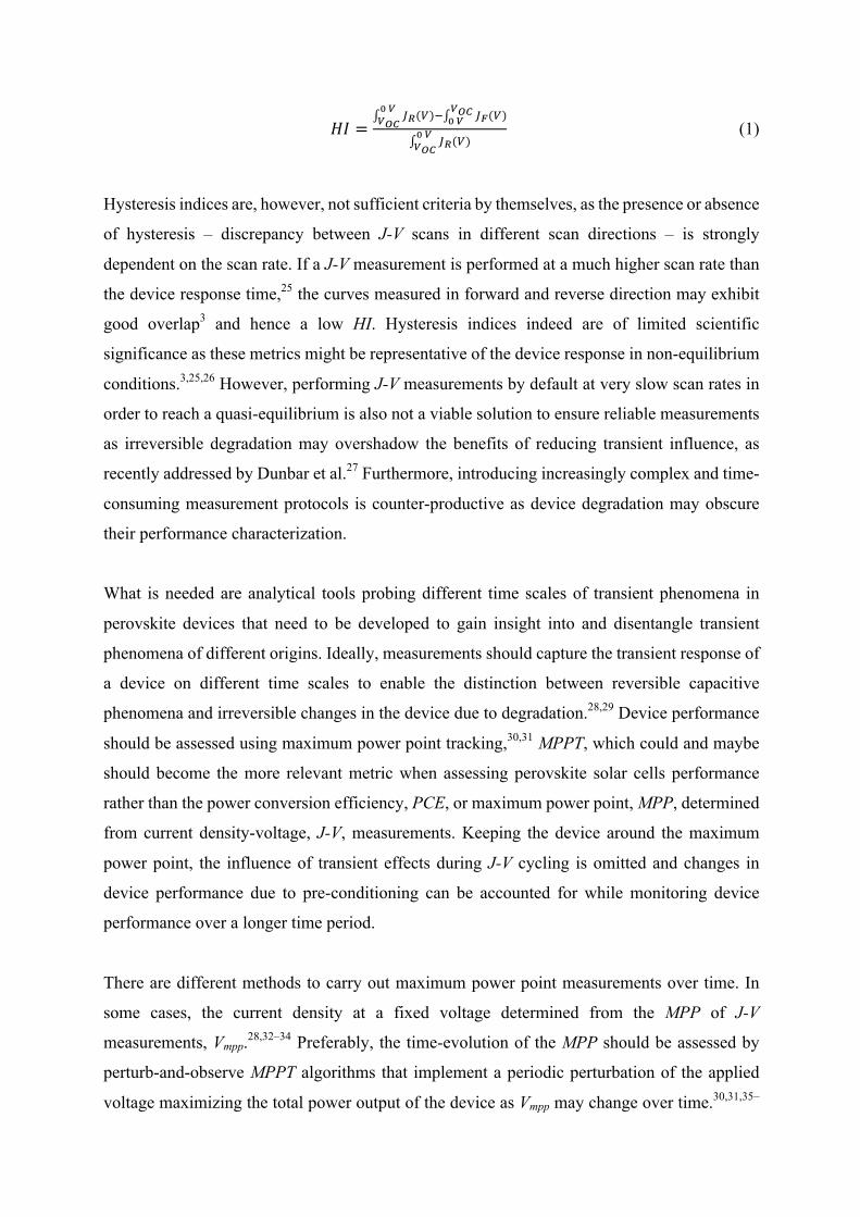
𝐻𝐼 =$%(')
)++,-
. $/(')+,-)+
$%('))++,-
(1)
Hysteresis indices are, however, not sufficient criteria by themselves, as the presence or absence
of hysteresis – discrepancy between J-V scans in different scan directions – is strongly
dependent on the scan rate. If a J-V measurement is performed at a much higher scan rate than
the device response time,25 the curves measured in forward and reverse direction may exhibit
good overlap3 and hence a low HI. Hysteresis indices indeed are of limited scientific
significance as these metrics might be representative of the device response in non-equilibrium
conditions.3,25,26 However, performing J-V measurements by default at very slow scan rates in
order to reach a quasi-equilibrium is also not a viable solution to ensure reliable measurements
as irreversible degradation may overshadow the benefits of reducing transient influence, as
recently addressed by Dunbar et al.27 Furthermore, introducing increasingly complex and time-
consuming measurement protocols is counter-productive as device degradation may obscure
their performance characterization.
What is needed are analytical tools probing different time scales of transient phenomena in
perovskite devices that need to be developed to gain insight into and disentangle transient
phenomena of different origins. Ideally, measurements should capture the transient response of
a device on different time scales to enable the distinction between reversible capacitive
phenomena and irreversible changes in the device due to degradation.28,29 Device performance
should be assessed using maximum power point tracking,30,31 MPPT, which could and maybe
should become the more relevant metric when assessing perovskite solar cells performance
rather than the power conversion efficiency, PCE, or maximum power point, MPP, determined
from current density-voltage, J-V, measurements. Keeping the device around the maximum
power point, the influence of transient effects during J-V cycling is omitted and changes in
device performance due to pre-conditioning can be accounted for while monitoring device
performance over a longer time period.
There are different methods to carry out maximum power point measurements over time. In
some cases, the current density at a fixed voltage determined from the MPP of J-V
measurements, Vmpp.28,32–34 Preferably, the time-evolution of the MPP should be assessed by
perturb-and-observe MPPT algorithms that implement a periodic perturbation of the applied
voltage maximizing the total power output of the device as Vmpp may change over time.30,31,35–
37 For perovskite solar cells, perturb-and-observe MPPT algorithms that dynamically adjust the
sampling time and voltage step size have been proposed as the dynamic response of devices
changes due to changes in internal electric field distribution and capacitance during device
operation.30,31,36 Cimaroli et al.30 proposed a predictive MPPT algorithm that derives the steady-
state power by fitting the current response to a voltage perturbation with a biexpontential
function. However, even perturb-and-observe as well as predictive MPPT algorithms might get
stuck in local performance maxima when devices exhibit current-voltage hysteresis.31,36 Pellet
et al.31 therefore proposed a so-called hill-climbing MPPT algorithm starting at applied
potentials larger than the MPP, which was found to have a positive effect on device
performance.
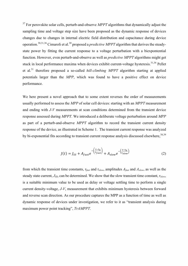
We here present a novel approach that to some extent reverses the order of measurements
usually performed to assess the MPP of solar cell devices: starting with an MPPT measurement
and ending with J-V measurements at scan conditions determined from the transient device
response assessed during MPPT. We introduced a deliberate voltage perturbation around MPP
as part of a perturb-and-observe MPPT algorithm to record the transient current density
response of the device, as illustrated in Scheme 1. The transient current response was analyzed
by bi-exponential fits according to transient current response analysis discussed elsewhere,38,39
𝐽 𝑡 = 𝐽22 + 𝐴5678𝑒. :;:)
<=>?: + 𝐴7@AB𝑒. :;:)
<?CDE (2)
from which the transient time constants, τfast and τslow, amplitudes Afast and Aslow, as well as the
steady state current, JSS, can be determined. We show that the slow transient time constant, τslow,
is a suitable minimum value to be used as delay or voltage settling time to perform a single
current density-voltage, J-V, measurement that exhibits minimum hysteresis between forward
and reverse scan direction. As our procedure captures the MPP as a function of time as well as
dynamic response of devices under investigation, we refer to it as “transient analysis during
maximum power point tracking”, TrAMPPT.
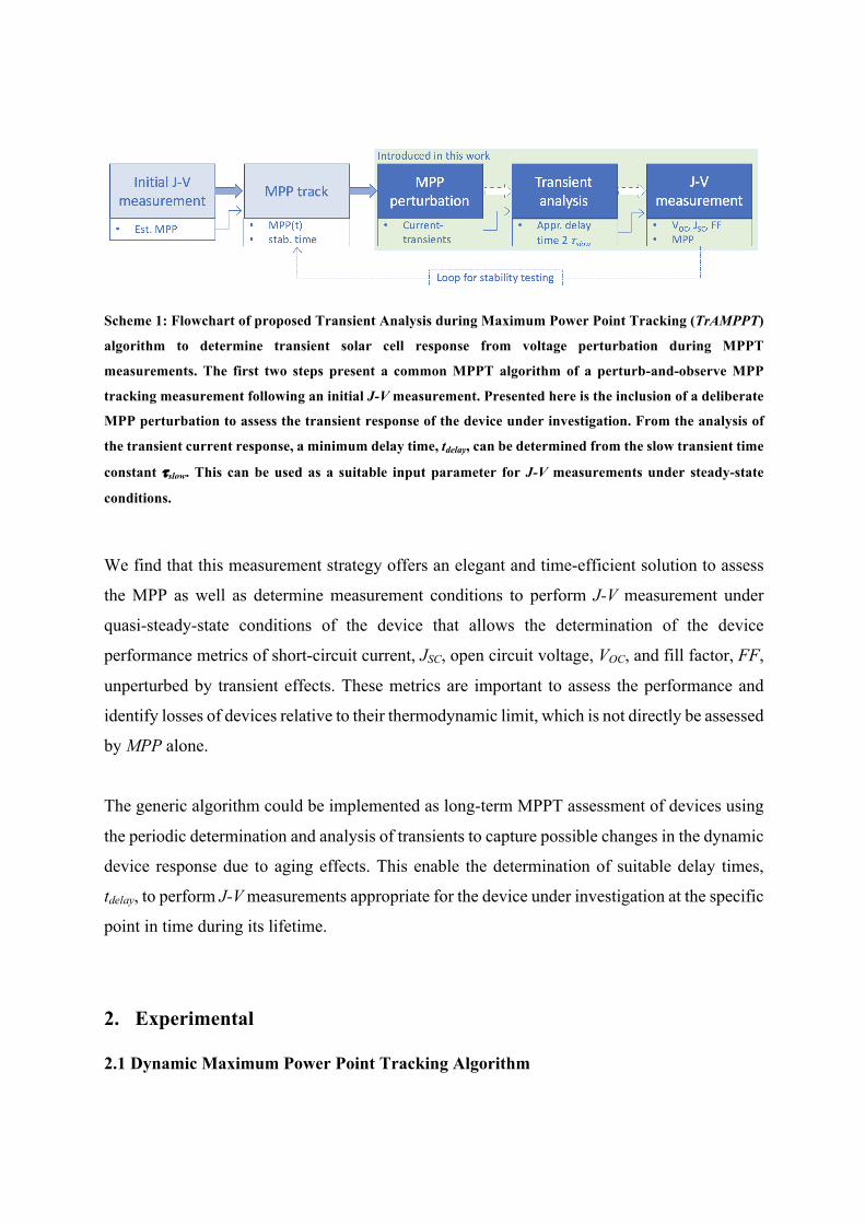
Scheme 1: Flowchart of proposed Transient Analysis during Maximum Power Point Tracking (TrAMPPT)
algorithm to determine transient solar cell response from voltage perturbation during MPPT
measurements. The first two steps present a common MPPT algorithm of a perturb-and-observe MPP
tracking measurement following an initial J-V measurement. Presented here is the inclusion of a deliberate
MPP perturbation to assess the transient response of the device under investigation. From the analysis of
the transient current response, a minimum delay time, tdelay, can be determined from the slow transient time
constant tslow. This can be used as a suitable input parameter for J-V measurements under steady-state
conditions.
We find that this measurement strategy offers an elegant and time-efficient solution to assess
the MPP as well as determine measurement conditions to perform J-V measurement under
quasi-steady-state conditions of the device that allows the determination of the device
performance metrics of short-circuit current, JSC, open circuit voltage, VOC, and fill factor, FF,
unperturbed by transient effects. These metrics are important to assess the performance and
identify losses of devices relative to their thermodynamic limit, which is not directly be assessed
by MPP alone.
The generic algorithm could be implemented as long-term MPPT assessment of devices using
the periodic determination and analysis of transients to capture possible changes in the dynamic
device response due to aging effects. This enable the determination of suitable delay times,
tdelay, to perform J-V measurements appropriate for the device under investigation at the specific
point in time during its lifetime.
2. Experimental
2.1 Dynamic Maximum Power Point Tracking Algorithm
The maximum power point tracking algorithm was based on a standard perturb-and-observe
MPPT40,41 measurement routine implemented as part of our current density – voltage, J-V,
LabVIEW based measurement program in our laboratory.42 To avoid getting stuck in local
performance minima, an estimate for the MPP is derived from a quick initial J-V measurement.
The regular algorithm perturbs the applied voltage by a double step of +/- 10 mV around the
maximum power point voltage, VMPP, compares the solar cell’s output power at these three
voltages and then sets the new VMPP to the one corresponding to maximum power. It is important
that the step duration is set long enough for transients to equilibrate before the power is
calculated at the newly set voltage level.31
We expanded this standard procedure by introducing a voltage perturbation phase to monitor
the transient current density response of devices, indicated in Scheme 1. As the amplitude of
the current transient is a function of the voltage step size, we usually chose a +/- 50 mV double
step around VMPP for the voltage perturbation, leading to a large enough amplitude for the fitting
procedure. The transient current response during MPP perturbation for the voltage steps to VMPP
was analyzed by fitting with equation (2). This allows the extraction and comparison of
characteristic fast and slow transient time constants, tfast and tslow, amplitude of transient current
response, Afast and Aslow, as well as the steady-state current, JSS.
The slow transient time constants, tslow, give a measure for appropriate delay times, tdelay, that
are suitable to perform current density – voltage, J-V, measurements at steady-state conditions.
This is equivalent to waiting “long enough” after a voltage step to let the transient current
response decay towards steady-state. As indicated in Scheme 1, in this work the acquisition and
analysis as well as consecutive J-V measurements were carried out as separate steps.
2.2 Devices investigated
Measurements presented herein were carried out on p-i-n and n-i-p devices prepared in baseline
manufacturing of metal-halide perovskite solar cells in the HySPRINT laboratory. We here
compare p-i-n and n-i-p thin film architecture types, where p and n stand for p- and n-type
selective contact layers and i for the perovskite layer, assuming that it can be considered an
intrinsic semiconductor. For both devices Cs0.05(FA0.83MA0.17)0.95Pb(I0.83Br0.17)3 perovskite,
sometimes referred to as “triple cation” perovskite reported by Saliba et al.43, was utilized as
the light-harvesting layer and deposited by spin-coating from a precursor solution as described
in more detail in the supporting information. For the p-i-n device, poly[bis(4-phenyl)-(2,4,6-
trimethylphenyl)amine (PTAA) was used as the p-type selective contact layer on transparent
conducting indium-doped tin oxide (ITO) on glass substrates. Consecutively evaporated layer
of C60, bathocuproine (BCP) and silver were used as n-type selective contacts. For the n-i-p
device, spin-cast tin oxide (SnO2) on ITO served as n-type selective contact and Li-
bis(trifluoromethanesulfonyl) imide (Li-TFSI) doped 2,2’,7,7’-tetrakis-(N,N-di-p-
methoxyphenylamine)-9,9’-spirobifluorene (spiro-OMeTAD) contacted with gold (Au) as p-
type selective contact layers. Detailed information all processing steps can be found in the
Supporting Information.
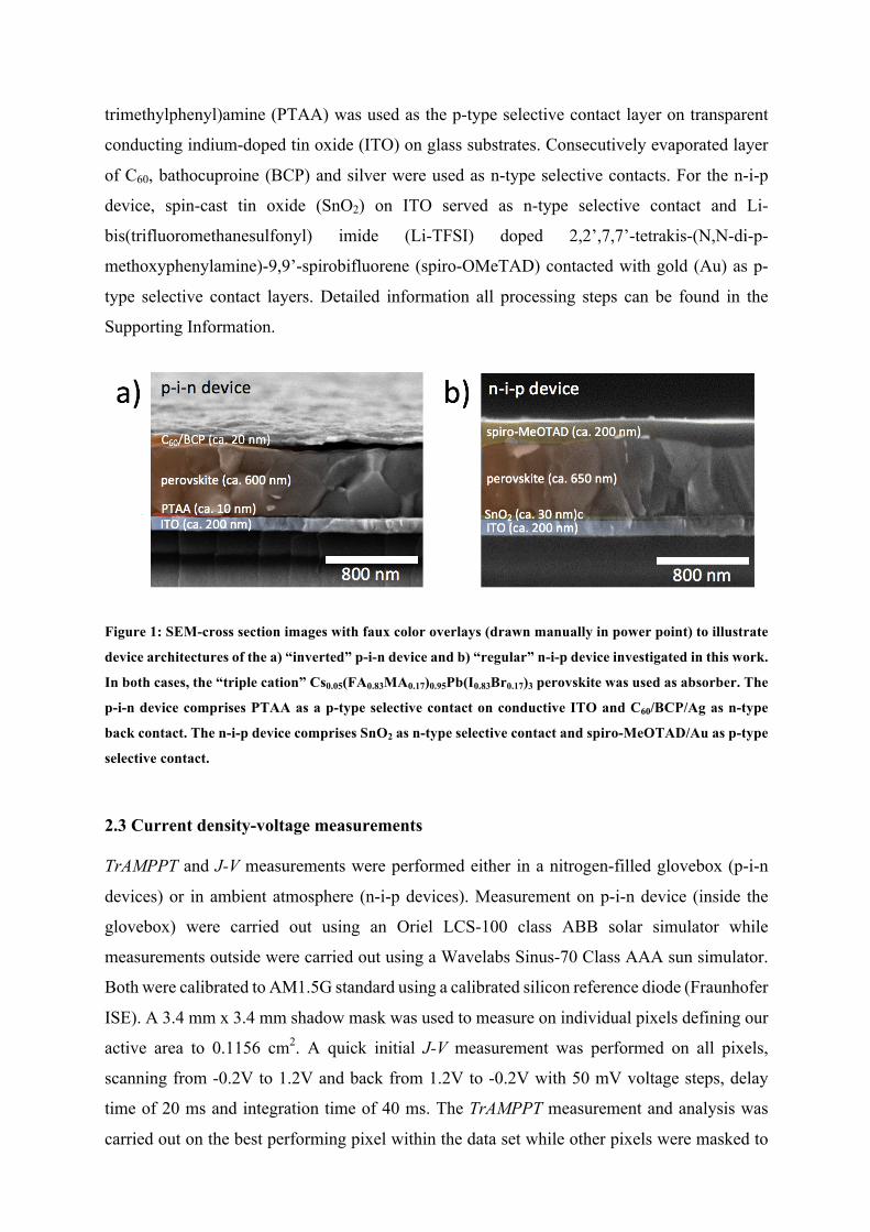
Figure 1: SEM-cross section images with faux color overlays (drawn manually in power point) to illustrate
device architectures of the a) “inverted” p-i-n device and b) “regular” n-i-p device investigated in this work.
In both cases, the “triple cation” Cs0.05(FA0.83MA0.17)0.95Pb(I0.83Br0.17)3 perovskite was used as absorber. The
p-i-n device comprises PTAA as a p-type selective contact on conductive ITO and C60/BCP/Ag as n-type
back contact. The n-i-p device comprises SnO2 as n-type selective contact and spiro-MeOTAD/Au as p-type
selective contact.
2.3 Current density-voltage measurements
TrAMPPT and J-V measurements were performed either in a nitrogen-filled glovebox (p-i-n
devices) or in ambient atmosphere (n-i-p devices). Measurement on p-i-n device (inside the
glovebox) were carried out using an Oriel LCS-100 class ABB solar simulator while
measurements outside were carried out using a Wavelabs Sinus-70 Class AAA sun simulator.
Both were calibrated to AM1.5G standard using a calibrated silicon reference diode (Fraunhofer
ISE). A 3.4 mm x 3.4 mm shadow mask was used to measure on individual pixels defining our
active area to 0.1156 cm2. A quick initial J-V measurement was performed on all pixels,
scanning from -0.2V to 1.2V and back from 1.2V to -0.2V with 50 mV voltage steps, delay
time of 20 ms and integration time of 40 ms. The TrAMPPT measurement and analysis was
carried out on the best performing pixel within the data set while other pixels were masked to
avoid crosstalk. Here, the TrAMPPT measurements were performed for a total time span of 500
s but the duration of the MPP tracking and MPP perturbation phase can be adjusted by the user.
To compare the transient response determined from TrAMPPT measurements, we also carried
out J-V measurements at different scan rates, as specified by different delay times as shown in
Table S1. As a standard, we carried out forward scans (F), from V £ 0V towards V ³ VOC,
followed by reverse scans (R) in the opposite direction. The J-V discrepancy was analyzed using
the definition of the hysteresis index, HI, according to equation (1).
3. Results and Discussion
We will here present and compare TrAMPPT measurement results for two different device
types: a p-i-n and an n-i-p device to showcase that this proposed measurement procedure can
be employed to both. Details on the device architecture and layer stack can be found in section
2.2 and the supporting information. Section 3.2 is dedicated to the analysis of the difference in
transient device response according to equation (2) while section 3.3 discusses J-V
measurements carried out at delay times, tdelay, determined from transient analysis. Section 3.4
compares information on the transient device response gathered during TrAMPPT
measurements in comparison with J-V discrepancy expressed as hysteresis indices, HI,
according to equation (1) as a function of delay time.
3.1 Maximum Power Point Tracking (MPPT) Measurements
As outlined in section 2.1 and 2.3 as well as shown schematically in Scheme 1, the TrAMPPT
measurement scheme initiates with a quick initial J-V scan to determine a starting value for
VMPP. In our measurements, we can usually discern four distinct phases. The device
characteristics during MPP tracking are marked as phases I-III in Figures 2a and 2b, while the
phase marked IV is the results of the deliberate voltage perturbation with 50 mV steps as
apparent from the panel showing the applied voltage. We distinguished phase I and II from the
more “steady” device response during MPP tracking as I sometimes exhibits a dramatic
change in the photocurrent reflecting capacitive effects as the device is held at open circuit
conditions immediately prior to stepping to VMPP for the MPP tracking measurement. Phase II
marks an initial phase in which the VMPP equilibrates from a value determined from a fast J-V
measurement to a value more representative of the device under steady state conditions. This
change of VMPP over time underlines the need to utilize a perturb and observe algorithm and
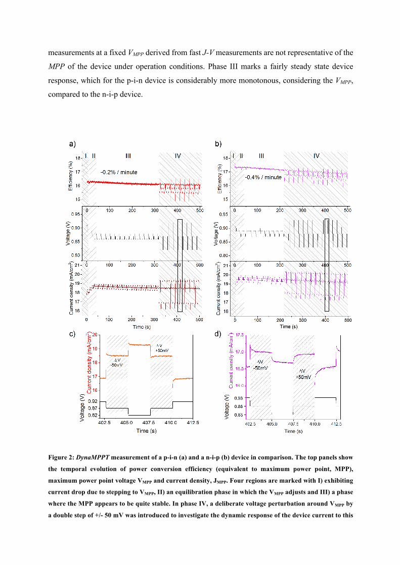
measurements at a fixed VMPP derived from fast J-V measurements are not representative of the
MPP of the device under operation conditions. Phase III marks a fairly steady state device
response, which for the p-i-n device is considerably more monotonous, considering the VMPP,
compared to the n-i-p device.
Figure 2: DynaMPPT measurement of a p-i-n (a) and a n-i-p (b) device in comparison. The top panels show
the temporal evolution of power conversion efficiency (equivalent to maximum power point, MPP),
maximum power point voltage VMPP and current density, JMPP. Four regions are marked with I) exhibiting
current drop due to stepping to VMPP, II) an equilibration phase in which the VMPP adjusts and III) a phase
where the MPP appears to be quite stable. In phase IV, a deliberate voltage perturbation around VMPP by
a double step of +/- 50 mV was introduced to investigate the dynamic response of the device current to this
perturbation. (c) and (d) show a close-up of one perturbation cycle – black boxes in (a), (b) - for p-i-n (c)
and n-i-p device (d).
During the MPP tracking phase (phase III) the device efficiency was determined to be 16.3 %
with the current density declining from 18.7 mAcm-2 to 18.5 mAcm-2 indicating an average
degradation of 0.2 mAcm-2/270 s, i.e. a relative decrease in performance of ca. -0.2% per
minute. The n-i-p device exhibited a MPP performance of 17.3 with a relative performance
decrease of ca. -0.4% per minute.
During the 50 mV voltage perturbation phase (phase IV) of the TrAMPPT measurement, the
transient response of the photocurrent becomes very pronounced. A close-up of the data is
shown in Figure 2 c) and d). The current responds with an over- or under-shoot followed by an
exponential decay upon a change in the applied potential. Already from the enlarged section of
Figure 2 (c and d), it is apparent that the transient response appears to be slightly slower for the
n-i-p compared to the p-i-n device, which will be discussed in greater detail in the next section.
Transient time constants are found to be comparable for voltage perturbations of different
magnitude, however the amplitude changes as a function of voltage step size as commented in
Figure S5.
The p-i-n device investigated here has a lower performance compared to current state-of-the-
art baseline devices with higher PCEs, achieved by further optimization of selective contact
layers.44,45 These devices show negligible hysteresis for all scan rates. The p-i-n device
discussed here was a device that was aged for three days and chosen as an example for a device
of this architecture type that does exhibit hysteresis, particularly for faster scan rates, as will be
further discussed in section 3.3. The n-i-p device presented here represents an improvement
with respect to previous results obtained for a similar device architecture.46
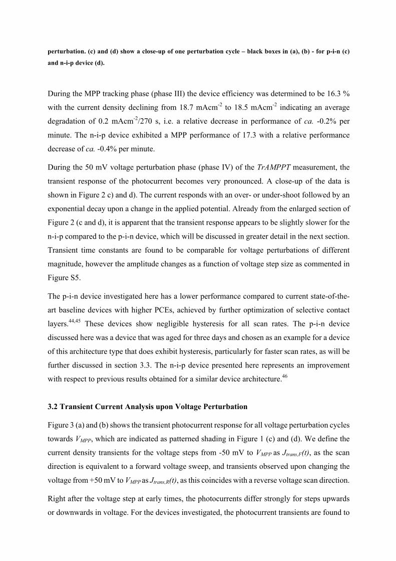
3.2 Transient Current Analysis upon Voltage Perturbation
Figure 3 (a) and (b) shows the transient photocurrent response for all voltage perturbation cycles
towards VMPP, which are indicated as patterned shading in Figure 1 (c) and (d). We define the
current density transients for the voltage steps from -50 mV to VMPP as Jtrans,F(t), as the scan
direction is equivalent to a forward voltage sweep, and transients observed upon changing the
voltage from +50 mV to VMPP as Jtrans,R(t), as this coincides with a reverse voltage scan direction.
Right after the voltage step at early times, the photocurrents differ strongly for steps upwards
or downwards in voltage. For the devices investigated, the photocurrent transients are found to
be symmetric for the - 50 mV and + 50 mV steps towards VMPP indicating that the device is
affected in a similar manner by the +/- voltage perturbation. Current transients merge for longer
settling times indicating that a similar steady state current density, JSS, is reached.
Figure 3: Transients upon positive and negative voltage steps (+ 50mV and - 50mV respectively) during
MPP perturbation for the p-i-n (a) and n-i-p (b) devices. Some oscillations of 10 Hz are observed and due
to noise from the power source. Transient time constants tfast and tslow as well as steady-state current, JSS
determined from bi-exponential fits of transients according to equation (2) for the p-i-n (c) and n-i-p (d)
device.
The transient response for both devices were fitted with equation (2) and the extracted time
constants, τfast and τslow, and JSS are shown in Figure 3 (c) and (d). The JSS for the p-i-n device
remains fairly similar for all perturbation cycles while for the n-i-p device, a distinct decline in
JSS can be observed.
The fact that more than one transient time constant is needed to fit the devices transient
behavior, may indicate that there is more than one underlying cause for the transient response
and hence for hysteresis in perovskite solar cells. For both device polarities investigated here,
the transients appear to be mirror images of each other, suggesting that the underlying cause
can be considered due to capacitive charging/discharging phenomena.
For the p-i-n device, the time constants and amplitudes are identical opposites within
experimental error. Figure 3 c) shows the extracted τfast and τslow from fits from equation (2) to
all transients showing that the +/- 50 mV step exhibit similar values. Average time constants of
18 (±9) ms for τfast, and 410 (±190) ms for τslow were determined and the steady-state current JSS
was found to decrease from 18.52 mA/cm2 with 0.019 mA/cm2min. The n-i-p device (Figure 3
d) exhibits average time constants of 63 (±25) ms for τfast, and 540 (±230) ms for τslow and a JSS
of 19.48 mA/cm2 decreasing by 0.065 mA/cm2min. The two devices investigated exhibit a
comparable slow component of the transient response but the fast component is markedly
slower for the n-i-p device compared to the p-i-n device.
For both devices, we observe an initial difference of about 1 mA in the current density around
MPP, JMPP, between the + 50 mV and – 50 mV step this amounts to a discrepancy in absolute
performance of about 5% when measurements would be carried out at very short tdelay. This will
be further discussed in section 3.4.
3.3 Current density – voltage, J-V, measurements
From the transient analysis discussed in section 3.2, a delay time, tdelay, appropriate for J-V
measurements can be determined. The rationale is that from the transient device response shown
in Figure 3 (a) and (b) and the slow time constants τslow extracted, the minimum time for the
current transients to become almost congruent can be estimated. We propose that tdelay can be
either set as a multiple of τslow or as the time when JSS in the forward and reverse direction
become close to identical. As the τslow for the devices under investigation are quite similar and
in the order of 0.5 s, we found a minimum delay time of 1 s to be appropriate to carry out J-V
measurements.
In Figure 4, J-V scans in forward (F, dashed lines) and reverse (R, solid lines) scan directions
are compared for tdelay of 0.1 ms (colored) and tdelay of 1 s (black) for the p-i-n (a) and n-i-p (b)
device. J-V scans were performed at 50 mV voltage steps and scan conditions are hence
equivalent to scan rates of 167 V/s and 0.05 V/s according to the definition in Table S1.
Measurements at all J-V scan conditions defined in Table S1 were carried out on the p-i-n and
n-i-p device and are detailed in the supporting information.
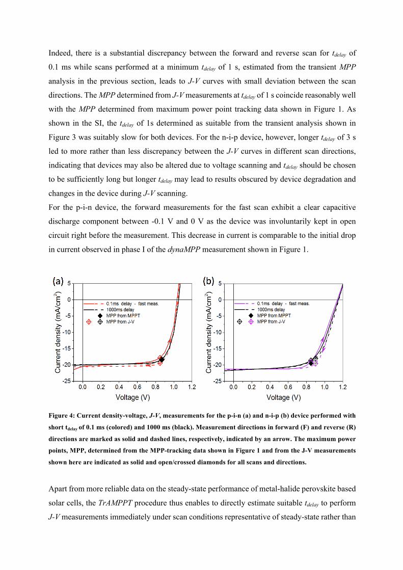
Indeed, there is a substantial discrepancy between the forward and reverse scan for tdelay of
0.1 ms while scans performed at a minimum tdelay of 1 s, estimated from the transient MPP
analysis in the previous section, leads to J-V curves with small deviation between the scan
directions. The MPP determined from J-V measurements at tdelay of 1 s coincide reasonably well
with the MPP determined from maximum power point tracking data shown in Figure 1. As
shown in the SI, the tdelay of 1s determined as suitable from the transient analysis shown in
Figure 3 was suitably slow for both devices. For the n-i-p device, however, longer tdelay of 3 s
led to more rather than less discrepancy between the J-V curves in different scan directions,
indicating that devices may also be altered due to voltage scanning and tdelay should be chosen
to be sufficiently long but longer tdelay may lead to results obscured by device degradation and
changes in the device during J-V scanning.
For the p-i-n device, the forward measurements for the fast scan exhibit a clear capacitive
discharge component between -0.1 V and 0 V as the device was involuntarily kept in open
circuit right before the measurement. This decrease in current is comparable to the initial drop
in current observed in phase I of the dynaMPP measurement shown in Figure 1.
Figure 4: Current density-voltage, J-V, measurements for the p-i-n (a) and n-i-p (b) device performed with
short tdelay of 0.1 ms (colored) and 1000 ms (black). Measurement directions in forward (F) and reverse (R)
directions are marked as solid and dashed lines, respectively, indicated by an arrow. The maximum power
points, MPP, determined from the MPP-tracking data shown in Figure 1 and from the J-V measurements
shown here are indicated as solid and open/crossed diamonds for all scans and directions.
Apart from more reliable data on the steady-state performance of metal-halide perovskite based
solar cells, the TrAMPPT procedure thus enables to directly estimate suitable tdelay to perform
J-V measurements immediately under scan conditions representative of steady-state rather than
having to sample many different scan conditions to find those where hysteresis becomes
minimal. The latter is time consuming and may not be appropriate for reliable device
characterization as reversible transient phenomena cannot be distinguished from device
degradation during prolonged measurements.
3.4 Comparison of MPPT transients with hysteresis indices
To give further evidence, that similar information can be obtained from transient photocurrent
response analysis in our proposed TrAMPPT procedure and the comparison of J-V
measurements performed at different J-V scan conditions, we compare the differential between
the average of the current transients shown in Figure 3 a) and b) with J-V scans in different scan
directions for the scan conditions defined in Table 1. The results of these measurements can be
found in Figure S4 and S6 the SI. The J-V discrepancy was quantified by calculating the HI as
specified in equation (1).
To relate the relative discrepancy between the transient current response in reverse, Jtrans,R(t),
and forward, Jtrans,F(t), voltage step direction, we calculated the delta difference between the
forward and reverse current density transients, DJ(t), with respect to the stabilized current
density, JSS:
F$ 8$GG
= $:H>I?,% 8 .$:H>I?,/ 8$GG
(3)
As shown in Figure 5, F$ 8$GG
shows a comparable dependence on time as the HI determined from
measurements at different delay times. For the p-i-n device, the agreement between the two
different sets of measurements is so striking, that we conclude that very similar information can
be gaged from the transient analysis around MPP and the discrepancy between J-V
measurements calculated from equation (1) for measurement at different delay times. This is in
agreement with the fact that the J-V discrepancy is found to be most pronounced around MPP.
For the n-i-p device, however, the discrepancy between J-V scan directions for longer delay
times is larger than suggested by the transient response. As shown in Figure 4 b, J-V
measurements with minimal discrepancy – hysteresis – were obtained using a tdelay of 1 s,
derived from analysis of the current density transients. That n-i-p solar cell seems to however
exhibit an increased J-V discrepancy at tdelay = 3 s, as shown in Figure S6, table S3 and indicated
by the increased HI of Figure 5 (b). This is an indication that voltage cycling during J-V
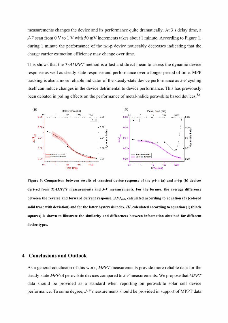
measurements changes the device and its performance quite dramatically. At 3 s delay time, a
J-V scan from 0 V to 1 V with 50 mV increments takes about 1 minute. According to Figure 1,
during 1 minute the performance of the n-i-p device noticeably decreases indicating that the
charge carrier extraction efficiency may change over time.
This shows that the TrAMPPT method is a fast and direct mean to assess the dynamic device
response as well as steady-state response and performance over a longer period of time. MPP
tracking is also a more reliable indicator of the steady-state device performance as J-V cycling
itself can induce changes in the device detrimental to device performance. This has previously
been debated in poling effects on the performance of metal-halide perovskite based devices.3,6
Figure 5: Comparison between results of transient device response of the p-i-n (a) and n-i-p (b) devices
derived from TrAMPPT measurements and J-V measurements. For the former, the average difference
between the reverse and forward current response, ΔJ/Jstab, calculated according to equation (3) (colored
solid trace with deviation) and for the latter hysteresis index, HI, calculated according to equation (1) (black
squares) is shown to illustrate the similarity and differences between information obtained for different
device types.
4 Conclusions and Outlook
As a general conclusion of this work, MPPT measurements provide more reliable data for the
steady-state MPP of perovskite devices compared to J-V measurements. We propose that MPPT
data should be provided as a standard when reporting on perovskite solar cell device
performance. To some degree, J-V measurements should be provided in support of MPPT data
to define the device performance metrics of JSC, VOC and FF and should always be verified to
have been measured at scan conditions representative of the steady-state device response.
The TrAMPPT procedure proposed here goes a step further by carrying out analysis of the
transient device response around MPP and from this derive suitable delay times, tdelay, to
perform J-V measurements under quasi steady-state conditions. This is of particular importance
for solar cells that exhibit pronounced current-transients and change during J-V scanning such
as metal-halide perovskite solar cells for which J-V measurements at a single scan rate do not
represent steady-state conditions of the device. We find that the TrAMPPT is more time-
efficient than having to perform several J-V measurements at different tdelay to find measurement
conditions at which J-V discrepancy – hysteresis – become negligible.
We here compare typical p-i-n and n-i-p devices that are representative solar cell architectures
showing differences in transient effects with typically less pronounced hysteresis in p-i-n type
devices compared to most planar n-i-p architectures, although ionic motion, a key driver for
hysteresis was also found in hysteresis-less p-i-n device architectures.47,48 The example of the
p-i-n devices shown here was a device aged for three days, after which it exhibited more
pronounced hysteresis than initially, demonstrating that hysteresis may evolve over time due to
the creation of ionic defects and imperfections at interfaces. The more detailed analysis
presented here shows that hysteresis strongly depends on tdelay and devices of different types
may exhibit characteristic differences in their transient behavior. The n-i-p device investigated
here exhibited similar dynamic response as the p-i-n device but exhibits a more dramatic
decrease in photocurrent during MPPT measurement indicative of changes in the device causing
performance decrease. We will utilize TrAMPPT measurements to analyze differences between
devices of different architecture types, contact layers, perovskite absorbers and stages in their
life-cycle to capture differences, similarities and changes in the MPP as well as dynamic
response of devices.
We aim to develop the TrAMPPT code further and integrate the transient analysis and
consecutive J-V measurements into the TrAMPPT measurement algorithm as illustrated in
Scheme 1. This will enable us to “loop” the measurement algorithm and utilize it e.g. for long
term stability testing.29 Apart from the MPP as a function of time, this would enable periodic
assessment of changes in the transient device response arising from microscopic changes in the
device upon degradation. The slow transient time constant tslow can be used to derive tdealy as
input parameters for periodic J-V measurements, from which a new MPP can be defined that
then in turn is used as starting MPP for the next MPP tracking cycles.
Acknowledgements The authors would like to thank Carola Klimm from HZB for technical assistance in SEM
measurements and Carola Ferber, Heinz Hagen and Monika Gabernig for technical assistance
in the laboratory. A. C. thanks Nga Phung, Philipp Tockhorn and Artiom Bakulin for providing
solar cell samples during the course of her MSc thesis work. Laboratory infrastructure in the
HySPRINT Innovation Lab has been funded by the Helmholtz Molecular Foundry (HEMF)
project. E. U. acknowledges funding from the Swedish Research Council (Project 2015-00163)
and Marie Sklodowska Curie Actions Cofund Project INCA (Grant number 600398). E. L. U.,
K. H., A. C. & J. D. acknowledge funding from the German Ministry of Education and Research
(BMBF) for the Young Investigator Group Hybrid Materials Formation and Scaling
(HyPerFORME) within the program “NanoMatFutur” (grant no. 03XP0091) and the
“SNaPSHoTs” project (grant no. 01IO1806). We further acknowledge the BMBF for funding
of the Young Investigator Group Perovskite Tandem Solar Cells within the program
“Materialforschung für die Energiewende” (grant no. 03SF0540) and the German Federal
Ministry for Economic Affairs and Energy (BMWi) for financial support through the “PersiST”
project (grant no. 0324037C). L. K. is a member and acknowledges funding from the graduate
school HyPerCell.
References
(1) Seok, S. Il; Grätzel, M.; Park, N.-G. Methodologies toward Highly Efficient Perovskite
Solar Cells. Small 2018, 1704177, 1704177.
(2) Green, M. A.; Ho-Baillie, A.; Snaith, H. J. The Emergence of Perovskite Solar Cells.
Nat. Photonics 2014, 8 (7), 506–514.
(3) Unger, E. L.; Hoke, E. T.; Bailie, C. D.; Nguyen, W. H.; Bowring, A. R.; Heumüller, T.;
Christoforo, M. G.; McGehee, M. D. Hysteresis and Transient Behavior in Current-
Voltage Measurements of Hybrid-Perovskite Absorber Solar Cells. Energy Environ. Sci.
2014, 7 (11), 3690–3698.
(4) Christians, J. A.; Manser, J. S.; Kamat, P. V. Best Practices in Perovskite Solar Cell
Efficiency Measurements. Avoiding the Error of Making Bad Cells Look Good. J. Phys.
Chem. Lett. 2015, 6 (5), 852–857.
(5) Tress, W. Metal Halide Perovskites as Mixed Electronic-Ionic Conductors: Challenges
and Opportunities - From Hysteresis to Memristivity. J. Phys. Chem. Lett. 2017, 8 (13),
3106–3114.
(6) Tress, W.; Marinova, N.; Moehl, T.; Zakeeruddin, S. M.; Nazeeruddin, M. K.; Grätzel,
M. Understanding the Rate-Dependent J–V Hysteresis, Slow Time Component, and
Aging in CH 3 NH 3 PbI 3 Perovskite Solar Cells: The Role of a Compensated Electric
Field. Energy Environ. Sci. 2015, 8 (3), 995–1004.
(7) Azpiroz, J. M.; Mosconi, E.; Bisquert, J.; De Angelis, F. Defect Migration in
Methylammonium Lead Iodide and Its Role in Perovskite Solar Cell Operation. Energy
Environ. Sci. 2015, 8 (7), 2118–2127.
(8) Meloni, S.; Moehl, T.; Tress, W.; Franckeviius, M.; Saliba, M.; Lee, Y. H.; Gao, P.;
Nazeeruddin, M. K.; Zakeeruddin, S. M.; Rothlisberger, U.; et al. Ionic Polarization-
Induced Current-Voltage Hysteresis in CH3NH3PbX3perovskite Solar Cells. Nat.
Commun. 2016, 7 (May 2015).
(9) Chen, B.; Yang, M.; Zheng, X.; Wu, C.; Li, W.; Yan, Y.; Bisquert, J.; Garcia-Belmonte,
G.; Zhu, K.; Priya, S. Impact of Capacitive Effect and Ion Migration on the Hysteretic
Behavior of Perovskite Solar Cells. J. Phys. Chem. Lett. 2015, 6 (23), 4693–4700.
(10) Li, C.; Tscheuschner, S.; Paulus, F.; Hopkinson, P. E.; Kießling, J.; Köhler, A.; Vaynzof,
Y.; Huettner, S. Iodine Migration and Its Effect on Hysteresis in Perovskite Solar Cells.
Adv. Mater. 2016, 28 (12), 2446–2454.
(11) Chen, B.; Yang, M.; Priya, S.; Zhu, K. Origin of J-V Hysteresis in Perovskite Solar Cells.
J. Phys. Chem. Lett. 2016, 7 (5), 905–917.
(12) Calado, P.; Telford, A. M.; Bryant, D.; Li, X.; Nelson, J.; O’Regan, B. C.; Barnes, P. R.
F. Evidence for Ion Migration in Hybrid Perovskite Solar Cells with Minimal Hysteresis.
Nat. Commun. 2016, 7, 1–10.
(13) Belisle, R. A.; Nguyen, W. H.; Bowring, A. R.; Calado, P.; Li, X.; Irvine, S. J. C.;
McGehee, M. D.; Barnes, P. R. F.; O’Regan, B. C. Interpretation of Inverted
Photocurrent Transients in Organic Lead Halide Perovskite Solar Cells: Proof of the
Field Screening by Mobile Ions and Determination of the Space Charge Layer Widths.
Energy Environ. Sci. 2017, 10 (1), 192–204.
(14) Roiati, V.; Mosconi, E.; Listorti, A.; Colella, S.; Gigli, G.; De Angelis, F. Stark Effect in
Perovskite/TiO2solar Cells: Evidence of Local Interfacial Order. Nano Lett. 2014, 14
(4), 2168–2174.
(15) Guerrero, A.; You, J.; Aranda, C.; Kang, Y. S.; Garcia-Belmonte, G.; Zhou, H.; Bisquert,
J.; Yang, Y. Interfacial Degradation of Planar Lead Halide Perovskite Solar Cells. ACS
Nano 2016, 10 (1), 218–224.
(16) Yu, H.; Lu, H.; Xie, F.; Zhou, S.; Zhao, N. Native Defect-Induced Hysteresis Behavior
in Organolead Iodide Perovskite Solar Cells. Adv. Funct. Mater. 2016, 26 (9), 1411–
1419.
(17) Lee, J. W.; Kim, S. G.; Bae, S. H.; Lee, D. K.; Lin, O.; Yang, Y.; Park, N. G. The
Interplay between Trap Density and Hysteresis in Planar Heterojunction Perovskite Solar
Cells. Nano Lett. 2017, 17 (7), 4270–4276.
(18) Shao, Y.; Xiao, Z.; Bi, C.; Yuan, Y.; Huang, J. Origin and Elimination of Photocurrent
Hysteresis by Fullerene Passivation in CH3NH3PbI3planar Heterojunction Solar Cells.
Nat. Commun. 2014, 5, 1–7.
(19) Hishikawa, Y.; Shimura, H.; Ueda, T.; Sasaki, A.; Ishii, Y. Precise Performance
Characterization of Perovskite Solar Cells. Curr. Appl. Phys. 2016, 16 (8), 898–904.
(20) Zimmermann, E.; Wong, K. K.; M�ller, M.; Hu, H.; Ehrenreich, P.; Kohlst�dt, M.;
W�rfel, U.; Mastroianni, S.; Mathiazhagan, G.; Hinsch, A.; et al. Characterization of
Perovskite Solar Cells: Towards a Reliable Measurement Protocol. APL Mater. 2016, 4
(9).
(21) Nature. Reporting Checklist For Solar Cell Manuscripts. 2015, 2015 (October), 2015–
2016.
(22) Jesper Jacobsson, T.; Correa-Baena, J. P.; Pazoki, M.; Saliba, M.; Schenk, K.; Grätzel,
M.; Hagfeldt, A. Exploration of the Compositional Space for Mixed Lead Halogen
Perovskites for High Efficiency Solar Cells. Energy Environ. Sci. 2016, 9 (5), 1706–
1724.
(23) Kim, H. S.; Park, N.-G. Parameters Affecting I-V Hysteresis of CH 3 NH 3 PbI 3
Perovskite Solar Cells: Effects of Perovskite Crystal Size and Mesoporous TiO 2 Layer.
J. Phys. Chem. Lett. 2014, 140811175830000.
(24) Sanchez, R. S.; Gonzalez-Pedro, V.; Lee, J. W.; Park, N. G.; Kang, Y. S.; Mora-Sero, I.;
Bisquert, J. Slow Dynamic Processes in Lead Halide Perovskite Solar Cells.
Characteristic Times and Hysteresis. J. Phys. Chem. Lett. 2014, 5 (13), 2357–2363.
(25) Levine, I.; Nayak, P. K.; Wang, J. T. W.; Sakai, N.; Van Reenen, S.; Brenner, T. M.;
Mukhopadhyay, S.; Snaith, H. J.; Hodes, G.; Cahen, D. Interface-Dependent Ion
Migration/Accumulation Controls Hysteresis in MAPbI3solar Cells. J. Phys. Chem. C
2016, 120 (30), 16399–16411.
(26) Habisreutinger, S. N.; Noel, N. K.; Snaith, H. J. Hysteresis Index : A Figure without
Merit for Quantifying Hysteresis in Perovskite Solar. ACS Energy Lett. 2018, 3, 2472–
2476.
(27) Dunbar, R. B.; Duck, B. C.; Moriarty, T.; Anderson, K. F.; Duffy, N. W.; Fell, C. J.;
Kim, J.; Ho-Baillie, A.; Vak, D.; Duong, T.; et al. How Reliable Are Efficiency
Measurements of Perovskite Solar Cells? The First Inter-Comparison, between Two
Accredited and Eight Non-Accredited Laboratories. J. Mater. Chem. A 2017, 5 (43),
22542–22558.
(28) Domanski, K.; Roose, B.; Matsui, T.; Saliba, M.; Turren-Cruz, S. H.; Correa-Baena, J.
P.; Carmona, C. R.; Richardson, G.; Foster, J. M.; De Angelis, F.; et al. Migration of
Cations Induces Reversible Performance Losses over Day/Night Cycling in Perovskite
Solar Cells. Energy Environ. Sci. 2017, 10 (2), 604–613.
(29) Saliba, M.; Stolterfoht, M.; Wolff, C. M.; Neher, D.; Abate, A. Measuring Aging
Stability of Perovskite Solar Cells. Joule 2018, 2 (6), 1019–1024.
(30) Cimaroli, A. J.; Yu, Y.; Wang, C.; Liao, W.; Guan, L.; Grice, C. R. .; Zhao, D.; Yan, Y.
Tracking the Maximum Power Point of Hysteretic Perovskite Solar Cells Using a
Predictive Algorithm. J. Mater. Chem. C 2017, 5 (39), 10152–10157.
(31) Pellet, N.; Giordano, F.; Ibrahim Dar, M.; Gregori, G.; Zakeeruddin, S. M.; Maier, J.;
Grätzel, M. Hill Climbing Hysteresis of Perovskite-Based Solar Cells: A Maximum
Power Point Tracking Investigation. Prog. Photovoltaics Res. Appl. 2017, 25 (11), 942–
950.
(32) Snaith, H. J.; Abate, A.; Ball, J. M.; Eperon, G. E.; Leijtens, T.; Noel, N. K.; Stranks, S.
D.; Wang, J. T. W.; Wojciechowski, K.; Zhang, W. Anomalous Hysteresis in Perovskite
Solar Cells. J. Phys. Chem. Lett. 2014, 5 (9), 1511–1515.
(33) Jeon, N. J.; Noh, J. H.; Yang, W. S.; Kim, Y. C.; Ryu, S.; Seo, J.; Seok, S. Il.
Compositional Engineering of Perovskite Materials for High-Performance Solar Cells.
Nature 2015, 517 (7535), 476–480.
(34) Liao, W.; Zhao, D.; Yu, Y.; Shrestha, N.; Ghimire, K.; Grice, C. R.; Wang, C.; Xiao, Y.;
Cimaroli, A. J.; Ellingson, R. J.; et al. Fabrication of Efficient Low-Bandgap Perovskite
Solar Cells by Combining Formamidinium Tin Iodide with Methylammonium Lead
Iodide. J. Am. Chem. Soc. 2016, 138 (38), 12360–12363.
(35) Zimmermann, E.; Wong, K. K.; Müller, M.; Hu, H.; Ehrenreich, P.; Kohlstädt, M.;
Würfel, U.; Mastroianni, S.; Mathiazhagan, G.; Hinsch, A.; et al. Characterization of
Perovskite Solar Cells: Towards a Reliable Measurement Protocol. APL Mater. 2016, 4
(9).
(36) Bliss, M.; Smith, A.; Baker, J.; Rossi, F. De; Watson, T.; Schutt, K.; Snaith, H.; Betts,
T. R.; Gottschalg, R. I-V Performance Characterisation of Perovskite Solar Cells.
Photovolt. Sci. Appl. Technol. 2018, 5–8.
(37) Cojocaru, L.; Uchida, S.; Tamaki, K.; Jayaweera, P. V. V.; Kaneko, S.; Nakazaki, J.;
Kubo, T.; Segawa, H. Determination of Unique Power Conversion Efficiency of Solar
Cell Showing Hysteresis in the I-V Curve under Various Light Intensities. Sci. Rep.
2017, 7 (1), 1–8.
(38) Christoforo, M.; Hoke, E.; McGehee, M.; Unger, E. Transient Response of Organo-
Metal-Halide Solar Cells Analyzed by Time-Resolved Current-Voltage Measurements.
Photonics 2015, 2 (4), 1101–1115.
(39) Ono, L. K.; Raga, S. R.; Wang, S.; Kato, Y.; Qi, Y. Temperature-Dependent Hysteresis
Effects in Perovskite-Based Solar Cells. J. Mater. Chem. A 2015, 3 (17), 9074–9080.
(40) Ram, J. P.; Babu, T. S.; Rajasekar, N. A Comprehensive Review on Solar PV Maximum
Power Point Tracking Techniques. Renew. Sustain. Energy Rev. 2017, 67, 826–847.
(41) Saravanan, S.; Ramesh Babu, N. Maximum Power Point Tracking Algorithms for
Photovoltaic System - A Review. Renew. Sustain. Energy Rev. 2016, 57, 192–204.
(42) Rattig, S. IU-Kennlinienmessung Mit Einem Keithley Model 2601B
Entwicklerdokumentation. Helmholtz-Zentrum Berlin 2016.
(43) Saliba, M.; Matsui, T.; Seo, J. Y.; Domanski, K.; Correa-Baena, J. P.; Nazeeruddin, M.
K.; Zakeeruddin, S. M.; Tress, W.; Abate, A.; Hagfeldt, A.; et al. Cesium-Containing
Triple Cation Perovskite Solar Cells: Improved Stability, Reproducibility and High
Efficiency. Energy Environ. Sci. 2016, 9 (6), 1989–1997.
(44) Magomedov, A.; Al-Ashouri, A.; Kasparavičius, E.; Strazdaite, S.; Niaura, G.; Jošt, M.;
Malinauskas, T.; Albrecht, S.; Getautis, V. Self-Assembled Hole Transporting
Monolayer for Highly Efficient Perovskite Solar Cells. Adv. Energy Mater. 2018.
(45) Stolterfoht, M.; Wolff, C. M.; Márquez, J. A.; Zhang, S.; Hages, C. J.; Rothhardt, D.;
Albrecht, S.; Burn, P. L.; Meredith, P.; Unold, T.; et al. Visualization and Suppression
of Interfacial Recombination for High-Efficiency Large-Area Pin Perovskite Solar Cells.
Nat. Energy 2018, 3 (10), 847–854.
(46) Kegelmann, L.; Wolff, C. M.; Awino, C.; Lang, F.; Unger, E. L.; Korte, L.; Dittrich, T.;
Neher, D.; Rech, B.; Albrecht, S. It Takes Two to Tango - Double-Layer Selective
Contacts in Perovskite Solar Cells for Improved Device Performance and Reduced
Hysteresis. ACS Appl. Mater. Interfaces 2017, 9 (20), 17245–17255.
(47) Park, B. W.; Philippe, B.; Jain, S. M.; Zhang, X.; Edvinsson, T.; Rensmo, H.; Zietz, B.;
Boschloo, G. Chemical Engineering of Methylammonium Lead Iodide/Bromide
Perovskites: Tuning of Opto-Electronic Properties and Photovoltaic Performance. J.
Mater. Chem. A 2015, 3 (43), 21760–21771.
(48) Bertoluzzi, L.; Belisle, R.; Bush, K. A.; Cheacharoen, R.; McGehee, M. D.; O’Regan, B.
C. In Situ Measurement of Electric-Field Screening in Hysteresis-Free
PTAA/FA0.83Cs0.17Pb(I0.83Br0.17)3/C60 Perovskite Solar Cells Gives an Ion
Mobility of ∼3 × 10⁻⁷ Cm2/(V s), 2 Orders of Magnitude Faster than Reported for Metal-
Oxide-Contacted Perovskite C. J. Am. Chem. Soc. 2018, 140 (40), 12775–12784.