A Single-Stage Grid Connected Inverter Topology for Solar PV Systems With Maximum Power Point...
13
1928 IEEE TRANSACTIONS ON POWER ELECTRONICS, VOL. 22, NO. 5, SEPTEMBER 2007 A Single-Stage Grid Connected Inverter Topology for Solar PV Systems With Maximum Power Point Tracking Sachin Jain and Vivek Agarwal, Senior Member, IEEE Abstract—This paper proposes a high performance, single-stage inverter topology for grid connected PV systems. The proposed configuration can not only boost the usually low photovoltaic (PV) array voltage, but can also convert the solar dc power into high quality ac power for feeding into the grid, while tracking the maximum power from the PV array. Total harmonic distortion of the current, fed into the grid, is restricted as per the IEEE-519 standard. The proposed topology has several desirable features such as better utilization of the PV array, higher efficiency, low cost and compact size. Further, due to the very nature of the pro- posed topology, the PV array appears as a floating source to the grid, thereby enhancing the overall safety of the system. A survey of the existing topologies, suitable for single-stage, grid connected PV applications, is carried out and a detailed comparison with the proposed topology is presented. A complete steady-state analysis, including the design procedure and expressions for peak device stresses, is included. Necessary condition on the modulation index “ ” for sinusoidal pulsewidth modulated control of the pro- posed inverter topology has also been derived for discontinuous conduction mode operation. All the analytical, simulation and experimental results are presented. Index Terms—Efficiency, grid-connected, inverter, photovoltaic (PV), single-stage. I. INTRODUCTION H IGH initial investment and limited life span of a photo- voltaic (PV) array makes it necessary for the user to ex- tract maximum power from the PV system. The nonlinear i–v characteristics of the PV array [1] and the rotation and revo- lution of the earth around the sun, further necessitate the ap- plication of maximum power point tracking (MPPT) [2] to the system. In this context, grid connected PV systems have become very popular because they do not need battery back-ups to en- sure MPPT. Stand alone systems can also achieve MPPT, but they would need suitable battery back-ups for this purpose. Though, multistage systems [1] have been reported for certain applications, grid connected PV systems usually employ two stages [Fig. 1(a)] [3]–[7] to appropriately condition the avail- able solar power for feeding into the grid. While the first stage is used to boost the PV array voltage and track the maximum solar power, the second stage inverts this dc power into high quality ac power. Typically, the first stage comprises of a boost or buck-boost type dc–dc converter topology. Such two-stage Manuscript received August 24, 2006; revised January 14, 2007. Recom- mended for publication by Associate Editor R. Teodorescu. The authors are with the Applied Power Electronics Laboratory, Department of Electrical Engineering, Indian Institute of Technology-Bombay, Mumbai 400 076, India (e-mail: [email protected]). Digital Object Identifier 10.1109/TPEL.2007.904202 Fig. 1. Grid connected PV system topologies: (a) conventional two-stage and (b) single-stage configuration. configurations are time tested and work well, but have draw- backs such as higher part count, lower efficiency, lower reli- ability, higher cost and larger size. The question is whether it is possible to reduce the number of power processing stages in such systems or, in short, is it possible to realize the situation depicted in Fig. 1(b)? Two simple and straightforward solutions to this requirement could be as follows. 1) Using the conventional H-bridge inverter followed by a step-up transformer [8]. 2) Using an array with sufficiently large PV voltage, which may be realized using a string of series connected modules followed by an H-bridge inverter [9], [10]. While these options are feasible, they suffer from the fol- lowing drawbacks. Adding a transformer (corresponding to the grid frequency) will add to the bulk and cost of the system, be- sides adding losses. On the other hand, a PV array with large dc voltage suffers from drawbacks such as hot-spots during partial shading of the array, reduced safety and increased probability of leakage current through the parasitic capacitance between the panel and the system ground [11], [12]. Further, in both the op- tions, the inverter must take care of the MPPT. In view of the ongoing discussion, it is reasonable to con- clude that the best option is to have only a single power elec- tronic stage between the PV array and the grid to achieve all the functions—namely the electrical MPPT, boosting and in- version [Fig. 1(b)] leading to a compact system. Such com- pact systems are also in line with the modern day need to have highly integrated systems built into modules having high relia- bility, high performance (e.g., intelligence, protection, low elec- tromagnetic interference (EMI), etc.), reduced weight and low cost [11]–[14]. Lesser is the number of (power) stages, easier is the module integration. Also, the number of devices in a power stage should also be minimized. In other words, a complete cir- cuit optimization is required [13]. 0885-8993/$25.00 © 2007 IEEE
-
Upload
efluniversity -
Category
Documents
-
view
0 -
download
0
Transcript of A Single-Stage Grid Connected Inverter Topology for Solar PV Systems With Maximum Power Point...

1928 IEEE TRANSACTIONS ON POWER ELECTRONICS, VOL. 22, NO. 5, SEPTEMBER 2007
A Single-Stage Grid Connected InverterTopology for Solar PV Systems With
Maximum Power Point TrackingSachin Jain and Vivek Agarwal, Senior Member, IEEE
Abstract—This paper proposes a high performance, single-stageinverter topology for grid connected PV systems. The proposedconfiguration can not only boost the usually low photovoltaic(PV) array voltage, but can also convert the solar dc power intohigh quality ac power for feeding into the grid, while tracking themaximum power from the PV array. Total harmonic distortionof the current, fed into the grid, is restricted as per the IEEE-519standard. The proposed topology has several desirable featuressuch as better utilization of the PV array, higher efficiency, lowcost and compact size. Further, due to the very nature of the pro-posed topology, the PV array appears as a floating source to thegrid, thereby enhancing the overall safety of the system. A surveyof the existing topologies, suitable for single-stage, grid connectedPV applications, is carried out and a detailed comparison with theproposed topology is presented. A complete steady-state analysis,including the design procedure and expressions for peak devicestresses, is included. Necessary condition on the modulation index“ ” for sinusoidal pulsewidth modulated control of the pro-posed inverter topology has also been derived for discontinuousconduction mode operation. All the analytical, simulation andexperimental results are presented.
Index Terms—Efficiency, grid-connected, inverter, photovoltaic(PV), single-stage.
I. INTRODUCTION
HIGH initial investment and limited life span of a photo-voltaic (PV) array makes it necessary for the user to ex-
tract maximum power from the PV system. The nonlinear i–vcharacteristics of the PV array [1] and the rotation and revo-lution of the earth around the sun, further necessitate the ap-plication of maximum power point tracking (MPPT) [2] to thesystem. In this context, grid connected PV systems have becomevery popular because they do not need battery back-ups to en-sure MPPT. Stand alone systems can also achieve MPPT, butthey would need suitable battery back-ups for this purpose.
Though, multistage systems [1] have been reported for certainapplications, grid connected PV systems usually employ twostages [Fig. 1(a)] [3]–[7] to appropriately condition the avail-able solar power for feeding into the grid. While the first stageis used to boost the PV array voltage and track the maximumsolar power, the second stage inverts this dc power into highquality ac power. Typically, the first stage comprises of a boostor buck-boost type dc–dc converter topology. Such two-stage
Manuscript received August 24, 2006; revised January 14, 2007. Recom-mended for publication by Associate Editor R. Teodorescu.
The authors are with the Applied Power Electronics Laboratory, Departmentof Electrical Engineering, Indian Institute of Technology-Bombay, Mumbai 400076, India (e-mail: [email protected]).
Digital Object Identifier 10.1109/TPEL.2007.904202
Fig. 1. Grid connected PV system topologies: (a) conventional two-stage and(b) single-stage configuration.
configurations are time tested and work well, but have draw-backs such as higher part count, lower efficiency, lower reli-ability, higher cost and larger size. The question is whether itis possible to reduce the number of power processing stages insuch systems or, in short, is it possible to realize the situationdepicted in Fig. 1(b)? Two simple and straightforward solutionsto this requirement could be as follows.
1) Using the conventional H-bridge inverter followed by astep-up transformer [8].
2) Using an array with sufficiently large PV voltage, whichmay be realized using a string of series connected modulesfollowed by an H-bridge inverter [9], [10].
While these options are feasible, they suffer from the fol-lowing drawbacks. Adding a transformer (corresponding to thegrid frequency) will add to the bulk and cost of the system, be-sides adding losses. On the other hand, a PV array with large dcvoltage suffers from drawbacks such as hot-spots during partialshading of the array, reduced safety and increased probabilityof leakage current through the parasitic capacitance between thepanel and the system ground [11], [12]. Further, in both the op-tions, the inverter must take care of the MPPT.
In view of the ongoing discussion, it is reasonable to con-clude that the best option is to have only a single power elec-tronic stage between the PV array and the grid to achieve allthe functions—namely the electrical MPPT, boosting and in-version [Fig. 1(b)] leading to a compact system. Such com-pact systems are also in line with the modern day need to havehighly integrated systems built into modules having high relia-bility, high performance (e.g., intelligence, protection, low elec-tromagnetic interference (EMI), etc.), reduced weight and lowcost [11]–[14]. Lesser is the number of (power) stages, easier isthe module integration. Also, the number of devices in a powerstage should also be minimized. In other words, a complete cir-cuit optimization is required [13].
0885-8993/$25.00 © 2007 IEEE
JAIN AND AGARWAL: SINGLE-STAGE GRID CONNECTED INVERTER TOPOLOGY 1929
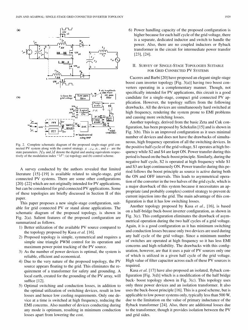
Fig. 2. Complete schematic diagram of the proposed single-stage grid con-nected PV system along with the control strategy. x ; x ; x , and x are thestate parameters. M and M denote the digital and analog equivalents respec-tively of the modulation index “M”: (a) topology and (b) control scheme.
A survey conducted by the authors revealed that limitedliterature [15]–[19] is available related to single-stage, gridconnected PV systems. There are some other configurations[20]–[22] which are not originally intended for PV applications,but can be considered for grid connected PV applications. Someof these topologies are briefly discussed in Section II of thispaper.
This paper proposes a new single-stage configuration, suit-able for grid connected PV or stand alone applications. Theschematic diagram of the proposed topology, is shown inFig. 2(a). Salient features of the proposed configuration aresummarized as follows.
1) Better utilization of the available PV source compared tothe topology proposed by Kasa et al. [16].
2) Proposed topology is simple, symmetrical and requires asimple sine triangle PWM control for its operation andmaximum power point tracking of the PV source.
3) As the number of power devices is optimal, the system isreliable, efficient and economical.
4) Due to the very nature of the proposed topology, the PVsource appears floating to the grid. This eliminates the re-quirement of a transformer for safety and grounding. Alocal earth, created for the grounding of the PV array, willsuffice [12].
5) Optimal switching and conduction losses, in addition tothe optimal utilization of switching devices, result in lowlosses and hence low cooling requirements. Only one de-vice at a time is switched at high frequency, reducing theEMI concerns. Also number of devices conducting duringany mode is optimum, resulting in minimum conductionlosses apart from lowering the cost.
6) Power handling capacity of the proposed configuration ishigher because for each half cycle of the grid voltage, thereis a separate, dedicated inductor and switch to handle thepower. Also, there are no coupled inductors or flybacktransformer in the circuit for intermediate power transfer[23], [24].
II. SURVEY OF SINGLE-STAGE TOPOLOGIES SUITABLE
FOR GRID CONNECTED PV SYSTEMS
Caceres and Barbi [20] have proposed an elegant single-stageboost cum inverter topology [Fig. 3(a)] having two boost con-verters operating in a complementary manner. Though, notspecifically intended for PV applications, this circuit is a goodcandidate for a single-stage, compact grid connected PV ap-plication. However, the topology suffers from the followingdrawbacks. All the devices are simultaneously hard switched athigh frequency, rendering the system prone to EMI problemsand causing more switching losses.
Another topology, derived from the basic Zeta and Cuk con-figuration, has been proposed by Schekulin [15] and is shown inFig. 3(b). This is an improved configuration as it uses minimalnumber of devices and does not have the drawbacks of simulta-neous, high frequency operation of all the switching devices. Inthe positive half cycle of the grid voltage, S1 operates at high fre-quency while S2 and S4 are kept ON. Power transfer during thisperiod is based on the buck-boost principle. Similarly, during thenegative half cycle, S2 is operated at high frequency while S1and S3 are kept continuously ON. Power transfer during this pe-riod follows the boost principle as source is active during boththe ON and OFF intervals. This leads to asymmetrical opera-tion of the converter in the two halves of the grid cycle, which isa major drawback of this system because it necessitates an ap-propriate (and probably complex) control strategy to prevent dccurrent injection into the grid. The main advantage of this con-figuration is that it has low switching losses.
Another topology proposed by Kasa et al., [16], is basedon a half-bridge buck-boost inverter configuration, as shown inFig. 3(c). This configuration eliminates the drawback of asym-metrical operation during the two half cycles of a grid voltage.Again, it is a good configuration as it has minimum switchingand conduction losses because only two devices are used duringany half cycle of the grid voltage. Since a minimum numberof switches are operated at high frequency so it has less EMIconcerns and high reliability. The drawbacks with this config-uration, however, are that it uses a pair of PV sources only oneof which is utilized in a given half cycle of the grid voltage.High value of filter capacitor across each of these PV sources isrequired.
Kasa et al. [17] have also proposed an isolated, flyback con-figuration [Fig. 3(d)] which is a modification of the half bridgebuck- boost topology shown in Fig. 3(c). This topology usesonly three power devices and an isolation transformer. It alsouses the buck-boost principle [16]. This is a good scheme, but isapplicable to low power systems only, typically less than 500 W,due to the limitation on the value of primary inductance of theflyback transformer [24]. Also, there are additional losses dueto the transformer, though it provides isolation between the PVand grid sides.

1930 IEEE TRANSACTIONS ON POWER ELECTRONICS, VOL. 22, NO. 5, SEPTEMBER 2007
Fig. 3. (a)–(g): Schematic circuit diagrams of the various existing single-stage topologies [15]–[18], [20]–[22], [25] and (h) proposed scheme.
Wang [21] has proposed a single-stage, full bridge configu-ration based on the buck-boost principle as shown in Fig. 3(e).During the positive half cycle of the grid voltage, S4 operatesat high frequency and S1 is kept continuously ON. The pathduring turn OFF is completed through S1 and D2. During thenegative half cycle of the grid voltage, S3 operates at high fre-quency and S2 is kept continuously ON. During turn OFF, thepath is completed through S2 and D1. This configuration has alarge number of devices conducting at a given instant resultingin higher conduction losses.
Based on the buck-boost principle, Xue et al. [18] have pro-posed yet another single-stage grid connected PV system, asshown in Fig. 3(f). Proposed configuration uses flyback prin-ciple with mutually coupled coils during the negative half cycleof the grid voltage. The limitation of this system is that it canbe used only for low power applications due to the limitationof the mutually coupled coils or flyback transformer to handlehigh power [24]. In addition to this, the switching and conduc-tion losses are higher and the operation is asymmetrical in thetwo halves of the grid voltage cycle.
Wang [22] has proposed another single-stage configurationbased on buck-boost principle as shown in Fig. 3(g). Thoughthis configuration is not specifically intended for grid connectedPV systems, it may be considered for this application. But thedrawback with this configuration is that it uses five switches,with three switches operating at high frequency, leading to EMIconcerns and higher switching losses.
Huang et al. [19] have proposed a single stage configura-tion for a split–phase system for PV applications, which usesa -source inverter. This configuration, which requires sixswitches, operating at high frequency, is recommended for highpower applications.
This paper proposes a single stage topology based on buck-boost principle as shown in Fig. 3(h). During the positive halfcycle of the grid voltage, operates at high frequencywhile is kept continuously ON. During the negative halfcycle, is operated at high frequency while is keptcontinuously ON. As an optimum number of switches are op-erated at any given time, the proposed topology has the advan-tage of low switching and conduction losses, low EMI and low
cooling requirements. The proposed topology overcomes sev-eral drawbacks of the topologies surveyed and described in thissection. Working principle and all other details of this topologyare presented in the following section.
III. PROPOSED TOPOLOGY
The proposed topology consists of two dc-to-dc, buck-boostconverters connected as shown in Fig. 2. Each of these con-verters operates in DCM for one half cycle of the fundamentalgrid voltage. The resulting circuit acts as a current source in-verter which feeds sinusoidal current into a low value capacitoracross the grid. DCM operation helps in feeding sinusoidal cur-rent with near unity power factor (UPF) into the grid becausethe energy can be drawn in the form of “energy packets,” whosemagnitudes vary in a sinusoidal manner.
The power device (or ) is switched at highfrequency while (or ) is kept continuously ONduring the positive half cycle (or negative half cycle). (or
) is switched as per sine triangle pulse width modulation(SPWM) method. When is ON, energy is stored in thebuck-boost inductor “ ” by the PV source. When isOFF, (or ) gets forward biased, discharging the storedinductor energy into capacitor which feeds sinusoidal cur-rent into the grid. The state equations governing the operationof the proposed configuration during the positive half cycle ofthe grid voltage are given below. The switching control strategyimplemented is also shown in Fig. 2(b). During the positivecycle the various state equations are as follows.
When power device is ON. Applying KCL to thenodes “a” and “e” and KVL to the loops a-b-c-d-a and e-f-g-h-e,the following state equations are obtained:
(1)
When power device is OFF, and diode is conducting.Applying KCL to the nodes “a” and “e” and KVL to the loopsj-b-e-h-i-j and e-f-g-h-e, yields the following state equations:
(2)

JAIN AND AGARWAL: SINGLE-STAGE GRID CONNECTED INVERTER TOPOLOGY 1931
Fig. 4. Grid current and voltage waveforms considered for the analysis in dis-crete time domain. k = n=2 is the peak interval showing “Critical ConductionMode” operation.
When power device is OFF, and diode is not con-ducting. Applying KCL to the nodes “a” and “e” and KVL tothe loop e-f-g-h-e, results in the following state equations:
(3)
In a similar manner, state space equations can be written fornegative cycle when other half of the inverter is operated. Usingthese state space equations, the complete PV system is simulatedin MATLAB/SIMULINK software [26], [27].
IV. ANALYSIS OF THE PROPOSED CONFIGURATION
For analysis of the proposed configuration, the following as-sumptions are made.
1) Switching frequency is 2 times the fundamental fre-quency of the grid voltage.
2) Grid voltage is constant over a high frequency switchingtime period.
3) Value of duty cycle is constant over a high frequencyswitching time period.
4) DCM operation during the entire cycle of the grid voltage.5) The PV array followed by ‘ ’ provides a dc voltage
which is constant over the entire grid cycle.In view of assumption (1), one complete cycle of grid voltage
can be divided into 2 high switching periods [Fig. 4(a)]. For theth division of the grid voltage the following expression may be
written:
(4)
To feed UPF sinusoidal power into the grid, the energy,that should be transferred during the th switching interval is
(5)
where is the amplitude of the current fed into the grid andis governed by the MPPT algorithm. ‘ ’ is the switching timeperiod. Due to DCM operation, a definite amount of energy canbe transferred during each switching cycle. Thus, for injectingsinusoidal current into the grid, the expression for duty ratio ,required in the th switching cycle is derived as follows.
Energy drawn from the source during th switching cycle
(6)
where is the duty ratio during the th switching cycle.Equating (5) and (6) and solving for yields
(7)
Writing (7) in continuous time domain yields an expression forthe reference waveform r(t) given by
where (8)
where “ ” is the modulation index determined by the MPPT al-gorithm. Thus, SPWM technique can be used to feed sinusoidalcurrent into the grid with no voltage distortion. Using assump-tion (3), the duty ratio for the th switching interval is given by
(9)
The following notations are followed in the subsequent analysis.denotes the th state variable as a function of time
where “ ” denotes the subinterval “on,” “off” or “ -off” of theth interval as shown in Fig. 4.
denotes the initial value of the th state variable at thestart of the subinterval “ ” of the th interval.
The following approximations regarding the initial values ofstate parameters and at the start of the ON period of the
th switching interval, represented by and , respec-tively, can be made
(10)
When switch is turned ON, the state equations governingthe circuits in Fig. 2 are
(11)
Solving the differential (11) during the ON period 0of the th switching interval using the initial condition
(10), yields (12), shown at the bottom of the next page, where. Initial value of the state parameters for the
OFF interval are the final value of the parameters during ON in-terval are obtained by substituting [Fig. 4] in (12).When switch is turned OFF, and the diode is conducting,the governing state equations are
(13)

1932 IEEE TRANSACTIONS ON POWER ELECTRONICS, VOL. 22, NO. 5, SEPTEMBER 2007
The differential (13) lead to the following solutions during theOFF period ( of the th switching interval
(14)
(15)
(16)
where . The OFF interval[Fig. 4] can be determined using the fact
that the average voltage across over a switching period iszero. Noting that the average voltage across duringis equal to the grid voltage during th switching interval, yieldsthe following:
(17)
Substituting the value of from (17) in (14)–(16), yieldsthe initial values of the state variables for the subsequent free-wheeling state. When the switch is turned OFF, and the
diode is not conducting , the governing state equa-tions are
(18)
Solution of (18) is similar to the one obtained for turn ON con-dition of except for which is zero during the free-wheeling interval
(19)
Substituting the value of in the solution of (19) givesthe value of state variables at the end of the th switching cyclewhich are also the initial values of the subsequent switchingcycle.
A. Peak Values of State Parameters
As maximum device stress and losses occur near , the highfrequency switching interval closest to (peak interval,
2 , Fig. 4) is considered for analysis i.e., 2, (whereis an odd integer). Substituting 2 in (4), (9) and (10),
we have
(20)
Peak values of the various state variables in this switching in-terval are
(21)
(22)
(12)

JAIN AND AGARWAL: SINGLE-STAGE GRID CONNECTED INVERTER TOPOLOGY 1933
Fig. 5. Plot of I (n=2) versus z with ! as the parameter.
(23)
where and are the peakvalues of the current in , voltage across and the currentin respectively during 2th interval. Value of canbe obtained by substituting (20) in (17), which yields
(24)
It is observed that 2 and 2 depend on thecharacteristic impedance and the reso-nant angular frequency of the cir-cuit. Plots showing the variation of 2 and 2with respect to and are shown in Figs. 5–8. These plotsare useful for optimizing the design of the proposed converter.
B. Condition for DCM
The proposed topology operates in DCM through out the gridcycle if it sustains DCM operation during the peak interval.Applying the condition for Critical Conduction Mode or DCMduring interval 2 yields
(25)
Fig. 6. Plots of I (n=2) versus (1=! ) with z as the parameter.
Fig. 7. Plot of V (n=2) versus z with ! as the parameter.
Fig. 8. Plot of V (n=2) versus (1=! ) with z as the parameter.

1934 IEEE TRANSACTIONS ON POWER ELECTRONICS, VOL. 22, NO. 5, SEPTEMBER 2007
This leads to the condition for DCM operation of the system
(26)
C. Rating of Power Devices and Losses
Maximum instantaneous current rating of any power devicein the circuit is determined by peak inductor current
(27)
Also, root mean square value of the current through switch(or ) over half cycle of the grid voltage is given by
(28)
Similarly, the root mean square current through switch(or ) over half cycle of the grid voltage is seen in (29),shown at the bottom of the page. The maximum voltage stressor the required forward blocking voltage of (or
) is given by
(30)
where is the voltage drop across the diode (or ).Similarly, the maximum voltage stress or the required reverseblocking voltage of (or ) is given by
(31)
D. Design of Inductor and Capacitor [Figs. 2 and 4]
The buck-boost inductor, ‘ ’ acts as an energy storage el-ement, which stores energy from the PV source and transfersit to the grid through capacitor . The maximum energy istransferred during the peak interval, [Fig. 4] when PV isdelivering rated power “ ” W. If “Critical Conduction Mode”or DCM operation is ensured during this interval, DCM oper-ation is guaranteed throughout the grid cycle and for all envi-ronmental conditions. Thus, design of is critical for properoperation of the converter. If the PV system can deliver a max-imum dc power of “ ” W, inductor should have a powerhandling capacity of “ ” W. This will ensure transfer of av-erage power “ ” W, into the grid. As the proposed SSGC con-
figuration operates in DCM, it transfers energy in the form ofpackets during each switching interval to feed high quality sinu-soidal power into the grid. Also, during each switching interval,the energy stored in the inductor is completely transferred tocapacitor ‘ ’ connected across the grid. Thus, near the peakof the fundamental cycle of the grid voltage, energy transferredinto the grid during ( /2) switching interval is given by
(32)
This is two times the average energy 2transferred into the grid. Thus, inductor must be capable ofhandling twice the average energy fed into the grid. The max-imum energy is transferred during the peak interval (when
2 ) [Fig. 4]. Due to the “Critical Conduction Mode” opera-tion during the peak interval, the following equations holds:
(33)
Also from Fig. 4 considering 2th interval yields
(34)
Using (34) in (33), with and notingthat 1 but positive, (33) can be simplified to give
(35)
Also, using (33) in (26) yields
(36)
Combining (35) and (36)
(37)
The design value is chosen in such a way that the max-imum value of ‘ ’ satisfies conditions (26) and (37) when thePV source is delivering rated power. This condition helps in en-suring DCM operation of the proposed configuration at any op-erating point under all environmental conditions.
To determine the value of , the energy stored in the in-ductor during the ON interval can be equated to the changein capacitor energy during the OFF interval, resulting in the fol-lowing expression:
(38)
where is the ripple in the capacitor voltage.
(29)

JAIN AND AGARWAL: SINGLE-STAGE GRID CONNECTED INVERTER TOPOLOGY 1935
Fig. 9. MATLAB/SIMULINK simulation results of the proposed topology onthe PV side. Subplot (d) shows the variation in the modulation index of theSPWM. The carrier (triangular) waveform has amplitude of 5 V.
Fig. 10. MATLAB/SIMULINK simulation results of the proposed topology onthe grid side.
Design of : is the filter inductor which filters thehigh switching frequency component present in the currentwaveform fed into the grid. For design, it requires the cut offfrequency to be lesser than the switching frequency .Thus, the design value of is given by
(39)
Design value of : acts as a buffer between the PV sourceand the proposed SSGC PV configuration. Value of decidesthe maximum amplitude of ripple in the voltage of the PV array.Let be the maximum value of the allowed ripple in thePV voltage and be the frequency of the fundamental cycle ofthe grid voltage, then the design value of is given by [7]
(40)
Fig. 11. Magnified view of Fig. 10. The subplot inset plot (d) shows the highfrequency switching ripple in V .
TABLE IPARAMETERS USED IN THE SIMULATION OF THE PROPOSED CONFIGURATION
Fig. 12. Photograph of the experimental setup used for testing the proposedconfiguration.
V. MAXIMUM POWER POINT TRACKING
“Hill climbing” or the “perturb and observe method” [1] hasbeen used to track the maximum power point (MPP) of the PVsource. This algorithm has been appropriately implemented inconjunction with the grid connected dc/ac configuration pro-posed in the paper.
Sine-triangle comparison technique is used to ensure thatnear-sinusoidal currents are fed into the grid. As inverter isfeeding sinusoidal power into the grid, the second harmonicpower is reflected on the PV source side. This appears in thecurrent and voltage waveforms of the PV source. Therefore,to avoid wrong decisions, the MPPT algorithm uses average

1936 IEEE TRANSACTIONS ON POWER ELECTRONICS, VOL. 22, NO. 5, SEPTEMBER 2007
TABLE IIPARAMETERS OF THE EXPERIMENTAL PROTOTYPE
TABLE IIIRMS AND PEAK VALUES OF THE CURRENT AND VOLTAGES HANDLED BY THE VARIOUS COMPONENTS AND DEVICES
values of the PV array current and voltage . Theseaverage values are obtained by using FFT block set in theSIMULINK software. In hardware, this is implemented usingthe DSP. Fig. 2(b) shows the complete control scheme im-plemented in software and hardware. The amplitudeof the sinusoidal reference signal, is governed by the MPPTalgorithm and is updated (only) at the beginning of everyfundamental cycle of grid voltage to avoid dc current injectioninto the grid. As varies, the magnitude of “ ” variesand hence, the widths of the SPWM pulses vary. The stringof pulses, whose widths vary in a sinusoidal manner, gets uni-formly scaled upwards or downwards depending upon whether
is increasing or decreasing. The maximum value of “ ” isset by (26) and the minimum value is decided by the minimumamount of power to be transferred.
VI. SIMULATION AND EXPERIMENTAL RESULTS
OF THE PROPOSED INVERTER TOPOLOGY
The proposed inverter topology was simulated in MATLAB/SIMULINK software [26], using the PV model proposed byWalker [27]. The important waveforms corresponding to the PVand grid sides, obtained with computer simulations, are shownin Figs. 9 and 10, respectively. MPPT, as discussed in the pre-vious section, was also incorporated in computer simulations.Tracking of maximum power for different environmental con-ditions is confirmed by the low ripple content in the PV poweroutput around MPP as shown in Fig. 9. In Fig. 9, when there isa step change in insolation from 0.9 to 0.1 Suns, the operatingvoltage shifts to the current source region. The MPP algorithmthen, decreases the value of “ ” which increases the operatingvoltage of the array, approaching MPP. The variation of modu-lation index “ ,” as the MPP is tracked, is also shown in plot(d). Fig. 10 shows the plots of capacitor voltage ( or ) andtotal harmonic distortion (THD) of the current fed into the grid.In general, the grid current THD under different environmentalconditions, remains with in 5%. Fig. 11 shows the magnifiedview of Fig. 10 for one fundamental cycle of the grid voltage.It also shows the high frequency switching ripple present in thecapacitor voltage.
Calculations of the design parameters for a PV array voltage90 V and peak grid voltage 325 V are shown
in the following.
Fig. 13. Experimental waveforms of the switching pulses at the gates of con-trollable switches: Plot (a): SW forM = 76.5%; Plot (b): SW ; Plot (c):SW forM = 76.5%; Plot (d) SW ; Plot (e): SW forM = 20%; Plot(f) SW forM = 20% [Plots (b) and (d) are independent ofM ].
Using (26), the value of “ ” is given by
(41)
Using (37), the value of buck-boost inductor for 700 W PVpower is given by
s kHz (42)
Thus, 176 H is the critical value. In simulations, a lower valueof was used to avoid CCM operation for power greaterthan the rated power. At the same time, precaution was takennot to use too low a value of (i.e., much lower than itscritical value) to avoid high current stress and losses. With allthese considerations, 150 H was chosen as an overallgood compromise value. Taking capacitor voltage ripple,50 V, the value of is given by
(43)

JAIN AND AGARWAL: SINGLE-STAGE GRID CONNECTED INVERTER TOPOLOGY 1937
Fig. 14. Experimental results showing MPP tracking using the conventionalhill climbing method. Horizontal x axis has a time scale of 2.5 s/div.
Fig. 15. Experimental waveforms of the input current and voltage (on the PVside). Horizontal x axis has a time scale of 2.5 ms/div.
Fig. 16. Experimental waveforms of the current fed into the grid and the gridvoltage. Horizontal x axis has a time scale of 2.5 ms/div.
Similarly, other parameters can be calculated using (39) and(40). Table I shows the values of the parameters used in the sim-ulation of the proposed single stage configuration.
A 300-W experimental prototype was built in the laboratoryto verify the working of the proposed configuration. As SPWMis used, the control circuit requires grid voltage template. How-ever, the grid voltage was found to have some distortion. Hence,
Fig. 17. FFT plots and the THD value of the grid current shown in Fig. 16,obtained using Tektronix TPS 2014 oscilloscope.
Fig. 18. Experimental waveforms of the buck-boost inductor current and filtercapacitor (C ) voltage. Horizontal x axis has a time scale of 2.5 ms/div.
Fig. 19. Experimental results showing voltage and current waveforms across aresistive load (grid is replaced by a stand-alone resistive load).
the grid voltage must be filtered to obtain the fundamental com-ponent. Hence, the generation of sine wave (used in SPWM) isdone by attenuating the sensed grid voltage and then passingit through a ‘low pass’ filter to render a unit amplitude pure

1938 IEEE TRANSACTIONS ON POWER ELECTRONICS, VOL. 22, NO. 5, SEPTEMBER 2007
Fig. 20. Experimental plots for low insolation value (�0.3 Suns): (a) MPP tracking plots and (b) grid current and voltage waveforms with a subplot showing theFFT and THD value of the grid current.
sine wave [Fig. 2(b)]. This waveform is then passed through an‘all-pass’ filter to compensate for any phase shift.
A photograph of the experimental set up used is shown inFig. 12. Specifications of the system are given in Table II.
Power MOSFETs (IRFP460) were used as the controllableswitching devices . CSD20060power diodes were used for and . Grid voltage is ad-justed to 150 V peak with the help of an autotransformer for theexperiments. For design and selection of devices, the peak andRMS values of currents and voltages are required which weredetermined using expressions obtained in Section IV and veri-fied using simulations. The RMS and peak values of the currentsand voltages handled by various components and devices usedin the prototype at the rated condition with 325 V are givenin Table III.
MPPT algorithm was implemented using Texas Instruments’DSP TMS320LF2407 which computes the value of “ ,” using“hill climbing” MPPT algorithm as shown in Fig. 2. Fig. 13shows the waveforms of the switching pulses applied to thegates of the various controllable devices in the proposed config-uration obtained using Agilent’s Infiniium oscilloscope (modelno. 54810A). It may be noted that the density of the switchingpulses (applied to and ) is higher for higher mod-ulation index. Other experimental waveforms, corresponding tothe power stage were obtained using Tektronix power oscillo-scope TPS 2014, especially suited for such measurements. Ex-perimental result showing MPP tracking is given in Fig. 14.Fig. 15 shows the experimental current and voltage waveformson the PV side. Fig. 16 shows the experimental waveforms ofgrid voltage and the current fed into the grid. Fig. 17 shows theFFT plot and the THD value corresponding to the grid currentshown in Fig. 16 while Fig. 18 shows the waveforms of the ca-pacitor voltage and the buck-boost inductor current.The current fed into the grid has a THD slightly higher than 5%due to the fact that the grid voltage itself is distorted which re-sults in the distortion of the current flowing into the grid. Thisfact is further highlighted by Fig. 19 which shows the exper-imental plots obtained for a resistive load of 104 (i.e., gridreplaced by stand-alone resistive load). It is observed that for
Fig. 21. Variation of efficiency and input power drawn by the proposed config-uration as the modulation index “M” is varied.
a resistive load, the proposed configuration feeds nearly sinu-soidal current (with negligible THD).
Fig. 20(a) shows experimental plot for MPP tracking duringlow insolation. Fig. 20(b) shows the corresponding grid voltageand current waveforms with the grid current THD 9.13%. Itmay be noted that the THD of current fed into the grid duringlow insolation is significantly higher.
To determine the variation in efficiency of the proposed con-figuration, as it operates from low power to rated power con-dition, a number of experiments were performed using a resis-tive load of 104 (in place of the grid) and by replacing thePV source by a dc source. Measurements of power on the inputand output sides were made using Voltech make high bandwidthpower analyzer (model PM300) and high bandwidth true RMSTektronix multimeter’s. Fig. 21 shows the experimental plot ofefficiency and the input power drawn with different modulationindexes used in the SPWM. Subsequently, various other exper-iments were also performed by restoring back the PV sourceand again connecting the proposed configuration’s output withthe power grid for obtaining the plots of power factor and gridcurrent THD with respect to output power fed into the grid and

JAIN AND AGARWAL: SINGLE-STAGE GRID CONNECTED INVERTER TOPOLOGY 1939
TABLE IVSUMMARY OF THE COMPARISON OF THE PROPOSED CONFIGURATION WITH EXISTING TOPOLOGIES
Fig. 22. Experimental plots with the PV source showing (a) efficiency versusinput PV power, and (b) THD of the current versus output power fed into thegrid, and (c) power factor versus power fed into the grid.
the plot of efficiency with respect to the input PV power. Theseplots are shown in Fig. 22.
VII. CONCLUSION
In this work, the importance of single-stage grid connectedPV systems has been highlighted. A single-stage topology withimproved features has been proposed. Relevant analysis, in-cluding derivations of the expressions for peak voltage and cur-rent stresses across the switching devices, has been performedand a design procedure has been presented. The topology issimple, symmetrical and easy to control. The other desirable
features include good efficiency due to optimal number of de-vice switchings and reduced switching losses. A comparison ofthe proposed configuration with several existing configurationsis summarized in Table IV.
The diodes ( and ), which are inherent to the buck-boost operation, also serve to prevent any reverse power flowfrom the power grid to the PV array. DCM operation ensuresbetter control apart from facilitating the generation and feedingof high quality current into the grid. DCM operation also elimi-nates the requirement of fast recovery diodes (i.e., and ).Thus, the design of the buck boost inductor is crucial, since thesystem must operate in DCM under any operating condition.
As per Figs. 16 and 17, the grid current THD is above 5%.But with a good grid voltage waveform (closer to a pure sinewave), the THD can be limited as per IEEE-519 (current THD
5%) and the topology will be able to feed high quality currentinto the grid. During low insolation, however, the current THDis observed to be high [Fig. 20(b)].
Some reactive power is also fed into the grid and its amountis found to be sensitive to the value of . As the value ofis decreased, the reactive power decreases and vice versa. How-ever, reducing the value of increases the THD of the currentfed into the grid. Thus, there is a trade-off between the reactivepower and current THD and extensive computer simulations canbe used to optimize the value of . In fact, an optimization ofthe other design parameters is also possible using the plots ofpeak grid current and capacitor voltage stresses versus and
presented in Section IV.The proposed configuration, operating in DCM, along with
the conventional hill climbing MPPT scheme, is highly robust.This is because the operating voltage of the PV array can becontrolled by varying . Also, there is a one-to-one relation-ship between and the average operating voltage of the PVarray i.e., for each value of , the system settles down to a

1940 IEEE TRANSACTIONS ON POWER ELECTRONICS, VOL. 22, NO. 5, SEPTEMBER 2007
stable average operating point. Thus, there is no probability ofthe system moving into the short circuit region for higher valuesof [9].
Though the experimental results presented show a boostingof only about 1.5 times, the proposed system is expected to havereasonable boosting capability (typically 3–4 times), whichmeans that low PV array voltages (typically 50–100 V range)can be boosted up to levels capable of interfacing with the gridvoltage (115 V or 230 V ac systems). This has been verifiedusing computer simulations.
Proposed configuration is highly suitable for an integratedsolution (e.g., plug-and-play type ac modules) for PV systems.In this work, MOSFETs are used as switching devices. If lowloss devices, like IGBTs, are used the efficiency can be furtherimproved. Experiments with a DSP based laboratory prototypehave shown encouraging results.
REFERENCES
[1] B. K. Bose, P. M. Szezesny, and R. L. Steigerwald, “Microcontrollercontrol of residential photovoltaic power conditioning system,” IEEETrans. Ind. Appl., vol. 21, no. 5, pp. 1182–1191, Sep./Oct. 1985.
[2] I. Anton, F. Perez, I. Luque, and G. Sala, “Interaction betweenSun tracking deviations and inverter MPP strategy in concentratorsconnected to grid,” in Proc. IEEE Photovolt. Spec. Conf., 2002, pp.1592–1595.
[3] S. Saha and V. P. Sundarsingh, “Novel grid-connected photovoltaicinverter,” Proc. Inst. Elect. Eng., vol. 143, no. 2, pp. 143–56, 1996.
[4] P. G. Barbosa, H. A. C. Braga, M. do Carmo Barbosa Rodrigues, andE. C. Teixeira, “Boost current multilevel inverter and its application onsingle-phase grid-connected photovoltaic systems,” IEEE Trans. PowerElectron., vol. 21, no. 4, pp. 1116–1124, Jul. 2006.
[5] M. Armstrong, D. J. Atkinson, C. M. Johnson, and T. D. Abeyasekera,“Auto-calibrating dc link current sensing technique for transformer-less, grid connected, H-bridge inverter systems,” IEEE Trans. PowerElectron., vol. 21, no. 5, pp. 1385–1396, Sep. 2006.
[6] L. Asiminoaei, R. Teodorescu, F. Blaabjerg, and U. Borup, “Imple-mentation and test of an online embedded grid impedance estimationtechnique for PV inverters,” IEEE Trans. Ind. Electron., vol. 52, no. 4,pp. 1136–1144, Aug. 2005.
[7] B. M. T. Ho and H. S.-H. Chung, “An integrated inverter with max-imum power tracking for grid-connected pv systems,” IEEE Trans.Power Electron., vol. 20, no. 4, pp. 953–962, Jul. 2005.
[8] F. S. Kang, S. Cho, S. J. Park, C. U. Kim, and T. Ise, “A new controlscheme of a cascaded transformer type multilevel PWM inverter fora residential photovoltaic power conditioning system,” Solar Energy,vol. 78, no. 6, pp. 727–738, 2005.
[9] T. J. Liang, Y. C. Kuo, and J. F. Chen, “Single-stage photovoltaic en-ergy conversion system,” Proc. Inst. Elect. Eng., vol. 148, no. 4, pp.339–344, 2001.
[10] Y. Chen and K. Ma-Smedley, “A cost-effective single-stage inverterwith maximum power point tracking,” IEEE Trans. Power Electron.,vol. 19, no. 5, pp. 1289–1294, Sep. 2004.
[11] F. Blaabjerg, Z. Chen, and S. B. Kjaer, “Power electronics as efficientinterface in dispersed power generation Systems,” IEEE Trans. PowerElectron., vol. 19, no. 5, pp. 1184–1194, Sep. 2004.
[12] S. B. Kjaer, J. K. Pedersen, and F. Blaabjerg, “A review of single-phasegrid-connected inverters for photovoltaic Modules,” IEEE Trans. Ind.Appl., vol. 41, no. 5, pp. 1292–1306, Sep./Oct. 2005.
[13] F. Blaabjerg, A. Consoli, J. A. Ferreira, and J. D. Van Wyk, “The futureof electronic power processing and conversion,” IEEE Trans. PowerElectron., vol. 20, no. 3, pp. 715–720, May 2005.
[14] M. Meinhardt, V. Leonavicius, J. Flannery, and S. C. Ó. Mathúna, “Im-pact of power electronics packaging on the reliability of grid connectedphotovoltaic converters for outdoor applications,” Microelectron. Rel.,vol. 39, no. 10, pp. 1461–1472, 1999.
[15] D. Schekulin, “Grid-Connected Photovoltaic System,” Germany patentDE197 32 218 Cl, Mar. 1999.
[16] N. Kasa, T. Iida, and H. Iwamoto, “Maximum power point trackingwith capacitor identifier for photovoltaic power system,” Proc. Inst.Elect. Eng., vol. 147, no. 6, pp. 497–502, Nov. 2000.
[17] N. Kasa and T. Iida, “Flyback type inverter for small scale photovoltaicpower system,” in Proc. IEEE IECON, 2002, vol. 2, pp. 1089–1094.
[18] Y. Xue and L. Chang, “Closed-loop SPWM control for grid-con-nected buck-boost inverters,” in Proc. IEEE PESC, 2004, vol. 5, pp.3366–3371.
[19] Y. Huang, M. Shen, F. Z. Peng, and J. Wang, “Z-source inverter forresidential photovoltaic systems,” IEEE Trans. Power Electron., vol.21, no. 6, pp. 1776–1782, Nov. 2006.
[20] R. O. Caceres and I. Barbi, “A boost dc-ac converter: Analysis, design,and experimentation,” IEEE Trans. Power Electron., vol. 14, no. 1, pp.134–141, Jan. 1999.
[21] W. Chien-Ming, “A novel single-stage full-bridge buck-boost inverter,”IEEE Trans. Power Electron., vol. 19, no. 1, pp. 150–159, Jan. 2004.
[22] W. Chien-Ming, “A novel single-stage series-resonant buck–boost in-verter,” IEEE Trans. Ind. Electron., vol. 52, no. 4, pp. 1099–1108, Aug.2005.
[23] L. Meysenc, M. Jylhakallio, and P. Barbosa, “Power electronicscooling effectiveness versus thermal inertia,” IEEE Trans. PowerElectron., vol. 20, no. 3, pp. 687–693, May 2005.
[24] R. Henk, Practical Design of Power Supplies. New York: McGrawHill, 1998, pp. 95–96.
[25] Y. Xue, L. Chang, S. B. Kjær, J. Bordonau, and T. Shimizu, “Topolo-gies of single phase inverters for small distributed power generators: Anoverview,” IEEE Trans. Power Electron., vol. 19, no. 5, pp. 1305–1314,Sep. 2004.
[26] V. F. Pires and J. F. Silva, “Teaching non linear modeling, simu-lation, and control of electronic power converters using MATLAB/SIMULINK,” IEEE Trans. Education, vol. 45, no. 3, pp. 253–261,Aut. 2002.
[27] G. Walker, “Evaluating MPPT converter topologies using a MATLABPV model,” J. Electr. Electron. Eng., Australia, vol. 21, no. 1, pp.49–56, 2001.
Sachin Jain, photograph and biography not available at the time of publication.
Vivek Agarwal, photograph and biography not available at the time ofpublication.