INSTRUCTION MANUAL (Applied) INVERTER INVERTER FR-F700 INSTRUCTION MANUAL (Applied
Upload
khangminh22Category
view
4download
0
MITSUBISHI type A~.CPUlAnACPU/AnUCPU/QCPU-A (A Model I
!
I
0 1

i
SAFETY CAUTIONS (You must read these cautions before using the product)
In connection with the use of this product, in addition to carefully reading both this manual and the r e l a t e d manuals indicated in this manual, it is also essential to pay due attention to safety and handle the product correctly. The safety cautions given here apply to this product in isolation. For information on the safety of the PC system as a whole, refer to the CPU module User's Manual. Store this manual carefully in a place where it is accessible for reference whenever necessary, and forward a copy of the manual to the end user.

I
Thank you for choosing the Allitsubishi MELSEC-A Series of Generql Purpose Programmable Controllers. Please read this manual carefully so that the equipment is used to its optimum. A copy of this manual should be forwarded to the end User.

REVISIONS The manual number is given on the bottom left of the back cover.
Print Date Dec., 1990 Aug., 1993
Wanual Nunrkr IB (NA) 66251-A IB (NA) 66251-8
Dec., 1997 IB(NA)66251 -D
Feb., 2OOO IB(NA)66251 -F
I L
~~ ~~ ~~ ~ ~~~
First edition The manual name is changed m accordance with the addition of the contents of MU(S1 )/A3U/A4UCPU. [Before change] A2A(Sl)MACPU(Dedicated instructions) [After change] AnACPU/AnUCPU(Dedicated instructions)
CONTENTS, Section 1, 2.1, 2.3, 3.2,3.3,4, 4.1,4.2. 5.1,5.4, 8.2.4, 8.2.5,8.2.6, 8.2.7, 12.1, 12.1.1, 12.1.2, 12.1.3, 13, 13.1, 13.2, 13.3, 13.4, 14, 14.1, 14.1, 14.4, 14.4.1, 14.4.2, 14.4.3,14.4.4, 14.4.5, 15 is changed to 16, APP.1 ,APl?2, INDEX
Section 13.5, 13.6, 13.7, 15 The manual name is changed into AnSHCPU/AnACPU/AnUCPU Programming Manual (Dedicated instructions). [Old name: AnACPU/AnUCPU Programming Manual (Dedicated instructions)]
~~
piZiil
p Z G . 1
]correction I Safety Cautions, CONTENTS, Chapter 1, Section 2.1,2.3,3.3,6.1, 8.1.2,8.1.3,8.1.4,8.1.5, 8.1.7,8.2.18, 9.7,9.9, 9.10, 9.11,Chapter 13, Section 13.6, 13.7, Chapter 14, Sectin 14.1, 14.2, 14.6.4, Chapter 16 changed into Chapter 17, Section 16.2, Appendiil, Index Addition Section 13.8, 13.9, Chapter 16 (CC-Link Dedicated Instructions), Section 17.4 pGGGl
p Z i G l Chapter 1, Index
CONTENTS, Chapter 1, Section 21,2.3,13.8,13.9, Chapter 14, Sec(i0n 14.1, Chapter16, section 16.1 to 16.9,172,17.4, Appedix 1, The manual name is changed into AnSHCPU/AnACPU/AnUCPU/ QCPU-A (A Mode) Programming Manual (Dedicated instructions), [Old name: AnSHCPU/AnACPU/ AnUCPU Programming Manual (Dedicated instructions)] I Addition of Modeles I A2USHCPU-S1 QO2CPU-A, WHCPUA, QOGHCPU-A -1 p&Gl Chapter 17, Section 18.5
Section 9.10, 9.16, 12.1.2, 13.1 to 13.9, 16.1 to 16.9, Appendix 1
This manuel c&rs no industrial property rights or any rights of any other kind, nor does it confer any patent licenses. Miubishi Electric Corporation cannot be held responsible for any pro#ems involving industrial property rights which may occur as a result of using the contents noted in this manual.
i
0 1990 Mitsubishi Electric Corporation

REVISIONS *The manual number is given on the bottom left of the back cover.
Print Date Jun., 2000
~-~ *Manual Number
IB(NA)66251 -G

.... . . . . . . ..................... ..-
CONTENTS
1 . lNTROWCTlON .............................................................................................................................. 1-1-1-2
2 .
i.r 3 .
4 .
5 .
r 6 .
7 .
8 .
DEDICATED INSTRUCTIONS ....................................................................................................... 2-1-2-30
2.1 Classification of Dedicated Instructions ........................................................................................ 2-1 2.1.1 Dedicated instructions for AnACPU ................................................................................. 2-1 2.1.2 Dedicated instructions for AnUCPU .............................................................................. 2-1-1 2.1.3 Dedicated instructions for AnSHCPU ........................................................................... 2-1 -2 2.1.4 Dedicated instructions for QCPU-A (A Mode) .............................................................. 2-1-2 2.1.5 Special function modules that can be used by special function module instructions ... 2-1 -3
2.2 Reading Instruction Lists ............................................................................................................... 2-2 2.3 Dedicated Instruction Lists ............................................................................................................ 2-4
USING DEDICATED INSTRUCTIONS ........................... .. ................................................ .. ............. 3-1-34
3.1 Describing Dedicated Instructions ................................................................................................ 3-1 3.2 Number of Instruction Steps ......................................................................................................... 3-3 3.3 Precautions on Using Dedicated Instructions ............................................................................... 3-4 3.4 How To Read Instruction Explanations ......................................................................................... 3-5
DIRECT OUTPUT INSTRUCTION .................................................................................................. 4-1-45
4.1 Direct Output (DOUT) ................................................................................................................... 4-2 4.2 Direct SetlReset (DSET. DRST) ................................................................................................... 4-4
INSTRUCTIONS FOR STRUCTURED PROGRAMS .................................................................... 5-1 -5-15
5.1 Index Qualification of a Circuit Block (IX. IXEND) ......................................................................... 5-2 5.2 Forced Termination of FOR-NEXT Loops (8REAK) ..................................................................... 5-5 5.3 Subroutine Call (FCALL) ............................................................................................................... 5-7 5.4 Changing the Check Pattern for the CHK Instruction (CHK. CHKEND) ..................................... 5-10
DATA PROCESSING INSTRUCTlONS ......................................................................................... 6 1 ~ . 6 1 6
6.1 32-bit Data Search (DSER) ........................................................................................................... 6-2 6.2 Swapping Upper and Lower Bytes of 16-bit Data (SWAP) ........................................................... 6-4 6.3 Data Dissolving (DlS) .................................................................................................................... 6-6 6.4 Unifying Data (UNI) ..................................................................................................................... 6-10 6.5 Bit Extraction (TEST. DTEST) ..................................................................................................... 6-14
INPUT/OUTPUT PROCESSING INSTRUCTIONS ......................................................................... 7-1-7-7
7.1 Reversing Output (Flip-flop) (FF) .................................................................................................. 7-2 7.2 Entering Data from Number Keys (KEY) ...................................................................................... 7-4
REAL NUMBER PROCESSING INSTRUCTIONS ....................................................................... 8-1 -8-57
8.1 BCD Real Number Processing Instructions .................................................................................. 8-1 8.1.1 BCD 4-digWMigit square root operation (BSQR. BDSQR) ............................................ 8-2
I B ( N A m 1 - F
... . ......... - ... ....................... .. ._

. .. .......................... --... . .......... .... - ..... -
8.1.2 Sine operation (BSIN) .............................................................................................................. 8-5 8.1.3 Cosine operation (BCOS) ........................................................................................................ 8-8 8.1.4 Tangent operation (BTAN) ...................................................................................................... 8-11 8.1.5 Arc sine operation (BAS1 N) .................................................................................................... 8-14 8.1.6 Arc cosine operation (BACOS) .............................................. - ............................................. 8-16 8.1.7 Arc tangent operation (BATAN) .............................................................................................. 8-18
8.2 Roating-Point Real Number Processing Instructions ......................................................................... 8-20 8.2.1 8.22 8.2.3 8.2.4 8.2.5 8.2.6 8.2.7 8.2.8 8.2.9 8.2.1 0 8.2.11 82.12 8.2.13 8.2.14 82.1 5 8.2.16 8.2.17 8.2.1 8
Pmcautions on using floating-point m a l numbers ................................................................. 8-21 Real number to integer (binary) conversion (INT. DINT) ....................................................... 8-22 Integer @inary) to real number conversion (FLOAT. DFLOAT) ............................................. 8-25 Addhon (ADD) .. ..................................................................................................................... 8-28 Subbacbkn (SUB) .................................................................................................................. 8-30 Mukiplication (MUL) ............................................................................................................... 8-32 Division (DIV) ........................................................................................................................ 8-34 Angle to radians conve.rs ion (RAD) ....................................................................................... 8-36 Radians to angle conversion (DEG) ...................................................................................... 8-38 Sine operation (SIN) ............................................................................................................. 8 4
Tangent operation (TAN) ........................................................................................................ 8-44 Arc sine operation (ASIN) ...................................................................................................... 8-46 Arc cosine operation (ACOS) ................................................................................................ 8-48 Arc tangent operation (ATAN) ................................................................................................ 8-50 Square root operation (SQR) ................................................................................................. 8-52 Exponent.operation (u(P) ..................................................................................................... 8-54 Natural logarithm (LOG) ........................................................................................................ 8-56
..
Cosine operation (COS) ........................................................................................................ 8-42
9 . CHARACTER STRING PROCESSING INSTRUCTIONS ........................................................... 9-1 -9-62
9.1 9.2 9.3 9.4 9.5 9.6 9.7 9.8 9.9 9.1 0 9.11 9.1 2 9.1 3 9.1 4 9.1 5 9.1 6 Qi17
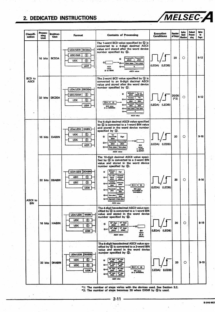
16/32-Bit Binary to ASCII (Decimal) Conversion (BINDA, DBINDA) .................................................... 9-3 16/32-Bit Binary to ASCII (Hexadecimal) Conversion (BINHA. DBINHA) ............................................ 9-8 1613288 BCD to ASCII (Decimal) Conversion (BCDDA, DBCDDA) ................................................. 9-12
ASCII (Hexadecimal) to 16/32-Bit Binary Conversion (HABIN. DHABIN) .......................................... 9-19 ASCII (Decimal) to 16/32-Bit BCD Conversion (DABCD. DDABCD) ................................................. 9-22
Detecting Character-String Length (LEN) ............................................................................................ 9-27 W32-Bit Binary to Character Sbing Conversion (STR. DSTR) ......................................................... 9-29
ASCII (Decimal) to 1W32-Bit Binary Conversion (DABIN. DDABIN) .................................................. 9-16
Device Comment Read (COMRD) ...................................................................................................... 9-25
Character String to 1&32-Bii Binary Data Conversion (VAL. DVAL) .................................................. 9-37 Hexadecimal Binary to ASCII Conversion (ASC) ............................................................................... 9-42 ASCII to Hexadecimal Binary Conversion (HEX) ............................................................................... 9-45 Moving Character Sbing (SMOV) ................................................................ .. ..................................... 9-48 Addition of Character Strings (SADD) ............................................................................................... 9-51 Comparsion between Character Strings (SCMP) ............................................................................... 9-54 Separation into Byte Unlts (WrOR) .................................................................................................... Q-57 Combining Byteunit Data .................................................................................................... 9-60

.................................. .- I ..- . . . . . . . . . . .
10.1 Upperbwer Limit Control (LIMITa DUMIT) ....................................................................................... 10-2
10.3 Zone C o n t r o l (ZONE, DZONE) ......................................................................................................... 10-10 102 . Dead Zone Control (BAND. DBAND) ................................................................................................. 10-6
11.1 Reading Clock Data (DATERD) ........................................................................................................... 11-2 112 Writing in Clock Data (DATMIR) ......................................................................................................... 1 1 ~
r 121
122 12.3 12.4 12.5
126
Extension File Registers ..................................................................................................................... 12-2 12.1 . 1 Exlension file register assignment ......................................................................................... 12-2 12.1.2 How to use extension file registers ........................................................................................ 12-3 121.3 Precautions when using extension file registers .................................................................... 12-4 Changing the Gctension File Register Block Number (RSET) ........................................................... 12-5 Block Move Between Extension File Registers (BMOVR) .................................................................. 12-7 Block Exchange Between Exlension File Registers (BXCHR) ......................................................... 12-10 Direct ReadMlrite of Extension file Register in 1-Word Units ........................................................... 12-1 3 125.1 Device number assigned for direct readiwrite operations ................................................... 12-14 12.5.2 Direct read of extension file reg'kters in 1 -word 'units (2RRD) ............................................ 12-1 6 12.5.3 Direct write of extension file registers in 1-word units (ZRW) ........................................... 12-19
12.6.1 Device numbers assigned for direct readhite operations ................................................. 12-23 12.6.2 Direct read of extension file register in units of bytes (ZRRDB) .......................................... 12-25 12.6.3 Direct write of extension file register in units of bytes (ZFiWD) ......................................... 12-28
Direct ReadMlrite of Extension File Register in Units of Bytes ........................................................ 12-22
. . 13.1 132 13.3 13.4 13.5 13.6
13.7 13.8
13.9
Reading Word Devices in Local Sation (IRDP) ................................................................................ 13-3 Writing Data to Word Devices in Local Station (LWTP) ...................................................................... 13-7 Reading Data from Remote ID Station Special Function Module (RFRP) ....................................... 13-11 Writing Data to Remote VO Station Special Function Module (RTOP), ........................................... 13-15 Link Refresh of Designated Network (ZCOM) (usable with AnUCPU/QCPU-A (A Mode)) ................. 13-20 Reading Data from Word Devices in the MELSECNET/lO Station (ZNRD)
Writing Data to Word Devices in Local Stah (ZNWR) (usable with AnUCPUKJCPU-A (A Mode)) ......... 13-26 Data Read from Special Function Module in MELSECNETA 0 Remote VO Station (ZNFR)
Data Write to Special Function Module in MELSECNET/lO Remote I/O Station (ZMO)
(usable with AnUCPU/QCPU-A (A Mode)) .......................................................................................... 13-22
(Available for AnUCPU/QCPU-A (A Mode)) ........................................................................................ 13-30
(Available for AnUCPU/QCPU-A (A Mode)) ........................................................................................ 13-33
14.1 Precautions for Using special Function Module lnstnrctions ............................................................. 14-2 142 AD6l(S1) High-speed Counter Module Control Insttuctions ............................................................. 146
14.2.1 Setting preset data (PVWR1 . PVWR2) .................................................................................. 14-7 I E p u p 6 2 3 1 - F
._ I_ . . . . . . . . . . ._ .................... - __- ...... . .

. ...... .... . . . . . . . .... .- ........................ ._.. ...
142.2 Setting comparison reference data (SVWR1 . SVWR2) ......................................................... 14-9 14.2.3 Reading present value (PvRD1. PVRM) ............................................................................ 14-11
14.3.1 Outputting required number of characters to printer (PRN) ................................................ 14-1 4 14.3.2 Outputting characters to printer up to 'eon' code (PR) ........................................................ 14-17 14.3.3 Reading data from memory card (GET) .............................................................................. 14-20
14.4 AJ71C24(S3. S6. S8yA171UC24 Computer Link Control lnstnrdions ............................................ 14-26 14.4.1 Sending designated number of bytes of data m n o p r o t o c o l mode (PRN) .......................... 14-27 14.4.2 Sending data up to OOH code in noprotocol mode (PR) ...................................................... 14-31 14.4.3 Receiving data in no-protocol mode (INPUT) ...................................................................... 14-35 14.4.4 Reading communication status (SPBUSY) ......................................................................... 14-41 14.4.5 Forced stop of communication processbg (SPCLR) ........................................................... 14-43
14.5 AJ71C21(S1) Terminal Interface Module Control Instructions ......................................................... 14-45
14.5.2 Sending data up to O O H code (PR2. PR4) ............................................................................ 14-50
14.5.4 Reading RAM (GET) .......................... ................................................................................. 14-60
14.3 AW(S1) M m CetVCENTRONlCS Inteh Module contrd lnshuctkns ............................. 14-13
14.3.4 -Writing data to m"IOry Card (PUT) ..................................................................................... 14-23
14.5.1 Sending designated number of bytes of data (PRN2. PRN4) ............................................. 14-46
14.5.3 Receiving data (INPUT2. INPUT4) ...................................................................................... 14-54
14.5.5 Writing data to RAM (PUT) .................................................................................................. 14-64 14.5.6 Reading communication status (SPBUSY) ......................................................................... 14-68 14.5.7 Forced stop of communication processing (SPCLR) ........................................................... 14-70
14.6 MELSECNET/MINI-S3 Master Module Con t ro l Instructions for A171 PT 32(S3) .............................. 14-72 14.6.1 14.6.2 14.6.3
14.6.4 14.6.5 14.6.6 14.6.7
Precautions on using A171 PT 32(S3) c o n t r o l instructions ................................................... 14-73 Key data entry from operating box (INPUT) ........................................................................ 14-74 Data communication with the AJ35 PTF-R2 ........................................................................ 14-78 (1) Sending data in no-protocol mode by designating the number of bytes (PRN) ........... 14-78 (2) Sending data up to OOn code in n o p r o t o a ~ l mode (PR) ............................................... 14-82
Communication with remote terminal modules (MINI) ......................................................... 14-01 (3) Data communication in neprotocol mode (INPUT) ...................................................... 14-86
Enor resetting with remote terminal modules (MINIERR) ................................................... 14-96 Reading communication status (SPBUSY) ......................................................................... 14-98 Forced stop of communication processing (SPCLR) ......................................................... 14-1 00
15 . PROGRAM SWITCHING INSTRUCIION (USABLE WITH MUCPU) ........ - ........U.n........ .. ..... 151-15-7
15.1 Switching between Main Program and Designated Sub Program (1 to 3) (ZCHG) (Usable with A4UCPU) .......................................................................................................... 152
16.1 162 16.3 16.4 16.5 16.6 16.7 16.8 16.9
Instructions for Use of the CC-Unk Dedicated Instructions ................................................................ 16-2 Network Parameter Setting (RLPA) .................................................................................................... 16-3 Automatic Refresh Panuneter Settlng (RRPA) ................................................................................... 16-7 Read from Automatic Updating Buffer Memory ( R I F R ) ......... .......................................................... 16-14 Write to Autometic Updating Buffer Memory (RITO) ........................................................................ 16-16 Read from Intelligent Device Station Buffer Memory (RIRD) ............................... ............................. 16-18 Write to Intelligent Device Sation Buffer Memory (RWT) ................................................................ 16-23
Write to Intelligent Devim W o n Buffer Memory (with Handsheke) (RISEND) ................................ 16-32 Read from Intelligent oevice Station Buffer Memory (with Handshake) (RIRCV) .. " ........................ 16-28

. . .
17 . 1MS TIMER SETTING INSTRUCTION (QCPU-A (A MODE) ONLY) ......................................... 17-1-17-4
17.1 lms Timer Setting (ZHTIME) ...................................................................................................... 17-2
18 . ERROR CODE LIST .................................................................................................................. 1&1-1&30
18.1 Reading Error Code .................................................................................................................... 18-1 18.2 Error Code List for AnACPU ....................................................................................................... 18-1 18.3 Error Code List for the AnUCPU. A2ASCPU and MUSH board ................................................ 18-8 18.4 Error Code List for AnSHCPU ................................................................................................... 18-1 7 18.5 Error Code List for WPU-A (A Mode) ...................................................................................... 18-22
APPENDICES ............................................................................................................................... APP-1 -APP-8
APPENDIX 1 PROCESSING TIME LIST .......................................................................................... APP-1 APPENDIX 2 INTERNAL REPRESENTATION OF FLOATING-POINT REAL NUMBERS .............. APP-7
IB(NA)66251 -G
.
1. INTRODUCTION
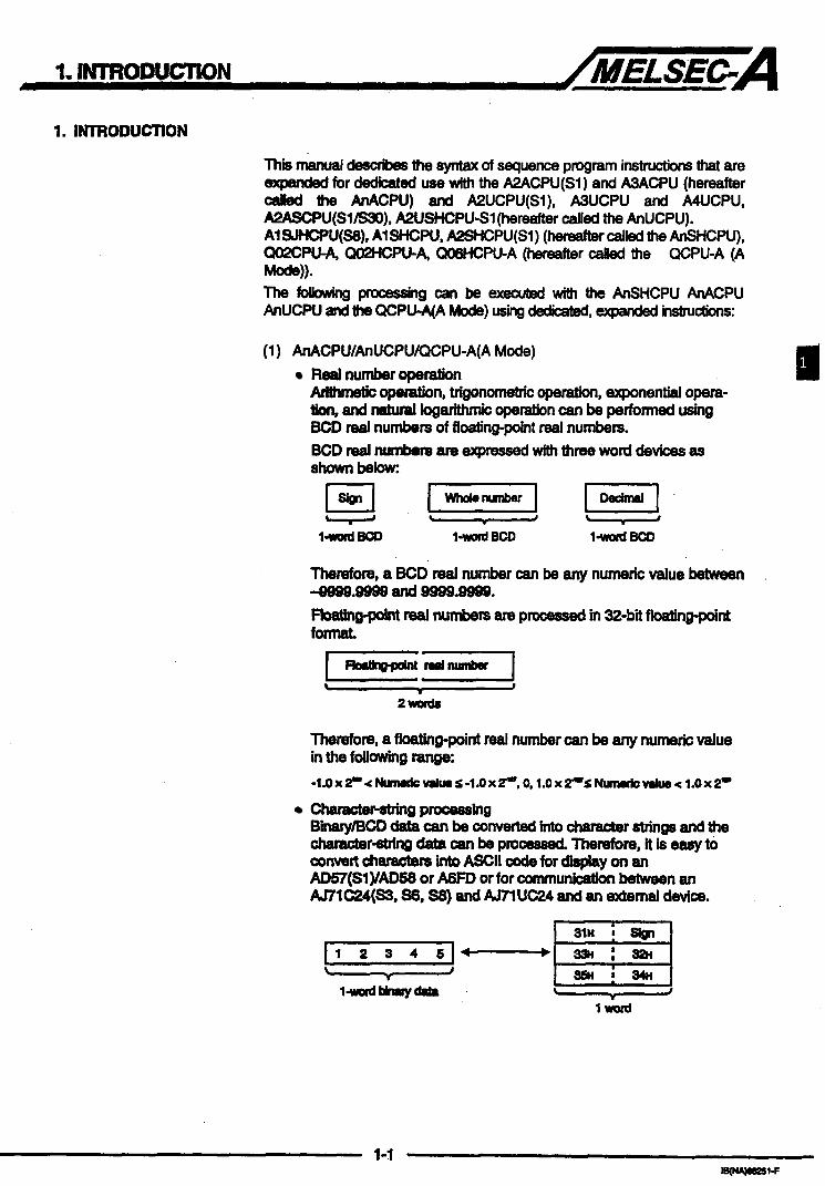
This mentlal des& the syntax of sequence program instructions that are expernded for dedicated use with the A2ACPU(S1) and A3ACPU (hereafter called the AnACPU) and A2UCPU(S1), A3UCPU and AWCPU, A2AScPU(SlIs30), A2USHCPU-Sl (hereafter c a l l e d the AnUCPU). AlSJHCPU(SB), A1 SHCPU, A2SHCPU(Sl) (hereafter called the AnSHCPU), QoxPlJ-A, QO2HCPUA, QOBHCPU-A (hemafter called the QCPUA (A -1). The folbmng prooessing can be execubed with the AnSHCPU AnACPU AnUCPU and the QCPU-A(A Mode) using dedi-, expanded instructions:
(1) AnACPU/AnUCPU/QCPU-A(A Mode) Realnumberoperation Arithmetic operation, trigonometric operation, exponential opera- lion,andnehrrallogarithmicoperationcanbeperformedusing BCD real numbers of floating-point real numbers. BCDdnumkmamexpressedwiththreeworddevkesas shown below:
L J I l GI.
Therefom, a f loat ing-point real number can be any numeric value in the foUowing range: - 1 ~ ~ ~ ~ ~ ~ ~ 5 - 1 . 0 ~ ~ " : 0 , 1 . 0 ~ T S N u n w l o ~ < 1 . 0 ~ 2 ~
charader-gtringprocrrssing BinaryIBCD data can be conve&d into character strings and the charactergtring data can be pmcsssed Therefore, it is easy to convefi charactem into A S C I I code for display on an AD57(Sl)/ADsB or A6FD or for curnrnunlcetion between an AJ7lC24(sS, S6, SS) and MlUC24 and external device.

-ring P W M StnrChrrIng proorams makes it possible to create efficient pmg- rams.Therofore,pragramsiteconbereduced. For exampla, iiis possible to create the same format arcub in whiehonlythedevlcenumbemdifferwiththeD(andIXEN0inst- Wns, to dmge the amadion staius timing (FCALL instrudion) af the PIA, m, and OUT btn~ctiom in a subroutine program, and to fordblyteninate a FOR-NEXr loop with the BREAK inst- N d i O n .
Thevacant~inamemorycassettecanbeusedasan~ don area for file registers (R), increasing the file register capacity. Controlling spedal function modules An AD61 (SI), AO59(Sl), An1 C24(S3, S6, Se)/AJ71 UC24, AJ71C21(Sl),orAJ7lPf52-S3, AlsJ71C24-R2(R4, PRF),
be c o n b U e d without being aware of inputloutput signals and buffer .? '. I
EXP=wJ fk reaiotem (R)
Ai 5571 UC26R2(R4, PRF), A1 SJ71 PT32-S3, AlSD62(E, D) an
memoIycrddr4Yjses. -
(2) AnSHCPU Controlling CGLink Automatic refresh setting with mastem module and data com-
. munication with a FBmote station connected to CC-Link are made.
Refer to the fotlowing m u & for information on any instructions that arenotdescribedinthismanual:
ACPU Programming Manual (basic) IB (NA-49 ACPU Programming Manual (commoninsbudions) 'IB (NA)-66250 AnACPU/AnucPU Programming Manual (AD57 control instructions) ' IB ( N A Y AnACPU/AnUCPU Programming Manual (PID control Instnrctions) IB (NA)-66258
Refer to the following manuals for information on the use of the AnSHCPU, AnACPU, AnUCPU and QCPU-A (A mode):
A2A(S1 )/A3ACPU Uesr's Manual IB(NA)-66544 MU(S1 )/A3UCPU/A4UCPU Uesr's Manual IB(NA)-66436 MSCPU(S1) Uesr's Manual IB(NA)-66455 A1 SJWA1 WMSHCPU(S1) Uesr's Manual IB(NA)-66779 MUSHCPU-S1 Uesr's Manual IB(NA)-66789 QCPU-A(AMode) Uesr's Manual SH(NA)-080065 A161 BT11, A1 SJ61 BT11, CC-Link system Master Local Mdul Uesr' s Manual IB(NA)-66721
The dedicated instructions which can be used differ according to ~
CPU type. Please confirm that it is possible to use the desired instruction in section 2.1 'Classification of dedicated instructions'.
(? 7 d ' .
I
I
, !
1 I

, ... , , .“ . . ..
2. DEDICATED INSTRUCTONS
21 ClrssHication of Dedicated kutnrctions
21.1 Dedicated instructions for AnACPU
Direct processing insbvcEkn
Inputloutput operatbn i m
Data link instnrction
Section 14
. .. .. , .. I

2.1 9 Dedicated instructions for AnUCPU
AD61(s1)oontrd
Output of data to a printer, readkrite of data with a memoly 'ADS(S1) contrd
Reedingowrddueandwritingsetdataandpresetdate instmtkm
insbuctkn cerd
~ n i c 2 i ( s i ) conw
Data communication vvith a remote terminal unit in the A171 m - S 3 control
Data communication with an external device in the no-pro- inamtion tcdmodeendRAMdatareadlwrite
indNctiOn MELSECNET/AAINi-S3 Qta ilnk S y S t m
Program switching instruction section 15 Switches to a designetsd protram (main p q m , subpro- (MUCPU only) gram 1 to 3).
used to make automplic mfresh setting betwen AnUCPU
remote statkm connected to CGLhk C C L i n k d e r h t U d ~ ' 1 Section 16 andmester/kcalmoduleanddatecommunicationwitha
'1 : Usable with the following versions of software.

r
r
2. DEDJCATED~NSTRUCTIONS .. ' ..... 1 . . /MELSEC-A 2.1.3 Dedioatad inrbuczkrw for AnSHCPU
2.1.4 Dedicated imtnrctions for QCPU-A (A k d a )
I Dksctprocessing insbuclion
I I Data menipulatkm instruction
pattern. and sukoutine program non-execution Executes the following processing: Exchanging the upper and l o w e r bytes in the data, pertial Section6 extracbion of data, and joking dace
Detacontrolinstruction
Ckdc imtructlon
Expension file reglster l n s t r u c t k n
Data link in- executes data comrnunicatkn &the MELSECNET/lO Stetkns. I
lms Umer setting inanrction (QCPU-A.(A Mode) only) I Section17
2-1 -2 IB(NA)S825l-F

2.1.5 Special function modules that can be used by special function module in8fruction8
,
2-1-3 IB(NA)66251-F
I 1'

2. DEDICATED INSTRUCTIONS /MELSEC-A 2.2 Reading Instruction Lists
P Classif ,- d o n
BIN to
:haracter decimal -
- R O C e S -
sing Unit -
16 bits
T P B
i
Format
~
Contents of Processhg
The 1-word BIN value specified by (sz) is converted to the character string
specified by :51) and the result is stored adding a decimal point at the position
in the word device number specified by 8.
-ria
The 2-word BIN value specified by (sz) - ILEDA) ILEDB)
0. . . . . . . . . Classifies instructions by application 0. . . . . . . . . Indicates the processing unit when an instruction is
executed
Rocessing Unit I Device Number of Points I X, Y, M, L, S, F, B
l p o i n t T , C , D , W , R , A , Z , V
Max. 16 po in ts in un i ts of 4 points
2 points T, C, D, W, R, AO, 2
Max. 32 po ints in un i ts of 4 points X. Y, M. L, S, F, B
~ ~~~~~ __
16-bit
32-bit
0. . . . . . . . . Indicates the name of the instruction used in a sequence program The instruction symbols are defined on a basis of 16-bit instructions. Instructions that can be processed in units of 32 bits are identified with a "D" at the head of the instruction symbol.
Example: 16-bit instruction--..--..- DABlN 32-bit instruction-........ DDAB I N -
t Designation of a 32-bit instruction
@ . . . . . . . . . Indicates the instruction symbol used in the ladder circuit
Condition instruction to be used
Indicates the beginning of a dedicated instruction rz-l} ... for Speciiy the operation the data and to be the used de-
I vice where the result of the operation is to be stored
cated instruction Indicates the end of a dedi- LEDR ......
Refer to Section 3 for details.

2. DEDICATED INSTRUCTIONS /MELSEC-A 0. . . . . . . . . Indicates the processing of each instruction
I Indicates 16-bit data 32-bit data
(first 16 bits) (last 16 bits)
0 + 2 1 1 0 + 3 7 1 t
Indicates the 4 con- vice number de- Indicates the de-
secutive device num- signated with a bers beginning with the device number de- signated with an %: Indicates the device number
next to the one designated with a @
8. . . . . . . . .
n/f indicates the execution timing of an instruction.
(LEDA) (LEDB)
1' Indicates the timing for
Indicates the timing for [ LEDB 1 instruction-name I I LEDA 1 instruction-name I
Symbol I Execution Timing
An instruct ion is always executed regardless of (Always) whether the condit ion for executing the instruct ion
is ON or OFF.
n An instruct ion is executed in every scan whi le the condi t ion for execut ing the instruct ion is ON.
f An inst ruct ion is executed only once at the leading edge of the condit ion for executing the instruct ion.
An instruct ion is executed in every scan whi le the condi t ion for execut ing the instruct ion is OFF.
An instruct ion is executed only once at the t ra i l ing edge of the condit ion for executing the instruct ion.
0. . . . . . . . . Indicates the number of steps of each instruction. Depending on the device to be used, the actual number of steps required for the execution of the instruction may be greater. Refer to Section 3.2 for details.
@ . . . . . . . . . A circle indicates that the device used by the instruction and an index register (Z, V) can be specified for a constant.
@. . . . . . . . . A circle indicates that subset processing can be per-
@ . . . . . . . . . indicates the page in this manual where the instruction is formed.
explained in detail. 2-3
IB 0 66.2514

2. DEDICATED INSTRUCTIONS /MELSEC-A 2.3 Dedicated instruction Lists
(1) to (13) indicate instructions expanded for exclusive use with the AnACPU/AnUCPU/QCPU-A (A Mode). (14) indicates instructions expanded for exclusive use with the AnSHCPU. (1 5) indicates instructions expanded for exclusive use with the QCPU-A (A Mode). (1) Direct processing instructions (AnACPU/AnUCPU/QCPU-A (A mode)
compatible)
~bssifi- cation
Instntc- Tr- dng wn of Svpr Conditions tion Unit
Format Contents of Processing
devices by direct processing. (OUT Output (Y) is output to PC CPU enernal + EDA I M)vT +
- hdp N V ~ Execution w- to P m e Rgc:
Direct output DOUT
OFF a t condition contact OFF ON at condition contact ON
0 17 (Normally) instruction equivalent) 4 LEDC 1 @ /- a2
LEDANDB 1 mET h struction equivalent)
Output (Y ) is set to PC CPU external devices by direct processing. (SET in-
Diren 1 bit
DEST 1 4 1 a 4-4
(LEDAJ (LEDBJ
DRST
Output (YJ is reset to PC CPU external I E D W D B DRST devices by direct processing. (RST in-
Direct reset
struction equivalent) 4-4
(LEDA) (LEDB)
(2) Instructions for structured program (AnACPU/AnUCPU/QCPU-A (A Mode) compatible)
I I Classifi- cation -
Circuit index quali-
fication
Repeat forced
end
Sub- romine
call
Conditions E x d o n
I I Index qualification of each device used I in device qualification circuits.
IX I
(Normally)
IXEND
BREAK
m m ~ BREAK Repeat processmg by FOR to NEXT
execution goes 10 the pointer specified i n m a i o n s are forcibly ended and
LEK3 by 0. 5-5
I Non-executed processing of the sub-
In error check by the CHK i n m a i o n , the check circuit pattern is changed to any
LEDA) (LEDBI
Zhanges in error check circuit pattern
-
(Normally)
EHKEND
+1: The number of steps vanes wfth devices used. See Section 3.2. *2: Index qualification is enabled for the circuit patterns, except the check circuit pattrn.
2-4 18(NA)66251-F
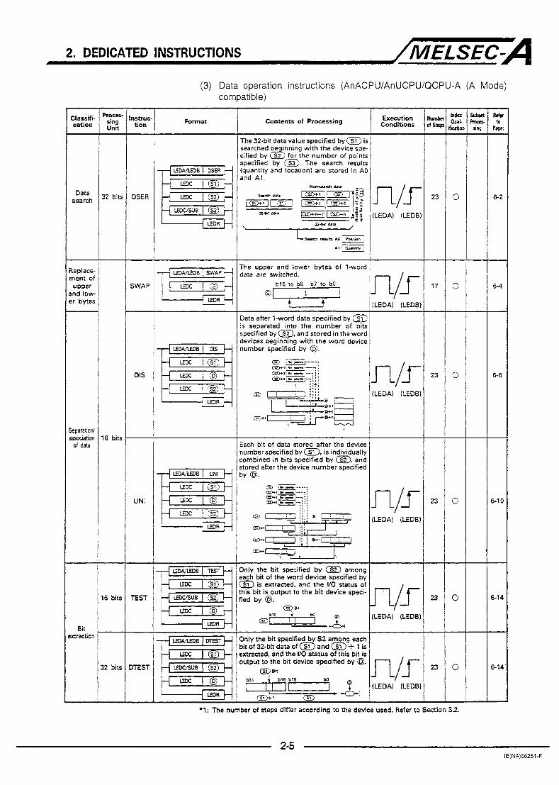
2. DEDICATED INSTRUCTIONS /MELSEC-A (3) Data operation instructions (AnACPUIAnUCPUIQCPU-A (A Mode)
compatible)
Classifi. cation -
Data search
- 3eplace. nent oi
md low ?r bytes
upper
ROCOS- sing Unit -
32 bits
Format Contents of Processing Conditions Execution n m c
tion
DSER
The 32-bit data value specified b y a ia
cified by (& for the number of points searched be inning with the device spe.
specified by (53). The search results (quantity and location) are stored in A0 and A l .
1
The upper and lower bytes of 1-word data are switched.
b15 IO b8 b7 Io bO 01 u
SWAP
[LEDA) ILEDB)
Data after 1-word data specified by (51)
specified by (St), and stored in the word is separated into the number of bits
devices beginning with the word device number specified by @.
DIS
ILEDA) (LEDB)
iepatationi raodation of data
16 bits
numberspecified b y a , is individually Each bit of data stored aher the device
combined in bits specified by (sz, and stored after the device number specified by @.
UNI
Only the bit specified by (sz) among
(s1) is extracted, and the VO status of each bit of the word device specified by
this bit is output to the bit device speci- fied by @. 6 bits TEST
-
)TEST
Bit xtraction Only the bit specified by S2 among each
bit of 32-bit data of a and (s1) -t 1 is extracted, and the VO status of this bit is output to the bit device specified by @.
0 Bn 12 bits
L
*1: The number of steps differ according to the device used. Refer to Section 3 2 .
2-5 IB(NA)66251-F
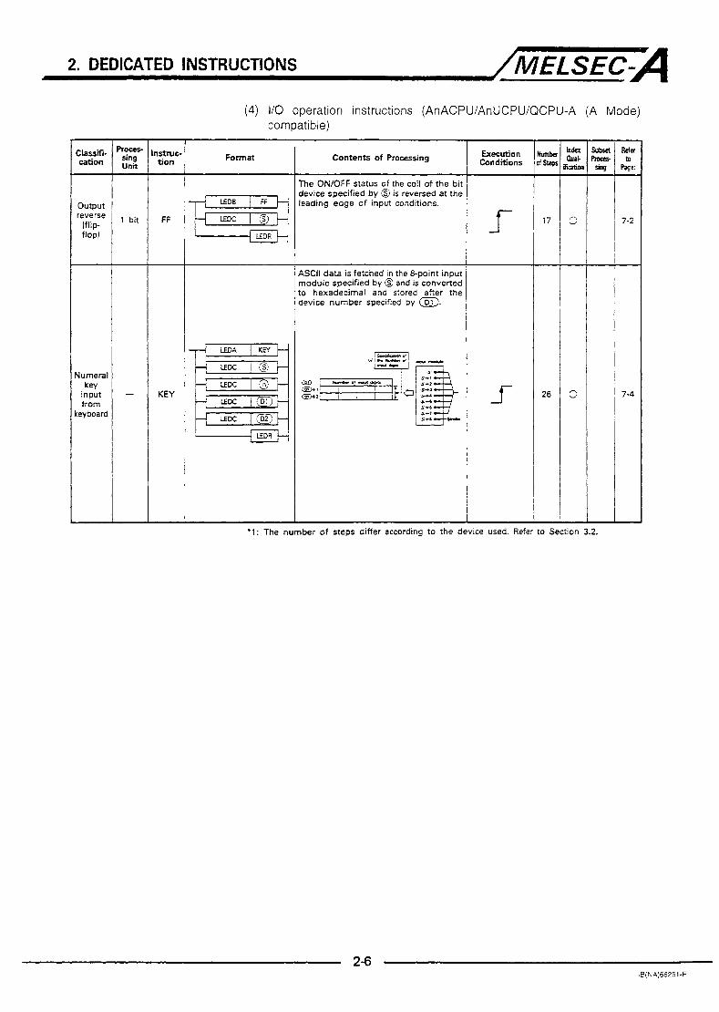
2. DEDICATED INSTRUCTIONS /MELSEC-A (4) IIO operation instructions (AnACPUIAnUCPUIQCPU-A (A Mode)
compatible) - Classifi- cation - Output reverse
(flip- flop)
Jumeral
input from
:eyboard
key
nstruc- tion -
FF
-
KEY
Format
I
Contents of Processing
h e OMOFF status of the coil of the bit jevice specified by 0 is reversed at the eading edge of input conditions.
4SCll data is fetched In the %point input nodule specified by @ and is converted .o hexadecimal and stored after the jevice number specified by
Conditions Execution
f-
f
1 *1: The number of steps differ according to the device used. Refer to Section 3.2.
2-6 IB(NA)66251.F

2. DEDICATED INSTRUCTIONS /MELSEC-A (5) Real number processing instructions (AnACPU/AnUCPU/QCPU-A
(A Mode) compatible) (a) BCD real number processing instructions -
Procer- sing Unir -
16 bits
-
32 bits
- nstntc tion -
BSQR
-
BDSQR
Conditions Execution :1aSSifi-
cation
The square
:alcula- root
of BCD tlon
4/8 digits
Contents of Processing
The square root of the value specified by 9 (BCD 4 digits) is calculated and stored In the word devices number specified by 5).
m- I! lnlegcr
@+i 1-1 DsPrnalr
The square root of the value specified by 3 and @ + llBCD 8 digits) is calculated and stored in the word device number specified by @.
m- Q I - ] intqsr
*+I -1 k m a k
The sine of the value specified by @ (SCD 4 digits) is calculated and stored in :he word device numbers specified by @ f 1 and @ 4- 2.
I lLEDA) (LEDBI
ILEDA) (LEDB)
BSlN
ILEDA) (LEDB)
The cosine of the value specified by @ [BCD 4 digits) is calculated and stored in the word device numbers specified by @ f 1 and @ + 2 .
CE -1sig.
cos B - -1 Integer
B+Z [ I Deurnals
BCOS
(LEDA) ILEDB)
The tangent of the value specified by @ [BCD 4 digits) is calculated and stored in the word device numbers specified by @ f 1 and @ -I-2.
r---lSign
tan 0 - D+I r-1 Integer
-2 -1 h m a k
The angle is calculated from the arcsine [sin -') value specified by @ and is stored in the word device specified by @ [BCD 4 digits).
LEDPJLEDB 1 BTAN
BTAN
-
BASIN
ILEDA) (LEDB) Trigo- nornet-
unction I i C
16 bits
1 sin-' ILEDA) (LEDB)
The angle is calculated from the arwsine (COS -') value specified by @ and is stored in the word device specified by @ (BCD 4 digits].
BACOS
-
BATAN
jslgn cos-' @+l [)Integer -c @,
@+z -1 w m a l s
The angle is calculated from the arctan- gent (tan -')value specified by @ and is stored in the word device specified by @, [BCD 4 digits)
ILEDA) (LEDBI
*I: The number of steps vanes with devices used. See Section 32. *2: The number of steps becomes 26 when DXNR by @is used.
2-7 IB(NA)66251-F

2. DEDICATED INSTRUCTIONS /MELSEC-A (b) Floating point real number processing
Instrue Unit tion Conditions
Execution Classiti- cation -
Real
bers to num-
ntegers
Integer to real num- bers
Format Contents of Processing
The floating point real number specified by 8 is converted to a 1-word integer and stored in the word device number specified by @. i
INT
I Floatmg polnt 1-word real number Integer
11bbit BIN1
I
-
DINT
-
FLOAT
-
IFLOAl
-
ADD
-
SUB
-
M U L
-
DIV
-
The floating point real number specified by @ is convened to a 2-word integer and stored in the word device number specified by @.
ILEDA) ILEDB) Floatmg point 2-word integer real number 13Z-blf BIN1
The 1-word integer specified by @ is converted to a floating point real number and stored in the word device number specified by @.
LEDNLEDB 1 FLOAT
I integer 1-word Floating polnt
Ilbbt! BIN1 real number
ILEDA) ILEDB)
2-word integer specified by @ is con- verted to a floating point real number and stored in the word device number specified by @. ~ ~ ~ - - q + G - l ~ ~
2-word integer Floattng point (324: BIN1 real number
I ILEDA)' (LEDB)
$2 bits
-
l-
The floating point real numbers specified by (57) and (52) are added and the result is stored in the word device num- ber specified by @.
~ ~~
~ ~ ] + m m + q ~ Ic3l I Iyrnbef mrumbn 22s R m n q a m Rc-ngmrn
The floating point real number specified by (s2) is subtracted from the floating point real number specified by (s1) and the result is stored in the word device number Specified by @. ~ m l - b q m l + q ~ ] m m nDmnsm nc-?g$-Q m d n u m b r IUInnnla dnrmbn
I
[LEDA) ILEDB) Algeb- aic o p frations
-
~
The floating point real numbers specified by (s1: and (sz) are multiplied and the result is stored in the word device num- ber specified by @.
The floating point real numbers specified by tsl) is divided by the floating point real number specified by <s2) and the result is stored in the word device num- ber specified by @. mm+mmI+mFl moon -m mppnt rule )olrunk rul-
I
I
*2: The number of steps becomes 26 when DXNR by @is used. *1: The number of steps vanes with the devices used. See Section 3.2.

2. DEDICATED INSTRUCTIONS /MELSEC-A - Roses-
sing Unit -
32 bits
- nstruc tion -
RAD
-
DEG
-
SIN
-
cos
-
TAN
-
ASIN
-
ACOS
-
ATAN
-
SQR
-
q Conditions Contents of Processing 7 W n sing
Classiii- cation -
tngle to radian
Radian o angle
Algeb-
unction raic
Format
The unit of angle size is converted from degrees specified by @ t o radian and the result is stored in the word device speci. fied by @.
( 7 z q ~ ~ ~ - ( j j l ~ rad
FiDanng can1 noany p n 1 M I n v n D e r r e a number
I
The unit of angle size is converted from radian specified by @ to degrees and the
fied by 0. result is stored in the word device speci-
(-1 i ) ) . . 4 -(WI m) ficdnng W,", rea, number
Floarmg m n r M I rambeer
n/s 2o
The sine of the value specified by ($1 is
specified by a'. calculated and stored in the word device
~
The cosine of the value specified by @ is calculated and stored in the word device specified by a.
cos 4-m) - pT
The tangent of the value specified by @
device specified by @. is calculated and stored in the word
The angle is calculated from the arcsine (sin -') value specified by @and is stored in the word device specified by @. n/r/ 2o
The angle is calculated from the arcax- sine (cos-') value specified by @and is stored in the word device specified by Q. n1.1 2o
The angle is calculated from the arctan- gent (tan-') value specified by @ and is stored in the word device specified by @. n/s The square root of the value specified by @ is calculated and stored in the word device number specified by @. n/J 2o I
*I: The number of steps varies with the devices used. See Section 3.2.


2. DEDICATED INSTRUCTIONS /MELSEC-A - Zlassifi cation
- Races
sing Unit -
16 bit:
- In-
tion -
DABCI
~~
Contents of Processing Conditions Execution Format
The 4-digit decimal ASCII value specifiec
and stored in the word device nurnbe by @) is convened to a 1-word BCD valuc
specified by @.
~ - 1 LEDAAEDB IDABCD
(LEDA) (LEDB
\sal t c BCD The %digit decimal ASCII value specifiec
and stored in the word device numbel by @ is convened to a 2-word BCD valuc
specified by @J.
n/f 32 bits IDABCI
The comment of the device specified by 3 is stored as an ASCII value after the word device number specified by @,
Device com- ment read
:OMRt
The length (number of characters) of zharacter string data stored in the word device specified by @ is stored in the word device number specified by @.
haracter string '"sfh etectlon
-
I LEDA) (LED81 I
*l: The number of varies with devices used. See Section 32.
2-1 2 IB !W - 1 4


2. DEDICATED INSTRUCTIONS /MELSEC-A 3assifi- cation -
:haracter
mnpari- son
string
Separa-
mnation oniCorn-
?to units Nf 1 byte
- Pr- sing Unit -
16 bits
-
3TOW
-
Format
L l
Contents of Processing
The character string specified by (sz) is :ompared with the character string spe- :ified by (51) and, if they are identical, he bit devices specified by @ IS turned , n .
h e 1-word data of the number of bytes ,pecified by 8, beginning with the word levice specified by @, is separated into lpper and lower bytes, which are stored n the word devices beginning with the vord device specified by a.
,pecified by @ beginning with the word -byte data for the number of bytes
levice specified by @ are combined into lpper and lower bytes. The results are Rored in the word devices beginning vith the word device specified by @.
Conditions Execution
n/r E D A ) (LEDB
+1: The number of steps varies with devices used. See Section 3.2.
2-1 5 8 I N . 4 662514

2. DEDICATED INSTRUCTIONS /MELSEC-A (7) Data control instructions (AnACPU/AnUCPU/QCPU-A (A Mode)
compatible) - Proces
sing Unit -
16 bit:
32 bits
6 bits
-
lnStm1 tion
LIMIT
Format Contents of Processing
The value specified by (53) is processec to the data with fixed ran es by upper lower limit values set in &/a an( the result is stored in the word devict number specified by @I. - (s3) < (s1) when:
5 S (sz) when Value of (sl) is stored
< (53) when: Value of (53) is stored
Value of a is stored
The values specified by (a + 1, (53) are processed to the data within fixec
by upper/lower limit values set lr + 1. 0~Js2) + I , 0) anc :he results are stored in the word devlce numbers specified by 4- 1, @), -(m+1,(53))<(0+1,(s1,
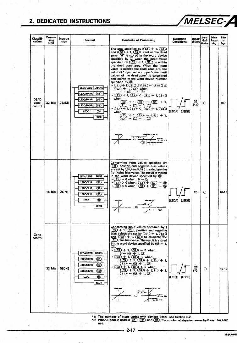
h e area specified by (s1) and <s2) is st as the dead zone. '0" is stored in the vord device specified by @when the nput value specified by <53) is within he dead zone area. When the input ralue is outside the zone area, the value If "inputvalue-upperAower limitvalues I f t he dead zone' is calculated and xored in the word device number
Conditions Execution
LEDA) (LEDB
n/r LEDA) (LEDBi
L J *1: The number of steps varies with devices used. See Section 3.2. *2: When DXNR is used in 0, (52). and 0, the number of steps increases by 6 each for each use.
2-1 6 IB(NA)66251-F

2. DEDICATED INSTRUCTIONS /MELSEC-A (8) Clock instructions (AnACPUIAnUCPUIQCPU-A (A Mode) compatible)
T T
Proces- sing Unit -
16 bits
Inrrmc tion -
DATERC
-
IATEWR
~~
Format Conditions Execution Zlassifi-
cation
Clock data read/ wrlte
Contents of Processing
i ~~~~ ~~
Clock data is stored as a BIN value In thc word devices
specified by (D!. beginning with the word devlce number
BIN value - D 1 Year 110 10 991
D t l I1 10 121 [ p z q LEDbJLEDB DATERD
EDR
l7 ! ':'
D+21 Date j 11 10 321
[CloctdaraJ 4 '0'+3 F l 10 10 231
.D'+4 F] 10 lo 591
0 1 5 io to 59)
D +6 F l 10 to 61
T Clock data (BIN value) set in the word devices beginning with the word device number specified by 'CS) is written to the clock.
BIN value s / - T z 7 1 1 0 10 991
s,+1 [ M o n t h 1 I 1 10 121
'S,+4 F1 IO to 591
,S'+2 F] I1 to 321
.s+3 F] 10 IO 231 - 'FJ 'SI+S (0 to 591
' 5 + 6 j ] 10 lo 61
(LEDAI (LEDBI
(9) Extension file register instructions (AnACPU/AnUCPU/QCPU-A (A Mode) compatible) -
Classiii- cation - Block
cifica- tion
40. spe
Block move
Format Contents of Processing Conditions ofS(cp Execution Numbe~
The block number of an extension file register is changed to the number speci- fied by (2.
The number of points, specified by @, of the content of extension file register specified by (s1) is transferred to the extension file register specified by a.
16 bits
The number of points. specified by @, of the content of the extension file register specified by cD1) and (DZ) is replaced.
Block uchange BXCHR
-
23
'1: The number of steps varies with devices used. Refer to Section 3 2 for details.


2. DEDICATED INSTRUCTIONS /MELSEC-A (12) Special function module instructions (AnACPUIAnUCPUIQCPU-A
(A Mode) compatible) AD61 (S1 ) high speed counter module control instructions
Xassifi cation -
'resen1 value data ietting
-
Set talue data rite fo corn- arison and oinci- lence jenti- cation
-
'esent ,slue .cad
-
lnstrul t ion -
PVWR'
I Proces
sing Unit -
Contents of Processing Execution Conditions Format
Preset data specified by @ is written to CH. 1 of the ADBl(S1) specified by 0.
n/r 1 (LEDA) (LEDE
Preset data specified by @ is written t c CH. 2 of the AD6161) specified by 0.
LEDAAEDB PVWRZ
LEDR (LEDA) (LEDB
Set value data specified by @ is wriner to CH. 1 of the ADBl(S1) specified by 3.
n/r I
1
Set value data specified by @ is written to CH. 2 of the ADBl(S1) specified by 0.
(LEDA) (LEDB
The present value of CH. 1 of the 4D61(S1) specified by @ is read and stored in the word device number speci- Red by 0.
I- t
The present value of CH. 2 of the 4D61lS1) specified by @ is read and ;tored in the word device number speci- 9ed by @.
I E D A ) (LEDBI
'1: The number of steps varies with devices used. See Section 3.2.
2-22 IB(NA)66251-F
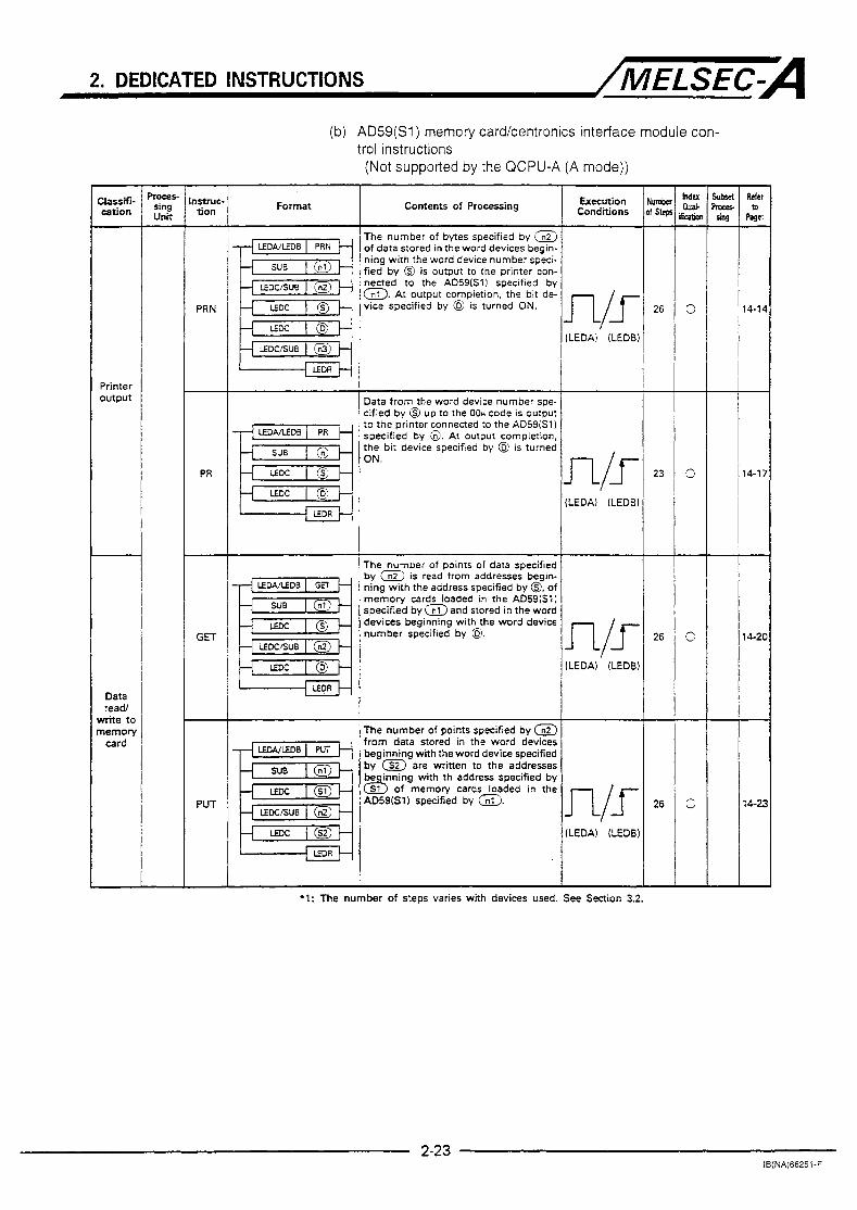
2. DEDICATED INSTRUCTIONS /MELSEC-A (b) AD59(S1) memory cardkentronics interface module con-
trol instructions (Not supported by the QCPU-A (A mode)) -
nstnrc tion -
PRN
Conditions Format Contents of Processing
The number of bytes specified by inz) of data stored in the word devices begin- ning with the word device number speci- fied by @ is output to the printer con-
a. At output completion, the bit de- neaed to the A D 5 9 6 1 ) specified by
vice specified by @ is turned ON. n/!i 26 LEDA) (LEDB)
Printer output Data from the word device number spe-
to the printer connected to the AD59(Sl ) cified by 0 up to the O O H code is output
specified by 3. At output completion, the bit device specified by @ is turned ON. n/ri 23
PR 14-1i
-
14-2c
-
14-2:
I
The number of points of data specified by (nz) is read from addresses begin- ning with the address specified by @, of
specified by (nr) and stored in the word memory cards loaded in the AD59(S1)
devices beginning with the word device number specified by @. GET
-
PUT
Data
write to read
nemory card
T h e number of points specified by (n2) from data stored in the word devices beginning with the word device specified by (52) are written to the addresses be inning with th address specified by
AD59E1) specified by m. S1 of memory cards loaded in the CQ I
* l : The number of steps varies with devices used. See Section 3.2.
2-23 IB(NA)66251-F

2. DEDICATED INSTRUCTIONS /MELSEC-A ( c ) AJ71C24(S3, S6, S8)/AJ71 UC24 computer l i n k unit control
instructions (No-protocol mode application instructions) -r
Zlassifi. cation -
Data send
Roces. sing Unit
n m c t ion -
PRN
Format Contents of Processing Conditions Execution Mer
to Page: -
14-27
I I' T The number of points specified by (nz>
of dara in the word devices beginning wirh the word device number specified by @ is output in the no-protocol mode from the RS-232URS-422 of the AJ71C24(S3. S6, S8)/AJ71UC24 specified by (nl). At output completion, the bit device specified by @ is turned ON.
~ ~ _ _ _ _ _ _
LEDA) ILEDBI
Data from the word device number spe- cified by @ up to the OOH code are output in the no-protocol mode from the RS- 232c/RS422 of the AJ71C24(S3, S6, S8)/ AnlUC24 specified by 0. At output completion, the bit device specified by a is turned ON.
PR 14-3 1 3
c
The number of points specified by (n2) of data received in the no-protocol mode to the RS-232QRS-422 of the AJ71C24(S3,S6, S8)/AJ71UC24specified by (nl) is stored in the word devices beginning with word device number specified by(. At processing cornple- tion, the bit device specified by a is tumed ON.
Data receive INPUT 14-35
The sendlreceive processing status of the AJ71C24(S3, S6, S8)/AJ71UC24 spe- cified by @ is stored in t h e word device number specified by @#. nunica.
Corn-
ion sta us reat
-
Forced StOD
0
0
-
SPBUS!
SPCLF
14-41
14-42
ILEDA) (LEDB) c Sendreceive processing of the AJ71C24(S3, S6, S8VN71UC24 specified by 8 is forced to stop.
LEaeJLEDB SPOR
LEOR
I ! :LEDA)'. (LEDE
(d) AJ71 C21 (Sl) computer link unit control instructions (Not supported by the QCPU-A (A mode))
I
Contents of P r o w i n g Conditions Execution Format
LEDALEDB PRNZ
cation Unit
Send data of speci- fied
of bytes number
The number of points specified by in2) of data stored in the word devices begin- ning with the word device number speci- fied by @ is output in the no-protocol mode from the RS-232C of the MlC2l(Sl) specified by (nl. At out- put completion, the bit device specified by @, is turned ON.
PRNZ 1 The number of points specified by (n2) of data stored in the word devices begin- ning with the word device number speci- fied by @ is output by the nc-protocol mode from the RS-422 of the AJi'lC2l(Sl) specified by 0. At output completion. the bit device specified by @ is turned ON. (LEDA) (LEDB)
*l: The number of steps varies with devices used. See Section 3.2.
2-24 lB(NA)66251-F

2. DEDICATED INSTRUCTIONS /MELSEC-A - Classifi- cation
Data send up
code to OOH
Data received
Rea& write to the RAN memob
- ISrmC- tion -
PR2
-
PR4
-
NPUTZ
NPLIT4
-
GET
-
PUT
Format
u LEDR
Contents of Rocessing Execution Conditions
~~ ~ ~~~~~ ~~~ ~~ ~ ~ ~ ~~
Data stored in the word device numbers
specified by @ and up to the OOH code beginning with the word device number
are output in the no-protocol mode from the RS-232C of the AJ71C2(S1) specified
device specified by (0; is turned ON. by @. At output completion, the bit n/J
ILEDA) (LEDB)
fied by 'SI up to the OOH code are output Data from word device numbers speci-
422 ofthe AJ71CZ(Sl) specified by lg . At by the no-protocol mode from the RS-
output completion, bit devices specified by @ are turned ON.
ILEDA) ILEDB)
to the RS-232C of the AJ71C21(S1) speci- 1 of data received in the no-protocol mode
fied by (nli 15 stored in the word devices beginning with the word device
completion, bit device specified by ( D Z ) number specified by <D1). At processing
are turned ON. 1 ILEDA) (LEDB! I
The number of points specified by (nz) j of data received by the no-protocol mode to the RS-422 of the AJ71C211S1) specified by (nli is stored in the word devices beginning with the word device number specified by (ol>. At processing completion, bit devices specified by co2: are turned ON.
(!IDA) (LEDBI
The number of points specified by <n2) of data is read from the addresses begin- ning with the address specified by @ of the RAM memory of the AJ71Ql-Sl specified by (nl) and stored in the word devices beginning with the word device number specified by (D1). At processing completion, the bit device specified by (D2) is turned ON. (LEDA) (LEDB:
The number of points specified by (n2) of data stored in the word devices begin- ning with the word device number speci- fied by (sz) is written in the addresses
Inning with the address specified by
AnlC21-Sl specified by (nl). At pro- of the RAM memory of the
cessing completion, the bit device speci- fied by @ is turned ON. (LEDA) (LEDE
&
*l: The number of steps varies with devices used. See Section 3.2.

2. DEDICATED INSTRUCTIONS /MELSEC-A - Proces-
sing Unit -
-
- nstruc tion -
SPBUSY
-
SPCLR
Format Contents of Processing Execution k m h Cond'kions d Stq
krhn Rda hrn
Page:
I 4 4 8
14-70
CLaSSifi- cation
specified by 6) is stored in the word device number specified by @.
Com-
tion sta- munica-
tus read I
Processing of the AJ71C21iSlJ specified by is forced to stop.
i I LEDM/LEDB SPCLR Com- munica- tion pro- cessing forced stop
I (LEDAI (LEDBI
(e) AJ71PT32-S3 MELSECNET/MINI-S3 master module con- trol instructions
'races- sing Unit -
Format Conditions Execution Zlassifi-
cation Contents of Processing
<ey input data from the operation box ;pecified by (n3) connected to the U71PT32-S3 specified by (nl) is read and stored in the word devices begin- 7ing with the word device number speci- 5ed by (D1). At processin completion, :he bit device specified by is turned 3N.
Key in- ut from opera- ion box
INPUT
(LEDAI (LED61
The number of points specified by (nz> 3f the data stored in the word devices beginning with the word device number specified by @ is output to the Al35PTF- R2 specified by (n3) connected to the C1171PT32-S3 specified by (nr. At pro- cessing completion, the bit device speci- fied by @I is turned ON.
PRN
Data sendl
receive of
sped- fied
number >f bytes to and rom the A135 PTF-R2
Data from the word device specified b y @ up to the OOH code is out ut to the AJ35PTF-R2 specified by & con, neded to the AJ71PT32-S3 spcified b y m. At processing completion, the bil device specified by @ is turned ON.
PR
'1: The number of steps varies with devices used. See.Section 3.2.

2. DEDICATED INSTRUCTIONS /MELSEC-A nstruc. tion -
INPUT
Format Contents of Processing 3assifi- cation - Data sendl
receive o i
speci- fied
lumber If bytes to and rom the N 3 5 - PTF-RZ
Data within the number of points speci- fied by (n2) of data from the AJ35PTF- R Z specified by Cna) connected to AJ71PT3Z-S3 specifled by <nl) is stored in the word devices beginning with the word devlce number specified by (E. At processrng completion, the bit devlce specified by (D2) is turned ON.
(LEDA) (LEDB)
Communication with the MINI standard protocol remote terminal module con- nected to the A171 PT32-S3 speciiied by 5, is executed.
L D A MINI
SUB
instruction i i--------J
MINI stan- dard
xotocol nodule
data rea& write
MINI
Error reset at the occurrence of a remote terminal error is executed to the AJ71PT3233 specified by 3.
eset for Error
the remote erminal nodule
nunica- Com-
ion sta- us read
dINIERR
-
SPBUSY
-
SPCLR
-
I
(LEDA) (LEDB)
The processing status of the AJ71PT32- S3 specified by @ is stored in the word device specified by @.
n/! 2o I
Communication processing between the AJ71PT32-S3 specified by @ and the remote terminal module is stopped only for the remote terminal module specified by 0. LEDANDB SPUR
nunica- Corn-
ion pro- cessing forced
S O P
n/f/ 2o
'1: The number of steps varies with devices used. See Section 3.2.
2-27 IB (NAI 662514

2. DEDICATED INSTRUCTIONS /MELSEC-A - Classifi- cation
- Proces-
sing Unit
- Instruc.
tion Conditions
- R d n ta
Page: Format Contents of Processing
Al35PTF-R2 is designated by (n3) con- nected to A171 PT32-S3, which is desig- nated by Cnl). Data from the A135PTF-
designated by (n2, and is stored in the R2 is read within the number of points
word devices begmnlng with the word device number designated by 0. At processing corn letion, the bit device designated by & is turned ON.
Data send /receive of desig-
nated
of bytes number
to and from the
FTF-W AI35
INPUT 14-91
-
14-97
0 I
0
T ~
Communication with the MINI standard protocol remote terminal module con- nected to the AJ71PT32-S3 designated by 0 is executed.
~ ~~
MINI standard protocol module
data read
Write
n 17+C MINI
iLEDA’ I Error reset at the occurrence of a remote terminal error is executed to the AJ71PT3263 designated by 0.
Enor reset for the re mote ter-
module minal
munica- Com-
tion sta- t u s read
14-10:
-
l4lOt
n/s 17 MINIERR
-
SPEUSY
-
SPCLR
+ ‘LEDA) (LEDB)
The processing status of the AJ71PT32- S3 designated by 6 is stored in the word device designated by @. n/r 2o
:LEDA) (LEDB)
Communication processing between the AJ71PT3263 designated by @ and the remote terminal module is stopped only for the remote terminal module desig- nated by 0.
Com- munica- tion pro- cessing forced stop
- UaSSiti- d o n -
Switching to desi*
nated prW3-m
14-10:
- ILEDA) (LEDB!
(1 3) Program switching instruction (A4UCPU compatible)
h s y Instnrc- Format Contents of Processing becrrtion d Sbpr Conditions tion HU* 2
Unit Rgc:
-I LEDT~ Switches to the main program.
Lml I Z W I H Switches to sub program 1.
ZCHG 15-2 13 LEDA I ZCHG2 H Switches to sub program 2.
’ (LEDA! L D A 7-H ZWG3 Switches to sub program 3.
*1: The number of steps varies with the type of devices used. See Section 3.2.
2-28 IB(NAi66251-F

2. DEDICATED INSTRUCTIONS /MELSEC=A (14) CC-Link instructions (AnUCPU/QCPU-A ( A Mode)/AnSHCPU . .
compatible)
Format Contents of Processing
- Classifi- cation
- Proces.
sing Unit -
Execution Conditions
~
RLPA Sets the network parameter data set at the devices beginning with the one specified a1 @)to the master module specified at 0.
LEDC
Network pararne- fer setting
Auto- matic refresh parame- ter setting
Read from auto- matic rrpdam wffer memory for specified mtelli- pent device station Pirite to auto- “tic updating wffer memory lor spedfied ntelli- 3Wt kvice jtation
RLPA
-
RRPA
I Sets the devices and numbers of points on which automatic refresh will be made between the AnSHCPU and masterhxal
(LEDA) (LEDB]
R e a d s the points of data specified at @ from the automatic updating bcrtfer memory addresses beginning with the one specified at 0 for the station having the station number specified at @ in the master
@ module specified at 0. and stores that
data into the devices starting from the one specified at a.
L E W S U B @
RlFR
1
writes the points of data specified at @ from the devices s ta~ng from the one specified at @ to the automatic updabng bcrtfer memory addresses beginning with the one smfied at @ for the station having the station number specified at @ in the master module specified at 0.
RiTO
Reads the points of data specjfied at @ +1 from the buffer memry addresses begin-
the remote station having the station number specified at @ and connected to the master/locat d u l e s p e ~ i f i e d at @, and stores that data into the devices stan- ing from the one specified at @A. On read completion. the ba device specified
ning with the one spedfied at [ @ +3] in
n/r RlRD [LEDA) ‘ (LEDB)
1 at @ switches on one scan. On abnormal con-@etmn, the bit device at
I @+I switches on one scab ~ writes the points of data speclfiec~ at @+I 1 from the devices starting from the one I at @A to the buffer memory I addresses beginning with the one specified at [@+?,].in the rermte station having the station number specified at @ and con- nected ~LI the masterAccaI module specified
Nile to emote ;talion M e r mmory
w
On abnomsal complebn, the bit device at @+I switches on one scan.
2-29 IB(NA)66251.F

2. DEDICATED INSTRUCTIONS /MELSEC-A
Read from intelli-
device gent
station RIRCV buffer memory (with hand- shake)
Write to intelli- gent device station bufier memoiy (with hand- shake)
RISEND
Format Contents of Processing
Reads the points of data specified at @ +1 from the buffer memory addre-
at [a +3] in the intelligent device sta- tion having the station number speci- fied at @ and connected to the mas- ter module specified at @, and stores
sses beginning with the one specified
LEOC
that data into the devices starting from the one specified at 4. On read comDletion. the bit device
ches on one scan.
station number specified at @ and connected to the master module spe-
On write com letion, the bit device specified at & switches on one scan.
f Execution Number Conditions of Steps t Index Subset
iication -sing Quali- Proces
- Refer
to Page: -
16-27
-
16-31
*I : Usable with the following versions of software.
CPU type Sottware version Instruction
A2U(S1), A3UCPU, A4UCPU
A2ASCPU(Sl)
RRPA
S M , version E made on July, 1998, or later Other than RRPA S M , version A made on September, 1998, or later RRPA S M , version 0 made on July, 1999, or later Other than RRPA S M , version K made on September, 1998, or later
A2ASCPU-S30 S M , version L made on July, 1998, or later All eight instructions AZUSHCPU-Si S M , version L made on July, 1998, or later All eight instructions
(15) 1 ms timer setting instruction (QCPU-A (A Mode) only) Classifi-
proces- sing
‘nstruc- lndar
PIID. s i n [ Iftcation t o Pr0s.r- Q u a l -
R e f e r S u b s e t
cation Uni, , . o f Steps Conditions t ion Format Contents 0 1 Processing
Execution lumber
1 ms :lmer s e m g ZHTIME 17-2 13 Enable the lrns hmer
LEDR
2-30 IB(NA)66251-F

3. USING DEDICATED INSTRUCTIONS /MELSEC-A 3. USING DEDICATED INSTRUCTIONS
3.1 Describing Dedicated Instructions
Dedicated instructions are described in combination with an LEDA, LEDB, LEDC, LEDR, SUB, or DXNR instruction a s shown below:
In a Ladder Circuit In an Instruction List
(Condition contact) Describe an Instruction symbol.
1-1 LEDA ~BCDDA Specify the data used for the operation and the de- vice where t he result of
LEOC I D l 0 the operation is to be stored. Indicates the end of dedi-
LEDA I I cated instruction.
LEDA ' BCDDA
I K12345 LEDC j Dl0 LEDR i
~
(Condition contact) I
I
f LEDB l D B C D D A F (durnmvl
DXNRl K12345671 DO
LEDC Dl00
Describe a n Instruction symbol. Specify the data used for the operation and the de- vice where t he result of the operation is to be stored. indicates the end of dedi-
I cated instruction.
LD I X10 LEDB '/ DBCDDA I
DXNR i K1234567 j DO LEDC j D l 0 0
LEDR
In the description explained in the instructions lists in Section 2.3 and detailed explanations for the instructions in Section 4, the dedicated instructions are described as shown below:
Instruction symbol , Condition contact I , [ E F F LEDA/LEDB BCDDA
I 1 1 LEDR
Instruction symbol Condition contact
3-1 IB I N A ! 66251A

3. USING DEDICATED INSTRUCTIONS /MELSEC-A (1) LEDA, LEDB, LEDC, LEDR, SUB, and DXNR instructions are
used in the following manner:
[ LEDNLEDB I Instruction symbol 1 - . * Indicates the beginning of a dedicated instruction. LLEDA I Instruction symbol 1: A dedicated instruction is ex-
ecuted in every scan while the condition contact is ON.
[LEDB 1 Instruction symbol 1: A dedicated instruction is ex- ecuted once at the leading edge of the condition signal.
LEDC/SUB I @ ..................... Sets the data used for the operation or specifies the device
LEDUDXNR 1 @ I * - . - - - - . i that either LEDC or -1 .................. i 1-1 ................... i
DXNR can be s ecified. Designating indicates that only LEDC can be designated. Designating -1 indicates that only S U B can be designated.
LEDC i s used to set a device number. p E q E - L m / S U B is used to set a 16-bit constant.
or OOOOH to FFFF,
DXNR is used to set a 32-bit constant. Use the following format when DXNR is used:
I DXNR 1 @ I ( D u m m Y ) k At1 devices except for inputs (X) can be specified. (No processing) Digi t speci f icat ion is required whenever a bit device is specif ied.
Setting range: -2147483648 to 2147483647 or OOOOOOOOH
I DXNR I K2147483647 1 DO 1 I DXNR I HFFFFFFFF I DO 1 to FFFFFFFFH
.................................. Indicates the end of a dedicated instruction. With some dedicated instructions, this indication is not necessary.
(2) 0, @, and @ described with
+ t-- LEDA/LEDB WTOB
LEDR
LEDC, SUB, or DXNR @...... Speci fy the dev ice number
where the data to be used for the operat ion is stored o r t he da ta t o be used for the operat ion.
@-----. Speci fy the device number where the resul t of the o p era t i on i s t o be stored.
@.....e Speci fy the number of pieces of data used for op- eration.
3-2 IS I N A J 662516

3. USING DEDICATED INSTRUCTIONS /MELSEC-A 3.2 Number of. Instruction Steps
The number of instruction steps increases by one because the device number (device extended for use with the AnACPU/AnUCPU/QCPU-A (A Mode)) is used in each instruction.
Device Name mber Range
I AnUCPU . . . - - . - I QCPU-A (A Mode) InpuVOutput 800 to 1 FFF -.
Internal relay (M, L, S)
256 to 1023 Counter (C) 256 to 2047 Timer (T) 2048 to 8191
Link relay (B) 400 to FFF 400 to 1 FFF Data register (D) I 1024 to 6143 I 1023tO8191 ~
Link register (W) 400 to 1 FFF 400 to FFF Annunciator (F) 256 to 2047
Index register (2) 1 to 6 lV\ 1 to 6
When an extended device is not used:
P=:q LEDC Dl00
W h e n an extended device is used:
of steps = 20
of steps = 20 + 1 = 21 T
Used for an extended device (D5000)
Number of steps = 20 4- 1 1 = 22
Used for an extended LEDC ID5800 device (D5800) I
Used for an extended L device (21 1 I Extended device
Number of steps = 20 + 1 + 1 = 22
Used for an extended device (D3000 2 2 ) I
Used for an extended device (21)
I I Extended device
3 -3 lB(NA)66251-F

3. USING DEDICATED INSTRUCTIONS /MELSEC-A 3.3 Precautions on Using Dedicated Instructions
A series of descript ions beginning with LEDNLEDB a n d end ing with LEDR is a single dedicated instruction. Therefore, an error will occur if an format er ror is found a t any s tep in a single dedicated instruction. An er ro r will also occur if the descr ipt ion of an instruct ion is i l legal.
The AnACPUIAnUCPUIQCPU-A (A Mode) does not check the device number when index qualification is described so that operation processing is executed at a high speed. Only the file register (R) is checked. Therefore, if the device number exceeds the last device number of the designated device or is "0" because of index qualification, unexpected processing might be executed or the PC CPU might malfunction. Note that this does not cause an error.
Index qualification is not available for the AnSHCPU.
3-4 IB(NA)66'251-F


....................................................................................................................................................................
....................................................................................................................................................................
....................................................................................................................................................................
....................................................................................................................................................................
....................................................................................................................................................................
....................................................................................................................................................................
.....................................................................................................................................................................
.....................................................................................................................................................................
.....................................................................................................................................................................
.....................................................................................................................................................................
.....................................................................................................................................................................
.....................................................................................................................................................................
....................................................................................................................................................................
....................................................................................................................................................................
....................................................................................................................................................................
.....................................................................................................................................................................
.....................................................................................................................................................................
....................................................................................................................................................................
....................................................................................................................................................................
....................................................................................................................................................................
I B (NAI €62514

4. DIRECT OUTPUT INSTRUCTION /MELSEC-A 4. DIRECT OUTPUT INSTRUCTION
Direct output instructions output the output signals ( Y ) to external devices when an instruction is executed. Because the I/O image refresh mode is used for the I/O control of the AnACPU/AnUCPU/QCPU-A ( A Mode), outputting the output signals ( Y ) from the PC CPU and inputting the input signals (X) to the PC CPU are executed when the END instruction is executed. By using direct output instructions, i t is possible to output the signals to an external device while a sequence program is being executed.
The direct output instructions are summarized below:
Classification instruction Symbol Description
Direct output instruction equivalent to OUT instruction
Turns output (Y) ON when the condi- tion contact is turned ON and turns output (Y) OFF when the condition contact is OFF. I Coil output
Refer to Page - 4-2
Direct output instruction equivalent to SET instruction
Turns output (Y) ON when the condi- tion contact is turned ON and holds the output status. 1
Direct output instruction equivalent to SET instruction
Set output DSET
[ Reset output Turns output W) OFF when the DRST
tion contact is turned ON and holds the output status.
With a direct output instruction, outputs (Y) are designated in units of points.
In addition to the instructions above, a SEG instruction can also be used for direct output. Unlike the instructions in the table, the SEG instruction outputs multiple, consecutive output signals in batch. The SEG instruction can fetch inputs (X) to the PC CPU in the direct processing mode. Refer to the ACPU Programming Manual (Common Instructions) for details on the SEG instruction.
4- 1 IE(NA)66251-F

4. DIRECT OUTPUT INSTRUCTION /MELSEC-A 4.1 Direct Output----.DOUT
Available Devices S Z ” , C “
I L
2
0 o 117 , , , , , , , , , , , , , 0 @ ,
:g gg 5 Bit device Y O= 7 2 E f h e 1 Pointer Constant Word (16-bit) device a
X Y M L S B F T C D W R A O A l Z V K H P I N s = M9012 M9011 .e - % a -
*1: The number of steps varies with devices used. Refer to Section 3.2 for details.
Direct output command 1 LEDA I DOUT
LEOR
Data to be set ~
Set the device number of
in direct processing. output (Y) which is output
Functions
Execution
Refresh mode
Direct mode
Conditions
(1) The DOUT instruction outputs the output (Y) designated with a (@ from the PC CPU in the direct mode. With an AnACPUIAnUCPUIQCPU-A (A Mode), outputs are usually processed in the refresh mode.
Sequence program
step 0 END SIEp 0
+ Output from the PC Output from the PC Output from the PC I
Sequence program
S1ep 0 END Slep 0 END Step 0 END
Output from the PC Output frdrn the PC Output f;orn the PC I (2) The DOUT instruction executes the. same processing as the
OUT instruction used for the PC CPU that is operating in the direct processing mode.
The DOUT instruction is executed every scan while the direct output command remains ON.
SYP 0
Sequence program flow t I I I I I I
ON I I I I I
I I I Direct output command OFFJ I I I I I
a 1 I
I I I
DOUT
I I
I I I I I I I I 1
4-2 IB(NA)66251-F
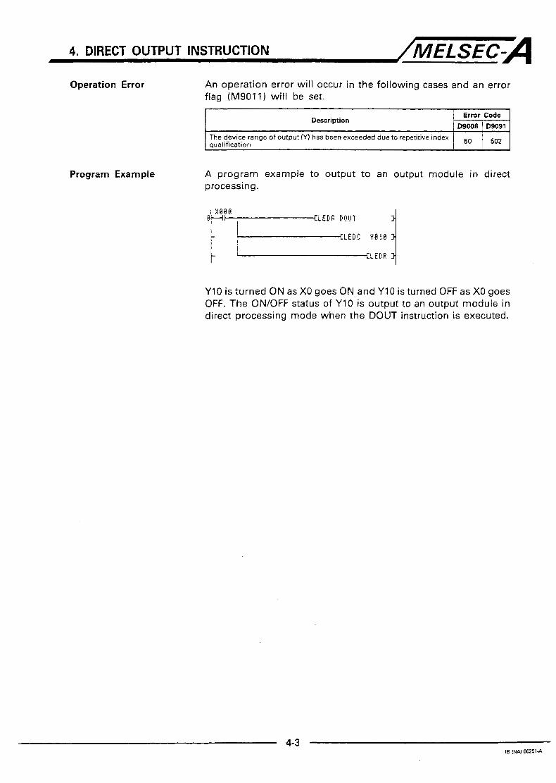
4. DIRECT OUTPUT INSTRUCTION /MELSEC-A Operation Error An operation error will occur in the following cases and an error
flag (M9Ol l ) will be set.
Program Example
Description j Error Code 1 1 D9008 I D9091 I
I The device range of output (Y) has been exceeded due to repetitive index oualification I 50 1 502 I
A program example to output to an output module in direct processing.
Y10 is turned ON as X0 goes ON and Y10 is turned OFF as X0 goes OFF. The ON/OFF status of Y10 is output to an output module in direct processing mode when the DOUT instruction is executed.

4. DIRECT OUTPUT INSTRUCTION /MELSEC-A 4.2 Direct Set/Reset--.---DSET, DRST
1 Available Devices g o c -
p . - w = : , D X k g E m 0’
Bit device 5 S < 4 E Leva Constant j Pointer Word (16-bit) device
X Y M L S B F T C D W R A O A l Z V K H P I N ~ z M9012 M9011 .& v) 5 .n - -
DSET
I ! . , I ~
DRST ‘ I 1 ! 0
-@ 0
17 C 0
*1: The number of steps varies with devices used. Refer to Section 3.2 for details.
Direct set command
LEDB-.Executed at leading edge LEDA...Executed while ON
Data to be set
Direct reset command
LEDB...Executed at leading edge LEDA-Executed while ON
Set the device num-
that is set in direct processing.
that is reset In direct processing.
Functions
Refresh mode
Direct mode
(1) The DSET/DRST instruction outputs the output (Y) designated with a @ from the PC CPU in the direct mode. With an AnACPU/AnUCPU/QCPU-A (A Mode), outputs are usually processed in the refresh mode.
Sequence program
Output from the PC Output from the PC Output from the PC
Sequence program 1
Output from the PC Output from the PC Output from the PC
(2) The DSET instruction turns ON output (Y), designated by 0, when the direct set command goes ON. The output (Y) keeps the ON status, thereafter, even when the direct reset command goes OFF. The DRST instruction forcibly turns OFF the output (VI, designated by @, when the direct reset command goes ON.
4-4 IB(NA)66251-F

4. DIRECT OUTPUT INSTRUCTiON /MELSEC-A Execution Conditions When used in combination with an LEDA instruction, the DSET
and DRST instructions are executed in every scan while the direct setheset command remains ON. When used in combination with an LEDB instruction, the DSET and DRST instructions will only be executed once at the leading edge of the direct setheset com- mand.
Sequence program flow I I I I
I I I I I 1
! ON
I I
Direct setlreset command O F F A I I I I I I I I 1 1
I I I 1 I I I I
(used with LEDA) n I n I
I I I I I I I I I I I I I I 1
DSET I I DRST (used with LEDB) I I
Operation Error An operation error will occur in the following cases a n d an error flag (M9011) wil l be set.
Program Example
Description i Error Code I ! D9008 1 D9091 I
The device range of output (Y) has been exceeded due to repetitive index 1 5o qualification I
502
A program example to setheset output (Y) in direct processing.
LED8 D S E T I
L E D C Y e l o Direct set of Y10
L E D B P P S T
I LEDP
Sets Y10 when X2 goes from OFF to ON and outputs the ON status to an output module in direct processing. Resets Y10 when X2 goes from ON to OFF and outputs the OFF status to an output module in direct processing.
4-5 IB I N A J 6 6 2 5 1 4

....................................................................................................................................................................
....................................................................................................................................................................
....................................................................................................................................................................
....................................................................................................................................................................
....................................................................................................................................................................
....................................................................................................................................................................
.....................................................................................................................................................................
.....................................................................................................................................................................
.....................................................................................................................................................................
.....................................................................................................................................................................
....................................................................................................................................................................
.....................................................................................................................................................................
....................................................................................................................................................................
....................................................................................................................................................................
....................................................................................................................................................................
18 l N . 4 E6251-A

5. INSTRUCTIONS FOR STRUCTURED PROGRAMS /MELSEC-A 5. INSTRUCTIONS FOR STRLKTURED PROGRAMS
Structured program instructions are used to partially structure a sequence program so that the program can be created efficiently. Structured program instructions simplify the creation of programs that have the same format, subroutines, and FOR to N E X T loops.
Structured program instructions are summarized below:
Classification Instruct ion Symbol Description
~ ~ ~ ~~~ ~~ ~~
Executes index modification of de- vice numbers for all the devices in the designated circuit block. 7 5-2 I 1 ;:END I ~
~~ ~ ~~
Forced termination Forcibly terminates a FOR to NEXT
I I I I I Non-execution processing is ex-
Subrou t ine p rog - 5-7 program skipped at the trailing edge FCALL ram non-execution
ecuted for the designated subroutine
processing of the conditional contact or when the conditional contact is OFF.
C h a n g i n g f a i l u r e check pattern
The pattern of the circuit to be check- CHK ed by the CHK instruction is changed. CHKEND 5-1 0

5. INSTRUCTIONS FOR STRUCTURED PROGRAMS /MELSEC=A 5.1 Index Qualification of a Circuit Block...--IX, IXEND
Available Devices
z Level Pointer Conrtant Word (16-bit) device Bit device
z s u C) e :
0 , , , 6 3 , 3 0 0 0 0 a > , ,
*= B v) 4 s f
k F : m a E m J 2
X M9011 M9012 s z N I P H K W R A O A l Z I V D C T F B S L M Y I 17
'I: The number of steps varies with devices used. Refer to Section 3.2 for details. *2: The number of steps: IX...17 steps, IXEND.-*13 steps
(Always ON) I
Data to be set
Designate the device
@ for each device.
number that sets the in- dex qualification value set
1 I
Functions (1) Index qualification of device numbers is executed for all the devices in a circuit block beginning with the IX instruction and ending with the IXEND instruction.
(2) By setting a qualification value for each individual device in advance, the set qualification value is added to the numbers of the devices used in the circuit block beginning with the IX instruction and ending with the IXEND instruction; the prog- ram is executed for the device numbers after qualification.
(3) Set the index qualification values in binary and designate the head device number of the devices for which the qualification value is set with an 0. Set the word devices with an MOV instruction, for example.
@ I Qualification value for input (X) I
step relay (SI
@ + 3
@ + 4
Qualification value for link relay (B)
Qualification value for pointer (P) @ + 9
Qualification value for file register (R) @ 4- 8
Qualification value for link register (W) @ + 7
Qualification value for data register (D) @ + 6
Qualification value for counter (C) @ + 5
Qualification value for timer Tr)
5-2 IB INAI E6251A

5. INSTRUCTIONS FOR STRUCTURED PROGRAMS /MELSEC-A (4) Execute index qualification for the device numbers in the
following manner: Qualification value
In the circuit shown above, the devices are processed as indicated below:
For X1 and X19, the value "2" is added to the device
For Y24 and Y40, the value "A," is added to the device
For M6 and M62, the value "10" is added to the device
For B20, the value "16" is added to the device number, and
For T495, the value "3" is added to the device number, and it is
For device C10, the value "5" is added to the device
For device DO, the value "1" added to the device number,
(5) For devices used in the designated circuit blocks, index qualification with an index register (V, Z) is not allowed.
The following instructions and devices cannot be used within the designated circuit blocks. If used, unexpected operation results may be obtained. An instruction, which is executed only once at the leading edge of the conditional input, such as LEDB, which is used with dedicated instructions as well as the PLS, PLF, and L.,=-T.IP instructions.
number, and they are processed as X3 and X1B.
number, and they are processed as X3 and X1B.
number, and they are processed as M16 and M72.
it is processed as B30.
processed as T498.
number, and it is processed as C15.
and it is processed as D l .
r - , p - . I r - ,
CHK instruction TO to T255 and CO to C255 (T256 to T2047, C256 to C2047 can be used.) Pointer (PI, which is used as label.
(6) An error will not result if a device number exceeds the set device range after adding qualification value. In this case, however, processing will not be executed for the correct device.
(7) Up to 32 pairs of IX and IXEND instructions can be used in a program.
5-3 IB W J -1-G

5. INSTRUCTIONS FOR STRUCTURED PROGRAMS /MELSEC-A Execution Conditions The IX and IXEND instructions can be used regardless of ON/OFF
status of the conditional contact.
Operation Error An operation error will occur in the following case and an error flag (M9011) will be set.
Error Code D9008 I D9091 Description
An index qualification is executed using an index register (V, Z) in the range of the circuit block designated by the IX and IXEND instructions. ,06
More than 32 pairs of IX and IXEND instructions are designated in a program. IX and IXEND instructions are not written in pairs.
13 135
Program Example A program to execute the same circuit block 10 times while changing the device numbers.
Setting the qualification value for an input (X) Setting the qualification value for an output (Y) Setting the qualification value for an internal relay (M) Setting the qualification value for a data register (Di Setting the qualification value for a link register (W)
2 6 F O P 1F( I
‘‘ ‘qualification is executed
-
- -
Circuit block in which device
59 :: f l 9836 CLEOR I X E H D
c+ 1 K
Changing the qualification value
K c+ 1 Changing the qualification value
K + 1 Changing the qualification value
K C t 1 Changing the qualification value
K Changing the qualification value
for an input (X)
for an output (Y)
for an internal relay (M) ,
for a data register (D)
for a link register (W)
- - -
9 8 CHEXT
The program is executed 10 times while adding ‘1” to the device number for the devices in circuit block 1. ........................ 1 st 2nd 3rd 10th
x 0 - x1 - x2 ........................ x 9 x10 - x11 x12 ........................ x 1 9
........................ Y39 y3Q y31 - y32 MO + M1 + M2 ........................ M9 DO - Dl - D2 ........................ D9 Dl0 - Dl1 + D l 2 ........................ D l 9 wo - w 1 + w 2 ........................ w9

M E M O ....................................................................................................................................................................
....................................................................................................................................................................
....................................................................................................................................................................
....................................................................................................................................................................
.....................................................................................................................................................................
.....................................................................................................................................................................
....................................................................................................................................................................
.....................................................................................................................................................................
....................................................................................................................................................................
....................................................................................................................................................................
....................................................................................................................................................................
.....................................................................................................................................................................
.....................................................................................................................................................................
....................................................................................................................................................................
....................................................................................................................................................................
....................................................................................................................................................................
IB (W €62514

5. INSTRUCTIONS FOR STRUCTURED PROGRAMS /MELSEC-A 5.2 Forced Termination of FOR-NEXT Loops.*----BREAK
Available Devices _ - n L
Bit device
X Y M L S B F T C D W R A O A I Z V K H P I I N ~ z
Level Pointer Constant Word (16-bit) device .s v) f M9012 1 M9011
@ I , I ~: Cj 3 c ~3 20 3
0 * l : The number of steps varies with devices used. Refer to Section 3.2 for details.
, Forced termination command
km LEDA/LEDB 1 BREAK
I -1 LEDR
LEDA...Executed while ON LEDB...Executed at leading edge
Data t o be set
petitive number is stored.
tination where the sequ- Designate the branch des-
@ ence jumps after the forced termination of loop processing
Functions
Execution Conditions
Sequence program flow
(1) Forcibly terminates the FOR to NEXT loop and jumps to the pointer designated with an 0.
(2) The remaining number of the FOR to NEXT loops at the time the processing is forcibly terminated is stored in @.
(3) The BREAK instruction can only be designated within the FOR to NEXT loop.
The BREAK instruction execution mode depends on whether it is designated with an LEDA or LEDB instruction. It will be executed in every scan while the forced terminal command remains ON, provided that it is designated with an LEDA instruction. When it is designated with an LEDB instruction, it is executed only once at the leading edge of the forced termination command.
step 0 END Step 0 END Step 0 END step 0 END SlEP 0 , I I I
I r l I I n I I
ON OFF
I I 1 I I Forced termination command r i I I
I I I I I I I I I I I
I BREAK (used with LEDA) 1 n 1
I I I I I
I I I I I I I 1 I I 1 I I I I I I I BREAK (used with LEDB) 1
Operation Errors An operation error will occur in the following case and an error flag (M9011) will be set.
r Description The BREAK instruction is used outside the FOR t o NEXT loop. 133
' The jump destination pointer designated with an @ is not found in the 13 132
5-5 IB INAJ 662514

5. INSTRUCTIONS FOR STRUCTURED PROGRAMS /MELSEC-A Program Example C: program to store the data in registers DO through D9 to Dl0
through Dl9 after BCD conversion with a FOR t o NEXT loop.
z B R E A K 4 Registen are checked in
the range of DO through D9; the BREAK instruction
e [ : i D R 1 1 . IS executed i f a value of 10000 or more is found to be stored
~5 17/ x e e e
If any piece of data cannot be converted to BCD, the BREAK instruction causes the sequence to exit the FOR to NEXT loop. After this, the remaining number of loop processing to be executed is stored in D20 and the program is executed from P5.

5. INSTRUCTIONS FOR STRUCTURED PROGRAMS /MELSEC-A 5.3 Subroutine Call--.-..FCALL
Available Devices - S P '
Bit device = 5 Level Pointer Constant Word (16-bft) device 5 2 - 9 V E
M9011 M9012
W E
X Y M L S B F T C D W R A O A l Z V K H P I N s z - - - E r n -
P I 0 I 17 0 P ,
- 2
* l : The number of steps varies with devices used. Refer to Section 3.2 for details.
l-[LEDA/LEDBI FCALL 4 LEDB...Executed at trailing edqe LEDA...Executed while OFF
- -
Head pointer number of subroutine program
4 '**
-5 r-Eff-d 1 Subroutine program
Data to be set
&- - - - - - . I
Functions (1) Executes the non-execution processing of the designated subroutine program while the subroutine call command is OFF or at the trailing edge of the command. The term "non-execution processing" means that the coil instruction is processed in the same manner as when the conditional contact goes OFF. By executing the FCALL instruc- tion, the operation results of the coil instructions in the subroutine program will be as indicated below regardless of the ON/OFF status of the conditional contact.
OUT instruction ..................... Forcibly turned OFF
SET instruction RST instruction SFT instruction
Application instructions ' Basic instructions
....... Status retained
PLS instruction ............ Executes the same processing as X X XP instructions when conditional contact goes OFF 10 msedl00 msec timer present value
.......... Reset to "0"
100 msec retentive timer present value ...... Count value retained Counter present value
57 IB (W € 6 2 5 1 4

5. INSTRUCTIONS FOR STRUCTURED PROGRAMS /MELSEC-A The FCALL instruction is used in combination with the CALL instruction.
If a CALL instruction is executed without executing an FCALL instruction, the subroutine program will not be executed because the subroutine call command is OFF. Therefore, the output status of each coil instruction is retained. The subroutine program non-execution processing is ex- ecuted when the FCALL instruction is executed. This allows the OUT instruction and PLS instruction (including *%XPLS instruction) to be forcibly turned OFF.
: I
PO
1 When FCALL is not executed 1 n n
x 1 I Y10 J Y11 I
I
MO 7 [When FCALL is executed 1
x 1 I 4 I
Y11
MO
Processing by FCALL
Execution Conditions The FCALL instruction execution mode depends on whether i t . is designated with an LEDA or LEDB instruction. It will be executed in every scan while the subroutine call command remains OFF, provided that it is designated with an LEDA instruction. If it is designated with an LEDB instruction, it is executed only once at the leading edge of the subroutine call command.
Step D END Step 0 END Scep 0 , I I ,
Sequence program flow t I I I I I
ON Subroutine call command O F F 1 : I I I i l ! r I I
I I I I I I I I I I I I I
I I FCALL (with LEDA) n
I I I I I I I 1 I I I I I I I I I I
I I I I I I FCALL (with LEDB)
5-8 IS (M 662514
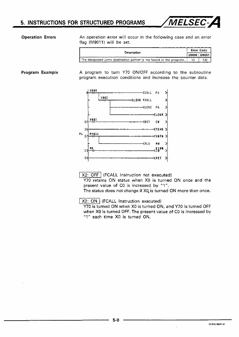
5. INSTRUCTIONS FOR STRUCTURED PROGRAMS / M E L S E C - A Operation Errors An operation error will occur in the following case and an error
flag (M9011) will be set.
Program Example
I Description Error Code
09008 1 D9091 I The desianated iurnD destination Dointer is not found in the oroaram. I 13 1 132 I
A program to turn Y70 ON/OFF according to the subroutine program execution conditions and increase the counter data.
e- :, xege ECRLL P6 3
LEDB FCRLL
LEDC P6
22 .
- CPLS H e 3
CY878 > tFEHD 3 2 6
I I CRST C 6 3
P6 2 7 H9e36
3 3 - I:
H 8, K e e c t 8 >
1 X2: OFF 1 (FCALL instruction not executed) Y70 retains ON status when X0 is turned ON once and the present value of CO is increased by "I" . The status does not change i f Xqis turned ON more than once.
\ X2: ON 1 (FCALL instruction executed) Y70 is turned ON when X0 is turned ON, and Y70 is turned OFF when X0 is turned OFF. The present value of CO is increased by "1" each time X0 is turned ON.
5-9 IB I N N €62514

MEMO
....................................................................................................................................................................
....................................................................................................................................................................
....................................................................................................................................................................
....................................................................................................................................................................
.....................................................................................................................................................................
.....................................................................................................................................................................
.....................................................................................................................................................................
....................................................................................................................................................................
.....................................................................................................................................................................
....................................................................................................................................................................
....................................................................................................................................................................
....................................................................................................................................................................
.....................................................................................................................................................................
.....................................................................................................................................................................
....................................................................................................................................................................
....................................................................................................................................................................
....................................................................................................................................................................
....................................................................................................................................................................
....................................................................................................................................................................
I6 (NAI 6SZ514

5. INSTRUCTIONS FOR STRUCTURED PROGRAMS /MELSEC=A 5.4 Changing t h e Check Pattern for the CHK Instruction..---.CHK, CHKEND
(LEDA) CHKEND
-
*1: The number of steps varies with devices used. Refer to Section 3.2 for details.
?25 t
Always set CHK instruction at pointer P254
P
Device which turns ON when a failure occurs.
Check conditions (max. 150 contacts)
-__---------_-____----__-. a F: '
I I - I Circuit pattern to be checked - I I - I I - I
1 I--- be used' ~~ ' I
- Dummy annunciator (F)
Max. 6 coils Data to be set
Device number that is D l turned ON at detection of
~ ~~~~
1 lo/ Device number that] D2 stores an error number at
the detection of failure
Functions (1) Changes the pattern of the circuit to be checked into the required format.
POINT I The CHK and CHKEND extension application instructions provided for the AnACPU/AnUCPU are only used to change the circuit pattern for failure check. Failure check is executed using the same procedure as the CHK instruction that is common to all types of CPUs. When using the CHK and CHKEND extension application instructions, refer t o t he ACPU Programming Manual (Common Instructions) for an explanation of the CHK instruction.
5-1 0 15 (NAJ 662518

5. INSTRUCTIONS FOR STRUCTURED PROGRAMS /MELSEC=A (2) A failure check is executed according to the contact device
numbers designated as the check conditions and the circuit
b] and ending with -1. attern described in the circuit block that be ins with
1) P254 must be written a t the head of the CHK instruction step.
2) A maximum of 150 contacts can be designated as check conditions with the LD and AND instructions. (Instructions other than LD and AND cannot be used. However, the LDI or ANI instruction can be used to designate no-processing contacts.)
3) The device number indicated in the check conditions (X2 and X8 in the ladder example shown below) is used as an index qualification for the device numbers described in the circuit pattern, excluding annunciator (F).
X10 is processed in the following device number: X2 ..-.e. For check condition X12 X8 . . - e - . For check condition X18
I I
Equivalent circuit for x2
Equivalent circuit for xa
4) In the failure check, the ON/OFF status of OUT F[:I is checked in each check condition. In all check conditions, if any OUT F[:l is turned ON under, the bit device designated by @ is turned ON. At the same time, the error number (see Item 3 above) corresponding to the OUT that has been turned ON is stored in a BCD value in the device designated by @.
5) The following instructions can be used in the circuit
Contact .--. LD, LDI, AND, ANI, OR, ORI, ANB, ORB, MPS, MPP, MRD, and comparison instructions co; I . . . . . . . . , OUT
pattern:
6) The following devices can be used in the circuit pattern contacts:
input (X), output (Y) 5 1 1
IS I t G I €62514

5. INSTRUCTIONS FOR STRUCTURED PROGRAMS /MELSEC-A 7 ) The only device that can be used for the circuit pattern coil
is an annunciator (F). Because an annunciator is used as "dummy", any value in the range of FO through F2047 can be set. The same value can be set repeatedly. If the annunciator (F) that is assigned the same number as the one used in the circuit pattern is used outside the circuit pattern, it can be turned ON/OFF properly, because annun- ciators used in and out of the circuit pattern are processed separately. Because the annunciator (F) used for the CHK instruction is not actually turned ON/OFF, it is not turned ON when monitored with an external device.
8 ) A circuit pattern of up to 256 steps can be created. For OUT F[:l, up to 6 coifs can be used.
(3) Error numbers stored in @ are assigned as indicated below according to the contacts designated as check conditions and
BCD value. 2nd contact 149th contact the coils in the circuit pattern. Error numbers are stored in a
1st coil
2nd coil
3rd coil
4th coil
5th coil
6th coil
Example: If the 5th coil is ON in the circuit check based on the 55th contact:
Error number = 601 + 2 (55 - 51) = 609

5. INSTRUCTIONS FOR STRUCTURED PROGRAMS /MELSEC=A (4) If any OUT F:11 is detected to be in the ON state, execution of
the CHK instruction stops and consequent check is aborted. Therefore, write a program taking into account the following priority order when the CHK instruction is used.
High Priority Low
2nd contact 749th contact 1st contact 13rd contact I 150th contact
P I I LEDA I CHK
High
Low
(5) To clear the bit device designated by 0, which has been turned ON by executing the CHK instruction, and the error number stored in 0, use a user program after taking proper corrective action. The CHK instruction cannot be executed again unless the bit device designated by @is turned OFF.
(6) The CHK instruction cannot be written or corrected while the PC CPU is running.
Execution Conditions The CHK instruction is executed regardless of the ON/OFF status of the contact designated as the check condition. The ILEDA(CHKJ and [ LEDA I CHKEND I instruction is also ex- ecuted regardless of the ON/OFF status of the contact designated as the check condition. When the execution of the CHK instruction is not required, use the CJ instruction to skip those blocks which include CHK or CHKEND instructions.

5. INSTRUCTIONS FOR STRUCTURED PROGRAMS /MELSEC-A Operation Errors An operation error will occur and the PC CPU will stop in the
following cases: A parallel circuit exists in the check condition or the condition contact for the CJ instruction.
Bit device designated by @
P254
0 Eliminate parallel contacts
e, Eliminate parallel contacts in the U circuit block
An NOP instruction is contained in the check condition. Eliminate the NOP instruction (An LDI or ANI instruction can be used instead of an NOP instruction)
Not displayed in the ladder mode
F4z-d P254
Pointer P254 is not designated at the head of the CHK instruction step.
More than 150 contacts are designated as the check conditions.
I I T More than 150 contacts
A CJ instruction circuit block is missing.

5. INSTRUCTIONS FOR STRUCTURED PROGRAMS /MELSEC-A There is more than one check pattern to be checked.
I j Circuit pattern to be checked ; ' l } a
More than six OUT F:I1 exist in a circuit pattern. A circuit pattern consists of more than 256 steps. An instruction or device that cannot be used exists in a circuit pattern. An index register (Z, V) is used for each device in a circuit pattern (if index qualification is executed). The conditional contact designated prior to 1 LEDA 1 CHKEND 1 i s not LD, LDI, or NOP instruction, or more than one LD, LDI, and NOP instructions exists. Only one contact or NOP instruc- tion can be designated.
POINTS 1 (1) CHK and CHKEND instructions cannot be written or
corrected when the PC CPU is in the RUN state. (2) An operation error occurs if there is an NOP instruction
within a format determined by the CHK and CHKEND instructions. Since the NOP instruction is not display- ed with peripheral devices in the ladder mode, check the NOP instruction with the list mode.

MEMO ....................................................................................................................................................................
....................................................................................................................................................................
....................................................................................................................................................................
....................................................................................................................................................................
....................................................................................................................................................................
.....................................................................................................................................................................
.....................................................................................................................................................................
....................................................................................................................................................................
....................................................................................................................................................................
....................................................................................................................................................................
....................................................................................................................................................................
.....................................................................................................................................................................
....................................................................................................................................................................
....................................................................................................................................................................
...................................................................................................................................................................
....................................................................................................................................................................
.....................................................................................................................................................................
....................................................................................................................................................................
....................................................................................................................................................................
....................................................................................................................................................................
IB (N.4) e 3 5 1 4

6. DATA PROCESSING INSTRUCTIONS ,/MELSEC-A 6. DATA PROCESSING INSTRUCTIONS
Data processing instructions process data in units of bits to form the required data.
The following table summarizes the data processing instructions:
I Classification Instruction I Name 1 Description Refer t o I Page ~
Searching
6-4 data. SWAP and lower bytes Swaps upper and lower 8 bits in 16-bit Swapping upper
from the group of 32-bit data. 32-bit data Searches the designated 32-bit data DSER 6-2
in 16-bit data
Dissolving data D,S Dissolves data into units of designated bits. 6-6
I I UNI I Unifying data Data is constructed by joining desig- 1 nated bits from several sets of data. 1 6-1 0
Extracting bits TEST
DTEST
The status of designated bit is read t o the bit device. 6-14
The following instructions can be used for all types of PC CPUs for data processing. Refer to t h e ACPU Programming Manual (com- mon instructions) for details.
1Gbitdatasearch ................... Bit check ................................ Decode/encode ......................
SER instruction SUM instruction DECO/ENCO instruction SEG instruction BSETIBRST instruction
7-segment decode .................. Bit set/reset ............................ Data dissociation/association DIS/UNI instruction (dissotvinghnifying)
The DIS and UNI instructions are used differently depending on whether they are used as common instructions or dedicated instructions.

6. DATA PRO.CESSING INSTRUCTIONS /MELSEC-A 6.1 32-bit Data Search-..--*DSER
4- M9012 MSOll
+ t Search command LEDA..--Executed while ON
[ L E D A / L E m w LEDB...--Executed at Data to be set leading edge
-- device number
1 LEDC/SUB I @ is designated Head number of the de-
-[ LEDR constant is designated
I
(1) Search is executed in the 32-bit data range. It is designated with @, beginning with the device number designated with @ using the 32-bit data designated with @) as the keyword.
(2) The result of the search is stored in accumulators A1 and A2. The number of the data agreeing with the keyword is stored in A1 and the position of the data which agreed first is stored in A0 .
2 1 2 3 4 5 6 7 8 9 I Number of agreed data 1 A1 1 5 1 ' Device number storing the I data that agreed fiM I 2 1
(3) Processing does not occur if the number of points designated with @ is "0" or a negative value.
6-2 IB (W €62514
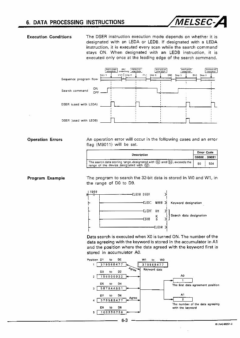
6. DATA PROCESSING INSTRUCTIONS /MELSEC-A Execution Conditions The DSER instruction execution mode depends on whether it is
designated with an LEDA or LEDB. If designated with a LEDA instruction, it is executed every scan while the search command stays ON. When designated with an LEDB instruction, it is executed only once at the leading edge of the search command.
Sequence program flow I I I I I
ON OFF
I I I 1
Search command I I I I
I I I I I I
I I I I I I I
I I I I I I
DSER (used with LEDA) n I
I
I
I
I I I I I DSER (used with LEDB)
I
Operation Errors An operation error will occur in the following cases and an error flag (M9011) wil l be set.
Program Example
Description I Enor Code I I D9008 1 D9091 1
The search data storing range, designated with @ and @,exceeds the 5o range of the device designated with @. 504
The program to search the 32-bit data is stored in WO and W1, in the range of DO to D9.
1 p'.'"''~ ;I LEDC U P 9 0 Keyword designation
Search data designation
LEUR
Data search is executed when X0 is turned ON. The number of the data agreeing with the keyword is stored in the accumulator in A1 and the position where the data agreed with the keyword first is stored in accumulator AO. Position D l to W w1 to wo ..
1 3 7 9 5 6 8 4 7 7 3 7 9 5 6 8 4 7 7
03 to D2 2 1 0 6 0 0 0 0 3 2 A0
0 5 to D4 1
The first data agreement position
4 ,-4 3 7 9 5 6 8 4 7 7
5 25-J 1 0 0 3 9 6 7 5 8
The number of the data agreeing with the keyword
6-3 18 INAtE251-C

6. DATA PROCESSING INSTRUCTIONS /MELSEC-A 6.2 Swapping Upper and Lower Bytes of 16-bit Data-----.SWAP
'1: The number of steps varies with devices used. Refer to Section 3.2 for details.
Swap command LEDA'iEDBI SWAP LEDB......Executed at leading edge
LEDA--.Executed while ON
I LEDR Data to be set
1 @ upper and lower bytes are Device number for which
swapped.
Functions (1) Swaps the upper and lower 8 bits of the data in the device designated with 0.
b15 to b8 b7 to bO b15 to b8 b7 to bO 01 X H 1 1 2 H 1
I I
Execution Conditions The SWAP instruction execution mode depends on whether it is designated with an LEDA or LEDB instruction. It is executed every scan while the swap command stays ON if it is designated with an LEDA instruction. When it is designated with an LEDB instruction, it is executed only once a t the leading edge of the swap command.
END Srep 0 END Stcp 0 I
Sequence program flow H I I I I I
I I I I I I I I I
I I 1 I I
I I
I I I I I I I I I I I I I I 1
ON Search command O F F 1 1 I
SWAP (used with LEDA) I I
I I I I I I I I I I I I I I I I
I I
1 I I SWAP (used with LEDB) I I 1 I
6-4 IB IN4 €62514

6. DATA PROCESSING INSTRUCTIONS /MELSEC=A Program Example This is the program to swap the upper and lower bytes of the
binary data in X20 to X2F and output them to Y30 to Y3F.
after swap
b15 to b12 b l l to b8 b7 to b4 b3 to bO DO 1 1H 2 H 3H 4!4
b15 to b12 b l 1 to b8 b7 to b4 b3 to bO DO 3 H 2 H I n 4 n

6. DATA PROCESSING INSTRUCTIONS /MELSEC=A 6.3 Data Dissolving.----DIS
Available Devices t a 2 ~S
i g $m x 5 Bit device w S S % 2 z L e v e l Pointer constant Word (16-bit) device
X Y M L S B F T C D W R A O A l Z V K H P I N a z 3 s
M9012 M9011
0 I
c e (2 0 0 0 c Z 23 1 c 0 ( 3 \3 3 03
O ~ C : C 3 0 I
I '1: The number of steps varies with devices used. Refer to Section 3.2 for details. I
I [ LEDR l-
Data to be set
Head number of the de- vices that store the data to be dissolved.
Head number of the de-
Functions (1) Each bit of the data stored in the devices following the device number designated with @ is dissolved into units of bits designated with @, and this data is stored in the devices following the device designated with @I,
Deslgnatm 0 1 dlssoivlng blls
@ + ~+~Oerignaltor of end of sening
b15b14b13 , , to I b6b5 , 10 bo,
- Bits deslgnated with 0 4
@+l[-]
Brts desigmed wifh 0 -+ 1 k b8 b7 10 M b3 to bO m to w
-- I I I Bits d e v g m e d wilh @ + 2 4
I b3 to W
b7 10 W @ + 4 [
B~ts dewgnafed with @ + 4 4 b121oblOb9 b9 to bO
. . . .

6. DATA PROCESSING INSTRUCTIONS /MELSEC-A (2) @ can be designated in the range of 1 bit to 16 bits,
(3) The numbers stored in the devices beginning with the device designated with @ to the device preceding the one where "0" is stored are assumed to be the number of bits used for dissolving.
Execution Conditions The DIS instruction execution mode depends on whether it is designated with an LEDA or LEDB. If it is designated with an LEDA instruction, it is executed in every scan while the dissolve command stays ON. When designated with an LEDB instruction, it is executed only once at the leading edge of the dissolve command.
Step 0 END Step 0 ESD Step 0
Sequence program flow I I I I I I I I I I I I I I
ON I I
OFF Dissolve command / I I I I
I I I I I I 1 I I I t I I I I
I DIS (used with LEDA) n I
I I I I I I I I I I I I 1 I I I I I I I
I I I
DIS (used with LEDB) I I I
Operation Errors An operation error will occur in the following cases and an error flag (M9011) will be set.
Description
The use range of the device designated with @and @ exceeds the last device number of each of the designat d devices due to the designation of the dissolving bit numbers with &. 504
The dissolving bit number designation is outside the range of 1 to 16. 503
~ ~~~ ~~ ~
50
*
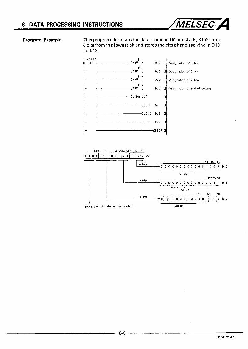
6. DATA PROCESSING INSTRUCTIONS /MELSEC-A Program Example This program dissolves the data stored in DO into 4 bits, 3 bits, and
6 bits from the lowest bit and stores the bits after dissolving in Dl0 to D12.
P l c @ ? a 3 Designation of 4 bits
i
I - Designation of 3 bits
- Designation of 6 bits
- Designation of end of setting
- KLEPR P I S
- - - -
L E D C Dl8
L E D C D Z @
LEDR
b12 to b7 b6tob4 b3 to bO 1 ~ l ~ O : l ~ O ~ l ~ l : O ~ O O ' l j l l l 1 0'0 DO -- e-- b3 to bO
All Os b2 to bO
All Os
6 bits b5 to bO
0 O ~ O ~ O ~ o ~ O ~ O ~ O ~ O : O , 1 j O ~ 1 j 1 ~ O j O Dl2 t
Ignore the bit data in this portion. All Os

6. DATA PROCESSING INSTRUCTIONS /MELSEC=A This program dissolves the data stored in DO and Dl into 9 bits, 10 bits, and 8 bits from the lowest bit and stores the bits after dissolving in Dl0 to D12.
Designation of 9 bits
Designation of 10 bits
LEDC D O
I- ! I C L E b C Dl13 y
CLEDL D ? @ 4 CLEhE 4
b10 to b3 b2 t o m D l 1 : O ; l j l 110 1 0 0 l j 1 ; 0 1 0 0 : l i l
I I I I-
b15 to b9b8 to bO
3 bits 7 bits All Os b7 to bO
Dl1 10.0 0 o ~ o ~ O ~ o i O ~ 1 ~ 1 j O ~ O ~ O ~ 1 ~ 1 11
I d
All Os '
8 bits b9 to bO *Dl2 0 0 O . O / 0 1 0 ~ 0 j l 1 ; l j O ; O 0 j l j O : l
ignore the bit data in this portion. All Os

6. DATA PROCESSING INSTRUCTIONS /MELSEC-A 6.4 Unifying Data..--.UNI
+ t Unifying command
JLEDA/LEDB/ UNI
---f LEDC 1l- I LEDC ol-
-i LEOC - TI
1 -1 LEDA
-.Executed while
-.Executed at ON
leading edge
Data t o be set
be unified. ~ ~~ ~~
1 Head number of the de-
of data being unified.
Functions (1) Each bit of the data stored in the devices following the device number, designated with a, is unified in units of bits, designated with @, and stored in the devices following the device, designated with a'.
0 - i Destgnatlon of the end of Ine Settlng
b7 to bO @ + l I I
611s dewqnated wlth 0 + 1 r- @ + 2 [ b5 to bo M b 7 Io Mb3 to M
i
I Bits deslgnated wlth @ + 2 b A 4
b l Z t o b l 0 to W @ + Z
. . . .
I Bits designated with 0 + 5 - 4 b
b2 to bo - 1 Bits designated with @ + 6

6. DATA PROCESSING INSTRUCTIONS /MELSEC-A (2) can be designated in the range of 1 to 16 bits.
(3) The numbers stored in the devices beginning with the device designated with @ t o the device preceding the one where "0" is stored are assumed to be the number of bits used for unifying.
Execution Conditions The UNI instruction execution mode depends on whether it is designated with an LEDA or LEDB. If it is designated with a LEDA instruction, it is executed in every scan while the unify command stays ON. When it is designated with an LEDB instruction, it is executed only once a t the leading edge of the unify command.
ON OFF
I I I I I I I I I I I I 1
I I I
Unify command I I I t l j I I
I I I I I I I I I I
I UNI (used with LEDA) n I
I I I I 1 I I I I I
I I I I
I I I
I I
UNI (used with LEDB) 1 I I 1 I
Operation Errors An operation error will occur in the following cases and an error flag (M9011) will be set.
Description
The use range of the device designated with 0 and @ exceeds the last device number of each of the designated devices due to designating the dissolvina bit numbers with 0. The dissolvina bit number desianation is outside the ranae of 1 to 16.
Error Code I D9008 1 D9091 I
6-1 1 19 INN

6. DATA PROCESSING INSTRUCTIONS /MELSEC-A Program Example This program unifies the lower 4 bits of the data stored in D10, the
lower 3 bits of the data stored in D l 1, and the lower 6 bits of the data stored in Dl2 and stores the unified data
I
P K Designation D 2 ? 3
P I ! c w 6 L
Designation tnciv 3 D? 1 3 - F I,
- cfliiu fl D 2 3 3
' L E D R U H I 3
Designation
- CLEDC D l 0 3
- ELEDC DB 3
- C L E D R 3 -
ELEDC D ? B 3
-
in DO.
of 4 bits
of 3 bits
of 6 bits
of end of setting
b3 to bO
,__e_ 1 4 bits
Ignore the bit data in this portion
I

6. DATA PROCESSING INSTRUCTIONS /MELSEC-A This program unifies the lower 9 bits of the data stored in D10, the lower 10 bits of the data stored in D l 1, and the lower 8 bits of the data stored in Dl2 and stores the unified data in DO.
RI H9;y3Ci CnCIU P K I [ ) ?8 Designation of 9 bits
P K # D ( J 18 [I? 1 Designation of 10 bits
H O W 8 P V
@?I Designation of 8 bits
Y U i O l J 8 F K
D?! 4 Designation of end of
+XEDR !IHI
1 4 CLEDC D l @
CLEDC Ub
CLEDC DZO 1 I
CLEDR
b8 to bO D l 0 l.O~l,O~O~l:l:l 1 : l j l j O 0 ; l : O 0
r q hit.
senin 9
- -..- 1
b9 to bo
10 bits
b7 to bo
+ 8 bits r . .
D 1 [ 0 ~ 0 j 0 j 0 ~ 0 ~ i j i j 0 ~ 0 j O j i ~ i ( 1 ~ o ~ i ~ o ] Do~ijo~i~l/i~o o o ( i j o ' i . o l o iji{i] 'b10 to b3 b2 to W b15 to b9 b8 to bO ignore t he bit data in this portion
. .
All Os
6-13 IB I W 662514

6. DATA PROCESSING INSTRUCTIONS /MMELSEC=A 6.5 Bit Extraction.--...TEST, DTEST
Available Devices L. 2 .g c m
Bit device = 9 s 2 ' = f pointer b n a m Word (16-bit) device f 4 s e X Y M L S B F T ~ C D W R A O A I Z V K H P I N ~ $ O M9011 M9012
0 2 ss clg 0 8-
Cl I 23 3 3 I C C 3 0 ' 5 n
a 0 0 0 3 3
, +1: The number of steps varies with devices used. Refer to Section 3.2 for details.
1
: . .. : Indicates the instruction s y m b o l . . ..
TEST, DTEST 1 Bit extraction command I
I
--{ L E X r/- -[ LEDC/SUB I @ -1 LED-@
-{ LEDR E
LEDA..--.Executed while ON LEDB.--.Executed at
leading edge
LEDC......Device number designated
SUB.....Constant designated
Data to be se<
data to be extracted.
Position of the bit data to be extracted. I
~~
Bit device number of the device that stores the bit data extracted. 1
1
Functions ITEST/ (1) The bit data at the position designated with @ in the word
device designated with @ is extracted and written to the bit device designated with @.
(2) The bit device designated with @j is turned OFF when the corresponding bit is "0". It is turned ON when "1".
(3) With @ bit position (0 to 15) in word data is designated. (@ bit
1
1 DTEST I (1) The bit data at the position designated with @ in the 2-word
device, designated with @ and @ 4-1 is extracted and written to the bit device designated with @.
(2) The bit device designated with @ is turned OFF when the corresponding bit is "0". It is turned ON when "1".
(3) With @, the bit position (0 to 31) in 2-word data is designated. @ bit
4 b31 to b28b27 to b24 b23 to'b20b19 to b16 b15 to b12 b l l to b8b7 to M b 3 t o W
j ; j j ; ; jY/ j ; ; . . . , , . . . . . . . . . I ,
. I . , . . , , . . . . . . . . . . . . .

6. DATA PROCESSING INSTRUCTIONS /MELSEC-A Execution Conditions The TEST and DTEST instruction execution mode depends on
whether it is designated with an LEDA or LEDB. If they are designated with an LEDA instruction, they are executed every scan while the bit extraction command stays ON. When they are designated with an LEDB instruction, they are executed only once a t the leading edge of the bit extraction command.
ON OFF
I I I I I I I I I I I Bit extraction command I I I I i j I I / I I I
I I I I I I
E S T 1 I 1 D ~ E S T (used with LEDA) I
I
I I I I I I I I I I
I I I I 1 I TEST (used with LEDB) DTEST
Operation Errors An operation error will occur in the following cases and an error flag (M9011) will be set.
Program Example
Description I Ermr Code I I m s i ~ 9 - 1 I
When executing a TEST instruction, the bit position designation using @ is outside the range of 0 to 15. When executing a DTEST instruction, the bit Dosition designation using
~ ~~
50 ~ 503 I I 62) is outsidethe ranae of 0 to 15.
- - 1 I I
This program turns MO ON/OFF according to the status of bit 10 of word data stored in DO.
Bit position designation
ONlOFF device designation
l e MO is turned OFF because bit 10 is '0'
1 MO is turned ON because bit 10 is '1'

6. DATA PROCESSING INSTRUCTIONS /MELSEC-A This program turns Y40 ON/OFF according to the status of bit 19 of the 2-word data stored in WO and W1.
Bit position designation
OWOFF device designation
W l wo b31 to b24 b23 to b19 to b16 b15 to b8b7 to bo f i 0 1 1 ( 0 . 0 ' 1 011 0 1 1 j l ~ O j O . O o ~ l ~ o ~ l ~ l ~ o j l : l ~ l ~ o ~ l ~ l ~ l ~ o ~ l ~ l ~ o
v
w 1 L Y 4 0 is turned OFF because bit 19 is '0"
wo b31 to b24 b23 to b19 to b16 b15 to b8b7 to bo 10 1 1 011:110 l ~ l : l : o ~ l ~ l ~ o ~ o . l ~ l : o : l : o ~ l 1 1 o ; o ~ o j o j l j o ~ l i l j o 11
L Y 4 0 is turned ON because bit 19 is '1"
7. lNPUT/OUTPUT PROCESSING INSTRUCTIONS /MELSEC-A 7. INPUT/OUTPUT PROCESSING INSTRUCTIONS
Inputloutput instructions are used to change the output status or enter a numeric character-string from an external device.
The following table summarizes inputloutput instructions:
Description ~
Reverses ou tpu t device.
FF status (flip-flop)
Reverses the ON/OFF status of a bit 7-2
Converts the ASCII code (30~ to 39~, 4 1 ~ t o ~ F H ) entered from eight points o f input (X) into hexadecimal data.
Enters data using number keys I KEY I

7. INPUT/OUTPUT PROCESSING INSTRUCTIONS ~/MELSEC-A 7.1 Reversing Output (Flip-flop)--...FF
~~ ~~
Available Devices 2 s s z CI
Bit device
X Y M L S B F T C D W R A O A l Z V K H P l N ~ z
z f he^ Pointer Constant Word ( 1 6 b i t ) device f 2 g
0 , , , 9 c o 3 0 17 ' ! ! ,
I M9012 1 M9011 I 1
' 1 : The number of steps varies with devices used. Refer to Section 3.2 for details.
k l I
Flip-flop instruction
Data t o be set
Device number for which
ecuted.
Functions
Execution Conditions
(1) Reverses the output status of the device, designated by 0, at the leading edge of the flip-flop instruction.
Flip-flop command ON OFF I b b OFF ON @
(2) The ON/OFF status of the device, designated by 0, stays as it is until the leading edge of the next flip-flop command.
The FF instruction is executed for one scan at the leading edge of the flip-flop command.
ON OFF
I I I I I I I I I I I I I I
I I I I I
Flip-flop command
FF

7. INPUT/OUTPUT PROCESSING INSTRUCTIONS /MELSEC-A Program Example This program reverses the output status of M10.
The output status of M10 is reversed when X0 is turned ON.
x0 I I I I I I I I I I I I I 1 I I I I I
I I I I I ON
0 FF I 1 I MO
7-3 IB I W 662514

7. INPUT/OUTPUT PROCESSING INSTRUCTIONS / M E L S E C - A 7.2 Entering Data from Number Keys.--.-KEY
Data to be set
entry.
The number of digits of input data.
Head number of the de- vices where input numer- ic data are stored.
The bit device number
completion of data input.
Functions (1 ) The ASCII data input to 8 points of input (X), designated by 0, is converted into hexadecimal and stored in the devices beginning with the device designated by @. When the designated number of digits is input or when the ODH code is input, the input processing terminates and the bit device designated by @I is turned ON.
@ I Designation of input digits I Input module
: n I
b15 to b12 bl l to b8 b7 to b4 b3 to bO I
Example: wl 5 1
I I I I
Dl0 I 5
o - t 7 0- o- Strobe signal
i
Input module
n Rrst input value
- 1 3 5 6 9 " ( 3 1 ~ ) 1 3 3 ~ ) (35H) ( 3 7 H ) ( B H )
Strobe signal

7. INPUT/OUTPUT PROCESSING INSTRUCTIONS /MELSEC-A The ASCII code of the entered number is input to 8 points of input (X) designated by 0. ASCII code range: 3 0 ~ (0) to 3gH (9), 41H (A) to 46H (F)
When the strobe signal of "0 -t 8" is turned ON after the ASCII code is input to @ to @ i- 7, the entered number is input to the PC CPU. The strobe signal should remain ON/OFF for more than one scan of a sequence program. If the ON/OFF status does not remain for one scan or longer, the entered data cannot be input correctly.
(4)
Input command
Input command (conditional contact for KEY instruction execution) OH for one s a n OFF lor one s ~ n
or longer or her
Strobe signal (0 -I- 8) I 1 I ASCII code input (0 to @ + 7) 3 1 ~ x 32n x 3 3 ~ x 3 4 ~ x I 1 1 1
Inputting Inputting Inputting Inputting "1" "2" '3" "4"
The input command (conditional contact for executing the KEY instruction) should remain ON until the input of the designated number of digits is completed. The KEY instruction cannot be executed if the input condition is turned OFF.
When the data is stored in the devices designated by @,the number of input digits is stored in @ and the data is stored in 0 + 1 and 0 -l- 2 after converting the ASCII code into binary data.
(conditional contact for the J execution of KEY instruc- tion)
Strobe signal (0 -I- 8)
ASCII code input (0 to @ +7)
@ @ + l
@ + 2

7. INPUT/OUTPUT PROCESSING INSTRUCTIONS /MELSEC-A (5) The number of input digits designated for @ should range of
from 1 to 8.
(6) Input entry is terminated when the input of the number of digits designated by @ is completed or when the ODH code is input. The bit device designated by @ is turned ON at this timing. To input the numeric data again, clear the number of digits stored in 0 and the input data, and turn OFF the bit device designated by @ with a user program.
The designated number of digits has been input
ODH code is inpol
Example: E = 5
Input command 1
Strobe signal 1 1 1 1 (a + 8) ASCII code input 3 1 ~ x 4 2 ~ x 35r x 37H x 3% X
@9 @ + 1
@ + 2
Processing completion (@I
Input command
Go @ + l
@ + 2
Processing completion I@)
Execution Conditions The KEY instruction is executed during every scan while the input command remains ON as illustrated below.

7. INPUT/OUTPUT PROCESSING INSTRUCTIONS /MELSEC-A Operation Error An operation error will occur in the following cases and an error
flag (M9011) will be set.
Program Example
Description j Error Code i DSOOS ~ WOW
502 503
The device designated by 0 is not an input (X) . The number of digits designated for @ is outside the range of 1 to 8.
I
50
This program reads data of up to five digits from the ten keys connected to X20 to X28 and stores the read data at DO
S E T M8 3 K P K
F N D U e 3 3 Clearing previously input data
D l 0 3 Setting the number of input digits
3
L E D C X828 3 Designating X20 to X28
L E D C D l 8 3 Setting the number of input digits
Designating the head of the data storing devices Turning ON the device at the completion of data input
R S T M e
Resetting the data input cornple- tion flag
Input module
/x20 lol x23 x24 X25 x26
I x27 (Strobe signal) - x28
Ten-key pad

....................................................................................................................................................................
....................................................................................................................................................................
....................................................................................................................................................................
....................................................................................................................................................................
....................................................................................................................................................................
....................................................................................................................................................................
.....................................................................................................................................................................
.....................................................................................................................................................................
.....................................................................................................................................................................
.....................................................................................................................................................................
.....................................................................................................................................................................
....................................................................................................................................................................
.....................................................................................................................................................................
.....................................................................................................................................................................
....................................................................................................................................................................
....................................................................................................................................................................
....................................................................................................................................................................

8. REAL NUMBER PROCESSING INSTRUCTIONS /MELSEC-A 8. REAL NUMBER PROCESSING INSTRUCTIONS
Real number processing instructions are used to execute PC CPU operations that contain real numbers.
There are two types of real number processing instructions:
BCD real number processing Floating-point real number processing
8.1 BCD Real Number Processing Instructions
BCD real number processing instructions process real numbers by first dividing the real number into an integer and a decimal; each part is processed in BCD.
BCD real number processing instructions can handle values from 0.0001 to 9999.9999.
BCD real number processing instructions are summarized in the following table:
I 1 Classification Instruction Description
Square root Calculates the square root of the BSQR operation designated value BDSQR
8-2
i I SIN operation 1 BSlN 1 Calculates the sine of the desig- nated anale.
I cos operation 1 Bcos I Calculates the cosine of the desig- nated angle. I 88 I
I TAN operation 1 BTAN 1 Calculates the tangent of the desig- nated angle. I I
1 'IN-' Operation 1 I nated value to obtain an angle. Calculates the arc sine of the desig- 1 8-14 I
- Calculates the arc cosine of the
angle. COS-' operation 8-16 designated- value to obtain an BACOS
Calculates the arc tangent of the
angle. TAN-' operation 8-18 designated value to obtain an BATAN
I

8. REAL NUMBER PROCESSING INSTRUCTIONS /MELSEC-A 8.1.1 BCD 4-digiV8-digit square root operation-.-..BSQR, BDSQR
'1: The number of steps varies with devices used. Refer to Section 3.2 for details. * 2 : When DXNR is used for @ with the BDSQR, the number of steps is 26.
p.%q Square root
. o~erat ion command LEDA...Executed while ON 1 LEoA'md LEDB-.Executed at leading edge
1 I @ SUB-Constant designated LEDC-.Device number designated
1 LEDC Data for which square root operation is executed
Head number of the de-
the operation are stored.
Square root operation command LEDA...Executed while ON
LEDB-Executed at leading edge *To use DXNR, state as LEDC...Device number designated indicated be'ow. 1 DXNR.-Constant designated 1 DUNR 1 0 I (Dummy) I
~~ ~~
t All devices except for input (X) can be desig- nated.
Functions IssaR] ~-
(1) The square root of the value designated by @ is calculated and the result stored in the word devices designated by @.
(2) A value of up to 4 digits (0 to 9999) can be designated in BCD with 0.
(3) The operation result is stored in 0 and (@i-l) in BCD. (0.0000 to 9999.9999)
(4) Since the result is rounded off to four decimal places, it will be accurate to .0001.

8. REAL NUMBER PROCESSING INSTRUCTIONS /MELSEC=A (1) The square root of the value designated by @ and ~ ~ 4 - 1 is
calculated and the result is stored in the word devices designated by @.
(2) A value of up to 8 digits (0 to 99999999) can be designated in BCD with 0, @N-l.
(3) The operation result is stored in @ and @A-l in BCD. (0.0000 to 9999.9999)
(4) Since the result is rounded off to four decimal places, it will be accurate to .0001.
Execution Conditions The BSQR and BDSQR instruction execution mode depends on whether it is designated with an LEDA or LEDB instruction. It is executed every scan while the square root operation command stays ON if it is designated with an LEDA instruction. When it is designated with an LEDB instruction, it is executed only once at the leading edge of the square root operation command.
Sequence program flow
ON OFF
I I I I I I I I I I I
I I I I I I I I I I I I I I I
Square root calculation command I I I I
(with LEDA) BDSQR
BSQR BDSQR (with LEDB)
Operation Errors
n 1 I I
1 I
I I
I I I
I I I I I I 1
I I I I I 1 I
An operation error will occur in the following cases and an error flag (M9011) will be set.
Description I Error Code I
The data designated by 0 or by @ and @+1 is not BCD. I 50 1 503

8. REAL NUMBER PROCESSING INSTRUCTIONS /MELSEC-A Program Example -1
This program calculates the square root of 1325 (decimal) and outputs the integer part of the operation result to Y5F to Y50 in 4-digit BCD and the decimal part of the operation result to Y4F to Y40 in 4-digit BCD.
11 '3 Ii 3 6 H ' ~ ~ ~ ' ' ' 1 ' ''?' ['' 7 , square root is calculated (3)
1 Setting the data for which the
LELR PSQP
LEDC D9 3
CLEDC D l lj
E 4 4 Outputting integer part of the op- eration result to display unit (3)
r 4 Outputting decimal part of the op- "" 4 eration result to display unit (2)
j Square root calculation (3)
CLEDR
CHD1.I lii
i H O V D Z
'
DO D l Y5F to Y50 0 B S Q R operation
132h 0 0 3 6 1 3 2 5 a Move
0 integer 6 3 0 IMOV/ BCD value BCD value BCD value
D2 Y4F to Y40 @ Move
4 Decimal 5 0 0 [MOVI
BCD value BCD value
[BDSQR I This program calculates the square root of 74625813 (decimal) and outputs the integer part of the operation result to Y5F to Y50 in 4-digit BCD and the decimal part of the operation result t o Y4F to Y40 in 4-digit BCD.
1 e l i b U D 2
4. Outputting eration m u t t integer to display pan of unit the (a) o p
Hou y 8 4 8 Outputting decimal pan of the op etation result to display unit (a)
Dl Do m D2 Y5F to Y50 - . v
7462581 3 @ 4 7 1 4 1 6 1 2 1 1 5 / 8 1 1 / 3 / BCD value
BSQR operation 8 Integer 8 3 6
W l BCD value BCD value BCD value
D3 Y4F to Y40
6 Decimal 3 3 2
BCD value

....................................................................................................................................................................
....................................................................................................................................................................
....................................................................................................................................................................
....................................................................................................................................................................
.....................................................................................................................................................................
.....................................................................................................................................................................
.....................................................................................................................................................................
.....................................................................................................................................................................
.....................................................................................................................................................................
....................................................................................................................................................................
....................................................................................................................................................................
....................................................................................................................................................................
....................................................................................................................................................................
.....................................................................................................................................................................
....................................................................................................................................................................
....................................................................................................................................................................
....................................................................................................................................................................
IE IW 662511

8. REAL NUMBER PROCESSING INSTRUCTIONS /MELSEC-A 8.1.2 Sine operation-..-..BSIN
* I : The number of steps varies with devices used. Refer to Section 3.2 for details
I Sine operation I
I LEDR
LEDA...Executed while ON LEDB-.Executed at leading edge LEDC...Device number designated SUB ... Constant Data to be set
designated 0 . ' tlon IS executed Data for which sine opera-
vices where the operation Head number of the de-
result is stored.
Functions (1) Calculates the sine value of the angle designated by @ and stores the sign of the operation result to the word device designated by @l and the operation result to the word devices designated by @l+l and @$2.
(2) A value in the range of 0 to 360' (units: degrees) can be designated for @ i n BCD.
(3) The value to be stored in @I:
0 ......... When the operation result is positive. 1 ......... When the operation result is negative.
(4) The operation result stored in @)+l and @+2 is BCD in the range of -1.000 to 1 .OOO.
(5) The result is rounded off to four decimal places.

8. REAL NUMBER PROCESSING INSTRUCTIONS /MELSEC-A Execution Conditions Tbs BSlN instruction execution mode depends on whether it is
designated with an LEDA or LEDB instruction. It is executed every scan while the SIN operation command stays ON if it is designated with an LEDA instruction. When it is designated with an LEDB instruction, it is executed only once at the leading edge of the SIN operation command.
ON I I I I I I I I
OFF I I
I I I I I I
Sine operation command I I I I r : I I
I I I
I BSIN (with LEDA) n 1 I
I I I I
BSIN (with LEDB)
Operation Errors
I I I I I I I I I I I I I I I I I I
I
1
An operation error will occur in the following cases and an error flag (M9011) wil l be set.
Description
The data designated by @ is not BCD. The data desiqnated by 0 is not in the ranoe of 0 to 360.
Error Code D9008
503 50
D9091

8. REAL NUMBER PROCESSING INSTRUCTIONS /MELSEC-A Program Example This program calculates sine value of the data designated to X2F
to X20 in 4-digit BCD outputs the integer part of the operation result to Y53 to Y50 in 1-digit BCD and the decimal part of the operation result to Y4F to Y40 in 4-digit BCD.
Ct,/ DB 8 3 6 8 D l 9 2- H
C L E D R B S I H 2-
C L E D L D l 1 3
E L E D C D 2 9 3
CLEDR 2-
cnou D Z ~ y e 5 8 2-
C H C I U ~ 2 2 y e 4 8 2-
K1
K4
U 2 8 1 -3969 > K
Setting the data for which the sine value is calculated ( 0 ) Processing so that the input angle will fall within the range of 0 to 360. (a)
Sine value calculation (9)
Outputting integer part of the op- eration result to display unit (a) Outputting decimal pan of the op- eration result to display unit Is) Outputting the sign of the opera- tion result in OWOFF sratus (8)
For a value greater than 360' (degrees), the value is converted to a value in the range of 0 to 36O'to calculate sine using the following formula:
Sin X = Sin (360n $- X )
XZF to X20 DO 0 D l 0
0 5 9 0
BCD value BCD value BCD value
0 5 9 0 BI operation
Quotient
590 f 360 = 1 ...... 230
8 0 2 3 0 0 0 0 1
loufi my60 ON
BCD value BCD value - Remainder
sin 230' -0.7660 ...... D21 X53 to X50
@ Move
BCD value
022 X4F to X40
7 6 6 0 7 6 6 0
BCD value BCD value

MEMO
....................................................................................................................................................................
....................................................................................................................................................................
....................................................................................................................................................................
.....................................................................................................................................................................
.....................................................................................................................................................................
.....................................................................................................................................................................
.....................................................................................................................................................................
....................................................................................................................................................................
....................................................................................................................................................................
....................................................................................................................................................................
....................................................................................................................................................................
.....................................................................................................................................................................
.....................................................................................................................................................................
....................................................................................................................................................................
....................................................................................................................................................................
....................................................................................................................................................................
....................................................................................................................................................................
....................................................................................................................................................................
18 INA) 662514

8. REAL NUMBER PROCESSING INSTRUCTIONS /MELSEC-A 8.1.3 Cosine operation----.-BCOS
* l : The number of steps varies with devices used. Refer to Section 3.2 for details
I Cosine operation I command
LEDB...Executed at leading edge LEDA-Executed while ON
I -EDC/SUB I @ LEDC-.Device number designated Data to be set
SUB ... Constant designated { L E D C I 1 @ 1 eration is executed
Data for which cosine op-
LEDR vices where the operation
Functions (1) Calculates cosine value of the angle designated by @ and stores the sign of the operation result to the word device designated by 0 and the operation result to the word devices designated by (@+I and @1+2.
(2) A value in the range of 0 to 360 (units: degrees) can be designated for @ in BCD.
(3) The value to be stored in @: 0 ......... When the operation result is positive. 1 ......... When the operation result is negative.
(4) The operation result to be stored in @+l and @$-2 is BCD in the range of -1.000 to 1 .OOO.
(5) The result is rounded off to four decimal places.

8. REAL NUMBER PROCESSING INSTRUCTIONS /MELSEC-A Execution Conditions The BCOS instruction execution mode depends on whether it is
designated with an LEDA or LEDB instruction. It is executed every scan while the COS operation command stays ON if it is designated with an LEDA instruction. When it is designated with an LEDB instruction, it is executed only once at the leading edge of the COS operation command.
END Slep 0
Sequence program flow I I I I I I I I I
ON OFF
Cosine operation command I I I I I : I I I
I
I I I I I I I I
BCOS (with LEDA) 1 I
I I
I I I I
I I I I I I I I I I
I I I I h I BCOS (with LED&
Operation Errors An operation error will occur in the following cases and an error flag (M9011) will be set. ~
Description
The data designated by 0 is not BCD.
1 Error Code D9008 1 D9091
-The data desianated bv 6? is not in the ranae of 0 to 360. - 503 50
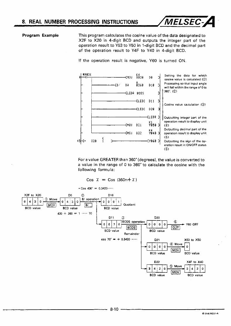
8. REAL NUMBER PROCESSING INSTRUCTIONS /MELSEC-A Program Example This program calculates the cosine value of the data designated to
X2F to X20 in 4-digit BCD and outputs the integer part of the operation result to Y53 to Y50 in 1-digit BCD and the decimal part of the operation result to Y4F to Y40 in 4-digit BCD.
If the operation result is negative, Y60 is turned ON.
H 9 6 3 6 K4 C H O U X828 DB 3
C8.l DB 6 3 6 6 D l 9 3 H
CLEDR B C O S
I L E D C Dl1
'LEDC D2B
CLEDR
C N O U D 2 1 Ye56 K1
CHOU D 2 2 Ye46 K 4
K
Setting the data for which cosine value is calculated (0) Processing so that input angle will fall within the range of 0 to 360'. (0)
Cosine value calculation (0)
Outputting integer part of the operation result to display unit
Outputting decimal part of the operation result to display unit
Outputting the sign of the op- eration result in ON/OFF status
(0)
(8)
For a value GREATER than 360' (degrees), the value is converted to a value in the range of 0 to 360'to calculate the cosine with the following formula:
Cos X = C o s (360114- X )
x 2 F to x20 DO 0 Dl0
0 4 3 0 0 0 0 1 0 4 3 0 Quotient
BCD value - BCD value - I BCD value
8-1 0 IB (NAJ €62514

MEMO ....................................................................................................................................................................
....................................................................................................................................................................
....................................................................................................................................................................
....................................................................................................................................................................
....................................................................................................................................................................
....................................................................................................................................................................
.....................................................................................................................................................................
.....................................................................................................................................................................
.....................................................................................................................................................................
....................................................................................................................................................................
.....................................................................................................................................................................
....................................................................................................................................................................
....................................................................................................................................................................
....................................................................................................................................................................
.....................................................................................................................................................................
.....................................................................................................................................................................
....................................................................................................................................................................
....................................................................................................................................................................
....................................................................................................................................................................
IB IW 662514

8. REAL NUMBER PROCESSING INSTRUCTIONS /MELSEC-A 8.1.4 Tangent operation...-.-BTAN
Available Devices I f = I ' x a m E m k z z Bit device w 0 4 4 h e 1 Pointer constant Word (16-bit) device
X Y M L S B F T C D W R A O A ~ Z V K H P I N E Z Z M9011 M9012
@I
@I
'E) 3 3 2 ' 2 3 3 j 20 3 n
LI
3 3 2 3 3
'1: The number of steps varies with devices used. Refer to Section 3.2 for details.
Tangent operation command
LEDB-.Executed at leadlng edge LEDA.-Executed while ON
LEDC...Device number designated I LEDcmd SUB ... Constant designated Data to be set
I -1 LEDR
Data for which tangent operation is executed
vices where the operation result is stored.
Functions (1 ) Calculates the tangent value of the angle designated by @ and stores the sign of the operation result to the word device designated by @ and the Operation result to the word devices designated by @i-1 and @+2.
(2) A value in the range of 0 to 360" (units: degrees) can be designated for @ in BCD.
(3) The value to be stored in 0: 0 ......... When the operation result is positive. 1 ......... When the operation result is negative.
(4) The operation result to be stored in @+l and @+2 is BCD in the range of -57.2900 to 57.2900.
(5) The result is rounded off to four decimal places.

8. REAL NUMBER PROCESSING INSTRUCTIONS /MELSEC-A Execution Conditions The BTAN instruction execution mode depends on whether it is
designated with an LEDA or LEDB instruction. It is executed every scan while the TAN operation command stays ON if it is designated with an LEDA instruction. When it is designated with an LEDB instruction, it is executed only once a t the leading edge of the TAN operation command.
Sequence program flow
O N I I I I I I I I
OFF I I I Tangent operation command I I I I I I I I I I I I
BTAN (with LEDA)
BTAN (with LEDB)
Operation Errors
I I I I
1 I I
I I I I I I I
I I I I I I I I I
I I I I I
I I
An operation error will occur in the following cases and an error flag (M9011) will be set.
~
Description
The data designated by @ is not BCD.
Error Code D9008 D9091
- The data designated by ($ is not in the range of 0 to 360. The data desianated bv 0 is 90' or 270' Idearees). 1 I 503 I
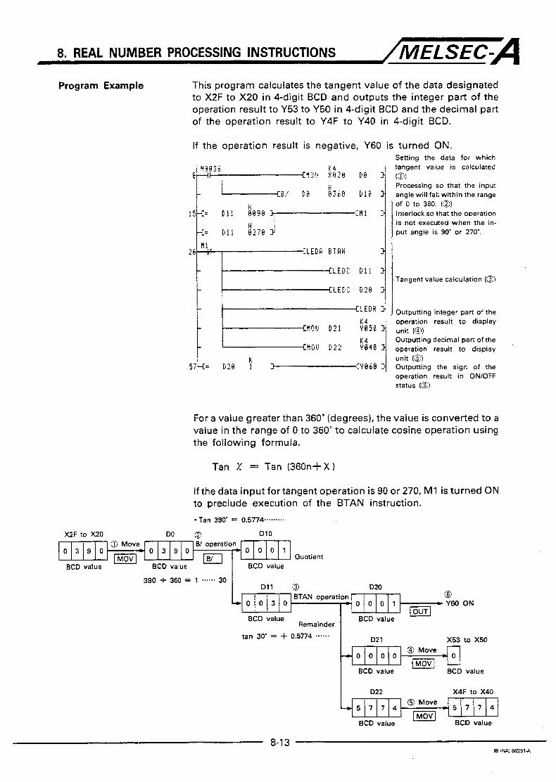
8. REAL NUMBER PROCESSING INSTRUCTIONS /MELSEC-A Program Example This program calculates the tangent value of the data designated
to X2F to X20 in 4-digit BCD and outputs the integer part of the operation result to Y53 to Y50 in 4-digit BCD and the decimal part of the operation result to Y4F to Y40 in 4-digit BCD.
If the operation result is negative, Y60 is turned ON. Setting the data for which
K 4 tangent value is calculated IO!, X 0 2 6 G B 3 (3)
Processing so that the input 836@ Dl6 3
]-IH1 >
angle will fall within the range
put angle is 90' or 270'. -C= Dl1 6 2 7 6 is not executed when the in- Interlock so that the operation
' of 0 to 360. 10) 1 5 1 = Dl 1
ill 2 6 -
CLEGC G?6 3 - C L E M : Dl1 3 -
CLEDA B T A H 3 ::
Tangent value calculation (0)
- ,
operation result to display K4 Outputting integer part of the
operation result to display CHOU D22 w 4 8 3 Outputting decimal part of the K 4
5 7 4 = G 2 @ 1 -:?fGS6 2 Outputting the sign of the operation result in ON/OFF status (8)
- unit (a) WJ D?I y e 5 8 3
- k unit (a)
For a value greater than 360' (degrees), the value is converted to a value in the range of 0 to 360' t o calculate cosine operation using the following formula.
Tan X = Tan (360ni-X)
If the data input for tangent operation is 90 or 270, M1 is turned ON to preclude execution of the BTAN instruction. . Tan 390' = 0.5774 .........
X 2 F to X20 DO t2 D l 0 - 0 3 9 0
BCD value BCD value
0 3 9 0 B/ operation
Quotient
390 + 360 1 ...... 30 BCD value
BTAN operation Y60 ON
BCD value BCD value Remainder
tan 30' = -k 0.5774 ...... X53 t o X50 @ Move
BCD value
I D22 X4F to X40
5 7 7 4 -w- BCD value BCD value
8-1 3 IB I N 4 6 6 2 5 1 4

MEMO ....................................................................................................................................................................
....................................................................................................................................................................
....................................................................................................................................................................
....................................................................................................................................................................
....................................................................................................................................................................
.....................................................................................................................................................................
.....................................................................................................................................................................
.....................................................................................................................................................................
....................................................................................................................................................................
....................................................................................................................................................................
....................................................................................................................................................................
.....................................................................................................................................................................
.....................................................................................................................................................................
....................................................................................................................................................................
....................................................................................................................................................................
....................................................................................................................................................................
.....................................................................................................................................................................
....................................................................................................................................................................
....................................................................................................................................................................
IB INAI 6 8 5 1 4

8. REAL NUMBER PROCESSING INSTRUCTIONS /MELSEC-A 8.1.5 Arc sine operation-..--*BASIN
Available Devices I C z . E % x
Bit device Word (%bit) device constant Pointer LA
X I Y J M I L J S I B I F T J C J D I W / R / A O J A ~ I Z I V K I H P I I N b S
I
+1: The number of steps varies with devices used. Refer to Section 3.2 for details.
Arc sine operation command
LEDA--Executed while ON LEDB..+xecuted at leading edge LEDC...Device number
SUE ... Constant designated designated
Data to be set
Data for which arc sine operation is executed
Head number of the de-
result IS stored. I I I
Functions (1) Calculates arc sine value of the value designated by @ and stores the operation result to the word device designated by a.
@ @+1 @+2
SIN-l ( l S i g n j -Integer/ . -1 ) = @
Execution Conditions
(2) Set the sign of the data for which operation is executed to @. 0 ......... When the data is positive. 1 ......... When the data is negative.
(3) Store the integer par t and decimal part of the data to be operated in @+1 and @+2), respectively, in BCD. (Setting range: 0 to 1.0000)
(4) The operation result is stored in in BCD in the range f rom 0 to 90' or from 270 to 360' (degrees).
(5) The decimal part is rounded off to obtain an angle.
The BASIN instruction execution mode depends on whether it is designated with an LEDA or LEDB instruction. It is executed every scan while the SIN-' operation command stays ON if it is designated with an LEDA instruction. When it is designated with an LEDB instruction, it is executed only once at the leading edge of the SIN-' operation command.
SED 0 END SIep 0
Sequence program flow t I I I I I
ON OFF
I I I I I 1 I
I I I I I I I I I I I I I I I I I
Arc sine operation command I I I
I BASIN (with LEDAl I
I I ' I I I
I I I I I
I I I I I I
I I I I I I I I
I I BASIN (with LEDB) I
8-1 4 IB (NAJ €62514

8. REAL NUMBER PROCESSING INSTRUCTIONS /MELSEC-A Operation Errors An operation error will occur in the following cases and an error
flag (M9011) will be set.
Description
The data designated by 0 is not BCD. The data desiqnated by 6'1 is not in the ranqe of -1.000 to 1.000.
Error Code D9008 I DW91
50 1 503
Program Example This program calculates the arc sine of the set data and outputs the operation result to Y4F to Y40 in 4-digit BCD.
Data setting : x0 ........................... Sign (Plus when ON, minus when OFF) x33 to x30 ............... Integer part (1-digit BCD) X2F to X20 ............... Decimal part (4-digit BCD)
t ' @' 4 1 Setting the sign of sine value
1 -L:@R H U U [I?@ Y B 4 B 1 ' to Outputting unit the operation (@) result
The MO is turned ON in the following case and the BASIN instruction is not executed.
The value set in X33 to X30 (integer part) is greater than 1. The value set in X2F to X20 is not 0 while the value set in X33 to X30 (integer part) is 1
Sin-' 0.4753 = 28.3.- .... DO
0 0 0 0 X0 OFF (3
BCD value
x33 to x30 Dl
0 0 2 8 0 0 2 8 0 0 0 0 @ BASIN operation
020 Y4F to Y40
BCD value BCD value BCD value
X2F to X20 - D2
4 4 7 5 3 3- 5 7
BCD value BCD value

8. REAL NUMBER PROCESSING INSTRUCTIONS /MELSEC-A 8.1.6 Arc cosine operation.--*-BACOS
Arc cosine operation command LEDA-Executed while ON
l L E D A / L E D B I B A C O S F LEDB-.Executed at leading edae Data to be set
ch arc cosine executed
vices where the operation result is stored. I
Functions
Execution Conditions
(1) Calculates arc cosine value of the value designated by @ and stores the result (angle) of the operation to the word device designated by a.
a' @+1 Biz (m ~ ~ . ~ ~ ) = @
(2) Set the sign of the data for which operation is executed to 0. 0 ......... When the data is positive. 1 ......... When the data is negative.
(3) Store the integer part and decimal part of the data to be operated in Q-I-1 and @-I-2, respectively, in BCD. (Setting range: 0 to 1.0000)
(4) The operation result is stored in @j in BCD in the range of 0 to 180' (degrees).
(5) The decimal part is rounded off to obtain an angle.
The BACOS instruction execution mode depends on whether it is designated with an LEDA or LEDB instruction. It is executed every scan while the C O Y 1 operation command stays ON if it is designated with an LEDA instruction. When it is designated with an LEDB instruction, it is executed only once at the leading edge of the COS-1 operation command.
Sequence program flow
Arc cosine operation command ON OFF
I I I I I I I I I I I I I
I BACOS ( w i t h LEDA) 1 I
I I I I I I I I I
I I I I I
I I I
I I I
BACOS (with E D B ) I I 1 I
8-1 6 IS (W 66251-A

8. REAL NUMBER PROCESSING INSTRUCTIONS /MELSEC-A Operation Errors An operation error will occur in the following cases and an error
flag (M9011) will be set.
Description
The data designated by a is not BCD.
Error Code 09008
503 50
D9091
' The data designated by 8 is not in the range of -1.000 to 1.000.
Program Example This program calculates the arc cosine of the set data and outputs the operation result to Y4F to Y40 in 4-digit BCD.
Data setting: x 0 ........................... Sign (plus when ON, minus when OFF) x33 to x30 ............... Integer part (1-digit BCD) X2F to X20 ............... Decimal part (4-digit BCD)
Setting the sign of cosine value (0)
11 Setting integer part of cosine
K 4 Setting decimal part of cosine H?lJ X034 [I?
value (0)
Checking the set cosine value
+ p 1 1 -
3 9 . :: CLE[IR EQI:OS
1 range
NO
The MO is turned ON in the following case and the -1 instruction is not executed.
The value set in X33 to X30 (integer part) is greater than 1. The value set in X2F to X20 is not 0 while the value set in X33 to X30 (integer part) is 1
COS-' -0.7650 = 139.9.... .. '
w 0 0 0 1 x0 ON
0
BCD value
x33 to x30 D l D20 Y4F t o Y40 @ BACOS operation
0 0 0 0 @ * m l 0 1 4 0
BCD value BCD value BCD value
X2F t o X20 D2
7 6 5 0
BCD value BCD value 8-1 7

8. REAL NUMBER PROCESSING INSTRUCTIONS /MELSEC=A 8.1.7 Arc tangent operation-.-BATAN
I *1: The number of steps varies with devices used. Refer to Section 3.2 for details. I Arc tangent
+ I operation command LEDA..,Executed while ON
1 L E D A / L v LEDB-.Executed at leading edge Data to be set
designated Data for which arc tangent 1 LED-
it- @
LEDC...Device number
... SUB Constant designated operation is executed I LEDC Head number of the de-
- -LLEDA result IS stored.
Functions
Execution Conditions
Sequence program flow
(1) Calculates arc tangent value of the value designated by and stores the result (angle) of operation to the word device designated by 0.
@ @+1 @+2
tan-' ( lS ign l [ I n t e g e r ( . -1 ) = (@
(2) Set the sign of the data for which operation is executed to 0. 0 ......... When the data is positive. 1 ......... When the data is negative.
(3) Store the integer part and decimal part of the data to be operated in @+I and @+2, respectively, in BCD. (Setting range: 0 to 9999.9999)
(4) The operation result is stored in @ in BCD in the range of 0 to go', and 270 to 360' (degrees).
(5) The decimal part is rounded off t o obtain an angle.
The BATAN instruction execution mode depends on whether it is designated with an LEDA or LEDB instruction. It is executed every scan while the TAN-' operation command stays ON if it is designated with an LEDA instruction. When it is designated with an LEDB instruction, it is executed only once at the leading edge of the TAN-' operation command.
ON OFF
I I I 1 I I I I I I I I I I I I I
Arc tangent operation command I I I I I I
BATAN (with LEDA)
BATAN (with LEDB)
I I
I I I 1 I
I I I I
I I I I I I I I I
I I I I I I

8. REAL NUMBER PROCESSING INSTRUCTIONS /MELSEC-A Operation Errors An operation error will occur in the following cases and an error
flag (M9011) wil l be set.
Program Example
Description Enor Code
D9008 I D9091 The data designated by is not BCD. 50 1 503
This program calculates the arc tangent of the set data and outputs the operation result to Y4F to Y40 in 4-digit BCD.
Data setting : x 0 ........................... Sign (plus when ON, minus when OFF) X2F to X20 ............... Integer part (4-digit BCD) X3F to X30 ............... Decimal part (4-digit BCD)
I
1 E i n g the sign of tangent value
Setting integer part of tangent value (0) Setting decimal part of tangent
ELEDR P R T R H
'Arc tangent calculation (a) CLEDC D2@
LEDR Outputting operation result to display unit (9)
DO
8-1 9 IB ( N A J 6 6 2 5 1 4

8. REAL NUMBER PROCESSING INSTRUCTIONS /MELSEC-A 8.2 Floating-point Real Number Processing instructions
The floating-point real number processing instructions execute real number operation with the 32-bit floating-point real numbers.
The floating-point real number processing instructions can pro- cess the following range of values:
- 1 . 0 ~ 2 ~ ~ ~ < Value 5 -1.ox2-lz7, 0, 1.ox2-lz7 5 Value < 1 . 0 ~ 2 ~ ~ ~
The floating-point real numbers are processed in single precision of 32 bits.
Therefore, the effective number of digits of real numbers is as indicated below:
24 bits when expressed in binary Approx. 7 digits when expressed in decimal
The floating-point real number processing instructions include the following instructions:
Classification Instruction Description Refer to Symbol Page
Real number to Converts a floating-point real integer conversion number to an integer (binary). I 8-22
~~ ~ ~
Integer to real FLOAT Converts an integer (binary) into a 8-25 number conversion DFLOAT floating-point real number.
Addition ( + I 1 ADD 1 Executes Addition (+) of floating- point real number data. 1 8 2 8
Subtraction I SUB 1 ina-ooint real number data. Executes subtraction (-1 of
float- I 8-30
(x, I MUL I Executes multiplication (X ) of 1 8-32 floating-point real number data.
Division (+) I I Executes division (t) of fioating- ooint real number data. I 8-34
Degrees to radians RAD conversion grees to radian. Converts angle units from de- 8-36
Radians to degrees DEG Converts angle units from radians 838 conversion to degrees.
Sine operation SIN Calculates the sine value of the designated angle. 840
Cosine operation I cos I Calculates the cosine value of the designated anale. I 8-42
Tangent operation TAN
Arc sine operation ASlN
Arc cosine operation ACOS
Arc tangent operation ATAN
Calculates the tangent value of the designated angle. Calculates the arc sine of the designated value to obtain an 8-46 angle. Calculates the arc cosine of the designated value to obtain an 8-48 angle.
~ Calculates the arc tangent of the designated value to obtain an 8-50
8-44
Square root operation SQR 852 Calculates the square root of the desianated value.
Exponent operation u(p Calculates the exponent of the &54 designated value.
Logarithm Owration (logarithm of “e” as base) Calculates the natural logarithm 856

8. REAL NUMBER PROCESSING INSTRUCTIONS /MELSEC-A 8.2.1 Precautions on using floating-point real numbers
(1) Floating-point real numbers are processed in single precision of 32 bits.
Therefore, the effective number of digits of real numbers is as indicated below:
24 bits when expressed in binary Approx. 7 digits when expressed in decimal
If the operation result exceeds the value indicated above, the result contains an error.
(2) Comparison of floating-point real numbers is possible using the 32-bit data comparison instruction for the data within the following range:
0 and positive number 0 and negative number Positive numbers Negative numbers
If a comparison is executed between two negative numbers, the result is the reverse of the actual relationship.
For details of 32-bit data comparison instructions, refer to the ACPU Programming Manual (Common Instructions).
1 POINT I The binary numbers and floating-point real numbers cannot be directly compared. Use the (D) FLOAT or (D) I N T instruction to make the data format of the t w o the same.
(3) Refer to Appendix 2 for the internal representation of the floating-point real numbers.
8-2 1 I6 I N N € 6 2 S I - P ,

8. REAL NUMBER PROCESSING INSTRUCTIONS /MELSEC-A 8.2.2 Real number to integer (binary) conversion-----.lNT, DINT
Available Devices t L E 5 ~m gg Bit device Level Pointer ~~~ Word (16-bit) device t 2 2 4 :
2 w 9 2 X Y M L S B F T C D W R A O i A I Z V K H P I N ~ $ w - M9011 M9012
0 1 1 1 1 (2 C! (3 :si 1 1:) Q cj Q '3
(@ ~ ' S 20 n
L,
*1: The number of steps varies with devices used. Refer to Section 3.2 for details.
Conversion command
I 1 -[ LEDR
.... .
.. ... Indicates the instruction symbol.
LEDA.-.Executed while ON INT, DINT LEDB...Executed at leading
edge Data t o be set
Device number where the real number to be con- verted into binary data is stored.
Device number where
s o n w ~ l l be stored.
Functions LINT 1 (1) Converts the floating-point real number designated by @ into
a 16-bit integer (binary) and stores it to the device number, designated by @.
Floating-point real number
(2) A floating-point real number, designated by @ and 6Ji-1, can be designated in the range of -32768 to 32768.
(3) An integer is stored in @ in 16-bit binary data.
(4) The first digit to the right of a decimal point of a real number is rounded to obtain an integer.
1 DINT j (1 ) Converts the floating-point real number designated by @ into
a 32-bit integer (binary) and stores it to the device number, designated by @.
1 1 I I - I Upper 16 bits I I Lower 16 bits I a .
Floating-point real number Integer
(2) A floating-point real number, designated by @ and @+l, can be designated in the range of -2147483648 to 2147483647.
(3) An integer is stored in @, @i-1 in 32-bit binary data.
(4) The value is rounded off to obtain an integer.
8-22 IB I W - 1 4

8. REAL NUMBER PROCESSING INSTRUCTIONS /MELSEC-A Execution Conditions The INT or DINT instruction execution mode depends o n whether
it is designated with an LEDA or LEDB instruction. It is executed every scan while the conversion command stays ON if it is designated with an LEDA instruction. When it is designated with an LEDB instruction, it is executed only once at the leading edge of the conversion command.
ON OFF
I I I I I I 1 I I I I
Arc tangent operation command I I I I I I I I
I I I
INT (with LEDA) Dl NT
!AT (with LEDB)
Operation Errors
Program Example
n I I
I I I I I I I I I I I I I I I I I I I
I I I I I
An operation error will occur in the following cases and an error flag (M9011) wil l be set.
I Error Code Description
When an INT instruction is used, the real number designated with @ is outside the range of -32768 to 32767. When a DINT instruction is used, the real number designated with @ is outside the range of -2147483648 to 2147483647.
D9008 09091
50 503
jlNTl This program converts a floating-point real number stored in D21 to D20 into a 16-bit integer (binary data) and stores it in DO.
D2 1 D20 DO
Real number Binary data
D20 Convert to real number An opention error r ~ m ~ r s
E l -because the set data is less
than -32768 Real number
8-23 IB iW 662514

8. REAL NUMBER PROCESSING INSTRUCTIONS /MELSEC-A FJ This program converts a floating-point real number stored in D21 to D20 into a 32-bit integer (binary data) and stores it in D l and DO.
D20 D l
Real number Binary data
D20 Convert to leal number An Operation error occurs
*because the set data less /DINTI than -2147483E47 Real number
8-24 IB (NAJ €62514

M E M O
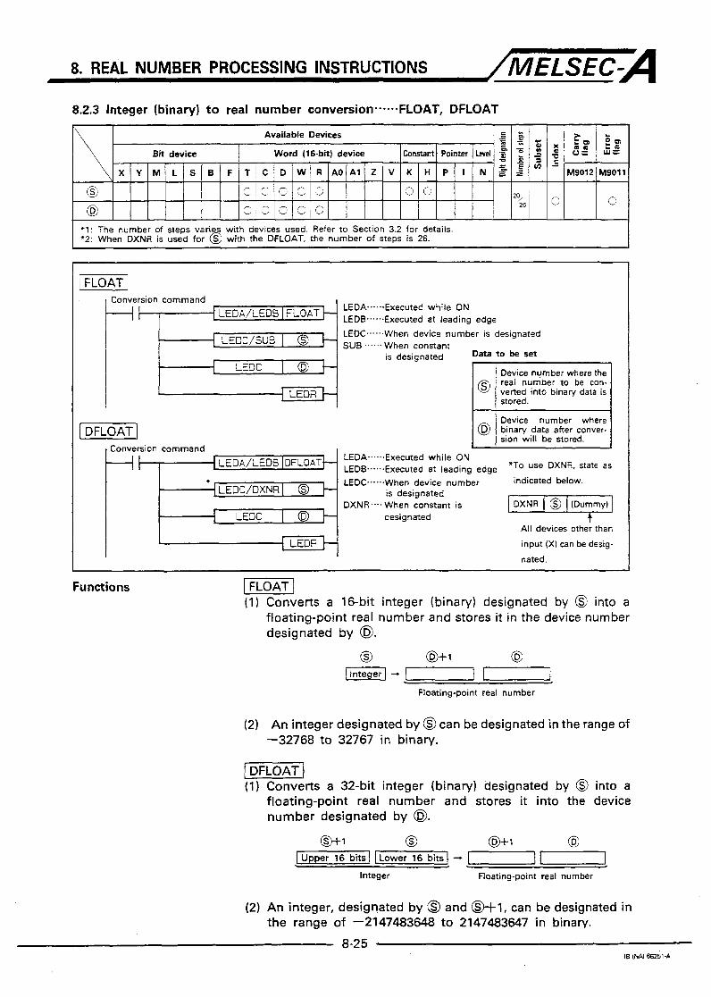
8. REAL NUMBER PROCESSING INSTRUCTIONS /MELSEC-A 8.2.3 integer (binary) to real number conversion.-..--FLOAT, DFLOAT
Available Devices E t - z z - ggl Bit device '
L H ~ . Pointer Constant Word (16-bit) device
X M9011 M9012 5 E N I P H K V 2 A O A l W / R D T i C F B S L M Y . - : a -
v = 8 s
@ 20 0 0 cl2 c 2 ' 2
@ 36 e 0 s sjs c '3
'1: The number of steps varies with devices used. Refer to Section 3.2 for details. '2: When DXNR is used for @ with the DFLOAT, the number of steps is 26.
Conversion command
LEDB.-..-Executed at leading edge LEDA....-.Executed while ON
LEDC-...-When device number is designated SUB ...... When constant
is designated Data to be set I I Device number where the I
-[ LEDR real number to be con- verted into binary data is stored. I
t i I
(DFLOATI Device number m e r e
Conversion command LEDA..--Executed while ON E D B . . . . . . E ~ ~ , , ~ ~ ~ at leading edge *To use DXNR. state as
LEDC.-.-..When device number indicated below.
DXNR.... When constant is is designated
designated All devices other than
LEDR input (X) can be desig- nated.
Functions (1) Converts a 16-bit integer (binary) designated by 8 into a
floating-point real number and stores it in the device number designated by @.
0 @+l @ [ I n t e g e r / - 7 1
+ Floating-point real number
(2) An integer designated by @ can be designated in the range of -32768 to 32767 in binary.
[DFLOAT 1 (1) Converts a 32-bit integer (binary) designated by @ into a
floating-point real number and stores it into the device number designated by @.
o t l 0 @+l @ I Upper 16 bits I I Lower 16 b i q - [ ~~ ~~ ~~ ll
Integer Floating-point real number
(2) An integer, designated by @ and @+l, can be designated in the range of -2147483648 to 2147483647 in binary.
8-25 18 (W 662514
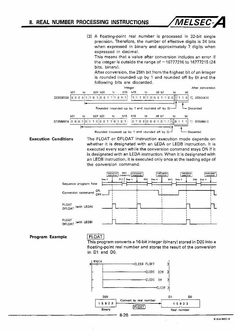
8. REAL NUMBER PROCESSING INSTRUCTIONS /MELSEC-A (3) A floating-point real number is processed in 32-bit single
precision. Therefore, the number of effective digits is 24 bits when expressed in binary and approximately 7 digits when expressed in decimal. This means that a value after conversion includes an error if the integer is outside the range of -16777216 to 16777215 (24 bits, binary). After conversion, the 25th bit from the highest bit of an integer is rounded (rounded up by 1 and rounded off by 0) and the following bits are discarded.
Integer After conversion b31 to b24 b23 to b16 b15 to b8 b7 to bO
22203003010 0 . 0 0 1 1'0'1/0 0 1.1/1'0 1 : l l 11 1 ' 1 0 ) 1 ~ 0 ~ 0 011 1 . 0 OB1 1 O/e222030032
4
Rounded (rounded u p by 1 and rounded off by 0) tDiscarded
b31 to b24 b23 to b16 b15 to b8 b7 to bO
372588919 5) 372588912 0 1'0 010 0 0 llO:l:lf? 0 1 : l ' l O ~ O j O ~ l ( O ~ l ~ 1 : O ~ O 0jl:ljO 1 0 ' 1 . . . .
+ Rounded (rounded u p by 1 and rounded off by 0) tDiscarded
Execution Conditions The FLOAT or DFLOAT instruction execution mode depends on whether it is designated with an LEDA or LEDB instruction. It is executed every scan while the conversion command stays ON if it is designated with an LEDA instruction. When it is designated with an LEDB instruction, it is executed only once at the leading edge of the conversion command.
SteD 0 END 5- 0 END Step 0 I ,
Sequence program flow I 7 I I I I I
ON OFF
I I I I I I I I I I I I I
I I I
Conversion command I I I l j I I I
I I I I I I
FLOAT I
DFLOAT (with LEDN p I 1
I I I I I I
I I
I
I I I I I I I I I
I
(with LEDB) I I I I # I
DFLOAT h
Program Example FLOAT] This program converts a 16-bit integer (binary) stored in D20 into a floating-point real number and stores the result of the conversion in Dl and DO.
D20 D l Convert to real number
1 5 9 2 3 1 5
Binary Real number

8. REAL NUMBER PROCESSING INSTRUCTIONS ,/MELSEC=A This-program converts a 32-bit integer (binary) stored in D21 and D20 into a floating-point real number and stores the conversion result in D l and DO.
021 D20 Dl Convert to real number
Binary
+67/ D20 Convert to real number An error is generated
p i c q 9 because the number of
Binary effective digits is 7. Dl DO 1 1 7 3 9 6 3 1 2 0 I
Real number
8-27 IB (W 6 6 2 5 1 4

MEMO
....................................................................................................................................................................
....................................................................................................................................................................
.....................................................................................................................................................................
.....................................................................................................................................................................
.....................................................................................................................................................................
.....................................................................................................................................................................
....................................................................................................................................................................
.....................................................................................................................................................................
....................................................................................................................................................................
....................................................................................................................................................................
....................................................................................................................................................................
....................................................................................................................................................................
....................................................................................................................................................................
....................................................................................................................................................................
IB I W €62514

8. REAL NUMBER PROCESSING INSTRUCTIONS /MELSEC-A 8.2.4 Addition----..ADD
Available Devices 1 - E g - - a - + c E $ i g x w : z Bit device w - u canstanti Pointer I Level Word (1Bbitl device 3
I
\ , X M9Oll M9012 z E I I N H I P K V 2 A O A l R W D C T F B S L M Y = E r n - - - .n
3 C j 3 0 ' 2 ~
@) i c: 0 0 0 c: I
\5
@ I '1: The number of steps varies with devices used. Refer t o Section 3.2 for details.
Addition command LEDA,..Executed 1 LED AILEWE LEDB...Executed
edge
LEDC - r - -1 LEDC 1@+ 4 LEDC I F
I -1 LEDR
while ON at leading Data to be set
Head number of devices
stored.
Head number of devices
sult (sum) is stored.
Functions (1) Adds the floating-point real number, designated by @, and the floating-point real number, designated by @, and stores the result of the addition in the device number designated by 0.
a=+ma=mEII Floating-point Floating-point Floating-point real number real number real number
(2) The value which can be designated by @I and @ and the value which can be stored in @ are indicated below.
0, 2-127 s I Value I < * 2129
Execution Conditions The ADD instruction execution mode depends on whether it is designated with an LEDA or LEDB instruction. It is executed every scan while the addition command stays ON if it is designated with an LEDA instruction. When it is designated with an LEDB instruction, it is executed only once at the leading edge of the addition command.
Sequence program flow
ON OFF
I I I I I I I I I I
I 1 Addition command I I 1 : I I
I I I I I I I I I I I
I ADD ( w i t h LEDA) n I 1 1
I I I I I
I I I I
I I I I I I I I I
I
I I I I I ADD (with LEDB) I

8. REAL NUMBER PROCESSING INSTRUCTIONS /MELSEC-A Operation Error An operation error occurs in the following case and the error flag
(M9011) is set.
Program Example
Description Error Code
D9008 I D9091 The operation result is outside the following range or not "0". I
-+2-lZ7 5 I Operation result 1 < 2129 50 503
This program adds the floating-point real number stored in Dl1 and Dl0 to the floating-point real number stored in D21 and D20 and outputs the operation result to Y5F to Y40 after converting it into an integer.
' I 'LEPI [)26 4 } Addition of floating-point real 1 numbers (3)
I I I ,
on re- conversion of the operati sult into an integer (GI)
Outputting integer to display unit (3)
D21 D20 a *.e] + i12op 3. 2 1 JADDI :f? Real number value
I C
D31
1 7 9 6 4 . 6 4 Addition
Real number value Real number value Conversion to integer
f k - : 6 5
DO a Convert Y5F to Y50 Y4F to Y40
0 5 6 9 1 1 7 0 0
Binary value BCD value

8. REAL NUMBER PROCESSING INSTRUCTIONS /MELSEC-A 8.2.5 Subtraction---.-SJB
r * l : The number of steps varies with devices used. Refer to Section 3.2 for details.
m o l 2 7 M9011
Subtraction command LEDA...Executed while ON Data to be set
Head number of devices
Head number of devices S2 where the subtrahend is
to be stored.
t { LEDC
I 4 LEDR Head number of devices
sult IS stored. the operation re-
Functions (1) Subtracts the floating-point real number designated by @ from the floating-point real number designated by @ and stores the result to the device number designated by @I.
UD--DD=DO Floating-point Floating-point Floating-point real number real number real number
(2) The value which can be designated by @ and @ and the value which can be stored in @ are indicated below.
0, 2 2-lZ7 s I Value I < I 2lZ9
Execution Conditions The SUB instruction execution mode depends on whether it is designated with an LEDA or LEDB instruction. It is executed every scan while the subtraction command stays ON i f it is designated with an LEDA instruction. When it is designated with an LEDB instruction, it is executed only once at the leading edge of the subtraction command.
s a p o END Step 0 END slrp 0 END spp 0 END Suo 0 I I
Sequence program flow I7
Subtraction command
I I I I I I I I I I
i I I I I I
ON OFF I J I I
SUB (with E D A )
SUB (with E D B )
I I I
I I I I I I 1
I 1 I 1 I I I I I I I
I I I
I I I I I I I I I

8. REAL NUMBER PROCESSING INSTRUCTIONS /MELSEC-A Operation Error An operation error occurs in the following case and the error flag
(M9011) is set.
Program Example
Error Code Description
The operation result is outside the following range or not ‘0’ ’ . 1 D9008 1 09091
This program subtracts the floating-point real number stored in D21 and D20 from the floating-point real number stored in Dl1 and Dl0 and outputs the operation result to Y5F to Y40 after converting it into an integer.
L E D C Dj8
LEER P I N T
Conversion of the operation re- sult into an integer (a) LEDC DB
I
c I L ‘ D B C E Kg Outputting integer to display Y i r4@ 3 ! unit (0)
Dl 1 D l 0 D21 D20 0 D31
- i { 9 . 8 2 1 3 0 5 . 4 1 I 1 5 Real number value
R e a l number value Real number value I O Convert to integer IDINT(
DO Convert Y5F to y50 Y4F to Y40
0 0 0 2 1 3 0 5 to BCD
Binary value BCD value
8-3 1 IB I W 652518

8. REAL NUMBER PROCESSING INSTRUCTIONS /MELSEC-A 8.2.6 Mukiplication....-.MUL
Available Devices z - E r 8 P - ~ hJ : m x 0 : z
Bit device W = 4 .2 z Level Pointer Constant Word (%bit) device X c , a ' X Y M L S B F T C D W R A O A I Z V K H P I N ~ ~ w - M9011 M9012
0
I 0 3 0 0 0 Go
o c ; o o o 0 0
23 1 3 0 c 3 0 h
Y
'1: The number of steps varies with devices used. Refer to Section 3.2 for details.
I I Multiplication command
LEDA/LEDB MUL LEDA., LEDB-
,.Executed '.Executed edge
while ON at leading
Data t o be set
Head number of devices
data is stored.
be stored.
Head number of devices
stored.
Functions (1) Multiplies the floating-point real number designated by @ with floating-point real number designated by @ and stores the result of multiplication in the device number designated by @.
Floating-point real number
Floating-point real number
Floating-point real number
(2) The value which can be designated by @ and @ and the value which can be stored in @ are indicated below.
Execution Conditions The MUL instruction execution mode depends on whether it is designated with an LEDA or LEDB instruction. It is executed every scan while the multiplication command stays ON if it is designated with an LEDA instruction. When it is designated with an LEDB instruction, it is executed only once a t the leading edge of the multiplication command.
Sequence program flow
ON OFF
I I I I I
Multiplication command I I I I I I I
I I 1 I I I I
I I I I
MUL (with LEDA) -I I I I I
I
I I
I I I I I I I I I
I I
I I I MUL (with LEDB) I I I
8-32 IB ( N A E8251-A

8. REAL NUMBER PROCESSING INSTRUCTIONS /MELSEC-A Operation Error A.n operation error occurs in the following case and the error flag
(M9011) is set.
Description Error Code
D9008 I D9091
Program Example
The operation result is outside the following range or not "0". 50 503
k 2-12' S I Operation resuit I < F 2lZ9
This program multiplies the floating-point real number stored in Dl1 and Dl0 by the floating-point real number stored in D21 and D20 and outputs the operation result in Y5F to Y40 after converting it into an integer.
RI4F+LLEDA #UL
-
CLEDC D38 - CLEDf D 2 6 - CLEDC D l @
- CLEDR 1
Multiplication between floating- point real numbers (0)
CLEDFi D I N T
- D 3 e Conversion of the operation result into an integer (3) - CLEDC D e 3
- I L E b F : 3
- C D B C D @ e KE! y 8 4 e Outputting integer to display
unit (G)
Conversion of the operation result into an integer (3)
Outputting integer to display unit (G)
D20 0
X E l 2 7 8 6 1 Real number value Real number value
D3 1 Multiplication 4 4 3 8.1-1 1
Real number value
a Convert to integer
Dl 4 DO @ Y5F to Y50 Y4F to Y40
0 0 0 0 0 4 3 9 Convert to BCD
lDBCDl Binary value BCD value

8. REAL NUMBER PROCESSING INSTRUCTIONS /MELSEC-A 8.2.7 Division-.-.-DIV
1 * l : The number of steps varies with devices used. Refer to Section 3.2 for details. I Division command
+I LEDA.
-+LED- LEDB-
1 LEDC I 8 I LEDC I7
t [ LEDC I 0
..Executed while ON
..Executed at leading Data to be set edge
where the multiplicand 0 Head number of devices
data is stored.
@ where the multiplier is to Head number of devices
be stored.
Head n u d e r of devices (@ where operation result is
stored.
i
Functions (1) Multiplies the floating-point real number designated by @I with floating-point real number designated by @ and stores the result of the multiplication in the device number desig- nated by 0.
Floating-point Floating-point Floating-point real number real number real number
(2) The value which can be designated by @ and @ and the value which can be stored to @ are indicated below.
0, zk 2-12’ s I Value I < k 2’29
Execution Conditions The DIV instruction execution mode depends on whether it is designated with an LEDA or LEDB instruction. It is executed every scan while the division command stays ON if it is designated with an LEDA instruction. When it is designated with an LEDB instruction, it is executed only once a t the leading edge of the division command.
Sequence program flow
Multiplication command ON OFF
I I I I I I I I I I
I I I
D N (with LEDA) 1 1 I I I I I I
I I I I
I 1 I I I I I
I I I DN (with LEDB) I 1 1 I
8-34 IB (NAJ 662514

8. REAL NUMBER PROCESSING INSTRUCTIONS ~/MELSEC-A Operation Error An operation error occurs in the following case and the error flag
(M9011) is set.
Program Example
Description Error Code
D9008 1 D9091 The operation result is outside the following range or not "0". 1
k 2 -m s 1 Operation result I < & 2 129 503 50 The divisor designated by @ is "0".
This program divides the floating-point real number stored in Dl 1 and Dl0 by the floating-point real number stored in D21 and D20 and outputs the operation result in Y5F to Y40 after converting it into an integer.
- I1 9 0 3 6
CLEDFI D I U I
CLEDC D l @ 3
CLEDC D 2 0 3
CLEDC D 3 8 3
CLEDFl 3
CLEDR D I H T 3
CLEDC D30 3
CLEDC D0 3
CLEDK 3 K8 Y @ 4 @ 3 CDBCD D@
Division of floating-point real numbers (9)
Conversion of the operation result into an integer (9)
Outputting integer to display unit (0,
Dl 1 D l 0 D21 D20 D31 a Division
5 3 5 9 . 0 4 1 :5 Real number Real number Real number
Convert to integer
D l W @ Y5F to Y5OY4F to Y40
Binav value BCD value
8-3 5 I6 INAl65251-6

8. REAL NUMBER PROCESSING INSTRUCTIONS /MELSEC-A 8.2.8 Angle to radians conversion.----RAD
'1: The number of steps varies with devices used. Refer to Section 3.2 for details.
M9012 I M9011
I
Conversion command
I f LEDR
LEDA...-+xecuted while ON LEDB.--..Executed at leading edge
Data to be set
where the angle to be converted in radians is stored.
Head number of devices
stored.
Functions (1) Converts an angle expressed in floating-point real number designated by @ into radians and stores the result of the conversion in the device number designated by 0.
E' f 1 0 @ + l @ (I/)* rad
Floating-point real number Floating-point real number
(2) Conversion from "degree" to "radian" is executed using the following formula.
Degrees X 180 - - Radians TT
Execution Conditions The RAD instruction execution mode depends on whether it is designated with an LEDA or LED5 instruction. It is executed every scan while the conversion command stays ON if it is designated with an LEDA instruction. When it is designated with an LEDB instruction, it is executed only once at the leading edge of the conversion command.
m ~ l ~ c b c n I z2%nq p r o e c r r ~ ~ a a m n e-un END h m m m n InSrmPDn
D I C M l D " -on -&on
smp 0 END Slcp 0 END Step0 END Step 0 END Step 0 I , , I
Sequence program flow n Conversion command
I I I I I . I I I I I I I I I I I I I
I I I I I I I I
I I I
ON OFF I I I I I
RAD (with LEDA) 1 I 1 I I I
I I I I I I I
I
I I I I
FAD (with LEDB) 1 I I 1 I
8-36 18 (NAI W 5 1 4

8. REAL NUMBER PROCESSING INSTRUCTIONS /MELSEC-A Program Example This program converts the angle set in X2F to X20 in 4-digit BCD
into radians and stores the operation result in D21 and D20 as a floating-point real number.
H 9 8 3 6 K 4 Inputting an angle to be con- verted into radians. (0)
- I L E D R FLDRT
- CLEDC D e
- -
Conversion of the input angle (degree) into a floating-point
ELEDC D l @ real number. ( 2 )
€LE@R I - C L E D R R R D
- Conversion of the input angle
- (degree) into radian. (a) CLEDC @ ? @ 1 -
CLEDR 7 '
120' -.2.094395.-.rad a
X 2 F to X20 0 DO Convert to a D l 1 Dl0 @ D21 D20 I1 real number Conven to radian
120 I I
0 1 2 0 120 F] -F 2 . 094395.'.
BCD value Binary value Real number value Real nukber value

8. REAL NUMBER PROCESSING INSTRUCTIONS /MELSEC-A 8.2.9 Radians to angle conversion..--..DEG
I '1: The number of steps varies with devices used. Refer to Section 3.2 for details.
Conversion command
LEDC
1 -1 LEDA
LEDA......Executed while ON LEDB......Executed at leading
edge Data to be set
number of devices
radians to be con- where the angle express-
verted in degrees is stored.
Head number of devices
sult is stored.
Functions (1) Converts an angle expressed in radians designated by @ into degrees and stores the conversion result to the device number designated by @.
@ + 1 E @ + l @ ( 7 1 -1) rad - (m -1) '
Floating-point real number Floating-point real number I
(2) Conversion from "radians" to "degrees" is executed using the following formula:
180 Radians X = Degrees
Execution Conditions The DEG instruction execution mode depends on whether it is designated with an LEDA or LEDB instruction. It is executed every scan while the conversion command stays ON i f it is designated with an LEDA instruction. When it is designated with an LEDB instruction, it is executed only once at the leading edge of the conversion command.
Sequence program flow
ON OFF Conversion command
I I I I I I I I I I
I I I I I
DEG (with LEDA) 1 n I
I a 1 I
I I I I I I I I I I 1 I I I
DEG (with LEDB) 1 I I I
8-38 IB W €62514
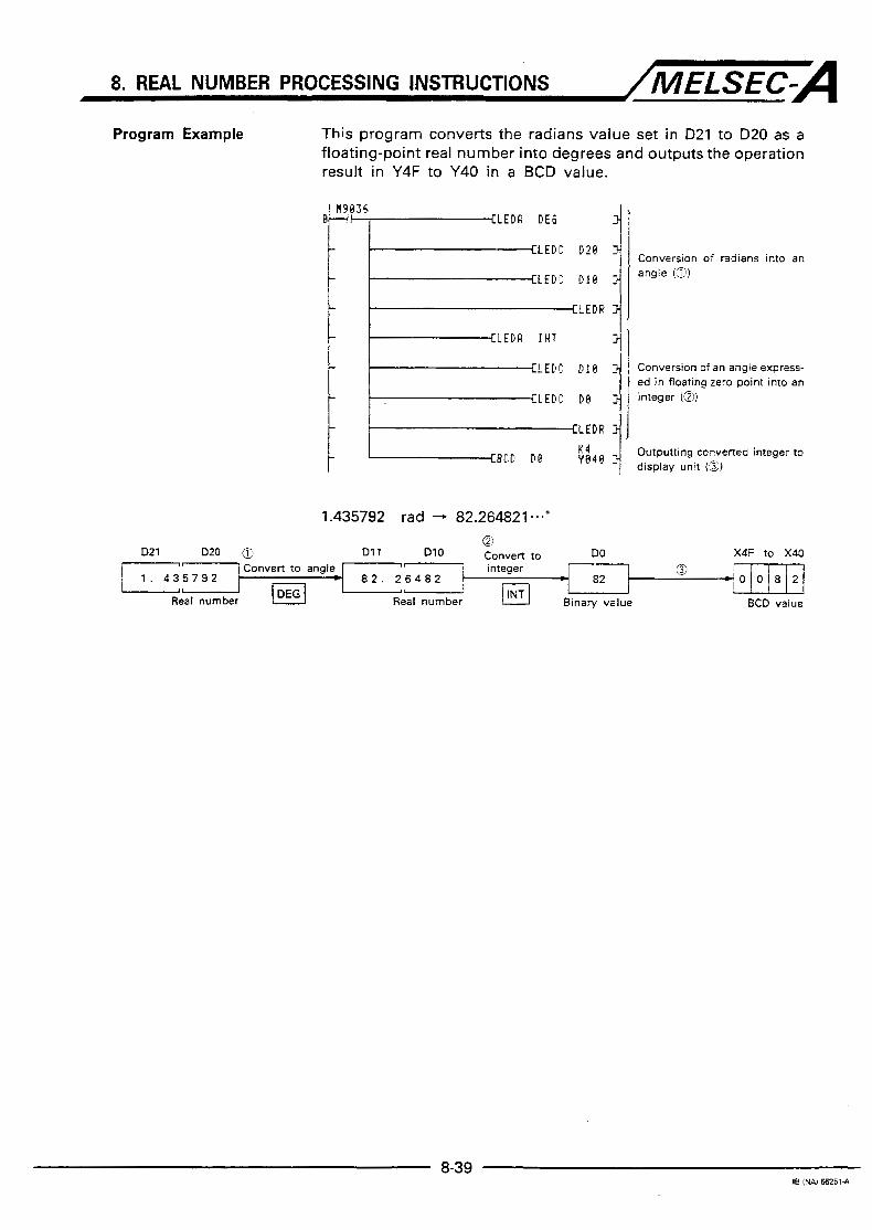
8. REAL NUMBER PROCESSING INSTRUCTIONS /MELSEC-A Program Example This program converts the radians value set in D21 to D20 as a
floating-point real number into degrees and outputs the operation result in Y4F to Y40 in a BCD value.
L D 2 B ' Conversion of radians into an - C L E D C D l @ 3
C L E D F 3
C L E D R I H T 3
angle (0)
-
-
- Conversion of an angle express- C L E D r @ I @ 3 ' ed in floating zero point into an - E L E D C D @ 3 Integer @?)
- C L E D R 3
1 IBC@ '@ y e 4 e I display unit (3) K4 Outputting converted integer to
1.435792 rad - 82.264821
Dl 1 D l0 Convert to DO X4F to X40 0
integer a 82 2 8 0 10 L
Real number Real number Binary value BCD value
8-39 B IW 662514

8. REAL NUMBER PROCESSING INSTRUCTIONS /MELSEC-A 8.2.10 Sine operation--.---SlN
Available Devices P s . .s E m - g Bit device Y 8 4 f f &I Pointer constant Word (16-bit) device
x m s
X Y M L S B F T I C D W R A O A l 2 V K H P I N i i j " ; c M9012 M9011 ~ . = = v)
0 @
3 3 0 0 3 20 C' '2
5 3 0 0 3
€1: The number of steps varies with devices used. Refer to Section 3.2 for details.
Sine operation command
LEDA/LEOB( SIN 1
-1 LEDC I 0 I -1 LEDfi
LEDA.-....Executed while ON LEDB......Executed at leading edge
Data to b e set
where the angle data for
to be executed is stored. which the sine operation
Head number of devices
sult is stored.
L
Functions
Execution Conditions
(1) Calculates the sine value of the angle designated by 0 and stores the operation result in the device designated by @.
SIN 7 1 ) - 7 1 Floating-point real number Floating-point real number
(2) An angle to be designated by @ should be set in units of radians (angle X r/180). For the conversion between "degrees" and "units", refer to the DEG and RAD instructions.
The SIN instruction execution mode depends on whether it is designated with an LEDA or LEDB instruction. It is executed every scan while the SIN operation command stays ON if it is designated with an LEDA instruction. When it is designated with an LEDB instruction, it is executed only once at the leading edge of the SIN operation command.
hstnxlm END lnprusbM a h -ng a d m n
step 0 END Step 0 END St- 0 I 1 1 1
Sequence program flow t Sine operation command
I I I I I I I I
1 ON OFF I : I I
I I I I I I
I I I I I I I
I SIN ( w i t h LEDA) 1 I 1
I I I I
I I I I I
I 1 I I I I I
I I I SIN (with LEDB) I I 1 I
8-40 I8 ( N A J €62514

8. REAL NUMBER PROCESSING INSTRUCTIONS /MELSEC-A Program Example This program executes the sine operation for the angle set in X2F
to X20 in 4-digit BCD and stores the operation result in D l and DO as a floating-point real number.
> I L E D R FLORT 3
CLEDC D36 3 Conversion of an angle into
CLEDC D 2 6 floating-point real number (3)
CLEDF! 3
CLEDR R R D 3
ELEDC D26 3
‘LEDC ~ 1 6 3 radians ( G I ) Conversion of an angle into
CLEDR 3
CLEDR SIN - > - ’ Sine operation using convened
CLEDC D 6 3 angle (radians) (0)
CLEDR 3 ,
150’ = 0.5 D30
Binary conversion
BCD value a Binary value Convert to real number
a @ D20 Convert D l 1 D l0 Sine D l Do
to radians I1 2 . 6 1 7 9 9 3
operation 1 1
Real number value Real number value Real number value

8. REAL NUMBER PROCESSING INSTRUCTIONS /MELSEC=A 8.2.1 1 Cosine operation-...-*COS
Available Devices
Bit device Word [ lbbi t ) device
X Y M L S B F T C D W R A 0 A l Z V K H P I N a " z M9012 M9011
0 62
0 3 0 0 0 20 0 0
3 0 0 c, r,
b-: -The number of steps varies with devices used. Refer to Section 3.2 for details. I I
Cosine operation command
l L E D A ' L E m LEDB......Executed at leading edge LEDA..-..-Executed while ON
t 1 LEDC I @
-1 LEDC I
Data t o be set
where the angle data for Head number of devices
which cosine operation is to be executed is stored.
i Head number of devices
~ stored. where operation result is
Functions (1) Calculates the cosine value of the angle designated by 0 and stores the operation result in the device designated by 0.
Floating-point real number Floating-point real number
(2) An angle to be designated by @ should be set in units of radians (angle X r/180). For the conversion between "degrees" and "units", refer to the DEG and RAD instructions.
Execution Conditions The COS instruction execution mode depends on whether it is designated with an LEDA or LEDB instruction. It is executed every scan while the COS operation command stays ON if it is designated with an LEDA instruction. When it is designated with an LEDB instruction, it is executed only once at the leading edge of the COS operation command.
Sequence program flow
Sine operation command ON OFF
I I I I I I I I I I I I I
I COS (with LEDA) n I
I I I I I I I I I I
I I I
I I I
I I I
COS (with LEDB) I I 1 I
8-42 16 I W 66251-A

8. REAL NUMBER PROCESSING INSTRUCTIONS /MELSEC-A Program Example This program executes the cosine operation for the angle set in
X2F to X20 in 4-digit BCD and stores the operation result in D l and DO as a floating-point real number.
Inputting an angle (0)
CLEDR FLORT E
D 3 e ' , Conversion of an angle into a
floating-point real number (a) CLEDC 0 2 0 3.
CLEDF: 3
3.. CLEDR R R D
,
D29 3 Conversion of an angle into
CLEDC Dl@ radians (3)
CLEDR 1, CLEDR C O S
, Sine operation using converted
CLEDC D Q 1 angle (radians) (8)
CLEDL ,
COS 60' = 0.5
WF to X20 0 Binary conversion
BCD value @ Binary value Convert to real number
@ @ D21 D20 Convert Dl 1 Dl0 Cosine Dl
Real number value ' [RADI ' Real n i k b e r valu!
to radians -1 operation 1 . 0471 9 7

8. REAL NUMBER PROCESSING INSTRUCTIONS /MELSEC-A 8.212 Tangent operation*.-...TAN
Available Devices C n 0 - .= - P
- E E g a m c m x 0 - Bit device 0 4 Level Constant I Pointer Word (16-bit) device
.&; X Y M L S B F T C D W R A O A l Z V K H P I N S z M9011 M9012
0 C' 0 3 0 L1 E' 0 0 0 013
20 c - & L
* I : The number of steps varies with devices used. Refer to Section 3.2 for details.
Tangent operation command
- i t ~ + L E O A / L E ~ LEDB.-...Executed at LEDA--.,Executed while ON
leading edge Data to be set
-1 LEDC r k __f LEDC 1 @I stored.
-1 LEDR
Functions (1) Calculates the tangent value of the angle designated by @ and stores the operation result in the device designated by @.
@ + 1 3 @ + l @ TAN (-1 I])- 7 1 -
Floating-point real number Floating-point real number
( 2 ) An angle to be designated by @ should be set in units of radians (angle X n1180). For the conversion between "degrees" and "units", refer t o the DEG and RAD instructions.
(3) If an angle designated by @ is "n/2" radians or "(3/2)T'' radians, an operation error is generated to obtain a radians value and, therefore, the error is not caused.
Execution Conditions The TAN instruction execution mode depends on whether it is designated with an LEDA or LEDB instruction. It is executed every scan while the TAN operation command stays ON if it is designated with an LEDA instruction. When it is designated with an LEDE instruction, it is executed only once a t the leading edge of the TAN operation command.
blsmdi~n END insauumn I z z x ] a w o n exrnmon pmcessnq aeMm IIIsbvctmn lnpnmon
c r e M m n
SQQ 0 END Step 0 END Stcp 0 END strpo W D step 0 I I , I , I I I
Sequence program flow t rl n n Tangent operation command
I I I I I I I I I I I 1 I I
ON OFF I I I I 1 : I I I
I I I I I I
I TAN (with LEDA) 1 I
I I I
I I
I I I I I I I I I I I
TAN (with E D B ) 1 I I I
8-44 18 (W 6ml-A

8. REAL NUMBER PROCESSING INSTRUCTIONS /MELSEC-A Operation Errors An operation error will occur in the following cases and an error
flag (M9011) will be set.
Program Example
Description Error Code
D9008 1 D9091 The operation result is outside the following range.
k 2 s 1 Operation result I < I 2 '29 . -
50 503
This program executes the tangent operation for the angle set in X2F to X20 in 4-digit BCD and stores the operation result in Dl and DO as a floating-point real number.
Y4 I y C B I H X828 D38 3 Inputting an angle (0)
I
I CLEDR FLOFIT 3
ELEDC 036 3 Conversion of an angle into
rLEDC D2e floating-point real number (a)
'LEDR 3
CLEDii R R D 3
CLEDC D2e 3
LED^ D l e . radians
CLEDR 3 J
Conversion of an angle into
ILEDF l T R H 3
4 ' verted angle (radians) (@)
Tangent operation using con-
CLEDC D0 3-
CLEDR 3
TAN 135" = -1
X 2 F to X20 il: D30 - Binan/ conversion - 135
BCD value '/inan, value
I Convert t o real number
4 0 @ D21 D20 Convert D l 1 D l 0 Tangent D l
t o radians
Real number value Real number vahe Real number value

8. REAL NUMBER PROCESSING INSTRUCTIONS /MELSEC-A 8.2.13 Arc sine operation---.-.ASIN
Available Devices
Bit device
X Y M L S B F T C D W R A O A l Z V K H P I N s S
0 u= Level Pointer &stant Word (16-bit) device
M9011 M9012 $ f ; r , %
0 0
0 0 ~ 0 0
3 3 0 0 0 20 '3 3
+1: The number of steps varies with devices used. Refer to Section 3.2 for details.
Arc sine operation
t+ command t - / L E D A E m
-1 LEDC l-F+ -1 LEOC
1 [ LEDR I
LEDA-..--Executed while LEDB..-..Executed at
leading edge
ON
Data to be set
stored.
Functions
Execution Conditions
(1) Calculates an angle from the sine value designated by @ and stores the operation result in the device designated by 0.
@ + l c3 @ + l @ SIN -' 7 1 ) - 7 1
Floating-point real number Floating-point real number
(2) Sine value to be designated by @. Setting range: -1.0 to 1.0
(3) An angle obtained by arc sine operation and stored in @ should be in units of degrees. For the conversion between "degrees" and "radians", refer to the DEG and RAD instructions.
The ASlN instruction execution mode depends on whether it is designated with an LEDA or LEDB instruction. It is executed every scan while the SIN-1 operation command stays ON if it is designated with an LEDA instruction. When it is designated with an LEDB instruction, it is executed only once at the leading edge of the SIN-1 operation command.
Sequence program flow
Arc sine operation command ON OFF
I 1 I I I I I I I I I
ASlN (with LEDA) 1 I 1 4 I I
I I I I I
I I
I I I I I
I I I ASIN (with LEDB) I
I I

8. REAL NUMBER PROCESSING INSTRUCTIONS /MELSEC-A Operation Errors An operation error will occur in the following cases and an error
flag (M9011) will be set.
Program Example
Error Code D9008 1 D9091 Description
The sine value designated by @ is outside the following range 1 503 . - - l n t n ~n I
This program obtains the arc sine value for the floating-point real number stored in D l and DO and outputs the obtained angle to Y4F to Y40 in a 4-digit BCD.
el-Y8+LEDR R S I H I 1
CLEDC D O 3
'LEDC D l 0 3
CLEDR 3
CLEDR DE6 3 .
CLEDC Dl8 1
CLEDC 3
CLEDP, 3
L L E D U I H T 3
CLEDC D 2 P 3
CLEDC D 3 P f
CLEDR 3 ,
CBCD D 3 8 Y 8 4 8 3 K 4
SIN -' 0.5 = 30" D l m a Dl 1 D l 0
Real number value I 0 Real number value
I Convert to degrees (DEGJ D21 D20 0 D30
Calculating an angle (radians- )by executing arc sine opera- tion (0)
Conversion the angle (radians) into degrees (a)
Conversion of the angle (de- grees) expressed as a floating- point real number into an inte- ger ('3)
Outputting the obtained angle to the display unit (@I
0 X4F to Y40 - - Integer conversion
3 0 BCD conversion
Real number value BCD value
If the value of a floating-point real number stored in Dl and DO is outside the range of -1.0 to 1.0, an operation error occurs when the instruction is executed.

8. REAL NUMBER PROCESSING INSTRUCTIONS /MELSEC-A 8.2.14 Arc cosine operation..----ACOS
Available Devices g e z x ;g Bit device 0 = $ $ Level Pointer constant Word (lbbit) device
= -
X Y M L S B F T C D W R A O A ~ Z V K H P I N E Z M9012 M9011 . = E m -
0 @
3 3 o o c ' 3 20 ,- '4 0 3 0 o c
'1: The number of steps varies with devices used. Refer to Section 3.2 for details.
Arc cosine operation LEDA..-...Executed while ON
L E D A / L E D B m k LEDB.-...Executed at Data to be set leading edge
1 - - LEDC
[ LEDC I+ for which arc cosine o p where the cosine value
IS gored. eration is to be executed
where operation result is stored.
Functions (1) Calculates an angle from the cosine value designated by 8 and stores the operation result in the device designated by a.
@ + 1 (9 @ + 1 @ cos -' (m 7 1 ) - It I -
Floating-point real number Floating-point real number
(2) Cosine value to be designated by 0. Setting range: - 1 .O to 1 .O
(3) An angle obtained by arc cosine operation and stored in @ should be in units of degrees. For the conversion between "degrees" and "radians", refer to the DEG and RAD instructions.
Execution Conditions The ACOS instruction execution mode depends on whether it is designated with an LEDA or LEDB instruction. It is executed every scan while the COS-1 operation command stays ON if it is designated with an LEDA instruction. When it is designated with an LEDB instruction, it is executed only once at the leading edge of the COS-1 operation command.
-ion bsmsuon pospsing ueculion exeQnlon
l n s m d n n END hrrmaion U e M l O n UeCMDn
LmOuamn DL-
% P o END step 0 END 8ep 0 END S W O I 1
Sequence program flow I I I I I I I I I I I I I I I 1 I I I
ON OFF Arc cosine operation command
I I I I I I I : I I I
I I I I I
ACOS (with LEDA)
ACOS (with LEDB) I I I I I I

8. REAL NUMBER PROCESSING INSTRUCTIONS /MELSEC-A Operation Errors A.n operation error will occur in the following cases and an error
flag (M9011) will be set.
Program Example
Description Error Code
WOO8 D9091 The cosine value designated by is outside the following range
: -1.0 to 1.0 I 50 503 ~~
This program obtains the arc cosine value for the floating-point real number stored in D l and DO and outputs the obtained angle in Y4F to Y40 in 4-digit BCD.
@ / - i p C L E D f i A C O S I H9836
I
cos Dl m o
D @ ' by executing arc cosine opera-
Calculating an angle (radians)
ELEDC Dl6 3 tion (3)
CLEDF > CLEDR DE6 2-
' le ~ Conversion of the angle (ra-
[ L E K D X 1 dians) into degrees (a)
C L E D R 3
3 ' LLEDF! I H T
,
Conversion of the angle (de- D 2 8 ' grees) expressed as floating- point real number into an inte- CLEDr D 3 P 3 ger
CLEDR 3
IBCD D 3 e 6'46 4 to the display unit (a) Outputting the obtained angle
-' 0.5 = 60'
Dl 1 Dl 0
Real number value
Convert to degrees
D30 @ Y4F to Y40
Real number value BCD value
If the value of a floating-point real number stored in Dl and DO is outside the range of -1 .O to 1 .O, an operation error occurs when the w l instruction is executed.

8. REAL NUMBER PROCESSING INSTRUCTIONS /MELSEC-A 8.2.15 Arc tangent operation..--.ATAN
I M9012 M9011
* l : The number of steps varies with devices used. Refer to Section 3.2 for details.
Arc tangent operation command
+ I I LEDC I 8 4 , LEDC - I O +
1 LEDR + Head number of devices
@ for which arc tangent op- where the cosine value
eration is to be executed is stored.
Head number of devices where the operation re- sult is stored.
Functions (1) Calculates an angle from the tangent value designated by @ and stores the operation result in the device designated by 0.
@ + 1 0 @ + l @ TAN (m 7 1 )
I - Floating-point real number Floating-point real number
(2) An angle obtained by arc tangent operation and stored in 0 should be in units of degrees. For the conversion between "degrees" and "radians", refer to the DEG and RAD instructions.
Execution Conditions The ATAN instruction execution mode depends on whether it is designated with an LEDA or LEDB instruction. It is executed every scan while the TAN-1 operation command stays ON if it is designated with an LEDA instruction. When it is designated with an LEDB instruction, it is executed only once at the leading edge of the TAN-1 operation command.
Sequence program Row
ON OFF
I I I I I I I I I
I I I I I I I I I I I I
Arc tangent operation command I I I 1 : I I
ATAN (w i th EDA)
I I I I I I I I
ATAN (with LEDB) I I I
8-50 Is I N A J Ea514

8. REAL NUMBER PROCESSING INSTRUCTIONS /MELSEC-A Program Example This program obtains the arc tangent value for the floating-point
real number stored in D l and DO and outputs the obtained angle in Y4F to Y40 in 4-digit BCD.
Calculating an angle (radians) ' by executing arc tangent opera-
tion (a)
Conversion of the angle (ra- dians) into degrees (@)
Conversion of the angle (de- grees) expressed in floating-
t point real number into an inte-
Outputting the obtained angle to the display unit @ I
TAN-' 1 =450 D l DO D l 1 D l 0 7 Arc tangent operation] -
-- Real number value aReal number value
Convert to degrees
D2 1 D20 9 D30 Y4F to Y40 BCD conversion
4 5
Real number value Binary value BCD value

8. REAL NUMBER PROCESSING INSTRUCTIONS ~ELSEC-A 8.2.16 Square root operation *--..- SQR
Available Devices g g = = - = - o x ( o m > ~m
w = v = 4 p" 0 Level Pointer Constant Word (16-bit) device Bit device j g
X Y M L S B F T C D W R A O A I Z V K H P I N = ' a - 6 Z M9011 M9012 a E . a -
E' 0 ,a '1: tz, @I
1 (3 , '3 2 82 I 2 20 , - ~ '1' -,
'1 The number of steps varies with devices used. Refer to Section 3.2 for details.
Square root operation
LEDR
.".Executed while ON
..,.Executed at leading edge Data to be set
I I
Head number of devices where the data for which
to be executed is stored. square root operation is
where the operation re- Head number of devices
sult is stored.
Functions (1) Calculates a square root of the value designated by @ and stores the operation result in the device designated by @.
Execution Conditions
Sequence program flow
p & m1
Floating-point real number Floating-point real number
(2) Only a positive value can be designated with 0. A square root operation is impossible using a negative value.
Square root operation command
SQR (with LEDA)
The SQR instruction execution mode depends on whether it is designated with a n LEDA or LEDB instruction. It is executed every scan while the square root operation command stays ON if it is designated with an LEDA instruction. When it is designated with an LEDB instruction, it is executed only once at the leading edge of the square root operation command.
Step 0 END Step 0 END slep 0 END S t 4 0 I t I 1 I H n I n I
SQR (with LEDB)
I I I I I I I I
I I I I I I

8. REAL NUMBER PROCESSING INSTRUCTIONS /MELSEC-A Operation Errors An operation error will occur in the following cases and an error
flag (M9011) will be set.
Program Example
Description Error Code
D9008 1 D9091 1 A negative value is designated with @.
~ ~~~ ~
j 50 j 503 1
This program calculates the square root exponent for the value set in X2F to X20 in 4-digit BCD and stores the operation result in Dl and DO as a floating-point real number.
C B I H X 8 2 8 D 2 1 I/
C L E D R F L O R T
K4
CLEDC ~ 2 1 3
€ L E D C D l 8
E L E D R SPI!
I L E D C PI9
C L E D C D e
L E D R
inputting the data from which the square root is calculated. (a)
Conversion of the input data into a floating-poinr real number. (0)
X2F to X20 Binary Real number Dl1 Dl0 Square root D l conversion I i conversion operation
0 6 5 0 6 5 0 6 5 0
BCD value Binary value Real number value Real number value

8. REAL NUMBER PROCESSING INSTRUCTIONS /MELSEC=A 8.2.17 Exponent operation.-.-*-U(P
I '1 The number of steps varies with devices used. Refer to Section 3.2 for details.
47- M9012 ~ M9011
Exponent operation
LEDC I @
command LEDA......Executed while ON +LE-- LEDB,...-Executed at Data to be set
leading edge
LEDR
where the data from Head number of devices
which the exponent op- eration is to be executed is stored.
where operation result is Head number of devices
stored.
Functions ( 1 ) Calculates the exponent of the value designated by @ and stores the operation result in the device designated by a.
@+1 @,+ 1
e . (r,+,)- DL5 Floating-point real number Floating-point real number
(2) In the exponent operation, the value "2.71828" is used as the base (e).
Execution Conditions The EXP instruction execution mode depends on whether it is designated with an LEDA or LEDB instruction. It is executed every scan while the exponent operation command stays ON if it is designated with an LEDA instruction. When it is designated with an LEDB instruction, it is executed only once at the leading edge of the exponent operation command.
ln~rucuon END lnsrmqion 1-n e x m a n p-ng execuMn 5 m w n
I- m i o n
l n O M i o n BRCu60"
srm 0 END Wtp 0 END Stcp 0 END - 0 END - 0 I I 1 I I
Sequence program flow c I I I I I I I I I I I I
ON OFF Exponent operation command
I I I I I j I I I
I I I I I I I
EXP (with LEDAl 1 I 1 I I I
I I I I I
I I ;
1 I I 1 I
I I I EXP (with LEDB)

8. REAL NUMBER PROCESSING INSTRUCTIONS /MELSEC-A Operation Errors A: operation error will occur in the following cases and an error
flag (M9011) will be set.
Program Example
Description Error Code
D9008 D9091 The operation result is outside the following range:
2--1271 - I Operation result 1 < 2’‘’ 503 50
This program calculates an exponent for the value set in X27 to X20 in 4-digit BCD and stores the operation result in Dl and DO as a floating-point real number.
8 ~ e ~ B 1 ’ @’@ i the exDOnent is calculated. ( 0 ) InpuTting the data from which
Checking the range of the set value
1 2 LED0 FLOFiT
L E D C D2e Conversion of the input data
- - CLEDR EXP
- Calculating the exponent (9) -
- 1
e13=44241 3. 3 9 . e -
0 G x27 to x20 Binary
(3 D20 Real number D l1 Exponent Dl DO
1 3 conversion
1 3 conversion operation
I t
BCD value Binaty value Real number Real number
When the BCD data set in X20 to X27 is 89 or less, the operation result becomes less than 2”’ as log e 2”’ =89.4. Therefore, do not turn MO ON if a value of 90 or larger is set to execute the operation.
8-55 IB LW €62514

8. REAL NUMBER PROCESSING INSTRUCTIONS /MELSEC-A 8.2.18 Natural logarithm*-.-..LOG
Available Devices c - > L
E m 001
Bit device Word (16-bit) device /Constant 0 E p 4 eve^ Pointer Y = - p %
- = s a -
t r E J Q
X z E N 1 P H K V 2 R A O A l S I B I F T C D W L M Y M9012 M9011
0 @ f; c, 2 :> 0 20 2 - , ,
v
*l The number of steps varies with devices used. Refer to Section 3.2 for details.
Logarithm operation command
-1 L E D A ~ Z E T T E +
LEDR
LEDA,....,Executed while ON LEDB......Executed at
leading edge I 2ata to be set
Head number of devices where the data from which the logarithm op- eration is to b e executed
Head number of devices where the operation re- sult is stored.
Functions
Execution Conditions
Sequence program flow
(1) Calculates a natural logarithm of the value designated by @ and stores the operation result in the device designated by a'.
Floating-point real number Floating-point real number
(2) Only a positive value can be designated with 0. Logarithm operation cannot be executed with a negative value.
The LOG instruction execution mode depends on whether it is designated with an LEDA or LEDB instruction. It is executed every scan while the logarithm operation command stays ON if it is designated with an LEDA instruction. When it is designated with an LEDB instruction, it is executed only once at.the leading edge of the logarithm operation command.
END Step 0
ON OFF
I I I I I I I I I I I
I I I I I I I I I I I
Logarithm operation command I I I I
LOG (with LEDA) n 1 'I I
I I I I I I I t I I I I I I I I
I I I
I I I
LOG (with LEDB) I I I

8. REAL NUMBER PROCESSING INSTRUCTIONS ~/MELSEC-A Operation Errors An operation error will occur in the following cases and an error
flag (M9011) will be set.
Program Example
Description Error Code
Dm08 1 Dm91 A negative value or 0 is designated with @. The operation result is I outside the following range:
- l i 3
50 I 503 z-”’s 1 Operation result I < 2
This program calculates a logarithm for the value set in D41 to D40 as a floating-point real number and stores the operation result in D31 and D30.
Conversion of the input data into a floating-point real num- ber. (‘3)
Calculating natural logarithm ( ‘ 2 1
D50 Real number D41 D40 Logarithm D31 D30
1 0 1 0
%I a Substitution II
1 0 conversion
I1
Blnary value Real number value Real number value
8-57 IB 0 66251-4

9. CHARACTER, STRING PROCESSING INSTRUCTIONS /MELSEC-A 9. CHARACTER STRING PROCESSING INSTRUCTIONS
The character string processing instructions are used to execute the processings using the character string (ASCII code) data for communication with external devices, display of characters to peripheral devices, and inputting set data. The character string processing instructions permit conversion between integer and character strings, manipulation of character string data, etc.
The character string processing instructions are summarized below.
Classification I Instruction ~ Symbol Description Refer to
Pane
Binary to ASCII (decim- al) conversion
the binary value into an ASCII character string (de- 9-3
Binary to ASCII (hex- adecimal) conversion
binary value into an ASCII character string (hex- 9-8
BCD to ASCII (decimal) Converts the BCD value into an conversion ASCII character string (decimal). 1 9-12
ASCII (decimal) to bin- ary conversion
the ASCII character string (decimal) into a binary 9-16
ASCII (hexadecimal) to binary conversion
the ASCII character string (hexadecimal) into a bin- 9-19
ASCII (decimal) t o BCD conversion
the ASCII character string (decimal) into a BCD 9-22
Reads the comment data, set in
acter strina (ASCII code). Comment read 9-25 the designated device, as a char- COMRD
Detection of character string length
Detects the length of the charac- ter string stored in the desig- nated device.
9-27
ber to character string E l Fixed point real num-
conversion
Converts into a character string by adding a decimal point at the
value. required position in the binary 9-29
Real number character . - string to fixed point real Convertsthe character string ex- VAL
binary value. DVAL number conversion 9-37 pressed by a real number into a
Multiple-piece binary data to character string conversion
542 specified number of points into ASC Converts the binary value at a
a character string assuming hex- adecimal.
Specified number of Converts the character string of character strings to bin- ary conversion into a hexadecimal binary value. 1 HEX I a specified number of characters 945
Character string move 1 SMoV data t o another device. 1 Transmits the character string
Character string I SADD I Adds the two pieces of character 1 9-51 1 addition strino data.
Character string corn-/ SCMP I Compares the two pieces of parison character string data.
9-1 m ( t w

9. CHARACTER STRING PROCESSING INSTRUCTIONS /MELSEC-A Classification i ns t ruc t i on I Symbol 1 Description
Separa t ion in to b f le . units are separated into byte units. ! wToB I Multiple pieces of binary data
C o m b i n a t i o n of byte are combined into 1-word units. un i t s 9-60 Multiple pieces of 1-byte data
9-2 IB I N A J 6 5 2 5 1 4

9. CHARACTER STRING PROCESSING INSTRUCTIONS / M E L S E C - A 9.1 16/32-Bit Binary to ASCII (Decimal) Conversion----.-BINDA, DBINDA
+1: The number of steps varies with devices used. Refer to Section 3.2 for details. +2: When DXNR is used for (3 with the DBINDA, the number of steps is 26.
Conversion command
LEDA/LEDB 1 BINDA LEDB....Executed at the leading edge LEDA-...Executed while ON
D B l N D A ]
__I LEDc’suam SUB ..... When constant is designated LEDC....When device number is designated
Data to be set
Binary data to be con- v e ~ e d into ASCII data I 1 1 i;iea;Fes;;;;rsion re- Head number of devices
Conversion command
LEDB....Executed at the leading edge LEDA....Executed while ON
LEDC....When device number is designated DXNR...When constant is designated
LEDC I 0 1 -1 LEDR
DXNR is used as stated below.
Except for input (X), all devices can be desianated.
Functions I BINDA I (1) Converts the 16-bit binary data, designated by 0, into ASCII
code; the 16-bit binary data is expressed in decimal and each digit number is converted into ASCII code.
~ ~~
115 to b8 b7 to b i
b15 @ ASCII code of a number at 104 : Sign
@ + 1 ASCII code of a number at 102, ASCII code of a number at 103
D -I- 2 ASCII code of a number at 100 i ASCII code of a number at 101
9-3 IB (W -514

9. CHARACTER STRING PROCESSING INSTRUCTIONS /MELSEC-A (2) The binary data designated by @ should fall within the range
of -32768 through 32767.
(3) The result of the operation is stored in @‘ as shown below.
1) In the sign field:
20H ...... Binary data is positive. 2DH ...... Binary data is negative.
2) Leading zeros
20H is stored in the columns filled with zeros to the left of the first digit of the effective number of digits (zero suppres- sion).
Example: p9 ;1 0 3, Stored Effective in ?OH” digits
3) Device defined by @+3
The data to be stored in the device defined by “@3-3” varies depending on the ON/OFF status of the special relay M9049.
M9049 OFF * * * . * * ”0” is stored M9049 ON * * - - * . Remains unchanged
-1 (1) Converts the 32-bit binary data, designated by 0, into ASCII
code and stores the result in the devices following the device designated by 0. The 32-bit binary data is expressed in decimal and the number of each of the digits is converted into ASCII code.
@ @ + l 0 @ + l
@ + 2 I I Upper 16 bits Lower 16 bits - 32-bit binarv data c D $ 4
@ + 5
b15 to b8 b7 to bO
ASCII code of a number at 109 j Sign
ASCII code of a number at 107 ASCII code of a number at 108
ASCII code of a number at 105 ASCII code of a number at 106
ASCII code of a number at 103 ASCII code of a number at 104
ASCII code of a number at 101 ASCII code of a number at 102
0 or 2 0 H ASCII code of a number at 100 I
t 0 when M9049 is OFF 20H when M9049 is ON
Example: b15 to b8 b7 to bO
9-4 IB INK 562514

9. CHARACTER STRING PROCESSING INSTRUCTIONS /MELSEC-A (2) The binary data designated by @ should fall within the range
of -2147483648 through 2147483647.
(3) The result of the operation is stored in @ as shown below.
1) In the sign field
20H ...... Binary data is positive. 2DH ...... Binary data is negative.
2) Leading zeros
20H is stored in the columns filled with zeros to the left of the first digit of the effective number of digits (zero suppres- sion).
Example: 0 0 1 2 0 3 4 5 6 0 - I
Stored Effective digits in '20~"
3) Data is stored in the upper 8 bits of the device defined by @ +5.
The data stored in the upper 8 bits of the device defined by " @+5" varies depending on the ON/OFF status of the special relay M9049.
M9049 OFF - * - - * - "0" is stored M9049 ON - - - . * * "20H" is stored
9-5 IB WAJ 6625161

9. CHARACTER STRING PROCESSING INSTRUCTIONS / M E L S E C - A Execution Conditions The BINDA and DBINDA instruction execution mode depends on
whether it is designated with an LEDA or LEDB instruction. They are executed every scan while the conversion command stays ON if they are designated with an LEDA instruction. When they are designated with an LEDB instruction, they are executed only once at the leading edge of the conversion command.
Sequence program flow
ON OFF
I I I I I I I I I I I
I I I I
I
Conversion command I
I I I
I I I
I I I I I BINDA (with LEDA) DBINDA , n
I
I I I
I I I I I I I I I
I I BINDA (with LEDA) DBINDA , n
I I I I I
BlNDA I I 1 DB,NDA (with LEDB) I I I
Program Example This program outputs the 16-bit binary data stored in WO to Y48 through Y40 in the ASCII code (decimal) using a PR instruction.
When X0 is turned ON, the instruction outputs the data to Y48 through Y40 in the ASCII code. Because M9049 is OFF, output is executed up to ASCII code OOH.
Do wo -1 D l
5126 * D2
D3 Binary value
b15 to b8 b7 to bO
36n 16) j 3 2 ~ (2) -uu5125- -
OOH ’ OOn is output.
. Y48 through Y40
9-6 IB INAI 662514

9. CHARACTER STRING PROCESSING INSTRUCTIONS /MELSEC-A This program outputs the 32-bit binary data stored in W10 through W11 to Y48 through Y40 in the ASCII code (decimal) using a PR instruction.
When X0 is turned ON, t h e m instruction outputs the data to Y48 through Y40 in the ASCII code. Because M9049 is OFF, output is executed up to ASCII code OOH.
b15 to b8 b7 to bO
DO n.
Binaty value D4
lPRl ~ * Y48 through "40
'--uuu3842563" is output.

.......................
....................................................................................................................................................................
....................................................................................................................................................................
....................................................................................................................................................................
....................................................................................................................................................................
....................................................................................................................................................................
.....................................................................................................................................................................
.....................................................................................................................................................................
.....................................................................................................................................................................
.....................................................................................................................................................................
....................................................................................................................................................................
..................
....................................................................................................................................................................
....................................................................................................................................................................
.....................................................................................................................................................................
.....................................................................................................................................................................
....................................................................................................................................................................
....................................................................................................................................................................
....................................................................................................................................................................
....................................................................................................................................................................
....................................................................................................................................................................
....................................................................................................................................................................
....................................................................................................................................................................
IB ( N 4 1 €62514

9. CHARACTER STRING PROCESSING INSTRUCTIONS /MELSEC-A 9.2 16/32-Bit Binary to ASCII (Hexadecimal) Conversion..-.-.BINHA, DBINHA
LEDA/LEDB BINHA
I -1 LEDR
m Conversion command
LEDA/LEDB DBINH+ c 1 LEDCIDXNR
I -[ LEDR
LEDA..,.Executed while ON LEDB.-..Executed at the leading edge LEDC....When device number is designated SUB ..... When constant is designated
Data to be set
Binary data to be con- verted into ASCII data
Head number of devices where the result of the conversion will be stored.
LEDA....Executed while ON LEDB..-Executed at the leading edge
LEDC...-When device number is designated DXNR...When constant is designated
To use DXNR, state as indicated below.
All devices except for input (X) can be designated.
Functions (1) Converts the 16-bit binary data, designated by 0, into ASCII
code. The 16-bit binary data is expressed in hexadecimal and the number of each of the digits is converted into ASCII code.
Example:
(2) The binary data designated by @ should range from OH through FFFFH
9-8 I8 W662516

9. CHARACTER STRING PROCESSING INSTRUCTIONS /MELSEC-A The result of the operation is stored in 0 as a 4-digit hexadecimal number.
Therefore, zeros appearing to the left of the farthest left effective digit are processed as "0" (i.e., zeros are not suppressed).
The data to be stored in the device defined by "@$2'' varies depending on the ON/OFF status of the special relay M9049.
M9049 OFF * - * - . * "0" is stored M9049 ON - . - * - * Remains unchanged
I DBINHA J (1 1 Converts the 32-bit binary data, designated b y El, into ASCII
code and stores the result in the devices following the device designated by @. The 32-bit binary data is expressed in hexadecimal and the number of each of the digits is converted into ASCII code.
115 to b8, b7 to b,
0 ASCII code of a number at 106 : ASCII code of a number at 107 + 1 0 @ -I- 1 ASCII code of a number at 104 j ASCII code of a number at 105
I U p p e r 16 bits Lower 16 bits 1 @ -I- 2 ASCII code of a number at 102 i ASCII code of a number at 103
0 -I- 3 ASCII code of a numbar a t 100 I ASCII code of a number at 101
32-bit binary data D + 4 : 0 0 L ---------------_----------------- 1 Example:
(Only when M9049 is OFF)
b l5 to b8 b7 to bO
@ + 1 0 @ + l pTzz-+4J + 2
@ + 3 45H 35H
D + 4 ! 0 0 L ---------------. f (2) The binary data designated by @should range from oH
through FFFFFFFFH.
(3) The result of the operation is stored in @ as an 8-digit hexadecimal number.
Therefore, zeros appearing to the left of the leftmost effective digit are processed as "0" (i.e, zeros are not suppressed).
(4) The data to be stored in the device defined by "@+2" varies depending on the ON/OFF status of the special relay M9049.
M9049 OFF .---*. "0" is stored M9049 ON ..---- Remains unchanged

9. CHARACTER STRING PROCESSING INSTRUCTIONS /MELSEC-A Execution Conditions The BINHA and DBINHA instruction execution mode depends on
whether it is designated with an LEDA or LEDB instruction. They are executed every scan while the conversion command stays ON if they are designated with an LEDA instruction. When they are designated with an LEDB instruction, they are executed only once at the leading edge of the conversion command.
Sequence program flow I I I I I
ON OFF
I I I I I I I I I
I I
I I I I I I I I I I I I I I
I I Conversion command
I I I I BINHA I DB,NHA (with LEDA) n I
I I t # I I I
I I I I I I I I I
I I I I I I
DBINHA 'INHA (with LEDB)

9. CHARACTER STRING PROCESSING INSTRUCTIONS /MELSEC-A Program Example W l
This program outputs the 16-bit binary data stored in WO to Y48 through Y40 in the ASCII code (hexadecimal) using a PR instruc- tion.
When X0 is turned ON, t h e m instruction outputs the data to Y48 through Y40 in the ASCII code. Because M9049 is OFF, output is executed up to ASCII code OOH.
b15 to b8 b7 to bO
3% (9)
Y48 through Y40 “9C06” is output. D2
Binary value
-1 This program outputs the 32-bit binary data stored in W10 through W11 to Y48 through Y40 in the ASCII code (hexadecimal) using a PR instruction.
When X0 is turned ON, the IPR( instruction outputs the data to Y48 through Y40 in the ASCII code. Because M9049 is OFF, output is executed up to ASCII code OOH.
b15 to b8 b7 to bO
Dl through Y40
’783C581 F”
D4
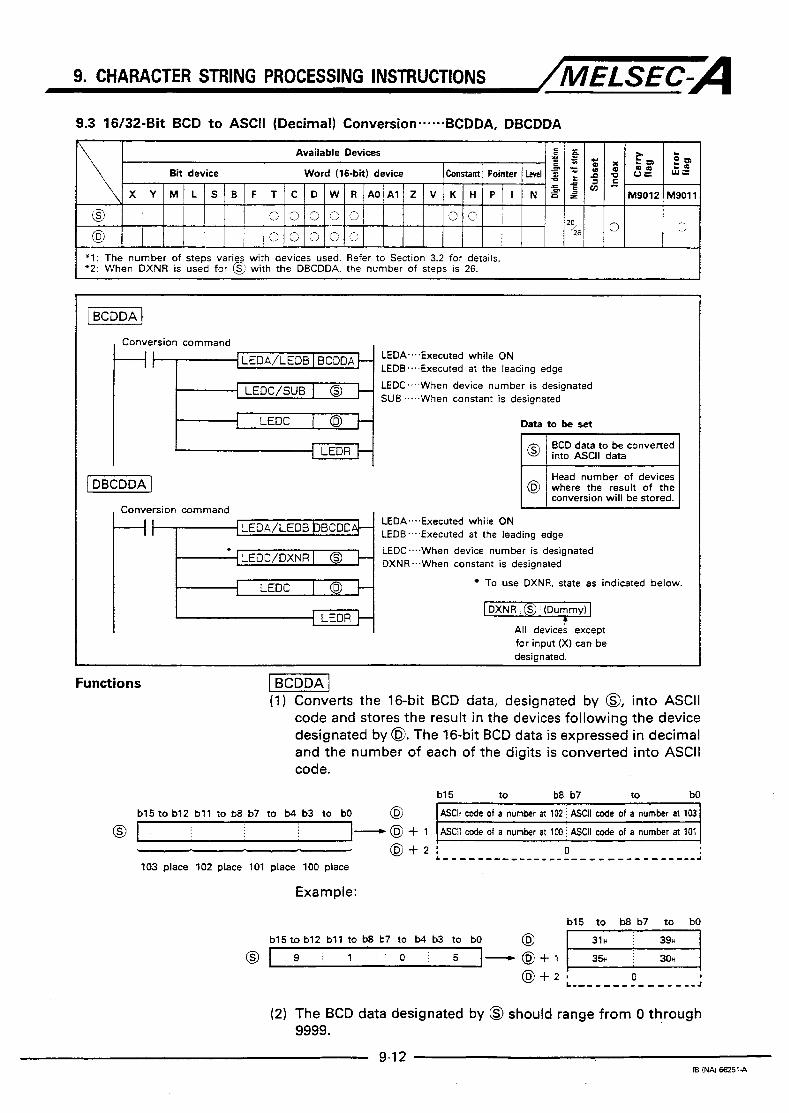
9. CHARACTER STRING PROCESSING INSTRUCTIONS /MELSEC-A 9.3 16/32-Bit BCD to ASCII (Decimal) Conversion-.-.--BCDDA, DBCDDA
-~
Available Devices ; g w Bit device u a E eve^ Pointer Constant Word (16-bit) device - 2 g
= - z = X Y M L S B F T C D W R A O A l Z V K H P l N H ’ z
@ @
Cl 0 0 0 0 ‘3 =: 20
S C G C C /;5 0
+1: The number of steps varies with devices used. Refer to Section 3.2 for details. ‘2: When DXNR is used for (9 with the DBCDDA, the number of steps is 26.
Conversion command
L E D A / G E E T E E +
I--[ LEDR
LEDA....Executed while ON LEDB..,.Executed at the leading edge LEDC....When device number is designated SUB -...When constant is designated
Data to be set
I j DBCDDA I
LEDA....Executed while ON LEDB..-.Executed at the leading edge LEDC....When device number is designated DXNR.,,When constant is designated
To use DXNR, state as indicated below.
Head number of devices
conversion will be stored.
All devices except for input (X) can be designated.
Functions (1) Converts the 16-bit BCD data, designated by 0, into ASCII
code and stores the result in the devices following the device designated by @. The 16-bit BCD data is expressed in decimal and the number of each of the digits is converted into ASCII code.
b15 to b8 b7 to bO
b15 t o b12 b l l t o b8 b7 to b4 b3 to bO @ ASCII code of a number at 102 j code of a number at 103
01 1- @ i- 1 ASCII code of a number at 100 i ASCII code of a number at 101 - @ + 2 i 0 b - - - - - - - - - - _-_-__-- - - - - ---------.I
103 place 102 place 101 place 100 place
Example:
b15 to b8 b7 to bO
(2) The BCD data designated by 0 should range from 0 through 9999.
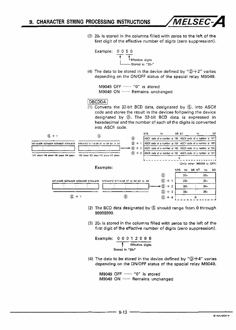
9. CHARACTER STRING PROCESSING INSTRUCTIONS / M E L S E C - A 20H is stored in the columns filled with zeros to the left of the first digit of the effective number of digits (zero suppression).
Example: 0 0 5 0 -- L! Effective digits
Stored in '20H'
The data to be stored in the device defined by "a)$-2" varies depending on the ON/OFF status of the special relay M9049.
M9049 OFF * * * - - * "0" is stored M9049 ON - * . ** . Remains unchanged
(1) Converts the 32-bit BCD data, designated by 0, into ASCII code and stores the result in the devices following the device designated by @. The 32-bit BCD data is expressed in hexadecimal and the number of each of the digits i s converted into ASCII code.
@' + 1 0 115 to b8 b7 to t j
0
@ ASCII code of a number at 1 0 6 ASCII code of a number at 107
Ki l tob28 b17tob24 bZnobSD b191ob16 b15tob12 b l l tob8 b7 10 M b3 to bO @ -I- 1 ASCII code of a number at 104 ASCII code of a number at 105
I I 7 1 - @ -k 2 ASCII tude of a number at 102 ASCII code of a number a1 103
@ f 3 ASCII code of a number ar 100 ASCII code of a number at 101 - 107 place 106 place 105 place 104 place 103 place 102 dace 101 place 100 place
I-
I L _ - _ _ _ _ - - _ _ - - _ _ _ - - - - - - - - - - . A
(Only when MSC49 is OFF) Example: b15 to b8 b7 to bO
h31tob28 b27tob24 bZ3tob20 b19tob16 b15tob12 b l l tob8 b7 to b4 b3 to bo @ + l I---@ + 2 35n
The BCD data designated by @ should range from 0 through 99999999.
20H is stored in the columns filled with zeros to the left of the first digit of the effective number of digits (zero suppression).
Example: 0 0 0 1 2 0 9 8 'T' iffective digits
Stored in '20~'
The data to be stored in the device defined by "@+4'' varies depending on the ON/OFF status of the special relay M9049.
M9049 OFF -.*-.* "0" is stored M9049 ON *..-.* Remains unchanged
9-7 3 I 8 WW €6251 P.

9. CHARACTER STRING PROCESSING INSTRUCTIONS /MELSEC-A Execution
Operation
Conditions The BCDDA and DBCDDA instruction execution mode depends on whether it is designated with an LEDA or LEDB instruction. They are executed every scan while the conversion command stays ON if they are designated with an LEDA instruction. When they are designated with an LEDB instruction, they are executed only once at the leading edge of the conversion command.
I I I BCDDA
(with LEDA) DBCDDA 1 I I
I I I I I I I I I
I I I I I
I I I
I
BCDDA (with LEDB) DBCDDA , I 1 I
Errors An operation error will occur in the following case and an error flag (M9011) will be set.
Error Code D9008 1 WO91
Description
The BCD data designated by @ is not a BCD value. 50 1 503
9-1 4 IB WJ 6E251A

9. CHARACTER STRING PROCESSING INSTRUCTIONS /MELSEC-A Program Example -1
This program outputs the 16-bit BCD data stored in WO to Y48 through Y40 in the ASCII code (decimal) using a PR instruction.
When X0 is turned ON, t h e m instruction outputs the data to Y48 through Y40 in the ASCII code. Because M9049 is OFF, output is executed up to ASCII code 00,.
b15 to b8 b7 to bO
wo 1 2 9 5 Y48 through Y40
BCD value D2 output.
jDBCDDAl This program outputs the 32-bit BCD data stored in W10 through W11 to Y48 through Y40 in the ASCII code (decimal) using a PR instruction.
When X0 is turned ON, t h e m instruction outputs the data to Y48 through Y40 in the ASCII code. Because M9049 is OFF, output is executed up to ASCII code 00".
w11 w10 [DBCDDA( 3 5 4 7 8 3 5 2 c
BCD value
DO
D l
D2
D3
D4
b15 to b8 b7 to
lPRl 3 3 ~ (3) i 3% (8)
32, (2) i 3% (51 i s outpat. '35478352"
Y48 through Y40
9-1 5 IB (NAJ 662514

9. CHARACTER STRING PROCESSING INSTRUCTIONS /MELSEC-A 9.4 ASCII (Decimal) to 16/32-Bit Binary Conversion--.*-.DABIN, DDABIN
Available Devices
Bit device Word (%-bit) device /constant 1 Pointer I ~ml E
1 * l : The number of steps varies with devices used. Refer to Section 3.2 for details.
1 M9012 I M9011 I
Conversion command LEDA.-., LEDB...,
.....
...... : Indicates the instruction symbol. I 1
-Executed while ON DABIN, DDABIN J
--Executed at the leading edge Data to be set
Head number of devices where the ASCII data to be converted into binary data is stored.
The number of the device where the conversion re- sult will be stored.
Functions (1) Converts the ASCII data (decimal) stored in the devices
following the device designated by @ into 16-bit binary data and stores the result in the device number designated by @.
~ 115 to b 8 , b7 to M,
ASCII code of a number at 104 Sign b15 to bO
@ -I- 1 ASCII code of a number at 102 ASCII code of a number at 103 - @ 7 1 @ + 2 ASCII code of a number at 100 j ASCII code of a number at 101
16-bit binary data
Example:
b15 to b8 b7 to bo
b15 t o bO
@ + l -031 - 2 5 1 0 8 1 @ + 2 3% 3oH .
Binary value
(2) The ASCII designated by @ through O - f Z should be in the range of -32768 through 32767.
(3) In the sign data field, the following is stored:
20H ...... ASCII data is positive. 2DH ...... ASCII data is negative.
(4) In each of the digits, the ASCII code can be set in the range of 30H through 39~.
(5) When the ASCII code is set at "20H" or "OOH", it is processed as "30n".
9-1 6 I9 I W 6 6 2 5 1 4

9. CHARACTER STRING PROCESSING INSTRUCTIONS /MELSEC-A
@ @ + l
3, + 2
@ + 3
'3 + 4
@ + 5
p E K ( (1) Converts the ASCII (decimal) data, stored in the devices
following the device designated by 0, into the 32-bit binary data and stores the result in the device number designated by @.
I1 5 to b8 b7 to bO
ASCII code of a number at 109 j Sign
ASCII code of a number at 107 j ASCII code of a number at 108
ASCII code of a number at 105 ASCII code of a number at 106
ASCII code of a number at 103 j ASCII code of a number at 1 0 4
ASCII code of a number at 101 j ASCII code of a number at 102
( i g n o r e ) : ASCII code of a number at 1 0 0
@ + 1 @ b31 to b16 b15 to bO
---L U p p e r 16 bits I L o w e r 16 bits
32-bit binary data
Example: b15 to b8 b7 to bO
3 1 ~ ZDH
The ASCII data designated by @ through @i-5 should range from -2147483648 through 2147483647.
Note that the data stored in the upper byte of the 0 4 - 5 device is ignored.
In the sign data field, the following is stored: 20H ...... ASCII data is positive. 2DH ...... ASCII data is negative.
In each of the digits, the ASCII code can be set in the range of 30H through 3gH.
When the ASCII code is set at "20H" or "0OH'', it is processed as "30H".
Execution Conditions The DABIN and DDABIN instruction execution mode depends on whether it is designated with an LEDA or LEDB instruction. They are executed every scan while the conversion command stays ON if they are designated with an LEDA instruction. When they are designated with an LEDB instruction, they are executed only once at the leading edge of the conversion command.
ON OFF
I I I I I I I I I I I I I
I I I I I I I 1 I
Conversion command I I I I : I I
I I I I I
(with LEDA) I I
DDABIN n I I I I I I ! I I I I I I

9. CHARACTER STRING PROCESSING INSTRUCTIONS /MELSEC-A Operation Errors
Program Example
An error occurs in the following cases and an error flag (M9011) is set. r Error Code
Description WOO8 D9091
The sign data designated with @ is neither "20H" nor " ~ D H " . The ASCII code in each of the digits from @ through @+5 is not " 3 0 ~ " through "3%". "20r , or "00~" . The ASCII data designated by @ through @+5 is outside the following ranges:
50 503
Used with DABIN instruction ... -32768 through 32767 Llsed with DDABIN instruction ... -2147483648 throuqh 2147483647
1 DABIN This program converts the sign and 5-digit decimal, set in D22 through D20, into a binary value and stores the result in DO.
b15 to b8 b7 to bO
D20 20H ( - 1 ~ D H (-) - D21 3 2 ~ (2) ' 20H ( L - )
D22 3 6 ~ (6) 37H (7) (regarded as -00276)
Binary value " - u u 2 7 6 "
This program converts the sign and 10-digit decimal, set in D25 through D20, into a binary value and stores the result in Dl1 through D10.
Binary value

MEMO
....................................................................................................................................................................
....................................................................................................................................................................
....................................................................................................................................................................
.....................................................................................................................................................................
....................................................................................................................................................................
....................................................................................................................................................................
....................................................................................................................................................................
.....................................................................................................................................................................
.....................................................................................................................................................................
....................................................................................................................................................................
....................................................................................................................................................................
....................................................................................................................................................................
....................................................................................................................................................................
....................................................................................................................................................................
18 fNA166251A

9. CHARACTER STRING PROCESSING INSTRUCTIONS /MELSEC-A 9.5 ASCII (Hexadecimal) to 16/32-Bit Binary Conversion--.--.HABIN, DHABIN
I *l: The number of steps varies with devices used. Refer to Section 3.2 for details,
..... : ..... Indicates the instruction symbol.
Conversion command HABIN, DHABIN LEDA.---..Executed while ON LEDB.-...Executed at the D~~~ to be Set
I -4 0 Head number of devices
leading edge
where the ASCII data to
value is stored. be converted into a binary
LEDR The number of the device conversion will be stored.
Functions W I (1) Converts the ASCII data (hexadecimal) stored in the devices
following the device designated by 6J into 16-bit binary data and stores the result in the device number designated by @.
b15 to b8 b7 t o bO
@ ASCII code of a number at 100 i ASCII code of a number at 101 @ i- 1
ASCII code of a number at 102 . ASCII code of a number at 103 - l B b i t binary data
Example:
b15 to b8 b7 to bO b15 to bo
@ + 1 44H , 38H - 5A8DH I
16-bit binary data
(2) The ASCII designated by @ and @+1 should be in the range of OOOOH through FFFFH.
(3) In each of the digits, the ASCII code can be set in the ranges of 30H through 3gH, and 41H through 46H.
9-1 9 I8 r N A J 6Qs14

9. CHARACTER STRING PROCESSING INSTRUCTIONS /MELSEC-A 1-1 (1) Converts the ASCII (hexadecimal) data, stored in the devices
following the device designated by 0, into the 32-bit binary data and stores the result in the device number designated by 0.
b15 t o b8 b7 to bO
ASCII code of a number at 106 ASCII code of a number at 107
ASCII code of a number at 104 ASCII code of a number at 105
ASCII code of a number at 102 ASCII code of a number at 103
ASCII code of a number at 100 ASCII code of a number at 101
@ + l @ b31 to b16 b15 to bO
_c Upper 16 bits Lower 16 bits 1 32-bit binary data
Example:
b15 to b8 b7 to bo - - @ + l
@ + 1 38n 4 2 ~ b3 1 to t b16 b15 to bO .
(2) The ASCII data designated with 0 to @+3 should be in the range of OOOOOOOOH through FFFFFFFFH.
(3) In each of the digits, the ASCII code can be set in the ranges of 30H through 3gH and 41H through 46,.
Execution Conditions The HABIN and DHABIN instruction execution mode depends on whether it is designated with an LEDA or LEDB instruction. They are executed every scan while the conversion command stays ON if they are designated with an LEDA instruction. When they are designated with an LEDB instruction, they are executed only once at the leading edge of the conversion command.
ON OFF
I I I I I I I I I I I I I Conversion command I I I 1 ; I I
I I I I
I I I I I I I
I I I HABIN I (with LEDB)
Operation Errors An error occurs in the following cases and an error flag (M9011) is set.
~~~ ~~
Description G m r Code
D9008
through ' ~ S H " , or '41~' through '46~'. 503 5o The ASCII code in each of the digits of @ through @+3 is not D9091

9. CHARACTER STRING PROCESSING INSTRUCTIONS /MELSEC-A Program Example
This program converts the 4-digit hexadecimal ASCII data, set in D22 through D20, into binary data and stores the result in DO.
i 020
D21
C L E D A H R B I H
CLEDC D28
b15 to b8 b7 to bO -1 41n (A) /HABlN] DO
(regarded as A ~ ~ F H (-222977 in decimal)) Binary value 'A63F"
This program converts the 8-digit hexadecimal ASCII code, set in D23 through D20, into binary data and stores the result in D l 1 through D10.
. .
b15 to b8 b7 to bO
-1 D l 1 D l 0 4 13391:'-1 3 8 ~ (8) (regarded as 4FD2875Ck
(1339197264 in decimal)) Binary value
'4FD28750'

MEMO ....................................................................................................................................................................
....................................................................................................................................................................
....................................................................................................................................................................
....................................................................................................................................................................
....................................................................................................................................................................
....................................................................................................................................................................
.....................................................................................................................................................................
.....................................................................................................................................................................
....................................................................................................................................................................
....................................................................................................................................................................
....................................................................................................................................................................
.....................................................................................................................................................................
.....................................................................................................................................................................
....................................................................................................................................................................
....................................................................................................................................................................
......................................................................................................................
.....................................................................................................................................................................
....................................................................................................................................................................
....................................................................................................................................................................
....................................................................................................................................................................
1B I N 4 66zsl-A

9. CHARACTER STRING PROCESSING INSTRUCTIONS /MELSEC-A 9.6 ASCII (Decimal) to 16/32-Bit BCD Conversion-..---DABCD, DDABCD
I * I : The number of steps varies with devices used. Refer to Section 3.2 for details.
: .____: indicates the instruction symbol. .....
i l
Conversion command DABCD. DDABCD LEDA--..Executed while ON LEDB.--..Executed at the
I I -1 LEDC I 0 leading edge Data to be set
where the ASCII data t o Head number of devices
data is stored. be converted into BCD
I '@ where the result of the conversion will be stored.
Functions jDABCDl (1) Converts the ASCII data (decimal) stored in the devices
following the device designated by @ into 16-bit BCD data and stores the result in the device number designated by @.
b15 t o b8 b7 t o bo
0 ASCII mde of a number at 102 j ASCII code of a number at 103 b15 to b12 b l l to b8 b7 to b4 b3 t o bO
0 i- 1 ASCII code of a number at 100 'i ASCII code of a number at 101 - 103 place 102 place 101 place 100 place
Example:
0 @ + 1
b15 to b8 b7 to bO
3 5 3 6 a b15 to b12 b l l to b8 b7 to b4 b3 to bO
(2) The ASCII data designated with @ to @+2 should be in the range of 0 through 9999.
(3) In each of the digits, the ASCII code can be set in the range of 30H through 3gH.
(4) When the ASCII code is set at "20," or "0OH", it is processed as " 3 0 n " .

9. CHARACTER STRING PROCESSING INSTRUCTIONS /MELSEC-A -1 (1) Converts the ASCII (decimal) data, stored in the devices
following the device designated by @, into 32-bit BCD data and stores the result in the device number designated by @.
1 1 5 to b 8 , b7 to bo,
ASCII mde of a number at 106 ' ASCII code of a number at 107 b31 lob28 bt71ob24 br5lob20 b19fob16
ASCII mde of a number at 1M : ASCII code of a number a! 105
ASCll code of a number at 102 ASCII code of a number at 103 I ASCII code of a number at 1W ASCII code of a number a! 101 107 place 106 place 105 place 1M place
@ + l
- c--
Example:
b15 to b8 b7 to bO @ + l
b31 to bt8 bZ7tab24 b23tob20 b19to b16 - 8 j 7 i 6 1 5 33H
31r 3 2 n
blSlob12 b l l l obs b7 15 M b3 10 W
---- 103 place 102 place 101 place 1W place
b15tob12 b l l to b8 b7 to b4 b3 10 bO
4 3 : 2 1
The ASCII data designated by @ through @+3 should be in the range of 0 through 99999999.
In each of the digits, the ASCII code can be set in the range of 30H through 3gH.
When the ASCII code is set at "20H" or "OOn", it is processed as "30H".
Execution Conditions The DABCD and DDABCD instruction execution mode depends on whether it is designated with an LEDA or LEDB instruction. They are executed every scan while the conversion command stays ON if they are designated with an LEDA instruction. When they are designated with an LEDB instruction, they are executed only once at the leading edge of the conversion command.
lmrruamn U F P m Q n R X C W l I O " lnstndon
END S t t v O
Sequence program flow
Conversion command
I I I I I 1 I I I I I I I I I I I I
I
ON OFF I I I I : I I , I I
I I I I I I
DABCD I
DDABCD (with LEDAI 1 I 1 I I I
I I I
I I I I I I I I I
(with LEDB) I I I I I I
DDABCD
Operation Errors An operation error will occur in the following case and an error flag (M9011) will be set. ,
Description Error Code
D9008 D9091 The ASCII code in each of the digits of @ through @-3 is not '30~' through 'a', '20~'. or 'Mkl". 503 5o
9-23 IB ( N N 662514
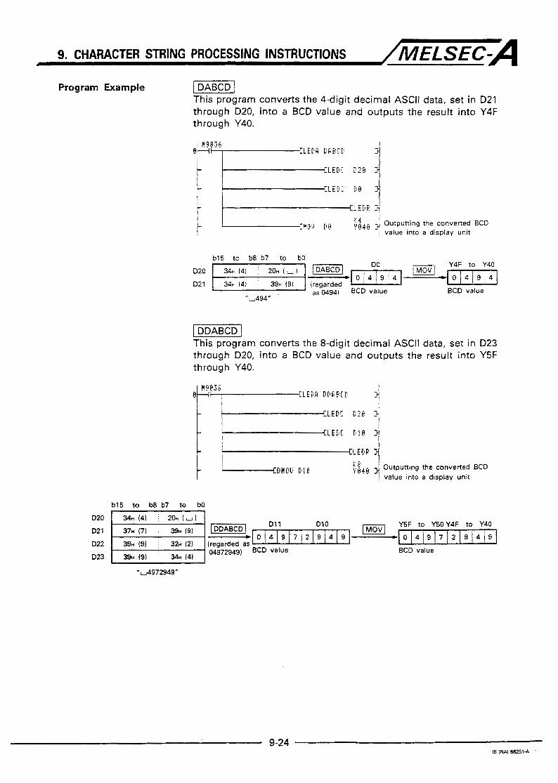
9. CHARACTER STRING PROCESSING INSTRUCTIONS /MELSEC-A Program Example ~ A B C D I
This program converts the 4-digit decimal ASCII data, set in D21 through D20, into a BCD value and outputs the result into Y4F through Y40.
D20
D2 1
D22
D23
1 1
D20
D21
I \i4@ 4 Outputting the,converted BCD value Into a dlsplay unit
b15 to b8 b7 to bO DO Y4F to Y40
(regarded a s w 9 4 ) BCD value BCD value
"-494"
[ DDABCD I This program converts the 8-digit decimal ASCII data, set in D23 through D20, into a BCD value and outputs the result into Y5F through Y40.
I I
b15 to b8 b7 to bO
Outputting the converted BCD value into a display unit
piiEq Dl1 D l 0 Y5F to Y50 Y4F to Y40 - 0 4 9 7 2 9 4 9 - 0 4 9 7 2 9 4 9 (regarded as 04972949) BCD BCD value
9-24 I6 INAJ 562514

...................................................................................................................................................................
....................................................................................................................................................................
....................................................................................................................................................................
....................................................................................................................................................................
.....................................................................................................................................................................
.....................................................................................................................................................................
....................................................................................................................................................................
.....................................................................................................................................................................
....................................................................................................................................................................
....................................................................................................................................................................
....................................................................................................................................................................
.....................................................................................................................................................................
.....................................................................................................................................................................
....................................................................................................................................................................
....................................................................................................................................................................
....................................................................................................................................................................
I8 IW 6 6 2 5 1 4

9. CHARACTER STRING PROCESSING INSTRUCTIONS /MELSEC-A 9.7 Device Comment Read.-.--COMRD
I '1: The number of steps varies with devices used. Refer to Section 3.2 f o r details. I
Read command
I 1 LEDR
LEDA-....Executed while ON LEDB......Executed at the leading edge
Data to be set
I @ 1 read comment is entered. I Device number where the
Head number of the de-
ment will be stored.
Functions (1) Reads the comment set in the device number, designated by a, and stores the comment in the device fol lowing the device designated by @.
Comment entered in the device designated by @ I
Example:
b15 to b8 b7 to bO
@ ASCII code of the 4th character j A S C I I code of the 3rd character @ -I- 1
ASCII code of the 2nd character j ASUl code of the 1st charader
ASCII code of the 6th character j ASCII code of the 7th charade: @ -I- 3 ASCII code of the w character j ASal code of the 5th character @ + 2
ASCII code of the 14th character : ASCII code of the l h h character @ + 6
ASCII code of the 1% character j ASCII code of the 11th character @I + 5
ASCII code of the 1lM character ASCII code of the Stn character @ + 4
@ + 7 O O H ASCII code of the 15th character
b15 to b8 b7 t o b0
6 h (0) i ~ E H (N)
@ + l
Comment in @ [NO. i i ]
@ + 7 20H ( u
(2) The device number designated by @ should be in the range of the device numbers set as the comment set range devices.
(3) If no comment is entered in the designated device, all characters from the 1st through the 15th characters are processed as "2On" (space).
(4) "OOH" is automatically stored in the upper 8 bits of @ + 7. 9-25
IB INAI 652514

9. CHARACTER STRING PROCESSING INSTRUCTIONS /MELSEC-A Execution Conditions Ths COMRD instruction execution mode depends on whether it is
designated with an LEDA or LEDB instruction. It is executed every scan while the read command stays ON if it is designated with an LEDA instruction. When it is designated with an LEDB instruction, it is executed only once at the leading edge of the read command.
Sequence program flow I I I 1 I
ON OFF
I I I I I I I I I I I
I I I I I
Read command I I I I
I I
I I
I I I COMRD (with LEDB) I I
Operation Errors An error occurs in the following case and an error flag ( M 9 O l l ) is set.
Program Example
Description I Error Code I
The device number designated by 0 i s outside the comment setting range device. 503
This program stores the comment entered in data register Dl000 to WO through W7 in the ASCII code.
When X0 is turned ON, the comment entered in Dl000 is stored in WO through W7 in the ASCII code.
9-26 18 IW €62514

9. CHARACTER STRING PROCESSING INSTRUCTIONS /MELSEC-A 9.8 Detecting Character-String Length-..--.LEN
Available Devices s g 'Z - ti 4 5: cg g j cu!
Bi device Word (16-bit) device ~ m l Pointer canstant = -
X Y M L S B F T C D W R A O A l Z V K H P l N ~ S M9012 M9011 - = 4 4
E 3 0 82 CI CI ! i
@ I 2 O I 0 3 c i 0 3 c,
+ l : The number of steps varies with devices used. Refer to Section 3.2 for details. c
t - i I I Detection command
LEDA.-.,.Executed while ON LEDB.--Executed at the leading edge
Data t o be set
string is stored.
Device number where the detected character string length will be stored.
Functions (1) Detects the length of the character string, designated by 0, and stores the detected length in the device number desig- nated by @ in units of bytes. The data stored in the devices beginning with the device designated by @ and ending the one where "OOH" is stored is regarded as the character string.
b15 to b8 b7 to bO
0 @ + I
@ + 2
I I
2nd character 1st character 1 4th character 3rd character
6th character 5th character
to I
b15 to bO ___.t
I @I I Character string length
(in bytes)
Indicates the end of the character string
Example:
42n 41 n

9. CHARACTER STRING PROCESSING INSTRUCTIONS /MELSEC-A Execution Conditions The LEN instruction execution mode depends on whether it is
designated with an LEDA or LEDB instruction. It is executed every scan while the detection command stays ON if it is designated with an LEDA instruction. When it is designated with an LEDB instruction, it is executed only once at the leading edge of the detection command.
I I I I I I I I
1 LEN (with LEDA) 1 I
I I
I I I I
LEN (with LEDB) I I I
I
Operation Errors An error occurs in the following case and an error flag (M9011) is set.
Description Error Code
D9008 D9091
one desianated bv @I. ' O b " is not set in a device in the corresponding device range after the 504 5o
Program Example This program outputs the character string set in the devices beginning with DO to Y4F through Y40 in the 4-digit BCD.
Data set i n the devices following DO
DO I 4!3~ ( I I j 4 0 ~ (M) I
D2
D3 D4
D5
D6
(LENI ' 'MITSUBISHI' is
regarded as a character string. The characters
4-j that appear after 'Ob' A. B, C are ignored. I I
Outputting the character string length to the display unit
D l 0 Y4F to Y40
1 0
Binarv value BCD value
0 0 1 0 BCD conversion
9-28 IB W N 66251-4

9. CHARACTER STRING PROCESSING INSTRUCTIONS /MELSEC-A 9.9 16/32-Bit Binary to Character String Conversion-----SlR, DSTR
Available Devices 4 g - 0 Bit device Pointer cwtant Word (16-bit) device
= - x m a
X Y M L S B F T C D W R A O A l Z V K H P I N % z M9011 M9012
0
0 0 2 0 0 @ 0
l I 3 (3 'C! CI
C l 0 3 3 % L, P 0 cr -------------------- -
'1: The number of steps vari s with devices used. Refer to Section 3.2 for details. '2 When DXNR is used for & with the DSTR, the number of steps is 29.
Conversion command LEDA...-.Executed while ON LEDB......Executed at the leading edge
LEDC......When the device Data to be set number is p-3 SUB......When the constant designated Device number where the
number of digits of the is designated number to be converted is
stored.
I I -[ LEDR 4 Binary data to be con- verted.
I I Head number of the de- vices where the result of the conversion will be p5TF-l
Conversion command LEDA.-...-Executed while ON LEDB......Executed at the leading edge
LEDC I LEDC......When the device number is designated SUB-....When the constant is designated
-1 LEM: I 0 -1 L E D R E
To use DXNR, state as indicated below.
All devices except for input (X) can be designated.
Functions pTF (1) Converts the 16-bit binary data, designated by @, into the
character string by adding a decimal at the position desig- nated by @. It stores the result of the conversion in the devices beginning the device designated by 0.
b15 to b8 b7 to bo
@ fraction digits
. . , . , . , , , , , I.-.. , . . . . . , . . . , I . , , , I , . , . . I
. . . . . . . . . . . . . . . . . . . . . . , , , , , , j
:.:.' ,...: I _ _ _ (
Sign
@ + 4 OOn
0 Automatically stored at the end of the character string
9-29 IB (W €62514

9. CHARACTER STRING PROCESSING INSTRUCTIONS /MELSEC-A Example:
@ + 1 1 b15 to b8 b7 to bO 4 @I 3 1 n I t ) ~ D H (-1 . . . . . . . . . . . . .
(2) The total number of digits that can be designated by @ ranges from 2 through 8
(3) The number of decimal fraction digits that can be designated by @I +l ranges from 0 through 5 Note: The number of decimal fraction digits S (total number
of digits -3)
(4) The binary data designated by @ should range from -32768 through 32767
(5) The character data after conversion is stored in the devices following the device designated 0 as indicated below.
1) In the sign data field, the following is stored: 2On...... Binary data is positive. 2DH.. .... Binary data is negative.
2) If a number other than "0" is set for the number of decimal fraction digits, the "2EH ( . ) " is automatically stored a t the "designated number of digits +1" digit place.
Example:
Total number of digits
Number of decimal fraction digits
Binary data Number of decimal fraction digits
1 Added automatically
The " ~ E H ( . 1'' code is not stored if the number of decimal fraction digits is "0".
9-30 18 (NE3 W51-A

9. CHARACTER STRING PROCESSING INSTRUCTIONS /MELSEC=A 3) If the number of decimal fraction digits is greater than the
number of binary data digits, the.result of the conversion is automatically set as "0. '
Example:
.. ...
. . . . . . . . . .
Total number of digits
Number of decimal fraction digits
Binary data
- u o . 0 1 2
f Added automatically
4) If the number of digits (excluding the sign and decimal point from the total number of digits) is greater than the number of binary data digits, store the "20" (space)" between the sign and the number.
Example:
Total number of digits l a I 1 Number of decimal fraction digits
Binary data
20H (space) is inserted
If the number of binary data digits is greater than the number of digits (excluding the sign and decimal point from the total number of digits) there is an error.
5) The ''OOH" code is automatically stored at the end of the converted character string.
9-3 1 IB (NAJ €62514

9. CHARACTER STRING PROCESSING INSTRUCTIONS
IDSTR] (1) Converts the 32-bit binary data, designated by @, into the
character string of a fixed point real number in the number of digits designated by @. It stores the result of the conversion in the devices beginning with the device designated with 0.
j decimal fraction s,, + Number of digits of t
L I I
. . . . . . . . . . . . . . . . . . . . . . . . . . . . . . . . @: + 2
@ + 3
. . . '.*' .. .: . . . . . . . . . . . . . . . . . . . . . . . . . . . .
- Sign
t + 4
32-bit binary data
Example:
ASCU code of Itotai number code of sign of diglts -11 th diglt I of digits -3) th digit of dlgits -2) th dlgtt
of digits - 5 ) t h dlgit of digits -4) fh dlgft
ASCII code of ltotal number . ASCII code of Ilotal number of digits -71 th diglt of digits -6 ) th dlgit I
ASCII code of (total number ' ASCII code of lfotal number of diglts -9) th drgit ' of dig- -8) th digit I
A S C l l code of Itoral number of digits -10) th digit
Designated total number of digits
Binary data
Automatically stored at the end of the character string
(2) The number of digits that can be designated by ranges from 2 through 13 digits
(3) The number of decimal fraction digits that can be designated by @-I-1 ranges from 0 through 10 digits Note: The number of decimal fraction digits S total number
of digits -3
(4) The binary data designated by @I, and @ 4-1 should range from -2147483648 through 2147483647
9-32 18 IN4 662514

9. CHARACTER STRING PROCESSING INSTRUCTIONS /MELSEC-/~ (5) After conversion, the character data is stored in the devices
following the device designated with @I as shown below.
1) In the sign data field, the following is stored: 20 n....,. Binary data is positive. 2D, ...... Binary data is negative.
2) If a number other than ”0” is set for the number of decimal fraction digits, “2EH ( . ) ” is automatically stored a t the ”designated number of digits -I-1” digit place.
Exampie:
Total number of digits I 10 I Number of decimal fraction digits 1 3 I Binaw data
- u 1 2 3 4 5 . 6 7 8
1 - 1 1 Added automaticallyJ N z e r of decimal fraction digits
The “2E4. 1‘’ code is not stored if the number of decimal fraction digits is “0”.
3) If the number of decimal fraction digits is greater than the number of binary data digits, . .. the-result-of the conversion is automatically set as ”0. j : : Example:
I, , . . . . , . . . . . . . . . . . . . . .
Total number of digits
Number of decimal fraction digits
Binary data I 5 4 3 2 1 I - u o . 0 0 0 0 0 5 4 3 2 1
T Added automatically

9. CHARACTER STRING PROCESSING INSTRUCTIONS /MELSEC-A 4) If the number of digits (excluding the sign and decimal
point from the total number of digits) is greater than the number of binary data digits, the "20H (space)" is stored between the sign and the number.
Example:
Total number of digits I 13 I Number of decimal fraction digits /21 Binary data 1 - 5 4 : 3 2 1 I
- u u - i u - 5 4 3 2 . 1 0
20H (space) is inserted
If the number of binary data digits is greater than the number of digits (excluding the sign and decimal point from the total number of digits) there is an error.
5) The ''OOH" code is automatically stored a t the end of the converted character string.
Execution Conditions The STR and DSTR instruction execution mode depends on whether it is designated with an LEDA or LEDB instruction. They are executed every scan while the conversion command stays ON if they are designated with an LEDA instruction. When they are designated with an LEDB instruction, they are executed only once at the leading edge of the conversion command.
~ n s v u d ~ l n p-ng e x m t m n amm
END IMruumn
SLeP 0 END Slep 0 END Step 0 I 1
Sequence program flow I I I I I
ON OFF
I 1 I I I I I
I I I I I I
I I I I I I I I
Conversion command I I I 1 ; I I
I I I 1 STR 1 I DSTR (with E D A ) n I
I I
I I I I I
I I I I 1 I I I I I I I I I ETTR (with ED61 1
Operation Errors An error occurs in the following cases and an error flag (M9011) is set.
Error Code DWO8 D9Wl
Description
The total number of digits designated by @) is outside these ranges: . Used with sm instruction .............................. 2 through 10 . Used with D S n instruaion ............................ 2 through 13 The number of decimal fraction digits designated by @ +1 is outside these ranges: , Used with Sm ins~,-Jjon ........................................ , Used with D S m instmaion .................................... 0 t o 5
0 to 10 The relationship between the total number of digits, designated by a, as indicated below; and the number of decimal fraction digits, designated by 0 4-1, is not 5o
503
Total number of diaits -3 B number of fraction diaits 1 The number of diaits (excludina the sian and decimal fraction from the 1 I
total number of dhits) designaGd by 0. is greater than the number of digits designated by 0. The ange of devices designated to store the character string designated by @ exceeds the range of that device. 504

9. CHARACTER STRING PROCESSING INSTRUCTIONS /IWELSEC-A Program Example [ STR I
This program to converts the binary data stored in D l 0 (assuming the data is an integer) into a character string, when X0 is turned ON. It outputs the character string to Y40 through Y49 in the ASCII code.
' i B S ? H.t CH?!, 6
I: Setting the total number of 4 1 @' 4 digits
Setting the number of decimal For PR fraction digits instruction inter locking LEDR STF'
-
CLEDF 3 - T L E D C : DIE( 3 - CLEDC Dl8 3 - CLEPC P O 3
- CPR D Z B "" ' acter string in ASCII Outputting the converted char-
D l 0 ISTRJ b15 to b8 b7 to bO 1 1 2 6 7 2 )
Y40 I 'D20 3 1 ~ (1) j 20H (u) .,.- e to "-1 1 2 6 7 2" is output 4 1 36H (6) 32H (2) 1 L 74'
DO Total number of digits 3 2 ~ (2) 37H (7) Y48 (Strobe signal)
0 1 1 0 I Number of d e c i m a l 1 D23 1 O O H
fraction digits

9. CHARACTER STRING PROCESSING INSTRUCTIONS /MELSEC-A L r n ] This program converts the binary data stored in Dl0 through Dl 1 (assuming the data is an integer) into a character string when X0 is turned ON. It outputs the character string to Y40 through Y49 in the ASCII code.
K cnou 11 4 digits Setting the total number of
Setting the number of decimal fraction digits
L E D R D S T R I
Outputting the converted char- acter string in ASCII
Dl 1 b15 to b8 b7 to b0 l p ~ i y40 to "-1 1 4 7483647"
Y47 is output
DO Total number of digits D22 37u
Number of decimal D23 3 8 ~ Dl fraction digits D24 36r . 3 4 ~
Y48 (Strobe signal)
D25 O O H ' 37n 1

9. CHARACTER STRING PROCESSING INSTRUCTIONS /MELSEC-A 9.10 Character Str ing to 16132-Bi-t Binary Data Conversion-.*-..VAL, DVAL
i
Available Devices 2 5 P E C c m Bit device Word (l6-bfi) device Level Pointer Constant
0 m m x $ o= %
s a = X Y M L S B F T C D W R A O A l Z V K H P I N ~ z M9011 M9012
0 130300 ~ - ~
@ I r , O O 0 0 @ I
C O G 0 0
'1: The number of steps varies with devices used. Refer to Section 3.2 for details.
Data to be set Conversion command LEDA ...... Executed while ON
+ I I-----€ LEDB ...... Executed at the leading edge
LEDC
Head number of devices where the character string to be converted into bin- ary data is stored.
where the number of
obtained by conversion will be stored.
Device number where the
be stored.
Functions
0 @ + 1
O f 2 @ + 3
m s 4
[VAL 1 (1) Converts the numeric character string, stored in the devices
beginning with the device designated by 0, into 16-bit binary data and stores the number of converted binary data digits and the converted binary data to @ and @. In the character string to binary conversion, the data stored in the devices beginning with the device designated by @ and ending with the device where the ''OOH" code is stored is treated as the numeric character string.
~ 1 5 to b8 b7 to ASCII d e of the 1s character ASCII code of sian ASCII code of the 3rd charaner A S C I I code of the 2nd characte
~~~~~ ~ ~
A S C I I code of the 5th charaaer ASCII code of the 4th charactel
ASCII d e of the 7th charaner ' ASUl code of the 6th charactel
OOW
0
- 1 I T
Indicating the end of
Total number of digits
fraction digits 2--. . . . . . . . . . . . . . . . . . . . . . . .
Sign I 2nd character 7th character 1st character 18bit binary data
the chadcter string
Example:
5 - .... . . . . . . . . . . . . . . . . . . . - - -
............................ - 1 2 3 4 5
9-37 IB (W -14

9. CHARACTER STRING PROCESSING INSTRUCTIONS / ~ ~ E L s E c - / ~ ~ (2) The total number of characters of the character string,
designated by 0, should range from 2 through 8 characters.
(3) In the character string designated by 0, the number of characters in the decimal fraction part should be a s : Range: 0 to 5 characters Note that the number of characters in the decimal fraction part should be "total number of characters -3" characters or less.
(4) The range of the numeric character string that can be converted into binary data should (with a decimal point ignored) range from -32768 through 32767. The character string, excluding the sign and decimal point, can be designated only within the following range: 3 0 ~ through 3 9 ~ An example of a value with a decimal point ignored is as follows: "-1 2345.6" + "-1 23456".
(5) The plus or minus sign is set as indicated below: 20 n...... For positive numeric data 2D ,,...... For negative numeric data
(6) The "2EH" code is set for a decimal point.
(7) The number of all characters, representing a number (sign and decimal point included), i s stored in @. The number of characters in the decimal fraction part, right to a decimal point (2EH), is stored in @ +l. The character string converted into binary data with the decimal point ignored is stored in @.
(8) If the " 2 0 H (space)" and/or "30H (0)" code exists between the sign and the number appearing first (except "O"), these codes are ignored when converted into binary data.
- u l 2 3 . - 4 5 - - t
Ignored
Total number of digits
fraction digits ~ Number of decimal
Binary data 1 - 1 2 3 4 5 1
I
Total number of digits Number of decimal
u o . 0 0 1 2 mG
4 7 fraction digits
Sign Ignored I I I Binary data
9-38 IB(NA)66251-F

9. CHARACTER STRING PROCESSING INSTRUCTIONS /MELSEC-A I DVAL 1 (1) Converts the numeric character string, stored in the devices
beginning with the device designated by @, into the 32-bit binary data and stores the number of converted binary data digits and the converted binary data into @ and @. In the character string to binary conversion, the data stored in the devices beginning with the device designated by and ending with the device where the "OOh" code is stored is treated as the numeric character string.
b15 to b8 b7 to bo
ilscll code ol the 151 mdraner ASCII code of sign
ASCJ code 01 she *e charaaer ASCII code of me &d character
t 12th character 32-bit bmary data
1st character A s w c o j e o l t h e l h n c h ~ s
lndtcatlng the end of the character Rnng
Example: b15 to b8 b7 bO
32n (2) I
(3) In the character string, designated by @, the number of characters in the decimal fraction part should range from 0 through 10 characters. Note that the number of characters in the decimal fraction part should be the "total number of characters -3" or less.
(4) The range of the numeric character string that can be converted into binary data should (with a decimal point ignored) range from -2147483648 through 2147483467. The character string (excluding the sign and decimal point) can be designated only within the range of 30H through 3%.
(5) The plus or minus sign is set as indicated below: 20~-*..--FOr positive numeric data 2DH-.-..-For negative numeric data
(6) The " ~ E H " code is set for a decimal point.
(7) The number of all characters, representing a number (sign and decimal point included), is stored in @. The number of characters in the decimal fraction part, right to a decimal point (ZEH), is stored in @ i- 1. The character string converted into binary data (with the decimal point ignored) is stored in @.
9-39 IB IW 662514.

9. CHARACTER STRING PROCESSING INSTRUCTIONS /MELSEC-A (8) If the "20H (space)" and/or "30H (0)" code exists between the
sign and the number appearing first (other than ''0") these codes are ignored when converted into binary data. Example: I Total number of digits
Number of decimal - 1 a - 2 6 5 4 3 . 2 1 -{ fraction digits
I Ignored I Binary data i - 6 5 4 , 3 2 1 1
I
Total number of digits Number of decimal
u 0 . 0 0 0 5 4 3 2 1 -, fraction digits
t=T= Sign Ignored
Binary data 1 7 - z ; 1 1 Execution Conditions The VAL and DVAL instruction execution mode depends on
whether it is designated with an LEDA or LEDB instruction. They are executed every scan while the conversion command stays ON if they are designated with an LEDA instruction. When they are designated with an LEDB instruction, they are executed only once at the leading edge of the conversion command.
Sequence program flow I
ON OFF
I I I I I I I I I I I
I I I I I I I I I I I I I I I
Conversion command I I I I
VAL (with LEDA) DVAL I I n
I I I I I I I I I I I I I I I I I I I
I I I I I EiL (with LEDB)
Operation Errors An error occurs in the following cases and an error flag (M9011) is set.
Description
The total number of characters of the character string designated by @ is outside the following ranges:
Error Code I woo8 D9091
. ........................... Used with DVALinstruction 2through 13 UsedwithVAL instmaion 2through 8
........................ The number of characters of the character string in the decimal fraction part designated by @ is outside the following ranges: . Used with VAL instruction ..................................... . Used with DVAL instruaion ................................ 0 to 10
Oto 5
The relationship between the total number of characters in the character string designated with @ and the number of characters in the decimal fraction part is not as indicated below. 503
Total number of characters -3 1 Number of characters in the 5o decimal fraction part - An ASCII code other than " 2 0 ~ ' or " ~ D H " is set for the sign.
An ASCII code other than "30~" through "39H' and " ~ E H ' is
More than one decimal point is designated. After the conversion. binan/ data exceed the following ranges;
Used with VAL instruction ........... -32768 through 32767 - U s d with DVAL instruction ......... -2147483648thrwgh2147483647
designated in a digit of numbers.
The "00~" code is not set in a device within the range beginning with the device designated by @ and ending with the final device number of that device.
504
9-40 IS fNA) 66251-C

9. CHARACTER STRING PROCESSING INSTRUCTIONS /MELSEC-A Program Example 1 x 1
This program converts the character string data stored in D20 through D22 into a binary value (assuming the character string data is an integer) and stores the result in DO when X0 is turned ON.
b15 to b8 b7 to bO
D20 3 1 ~ (1) j 2Dn (-)
D21 r, D22 % (41 , 35H (5) D23 OOH is set
...... Total number of digits
..... .Number of decimal fraction digits
W l This program converts the character string data stored in D20 through D24 into binary data (assuming the character string data is an integer) and stores the result in DO when X0 is turned ON.
bl5 to b8 b7 to bO D l
Dl0 ~ ~ 1 " " ! number of digits
3 1 ~ (1) Dl 1 .-.-*Number of decimal fraction digits

....................................................................................................................................................................
.....................................................................................................................................................................
.....................................................................................................................................................................
.....................................................................................................................................................................
.....................................................................................................................................................................
....................................................................................................................................................................
.....................................................................................................................................................................
....................................................................................................................................................................
....................................................................................................................................................................
....................................................................................................................................................................
.....................................................................................................................................................................
.....................................................................................................................................................................
....................................................................................................................................................................
....................................................................................................................................................................
....................................................................................................................................................................
.....................................................................................................................................................................
....................................................................................................................................................................
......... .......................................................-..................................................................................................
IB (Mi) 6s251-4

9. CHARACTER STRING PROCESSING INSTRUCTIONS /MELSEC-A 9.1 1 Hexadecimal Binary to ASCII Conversion--...*ASC
I '1: The number of steps varies with devices used. Refer to Section 3.2 for details. 1 I
1 1 Conversion command
- - - I 1 LEDA......Executed while ON
[LEDA/LEDB I ASC
string is stored. converted to a character LEDC..-...When device I LEOC 1 0 where binary data to be 0 Head number of devices I LEDC I 0 E
LEDB-..,.Executed at the leading edge Data to be set
number is designated Head number of devices
SUB......When constant is acter string will be stored. where the converted char- @,?
Number of characters t o designated 1 LEDR
@ be stored.
Functions (1) Converts the 16-bit binary data, stored in the devices begin- ning with the device designated by @, into the ASCII data in the same manner as hexadecimal conversion, and stores it in the range (the number of characters designated by 0) of the devices beginning with the device designated by @.
Example:
@ + 1
I -1

9. CHARACTER STRING PROCESSING INSTRUCTIONS /IWELSEC-A (2) By designating the number of characters with 0, the range of
the binary data to be designated by @ and the range of devices, where the character string is to be stored, designated with 0 are determined automatically.
(3) If the range of the devices (0 through -I- n), where the binary data to be converted is stored, and the range of the devices (@ through 0 -t n) where the converted ASCII data will be stored, overlap, processing is executed correctly.
Example:
Dl1 r-1 D l 2 Dl2
D l 3 AH 9 H Dl3
D l 4
b15 to b12 bll 10 b8 b7 to M b3 to b€
b15 to b8 b7 to bO
36r
37r
4 1 ~ 3%
(4) If an odd number is designated for @, the "OOM" code is automatically stored in the upper 8 bits of the final device number of the device range where the character string will be stored.
Example: @ = 5
+ 1
b15 to b12 bll to b8 b7 to M b3 to W
1 ' A : 2 ' B I I I
I 8
03 @ + l
@ + 2
Stored automatically
(5) Conversion processing is not executed if "0" is set for @.
Execution Conditions The ASC instruction execution mode depends on whether it is designated with an LEDA or LEDB instruction. It is executed every scan while the conversion command stays ON if it is designated with an LEDA instruction. When it is designated with an LEDB instruction, it is executed only once at the leading edge of the conversion command.
kmmm END immctmn hsmction u r n t o n process~ng excamon execution
II)IuyPmn crcMion a w n h s m p o n
SlCP 0 END Step 0 END S u p 0 END Step 0
Sequence program flow I I I I I
ON OFF
I I I 1 I I I I I I I I I
I I I 1 I I I I
Conversion command I I I Ij I I I
I ! 1 I I
ASC (with LEDA) n I I I I I I 1
I I I I I
I I I I I I I I I
I I I I I ASC (with LEDB) I

9. CHARACTER STRING PROCESSING INSTRUCTIONS /MELSEC-A Operation Errors An error occurs in the following cases and an error flag (M9011) is
set.
Program Example
Description Error Code
WOO8 1 D9091 The device range designated by 0 n exceeds the final device number of
This program converts the binary data, stored in DlO, into a character string (assuming that the stored binary data is hexade- cimal when X0 is turned ON).
C L E D R R S C I
ILEDC DEI 3
C L E D C D l @ 3
[SUB 18 3
C L E D R 3
K
b15 to b12 bl l to MI b7 to M b3 to W ID10 d
D l 2H D l 3
Dl4

....................................................................................................................................................................
....................................................................................................................................................................
....................................................................................................................................................................
....................................................................................................................................................................
....................................................................................................................................................................
....................................................................................................................................................................
.....................................................................................................................................................................
.....................................................................................................................................................................
....................................................................................................................................................................
....................................................................................................................................................................
....................................................................................................................................................................
.....................................................................................................................................................................
.....................................................................................................................................................................
....................................................................................................................................................................
....................................................................................................................................................................
....................................................................................................................................................................
IB I W 86262516

9. CHARACTER STRING PROCESSING INSTRUCTIONS /MELSEC-A 9.12 ASCII to Hexadecimal Binary Conversion---.--HEX
Available Devices
3 t G Z 3 2 5 Level Pointer Constant Word (l&bit) device Bit device
._ + . . a = - > x k m
X Y M L S B F T C D W R A O ~ A l Z V K H P I N ~ s z M9012 M9011 s . % E r n '
0 @ @ '2 I c ::I 13 v , ., ~-, I
5 (-,! :I 'E: I:, r :
c, (2 ,2 - - - 23 r ; - c
, p - ,-\
* l : The number of steps varies with devices used. Refer to Section 3.2 for details.
Conversion command LEDA/LEDB HEX
LEDA-.-.Executed while ON LEDB....-Executed at the
leading edge
LEDC......When the device number is designated
SUB--.When a constant is designated
Data t o be set
Head number of devices where the character string to be converted into bin- ary data is stored.
Head number of devices
ary data will be stored.
0 1 be converted. Number of characters to
~~
Functions (1) Converts the ASCII data (hexadecimal) of the number of characters designated by @, stored in the devices beginning with the device designated by 0, into binary data. It stores the result in the devices beginning with the device designated with @.
- ' @
@J
The number of characters designated with @
b15 to b8 b7 to bO
for @
The '38H" code is not converted because designation has 9 characters.
b15 to b12 b l l to b8 b7 to M b3 to bO
dqi t chander M 6gil & m a znd &g cham 1s dqil charas
+ 1 P m d J g d d L l m W Mmgii&faaer wdgll&!draEl 1SdQgilshaaaer
to
b15 to b12 b l l to h3 b7 to M b3 to bo
-@ + 1 h I 9~ , BH 6~
OH : OH . OH EH
Example:
+ 2 2nd I g n &mer 1s dqfl ciianaer
Binary data

9. CHARACTER STRING PROCESSING INSTRUCTIONS /MELSEC-A By designating the number of characters by 0, the range of the character string to be designated by @ and the range of devices designated by 0, where the binary data will be stored, are determined automatically.
If the range of the devices (9 through Gj + n), where the ASCII data to be converted is stored, and the range of the devices (a through 0 -k n) where the converted binary data will be stored, overlap, processing is executed correctly.
Example:
b15 to b8 b7 to bO
b15 to b12 b l l to b8 b7 to M b3 IO W D l 1 Dl1
Dl2 3 6 ~ Dl2
D l 3 O H OH A+ S a
Dl4 41 H 3%
If the number of characters designated by @ is not a multiple of 4, Os are automatically stored in the field following the designated number of characters in the final device among the devices in which the converted binary value will be stored.
Example: @ = 5
b15 to b8 b7 to bO b15 to b12 bl1 to b8 b7 lo M b3 tc W
+ 2 3 8 ~ (8) Os are automatically stored
(5) Conversion processing is not executed if "0" is set for 0.
(6 ) The range of ASCII code which can be designated by @ should range from 30H through 3gH and 41, through 46H
Execution Conditions The HEX instruction execution mode depends on whether it is designated with an LEDA or LEDB instruction. It is executed every scan while the conversion command stays ON if it is designated with an LEDA instruction. When it is designated with an LEDB instruction, it is executed only once at the leading edge of the conversion command.
Sequence program flow
ON OFF Conversion command
I I I I I I
HEX (with LEDA) n I
I
I I I I I I I 1 I
I I I I I I I
I I
I I
HEX (with LEDB) I I 1 I

9. CHARACTER STRING PROCESSING INSTRUCTIONS /MELSEC-A Operation Errors
Program Example
An error occurs in the following cases and an error flag (M9011) is set.
Description Error Code
D9008 1 D9091 A character other than the hexadecimal number (30~ through 39H, 4 1 ~ through 4 6 ~ ) is set in 0. The device range designated by @ exceeds the final device number of thatAevice; the device range begins with the device number designated H bv 0.
I by 0. The device range designated by @ exceeds the final device number of that device; the device range begins with the device number designated
The number of characters designated by 0 is negative. 1
50 504
This program converts the character string, stored in D20 through D21, into binary data (assuming that the stored character string is hexadecimal) and stores the converted data in DO when X0 is turned ON.
ELEDR H E X I
ELEDC D0 3
CLEDC Dl8 3
CSUB 10 3
i L E D R 3
K
b15 to b8 b7 to bO
Dl D2 37 H 41 H
D3
D4 3 9 H 37H
b15 to bl2 bll to b8 b7 to M b3 to W
3 n 1 H 7 H
O H &I % . 7H
9-47 IB (W 662514

MEMO ....................................................................................................................................................................
....................................................................................................................................................................
....................................................................................................................................................................
....................................................................................................................................................................
....................................................................................................................................................................
....................................................................................................................................................................
.....................................................................................................................................................................
.....................................................................................................................................................................
.....................................................................................................................................................................
.....................................................................................................................................................................
....................................................................................................................................................................
.....................................................................................................................................................................
....................................................................................................................................................................
....................................................................................................................................................................
....................................................................................................................................................................
....
.....................................................................................................................................................................
....................................................................................................................................................................
....................................................................................................................................................................
IE I N A ) €67514,

9. CHARACTER STRING PROCESSING INSTRUCTIONS /MELSEC-A 9.13 Moving Character String...-.-SMOV
Available Devices Z z - = s 5 m E m
Bit device w 0 5 2 0 ~evd Pointer Constant Word (16-bit) device - 6 b 6
1 9 $ a = .e
u . X Y M L S B F T C D W R A O A l Z V K H P I N E z M9012 M9011
2 2 ' 3 0 C = :
13 'Z 0 20 ' 2 c:
*1: The number of steps varies with devices used. Refer to Section 3.2 for details.
1 dL LEOR
,....Executed while ON .-.Executed at the leading edge
Data to be set
Head number of devices where character string is stored.
where character string Head number of devices
moved is to be stored.
Functions (1) Moves the character string data, stored in the devices beginning with the device designated by 0, to the devices beginning with the device designated by 0. When the character string moves, the character strings stored in the device beginning with the device designated by @ and ending with the device where the "OOH" code is stored are processed in a batch.
115 to b 8 b7 to b0,
@) 2nd character ' 1st character
@) + 1 4th character 3rd character
@ + 2 6th character ' 5th character -
Indicates the end of character string
Example:
115 to b8 ~ b7 t o bo, I to
@ 2nd character j 1st character
@ -I- 1 4th character j 3rd character
+@ 4- 2 6th character 5th character
@ + n OOH : 'n'th character
b15 to b8 b7 to bO b15 to b8 b7 to bO
% . S H @ + l 34H 3 3 H

9. CHARACTER STRING PROCESSING INSTRUCTIONS /MELSEC-A !2) If the range of the devices (@ through @ + n), where the
character string data to be moved is stored, and the range of the devices (@ through @j n) where the moved character string data will be stored, overlap, the processing has been correctly executed.
b15 to b8 b7 to bO
D l 0
Dl3 3 8 ~ 37n Dl3
3 6 ~ 35H D l 2
34. 33n D l 1
- - - b15 to b8 b7 to bo 3 2 3 1 ~ - - - - -__ --
-- - - -_
(3) If "OOH" is stored in the lower byte of @ 4- n, ''OOH" is stored in both the upper and lower bytes of + n.
Example:
b15 to b8 b7 to bO b15 to b8 b7 to bO
@ + l - @ + 1 43n
$1 + 2 O O H OOU
"00~" is also automatically stored in the upper byte
Execution Conditions The SMOV instruction execution mode depends on whether it is designated with an LEDA or LEDB instruction. It is executed every scan while the move command stays ON if it is designated with an LEDA instruction. When it is designated with an LEDB instruction, it is executed only once at the leading edge of the move command.
I I I I I SMOV (with LEDB) I
Operation Errors An error occurs in the following cases and an error flag (M9011) is set.
Description l -----
The ' ~ O H " code is not set in a device within the device range beginning with the device designated by @) and ending with the final number of that device. The " O h ' code is not set in a device within the device range beginning with the device designated by @ and ending with the final number of that device.
50

9. CHARACTER STRING PROCESSING INSTRUCTIONS /MELSEC=A Program Example This program moves the character string data, stored in D l 0
through D11, to D20 through D21 when X0 is turned ON.
b15 to b8 b7 to bO b15 to b8 b7 to bO
Dl0 mm D20
D l 1 4 5 (E) 4 5 ~ (E) - D21 4 5 (E) 4% (E) D l 2 OOn is set 022 -00~ is set

MEMO ....................................................................................................................................................................
....................................................................................................................................................................
....................................................................................................................................................................
....................................................................................................................................................................
....................................................................................................................................................................
.....................................................................................................................................................................
.....................................................................................................................................................................
....................................................................................................................................................................
.....................................................................................................................................................................
.....................................................................................................................................................................
....................................................................................................................................................................
....................................................................................................................................................................
....................................................................................................................................................................
.....................................................................................................................................................................
....................................................................................................................................................................
....................................................................................................................................................................
IB (NLU 652514

9. CHARACTER STRING PROCESSING INSTRUCTIONS /MELSEC-A 9.44 Addition of Character Strings.-.--.SADD
Available Devices
Pointer ! ~evd Constant Word ( lbb i t ) device Bit device
I ; ; ._
? & E " - X Y M L S B F T I C D W R A O A ~ Z V K H P I N S ~
5 I 5 4 0
5 i g x f O= w
M9012 j ~ 9 0 1 1
6.3 @)
2 3 0 ':; '3 j 03 r ) I-: 0 #2 3
I
C / I s ' 3 0 0 , I , P.
-.
* I : The number of steps varies with devices used. Refer to Section 3.2 for details
Addition command
+ t LEDA..,
liEDA/LEDB I SADD LEDB...
-1 L E D C ~
1 LEDC I @ E
I
,...Executed while ON Data to be ... Executed at the
leading edge data (sumadd) is stored.
Head number of devices
data (addend) is stored.
Head number of devices
addition will be stored.
Functions (1) Adds the character string, stored in the devices beginning with the device designated by @, to the character string, stored in the devices beginning with the device designated by @. It stores the result of the addition in the devices beginning with the device designated by 0. In this operation, the characters stored in the devices begin- ning with the device designated by @ or @ and ending with the device where the ''OOH" code is stored, are treated as the character string.
b15 to b8 b7 to bO b15 to b8 b7 to bO
to
m+n I Mki 'n'th character &Indicates the end of
b15 to b8 b7 to bO the character string
to
@+l
to
1st character I 'n'th character
to
0 + n I OT 'n'th character I Indicates the end of the character string
Example: b15 to IS b7 to bO
b15 t o b8 b7 to bO Dl D2 O O H
Dl01 b15 to bi3 b7 to bO 4 2 ~ : 4 1 ~
W H : 4 3 H
w1 OOn
w2 O O H
9-5 1 IB ( N A I 662514

9. CHARACTER STRING PROCESSING INSTRUCTIONS ~/MELSEC-A (2) In the addition operation, the "OOH" code which indicates the
end of the character string designated by @ is ignored. The character string designated by @ is united to the character string designated by @ following its last letter.
(3) The " 0 0 ~ " code is automatically stored at the end of the character string stored in @I.
(4) If the range of the devices (a through @ i -n and @ through @ +n), where the character string to be added is stored, and the range of the devices ( 8 through 0 i- n), where the character string of the addition result will be stored, overlap, an error occurs and processing will not be executed.
Execution Conditions The SADD instruction execution mode depends on whether it is designated with an LEDA or LEDB instruction. It is executed every scan while the addition command stays ON if it is designated with an LEDA instruction. When it is designated with an LEDB instruction, it is executed only once at the leading edge of the addition command.
I I I I I I
I SADD (with LEDA) n I
I
I I I I I I I I
SADD (with LEDB) I I
Operation Errors An error occurs in the following cases and an error flag (M9011) is set.
Descn'ption
The " O b " code is not set in a device within the device range beginning with the device designated by @ and ending with the final number of that device. The "00~" code is not set in a dcvice within the device ranqe beginning
I that device. with the device designated by @ and ending with the final number 3 I 50 All characters of the character string obtained by the addition operation cannot be stored in the devices beginning with the device designated by @ and ending with the last number of that device. The devices designated by @ or @ and the devices designated by @. L
9-52 16 (W 66251-A

9. CHARACTER STRING PROCESSING INSTRUCTIONS /MELSEC-A Program Example This program adds the character string in D20 through D21 to the ,
character string in Dl0 through Dl1 and outputs the result into Y40 through Y49 in ASCII code.
0 x000 ' 1041
Outputting the addition
b15 to b8 b7 t o bO
D l 0 42n (6) I 4 1 ~ (A) ~
D l 1 - 44H (D) 43H (C)
D l 2 OOn D30
i -1 031 'Oon" indicates the end of the character string
- - D32
b15 to b8 b7 to bO D33
D34 D20
Ob D22
- 4& (H) i 4 7 ~ (G) D21
4 6 ~ (Fl i 4 5 ~ (E) ~
4 "DOH' indicates the end of the character string
b15 to b8 b7 to bO
t o "A B C D E F G H" is output Y47
Y48 - Strobe signal
4& (H) I 47H (G)
"00~" is stored automatically
9-53 IB W -1-A

MEMO
....................................................................................................................................................................
....................................................................................................................................................................
....................................................................................................................................................................
.....................................................................................................................................................................
.....................................................................................................................................................................
.....................................................................................................................................................................
.....................................................................................................................................................................
....................................................................................................................................................................
.....................................................................................................................................................................
....................................................................................................................................................................
....................................................................................................................................................................
.....................................................................................................................................................................
.....................................................................................................................................................................
....................................................................................................................................................................
....................................................................................................................................................................
....................................................................................................................................................................
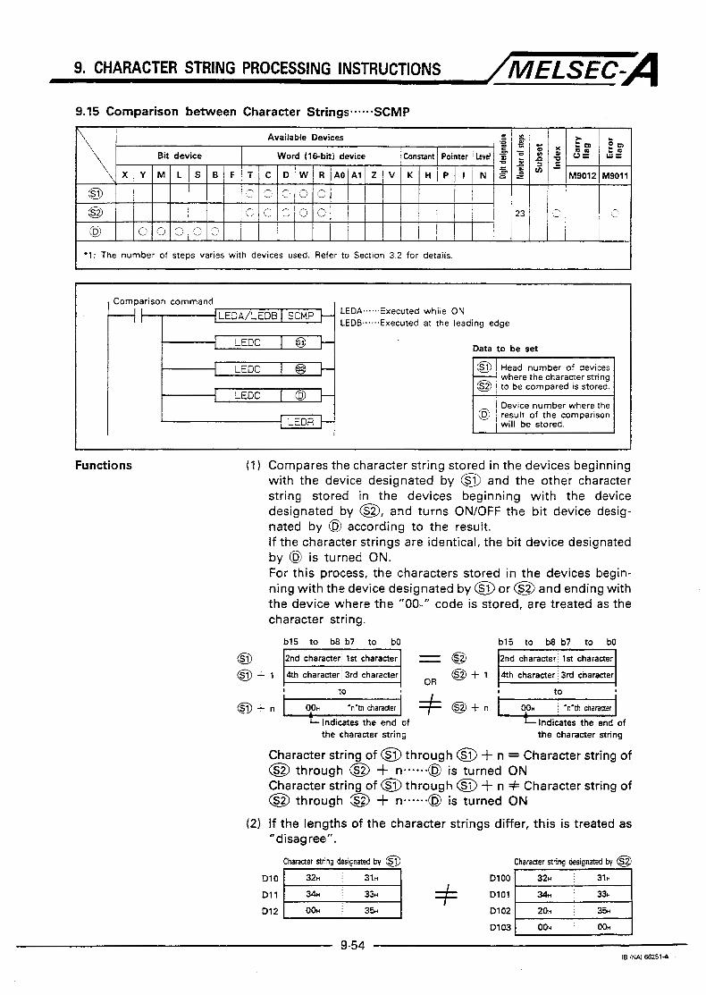
9. CHARACTER STRING PROCESSING INSTRUCTIONS /MELSEC-A 9.15 Comparison between Character Strings.-.---SCMP
\ B S Available Devices E
3 0 Level Pointer /constant k g x %
S a c
i? Y 0 E m
Bit device Word (1Cbit) device
X M9011 M9012 g g c n - P Z N I P H V I K R A O i A l I Z W D C T F 8 S L M Y
0
I E' =: 3 (21 0 @I
3 23 ! c> 3 0 C' IC @ I 1 1 , - ' 2 3 3 r C : l i
+1: The number of steps varies with devices used. Refer to Section 3.2 for details.
+ I -1 L E O A ~ ~ Comparison command
[ LE--
[ T E
j=-m [ LEDR
.-,Executed while ON
.... Executed at the leading edge
Data to be set
Head number of devices
to be compared is stored. where the character string
Device number where the
wil l be stored. result of the comparison
I I
Functions ( 1 ) Compares the character string stored in the devices beginning with the device designated by @ and the other character string stored in the devices beginning with the device designated by @, and turns ON/OFF the bit device desig- nated by @ according to the result. If the character strings are identical, the bit device designated by 0 is turned ON. For this process, the characters stored in the devices begin- ning with the device designated by @ or @ and ending with the device where the "00," code is stored, are treated as the character string.
b15 to b8 b7 to bO
to
I I Llndicates the end of
the character string
OR @+l
# @ + n
b15 to b8 b7 to bO
Indicates the end of the character string
Character string of @ through @ -I- n = Character string of @ through (@ +- n---.--@ is turned ON Character string of @J through @I -k n .i. Character string of @ through @ -I- n.----.@ is turned ON
If the lengths of the character strings differ, this is treated as "disagree".
C h a m e r string designated by @ , Chaader string designated by @
Dl0 I / 3 1 ~ I Dl 1 3 3 H # Dl01
Dl2 OOn 3 5 D l 02
OOH

9. CHARACTER STRING PROCESSING INSTRUCTIONS /MELSEC-A Execution Conditions The SCMP instruction execution mode depends on whether it is
designated with an LEDA or LEDB instruction. It is executed every scan while the comparison command stays ON if it is designated with a n LEDA instruction. When it is designated with an LEDB instruction, it is executed only once at the leading edge of the comparison command.
step 0 END Step 0 END Step 0 END Step 0 END 51ep 0 I L
Sequence program flow I I I I I
ON OFF
I 1 I I I 1 I
I I I I I I I I
I I I I I I I I I I
I I I I I I I I Comparison command
I SCMP (with LEDA) 1 I
I I I I I I I I I I I
I I I I I I I I I I I
I I
I I
SCMP (with LEDB)
Operation Errors An error occurs in the following cases and an error flag (M9011) is set.
Description 1 Error Code I
The “0011“ code is not set in device within the device range beginning with the device designated 6 and ending with the final number of that I device. The “00~” code is not set in a device within the device range beginning with the device designated by 0 and ending with the final number of that device.
-

9. CHARACTER STRING PROCESSING INSTRUCTIONS /MELSEC-J~ Program Example This p rog ram compares t h e c h a r a c t e r s t r i n g in D l 0 t h r o u g h D l 1
wi th t he cha rac t e r s t r i ng i n D20 t h r o u g h D21 w h e n X0 is t u rned ON. It t u r n s Y40 ON w h e n t h e r e s u l t is "ag ree" and t u rns Y41 ON w h e n t h e r e s u l t is "not agree" .
Y I
b15 to b8 b7 to bO b15 to b8 b7 to bO D20 "1 E:: Dl2 p 4 7 D 2 1 +"OOn" is stored -1 D22 OOH 36
-+ "00~" indicates the end automatically of the character string
"Agree' - MO is turned ON
4 (Y40 ON)
b15 to b8 b7 to bO b15 to b8 b7 to bO
D l 0 D l 1 w 7 D 2 1 lz%q D20 1 :: :: I D l 2
v_v
-c "Oh" is stored D22 OOH + '00~" indicates the end automatically of the character string
'Not agree" - MO is turned OFF
4 (Y41 ON)
9-56 18 (W 662514

9. CHARACTER STRING PROCESSING INSTRUCTIONS ~~/MELSEC-A 9.16 Separation into Byte Units--....WTOB
Available Devices C - SZ:, > Q X k z
s Bit device Word (16-bit) device
= - Constant $ 4 E E Level Pointer U =
M9011 M9012
w - X N P i I H K V 2 R A O A l W D T ’ C F B S L M Y
0
6 Z a -
0 0 0 ~ 0 0
@ 0 0 0 0 o/c! 0 0
0 0 0 013 0
* 1 : T h e number of steps varies with devices used. Refer to Section 3.2 for details.
edge
LEDC--...When device number is
1-1 LEDC’SUB I @ SUB.-.-When constant is designated
u LEDR designated
@ vices where the 16-bit Head number of the de-
data to be separated into byte data is stored.
@ where byte data after Head number of devices
separation is to be stored.
Number of pieces of byte @ data to which 16-bit data
is to be separated.
Functions (1) Separates the @ byte 16-bit data, stored in the devices beginning with the device designated by @ into byte units. It stores the result into the devices beginning with the device designated by @.
b15 to b8 b7 to bO b15 to b8 b7 to bO
@ + 2 Number of bytes designated by @
Lower we data
Example:
9-57 lB(NA)66251-F

9. CHARACTER STRING PROCESSING INSTRUCTIONS /MELSEC-A (2) By designating the number of bytes by 0, the range of the 16-
bit data to be designated by 0, and the range of devices where the byte data is to be stored, designated by @ are determined automatically.
(3) If the range of the devices (0 through @ 4- n), where the 16-bit data to be separated is stored, and the range of the devices ( @through @-I- n ) where the separated byte data will be stored overlap, the processing is been correctly executed.
Example:
b15 to b8 b7 to bO
(4) Processing is not executed if "0" is set for 0.
(5) The " 0 0 ~ " code is automatically stored in the upper 8-bits of the designated devices.
Execution Conditions The WTOB instruction execution mode depends on whether it is designated with an LEDA or LEDB instruction. It is executed every scan while the separation command stays ON if it is designated with an LEDA instruction. When it is designated with an LEDB instruction, it is executed only once at the leading edge of the separation command.
5141 0 END Slep 0 END Slep 0
Sequence program flow I I I I I
ON OFF
I I I I I I 1 I
1 I I I I I I I I I I I I
Combination command I 1 I I
I I I I
W O E (with LEDE) n I
I
Operation Errors An error occurs in the following cases and an error flag (M9011) is set.
Description
The device range of which number of bytes is designated with @exceeds the final number of that device; device range beginning with the device number designated by 0. The device range of which number of Wes is designated with 50 504
the number designated by @. @exceeds the final number of that device; device range beginning with
The number of bytes designated with @is a negative number.
Error Code D9008 D9091
Y YY
lB(NA)66251-F

....................................................................................................................................................................
....................................................................................................................................................................
....................................................................................................................................................................
....................................................................................................................................................................
....................................................................................................................................................................
.....................................................................................................................................................................
.....................................................................................................................................................................
.....................................................................................................................................................................
.....................................................................................................................................................................
....................................................................................................................................................................
.....................................................................................................................................................................
....................................................................................................................................................................
....................................................................................................................................................................
....................................................................................................................................................................
.....................................................................................................................................................................
.....................................................................................................................................................................
....................................................................................................................................................................
....................................................................................................................................................................
....................................................................................................................................................................
IB (NAJ €62514

9. CHARACTER STRING PROCESSING INSTRUCTIONS /MELSEC-A Program Example This program separates the data stored in Dl0 through 012 into
byte data and stores the separated bytes in D20 through D25.
H I
- C L E D C Dl8
C L E D C D28
[SUB 6 K
-
- - C L E D R
Dl0
Dl 1
Dl2
b15 to b8 b7 to bO
' 6 bytes
9-59 IB 0 - 1 4

MEMO ...................................................................................................................................................................
....................................................................................................................................................................
....................................................................................................................................................................
....................................................................................................................................................................
....................................................................................................................................................................
.....................................................................................................................................................................
.....................................................................................................................................................................
.....................................................................................................................................................................
.....................................................................................................................................................................
....................................................................................................................................................................
.....................................................................................................................................................................
....................................................................................................................................................................
....................................................................................................................................................................
....................................................................................................................................................................
.....................................................................................................................................................................
.....................................................................................................................................................................
....................................................................................................................................................................
....................................................................................................................................................................
....................................................................................................................................................................
.....................................................................................................................................................................
................. .................._____..-........................................................................................................................
.....................................................................................................................................................................
....................................................................................................................................................................
la IW 6625111
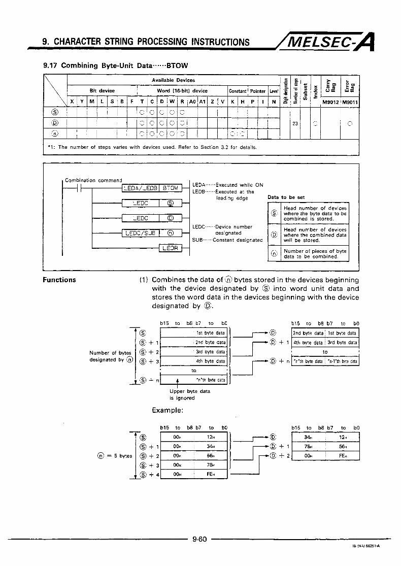
9. CHARACTER STRING PROCESSING INSTRUCTIONS ~/MELSEC=A 9.17 Combining Byte-Unit Data.....-BTOW
Available Devices ? G + s g
.= v) g Bit device Y 0 1 4 E ~evd Pointer Constant Word (16-bit) device
- - X M9011 M9012 z 3 N I P K I H V 2 AO.A1 R W D C T F S I B L M Y
0 - 0
9 Zm 23 3 G 0 0 0 @ 0 0 0 12 '3 !
I
j '̂ - ,^I L, 0 0 Zli0 0
I '1: The number of steps vanes with devices used. Refer to Section 3.2 for details. I
--It --+ Combination command LEDA/LEOBI BTOW
[ LEOC I @ E 1 LEDC I @) E 1 LEDC/SUB 1 @
-[LEDR
LEDA...,..Executed while ON LEDB......Executed at the
leading edge Data to be set
combined is stored. LEDC......Device number
SUB...,..Constant designated will be stored. designated Head number of devices
where the combined data
data to be combined. Number of pieces of byte
Functions (1) Combines the data of @ bytes stored in the devices beginning with the device designated by @ into word unit data and stores the word data in the devices beginning with the device designated by @I.
b15 to b8 b7 t o bO
Number of byte! 1
1st byte data
2nd byte data
3rd byte data designated by @ @ + 4th byte data
Upper byte data is ignored
Example:
b l 5 t o b8 b7 to bO
to
b15 to b8 b7 t o bO b15 to b8 b7 to bO
@ = 5 b ytef @ + 3 1 s + 4 0% FEH
u-vu

9. CHARACTER STRING PROCESSING INSTRUCTIONS /MELSEC-A
Execution Conditions
By designating the number of bytes by 0, the range of the byte data, designated by @, and the range of devices where the combined word data is to be stored, designated by 0, are determined automatically.
If the range of the devices (9 through @ i- n), where the byte data to be combined is stored, and the range of the devices (@ through 0 -I- n) where the combined word data will be stored overlap, the processing is correctly executed.
Example:
b15 to b8 b7 to bO
Dl5 3 6 n
1 - 1 b15 to b8 b7 to bO
3 6 ~ 35r
(4) Processing wil l not be not executed if "0" is set for a. (5) With the byte data storing devices designated by s), only the
lower 8-bit data is recognized as the data to be combined, The upper 8-bit data is ignored.
The BTOW instruction execution mode depends on whether it is designated with an LEDA or LEDB instruction. It is executed every scan while the combination command stays ON if it i s designated with an LEDA instruction. When it is designated with an LEDB instruction, it is executed only once at the leading edge of the combination command.
Sequence program flow
ON I I I I I I I I I I I I I
Combination command I I I I
I I I I I I I I
I BTOW (with LEDA) 1 n I
I
I I I BTOW (with LEDB) I I h I

9. CHARACTER STRING PROCESSING INSTRUCTIONS /MELSEC-A Operation Errors An error occurs in the following cases and an error flag (M9011) is
set.
Program Example
Error Code D9008 1 D9091
Description
The device range of which number of bytes is designated with @ exceeds the final number of that device; device range beginning with the device number desionated bv 0 . The device range of which number of bytes is designated with @ device number designated by @.
50
The number of bytes designated wi th E is a negative number.
exceeds the final number of that device; device range beginning with the 504
- This program combines the byte data stored in D20 through D25 into word data and stores the word data to D l 0 to D12.
b15 to b8 b7 to bO
D22
D23
D24 67r
D25 3 1 ~
Upper bytes are ignored
b15 to b8 b7 to bO
I D 1 0

10. DATA CONTROL INSTRUCTIONS /MELSEC-A 10. DATA CONTROL INSTRUCTIONS
The data control instructions are used to automatically control the output level by checking the range of the input data.
The data control instructions are summarized in the table below.
Classification Name Instruction Description Refer to
Checks the upper and lower limits of the input data and controls the input data so that the data will fall within 70-2
lower limits to output the data.
UpperAower limit control the range defined by the upper and
I I BAND I Subtracts the designated range value I I Dead control zone 1-1 data. I 10-6
from the input data to output the
I DBAND I If the input data is within the desig- nated range, "0" is outputted.
I 1 ZONE 1 Adds the designated range value to 1 Zone control the input data to output the data.
If the input data is "0". "0" is out- .lo-lo b l putted.

IO. DATA CQNTROL INSTRUCTIONS /MELSEC-A 10.1 Upper/Lower Limit Control-.----LIMIT, DLlMlT
'1: The number of steps varies with devices used. Refer to Section 3.2 for details. '2: With the DLlMlT instruction, the number of steps increases in units of 6 steps each time DXNR is used with a, @, or @).
I Control command E - -
LEDC/SUB
L E D = -
((Control command DLlMlT
I
LEDA....Executed when ON LEDB....Executed at the leading edge
Data t o be set
LEDC...-Device number
SUB ..... Constant designated
designated Upper limit value Imax- lmurn output limit)
Input value to be control-
limit control.
Device number where the output value controlled by the uppedlower limit control is to be stored.
LEDA....Executed when ON LEDB....Executed at the leading edge
LEDC....Device number designated DXNR..Constant designated
I
To use DXNR, state as indicated below.
All devices except for input (X) can be designated.
Functions I LIMIT^ (1) Controls the output value, to be stored in the device desig-
nated by @, according to the magnitude of the input value (16-bit binary value) designated by @ whether it is within the range defined by the upper and lower limit values designated by @ and @. The output value is controlled a s indicated below.
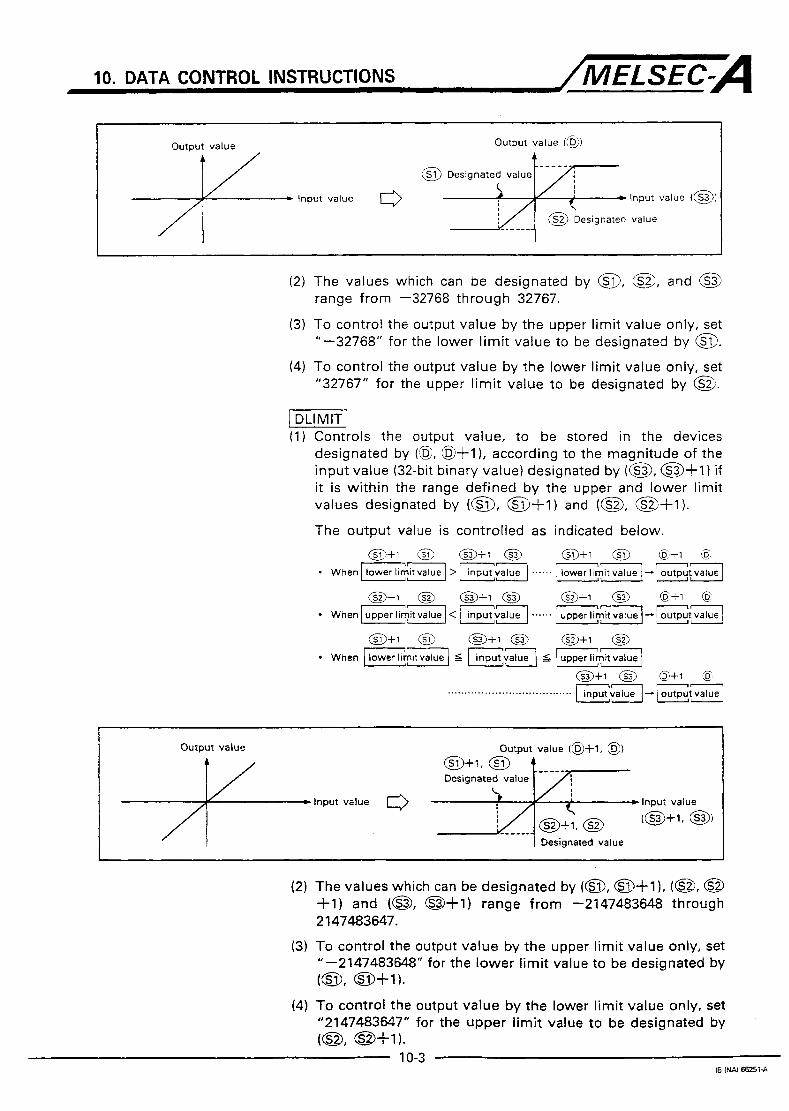
I O . DATA CONTROL INSTRUCTIONS /MELSEC-A
(2) The values which can be designated by @I, @, and @ range from -32768 through 32767.
(3) To control the output value by the upper limit value only, set "-32768" for the lower limit value to be designated by @.
(4) To control the output value by the lower limit value only, set "32767" for the upper l imit value to be designated by @.
1 DLIMIT] (1) Controls the output value, to be stored in the devices
designated by KG, a i - l ) , according to the magnitude of the input value (32-bit binary value) designated by (@, @+l) if it is within the range defined by the upper and lower limit values designated by (a, a4-1) and (@, m f l ) .
The output value is controlled as indicated below. @+l @ @+1 @ @+I @ @+l (E
. W h e n F m F l > w v g ...... F m F / - E ; F l L
. Whenlupper limit ..... I < 1 input v 4 ...... 1 ..... libit ..... I- 1 outpu,?value ~
@+l @ @+1 @ @+1 @ When P m - 1 5 [ i F ) i (upperm-]
@+1 @ @'+l @ .....................................
Output value
1 Designated value
(2) The values which can be designated by (a, @+l), (@, @ +1) and (8, @+1) range from -2147483648 through 2 147483647.
(3) To control the output value by the upper limit value only, set "-2147483648" for the lower limit value to be designated by (@, @+1)*
(4) To control the output value by the lower limit value only, set "2147483647" for the upper limit value to be designated by (@, @+v.
10-3 18 IW €62514

10. DATA CONTROL INSTRUCTIONS /MELSEC-A Execution Conditions The LIMIT and DLlMlT instruction execution mode depends on
whether it is designated with an LEDA or LEDB instruction. They are executed every scan while the control command stays ON if it is designated with a n LEDA instruction. When it is designated with an LEDB instruction, they are executed only once at the leading edge of the control command.
END Steo 0 END Slep 0 END srep 0
Sequence program flow I I
ON OFF
I I I I I I I I I I
l j I I I j I I
. I I I Control command
I I I I I I I I
LIMIT I DLIM,T (with LEDA) n I
I I I
LIMIT I I I
DLIMIT (with LEDBl I I
Operation Errors An error occurs in the following case and an error flag (M9011) is set.
Program Example
Description
The lower limit value designated by 0 is greater than the upper limit value designated by a.
Error Code D9008
503 50
D9091
FlM-IT 1 This program executes the upper/lower limit control (500 through 5000) for the data in DO and stores the result in D l .
B I N P De
Upper limit value
Lower limit value
L E D C D B
DO 1 LIMIT- 1 D l
6250
10-4 IB { N A l 662516

10. DATA CONTROL INSTRUCTIONS /IWELSEC-A This program executes the upper/lower limit control (1000 through 1000000) for the data in DO through D l and stores the result in D10.
x e 2 e D O 3
CLEDR D L I M I T 3 K
K
P K 8
EDXHR leee C D X H R l eeeeee D 1 8 8 3 Lower limit value
D 1 8 8 3 Upper limit value
C L E D C D O 3
C L E D C D l 8 3
DO 1 DLlMlT 1 d10
400
DO Dl 0
345678 4 345678
DO d10

I O . DATA CONTROL INSTRUCTIONS /MELSEC-A 10.2 Dead Zone Control..----BAND, DBAND
M9012 M9011
*l: The number of steps varies with devices used. Refer to Section 3.2 for details. '2: With the DBAND instruction, the number of steps increases in units of 6 steps each time DXNR is used with a, @,or a.
(Control command BAND
P V LEDMLEDB~ BAND t- LEDA....Executed when ON LEDB....Executed at the
leading edge Oats to be set
LEDC....Device number designated range)
I SUB ....- Constant designated dead zone (no output
range) I
the dead zone control. I Input value controlled by
Device number where the output value controlled by the dead zone control will be stored.
J Control command
LEDB-...Executed at the leading edge LEDA..,.Executed when ON
LEDC/DXNR
-== LEDC I 0 -[ LEDR
LEDC....Device number designated DXNR...Constant designated
To use DXNR, state as indicated below.
All devices except for input (X) can be designated.
Functions I BAND I (1) Controls the output value, to be stored in the device desig-
nated by @,-according to the magnitude of the input value (16-bit binary data) designated by @ if it is within the dead zone defined by the upper and lower limit values designated by @ and @. The output value is controlled a s shown below.
........................................................................ o -.@I output value] 10-6
I8 (NAI 6 6 2 5 1 4

10. DATA CONTROL INSTRUCTIONS /MELSEC-A
r Output value Output value (@;) I Lower limit value of dead zone (a)
Upper limit value of dead zone (@)
value =
(2) The values which can be stored in @, @, and range from -32768 through 32767.
(3) The output value to be stored in @ is the signed 16-bit binary value. Therefore, if the operation result is outside the range of -32768 through 32767, the value to be stored in @ is processed as shown below.
Example: When the dead zone lower limit value (@) = 10, the input value (@) = -32768 Output value is calculated as indicated below:
Output value = -32768 - 10 = 8O0OH - AH = 7FF6H = 32758
I DBAND I (1) Controls the output value, to be stored in the device desig-
nated by 0, according to the magnitude of the input value (32-bit binary data) designated by (@I, @+1) if it is within the dead zone defined by the upper and lower limit values designated by (@I, @)-I-1) and (a, a - I - 1 ) .
The output value is controlled as indicated below.
When 1 lower limit value I 5 I input:ialue 1 5 [upper limit value I m1 @
......................................................... O--[+q
Output value Output value (@, @)+I) Lower limit value of dead zone ( 0 1 , @+1)

10. DATA CONTROL INSTRUCTIONS /MELSEC-A (2) The values which can be stored in (a, @ + l ) , (@, @-l-1)
and (@, @$1) range from -2147483648 through 2147483647.
(3) The output value to be stored in 0, @ k t 1 is the signed 32-bit binary value. Therefore, if the operation result is outside the range of -2147483648 through 2147483647, the value to be stored is processed as shown below.
Example: When the dead zone lower limit value (@, mi-1) = 1000, the input value (a, m-l-1) = -2147483648 Output value is calculated below:
Output value = -2147483648 - 1000 = 80000000~ - 000003E8~ = 7FFFFC18H = 2147482648
Execution Conditions The BAND and DBAND instruction execution mode depends on whether, it is designated with an LEDA or LEDB instruction. They are executed every scan while the control command stays ON if it is designated with an LEDA instruction. When it is designated with an LEDB instruction, they are executed only once at the leading edge of the control command.
ON OFF
1 I I I I I Control command I / I I
I I I I I I I I I I I I I
I I
DBAND BAND (with LEDA) n I I I I I I I
I I I I I I I I I I I
I I
I
I DBAN D BAND (with LEDB) 1
Operation Error An error occurs in the following case and an error flag (M9011) is set.
Description I k G T i G G - 1 Error Code
e l o w e r limit value designated by a is greater than the upper limit 503 5o value designated by 0.
10-8 B [NAJ 662516,

10. DATA CONTROL INSTRUCTIONS /MELSEC=A Program Example I BAND I
This program executes the dead zone control (-1000 through 1000) for the data in DO and stores the result in D l .
B I H x e z e D B
- zeee D B
P K 4
1 1 I CLEDF) B R H D
- - - C L E D C D B
- C L E D C D l
- L E D R
DO D l
-2000 -1000
DO D l
500 0
DO D l
7000 6000
j D B A N D l This program executes the BAND control (-10000 through 10000) for the data in DO through D l and stores the result in D10.
P K8 D B
L E D R DBAHD
Lower limit value
D 188 Upper limit value
DO D l 0
- 12345 -2345
DO [ DBAND D l 0
6789 0
DO Dl 0
50000 40000

10. DATA CONTROL INSTRUCTIONS /MELSEC-A 10.3 Zone Control..---.ZONE, DZONE
*l: The number of steps varies with devices used. Refer to Section 3.2 for details. '2: With the DZONE instruction, the number of steps increases in units of 6 steps each time DXNR is used with 0, @, or @).
ZONE 1 Control command
[ LEOC/SUB 1 @ }
I LEOR
1 DZONE 1 I Control command
I -{ LEDR
LEDA....Executed when ON LEDB....Executed at the leading edge
Data t o be set LEDC....Device number
SUB ..... Constant designated
designated Positive bias value to be
Device number where the output value controlled by the zone control is to 1 be stored.
LEDA....Executed when ON LEDB.-..Executed at the leading edge
LEDC.--.Device number designated DXNR..Constant designated
To use DXNR, state as indicated below.
All devices except for input (X) can be designated.
Functions NE I (1) Adds the bias value, designated by @ or @, to the input
value designated by @ and stores the result in .the device designated by @.
The bias value is added as shown below.
....................................................................... O-@loutputvalueI
When @ [ S I > 0

10. DATA CONTROL INSTRUCTIONS /.ELSEC-A Output value
/I__ Output value (@)
Positive bias value (@I \ 0
Input value 0 - Input value (@I
/ CL Negative bias value (@)I
(2) The values which can be stored in a, @, and @ range from -32768 through 32767.
(3) The output value to be stored in @) is the signed 16-bit binary value. Therefore, if the operation result is outside the range of -32768 through 32767, the output value to be stored in a is processed as indicated below.
Example: When the negative bias value (a) = -100, the input value (@) = -32768 Output value is calculated as indicated below:
Output value = -32768 + (-100) = 8O0OH i- FF9CH = 7F9CH = 32668
j DZONE] (1) Adds the bias value, designated by (@, @+1) or (@, @
4-1) to the input value designated by (@I, B i - 1 ) and stores the result in the device designated by (0, D4-1).
The bias value is added as indicated below. @+l @ @+1 @ @+1 0 @)+1 @
@+1 @ @+l @
@+l 0 -1 @ @+l 0 @ t l @
- When F,m < 0 ...... [ G I -I- F p - 1 -
. When input value = 0 ........................................................ CII 0 - [ Z + 3
- When /,F] > 0 ...... l q a ' -I- Fbfi -. ({FI
I Output value Output value (@, @+-I) I t
0
Positive bias value y (@. @+1) 0 - Input value (@, @+I)
Negative bias value
/ - (a, @+1)
1 I

I O . DATA CONTROL INSTRUCTIONS /MELSEC-A (2) The values which can be stored in (@,@i-l), (@, Q i - 1 1 ,
and (a, @+I) range from -2147483648 through 2147483647.
Execution Conditions
(3) The output value to be stored in (@I, @m+l) is the signed 32-bit binary data. Therefore, if the operation result is outside the range of -2147483648 through 2147483648, the value to 'be stored is processed as indicated below.
Example: When the negative bias value (@I, @+1) = -1000, the input value (@I, @+l) = -2147483648 The output value is calculated as shown below:
Output value = -2147483648 -t (-1000) = 80000O0OH -I FFFFFC18, = 7FFFFC183 = 2147482648
The ZONE and DZONE instruction execution mode depends o n whether it is designated with an LEDA or LEDB instruction. They are executed every scan while the control command stays ON if it is designated with an LEDA instruction. When it is designated with an LEDB instruction, they are executed only once at the leading edge of the control command.
erecurion
Sequence program flow
ON OFF
I I I I I I I I I I I I I
I I I I I I I I
Control command I I I l j I I I
ZONE I
DZONE (with LEDA) 1 n I 1 I I I I I I I I I I
I I I I I I I 1 I I I
I I
::LE (with LEDB)
10-12 I6 IW m51-A

10. DATA CONTROL INSTRUCTIONS /.ELSEC-A Program Example PONE I
This program executes the zone control (-100 through 100) for the data in DO and stores the result in D l .
' r 8 e P K BIH x e 2 e D e
P K 4
- 2666 DB n g e x
ELEDR ZONE K -
K [SUB 108
€SUB 1 6 6
I L E D C D e
-CLEDC D l
CLEDR
Negative bias value
Positive bias value
DO D l
-200 -300
DO D l
0
DO D l
700 800
-1 This program execute the zone control (-10000 through 10000) for the data in DO through D l and stores the result in D10.
DB 3
D- l e e e e e D e 3
CLEDR DZOHE 3 K-
K ~ D X H R I eeee E D X H R 1 e e . e ~ D l 8 6 3 Positive bias value
D l 6 8 3 Negative bias value
C L E D C D 8 1
ELEDC D l 8
t I ELEDR 4
DO D l 0
-22345
M) Dl0
0 0 1 DO Dl0
50000 60000
10-1 3 IB IW 662514

M E M O ....................................................................................................................................................................
....................................................................................................................................................................
....................................................................................................................................................................
....................................................................................................................................................................
....................................................................................................................................................................
.....................................................................................................................................................................
.....................................................................................................................................................................
.....................................................................................................................................................................
.....................................................................................................................................................................
....................................................................................................................................................................
.....................................................................................................................................................................
.. ..............................................................-...................................................................................................
.....................................................................................................................................................................
.....................................................................................................................................................................
............_.................-.................. ...................................................................................................................
....................................................................................................................................................................
.. ...................................-..............................................................................................................................
.....................................................................................................................................................................
....................................................................................................................................................................
....................................................................................................................................................................
....................................................................................................................................................................
IB IN& €62514

11. CLOCK INSTRUCTIONS /MELSEC-A 11. CLOCK INSTRUCTIONS
The clock instructions are used for writing in and reading clock data.
The clock instructions are summarized in the table below.
Refer t c j Paoe
Clock data read
I Clock data
write
~
Reads the clock data (year, month, day, hour, minute, second, and day of the week) from the clock element in the PC DATERD ,1-2
CPU.
Writes the clock data (year, month, day. hour, minute, second, and day of DATEWR the week) into the clock element in the PC CPU.
11-4
11-1 IB I N 4 C625141

11. CLOCK lN.STRUCTlONS /MELSEC-A 11.1 Reading Clock Data----.DATERD
Available Devices
Bit device Word (16-bit) device
M9012 M9011
c o o 0 0 17 0 0
'1: The number of steps varies with devices used. Refer to Section 3.2 for details.
Read command lLEoTd LEDB-..Executed at the leading edge LEDA...Executed when ON
-1 LEDC It-- Data to be set I I
Head number of devices where the read clock data will be stored.
I Functions (1 1 Reads the clock data (year, month, day, hour, minute, second,
and day of week) from the clock element in the PC CPU and then stores it as a binary value in the device designated by @.
Year (AD>) (0 to 99)
Month (1 to 12)
(1 to 31)
Hour (24 hours) (0 to 23)
@+4 Minute 10 t o 59)
@+5 Second (0 t o 59)
Day of the week (0 t o 6)
For the year, the last two digits are stored in @. Example: 1989 - 89
For the day of the week, to be stored in @+6, the numbers "0" through "6" represent "Sunday" through "Saturday".
Leap years are automatically figured in.
Execution Conditions The DATERD instruction execution mode depends on whether it is designated with an LEDA or LEDB instruction. It is executed every scan while the read command stays ON if it is designated with an LEDA instruction. When it is designated with an LEDB instruction, it is executed only once at the leading edge of the read command.
I-IOII END .x(IMmn B.M- #ng irmmdon IllSmdD"
m m t o n LMIumon
aravnon srealiian 1-0"
stop 0 END Step 0 END stop0 END Step 0 END SLap 0 I 1 I I t I ,
t I I I I I 1 I I I
I
Sequence program flow r-i ti
Read command ON OFF
I I I I / I I
I I I I I I I 1
I I
DATERD (with LEDA) 1 I I I 1
I I I I
I
I I I I
I I DATERD ( w i t h LEDB) 1 I 4 1 11-2
IB iNAJ € 6 2 5 1 4

11. CLOCK INSTRUCTIONS /MELSEC-A Program Example This program outputs the clock data as a BCD value.
Month .................. Day ...................... Hour ..................... Minute .................. Second.. ............... Y40 through Y47
Y60 through Y67 Y58 through Y5F Y50 through Y57 Y48 through Y4F
C L E D C DO
# ?
1 I-LBCD D 3 4 Outputting "hour"
Outputting "minute"
B C D D 5 Outputting "second"
Clock data
I '89.12.24 12:57:39 I Y5F to Y58 Y57 to Y50
(Day. hour)
Y4F to Y48 Y47 to Y40
(Minute, second)
11-3 IB (W 562514
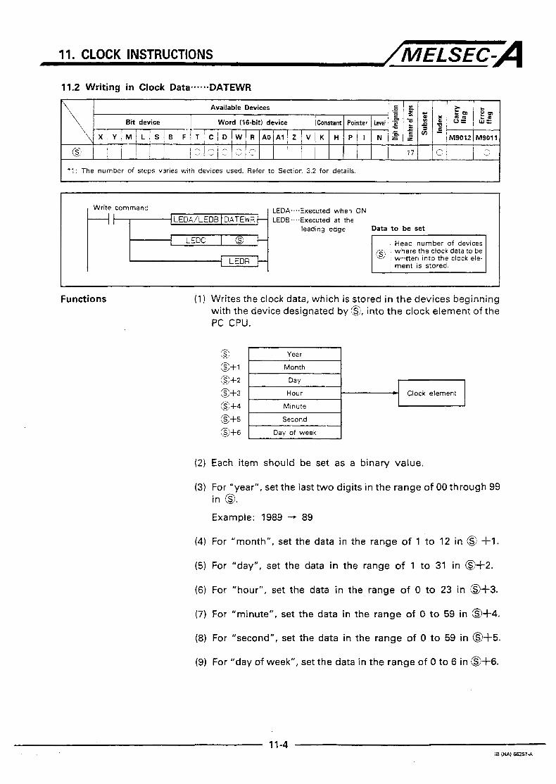
11. CLOCK INSTRUCTIONS /MELSEC-A 11.2 Writing in Clock Data...-*-DATEWR
Available Devices ._ 5 P c m a m 8 E $ Bit device
t
Word (16-bit) device w - u 2 Pointer j &el Constant - m = z X I Y d 5 P / I / N H K V 2 A O A l B F T ' C / D / W R S M I L
._ - M9012 M9011
o i l I-, 1 17 I - - -
'1: The number of steps varies with devices used. Refer to Section 3.2 for details. 1 Write I I command , z+j LEDA....Executed when ON LEDA/LEDB DATEWR LEDB-...Executed at the
leading edge Data to be set
where the clock data to be written into the clock ele- ment is stored. LEDR
I I I I I
Functions (1 1 Writes the clock data, which is stored in the devices beginning with the device designated by GI, into the clock element of the PC CPU.
Year
@+l
Minute @,+4
Clock element * Hour @'+3
W 0 + 2
Month
J
3 + 5 Second
3 + 6 Day of week -
Each item should be set as a binary value.
For "year", set the last two digits in the range of 00 through 99 in @. Example: 1989 - 89
For "month", set the data in the range of 1 t o 12 in @ +1.
For "day", set the data in the range of 1 to 31 in @+2.
For "hour", set the data in the range of 0 to 23 in @+3.
For "minute", set the data in the range of 0 t o 59 in @+4.
For "second", set the data in the range of 0 to 59 in @+5.
For "day of week", set the data in the range of 0 t o 6 in @+6.
11-4 I8 (NAJ 662514

11 CLOCK INSTRUCTIONS /MELSEC-A Execution Conditions The DATEWR instruction execution mode depends on whether it
is designated with an LEDA or LEDB instruction. It is executed every scan while the write command stays ON if it is designated with an LEDA instruction. When it is designated with an LEDB instruction, it is executed only once at the leading edge of the write command.
ON OFF
I I I I I I I I I I I
I I I
Write command
I I I I I I
DATEWR (with LEDA) n I
I
I I I I I I
I I 4 I I I I I
I I I DATEWR (with LEDB) I I
Operation Error An operation error occurs in the following case and an error flag (M9011) is set.
Description Error Code
D9008 1 D9091 When data is set outside the specified range. 50 1 503
Program Example This program writes the clock data entered as a BCD value into the clock device.
year ..................... X28 through X2F X20 through X27 X18 through X1F X10 through X17 X8 through XF
Month .................. Day ...................... Hour ..................... Minute.. ................
................. Second X0 through X7
K? C B I H X 9 2 8 P B :
K Z C B l H X I 2 8 1'1 :
# 2 CRIH X 8 1 8 D ?
# 2 CBIH X 8 1 6 D3 : C B I H X 6 8 8 @ 4 : K Z
C B I H X e e b P5 : K2
CLEDR DRTEYR
CLEDC @ B 1
LEDR 1
X2F to X28 X27 to X20
1 1
Setting "year"
Setting "month"
Setting "day"
Setting "hour"
Setting 'minute"
Setting "second"
X1F to X18 X17 to X10 1-1 Clock data
(Day, Hour) '90,01,01 12:oo:oo
XOF to X08 X07 to X00
(Minute, Second) 0 0 I 0 : 0
11-5 IS (NAJ 662514

12. INSTRUCTIONS FOR USING EXTENSION FILE REGISTERS /MELSEC-A 12. INSTRUCTIONS FOR USING EXTENSION FILE REGISTERS
The extension file register instructions show h o w to use vacant areas in the memory cassette as file registers. Using these instructions extends the range of the data storage device. For details about the extension file register instructions, refer to Section 12.1.
The extension file register instructions are summarized in the table below.
Block number I RSET change
Block movement BMOVR
1 Block change BXCHR
me-word units E. Direct readwrite of
ZRRDB
Direct readwrite of data in bytes
ZRWRB
I
Description
Changes the block number of the exten- sion fi le registers.
Moves a designated number of data points between the extension file regis- ters.
Exchanges a designated number of data points between the extension file registers.
Reads the data in one-word units from the extension file registers. In this op- eration, device numbers in the exten- sion file registers can be continuously designated, ignoring the block num- bers.
Writes the data in one-word units to the extension file registers. In this opera- tion, device numbers in the extension file registers can be continuously desig- nated, ignoring the block numbers.
Reads the data in byte units from the extension file registers. In this opera- tion, consecutive device numbers of the extension file registers are automatical- ly assigned. Therefore block numbers may be ignored.
Writes the data in byte units from the extension file registers. In this opera- tion, consecutive device numbers of the extension file registers are automatical- ly assigned. Therefore block numbers may be ignored.
Refer t o Page
12-5
12-7
12-10
12-16
~~ ~
12-19
12-25
12-28

12. INSTRUCTIONS FOR USING EXTENSION FILE REGISTERS /MELSEC-A 12.1 Extension File Registers
Extension file registers are automatically assigned to the vacant (unused) areas in the memory cassette in block units. One block consists of 8192 points (16K bytes). Up t o 64 blocks are assigned. The number of blocks varies depending on the memory cassette used and the vacant capacity in the memory cassette.
POINT I Extension file registers can be used only when the file register capacity is set in parameter assignment.
12.1.1 Extension file register assignment
The extension file registers are automatically assigned to the vacant area in the memory cassette a s described below. The vacant areas are segmented in units of 16K bytes. Each segmented area is assigned a block number. A vacant area smaller than 16K bytes cannot be used for extension file registers.
- A3NMCA16 ......... u N M C M 4 ......... 4 8 K bytes M N M C A a ......... 176K bytes
32K bytes
A3NMCA56 ......... 3D4K bytes A3AMCA96 ......... 6 2 4 K bytes A4UMCA128 ........ 880K bytes -
Parameter area
Main program area
Subprogram area only for M A , A3U, A4U:
For subprogram use, TIC seningand P.1 addresses
Extension comment area
(Vacant)
Status latch Sampling trace 1 area
File register (R)
Comment area
(Vacant)
..... 4K bytes
* -.. Depends on parameter setting
..... 5K bytes (0 bytes if subprograms are not used)
................... (Less than 16K bytes)
I 1 Block number 8 I.--- 16K bytes
0 Extension file
I ................... I
.*.. Depends on parameter setting
Depends on parameter setting Used as block number 0
.....
::I: A2A(S1). A2U: 28 A3A, A3U: 48
A4U: 64
12-2 ID,h!A)SiiSl-F
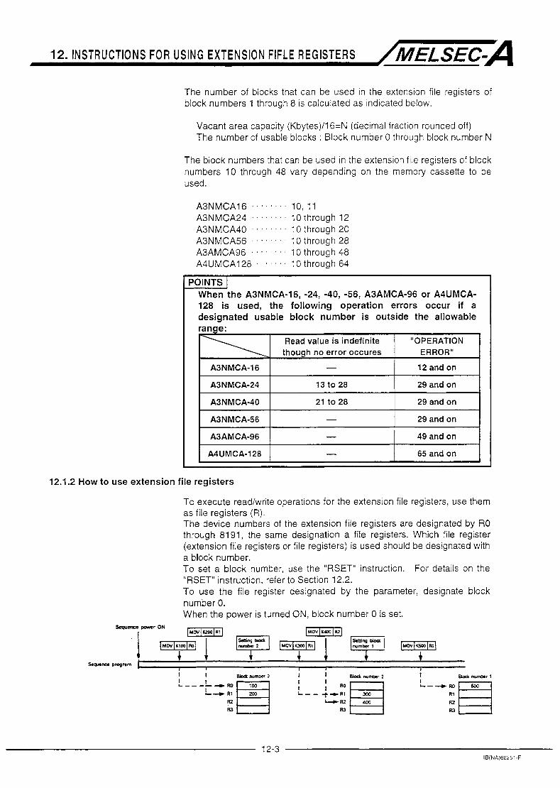
12. INSTRUCTIONS FOR USING EXTENSION FlFLE REGISTERS /MELSEC-A The number of blocks that can be used in the extension file registers of block numbers 1 through 8 is calculated as indicated below.
Vacant area capacity (Kbytes)/l6=N (decimal fraction rounded off) The number of usable blocks : Block number 0 through block number N
The block numbers that can be used in the extension file registers of block numbers 10 through 48 vary depending on the memory cassette to be used.
A3NMCAl6 . . . . . . . . 10, 11 A3NMCA24 . . . . . . . . lothrough 12 A3NMCA40 ' ' .
' ' . 10 through 20 A3NMCA56 . . ' ' ' ' 10 through 28 A3AMCA96 ' . .
' . 10 through 48 A4UMCAl28 ' . . . 10 through 64
POINTS I When the A3NMCA-16, -24, -40, -56, A3AMCA-96 or A4UMCA- 128 is used, the following operation errors occur if a designated usable block number is outside the allowable range:
Read value is indefinite ERROR" though no error occures
"OPERATION
A3NMCA-16 12 and on - ~ ~~~ ~
A3NMCA-24
29 and on 21 to 28 A3NMCA-40
29 and on 13 to 28
I I I I I
A3NMCA-56 -
49 and on - A3AMCA-96
29 and on ~ ~~~ ~
I I 1 I I
A4UMCA-128 ~~~ ~~~
- 65 and on
12.1.2 How to use extension file registers
To execute readiwrite operations for the extension file registers, use them as file registers (R). The device numbers of the extension file registers are designated by RO through 8191, the same designation a file registers. Which file register (extension file registers or file registers) is used should be designated with a block number. To set a block number, use the "RSET" instruction. For details on the "RSET" instruction, refer to Section 12.2. To use the file register designated by the parameter, designate block number 0. When the power is turned ON, block number 0 is set.
12-3 IB(NA)66251-F

12. INSTRUCTIONS FOR USING EXTENSION FILE REGISTERS /MELSEC-A POINT I
In the blocks from number 1 through 28 of the extension file registers, the device numbers for which read/write is possible are within the range set for the fi le register (block number 0 ) within the parameter.
Example: 4K is set by parameter
Block number 0 Block number
RO
. . . . . . . . . . . . . .
R8191
1 Block number 28
5 -5 . . . . . . . . . . . . . .
R8191
By using the index register (2, V), it is possible t o use all devices (RO through 8191) for readlwrite operations. Moving and exchanging data between extension file registers using the BMOVR instruction and BXCHR in- struction can de done with all device numbers (RO through 8191).
12.1.3 Precautions when using extension file registers
(1) To use extension file registers, set the file register capacity with a parameter. Extension file registers cannot be used if the file register capacity is not set.
(2) If the sampling trace or status latch function is executed while the extension file register is used, the objective file for data collection is as indicated below.
Sampling trace When the step number is . - e . . . The f i le register of the block designated number designated when the
END instruction is executed. When sampling time is ......-.- Indefinite designated
Status latch The file register of the block number designated when the END instruction is executed.
(3) If the file register read/write is executed from an external module such as AD51 (S3) and AJ71 C24(S3, S6, S8)/AJ71 UC24, read/write is executed for the file register of the block number designated when the END instruction is executed. When read/write is executed for the extension f i le register, readlwrite is executed for the file register in the designated block number.

12. INSTRUCTIONS FOR USING EXTENSION FILE REGISTERS /MELSEC-A 12.2 Changing the Extension File Register Block Number--....RSET
Available Devices > E L - c :m k m
Bit device Word (16-bit) device w 0 E u n E t Level Pointer Constslrt 2 k 6 6 s
- 3 s Le VJ-
X Y M L S B F T I C D ! W R A O A l Z V K H P I N ~ ~ M9012 M9011
0 '3 17 0 f. c: clo 013 - -
*1: The number of steps varies with devices used. Refer to Section 3.2 for details.
Block number change command
f IEDA/LEDB I 4 LEDB-...Executed at the leading edge LEDA,...Executed while ON
Functions ~~~
(1) Changes the block number of the file register (R) to be used in a program to the number designated by 0. After the block number is changed, operation processings are execute with file registers which are different from those before the block number is changed.
RO
to
Rn
I Processing for file reqister IR)l
I .t-t----t' i
(2) For the designation available for block numbers, refer to Section 12.1 .l.
Execution Conditions The RSET instruction execution mode depends on whether it is designated with an LEDA or LEDB instruction. It is executed every scan while the block number change command stays ON if it is designated with an LEDA instruction. When it is designated with an LEDB instruction, it is executed only once at the leading edge of the block number change command.
lnsmpl~n END w" LnprupDn aetutyn procraing - QcPmOn
step 0 EN0 S M 0 END Step 0 I 1 , I
Sequence program flow c I I 7 I n I 1
I I I
I I I I I I I I
I I I I I
ON 0 FF
I I I I
Block number change command I I I I
RSET (with LEDA) 1 I 1 I I
I I I I I
I I I I I I I I I I
I I I I I RSFT (with LEDB) h I
12-5 18 (Nn) 662514

12. INSTRUCTIONS FOR USING EXTENSION FILE REGISTERS /MELSEC-A Operation Errors An operation error occurs in the following cases and an error flag
(M9011) is set.
Program Example
Description Error Code
D9008 1 D9091 When an unusable block number is set. When the file register capacity is not set by a parameter.
50 501
This program compares RO in block number 0 with RO in block number 1.
Y40 is ON when RO in block number 0 = RO in block number 1 Y41 is ON when RO in block number 0 < RO in block number 1 Y42 is ON when RO in block number 0 > RO in block number 1
3D36 - i I C L E @ F I RSET
[SUE c { ' Block number 0 designation
C L E D R ,
RO
R1
R2
R3
R4
R5
Block number 0
-3216
-7981 I I
1
Reading RO in block number 0
Block number 1 designation
Reading RO in block number 1
Comparison of respective read values
Block number 1
-3216 R3
-5 R 4
-3781 R5
I I L- - - -r - --J
Y41 is turned ON as DO < Dl

12. INSTRUCTIONS FOR USING EXTENSION FILE REGISTERS /MELSEC-A 12.3 Block Move Between Extension File Registers------BMOVR
Available Devices
Bit device Word (16bit) device
X Y M L S B F T C D W R A O A l Z V K H P I N i s z M9012 M9011 = s w -
0
c CI c c o o c i 0 *z 23 I c G Z ' C 3 @
C : C C G O I r L
'1: The number of steps varies with devices used. Refer to Section 3.2 for details.
Move command LEDA..-.Executed while ON
LLEDA/LEDB I BMOVR E LEDB......Executed at the leading edge
LEDC I - - o--
1 L r I @ LEDC-.....Device number
SUB...-..Constant designated 1 LED^^ designated
-[ LEDR E
L
Data to be set
Functions
Head number of the de- vices where the block number and device num- ber of file register ( R ) of the move source are stored.
Head number of the de- vices where the block number and device num- ber of file register (R ) of move destination will be stored.
The number of filer regis- ter (R) points to be moved.
(1) Moves the designated number @ of data points stored in the extension file register (R), designated by 0, to the extension file register (R), designated by @.
Move source designation
Block number
I
I I I
I I 4 J , /
+' Block number :.I , 0
, 0 , /
Move destination designation Block number
I I
1
I i Block number :.,
R X X X X
Example:
Move source designation Move destination designation 5
@ + l I I ' 63 @ + l -1-1 I I I
I /
I
i R15
R16
R17
R18
R19
I
4 Block number 2 , ,
J I
/
I I I I 4 i
R10
R11
R12
R13
R14
Block number 5
El

12. INSTRUCTIONS FOR USING EXTENSION FILE REGISTERS /MELSEC-A (2) For the block numbers that can be designated as the move
source and destination, refer to Section 12.1.7.
(3) If the device range (a through 4- n) designated as those devices where the data to be moved is stored and the device range (@ through -I- n) designated as those devices where the moved data will be stored overlap in the same block number, the processing has been done correctly.
Example:
Block number 1 - - - - - - - - - - Block number 1
R12
R13 R13
(4) The device numbers that can be designated in the move source and move destination are indicated below.
Block number 0 ................ 0 to parameter set capacity
Block numbers 1 through 48 --.... 0 through 8192
Execution Conditions The BMOVR instruction execution mode depends on whether it is designated with an LEDA or LEDB instruction. It is executed every scan while the move command stays ON if it is designated with an LEDA instruction. When it is designated with an LEDB instruction, it is executed only once at the leading edge of the move command.
Sequence program flow
ON OFF
I I I I I
Move command I I
I I I I I I ,
I I I
I I I I I I I I I I
I BMOVR (with LEDA) 1 I
I I
I I I
I I I I
I I I I I I I I I I I
I I BMOVR (with LEDB) 1 I
Operation Errors An operation error occurs in the following cases and an error flag (M9011) is set.
Description Error Code
D4008 Bo91 A block number that does not exist is designated.
r mi The move destination area is memory protected. The range defined by the 'head device number + number of points" exceeds the final device number of the conesoondina block. 50 1 5 1

12. INSTRUCTIONS FOR USING EXTENSION FILE REGISTERS / M E L S E C - A Program Example This program moves RO through R9 in block number 0 to R100
through R109 in block number 1 when X0 is turned ON.
K Designating the block number and device number of the move
no 11 1 K Designating the block number
and device number of the move K
(Block number 1. R100)
L E D P GtlDlJF: 3
Designating the number of L E D R 3 points of the devices to be
moved
Block number 0
7594n
R l O O
R101
R102
R103 -1 R104 -
R105
R106
R107
R108
R109
Block number 1
7594d
3021 n
5360H
1023~
12-9 IB I N 4 66251-A

....................................................................................................................................................................
....................................................................................................................................................................
....................................................................................................................................................................
....................................................................................................................................................................
....................................................................................................................................................................
....................................................................................................................................................................
.....................................................................................................................................................................
.....................................................................................................................................................................
.....................................................................................................................................................................
.....................................................................................................................................................................
.....................................................................................................................................................................
.....................................................................................................................................................................
....................................................................................................................................................................
....................................................................................................................................................................
....................................................................................................................................................................
I6 (MI 6 6 2 5 1 4

12. INSTRUCTIONS FOR USING EXTENSION FILE REGISTERS /MELSEC-A 12.4 Block Exchange Between Extension File Registers..--..BXCHR
! I - ~~~ ~~~
* I : The number of steps varies with devices used. Refer to Section 3.2 for details.
Exchange command
LEDB......Executed at the leading edge LEDA-.-.Executed while ON
LEDC
LEDC LEDC
SUB..
Data t o be set
...... Device number desionated number and head device
...Constant designated file registen that are to be number of the extension
exchanged is stored.
0 I Number of points. ~~~~ ~
Functions (1) Exchanges the data of the specified number @ of points between the extension file register, designated by @, and the extension file register, designated by 0.
I I
I I
I I
J
I I t I I 4 I
Block number ::: I I +' Block number ::: / .
R%XX%
*
Example:
I I
I I
i R15
R16
R17
R18
R19
I I + I I I
I I
i R10
R11
R12
R13 R14
I I
4 Block number 5
12-10 18 W 6h251-A

12. INSTRUCTlONS FOR USING EXTENSION FILE REGISTERS /MELSEC-A' (2: For the block numbers that can be designated by @ and @,
refer to Section 12.1.1.
(3) The device numbers that can be designated by @ i- 1 and @ 4- 1 are as indicated below.
Block number 0 .................. .... -.. 0 to parameter set capacity
Block numbers 1 through 48 - - - - - . 0 through 8192
Execution Conditions The BXCHR instruction execution mode depends on whether it is designated with an LEDA or LEDB instruction. It is executed every scan while the exchange command stays ON if it is designated with an LEDA instruction. When it is designated with an LEDB instruction, it is executed only once at the leading edge of the exchange command.
Sequence program flow I I I I I I I I I I I I I I I I I I
ON OFF Exchange command
I I l j I I I I I I I I I I
BXCHR (with LEDA) I
I I I BXCHR (with LEDB) I I I
Operation Errors Operation errors occur in the following cases and an error flag (M9011) is set.
I Description Error Code
D9008 I D9091 A block number that does not exist is designated. The move destination area is memory protected.
50 The same block number is designated by @ and @. 50 1
The range defined by the "head device number + number of points" exceeds the final device number of the corresponding block 504

12. INSTRUCTIONS FOR USING EXTENSION FILE REGISTERS /MELSEC-A Program Example
r number
RO
2345n R1
12%
3021 H R5
C765n R4
A B ~ ~ H R3
7 5 9 4 R2
3 0 0 2 ~ R9
AD8& R8
1023n R7
5 3 6 0 ~ R6
This program exchanges RO through R9 in block number 0 with R100 through R101 in block number 1 when X0 is turned ON.
nclu cr K Designating the file register for data exchange
HOlJ 0 (block number 0, RO)
Designating the file register for
I’ data exchange HrJU 1rre Dl1 (block number 1, R100)
L E D E B X C H E
Designating the number of points for data exchange
- Block number 1 -
R l O O
R101 AC52n
R102 I 20031 I
FFFFH
5 2 2 2 ~
R108
R109 E 3
-Block number 0-
R5
FFFFH
5222r
-Block number 1-
3100
3101 2 3 4 5 ~
3102 I 75% I 3103
3104 H C765h
3105 I 3 0 2 1 ~ I 5360n
1 0 2 3 ~
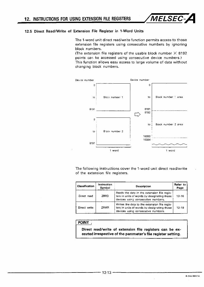
12. INSTRUCTIONS FOR USING EXTENSION FILE REGISTERS /MELSEC-/~ 12.5 Direct ReadMrite of Extension File Register in 1-Word Units
The 1-word unit direct readlwrite function permits access to those extension file registers using consecutive numbers by ignoring block numbers. (The extension file registers of the usable block number X 8192 points can be accessed using consecutive device numbers.) This function allows easy access to large volume of data wi thout changing block numbers.
Device number
o r
to
8191 I t
Device number
0
Block number 1 to - 8191 +, 8192
Block number 2
8191
to
16383 16384
Block number 1 area
Block number 2 area
1 word 1 word
The following instructions cover the 1-word unit direct read/write of the extension file registers.
Classification instruction Description
Refer to Symbol Page
Reads the data in the extension file regis-
devices using consecutive numbers. 1 Direct read 1 ZRRD ~ ters in units of words by designating those 1 12-16 1
Writes the data to the extension f i le regis- Direct write 12-19 ZRWR ters in units of words by designating those i devices using consecutive numbers.
I POINT I I I I
Direct readlwrite of extension file registers can be ex- ecuted irrespective of the parameter’s file register setting.
12-1 3 I8 (NAJ 6&251-p.

12. INSTRUCTIONS FOR USING EXTENSION FILE REGISTERS /MELSEC-A 12.5.1 Device numbers assigned for direct readlwrite operations
- POINT 1
The direct readlwrite function can only access the exten- sion file registers. The file registers (R) set by the parameter cannot be accessed by this function.
( 1 ) For direct readiwrite operations, device numbers are automati- cally assigned f rom those block numbers given a lower block number.
Device number
to Block No. 1 area
Block No. 2 area I to Block No. 3 area
(2) Device numbers cannot be assigned to block numbers that do not exist in the memory cassette. Therefore, the device numbers are assigned by skipping the block numbers that do not exist in the memory cassette.
Device number
to Block No. 1 area
Block No. 2 area
16383 - When blocks No. 3 through 9 do not exist due to insuffi- cient memory capacity
to 1 Block No. 11 area
12-1 4 18 I N 4

12. INSTRUCTIONS FOR USING EXTENSION FILE REGISTERS /MELSEC-A The device number is set in special data registers D9036 and D9037 in 2-word binary.
D9037 D9036
1 designated dev~ce !X number
(upper) (lower)
Any number in the range of 0 through “usable number of blocks X 8192 -1” can be designated as the device number.
An error occurs if a device number is designated which exceeds the device number corresponding to the extension file register. Depending on the memory cassette used, an error does not occur if a device number in certain ranges is designated. Those ranges where an error is not caused are indicated below: . A3NMCA12 *..--..-. Device numbers corresponding t o block
numbers 10 and 11.
numbers 10 through 28.
numbers 13 through 28.
numbers 21 through 28.
A3NMCA18 *..*-*.-- Device numbers corresponding to block
A3NMCA24 * - * . * * - * . Device numbers corresponding to block
A3NMCA40 . * - . * * * . * Device numbers corresponding t o block

12. INSTRUCTIONS FOR USING EXTENSION FILE REGISTERS /MELSEC-A 12.5.2 Direct read of extension file registers in .l-word units .-...--.. ZRRD
+I M9012 M9011 L I
Read command
Data to be set LEDA ..-. Executed while ON LEDB .... Executed at the Device numbers (con-
leading edge secutive numbers) of ex- tension f i le registers
1 I
Functions (1) The contents of the devices of the extension file registers can be read in l-word units by designating the consecutive numbers and ignoring block numbers.
Extension file register
D9037 D9036
0 Block number 1
8192 Block . - . - . . . . . - . . . . . - . .
to I area number 2 I
to number 3
(2) For the device numbers assigned for direct read, refer t o Section 12.5.1.
(3) The device number, where the data to be read is stored, is set as a 2-word binary value in special data registers D9036 and D9037.
(4) The read data is automatically stored in accumulator (AO).
12-16 I8 lNA! €62514

12. INSTRUCTIONS FOR USING EXTENSION FILE REGISTERS /MELSEC-A Execution Conditions Tke ZRRD instruction execution mode depends on whether it is
designated with an LEDA or LEDB instruction. It is executed every scan while the read command stays ON if it is designated with an LEDA instruction. When it is designated with an LEDB instruction, it is executed only once at the leading edge of the read command.
Sequence program flow
ON OFF Read command
I I I I I I I I I I I I I I I
I Z R R D (with LEDA) n I
I
I I , I
I I I I I ZRRD (with LEDB) I
Operation Error An operation error occurs in the following case and an error flag (M9011) is set.
Contents Error Code
D9008 I D9091 I Adevice number exceeding the allowed designation range is designated. I 50 I 503 1
12-17 18 IW E 2 5 1 4


M E M O ....................................................................................................................................................................
....................................................................................................................................................................
....................................................................................................................................................................
....................................................................................................................................................................
....................................................................................................................................................................
....................................................................................................................................................................
.....................................................................................................................................................................
.....................................................................................................................................................................
.....................................................................................................................................................................
.....................................................................................................................................................................
...................................................................................................................................................................
....................................................................................................................................................................
.....................................................................................................................................................................
.....................................................................................................................................................................
....................................................................................................................................................................
....................................................................................................................................................................
....................................................................................................................................................................
IB (W 66251-4

12. INSTRUCTIONS FOR USING EXTENSION FILE REGISTERS /MELSEC=A 12.5.3 Direct write of extension file registers in 1-word units .-.-.-..- ZRWR
Available Devices > r w 0 - - = E + k g E k g % 0 != B i t device W E u % 2 E p &el Pointer Constant Word (%-bit] device
X Y M L S B ( F T C D W R A O A I Z V K H P , I N = = a c .
. = , E m -
3 20 c , , I 0 '3 S 3 5 0 0 C I Z C: 0 E) e! r r 12,s
- M9012 M9011
*l The number of steps varies with devices used. Refer to Section 3.2 for details.
I , Write command
Data to be set LEDA .... Executed while ON LEDB .... Executed at the
leading edge tension file register secutive numbers) of ex-
I 1 ' I Functions (1) Data can be written into the devices of the extension fi le
reciters in 1-word units by designating the consecutive numbers and ignoring block numbers.
D9037 D9036
I @ (Device number) 1
Extension file register
0 to
8191 81 92
t o - r--- L - - A -A0 16383
16384
to
(2) For the device numbers assigned for direct write, refer to Section 12.5.1.
(3) The device number, where the data is to be written, is set in 2- word binary data in special registers D9036 and D9037.
(4) The data to be written should be set in accumulator AO.
12-19 IB via) 6 6 2 5 1 4

12. INSTRUCTIONS FOR USING EXTENSION FILE REGISTERS /MELSEC-A Execution Conditions The ZRWR instruction execution mode depends on whether it is
designated with an LEDA or LEDB instruction. It is executed every scan while the write command stays ON if it is designated with an LEDA instruction. When it is designated with an LEDB instruction, it is executed only once at the leading edge of the write command.
lnnwctton I E N D ex-tlon e x e ~ m o n 1 processing ~nnmmmn Innrunlo" I
eleCYfl0" 1 s:eo 0 ENC Step 0 END S r e ~ 0 END S t e p 0
, I Sequence program flow ?I
Write command
I I I I I I I I I I I I 1 I I I I I
I I I I I I I I I I I
ON OFF I I I I I
I ZRWR (with LEDA) 1 I
I I I I I I I I
I I
Operation Error
I I I 1 I ZRWR (with LEDB) I
An operation error occurs in the following case and an error flag (M9011) is set.
Error Code WOO8 1 D9091
Contents
A device number exceeding the deslgnation allowed range is designated. 50 1 503
12-20 IB (NAI €62514

12. " R C T l O N S FOR USING EXTENSION FILE REGISTERS /MELSEC-A Program Example A program to write the data stored in D l00 to D l09 to extension
file registers R8200 to R8209 (R8 to R17 in block number 2) when X0 is turned ON.
D N O U D288
LEDR ZRUR
I HC
I HC
P7 5b
D98363
3
2 3
D ? B B 3
PP 3
Dl00
Dl01
Dl 02 Dl 03
Dl04
Dl 05 Dl06
Dl 07 Dl 08
Dl 09
Data register
1 23 I -32768 I
Y I 28561
2 1
Designating head device number of extension file registers Writing the data in data register to A0 Designating extension file register device number
Writing
Setting device number which is to be processed following the data register and extension file register
Extension file register (Block number 21
R8200 (R8)
R8201 (R9) -32768
R8202 (R10)
R8203 (R11) I 7869 I R8204 (R12)
c3 R8205 (R13) R8206 (R14) 28561
R8207 (R15)
R8208 (R16)
R8209 (R17)

12. INSTRUCTIONS FOR USING EXTENSION FILE REGISTERS /MELSEC-A 12.6 Direct Read/Write of Extension File Register in Units of Bytes
The one-byte unit direct read/write function can use the extension file registers as data memory area in units of bytes. With this function, the device numbers are segmented in units of bytes and each byte is automatically assigned wit the device numbers. Because the device numbers are assigned in the consecutive numbers, block numbers can be ignored when using this function. (Usable number of blocks X 8192 can be accessed using consecutive device numbers.)
Device number b7 Block number 1
Device number b15 to b8b7 to bO
1 I IH)
to I
I
8191 (H)
Block number 2 Device
number b15 to b8b7 to M,
/ 1 I c
I
to I I
I . . I to :
I I
16382
16383
Block number 1 area
Block number 2 area
The following instructions are used for byte unit direct read/write of extension file registers.
Classificauon Instruction Description Refer to Symbol Page
Reads the extension file register data in
Writes the data to the extension file regis-
Direct read/write of extension file registers can be executed regardless of the file register capacity setting by a parameter.
12-22 IS (NA) - 1 4

12. INSTRUCTIONS FOR USING EXTENSION FILE REGISTERS /MELSEC-A 12.6.1 Device numbers assigned for direct readiwrite operation
The direct readiwrite function can access only the extension file registers and the file registers (R) set by the parameter cannot be accessed by this function.
(1) The device numbers used for direct read/write are automatical- ly assigned in order from the lower bytes of the devices in a lower block number in block numbers 1 to 28.
number Device
2 1
I
to ; 16382
16383
16384
16385 16386 ~ (H)
16387 (H)
to : I
I
32766 ILi 32767 I (H) I
32769 32768 H-i to 1 I
R 1 area
R8191 area
RO area
R 1 area
RO area
R8191 area
i Block number 1 area
Block number 2 area
Block number 3 area
(2) Device numbers are not assigned to the block numbers that do not exist in the memory cassette. Therefore, the device numbers are assigned by skipping the block numbers that do not exist in the memory cassette.
Extension file register
Block number 1
16:: 1 6 3 8 4 Block
32767 to number 2
~ When blocks number 3 to number 9 do not exist due
Block number 10
to insufficient memory capacity
491 51 491 52 Block
to number 1 1
12-23 I6 I W 66251-A

12. INSTRUCTIONS FOR USING EXTENSION FILE REGISTERS /MELSEC-A (3) The device number is set in special data registers D9036 and
D9037 in 2-word binary.
D9037 D9036
I designated device number I
For the device number, a number in the range of 0 to ”usable number of blocks X 8192 X 2 - 1 ” can be designated.
(4) If a device number exceeding the device number correspond- ing to the extension file register is designated, an error occurs. Depending on the memory cassette to be used, an error does not occur if a device number in some range is designated. The range that does not cause an error is indicated below.
. A3NMCA12 ........... Device numbers corresponding to block numbers 10 and 11.
block numbers 10 to 28.
block numbers 13 and 28.
block numbers 21 and 28.
A3NMCA18 ........... Device numbers corresponding to
A3NMCA24 ........... Device numbers corresponding to
A3NMCA40 ........... Device numbers corresponding to
12-24 IB INK 662514

12. INSTRUCTIONS FOR USING EXTENSION flLE REGISTERS ~ELSEC-A 12.6.2 Direct read of extension file register in units of bytes.-..-ZRRDB
*1: The number of steps varies with devices used. Refer to Section 3.2 for details.
, Read command
LEDA .... Executed while ON Daw to LEDE .... Executed at
leading edge secutive numbers) of ex,
Functions (1) The data in the devices of the extension file registers can be read in units of bytes by designating the consecutive numbers ignoring block numbers.
Extension f i le register
0 to
16383
16384
to D9037 D9036 b15 to b8b7 to bO
I@ (Device number)]-,--, r - - - , -A0 r] Read data
For the device numbers assigned for direct read, refer t o Section 12.6.1.
The device number, where the data to be read is stored, is set in 2-word binary data in special registers D9036 and D9037.
The read data is automatically stored in lower byte of accumulator AO.

12. INSTRUCTIONS FOR USING EXTENSION FILE REGISTERS /MELSEC=A Execution
Operation
Conditions Tha ZRRDB instruction execution mode depends on whether it is designated with an LEDA or LEDB instruction. It is executed every scan while the read command stays ON if it is designated with an LEDA instruction. When it is designated with an LEDB instruction, it is executed only once at the leading edge of the read command.
ZRRDB
ZRRDB
Errors
I I I I I I I I
(with LEDA) 1 1 I 1 I I I
I I
I I I I I I 1 I I I I
(with LEDB) 1 I I I
An operation error occurs in the following case and a n error flag (M9011) is set.
~ ~~
Description Error Code
WOOS I D9091 Adevice number exceeding the designation allowed range is designated. 50 I 503
>
12-26 IB LW - 5 1 4

12. INSTRUCTIONS FOR USING EXTENSION FILE REGISTERS /MELSEC-A Program Example A program to read the data in extension file registers R16394 to
R16403 (R5 to R9 in block number 2) to Dl00 to Dl09 when X0 is turned ON.
R16394
R 16395
R16396
R16397
R16398
R16399
R16400
R16401
RIM02
R16403
Storing read data to data register
which is to be processed Setting device number
following the data register and extension file register I t i 1 H C
Extension file register (Block number 2)
I (R6 area)
4 I
}+{ } (R8 areal
I I '
D28Q
p9 1
Designating head device number of extension file registers Designating extension file register device number
Reading
D l 00
Dl01
Dl02
Dl03
c3 Dl05
Dl04
Dl06
Dl07
Dl08
Dl09
Data register
I OOCEH I

M E M O

12. INSTRUCTIONS FOR USING EXTENSION FILE REGISTERS /MELSEC-A 12.6.3 Direct write of extension file register in units of bytes-.---.ZRWRB
+l: The number of steps varies with devices used. Refer to Section 3.2 for details.
Read command
{ DMOV I 0 ID9036 LEDA .... Executed while ON Data to be set
ILEDAILEDB] ZRWRB /- LEDE .... Executed at leading edge Device numbers Icon-
secutive numbers) of ex- tension file register
Functions (1) Data can be written to the devices of the extension f i le registers in units of bytes by designating the consecutive numbers ignoring block numbers.
Extension file register
0
8791
Block
a rea number 2
Block 81 92
area number 1 to
.....--._.___...___.
D9037 W036 I($ (Device number)]- r-- L _ -.I T/////////A to
16383
16384 Block ...-.____......-_.-.
b15 to b8b7 to bO
-A0 r l Read data -
to number 3
(2) For the device numbers assigned for direct write, refer t o Section 12.6.1.
(3) The device number, where the data is to be written, is set in 2-word binary data in special registers D9036 and D9037.
(4) The data to be written should be set in a lower byte of accumulator AO.
12-28 IB INAJ W51A

12. INSTRUCTIONS FOR USING EXTENSION FILE REGISTERS /MELSEC-A Execution Conditions The ZRWRB instruction execution mode depends on whether it is
designated with an LEDA or LEDB instruction. It is executed every scan while the write command stays ON if it is designated with an LEDA instruction. When it is designated with an LEDB instruction, it is executed only once at the leading edge of the write command.
~nsrunmn procosing exRYtmn e x m l l o n
END Insnsnlon IhSfIURlO" ex:eclltion
Step 0 END Step 0 END Step 0
Sequence program flow I I I I I I I I I I
I 1 I I I
I I I I I I I I I I
ON OFF Read command I
I I I I
I ZRWRB (with LEDA) 1 I
I I I I I I I I I I I I I I I I I I
I I I ZRWRB (with LEDB) I
I I
Operation Errors An operation error occurs in the following case and an error flag (M9011) is set.
Error Code Description woo8 1 wo91
Adevlce number exceeding the designation allowed range is designated. ~ 50 1 503
12-29 IB I N A I -14

12. INSTRUCTIONS FOR USING EXTENSION FILE REGISTERS /MELSEC=A Program Example A program to write the lower byte data stored in Dl00 to Dl09 to
extension file registers R1634 to R16406 (R5 to R9 in block number
Dl00
Dl01
Dl 02
Dl 03
Dl04
Dl05
Dl 06
Dl 07
Dl 08
Dl 09
when X0 is turned ON.
Designating head device number of extension file registers Writing the data in data register to A0 Designating extension file register device number
Writing I I-CIHC 2 4 Setting device number which is to be processed
Data register r i \
'(135 area) 0082~
(R6 area) E801 H
Extension file register Block number 2)
R16394
R16395
R16396
R16397
cl> ;;:: R16400
R16401
R16402
R16403
l+l I SOH I
I ~ E H I
12-30 ,B(NA)6625i-F

13. DATA LINK INSTRUCTIONS /MELSEC-A 13. DATA LINK INSTRUCTIONS
Data l ink instructions are classified as the instructions for MELSECNET( II, /B) and those for MELSECNETjl 0. (1) Data link instructions for MEtSECNET(II, /B)
With the data link instructions, because the handshake signal control for executing an instruction is automatically executed by internal processing, the user can write a program ignoring the handshake signal control. The data link instructions area used by a master station for read/write operations with a local and remote 1/0 station in the MELSECNET (E, /B) data link system.
(2) Data link instructions for MELSECNET/IO These instructions are used to read/write data from/to the word device of a designated station in the MELSECNET/lO data link system. Data link instructions make it easy for the program to read data from and write data to a designated station.
The data link instructions are summarized in the table below.
Applicable CPU Classification Instruction Description Refer to Symbol Page
i Local station data read The master station reads the data of the 1 13-2 i LRDP I word devices in a local station.
Local station data write LwTp 13-6 The master station writes the data to the word devices in a local station. The master station read the data of a special
station
. AnACPU AnUCPU Remote I/O station data
QCPU-A (A Mode) read RFRP 13-10 function module loaded in a remote 110
Remote WO station data write 1 ATOP I The master station writes the data to a
special function module loaded in a remote 13-14 110 station
Link refresh of and refresh of network is executed. designated network ,3-20 Sequence program processing is interrupted ZCOM
Reading from word Data is read from a word device in a device in the ZNRD
data link system to the self station. MELSECNET/lO station 13-23 designated station in the MELSECNET/lO
Writing to word device Data is written from the self station to a AnUCPU 13-27 designated station in the MELSECNET110 ZNWJ in theMELSECNET/lO
QCPU-A (A Mode) data link system. station
Data read from special
remote I10 station. remote I/O station 13-30 function module loaded in the MELSECNET/lO ZNFR function module in
The master station reads the data of the special
Data write to special The master station writes data to the special function module in ZNTO function module loaded in the MELSECNET/lO
remote I10 station. remote VO station 13-33
13-1 IEi(NA)66251-F

13. DATA LINK INSTRUCTIONS /MELSEC=A (3) Executing a different data l ink instruction simultaneously for
the same link module Table 13.1 to 13.3 explains whether a different data link instructions can be executed simultaneously for the same link module. For the combinations marked by an "X" in the table below, handshaking is automatically performed even if the execution conditions are turned ON simultaneously, and the instruction executed later is not processed. When multiple data link instructions are executed for the same link module, use the execution-completed flag as the com- munication start command to execute the program sequen- tially. (Refer to the program examples of data link instructions.)
Table 13.1 Availability of the Simultaneous Execution of Data Link Instructions
Data link system MELSECNET/B used MELSECNET, MELSECNET/lO
used instruction t o be executed LRDP ZNWR L W ZNRD LRDP LWTP
MELSECNET, , L W - l
MELSECNETIB LRDP *'
LRDP -' ZNRD L W P -l
ZNWR
X - -
- x '3 9 MELSECNET/lO
- 0 x -3
~ ~ _ _ _ _ _ _ _ _ _ _ _ ~ ~ ~ ~~ ~ ~~
0: can be executed, X: cannot be executed, -: no combination
1) +1: When the LRDP/LWTP instruction is executed for the AnUCPU, the processing varies with the link module used as follows.
LRDPLWP instruction is executed.
No (only for MELSECNET/lO)
t
A master module for the MELSEC-
accessing other station" in the is to be processed. to "valid module number when NET or MELSECNETlB link module A l ink module which has been set
data link parameter '* is to be processed.
2) '2: For details of data link parameters, see the following manual. MELSECNET/10 Network System Reference Manual (PC to PC network)
3) +3: When a data link instruction is used for different link modules, the data link instruction can be executed at the same time.

13. DATA LINK INSTRUCTIONS /MELSEC-A Table 13.2 Whether the RFRP/RTOP Instructions May Be Executed
Simultaneously or Not ( for the MELSECNET, MELSECNET/II)
Instruction Being Other RFRP Instruction Other RTOP Instruction
Executed Same special function module I Another special function module Same special function module 1 Another s&al funcijon module I RFRP 1 X A
'd X 1 I RTOP [:I X n, - X
~ ~~~
0: May be executed, X: Cannot be executed
Table 13.3 Whether the ZNFR/ZNTO Instruct ions May Be Executed Simultaneously or Not (for the MELSECNET/lO)
Instruction Being Other ZNT'O Instruction Other ZNFR Instruction ~~~~ ~ ~ -
Executed Another special function module Same special function module Another special function module Same special function module
ZN FR L1 X 0 X
I ZNTO I X c X I I I I I 0: May be executed, X: Cannot be executed
13-2-1 IB (NA) 66251-C

13. DATA LINK INSTRUCTIONS /MELSEC-A 13.1 Reading Word Devices in Local Station-.....LRDP
'1: The number of steps varies with devices used. Refer to Section 3.2 for details.
I; s a
Data to be set Read command LEDA....-.Executed while ON
LEDB.--.Device number de- l I I sianated 1'1 read.
station where device is Station number of a local
- LEDC......Connant desig-
SUB......Device number de- nated
signated
LEDC-.-.Device number de-
SUB....-.Constant designated 1 LEDC/SUB I @ + signated
I I I LEDR
Head number of word de- vices, where data t o be read is stored, in a local station.
Head number of word de-
to be stored, in a master vices, h e r e read data is
station.
reading.
Functions (1) LRDP operation (a) In the MELSECNET (IT) data link system, the LRDP
instruction reads the @ points (words) of data of the word devices, beginning with the word device designated by @, in the local station designated by @, to the word devices, beginning with the word device designated by @, in the master station. After the completion of reading from a local station, the bit device designated by @ is automatically turned ON for one scan.

.13. DATA LINK INSTRUCTIONS ,/MELSEC-A (b) In the MELSECNETAO data link system, the LRDP instruction
reads the @ points (words) of data of the word devices, beginning with the word device designated by @, in the MELSECNET/lO station designated by @, to the word device designated by @, in the self station. After the completion of reading from the designated MELSECNETilO station, the bit device designated by (@ is automatically turned ON for one scan.
Self station MELSECNET/10 station (@ station)
MELSECNETAO @ + l data l ink system
I @ points
to I to
( I f there are several network units with unspecified network numbers, the LRDP instruction is executed for a network module set by "valid module number when accessing other station" in the data link parameter.)
1 2 3
stations is 2 t t x o x
(The AnACPU cannot use the LRDP instruction.)
(2) The LRDP instruction, provided as a dedicated instruction, executes the same processing as with the LRDP instruction described in the ACPU Programming Manual (Common Instructions).
(3) With the LRDP instruction provided as a dedicated instruction, on/off control of M9200 and M9201 is automatically processed internally.
Program Example Using Dedicated Program Example Using Common LRDP Instruction LRDP Instruction
r ( R e a d cxm-nand) 1
1
- - - - - - - - - - - - - - - - - - - - - - - - - - - - ' I (Read command) I 1 1
I I I I I I I I I I I
I I I I
- I

13. DATA LINK INSTRUCTIONS /MELSEC=A The LRDP instruction can be used only in a master station sequence program.
See page 13-2 (3) for the simultaneous execution of a differnt data link instruction a t two or more locations.
The number of points that can be processed in a single reading processing is 1 to 32 points (words).
The bit device, designated by @, is automatically turned ON at the t ime the END instruction is executed in the scan where the read processing is completed. It is turned OFF when the END instruction in the next scan is executed. This bit device is used as the execution completion flag for the LRDP instruction.
If the LRDP instruction is designated with the LEDA instruction, read processing is executed continuously after the preceding read processing has completed while the read command stays ON. If it is designated with the LEDB instruction, read processing is executed only once at the leading edge of the read command.
Execution Conditions The LRDP instruction execution mode depends on whether it is designated with an LEDA or LEDB instruction. It is executed every scan while the read command stays ON if it is designated with an LEDA instruction. When it is designated with an LEDB instruction, it is executed only once at the leading edge of the read command.
step 0 END Sxep 0 END Step 0 I 1
Sequence program flow r-i I I I I I
ON OFF
I I I I I I I I I I I I I
I I 1 I I I I I I
Read command I I I 1 : I I I
I I I I
LRDP (with LEDA) n I
I I I I I I I I I I 1
I I I I I
I I I
I I
LRDP (with LEDB) I I 1 I
Operation Errors An operation error occurs in the following case and the error flag (M9011) is set.
1 Error Code I Contents I D9008 1 D9091 I
The device range defined by @ points exceeds the final device number of that device.
504
The number of points (words) designated by @ is outslde the range of 1 to 32. I 50 I 503 I
I The station desianated bv 6? is not a local station. .. ._
1 1 5 0 5 1 I I I -
The combination of devices specified in the instruction is not correct. I I 502
13-5 IB(NA)66251-F

13. DATA LINK INSTRUCTIONS /MELSEC-A Program Example A program to read the data in D3 to D8 in local station 1 and the
data in D20 to D23 in local station 3, and to store the read data to Dl00 to Dl05 and Dl10 to Dl13 in a master station when X0 is turned ON. The read processing is executed continuously after X0 is turned ON.
C P t S Hl@
C L E D R L R D P
[SUB 1 K
Designating local station 1 . i L E D C n e Turning ON MO atthe completion of the instruction 1 1) 1 Designating local station 3
L E D C D l 1 8
SUB
1 1-CLEDC H 1 4 Turning of the instruction ON M1 at the completion
1 ‘IEDR 4 Local station 1
D3
D4
D5
D6
D7
D8
D20
D2 1
D22
D23
I 9876 I -1357
-952
Local station 3
12258
I -1611 I I 243 I
1 LRDP I t
I LRDP I c
D l 00
D l 01
D l 02
D l 03
Dl04
Dl05
Dl10
Dl11
D l 12
D l 13
Master station
- 1357
-952
-1611
Because the LRDP instruction cannot be executed at more than one location at the same time, the completion flag (MO, M1) is used as the communication start signal to executed the LRDP instructions alternately or sequentially.
POINT 1 If the LRDP instruction is executed with the CPU which is not the data link CPU or while the link card mode switch is set in the offline position, an operation error does not occur. The LRDP instruction is not processed and only the M9200 (LRDP instruction accepted flag) is set.
13-6 IB iWI € 6 2 5 1 6

13. DATA LINK INSTRUCTIONS /MELSEC-A 13.2 Writing Data to Word Devices in Local Station.--.-.LVVTP
'1: The number of steps varies with devices used. Refer to Section 3.2 for details.
Write command LEDA......Executed while ON
{ LEDA/LEDB I LWTP E LEDB-.-.Executed at leading edge
LEDC.-..-.Device number de-
SUB......Constant designated signated
LEDC
LEDC......Device number de- signated
SUB..-...Constant designated ~ __f LEDC
LEDR
Data to be set
station where data is to be Station number of a local
written to word devices.
vices, where written data Head number of word de-
is t o be stored, in a local station.
Head number of word de-
written is stored, in a vices, where data to be
Number of points of word
Device number of bit de- vice which is to be turned ON at completion of writing.
Functions (1) LWTP operation (a) In the MELSECNET (II) data link system, the LWTP
instruction writes the @ points (words) of data of the word devices, beginning with the word device designated by a, in the master station, to the word devices, beginning with the word device designated by @, in a local station designated by @. fter the completion of writing to a local station, the bit device designated by @ is automatically turned ON for one scan.
13-7 18 l N N 60251-8

13. DATA LINK INSTRUCTIONS /MELSEC-A (b) In the MELSECNET(10) data link system, the LWTP instruc-
tion writes the @ points (words) of data of the word devices, beginning with the word device designated by 0, in the master station, to the word device, beginning with the word device designated by @, in the MELSECNET/10 station designated by @. (The LRDP instruction is executed for a link module set by "valid module number when accessing other station" in the data link paramater.) After the completion of writing from the self station, the bit device designated by @, in the self station, is automati- cally turned ON for one scan.
Self station MELSECNET/10 station (0 station)
@ points @ + 1
MELSECNET/lO data link system
I 1
I to to
(2) The LWTP instruction, provided as a dedicated instruction, executes the same processing as with the L W P instruction described in the ACPU Programming Manual (Common Instructions).
(3) With the LWTP instruction provided as a dedicated instruction, on/off control of M9202 and M9203 is automatically processed internally.
Program Example Using Dedicated Program Example Using Common LWTP Instruction LWTP Instruction r(Write command) I [Write command)
1 I I I
- - - - - - - - - - - - _ - 1 - - - - - - - _ - - - - - - I
I- I
I- I I I I I I I I 1 1 1
(4) The LWTP instruction can be used only in a master station sequence program.

13. DATA LINK INSTRUCTIONS /MELSEC-A (5) See page 13-2 (3) for the simultaneous execution of a differnt
data l ink instructions at two or more locations.
(6) The number of points that can be processed in a single writing processing is 1 to 32 points (words).
(7) The bit device, designated by @, is automatically turned ON at the time the END instruction is executed in the scan where the write processing is completed. It is turned OFF when the END instruction in the next scan is executed. This bit device is used as the execution completion flag for the LWTP instruction.
(8) If the L W P instruction is designated with the LEDA instruc- tion, write processing is executed continuously after the preceding write processing has completed while the write command stays ON. If it is designated with the LEDB instruction, write processing is executed only once at the leading edge of the write command.
Execution Conditions The LWTP instruction execution mode depends on whether it is designated with an LEDA or LEDB instruction. It is executed every scan while the write command stays ON if it is designated with an LEDA instruction. When it is designated with an LEDB instruction, it is executed only once at the leading edge of the write command.
Inswuaban IMNClLaII C I C M l O " execution
END Step 0 END Step 0
Sequence program flow I I I I I
ON I I I I I I I I I I I I I Write command I I i j I I I I I I I I I I I I 1 I I I
I L W r P (with LEDA) 1 I
1 I
I I I
I I I I
I I I I I I I
I 1 I L W f P (with LEDB) I
I 1 I
Operation Errors An operation error occurs in t h e following case and t h e error flag (M9011) is set. I 1 Error Code 1 I Contents
The device range defined by @ points exceeds the final device number of that device. The number of points (words) designated by @ is outside the range of 1 to 32. 50 503
The station designated by @ is not a local station. 505 The combination of devices specified in the instruction is not correct. 502
504
13-9 IB(NA)66251-F

13. DATA LINK INSTRUCTIONS /MELSEC-A Program Example A program to write the data in Dl00 to Dl05 and Dl10 t o Dl 13 in a
master station to D3 to D8 in local station 1 and to D20 to D23 in local station 3 when X0 is turned ON. The write processing is executed continuously after X0 is turned ON.
C P L S n l ~ c
L 4 T P Designating local station 1
Turning ON MO at the completion of the instruction
CLEDP
5 4 Designating local station 3
Turning ON M1 at the completion of the instruction
Master station
Dl01
1 D3
I D4 I
D l 02
D l 03
D l 04
D l 05
-1357 1
m D l 10
Dl11
D l 12
D l 13
H -1611
I 5858 I
D5
D6
D7
D8
D20
D2 1
D22
D23
Local station 1
i 1234
I I -952
Local station 3
E 4 -1611
I 5858 I
Because the LWTP instruction cannot be executed at more than one location at the same time, the completion flag (MO, M1) is used as the communication start signal to execute the LWTP instructions alternately or sequentially.
If the L W P instruction is executed with the CPU which is not the data link CPU or while the link card mode switch is set in the offline position, an operation error does not occur. The LWTP instruction is not processed and only t h e M9202 (LWTP instruction accepted flag) is set.

13. DATA LINK INSTRUCTIONS /IMELSEC-A 13.3 Reading Data from Remote I10 Station Special Function Module--...-RFRP
Read command I L E O A / L ~ +
LEDA....-.Executed while ON LEDB-.-.Executed at leading
edge
LEDC......Device number
SUB.-..Constant desig- designated
nated
1 1 LEDR
Data to be set
I I Head UO number of we- I cia1 function module, where data is to be read, assigned at the master station.
Head number of buffer memory adrress of spe- cial function module where data to be read is stored.
..Device number de-
Constant designated signated
Device number of a mas- ter station bit device whlch IS to be turned ON at completion of reading.
@ . .
Functions (1) In the MELSECNET (II) data link system, the RFRP instruction reads the @ points (words) of data in the buffer memory address area beginning with the address designated by @ in the remote I/O station special function module assigned to @ to the master station word devices designated by @. After the completion of reading from a remote I/O station, the bit device designated by @ is automatically turned ON for one scan.
Master station
I Word device
MELSECNET( EI I data link system
to I
+
Remote VO station
Special function module buffer memory of UO number @
Address
- "B @ + l points
to
+
13-1 1 !B IW € 6 2 5 1 4
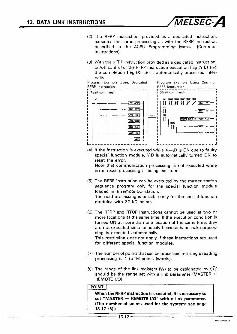
13. DATA LINK INSTRUCTIONS /MELSEC-A (2) The RFRP instruction, provided as a dedicated instruction,
executes the same processing as with the RFRP instruction described in the ACPU Programming Manual (Common Instructions).
(3) With the RFRP instruction provided as a dedicated instruction, on/off control of the RFRP instruction execution flag (YnE) and the completion flag (X,n+llE) is automatically processed inter- nally.
Program Example Using Dedicated Program Example Using Common RFRP Instruction RFRP Instruction
I I I I I I I
I- I- I I
I
I I I I I I
I I I I I I I I I I I I I I I I
If the instruction is executed while XIn+,,D is ON due to faulty special function module, Y.D is automatically turned ON to reset the error. Note that communication processing is not executed while error reset processing is being executed.
The RFRP instruction can be executed by the master station sequence program only for the special function module loaded in a remote I/O station. The read processing is possible only for the special function modules with 32 I/O points.
The RFRP and RTOP instructions cannot be used at two or more locations at the same time. If the execution condition is turned ON at more than one location at the same time, they are not executed simultaneously because handshake proces- sing is executed automatically. This restriction does not apply if these instructions are used for different special function modules.
The number of points that can be processed in a single reading processing is 1 t o 16 points (words).
The range of the link registers (W) to be designated by @ should be the range set with a link parameter (MASTER - REMOTE 1/01.
POINT I When the RFRP instruction is executed, it is necessary to set ”MASTER - REMOTE I/O” with a link parameter. (The number of points used for the system: see page 13-17 (8).)
13-1 2 I6 INA) 66251-8

13. DATA LINK INSTRUCTIONS ~/MELSEC-A (9) The bit device, designated by @, is automatically turned ON
at the time the E N D instruction is executed in the scan where the read processing is completed. It is turned OFF when the E N D instruction in the next scan is executed. This bit device is used as the execution completion flag for the RFRP instruction.
(IO) If the RFRP instruction is designated with the LEDA instruction, read processing is executed continuously after the preceding read processing has completed while t h e read command stays ON. If it is designated with the LEDB instruction, read processing is executed only once at the leading edge of the read command.
Execution Conditions The RFRP instruction execution mode depends on whether it is designated with an LEDA or LEDB instruction. It is executed every scan while the read command stays ON if it is designated with an LEDA instruction. When it is designated with an LEDB instruction, it is executed only once at the leading edge of the read command.
Operation Errors An operation error occurs in the following case and the error flag (M9011) is set. I 1 Error Code I
Contents D9008 D9091
The I/O number designated by @ is not the remote I/o station device. 505 (1 50
The 110 number designated by @ is not the head I/o number Of a special function module, or the designated special function module is not a 32 I/O point special function module. The range, designated by 0. of the link registers (W) exceeds the parameter set link register range. The number of points designated by @ is outside the range Of 1 to 16
504
503 points (words). The combination of devices specified in the instruction is not Correct. 502
13-1 3 IB(NA)66251-F

13. DATA LINK INSTRUCTIONS /MELSEC-A Program Example A program to read the data from address 10, 11, 14, and 15 of a
special function module loaded in I/O numbers 180 to 19F, assigned to a remote I/O station when X0 is turned ON.
The read processing is executed continuously after X0 is turned ON.
function module 110 number assigned to special
Head address number of addres- ses storing the data to be read Link register (W) set by link para- meter "M - R "
Number of read points E S U S 9 7
Turning MO ON at completion of instruction
VO number assigned to special function module Head address number of addres- ses storing the data to be read 1 -IEDi U894 4 Link meter register "M - (W) R " set by link para-
" 1 I-LSUB 2 4 Number of read points
Turning M1 ON at completion of instruction
Special function module in remote
I/O station
11
12
Master station
I w91 W92 w :: P I , 15 I w95 I 15
Because the RFRP and RTOP instructions cannot be executed at more than one location at the same time, the completion flag (MO, M1) is used as the communication start signal to executed these instructions alternately or sequentially.

13. DATA LINK lNSTRUCTlONS /MELSEC-A
Data t o be set
1 Head VO number of sDe- Write command EDA-----Executed while ON
LEDB..-...Executed at leading @
7- LEDC t-
cia1 function module, where data is t o be writ- ten, assigned at the mas- ter station.
Head number of buffer memory address of spe- cial function module where written data is to be stored.
Head number of master LEDC...-.Device number d e station link registers (W)
SUB-.-Constant designated I @ 1 ten is stored. --+- signated where the data t o be writ-
1 1 LEDA Number of points of data to be written.
Device number of a rnas- ter station bit device which is to be turned ON at completion of writing.
Functions (1 1 In the MELSECNET (II) data link system, the RTOP instruction writes the @ points (words) of data in the master station word devices beginning with the word device designated by 0 to buffer memory address area beginning with the address designated by @ in the remote I/O station special function module assigned to 1/0 number designated by @. After the completion of reading writing to a remote I10 station, the bit device designated by @ is automatically turned ON for one scan.
Master station Remote VO station
Special function module buffer memory of I/O number @
@+ 1 E of data MELSECNET data link system (II ) @+ 1
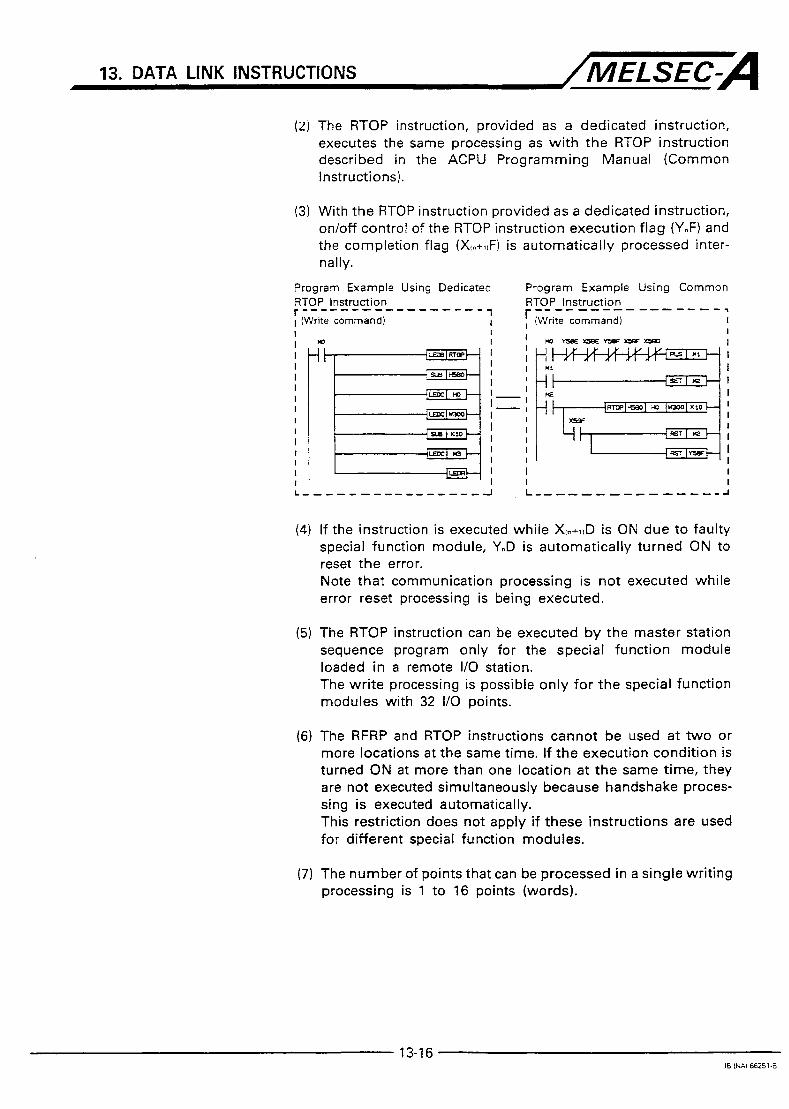
13. DATA LINK INSTRUCTIONS /MELSEC-A ( z j The RTOP instruction, provided as a dedicated instruction,
executes the same processing as with the RTOP instruction described in the ACPU Programming Manual (Common Instructions).
(3) With the RTOP instruction provided as a dedicated instruction, on/off control of the RTOP instruction execution flag (YnF) and the completion flag (X{,+,,F) is automatically processed inter- nally.
Program Example Using Dedicated Program Example Using Common RTOP Instruction I (Write command)
7 r --------------- --I
I , (Write command) I
- - - - - - - - - - - - - - - - - RTOP Instruction
I
I - I I I I I I I I I I
I I I
I I I I I I I I
I
If the instruction is executed whiie X,,+,,D is ON due to faulty special function module, Y,D is automatically turned ON to reset the error. Note that communication processing is not executed while error reset processing is being executed.
The RTOP instruction can be executed by the master station sequence program only for the special function module loaded in a remote I/O station. The write processing is possible only for the special function modules with 32 I/O points.
The RFRP and RTOP instructions cannot be used at two or more locations a t the same time. If the execution condition is turned ON at more than one location at the same time, they are not executed simultaneously because handshake proces- sing is executed automatically. This restriction does not apply if these instructions are used for different special function modules.
The number of points that can be processed in a single writing processing is 1 to 16 points (words).

13. DATA LINK INSTRUCTIONS /MELSEC-A (8) The range of the link registers (W) to be designated by @
should be the range set with a link parameter (MASTER - REMOTE 1/01. Note that the link parameter area, corresponding to the number of special function modules loaded in the remote I/O station and beginning with the head device number of the parameter set range, is used by the system and thus the user cannot use this range. See the illustration below.
The number of points corresponding to the number of spectal function modules loaded in the remote I/O
Range set by I statlon is used by the system link parameter 1 W118 I 1 1 Written data can be stored within this (user area) , range
(9) The bit device, designated by 0, is automatically turned ON at the t ime the END instruction is executed in the scan where the read processing is completed. It is turned OFF when the END instruction in the next scan is executed. This bit device is used as the execution completion flag for the RTOP instruction.
(10) If the RTOP instruction is designated with the LEDA instruction, read processing is executed continuously after the preceding read processing has completed while the read command stays ON. If it is designated with the LEDB instruction, read processing is executed only once at the leading edge of the read command.
13-17 IB CW 66251-A

13. DATA LINK INSTRUCTIONS /MELSEC-A Execution Conditions The RTOP instruction execution mode depends on whether it is
designated with an LEDA or LEDB instruction. It is executed every scan while the write command stays ON if it is designated with an LEDA instruction. When it is designated with an LEDB instruction, it is executed only once at the leading edge of the write command.
Step 0 END Step 0 END Step 0 END Step 0 I 1
Sequence program flow r l I I I I I
Operation Errors
Read command
RTOP (with LEDA)
RTOP (with LEOS)
ON OFF
I I I I I I I I I I I I I
I I I I I I I I I I I I I I
I I I I j 1 I I
n I I
I I I I I I I I
I
h I I h I I I I
An operation error occurs in the following case and the error flag (M9011) is set.
Contents I Error Code
I D9008 1 D9091
The VO number designated by @) is not the remote I/O station device. The 1/0 number designated by @ is not the head VO number of a
I special function module, or the designated special function module is I not a 32 I/O point special function module. The range, designated by @, of the link registers (W) exceeds the SO
1 Darameter set link reclister ranae. I
l The number of points designated by is outside the range of 1 to 16 ooints iwords).
~~ ~ ~~ ~ ~~~
The combination of devices specified in the instruction is not correct. ~ ~~ ~~~
13-1 8 IB(NA)66251-F

13. DATA LINK INSTRUCTIONS /MELSEC-A Program Example A program to write the data to address 0, 1, 5, and 6 of a special
function module loaded in 110 numbers 1AO to lBF, assigned to a remote I/O station when X0 is turned ON. The data to be written is set by the master station at W70, W71, W75, and W76. The write processing is executed continuously after X0 is turned ON.
CPLS R ! 6
ELEDR R l O P I/O number assigned to special function module
H Head address numberof addres- ses where data is to be written Link register (W) set by link para- meter "M - R" S U B
1 1-CIEDC U B ? B 4 Number of write points t CSUP 2 Turning MOON at completion of instruction
C L E D C me
I/O number assigned to special function module Head address number of addres- ses where data is to be written Link register N v ) set by link para- meter "M - R " Number of write points
Turning M1 ON at completion of instruction
LEDC H 1
Special function module in remote
Master station 110 station
w7l
w 7 2
w73
w74
w 7 5 28 28
W76 56 6 56 c
Because the RFRP and RTOP instructions cannot be executed at more than one location at the same time, the completion flag (MO, M1) is used as the communication start signal to executed these instructions alternately or sequentially.

13, DATA LINK INSTRUCTIONS /MELSEC-A 13.5 Link Refresh of Designated Network ZCOM (usable with AnUCPU/QCPU-A (A Mode))
Available Devices % .P L
c *
" 3 - w - Crn x OI
Bit device
M9011 M9012 X Y M L S B F T C D W R A O A ~ Z ~ V K H P I N ~ Z
u = uc a m d 5 Level Pointer Constant Word (16-bit) device * . % v)
10 C 0 1 3 17 0 C C / C : 0 3 0 3 0
Data to be set
I Link refresh command
1 n I Head VO number
I
/ -ILED-T~ I LEDA.--Executed while ON LEDB......Executed at leading
edge LEDC......Device number de-
signated SUB--.Constant designated
Functions (1) The ZCOM instruction is used to fetch data correctly when the sequence program scan time for the normal station is longer than that of the control station master.
(2) When the ZCOM instruction is executed, AnUCPU/QCPU-A (A Mode) interrupts the processing of the sequence program and executes the link refresh processing for the network designated by @ using an I/O number.
ZCOM instruction is executed. ZCOM instruction is executed.
Network refresh Network refresh
(3) The ZCOM instruction can be used any time in the sequence program. However, the sequence program scan time delays the network refresh time.
13-20 IB(NA)66251-F

....................................................................................................................................................................
....................................................................................................................................................................
....................................................................................................................................................................
....................................................................................................................................................................
....................................................................................................................................................................
....................................................................................................................................................................
.....................................................................................................................................................................
.....................................................................................................................................................................
.....................................................................................................................................................................
....................................................................................................................................................................
....................................................................................................................................................................
....................................................................................................................................................................
.....................................................................................................................................................................
.....................................................................................................................................................................
....................................................................................................................................................................
....................................................................................................................................................................
....................................................................................................................................................................
....................................................................................................................................................................
....................................................................................................................................................................
. -
IS IN41 66251

13. DATA LINK INSTRUCTIONS /MELSEC-A Execution Conditions
Program for the control station
Data send/receive
Program for the normal station
Program for the control station
Data send'receive
Program for the normal station
Sequence program link scan
(1) Data sendheceive when the ZCOM instruction is used 1) Example of data send/receive when the ZCOM instruction is
not used
2) Example of data send/receive when the ZCOM instruction is used
3) When the sequence program scan time for the normal station is longer than that of the control station, the occurrence of timing that cannot fetch data described in (1) can be prevented by using the ZCOM instruction fo.r the normal station.
4) When the ZCOM instruction is used for the normal station, link refresh is executed once by receiving the command from the control station between the following instructions. (a) 0 step to ZCOM instruction (b) ZCOM instruction to ZCOM instruction (c ) ZCOM instruction t o END instruction
Link refresh
(2) When the link scan is longer than the sequence program scan time for the master station, the speed for data sendheceive does not change even if the ZCOM instruction is used for the control station.

13. DATA LINK INSTRUCTIONS /MELSEC-A 13.6 Reading Data from Word Devices in the MELSECNET/lO Station
.. ....ZNRD (usable with AnUCPU/QCPU-A (A Mode))
I M9012
I- O
M9011
0
Data t o be set Read command
LEDB......Executed at leading edge LEDA......Executed while ON
LEDC......Device number desig-
SUB ....- Constant designated nated
SUB
LEDC -7-0-
i LEDC I @ + LEDC....-Device number desig-
SUB Constant designated - - SUB --T-GFt--
LEDC l @ t -
nated
-1 LEDR E
Station number of a MELSECNET!lO station where data IS read.
Head number of word de- vices, where data t o be I read is stored, in MELSECNET/lO station. a I vices, where read data is to be stored, in the self station.
t Number of points (words) @ of data to be read.
Device number of bit de- vice which is to be turned
readina. @ ON at completion
Functions (1) In the MELSECNET/10 data link system, the ZNRD instruction reads the @ points (words) of data of the word devices, beginning with the word device designated by 0, in the MELSECNET/10 station designated by @ and @, to the word device designated by @I, in the self station. After the completion of reading from the designated MELSEC- NET/10 station, the bit device designated by @ is automati- cally turned ON for one scan.
Self station MELSECNET/10 station (@ station) in the. designated network No. (@ Station)
MELSECNET/lO @ + l data link system
I 4
I to I I to
*
13-22 IB(NA)66251-F
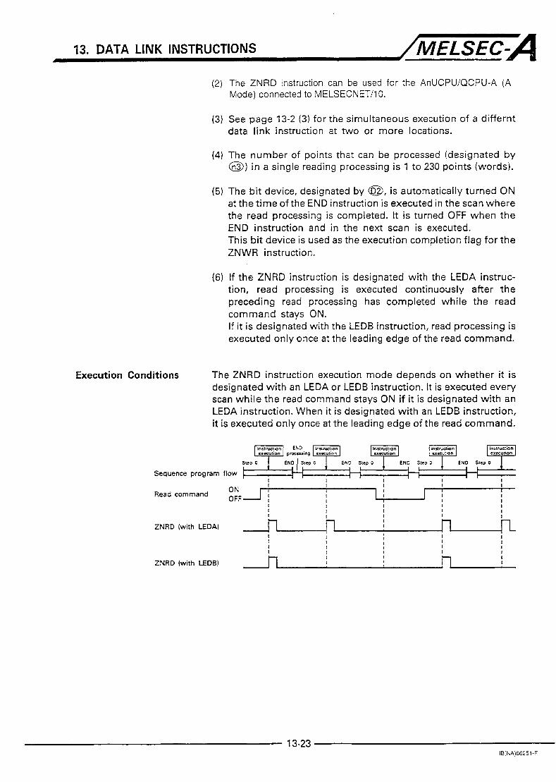
13. DATA LINK INSTRUCTIONS /MELSEC-A (2) The ZNRD instruction can be used for the AnUCPU/QCPU-A (A
Mode) connected to MELSECNET/lO.
(3) See page 13-2 (3) for the simultaneous execution of a differnt data link instruction a t two or more locations.
(4) The number of points that can be processed (designated by @) in a single reading processing is 1 to 230 points (words).
(5) The bit device, designated by 0, is automatically turned ON at the time of the END instruction is executed in the scan where the read processing is completed. It is turned OFF when the END instruction and in the next scan is executed. This bit device is used as the execution completion flag for the ZNWR instruction.
(6) If the ZNRD instruction is designated with the LEDA instruc- tion, read processing is executed continuously after the preceding read processing has completed while the read command stays ON. If it is designated with the LEDB instruction, read processing is executed only once at the leading edge of the read command.
Execution Conditions The ZNRD instruction execution mode depends on whether it is designated with an LEDA or LEDB instruction. It is executed every scan while the read command stays ON if it is designated with an LEDA instruction. When it is designated with an LEDB instruction, it is executed only once at the leading edge of the read command.
I I 1 I I
ZNRD (with LEDA) n I 1 I I
I I I ZNRD (with LEDB) I I I
13-23 IB[NA)66251-F

13. DATA LINK INSTRUCTIONS /MELSEC=,~
Operation Errors An operation error occurs in the following case and the error flag (M9011) is set
Program Example
Contents l t z G a G G - 1 Error Code
The device range designated by @ points beginning with the device number designated by @ and @ exceeds the final device number of that device.
504
Network number designated by @ does not exist or is 0. Station number designated by @ does not exist. The number of points (words) designated by @ is outside the range
The combination of devices specifled in the instruction is not correct. 502
50 503
of 1 to 230.
A program to read the data in D3 to D8 in network No.2 MELSECNEnlO station 1 and the data in D20 to D23 in network 2 MELSECNET/lO station 3, and to store the read data to D l 00 to Dl 05 and D l 10 to Dl 13 in the self station when X0 is turned ON. Read processing is executed continuously after X0 is turned ON.
0 7 ?? 0 rps nio 3
4 m I-
n} K , I cm 2 3 Designating network No. 2
K - Designating station 1 t m 1 3
- c m m 3
- &ax 0100 3
K - Turning ON MO a t the LEDc ccl -
c s s I 3
completion of the instruction iLEm 3
35s &am u+Ic 3
K - Designating station 3 LSS J > - Designating network No. 2 CsLB 2 >
K
- m > -
c a s 4 3 - CMC Dl10 >
ELEDC n1 3 - K
Turning ON M1 at the completion of the instruction
13-24 IB(NA)66251-F

13. DATA LINK INSTRUCTIONS / M E L S E C - -
MELSECNET/lO station 1 Self station
D3
D4
D5
D6
07
Da
D20
D2 1
D22
D23
9876
- 1357
2468
-952
MELSECNET/lO station 3
12258
Dl01
c. Dl03 -1357
Dl04
Dl05 -952
12258 I -1611 1 I [ ZNRD 1 1 Dl11 I -1611
h
I I I
Because the ZNWR instruction cannot be executed at more than one location at the same time for the same link module, the completion flag (MO, M1) is used as the communication start signal to execute the ZNWR instructions alternately.
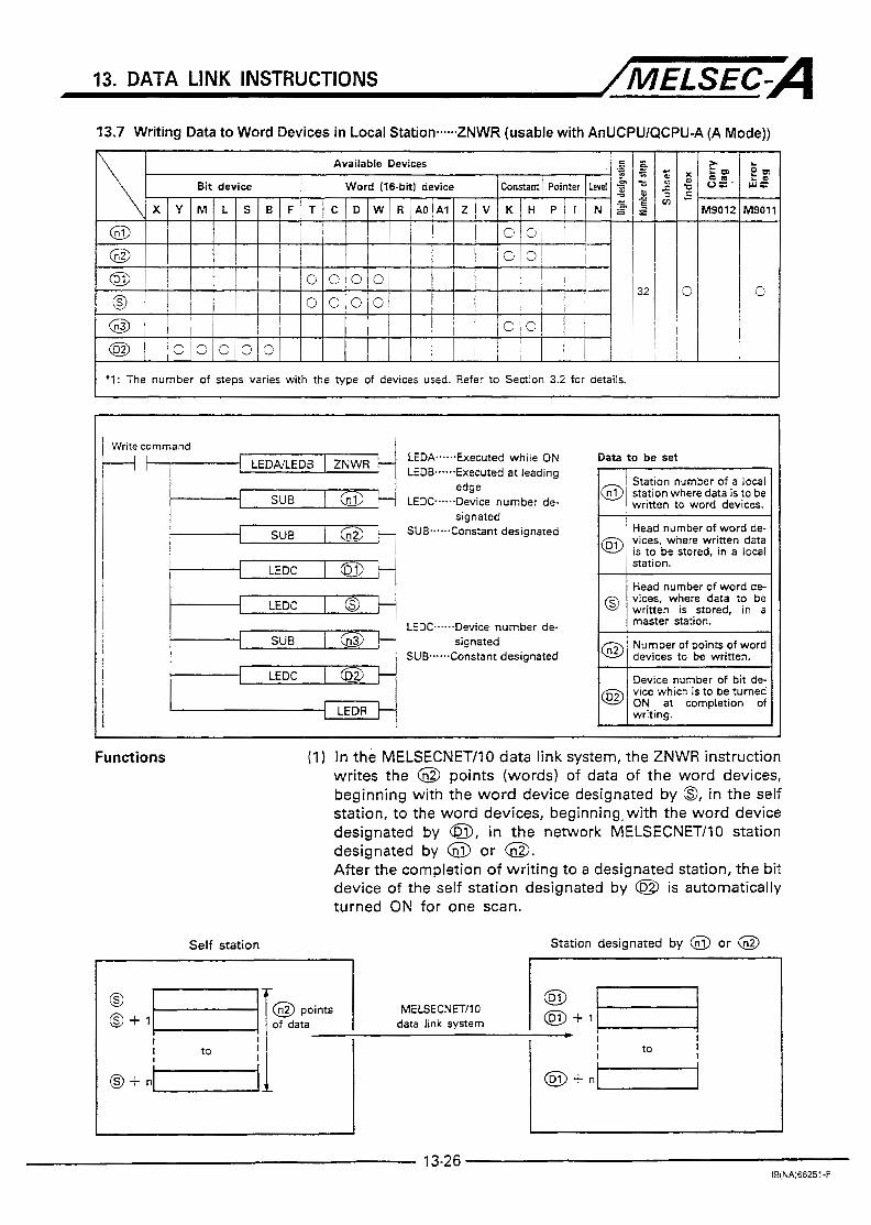
13. DATA LINK INSTRUCTIONS /MELSEC=A 13.7 Writing Data to Word Devices in Local Station-.ZNWR (usable with AnUCPU/QCPU-A (A Mode))
1 ‘1: The number of steps varies with the type of devices used. Refer to Section 3.2 for details.
I M9012 I M9011
Write command
LEDB.--Executed at leading LEDA--Executed while ON
edge
signated SUB l - - G n - -
SUB--Constant designated
LEDC--.Device number de-
I SUB rn i LEDC
LEDC I 0 ~d LEDC..--.Device number de-
SUB--Constant designated S U B I 6 3 -i- signated
LEDC l o t - I I I -[ LEDR
Data to be set
Station number of a local station where data is to be written t o word devices.
Head number of word de- vices, where written data is t o be stored, in a local station.
Head number of word de- vices, where data to be written is stored, In a master station.
Number of points of word devices to be written.
Device number of bit de- vice which is to be turned
writing.
Functions (1) In the MELSECNET/10 data link system, the ZNWR instruction writes the @ points (words) of data of the word devices, beginning with the word device designated by 0, in the self station, to the word devices, beginning,with the word device designated by @, in the network MELSECNET/lO station designated by @ or @. After the completion of writing to a designated station, the bit device of the self station designated by @ is automatically turned ON for one scan.
Self station Station designated by @ or @
MELSECNET/lO data link system @ + l
I to I
13-26 19(NA)66251-F
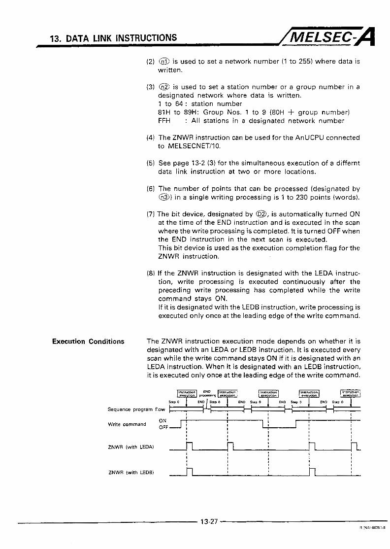
13. DATA LINK INSTRUCTIONS /MELSEC-A (2) @ is used to set a network number (1 t o 255) where data is
written.
(3) @ is used to set a station number or a group number in a designated network where data is written. 1 to 64 : station number 81H to 89H: Group Nos. 1 to 9 (80H + group number) FFH : All stations in a designated network number
(4) The ZNWR instruction can be used for the AnUCPU connected to MELSECNET/10.
(5) See page 13-2 (3) for the simultaneous execution of a differnt data link instruction at two or more locations.
(6) The number of points that can be processed (designated by @I) in a single writing processing is 1 to 230 points (words).
(7) The bit device, designated by @, is automatically turned ON at the time of the END instruction and is executed in the scan where the write processing is completed. It is turned OFF when the END instruction in the next scan is executed. This bit device is used as the execution completion flag for the ZNWR instruction.
(8) If the ZNWR instruction is designated with the LEDA instruc- tion, write processing is executed continuously after the preceding write processing has completed while the write command stays ON. If it is designated with the LED& instruction, write processing is executed only once at the leading edge of the write command.
Execution Conditions The ZNWR instruction execution mode depends on whether it is designated with an LEDA or LEDB instruction. It is executed every scan while the write command stays ON if it is designated with an LEDA instruction. When it is designated with an LEDB instruction, it i s executed only once at the leading edge of the write command.
ON I I t I I I I I I I I
I I I I I I I I I I I I I
Write command
I
ZNWR (with LEDA) 1 I
I I
I I I I
I I I I I I I I I I I I I I I
ZNWR (with LEDB) 1 I I I
13-27 IB INN 662518

13. DATA LINK INSTRUCTIONS /MELSEC=A Operation Errors An operation error occurs in the following cases and the error flag (M9011)
is set
Program Example
Contents
The device range designated by @ points beginning with the device number designated by @and @ exceeds the final device number of that device. - Network number designated by @ does not exlst or is 0.
Station number designated by @ does not exist. The number of points (words) designated by @ is outside the range of 1 to 230.
The combination of devices speclfied in the instruction is not correct.
Error Code
iiGd-Ez
k I 503 I I 502
A program to write the data in Dl00 to D l 05 and D l 10 to D l 13 in the self station to D3 to D8 in network No.2 MELSECNET/IO station 1 and to D20 to D23 in network No.2 MELSECNETA 0 station 3. The write processing is executed continuously after X0 is turned ON.
K 2 3 Designating network No. 2
Cm I 3 Designating local station 1 K
nmc m >
C M C Dl00 >
C S E 6 3
C M c m > Turning ON MO at the completion of the instruction
- 3
t---------(- 5 4 Designating network No. 2
K - C- 3 - Designating local station 3
C L B X m 3
C l E O c D l10 3
K c a e 4 3
cLaK: ni Turning ON M1 a t the completion of the instruction
L E m I-
I "-&"
IB(NA)66251-F

13. DATA LINK INSTRUCTIONS /MELSEC-A Self station
Dl02
D l 03 - 1357
Dl04 2468 1
Dl05 -952
12258
Dl12
D l 13 5858
' Z N W R I
D3
D4
D5
D6
D7
D8
Network No.2 MELSECNET/lO station 1
i 1234 1 I 5678 I
--"""-I - 1357
I 2468 I I -952 I
Network No.1
MELSECNET/10 station 3
-1611
D22
D23
Because the ZNWR instruction cannot be executed at more than one location at the same time for the same link module, the completion flag (MO, M1) is used a s the communication start signal to execute the ZNWR instructions alternately.
13-29 I6 IN4 €625;-B

13. DATA LINK INSTRUCTIONS /MELSEC=A 13.8 Data Read from Special Function Module in MELSECNET/lO Remote I/O Station
...... ZNFR (Available for AnUCPU/QCPU-A (A Mode))
I M9012 I M9011
0 0
Read command I LEDA.. .--Executed whlle ON LEDB.. -Executed at leading edge LEDC ..... Device number deslgnated SUB.. . . . . .Constant designated
Data to be set
@ Network number
Specify from which statlon number and from which
will be read
~
statlon link registers whlch Head number of master special function module @ Buffer memory address of
~ .- -
@ special function module data
~
0 will store the data read (W only)
@ words) of data which w ~ l l be Number of points (number of
read
LEDR Bit devlce number in master
on on completion of execution
Functions (1) Reads the points (words) of data at the buffer memory addresses beginning with the one specified at @ on the special function module specified at ( 3 1 in the remote 110 station specified at (@ in the MELSECNET/lO data link system, and stores that data into the master station link register beginning with the one specified at @. On completion of read processing from the remote I/O station, the bit device specified at @ switches on automatically only one scan.
Master statlon Remote 1/0 station
Buffer memory of special functlon module having 110 number @
Link register
MELSECNETIIO data link system
j to j
@+"
(2) The ZNFR instruction may only be used in the sequence program of the MELSECNET/lO remote master station.
(3) At @ set the network number (1 to 256) from which data will be read.
13-30 IB(NAi6625'-F

13. DATA LINK INSTRUCTIONS /MELSEC=A At @, set the station number in the specified network where data is read and also the location number of the read-out special function module among the special function modules in the corresponding station. Atmset the location number of the specified function module in the corresponding station to the lower 8 bits (bo to b7) and the station number to the upper 8 bits (b8 to b15) in hexadecimal. b l 5 to b8 b7 to bo
Station number 1 Location number
1 to64
The ZNFR and ZNTO Instructions cannot be executed for the same special function module in two or more places at the same time. If their execution conditions switch on simultaneously in two or more locations, the ZNFRENTO instruction executed later will not be processed because of automatic handshaking being performed. The above restriction does not apply to a case where the instructions are executed for different special function modules.
The number of data points that may be processed in one reading (specified at @) is 1 to 256 (words).
The bit device specified at @switches on automatically at the execution of the END instruction of the scan where read processing is completed, and switches off at the END instruction of the next scan. It is used as a ZNFR instruction execution completion flag.
When the ZNFR instruction is executed by the LEDA instruction, read processing is repeated while the read command is on. When the ZNFR instruction is executed by the LEDB instruction, processing is performed only on the leading edge (OFF + ON) of the read command.
Execution Conditions As shown below, when the LEDA instruction is used, the ZNFR instruction is executed every scan while the read command is ON. When the LEDB instruction is used, the ZNFR instruction is executed only one scan on the leading edge (OFF 4 ON) of the read command.
Sequence program flow I I I I I I I I I I
ON I Read command I I
OFF I I I I I I I
I I I I I I I I I I
I ZNFR (with LEDA) I
I I I I I I I I I I
I I I I I I ZNFR (with LEDB)

13. DATA LINK INSTRUCTIONS /MELSEC-A Operation Errors Any of the following conditions will result in an operation error and the error
flag (M9011) switch on:
Program Example
Error Code
D9008 D9091 Description
The 110 number specifled at 69 is not that of a remote 110 station. The I/O number speclfied at @ is not the head I/O number of a speclal
505
function module or a 32-point occupying special function module. 506
The link registers beginning wlth the one specifled at 'a or the number of points specified at @ exceeds the range set in the "master station 50 504 t remote 110 station" llnk parameter. The number of points specified at @ is outside the range 1 to 256
503 (words). The combination of devices specified In the instruction is not Correct. 502
The following program switches on X0 to read data at Dl00 to Dl05 of the host station from addresses beginning with 0 at the buffer memory on the special function module loaded in the second position of the MELSECNETilO remote I/O station No. 1 in the network No. 2.
> Deslgnates network No. 2. Deslgnates remote 110 station No. 1 and second module. Deslgnates buffer memory aodress 0.
> Deslgnates read data storage device.
> Deslgnates number of polnts read. Swltches on MG on completlon of lnstructlon execution.
Statlon No. 1 connected to MELSECNETilO
"1 1 I Host statlon
w201
w202
-1 357
W2G4
W205 -952
Since the ZNFR instruction cannot be executed for^ the same special fynction module in-two or more places at the same time, respective .~. execuJion completion flags (MO, M1) are used as communication star? commands and executed alternately.
13-32 IB(NA)6625i-F

13. DATA LINK INSTRUCTIONS /MELSEC=A 13.9 Data Write to Special Function Module in MELSECNETIlO Remote Station
ZNTO (Available for AnUCPU/QCPU-A (A Mode))
Available Devices C n 0 -
Z B S X
.= 5 ' " - Bit Device Word Device Constant Pointer Level '5
. u u P ? c 3 d
0 7 8
X Y M L S B F T C D W R A O A l Z V K H P I N $ ,
32 0
~ ~ I I I I I I I I I I I I I I I I l O l O l [ ~ ( ~ 1 ( I I I I J / I I I I I I I I I / I I I 0 0 0 0 0
M9012 1 M9011 r Read command
LEDA... ,.-Executed while ON Data to be set LEDB... -.Executed at leadina edae 1 I LEDC ... Devlce number designated
- - SUB, .... . Constant designated
SUB
LEDC
-I SUB
LEDR
Gi) Network number _. . . .. . ~~ _i
Speclfy from whlch statlon ~
@ will be read
number and from whlch speclal function module data
/@ Buffer memory address of speclal function module Head number of master
,/- will store the data read \B' station link registers which
iW only)
Number of points (number of @I words) of data which will be
on on completion of execution
Bit device number in master station whlch w ~ l l be switched @
read
Functions (1) Writes the points (words) of data from the master station lrnk register beginning with the one specified at @I to the buffer memory addresses beginning with the one specified at @ on the special function module specified at <j@ in the remote 110 station specified at @ in the MELSECNET/IO data link system. On completion of write processing to the remote I/O station. the bit device specified at @$ switches on automatically only one scan , Master station ! Remote li0 statlon
Buffer memow of meclal function module havlng 110 number
Address e3 @+1
MELSECNETIlO data llnk system - of points U
Llnk register
13-33 IB(NA)66251-C

MEMO

13. DATA LINK INSTRUCTIONS /MELSEGA The ZNTO instruction may only be used in the sequence program of the MELSECNETIlO remote master station.
At@, set the network number (1 to 256) to which data will be written.
At @, set the station number in the specified network where data is written and also the location number of the writing-in special function module among the special function modules in the corresponding station. At @, set the location number of the specified function module in the corresponding station to the lower 8 bits (bo to b7) and the station number to the upper 8 bits (b8 to bl5) in hexadecimal. b l 5 to b8 b7 to bO
Station number I Location number
1 t o 6 4
The ZNFR and ZNTO instructions cannot be executed for the same special function module in two or more places at the same time. I f their execution conditions switch on simultaneously in two or more locations, the ZNFWZNTO instruction executed later will not be processed because of automatic handshaking being performed. The above restriction does not apply to a case where the instructions are executed for different special function modules.
The number of data points that may be processed in one writing (specified at @) is 1 to 256 (words).
The bit device specified at @switches on automatically at the execution of the END instruction of the scan where write processing is completed, and switches off at the END instruction of the next scan. It is used as a ZNTO instruction execution completion flag.
When the ZNTO instruction is executed by the LEDA instruction, write processing is repeated while the write command is on. When the ZNTO instruction is executed by the LEDB instruction, processing is performed only once on the leading edge (OFF + ON) of the write command.
Execution Conditions As shown below, when the LEDA instruction is used the ZNTO instruction is executed every scan while the write command is ON. When the LEDB instruction is used, the ZNTO instruction is executed only one scan on the leading edge (OFF + ON) of the write command.
Sequence program flow I I I I I I I I I I
Write command I I I I I ! I l i I I
I I I I I
ZNTO (with LEDA) I 1 I I 1 I I I I I I I
I I I I I I ZKTO (with LEDB)
13-34 IB(NA)66251-€

13. DATA LINK INSTRUCTIONS /MELSEC-A,
Operation Errors Any of the following conditions will result in an operation error and the error flag (M9011) switch on:
Error Code D9008 I 09091
Description
Program Example
The 110 number specified at 0 is not that of a remote I/O station. The 110 number specifled at @ is not the head 110 number of a special function module or a 32-point occupying special function module. The link registers beginning with the one specified at 0 or the number of points specified at @ exceeds the range set in the "master station -> remote 1/0 station" link parameter.
The number of points specified at @ is outside the range 1 to 256 (words).
The combination of devices specified in the instruction is not correct. 1
50 fj The following program switches on X0 to write data at D l 00 to D l 05 of the host station to addresses beginning with 0 at the buffer memory on the special function module loaded in the second position of the MELSECNETilO remote I/O station No. 1 in the network No. 2. Write processing is always executed continuously after X0 switches on.
: y M L , A ; ; 1 Deslanates network No. 2. Designates remote 110 statlon No. 1 and second module.
{sua Designates buffer memory address 0.
lLLDc n o 3 { Designates written data storage devtce.
[SUB Designates number of points wrltten Switches on MO on completion of instruction execution.
Host station
W103
5678
W106 -1 357
W107
W108
Special function module loaded in the second position
of MELSECNETIl 0 remote I10 station No. 1 in network No. 2
2
3 -1357
4
5 -952
Since the ZNTO instruction cannot be executed for the same special func- tion module in two or rn- places at the same time, respective execution completion flags (MO, M 1 ) are used as communication start commands and executed alternam'
13-35 IB(NA)66251-F

MEMO

14. SPECIAL FUNCTION MODULE INSTRUCTIONS /MFf sEc=A 14. SPECIAL FUNCTION MODULE INSTRUCTIONS
The special function module instructions are used to access special function modules to for data readwrite operation.
AD61 (SI) high-speed counter module AD59 (Sl) memory card/CENTRONICS interface module AJ71 C24 (S3, S6, S8) computer link module (no-protocol mode) AJ71 UC24 computer link module (no-protocol mode) AJ71C21 (Sl) terminal interface module AJ71 P i3243 MELSECNET/MINI-S3 master module AlSJ71 C24-R2 (R4, PRF) computer link module (no-protocol mode) AlSJ71 UC24-R2 (R4, PRF) computer link module (no-protocol mode) A1 SJ71 PT32-S3 MELSECNET/MINI-S3 master module A1 SD62 (E, 0) high-speed counter module (there are some restrictions)
0 For inputting key entry data using AJ35PT-OPB-M1/AJ35T-
For sending data to AJ35PTF-R2 RS-232C interface module 0 For receiving data from AJ35PTF-R2 RS-232C interface module 0 Readwrite of data with MINI standard protocol compatible
OPB-P1 operation box
, remote terminal unit AD57(Sl)/AD58 CRTLCD controller unit
(Refer to AnACPU Programming Manual (AD57 Instructions))
The special function module instructions simplify the control of the above indicated special function modules. With the special function module instructions, a programmer can write a program ignoring handshake signal control for read/write processing and buffer memory address.
POINTS I (1) While executing a dedicated instruction, do not execute
(2) The instructions for AJ71 PT32-S3 can be used only for the F R O M 0 instruction that calls the same processing.
the AJ71 PT32-S3 which are set in the extension mode (mode setting pin set in "48" position). If there instructions are used for AJ71 PT32 or AJ71PT32- S3 not set for the extension mode, an error occurs and the instructions are not processed.
14-1 1B(NA)66251-E

14. SPECIAL FUNCTION MODULE INSTRUCTIONS /MELSEC-A 14.1 Precautions for Using Special Function Module Instructions
(1) When data communication is made with a special function module using a special function module, it is recommended to enter the module name using a parameter.
The following table shown the special function module setting when entering the module name.
Special function module AD5741 I AD57S1 AD61 AD61
Special function module 1 Module name Module name
AD6141 AD58 AD58 AD61 S1 ~ ~-
AD59 AlSD62 AD59
AD5941 AD61 AlSD62E AD59S1
AJ71C24 A1 SD62D AJ71C24
AJ71 C24-S3 AlSJ71C24-R2 AJ71C24S3 ~
AJ71 C24-S6
pJ71 C24S8 1 AlSJ71C24-PRF AJ71C24-SS
AlSJ71C24-R4 A171 C24S6 ~ -~
AJ71 C24S3
AJ71UC24
AlSJ71UC24-R4 AJ71C21 AJ71C21
AlSJ71UC24-R2 AJ71 UC24' A2AS :AJ71 UC24 M A S :AJ71 C24S3
AJ71C21-Sl
AlSPT32S3 AlSJ71PT-3263 PT32S3 AS71 PT32-S3
A1 SJ71 UC24-PRF AJ71 C21 S1
AD57 AD57
*: This serting is applicable only to the peripheral device for the AnUCPU.
By entering a module name, error can be checked at a higher level when using various instructions. If a module name is not entered, the PC CPU cannot recognize individual modules in each of the following groups and the processing is executed assuming the module indicated below.
Group 1 Group 2 Group 3 Group 4
AlSDQIE. Dl
0 U 0 a Processed Processed Processed Processed
assuming AD57 assuming assuming AD59 assuming AD61 AJ71 C24 or AJ71 C21-SI
Therefore, if an illegal instruction is executed for a certain model in a group, that instruction might be executed without causing an error resulting in malfunctioning of the module.
An illegal instruction, given to a special function module of a different group, causes an error and the instruction is not executed.

14. SPECIAL FUNCTION MODULE INSTRUCTIONS /MELsEc-A
If module name is not entered, the following restrictions apply in communication processing with AJ71 C24-S3, S6, S8/AJ71 UC24, etc.
No-protocol word/byte designation ..... Only word is allowed. No-protocol transmission buffer
No-protocol receive buffer memory
Receive data length ....................... Up to CWLF code or 127
memory area ................................ OH to ~ F H only
area ........................................... 8 0 ~ to FFH only
words
For details of module name entry, refer to the operating manuals of the respective peripheral devices.
(2) The number of the following special function modules used is limited. AD59(S1) AD57(Sl)/AD58 AJ71 C24(S3, S6, S8) AJ71UC24
0 AJ71 C21 (Sl) AJ71 PT32(S3) A1 SJ71 C24-R2(R4, PRF) AlSJ71UC24-R2(R4, PRF) A1 SJ71 PT32-S3
The above indicated special function modules can be used within the range indicated below.
The total of the following numbers < 1344 5 X AD59(S1)
0 8 X AD57(Sl)/AD58 10 X AJ71C24(S3, S6, S8)
10 X AJ71 UC24
29 X AJ71 C21 (Sl) 125 X A1 SJ71 PT32-S3
0 10 X AlSJ71 C24-R2(R4, PRF)
10 X A1 SJ71 UC24-R2(R4,PRF)
Example: When the number of each individual special function modules used is as indicated below.
AD59 ................... 2 modules AD57 ................... 4 modules AJ71 C24-S3 ......... 3 modules AJ71 PT32-S3 ........ 5 modules
5 x 2 + 8 ~ 4 + 1 0 ~ 3 + 1 2 5 ~ 5 = 6 9 7 < 1 3 4 4 Therefore, all these special function modules can be used.
14-3 IB(NA)€6251-E

14. SPECIAL FUNCTION MODULE INSTRUCTIONS /MELSEC-A (3) In any of the instructions given to the following special function
modules, the completion flag specified for the corresponding instruction (device which switches on/off on completion of instruction execution) switches on only one scan after the end of communication processing as shown below:
AJ71 C24(S3, S6, S8) AJ71 UC24 AJ71 PT32-S3
*AlSJ71C24-R2(R4, PRF) AI SJ71 UC24-R2(R4, PRF) A1 SJ71 PT32-S3
---- [ LEDA I PR f- + SUB
-Device number used as k the completion flag
Sequence program execution status
END Step 0 END Step 0 E N D Step 0 I , H
I I
Communication status at execution of instruction
Completion flag ON OFF I
The completion flag is turned ON/OFF at the time the following instruction is executed.
Main Program Subprogram END
c X CHG
FEND
; I -. ,e
v
?
I i
T\ W
_-, . . ONlOFF processing executed
X : ON/OFF processing not executed
1 4 4 IB ( N A I -514

14. SPECIAL FUNCTION MODULE INSTRUCTIONS /MELSEC-A Therefore, if only a main program is used or main and sub programs are used in series (executed alternately), the ON/OFF status of the completion flag can be detected correctly with a user program. However, if main and s u b programs are not operated in series, there are cases that the ON/OFF status cannot detected correctly.
1 During Serial Operation 1 FAi l "R~"Cl I0"
eieCull0"
Step 0 Step 0 CHG Step 0 CHG Step 0 Main program execution status
Subprogram execution status UE4-i I
Communication status depending I I I
on instruction execution
;Step 0 CHG ,
I I I
I 4
I I I I I
I ON OFF I Completion flag
ONiOFF processing is not executed with the CHG instruction in a main program
1 Not during Serial Operation 1
Step 0
Main program execution status 1 Subprogram execution status
Communication status depending on instruction execution I
I I I C '
I I I I
I I I I I I
I I
I ! !
Completion flag ON OFF I
The completion flag cannot b e detected by' a main program because it is turned ON and then OFF while a subprogram is executed
If the programs are not operated in series, append the following program steps to the main and sub programs to detect the completion flag.
Example: To execute the instruction in a main program
Main Program
pTEEsA Subprogram
Completion flag retaining signal [ SET I '1
\ Detection of completion flag
Detection of cornpietion flag Signal to retain comple-
t ion Rag detected by sub-
14-5 IS IW €62514

14. SPECIAL FUNCTION MODULE INSTRUCTIONS /MELSEC-A 14.2 ADGl(S1) High-speed Counter Module Control Instructions
The AD61 (SI 1, A1 SD62, AlSD62E, AlSD62D control instructions are summarized in the table below.
Classification
Writing preset data
Writing setting data
Reading present value
instruction Description Refer t c Symbol Page
Writes the preset data for channel 1 to PVWR1 buffer memory address 1 and 2. 14-7
Writes the preset data for channel 2 to buffer memory address 33 and 34.
Writes the setting data for channel 1 to SVWR1
buffer memory address 38 and 39. Writes the setting data for channel 2 to SVWR2
buffer memory address 6 and 7.
ory address 4 and 5. value) for channel 1 from buffer mem- PVRD1 Reads the present value (counter input
ory address 36 and 37.
Reads the present value (counter input
14-9
14-11
PVRD2 I
I value) for channel 2 from buffer mern-
POINT I If module name is not entered in parameter setting, an error does not occur if control instructions for ADGl(S1) are executed for AJ71C21(Sl). If attempted, the AJ71C21(Sl) might malfunction. (For details, refer t o Section 14.1.) In the AlSD62, AlSD62E and AlSD62D, the SVWR instruction cannot be used with the coincidence output point setting No. 2. This instruction cannot be used with the AlSD61.

14. SPECIAL FUNCTION MODULE INSTRUCTIONS /MELSEC=A 14.2.1 Setting preset data -.---- PVWR1, PVWR2
Available Devices C 8 . 9 ._
Bit device ;g $ g x
5 g i g Level Pointer Constant Word (16-bit) device
> I L
f 0 4 + .E
x ' Y i M i L M9012 i M9011 z - * E ~ ' 2 I P K I H v z A O A ~ W ~ R T I C I D F s / B
.-
0 1 1 1 I C / Z r / : : /o 6)
I 1': j 2 , I I I
J I r , _I
' 1 : The number of steps varies with devices used. Refer to Section 3.2 for details.
LEDA/LEDB
. ....
.... indicates the instruction symbol.
LEDA..-- .Executed while ON I PVWR1, PVWR2 LEDB...-.Executed at I
leading edge Data to be set
Head number of AD61 where preset data is t o be written
written is stored
Functions (1) Writes the preset data, stored in the devices beginning with the device designated by @, to theADGl(S1) that is designated by its I/O number by @. When writing the preset data, the data is directly written to buffer memory address 1 and 2 (for channel l), and 33 and 34 (for channel 2) of AD61 (S l ) . The channel used for writing the preset data varies depending on the instruction.
PVWR1 instruction .-..-. For channel 1 PVWR2 instruction -.-... For channel 2
AD61 buffer memory Address
PVWR1 instruction
Preset data
34 channel 2 (upper)
(2) In the preset data writing processing with the PVWR1 or PVWR2 instruction, the on/off control of I/O signal Y,n+17r and Y,n+lB, (preset command signal) of ADGl(S1) is automatically processed internally.

14. SPECIAL FUNCTION MODULE INSTRUCTIONS /MELSEC-A (31 For the head I/O number of AD61 (S l ) to be designated 3, the
upper two digits of the head I/O number expressed in 3-digit hexadecimal are set. Example:
When AD61 is assigned t o W 1 2 0 to XN13F. Set "1zH" for 6.
(4) The preset data to be designated by 0 and CSWl should be set within the following range. Range: 0 to 16777215
Execution Conditions The PVWRl and PVWR2 instruction execution mode depends on whether it is designated with an LEDA or LEDB instruction. They are executed every scan while the set command stays ON if they are designated with an LEDA instruction. When they are desig- nated with an LEDB instruction, they are executed only once at the leading edge of the set command.
ON OFF
I I I t I I I I I I I Set command I I I I I I j I I I
I I I I I
Program Example
I I I I PVWR1 PVWR2 (with LEDA) I
I I
I I
I I I t I I
PVWR1 I I I PVWR2 (with LEDB) I ! I
A program to write the preset data in DO and D l t o channel 1 buffer memory in AD61 loaded at 1/0 numbers 020 to 03F.
AD61
Buffer memory 1 -

14. SPECIAL FUNCTION MODULE INSTRUCTIONS /MELSEC=A 14.2.2 Setting comparison reference data - - * - . - S W R 1 , S W R 2
+l: The number of steps varies with devices used. Refer to Section 3.2 for details.
...... ~ _ _ . _ . I Indicates the instructian symbol.
Set command
+I LEDA--... LEDB.....
r -=-==== f LEDC 7 -
-1 LEDR
.Executed while ON
.Executed at SVWR1, SVWR2
leading edge Data t o be set
Head number of AD61 where setting data is to be written
written is stored
Functions (1) Writes the setting data, stored in the devices beginning with the device designated by 0, to the AD61 (Sl) that is designated by its I/O number by 8. The setting data means the reference data with which the present count value is compared. When writing the setting data, the data is directly written to buffer memory address 6 and 7 (for channel 1), and 38 and 39 (for channel 2) of ADGl(S1). The channel used for writing the setting data varies depending on the instruction.
SVWRl instruction '.-... For channel 1 SVWR2 instruction ..--.- For channel 2
AD61 buffer memory Address
(2) In the setting data writing processing with the SVWR1 or SVWR2 instruction, the on/off control of I/O signal and Y,n+171 (agree signal reset command) and Yln+121 and Yln+l~l (agree signal output enable signal) of ADGl(S1) is automatically processed internally.
14-9 18 lN.4 -14

14. SPECIAL FUNCTION MODULE INSTRUCTIONS /MELSEC-A (3) For the head I/O number of ADGl(S1) to be designated a, the
upper two digits of the head I/O number expressed in 3-digit hexadecimal are set. Example:
When AD61 is assigned to W 1 2 0 to WY13F. Set ''12~'' for 0 .
(4) The preset data to be designated by @ and @+l should be set within the following range. Range: 0 to 16777215
Execution Conditions The SVWRI and SVWR2 instruction execution mode depends on whether it is designated with an LEDA or LEDB instruction. They are executed every scan while the set command stays ON if they are designated with an LEDA instruction. When they are desig- nated with an LEDB instruction, they are executed only once a t the leading edge of the set command.
I I I I I SVWR1 I SVWRZ (with LEDA) n I
1 I I I I I I I I I I I I I
I 1 I I
SVWR1 (with LEDB) S W R 2 !
I I I I I I
Program Example A program to write the setting data in DO and D l t o channel 1 buffer memory in AD61 loaded at I/O numbers 020 to 03F.
AD61
14-10 IB I W 662514
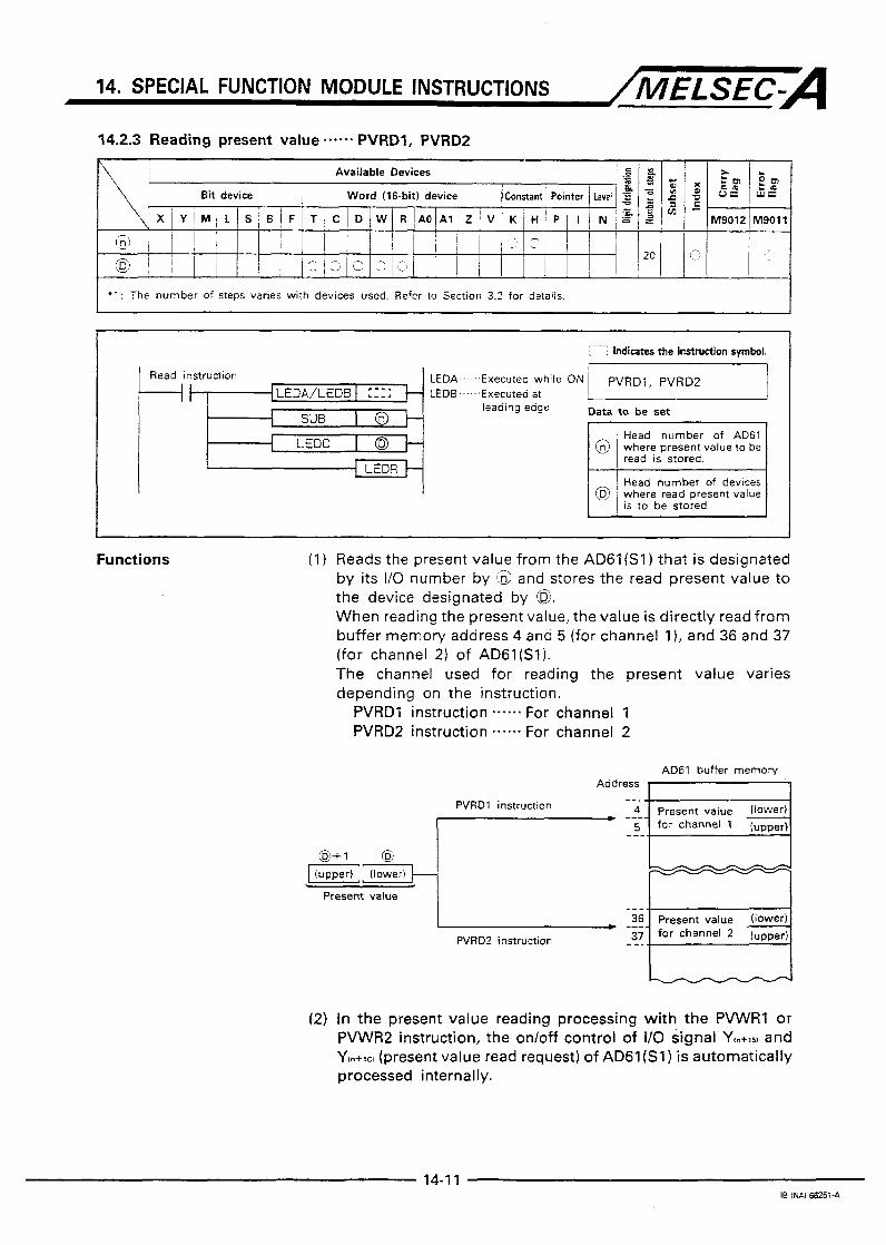
14. SPECIAL FUNCTION MODULE INSTRUCTIONS /MELSEC-A 14.2.3 Reading present value .*.-.. PVRD1, PVRD2
Available Devices 5 .s c - Z L
g ” - g g $ g x 0 Bit device I Word (16-bit) device Constant i Pointer 1 Level 2 = ; 5
B w o= 3” m -
X , Y ! M ! L H / P ~ I / N , ~ j :”- K A O A I ~ Z ~ V R w D T I C S I B I F M9012 M9011
6 ) : I / @ !
- , - I ~ i I 1 i ’ ? h
I I ,
1 i : j 2 :, ’,: CJ
! ‘1: The number of steps varies with devices used. Refer to Section 3.2 for details.
......
...... j Indicates the instruction symbol.
Read instruction
--It LEDA..--..Executed while ON pVRD1, P V R D ~ I
L L E D A / L E D ~ + LEDB......Executed at
SUB @ + leading edge Data t o be set
I LEDC 7 - Head number of AD61
read is stored.
Head number of devices where read present value is t o be stored
-1 LEDR
Functions (1 ) Reads the present value from the AD61 (Sl) that is designated by its I/O number by 1 6 ; and stores the read present value to the device designated by 0. When reading the present value, the value is directly read from buffer memory address 4 and 5 (for channel l ) , and 36 and 37 (for channel 2) of AD61 (Sl). The channel used for reading the present value varies depending on the instruction.
PVRD1 instruction .--.-. For channel 1 PVRD2 instruction ---..- For channel 2
AD61 buffer memory Address I I
PVRD1 instruction
Present value
WRDZ instruction
(2) In the present value reading processing with the PVWR1 or PVWR2 instruction, the on/off control of 1/0 signal YlntlS1 and Y,n+lci (present value read request) of ADGl(S1) is automatically processed internally.
14-1 1 IB iW 662514

14. SPECIAL FUNCTION MODULE INSTRUCTIONS /MELSEC-A (3) For the head I/O number of ADGl(S1) to be designated 0, the
upper two digits of the head 110 number expressed in 3-digit hexadecimal are set. Example:
When AD61 is assigned to W 1 2 0 to wY13F. Set " 1 2 ~ " for ' 5 2 .
Execution Conditions The PVRD1 and PVRD2 instruction execution mode depends on whether it is designated with an LEDA or LEDB instruction. They are executed every scan while the read command stays ON if they are designated with an LEDA instruction. When they are desig- nated with an LEDB instruction, they are executed only once a t the leading edge of the read command.
Sequence program flow I I I I
ON OFF
I I I I I I I I I I I I I I I I I I I I I I I I I I I I
Read command
PVRD1 (with LEDA) PVRDZ 1 n I I
I I
I I
I I I I I
I I I I I I I
PVRD1 I I I (with LEDB) I I PVRD2
Program Example A program to read the present value for channel 1 from buffer memory in AD61 loaded a t I/O numbers 020 to 03F.
AD61
I Buffer memory I 1 2

14. SPECIAL FUNCTION MODULE INSTRUCTIONS /MELSEC-A 14.3 AD59(S1) Memory Card!CENTRONICS Interface Module Control instructions
The AD59(S1) control instructions are summarized in the table below.
Classification Instruction 1 Symbol 1 Description Refer t o i P a w I - Outputs the character data of the speci-
Outputting 14-14 fied number of characters to the printer. PRN characters to
printer Outputs the character data up to the PR OOH code to the printer. 14-17
Read/write of 14-23 Writes the data to the memory card. PUT memory card 14-20 Reads the data from the memory card. GET
POINTS
(1) For printer output processing using the AD59(S1), it is not necessary to initialize the AD59 by a user program because it is automatically initialized when the PC CPU is started. In automatic initialization, printer output is set in units of bytes. Do not change this into units of words. If the unit is changed to words, data might not be output corrected when the PRN or PR instructions executed.
(2) The AlSD59J-SZMTF cannot be used. (3) The AD59(S1) control instruction cannot be used with the
QCPU-A (A Mode).
14-1 3 IB(NA)66251-F

MEMO
.....................................................................................................................................................................
.....................................................................................................................................................................
....................................................................................................................................................................
....................................................................................................................................................................
....................................................................................................................................................................
.....................................................................................................................................................................

14. SPECIAL FUNCTION MODULE INSTRUCTIONS /MELSEC-A 14.3.1 Outputting required number of characters to printer ...-.. PRN
; U E
M90 12
3utout command I LEDA......Executed while ON LEDB ..,,..Executed at
leading edge to be set LEDC. .... Device number
SUB .....,. Constant data to printer. I ! Head VO number of designated 0 AD59(Sll that outputs
LEDC I -{ LEDR
designated Number of characters (bytes) to be output.
Head number of devices where characters to be output are stored.
Bit device that is to be turned ON at completion
I
Functions ( 1 ) Outputs the characters to the printer connected to the AD59(S1) that is designated by a. The number of characters (bytes) designated by (n), beginning with the device designated by 0 , is output. After the completion of output processing, the bit device designated by @I is automatically turned ON for one scan.
c2 G+l c2+2
@+n
,b15 to b8 b7 to bti 2nd character 1st character 4th character 3rd character 6th character 15th character
I I
I to I I I
' n t l ' t h character I "n"th character
I
Printer 0 ASCII data
Example:
b15 to b8 b7 to bO Printer
Dl 1 Dl2
14-1 4 IB I N 4 662514
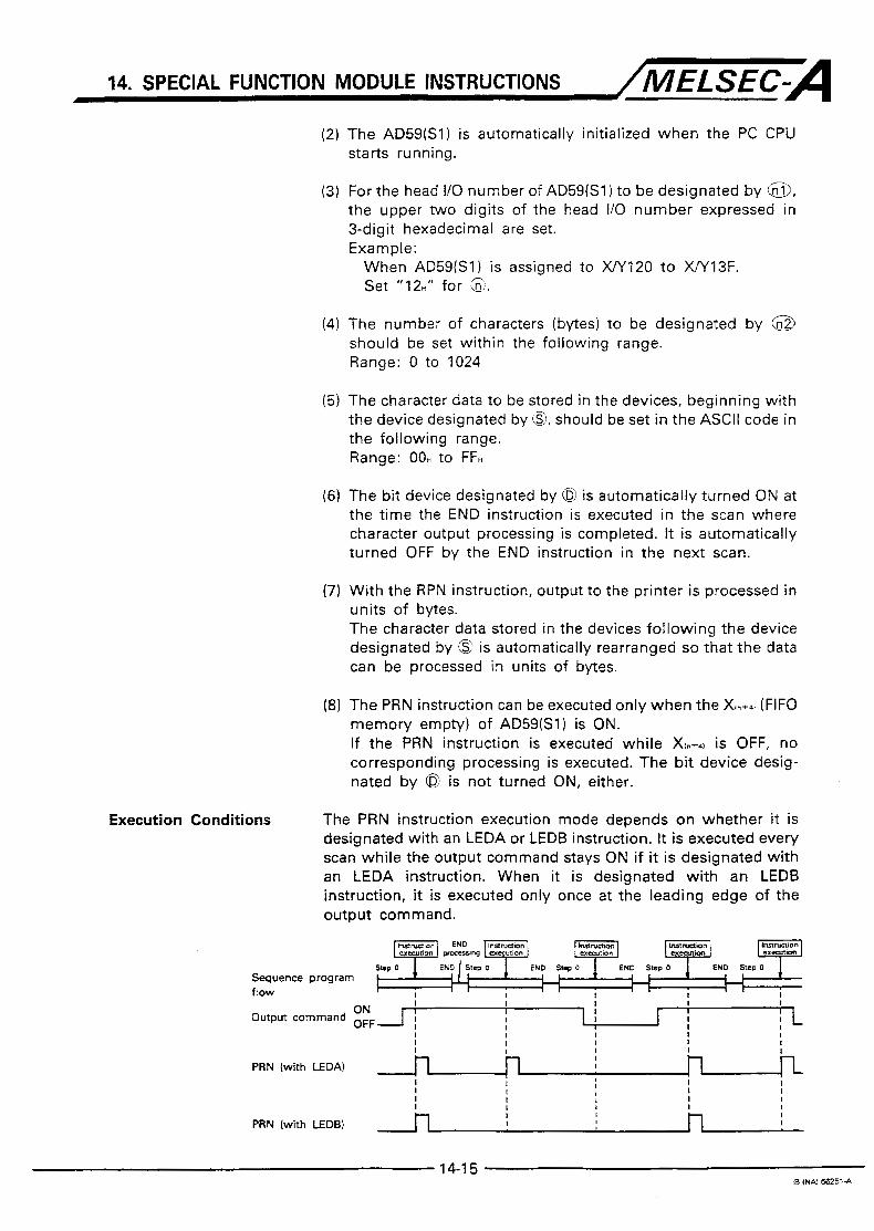
14. SPECIAL FUNCTION MODULE INSTRUCTIONS /MELSEC-A The AD59(S1) is automatically initialized when the PC CPU starts running.
For the head I/O number of AD59(S1) to be designated by a, the upper two digits of the head I/O number expressed in 3-digit hexadecimal are set. Example:
When AD59(S1) is assigned to W 1 2 0 t o W 1 3 F . Set "12~'' for ; 3 .
The number of characters (bytes) to be designated by @ should be set within the following range. Range: 0 to 1024
The character data to be stored in the devices, beginning with the device designated by @, should be set in the ASCII code in the following range. Range: OOH to FFH
The bit device designated by @I is automatically turned ON at the time the END instruction is executed in the scan where character output processing is completed. It is automatically turned OFF by the END instruction in the next scan.
With the RPN instruction, output to the printer is processed in units of bytes. The character data stored in the devices following the device designated by @ is automatically rearranged so that the data can be processed in units of bytes.
The PRN instruction can be executed only when the X,n+a, (FIFO memory empty) of AD59(S1) is ON. If the PRN instruction is executed while XI.+, is OFF, no corresponding processing is executed. The bit device desig- nated by 0 is not turned ON, either.
Execution Conditions The PRN instruction execution mode depends on whether it is designated with an LEDA or LEDB instruction. It is executed every scan while the output command stays ON if it is designated with an LEDA instruction. When it is designated with an LEDB instruction, it is executed only once a t the leading edge of the output command.
m ~ r u s t ~ o n END I n n d o n hsuucuon exa~ltion p$ocrssng erecutlon exeaJKlon
lnsmRwn excartion
lnnnrtlon execulion
slep 0 END Sleu 0 END Slep 0 END Slep 0 Sequence program I I I
flow I r i I I I I
ON OFF
I I I I I I I
I I I I I I
I I I I I I I I
Output command I I I I j I I
PRN (with LEDA) 1 I 1 I I
I I I I
I 1 I I
I
I I I I
PRN (with LEDB) 1 I 1 I I
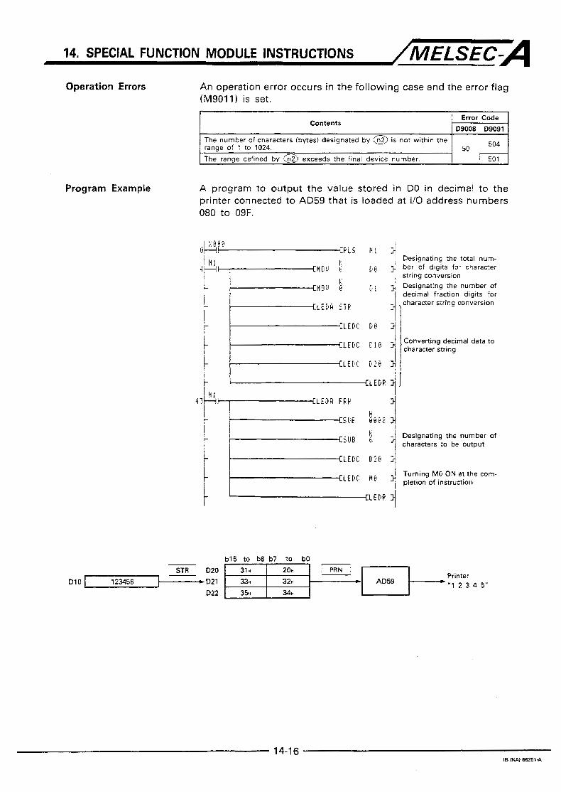
14. SPECIAL FUNCTION MODULE INSTRUCTIONS /MELSEC-A Operation Errors An operation error occurs in the following case and the error flag
(M9011) is set.
Program Example
Contents Error Code
D9008 1 D9091 I The number of characters (bytes) designated by @ is not within the
ranae of 1 to 1024. I
[The range defined by @ exceeds the final device number. 501
A program to output the value stored in DO in decimal to t h e printer connected to AD59 that is loaded at 1/0 address numbers 080 to 09F.
G H ! 1 til k
4 c l l I i
1 X O O F f CPLS t i l 3
Designating the total num-
string conversion
decimal fraction digits for
[H(jl.! 6 [ , e 3
Designating the number of [H@!! 8 [ , I 3
ber of digits for character
t
i c c [LEkC [ # ) e
CLEDL ETF: ,character string conversion
r C L E P C [JB 3
["' 7 'character string Converting decimal data to
I
CLEGF: 1, CLEUR PFtH
c H
I> 1 CS!iB ljlj1:43 3
L CS !I8 t. I Designating the number of characters to be output
ILEDC. [)?B
'LE')' '0 pietion of instruction Turning MO ON at the com-
[LEDP
b15 to b8 b7 to bO
Dl 0 * D21 D22
Printer "1 2 3 4 5"
14-1 6 IB R.w €62514

MEMO
....................................................................................................................................................................
....................................................................................................................................................................
....................................................................................................................................................................
....................................................................................................................................................................
.....................................................................................................................................................................
.....................................................................................................................................................................
.....................................................................................................................................................................
....................................................................................................................................................................
.....................................................................................................................................................................
..................................................................................................................................................................
....................................................................................................................................................................
....................................................................................................................................................................
.....................................................................................................................................................................
.....................................................................................................................................................................
....................................................................................................................................................................
....................................................................................................................................................................
....................................................................................................................................................................
iE (NA) 66251.A

14. SPECIAL FUNCTION MODULE INSTRUCTIONS /MELSEC-A 14.3.2 Outputting characters to printer up t o "00," code --..** PR
I *1: The number of steps varies with devices used. Refer to Section 3.2 for details
Outaut command
LEDC
LEDA..-.,.Executed while ON LEDB.....,Executed at
leading edge Dam be set
AD59(S1) that outpurs data to printer.
Head number of devices
output are stored
Bit device that is to be turned ON at completion
Functions (1) Outputs the characters to the printer connected to the AD59(S1) that is designated by 0. The characters (bytes) within the range beginning with the device designated by '3 to the one storing the ''00,'' code, are output. After the completion of output processing, the bit device designated by @ is automatically turned ON for one scan.
b15 to b8 b7 t o bO 12nd character1 1st character I n
Oi-1 4th character 13rd character -
@+2 6th character 15th character I - AD59 -
/ C $ I I I
'n"th character
indicates the end of character string
Example:
Dl0 D l 1 D l 2 D l 3
U

14. SPECIAL FUNCTION MODULE INSTRUCTIONS /MELSEC-A The AD59(S1) is automatically initialized when the PC CPU starts running.
For the head 1/0 number of AD59(S1) to be designated by a, the upper two digits of the head I/O number expressed in 3-digit hexadecimal are set. Example:
When AD59(S1) is assigned to W 1 2 0 t o W 1 3 F . Set " 1 2 ~ " f o r 8.
The character data to be stored in the devices, beginning with the device designated by @, should be set in the ASCII code in the following range. Range: On to FFH Note that the "001" code cannot be designated as data because it is the code to indicate the end of character string.
The maximum number of characters that can be output at a time is 1024.
The bit device designated by @ is automatically turned ON a t the time the END instruction is executed in the scan where character output processing is completed. It is automatically turned OFF by the END instruction in the next scan.
With the PR instruction, output to the printer is processed in units of bytes. The character data stored in the devices following the device designated by 9 is automatically rearranged so that the data can be processed in units of bytes.
The PR instruction can be executed only when the X(n+ai (FIFO memory empty) of AD59(S1) is ON. If the PR instruction is executed while Xln+41 is OFF, no corresponding processing is executed. The bit device desig- nated by 0 is not turned ON, either.
Execution Conditions The PR instruction execution mode depends on whether it is designated with an LEDA or LEDB instruction. It is executed every scan while the output command stays ON if it is designated with an LEDA instruction. When it is designated with an LEDB instruction, it is executed only once at the leading edge of the output command.
1-1 END 1 7 1 exeMwn procssmg e x ~ f l o n SlPP 0 END step 0 END Step 0 END Step 0 END Step 0
Sequence program I 1
flow I I ' I I
ON I I I I I I I I I I I I I I I
I 1 I I I I I I I I I I
I
Output command I I 1 1 I I
PR (with LEDA) 1 n I I I I
I I I I I I I I I I I I I
I I I PR [with LEDB) I I I
14-18 18 INN €62514

14. SPECIAL FUNCTION MODULE INSTRUCTIONS /MELSEC-A Operation Errors An operation error occurs in the following case and the error flag
(M9017) is set.
Program Example
Contents I Error Code 1 D9008 1 D9091
The designated number of characters to be output is greater than 1024 or 0. The " 0 0 ~ " codeis not stored in a device In the range from the device ~
designated by ',%' and to the device of the final device number. ~
50 504
A program to output the value stored in DO in decimal to the printer connected to AD59 that is loaded at 110 address numbers 080 to 09F.
D20 021 D22
DO 1 3 2 5 7 - D22
Designating the total number of digits for character string con-
Designating the number of de-
ter string conversion digits for charac- ,
Converting decimal data t o char- acter string
LEBF.' IF 1 L E b E PF:
H S!IB Ba i rD
LEDC 1126
LED[. R B Turning MO ON at the comple- tion of insrruction
b15 to b8 b7 to bO
14-19 IB L N A I 662514

M E M O
....................................................................................................................................................................
....................................................................................................................................................................
....................................................................................................................................................................
....................................................................................................................................................................
....................................................................................................................................................................
.....................................................................................................................................................................
.....................................................................................................................................................................
.....................................................................................................................................................................
.....................................................................................................................................................................
....................................................................................................................................................................
.....................................................................................................................................................................
....................................................................................................................................................................
....................................................................................................................................................................
....................................................................................................................................................................
....................................................................................................................................................................
.....................................................................................................................................................................
....................................................................................................................................................................
....................................................................................................................................................................
....................................................................................................................................................................

14. SPECIAL FUNCTION MODULE INSTRUCTIONS /MELSEC=A 14.3.3 Reading data from memory card -**.-.GET
Available Devices c 0 ._ - m
Bit device Word (16-bit) device Pointer i Level Constant m
x E N I P H K v R A O / A I / Z w D c T B / F s L M Y - . -
0
0 0
,-. I_ ,
-\ - ,E (Zt ;; ,=, I t ~l
1 i i I 8: (1) ,E CI 2 12 8;
@ I :3 ._I 3 (7 c ~
* l : The number of steps varies with devices used. Refer to Section 3.2 for details
Read command I x LEDR
.,..Executed while ON Data t o be set
.,..Executed at leading
.... Device number
..,.Constant designated
designated read is stored.
Head number of the de-
is to be stored.
Functions (1) Read the data from the memory card loaded in AD59(S1), . designated by @, and stores the read data to the devices beginning with the device designated by 0. The number of words designated by @ is read beginning with the address designated by @.
@ r a d address 1- @+1 Area number I
I I I I I I I I I I
I
Area number, Address ' -ko +1
+ AD59 memory card
@+l words
to to
-
14-20 IB ( N 4 662514,

14. SPECIAL FUNCTION MODULE INSTRUCTIONS /MELSEC-A Example:
D l Do B - - i t
Area number I
4 AD53
H Address
125n 126H 127r 1 2 8 ~ 1 2 3 ~ €3
memory card
@ = 5 words
In the memory data reading processing with the GET instruc- tion, the area change by the onloff control of I/O signal Y10 and Y11 of ADGl(S1) is automatically processed internally.
For the head I/O number of AD59(S1) to be designated by @, the upper two digits of the head I/O number expressed in 3-digit hexadecimal are set. Example:
When AD59(Sl) is assigned to W 1 2 0 t o W 1 3 F . Set ”12~” fo r a.
The head address to be designated by @ should be set in the following range. Range: OH to OFFFn
The area number to be designated by Qi-1 should be set in the following range. Range: 0 to 3
The number of words to be designated by (3 should be set in the following range. Range: 1 to 4096 Note that reading data over two or more areas is not possible.
Execution Conditions The GET instruction execution mode depends on whether it is designated with an LEDA or LEDB instruction. It is executed every scan while the read command stays ON if it is designated with an LEDA instruction. When it is designated with an LEDB instruction, it is executed only once at the leading edge of the read command.
SQP 0 Sequence program
END Step 0 END Step 0
flow I I I
ON OFF
I I I I I I I Read command I I r i I I
1 I I I I I I I I
GET [with LEDA) 1 I I
I I I
I I I 1
I I I I I I I I I
I I I I I GET (with LEDB) I
1 4-2 1 I6 (NLU 562514.

14. SPECIAL FUNCTION MODULE INSTRUCTIONS /MELSEC-A Operation Errors
Program Example
An operation error occurs in the following case and the error flag (M9011) is set.
Contents D9008 I D9091
An address designated by @ is not in the range of OH to OFFFH. 503 The area number designated by @+1 is not in the range of 0 to 3. 504
The address defined by the number of words designated by @exceeds . The number of words designated by 0 is not in the range of 1 to 4096.
50 the address OFFFH. 504 The device range defined by the number of words designated by @ exceeds the final device number of that device.
A program to read the data from address OOOOH to 0004H in area number 1 of memory card loaded in AD59 which is loaded in I/O number 020 to 03F and store the read data to DO to D4.
[ H @ U @ O B @ 1118 1 Designating head address H
EiIDU 1 K
D l 1 Designating area number
- rLE[)E: 6ET a
-
CLEDF: 3 - LLEDC D O 3 - CSUB 5 - C L E D C D l @ 3 - [SUB 8 8 6 2 3
H
I: Designating the number of points to be read
14-22 18 (W €62514

MEMO ....................................................................................................................................................................
....................................................................................................................................................................
....................................................................................................................................................................
....................................................................................................................................................................
.....................................................................................................................................................................
.....................................................................................................................................................................
.....................................................................................................................................................................
.....................................................................................................................................................................
.....................................................................................................................................................................
.....................................................................................................................................................................
....................................................................................................................................................................
....................................................................................................................................................................
....................................................................................................................................................................
.....................................................................................................................................................................
.....................................................................................................................................................................
....................................................................................................................................................................
....................................................................................................................................................................
....................................................................................................................................................................
IB (W 662514

14. SPECIAL FUNCTION MODULE INSTRUCTIONS /MELSEC-A 14.3.4 Writing data t o memory card * - . . * - PUT
Available Devices ._ 0 E
Bit device Word (16-bit) device / ~ w t a n t I Pointer 1 Level p - a E
I '1: The number of steps varies with devices used. Refer to Section 3.2 for details.
I -[ LEDR
.Executed while ON
..Executed at Data to be set leading edge
..Device number designated
designated ... Constant
written is stored.
Functions (1) Writes the data to the memory card loaded in AD59(S1), designated by @ ; the data to be written is stored in the devices beginning with the device designated by @. The data is written to the address beginning with the address designated by @ in the memory card.
I I 1 I I I I
I
+ AD59 memory card Area number, Address i -0
@+l t I I
to I to I
14-23 IB I N A ) 662514

14. SPECIAL FUNCTION MODULE INSTRUCTIONS /MELSEC-A Example:
DO I 1 7 " I--; D l
t I Area number I
3 t AD59 Address memory card
5 words
128n 1 2 9 ~
In the memory data reading processing with the PUT instruc- tion, the area change by the on/off control of I/O signal Y10 and Y11 of AD59(S1) is automatically processed internally.
For the head I/O number of AD59(S1) to be designated by a, the upper two digits of the head I/O number expressed in 3-digit hexadecimal are set. Example:
When AD59(S1) is assigned to XfY120 to W 1 3 F . Set ' ' 1 ~ ~ ' ' for @I.
The head address to be designated by a should be set in the following range. Range: On to OFFF,
The area number to be designated by @+l should be set in the following range. Range: 0 to 3
The number of words to be designated by (3 should be set in the following range. Range: 1 to 4096 Note that reading data over two or more areas is not possible.
Execution Conditions The PUT instruction execution mode depends on whether it is designated with an LEDA or LEDB instruction. It is executed every scan while the write command stays ON if it is designated with an LEDA instruction. When it is designated with an LEDB instruction, it is executed only once at the leading edge of the write command.
hLsvuaDn END IIISUUC~D~ cIe=Lllmn w i n g cIeCm0"
Step 0 END SIpp 0 Sequence program , I
flow I r l 1 I I I
ON OFF
I I I I I I I
I I I I I I I I
I I I I I I Write command
I I I I I I I I I I
I PUT (with LEDA) I h
I I I I I I I I
I I I PUT (with LEDB) I 1 I
14-24 18 (NAl66251-4

14. SPECIAL -FUNCTION MODULE INSTRUCTIONS /MELSEC-A Operation Errors An operation error occurs in the following case and the error flag
(M9011) is set.
Program Example
I 1 Error Code I Contents
~ _ . ~ ~
09008 D9091 An address designated by @ is not in the range of OH to OFFFH.
503 The area number designated by @-kl is not in the range of 0 to 3. 504
~
The number of words designated by a is not in the range of 1 to 4096.
the address OFFFH. The device range defined by the number of words designated by @
504
exceeds the final device number of that device.
-The address defined by the number of words designated by@ exceeds 50
A program to write the data, stored in DO to D4, to address OOOOH to 0004 in area number 1 of memory card loaded in AD59 which is loaded in I/O number 020 to 03F.
Designating head address
D 1 1 Designating area number
K 5 Designating the number of
points to be written
r Memory card area 1 7 3 0 2 1 ~
D3 D4 FFBEH 1 I I
302 1 H
FFBEH
14-25 I6 I N A I EQ5l-A

14. SPECIAL FUNCTION MODULE INSTRUCTIONS /MELSEC-A 14.4 AJ71C24(S3, S6, S8)/AJ7? VC24 Computer Link Control Instructions
The AJ71C24(S3, S6, S8)/AJ71 UC24 computer link control instruc- tions controls data transmission with an external device con- nected to AJ71C24(S3, S6, SS)/AJ71 UC24 in no-protocol mode. The AJ71C24(S3, S6, S8)/AJ71 UC24 computer link control instruc- tions are summarized below.
Classification Instruction Svmbol Description Refer to 1 Paae I -
PRN ,
Sends data up to the OOH to the the connected external device.
14-27 Sends data of the specified range to
Data send PR
connected external device. 14-31
Data receive Reads the data received from the j 14-35 1 INPUT 1 connected external device. Reading corn-
status. SPBUSY munication status 14-41 Reads data sendheceive processing
Forced stop of communication processing
spcLR forcibly. Stops data sendreceive processing 1443
POINT 1 If an AJ71C24(S3, S6, SS)/AJ71UC24 computer link control instruction is executed without entering unit module name with a parameter, the following is assumed t o execute processing.
No-protocol wordlbyte
No-protocol buffer memory area
No-protocol buffer memory area
Received data length ................ Up to CR or LF code,
Therefore, if the fol lowing is set, the AJ71C2443, S6, S8/AJ71 UC24 might malfunction because the AnACPW AnUCPU reads data to or wr i tes data from the AJ71C24- S3, S6, S8/AJ71UC24 ignoring the setting.
No-protocol receive end code designation (address
No-protocol word/byte designation (address 103) Designation of head address of buffer memory for sending data in no-protocol mode (address 104) Designation of length of buffer memory for sending data in no-protocol ode (address 105) Designation of head address of buffer memory for receiving data in no-protocol mode (address 106) Designation of length of buffer memory for receiving data in no-protocol ode (address 107) Designation of the number of no-protocol receive end data (address 108)
When the module name is entered, the setting of buffer memory indicated above is effective. (For details of module name entry, refer t o section 14.1.)
designating ............................. Words only
OH t o 7H only for sending data .......................
for receiving data ..................... 80H t o FFH only
or 127 words
100)
14-26 IB (NA) Ei251-B

14.4.1 Sending designated number of bytes of data in no-protocol mode ..-.-- PRN
U Y E - M9012 M9011
I *l: The number of steps varies with devices used. Refer to Section 3.2 for details.
c a AJ7lC24/S3, S6, S8)
Head UO number of
IAJ71UC24 which sends data
designated .Device number designated 'Constant designated I S"B ......
of data to be sent. Number of bytes or words
rg where data to be sent is Head number of devices
stored.
vice to be turned on at Device number of bit de-
completion of processing.
Functions (1) Sends <3 byte or word data stored in the devices beginning with the device designated by $8 to the external device connected to the AJ71 C24(S3, S6, S8)/AJ71 UC24 designated
After the completion of send processing, the bit device designated by @ is automatically turned ON for one scan.
by 6 3 .
b15 to b8 b7 to W - 0 0 + 1 O f 2
-
A17 1 C24 -sa
-
a bytes )r words
c External
I to I
Example:
b15 to b8 b7 to b0
Dl7 Dl8 47s Dl9 4AH 49!i
n External
AJ71 C24 -S8
device @ = 5 bytes c
'43~' to ' 4 1 ~ "
14-27 IB (Na) 66251-9

14. SPECIAL FUNCTION MODULE INSTRUCTIONS /MELSEC-A (2) The PRN instruction executes ON/OFF control of (send
completion) and Ycn+lo, (send request) of the AJ71C24(S3, S6, S8)/AJ71 UC24 automatically.
(3) For the head I/O number of AJ71 C24(S3, S6, S8VAJ71 UC24 to be designated by a, the upper two digits of the head I10 number expressed in 3-digit hexadecimal are set. Example:
When AJ71 C24(S3, S6, S8)/AJ71 UC24 is assigned to W 1 2 0 to W13F. Set ' ' 1 ~ ' ' for @.
(4) Send data range should be designated by @ in the following range.
With AJ71C24(S3, -...-. 1 to (no-protocol send buffer memory S6, S8)/AJ71 UC24 length setting - 1) words, or
1 to (no-protocol send buffer memory length setting - 1) X 2 bytes
When the AJ71 C24(S3, S6, S8)/AJ71 UC24 is used, the settings of the following items become effective for data unit (byte/ word) and buffer memory length. (Use a TO instruction for setting these items.)
No-protocol communication word/byte designation (at pow-
Designation of head address of buffer memory for sending
Designation of length of buffer memory for sending data in
With AJ71C24 . . . . . . . . . . . . 1 to 127 words
er turning ON: word)
data in no-protocol mode (at power turning ON: On)
no-protocol mode (at power turning ON: 8 0 ~ )
(5) The units of data to be designated by (3 varies according to the designation of data unit (byte/word) for AJ71C24(S3, S6, S8)/AJ71 UC24. Similarly, send data to be set by 0 varies according to the data unit (bytelword) as illustrated below.
In word unit setting In byte unit setting
0 @+1 @+2 @+3 @+4
3rd word
I
1 J b15 to b8 b7 to bO , I
@+4
(6) The bit device designated by @I is automatically turned ON when the END instruction is executed in the scan .in which the send processing is completed and turned OFF when the E N D instruction is executed in the next scan. It is used as the PRN instruction execution completion flag.

14. SPECIAL FUNCTION MODULE INSTRUCTIONS /MELSEC-A (7) When the PRN instruction is executed with the LEDA instruc-
tion, send processing is executed continuously while the sent command stays ON. When the PRN instruction is executed with the LEDB instruc- tion, send processing is executed only once at the leading edge of the send command.
Execution Conditions The PRN instruction execution mode depends on whether it is designated with an LEDA or LEDB instruction. It is executed every scan while the send command stays ON if it is designated with an LEDA instruction. When it is designated with an LEDB instruction, it is executed only once at the leading edge of the send command.
l n n l u ~ ~ n procersmg erecutton execmwn executmn
END I~srmc1m
Step 0 Sequence program flow I I I I I
ON OFF
I I I I I I I
I I I I I I
I I I I I I I I I
Send command I I I 1 : I I
I I I
PRN (with LEDA) I
I I 1 PRN (with LEDB) I I I
Operation Errors An operation error occurs in the following case and the error flag (M9011) is set.
I Contents I Error Code I I
'The number of bytedwords designated by 0 exceeds the following range. AJ71C24...... 1 to 127 N71C24(S3. S6, S8YAJ71 UC24
In byte setting: 1 to (no-protocol send buffer memory length setting
In word setting: 1 to (no-protocol send buffer memory length setting
The data range designated by @ exceeds the final device number of that device.
- 1) x 2 50
- 1)
504

14. SPECIAL FUNCTION MODULE INSTRUCTIONS /MELSEC-A Program Example A program to send the data stored in DO to D4 when X0 is turned
ON in units of words to the external device connected to the AJ71C24-S8 loaded at 110 number 020 to 03F.
t 1 csuG 4 Det;;ating the number of send
Turning MO ON at the cornple- tion of instruction
DO D l D2 D3 D4
L x t e r n a l i device 'MITSUBISHI"
14-30 I6 I F W 6 6 2 5 1 8
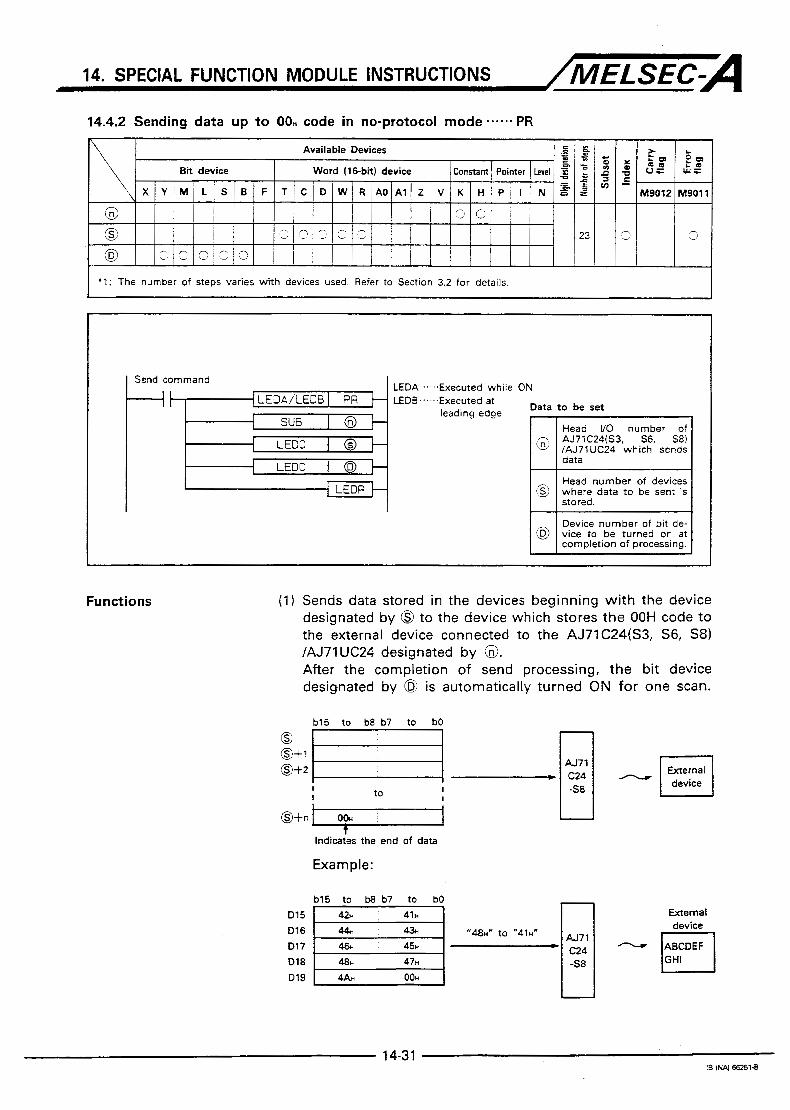
14. SPECIAL FUNCTION MODULE INSTRUCTIONS /MELSEC-A 14.4.2 Sending data up to 00" code in no-protocol mode -.--.. PR
'1: The number of steps varies with devices used. Refer to Section 3.2 for details.
Send command
---ll----l LEDA......Executed while ON
L E D A I L E D ~ E LEDB.....-Executed at leading edge
Head UO number of
1 LEOC /AJ71UC24 which sends @ -T-l-- AJ71C24(S3, S6, S 8 )
data
Head number of devices I LEDR l- @ where data to be sent is stored.
Device number of bit de- @ vice to be turned on at
completion of processing.
Data to be set SUB
[ L E D C -
O F
Functions (1) Sends data stored in the devices beginning with the device designated by 0 to the device which stores the OOH code to the external device connected to the AJ71C24(S3, S6, S8) /AJ71UC24 designated by 0. After the completion of send processing, the bit device designated by is automatically turned ON for one scan.
b15 to b8 b7 to bO
@+2
indicates the end of data
Example:
bl5 to b8 b7 to bO D l 5 D l6 "48~' to " 4 1 H " Dl7 D l 8 Dl9
bl5 to b8 b7 to bO D l 5 D l6 "48~' to " 4 1 H " Dl7 D l 8 Dl9
- A171 c24 -s8
-
External device
ABCDEF

14. SPECIAL FUNCTION MODULE INSTRUCTIONS /MELSEC-A (2) The PR instruction executes ON/OFF control of Xtn+0i (send
completion) and Yin+ro, (send request) of the AJ71C24S3, S6, S8)/AJ71 UC24 automatically.
(3) For the head 1/0 number of AJ71C24(S3, S6, S8)/AJ71UC24 to be designated by 0, the upper two digits of the head I/O number expressed in 3-digit hexadecimal are set. Example:
When AJ71C24(S3, S6, S8)/AJ71 UC24 is assigned to X/Y120 to W 1 3 F . Set ''12H" for 0.
(4) In the send data to be stored in the devices following the device designated by G, the "OOH" code cannot be set as the data. The "OOH" code is used as the end of send data code.
(5) Number of bytes or words of data that can be sent in one data send processing is indicated below.
With AJ71 C24(S3, e..-.. 1 to (no-protocol send buffer memory S6, S8VAJ71 UC24 length setting - 1) words, or
1 to (no-protocol send buffer memory length setting - 1) X 2 bytes
When the AJ71C24(S3, S6, S8)/AJ71 UC24 is used, the settings of the following items become effective for data unit (byte/ word) and buffer memory length. (Use a TO instruction for setting these items.)
No-protocol communication word/byte designation (at pow-
Designation of head address of buffer memory for sending
Designation of length of buffer memory for sending data in
With AJ71 C24 .. . . . . . .... , 1 to 127 words
er turning 0N:word)
data in no-protocol mode (at power turning ON: OH)
no-protocol mode (a t power turning ON: 80~)
(6) Send data to be set by @ varies according to the setting of data unit (byte/word) as illustrated below.
I In word unit setting I In byte unit setting I ' b15 to bO
@ [ 1st word 1 @+l @+2 @+3 8 + 4 @+5
I 2nd word I 3rd word
I OOH I + End of data
I b15 to b8 b7 to bO
@ I 2nd byte ; lao:e 1 @+l 4th byte 3rd byte @+2 6th byte j 5th byte @+3 8th byte 7th byte @+3 10th byte : 9th byte @+5 f
End of data
I I I
(7) The bit device designated by @ is automatically turned ON when the END instruction is executed in the scan in which the send processing is completed and turned OFF when the END instruction is executed in the next scan. It is used as the PR instruction execution completion flag.
1 4-3 2 Is (W 6 6 2 5 1 1

14. SPECIAL FUNCTION MODULE INSTRUCTIONS /MELSEC-A (8) When the PR instruction is executed with the LEDA instruction,
send processing is executed continuously while the sent command stays ON. When the PR instruction is executed with t h e LEDB instruction, send processing is executed only once at the leading edge of the send command.
Execution Conditions The PR instruction execution mode depends on whether it is designated with an LEDA or LEDB instruction. It is executed every scan while the send command stays ON if it is designated with an LEDA instruction. When it is designated with an LEDB instruction, it is executed only once at the leading edge of the send command.
Sequence program flow I
ON OFF
I I I I I I I I I I I
I I I I
Send command I I I I
I I I I 1 I
I
PR (with LEDA) 1 I 1 I I
I I
I I I I I I I I I I I
PR (with LEDB) 1 I I I
Operation Errors An operation error occurs in the following case and the error flag (M9011) is set.
Contents
The "OOH" code is not stored in a device in the device range from the one designated by (SI to the final device number of that device. The number of byteslwords designated by @ exceeds the following range.
Error Code D9008 D9091
Al71C24 ...... 1 to 127 AJ71C24-53, S6, S8/AJ71UC24
50 504
In byte setting: 1 to (no-protocol send buffer memory length setting
In word setting: 1 to (no-protocol send buffer memory length setting - - ) x 2
- 1)
14-33 IB(NA)66251-F

14. SPECIAL FUNCTION MODULE INSTRUCTIONS /MELSEC=A Program Example A program to send the data stored in the devices from DO the
device which stores the "OOH" code when X0 is turned ON in units of words to the external device connected to the AJ71C2468 loaded a t I/O number 020 to 03F.
- _ - - - _ _ - - - - - - - - _ _ - - _ - - - - - - - - - -~ Designation of "word unit" for
1 set once after PC CPU run (only when AJ71C2453, S6, S8 /AJ71UC24 is used)
H Y ; sendinglreceiving data; to be J
t Turning MO ON at the comple- t ion of instruction
D4I FFBEH I
14-34 16 NN 66251-E

14. SPECIAL FUNCTION MODULE INSTRUCTIONS /MELSEC-A 14.4.3 Receiving data in no-protocol mode.-....INPUT
E m
Data to be set ... Executed while
.--Executed a t ON AJ71C24 (53, S6, S8)
leading edge
Device number of bit de-
completion of processing.
Functions (1) Receives the data from the external device connected to the AJ71 C24 (S3, S6, S8)/AJ71 UC24 designated by @ within the range of allowable receive data size designated by @ and stores the received data in the devices following the device designated by @. After t h e completion of send processing, the bit device designated by @ is automatically turned ON for one scan.
@ @+ 1
@ + 2
62 Allowable receive data size - - , @+l
b15 to b8 b7 I I
* I
I I
The "00~" code is stored in @ + (n + 11 only when (Allowable receive data size) 2 (Receive data size)
I
3- -sa device
14-35 iB INAI 662518

14. SPECIAL FUNCTION MODULE INSTRUCTIONS /MELSEC=A Example:
DO
D l
15
9
.- - - 1 I I
I
Dl 0 4 2 ~ 41-1
D l 1 44.w 4%
D l 2 46n 4%
Dl 3
(2) The INPUT instruction executes ON/OFF control of (receive data read request) and Y,,-,,, (receive data read completion) of the AJ71 C24 (S3, S6, S8)/AJ71 UC24 automati- cally.
(3) For the head I/O number of AJ71 C24 (S3, S6, S8)/AJ71 UC24 to be designated by a, the upper two digits of the head I/O number expressed in 3-digit hexadecimal are set.
Example: When AJ71 C24 (S3, S6, S8)/AJ71 UC24 is assigned t o W 1 2 0 to X/Y13F. Set "12H" for @.
(4) Number of bytes or words of data that can be received in one data receive processing is indicated below.
With AJ71C24: Max. 127 words With AJ71C24 (S3, Max. (no-protocol send buffer memory S6, S8)/AJ71UC24: length setting -1) words, or Max. (no-
protocol send buffer memory length set- ting - 7 ) X 2 bytes
When the AJ71C24 (S3, S6, S8)/AJ71 UC24 is used, the settings of the following items become effective for data unit (byte/ word) and buffer memory length. (Use a TO instruction for setting these items.)
No-protocol communication word/by&e designation (at power
Designation of head address of buffer memory for receiving
Designation of length of buffer memory for receiving data in
turning ON: word)
data in no-protocol mode (at power turning ON: 804
no-protocol mode (at power turning ON: 80,)
14-36 I6 INAI €6251-E

14. SPECIAL FUNCTION MODULE INSTRUCTIONS /MELSEC=A (5) The allowable receive data size to be designated by @ is set
to secure the device range where the received data is stored. The range is secured from the device designated by @ and its range size is defined by @. The actual receive data size is automatically stored in @ +l.
@ '@+ 1
- - - - - - Allowable recelve data w e
-1 Receive data size -1
I I I
Stored received data I
I I
' I I I +
Received data storing range
(6) If the size of actually received data size is greater than the allowable receive data size designated by @, the data which fits in the designated allowable receive data size is stored in the devices and the excess of received data is discarded.
(7) The units of data to be designated by @ and @ -l- 1 vary according to the designation of data unit (byte/word) for AJ71C24 (S3, S6, S8)/AJ71 UC24. Similarly, receive data to be stored in @ varies according to the data unit (byte/word) as illustrated below.
In word unit setting In byte unit setting
16 (bytes)
@+l I @+l 10 (bytes) I
b15 to b8 b7 to bO ' !
Autbrnatically added at the end of received I data
@+3 @+4 @+5
@+7 @+6
8th byte ' 7th byte I 1 1 10th byte 9th byte
Automatically added at the end of received data

14. SPECIAL FUNCTION MODULE INSTRUCTIONS /MELSEC-A (8) When the byte unit is designated, the " 0 0 ~ " code is stored in
the manner as described below according to whether the receive data is odd-numbered or even-numbered bytes. Odd-numbered bytes
-.-.-.The "OOH" code is stored in the upper byte field of the final device of the devices where the receive data is to be stored.
Even-numbered bytes . - - - - -The "OOH" code is stored in the device following the
final device of the devices where the receive data is to be stored.
0 + 1 I 9 (bvtes) I b15 to b8 b7 to bO
"00~" is stored automatically
@+1 I 8 (bytes)
b15 to b8 b7 to hO
2nd byte 1st byte
mi-2 6th byte : 5th byte a i - 3 8th byte 7th byte mi-4 OOH byte OOH byte -e "0000~" is stored
automatically
(9) If the size of actually received data is greater than the allowable receive data size, the "00~'' code is stored in the device following the final device of the receive data storing devices.
In word unit setting In byte uni t setting
8 (words) 10 (bytes) @+1 7 (words) @+l 15 (bytes) 1 .
@ 1st word @+l 2nd word @+2 3rd word @+3 4th word @+4 5th word @+5
14-38 18 INN 66257-8

14. SPECIAL FUNCTION MODULE INSTRUCTIONS /MELSEC-A (10) The bit device designated by @ is automatically turned ON
when the END instruction is executed in the scan in which the receive processing is completed and turned OFF when the END instruction is executed in the next scan. It is used as the INPUT instruction execution completion flag.
(11) When the INPUT instruction is executed with the LEDA instruction, receive processing is executed continuously while the receive command stays ON. When the INPUT instruction is executed with the LEDB instruction, receive processing is executed only once a t the leading edge of the receive command.
Execution Conditions The INPUT instruction execution mode depends on whether it is designated with an LEDA or LEDB instruction. It is executed every scan while the receive command stays ON if it is designated with an LEDA instruction. When it is designated with an LEDB instruction, it is executed only once at the leading edge of the receive command.
Operation Errors An operation error occurs in the following case and the error flag (M9011) is set.
Error Code D9008 I D9091
Description
The range defined by @ exceeds the final device number of that device. 50 1 504
14-39 le IW €6751-A
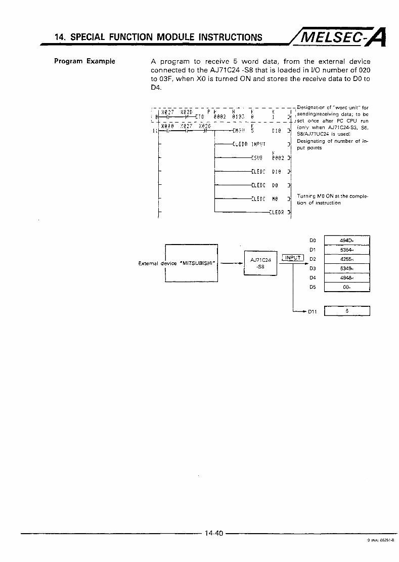
14. SPECIAL FUNCTION MODULE INSTRUCTIONS /MELSEC-A Program Example A program to receive 5 word data, from the external device
connected to the AJ71C24 -S8 that is loaded in 1/0 number of 020 to 03F, when X0 is turned ON and stores the receive data to DO to D4.
LEDR IHP!Il Designating of number of in- put points
Turning MO ON at the comple- tion of instruction
14-40 IJ (NA: 652518

14. SPECIAL FUNCTION MODULE INSTRUCTIONS /MELSEC-A 14.4.4 Reading communication status.-----SPBUSY
Available Devices - Bit device Pointer Word (16-bit) device /Constant
X I M9012 M9011 P H V / K 2 A O A l R W D C T B / F S L M Y
0 - -.' 3
-,
c / o 0 0 c * l : The number of steps varies with devices used. Refer to Section 3.2 for details.
Read command + -{LEDA/LEDB ISPBUSY+ SUB tot-
{ LEDC I @ + -[ LEDR E
LEDA......Executed while LEDB......Executed at
leading edge
ON
Data t o be set
AJ71C24 (S3, S6, S81 /AJ71UC24 which reads
communication status.
Functions (1) Reads the execution status of the following instruction to the AJ71C24 (S3, S6, S8)/AJ71UC24 designated by @ and stores the status in the device designated by @.
PRN, PR instruction (data send instruction) INPUT instruction (data receive instruction)
(2) For the head I/O number of AJ71C24 (S3, S6, S8)/AJ71UC24 to be designated by @, the upper two digits of the head I/O number expressed in 3-digit hexadecimal are set.
Example: When AJ71C24 (S3, S6, S8VAJ71UC24 is assigned t o W 1 2 0 to W13F. Set ''12,'' for 63.
(3) When the processing called by an instruction starts, "1" is set to the designated bit. After the Completion of processing, "0" is stored in that bit. The completion of processing is recognized at the trailing edge of the completion flag of each instruction.
hl 5 to b2 bl bO
@ 0 @ i - 1
0 Stores the execution status of PRN, PR instruction Stores the execution status of INPUT instruction (Always "0")
14-41 IB (N1) 66251-8

14. SPECIAL FUNCTION MODULE INSTRUCTIONS /MELSEC-A Execution Conditions Th? SPBUSY instruction execution mode depends on whether it is
designated with a n LEDA or LEDB instruction. It is executed every scan while the read command stays ON if it is designated with an LEDA instruction. When it is designated with an LEDB instruction, it is executed only once at the leading edge of the read command.
1"SINRlO" InSlmRion e X R y l l 0 " er-llC."
InnNCllOn eXRUl l0"
END Step 0 END Step 0 I ,
Sequence program flow H I I I I I I I I I I I
I I I I I I I I
I I I 1
I I I I I I
ON OFF
I Read command
I
SPBUSY (with LEDA) 1 I 1 I I
I I I I
I I I I I I I I I I
I I I I I SPBUSY (with LEDB) 1
Program Example A program to turn M10 ON while the PR instruction is executed for the AJ71C24 (S3, S6, S8VAJ71UC24, loaded at I/O numbers of 020 to 03F.
14-42 IB (N4 66251-5

14. SPECIAL FUNCTION MODULE INSTRUCTIONS /MELSEC-A 14.4.5 Forced stop of communication processing..*-**SPCLR
L I * l : The number of steps vanes with devices used. Refer to Section 3.2 for details.
1 Stoo command I
1 . - LEDR
LEDA......Executed while LEDB......Executed at
leading edge
ON
Data to be set
Head UO number of AJ71C24 (53, S6, 58) /AJ71UC24 which stops data communication.
Head number of devices where communication stop designation data is stored.
Functions (1 ) Stops communication processing (processing called by PRN, PR or INPUT instruction) with the AJ71C24 (S3, S6, S8) /AJ71UC24 designated by 0.
(2) For the head I/O number of AJ71C24 (S3, S6, S8)/AJ71UC24 to be designated by 0, the upper two digits of the head I/O number expressed in 3-digit hexadecimal are set.
Example: When AJ71C24 (S3, S6, S8VAJ71UC24 is assigned t o W 1 2 0 t o XN13F. Set " 1 for 0.
(3) The processing to be forcibly stopped is stored in 0. Set "1" to the bit corresponding to the processing to be stopped.
b2 b l b0 For send processing called by PRN, PR instruction
@+ 1
For receive processing called by INPUT and bO is ignored) instruction
(4) If the processing is stopped, the completion flag of the corresponding instruction is not turned ON.
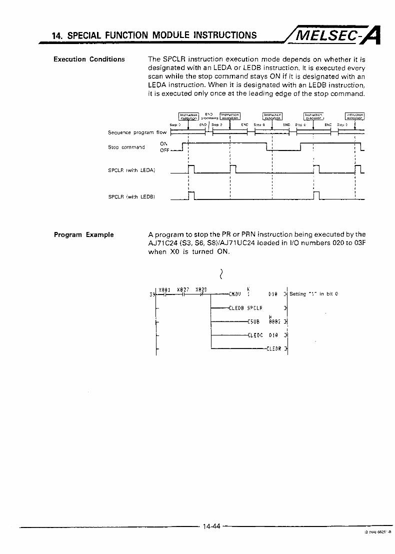
14. SPECIAL FUNCTION MODULE INSTRUCTIONS /MELSEC-A Execution Conditions The SPCLR instruction execution mode depends on whether it is
designated with an LEDA or LEDB instruction. It is executed every scan while the stop command stays ON if it is designated with an LEDA instruction. When it is designated with an LEDB instruction, it is executed only once at the leading edge of the stop command.
Sequence program flow I I I I I
ON OFF
I I I I I I I I I I I I 1 I I I I 1 I I I
Stop command
I I I I I I
SPCLR (with LEDA) n I
I I I I I I I I I I I I I I I I I I I
I I I
I
SPCLR (with LEDB) I I
Program Example A program to stop the PR or PRN instruction being executed by the AJ71C24 (S3, S6, S8)/AJ71UC24 loaded in I/O numbers 020 to 03F when X0 is turned ON.
t iLEDC
Setting "1" in bit 0
D l 9
t -LEDR

14. SPECIAL FUNCTION MODULE INSTRUCTIONS /MELSEC-A 14.5 AJ71C21(S1) Terminal Interface Module Control Instructions
The AJ71C21 (Sl) control instructions are used to send or receive data in the no-protocol mode with the external device connected to the AJ71C21 (Sl), or read data from or write data to the RAM memory in the AJ71C21-Sl.
The AJ71C21 (Sl) control instructions are summarized below.
Classification Instruction 1 Svrnbol Description Refer to I Page ~~~ ~~~
Sends data of the specified range t o the connected RS-232C external de- vice.
14-46
the connected RS-422 external de- Data send vice.
Sends data up to the OOH to the connected RS-232C external device.
connected RS-422 external device. 5 1 14-54 Data receive
Reads the data received from the lNPUT2 connected RS-232C external device.
Reads the data received from the INPUT4 1 connected RS422 external device.
I I I
RAM memory read Reads the data stored in AJ71C21-Sl RAM area. 1 14-60
RAM memory write PUT 1 Writes the data to AJ71C21-Sl RAM 14-64 area.
Reading communication Status
Reads data sendheceive processing status or RAM area read/write pro- cessino status.
14-68 I -
Forced stop of 14-70 or RAM area readiwrite processing SPCLR communication
Stops data sendreceive processing
Drocessinq forcibly.
POINTS (1) If an AJ71C21 (SI) control instruction is executed for
AD61 (Sl) without entering module name in parameter setting, it does not cause an error. In this case, the AD61 (Sl) might malfunction. (For details, refer to Section 14.1.)
(2) The GET and PUT instructions cannot be used with the AF71C21 (Sl). This is because the AF71C21 i s not provided with RAM memory. If the module name has been entered, an error occurs on these instructions cannot be executed. If the module name has not been executed, the instruction is executed. In this case, however, t he control is not influenced by it.
(3) The AJ71 C21 (SI) control instruction cannot be used with the QCPU-A (A Mode).
7 4-45 lB(NA)66251-F

MEMO
..................................................................................................................................................................
....................................................................................................................................................................
.....................................................................................................................................................................
.....................................................................................................................................................................
.....................................................................................................................................................................
.....................................................................................................................................................................
....................................................................................................................................................................
.....................................................................................................................................................................
....................................................................................................................................................................
....................................................................................................................................................................
....................................................................................................................................................................
....................................................................................................................................................................
....................................................................................................................................................................
....................................................................................................................................................................
....................................................................................................................................................................
....................................................................................................................................................................
13 tNA! € 6 2 j : - f

14. SPECIAL FUNCTION MODULE INSTRUCTIONS ,/MELSEC-A 14.5.1 Sending designated number of bytes of data-----.PRN2, PRN4
+1: The number of steps vanes with devices used. Refer to Section 3.2 for details.
...... :. ..... Indicates the instruction symbol.
I
+ t Send command
I LEDA/LEDB 1 :IT: s u i -
-/ L E D C / S U B ~ ~ - -1 LEDC
1 LEDC (Dl- O F
-- LEDA
..-Executed while ON
... Executed at leading edge
... Device number designated
..Constant designated
PRNZ, PRN4
Data to be set I I@) 1 AJ71C21 6 1 ) whicqf I Head VO number
sends data.
Number of bytes or words of data to be sent. I Head number of devices
stored.
Device number of bit de-
completion of processing.
Functions (1 ) Sends @ byte or word data stored in the devices beginning with the device designated by @ to the external device connected to the AJ71C21 (Sl) designated by @. After the completion of send processing, the bit device designated by @ is automatically turned ON for one scan. The interface to be used varies according to the instruction.
PRN2 instruction.----.RS-Z32C interface PRN4 instruction------RS422 interface
@+ 1 @bytes or words
@ + 2 , PRNZ instruction
I
I t o i I
b15 to b8 b7 to bO
~ 1 5 1 421 i 413 I t
Example:
I @= 9 bytes
AJ7 1 C21
232C device
. - q AJ71C21
External device -

14. SPECIAL FUNCTION MODULE INSTRUCTIONS /MELSEC-A (2) The PRN2 and PRN4 instructions execute ON/OFF control of
Xin+2,, X ! n + 7 ) (send completion) and YWZ~, Y ~ 7 1 (send request) of the AJ71C21 (Sl) automatically.
(3) For the head I/O number of AJ71C21 (Sl) to be designated by @, the upper two digits of the head I/O number expressed in 3-digit hexadecimal are set.
Example: When AJ7lC21 (Sl) is assigned to W 1 2 0 to X/Y13F. Set " 1 2 ~ " for @.
(4) The units of data to be sent and allowable setting range to be designated by @ vary according to the data unit designation (byte/word) and buffer memory length setting for no-protocol mode sending to be set for the AJ71C21 (Sl) . The send data to be set by @ varies according to byte/word designation as illustrated below.
Word unit setting
6 3 I 5 (words) 7
0 Q+1
Q f 3 '@+2 1 3rd word I I -$
2nd word
0 1 9 (bytes) f 1 I
b15 to b8 b7 to bO I
2nd byte 1st byte J
0 + 2 6th bvte 5th bvte
@+4
Setting range Word unit designated -.-.-.. 1 to (no-protocol send buffer
memory length setting -1) words Byte unit designated---..-... 1 to (no-protocol send buffer mem-
ory length setting -1) X 2 bytes 1 I
To execute the instructions other than the default setting for data unit and buffer memory length, it is necessary to set the following. (Use a TO instruction for setting these items.)
No-protocol communication wordbyte designation (at pow- er turning ON: word) Designation of head address of buffer memory for sending data in no-protocol mode (at power turning ON: OH (RS-
Designation of length of buffer memory for sending data in 232C), 1 OOH (RS-422))
no-protocol mode (at power turning ON: 80H)
14-47 !E lhui €6251-A

14. SPECIAL FUNCTION MODULE INSTRUCTIONS /MELSEC-A (5) The bit device designated by @is automatically turned ON
when the END instruction is executed in the scan in which the send processing is completed and turned OFF when the END instruction is executed in the next scan. It is used as the PRN2 or PRN4 instruction execution completion flag.
(6) When the PRN2 or PRN4 instruction is executed with the LEDA instruction, send processing is executed continuously while the sent command stays ON. When they are executed with the LEDB instruction, send processing is executed only once at the leading edge of the send command.
Execution Conditions The PRN2 and PRN4 instruction execution mode depends on whether it is designated with an LEDA or LEDB instruction. They are executed every scan while the send command stays ON if they are designated with an LEDA instruction. When they are designated with an LEDB instruction, they are executed only once at the leading edge of the send command.
i n n ~ n ~ o n END Innrumon exeatton prosessmg execmon
I W N c l l O n Ins1MY)n l"SruN0" erecutlo" ex-tton eXeCUll0"
Step 0 END Stm 0 END Step 0 END Step 0 END Step 0 I I
Sequence program flow t-7
Send command
I I I I I I I I I I
ON I I I I
OFF I I I I I I I I I I I I I I I I I I
I I I I
PRNZ [with LEDA) PRN4
I I 1 n
I I I I I I
I I I I I I I 1 I I I I I I PRN2 (with LEDB) P R N 4 1
Operation Errors An operation error occurs in the following cases and the error flag (M9011) is set.
Description
The number of bytesiwords designated by @exceeds the following range.
Error Code D9008 D9091
I In byte setting:
In word settina: 1 to (no-protocol send buffer memory length setting -1 ) X 2 I 50 I 504 I 1 to (no-protocol send buffer memory length setting -1)
The data range designated by @exceeds the final device number of I I
14-48 IB INAI 65251-A

14. SPECIAL FUNCTION MODULE INSTRUCTIONS /MELSEC-A Program Example A program to send the data stored in DO to D4 when X0 is turned
ON in units of words to the external device connected to the RS- 232C interface in the AJ71C21(S1) loaded at I/O number 020 to
Designation of "word unit" for 1 sendinghceiving data; to be set
once after PC CPU run (only when AJ77C24-S3 is used) ! J
I PRN2 instruction is used; pro- cessing for RS-232C interface 3
H 080; 1 D B 4 i; Designating the number of send 5 '4 points
71 Turning MO ON at the comple H F - 1 tion of instruction
D 2 4 2 5 5 ~ (RS-232C) -External device "MITSUBISHI"
D3
D4
14-49 IS INA 5625i4,

14. SPECIAL FUNCTION MODULE INSTRUCTIONS /MELSEC-A 14.5.2 Sending data up t o OOH code......PR2, PR4
'1: The number of steps vanes with devices used. Refer to Section 3.2 for details.
U E W E
M9012 M9011
Send command LEDA..-.Executed while
-1 L E D A ~ ON LEDB......Executed at
1 SUB I @ + leading edge
f LEDC I @ -{ LEDC I 1
....~
...... Indicates the instruction symbol.
I PR2, PR4 I Data t o be set
0 1 AJ71C21 ( S l ) whic"hi 1 Head I/O number
sends data. ~ ~ ~~~~~~
Head number of devices
Device number of bit de-
completion of processing.
Functions (1) Sends data stored in the devices beginning with the device designated by G ~ t o the device which stores the OOH code to the external device connected to the AJ71C21 (S1) designated by @. After the completion of send processing, the bit device designated by is automatically turned ON for one scan. The interface to be used varies according to the instruction.
PR2 instruction...-.-RS-232C interface PR4 instruction..-...RS-422 interface
0 @+ 1
@ + 2
@+ n
AJ71C21
PR2 instruction
I I
External device
I t o I i " p ' i PR4 instruction
Indicates the end of data
Example:
b15 t o b8 b7 to bO
N71C21
External device - - I iBCDEFG I 14-50
I6 INN €62514

14. SPECIAL FUNCTION MODULE INSTRUCTIONS /MELSEC-A (2) The PR2 and PR4 instructions execute ON/OFF control of
(send completion) and Yinf2,, Y,,+,, (send request) of the AJ71C21 (Sl) automatically.
(3) For the head I/O number of AJ71C21 (Sl) to be designated by a, the upper two digits of the head I/O number expressed in 3-digit hexadecimal are set.
Example: When AJ71C21 ( S l ) is assigned t o W 1 2 0 t o W13F. Set ''12~'' for @.
(4) In the send data t o be stored in the devices following the device designated by 0, the "00," code cannot be set as the data. The "OOn" code is used as the end of send data code.
(5) Number of bytes or words of data that can be sent in one data send processing is indicated below.
Word unit designated...-..l to (no-protocol send buffer memory
Byte unit designated..-..-l to (no-protocol send buffer memory length setting -1) words
length setting -1) X 2 bytes To execute the instructions in other than the default setting for data unit and buffer memory length, it is necessary to set the following. (Use a TO instruction for setting these items.)
No-protocol communication word/byte designation (a t pow- er turning ON: word) Designation of head address of buffer memory for sending data in no-protocol mode (at power turning ON: OH (RS-
Designation of length of buffer memory for sending data in 232C), 1 OOw (RS-422))
no-protocol mode (at power turning ON: 8OH)
(6) Send data to be set by o v a r i e s according to the setting of data unit (bytelword) as illustrated below.
~~
Word uni t setting
b15 to bO
0 @+1 @+2 @+3 @+4 @+5
1 1 1st word 2nd word
I 4th word I
1-L 5th word End of data
Byte unit setting
b15 to b8 hi' to bO
0 @+1 @+2 0 + 3
I 6th bvte 5th bvte I I 8th byte 7th byte I
@+5 data
14-51 IB IkAI 66251.A
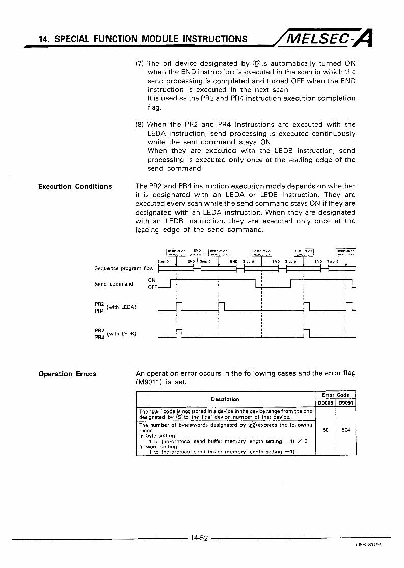
14. SPECIAL FUNCTION MODULE INSTRUCTIONS /MELSEC-A (7) The bit device designated by @is automatically turned ON
when the END instruction is executed in the scan in which the send processing is completed and turned OFF when the END instruction is executed in the next scan. It is used as the PR2 and PR4 instruction execution completion flag.
(8) When the PR2 and PR4 instructions are executed with the LEDA instruction, send processing is executed continuously while the sent command stays ON. When they are executed with the LEDB instruction, send processing is executed only once at the leading edge of the send command.
Execution Conditions The PR2 and PR4 instruction execution mode depends on whether it is designated with an LEDA or LEDB instruction. They are executed every scan while the send command stays ON if they are designated with an LEDA instruction. When they are designated with an LEDB instruction, they are executed only once at the leading edge of the send command.
Sequence program flow
ON OFF Send command
I I I I I I I I I I I I I I
I I t I I I
I
(with E D B ) PR4
Operation Errors An operation error occurs in the following cases and the error flag (M9011) is set.
Error Code D9008 D9091 Description
The "00~" code is not stored in a device in the device range f rom the one designated by @to the final device number of that device. The number of bytedwords designated by @exceeds the following range. 50 504
I 1 to (no-protocol send buffer memory length setting -1) X 2 I 1 1 In byte setting:
In word setting: ! 1 to (no-protocol send buffer memory length setting -1) I
14-52 ' IB IN41 E62514

14. SPECIAL FUNCTION MODULE INSTRUCTIONS ,/MELSEC-A Program Example A program to send the data stored in the devices from DO to the
device which stores the " 0 0 ~ " code when X0 is turned ON in units of words to the RS-232C external device connected to the AJ71 C21 (Sl) loaded at I/O number 020 to 03F.
Designation of "word unit" for
1 - I
when AJ71C24-S3 is used)
PR2 instruction is used; RS-
L E D C D B Turning MO ON at the comple- tion of instruction
t
D2 1-1 -1 AJ71C21 I - External device "MITSUBISHI' 1 PR2 I
IS1 1
D4 I FFBEH I 1
14-53 I6 iNAi €62514

14. SPECIAL FUNCTION MODULE INSTRUCTIONS /MELSEC-A
I '1: The number of steps varies with devices used. Refer to Section 3.2 for details.
Receive command I LEDA,
. ....
..... Indicates the instruction symbol.
I INPUT2. INPUT4 I ...... Executed while
~~
n M Data to be set ..... Executed at
VI.
leading edge AJ71C21 (Sl) which re- Head 110 number of
1 - I ceives data. I I E 1 Allowable receive data I slze and receive data size.
D l where data received is to Head number of devices
be stored.
Device number of bit de-
completion of processing.
Functions (1) Receives the data from the external device connected to the AJ71C21 (Sl) designated by @within the range of allowable receive data size designated by @ and stores the received data in the devices following the device designated by After the completion of send processing, the bit device designated by @ is automatically turned ON for one scan. The interface to be used varies according to the instruction.
INPUT2 instruction.----.RS-232C interface INPUT4 instruction-*-..-RS-422 interface
0 - I Receive data size @+ 1
- - - - 1 Allowable receive data size
I b15 to b8 b7 to bO I
@+ 2 INPUT2 instruction
I to I INPUT4 instruction
The " 0 0 ~ " code is stored in @ + (n + 1) only when (Allowable receive data size) t (Receive data size)
AJ71C21
232C
RS- 422
device
14-54 IB INA.) 66251-4

14. SPECIAL FUNCTION MODULE INSTRUCTIONS /MELSEC-A Example:
Dl 0
Dl 1
Dl 2
Dl 3
Dl 4
I I
I I>' ' I U
External device
L A ABCDEFG
(2) The INPUT2 and INPUT4 instructions execute ON/OFF control of X,"-T), XI" - 81 (receive data read request) and Y I ~ - I), Y ( n - 8 '
(receive data read completion) of the AJ71C21 ( S l ) automati- cally.
(3) For the head 110 number of AJ71C21 (S l ) to be designated by @, the upper two digits of the head I/O number expressed in 3-digit hexadecimal are set.
Example: When AJ71C21 (S l ) is assigned to XN120 to W 1 3 F . Set "12H" for @.
(4) Number of bytes or words of data that can be received in one data send processing is indicated below.
Word unit designated...l to (no-protocol receive buffer memory length setting -1) words
Byte unit designated....l to (no-protocol receive buffer memory length setting -1) X 2 bytes
To execute the instructions in other than the default setting for data unit and buffer memory length, it is necessary to set the following. (Use a TO instruction for setting these items.)
No-protocol communication word/byte designation (at pow- er turning ON: word) Designation of head address of buffer memory for sending data in no-protocol mode (a t power turning ON: O H (RS-
Designation of length of buffer memory for sending data in 232C), 1 OOH (RS-422))
no-protocol mode (at power turning ON: 80H)
14-55 IB (NAI 86251-A

14. SPECIAL FUNCTION MODULE INSTRUCTIONS /MELSEC=A (5) The allowable receive data size to be designated by @ is set
to secure the device rang2 where the received data is stored. The range is secured from the device designated by @and its range size is defined by @. The actual receive data size is automatically stored in @ + 1.
-1
I I
I I I
I I I I
Stored received 4 Received data storing range
(6) If the size of actually received data size is greater than the allowable receive data size designated by @, the data which fits in the designated allowable receive data size is stored in the devices and the excess of received data is discarded.
(7) The units of data to be designated by @ and @ i- 1 vary according to the designation of data unit (byte/word) for AJ71 C21 (Sl ) . Similarly, receive data to be stored in @ varies according to the data unit (bytelword) as illustrated below.
Word unit setting Byte unit setting
@+1 5 (words) @+l 10 (bytes)
b15 to b8 b 7 t o bO I
11 I I @ . 2nd byte I 1st byte
@+1 4th byte ' 3rd byte @+2 6th byte ~ 5th byte @+3 8th byte : 7th byte @+4 10th byte j 9th byte @+5 OOH byte I O b byte -+
@ +6 @+7
Automatically added at the end of received data
Automatically added at the end of received data
14-56 13 INAI ffi251.A

14. SPECIAL FUNCTION MODULE INSTRUCTIONS /MELSEC-A (2) When the byte unit is designated, the " 0 0 ~ " code is stored in
the manner as described below according to whether the receive data is odd-numbered or even-numbered bytes.
Odd-numbered bytes .....- The "00," code is stored in the upper byte field of the
final device of the devices where the receive data is to be stored.
Even-numbered bytes ..-... The "OOH" code is stored in the device following the
final device of the devices where the receive data is to be stored.
b15 to b8 b7 to bO 6? I 2nd bvte 1st byte 1
b15 to b8 b7 t o bO
I "00~" is stored automatically I "0000~" is stored automatically
(9) If the size of actually received data is greater than the allowable receive data size, the ''OOH" code is stored in the device following the final device of the receive data storing devices.
Word unit setting
5 Iwords) 7 (words)
b15 to bo 1 ' m l 1st word im! @+l I -
2nd word
AJ71C24(S3) in byte unit setting
i 1 5 to b8 b7 to b] 1 0 2nd byte . 1st byte @+1 4th byte 3rd byte mi-2 6th byte : 5th byte m4-3 8th byte ' 7th byte mi-4 10th b y t e . 9th byte @-I-5 OOH byte : OOH byte

14. SPECIAL FUNCTION MODULE INSTRUCTIONS /MELSEC-A (10) The bit device designated by @ is automatically turned ON
when the END instruction is executed in the scan in which the receive processing is completed and turned OFF when the END instruction is executed in the next scan. It is used as the INPUT2 and INPUT4 instruction execution completion flag.
(11) When the INPUT2 and INPUT4 instructions are executed with the LEDA instruction, receive processing is executed con- tinuously while the receive command stays ON. When they are executed with the LEDB instruction, receive processing is executed only once at the leading edge of the receive command.
Execution Conditions The INPUT2 and INPUT4 instruction execution mode depends on whether it is designated with an LEDA or LEDB instruction. They are executed every scan while the receive command stays ON if they are designated with an LEDA instruction. When they are designated with an LEDB instruction, they are executed only once at the leading edge of the receive command.
lnrnm~~ton END Instrumon eXeCUll0" p r a e s r m g exeC"ll0n
Step 0
Sequence program flow I I I I I
ON I I I I I I I
OFF I I
I I I I I
Receive command I I I I I : I I
I
Operation Errors An operation error occurs in the following case and the error flag (M9011) is set.
Description Error Code
D9008 1 Dm91 1 The range defined by 0 exceeds the final device number of that device. I 50 I 504 I
14-58 16 lNN 662514.

14. SPECIAL FUNCTION MODULE INSTRUCTIONS /MELSEC-A Program Example A program to receive 5 word data, from the external device
connected to the RS-232C interface in the AJ71C21 (Sl) that is loaded in I/O numbers 020 to 03F, when X0 is turned ON and stores the receive data to DO to D4.
Desiqnation of "word unit" for I % @ ? I X 8 2 8 R l O
S F , t I [T(l ! : e 2 ; t- I-CSE~ when AJ71C24 (53) is used)
sendingireceiving data; to be set once after PC CPU run (only I
Y I <H 111 1: 5 Designating of number of input , points
t CLEbE IHPUT? INPUT2 instruction is desig-
nated; RS-232C interface
! C S U I i e e e z
r
I
1
' Turning MO ON at the comple- 7 tion of instruction
External device "MITSUBISHI"
D4 D5 E

14. SPECIAL FUNCTION MODULE INSTRUCTIONS /MELSEC-A 14.5.4 Reading RAM-..--.GET
V E Y E
M9012 M9011
"
I '1: The number of steps varies with devices used. Refer to Section 3 2 for details.
Data to be set
,~ 1 Head I/O numoer of @ AJ71C27 (S1) which reads
RAM area.
Head address of RAM area where data to be read is stored.
...... - - i t , + Read command LEDA Executed while ON
LEDE ...... Executed ai
SUE leading edge I T =
-- pEiT---T .f L E K I @ +
LEDC ...... Device number designated
SUB Constant designated .....
-1 LEDR
@ 1 read. Number of words to be
~~~ ~ ~
where the read data is t o Head number of devices
be stored.
device which is turned ON Device number of the bit
sing. at completion of proces-
Functions (1) Reads data from the RAM area in the AJ71C21 (Sl), designated by @, and stores the read data to the devices beginning with the device designated by 0. The designated number of words is read at a time. After the completion of read processing, the bit device designated by @is automatically turned ON for one scan.
------1 AJ77C21-Sl RAM area address I Head address - - - - - 1
I I
I
@+ 1 RAM number
I I I Device I I #
Address
+ 1
I to 1- number I
number RAM oesj Mted I
Jm I I .................... j OOOH
I AJ71CZl-Sl RAM area
1 to
I 1 RAM 1 1 + -
I 2 : to 7 F h ...........................
I + ...........................
79 ~ F F H ...........................

14. SPECIAL FUNCTION MODULE INSTRUCTIONS /MELSEC-A Example:
Dl 2 1-1 c D13w- RAM number 8 area
D l 4
- _ 1 I I
< t D l 08r
D l 0 9 ~
D ~ O A H
D~OBH
D l OCr
A J 7 1 C 2 1 - S l
@j = 5 words
(2) The GET instruction executes ON/OFF control of (RAM read request) and Y,n+lDI (RAM read completion) of the AJ71C21 -S1 automatically.
(3) For the head I/O number of AJ71C21 (Sl) to be designated by @,the upper two digits of the head I/O number expressed in 3-digit hexadecimal are set.
Example: When AJ71C21-Sl is assigned to W 1 2 0 t o X/Y13F. Set ''12~'' for @.
(4) The designation range of head address to be designated by @ is indicated below. Range: OH to 7FFH
(5) The designation range of RAM number to be designated by @ + 1 is indicated below. Range: 0 to 79
(6) The number of words to be designated by @ is indicate'd below. Range: 1 to 2048 Note that reading of RAM data over multiple RAM areas is not allowed.
(7) The bit device designated by @ is automatically turned ON when the END instruction is executed in the scan in which the read processing is completed and turned OFF when the END instruction is executed in the next scan. It is used as the GET instruction execution completion flag.
14-61 'B Ihil €6251-1

14. SPECIAL FUNCTION MODULE INSTRUCTIONS /MELSEC-A Execution Conditions The GET instruction execution mode depends on whether it is
designated with an LEDA or LEDB instruction. It is executed every scan while the read command stays ON if it is designated with an LEDA instruction. When it is designated with an LEDB instruction, it is executed only once a t the leading edge of the read command.
Sequence program flow I I I I I
ON OFF
I I I I I I I
I I I I I I I I I I I I I Read command
I I I I I I I
I I I
GET (with LEDA)
GET (with LEDB)
Operation Errors
n I I
I
I
I I
I
I
h I I h I I I I
An operation error occurs in the following cases and the error flag (M9011) is set. 1 I Error Code I 1 Description
D9008 D9091 _.~.
I The module desianated bv m i s AJ71C21. I 46 I 462 I The address designated by E1 is outside the range of OH to ~ F F H .
The range defined by @exceeds the final number of that device.
504 The range defined by @exceeds 07FFh.
50 The number of words designated by@ is outside the range of 1 to 2048.
5 03 The area number designated by + 1 is outside the range of 0 to 79. 504

14. SPECIAL FUNCTION MODULE INSTRUCTIONS /MELSEC-A Program Example A program to read the data stored in address OOOOH to 0004~ of
RAM number 1 in the AJ71C21 (Sl ) , loaded at 110 numbers 020 to 03F, when X0 is turned ON and store the read data to DO to D4.
DIE( Setting head address of RAM area
Dl 1 1 Setting RAM number I
Setting the number of red points
D @
Turning MOON after completion of instruction
AJ71C21-Sl
14-63 IB (NN 65.751-A

14. SPECIAL FUNCTION MODULE INSTRUCTIONS /MELSEC=A 14.5.5 Writing data t o RAM---.*.PUT
i
V G n
, M9012
+l The number of steps varies with devices used. Refer to Section 3.2 for details
Data t o be set
Head 110 n u m b e r of @ AJ71C21(Sl) which writes
area where written data is @)
data to RAM area.
Head address of RAM
stored.
Number of words to be wntten. @ .
Write command
LEDC
LEDA ...... Executed while ON LEDB. ..... Executed at
leading edge
LEDC ...... Device number designated
SUB ....... Constant designated
~~ where the data to be writ- ~
Head number of devices
ten IS stored.
device which is turned ON Device number of the bit
at completion of proces- sing
I
) Writes data, stored in the device designated by @,to the RAM area in the AJ71C21-S1, designated by a. The designated number of words is written at a time. After the completion of write processing, the bit device designated by @ is automatically turned ON for one scan.
Functions
RAM area address -1 ' RAM Desiarsted
I number a d d m C O O H
...........................
I
0 ~ to
1 ~ to
........................... ~ ~ F F H ~ M O H
' 7FFn won
2 ' ~ F F H
t o
...........................
...........................
to i to
I AJ71C21-Sl RAM area
1 to I I
Device
Address + 0 + 1 t
RAM number
I + n t I
........................... ! OOOH
79 : to j ~ F F H ...........................
14-64 IB INA) 66251-A

14. SPECIAL FUNCTION MODULE INSTRUCTIONS /MELSEC-A Example:
Dl 1
Dl 2
Dl 3
Dl4
D l 5
Device
DO] 108- k------- Dl] 8 k---.
I I I
0 = 5 words i RAM number
* 8 area E AJ71C21-Sl RAM area
(2) The PUT instruction executes ON/OFF control of XWI (RAM write completion) and Yln+ IC) (RAM write request) of the AJ71C21-Sl automatically.
(3) For the head 110 number of AJ71C21-Sl to be designated by @, the upper two digits of the head I/O number expressed in 3-digit hexadecimal are set.
Example: When AJ71C21-Sl is assigned to XN120 to XN13F. Set "12Y" for @.
(4) The designation range of head address to be designated by @ is indicated below. Range: OH to 7FFH
(5) The designation range of RAM number to be designated by @ +I is indicated below. Range: 0 to 79
(6) The number of words to be designated by @ is indicated below. Range: 1 to 2048 Note that writing data over multiple RAM areas is not allowed.
(7) The bit device designated by 0 is automatically turned ON when the END instruction is executed in the scan in which the read processing is completed and turned OFF when the END instruction is executed in the next scan. It is used as the PUT instruction execution completion flag.

14. SPECIAL FUNCTION MODULE INSTRUCTIONS /MELSEC-A Execution Conditions The PUT instruction execution mode depends on whether it is
designated with an LEDA or LEDB instruction. It is executed every scan while the write command stays ON if it is designated with an LEDA instruction. When it is designated with an LEDB instruction, it is executed only once at the leading edge of the write command.
lnnrunlon lnnuCllan I execution B I R U l l O R
END Step 0 EhD Step 0
Sequence program flow I I
ON OFF
I I I I I I I I I I I I I I I Write command I I I 1 I I I I I I I I I
I I I I I
PUT (with LEDA) 1 I
I I I I I I I I 1
I I I
I I I I I I 1 I
PUT (with LEDB) I 1 1 I
Operation Errors An operation error occurs in the following cases and the error flag (M9011) is set.
Description Error Code
Dm08 1 D9091 -
The module designated by @ is AJ71C21. I 46
The number of words designated by @ is outside the range of 1 to 503 'The area number designated by @+1 is outside the range of 0 to 79. 504 The address designated by @ is outside the range of OH t o ~ F F H . 462
2048. The range defined by @ exceeds O ~ F F H . The range defined by @ exceeds the final number of that device.
504
14-66 IB iNAi 662514

14. SPECIAL FUNCTION MODULE INSTRUCTIONS /MELSEC-A Program Example P. program to write the data stored DO to D4 to address OOOOH to
0 0 0 4 ~ of RAM number 1 in the AJ71C21-S1, loaded at I/O numbers 020 to 03F, when X0 is turned ON.
t nou : i:
D l 1 4 Setting RAM number
LEDB P U T
SUB e e e - , H
L E D C D l @
sue 5 Setting the number of red points
L E D C D @
K
Turning MO ON after completion of instruction
AJ71C21-Sl
m c
RAM number 1
0002~ 1 3027n I
14-67 I6 INAJ 6m51-C

14. SPECIAL FUNCTION MODULE INSTRUCTIONS / M E L S E C = A 14.5.6 Reading communication status.-..--SPBUSY
I +1 The number of steps varies with devices used. Refer to Section 3.2 for details. I
Read command LEDA/LEDE PBUS
LEDR
LEDA...-..Executed while ON LEDB......Executed at
leading edge Data to be set
AJ71C21(Sl) which reads the communication status
Device number of device
tion status is to be stored
Functions (1) Reads the execution status of the following instruction to the AJ71 CZl(S1) designated by @ and stores the status in the device designated by @I.
PRN2, PRN4, PR2, PR4 instruction (data send instruction) INPUT2, INPUT4 instruction (data receive instruction) GET, PUT instruction (RAM data read/write)
(2) For the head I/O number of AJ71C21(Sl) to be designated by 0, the upper two digits of the head I/O number expressed in 3-digit hexadecimal are set.
Example: When AJ71C21 (Sl ) is assigned to WY120 to WY13F. Set "12~'' for 0.
(3) When the processing called by an instruction starts, "1" is set to the designated bit. After the completion of processing, "0" is stored in that bit.
The completion of processing is recognized a t the trailing edge of the completion flag of each instruction.
b5b4 b3 b2 bl bO
Stores the execution status of PRNP, PR2 instruction
Stores the execution status of INPUT2 instruction
Stores the execution status of PRN4. PR4 instruction
Stores the execution status of INPUT4 instruction
Stores the execution status of GET, PUT instruction
14-68 18 IN4! 66251A

14. SPECIAL FUNCTION MODULE INSTRUCTIONS /MELSEC-A Execution Conditions The SPBUSY instruction execution mode depends on whether it is
designated with an LEDA or LEDB instruction. It is executed every scan while the read command stays ON if. it is designated with an LEDA instruction. When it is designated with an LEDB instruction, it is executed only once at the leading edge of the read command.
Step 0 END Step 0 END Sleo 0 END Srep 0
Sequence program flow I I I I I I I I I I
I ON OFF i j I I
Read command
I SPBUSY (with LEDA) 1 1 1
I I
I I I
I I I I I
I I I I
I
S P B U S Y (with LEDB) 1 I I
Program Example A program to turn M10 ON while the PR2 or PRN2 instruction is executed for the AJ71C21(S1), loaded a t I/O numbers of 020 to 03 F.
Extracting bit 0
14-69 IS I N A ) €6251-A

14. SPECIAL FUNCTION MODULE INSTRUCTIONS / M E L S E C - - 14.5.7 Forced stop of communication processing--....SPCLR
\\\
Available Devices , = e
Bit device Level Pointer Constant Word (16-bit) device
x i y - .= 5 N P I I K I H v z A O / A I R w D c T B I F s M I L - = c - v) I M9012 1 M9011
I@
@
I i
-I - I - - I-’
I
I *I The number of steps varies with devices used. Refer to Section 3.2 for details.
Stop command ..Executed while ON ..Executed at
leading edge Data to be set
AJ71C21(S1) which stops Head I/O number
data communication
where communication stop designation data is stored
Functions (1) Stops communication processing (processing called by PR(N)2, PR(N)4, or INPUT instruction) with the AJ71C21(S1) designated by 0, or RAM area access processing (processing called by GET or PUT instruction).
(2) For the head I/O number of AJ71C21(S1) to be designated by 0 , the upper two digits of the head I/O number expressed in 3-digit hexadecimal are set.
Example: When AJ71 C21 ( S l ) is assigned t o W 1 2 0 t o X/Y13F. Set ’‘12~’’ for @.
(3) The processing to be forcibly stopped is stored in @.
Set “1” to the bit corresponding to the processing to be stopped.
~ 115 to , , : I I
For send processing called by PAN2 or PR2 instruction
For receive processing called by INPUT2 instruction
For send processing called by PRN4 or PR4 instruction
For receive processing called by INPUT4 instruction
For RAM access processing called by GET or P U T instruction
( ignored Setting is
1 1-1 (Setting is ignored)
(4) If the processing is stopped, the completion flag of the corresponding instruction is not turned ON.
14-70 la IN% 66251-4

14. SPECIAL FUNCTION MODULE INSTRUCTIONS /MELSEC-A Execution Conditions The SPCLR instruction execution mode depends on whether it is
designated with an LEDA or LEDB instruction. It is executed every scan while the stop command stays ON if it is designated with an LEDA instruction. When it is designated with an LEDB instruction, it i s executed only once a t the leading edge of the stop command.
1"Sl i"Cl lO" eXeC"l,OF
In5fWa,On e X e C U I l 0 "
END Step 0 END Step C END Step 0
Sequence program flow I I I I I I I I I I I
I I I I I I I I
I I I I I
I I I I I I I I
ON OFF Stop command
I SPCLR (with LEDA) 1 1 I
I I I I I I
I I I I I I I I I I
I I I I I SPCLR (with LEDB) I I
Program Example A program to stop the PR2 or PRN2 instruction being executed by the AJ71C21(Sl) loaded in I/O numbers 020 to 03F.
14-7 1 IB INA) €6251-A

14. SPECIAL FUNCTION MODULE INSTRUCTIONS /MELSEC-A 14.6 MELSECNET/MINI-S3 Master Module Control Instructions for AJ71PT32(S3)
The AJ71PT32(S3) control instructions are used to execute data communication with a remote terminal module connected to the MELSECNET/MINI-S3 data link system.
TheAJ71 PT32(S3) control instructions are summarized below.
Classification
Key data entry from operating box
Sending data via AJ35PTF-R2
Receiving data via AJ35PTF-R2
Communication with MINI standard pro- tocol device
Error reset
Reading communica- tion status
Forced stop of com- munication proces- sing
Instruction Symbol
INPUT
PR N
PR
INPUT
MINI
MINIERR
SPBUSY
S PC LR
Description
Reads key data entered from the
operating box.
Sends the designated number of bytes or words of data to the external device connected to the AJ35PTF-R2 RS-232C interface module.
Sends the data in the range from the designated device to the de- vice storing the OOH code to the external device connected to the AJ35PTF-R2 RS-232C interface module.
Reads the data received from the external device connected to the AJ35PTF-R2 RS-232C interface module.
Sends data to or receives data from the remote terminal module com- patible with the MINI standard pro- tocol.
Resets the error detected state of AJ71 PT32(S3) master module.
Reads communication status with a remote terminal module.
Stops communications with a remote terminal module forc- ibly.
AJ35PT-OPB-Ml/AJ35T-OPB-P1
Refer to Page
14-74
14-78
14-82
14-86
14-91
14-96
14-98
14-100
14-72 IS INAl €6251-A

14. SPECIAL FUNCTION MODULE INSTRUCTIONS /MELSEC-A 14.6.1 Precautions on using AJ71 PT32(S3) control instructions
The AJ71PT32-S3 control instructions can be used only with the AJ71PT32-S3 set in the extension mode. If these instructions are executed with the AJ71 PT32-S3 set in the dedicated 1/0 mode or the AJ71PT32, an error occurs and the instructions are not processed.
Always install the initial data ROM for the AJ71PT32-S3 for which the AJ71PT32-S3 control instructions are used. If the initial data ROM is not installed, it is not possible to control the AJ71 PT32-S3. It is also necessary to install the message ROM is the AJ35PT-OPB-Ml/AJ35-OPB-P1 operating box is used. For the procedure to create the initial data ROM and the message ROM, refer to the SWOGHP-MINIP Operating Manual.
For data communication between the AJ71PT32-S3 or AJ71PT32 and a batch refresh type remote I/O module, set automatic refresh mode by the parameter. By this setting, a program can be written by ignoring buffer memory address. When automatic refresh is set, ON/OFF status of each bit in the batch refresh communication data area is processed after replaced with inputs (X) and outputs (Y) automatically. Therefore, by using the set inputs (X) and outputs (Y) in a sequence program, it is possible to execute communications with a batch refresh type remote I/O module. (For details, refer to the A2A(Sl)IASACPU User’s Manual)
To execute data communications between the AJ71PT32-S3 and a remote terminal module using the AJ71 PT32-S3 control instructions, turn ON the communication start signal (Yinf tB l ) of the AJ71 PT32-S3 before executing the instruction. Execution of an instruction while the communication start signal is OFF causes the instruction to be set in the processing waiting status and thus processing is not completed. If the communication start signal is turned ON while in the processing waiting status, the instruction processing starts at this timing. The communication start signal is automatically turned ON when the PC CPU is set started (RUN) if automatic refresh is set.
For one A2ACPU(S1 )/A3ACPU, up to 8 modules of AJ71PT32- S3 can be loaded. An error occurs if more than 8 modules are loaded.
14-73 lEiNAj66251-F
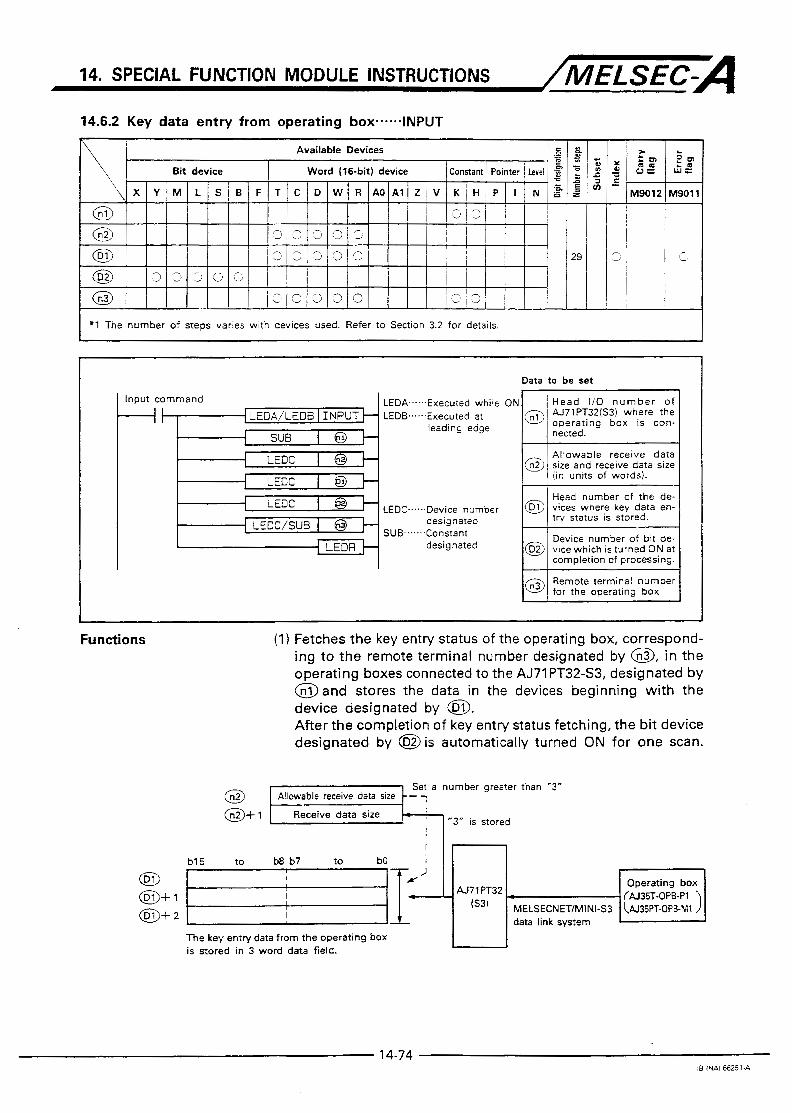
14. SPECIAL FUNCTION MODULE INSTRUCTIONS /MELSEC-A 14.6.2 Key data entry from operating box----.-INPUT
I *l The number of steps varies with devices used. Refer to Section 3.2 for details
Data t o be set 1
I I leaalng eoge SUB
LEDC..,..,Device number
SUB ...... designated
I - = , LEDR __.
Allowable receive data
try status is stored. Constant designated Device number of bit de-
vlce which is turned ON at completion of processing.
Remote terminal number
Functions (1) Fetches the key entry status of the operating box, correspond- ing to the remote terminal number designated by @, in the operating boxes connected to the AJ71PT32-S3, designated by @and stores the data in the devices beginning with the device designated by @. After the completion of key entry status fetching, the bit device designated by @is automatically turned ON for one scan.
Set a number greater than “3”
@+ 1 Receive data size “3” is stored
b15 to b8 b7 t o
The key entry data from the operating box is stored in 3 word data field. ‘ I 4J71 PT32
6 3 )
data link system
14-74 iB INAi 66251-A

14. SPECIAL FUNCTION MODULE INSTRUCTIONS /MELSEC-A (2) In the receive processing with the INPUT instruction, reading
data received by AJ71PT3243 buffer memory and ON/OFF control of read requestkompletion signal is automatically processed internally.
(3) The key entry data is stored in the 3 word data field as illustrated below.
Operation panel
In each bit of @ to m-l-2, "1" is stored for the key turned ON and "0" is stored for the key turned OFF.
For the head I/O number of AJ71 PT32-S3 to be designated by @, the upper two digits of the head I/O number expressed in 3-digit hexadecimal are set.
Example: When AJ71PT32-S3 is assigned to W 1 2 0 to xpI13F. Set "12H" for @.
The allowable receive data size to be designated by @ is set t o secure the device range where the received data is stored. The range is secured from the device designated by @ and its range size is defined by @. The actual receive data size is automatically stored in @+l.
1 I I
I I
g+, T I 1 Stored received
m + 2 data
Received data
In the key entry operation using an operating box, data size to be received is 3 words. Therefore, the setting for @ should be "3" or greater. If the setting is "2" is smaller, it is impossible to store all key entry status.
Exampie:
@ = 4 @ = 2
Touch key ON/OFF status @+I -. Sheet key OWOFF (Sheet key ON/OFF status is not stored)
-1 Touch key ON/OFF status

14. SPECIAL FUNCTION MODULE INSTRUCTIONS /MELSEC=A (6) The bit device designated by @ is automatically turned ON
when the END instruction is executed in the scan in which the receive processing is completed and turned OFF when the END instruction is executed in the next scan. It is used as the INPUT instruction execution completion flag.
(7) The remote terminal number, to be designated by @, is the number assigned to the initial ROM which is installed in the operating box. Set the remote terminal number by the initial data setting using the SWOGP-MINIP system FD.
(8) The ON/OFF status of the keys read by the INPUT instruction is retained unto the next INPUT instruction is executed. If ON/OFF status of more than one key changes after the execution of the INPUT instruction and before the execution of the next INPUT instruction, the ON/OFF status of the key only changed first is stored and the rest of changes cannot be detected.
POINT 1 Communications with the remote terminal module con- nected to the AJ71PT3243 is possible only when the communication start signal (Y(n+z*)) of the AJ71PT32-S3 is ON. If an instruction is executed while this signal is OFF, the bit device set as the instruction processing completion flag is not turned ON although it does not cause an error.
Execution Conditions The INPUT instruction execution mode depends on whether it is designated with an LEDA or LEDB instruction. It is executed every scan while the input command stays ON if it is designated with an LEDA instruction. When it is designated with an LEDB instruction, it is executed only once at the leading edge of the input command.
1n5vycllon END lnnmttl~n I"S7rUCtlO" e x ~ u ~ l o n p m t n g ex-tmn exemuon
END Step 0 END Slcp 0
Sequence program flow
ON OFF
I I I I I I I I I I I I I I input command I I I I l j I I I
I I I I I I
I
INPUT (with LEDA) 1 n I I I I I I I I I I I
I I I I I
I I I
I
INPUT (with E D B ) I 1 I
Operation Errors An operation error occurs in the following cases and the error flag (M9011) is set.
Description
The range defined by @ exceeds the final device number of that device. The INPUT instruction is executed for other than the operating box or
Error Code D9008 D9091
504 5 0 ,
AI35PTF-RZ. 509
14-76 IB iNAJ 66251-A

14. SPECIAL FUNCTION MODULE INSTRUCTIONS /MELSEC-A Program Example A program to read the ON/OFF status of the touch keys and sheet
keys of the operating box connected to the AJ71PT32-S3, loaded in I/O numbers 020 to 03F, as a remote terminal 1 and to store the read status to DO to D2 when X0 is turned ON. (Touch key ON/OFF status is stored in DO and D l and sheet key ON/OFF status is stored in D2.)
I Turning ON the communication Y start sianal - I
now 3 t: ,/ Designating the number of input
points I
Operating box
Turning MO ON at the completion of instruction
MELSECNET/MINI-S3 data link
Touch key Input status
Sheet key input status

14. SPECIAL FUNCTION MODULE INSTRUCTIONS /MELSEC-A 14.6.3 Data communication with the AJ35PTF-R2
(1) Sending data in no-protocol mode by designating the number of bytes.-.---PRN
29
T t L
Send command LEDA....Executed while ON
1 L E D A / L m E LEDB....Executed at I - leading edge
SUB ut- -[ LEDC/SUE @
LEDC....Device number designated
SUB -.-.Constant designated __t LEDC I 0 p -1 LEDC Tl
LEOC/SUE -1 LEDP
8 LEDC-...Device number
designated SUB ..... Constant designated
Data to be set
Head UO number of AJ71 PT32-S3 where the AJ35PTF-R2 that sends data is connected.
Number of bytes or words of data t o be sent
Head number of the de- vices where the data to be sent is stored.
Device number of the bit device which is turned ON at the completion of pro- cessing.
Remote terminal number of the AJ35PTF-RZ which sends data.
Functions (a) Sends data in the no-protocol mode to the external device connected to the AJ35PTF-R2, corresponding to the remote terminal number designated by @, among the AJ35PTF-R2s connected to the AJ71PT32-S3, designated by a. The data to be. sent is set in @ points in the devices beginning with the device designated by 0. After the completion of send processing, the bit device designated by 0 is automatically turned ON for one scan.
0 @+1
@+2
@+n
b15 to b8 b7 to bO n Remote terminal
I to
AJ35PTF-RZ MELSECNET/MINI-S3 data link system
U
External device
14-78 13 lNAi €6251-4

14. SPECIAL FUNCTION MODULE INSTRUCTIONS /MELSEC-A Example:
b15 to b8 b7 to bo .-
Dl 8
n External device
A J 7 - F 2 1 "49H" to " 4 1 ~ " ~ r/ j l AJ35PTF-R2 - ABCDEFGHI
MELSECNET/MINI-S3 data link system
In the send processing with the PRN instruction, writing data to the AJ71PT32-S3 buffer memory and ON/OFF control of sent requestkompletion signal is automatically processed internally.
For the head I/O number of AJ71PT32-S3 to be designated by @,the upper two digits of the head I/O number expressed in 3-digit hexadecimal are set.
Example: When AJ71PT32-S3 is assigned to W 1 2 0 to X/ Y 13F. Set "12," for @.
The units of data to be sent and allowable setting range to be designated by @ vary according to the data unit designation (byte/word) for AJ71PT32-S3 and TO area setting in the remote terminal setting with parameters. The send data to be set by @ varies according to byte/word designation as illustrated below.
I Word uni t setting 1 - Byte unit setting I I I
/ 2nd word
@+2 3rd word
@+3 4th word @+4
I
I @ 2nd byte 1st byte
@l 4th byte 3rd byte
@+2
g+4
@+3 8th byte 7th byte
Setting range
Word unit designated ..-1 to (TO area setting - 1) words Byte unit designated ..-.1 to (TO area setting - 1) X 2 bytes
Data unit and TO area must be set in advance for the AJ7 1 PT32-S3.
Data unit designation...-Set the data unit with the remote terminal parameter for AJ71 PT32- S3 buffer memory using the TO instruction.
SWOGP-MINIP system FD. TO area setting .. .......... Set to the initial da ta ROM using the
14-79 IB I N K 66251-A

14. SPECIAL FUNCTION MODULE INSTRUCTIONS /MELSEC-A (e) The remote terminal number, to be designated by @, is the
number assigned to the initial ROM for the corresponding
Set the remote terminal number by the initial data setting using the SWOGP-MINIP system FD.
AJ35PTF-R2.
The bit device designated by a, is automatically turned ON when the END instruction is executed in the scan in which the send processing is completed and turned OFF when the END instruction is executed in the next scan. It is used as the PRN instruction execution completion flag.
POINT I Communications with the remote terminal module con- nected to the AJ71PT3243 is possible only when the communication start signal (YI"+=I) of the AJ71PT3243 is ON. If an instruction is executed while this signal is OFF, the bit device set as the instruction processing completion flag is not turned ON although it does not cause an error.
Execution Conditions The PRN instruction execution mode depends on whether it is designated with an LEDA or LEDB instruction. It is executed every scan while the send command stays ON if it is designated with an LEDA instruction. When it is designated with a n LEDB instruction, it is executed only once at the leading edge of the send command.
ON OFF
I I I I I I I I I I I
Send command I I I I
I I I I I
I PRN (with LEDA) 1 I
I I I I I I I I I I I I
I I I I I
I I I
PRN (with LEDB) I
Operation Errors An operation error occurs in the following cases and the error flag (M9011) is set.
Description Error Code
WOO8 D9091 The data size designated by a exceeds the following range:
Word units .... 1 to (TO area setting - 1) words Byte units ...... 1 to (TO area setting - 1) X 2 bytes 504
The range defined by a exceeds the final device number of that 50 device. The PRN instruction is executed for other than the AJ35PTF-R2. 509
14-80 18 IN4 662514

14. SPECIAL FUNCTION MODULE INSTRUCTIONS /MELSEC-A Program Example A program to send the data, stored in DO to D4, to the external
device connected to AJ35PTF-R2, the remote terminal number 1, of the AJ71PT32-S3 loaded to 1/0 numbers 020 to 04F when X0 is turned ON.
Designation of "word unit" for sendingireceiving data; t o be set once after PC CPU run Turning ON communication start signal of AJ7lPT32-S3
t I Designating the number of send 7 points
r Turning MO ON at the comple- t lon of instruction Designating remote terminal number
DO Remote terminal
MELSECN€T/MINI-S3
D2 I AJ35PTF-R2 - External device "MITSUBISHI"
D3
w 4 9 4 8 u
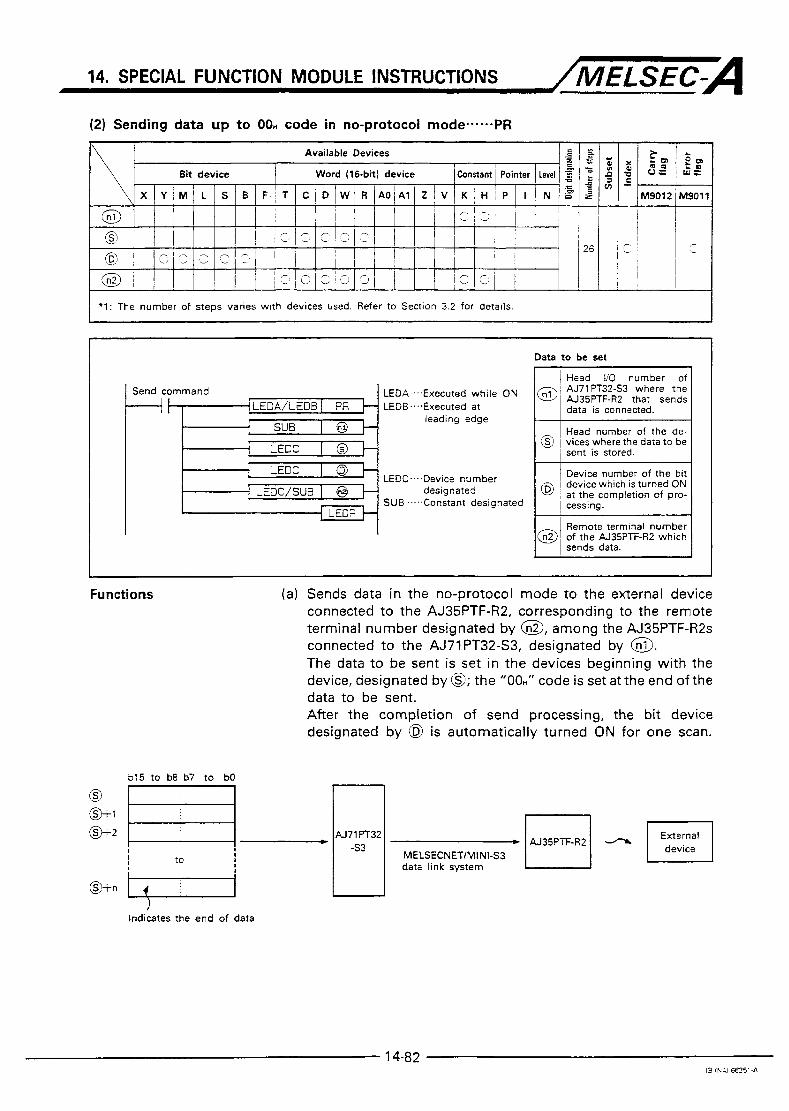
14. SPECIAL FUNCTION MODULE INSTRUCTIONS /MELSEC-A (2) Sending data up t o OOH code in no-protocol mode------PR
c Available Devices
5 Level Pointer canstant Word (16-bit) device Bit device
._ 0 - L
, \ x E N P / I K ! H z 1 v R ~ A O A I w D c F I T B s Y / M ~ L
.e
Jzil I i I ?~ 1
i 1 : ' i 1 0 I 1 1 ' i l , '2 ,:. : I 1, '1, 1 I @ ' ! . j
i I., 9 I:: z Ci E: 0 1 c. 2 '2 '"
- - n r ,
'1: The number of steps varies with devices used. Refer to Section 3.2 for details
Send command
-+t LEDA-...Executed while ON
-[LEDA/LEDB 1 PR LEDB-,..Executed at
1 SUB I @ / - leading edge
-1 LEDC o / - -n LEDC....Device number
1 LEDC/SUB designated @' - LEDR
SUB ...,. Constant designated
Data to be set
1 Head 110 number of I AJ71PT32-S3 where the
data is connected.
@ ~ vices where the data to be i sent is stored.
Device number of the bit device which is turned ON at the completion of pro- cessing.
Remote terminal number of the AJ35PTF-RZ which sends data.
Functions (a ) Sends data in the no-protocol mode to the external device connected to the AJ35PTF-R2, corresponding to the remote terminal number designated by @, among the AJ35PTF-R2s connected to the AJ77PT32-S3, designated by @. The data to be sent is set in the devices beginning with the device, designated by @; the "OOH" code is set at the end of the data to be sent. After the completion of send processing, the bit device designated by 0 is automatically turned ON for one scan.
b15 t o b8 b7 t o bO
I I I f to v U71M32
-s3
indicates the end of data
MELSECNET/MINI-S3 data link system
14-82 IB (hit 5 6 2 5 ' - A

14. SPECIAL FUNCTION MODULE INSTRUCTIONS /MELSEC-A Example:
D17 MELSECNET/MINI-S3 data link system
In the send processing with the PR instruction, writing data to the AJ71PT32-S3 buffer memory and ON/OFF control of sent requestkornpletion signal is automatically processed internally.
For the head I/O number of AJ71PT32-S3 t o be designated by @, the upper two digits of the head I/O number expressed in 3-digit hexadecimal are set.
Example: When AJ71PT32-S3 is assigned t o W 1 2 0 t o X/ Y 13F. Set "12," for @.
In the send data to be stored in the devices following the device designated by 3, the "00," code cannot be set as the data. The "OOH" code is used as the end of send data code.
The number of bytedwords of data that can be sent in a single data send processing varies according to the data unit designation for the AJ71PT32-S3 and the TO area setting by the initial parameter.
Word unit designation 1 to (TO area setting - 1) words Byte unit designation-... 1 to (TO area setting - 1) X 2 bytes
Data unit and TO area must be set in advance for the AJ71 PT32-S3.
Data unit designation....Set the data unit with the remote terminal parameter for AJ71 PT32- S3 buffer memory using the TO instruction.
SWOGP-MlNlP system FD. e TO area setting ............ Set to the initial data ROM using the
The send data to be set by 0 varies according t o bytelword designation as illustrated below.
1
Word unit designation I Byte unit designation b15 to b8 b7 to bO
@ 2nd byte 1st byte
2nd word @+l 4th byte 3rd byte
@+2 3rd word @+2 6th byte 5th byte
@+3 4th word @+3 8th byte 7th byte
@+5 End of @+5 End of
5th word @+4 lUth byte 9th byte
data data
14-83 le IhAi) S57jlP

14. SPECIAL FUNCTION MODULE INSTRUCTIONS /MELSEC-A The remote terminal number, to be designated by @, is the number assigned to the initial ROM for the corresponding
Set the remote terminal number by the initial data setting using the SWOGP-MINIP system FD.
AJ35PTF-R2.
The bit device designated by is automatically turned ON when the END instruction is executed in the scan in which the send processing is completed and turned OFF when the END instruction is executed in the next scan. It is used as the PR instruction execution completion flag.
Execution Conditions
POINT 1 Communications with the remote terminal module con- nected to the AJ71PT3243 is possible only when the communication start signal (Y(n+~s)) of the AJ71PT3243 is ON. If an instruction is executed while this signal is OFF, the bit device set as the instruction processing completion flag is not set although it does not cause an error.
The PR instruction execution mode depends on whether it is designated with an LEDA or LEDB instruction. It is executed every scan while the send command stays ON if it is designated with an LEDA instruction. When it is designated with an LEDB instruction, it is executed only once at the leading edge of the send command.
Sequence program flow I I I I I
ON OFF
I I I I I I I I I
I Send command
I I I I I
I I I 1 I I
PR (with LEDB)
Operation Errors An operation error occurs in the following cases and the error flag (M9011) is set.
Description M Error Code
The ‘00~” code is not stored in a device in the range from the device designated by 0 to the final device number. The size of data to be sent exceeds the following range: 504 50
Wordunits .... 1 to (TO area setting - 1) words Byte units ...... 1 to (TO area setting - 1) X 2 bytes
The PR instruction is executed for other than the AJ35PTF-R2. 509

14. SPECIAL FUNCTION MODULE INSTRUCTIONS /MELSEC-A Program Example A program to send the data, stored in the devices from DO to the
device storing the ''00~'' code, to the external device connected to AJ35PTF-R2, the remote terminal number 1, of the AJ71PT32-S3 loaded to I/O numbers 020 to 04F in units of words when X0 is turned ON.
DO
Dl D2
D3
D4
Remote terminal
Designation of "word unit" for sendinglreceiving data; to be set once after PC CPU run Turning ON communication Stan signal of A171PT32-S3
Turning MO ON at the comple- tion of instruction Designation of remote terminal number
MELSECNET/MINI-S3 data link
number 1
I - External device 'MELSEC"

14. SPECIAL FUNCTION MODULE INSTRUCTIONS /MELSEC-A (3) Data communication in no-protocol mode--*..-INPUT
-IT M9012 1 M9011
3eceive command LEDA....Executed while ON * [ L E D A / m d LEDB....Executed at
~
[ SUB Io)-i leading edge
LEDC I 8 -[ LEDC 7- -- LEDC
LEDC....Devlce number
LEDC/SUB F b SUB -...Constant designated
designated -
I -{ LEDR
Data to be set
~ Head IiO number of AJ71 PT32-S3 where the AJ35PTF-R2 that receives data is connected.
P i Allowable receive data size @-) and received data size
P I device which is turned ON a at the completion of pro- cessing.
Remote terminal number
receives data.
Functions (a) Reads the data received by the AJ35PTF-R2, corresponding to the remote terminal number designated by @I, in the AJ35PTF-R2s connected to the AJ71PT32-S3 designated by
The data is received in the devices beginning with the device designated by @I within the ranged designated by @. After the completion of receive processing, the bit device designated by @ is automatically turned ON for one scan.
@.
b15 to b8 b7 to bO ! I
AJ71 PT32 -s3
AJ35PTF-R2 MELSECNET/MINI-S3
I I data link
14-86 '3 IHAI 662514

14. SPECIAL FUNCTION MODULE INSTRUCTIONS /MELSEC-A Example:
DO
D l 0 External device
43b n "4," to "49"
D l 3 4% 4 , ~ 1 I (Byte designated) da;a link system -
In the receive processing with the INPUT instruction, reading data from the AJ71 PT32-S3 buffer memory and ON/OFF control of read requedcompletion signal is automatically processed internally.
For the head I/O number of AJ71PT32-S3 to be designated by @,the upper two digits of the head I/O number expressed in 3-digit hexadecimal are set. Example: When AJ71 PT32-S3 is assigned to W 1 2 0 t o x p l l 3 F .
Set ''12~'' for @. Number of bytes or words of data that can be received in one data send processing varies according to the data unit designation and the FROM area setting by the initial data.
Word unit designated -..1 to (FROM area setting -1) words Byte unit designated.-...l to (FROM area setting - 1) X 2 bytes
Data unit and FROM area must be set in advance for the
Data unit designation....Set the data unit with the remote terminal parameter for AJ71 PT32- S3 buffer memory using the TO instruction.
FROM area setting..-.....Set to the initial data ROM using the SWOGP-MINIP system FD.
AJ71 PT32-S3.
The allowable receive data size to be designated by @ is set to secure the device range where the received data is stored. The range is secured from the device designated by @ and its range size is defined by @. The actual receive data size is automatically stored in @+l.
@ Ailowable receive data size - - - - - - - - - - 1 @+l Receive data size - - I
I B :+11'm
@+2
@'+3 Received data
Stored received I 4
storing range
If the size of actually received data size is greater than the allowable receive data size designated by @, the data which fits in the designated allowable receive data size is stored in the devices and the excess of received data is discarded.

14. SPECIAL FUNCTION MODULE INSTRUCTIONS /IWELSEC-A (9) The units of data to be designated by @and G i - 1 vary
according to the designation of data unit (byte/word) for
Similarly, receive data to be stored in @ varies according to the data unit (byte/word) as illustrated below.
AJ71 PT32-S3.
Word unit setting
@+ 1 5 (words)
b15 to I
@ @+ 1
@+2
@+3
@+4
@+5
@+7
@+6
2nd word
4th word
,
I I i
Byte unit setting
63 16 (bytes) - - - - 10 (bytes) 1
I b15 to b8 b7 to bO 1
@+5
@+7
'y added 91 I- end of r e Ceived da,r
(h) When the byte unit is designated, the "OOH" code is stored in the manner as described below according to whether the receive data is odd-numbered or even-numbered bytes. Odd-numbered bytes:
The " 0 0 ~ " code is stored in the upper byte field of the final device of the devices where the receive data is to be stored.
The "OOOOH" code is stored in the device following the final device of the devices where the receive data is to be stored.
Even-numbered bytes:
r
@+l I 9 (bytes) I @+1 I 8 (bytes) 1 b15 to b8 b7 to bO
@+3 8th byte : 7th byte
'00~" is stored automatically "0000~" is stored automatically
( i ) If the size of actually received data is greater than the allowable receive data size, the "00," code is stored in the device following the final device of the receive data storing devices.
Word unit setting Byte unit setting
@+1
bO I b15 to b8 b7 to bO
3rd word
@+3 4th word
@+4 5th word

14, SPECIAL FUNCTION MODULE INSTRUCTIONS /MELSEC-A ( ; 1 The remote terminal number, to be designated by @, is the
number assigned to the initial ROM for the corresponding
Set the remote terminal number by the initial data setting using the SWOGP-MINIP system FD.
AJ35PTF-R2.
(k) The bit device designated by @ is automatically turned ON when the E N D instruction is executed in the scan in which the receive processing is completed and turned OFF when the END instruction is executed in the next scan. It is used as the INPUT instruction execution completion flag.
( I ) In data receive processing with the AJ35PTF-R2, received data is retained until the receive processing by the INPUT instruc- tion is executed. Therefore, the external device cannot send the next set of data to the same AJ35PTF-R2 until the receive processing by the INPUT instruction is completed.
POINT 1 Communications with the remote terminal module con- nected to the AJ71PT3243 is possible only when the communication start signal (YMw) of the AJ71PT3243 is ON. If an instruction is executed while this signal is OFF, the bit device set as the instruction processing completion flag is not turned ON although it does not cause an error.
Execution Conditions The INPUT instruction execution mode depends on whether it is designated with an LEDA or LEDB instruction. It is executed every scan while the receive command stays ON if it is designated with an LEDA instruction. When it is designated with an LEDB instruction, it is executed only once a t the leading edge of the receive command.
1nnWtt-m END I ~ S N R I O ~ e x m m n pmessmg execution
l”SrYRl0” eXR”ll0”
Step 0 END Slep 0
Sequence program flow I I I I I
ON I I I I I I
OFF I I
I I I I I I I I I I I
I I I I I I
Receive command
INPUT (with LEDA) 1 7 I I
I I I I I I I I I I I I I I I I I I I
INPUT (with LEDB) 1 I I I
I I
Operation Errors An operation error occurs in the following cases and the error flag (M9011) is set.
Error Code D9008 I D9091 Description
- The range defined by a exceeds the final device number of that 1 device. The INPUT instruction is executed for the AJ35PTF-RZ or o~eratina box. 1 50

14. SPECIAL FUNCTION MODULE INSTRUCTIONS /MELSEC-A Program Example
External device "MITSUBISHI"
A program to receive 5 word data, from the external device connected to the remote terminal number 1, AJ35PTF-R2, of the AJ71PT32-S3 that is loaded in l/O numbers 020 to 04F, when X0 is turned ON and stores the receive data to DO to D4.
Designation of "word uni;" for
set once after PC CPU run P H K 1,
nil 0 8 0 2 8 6 ~ 1 sendinglreceiving data; to be
Turning ON the communication
X Y B B x 0 4 0 : @ d l start signal
5 P i :
DIE( y Designating of number of re-
Turning MO ON a i the cornple- t ion of instruction Designation of remote terminal number
Remote terminal number 1 DO
MELSECNET/MINI-S3 data link AJ71 PT32 42554
D4 D5 l+l
14-90 I6 INK 66251-A

MEMO
.....................................................................................................................................................................
.....................................................................................................................................................................
.....................................................................................................................................................................
....................................................................................................................................................................
....................................................................................................................................................................
....................................................................................................................................................................
....................................................................................................................................................................
....................................................................................................................................................................
....................................................................................................................................................................
IB (NAI 662516,

14. SPECIAL FUNCTION MODULE INSTRUCTIONS /MELSEC-A 14.6.4 Communication with remote terminal modules.--.-.MINI
[ * l : The number of steps varies with devices used. Refer to Section 3.2 for details
Communication command
I I 5
Data to be set
Head 110 number of the N71PT32iS3) where the re- mote terminal module for communication is connected.
Unit number of the remote
communication is executed.
Head number of the de-
is to be stored.
points I I The number of reaawrite
Device number of the bit de-
completion of processing
Device number of for dum- my output (no processing). I
Functions (1) Executes communications with the remote terminal module, designated by @, in the remote terminal modules connected to the AJ71PT32-S3 designated by @. The remote terminal modules with which communications can be executed are the MINI standard protocol compatible remote terminal modules.
(2) In the communications with the remote terminal modules using the MINI instruction, the send requestkompletion signal, read requestkompletion signal, and buffer memory address of the AJ71PT32-S3 are automatically controlled.
14-9 1 I8 INAI 66251-2

14. SPECIAL FUNCTION MODULE INSTRUCTIONS /MELSEC-A (3) The MINI instruction is used in combination with the FROMTTO
instruction and PRC instruction. Up to 32 FROMA-0 instruc- tions can be used in a single MINI instruction. The PRC instruction is used with the FROM/TO instruction in pairs.
1 Read (FROM) ]
@+1
@+2
I to I I I
AJ71 PT32
I I
I to I I I
I AJ71 PT32
Remote terminal module
1 - 1 : to
Remote termlnal mocule
Buffer memory
0
(4) For the head I/O number of AJ71PT32-S3 to be designated by @, the upper two digits of the head I/O number expressed in 3-digit hexadecimal are set. Example: When AJ71PT32-S3 is assigned to W 1 2 0 t o wY13F.
Set "12H'' for @. ( 5 ) For the remote terminal module number designated by @,
set the unit number assigned to the remote terminal module with which communications is executed. The remote terminal module number is assigned to each individual remote terminal module in the setting of the initial data ROM of the AJ71PT32-S3.
(6) For the buffer memory address designated by @, set the head of the buffer memory address at the remote terminal module with which communication is executed. The communication area is defined by @ beginning with the address designated by @.
(7) The device number designated by @ indicates the head device number of the devices where the read data is to be stored. The read data is stored in the range defined by @ beginning with the device number designated by @.
(8) For the data or the device number to be designated by @, designate the data to be written to the remote terminal module or the head number of the devices where the data to be written is stored. If a constant is designated, the designated value is written to the number of points designated by @ from the designated address of the remote terminal module. If a device number is designated, the data stored in the device range designated by @ beginning with the designated device number is written to the addresses in the remote terminal module beginning with the designated address.
14-92 IS lNAl €66251-&

14. SPECIAL FUNCTION MODULE INSTRUCTIONS /MELSEC-A (9) The number of points designated by @ designates the
number of points for read/write processing.
(10) The bit device designated by @ is used as the communica- tion processing completion flag. It is automatically turned ON when the END instruction is executed in the scan in which the communication processing is completed. It is turned OFF when the END instruction in the next scan is executed.
step 0 END Srep 0 END Step 0 END Step a END Step 0 I I
Sequence program flow :3
Comrnunlcatlor, 5:aR ~
I I TT-? I I t
I I
Comrnun~ca t~or end
I I I I I I
I I Device number ON designated by @ OFF t I
(1 1) The items designated by @ is dummy information which is not processed; designate an arbitrary device number of an output (Y).
(12) The communication processing with remote terminal modules using the MINI instruction permits simultaneous cornmunica- tions with up to 32 remote terminal modules for all AJ71PT32- s3s.
(13) The set data is entered to the communication request entry area using the FROM/TO instruction and communication processing is executed according to the data in the entry area.
, The instruction execution is completed by entering the data to the communication request entry area, then the next instruc- tion is executed.
AZACPU(Sl)/A3ACPU
Communication request entry area
Remote terminal - Area No. 1
Area No. 2 ~ Remote terminal
module No. 2
Remote terminal module No. 3
Remote terminal module No. 4
-- AJ71 PT32
Remote terminal module No. 1
14-93 IB (NA) 662516

14. SPECIAL FUNCTION MODULE INSTRUCTIONS /MELSEC-A Therefore, once the set data is entered by executing the instruction, communication processing is completed even if the communication command (conditional contact preceding the MINI instruction) is turned OFF.
(14) When the set data is to be entered, the device number of the bit device designated by @ is checked and entry processing is not executed even if the instruction is executed if the processing using the same device number is being executed.
(15) After the completion of the processing according to the entered set data, the device designated by @ is turned ON and deleted from the communication request entry area.
(16) The communication request entry area allows entry of up 32 communication requests. If more than 32 communication requests are to be entered, an error occurs and entry processing is not executed.
(17) Entry status in the communication request entry area can be confirmed by reading M9081 and D9081.
M9081 .. . . . . . Turned ON if the communication request entry area becomes full; turned OFF when entry area becomes available.
D9081 ........ Stores the available number of areas where set data can be entered.
Therefore, the M9081 and D9081 can be used as the hand- shake signal to execute an instruction.
(18) If an instruction is executed for the remote terminal module which is currently executing communications, communication processing is executed continuously after the current com- munication processing is completed.
(19) For details of how to use the MINI instruction and its programming restrictions, refer to the User's Manual for the individual MINI standard protocol compatible remote terminal module.
I I Communications with the remote terminal module con- nected to the AJ71PT3263 is possible only when the communication start signal (Y,.+=)) of the AJ71PT3263 is ON. If an instruction is executed while this signal is OFF, the bit device set as the instruction processing completion flag is not turned ON although it does not cause an error.
14-94 19 I N A ! 662514

14. SPECIAL FUNCTION MODULE INSTRUCTIONS [ M E L S E C - A Execution Conditions The MINI instruction is executed every scan while the communica-
tion command stays ON.
MINI
Operation Errors
I I I I I I I I I I I I I I I
I I
An operation error occurs in the following cases and the error flag (M9011) is set.
Description
The MINI instruction is executed for a module other than AJ71PT32-S3. The unit with which communications is to be executed is not the MINI standard protocol compatible remote terminal module. The range defined by @ exceeds the final device number of that device. With the PRC instruction, devices other than M. L, S, and B are used for the bit device desianated bv 6 f l . With the FROM instruction, the number of points designated by @ is greater than "receive area setting - 1". In the initial data setting, the receive area setting is less than 3 words. With the TO instruction, the number of points designated by @ is areater than "send area settina - 3". The communication entrv area is full.
Error Code 1 WOO8 1 D9091 1
50
509
14-95 I3 (NN 6 6 2 5 1 4

MEMO ....................................................................................................................................................................
....................................................................................................................................................................
....................................................................................................................................................................
....................................................................................................................................................................
....................................................................................................................................................................
....................................................................................................................................................................
.....................................................................................................................................................................
.....................................................................................................................................................................
.....................................................................................................................................................................
.....................................................................................................................................................................
....................................................................................................................................................................
.....................................................................................................................................................................
....................................................................................................................................................................
....................................................................................................................................................................
....................................................................................................................................................................
.....................................................................................................................................................................
.....................................................................................................................................................................
....................................................................................................................................................................
....................................................................................................................................................................
....................................................................................................................................................................
IB !\AI 60751-A

14. SPECIAL FUNCTION MODULE INSTRUCTIONS /MELSEC-A 14.6.5 Error resetting with remote terminal modules-.----MINIERR
Available Devices E 6 - z z - g z x 0 Bit device w = 0 2 Level canstanti Pointer Word (16-bit) device
X Y M L S B F T C D W R A O A ~ Z V K H I P I N ~ Z v) 5 ",
.n - - ' M9012 i ~ 9 0 1 I
a ' 1 1 5 , I r* - ' 17 E, 1
* I : The number of steps varies with devices used. Refer to Section 3.2 for details.
Reset command
[ SUB i o k 1 -1 LEDR
LEDA.-..Executed while ON LEDB.-..Executed at leading
edge Data to be set
AJ71PT32-S3 which re- sets the remote terminal module error.
Functions
Execution Conditions
(1) Resets the error detected status for the remote terminal module of the AJ71PT32-S3 designated by @.
(2) The remote terminal module error detection reset signal (Y24) is automatically turned ON.
(3) For the head I10 number of AJ71PT32-S3 to be designated by a, the upper two digits of the head I/O number expressed in 3-digit hexadecimal are set.
Example: When AJ71 PT32-S3 is assigned to W 1 2 0 to XNl3F. Set "12H" for @.
The MINIERR instruction execution mode depends on whether it is designated with an LEDA or LEDB instruction. It is executed every scan while the reset command stays ON if it is designated with an LEDA instruction. When it is designated with an LEDB instruction, it is executed only once at the leading edge of the reset command.
Sequence program flow
ON OFF Reset command
I I
1 I
I I I I I
MINIERR (with LEDA) n I I I I I I I I I 1 I I I I I I I I I
I I I MINIERR (with LEDB) I I I
I
1 4-9 6 IB INN €62514

14. SPECIAL FUNCTION MODULE INSTRUCTIONS /MELSEC-A Program Example A program to reset the remote terminal error detection signal of
the AJ71PT32-S3 loaded in I/O numbers 020 to 04F.
14-97 IS IhAI € 6 2 5 1 4

14. SPECIAL FUNCTION MODULE INSTRUCTIONS /MELSEC-A 14.6.6 Reading communication status..-*-*SPBUSY
I *1: The number of steps varies with devices used. Refer to Section 3.2 for details. I
I Read command I Data to be set
LEDA.,..Executed while ON LEDB.-..Executed at AJ71PT32(S3) which
leading edge reads the communication status.
Device number of the de- vice where the read com-
stored. munication status is to be
Functions (1) Reads the execution status of the following instructions for the remote terminal module connected to the AJ71PT32-S3 designated by @ and stores the execution status to the device designated by @. Key entry from the operating box ..-e....-...-. INPUT instruction Data communications with AJ35PTF-RZ
PRN, PR, INPUT instruction Data communications with MINI standard protocol compatible remote terminal module ---.-...--... MINI instruction
..................................
(2) For the head 110 number of AJ71PT32-S3 to be designated by 0, the upper two digits of the head I/O number expressed in 3- digit hexadecimal are set. Example: When AJ71PT32-S3 is assigned t o W 1 2 0 t o wY13F.
Set "12"' for 0. (3) When the communication processing starts, "1" is set to the
designated bit. After the completion of processing, "0" is stored in that bit. The completion of processing is recognized at the trailing edge of the completion flag of each instruction.
b15 to b12 b l l t o b8 b7 t o b4 b3 to bO
@ Stores data send status to the 1st remote terminal module
-Stores the data receive status from the 1st remote terminal module Stores data send status to the 2nd remote terminal module Stores the data receive status from the 2nd remote terminal module
I 1 Stores data send status to the 8th remote terminal module Stores the data receive status from the 8th remote terminal module
b15 to b12 b l l to b8 b7 to b4 b3 to W
@+I [-a-isstord/ . . , . . . . . , .
, .
Stores data send status to the 9th remote terminal module
k -Stores the data receive status from the 9th remote terminal module Stores data send status to the 10th remote terminal module Stores the data receive status from the 10th remote terminal module >
I Stores data send status to the 14th remote terminal module Stores the data receive status from the 14th remote terminal module
14-98 I6 INAI M251-A

14. SPECIAL FUNCTION MODULE INSTRUCTIONS /MELSEC-A Execution Conditions The SPBUSY instruction execution mode depends on whether it is
designated with an LEDA or LEDB instruction. It is executed every scan while the read command stays ON if it is designated with an LEDA instruction. When it is designated with an LEDB instruction, it is executed only once a t the leading edge of the read command.
l n n r ~ n ~ o n p m s m g ereCutfOn ereC"llOn
END lnnl l~t lon I n n l i K l m BIRUl lO"
lnnmcuan elR"t l0" e x e m o n l"RrUQl0"
Slep 0 END Step 0 END Step 0 END Step 0
Sequence program flow
ON OFF
I I I I I I I I I I I I 1 I I I I I
I I I I I I I I I I I I I I I
Read command I I I I I
I SPBUSY (with LEDA) 1 I
I I
I I I I I I
1 I I I I I I I 1 I
I I I SPBUSY (with LEDB) I , I
Program Example A program to turn M10 ON when the remote terminal station number 1 of the AJ71 PT32-S3, loaded in I/O numbers 020 to 04F, is sending data.

14. SPECIAL FUNCTION MODULE INSTRUCTIONS /MELSEC-A 14.6.7 Forced stop of communication processing-...--SPCLR \ Available Devices
Bit device Word (16-bit) device
X M9012 1 M9011 W T ! C / D B / F S L M Y
G; i i i (3 8 , , -. ,.. I ,- , c i L. 1 ._
*1: The number of steps varies with devices used. Refer to Section 3.2 for details.
Stop command
L E D A / L E D B / S P C L R k
{ SUB I O F { LEDC 1 0 +
[ LEDR
LEDA....Executed while LEDB...-Executed at
leading edge
Data to be set
AJ71 PT32-S3 which stops communication proces- sing.
Head number of devices
data is stored.
Functions (1) Stops communication processing, called by the following instructions, with the remote terminal module connected to the AJ71PT32-S3 designated by a. Key entry from the operating box .......-..-... INPUT instruction Data communications with AJ35PTF-R2
PRN, PR, INPUT instruction Data communications with MINI standard protocol compatible remote terminal module ..e.-.....-. MINI instruction
..................................
(2) For the head I/O number of AJ71 PT32-S3 to be designated by @,the upper two digits of the head I/O number expressed in 3- digit hexadecimal are set.
Example: When AJ71 PT32-S3 is assigned to W 1 2 0 t o W 1 3 F . Set " 1 2 H " for @.
(3) The processing to be forcibly stopped is stored in El.
Set "1 " to the bit corresponding to the processing to be stopped. b15 to b12 b l l t o b8 b7 to b4 b3 to bO
@ '&I " ' ' "i' TtL For data send processing to the 1st remote terminal module For data receive processing from the 1st remote terminal For data send processing to the 2nd remote terminal module For data receive processing from the 2nd remote terminal
For data send processing to the 8th remote terminal module For data receive processing from the 8th remote terminal
b15 to b12 b l l to b8 b7 to b4 b3 to bO
@+-1 10- is stored 1 I & A & & & &
L F o r data send processing to the 9th remote terminal module For data receive processing from the 9th remote terminal For data send processing to the 10th remote terminal module For data receive processing from the 10th remote terminal
1
For data receive processing from the 14th remote terminal For data send processing to the 14th remote terminal module
14-1 00 13 (ha 662514

14. SPECIAL FUNCTION MODULE INSTRUCTIONS /MELSEC=A (4) If the processing is stopped, the completion flag of the
corresponding instruction is not turned ON.
Execution Conditions The S P U R instruction execution mode depends on whether it is designated with an LEDA or LEDB instruction. It is executed every scan while the stop command stays ON if it is designated with an LEDA instruction. When it is designated with an LEDB instruction, it is executed only once a t the leading edge of the stop command.
ON OFF
I I I I I I I I I I I
I
I
Stop command I I I I I ; I [ j I I
I
I I I
I I
SPCLR (with LEDA) 1 I I I I I I I I I I I I I
I I I SPCLR (with LED61 I 1 h I
6 I I
I I
Program Example A program to stop sending data to the remote terminal module 1 of the AJ71PT32-S3 loaded in I/O numbers 020 to 04F.
X9@l X@4@ X 8 4 1 P I :
F K CHOU 1 Dl8 2 Storing "1" t o the bit corres-
ponding to send processing to cnou 8 Dl I 3. remote terminal module 1
C L E D P SPCLR H
CSUB @ @ e 2
CLEDC Dl@
LEDR
14-101 IB INA! 652514

15. PROGRAM SWITCHING INSTRUCTION (USABLE WITH A4UCPU) /MELSEC-A 15. PROGRAM SWITCHING INSTRUCTION (USABLE WITH A4UCPU)
The program switching instruction is used to switch the programs for A4U between the main program and a sub program (1 to 3).
The program switching instructions are as follows.
Classification
Switching between main program and desig- nated sub program (1 to 3) switches to t h e main program
I
Instruction Symbol
ZCHGO ZCH G 1 ZCHG2 ZCHGS
Refer
Page Switches to the main program 15-1 Switches to sub program 1 Switches to sub program 2 Switches to sub program 3
Description to
15-1 IB (NAJ € 6 2 5 1 8

MEMO ....................................................................................................................................................................
....................................................................................................................................................................
....................................................................................................................................................................
....................................................................................................................................................................
....................................................................................................................................................................
....................................................................................................................................................................
.....................................................................................................................................................................
.....................................................................................................................................................................
.....................................................................................................................................................................
....................................................................................................................................................................
.....................................................................................................................................................................
....................................................................................................................................................................
....................................................................................................................................................................
....................................................................................................................................................................
.....................................................................................................................................................................
.....................................................................................................................................................................
....................................................................................................................................................................
....................................................................................................................................................................
....................................................................................................................................................................
....................................................................................................................................................................
....................................................................................................................................................................
IB iNA1 €62514

15. PROGRAM SWITCHING INSTRUCTION (USABLE WITH A4UCPU) /MELSEC-A 15.1 Switching between Main Program and Designated Sub Program (1 to 3)
..--.-ZCHGn (Usable with A4UCPU)
L
:g W E I Available Devices z L
Bit device Word (16-bit) device Constant Pointer tevel W E :g
' X Y M L S B F T C D W I R A O A l Z V K H P I N M9012 M9010, M9011 I /
_ _ ~
I i , ~~~
13
1
X Y M L S B F T C D W R A O A l Z V K H P I N a G
M9012 M9010, M9011 I /
I
, I 13
Switching command / Interlock condition /
LEDA I ZCHGO Switching to the main program
Switching to sub program 1
LEDA Switching to sub program 2
LEDA Switching to sub program 3
Executed during ON
Functions Four sequence programs including the main program and sub programs 1 to 3 can be used for an A4UCPU. The ZCHGn instruction switches the program to a designated program.
(1) Switching between the main program and designated sub program is executed after timer and counter processing and self-diagnosis check. Once a program is switched, the operation is executed beginning with the head step of a program after switching.
ZCHGI Main sequence Drogram
I I t 1 1 . I
Tner and counter processing
I I I 1 Sub sequence 1 1 program 1 ZCH GO
(2) For details of the function and method of use, refer to the "method for using sub program" in the ACPU Programming Manual (fundamental).
D9016 can be used to check t h e type of a program being executed.
15-2 IB lNAi €62518

15. PROGRAM SWITCHING INSTRUCTION (USABLE WITH A4UCPU) /MELSEC=A Execution Conditions The ZCHG instruction is executed when the condition contact is
ON.
Ladder example
Timing chart
Operation OFF
ON/OFF ON by turning
x0
OFF 1 ON
L Remark
Ladder example
Operation
x0
OFF ON Status o f .
OFF 1
ON
Nhen the following program is writ ten to the main sequence program and sub sequence xogram 2 before the END or FEND instruction.
Input condttion
Main sequence program /2y'Ayy[ LEDA ZCYG2
Sub sequence program 2 12y'&)+[ LEDA ZCHGO
Interlock
lnpur condmon Interlock
33 Q. :: 3, '5, IT, H" 3, (Ts (51 8 , ON I -
x0 OFF 1 1 j Executing the ZCHGZ instruction of the main r r I [1 r , :I-, seauence Droqram . -
Main sequence program
Sub sequence program 2
Executing the ZCHGO insti of sub sequence program
-uctlon 2
~~~
The main sequence program and sub sequence program 2 are not switched. (a, E), 0) The ZCHG instruction is executed at every scan and the main sequence program and sub sequence program 2 are switched. (a, 0, a, e, 8, @)
The main sequence program and sub sequence program 2 are switched. :a, 6, 03) ~~ ~~ ~~
ahen the ZCHG instruction is executed, END processing such as timer operation Jounter operation, and WDT reset are executed and the operation is executed beginnins Nith step 0 of the program after switching.
~ ~~~
Execution status of PLS instruction when the CHG instruction is used Ladder example
When the following program is written to the main sequence program and sub sequence Drogram 2 before the END or FEND instruction.
1 scan M Z C ~ G instruction execution
Executing the main sequence program
Executing sub sequence program 2 ution
MO is not turned ON.
MO is turned ON for the first scan where sub sequence program 2 is switched by the ZCHG instruction executed after X0 i s turned ON. MO is turned ON for one scan.

15. PROGRAM SWITCHING INSTRUCTION (USABLE WITH A4UCPU) /MELSEC-A Execution status of counter when the CHG instruction is used
Ladder example
Timing chart
Nhen the following program is written to the main sequence program and sub sequence I rogram 2 step 0.
Executing sequence Executing seauence
x0
co
1 scan
tion
- Count value of CO does not change.
1 is added to the count value of CO after the END (FEND, CHG) instruction is executed for first scan of the program after switching by the ACHG instruction executed after X0 is turned ON.
OFF 1 is added to the count value of CO after the END (FEND, CHG) instruction is executed. I
, ON
Execution status of 111 P instruction when the CHG instruction is used
Ladder example
When the following program is written to the main sequence program and sub sequence program 2 step 0.
4 I
I
1 Scan ZCHG instruction execution
Timing chart
Executing the main sequence program
Executing sub sequence program 2
X0 OFF
MOVP
xution
Operation by turning ON/OFF x0
1 OFF IThe MOVP instruction is not executed. ~~~ ~ ~
The MOVP instruction is executed for the first scan where sub sequence program 2 is switched by the ZCHG instruction executed after X0 is turned ON.
~~~ ~~ ~~ ~~
OFF
ON 1
The MOVP instruction is executed once.

15. PROGRAM SWITCHING INSTRUCTION (USABLE WITH A4UCPU) /MELSEC-A Execution status of timer when the CHG instruction is used
A4UCPU has four timer setting value storage areas for the main sequence program and sub sequence programs 1 t o 3. The setting value of unused type number is 0 in the timer setting value storage area.
When the setting value is 0, the setting is regarded as infinite and the timer does not time out. After the timer used for the main (sub) sequence program begins time count by the establishment of input conditions, the timer does not time out during execution of the sub (main) program when the timer designated by the sub (main) program switched by the ZCHG instruction is not used.
Ladder examde
Timing chart
Operation
When the following program is written to the main sequence program and the same timer number is not used for sub sequence program 2.
Executing the maln sequence program
Executing sub sequence program 2
x0 OFF
T200 coil OFF N
T200 turned ON by the main sequence program does not time out during operation o sub sequence program 2. It times out when the main sequence program is executed again and the followin! conditions are established. q
15-5 I6 (NAI 662512
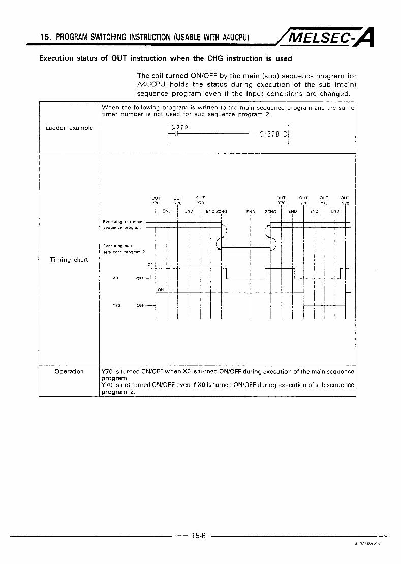
15. PROGRAM SWITCHING INSTRUCTION (USABLE WITH A4UCPU) /MELSEC-A Execution status of OUT instruction when the CHG instruction is used
The coil turned ON/OFF by the main (sub) sequence program for A4UCPU holds the status during execution of the sub (main) sequence program even if the input conditions are changed.
Ladder example
T iming chart
Operation
When the following program is written to the main sequence program and the Sam6 timer number is not used for sub sequence program 2.
p [ " P I-:: I? 8 7 0 -A
! I !
OUT OUT n o
1 END ENC
Executing the rnaln sequence progran:
Executing sub sequence program 2
x0 OFF
Y-70 OFF T i
OUT OUT Y ? O
f i Y-
i
NC I
i I i
0 0 is turned ONiOFF when X0 is turned ON/OFF during execution of the main sequencc x o g r a m . 0 0 is not turned ON/OFF even if X0 is turned ON/OFF during execution of sub sequence woaram 2.
15-6 IB (NAI m51-8

15. PROGRAM SWITCHING INSTRUCTION (USABLE WITH A4UCPU) ~/MELSEC-A Program Example
The following program is used to output the PLS instruction following the input conditions while executing the main program and sub program 2 alternately.
The program is as shown below because an A4UCPU ZCHG instruction is executed while the input conditions are ON.
* Main sequence program - Sub sequence program 2 I 1 2 I Always ON 1 , Always ON
C F E H D Main sequence program Sub sequence program 2
When modifying sub program 1 to 3 during execution of the main program or modifying the main program during execution of sub program 1 to 3, provide interlocks with the ZCHG instruction by setting M9051, M9056, M9057, M9060, and M9061 contacts so that the program being executed is not switched to the program being modified by the ZCHG instruction.
. ~ 9 0 5 1 : ......... CHG instruction execution disabled . M9056: ......... P, I set request for main ~ 9 0 5 7 : ......... P, I set request for sub 1 M9060: ......... P, I set request for sub 2 . M9061 : ......... P, I set request for sub 3
For details of M9051, M9056, M9057, M9060, and M9061, refer to the ACPU Programming Manual (Common Instructions).
15-7 IB I W I 66251-8

16. CC-Link DEDICATED INSTRUCTIONS /MELSEC-A 16. CC-Link DEDICATED INSTRUCTIONS
The dedicated instructions for the CC-Link network system are used for the setting of automatic refreshing of the AnSHCPU and the master module/local module, and also for data communications with the remote station connected to the CC-Link network system. Transient transmission to an intelligent device station and a local station is possible using the dedicated instructions. Read/write of the data with handshake is enabled for a remote device. Which of the dedicated instructions for the CC-Link (8 kinds) can be used at which station is shown below in Table 16.1, 16.2.
Table 16.1 Dedicated instructions for parameter setting Availability (0 : Available, x : Not available)
Instruct ion Description Master station station station
section S:l::,g~ Local Refer to Remarks
RLPA
RRPA
Set a network parameter for the CC-Link master unit. Set an automatic refresh parameter for CC-Link master unithcal unit.
0
Section 16.3 0 0 0
Section 16.2 X X
Table 16.2 Dedicated instructions for data links Availability (0 : Available, x : Not available)
Instruct ion Description Master station stat ion station
section S$gf:,gY Local Refer to Remarks
RIFR Read data from the automatic updating buffer memory of the specified station. 0 (A random access buffer can be specified.)
Section 16.4 0 0
Write data into the automatic updating
(A random access buffer can be specified.) Read data from the buffer memory of the specified station. Read data from the device memory of the CPU of the specified station. Write data into the buffer memory of the specified station. Write data into the buffer memory of the CPU of the specified station. Read data from the buffer memory of the specified station by handshaking. Write data into the buffer memory of the specified station by handshaking.
RlTO Section 16.5 0 0 0 buffer memory of the specified station.)
0
Section 16.9 X X 0
Section 16.8 X X 0
'1 0 0 0
0 0 0
'1 0 0 0
0 0 RlRD Section 16.6 .
RlWT Sectlon 16.7
RI RCV
RISEND
piiq 1) '1: Can be used with master unit software version J or later. 2) Availability of dedicated instructions for the CC-Link depends on the unit of the station
3) The dedicated instructions for the CC-Link are supported by the following CPUs: connected to the CC-Link, so refer to the manual for the unit to be used.
CPU type Software version Instruction AISJHCPU(SB'* Available with all S M , versions. All eight instructions A7SHCPII(Si\
I ~ ~ ~ ~ " , A ~ o z H c p u ~ A ~ 1 All elght Instructions I Available with all SANversions. vyv / - , I I I
A2ASCPU-S30 1 All elght instructions ] SM, version L made on July, 1999, or later AZUSHCPU-S1 I All eight instructions I SM, version L made on July, 1999, or later
A2UCPU(S1), ABUCPU, A4UCPU
RRPA SM, version K made on September, 1998, or later
Other than RRPA
RRPA
S/W verslon Q made on July, 1999, or later
SAN version E made on July, 1999, or later Otherthan RRPA
SM, version A made on September, 1998, AZASCPU(S1) or later
16-1 IB(NA)66251-F

16. CC-Link DEDICATED INSTRUCTIONS /MELSEC~A 16.1 Instructions for Use of the CC-Link Dedicated Instructions
Different intelligent device stations have different buffer memory capacities. Refer to the manual of the intelligent device station used.
Only one of the RIRD, RIWT, RISEND and RIRCV instructions may be executed for the same station. I f two or more of the RIRD, RIWT, RISEND and RIRCV instructions are executed, the second and subsequent instructions are ignored,
RIRD, RIWT, RISEND, and RIRCV may be executed for different stations at the same time. Note that up to 64 instructions may be executed simultaneously.
The data of any device used by the CCLink dedicated instruction should not be changed until the completion of the instruction. I f the data of the device is changed during execution of the instruction, the CC-Link dedicated instruction cannot be completed properly.
Specify the head I10 number of the masterAoca1 module in the CC- Link dedicated instruction. This head li0 number of the masterAocai module is the value in the upper 2 digits of the master/local module's I/O number represented in 3 digits. For example, when the master/local module's I/O number is XiY120, the head 1/0 number is 1 2 H .
~
S A A A A A A A D r , l l l l l l ~ s s s s s s s E H X X Y Y Y J a
C
11 T g u a
B b P 61 41 42 42 42 42
x
X00 X40 X80 YCO Y100 120 CIIO number
to IO to I O to to
X3F X7F XBF YFF Y1lF 13F . Head 1/0 number: 1 ZH
(6) Using the dedicated commands (RIRD, RIWT, RISEND, RIRCV) When the dedicated commands (RIRD, RIWT, RISEND, RIRCV) are used, RY(n+l)E, R Y ( n + l ) F are used with the dedicated commands, so the user must make sure that this signal information is not rewritten.
I [DRlo HO HI60 050 K1 Read RY new information
[ D M lt3CWOOOOO D50
')Retrieve RY(n+l)E, [DX KEY100 D50 , - RY(n+l)F state
HO H160 050 Write to RYnO to RY(n+l)F
16-2 IB(NAj66251-F

RLPA /MELSEC-A 16.2 Network Parameter Setting .....- RLPA
Available Devices c m - % L 0 0 -
H
M9011 M9012 a 1
g g x Z 2 Bit Device w E 0 = .g f Level Pointer Constant Word Device v) m m a
X Y M L S B F T C D W R A O A I Z V K H P I N ~ E V ) - = a
0 0 23 0 0 0 0 0 0
0 0
0 0 0 0 0 @
--I Command
LEDA--Executed while ON LEDB---Executed at leading edge
SUB----Constant designated
~ SUB LEDC--- Device number designated
~ LEDC T+ LEDC Tt- - LEDR
I Data to be set - Head UO number of object
@ 1 [ two digits when the head 1 master module Specified with the upper
I10 number is expressed in 3 hexadecimal digits.
Head number of devices which store link parameters a ’ Host station’s bit device
Network Parameter Data (1) Network parameter setting items
to
I Slave station sening information I
to Automatic update buffer size
Set values for the number of stations connected for communication,
t Set values for one IocaVintelligent device station.
(2) Number of points required for the network parameter area The following points are required for the network parameter setting:
Synchronous mode .......... 1 point validhnvalid setting Communication station .... 1 point count setting Slave station setting ........ Number of points for the number of slave information stations connected for communication Sending buffer size .......... Number of points for the number of local
Receiving buffer size ....... Number of points for the number of local
Automatic update ............. Number of points for the number of local
and intelligent device stations
and intelligent device stations
buffer size and intelligent device stations
16-3 IB(NA)66251-E

RLPA /MELSEC-A (3) Network parameter settings
Synchronous mode lalidhnvalid
\lumber of statlons :onnected for :ommunication
;lave station setting ?formation
;ending buffer size
leceiving buffer size
rutomatic updatlng luffer size
Set Data Set whether the synchronous mode IS valid or lnvE lid.
When synchronous mode IS valid: 1 When synchronous mode is Invalid: 0
Set the number of slave stations connected to th master module of CC-Link.
Set the slave station type. number of slave station occupied. and station number as lndlcated below:
b15 to b12 b l l to b8 b7
Station number Number of slave stations occupled Slave statlon type
Station number setting 1 to 64 (Setting with BIN!
* Set the number of slave statlons occupied
Number of slave stations Setting
occupied 1 station 1
2 station 2
3 station 3
4 station 4
Slave station type setting
Slave Station Type Setting
Remote I/O station 0
Intelligent device station
Set the number of points transmitted from the mas er station to a localilntelligent device station. Set the number of points transmitted from a lo :al/intelligent devlce statlon to the master station Set the number of points of the automatc updatin! luffer used by the master station and localiintelligen levlce station.
Setting Ranc
Oil
1 to 64
b8 to b l l 1104
b12 to b15 0 to 2
Setting End
User
User
User
User
User
User
*: To be set In response to the module used.
IMPORTANT I Use the parameter setting described above when setting only the "synchronous mode valid/invalid", "number of stations connected for communication", "slave station setting information", "sending buffer size", "receiving buffer size", and "automatic updating buffer size". For all other parameters, initial values are forcibly set. If both the RLPA instruction and the TO instruction are used for setting the parameters, the parameters set using the TO instruction are disregarded.
16-4 IBiNA166251-F

RLPA /MELSEC===
Functions (1) When the RLPA instruction is executed, the network parameter data set to the devices beginning with the one specified at @ is set to the master module specified at (2.
AnSHCPU v
Master module @ ( _ _ _ ~ ~ _ _
(2) When the slave station type specified is a local/intelligent device sta- tion, it is necessary to set the "sending buffer size", "receiving buffer size" and "automatic updating buffer size". When the slave station type is a remote 1/0 station or a remote device station, it is not necessary to set the "sending buffer size", "receiving buffer size" and "automatic updating buffer size". (Example)
Teninalrr Tenninalw
In:ecllgent devlce staton (1st module)
Remole I/O station
Remole device statlan
lntelilgent device slamn (2nd module)
Sendlng buffer size
Receiving buffer stze
Automatic updating buffer size
Sendlng buffer w e Recetvlng buffer sue
Automatic updaung buffer w e . .2nd module
Sendlng buffer size. recelvlng buffer sue and automatlc buffer slze need not be set.
Set sizes for local and mtelllgent devlce slations Successively
[ M e n sethng for the other slallons. therefore. start setbng wtth the frontmost empty pasibon] For remote If0 arm remote devlce stations. thelr buffer sues are not set.
POINTS I 0 For the sendingheceiving buffer size, specify a number 7
words larger than the size of the data to be senvreceived. 0 For the automatic updating buffer size, allocate the
necessary size for the individual intelligent device station. 0 Among the intelligent device stations, set "0" for the
automatic updating buffer size for the stations where the automatic updating function is not provided. Set "0" also for the stations where this function is not used.
(3) After setting of the network parameters, if the RLPA instruction is executed again during RUN to change the network parameters, new data is not used for communication with the slave stations. When the AnSHCPU is switched to STOP/PAUSE, then to RUN, the new network parameters are used for communication with the slave stations.
(4) Execution of the RLPA instruction automatically starts the data link. (5) When the RLPA instruction is executed, interlocking must be
executed using unit error signal XnO and unit ready signal XnF, which indicate whether the CC-Link unit is ready.
16-5 IB(NA)66251-F

RLPA /MELSEC=A Execution Conditions As shown below, when the LEDA instruction is used, the RLPA instruction
is executed every scan while the write command is ON. When the LEDB instruction is used. the RLPA instruction is executed only one scan on the leading edge (OFF -+ ON) of the write command.
slip c ENC %ea 0 END Step 0
Sequence program flow END Step 0
H I I I I I I I I I I I
ON OFF I I i j I , Wnte command I I I I
I I I I I I I I I I
I RLPA jwlth LEDAI n I
I 0 I I I 1 I I I
I I I
RLPA (wlth LEDB) I I I
Program Example The following program sets the network parameters to the master module of CC-Link allocated to 110 numbers 000 to 01 F:
(1) Network parameter settings Set Item Set Data I Device for Storing Data
Synchronous mode validiinvalid settin Communication station count
Synchronous mode D l 000
1 module D l001
lntelllgent device station Slave station
setting occupied Information
D l 002 1 1 station slave stations
Station number 1 1
Sendlng buffer size D 1003 128 ( 8 0 ~ ) words Receivlng buffer size I 128 ( 8 0 ~ ) words
D 1005 Automatic buffer size I960 1600~) words D l 004
(2) Program
CMOV 0001 Dl000 I- Synchronous mode valld setting
CMoV oool D1OO, I-
CMOV 210, D1002
CMOV 0080 Dl003 3- Settlng of sending buffer w e
CMOV 0080 D l 004 I- Settlng of recelving buffer slze
CMOV 0600 D1005
CLEDB RLPA
P H
Setting of number of communication statlox Settlng of slave statlon setttng ~nformatton
P H
P H
P H
P H
Settlng of automatlc updating buffer slze
P Y
K
Designation of RLPA Instructton
LEDC Ll000
LEDR
16-6 lB(NA)66251-F

RRPA /MELSEC=A 16.3 Automatic Refresh Parameter Setting ...... RRPA
rtl M9012 M9011
I Data to be set
LEDA---Executed while ON LEDB---Executed at leading edge LEDC-. Device number designated SUB----Constant designated
LEDR
Head VO number of object master module
Specified with the upper two digits when the head 110 number is expressed in 3 hexadecimal digits. 1 @ [
@ ' Head number of devices which store link parameters
Automatic Refresh (1) Auton Parameter Data
@+ 0
@+ 1
@+ 2
@+ 3
@+ 4
@+ 5
@+ 7
@+ 8
@+ 9
@+IO
@ + I 1
@+I2
@+ 6
@ + I 3
@ + 1 4
@ + 1 5
@+16
@+17
@+18
@+19
ltic refresh parameter setting items
RX's head number
CPU slde refreshed device code
CPU side refreshed device's head number
Number of refresh points
RY's head number
CPU side refreshed device code
CPU side refreshed device's head number
Number of refresh points
RWs head number
CPU side refreshed device code
CPU side refreshed device's head number
Number of refresh points
SB's head number
CPU side refreshed device code
CPU side refreshed device's head number
Number of refresh points
S W s head number
CPU side refreshed device code
CPU side refreshed devlce's head number
Number of refresh points
1 t RX refresh range setting
I RY refresh range settlng
} RW refresh range setting
1 SB refresh range setting
1 SW refresh range setting
16-7 IB(NA)66251-F

RRPA /MELSEC-A (2) Points for automatic refresh parameter area
Automatic refresh parameter data occupies 20 points from @3 +O to
When there is a device on which automatic refresh will not be per- formed (RX, RY, RW, SB, SW), set "0" to its refreshed device code or number of refresh points.
@i +19.
(3) Automatic refresh parameter settings I Item I Set Data I Settino End I ..
I
RX's head number
Set the head number of RW on the masterilocal module side. RW's head number
User Set the head number of RY on the master/local module side. RY's head number System Set the head number of RX on the master/local module side.
RWr : System RWw ' Ilsw . , . . . . . - - -.
SB's head number Svstem Set the head number of SW on the master/local module side. SW's head number System Set the head number of SB on the masterilocal module side.
I I Set the CPU side device with the followinq device code:
I I I CPU side refreshed Devlcename I X 1 Y I M I B I T I C I D I W I R device code Device code 1 1 1 2 1 3 1 4 1 5 1 6 1 7 1 8 1 9 User
0: No automatic refresh settlng
Set the head device number on the CPU side.
Set the number 01 polnts on which automatic refresh will be performed."
User
0: No automatic refresh settina User
CPU slde refreshed device's head number
Number of refresh points
'1 Set "0" or a multiple of "16" for the device number of bit devices (X, Y , M, B) and the number of automatic refresh polnts. An error occurs if the set value IS not "0" or a multiple of "16".
16-8 'B(NA'66251-F

RRPA /MELSEC=A Functions (1) Set the devices and numbers of points on which automatic refresh will
be performed between the CPU and master/local module. When the FROM/TO instruction is used to read/write data from/to the masterilocal module, the RRPA instruction need not be executed. (a) In the case of "CPU e Master station"
I I I
RW area I I
I I RW
I $ j+9. '@+IO I Refresh
SB area SB

RRPA /MELSEC-A (b) In the case of "CPU ++ Local station"
I of device code head number I I
I I the head number refresh points I I I I
I
I I I
I I
I I I I
I
I I I
I I
I
I I I
I
I
I
I l I 1 RX area I I I I I RX 1 ; I
I '@+I . E+2 I I I Refresh
I a+0 F I ] [@+3]polnts I
I RY area
I ; @+4 I
I
I @+5, @+6
I I I
Refresh I Refresh - - - - - - - - -
Refresh - - - - - - - - - I I I
I I I I
I
I I
I
I
I I I I I I
RW area I Refresh
I Refresh
I al+8 I I
1 f
t
- - - - - - - - - Refresh
Refresh
Host station - - - - - - - - -
SB area I 1 I I SB
I
1 I I I
[ @ + ~ ~ ] p o ~ n t s I I I I I I I I
I I @ + I 3 21+14
I r - l f
I I I I
I
I Refresh
I I I I I I
I I I I SW area I I SW
(2) When the RRPA instruction is executed, the automatic refresh set- tings are registered to the CPU and automatic refresh is performed between the CPU and master/local module.
(3) The RRPA instruction is executed only once after RUN. If several RRPA instructions are set for the same unit, only the first one is executed. When the CPU is switched to STOP/PAUSE, then to RUN, the new automatic refresh parameters are used for refreshing.
16-1 0 IB:NA)66'251-F

RRPA /MELSEC~A (4) Setting is made in the parameter areas of the head number [D+8] of
Automatic Refresh and of the number of Refresh Points [D+11]. Setting "0" to the head number of Automatic Refresh [D+8] and "51 2" to the number of Automatic Refresh Points [D+11] automatically refreshes all the areas of RWw and RWr.
Follow the instruction given below, for saving the device on CPU (the number of refresh points) during refreshing. <Example of System Configuration for Explanatory Purpose>
1-1 Station No.1 Station No.2 Station No.3 Master Remote VO 1 1 Remote UO I I Rernote,device station station station
(1 stabon (2 stations occupied) occupied)
(a) 64 stations (256 points) of RWw are assigned in the RW areas even if the total number of stations is less than 64, and therefore the head of RWr comes after those 64 stations of RWw (256 points.)
mote device stations The number of refresh points can be reduced because it's an area applicable to the remote I/O station.
. __ - - - - - - - - - - - - - - - '2 8 points
Set '8' to the head number [D+8].
'3 242 points Set '264' to the number of refresh points [D+11].
. _ - - - - _ _ - _ _ - - _ - _ - - '5 8 points
number of refresh points can be reduced because it's an unused area.
'1 : RWw area (for 8 points) applicable to Station No.1 and 2 (Remote 110 stations) '2 : RWw area (for 8 points) applicable to Station No.3 (Remote device station) '3 : RWw area (for 242 points) occupied automatically in the system '4 : RWr area (for 8 points) applicable to Station No.1 and 2 (Remote I/O stations) ' 5 : RWr area (for 8 points) applicable to Station No.3 (Remote device station)
(5) Instructions for setting refreshed devices in SB and SW In S B and SW, set refreshed devices within the specified number of points starting from the head number. SBOOOO to SB003F are refreshed from the CPU to the master module, and SB0040 to SBOOFF are refreshed from the master module to the CPU. File registers (R) cannot be specified as refreshed devices in SB and SW. I f file registers are set in SB or SW and written to the CPU, an instruction code error occurs and the CPU is inoperative. The device range set for refreshed devices in SB or SW should not be specified as a latch range. I f the device range set for refreshed devices in SB or SW is specified as a latch range, normal operation may not be per- formed due to undefined data at power-onheset. The S B and SW refresh ranges set with the RRPA instruction during power-on cannot be changed.
16-1 1 ,B(NA)66251-i

RRPA /MELSEC=A Execution Conditions As shown below, when the LEDA instruction is used, the RRPA instruction
is executed every scan while the write command is ON. When the LEDB instruction is used, the RRPA instruction is executed only one scan on the leading edge (OFF + ON) of the write command.
Sequence program flow I I I I I I I I I
ON I Write command I I I I
OFF I 1 I I I I I I I I I I I
I RRPA (with LEDA) n I
I I I I I I I I I
I I I RRPA (with LEDB) I I 1
Operation Errors Any of the following conditions will result in an operation error and the error flag (M901 I ) switch on.
Program Example
I Error Code I Description 1 I I AnSH 1
D9008 QCPU-A D9091 D9092
The device code specified is 0 or other than 1 to 9 The head number of a bit device is not a multiple of 16 The number of refresh Doints is not a multiole of 16
503 50
The following program sets the automatic refresh parameters to the mas- ter module of CC-Link allocated to I/O numbers 000 to 01 F:
(1 ) Automatic refresh parameter settings and data storage devices
16-1 2 IB(NA)66251-F
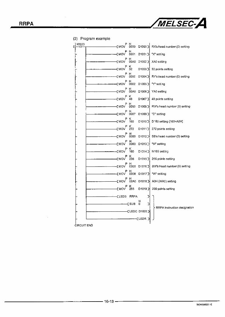
RRPA /MELSEC=A (2) Program example
I 0020 -I}-LMOV 0000 DlOOO]
P H
MOV OOAO Dl0021
I I M O V P ;2 Dl0031
P H MOV 0000 Dl0041
MOV 0002 Dl005 7
MOV OOAO Dl006 7
P H
P H
I-[MOVP 78 Dl0071
MOV 0007 Dl009 3 P K
P K
P H
MOV 160 Dl0101
MOV 272 Dl011 1
MOV 0000 Dl0121
I-[MOVP !003 Dl0131 P K
P K
P H
MOV 160 Dl0141
MOV 256 Dl0151
MOV 0000 Dl0161
I-'MOVP :008 Dl0171 P H
P K
MOV OOAO Dl0181
MOV 256 Dl0191
LEDB RRPA
SUB 0 1 H
LEDC D l 000 1
1-ELEDR : CUIT END
t
t
t
i.
t
t
t
t
t
I-
t
t
F
F
RX's head number (0) setting
X setting
X A O setting
32 points setting
RYs head number (0) setting
V setting
YAO setting
48 points setting
RWs head number (0) setting
'D" setting
Dl60 setting (160=AOH)
272 points setting
SB's head number (0) setting
'M" setting
M160 setting
256 points setting
SWs head number (0) setting
'w" setting
AOH (WAO) setting
256 points setting
RRPA instruction designation
16-1 3 IB(NA)66251-E

RlFR /MELSEC=A 16.4 Read from Automatic Updating Buffer Memory RlFR
Available Devices c ( 0 P Q 2 z z x P
Bit Device Word Device Constant Pointer Level ,F z n 'o 0 $ L v) a e m
- 2 a c X Y M L S B F T C D W R A O A l Z V K H P I N $ , M9012 M9011
= g m -
0 0
29 0
+ I Command
-
LEDC. .... Device number designated -
LEDA. .. .-Executed while ON ~ LEDB.--Executed at leading edge - SUB
LEDC,Surr SUB. ... . . . Constant designated
LEDC/SUB @
LEDR
Data to be set 1 T Head 1/0 number of object
master module Specified with the upper two drglts when the head 110 number IS expressed in 3 hexadecimal diglts.
Read destlnatlon deslgnatlon Intelligent device statlon Statlon numbers 1 to 64 (only when the host station IS the master station)
9 Random access buffer. FFH
Intelligent device station's sendingireceiving buffer address specified In master statlon (Spectfy the offset address)
Devlce whlch w~ l l store the read data
4096 Number of points read. 1 to
Functions (1) Reads the points of data specified at @ from the automatic updattng buffer memory address specified at for the station having the station number specified at (a in the master module specified at @ and stores that data into the devices starting from the one specified at (9.
,RIFR instruction executlon range
/local station lntelhgent devlce
(2) When executed, the RlFR instruction reads data from the automatic updating buffer of the master module.
(3) Up to 4096 points may be read by the RlFR instruction.
(4) To set the number of automatic updating buffer memory points, make the automatic updating buffer size setting using the network pararne- ter instruction (RLPA instruction).
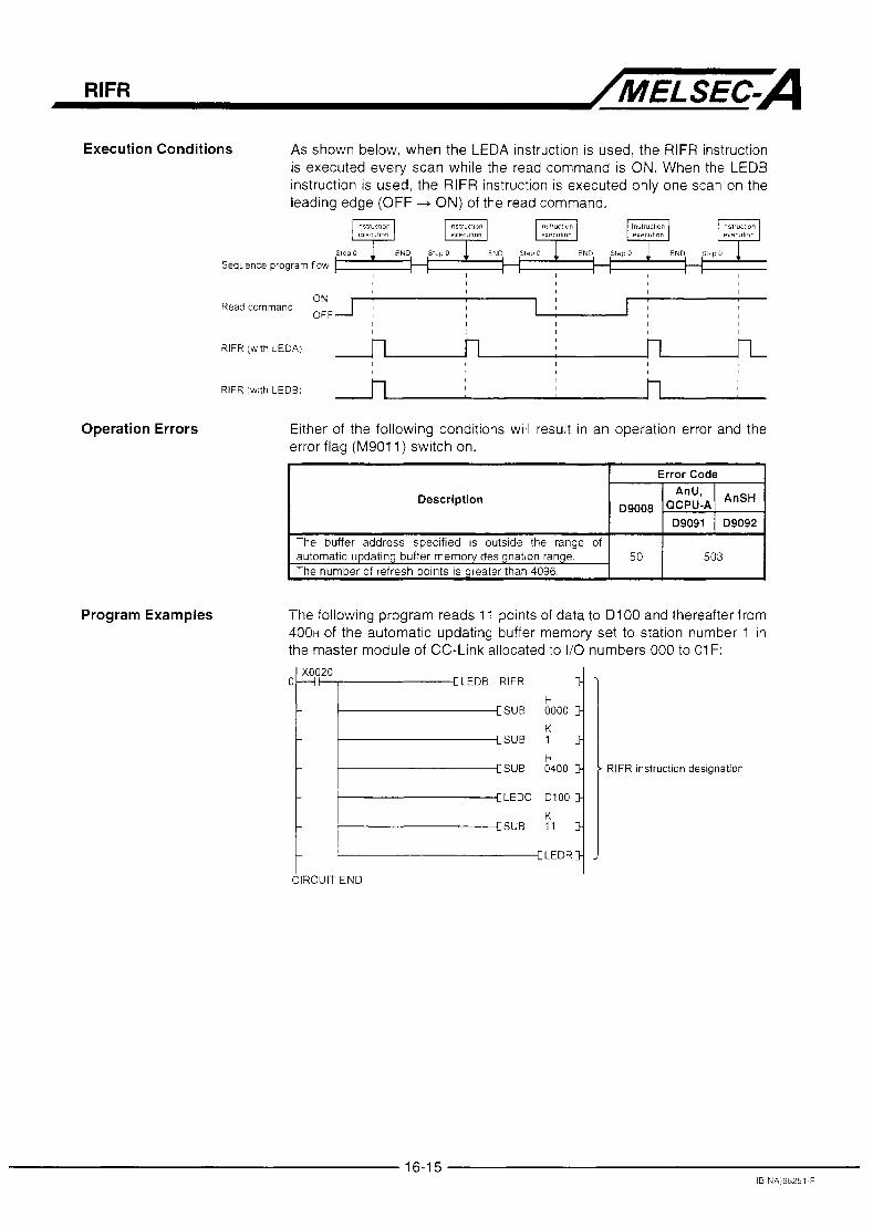
RlFR /MELSEC-A Execution Conditions As shown below, when the LEDA instruction is used, the RlFR instruction
is executed every scan while the read command is ON. When the LEDB instruction is used, the RlFR instruction is executed only one scan on the leading edge (OFF -+ ON) of the read command.
'PSl l"Cl l0" ln511"ctlo" PIBT"I13n
lnhll"CllOn Illh'IU'IIL'" erecuhon
rSl,"CllO"
?XCCL,U"" e*e:UtiO-, execuhon
Sequence program flow step 0 END Sfrp 0 END SIBDC END Step0
H H H I I , , I I I I I I I I I I I
I I 1 ,
ON I
OFF I : I Read command I I
I I I
I
RlFR (wlth LEDA) n I
I I 4 I 1 I I I I I
I I 1 I RlFR (with LEDB) I I
Operation Errors Either of the following conditions will result in an operation error and the error flag (M9011) switch on.
Program Examples
I I 4
I Description I 1 1 AnSH I D9008 QCPU-A
D9091 D9092 The buffer address specified IS outslde the range of automatic updating buffer memory deslgnation range. The number of refresh points is greater than 4096.
503 50
The following program reads 11 points of data to D l 00 and thereafter from 4 0 0 ~ of the automatic updating buffer memory set to station number 1 in the master module of CC-Link allocated to I/O numbers 000 to 01 F:
I- x0020 [LEDB RlFR I'
[SUB 0000 2-
[SUB 1 K
2-
[SUB 0400 3 H
RlFR instruction designation
[LEDC Dl00 1
[SUB 11 2-
H
K
I-ELEDRI , CIRCUIT END

RlTO /MELSEC-A 16.5 Write to Automatic Updating Buffer Memory ...*.. RlTO
'@)
0 0 0 0 0 0 0 '@ 0 0 0 0 0 @)
29 0 0 0 0 0 0 0 lL 7 M9011
Data to be set
Command 1 LEDNLEDB I RlTO LEDA.-. ... Executed while ON
I
SUB
I LED6 .... Executed at leading edge
I G LEDC...- Devlce number deslgnated
LEDClSUB I SUB....- . Constant designated
LEDR E
I
Head IiO number of ob~ect master module Specified with the upper ' two digits when the head I10 number is expressed in 3 hexadecimal digits. ,
Wrlte desltnatlon designation lntelllgent device station: Statlon numbers 1 to 64 (only when the host statlon is the master station) Random access buffer: FFH
lntelllgent device station's sendingireceiving buffer address specified in master station (Specify the offset address)
Devlce whlch will store the written data Number of polnts written 1 to 4096
I
Functions (1) Writes the points of data specified at @ from the devices beginning with the one specified at @ t o the automatic updating buffer memory addresses beginning with the specified one at @for the station hav- ing the station number specified at @ in the master module specified at ~3.
,RITO mstructlon execution range
I I 1 -' I I I I '
I I
I Transferred when I data IS updated
(2) When executed, the RlTO instruction writes data.
(3) Up to 4096 points may be written by the RlTO instruction.
(4) To set the number of automatic updating buffer memory points, make the automatic updating buffer size setting using the network parame- ter instruction (RLPA instruction).
16-1 6 lB(NA166253-F

R IT0 /MELSEC-A Execution Conditions As shown below, when the LEDA instruction is used, the RlTO instruction
is executed every scan while the write command is ON. When the LEDB instruction is used, the RlTO instruction is executed only one scan on the leading edge (OFF + ON) of the write command.
I"SlrLcllOn EIeCdllO"
I"B1IUCtlOl 1"51r"C1,a" Erccutton
l"51rUc113" E x e c u m n Execul~on
I"slr"c1IDn EX.?C"l,O"
Sequence program flow I
I I I I I I I I I I
ON 1 Wrlte command I 1 I
OFF I I I I I I I I 4 I
I
RITO (with LEDA) 1 n I
I I I I , I I I I I
RlTO (wth LEDB) I I
Operation Errors
Program Examples
Either of the following conditions will result in an operation error and the error flag (M9011) switch on.
I Error Code I Description
D9091 D9092 The buffer address specified is outside the range of automatic updating buffer memory designation range. The number of refresh points is greater than 4096.
503 50 -
The following program writes "ABCDEFGHIJ" to 200H and subsequent addresses of the automatic updating buffer memory for the station set to station number 1 in the master module of CC-Link allocated to I/O num- bers 000 to 01 F:
P K 4 (word) Settlng of number of points wrltten
CMOV' 4142 D l 1 3.
Setting of written data "GH" [MOV 4748 D l 4 3
Setting of written data "EF ' [MOV 4546 D l 3 3
Setting of wrrtten data "CD" C MOV 4344 D l 2 3.
Setting of written data "AB"
3 ' [LEDB RlTO
Setting of wrltten data "IJ" [MOV 494A D l 5 3
P H
P H
P H
P H
H [SUB 0000 3
[SUB 1 3
[SUB 0200 3
[LEDC D l 0 3
RlTO instruction designatlon
K
H
K [SUB 6 3
CLEDR, , CIRCUIT END
16-1 7 lBiNA)66251-F

RlRD /MELSEC=A 16.6 Read from Intelligent Device Station Buffer Memory ...... RlRD
Command I LEDALEDB 1 RlRD LEDA--Executed while ON
LEDB---Executed at leading edge LEDC--. Device number designated
~ SUB----Constant designated
LEDC @ I 1 LEDR
Data to be set Head l/O number of object masternocal module
Specified with the upper two digits when the head UO number is expressed in 3 hexadecimal digits. i
Remote station number When the host station is the master station: 1 to 64 Local station: 0 to 64
and read data 1 Device for storing control data
Bit device number which is swltched on on completion of execution
Control Data Setting Items (1) Control data setting items @+o @ +1
@ +2 @ +3
@+4 to
@ +n
r Completion status 1 I Number of points read I
Read data storage area
* Control data
Stores data read from remote station on - completion of RlRD instruction execution. [Number of points specified at @ + I ]
(2) Number of control data area points Data read from a remote station is stored into the area after the 4 points of control data [@O to @3]. Reserve the control data area for 4 points + [number of points speci- fied at @1] successively.
16-1 8 IB(NA)66251-E

RlRD /MELSEC=A Control data The setting range of the control data depends on the software version of
the master module to be used as shown below. (1) Software version A to H
Item Set Data Setting Setting Range End
I The status at the completion of an instructlon is 1 I I Completion stored. status : No error
Other than 0 : Error code '' Number of read-
words). out points to 480'2 Specify the number of read-out data (in unit User
Set "0004~" to access the buffer memory of an Access code and
Set "2004~" to access the random access attribute intelligent device station.
address Buffer memory
2 0 0 4 ~ 0004H User
buffer memory of a local station.
Specify the head address of the buffer memory. User
Read-out data I - - I System I '1: For error codes at the occurrence of an error, refer to the following manual.
'2: If the CPU is not AnU QnA series or QCPU A (A Mode), the setting range is 1 to 32
'3: Refer to the manual for the intelligent device statlon where the data is written.
AJ61 BT11, A1 SJ61 B T l l CC-Llnk system Master.Local Module User's Manual
points.
(2) Software version J to on
Item Set Data Setting End Range
Setting
The status at the completion of an instruction is
I Completion status I : No error (normal completion) 1 - I Syster
Other than 0: Error code" Number of read-
words). out polnts User to 480 '2
Specify the number of read-out data (in unit of
Access code (upper 8 bits): See items (a) and (b) below. (a) and
See items
(b) below Access 'Ode and
(b) To access a CPU devide : O ~ H 05H Link : 0 4 ~ or (a) To access the buffer memory in the CC- 0 4 ~ attribute Attribute (lower 8 bits): User
Buffer memory address or device number
Specify the head address of the buffer memory.
'1: For error codes at the occurrence of an error, refer to the following manual.
'2: If the CPU is not AnU QnA series or QCPU A (A Mode), the setting range is 1 to 32
'3: Refer to the manual for the intelligent device station where the data is written.
3 User
AJ61 BT11, A1 SJ61 B T l l CC-Link system Master.Local Module User's Manual
points.
(a) Buffer memory in the CC-Link Contents of Buffer Memory Access Code
Buffer memory in intelligent device station
21H Remote input 20H Random access buffer 00-
Buffer memory in master/ Remote output 22H local station Remote register
Special link relay 2 4 ~
64- Special link register 63-
16-1 9 IB(NA)66251-F

(b) Device memory in CPU
Function
Device Name Device type Bit Word Access code
Input relay
8 3 ~ 0 L Latch relay 0 3 ~ 0 M Internal relay 02H 0 Y Output relay OOH 0 X
~~~~~~~~ ~
Link rela
OAH OCH
C 0 C 0 1 2 H
Counter h e s e n t value) C D 1 A H
Data register
8 4 H 0 R File register 2 4 ~ 0 w Link register 0 4 H 0 D
'1 Devices not indicated above are not accessible. '2 To access a bit device, specify '0' or a multiple of '1 6'.
If any other number is specified, it will cause an error.
(1) The instruction reads the data from the buffer memory address specified at [ @ +3] of the station specified at @, which is connected to the masterllocal station specified at @, by the number of points specified at @ +1, then stores the read data to the devices starting from the one specified at @ +4. At the completion of reading, the bit device specified at @ switches ON for one-scan period. If an error occurs during reading, the bit device specified at @ +I switches ON for one-scan period.
(a) Software version A to H
I I I I I I I I I I I I I I I I I I
MasterAocaI CPU station @ Specified station@
t-1 +I ~~~~instructionH Request
/ I / /' Reading data from
Buffer memory
buffer memory
device
I I I I I I I I I I I
16-20 IB(NA)66251-F

RIRD /MELSEC=A Master/local Specifled
CPU station @ sta t l ona CPU
I+ /--I RIRD Instru- Request
/ c
/ /' Reading data from
- Specifled device
the specified device
device
(2) An RlRD instruction can be executed for the specified multiple sta- tions at the same time. Note that simultaneous execution at more than one locations is not permitted for the same station.
(3) Set the network parameters by executing an RLPA instruction (net- work parameter set instruction) before executing an RlRD instruction.
(4) I f the number of read-out points specified at @ cl is "0 or outside the range 1 to 480." such a designation results in error completion ( B B ~ ~ H ) .
Execution Conditions I f an LEDA instruction is used, an RlRD instruction executes scan at each execution of the read command. I f an LEDB instruction is used, scan is executed only once at the falling edge of the read command. Note that the read processing executed by the RlRD instruction will take time for several scans before the processing is completed. Therefore, execute the next RlRD instruction only after the switching ON of a completion device. (The RlRD instruction executed before the completion of the current RlRD instruction is disregarded.)
END END processing processing
END END processing processing
Sequence program flow +-=- - - - - - - - - RIRD instruction
16-21 lB(NA)66251-F

RlRD /MELSEC=-
Program Example The following program reads I point of data from 1 A 8 ~ of the buffer mem- ory of the intelligent device station having station number 1 and connected to the master module of CC-Link allocated to I/O numbers 000 to 01 F:
x0020 P K CMOV 1 D241 3- Setting of the number of read points
LMOV D242
-MOV 0,A8 D243
P H SeNng of intelligent device station buffer memory
P H Setting of buffer memory head address
CLEDB RlRD H
CSUB OOOO K
CSUB 1 RlRD instruction designation
{LEDC D240
CLEDC M340
E: LEDR
CIRCUIT END
." bb IB(NA)66251-E

16.7 Write to Intelligent Device Station Buffer Memory - - - - - - RIWT
I ~
M9012 M9011
Data to be set Vrite command
+ t Head VO number of object
LEDB--Executed at leading edge SUB l O F Remote station number
LEDC .-.. Device number designated When the host station is the SUB T k
and written data @ LEDC T+
Device for storing control data LEDC Local station: 0 to 64 master station: 1 to 64 @ SUB......-Constant designated
] LEDMLEDB 1 RlWT masterAoCal module @ LEDA---Executed while ON
i I
I LEDR Bit device number which is
execution @ switched on on completion of
Control Data Setting Items (1) Control data setting items @+o @+1
@ +2 @ +3 @+4
to
@ +n
Number of points written
Buffer address
Written data storage area I 1 ' Control data
Stores data written to remote
[Number of points specified at @+l] - station by RlWT instruction.
16-23 IB(NA)66251-E

RlWT /MELSEC-A Control data The setting range of the control data depends on the software version of
the master module to be used as shown below.
(1) Software version A to H
Item Set Data Setting Range
Setting End
I I The status at the completion of an instruction is I I I Completton I status : No error I -
Other lhan 0 : Error code " Number of write
oink Set "0004~" to access the buffer memory of an
attribute
Buffer memory 3
address Specify the head address of the buffer memory. User
I Write data - - I System I '1 : For error codes at the occurrence of an error, refer to the following manual.
'2: I f the CPU is not AnU QnA series or QCPU A (A Mode), the setting range is 1 to 10
'3: Refer to the manual for the intelligent device station where the data is written.
AJ61BT11, AlSJ61 BTI 1 CC-Link system Master,Local Module User's Manual
points.
(2) Software version J to on
Item Set Data Setting Range
Settins End
The status at the completion of an instruction is Completion
0 : No error (normal completion) status stored.
Doints User 1 to 480" Specify the number of wrtte data (in unit of words). Number Of write
- Systerr Other than 0 : Error code ''
Accesscodeand attribute
(a) To access the buffer memory in the CC-Link 0 5 ~
Buffer memory address or device number
Specify the head address of the buffer memory or the head number of devices.
.3 User
'1: For error codes at the occurrence of an error, refer to the followtng manual.
'2: I f the CPU is not AnU QnA series or QCPU A (A Mode), the setting range is 1 to 10
'3: Refer to the manual for the intelligent device station where the data is written.
AJ61BT11, AlSJGlBT11 CC-Link system Master Local Module User's Manual
points.
(a) Buffer memory in the CC-Link
I Contents of Buffer Memory Access Code 1 Buffer memory in intelligent device station OOH
[ Random access buffer 20H 1 Remote input Remote output Buffer memory in master/
21 H
2 4 ~ Remote register local station 22H
Special link relay 6 3 ~ Special link regtster 6 4 ~
16-24 lB(NA)66251-F

(b) Device memory in CPU
Function
I Device I Name 1 Device type Bit I Ward 1 Access code I
input relay 02H 0 Y Output relay
0 X ~ ~~
OOH
Internal relay Latch relay
0 3 ~ 0 M 8 3 ~ 0 L
Timer (contact)
1% 0 C Counter (coil) 11H 0 C Counter (contact) OCH 0 T Timer (present value) OAH 0 T Timer (coil) 09H 0 T
Counter (present value) Data register D 0 C 4 H
1 4 ~ 0 C
Link register W 0 2 4 ~ File register 0 8 4 ~ R
'1 Devices not indicated above are not accessible. '2 To access a bit device, specify '0' or a multiple of '1 6'. If any other number is
specified, it will cause an error.
(1) The instruction writes the data to the buffer memory address specified at [ @ +3] of the station specified at @I, which is connected to the masterAoca1 station, specified at @, by the number of points specified at @ +1, At the completion of reading, the bit device specified at @ switches ON for one-scan period. If an error occurs during writing, the bit device specified at @ +1 switches ON for one-scan period.
(a) Software version A to H
device
1 I Master/local I CPU station Specified station @ I
I I -1 RlWT instruction
I I I I I I
I I
I I
Wrlllng data to buffer memory
16-25 IB('vA)66251.F

Rl WT /MELSEC--
I I I CPU
I
I / I /
I I I
statlon @ Masterilocal Specified
station @
/ / Writing data lo
the specified devlce
CPU
I I
I I I I I I I I I I I
I I
I I I
(2) An RlWT instruction can be executed for the specified multiple sta- tions at the same time. Note that simultaneous execution at more than one locations is not permitted for the same station.
(3) Set the network parameters by executing an RLPA instruction (net- work parameter set instruction) before executing an RlWT instruction.
(4) I f the number of read-out points specified at @ +1 is "0" or outside the range 1 to 480, such a designation results in error completion (BB42H).
Execution Conditions If an LEDA instruction is used, an RlWT instruction executes scan at each execution of the read command. If an LEDB instruction is used, scan is executed only once at the falling edge of the read command. Note that the read processing executed by the RlWT instruction will take time for several scans before the processing is completed. Therefore, execute the next RlWT instruction only after the switching ON of a completion device. (The RlWT instruction executed before the completion of the current RIWT instruction is disregarded.)
END END processing processing
END END processing processing
Sequence program now --- - - - - - - - - u-m RlWT instruction I 1
I I I I I I
r d e d execution cornplet RlWT instruction I I - - - - - - -_
I I
I I I I
1 i :ON I
I I Abnormal I I ON! mmpletion 1 I I t------ -I
I 'Hmnal0orrqlak.n; i I scan 4
Completion device OFF - - - - - - - - 4 I
I
I I
Oncompletion status display device - - - _ _ _ _ _
During processing of RlWT instruction Reading by RlWT instruction is enabled
16-26 IB(NA)66251-F
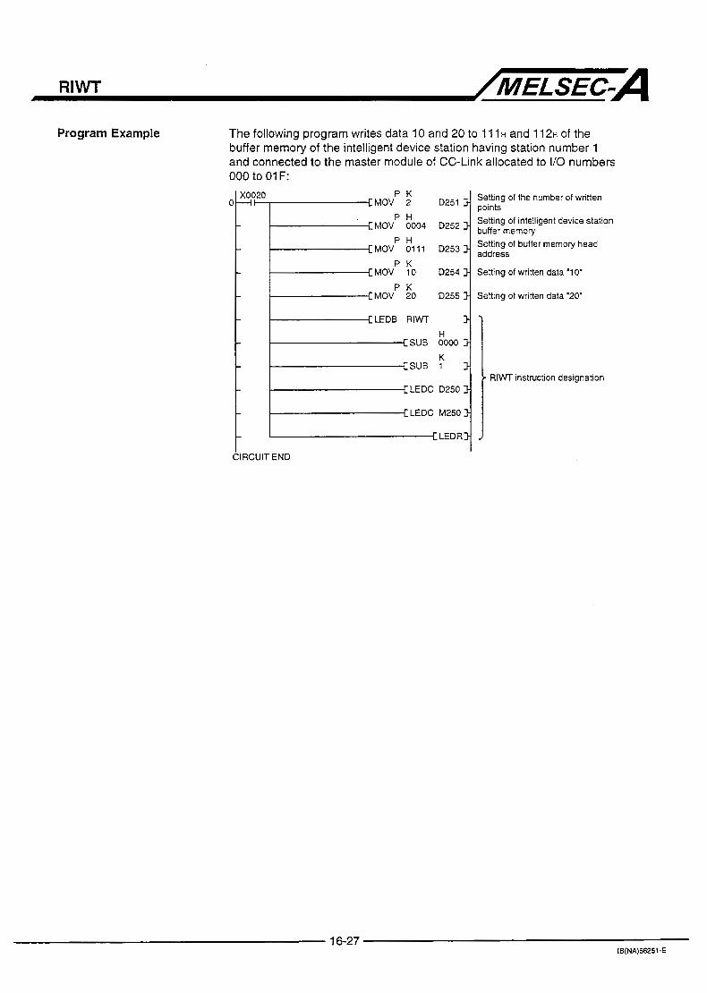
RlWT /MELSEC--
Program Example The following program writes data 10 and 20 to 11 1 H and 11 2~ of the buffer memory of the intelligent device station having station number 1 and connected to the master module of CC-Link allocated to I/O numbers 000 to 01 F:
x0020 P C MOV
C MOV
C MOV
I: MOV
C MOV
P
P
P
P
LEDB
K 2
ooo4 H D252
Setting of buffer memory head o, H 1, D253
buffer memory Setting of intelligent device station
address K 10 D254 1 Setting of written data '10' K 20 D255 1 Setting of written data '20'
RlWT
D25, Setting of the number of written 1 points
1-l H - {SUB 0000
-
- :rI:C a250 1 I R I W instruction designation
-
CIRCUIT END
CLEDR - CLEDC M250
16-27 IB(NA)WSl-E

RlRCV /MELSEC=A 16.8 Read from Intelligent Device Station Buffer Memory (with Handshake) ...... RlRCV
I Read command I
LEDR
Data to be set Head VO number of object master module
Specified with the upper two digits when the head 110 number is expressed in 3 hexadecimal digits. 1
Intelligent device station
Handshaking link device number ' I
Bit device number which is swtched on on completion of executcon
Control Data ( I ) Control data setting items
@ +O
@+1
@ +2
@ +3
@+4 @+5
to
@+n
I Completion status I
I Error check I Buffer address
Read data storage area
. Control data
on completion of RlRCV instrucSon execution. Stores data read from intelligent device station
[Number of points specified at ( 9 1
(2) Number of control data area points Data read from an intelligent device station is stored into the area after the 5 points of control data [@+O to @4]. Reserve the control data area for 5 points + [number of points speci- fied at @+l] successively.
I POINTS I I . - . . . . - I
(1) The RlRCV instruction can only be used with the master
(2) The intelligent device station is, mainly, the AJ65BT-R2. station CPU.
16-28 IB(NA)66251.F

RIRCV /MELSEC=A (3) Control data
Item Set Data ~~
Setting End Range
Setting ~ ~~~
Status on completion of instruction execution is Completion I status : No error
Other than 0 : Error code " Number of points read
Object area an intelligent device station.
Specify the number of data read (word basis).
Specifv the error check devrce.
User 0 0 0 4 ~ Set "0004~" when accessing the buffer memory of
User 1 to 480 ''
I I ' O ' Error check Completion status IS used for
error check. 1 0 . 1 1 User I I I Other than 0 : RX+1 is used for error check. I
Buffer memory address Specify the head address of the buffer memory. User
1) '1: For error codes at error occurrence, refer to the following manual: Type AJ61 BT11. AISJ61 BT11 CC-Link System Master/Local Module User's Man- ual (Details)
Set a value within the intelligent device station buffer memory capacity and parameter-set receiving buffer area setting range.
2) '2: Indicates the maximum number of data read.
3) '3: Refer to the manual of the intelligent device station from which data IS read.
Handshaking Link Devices (1) Handshaking link device setting items
@+o I RX RY I @ + I RWr I
(2) Setting of handshaking link devices
Item Set Data Setting
0 to 124
End Range Setting
User '* RX Specify the handshaking RX number of the intelll- gent device station.
RY
RWr
Specify the handshaking RY number of the intelli- to 125 gent device station. Specify the handshaking RWr number of the 0 to 15 intelligent device station.
User '>
FF User '7
POINTS I (1) *1: When FFH is set, no number is specified. (2) '2: The RX, RY and RWr numbers used are set by the user.
Note that RX and RY ON/OFF control and RWr data setting are performed by the system and cannot be changed by the user. If RX, RY and RWr are changed by the user, the RIRVC instruction will not be completed properly.
(3) If handshaking is used, set AJ65BT-R2 RXn2 and RYn2.
16-29 IB(NA166251-F

RlRCV /MELSEC-A Functions (1) Reads the points of data specified at @+l from the buffer memory
address specified at [@3] in the intelligent device station having the station number specified at @ and connected to the master module specified at @, and stores that data into the devices starting from the one specified at @4. On completion of reading, the bit device specified at @ switches on only one scan. On abnormal completion, the bit device at @I switches on only one scan.
/ RIRCV instruction execution range
I I I 1 I I I I I
I I
I I I I I i I I
CPU Mater module @ Intelligent device station @
H HRIRCV inst ruc t i onH Request
/ c
/ Read from buffer memory
Handshake /
@ t4 Specified @+Oil
(2) The RlRCV instruction may be executed for two or more intelligent device stations at the same time. However, this instruction cannot be executed for the same intelligent device station in two or more locations at the same time.
(3) Before executing the RlRCV instruction, set the network parameters using the RLPA instruction (network parameter setting). If the RlRCV instruction is executed without the network parameters set, abnormal completion will occur and " ~ B O O H " be stored into the completion status.
(4) If the number of read-out points specified at @ +1 is "0" or outside the range 1 to 480, such a designation results in error completion (BB42H).
Execution Conditions When the LEDA instruction is used, the RIRCV instruction is executed every scan while the read command is ON. When the LEDB instruction is used, the RIRCV instruction is executed only one scan on the leading edge (OFF + ON) of the read command. Note that several scans will be required until the completion of read proc- essing by the RIRCV instruction. Therefore, execute the next RIRCV instruction after the completion device has switched on. (The RIRCV instruction executed before the completion of RlRCV instruction execution is ignored.)
END END END END processing processing processing processing
Sequence program flow ---- - - - - - - - - RIRCV instruction 1
execution complete I I I
I I I I I RlRCV instruction - - - - - _ - _
I 1 1 I
1 I I I
I I I O N I
Completion device OFF - - - - - - - - 1 I A b n o r m a l I
During processing of RlRCV instruction -;*Data can be read by RIRCV instruction. 8 -

RIRCV /MELSEC=A Program Example The following program reads data from 4 0 0 ~ - 4 0 5 ~ of the buffer memory of
the intelligent device station having station number 1 and connected to the master module of CC-Link allocated to 110 numbers 000 to 01 F. The completion status is used for error check. Also RX2, RY2 and RWr2 are used as handshaking link devices:
O r E M O V p P K D221 1 points Setting of the number of read
MOV ooo4 D222 Sening of intelligent device station bufier memory
t D224 .I Settjng of buffer memory head address
I I CIRCUIT END
r RIRCV instruction designation
16-31 IB(NA)6K51-E

RISEND /MELSEC=--
16.9 Write t o Intelligent Device Station Buffer Memory (with Handshake) ...... RISEND
Command LEDA---Zxeculed while ON LEDB--Executed at leading edge LEDC-- Device number designated SUB---Constant designated
d LEDC , -7-
I LEDC --I- LEDC 1 @ -
LEDR -
Data to be set Head UO number of object master module
Specified with the upper
I/O number is expressed in 3 hexadecimal digits.
Intelligent device station
0 1 [ t w o digits when the head]
@ number: 1 to 64
Handshaking link device
Bit device number which is swltched on on completion of executron
Control Data (1) Control data setting items
@ +O
@ +2 @+3 I Error check 1
+ Control data
Buffer address
Stores data written to intelligent device station
[Number of points specified at @+1] to Written data storage area by RISEND instruction.
POINTS I ( 1 ) The RISEND instruction can only be used with the master
(2) The intelligent device station is, mainly, the AJ65BT-R2. station CPU.
16-32 iB(NA)66251-F

RISEND /MELSEC-A (2) Control data
Item Set Data Setting End Range
setting
Status on completion of instruction execution is
I Completion stored. status : No error
Other than 0: Error code '' written Number Of points
User 0 0 0 4 ~ an intellioent device station. Object area Set "00041." when accessing the buffer memory of
User 1 to 480'' Specify the number of data written (word basls).
1 S p r i f y the error check devlce.
Error check : Completion status IS used for error check. I Other than 0 : RXL1 is used for error check. I
Buffer memory I Specify the head address of the buffer memory. 1 address User
Written data storage area
- User
1) '1: For error codes at error occurrence, refer to the following manual: Type AJ61 BT11, AlSJGl BT11 CC-Link System MasteriLocal Module User's Man- ual (Details)
Set a value within the intelligent device station buffer memory capacity and parameter-set receiving buffer area setting range.
2) ' 2 : Indicates the maximum number of data written.
3) '3: Refer to the manual of the intelligent device station to which data is written.
Handshaking Link Devices (1 ) Handshaking link device setting items
@+o I RX RY
@ + l RWr
(2) Setting of handshaking link devices
RX
RY
RWr
Specify the handshaking RX number of the intelli- to 127 gent device station. User .' Specify the handshaking RY number of the intelli- to 127 gent device station. User '?
Specify the handshaking RWr number of the 0 to J 5 User .L intelligent device station. FF '
(1) *1: When FFH is set, no number is specified. (2) *2: The RX, RY and RW numbers used are set by the user.
Note that RX and RY ON/OFF control and RWr data setting are performed by the system and cannot be changed by the user. I f RX, RY and RW are changed by the user, the RISEND instruction will not be completed properly.
(3) If handshaking is used, set AJ65BT-R2 RXnO and RYnO.
16-33 IB(NA)66251-F

RISEND /MELSEC=A Functions (1) Writes the points of data specified at @ + I from the devices begin-
ning with the one specified at @ +5 to t h e buffer memory address specified at [ @ +4] in the intelligent device station having the station number specified at @ and connected to the master module specified at @. On completion of writing, the bit device specified at @ switches on only one scan. On abnormal completion, the bit device at @ +l switches on only one scan.
,RISEND instructlon execution range
I
I ) I CPU Master module 0 Intelligent devlce station @
I I I
I I I I I I
I I+ RISEND instruction H I I I
@ +4 Request
Buffer memory I
I I
I / - I I
(2) The RISEND instruction may be executed for two or moreintelligent device stations at the same time. However, this instruction cannot be executed for the same intelligent device station in two or more locations at the same time.
(3) Before executing the RISEND instruction, set the network parameters using the RLPA instruction (network parameter setting).
(4) If the number of read-out points specified at @ t1 is "0" or outside the range 1 to 480, such a designation results in error completion (BB42H).
Execution Conditions When the LEDA instruction is used, the RlSEND instruction is executed every scan while the write command is ON. When the LEDB instruction is used, the RISEND instruction is executed only one scan on the leading edge (OFF + ON) of the write command. Note that several scans will be required until the completion of write proc- essing by the RISEND instruction. Therefore, execute the next RlSEND instruction after the completion device has switched on. (The RISEND instruction executed before the completion of RISEND instruction execution is ignored.)
END END END END processing processing processing processing
Sequence program flow e- - - - - - - - - RISEND instruction
r k d execution complete I 1
I I I I
I I I I
I I
RISEND instruction - - - - - - - - I I :ON I
Completion device OFF I I I
I I
- - - - - - - - 1 ; I Abnormal I ON1 c c m p l e h I
I I t------ -I I 1 Ni*rrPlcarpbtbn$
On-completion status display device - - - - - - - -
I I
i lscan J
During processing of RISEND instruction bIaData c a n be written by RISEND instruction
16-34 IB(NA)66251-F

RlSEND /MELSEC-A Program Example The following program writes the number of data written and data
"ABCDEFGHIJ" to 200~-205~ of the buffer memory of the intelligent device station having station number 1 and connected to the master module of CC-Link allocated to I/O numbers 000 to 01 F. The completion status is used for error check. Also RXO, RYO and RWrO are used as handshaking link devices:
5
C
x 0 0 2 0 II , EMov P K D20, 4 ;;;;g of the number of written
of intelligent device station buffer memory
. 1-CMOV' 0000 D203 1 Setting of error check
MOV 0200 D204 P H Setting of buffer memory head
address P K
[UOV 5 D205 3
[MOV 4142 D206 3
Written data '5' setting
Written data 'I3 setting [UOV 494A D210 3
Written data 'GH' setling [ MOV 4748 D209 3
Written data 'EF' setting rMOV 4546 D208 3
Written data 'CD' setting CMOV 4344 D207 3
Written data 'AB' setting P H
P H
P H
P H
P H
x0020 P H +tr: P H MOV 0000 D300 I-
RWrO setting MOV 0001 D301 I-
RYO, RXO setting
[LEDB RlSEND 3
[ S U B 0000 3
[ S U B 1 1
[LEDC D200 3
[LEDC D300 3
[ LEDC M300 I-
[: LEDRI-
H
K
:IRCUIT END
RlSEND instruction designation
16-35 IB(NA)W51-E

17. 1 ms timer setting instruction (QCPU-A (A Mode) only) /MF/ SEC-A
17. l m s timer setting instruction (QCPU-A (A Mode) only)
The 1 ms timer setting instruction enables the 1 ms timer for the QCPU-A (A Mode).
Classification I Instruction I Description I Refer to 1 ms timer setting I ZHTIME I Enable the l m s timer. I 17-2
17-1 ISiNA)66251-F
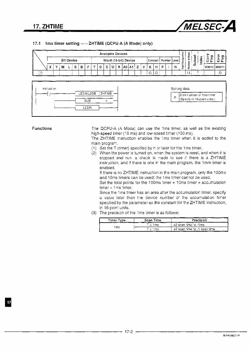
17. ZHTIME /MELSEC==
17.1 lrns timer setting ZHTlME (QCPU-A (A Mode) only)
Available Devices
E .p Level Pointer Constant Word (16-bit) Device Bit Device
L ,E 5 i 2 9 E 4 g r n k m x 5
X Y M L S B F T C D W R A Q A I Z V K H P I N E z - 0 n
5 cn - I
M9012 M9011
, 0 I
13 0 0 I ,
1 1nstr;:t s+ LEDNLEDB ZHTIME
LEDR
Setting data Start number of lrns tlmer (Specify in 16-point unlls.)
Functions The QCPU-A (A Mode) can use the I m s timer, as well as the existing high-speed timer (10 ms) and low-speed timer (1 00 ms). The ZHTIME instruction enables the I m s timer when it is added to the main program. (1) Set the T (timer) specified by n or later for the 1 ms timer. (2) When the power is turned on, when the system is reset, and when it is
stopped and run, a check is made to see if there is a ZHTIME instruction, and if there is one in the main program, the l m m timer is enabled. If there is no ZHTIME instruction in the main program, only the 1 OOrns and 1 Oms timers can be used; the 1 ms timer cannot be used. Set the total points for the lOOms timer + 1Oms timer + accumulation timer + 1 ms timer. Since the 1 ms timer has an area after the accumulation timer, specify a value later than the device number of the accumulation timer specified by the parameter as the constant for the ZHTIME instruction, in 16-point units.
(3) The precision of the 1 ms timer is as follows:
Timer Type Precision Scan Time T < l m s +2 scan time to -1 ms T > l m s +2 scan time to -1 scan tlme 1 ms
17-2 IB(NA)66251-F

17. ZHTIME /MELSEC-A Operation error An operation error occurs in the following case, and an error flag
(W9011) is set.
Description Error Code D9008 I D9091
The value specifred by n IS not a multiple of 16 103 10
Program example T208 or later is set for the 1 ms timer
0 I ; M9037
[LEDB ZHT I ME
[SUE K208
[LEDR
18 [END


18. ERROR CODE LIST /MELSEC=A 18. ERROR CODE LIST
Table 18.1 shows the error messages, description and cause of error and corrective actions. Error codes, detailed error codes and error steps are stored in the following special registers.
Error code: D9008 Detailed error code: D9091 Error step: D9010 and D9011
18.1 Reading Error Code
If an error occurs, the error code can be read using a peripheral device. For details of operational procedure, refer to the Operating Manual of the peripheral device to be used.
18.2 Error Code List for AnACPU
Table 18.1 Error Code List for AnACPU (Continue)
Error Massage
'INSTRCT CODE ERR.'
(Checked when STOP + R U N or at execution of instruction.)
Error Code (D9008)
10
Detailed
(D9091) Error Code Description and Cause of Error Corrective Action
101 Instruction codes which the CPU can- not decode are included in the prog- ram.
102 Index qualification is specified for a 32- bit constant. Device specified by an dedicated inst- ruction is not correct. An dedicated instruction has incorrect program structure. An dedicated instruction has incorrect command name.
106 Index qualification using Z or V is inclu-
107 (1) Index qualification is specified for the device numbers and set value: in the OUT instruction of timers and counters.
the label number of the pointer (P) provided to the head of destination
(2) Index qualification Is specified at
or at the label number of the inter- 1 rupt pointer (1) provided to the head of an interrupt program.
(1) Read the error step usinga periph. era1 device and correct the prog- ram of the step.
(2) Check the ROM if it contains inst- ruction codes which cannot be de- coded. I f it does, replace it with a correct ROM.
~ ~~~
Read the error step using a periphera device and correct the program of t h s step.
108 Errors other than 101 to 107 rnention- ed above.
18-1 iB(NA)66251-F

18. ERROR CODE LIST /MELSEC-A Table 18.1 Error Code List for AnACPU (Continue)
~~ ~
trror Codt (D9008)
Detailed Error Cod€
(D9091) Error Message Description and Cause of Error Corrective Action
"PARAMETER ERROR"
(Checked at power on and
at ST0 P/ PAUSE -
RUN.)
11 111 Capacity settings of the main and sub programs, microcomputer program, fi le register comments, status latch, sampling trace and extension file registers are not within the usable range of the CPU.
~~~ ~~~ ~
Read parameters in the CPU mem. ory, check the contents, make necessary corrections and write them again to the memory.
~ ~~
112 Total of the set capacity of the main and sub programs, file register com- ments, status latch, sampling trace and extension file registen exceeds capacity of the memory cassette.
Latch range set by parameters or setting of M, L or S is incorrect.
Sum check error
113
114
115 Either of settings of the remote RUN/PAUSE contact point by para- meters, operation mode at occurr- ence of error, annunciator indica- tion mode, or STOP - RUN indica- tion mode is incorrect.
Read parameters in the CPU mem- ory, check the contents, make necessary corrections and write them again to the memory.
116 The MNET-MINI automatic refresh setting by parameters is incorrect.
117 Timer setting by parameters is in- correct.
Counter setting by parameters is incorrect.
118
121 ~~
The END (FEND) instruction is not given in the main program.
"MISSING END INS."
(Checked at STOP - RUN.)
12 Write the END instruction at the end of the main program.
122 Write the END instruction at the end of the sub program.
The END (FEND) instruction is not given in the sub program if the sub program is set by parameters.
The same device number is used at two or more steps for the pointers (P) and interrupt pointers ( 1 ) used as labels to be specified at the head of jump destination.
"CAN'T EXECUTE (P)"
(Checked at execution of instruction.)
13 131 Eliminate the same pointer num- bers provided at the head of jump destination.
132 Label of the pointer (P) specified i n Read the 'error step using a peripheral device, check contents and insert a jump destination poin- ter (PI.
provided before the END instruction.
133 (1) The instruction was in- cluded in the program and ex- ecuted though the [=] in-
(1) Read the error step using a peripheral device, check con- tents and correct program 01 the step.
levels of the m t m' and instructions to 5 0 1 less.
(2) Reduce the number of nestin struction was not given.
were included in the pro ram and executed though the &
(3) Nestin level of the 1-1 instruction was not given.
and instructions is 6 levels or deeper, and the 6th
(4) There is no or m l level was executed.
instruction at execution of the [ E S J or [FORI instruction.
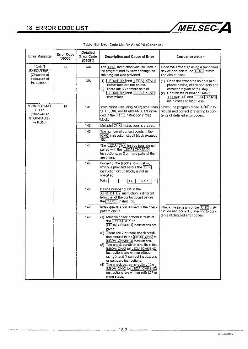
18. ERROR CODE LIST /MELSEC-A Table 18.1 Error Code List for AnACPU (Continue)
Error Code (D9008)
13
14
Detailed
The instruction was included in the program and executed though no sub program was provided.
135 (1) (LEDA/B( land[LEDAl IXENDl instructions are not paired.
-1 and[LEDAJ IXENDI instructions.
(2) There are 33 or more sets of
Instructions (including NOP) other than LDX, LDIX, ANDX and ANlX are inclu- ded in t h e m instruction circuit block.
Multiple instructions are given.
143
144
The number of contact points in the
150.
The I LEDA 1 CHK] instructions are not paired with the 1 LEDA I CHKEND] instructions, or 2 or more pairs of them are given.
instruction circuit block exceeds
145 Format of the block shown below, which is provided before the (CHKI instruction circuit block, is not as specified.
pz~t-; +[ CJ I P;:;: H 146
1 47
Device number of D l in the instruction is different
from that of the contact point before
Index qualification is used in the check pattern circuit.
~~~~
the IcJP,_] -7 instruction.
(1) Multiple check pattem circuits of
I given.
using X and Y contact instructions or compare instructions.
(41 The check oattem circuits of the ' ' tolLEDA( CHKEND 1 instructions are written with 257 o!
more steps.
Corrective Action
Read the error step using a peripheral device and delete t h e m instruc- tion circuit block.
(1) Read the error step using a peri- pheral device, check contents and correct program of the step.
(2) Reduce thenumber of sets of -1 and[LEDAl IXEND] instructions to 32 or less,
Check the program of t h e m inst- ruction and correct it referring to con- tents of detailed error codes.
Sheck the program of t h e m inst- ruction and correct it referring to con- ients of detailed error codes.
18-3 IE(NA)66251-F

18. ERROR CODE LIST /MELSEC--
Table 18.1 Error Code List for AnACPU (Continue)
Detailed I 1 (D9008) 1 (D9091) Error Massage Error 'Ode Error Code
'CAN'T EXECUTE([) (Checked at
occurrence of interrupt)
END processing.)
'END NOT 24 241 EXECUTE' (Checked at execution of
the END instruction.)
'MAIN CPU 26 DOWN'
-
Description and Cause of Error
T h e m instruction was given ,utside of the interrupt program and ,vas executed. rhere is n o m instruction in the nterrupt program.
rhough an interrupt module is used, no nterrupt pointer ( I ) which corresponds :o the module is given in the program. Jpon occurrence of error, the problem minter ( I ) number is stored at D9011
:1) Memory cassette is not loaded. :2) The memory cassette loaded to
the AnACPU is an unloadable one. The sequence program storage P A M n the CPU module caused an error. The work area RAM in the CPU mod- ule caused an error. The device memory in the CPU mod- ule caused an error. The address RAM in the CPU module =used an error.
~
The operation circuit for index qualifi- :ation in the CPU does not work cor- rectly. Hardware (logic) in the CPU does not operate correctly. The operation circuit for sequential processing in the CPU does not ope- rate correctly. Scan time is longer than the WDT time. (1) Scan time of the usets program
has been extended due to certain conditions.
(2) Scan time has been extended due to momentary power failure occur- red during scanning.
Whole program of specified program capacity was executed without execu- ting the END instruction. (1) When the END instruction was to
be executed, the instruction was read as other instruction code due to noise.
(2) The END instructiorl changed to other instruction code due to un- known cause.
The main CPU is malfunctioning or faulty.
Corrective Action
3ead the error step usin a peripheral jevice and delete the & nstruction.
~ ~ ~~~ ~ ~~ ~
>heck the interrupt program if the instruction is given in it.
Nnte the JIRETI instruction i f it is not given. Llonitor special register D9011 using a ~eripheral device, and check if the nterrupt program that corresponds to :he stored data is provided or if two or nore interrupt pointers ( I ) of the same lumber are given. Make necessary :orrections. (1) Turn off the PC power and load
[2) Load a usable memory cassette. the memory cassette.
CPU hardware error Sonsult Mitsubishi representative.
CPU hardware error. Consult Mitsubishi representative.
(1) Check the scan time of the user's program and shorten it using the lcJl instructions.
(2) Monitor contents of special regis- ter D9005 using a peripheral devi- ce. If the contents are other than 0, power supply voltage may not be stable. Check power supply and reduce variation in voltage.
(1) Reset and run the CPU again. If the same error recurs, consult Mitsubishi representative since this is CPU hardware error.
CPU hardware error. Consult Mitsubishi representative.
18-4 IB(NA)66251-F

18. ERROR CODE LIST /MELSEC-A Table 18.1 Error Code List for AnACPU (Continue)
Detailed irror Code (09091) -
jrror Code (D9008)
31
Corrective Action :mor Message Description and Cause of Error
k r r e n t l/O module information i s different from that recognized Nhen the power was turned on. :l) The 110 module (including spe-
cial function modules) connec- tion became loose or the mod- ule was disconnected during operation, or wrong module was connected.
Read detailed error code using a peripheral device and check or re- place the module which corres- ponds to the data (I/O head number). Or, monitor special registers D9116 to D9123 using a peripheral device and check or replace the modules if corresoondins data bit is "1".
"UNITVERIW ERR."
(Checked continuously.)
"FUSE BREAK OFF"
(Checked continuously.)
32 There is an output module of which Fuse is blown.
(1) Check the FUSE BLOWN indica- tor LED on the output module and replace the fuse.
(2 ) Read detailed error code using a peripheral device and replace the fuse of the output module which corresponds to the data (I/O head number). Or, monitor special registers D9100 to D9107 using a peripheral device and replace the fuse of the output module of which corresponding data bit is " 1 " .
Since it is a hardware error of special function module, CPU mod- ule or base module, replace and check defective module(s1. Consult Mitsubishi representative for defec- tive modules.
"CONTROL- BUS ERR."
401 Due to the error of the control bus which connects to special function modules, the FROMKO instruction cannot be executed.
If parameter I/O assignment is being executed, special function modules are not accessible at initial communication. At error occurrence, the head I/O number (upper 2 digits of 3 digits) of the special function module that caused error is stored at D9011.
40
41
402
I
"SP. UNIT DOWN"
41 1 Though an access was made to a special function module at execu- tion of the FROMnO instruction, no response is received.
Since i t is hardware error of the special function module to which an access wasmade, consult Mitsu- bishi representative.
41 2 If parameter I10 assignment is being executed, no response is re- ceived from a special function rnod- ule at initial communication. At error occurrence, the head I/O number (upper 2 digits of 3 digits) of the special function module that caused error is stored at D9011.
I
42 Set one of them as master station and the other as local station.
Since it is hardware error of E module, replace and check a defec tive module. For defective mod ules, consult Mitsubishi representa
Execute 1/0 assignment again using parameters from the peripheral de- vice according to the loading status of special function modules.
Both AJ71AP21m21 and AJ71AT21B have been set as master stations.
Though the interrupt module is no1 loaded, an interrupt occurred.
"LINK UNIT ERROR"
"VO INT. ERROR"
43
'SP. UNIT LAY. ERR."
44 441 A special function module is assigned as an VO module, or vice versa, in the 110 assignment u s i y parameters from the peripheral de. vice.
18-5 IB(NA)66251-F

18. ERROR CODE LIST ~/MEf SEC=A Table 18.1 Error Code List for AnACPU (Continue)
I Error Massage
'SP. UNIT ERROR'
(Checked at execlrtion of the
F R O M O instruction or the dedicated inst-
ructions for special function
'LINK PARA ERROR'
I 'OPERATION ERROR'
(Checked at execution of instruction.)
Error Code (D9008)
46
47
50
Detailed Error Code
(D9091)
442
443
444
445
446
447
461
462
(NET II) -
501
502
Description and Cause of Error
There are 9 or more special function modules (except AEl(S1)) which can execute interruption to the CPU mcd- ule loaded. There are 2 or more AJ71AP21/R21 or AJ71AT21B modules loaded. There are 7 or more modules such as a computer link module loaded to one CPU module. There are 2 or more A161 (Sl) modules loaded. Modules assigned by parameters for MNTlMlNl automatic refresh from the peripheral device do not conform with the types of station modules actually linked. The number of modules of I/O assign- ment registration (number of loaded modules) per one CPU module for the special function modules which can use dedicated instructions is larger than the specified limit. (Total of the number of computers shown below is larger than 1344.)
(AD59 x 5 ) (AD57(Sl)/AD58 x 8)
(AJ71 C24(SWS6/S8) x 10) (AJ71 UC24 x 10)
(AJ71C21(Sl) x 29)
Total > 1344 + (AJ71 PT32(S3)' x125)
Module specified by the FROMRO instruction is not a special function module.
Module specified by the dedicated inst- ruction for special function module is not a special function module or not a :orresponding special function module.
(1) Data written to the parameter areas of the link of which range was set by parameters using a peripheral device does not confom with the data of link parameters read by the CPU.
(2) Total number of local stations is set at 0.
(1) When file registers (R) are used, operation is executed outside of specified ranges of device numb- ers and block numbers of file regi- sters (R).
(2) File registers are used in the prc- gram without setting capacity of file registers.
Combination of the devices specified by instruction is incorrect
Corrective Action
Reduce the special function modules (except A161 (Sl)) which can execute interrupt start to 8 or less.
Reduce AJ71AP2VR21 or AJ71AT21E to 1 or less. Reduce the computer link modules to 6 or less.
Reduce the A161 (Sl) module to 1.
Perform again module assignment for MNT/MlNI automatic refresh with para- meters according to actually linked sta, tion modules.
~~ __
Reduce the number of loaded special function modules. * If the extend mode is used.
Read the error step using a peripheral device and check and correct contents 3f the F R O M O instruction of the step.
Read the error step using a peripheral jevice and check and correct contents 3f the dedicated instruction for special !unction modules of the step.
(1) Write in parameters again and check.
(2) If the same error indication is giv- en again, it is hardware failure. Consult Mitsubishi representative.
Read the error step using a peripheral device and check and correct program of the step.
18-6 IB(NA)66251-F

18. ERROR CODE LIST /MELSEC-A Table 18.1 Error Code List for AnACPU (Continue)
Detailed Error Code
(D9091)
Error Code (D9608)
50
Description and Cause of Error Corrective Action Error Message
"OPERATION ERROR"
[Checked at execution of instruction.)
Read the error step using a peripheral device and check and correct program of the step.
Stored data or constant of specified device is not in the usable range.
Set number of data to be handled is out of the usable range.
503
504
505 (1) Station number specified by the [LEDNB I LRDPI, [LEDNB I L W P ~ , ~ , LLwrpl instructions is not a local station.
number specified by the
instructions is not of a remote station.
Head I/O number specified by the I LEDNB j RFRP 1 I LEDNB 1 RTOP 1 [RFRPL. m l instructions is not of a special function module.
(1) When the AD57(S1) or AD58 was executing instructions in divided processing mode, other instructions were executed to either of them.
(2) When an AD57(S1) or AD58 was executing instructions in divided processing mode, other instructions were executed in divided mode to another AD57(S1) or AD58.
506
507 Read the error step using a peripheral device and provide inter- lock with special relay M9066 or modify program structure so that, when the AD57(S1) or AD58 is executing instructions in divided processing mode, other instruc- tions may not be executed to either of them or to another AD57611 or AD58 in divided mode.
509 (1) Read the error step using a peripheral device and correct the program, meeting loaded conditions of remote terminal modules.
(2) Provide interlock using M9081 (communication request reg- istration areas BUSY signal) or D9081 (number of vacant areas in the communication request
(1) An instruction which cannot be executed by remote terminal modules connected to the MNETMINLS3 was executed to the modules.
(2) When the /PRCJ instruction was executed to a remote terminal, the communication request
(3) The instruction was registration areas overflowed.
executed without executing the
Instruction was ex- a remote terminal. Execute the -1 instruc-
w l or I P l D C O N T j instruc- ecuted without executing the
tion after execution of the [ P i D l N l T I instruction. Execute the instruction after execution of the -1 and [=I instructions.
tion.
60 (1) The CPU malfunctioned due to
(2) Hardware failure. noise.
(1) Take proper countermeasures
(2) Hardware failure. for noise.
"MAIN CPU DOWN"
"BATERY E R R O R "
(Checked at power on.)
70 (1) Battery voltage has lowered be-
(2 ) Battery lead connector is not low specified level.
connected.
(1) Replace batten/. (2) If a RAM memory or power
failure compensation function is used, connect the lead con- nector.
18-7 lB(NAj66251-F

18. ERROR CODE LIST /MELSEC-A 18.3 Error Code List for the AnUCPU, A2ASCPU and A2USH board
Table 18.2 shows the error messages, description and cause of error and corrective actions. (*: The detailed error codes added to AnUCPU, A2ASCPU and A2USH board) Error codes, detailed error codes and error steps are stored in the following special registers.
Error code: D9008 Detailed error code: D9091 Error step: D9010 and D9011
Table 18.2 Error Code List for the AnU, A2AS and A2USH board (Continue)
Error Massage
"INSTRCT CODE ERR"
(Checked when STOP + RUN or at execution of instruction.)
"PARAMETER ERROR"
(Checked at power on and at STOPIPAUSE
+ RUN.)
Error Code (D9008)
10
1 1
~~
Detailed Error Code
(D9091)
101
102
103
104
105
Error and Cause Corrective Action
Instruction codes which the CPU cannot peripheral device and correct the decode are included in the program.
(1) Read the error step using a
program of the step.
instruction codes which cannot be decoded. I f it does. replace it with a correct ROM.
(2) Check the ROM if it contains
Index qualificatlon is specified for a 32- bit constant.
Device specified by an dedicated instruction is not correct.
An dedicated instruction has incorrect Droaram structure.
An dedicated instruction has Incorrect command name.
106
[LEDA/BJIXI and ILEDNB I IXENDI.
Index qualification using Z or V is included in the program between
107 (1) Index qualification is specified for the device numbers and set values in the OUT instruction of timers and counters.
(2) Index qualification is specified at the label number of the pointer (P)
the label number of the interrupt polnter (I) provided to the head of an interruot Droaram.
Read the error step using a peripheral device and correct the program of the step.
108 Errors other than 101 to 107 mentioned above.
111 Read parameters in the CPU memory, Capacity settings of the main and sub programs, microcomputer program, file
Total of the set capaclty of the main and 1 12
not within the usable range of the CPU.
corrections and write them again to the register comments, status latch, sampl- check the contents, make necessary
, ing trace and extensron file registers are memory.
sub programs, file register comments, status latch, sampling trace and extension file registers exceeds capacity of the memory cassette.
18-8 .B(NAj66251-F

18. ERROR CODE LIST /MELSEC=A Table 18.2 Error Code List for the AnU, A2AS and A2USH board (Continue)
Error Code (09008)
Detailed Error Code
(D9091) rror Massage Error and Cause Corrective Action
PARAMETER ERROR"
(Checked at Iwer on and at ;TOPIPAUSE
+ RUN )
11 113 Read parameters in the CPU memory, check the contents, make necessary corrections and write them again to the memory
Latch range set by parameters or setting of M. L or S is incorrect.
Sum check error 114
115 Either of settings of the remote RUN/ PAUSE contact point by parameters, operation mode at occurrence of error, annunctator indication mode, or STOP - RUN indlcation mode is incorrect.
116 The MNET-MINI automatic refresh setting by parameters is incorrect.
117 Timer settina bv Darameters is Incorrect.
118 Counter setttng by parameters is incorrect.
vllSSlNG END INS"
(Checked at TOP + RUN.j
12 121 Write the END instruction at the end of the mam Drooram.
The END (FEND) instruction is not given in the main program.
The END (FEND) instructton is not given in the sub program if the sub program is set bv Darameters.
Write the END instruction at the end of the sub program.
122
123 (1 j When subprogram 2 is set by a parameter, there IS no END (FEND) instruction in subprogram 2 .
(2) When subprogram 2 is set by a parameter. subprogram 2 has not been written from a peripheral device.
124 ( 1 ) When subprogram 3 is set by a parameter. there is no END (FEND) instruction in subprogram 3.
(2) When subprogram 3 is set by a parameter, subprogram 2 has not been written from a peripheral device
"CAN'T YXECUTE (P)" (Checked at execution of instruction.)
13 1 131 The same device number is used at two or more steps for the potnters (P) and Interrupt pointers (I) used as labels to be specified at the head of jump destlnation.
Eliminate the same polnter numbers provided at the head of jump destlnation.
132 Read the error step uslng a peripheral device, check contents and insert a jump destination pointer (P). ILEDNB I FCALL~ or I LEDNB I BREAK]
Instruction is not provtded before the END instruction.
(1) T h e m instruction was included in the program and executed though t h e m instruction was
133 (1 ) Read the error step using a peripheral device, check contents and correct program of the step.
levels of the m, =/and (2) Reduce the number of nesting
instructions to 5 or less. (2) YOhteja and j LEDAL3 BREAK]
instructions were included in the
(3) Nestin level of the and & instructions is 6 levels or deeper, and the 6th level was
(4) There is no lm or (NEXTI executed.
Instruction at execution of the or instruction.


18. ERROR CODE LIST /MELSEC=A Table 18.2 Error Code List for the AnU, A2AS and A2USH board (Continue)
Error Code (D9008)
Detailed
(D9091) Error Code Error and Cause
153 Though an Interrupt module is used, no interrupt pointer (I) whlch corresponds to the module is given in the program. Upon occurrence of error. the problem pointer ( I ) number is stored at D9011.
.-. I Memory cassette is not loaded.
Corrective Action Error Massage
"CAN'T EXECUTE (I)" (Checked at
occurrence of interrupt.)
"CASSETTE ERROR"
"RAM ERROR" (Checked at power on.)
"OPE CIRCUIT ERROR"
(Checked at power on.)
"OPE. CIRCUIT ERR."
(Checked at executlon of the
END instruction)
"WDT ERROR" (Checked at execution of
END processing.)
"END NOT EXECUTE" (Checked at
execution of the END
instruction.)
"MAIN CPU DOWN"
15 Monitor special register D901 1 using a peripheral devlce. and check if the interrupt program that corresponds to the stored data is provlded or if two or more interrupt pointers (I) of the same number are given. Make necessary corrections.
Turn off the PC power and load the memorv cassette.
16
Slnce thls IS CPU hardware error, consult Mitsubishl representative.
20 The sequence program storage RAM in the CPU module caused an error.
202 1 The work area RAM in the CPU module ' caused an error.
203 The device memory in the CPU module caused an error.
204 The address RAM in the CPU module
+ caused an error
21 21 1 Since this is CPU hardware error, consult Mitsubishl representative.
The operation circuit for index qualification in the CPU does not work correctly.
Hardware (logic) in the CPU does not operate correctly.
The operation circuit for sequential processing in the CPU does not operate correctly.
In the END processing check, the operation circuit for index qualification In the CPU does not work correctly.
In the END processing check, the hardware in the CPU does not operate correctly.
Scan time is longer than the WDT time. (1) Scan time of the user's program has
been extended due to certain conditions.
(2) Scan tlme has been extended due to momentary power failure occurred during scanning.
Whole program of speclfied program capacity was executed without executing the END instructlons. (1) When the END instruction was to
be executed, the instruction was read as other instruction code due to noise.
(2) The END instruction changed lo other instruction code due to unknown cause.
The main CPU is malfunctioning or faulty
21 2
21 3
21 4
21 5
22 (1) Check the scan tlme of the user's program and shorten it using the rcJl instructions.
(2) Monitor contents of special register D9005 using a peripheral device. If the contents are other than 0, power supply voltage may not be stable. Check power supply and reduce variation in voltaae.
24 24 1 (1) Reset and run the CPU again. I f the same error recurs, Since this is CPU hardware error, consult Mitsubishl representative.
Since this IS CPU hardware error, consult Mitsubishi representative
26
18-1 1 IBiNA'66251-F

18. ERROR CODE LIST /MELSEC=A Table 18.2 Error Code List for the AnU, A2AS and A2USH board (Continue)
~~
Error Code (D9008)
31
32
40
41
42
43
44
Detailed Error Code
(D9091) Error and Cause Corrective Action
Current I10 module information IS different from that recognized when the power was turned on. (1) The I/O module (including speclal
functlon modules) connection became loose or the module was disconnected durinq operation, or
~ ~~~
Read detailed error code using a perlpheral devlce and check or replace the module whlch corresponds to the data (110 head number). Or. monitor special registers D9116 to D9123 using a peripheral device and check or redace the modules if - .
wrong module was connected. corresponding data bit is "1" .
There IS an output module of which fuse (1 j Check the FUSE BLOWN indicator is blown. LED on the output module and
replace the fuse. (2) Read detailed error code using a
peripheral device and replace the fuse of the output module whlch corresponds to the data (I10 head number). Or, monitor special registers D9100 to D9107 using a peripheral device and replace the fuse of the output module of which correspondlng data bit is "1 ".
401
402
Due to the error of the control bus which connects to special function modules. the FROMnO instructlon cannot be executed.
If parameter I/O assignment is being executed, special function modules are not accessible at initlal communlcation. At error occurrence. the head I/O number (upper 2 digits of 3 digits) of the special function module that caused error is stored at D9011
Since it is a hardware error of speclal function module, CPU module or base module, replace and check defective moduleis). Consult Mitsubishi representative for defective modules.
I 41 1 Though an access was made to a
special function module at execution of the FROMnO instruction, no response IS received.
41 2 ~
I f parameter I/O assignment is being executed, no response is received from a special function module at initlal communication. At error occurrence, the head I/O number (upper 2 digits of 3 digits) of the special function module that caused
Since it is hardware error of the special function module to which an access was made, consult Mitsubishi representatlve.
error is stored at D9011 -
Since it is hardware error of a module, Though the interrupt module IS not -
Remove either AJ71 (A)R22 or AJ71 (A) Either AJ71 (A)R22 or AJ71 (A)P22 is loaded to the master station. P22 from the master station.
loaded, an interrupt occurred. replace and check a defective module. For defective modules, consult Mitsubishi representative.
441 Execute l/O assignment again using A speclal function module is asslgned as an I/O module, or vice versa. in the I/O
function modules. peripheral device. according to the loading status of special assignment using parameters from the parameters from the perlpheral device
442 Reduce the special function modules There are 9 or more special function modules (except A161 (S l j) which can
interrupt start to 8 or less. execute interruption to the CPU module (except A161 (S1 j ) which can execute
1 loaded.
18-1 2 IBiNA)66251-F

18. ERROR CODE LIST ~/MELSEC-A Table 18.2 Error Code List for the AnU, A2AS and A2USH board (Continue)
I Error Code (09008)
Detailed Error Cod€
(D9091) Error and Cause Corrective Action
44 443 There are 2 or more AJ71AP21, AJ71AR21, AJ71P22 or AJ71R22 modules loaded.
Reduce the AJ71AP21, AJ71AR21, AJ71 P22 or AJ71 R22 modules to 1 or less.
Reduce the computer link modules to 6 or less.
L 444 There are 7 or more modules such as a
computer link module loaded to one CPU module.
There are 2 or more A161 ( S l ) modules loaded. I 445 Reduce the A161 module to 1
Modules assigned by parameters for MNT/MINI automatic refresh from the peripheral device do not conform with the types of statlon modules actually linked.
Perform agaln module assignment for MNTiMlNl automatic refresh with parameters according to actually llnked station modules.
446
447
448'
The number of modules of I10 assignment reglstration (number of loaded modules) per one CPU module for the special function modules which can use dedicated instructions is larger than the specified limit. (Total of the number of computers shown below is larger than 1344.)
(AD59 x 5) (AD57(Sl)/AD58 x 8)
(AJ71C24(S3/S6/S8) x 10) (AJ71UC24 x 10)
Reduce the number of loaded special function modules.
(AJ71C21(Sl) A 29) + (AJ71 PT32(S3) x 125)
Total > 1344
(1) Five or more AJ71 LP21IAJ71BRlls
(2) A total of five more of the following have been installed.
AJ71AP211R21, AJ71 LP21, have been Installed;
AJ71BR21.
(1) Make the total of the installed AJ71AP21iR21, AJ71LP21, AJ71BR21 units four or less.
46 461 Module specified by the FROMITO instructlon IS not a special function module.
'SPUNIT ERROR"
(Checked at execution of the
FROMITO instructlon or the dedicated instructlons for special functlon
modules.)
"LINK PARA. ERROR"
Read the error step using a perlpheral device and check and correct contents of the FROM/TO instruction of the step.
462 (1) Module specified by the dedicated instruction for speclal function module is not a special function module or not a corresponding special function module.
module with function version under B.
(3) A CC-Link dedicated command was issued to a CC-Llnk module for whlch the network parameters have not been set.
(2) A command was issued to a CC-Link
(1) Read the error step using a peripheral device and check and correct contents of the dedicated instruction for special function modules of the step.
having function version B and above.
(2) Replace with a CC-Link module
(3) Set the parameters.
I 47 0 [When using MELSECNET/(II)] (1) When the link range at a data link
CPU whlch is also a master statlon (station number = 00) is set by parameter setting at a peripheral device, for some reason the data written to the link parameter area differs from the link parameter data read by the CPU. Alternatively, no link parameters have been written.
set at 0. (2) The total number of slave stations IS
(1) Write the parameters again and
(2) Check the station number settings. (3) Persistent error occurrence may
check.
indicate a hardware fault. Consult your nearest Mitsubishi representa- tive, explaining the nature of the problem.
18-13 lBiNA)66251-F

18. ERROR CODE LIST /MELSEC-A Table 18.2 Error Code List for the AnU, A2AS and A2USH board (Continue)
Error Massage
"LINK PARA ERROR"
Error Code (D9008)
47
Detailed Error Code
(D9091)
470'
471 *
472'
473'
474*
475'
Error and Cause
[When usmg MELSECNETIlO] (1 ) The contents of the network refresh
parameters written from a perlpheral device differ from the actual system at the base unit.
(2) The network refresh parameters have not been written.
[When using MELSECNETilO] (1) The transfer source device range
and transfer destination device range specified for the inter-network transfer parameters are in the same network.
source devices or transfer destina- tion devices for the inter-network transfer parameters spans two or more networks.
source devices or transfer destina- tion devices for the inter-network transfer parameters is not used by the network.
(2) The specified range of transfer
(3) The specified range of transfer
[When using MELSECNETIIO] The contents of the routing parameters written from a peripheral device differ from the actual network system.
[When using MELSECNETIIO] (1) The contents of the network
parameters for the first link unit, written from a peripheral device, differ from the actual network system.
unit have not been written.
stations IS 0.
(2) The link parameters for the first link
(3) The setting for the total number of
[When using MELSECNET/lO] (1) The contents of the network
parameters for the second link unit, written from a peripheral device, differ from the actual network system.
(2) The link parameters for the second link unit have not been written.
(3) The setting for the total number of stations is 0.
[When using MELSECNETil 01 (1) The contents of the network
parameters for the third link unit, written from a peripheral devlce, differ from the actual network system.
unit have not been written.
stations is 0.
(2) The link parameters for the third link
(3) The setting for the total number of
Corrective Action
Write the network refresh parameters agaln and check.
Wrlte the network parameters again and check.
Write the routing parameters again and check.
(1) Write the parameters again and
(2) Check the station number settings. (3) Persistent error occurrence may
check.
indicate a hardware fault. Consult your nearest Mitsubishi representa- tive, explaining the nature of the problem.
18-1 4 lB(NA)66251-F

18. ERROR CODE LIST /MELSEC-A Table 18.2 Error Code List for the AnU, A2AS and A2USH board (Continue)
______ ~~
Detailed Error Code
(D9091)
476'
477
50 1
502
503
504
505
506
508
507
~~ ~~
Error and Cause
[When using MELSECNETAO] (1) The contents of the network
parameters for the fourth link unit, written from a peripheral devlce, differ from the actual network system.
(2) The lmk parameters for the fourth link unit have not been written.
(3) The setting for the total number of stations IS 0.
A ink parameter error was detected by the CC-Link module.
( 1 ) When file registers (R) are used, operation is executed outslde of specified ranges of device numbers and block numbers of file registers (R).
(2) File registers are used In the program without settlng capaclty of file reaisters.
Combination of the devices specified by Instruction is incorrect.
Stored data or constant of specifred device is not In the usable range.
Set number of data to be handled IS out of the usable range.
(1) Statlon number specified by the (LEDA/BILRDPI,ILEDNBILWTP~ m/, (LWTPI instructions is not a local station.
(2) Head 110 number specified b the [ LEDAIBI RFRPj, I&, /RFRP(, (RTOPJ instructions is not of a remote station.
m i , instructions IS not of a speclal function module.
A CC-Link dedicated command was issued to three or more CC-Link moduies.
(1) When the AD57(Sl) orAD58 was executing instructions in divided processing mode, other instructions were executed to either of them.
executing instructions in divided processing mode, other instructions were executed In divided mode to another AD57(S1) or AD58.
(2) When an ADS7(S1) or AD58 was
- ~~~ ~ ~~
Corrective Action
(1) Write the parameters again and
(2) Check the station number settings. (3) Persistent error occurrence may
check.
indicate a hardware fault. Consult your nearest Mltsublshi representa- tive, explalning the nature of the probiem.
(1) Write the parameters in agaln and
(2) If the error appears again, there is a check.
problem with the hardware. Consult your nearest System Service, sales office or branch office.
Read the error step using a peripheral device and check and correct program of the step.
The CC-Llnk dedicated command can be issued only to two or less CC-Link modules.
Read the error step using a perlpheral device and provlde interlock with special relay M9066 or modify program structure so that, when the AD57(S1) or AD58 is executing instructions in divided processing mode. other instructions may not be executed to either of them or to another AD57(S1) or AD58 in divided mode.

18. ERROR CODE LIST /MELSEC=A Table 18.2 Error Code List for the AnU, A2AS and A2USH board (Continue)
Error Massage
"OPERATION ERROR''
(Checked at executlon of instruction.)
"MAIN CPU DOWN"
"BATTERY ERROR"
(Checked at Dower on.)
Error Code (D9008)
50
60
70
Detailed Error Code
(09091)
509
Error and Cause
(1) An lnstructlon which cannot be executed by remote terminal modules connected to the MNET/MINI-S3 was executed to the modules.
executed to a remote terminal. the communication request registration
(2) When t h e m instruction was
areas overflowed. (3) The instruction was
rPlolNlTl instruction. executed without executing the
The [PID571 instruction was executed without executing the /PIDINITI or lPlDCONTj instruction. The program present1 executed was specified by the h instruction.
(4) The number of CC-Link dedicated command executed in one scan exceeded 10.
(1) The CPU malfunctioned due to
(2) Hardware failure.
(1) Battery voltage has lowered below
(2) Battery lead connector is not
noise.
specified level.
connected.
Corrective Action
(1 ) Read the error step using a peripheral device and correct the program, meeting loaded conditions of remote terminal modules.
(2) Provide interlock using M9081 (communication request registratlon areas BUSY signal) or D9081 (number of vacant areas in the communicatlon re uest registratlon areas) when the & instruction is executed to a remote terminal.
(3) Correct the program specified by the ml instruction to other.
(4) Set the number of CC-Link dedicated commands executed In one scan to 10 or less.
(1) Take proper countermeasures for
(2) Hardware failure.
(1) Replace battery. (2) If a RAM memory or power failure
compensation functlon is used. connect the lead connector.
noise.
18-1 6 IB(NA)66251-F

18. ERROR CODE LIST /MELSEC-A 18.4 Error Code List for AnSHCPU
The detailed error code is stored into D9092 only when the CC-Link dedicated instruction is used.
Table 18.3 Error Code List for AnSHCPU
Error Massage
INSTRUCT CODE ERR.
PARAMETER ERROR
MISSING END INS.
Zontents of
Special Register D9008 (BIN
value)
10
1 1
12
- 3etailed
Error Code
(D9092)
101
103
104
105
CPU State
STOP
STOP
STOP -
Error and Cause
An instruction code which cannot be de- coded by the CPU is included in the pro- gram. (1) A memory cassette containing an
invalid instruction code has been loaded.
(2) The Occurrence of an error destroyed the memory contents, adding an instruction code that cannot be read to the memory.
An instruction code which cannot be d e coded by the CPU is included in the pro- gram. (1) A memory cassette containing an
invalid instruction code has been loaded.
(2) The occurrence of an error destroyed the memory contents, adding an in- struction code that cannot be read to the memory.
The device specified in the CC-Link dedicated instruction is incorrect. Program configuration of the CC-Link dedicated instruction is incorrect. The command name of the CC-Link dedicated instruction is incorrect. The contents of the memory installed in the PC CPU have been destroyed because of noise, or the failure of the memory cassette.
(1) There is no END (FEND) instruction in the program.
Corrective Action
(1) Read the error step by using a peripheral device and cor- rect the program at that step.
contains instruction codes that cannot be interpreted, and insert the correct ROM.
(2) Check if the used ROM
(1) Read out the steps where the error occurred using a pe- ripheral device, and correct the program.
contains instruction codes that cannot be interpreted, and insert the correct ROM.
(2) Check if the used ROM
Read the error step by using a peripheral device and correct the program at that step.
(1) Check the loading of the PC CPU memory cassette and load it correctly.
from the PC CPU by using a peripheral device. Make any necessary correc- tion and write it to the PC CPU again.
program.
(2) Read the parameter data
(1) Write END at the end of the
18-1 7 lB(NA)66251-F
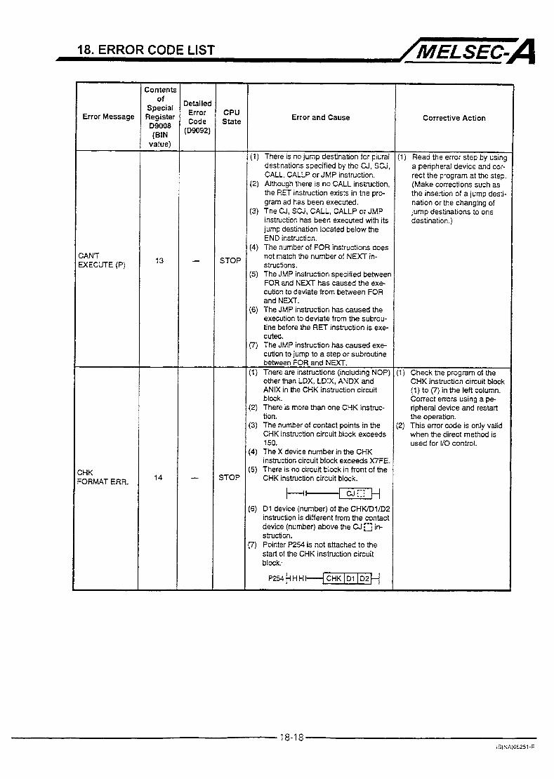
18. ERROR CODE LIST /MELSEC=A
Error Message
;AN7 XECUTE (P)
:HK :ORMAT ERR.
Contents of
Special Register D9008 (BIN
value)
~~~~ ~
13
14
Detailed Error Code
(D9092)
- CPU State
STOP
STOP
-
Error and Cause
(1) There is no jump destination for plural destinations specified by the CJ, SCJ CALL, CALLP or JMP instruction.
(2 ) Although there is no CALL instruction, the RET instruction exists in the prc- gram ad has been executed.
(3) The C J , SCJ, CALL, CALLP or JMP instruction has been executed with its jump destination located below the END instruction.
(4) The number of FOR instructions does not match the number of NEXT in- structions.
(5) The JMP instruction specified betweer FOR and NEXT has caused the e x e cution to deviate from between FOR and NEXT.
(6) The JMP instruction has caused the execution to deviate from the subrou- tine before the RET instruction is e x e Cuted.
(7) The JMP instruction has caused e x e cution to jump to a step or subroutine between FOR and NEXT.
(1) There are instructions (including NOP: o?her than LDX. LDIX. ANDX and ANlX in the CHK instruction circuit block.
tion.
CHK instruction circuit block exceeds 150.
(4) The X device number in the CHK instruction circuit block exceeds WFE
(5) There is no circuit block in front of the CHK instruction circuit block.
(2) There is more than one CHK instruc-
(3) The number of contact points in the
:6) D l device (number) of the CHWDllDP instruction is different from the contact device (number) above the CJ [z iri- struction.
start of the CHK instruction circuit 7) Pointer P254 is not attached to the
block:
(1) Read the error step by using a peripheral device and cor- rect the program at the step. (Makecorrectionssuchas the insertion of a jump desti- nation or the changing of jump destinations to one destination.)
1) Check the program of the CHK instructicn circuit block (1) to (7) in the left column. Correct errors using a pe ripheral device and restart the operation.
when the direct method is used for I/O control.
2) This error code is only valid
18-18 IB(NA)66251-F

18. ERROR CODE LIST /MELSEC-A ~~
Error Massage
CAN'T EXECUTE (I)
ROM ERR
RAM ERROR
OPE. ClRCUiT ERR.
WDT ERROR
END NOT EXECUTE
WDT ERROR
UNIT VERIFY ERR.
Contents of
Special Register
D9008 (BIN
value)
15
17
20
21
22
24
25
31
letailed Error Code D9092)
-
CPU State
-
STOP
STOP
-
STOP
STOP -
STOP
-
STOP
- STOP
STOP (RUN)
Error and Cause
(1) Although the interrupt module is used, there is no number for interrupt pointer I, which corresponds to that module, in the program, or more than one number for pointer I exists in the program.
(2) No IRET instruction has been entered in the interrupt program.
(3) There is an IRET instruction sorne- where besides the interrupt program.
(1) Parameters and/or sequence pro- grams are not correctly written to the installed memory cassette.
(1) The PC CPU has checked if write and read operations can be performed properly with respect to the data memory area of the PC CPU. Normal writing and/or readwrite tumed out to be impossible.
(1) The operation circuit, which performs the sequence processing in the PC CPU. does not operate properly.
Scan time exceeds watchdog monitoring time. (1) Scan time of user program is exces-
sive. (2) Scan time has lengthened due to
instantaneous power interruption which occurred during the scan.
(1) When the END instruction is executed, it is read as another instruction code due to noise, etc.
(2) The END instruction has changed to another instruction code.
The END instruction cannot be executed with the program looped. VO module data is different from that at power ON. (1) The WO module (including the special-
function module) is incorrectly disen- gaged or has been removed, or a dif- ferent module has been loaded.
Corrective Action
(1) Check for the presence of interrupt program which cor- responds to the interrupt module and create an inter- rupt program of reduce the number of Is to one.
(2) Check if there is an IRET instruction in the interrupt program and enter the IRET instruction.
instruction somewhere be- sides the interrupt program and delete that IRET instruc- tion.
( I ) Write parameters and/or sequence programs correctly to the memory cassette.
(2) Remove a memory cassette which does not have any pa- rameter and/or sequence program.
(3) Check if there is an IRET
Since this is a PC CPU hardware fault, consult your nearest Mitsu- bishi representative.
(1) Calculate and check the scan time of the user program and reduce the scan time by the use of CJ instructions, etc.
(2) Monitor the contents of spe- cial register D9005 by using a peripheral device. If the contents are other then 0, the line voltage is insufficient. Therefore, check the power and eliminate the voltage fluctuation.
If the same error is displayed again, it is a PC CPU hard- ware fault Therefore, consult your nearest Mitsubishi represen- tative.
(1) Perform reset and RUN.
Check for an endless loop and correct the program. (1) Among special registers
D9116 to D9123, the bit cor- responding to the module verify error is set to '1'. Therefore, monitor the regis- ters by using a peripheral de- vice and check for the module whose bit is '1'.
(2) When the fault has been corrected, reset the PC CPU.
18-19 IB(NA)6625'e-F

18. ERROR CODE LIST /MELSEC-A Error Massage
FUSE BREAK OFF
CONTROL- BUS ERR
SP. UNIT DOWN
If0 INT. ERROR
SP. UNIT LAY. ERR.
SP. UNIT ERROR
Contents of
Special Register D9008 (BIN
value)
32
40
41
43
44
46
letailec Error Code :D9092)
462
-
CPU State
-
RUN STOF
-
STOP
STOP
STOP
Error and Cause
(1) There is an output module with a
(2) The external power supply for the blown fuse.
output load is OFF or not connected.
The FROM and TO instructions cannot be executed. (1) Control bus error in the special-
function module.
When FROM and TO instructions cannot be executed. (1) Contrd bus error in the special-
function module.
Although the interrupt module is not installed, an interruption has occurred.
(1) Three or more computer link modules are installed in a single CPU module.
(2) Two or more data link modules are installed.
(3) Two or more interrupt module are installed.
(4) In the parameter setting of the periph- eral device, while an 110 module is ac- tually installed, a special-function module has been set in the I/O as- signment, or vice versa.
(1) Access (execution of FROMITO in- struction) has been made to a location where there is no special-function module.
(1) The model name of the module speci- fied in the CCLink dedicated instruc- tion is different from that specified by I/O allocation parameter.
dedicated instruction is not a master module.
(2) The modle specified by a CCLink
Corrective Action
(1) Check the blown fuse indica- tor LED of the output module and change the fuse in the module whose LED is ON.
(2) Checking modules for blown fuses can also be done with a peripheral device. Among special registers D9100 to D9107 , the bit corresponding to the module with a blown fuse is set to '1'. Therefore, check by monitor- ing the registers.
the external power supply for the output load.
module, CPU module or base unit hardware fault. There- fore, change the module and check the defective module. Consult your nearest Mitsu- bishi, representative about the defective module.
(3) Check the ONOFF state of
(1) This is a special-function
This is a hardware fault in a special function module to which access has been made. Therefore, consult your nearest Mitsubishi representative about the defective module. (1) This is a module hardware
fault. Therefore, change the module and check the defec- tive module. Consult your nearest Mitsu- bishi representative about the defective module.
(1) Reduce the number of com- puter link modules to two or less.
(2) Use one data link module. (3) Use one interrupt module. (4) Reset the 1/0 assignment in
the parameter setting according to the actually loaded special-function mod- ule by using a peripheral de- vice.
(1) Read the error step by use of peripheral device, and check and correct the content of the F R O M 0 instruction at that step by using a peripheral device.
specified by VO allocation parameter with that specified in the CCLink dedicated in- struction.
peripheral device. Check and correct the CCLink dedicated instruction in the step.
(1) Match the model name
(2) Read the error step with a
. v L"
IB(NA)66251-F

18. ERROR CODE LIST /MELSEC-A
Error Message
.INK PARA. ERROR
3PERATION ERROR
3AlTERY ERROR
Contents 1 Of Detailed
Special Code Register Error
(DW92) (BIN value) I
47
50 F? 'O I -
CPU State
RUN
RUN STOP)
L_
RUN
-
Error and Cause
1) The contents which have been written to the parameter area of the link by setting the link range in the parameter setting of peripheral device are differ- ent from the link parameter contents.
slave station is 0. 2) The setting for the total number of
1) The result of BCD conversion has exceeds the specified range (9999 or 99999999).
2) A setting has been done which ex- ceeded the specified device range anc the operation cannot be done.
3) File registers are used in the program without performing the capactty settinG of file registers.
'he storage data or constant for the speci- ed device is out of range. 'he set number of data to be handled xceeds the usable range. 'he number of CCLink dedicated instruc- o w for one scan exceeds 64.
:Gunk dedicated instruction was exe- uted to the CC-Link module in which lararneters are not set. 1) The battery voltage is below 24 VDC. 2) The battery lead is disconnected.
Corrective Action
(1) Write the parameters again
(2) If this message is displayed and check.
again, there is a hardware fault. Therefore, consult your nearest Mitsubishi represen- tative.
(1) Use a peripheral device to read the error step and check and correct the program at that step. (Check device setting range BCD conversion value, e t . )
Read the error step by using a 3eripheral device and correct the xogram at that step. Decrease the number of CGLink dedicated instructions executed for one scan to 64 or less. Set the parameters.
(1) Change the battery. (2) When RAM or power inter-
ruption compensation is used, connect the battery.
18-21 lB(NA)65251-F

18. ERROR CODE LIST /MELSEC-= 18.5 Error Code List for the QCPU-A (A Mode)
Meanings and causes of error message. error codes, detailed error codes and corrective actions are described
Error Massage
"INSTRCT CODE ERR" (Checked when STOP - RUN or at execution of Instructlon.)
Table 18.4 Error Code List for the QCPU-A (A Mode)
Error Code Detailed Error Code
(D9008) (D909,) Error and Cause Corrective Action
10 (1) Read the error step using a Instruction codes whlch the CPU cannot 101 decode are included in the program peripheral devlce and correct
the program of the step. (2) Check the ROM if it contains
instruction codes which cannot be decoded. If it does, replace It with a correct ROM.
102 Read the error step uslng a peripheral Index qualification is specified for a 32-blt constant.
program structure.
tnstruction is not correct.
device and correct the program of the
command name.
103 step. Device specified by an dedlcated
104 An dedicated instruction has incorrect
105
Included In the program between Index qualification using Z or V is 106
An dedicated instruction has Incorrect
and I LEDAB 1 lXEND1 107 (1) Index qualificatlon is speclfied for the
device numbers and set values In the
counters. OUT Instruction of tlmers and
(2) Index qualificatlon is specified at the label number of the polnter (P) provided to the head of destination of
LEDNB I BREAK I Instructions or at the label number of the interrupt pointer (I) provided to the head of an interrupt program.
Errors other than 101 to 107 mentloned

18. ERROR CODE LIST /MELSEC-A Table 18.4 Error Code List for the QCPU-A (A Mode) (Continue)
Error Massage
"PARAMETER ERROR" (Checked at power on and at STOPJPAUSE -+ RUN )
"MISSING END INS" (Checked at STOP + RUN )
"CAN'T EXECUTE (P)" (Checked at executlon of Instruction )
~~
Error Code (D9008)
11
12
13
Detailed Error Code
(D9091) 111
112
113
114 115
116
11: 118
121
122
131
132
133
Error and Cause Correctwe Action
Capacity settlngs of the mam and sub Read parameters In the CPU memory, programs, microcomputer program, file check the contents, make necessary register comments, status latch. sampling
specified at the head of jump destlnatlon interrupt pointers (I) used as labels to be
provided at the head of jump destrnatlon or more steps for the pointers (P) and Eliminate the same pointer numbers The same d e v w number is used at two
set by parameters. the sub program. in the sub program if the sub program is Write the END instruction at the end of The END (FEND) instructlon is not glven the mam program in the main program. Write the END instruction at the end of The END (FEND) instruction IS not given
incorrect. Counter setting by parameters is Timer settmg by parameters IS Incorrect. by parameters IS Incorrect. The MNET-MINI automatc refresh setting indication mode IS Incorrect. indication mode, or STOP - RUN occurrence of error. annunclator parameters, operatlon mode at RUN/PAUSE contact pomt by
memory Either of settings of the remote corrections and wrlte them again to the Sum check error check the contents, make necessary of M. L or S is incorrect Read parameters In the CPU memory, Latch range set by parameters or settlng
of the memory cassette extenslon file registers exceeds capacity status latch, samplhg trace and sub programs, file regrster comments. Total of the set capacity of the main and withln the usable range of the CPU
memory trace and extension file reglsters are not correctlons and wrrte them again to the
Label of the polnter (P) specified in the Read the error step usln9 a Peripheral
m, m, ~ 1 , ~ 1 , m, device, check contents and Insert a lump
I LEDNB IFCALL 1 or 1 LEDNBI BREAK 1 lnstructlon IS not provided before the END
destmation pointer (P).
instruction. (1) T h e m instruction was included in
the program and executed though the instruction was not glven.
(2) The and 1 LEDNB I BREAK instructions were included In the program and executed though the IFOR/ Instruction was not glven
and ,FOR/ lnstructlons is 6 levels or deeper, and the 6th level was executed.
(3) Nestmg level of t h e m ,
(1) Read the error step using a perlpheral device. check contents and correct program of the step.
(2) Reduce the number of nesting levels of the m i , m] and lnstructlons to 5 or less.
(4) There is no [RET] or m d instructlon at executlon of the or [FORI instruction.
18-23 IBINA)66251-F

18. ERROR CODE LIST /MELSEC-A Table 18.4 Error Code List for the QCPU-A (A Mode) (Continue)
Error Massage
"CAN'T EXECUTE (P)" (Checked at executlon of Instruction.)
"CHK FORMAT ERR' (Checked at STOPlPAUSE - RUN.)
"CAN'T EXECUTE (I)" (Checked at occurrence of Interrupt.)
Error Code (D9008)
13
14
15
Detalled Error Code
(D9091) 134
135
141
142
143
144
145
146
147
148
151
152
153
Error and Cause Corrective Actlon
The /CHGl instruction was Included In the device and delete the /CHGI instructlon program and executed though no sub Read the error Step using a peripheral
Instructions (including NOP) other than I Check the program of the lnstructlon and correct it referring to contents of detalled error codes.
Multiple Instructions are given
The number of contact points In t h e m instruction circult block exceeds 150. The -1 Instructions are not palred with the 1 LEDA[ CHKEND I instructions, or 2 or more pairs of them are glven. Format of the block shown below, whlch is provided before t h e m instruction circuit block, IS not as specified
P 2 5 4 t ( t--+ CJ I p 7 2
Device number of D l In the -1 instruction is different from that of the contact point before the m] instructlon. Index quallficatlon is used in the check pattern circuit. (1) Multiple check pattern circuits of the
ILEDA/CHKI - I LEDA ICHKEND I Instructions are glven.
12) There are 7 or more check conditlon \-,
circuits In the -1 - 1 LEDA ICHKEND I Instructions
(3) The check condltion clrcuits in the -1 - ILEDAI CHKEND 1 instructions are written without using X and Y contact instructions or compare instructlons.
(4) The check pattern circuits of the -1 - 1 LEDA I CHKEND 1 instructions are written wlth 257 or more steps.
T h e m instruction was glven outside device and delete t h e m instruction of the interrupt program and was Read the error step using a Peripheral
executed. There IS n o m Instruction in the interrupt program.
Check the Interrupt program if the /IRETI instruction IS given In it. Wrlte the /IRETI instruction if it IS not aiven
(I) number is stored at D9011 interrupt pointers (I) of the same number

18. ERROR CODE LIST /MELSEC=A Table 18.4 Error Code List for the QCPU-A (A Mode) (Continue)
Error Massage
"CASSETTE ERROR"
"RAM ERROR" (Checked at power on.)
"OPE CIRCUIT ERROR" (Checked at power on.)
"OPE CIRCUIT ERR '' (Checked at executlon of the END instructlon )
'WDT ERROR' (Checked at executlon of END processlng.)
"END NOT EXECUTE" (Checked at execution of the END instruct1on.j
"MAIN CPU DOWN" "UNIT VERIFY ERR" (Checked contlnuously j
Detailed
2o c I 204
T
26 I - 31 -
Error and Cause
(1) A memory card IS Inserted or removed
(2) An invalid memory card IS Inserted. The sequence program storage RAM In the CPU module caused an error. The work area RAM in the CPU module caused an error The devlce memory in the CPU module caused an error The address RAM In the CPU module caused an error. The operatlon circult for Index qualification in the CPU does not work
while the CPU module is ON.
correctlv ~~~
Hardware (logic) in the CPU does not operate correctly The operation circult for sequentlal processing In the CPU does not operate correctlv In the END processing check. the operation circuit for index quallficatlon in the CPU does not work correctly. In the END processing check, the hardware in the CPU does not operate correctly. Scan time is longer than the WDT tlme. (1 j Scan tlme of the user's program has
been extended due to certain conditions.
(2) Scan time has been extended due to momentary power failure occurred during scanning.
Whole program of speciried program capaclty was executed without executing the END instructions. (1) When the END instruction was to be
executed, the instruction was read as other Instruction code due to noise.
(2) The END instructlon changed to other Instruction code due to unknown
The mam CPU is malfunctlonmg or faulty
Current I/O module informatlon is dlfferent from that recognlzed when the power was turned on. (1) The 110 module (including special
functlon modules) connection became loose or the module was disconnected during operation, or wrong module was connected.
Corrective Actlon
(1 ) Do not Insert or remove a memory card whlle the CPU module IS ON.
(2) Insert an available memory card. Slnce thls IS CPU hardware error, consult Mltsubishi representative.
Slnce this IS CPU hardware error, consult Mitsubishl representative.
(1) Check the scan tlme of the user's program and shorten it using the IcJ/ instructlons
(2) Monitor contents of special register D9005 using a peripheral device. If the contents are other than 0, power supply voltage may not be
stable Check power supply and reduce varlatlon in voltage.
(1) Reset and run the CPU again. If the same error recurs Since this is CPU hardware error, consult Mitsublshi representatwe.
Since this is CPU hardware error, consult Mltsubishi representative. Read detailed error code usmg a perlpheral device and check or replace the module which corresponds to the data (110 head number). Or, momtor special registers D9116 to D9123 using a peripheral device and check or replace the modules if corresponding data bit is "1".
18-25 (B(NAj66251-F

18. ERROR CODE LIST /MELSEC-A Table 18.4 Error Code List for the QCPU-A (A Mode) (Continue)
Error Massage
"FUSE BREAK OFF' (Checked continuously.)
"CONTROL- BUS ERR"
'SP.UNIT )OWN"
'LINK UNIT ZRROR"
'I10 INT. IRROR"
~~~
Error Code (D9008)
32
40
41
42
43
Detailed Error Code
(D9091)
401
402
403
405
41 1
41 2
Error and Cause
(1) There is an output module of whlch
(2) The external power supply for output fuse IS blown
load IS turned OFF or is not connected.
Due to the error of the control bus which connects to special function modules, the FROMnO Instruction cannot be executed. If parameter 110 assignment IS belng executed. speclal function modules are not accesslble at Indial communication. At error occurrence, the head I/O number (upper 2 diglts of 3 digits) of the special function module that caused error IS
stored at D9010 Hardware failure. The factor is stored in D9184 (1) The expanslon cable is not properly
(2) QA1S base failure. The base connected
information IS different from that obtalned at power on The failed base is stored in D9068 as a bit pattern The failed base is stored in D9010 from the upper stage.
Though an access was made to a speclal function module at execution of the FROMnO instruction. no response is received. If parameter 110 assignment is being executed, no response is recelved from a speclal function module at initial communlcatlon At error occurrence, the head I10 number (upper 2 digits of 3 dlgits) of the special functlon module that caused error is stored at D9011 Two of AlSJ71APZl/R21 and AISJ71AT21B are specified as master stations. Though the interrupt module IS not loaded, an interrupt occurred.
Corrective Action
(1) Check the FUSE BLOWN indicator LED on the output module and replace the fuse.
(2) Read detailed error code usmg a perlpheral devlce and replace the fuse of the output module which corresponds to the data (110 head number). Or monitor speclal registers D9100 to D9107 using a peripheral devlce and replace the fuse of the output module of which corresponding data bit IS "1".
external power supply for output load. (3) Check the ONiOFF status of the
Since It is a hardware error of speclal function module. CPU module or base module. replace and check defective module(s). Consult Mitsubishi representative for defective modules.
(1) Connect the expansion cable properly. (2) The hardware failure occurs In the
special function, CPU, or base module. Replace the module and find the faulty one Describe the problem to the nearest system service retail store, or corporate oftice, and obtain advice.
Slnce it is hardware error of the speclal function module to which an access was made. consult Mitsubishi representative.
Specify one of AlSJ71AP21iR21 and A I SJ71AT21B as a master station and another as a local station. Since It IS hardware error of a module, replace and check a defective module. For defective modules, consult Mitsubishi representative.
18-26 lB;NA166251-F

18. ERROR CODE LIST /MELSEC-A Table 18.4 Error Code List for the QCPU-A (A Mode) (Continue)
Error Code (D9008)
44
46
Detailed Error Code
(D9091) 44 1
442
443
444
445
446
447
448
449
46 1
462
Error and Cause
A special functlon module IS asslgned as an I/O module. or vice versa, in the 110 asslgnment usmg parameters from the peripheral device There are 9 or more speclal functlon modules (except AlS161 j which can execute Interruption to the CPU module loaded Three or more AlSJ71AP21/R21 and A1 SJ71AT21B are installed. There are 7 or more modules such as a computer link module loaded to one CPU module. There are 2 or more AlS161 modules loaded Modules assigned by parameters for MNTiMlNl automatic refresh from the perlpheral device do not conform with the types of station modules actually Ilnked. The number of modules of I/O assignment reglstration (number of loaded modules) per one CPU module for the speclal function modules whlch can use dedicated instructions is larger than the speclfied limlt. (Total of the number of computers shown below IS larger than 1344.) Number of AlSJ71C24-R2 (PRF/R4)
Number of AlSJ71UC24
Number of A1 SJ71 PT32-S3
Number of A1 SJ71PT32 (S3 ) * (1) Flve ormoreAlSJ71LP21 and
AlSJ71 BR11 are installed. (2) Five or more A1 SJ71AP21/R211
AlSJ71AT2lB,AlSJ71LP21, and A1 SJ71 BR1 1 are installed In total
being installed 10
being Installed 10
bemg Installed 125
belng Installed 2: 125
An invahd base module is used. Fallure of base module hardware Module speclfied by the FROMRO instruction is not a speclal functlon module
(1) Module specified by the dedicated instructlon for special functlon module is not a speclal functlon module or not a corresponding special function module.
(2) A command was Issued to a CC-Link module with function version under B.
(3) A CC-Lmk dedicated command was issued to a CC-Llnk module for which the network parameters have not been set.
Corrective Action
Execute 110 asslgnment agam using parameters from the peripheral devlce accordmg to the loadmg status of special function modules Reduce the speclal functlon modules (except AlS161) whch can execute Interrupt start to 8 or less.
Reduce the number of AlSJ71AP21/R21 and AlSJ71AT21B to two or less. Reduce the computer link modules to 6 or less
Reduce the AlS161 module to 1
Perform agar module asslgnment for MNTlMlNl automatic refresh with parameters accordmg to actually linked statlon modules Reduce the number of loaded special functlon modules
(1) Reduce the number to four or less. (2) Reduce the total number to four or
less.
Use an available base module. Replace the failed base module. Read the error step usmg a peripheral device and check and correct contents of the FROMRO instruction of the step.
(1) Read the error step using a peripheral devlce and check and correct contents of the dedicated Instruction for special function modules of the step.
(2) Replace with a CC-Link module havlng function verslon B and above.
(3) Set the parameters.
18-27 IB(NAi66251-F

18. ERROR CODE LIST /MELSEC-A Table 18.4 Error Code List for the QCPU-A (A Mode) (Continue)
Error Massage
"LINK PARA ERROR"
Error Code (D9008)
47
Detailed Error Code
(D9091) 0
470
47 1
472
473
474
475
Error and Cause ~
[When uslng MELSECNET/(II)] (1 ) When the link range at a data link
CPU which is also a master station (station number = 00) is set by parameter settmg at a peripheral device, for some reason the data wrltten to the link parameter area differs from the lmk parameter data read by the CPU Alternatlvely, no llnk parameters have been written.
set at 0. (2) The total number of slave statlons IS
[When using MELSECNETIlO] (1) The contents of the network refresh
parameters wrltten from a peripheral device differ from the actual system at the base unit.
(2) The network refresh parameters have not been written
[When usmg MELSECNET/IO] (1) The transfer source device range and
transfer destinabon devlce range specified for the inter-network transfer parameters are in the same network
(2) The specified range of transfer source devlces or transfer destination devlces for the inter-network transfer parameters spans two or more networks.
(3) The specified range of transfer source devlces or transfer destination devlces for the inter-network transfer parameters is not used by the network
[When using MELSECNETll 01 The contents of the routing parameters wrltten from a DerlDheral device dlffer from the actuai network system. [When using MELSECNETIlO] (1) The contents of the network
parameters for the first llnk unit, wrltten from a peripheral device, differ from the actual network system.
(2) The link parameters for the first llnk unit have not been written.
(3) The settlng for the total number of stations i sb .
[When using MELSECNETIl 01 (1) The contents of the network
parameters for the second llnk unit, written from a peripheral device, differ from the actual network system.
(2) The link parameters for the second link unlt have not been written.
(3) The settlng for the total number of stations i sb .
[When using MELSECNETIlO] (1) The contents of the network
parameters for the thlrd link unit, written from a peripheral devlce, differ from the actual network system.
(2) The link parameters for the thlrd link unit have not been wrltten
:3) The setting for the total number of stations IS 0.
Corrective Action
(1 j Wrlte the parameters agam and
(2) Check the statlon number settings (3) Persistent error occurrence may
check.
lndlcate a hardware fault Consult your nearest Mitsubishi representatwe, explaining the nature of the problem
Write the network refresh parameters again and check.
Write the network parameters again and check.
Jdrlte the routlng parameters agaln and ,heck
:1) Write the parameters again and
12) Check the station number settings 13) Persistent error occurrence may
check.
Indicate a hardware fault. Consult your nearest Mltsubishi representatwe, explarnlng the nature of the problem.
18-28 IB(NAI66251.:
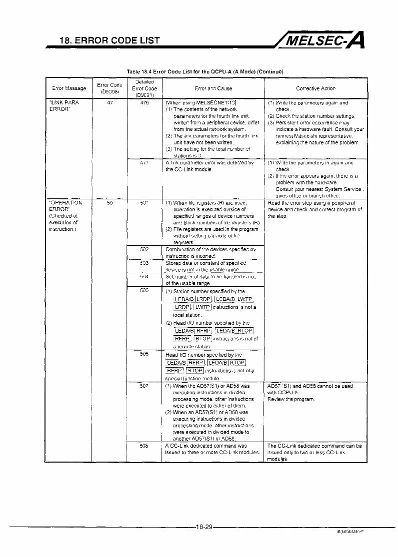
18. ERROR CODE LIST /MELSEC=A Table 18.4 Error Code List for the QCPU-A (A Mode) (Continue)
Error Code (D9008)
47
50
Detalled Error Code
(D9091) 476
477
501
502
503
504
505
506
507
508
Error and Cause
[When using MELSECNETilO] (1) The contents of the network
parameters for the fourth hnk unlt. written from a peripheral device, dlffer from the actual network system.
(2) The link parameters for the fourth lmk unit have not been written.
(3) The setting for the total number of statlons IS 0
A link parameter error was detected by the CC-Link module.
(1) When file registers (R) are used, operation is executed outstde of specified ranges of devlce numbers and block numbers of file reglsters (R)
(2) File reglsters are used in the program wlthout setting capaclty of file regtsters.
Combinatlon of the devices speclfied by Instruction is Incorrect Stored data or constant of speclfied device is not In the usable range Set number of data to be handled is out of the usable range. (1) Station number specified by the
j LEDNB 1 LRDP I, 1 LCDNB 1 LWTP I ILRDP(, /LVVTPI instructlons IS not a local statlon
(2) Head 110 number speclfied by the I LEDNB 1 RFRP 1. j LEDNB/ RTOP I -1. instructlons is not of a remote statlon.
Head 110 number speclfied by the
/ R F R P I . I R T o P l lnstructlons IS not of a special function module (1) When the AD57(S1) or AD58 was
executlng Instructions in divided processlng mode. other instructlons were executed to elther of them.
executlng Instructions in dtvlded processing mode. other instructions were executed in divided mode to another AD57(S1) or AD58.
A CC-Llnk dedicated command was issued to three or more CC-Link modules.
1 LEDA~B 1 RFRP 1, I LEDNB ~RTOP I,
(2) When an AD57(S1) or AD58 was
Correctlve Actton
(1) Wrlte the parameters agatn and
(2) Check the statlon number settings. (3) Perststent error occurrence may
check
lndlcate a hardware fault Consult your nearest Mltsublshi representatwe, explaming the nature of the problem
(1) Write the parameters in again and
(2) If the error appears agatn, there is a check
problem with the hardware. Consult your nearest System Serwce , sales ofice or branch office.
Read the error step usrng a perlpheral device and check and correct program of the step.
AD57 (Sl) and AD58 cannot be used with QCPU-A. Review the program.
The CC-Link dedicated command can be issued only to two or less CC-Llnk modules
18-29 lB(NA)66251-F

18. ERROR CODE LIST /MELSEC=A Table 18.4 Error Code List for the QCPU-A (A Mode) (Continue)
Error Massage
"OPERATION ERROR" (Checked at executlon of instructlon )
'MAIN CPU DOWN"
'BATTERY ERROR" [Checked at 3ower on i
Error Code (D9008)
50
60
61
70
Detailed
(D9091) Error Code Error and Cause
509 (1) An instruction whtch cannot be executed by remote terminal modules connected to the MNETIMINI-S3 was executed to the modules.
executed to a remote terminal. the communlcatlon request reglstration
(2) When t h e m instructlon was
areas ovefflowed (3) The -1 instructlon was
executed without executtnq the 1 PIDINIT j instruction. The p ID57 1 instructton was executed without executing the or -1 instructlon. The program presently executed was specified by the -1 instruction
(4) The number of CC-Link dedlcated command executed tn one scan exceeded 10.
- (1) The CPU malfunctloned due to noise. (2) Hardware failure.
- (1) The battery voltage for the CPU module has dropped below the specified value.
(2) The lead connector of the CPU module battery IS dlsconnected. (M9006 is ON.)
(3) The battery voltage for the memory card has dropped below the speclfled value. (M9048 is ON.)
Correctlve Action
(1) Read the error step using a peripheral device and correct the program, meeting loaded conditlons of remote termlnal modules
(2) Provide tnterlock using M9081 (communlcatlon request registratlon areas BUSY signal) or D9081 (number of vacant areas in the communication request reglstration areas) when the PRC instruction IS
executed to a remote teminal (3) Correct the program specltied by the
ZCHG instructlon to other (4) Set the number of CC-Lmk dedlcated
commands executed in one scan to 10 or less.
(1) Take proper countermeasures for noise.
(2) Since it is hardware error, consult Mrtsubishi representative
(1) Replace the battery of the CPU module.
(2) Connect the lead connector when using the standard RAM or the memory retention function during power fallure.
(3) Replace the battery of the memory card.
18-30 lBINA)66251-F

M E M O
.....................................................................................................................................................................
.....................................................................................................................................................................
.....................................................................................................................................................................
.....................................................................................................................................................................
....................................................................................................................................................................
....................................................................................................................................................................
....................................................................................................................................................................
....................................................................................................................................................................
.....................................................................................................................................................................
.....................................................................................................................................................................
....................................................................................................................................................................
....................................................................................................................................................................
....................................................................................................................................................................
....................................................................................................................................................................
....................................................................................................................................................................
....................................................................................................................................................................
16 INN €6251-A

APPENDICES / M E L S E C ~ =
APPENDICES
APPENDIX 1 PROCESSING TIME LIST
The following lists show the processing time of dedicated instructions used with the AnACPU/AnUCPU/QCPU-A (A Mode). The Processing Time columns indicate how long (in microseconds) the A3AMCA-96 memory casette is used.
1 -bit specification
1, 4, 8, 12, 15-bit 105 specification
83.0 111 51.5 44.2 19.0
140 64.8 55.8 24.0 Data processing DIS
instructions
1 -bit specification
1, 4, 8, 12, 15-bit specification
84.0
12.4 28.7 33.4 72.0 54.0 TEST
24.7 57.3 66.6 144 108
19.2 44.6 52.1 112 UNI
real number
APP-1 IB(NA)66251-F

APPENDICES /MELSEC-=
Processing Time (p s) Classification Instruct ion Conditions
Symbol A3A' A3U' I ASAS I APUSH-Sl I QOSCPU-A I QOGHCPU-A QOSHCPU-A
A4U ASUS ADD
SUB 482 642 260 292 110 1 109 288 262 634 476
Floating point real number processlng instructions
SQR
931 21 60 3112 5420 4070 loq 10
209 486 554 1220 913 log 1
1025 2379 271 1 5970 4480 EXP 819 1901 2060 4770 3580
LOG
Character- string
processing instructions

APPENDICES /MELSEC=A Processing Time (p s)
1 Conditions I A3A, A3U, I A2A, A2U, I ~~, ,cu c~ I I Q02HCPU-A I Instruction Symbol
I Classification
A4U I ASUS ~ ~ u a n - 3 I uuLw-u-n I QOGHCPU-A , ,.L.-.--,-- I I I I i
+ 1 character 96 characters + 96 characters
I L I ~ ~ ~ ~ L L C ' I 141
137 318 364 799 599
32.1 74.5 85.0 187
1 Character- SCMP
1 character
processing string
17.5 40.7 46.4 102 77
96 characters 356 475 21 6 189 81.6
instructions
43.6 101 117 254 191 96 bytes
20.9 48.6 56.3 122 91 .o 1 byte WTOB
instructions
Instructions
Extension file register
Instructions
ZRWR
ZRRDB
ZRWRB
8.40 (9.80) 9.30
11.0
2.54 5.91 6.48 12.0
2.42 5.66 5.28
(11.0) 9.30 !+I nl 2.64 6.14 6.48 13.0
LRDP 23.5 54.9 71 .O 140 105
Data link LWTp
84.4 111 135 213 160 PVWR1 25.8 54.9 66.4 146 110 RTOP 26.2 61.3 66.4 146 110
23.5 54.9 85.4 186 139 instructions RFRP
PVWR2
91.2 118 138 228 171 SVWR1 ADGl(S1)
84.5 111 135 213 160
instructions SVWR2 171
82.6 113 159 215 161 PVRD2
82.2 112 159 214 161 PVRDl
91.4 118 138 228
APP-3 IBlNA)66251-:

APPENDICES /MELSEC-A Instruction
Symbol
Processing Time (p s)
A3A’ A3U’ I A2A’ A2U’ 1 APUSH-SI 1 QOPCPU-A I QOGHCPU-A Classification Conditions Q02HCPU-A
A4U APUS
I ~
AD59(S1) mstructions
I PRN 2 word I 277
537 647 5 97 869 673 96 words
220 265 231 369
2 word
34.9 42.1 27.0 58.0 44.0 SPCLR
38.1 45.9 29.8 63.0 48.0 SPBUSY
366 44 1 558 61 5 461 100 words INPUT
576 694 725 768 576 96 words
139 167 229 354 265 AJ71 UC24 - instructions
PR
PRN2 2 words
- -_ 628.0 950 712 96 words
- 237 42 1 316 2 words
- 628 950 712 96 words
- - 237 422 316
~
PRN4
1 PR2 2 words
~ .. . 570.0 822 61 7 96 words
~~ 231 .O 408 306
I PR4
I INPUT4
~
2 words
- - 523.0 706 529 100 words
- - 523.0 706 529 100 words
- 570.0 822 61 7 96 words
- - 231 .O 408 306
GET 1 word
- - 624.0 940 705 96 words
- - 238.0 426 320 1 word
- - 390.0 412 309 96 words
-_ - 231 .O 41 2 309
SPBUSY 53.0 70.0 31.8 ~ ~
PUT

APPENDICES /MELSEC-=
Processing Time (p s) Classification Instruction Conditions A3A' A3U' A2U'
A2USH-S1 QOPCPU-A Q06HCPU-A QOPHCPU-A
A4U APUS INPUT
I (operating I I 198 I 264 I 120 I 189 I 157
PRN 1 character 254 338 198 243 202 AJ35PTF-R2 96 characters 6 54 872 51 6 626 51 9
PR 1 character 25 1 334 196 240 199 AJ35PTF-R2 96 characters I 559 744 458 535 444
AJ71 PT32-S3 instructions
MINIERR 43.0 57.0 25.9 41.1 34.1 ~~
SPBUSY I 73.0 97.0 44.1 69.8 58.0
SPCLR 88.0 117 53.2 84.2 69.9
Data link instructions
I ZCOM I I 107 I 145 I 65.9 I 34.0 I 14.6
ZNRD 109 160 72.7 86.2 29.7
ZNWR 69.0 117 53.2 87.3 29.7
ZNFR 116 155 68.7 65.2 27.9
ZNTO 116 155 68.7 65.4 28.0
I ZCHGO I I 578 I -~ I - - I - I --
I m s timer I I setting I ZHTIME instructlon I I - l - I - I 5.42 1 2.33
APP-5 IB(NA16625'-F

APPENDICES /MELSEC-A 2lassificatior
CC-Link Dedicated
Instructions
1 station 0.173 0.230 0.104 - -~ - 0.173 0.116
64 stations 0.503 0.670 0.302 309 324 241 256 0.600 0.500
1 point 0.480 0.640 0.288 - - 0.192 0.150
4096 points 0.480 0.640 0.288 276 293 206 221 0.192 0.171
PLPA
RRPA
RlFR
RlTO
1 point 0.312 0.415 0.187 - - -- 0.217 0.153
4096 points 13.4 17.8 8.01 341 349 285 294 13.3 12.3
1 point 0.342 0.455 0.205 - - - -- 0.277 0.220
4096 polnts 13.5 17.9 8.06 349 357 291 300 12.8 12.7
1 point 0.398 0.530 0.239 - - - -- 0.326 0.340
480 points 0.398 0.530 0.239 199 202 149 153 0.315 0.300 RIRD
1 point 0.402 0.535 0.241 ~ -- - - - 0.298 0.350
4 8 0 ~ o i n t s I 1.97 1 2.62 I 1.18 1 193 I 196 I 1 4 5 I 149 I 1.75 I 1.68 R lWT
1 polnt 0.432 0.575 0.259 - - -~ 0 337 0.320
480 polnts 1.96 2.61 1.18 231 232 173 175 1.17 1.10
1 polnt 0.458 0.61 0 0.275 ~ ~ ~- 0.361 0.301
480 polnts 0.458 0.610 0.275 231 232 173 175 0.370 0.380 R : Refresh type D: Dlrect type
RISEND ~-
RIRCV
'1: The dedicated instructions for the CC-Link cannot be used wlth the A2ACPU and A3ACPU. For mformatlon about avallability of the instructlons for each CPU, see Sectlon L. I
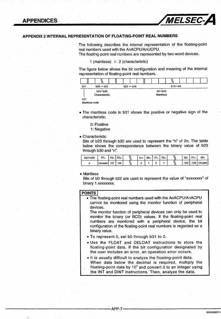

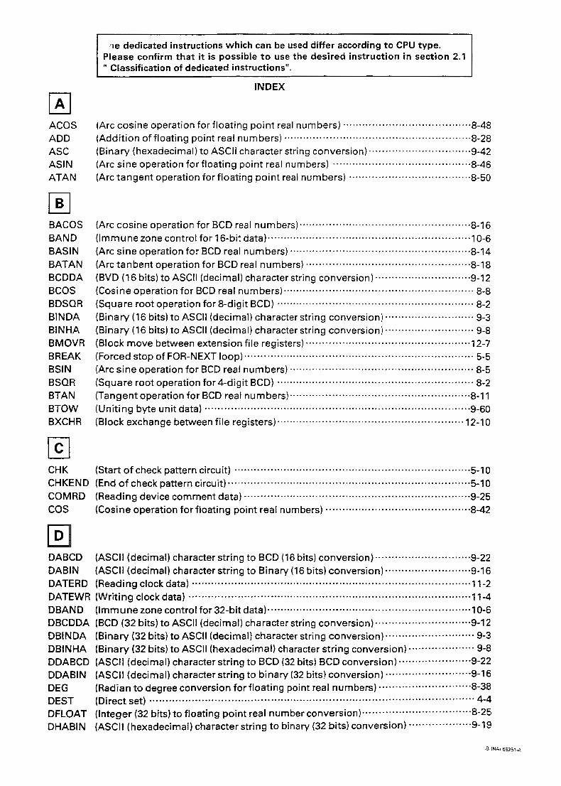
:le dedicated instructions which can be used differ according to CPU type . Please confirm t h a t it is possible t o use the desired instruction in section 2.1 " Classification of dedicated instructions".
INDEX
BAND BAS1 N BATAN BCDDA BCOS BDSQR BINDA BINHA BMOVR BREAK BSlN BSQR BTAN BTOW BXCHR
........................................................................ CHK (Start of check panern circuit) 5-10 5-10 9-25
CHKEND (End of check panern circuit) .......................................................................... COMRD (Reading device comment data) .....................................................................
............................................ cos (Cosine operation for floating point real numbers) 8 4 2
DABCD (ASCII (decimal) character string to BCD (16 bits) conversion).. ........................... 9-22 DABIN (ASCII (decimal) character string to Binary (16 bits) conversion) .......................... 9-16
11-2 11-4
DATERD (Reading clock data) ..................................................................................... DATEWR (Writing clock data) ...................................................................................... DBAND (ImmunezonecontrQifor32-bitdata) ............................................................. -10-6 DBCDDA (BCD (32 bits) to ASCII (decimal) character string conversion) ............................. 9-12 DBINDA (Binary (32 bits) to ASCII (decimal) character string conversion) ........................... 9-3 DBINHA (Binary (32 bits) to ASCII (hexadecimal) character string conversion) .................... 9-8 DDABCD (ASCII (decimal) character string to BCD (32 bits) BCD conversion) ...................... 9-22 DDABIN (ASCII (decimal) character string to binary (32 bits) conversion) ........................ m.9-16 DEG (Radian to degree conversion for floating point real numbers) ............................ 8-38
DFLOAT (Integer (32 bits) to floating point real number conversion) ................................. 8-25 DEST (Directset) ................................................................................................... 4-4
DHABIN (ASCII (hexadecimal) character string to binary (32 bits) conversion) ................... 9.19
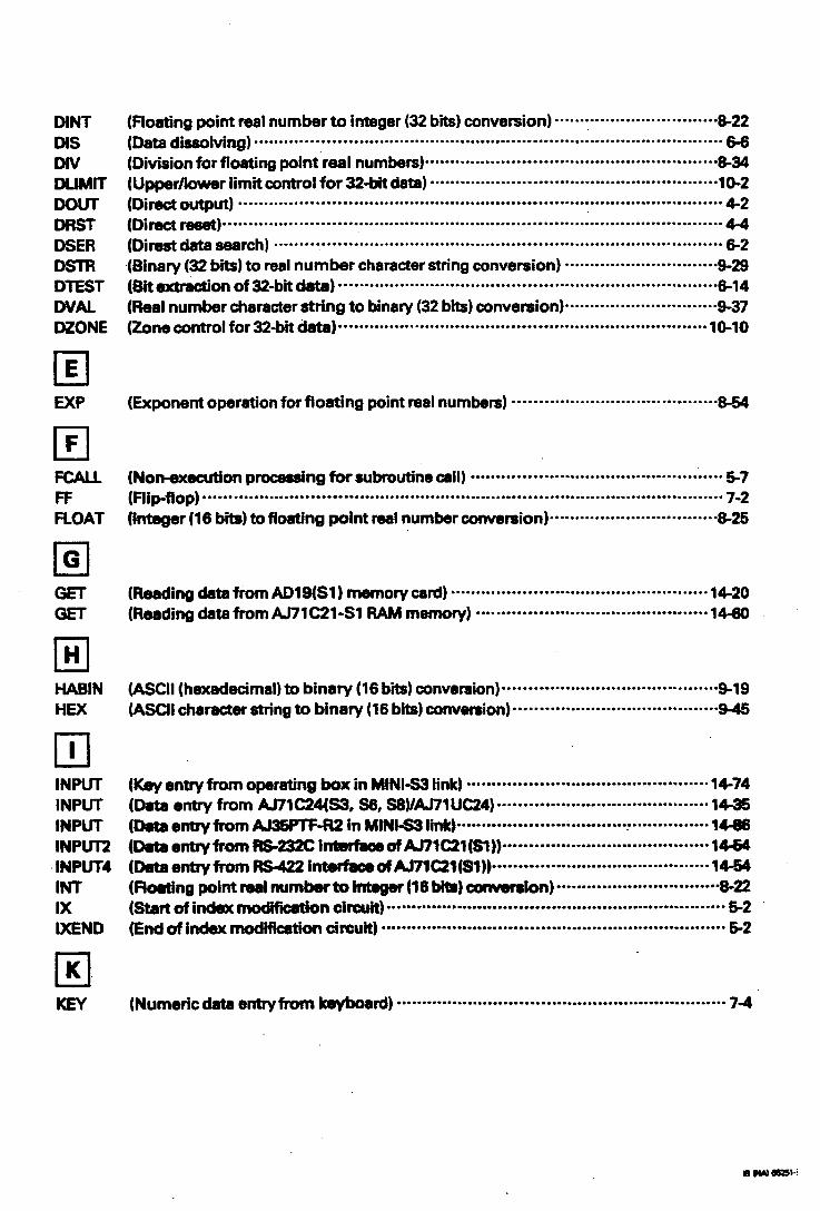
. . . . _._. . .. ...-. ......... __ . . . .... ................... -- .
r ...
f- ' .
DINT MS Mv DuMrr Dour MIST DSER DSTR DTEST DVAL =ONE
El EXP
FCAU R FLOAT
W I N HEX
INPUT INPUT INPUT INPUT2
. INPUT4 INT IX IXEND
K€Y
( N o ~ m i m p k n g f o r s u h u t i n e a l l ) ................................................. 5-7 7-2 (flip-flop) .....................................................................................................
(integer (16 bm) to floating point real number co.rsion).*.*. ............................ a25
.........

. . . . . . ............. - .. .
(Detecting character string length) ..................................................... " ....................................... 827
(Logarithm operation for floating point real numbers) .................................................................. 8-56 (Reading data to word device in local station) .............................................................................. 13-2 (wtfting data to word device in local station) ................................................................................ 13-6
(Upperh r limit control for 16-bit data) ......................................... .. ......................................... 10-2
(Communication control for MINI standard p&l compatbk remofe terminal unit in MINI43 link) ............................................................................................................................................. 14-91
MUL MINIERR (Resetting erm in remate terminal unit in MINI-S3 link) ........................................................... 14-96
(MultpScation for floating point real numbers) .............................................................................. 8-32
PR PR PR PR2 PR4 PRN PRN PRN PRN2 PRN4 PUT PUT PVRD1 PVRD2 'PVwR1 PvwR2
RAD RFRP RlFR RIRCV RlRD RISEND RlTO RlWT RLPA RRPA RsEr mop
(Outputting characters tothe printer connected to AMQ(S1) (up to OOH code) ......................... 14-17 (Data output forAnlC24(S3. S6. S8yA171UC24 (up to o(k code)) ........................................ 14-31 (Data output for AJ35FW-R2 in MINl-S3 link (up to OOH code)) ................................................ 14-82 (Data oulput for RS232C interface d AJ7l C21 (Sl) in M I N I S 3 link (up to 0th d e ) ) ............ 14-50
(Outputting characten, to printerconmctd to WQ(S1) (requined numbet of charaoters)) ..... 14-14 (Data output for AJ71C24(S3. S6. S8yA171UC24 (required number of points)) ....................... 14-27 (Data output for AJ35PTF-R2 in MINIS3 link) ........................................................................... 14-78
(Data output for RS-422 interface of An1 C21(51) (required number of points)) ...................... 14-46
(writing data to AD59(S1) memory card) ................................................................................... 14-23 (Reading present value from CH.1 of AD61(S1)) ........................................................................ 14-11 (Reading present value from CH2 of AD61(S1)) ........................................................................ 1 ~ 1 1 (Setting preset value for CH.1 of ADGl(S1)) ................................................................................ 14-7
(Data *ut for RS-422 interface ofA171C21(Sl)in MINIS3 link (up to Oonoode)) ............... 14-50
(Data output for RS232C interface of An1 C21 (Sl) (required number of points)) ................... 14-46
(Wtithg data to MlC21-Sl RAM ~WIWY) ............................................................................. 14-64
(Setting preset value for CH2 of AD61 (Sl)) ................................................................................ 14-7
(Angle to radian conversion for flatting point rerrl rwrmrs) ...... ... ......... ................................... 8-36 (Reading data frwn qecial functbn module in eMnde VD steblan) ....................................... 13-10 (Read from automaticupdating buffer . ........................... , .................................. 16-14 (Read from i n t e l l i i device station butter mrmory [with hudshako) ), ............................... 16-28 (Read from i n b U i g e n t devioe 8Won M e r m e m a y ) ............................ ., .."................ " ........... 16-1 8
(WW to automatic updating krtter memoty) ...................................................................... 1616 (WW to intelligent device etation butter memory) ................................................................ 16-23 (Netwok parameter setb'ng) ......................................................................................................... 16-3 (Automatic refresh parameter setting) .......................................................................................... 16-7 (Changing block number in extension file register) ...................................................................... 12-5 (Wrtting data to special fundkn module in remQIb VD rtrtion) ..., ..... .... ,... .. ........................... 13-14
(w& to intelligent d e v b rtetion buffer memoly [with ) I ....... , ............................. 16-32
1
*

. . . . . . . . . . . . . ._ . -_-_ .
SADD SCMP SIN SMOV SPBUSY SPBUSY SPBUSY SPCLR SPCLR SPCLR SQR STR SUB
f- SVWRl S W R 2 SWAP
TAN TEST
UNI
VAL
. . . WTOB
ZCHG ZCOM MTlME ZNFR ZNRD ZNTO m ZONE ZRRD ZRRDB ZRWR ZRWRk
(Real number character string to binary (16 bits) conversion) .............................. 937
c
(Switching between main program and designated sub program (1 to 3)) ....... 15-2 (Unk refresh af designated network) ................................................. 13-20 ( l m s n ~ ~ i n g ) ......................................................................... 7.2 @ata.fromspedalfundknmoduleinMELSECNETI10ren#4eVO.)=.= 13-30 (Reading from word device in the MELSECNETflO station) ...................... 13-22 @sEawritetospectdfunctionmoduleinYELSECNETnOmnoteVOstation) ...... 13-33 (Writing to word device in the MELSECNETAO station) ........................... 13-26
(Direct read of extension file register in units of words) .......................... 12-1 6 (Direct read of extension file register in units of bytes) ........................... 12-25 (Direct write of extension file register in units of words)====**=.=.=.==. ........... 12-19
. @ o n e c-1 for 1- h) ........................................................... 10-10
(Direct write of extension file register in units of words) .......................... 12-28
... .......... .. . . . . . . . . . . -... -

1 type AnSHCPU/AnACPU/AnUCPU/QCPU-A ,[A Mode) I 1 Programming Manual (Ddicated Instructions)
MOOEL I A2A/A3A-DEDI-P-E 1
MODEL 1 COOE 13J742
IB(NA)6625 1 -G(0006)MEE 1
. . . . .- . .. . . , . . .
Specifications subject to change without notice. Printed in Japan on recycled paper.
Copyright © 2022 FDOKUMEN