
GOC43 User Manual - Mitsubishi Electric
228
_________________________________Page 1 of 228__________________________________ GOC43 User Manual Document No.: N18006AAMH01 Version: 1.04
-
Upload
khangminh22 -
Category
Documents
-
view
0 -
download
0
Transcript of GOC43 User Manual - Mitsubishi Electric
_________________________________Page 1 of 228__________________________________
GOC43 User Manual Document No.: N18006AAMH01
Version: 1.04
_________________________________Page 2 of 228__________________________________
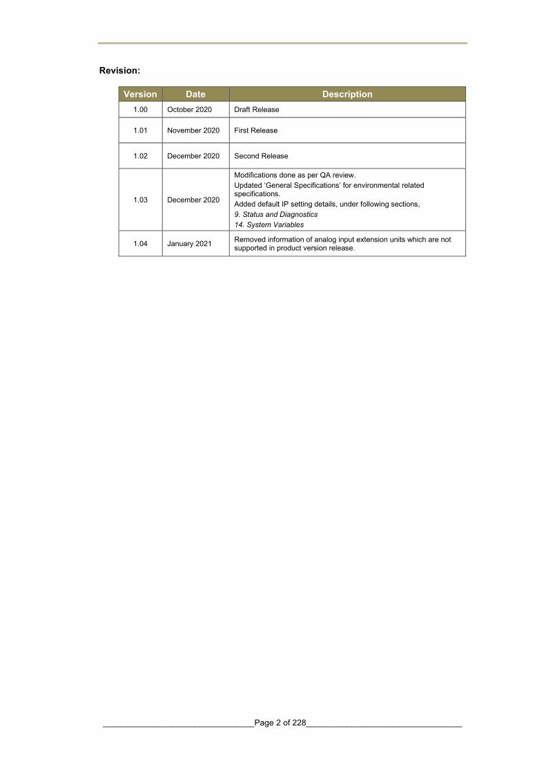
Revision:
Version Date Description 1.00 October 2020 Draft Release
1.01 November 2020 First Release
1.02 December 2020 Second Release
1.03 December 2020
Modifications done as per QA review. Updated ‘General Specifications’ for environmental related specifications. Added default IP setting details, under following sections, 9. Status and Diagnostics 14. System Variables
1.04 January 2021 Removed information of analog input extension units which are not supported in product version release.

_________________________________Page 3 of 228__________________________________
Intended audience of this manual Thank you for choosing the Mitsubishi product. Do not use this product until you have full knowledge of the equipment. Please forward this manual to end user.
This manual is intended to the following personnel,
Managing in charge.
Designing or developing personnel.
Commissioning and Maintaining personnel.
Supervising personnel.
Operating personnel.
Scope of manual
This user manual provides the following details of GOC43 product.
List of Main units, Extension units, COM units.
Guideline for installation and wiring.
Features and specifications of all types of units.
Configuration and programming details.
Status and diagnostic information.
Maintenance and troubleshooting
Important information for user
Read and understand the manual carefully before using GOC43 product, to avoid any damages to persons, properties or environment. Ensure safe and proper usage of this product.
Do not modify, dismantle, re-construct and repair the electronic modules. For repair, contact nearest authorized sales office or technical support team.
Qualified and properly trained personnel should only install the product. The personnel should be aware of all the safety aspects of automated products and completely familiar with all associated documentation for the said product.
Protect the product from conductive dust, corrosive gases, wire debris, flammable gases, rain and fluid entering into the product through ventilation slits, this may cause malfunctioning, damage, fire, electric shock and deterioration.
_________________________________Page 4 of 228__________________________________
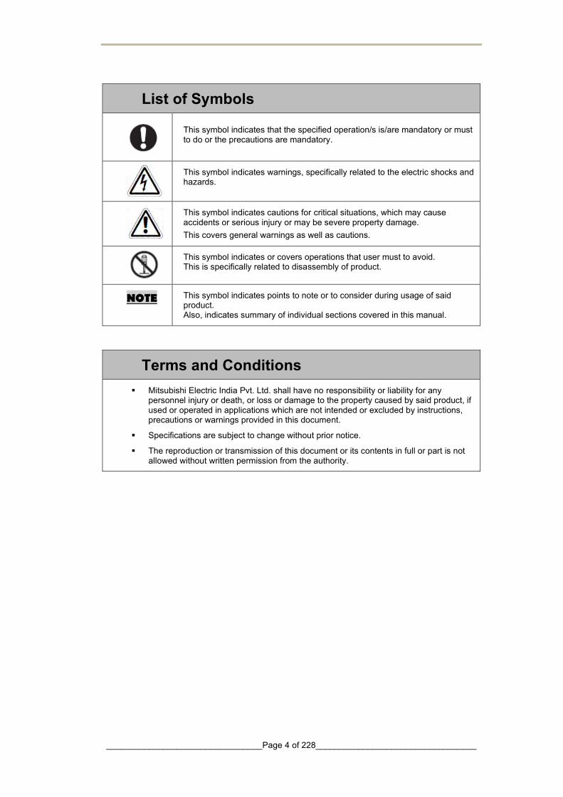
List of Symbols
This symbol indicates that the specified operation/s is/are mandatory or must to do or the precautions are mandatory.
This symbol indicates warnings, specifically related to the electric shocks and hazards.
This symbol indicates cautions for critical situations, which may cause accidents or serious injury or may be severe property damage. This covers general warnings as well as cautions.
This symbol indicates or covers operations that user must to avoid. This is specifically related to disassembly of product.
NOTE This symbol indicates points to note or to consider during usage of said product. Also, indicates summary of individual sections covered in this manual.
Terms and Conditions Mitsubishi Electric India Pvt. Ltd. shall have no responsibility or liability for any
personnel injury or death, or loss or damage to the property caused by said product, if used or operated in applications which are not intended or excluded by instructions, precautions or warnings provided in this document.
Specifications are subject to change without prior notice.
The reproduction or transmission of this document or its contents in full or part is not allowed without written permission from the authority.
_________________________________Page 5 of 228__________________________________
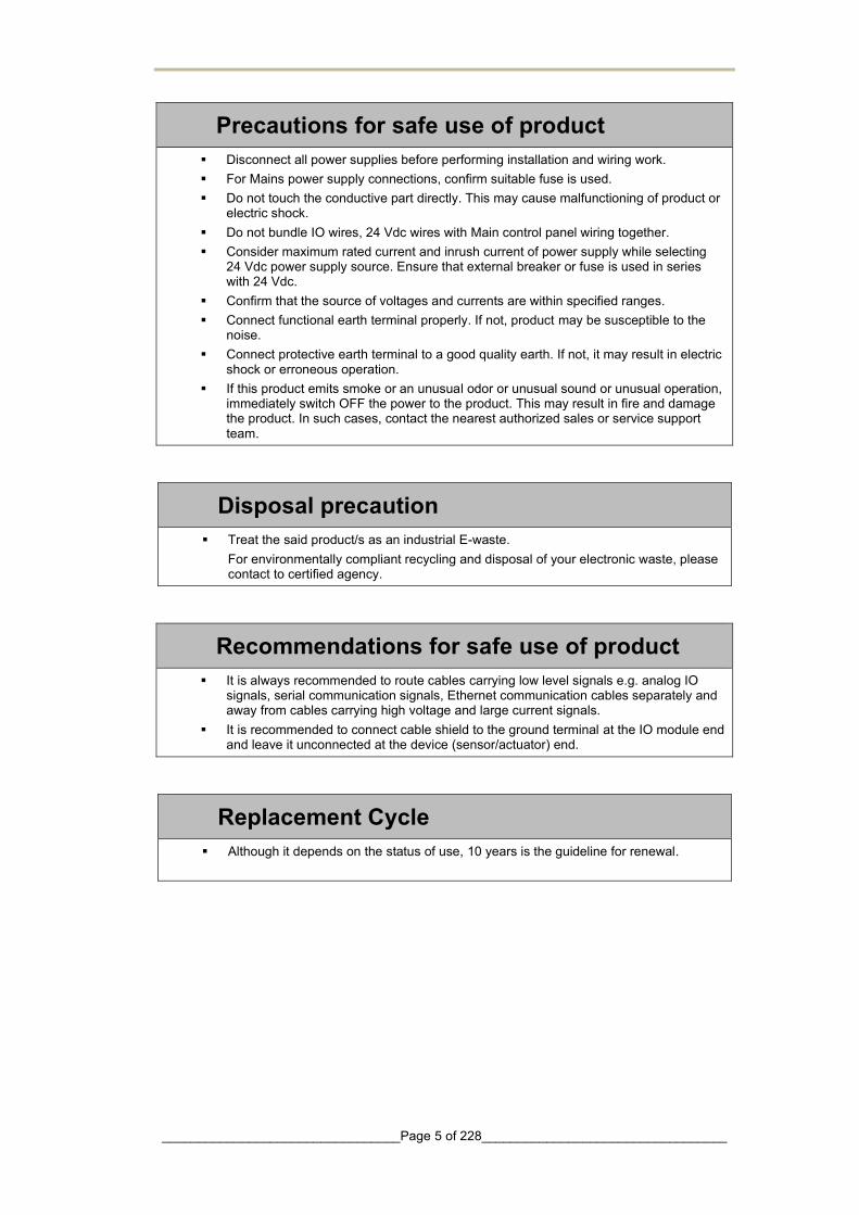
Precautions for safe use of product Disconnect all power supplies before performing installation and wiring work. For Mains power supply connections, confirm suitable fuse is used. Do not touch the conductive part directly. This may cause malfunctioning of product or
electric shock. Do not bundle IO wires, 24 Vdc wires with Main control panel wiring together. Consider maximum rated current and inrush current of power supply while selecting
24 Vdc power supply source. Ensure that external breaker or fuse is used in series with 24 Vdc.
Confirm that the source of voltages and currents are within specified ranges. Connect functional earth terminal properly. If not, product may be susceptible to the
noise. Connect protective earth terminal to a good quality earth. If not, it may result in electric
shock or erroneous operation. If this product emits smoke or an unusual odor or unusual sound or unusual operation,
immediately switch OFF the power to the product. This may result in fire and damage the product. In such cases, contact the nearest authorized sales or service support team.
Disposal precaution Treat the said product/s as an industrial E-waste.
For environmentally compliant recycling and disposal of your electronic waste, please contact to certified agency.
Recommendations for safe use of product It is always recommended to route cables carrying low level signals e.g. analog IO
signals, serial communication signals, Ethernet communication cables separately and away from cables carrying high voltage and large current signals.
It is recommended to connect cable shield to the ground terminal at the IO module end and leave it unconnected at the device (sensor/actuator) end.
Replacement Cycle Although it depends on the status of use, 10 years is the guideline for renewal.


_________________________________Page 1 of 228__________________________________
This page is kept blank intentionally

_________________________________Page 1 of 228__________________________________
Content 1 Overview ..................................................................................................... 3
1.1 Highlighting Features ....................................................................................... 3
1.2 Nomenclature .................................................................................................. 6 1.2.1 Main Unit ...................................................................................................................... 6 1.2.2 I/O Extension Unit ........................................................................................................ 7 1.2.3 COM Extension Unit ..................................................................................................... 8 1.2.4 Main Unit with Extension Units ..................................................................................... 9
1.3 Ordering Information ...................................................................................... 10
1.4 General Specifications ................................................................................... 12
1.5 Technical Specifications ................................................................................ 13
2 Installation and Wiring ............................................................................... 16
2.1 Dimensional Details ....................................................................................... 16 2.1.1 Main Unit .................................................................................................................... 16 2.1.2 I/O Extension Unit ...................................................................................................... 17 2.1.3 COM Extension Unit ................................................................................................... 17 2.1.4 Main Unit with Extension Units ................................................................................... 18
2.2 Installation ...................................................................................................... 18 2.2.1 Installation Recommendations ................................................................................... 18 2.2.2 Precautions to be taken .............................................................................................. 19 2.2.3 Main Unit Installation .................................................................................................. 20 2.2.4 I/O Extension Unit Installation .................................................................................... 23 2.2.5 COM Extension Unit Installation ................................................................................. 26 2.2.6 microSD card Installation ........................................................................................... 29
2.3 Wiring ............................................................................................................. 31 2.3.1 Recommendations ..................................................................................................... 31 2.3.2 Precautions to be taken .............................................................................................. 32 2.3.3 Guidelines for Earthing ............................................................................................... 32 2.3.4 Digital input sink/source operation .............................................................................. 33 2.3.5 Guidelines for using digital outputs ............................................................................. 34 2.3.6 Guidelines for using relay outputs .............................................................................. 34
3 Main Unit .................................................................................................. 35
3.1 I/O Specifications ........................................................................................... 35 3.1.1 Digital Input Specifications ......................................................................................... 35 3.1.2 Analog Input Specifications ........................................................................................ 36 3.1.3 Transistor Output (Source) Specifications .................................................................. 37 3.1.4 Relay Output Specifications ....................................................................................... 38
3.2 Wiring ............................................................................................................. 39 3.2.1 Wiring of Input Power Supply (24 VDC) ..................................................................... 39 3.2.2 Wiring of Digital Inputs ............................................................................................... 39 3.2.3 Wiring of Analog Inputs .............................................................................................. 40 3.2.4 Wiring of Transistor Source Outputs .......................................................................... 41 3.2.5 Wiring of Relay Outputs ............................................................................................. 41

_________________________________Page 1 of 228__________________________________
3.3 Configuration and Programming ................................................................... 42 3.3.1 Communication settings ............................................................................................. 44 3.3.2 Hardware Configuration ............................................................................................. 45 3.3.3 Log ............................................................................................................................. 47 3.3.4 PLC Settings .............................................................................................................. 48 3.3.5 Parameter Configuration ............................................................................................ 48
3.3.5.1 High Speed Counter ............................................................................................. 49 3.3.5.2 Analog Input.......................................................................................................... 49
3.3.6 Backup ....................................................................................................................... 50 3.3.7 IO Mapping ................................................................................................................. 50 3.3.8 IEC Objects ................................................................................................................ 51 3.3.9 Information ................................................................................................................. 52
4 Digital I/O Extension Units ........................................................................ 53
4.1 GC-8EX-ES ................................................................................................... 54 4.1.1 Specifications ............................................................................................................. 54 4.1.2 Wiring ......................................................................................................................... 55 4.1.3 Configuration and Programming ................................................................................. 56 4.1.4 I/O Mapping ................................................................................................................ 57
4.2 GC-6EYR-ES ................................................................................................. 58 4.2.1 Specifications ............................................................................................................. 58 4.2.2 Wiring ......................................................................................................................... 59 4.2.3 Configuration and Programming ................................................................................. 60 4.2.4 I/O Mapping ................................................................................................................ 61
4.3 GC-8ET-ESS ................................................................................................. 62 4.3.1 Specifications ............................................................................................................. 62 4.3.2 Wiring ......................................................................................................................... 63 4.3.3 Configuration and Programming ................................................................................. 64 4.3.4 I/O Mapping ................................................................................................................ 65
5 Analog I/O Extension Units ....................................................................... 66
5.1 GC-4DA-12 .................................................................................................... 67 5.1.1 Specifications ............................................................................................................. 67 5.1.2 Wiring ......................................................................................................................... 68 5.1.3 Configuration and Programming ................................................................................. 69
5.1.3.1 Parameter Configuration ....................................................................................... 70 5.1.3.2 I/O Mapping .......................................................................................................... 71 5.1.3.3 IEC Objects........................................................................................................... 72
5.2 GC-4A-12 ....................................................................................................... 74 5.2.1 Specifications ............................................................................................................. 74 5.2.2 Wiring ......................................................................................................................... 75 5.2.3 Configuration and Programming ................................................................................. 77
5.2.3.1 Parameter Configuration ....................................................................................... 78 5.2.3.2 I/O Mapping .......................................................................................................... 81 5.2.3.3 IEC Objects........................................................................................................... 83
5.3 GC-4UAD-16 ................................................................................................. 85 5.3.1 Specifications ............................................................................................................. 85 5.3.2 Wiring ......................................................................................................................... 86 5.3.3 Configuration and Programming ................................................................................. 87
5.3.3.1 Parameter Configuration ....................................................................................... 88 5.3.3.2 I/O Mapping .......................................................................................................... 90 5.3.3.3 IEC Objects........................................................................................................... 92

_________________________________Page 1 of 228__________________________________
6 COM Extension Units ................................................................................ 94
6.1 GC-RS232-COM ........................................................................................... 95 6.1.1 Specifications ............................................................................................................. 95 6.1.2 Wiring ......................................................................................................................... 95 6.1.3 Configuration and Programming ................................................................................. 96
6.1.3.1 I/O Mapping .......................................................................................................... 97 6.1.3.2 Parameter Configuration ....................................................................................... 97 6.1.3.3 IEC Objects........................................................................................................... 98
6.2 GC-RS422-COM ........................................................................................... 99 6.2.1 Specifications ............................................................................................................. 99 6.2.2 Wiring ......................................................................................................................... 99 6.2.3 Configuration and Programming ............................................................................... 100
6.2.3.1 I/O Mapping ........................................................................................................ 101 6.2.3.2 Parameter Configuration ..................................................................................... 101 6.2.3.3 IEC Objects......................................................................................................... 102
7 Modbus RTU Configuration ..................................................................... 103
7.1 Modbus RTU Slave ..................................................................................... 103 7.1.1 Overview .................................................................................................................. 103 7.1.2 Configuration ............................................................................................................ 104
7.2 Modbus RTU Master ................................................................................... 107 7.2.1 Overview .................................................................................................................. 107 7.2.2 Configuration ............................................................................................................ 108 7.2.3 IEC Objects .............................................................................................................. 116
8 Modbus TCP Configuration ..................................................................... 118
8.1 Modbus TCP Slave ...................................................................................... 118 8.1.1 Overview .................................................................................................................. 118 8.1.2 Configuration ............................................................................................................ 119 8.1.3 IEC Objects .............................................................................................................. 121
9 Status and Diagnostics ........................................................................... 122
9.1 LED Indications ........................................................................................... 122
9.2 System Menu ............................................................................................... 123 9.2.1 System Info .............................................................................................................. 124 9.2.2 Ext. unit info.............................................................................................................. 125 9.2.3 Scan time ................................................................................................................. 126 9.2.4 Ethernet status ......................................................................................................... 127 9.2.5 IP setting .................................................................................................................. 128 9.2.6 RTC .......................................................................................................................... 129 9.2.7 Display ..................................................................................................................... 130 9.2.8 Touch calibration ...................................................................................................... 131 9.2.9 Touch panel check ................................................................................................... 132 9.2.10 Keypad check ........................................................................................................... 133 9.2.11 SD card .................................................................................................................... 134
10 Programming .......................................................................................... 136
10.1 Setup requirements ..................................................................................... 136
10.2 GOCToolkit V3 Installation .......................................................................... 137
10.3 Quick start CoDeSys ................................................................................... 139 10.3.1 Creation of a new project using GOC43 project template ........................................ 139 10.3.2 Hardware configuration ............................................................................................ 141
_________________________________Page 2 of 228__________________________________
10.3.3 IO mapping ............................................................................................................... 144 10.3.4 IEC Objects .............................................................................................................. 145 10.3.5 PLC Settings ............................................................................................................ 145 10.3.6 To create simple ladder program .............................................................................. 146 10.3.7 To create simple HMI program ................................................................................. 151 10.3.8 To download project and Online operations ............................................................. 154
11 Controller Memory .................................................................................. 155
11.1 Input Process Image .................................................................................... 155
11.2 Output Process Image ................................................................................. 156
11.3 Marker Memory............................................................................................ 156
11.4 Data Memory ............................................................................................... 156
11.5 I/O Memory Mapping ................................................................................... 156
11.6 Addressing Range ....................................................................................... 158
11.7 Retained Memory ........................................................................................ 159
11.8 System Variables ......................................................................................... 160
11.9 Application Program Memory ...................................................................... 161
12 Built-in HSC (High Speed Counter) ......................................................... 163
12.1 Specifications............................................................................................... 163
12.2 Single Phase Counter with Software Direction ............................................ 164
12.3 Encoder A B Phase ..................................................................................... 165
12.4 Encoder A B Phase with Z Pulse................................................................. 166
12.5 Configuration and Programming ................................................................. 168 12.5.1 Parameter Configuration .......................................................................................... 168 12.5.2 I/O Mapping .............................................................................................................. 169 12.5.3 IEC Objects .............................................................................................................. 170
13 Built-in Analog V/I Input .......................................................................... 171
13.1 Analog Input Specifications ......................................................................... 171
13.2 Configuration and Programming ................................................................. 172 13.2.1 Parameter Configuration .......................................................................................... 172 13.2.2 I/O Mapping .............................................................................................................. 173 13.2.3 IEC Objects .............................................................................................................. 173
14 System Variables .................................................................................... 174
_SysvarCPU................................................................................................................ 174
_SysvarDiskMemory ................................................................................................... 174
_SysvarETH ................................................................................................................ 174
_SysvarHMI................................................................................................................. 174
_SysvarMemPtr .......................................................................................................... 174
_SysvarRTC ................................................................................................................ 174
_SysvarSDCard .......................................................................................................... 174
_SysvarVersionInfo ..................................................................................................... 174
_________________________________Page 1 of 228__________________________________
15 HMI Function .......................................................................................... 186
15.1 Highlighting Features ................................................................................... 187
15.2 Keys and LEDs ............................................................................................ 188 15.2.1 Function keys (F1 to F4) .......................................................................................... 188 15.2.2 Illuminated keys (K1 to K4)....................................................................................... 189 15.2.3 Slide-in Label............................................................................................................ 190
15.3 Visualization screens ................................................................................... 191 15.3.1 Visualization Editor ................................................................................................... 192 15.3.2 Visualization elements .............................................................................................. 193 15.3.3 Visualization element properties ............................................................................... 198 15.3.4 Performance of HMI function .................................................................................... 199
16 SD Card .................................................................................................. 201
16.1 Backup application program and source code ............................................ 202 16.1.1 Enabling backup function and setting password....................................................... 202 16.1.2 Executing backup ..................................................................................................... 203
16.2 Restore application program and source code ............................................ 205 16.2.1 Enabling restore function on device and setting Password ...................................... 205 16.2.2 Copying application program and / or source code to SD card ................................ 206 16.2.3 Executing restore ..................................................................................................... 210
16.3 Verify application program and source code ............................................... 212 16.3.1 Executing Verify ....................................................................................................... 212

_________________________________Page 2 of 228__________________________________
This page is kept blank intentionally
Overview
_________________________________Page 3 of 228__________________________________
1 Overview
Graphic Operation Controller (GOC43) is a micro range of controller which consists of PLC function, HMI function, function keys and illuminated keys. It is designed to cater the automation requirements of any small size, standalone machine.
1.1 Highlighting Features
PLC Function
Flexible Hardware Configuration
Various options of main units and extension units depending upon number of I/Os and type of I/Os.
Functionality can be extended with addition of up to 2 I/O extension units and 1 COM extension unit.
Offers 16 digital I/Os minimum to 48 digital I/Os maximum.
Supports 1 serial port by adding COM extension unit.
2 built-in analog V/I input channels. Can be extended by additional 8 analog V/I input channels using I/O extension units
Configurable Special Functionality to Digital Inputs in Main Unit
2 single phase counters (inputs I00 and I03) with software direction and start/ stop control. Maximum input frequency 20 KHz.
2 Quadrature ABZ encoder interfaces (inputs I00, I01, I02 and I03, I04, I05). Maximum input frequency10 KHz.
General Features Built-in Real Time Clock.
Controller input power is 24 VDC.
Front panel mount; IP65 protection from front side, IP20 protection from rare side.
Built-in Ethernet Port Up to 8 simultaneous connections.
Protocols supported: - Modbus TCP server
Programming Platform Programming via built-in Ethernet port.
Windows based IEC 61131-3 compatible programming software CoDeSys V3.5.
Support of all IEC languages (LD, FBD, ST, IL, SFC) and CFC.
Single software for programming PLC and HMI functionality.
Manage password protection for project

Overview
_________________________________Page 4 of 228__________________________________
Highlighting Features…
HMI Function
Built-in LCD Display 4.3" 480 x 272 pixels, TFT, 64K color, Touch graphics LCD View size: 95.04 x 53.86 mm
4 function keys (F1 to F4)
4 illuminated keys (K1 to K4) with dual color (Green, Red) LEDs User Defined LCD Screens
Up to 64 user definable screens
5 fonts (Default, Headline, Large, Title, Annotation). Standard Windows® fonts supported.
Monitor/ modify PLC data with all supported data types and formats.
Alpha-numeric data entry by embedded Keypad, Numpad or Extended Numpad
Direct access of PLC variable with symbolic name.
Visualization Elements
Basic: Rectangle, Round rectangle, Ellipse, Line, Polygon, Polyline, Pie, Image, Frame.
Common controls: Label, Combo box integer, Combo box array, Tab control, Button, Group box, Table, Text field, Scrollbar, Slider, Spin Control, Invisible input, Progress bar, Checkbox, Radio button
Measurement controls: Bar display, Meter 90°, Meter 180°, Meter, Potentiometer, Histogram.
Special controls: Waiting symbol flower, Cartesian XY Chart
Date/time controls: Analog clock, Date picker
Lamps/switches/bitmaps: Image switcher, Lamps and Switches
Symbols: Arrows, Symbols, Icons
Function Keys 4 keys F1 to F4
Quick access to IO status monitor and system menu
Illuminated Keys 4 Illuminated keys i.e. keys with dual color bright LEDs
LED control Red/Green/Yellow
Insertable slide-in label over illuminated keys
Built-in Status and Diagnostics
Monitor status of all digital IOs in one screen.
System Menu for
- Monitoring system status
- System diagnostics: CPU, IO and Ethernet
- System settings: RTC, IP settings, display, buzzer
- Touch calibration and check
- Keys and LEDs check

Overview
_________________________________Page 5 of 228__________________________________
Highlighting Features…
MicroSD card support
Backup and restore For application program and/ or source code
With user configurable password protection
Customization and branding
Easy Customization of Front Look
Insertable slide-in label over illuminated keys
Customizable for OEM branding.

Overview
_________________________________Page 6 of 228__________________________________
1.2 Nomenclature GOC43 consists of main unit with built-in I/Os, display, function keys and illuminated keys. User can attach I/O extension units (up to 2) and COM extension unit (1 no.) to add I/Os and enhance functionality.
This section provides nomenclature details as below.
Main unit I/O extension unit COM extension unit Main unit with extension units
1.2.1 Main Unit The figure below shows all the views of bare Main unit with part names.
Figure 1: Main unit nomenclature
12 9
14 10
11 15
9 6
Parts Description 1. 4.3", 480 x 272 pixels, Touch graphics LCD 2. 4 Function keys [F1 to F4] 3. 4 Illuminated keys [K1 to K4] 4. LED indications [PWR, RUN] 5. Slide-in label 6. 3-pin terminal block [+24VDC, 0V, Earth] 7. 2 nos., 10-pins terminal block [Digital Inputs] 8. 1 no., 5-pin terminal block [Analog V/I Inputs] 9. 2 nos., 10-pins terminal block [Transistor/ Relay Outputs]
7 8
10. IO1 slot 11. IO2 slot 12. IO slot cover 13. COM slot 14. COM slot cover 15. Ethernet port 16. Cut-out for mounting clamp 17. MicroSD card slot with door 18. USB port with door
6
13
17
16
5
7 8
17
3 2
4 1
18
Overview
_________________________________Page 7 of 228__________________________________
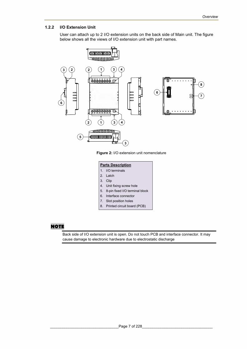
1.2.2 I/O Extension Unit User can attach up to 2 I/O extension units on the back side of Main unit. The figure below shows all the views of I/O extension unit with part names.
Figure 2: I/O extension unit nomenclature
NOTE
Back side of I/O extension unit is open. Do not touch PCB and interface connector. It may cause damage to electronic hardware due to electrostatic discharge
Parts Description 1. I/O terminals 2. Latch 3. Clip 4. Unit fixing screw hole 5. 8-pin fixed I/O terminal block 6. Interface connector 7. Slot position holes 8. Printed circuit board (PCB)
3 2 2 1 3 4
8
7 6
6
3
2 1 3 4
5
Overview
_________________________________Page 8 of 228__________________________________
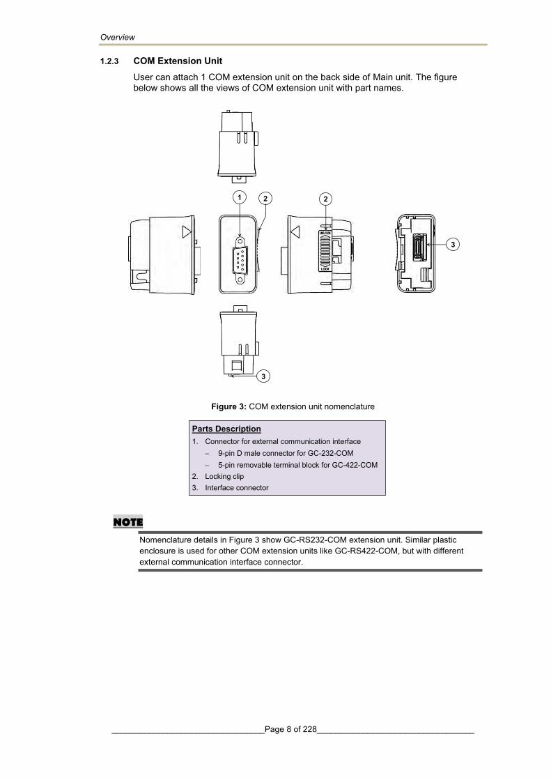
1.2.3 COM Extension Unit User can attach 1 COM extension unit on the back side of Main unit. The figure below shows all the views of COM extension unit with part names.
Figure 3: COM extension unit nomenclature
NOTE
Nomenclature details in Figure 3 show GC-RS232-COM extension unit. Similar plastic enclosure is used for other COM extension units like GC-RS422-COM, but with different external communication interface connector.
Parts Description 1. Connector for external communication interface
− 9-pin D male connector for GC-232-COM − 5-pin removable terminal block for GC-422-COM
2. Locking clip 3. Interface connector
2 2 1
3
3
Overview
_________________________________Page 9 of 228__________________________________
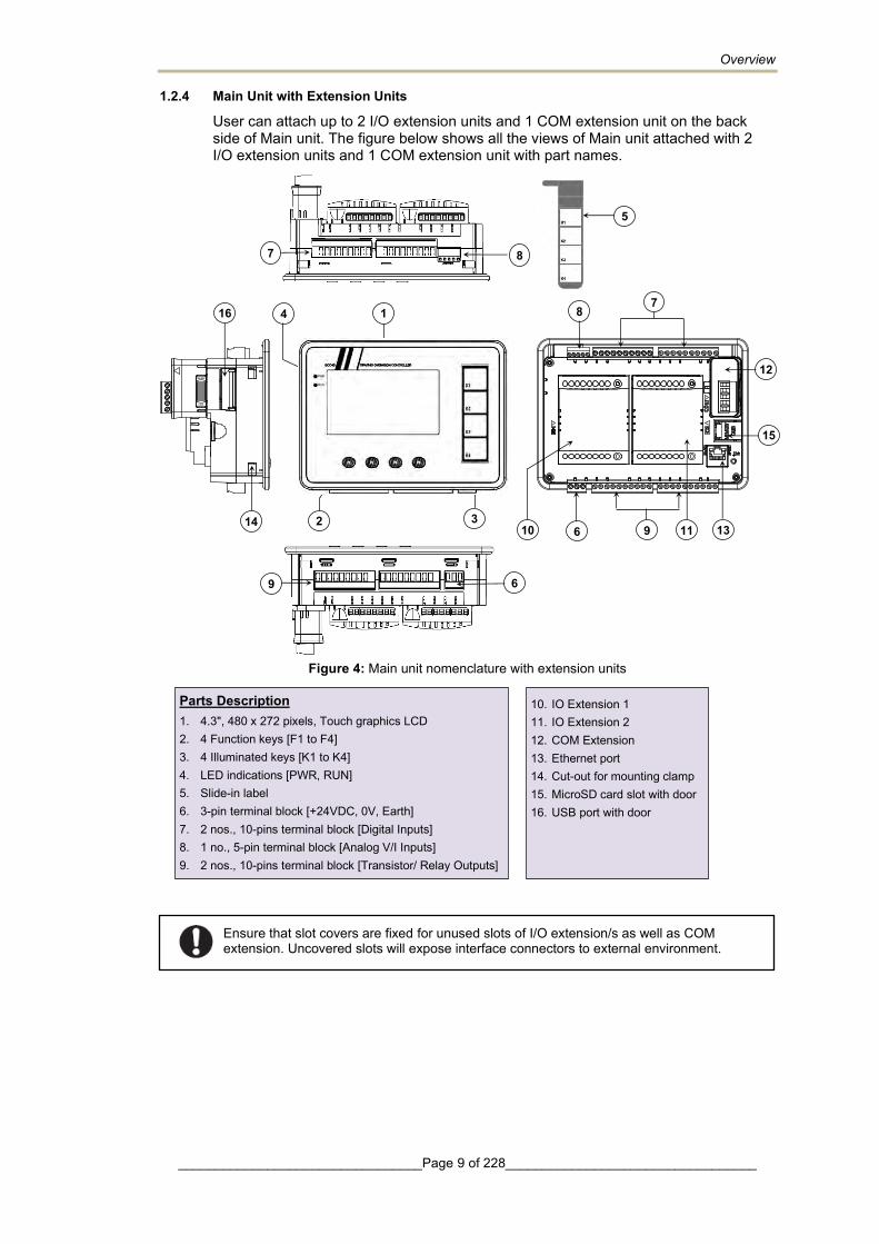
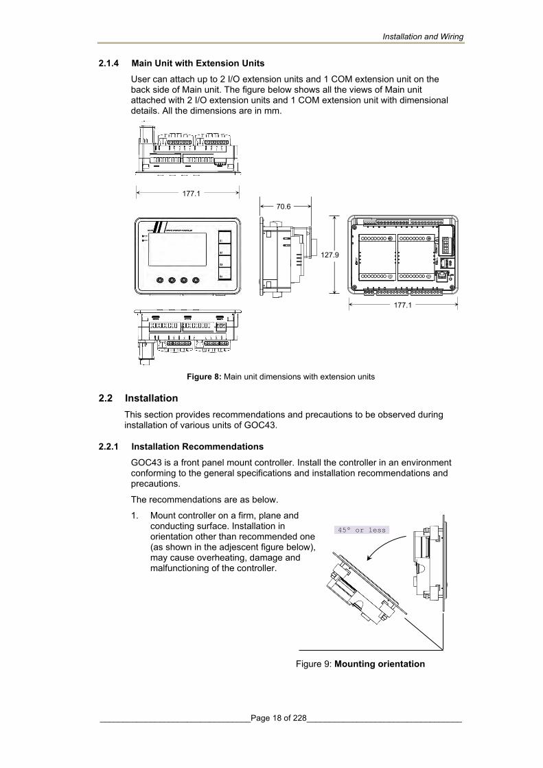
1.2.4 Main Unit with Extension Units
User can attach up to 2 I/O extension units and 1 COM extension unit on the back side of Main unit. The figure below shows all the views of Main unit attached with 2 I/O extension units and 1 COM extension unit with part names.
Figure 4: Main unit nomenclature with extension units
10. IO Extension 1 11. IO Extension 2 12. COM Extension 13. Ethernet port 14. Cut-out for mounting clamp 15. MicroSD card slot with door 16. USB port with door
10 9
12
11 13
7 8 1
6
15
2
Parts Description 1. 4.3", 480 x 272 pixels, Touch graphics LCD 2. 4 Function keys [F1 to F4] 3. 4 Illuminated keys [K1 to K4] 4. LED indications [PWR, RUN] 5. Slide-in label 6. 3-pin terminal block [+24VDC, 0V, Earth] 7. 2 nos., 10-pins terminal block [Digital Inputs] 8. 1 no., 5-pin terminal block [Analog V/I Inputs] 9. 2 nos., 10-pins terminal block [Transistor/ Relay Outputs]
3
16 4
5
9 6
14
8 7
Ensure that slot covers are fixed for unused slots of I/O extension/s as well as COM extension. Uncovered slots will expose interface connectors to external environment.
UNLOCK
LOCK

Overview
_________________________________Page 10 of 228__________________________________
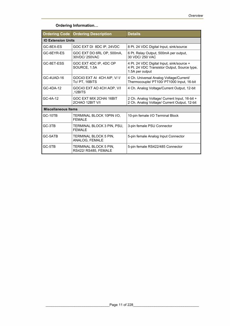
1.3 Ordering Information
Ordering Code Ordering Description Details Main Units
GC43MH-32MR-D GOC- MAIN, 16DI+16RL, 500mA+2CH AI V/I
4.3” Touch Screen, 16 Pt. 24 VDC Digital Input, sink/source + 16 Pt. Relay Output, 500mA per output, 220 VAC/30 VDC + 2 Pt. Analog Input Voltage/ Current Horizontal model
GC43MH-32MT-DSS GOC- MAIN, 16DI+16DO, SOURCE, 300mA+2CH AI V/I
4.3” Touch Screen, 16 Pt. 24 VDC Digital Input, sink/source + 16 Pt. 24 VDC Transistor Output, Source type, 300mA per output + 2 Pt. Analog Input Voltage/ Current Horizontal model
GC43MH-16MR-D GOC- MAIN, 8DI+8RL, 500mA+2CH AI V/I
4.3” Touch Screen, 8 Pt. 24 VDC Digital Input, sink/source + 8 Pt. Relay Output, 500mA per output, 220 VAC/30 VDC + 2 Pt. Analog Input Voltage/ Current Horizontal model
GC43MH-16MT-DSS GOC- MAIN, 8DI+8DO, SOURCE, 300mA+2CH AI V/I
4.3” Touch Screen, 8 Pt. 24 VDC Digital Input, sink/source + 8 Pt. 24 VDC Transistor Output, Source type, 300mA per output + 2 Pt. Analog Input Voltage/ Current Horizontal model
COM Extension Units
GC-RS232-COM GOC43 COM EXT PORT RS232 SERIAL
1 Port RS232 Serial
GC-RS422-COM GOC43 COM EXT PORT RS422/485 SERIAL
1 Port RS422/485 Serial
Overview
_________________________________Page 11 of 228__________________________________
Ordering Information…
Ordering Code Ordering Description Details IO Extension Units
GC-8EX-ES GOC EXT DI 8DC IP, 24VDC 8 Pt. 24 VDC Digital Input, sink/source
GC-6EYR-ES GOC EXT DO 6RL OP, 500mA, 30VDC/ 250VAC
6 Pt. Relay Output, 500mA per output, 30 VDC/ 250 VAC
GC-8ET-ESS GOC EXT 4DC IP, 4DC OP SOURCE, 1.5A
4 Pt. 24 VDC Digital Input, sink/source + 4 Pt. 24 VDC Transistor Output, Source type, 1.5A per output
GC-4UAD-16 GOC43 EXT AI 4CH AIP, V/ I/ Tc/ PT, 16BITS
4 Ch. Universal Analog Voltage/Current/ Thermocouple/ PT100/ PT1000 Input, 16-bit
GC-4DA-12 GOC43 EXT AO 4CH AOP, V/I ,12BITS
4 Ch. Analog Voltage/Current Output, 12-bit
GC-4A-12 GOC EXT MIX 2CHAI 16BIT 2CHAO 12BIT V/I
2 Ch. Analog Voltage/ Current Input, 16-bit + 2 Ch. Analog Voltage/ Current Output, 12-bit
Miscellaneous Items
GC-10TB TERMINAL BLOCK 10PIN I/O, FEMALE
10-pin female I/O Terminal Block
GC-3TB TERMINAL BLOCK 3 PIN, PSU, FEMALE
3-pin female PSU Connector
GC-5ATB TERMINAL BLOCK 5 PIN, ANALOG, FEMALE
5-pin female Analog Input Connector
GC-5TB TERMINAL BLOCK 5 PIN, RS422/ RS485, FEMALE
5-pin female RS422/485 Connector
Overview
_________________________________Page 12 of 228__________________________________
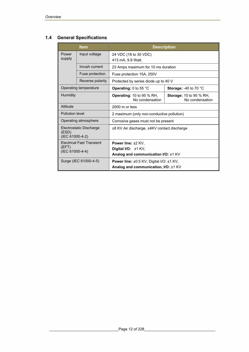
1.4 General Specifications
Item Description Power supply
Input voltage 24 VDC (18 to 30 VDC) 413 mA, 9.9 Watt.
Inrush current 23 Amps maximum for 10 ms duration
Fuse protection Fuse protection 15A, 250V
Reverse polarity Protected by series diode up to 40 V
Operating temperature Operating: 0 to 55 °C Storage: -40 to 70 °C
Humidity Operating: 10 to 95 % RH, No condensation
Storage: 10 to 95 % RH, No condensation
Altitude 2000 m or less
Pollution level 2 maximum (only non-conductive pollution)
Operating atmosphere Corrosive gases must not be present
Electrostatic Discharge (ESD) (IEC 61000-4-2)
±8 KV Air discharge, ±4KV contact discharge
Electrical Fast Transient (EFT) (IEC 61000-4-4)
Power line: ±2 KV, Digital I/O: ±1 KV, Analog and communication I/O: ±1 KV
Surge (IEC 61000-4-5) Power line: ±0.5 KV, Digital I/O: ±1 KV, Analog and communication, I/O: ±1 KV

Overview
_________________________________Page 13 of 228__________________________________
General specifications…
Item Description Over voltage category II (IEC 60664-1)
The surge voltage withstand level for up to the rated voltage of 30V is ±500 V
Vibration, Shock as required by EN- 61131-2
IEC 60068 -2-6 (test Fc), IEC 60068-2-27 test Ea
IP protection IP65 from front side. IP20 from rare side
Dimensions (W x H x D) in mm Main unit: Front panel: 177.0 (W) x 127.8 (H) x 4 (D) Rear side: 164.6 (W) x 105.6 (H) x 49.2(D)
I/O extension unit: 61.5 (W) x 75 (H) x 24.5 (D)
COM extension unit : 26.0 (W) x 51.0 (H) x 42.2 (D)
10-pin and 3-pin terminal block
I/O wires 0.5 to 1 mm² copper, stranded (flexible) or solid wire
Termination lugs For 0.5 to 1 mm² wire, insertion length 6 mm
Suggested tool Flat blade screwdriver 3 mm wide, 0.4 mm thick
5-pin terminal block
I/O wires 0.5 to 1.5 mm² copper, stranded (flexible) or solid wire
Termination lugs For 0.5 to 1.5 mm² wire, insertion length 6 mm
Suggested tool Flat blade screwdriver 1.6 mm wide, 0.4 mm thick
1.5 Technical Specifications This section provides CPU specifications covering system specifications.
Item Description Execution time BOOL: 0.9 sec
BYTE/ WORD/ DWORD/ REAL Move: 0.9 / 0.9 / 1.0 / 1.0 μsec
Number of I/O points Main unit: up to 32 digital I/Os + 2 analog I/Os. Can be extended up to 48 digital I/Os using I/O extension units. Digital I/O status indication on graphical LCD.
Extensions units Up to 2 I/O extension units and 1 COM extension unit
Marker memory 32 Kbytes
Data memory 2 Mbytes
Retain memory 4 Kbytes Stored in FRAM type of memory. Battery free operation.
Program memory 64 Mbytes flash includes - Application program code (8 Mbytes maximum), - Application program source code, - Application data (Visualization fonts, images, text lists, other system files, etc.)

Overview
_________________________________Page 14 of 228__________________________________
Technical specifications…
Item Description Application program security Password protection supported for
- Project file
- Source code upload
Timers Number of instances (TON, TOFF, TP) can be called. Limited by available data memory only. *1
Counter Number of instances (CTU, CTD, CTUD) can be called. (Limited by available data memory only) *1
Real Time Clock Onboard
Super capacitor backup: 2 weeks duration nominal at 25°C ambient
Max error: ± 2 Secs max per day
Special functionality for digital inputs on Main unit (User configurable)
Single phase counter: 20 KHz – Up to 2
Counter0: I00
Counter3: I03
Encoder (A, B, Z) interfaces: 10 KHz – Up to 2
Encoder1: I00 (A), I01(B), I02(Z) Encoder3: I03 (A), I04(B), I05(Z)
Operating modes RUN, STOP
HMI *2
Display 4.3", 480 x 272 pixels, TFT Touch graphics LCD, 64K Color View size: 95.04 x 53.86 in mm
Keypad 4 Function keys (F1 to F4) for system settings, diagnostics, alarms and to monitor IOs
Illuminated keys 4 illuminated keys, with dual colored LED (Red, Green)
Slide-in label Insertable label over illuminated keys
Ethernet port
Physical layer 10/100 Base-TX
Connector type RJ45 female, shielded
Auto crossover Yes
Cable type Category 5e or higher STP (Shielded Twisted Pair)
Max. cable distance 100 meters
Diagnostics Green and Yellow LEDs (On RJ45 connector)
Isolation 1500 Vac / 1 minute
Protocols supported Modbus TCP Server
No. of simultaneous connections supported
8 maximum
*1 FB instance can be declared retentive and entire instance data is retained. (limited by available retentive memory)
*2 Even though, maximum 64 user defined screens are allowed, it is limited by program memory.

Overview
_________________________________Page 15 of 228__________________________________
Technical specifications…
Item Description Programming
Port Built-in Ethernet port
Software Windows® based GOC Toolkit V3 consisting of CoDeSys version 3.5
Standard IEC 61131-3
Languages IL, LD, FBD, SFC, ST, CFC
Debugging and Online Monitoring
Visualization, Forcing, Writing for PLC variables, Watch windows
Online change Not supported
Offline simulation Supported for PLC logic only. Not supported for visualization screens
Memory Card Type Micro SD Card
SD Card standard SDHC
Speed Class Supported Class 4 (4MB/S), Class 6 (6MB/S), Class 10 (10MB/S) Memory Capacity 2 to 32GB
File System FAT32
SD Card Dimensions (D x H x W) in mm
11 x 15 x 1.0
Backup and Restore via SD memory Card
Applicable for Boot project and sourcecode
Password protecion User configurable
NOTE
Firmware download is possible on the field by MEI authorized personnel only using PC based tool via USB port. Micro size slide switch is provided near USB port. When slide switch position is towards top side of unit and unit power is turned on, unit is put in firmware download mode. In such case, RUN LED indication is turned off.
Installation and Wiring
_________________________________Page 16 of 228__________________________________
2 Installation and Wiring
This chapter discusses about installation and wiring of Main unit, IO extension unit and COM extension unit. It also explains installation and removal of microSD card in the Main unit.
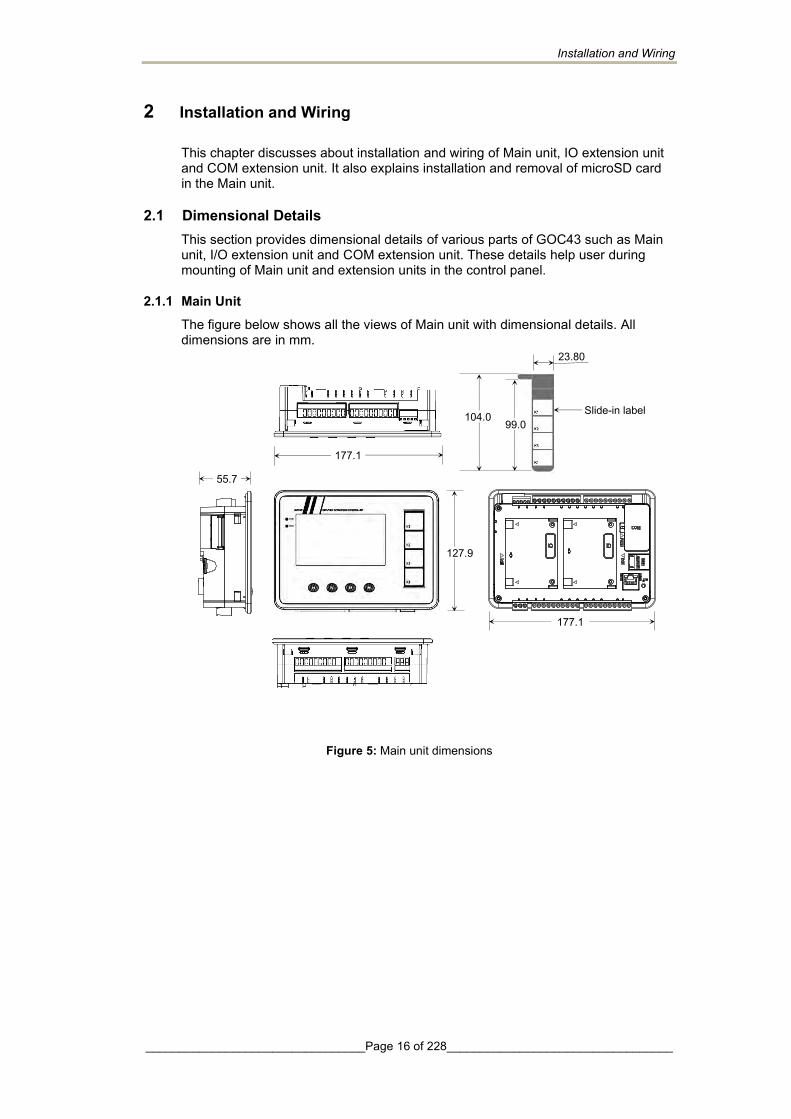
2.1 Dimensional Details This section provides dimensional details of various parts of GOC43 such as Main unit, I/O extension unit and COM extension unit. These details help user during mounting of Main unit and extension units in the control panel.
2.1.1 Main Unit The figure below shows all the views of Main unit with dimensional details. All dimensions are in mm.
Figure 5: Main unit dimensions
177.1
55.7
99.0 Slide-in label
127.9
177.1
23.80
104.0

Installation and Wiring
_________________________________Page 17 of 228__________________________________
2.1.2 I/O Extension Unit User can attach up to 2 I/O extension units on the back side of Main unit. The figure below shows all the views of I/O extension unit with dimensional details. All the dimensions are in mm.
Figure 6: I/O extension unit dimensions
2.1.3 COM Extension Unit User can attach 1 COM extension unit on the back side of Main unit. The figure below shows all the views of COM extension unit with dimensional details. All the dimensions are in mm.
Figure 7: COM extension unit dimensions
NOTE
Dimensional details in Figure above shows GC-RS232-COM extension unit. Similar plastic enclosure is used for another COM extension unit GC-RS422-COM with different interface connector. So, there is small change in dimensions due to connector used for external communication interface.
17.5
24.5
75
45.5
26.0
51.0
42.0 48.0
25.5
Installation and Wiring
_________________________________Page 18 of 228__________________________________
2.1.4 Main Unit with Extension Units User can attach up to 2 I/O extension units and 1 COM extension unit on the back side of Main unit. The figure below shows all the views of Main unit attached with 2 I/O extension units and 1 COM extension unit with dimensional details. All the dimensions are in mm.
Figure 8: Main unit dimensions with extension units
2.2 Installation This section provides recommendations and precautions to be observed during installation of various units of GOC43.
2.2.1 Installation Recommendations GOC43 is a front panel mount controller. Install the controller in an environment conforming to the general specifications and installation recommendations and precautions.
The recommendations are as below.
1. Mount controller on a firm, plane and conducting surface. Installation in orientation other than recommended one (as shown in the adjescent figure below), may cause overheating, damage and malfunctioning of the controller.
Figure 9: Mounting orientation
177.1
70.6
45° or less
177.1
127.9

Installation and Wiring
_________________________________Page 19 of 228__________________________________
2. Mount controller on non-vibrating surfaces and should be protected if necessary by rubber pads so that the shock is not felt.
3. Mounting plate thickness should not exceed 4 mm. 4. Installation should take care of keeping free space considering depth of
controller with COM extension unit installed on it i.e. 90 mm inclusive of additional space required for communication cable routing.
Figure 10: Mounting recommendations
5. Ensure the gap of 40 mm between controller and cabinet walls, other equipments and wiring duct.
6. Leave a minimum space of 40 mm around the Main unit to facilitate air circulation for heat transfer by natural convection and easy fixing and removal of unit.
2.2.2 Precautions to be taken This section lists out general precautions to be observed during installation.
1. Make sure to cut off all the phases of the power supply externally before attempting installation or wiring work. Failure to do so may cause electric shock or damage to the product.
2. Back side of I/O extension unit is open. Do not remove I/O extension unit specially relay output extension unit with AC power connected. It may cause electric shock.
3. Maintain proper thermal distances between equipments producing heat (like heaters, transformers etc.) inside the control panel. Do not install controller immediately above such equipments.
4. Protect the controller from conductive dust, corrosive gases, wire debris, flammable gases, rain and fluid from entering into the controller through ventilation slits. This may cause malfunction, damage, fire, electrical shock and deterioration to the controller. Proper dust tight control panels, filters, rubber gaskets, etc. should be provided to minimize this problem.
5. The ambient temperature of the installation location should be between 0 to 55ºC. Cooling of the electrical and electronic components is accomplished by method of convection.
6. Exposure to humid environment for a long time can reduce component life. It may cause corrosion of electrical and electronic components, or may lead to shorts or malfunctions. Do not expose controller to humid atmosphere for an extended period.
90
Control panel or
another device
40
40
40 40
130
40
40

Installation and Wiring
_________________________________Page 20 of 228__________________________________
7. Avoid controller exposure to excessive or continuous vibrations or shocks. Failure to do so may cause disengagement of PCB components, connectors, on-board soldered components, etc. from their counter positions.
8. Cover unused slots (IO and COM) by covers provided with Main unit to protect them against dust, moisture and ESD (Electric Static Discharge).
9. Use controller within the range of general and technical specifications.
10. Connect functional ground terminal properly. If not, product may susceptible to noise.
11. Connect protective earth to a good quality earth. If not, it may result in electric shock or errorneous operation.
2.2.3 Main Unit Installation This section provides steps to mount Main unit on front panel as well as unmounting it.
Product packaging consists of
1. Main unit with all the terminal blocks attached
2. installation manual
3. mounting template
4. 4 mounting clamps
Mounting Main Unit Follow the steps below to mount Main unit on front panel.
1. Prepare Main unit for mounting
Detach all the terminal blocks (10-pin I/O terminal blocks, 3-pin power supply terminal block and 5-pin analog V/I input terminal block) from Main unit.
Make sure that silicone rubber gasket on outer periphery of front panel backside is in place.
2. Insert slide-in label
Main unit is provided with default slide-in label inserted. But user can remove it and insert customized label. Slit is provided to insert slide-in label. It is located at left top on the backside of Main unit.
See that top edge of slide-in label remains below groove of the gasket.
Before installation and removal, refer sections Installation Recommendations and Precautions to be observed. Failure to follow the recommendations and precautions to be observed may cause electric shock or damage to the product.

Installation and Wiring
_________________________________Page 21 of 228__________________________________
3. Make cut out in the control panel
Remove adhesive tapes provided at corners of backside of mounting template and stick the mounting template on front panel where Main unit is to be mounted. Mark 4 corners of the rectangular cut-out and make a cut out.
Dimensions of cut out should be 166.5 X 107.5 mm minimum.
4. Insert Main unit through cut-out
Insert Main unit from outside through cut out on panel. Hold Main unit by hand from outer side of the panel so that it will not fall during fitment of mounting clamps.
5. Attach mounting clamps
Cut-outs are provided near each corner on back side of Main unit to insert mounting clamps.
Insert legs of clamp into matching cut-out.
Then pull body of mounting clamp away from panel till it clicks and engage at corner of plastic enclosure as shown in adjacent figure.
6. Tighten mounting clamps
Mounting clamp screw (M4 x 30 mm) head is of star type. Turn mounting clamp screw in clockwise direction till tip of screw slightly touches surface of panel. Rotate screw an additional 1 - 2 turns in clockwise direction and ensure controller is firmly mounted in the panel. Fix all the 4 mounting clamps by tightening screws one by one progressively.
Tightening torque should not exceed 0.2 Nm. Excessive tightening can damage plastic enclosure. Under tightening can cause loose fitment or malfunction.
Installation and Wiring
_________________________________Page 22 of 228__________________________________
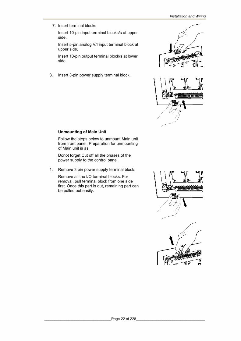
7. Insert terminal blocks
Insert 10-pin input terminal blocks/s at upper side.
Insert 5-pin analog V/I input terminal block at upper side.
Insert 10-pin output terminal block/s at lower side.
8. Insert 3-pin power supply terminal block.
Unmounting of Main Unit Follow the steps below to unmount Main unit from front panel. Preparation for unmounting of Main unit is as,
Donot forget Cut off all the phases of the power supply to the control panel.
1. Remove 3 pin power supply terminal block.
Remove all the I/O terminal blocks. For removal, pull terminal block from one side first. Once this part is out, remaining part can be pulled out easily.

Installation and Wiring
_________________________________Page 23 of 228__________________________________
2. Turn mounting clamp screws in anti- clockwise direction to loosen it one by one.
Push body of clamp towards panel to disengage it from the cut-outs on the Main unit.
Take moulting clamps off the Main unit.
Hold Main unit from front side with one hand while untightening of the clamps.
3. Removal of Main unit
After removing all mounting clamps, hold and pull out unit from front side, through the cut out.
2.2.4 I/O Extension Unit Installation User can attach up to 2 I/O extension units on the back side of Main unit and extend no. of I/Os as per application requirement. This unit is optional and should be procured separately. This section explains mounting and unmounting of I/O extension unit.
Product packaging consists of I/O extension unit, installation manual and 2 self-tapping screws (M3 x 10 mm) for fixing I/O extension unit on Main unit.
Mounting of I/O Extension Unit
1. Prepare Main unit for mounting I/O extension unit.
Main unit is provided with slot covers fixed on IO interface connectors and COM interface connector.
Remove interface connector cover on IO slot interface connector on Main unit.
Before installation and removal, refer sections Installation Recommendations and Precautions to be observed. Failure to follow recommendations and precautions to be observed may cause electric shock or damage to the product.
Installation and Wiring
_________________________________Page 24 of 228__________________________________
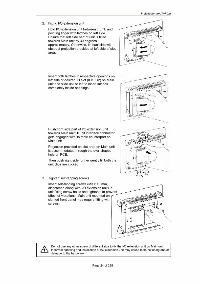
2. Fixing I/O extension unit
Hold I/O extension unit between thumb and pointing finger with latches on left side. Ensure that left side part of unit is tilted towards Main unit by 30 degrees approximately. Otherwise, its backside will obstruct projection provided at left side of slot area.
Insert both latches in respective openings on left side of desired IO slot (IO1/IO2) on Main unit and slide unit to left to insert latches completely inside openings.
Push right side part of I/O extension unit towards Main unit till unit interface connector gets engaged with its male counterpart on Main unit.
Projection provided on slot area on Main unit is accommodated through the oval shaped hole on PCB.
Then push right side further gently till both the unit clips are clicked.
3. Tighten self-tapping screws
Insert self-tapping screws (M3 x 10 mm, dispatched along with I/O extension unit) in unit fixing screw holes and tighten it to prevent effect of vibrations. Main unit mounted on slanted front panel may require fitting with screws.
Do not use any other screw of different size to fix the I/O extension unit on Main unit. Incorrect handling and installation of I/O extension unit may cause malfunctioning and/or damage to the hardware.
Click
Click
Installation and Wiring
_________________________________Page 25 of 228__________________________________
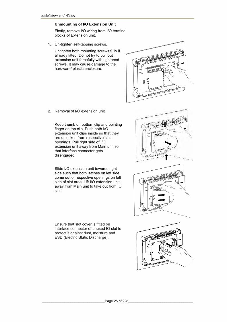
Unmounting of I/O Extension Unit Firstly, remove I/O wiring from I/O terminal blocks of Extension unit.
1. Un-tighten self-tapping screws.
Untighten both mounting screws fully if already fitted. Do not try to pull out extension unit forcefully with tightened screws. It may cause damage to the hardware/ plastic enclosure.
2. Removal of I/O extension unit
Keep thumb on bottom clip and pointing finger on top clip. Push both I/O extension unit clips inside so that they are unlocked from respective slot openings. Pull right side of I/O extension unit away from Main unit so that interface connector gets disengaged.
Slide I/O extension unit towards right side such that both latches on left side come out of respective openings on left side of slot area. Lift I/O extension unit away from Main unit to take out from IO slot.
Ensure that slot cover is fitted on interface connector of unused IO slot to protect it against dust, moisture and ESD (Electric Static Discharge).
Installation and Wiring
_________________________________Page 26 of 228__________________________________
2.2.5 COM Extension Unit Installation User can attach 1 serial COM extension unit on the back side of Main unit and interface third party serial devices. This section explains mounting and unmounting of COM extension unit.
Product packaging consists of COM extension unit and installation manual. For GC-RS422-COM unit, 5-pin terminal block is attached to the unit.
Mounting of COM Extension Unit
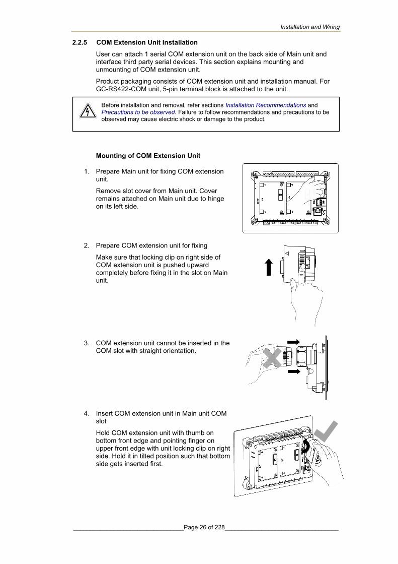
1. Prepare Main unit for fixing COM extension unit.
Remove slot cover from Main unit. Cover remains attached on Main unit due to hinge on its left side.
2. Prepare COM extension unit for fixing
Make sure that locking clip on right side of COM extension unit is pushed upward completely before fixing it in the slot on Main unit.
3. COM extension unit cannot be inserted in the COM slot with straight orientation.
4. Insert COM extension unit in Main unit COM slot
Hold COM extension unit with thumb on bottom front edge and pointing finger on upper front edge with unit locking clip on right side. Hold it in tilted position such that bottom side gets inserted first.
Before installation and removal, refer sections Installation Recommendations and Precautions to be observed. Failure to follow recommendations and precautions to be observed may cause electric shock or damage to the product.
UNLOCK
LOCK
Installation and Wiring
_________________________________Page 27 of 228__________________________________
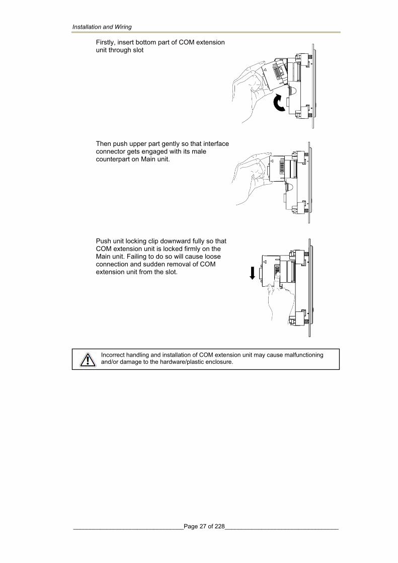
Firstly, insert bottom part of COM extension unit through slot
Then push upper part gently so that interface connector gets engaged with its male counterpart on Main unit.
Push unit locking clip downward fully so that COM extension unit is locked firmly on the Main unit. Failing to do so will cause loose connection and sudden removal of COM extension unit from the slot.
Incorrect handling and installation of COM extension unit may cause malfunctioning and/or damage to the hardware/plastic enclosure.
Installation and Wiring
_________________________________Page 28 of 228__________________________________
Unmounting of COM Extension Unit
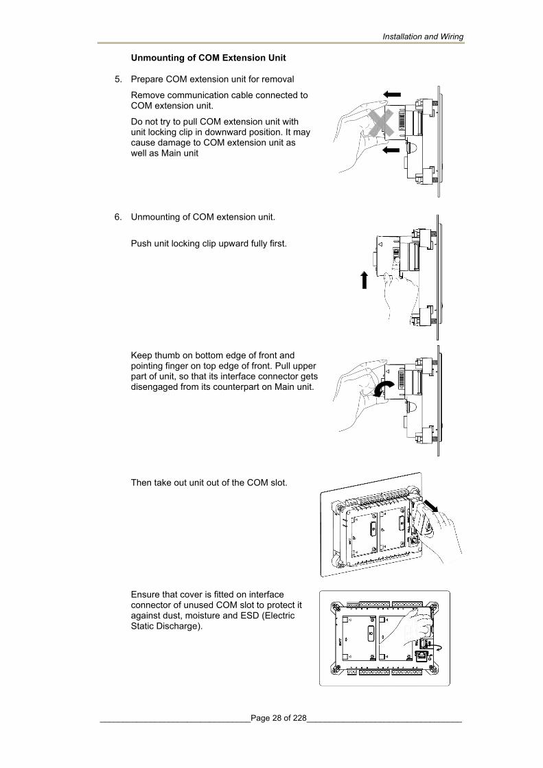
5. Prepare COM extension unit for removal
Remove communication cable connected to COM extension unit.
Do not try to pull COM extension unit with unit locking clip in downward position. It may cause damage to COM extension unit as well as Main unit
6. Unmounting of COM extension unit.
Push unit locking clip upward fully first.
Keep thumb on bottom edge of front and pointing finger on top edge of front. Pull upper part of unit, so that its interface connector gets disengaged from its counterpart on Main unit.
Then take out unit out of the COM slot.
Ensure that cover is fitted on interface connector of unused COM slot to protect it against dust, moisture and ESD (Electric Static Discharge).
Installation and Wiring
_________________________________Page 29 of 228__________________________________
2.2.6 microSD card Installation All the Main units are equipped with a SD card slot located above RJ45 connector.
User can insert commercially available microSD card in this slot. Specifications of compatible microSD cards are mentioned in section SD memory card .
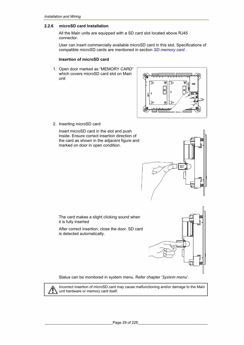
Insertion of microSD card
1. Open door marked as “MEMORY CARD” which covers microSD card slot on Main unit
2. Inserting microSD card
Insert microSD card in the slot and push inside. Ensure correct insertion direction of the card as shown in the adjacent figure and marked on door in open condition.
The card makes a slight clicking sound when it is fully inserted
After correct insertion, close the door. SD card is detected automatically.
Status can be monitored in system menu. Refer chapter ‘System menu’.
Incorrect insertion of microSD card may cause malfunctioning and/or damage to the Main unit hardware or memory card itself.
Installation and Wiring
_________________________________Page 30 of 228__________________________________
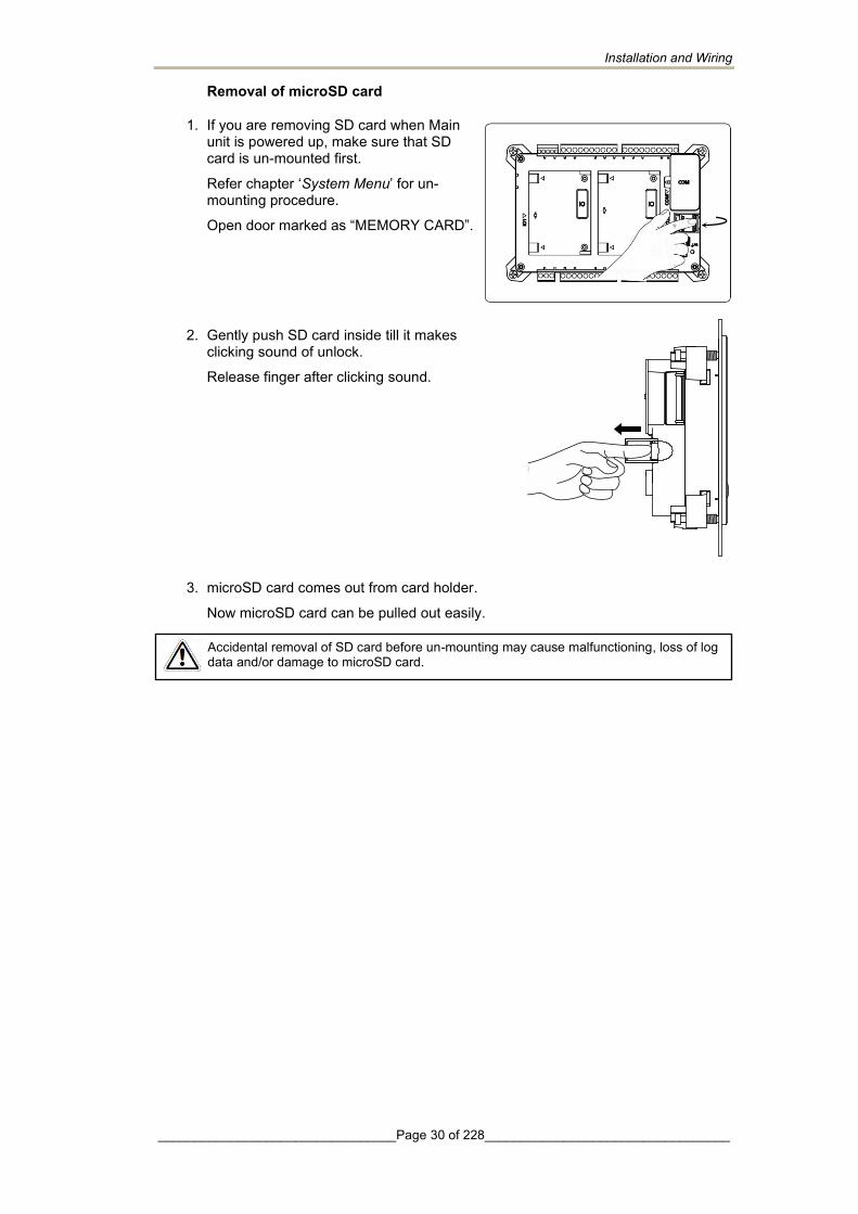
Removal of microSD card
1. If you are removing SD card when Main unit is powered up, make sure that SD card is un-mounted first.
Refer chapter ‘System Menu’ for un-mounting procedure.
Open door marked as “MEMORY CARD”.
2. Gently push SD card inside till it makes clicking sound of unlock.
Release finger after clicking sound.
3. microSD card comes out from card holder.
Now microSD card can be pulled out easily.
Accidental removal of SD card before un-mounting may cause malfunctioning, loss of log data and/or damage to microSD card.
Installation and Wiring
_________________________________Page 31 of 228__________________________________
2.3 Wiring This chapter provides recommendations and precautions to be observed during wiring of entire controller. GOC43 consists of Main unit, IO extension unit (optional) and COM extension unit (optional). For wiring of individual unit, refer subsequent chapters specific to individual unit type and model.
2.3.1 Recommendations
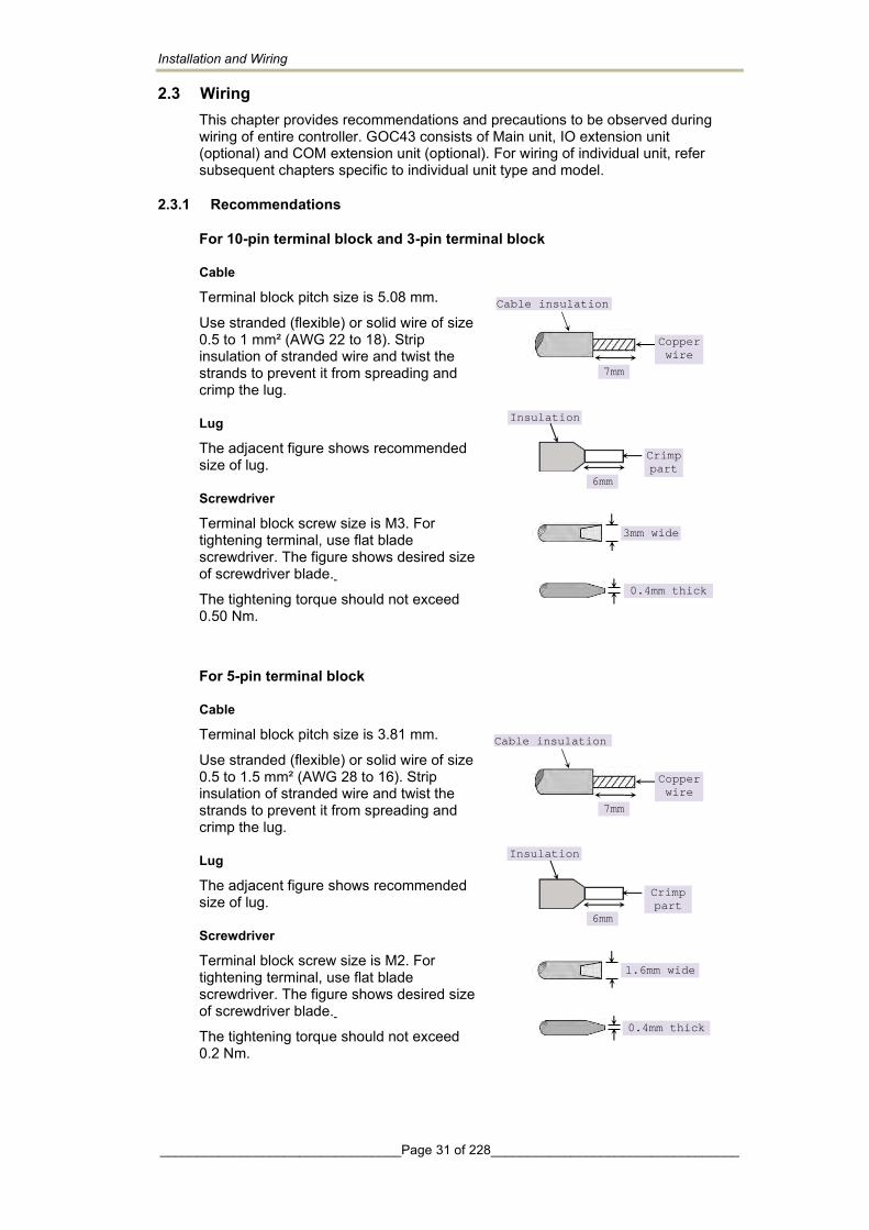
For 10-pin terminal block and 3-pin terminal block
Cable
Terminal block pitch size is 5.08 mm.
Use stranded (flexible) or solid wire of size 0.5 to 1 mm² (AWG 22 to 18). Strip insulation of stranded wire and twist the strands to prevent it from spreading and crimp the lug.
Lug
The adjacent figure shows recommended size of lug.
Screwdriver
Terminal block screw size is M3. For tightening terminal, use flat blade screwdriver. The figure shows desired size of screwdriver blade.
The tightening torque should not exceed 0.50 Nm.
For 5-pin terminal block
Cable
Terminal block pitch size is 3.81 mm.
Use stranded (flexible) or solid wire of size 0.5 to 1.5 mm² (AWG 28 to 16). Strip insulation of stranded wire and twist the strands to prevent it from spreading and crimp the lug.
Lug
The adjacent figure shows recommended size of lug.
Screwdriver
Terminal block screw size is M2. For tightening terminal, use flat blade screwdriver. The figure shows desired size of screwdriver blade.
The tightening torque should not exceed 0.2 Nm.
Crimp
part
Insulation
6mm
3mm wide
0.4mm thick
Copper
wire
Cable insulation
7mm
Crimp
part
Insulation
6mm
1.6mm wide
0.4mm thick
Copper
wire
Cable insulation
7mm
Installation and Wiring
_________________________________Page 32 of 228__________________________________
2.3.2 Precautions to be taken 1. Make sure to cut off all phases of the power supply externally before attempting
installation or wiring work. Failure to do so may cause electric shock or damage to the product.
2. Do not use wire without lug. Do not solder-plate the wire ends.It may cause loose connection. Ensure that only one lug is connected to one terminal.
3. Ensure that size of wire and lug used are as per the specifications. Use screw driver with specified size of tip. Tightening torque should be as per the specifications.
4. Ensure the gap of 40 mm between controller and cabinet walls, other equipments and wiring duct This will help in natural cooling of controller and also easy mounting or unmounting of hardware.
5. Separate wiring by signal types. Bundle wiring with similar electrical characteristics together. Differnetiate wiring with different electrical characteristics by coloured insulations e.g. AC wiring and DC wiring
6. Make sure that there is a separate bundle and routing for input and output wires. Fix-up the wire bundle with support on panel so thatthere is no stress on wires and subsequently on unit. Ensure that bunch is routed properly and wires are not kept hanging.
7. Do not bundle 24 VDC I/O wires with main control panel wiring. 8. Do not bundle cable carrying low level signals like communication and analog
signals with input output wiring and control panel wiring. 9. 50 to 100 meter long wiring for input/output will not cause any problems of
noise but, generally, the wiring length should not exceed 30 meters to ensure the safety. For longer distance, route the input and output signal lines separately.
10. Ensure that length of wire that connects 24 VDC power supply to I/O unit is less than 3 meters. Locate 24 VDC power supply near to the controller.
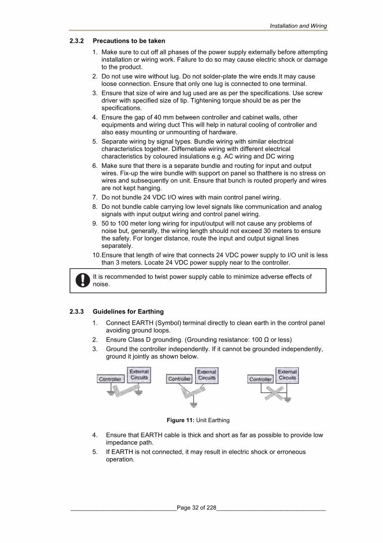
2.3.3 Guidelines for Earthing 1. Connect EARTH (Symbol) terminal directly to clean earth in the control panel
avoiding ground loops. 2. Ensure Class D grounding. (Grounding resistance: 100 Ω or less) 3. Ground the controller independently. If it cannot be grounded independently,
ground it jointly as shown below.
Figure 11: Unit Earthing
4. Ensure that EARTH cable is thick and short as far as possible to provide low impedance path.
5. If EARTH is not connected, it may result in electric shock or erroneous operation.
It is recommended to twist power supply cable to minimize adverse effects of noise.
Installation and Wiring
_________________________________Page 33 of 228__________________________________
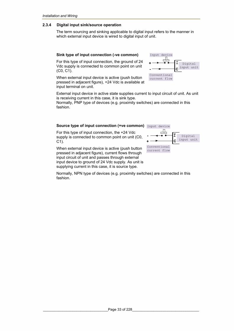
2.3.4 Digital input sink/source operation The term sourcing and sinking applicable to digital input refers to the manner in which external input device is wired to digital input of unit.
Sink type of input connection (-ve common) For this type of input connection, the ground of 24 Vdc supply is connected to common point on unit (C0, C1).
When external input device is active (push button pressed in adjacent figure), +24 Vdc is available at input terminal on unit.
External input device in active state supplies current to input circuit of unit. As unit is receiving current in this case, it is sink type. Normally, PNP type of devices (e.g. proximity switches) are connected in this fashion.
Source type of input connection (+ve common) For this type of input connection, the +24 Vdc supply is connected to common point on unit (C0, C1).
When external input device is active (push button pressed in adjacent figure), current flows through input circuit of unit and passes through external input device to ground of 24 Vdc supply. As unit is supplying current in this case, it is source type.
Normally, NPN type of devices (e.g. proximity switches) are connected in this fashion.
Digital
input unit
Input device
Conventional
current flow
+ - C
+ -
Input device
Digital
input unit
Conventional
current flow
C
Installation and Wiring
_________________________________Page 34 of 228__________________________________
2.3.5 Guidelines for using digital outputs
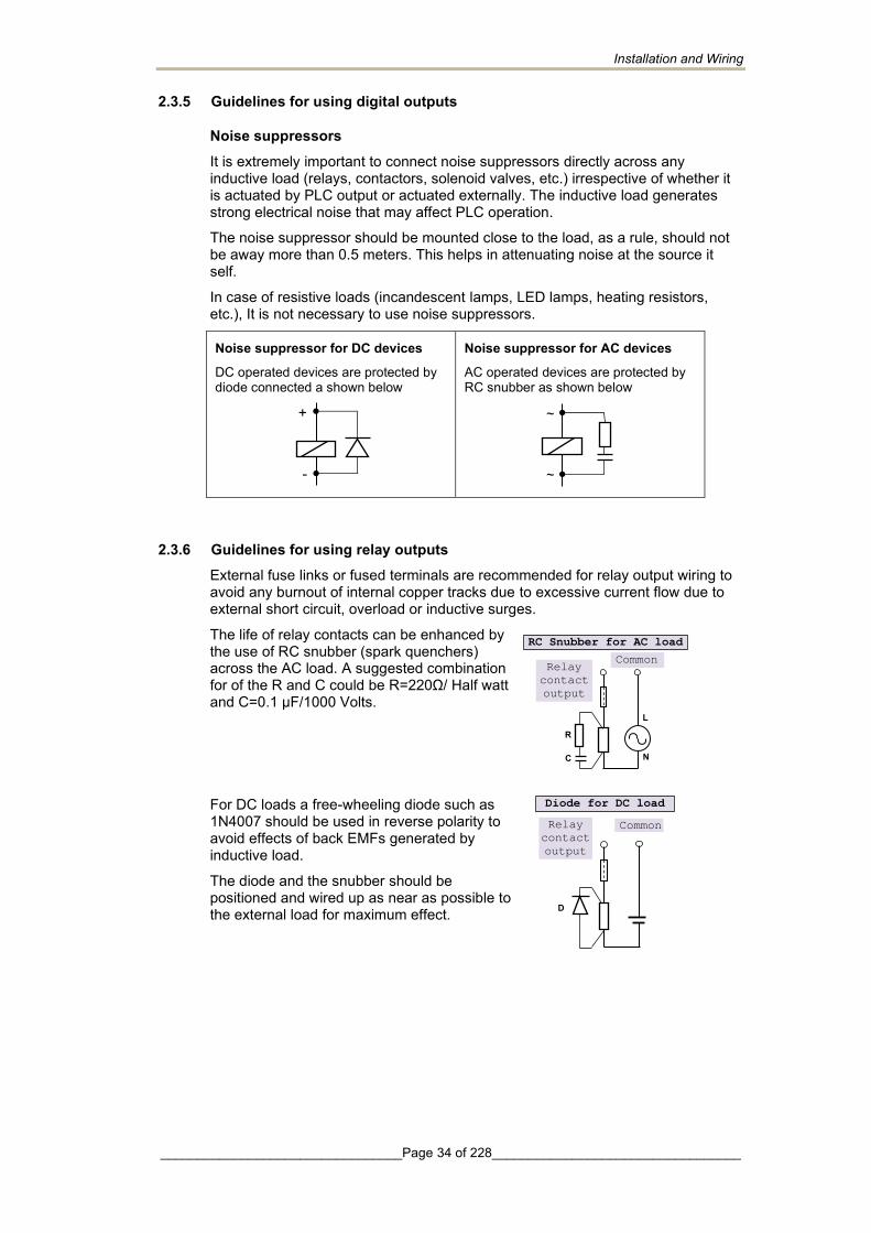
Noise suppressors It is extremely important to connect noise suppressors directly across any inductive load (relays, contactors, solenoid valves, etc.) irrespective of whether it is actuated by PLC output or actuated externally. The inductive load generates strong electrical noise that may affect PLC operation.
The noise suppressor should be mounted close to the load, as a rule, should not be away more than 0.5 meters. This helps in attenuating noise at the source it self.
In case of resistive loads (incandescent lamps, LED lamps, heating resistors, etc.), It is not necessary to use noise suppressors.
Noise suppressor for DC devices
DC operated devices are protected by diode connected a shown below
Noise suppressor for AC devices
AC operated devices are protected by RC snubber as shown below
2.3.6 Guidelines for using relay outputs External fuse links or fused terminals are recommended for relay output wiring to avoid any burnout of internal copper tracks due to excessive current flow due to external short circuit, overload or inductive surges.
The life of relay contacts can be enhanced by the use of RC snubber (spark quenchers) across the AC load. A suggested combination for of the R and C could be R=220Ω/ Half watt and C=0.1 µF/1000 Volts.
For DC loads a free-wheeling diode such as 1N4007 should be used in reverse polarity to avoid effects of back EMFs generated by inductive load.
The diode and the snubber should be positioned and wired up as near as possible to the external load for maximum effect.
RC Snubber for AC load
Common Relay
contact
output
L
N
R
C
+
-
~
~
Diode for DC load
Common
D
Relay
contact
output
Main Unit
_________________________________Page 35 of 228__________________________________
3 Main Unit
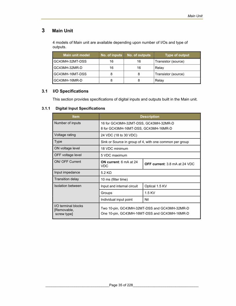
4 models of Main unit are available depending upon number of I/Os and type of outputs.
Main unit model No. of inputs No. of outputs Type of output
GC43MH-32MT-DSS 16 16 Transistor (source)
GC43MH-32MR-D 16 16 Relay
GC43MH-16MT-DSS 8 8 Transistor (source)
GC43MH-16MR-D 8 8 Relay
3.1 I/O Specifications
This section provides specifications of digital inputs and outputs built in the Main unit.
3.1.1 Digital Input Specifications
Item Description
Number of inputs 16 for GC43MH-32MT-DSS, GC43MH-32MR-D 8 for GC43MH-16MT-DSS, GC43MH-16MR-D
Voltage rating 24 VDC (18 to 30 VDC)
Type Sink or Source in group of 4, with one common per group
ON voltage level 18 VDC minimum
OFF voltage level 5 VDC maximum
ON/ OFF Current ON current: 6 mA at 24 VDC OFF current: 3.8 mA at 24 VDC
Input impedance 5.2 KΩ
Transition delay 10 ms (filter time)
Isolation between Input and internal circuit Optical 1.5 KV
Groups 1.5 KV
Individual input point Nil
I/O terminal blocks [Removable, screw type]
Two 10-pin, GC43MH-32MT-DSS and GC43MH-32MR-D One 10-pin, GC43MH-16MT-DSS and GC43MH-16MR-D
Main Unit
_________________________________Page 36 of 228__________________________________
Digital input specifications…
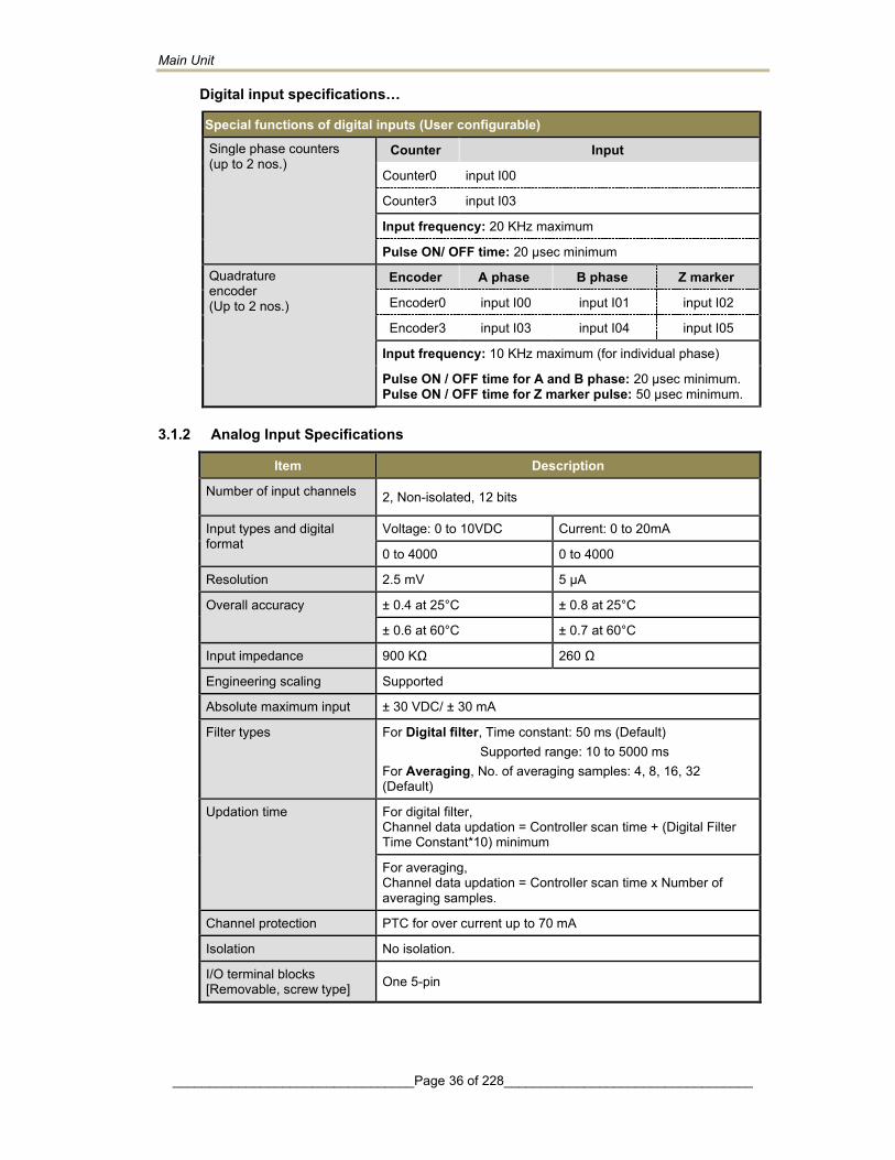
Special functions of digital inputs (User configurable) Single phase counters (up to 2 nos.)
Counter Input
Counter0 input I00
Counter3 input I03
Input frequency: 20 KHz maximum
Pulse ON/ OFF time: 20 µsec minimum
Quadrature encoder (Up to 2 nos.)
Encoder A phase B phase Z marker
Encoder0 input I00 input I01 input I02
Encoder3 input I03 input I04 input I05
Input frequency: 10 KHz maximum (for individual phase)
Pulse ON / OFF time for A and B phase: 20 µsec minimum. Pulse ON / OFF time for Z marker pulse: 50 µsec minimum.
3.1.2 Analog Input Specifications
Item Description
Number of input channels 2, Non-isolated, 12 bits
Input types and digital format
Voltage: 0 to 10VDC Current: 0 to 20mA
0 to 4000 0 to 4000
Resolution 2.5 mV 5 µA
Overall accuracy ± 0.4 at 25°C ± 0.8 at 25°C
± 0.6 at 60°C ± 0.7 at 60°C
Input impedance 900 KΩ 260 Ω
Engineering scaling Supported
Absolute maximum input ± 30 VDC/ ± 30 mA
Filter types For Digital filter, Time constant: 50 ms (Default) Supported range: 10 to 5000 ms
For Averaging, No. of averaging samples: 4, 8, 16, 32 (Default)
Updation time For digital filter, Channel data updation = Controller scan time + (Digital Filter Time Constant*10) minimum
For averaging, Channel data updation = Controller scan time x Number of averaging samples.
Channel protection PTC for over current up to 70 mA
Isolation No isolation.
I/O terminal blocks [Removable, screw type] One 5-pin
Main Unit
_________________________________Page 37 of 228__________________________________
3.1.3 Transistor Output (Source) Specifications
Item Description Number of outputs 16 for GC43MH-32MT-DSS
8 for GC43MH-16MT-DSS
Type of output Transistor source type
Voltage rating 24VDC (18 to 30 VDC)
Current rating 0.3A per point 1 common per group of 8 outputs. Paralleling of outputs is possible in a group.
On voltage drop 0.6 VDC maximum
Off state leakage current 10 µA maximum
Response time OFF to ON 250 µs
ON to OFF 300 µs
Isolation Optical 1.5 KV between input and internal circuit
Protection Output short circuit protection
Fast demagnetization for inductive loads
Load supply 24 VDC (18 to 30 VDC)
Reverse polarity protection
I/O terminal blocks [Removable screw type]
Two 10-pin, GC43MH-32MT-DSS and GC43MH-32MR-D One 10-pin, GC43MH-16MT-DSS and GC43MH-16MR-D

Main Unit
_________________________________Page 38 of 228__________________________________
3.1.4 Relay Output Specifications
Item Description Number of outputs 16 for GC43MH-32MR-D
8 for GC43MH-16MR-D
Type of output Non latching normally open (NO) contact Electro-mechanical relay
Voltage rating 24 to 250 VAC, 47-63 Hz, 5-30 VDC
Current rating 0.5A at 250 VAC and 30 VDC per point 1.5 A per common
Minimum load 1 mA
Contact life Electrical life Refer table and Life curve *
Mechanical life min 20, 000, 000 (180 cpm)
Response time OFF to ON 10 ms
ON to OFF 5 ms
Isolation Galvanic between output and internal circuit
Dielectric strength 3 KVrms (between coil and contact circuit) 0.75 KVrms (for open contact)
I/O terminal blocks [Removable, screw type]
Two 10-pin, GC43MH-32MR-D One 10-pin, GC43MH-16MR-D
*Electrical life of relay
Voltage Current Type of load Electrical life (20 cpm)
250 VAC 1 A
Resistive 500,000 Inductive 30,000
500 mA Resistive 10,00,000 Inductive 80,000
30 VDC 1 A
Resistive 600,000 Inductive 150,000
500 mA Resistive 10,00,000 Inductive 3,80,000
The graph shown is provided by relay manufacturer specification sheet. There may be some degree of variation in relay characteristics depending on ambient and type of load. So this data should be used only for reference purpose.
* Life curve of Relay:
Switching capacity, A
No.
of O
pera
tions
, x10
^4
AC 125V resistive load DC 30V resistive load AC 250V resistive load
DC 30V T=7ms
AC 125V COS Ø=0.4
AC 250V COS Ø=0.4
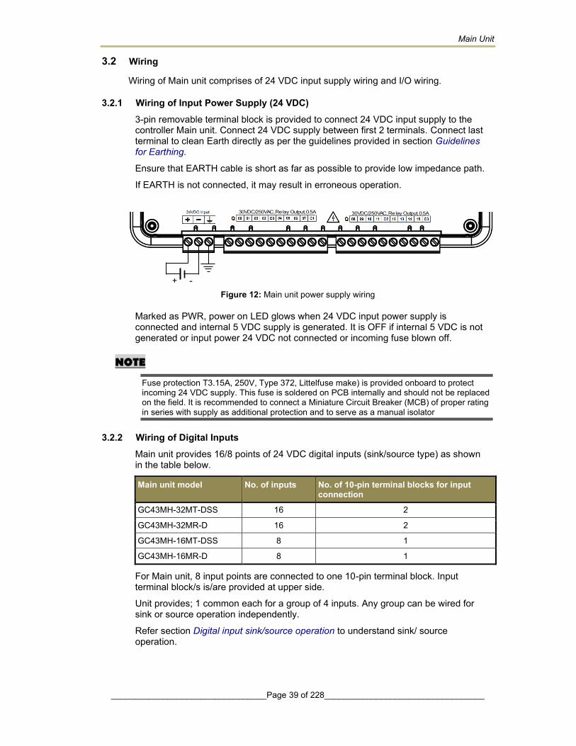
Main Unit
_________________________________Page 39 of 228__________________________________
3.2 Wiring
Wiring of Main unit comprises of 24 VDC input supply wiring and I/O wiring.
3.2.1 Wiring of Input Power Supply (24 VDC) 3-pin removable terminal block is provided to connect 24 VDC input supply to the controller Main unit. Connect 24 VDC supply between first 2 terminals. Connect last terminal to clean Earth directly as per the guidelines provided in section Guidelines for Earthing.
Ensure that EARTH cable is short as far as possible to provide low impedance path.
If EARTH is not connected, it may result in erroneous operation.
Figure 12: Main unit power supply wiring
Marked as PWR, power on LED glows when 24 VDC input power supply is connected and internal 5 VDC supply is generated. It is OFF if internal 5 VDC is not generated or input power 24 VDC not connected or incoming fuse blown off.
NOTE
Fuse protection T3.15A, 250V, Type 372, Littelfuse make) is provided onboard to protect incoming 24 VDC supply. This fuse is soldered on PCB internally and should not be replaced on the field. It is recommended to connect a Miniature Circuit Breaker (MCB) of proper rating in series with supply as additional protection and to serve as a manual isolator
3.2.2 Wiring of Digital Inputs Main unit provides 16/8 points of 24 VDC digital inputs (sink/source type) as shown in the table below.
Main unit model No. of inputs No. of 10-pin terminal blocks for input connection
GC43MH-32MT-DSS 16 2
GC43MH-32MR-D 16 2
GC43MH-16MT-DSS 8 1
GC43MH-16MR-D 8 1
For Main unit, 8 input points are connected to one 10-pin terminal block. Input terminal block/s is/are provided at upper side.
Unit provides; 1 common each for a group of 4 inputs. Any group can be wired for sink or source operation independently.
Refer section Digital input sink/source operation to understand sink/ source operation.
+ -
30VDC/250VAC, Relay Output, 0.5A 30VDC/250VAC, Relay Output, 0.5A
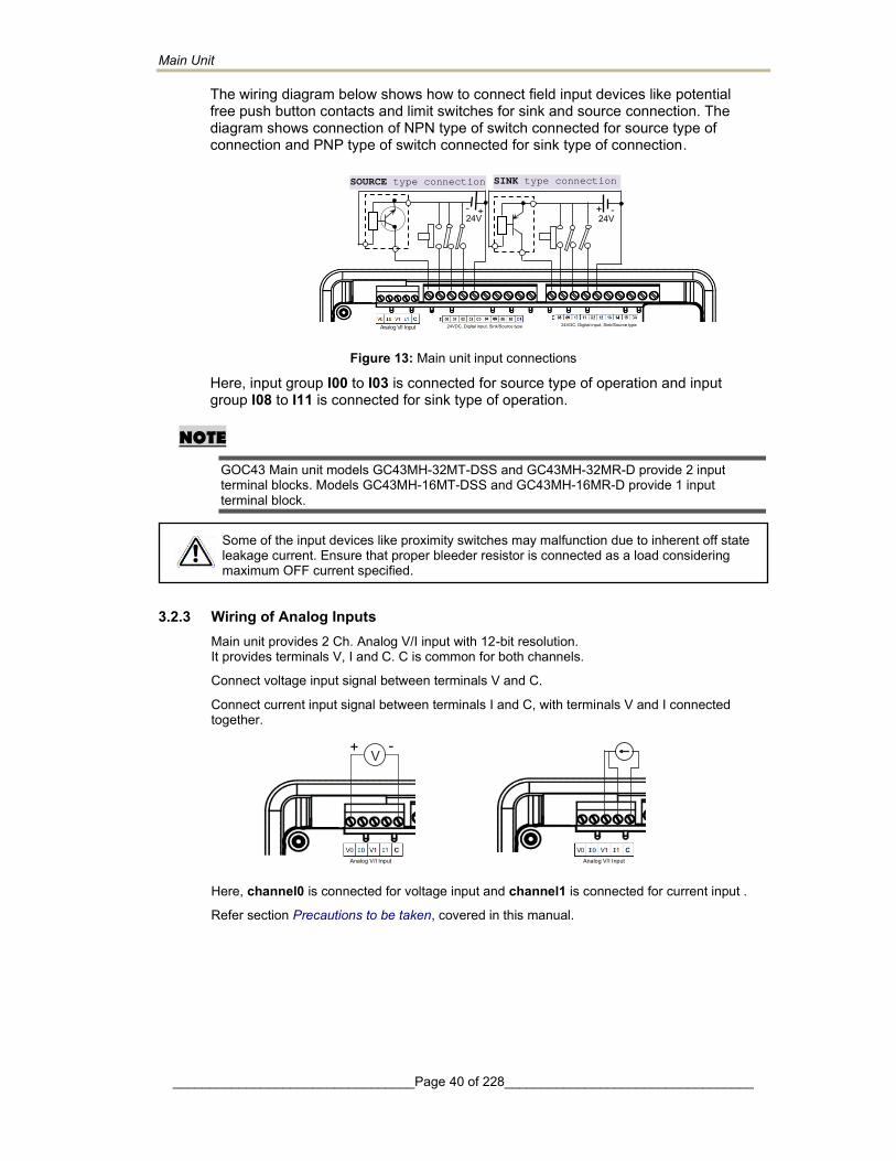
Main Unit
_________________________________Page 40 of 228__________________________________
The wiring diagram below shows how to connect field input devices like potential free push button contacts and limit switches for sink and source connection. The diagram shows connection of NPN type of switch connected for source type of connection and PNP type of switch connected for sink type of connection.
Figure 13: Main unit input connections
Here, input group I00 to I03 is connected for source type of operation and input group I08 to I11 is connected for sink type of operation.
NOTE
GOC43 Main unit models GC43MH-32MT-DSS and GC43MH-32MR-D provide 2 input terminal blocks. Models GC43MH-16MT-DSS and GC43MH-16MR-D provide 1 input terminal block.
3.2.3 Wiring of Analog Inputs Main unit provides 2 Ch. Analog V/I input with 12-bit resolution. It provides terminals V, I and C. C is common for both channels.
Connect voltage input signal between terminals V and C.
Connect current input signal between terminals I and C, with terminals V and I connected together. Here, channel0 is connected for voltage input and channel1 is connected for current input .
Refer section Precautions to be taken, covered in this manual.
24V
24VDC, Digital input, Sink/Source type 24VDC, Digital input, Sink/Source type
SINK type connection SOURCE type connection
+ - 24V
+ -
Some of the input devices like proximity switches may malfunction due to inherent off state leakage current. Ensure that proper bleeder resistor is connected as a load considering maximum OFF current specified.
+ -
Analog V/I Input Analog V/I Input
Analog V/I Input
V

Main Unit
_________________________________Page 41 of 228__________________________________
3.2.4 Wiring of Transistor Source Outputs Main unit provides 16/8 points of 24 VDC transistor output (source type) as shown in the table below.
Main unit model No. of transistor outputs (source)
No. of 10-pin terminal blocks for output connection
GC43MH-32MT-DSS 16 2
GC43MH-16MT-DSS 8 1
For Main unit, 8 output points are connected to one 10-pin input terminal block. Output terminal block/s is/are provided at lower side. As transistor output is of source type, connect one end of output device to output point on terminal block and connect other end of output device to GND terminal of 24 VDC load supply. It is mandatory to connect 24 VDC output load supply as shown below.
Figure 14: Main unit transistor source output connections
The ON voltage across the output transistor is 0.6V maximum. When driving a semiconductor element, check the voltage characteristics of the connected element.
NOTE
GOC43 Main unit model GC43MH-32MT-DSS provides 2 output terminal blocks. Model GC43MH-16MT-DSS provides 1 output terminal block.
3.2.5 Wiring of Relay Outputs Main unit provides 16/8 points of relay outputs as shown in the table below.
Main unit model No. of relay outputs No. of 10-pin terminal blocks for outputs connection
GC43MH-32MR-D 16 2
GC43MH-16MR-D 8 1
Before wiring relay outputs, refer section Guidelines for using relay outputs.
For Main unit, 8 outpoint points are connected to one 10-pin input terminal block. Output terminal block/s is/are provided at lower side. 2 common points are provided per 10-pin output terminal block i.e. 1 common point for 4 outputs.
24VDC Load
supply
L L L L L L L L L L L L L L L L
24VDC, Transistor Output, Source, 0.3A 24VDC, Transistor Output, Source, 0.3A
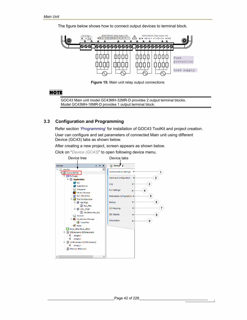
Main Unit
_________________________________Page 42 of 228__________________________________
The figure below shows how to connect output devices to terminal block.
Figure 15: Main unit relay output connections
NOTE
GOC43 Main unit model GC43MH-32MR-D provides 2 output terminal blocks. Model GC43MH-16MR-D provides 1 output terminal block.
3.3 Configuration and Programming Refer section ‘Programming’ for installation of GOC43 ToolKit and project creation. User can configure and set parameters of connected Main unit using different Device (GC43) tabs as shown below. After creating a new project, screen appears as shown below. Click on “Device (GC43)” to open following device menu.
30VDC/250VAC, Relay Output, 0.5A 30VDC/250VAC, Relay Output, 0.5A
Load supply
1 2
3
4
5
6
7
8
9
Device tree Device tabs
Fuse
protection

Main Unit
_________________________________Page 43 of 228__________________________________
Sr. No. Device menu Description
1 Communication settings
User can define the connection path between CoDeSys V3.5 and the device where application should run. User can - scan network for connected device. - Add or manage Gateway
2 Hardware configuration
User can update device version i.e. Main unit version. User can plug IO Extension device in slot IO1 and IO2. and COM Extension device in COM slot. User can configure various functions supported.
3 Log It lists the events that were recorded on the GOC43. This includes the following:
• Events during the startup and shutdown of the system (components loaded, with version)
• Application download and loading of the boot application • Log entries from I/O drivers etc.
4 PLC Settings User can define I/O behavior in case of PLC STOP mode, along with additional settings such as, - bus cycle task - enable diagnostics for device - showing I/O warnings as errors.
5 Parameter Configuration
User can configure functionality of digital and analog inputs of Main unit.
6 Backup User can allow transfer of application program and source code between CPU and SD memory card, User can set password protection for such transfer. User can also back up application program and source code from PC to SD memory card.
7 I/O Mapping Lists of digital inputs and outputs of Main unit with pre-defined variable names. Also, shows on/off status in online mode. User can use these variable names directly in the application program. User can modify variable names if required.
8 IEC Objects Shows variables related to functionality configured. Also, shows system variables with prefix as _SysVar. User can monitor values in online mode.
9 Information Shows device description
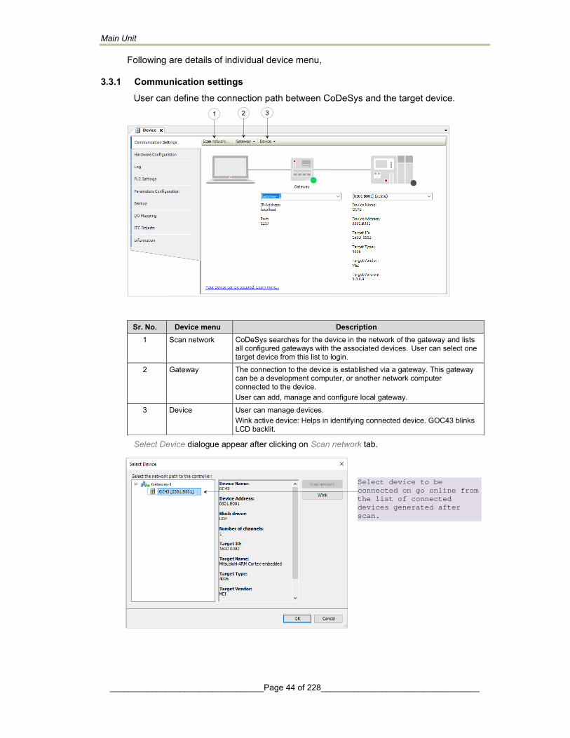
Main Unit
_________________________________Page 44 of 228__________________________________
Following are details of individual device menu,
3.3.1 Communication settings User can define the connection path between CoDeSys and the target device.
Select Device dialogue appear after clicking on Scan network tab.
Sr. No. Device menu Description 1 Scan network CoDeSys searches for the device in the network of the gateway and lists
all configured gateways with the associated devices. User can select one target device from this list to login.
2 Gateway The connection to the device is established via a gateway. This gateway can be a development computer, or another network computer connected to the device. User can add, manage and configure local gateway.
3 Device User can manage devices. Wink active device: Helps in identifying connected device. GOC43 blinks LCD backlit.
2
3
Select device to be
connected on go online from
the list of connected
devices generated after
scan.
1
Main Unit
_________________________________Page 45 of 228__________________________________
3.3.2 Hardware Configuration Hardware configuration tab shows back side view of Main unit as below. There is no differentiation for Main unit based on model.
After right click → Update Device window pops up.
Red highlighter shows
unit/device. Currently,
it shows that Main unit
is selected
Right click on Main unit
area to update device
version if necessary.
Select required device
version and click on ‘Update
Device’ button.
Adjacent dialog shows only
one version. Device versions
will get added in near
future as new features will
get added
Main Unit
_________________________________Page 46 of 228__________________________________
Back side view shows IO1 slot, IO2 slot and COM slot where use can plug extension unit. Click on slot area to highlight selected slot. Image below shows that IO1 slot is selected. Right click on selected slot to plug extension as shown below.
Click on context menu ‘Plug Device’ to pop up ‘Plug Device’ window as shown below.
After plugging any device, one can right click on selected slot to plug/update or delete device as required.
User can select IO
extension device as per
requirement and click on
button ‘Plug Device’.
IO1 slot IO2 slot
COM slot
Main Unit
_________________________________Page 47 of 228__________________________________
Alternately, user can plug extension device in respective slot (IOExtension and COMExtension) in Device tree. Follow the steps below.
1. Right click on <Empty> slot to pop up context menu.
2. Click on Plug Device. Plug Device dialog shows the list of extension devices supported for the selected slot.
3. Select extension device and double click on it or click on button Plug Device to plug it into selected slot.
3.3.3 Log
It lists the events that were recorded on the GOC43.
This includes the following:
• Events during the startup and shutdown of the system (components loaded, with version)
• Application download and loading of the boot application
• Log entries from I/O drivers etc
Main Unit
_________________________________Page 48 of 228__________________________________
3.3.4 PLC Settings
User can make the basic settings like updation of inputs and outputs and its association with the bus cycle task.
Any setting other than recommended above will cause malfunctioning and hence, should be avoided.
3.3.5 Parameter Configuration User can configure special functionality of Main unit like, high speed counter and analog input.
Ensure to choose option
Enabled 2 (always in bus
cycle task’ for setting
Always update variables.
Tabs available in
‘Parameter
Configuration’
dialogue
For safe operation, select
option Set all outputs to
default for setting
Behaviour of outputs in
Stop.
Ensure to choose option
MainTask’ for setting Bus
cycle task.
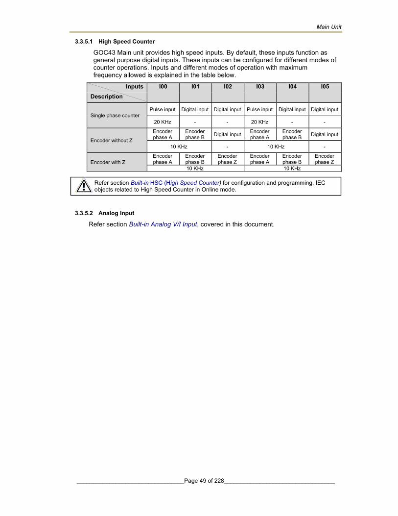
Main Unit
_________________________________Page 49 of 228__________________________________
3.3.5.1 High Speed Counter
GOC43 Main unit provides high speed inputs. By default, these inputs function as general purpose digital inputs. These inputs can be configured for different modes of counter operations. Inputs and different modes of operation with maximum frequency allowed is explained in the table below.
Inputs I00 I01 I02 I03 I04 I05 Description
Single phase counter Pulse input Digital input Digital input Pulse input Digital input Digital input
20 KHz - - 20 KHz - -
Encoder without Z
Encoder phase A
Encoder phase B Digital input Encoder
phase A Encoder phase B Digital input
10 KHz - 10 KHz -
Encoder with Z Encoder phase A
Encoder phase B
Encoder phase Z
Encoder phase A
Encoder phase B
Encoder phase Z
10 KHz 10 KHz
3.3.5.2 Analog Input
Refer section Built-in Analog V/I Input, covered in this document.
Refer section Built-in HSC (High Speed Counter) for configuration and programming, IEC objects related to High Speed Counter in Online mode.
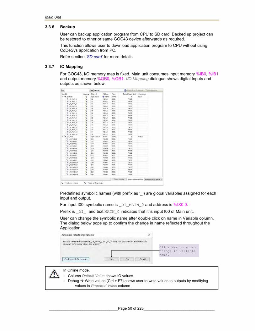
Main Unit
_________________________________Page 50 of 228__________________________________
3.3.6 Backup User can backup application program from CPU to SD card. Backed up project can be restored to other or same GOC43 device afterwards as required. This function allows user to download application program to CPU without using CoDeSys application from PC. Refer section ‘SD card’ for more details
3.3.7 IO Mapping For GOC43, I/O memory map is fixed. Main unit consumes input memory %IB0, %IB1 and output memory %QB0, %QB1. I/O Mapping dialogue shows digital Inputs and outputs as shown below.
Predefined symbolic names (with prefix as ‘_’) are global variables assigned for each input and output. For input I00, symbolic name is _DI_MAIN_0 and address is %IX0.0. Prefix is _DI_ and text MAIN_0 indicates that it is input I00 of Main unit. User can change the symbolic name after double click on name in Variable column. The dialog below pops up to confirm the change in name reflected throughout the Application.
Click Yes to accept
change in variable
name.
In Online mode, - Column Default Value shows IO values. - Debug → Write values (Ctrl + F7) allows user to write values to outputs by modifying
values in Prepared Value column.

Main Unit
_________________________________Page 51 of 228__________________________________
3.3.8 IEC Objects IEC objects are pre-defined global variables ((with prefix as ‘_’) which consists of system variables and variables related to various functions. The dialog below shows offline view.
Refer section ‘Built-in Analog V/I Input’ for more details on ‘_Base_Analog’. Refer section ‘Built-in HSC (High Speed Counter)’ for more details on ‘_HSC0’ and ‘_.HSC3’ Refer section ‘System Variables’ for more details of system variables.
User can monitor and modify values of IEC objects (Read write type) in Online mode.

Main Unit
_________________________________Page 52 of 228__________________________________
3.3.9 Information Information tab provides general details of Main unit such as device name, vendor name, category, type, ID, version, ordering code and description etc. as shown below.

Digital I/O Extension Units
_________________________________Page 53 of 228__________________________________
4 Digital I/O Extension Units
Digital input extension units accept 24 VDC inputs from various input devices like push buttons, limit switches and proximity switches. It can be used for sink or source type of interface.
Digital output extension units provide 24 VDC type of output through solid-state type of devices in order to switch on off various field elements like relays, contactors, lamps and solenoid valves, etc. Source type of digital output modules are available.
Digital I/O Extension Units
_________________________________Page 54 of 228__________________________________
4.1 GC-8EX-ES
This is 8 Pt. 24 VDC Digital Input extension unit. User can attach up to 2 I/O extension units on the back side of Main unit.
4.1.1 Specifications
Item Description Number of Inputs 8, 2 groups of 4 inputs each
Mode of operation Sink or source in group of 4 inputs; depends on connections
Voltage rating 24 VDC
ON / OFF voltage ON voltage: 18 VDC minimum OFF voltage: 5 VDC maximum
Current rating 6 mA at 24 VDC
OFF Current 3.8 mA max
Input impedance 5.2 KΩ
Transition delay 10 ms (Digital filter)
Isolation Optical 1.5 KV between input and internal bus, 1.5 KV between groups, Nil between input points in a group.
Method of termination 2 nos. 8-pin terminal blocks, fixed, screw type
Status indication On LCD screen on Main unit
Dimensions (in mm) 61.5 (W) x 75 (H) x 24.5 (D)
Weight (in grams) 60
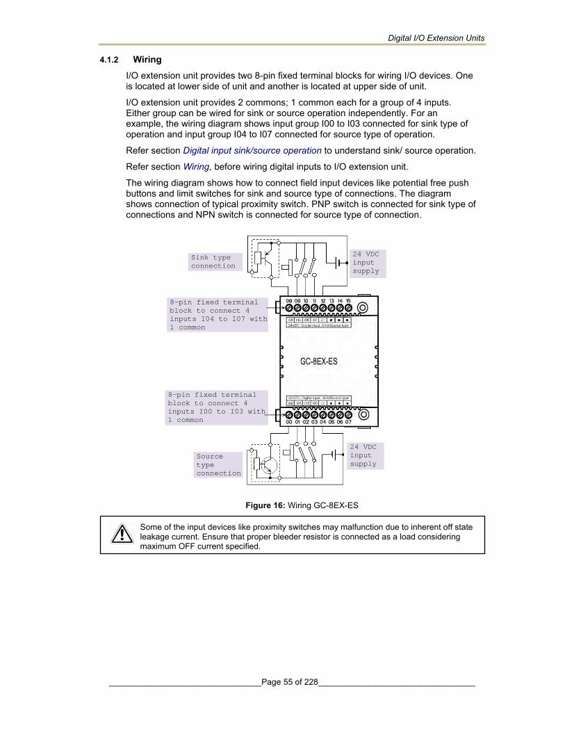
Digital I/O Extension Units
_________________________________Page 55 of 228__________________________________
4.1.2 Wiring
I/O extension unit provides two 8-pin fixed terminal blocks for wiring I/O devices. One is located at lower side of unit and another is located at upper side of unit.
I/O extension unit provides 2 commons; 1 common each for a group of 4 inputs. Either group can be wired for sink or source operation independently. For an example, the wiring diagram shows input group I00 to I03 connected for sink type of operation and input group I04 to I07 connected for source type of operation.
Refer section Digital input sink/source operation to understand sink/ source operation.
Refer section Wiring, before wiring digital inputs to I/O extension unit.
The wiring diagram shows how to connect field input devices like potential free push buttons and limit switches for sink and source type of connections. The diagram shows connection of typical proximity switch. PNP switch is connected for sink type of connections and NPN switch is connected for source type of connection.
Figure 16: Wiring GC-8EX-ES
24 VDC
input
supply
8-pin fixed terminal
block to connect 4
inputs I04 to I07 with
1 common
8-pin fixed terminal
block to connect 4
inputs I00 to I03 with
1 common
Source
type
connection
24 VDC
input
supply
Sink type
connection
Some of the input devices like proximity switches may malfunction due to inherent off state leakage current. Ensure that proper bleeder resistor is connected as a load considering maximum OFF current specified.
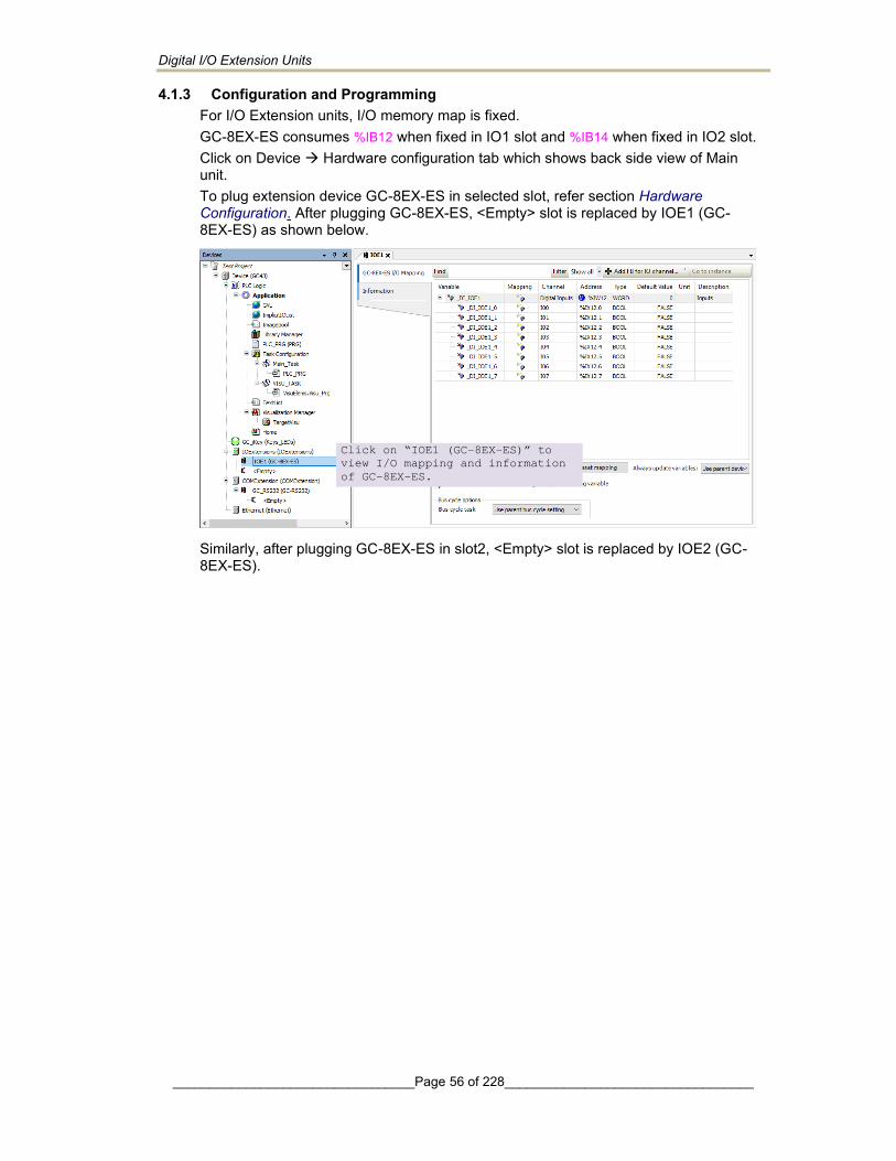
Digital I/O Extension Units
_________________________________Page 56 of 228__________________________________
4.1.3 Configuration and Programming For I/O Extension units, I/O memory map is fixed. GC-8EX-ES consumes %IB12 when fixed in IO1 slot and %IB14 when fixed in IO2 slot. Click on Device → Hardware configuration tab which shows back side view of Main unit. To plug extension device GC-8EX-ES in selected slot, refer section Hardware Configuration. After plugging GC-8EX-ES, <Empty> slot is replaced by IOE1 (GC-8EX-ES) as shown below. Similarly, after plugging GC-8EX-ES in slot2, <Empty> slot is replaced by IOE2 (GC-8EX-ES).
Click on “IOE1 (GC-8EX-ES)” to
view I/O mapping and information
of GC-8EX-ES.
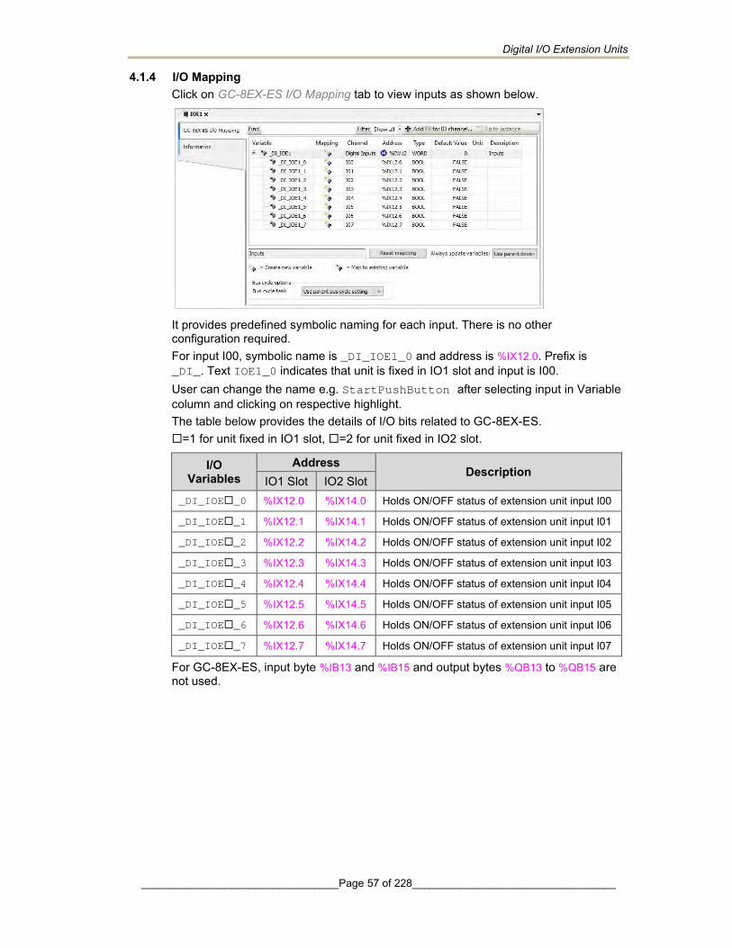
Digital I/O Extension Units
_________________________________Page 57 of 228__________________________________
4.1.4 I/O Mapping Click on GC-8EX-ES I/O Mapping tab to view inputs as shown below.
It provides predefined symbolic naming for each input. There is no other configuration required. For input I00, symbolic name is _DI_IOE1_0 and address is %IX12.0. Prefix is _DI_. Text IOE1_0 indicates that unit is fixed in IO1 slot and input is I00. User can change the name e.g. StartPushButton after selecting input in Variable column and clicking on respective highlight. The table below provides the details of I/O bits related to GC-8EX-ES. =1 for unit fixed in IO1 slot, =2 for unit fixed in IO2 slot.
I/O Variables
Address Description
IO1 Slot IO2 Slot _DI_IOE_0 %IX12.0 %IX14.0 Holds ON/OFF status of extension unit input I00
_DI_IOE_1 %IX12.1 %IX14.1 Holds ON/OFF status of extension unit input I01
_DI_IOE_2 %IX12.2 %IX14.2 Holds ON/OFF status of extension unit input I02
_DI_IOE_3 %IX12.3 %IX14.3 Holds ON/OFF status of extension unit input I03
_DI_IOE_4 %IX12.4 %IX14.4 Holds ON/OFF status of extension unit input I04
_DI_IOE_5 %IX12.5 %IX14.5 Holds ON/OFF status of extension unit input I05
_DI_IOE_6 %IX12.6 %IX14.6 Holds ON/OFF status of extension unit input I06
_DI_IOE_7 %IX12.7 %IX14.7 Holds ON/OFF status of extension unit input I07
For GC-8EX-ES, input byte %IB13 and %IB15 and output bytes %QB13 to %QB15 are not used.

Digital I/O Extension Units
_________________________________Page 58 of 228__________________________________
4.2 GC-6EYR-ES This is 6 Pt. Relay output extension unit. User can attach up to 2 I/O extension units on the back side of Main unit.
4.2.1 Specifications
Item Description Number of Outputs 6, 2 groups of 3 outputs each
Type of output Non latching normally open (NO) contact Electro-mechanical relay
Voltage rating 24 to 250 VAC, 47-63 Hz, 5-30 VDC
Current rating 500 mA at 250 VAC and 30 VDC per point1.5 A per common
Minimum load 1 mA
Contact life Electrical life Refer table and Life curve*
Mechanical life min 20, 000, 000 (180 cpm)
Response time OFF to ON 10 ms
ON to OFF 5 ms
Isolation Galvanic between output and internal circuit
Dielectric strength 3 KVrms (between coil and contact circuit) 0.75 KVrms (for open contact)
Method of termination 2 nos. 8-pin terminal blocks, fixed, screw type
Status indication On LCD screen on Main unit
Dimensions (in mm) 61.5 (W) x 75 (H) x 24.5 (D)
Weight (in grams) 60
Electrical life of relay
Voltage Current Type of load Electrical life (20 cpm)
250 VAC 1 A Resistive 500,000
Inductive 30,000
500 mA Resistive 10,00,000 Inductive 80,000
30 VDC 1 A Resistive 600,000
Inductive 150,000
500 mA Resistive 10,00,000 Inductive 3,80,000
The graph shown is provided by relay manufacturer specification sheet. There may be some degree of variation in relay characteristics depending on ambient and type of load. So this data should be used only for reference purpose.
*Life curve of Relay:
Switching capacity, A
No.
of O
pera
tions
, x10
^4
AC 125V resistive load DC 30V resistive load AC 250V resistive load
DC 30V T=7ms
AC 125V COS Ø=0.4 AC 250V COS Ø=0.4
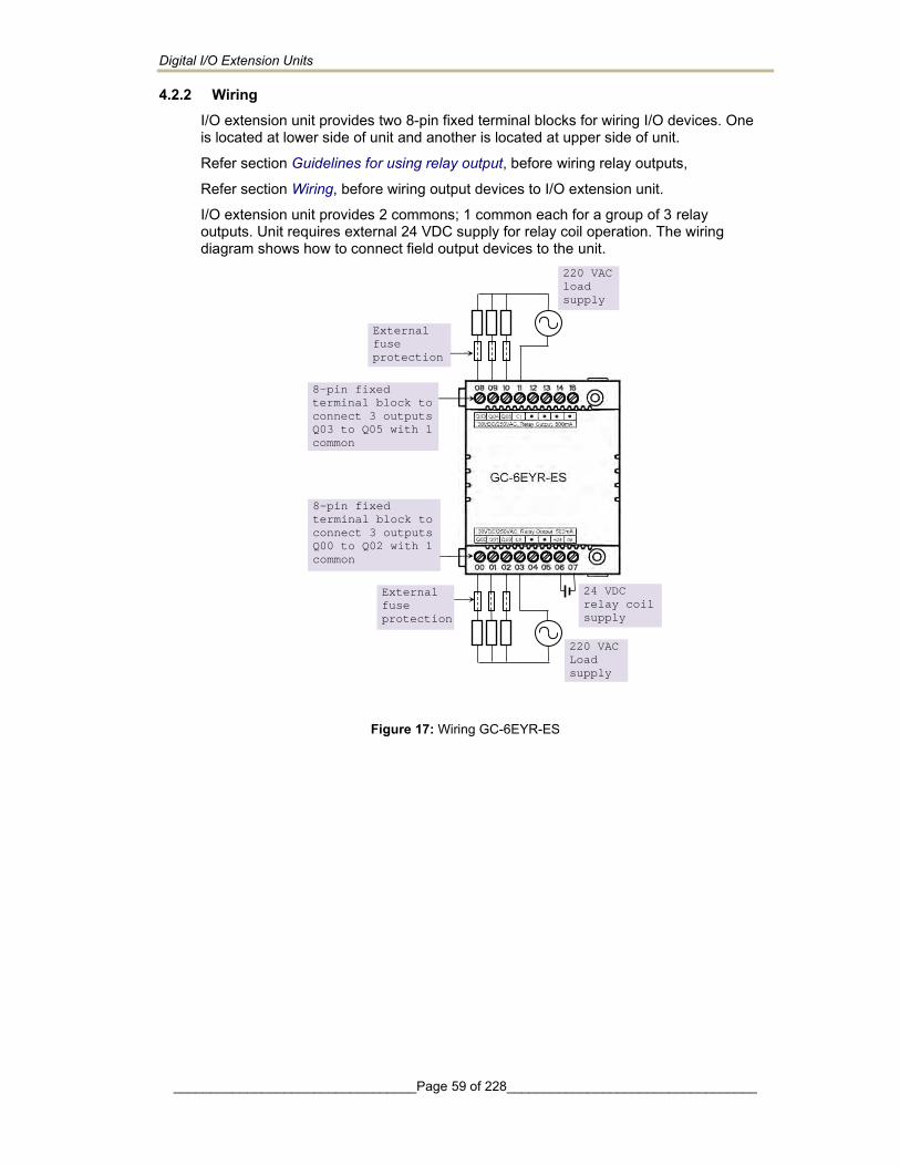
Digital I/O Extension Units
_________________________________Page 59 of 228__________________________________
4.2.2 Wiring I/O extension unit provides two 8-pin fixed terminal blocks for wiring I/O devices. One is located at lower side of unit and another is located at upper side of unit.
Refer section Guidelines for using relay output, before wiring relay outputs,
Refer section Wiring, before wiring output devices to I/O extension unit.
I/O extension unit provides 2 commons; 1 common each for a group of 3 relay outputs. Unit requires external 24 VDC supply for relay coil operation. The wiring diagram shows how to connect field output devices to the unit.
Figure 17: Wiring GC-6EYR-ES
External
fuse
protection
8-pin fixed
terminal block to
connect 3 outputs
Q03 to Q05 with 1
common
220 VAC
load
supply
8-pin fixed
terminal block to
connect 3 outputs
Q00 to Q02 with 1
common
24 VDC
relay coil
supply
External
fuse
protection
220 VAC
Load
supply

Digital I/O Extension Units
_________________________________Page 60 of 228__________________________________
4.2.3 Configuration and Programming For I/O Extension units, I/O memory map is fixed. GC-6EYR-ES consumes %IB12 and %QB12 when fixed in IO1 slot and %IB14 and %QB14 when fixed in IO2 slot. To plug extension device GC-6EYR-ES in selected slot, refer section Hardware Configuration. After plugging GC-6EYR-ES, <Empty> slot is replaced by IOE1 (GC-6EYR-ES) as shown below.
Similarly, after plugging GC-6EYR-ES in slot2, <Empty> slot is replaced by IOE2 (GC-6EYR-ES).
Click on “IOE1 (GC-6EYR-ES)”
to view I/O mapping and
information of GC-6EYR-ES.
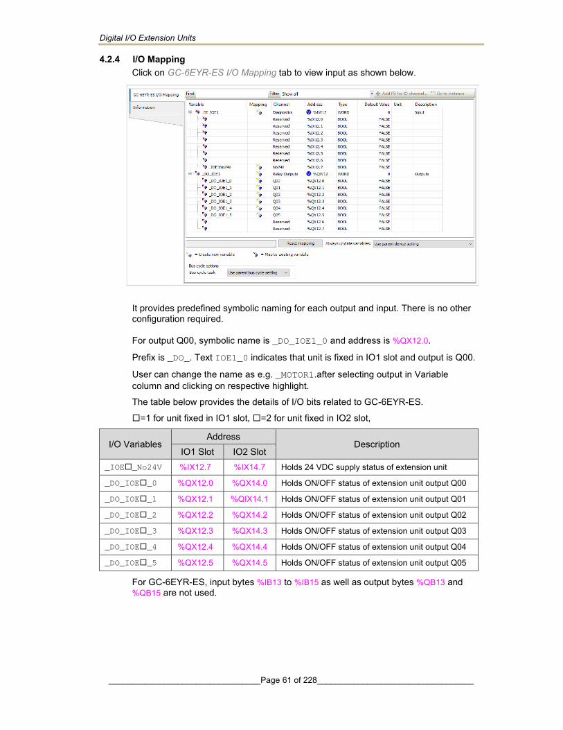
Digital I/O Extension Units
_________________________________Page 61 of 228__________________________________
4.2.4 I/O Mapping Click on GC-6EYR-ES I/O Mapping tab to view input as shown below.
It provides predefined symbolic naming for each output and input. There is no other configuration required.
For output Q00, symbolic name is _DO_IOE1_0 and address is %QX12.0.
Prefix is _DO_. Text IOE1_0 indicates that unit is fixed in IO1 slot and output is Q00.
User can change the name as e.g. _MOTOR1.after selecting output in Variable column and clicking on respective highlight.
The table below provides the details of I/O bits related to GC-6EYR-ES.
=1 for unit fixed in IO1 slot, =2 for unit fixed in IO2 slot,
I/O Variables Address
Description IO1 Slot IO2 Slot
_IOE_No24V %IX12.7 %IX14.7 Holds 24 VDC supply status of extension unit
_DO_IOE_0 %QX12.0 %QX14.0 Holds ON/OFF status of extension unit output Q00
_DO_IOE_1 %QX12.1 %QIX14.1 Holds ON/OFF status of extension unit output Q01
_DO_IOE_2 %QX12.2 %QX14.2 Holds ON/OFF status of extension unit output Q02
_DO_IOE_3 %QX12.3 %QX14.3 Holds ON/OFF status of extension unit output Q03
_DO_IOE_4 %QX12.4 %QX14.4 Holds ON/OFF status of extension unit output Q04
_DO_IOE_5 %QX12.5 %QX14.5 Holds ON/OFF status of extension unit output Q05
For GC-6EYR-ES, input bytes %IB13 to %IB15 as well as output bytes %QB13 and %QB15 are not used.

Digital I/O Extension Units
_________________________________Page 62 of 228__________________________________
4.3 GC-8ET-ESS
This I/O extension unit (GC-8ET-ESS) provides 4 point 24 VDC digital inputs and 4 point 24VDC transistor outputs. It allows sink or source type connections for 4 inputs and source type of connections for 4 outputs. It can be fixed in any IO slot on the back side of Main unit.
4.3.1 Specifications
Item Description
Digital Inputs (Sink/ Source type)
Number of Inputs 04
Mode of operation Sink or source, depends on connections
Voltage rating 24 VDC
ON / OFF voltage ON voltage: 18 VDC minimum OFF voltage: 5 VDC maximum
Current rating 6 mA at 24 VDC
OFF current 3.8 mA maximum
Input impedance 5.2 KΩ
Transition delay 10ms (Default filter time)
Digital Outputs (Source type)
Number of Outputs 04
Type of output Transistor source type
Voltage rating 24 VDC
Current rating 1.5 A per output, 1 common point. Paralleling of outputs is possible
ON voltage drop 0.6V DC maximum
OFF state leakage current 10 µA maximum
Response Time OFF to ON: 300 µs ON to OFF: 300 µs
Isolation 1.5 KV optical from internal bus
Detection No 24 VDC supply
Load supply 24 VDC
Reverse polarity protection

Digital I/O Extension Units
_________________________________Page 63 of 228__________________________________
GC-8ET-ESS specifications continue…
Item Description
General
I/O status indication On LCD screen on Main unit
Isolation Optical 1.5 KV between input and internal circuit Optical 1.5 KV between output and internal circuit
Protection Output Short circuit protection. Fast demagnetization for inductive loads
Method of termination For inputs, 1 no., 8-pin terminal block (fixed, screw type) located at upper side of unit
For outputs, 1 no., 8-pin terminal block (fixed, screw type) located at lower side of unit.
Dimensions (in mm 61.5 (W) x 75 (H) x 24.5 (D)
Weight (in grams) 60
4.3.2 Wiring I/O extension unit provides two 8-pin fixed terminal blocks for wiring I/O devices. One is located at lower side of unit is for transistor (source type) outputs and another is located at upper side of unit is for digital (sink/ source type) inputs. As 1 common is provided for a group of 4 inputs, all the inputs can be either connected for source type of input connection or sink type of input connection at a time as shown in figure below. Figure also shows connection of transistor outputs Q00 to Q03 as source type of outputs.
Figure 18: Wiring GC-8ET-ESS
24 VDC
Load
supply +
8-pin fixed
terminal block to
connect 4 inputs
I00 to I03 with 1
common
8-pin fixed
terminal block to
connect 4 outputs
Q00 to Q03
GC-8ET-ESS
SINK type
connection +
+
-
- 24VDC
GC-8ET-ESS
SOURCE type
connection -
24VDC
+
- 24VDC
24 VDC
Load
supply -

Digital I/O Extension Units
_________________________________Page 64 of 228__________________________________
4.3.3 Configuration and Programming For I/O Extension units, I/O memory map is fixed. GC-8ET-ESS consumes %IB12 and %QB12 when fixed in IO1 slot and %IB14 and %QB14 when fixed in IO2 slot. To plug extension device GC-8ET-ESS in selected slot, refer section Hardware Configuration. After plugging GC-8ET-ESS, <Empty> slot is replaced by IOE1 (GC-8ET-ESS) as shown below.
Similarly, after plugging GC-8ET-ESS in slot2, <Empty> slot is replaced by IOE2 (GC-8ET-ESS).
Click on “IOE1 (GC-8ET-ESS)”
to view I/O mapping and
information of GC-8ET-ESS.
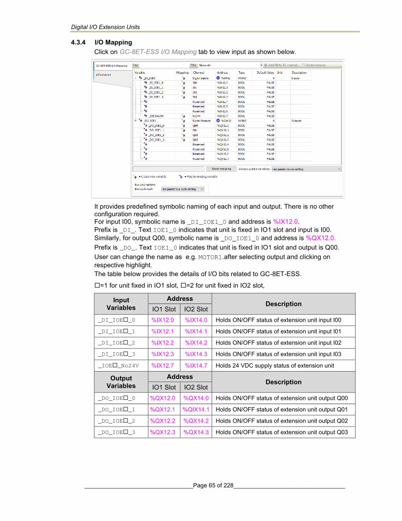
Digital I/O Extension Units
_________________________________Page 65 of 228__________________________________
4.3.4 I/O Mapping Click on GC-8ET-ESS I/O Mapping tab to view input as shown below.
It provides predefined symbolic naming of each input and output. There is no other configuration required. For input I00, symbolic name is _DI_IOE1_0 and address is %IX12.0. Prefix is _DI_. Text IOE1_0 indicates that unit is fixed in IO1 slot and input is I00. Similarly, for output Q00, symbolic name is _DO_IOE1_0 and address is %QX12.0. Prefix is _DO_. Text IOE1_0 indicates that unit is fixed in IO1 slot and output is Q00. User can change the name as e.g. MOTOR1.after selecting output and clicking on respective highlight. The table below provides the details of I/O bits related to GC-8ET-ESS.
=1 for unit fixed in IO1 slot, =2 for unit fixed in IO2 slot,
Input Variables
Address Description
IO1 Slot IO2 Slot _DI_IOE_0 %IX12.0 %IX14.0 Holds ON/OFF status of extension unit input I00
_DI_IOE_1 %IX12.1 %IX14.1 Holds ON/OFF status of extension unit input I01
_DI_IOE_2 %IX12.2 %IX14.2 Holds ON/OFF status of extension unit input I02
_DI_IOE_3 %IX12.3 %IX14.3 Holds ON/OFF status of extension unit input I03
_IOE_No24V %IX12.7 %IX14.7 Holds 24 VDC supply status of extension unit
Output Variables
Address Description
IO1 Slot IO2 Slot _DO_IOE_0 %QX12.0 %QX14.0 Holds ON/OFF status of extension unit output Q00
_DO_IOE_1 %QX12.1 %QIX14.1 Holds ON/OFF status of extension unit output Q01
_DO_IOE_2 %QX12.2 %QX14.2 Holds ON/OFF status of extension unit output Q02
_DO_IOE_3 %QX12.3 %QX14.3 Holds ON/OFF status of extension unit output Q03

Analog I/O Extension Units
_________________________________Page 66 of 228__________________________________
5 Analog I/O Extension Units
Analog input extension units convert input voltage, current, RTD and thermocouple readings into equivalent binary values.
Analog output extension unit takes digital value data from processor and generates equivalent analog output voltage or current as per channel configuration.
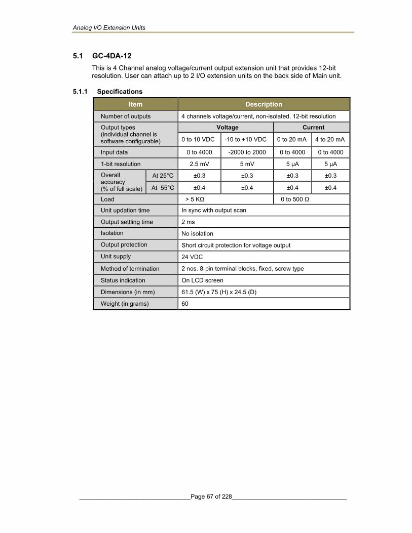
Analog I/O Extension Units
_________________________________Page 67 of 228__________________________________
5.1 GC-4DA-12 This is 4 Channel analog voltage/current output extension unit that provides 12-bit resolution. User can attach up to 2 I/O extension units on the back side of Main unit.
5.1.1 Specifications
Item Description Number of outputs 4 channels voltage/current, non-isolated, 12-bit resolution
Output types (individual channel is software configurable)
Voltage Current
0 to 10 VDC -10 to +10 VDC 0 to 20 mA 4 to 20 mA
Input data 0 to 4000 -2000 to 2000 0 to 4000 0 to 4000
1-bit resolution 2.5 mV 5 mV 5 µA 5 µA
Overall accuracy (% of full scale)
At 25°C ±0.3 ±0.3 ±0.3 ±0.3
At 55°C ±0.4 ±0.4 ±0.4 ±0.4
Load > 5 KΩ 0 to 500 Ω
Unit updation time In sync with output scan
Output settling time 2 ms
Isolation No isolation
Output protection Short circuit protection for voltage output
Unit supply 24 VDC
Method of termination 2 nos. 8-pin terminal blocks, fixed, screw type
Status indication On LCD screen
Dimensions (in mm) 61.5 (W) x 75 (H) x 24.5 (D)
Weight (in grams) 60
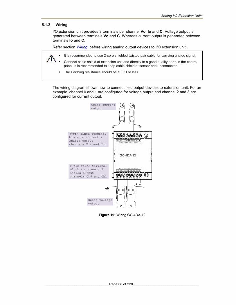
Analog I/O Extension Units
_________________________________Page 68 of 228__________________________________
8-pin fixed terminal
block to connect 2
Analog output
channels Ch2 and Ch3
8-pin fixed terminal
block to connect 2
Analog output
channels Ch0 and Ch1
+ +
Using current
output
Using voltage
output
5.1.2 Wiring I/O extension unit provides 3 terminals per channel Vo, Io and C. Voltage output is generated between terminals Vo and C. Whereas current output is generated between terminals Io and C.
Refer section Wiring, before wiring analog output devices to I/O extension unit.
The wiring diagram shows how to connect field output devices to extension unit. For an example, channel 0 and 1 are configured for voltage output and channel 2 and 3 are configured for current output.
Figure 19: Wiring GC-4DA-12
It is recommended to use 2-core shielded twisted pair cable for carrying analog signal.
Connect cable shield at extension unit end directly to a good quality earth in the control panel. It is recommended to keep cable shield at sensor end unconnected.
The Earthing resistance should be 100 Ω or less.
V V
+

Analog I/O Extension Units
_________________________________Page 69 of 228__________________________________
5.1.3 Configuration and Programming For I/O Extension units, I/O memory map is fixed. GC-4DA-12 consumes %IB12 when fixed in IO1 slot and %IB14 when fixed in IO2 slot. To plug extension device GC-4DA-12 in selected slot, refer section Hardware Configuration. After plugging GC-4DA-12, <Empty> slot is replaced by IOE1 (GC-4DA-12) as shown below.
Similarly, after plugging GC-4DA-12 in slot2, <Empty> slot is replaced by IOE2 (GC-4DA-12).
Click on “IOE1 (GC-4DA-12)”
to view parameter
configuration, I/O mapping
and IEC Objects of GC-4DA-12.

Analog I/O Extension Units
_________________________________Page 70 of 228__________________________________
5.1.3.1 Parameter Configuration For parameters configuration of extension GC-4DA-12, click on device ‘GC-4DA-12’ → Parameters Configuration. Set individual channel parameters using list of parameters provided under ‘Channel 0’ to ‘Channel 3’. As shown below, parameters configuration is explained for Channel 0.
Sr. No. Parameter Options Description Analog Output configuration
1 Output Type Voltage 0 to 10V (Default) Voltage -10 to +10V Current 0 to 20mA Current 4 to 20mA
Selection for type of output as per application requirement.
Engineering scaling [Enable Scaling] applicable for all supported output types
2 Enable Scaling Enable/ Disable Check ‘Enable’ to apply engineering scaling to Channel 0.
3 Engineering scale
For Voltage 0 to 10V output type, Min: 0 V and Max: 10 V. For Voltage -10 to +10V output type, Min: -10 V and Max: 10V. For Current 0 to 20mA output type, Min: 0 mA and Max: 20 mA For Current 4 to 20mA output type, Min : 4 mA and Max : 20 mA
This parameter holds minimum and -maximum values of output signal as per configured output type.
4 Signal scale Default values: Min: 0 and Max: 100 Supported range: -64000.0 to 64000.0 for both Min- Max settings
User can set minimum and maximum values of engineering scaling as per application requirement. This parameter in not editable
Similarly, user can configure parameters for Channel 1 to Channel 3 using tabs ‘Channel 1’, ‘Channel 2’ and ‘Channel 3’ as shown above.
1
2
3 4
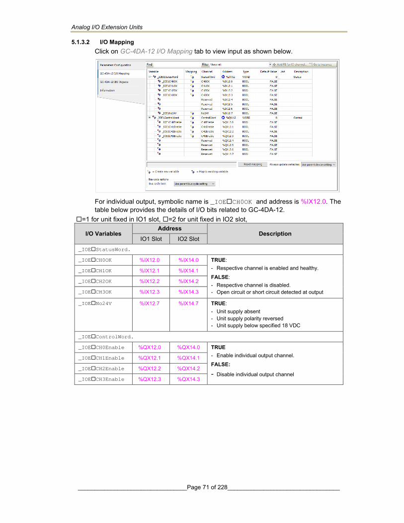
Analog I/O Extension Units
_________________________________Page 71 of 228__________________________________
5.1.3.2 I/O Mapping Click on GC-4DA-12 I/O Mapping tab to view input as shown below.
For individual output, symbolic name is _IOECH0OK and address is %IX12.0. The table below provides the details of I/O bits related to GC-4DA-12.
=1 for unit fixed in IO1 slot, =2 for unit fixed in IO2 slot,
I/O Variables Address
Description IO1 Slot IO2 Slot
_IOEStatusWord.
_IOECH0OK %IX12.0 %IX14.0 TRUE: - Respective channel is enabled and healthy. FALSE: - Respective channel is disabled. - Open circuit or short circuit detected at output
_IOECH1OK %IX12.1 %IX14.1
_IOECH2OK %IX12.2 %IX14.2
_IOECH3OK %IX12.3 %IX14.3
_IOENo24V %IX12.7 %IX14.7 TRUE: - Unit supply absent - Unit supply polarity reversed - Unit supply below specified 18 VDC
_IOEControlWord.
_IOECH0Enable %QX12.0 %QX14.0 TRUE - Enable individual output channel. FALSE:
- Disable individual output channel
_IOECH1Enable %QX12.1 %QX14.1
_IOECH2Enable %QX12.2 %QX14.2
_IOECH3Enable %QX12.3 %QX14.3
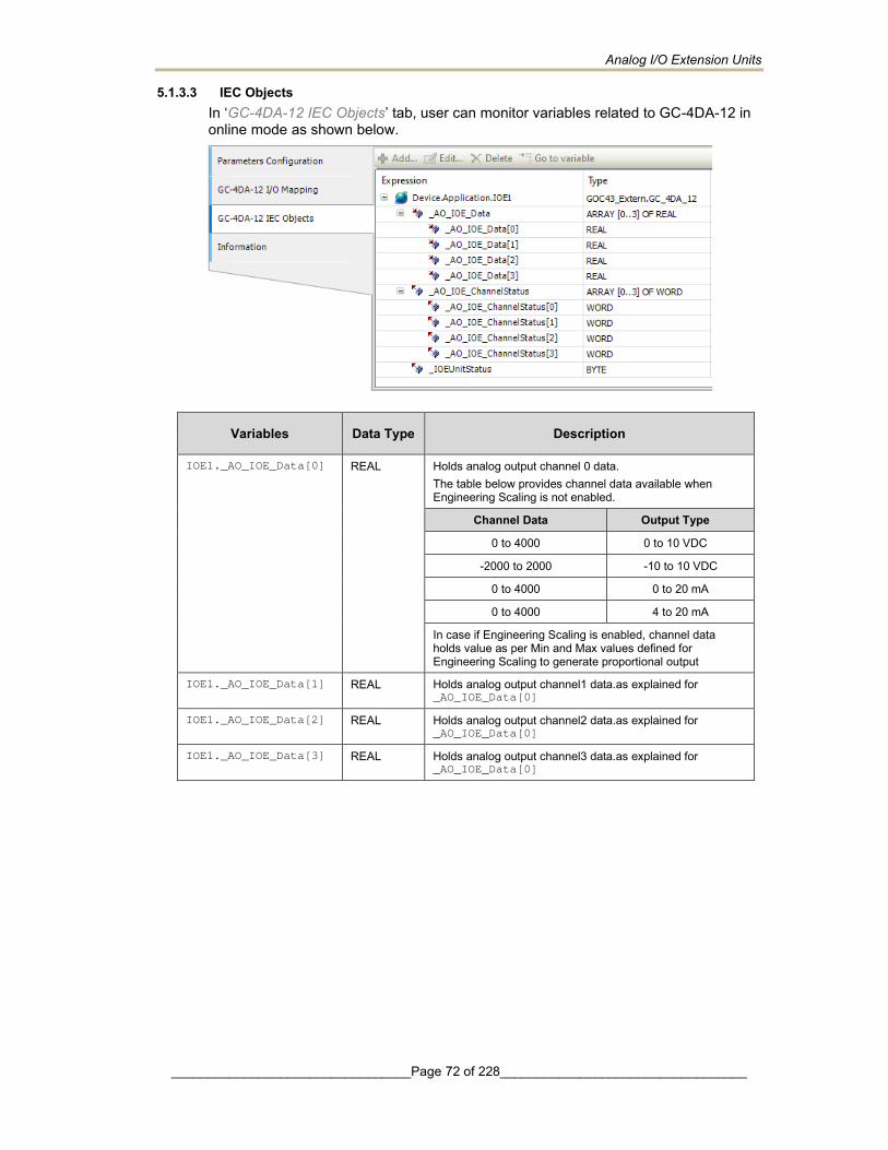
Analog I/O Extension Units
_________________________________Page 72 of 228__________________________________
5.1.3.3 IEC Objects In ‘GC-4DA-12 IEC Objects’ tab, user can monitor variables related to GC-4DA-12 in online mode as shown below.
Variables Data Type Description
IOE1._AO_IOE_Data[0] REAL Holds analog output channel 0 data. The table below provides channel data available when Engineering Scaling is not enabled.
Channel Data Output Type
0 to 4000 0 to 10 VDC
-2000 to 2000 -10 to 10 VDC
0 to 4000 0 to 20 mA
0 to 4000 4 to 20 mA
In case if Engineering Scaling is enabled, channel data holds value as per Min and Max values defined for Engineering Scaling to generate proportional output
IOE1._AO_IOE_Data[1] REAL Holds analog output channel1 data.as explained for _AO_IOE_Data[0]
IOE1._AO_IOE_Data[2] REAL Holds analog output channel2 data.as explained for _AO_IOE_Data[0]
IOE1._AO_IOE_Data[3] REAL Holds analog output channel3 data.as explained for _AO_IOE_Data[0]
Analog I/O Extension Units
_________________________________Page 73 of 228__________________________________
IOE1._AO_IOE_Channe
lStatus
ARRAY [0..3] OF WORD
Holds status of channels if Extended Settings is enabled. Each array element is assigned for individual channel e.g._IOEChannelStatus[0] holds status of channel 0. Details of bits of status word as follows
Bit No Details
0 Channel enable status 0 - Disabled 1 - Enabled
1 Channel configuration 0 - Valid 1 - Invalid
2 Channel data (written at _AO_IOE_Data[n]) is out of range as defined by default resolution or engineering scaling.
0: Data count valid 1: Data count invalid
3 Open circuit or short circuit detected at output 0 - No open circuit 1 - Open circuit
4 - 15 Reserved
IOE1._IOEUnitStatus BYTE This variable holds I/O extension unit state as follows
Bit No Details
0 No unit is fixed in I/O slot or No unit is detected in I/O slot by CPU
1 Mismatch between configured unit and attached unit in I/O slot.
2 Configured unit is detected, and it is in configuration state.
100 Configured unit is detected, configured successfully and is in running condition.
Similarly, user can access IEC objects of I/O extension unit configured in I/O extension slot2 with IOE2._<VariableName>.

Analog I/O Extension Units
_________________________________Page 74 of 228__________________________________
5.2 GC-4A-12 This is mixed analog I/O extension unit that provides 2 Ch., 16-bit, analog voltage/ current input and 2 Ch., 12-bit, analog voltage/ current output. User can attach up to 2 I/O extension units that can be fixed in IO1 slot and IO2 slot to the Main unit.
5.2.1 Specifications
Item Description Analog Input
Number of input channels 2 channels voltage/current input, single ended/ differential, non-isolated, 16-bit resolution
Input types (User configurable)
Voltage Current
0 to 10 VDC ±10 VDC 0 to 20 mA 4 to 20 mA
Output data 0 to 64000 -32000 to 32000 0 to 64000
1-bit Resolution 0.15 mV 0.3 mV 0.3 µA 0.3 µA
*Overall accuracy (% of full scale)
At 25°C ±0.1 ±0.1 ±0.2 ±0.2
At 55°C ±0.3 ±0.3 ±0.4 ±0.4
Input impedance 1 MΩ 124 Ω
**Channel updation time
Channel data updation = Controller scan time x Number of averaging samples. Channel data updation = Controller scan time + (Digital Filter Time Constant*5) minimum
Absolute maximum input ±30 VDC/ 30 mA
Open circuit detection For 4 to 20mA input type
Channel Protection PTC for over current protection for current input up to 70 mA.
Isolation No isolation from internal logic
Method of termination 2 nos. 8-pin terminal blocks, fixed, screw type
Connection terminals Iin, Vin and Cn for each analog input channel
* Overall accuracy mentioned is applicable for digital filter setting of 50 msec.
** Channel updation time depends on digital filter time constant setting and number of averaging samples.
Analog I/O Extension Units
_________________________________Page 75 of 228__________________________________
Item Description
Analog Output
Number of output channels
2 channels voltage/current output, non-isolated, 12-bit resolution
Output types (User configurable)
Voltage Current
0 to 10 VDC ±10 VDC 0 to 20 mA 4 to 20 mA
Input data 0 to 4000 -2000 to 2000 0 to 4000
1-bit Resolution 2.5 mV 5 mV 5 µA 5 µA
Overall accuracy (% of full scale)
At 25°C ±0.05 ±0.05 ±0.05 ±0.05
At 55°C ±0.1 ±0.1 ±0.1 ±0.1
Channel updation time 2 msec on-board
Output settling time 2 msec typically
Output load Voltage output: > 5 KΩ Current output: 0 to 500 Ω
Open circuit detection Supported
Channel Protection Short circuit protection for voltage output
Connection terminals Von, Ion and Cn for analog output channel
Unit supply 18 to 30 VDC at terminals +24V and 0V
Unit supply protection No 24V detection Reverse polarity protection
Dimensions (in mm) 61.5 (W) x 75 (H) x 24.5 (D)
Weight (in grams) 60
5.2.2 Wiring I/O extension unit provides 3 terminals for individual input channel and output channel as below.
1. For Analog inputs, unit provides 3 terminals per channel Iin, Vin and Cn.
- Voltage input is connected between terminals Vin and Cn.
- Current input is connected between terminals Iin and Cn with and Vin and Iin connected together externally.
2. For Analog outputs, unit provides 3 terminals per channel Von, Ion and Cn.
- Voltage output is generated between terminals Von and Cn.
- Current output is generated between terminals Ion and Cn. 3. External 24 VDC supply is required for analog output. It is connected between
terminals +24V and 0V.

Analog I/O Extension Units
_________________________________Page 76 of 228__________________________________
The wiring diagram shows how to connect field input devices to I/O extension unit. For an example, for analog inputs, channel 0 is connected to current input and channel 1 is connected to voltage input. For analog outputs, channel 0 is connected for voltage output and channel 1 is connected for current output. External unit supply is connected between terminals +24V and 0V. Refer section Wiring, before wiring analog input sensors and actuators to I/O extension unit.
Figure 20: Wiring GC-4A-12
It is recommended to use 2-core shielded twisted pair cable for carrying analog signal. Connect cable shield at I/O extension unit end directly to a good quality earth. It is
recommended to keep cable shield at sensor end unconnected. The Earthing resistance should be 100 Ω or less.
No over voltage
protection provided
for external 24VDC
module supply
Current
input
V + Voltage
input
+ V Voltage
output
Current
output
+
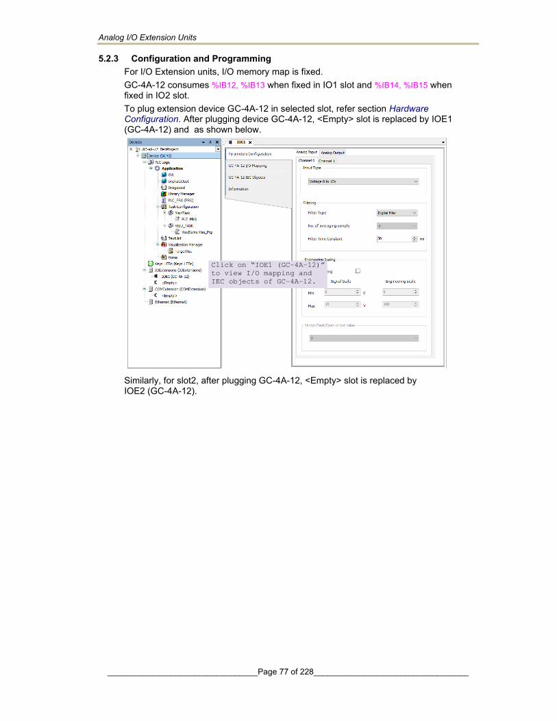
Analog I/O Extension Units
_________________________________Page 77 of 228__________________________________
5.2.3 Configuration and Programming For I/O Extension units, I/O memory map is fixed. GC-4A-12 consumes %IB12, %IB13 when fixed in IO1 slot and %IB14, %IB15 when fixed in IO2 slot. To plug extension device GC-4A-12 in selected slot, refer section Hardware Configuration. After plugging device GC-4A-12, <Empty> slot is replaced by IOE1 (GC-4A-12) and as shown below. Similarly, for slot2, after plugging GC-4A-12, <Empty> slot is replaced by IOE2 (GC-4A-12).
Click on “IOE1 (GC-4A-12)”
to view I/O mapping and
IEC objects of GC-4A-12.

Analog I/O Extension Units
_________________________________Page 78 of 228__________________________________
5.2.3.1 Parameter Configuration For parameters configuration of GC-4A-12, double click on device ‘IOE1 (GC-4A-12) → Parameters Configuration. For analog inputs, set individual channel parameters using tabs ‘Analog Input → ‘Channel 0’ and ‘Channel 1’. Parameters configuration is explained for ‘Analog Input → ‘Channel 0’ as shown below.
Sr. No. Parameter Options Description Analog Input configuration
1 Input type Voltage 0 to 10V (Default) Voltage -10 to +10V Current 0 to 20mA Current 4 to 20mA
Selection for type of input as per application requirement.
2 Filter type No Filter Averaging Digital Filter (Default)
Selection for signal conditioning by software filtering
3 No. of averaging sample
4 (Default) 8 16 32
For filter type as ‘Averaging’, user can select number of averaging samples using drop-down.
4 Filter time constant
Default value: 50 ms Supported range: 10 to 5000 ms
For filter type as ‘Digital Filter’, user can set filter time constant in msec.
1
2
3
4
6 7 5
8
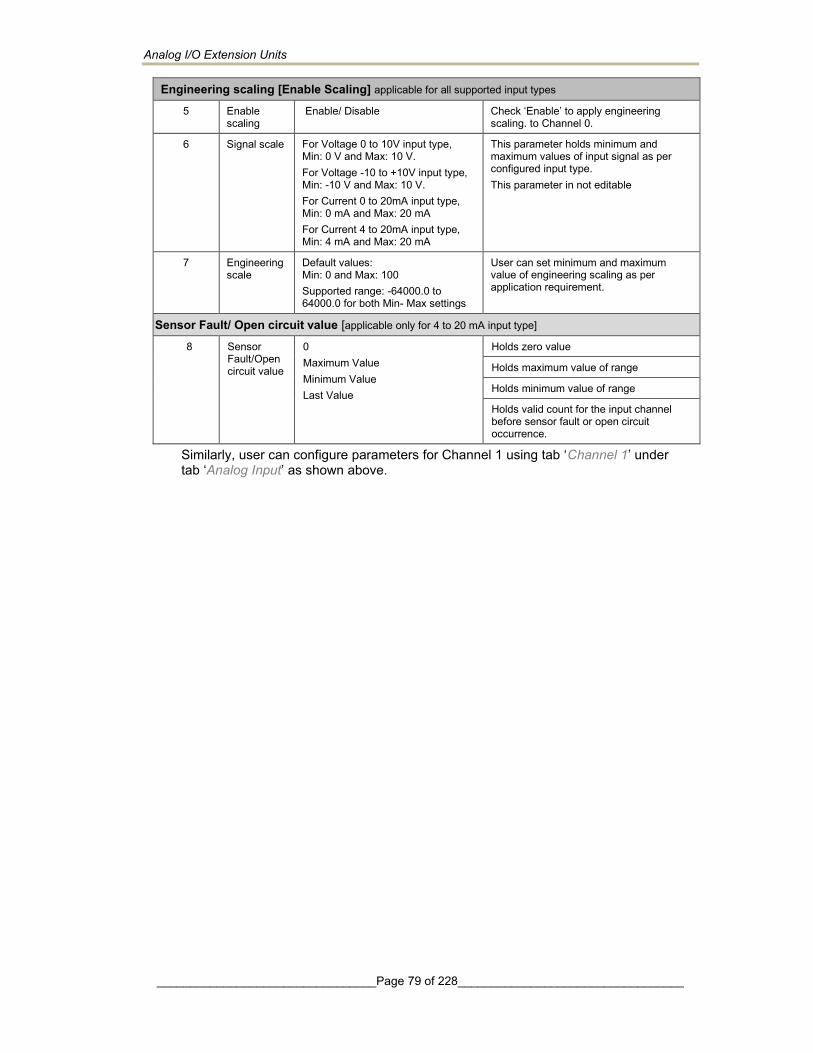
Analog I/O Extension Units
_________________________________Page 79 of 228__________________________________
Engineering scaling [Enable Scaling] applicable for all supported input types
5 Enable scaling
Enable/ Disable Check ‘Enable’ to apply engineering scaling. to Channel 0.
6 Signal scale For Voltage 0 to 10V input type, Min: 0 V and Max: 10 V. For Voltage -10 to +10V input type, Min: -10 V and Max: 10 V. For Current 0 to 20mA input type, Min: 0 mA and Max: 20 mA For Current 4 to 20mA input type, Min: 4 mA and Max: 20 mA
This parameter holds minimum and maximum values of input signal as per configured input type. This parameter in not editable
7 Engineering scale
Default values: Min: 0 and Max: 100 Supported range: -64000.0 to 64000.0 for both Min- Max settings
User can set minimum and maximum value of engineering scaling as per application requirement.
Sensor Fault/ Open circuit value [applicable only for 4 to 20 mA input type] 8 Sensor
Fault/Open circuit value
0 Maximum Value Minimum Value Last Value
Holds zero value
Holds maximum value of range
Holds minimum value of range
Holds valid count for the input channel before sensor fault or open circuit occurrence.
Similarly, user can configure parameters for Channel 1 using tab ‘Channel 1’ under tab ‘Analog Input’ as shown above.

Analog I/O Extension Units
_________________________________Page 80 of 228__________________________________
For analog outputs, set individual channel parameters using tabs ‘Analog Output → ‘Channel 0’ and ‘Channel 1’. Parameters configuration is explained for ‘Analog Output → ‘Channel 0’ as shown below.
Sr. No. Parameter Options Description Analog Output configuration
1 Output Type Voltage 0 to 10V (Default) Voltage -10 to +10V Current 0 to 20mA Current 4 to 20mA
Selection for type of output as per application requirement.
Engineering scaling [Enable Scaling] applicable for all supported output types
2 Enable Scaling Enable/ Disable Check ‘Enable’ to apply engineering scaling to Channel 0.
3 Engineering scale For Voltage 0 to 10V output type, Min: 0 V and Max: 10 V. For Voltage -10 to +10V output type, Min: -10 V and Max: 10V. For Current 0 to 20mA output type, Min: 0 mA and Max: 20 mA For Current 4 to 20mA output type, Min : 4 mA and Max : 20 mA
This parameter holds minimum and -maximum values of output signal as per configured output type.
4 Signal scale Default values: Min: 0 and Max: 100 Supported range: -64000.0 to 64000.0 for both Min- Max settings
User can set minimum and maximum values of engineering scaling as per application requirement. This parameter in not editable
Similarly, user can configure parameters for Channel 1 using tab ‘Channel 1’ under tab ‘Analog Output’ as shown above.
1
2 3 4
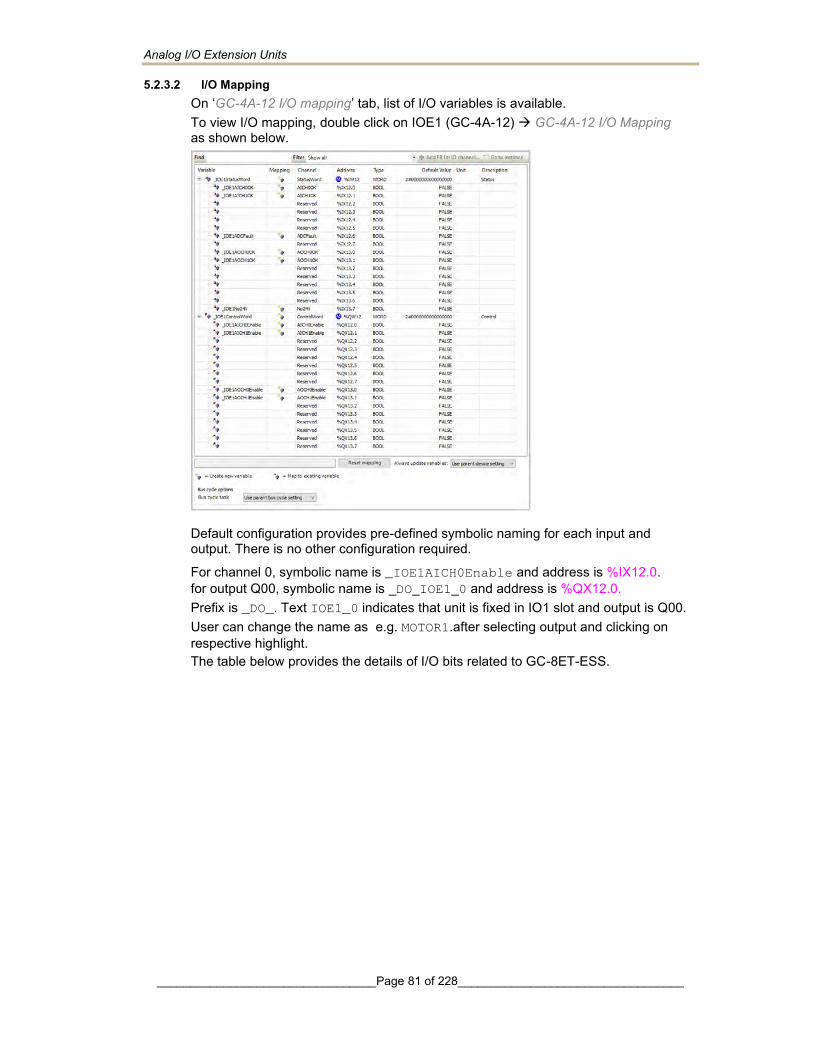
Analog I/O Extension Units
_________________________________Page 81 of 228__________________________________
5.2.3.2 I/O Mapping On ‘GC-4A-12 I/O mapping’ tab, list of I/O variables is available. To view I/O mapping, double click on IOE1 (GC-4A-12) → GC-4A-12 I/O Mapping as shown below.
Default configuration provides pre-defined symbolic naming for each input and output. There is no other configuration required.
For channel 0, symbolic name is _IOE1AICH0Enable and address is %IX12.0. for output Q00, symbolic name is _DO_IOE1_0 and address is %QX12.0. Prefix is _DO_. Text IOE1_0 indicates that unit is fixed in IO1 slot and output is Q00. User can change the name as e.g. MOTOR1.after selecting output and clicking on respective highlight. The table below provides the details of I/O bits related to GC-8ET-ESS.
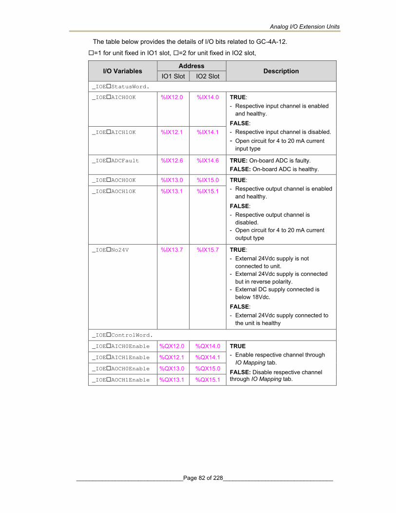
Analog I/O Extension Units
_________________________________Page 82 of 228__________________________________
The table below provides the details of I/O bits related to GC-4A-12.
=1 for unit fixed in IO1 slot, =2 for unit fixed in IO2 slot,
I/O Variables Address
Description IO1 Slot IO2 Slot
_IOEStatusWord. _IOEAICH0OK %IX12.0 %IX14.0 TRUE:
- Respective input channel is enabled and healthy.
FALSE: - Respective input channel is disabled. - Open circuit for 4 to 20 mA current
input type
_IOEAICH1OK %IX12.1 %IX14.1
_IOEADCFault %IX12.6 %IX14.6 TRUE: On-board ADC is faulty. FALSE: On-board ADC is healthy.
_IOEAOCH0OK %IX13.0 %IX15.0 TRUE: - Respective output channel is enabled
and healthy. FALSE: - Respective output channel is
disabled. - Open circuit for 4 to 20 mA current
output type
_IOEAOCH1OK %IX13.1 %IX15.1
_IOENo24V %IX13.7 %IX15.7 TRUE: - External 24Vdc supply is not
connected to unit. - External 24Vdc supply is connected
but in reverse polarity. - External DC supply connected is
below 18Vdc. FALSE: - External 24Vdc supply connected to
the unit is healthy
_IOEControlWord.
_IOEAICH0Enable %QX12.0 %QX14.0 TRUE - Enable respective channel through
IO Mapping tab. FALSE: Disable respective channel through IO Mapping tab.
_IOEAICH1Enable %QX12.1 %QX14.1
_IOEAOCH0Enable %QX13.0 %QX15.0
_IOEAOCH1Enable %QX13.1 %QX15.1
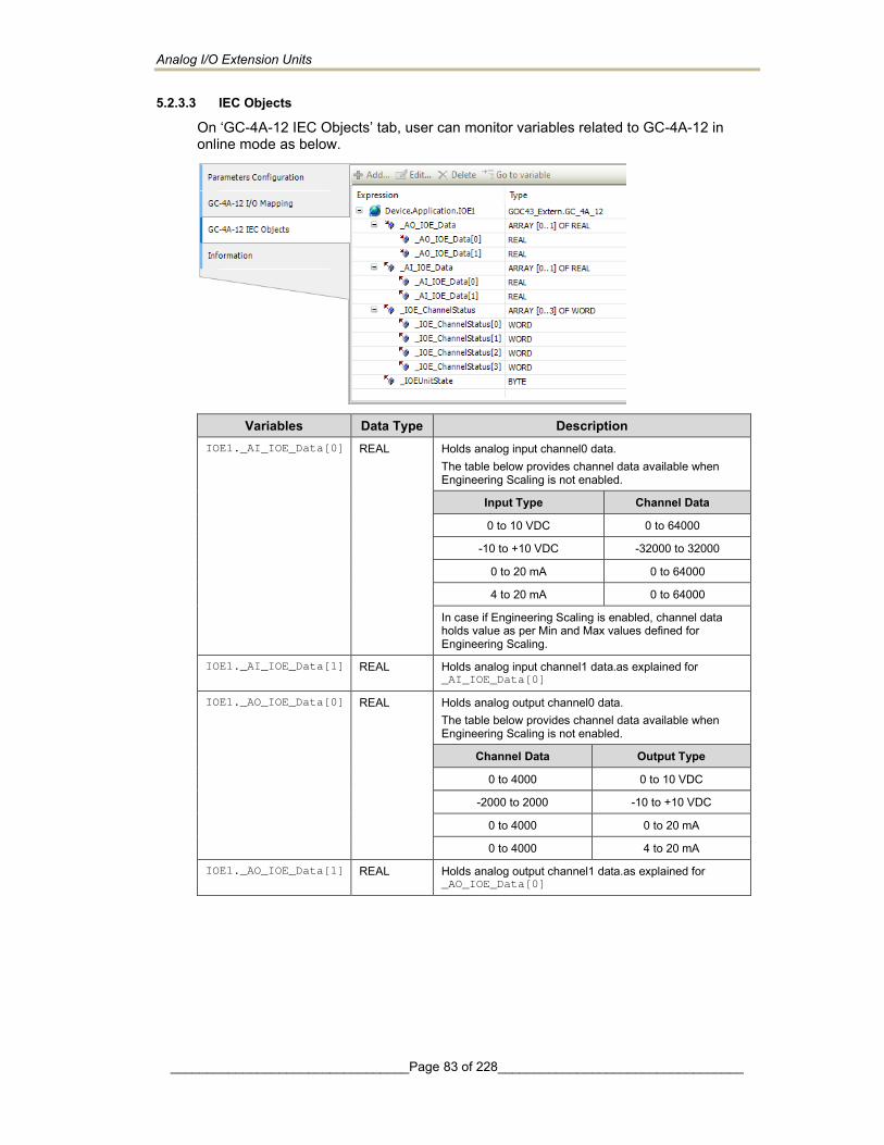
Analog I/O Extension Units
_________________________________Page 83 of 228__________________________________
5.2.3.3 IEC Objects
On ‘GC-4A-12 IEC Objects’ tab, user can monitor variables related to GC-4A-12 in online mode as below.
Variables Data Type Description IOE1._AI_IOE_Data[0] REAL Holds analog input channel0 data.
The table below provides channel data available when Engineering Scaling is not enabled.
Input Type Channel Data
0 to 10 VDC 0 to 64000
-10 to +10 VDC -32000 to 32000
0 to 20 mA 0 to 64000
4 to 20 mA 0 to 64000
In case if Engineering Scaling is enabled, channel data holds value as per Min and Max values defined for Engineering Scaling.
IOE1._AI_IOE_Data[1] REAL Holds analog input channel1 data.as explained for _AI_IOE_Data[0]
IOE1._AO_IOE_Data[0] REAL Holds analog output channel0 data. The table below provides channel data available when Engineering Scaling is not enabled.
Channel Data Output Type
0 to 4000 0 to 10 VDC
-2000 to 2000 -10 to +10 VDC
0 to 4000 0 to 20 mA
0 to 4000 4 to 20 mA
IOE1._AO_IOE_Data[1] REAL Holds analog output channel1 data.as explained for _AO_IOE_Data[0]
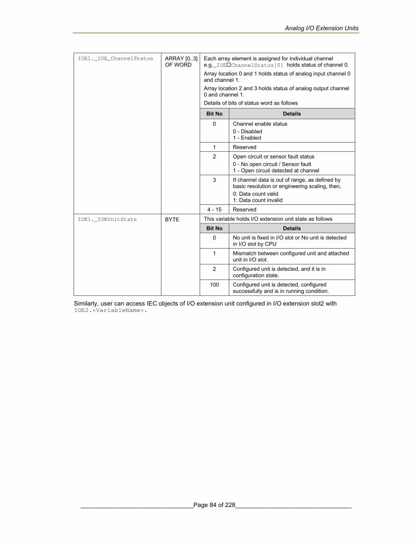
Analog I/O Extension Units
_________________________________Page 84 of 228__________________________________
IOE1._IOE_ChannelStatus ARRAY [0..3] OF WORD
Each array element is assigned for individual channel e.g._IOEChannelStatus[0] holds status of channel 0. Array location 0 and 1 holds status of analog input channel 0 and channel 1. Array location 2 and 3 holds status of analog output channel 0 and channel 1. Details of bits of status word as follows
Bit No Details
0 Channel enable status 0 - Disabled 1 - Enabled
1 Reserved 2 Open circuit or sensor fault status
0 - No open circuit / Sensor fault 1 - Open circuit detected at channel
3 If channel data is out of range, as defined by basic resolution or engineering scaling, then, 0: Data count valid 1: Data count invalid
4 - 15 Reserved
IOE1._IOEUnitState BYTE This variable holds I/O extension unit state as follows
Bit No Details 0 No unit is fixed in I/O slot or No unit is detected
in I/O slot by CPU
1 Mismatch between configured unit and attached unit in I/O slot.
2 Configured unit is detected, and it is in configuration state.
100 Configured unit is detected, configured successfully and is in running condition.
Similarly, user can access IEC objects of I/O extension unit configured in I/O extension slot2 with IOE2.<VariableName>.
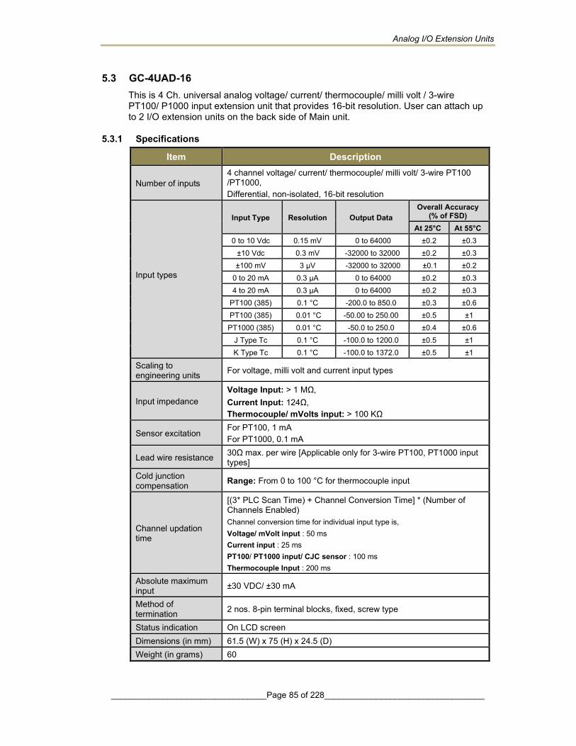
Analog I/O Extension Units
_________________________________Page 85 of 228__________________________________
5.3 GC-4UAD-16 This is 4 Ch. universal analog voltage/ current/ thermocouple/ milli volt / 3-wire PT100/ P1000 input extension unit that provides 16-bit resolution. User can attach up to 2 I/O extension units on the back side of Main unit.
5.3.1 Specifications
Item Description
Number of inputs 4 channel voltage/ current/ thermocouple/ milli volt/ 3-wire PT100 /PT1000, Differential, non-isolated, 16-bit resolution
Input types
Input Type Resolution Output Data Overall Accuracy
(% of FSD) At 25°C At 55°C
0 to 10 Vdc 0.15 mV 0 to 64000 ±0.2 ±0.3 ±10 Vdc 0.3 mV -32000 to 32000 ±0.2 ±0.3 ±100 mV 3 µV -32000 to 32000 ±0.1 ±0.2
0 to 20 mA 0.3 µA 0 to 64000 ±0.2 ±0.3 4 to 20 mA 0.3 µA 0 to 64000 ±0.2 ±0.3
PT100 (385) 0.1 °C -200.0 to 850.0 ±0.3 ±0.6 PT100 (385) 0.01 °C -50.00 to 250.00 ±0.5 ±1 PT1000 (385) 0.01 °C -50.0 to 250.0 ±0.4 ±0.6
J Type Tc 0.1 °C -100.0 to 1200.0 ±0.5 ±1 K Type Tc 0.1 °C -100.0 to 1372.0 ±0.5 ±1
Scaling to engineering units For voltage, milli volt and current input types
Input impedance Voltage Input: > 1 MΩ, Current Input: 124Ω, Thermocouple/ mVolts input: > 100 KΩ
Sensor excitation For PT100, 1 mA For PT1000, 0.1 mA
Lead wire resistance 30Ω max. per wire [Applicable only for 3-wire PT100, PT1000 input types]
Cold junction compensation Range: From 0 to 100 °C for thermocouple input
Channel updation time
[(3* PLC Scan Time) + Channel Conversion Time] * (Number of Channels Enabled) Channel conversion time for individual input type is, Voltage/ mVolt input : 50 ms Current input : 25 ms PT100/ PT1000 input/ CJC sensor : 100 ms Thermocouple Input : 200 ms
Absolute maximum input ±30 VDC/ ±30 mA
Method of termination 2 nos. 8-pin terminal blocks, fixed, screw type
Status indication On LCD screen Dimensions (in mm) 61.5 (W) x 75 (H) x 24.5 (D) Weight (in grams) 60
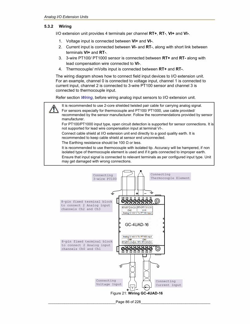
Analog I/O Extension Units
_________________________________Page 86 of 228__________________________________
5.3.2 Wiring I/O extension unit provides 4 terminals per channel RT+, RT-, VI+ and VI-.
1. Voltage input is connected between VI+ and VI-. 2. Current input is connected between VI- and RT-, along with short link between
terminals VI+ and RT-. 3. 3-wire PT100/ PT1000 sensor is connected between RT+ and RT- along with
lead compensation wire connected to VI-. 4. Thermocouple/ mVolts input is connected between RT+ and RT-.
The wiring diagram shows how to connect field input devices to I/O extension unit. For an example, channel 0 is connected to voltage input, channel 1 is connected to current input, channel 2 is connected to 3-wire PT100 sensor and channel 3 is connected to thermocouple input.
Refer section Wiring, before wiring analog input sensors to I/O extension unit.
Figure 21: Wiring GC-4UAD-16
It is recommended to use 2-core shielded twisted pair cable for carrying analog signal. For sensors especially for thermocouple and PT100/ PT1000, use cable provided/ recommended by the sensor manufacturer. Follow the recommendations provided by sensor manufacturer. For PT100/PT1000 input type, open circuit detection is supported for sensor connections. It is not supported for lead wire compensation input at terminal VI-. Connect cable shield at I/O extension unit end directly to a good quality earth. It is recommended to keep cable shield at sensor end unconnected. The Earthing resistance should be 100 Ω or less. It is recommended to use thermocouple with isolated tip. Accuracy will be hampered, if non isolated type of thermocouple element is used and if it gets connected to improper earth. Ensure that input signal is connected to relevant terminals as per configured input type. Unit may get damaged with wrong connections.
8-pin fixed terminal block
to connect 2 Analog input
channels Ch0 and Ch1
8-pin fixed terminal block
to connect 2 Analog input
channels Ch2 and Ch3
V
Connecting
Voltage Input Connecting
Current Input
Connecting
3-wire PT100
Sensor
+ _
+ _
Connecting
Thermocouple Element
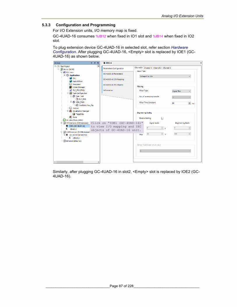
Analog I/O Extension Units
_________________________________Page 87 of 228__________________________________
5.3.3 Configuration and Programming For I/O Extension units, I/O memory map is fixed. GC-4UAD-16 consumes %IB12 when fixed in IO1 slot and %IB14 when fixed in IO2 slot.
To plug extension device GC-4UAD-16 in selected slot, refer section Hardware Configuration. After plugging GC-4UAD-16, <Empty> slot is replaced by IOE1 (GC-4UAD-16) as shown below.
Similarly, after plugging GC-4UAD-16 in slot2, <Empty> slot is replaced by IOE2 (GC-4UAD-16).
Click on “IOE1 (GC-4UAD-16)”
to view I/O mapping and IEC
objects of GC-4UAD-16 unit.
Analog I/O Extension Units
_________________________________Page 88 of 228__________________________________
5.3.3.1 Parameter Configuration
For parameters configuration of GC-4UAD-16, click on device ‘GC-UAD-16’ → Parameters Configuration.
Set individual channel parameters using tabs ‘Channel 0’ to ‘Channel 3’.
As shown below, parameters configuration is explained for Channel 0.
The table below provides the details of configuration required for analog input channel.
Sr. No. Parameter Options Description Analog Input configuration
1 Input Type Voltage: 0 to 10Vdc (Default) -10 to +10Vdc -100 to +100mV
Current: 0 to 20mA 4 to 20mA
PT100: -200 to 850°C
-50 to 250°C PT1000 : -50 to 250°C Thermocouple: J type K type
Selection for type of input as per application requirement.
2 Filter type No Filter Averaging Digital Filter (Default)
Selection for signal conditioning by software
3 Number of Samples
4 (Default), 8, 16, 32 Selection for number of samples for moving average. Channel data updation = Controller scan time x Number of averaging samples.
1
2
3
4
5 6 7
8
Analog I/O Extension Units
_________________________________Page 89 of 228__________________________________
4 Time Constant Default value 50 ms Enter digital filer time constant value from 10 to 5000 ms Channel data updation = Controller scan time + (Time Constant*5). Apply digital filter for analog input signal with erroneous fast variations.
5 Enable Scaling Checkbox unchecked Channel data holds value as per basic resolution e.g. 0 to 64000 if input signal is 0 to 10 VDC for input type 0 to 10VDC.
Checkbox checked Channel data scaling to engineering units as per user defined values of Min and Max. User defined Engineering Scaling is not supported for thermocouple and 3-wire PT100/ PT1000 input types.
6 Signal Scale For 0 to10V input type, Min : 0V and Max : 10V.
This parameter holds min-max values as per configured input type
For -10 to +10V input type, Min : -10V and Max : +10V.
For 0 to 20mA input type, Min : 0mA and Max : 20 mA
For 4 to 20mA input type, Min : 4mA and Max : 20 mA
7 Engineering Scale
Default value=0 Supported range : -64000.0 to 64000.0 for both Min setting
Enter channel data value as per the application requirement. - 0 for input type 0 to 10VDC - -100 for input type ±10VDC, ±100mV - 0 for input type 0 to 20mA, 4 to 20mA
Default value=100 Supported range : -64000.0 to 64000.0 for Max setting
Enter channel data value as per the application requirement. 100: for input types 0 to 10VDC, ±10VDC, ±100mV, for input type 0 to 20mA, 4 to 20mA
8 Sensor Fault/ Open circuit Value
0 (Default) Minimum Value Maximum Value Last Value
Applicable for thermocouple, 4 to 20mA and 3-wire PT100/ 1000 input types. Defines value of channel data in case if sensor fault is detected at input channel *1 Minimum value and maximum value depend upon Engineering scaling selected.
*1 Sensor fault detection is provided for thermocouple, 4 to 20mA and 3-wire PT100/ 1000 input types Sensor fault is detected in case if sensor is open/ gets disconnected/ in case of malfunctioning.
Similarly, user can configure analog input Channel 1, Channel 2 and Channel 3,using respective channel tabs.

Analog I/O Extension Units
_________________________________Page 90 of 228__________________________________
5.3.3.2 I/O Mapping On ‘GC-4UAD-16 IO mapping’ tab, list of I/O variables is available. To view I/O mapping, click on Devices → IOE1 (GC-4UAD-16) → GC-4UAD-16 I/O Mapping as shown below. The table below provides the details of I/O bits related to GC-4UAD-16. =1 for unit fixed in IO1 slot, =2 for unit fixed in IO2 slot,
I/O Variables Address
Description IO1 Slot IO2 Slot
_IOEStatusWord.
_IOECH0OK %IX12.0 %IX14.0 TRUE: - Respective channel is enabled and healthy. FALSE: - Respective channel is disabled. - Open circuit for PT100/ PT1000 sensor,
thermocouple and 4 to 20mA input types.
_IOECH1OK %IX12.1 %IX14.1
_IOECH2OK %IX12.2 %IX14.2
_IOECH3OK %IX12.3 %IX14.3
_IOECJCFault %IX12.4 %IX14.4 TRUE: - CJC faulty - CJC Sensor Open or Short - CJC value below 0°C or beyond 100°C FALSE: CJC healthy
%IX12.5 %IX14.5 Reserved
_IOEADCFault %IX12.6 %IX14.6 TRUE: - ADC faulty FALSE: - ADC healthy
Analog I/O Extension Units
_________________________________Page 91 of 228__________________________________
_IOEControlWord.
_IOECH0Enable %QX12.0 %QX14.0 TRUE - Enable respective channel through Hardware
Configuration Tool. FALSE: - Disable respective channel through Hardware
Configuration Tool.
_IOECH1Enable %QX12.1 %QX14.1
_IOECH2Enable %QX12.2 %QX14.2
_IOECH3Enable %QX12.3 %QX14.3
NOTE
In module memory, CJC data gets updated for any input channel irrespective of input type configuration. It is recommended to consider CJC count for thermocouple input type configuration only. For PT100/PT1000 input type, open circuit detection is supported for sensor connections. It is not supported for lead wire compensation input at terminal VI-.

Analog I/O Extension Units
_________________________________Page 92 of 228__________________________________
5.3.3.3 IEC Objects On ‘GC-4UAD-16 IEC Objects’ tab, user can monitor variables related to GC-4UAD-16 in online mode as below.
Variables Data Type Description IOE1._AI_IOE_Data[0] REAL Holds analog input channel0 data.
The table below provides channel data available when Engineering Scaling is not enabled.
Input Type Channel Data
0 to 10 Vdc 0 to 64000
±10 Vdc -32000 to 32000
±100 mV -32000 to 32000
0 to 20mA 0 to 64000
4 to 20mA 0 to 64000
PT100 -200.0 to 850.0
PT100 -50.00 to 250.00
PT1000 -50.0 to 250.0
J Type Tc -100.0 to 1200.0
K Type Tc -100.0 to 1372.0
In case if Engineering Scaling is enabled, channel data holds value as per Min and Max values defined for Engineering Scaling. User defined Engineering Scaling is not supported for thermocouple and 3-wire (PT100, PT1000) input types.
IOE1._AI_IOE_Data[1] REAL Holds analog input channel1 data as explained for _AI_IOE_Data[0]
IOE1._AI_IOE_Data[2] REAL Holds analog input channel2 data as explained for _AI_IOE_Data[0]
IOE1._AI_IOE_Data[3] REAL Holds analog input channel3 data as explained for _AI_IOE_Data[0]
Analog I/O Extension Units
_________________________________Page 93 of 228__________________________________
IOE1._AI_IOE_Data[4] REAL Holds CJC1 data
IOE1._AI_IOE_Data[5] REAL Holds CJC2 data
_IOEChannelStatus ARRAY [0..3] OF WORD
Holds status of channels if Extended Settings is enabled. Each array element is assigned for individual channel e.g._IOEChannelStatus [0] holds status of channel 0. Details of bits of status word as follows
Bit No Details
0 Channel enable status 0 - Disabled 1 - Enabled
1 Channel configuration 0 - Invalid 1 - Valid
2 Sensor fault 0 - No open circuit 1 - Open circuit for Thermocouple, PT100, PT1000 and 4 to 20mA input ranges and CJC sensor fault.
3 CJC Sensor fault 0 - CJC sensor is healthy 1 - CJC Sensor is faulty
4 - 15 Reserved
IOE1._IOEUnitState BYTE This variable holds I/O extension unit state as follows Bit No Details
0 No unit is fixed in I/O slot or No unit is detected in I/O slot by CPU
1 Mismatch between configured unit and attached unit in I/O slot.
2 Configured unit is detected, and it is in configuration state.
100 Configured unit is detected, configured successfully and is in running condition.
Similarly, user can access IEC objects of I/O extension unit configured in I/O extension slot2 with IOE2.<VariableName>.
NOTE
CJC data i.e. terminal temperature is updated when any channel is configured for any input type.
User defined setting for “Engineering Scale” is applicable only for voltage and current input types (i.e. 0 to 10Vdc, ±10Vdc, ±100mV, 0 to 20mA and 4 to 20mA).

COM Extension Units
_________________________________Page 94 of 228__________________________________
6 COM Extension Units
This section provides information related to serial communication extension units supported for GOC43.

COM Extension Units
_________________________________Page 95 of 228__________________________________
6.1 GC-RS232-COM This is RS232 serial communication extension unit. User can attach only 1 COM extension unit on the back side of Main unit.
6.1.1 Specifications
Item Description No. of serial ports 1 Hardware interface RS232C Signals TxD, RxD, GND, Carrier detect *1
Communication parameters
Baud rate (bps) 9600, 19200, 38400, 57600, 115200 Data bits 7, 8 Parity Odd, Even, None Stop bits 1, 2
Communication type Full duplex or half duplex Connector type 9-pin D male Isolation No isolation from Main circuit Dimensions (in mm) 26.0 (W) x 51.0 (H) x 48.0 (D) Weight (in grams) 40
*1 RS/CS control is not supported.
6.1.2 Wiring This is 1 port RS232 serial communication unit. It provides 9-pin D male connector on its front side.
The figure below shows front view of COM extension unit with connection details.
Figure: Connection details for GC-RS232-COM
Refer section Wiring, before wiring to COM extension unit.
Tighten both screws on 9-pin D female connector to avoid malfunctioning due to loosen connections.
Do not try to pull out communication cable connector before un-tightening 2 screws. It may cause damage to the electronic hardware /plastic enclosure of COM extension unit.
1 Carrier Detect
2 RxD
3 TxD
4 NC
5 GND
9-pin D male
Connector
NC 6
NC 7
Reserved 8
NC 9
It is recommended to limit RS232 communication cable length to 10 meters maximum.
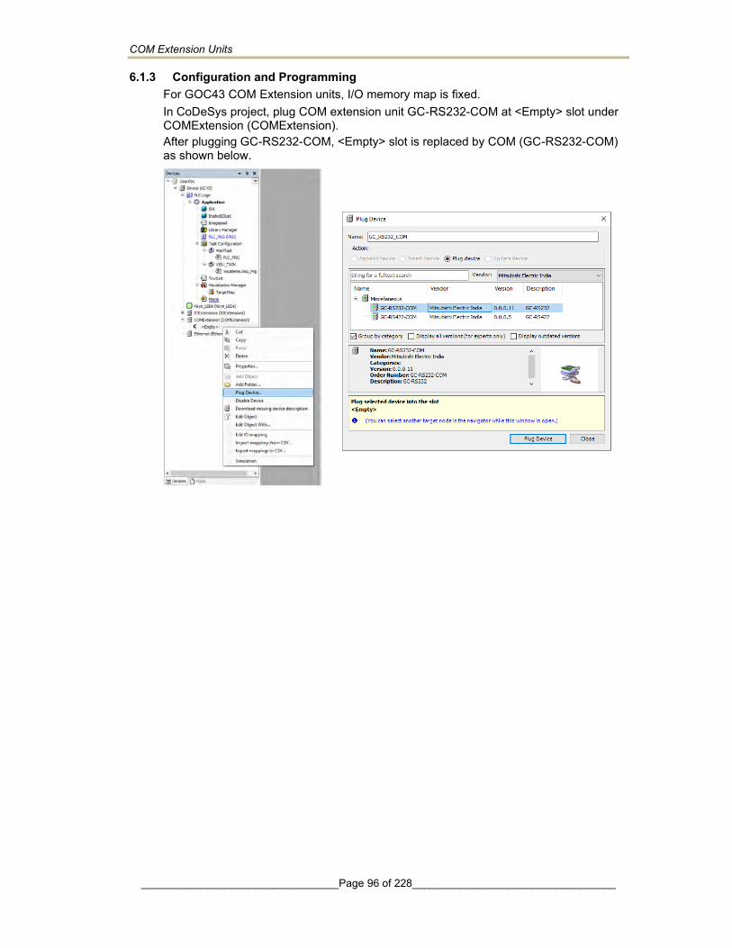
COM Extension Units
_________________________________Page 96 of 228__________________________________
6.1.3 Configuration and Programming For GOC43 COM Extension units, I/O memory map is fixed. In CoDeSys project, plug COM extension unit GC-RS232-COM at <Empty> slot under COMExtension (COMExtension). After plugging GC-RS232-COM, <Empty> slot is replaced by COM (GC-RS232-COM) as shown below.

COM Extension Units
_________________________________Page 97 of 228__________________________________
6.1.3.1 I/O Mapping To view I/O mapping, click on Devices → COM (GC-RS232-COM) → GC-RS232-COM I/O Mapping as shown below.
6.1.3.2 Parameter Configuration
Click on tab ‘Parameter Configuration’, to set communication settings available under ‘GC-RS232-COM_General’,
Sr. No. Parameter Option Description 1 Bus cycle task Use parent bus cycle setting
MainTask VISU_TASK
--
Sr. No. Parameter Option Description 1 Baud Rate 1200, 2400, 4800, 9600 (Default),
19200, 38400, 57600, 115200 Baud rate in bps
2 Data Bits 8 (Default), 7 Number of data bits 3 Parity EVEN, ODD, NONE (Default) Parity 4 Stop Bits StopBits_1 (Default),
StopBits_2 Number of stop bits
5 Communication Mode
FULL-DUPLEX (Default) HALF-DUPLEX
Communication mode as half duplex or full duplex.
1
2
3
4
5
1
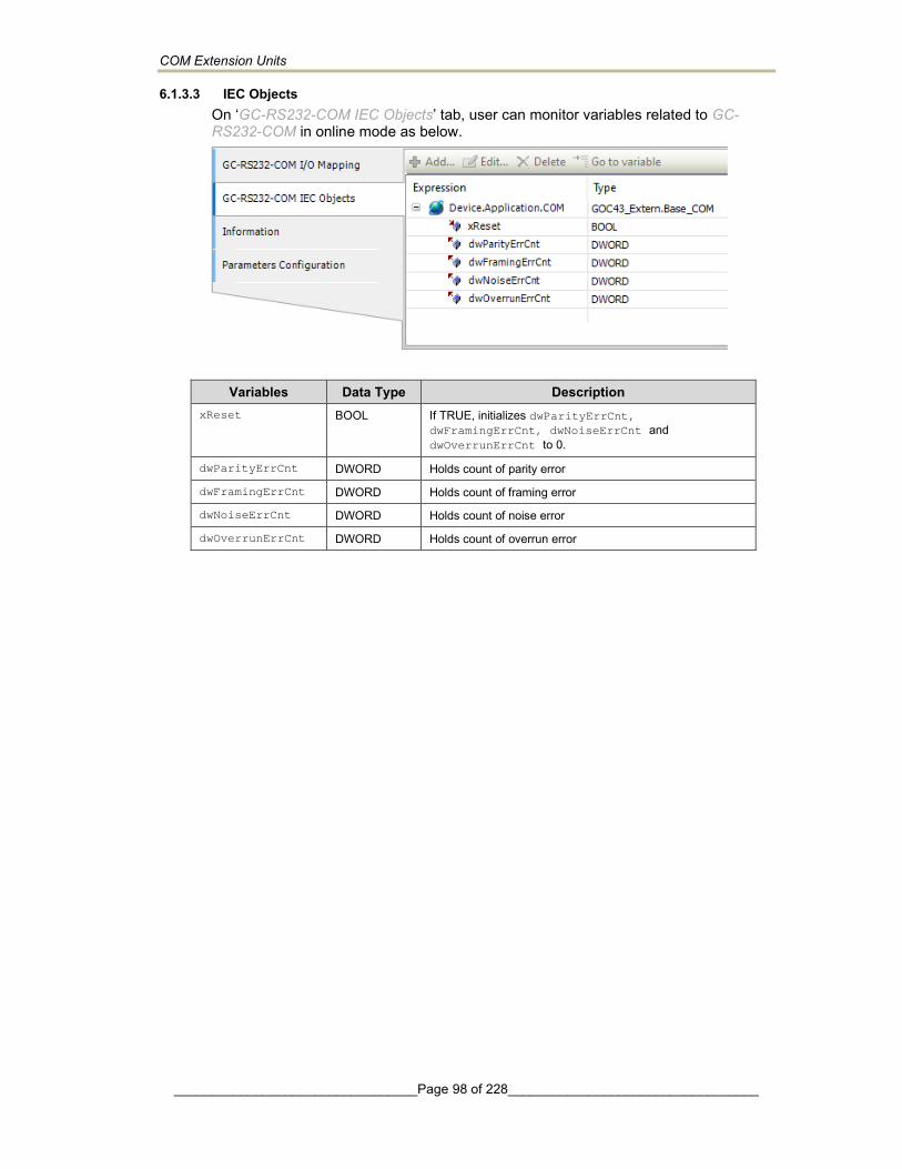
COM Extension Units
_________________________________Page 98 of 228__________________________________
6.1.3.3 IEC Objects On ‘GC-RS232-COM IEC Objects’ tab, user can monitor variables related to GC-RS232-COM in online mode as below.
Variables Data Type Description xReset BOOL If TRUE, initializes dwParityErrCnt,
dwFramingErrCnt, dwNoiseErrCnt and dwOverrunErrCnt to 0.
dwParityErrCnt DWORD Holds count of parity error
dwFramingErrCnt DWORD Holds count of framing error
dwNoiseErrCnt DWORD Holds count of noise error
dwOverrunErrCnt DWORD Holds count of overrun error
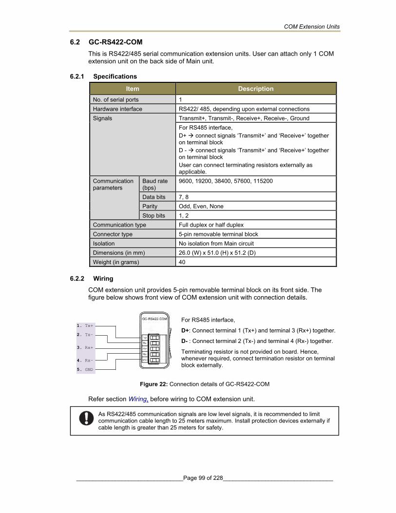
COM Extension Units
_________________________________Page 99 of 228__________________________________
6.2 GC-RS422-COM This is RS422/485 serial communication extension units. User can attach only 1 COM extension unit on the back side of Main unit.
6.2.1 Specifications
Item Description No. of serial ports 1 Hardware interface RS422/ 485, depending upon external connections Signals Transmit+, Transmit-, Receive+, Receive-, Ground
For RS485 interface, D+ → connect signals ‘Transmit+’ and ‘Receive+’ together on terminal block D - → connect signals ‘Transmit+’ and ‘Receive+’ together on terminal block User can connect terminating resistors externally as applicable.
Communication parameters
Baud rate (bps)
9600, 19200, 38400, 57600, 115200
Data bits 7, 8 Parity Odd, Even, None Stop bits 1, 2
Communication type Full duplex or half duplex Connector type 5-pin removable terminal block Isolation No isolation from Main circuit Dimensions (in mm) 26.0 (W) x 51.0 (H) x 51.2 (D) Weight (in grams) 40
6.2.2 Wiring COM extension unit provides 5-pin removable terminal block on its front side. The figure below shows front view of COM extension unit with connection details.
Figure 22: Connection details of GC-RS422-COM
Refer section Wiring, before wiring to COM extension unit.
For RS485 interface,
D+: Connect terminal 1 (Tx+) and terminal 3 (Rx+) together.
D- : Connect terminal 2 (Tx-) and terminal 4 (Rx-) together.
Terminating resistor is not provided on board. Hence, whenever required, connect termination resistor on terminal block externally.
1. Tx+
2. Tx-
3. Rx+
4. Rx-
5. GND
As RS422/485 communication signals are low level signals, it is recommended to limit communication cable length to 25 meters maximum. Install protection devices externally if cable length is greater than 25 meters for safety.
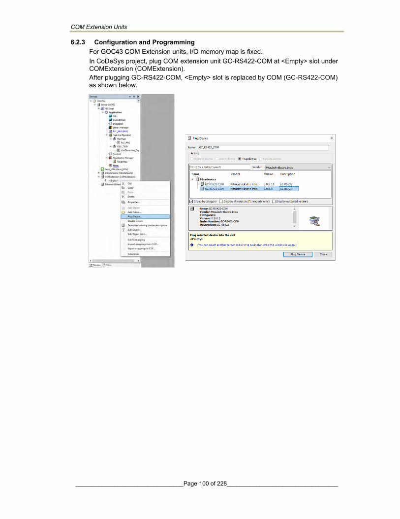
COM Extension Units
_________________________________Page 100 of 228__________________________________
6.2.3 Configuration and Programming For GOC43 COM Extension units, I/O memory map is fixed. In CoDeSys project, plug COM extension unit GC-RS422-COM at <Empty> slot under COMExtension (COMExtension). After plugging GC-RS422-COM, <Empty> slot is replaced by COM (GC-RS422-COM) as shown below.
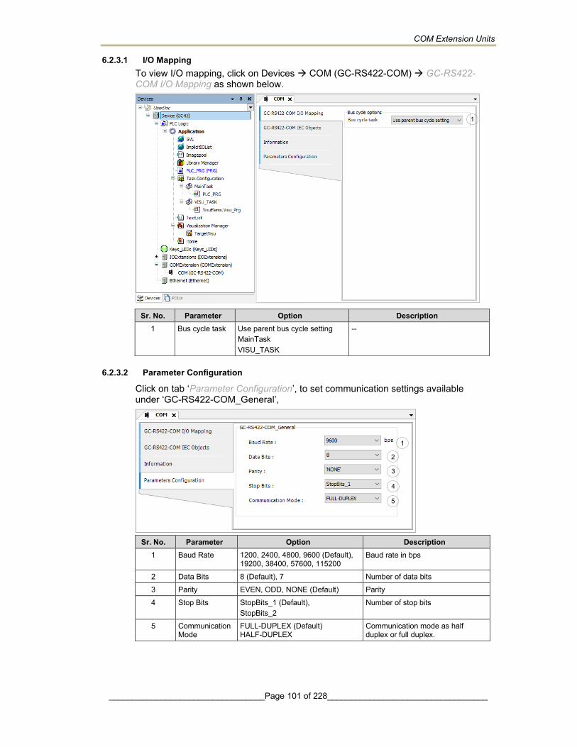
COM Extension Units
_________________________________Page 101 of 228__________________________________
6.2.3.1 I/O Mapping To view I/O mapping, click on Devices → COM (GC-RS422-COM) → GC-RS422-COM I/O Mapping as shown below.
6.2.3.2 Parameter Configuration
Click on tab ‘Parameter Configuration’, to set communication settings available under ‘GC-RS422-COM_General’,
Sr. No. Parameter Option Description 1 Baud Rate 1200, 2400, 4800, 9600 (Default),
19200, 38400, 57600, 115200 Baud rate in bps
2 Data Bits 8 (Default), 7 Number of data bits 3 Parity EVEN, ODD, NONE (Default) Parity
4 Stop Bits StopBits_1 (Default), StopBits_2
Number of stop bits
5 Communication Mode
FULL-DUPLEX (Default) HALF-DUPLEX
Communication mode as half duplex or full duplex.
Sr. No. Parameter Option Description 1 Bus cycle task Use parent bus cycle setting
MainTask VISU_TASK
--
1
2
3
4
5
1

COM Extension Units
_________________________________Page 102 of 228__________________________________
6.2.3.3 IEC Objects On ‘GC-RS422-COM IEC Objects’ tab, user can monitor variables related to GC-RS422-COM in online mode as below.
Variables Data Type Description xReset BOOL If TRUE, initializes dwParityErrCnt,
dwFramingErrCnt, dwNoiseErrCnt and dwOverrunErrCnt to 0.
dwParityErrCnt DWORD Holds count of parity error
dwFramingErrCnt DWORD Holds count of framing error
dwNoiseErrCnt DWORD Holds count of noise error
dwOverrunErrCnt DWORD Holds count of overrun error
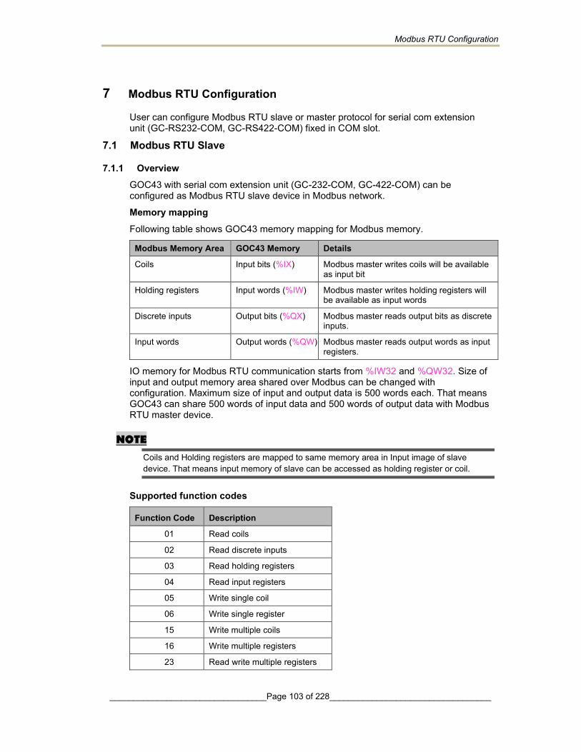
Modbus RTU Configuration
_________________________________Page 103 of 228__________________________________
7 Modbus RTU Configuration
User can configure Modbus RTU slave or master protocol for serial com extension unit (GC-RS232-COM, GC-RS422-COM) fixed in COM slot.
7.1 Modbus RTU Slave
7.1.1 Overview GOC43 with serial com extension unit (GC-232-COM, GC-422-COM) can be configured as Modbus RTU slave device in Modbus network.
Memory mapping Following table shows GOC43 memory mapping for Modbus memory.
Modbus Memory Area GOC43 Memory Details
Coils Input bits (%IX) Modbus master writes coils will be available as input bit
Holding registers Input words (%IW) Modbus master writes holding registers will be available as input words
Discrete inputs Output bits (%QX) Modbus master reads output bits as discrete inputs.
Input words Output words (%QW) Modbus master reads output words as input registers.
IO memory for Modbus RTU communication starts from %IW32 and %QW32. Size of input and output memory area shared over Modbus can be changed with configuration. Maximum size of input and output data is 500 words each. That means GOC43 can share 500 words of input data and 500 words of output data with Modbus RTU master device.
NOTE
Coils and Holding registers are mapped to same memory area in Input image of slave device. That means input memory of slave can be accessed as holding register or coil.
Supported function codes
Function Code Description
01 Read coils
02 Read discrete inputs
03 Read holding registers
04 Read input registers
05 Write single coil
06 Write single register
15 Write multiple coils
16 Write multiple registers
23 Read write multiple registers
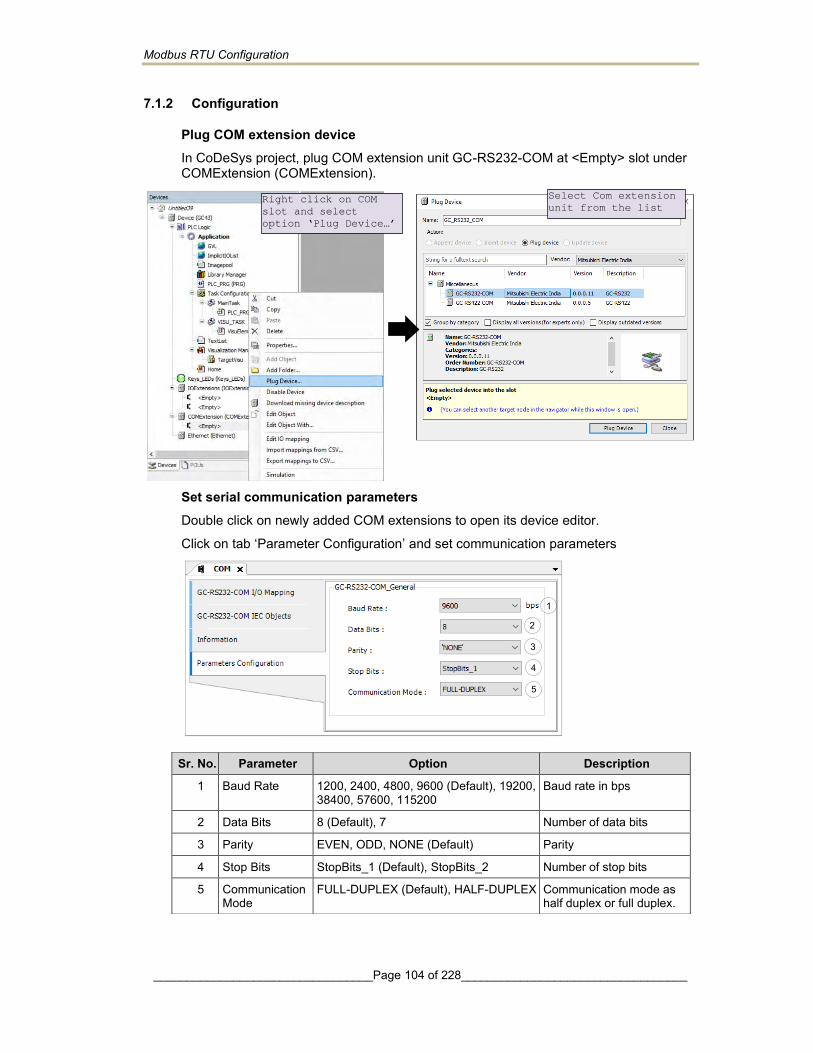
Modbus RTU Configuration
_________________________________Page 104 of 228__________________________________
7.1.2 Configuration
Plug COM extension device In CoDeSys project, plug COM extension unit GC-RS232-COM at <Empty> slot under COMExtension (COMExtension).
Set serial communication parameters Double click on newly added COM extensions to open its device editor.
Click on tab ‘Parameter Configuration’ and set communication parameters
Sr. No. Parameter Option Description
1 Baud Rate 1200, 2400, 4800, 9600 (Default), 19200, 38400, 57600, 115200
Baud rate in bps
2 Data Bits 8 (Default), 7 Number of data bits
3 Parity EVEN, ODD, NONE (Default) Parity
4 Stop Bits StopBits_1 (Default), StopBits_2 Number of stop bits
5 Communication Mode
FULL-DUPLEX (Default), HALF-DUPLEX Communication mode as half duplex or full duplex.
Right click on COM
slot and select
option ‘Plug Device…’
Select Com extension
unit from the list
1
2
3
4
5
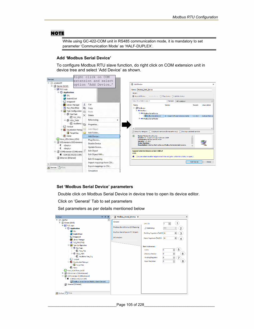
Modbus RTU Configuration
_________________________________Page 105 of 228__________________________________
NOTE
While using GC-422-COM unit in RS485 communication mode, it is mandatory to set parameter ‘Communication Mode’ as ‘HALF-DUPLEX’.
Add ‘Modbus Serial Device’ To configure Modbus RTU slave function, do right click on COM extension unit in device tree and select ‘Add Device’ as shown.
Set ‘Modbus Serial Device’ parameters Double click on Modbus Serial Device in device tree to open its device editor.
Click on ‘General’ Tab to set parameters
Set parameters as per details mentioned below
1 2
Right click on COM
extension and select
option ‘Add Device…’
3 4
5 6
7 8
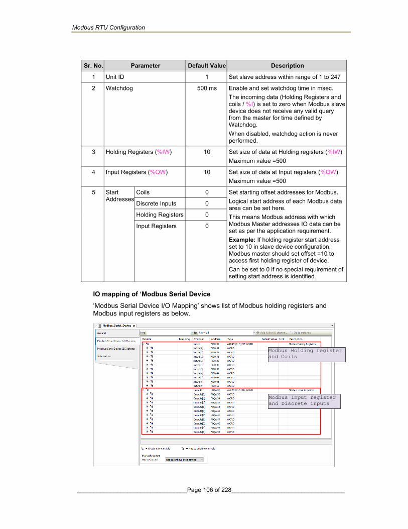
Modbus RTU Configuration
_________________________________Page 106 of 228__________________________________
IO mapping of ‘Modbus Serial Device ‘Modbus Serial Device I/O Mapping’ shows list of Modbus holding registers and Modbus input registers as below.
Sr. No. Parameter Default Value Description
1 Unit ID 1 Set slave address within range of 1 to 247
2 Watchdog 500 ms Enable and set watchdog time in msec. The incoming data (Holding Registers and coils / %I) is set to zero when Modbus slave device does not receive any valid query from the master for time defined by Watchdog. When disabled, watchdog action is never performed.
3 Holding Registers (%IW) 10 Set size of data at Holding registers (%IW) Maximum value =500
4 Input Registers (%QW) 10 Set size of data at Input registers (%QW) Maximum value =500
5 Start Addresses
Coils 0 Set starting offset addresses for Modbus. Logical start address of each Modbus data area can be set here. This means Modbus address with which Modbus Master addresses IO data can be set as per the application requirement. Example: If holding register start address set to 10 in slave device configuration, Modbus master should set offset =10 to access first holding register of device. Can be set to 0 if no special requirement of setting start address is identified.
Discrete Inputs 0
Holding Registers 0
Input Registers 0
Modbus Holding register
and Coils
Modbus Input register
and Discrete inputs

Modbus RTU Configuration
_________________________________Page 107 of 228__________________________________
7.2 Modbus RTU Master
7.2.1 Overview GOC43 with serial com extension unit (GC-232-COM and GC-422-COM) can be configured as Modbus RTU Master in Modbus network.
When configured as Master, GOC43 allows to configure communication with 16 slave devices.
Data read from slave devices is mapped in to input memory.
Data to be write to slave devices is mapped to output memory.
Modbus master can use IO memory starting from %IW32 and %QW32.
Out of 2048 bytes first 32 bytes of IO memory is reserved for Local IOs from Main unit and IO extension units, remaining memory can be used by Modbus master. That means total memory available for Modbus master is 2048-32 =2016 BYTEs or 1008 WORDs.
Note that same IO memory area is also used by other communication protocols like Modbus RTU slave, Modbus TCP Master, Modbus TCP slave etc.
Supported function codes
Function Code Description
01 Read coils
02 Read discrete inputs
03 Read holding registers
04 Read input registers
05 Write single coil
06 Write single register
15 Write multiple coils
16 Write multiple registers
23 Read write multiple registers

Modbus RTU Configuration
_________________________________Page 108 of 228__________________________________
7.2.2 Configuration
Add COM extension unit in configuration In CoDeSys project, plug COM extension unit GC-RS232-COM at <Empty> slot under COMExtension (COMExtension).
Set serial communication parameters Double click on newly added COM extensions to open its device editor.
Click on tab ‘Parameter Configuration’ and set communication parameters
Sr. No. Parameter Option Description
1 Baud Rate 1200, 2400, 4800, 9600 (Default), 19200, 38400, 57600, 115200
Baud rate in bps
2 Data Bits 8 (Default), 7 Number of data bits
3 Parity EVEN, ODD, NONE (Default) Parity
4 Stop Bits StopBits_1 (Default), StopBits_2 Number of stop bits
5 Communication Mode
FULL-DUPLEX (Default), HALF-DUPLEX Communication mode as half duplex or full duplex.
Right click on COM
slot and select
option ‘Plug Device…’ Select Com extension
unit from list
1
2
3
4
5
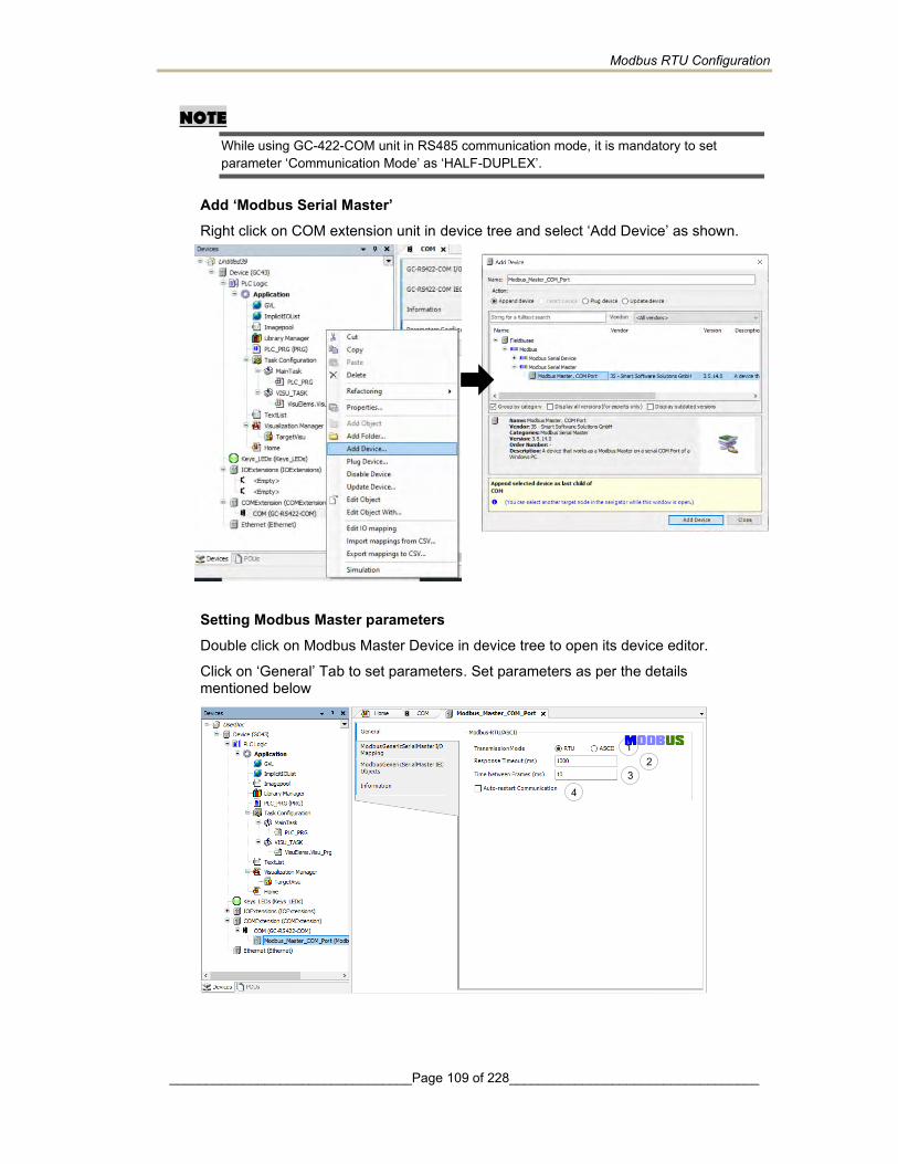
Modbus RTU Configuration
_________________________________Page 109 of 228__________________________________
NOTE
While using GC-422-COM unit in RS485 communication mode, it is mandatory to set parameter ‘Communication Mode’ as ‘HALF-DUPLEX’.
Add ‘Modbus Serial Master’ Right click on COM extension unit in device tree and select ‘Add Device’ as shown.
Setting Modbus Master parameters Double click on Modbus Master Device in device tree to open its device editor.
Click on ‘General’ Tab to set parameters. Set parameters as per the details mentioned below
1 2
3 4
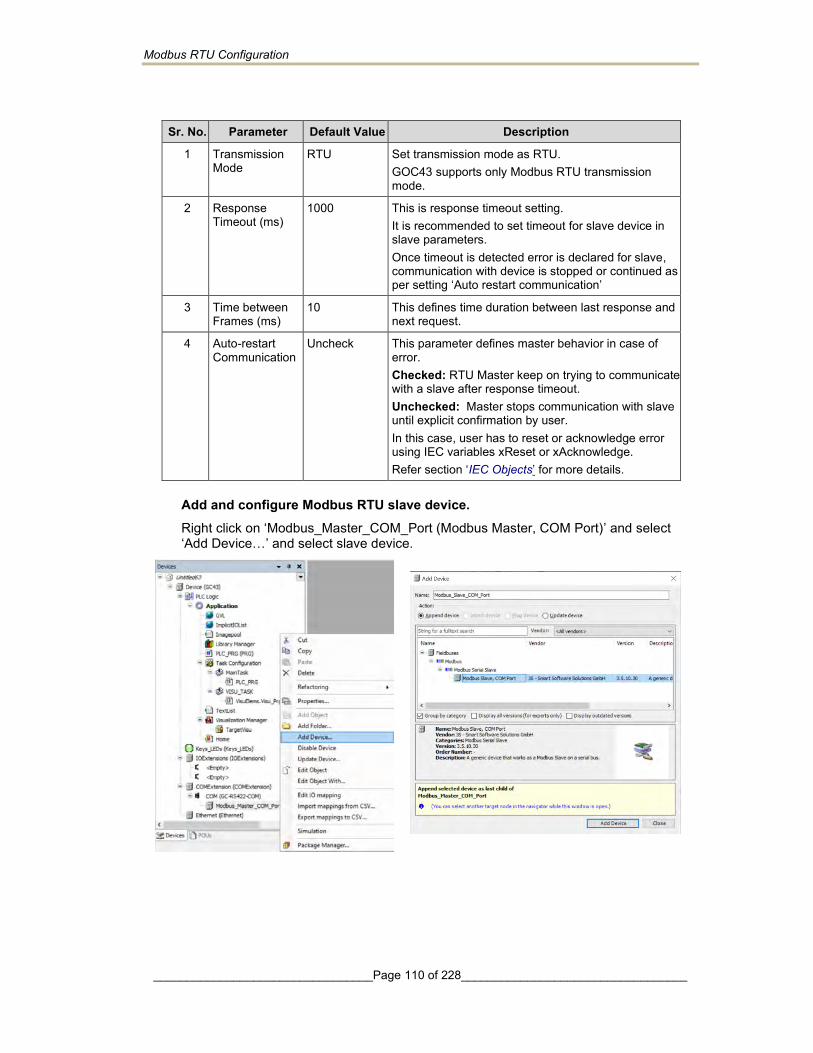
Modbus RTU Configuration
_________________________________Page 110 of 228__________________________________
Add and configure Modbus RTU slave device. Right click on ‘Modbus_Master_COM_Port (Modbus Master, COM Port)’ and select ‘Add Device…’ and select slave device.
Sr. No. Parameter Default Value Description
1 Transmission Mode
RTU Set transmission mode as RTU. GOC43 supports only Modbus RTU transmission mode.
2 Response Timeout (ms)
1000 This is response timeout setting. It is recommended to set timeout for slave device in slave parameters. Once timeout is detected error is declared for slave, communication with device is stopped or continued as per setting ‘Auto restart communication’
3 Time between Frames (ms)
10 This defines time duration between last response and next request.
4 Auto-restart Communication
Uncheck This parameter defines master behavior in case of error. Checked: RTU Master keep on trying to communicate with a slave after response timeout. Unchecked: Master stops communication with slave until explicit confirmation by user. In this case, user has to reset or acknowledge error using IEC variables xReset or xAcknowledge. Refer section ‘IEC Objects’ for more details.
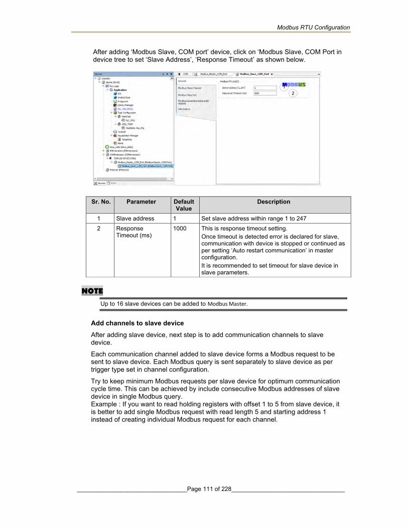
Modbus RTU Configuration
_________________________________Page 111 of 228__________________________________
After adding ‘Modbus Slave, COM port’ device, click on ‘Modbus Slave, COM Port in device tree to set ‘Slave Address’, ‘Response Timeout’ as shown below.
NOTE
Up to 16 slave devices can be added to Modbus Master.
Add channels to slave device After adding slave device, next step is to add communication channels to slave device.
Each communication channel added to slave device forms a Modbus request to be sent to slave device. Each Modbus query is sent separately to slave device as per trigger type set in channel configuration.
Try to keep minimum Modbus requests per slave device for optimum communication cycle time. This can be achieved by include consecutive Modbus addresses of slave device in single Modbus query. Example : If you want to read holding registers with offset 1 to 5 from slave device, it is better to add single Modbus request with read length 5 and starting address 1 instead of creating individual Modbus request for each channel.
Sr. No. Parameter Default Value
Description
1 Slave address 1 Set slave address within range 1 to 247 2 Response
Timeout (ms) 1000 This is response timeout setting.
Once timeout is detected error is declared for slave, communication with device is stopped or continued as per setting ‘Auto restart communication’ in master configuration. It is recommended to set timeout for slave device in slave parameters.
2 1
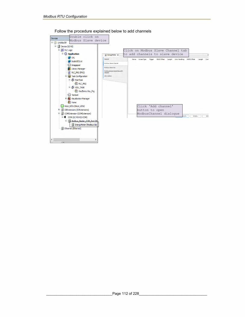
Modbus RTU Configuration
_________________________________Page 112 of 228__________________________________
Follow the procedure explained below to add channels
Double click on
Modbus Slave device
Click on Modbus Slave Channel tab
to add channels to slave device
Click ‘Add channel’
button to open
ModbusChannel dialogue
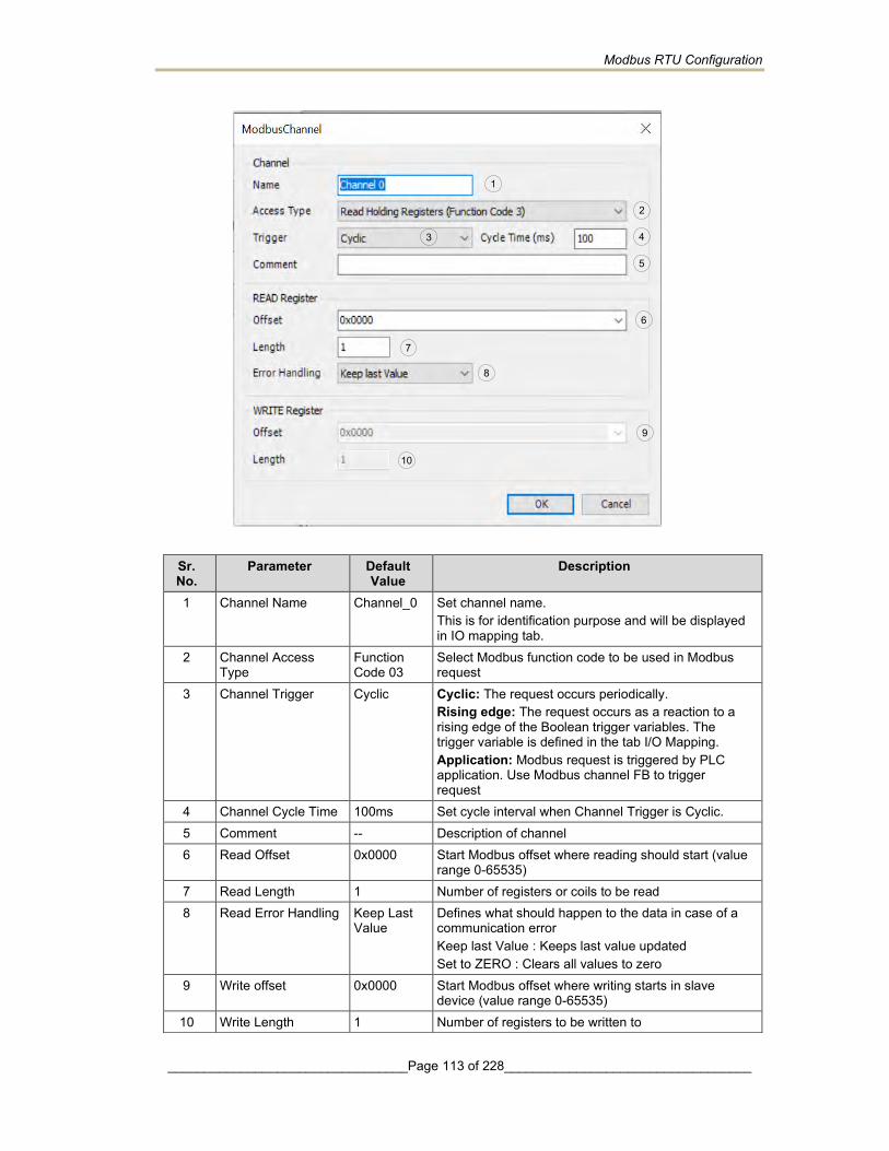
Modbus RTU Configuration
_________________________________Page 113 of 228__________________________________
Sr. No.
Parameter Default Value
Description
1 Channel Name Channel_0 Set channel name. This is for identification purpose and will be displayed in IO mapping tab.
2 Channel Access Type
Function Code 03
Select Modbus function code to be used in Modbus request
3 Channel Trigger Cyclic Cyclic: The request occurs periodically. Rising edge: The request occurs as a reaction to a rising edge of the Boolean trigger variables. The trigger variable is defined in the tab I/O Mapping. Application: Modbus request is triggered by PLC application. Use Modbus channel FB to trigger request
4 Channel Cycle Time 100ms Set cycle interval when Channel Trigger is Cyclic. 5 Comment -- Description of channel 6 Read Offset 0x0000 Start Modbus offset where reading should start (value
range 0-65535) 7 Read Length 1 Number of registers or coils to be read 8 Read Error Handling Keep Last
Value Defines what should happen to the data in case of a communication error Keep last Value : Keeps last value updated Set to ZERO : Clears all values to zero
9 Write offset 0x0000 Start Modbus offset where writing starts in slave device (value range 0-65535)
10 Write Length 1 Number of registers to be written to
1
2
4 3
5
6
8
9
10
7

Modbus RTU Configuration
_________________________________Page 114 of 228__________________________________
Follow the same procedure to add other channels of the slave. You can add up to 99 channels for each slave device.
Add Modbus Slave Init Channels Apart from communication channels explained before, Modbus master allows to add ‘Init’ channels.
Init channels allows to send initialization commands to slave device. Initialization commands are executed one time when starting the slave device or after slave device recovered from error.
Initialization commands are sent to slave device in following cases
• Start of communication
• Reset of PLC (Reset warm or cold)
• Recovery of communication after error
Follow the procedure explained below to add ‘Init channels’
Double click on
Modbus Slave device
Click on Modbus Slave Init tab
Click ‘New’ button to
open Initialization
Value dialogue

Modbus RTU Configuration
_________________________________Page 115 of 228__________________________________
You can add up to 20 initialization channels for a slave.
IO mapping After adding communication channels, IO mapping is updated accordingly in IO mapping tab of slave devices. Below is an example of IO mapping Follow the procedures explained to add Slave device, Modbus channel and Init channels for other slave devices, you can add up to 16 slave devices in the network.
Sr. No.
Parameter Default Value
Description
1 Access Type Function Code 16
Select Modbus function code to Write initialization value.
2 Read Offset 0x0000 Start address where write should start (value range 0-65535)
3 Read Length 1 Number of registers to be read 4 Initialization value 1 Initialization value for the registers or coils 5 Comment -- Description of channel
1
2
3
4
5
Set variable names here.
You can use these
variables in application.
Set variable names here.
You can use these
variables in application.
Click on IO mapping tab to
view channels variable names
here. You can use these
variables in application
Modbus RTU Configuration
_________________________________Page 116 of 228__________________________________
Using Channel data in PLC code Channels read from slave device are displayed as BOOL or WORD data type in IO mapping irrespective of their native data type in slave device. If you want to use them in PLC code with their actual data types, declare a variable of required data type in the application program with IO address mentioned in IO mapping. For example, Active energy value in above IO mapping image is a DWORD value in slave device and is mapped to two consecutive Modbus registers. In IO mapping, value displayed as two WORDs, to use active energy value in PLC application as DWORD declare a variable as below ActiveEnergy AT %IW52: DWORD;
Same method should be used for other data types like INT, DINT, REAL etc.
7.2.3 IEC Objects Modbus master provides information related to status and diagnostics in IEC objects of Master device as well as configured slave device/s.
For Modbus master, IEC object instance is created with name of Modbus master device by default it is ‘Modbus_Master_COM_Port’. Table shows details of individual variable in IEC object
Variable Name (Instance.XXX)
Data Type Access Description
xStop BOOL RW If TRUE, then each new request to all the slaves is stopped. If FALSE, the communication process continues.
xResetComPort BOOL RW Immediately closes and opens the COM port at a rising edge.
uiNumberOfCommunicatingSlaves UINT RO Displays the number of communicating slaves
xAllSlavesOk BOOL RO TRUE if all slaves are communicating. FALSE if one or more slaves have error.
For Modbus slave, IEC object instance is created with name of Modbus slave device. Table shows details of individual variable in IEC object
Variable Name (Instance.XXX) Data Type Access Description
xTrigger BOOL RW Triggers the transmission of all configured Modbus channels for a rising edge
xReset BOOL RW Restarts communication and resets xError and byModbusError
xAcknowledge BOOL RW Restarts communication and does not reset xError and byModbusError
xDoInit BOOL RW TRUE execute Initialisation.
xInitDone BOOL RO All initialization commands execution completed.
xBusy BOOL RO Execution under process.
xDone BOOL RO Execution completed for current channel.
xError BOOL RO TRUE if any error occurs. Communication to the slave is interrupted.
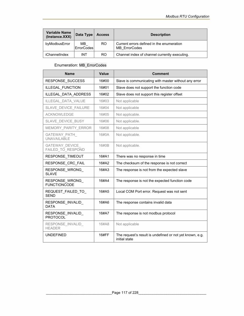
Modbus RTU Configuration
_________________________________Page 117 of 228__________________________________
Variable Name (Instance.XXX) Data Type Access Description
byModbusError MB_ ErrorCodes
RO Current errors defined in the enumeration MB_ErrorCodes
iChannelIndex INT RO Channel index of channel currently executing.
Enumeration: MB_ErrorCodes
Name Value Comment
RESPONSE_SUCCESS 16#00 Slave is communicating with master without any error
ILLEGAL_FUNCTION 16#01 Slave does not support the function code
ILLEGAL_DATA_ADDRESS 16#02 Slave does not support this register offset
ILLEGAL_DATA_VALUE 16#03 Not applicable
SLAVE_DEVICE_FAILURE 16#04 Not applicable
ACKNOWLEDGE 16#05 Not applicable.
SLAVE_DEVICE_BUSY 16#06 Not applicable.
MEMORY_PARITY_ERROR 16#08 Not applicable
GATEWAY_PATH_ UNAVAILABLE
16#0A Not applicable.
GATEWAY_DEVICE_ FAILED_TO_RESPOND
16#0B Not applicable.
RESPONSE_TIMEOUT 16#A1 There was no response in time
RESPONSE_CRC_FAIL 16#A2 The checksum of the response is not correct
RESPONSE_WRONG_ SLAVE
16#A3 The response is not from the expected slave
RESPONSE_WRONG_ FUNCTIONCODE
16#A4 The response is not the expected function code
REQUEST_FAILED_TO_ SEND
16#A5 Local COM Port error. Request was not sent
RESPONSE_INVALID_ DATA
16#A6 The response contains invalid data
RESPONSE_INVALID_ PROTOCOL
16#A7 The response is not modbus protocol
RESPONSE_INVALID_ HEADER
16#A8 Not applicable
UNDEFINED 16#FF The request’s result is undefined or not yet known, e.g. initial state
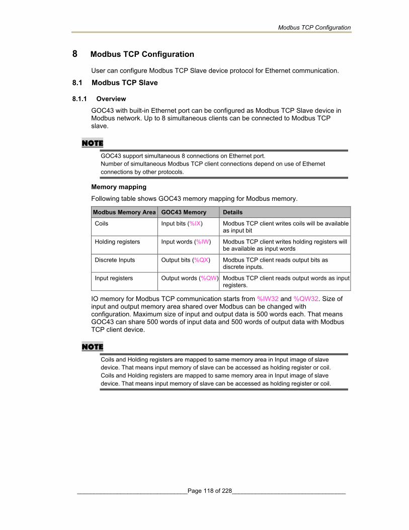
Modbus TCP Configuration
_________________________________Page 118 of 228__________________________________
8 Modbus TCP Configuration
User can configure Modbus TCP Slave device protocol for Ethernet communication.
8.1 Modbus TCP Slave
8.1.1 Overview GOC43 with built-in Ethernet port can be configured as Modbus TCP Slave device in Modbus network. Up to 8 simultaneous clients can be connected to Modbus TCP slave.
NOTE
GOC43 support simultaneous 8 connections on Ethernet port. Number of simultaneous Modbus TCP client connections depend on use of Ethernet connections by other protocols.
Memory mapping Following table shows GOC43 memory mapping for Modbus memory.
Modbus Memory Area GOC43 Memory Details
Coils Input bits (%IX) Modbus TCP client writes coils will be available as input bit
Holding registers Input words (%IW) Modbus TCP client writes holding registers will be available as input words
Discrete Inputs Output bits (%QX) Modbus TCP client reads output bits as discrete inputs.
Input registers Output words (%QW) Modbus TCP client reads output words as input registers.
IO memory for Modbus TCP communication starts from %IW32 and %QW32. Size of input and output memory area shared over Modbus can be changed with configuration. Maximum size of input and output data is 500 words each. That means GOC43 can share 500 words of input data and 500 words of output data with Modbus TCP client device.
NOTE
Coils and Holding registers are mapped to same memory area in Input image of slave device. That means input memory of slave can be accessed as holding register or coil. Coils and Holding registers are mapped to same memory area in Input image of slave device. That means input memory of slave can be accessed as holding register or coil.
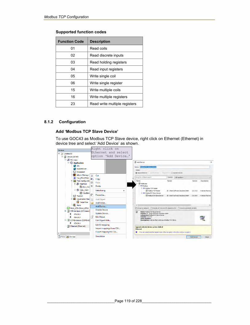
Modbus TCP Configuration
_________________________________Page 119 of 228__________________________________
Supported function codes
Function Code Description
01 Read coils
02 Read discrete inputs
03 Read holding registers
04 Read input registers
05 Write single coil
06 Write single register
15 Write multiple coils
16 Write multiple registers
23 Read write multiple registers
8.1.2 Configuration
Add ‘Modbus TCP Slave Device’ To use GOC43 as Modbus TCP Slave device, right click on Ethernet (Ethernet) in device tree and select ‘Add Device’ as shown.
Right click on
Ethernet and select
option ‘Add Device…’

Modbus TCP Configuration
_________________________________Page 120 of 228__________________________________
Set ‘Modbus TCP Slave Device’ parameters Double click on Modbus TCP Slave Device in device tree to open its device editor.
Click on ‘General’ Tab to set parameters.
Set parameters as per details mentioned below
Sr. No. Parameter Default Value
Description
1 Watchdog 500 ms Enable and set watchdog time in msec. The incoming data (Holding Registers, coils / %I range) is set to zero when the Modbus device does not receive any valid query from the client for time defined by Watchdog. When disabled, watchdog action is never performed.
2 Slave Port 502 Port number of the slave. 3 Unit ID 1 Set station address within range 1 to 247 4 Holding Registers (%IW) 10 Set size of data at Holding registers (%IW)
Maximum value =500
5 Input Registers (%QW) 10 Set size of data at Input registers (%QW) Maximum value =500
6 Start Addresses
Coils 0 Set starting offset addresses for Modbus. Logical start address of each Modbus data area can be set. This means Modbus address with which Modbus Master addresses IO data can be set as per requirement Example: If holding register start address set to 10, Modbus master should set offset =10 to access first holding register of device. Can be set to 0 if no special requirement of setting start address is identified.
Discrete Inputs 0
Holding Registers 0 Input Registers 0
7 Holding- and Input-Register-Data Areas overlay : Overlay of the process image by the holding
and input register. This is required, for example, when the slave application is used to write to the holding register.
2 3
4 5
6
7
1
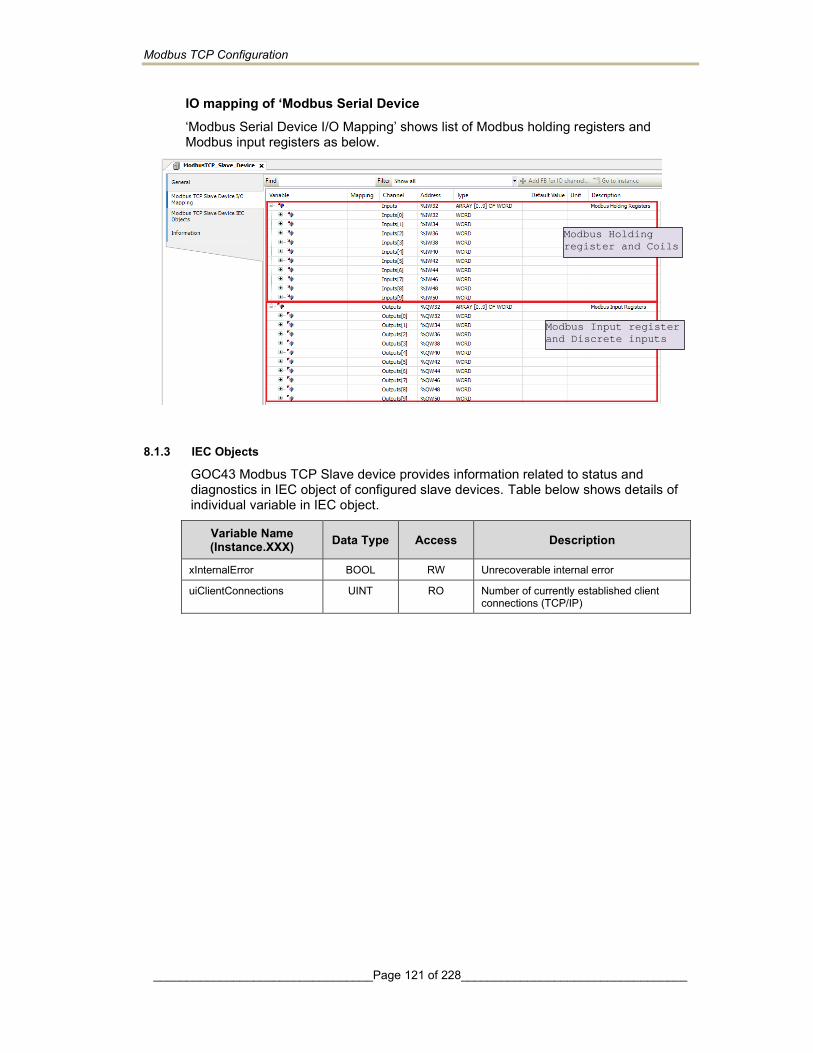
Modbus TCP Configuration
_________________________________Page 121 of 228__________________________________
IO mapping of ‘Modbus Serial Device ‘Modbus Serial Device I/O Mapping’ shows list of Modbus holding registers and Modbus input registers as below.
8.1.3 IEC Objects
GOC43 Modbus TCP Slave device provides information related to status and diagnostics in IEC object of configured slave devices. Table below shows details of individual variable in IEC object.
Variable Name (Instance.XXX) Data Type Access Description
xInternalError BOOL RW Unrecoverable internal error
uiClientConnections UINT RO Number of currently established client connections (TCP/IP)
Modbus Input register
and Discrete inputs
Modbus Holding
register and Coils

Status and Diagnostics
_________________________________Page 122 of 228__________________________________
9 Status and Diagnostics
Main unit provides 2 LED indications and LCD display on front panel to provide status and diagnostic information useful for troubleshooting. GOC43 provides system menu screen that provides more information.
9.1 LED Indications Main unit provides 2 LED indications on front panel. The table below explains the significance of CPU diagnostics related LEDs
Status Power Run Relevant System Variables
Red Green
OFF • No power • User stop. • Stop due to system error. *1 • New firmware download,
_SysvarCPU.WSTATUS
_SysvarCPU.BCPUSTOPCAUSE
ON • Power ON • Run mode _SysvarCPU.WSTATUS
_SysvarCPU.BINITSTATUS
Blinking 1x • Not applicable
• IO Error _SysvarCPU.WSTATUS
Blinking 2x • Power fail error *2 NA
Blinking 3x • Watchdog fault _SysvarCPU.WSTATUS
_SysvarCPU.BCPUSTOPCAUSE
Flashing • Memory error • Application download in
progress • Key error
- If any of Illuminated key, function key, touch screen is detected as pressed, at power on due to actual pressing or hardware fault.
_SysvarCPU.WSTATUS
_SysvarCPU.BCPUSTOPCAUSE
*1 When CPU is in STOP mode, LCD screen shows system menu SYSTEM INFO. For more details, refer section System Info
*2 CPU goes in Stop mode permanently, when input supply falls below 18 VDC (but remains above 10 VDC). It continues in Stop mode even though input supply is recovered above 18 VDC for safety purpose. To recover the system, it is necessary to power cycle the Main unit.
Refer section System Variables, for more details of system variables.
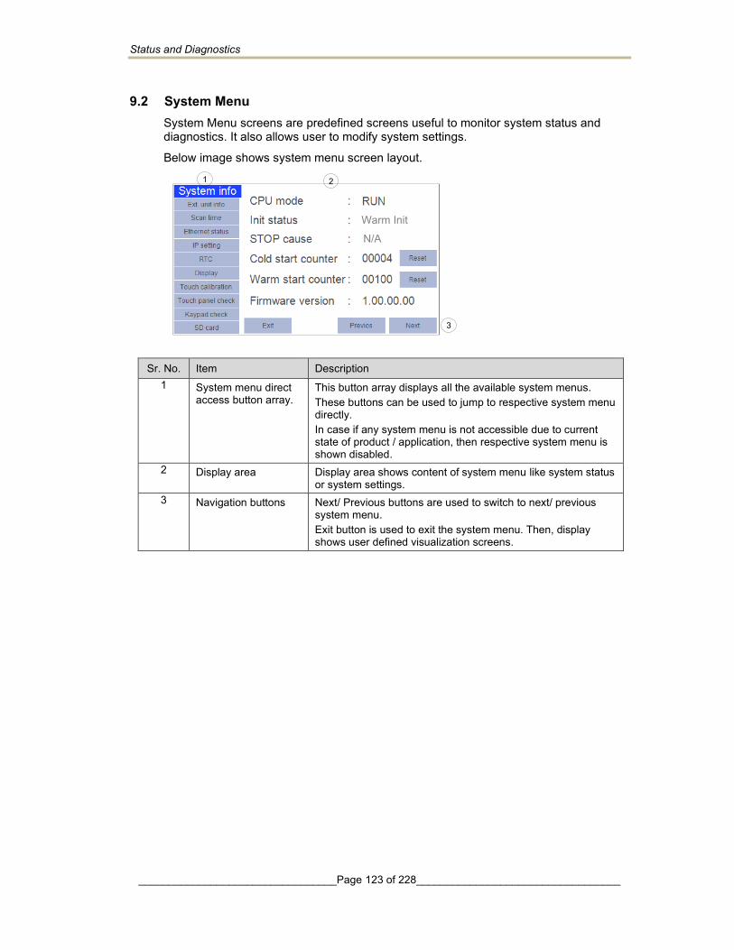
Status and Diagnostics
_________________________________Page 123 of 228__________________________________
9.2 System Menu System Menu screens are predefined screens useful to monitor system status and diagnostics. It also allows user to modify system settings.
Below image shows system menu screen layout.
Sr. No. Item Description 1 System menu direct
access button array. This button array displays all the available system menus. These buttons can be used to jump to respective system menu directly. In case if any system menu is not accessible due to current state of product / application, then respective system menu is shown disabled.
2 Display area Display area shows content of system menu like system status or system settings.
3 Navigation buttons Next/ Previous buttons are used to switch to next/ previous system menu. Exit button is used to exit the system menu. Then, display shows user defined visualization screens.
1 2
3
N/A
Warm Init

Status and Diagnostics
_________________________________Page 124 of 228__________________________________
9.2.1 System Info System info menu shows CPU status, useful for diagnostics and troubleshooting.
Sr. No. Item Details Applicable system variable 1 CPU
mode Shows CPU mode as RUN or STOP. RUN: Application program executing STOP: Application program not
executing
_SysvarCPU.WSTATUS.0
2 Init status
Displays CPU initialization status. Hot Init- If power fail has occurred for short duration. CPU continues to function normally as if there is no power fail Warm Init- If power fail has occurred normally or if CoDeSys menu command Online → Reset warm is issued. This is healthy initialization. Non retained data is reset to 0 or user defined initial value. Retained data holds last value before power off. Cold Init- This is faulty initialization or if CoDeSys menu command Online → Reset cold is issued or if program is downloaded. All the data is reset to 0 or user defined initial value. Cause may be hardware fault or external EMI issue.
_SysvarCPU.BINITSTATUS
3 Stop cause
User- If programmer puts CPU in STOP mode intentionally through programming software CoDeSys. Mem Err – If application program code is invalid. Wd Err_<Name of Task> – If CPU is in STOP mode due to watchdog error i.e. if scan time of respective task exceeds watchdog time set.
_SysvarCPU.BCPUSTOPCAUSE
4 Cold start counter
Number of occurrences of cold start initialization till date or last reset. Increment in count indicates recent occurrence. User can reset counter to 0 by Reset button.
_SysvarCPU.WCOLDSTARTCOUNT
ER
1
2
3
4
5
6
Warm Init
N/A

Status and Diagnostics
_________________________________Page 125 of 228__________________________________
System info continues..
Sr. No. Item Details Applicable system variable 5 Warm
start counter
Number of occurrences of warm start initialization till date or last reset. Increment in count indicates recent occurrence. User can reset counter to 0 by Reset button.
_SysvarCPU.WWARMSTARTCOUNT
ER
6 Firmware version
Shows firmware version running in the device
_SysvarVersionInfo.SRTSVER
SION
9.2.2 Ext. unit info Ext. unit info menu shows extension related information such as extension unit configured, actual present, status (Ok or Not ok) along with extension unit ordering code.
Sr. No. Item Details Applicable system variable 1 Configured
unit Shows ordering code of extension unit configured in COM / IO extension slot. Shows ‘Empty’ if not configured.
_SysvarCPU.CONFIGMODULES
2 Present unit Shows ordering code of extension unit actually present in COM / IO extension slot. Shows ‘Empty’ if not configured.
_SysvarCPU.AMODULEORDERINGCODE
3 Status Shows IO error status of extension unit [Ok/ Not ok]
_SysvarCPU.W_IOERR
1
2
3
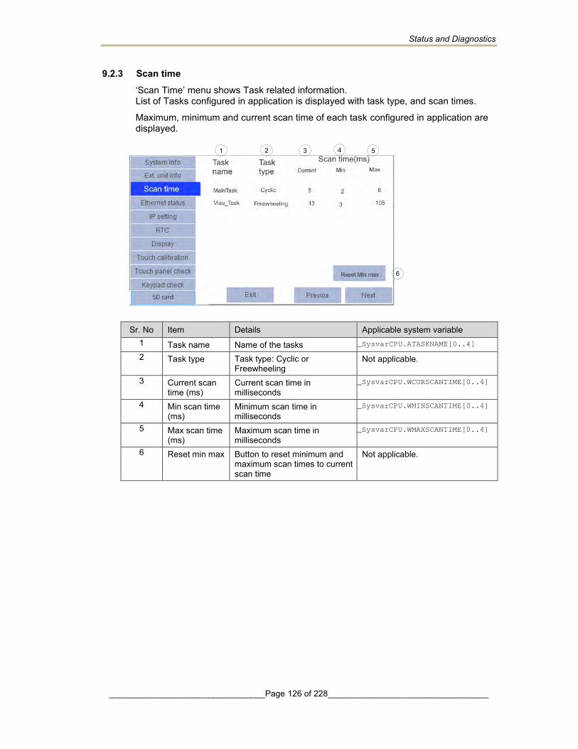
Status and Diagnostics
_________________________________Page 126 of 228__________________________________
9.2.3 Scan time ‘Scan Time’ menu shows Task related information. List of Tasks configured in application is displayed with task type, and scan times.
Maximum, minimum and current scan time of each task configured in application are displayed.
Sr. No Item Details Applicable system variable 1 Task name Name of the tasks _SysvarCPU.ATASKNAME[0..4]
2 Task type Task type: Cyclic or Freewheeling
Not applicable.
3 Current scan time (ms)
Current scan time in milliseconds
_SysvarCPU.WCURSCANTIME[0..4]
4 Min scan time (ms)
Minimum scan time in milliseconds
_SysvarCPU.WMINSCANTIME[0..4]
5 Max scan time (ms)
Maximum scan time in milliseconds
_SysvarCPU.WMAXSCANTIME[0..4]
6 Reset min max Button to reset minimum and maximum scan times to current scan time
Not applicable.
1
2
3 4
5
6

Status and Diagnostics
_________________________________Page 127 of 228__________________________________
9.2.4 Ethernet status Will be supported in future.
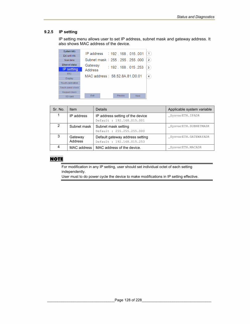
Status and Diagnostics
_________________________________Page 128 of 228__________________________________
9.2.5 IP setting IP setting menu allows user to set IP address, subnet mask and gateway address. It also shows MAC address of the device.
Sr. No. Item Details Applicable system variable 1 IP address IP address setting of the device
Default : 192.168.015.001 _SysvarETH.IPADR
2 Subnet mask Subnet mask setting Default : 255.255.255.000
_SysvarETH.SUBNETMASK
3 Gateway Address
Default gateway address setting Default : 192.168.015.253
_SysvarETH.GATEWAYADR
4 MAC address MAC address of the device. _SysvarETH.MACADR
NOTE
For modification in any IP setting, user should set individual octet of each setting independently. User must to do power cycle the device to make modifications in IP setting effective.
1
2
3
4

Status and Diagnostics
_________________________________Page 129 of 228__________________________________
9.2.6 RTC RTC (Real Time Clock) menu allows user to set real time clock. User can monitor RTC status, current date in (DD : MM : YYYY) format and current time.in (HH : MM : SS) format.
Sr. No. Item Details Applicable system variable 1 RTC
status Shows RTC status as OK or Invalid. Invalid: RTC fault due to discharge of backup super capacitor or hardware fault. So current date is set to 01:01:1971 and current time to 00:00:00. In such case, user should ensure that backup supper capacitor is fully charged and set RTC value again. OK: RTC value is valid.
_SysvarCPU. WSTATUS.4
2 Current Date
Current date. _SysvarRTC. BREADDATE
_SysvarRTC. BREADMONTH
_SysvarRTC. BREADYEARL
_SysvarRTC. BREADYEARH
3 Current Time
Current time. _SysvarRTC. BREADHRS
_SysvarRTC. BREADMINS
_SysvarRTC. BREADSECS
NOTE
For modification in RTC, user should set date, month, year, hour, minute and second independently.
1 2
3

Status and Diagnostics
_________________________________Page 130 of 228__________________________________
9.2.7 Display Display menu provides display related settings such as backlit timeout, display brightness, buzzer volume and buzzer pitch.
Sr. No. Item Details Applicable system variable 1 Backlit
timeout Backlit timeout can be set from 0 to 99 minutes Default setting is 05 minutes. Setting 00 means that backlit is continuously ON. Note that backlit life is 20,000 hours at ambient temperature.
_SysvarHMI.BACKLITTIMEOUT
2 Display brightness
Display brightness can be set from 0 to 100%. Default setting is 50 %. i.e. minimum brightness.
_SysvarHMI.LCDBRIGHTNESS
3 Buzzer volume
Buzzer volume can be set as Short, Long, OFF Default: Short
_SysvarHMI.BUZZERVOLUME
4 Buzzer pitch Buzzer pitch can be set in 5 levels from 1 to 5. Default setting is 3
_SysvarHMI.BUZZERPITCH
5 Buzzer on User can select buzzer to sound on pressing of Only touch Only keys Touch & key Default setting is Touch & key
_SysvarHMI.BUZZERONOPTION
1
2
3
4
5
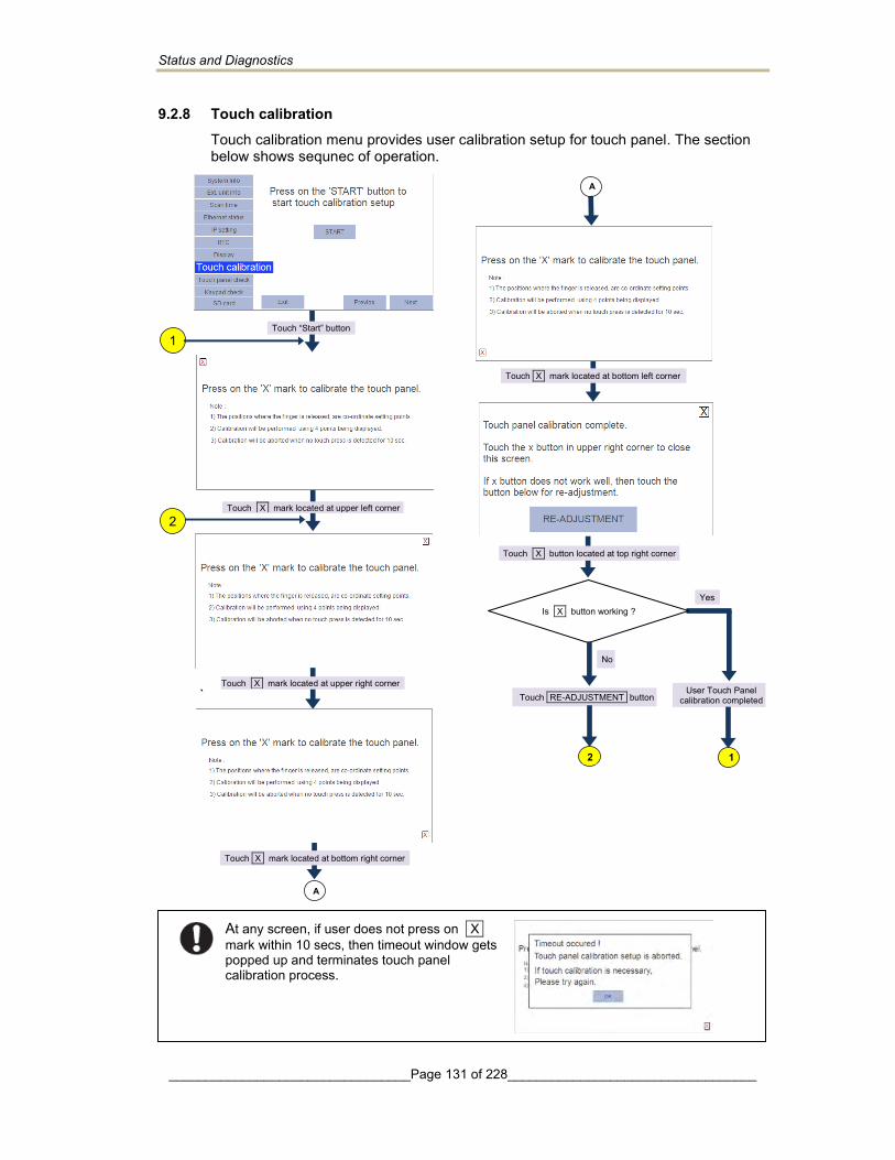
Status and Diagnostics
_________________________________Page 131 of 228__________________________________
9.2.8 Touch calibration Touch calibration menu provides user calibration setup for touch panel. The section below shows sequnec of operation.
`
A
Is X button working ?
Touch RE-ADJUSTMENT button
No
Yes
Touch “Start” button
Touch X mark located at upper left corner
Touch X mark located at upper right corner
Touch X mark located at bottom right corner
Touch X mark located at bottom left corner
User Touch Panel calibration completed
A
1
1 2
At any screen, if user does not press on X mark within 10 secs, then timeout window gets popped up and terminates touch panel calibration process.
Touch X button located at top right corner
2
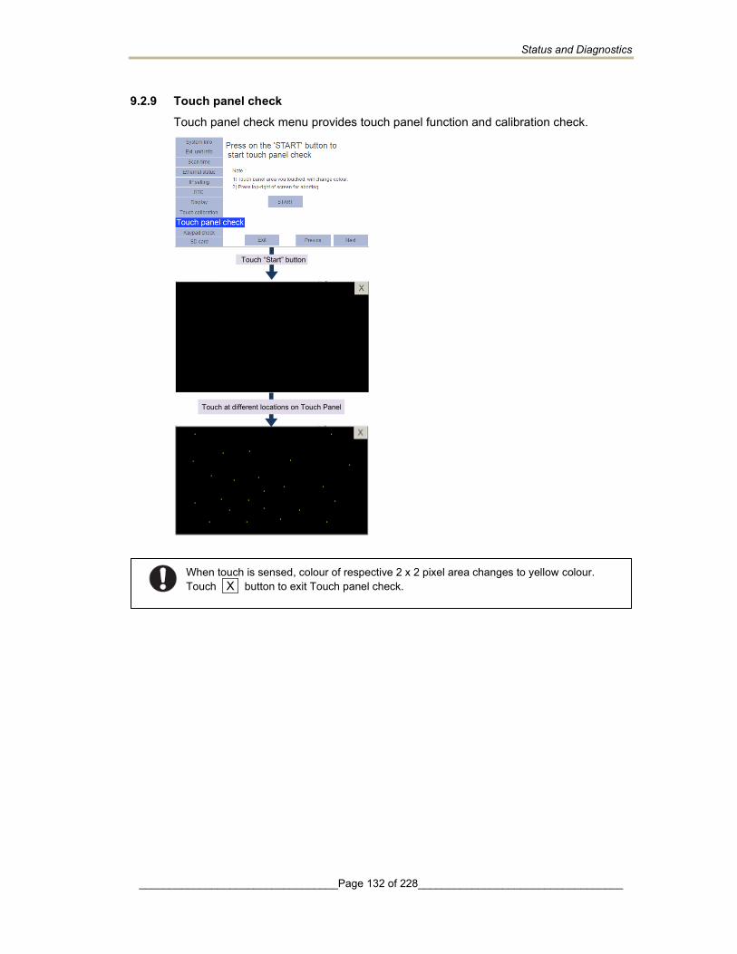
Status and Diagnostics
_________________________________Page 132 of 228__________________________________
9.2.9 Touch panel check Touch panel check menu provides touch panel function and calibration check.
Touch “Start” button
Touch at different locations on Touch Panel
When touch is sensed, colour of respective 2 x 2 pixel area changes to yellow colour. Touch X button to exit Touch panel check.
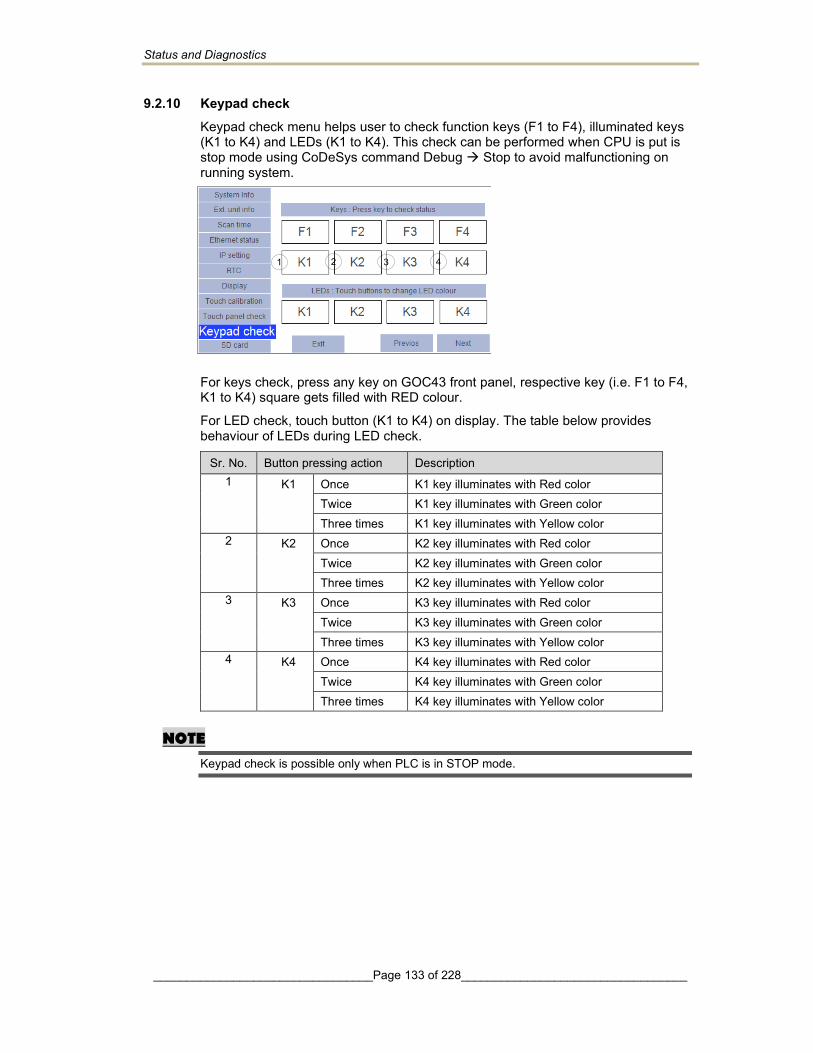
Status and Diagnostics
_________________________________Page 133 of 228__________________________________
9.2.10 Keypad check Keypad check menu helps user to check function keys (F1 to F4), illuminated keys (K1 to K4) and LEDs (K1 to K4). This check can be performed when CPU is put is stop mode using CoDeSys command Debug → Stop to avoid malfunctioning on running system.
For keys check, press any key on GOC43 front panel, respective key (i.e. F1 to F4, K1 to K4) square gets filled with RED colour.
For LED check, touch button (K1 to K4) on display. The table below provides behaviour of LEDs during LED check.
Sr. No. Button pressing action Description 1 K1 Once K1 key illuminates with Red color
Twice K1 key illuminates with Green color Three times K1 key illuminates with Yellow color
2 K2 Once K2 key illuminates with Red color Twice K2 key illuminates with Green color Three times K2 key illuminates with Yellow color
3 K3 Once K3 key illuminates with Red color Twice K3 key illuminates with Green color Three times K3 key illuminates with Yellow color
4 K4 Once K4 key illuminates with Red color Twice K4 key illuminates with Green color Three times K4 key illuminates with Yellow color
NOTE
Keypad check is possible only when PLC is in STOP mode.
1
2
3
4
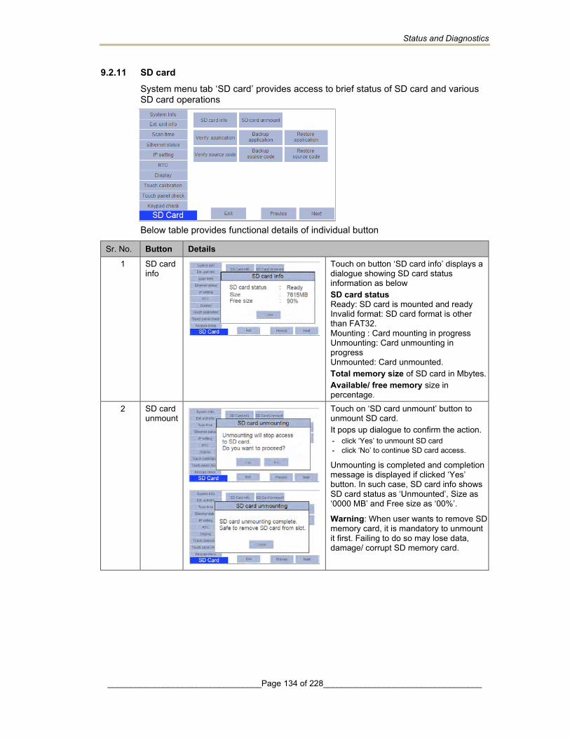
Status and Diagnostics
_________________________________Page 134 of 228__________________________________
9.2.11 SD card System menu tab ‘SD card’ provides access to brief status of SD card and various SD card operations
Below table provides functional details of individual button
Sr. No. Button Details 1 SD card
info Touch on button ‘SD card info’ displays a
dialogue showing SD card status information as below SD card status Ready: SD card is mounted and ready Invalid format: SD card format is other than FAT32. Mounting : Card mounting in progress Unmounting: Card unmounting in progress Unmounted: Card unmounted. Total memory size of SD card in Mbytes. Available/ free memory size in percentage.
2 SD card unmount
Touch on ‘SD card unmount’ button to unmount SD card. It pops up dialogue to confirm the action. - click ‘Yes’ to unmount SD card - click ‘No’ to continue SD card access.
Unmounting is completed and completion message is displayed if clicked ‘Yes’ button. In such case, SD card info shows SD card status as ‘Unmounted’, Size as ‘0000 MB’ and Free size as ‘00%’.
Warning: When user wants to remove SD memory card, it is mandatory to unmount it first. Failing to do so may lose data, damage/ corrupt SD memory card.

Status and Diagnostics
_________________________________Page 135 of 228__________________________________
Backup application, Backup source code
Buttons initiate backup function to copy application program and source code from device to SD card. Refer section ‘Backup application program and source code’ for more details.
Restore application, Restore source code
Buttons initiate restore function to copy application program and source code from SD card to device. Refer section ‘Restore application program and source code’ for more details.
Verify application, Verify source code
Buttons initiate verify function to compare application program and source code from device and SD card. Refer section ‘Verify application program and source code’ for more details.
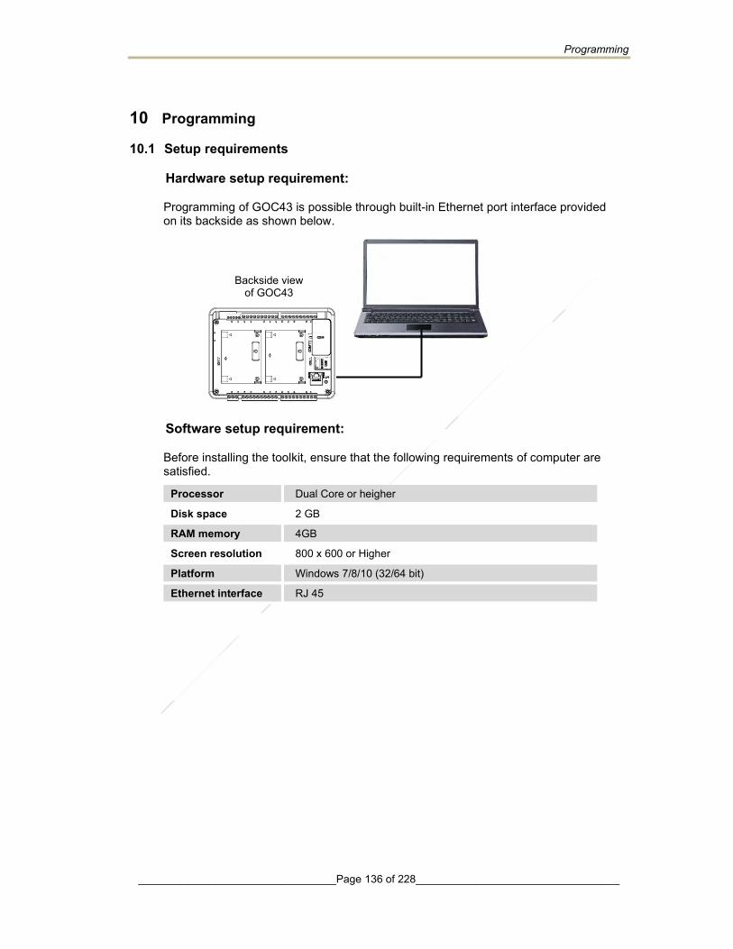
Programming
_________________________________Page 136 of 228__________________________________
10 Programming
10.1 Setup requirements
Hardware setup requirement:
Programming of GOC43 is possible through built-in Ethernet port interface provided on its backside as shown below.
Software setup requirement:
Before installing the toolkit, ensure that the following requirements of computer are satisfied.
Processor Dual Core or heigher
Disk space 2 GB
RAM memory 4GB
Screen resolution 800 x 600 or Higher
Platform Windows 7/8/10 (32/64 bit)
Ethernet interface RJ 45
Backside view of GOC43

Programming
_________________________________Page 137 of 228__________________________________
10.2 GOCToolkit V3 Installation For installation of GOCToolKit V3, follow the steps as provided below.
1. Confirm the requirement covered under ‘Software setup requirement’ section.
2. Download ‘GOCToolkit V3.exe’ setup from MEI website.
3. Run ‘GOCToolkit V3.exe’ on your PC. During execution of .exe file,
In case if user, uninstalls previous ToolKit versions from PC and updates system with latest ToolKit setup, then before running ‘GOCToolkit V3.exe’. It is mandatory to uninstall CODESYS 3.5.14.10 from PC and delete all files/ folders from path C:\Program Files (x86)\CODESYS 3.5.14.10. Folder “CODESYS 3.5.14.10” should be empty before latest ToolKit installation. Refer below screenshot as an example….
Click “Next” button
Click “Next” button
1
Click “Next” button
It is recommended to
select setup type as
“Complete”
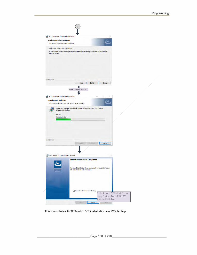
Programming
_________________________________Page 138 of 228__________________________________
This completes GOCToolKit V3 installation on PC/ laptop.
Click “Install” button
1
Click on ‘Finish’ to
complete ToolKit V3
installation
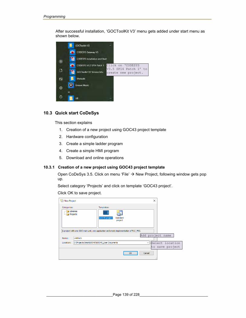
Programming
_________________________________Page 139 of 228__________________________________
After successful installation, ‘GOCToolKit V3’ menu gets added under start menu as shown below.
10.3 Quick start CoDeSys
This section explains
1. Creation of a new project using GOC43 project template
2. Hardware configuration
3. Create a simple ladder program
4. Create a simple HMI program
5. Download and online operations
10.3.1 Creation of a new project using GOC43 project template Open CoDeSys 3.5. Click on menu ‘File’ → New Project, following window gets pop up.
Select category ‘Projects’ and click on template ‘GOC43 project’.
Click OK to save project.
Click on ‘CODESYS
V3.5 SP14 Patch 1’ to
create new project.
Add project name
Select location
to save project

Programming
_________________________________Page 140 of 228__________________________________
After saving project below ‘GOC 43 Project’ window gets pop up.
After clicking OK, following ‘Devices’ tab gets open as shown below. This completes project creation and device (Main unit) selection.
Select programming
language for POU
PLC_PRG
Click OK to create
project

Programming
_________________________________Page 141 of 228__________________________________
10.3.2 Hardware configuration 1. For Hardware configuration, click on device Device(GC43) as shown below.
2. On Hardware configuration tab back side view of Main unit is shown as below.
3. Right click on Main unit area opens, Update Device window.
Red highlighter
denotes Main unit
is selected.
Select device and
click on ‘Update
Device’ button.
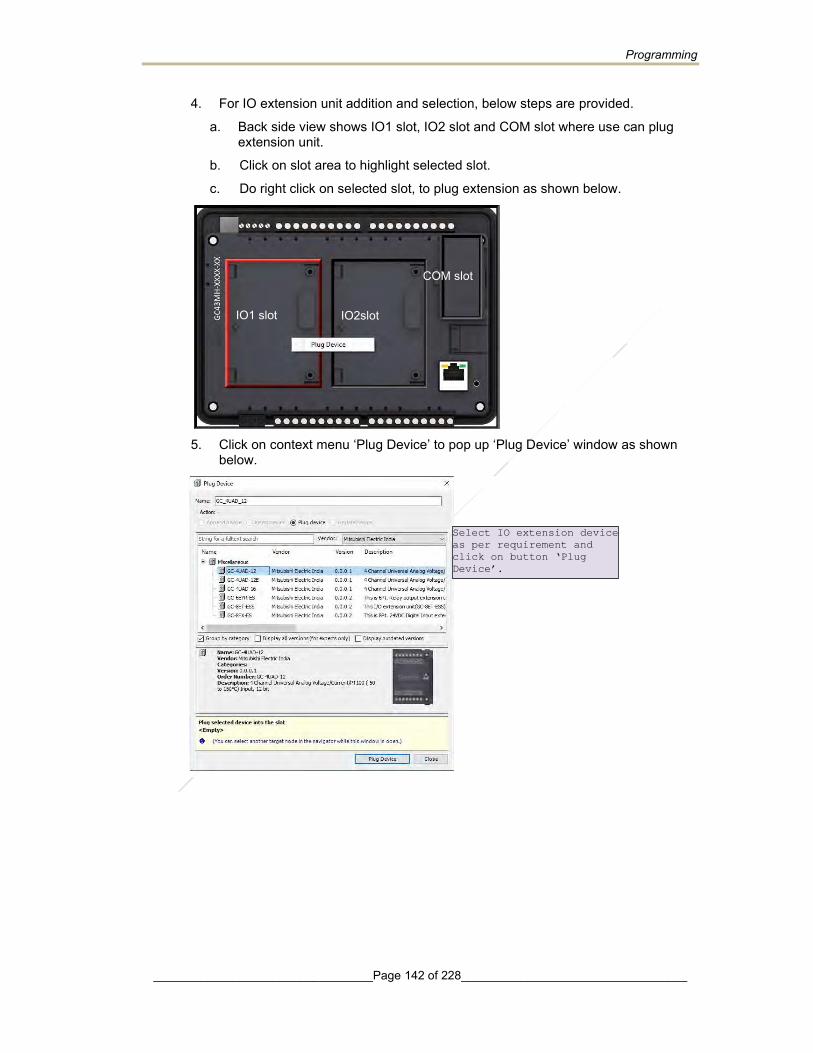
Programming
_________________________________Page 142 of 228__________________________________
4. For IO extension unit addition and selection, below steps are provided.
a. Back side view shows IO1 slot, IO2 slot and COM slot where use can plug extension unit.
b. Click on slot area to highlight selected slot.
c. Do right click on selected slot, to plug extension as shown below.
5. Click on context menu ‘Plug Device’ to pop up ‘Plug Device’ window as shown below.
IO1 slot IO2slot
COM slot
Select IO extension device
as per requirement and
click on button ‘Plug
Device’.

Programming
_________________________________Page 143 of 228__________________________________
6. After plugging IO extensions, if user requires to plug/update or delete device as per application requirement, right click on extension unit.
For example, IO1 slot extension unit is selected and right clicked as shown below.
This completes one method for plugging IO extensions and COM extensions.
Alternately, user can plug extension devices in respective slots (IOExtensions and COMExtension) in Device tree. Follow the steps below.
1. Right click on <Empty> slot to pop up context menu. 2. Click on Plug Device. Plug Device dialog shows list of extension devices
supported for the selected slot. 3. Select extension device and double click on it or click on button Plug Device
to attach it to selected slot. After plugging, default name of I/O extension unit as IOE1<UnitOrderingCode> and IOE2<UnitOrderingCode>.
This completes hardware configuration selection.
Here, default name of
I/O extension unit is
IOE1(GC-4A-12) in device
tree.
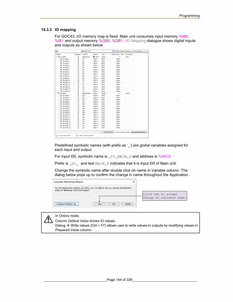
Programming
_________________________________Page 144 of 228__________________________________
10.3.3 IO mapping For GOC43, I/O memory map is fixed. Main unit consumes input memory %IB0, %IB1 and output memory %QB0, %QB1. I/O Mapping dialogue shows digital Inputs and outputs as shown below.
Predefined symbolic names (with prefix as ‘_’) are global variables assigned for each input and output.
For input I00, symbolic name is _DI_MAIN_0 and address is %IX0.0.
Prefix is _DI_ and text MAIN_0 indicates that it is input I00 of Main unit.
Change the symbolic name after double click on name in Variable column. The dialog below pops up to confirm the change in name throughout the Application .
In Online mode, Column Default Value shows IO values. Debug → Write values (Ctrl + F7) allows user to write values to outputs by modifying values in Prepared Value column.
Click Yes to accept
change in variable name.

Programming
_________________________________Page 145 of 228__________________________________
10.3.4 IEC Objects IEC objects are pre-defined global variables ((with prefix as ‘_’) which consists of system variables and variables related to various functions.
The dialog below shows offline view.
10.3.5 PLC Settings User can make the basic settings like handling of inputs and outputs and the bus cycle task.
Using tab “IEC Objects”, user can monitor and set system variables in CoDeSys online mode.
User can monitor and modify values of IEC objects in Online mode.
For safe operation, select
option Set all outputs to
default for setting Behaviour
of outputs in Stop.
Ensure to choose option
Enabled 2 (always in bus
cycle task’ for setting
Always update variables.
Ensure to choose option
MainTask’ for setting
Bus cycle task.
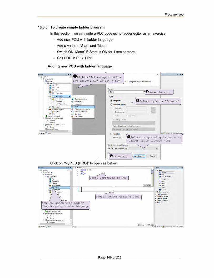
Programming
_________________________________Page 146 of 228__________________________________
10.3.6 To create simple ladder program In this section, we can write a PLC code using ladder editor as an exercise.
– Add new POU with ladder language
– Add a variable ‘Start’ and ‘Motor’
– Switch ON ‘Motor’ if ‘Start’ is ON for 1 sec or more.
– Call POU in PLC_PRG
Adding new POU with ladder language
Click on “MyPOU (PRG)” to open as below.
Right click on application
and execute Add object > POU…
Name the POU
Select type as ‘Program’
Select programming language as
‘Ladder Logic Diagram (LD)
Click ADD
New POU added with Ladder
diagram programming language
Ladder editor working area.
Local variables of POU
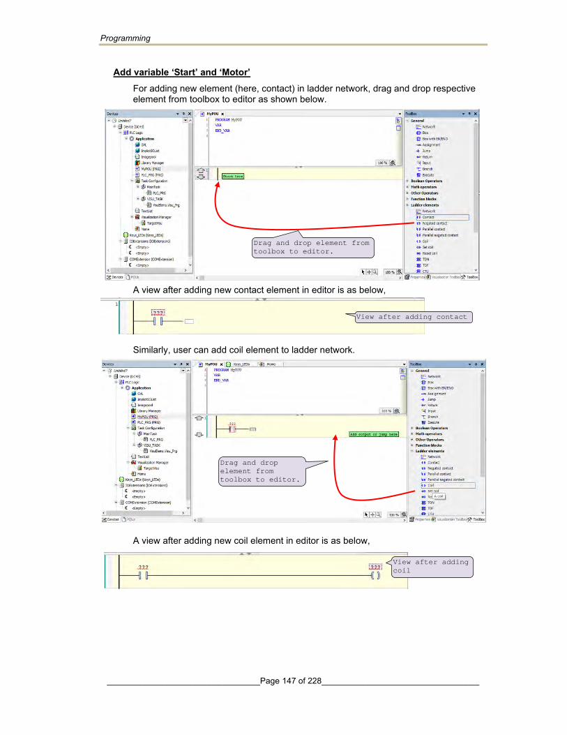
Programming
_________________________________Page 147 of 228__________________________________
Add variable ‘Start’ and ‘Motor’ For adding new element (here, contact) in ladder network, drag and drop respective element from toolbox to editor as shown below.
A view after adding new contact element in editor is as below,
Similarly, user can add coil element to ladder network.
A view after adding new coil element in editor is as below,
View after adding contact
Drag and drop element from
toolbox to editor.
Drag and drop
element from
toolbox to editor.
View after adding
coil

Programming
_________________________________Page 148 of 228__________________________________
After adding elements to ladder network , user can assign variable to element as shown below.
Similarly, assign variable to coil element as ‘Motor’.
Type-in name of variable and press
Enter. If variable with this name is
not declared earlier then ‘Auto
declare’ dialogue opens
Select scope Local/ Global/
VAR_IN/ VAR_OUT, etc. Select data type
Enter address
(optional)
Enter comment here
(optional)
Check ‘Retain’ if you
want to retain
variable.(Optional)
Click OK to close
View after adding
variables

Programming
_________________________________Page 149 of 228__________________________________
Switch ON ‘Motor’, if ‘Start’ is ON for 1 sec. To turn ‘Motor’ ON when ‘Start’ is ON for 1 sec, it is required to add timer function block in ladder network as shown below.
After pressing enter, auto-declare dialogue opens to declare timer FB instance.
This completes assigning names and variables to added elements.
Drag and drop element from
toolbox to editor.
Change Name and comment if
required and check OK to
close dialogue.
View after adding
Timer
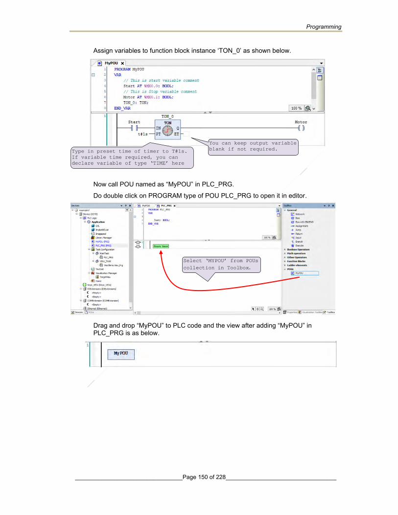
Programming
_________________________________Page 150 of 228__________________________________
Assign variables to function block instance ‘TON_0’ as shown below.
Now call POU named as “MyPOU” in PLC_PRG.
Do double click on PROGRAM type of POU PLC_PRG to open it in editor.
Drag and drop “MyPOU” to PLC code and the view after adding “MyPOU” in PLC_PRG is as below.
Type in preset time of timer to T#1s.
If variable time required, you can
declare variable of type ‘TIME’ here
You can keep output variable
blank if not required.
Select ‘MYPOU’ from POUs
collection in Toolbox.

Programming
_________________________________Page 151 of 228__________________________________
10.3.7 To create simple HMI program In this section, we can see how to do HMI programming in CoDeSys 3.5.
Execute Device (GC43) >> Application >> Visualization Manager, for HMI function settings and to drag and drop HMI objects from visualization toolbox.
For setting HMI functions, click on “Visualization Manager”,
Do not modify default settings available on “Visualization Manager” tab as below. It may cause malfunction of HMI functionality.
HMI function settings can be
done at ‘Visualization
Manager” and ‘TargetVisu’.
Home : Starting screen
Visualization toolbox
Do not modify default settings provided on “Visualization Manager” tab and “TargetVisu” tab.
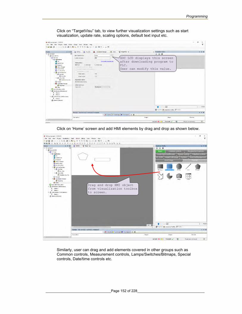
Programming
_________________________________Page 152 of 228__________________________________
Click on “TargetVisu” tab, to view further visualization settings such as start visualization, update rate, scaling options, default text input etc.
Click on ‘Home’ screen and add HMI elements by drag and drop as shown below.
Similarly, user can drag and add elements covered in other groups such as Common controls, Measurement controls, Lamps/Switches/Bitmaps, Special controls, Date/time controls etc.
GOC LCD displays this screen
after downloading program to
PLC.
User can modify this value.
Drag and drop HMI object
from visualization toolbox
to screen.

Programming
_________________________________Page 153 of 228__________________________________
For setting properties of individual element, select element on screen so that element ‘Properties’ window gets open in toolbox as shown.
Also, user can add multiple screens up to 64 screens by executing Device (GC 43) >> Application [do right click] >> Add Object >> Visualization.
Element properties window
for selected element.
Here, Polygon.
User can modify
visualization name as per
application requirement.
Click on Add button, to
add screen under
‘Visualization Manager’.

Programming
_________________________________Page 154 of 228__________________________________
10.3.8 To download project and Online operations
For downloading project to PLC, it should be error free.
Compile project by executing menu Build >> Clean all, Build >> Rebuild. This provides user list of errors (if any), warnings and information messages under “Messages” window.
After successful compilation of project, follow below steps,
1. Power ON and connect GOC43 device to PC via Ethernet.
2. Click on Device (GC 43) >> Communication settings as shown below.
3. Execute menu Online >> Login (Alt + F8), this opens confirmation dialogue to start project downloading
4. After successful downloading, execute menu Debug >> Start (F5) to put device in RUN mode.
Click on Scan network to open
‘Select Device’ dialogue.
Click here on
Scan network to
update connected
device.
Click Ok to connect
with selected device
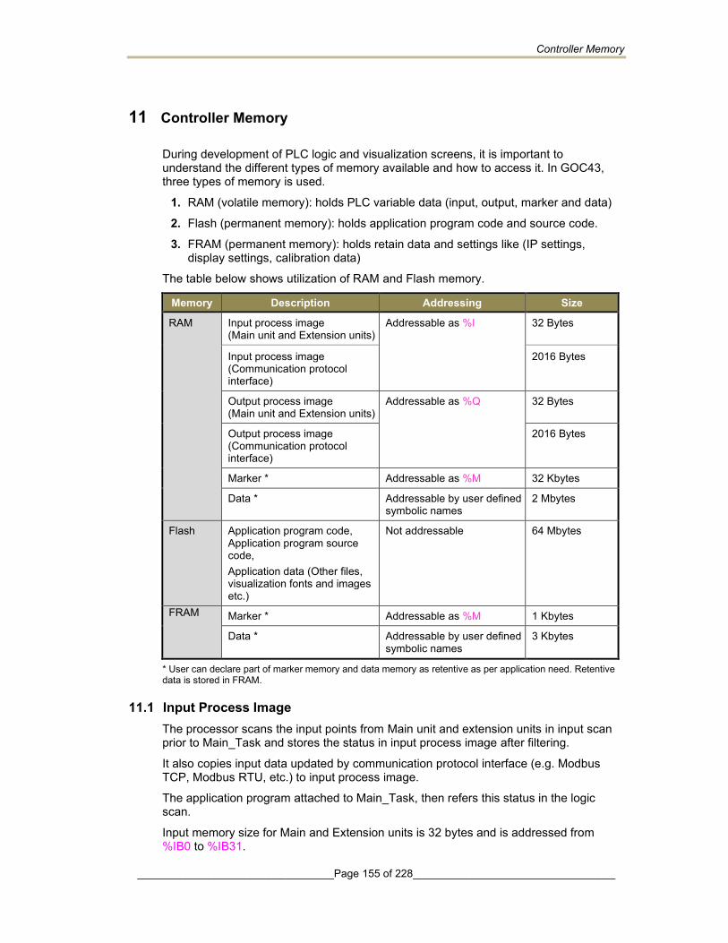
Controller Memory
_________________________________Page 155 of 228__________________________________
11 Controller Memory
During development of PLC logic and visualization screens, it is important to understand the different types of memory available and how to access it. In GOC43, three types of memory is used.
1. RAM (volatile memory): holds PLC variable data (input, output, marker and data)
2. Flash (permanent memory): holds application program code and source code.
3. FRAM (permanent memory): holds retain data and settings like (IP settings, display settings, calibration data)
The table below shows utilization of RAM and Flash memory.
Memory Description Addressing Size
RAM Input process image (Main unit and Extension units)
Addressable as %I 32 Bytes
Input process image (Communication protocol interface)
2016 Bytes
Output process image (Main unit and Extension units)
Addressable as %Q 32 Bytes
Output process image (Communication protocol interface)
2016 Bytes
Marker * Addressable as %M 32 Kbytes
Data * Addressable by user defined symbolic names
2 Mbytes
Flash Application program code, Application program source code, Application data (Other files, visualization fonts and images etc.)
Not addressable 64 Mbytes
FRAM Marker * Addressable as %M 1 Kbytes
Data * Addressable by user defined symbolic names
3 Kbytes
* User can declare part of marker memory and data memory as retentive as per application need. Retentive data is stored in FRAM.
11.1 Input Process Image The processor scans the input points from Main unit and extension units in input scan prior to Main_Task and stores the status in input process image after filtering.
It also copies input data updated by communication protocol interface (e.g. Modbus TCP, Modbus RTU, etc.) to input process image.
The application program attached to Main_Task, then refers this status in the logic scan.
Input memory size for Main and Extension units is 32 bytes and is addressed from %IB0 to %IB31.
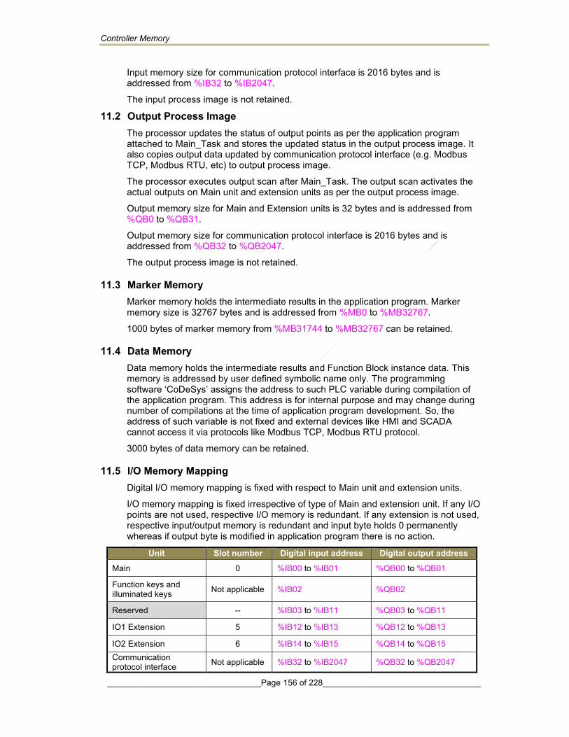
Controller Memory
_________________________________Page 156 of 228__________________________________
Input memory size for communication protocol interface is 2016 bytes and is addressed from %IB32 to %IB2047.
The input process image is not retained.
11.2 Output Process Image The processor updates the status of output points as per the application program attached to Main_Task and stores the updated status in the output process image. It also copies output data updated by communication protocol interface (e.g. Modbus TCP, Modbus RTU, etc) to output process image.
The processor executes output scan after Main_Task. The output scan activates the actual outputs on Main unit and extension units as per the output process image.
Output memory size for Main and Extension units is 32 bytes and is addressed from %QB0 to %QB31.
Output memory size for communication protocol interface is 2016 bytes and is addressed from %QB32 to %QB2047.
The output process image is not retained.
11.3 Marker Memory Marker memory holds the intermediate results in the application program. Marker memory size is 32767 bytes and is addressed from %MB0 to %MB32767.
1000 bytes of marker memory from %MB31744 to %MB32767 can be retained.
11.4 Data Memory Data memory holds the intermediate results and Function Block instance data. This memory is addressed by user defined symbolic name only. The programming software ‘CoDeSys’ assigns the address to such PLC variable during compilation of the application program. This address is for internal purpose and may change during number of compilations at the time of application program development. So, the address of such variable is not fixed and external devices like HMI and SCADA cannot access it via protocols like Modbus TCP, Modbus RTU protocol.
3000 bytes of data memory can be retained.
11.5 I/O Memory Mapping Digital I/O memory mapping is fixed with respect to Main unit and extension units.
I/O memory mapping is fixed irrespective of type of Main and extension unit. If any I/O points are not used, respective I/O memory is redundant. If any extension is not used, respective input/output memory is redundant and input byte holds 0 permanently whereas if output byte is modified in application program there is no action.
Unit Slot number Digital input address Digital output address
Main 0 %IB00 to %IB01 %QB00 to %QB01
Function keys and illuminated keys Not applicable %IB02 %QB02
Reserved -- %IB03 to %IB11 %QB03 to %QB11
IO1 Extension 5 %IB12 to %IB13 %QB12 to %QB13
IO2 Extension 6 %IB14 to %IB15 %QB14 to %QB15 Communication protocol interface Not applicable %IB32 to %IB2047 %QB32 to %QB2047
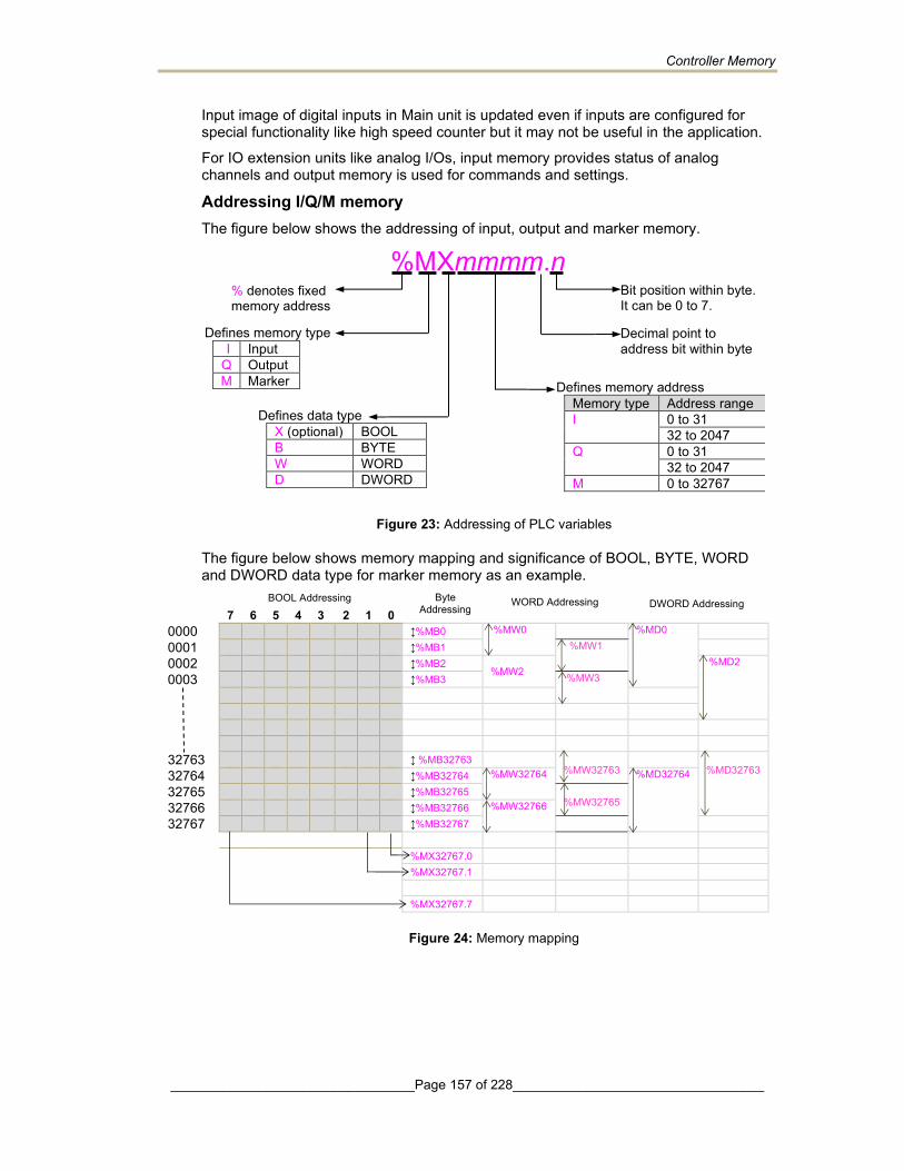
Controller Memory
_________________________________Page 157 of 228__________________________________
Input image of digital inputs in Main unit is updated even if inputs are configured for special functionality like high speed counter but it may not be useful in the application.
For IO extension units like analog I/Os, input memory provides status of analog channels and output memory is used for commands and settings.
Addressing I/Q/M memory The figure below shows the addressing of input, output and marker memory.
%MXmmmm.n
Figure 23: Addressing of PLC variables
The figure below shows memory mapping and significance of BOOL, BYTE, WORD and DWORD data type for marker memory as an example.
7 6 5 4 3 2 1 0 0000 %MB0 %MW0 %MD0 0001 %MB1 %MW1 0002 %MB2
%MW2 %MD2
0003 %MB3 %MW3
32763 %MB32763
%MW32763
%MD32763 32764 %MB32764 %MW32764 %MD32764
32765 %MB32765 %MW32765 32766 %MB32766 %MW32766
32767 %MB32767 %MX32767.0 %MX32767.1 %MX32767.7
Figure 24: Memory mapping
% denotes fixed memory address
Defines memory type I Input
Q Output M Marker
Defines data type
X (optional) BOOL B BYTE W WORD D DWORD
Defines memory address Memory type Address range I 0 to 31
32 to 2047 Q 0 to 31
32 to 2047 M 0 to 32767
Decimal point to address bit within byte
Bit position within byte. It can be 0 to 7.
Byte Addressing
WORD Addressing DWORD Addressing BOOL Addressing

Controller Memory
_________________________________Page 158 of 228__________________________________
Points to remember 1. Memory is arranged byte wise. All the 8 bits (0 to 7) within a byte can be
addressed individually.
2. When memory is addressed as WORD, then two consecutive bytes are accessed. Byte at start address is lower byte and next byte is higher byte.
3. When memory is addressed as DWORD, then two consecutive words (i.e. four consecutive bytes) are accessed. Word at start address is lower word and next word is higher word.
4. Addressing of WORD and DWORD as %MW0, %MW1, %MW2, %MD0, %MD1, %MD2, %MD3 is allowed.
5. Addressing words like %MD0, %MD1 in same application program will overlap 2 bytes (%MB1 in this case) and should be avoided.
6. Addressing double words like %MD0, %MD1 and like %MD2, %MD4 in same application program will certainly overlap 3 bytes (%MB1, %MB2 and %MB3 in first case) and 2 bytes (%MB4 and %MB5 in second case) and should be avoided.
11.6 Addressing Range The following table shows addressing range supported by GOC43.
PLC Memory Type Data Type Range
Input BOOL I X
%IX0.0 to %IX0.7 %IX1.0 to %IX1.7 %IX2047.0 to %IX2047.7
Input BYTE I B %IB0, %IB1, %IB2 to %IB2047 Input WORD I W %IW0, %IW1, %IW2, %IW3, %IW4 to %IW2046
Input DWORD I D %ID0, %ID1, %ID2, %ID3, %ID4 to %ID2044
Output BOOL Q X
%QX0.0 to %QX0.7 %QX1.0 to %QX1.7 %QX2047.0 to %QX2047.7
Output BYTE Q B %QB0, %QB1, %QB2 to %QB2047
Output WORD I W %QW0, %QW1, %QW2, %QW3, %QW4 to %QW2046
Output DWORD I D %QD0, %QD1, %QD2, %QD3, %QD4 to %QD2044
Marker BOOL M X
%MX0.0 to %MX0.7 %MX1.0 to %MX1.7 %MX32767.0 to %MX32767.7
Marker BYTE M B %MB0, %MB1, %MB2 to %MB32767
Marker WORD M W %MW0, %MW1, %MW2, %MW3, %MW4 to %MW32766
Marker DWORD M D %MD0, %MD1, %MD2, %MD3, %MD4 to %MD32764

Controller Memory
_________________________________Page 159 of 228__________________________________
11.7 Retained Memory Retentive memory is a memory that is declared by the user to maintain values through a power cycle or warm initialization. GOC43 allows 4000 bytes of memory to retain. The table below shows memory type and maximum size of memory that can be retained
Data memory 3 Kbytes
Marker memory 1 Kbytes (from %MB31744 to %MB32767)
Retained data is stored in FRAM type of memory. Cold initialization resets entire memory (including retentive memory) to 0 or user defined initial value.
Points to remember 1. User can define PLC variable as retentive using keyword VAR RETAIN. Local as
well as global variable can be declared as retentive.
e.g.
VAR RETAIN Data1: WORD;
END_VAR
Here, variable declared with symbolic name Data1 is retained.
2. Marker memory form %MB31744 to %MB32767 is retained by default if user accesses it directly by marker memory address (and not declared with some symbolic name). Whereas remaining marker memory from %MB0 to %MB31743 is cleared at warm initialization.
3. If any variable with symbolic name is mapped at marker memory address from %MB31744 to %MB32767, it is cleared at warm initialization if declared as shown below
VAR Data1 AT%MW32000: WORD;
END_VAR
To retain this variable, user has to declare it as retentive as below
VAR RETAIN Data1 AT%MW32000: WORD;
END_VAR
4. Any variable mapped outside specified marker memory is not retained even though declared as retentive.
e.g.
VAR RETAIN Data10 AT%MW1000: WORD; Op2 AT%QB2: BYTE;
END_VAR
Here, variables Data10 and Op2 will not be retained.

Controller Memory
_________________________________Page 160 of 228__________________________________
5. If user declares function block instance as retentive, then the complete instance of the function block (all the data of function block instance) is retained.
e.g.
VAR RETAIN T1: TON;
END_VAR
If instance T1 of ON delay timer TON is declared as retentive, then 28 bytes of data memory is retained.
6. During application program compilation, programming software ‘CoDeSys’ checks PLC variables declared by symbolic name (and not mapped at I/Q/M memory) for retained size limit of 3 Kbytes. If retained size exceeds 3 Kbytes, it displays compilation error as C0103: Out of retain memory: Variable ‘<name>’, <number> bytes
But for PLC variables mapped at marker memory (as well as for input and output memory), it does not check for retained size limit of 1 Kbytes. It does not display any compilation error for user mistake.
11.8 System Variables The system variables are pre-defined global variables. These variables exchange the information between CPU and application program. Each system variable has a unique name which starts with underscore ‘_Sysvar’. These system variables are useful to know the system status and diagnostics.
For more details, refer chapter System Variables.

Controller Memory
_________________________________Page 161 of 228__________________________________
11.9 Application Program Memory GOC43 stores application program in flash memory in form of code and source code.
Application Program Code (Boot Project)
The programming software ‘CoDeSys V3.5’ downloads complied project when
1. Menu command Online→_Download is executed or
2. Menu command Online → _Login Alt+F8__ is executed and there is mismatch between complied project and existing project in GOC43
This complied project is called the application program code or boot project which is executed by the processor.
Maximum application program code size is 8 Mbytes.
Application Data
This memory consists of visualization fonts, images, text lists, other system files, etc. It gets downloaded along with application program code. This is not a part of 8 Mbytes of application program code memory size.
Note that application data once downloaded to the device is stored in the flash memory. On further downloads, only additional application data is downloaded. If user deletes some of the previously downloaded application data (e.g. image, fonts) from visualization, it will not be deleted from flash memory on the device. So, there are chances of consuming 64 Mbytes of flash memory. In such case, CoDeSys declare disk full error and downloading is aborted.
To delete unused application data, user can erase application data along with application program code by executing command Online → Reset origin and download application program again. This ensures that only used application data is stored in the device.
Points to remember
1. Application program code (boot project) is not retrievable i.e. cannot be uploaded as a project file.
2. CoDeSys downloads application program code in flash memory. In case of unresolved external POUs (POUs in external library those are not supported by CPU firmware), CoDeSys prompts programmer at the end of download and PLC remains in STOP mode indicating memory error. At this point, programmer must download a valid application program code and put PLC in RUN mode. Instead if programmer recycles PLC power, PLC may start executing application code containing unresolved external POUs and may malfunction.

Controller Memory
_________________________________Page 162 of 228__________________________________
Application Program Source Code
The programming software ‘CoDeSys’ enables user to develop the application program using various IEC languages. This application program is saved as <Project_Name>.pro file on computer hard disk. The project file contains all project related information e.g. POUs in various IEC languages, program comments, variable declarations with symbolic name and comments, password, visualization screens with images and fonts, libraries (optional), system files, etc. It is necessary to store all this information called as Source code in GOC43 in the format defined by user.
Menu command Online→_Sourcecode download to connected device or Menu → Source download.. downloads application program source code to flash memory. Source code download is possible when CoDeSys is in Online monitoring mode.
Menu command File→_Source upload uploads project file from GOC43 and present it in .pro file format.
Points to remember 1. Download source code is mandatory so that entire application project remains with
GOC43 Main unit and can be retrieved later on whenever required. 2. Programmer can restrict unauthorized uploading of source code by programming read
protection password. 3. During source code download / upload, PLC function and visualization continues to
function normally. 4. Command Online → Reset origin deletes application program and application data.

High Speed Counter
_________________________________Page 163 of 228__________________________________
12 Built-in HSC (High Speed Counter)
GOC43 Main unit provides high speed inputs. By default, these inputs function as general purpose digital inputs. These inputs can be configured for different modes of counter operations.
12.1 Specifications
Item Description
Special functions of digital inputs (User configurable)
Single phase counters (up to 2 nos.)
Counter Input
Counter0 input I00
Counter3 input I03
Input frequency: 20 KHz maximum
Pulse ON/ OFF time: 20 µsec minimum
Quadrature encoder (Up to 2 nos.)
Encoder A phase B phase Z marker
Encoder0 input I00 input I01 input I02
Encoder3 input I03 input I04 input I05
Input frequency: 10 KHz maximum (for individual phase)
Pulse ON / OFF time for A and B phase: 20 µsec minimum. Pulse ON / OFF time for Z marker pulse: 50 µsec minimum.
NOTE
All the counters are 32-bit bi-directional counters.
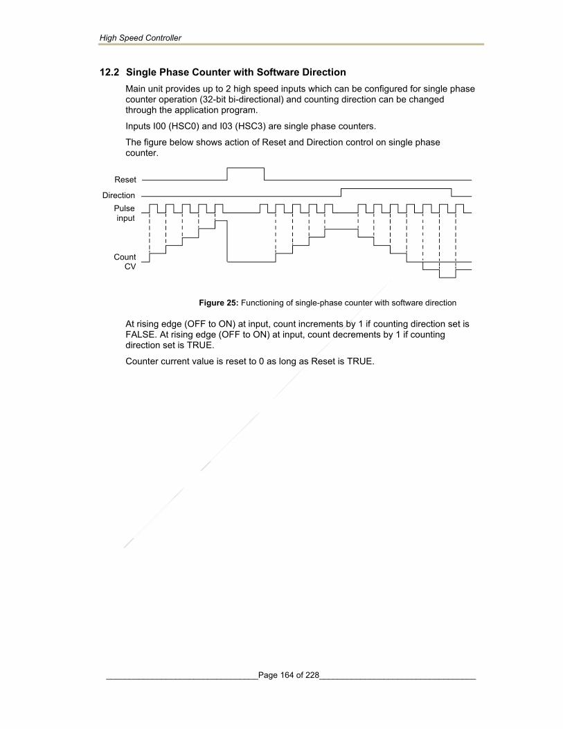
High Speed Controller
_________________________________Page 164 of 228__________________________________
12.2 Single Phase Counter with Software Direction Main unit provides up to 2 high speed inputs which can be configured for single phase counter operation (32-bit bi-directional) and counting direction can be changed through the application program.
Inputs I00 (HSC0) and I03 (HSC3) are single phase counters.
The figure below shows action of Reset and Direction control on single phase counter.
Figure 25: Functioning of single-phase counter with software direction
At rising edge (OFF to ON) at input, count increments by 1 if counting direction set is FALSE. At rising edge (OFF to ON) at input, count decrements by 1 if counting direction set is TRUE.
Counter current value is reset to 0 as long as Reset is TRUE.
Reset
Count CV
Direction Pulse input
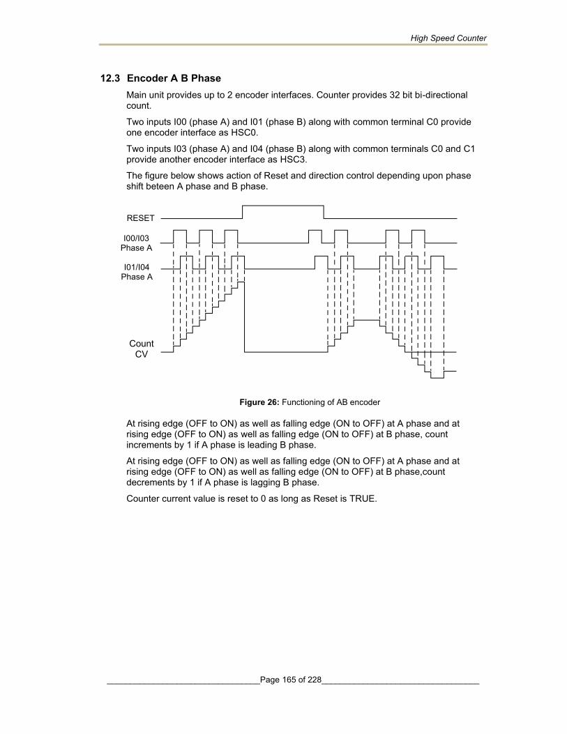
High Speed Counter
_________________________________Page 165 of 228__________________________________
12.3 Encoder A B Phase Main unit provides up to 2 encoder interfaces. Counter provides 32 bit bi-directional count.
Two inputs I00 (phase A) and I01 (phase B) along with common terminal C0 provide one encoder interface as HSC0.
Two inputs I03 (phase A) and I04 (phase B) along with common terminals C0 and C1 provide another encoder interface as HSC3.
The figure below shows action of Reset and direction control depending upon phase shift beteen A phase and B phase.
Figure 26: Functioning of AB encoder
At rising edge (OFF to ON) as well as falling edge (ON to OFF) at A phase and at rising edge (OFF to ON) as well as falling edge (ON to OFF) at B phase, count increments by 1 if A phase is leading B phase.
At rising edge (OFF to ON) as well as falling edge (ON to OFF) at A phase and at rising edge (OFF to ON) as well as falling edge (ON to OFF) at B phase,count decrements by 1 if A phase is lagging B phase.
Counter current value is reset to 0 as long as Reset is TRUE.
RESET
Count CV
I00/I03 Phase A
I01/I04 Phase A

High Speed Counter
_________________________________Page 166 of 228__________________________________
12.4 Encoder A B Phase with Z Pulse Main unit provides up to 2 encoder interfaces. Counter provides 32-bit bi-directional count.
Three inputs I00 (A phase), I01 (B phase), I02 (Z marker pulse) along with common terminal C0 provide one encoder interface as HSC0.
Three inputs I03 (A phase), I04 (B phase), I05 (Z marker pulse) along with common terminals C0 and C1 provide one encoder interface as HSC3.
User can program Z input to reset counter current value on occurance.The figure below shows action of Reset and Z input on encoder count.
Figure 27: Functioning of ABZ encoder
Count CV
Z_En
RESET
12
0 1
6
-1 On occurrence of Z, Current
value CV is reset if Z_EN is
active
I02/I05 Z pulse
I00/I03 A phase
I01/I04 B phase
5

High Speed Counter
_________________________________Page 167 of 228__________________________________
If RUN is TRUE, counter starts counting. If RUN is FALSE, counter does not count and counter current value CV holds last value.
At rising edge (OFF to ON) as well as falling edge (ON to OFF) at A phase and at rising edge (OFF to ON) as well as falling edge (ON to OFF) at iB phase, count increments by1 if A phase is leading B phase.At rising edge (OFF to ON) as well as falling edge (ON to OFF) at A phase and at rising edge (OFF to ON) as well as falling edge (ON to OFF) at B phase,count decrements by 1 if A phase is lagging B phase.Counter current value is reset to 0 as long as Reset is TRUE.
If user enables Z action then counter current value gets reset to 0 on occurrence of Z pulse. It reMains 0 as long as Z marker pulse in ON.
User can modify counter current value at any time and counter starts counting from modified value afterwards.
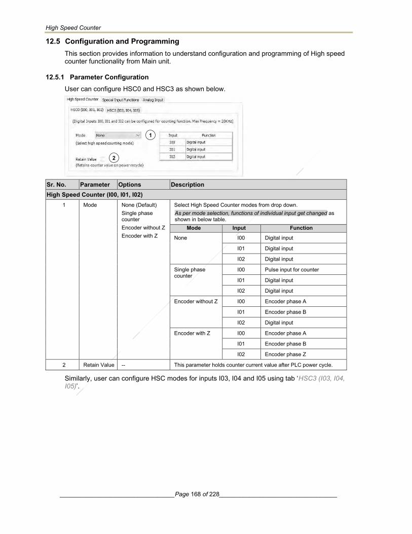
High Speed Counter
__________________________________Page 168 of 228___________________________________
12.5 Configuration and Programming This section provides information to understand configuration and programming of High speed counter functionality from Main unit.
12.5.1 Parameter Configuration User can configure HSC0 and HSC3 as shown below.
Sr. No. Parameter Options Description High Speed Counter (I00, I01, I02)
1 Mode None (Default) Single phase counter Encoder without Z Encoder with Z
Select High Speed Counter modes from drop down. As per mode selection, functions of individual input get changed as shown in below table.
Mode Input Function
None I00 Digital input
I01 Digital input
I02 Digital input
Single phase counter
I00 Pulse input for counter
I01 Digital input
I02 Digital input
Encoder without Z I00 Encoder phase A
I01 Encoder phase B
I02 Digital input
Encoder with Z I00 Encoder phase A
I01 Encoder phase B
I02 Encoder phase Z
2 Retain Value -- This parameter holds counter current value after PLC power cycle.
Similarly, user can configure HSC modes for inputs I03, I04 and I05 using tab ‘HSC3 (I03, I04, I05)’.
1
2

High Speed Counter
_________________________________Page 169 of 228__________________________________
12.5.2 I/O Mapping I/O Mapping dialogue shows digital Inputs and outputs as shown below.
As per mode selection, functions of individual input get changed as shown in below table. HSC Mode Input Function
None I00 Digital input
I01 Digital input
I02 Digital input
Single phase counter I00 Pulse input for counter
I01 Digital input
I02 Digital input
Encoder without Z I00 Encoder phase A
I01 Encoder phase B
I02 Digital input
Encoder with Z I00 Encoder phase A
I01 Encoder phase B
I02 Encoder phase Z
High Speed Counter
__________________________________Page 170 of 228___________________________________
12.5.3 IEC Objects The table below provides IEC objects related to Main unit high speed counter inputs.
IEC Variables Data Type Description Device.Application._HSC0
_HSC0_En BOOL Enable counting for HSC0
_HSC0_Dir BOOL If True, counting direction for HSC0 is upward. If False, counting direction for HSC0 is downward.
_HSC0_Reset BOOL If True, resets HSC0 count
_HSC0_Load BOOL If True, loads Preset value (PV)to HSC0
_HSC0_PV DINT Holds preset value (PV)for HSC0
_HSC0_CV DINT Holds current value (CV)for HSC0
Device.Application._HSC3
_HSC3_En BOOL Enable counting for HSC3
_HSC3_Dir BOOL If True, counting direction for HSC3 is upward. If False, counting direction for HSC3 is downward.
_HSC3_Reset BOOL If True, resets HSC3 count
_HSC3_Load BOOL If True, loads Preset value (PV)to HSC3
_HSC3_PV DINT Holds preset value (PV)for HSC3
_HSC3_CV DINT Holds current value (CV)for HSC3
Using tab “IEC Objects”, user can also monitor and set system variables in CoDeSys online mode.
Analog V/I Input
_________________________________Page 171 of 228__________________________________
13 Built-in Analog V/I Input
Main unit provides 2 channels analog V/I input with 12-bits resolution. It supports 0 to 10VDCand 0 to 20mA input ranges. Equivalent count is generated from 0 to 4000.
13.1 Analog Input Specifications Item Description
Number of input channels 2, Non-isolated, 12 bits
Input types and digital format
Voltage: 0 to 10VDC Current: 0 to 20mA
0 to 4000 0 to 4000
Resolution 2.5 mV 5 µA
Overall accuracy ± 0.4 at 25°C ± 0.8 at 25°C
± 0.6 at 60°C ± 0.7 at 60°C
Input impedance 900 KΩ 260 Ω
Engineering scaling Supported
Absolute maximum input ± 30 VDC/ ± 30 mA
Filter types For Digital filter, Time constant: 50 ms (Default) Supported range: 10 to 5000 ms
For Averaging, No. of averaging samples: 4, 8, 16, 32 (Default)
Updation time For digital filter, Channel data updation = Controller scan time + (Digital Filter Time Constant*10) minimum
For averaging, Channel data updation = Controller scan time x Number of averaging samples.
Channel protection PTC for over current up to 70 mA
Isolation No isolation.
I/O terminal blocks [Removable, screw type] One 5-pin

Analog V/I Input
__________________________________Page 172 of 228___________________________________
13.2 Configuration and Programming
13.2.1 Parameter Configuration User can configure Channel 0 and Channel 1 as shown below.
Sr. No. Parameter Options Description Filtering
1 Enable -- Check to enable the channel 0.
2 Input Type Voltage 0 to 10V (Default) Current 0 to 20mA
Selection for type of input as per application requirement.
3 Filter Type - No Filter - Digital Filter - Averaging
User can select filter type for input channel 0
4 No. of averaging sample
4, 8, 16, 32 (Default) For filter type as ‘Averaging’, user can select number of averaging samples using drop-down as either,
5 Filter time constant
Default value: 50 (ms). Supported range: 10 to 5000 ms
For filter type as ‘Digital Filter’, user can set filter time constant in msec.
Enable [Engineering scaling] 6 Enable -- Check ‘Enable’ to apply engineering
scaling to Channel 0.
7 Signal scale For 0 to10V input type, Min: 0V and Max: 10V. For 0 to 20mA input type, Min: 0mA and Max: 20 mA
This parameter holds min-max values as per configured input type. User cannot modify this parameter
8 Engineering scale
Default values, Min: 0.0 and Max: 100.0 Supported range: -64000.0 to 64000.0 for both Min- Max settings
User can set min-max values of engineering scaling as per application requirement.
Similarly, user can configure analog input Channel 1, using ‘Channel 1’ tab.
1
2
3
4
6
5
7 8
Analog V/I Input
_________________________________Page 173 of 228__________________________________
13.2.2 I/O Mapping Not applicable
13.2.3 IEC Objects The table below provides IEC objects related to the analog inputs of Main unit.
IEC Variables Data Type Description
Device.Application._Base_Analog _AI_Data_00 REAL Holds analog input data for Channel 0 _AI_Data_01 REAL Holds analog input data for Channel 1 _AI_ChannelStatus ARRAY
[0..1]OF WORD Holds status of channels 0 and 1. Each array element is assigned for individual channel e.g._AI_ChannelStatus[0] holds status of channel 0. Details of bits of status word as follows
Bit No Details
0 Channel enable status 0 - Disabled 1 - Enabled
1 Channel configuration 0 - Valid 1 - Invalid
2 Channel input data is out of range,
0: Data count valid 1: Data count invalid
3 Open circuit or short circuit detected, 0 - No open circuit 1 - Open circuit
4 - 15 Reserved
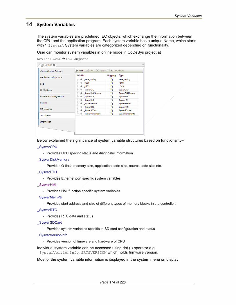
System Variables
__________________________________Page 174 of 228___________________________________
14 System Variables
The system variables are predefined IEC objects, which exchange the information between the CPU and the application program. Each system variable has a unique Name, which starts with ‘_Sysvar’. System variables are categorized depending on functionality.
User can monitor system variables in online mode in CoDeSys project at Device(GC43)→IEC Objects
Below explained the significance of system variable structures based on functionality– _SysvarCPU
- Provides CPU specific status and diagnostic information
_SysvarDiskMemory
- Provides Q-flash memory size, application code size, source code size etc.
_SysvarETH
- Provides Ethernet port specific system variables
_SysvarHMI
- Provides HMI function specific system variables
_SysvarMemPtr
- Provides start address and size of different types of memory blocks in the controller.
_SysvarRTC
- Provides RTC data and status
_SysvarSDCard
- Provides system variables specific to SD card configuration and status
_SysvarVersionInfo
- Provides version of firmware and hardware of CPU
Individual system variable can be accessed using dot (.) operator e.g. _SysvarVersionInfo.SRTSVERSION which holds firmware version.
Most of the system variable information is displayed in the system menu on display.
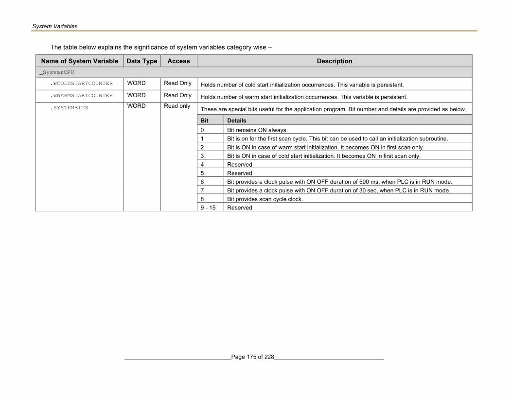
System Variables
_________________________________Page 175 of 228__________________________________
The table below explains the significance of system variables category wise –
Name of System Variable Data Type Access Description _SysvarCPU
.WCOLDSTARTCOUNTER WORD Read Only Holds number of cold start initialization occurrences. This variable is persistent.
.WWARMSTARTCOUNTER WORD Read Only Holds number of warm start initialization occurrences. This variable is persistent.
.SYSTEMBITS WORD Read only These are special bits useful for the application program. Bit number and details are provided as below.
Bit Details 0 Bit remains ON always. 1 Bit is on for the first scan cycle. This bit can be used to call an initialization subroutine. 2 Bit is ON in case of warm start initialization. It becomes ON in first scan only. 3 Bit is ON in case of cold start initialization. It becomes ON in first scan only. 4 Reserved 5 Reserved 6 Bit provides a clock pulse with ON OFF duration of 500 ms, when PLC is in RUN mode. 7 Bit provides a clock pulse with ON OFF duration of 30 sec, when PLC is in RUN mode. 8 Bit provides scan cycle clock. 9 - 15 Reserved
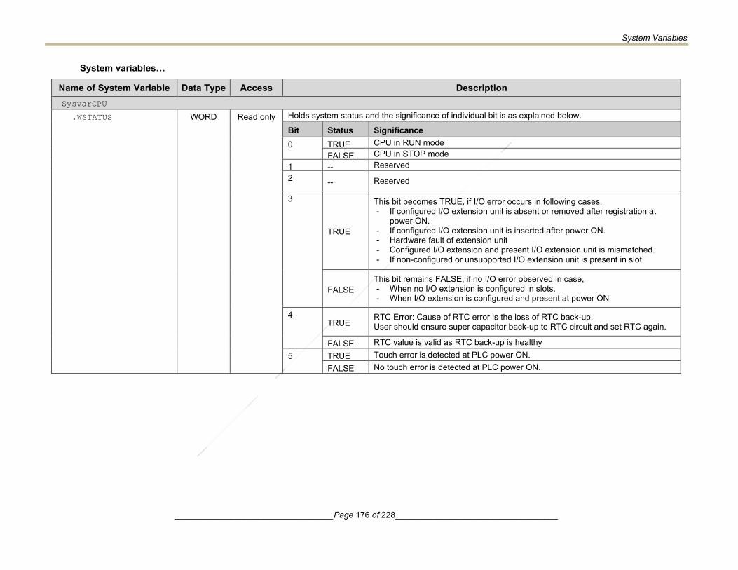
System Variables
__________________________________Page 176 of 228___________________________________
System variables…
Name of System Variable Data Type Access Description _SysvarCPU
.WSTATUS WORD Read only Holds system status and the significance of individual bit is as explained below.
Bit Status Significance 0 TRUE CPU in RUN mode
FALSE CPU in STOP mode 1 -- Reserved 2 -- Reserved
3
TRUE
This bit becomes TRUE, if I/O error occurs in following cases, - If configured I/O extension unit is absent or removed after registration at
power ON. - If configured I/O extension unit is inserted after power ON. - Hardware fault of extension unit - Configured I/O extension and present I/O extension unit is mismatched. - If non-configured or unsupported I/O extension unit is present in slot.
FALSE This bit remains FALSE, if no I/O error observed in case, - When no I/O extension is configured in slots. - When I/O extension is configured and present at power ON
4 TRUE
RTC Error: Cause of RTC error is the loss of RTC back-up. User should ensure super capacitor back-up to RTC circuit and set RTC again.
FALSE RTC value is valid as RTC back-up is healthy 5 TRUE Touch error is detected at PLC power ON.
FALSE No touch error is detected at PLC power ON.
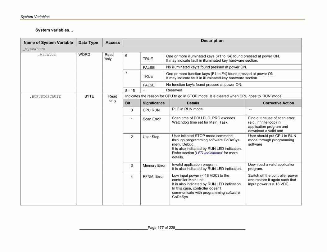
System Variables
_________________________________Page 177 of 228__________________________________
System variables…
.BCPUSTOPCAUSE BYTE Read only
Indicates the reason for CPU to go in STOP mode. It is cleared when CPU goes to 'RUN' mode.
Bit Significance Details Corrective Action
0 CPU RUN PLC in RUN mode --
1 Scan Error Scan time of POU PLC_PRG exceeds Watchdog time set for Main_Task.
Find out cause of scan error (e.g. infinite loop) in application program and download a valid and corrected application program. 2 User Stop User initiated STOP mode command
through programming software CoDeSys menu Debug. It is also indicated by RUN LED indication. Refer section ’LED Indications’ for more details.
User should put CPU in RUN mode through programming software
3 Memory Error Invalid application program. It is also indicated by RUN LED indication.
Download a valid application program.
4 PFNMI Error Low input power (< 18 VDC) to the controller Main unit. It is also indicated by RUN LED indication. In this case, controller doesn’t communicate with programming software CoDeSys
Switch off the controller power and restore it again such that input power is > 18 VDC.
Name of System Variable Data Type Access Description
_SysvarCPU .WSTATUS WORD Read
only 6
TRUE One or more illuminated keys (K1 to K4) found pressed at power ON. It may indicate fault in illuminated key hardware section.
FALSE No illuminated key/s found pressed at power ON. 7
TRUE One or more function keys (F1 to F4) found pressed at power ON. It may indicate fault in illuminated key hardware section.
FALSE No function key/s found pressed at power ON. 8 - 15 -- Reserved
System Variables
__________________________________Page 178 of 228___________________________________
System variables…
Name of System Variable Data Type Access Description
_SysvarCPU .BINITSTATUS BYTE Read only Holds the status of CPU initialization. This byte is updated whenever related action is executed.
Hot Initialization _SysvarCPU.BINITSTATUS holds 1, if system detects a power break for 20 to 200 ms. In this case controller functioning is normal as if there is no power disturbance.
Warm Initialization _SysvarCPU.BINITSTATUS holds 2 on healthy power ON, if system detects a power break for more than 200 ms. It results resetting of data, which is not retained. CoDeSys menu command Online → Reset warm causes warm initialization
Cold Initialization/ application download _SysvarCPU.BINITSTATUS holds 3, - If system detects any change in the application program. If a new application program is download
is in progress or cold start is observed. - Retentive data is destroyed because of hardware fault. - CoDeSys menu command Online →Reset cold is executed.
.ATASKNAME ARRAY [0..4] OF
STRING(15)
Read Only This variable holds task configuration available in CoDeSys application such as “MainTask”, “VISU_TASK” etc.
.WCURSCANTIME ARRAY [0..4] OF WORD
Read Only Holds scan time of last scan (in ms) of POU PLC_PRG attached to Main_Task. The value is updated at the end of each scan. If current scan exceeds Watchdog time set, CPU is put in STOP mode by declaring ‘scan error’.
.WMINSCANTIME Read Only Holds minimum scan time (in ms) in all previous PLC scans after power ON or warm or cold initialization. The value is updated at the end of each scan.
.WMAXSCANTIME Read Only Holds maximum scan time (in ms) in all previous PLC scans after power ON or warm or cold initialization with 1ms resolution.
System Variables
_________________________________Page 179 of 228__________________________________
System variables…
Name of System Variable Data Type Access Description _SysvarCPU
.W_REG_STATUS WORD Read only
Holds extension unit registration status as per the slots. The table below explains significance of bit depending upon hardware units and slot numbers. Bit Details 0 Bit becomes TRUE, if CPU detects presence of Main unit
1
Bit becomes TRUE, if CPU detects configured and fixed COM extension unit is identical.
Bit remains FALSE, in case if CPU detects, - Configured and fixed COM extension unit is mismatched. - Presence of unsupported COM extension unit. - COM extension unit is present at power ON but not configured in application. - Hot plugin, hot plug out of Configured and fixed COM extension unit. - COM extension unit is configured but absent at power ON.
2, 3,4 Reserved
5
Bit becomes TRUE, if CPU detects configured and fixed IOE1 extension unit is identical.
Bit remains FALSE, in case if CPU detects, - Configured and fixed IOE1 extension unit is mismatched. - Presence of unsupported IOE1 extension unit. - IOE1 extension unit is present at power ON but not configured in application. - Hot plugin, hot plug out of Configured and fixed IOE1 extension unit. - IOE1 extension unit is configured but absent at power ON.
6
Bit becomes TRUE, if CPU detects configured and fixed IOE2 extension unit is identical.
Bit remains FALSE, in case if CPU detects, - Configured and fixed IOE2 extension unit is mismatched. - Presence of unsupported IOE2 extension unit. - IOE2 extension unit is present at power ON but not configured in application. - Hot plugin, hot plug out of Configured and fixed IOE2 extension unit. - IOE2 extension unit is configured but absent at power ON.
7 to 15 Reserved
System Variables
__________________________________Page 180 of 228___________________________________
System variables…
Name of System Variable Data Type Access Description _SysvarCPU
.W_IOERR WORD Read only
Holds hardware units error status as per the slots. Probable cause for this error is - Configured extension unit is absent or removed after registration at power ON. - Hardware fault of extension unit is detected. - Configured and fixed extension unit is mismatched.
It takes 3 sec time duration to detect such error. Once IO error is declared it will not be cleared even if hardware is restored. I/O error is declared only for the hardware unit which is registered during controller power ON. IO Error is also indicated by RUN LED indication. Bit Details 0 Reserved
1
Bit becomes TRUE, if CPU detects IO error for COM extension slot such as, - Configured and fixed COM extension unit is mismatched. - Presence of unsupported COM extension unit. - COM extension unit is present at power ON but not configured in application. - Hot plugin, hot plug out of Configured and fixed COM extension unit. - COM extension unit is configured but absent at power ON.
Bit remains FALSE, if configured and fixed COM extension unit is identical. 2, 3,4 Reserved
5
Bit becomes TRUE, if CPU detects IO error for IO extension slot IOE1 such as, - Configured and fixed IOE1 extension unit is mismatched. - Presence of unsupported IOE1 extension unit. - IOE1 extension unit is present at power ON but not configured in application. - Hot plugin, hot plug out of Configured and fixed IOE1 extension unit. - IOE1 extension unit is configured but absent at power ON.
Bit remains FALSE, if configured and fixed IOE1 extension unit is identical.
6
Bit becomes TRUE, if CPU detects IO error for IO extension slot IOE1 such as, - Configured and fixed IOE2 extension unit is mismatched. - Presence of unsupported IOE2 extension unit. - IOE2 extension unit is present at power ON but not configured in application. - Hot plugin, hot plug out of Configured and fixed IOE2 extension unit. - IOE2 extension unit is configured but absent at power ON.
Bit remains FALSE, if configured and fixed IOE2 extension unit is identical. 7 to 15 Reserved
System Variables
_________________________________Page 181 of 228__________________________________
System variables…
Name of System Variable Data Type Access Description _SysvarCPU .AMODULEORDERINGCODE ARRAY [0..15]
OF STRING Read Only This array holds ordering code of hardware units detected.
_SysvarCPU.AMODULEORDERINGCODE[0]:Ordering code of Main unit _SysvarCPU.AMODULEORDERINGCODE[1]:Ordering code of COM Extension unit fixed in COM slot _SysvarCPU.AMODULEORDERINGCODE[2]:Reserved _SysvarCPU.AMODULEORDERINGCODE[3]:Reserved _SysvarCPU.AMODULEORDERINGCODE[4]:Reserved _SysvarCPU.AMODULEORDERINGCODE[5]:Ordering code of IO Extension unit fixed in IOE1 slot _SysvarCPU.AMODULEORDERINGCODE[6]:Ordering code of IO Extension unit fixed in IOE2 slot _SysvarCPU.AMODULEORDERINGCODE[7]to _AMODULEORDERINGCODE[15]: Reserved
_SysvarDiskMemory
.DWTOTALSIZEKB
DWORD
Read only This variable holds Q-Flash total memory size of connected device
.DWFREESIZEKB Read only This variable holds Q-Flash free memory size of connected device
.DWAPPSIZEKB Read only This variable holds application code size in Kbytes.
.DWAPPOBJECTDATASIZEKB Read only This variable holds object data files size in Kbytes.
.DWSOURCECODESIZEKB Read only This variable holds source code size in Kbytes. _SysvarETH
.IPADR ARRAY [0..3] OF BYTE
Read write This variable is used to set octets of IP address for connected device. Default IP address : 192.168.015.001
.SUBNETMASK Read write This variable is used to set subnet mask for connected device. Default Subnet mask : 255.255.255.000
.GATEWAYADR Read write This variable is used to set gateway address for connected device. Default Gateway Address : 192.168.015.253
.MACID Read write This variable is used to monitor and set MAC ID of connected device.
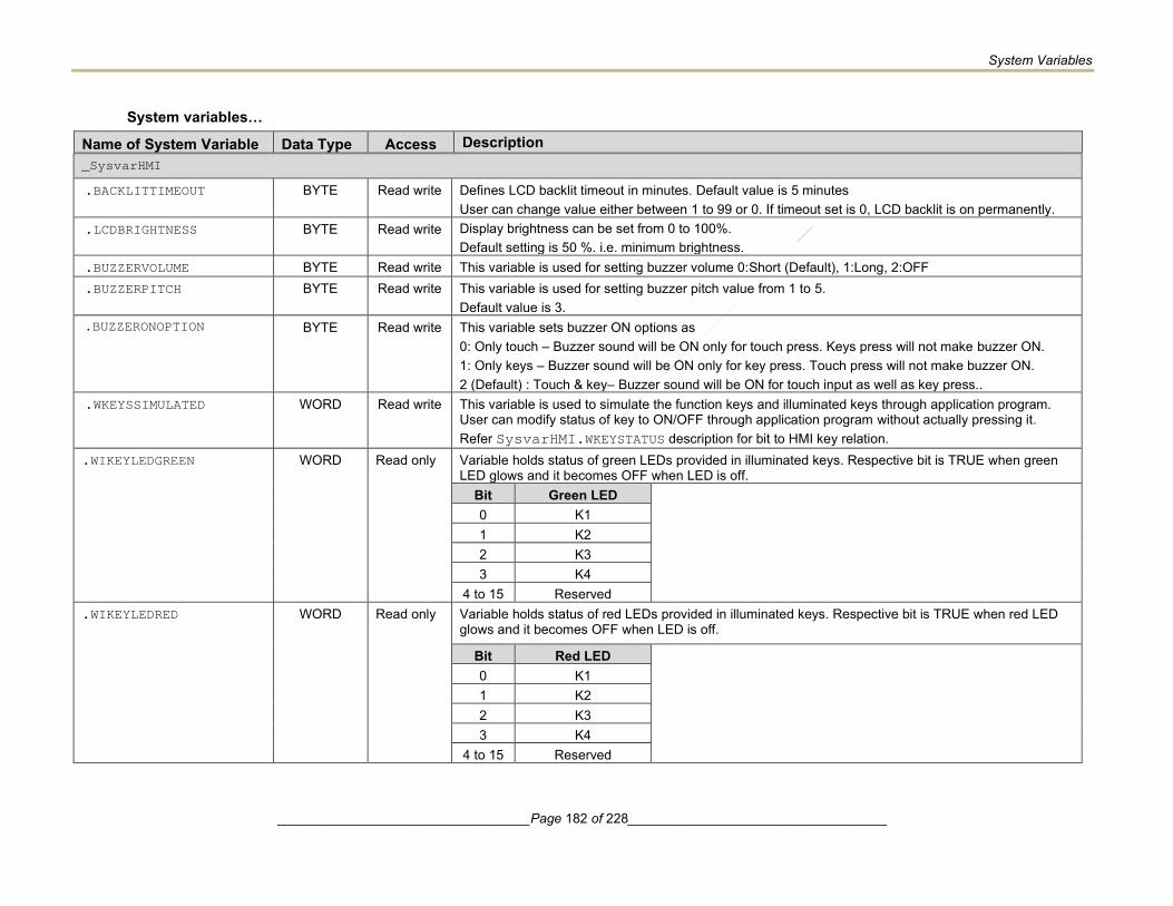
System Variables
__________________________________Page 182 of 228___________________________________
System variables…
_SysvarHMI
.BACKLITTIMEOUT BYTE Read write Defines LCD backlit timeout in minutes. Default value is 5 minutes User can change value either between 1 to 99 or 0. If timeout set is 0, LCD backlit is on permanently.
.LCDBRIGHTNESS BYTE Read write Display brightness can be set from 0 to 100%. Default setting is 50 %. i.e. minimum brightness.
.BUZZERVOLUME BYTE Read write This variable is used for setting buzzer volume 0:Short (Default), 1:Long, 2:OFF
.BUZZERPITCH BYTE Read write This variable is used for setting buzzer pitch value from 1 to 5. Default value is 3.
.BUZZERONOPTION BYTE Read write This variable sets buzzer ON options as 0: Only touch – Buzzer sound will be ON only for touch press. Keys press will not make buzzer ON. 1: Only keys – Buzzer sound will be ON only for key press. Touch press will not make buzzer ON. 2 (Default) : Touch & key– Buzzer sound will be ON for touch input as well as key press..
.WKEYSSIMULATED WORD Read write This variable is used to simulate the function keys and illuminated keys through application program. User can modify status of key to ON/OFF through application program without actually pressing it. Refer SysvarHMI.WKEYSTATUS description for bit to HMI key relation.
.WIKEYLEDGREEN WORD Read only Variable holds status of green LEDs provided in illuminated keys. Respective bit is TRUE when green LED glows and it becomes OFF when LED is off.
Bit Green LED 0 K1 1 K2 2 K3 3 K4
4 to 15 Reserved .WIKEYLEDRED WORD Read only Variable holds status of red LEDs provided in illuminated keys. Respective bit is TRUE when red LED
glows and it becomes OFF when LED is off.
Bit Red LED 0 K1 1 K2 2 K3 3 K4
4 to 15 Reserved
Name of System Variable Data Type Access Description
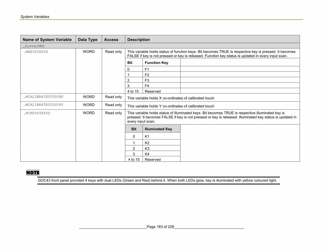
System Variables
_________________________________Page 183 of 228__________________________________
NOTE GOC43 front panel provided 4 keys with dual LEDs (Green and Red) behind it. When both LEDs glow, key is illuminated with yellow coloured light.
Name of System Variable Data Type Access Description _SysvarHMI .WKEYSTATUS WORD Read only This variable holds status of function keys. Bit becomes TRUE is respective key is pressed. It becomes
FALSE if key is not pressed or key is released. Function key status is updated in every input scan.
Bit Function Key
0 F1 1 F2 2 F3 3 F4 4 to 15 Reserved
.WCALIBRATEDTOUCHX WORD Read only This variable holds X co-ordinates of calibrated touch
.WCALIBRATEDTOUCHY WORD Read only This variable holds Y co-ordinates of calibrated touch
.WIKEYSTATUS WORD Read only This variable holds status of illuminated keys. Bit becomes TRUE is respective illuminated key is pressed. It becomes FALSE if key is not pressed or key is released. Illuminated key status is updated in every input scan.
Bit Illuminated Key
0 K1
1 K2 2 K3 3 K4
4 to 15 Reserved

System Variables
__________________________________Page 184 of 228___________________________________
System variables…
Name of System Variable Data Type Access Description _SysvarMemPtr
.ASEGMENTPTR ARRAY [0..5] OF DWORD
Read only Holds start address of various memory blocks – _SysvarMemPtr.ASEGMENTPTR[0]: Start address of input memory _SysvarMemPtr.ASEGMENTPTR[1]: Start address of output memory _SysvarMemPtr.ASEGMENTPTR[2]: Start address of marker memory _SysvarMemPtr.ASEGMENTPTR[3]: Start address of data memory _SysvarMemPtr.ASEGMENTPTR[4]: Reserved _SysvarMemPtr.ASEGMENTPTR[5]: Start address of LCD data buffer
.ASEGMENTLEN ARRAY [0..5] OF WORD
Read only Holds size of memory blocks – _SysvarMemPtr.ASEGMENTLEN[0]: Size of input memory _SysvarMemPtr.ASEGMENTLEN[1]: Size of output memory _SysvarMemPtr.ASEGMENTLEN[2]: Size of marker memory _SysvarMemPtr.ASEGMENTLEN[3]: Size of data memory _SysvarMemPtr.ASEGMENTLEN[4]: Reserved _SysvarMemPtr.ASEGMENTLEN[5]: Size of LCD data buffer
.ADRRXPORT1 DWORD Read only This variable holds start address of receive buffer of COM slot.
.ADRTXPORT1 DWORD Read only This variable holds start address of transmit buffer of COM slot. _SysvarRTC
.BRTCINVALID BYTE Read only RTC is backed up by super capacitor and back up time is 2 weeks nominal. This bit is TRUE if RTC is corrupted due to loss of back up due to any reason. RTC is then initialized to date of January 1, 1970 and time of 00H:00M:00S:00MS. In such case user has to ensure that super capacitor back up is restored and set proper value of RTC again. If user wants to use RTC data in application, programmer should consider this bit to check validity of RTC and inform user to take necessary action.
.BREADSECS BYTE Read only Holds current “Seconds” value of RTC
.BREADMINS BYTE Read only Holds current “Minutes” value of RTC
.BREADHRS BYTE Read only Holds current “Hours” value of RTC
.BREADDATE BYTE Read only Holds current “Date” value of RTC
.BREADMONTH BYTE Read only Holds current “Month” value of RTC
.BREADYEARL BYTE Read only Holds current “Year” value (lower byte)
.BREADYEARH BYTE Read only Holds current “Year” value (higher byte)

System Variables
_________________________________Page 185 of 228__________________________________
System variables…
Name of System Variable Data Type Access Description _SysvarSDCard
.BUNMOUNT BOOL Read only On rising edge of this variable SD card gets unmount from tool.
.BCARDREADY BOOL Read only This bit provides card healthy status.
.BCARDFULL BOOL Read only This bit becomes TRUE if SD card memory is 90% full.
.BCARDSTATUS BYTE Read only Holds bitwise SD card status information. Bit Details
0 SD card detected. This bit is TRUE, when microSD card is detected.
1
Card mount / unmount status This bit becomes TRUE, when microSD card is mounted successfully. This bit becomes FALSE, when microSD card is removed without unmount.
2
Invalid format This bit becomes TRUE, when format of microSD card is unknown. (other than FAT32 file system). This bit remains FALSE, inserted microSD card is formatted with FAT32 file system.
3 to 6 Not supported
7 SD card is 80% full This bit is TRUE, when microSD card memory is 80% full. This bit can be used in application program to generate prior intimation for operator before card is 100% full.
.WSIZE WORD Read only Holds microSD card memory size in Mbytes. For e.g. for 4GB card, it displays 4096.
.BFREESIZE BYTE Read only Holds percentages (%) of free memory on microSD card. _SysvarVersionInfo
.SRTSVERSION STRING Read only String holds CPU firmware version.
.SHWVERSION STRING Read only String holds CPU hardware version.
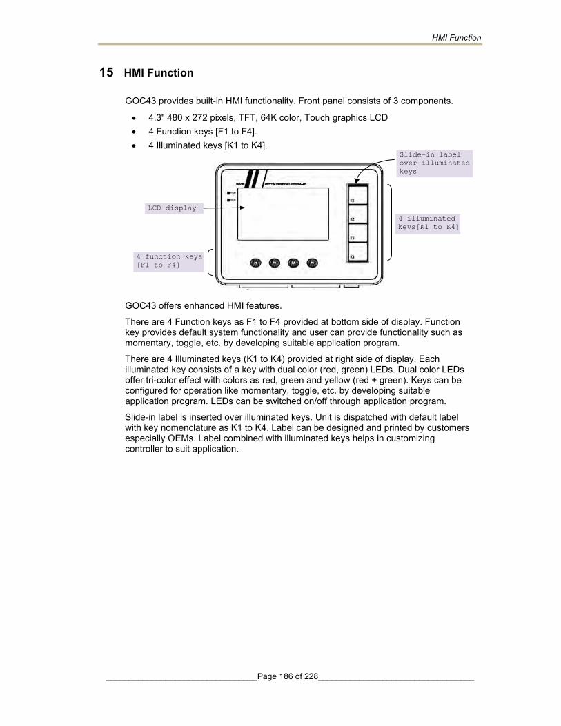
HMI Function
_________________________________Page 186 of 228__________________________________
15 HMI Function
GOC43 provides built-in HMI functionality. Front panel consists of 3 components.
• 4.3" 480 x 272 pixels, TFT, 64K color, Touch graphics LCD • 4 Function keys [F1 to F4]. • 4 Illuminated keys [K1 to K4].
Figure 28: HMI components
GOC43 offers enhanced HMI features.
There are 4 Function keys as F1 to F4 provided at bottom side of display. Function key provides default system functionality and user can provide functionality such as momentary, toggle, etc. by developing suitable application program.
There are 4 Illuminated keys (K1 to K4) provided at right side of display. Each illuminated key consists of a key with dual color (red, green) LEDs. Dual color LEDs offer tri-color effect with colors as red, green and yellow (red + green). Keys can be configured for operation like momentary, toggle, etc. by developing suitable application program. LEDs can be switched on/off through application program.
Slide-in label is inserted over illuminated keys. Unit is dispatched with default label with key nomenclature as K1 to K4. Label can be designed and printed by customers especially OEMs. Label combined with illuminated keys helps in customizing controller to suit application.
4 function keys
[F1 to F4]
LCD display
4 illuminated
keys[K1 to K4]
Slide-in label
over illuminated
keys

HMI Function
_________________________________Page 187 of 228__________________________________
15.1 Highlighting Features
HMI Function Built-in LCD 4.3" Touch graphics LCD, 480 x 272 pixels, 64K color,
View size: 95.04 x 53.86 mm
4 function keys (F1 to F4)
4 illuminated keys (K1 to K4) with dual color (Green, Red) LEDs User Defined LCD Screens
5 fonts (Default, Headline, Large Headline, Title, Annotation). Standard Windows® fonts supported.
Monitor/ modify PLC data with all supported data types and formats.
Alpha-numeric data entry by Embedded keypad, Numpad or Extended Numpad
Direct access of PLC variable with symbolic name.
Visualization Elements
Basic: Rectangle, Round rectangle, Ellipse, Line, Polygon, Polyline, Pie, Image, Frame.
Common controls: Label, Combo box integer, Combo box array, Tab control, Button, Group box, Table, Text field, Scrollbar, Slider, Spin Control, Invisible input, Progress bar, Checkbox, Radio button
Measurement controls: Bar display, Meter 90°, Meter 180°, Meter, Potentiometer, Histogram.
Special controls: Waiting symbol flower, Cartesian XY Chart
Date/time controls: Analog clock, Date picker
Lamps/switches/bitmaps: Image switcher, Lamps and switches
Symbols: Arrows, Symbols, Icons
Function Keys 4 keys F1 to F4
Quick access to IO status monitor (F1 key) and system menu (F2 key)
Illuminated Keys 4 Illuminated keys i.e. keys with dual color bright LEDs
LED control Red/Green/Yellow
Built-in Status and Diagnostics
Monitor all IOs on one display screen.
System Menu for
- Monitoring system status
- System diagnostics: CPU, IO and Ethernet
- System settings: RTC, IP settings, display, buzzer
- Touch calibration and check
- Keys and LEDs check
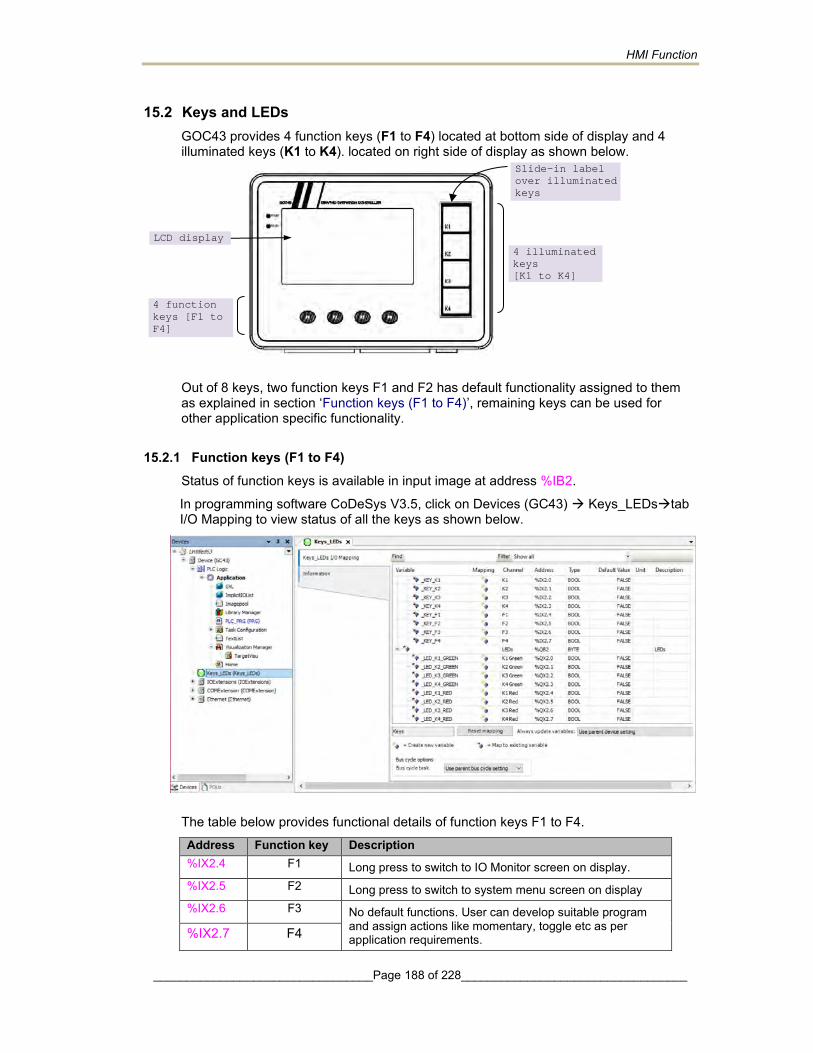
HMI Function
_________________________________Page 188 of 228__________________________________
15.2 Keys and LEDs GOC43 provides 4 function keys (F1 to F4) located at bottom side of display and 4 illuminated keys (K1 to K4). located on right side of display as shown below.
Out of 8 keys, two function keys F1 and F2 has default functionality assigned to them as explained in section ‘Function keys (F1 to F4)’, remaining keys can be used for other application specific functionality.
15.2.1 Function keys (F1 to F4) Status of function keys is available in input image at address %IB2.
In programming software CoDeSys V3.5, click on Devices (GC43) → Keys_LEDs→tab I/O Mapping to view status of all the keys as shown below.
The table below provides functional details of function keys F1 to F4.
Address Function key Description %IX2.4 F1 Long press to switch to IO Monitor screen on display. %IX2.5 F2 Long press to switch to system menu screen on display %IX2.6 F3 No default functions. User can develop suitable program
and assign actions like momentary, toggle etc as per application requirements. %IX2.7 F4
4 function
keys [F1 to
F4]
LCD display
4 illuminated
keys
[K1 to K4]
Slide-in label
over illuminated
keys

HMI Function
_________________________________Page 189 of 228__________________________________
NOTE
Status of function keys (F1 to K4) is also updated in system variable ‘_SysvarHMI.WKEYSTATUS’. Each key is assigned to a specific bit in this variable.
15.2.2 Illuminated keys (K1 to K4) Status of illuminated keys is available in input image at address %IB2.
In programming software CoDeSys V3.5, click on Devices (GC43) → Keys_LEDs→tab I/O Mapping to view status of all the keys as shown below.
The table below provides functional details of illuminated keys K1 to K4.
Address Illuminated key Description
%IX2.0 K1 No default functions. User can develop suitable program and assign actions like momentary, toggle, etc as per application requirements.
%IX2.1 K2
%IX2.2 K3
%IX2.3 K4
In every input scan, key status is read and updated to system variable and input image. LEDs in illuminated keys can be turned on/off using output address %QB2 as below.
Address LED Description %QX2.0 K1 GREEN LED 0 – LED off.
1 – LED on %QX2.1 K2 GREEN LED
%QX2.2 K3 GREEN LED
%QX2.3 K4 GREEN LED
%QX2.4- K1 RED LED
%QX2.5 K2 RED LED
%QX2.6 K3 RED LED
%QX2.7- K4 RED LED
In every output scan, LED illuminated is turned on/off as per output image %QB2.
HMI Function
_________________________________Page 190 of 228__________________________________
NOTE
Status of illuminated keys (K1 to K4) are also updated in system variable ‘_SysvarHMI.WIKEYSTATUS’. Each key is assigned to a specific bit in this variable.
Status of LEDs in illuminated keys (K1 to K4) is updated in system variables ‘_SysvarHMI.WIKEYLEDGREEN’ and ‘_SysvarHMI.WIKEYLEDGRE’.
Refer section ‘System variables’ for more details.
15.2.3 Slide-in Label Main unit is dispatched with default slide-in label with key nomenclature as K1 to K4. Label can be designed and printed by customers especially OEMs as per the design template provided by Mitsubishi Electric India. Label combined with illuminated keys helps in customizing controller to suit application. It can be used as push buttons and lamps and alarm annunciation.
Slide-in label can be inserted from backside of controller front surface when unit is not mounted. Insertion slit is located at left top on the backside of front panel.
Refer section Main Unit Installation to know how to insert and remove slide-in label.
Guidelines for customizing slide-in label 1. Use 14137C02V3_I-KEY SLIDE LABEL GOC43.cdr file for dimensional details
and sample label design. 2. Use material PVC with thickness 150 microns with glossy/mat finish.
a. If failing to do so, may reduce pressing experience for individual key as well as disturbs smooth insertion of slide in label via insertion slit.
3. Process should be screen printing rather than digital printing which provides better quality and repeatability.
4. Printing should be carried out on the back side of slide-in label. a. Ensure that part excluding illuminated key parts (4 nos.) is completely
opaque. b. User can get letters or any objects in white colour on opaque part of the slide-
in label 5. LED light can be transmitted through rectangular illuminated key part. For the
same, ensure that required portion of label should be translucent white. a. Translucent effect is mandatory to ensure uniform illumination. b. Illuminated key part should not be transparent completely as it will show key
part with cuts on it.
Slide-in label with
default printing.

HMI Function
_________________________________Page 191 of 228__________________________________
15.3 Visualization screens For the configuration and development of screens and design of user interface, CoDeSys 3.5 project provides visualization editor.
In CoDeSys project, Application → Visualization Manager and TargetVisu contains various setting related to HMI.
NOTE
Do not make changes to default settings of Visualization Manger and TargetVisu after creating project with GOC43 template.
Change in default settings may lead to unpredictable behavior.
By default, blank screen ‘Home’ gets added after project creation.
Additional HMI screens can be added by right click on ‘Application’ node and select ‘Add Object’ → Visualization.
NOTE
Maximum 64 visualization screens can be added in GOC43 project.
HMI Function
_________________________________Page 192 of 228__________________________________
15.3.1 Visualization Editor To edit HMI screen design, Click on Visualization screen, this opens visualization editor as shown below
Sr. No. Parameter Description
1 Working area Screen design area. White square shows display boundaries. Anything placed out of white color area is not displayed on LCD.
2 Visualization Toolbox
Contains various visualization elements which can be utilized to design HMI screen as per requirement. Elements are grouped as per the type. Section ‘Visualization elements’ contains list of visualization elements in all the groups.
3 Properties Tab shows properties of visualization element on screen. Click on visualization element to view object properties.
4 Visualization Toolbar
Contains different commands useful for editing, alignment, spacing, size of visualization elements. Refer CoDeSys help for more details.
5 Visualization Menu
Visualization menu on Menu bar provides various commands useful for editing screen design. Refer CoDeSys help for more details.
1
2
4
5
3
HMI Function
_________________________________Page 193 of 228__________________________________
15.3.2 Visualization elements For easy access, visualization elements in toolbox are grouped in categories such as ‘Basic’, ‘Common controls’, ‘Measurement controls’, Lamps/Switches/Bitmaps’, ‘Special controls’, ‘Date/time controls’, ‘Symbols’ etc.
Below image provides visualization toolbox overview in CoDeSys application and table provides list of supported visualization categories/ groups.
NOTE
User can utilize custom category ‘Favorite’ for frequently used visualization elements. To add element in favorite category. right click on element in toolbox and select ‘Add item to category favorite’ from context menu.
Visualization Categories 1. Basic 2. Common controls 3. Measurement controls 4. Lamps/Switches/Bitmaps 5. Special controls 6. Date/time controls 7. Symbols
HMI Function
_________________________________Page 194 of 228__________________________________
The table below provides information about each visualization category along with elements supported in it.
Name of element Symbol Description Basic Rectangle These elements can be used to display data by linking with
application variables. User can set background color as per linked variable state. Also, user can convert element type within Rectangle, Round rectangle and Ellipse, only by changing ‘Element type’ property.
Round
rectangle
Ellipse
Line This element draws a single line. User can animate line object by linking with application variables.
Polygon
Polyline
Pie This element draws a pie of any angle by referring start (begin) and end angles.
Image This element adds an image to the visualization. The displayed image is managed in the image pool and referenced in the visualization element by means of a static ID property.
Frame This element allows user to display one or more already existing visualizations. The display area of the referenced visualization then adapts itself to the frame size.
Common controls Label This element is used to label the visualizations.
Combo box
integer
This element shows values as a drop-down list. When the user clicks on an entry, the ID of the entry is written to an integer variable. The entries in the drop-down list can be from a list and contain images from an image pool.
Combo box
array
This element shows values of an array as a drop-down list. When the visualization user clicks an entry, the array index of the entry is written to an integer variable.
Tab control This element displays selected visualizations in tabs. The tabs can be used by means of the tab header without any input configuration. A visualization user can switch between visualizations by clicking the tab header.
Button This element triggers an action, such as setting a variable.
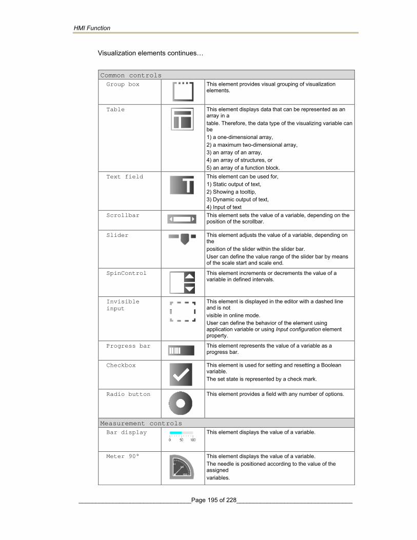
HMI Function
_________________________________Page 195 of 228__________________________________
Visualization elements continues…
Common controls Group box This element provides visual grouping of visualization
elements.
Table This element displays data that can be represented as an array in a table. Therefore, the data type of the visualizing variable can be 1) a one-dimensional array, 2) a maximum two-dimensional array, 3) an array of an array, 4) an array of structures, or 5) an array of a function block.
Text field This element can be used for, 1) Static output of text, 2) Showing a tooltip, 3) Dynamic output of text, 4) Input of text
Scrollbar This element sets the value of a variable, depending on the position of the scrollbar.
Slider This element adjusts the value of a variable, depending on the position of the slider within the slider bar. User can define the value range of the slider bar by means of the scale start and scale end.
SpinControl This element increments or decrements the value of a variable in defined intervals.
Invisible
input
This element is displayed in the editor with a dashed line and is not visible in online mode. User can define the behavior of the element using application variable or using Input configuration element property.
Progress bar This element represents the value of a variable as a progress bar.
Checkbox This element is used for setting and resetting a Boolean variable. The set state is represented by a check mark.
Radio button This element provides a field with any number of options.
Measurement controls Bar display This element displays the value of a variable.
Meter 90° This element displays the value of a variable. The needle is positioned according to the value of the assigned variables.

HMI Function
_________________________________Page 196 of 228__________________________________
Visualization elements continues…
Measurement controls Meter 180° This element displays the value of a variable.
The meter is positioned according to the value of the assigned variables on the scale.
Meter This element displays the value of a variable. The needle is positioned according to the value of the assigned variables.
potentiometer This element displays the value of a variable as a setting on the potentiometer. User can modify the value by dragging the pointer to another position.
Histogram This element displays the data of a one-dimensional array as a histogram. User can assign specific colors for certain value ranges.
Lamps/Switches/Bitmaps Image
switcher
This element displays one of three referenced images. Mouse actions can change the displayed image. The images can be defined in the Image settings element properties.
Lamp This element shows the value of a variable, and the element is displayed as illumination.
Dip switch This element assigns a value to a Boolean variable. The switch position "ON" assigns value TRUE to the variable, and the switch position "OFF" assigns the value FALSE to the variable. User can change the switch position using mouse actions. Power switch
Push switch
Push switch
LED
Rocker switch
Rotary switch
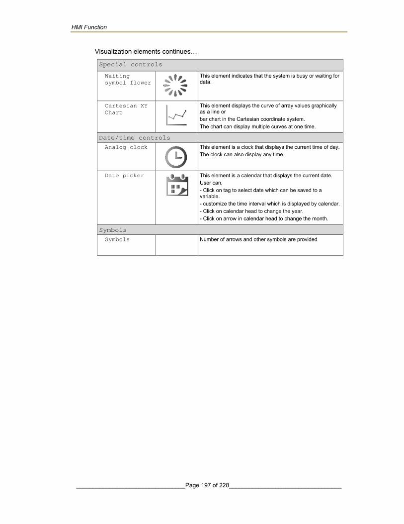
HMI Function
_________________________________Page 197 of 228__________________________________
Visualization elements continues…
Special controls
Waiting
symbol flower
This element indicates that the system is busy or waiting for data.
Cartesian XY
Chart
This element displays the curve of array values graphically as a line or bar chart in the Cartesian coordinate system. The chart can display multiple curves at one time.
Date/time controls
Analog clock This element is a clock that displays the current time of day. The clock can also display any time.
Date picker This element is a calendar that displays the current date. User can, - Click on tag to select date which can be saved to a variable. - customize the time interval which is displayed by calendar. - Click on calendar head to change the year. - Click on arrow in calendar head to change the month.
Symbols
Symbols Number of arrows and other symbols are provided

HMI Function
_________________________________Page 198 of 228__________________________________
15.3.3 Visualization element properties Appearance and runtime behavior of visualization element can be changed with help of object properties.
To view properties of visualization element, click on element in working area. Element properties will be displayed as shown below.
Depending on visualization element type, properties of element will be displayed in properties tab.
Refer CoDeSys help for more details on properties of visualization elements.
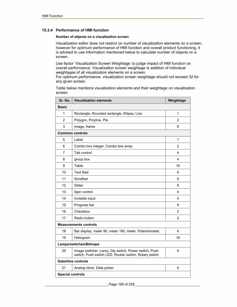
HMI Function
_________________________________Page 199 of 228__________________________________
15.3.4 Performance of HMI function Number of objects on a visualization screen
Visualization editor does not restrict on number of visualization elements on a screen, however for optimum performance of HMI function and overall product functioning, it is advised to use information mentioned below to calculate number of objects on a screen.
Use factor ‘Visualization Screen Weightage’ to judge impact of HMI function on overall performance. Visualization screen weightage is addition of individual weightages of all visualization elements on a screen. For optimum performance, visualization screen weightage should not exceed 32 for any given screen.
Table below mentions visualization elements and their weightage on visualization screen.
Sr. No. Visualization elements Weightage
Basic
1 Rectangle, Rounded rectangle, Ellipse, Line 1
2 Polygon, Polyline, Pie 2
3 Image, frame 8
Common controls
5 Label 1
6 Combo box integer, Combo box array 2
7 Tab control 4
8 group box 4
9 Table 16
10 Text field 4
11 Scrollbar 8
12 Slider 8
13 Spin control 4
14 Invisible input 4
15 Progress bar 8
16 Checkbox 2
17 Radio button 2
Measurements controls
18 Bar display, meter 90, meter 180, meter, Potentiometer, 4
19 Histogram 16
Lamps/switches/Bitmaps
20 Image switcher, Lamp, Dip switch, Power switch, Push switch, Push switch LED, Rocker switch, Rotary switch
4
Date/time controls
21 Analog clock, Date picker 4
Special controls

HMI Function
_________________________________Page 200 of 228__________________________________
22 Wait symbol 16
23 Cartesian XY chart 16
Symbols
24 All symbols 4
HMI design with higher visualization screen weightage may impact performance of HMI function which may lead to slower screen updation, delay in screen changeover, delayed start after power on and higher touch sensing time.
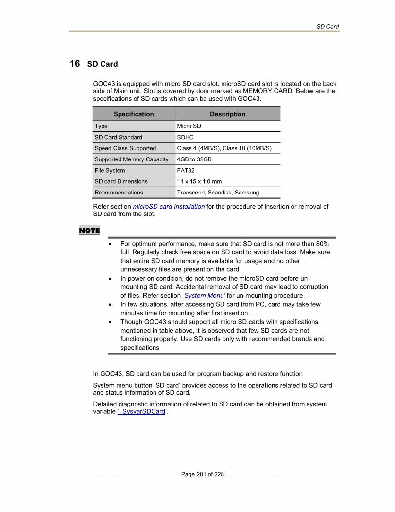
SD Card
_________________________________Page 201 of 228__________________________________
16 SD Card
GOC43 is equipped with micro SD card slot. microSD card slot is located on the back side of Main unit. Slot is covered by door marked as MEMORY CARD. Below are the specifications of SD cards which can be used with GOC43.
Specification Description
Type Micro SD
SD Card Standard SDHC
Speed Class Supported Class 4 (4MB/S), Class 10 (10MB/S)
Supported Memory Capacity 4GB to 32GB
File System FAT32
SD card Dimensions 11 x 15 x 1.0 mm
Recommendations Transcend, Scandisk, Samsung
Refer section microSD card Installation for the procedure of insertion or removal of SD card from the slot.
NOTE
• For optimum performance, make sure that SD card is not more than 80% full. Regularly check free space on SD card to avoid data loss. Make sure that entire SD card memory is available for usage and no other unnecessary files are present on the card.
• In power on condition, do not remove the microSD card before un-mounting SD card. Accidental removal of SD card may lead to corruption of files. Refer section ‘System Menu’ for un-mounting procedure.
• In few situations, after accessing SD card from PC, card may take few minutes time for mounting after first insertion.
• Though GOC43 should support all micro SD cards with specifications mentioned in table above, it is observed that few SD cards are not functioning properly. Use SD cards only with recommended brands and specifications
In GOC43, SD card can be used for program backup and restore function
System menu button ‘SD card’ provides access to the operations related to SD card and status information of SD card.
Detailed diagnostic information of related to SD card can be obtained from system variable ‘_SysvarSDCard’.
SD Card
_________________________________Page 202 of 228__________________________________
16.1 Backup application program and source code "Backup" function allows saving application program and / or source code from CPU to SD card.
16.1.1 Enabling backup function and setting password
To use backup function, setting ‘Allow copy from CPU to Memory card’ should be enabled in the device setting. Also, password can be set in application program to allow backup / restore operations.
Sr. No. Settings Description 1 Allow copy from CPU
to Memory card Select to allow copy application and /or source code from CPU to Memory Card’. If disabled, backup function will not be allowed from device.
2 Set password If selected, backup /restore will be allowed only after entering valid password.
3 Password User can set 6 digits numeric security password to project backup.
1
3
2
SD Card
_________________________________Page 203 of 228__________________________________
16.1.2 Executing backup To execute backup operation, follow sequence mentioned below.
This section explains application program backup process only. Follow the same procedure for source code backup by selecting ‘Backup source code’ option in the sequence.
1. Insert SD card in SD card slot. Ensure card is formatted with FAT32 and having enough free memory (at least 20%).
2. Enter ‘System menu’ Press F2 key on device for 3 sec duration to enter into System Menu.
3. Navigate to ‘SD Card’ menu as shown.
Open ‘SD card info’ and confirm SD card is ready.
Touch on ‘Backup application’ or ‘Backup source code’ button to start copy operation.
4. If application backup is not enabled in the application program running on device, adjacent message is displayed.
Application or source code backup is not possible in this case and backup process is aborted.
5. If free size on SD card is not sufficient to copy application program, then device will block backup process with error message as shown below.
Make enough (at least 20%) free space on SD card and try again.
6. Device will check if password is set for application backup / restore.
If password is set, then message will be displayed for user to enter the password.
Enter valid 6 digits numeric password to proceed with backup.
NOTE
During backup action, GOC compares password entered by user with password in application program stored on the device and allows backup only if password matches

SD Card
_________________________________Page 204 of 228__________________________________
7. If SD card already contains application backup, then warning message is displayed as shown.
Selecting ‘No’ will abort backup operation.
Selecting ‘Yes’ will overwrite application program files on SD card.
8. Once backup process is started, progress of file copying is displayed as shown below
Wait till CPU copies files to SD card.
9. Once application backup is completed successfully, message is displayed as shown.
Touch on ‘Close’ button to complete the process.
You can unmount SD card and either copy files on SD card to PC or use this SD card to restore application to another GOC43.
10. During application backup, if backup process gets failed due to any reason, then error message is displayed.
In this case, it is recommended to format SD card before retrying backup process again.

SD Card
_________________________________Page 205 of 228__________________________________
16.2 Restore application program and source code "Restore" function allows copying the application program and source code from SD card to CPU.
16.2.1 Enabling restore function on device and setting Password To use restore function, setting ‘Allow copy from Memory card to CPU’ should be enabled in device setting. Also, password can be set in application program for backup / restore operations.
Sr. No. Settings Description
1 Allow copy from Memory card to CPU
Select to allow copy application and /or source code copy from Memory Card to CPU. If disabled restore function will be locked from device.
2 Set password If selected, backup/restore will be allowed only after entering valid password.
3 Password User can set 6 digits numeric security password to project backup.
2
1
3

SD Card
_________________________________Page 206 of 228__________________________________
16.2.2 Copying application program and / or source code to SD card Let’s first understand how to make SD card ready for restore, that means how to copy application and source code from PC to SD card. Once copied to SD card, application program and / or source can be copied to multiple GOC43 devices using restore function.
Method 1: Using ‘Backup’ tab in device properties Follow below steps to copy application program and /or source code to SD card
1. Create boot application
This step is required if you want to restore application program. If you want to restore source code only then this step can be skipped. Open application program to be copied to SD card. Compile application and ensure that there are no errors. Execute command ‘Online’→‘Create boot application’. ‘Save boot application’ dialogue will appear as shown below.
Select path on local drive of PC and click button save.
Do not change file name from ‘Application.app’
Below message will be displayed
Check ‘Yes’ to save application. Folder ‘PlcLogic’ and file ‘Application.app’ will be saved at selected path.
Do not make any changes to the contents of folder and file.
SD Card
_________________________________Page 207 of 228__________________________________
2. Create project archive This step is required if you want to restore source code. If you want to restore application program only then this step can be skipped. Open application program whose source code to be copied to SD card. Compile application and ensure that there are no errors. Execute command ‘File’ → ‘Project Archive’ →‘Save/Send Archive…’. This will open ‘Project Archive’ dialogue as shown below
Select options as shown in above picture and click on ‘Save…’ button.
Save Project Archive dialogue will appear as shown below
Select path on local drive of PC and click button save.
SD Card
_________________________________Page 208 of 228__________________________________
3. Create Package This step creates package using boot application created in step 1 and project archive created in step 2.
To create package, go to ‘Backup’ tab in device editor.
In ‘Select items for backup’, enable ‘Boot application’ and / or ‘Source archive’
Sr. No. Settings Description
1 Select ‘Boot application’ Select to include boot application in the package. If unchecked, the package will not contain boot application and application restore cannot be executed.
2 Select boot application to include in the package.
Select boot application created in step 1.
3 Select Source archive to include in the package.
Select to include ‘Source archive’ in the package. If unchecked, the package will not contain source archive and source code restore cannot be executed.
4 Select Source archive path Select source code archive created in step 2.
1
3
2
4

SD Card
_________________________________Page 209 of 228__________________________________
Select items to be included in the package and click Save button.
Select folder to save the package and click ‘Select folder’
‘GOC43’ folder containing the package will be created at selected folder.
You should copy ‘GOC43’ folder to root directory of SD card to execute restore function.
Method 2: Using ‘Backup’ function of CPU This method uses ‘Backup application program and source code’ function to copy files to SD card. Refer section ‘Backup application program and source code’ for more details.
Once application and source code copied to memory card using backup function, card can be used to restore application program and / or source code restore on multiple GOC43 devices using restore function.
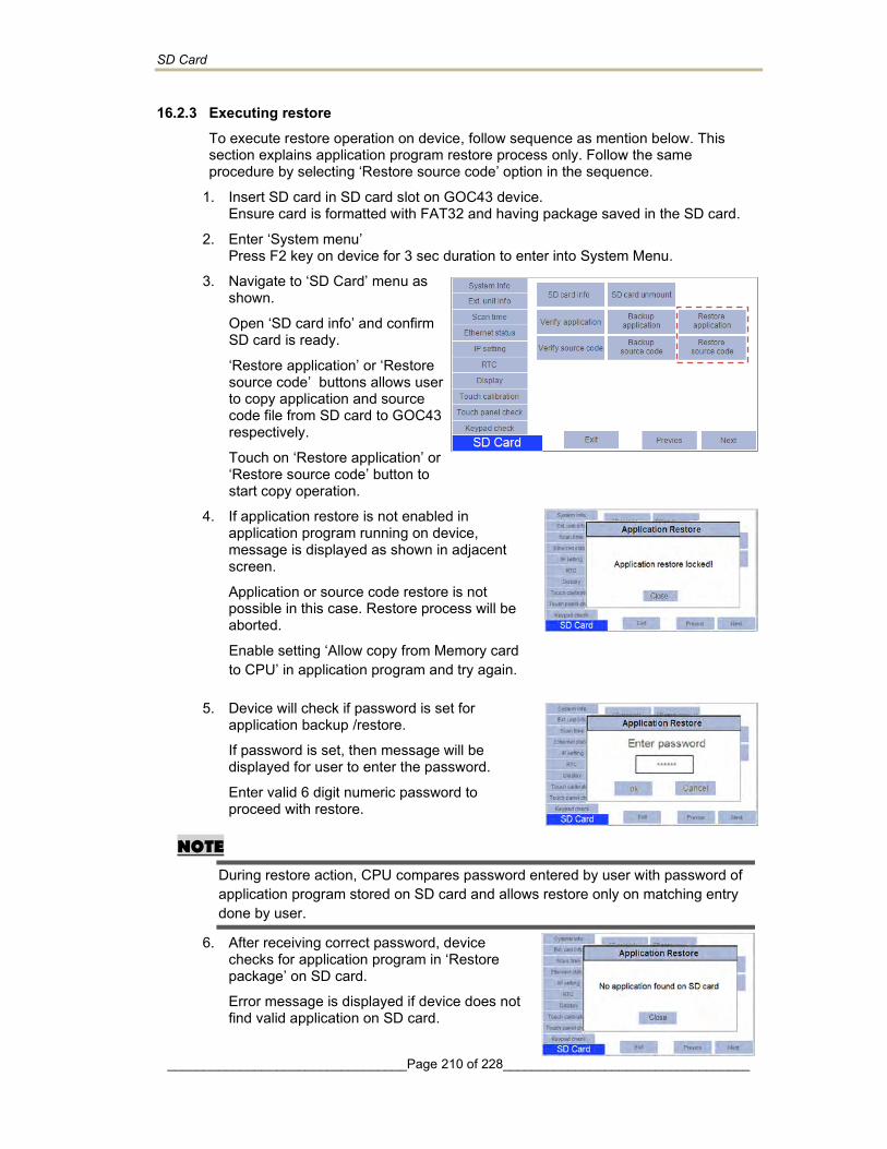
SD Card
_________________________________Page 210 of 228__________________________________
16.2.3 Executing restore To execute restore operation on device, follow sequence as mention below. This section explains application program restore process only. Follow the same procedure by selecting ‘Restore source code’ option in the sequence.
1. Insert SD card in SD card slot on GOC43 device. Ensure card is formatted with FAT32 and having package saved in the SD card.
2. Enter ‘System menu’ Press F2 key on device for 3 sec duration to enter into System Menu.
3. Navigate to ‘SD Card’ menu as shown.
Open ‘SD card info’ and confirm SD card is ready.
‘Restore application’ or ‘Restore source code’ buttons allows user to copy application and source code file from SD card to GOC43 respectively.
Touch on ‘Restore application’ or ‘Restore source code’ button to start copy operation.
4. If application restore is not enabled in application program running on device, message is displayed as shown in adjacent screen.
Application or source code restore is not possible in this case. Restore process will be aborted.
Enable setting ‘Allow copy from Memory card to CPU’ in application program and try again.
5. Device will check if password is set for application backup /restore.
If password is set, then message will be displayed for user to enter the password.
Enter valid 6 digit numeric password to proceed with restore.
NOTE
During restore action, CPU compares password entered by user with password of application program stored on SD card and allows restore only on matching entry done by user.
6. After receiving correct password, device checks for application program in ‘Restore package’ on SD card.
Error message is displayed if device does not find valid application on SD card.

SD Card
_________________________________Page 211 of 228__________________________________
Message is displayed in case of invalid application.
Message is displayed if size of application program is exceeding device memory.
In such cases, copy ‘package’ with valid application program and try again.
7. Once confirmation of validity of application is done, then message is displayed as
Select ‘Yes’ to start restores action.
Selecting ‘No’ to abort restore action.
8. During restore action, progress is displayed. Wait till files CPU copies files from SD card.
9. Once application restore is completed successfully, message is displayed as shown.
Power cycle GOC to start restored application.
10. During application restore, if restore process gets failed due to any reason then error message is displayed.
In this case, it is recommended to start restore process again.

SD Card
_________________________________Page 212 of 228__________________________________
16.3 Verify application program and source code "Verify" function compares application program and / or source code on SD card with that of the device.
16.3.1 Executing Verify To execute verify operation on device follow sequence as mention below, here only application program verification process is explained. Follow same procedure with selecting ‘Verify source code’ option in the sequence.
1. Insert SD card in SD card slot on GOC43 device. Ensure card is formatted with FAT32 and having restore package saved in the SD card.
2. Enter ‘System menu’ Press F2 key on device for 3 sec to enter in System Menu.
3. Navigate to ‘SD Card’ menu as shown in the screen below.
Open ‘SD card info’ and confirm SD card is ready.
‘Verify application’ or ‘Verify source code’ buttons allow user to compare application and source code file from SD card to GOC43 respectively.
4. Touch on ‘Verify application’ or ‘Verify source code’ button to start copy operation.
5. After starting verification, device checks for application program in ‘Restore package’ on SD card.
6. If device does not find valid application on SD card, then it displays error message as
Error message is displayed in case of invalid application.
7. During verification, device checks application program and all supporting files on device and SD card.
For its progress, progress bar is displayed.
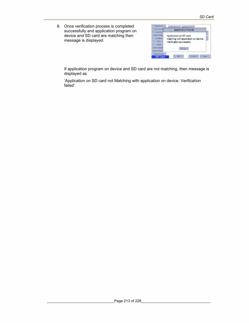
SD Card
_________________________________Page 213 of 228__________________________________
8. Once verification process is completed successfully and application program on device and SD card are matching then message is displayed.
If application program on device and SD card are not matching, then message is displayed as
‘Application on SD card not Matching with application on device. Verification failed’

Mitsubishi Electric India Pvt. Ltd. Factory Automation and Industrial Division
ICC-Devi Gaurav Technology Park, Unit No. 402,
Opp. Vallabh Nagar Bus Depot,
Pune-411018, Maharashtra, India.
Email – [email protected]
Web – http://in.mitsubishielectric.com