Towards Utilization of Distributed On-Chip Power Delivery ...
52
University of South Florida Scholar Commons Graduate eses and Dissertations Graduate School April 2018 Towards Utilization of Distributed On-Chip Power Delivery Against EM Side-Channel Aacks Ahmed Waheed Khan University of South Florida, [email protected] Follow this and additional works at: hp://scholarcommons.usf.edu/etd Part of the Electrical and Computer Engineering Commons is esis is brought to you for free and open access by the Graduate School at Scholar Commons. It has been accepted for inclusion in Graduate eses and Dissertations by an authorized administrator of Scholar Commons. For more information, please contact [email protected]. Scholar Commons Citation Khan, Ahmed Waheed, "Towards Utilization of Distributed On-Chip Power Delivery Against EM Side-Channel Aacks" (2018). Graduate eses and Dissertations. hp://scholarcommons.usf.edu/etd/7178
-
Upload
khangminh22 -
Category
Documents
-
view
4 -
download
0
Transcript of Towards Utilization of Distributed On-Chip Power Delivery ...
University of South FloridaScholar Commons
Graduate Theses and Dissertations Graduate School
April 2018
Towards Utilization of Distributed On-Chip PowerDelivery Against EM Side-Channel AttacksAhmed Waheed KhanUniversity of South Florida, [email protected]
Follow this and additional works at: http://scholarcommons.usf.edu/etd
Part of the Electrical and Computer Engineering Commons
This Thesis is brought to you for free and open access by the Graduate School at Scholar Commons. It has been accepted for inclusion in GraduateTheses and Dissertations by an authorized administrator of Scholar Commons. For more information, please contact [email protected].
Scholar Commons CitationKhan, Ahmed Waheed, "Towards Utilization of Distributed On-Chip Power Delivery Against EM Side-Channel Attacks" (2018).Graduate Theses and Dissertations.http://scholarcommons.usf.edu/etd/7178

Towards Utilization of Distributed On-Chip Power Delivery
Against EM Side-Channel Attacks
by
Ahmed Waheed Khan
A thesis submitted in partial fulfillment of the requirements for the degree of
Master of Science in Electrical Engineering Department of Electrical Engineering
College of Engineering University of South Florida
Major Professor: Selçuk Köse, Ph.D. Gokhan Mumcu, Ph.D.
Mehran Mozaffari Kermani, Ph.D.
Date of Approval: April 15, 2018
Keywords: Hardware security, EM side-channel attacks, distributed voltage regulation, security implications, power grid lines
Copyright © 2018, Ahmed Waheed Khan

DEDICATION
To my parents for all their love, support and putting me through the best education possible.
I wouldn’t have been able to get to this stage without them.

ACKNOWLEDGMENTS
I would like to extend my profound gratitude to many people, who generously contributed
to the work presented in this thesis.
Special mention goes to my supporting and passionate supervisor and mentor, Dr. Selçuk
Köse. My thesis has been an amazing learning experience and I thank him wholeheartedly. His
willingness to offer me so much of his time and intellect is the major reason behind the completion
of this thesis. Similar profound gratitude goes to my committee members Dr. Gokhan Mumcu and
Dr.Mehran Mozaffari Kermani for being truly dedicated advisors. The constant support and
resources provided by the Electrical Engineering Department at USF are also gratefully
acknowledged. Special mention goes to my lab mates Mahmood Azhar, Mohammad Ali Vosoughi
and Longfei Wang for frequently offering me wise counseling at opportune times.
Finally, but by no means least, I would like to thank my family to whom I owe a great deal.
A big thanks goes to my mother Sufia Gul, father Abdul Waheed Khan and my wife Nimrah Ahmed
for almost unbelievable support throughout. They are the most important people in my world.
I thank you all

i
TABLE OF CONTENTS
LIST OF TABLES ..................................................................................................................... iii
LIST OF FIGURES ................................................................................................................... iv
ABSTRACT .............................................................................................................................. v
CHAPTER 1: INTRODUCTION ............................................................................................... 1
CHAPTER 2: ELECTROMAGNETIC ATTACKS ........................................................................ 5 2.1 Magnetic Field and Electric Field – Revisited ................................................... 5 2.2 EM Attack Methods .......................................................................................... 8
2.2.1 Active Attack ........................................................................................... 8 2.2.2 Passive Attack ........................................................................................ 8
2.3 EM Side Channel Analysis Types .................................................................... 8 2.3.1 Simple Side-Channel Analysis ................................................................ 9 2.3.2 Differential Side-Channel Analysis .......................................................... 9
2.4 EM Emanation Types ....................................................................................... 9 2.4.1 Direct Emanations ................................................................................... 10 2.4.2 Indirect Emanations ................................................................................ 10
2.5 Near-field and Far-Field Approximation ............................................................ 11
2.5.1 Near Field ............................................................................................... 11
2.5.2 Far Field .................................................................................................. 12
2.6 EM Propagation ................................................................................................ 12
2.7 EM Probe ......................................................................................................... 13
CHAPTER 3: LEAVERGING ON-CHIP POWER DELIVERY ................................................... 15
3.1 Background ....................................................................................................... 15 3.1.1 Low Dropout Regulators ........................................................................... 16 3.1.2 Switched Capacitor Converters ................................................................ 17 3.1.3 Buck Converters ....................................................................................... 17
3.2 Working of AES .................................................................................................. 19
3.3 Threat Model ...................................................................................................... 20
CHAPTER 4: EVALUATION MODEL ...................................................................................... 22
4.1 Simulation Setup ............................................................................................... 22
4.2 Effect of the Size of Power Grid and Distance from the Probe .......................... 23
4.3 Security Implication of the Implemented Design ............................................... 27
4.4 Shielding with MIM Capacitor ............................................................................ 29
4.5 Effect of Upper Metal Layers on the EM Emanations From Lower Layers ......... 31
4.6 Discussion ........................................................................................................ 32

ii
CHAPTER 5: FUTURE WORK ................................................................................................ 34
CHAPTER 6: CONCLUSION ................................................................................................... 36
REFERENCES ........................................................................................................................ 37
APPENDIX A: COPYRIGHT PERMISSIONS ........................................................................... 41

iii
LIST OF TABLES
Table 4.1 Simulation parameters ....................................................................................... 22 Table 4.2 EM emanations from local vs global grid at varying probe distance ................... 23
Table 4.3 EM emanations from the local and global power grids to a
probe for different wire lengths .......................................................................... 26
Table 4.4 EM emanations from the local and global power grids to a probe placed at 100 um ..................................................................................... 27
Table 4.5 EM comparison with MIM shielding ................................................................... 31
Table 4.6 EM comparison with upper layer ........................................................................ 32

iv
LIST OF FIGURES Figure 1.1 Side channel attack model .................................................................................... 2
Figure 2.1 Magnetic field of current and carrying conductor ................................................... 6
Figure 2.2 Electric field of current and carrying conductor ...................................................... 7
Figure 2.3 Near field and far field illustration .......................................................................... 11
Figure 2.4 EM waves propagation .......................................................................................... 13
Figure 3.1 Distributed on-chip power delivery network ........................................................... 16
Figure 3.2 Leveraging local power delivery reduces EM emanations originating
from the power delivery network ............................................................................ 18
Figure 3.3 AES flow chart ....................................................................................................... 20
Figure 3.4 Measurement setup .............................................................................................. 21
Figure 4.1 EM emissions from local grid at varying probe distances ....................................... 23
Figure 4.2 EM emissions from global grid at varying probe distances ..................................... 24
Figure 4.3 EM emissions from local grid at varying wire lengths ............................................. 24
Figure 4.4 EM emissions from global grid at varying wire lengths .......................................... 25
Figure 4.5 EM emissions comparison of local and global grids at 100 um .............................. 26
Figure 4.6 Using MIM capacitor as a shield ............................................................................ 30
Figure 4.7 Reduction in EM emission due to shielding effect of the MIM capacitor ................. 31
Figure 4.8 Effect of the global grid on the emanations from the local power grid .................... 32
Figure 6.1 EM emanations captured from 1 mm distance ....................................................... 34

v
ABSTRACT
Non-invasive side-channel attacks (SCAs) are potent attacks on a cryptographic circuit
that can reveal its secret key without requiring lots of equipment. EM side-channel leakage is
typically the derivative of the power consumption profile of a circuit. Since the fluctuations of the
supply voltage strongly depend on the topology and features of the power distribution network
(PDN), design of the PDN has a direct impact on EM side-channel leakage signature.
In this thesis, we explore the security implications of distributed on-chip voltage regulators
against EM side-channel attacks. Extensive HFSS simulations have demonstrated that the
maximum EM radiation can be reduced by 33 dB and 11 dB, respectively, at the top and bottom
sides of an integrated circuit through distributed on-chip voltage regulation. The primary reason
is that the power is delivered locally through partially shorter and thinner metal lines as compared
to off-chip implementation.

1
CHAPTER 1: INTRODUCTION
As data security becomes more and more important as a modern design metric, most
systems these days make use of a cryptographic module for processing secure data. Although
employing a dedicated cryptographic module does help to improve data security, it is still possible
for an attacker to get through the security of the device by using passing and non-invasive attacks
in order to extract the secret key used for encryption. These "side-channel" attacks use
information that gets leaked from a device while it is processing secure data through observing it
in real-time [34]. Side-channel attacks (SCA) are a major threat to the security of cryptographic
devices. A significant amount of work has been performed on SCAs over the past two decades.
One of the primary types of SCAs is the power analysis attack. While simple power analysis (SPA)
obtains the data directly from power consumption, differential power analysis (DPA) attacks
require certain statistical operations on numerous power traces to get relevant information [1,2].
Apart from the power consumption, other leakage information such as electromagnetic emission,
computation time and temperature can also be used to attack a device [3,5]. SCAs attempt to
define the correlation between any kind of side-channel information and the internal operations of
the device. These attacks pose a threat to many modern-day devices, for example smart cards,
that use cryptographic algorithms like the Data Encryption Standard (DES) or the more intricate
Advanced Encryption Standard (AES) algorithm [34].
While the popularity of power analysis attacks has risen, there are certain benefits
attached with using EMA (Electro-Magnetic Analysis) for analyzing devices with unconventional
interfaces, when a power tap is not easy to implement or when there are countermeasures in
place for power analysis [32,33].

2
In circumstances where a power side channel is not possible or a non-contact type of
attack needs to be implemented, electromagnetic (EM) attacks offer an advantage over
conventional power analysis attacks. Additionally, Agrawal et al. [6], discussed how
electromagnetic radiations can be modulated using an inner loop structure and also described
how a suitable AM demodulator is useful in performing effective attacks even at a distance of
some meters from the chip. They also showed that EM attacks can be used to nullify many of the
countermeasures that are effective in the face of power analysis attacks. Just as in the case of
SPA and DPA, EM side channel attacks can be used for both simple electromagnetic (SEMA) as
well as differential electromagnetic (DEMA) attacks. The different surveillance methods that are
practiced by the US National Security Agency (NSA) are all cited in a classified document the
NSA advanced network technology (ANT) catalog, which was famously revealed by Edward
Snowden in 2013. ANGRYNEIGHBOR was one of the technologies mentioned in that catalog.
This technology and its many variants are attack techniques built on the RF retroreflector attack
(RFRA) standard, an active EM side-channel attack [35]. Despite the gravity of this topic, very
few publications have taken it upon themselves to discuss it.
Figure 1.1 Side channel attack model [41]

3
Modern ICs have transistors and interconnections in the millions through which data-
dependent current flows. The amplitude of the EM radiation is proportional to the dimension of
the current carrying conductor in the circuit under attack. Longer interconnect wires emit greater
EM signals, resulting in a higher amount of leakage. As the conducting wires become shorter and
narrower, the EM radiation reduces, making it more and more challenging for the assailant to
obtain sufficient level of useful information from a distance to perform a successful EM attack.
Therefore, utilizing shorter interconnect wires can help in minimizing the unintentional leakage of
critical side channel information. While near-field probes could be used to detect emissions in the
near field, larger antennas can be used to capture information bearing signals from a distance,
making the EM attacks non-invasive. With these factors in mind, distributed on-chip voltage
regulators may potentially provide certain inherent security benefits against EM attacks. Besides,
tailoring the placement of capacitors in the power delivery network can further mitigate the EM
side-channel leakage. In recent years, quite a few techniques have been suggested to implement
voltage regulator fully on chip to obtain faster voltage scaling and multiple power islands [7,10].
In recent times, interest has been shifting towards leveraging power delivery network
(PDN) as well as on-chip integrated voltage regulator (IVR) as a preventive measure against
power analysis attacks. This thesis, for the first time ever, aims to analyze the implications of an
on-chip power delivery network (PDN) on EM emissions. Utilizing on-chip voltage regulators
enables the utilization of shorter and thinner interconnect wires to deliver power as compared to
their off-chip counterparts.
In addition, various design options such as placing voltage regulators close to the
cryptographic module and locally delivering power to the crypto circuit through the bottom metal
layers are examined in this thesis with the aim of making detection of EM radiation by any probe
difficult [11].

4
The remaining part of the thesis is organized as follows. EM attacks are explained in
chapter 2 and the introduction to the on-chip power delivery and AES with the threat model is
provided in chapter 3. The evaluation of the security implications is provided in chapter 4. The
direction of future work is discussed in chapter 5 and finally the thesis is concluded in chapter 6.
5
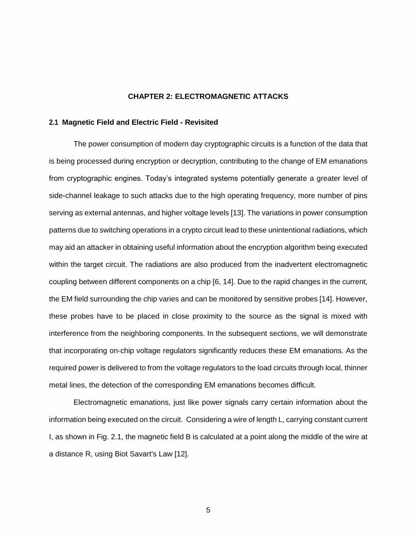
CHAPTER 2: ELECTROMAGNETIC ATTACKS 2.1 Magnetic Field and Electric Field - Revisited
The power consumption of modern day cryptographic circuits is a function of the data that
is being processed during encryption or decryption, contributing to the change of EM emanations
from cryptographic engines. Today’s integrated systems potentially generate a greater level of
side-channel leakage to such attacks due to the high operating frequency, more number of pins
serving as external antennas, and higher voltage levels [13]. The variations in power consumption
patterns due to switching operations in a crypto circuit lead to these unintentional radiations, which
may aid an attacker in obtaining useful information about the encryption algorithm being executed
within the target circuit. The radiations are also produced from the inadvertent electromagnetic
coupling between different components on a chip [6, 14]. Due to the rapid changes in the current,
the EM field surrounding the chip varies and can be monitored by sensitive probes [14]. However,
these probes have to be placed in close proximity to the source as the signal is mixed with
interference from the neighboring components. In the subsequent sections, we will demonstrate
that incorporating on-chip voltage regulators significantly reduces these EM emanations. As the
required power is delivered to from the voltage regulators to the load circuits through local, thinner
metal lines, the detection of the corresponding EM emanations becomes difficult.
Electromagnetic emanations, just like power signals carry certain information about the
information being executed on the circuit. Considering a wire of length L, carrying constant current
I, as shown in Fig. 2.1, the magnetic field B is calculated at a point along the middle of the wire at
a distance R, using Biot Savart's Law [12].

6
Figure 2.1 Magnetic field of current and carrying conductor
𝐵 = 𝜇0𝐼
4𝜋𝑅(
𝐿
√𝐿24⁄ +𝑅
) (1)
where uo is the magnetic constant, R is the distance between the current and the field point while
I is the current carried on a conductor of infinitesimal length.
The electric field generated can be approximated to be a cylindrical Gaussian surface as
shown in Fig. 2.2. The Gaussian cylindrical surface is assumed to be coaxial with the wire of
radius R and length L.
∅𝐸 = 𝐸 ∫ 𝑑𝐴 ≈ 𝐸(𝑅)(2𝜋𝑅𝐿) (2)
where E ∫ dA = Qin/E0 and Qin is the new charge inside the Gaussian surface (λL).
Additionally, according to Faraday’s law any variation in the surrounding of the loop probe
will generate an induced voltage (emf) in the coil:

7
Figure 2.2 Electric field of current and carrying conductor.
𝑒𝑚𝑓 = −𝑁𝑑∅
𝑑𝑡 (3)
𝑑∅ = ∫ 𝐵. 𝑑𝑆𝑙
𝑠𝑢𝑟𝑓𝑎𝑐𝑒 (4)
where N is the number of turns in the coil and ∅ the magnetic flux.
When the wire length is significantly greater than the distance, the magnetic field B can
be simplified as:
𝐵 = 𝜇𝐼
2𝜋𝑑𝛼∅ (5)
where d is the spacing between the wire and αØ is a unit vector which is azimuthally oriented with
respect to the wire. As can be seen from the above equations, the electric and magnetic fields
are inversely dependent on the distance among the surface and point of observation (what was
observed in our simulation results as well). While these modest equations do not define the

8
precise conduct of the magnetic field, they highlight two noteworthy points, firstly that the field is
dependent on data and the orientation of the field is dependent on current orientation [36].
2.2 EM Attack Methods
The side-channel information from each device can be retrieved via two methods which
are classified based on their approach as:
2.2.1 Active Attack
For these attacks, probes are placed directly onto different parts of the device in order to
collect information. These attacks tamper with the outer layer of the device and then analyze its
behavior [40].
2.2.2 Passive Attack
This means of attack involves observing leakages and radiations from the device without
direct contact or any kind of tampering of the device in order to collect data which can be used to
extract confidential information. The passive attack method is dealt with in this work from the EM
SCA perspective.
2.3 EM Side Channel Analysis Types
Although they are considered extremely efficient, EM side-channel analyses require
extensive technical familiarity of the inside operation of the system on which the cryptography is
9
executed. These side-channel analyses when classified based on their complexity comes under
two broad categories:
2.3.1 Simple Side-Channel Analysis
This method of side-channel analysis involves retrieving the key of a cryptographic design
by simply picking up a trace and pinpointing the operations and guessing the key based on clocks.
This is done mainly through visual inspection.
2.3.2 Differential Side-Channel Analysis
This is a more complex method and is used in cases where the direct relationship between
the waveform and the key is unknown. This side-channel analysis involves extracting the key
through repeated performance of a sequence of steps of statistical analysis. These days, with
more sophisticated systems in place, nearly all attacks require this type of analysis [40].
2.4…..EM Emanation Types
The examination of electromagnetic interferences (EMI) or Radio Frequency Interferences
(RFI) in relation with electrical devices is known as Electromagnetic compatibility (EMC). There
are generally two types of electromagnetic emissions distinguishable using EMC depending on
the type of radiation source, the differential-mode and the common-mode. Differential-mode
radiation is produced by loops created by printed circuit traces, components, cables, etc. These
loops behave as small circular antennas and ultimately start producing radiations that are quite
low and that neither disturb the entire system nor are influenced easily by outside radiations. They
can also be avoided quite easily by system shielding [53]. Conversely, common-mode radiations

10
are generated as a consequence of undesired internal descents in voltage within the circuit which
mostly appear in the ground loop. Currents in the ground loop arise due to the unpredictable
characteristics of conventional transmitting and receiving circuits. So the outer cables that are
contained within the ground loop start behaving as antennas that are energized by some internal
voltage drops. Since these voltage drops are unintentional, it is often much harder to identify and
control these radiations as compared to differential-mode radiations [37]. From the view point of
attacker there are two major types of emanations, known as direct and indirect.
2.4.1 Direct Emanations
During the time taken for the transition among two states, digital devices eventually emit
electromagnetic waves at a determined frequency related to the interval of the rise/fall time. These
conceding radiations are called direct emanations owing to the fact that they are produced directly
by the wire communicating sensitive data [58].
2.4.2 Indirect Emanations
Sometimes new types of emanations are induced through the interaction of
electromagnetic radiations and active electronic components. These unintended emissions start
appearing as modulations or inter-modulations (amplitude, phase or frequency) or as carrier
signals. Oftentimes, conceding modulated emissions are produced by non-linear coupling
between carrier signals and sensitive data signals like crosstalk, ground or power supply DC
effluence. Compared to direct emanations, these indirect emanations often have better
propagation and can thus be intercepted at a greater range. Predicting these emanations are
immensely hard and they are usually exposed during compliance tests [37].
11
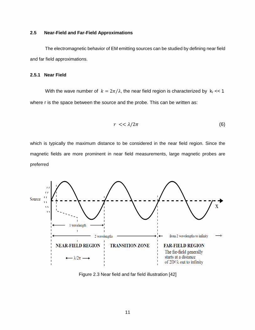
2.5 Near-Field and Far-Field Approximations
The electromagnetic behavior of EM emitting sources can be studied by defining near field
and far field approximations.
2.5.1 Near Field
With the wave number of 𝑘 = 2𝜋 𝜆⁄ , the near field region is characterized by kr << 1
where r is the space between the source and the probe. This can be written as:
𝑟 << 𝜆/2𝜋 (6)
which is typically the maximum distance to be considered in the near field region. Since the
magnetic fields are more prominent in near field measurements, large magnetic probes are
preferred
Figure 2.3 Near field and far field illustration [42]

12
2.5.2 Far Field
As opposed to the near field region, the far field boundary is specified by kr >> 1 which
can be written as:
𝑟 >> 𝜆/2𝜋 (7)
This area is controlled by radiated fields where the electric and magnetic fields are at right
angle to each other. In far field measurements, both E and H fields can be measured and the
larger amplitude of the field makes this measurement easier. A successful EM attack on a smart
card from a far field distance of approximately 5 meters has been performed in [2]. Also in [38],
authors were able to validate full extraction of ECDSA secret signing keys from OpenSSL and
CoreBit coin executing on iOS devices. In these experiments, a shielded environment requires
only a few hundred traces, which is analogous to a near field attack. Alternatively, in an
unshielded environment, the number of required measurements may increase to a few thousand.
2.6 EM Propagation
Electromagnetic emanations propagate from the source in four ways:
i) Electromagnetic radiation.
ii) Conduction.
iii) Modulation of another signal.
iv) Acoustic signals.
Radiated EM emissions can be seized by using near field probes or antennas at a close
proximity. If the amplitude is low, direct radiation should be computed in the near field.
Cryptographic chip can be considered to contain multiple radiation sources in the form of current
elements.

13
Accordingly, a cryptographic chip is modeled by replacing small current loops with
magnetic dipoles and common mode currents with electric dipoles in [16], considering their very
similar field characteristics.
Figure 2.4 EM waves propagation [43]
2.7 EM Probe
A diverse range of EM probes is available to choose from for performing an EM side-
channel attack. A probe is usually a combination of an amplifier and a sensor. The most commonly
used probe is the one with a coil as sensor. Picking a suitable EM probe has a large impact on
the captured EM results. Different EM probes have different measured quantities (magnetic H-
and B-fields), sensitivities, resolutions and frequency bandwidths. The orientation of this probe
needs to equate the course of the originated EM field. Usually, B-field probes have a coil with
several windings which provides a robust output signal while the H-field probes have a single
winding coil that is electrically shielded. The exact placement of the EM probe above the chip
exterior also matters. This is because several processes with different clock frequencies are

14
running simultaneously in a chip. Another thing that matters is the probe resolution. Probes which
have a lesser resolution will pick up EM emanation of executions that are running in neighboring
die areas, which will add more noise to the signal being picked. On the other hand, probes with a
greater resolution will measure only a fragment of the process being surveyed. The transistor
switching period is typically smaller than the clock cycle in most modern chips. In order to capture
emissions, the probe bandwidth must be kept to be roughly five times the clock frequency [39].

15
CHAPTER 3: LEVERAGING ON-CHIP POWER DELIVERY
3.1…..Background
In today’s hardware market, the demand for very efficient electronics in for all sort of
purposes is increasing, different types of countermeasures are being proposed and developed.
These measures will always require a power regulation system. This is because they are strongly
dependent on power that is very specific with its behavior whatever type of prerequisite they
require. The power density is becoming more challenging task for designers as we go down to
smaller nodes of technology [64]. This is making the on-chip voltage regulation into a huge and
hot research area so that it will be able to cater for small, fast, efficient, robust, and high power-
density voltage regulators which will be located very close to the on-die load circuits [9]. The main
advantages they bring are faster voltage scaling, reduction in I/O pins of the chip, and improve
fine-granularity power distribution techniques [9,19]. The design of voltage regulators on die also
calls for new challenges on process and design technologies. On-chip integration of voltage
regulators increases complexity and consequently and can take significant design efforts. On-
chip integration requires the same process technology as other chip components making it a
difficult task as it requires to maintaining high efficiency and excellent performance. The level of
integration also increases the chip size [20,52]. In order to have optimum level integration for
power delivery, we require to decrease the total area under these devices and yet make sure to
do that under acceptable range of power efficiency. The manufacturing cost is directly related to
the area needed by the on-chip voltage converter also it is highly desirable to keep the regulator
in close proximity of the load [60].

16
Figure 3.1 Distributed on-chip power delivery network.
In today’s modern circuits, we are mainly using three types of voltage regulators: low
dropout regulators, switched capacitor also called charge pump and buck converters [21].
3.1.1 Low Dropout Regulators
The most common and simplest solution the power delivery problem is provided by Low
Dropout Regulators (LDOs). The power transistor inside an LDO is dependent on a feedback loop
that stabilizes its output voltage. These regulators provide a fast response as there is no limitation
on the feedback loop other than the stable bandwidth of the error amplifier. The output power to
the goes through the power transistor, the density of which is generally controlled by the current
density of transistors fabricated in the used technology node. This current density is generally
high enough to exceed the current density of the other widely applied topologies. As the
differences between the output and input voltages gets higher, the LDO suffers from a significant
drop in power efficiency. Thus the dependence of this type of regulator on the VOUT/VIN ratio

17
reduces its efficiency. LDOs are very useful in producing a cleaner output from a noisy power
supply [60].
3.1.2 Switched Capacitor Converters
These use capacitors in various configurations for delivering power to the output. These
types of converters usually start from a charging phase during which capacitors are pumped to a
voltage that is pre-determined, as well as a discharging phase when the charge accumulated by
the capacitors is delivered to the output. The output voltage levels are regulated using frequency
of operation and the duty cycle. In any given configuration, the capacitors charge to a certain
voltage, so these converters generally have a distinct ideal conversion ratio which allows them to
operate at 100% efficiency. The large size of the capacitor in this topology, which occupies a
greater than desired area on the chip hinders the efficiency of on-chip implementation and is a
significant disadvantage. If the capacitor size is reduced, less charge may be stored in it, and thus
less charge is available to the load [60].
3.1.3 Buck Converters
The inductor current and its direction in these inductance based converters can be
adjusted to generate a precise output voltage. The standard method for regulating the current
flow through the inductance employs a pair of power transistors. One is connected to the supply
voltage while the other is connected to ground. In this topology, the output voltage is generated
when the switching activity causes a changing current to flow through the inductance. This
switching activity produces some ripple voltage in the output. There are also some serious
concerns in the usage of this configuration in the case of on-chip implementation. The inductor in
this topology occupies a large area, which is a major shortcoming. The size of all the filters needs
18
to be much reduced because the regulator is integrated on-chip, which results in higher switching
frequencies, significantly reducing the efficiency of the regulator [60].
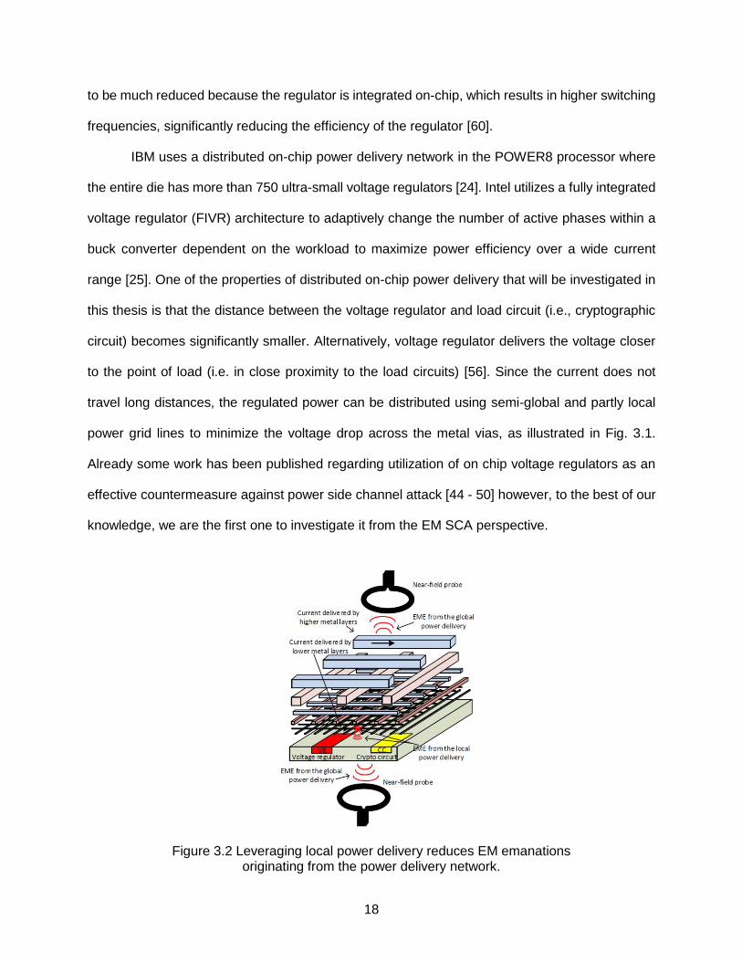
IBM uses a distributed on-chip power delivery network in the POWER8 processor where
the entire die has more than 750 ultra-small voltage regulators [24]. Intel utilizes a fully integrated
voltage regulator (FIVR) architecture to adaptively change the number of active phases within a
buck converter dependent on the workload to maximize power efficiency over a wide current
range [25]. One of the properties of distributed on-chip power delivery that will be investigated in
this thesis is that the distance between the voltage regulator and load circuit (i.e., cryptographic
circuit) becomes significantly smaller. Alternatively, voltage regulator delivers the voltage closer
to the point of load (i.e. in close proximity to the load circuits) [56]. Since the current does not
travel long distances, the regulated power can be distributed using semi-global and partly local
power grid lines to minimize the voltage drop across the metal vias, as illustrated in Fig. 3.1.
Already some work has been published regarding utilization of on chip voltage regulators as an
effective countermeasure against power side channel attack [44 - 50] however, to the best of our
knowledge, we are the first one to investigate it from the EM SCA perspective.
Figure 3.2 Leveraging local power delivery reduces EM emanations originating from the power delivery network.

19
When the power is delivered through thinner metal lines as shown in figure 3.2 at
significantly closer distances, our hypothesis is that the EM emanations are expected to be
significantly mitigated. There are four intuitive explanations [54]:
i) The amount of current will be significantly smaller.
ii) The cross-section of the wires carrying current will be thinner.
iii) The local metal lines may be farther from the probe.
iv) The higher metal layer may partially act as a shield to reduce the EM radiation from
the lower metal lines.
In this thesis, we validate our hypothesis with extensive HFSS simulations, as explained
in next chapters. The simulation of EM SCA attacks on crypto-circuits requires certain number of
EM traces to be observed easily by a nearby placed EM field probe, which needs to be further
analyzed during perilous execution cycles of different encryptions. Once the attacker captures the
traces, the susceptibility of the hardware design to different EM SCA attacks can be explored.
3.2 Working of AES
AES has been in widespread use since 1999 for symmetric cryptography. It is a substitution-
permutation network, has a fixed block size of 128 bits and uses 128, 192 or 256- bit keys [59]. The
number of transformation rounds that the unencrypted text undergoes in order to produce the cipher
depends upon the key size. AES has a well-known flaw in that there is side-channel leakage at the
final transformation round. In ASIC operation, a register is utilized for the AES state to be kept in at the
end of each round; consequently, the round key which is used in the last round can be inferred by
working the side-channel leaks when this register is updated. It is assumed in this work that the EM
emission produced by the AES circuit depends on how many transitions there are at the state register
and at the same time, the hamming distance between the values on the state register.

20
This model is valid since the amount of current that is drawn by the AES circuit is dependent
on the number of CMOS logic gate transitions [61].
Figure 3.3 AES flow chart [61]
3.3 Threat Model
A threat is defined as a situation or occurrence with the likely to reason harm to a system
in the form of obliteration, disclosure, modification of data, and/or denial of service [55]. In our
threat model, the targets are cryptographic circuits, which are running confidential information on
the chip. The goal of the attacker is to learn information that s/he normally has no valid access to,
e.g., the secret keys. For the EM side channel attacks, the attacker typically needs little
capabilities [57]. The measurement setup for EM attacks consists of a sensor or antenna, analog
preprocessing equipment, analog to digital converter, and a cable connection.
21
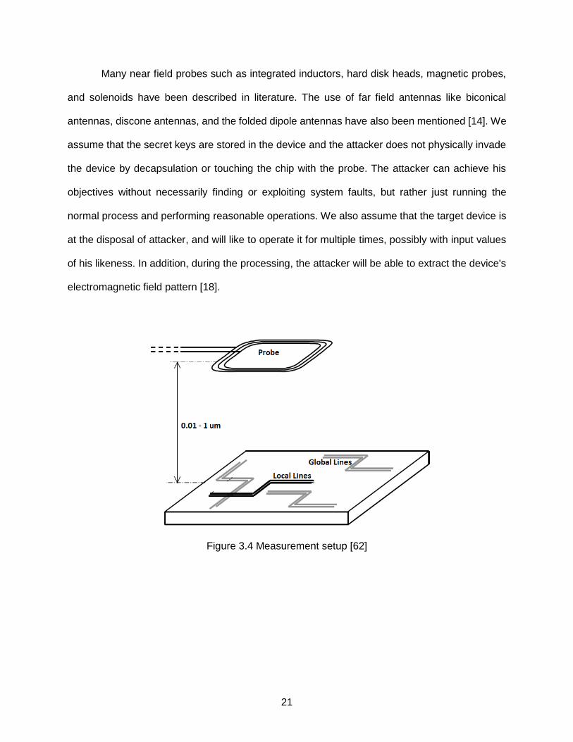
Many near field probes such as integrated inductors, hard disk heads, magnetic probes,
and solenoids have been described in literature. The use of far field antennas like biconical
antennas, discone antennas, and the folded dipole antennas have also been mentioned [14]. We
assume that the secret keys are stored in the device and the attacker does not physically invade
the device by decapsulation or touching the chip with the probe. The attacker can achieve his
objectives without necessarily finding or exploiting system faults, but rather just running the
normal process and performing reasonable operations. We also assume that the target device is
at the disposal of attacker, and will like to operate it for multiple times, possibly with input values
of his likeness. In addition, during the processing, the attacker will be able to extract the device's
electromagnetic field pattern [18].
Figure 3.4 Measurement setup [62]

22
CHAPTER 4: EVALUATION MODEL 4.1 Simulation Setup
The implications of delivering power through the off-chip and on-chip voltage regulators
on the amplitude of EM emissions are presented with extensive simulations in HFSS [26]. Driven
Modal type simulation is selected in the HFSS to compute the modal-based S parameters in terms
of power. The S matrix solutions are articulated in terms of the incident and reflected powers of
the waveguide modes. An excitation port permits energy to in and out of the structure. For this
model, a lumped port is chosen as the excitation port. The local/global power grids are modeled
based on the metal layer parameters in [27]. The solution frequency is chosen as 1 GHz. The
frequency is swept from 400 MHz to 6 GHz with the step size of 0.1 GHz, where the rest of the
data at intermediate frequencies is interpolated. The maximum number of adaptive passes
allowed is 20 and the extreme change in the scale of S parameters between two successive
passes (Delta S) is 0.02. The S parameters are plotted in the 2D Cartesian plane. The antenna
used as a near field probe is a loop antenna with a circumference of 600 um.
Table 4.1 Simulation parameters
Simulator High Frequency Electromagnetic Field Simulation
Incident and reflected power S matrix solution
Solution frequency 1 GHz
Range 400 MHz – 6 GHz
Step size 0.1 GHz
Near field probe model Loop antenna
Circumference 600 um

23
Figure 4.1 EM emissions from local grid at varying probe distances.
4.2 Effects of the Size of the Power Grid and Distance from the Probe
While the highest two metal layers (eighth and ninth) are considered to form the global
power grid, the lower metal layers (third and fourth) are considered to form the local power grid.
We first analyze the emanations when a probe is placed at the top of the circuit. The emanations
from the local and global power grid lines are extracted when the distance of the near field probe
to the chip is swept from 25 um to 150 um, as shown respectively, in Figs. 4.1 and 4.2. The lengths
of the local and global power grid lines are, respectively, 100 um and 250 um. The amplitude of
the EM emissions from both the global and local grids to the probe increases with frequency and
with a reduction in the distance from the probe.
Table 4.2 EM Emanations from local vs global grid at varying probe distance.
Distance from probe (um) Local grid (dB) Global grid (dB)
25 -104.4053 -70.4994
50 -122.6810 -79.5490
100 -132.9984 -95.3681
150 -144.0217 -108.4753
24
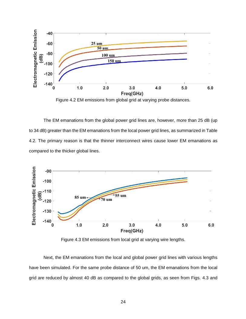
Figure 4.2 EM emissions from global grid at varying probe distances.
The EM emanations from the global power grid lines are, however, more than 25 dB (up
to 34 dB) greater than the EM emanations from the local power grid lines, as summarized in Table
4.2. The primary reason is that the thinner interconnect wires cause lower EM emanations as
compared to the thicker global lines.
Figure 4.3 EM emissions from local grid at varying wire lengths.
Next, the EM emanations from the local and global power grid lines with various lengths
have been simulated. For the same probe distance of 50 um, the EM emanations from the local
grid are reduced by almost 40 dB as compared to the global grids, as seen from Figs. 4.3 and
25
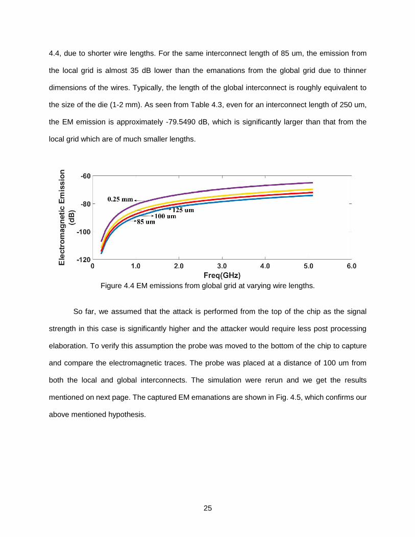
4.4, due to shorter wire lengths. For the same interconnect length of 85 um, the emission from
the local grid is almost 35 dB lower than the emanations from the global grid due to thinner
dimensions of the wires. Typically, the length of the global interconnect is roughly equivalent to
the size of the die (1-2 mm). As seen from Table 4.3, even for an interconnect length of 250 um,
the EM emission is approximately -79.5490 dB, which is significantly larger than that from the
local grid which are of much smaller lengths.
Figure 4.4 EM emissions from global grid at varying wire lengths.
So far, we assumed that the attack is performed from the top of the chip as the signal
strength in this case is significantly higher and the attacker would require less post processing
elaboration. To verify this assumption the probe was moved to the bottom of the chip to capture
and compare the electromagnetic traces. The probe was placed at a distance of 100 um from
both the local and global interconnects. The simulation were rerun and we get the results
mentioned on next page. The captured EM emanations are shown in Fig. 4.5, which confirms our
above mentioned hypothesis.

26
Table 4.3 EM emanations from the local and global power grids to
a probe for different wire lengths
Wire length (um) Local grid emissions (dB) Global grid emissions (dB)
55 -127.1706 -
70 -125.6433 -
85 -123.8549 -88.4574
100 - -86.4093
125 -84.0472
250 -79.5490
When capturing the EM emanations from the bottom, there is a decrease of 8 dB in
emissions from global interconnect wires. The increased distance and shielding from the
substrate are the two main reasons for this drop. The emissions from the local wires however are
increased. This is because the probe is now relatively closer to the wires as compared to the
previous case when the probe was placed at the top of the chip. The emanations from the global
wires can still be seen to be higher than the emanations from the local wires, which supports our
claim that on chip regulation will significantly improve the security.
Figure 4.5 EM emissions comparison of local and global grids at 100 um.

27
The comparison can also be seen in Table 4.4, for the interconnect length of 100 um, the
EM emission from global grid is -103.4635 dB, which is significantly higher than the local grid of
the same length.
Table 4.4 EM emanations from the local and global power grids to a probe placed at 100 um.
Probe position Local grid (dB) Global grid (dB)
Top -132.9984 -95.3681
Bottom -114.6810 -103.4635
4.3 Security Implication of the Implemented Design
Although we have discussed the reduction in the signal strength in the previous sections,
the security implications as a function of the signal strength are explained in this section. This
section validates our discussion with mathematical calculations performed under the same
scenarios stated in the previous sections.
Assuming that PS1 is the power of the EM signal without the proposed countermeasure,
PN is the measured power noise, and PS is the power of the signal with countermeasure,
10𝐿𝑜𝑔 𝑃𝑆1
𝑃𝑁− 10𝐿𝑜𝑔
𝑃𝑆2
𝑃𝑁= 33
10 (𝐿𝑜𝑔𝑃𝑆1 − 𝐿𝑜𝑔 𝑃𝑁 − 𝐿𝑜𝑔 𝑃𝑆2 + 𝐿𝑜𝑔 𝑃𝑁) = 33
10𝐿𝑜𝑔𝑃𝑆1
𝑃𝑆2= 33
𝑃𝑆1
𝑃𝑆2= 1995
Signal to noise ratio (SNR) is a degree of how much useful information there is in a system.

28
𝑆𝑁𝑅1 = 𝑉𝑎𝑟𝑃𝑆1
𝑃𝑁 𝑊𝑖𝑡ℎ 𝐶𝑜𝑢𝑛𝑡𝑒𝑟𝑚𝑒𝑎𝑠𝑢𝑟𝑒
𝑆𝑁𝑅2 = 𝑉𝑎𝑟𝑃𝑆2
𝑃𝑁 𝑊𝑖𝑡ℎ𝑜𝑢𝑡 𝐶𝑜𝑢𝑛𝑡𝑒𝑟𝑚𝑒𝑎𝑠𝑢𝑟𝑒
𝑆𝑁𝑅2 = 𝑆𝑁𝑅1
𝑉𝑎𝑟 (𝑃𝑆2)
𝑉𝑎𝑟 (𝑃𝑆1)= 𝑆𝑁𝑅
1
1995
SNR has a relationship with the correlation coefficient given by the following equation:
𝐶𝑜𝑟𝑟𝑒𝑙𝑎𝑡𝑖𝑜𝑛 𝛾 = 1
√1 +1
𝑆𝑁𝑅
From the security perspective, we are interested in computing the number of plaintexts
that are mandatory to have a fruitful attack with a success rate of 0.9 as a function of the
correlation coefficient value [28]. We witnessed that the quantity of plaintexts with a success rate
of N0.9 required to perform a correlation analysis attack can be expected with [28].
𝑁0.9 ≈ 𝐶 × 1
𝛾2= 𝐶 (1 +
1
𝑆𝑁𝑅2)
≈ 𝐶
𝑆𝑁𝑅2=
𝐶
𝑆𝑁𝑅1 × (1995)2
where C is a constant reliant on the numeral of key guesses considered and the necessary
success rate. The enhancement in the measurement to disclosure (MTD) value comes out to be
(1995)2 which is considered a significant improvement. Similarly, from Table 4.4 it can be
observed that the EM emanations from the global interconnect is approximately 11 dB higher than
that captured from the local grid. Using this result and following the same procedure:
10 𝐿𝑜𝑔𝑃𝑆1
𝑃𝑆2= 11
𝑃𝑆1
𝑃𝑆2= 13
𝑁0.9 ≈ 𝐶 ×1
𝛾2=
𝐶
𝑆𝑁𝑅1× (13)2

29
It is observed that the MTD enhancement ratio is not decreased significantly if the attack
is performed from the bottom. This is primarily because when captured from the bottom, the EM
emanations by the global grid is decreased but increased by the local grid, due to the close
proximity to the measuring probe.
Although the MTD enhancement ratio is significantly larger for the attacks that are
performed from the top side, the EM signal strength is still larger when the attack is performed
from the top side as compared to the bottom side. The focus of this thesis is to reduce the
emanations from the top side to make the EM side channel attack difficult to perform. We have
shown that using on-chip voltage regulators, EM emissions are reduced by 33 dB and the MTD
enhancement ratio is increased by a factor of (1995)2. In the following sections, two techniques
will be discussed which will further reduce the EM emissions from the top probe, making the attack
even more difficult to perform.
4.4 Shielding with MIM Capacitor
Sheet metal is typically used for shielding EM radiation. Copper absorbs radio and
magnetic waves and is used for RF shielding [29,51]. The electric field in EM radiation produces
forces on the electrons in the conductor, which causes displacement of charges inside the
conductor and cancels the applied field. Similarly, magnetic fields produce eddy currents inside
the conductor which reflect the electromagnetic radiation from the surface.
However, due to the electrical resistivity of the conductor, the excited field does not
completely cancels the applied field. Any holes in the shield must be significantly smaller than the
wavelength of the radiation that is trying to be kept out. Holes bigger than the wavelength allow
the current to flow around them so the incident wave does not excite the opposing electromagnetic
fields [30]. High frequencies (100MHz- 40 GHz) are extremely sensitive to gaps in the shielding
enclosure. Also, due to the ferromagnetic response of the conductors to low frequency magnetic

30
field, these fields are not completely mitigated by the conductor. All these factors reduce the
shielding capability of a conductor [30].
EM shielding also occurs due to absorption. The loss due to absorption is proportional to
the thickness of the shield, and is because of the presence of electric or magnetic dipoles, which
interact with the fields in the incident radiation. Shielding can also occur due to multiple reflections
from the conductor surface. The loss due to multiple reflections is directly related to the surface
area of the shield where a larger interface area increases the radiation loss. At higher frequencies,
electromagnetic radiation penetrates only the near surface of an electrical conductor which is
known as skin effect [31,59].
Figure 4.6 Using MIM capacitor as a shield.
Accordingly, we experimented with MIM capacitors and investigated the effectiveness of
MIM capacitors on minimizing the EM emanations from the local power grids, as illustrated in Fig.
4.6. MIM capacitors are typically implemented between the fifth and sixth metal layers, making
them physically appropriate to shield the local power grid lines which use the third and fourth
metal layers in our simulations. Fig. 4.7 shows the effect of using an MIM capacitor to shield the
local power grid. As tabulated in Table 4.5, the MIM shielding leads to a reduction in the EM
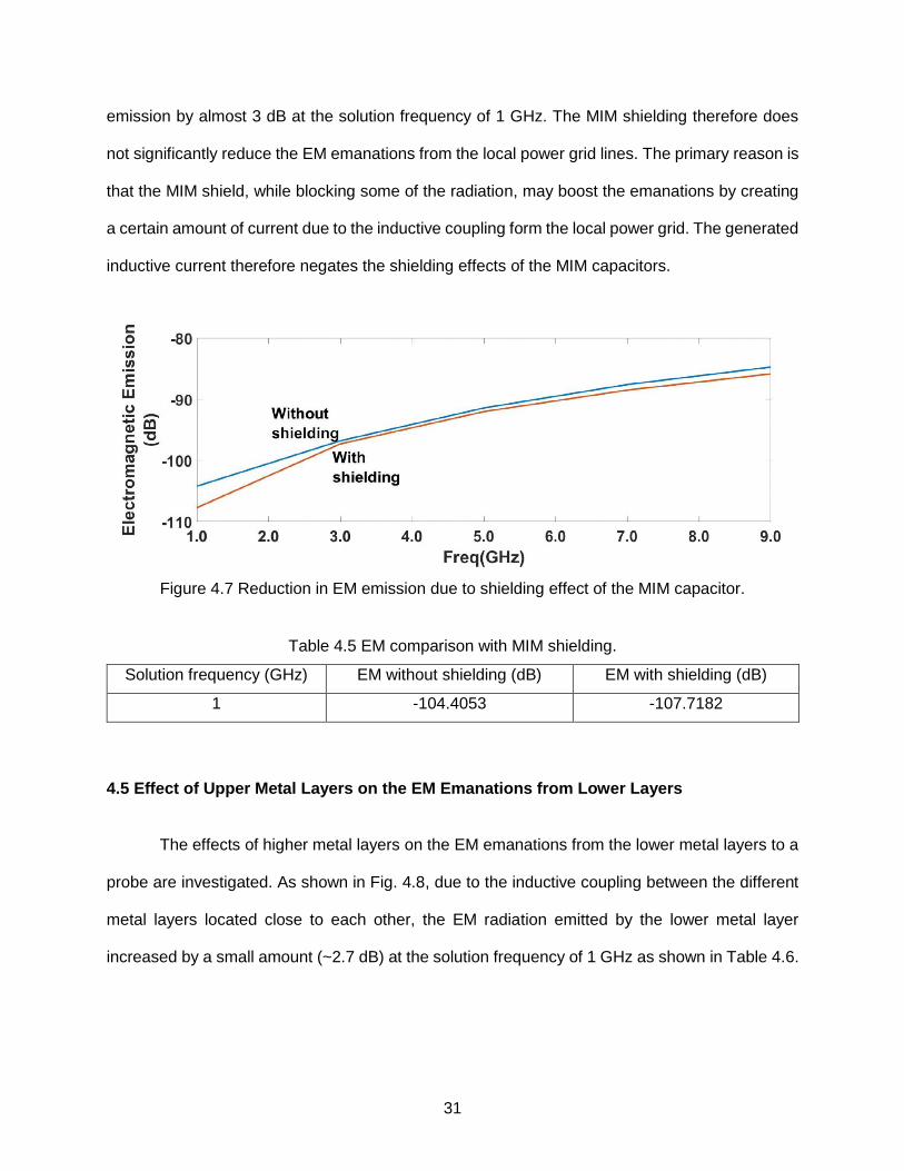
31
emission by almost 3 dB at the solution frequency of 1 GHz. The MIM shielding therefore does
not significantly reduce the EM emanations from the local power grid lines. The primary reason is
that the MIM shield, while blocking some of the radiation, may boost the emanations by creating
a certain amount of current due to the inductive coupling form the local power grid. The generated
inductive current therefore negates the shielding effects of the MIM capacitors.
Figure 4.7 Reduction in EM emission due to shielding effect of the MIM capacitor.
Table 4.5 EM comparison with MIM shielding.
Solution frequency (GHz) EM without shielding (dB) EM with shielding (dB)
1 -104.4053 -107.7182
4.5 Effect of Upper Metal Layers on the EM Emanations from Lower Layers
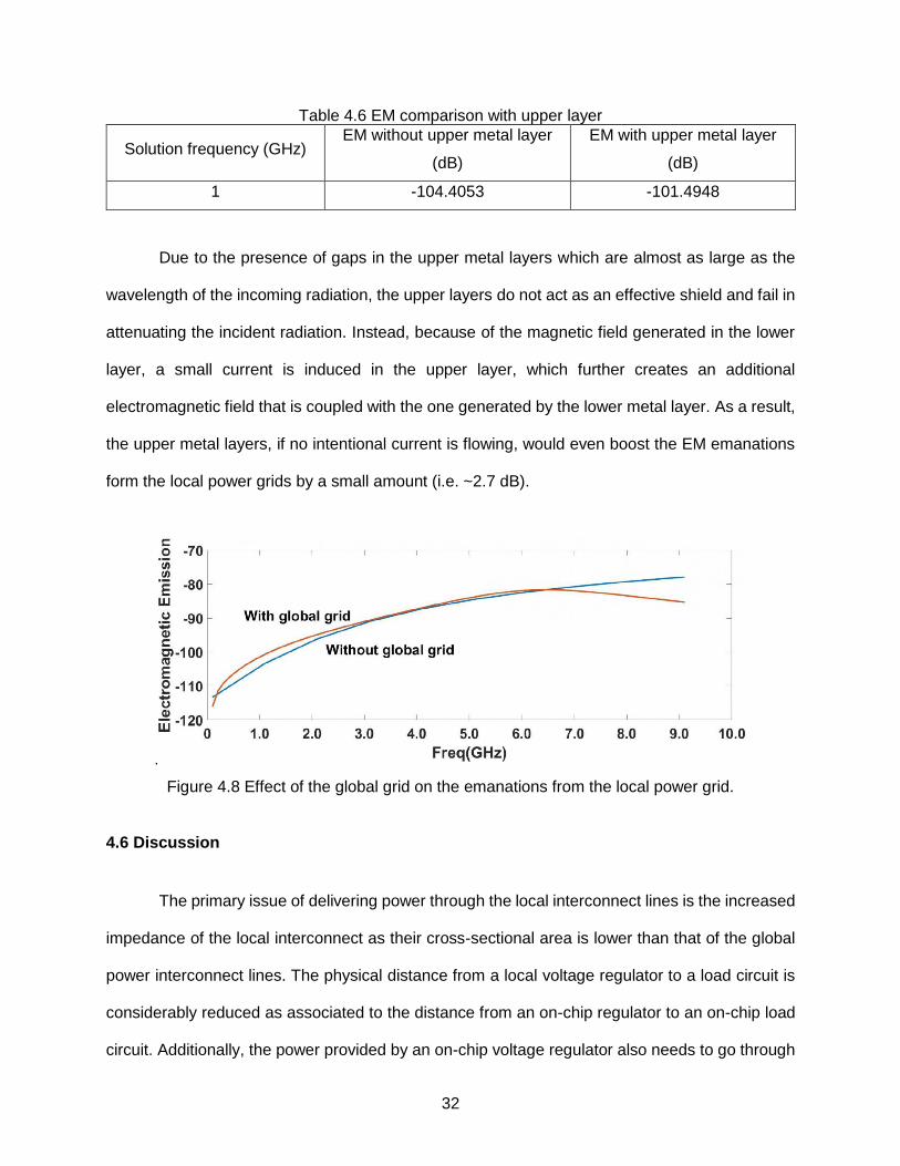
The effects of higher metal layers on the EM emanations from the lower metal layers to a
probe are investigated. As shown in Fig. 4.8, due to the inductive coupling between the different
metal layers located close to each other, the EM radiation emitted by the lower metal layer
increased by a small amount (~2.7 dB) at the solution frequency of 1 GHz as shown in Table 4.6.
32
Table 4.6 EM comparison with upper layer
Solution frequency (GHz) EM without upper metal layer
(dB)
EM with upper metal layer
(dB)
1 -104.4053 -101.4948
Due to the presence of gaps in the upper metal layers which are almost as large as the
wavelength of the incoming radiation, the upper layers do not act as an effective shield and fail in
attenuating the incident radiation. Instead, because of the magnetic field generated in the lower
layer, a small current is induced in the upper layer, which further creates an additional
electromagnetic field that is coupled with the one generated by the lower metal layer. As a result,
the upper metal layers, if no intentional current is flowing, would even boost the EM emanations
form the local power grids by a small amount (i.e. ~2.7 dB).
.
Figure 4.8 Effect of the global grid on the emanations from the local power grid.
4.6 Discussion
The primary issue of delivering power through the local interconnect lines is the increased
impedance of the local interconnect as their cross-sectional area is lower than that of the global
power interconnect lines. The physical distance from a local voltage regulator to a load circuit is
considerably reduced as associated to the distance from an on-chip regulator to an on-chip load
circuit. Additionally, the power provided by an on-chip voltage regulator also needs to go through

33
the package and/or board level interconnects as well as the pad/pin parasitic impedance. As
compared to going through all of these parasitic impedances, the output power of a localized on-
chip voltage regulator only needs to travel small distances. Considering these differences
between the on-chip voltage regulators and distributed on-chip voltage regulators, delivering the
required power through lower metal lines to the circuits at close proximity would not cause
significant amount of noise. Additionally, the power output of each individual distributed voltage
regulator is considerably smaller than that of the on-chip regulators, making it possible for the
localized regulated power to be delivered through the local power grid lines.
34
CHAPTER 5: FUTURE WORK
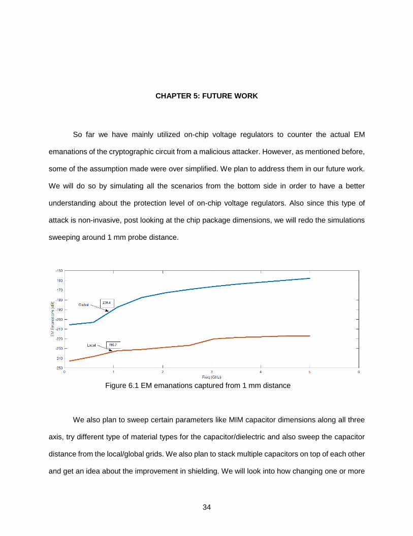
So far we have mainly utilized on-chip voltage regulators to counter the actual EM
emanations of the cryptographic circuit from a malicious attacker. However, as mentioned before,
some of the assumption made were over simplified. We plan to address them in our future work.
We will do so by simulating all the scenarios from the bottom side in order to have a better
understanding about the protection level of on-chip voltage regulators. Also since this type of
attack is non-invasive, post looking at the chip package dimensions, we will redo the simulations
sweeping around 1 mm probe distance.
Figure 6.1 EM emanations captured from 1 mm distance
We also plan to sweep certain parameters like MIM capacitor dimensions along all three
axis, try different type of material types for the capacitor/dielectric and also sweep the capacitor
distance from the local/global grids. We also plan to stack multiple capacitors on top of each other
and get an idea about the improvement in shielding. We will look into how changing one or more

35
than one of the above mentioned parameters change the shielding effectiveness of the MIM
capacitor. The shielding effectiveness (SE) is equal to ratio quantities at the receptor without the
shield and with shield:
SEdB = 20LogEM1
EM2
where, EM1 represents emanation at the receptor without shielding body, EM2 denote the
emanations at the receptor with a shielding barrier (MIM) between the emitter and receptor. This
formula is valid as long as the thickness of the shield is much less than a skin depth, δ, where the
skin depth is defined as follows:
σ = √2
ωμσ
We also plan to sweep the local/global grid dimensions for more accurate and realistic
assumptions. Right now the dimensions used were from [27] which is around a decade old
technology standards. Since then, with the rapid development of nanoscale integrated circuits
(ICs), the thickness of interconnects has been decreased dramatically. Moving forward we will
model our local and global grids according to the information provided in [63]. This will provide us
more accurate and realistic results.
Lastly we plan to replace MIM capacitor with other available on chip passive devices like
inductor and see what impact they create on the captured EM emanations by the attacker.

36
CHAPTER 6: CONCLUSION
In this work, the implications of distributed on-chip power delivery on EM side channel
attacks are investigated. The key idea is the observation that on-chip voltage regulators can utilize
shorter and thinner local interconnect wires, and the EM emissions from the circuit would be
considerably lower than those from circuits using on-chip voltage regulators which have to utilize
thicker global wires. A 33 and 11 dB reduction in the EM emanations from top and bottom can be
achieved, respectively, when distributed on-chip voltage regulators are utilized instead of on-chip
voltage regulators. In the analysis, we are able to simulate global grid up to 0.25 mm length due
to computational complexity of the simulation with longer wires. With typical global grids having
lengths of 1-2 mm, the EM radiation will be significantly higher than local grids when captured
from either top or bottom. We also demonstrate that shielding a cryptographic circuit with MIM
capacitors can further decrease the emission of EM side channel information by less than 3 dB.

37
REFERENCES [1] P. Kocher, J. Jaffe, and B. Jun, “Differential power analysis," Advances in cryptology.
Springer, pp. 789 - 789, 1999.
[2] S. Mangard, E. Oswald, and T. Popp, Power analysis attacks: Revealing the secrets of
smart cards, Vol. 31, Springer Science, 2008.
[3] E. Brier and M. Joye, “Weierstras elliptic curves and side-channel attacks," pp. 200 - 210,
2002.
[4] B. Kopf and D. Basin, “An information-theoretic model for adaptive side-channel attacks,"
Proceedings of the ACM conference on Computer and communications security, 2007.
[5] J.J. Quisquater and D. Samyde, “ElectroMagnetic Analysis (EMA): Measures and
Counter-Measures for Smart Cards," Smart Card Programming and Security, Vol. 40, pp.
200 - 210, 2001.
[6] D Agrawal, B Archambeault, R. Rao, and P Rohatgi, “The EM Side-Channel(s)," pp. 29
- 45, 2003.
[7] R. J. Milliken, J. Silva-Martinez, and E. Sanchez-Sinencio, “Full On-Chip CMOS Low-
Dropout Voltage Regulator," IEEE Transactions on Circuits and Systems I: Regular
Papers, Vol. 54, No. 9, pp. 1879 - 1890, 2007.
[8] K. Chava and J. Silva-Martinez, “A frequency compensation scheme for LDO voltage
regulators," IEEE Transactions on Circuits and Systems I: Regular Papers, Vol. 51, No.
6, pp. 1041 - 1050, 2004.
[9] W. Kim, S. Gupta, G. Wei, and D. Brooks, “System level analysis of fast, per-core DVFS
using on-chip switching regulators," High Performance Computer Architecture, 2008.
HPCA 2008. IEEE 14th International Symposium on. IEEE, pp. 123 - 134, 2008.
[10] S. Köse and E. G. Friedman, ''Distributed On-Chip Power Delivery,'' IEEE Journal on
Emerging and Selected Topics in Circuits and Systems, Vol. 2, No. 4, pp. 704 - 713,
December 2012.
[11] Robert Callan, Alenka Zajic, and Milos Prvulovic, “FASE: Finding amplitude-modulated
side-channel emanations," ACM SIGARCH Computer Architecture News. ACM, Vol. 43,
pp. 592 - 603, 2015.
[12] PT Pappas, “The original Ampere force and Biot-Savart and Lorentz forces," Vol. 76, pp.
189 - 197, 1983, Springer.
[13] A. Zajic and M. Prvulovic, “Experimental demonstration of electromagnetic information
leakage from modern processor-memory systems," IEEE Transactions on
Electromagnetic Compatibility, Vol. 56, No. 4, pp. 885 - 893, 2014.
[14] D. Mulder, “Electromagnetic Techniques and Probes for Side-Channel Analysis on
Cryptographic Devices," Diss. PhD thesis, 2010.
[15] National Security Agency," NACSIM 5000: TEMPEST Fundamentals, February 1982.
[16] Y. Cao, Predictive Technology Model for Robust Nanoelectronic Design, Springer, 2011.
[17] C. Rechberger and E. Oswald, “Stream ciphers and side-channel analysis," In ECRYPT
Workshop, SASC-The State of the Art of Stream Ciphers, pp. 320 - 326, 2004.
38
[18] A. Aldini, R. Gorrieri, and F. Martinelli, Foundations of Security Analysis and Design III:
FOSAD 2004/2005 Tutorial Lectures, Vol. 3655, Springer, 2005.
[19] L. Benini, A. Bogliolo, and G. De Micheli, “A Survey of Design Techniques for System-
Level Dynamic Power Management," IEEE Transactions on Very Large Scale Integration
(VLSI) Systems, Vol. 8, No. 3, pp. 299 - 316, March 2000.
[20] Steven K., “Understanding the Advantages and Disadvantages of Linear Regulators,"
Aug. 2012.
[21] C. F. Lee and P. K. Mok, “A Monolithic Current-Mode CMOS DC-DC Converter with On-
Chip Current-Sensing Technique," IEEE Journal of Solid-State Circuits, Vol. 39, No. 1,
pp. 3 - 14, January 2004.
[22] W. Kim, M. S. Gupta, G. Wei, and D. M. Brooks, “Enabling on-chip switching regulators
for multicore processors using current staggering," Proceedings of the Work on
Architectural Support for Gigascale Integration, 2007.
[23] J. Gjanci, On-Chip Voltage Regulation for Power Management in System-on-Chip, Ph.D.
thesis, University of Illinois at Chicago, 2008.
[24] E. J. Fluhr et al., “The 12-Core POWER8 Processor With 7.6 Tb/s IO Bandwidth,
Integrated Voltage Regulation, and Resonant Clocking," IEEE Journal of Solid-State
Circuits, Vol. 50, No. 1, pp. 10 - 23, January 2015.
[25] E. A. Burton et al., “FIVR - Fully Integrated Voltage Regulators on 4th Generation Intel
Core SoCs," apec, pp. 432 - 439, March 2014.
[26] HFSS Ansoft, “ver. 11," Ansoft Corporation, Pittsburgh, PA, 2007.
[27] K. Mistry et al., \A 45nm Logic Technology with High-k+Metal Gate Transistors, Strained
Silicon, 9 Cu Interconnect Layers, 193nm Dry Patterning, and 100Pb-free Packaging,"
IEEE International Electron Devices Meeting, pp. 247 - 250, May 2007.
[28] O-X Standaert, E. Peeters, G. Rouvroy, and J-J Quisquater, “An overview of power
analysis attacks against field programmable gate arrays," Proceedings of the IEEE, Vol.
94, No. 2, pp. 383 - 394, 2006.
[29] Frederick Lilienthal II Peter and Fred William Verdi, “Circuit board RF shielding” May 29
2001, US Patent 6,239,359.
[30] “Practical EM Shielding," 2016. [Online]. Available: http://learnemc.com/practical-em
shielding.
[31] D. C. Mattis and J. Bardeen, “Theory of the Anomalous Skin Effect in Normal and
Superconducting Metals," Phys. Rev., Vol. 111, No. 0, pp. 412 - 417, Jul 1958.
[32] ‘Matching shielded loops for cryptographic analysis’ W. Aerts, E. De Mulder, B. Preneel,
G.A.E. Vandenbosch, and I. Verbauwhede, Proceedings ‘EuCAP 2006’, Nice, France, 6
10 November 2006.
[33] ‘Electromagnetic Analysis: Concrete Results’ Karine Gandol, Christophe Mourtel, and
Francis Olivier, CHES 2001, vol. 2162 of Lecture Notes in Computer Science, pp. 251
Springer-Verlag, 2001.
[34] M. Mayhew and R. Muresan, "On-Chip Nanoscale Capacitor Decoupling Architectures
for Hardware Security," IEEE Transactions on Emerging Topics in Computing, vol. 2, no.
1, pp. 4-15, March 2014.
[35] Wakabayashi, Satohiro & Maruyama, Seita & Mori, Tatsuya & Goto, Shigeki & Kinugawa,
Masahiro & Hayashi, Yu-ichi. POSTER: Is Active Electromagnetic Side-channel Attack
Practical? Power and electromagnetic analysis: Improved model, consequences and
comparisons.(2017).
39
[36] Vuagnoux, Martin and Pasini, Sylvain, “Compromising Electromagnetic Emanations of
Wired and Wireless Keyboards”, Proceedings of the 18th USENIX Security Symposium,
Pp 1-16, May 2009.
[37] Genkin, Daniel and Pachmanov, Lev and Pipman, Itamar and Tromer, Eran and Yarom,
Yuval, “ECDS A Key Extraction from Mobile Devices via Nonintrusive Physical Side
Channels” Proceedings of the 2016 ACM SIGSAC Conference on Computer and
Communications Security. Pp 1626 – 1638, Oct 2016.
[38] F. Debeer et al., “Practical electro-magnetic analysis,” Non-Invasive Attack Testing
Workshop NIAT, 2011.
[39] A. Lakshminarasimhan, “Electromagnetic side-channel analysis for hardware and
software watermarking,” Master’s thesis, University of Massachusetts Amherst, 2011.
[40] Elke De Mulder, “Electromagnetic Techniques and Probes for Side-Channel Analysis on
Cryptographic Devices” Dissertation presented in partial fulfillment of the requirements
for the degree of Doctor in Electrical Engineering, Katholieke Universiteit Leuven, Nov
2010.
[41] Adegbite OJ. A novel and cost-effective test bed implementation of side channel attacks
on aes: Leveraging correlation power analysis and machine learning. [Order
No..10269041].Tennessee.Technological.University;2017.
https://search.proquest.com/docview/1908536763?pq-origsite=gscholar
[42] By OSHA, Dept of Labor
http://www.osha.gov/SLTC/radiofrequencyradiation/electromagnetic_fieldmemo/electro
magnetic.html, Public Domain,
https://commons.wikimedia.org/w/index.php?curid=20417753
[43] https://pixabay.com/en/electromagnetic-waves-wave-length-1526374/
[44] W. Yu and S. Köse, ''Exploiting Voltage Regulators to Enhance Various Power Attack
Countermeasures,'' IEEE Transactions on Emerging Topics in Computing, VOL.5, NO.1,
March 2017.
[45] W. Yu and S. Köse, ''False Key-Controlled Aggressive Voltage Scaling: A
Countermeasure Against LPA Attacks,'' IEEE Transactions on Computer-Aided Design
of Integrated Circuits and Systems, Vol. 36, No. 12, pp. 2149 -- 2153, December 2017.
[46] W. Yu and S. Köse, ''Security-Adaptive Voltage Conversion as a Lightweight
Countermeasure Against LPA Attacks,'' IEEE Transactions on Very Large Scale
Integration (VLSI) Systems, Vol. 25, No. 7, pp. 2183 -- 2187, July 2017.
[47] W. Yu and S. Köse, ''A Voltage Regulator-Assisted Lightweight AES Implementation
Against DPA Attacks,'' IEEE Transactions on Circuits and Systems I: Regular Papers,
Vol. 63, No. 8, pp. 1152 - 1163, August 2016.
[48] W. Yu and S. Köse, "A Lightweight AES Implementation Against Bivariate First-Order
DPA Attacks," Proceedings of the ACM Workshop on Hardware and Architectural
Support for Security and Privacy (HASP), pp. 1 - 7, June 2017.
[49] W. Yu, O. A. Uzun, and S. Köse, "Leveraging On-Chip Voltage Regulators as a
Countermeasure Against Side-Channel Attacks," Proceedings of the IEEE/ACM Design
Automation Conference (DAC), pp. 1 - 6, June 2015.
[50] W. Yu and S. Köse, ''Charge-Withheld Converter-Reshuffling (CoRe): A Countermeasure
Against Power Analysis Attacks'' IEEE Transactions on Circuits and Systems II: Express
Briefs, Vol. 63, No. 5, pp. 438 - 442, May 2016.
[51] S. Köse, E. Salman, and E. G. Friedman, ''Shielding Methodologies in the Presence of
Power/Ground Noise,'' IEEE Transactions on Very Large Scale Integration (VLSI)
Systems, Vol. 19, No. 8, pp. 1458 - 1468, August 2011.

40
[52] S. Köse, S. Tam, S. Pinzon, B. McDermott, and E. G. Friedman, ''Active Filter Based
Hybrid On-Chip DC-DC Converters for Point-of-Load Voltage Regulation,'' IEEE
Transactions on Very Large Scale Integration (VLSI) Systems, Vol. 21, No. 4, pp. 680 -
691, April 2013.
[53] I. Vaisband, M. Azhar, E. G. Friedman, and S. Köse, ''Digitally Controlled Pulse Width
Modulator for On-Chip Power Management,'' IEEE Transactions on Very Large Scale
Integration (VLSI) Systems, Vol. 22, No. 12, pp. 2527 - 2534, December 2014.
[54] L. Wang, S. K. Khatamifard, O. A. Uzun, U. R. Karpuzcu, and S. Köse, ''Efficiency,
Stability, and Reliability Implications of Unbalanced Current Sharing among Distributed
On-Chip Voltage Regulators,'' IEEE Transactions on Very Large Scale Integration (VLSI)
Systems, Vol. 25, No. 11, pp. 3019 -- 3032, November 2017.
[55] S. K. Khatamifard, L. Wang, W. Yu, S. Köse, and U. R. Karpuzcu, "ThermoGater:
Thermally-Aware On-Chip Voltage Regulation," Proceedings of the IEEE International
Symposium on Computer Architecture (ISCA), pp. 120 - 132, June 2017.
[56] S. Köse, "Efficient and Secure On-Chip Reconfigurable Voltage Regulation for IoT
Devices," Proceedings of the ACM/IEEE Great Lakes Symposium on VLSI, pp. 369 -
374, May 2017.
[57] S. Köse, "Thermal Implications of On-Chip Voltage Regulation: Upcoming Challenges
and Possible Solutions," Proceedings of the IEEE/ACM Design Automation Conference
(DAC), pp. 1 - 6, June 2014.
[58] S. Köse, "Regulator-Gating: Adaptive Management of On-Chip Voltage Regulators,"
Proceedings of the ACM/IEEE Great Lakes Symposium on VLSI, pp. 105 - 110, May
2014.
[59] S. Köse, E. Salman, and E. G. Friedman, "Shielding Methodologies in the Presence of
Power/Ground Noise," Proceedings of the IEEE International Symposium on Circuits and
Systems, pp. 2277 - 2280, May 2009.
[60] Orhun Aras Uzun, “Speed, Power Efficiency, and Noise Improvements for Switched
Capacitor Voltage Converters”, PhD. Dissertation, University of South Florida, 2017
[61] A. Kumar, C. Scarborough, A. Yilmaz and M. Orshansky, "Efficient simulation of EM side-
channel attack resilience," 2017 IEEE/ACM International Conference on Computer-Aided
Design (ICCAD), Irvine, CA, 2017, pp. 123-130.
[62] K. Tiri and I. Verbauwhede, "A VLSI design flow for secure side-channel attack resistant
ICs," Design, Automation and Test in Europe, 2005, pp. 58-63 Vol. 3.
[63] K. Fischer et al., "Performance enhancement for 14nm high volume manufacturing
microprocessor and system on a chip processes," 2016 IEEE International Interconnect
Technology Conference / Advanced Metallization Conference (IITC/AMC), San Jose,
CA, 2016, pp. 5-7.
[64] S. Köse and E. G. Friedman, "On-Chip Point-of-Load Voltage Regulator for Distributed
Power Supplies," Proceedings of the ACM/IEEE Great Lakes Symposium on VLSI, pp.
377 - 380, May 2010.

41
APPENDIX A: COPYRIGHT PERMISSIONS
Significant part of this thesis is based on our previously published work.

42
The following is the copyright permission notice for Fig. 2.3 and 2.4 of Chapter 2.
The following is the copyright permission notice for Fig. 3.3 of Chapter 3.

43
The following is the copyright permission notice for Fig. 3.4 of Chapter 3.


![Transmission Distribution and Utilization [15EE52T]](https://static.fdokumen.com/doc/165x107/6328d58109048e4b7c061729/transmission-distribution-and-utilization-15ee52t.jpg)