Title Schematic by Title Description - Orange County, California
Upload
fz-juelichCategory
view
0download
0
Micromorph silicon tandem solar cells with fully integrated3D photonic crystal intermediate reflectors
J. Upping*a, A. Bielawnya, S. Fahrb, C. Rockstuhlb, F. Ledererb, L. Steidlc, R. Zentelc,T. Beckersd, A. Lambertzd, R. Cariusd, and R. B. Wehrspohna,e
a Institute of Physics, Martin-Luther-University Halle-Wittenberg, Germanyb Institute of Condensed Matter Theory and Solid States Optics, Friedrich Schiller
University Jena, Germanyc Dept. of Chemistry, Pharmacy and Earth Science, Johannes Gutenberg University of
Mainz, Germanyd Institute of Energy Research, IEF-5 Photovoltaik, Forschungszentrum Julich GmbH,
Germanye Fraunhofer Institute for Mechanics of Materials Halle, Germany
ABSTRACT
A 3D photonic intermediate reflector for textured micromorph silicon tandem solar cells has been investigated.In thin-film silicon tandem solar cells consisting of amorphous and microcrystalline silicon with two junctionsof a-Si:H/c-Si, efficiency enhancements can be achieved by increasing the current density in the a-Si:H topcell providing an optimized current matching at high current densities. For an ideal photon-managementbetween top and bottom cell, a spectrally-selective intermediate reflective layer (IRL) is necessary. We presentthe first fully-integrated 3D photonic thin-film IRL device incorporated on a planar substrate. Using a ZnOinverted opal structure the external quantum efficiency of the top cell in the spectral region of interest couldbe enhanced. As an outlook we present the design and the preparation of a 3D self organized photonic crystalstructure in a textured micromorph tandem solar cell.
Keywords: photon management, light trapping, tandem solar cells, photonic crystals, atomic layer deposition,inverted opal
1. INTRODUCTION
Micromorph silicon solar cells are currently used for large area and building-integrated photovoltaic appli-cations. However, they suffer from the significantly lower efficiency compared to high-efficiency CIGS-solarcells and higher costs compared to CdTe-solars. One important challenge is therefore, to increase the overallefficiency of micromorph silicon solar cells. Micromorph silicon solar cells are composed of two cells, an a-Si:Hfront absorber and a μc-Si bottom absorber (Fig. 1a)). The external quantum efficiencies (EQE) (Fig. 1b))of the series-connected cells for typical thickness of the absorbing material lead to an unbalanced distributionof the absorbed photon flux. The front cell produces a lower electrical current than the bottom cell whichreduces the overall efficiency since the tandem is a serial connected device. A typical silicon tandem cell withscattering front, jsc = 12.1 mA/cm2 and Voc,a = 0.91 V , Voc,c = 0.5 V reaches 11.1% in efficiency (FF=0.65).We have shown that an intermediate reflector has the theoretical potential to increase the current in the cellresulting in an efficiency of 12.4%, i.e. an absolute increase of 1.3%.1
In a nutshell, the combined efficiency of micromorph cells suffers from the difference in absorbed pho-ton flux between a-Si:H and μc-Si under AM1.5 irradiation. Representative currents of the junctions arejsc,a = 10.7 mA/cm2 and jsc,µ = 12.5 mA/cm2 measured within the tandem.2 To reduce this current mis-match and to operate the tandem at its maximum power point intermediate reflective layers (IRL) may beintroduced between a-Si:H and μc-Si to alter optically the photon distribution. IRLs have been investigated
Corresponding author information:J. Upping: E-mail: [email protected]
Invited Paper
Photonics for Solar Energy Systems III, edited by Ralf B. Wehrspohn, Andreas Gombert, Proc. of SPIE Vol. 7725, 77250K · © 2010 SPIE · CCC code: 0277-786X/10/$18 · doi: 10.1117/12.857614
Proc. of SPIE Vol. 7725 77250K-1
Downloaded from SPIE Digital Library on 22 Aug 2010 to 153.96.77.2. Terms of Use: http://spiedl.org/terms

a) b)400 500 600 700 800 900
0
0.2
0.4
0.6
0.8
1
EQ
E
wavelength [nm]
aSi
�c Si
Figure 1. a) Schematic diagram of the investigated IRL inside the micromorph tandem cell. b) External quantumefficiencies of a-Si:H and μc-Si junctions measured inside the tandem cell.
successfully by several approaches in recent years.3–7 From the working principle of the micromorph tandemcell, three main requirements for the IRL can be deduced:
• Firstly, the IRL should provide for a spectrally-limited back reflectance for the a-Si:H top cell where theexternal quantum efficiency (EQE) of both junctions overlap.
• Secondly, the IRL should be transparent for red and infrared light in order to avoid a negative impacton the bottom cell.
• Thirdly, the IRL must exhibit sufficient electrical sandwich conduction as the micromorph tandem is aseries connected device.
An IRL has to reflect photons preferably in the low-absorption regime of a-Si:H (550 nm-700 nm) back intothe a-Si:H top-cell. A common approach is the use of a thin ZnO layer that generates Fabry-Perot oscillationsenhancing the photon flux in the a-Si:H cell.8–10 Three-dimensional thin-film photonic crystals have beensuggested1, 4, 11 as an integrated reflector to optically match the current by appropriate photon managementbetween the two absorbers because of their spectral selectivity and diffractive properties8(Fig. 1 a)). Theuse of 3D inverted opal structure has advantages in comparison to a 1D Bragg stack usage. Because of thelow effective index of the inverted opal, the total internal reflexion is stronger than for a Bragg stack withconventional materials. Furthermore, the inverted opal is a real connected structure while the Bragg stackintroduce new interfaces which can decrease the conductivity through the structure.Tandem current simulations using the EQE-data and the inverted opal reflexion show two possible workingpoints for minimum current mismatch. These points can be realized experimentally via choosing the sphere di-ameter during the fabrication. The ’green’ regime close to a center position of the reflexion peak of λ ≈ 550 nmand the ’red’ regime close to a center position of the reflexion peak of λ ≈ 650 nm -700 nm. The ’green’ regimeoffers low back reflection losses while the ’red’ regime offers a more robust region for spectral imperfections ofthe IRL. The ’green’ regime reduces thermalization in the bottom cell because it filters at shorter wavelengths.However, it requires sharper band stop filtering and generally higher spectral precision of the IRL properties.The ’red’ regime promises more tolerant working conditions for imperfect (thus low-cost) IRL structures andangular incidence of the irradiation and is considered preferable for the discussed application.8
2. FABRICATION OF TANDEM SOLAR CELLS WITH INTEGRATED IRL ONFLAT SUBSTRATES
The preparation of the samples is done in a stepwise process including cleaning and coating processes issummarized in the overview scheme (Fig 2). The substrate itself is a sputtered Zinc oxide (ZnO) layer. Afollowing 200 nm thick amorphous silicon layer (a-Si:H) was then grown on top of the structured ZnO as
Proc. of SPIE Vol. 7725 77250K-2
Downloaded from SPIE Digital Library on 22 Aug 2010 to 153.96.77.2. Terms of Use: http://spiedl.org/terms
starting substrate for the opal crystallization. To be suitable for a vertical dip coating process the substrateis treated with a so-called Piranha solution (75% H2SO4 + 25% H2O2) for 15 minutes. After cleaning thesubstrate, it is rinsed with distilled water and dried with gaseous nitrogen. Using vertical dip coating with avelocity of approximately 3.25 mm per hour PMMA nanospheres with a diameter of 300 nm − 370 nm arecoated on the randomly textured surface. For better stability, the sample is baked (90oC) for 3 minutes. Byatomic layer deposition the grown opal is inverted. Here, the opaline film is exposed alternatively to gaseousprecursors, either Zn(Me)2 (DMZ) or Zn(Et)2 (DEZ) as first and H2O as second one. The two reagents adsorbto the surface of the colloids and react there to ZnO. If after every precursor deposition, the remaining gaseouschemicals are flushed out of the reaction chamber, the surface reaction becomes completely self-terminating.The temperature of the sample during reaction was kept lower than 85oC. We choose a coating thicknesslarger then the limit for conformal coating which is for d = 300nm spheres around 23 nm shell thickness. Thisadditional thickness on the outer surfaces and on top of the PhC film provides improved mechanical stabilityand easier electrical contact procedures later on. To remove the opal template the PMMA nanosphere weredissolved in Tetrahydrofuran (THF) and rinsed with water again. To match the refractive index interface tothe inverted opal correctly back side silicon is deposit via PECVD. In this way a first integrated prototypewas produced (Fig 3 a)). To verify the impact of the IRL to the top cell the external quantum efficiency hasbeen measured in the visible spectrum (Fig 3b)). Note that the EQE was measured at reversed bias voltagedue to the low conductivity of the undoped ZnO. The bias influence has been observed to saturate between2V and 3V which is interpreted a large series resistance in the IRL. In comparison to a high efficient referencecell with randomly textured light trapping surfaces the flat cell with 3D photonic IRL suffers over nearly thecomplete absorption region from reduced absorbance. Nevertheless, the proof of concept is given because ofthe enhanced absorption in the spectral range of design back reflectance of the IRL. In this range both EQEare at the same level (black circle in Fig. 3b)). The electrical transport through the intermediate reflectorlayer is the third critical property for its applicability. From the prototype it is known that the conductivityof plain ZnO by atomic layer deposition (ALD) is too low for being suitable as IRL when deposit at 85oC. Apossible solution is the use of Al-doped ZnO (ZnO:Al). To fabricate this material via ALD the normal ZnOcycles is intercepted with single cycles to deposit aluminum using trimethylaluminum as precursor. In sucha way the doping level of aluminum can be tuned by changing the number of aluminum cycles. Massive thinfilm samples with different aluminum concentrations were produced at low temperature (T = 85oC) and theconductivities are compared. Thereto, the sheet resistivities are measured with an interdigitated gold maskwhich has been sputtered directly on the thin film samples with an W/L = 36. Note that the measured sheetconductivity is a mixture of surface and bulk conductivity. A good performance is obtained for doping con-centrations c ≈ 1.6−2% (5.4 ·10−4Ωcm at 1.67% concentration) compared to higher concentrations (0.22Ωcmat 0% concentration) and undoped films (4.7Ωcm at 2.5% concentration).12 This enhanced sheet conductivitycan also be observed for Al-doped ZnO inverted opal crystals under scanning electron microscopy investigationwhere nearly no charging effects had been observed.
3. INTEGRATION IN TEXTURED TANDEM CELLS
Since the randomly rough surface of HCl etched ZnO on the front glass is currently the best available lighttrapping structure for the tandem cell,13 the possibility to grow an opaline IRL directly on this conformalroughness would allow a direct introduction of the novel interlayer in the fabrication process of the micromorphtandem cell. It is mandatory to emphasize, that the texture is a key component for an efficient micromorphtandem. In contrast to this demand, rough substrates are typically avoided for self-organized growth ofphotonic crystals. In case of opals, roughness of the substrate usually leads to amorphous colloidal films witha highly disordered arrangement of the spheres. Crystal long-range order is impossible for thin-films in contactwith such a surface. Local crystallization, however, may be possible depending on the actual size parametersof roughness. The combination of randomly structured surfaces with highly-ordered colloidal PhCs leads tothe pivotal question if an inverted opal grown on a rough substrate is still crystalline and exhibits diffractiveand refractive properties. Growth experiments with PMMA opal films on the backside of randomly roughHCl etched ZnO of (superstrate) a-Si:H top-cells show, that the self-organization process of opals is capableof healing out the distortion caused by the actual substrate roughness. The preparation of inverted opals on
Proc. of SPIE Vol. 7725 77250K-3
Downloaded from SPIE Digital Library on 22 Aug 2010 to 153.96.77.2. Terms of Use: http://spiedl.org/terms

a) b)
c) d)
e)Figure 2. Fabrication scheme of the inverted opal. a) the flat surface (including the a-Si:H top cell) is cleaned usingPiranha solution and b) the opal is crystallized via vertical dip coating and subsequently baked in a furnace. c)The ZnO is deposit conformally with atomic layer deposition und finally d) the opal template is removed using wetchemistry methods. e) To match the refractive index interface to the inverted opal correctly back side silicon is depositvia PECVD.
Proc. of SPIE Vol. 7725 77250K-4
Downloaded from SPIE Digital Library on 22 Aug 2010 to 153.96.77.2. Terms of Use: http://spiedl.org/terms

a) b)300 400 500 600 700 8000
0.1
0.2
0.3
0.4
0.5
0.6
0.7
0.8
0.9
wavelength [nm]
EQ
E
reference cellprototype
Figure 3. a) Scanning electron microscope image of the profile of the prototype: 1) substrate layer 2) TCO front contact3) a-Si:H top cell 4) photonic IRL 5) backside silicon and metal back contact. b) Experimentally determined spectralEQE of the prototype and a state-of-the-art reference cell (a-Si:H cell on textured substrate). Note, that in the spectralrange, where the back reflectance of the IRL is maximum, the EQEs are comparable (black circle).
randomly textured surfaces follows the scheme for inverted opals on flat surfaces. Of course, the parametersduring the vertical dip coating process have to be changed, while the ALD parameters can be used as before.After few layers of randomly distributed spheres, the opal crystalline phase prevails and the distortion causedby the substrate is compensated (Fig. 4 a)). The amorphous colloidal part close to the substrate does notcontribute to formation of a photonic stop gap. Such opals show for example lower reflectance than their flat-grown counterparts. Nevertheless, a stop gap is pronounced, if the opal can establish enough lattice planeswith sufficient crystalline order (Fig. 4 b)). Beside the growth of an inverted opal on randomly textured
a) b)Figure 4. a) Scanning electron microscope image of the opal grown on a textured a-Si:H top cell. After some monolayersthe opal heals out the rough layer and start a regular growth in Γ−L-direction. b) False-colour diagram of the spectrally-and angular-resolved transmission as through the textured substrate with the ZnO inverted opal on top of it. Thefalse colour scale corresponds to the normalized transmission T (α) = S/S0 where the reference S0 is the transmissionthrough the textured substrate.
surfaces the growth of the μc-Si:H on top of the opal is of special interest. If additional defects in the bottomcell absorber layer are caused by the IRL the efficiency of the tandem cell will decrease. There to invertedopals were fabricated and μc-Si:H was deposit on top of the crystal subsequently. The structural investigationwas done using the FIB technique and especially the growth near the drying cracks of the inverted opal was
Proc. of SPIE Vol. 7725 77250K-5
Downloaded from SPIE Digital Library on 22 Aug 2010 to 153.96.77.2. Terms of Use: http://spiedl.org/terms

studied. The profile of the growth (Figure 5) shows a conformal growth of the μc-Si:H on top of the opal.Even the cracks were closed without introducing a massive defect in the bottom cell.
Figure 5. Scanning electron microscope image of the profile of the interface between inverted opal and the μc-Si. Theconformal deposition follows the ZnO shells of the inverted and closes the drying crack without introducing new massivedefects.
4. SUMMARY & CONCLUSION
A first prototype of a micromorph tandem cell with intermediate reflector consisting of a ZnO-inverted opal wassuccessfully fabricated. Although the conductivity of the ZnO layer is still limiting the electrical performance,in the region of spectral enhancement of the top cell the prototype has the same performance than state-of-the-art amorphous silicon solar cells. Doping of the ZnO layer with aluminum has been shown to improve theconductivity for films deposited at 85oC by atomic layer deposition.The concept was then transferred to randomly textured tandem cells. An inverted opal with the expectedphotonic properties was grown on a randomly textured a-Si:H top cell. It turns out that the opal templateheals out the roughness within the first five monolayers and the principle function of the stop gap is notaffected by the roughness. The growth of inverted opals on textured surface is possible and either the bottomcell can be deposit on top of an inverted opal. Thus, all experimental steps are available and the first fullintegrated inverted opal intermediate layer within an textured micromorph tandem cell can be fabricated inthe next step.
ACKNOWLEDGMENTS
Financial support by the German science foundation (DFG) under Pak88 project Nanosun is gratefully ac-knowledged.
REFERENCES
[1] A. Bielawny, P. T. Miclea, R. B. Wehrspohn, A. von Rhein, C. Rockstuhl, M. Lisca, F. L. Lederer, B.Lange, R. Zentel, R. Carius, “Diffractive and energy selective photonic crystals for thin-film tandem solarcells,” Proc. of SPIE 6651(665106) (2007).
[2] D. Domine, J. Steinhauser, L. Feitknecht, A. Shah, and C. Ballif, “Effect of ZnO layer as intermediaterefector in micromorph solar cells,” Proc. IEEE Photovolt. Ener. Conv. 3, 1465 – 1468 (2006).
[3] H. Stiebig, N. Senoussaoui, C. Zahren, C. Haase, and J. Muller, “Silicon thin-film solar cells withrectangular-shaped grating couplers” Prog. Photovolt: Res. Appl. 14, 13 – 24 (2006).
[4] N. Feng, J. Michel, L. Zeng, J. Liu, C. Hong, L. C. Kimerling, and X. Duan, “Design of highly effcientlight-trapping structures for thin-film crystalline silicon solar cells,” IEEE Trans. Electr. Dev. 54(8), 1926– 1933 (2007).
Proc. of SPIE Vol. 7725 77250K-6
Downloaded from SPIE Digital Library on 22 Aug 2010 to 153.96.77.2. Terms of Use: http://spiedl.org/terms
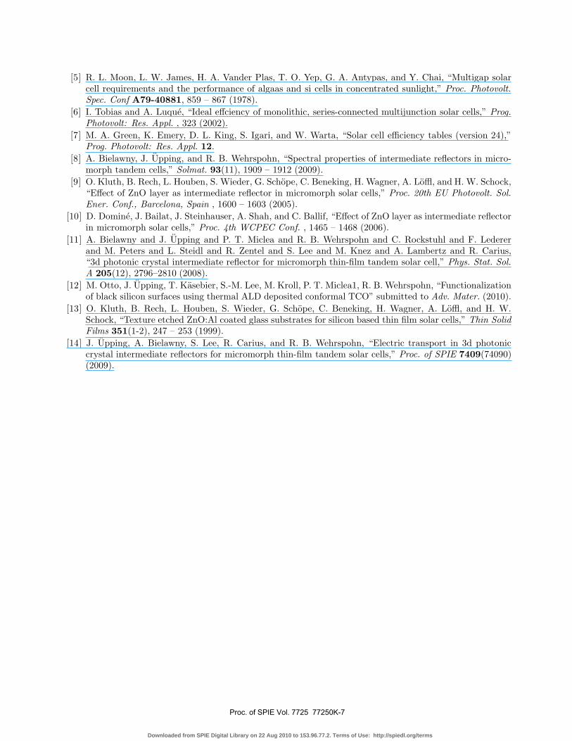
[5] R. L. Moon, L. W. James, H. A. Vander Plas, T. O. Yep, G. A. Antypas, and Y. Chai, “Multigap solarcell requirements and the performance of algaas and si cells in concentrated sunlight,” Proc. Photovolt.Spec. Conf A79-40881, 859 – 867 (1978).
[6] I. Tobias and A. Luque, “Ideal effciency of monolithic, series-connected multijunction solar cells,” Prog.Photovolt: Res. Appl. , 323 (2002).
[7] M. A. Green, K. Emery, D. L. King, S. Igari, and W. Warta, “Solar cell efficiency tables (version 24),”Prog. Photovolt: Res. Appl. 12.
[8] A. Bielawny, J. Upping, and R. B. Wehrspohn, “Spectral properties of intermediate reflectors in micro-morph tandem cells,” Solmat. 93(11), 1909 – 1912 (2009).
[9] O. Kluth, B. Rech, L. Houben, S. Wieder, G. Schope, C. Beneking, H. Wagner, A. Loffl, and H. W. Schock,“Effect of ZnO layer as intermediate reflector in micromorph solar cells,” Proc. 20th EU Photovolt. Sol.Ener. Conf., Barcelona, Spain , 1600 – 1603 (2005).
[10] D. Domine, J. Bailat, J. Steinhauser, A. Shah, and C. Ballif, “Effect of ZnO layer as intermediate reflectorin micromorph solar cells,” Proc. 4th WCPEC Conf. , 1465 – 1468 (2006).
[11] A. Bielawny and J. Upping and P. T. Miclea and R. B. Wehrspohn and C. Rockstuhl and F. Ledererand M. Peters and L. Steidl and R. Zentel and S. Lee and M. Knez and A. Lambertz and R. Carius,“3d photonic crystal intermediate reflector for micromorph thin-film tandem solar cell,” Phys. Stat. Sol.A 205(12), 2796–2810 (2008).
[12] M. Otto, J. Upping, T. Kasebier, S.-M. Lee, M. Kroll, P. T. Miclea1, R. B. Wehrspohn, “Functionalizationof black silicon surfaces using thermal ALD deposited conformal TCO” submitted to Adv. Mater. (2010).
[13] O. Kluth, B. Rech, L. Houben, S. Wieder, G. Schope, C. Beneking, H. Wagner, A. Loffl, and H. W.Schock, “Texture etched ZnO:Al coated glass substrates for silicon based thin film solar cells,” Thin SolidFilms 351(1-2), 247 – 253 (1999).
[14] J. Upping, A. Bielawny, S. Lee, R. Carius, and R. B. Wehrspohn, “Electric transport in 3d photoniccrystal intermediate reflectors for micromorph thin-film tandem solar cells,” Proc. of SPIE 7409(74090)(2009).
Proc. of SPIE Vol. 7725 77250K-7
Downloaded from SPIE Digital Library on 22 Aug 2010 to 153.96.77.2. Terms of Use: http://spiedl.org/terms
Copyright © 2022 FDOKUMEN