Integrated optical microfluidic lab-on-a-chip
8
- T:: : - - J7 - Input I A I Fluid I • out I j V I I Signal Processiiig I I I Integrated Optical Microfluidic Lab-on-a-chip Arvind Chandrasekaran 1,* , Muthukumaran Packirisamy 2 Optical-Bio Microsystems Laboratory, Department of Mechanical Engineering, Concordia University, Montreal Canada *Corresponding author Ph: (514) 8482424 x7098 Email: [email protected] ABSTRACT Bio-security for health monitoring and diagnosis are the needs of the hour, for rapid detection of biological and chemical species. This calls for a necessity to develop a cost effective miniaturized and portable biosensor device for in-situ biomedical applications and Point-of-Care Testing (POCT). While portability of the biosensor is required for in-situ medical detections, miniaturization is essential for handling smaller sample volumes and high throughput. Thus, the above mentioned concerns cannot be addressed unless a fully integrated biosensor system is developed. In this work, an integrated opto microfluidic based Lab-on-a-chip device is proposed for carrying out fluorescence based biodetection. The input and output fibers were integrated with the microfluidic channel so as to make a robust setup. Fluorescence detection was carried out using Alexafluor 647 tagged antibody particles and the output was measured with a Spectrometer-on-Chip, integrated with the device. The experimental results prove that the proposed device is highly suitable for Lab-on-a-Chip applications. Keywords: Lab-on-a-Chip, Microfluidics, Spectrometer-on-Chip, Fluorescence, AF647, Hybrid integration, Silicon, Poly dimethylSiloxane (PDMS), 1. Introduction Integrated Lab-on-a-Chip (LOC) systems or Micro-Total Analysis Systems, as they are sometimes referred to as, are miniaturized chemical or biological analysis systems 1 . They basically derive their functionalities by virtue of miniaturization, i.e., all functional modules and clinical functions which can be performed on a macro scale can be miniaturized to a single chip, which is termed as Lab-on-a-Chip. The general flow layout of a Lab-on-a-Chip system is as shown in Figure 1. The chemical or biological samples, after sampling and pre-treatment are transported into the detection system wherein the presence or activity of a chemical or biological specimen is detected and analyzed using suitable signal processing methods and the fluid is finally ejected out of the system 2 . Fig. 1: Generalized flow chart for a Lab-on-a-Chip system Photonics North 2008, Réal Vallée, Michel Piché, Peter Mascher, Pavel Cheben, Daniel Côté, Sophie LaRochelle, Henry P. Schriemer, Jacques Albert, Tsuneyuki Ozaki, Eds., Proc. of SPIE Vol. 7099, 70992B, (2008) · 0277-786X/08/$18 · doi: 10.1117/12.807550 Proc. of SPIE Vol. 7099 70992B-1 2008 SPIE Digital Library -- Subscriber Archive Copy
Transcript of Integrated optical microfluidic lab-on-a-chip

-T:: :
- -
J7-
Input I AI
FluidI • out
I j V I
I Signal Processiiig I
II
Integrated Optical Microfluidic Lab-on-a-chip
Arvind Chandrasekaran1,*, Muthukumaran Packirisamy2
Optical-Bio Microsystems Laboratory, Department of Mechanical Engineering, Concordia University, Montreal Canada
*Corresponding author Ph: (514) 8482424 x7098 Email: [email protected]
ABSTRACT
Bio-security for health monitoring and diagnosis are the needs of the hour, for rapid detection of biological and chemical species. This calls for a necessity to develop a cost effective miniaturized and portable biosensor device for in-situ biomedical applications and Point-of-Care Testing (POCT). While portability of the biosensor is required for in-situ medical detections, miniaturization is essential for handling smaller sample volumes and high throughput. Thus, the above mentioned concerns cannot be addressed unless a fully integrated biosensor system is developed. In this work, an integrated opto microfluidic based Lab-on-a-chip device is proposed for carrying out fluorescence based biodetection. The input and output fibers were integrated with the microfluidic channel so as to make a robust setup. Fluorescence detection was carried out using Alexafluor 647 tagged antibody particles and the output was measured with a Spectrometer-on-Chip, integrated with the device. The experimental results prove that the proposed device is highly suitable for Lab-on-a-Chip applications. Keywords: Lab-on-a-Chip, Microfluidics, Spectrometer-on-Chip, Fluorescence, AF647, Hybrid integration, Silicon, Poly dimethylSiloxane (PDMS), 1. Introduction Integrated Lab-on-a-Chip (LOC) systems or Micro-Total Analysis Systems, as they are sometimes referred to as, are miniaturized chemical or biological analysis systems1. They basically derive their functionalities by virtue of miniaturization, i.e., all functional modules and clinical functions which can be performed on a macro scale can be miniaturized to a single chip, which is termed as Lab-on-a-Chip. The general flow layout of a Lab-on-a-Chip system is as shown in Figure 1. The chemical or biological samples, after sampling and pre-treatment are transported into the detection system wherein the presence or activity of a chemical or biological specimen is detected and analyzed using suitable signal processing methods and the fluid is finally ejected out of the system2.
Fig. 1: Generalized flow chart for a Lab-on-a-Chip system
Photonics North 2008, Réal Vallée, Michel Piché, Peter Mascher, Pavel Cheben, Daniel Côté,Sophie LaRochelle, Henry P. Schriemer, Jacques Albert, Tsuneyuki Ozaki, Eds., Proc. of SPIE
Vol. 7099, 70992B, (2008) · 0277-786X/08/$18 · doi: 10.1117/12.807550
Proc. of SPIE Vol. 7099 70992B-12008 SPIE Digital Library -- Subscriber Archive Copy

Lab-on-a-Chip systems offer several advantages for health monitoring, Point-of-Care Testing (POCT), rapid detection of biological and chemical species and bio-security. There are several components which can be integrated within a LOC system depending upon its application and functionality. However, the important elements include an actuation system for the transportation of the analyte, detection and signal processing units and suitable. Microfluidics is essential because it not only introduces the biological environment into the LOC system but also enables convenient handling of smaller sample volumes, transportation of the fluids into the detection system and the ejection of wastes after analysis. Figure 2 shows some of the components which can be incorporated within a Lab-on-a-Chip.
Fig.2: Different components used in a Lab-on-a-Chip. Among the other essential units of a Lab-on-a-Chip system are suitable sensing and detection systems, Reaction chambers for biological applications wherein it is essential to provide a good ambience for the There are several techniques of analyte detection which are used in Lab-on-a-Chip systems. Laser induced Fluorescence spectroscopy is one of the most common techniques used for biosensing owing to its high sensitivity, selectivity, and the ability to carry out instantaneous detection, among others. In this method, the presence of an enzyme or antigen in a given sample is detected by conjugating the particles with their corresponding fluorophore tagged antibody and measuring the emitted fluorescence from the antigen-antibody pair. Although fluorescence measurements do not provide detailed structural information, the technique has become quite popular because of its acute sensitivity to changes in the structural and dynamic properties of biomolecules and biomolecular complexes3. In the past, several researches have been carried out to fabricate an integrated Lab-on-a-chip system for the fluorescence spectroscopy. Different material platforms have been explored for hybrid and monolithic integrated device, including Silicon and its other forms4, Glass5,6, SU87, Poly Di Methyl Siloxane (PDMS)8 and also the combination of the above9. In the present work, an integrated optical microfluidic Lab-on-a-chip device is proposed for carrying out fluorescence based biodetection. Herein, a silicon based microfluidic platform is integrated with Silica-On-Silicon (SOS) based Spectrometer-on-Chip. The feasibility of using the device for LOC applications has been demonstrated by the detection
µ−valves
µ−mechanics
µ−pumps
Detection unit
µ−Dialyzers
µ−actuators
µ−heaters
Reaction chambers
PCR and cell lysis
µ−electronic circuitry
µ−Sensors
µ−mixers
Particle Separators
µ−needles
µ−fluidics
µ−optics
Biosensing
Proc. of SPIE Vol. 7099 70992B-2
___ 08 0 __I
00 0 ij
of Alexafluor 647 tagged Antisheep antibody. The setup has been improved upon by integrating the optical fibers directly onto the microfluidic platform so as to avoid optical coupling losses and increase the sensitivity and efficiency of the system. This device enables smaller sample volumes, controlled fluid injection, portability and rapid target detection.
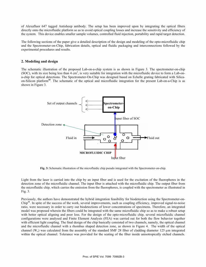
The following sections of the paper give a detailed description of the design and modeling of the opto-microfluidic chip and the Spectrometer-on-Chip, fabrication details, optical and fluidic packaging and interconnections followed by the experimental procedures and results. 2. Modeling and design The schematic illustration of the proposed Lab-on-a-chip system is as shown in Figure 3. The spectrometer-on-chip (SOC), with its size being less than 4 cm2, is very suitable for integration with the microfluidic device to form a Lab-on-a-chip for optical detections. The Spectrometer-On-Chip was designed based on Echelle grating fabricated with Silica-on-Silicon platform10. The schematic of the optical and microfluidic integration for the present Lab-on-a-Chip is as shown in Figure 3.
Fig. 3: Schematic illustration of the microfluidic chip pseudo integrated with the Spectrometer-on-chip. Light from the laser is carried into the chip by an input fiber and is used for the excitation of the fluorophores in the detection zone of the microfluidic channel. The input fiber is attached with the microfluidic chip. The output fiber from the microfluidic chip, which carries the emission from the fluorophores, is coupled with the spectrometer as illustrated in Fig. 3. Previously, the authors have demonstrated the hybrid integration feasibility for biodetection using the Spectrometer-on-Chip11. In spite of the success of the work, several improvements, such as coupling efficiency, improved signal-to-noise ratio, were necessary in order to carry out biodetections of lower concentrations of specimens. Therefore, an integrated model was proposed wherein the fibers could be integrated with the same microfluidic chip so as to make a robust setup with better optical aligning and poor loss. For the design of the opto-microfluidic chip, several microfluidic channel configurations were analysed and Finite Element Analysis (FEA) was carried out for both the flow behavior together with efficient light coupling. The final design of the chip basically consisted of two channels, namely, the optical channel and the microfluidic channel with a rhombus shaped detection zone, as shown in Figure 4. The width of the optical channel (Wo) was calculated from the assembly of the standard SMF 28 fiber of cladding diameter 125 µm integrated within the optical channel. Tolerance was provided for the seating of the fiber inside anisotropically etched channels.
Fluid in
MICROFLUIDIC CHIP
Input fiber
Input fiber of SOC
Fluid out
Detection zone
Spectrometer-on-Chip
Set of output channels
Proc. of SPIE Vol. 7099 70992B-3

Microfluidic chip width (d) and channel width (Wmf) were obtained for no-stagnation flow conditions obtained from the flow behavior as predicted by the Finite Element Analysis. Herein, the parameters considered for the design of the opto-microfluidic chip, as shown in Figure 4, were as follows d = 1000 µm, Wmf = 250 µm, Wo = 125 µm.
Fig. 4: Schematic of fluorescence detection using the opto-microfluidic channel
3. Opto-microfluidic chip synthesis There are several methods of fabricating microfluidic channels on Silicon, such as isotropic etching with Xenon difluoride12, Deep Reactive Ion etching (DRIE), etc. However, there are certain problems posed by the surface roughness in such micromachining techniques13 which are unfavorable for the current application. Therefore, anisotropic wet etching was proposed for the present application, which would render smooth surfaces. The microfluidic channels were fabricated on silicon with anisotropic etching using Tetra Methyl Ammonium Hydroxide (TMAH). 3.1 Fabrication The silicon wafers were procured from Montco Silicon Technologies, CA. 500 µm thick silicon wafers, single side polished, oxidized on both sides. Using standard lithographic process, the wafer was spun-coated with photoresist and patterned with UV exposure in accordance to the mask design. HF buffer solution was prepared in the ratio 1:4, diluting with DI water. The patterned silicon samples were introduced into the HF buffer to remove the oxide layer. Etch stop was coated on the backside of the wafer. The samples were loaded into a Teflon holder and introduced into the etchant which was rotated in a closed flask, heated in a water bath to 80
oC. Under these conditions, the etch rate achieved for the
d
Wo
Wmf
Fluid outlet
Fluid inlet
Collector fiber
Input fiber
Fluorescent particle
d
A A
Wo
Section A-A
Proc. of SPIE Vol. 7099 70992B-4

silicon samples was found to be ~25 µm/hr. Figure 5 shows the Scanning Electron Micrograph (SEM) of one of the etched samples.
Fig. 5: SEM images of anisotropically etched silicon microfluidic channels. In order to allow provisions for embedding the optical fibers with the microfluidic chip, the wafers were diced along the corners, so as to open up the V-grooves for fiber attachment. The specifications of the wafer dicing operations are as follows: Blade speed: 20000 rpm, Feed rate: 2 mm/sec Blade thickness: 150 µm. 3.2 Packaging The packaging of the device involved two steps, namely, optical assembly and microfluidic interconnections. It is essential that the optical setup is robust so as to prevent optical losses in the system due to misalignment, coupling losses and losses due to absorption. From the microfluidic consideration, it is essential to provide a leak-proof seal to the chip with a top cover and also provide microfluidic ports for fluidic interconnections. 3.2.1 Optical assembly For the input, FC connectorized tapered lens ended fiber (OZ Optics, ON) was used. Fiber strippers and precision cleavers (Newport, USA) were used to remove the buffer layer and the cladding around SMF28 fiber, which was used for the output. The input and the output fibers were positioned on the V-groove and supported well so as to isolate them from stressors due to buckling or bending. The position of the collector fiber was finely adjusted for acquiring the maximum optical collection, taking into consideration the absorption losses due to the impending flow across the fibers. The fibers were fixed in the position with index matching glues, which not only binds the fiber with the silicon, but also blocks the channel, thereby preventing leakage of fluid through these optical ports. Through SEM, as shown in Figure 6, leaks on the fiber assembly were verified.
Fig. 6: SEM image of the optical port with fiber integrated and sealed with index matching glues.
Optical fiber
Proc. of SPIE Vol. 7099 70992B-5

3.2.2 Microfluidic packaging and interconnections Microfluidic channel packaging consists of sealing the microfluidic channel with a transparent top cover and the provision of the inlet and outlet fluidic ports for the fluidic connections. For the present microfluidic channel, Poly-(dimethylSiloxane) {PDMS} was chosen as the top covering layer due to the following advantages: (i) Bulk production of PDMS is made possible and the PDMS can be easily moulded to the required geometry to suit the microfluidic channel. (ii) Upon aging, the PDMS surface is rendered hydrophobic, which is advantageous for microfluidic lid in order to repel fluid from adhering onto the surface. (iii) The material is optically transparent in the UV-Vis and Near Infrared (NIR) spectral range, is of low density, highly flexible and possesses easily alterable properties, which renders ease of packaging to the material. Initially, metal mould was prepared for the PDMS by CNC machining. PDMS pre-polymer, commercially named as Sylgard 184 (Dow Corning), and curing agent were poured into the mould in the ratio 10:1 and mixed well. Exactly 2 gms of each type of elastomer mixture are then poured into separate metal templates. The templates must be completely dry and smooth with good surface finish. The mixture was placed in a desiccator/ vacuum pump setup until all the trapped air bubbles were removed. The template was then carefully placed inside an oven and cured at 75 ºC for 90 minutes. PDMS coagulates upon curing, and the pre-polymer conforms to the shape of the template replicating the features of the mould. The cured PDMS was peeled out gently and cut into different geometries suitable to fabricated chip. Three separate PDMS layers were bonded with the silicon, one of them being used as a sealant for the microfluidic channel and the other two PDMS layers attached over the input and output optical fibers to hold their positions. Two ports (2 mm diameter) were created on the PDMS sealant to form the inlet and the outlet of the microfluidic channel. The PDMS was then cleaned in DI water for 5 minutes. An epoxy glue was coated on the PDMS and was cured slightly for 60 s. The PDMS was then aligned with the microfluidic channel and bonded with the silicon by applying little pressure. Another layer of epoxy was then coated around the PDMS silicon interface so that the bonding is leak proof. The setup was then cured for 4 hours at 60
oC, so as to allow the PDMS to bind well with the substrate. Microfluidic tubes (250 µm
inner diameter) were then fitted on the microfluidic port openings; another layer of PDMS epoxy was coated around the tubes to make a leak proof sealing, and the setup was again cured. Figure 7 shows a packaged microfluidic chip with input/output waveguides.
Fig. 7: A fully packaged opto-microfluidic chip with fluidic interconnections and embedded optical fibers 4. Bio-optical Testing The main objective of carrying out fluorescence detection was to demonstrate the feasibility of biodetection using the integrated Lab-on-a-Chip system
Inlet port
Output fiber
Input fiber Outlet port
Proc. of SPIE Vol. 7099 70992B-6

Herein, the fluorescence based bio-detection has been demonstrated using Alexafluor 647 tagged anti-sheep antibody as the fluorophore. 10% of 2 mg/ml antibody was prepared by diluting with Phosphate Buffer Solution (PBS). Isopropyl Alcohol (IPA) was used to rinse the microfluidic channel after biodetection. A peristaltic pump (Gilson Minipuls3) was used for fluid injection into the micro-channels. The flow was initially calibrated and the residence time, i.e., the time taken by the fluorophore particles to reach the detection zone was computed. Florescence was observed for continuous passage of the fluid, thereby it was ensured that non-stagnant flow conditions are achieved. The laser source (OZ Optics) was coupled with the input fiber through optical adapter and the collector fiber was coupled with the multimodal input spectrometer. AF647 tagged antibody was pumped into the channel at different Reynolds’s numbers (Re). It was observed that, for Re <1, the biomolecules immobilized themselves directly on the fiber thereby preventing the efficient coupling of light. However, for Re >1, poor sensitivity was obtained not only due to the lack of immobilization of the biomolecules with the surface but also due to the problem of sampling time with the spectrometer. Thus, the Reynolds’ number for fluid flow was chosen as 1 for optimum fluorescence detection. The results of fluorescence detection at Re = 1 is as shown in Figure 8.
Fig. 8: Biodetection of AF647 tagged antibodies using the integrated device The efficiency of fluorescence detection of the device was negligibly different for all the coupling distances, thereby proving that the present setup is robust for optical fiber alignment. 5. Conclusion In this work, an integrated silicon based opto-microfluidic platform was attached with a spectrometer-on-chip for Lab-on-a-chip applications. The feasibility of biodetection has been demonstrated through the successful detection of Alexafluor 647 tagged antibody molecules. The integration of optical and microfluidic ensembles are intermediate between a hybrid externally coupled setup and a monolithic fully integrated device. Silicon has been found to be an excellent platform for the fabrication of biocompatible Lab-on-a-Chip devices. The success of the present work opens up the feasibility of monolithic integration of silicon based microfluidic channel with Silica-on-Silicon based Spectrometer-on-Chip.
180
200
220
240
260
280
300
600 620 640 660 680 700
Wavelength (nm)
Fluo
resc
ent I
nten
sity
(a.u
)
Excitation
Emission
Proc. of SPIE Vol. 7099 70992B-7

Acknowledgements The authors would like to sincerely thank Mr. Eric Duchesne of Ecole Polytechnique de Montreal for his assistance with the Scanning Electron Microscopy and Mr. Vito Logiudice and Mr. Donald Walter Berry, McGill University, for their assistance with wafer dicing. The authors would also like to thank the Canadian Institute of Photonics Innovations (CIPI) for their financial assistance and Enablence Technologies, Kanata, ON for their in-kind contribution towards the successful completion of this project.
References
1. S. C. Jakeway, A. J. de Mello and E. L. Russell, "Miniaturized total analysis systems for biological analysis," Fresenius J. Anal. Chem., vol. 366, pp. 525-539, Mar-Apr. 2000.
2. S. Krawczyk, "Discussion on optical integration in Lab-on-a-Chip microsystems for medical diagnostics," Physica Status Solidi- Conferences, pp. 998-1012, 2003.
3. C. A. Royer, "Approaches to teaching fluorescence spectroscopy," Biophys. J., vol. 68, pp. 1191-1195, 1995.
4. P. Friis, K. Hoppe, O. Leistiko, K. B. Mogensen, J. Hübner and J. P. Kutter, "Monolithic integration of microfluidic channels and optical waveguides in silica on silicon," Appl. Opt., vol. 40, pp. 6246-6251, 2001.
5. J. Vieillard, R. Mazurczyk, C. Morin, B. Hannes, Y. Chevolot, P. L. Desbene and S. Krawczyk, "Application of microfluidic chip with integrated optics for electrophoretic separations of proteins," J. Chromatogr. B. Analyt Technol. Biomed. Life. Sci., vol. 845, pp. 218-225, Jan 15. 2007.
6. R. Mazurczyk, J. Vieillard, A. Bouchard, B. Hannes and S. Krawczyk, "A novel concept of the integrated fluorescence detection system and its application in a lab-on-a-chip microdevice,” Sensors and Actuators.B, Chemical, vol. 118, pp. 11-19, 2006.
7. L. Cui, T. Zhang and H. Morgan, "Optical particle detection integrated in a dielectrophoretic lab-on-a-chip." J Micromech Microengineering, vol. 12, pp. 7-12, 2002.
8. Q. Xiang, X. Xuan, B. Xu and D. Li, "Multi-Functional Particle Detection with Embedded Optical Fibers in a Poly (dimethylsiloxane) Chip," Instrum Sci Technol, vol. 33, pp. 597-607, 2005.
9. J. M. Ruano, A. Glidle, A. Cleary, A. Walmsley, J. S. Aitchison and J. M. Cooper, "Design and fabrication of a silica on silicon integrated optical biochip as a fluorescence microarray platform," Biosensors and Bioelectronics, vol. 18, pp. 175-184, 2003.
10. S. Janz, A. Balakrishnan, S. Charbonneau, P. Cheben, M. Cloutier, A. Delage, K. Dossou, L. Erickson, M. Gao and P. Krug, "Planar waveguide echelle gratings in silica-on-silicon," Photonics Technology Letters, IEEE, vol. 16, pp. 503-505, 2004.
11. A. Chandrasekaran, A. Acharya, J. L. You, K. Y. Soo, M. Packirisamy, I. Stiharu and A. Darveau, "Hybrid Integrated Silicon Microfluidic Platform for Fluorescence Based Biodetection," Sensors, vol. 7, pp. 1901-1915, 2007.
12. A. K. Bhaskar, M. Packirisamy and R. B. Bhat, "Bulk micromachining for SOI based microsystems using double side XeF2 etching," Int. J. Manuf. Technol. Manage., vol. 13, pp. 297-307, 2008.
13. A. Chandrasekaran, M. Packirisamy, I. Stiharu and A. Delage, "Hybrid bulk micro-machining process suitable for roughness reduction in optical MEMS devices," Int. J. Manuf. Technol. Manage., vol. 9, pp. 144-159, 2006.
Proc. of SPIE Vol. 7099 70992B-8