Characteristics of Jumps in Case of Symmetric and Un-Symmetric Operations of Regulators
Upload
khangminh22Category
view
1download
0
University of Tennessee, Knoxville University of Tennessee, Knoxville
TRACE: Tennessee Research and Creative TRACE: Tennessee Research and Creative
Exchange Exchange
Masters Theses Graduate School
8-2002
Timing Jitter in Symmetric Load Ring Oscillators and the Timing Jitter in Symmetric Load Ring Oscillators and the
Estimation of Aperture Uncertainty in A-D Converters Estimation of Aperture Uncertainty in A-D Converters
Venkatesh Srinivasan University of Tennessee - Knoxville
Follow this and additional works at: https://trace.tennessee.edu/utk_gradthes
Part of the Electrical and Computer Engineering Commons
Recommended Citation Recommended Citation Srinivasan, Venkatesh, "Timing Jitter in Symmetric Load Ring Oscillators and the Estimation of Aperture Uncertainty in A-D Converters. " Master's Thesis, University of Tennessee, 2002. https://trace.tennessee.edu/utk_gradthes/2169
This Thesis is brought to you for free and open access by the Graduate School at TRACE: Tennessee Research and Creative Exchange. It has been accepted for inclusion in Masters Theses by an authorized administrator of TRACE: Tennessee Research and Creative Exchange. For more information, please contact [email protected].
To the Graduate Council:
I am submitting herewith a thesis written by Venkatesh Srinivasan entitled "Timing Jitter in
Symmetric Load Ring Oscillators and the Estimation of Aperture Uncertainty in A-D Converters."
I have examined the final electronic copy of this thesis for form and content and recommend
that it be accepted in partial fulfillment of the requirements for the degree of Master of Science,
with a major in Electrical Engineering.
Syed K. Islam, Major Professor
We have read this thesis and recommend its acceptance:
Benjamin J. Blalock, Donald W. Bouldin
Accepted for the Council:
Carolyn R. Hodges
Vice Provost and Dean of the Graduate School
(Original signatures are on file with official student records.)

To the Graduate Council:
I am submitting herewith a thesis written by Venkatesh Srinivasan entitled “Timing
Jitter in Symmetric Load Ring Oscillators and the Estimation of Aperture Uncertainty in
A-D Converters.” I have examined the final electronic copy of this thesis for form and
content and recommend that it be accepted in partial fulfillment of the requirements for
the degree of Master of Science, with a major in Electrical Engineering.
Syed K. Islam
Major Professor We have read this thesis
and recommend its acceptance:
Benjamin J. Blalock Donald W. Bouldin Accepted for the Council: Vice Provost and Dean of Graduate Studies
(Original signatures are on file with official student records.)

TIMING JITTER IN SYMMETRIC LOAD RING OSCILLATORS
AND THE ESTIMATION OF APERTURE UNCERTAINTY IN A-D
CONVERTERS
A Thesis
Presented for the
Master of Science Degree
The University of Tennessee, Knoxville
Venkatesh Srinivasan
August 2002

ii
AAAACKNOWLEDGEMENTSCKNOWLEDGEMENTSCKNOWLEDGEMENTSCKNOWLEDGEMENTS
My sincere thanks to my advisor Dr. Syed K. Islam for providing me the opportunity to
pursue my Master’s at this university and for guiding me towards the completion of this
thesis. Special thanks to Dr. Benjamin J. Blalock for so graciously allocating his time for
me, the result of which has been the many valuable suggestions that I have received
from him. I also wish to thank Dr. Donald W. Bouldin for teaching me the essentials of
IC design and for serving on my committee. A thank you also goes to Bryce Gray and
Gary T. Hendrickson of Analog Devices Inc., Greensboro, NC, for their support and
encouragement. And thanks to my fellow graduate students and to all the faculty and
staff at our department for making my graduate study such a rewarding experience.
My special thanks to the ‘Gaeng’ of BITS, Pilani, for the wonderful time during my
undergraduate days and the continued support here in the US. Also, my friend Nirisha,
deserves a special mention for her solid support during the final months of this thesis, a
big thank you to you. And thanks to all my friends both here in the US and back home
in India, life just got better after knowing you all!
And finally, thanks to destiny for blessing me with such a wonderful family. Amma,
Appa, Viji and Thathi, I owe it all to you.

iii
AAAABSTRACTBSTRACTBSTRACTBSTRACT
Timing jitter in clock signals presents a limitation to the performance of a variety of
applications and systems. The criticality of the issue is discussed with the A-D converter
as the backdrop. Timing errors in the sampling clock, the analog input signal and the
aperture uncertainty of the A-D converter degrade the signal-to-noise ratio performance.
In this thesis, a method to estimate the aperture uncertainty of the converter has been
developed. The model accounts for the converter’s quantization noise and differential
non-linearity errors and thereby improves the accuracy of the estimation. The technique
was applied to a 10-Bit converter and the results are presented.
For clock generation using PLLs, ring oscillators are attractive from an integration and
cost point of view for use as a VCO. Their timing jitter can be improved by increasing the
output voltage swing, the gate overdrive of the transistors of the differential pair and the
power dissipation while maintaining just a minimum required small signal gain for the
delay stage. In this thesis, it is shown that the maximum possible output voltage swing is
dependent entirely on technology parameters. The proposed oscillator topology uses an n-
MOS differential pair with a class of load elements called the ‘symmetric loads’ and is
designed for the maximum possible output voltage swing. Frequency variation is
achieved by driving the body of the symmetric loads in order to keep the swing and hence
phase noise constant across frequencies. Also, the frequency vs. body voltage
characteristics has been derived and found to be linear. Finally, the proposed theoretical
predictions have been validated with simulation results.

iv
CCCCONTENTSONTENTSONTENTSONTENTS
1 Introduction..........................................................................................................................1
1.1 Overview.......................................................................................................................1
1.2 Thesis Organization.....................................................................................................3
2 Timing Jitter And Estimation of Aperture Uncertainty in A-D Converters.............5
2.1 Introduction ..................................................................................................................5
2.2 Aperture Uncertainty ..................................................................................................6
2.3 Timing Jitter..................................................................................................................6
2.4 ADC Noise Sources .....................................................................................................7
2.5 Phase Noise Plots And Timing Jitter Extraction....................................................13
2.6 Estimation of Aperture Uncertainty........................................................................22
2.7 Experimental Results.................................................................................................23
3 Timing Jitter In Symmetric Load Ring Oscillators .....................................................27
3.1 Symmetric Load Ring Oscillator..............................................................................28
3.2 MOSFET Noise Analysis...........................................................................................32
3.3 Symmetric Load Noise Analysis..............................................................................34
3.4 Timing Jitter in Ring Oscillators ..............................................................................36
4 A Swing Optimized Body Driven Oscillator ...............................................................47
4.1 Maximum Possible Voltage Swing..........................................................................48
4.2 Ring Oscillator Phase Noise .....................................................................................53
4.3 Swing Maximized Body Driven Oscillator.............................................................55

v
4.4 Simulation Results .....................................................................................................57
5 Conclusions and Future Work ........................................................................................64
5.1 Conclusions.................................................................................................................64
5.2 Future Work................................................................................................................66
References....................................................................................................................................68
Appendices ..................................................................................................................................75
Appendix A – Timing Jitter Estimation For The 65MHz Sampling Clock .....................76
Appendix B – The Ring Oscillator system..........................................................................78
Vita ................................................................................................................................................85

vi
LLLLIST OF IST OF IST OF IST OF TTTTABLESABLESABLESABLES
Table 2.1 Sideband Noise power vs. Offset Frequency for a 100MHz Signal.....................20
Table 2.2 Measured SNR and extrapolated timing jitter for the ADC.................................24
Table 2.3 Estimated timing jitter for sampling clock and analog input signal ...................24
Table 4.1 Simulation Results for Osc-1, Osc-2 & Osc-3 ..........................................................59
Table 4.2 Phase Noise across the frequency range of Osc-1 & Osc-2 ...................................61 Table A.1 Sideband Noise Power vs. Offset Frequency for 65MHz Signal 77 Table B.1 Aspect Ratios of the Transistors used in the Delay stage of Osc-1 to Osc-3 ......79
Table B.2 Aspect Ratio for the Transistors of Bias Generation Circuitry ............................81
Table B.3 Aspect Ratios for the Transistors of Current Reference........................................82
Table B.4 Worst-Case Performance of Current Reference for Different Process Runs......83
Table B.5 Summary of worst-case performance for the Bias Generation Circuitry ...........84

vii
LLLLIST OF IST OF IST OF IST OF FFFFIGURESIGURESIGURESIGURES
Figure 2.1 Timing Jitter in Oscillators.........................................................................................7
Figure 2.2 Effect of Sampling Clock Jitter ..................................................................................9
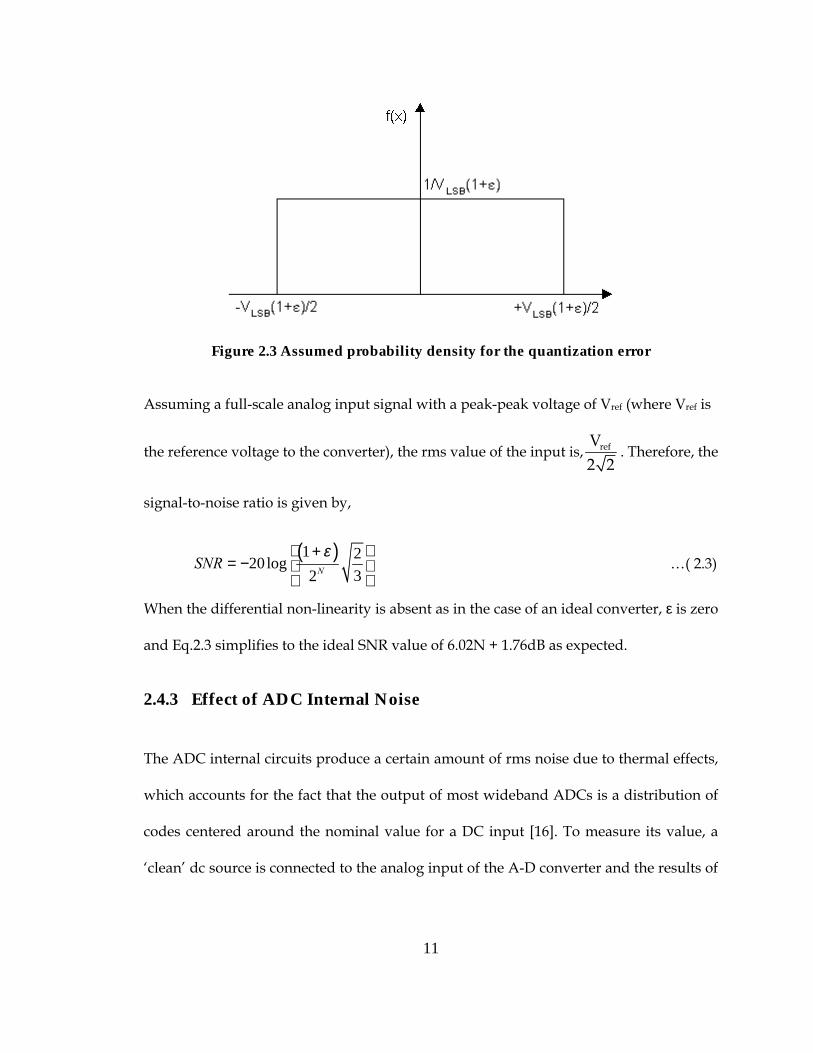
Figure 2.3 Assumed probability density for the quantization error ....................................11
Figure 2.4 Spectrum for Eq.2.10 (left) and an Actual Oscillator (Right) ..............................16
Figure 2.5 Phase Noise plot for 1GHz signal generated from the Rohde & Schwarz .......18
Figure 2.6 Phase noise plot for the 100MHz signal generated from Rohde & Schwarz....19
Figure 2.7 Phase Noise plots for different frequencies from the Rohde & Schwarz..........22
Figure 2.8 Calculated SNR vs. Measured SNR........................................................................25
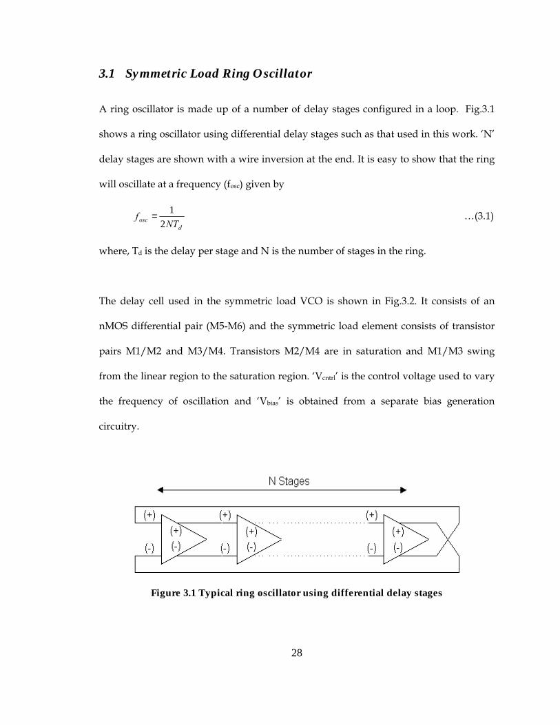
Figure 3.1 Typical ring oscillator using differential delay stages.........................................28
Figure 3.2 Symmetric load delay cell........................................................................................29
Figure 3.3 Symmetric Load and its I-V characteristics...........................................................30
Figure 3.4 Variation of noise spectral density with voltage drop across the load .............35
Figure 3.5 Intrinsic timing error per delay stage ....................................................................37
Figure 3.6 Output waveforms for differential delay stages ..................................................38
Figure 3.7 First crossing approximation for timing jitter.......................................................39
Figure 3.8 Noise current sources in the symmetric load delay cell......................................41
Figure 3.9 AC Noise Model for the delay cell .........................................................................41
Figure 4.1 Phase Noise plots for Osc-1, Osc-2 & Osc-3 ..........................................................59
Figure 4.2 Simulation Results vs. Theory for Osc-1................................................................61
Figure 4.3 Simulated Results vs. Theory for Osc-2.................................................................62 Figure A.1 Phase Noise plot for the 65MHz Sampling Clock...............................................77

viii
Figure B.1 Delay Cell for the Proposed Oscillator..................................................................79
Figure B.2 Bias Generation Circuitry........................................................................................80
Figure B.3 Current Reference Circuitry....................................................................................82
Figure B.4 Worst-Case Simulation Performance of Current Reference (Model-1).............83
Figure B.5 Magnitude & Phase of the Loop Transmission for the Bias Circuitry ..............84

1
1111 IIIINTRODUCTIONNTRODUCTIONNTRODUCTIONNTRODUCTION
1.1 Overview
Timing information in the form of clock or oscillator signals plays a critical role in most
modern applications. The timing jitter or uncertainty in the timing information presents
a serious limitation to the achievable system performance. Clock jitter in digital circuits
can lead to a violation of the setup/hold time requirements. While, in a sampling system
like the A-D converter (ADC), timing jitter in the sampling clock degrades the dynamic
range of the converter. Other applications include RF frequency synthesis where a low
phase noise oscillator needs to be employed for optimal performance. In all the above
cases, the challenge lies in generating low jitter clocks.
In this work, the effect of timing jitter is addressed with the perspective of a sampling
system like the A-D converter. For this system, jitter may be defined as the random
fluctuations in the sampling instant, thereby leading to an error in the sampled signal.
The voltage error is proportional to the slew rate of the input and so the problem of jitter
becomes more critical with an increase in the input signal frequency [1]. Apart from the
jitter on the sampling clock, the aperture uncertainty of the sample-and-hold internal to
the ADC also contributes to the signal-to-noise ratio (SNR) degradation. In the event of
an ideal analog input and sampling clock, the aperture uncertainty represents the limit
on the maximum achievable SNR. Therefore, an accurate estimation of the aperture
uncertainty becomes important.

2
Typically for a system like the A-D converter, the timing information is provided from
an external source like a crystal oscillator. In this scenario, the problem amounts to
minimizing the noise introduced by routing and clock distribution. From an end-user’s
point of view, the degradation in the ADC performance can be lessened through the use
of good quality crystal oscillators and ensuring good board layout. However, as
applications become faster, high-speed/high-quality crystal oscillators are harder to
make and hence does not amount to a cost effective solution.
Frequency synthesis through the use of a Phase Locked Loop (PLL) can be an attractive
option given the fact that it can be fully integrated. But, the Voltage Controlled
Oscillator (VCO) is noisier than a crystal oscillator and this being the dominant source of
noise in a PLL, degrades the overall phase noise performance. A careful design of the
VCO and a proper consideration of the PLL system level issues (loop bandwidth for
example) can lead to good phase noise performance [2]. Today, PLLs are being
increasingly used in jitter sensitive applications like RF frequency synthesis [3], clock &
data recovery [5], clock skew management and clock generation [4,6,7,8,9].
The primary focus of this thesis has been in understanding the noise processes in a ring
oscillator and suggesting circuit design techniques to achieve a lower phase
noise/timing jitter performance. The ring oscillator considered consists of an n-MOS
differential pair with a class of loads called the symmetric loads. The inverse
proportionality between jitter and output voltage swing is exploited and minimum jitter
is obtained by designing the oscillator for a maximum possible output swing. A

3
theoretical limit to the output voltage swing has also been derived. Frequency variation
is achieved by varying the threshold voltage of the p-MOS transistors in the load by
driving the body (n-well). It has also been shown that it is sufficient to optimize the
phase noise performance of the oscillator at one frequency and the performance remains
unaltered across the possible frequency range of the oscillator given a constant output
swing. Also, the relation between the frequency of oscillation and the oscillator control
voltage has been derived and validated with simulation results.
In summary, this thesis analyzes the effects of timing jitter on ADCs and also presents a
methodology to estimate the aperture uncertainty of the converter. The ADC is highly
sensitive to jitter on its sampling clock and this severely degrades the SNR performance.
This thesis looks at the issues involved in generating low jitter clocks primarily for use
as a VCO in a PLL system. The primary jitter contributor in such a setting being the
VCO, an analysis is carried out to identify the parameters that can help reduce the
timing jitter. Such an analysis has lead to a novel oscillator that employs body driving
for frequency control and achieves low jitter by maximizing the output voltage swing.
1.2 Thesis Organization
In chapter two, the effect of timing jitter on the performance of the ADC is discussed.
The link between the SNR of the ADC and the total jitter that the system sees is
established. Next, a discussion on oscillator phase noise and phase noise plots is
presented and the technique used for estimating timing jitter from a phase noise plot is
described. The ADC timing jitter model and the methodology for estimating aperture

4
uncertainty are developed and experimental results are presented to verify the proposed
technique.
Chapter three begins with a description of the symmetric load VCO and its
characteristics. A noise analysis of the delay cell is carried out based on the framework
established in [10]. The implications of this analysis specific to the case of the symmetric
load oscillator are discussed. Also the various parameters and their influences on the
timing jitter are explained and advantages of having a higher output voltage is
established.
In chapter four the proposed oscillator topology is developed. An upper bound on the
swing is derived and is found to be entirely technology dependent. It is also shown that
the phase noise performance needs to be optimized for only one frequency within the
frequency range of the oscillator. The frequency vs. Bulk voltage (applied to the n-well)
characteristic is also derived. Finally, the theoretical predictions are verified using
simulation results.
Chapter five discusses the key issues and conclusions arrived at and suggestions for
future work are also provided.

5
2222 TTTTIMING IMING IMING IMING JJJJITTER ITTER ITTER ITTER AAAAND ND ND ND EEEESTIMATION OF STIMATION OF STIMATION OF STIMATION OF AAAAPERTURE PERTURE PERTURE PERTURE UUUUNCERTAINTY IN NCERTAINTY IN NCERTAINTY IN NCERTAINTY IN AAAA----D CD CD CD CONVERTERSONVERTERSONVERTERSONVERTERS
2.1 Introduction
Timing jitter and non-linearity are major factors that limit the speed and accuracy of A-D
converters (ADCs) [11]. However, non-linearities and gain offsets can be trimmed out
and calibrated for in modern high-speed converters. Jitter effects due to their random
nature cannot be trimmed out. As the ADCs become faster, the requirements on timing
jitter become more stringent and today, for some demanding high speed applications,
the tolerable timing jitter needs to be a few picoseconds or less. The total system jitter
consists of the sampling circuit jitter inside the ADC (aperture uncertainty), the analog
input signal jitter and the sampling clock jitter. From an end-user point of view, the
aperture uncertainty represents the limit on the maximum achievable SNR. This being
the case, it is essential that the aperture uncertainty be accurately estimated.
A technique for the estimation of aperture uncertainty in sampling systems is presented
in [11]. However, this method does not properly separate the effects of the ADC
quantization noise and non-linearity on the measurement. In this thesis, a technique is
proposed that improves the accuracy of the estimation by accounting for the ADC non-
linearity and quantization noise.
This chapter begins with the definitions of aperture uncertainty and timing jitter
followed by a section introducing the noise sources in an ADC. In this section, a link by
6
means of an equation is established between the SNR of a converter and the total system
jitter that is present in the ADC system. Next, phase noise plots are introduced and a
quick method to estimate the timing jitter information from them is presented. In
subsequent sections, the jitter estimation model developed in [11] is described and the
technique for estimating the aperture uncertainty is developed. Finally, the
methodology is applied to a 10-Bit A-D Converter (AD9218) and the results are
discussed.
2.2 Aperture Uncertainty
Aperture Uncertainty is defined as the variation from ideal, in the timing of the
sampling events of the sample-and-hold internal to the ADC. To explain further,
requires the understanding of the parameter ‘Aperture Delay’. Aperture Delay
represents the amount of time taken from the sample-and-hold signal being provided to
the ADC to the sample-and-hold actually going into the hold mode. This delay is not
constant and varies from one sample to the next. This sample-to-sample variation in the
exact time taken by the sample-and-hold to go into hold mode is called Aperture
Uncertainty [12].
2.3 Timing Jitter
Due to several physical mechanisms, the output frequency of an oscillator changes with
time. One of these mechanisms is a systematic variation (drifts) that can occur due to
aging in oscillators and these effects are commonly referred to as “long-term
instabilities”. The random variations caused by internal noise sources such as thermal,

7
shot, flicker noises are referred to as “short-term instabilities”. These are so called
because they become more and more significant when shorter time intervals are
considered [13]. An oscillator’s short-term frequency instabilities are most commonly
quantified using the parameters Jitter and Phase Noise [2]. Here, the discussion is
centered on the short-term instabilities of an oscillator.
From a time domain standpoint, jitter represents the variation of the clock edges from
their ideal positions in time. This can be better understood by looking at Fig.2.1. In
Fig.2.1, the bold lines represent the instants of time when the edges of an ideal clock are
expected to arrive and the shaded region represents the time window within which the
edges actually arrive. This uncertainty in the timing of an oscillator (represented by the
shaded region) is called timing jitter.
2.4 ADC Noise Sources
There are three dominant sources of noise in an A-D converter. These include the ADC’s
quantization noise, noise because of jitter in sampling and the noise due to the devices
internal to the ADC [14].
Figure 2.1 Timing Jitter in Oscillators

8
This section investigates the effects of these noise sources on the signal-to-noise ratio of
the converter. The approach is as follows: each of the three noise sources is studied
individually and its effect on the ADC’s SNR is quantified, and assuming zero
correlation between the noise sources and summing their mean square values, the SNR
as limited by all the three noise sources is derived.
2.4.1 Effect of Timing Jitter
In a sampling system like the ADC, any uncertainty in the sampling process due to jitter
results in an uncertainty in the sampled voltage and hence degrades the overall SNR.
This error voltage is directly proportional to the input slew rate and jitter. Fig.2.2
illustrates the effect of jitter during the sampling process.
Assuming a full-scale analog input and a Gaussian distribution for timing jitter, the
theoretical SNR, as limited by the rms timing jitter is derived in [12] and is as given
below,
( )20 log 2 in jSNR f tπ= − …( 2.1)
where, fin is the analog input frequency and tj is the system jitter. Important insights can be gained from this simple equation with regards to the effect of
jitter. Let us solve Eq.2.1 for ‘tj’ with the requirement that a 60dB SNR be achieved at an
analog input signal frequency of 200MHz. In order to meet this design specification, the
total system jitter (tj) should be less than 0.8ps, a non-trivial task indeed!
9
Figure 2.2 Effect of Sampling Clock Jitter
In reality however, the system jitter needs to be lesser than what is predicted by Eq.2.1.
This is to account for the other noise sources that have not been considered yet. Also, for
a given timing jitter, the SNR degrades with an increase in the analog input frequency as
can be seen from the above equation. This implies more stringent requirements on
timing jitter as applications demand faster ADCs.
2.4.2 Effects of Quantization and DNL Errors
In an ideal A-D converter, each analog step size is 1 LSB or in other words, the transition
values are precisely 1 LSB apart. The differential non-linearity (DNL) of a converter is
defined as the variation in analog step sizes away from 1 LSB [15]. In the scenario where
the converter exhibits an average DNL error of ε, the step sizes become (1+ε) LSB.
A-D converters have a range of valid input values that produce the same output digital
word and this signal ambiguity produces what is called the ‘Quantization Noise’.

10
Quantization noise is inevitable and occurs even in ideal A-D converters. While
modeling the stochastic properties of the quantization noise, it is assumed to be a
random variable with a uniform probability density function distributed between
±VLSB/2. Now extending this assumption to the case of a real converter with DNL errors,
the quantization noise is distributed uniformly between )1(2
ε++++−−−− LSBV and )1(2
ε++++++++ LSBV .
With the condition that the total area under the probability density function be 1, the
height of the distribution can be calculated to be )1(
1ε++++LSBV
. The probability density
function is shown in Fig.2.3.
The rms value of the quantization noise can be calculated as follows:
1/2VLSB (1 ε)1/2 22 2rms
VLSB LSB(1 ε)2
1V x f(x)dx x dxV (1 ε)
++∞
−∞− +
= = ⋅∫ ∫ +
1/2VLSB (1 ε)2 2
VLSBLSB (1 ε)2
1 x dxV (1 ε)
+ +
− +
= ∫ +
( ) ( )
= + + + ⋅ +
1/23 33 3LSB LSB
LSB
V V1 1 ε 1 ε3 V (1 ε) 8 8
( )112
LSBV ε+= … ( 2.2)
11
Figure 2.3 Assumed probability density for the quantization error
Assuming a full-scale analog input signal with a peak-peak voltage of Vref (where Vref is
the reference voltage to the converter), the rms value of the input is, refV2 2
. Therefore, the
signal-to-noise ratio is given by,
( )1 220log32
ε += −
NSNR …( 2.3)
When the differential non-linearity is absent as in the case of an ideal converter, ε is zero
and Eq.2.3 simplifies to the ideal SNR value of 6.02N + 1.76dB as expected.
2.4.3 Effect of ADC Internal Noise
The ADC internal circuits produce a certain amount of rms noise due to thermal effects,
which accounts for the fact that the output of most wideband ADCs is a distribution of
codes centered around the nominal value for a DC input [16]. To measure its value, a
‘clean’ dc source is connected to the analog input of the A-D converter and the results of

12
a large number of conversions are noted. These are then plotted as a histogram and as
outlined in [14], the equivalent rms input referred noise is calculated in LSBs.
Let Vnoise represent the equivalent rms input referred noise in LSBs. Now, converting this
to an rms voltage, we get,
2ref
noise N
VV ⋅ … ( 2.4)
And again assuming a full-scale input, the signal-to-noise ratio becomes,
⋅⋅⋅⋅−−−−==== −−−−122
log20 Nnoise rmsV
SNR …( 2.5)
2.4.4 Generalized Expression for ADC’s SNR
As stated before, assuming that all the three noise sources are uncorrelated, the mean
square values can be summed together. And so, the signal-to-noise ratio taking into
consideration all the noise sources can be expressed as,
( )1/ 222
2
1
21 220log 232 2
noisein j N N
V rmsSNR f t επ −
⋅+ = − + + …( 2.6)
fin = Analog input signal frequency
tj = rms timing jitter (total)
ε = Average DNL of converter
Vnoise rms = Thermal noise in LSBs
N = number of bits

13
A similar equation is presented in [1]. However, this equation does not simplify to the
expected ADC SNR equation of 6.02N + 1.76dB when the effects of timing jitter and
thermal noise are removed. This is accounted for in Eq.2.6. Comparing the equations we
find that [1] is in error because of the missing 32
factor in the analysis for the
quantization noise. The equation given in [17] works fine when the effects of timing jitter
and thermal noise are removed but when included, it overestimates the timing jitter
contribution. Also a correction factor of 22 is introduced for the thermal noise in
Eq.2.6.
The total system jitter can be measured by analyzing the degradation of the ADC SNR
with analog input signal frequency. For a given timing jitter, the SNR degrades with an
increase in the analog input frequency. Hence for a low frequency SNR measurement,
the effect of jitter can be neglected and solving Eq.2.6, the total contribution due to
thermal and differential non-linearity noise can be estimated. Once these are known,
Eq.2.6 can be solved again to estimate the total system jitter (tj) for a different high
frequency analog input signal [1]. In this thesis, the above technique has been used to
estimate the total system jitter seen by the ADC.
2.5 Phase Noise Plots And Timing Jitter Extraction
Because the timing jitter is in the picoseconds or sub-picoseconds range, a direct time
domain measurement is both complicated and cumbersome. Frequency domain
measurements of Phase Noise on the other hand are easy and elegant and can give a

14
quick estimate of the amount of jitter present. This section introduces phase noise, phase
noise plots and the technique used for estimating timing jitter from phase noise plots.
2.5.1 Phase Noise
An ideal oscillator can be represented as
( )0 0 0cosV(t) A ω t φ= + …( 2.7)
where, A0 is the peak amplitude, ω0 is the frequency of oscillation (in rads/sec) and φ0 is
a fixed phase (in rads). The one-sided power spectral density of such an oscillator will
consist of an impulse at the frequency of oscillation (ω0).
A real oscillator however, contains both amplitude and phase noise. Its one-sided power
spectral density consists of skirts around the fundamental as shown in Fig.2.4. A real
oscillator is represented as below,
[ ] [ ]0 01 cosV(t) A ε(t) ω t φ(t)= + + …( 2.8)
where, ε(t) and φ(t) represent the random amplitude and phase fluctuations respectively.
Usually, the effect of amplitude noise on the frequency instability is much smaller than
that of the phase noise and hence can be neglected [13,18] . Eq.2.8 therefore, becomes,
( )= +0 0cosV(t) A ω t φ(t) …( 2.9)
Now, to estimate the timing jitter, φ(t) will first have to be measured. This is
accomplished by drawing a parallel between the cases of FM modulation and the
oscillator Eq.2.9. Classical FM modulation [19] is given by,

15
[ ]0 0cos sin mV(t) A ω t β ω t= + …( 2.10)
where ωm is the modulation frequency, β is the modulation index, ω0 is the carrier
frequency and A0 is the amplitude. Performing a rigorous analysis of FM modulation
yields [20],
[ ][ ][ ]
0 0 0
0 1 0 0
0 2 0 0
0 3 0 0
)cos) cos cos) cos 2 cos 2) cos 3 cos 3
m m
m m
m m
V(t) A J (β (ω t)A J (β (ω ω )t (ω ω )tA J ( (ω ω )t (ω ω )tA J ( (ω ω )t (ω ω )t ....
β
β
=+ + − −
+ + − −
+ + − − +
…( 2.11)
where, Jn(β) is the Bessel function of the first kind and nth order. For very small
modulation index (β<<1), only J0(β) & J1(β) are important and the other higher order
Bessel functions can be neglected. Also, for β<<1, J0(β)=1 and J1(β)=β/2 [19, 21].
Therefore, Eq.2.11 reduces to,
0 0
0
0
cos cos2
cos2
m
m
β(ω t) (ω ω )t
V(t) Aβ
(ω ω )t
+ + =
− −
…( 2.12)
Referring to Eq.2.10, the phase fluctuation is represented by βsinωmt and has a mean
square noise power of β2/2. Looking at Eq.2.12, it can be seen that the relative power of
the sidebands with respect to the carrier is also β2/2.
Comparing Eqs.2.9 & 2.10, it can be seen that Eq.2.9 is a case of φ(t) modulating the
carrier instead of βsinωmt. And since φ(t) represents random fluctuations of the phase,
the noise power will be distributed across the spectrum rather than at two discrete
spectral lines (at ω0+ωm and ω0-ωm) as in the case of Eq.2.10. This is illustrated in Fig.2.4.

16
Thus, if the case of a real oscillator is assumed to be similar to that of FM modulation,
one can apply the results of Eq.2.12. Also, since we are dealing with small values of
timing jitter, the assumption of β<<1 is justified. Therefore, noting that the mean square
noise power of the phase fluctuations in a FM modulated signal is equal to the relative
power of the sidebands with respect to the carrier, the phase jitter in radians2 of an
oscillator is equal to the relative total sideband noise power [21]. And so, integrating the
phase noise plots over the frequency range of interest, the total phase jitter can be
estimated and then converted to timing jitter.
2.5.2 Phase Noise Plots
In the frequency domain, the oscillator’s short term instabilities are expressed in terms of
single sideband noise spectral density, expressed in units of decibels below carrier/Hz
(dBc/Hz) and is defined as follows [2]
Figure 2.4 Spectrum for Eq.2.10 (left) and an Actual Oscillator (Right)
ω0 ω0-ωm ω0+ωm ω0
∆ω
dBc
1Hz

17
( ) [ ]010 log 1sideband carrierL P (ω Δω, Hz)/Pω∆ = + …( 2.13)
where Psideband(ω0+∆ω,1Hz) represents the single sideband power at a frequency offset of
∆ω (rads/sec) from the carrier in a measurement bandwidth of 1Hz as shown in Fig.2.4
and Pcarrier is the total power under the spectrum. The spectral densities are measured at
different offsets and plotted as in Fig.2.5. These are what are called ‘Phase Noise plots’.
The phase noise plots are easier to understand when they are broken down into regions
of different slopes. It has been found in [22] that the phase noise plots of various
oscillator sources can be modeled by power law curves. According to this model, the
phase noise plots have different regions, each of which can be expressed as,
ααh Δf …( 2.14)
The exponent α typically takes the integer values of –4, -3, -2, -1, 0 and is a characteristic
of the kind of noise like thermal, flicker, additive white noise etc. Also, non-integer
values of α can be observed as well. The constant hα is a measure of the noise level and
∆f represents the frequency offset from the carrier in Hertz. Plotting L(∆f) against ∆f on a
logarithmic scale, the different slopes can be clearly observed. Fig.2.5 shows the phase
noise plot for a 1GHz signal from a Rohde & Schwarz SMG signal generator measured
using a Rohde & Schwarz spectrum analyzer. Referring to Fig.2.5, Region I exhibits a
slope of –20dB/dec, Region II falls at approximately –10dB/dec while Region III shows
a slope of 0dB/dec. With reference to the power laws, Region I is modeled as h-2∆f-2,
Region II as h-1∆f-1 and Region III as h0∆f0.

18
Figure 2.5 Phase Noise plot for 1GHz signal generated from the Rohde & Schwarz
2.5.3 Timing Jitter Extraction
Integrating the phase noise plot over the frequency range of interest, we can get the total
sideband power. And using the theory presented earlier, this represents the phase noise
in radians2. Once the total phase noise is obtained, it can be very easily converted to
timing jitter. This is achieved by integrating the phase noise plot over the bandwidth in
question and then performing some additional calculations [23]. The result is an rms
value for φ(t). This result may be expressed in radians, dB, unit intervals or seconds. The
value in seconds represents one standard deviation of jitter contributed by the phase
noise in the bandwidth of integration. While quantifying the timing jitter values of
crystal oscillators, a bandwidth of 12KHz – 20MHz is used as a standard by crystal

19
manufacturers [24,25,26]. Hence, the same bandwidth has been used for integrating the
phase noise plots in this thesis.
Now, refer to Fig.2.6 where the phase noise plot for a 100MHz signal generated from the
Rohde & Schwarz signal generator is shown. The phase noise values are given in
decibels below carrier/Hz. Assuming a carrier power of 1mW, the absolute values turn
out to be as given in Table 2.1.
As stated before, each region of the phase noise plot can be expressed as hα∆fα where α =
-4, -3, -2, -1, or 0. Going by the above discussion, the total sideband power can be
obtained by integrating each region separately and then summing the result. Since hα
remains a constant for a particular region, it can be evaluated from a single phase noise
measurement at an offset frequency that falls into that region.
Figure 2.6 Phase noise plot for the 100MHz signal generated from Rohde & Schwarz

20
Table 2.1 Sideband Noise power vs. Offset Frequency for a 100MHz Signal
Frequency Offset (Hz) Phase Noise (dBc/Hz) Noise Power (W)
1e3 -111.30 7.413e-15
10e3 -121.03 7.889e-16
100e3 -123.10 4.897e-16
1e6 -134.95 3.1988e-17
10e6 -140.70 8.511e-18
100e6 -141.10 7.762e-18
From Fig.2.6 and using Table 2.1, the integration is performed first in the 12KHz –
100KHz bandwidth. The phase noise in this frequency range is assumed constant and
we get,
(((( )))) (((( )))) 106942.015889.7 0100
12
−−−−====⋅⋅⋅⋅⋅⋅⋅⋅−−−−∫∫∫∫ edffeK
K
∆
The region from 100KHz – 1MHz falls as 1/∆f1 and so integrating in this bandwidth we
get,
10255.211016897.410
100
5 −−−−====
××××××××−−−− ∫∫∫∫ edfΔf)(eM
K
From 10MHz and upwards, the region follows 1/∆f0 and as stated, the bandwidth has
been restricted to 20MHz. Integrating we get,
10851101020185118 −−−−====−−−−××××−−−− e.MHz)MHz(e.
Adding up, the total sideband noise power = 3.80e-10 W

21
Since we are concerned with the relative sideband power, and noting that we initially
assumed a carrier power of 1mW, the relative sideband power is obtained as 3.80e-7 on
dividing by 1mW. This is the total phase noise in radians2. Therefore, the total phase
noise in rads is obtained by taking the square root and is as given below.
Phase Noise = 6.164e-4 rads
To convert to timing jitter, we divide by 2 freqπ× and in this case, the frequency of
oscillation is 100MHz and so the total timing jitter is given by
Timing jitter (rms) psee 98.0)812(
4164.6 ====××××−−−−==== π
Thus, the Rohde & Schwarz SMG generator contributes an rms jitter of 0.98 ps at
100MHz carrier frequency in the 12KHz – 20MHz bandwidth.
Fig.2.7 shows the phase noise plots for different frequencies generated from the Rohde &
Schwarz signal generator. As can be observed from the figure, the phase noise remains
approximately constant over the 12KHz – 20MHz bandwidth. And so using the timing
jitter model presented in [11], we get,
2222
4 fBt π====∆ …( 2.15)
where, B2 represents the total mean square phase noise in the 12KHz – 20MHz
bandwidth in radians2, ‘f’ is the frequency of interest in Hertz and ∆t2 is the mean square
jitter. Using the value of 6.164e-4 rads for ‘B’ (determined from the phase noise plot for
the 100MHz frequency) in Eq.2.15, jitter for different frequencies generated from the
Rohde & Schwarz is calculated.

22
Figure 2.7 Phase Noise plots for different frequencies from the Rohde & Schwarz
2.6 Estimation of Aperture Uncertainty
In a sampling system like the ADC, three major contributors of jitter can be identified.
These include the sampling circuit jitter or aperture uncertainty (∆ts), the analog input
signal jitter (∆tin) and the sampling clock jitter (∆tclk). Each jitter component can be
assumed independent of each other [11] and so the mean square total system jitter
( 2jt∆ ) is given by,
2222clkinsj tttt ∆∆∆∆ ++++++++==== …( 2.16)
In the proposed methodology, the total system jitter is estimated from the ADCs SNR
measurements as explained in Section 2.4.4. The sampling clock & analog input signal
jitter are extracted from their phase noise plots. This technique has been illustrated in the

23
previous section. Knowing the total system jitter, sampling clock jitter and the analog
input signal jitter and solving Eq.2.16, the aperture uncertainty is estimated.
2.7 Experimental Results
The technique for estimating aperture uncertainty was tested on a 10-Bit A-D converter
(AD9218) [27]. The AD9218 from Analog Devices is a dual channel 10-Bit pipelined ADC
with an on-chip track-and-hold circuit. The converter is available with performance
optimized for 40, 65, 80 or 105 MSPS. Data was made available from Analog Devices for
the 65MSPS device and the methodology was applied to this case.
The SNR was measured at 2.5MHz to be 60.32dB and neglecting the effects of timing
jitter and solving Eq.2.6, the total rms contribution by thermal noise, quantization and
DNL errors was found to be 31096.0 −−−−×××× . Using this, Eq.2.6 and the SNR measurement
values available, the total system jitter was estimated. These are summarized in
Table.2.2. The analog input signal was obtained from the Rohde & Schwarz SMG signal
generator and the sampling clock was generated from a LeCroy Pulse Generator whose
external trigger came from the Rohde & Schwarz SMG generator. The phase noise plots
for these signals were measured using a Rohde & Schwarz spectrum analyzer. The
timing jitter for the analog input signals is estimated using Eq.2.15 and the estimation for
the sampling clock is shown in Appendix A. Table.2.3 summarizes the timing jitter
numbers obtained.

24
Table 2.2 Measured SNR and extrapolated timing jitter for the ADC
Input Frequency Clock Frequency SNR Rms Timing Jitter
40MHz 65MHz 54.80 dB 6.144ps
52MHz 65MHz 53.25 dB 5.97ps
70MHz 65MHz 51.17 dB 5.89ps
100MHz 65MHz 48.91dB 5.49ps
156MHz 65MHz 45.34dB 5.43ps
Table 2.3 Estimated timing jitter for sampling clock and analog input signal
Sampling Clock Analog Input Signal
40MHz 2.45ps rms
52MHz 1.88ps rms
70MHz 1.40ps rms
100MHz 0.98ps rms
65MHz
4.55ps rms
156MHz 0.63ps rms
25
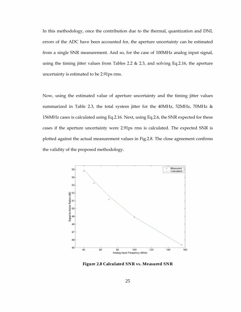
In this methodology, once the contribution due to the thermal, quantization and DNL
errors of the ADC have been accounted for, the aperture uncertainty can be estimated
from a single SNR measurement. And so, for the case of 100MHz analog input signal,
using the timing jitter values from Tables 2.2 & 2.3, and solving Eq.2.16, the aperture
uncertainty is estimated to be 2.91ps rms.
Now, using the estimated value of aperture uncertainty and the timing jitter values
summarized in Table 2.3, the total system jitter for the 40MHz, 52MHz, 70MHz &
156MHz cases is calculated using Eq.2.16. Next, using Eq.2.6, the SNR expected for these
cases if the aperture uncertainty were 2.91ps rms is calculated. The expected SNR is
plotted against the actual measurement values in Fig.2.8. The close agreement confirms
the validity of the proposed methodology.
Figure 2.8 Calculated SNR vs. Measured SNR
26
In summary, the technique involves estimating the analog input signal and sampling
clock jitter from phase noise plots and the total system jitter is measured based on SNR
degradation of the ADC. This method accounts for the quantization and differential
non-linearity of the converters. The accuracy of the method has been demonstrated by
testing on a 10-Bit ADC. Also, it is worth noting that the method has the capability of
measuring aperture uncertainty in the sub-picoseconds regime.

27
3333 TTTTIMING IMING IMING IMING JJJJITTER ITTER ITTER ITTER IIIIN N N N SSSSYMMETRIC YMMETRIC YMMETRIC YMMETRIC LLLLOAD OAD OAD OAD RRRRING ING ING ING OOOOSCILLATORSSCILLATORSSCILLATORSSCILLATORS
Phase Locked Loops (PLLs) are used in a wide range of applications such as frequency
synthesis, clock & data recovery and clock synchronization for microprocessors. The
critical component that affects performance with regards to jitter and phase noise is the
Voltage Controlled Oscillator (VCO). Of the several different implementations possible,
resonant circuit VCOs with an LC tank as the resonant element are known to have an
excellent jitter performance. However, these usually require off-chip components
defeating the purpose of integration [28,29]. On-chip implementations of inductors have
been reported [30], but these generally have a low Q and are bulky. Bond-wire inductors
[31] possess a higher Q but require special processing. Ring oscillators however are
attractive from an integration and cost point of view and are being increasingly
employed in jitter sensitive applications [6,8,32,33].
In this work, a symmetric load ring oscillator is analyzed for its jitter and phase noise
performance. These types of oscillators lend themselves to self-biasing techniques and
are amenable to novel schemes that implement low-jitter PLLs [9]. This chapter begins
with a brief introduction to the symmetric load VCO and its characteristics. A noise
analysis is performed and the timing jitter and phase noise is analyzed according to the
framework established in [10]. The implications of this analysis to the design of a low
jitter/phase noise VCO is presented next.
28
3.1 Symmetric Load Ring Oscillator
A ring oscillator is made up of a number of delay stages configured in a loop. Fig.3.1
shows a ring oscillator using differential delay stages such as that used in this work. ‘N’
delay stages are shown with a wire inversion at the end. It is easy to show that the ring
will oscillate at a frequency (fosc) given by
dosc NTf
21= …(3.1)
where, Td is the delay per stage and N is the number of stages in the ring.
The delay cell used in the symmetric load VCO is shown in Fig.3.2. It consists of an
nMOS differential pair (M5-M6) and the symmetric load element consists of transistor
pairs M1/M2 and M3/M4. Transistors M2/M4 are in saturation and M1/M3 swing
from the linear region to the saturation region. ‘Vcntrl’ is the control voltage used to vary
the frequency of oscillation and ‘Vbias’ is obtained from a separate bias generation
circuitry.
Figure 3.1 Typical ring oscillator using differential delay stages

29
Figure 3.2 Symmetric load delay cell
The symmetric load is so called because of the symmetry in its I-V characteristics. Fig.3.3
shows the symmetric load and its I-V characteristics. As can be observed the output
impedance of this load is highly nonlinear with the maximum resistance at the middle of
the characteristic. The effective resistance is approximated to be linear by the dotted line
as shown in the figure.
The biasing for the delay cell is such that, at equilibrium, half the tail current (Iss/2)
flows through one of the symmetric loads causing a voltage drop of Vcntrl/2 across it.
And during oscillation, the entire tail current (Iss) is steered from one side to the other.
Therefore, the voltage drop across the load swings from 0 to Vcntrl (as shown in Fig.3.3)
and the voltage swing at the output of the oscillator swings from Vdd to Vdd – Vcntrl.

30
Having established the voltage swings for the symmetric loads, it is easy to derive the
effective resistance as shown by the dotted line in Fig.3.3. Consider the end of the swing
where, the voltage drop across the load is Vcntrl and the current flowing through the load
is Iss.
Now, the resistance of the load is given by,
/L cntrl SSR V I= …(3.2)
In this condition, both the transistors are in the saturation region and both have a
source-gate voltage of Vcntrl. Assuming first level equations, the total current Iss can be
approximated as,
2 2
1 22 2p ox p ox
SS cntrl tp cntrl tp
C CW WI V V V VL L
µ µ = − + − …(3.3)
The symmetric loads are designed such that both the transistors are of equal sizes and so
the above equation becomes,
2
SS p ox cntrl tpWI C V VL
µ = − …(3.4)
Figure 3.3 Symmetric Load and its I-V characteristics
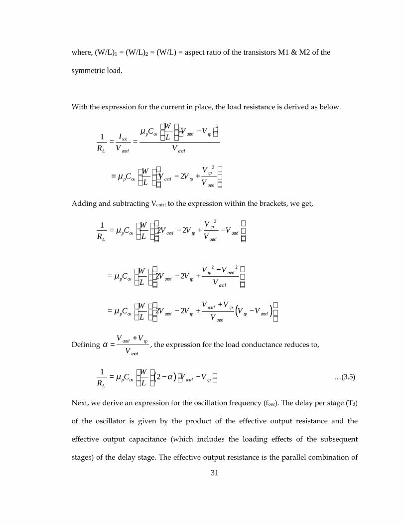
31
where, (W/L)1 = (W/L)2 = (W/L) = aspect ratio of the transistors M1 & M2 of the
symmetric load.
With the expression for the current in place, the load resistance is derived as below.
µ − = =
2
1 p ox cntrl tpSS
L cntrl cntrl
WC V VI L
R V V
2
2 tpp ox cntrl tp
cntrl
VWC V VL V
µ = − +
Adding and subtracting Vcntrl to the expression within the brackets, we get,
21 2 2 tpp ox cntrl tp cntrl
L cntrl
VWC V V VR L V
µ = − + −
2 2
2 2 tp cntrlp ox cntrl tp
cntrl
V VWC V VL V
µ − = − +
( )2 2 cntrl tpp ox cntrl tp tp cntrl
cntrl
V VWC V V V VL V
µ+ = − + −
Defining cntrl tp
cntrl
V VV
α+
= , the expression for the load conductance reduces to,
( )1 2p ox cntrl tpL
WC V VR L
µ α = − − …(3.5)
Next, we derive an expression for the oscillation frequency (fosc). The delay per stage (Td)
of the oscillator is given by the product of the effective output resistance and the
effective output capacitance (which includes the loading effects of the subsequent
stages) of the delay stage. The effective output resistance is the parallel combination of

32
that of the load and the output resistance of the n-MOS differential pair (M1 or M2 in
Fig.3.2). And, since the output resistance of the load is typically much lesser, it
dominates. Therefore, the delay per stage is given by
( )2
effd L eff
p ox cntrl tp
CT R C
WC V VL
µ α= ⋅ =
− −
…(3.6)
Now, substituting Eq.3.6 into Eq.3.1, we get
( )22
p oxosc cntrl tp
eff
C Wf V VNC Lµ
α = − − …(3.7)
It should be noted that for values of Vcntrl that are large in comparison to Vtp, α does not
change appreciably with changes in Vcntrl. Hence, the relationship between the VCO
operating frequency and the control voltage is linear to a first order. This is desirable
especially in a PLL based system because a highly non-linear voltage-frequency
characteristic tends to degrade the performance of the PLL on account of a non-constant
VCO gain.
3.2 MOSFET Noise Analysis
The expression for modeling the thermal noise in MOSFETs used in most of the
literature is as given below
2 2 43d mi kTg f = ∆
…(3.8)
where, gm is the transconductance at the operating point. However, this model is valid
only in the saturation region and is invalid in the triode region of operation [34,35]. For
instance, Eq.3.8 predicts zero noise when Vds=0 whereas the thermal noise is maximum

33
at this point. In the saturation region, the model works well, though it always predicts a
noise that is lower than the actual as can be seen from Fig.1 of [34].
A model for the thermal noise that works well in both the saturation and triode regions
in the case of long-channel devices is given by [35,36],
2 4d doi kTg fγ= ⋅ ∆ …(3.9)
where, gdo is the device conductance for zero drain-source bias and γ=2/3 for saturation
and ranges from 2/3<γ<1 in the triode region. For deep triode region, γ is close to 1.
An expression for γ is derived by Van Der Ziel in [37,38] and is given as below,
( )2/1
3/1 2
υυυγ
−+−= dsatd VV <
3/2=γ dsatd VV ≥ …(3.10)
where, dsatd VV /=υ . As can be observed, for Vds=0, γ=1 and in saturation γ=2/3 and
stays constant.
A more accurate but complex expression is derived in [34] which involves the actual
operating point of the device. But, this essentially simplifies to Eq.3.9 once the higher
order effects are neglected. Also, a comparison of both the models in [34] indicates a
good match between the two for long-channel devices in both the triode and saturation
regions. In this work, Eq.3.9 will be employed along with Eq.3.10 to model the noise in
the symmetric load devices.

34
3.3 Symmetric Load Noise Analysis
At equilibrium (i.e. no switching), the voltage drop across the load is Vcntrl/2 (this is
ensured by the biasing network). Refer Fig.3.3. Transistor M2 is in saturation and
transistor M1 is in saturation/triode region depending on the value of Vcntrl (if Vcntrl >
2Vtp then it is in the triode region). To keep the analysis general, no assumption is made
at this point about the region of operation of M1.
Neglecting short channel effects, gdo equals gm to a first order [35].
( )do gs t mg V V gβ= − = …(3.11)
Therefore, using Eqs.3.9 & 3.11, the total thermal noise due to the symmetric load at
equilibrium is,
21 1 2
24 43T m mi kT g kT gγ = +
…(3.12a)
where,
1m p ox cntrl tpWg C V VL
µ = − and 2 2
cntrlm p ox tp
VWg C VL
µ = − …(3.12b)
Depending on the value of Vcntrl and using Eq.3.10, γ1 can be calculated. Now, lets
consider the case of one end of the swing where Vdrop is close to zero and M1 is in the
linear region and M2 is cut-off. The noise current spectral density in this case is given by,
22 14T mi kT gγ= …(3.13)
Here, γ2 will be very close to ‘1’ as transistor M1 will be in deep triode region.

35
In the case of the other end of the swing where Vdrop = Vcntrl, both M1 & M2 are in
saturation and so the noise current spectral density in this case is given by,
212
324
324 mmT gkTgkTi
+
= …(3.14a)
In this situation, the transconductance of both the transistors is equal and so,
12
344 mT gkTi
= …(3.14b)
Using Matlab and the noise equations developed above, the noise current spectral
density is plotted for a symmetric load of W/L=10u/2u for the AMI 0.5u process.
Fig.3.4 shows the result. As the voltage drop across the symmetric load varies, the noise
current spectral density varies too (this situation occurs during switching). In order to
keep the analysis of jitter simple, the noise current density will be approximated by the
average of Eqs. 3.12 – 3.14 and this approximation gets better for smaller values of Vcntrl
as can be seen from Fig.3.4. A similar approach is adopted in [10].
Figure 3.4 Variation of noise spectral density with voltage drop across the load

36
3.4 Timing Jitter in Ring Oscillators
Timing jitter occurs because of noise sources both internal and external to the oscillator.
The external sources in most cases include the noise injection from nearby circuitry and
power supply noise. These interfering sources however can be minimized through
circuit techniques such as differential implementations. The fundamental limit is
presented by the internal noise sources of the circuit components used to implement the
oscillator. In the case of the symmetric load ring oscillator, these include the flicker and
thermal noise of the transistors present. Ring oscillators eventually find application as
VCOs in PLLs and it can be shown that the PLL presents a high-pass transfer function to
the VCO output noise. Therefore, the thermal noise is the most significant contributor to
noise [39]. And so, the key to achieving low jitter VCOs is to understand the effects of
thermal noise and minimizing its impact.
Several authors [39,40,41] have analyzed the issue of timing jitter in ring oscillators. The
class of circuitry explored has been source-coupled differential delay cells with resistive
loads, where the loads have been realized in CMOS technology using pMOS transistors
in the triode region of operation [39,40]. A similar analysis for bipolar transistors has
been presented in [41]. The approach in [39] takes into account some of the higher order
effects like inter-stage amplification that are not considered in [41]. In this thesis, using
the framework established in [10,39], the analysis is carried out for the symmetric load
case.

37
In the analysis that follows, each delay stage in the ring oscillator is assumed to have a
delay of ‘td’ and a timing error of ‘∆td’ that it imparts to each edge that passes through it
on account of the noise in the transistors that make up the delay stage. This is illustrated
in Fig.3.5 [10].
The timing error has a mean of zero and a variance given by 2dt∆ . Now, to a first order,
the delay per stage is measured from the time the outputs begin switching to the time
when the differential output reaches zero as illustrated in Fig.3.6. Using this assumption,
the delay per stage can be expressed as,
Ld SW
SS
Ct VI
= …(3.15)
where, ISS/CL is the output slew rate and VSW is the total change in the differential
output voltage at the 50% point of the transition. Expressed differently, the time delay
represents the time taken for the load capacitances to charge/discharge such that the
differential output voltage becomes zero. Now, if we make an assumption that the next
stage switches abruptly when the differential output voltage reaches zero (as shown in
Fig. 3.6), the timing error per stage due to noise can be easily calculated.
Figure 3.5 Intrinsic timing error per delay stage

38
The problem now breaks down to finding the timing error associated with the zero
crossing of the differential output voltage. Any timing error associated with this zero
crossing propagates to the subsequent stages and corrupts its timing performance. This
problem, commonly known as the “first crossing problem” can be solved by a “first
crossing approximation” [42]. This is illustrated in Fig.3.7. As can be seen, a voltage
noise on the differential output shifts the time of zero crossing by ∆td (timing error). To a
first order (“first crossing approximation”), the timing error is given by the voltage error
divided by the slew rate at the output. Hence, the variance of the timing error is given
by,
22 2 L
d nSS
Ct VI
∆ = ∆ ×
…(3.16)
The above equation serves as a link from voltage noise uncertainty to the timing jitter
and in [10], the “first crossing approximation” is modified to include some of the higher
order effects like inter-stage amplification.
Figure 3.6 Output waveforms for differential delay stages

39
Figure 3.7 First crossing approximation for timing jitter
The noise sources present in the delay stage are highly time varying in nature, an
example of which is the symmetric load presented earlier. In the case of the symmetric
load, the noise source has been approximated by an average value. The time varying
nature of the n-MOS differential pair and the tail current sources however has to be
dealt with using auto-correlation functions and convolution [10]. This is because during
a voltage swing, the transistors in the differential pair switch from being fully on to fully
off, during which the transconductance and the noise contribution varies significantly.
The same is true with the tail current noise as it appears as a common mode noise in the
equilibrium case, but contributes directly to the output during switching. Thus, the noise
variation is much more when compared to the load, hence requiring a rigorous
mathematical analysis.
Here, a first order analysis will be presented assuming equilibrium conditions just to
illustrate the concept. Also, the effect of the symmetric loads will become evident.
Thereafter, the scenario for the case of a simple p-MOS load (as analyzed in [10]) and the
symmetric loads are similar. That is, the issues of time-varying noise sources (n-MOS
differential pair and tail current noise) and inter-stage amplification are independent of

40
the load used. Hence, the final results in [10] are modified to include the contribution of
the symmetric loads. The detailed mathematical rigor needed in accounting for the
higher order effects can be found in [10].
The symmetric load delay cell along with the noise sources is shown in Fig.3.8. The noise
current source 21ti represents the average noise source of the symmetric loads as
discussed in the earlier section and is given by,
γ γ = + + + 2
1 1 2 1 24 4 2
3 3 3t m mkTi g g …(3.17)
and 25ni , 2
6ni , 27ni and 2
8ni represent the noise current densities of transistors M5-M8.
Now, the total output voltage noise can be determined through conventional noise
analysis techniques [43],
∫∞
+++=0
25
25
22
22
21
21
2 ...)()()()()()( dffHfifHfifHfiV nttn …(3.18)
where, 2nV is the total noise voltage and H1(f), H2(f), …are the transfer functions to the
output for the various noise current sources.
The tail current noise of transistors M7 & M8 split equally and appear on each side of the
differential output. They represent a common mode noise and hence a differential noise
of zero. Therefore, the AC noise model for this circuit is as given in Fig. 3.9 [10]. Here, RL
represents the effective resistance at the output node and CL represents the effective
capacitance including the input capacitance of the subsequent stage.

41
Figure 3.8 Noise current sources in the symmetric load delay cell
Figure 3.9 AC Noise Model for the delay cell
Now, the output voltage noise due to transistor M5 is given by,
22
5 50
243 1 2
Ln m
L L
RV kT g dfj fR Cπ
∞ = + ∫ …(3.19)
The 3-dB bandwidth of the RC system is given by,
31
2dBL L
fR Cπ
= …(3.20)
Using Eq.3.20 in Eq.3.19, we get,
22 2
5 530
2 143 1 /n m L
dB
V kT g R dff f
∞ = + ∫ …(3.21)
42
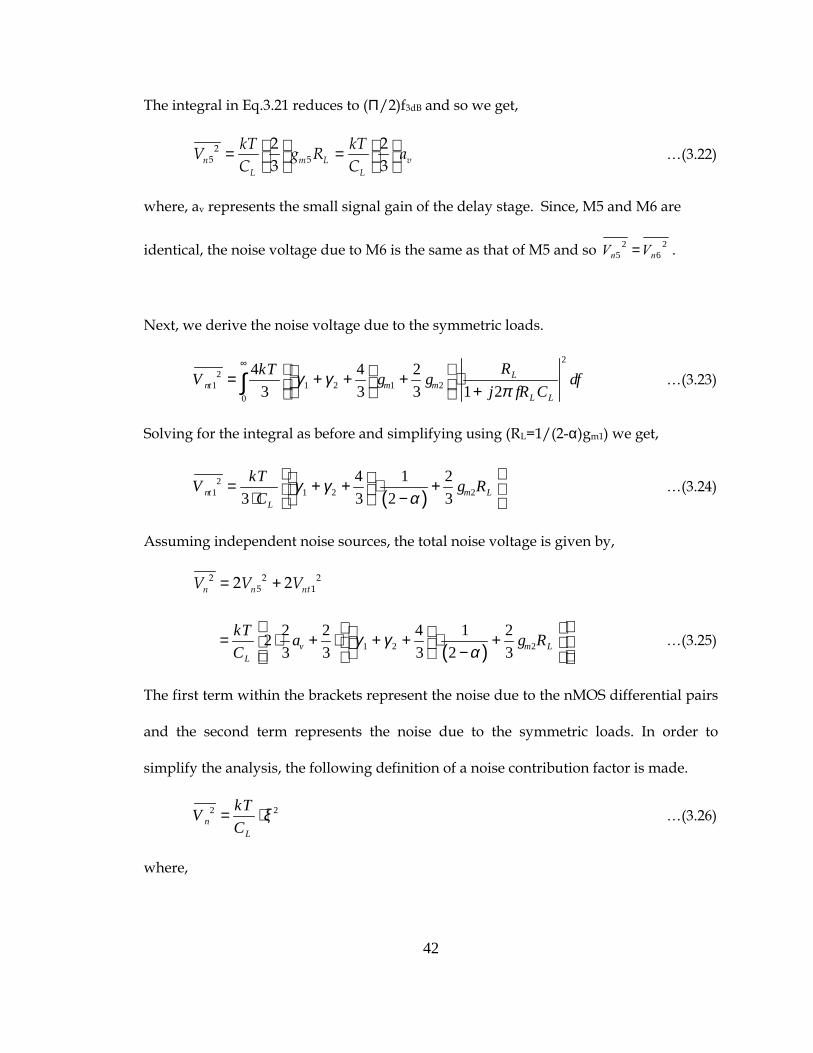
The integral in Eq.3.21 reduces to (Π/2)f3dB and so we get,
25 5
2 23 3n m L v
L L
kT kTV g R aC C
= = …(3.22)
where, av represents the small signal gain of the delay stage. Since, M5 and M6 are
identical, the noise voltage due to M6 is the same as that of M5 and so 26
25 nn VV = .
Next, we derive the noise voltage due to the symmetric loads.
γ γπ
∞ = + + + ⋅ + ∫2
21 1 2 1 2
0
4 4 23 3 3 1 2
Lnt m m
L L
RkTV g g dfj fR C
…(3.23)
Solving for the integral as before and simplifying using (RL=1/(2-α)gm1) we get,
( )γ γ
α = + + ⋅ + ⋅ −
21 1 2 2
4 1 23 3 2 3nt m L
L
kTV g RC
…(3.24)
Assuming independent noise sources, the total noise voltage is given by,
2 2 25 12 2n n ntV V V= +
( )
γ γα
= ⋅ + ⋅ + + ⋅ + − 1 2 2
2 2 4 1 223 3 3 2 3v m L
L
kT a g RC
…(3.25)
The first term within the brackets represent the noise due to the nMOS differential pairs
and the second term represents the noise due to the symmetric loads. In order to
simplify the analysis, the following definition of a noise contribution factor is made.
2 2n
L
kTVC
ξ= ⋅ …(3.26)
where,

43
( )ξ γ γ
α = ⋅ + ⋅ + + ⋅ + −
21 2 2
2 2 4 1 223 3 3 2 3v m La g R …(3.27)
The term 2ξ is called the noise contribution factor. Further analysis including the higher
order effects will only result in modifications to 2ξ .
Now, using Eqs. 3.15 & 3.16, we get,
1drms
d L SW
t kTt C V
ξ∆= ⋅ ⋅ …(3.28)
From the earlier discussions on the characteristics of the symmetric loads, recall that the
voltage swing is equal to the control voltage (Vcntrl). Substituting this in Eq.3.28, we get,
ξ∆= ⋅ ⋅ 1drms
d L cntrl
t kTt C V
…(3.29)
As has been mentioned earlier, the noise sources associated with the n-MOS differential
pairs and the tail currents are highly time varying in nature. These are analyzed in the
time domain using autocorrelation functions and convolution in [10]. Also, for a typical
CMOS delay chain, the switching times of adjacent stages overlap, unlike what has been
shown in the simplistic model of Fig. 3.5. This means that there are times when more
than one stage is in the active region of amplification. This has been suitably accounted
for in [10]. Analyzing these second order effects, the noise contribution factor changes
and the output noise voltage gets multiplied by a factor of 2/2va . This is as shown
below,
ξ= ⋅ ⋅2
2 2
2v
nL
akTVC
…(3.30)
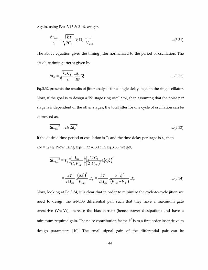
44
Again, using Eqs. 3.15 & 3.16, we get,
ξ∆= ⋅ ⋅ ⋅ 1
2drms
vd L cntrl
t kT at C V
…(3.31)
The above equation gives the timing jitter normalized to the period of oscillation. The
absolute timing jitter is given by
ξ∆ = ⋅ ⋅2
vLd
akTCt
Iss …(3.32)
Eq.3.32 presents the results of jitter analysis for a single delay stage in the ring oscillator.
Now, if the goal is to design a ‘N’ stage ring oscillator, then assuming that the noise per
stage is independent of the other stages, the total jitter for one cycle of oscillation can be
expressed as,
∆ = ∆2 22VCO dt N t …(3.33)
If the desired time period of oscillation is T0 and the time delay per stage is td, then
2N = T0/td. Now using Eqs. 3.32 & 3.15 in Eq.3.33, we get,
( )220 22 ( )
SS LVCO v
L SW SS
I kTCt T aC V I
ξ
∆ = ⋅ ⋅ ⋅
( )( )
2 2
0 02 2v v
SS SW SS GS T
a akT kTT TI V I V V
ξ ξ⋅= ⋅ ⋅ = ⋅ ⋅
⋅ ⋅ − …(3.34)
Now, looking at Eq.3.34, it is clear that in order to minimize the cycle-to-cycle jitter, we
need to design the n-MOS differential pair such that they have a maximum gate
overdrive (VGS-VT), increase the bias current (hence power dissipation) and have a
minimum required gain. The noise contribution factor 2ξ is to a first order insensitive to
design parameters [10]. The small signal gain of the differential pair can be
45
approximated as SWv
GS T
Va
V V=
−. The implication of this is that, one cannot simply
increase the gate overdrive without a corresponding increase in the output voltage
swing, as a minimum gain is required for the ring to oscillate. Ideally one would like to
design the ring with maximum possible power dissipation, maximum gate overdrive for
the n-MOS differential pair (hence maximum possible swing) and a minimum required
gain (typically 1.5 –3.0).
However, the situation of maximum gate overdrive and a corresponding increase in the
output voltage swing is not something that is easily achieved. While using resistively
biased p-MOS loads (as has been discussed in [10]), the voltage swing is constrained by
the fact that one has to maintain the loads in the linear region and in some cases in the
deep triode region, thereby making large swings difficult to achieve. This restriction
however is not present in the case of the symmetric loads. Here, the voltage drop across
the load swings from 0 to Vcntrl and hence by a proper choice of Vcntrl, the oscillator can
be designed for a large voltage swing.
Another consideration that sets the limit on the voltage swing in the case of both the
symmetric loads and the p-MOS resistively biased loads is the issue of maintaining the
n-MOS differential pairs in saturation during the entire voltage swing. Failure to do so
can lead to distortion in the waveforms as the devices are changing regions of operation
during the swing [10].
46
From the discussion above it can be observed that the symmetric loads offer the
advantage of a larger swing than the p-MOS loads. So a possible solution could be to
design a symmetric load VCO with a maximum possible swing and hence achieve low
jitter/phase noise. The key issue with the symmetric loads is that frequency variation is
achieved through Vcntrl and hence changing Vcntrl will change the output voltage swing.
Hence what is needed is an architecture using symmetric loads that optimizes the swing
(based on keeping the differential pairs in saturation, phase noise requirement and
power dissipation) and also achieves frequency variation without changes in the output
swing. Such an architecture is the subject of discussion in the next chapter.

47
4444 A SA SA SA SWING WING WING WING OOOOPTIMIZED PTIMIZED PTIMIZED PTIMIZED BBBBODY ODY ODY ODY DDDDRIVEN RIVEN RIVEN RIVEN OOOOSCILLATORSCILLATORSCILLATORSCILLATOR
In Chapter 3, the need for an increase in voltage swing in order to achieve low jitter/low
phase noise oscillators was presented. In the case of the symmetric loads, the upper limit
on the voltage swing is set primarily by the condition that the n-MOS differential pairs
remain in saturation during the entire voltage swing. This is important to avoid
distortion in the output waveform. A conventional ring oscillator with the symmetric
load can thus be optimized for a large output voltage swing. This architecture however
poses a serious limitation in that it cannot achieve frequency variation without a
resultant change in the output voltage swing. The oscillator developed in this thesis sets
the output voltage swing at the maximum allowed value and achieves frequency
variation by driving the body (n-well) of the symmetric loads.
This chapter begins by deriving an expression for the maximum possible voltage swing
that can be tolerated and still keep the n-MOS differential pairs in saturation. The
proposed oscillator architecture is presented next and its frequency vs. control voltage
characteristic is derived. The phase noise does not vary appreciably along the frequency
range of the oscillator and this is explained theoretically by means of a derivation. The
implication of this result is discussed next. This is followed by simulation results of the
oscillator designed for the AMI 0.5µ process and the match between theoretical
predictions and simulation results is illustrated.
48
4.1 Maximum Possible Voltage Swing
In this section, an expression is derived that gives the maximum possible voltage swing
at the output of the oscillator given the condition that the differential pairs remain in
saturation throughout the swing. Following the derivation in [10], the differential pair
transistors will remain in saturation if the voltage swing is kept below the n-MOS
threshold voltage. For the symmetric loads, this translates to,
≤cntrl tnV V …( 4.1)
where, Vtn is the n-MOS threshold voltage including body effect.
Now, to maximize the swing, one needs to increase the threshold voltage. This however
is not possible in a bulk CMOS process if an n-MOS differential pair is to be used. A
possible solution could be to use a p-MOS differential pair with n-MOS symmetric loads.
Using p-MOS symmetric loads with n-MOS differential pair (as has been discussed so
far) has an additional advantage of enabling frequency control (in a Bulk CMOS process)
due to which we will investigate this type of oscillator.
Since increasing the n-MOS threshold voltage using body driving is not possible in bulk
CMOS, we have to resort to biasing and a proper choice of the aspect ratio of the
transistors in the differential pair. This way, it is possible to introduce sufficient body
effect by increasing the common source voltage of the differential pair. In the analysis
that will follow, an expression is derived that will aid in the selection of the proper
voltage swing (Vcntrl in the case of the symmetric load).
49
The output voltage of the symmetric load ring oscillator swings from Vdd to Vdd – Vcntrl.
And since the input of one stage is connected to the output of the previous stage, the
inputs also follow the same swing. Now, consider the end of the swing, where the
output voltage is Vdd. This is applied to the gate of one of the n-MOS transistors in the
differential pair. The voltage drop across the load in this case is Vcntrl giving a drain
voltage of Vdd – Vcntrl for the particular transistor. This condition corresponds to the case
of maximum gate voltage and minimum drain voltage and hence the transistor is most
vulnerable to come out of saturation at this point. So, we choose Vcntrl such that it is
equal to the threshold voltage of the n-MOS transistor in this condition.
At this point, the tail current is completely switched to one side and the total tail current
of ISS flows through the transistor. Using first level equations,
[ ]µ µ = − = − − 2 2
2 2n ox n ox
SS gs tn dd s tnd d
C CW WI V V V V VL L
…( 4.2)
where, Vs is the source voltage, (W/L)d is the aspect ratio of the n-MOS differential pair
transistors and Vtn is the threshold voltage of the n-MOS transistors including body
effect.
The effect of body voltage on the threshold voltage is modeled in [44] as,
γ
φ
⋅= +
2 2n sb
tn tno
f
VV V …( 4.3)
where, Vtno is the threshold voltage with zero body effect, Vsb is the source to bulk
voltage and φf is the Fermi potential. In the case of an n-MOS, the bulk, which is the

50
substrate, is usually connected to the lowest potential, typically ground for a single
supply system. Assuming such a system, Vsb = Vs, and substituting this in Eq.4.3 and
solving for Vs, we get,
( )φ
γ= ⋅ −
2 2 f
s tn tnon
V V V
θ= ⋅ −( )n tn tnoV V …( 4.4)
where θn is defined as,
φ
θγ
=2 2 f
nn
…( 4.5)
It should be noted that θn is dimensionless.
And as stated earlier, in an effort to set the swing as high as possible, Vcntrl is set to equal
Vtn. Using this condition and Eq.4.4 in Eq.4.2, we get,
( )µ θ = − ⋅ − − 2
2n ox
SS dd n tn tno tnd
C WI V V V VL
( )µθ θ = + ⋅ − +
21
2n ox
dd n tno tn nd
C W V V VL
( )µθ θ = + ⋅ − +
21
2n ox
dd n tno cntrl nd
C W V V VL
…( 4.6)
Now, the tail current ISS can be approximated as the voltage drop across the load
divided by the resistance of the load and hence,
= cntrlSS
L
VI
R …( 4.7)
and,
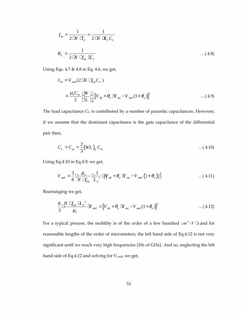
51
= =⋅ ⋅ ⋅ ⋅
1 12 2osc
d L L
fN T N R C
=⋅ ⋅ ⋅
12L
osc L
RN f C
…( 4.8)
Using Eqs. 4.7 & 4.8 in Eq. 4.6, we get,
= ⋅ ⋅(2 )SS cntrl osc LI V N f C
[ ]µθ θ = + ⋅ − +
2(1 )2
n oxdd n tno cntrl n
d
C W V V VL
…( 4.9)
The load capacitance CL is contributed by a number of parasitic capacitances. However,
if we assume that the dominant capacitance is the gate capacitance of the differential
pair then,
( )= = 23L gs oxdC C WL C …( 4.10)
Using Eq.4.10 in Eq.4.9, we get,
( )µ θ θ= ⋅ ⋅ ⋅ + ⋅ − + ⋅2
2
3 1 18
ncntrl dd n tno cntrl n
osc d
V V V VN f L
…( 4.11)
Rearranging we get,
[ ]2
28 (1 )3
osc dcntrl dd n tno cntrl n
n
N f LV V V Vθ θ
µ⋅ ⋅
⋅ ⋅ = + ⋅ − + …( 4.12)
For a typical process, the mobility is of the order of a few hundred sVcm ⋅/2 and for
reasonable lengths of the order of micrometers; the left hand side of Eq.4.12 is not very
significant until we reach very high frequencies (10s of GHz). And so, neglecting the left
hand side of Eq.4.12 and solving for Vcntrl, we get,

52
( )1dd n tno
cntrln
V VV
θθ
+ ⋅=
+ …( 4.13)
The above expression sets the upper limit on the control voltage and hence the output
voltage swing. For control voltages greater than that given by Eq.4.13, the differential
pair will go out of saturation. It is interesting to note that the maximum possible value
for Vcntrl is determined solely by technology parameters and cannot be changed by
design.
This can be better understood by a qualitative explanation. The condition that needs to
be satisfied for the differential pairs to remain in saturation is that the output swing be
less than the threshold voltage of the n-MOS differential pair. Increasing the output
swing will mean increasing the threshold voltage, which can be achieved by raising the
source voltage (common source point) of the transistors forming the differential pair.
Now, assume that the transistors are initially in saturation for a particular value of
output swing. Increasing the source voltage decreases the gate overdrive and decreases
the drain-source voltage as well. However, the decrease in the gate overdrive is stronger
on account of a decrease in the gate-source voltage and a simultaneous increase in the
threshold voltage due to body effect. This means a drain voltage lower than what we
began with can still keep the transistor in saturation even though the drain-source
voltage dropped as well. This allows for a slightly higher swing than before. If we
continue to raise the source voltage, the swing can get larger and larger until a limiting
condition is reached when the gate overdrive and the drain-source voltage both collapse

53
to zero. It is this condition that is represented mathematically in Eq.4.13. Now the fact
that the output swing is independent of design parameters and is totally technology
dependent should come as no surprise, as at its core, the analysis involves solving for
the condition of zero gate overdrive given a fixed gate voltage of Vdd. It should therefore
be noted that to avoid the transistor from getting totally cut-off, the swing should be
designed for values slightly lower than that obtained by solving Eq.4.13.
4.2 Ring Oscillator Phase Noise
The phase noise for a ring oscillator derived in [10] is as given below.
( )ξ ⋅ ⋅ ∆ = ⋅ ∆ ⋅ ⋅ −
2 2
( )2
osc v
SS gs t
f a kTL f
f I V V …( 4.14)
where, L(∆f) represents the phase noise at an offset frequency of ∆f and fosc is the
frequency of oscillation.
Using Eqs.4.7 & 4.8 and substituting for frequency of oscillation and the bias current ISS
in Eq.4.14 we get,
( )ξ
⋅ ∆ = ⋅ ⋅ ∆ ⋅ ⋅ −
2 2 21 1( )2 2
v
cntrlL Lgs t
L
a kTL f Vf NR C V V
R
…( 4.15)
Substituting ( )=−cntrl
vgs t
Va
V V, Eq.4.15 becomes,

54
( )ξ ⋅ ∆ = ⋅ ⋅ ⋅ ∆ ⋅ ⋅ ⋅ −
2 2
2
1( )2 2L L gs t
kTL fN f C R V V
…( 4.16)
The objective of this analysis is to find theoretically the variation of the phase noise at a
particular offset across the frequency range of an oscillator. For the type of ring
oscillators being discussed, different frequencies are achieved by varying the resistance
of the loads. Hence the terms within the first bracket in the right hand side of Eq.4.16
remain constant across the frequency range of the oscillator. In the second bracket, the
noise contribution term is relatively insensitive to delay cell design parameters [10] and
hence can be assumed constant with frequency. The only parameters that need to be
considered are RL and the square of the gate overdrive.
Consider the expression for the bias current given below,
µ = ⋅ − = = 2
2 2 2 2SS n ox SW cntrl
gs td L L
I C V VW V VL R R
…( 4.17)
If the scenario is such that RL varies (hence frequency variation) in such a way that the
output swing remains constant, then the product of RL times the square of the gate
overdrive remains constant as well. This can be observed from Eq.4.17. Using this
development in Eq.4.16, theoretically the phase noise would be expected to remain
constant with frequency.
The implication of this result is that if we design an oscillator subject to conditions
assumed above, the phase noise performance will remain unaltered across the frequency
range of the oscillator. Also, now the oscillator phase noise can be optimized by
55
maximizing the swing (subject to conditions derived earlier) and if the swing is
maintained constant across frequency, the phase noise performance will remain
unaltered. The above discussions on swing maximization and oscillator phase noise set
the stage for the presentation of the proposed oscillator topology, which follows next.
4.3 Swing Maximized Body Driven Oscillator
From the discussion on the symmetric loads, it must be clear that a change in the control
voltage (Vcntrl) leads to a change in frequency. Thus, by setting Vcntrl at its optimum value
as derived before, only one frequency can be implemented. Therefore, to make full use
of the output voltage swing optimization, one should be able to fix the swing at its
maximum and still vary the frequency of operation. The solution to this problem is body
driving the n-well of the p-MOS symmetric loads and is as developed below.
The relationship between the control voltage and frequency for the symmetric load ring
oscillator as derived earlier is given below for convenience.
( )22
p oxosc cntrl tp
seff
C Wf V VNC Lµ
α = − − …( 4.18)
As can be seen, by fixing Vcntrl and varying the p-MOS threshold voltage, a voltage
controlled oscillator results with a fixed output voltage swing as desired. Now, Vcntrl can
be set to the optimum value and a frequency control is achieved by putting the body
effect to good use. This can be achieved elegantly in bulk CMOS technology, as the p-
MOS transistors are isolated by the n-Wells. This is the reason for choosing an n-MOS

56
differential pair with p-MOS symmetric loads as opposed to p-MOS differential pairs
with n-MOS symmetric loads.
The p-MOS threshold voltage including the body effect is modeled in [44] as below,
γ
φ= −
2 2
p bstp tpo
f
VV V …( 4.19)
Using the above expression in Eq.4.14 and denoting Vbs as Vbulk, we get,
( )µ γ
αφ
= − − −
22 2 2
p ox p bulkosc cntrl tpo
seff f
C VWf V VNC L
( )22
p ox bulkosc cntrl tpo
seff p
C VWf V VNC Lµ
αθ
= − − − …( 4.20)
When Vcntrl is larger than the threshold voltage Vtp, changes in the threshold voltage
(through body effect) required to generate a new frequency does not cause appreciable
changes in the value of α. Thus, the frequency vs. bulk voltage characteristic will be
almost linear. The range of values possible for the bulk voltage is limited by
considerations of forward biasing the source-bulk p-n junction and gate oxide
breakdown. Based on these limits, a range of 4.6V – 6.0V has been chosen for
simulations.
Having a large output voltage swing provides the luxury of a high gate overdrive and
hence power dissipation; all of which are critical to achieving a low jitter/low phase
noise oscillator. The limitation to voltage swing is posed by the choice of technology.

57
Interestingly, if the voltage swing remains constant with frequency, then it is sufficient
to optimize the phase noise for one particular frequency. Thus using the proposed
oscillator topology, a low phase noise oscillator is possible by employing a high output
voltage swing. Variation in the frequency is achieved through body driving and the
same phase noise performance can be achieved across frequencies.
A design methodology would now involve choosing a high output voltage swing and a
correspondingly high gate overdrive for the n-MOS differential pairs such that the small
signal gain (given by the quotient of the two) is just a little more than the minimum
required for oscillation. A value for the tail current is chosen to be the maximum
possible given power dissipation requirements. The values chosen for the tail current
and the output voltage swing set the load resistance. A desired frequency can now be
achieved by varying the gate-source capacitance of the n-MOS differential pair
transistors. These conditions now set the phase noise for the required frequency.
Frequency variation can be achieved through body driving and the same phase noise
performance can be expected.
4.4 Simulation Results
A set of three oscillators (Osc-1, Osc-2 & Osc-3) was designed using AMI 0.5µ
technology, to analyze the effects of power dissipation, output voltage swing and gate
overdrive on the phase noise of the oscillator and also to verify the design methodology
presented earlier. In order to ensure a fair comparison between the three oscillators, all
of them were designed to oscillate at 100MHz and their small signal gain was fixed at

58
approximately 2.5. The circuit details of the oscillator system are presented in
Appendix-B and the simulations were performed using SPECTRE RF.
Approximating the value of 2φF as 0.6V and using γn = 0.48 from the MOSIS parametric
test results for the AMI0.5µ process [45], the maximum swing is calculated to be 1.8V
using Eq.4.13. As mentioned earlier this represents the mathematical maximum and a
practically possible swing turns out to be about 1.5V. This sets an upper limit on the
achievable gate overdrive for a given minimum small signal gain.
The three oscillators were designed for three different swings (1.5V, 1.4V & 1.3V) using
three different values (3.5V, 3.6V & 3.7V) at the gates of the p-MOS symmetric loads. The
aspect ratio of the p-MOS symmetric loads was kept constant in all the three oscillators
while the same oscillation frequency of 100MHz for all the three was achieved by
varying the aspect ratios of the n-MOS differential pairs. Since a three-stage ring
oscillator was designed, a minimum gain of 2 is required for oscillation. However, in
order to account for process variations and also to provide a safety margin, a larger gain
is needed. But, the phase noise degrades with too large a gain, and so, as a compromise,
all the three oscillators were designed for a gain of approximately 2.5. The simulation
results are presented in Table 4.1.

59
Table 4.1 Simulation Results for Osc-1, Osc-2 & Osc-3
Freq = 100MHz VBULK = 5.0V
Oscillator VCNTRL ISS VSW VGS-VTN Gain Phase Noise
@100KHz Offset
Osc-1 3.5V 101.5µA 1.5V 0.618V 2.43 -95.50 dBc/Hz
Osc-2 3.6V 70.83µA 1.4V 0.5875 2.39 -93.25 dBc/Hz
Osc-3 3.7V 45.07µA 1.3V 0.5153 2.52 -90.10 dBc/Hz
Figure 4.1 Phase Noise plots for Osc-1, Osc-2 & Osc-3

60
From Table 4.1, it can be seen that in the case of Osc-1, a higher output voltage swing has
made possible a higher gate overdrive which when coupled with a higher power
dissipation leads to a better phase noise performance. Key advantages of having a
higher swing and hence a higher gate overdrive is that higher power dissipation can be
achieved without a corresponding increase in the area of the n-MOS differential pairs.
Fig. 4.1 shows the phase noise plots for the three oscillators.
Now, if the phase noise has been optimized for a given value using acceptable values of
swing, gate overdrive and power dissipation, the theory predicts the phase noise to
remain the same with frequency variation. Table 4.2 summarizes the phase noise
performance of Osc-1 and Osc-2. As can be observed, Table 4.2 validates the developed
theory. The phase noise remains approximately constant for both the set of oscillators
even though the frequency changes by atleast a factor of 2.3. The implication of this
result is that the phase noise performance needs to be optimized for just one frequency
and if the swing remains constant across frequencies as in the case of this oscillator, the
phase noise remains constant.
As has been mentioned earlier, it is important that the frequency vs. bulk voltage
characteristic be linear. This ensures that the gain of the oscillator remains constant. For
the proposed oscillator, the Frequency vs. Bulk voltage characteristics has been shown
theoretically to be linear. This has been confirmed through simulations and can be
observed from Figs.4.2 & 4.3.

61
Table 4.2 Phase Noise across the frequency range of Osc-1 & Osc-2
Osc-1 (VCNTRL = 3.5V) Osc-2 (VCNTRL = 3.6V)
VBULK Freq. Phase Noise
@100KHz Offset
VBULK Freq. Phase Noise
@100KHz Offset
4.6V 117.7MHz -95.4922 dBc/Hz 4.6V 121.9MHz -93.0358 dBc/Hz
4.8V 110.3MHz -95.5782 dBc/Hz 4.8V 112.8MHz -93.1880 dBc/Hz
5.0V 100.4MHz -95.4992 dBc/Hz 5.0V 100.10MHz -93.2545 dBc/Hz
5.2V 89.2MHz -95.4969 dBc/Hz 5.2V 85.76MHz -93.2133 dBc/Hz
5.4V 78.26MHz -95.3603 dBc/Hz 5.4V 72.20MHz -93.2631 dBc/Hz
5.6V 68.05MHz -95.3147 dBc/Hz 5.6V 59.47MHz -93.3434 dBc/Hz
5.8V 58.39MHz -95.3014 dBc/Hz 5.8V 47.90MHz -93.4982 dBc/Hz
6.0V 49.43MHz -95.2866 dBc/Hz 6.0V 37.14MHz -93.6992 dBc/Hz
Figure 4.2 Simulation Results vs. Theory for Osc-1
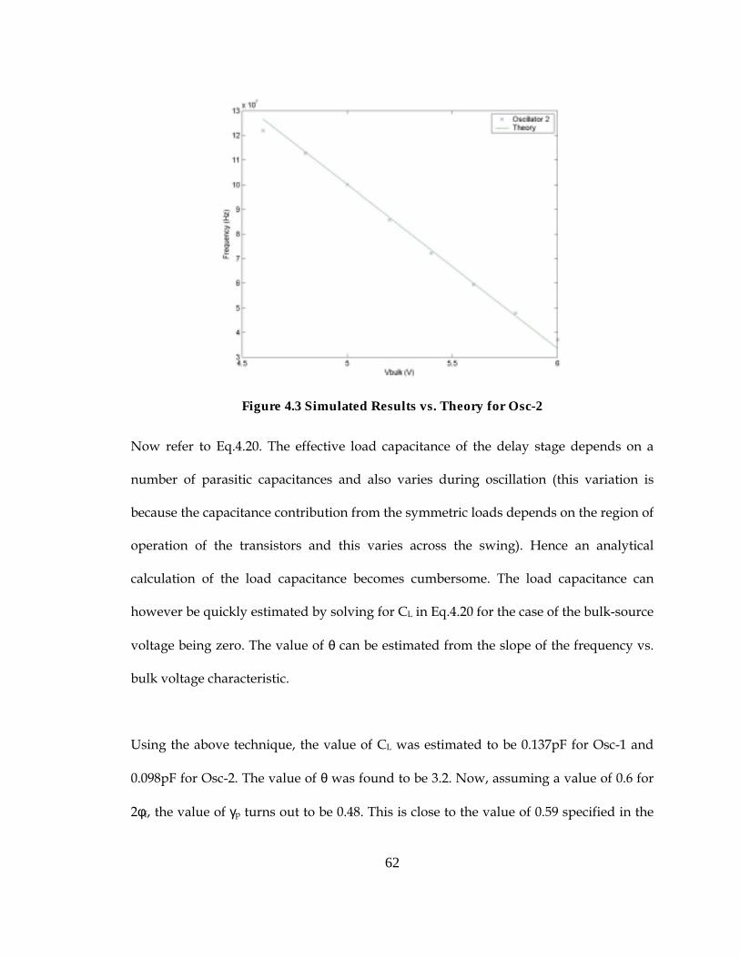
62
Figure 4.3 Simulated Results vs. Theory for Osc-2
Now refer to Eq.4.20. The effective load capacitance of the delay stage depends on a
number of parasitic capacitances and also varies during oscillation (this variation is
because the capacitance contribution from the symmetric loads depends on the region of
operation of the transistors and this varies across the swing). Hence an analytical
calculation of the load capacitance becomes cumbersome. The load capacitance can
however be quickly estimated by solving for CL in Eq.4.20 for the case of the bulk-source
voltage being zero. The value of θ can be estimated from the slope of the frequency vs.
bulk voltage characteristic.
Using the above technique, the value of CL was estimated to be 0.137pF for Osc-1 and
0.098pF for Osc-2. The value of θ was found to be 3.2. Now, assuming a value of 0.6 for
2φf, the value of γp turns out to be 0.48. This is close to the value of 0.59 specified in the
63
MOSIS parametric test results for AMI0.5µ technology [45]. Figs. 4.2 and 4.3 show the
simulated frequency vs. bulk voltage characteristics and the predicted theoretical
characteristics. The good fit confirms the validity of the proposed theory.
In summary, the proposed oscillator system maximizes the output voltage swing and
hence allows for a higher gate overdrive for a given minimum small signal gain. The
higher gate overdrive directly improves the phase noise performance of the oscillator
and also allows for higher power dissipation without the need for an increase in size of
the n-MOS differential pair transistors. A theoretical limit has been derived for the
output voltage swing subject to the condition that the n-MOS differential pair transistors
remain in saturation during the entire swing. Also, it has been shown that the phase
noise remains constant with frequency if the output swing remains constant. The
proposed oscillator achieves this by optimizing the output voltage swing and varying
the frequency by driving the body of the p-MOS symmetric loads. The frequency vs.
bulk voltage characteristics has been derived and found to be linear. This has been
verified with simulation results.
64
5555 CCCCONCLUSIONS AND ONCLUSIONS AND ONCLUSIONS AND ONCLUSIONS AND FFFFUTURE UTURE UTURE UTURE WWWWORKORKORKORK
5.1 Conclusions
Timing jitter has been shown to degrade the performance of the A-D converter. The jitter
on the sampling clock, the analog input signal and the aperture uncertainty of the
converter all combine to produce a lower SNR for the converter. An expression for the
SNR of the converter that takes into effect the overall timing jitter of the system, the
quantization noise, differential non-linearity errors and the internal noise sources of the
ADC has been presented. This equation has been used to measure the total system jitter.
The fundamentals of phase noise have been presented and a technique that enables the
extraction of timing jitter from phase noise plots has been explained. A jitter model that
works well for a sampling system like the ADC has also been presented. Using the jitter
model, the extraction of timing jitter from phase noise plots and the measurement of
total system jitter from SNR degradations, the aperture uncertainty of the converter can
be estimated. The results of applying this technique to a 10-Bit converter have also been
presented.
The issue of effective clock generation has been discussed from the perspective of a ring
oscillator. Although crystal oscillators and voltage controlled oscillators with LC tank as
the resonant element offer better phase noise performance, the ring oscillator is gaining
in popularity on account of its ease of integration. The key design parameters that affect
the phase noise performance of the ring oscillator include the output voltage swing, the
65
gate overdrive of the transistors in the differential pair, the power dissipation and the
small signal gain of the delay stage. The gate overdrive is constrained by the maximum
possible output voltage swing. This is because the small signal gain is given by the ratio
of the output swing to the gate overdrive and so increases in the gate overdrive has to be
accompanied by a corresponding increase in the output swing in order to maintain a
minimum required gain.
For ring oscillators that use symmetric loads, the output swing is limited by the
condition of maintaining the differential pair transistors in saturation throughout the
swing. A theoretical derivation has been presented in this thesis that solves for the
maximum possible swing subject to the condition that the differential pairs remain in
saturation. Interestingly, the maximum possible swing depends entirely on the
technology parameters and cannot be changed by design.
Now an oscillator topology that achieves minimum phase noise would be one that is
designed for the maximum swing and hence maximum gate overdrive, minimum gain
and maximum power dissipation. In the proposed architecture, the symmetric loads
have been used as they can be designed with the maximum swing possible for a given
technology. But, for a conventional ring oscillator with a symmetric load, this swing can
be optimized for only one frequency, thereby not allowing frequency variation. This
problem is circumvented by achieving frequency variation by driving the body of p-
MOS symmetric loads and varying their threshold voltages.
66
It has also been shown that for the proposed oscillator topology, the phase noise needs
to be optimized for just one frequency. This having been accomplished, the phase noise
performance remains unaltered with frequency variation. Also, the frequency vs. bulk
voltage characteristics of the oscillator has been derived and shown to be linear. Finally,
the theoretical predictions have been found to agree closely with the simulation results.
5.2 Future Work
!"For the proposed oscillator, frequency variation is achieved through body
driving, on account of which the bulk voltage needs to be higher than the power
supplies. When used as a VCO in a PLL based system, the charge pump circuitry
will now have to produce voltages above the supply voltage, which is not the
case in a conventional PLL. Charge pump architectures will have to be
investigated such that this is made possible.
!" The proposed architecture when used in bulk CMOS does not have the
capability of high frequency operation as it uses p-MOS symmetric loads. The
use of n-MOS symmetric loads will straight away achieve a 2.5 times increase in
frequency, as the mobility of electrons is approximately 2.5 times the mobility of
holes. The use of n-MOS symmetric loads is however not possible on account of
the inability to drive the body of the n-MOS in bulk CMOS technology. The ideal
technology for this topology is SOI and this prospect needs to be further
investigated.
67
!"The phase noise of the ring oscillator depends on an interplay between a number
of design parameters. One such parameter, the swing has been shown to be
entirely technology dependent. From a designer’s perspective, it is important to
investigate the effect of choice of technology and technology scaling on the
various design parameters that impact the oscillator’s frequency, phase
performance etc., such that a judicious choice of technology can be made based
on the oscillator specifications.

68
RRRREFERENCESEFERENCESEFERENCESEFERENCES

69
[1] Brad Brannon, “Aperture Uncertainty and ADC system performance,” AN 501:
Application Note, Analog Devices Inc.
[2] Ali Hajimiri and Thomas H.Lee, “Design of Low Noise Oscillators,” Kluwer
Academic Publishers, 1999.
[3] T. Stetzler, I. Post, J. Havens, M. Koyama, “ A 2.7 – 4.5 V single chip GSM
transceiver RF integrated circuit,” IEEE Journal of Solid-State Circuits, Vol. 30,
No. 12, pp. 1421 – 1429, Dec. 1995.
[4] U. Rohde, “Digital PLL Frequency Synthesizers,” Prentice-Hall, Englewood
Cliffs, N.J. 1983.
[5] S. Kiriaki, T. Viswanathan et. al., “A 160MHz analog equalizer for magnetic disk
read channels,” IEEE Journal of Solid-State Circuits, Vol. 32, No. 11, pp. 1839 –
1850, Nov. 1997.
[6] I. Young, J. Greason, J. Smith, K. Wong, “A PLL Clock Generator with 5 to
110MHz Lock Range for Microprocessors,” IEEE Journal of Solid-State Circuits,
Vol. 27, No. 11, pp. 1599 – 1607, Nov. 1992.
[7] D. Jeong, G. Borriello, D. Hodges, R. Katz, “Design of PLL Based Clock
Generation Circuits,” IEEE Journal of Solid-State Circuits, Vol. 22, No. 2, pp. 255
– 261, April 1987.
[8] M. Horowitz, A. Chan, J. Corbrunson, J. Gasbarro, T. Lee, W. Leung, W.
Richardson, T. Thrush and Y. Fujii, “PLL design for a 500Mb/s interface,”
ISSCC Dig. Tech. Papers, pp. 160-161, Feb. 1993.
70
[9] John G. Maneatis, “Low-Jitter Process-Independent DLL and PLL Based on Self-
Biased Techniques,” IEEE Journal of Solid-State Circuits, Vol. 31, No.11, pp.
1723-1732, Nov. 1996.
[10] Todd C. Weigandt, “Low-Phase-Noise, Low-Timing-Jitter Design Techniques for
Delay cell based VCOs and Frequency Synthesizers,” PhD Dissertation,
University of California, Berkeley, 1998.
[11] Mitsuru Shinagawa, Yukio Akazawa, Tsutomu Wakimoto, “Jitter Analysis of
High-Speed Sampling Systems,” IEEE Journal of Solid-State Circuits, Vol.25,
No.1, pp. 220 - 224, Feb. 1990.
[12] Jerry Horn, “Clock Jitter and ADCs,” High-Performance Mixed-Signal Design at
http://www.chipcenter.com/eexpert/jhorn/archive.html
[13] Jacques Rutman, “Characterization of Phase and Frequency Instabilities in
Precision Frequency Sources: Fifteen Years of Progress,” Proceedings of the IEEE,
Vol. 66, No. 9, pp. 1048 – 1076, Sept. 1978.
[14] Steve Ruscak and Larry Singer, “Using Histogram Techniques to Measure A/D
Converter Noise,” Analog Dialogue, Vol. 29-2, 1995.
[15] David A. Johns and Ken Martin, Analog Integrated Circuit Design. John Wiley &
Sons, NY, 1997.
[16] “High Speed Design Techniques,” Analog Devices, Inc., 1996
[17] Venkatesh Srinivasan, Syed K. Islam and Gary T. Hendrickson, “A Method for
the Estimation of Aperture Uncertainty in A-D Converters,” in Proc. 2002 IEEE
International Symposium on Circuits and Systems, pp. III-125 – III-128, May
2002.

71
[18] Ali Hajimiri and Thomas H. Lee, “A General Theory of Phase Noise in Electrical
Oscillators,” IEEE Journal of Solid State Circuits, Vol. 33, No. 2, Feb. 1998.
[19] Steven Harris, “The Effects of Sampling Clock Jitter on Nyquist Sampling
Analog-to-Digital Converters and Oversampling Delta-Sigma ADCs,” Journal of
Audio Engineering Society, Vol. 38, pp. 537- 542, Jul/Aug 1990.
[20] Jack Kurzweil, “An Introduction to Digital Communications,” John Wiley &
Sons, 1999.
[21] AN13: Application Note, “Phase Noise Demystified,” Peregrine Semiconductor
Corporation.
[22] J.A. Barnes, A.R. Chi, L.S. Cutler et. al., “Characterization of Frequency Stability,”
IEEE Transactions on Instrumentation Measurement, Vol. IM-20, pp. 105 – 120,
May 1971.
[23] Boris Drakhlis, “Calculate Oscillator Jitter by Using Phase Noise Analysis – Parts
I & II,” Microwaves & RF, Jan/Feb 2001.
[24] “CB3/CB3LV SMD Clock Oscillator,” CTS Frequency Products at
http://www.ctscorp.com/reeves/clock/045.pdf
[25] “M600 Series Voltage Controlled SAW Oscillators,” Micro Networks Corporation
at http://www.nordimar.com/m600.pdf
[26] “CO4605 High Frequency, Low Jitter, SMD Oscillator for GigaBit Ethernet
Applications,” Raltron Electronics Corporation at
http://www.raltron.com/apps/pdfspecs/co4605-125000-revc.pdf
[27] “AD9218 Converter Data Sheet,” Analog Devices Inc., Rev. 0, July 2001 at
http://www.analog.com/productSelection/pdf/AD9218_0.pdf

72
[28] R.R. Cordell, J.B. Forney, C.N. Dunn and W. Garrett, “A 50 MHz phase and
frequency-locked loop,” IEEE Journal of Solid-State Circuits, vol. 14, pp. 1003-
1009, Dec. 1979.
[29] H. Ransijn and P. O’Connor, “A PLL-based 2.5Gb/s GaAs clock and data
regenerator IC,” IEEE Journal of Solid-State Circuits, vol. 26, pp. 1345-1353, Oct.
1991.
[30] N.M. Nyugen and R.G. Meyer, “A 1.8 GHz monolithic LC voltage-controlled
oscillator,” ISSCC Dig. Tech. Papers, pp. 158-159, 1992.
[31] Jan Craninckx, Michel S.J. Steyart, “A 1.8 GHz CMOS Low-Phase-Noise Voltage-
Controlled Oscillator with Prescaler,” IEEE Journal of Solid-State Circuits, vol.
30, No.12, pp. 1474-1482, Dec. 1995.
[32] M. Negahban, R. Behrasi, G. Tsang, H. Abouhossein and G. Bouchaya, “A two-
chip CMOS read channel for hard-disk drives,” ISSCC Dig. Tech. Papers, pp.
216-217, Feb. 1993.
[33] W.D. Llewellyn, M.M.H. Wong, G.W. Tietz and P.A. Tucci, “A 33Mb/s data
synchronizing phase-locked-loop circuit,” ISSCC Dig. Tech. Papers, pp. 12-13,
Feb. 1988.
[34] Bing Wang, James R. Hellums and Charles G. Sodini, “MOSFET Thermal Noise
Modeling for Analog Integrated Circuits,” IEEE Journal of Solid State Circuits,
Vol. 29, No. 7, pp. 833-835, July 1994.
[35] Robert M. Fox, “Comments on Circuit Models for MOSFET Thermal Noise,”
IEEE Journal of Solid-State Circuits, Vol. 28, No. 2, pp. 184-185, Feb. 1993.

73
[36] A. Van der Ziel, NOISE: Sources, Characterization, and Measurement. Englewood
Cliffs, NJ: Prentice Hall Inc., 1970, pp. 72-76.
[37] A. Van der Ziel, Noise in Solid State Devices and Circuits. New York: Wiley, 1986.
[38] A. Van der Ziel, “Thermal Noise in field-effect transistors,” Proc. IRE, pp. 1808-
1812, Aug. 1962.
[39] Todd C. Weigandt, Beomsup Kim and Paul R. Gray, “Analysis of Timing Jitter in
CMOS Ring Oscillators,” Proc. ISCAS, vol. 4, pp. 27-30, May 1994.
[40] Todd C. Weigandt, Beomsup Kim and Paul R. Gray, “Analysis of Timing Jitter in
CMOS Ring Oscillators,” Proc. ISCAS, vol. 4, pp. 27-30, May 1994.
[41] John A. McNeill, “Jitter in Ring Oscillators,” IEEE Journal of Solid-State Circuits,
Vol. 32, No. 6, pp. 870-879, June 1997.
[42] A. Abidi and R.G. Meyer, “Noise in Relaxation Oscillators,” IEEE Journal of
Solid-State Circuits, Vol. 18, No. 6, pp. 794-802, Dec. 1983.
[43] P.R. Gray and R.G. Meyer, Analysis and Design of Analog Integrated Circuits. John
Wiley & Sons, NY, 1984.
[44] B.J. Blalock and S.A. Jackson, “A 1.2V CMOS Four-Quadrant Analog Multiplier,”
in Proc. 1999 Southwest Symposium on Mixed Signal Design, pp. 1-4, 1999.
[45] “T24H SPICE BSIM3 ver.3.1 Parameters,” MOSIS Corporation at
http://www.mosis.org/cgi-bin/cgiwrap/umosis/swp/params/ami-c5n/t24h-
params.txt
[46] “T22A SPICE BSIM3 ver.3.1 Parameters,” MOSIS Corporation at
http://www.mosis.org/cgi-bin/cgiwrap/umosis/swp/params/ami-c5n/t22a-
params.txt

74
[47] “T22Y SPICE BSIM3 ver.3.1 Parameters,” MOSIS Corporation at
http://www.mosis.org/cgi-bin/cgiwrap/umosis/swp/params/ami-c5n/t22y-
params.txt
[48] R. Jacob Baker, Harry W. Li and David E. Boyce, CMOS Circuit Design, Layout and
Simulation. Prentice Hall of India Private Limited, New Delhi, 2000.

75
AAAAPPENDICESPPENDICESPPENDICESPPENDICES

76
APPENDIX A – TIMING JITTER ESTIMATION FOR THE 65MHZ SAMPLING CLOCK
The calculations involved in the estimation of timing jitter for the 65MHz sampling clock
obtained from a LeCroy Pulse Generator whose external input trigger was from a Rohde
& Schwarz signal generator are presented here. Table A.1 summarizes the phase noise
values. The table also gives the absolute noise levels assuming a 1mW carrier power.
Fig.A.1 shows the phase noise plot.
The phase noise has to be integrated from 12KHz – 20MHz. The region from 12KHz –
100KHz remains almost constant and so integrating we get,
(((( )))) 100718.1108815218.1 3 −−−−====××××⋅⋅⋅⋅−−−− ee
In the region from 100KHz – 1MHz, the phase noise falls as 1/∆f2 and so integrating we
get,
1046.311015503.11
1001
5 −−−−====⋅⋅⋅⋅
⋅⋅⋅⋅⋅⋅⋅⋅−−−− ∫∫∫∫ edffe
M
K∆
From 1MHz to 20MHz,
(((( )))) 9003.361916581.1 −−−−====⋅⋅⋅⋅−−−− eee
Summing all the contributions, we get the equivalent sideband noise power to be 3.456e-
9W. Referencing back to 1mW and noting that the for small values of timing jitter, the
relative power of the sidebands is equal to the phase noise in rads2, we get,
Phase Noise = 18.59e-4 rads
Now, converting to timing jitter we get,
(((( )))) psee 55.46652459.18 ====⋅⋅⋅⋅−−−− π rms

77
Table A.1 Sideband Noise Power vs. Offset Frequency for 65MHz Signal
Offset Frequency (Hz) Phase Noise (dBc/Hz) Noise power (W)
1e3 -108.27 1.489e-14
10e3 -118.45 1.428e-15
12e3 -119.14 1.218e-15
100e3 -118.23 1.503e-15
1e6 -128.01 1.581e-16
10e6 -128.86 1.300e-16
20e6 -128.98 1.264e-16
100e6 -130.04 9.908e-17
Figure A.1 Phase Noise plot for the 65MHz Sampling Clock
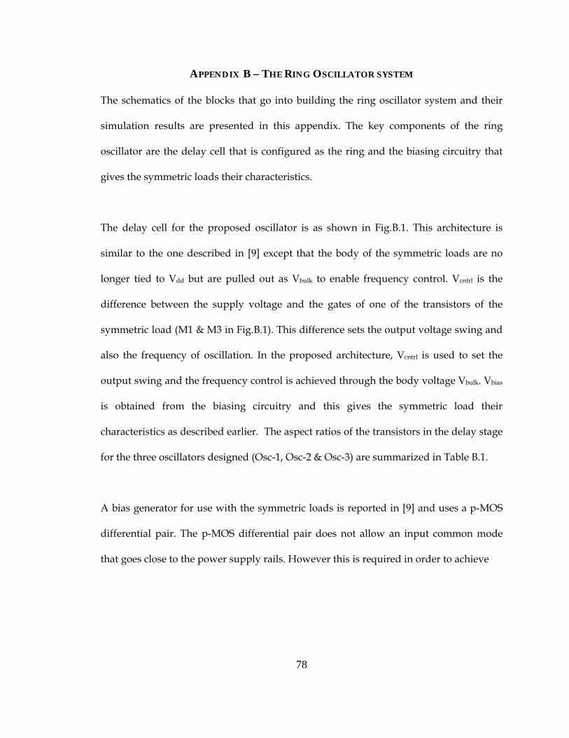
78
APPENDIX B – THE RING OSCILLATOR SYSTEM
The schematics of the blocks that go into building the ring oscillator system and their
simulation results are presented in this appendix. The key components of the ring
oscillator are the delay cell that is configured as the ring and the biasing circuitry that
gives the symmetric loads their characteristics.
The delay cell for the proposed oscillator is as shown in Fig.B.1. This architecture is
similar to the one described in [9] except that the body of the symmetric loads are no
longer tied to Vdd but are pulled out as Vbulk to enable frequency control. Vcntrl is the
difference between the supply voltage and the gates of one of the transistors of the
symmetric load (M1 & M3 in Fig.B.1). This difference sets the output voltage swing and
also the frequency of oscillation. In the proposed architecture, Vcntrl is used to set the
output swing and the frequency control is achieved through the body voltage Vbulk. Vbias
is obtained from the biasing circuitry and this gives the symmetric load their
characteristics as described earlier. The aspect ratios of the transistors in the delay stage
for the three oscillators designed (Osc-1, Osc-2 & Osc-3) are summarized in Table B.1.
A bias generator for use with the symmetric loads is reported in [9] and uses a p-MOS
differential pair. The p-MOS differential pair does not allow an input common mode
that goes close to the power supply rails. However this is required in order to achieve

79
Figure B.1 Delay Cell for the Proposed Oscillator
Table B.1 Aspect Ratios of the Transistors used in the Delay stage of Osc-1 to Osc-3
Oscillator W/L (M1-M4) W/L (M5-M6) W/L (M7)
Osc-1 12µ/1.2µ 8.7µ/3.9µ 7.2µ/1.2µ
Osc-2 12µ/1.2µ 5.7µ/3.3µ 7.2µ/1.2µ
Osc-3 12µ/1.2µ 3.0µ/2.1µ 7.2µ/1.2µ
swings of about 1.5V. This problem is addressed by using an n-MOS differential pair
followed by a p-MOS common source stage as shown in Fig.B.2.
The bias generator consists of a simple OTA (M1-M6 & current source ‘I’), followed by a
p-MOS common source stage (M7-M8) and a half buffer replica (M9–M12). The
transistor M13, configured as a MOS capacitor is connected to the highest impedance

80
node of the circuit in order to provide adequate phase margin to the feedback network.
The OTA and the half buffer replica are connected in a negative feedback fashion such
that the drain of the symmetric load is held constant at Vc (Vdd – Vcntrl). The transistors in
the half buffer replica, as the name suggests are identical in size to the transistors M1,
M2, M5 & M7 of the delay stage in the ring oscillator (refer Fig. B.1). The tail current (ISS)
represents the current that flows through the symmetric load when the drop across the
load is Vcntrl or the voltage at the drain is equal to Vc (Vdd –Vcntrl). With the drain of
transistors M9 & M10 set at Vc, the Opamp adjusts its output such that a current of ISS
flows through M12. This current is mirrored to the delay stage. This setup ensures that
the tail current is set by an identical buffer of the delay stage and most importantly
enables the symmetric load to swing from Vdd to Vdd – Vcntrl. The aspect ratios of the
transistors in the bias generation circuitry are summarized in Table B.2. The W/L ratio
of M11 is identical to that of the n-MOS differential pair transistors of the delay stage. In
Table B.2, the value of M11 is given for the case of Osc-1.
Figure B.2 Bias Generation Circuitry

81
Table B.2 Aspect Ratio for the Transistors of Bias Generation Circuitry
M1/M2 M3/M4 M5/M6 M7 M8/M12 M9/M10 M11 M13
7.5µ/1.5µ 4.5µ/1.8µ 1.5µ/0.6µ 7.5µ/1.5µ 7.2µ/1.2µ 12µ/1.2µ 8.7µ/3.9µ 15µ/12µ
The current reference circuitry is as shown in Fig. B.3. Transistors M1 – M8 represent the
current generation circuitry and transistors M9 – M12 represent the start-up circuitry.
The start-up circuitry is essential because the circuit has a stable operating point with
zero current through it. The start-up circuitry is designed such that it injects current
during initial start-up and is cut-off during normal mode of operation. The operation of
the current reference is well explained in [48].
The current source is designed for 50µA and the value of the resistor is chosen to be 20
squares which turns out to be 20.88KΩ for the process considered. Table B.3 summarizes
the aspect ratios of the transistors used. The simulations were performed across a
temperature range of 0°C - 85°C and also over a power supply range of 4.5V – 5.5V. The
process corners were not available from MOSIS and so simulations were performed
using model parameters extracted during process runs on three different dates (Model-1
[45], Model-2 [46] and Model-3 [47]). Worst-case simulations were performed for each of
the three models specified above by assuming a 20% variation in the value of the
resistors. Also, since the resistor was designed to be 20 squares, the absolute value of the
resistance was calculated from the sheet resistance of the high-resistive poly specified
for each of the processes. Fig.B.4 shows the simulated performance of the current
82
reference for the case of Model-1 and Table B.4 summarizes the worst-case performance
across all the three models.
Figure B.3 Current Reference Circuitry
Table B.3 Aspect Ratios for the Transistors of Current Reference
M1 M2 M3-M8 M9/M10 M11/M12 Resistor (R)
10.5µ/1.2µ 10.5µ/1.2µ 6µ/1.2µ 9µ/1.2µ 3µ/3µ 20 squares
Now, using the current reference in the bias generation circuitry, a stability analysis was
performed. Again the simulation was performed across all the three model parameters
for the worst-case conditions as described above. Fig.B.5 shows the magnitude and
phase of the loop transmission of the feedback system and Table B.5 tabulates the key
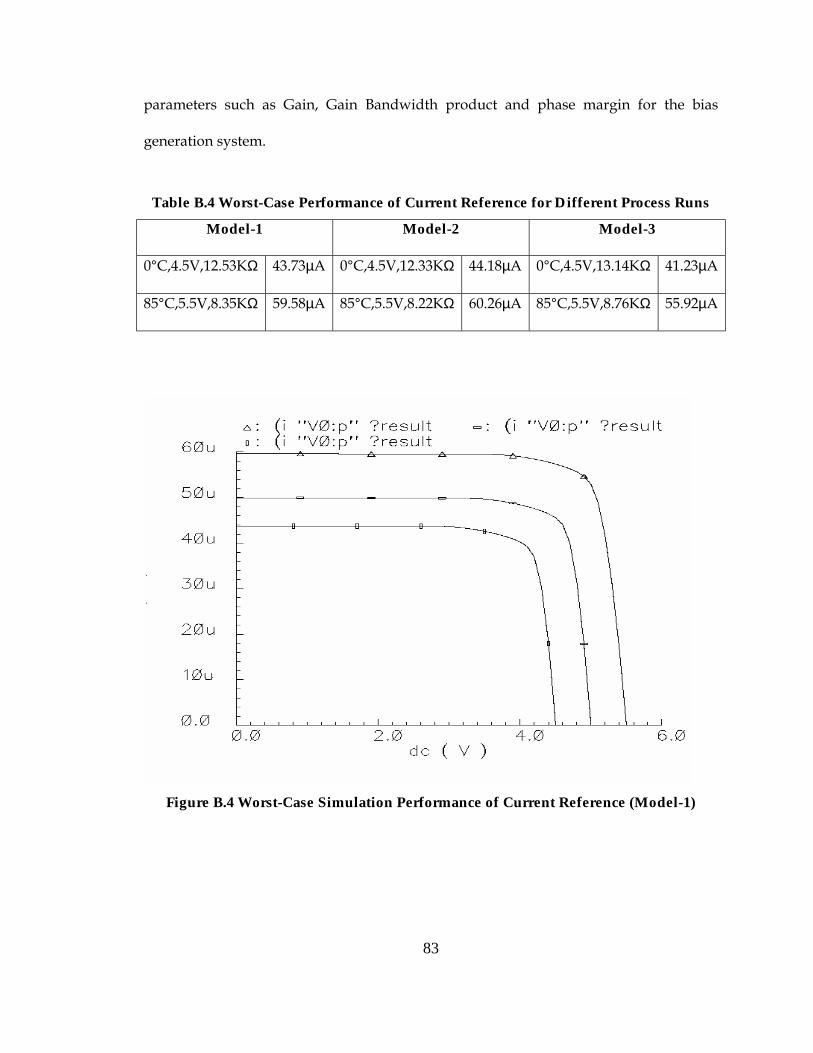
83
parameters such as Gain, Gain Bandwidth product and phase margin for the bias
generation system.
Table B.4 Worst-Case Performance of Current Reference for Different Process Runs
Model-1 Model-2 Model-3
0°C,4.5V,12.53KΩ 43.73µA 0°C,4.5V,12.33KΩ 44.18µA 0°C,4.5V,13.14KΩ 41.23µA
85°C,5.5V,8.35KΩ 59.58µA 85°C,5.5V,8.22KΩ 60.26µA 85°C,5.5V,8.76KΩ 55.92µA
Figure B.4 Worst-Case Simulation Performance of Current Reference (Model-1)

84
Table B.5 Summary of worst-case performance for the Bias Generation Circuitry
Model – 1 Model – 2 Model –3
0°°°°C,4.5V,12.53KΩΩΩΩ 0°°°°C,4.5V,12.33KΩΩΩΩ 0°°°°C,4.5V,13.14KΩΩΩΩ
GBW PM GBW PM GBW PM
64.69MHz 65° 64.46MHz 64.3° 64.32MHz 63.9°
85°°°°C,5.5V,8.35KΩΩΩΩ 85°°°°C,5.5V,8.22KΩΩΩΩ 0°°°°C,5.5V,8.76KΩΩΩΩ
GBW PM GBW PM GBW PM
51.47MHz 55° 51.22MHz 55.2° 51.27MHz 55.9°
Figure B.5 Magnitude & Phase of the Loop Transmission for the Bias Circuitry

85
VVVVITAITAITAITA
Venkatesh Srinivasan was born on the 25th of June 1978 in Madras, India. After his initial
schooling in Salem and Coimbatore, his family moved back to Madras in 1986. He
received his high school diploma from the Hindu Senior Secondary School, Madras in
1995. Interested in an engineering career, he enrolled at Birla Institute of Technology and
Science, Pilani, majoring in Electrical Engineering. During the Fall of ’98, he interned at
Texas Instruments, Bangalore, as a part of the undergraduate curriculum. In June ’99, he
graduated with a Bachelor of Engineering degree in Electrical and Electronics. He then
began his career in the industry and was employed at Wipro Technologies, Bangalore, as
a VLSI/System Design Engineer, where he worked for a year. In Fall 2000, he enrolled at
the University of Tennessee, Knoxville to earn a Master’s in Electrical Engineering. He is
currently working under the supervision of Dr. Syed K. Islam at the Analog VLSI and
Devices Laboratory. He plans to complete his Master’s with a specialization in Analog
IC design in August 2002 and work towards his Ph.D.
Copyright © 2022 FDOKUMEN