Time comparison in image processing: APS sensors versus an artificial retina based vision system
10
IOP PUBLISHING MEASUREMENT SCIENCE AND TECHNOLOGY Meas. Sci. Technol. 18 (2007) 2817–2826 doi:10.1088/0957-0233/18/9/011 Time comparison in image processing: APS sensors versus an artificial retina based vision system A Elouardi, S Bouaziz, A Dupret, L Lacassagne, J O Klein and R Reynaud Fundamental Electronics Institute, Bat. 220, Paris XI University, 91405 Orsay, France E-mail: [email protected] Received 23 November 2006, in final form 6 June 2007 Published 20 July 2007 Online at stacks.iop.org/MST/18/2817 Abstract To resolve the computational complexity of computer vision algorithms, one of the solutions is to perform some low-level image processing on the sensor focal plane. It becomes a smart sensor device called a retina. This concept makes vision systems more compact. It increases performance thanks to the reduction of the data flow exchanges with external circuits. This paper presents a comparison between two different vision system architectures. The first one involves a smart sensor including analogue processors allowing on-chip image processing. An external microprocessor is used to control the on-chip dataflow and integrated operators. The second system implements a logarithmic CMOS/APS sensor interfaced to the same microprocessor, in which all computations are carried out. We have designed two vision systems as proof of concept. The comparison is related to image processing time. Keywords: instrumentation, vision system architecture, retinas, CMOS/APS sensors (Some figures in this article are in colour only in the electronic version) 1. Introduction Intelligent vehicles and robots need sensors with fast response time, low energy consumption and the ability to extract high- level information from the environment [1, 2]. Adding hardware operators near pixels increases the computations potentiality and reduces inputs/outputs operations towards the central processor unit. CCD technology has been the dominant tool for electronic image sensors for several decades due to their high photosensitivity, low fixed pattern noise (FPN), small pixel and large array sizes. However, in the last decade, CMOS (complementary metal oxide semiconductor) sensors drew attention from many researchers and industries due to their low energy dissipation, low cost, on chip processing capabilities and their integration on a standard or quasi-standard VLSI (very large scale integration) process. Still, raw output images acquired by CMOS sensors need further processing, mainly because of noise, blurriness and poor contrast. In order to tackle these problems, image- processing circuits are typically associated with image sensors as a part of the whole vision system. Usually, two areas coexist within the same chip for sensing and preprocessing that are implemented onto the same integrated circuit. Integration of pixel array and image processing circuits on a single monolithic chip makes the system more compact and allows enhancing the behaviour and response of the sensor. Hence, to achieve low-level image processing tasks (early- vision), an artificial retina is a smart sensor which integrates analogue and/or digital processing circuits in the pixel [3, 4] or at the edge of the pixel array [5]. The aim of this paper is to obtain a conclusion on the aptitude of retinas, as smart sensors, to become potential candidates for a system on a chip, consequently to reach an algorithm-architecture adequacy. 0957-0233/07/092817+10$30.00 © 2007 IOP Publishing Ltd Printed in the UK 2817
-
Upload
master-sciences-du-vegetal -
Category
Documents
-
view
4 -
download
0
Transcript of Time comparison in image processing: APS sensors versus an artificial retina based vision system
IOP PUBLISHING MEASUREMENT SCIENCE AND TECHNOLOGY
Meas. Sci. Technol. 18 (2007) 2817–2826 doi:10.1088/0957-0233/18/9/011
Time comparison in image processing:APS sensors versus an artificial retinabased vision systemA Elouardi, S Bouaziz, A Dupret, L Lacassagne, J O Klein andR Reynaud
Fundamental Electronics Institute, Bat. 220, Paris XI University, 91405 Orsay, France
E-mail: [email protected]
Received 23 November 2006, in final form 6 June 2007Published 20 July 2007Online at stacks.iop.org/MST/18/2817
AbstractTo resolve the computational complexity of computer vision algorithms, oneof the solutions is to perform some low-level image processing on the sensorfocal plane. It becomes a smart sensor device called a retina. This conceptmakes vision systems more compact. It increases performance thanks to thereduction of the data flow exchanges with external circuits. This paperpresents a comparison between two different vision system architectures.The first one involves a smart sensor including analogue processors allowingon-chip image processing. An external microprocessor is used to control theon-chip dataflow and integrated operators. The second system implements alogarithmic CMOS/APS sensor interfaced to the same microprocessor, inwhich all computations are carried out. We have designed two visionsystems as proof of concept. The comparison is related to image processingtime.
Keywords: instrumentation, vision system architecture, retinas, CMOS/APSsensors
(Some figures in this article are in colour only in the electronic version)
1. Introduction
Intelligent vehicles and robots need sensors with fast responsetime, low energy consumption and the ability to extract high-level information from the environment [1, 2]. Addinghardware operators near pixels increases the computationspotentiality and reduces inputs/outputs operations towards thecentral processor unit.
CCD technology has been the dominant tool forelectronic image sensors for several decades due to their highphotosensitivity, low fixed pattern noise (FPN), small pixeland large array sizes.
However, in the last decade, CMOS (complementarymetal oxide semiconductor) sensors drew attention from manyresearchers and industries due to their low energy dissipation,low cost, on chip processing capabilities and their integrationon a standard or quasi-standard VLSI (very large scaleintegration) process.
Still, raw output images acquired by CMOS sensors needfurther processing, mainly because of noise, blurriness andpoor contrast. In order to tackle these problems, image-processing circuits are typically associated with image sensorsas a part of the whole vision system. Usually, two areas coexistwithin the same chip for sensing and preprocessing that areimplemented onto the same integrated circuit.
Integration of pixel array and image processing circuits ona single monolithic chip makes the system more compact andallows enhancing the behaviour and response of the sensor.Hence, to achieve low-level image processing tasks (early-vision), an artificial retina is a smart sensor which integratesanalogue and/or digital processing circuits in the pixel [3, 4]or at the edge of the pixel array [5].
The aim of this paper is to obtain a conclusion on theaptitude of retinas, as smart sensors, to become potentialcandidates for a system on a chip, consequently to reach analgorithm-architecture adequacy.
0957-0233/07/092817+10$30.00 © 2007 IOP Publishing Ltd Printed in the UK 2817
A Elouardi et al
We have made a comparison between two differentarchitectures dedicated to a vision system. The first oneimplements a logarithmic APS (active pixel sensor) imagerand a microprocessor. The second involves the samemicroprocessor with a CMOS artificial retina that implementshardware operators and analogue microprocessors. We havedesigned two vision systems. The comparison is related toimage processing time.
2. Review of integrated operators on smart sensors
Different partitions for the architectural implementation of on-chip image processing with CMOS image sensors are proposedin [6]. The partition does not take into account only thecircuit density, but also includes the nature of image processingalgorithms and the choice of the operators integrated in its focalplane with the pixels. The difference between partitions is thelocation of the signal processing unit, known as a processingelement (PE); this location becomes the discriminating factorof the different implementation structures.
Pixel processing, like the approach presented by Dudeckin [8], consists of one processing element (PE) per pixel. Eachpixel typically consists of a photodetector, an active buffer anda signal processing element. Pixel-level processing promisesmany significant advantages, including low power as well asthe ability to adapt image capture and processing to differentenvironments during light integration. However, the popularuse of this design idea has been blocked by severe limitationson pixel size, the low fill factor and the restricted number oftransistors in each PE.
In view of great block partitioning, a global processingunit can be implemented beside the array of pixels. This isone of the obvious integration methods due to its conceptualsimplicity and the flexibility of the parametrization of thedesign features. Each PE is located at the serial output channelat the end of the chip. There are fewer restrictions on theimplementation area of the PE, leading to a high fill factor ofthe pixel and a more flexible design. However, the bottleneckof the processing speed of the chip becomes the operationalspeed of the PE, and therefore, a fast PE is essentially required.The fast speed of the PE potentially results in high complexityof the design [7] and high power consumption of the chip [9].
Another structure is frame memory processing. Amemory array with the same number of pixels as the sensor islocated below the imager array. Typically, the image memoryis an analogue frame memory that requires less complexityof design and processing time [10]. However, this structureconsumes a large area, large power and high fabrication cost.Structures other than the frame memory face difficulty inimplementing temporal storage. The frame memory is themost adequate structure that permits iterative operation andframe operation, critical for some image processing algorithmsin a real time mode.
Even with these disadvantages, smart sensors are stillattractive, mainly because of their effective cost, size and speedwith various on-chip functionalities [11]. Simply, benefitsexist when a camera with a computer is converted into a smallsized vision system on a chip (SoC).
Analog/Digital Processors Vector
CMOS
Activ
e Pix
els Arra
y
Analog/Digital Processors Vector
CMOS
Activ
e Pix
els Arra
y
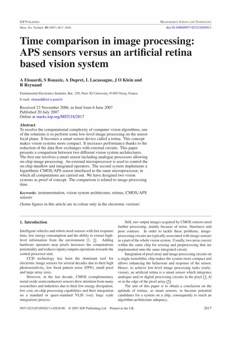
Figure 1. Sensor architecture.
3. Systems description
3.1. An artificial retina based vision system (PARIS-ARM)
3.1.1. Sensor architecture. A PARIS (parallel analogueretina-like image sensor) is an architecture model whichimplements, in the same circuit, an array of pixels,integrating memories and an analogue processor vector[12]. The architecture, shown in figure 1, allows a highdegree of parallelism and a balanced compromise betweencommunication and computations. Indeed, to reduce the areaof the pixels and to increase the fill factor, the image processingis centred on a row of processors. Such an approach presentsthe advantage of enabling the design of complex processingunits without decreasing the resolution. In return, becausethe parallelism is applied to a row of pixels, the computationswhich concern more than one pixel have to be processed in asequential way. However, if a sequential execution increasesthe time of processing for a given operation, it allows a moreflexible process. With this typical readout mechanism of animage, column processing offers the advantages of parallelprocessing that permit high frequency and thus low powerconsumption. Furthermore, it becomes possible to chain basicfunctions in an arbitrary order, as in any digital SIMD (singleinstruction–multiple data) machine. The resulting low-levelinformation extracted by this can then be processed by amicroprocessor.
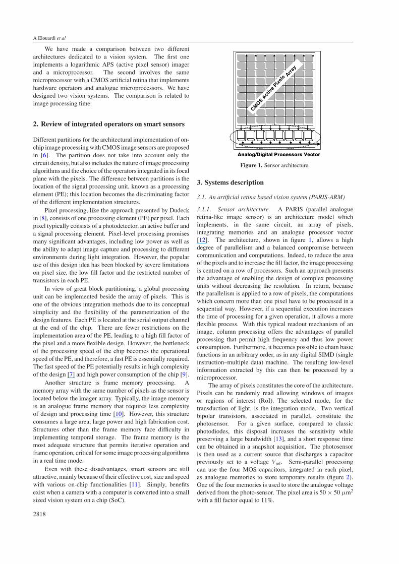
The array of pixels constitutes the core of the architecture.Pixels can be randomly read allowing windows of imagesor regions of interest (RoI). The selected mode, for thetransduction of light, is the integration mode. Two verticalbipolar transistors, associated in parallel, constitute thephotosensor. For a given surface, compared to classicphotodiodes, this disposal increases the sensitivity whilepreserving a large bandwidth [13], and a short response timecan be obtained in a snapshot acquisition. The photosensoris then used as a current source that discharges a capacitorpreviously set to a voltage Vref. Semi-parallel processingcan use the four MOS capacitors, integrated in each pixel,as analogue memories to store temporary results (figure 2).One of the four memories is used to store the analogue voltagederived from the photo-sensor. The pixel area is 50 × 50 µm2
with a fill factor equal to 11%.
2818
Time comparison in image processing: APS sensors versus an artificial retina based vision system
Figure 2. Pixel scheme (OTA: operational transconductanceamplifier).
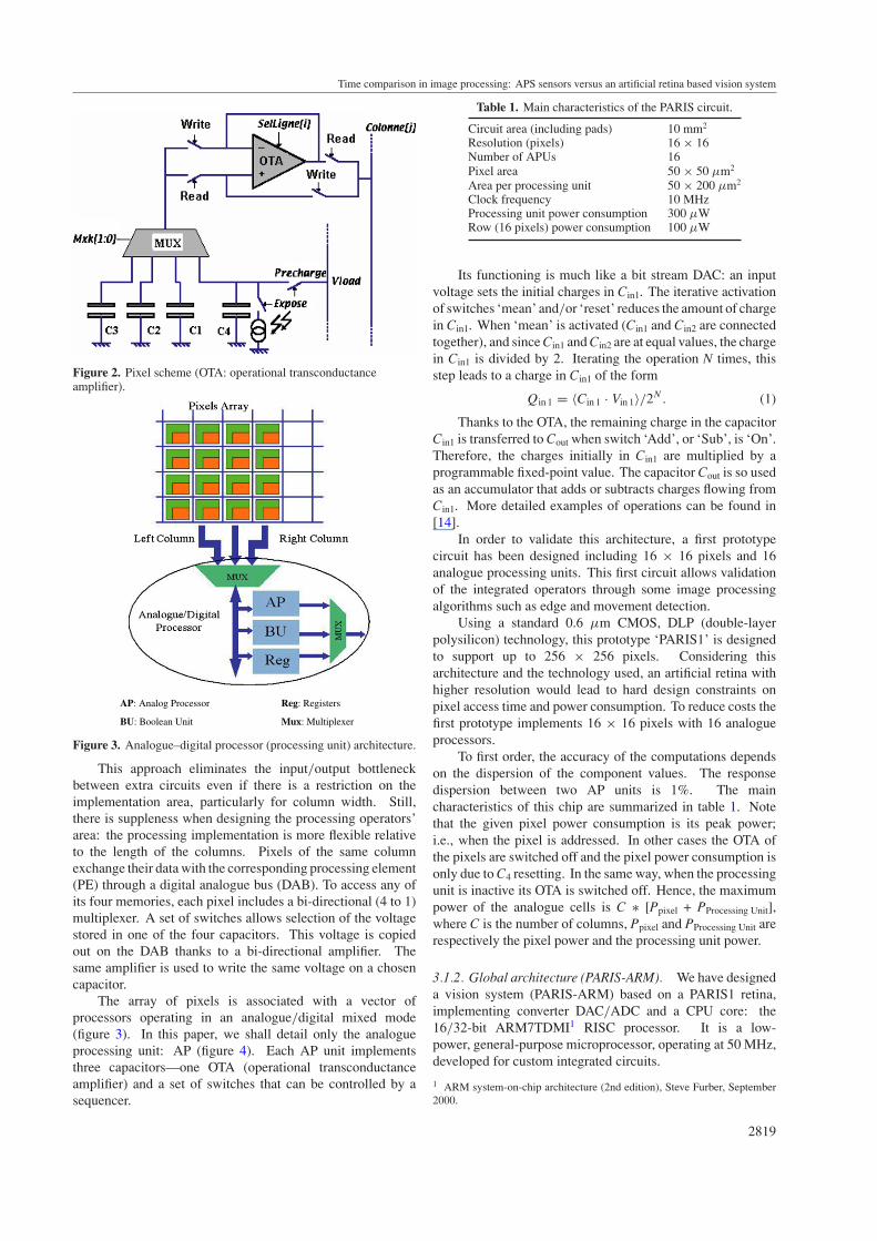
AP: Analog Processor
BU: Boolean Unit
Reg: Registers
Mux: Multiplexer
Figure 3. Analogue–digital processor (processing unit) architecture.
This approach eliminates the input/output bottleneckbetween extra circuits even if there is a restriction on theimplementation area, particularly for column width. Still,there is suppleness when designing the processing operators’area: the processing implementation is more flexible relativeto the length of the columns. Pixels of the same columnexchange their data with the corresponding processing element(PE) through a digital analogue bus (DAB). To access any ofits four memories, each pixel includes a bi-directional (4 to 1)multiplexer. A set of switches allows selection of the voltagestored in one of the four capacitors. This voltage is copiedout on the DAB thanks to a bi-directional amplifier. Thesame amplifier is used to write the same voltage on a chosencapacitor.
The array of pixels is associated with a vector ofprocessors operating in an analogue/digital mixed mode(figure 3). In this paper, we shall detail only the analogueprocessing unit: AP (figure 4). Each AP unit implementsthree capacitors—one OTA (operational transconductanceamplifier) and a set of switches that can be controlled by asequencer.
Table 1. Main characteristics of the PARIS circuit.
Circuit area (including pads) 10 mm2
Resolution (pixels) 16 × 16Number of APUs 16Pixel area 50 × 50 µm2
Area per processing unit 50 × 200 µm2
Clock frequency 10 MHzProcessing unit power consumption 300 µWRow (16 pixels) power consumption 100 µW
Its functioning is much like a bit stream DAC: an inputvoltage sets the initial charges in Cin1. The iterative activationof switches ‘mean’ and/or ‘reset’ reduces the amount of chargein Cin1. When ‘mean’ is activated (Cin1 and Cin2 are connectedtogether), and since Cin1 and Cin2 are at equal values, the chargein Cin1 is divided by 2. Iterating the operation N times, thisstep leads to a charge in Cin1 of the form
Qin 1 = 〈Cin 1 · Vin 1〉/2N. (1)
Thanks to the OTA, the remaining charge in the capacitorCin1 is transferred to Cout when switch ‘Add’, or ‘Sub’, is ‘On’.Therefore, the charges initially in Cin1 are multiplied by aprogrammable fixed-point value. The capacitor Cout is so usedas an accumulator that adds or subtracts charges flowing fromCin1. More detailed examples of operations can be found in[14].
In order to validate this architecture, a first prototypecircuit has been designed including 16 × 16 pixels and 16analogue processing units. This first circuit allows validationof the integrated operators through some image processingalgorithms such as edge and movement detection.
Using a standard 0.6 µm CMOS, DLP (double-layerpolysilicon) technology, this prototype ‘PARIS1’ is designedto support up to 256 × 256 pixels. Considering thisarchitecture and the technology used, an artificial retina withhigher resolution would lead to hard design constraints onpixel access time and power consumption. To reduce costs thefirst prototype implements 16 × 16 pixels with 16 analogueprocessors.
To first order, the accuracy of the computations dependson the dispersion of the component values. The responsedispersion between two AP units is 1%. The maincharacteristics of this chip are summarized in table 1. Notethat the given pixel power consumption is its peak power;i.e., when the pixel is addressed. In other cases the OTA ofthe pixels are switched off and the pixel power consumption isonly due to C4 resetting. In the same way, when the processingunit is inactive its OTA is switched off. Hence, the maximumpower of the analogue cells is C ∗ [Ppixel + PProcessing Unit],where C is the number of columns, Ppixel and PProcessing Unit arerespectively the pixel power and the processing unit power.
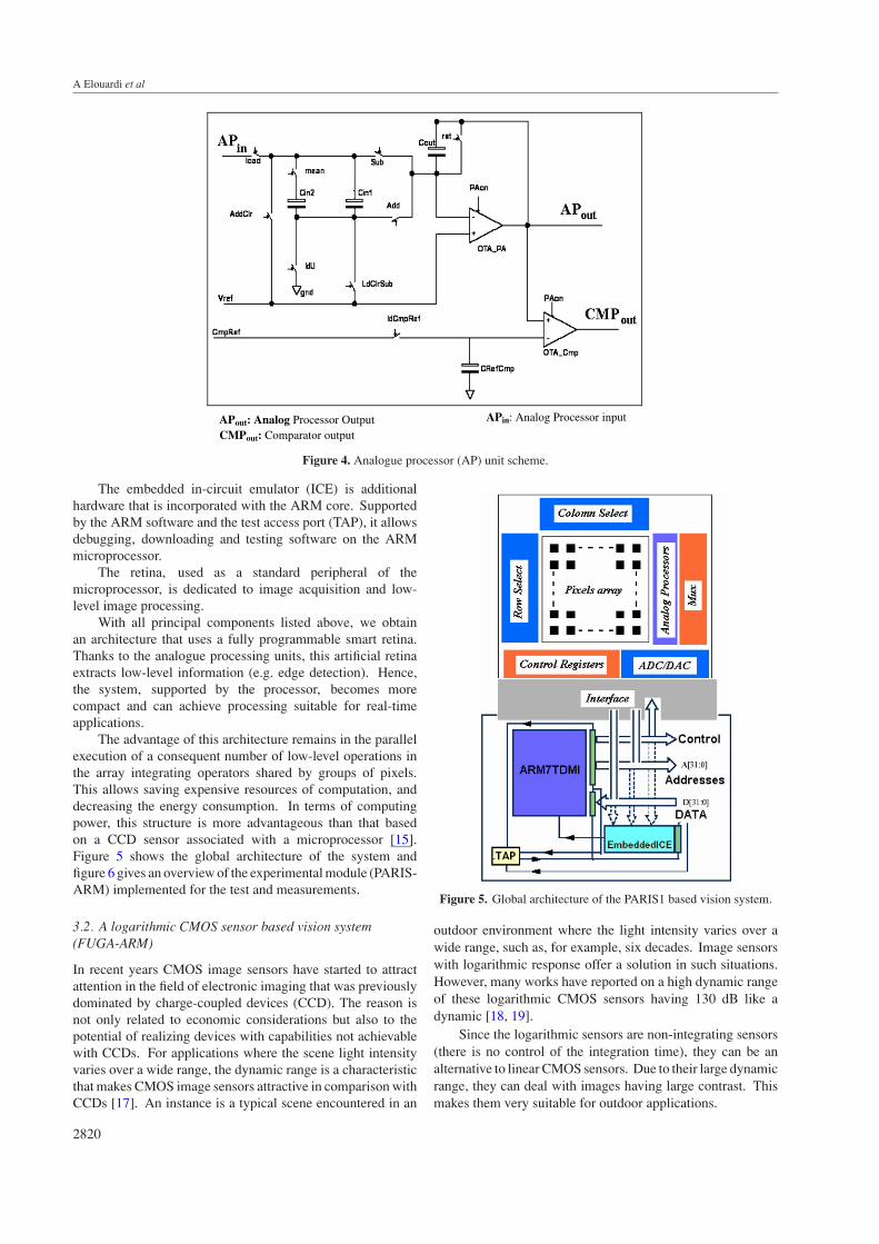
3.1.2. Global architecture (PARIS-ARM). We have designeda vision system (PARIS-ARM) based on a PARIS1 retina,implementing converter DAC/ADC and a CPU core: the16/32-bit ARM7TDMI1 RISC processor. It is a low-power, general-purpose microprocessor, operating at 50 MHz,developed for custom integrated circuits.
1 ARM system-on-chip architecture (2nd edition), Steve Furber, September2000.
2819
A Elouardi et al
APout: Analog Processor Output CMPout: Comparator output
APin: Analog Processor input
Figure 4. Analogue processor (AP) unit scheme.
The embedded in-circuit emulator (ICE) is additionalhardware that is incorporated with the ARM core. Supportedby the ARM software and the test access port (TAP), it allowsdebugging, downloading and testing software on the ARMmicroprocessor.
The retina, used as a standard peripheral of themicroprocessor, is dedicated to image acquisition and low-level image processing.
With all principal components listed above, we obtainan architecture that uses a fully programmable smart retina.Thanks to the analogue processing units, this artificial retinaextracts low-level information (e.g. edge detection). Hence,the system, supported by the processor, becomes morecompact and can achieve processing suitable for real-timeapplications.
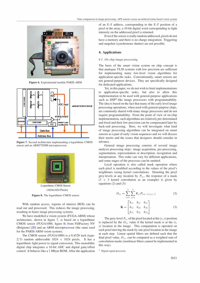
The advantage of this architecture remains in the parallelexecution of a consequent number of low-level operations inthe array integrating operators shared by groups of pixels.This allows saving expensive resources of computation, anddecreasing the energy consumption. In terms of computingpower, this structure is more advantageous than that basedon a CCD sensor associated with a microprocessor [15].Figure 5 shows the global architecture of the system andfigure 6 gives an overview of the experimental module (PARIS-ARM) implemented for the test and measurements.
3.2. A logarithmic CMOS sensor based vision system(FUGA-ARM)
In recent years CMOS image sensors have started to attractattention in the field of electronic imaging that was previouslydominated by charge-coupled devices (CCD). The reason isnot only related to economic considerations but also to thepotential of realizing devices with capabilities not achievablewith CCDs. For applications where the scene light intensityvaries over a wide range, the dynamic range is a characteristicthat makes CMOS image sensors attractive in comparison withCCDs [17]. An instance is a typical scene encountered in an
Figure 5. Global architecture of the PARIS1 based vision system.
outdoor environment where the light intensity varies over awide range, such as, for example, six decades. Image sensorswith logarithmic response offer a solution in such situations.However, many works have reported on a high dynamic rangeof these logarithmic CMOS sensors having 130 dB like adynamic [18, 19].
Since the logarithmic sensors are non-integrating sensors(there is no control of the integration time), they can be analternative to linear CMOS sensors. Due to their large dynamicrange, they can deal with images having large contrast. Thismakes them very suitable for outdoor applications.
2820
Time comparison in image processing: APS sensors versus an artificial retina based vision system
Figure 6. Experimental module PARIS-ARM.
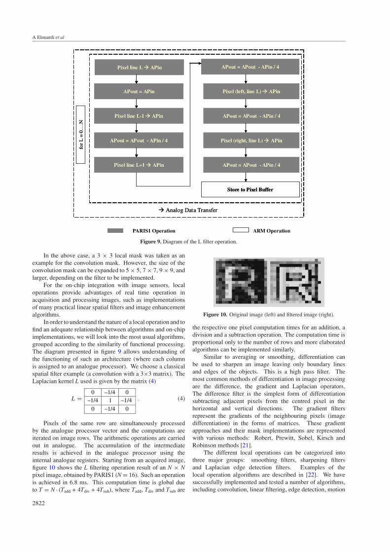
Figure 7. Second architecture implementing a logarithmic CMOSsensor and an ARM7TDMI microprocessor.
Logarithmic CMOS Sensor
(1024x1024 Pixels)
Figure 8. The logarithmic CMOS sensor.
With random access, regions of interest (ROI) can beread out and processed. This reduces the image processing,resulting in faster image processing systems.
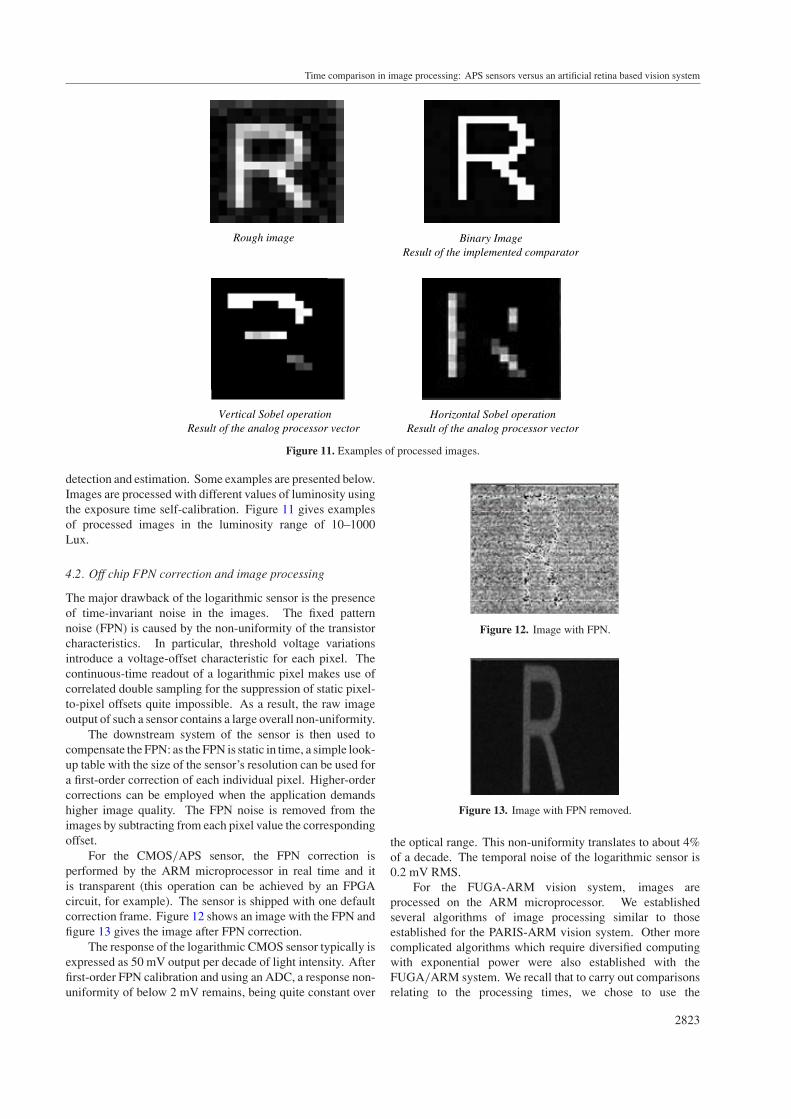
We have modelled a vision system (FUGA-ARM) whosearchitecture, shown in figure 7, is based on a logarithmicCMOS sensor (FUGA1000, figure 8) from FillFactory NV(Belgium) [20] and an ARM microprocessor (the same usedfor the PARIS-ARM vision system).
The CMOS sensor (FUGA1000) is a 0.4528 inch (type-2/3) random addressable 1024 × 1024 pixels. It has alogarithmic light power to signal conversion. This monolithicdigital chip integrates a 10-bit ADC and digital gain/offsetcontrol. It behaves like a 1 Mbyte ROM. After the application
of an X–Y address, corresponding to the X–Y position of apixel in the array, a 10-bit digital word corresponding to lightintensity on the addressed pixel is returned.
Even if the sensor is really random addressed, pixels do nothave a memory and there is no charge integration. Triggeringand snapshot (synchronous shutter) are not possible.
4. Applications
4.1. On chip image processing
The basis of the smart vision system on chip concept isthat analogue VLSI systems with low precision are sufficientfor implementing many low-level vision algorithms forapplication-specific tasks. Conventionally, smart sensors arenot general-purpose devices. They are specifically designedfor dedicated applications.
Yet, in this paper, we do not wish to limit implementationsto application-specific tasks, but also to allow thisimplementation to be used with general-purpose applicationssuch as DSP2-like image processors with programmability.The idea is based on the fact that many of the early level imageprocessing operations, when used with general-purpose chips,are commonly shared with many image processors and do notrequire programmability. From the point of view of on-chipimplementation, such algorithms are relatively pre-determinedand fixed and their low precision can be compensated later byback-end processing. Here, we will investigate what kindof image processing algorithms can be integrated on smartsensors as a part of early vision sequences and we will discusstheir merits and the issues that designers should consider inadvance.
General image processing consists of several imageanalysis processing steps: image acquisition, pre-processing,segmentation, representation or description, recognition andinterpretation. This order can vary for different applications,and some stages of the processes can be omitted.
Local operation is also called mask operation whereeach pixel is modified according to the values of the pixel’sneighbours (using kernel convolution). Denoting the pixelgrey-levels at any location by Pxy , the response of a mask(3 × 3 kernel convolution as an example) is given byequations (2) and (3):
Oxy =3∑
i=1
3∑j=1
KijPx+i−2,y+j−2 (2)
K =
k11 k21 k31
k12 k22 k32
k13 k23 k33
. (3)
The grey-level Pxy of the pixel located at the (x, y) positionis replaced by the Oxy value if the kernel mask is at the (x,y) location in the image. This computation is operated oneach pixel moving the mask by one pixel location in the imageat each step. Linear spatial filters are defined such that thefinal pixel value, Oxy , can be computed as a weighted sum ofconvolution masks (nonlinear filters cannot be implemented inthis way).
2 Digital signal processor.
2821
A Elouardi et al
Pixel line L APin
APout = APin
Pixel line L-1 APin
APout = APout - APin / 4
Pixel line L+1 APin
APout = APout - APin / 4
Pixel (left, line L) APin
APout = APout - APin / 4
Pixel (right, line L) APin
APout = APout - APin / 4
Store to Pixel Buffer
for
L =
0…
.N
PARIS1 Operation ARM Operation
Analog Data Transfer
Pixel line L APin
APout = APin
Pixel line L-1 APin
APout = APout - APin / 4
Pixel line L+1 APin
APout = APout - APin / 4
Pixel (left, line L) APin
APout = APout - APin / 4
Pixel (right, line L) APin
APout = APout - APin / 4
Store to Pixel Buffer
for
L =
0…
.N
Analog Data Transfer
Figure 9. Diagram of the L filter operation.
In the above case, a 3 × 3 local mask was taken as anexample for the convolution mask. However, the size of theconvolution mask can be expanded to 5 × 5, 7 × 7, 9 × 9, andlarger, depending on the filter to be implemented.
For the on-chip integration with image sensors, localoperations provide advantages of real time operation inacquisition and processing images, such as implementationsof many practical linear spatial filters and image enhancementalgorithms.
In order to understand the nature of a local operation and tofind an adequate relationship between algorithms and on-chipimplementations, we will look into the most usual algorithms,grouped according to the similarity of functional processing.The diagram presented in figure 9 allows understanding ofthe functioning of such an architecture (where each columnis assigned to an analogue processor). We choose a classicalspatial filter example (a convolution with a 3×3 matrix). TheLaplacian kernel L used is given by the matrix (4)
L =0 –1/4 0
–1/4 1 –1/4
0 –1/4 0
. (4)
Pixels of the same row are simultaneously processedby the analogue processor vector and the computations areiterated on image rows. The arithmetic operations are carriedout in analogue. The accumulation of the intermediateresults is achieved in the analogue processor using theinternal analogue registers. Starting from an acquired image,figure 10 shows the L filtering operation result of an N × Npixel image, obtained by PARIS1 (N = 16). Such an operationis achieved in 6.8 ms. This computation time is global dueto T = N · (Tadd + 4Tdiv + 4Tsub), where Tadd, Tdiv and Tsub are
Figure 10. Original image (left) and filtered image (right).
the respective one pixel computation times for an addition, adivision and a subtraction operation. The computation time isproportional only to the number of rows and more elaboratedalgorithms can be implemented similarly.
Similar to averaging or smoothing, differentiation canbe used to sharpen an image leaving only boundary linesand edges of the objects. This is a high pass filter. Themost common methods of differentiation in image processingare the difference, the gradient and Laplacian operators.The difference filter is the simplest form of differentiationsubtracting adjacent pixels from the centred pixel in thehorizontal and vertical directions. The gradient filtersrepresent the gradients of the neighbouring pixels (imagedifferentiation) in the forms of matrices. These gradientapproaches and their mask implementations are representedwith various methods: Robert, Prewitt, Sobel, Kirsch andRobinson methods [21].
The different local operations can be categorized intothree major groups: smoothing filters, sharpening filtersand Laplacian edge detection filters. Examples of thelocal operation algorithms are described in [22]. We havesuccessfully implemented and tested a number of algorithms,including convolution, linear filtering, edge detection, motion
2822
Time comparison in image processing: APS sensors versus an artificial retina based vision system
Rough image Binary ImageResult of the implemented comparator
Vertical Sobel operationResult of the analog processor vector
Horizontal Sobel operationResult of the analog processor vector
Figure 11. Examples of processed images.
detection and estimation. Some examples are presented below.Images are processed with different values of luminosity usingthe exposure time self-calibration. Figure 11 gives examplesof processed images in the luminosity range of 10–1000Lux.
4.2. Off chip FPN correction and image processing
The major drawback of the logarithmic sensor is the presenceof time-invariant noise in the images. The fixed patternnoise (FPN) is caused by the non-uniformity of the transistorcharacteristics. In particular, threshold voltage variationsintroduce a voltage-offset characteristic for each pixel. Thecontinuous-time readout of a logarithmic pixel makes use ofcorrelated double sampling for the suppression of static pixel-to-pixel offsets quite impossible. As a result, the raw imageoutput of such a sensor contains a large overall non-uniformity.
The downstream system of the sensor is then used tocompensate the FPN: as the FPN is static in time, a simple look-up table with the size of the sensor’s resolution can be used fora first-order correction of each individual pixel. Higher-ordercorrections can be employed when the application demandshigher image quality. The FPN noise is removed from theimages by subtracting from each pixel value the correspondingoffset.
For the CMOS/APS sensor, the FPN correction isperformed by the ARM microprocessor in real time and itis transparent (this operation can be achieved by an FPGAcircuit, for example). The sensor is shipped with one defaultcorrection frame. Figure 12 shows an image with the FPN andfigure 13 gives the image after FPN correction.
The response of the logarithmic CMOS sensor typically isexpressed as 50 mV output per decade of light intensity. Afterfirst-order FPN calibration and using an ADC, a response non-uniformity of below 2 mV remains, being quite constant over
Figure 12. Image with FPN.
Figure 13. Image with FPN removed.
the optical range. This non-uniformity translates to about 4%of a decade. The temporal noise of the logarithmic sensor is0.2 mV RMS.
For the FUGA-ARM vision system, images areprocessed on the ARM microprocessor. We establishedseveral algorithms of image processing similar to thoseestablished for the PARIS-ARM vision system. Other morecomplicated algorithms which require diversified computingwith exponential power were also established with theFUGA/ARM system. We recall that to carry out comparisonsrelating to the processing times, we chose to use the
2823
A Elouardi et al
Horizontal Smoothing (H)
Vertical Smoothing (V)
Smoothing (HV)
Vertical Sobel (H)
Horizontal Sobel (V)
Sobel (HV)
Figure 14. Examples of image processing implemented with theFUGA1000 sensor based vision system.
same processor (ARM7TDMI) for the different implementedsystems.
The filter we used has been designed by Garcia Lorca[23]. This filter is a simplification of the Deriche filter [24],the recursive implementation of the optimal Canny filter. Thesmoother is applied horizontally and vertically on the image,in a serial way. Then a derivator is applied. The Garcia Lorcaderivator is, after simplification of Deriche, derivator, a 3 × 3convolution kernel instead of a recursive derivator,
y(n) = (1 − λ)2 · x(n) + 2λ · y(n − 1) − λ2 · y(n − 2) (5)
y(n) = (1 − γ )2x(n) + 2γy(n − 1) − γ 2y(n − 2), (6)
with
γ = e−α. (7)
Here x(n) is the pixel source value, y(n) is the pixel destinationvalue and n is the pixel index in a one-dimensional tablerepresenting the image. γ is an exponential parameterallowing much more filtering flexibility, depending on thenoise within the image. If the image is very noisy weuse a very smoothing filter: α = [0.5, 0.7]; otherwise weuse bigger values of α: α = [0.8, 1.0]. Figure 14 givesexamples of smoothing and derivator filters implemented withthe FUGA-ARM vision system and applied to 120 × 120 pixelimages.
5. Time comparison in image processing
The aim is to compare the vision system implementing thelogarithmic CMOS imager (FUGA-ARM) with the one basedon the PARIS retina (PARIS-ARM). This comparison is relatedto image processing time and does not take into account theexposure time for which we developed a continuous auto-calibration algorithm that can manage this state for our visionsystem. This avoids pixel saturation and gives an adaptiveamplification of pixel output, which is necessary for post-processing.
The calibration concept is based on the fact that whenusing a photo-sensor in an integration mode, a constantluminosity leads to a voltage drop that varies according to
0.0E+00
1.0E+05
2.0E+05
3.0E+05
4.0E+05
5.0E+05
6.0E+05
7.0E+05
8.0E+05
9.0E+05
1.0E+06
0 100 200 300 400 500 600Square sensor pixel resolution: N
Pro
cess
ing
Tim
e (µ
s)
Processing time ARM/PARISProcessing time ARM/Logarithmic CMOS Sensor
Figure 15. Processing time of an edge detection: PARIS-ARMarchitecture versus ARM/logarithmic CMOS sensor.
the exposure time. If the luminosity is high, the exposuretime must be decreased; on the other hand if the luminosity islow the exposure time should be increased. One should thenaim at lower exposure time to have faster image processingalgorithms.
We have used a Laplacian edge detection algorithmand a Sobel filter algorithm to take several measurementsof the computation times relating to the two architecturesdescribed below. For the artificial retina based system, thesecomputations are carried out by the analogue processorsintegrated on-chip. For the FUGA-ARM system, thesecomputations are carried out by the ARM microprocessor.
The two computation time graphics presented infigure 15 translate the diverse computing times for differentsquare sensor pixel resolutions for both systems. It issignificant to note that the acquisition time of the frames isnot included in these measurements in order to evaluate justthe data processing computing time. Times relating to thePARIS artificial retina were obtained by extension of the dataprocessing timing obtained from those of the first prototype[12].
We deduce that the computation time for the FUGA-ARMsystem varies according to the pixel number N2 (quadraticform). Hence, the computation time for the PARIS-ARMsystem varies according to the row number N (linear form)thanks to the analogue processor vector.
Equation (8) gives the definition of the CPP (cycle perpixel) of a processor.
FCLK is the processor frequency, T is the time computing,L is the row number and C is the column number:
CPP = T × FCLK
L × C. (8)
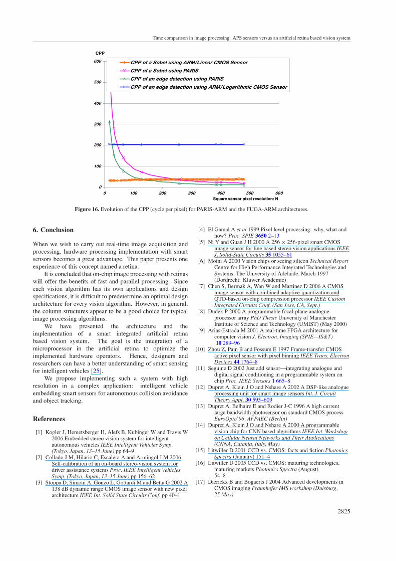
Figure 16 shows the evolution of the CPP for the PARIS-ARM system and FUGA-ARM system.
Consequently, the microcontroller of the FUGA-ARMsystem carries out a uniform CPP relative to regular imageprocessing independently of the number of processed pixels.For the PARIS-ARM system, the CPP factor is inverselyproportional to the row number (N).
As a result, our implementation demonstrates theadvantages of the single chip solution. Applications involvingimage processing algorithms will be less complex and efficientespecially for high resolution.
2824
Time comparison in image processing: APS sensors versus an artificial retina based vision system
0
100
200
300
400
500
600
0 100 200 300 400 500 600Square sensor pixel resolution: N
CPP
CPP of a Sobel using ARM/Linear CMOS Sensor
CPP of a Sobel using PARIS
CPP of an edge detection using PARIS
CPP of an edge detection using ARM/Logarithmic CMOS Sensor
Figure 16. Evolution of the CPP (cycle per pixel) for PARIS-ARM and the FUGA-ARM architectures.
6. Conclusion
When we wish to carry out real-time image acquisition andprocessing, hardware processing implementation with smartsensors becomes a great advantage. This paper presents oneexperience of this concept named a retina.
It is concluded that on-chip image processing with retinaswill offer the benefits of fast and parallel processing. Sinceeach vision algorithm has its own applications and designspecifications, it is difficult to predetermine an optimal designarchitecture for every vision algorithm. However, in general,the column structures appear to be a good choice for typicalimage processing algorithms.
We have presented the architecture and theimplementation of a smart integrated artificial retinabased vision system. The goal is the integration of amicroprocessor in the artificial retina to optimize theimplemented hardware operators. Hence, designers andresearchers can have a better understanding of smart sensingfor intelligent vehicles [25].
We propose implementing such a system with highresolution in a complex application: intelligent vehicleembedding smart sensors for autonomous collision avoidanceand object tracking.
References
[1] Kogler J, Hemetsberger H, Alefs B, Kubinger W and Travis W2006 Embedded stereo vision system for intelligentautonomous vehicles IEEE Intelligent Vehicles Symp.(Tokyo, Japan, 13–15 June) pp 64–9
[2] Collado J M, Hilario C, Escalera A and Armingol J M 2006Self-calibration of an on-board stereo-vision system fordriver assistance systems Proc. IEEE Intelligent VehiclesSymp. (Tokyo, Japan, 13–15 June) pp 156–62
[3] Stoppa D, Simoni A, Gonzo L, Gottardi M and Betta G 2002 A138 dB dynamic range CMOS image sensor with new pixelarchitecture IEEE Int. Solid State Circuits Conf. pp 40–1
[4] El Gamal A et al 1999 Pixel level processing: why, what andhow? Proc. SPIE 3650 2–13
[5] Ni Y and Guan J H 2000 A 256 × 256-pixel smart CMOSimage sensor for line based stereo vision applications IEEEJ. Solid-State Circuits 35 1055–61
[6] Moini A 2000 Vision chips or seeing silicon Technical ReportCentre for High Performance Integrated Technologies andSystems, The University of Adelaide, March 1997(Dordrecht: Kluwer Academic)
[7] Chen S, Bermak A, Wan W and Martinez D 2006 A CMOSimage sensor with combined adaptive-quantization andQTD-based on-chip compression processor IEEE CustomIntegrated Circuits Conf. (San Jose, CA, Sept.)
[8] Dudek P 2000 A programmable focal-plane analogueprocessor array PhD Thesis University of ManchesterInstitute of Science and Technology (UMIST) (May 2000)
[9] Arias-Estrada M 2001 A real-time FPGA architecture forcomputer vision J. Electron. Imaging (SPIE—IS&T)10 289–96
[10] Zhou Z, Pain B and Fossum E 1997 Frame-transfer CMOSactive pixel sensor with pixel binning IEEE Trans. ElectronDevices 44 1764–8
[11] Seguine D 2002 Just add sensor—integrating analogue anddigital signal conditioning in a programmable system onchip Proc. IEEE Sensors 1 665–8
[12] Dupret A, Klein J O and Nshare A 2002 A DSP-like analogueprocessing unit for smart image sensors Int. J. CircuitTheory Appl. 30 595–609
[13] Dupret A, Belhaire E and Rodier J-C 1996 A high currentlarge bandwidth photosensor on standard CMOS processEuroOpto’96, AFPAEC (Berlin)
[14] Dupret A, Klein J O and Nshare A 2000 A programmablevision chip for CNN based algorithms IEEE Int. Workshopon Cellular Neural Networks and Their Applications(CNNA, Catania, Italy, May)
[15] Litwiller D 2001 CCD vs. CMOS: facts and fiction PhotonicsSpectra (January) 151–4
[16] Litwiller D 2005 CCD vs. CMOS: maturing technologies,maturing markets Photonics Spectra (August)54–8
[17] Dierickx B and Bogaerts J 2004 Advanced developments inCMOS imaging Fraunhofer IMS workshop (Duisburg,25 May)
2825

A Elouardi et al
[18] Loose M, Meier K and Schemmel J 1998 CMOS image sensorwith logarithmic response and self calibrating fixed patternnoise correction Proc. SPIE 3410 117–27
[19] Choubey B et al 2006 An electronic-calibration scheme forlogarithmic CMOS pixels IEEE Sensors J. 6 no 4
[20] FUGA1000-EVB from FillFactory: http://www.framos.co.uk/news/newsletter/Notes0301.pdf
[21] Bovik A (ed) 2000 Handbook of Image & Video Processing(San Diego, CA: Academic)
[22] Blanchet G and Charbit M 2005 Digital Signal and ImageProcessing Using Matlab (London: Iste)
[23] Deriche R 1990 Fast algorithms for low level-vision IEEETrans. Pattern Anal. Mach. Intell. 12 78–88
[24] Garcia Lorca F, Kessal L and Demigny D 1997 Efficient ASICand FPGA implementation of IIR filters for real time edgedetections Proc. Int. Conf. on Image Processing (IEEEICIP)
[25] Elouardi A, Bouaziz S, Dupret A, Lacassagne L, Klein J Oand Reynaud R 2006 A smart sensor for imageprocessing: towards a system on chip IEEE Int. Symp.on Industrial Electronics (Montreal, Canada,9–12 July)
2826