
Novel method for patterned fabric inspection using Bollinger ...
Upload
independentCategory
view
0download
0
1TtmrslnTamoo(m+=fiw
e[tmwscsctrb
810 J. Opt. Soc. Am. B/Vol. 25, No. 5 /May 2008 Buss et al.
Three-dimensional numerical modeling ofemission from InSb light-emitting diodes with
patterned surfaces
I. J. Buss,1,* G. R. Nash,1,2 J. G. Rarity,1 and M. J. Cryan1
1Department of Electrical and Electronic Engineering, Photonics Group, University of Bristol,Bristol, BS8 1UB, UK
2QinetiQ, Malvern Technology Centre, Malvern, WR14 3PS, UK*Corresponding author: [email protected]
Received November 26, 2007; accepted February 7, 2008;posted March 18, 2008 (Doc. ID 90095); published April 28, 2008
Full 3D numerical modeling is undertaken on light-emitting diode structures with patterned surfaces repre-sented by regular, pseudorandomly disordered, and uniformly distributed random arrays of square holes toinvestigate both grating and random scattering phenomena. Unlike typical roughened surface LEDs, no recy-cling mirror is present below the source, enabling straightforward implementation in existing device designs.The period or feature width of the arrays is varied and the output emission intensity calculated. A maximumenhancement factor of �2 is seen for both a disordered pattern with an array period of 1.7 �m and patterndepth of 0.4 �m and a particular random pattern with a feature width of 0.85 �m and depth of 0.4 �m. Theenhancement is believed to be due to mitigation of both total internal reflection and Fresnel reflection phe-nomena at the semiconductor–air interface. © 2008 Optical Society of America
OCIS codes: 250.3140, 240.5770.
abGdc[
esp(fesncttswp
2PMtwcerc
. INTRODUCTIONhe poor extraction efficiencies associated with conven-ional light-emitting diodes (LEDs) have been well docu-ented since their inception [1]. The large difference in
efractive index between the emissive material and itsurrounding medium results in a large proportion of theight being trapped within the device through total inter-al reflection (TIR) and Fresnel reflection phenomena.he proportion of light that may escape after TIR may bepproximated by 1/4n2, which for most semiconductoraterial systems �n�3� implies an extraction efficiency
f �3% [2]. Fresnel reflection leads to a further reductionf 4n / �n+1�2 for light incident within the escape conenormal incidence assumed) [3]. This gives an approxi-ate rule of thumb for the external efficiency of 1/n�n1�2; in the midinfrared InSb material system (�03–5 �m, n=3.96) this rule implies a total extraction ef-ciency of �1%, leaving almost all of the light trappedithin the device.Several methods have arisen to maximize the external
fficiency of a device, many of which are outlined in2,4,5]. These include adding a highly reflective surface tohe rear of the device such as distributed Bragg reflectors,etal mirrors, and omnidirectional reflectors; using whate believe to be novel chip geometries, such as hemi-
pherical shaped dies or truncated inverted pyramids;reating resonant cavities to alter the spontaneous emis-ion parameters of the emitters; employing microma-hined optical concentrators [6,7]; and using surface pat-erning via 2D photonic crystal patterns or surfaceoughening. In principle, the Fresnel reflection can easilye reduced at a given wavelength by adding a thin-film
0740-3224/08/050810-8/$15.00 © 2
ntireflection (AR) layer to the surface, and these haveeen applied at midinfrared wavelengths in HgCdTe- andaSb-based devices [8,9]. In the past work has also beenone with monolithic subwavelength gratings that artifi-ially create an exact effective refractive index medium10,11].
In this paper we perform a detailed study focusing onnhancement in a midinfrared InSb-based device throughurface roughening/patterning of three different types: (i)eriodic gratings, (ii) periodic disordered gratings, andiii) uniformly distributed random patterns. We presentull 3D modeling results exhibiting greater than twofoldnhancement in near-field emission intensity. In the ab-ence of the recycling mirror, it is believed that a combi-ation of grating effects and an effective matching layerreated by the pattern leads to enhanced emission. Al-hough the modeling methods employed here are appliedo the midinfrared InSb system, in which the authors’ re-earch is primarily focused, they are of course largelyavelength and material independent and may be ap-lied to any material system at different wavelengths.
. SURFACE ROUGHENING/ATTERNINGost simply, the addition of a roughened surface to a ma-
erial serves to randomize the internal ray trajectoriesithin the device, thus increasing the probability of a ray
oinciding with a surface escape cone [12,13]. Maximumscape efficiency will be attained when the ray trajecto-ies are completely randomized, usually achieved via a re-ycling mirror below the light-emitting region. Alterna-
008 Optical Society of America

tmmnr[dohttcrp(Tpwa
3MAepTwplfura
mtItcli3i�ae�btseddbGwttgaT
tpbt
ritsgttwlrTffigtapsi
Fw
Fd�
Buss et al. Vol. 25, No. 5 /May 2008/J. Opt. Soc. Am. B 811
ively the effect of the roughness can be explained as aeasure to prevent the formation of in-plane guidedodes [14]. Most roughness models use analytical tech-iques or general modeling methods, such as Monte Carloay tracing, to assess structures with roughened surfaces12,15]. However these models either assume total ran-omization for the solutions or do not allow for physicalptics phenomena such as diffraction. More recently workas been done on treating the roughness via mean-fieldheory with a statistical fluctuation of refractive index athe surface [16]. Riyopoulos [17] has developed a self-onsistent integral model based on effective source cur-ents being created at the rough surface. Instead, this pa-er uses in-house 3D finite-difference time-domainFDTD) codes to provide solutions for specific structures.his will allow an in-depth investigation into the variousarameters of the roughness pattern, such as depth,idth, period, and degree of randomness, with a view topplying optimum parameters to an actual device.
. FINITE-DIFFERENCE TIME-DOMAINODEL
n in-house FDTD code is used that has been extensivelymployed in the design and modeling of optical devices,articularly photonic-crystal-based structures [18,19].he FDTD method is popular since it directly solves Max-ell’s equations, and its accuracy is limited only by com-utational resources. Also as a time-domain method, it al-ows the investigation of a whole range of wavelengthsrom one simulation with a short pulse excitation. These of a distributed computing cluster [20] allows a largeange of parameters to be simultaneously investigated inrelatively short time.The true in-plane dimensions of an LED device, usuallyeasured in hundreds of micrometers, make the simula-
ion of an entire device via FDTD simulation intractable.nstead, a relatively small lateral section of a device isaken—10 �m�10 �m—while retaining a realistic verti-al structure 5 �m in height. This trade-off allows a fairlyarge portion of the structure to be studied while provid-ng suitably low memory requirements and run times. AD model with some roughness imposed upon the surfaces illustrated in Fig. 1. A simulation space of 10 �m
5 �m�10 �m bounded on all sides by absorbing bound-ry conditions (perfectly matched layers) contains a di-lectric block of material that has dimensions 10 �m3.5 �m�10 �m and a refractive index of ns=3.96. This
lock occupies the lower section of the simulation space,he rest being occupied by free space, thus providing theemiconductor–air interface of the device. A single dipolexcitation is placed at the lateral center of the block, at aistance of 1.5 �m from the surface, to model an emittingipole in the active region of the device. This structure isased on that developed by Haigh et al. [21]. A broadbandaussian modulated sinusoidal pulse excitation is usedith a center emitting wavelength of �0=3.3 �m modeling
he infrared spontaneous emission of our device, althoughhis investigation need not be wavelength specific. Toather data regarding the behavior of the device, probesre placed at various points throughout the simulation.hese probes record the time-domain evolution of both
he electric and magnetic fields. A regular array of 81robes is placed in a plane 0.5 �m above the surface of thelock at 1 �m intervals in order to assess the emissionhrough the surface (see Fig. 1).
In the pseudorandom case the roughness patterns areepresented by a disordered array of blocks, with n=1,mposed on the surface of the main dielectric block. Ini-ially they are laid out in a regular grid, which is then off-et via a pseudorandom (normally distributed) numberenerator. Figure 2 illustrates some of the parameters ofhis roughness that may be controlled. Each element ofhe pattern has a width, depth, and a cell size denoted by, h, and p, respectively. Each block within a single simu-
ation has a uniform width and depth consistent with fab-ication methods, such as natural or optical lithography.he cell size p controls the period of the initial pattern be-
ore roughness is applied, while the ratio w /p denotes thell-factor or mark-space ratio, m, of the pattern. The de-ree of roughness is determined by the standard devia-ion, d (in �m), of the normally distributed offsets gener-ted by the pseudorandom script. In the modeling resultsresented here the depth, standard deviation, and mark-pace ratio are kept constant across the simulations, tak-ng values of h=400 nm, d=0.2 �m, and m=0.5, respec-
ig. 1. 3D view of FDTD model illustrating block of dielectricith a disordered array of air holes.
ig. 2. Parameters of surface patterns: period p, width w, depth, standard deviation of offsetting s, and mark-space ratio m
B /A�.

ti=
rbTm0wpltdm
it(idvotspstaws
4ABp
refcpfndftwmsfit
Tsc
Fwp
Fwi
812 J. Opt. Soc. Am. B/Vol. 25, No. 5 /May 2008 Buss et al.
ively. A single pattern generated in this manner is shownn Fig. 3 for increasing values of period (p=0.4, p=0.9, p1.5, and p=2.0 �m).In the uniformly distributed random patterns the
oughness is represented as air blocks as described hereinut without the constraint of being placed within a cell.he air blocks are placed by script in a uniformly randomanner within the simulation space in the interval–10 �m. The parameters of the pattern are then widthand depth h of the individual surface features. For the
atterns used in this paper overlapping of features is al-owed. The area covered by these features is then con-rolled by the number of applied features to achieve theesired fill factor. Four different patterns designed in thisanner are shown in Fig. 4.This paper primarily concentrates on the effect of vary-
ng the period p (or width w for uniformly random pat-erns) on the surface emission of the device. The periodwidth in the uniformly distributed random case) is var-ed from 0 to 2 �m �0–1 �m� in 100 nm �50 nm� steps. Theepth is fixed at 400 nm. The surface emission of the de-ice is calculated by performing Fourier transforms (FTs)n the time-domain data collected by the 81 probes abovehe surface. To calculate the total emission the intensity-quared data of the electric field from each individualrobe are summed together to give a total emission inten-ity measure. As the source is excited in Ex the calcula-ions focus on that component of the electric field. The FTsllow an analysis of the spectral behavior of the device asell as a quantitative measure of any enhancement in
urface emission.
. MODELING RESULTS AND ANALYSIS. Normalization Simulationsefore studying the effects of surface roughening it is im-ortant to check the validity of the model. This is done by
ig. 3. Single disordered pattern with increasing period valuesith other parameters kept constant. Period values are p=0.4,=0.9, p=1.5, and p=2.0 �m.
unning two normalization simulations to investigate theffects of the presence of a flat surface on the emissionrom the dipole measured at the probes. A simulation isarried out in which the electric field intensity in therobe plane is calculated for a structure without a sur-ace, i.e., filled with a homogeneous dielectric block withs=3.96. This is then compared to a simulation with aielectric–air interface as described in Section 3. No sur-ace patterning is present, so the results of the simula-ions will highlight both the drop in emission and anyavelength-specific effects caused by the surface andodel. The output intensities for both simulations are
hown in Figs. 5(a) and 5(b) together with the normalizedeld intensities, Fig. 5(c), for the surface as compared tohe homogeneous block simulation.
The peak in emission does not appear at �0=3.3 �m.his is due to the fact that a short pulse is used that re-ults in a nonideal Gaussian pulse definition, a factor notritical for this paper. The data illustrate the poor optical
Fig. 4. Four uniformly distributed random patterns.
ig. 5. Spectral response on a logarithmic scale for simulationsith (a) no surface, (b) surface, and (c) normalized field output
ntensity.

eiT1tbfptcbs
BHmdtd6s
w6ohc=ma=stp�1t
osetAtwkaT
wtvpopE
Fekterfeaf=pT
Frpis
R
0k23
Buss et al. Vol. 25, No. 5 /May 2008/J. Opt. Soc. Am. B 813
xtraction efficiency of a smooth surface device with a 6%ntensity ratio at �0=3.3 �m in the presence of a surface.his differs from the theoretical result of 1% (see Section) because we only measure over a limited solid angle andhe emitter in the simulations is not an isotropic sourceut a point dipole oriented parallel to the surface. Apartrom a steady increase in intensity the data show noeaks in wavelength. Herein the wavelength range isruncated to �0=1.5−8.0 �m in order to avoid the numeri-al noise floor. These normalization simulations provide aasis for weighting any enhancement introduced by theurface patterning.
. Pseudorandom Simulationsaving established the normalization parameters weay now investigate the effect of introducing pseudoran-
om patterns at the dielectric–air interface. Four pat-erns of this type are investigated, one regular and threeisordered periodic grids [patterns 1–3 in Figs. 6(a) and(b)]. The normalized field intensities across the fullweep of pattern periods for each simulation, at a single
(a)
(b)
ig. 6. (a) Output intensity normalized to flat surface for aegular pattern (i) and disordered pattern 1 across the sweep ofattern periods at �0=3.3 �m and (b) output intensity normal-zed to flat surface for disordered patterns 2 and 3 across theweep of pattern periods at � =3.3 �m.
0avelength of �0=3.3 �m, are shown in Figs. 6(a) and(b). Each graph shows a trend of variable normalizedutput intensity, which in general exhibits a slightly en-anced level over a flat surface simulation. This behaviorontinues showing a small increase until a dip at p1.4–1.5 �m, after which a large peak is seen. The maxi-um occurs at p=1.7 �m for the regular periodic pattern
nd disordered periodic patterns 1 and 2 and at p1.6 �m for the disordered pattern 3. In some of theimulations a further feature of oscillation in output in-ensity may be noticed, most obviously in the disorderederiodic pattern 3, which shows an oscillation period of0.5 �m. Local maxima are seen at periods of 0.3, 0.7,
.1, and 1.6 �m. Above the p=1.7 �m period the intensi-ies drop off in all four simulations.
In general the presence of a pattern, whether regularr disordered, seems to provide a measure of gain in emis-ion intensity over a flat surface. Theoretically the pres-nce of a grating allows emission above the critical anglehrough the admittance of extra scattered wave vectors.t a smooth interface between two dielectric media the
angential components of the incident and transmittedave vectors are equal, k�i=k�t, where k�i,t=k0n sin �i,t,
0=2� /�0 is the free space wave vector, and �i,t is thengle between the wave vector and the surface normal.he condition of transmission (Snell’s law) is then
k0n sin �i � k0, �1�
here n=3.96 in this case. The addition of a grating tohe surface creates an additional set of scattering waveectors, Q, which contains wave vectors that enable su-ercritical angle transmission and are integral multiplesf the grating period Nq, where q=2� /p, p is the patterneriod, and N=0,1,2,3¯. The transmission conditionq. (1) now becomes [17]
�k0n sin �i − Q� � k0. �2�
or the parameters of the simulations in this paper therexist a range of values dependent on the angle �i for0n sin �i, 0–3.96k0. Due to the placement of the probes inhe simulation the maximum angle for which verticalmission can be monitored is �=69°, which reduces theange to 0–3.70k0. Within this range there are subrangesor which an allowed set of scattering wave vectors Q mayxist. These ranges are listed in Table 1 with the associ-ted allowed grating wave vectors and the grating periodsor these wave vectors (expressed in terms of k0, q2� /p=Nk0). From this theory it is to be expected thateaks in emission will occur at p=�0, �0 /2, �0 /3, �0 /4.he simulations show a large peak at p=1.65–1.7 �m
Table 1. Predicted Periods, p, of the Grating atWhich Enhanced Emission Should Be Seen for theRanges of Allowed Incident Wave Vectors k¸ to the
Dielectric Interface
ange of k� Range of �i Q p
�k� �k0 0° –14.6° k0 �0
0�k� �2k0 14.6° –30.33° k0, 2k0 �0, �0 /2k0�k� �3k0 30.33° –49.25° 2k0,3k0 �0 /2, �0 /3k0�k� �3.70k0 49.25° –69° 3k0, 4k0 �0 /3, �0 /4

�cscdbclste
iapatttti
airprmfptmplnofis
ew7
Fe(g
Fdmap
814 J. Opt. Soc. Am. B/Vol. 25, No. 5 /May 2008 Buss et al.
�0 /2� and also show peaks at lower periods. This is mostlearly seen in Fig. 6(b) for disordered pattern 3 thathows peaks at periods of 0.8, 1.1, and 1.6 �m, which arelose to �0 /4, �0 /3, and �0 /2. However it is clear from theata that the patterns promote extra emission at periodselow those predicted by the theory. What these simplealculations also show is that any enhancement seen be-ow the minimum periods must be due to other effects,uch as a reduction in the Fresnel transmission proper-ies of the interface or enhancement due to rough surfaceffects.
Supercritical angle transmission, i.e., emission of lightncident on the surface at angles greater than the criticalngle for the materials, has been theoretically ap-roached and demonstrated by Riyopoulos [17], who usesn integral approach based on effective source terms in-roduced by discontinuities. Important for this paper ishe demonstration that in disordered periodic structureshe lateral invariance of the grating is destroyed and newransmission wave vectors at supercritical angles may bentroduced in the air, in addition to those associated with
(b)
(a)
ig. 7. Absolute spectral gain for the two periods showing great-st gain in Fig. 6(a) for the regular and disordered patterns 1 andb) absolute spectral gain for the two periods showing greatestain in Fig. 6(b) for disordered patterns 2 and 3.
regular grating, based on the structure periodicity. Thentroduction of disorder to the grating does not destroyesonances introduced by the regular grating; instead theatterns have a distribution of periods with a mean pe-iod equal to that of the regular pattern. This distributionay promote new emission maxima at new periods. This
actor may explain the extra emission most clearly seen inatterns 2 and 3 in Fig. 6(b) for disordered patterns ando a lesser extent in pattern 1 [Fig. 6(a)]. The localaxima are periodically seen at intervals of �0.5 �m in
attern 3, supporting the thesis that by destroying theateral invariance extra emission can be achieved throughew resonances. Further modeling is required to thor-ughly investigate the grating effects, and near-to-fareld transforms will also aid in the analysis of the emis-ion angle.
To exactly assess how much gain is associated withach pattern a plot of absolute gain across a range ofavelengths for various periods is shown in Figs. 7(a) and(b). The data for the two largest maxima in each pattern
ig. 8. (a) Normalized output intensities for two uniformly ran-om patterns (i and ii) with varying feature widths and (b) nor-alized output intensities for two uniformly random patterns (iii
nd iv) with varying feature widths, together with the mean out-ut intensity from all four uniformly random patterns.
ihwwgildtowtpgwt
ipsppet
felratmafmdtsFtaa
CTc
wtFbit=ohslwptattwtladqt
DA1ioai=1lhteepSvwsim
Buss et al. Vol. 25, No. 5 /May 2008/J. Opt. Soc. Am. B 815
n Figs. 6(a) and 6(b) are plotted. A general trend is aigher gain at lower wavelengths, decreasing as theavelength increases, a trend that must be comparedith the normalization simulations described herein. Theraph of the normalized output intensity, Fig. 5(c), exhib-ts an increased value as the wavelength increases. Atonger wavelengths the radiation is less confined to theielectric block, and consequently it “sees” less of the in-erface than shorter wavelengths, resulting in a greaterutput intensity. Analogously any surface pattern effectsill also be reduced along with any possible gain from
hose patterns. The area of maximum gain for the largereriods exhibits a plateau 0.5–0.75 �m wide. A maximumain of 2.03 occurs for a period of p=1.7 �m (or a width of=0.85 �m) at a free space wavelength �0�2.8 �m for
he disordered pattern 2 in Fig. 7(b).Above a period of 1.7 �m the intensity sharply falls off
n the 3D simulations [see Figs. 6(a) and 6(b)], and theatterning ceases to offer any enhancement; instead iteems to hinder emission. The drop in emission may beart of a larger general oscillatory behavior (the theoryredicts further enhancement at p=�0), but further mod-ling at longer pattern periods is necessary to confirmhis.
However, consistent with observations of rough sur-aces, feature widths above an internal wavelength do notfficiently scatter the incident field and instead appear asarge flat areas prone to specular reflection [12]. Howeverough surface effects are usually seen in conjunction withrecycling mirror placed below the substrate to ensure
he path randomization. In these simulations no suchirror is present. As the boundaries in the simulations
re absorbing layers, none of the downward-emitted fieldrom the source is reflected back. Therefore the enhance-ent shown cannot be due to any recycling of the
ownward-emitted energy; rather, it must be due to an al-eration of the effective transmission properties of theurface, either through grating effects or a reduction inresnel reflection. The addition of a back mirror will fur-her increase the emission enhancement, but this will becomplex effect due to the interplay of photon recycling
nd cavity effects.
. Uniformly Random Simulationshe effect of grating phenomena is partly addressed byhanging the method by which the pattern is defined, as
Fig. 9. 2
ith the uniformly random simulations described in Sec-ion 3. The calculated field intensity data are shown inigs. 8(a) and 8(b) for four uniformly random patterns, la-elled here i-iv. The data from the four patterns are var-ed in behavior, with no apparent general enhancementrend. Pattern iii shows a large enhancement ��2� at w850 nm, consistent with the theoretical understandingf enhancement through surface roughening; howeverere, once again, no recycling mirror is present in theseimulations. What the data seem to show is a generalevel of enhancement that is not strictly governed by theidth of the features in the same way that the disorderedatterns were, implying the absence of enhancementhrough grating phenomena. Instead the surface patterns a whole seems to dictate how much and at what fea-ure width the maximum enhancement will occur. This iso be expected as the pattern will undergo changes as theidth of the features is changed. As also evidenced by pat-
ern i the addition of a “rough” surface does not alwaysead to an enhancement being seen; it can lead to attenu-tion of the emitted radiation. Further simulations thato not allow for overlaps of the surface features are re-uired to verify the behavior seen by the random simula-ions.
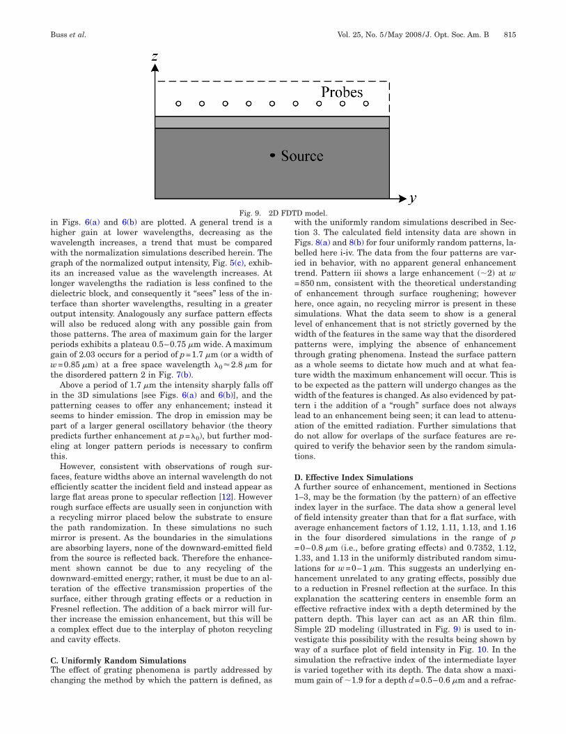
. Effective Index Simulationsfurther source of enhancement, mentioned in Sections
–3, may be the formation (by the pattern) of an effectivendex layer in the surface. The data show a general levelf field intensity greater than that for a flat surface, withverage enhancement factors of 1.12, 1.11, 1.13, and 1.16n the four disordered simulations in the range of p0–0.8 �m (i.e., before grating effects) and 0.7352, 1.12,.33, and 1.13 in the uniformly distributed random simu-ations for w=0–1 �m. This suggests an underlying en-ancement unrelated to any grating effects, possibly dueo a reduction in Fresnel reflection at the surface. In thisxplanation the scattering centers in ensemble form anffective refractive index with a depth determined by theattern depth. This layer can act as an AR thin film.imple 2D modeling (illustrated in Fig. 9) is used to in-estigate this possibility with the results being shown byay of a surface plot of field intensity in Fig. 10. In the
imulation the refractive index of the intermediate layers varied together with its depth. The data show a maxi-
um gain of �1.9 for a depth d=0.5–0.6 �m and a refrac-
D model.
D FDT
thapctwpncctc
hfwtbtswgba
5Tmsstedqgtvi
t
tlbw
mmhrfefm
AIPtUTTsCF
R
1
1
1
Fl
816 J. Opt. Soc. Am. B/Vol. 25, No. 5 /May 2008 Buss et al.
ive index of nlayer=2–2.5. The theoretical maximum en-ancement of 1.55 assumes a plane wave incident uponn interface; here we have a cylindrical wave from the di-ole for which the behavior at interfaces is more compli-ated. For the case of a plane wave at normal incidencehe magnitude of the parallel component of the incidentave vector k� is zero or negligibly small, whereas a di-ole will emit over a range of angles for which k� is sig-ificant. Those wave vectors with k� larger than for theritical angle will produce exponentially decaying evanes-ent waves above the surface, which will be measured byhe probes above the surface, and this will influence thealculation of emitted intensity.
The average gain ��1.15� seen in the 3D simulationserein suggests a layer of depth d=0.3–0.4 �m and a re-
ractive index of nlayer=3–3.5. This is intuitively plausibleith a depth “seen” by the radiation to be slightly less
han the feature depths of 400 nm and a refractive indexetween that of air and InSb. It is important to note thathis effective medium effect is usually associated withubwavelength features, so as the scattering centeridths become comparable to emission wavelengths therating effects will become dominant. This is emphasizedy the increasing oscillatory effect in the field intensitiess the period of the pattern is increased.
. CONCLUSIONhe performed simulations show a maximum enhance-ent in surface emission for a pseudorandom periodic
urface with feature size w=850 nm and a maximum ab-olute gain in emission intensity of 2.03 seen for this pat-ern as compared to a flat surface simulation. The mainffect appears to be that of wavelength scale features pro-ucing enhanced scattering; however, this normally re-uires a recycling mirror. There is good evidence of strongrating effects with peaks in emission associated withhose predicted by theory. Further modeling is planned toerify this behavior and to add a back mirror to identifyts contribution to any enhancement.
In the completely random case no dependence on fea-ure size is observed. In combination with enhanced scat-
ig. 10. Normalized output intensity for varying intermediateayer depths and refractive indices.
ering the pattern forms an intermediate refractive indexayer that acts as an AR thin-film layer. This is supportedy 2D modeling showing a similar level of enhancementith feasible layer parameters.The significance of this paper is that strong enhance-ent of emission has been shown without the require-ent for a back reflector, and it is felt that further en-ancement will be obtained with optimization of theoughness parameters. The simulated patterns are idealor prototyping via E-beam lithography methods; the longmission wavelengths in the midinfrared result in largereatures that are straightforward to realize via E-beamethods.
CKNOWLEDGMENTS. Buss acknowledges funding from the Engineering andhysical Sciences Research Council (EPSRC) and Qine-
iQ. QinetiQ acknowledges support for this work from thenited Kingdom Department of Trade and Industry’sechnology Program. G. Nash acknowledges support ofhe Royal Society through an Industrial Research Fellow-hip. The authors thank C. Railton and I. Craddock of theomputational Electromagnetics group for use of theirDTD codes and useful discussions.
EFERENCES1. W. N. Carr and G. E. Pittman, “One-watt GaAs p–n
junction infrared source,” Appl. Phys. Lett. 3, 173–175(1963).
2. E. F. Schubert, Light-Emitting Diodes (Cambridge U.Press, 2005).
3. T. S. Moss, G. J. Burrell, and B. Ellis, SemiconductorOpto-Electronics (Butterworth, 1973).
4. N. K. Patel, S. Cinà, and J. H. Burroughes, “High-efficiencyorganic light-emitting diodes,” IEEE J. Sel. Top. QuantumElectron. 8, 346–361 (2002).
5. K. Streubel, N. Linder, R. Wirth, and A. Jaeger, “Highbrightness AlGaInP light-emitting diodes,” IEEE J. Sel.Top. Quantum Electron. 8, 321–332 (2002).
6. G. R. Nash, N. T. Gordon, T. Ashley, M. T. Emeny, and T.M. Burke, “Large-area IR negative luminescent devices,”IEE Proc.: Optoelectron. 150, 371–375 (2003).
7. G. R. Nash, T. Ashley, N. T. Gordon, C. L. Jones, C. D.Maxey, and R. A. Catchpole, “Micromachined opticalconcentrators for IR negative luminescent devices,” J. Mod.Opt. 49, 811–820 (2002).
8. W. W. Bewley, M. J. Jurkovic, C. L. Felix, J. R. Lindle, I.Vurgaftman, J. R. Meyer, E. H. Aifer, J. H. Butler, S. P.Tobin, P. W. Norton, and M. A. Hutchins, “HgCdTephotodetectors with negative luminescent efficiencies�80%,” Appl. Phys. Lett. 78, 3082–3084 (2001).
9. L. Shterengas, G. Belenky, M. V. Kisin, and D. Donetsky,“High power 2.4 �m heavily strained type-I quantum wellGaSb-based diode lasers with more than 1 W of continuouswave output power and a maximum power-conversionefficiency of 17.5%,” Appl. Phys. Lett. 90, 011119 (2007).
0. T. K. Gaylord, W. E. Baird, and M. G. Moharam, “Zero-reflectivity high spatial-frequency rectangular-groovedielectric surface-relief gratings,” Appl. Opt. 25, 4562–4567(1986).
1. A. O. Dirisu, G. Silva, Z. Liu, C. F. Gmachl, F. J. Towner, J.Bruno, and D. L. Sivco, “Reduction of facet reflectivity ofquantum-cascade lasers with subwavelength gratings,”IEEE Photonics Technol. Lett. 19, 221–223 (2007).
2. I. Schnitzer, E. Yablonovitch, C. Caneau, T. J. Gmitter, andA. Scherer, “30% external quantum efficiency from surface

1
1
1
1
1
1
1
2
2
Buss et al. Vol. 25, No. 5 /May 2008/J. Opt. Soc. Am. B 817
textured, thin-film light-emtting diodes,” Appl. Phys. Lett.63, 2174–2176 (1993).
3. H. W. Deckman, C. B. Roxlo, and E. Yablonovitch,“Maximum statistical increase of optical absorption intextured semiconductor films,” Opt. Lett. 8, 491–493(1983).
4. R. Windisch, C. Rooman, B. Dutta, A. Knobloch, G. Borghs,G. H. Döhler, and P. Heremans, “Light extractionmechanisms in high-efficiency surface-textured light-emitting diodes,” IEEE J. Sel. Top. Quantum Electron. 8,248–255 (2002).
5. S. J. Lee, “Analysis of light-emitting diodes by Monte Carlophoton simulation,” Appl. Opt. 40, 1427–1437 (2001).
6. A. Sentenac and J.-J. Greffet, “Mean-field theory of lightscattering by one-dimensional rough surfaces,” J. Opt. Soc.Am. A 15, 528–532 (1998).
7. S. Riyopoulos, “Supercritical angle transmission throughquasi-random sub-wavelength-feature interfaces: integral
approach via effective surface currents,” J. Opt. Soc. Am. A22, 2859–2871 (2005).
8. M. J. Cryan, D. C. L. Wong, I. J. Craddock, S. Yu, J.Rorison, and C. J. Railton, “Calculation of losses in 2-Dphotonic crystal membrane waveguides using the 3-DFDTD method,” IEEE Photonics Technol. Lett. 17, 58–60(2005).
9. Y.-L. D. Ho, T. Cao, P. S. Ivanov, M. J. Cryan, I. J.Craddock, C. J. Railton, and J. G. Rarity, “Three-dimensional FDTD simulation of micro-pillar microcavitygeometries suitable for efficient single-photon sources,”IEEE J. Quantum Electron. 43, 462–472 (2007).
0. Condor high throughput computing cluster, http://www.cs.wisc.edu/condor/.
1. M. K. Haigh, G. R. Nash, S. J. Smith, L. Buckle, M. T.Emeny, and T. Ashley, “Mid-infrared AlxIn1−xSb light-emitting diodes,” Appl. Phys. Lett. 90, 231116 (2007).
Copyright © 2022 FDOKUMEN


![IJCBS RESEARCH PAPER VOL. 1 [ISSUE 3] JUNE, 2014 ISSN:-2349–2724 Light Emitting Diodes (LEDs) Reduce Vertimec, Resistance in Tetranychus urticae (Koch](https://static.fdokumen.com/doc/165x107/631ba468a906b217b9069031/ijcbs-research-paper-vol-1-issue-3-june-2014-issn-23492724-light-emitting.jpg)
