Thickness effect on the band gap of magnetron sputtered ...
7
Thickness effect on the band gap of magnetron sputtered Pb 45 Se 45 O 10 thin films on Si Xigui Sun a , Kewei Gao a , Xiaolu Pang a,n , Huisheng Yang a , Alex A. Volinsky b a Department of Materials Physics and Chemistry, University of Science and Technology Beijing, Beijing 100083, China b Department of Mechanical Engineering, University of South Florida, Tampa, FL 33620, USA HIGHLIGHTS Oxygen doped PbSe films were grown on Si (100) using magnetron sputtering. The band gap of doped PbSe films decreased from 0.278 to 0.21 eV. The band gap increased almost linearly with the lattice constant. The change rate between the light and dark resistance increased to 64.76%. article info Article history: Received 8 October 2014 Received in revised form 19 November 2014 Accepted 28 November 2014 Available online 29 November 2014 Keywords: Lead selenide Thin film Doping Magnetron sputtering abstract Oxygen doped PbSe thin films with different thickness were grown on the Si (100) substrates by mag- netron sputtering, and characterized using scanning electron microscopy, energy dispersive X-ray spectroscopy, X-ray diffraction, X-ray photoelectron spectroscopy, Fourier transform infrared spectro- scopy and physical properties measurement system. As the film thickness increased, the intensity of the (200) PbSe prominent diffraction peak increased, while the (220) peak almost vanished, indicating the primary growth direction. The change rate between the light and dark resistance increased with the film thickness, and the maximum of 64.76% was obtained. According to the density functional theory cal- culations and the experimental results, the band gap of the PbSe thin films decreased from 0.278 eV to 0.21 eV when doped with oxygen. Doping with oxygen during the deposition process is a viable way to prepare PbSe thin films with a tunable band gap. The band gap increased almost linearly with the lattice constant, confirmed by the calculated and experimental results. & 2014 Elsevier B.V. All rights reserved. 1. Introduction Lead selenide (PbSe) is a typical direct narrow band gap (0.278 eV) semiconductor material at room temperature [1], which has strong absorption from 3 μm to 5 μm in the mid-infrared re- gion [2]. Moreover, PbSe has the largest Bohr's radius of about 47 nm and relatively small effective mass of the exited electron– hole pair, compared with other lead chalcogenide materials, which allows remarkable quantum confinement and tunable band gap in large crystals [3]. For these reasons, PbSe has been widely used in infrared detectors [4], light emitting devices [5], laser diodes [6], solar cells [7], thermoelectric devices [8] and so on. At present, most of the PbSe devices, especially infrared de- tectors, are made in the form of a thin film because of the better performance, compared with the bulk material [9,10]. In addition, the PbSe infrared detectors can maintain excellent detectivity in the mid-wavelength infrared regi Prod. Type: FTPon, even at room temperature, which leads to a great interest in the funda- mental studies of this material, especially the preparation tech- niques. The PbSe thin films have been deposited by various che- mical and physical techniques, such as chemical bath deposition [11], electrochemical deposition [12], thermal evaporation [13], atomic layer deposition [14], molecular beam epitaxy [15], sput- tering [16] and several other improved methods [17–19]. In the present work, magnetron sputtering was used to deposit the PbSe thin films because of the medium cost, easy handling, high quality products and the potential for mass production, compared with other methods. Moreover, multiple deposition parameters, such as the gas flux, sputtering power, distance between the target and the substrate, substrate temperature, deposition time and so on, can be varied to modify the physical and chemical properties of the sputtered PbSe thin films, which in turn affect the perfor- mance of the PbSe devices. Within this research, only the Contents lists available at ScienceDirect journal homepage: www.elsevier.com/locate/physe Physica E http://dx.doi.org/10.1016/j.physe.2014.11.021 1386-9477/& 2014 Elsevier B.V. All rights reserved. n Corresponding author. E-mail address: [email protected] (X. Pang). Physica E 67 (2015) 152–158
-
Upload
khangminh22 -
Category
Documents
-
view
0 -
download
0
Transcript of Thickness effect on the band gap of magnetron sputtered ...
Physica E 67 (2015) 152–158
Contents lists available at ScienceDirect
Physica E
http://d1386-94
n CorrE-m
journal homepage: www.elsevier.com/locate/physe
Thickness effect on the band gap of magnetron sputtered Pb45Se45O10
thin films on Si
Xigui Sun a, Kewei Gao a, Xiaolu Pang a,n, Huisheng Yang a, Alex A. Volinsky b
a Department of Materials Physics and Chemistry, University of Science and Technology Beijing, Beijing 100083, Chinab Department of Mechanical Engineering, University of South Florida, Tampa, FL 33620, USA
H I G H L I G H T S
� Oxygen doped PbSe films were grown on Si (100) using magnetron sputtering.
� The band gap of doped PbSe films decreased from 0.278 to 0.21 eV.� The band gap increased almost linearly with the lattice constant.� The change rate between the light and dark resistance increased to 64.76%.a r t i c l e i n f o
Article history:Received 8 October 2014Received in revised form19 November 2014Accepted 28 November 2014Available online 29 November 2014
Keywords:Lead selenideThin filmDopingMagnetron sputtering
x.doi.org/10.1016/j.physe.2014.11.02177/& 2014 Elsevier B.V. All rights reserved.
esponding author.ail address: [email protected] (X. Pan
a b s t r a c t
Oxygen doped PbSe thin films with different thickness were grown on the Si (100) substrates by mag-netron sputtering, and characterized using scanning electron microscopy, energy dispersive X-rayspectroscopy, X-ray diffraction, X-ray photoelectron spectroscopy, Fourier transform infrared spectro-scopy and physical properties measurement system. As the film thickness increased, the intensity of the(200) PbSe prominent diffraction peak increased, while the (220) peak almost vanished, indicating theprimary growth direction. The change rate between the light and dark resistance increased with the filmthickness, and the maximum of 64.76% was obtained. According to the density functional theory cal-culations and the experimental results, the band gap of the PbSe thin films decreased from 0.278 eV to0.21 eV when doped with oxygen. Doping with oxygen during the deposition process is a viable way toprepare PbSe thin films with a tunable band gap. The band gap increased almost linearly with the latticeconstant, confirmed by the calculated and experimental results.
& 2014 Elsevier B.V. All rights reserved.
1. Introduction
Lead selenide (PbSe) is a typical direct narrow band gap(0.278 eV) semiconductor material at room temperature [1], whichhas strong absorption from 3 μm to 5 μm in the mid-infrared re-gion [2]. Moreover, PbSe has the largest Bohr's radius of about47 nm and relatively small effective mass of the exited electron–hole pair, compared with other lead chalcogenide materials, whichallows remarkable quantum confinement and tunable band gap inlarge crystals [3]. For these reasons, PbSe has been widely used ininfrared detectors [4], light emitting devices [5], laser diodes [6],solar cells [7], thermoelectric devices [8] and so on.
At present, most of the PbSe devices, especially infrared de-tectors, are made in the form of a thin film because of the betterperformance, compared with the bulk material [9,10]. In addition,
g).
the PbSe infrared detectors can maintain excellent detectivity inthe mid-wavelength infrared regi Prod. Type: FTPon, even atroom temperature, which leads to a great interest in the funda-mental studies of this material, especially the preparation tech-niques. The PbSe thin films have been deposited by various che-mical and physical techniques, such as chemical bath deposition[11], electrochemical deposition [12], thermal evaporation [13],atomic layer deposition [14], molecular beam epitaxy [15], sput-tering [16] and several other improved methods [17–19]. In thepresent work, magnetron sputtering was used to deposit the PbSethin films because of the medium cost, easy handling, high qualityproducts and the potential for mass production, compared withother methods. Moreover, multiple deposition parameters, such asthe gas flux, sputtering power, distance between the target andthe substrate, substrate temperature, deposition time and so on,can be varied to modify the physical and chemical properties ofthe sputtered PbSe thin films, which in turn affect the perfor-mance of the PbSe devices. Within this research, only the
X. Sun et al. / Physica E 67 (2015) 152–158 153
deposition time was changed, while other parameters remainedconstant, based on the previous experiments.
Generally, the as-prepared PbSe thin films cannot meet therequirements for the high quality detector materials, and furthertreatments are necessary to obtain better performance. As testifiedby other researchers [20], oxidation treatment, also known as“sensitization”, is an effective technique to improve the propertiesof the PbSe devices. Jung et al. [21] demonstrated that the oxidizedsurface of the radio frequency magnetron sputtered PbSe nano-wires significantly influences their optical properties and producesstrong confined states. Moreover, Gautier et al. [22] found that theoxygen-induced sensitization in the polycrystalline PbSe couldalter the microstructure, phase composition, and other properties.However, most of these studies are related to the after-treatments,i.e., these treatments are conducted after the thin film depositionprocess. Only few reports deal with the oxygen doping treatmentduring the deposition process, which can create a homogenousconcentration of oxygen all over the thin film, and the effects ofthis treatment on the properties of the PbSe thin films have notbeen adequately studied.
In the present work, three oxygen treated PbSe thin films withdifferent thickness were deposited on the Si (100) substrates usingmagnetron sputtering, and characterized by field emission scan-ning electron microscopy (FE-SEM), energy dispersive X-rayspectroscopy (EDX), X-ray powder diffraction (XRD), X-ray pho-toelectron spectroscopy (XPS), Fourier transform infrared spec-troscopy (FT-IR) and physical properties measurement system(PPMS). The effects of oxygen doping treatment during the de-position process on the properties of the sputtered PbSe thin filmswere studied in detail. In addition, the relationship between thefilm structure and photoelectric properties was also studied.
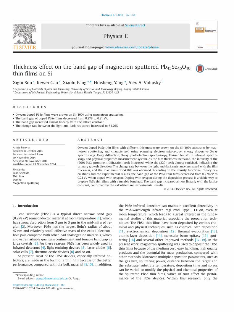
Fig. 1. FE-SEM images of (a) the surface and (b) the cross-section morphology ofthe sputtered Pb45Se45O10-2 thin film.
2. Experiment
Three oxygen doped PbSe thin films with different thickness,designated as Pb45Se45O10-1, Pb45Se45O10-2 and Pb45Se45O10-3,respectively, were grown on the single side polished Si (100)substrates using PM500-S sputtering system equipped with theMF-5K medium frequency sputtering power source. The PbSe alloytargets (nPb:nSe¼45:55) used in this research were prepared byconventional powder metallurgy with a purity of 99.99%. Thedeposition time was set to 120 min, 180 min and 240 min. Theoxygen and argon flux was set to 0.5 sccm and 30 sccm during thewhole deposition process, respectively. In order to improve thecrystallinity of the sputtered thin films, the temperature of thesubstrates was kept at 150 °C.
The surface and cross-section morphology of the sputtered thinfilms was studied using FE-SEM (Zeiss Auriga) with 15 kV oper-ating voltage. The variation of the dc resistance as a function of theillumination time was obtained using the two-probe method in adark chamber equipped with a 275 W infrared light and Fluke8808A digital multimeter. The dark resistance was recorded for300 s before and after illumination in 20 s steps, and the lightresistance was recorded for the same duration and step time. Thedc electrical resistance of the sputtered thin films was measuredusing the four-point probe method as a function of the film tem-perature ranged from 25 °C to 100 °C on the physical propertiesmeasurement system (PPMS, Quantum Design, Inc.).
The XRD patterns of the sputtered thin films were recordedusing the rotating anode diffractometer (Dmax-RB 12 kW, Rigaku)with the Cu Kα radiation source (λ¼1.5406 Å). The 2θ angle ran-ged from 10° to 64° with the scan speed of 8°/min. The chemicalstates of the elements contained in the sputtered thin films werestudied using X-ray photoelectron spectroscopy measurementsperformed on the AXIS ULTRADLD (SHIMADZU) X-ray
photoelectron spectrometer equipped with the Al Kα source,hν¼1486.6 eV. In order to study the difference of the chemicalstates on and beneath the film surface, the XPS tests were per-formed after the film surface was etched for 30 s by Arþ with theetching energy of 3000 eV. The Arþ etching and XPS analysis cyclewere conducted three times.
The infrared absorption spectra of the sputtered thin films weremeasured using the Nicolet Nexus 470 Fourier transform infraredspectrometer (FT-IR) from 4000 cm�1 to 400 cm�1 with the re-solution of 8 cm�1 at room temperature. In addition, the bandstructure of PbSe and Pb45Se45O10 was calculated using the Per-dew–Burke–Ernzerhof method for the solid form generalizedgradient approximation (GGAþPBEsol) of the density functionaltheory (DFT), in order to study the effects of oxygen atoms on thePbSe band structure.
3. Results and discussion
3.1. Film surface and cross-section morphology
High quality surface properties are essential to the performanceof the PbSe thin film devices, especially their lifetime. Fig. 1 showsthe surface and cross-section morphology of the sputteredPb45Se45O10 thin films, which are quite smooth and compact, andno impurities or cracks are observed, indicating that the magne-tron sputtering is a viable way to prepare the PbSe thin films.
The thickness of the sputtered thin films is 772 nm, 1231 nmand 1781 nm for Pb45Se45O10-1, Pb45Se45O10-2 and Pb45Se45O10-3,respectively, according to the corresponding cross-section imagesin Fig. 1(b) and Table 1.
3.2. Film composition and structure
Three elements, Pb, Se and O, are exclusively contained in the

Table 1Thickness, EDX and XRD results of the sputtered Pb45Se45O10 thin films.
Sample Thickness(nm)
Pb (at%) Se (at%) O (at%) Averagecrystalsize (nm)
Latticeconstant(Å)
Pb45Se45O10-1 772 46.76 43.43 9.81 61.1 6.1756Pb45Se45O10-2 1231 45.91 43.76 10.33 70.3 6.1738Pb45Se45O10-3 1781 45.28 45.61 9.11 76.4 6.1723
X. Sun et al. / Physica E 67 (2015) 152–158154
sputtered Pb45Se45O10 thin films, and their ratio corresponds withthe designed value, according to the EDX results, listed in Table 1.Moreover, the atomic ratio of the Pb and Se elements is about 1:1,illustrating that the Pb element is enriched in the sputtered thinfilms, considering the composition of the targets with nPb:nSe¼45:55.
The sputtered Pb45Se45O10 thin films have the rock salt crystalstructure, and the peaks at 29°, 41° and 60° are attributed to PbSe(200), (220) and (400), respectively, as seen in Fig. 2. No oxidespeaks are observed in the XRD patterns, which may be attributedto their low content, as testified by the XPS results shown later.
It is interesting to notice that the intensity of the PbSe (200)and PbSe (400) reflections increases with the film thickness. Onthe contrary, the PbSe (220) peak almost vanishes when the filmthickness reaches 1781 nm (Pb45Se45O10-3), which may be attrib-uted to the preferential growth mainly on the (220) crystal surface,and lead to the decrease of PbSe (220) and the increase of PbSe(200) and PbSe (400) intensities, as shown in Fig. 2 insets.
The average crystal size was calculated using the Debye–Scherrer formula [23]:
BAverage crystal size 0.9 /( cos ), (1)λ θ=
where the 0.9 value is derived from the spherical crystallite geo-metry, λ denotes the wavelength of the X-ray radiation (Cu Kα,λ¼1.5406 Å), B represents the full width at half maximum(FWHM) of the PbSe (200) diffraction peak, θ is the diffractionangle, corresponding to the peak maximum. The average crystalsize of the sputtered thin films increases from 61.1 nm to 76.4 nmas the film thickness increases, listed in Table 1.
The lattice constant for the cubic structure was calculated as[24]:
d h k lLattice constant , (2)2 2 2= + +
where d denotes the distance between the atomic lattice planes,and (hkl) are the Miller indices. The lattice constant of the
10 20 30 40 50 60
0
300
600
900
1200
1500
1800
2100
Inte
nsity
, a.u
.
2θ, deg
Fig. 2. XRD results of the sputtered Pb45Se45O10 thin films. The inset shows theschematic diagram of the crystal structure of the sputtered thin film with differentthickness: green balls represent the Pb atoms, red balls represent the Se atoms,while the O atoms are not shown in the structure. (For interpretation of the re-ferences to color in this figure legend, the reader is referred to the web version ofthis article.)
sputtered thin films varies from 6.1723 Å to 6.1756 Å, which ismuch larger than the bulk PbSe material (6.124 Å, JCPDS 06-0354).The deviation may be attributed to the existence of the dopedoxygen atoms (mainly interstitial atoms) in the PbSe crystal lattice[25].
As mentioned above, the properties of the sputtered PbSe thinfilms can be improved by the oxygen doping treatment during thedeposition process, and it is essential to study the chemical statesof the elements contained in the thin films using the XPS techni-que, as shown in Fig. 3. The XPS spectra of the three elements arequite different before and after the etching treatment, as seen inFig. 3(a1), (b1) and (c1). For the Pb element, two chemical states,PbSe (at about 137 eV and 142 eV) and PbO (at about 138 eV and143 eV), are detected before and after the etching treatment,however, the content of PbO decreases sharply after the etchingtreatment, as seen in Fig. 3(a2) and (a3), illustrating the existenceof the absorbed oxygen atoms on the film surface. For the Seelement, also two chemical states, PbSe (at about 53 eV and 54 eV)and SeO2 (at about 58 eV and 59 eV), are detected before theetching treatment, however, the SeO2 chemical state vanishes afterthe etching treatment, seen in Fig. 3(b2) and (b3). This can beattributed to the oxygen atoms substituting the Se atoms andbonding with the Pb atoms [22]. For the O element, just onechemical state, absorbed oxygen (at about 531 eV) or PbO (atabout 529 eV) is detected before and after the etching treatment,respectively. In fact, the absorbed oxygen includes PbO and SeO2
two chemical states, which are hardly differentiated.As testified by the XPS spectra, the content of the oxides con-
tained in the sputtered PbSe thin films is quite low, which is un-observable in the XRD experiment. Combined with the XRD re-sults, it is speculated that the oxygen atoms contained in the thinfilms have two states, the interstitial atoms and the substitutionalatoms, and their effects on the photoelectric properties is dis-cussed in Section 3.4.
3.3. Electrical properties
The change rate between the dark and light resistance is auseful parameter to evaluate the photosensitivity of the PbSe thinfilms. Fig. 4 shows the photoelectric properties of the sputteredPb45Se45O10 thin films. The resistance of these three thin filmsdecreases immediately to a small value when the light is turnedon, and then increases slowly after the light is turned off, as seenin Fig. 4(a). Within this research, the resistance cannot return tothe original value obtained before the illumination treatmentduring 300 s after the light turns off, which means that the re-combination of the charge carriers (electrons and holes) in thesputtered thin films is a time-consuming process. Moreover, thereis a linear relationship between the film thickness and the elec-trical resistivity calculated from the dark resistance value, obtainedbefore the illumination treatment, seen in Fig. 4(c). This can beattributed to the decrease of the crystal defects, which can inhibitthe transition of the charge carriers in the thin films [26].
As mentioned above, the PbSe thin films are mainly used asinfrared detector materials and, hence, the rate and the degree ofthe photoelectric response are quite important parameters for theperformance of the detectors. Within this research, the resistancechange rate was chosen as the photosensitivity of the sputteredPb45Se45O10 thin films, calculated as
R R RResistance change rate / 100%, (3)D L D= ¯ − ¯ ×
where RD¯ denotes the average value of the dark resistance beforethe illumination treatment, RL is the value of the light resistance ofthe sputtered Pb45Se45O10 thin films. The resistance change rate ofthe sputtered thin films increases sharply as the light is turned on,

Fig. 3. XPS spectra of the Pb45Se45O10 thin films before (0 s) and after (30, 60, 90, 120 s) etching treatment: (a1) Pb4f; (b1) Se3d; (c1) O1s; (a2), (b2) and (c2) are the analysisresults of Pb4f, Se3d and O1s before etching treatment; (a3), (b3) and (c3) are the analysis results of Pb4f, Se3d and O1s after 120 s etching treatment. The insets shown in(a1), (b1) and (c1) are the enlarged views of the spectra after etching.
X. Sun et al. / Physica E 67 (2015) 152–158 155
and reaches almost a stable value after 20 s, as seen in Fig. 4(b).Pb45Se45O10-3 shows the highest photosensitivity, compared withthe other two samples if only the resistance change rate from 20 sto 300 s is considered. The average values are 51.13%, 57.40% and64.76% for Pb45Se45O10-1, Pb45Se45O10-2 and Pb45Se45O10-3, re-spectively. There is a linear relationship between the film thick-ness and the average resistance change rate (from 20 s to 300 s), asshown in Table 2 and Fig. 4(c). That can also be explained by thedecrease of the crystal defects with the film thickness, which canincrease the mobility of the charge carriers and therefore increasethe resistance change rate.
The temperature dependence of the dc electrical conductivity,s, of the sputtered Pb45Se45O10 thin films is shown in Fig. 5. Theconductivity of the thin films increases with temperature ex-ponentially over the whole temperature range, indicating normalnon-degenerate semiconducting behavior [27]. The linear varia-tion of ln(s) with 1000/T indicates that the conduction in thesethin films is a thermally activated process, which is consistent withother results for the lead chalcogenides thin films [27,28].
Moreover, the plots of Pb45Se45O10-2 and Pb45Se45O10-3 consistof the two distinct linear regions, the low temperature extrinsicregion and the high temperature intrinsic region, indicating thepresence of the two conduction mechanisms [29], while the
Pb45Se45O10-1 sample shows just one linear region, the low tem-perature extrinsic region. The transition temperature betweenthese two regions increases with the film thickness, 329 K(3.04 K�1) for Pb45Se45O10-2 and 346 K (2.89 K�1) forPb45Se45O10-3. No transition temperature is observed during thewhole temperature range for Pb45Se45O10-1, which may be lessthan 300 K (3.33 K�1).
3.4. Optical properties
The FT-IR absorption spectra of the sputtered Pb45Se45O10 thinfilms were recorded in the mid-infrared region at room tem-perature. Additional pure sputtered PbSe thin film was also mea-sured for comparison, shown in Fig. 6(a). The absorption edge forthe sputtered PbSe and Pb45Se45O10 thin films is located at about2250 cm�1 (4.45 μm) and 1600 cm�1 (6.25 μm), respectively, il-lustrating a red shift for the Pb45Se45O10 thin films compared withthe pure PbSe thin films. This may be attributed to the dopingeffects created by oxygen, which may add impurity energy levelsin the band gap of the PbSe materials and lower the excitationenergy of the charge carriers, as shown in Fig. 7. The calculatedexcitation energy for the charge carriers of PbSe and Pb45Se45O10 is0.154 eV and 0.093 eV, respectively, indicating that the impurity

1.5x10⁴
2.0x10⁴
2.5x10⁴
3.0x10⁴
3.5x10⁴D
C re
sist
ance
, Ohm
9.0x10³
1.2x10⁴
1.5x10⁴
1.8x10⁴
2.1x10⁴
2.4x10⁴
2.7x10⁴
DC
resi
stan
ce, O
hm
0 300 600 900
6.0x10³
9.0x10³
1.2x10⁴
1.5x10⁴
1.8x10⁴
DC
resi
stan
ce, O
hm
Time, s
0 50 100 150 200 250 300202530354045505560657075
Res
ista
nce
chan
ge re
te, %
Illumination time, s
600 800 1000 1200 1400 1600 1800
51
54
57
60
63
66
Thickness, nm
Res
isita
nce
chan
ge ra
te, %
0.9
1.2
1.5
1.8
2.1
2.4
Resistivity, ohm
·cm
Fig. 4. The photoelectric properties of the sputtered Pb45Se45O10 thin films: (a) the dc resistance of the sputtered thin films in the dark and under illumination; (b) variationof the resistance change rate as a function of the illumination time; and (c) the effects of film thickness on the resistance change rate (the average value between 20 s and300 s after the illumination treatment) and the resistivity (in the dark) of the sputtered thin films.
Table 2Electrical and optical properties of the sputtered Pb45Se45O10 thin films.
Sample RD¯ (KΩ) RL (20–300 s)(KΩ)
Resistancechange ratea
(%)
Resistivity(Ω cm)
Eg (eV)
Pb45Se45O10-1 35.48 20.63–15.87 51.13 2.267 0.2130Pb45Se45O10-2 25.37 12.55–9.64 57.40 1.667 0.2098Pb45Se45O10-3 17.95 7.70–5.15 64.76 0.996 0.2075PbSe – – – 0.2780
a The resistance change rate is the average value between 20 s and 300 s.
2.5 2.6 2.7 2.8 2.9 3.0 3.1 3.2 3.3 3.4 3.5-5.7
-5.4
-5.1
-4.8
-4.5
-4.2
-3.9
-3.6
-3.3
-3.0
lnσ ,
ohm
-1·c
m-1
1000/T, K-1
Fig. 5. Variation of the dc electrical conductivity, ln(s), with the inverse tem-perature (1000/T) for the sputtered Pb45Se45O10 thin films of different thicknesses.
X. Sun et al. / Physica E 67 (2015) 152–158156
energy levels are created by the interaction of oxygen, Pb and Seatoms, as shown in Fig. 7(b).
The band gap of the sputtered thin films can be derived fromthe absorption spectra, since the band gap, Eg, and the absorptioncoefficient, α, obey the Tauc relation [30]:
hv B hv E( ) ( ), (4)ng
1/α = −
where α¼1/d ln(I0/I), I0 is the incident beam intensity and I is thebeam intensity after traversing a certain thickness d of the sample.hv represents the incident beam energy, and h is the Planck's
constant, 4.135667516(91)�10�15 eV � s, v is the incident beamfrequency (v¼2π/ω). B is a constant and n is an exponent, whichhas values of 1/2, 3/2, 2 and 3, depending on the nature of theelectronic transitions responsible for the absorption: n¼1/2 forthe allowed direct transition, n¼3/2 for the forbidden directtransition, n¼2 for the allowed indirect transition and n¼3 for the

Fig. 6. (a) FT-IR absorption spectra of the sputtered Pb45Se45O10 and PbSe thin filmsand (b) the relationship between the incident beam energy (hv) and (αhv)2. α is theabsorption coefficient of the sputtered thin films.
-2.4
-1.6
-0.8
0.0
0.8
1.6
2.4
GZQFG
Ene
rgy,
eV
-2.4
-1.6
-0.8
0.0
0.8
1.6
2.4
GZF Q
Ene
rgy,
eV
G
Fig. 7. Band structure for (a) PbSe and (b) Pb45Se45O10 calculated using theGGAþPBEsol method.
600 800 1000 1200 1400 1600 18000.207
0.208
0.209
0.210
0.211
0.212
0.213
Ban
d ga
p, e
V
Thickness, nm
6.1720 6.1728 6.1736 6.1744 6.1752 6.17600.084
0.086
0.088
0.090
0.092
0.094
Lattice constant, A
Cal
cula
ted
band
gap
, eV
0.2085
0.2100
0.2115
0.2130
0.2145
0.2160
0.2175
Experim
ental band gap, eV
Fig. 8. (a) Relationship between the thickness and the band gap of the sputteredPb45Se45O10 thin films and (b) the calculated and experimentally measured bandgap as a function of the lattice constant.
X. Sun et al. / Physica E 67 (2015) 152–158 157
forbidden indirect transition. The electronic transitions of the PbSematerials obey direct transition, indicating that n¼1/2, thus therelation between the band gap, Eg, the absorption coefficient, α,and the energy of the incident beam, hv, is given as
hv B hv E( ) ( ). (5)g2α = −
Fig. 6(b) presents the (αhv)2 variations with the photon energy,hv, for the sputtered Pb45Se45O10 and PbSe thin films. The bandgap values were obtained by extrapolating the linear part of thecurve to the incident beam energy axis at (αhv)2¼0, and the re-sults are shown in Table 2. It is clear that the Eg values of thesputtered Pb45Se45O10 thin films are similar, about 0.21 eV, whichis smaller than the value of the pure sputtered PbSe thin film of0.278 eV, illustrating that doping with oxygen can change theoptical properties of the PbSe materials.
The effect of the film thickness on the band gap of the sput-tered Pb45Se45O10 is shown in Fig. 8(a). The band gap decreasesalmost linearly with the film thickness, which may be attributed tothe variation of the lattice constant with the thickness. Fig. 8(b) shows calculated and experimentally measured band gap as afunction of the lattice constant, exhibiting similar trends. The in-crease of the lattice constant, i.e., the increase of the distance ofthe lattice atoms, leads to the energy bands narrowing and theincrease of band gap for the PbSe materials [31].
4. Conclusions
Three oxygen doped PbSe thin films with different thicknesswere successfully grown on the Si (100) substrates by magnetronsputtering, and the effects of the structure and composition on thephotoelectric properties of the sputtered Pb45Se45O10 thin filmswere studied in detail.
The sputtered Pb45Se45O10 thin films showed the rock saltcrystal structure with the prominent (200) PbSe diffraction.Moreover, the intensity of the (200) PbSe diffraction reflectionincreased with the film thickness, while the (220) PbSe peak al-most vanished, indicating that the primary growth is on the PbSe(220) surface. The change rate between the light and dark re-sistance of the sputtered thin films increased with the film

X. Sun et al. / Physica E 67 (2015) 152–158158
thickness, and the maximum of 64.76% was obtained. According tothe DFT calculation and the FT-IR results, the band gap of the PbSethin films decreased from 0.278 eV to about 0.21 eV when dopedwith oxygen, indicating that doping with oxygen during the de-position process is a viable way to prepare PbSe thin films withtunable band gap. Moreover, the band gap increased almost line-arly with the lattice constant, confirmed by both calculated andexperimental results.
Acknowledgments
This work was supported by the National Natural ScienceFoundation of China (51271022), the Fok Ying Tung EducationFoundation (132001) and the Fundamental Research Funds for theCentral Universities (FRF-TP-14-008A2).
References
[1] U.K. Mishra, J. Singh, Semiconductor Device Physics and Design, Springer,Netherlands, 2008.
[2] E.D. Palik, Handbook of Optical Constants of Solids, Academic Press, USA, 1998.[3] W.L. Ma, J.M. Luther, H.M. Zheng, Y. Wu, A.P. Alivisatos, Photovoltaic devices
employing ternary PbSxSe1�x nanocrystals, Nano Lett. 9 (2009) 1699–1703.[4] J.M. Martin, J.L. Hernández, L. Adell, A. Rodriguez, F. López, Arrays of thermally
evaporated PbSe infrared photodetectors deposited on Si substrates operatingat room temperature, Semicond. Sci. Technol. 11 (1996) 1740–1744.
[5] W.J. Hu, S. Gao, P.N. Prasad, J.K. Wang, J. Xu, Employing photoassisted ligandexchange technique in layered quantum dot LEDs, J. Nanomater. 2012 (2012)1–5.
[6] H. Preier, Recent advances in lead-chalcognide diode lasers, Appl. Phys. 20(1979) 189–206.
[7] J.J. Choi, Y.F. Lim, M.B. Santiago-Berrios, M. Oh, B.R. Hyun, L.F. Sun, A.C. Bartnik,A. Goedhart, G.G. Malliaras, H.D. Abruña, F.W. Wise, T. Hanrath, PbSe nano-crystal excitonic solar cells, Nano Lett. 9 (2009) 3749–3755.
[8] J.P. Heremans, V. Jovovic, E.S. Toberer, A. Saramat, K. Kurosaki,A. Charoenphakdee, S. Yamanaka, G.J. Snyder, Enhancement of thermoelectricefficiency in PbTe by distortion of the electronic density of states, Science 321(2008) 554–557.
[9] C. Sierra, M.C. Torquemada, G. Vergara, M.T. Rodrigo, C. Gutiérrez, G. Pérez,I. Génova, I. Catalán, L.J. Gómez, V. Villamayor, M. Álvarez, D. Fernández, M.T. Magaz, R.M. Almazán, Multicolour PbSe sensors for analytical applications,Sens. Actuators B 190 (2014) 464–471.
[10] B.B. Weng, J.J. Qiu, Z.J. Yuan, P.R. Larson, G.W. Strout, Z.S. Shi, Responsivityenhancement of mid-infrared PbSe detectors using CaF2 nano-structured an-tireflective coatings, Appl. Phys. Lett. 104 (2014) 021109.
[11] E.B. Salgado, M.T.S. Nair, P.K. Nair, R.A. Zingaro, Chemically deposited thin filmsof PbSe as an absorber component in solar cell structures, Thin Solid Films 519(2011) 7432–7437.
[12] N. Mukherjee, A. Mondal, Comparative study on the properties of galvanicallydeposited nano- and micro-crystalline thin films of PbSe, J. Electron. Mater. 39(2010) 1177–1185.
[13] S. Gad, M.A. Rafea, Y. Badr, Optical and photoconductive properties ofPb0.9Sn0.1Se nano-structured thin films deposited by thermal vacuum eva-poration and pulsed laser deposition, J. Alloy. Compd. 515 (2012) 101–107.
[14] A.D.R. Pillai, K. Zhang, K. Bollenbach, D. Nminibapiel, W. Cao, H. Baumgart, V.S.K. Chakravadhanula, C. Kübel, V. Kochergin, ALD growth of PbTe and PbSesuperlattices for thermoelectric applications, ECS Transit. 58 (2013) 131–139.
[15] X.J. Wang, Y.B. Hou, Y. Chang, C.R. Becker, R.F. Klie, R. Kodama, F. Aqariden,S. Sivananthan, Growth of PbSe on ZnTe/GaAs(211)B by molecular beam epi-taxy, J. Cryst. Growth 312 (2010) 910–913.
[16] S.P. Zimin, I.I. Amirovand, E.S. Gorlachev, RF sputtering of epitaxial leadchalcogenide films in argon and krypton plasma, Semicond. Sci. Technol. 26(2011) 055018.
[17] M. Fardy, A.I. Hochbaum, J. Goldberger, M.J. Zhang, P.D. Yang, Synthesis andthermoelectrical characterization of lead chalcogenide nanowires, Adv. Mater.19 (2007) 3047–3051.
[18] K.R. Murali, P. Ramanathan, Characteristics of slurry coated lead selenide films,Chalcogenide Lett. 6 (2009) 91–95.
[19] Z.W. Quan, Z.P. Luo, W.S. Loc, J. Zhang, Y.X. Wang, K.K. Yang, N. Porter, J. Lin,H. Wang, J.Y. Fang, Synthesis of PbSeTe single ternary alloy and core/shellheterostructured nanocubes, J. Am. Chem. Soc. 133 (2011) 17590–17593.
[20] F. Zhao, S. Mukherjee, J. Ma, D. Li, S.L. Elizondo, Z. Shi, Influence of oxygenpassivation on optical properties of PbSe thin films, Appl. Phys. Lett. 92 (2008)1–3.
[21] H. Jung, R. Kuljic, M.A. Stroscio, M. Dutta, Confinement in PbSe wires grown byrf magnetron sputtering, Appl. Phys. Lett. 96 (2010) 153106.
[22] C. Gautier, M. Cambon-Muller, M. Averous, Study of PbSe layer oxidation andoxide dissolution, Appl. Surf. Sci. 141 (1999) 157–163.
[23] S. Thanikaikarasan, T. Mahalingam, V. Dhanasekaran, A. Kathalingam, J.K. Rhee, Growth and characterization of lead selenide thin films, J. Mater. Sci.:Mater. Electron. 23 (2012) 1562–1568.
[24] M.M. Parvathi, V. Arivazhagan, S. Rajesh, Structural and optical properties ofZnSe thin films stacked with PbSe submonolayers, Appl. Phys. A 116 (2014)1773–1778.
[25] A. Begum, A. Hussain, A. Rahman, Effect of deposition temperature on thestructural and optical properties of chemically prepared nanocrystalline leadselenide thin films, Beilstein J. Nanotechnol. 3 (2012) 438–443.
[26] C.L. Heieman, R. Rostek, M.D. Anderson, A.A. Herzing, I.M. Anderson, D.C. Johnson, Synthesis and electronic properties of the misfit layer compound[(PbSe)1.00]1[MoSe2]1, J. Electron. Mater. 39 (2010) 1476–1481.
[27] E.A. El-Sayad, B.S. Farag, A.T. Amin, Electrical properties of crystallinePbxSn1�xTe0.5Se0.5 thin films, Vacuum 84 (2010) 807–811.
[28] H.M. Ali, S.A. Saleh, Growth and opto-eletro-structural properties of nano-crystalline PbSe thin films, Thin Solid Films 556 (2014) 552–559.
[29] S.D. Delekar, M.K. Patil, B.V. Jadhav, K.R. Sanadi, P.P. Hankare, Synthesis andcharacterization of Cd0.7Pb0.3Se thin films for photoelectrochemical solar cell,Sol. Energy 84 (2010) 394–400.
[30] A.A. Al-Ghamdi, S. Al-Heniti, Shamshad A. Khan, Structural, optical and elec-trical characterization of Ag doped lead chalcogenide (PbSe) thin films, J. Lu-min. 135 (2013) 295–300.
[31] S.H. Wei, Al Zunger, Electronic and structural anomalies in lead chalcogenides,Phys. Rev. B 1 (1997) 13605.