Mechanism of Thickness Dependence of Critical Current ...
105
Mechanism of Thickness Dependence of Critical Current Density in HTS YBCO Film and Its Elimination Using Nano-Engineering By Xiang Wang B.S., Huazhong University of Science and Technology, China, 1995 M.E., Huazhong University of Science and Technology, China, 1999 Submitted to the Department of Physics and Astronomy and the Faculty of the Graduate School of the University of Kansas in partial fulfillment of the requirement for the degree of Doctor of Philosophy Dissertation Committee: Dr. Judy Z. Wu, Committee Chair Dr. Hui Zhao Dr. Siyuan Han Dr. Philip S. Baringer Dr. Karen J. Nordheden Date Submitted:
-
Upload
khangminh22 -
Category
Documents
-
view
3 -
download
0
Transcript of Mechanism of Thickness Dependence of Critical Current ...

Mechanism of Thickness Dependence of Critical Current Density in HTS YBCO Film and Its Elimination Using Nano-Engineering
By
Xiang Wang B.S., Huazhong University of Science and Technology, China, 1995
M.E., Huazhong University of Science and Technology, China, 1999
Submitted to the Department of Physics and Astronomy and the Faculty of the Graduate
School of the University of Kansas in partial fulfillment of the requirement for the degree
of Doctor of Philosophy
Dissertation Committee: Dr. Judy Z. Wu, Committee Chair Dr. Hui Zhao Dr. Siyuan Han Dr. Philip S. Baringer Dr. Karen J. Nordheden Date Submitted:

The dissertation committee certifies that this is the approved version of
following dissertation:
Mechanism of Thickness Dependence of Critical Current Density in HTS
YBCO Film and Its Elimination Using Nano-Engineering
Chair: Dr. Judy Z. Wu Date approved:
ii

Abstract
The most promising characteristic of a High Temperature Superconductor (HTS)
is its ability to carry larger electrical current at liquid nitrogen boiling temperature and
strong applied magnetic field with minimal dissipation. Numerous large scale
applications such as HTS transmission cables, HTS magnets and HTS motors have been
developed using HTS materials. The major limitation that prevents its wide
commercialization is its high cost-to-performance ratio. However, the effort to further
improve HTS current carrying capability is jeopardized by a mysterious thickness
dependence of the critical current density (Jc) ⎯ Jc monotonically decreases with
increasing thickness (t) at 77 K and self-field (SF). This poses a great challenge for both
HTS applications and the understanding of vortex dynamics. What further complicates
this issue is the complex defect structure in HTS films as well as the creep nature of
magnetic vortices at a finite temperature. After a systematic study of the temperature and
magnetic field effects on Jc−t, we conclude that Jc−t is most likely the result of a
collective pinning effect dictated by a random pinning potential. Besides that, thermal
fluctuations also alter Jc−t in a predictable way. Therefore, by either modifying the vortex
structure or pinning structure, Jc−t can be eliminated. Indeed, a thin film Jc has been
restored in a HTS/insulator/HTS trilayer while the magnetic coupling is weakened.
Moreover, Jc−t has been removed when the random distributed point pins are
overpowered by strong linear defects.
iii
This dissertation is dedicated to my parents, my dearest wife and
daughter
iv
ACKNOWLEDGEMENT
I gratefully acknowledge Drs. Judy Z Wu, Siyuan Han, Philip S Baringer, Hui
Zhao, and Karen J Nordheden for serving on my dissertation committee and for their
valuable guidance in the preparation of this Ph.D. dissertation. I would also like to
acknowledge those who have provided guidance and assistance toward this dissertation
project over the years, which include Dr. Rongtao Lu and Ms. Rose Lyn Emergo for their
assistance in building the cryogenic system equipped with 8-Tesla NbTi superconducting
magnet and the probe for measuring anisotropic transport properties of HTS film, my
former colleagues Dr. Yiyuan Xie and Dr. Roberto S. Aga for their instrumental guidance
with operating the SQUID magnetometer and conductive AFM, Mr. Jonathan R. Dizon
for helping with the Labview programming of relevant electronic devices, Mr. Javier F.
Baca for his collaborative contribution with sample growth and TEM analysis. A special
thanks to Dr. Timothy Haugan from the Air Force Research Laboratory for the
continuous exchange of ideas and providing help on countless occasions with sample
fabrication and characterization.
I am indebted to my advisor, Dr. Judy Z Wu, for being a truly exceptional mentor,
for providing continuous support and guidance regarding professional as well as personal
matters each and every day. A special recognition goes to Dr. Alex Gurevich from the
National High Magnetic Field Laboratory, who provided the important and insightful
theoretical analysis of the puzzling Jc−t issue.
Finally, I want to thank all my physics colleagues for their generous support and
encouragement, which makes this seven-year academic journey special and fruitful.
v

TABLE OF CONTENTS
ACCEPTANCE PAGE.................................................................................ii
ABSTRACT..................................................................................................iii
ACKNOWLEDGMENTS...........................................................................iv
TABLE OF CONTENTS ...........................................................................vi
LIST OF FIGURES.....................................................................................ix
LIST OF SYMBOLS.................................................................................xiii
ABBREVIATIONS....................................................................................xv
CHAPTER 1: Introduction………………………………………………..1
1.1 Basic Phenomena………………………………………….2
1.2 Early Understanding………………………………………3
1.3 The BCS Theory…………………………………………..5
1.4 The Ginzburg-Landau Theory……………………………..6
1.5 Type II Superconductors…………………………………..8
1.6 High Temperature Superconductor……………………….10
CHAPTER 2: Critical Current Density of HTS Film…………..12
2.1 Limiting Factors of Critical Current Density…………….13
2.2 Flux Pinning in YBCO Film…………………………..16
2.3 Thermally Activated Flux Motion……………………...18
vi

2.4 YBCO Film Fabrication and Characterization…………...20
2.4.1 Pulsed Laser Deposition………………………..20
2.4.2 YBCO Film Characterization……………………21
2.5 The Effect of Applied Magnetic Field on Jc……………...25
2.6 The Effect of Temperature on Jc………………………28
2.7 Thickness Dependence of Jc in YBCO Film……………...29
2.8 Weak Collective Pinning Model………………………34
2.9 Summary…………………………………………37
CHAPTER 3: The Effect of Temperature and Magnetic Field on
Thickness Dependence of Critical Current Density……38
3.1 The Effect of Temperature on Jc−t………………………38
3.2 The Effect of Applied Magnetic Field on Jc−t…………….43
3.3 Theoretical Analysis of Jc−t…………………………….44
3.4 Conclusions……………………………………………48
CHAPTER 4: Jc−t Elimination Using Multilayer Approach…………50
4.1 Single Vortex in S/N/S Trilayer …………………………50
4.2 Decoupling Vortex in YBCO/CeO2/YBCO Trilayer………52
4.3 Discussion……………………………………………...56
vii

4.4 Summary……………………………………………....58
CHAPTER 5: Jc−t Elimination Using NTP Insertion…………………59
5.1 NTP Insertion in YBCO Film……………………………59
5.2 Microstructure Analysis of NTP …………………………61
5.3 Jc of YBCO Film Before and After NTP Insertion…………64
5.4 Conclusions……………………………………………...68
CHAPTER 6: Jc−t Elimination Using BZO NRD Insertion …………...69
6.1 Growth Temperature Effect on Jc of YBCO/BZO………….71
6.2 Growth Temperature Effect on Pinning Structure…………74
6.3 Elimination of Jc−t in Low H Regime……………………...75
6.4 Lower SF Jc Observed After BZO Insertion……………….76
6.5 Conclusions……………………………………………...78
CHAPTER 7: Conclusions and Outlook………………………………...80
References…………………………………………………………………82
Publications………………………………………………………………..88
viii
LIST OF FIGURES
CHAPTER 1
Fig.1.1: H-T phase diagram of a superconductor. Fig.1.2: Comparison of flux penetration behavior between type I and type II superconductors. Fig.1.3: The superconducting order parameter and magnetic vortex density as function of position from the center of a vortex core for an isolated vortex. CHAPTER 2
Fig. 2.1: Plume generated by a focused pulsed UV laser beam on a YBCO target. Fig. 2.2: I-V curves measured on a YBCO film at 77K and various fields. Fig. 2.3: M-H hysteretic loops measured on a YBCO film at 10, 50, 77 and 86K. Fig. 2.4: Jc as function of H measured on a same sample using traditional transport (transport Jc) and SQUID magnetization (magnetic Jc). Fig. 2.5: Jc as function of H of a typical YBCO film plotted in a log-log scale and at various temperatures. Inset table gives the characteristic field B*, which sets the boundary of SV regime, and α value at each given temperature. Fig. 2.6: Jc as function of reduced temperature T/Tc measured on a typical YBCO film plotted in a semi-log scale. Solid line represents the flux-creep model predicted Jc−T dependence and T0 is 46.8 K. Fig. 2.7(as plotted in ref. [2.37]): Jc−t comparison between YBCO films grown on single crystal substrates and metal tape at 75K and self-field. Fig. 2.8 (as plotted in ref. [2.38]): Milling generated Jc−d from three CC with thickness of 0.68, 3.0 and 4.7 μm. “Dead layer” is observed for two thick samples. Fig. 2.9(data extracted from ref. [2.39]): Thickness dependence of (a) in-plane texture and out-of-plane texture; (b) critical current density and portion of a-axis orientated grain in the YBCO films grown on STO single crystal substrate.
ix

Fig. 2.10(as plotted in ref. [2.42]): Jc as function of thickness for multilayered films (solid), plotted together with data taken on single layer YBCO films (open). Fig. 2.11(as shown in ref.[2.42]): Cross-sectional transmission electron microscope image of a YBCO film grown on single crystal MgO substrate. A high density of defects near the YBCO/SrTiO3 interface regarded as the dominant pinning centers is visible as a dark band. Fig. 2.12(as plotted in ref. [2.45]): Milling generated Jc−d at 77K and different fields for (a) the 2.9 and (b) 2.0 μm- thick films. Solid lines are fits to Jc − t from as-deposited samples. Fig. 2.13(as plotted in ref. [2.47]): Jc of as function of thickness measure at 77K and SF reported by different groups plotted in a normalized scale. Most of the data points can be more of less fitted by t/1 . Fig. 2.14(as plotted in ref. [2.35]): Single vortex line is pinned by the collective action of many weak point-like pinning centers. In order to accommodate optimally to the pinning potential, the flux line deforms elastically by Lc, the longitudinal collective pinning length. CHAPTER 3
Fig. 3.1: Shown is normalized M [M/M(10K)] as function of T for YBCO films with various thickness. Shown in the inset are the Tc and δTc as function of thickness. Fig. 3.2: Shown is (a) Jc(SF) − t at various temperatures. The error bar corresponds to the average over different sets of samples with same thickness. (b) The reduced Jc
r = Jc/Jc(0.6µm) as function of thickness at various temperatures. The dashed line represents the fitting of 1/t1/2. Fig. 3.3: Shown are Jc
r − t curves at (a) 77K and (b) 50K, respectively, at various H
fields. The dashed line represents the fitting of 1/t1/2. Fig. 3.4: Fig. 3.4 (as plotted in ref. [3.13]): Evolution of the Jc−t described by Eq.(3.2) for different values of (1) θ = 0.0065, (2) 0.01, (3)0.015, and (4) 0.025. Fig. 3.5: Jr
c(t) measured (squares)at 65K and 1T and calculated (blue line) from Eq.(3.1). Fig. 3.6: Jc
r(10K) − t curves at SF and 1.0 Tesla, respectively. The dashed line represents the fitting of 1/t1/2.
x

CHAPTER 4
Fig. 4.1: Magnetic coupling force Fc as function of insulator layer thickness tI calculated from Eq. 4.1. The superconducting layer thickness is fixed either at 0.25 or 0.5µm. Fig. 4.2: Jc as function of applied magnetic field for a double sided YBCO film (0.5 µm-thick for each side) and its one side after etching of the other. Fig. 4.3 (a) SEM and (b) conductive AFM images of a representative 0.25 µm thick YBCO film covered by 20 nm thick CeO2 layer. Fig. 4.4: Jc (SF, 77K) of trilayered films as function of CeO2 thickness tI (solid square). The solid line represents its polynomial fit. The dash-dot line corresponds to the Jc (SF, 77K) of 0.25 µm thick YBCO film. Fig. 4.5: Jc−H curves measured on a single-layer and tri-layer films at 77K. The effective YBCO film thickness is 0.5 µm and the CeO2 thickness tI in the tri-layer is 20 nm. CHAPTER 5
Fig. 5.1: SEM images of YBCO/NTP films at various thicknesses. Fig. 5.2: SEM images of a 1.2 μm-thick YBCO/NTP film at different stages of thinning using ion milling. R0(1.2µm) represents the original film and Rn(d) represents the film after nth milling with remaining thickness d. 500nm×500nm grids are applied to each image and a colored pattern is used for tracking a specific NTP through different layers of thickness. Fig. 5.3: Cross-sectional TEM of a 1.0 µm-thick NPT/YBCO film. Fig. 5.4: Jc−t curves of YBCO standard films (circles) and YBCO/NTP films (squares) at 77 K and SF. Also shown is the Jc−t curve of YBCO/NTP (triangles) assuming a thickness-independent NTP lateral dimension. Inset shows the Jc− t curves of the two types of films in a normalized scale Jc/Jc(0.2μm). The same symbols as in Fig. 5.4 are employed for the two curves in the inset. The dash line indicates the fitting of the CP model. Fig. 5.5: (a) Jc−t curves of YBCO/NTP films at 77 K and various H fields. Solid lines are drawn to guide eyes; (b) Jc−t of YBCO/NTP and standard YBCO films (inset) at 77 K and various H in a normalized scale Jc/Jc(0.6μm). The dash line indicates the fitting of the CP model.
xi

CHAPTER 6
Fig. 6.1: Jc as function of applied magnetic field H for two groups of YBCO/BZO grown at 790 and 810oC at 77 K. Fig. 6.2: Jc as function of θ, which is the angle enclosed between applied magnetic field and film normal for two representative 0.2 μm-thick YBCO/BZO films from group A and B. A similar curved measured on a 0.18 μm-thick standard YBCO film is also plotted together. Fig. 6.3: Cross-sectional TEM images from two representative samples from group A and B. Unfortunately the TEM of group A is not very clear but several through-thickness NRD are still visible. On the other hand, the TEM image of group B sample shows dense and well aligned BZO NRDs. Fig. 6.4: Jc as function of thickness measured on group A and B at 77 K and various magnetic fields. Solid lines and dashed lines are guides for eyes of data points from group A and group B respectively. Fig. 6.5: Jc−T measured on two 0.6μm-thick films with and without BZO NRD insertion. A Jc cross-over is observed at 70 K. A semi-log plot is applied to show the scaling behavior below 50 K.
xii

LIST OF SYMBOLS Ar
vector potential 1.2 a numerical constant of order unity 1.2 a inter-vortex distance 2.5 B magnetic induction 1.5 B* characteristic field of single vortex pinning regime 2.5 c velocity of light 1.2 d remaining sample thickness 2.7 Er
electrical field vector 1.2 Ec criteria of critical current density 2.4.2 El elastic energy 2.8 Ep pinning energy 2.8 e proton charge 1.2
LFr
Lorentz force 2.1
PFr
pinning force 2.1
ηFr
friction force 2.1 Fcm magnetic coupling force 4.1
cmF~ dimension-less coupling force of order unity 4.1 fn normal state Helmholtz free energy density 1.1 fs superconducting state Helmholtz free energy density 1.1 H applied magnetic field 1.1 Hc thermal dynamical critical field 1.1 Hc1 lower critical field 1.5 Hc2 upper critical field 1.5 hr
local magnetic flux vector 1.2 I electrical current 2.4.2 Ic critical current 2.1 Jr
current density vector 1.2
cJr
critical current density vector 2.1
sJr
superconducting current density vector 1.2 Jc critical current density 2.1 J0 depairing current density 2.1 L vortex length 2.8 Lc Larkin length 2.8 l electron mean free path 1.2 l sample length 2.4.2 M magnetization 2.4.2 m electron rest mass 1.2 n electron density 1.2
xiii

ni density of pinning center 2.8 ns density of superconducting electron 1.2 rp pin’s effective radius 2.8 T temperature 1.1 Tc critical temperature 1.1 t thickness 2.7 Uc activation energy barrier 2.3 vr vortex velocity vector 2.1 νF Fermi velocity 1.2
svr velocity of superconducting electron 1.4 w sample width 2.4.2 α second order GL coefficient 1.4 α power coefficient 2.5 β forth order of GL coefficient 1.4 εl vortex line tension 2.8 Δ energy gap 1.3 Φ0 flux quanta 1.5 η friction force coefficient 2.1 κ GL parameter 1.4 Λ London phenomenological parameter 1.2 λ London penetration depth 1.2 λab GL penetration depth along ab-plane 3.4 λGL GL penetration depth 1.4 τ time 2.3 ξ GL coherence length 1.4 ξ0 Pippard coherence length 1.2 ψ GL order parameter 1.4 θ dimensionless temperature 3.3 θ angle enclosed between applied magnetic field and c-axis 6.1 ρn normal state resistivity 1.5 ρeff effective screen radius 4.1
xiv
ABBREVIATIONS AFM atomic force microscopy 4.2 BCS Bardeen-Cooper-Schrieffer 1.3 BSCCO Bi-Sr-Ca-Cu-O superconductor 2.1 CC coated conductor 2.1 CP collective pinning 2.8 GL Ginzburg-Laudau 1.4 HTS High Temperature Superconductor 1.5 LTS Low Temperature Superconductor 1.5 NP nano-particle 5.1 NTP nano-tube pore 5.1 NRD nano-rod 6.1 PLD Pulsed Laser Deposition 2.4.1 SC superconductor 4.1 SEM scanning electron microscopy 4.2 SF self-field 2.1 SV single vortex 2.5 TAFM thermal activated flux motion 2.3 TEM transmission electron microscopy 5.2 YBCO YBa2Cu3O7-x 1.6 XRD X-ray diffraction 2.4.2 ZFC zero-field-cooled 3.1 2G second generation 2.1
xv

CHAPTER 1: Introduction
In 1911, just 3 years after he had first liquefied helium, superconductivity was
first discovered by H. Kamerlingh Onnes in Leiden [1.1]. What he observed was the
complete disappearance of electrical resistance in various metals when temperature was
reduced below a critical temperature Tc. Followed by the monumental discovery, a more
fundamental phenomenon of superconductivity has been revealed by Meissner and
Ochsenfeld in 1933 when they observed that a superconductor completely expels a weak
applied magnetic field from interior except for a thin layer at the surface [1.2]. This
remarkable phenomenon has attracted many scientists since then and still remains
fascinating after nearly a century of investigation. In 1955, a fundamental understanding
of superconductivity and satisfactory theoretical picture called BCS model emerged [1.3].
However the upper limit of Tc predicted by the original BCS model was about 30 K and
by 1973, the highest Tc observed was only 23.3 K found on Nb3Ge. This situation was
overturned and revitalized in 1986, when a new class of high-temperature superconductor
(HTS) with critical temperature Tc of 35 K, a 12 K above the old record, was discovered
by Bednorz and Müller[1.4]. This sparked an worldwide effort for searching
superconductors with even higher Tc. In 1987, C. W. Chu and Maw-Kuen Wu first
demonstrated that YBa2Cu3O7-x has Tc of 93 K. This discovery is of great importance for
HTS power-related application owing to this high Tc, which leads a significant reduction
of cryogenic cost.
1

1.1 Basic phenomena
The complete disappearance of electrical resistance of certain metals such as
mercury, lead and tin below their Tc, observed by Kamerlingh Onnes in 1911, suggests
that a persistent current could flow without measurable decrease for a long period. In fact,
as suggested by nuclear resonance measurement, one shall expect absolutely no change in
the persistent current in time less than 10 years. Therefore, literally in superconducting
state, material displays perfect conductivity (DC) which is regarded as the first traditional
hallmark of superconductivity.
1010
The second hallmark is the perfect diamagnetism, discovered in 1933 by Meissner
and Ochsenfel. They found that not only a magnetic field is excluded from entering a
superconductor, as might seem to be explained by perfect conductivity, but also is
expelled from an originally normal
sample as it is cooled through Tc. This,
of course, could not be explained by
perfect conductivity, which would tend
to trap flux in. The existence of
Meissner effect implies that
superconductivity could be destroyed
by a critical magnetic field Hc which is
thermodynamically related to the free-
energy difference between the normal
0 Tc T
Hc(0)
H
Hc(T)
Superconducting
Normal
0 Tc T
Hc(0)
H
Hc(T)
Superconducting
Normal
Fig.1.1: H-T phase diagram of a superconductor.
2

and superconducting states. This energy difference is called the condensation energy of
superconducting state and quantitatively Hc is determined by
)()(8
)(2
TfTfTHsn
c −=π
(1.1)
where fn and fs are the Helmholtz free energies per volume in the respective phases at zero
field. Empirically Hc(T) can be well approximated by a parabolic law
(1.2) ])/(1)[0()( 2ccc TTHTH −≈
illustrated in Fig. 1.1.
1.2 Early understanding
In 1935 the brothers of F. and H. London proposed two equations which well
described the two basic electrodynamics properties [1.5]: the perfect conductivity and
perfect diamagnetism. Microscopically, the electrical and magnetic response of a
superconductor can be written as
)( sJt
Err
Λ∂∂
= (1.3)
)( sJchrr
Λ×∇−= (1.4)
where (1.5) 222 //4 enmc s==Λ πλ
is a phenomenological parameter. Er
and hr
denote the value of local electrical field and
flux density, respectively. ns represents the density of superconducting electrons and sJr
,
3

the superconducting current density. Eq. (1.3) describe perfect conductivity and Eq. (1.4),
when combined with the Maxwell equation cJh /4rr
π=×∇ , leads to
22 / λhhrr
=∇ (1.6)
This simply suggests that a magnetic field is exponentially screened from the interior of a
superconductor with a penetration depth λ. Using the total density of electron n as the
natural limit ns, one obtains the λ as T approaches 0 K
(1.7) 2/122 )4/()0( nemc πλ =
However, experimentally measured λ is always larger than this theoretic prediction even
after and extrapolation to 0 K.
Pippard proposed a nonlocal generalization of London equation in attempt to
explain the shorter λ observed experimentally [1.6]. Based on an uncertainty-principle
argument, he argued that the superconducting wave function should have a characteristic
dimension ξ0 called as Pippard coherent length
c
F
kTva h=0ξ (1.8)
where a is a numerical constant of order unity and vF is the Fermi velocity. Physically ξ0
can be viewed as the smallest size of the wave packet which is formed by the
superconducting electrons. For typical elemental superconductors such as tin and
aluminum, ξ0 >> λ(0). The core equation of Pippard nonlocal theory can be written as
'/4
'
0
)]([4
3)( rdeR
rARRc
rJ Rs
rrrrr
rr∫ −⋅
Λ−= ξ
πξ (1.9)
in replacement of the original London expression
4
cAJs Λ
−=
rr
(1.10)
where 'rrR rrr−= and is the vector potential. The coherence length ξ in a dirty
superconductor is related to the clean limit ξ
Ar
0 through
l111
0
+=ξξ
(1.11)
where l is the mean free path. Not only Pippard’s nonlocal theory can fit the experimental
data, but it also has the similar electrodynamics form expected from the microscopic
theory found four years later.
1.3 The BCS theory
The establishment of BCS theory represents one of the most important
understandings of superconductivity. After several major experiments demonstrated the
existence of an energy gap Δ, of order of kTc, between the ground state and the quasi-
particle excitations of the system, Bardeen, Cooper, and Schrieffer produced their pairing
theory (BCS theory) of superconductivity. In this theory, they showed that even a weak
attractive interaction between electrons would cause instability of the ordinary Fermi-sea
ground state. Therefore electrons are pairing up through the second order electron-
phonon interaction. These so-called Cooper pairs have a spatial extension of Pippard
coherent length ξ0 and comprise the superconducting charges from the early
phenomenological theories.
The BCS theory predicts that, in order to break up the Cooper pair, minimum
energy of 2Δ(T) should be applied. The Δ(T) was predicted to increase from zero at Tc to
5

a maximum value Δ(0) = 1.764kTc at T<<Tc. Note that even though the BCS theory gives
an excellent account of the situation where Δ is a constant in space, it is not applicable to
those situations in which the existence of spatial inhomogeneity is of the entire interest.
1.4 The Ginzburg-Landau theory
Concentrating entirely on the superconducting electrons rather than on excitations,
Ginzburg and Landau proposed the Ginzburg-Landau (GL) theory in 1950, 7 years before
the BCS theory[1.7]. The core concept of GL theory is the superconducting electrons can
be described by complex pseudowave function ψ , and the local density of the
superconducting electrons ns is given by |ψ(x)|2. The basic postulate of GL theory is that,
under the assumption ψ is small and varies slowly in space, the free energy density f can
be expanded in a series of the form
πψψβψα
8|)(|
21||
2||
22
*
*42 hA
ce
imff n +−∇+++=
rh (1.12)
Using variation method, Eq. (1.12) leads to the famous GL differential equations
0)(2
1|| 2*
*2 =−∇++ ψψψβαψ A
ce
im
rh (1.13)
and sveAce
meJ rr
hr
2**
2*
*
||)(|| ψψψ =−∇= (1.14)
Combining the GL theory and London equations, one obtains the penetration depth
6
2*2
2*2
||4 ecm
GL ψπλ = (1.15)
Considering the paring of electron and replacing all the starred parameter by the free
electron value, for example m*=2m, e*=2e and , it is not hard to find that
London penetration depth is not changed by the pairing. The other important
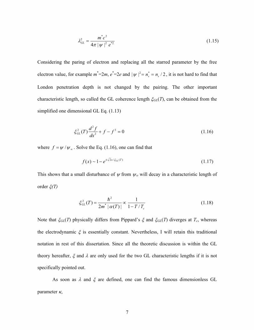
characteristic length, so called the GL coherence length ξ
2/|| ss nn*2 ==ψ
GL(T), can be obtained from the
simplified one dimensional GL Eq. (1.13)
0)( 32
22 =−+ ff
dxfdTGLξ (1.16)
where ∞= ψψ /f . Solve the Eq. (1.16), one can find that
)(/21~)( Tx GLexf ξ±− (1.17)
This shows that a small disturbance of ψ from ψ∞ will decay in a characteristic length of
order ξ(T)
c
GL TTTmT
/11
|)(|2)( *
22
−∝=
αξ h (1.18)
Note that ξGL(T) physically differs from Pippard’s ξ and ξGL(T) diverges at Tc, whereas
the electrodynamic ξ is essentially constant. Nevertheless, I will retain this traditional
notation in rest of this dissertation. Since all the theoretic discussion is within the GL
theory hereafter, ξ and λ are only used for the two GL characteristic lengths if it is not
specifically pointed out.
As soon as λ and ξ are defined, one can find the famous dimensionless GL
parameter κ,
7

0
2 )()(22)()(
Φ==
TTHTT c λ
ξλκ (1.19)
where ehπ
=Φ0 is the flux quanta. For typical classic pure superconductor, also called
Type I superconductor, κ << 1 and there is a positive surface energy associated with
interface between normal and superconducting region.
Fig.1.2: Comparison of flux penetration behavior between type I and type II superconductors.
1.5 Type II superconductors
In 1957, Abrikosov published an
important paper regarding the possible
existence of another type of
superconductor [1.8]. He investigated the
scenario of κ>>1 within the GL
framework and found that this type of
superconductor could have very different
properties from the Type I
superconductor. Abrikosov called it type
II superconductor to distinguish it from
the early type I variety. He also showed the exact break point between the two regimes
was at 2/1=κ . For superconductor with 2/1>κ , he found the diamagnetism could
be partially maintained even at H > Hc. In another word, instead of discontinuous
breakdown of superconductivity in a first-order transition at Hc for type I superconductor,
for type II superconductor, there is a continuous increase in flux penetration starting at a
8
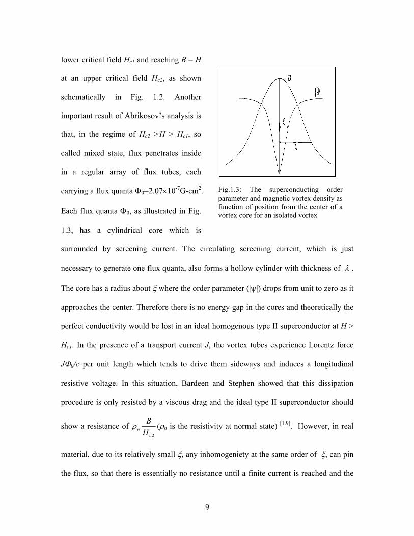
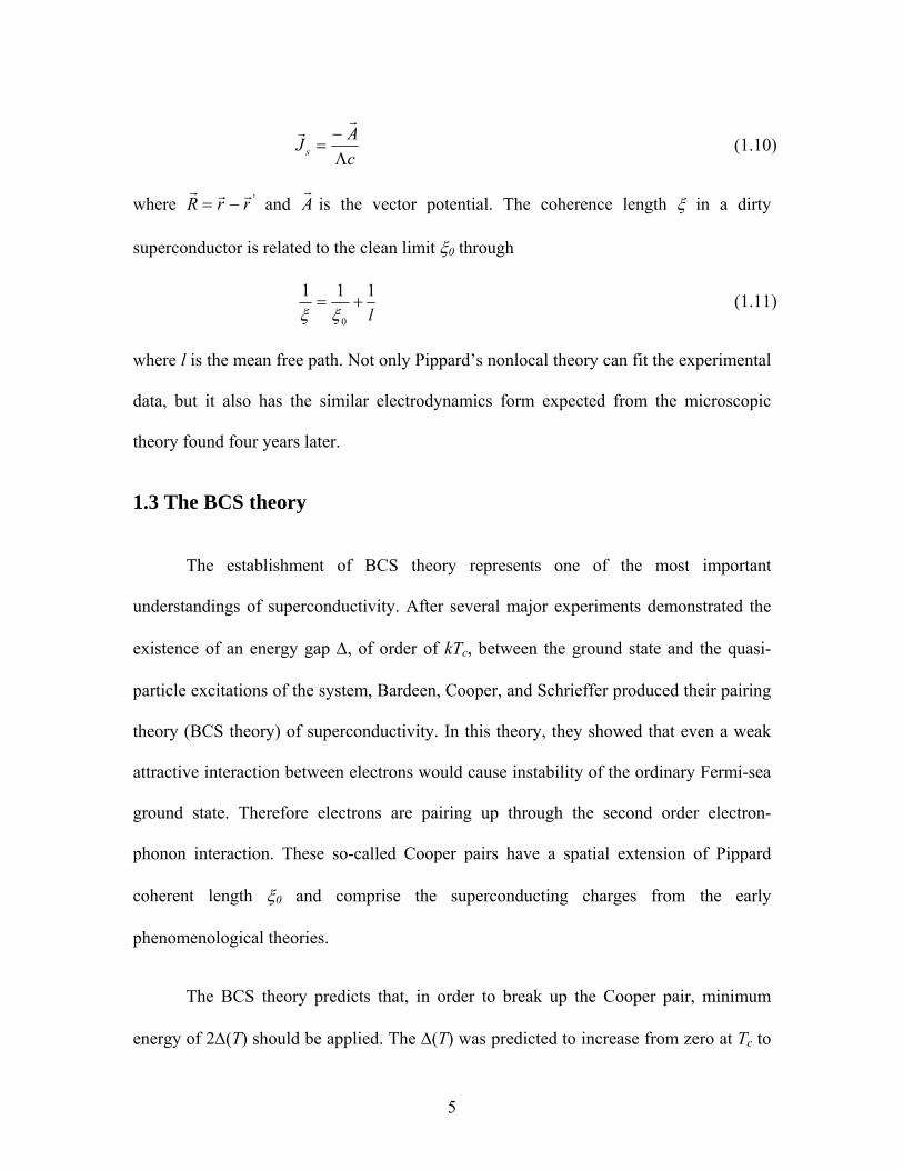
lower critical field Hc1 and reaching B = H
at an upper critical field Hc2, as shown
schematically in Fig. 1.2. Another
important result of Abrikosov’s analysis is
that, in the regime of Hc2 >H > Hc1, so
called mixed state, flux penetrates inside
in a regular array of flux tubes, each
carrying a flux quanta Φ0=2.07×10⁻⁷G-cm2.
Each flux quanta Φ0, as illustrated in Fig.
1.3, has a cylindrical core which is
surrounded by screening current. The circulating screening current, which is just
necessary to generate one flux quanta, also forms a hollow cylinder with thickness of λ .
The core has a radius about ξ where the order parameter (|ψ|) drops from unit to zero as it
approaches the center. Therefore there is no energy gap in the cores and theoretically the
perfect conductivity would be lost in an ideal homogenous type II superconductor at H >
Hc1. In the presence of a transport current J, the vortex tubes experience Lorentz force
JΦ0/c per unit length which tends to drive them sideways and induces a longitudinal
resistive voltage. In this situation, Bardeen and Stephen showed that this dissipation
procedure is only resisted by a viscous drag and the ideal type II superconductor should
show a resistance of 2c
n Hρ
Fig.1.3: The superconducting order parameter and magnetic vortex density as function of position from the center of a vortex core for an isolated vortex
B (ρn is the resistivity at normal state) [1.9]. However, in real
material, due to its relatively small ξ, any inhomogeniety at the same order of ξ, can pin
the flux, so that there is essentially no resistance until a finite current is reached and the
9

Lorentz force exceeds the pinning force. Therefore the whole business in terms of
superconductor application is to make the material “imperfect” in a specific way rather
than retaining a perfect material.
Unlike Type I superconductors, Type II superconductors typically can have a Hc2
as high as several tens of Tesla. Since the superconducting electrical property can be
maintained within Hc2 with introduction of pinning centers, many large-scale applications
such as superconducting magnet have been developed on conventional Type II
superconductors. To distinguish from the later discovered Type II superconductor with Tc
higher than 30 K (HTS), the conventional Type II superconductor is also called low Tc
superconductor (LTS).
1.6 High Temperature superconductivity
In 1986, Bednorz and Müller discovered the high Tc (~35K) superconductivity
in layered material LBCO dominated by copper oxide planes, for which they were
awarded the Nobel Prize in 1987. This discovery was surprising and exciting not only
because of the high Tc, but also because it revealed the great potential of a new class of
oxide superconductor. A big jump of Tc ~ 90K immediately followed, with the discovery
of YBa2Cu3O7-x(YBCO) nearly simultaneously by groups in the United States and China
[1.10]. As of this point, the highest Tc ~ 135K is found on mercury based HTS material and
this value can be further increased to ~ 164K if pressurized.
The discovery of HTS provides a great potential for industrial application as well
as a rich physical system for material science. With Tc above liquid nitrogen boiling
10
temperature, it has opened the way to a broader range of practical application than for the
traditional low Tc superconductor simply because cooling can be realized by readily
available liquid nitrogen. However, the ceramic nature of the cuprates also poses great
challenges to material scientists for several reasons: (1) It is hard to fabricate in useful
forms due to its brittle nature; (2) the high Tc combines with low vF results in a short ξ
and allows stronger fluctuations; (3) the anisotropy induced by layered structure reduces
the integrity of vortex lines as well as the efficiency of pinning. Despite all these
formidable obstacles, great accomplishments have been achieved in the past twenty years.
In the next chapter, we will briefly review the progress of HTS application, especially on
the aspect of power-related applications.
11
CHAPTER 2: Critical Current Density of HTS Film
Since the discovery of HTS, the promise of non-dissipation devices operating at
liquid-nitrogen temperature has stimulated a worldwide research tide. One of the most
prominent aspects is the application in the electric power area such as magnet, motors
and transmission lines. In order to make this ceramic material into a long, strong and
flexible conductor like copper wire, the first solution was to pack Bi-Sr-Ca-Cu-
O(BSCCO) superconducting powder into a silver tube[2.1]. Following a series of rolling,
annealing sequences and the final product was a 4-mm-wide flexible tape which can
carry the critical current over 100 A at 77 K. This so-called first-generation (1G) HTS
cable is widely used in the present-day HTS industry. However, the 1G HTS cable
fabrication heavily relies on the use of silver which makes it too expensive for most of
the commercial application. Another major setback comes from the intrinsic high
anisotropy of the BSCCO material itself, which strongly limits its current carrying
capability with even moderate magnetic field presence.
In the early 1990s, an alternative approach using thin-film expitaxy was
conceived [2.2]. This so-called second-generation coated conductor (CC) uses physical or
chemical procedures coating a thin epitaxial layer of HTS on metal tape. This process
needs very little silver and make the economy-of-scale cost reduction is possible. Also
the in-field behavior was improved because of the relatively weak anisotropy of YBCO
compound, which is regarded as the major candidate of 2G HTS CC. At this point, three
companies already demonstrated the great potential of 2G YBCO CC by recent
announcement of successful fabrication of YBCO tapes more than 100 meters long,
12

carrying 200A/cm-width at 77K [2.3-2.5]. SuperPower, one of these companies, has
delivered 10 km of YBCO CC for a power-distribution cable project in Albany, New
York [2.6]. The similar amount of YBCO CC was also delivered by another company,
American Superconductor, including two fault-current-limiter demonstrations. The
current cost ($/KA-m) of YBCO CC is about ten times of copper wire(~60$/KA-m) but
the gap is closing rapidly as the industries gear up for large scale application. Even with
such remarkable progress, the mission is still not accomplished. The challenge arises
from two important areas: performance in thick HTS film and at high applied magnetic
field. In another words, is there any potential existing to substantially reduce the
cost/performance ratio, and increase odds of commercial success? To answer this
question, first we have to go back to the fundamental property of HTS.
2.1 Limiting Factors of Critical Current Density
The fundamental property that makes superconductors attractive in power-related
applications is the ability to carry large current without any dissipation. However,
theoretically the zero dissipation is limited to a critical quantity, so-called critical current
density Jc. With a defined cross section area A, Jc translates to critical current Ic by Ic =
AJc. Therefore, understanding the major factors affecting Jc has been the central issue for
the HTS CC community.
13

From theoretical point of view, the superconducting current Js can be expressed in
the simple form of Eq. (1.14) within GL theory. This allows us to simplify the free-
energy expression Eq. (1.12) as
πψψβψα
821||||
2||
22*242 hvmff sn ++++= (2.1)
Use Eq. (2.1) to treat the case of a uniform current density though a thin film or wire with
transverse dimension much less than the penetration depth λ, for a given vs, we can
minimize Eq. (2.1) to find the optimum value of |ψ|2. The result can be written as
ss
ss vmveveJ )||2
1(2||2 2
222
αψψ −== ∞ (2.2)
It is not hard to find Js maximizes itself when and 3/||2 α=smv 22
32|| ∞= ψψ . Plug these
into Eq (2.2), we obtain the critical current density Jc and its temperature dependence
2/32/12 )1()(63
)()3
||(34
c
cc T
TT
TcHm
eJ −∝== ∞ λπαψ (2.3)
Despite complication given by the nonlinear treatment shown above, thermodynamically,
the critical current density Jc can be obtained by equating the density of kinetic energy to
that of condensation energy using the London descriptions
π
λπ8
221 2
222
2 cccs
HJc
mvn == (2.4)
14
and one obtains Jc = cHc/4πλ. This value exceeds GL result (2.3) by a factor of 1.84
because it fails to take into account the decrease in |ψ|2 with increasing current density.
Nevertheless, the above mentioned Jc poses the theoretic limit J0, the so-called “depairing
limit” for a thin uniform superconductor since superconductivity is associated with the
pairing of carriers.
Due to the small lower critical field Hc1 of HTS (and also type II superconductor),
a small amount of transporting current in the order of several tenth of the depairing Jc
will generate a self-field (SF) large enough to drive the system into mixed state. When an
external current J is applied to the vortex system, the vortex experiences the Lorentz
force per volume
r
cBJFL /rrr
×−= (2.5)
Within a perfect homogeneous system, this FL is only counteracted by the friction force
vF rrηη −= (2.6)
where is the steady-state velocity of the vortex system. The dissipation
arises due to the finite electrical field
ηcJBv /rrr
×=
cvBE /rrr×= (2.7)
generated as the consequence of vortex motion. Since J and E are anti-parallel, the power
η22 /)( cBJPrr
×= (2.8)
15

is dissipated and the property of transporting dissipation-free current is lost. In order to
recover the desired property of dissipation-free current flow, the vortex has to be pinned.
Therefore, the critical state in the mixed state is described by the equilibrium between the
Lorentz force FL and pinning force FP
PcL FcBJFrrrr
−=×= / (2.9)
and the Jc=cFP/B sets the depinning limit of the transporting current. Fortunately, in real
material, due to the relatively small ξ, any inhomogeniety at the same order of ξ affects
the order parameter and contributes to the finite pinning force FP, and thereby the
technological usefulness of Type II superconductor is recovered. Hence, improving
supercurrent carrying capability has become a matter of optimizing the pinning structure.
2.2 Flux Pinning in YBCO Film
Pinning arises from the localized material defects, crystalline imperfection and
secondary phase. Since the G-L coherence length ξ of HTS material are typically in the
order of nanometer, any defect with dimension larger than that could be potential pinning
center. Owing to the large number of defects naturally generated during the thin-film
growth, YBCO thin film usually has Jc one to two orders of higher than that of single
crystal.
Depending on its distribution and orientation within the SC matrix, the pinning
itself can be divided into two groups. One is correlated pinning and the other random
16
pinning. Correlated pinning arises from approximately parallel arrays of extended linear
or planar defects. Their effect becomes the most strong when the applied magnetic field
is aligned with them. The correlated pinning decreases with the increasing misalignment
between the defects and vortices. So the signature of correlated pinning is a peak in the
angular dependence of Jc. For example, the typical HTS has a layer structure consisting
alternative strong superconducting layers (ab-plane) and weak superconducting layers [2.7].
This layered structure results in a strong modulation of order parameter and hence
provides a preferential pinning for magnetic flux B parallel to them. It has been
confirmed that this preferential pinning, so called “intrinsic pinning”, contributes the
angular dependence of Jc [2.8]. There are some additional planar defects related to
imperfect epitaxial growth such as stacking faults and twin boundaries which could also
provide directional pinning enhancement as B parallel to them. It is also suggested that
linear growth defect which threads through film thickness, such as edge and screw
dislocations could play an important role for the observed high Jc in YBCO films [2.9, 2.10].
Sequential etching experiments by Dam et al showed a “characteristic field”, beyond
which Jc drops with increasing field, is correlated with the surface density of screw
dislocations [2.11]. “Random” or “uncorrelated pinning” is due to randomly distributed
localized defects, which are generally point-like defects and in this case the pinning is
relatively uniform for all field orientations. Among those point-like defects, foremost are
the oxygen vacancies in the strongly superconducting CuO2 plane (ab-plane) [2.12]. Such
atomic size vacancies are potentially pinning centers due to the small ξ of HTS material.
It is also suggested that large point defects, usually are sparse insulating or normal
metallic secondary-phase inclusions (Y2O3, Y124), could provide strong pinning in
17

YBCO films [2.13]. These defects, typically with diameter ~10 − 20 nm and density ~ 1021
− 1023 m-3, are known to exist in sputter-deposited [2.14, 2.15], pulsed laser deposited [2.16]
and solution-based metal organic deposited YBCO films [2.17]. Some authors also reported
observation of high Jc in porous YBCO films grown on miscut substrates [2.18]. It is
suggested that these pores could provide strong correlated pinning which improves Jc at
low field.
Unfortunately the HTS community has not reached a consensus regarding the
dominant pinning centers in typical as-grown YBCO films yet. This diversification brings
difficulty to directly correlate Jc with certain type of defect since pinning is not simply
additive. What further complicates Jc is the pronounced thermal fluctuation of flux,
which is inherently associated with the anisotropic nature of HTS material.
2.3 Thermally Activated Flux Motion
The technologically most interesting property of HTS is its ability to carry a bulk
current density J with essentially no dissipation. This current density is determined by
the magnetic flux density gradient via Maxwell’s equation
r
JcBrr
)/4( π=×∇ (2.10)
Therefore a YBCO film carrying a transport current at a finite temperature is only in a
metastable state from a thermodynamic point of view. In another word, this current is
bound to decay due to thermally activated flux motion (TAFM). This phenomenon is also
18

known as flux creep and was first introduced by Anderson in 1962 [2.19]. At a finite
temperature T, Anderson’s flux creep model leads to the famous logarithmic time (τ)
decay of the critical (diamagnetic) current Jc,
)]/1ln(1[)( 0τττ +−=c
c UTJJ (2.11)
where τ0 is a time constant determined by pinning structure and Uc is the energy barrier
against thermally activated flux motion. Typical Uc obtained in magnetic relaxation
experiments are in the range of 100-1000 K[2.20]. The decay coefficients T/Uc of LTS, in
the case in which J is close to its critical value Jc, are of the order of 10-3 [2.21]. However,
in the HTS material such as YBCO single crystal, the decay coefficients turn out to be
much larger, reaching even the order of 5% at 20 K [2.22]. This large logarithmic decay
rate is the result of several factors such as the small Uc, which is the consequence of
small ξ, and the large anisotropy due to the HTS layered structure. If combining with the
typical time factor τ/τ0 in the order of 20 (assuming waiting time τ = 60 seconds), this
large decay rate leads to an approximately halved experimentally measured current
density due to the flux creep, as compared with the Jc predicted from critical state even at
a low T ~ 10 K. Therefore for practical situation, besides pinning behavior, TAFM is the
other dominant factor dictating Jc. Since thermal creep could have occurred much earlier
before the critical state, it is worth knowing that determination of critical current density
of HTS material is not trivial. Precautions have to be taken to interpret reported Jc values
since various characterization techniques usually give very different Jc’s even on the
same sample.
19

2.4 YBCO Film Fabrication and Characterization
2.4.1 Pulsed Laser Deposition
Pulsed Laser Deposition (PLD) plays a prominent role in the fabrication of HTS
CC and record numbers of Jc and Ic have been achieved using this method. As a major
method for depositing films of complex material, PLD has been well established since its
first introduction by Smith and Turner in 1965 [2.23]. The real breakthrough of PLD
fabrication of epitaxial HTS films was made at Bell
Communications Research by Dijkkamp in 1987
[2.24]. Conceptually, the process of PLD is very
simple and the fabrication can be well controlled by
adjusting several critical parameters such as growth
temperature, oxygen partial pressure and laser
energy density. Therefore it serves as the major
YBCO film fabrication technique in this dissertation
study. During the fabrication process, a pulsed
ultraviolet (UV) laser (wave length is 248 nm) beam
is generated by the Lambda Excimer Laser (COMPex 205) and directed into the vacuum
chamber through a UV transparent window and two UV mirrors. The raw laser beam has
the output energy about 200 mJ. This beam is then focused onto the target surface into a
3.5 x 1.5 mm2 spot with the energy density ~ 3.2 J/cm2 by a lens outside the vacuum
chamber. Since in most of the materials, the UV laser energy is absorbed only by the
outermost layer of the target with thickness less than 100 nm, combining this
Target Targe
t
Target
Heater
Target Targe
t
Target
Heater
Fig. 2.1: plume generated by a focused pulsed UV laser beam on a YBCO target.
20

phenomenon with the extremely short pulse duration less than 50 ns, this high energy
density causes the local surface temperature to rise up to thousands of degrees of Celsius
(oC) and evaporate a small amount of target material in a very short time. Such non-
equilibrium heating process generates a flash of evaporated material called a plume that
deposits on a substrate, producing a film with identical cations composition as the target
surface. During the YBCO film growth, the substrate’s temperature is held at 760-790 oC
and the oxygen pressure is dynamically controlled at 230 to 300 mTorr by a throttle valve.
Following the deposition, the film is further oxygenated at 490 oC for 50 minutes to
realize a phase transition from a non-superconducting tetragonal phase to
superconducting orthorhombic phase.
Target
Since PLD offers one effective method to “photocopy” target composition into
thin film, it has been widely applied by researchers to systematically incorporate defects
in YBCO films. Specific approaches such as substrate surface decoration [2.25, 2.26],
impurity additions [2.27, 2.28], rare-earth addition and/or substitutions [2.29, 2.30] have been
made using PLD in the past five years and many exciting results have been obtained.
Construction of multilayer structure can also be realized using PLD by simply positioning
different targets under the laser beam.
2.4.2 YBCO Film Characterization
It is well known that large angle grain boundary greatly suppresses Jc since the
strong coupling only occurs when the ab-planes are well aligned. This necessitates the
epitaxial growth of YBCO film if its high critical current carrying capability for power-
related applications is desired. The most powerful tool for characterizing crystallinity is
21

X-ray diffraction (XRD), which is also the major characterization technique for
microstructure analysis in this work. Under carefully optimized growth condition, the
PLD YBCO films are c-axis oriented epitaxial films with their a-axis and/or b-axis well
aligned in plane with the (100) and (010) axes of the single crystal substrates.
Obviously the most interesting quantities in term of HTS application are its
superconducting properties such as Tc and Jc. The superconductivity properties are
characterized with either electrical transport method or magnetization using SQUID
magnetometer. Determination of Tc is rather straight forward and both techniques give
consistent results. However, Jc characterization involves complications owing to the flux
creep nature of HTS material, even though both techniques originated from the same
principle ⎯ movement of flux lines generates an electrical field E and leads to
observable dissipation. Regarding each individual technique, the transport measurement
is viewed as a simple model-free means to characterize Jc via the I-V characteristics. The
typical I-V curves measured on a 500 x 20 μm micro-bridge patterned from a 0.3 μm-
thick YBCO film is shown in Fig. 2.2. The measurement was conducted at 77 K and
various magnetic fields. The criteria of Jc was chosen as Ec = 1 μV/cm which is typically
22

Fig. 2.2: I-V curves measured on a YBCO film at 77K and various fields.
Fig. 2.3: M-H hysteretic loops measured on a YBCO film at 10, 50, 77 and 86K.
0 10000 20000 30000 40000 50000
-0.6
-0.4
-0.2
0.0
0.2
0.4
0.6 10K 50K 77K 86K
decreasing H
emu
H(Oe)
increasing H
0.00 0.05 0.10 0.15 0.20 0.250.0
0.1
0.2
0.3
0.4
0.5
1μV/cm
1T
applied by the majority of the HTS community. As for magnetic characterization, due to
the restraining force FP is always against flux motion, the flux density gradient is then
established across the sample. It causes hysteresis of the magnetic moment (M) during the
magnetization of a hard superconductor. Hysteretic loops measured on a 0.25 μm-thick
YBCO film at various temperatures are shown in Fig. 2.3. The magnetization difference
ΔM between up and low branches is proportional to Jc, according to the Bean model in
the situation where the H is applied along the film surface [2.31]. For the geometry with H
applied perpendicular to the film, which is the most important scenario for most of the
applications, the modified Bean model [2.32] gives
)]3/1(/[20 lwwMJ c −Δ= (2.12)
0.5T
Current(A)
Volta
ge(μ
V)
SFI-V curves at 77K and various fields
0 10000 20000 30000 40000 50000
-0.6
-0.4
-0.2
0.0
0.2
0.4
0.6 10K 50K 77K 86K
decreasing H
emu
H(Oe)
increasing H
0.00 0.05 0.10 0.15 0.20 0.250.0
0.1
0.2
0.3
0.4
0.5
1μV/cm
1T
Current(A)
Volta
ge(μ
V)
0.5TSF
I-V curves at 77K and various fields
0.00 0.05 0.10 0.15 0.20 0.250.0
0.1
0.2
0.3
0.4
0.5
1μV/cm
1T
Current(A)
Volta
ge(μ
V)
0.5TSF
I-V curves at 77K and various fields
23

where w and l is the width and length of the film and M here is the magnetic moment per
volume. Fig. 2.4 illustrates the Jc as function of H measured on a same sample using
traditional transport (transport Jc) and SQUID magnetization (magnetic Jc). It can be seen
that, even without applying H, the transport Jc is much higher than the magnetic Jc and
the ratio between them is about 1.5 at 77 K. This ratio increases to about 10 at 1 Tesla
and keeps increasing with H field. One important question immediately following is that
which technique gives the Jc closer to the practical situation. Considering the effective
thermal conduction in the real device working at 60 to 70 K, larger scale application
especially as superconducting magnet requires that the internal power dissipation be less
than 10-5-10-6W/cm3. This corresponds to a criterion E-field in the range of 10-3-10-4
µV/cm, which is 3-4 orders of magnitude below the typical 1 μV/cm applied in the
0 1 2 3 4 5
1E-3
0.01
0.1
1
Magnetic Jc
Transport Jc
J c(MA
/cm
2 )
μ0Η(T)
77KSample ID:WT122706
Fig. 2.4: Jc as function of H measured on a same sample using traditional transport (transport Jc) and SQUID magnetization (magnetic Jc).
24
transport measurement. On the other hand, since ΔM changing with H is also due to the
flux creep when one characterizes Jc using SQUID magnetometer, it continuously
generates an E-field across a sample and the E-field in the perimeter is given by [2.33]
12
)/()( 0 ττπμ ddJa
JE ≈ (2.13)
which is also proportional to τ(dM/dτ) since dJ/dτ = dM/dτ. This time dependent study,
so called magnetic relaxation experiment, has been done using a SQUID-based
magnetometer [2.34]. Using the typical instrumental settling time of 10-30 seconds, the
resulting E-fields were found in the range of 10-3 – 10-4µV/cm. Therefore the SQUID
magnetization has been applied as the major Jc characterization technique in my study
due to its close resemblance to practical applications.
2.5 The Effect of Applied Magnetic Field on Jc
It is known that the pinning structure is very sensitive to experimental conditions
such as growth techniques, growth conditions, substrates and the buffer layer used.
Experimentally it is difficult to fabric samples with an exclusive pinning structure and Jc
might be determined by the interplay between vortices and multi-scale pinning potential.
The situation also depends on the applied magnetic field H. At low H, inter-vortex
distance is large and inter-vortex interaction shall be negligible. In this single-vortex (SV)
pinning regime, while extrinsic factors such as microstructure degradation and material
non-uniformity are absent, Jc is simply determined by the pinning quality of the dominant
pinning centers and
25
0/c PJ cF= Φ (2.14)
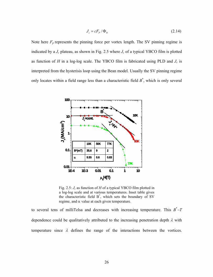
Note here Fp represents the pinning force per vortex length. The SV pinning regime is
indicated by a Jc plateau, as shown in Fig. 2.5 where Jc of a typical YBCO film is plotted
as function of H in a log-log scale. The YBCO film is fabricated using PLD and Jc is
interpreted from the hysterisis loop using the Bean model. Usually the SV pinning regime
to several tens of milliTelsa and decreases with increasing temperature. This B
only locates within a field range less than a characteristic field B*, which is only several
*−T
dependence could be qualitatively attributed to the increasing penetration depth λ with
temperature since λ defines the range of the interactions between the vortices.
1E-4 1E-3 0.01 0.1 1 100.01
0.1
1
10
100
Jc =H -α
J c(MA
/cm
2 )
μ0H(T)
10K
50K
77K
Jc=cont.
B*
0.830.60.55α
2935.6B*(mT)
77K50K10K
1E-4 1E-3 0.01 0.1 1 100.01
0.1
1
10
100
Jc =H -α
J c(MA
/cm
2 )
μ0H(T)
10K
77K
50K
Jc=cont.
B*
0.830.60.55α
2935.6B*(mT)
77K50K10K
1E-4 1E-3 0.01 0.1 1 100.01
0.1
1
10
100
Jc =H -α
J c(MA
/cm
2 )
μ0H(T)
10K
77K
50K
Jc=cont.
B*
0.830.60.55α
2935.6B*(mT)
77K50K10K
Fig. 2.5: Jc as function of H of a typical YBCO film plotted in a log-log scale and at various temperatures. Inset table gives the characteristic field B*, which sets the boundary of SV regime, and α value at each given temperature.
26

Specifically, for inter-vortex distance a < λ the inter-vortex interaction is logarithmic
while for large distance a > λ, it becomes exponentially small[2.35].
As H increases, both vortex density and the vortex-vortex interaction increase. In
this case, not only pin’s quality Fp but also density np matters. Empirically Jc can be fitted
by Jc~H-α represented by a line in log-log scale. The smaller the α-value, the better is the
in-field Jc performance. Several factor such as temperature, defect structure even
characterization technique applied could influence the α-value. The effect of temperature
is illustrated in the inset table of Fig. 2.5. It can be seen that higher temperature leads to
larger α-value. Qualitatively this can be explained by the pronounced thermal assisted
flux motion (TAFM) at higher temperatures. On the other hand, the α-value can be
greatly reduced by insertion of stronger pinning centers such as BaZrO3 (BZO) nano-rod.
A 40% reduction in α-value was observed in our group where same deposition and
measuring techniques were applied. The power relation Jc~H-α also evolves with
increasing H and at higher H, a much faster Jc reduction with increasing H is observed as
the system approaches to the irreversible field BBirr. In addition to the possibility of limited
pin’s density, a much more enhanced thermal fluctuation could be another reason for this
accelerated Jc decay as suggested by the faster drop at 77 K. Further complication
involved in the attempts to quantify the Jc-H dependence originates from the different
characterization techniques applied in various studies. Despite the difference in Jc values,
both the α value and characteristic fields such as B and Birr*
B are influenced by
characterization technique [2.34], which is also observed as shown in the Fig. 2.4. However,
27

qualitatively the H dependence of Jc could be understood as the outcome of interactions
between vortices and defects plus the thermal fluctuation.
2.6 The Effect of Temperature on Jc
Comparing to field dependence of Jc, the effect of temperature on Jc is more
straightforward. As shown in Fig. 2.6, where the SF Jc is plotted as the function of
reduced temperature T/Tc, it monotonically decreases with increasing T. Moreover, Jc− T
can be well fitted by the flux creep model Jc ~ exp(-T/46.8) with R2 of 0.9948, indicating
that TAFM is probably the dominant mechanism of Jc− T [2.36]. Deviations are observed,
however, near Tc. This
could be caused by the
additional temperature
dependence of the carrier
density ns ~ (1-T/Tc) near Tc,
as suggested by G-L theory.
How Jc evolves
with magnetic field and
temperature is of great
importance to the HTS
material application,
0.0 0.2 0.4 0.6 0.8 1.0
0.1
1
10
t=T/Tc
J c(MA
/cm
2 )
Jc of PLD YBCO film flux creep model: Jc~exp(-T/T0)
Christen and Thompson, Nature 364, 96(1993)
Fig. 2.6: Jc as function of reduced temperature T/Tc measured on a typical YBCO film plotted in a semi-log scale. Solid line represents the flux-creep model predicted Jc−T dependence and T0 is 46.8 K
28

especially in the large-scale power-related aspect. Qualitative or at least semi-
quantitatively we have understood their effects and the next step would be focused on
how to improve the performance of HTS film by defect structure engineering. However,
there are still many interesting and also puzzling phenomena that challenge our
understanding for both technical development and basic physics in HTS films. This
dissertation will be focused on the long-standing issue: thickness dependence of the
critical current density in YBCO films.
2.7 Thickness Dependence of Jc in YBCO Film
Aiming at the large critical current carrying capability at a fixed T and H, one of
the most important areas in YBCO CC research is to obtain high current carrying
capability. Two different distinct routes are: (a) further increasing Jc by optimizing
growth conditions; (b) realizing the state-of-art thin-film Jc in a thick film. It seems the
former approach is limited by the HTS nature of pronounced thermal creep even for the
less anisotropic YBCO. Some researchers have switched gears to the latter route since
1993. Foltyn et al reported their experimental results of PLD YBCO films with various
thickness (t) on single crystal substrates [2.37]. Unfortunately, Jc monotonically decreases
with increasing film thickness from 0.2 μm to 1 μm as measured at 77K in SF. Further
increasing film thickness up to 6.4 μm has less effect on Jc and Jc saturates at 1MA/cm2.
Crystalline degradation caused Jc reduction was excluded through X-ray analysis but
progressive film discontinuity with increasing thickness was suspected by the authors. As
the follow up study, Foltyn et al also studied Jc−t dependence of YBCO films deposited
29

on metal substrates using sequential ion milling [2.38]. Due to the poor in-plane texture on
metal tape, the overall Jc was lower than those on single crystal substrates(see Fig. 2.7).
Interestingly, Jc−t behavior was not affected qualitatively by the choice of substrates. Ion
milling of two thicker films (3.0 μm and 4.7 μm) and one thinner film (0.68 μm)
identified “dead layer”, where no current was carried, on top and bottom of the thicker
films while none of them was observed in the thinner one (see Fig. 2.8). They concluded
that the top “dead layer” was associated with a distinct microstructural transition at 1 − 2
μm, while the bottom one was related to chemical inter-diffusion across the film/substrate
interface.
YBCO thickness(µm)
Fig. 2.8 (as plotted in Ref. [2.38]): Milling generated Jc−d from three CC with thickness of 0.68, 3.0 and 4.7 μm. “Dead layer” is observed for two thick samples.
Fig. 2.7(as plotted in Ref. [2.37]): Jc−t comparison between YBCO films grown on single crystal substrates and metal tape at 75K and self-field.
A comparative study of Jc−t of PLD YBCO films grown on single crystal SrTiO3
(STO) substrates and metal tape (RABiTS) incorporated with microstructure evolution
with thickness was reported by B. W. Kang et al [2.39]. Similar Jc−t was observed for both
types of samples except the overall high Jc was observed for YBCO films grown on
30
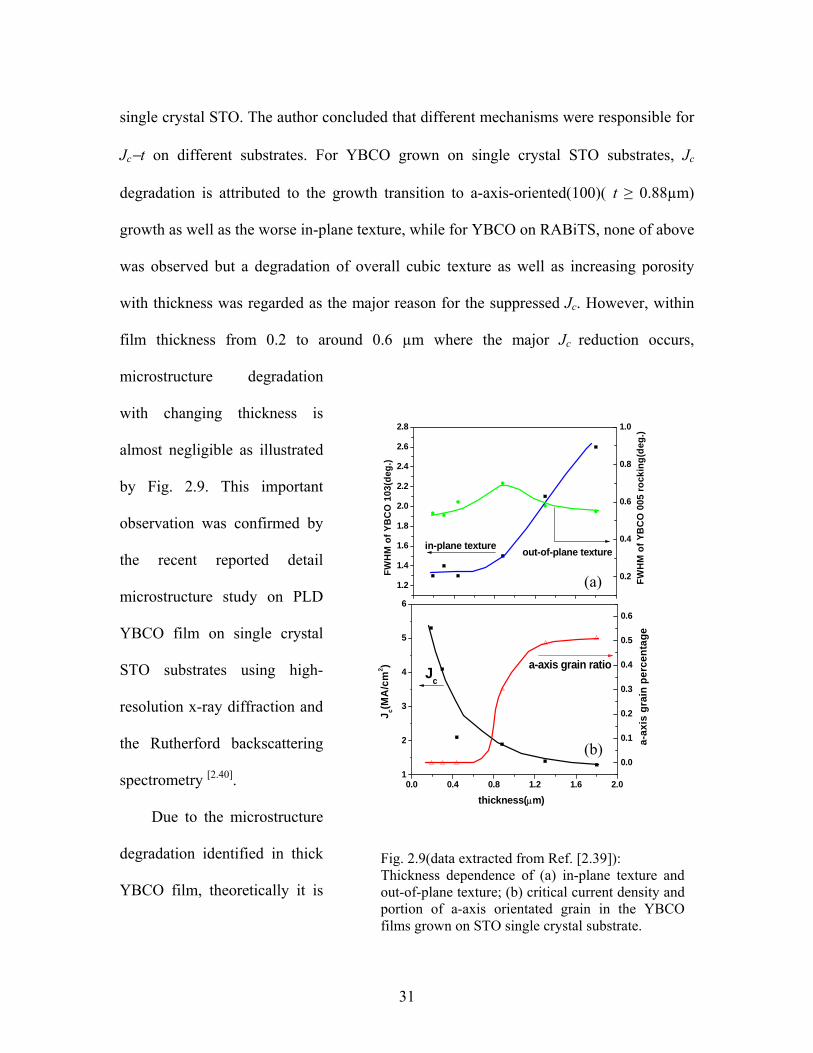
single crystal STO. The author concluded that different mechanisms were responsible for
Jc−t on different substrates. For YBCO grown on single crystal STO substrates, Jc
degradation is attributed to the growth transition to a-axis-oriented(100)( t ≥ 0.88µm)
growth as well as the worse in-plane texture, while for YBCO on RABiTS, none of above
was observed but a degradation of overall cubic texture as well as increasing porosity
with thickness was regarded as the major reason for the suppressed Jc. However, within
film thickness from 0.2 to around 0.6 µm where the major Jc reduction occurs,
microstructure degradation
with changing thickness is
almost negligible as illustrated
by Fig. 2.9. This important
observation was confirmed by
the recent reported detail
microstructure study on PLD
YBCO film on single crystal
STO substrates using high-
resolution x-ray diffraction and
the Rutherford backscattering
spectrometry [2.40].
(a)
(b)
Fig. 2.9(data extracted from Ref. [2.39]): Thickness dependence of (a) in-plane texture and out-of-plane texture; (b) critical current density and portion of a-axis orientated grain in the YBCO films grown on STO single crystal substrate.
1.2
1.4
1.6
1.8
2.0
2.2
2.4
2.6
2.8
0.2
0.4
0.6
0.8
1.0
out-of-plane texture
FWH
M o
f YB
CO
005
rock
ing(
deg.
)
FWH
M o
f YB
CO
103
(deg
.)
in-plane texture
0.0 0.4 0.8 1.2 1.6 2.01
2
3
4
5
6
0.0
0.1
0.2
0.3
0.4
0.5
0.6
a-ax
is g
rain
per
cent
age
J c(MA
/cm
2 )
thickness(μm)
Jca-axis grain ratio
Due to the microstructure
degradation identified in thick
YBCO film, theoretically it is
31
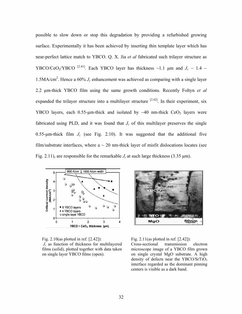
possible to slow down or stop this degradation by providing a refurbished growing
surface. Experimentally it has been achieved by inserting thin template layer which has
near-perfect lattice match to YBCO. Q. X. Jia et al fabricated such trilayer structure as
YBCO/CeO2/YBCO [2.41]. Each YBCO layer has thickness ~1.1 μm and Jc ~ 1.4 −
1.5MA/cm2. Hence a 60% Jc enhancement was achieved as comparing with a single layer
2.2 μm-thick YBCO film using the same growth conditions. Recently Foltyn et al
expanded the trilayer structure into a multilayer structure [2.42]. In their experiment, six
YBCO layers, each 0.55-μm-thick and isolated by ~40 nm-thick CeO2 layers were
fabricated using PLD, and it was found that Jc of this multilayer preserves the single
0.55-μm-thick film Jc (see Fig. 2.10). It was suggested that the additional five
film/substrate interfaces, where a ~ 20 nm-thick layer of misfit dislocations locates (see
Fig. 2.11), are responsible for the remarkable Jc at such large thickness (3.35 μm).
Fig. 2.10(as plotted in ref. [2.42]): Jc as function of thickness for multilayered films (solid), plotted together with data taken on single layer YBCO films (open).
Fig. 2.11(as plotted in ref. [2.42]): Cross-sectional transmission electron microscope image of a YBCO film grown on single crystal MgO substrate. A high density of defects near the YBCO/SrTiO3interface regarded as the dominant pinning centers is visible as a dark band.
32

It should be noticed that Jc−t seems to be independent of growth technique.
Similar trend was also observed on films produced by liquid phase epitaxy [2.43],
chemical-vapor deposition [2.44], ex situ BaF2 [2.45] and metal-organic deposition processes
[2.46]. Feldmann et al reported an observation of bilayer structure in ex situ BaF2
processed 2.9 μm-thick YBCO film [2.45]. The ion-milling generated Jc−d (d refers to
remaining thickness), which is shown in Fig. 2.12(a), displays uniform Jc across the
entire thickness. However, Jc−d deviates from Jc−t with overall lower Jc. Interestingly,
Jc−d of a thinner 2.0-μm-thick film, which is shown in Fig. 2.12(b), seems approaching
original Jc−t curve. According to the author, the difference between the milling generated
Jc−d and Jc−t measured on as-grown YBCO film could be the result of prolonged growth
time, which promoted a higher degree of interfacial degradation. Thus one may speculate
that, without microstructure and interfacial degradation, the Jc−d should have followed
the sub-linear thickness dependence. The question then arises that whether Jc−t reflects
an intrinsic interaction between vortex and surrounding pinning landscape? Knowing that
Jc is not only determined by a still unknown pinning structure, but also the nature of flux
creep, accurate quantification of Jc−t seems necessary.
33
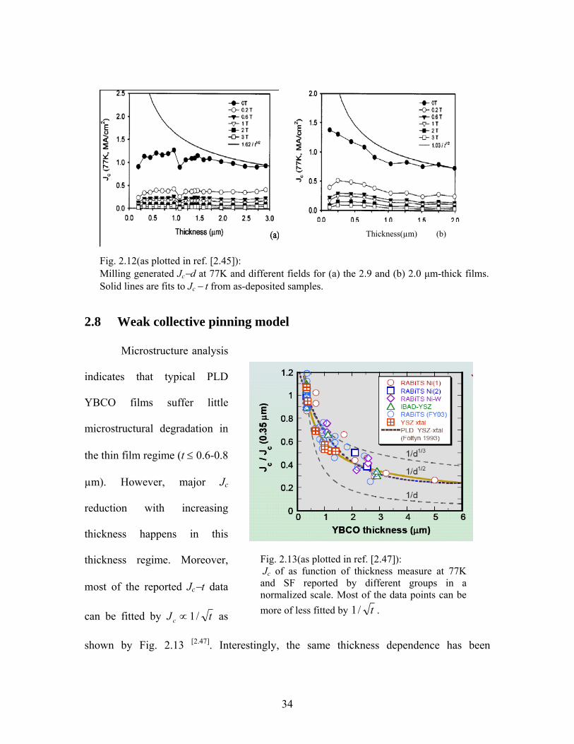
Thickness(µm) (b)
Fig. 2.12(as plotted in ref. [2.45]): Milling generated Jc−d at 77K and different fields for (a) the 2.9 and (b) 2.0 μm-thick films. Solid lines are fits to Jc − t from as-deposited samples.
2.8 Weak collective pinning model
Microstructure analysis
indicates that typical PLD
YBCO films suffer little
microstructural degradation in
the thin film regime (t ≤ 0.6-0.8
µm). However, major Jc
reduction with increasing
thickness happens in this
thickness regime. Moreover,
most of the reported Jc−t data
can be fitted by tJc /1∝ as
shown by Fig. 2.13 [2.47]. Interestingly, the same thickness dependence has been
Fig. 2.13(as plotted in ref. [2.47]): Jc of as function of thickness measure at 77K and SF reported by different groups in a normalized scale. Most of the data points can be more of less fitted by t/1 .
34
predicated by weak collective pinning model proposed by Larkin and Ovchinnilov in
1979 [2.48].
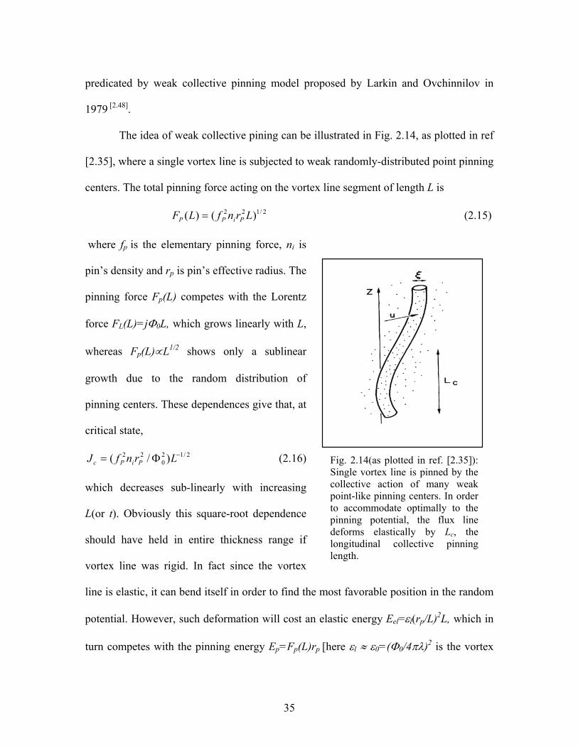
The idea of weak collective pining can be illustrated in Fig. 2.14, as plotted in ref
[2.35], where a single vortex line is subjected to weak randomly-distributed point pinning
centers. The total pinning force acting on the vortex line segment of length L is
(2.15) 2/122 )()( LrnfLF PiPP =
where fp is the elementary pinning force, ni is
pin’s density and rp is pin’s effective radius. The
pinning force Fp(L) competes with the Lorentz
force FL(L)=jΦ0L, which grows linearly with L,
whereas Fp(L)∝L1/2 shows only a sublinear
growth due to the random distribution of
pinning centers. These dependences give that, at
critical state,
2/120
22 )/( −Φ= LrnfJ PiPc (2.16)
which decreases sub-linearly with increasing
L(or t). Obviously this square-root dependence
should have held in entire thickness range if
vortex line was rigid. In fact since the vortex
line is elastic, it can bend itself in order to find the most favorable position in the random
potential. However, such deformation will cost an elastic energy Eel=εl(rp/L)2L, which in
turn competes with the pinning energy Ep=Fp(L)rp [here εl ≈ ε0=(Φ0/4πλ)2 is the vortex
Fig. 2.14(as plotted in ref. [2.35]): Single vortex line is pinned by the collective action of many weak point-like pinning centers. In order to accommodate optimally to the pinning potential, the flux line deforms elastically by Lc, the longitudinal collective pinning length.
35

line tension]. At L>Lc, where Lc is defined by the equality Eel(Lc)= Ep(Lc), the vortex can
readjust itself elastically to the optimal local configuration, consequently the FP(L) grows
linearly with increasing L and the square-root dependence LJc /1∝ is cut off. The
vortex then breaks into segments with length of Lc, each of which is pinned
independently and competes as one unit with the Lorentz force FL(Lc)= jΦ0Lc.
is called the correlated pinning length or Larkin length. Since f3/1220 )/( ipc nfL ε= P is not
directly accessible in an experiment, the ratio Jc/J0 is typically used as the fundamental
quantity characterizing the strength of pinning potential and Larkin length can be
expressed in a simple form as Lc ≈ rp(J0/Jc)1/2.
With the assumption that random distributed point-like defects determine the Jc in
YBCO films, it is plausible to apply the weak collective pinning model to describe the
vortex behavior in PLD YBCO films. Considering a superconducting film at weak field
where vortex-vortex interaction is negligible, Jc as function of thickness can be described
with the weak CP model as:
tJc /1∝ (t < Lc, 2D collective pinning regime)
0c cJ J= (t>>Lc, 3D bulk pinning regime)
where Jc0 is the bulk current density only depends on T and H. However, the Lc given by
the weak CP model is much smaller than that of the thickness range where Jc−t occurs.
For example, taking typical Jc of 4MA/cm2 for YBCO film and J0 of 36MA/cm2 at 77K
and SF, the Lc is found to be 4.5 nm. It should be realized that YBCO film represents a
strong pinning system in which the Jc/J0 ratio is one to two orders of magnitude higher
than that of weak pinning system such as YBCO single crystal. This raises a question
36

whether the result of weak CP model can be directly applied on strong pinning system
without any modification.
2.9 Summary
The most attractive nature of HTS material is their ability to carry large current
with very minimal dissipation. Their current carrying capability is influenced by both
temperature and applied magnetic field, owing to the dissipative nature of flux motions
induced by both TAFM and Lorentz-type driving force. Jc responses to a changing
temperature and magnetic field can be understood as a result of flux dynamics even
without knowing the detail pinning structure. However, regarding the thickness
dependence of critical current density, even though it quantitatively follows the collective
pinning behavior at 77 K and SF, it occurs in a thickness range far beyond the predicted
one. This discrepancy may arise from the different pinning environment in film and
crystal, and necessitate modifications of the original weak pinning CP theory. On the
other hand, since thermal fluctuation also plays an important role and most of the
reported Jc−t data is only at 77 K and SF, it is also important to expand the investigation
scope to a larger temperature and field region. This will serve the purpose of further
quantifying Jc−t and providing the insight into the underlying mechanism.
37

CHAPTER 3: The Effect of Temperature and Magnetic Field
on Thickness Dependence of Critical Current Density
3.1 The Effect of Temperature on Jc−t
YBCO films were fabricated on single crystal (100) LaAlO3 (LAO) substrates
using pulse laser deposition (PLD) technique. The laser energy density on the target was
~ 3.2 J/cm2 and the repetition rate was 10 Hz. The deposition was carried out onto
substrates heated to 765 °C at 230 mTorr oxygen followed by the oxygen annealing in
360 Torr O2 for 50 minutes [3.1]. About 24 films were fabricated with variable thicknesses
ranging from 0.01 to 0.7 µm to assure reproducibility. The thickness was calibrated with
Tencor P16 profiler. The superconducting properties of the samples were characterized
using a Quantum Design SQUID magnetometer. The superconducting transition
temperature (Tc) of the samples was obtained from zero-field-cooled (ZFC)
magnetization (M) as function of T and the Jc was interpreted from sample’s hysteresis
M−H loop using the Bean model [3.2].
Most of the films thicker than 0.05 µm have the magnetically measured Jc values
greater than 2 MA/cm2 at 77K and SF. Note that the magnetic Jc at SF and 77 K
interpreted from the irreversible magnetization is usually 1.5~2 times lower than that
from the transport measurement [3.3]. This means that the quality of the samples used for
this experiment is comparable to that of standard high-quality YBCO films. However, the
38

superconductivity degrades dramatically when t decreases to less than 0.05 µm. Since the
defect structure strongly depends on the substrate termination, especially at the early
stage of epitaxy, this degradation is most probably associated with atomic disorder
(cation and ionic disorder) near the film/substrate interface. However, with increasing t
beyond certain critical thickness tc, the epitaxial stress (or strain) will be relieved
accompanying with the appearance of structural defects. In particular, this critical
thickness tc up to which the film remains under epitaxial stress or strain depends on the
substrate termination. The reported tc is usually between 0.015 to 0.06 µm depending on
the substrate used [3.4]. In our study, since the mismatch between YBCO film and LAO
substrate is ~ 2.6% which is comparable to 2.1% on SrTiO3 [3.5], this critical thickness is
estimated to be ~ 0.06 µm.
The Zeor-Field-Cooled (ZFC) M−T measurement results on seven samples of
various thicknesses are shown in Figure 3.1. The applied H field is 10 Oe along the c-axis
of the film. The magnetic moment M is normalized to its absolute value at 10 K to
eliminate the effect of sample to sample difference in demagnetization factors.
39
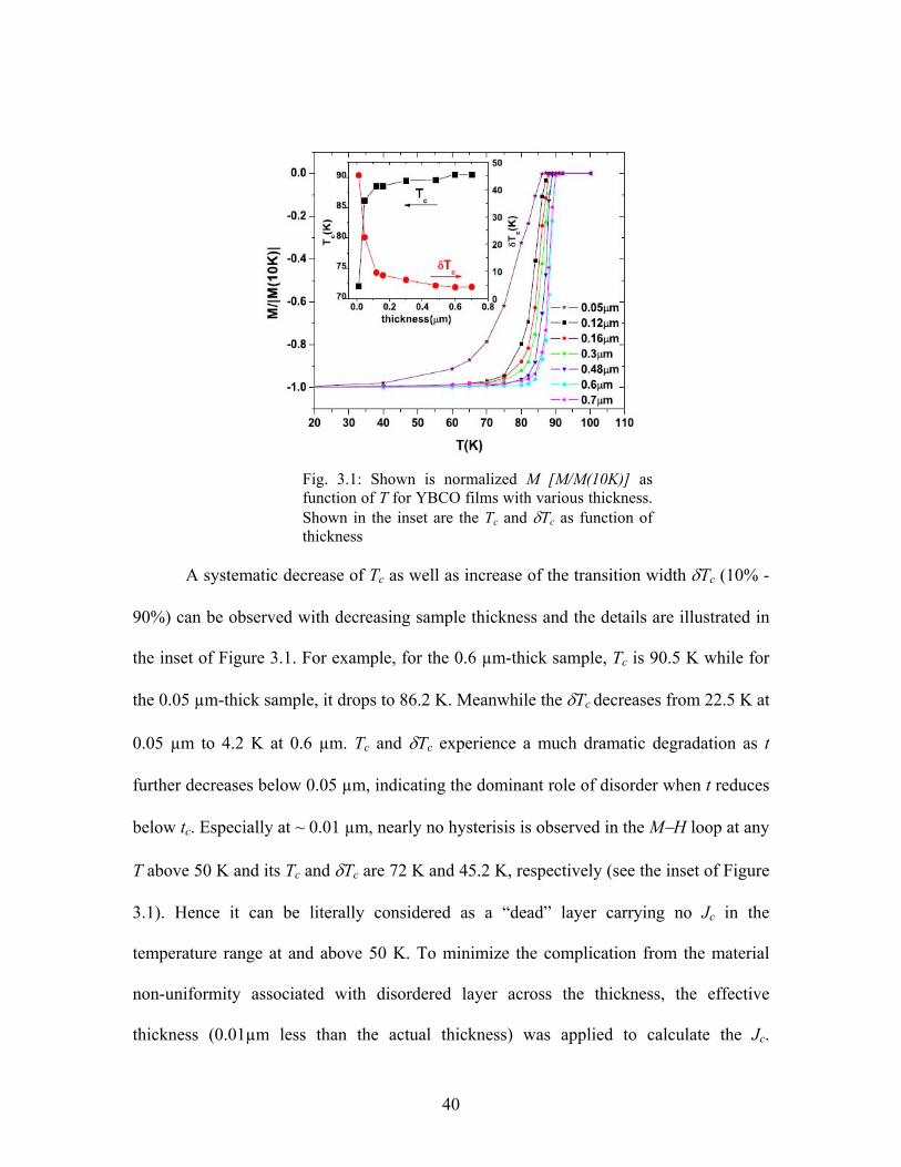
Fig. 3.1: Shown is normalized M [M/M(10K)] as function of T for YBCO films with various thickness. Shown in the inset are the Tc and δTc as function of thickness
A systematic decrease of Tc as well as increase of the transition width δTc (10% -
90%) can be observed with decreasing sample thickness and the details are illustrated in
the inset of Figure 3.1. For example, for the 0.6 µm-thick sample, Tc is 90.5 K while for
the 0.05 µm-thick sample, it drops to 86.2 K. Meanwhile the δTc decreases from 22.5 K at
0.05 µm to 4.2 K at 0.6 µm. Tc and δTc experience a much dramatic degradation as t
further decreases below 0.05 µm, indicating the dominant role of disorder when t reduces
below tc. Especially at ~ 0.01 µm, nearly no hysterisis is observed in the M−H loop at any
T above 50 K and its Tc and δTc are 72 K and 45.2 K, respectively (see the inset of Figure
3.1). Hence it can be literally considered as a “dead” layer carrying no Jc in the
temperature range at and above 50 K. To minimize the complication from the material
non-uniformity associated with disordered layer across the thickness, the effective
thickness (0.01µm less than the actual thickness) was applied to calculate the Jc.
40
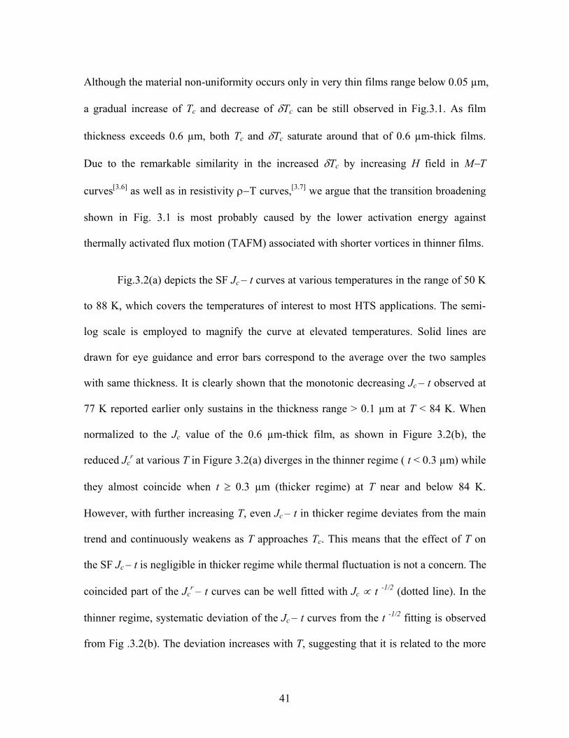
Although the material non-uniformity occurs only in very thin films range below 0.05 µm,
a gradual increase of Tc and decrease of δTc can be still observed in Fig.3.1. As film
thickness exceeds 0.6 µm, both Tc and δTc saturate around that of 0.6 µm-thick films.
Due to the remarkable similarity in the increased δTc by increasing H field in M−T
curves[3.6] as well as in resistivity ρ−T curves,[3.7] we argue that the transition broadening
shown in Fig. 3.1 is most probably caused by the lower activation energy against
thermally activated flux motion (TAFM) associated with shorter vortices in thinner films.
Fig.3.2(a) depicts the SF Jc – t curves at various temperatures in the range of 50 K
to 88 K, which covers the temperatures of interest to most HTS applications. The semi-
log scale is employed to magnify the curve at elevated temperatures. Solid lines are
drawn for eye guidance and error bars correspond to the average over the two samples
with same thickness. It is clearly shown that the monotonic decreasing Jc – t observed at
77 K reported earlier only sustains in the thickness range > 0.1 µm at T < 84 K. When
normalized to the Jc value of the 0.6 µm-thick film, as shown in Figure 3.2(b), the
reduced Jcr at various T in Figure 3.2(a) diverges in the thinner regime ( t < 0.3 µm) while
they almost coincide when t ≥ 0.3 µm (thicker regime) at T near and below 84 K.
However, with further increasing T, even Jc – t in thicker regime deviates from the main
trend and continuously weakens as T approaches Tc. This means that the effect of T on
the SF Jc – t is negligible in thicker regime while thermal fluctuation is not a concern. The
coincided part of the Jcr – t curves can be well fitted with Jc ∝ t -1/2 (dotted line). In the
thinner regime, systematic deviation of the Jc – t curves from the t -1/2 fitting is observed
from Fig .3.2(b). The deviation increases with T, suggesting that it is related to the more
41
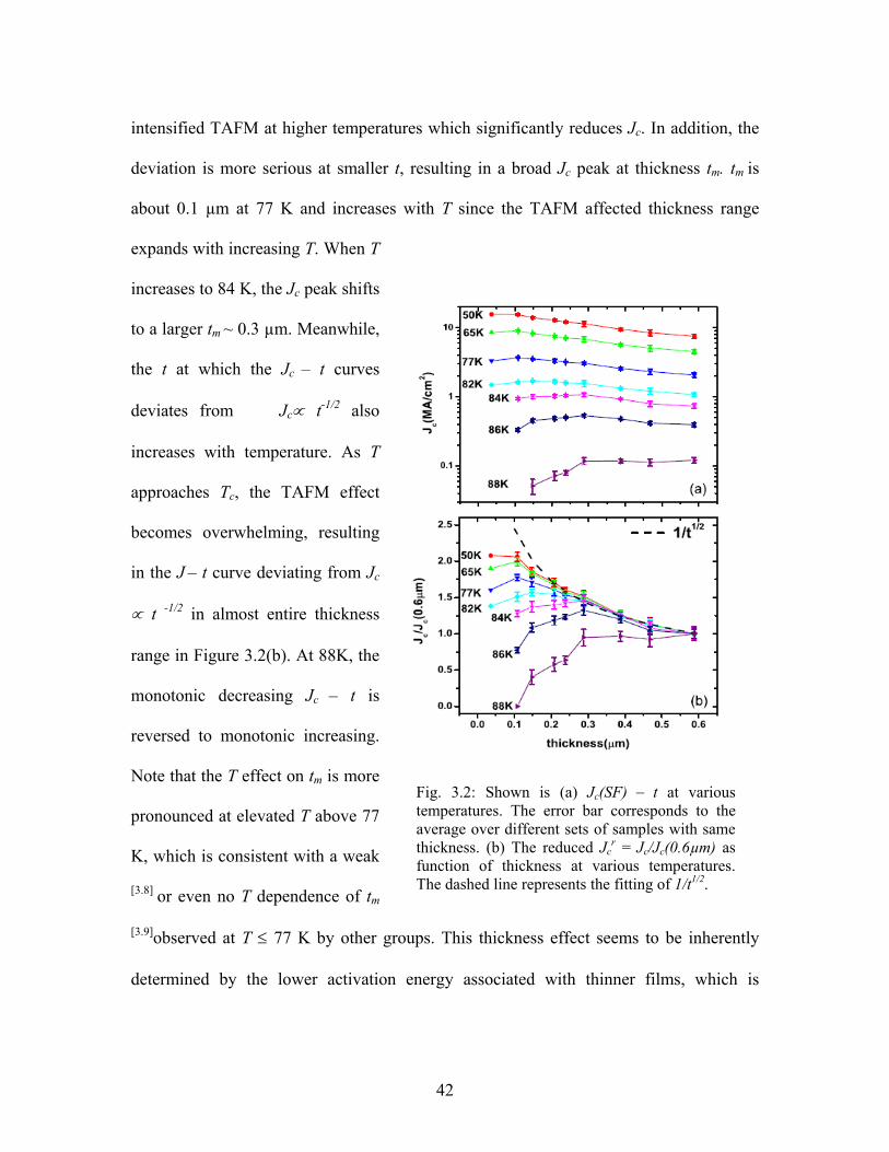
intensified TAFM at higher temperatures which significantly reduces Jc. In addition, the
deviation is more serious at smaller t, resulting in a broad Jc peak at thickness tm. tm is
about 0.1 µm at 77 K and increases with T since the TAFM affected thickness range
expands with increasing T. When T
increases to 84 K, the Jc peak shifts
to a larger tm ~ 0.3 µm. Meanwhile,
the t at which the Jc – t curves
deviates from Jc∝ t-1/2 also
increases with temperature. As T
approaches Tc, the TAFM effect
becomes overwhelming, resulting
in the J – t curve deviating from Jc
∝ t -1/2 in almost entire thickness
range in Figure 3.2(b). At 88K, the
monotonic decreasing Jc – t is
reversed to monotonic increasing.
Note that the T effect on tm is more
pronounced at elevated T above 77
K, which is consistent with a weak
[3.8] or even no T dependence of tm
[3.9]observed at T ≤ 77 K by other groups. This thickness effect seems to be inherently
determined by the lower activation energy associated with thinner films, which is
Fig. 3.2: Shown is (a) Jc(SF) − t at various temperatures. The error bar corresponds to the average over different sets of samples with same thickness. (b) The reduced Jc
r = Jc/Jc(0.6µm) as function of thickness at various temperatures. The dashed line represents the fitting of 1/t1/2.
42

confirmed by the observation of considerable increase of relaxation rate dM/dt in the
thinner YBCO films at T ≥ 70 K [3.10] .
3.2 The Effect of Applied magnet field on Jc−t
If the deviation of Jc – t from the Jc ∝ t-1/2 curve is caused mainly by TAFM,
much enhanced effect is expected
in the applied H which further
facilitates TAFM. Therefore a Jc
crossover is expected if one plots
Jc as function of H of films with
various thicknesses at certain T.
Previous experiments on single
layer YBCO [3.11] as well as HTS
superlattice [3.12] did observe such
crossover. In our study, this
crossover could be also inferred
as summarizing Jcr − t curves at
various H measured at 77 K and
50 K in Figures 3.3(a) and 3.3(b),
respectively. The H field causes
Jcr − t to deviate from the
J
Fig. 3.3: Shown are Jcr − t curves at (a)
77K and (b) 50K, respectively, at various H fields. The dashed line represents the fitting of 1/t1/2.
c ∝ t e f-1/2 curv in the thinner ilm
43
regime first at low H and the thickness range affected increases with H at a given T.
Moreover, Jc at smaller thickness of the curve drops much more than that at the thicker
part. Consequently a broad Jc peak similar to that on the SF Jcr − t curve appears with
increasing H which is followed by a complete reversal of the Jcr − t curve from
onotonic decreasing to monotonic increasing at higher H if T is high enough. This
entire sequence can be clearly seen in Figure 3.3(a) at 77 K and the reversal occurs at
~1.25 Tesla. The similar trend has also been observed at lower temperatures despite some
quantitative differences. Basically, higher H field is necessary to generate the same or
similar effect on the J
m
3.3 Theoretical Analysis of Jc−t
If one compares the T effect with H effect on Jc − t, it is interesting to see that
both T
cr − t curve at lower temperatures. For example, at T = 50 K, which
is shown in Figure 3.3(b), the broad Jc peak is not fully formed until H increases to 3.0
Tesla, and a complete reversal from monotonic decreasing to monotonic increasing is not
realized even at 4.0 Tesla. Instead, a cusp is formed at tm ~ 0.25 µm, which separates the
monotonic increasing Jc − t below tm and the monotonic decreasing Jc − t above it.
and H influence Jc − t in a very similar way, or say, through a thermal activated
process. Actually the thermal effect on Jc – t has been treated theoretically using the
dynamic approach within the frame of original CP model [3.13]. In the flux creep region J
< Jc, since the small induced electric field E is mostly determined by the thermally
activated vortex jumps between pinning centers in the direction of Lorentz force FL, the
44

thermally activated dynamics of vortices can be described using the E−J characteristics
with the form
αθ
αθπ θαβθπβ dtfIete rt
rt rr ]sin)([/)1( 00
// ∫ −−−∈= (3.1)
where ∈ = E/ρFJ0, β=J/Jc0, tr=t/Lc, and f(t)=FP(t)/ FP(Lc)are the dimensionless electric
field, current density, film thickness and pinning force line density, respectively, ρF =
ρnH/Hc2 is the flux flow resistivity and I0(x) is a modified Bessel function. The strength
of thermal fluctuation strength is quantified using a dimensionless temperature θ :
θ =πkBcT/JB c0Φ0Lcl (3.2)
It can be seen that, besides temperature
T, applying magnetic field H also
influences θ through 3D bulk Jc0(T,
H). θ can be also affected by material
dimensionality through Lc as well as
the defect structure from the average
inter-defect spacing l. For some typical
YBCO thin film parameters, Jc0 (77K,
SF) = 1MA/cm2, Lc = 0.5 µm, l = 50
nm and T =77 K, Eq.(3.2) yields θ ≈
6.7 × 10⁻³.
t/Lc
Fig. 3.4 (as plotted in ref. [3.13]): Evolution of the Jc−t described by Eq.(3.2) for different values of (1) θ = 0.0065, (2) 0.01, (3)0.015, and (4) 0.025.
45

For a given electric field criteria c∈ , the Jc as function of thickness is determined
by the implicit Eq.(3.1) with the account of TAFM. Shown in Fig. 3.4 is the evolution of
Jc – t with changing θ. Jc(t) is calculated from Eq.(3.1) using c∈ = 10-6 for typical E
standard of 1µV/cm and f(t)=[t(1+t)]1/2, H/Hc2=0.01 and ρn=0.1mΩ⋅cm. It can be seen
that, qualitatively, Jc – t calculated evolves with increasing θ in a very similar way as the
experimentally observed Jc – t
under the influence of changing
T and H. In fact, quantitatively
this model also fits the
experiment data well with R2 of
0.9154 as seen in Fig. 3.5, where
the measured (squares) and
calculated Jc − t (blue line) at
65K and 1T are plotted together.
This remarkable consistency
between theory and experiment
suggests that Jc − t actually reflects the interplay between TAFM and CP behavior. In
order to extract the pure CP behavior, one can drop T very close to zero to suppress the
TAFM. Indeed, the Jcr − t at SF and 10 K (see squares in Fig. 3.6) shows consistency
with the CP model in most thickness range down to ~ 0.2 µm. At t < 0.2 µm, although
monotonic decreasing Jc − t is observed, substantial discrepancy remains. It should be
mentioned that the Jc presented in this work is interpreted from remnant magnetization
thickness (µm)
Fig. 3.5: Jrc(t) measured (squares)at 65K
and 1T and calculated (blue line) from Eq.(3.1).
46

using the Bean model. In the thin film geometry, the calculated Jc at small H may deviate
from real Jc if film thickness is comparable or less than λab (λab is about 200 nm at 10 K).
To ensure a uniform critical state across the whole sample, the Jcr − t curve was measured
at 1.0 Tesla and included also in Figure 3.6. Much improved agreement between
experiment and the CP model is observed in the entire thickness range except some minor
deviation at t < λab. The mechanism responsible for this minor deviation may be
attributed to the material non-uniformity occurred at t < 50 nm, which may not be
removed completely with the 10 nm-dead-layer correction. Some other unknown
mechanism may exist also. Nevertheless, the overall result suggests that the CP model
plays a dominant role in the Jc − t behavior of uniform HTS films when TAFM effect is
suppressed.
0.0 0.1 0.2 0.3 0.4 0.5 0.60.8
1.0
1.2
1.4
1.6
1.8
2.0
2.2
2.4
2.6
J c/Jc(0
.6μm
)
thickness(μm)
10K, SF 10K, 1T 1/t1/2
Fig. 3.6: Jcr(10K) − t curves at SF and 1.0
Tesla, respectively. The dashed line represents the fitting of 1/t1/2.
47

3.4 Conclusions
Even though there is still argument regarding the mechanism behind Jc−t, at least
most of the HTS community agrees that Jc−t is the consequence of vortex dynamics and
it has little correlation with microstructural evolution with thickness, especially at t less
than 0.6-0.8 µm. Although the CP model fits the Jc − t very well after modification, some
questions remain. The first question is about the order of magnitude of the Larkin length
Lc. In a weak pinning system where Jc is at least two orders of magnitude lower than J0,
pinning is most likely dominated by point defects like oxygen vacancies with atomic size
and rp is on the order of the coherent length ξ. For anisotropic YBCO, ξc is ~ 0.4 nm at
77 K. Consequently Lc is ~ 4 nm, more than two orders of magnitude smaller than the
HTS film thickness range at which the Jc − t behavior occurs. In fact, YBCO thin film is a
strong pinning system and the typical Jc is ~ 10% of J0 at 77 K and SF. This means that
atomic size point defects such as oxygen vacancies are unlikely the dominant pinning
centers and rp should be comparable to the dimension of other defects, such as
precipitates and secondary-phase inclusions which are on the order of few to tens of nm
in dimension [3.14-3.16]. Assuming pinning in YBCO films is dominated by these large
point defects, Lc would be up to tens of nm, still an order of magnitude smaller than the
relevant film thickness at which Jc − t is important. On the other hand, experiment results
suggest that a larger Lc exist in YBCO film. For example, the thickness dependence of
irreversible field BBirr indicated that an extremely long Lc on the order of sub-micrometer
in YBCO thin films . This then raises a question on whether the summation approach
originated from the large number of small-size weak pins can still be applied to the case
[3.17]
48

of sparse large-size strong pins. Considering the strong pinning nature as well as the
dispersive nature of vortex line tension in anisotropic HTS material, Gurevich
reformulated the weak collective pinning model to account for the multi-scale pinning
potential in YBCO films and theoretically demonstrated that the Lc in YBCO films could
be as long as 1 µm . [3.18]
We have found that within the thickness comparable to the modified Larkin
length, the Jc − t behavior can be well described by collective pinning model which
predicts Jc ∝ t-1/2, in combination with the TAFM effect. Deviation from the CP model
occurs when thermally activated flux motion becomes significant at elevated
temperatures and applied magnetic fields in the thickness range of t ≤ λab. A clear
demonstration of the CP model is obtained at 10 K when the TAFM is greatly suppressed.
This study of T and H effect on Jc − t suggests that the monotonic decreasing Jc − t in
YBCO films is an intrinsic property which reflects the random pinning nature in typical
YBCO films. Hence, the Jc − t may be removed either by reducing the Lc via multilayer
structure or changing the pinning structure via introduction of strong linear pinning
centers.
49

CHAPTER 4: Jc−t Elimination Using Multilayer Approach
We have studied temperature and magnetic field effect on Jc−t of YBCO films.
The remarkable consistency between experimental observation and modified CP theory
indicates that Jc−t is most likely determined by the sub-linear thickness dependence of
pinning force line density Fp. This sub-linear dependence in turn reflects the random
pinning nature of typical as-grown YBCO films. Therefore the key point to eliminate Jc−t
is to maintain a constant Fp at various thicknesses. This can be realized by altering either
vortex structure or pinning structure. In this chapter we will discuss the approach to
eliminate Jc−t using a trilayer structure YBCO/insulator/YBCO.
4.1 Single Vortex in S/N/S Trilayer
Considering a single vortex that is collectively pinned by a random pinning
potential, if the vortex length is less than Lc, the vortex stays straight and any local
bending to accommodate nearby pinning centers is not energetically favored. Therefore
the Fp decreases with increasing thickness as t-1/2. In order to get rid of this thickness
dependence, a scheme that enables the local bending of vortex is the key. One strategy is
to “chop” a vortex into two or more segments with construction of
(HTS/insulation/HTS)n multilayer structure. Since it softens the vortex and reduces the
cost of elastic energy, the multilayer structure enables the local vortex bending even
though the effective vortex length is still within the Lc.
50
With construction of a superconductor/insulator/superconductor trilayer structure,
the so called Giaever transformer, early studies indicate that vortices in two
superconducting layers are coupled through magnetic interaction. The original
transformer using LTS showed that dissipation in type II superconductor (SC) arises from
the motion of the vortex. In his pioneering work, Giaever used two SC tin layers
sandwiching a thin insulating SiO2 layer which electrically isolates the two SC layers [4.1].
As a dc current passed through one of the tin layers (primary) became large enough to
create a flux flow, the voltage drop was observed on both films. This observation
presented strong evidence of vortex as an axially coherent entity.
Theoretical calculations based on the Pearl model [4.2] show that the magnetic
coupling force (Fc) is determined on seven characteristic lengths: tp, ts, tI, λp, λs, ξp and ξs
when inter-vortex interaction is negligible.33 These correspond, respectively, to the
thickness of the primary, secondary SC and the insulating layers, the penetration depth of
the primary and secondary superconducting films (λp, λs), and the coherent length of the
primary and secondary films (ξp, ξs). The maximum coupling force Fcm exerted by the
primary vortex segment upon a secondary segment is then given by [4.3]
cmeff
cm FF ~8 22
20
ρπΦ
= (4.1)
where effρ is an effective screening radius given by
)/coth()/coth( SSSPPPIeff ttt λλλλρ ++= (4.2)
51

Except at high fields, cmF~ is simply a dimension-less quantity of order unity for all values
of tp, ts, tI, λp, λs, ξp and ξs. Thus at reasonably low fields the magnitude of the Fcm is
dominated by the prefactor . 2220 8/ effρπΦ
4.2 Decoupling Vortex in YBCO/CeO2/YBCO Trilayer
Now return to the YBCO/CeO2/YBCO trilayer, to simplify the situation, the
thickness of the two YBCO layers is
fixed while the thickness of the
insulator (tI) is systematically altered.
Qualitatively it is obvious that the
inter-vortex segment coupling
decreases with increasing tI. Due to the
weakened coupling, the vortex
segment in each YBCO layer becomes
relatively free to adjust itself to nearby
pinning potential. Therefore the system
obtains improved pinning efficiency so
as Jc. Taking YBCO sub-layer
thickness fixed at either 0.25 or 0.5 µm,
Fcm is calculated using Eq.(4.1) and
plotted as function of tI in a normalized scale [Fcm/Fcm(tI=0)] as shown in Fig. 4.1. It is
0 2000 4000 6000 8000 10000
0.0
0.2
0.4
0.6
0.8
1.0
t(YBCO)=250 nm t(YBCO)=500 nm
F cm/F
cm(t I
=0)
tI(n m )
Fig. 4.1: Magnetic coupling force Fc as function of insulator layer thickness tIcalculated from Eq. 4.1. The superconducting layer thickness is fixed either at 0.25 or 0.5µm.
52
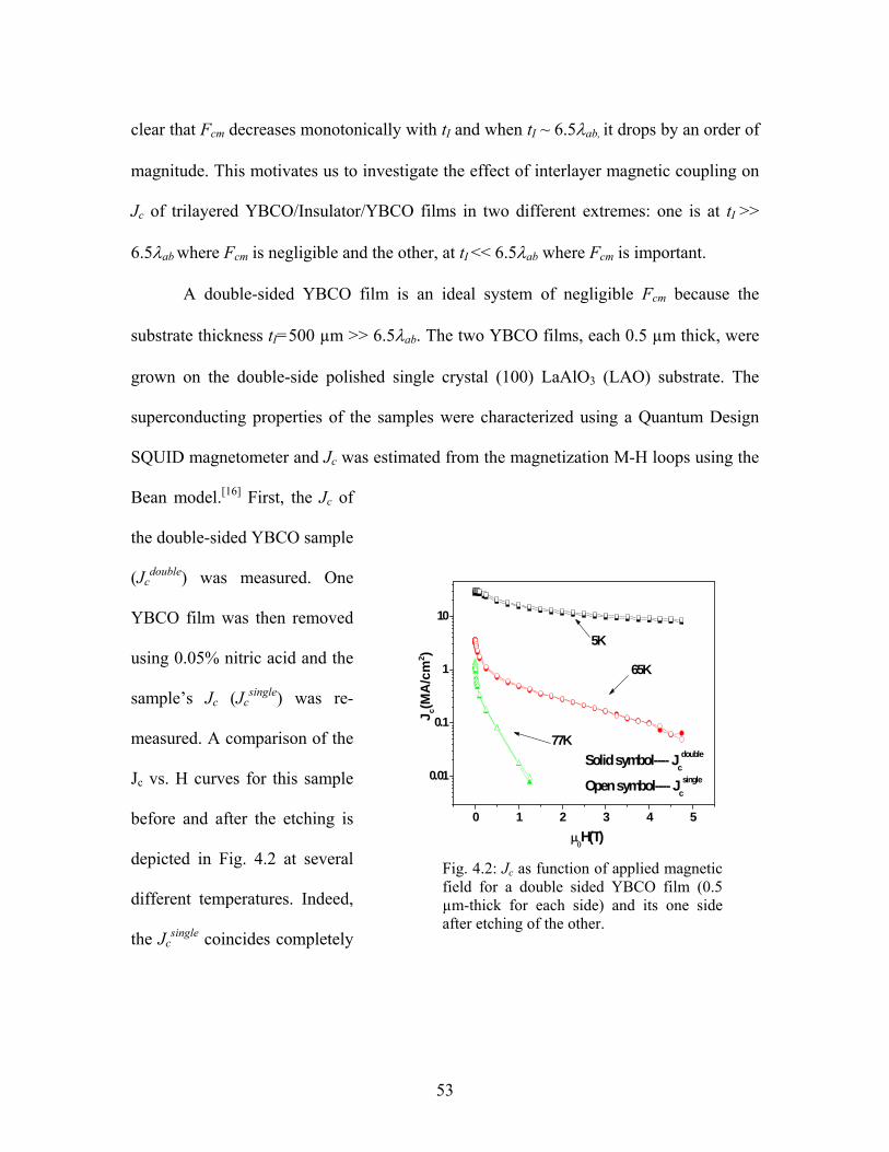
clear that Fcm decreases monotonically with tI and when tI ~ 6.5λab, it drops by an order of
magnitude. This motivates us to investigate the effect of interlayer magnetic coupling on
Jc of trilayered YBCO/Insulator/YBCO films in two different extremes: one is at tI >>
6.5λab where Fcm is negligible and the other, at tI << 6.5λab where Fcm is important.
A double-sided YBCO film is an ideal system of negligible Fcm because the
substrate thickness tI=500 µm >> 6.5λab. The two YBCO films, each 0.5 µm thick, were
grown on the double-side polished single crystal (100) LaAlO3 (LAO) substrate. The
superconducting properties of the samples were characterized using a Quantum Design
SQUID magnetometer and Jc was estimated from the magnetization M-H loops using the
Bean model.[16] First, the Jc of
the double-sided YBCO sample
(Jcdouble) was measured. One
YBCO film was then removed
using 0.05% nitric acid and the
sample’s Jc (Jcsingle) was re-
measured. A comparison of the
Jc vs. H curves for this sample
before and after the etching is
depicted in Fig. 4.2 at several
different temperatures. Indeed,
the Jcsingle coincides completely
0 1 2 3 4 5
0.01
0.1
1
10
Solid symbol---- Jcdouble
Open symbol---- Jcsingle
77K
65K
5K
J c(MA
/cm
2 )
μ0H(T)
Fig. 4.2: Jc as function of applied magnetic field for a double sided YBCO film (0.5 µm-thick for each side) and its one sideafter etching of the other.
53
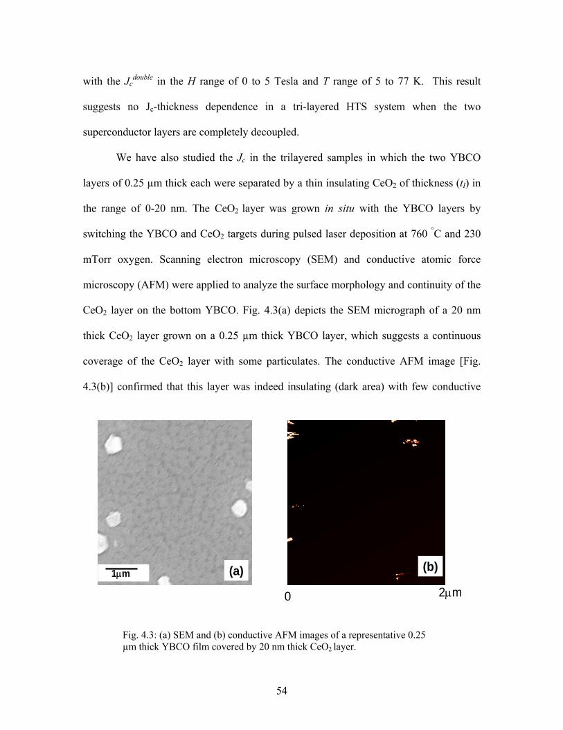
with the Jcdouble in the H range of 0 to 5 Tesla and T range of 5 to 77 K. This result
suggests no Jc-thickness dependence in a tri-layered HTS system when the two
superconductor layers are completely decoupled.
We have also studied the Jc in the trilayered samples in which the two YBCO
layers of 0.25 µm thick each were separated by a thin insulating CeO2 of thickness (tI) in
the range of 0-20 nm. The CeO2 layer was grown in situ with the YBCO layers by
switching the YBCO and CeO2 targets during pulsed laser deposition at 760 °C and 230
mTorr oxygen. Scanning electron microscopy (SEM) and conductive atomic force
microscopy (AFM) were applied to analyze the surface morphology and continuity of the
CeO2 layer on the bottom YBCO. Fig. 4.3(a) depicts the SEM micrograph of a 20 nm
thick CeO2 layer grown on a 0.25 µm thick YBCO layer, which suggests a continuous
coverage of the CeO2 layer with some particulates. The conductive AFM image [Fig.
4.3(b)] confirmed that this layer was indeed insulating (dark area) with few conductive
1μm (a) (b)
0 2μm
Fig. 4.3: (a) SEM and (b) conductive AFM images of a representative 0.25 µm thick YBCO film covered by 20 nm thick CeO2 layer.
54

pinholes (bright spots). At smaller CeO2 thickness, a slightly higher population of
pinholes was observed. For example, on 10 nm thick CeO2, the area covered by pinholes
increased to 10-12 % as opposed to 1-2% at 20 nm thick CeO2. The two superconducting
layers are therefore not completely decoupled electrically, which is consistant with the
previous report on the attempt to fabricate S-I-S junctions [4.4].
Fig. 4.4 shows the Jc value of the trilayered film as function of tI at 77 K and SF.
At tI =0, the Jc value is for a 0.5 µm
thick single-layered YBCO film.
With increasing tI, a monotonic Jc
increase has been observed. At tI=20
nm the Jc in the trilayered film
saturated to the value of the 0.25 µm
thick YBCO film (dash-dot line).
Since all these trilayered samples
have the same effective
superconducting cross-sectional area
for Jc, the increase of the Jc with the
thickness of the insulating CeO2
layer therefore implies a direct
correlation between the Jc of the
trilayered sample and the coupling between the top and bottom superconducting layers as
the CeO2 layer thickness is varied.
0 5 10 15 20
1.7
1.8
1.9
2.0
2.1
2.2
Jc(0.25μm)
Jc(0.5μm) 77K,SF
J c(M
A/c
m2 )
tI(nm)
Fig. 4.4: Jc (SF, 77K) of trilayered films as function of CeO2 thickness tI (solid square). The solid line represents its polynomial fit. The dash-dot line corresponds to the Jc (SF, 77K) of 0.25 µm thick YBCO film.
55
4.3 Discussion
A major inconsistency, however, is in the discrepancy between the experimentally
measured critical thickness of the insulator tI ~ 20 nm and the theoretically predicted one
6.5λab ~2000 nm, at which the magnetic interlayer coupling is insignificant. Note that the
DC transformer theory is developed on weak pinning system. One hypothesis is that, for
strong pinning system YBCO thin film, the decoupling tI could be much shorter.
Unfortunately so far there is no modified theory on strong pinning system available yet
but experimentally, it has been demonstrated that for HTS transformer, even at tI=50nm,
the two YBCO layers are still magnetically coupled [4.5]. This suggests it is not necessary
to completely decouple the YBCO layers in order to realize the sub-layer pinning
efficiency. As long as the coupling becomes weak enough and the elastic energy during
deformation becomes much less than the pinning energy gained, sub-film (thin film) Jc
can be restored in the trilayer.
Note that theoretically in a tri-layer where the two YBCO sub-layers are
completely decoupled, the effective Lc becomes equivalent to the thickness of the YBCO
sub-layer. Consequently a pseudo thickness-independent Jc is obtained with increasing
YBCO layer number as long as the sub-layer thickness is fixed. The tri-layer structure
can be generalized into a multi-layer structure and indeed, experimentally a thin film Jc
has been realized in a 6-ply multi-layer structure [4.6]. Moreover, if one follows the CP
theory, the Jc of the multi-layer should be determined by the vortex dynamics of sub-
layer. Therefore for a multi-layer structure, although the pinning efficiency is improved
56

owing to the reduced thickness, the energy barrier against thermal activated flux motion
is also reduced. With increasing influence from thermal fluctuation, at certain threshold T
or H, the decoupling process will not play any role and CP behavior becomes less
important. This has been indeed observed as one compares the Jc−H curves measured at
77K on a single-layer and tri-layer with total YBCO layer thickness of 0.5 µm shown in
Figure 4.5. The CeO2 layer thickness is 20 nm. It can be seen that Jc of the tri-layer drops
faster with increasing H than that of single-layer, and at 1 Tesla, Jcs of both tri-layer and
single-layer becomes comparable.
1E-4 1E-3 0.01 0.1 10.01
0.1
1
singlelayer Trilayer(tI=20nm)
J c(MA/
cm2 )
μ0H(T)
YBCO thickness=0.5μm
77K
Fig. 4.5: Jc−H curves measured on a single-layer and tri-layer films at 77K. The effective YBCO film thickness is 0.5 µm and the CeO2 thickness tI in the tri-layer is 20 nm.
57
4.4 Summary
In summary, Jc has been studied in YBa2Cu3O7-x/insulator/YBa2Cu3O7-x trilayers
as the interlayer magnetic coupling is reduced by increasing the thickness (tI) of the
intermediate insulating layer, while the thickness of two YBa2Cu3O7-x layer was each
fixed at 0.25 µm. The experimental results have revealed an intimate correlation between
Jc and magnetic coupling and further supported that CP behavior is the underlying
mechanism behind the puzzling Jc−t dependence. As expected from the CP theory, the
multi-layer approach provides one solution for eliminating Jc−t dependence in YBCO
film. However, this approach can only generate a pseudo thickness-independent Jc and
within the YBCO sub-layer, Jc−t still maintains. Most importantly, although a thickness-
independent Fp can be realized by decoupling vortex into short segments, the Fp is still
determined by the random pinning nature within the YBCO sub-layer and is not
optimized. With introduction of strong linear defects in as-grown YBCO films, Fp can be
optimized and most importantly, made thickness-independent.
58
CHAPTER 5: Jc−t Elimination Using NTP Insertion
In the previous chapter, we have demonstrated that a pseudo thickness
independent Jc could be realized using superconductor/insulator/superconductor tri-layer
structure. However, the essence of Jc−t remains untouched and Jc is still determined by
the random pinning potential. If one can overpower the random distributed pinning
centers by some strong linear defects extending through the film thickness, two positive
outcomes are expected: first the Fp is optimized and most importantly, it remains
thickness-independent hence leads to a thickness-independent Jc. In this chapter, we will
illustrate the method to generate such through-thickness linear defects, so called nanotube
pores (NTP) insertion in the YBCO films and reveal the effect of NTP on Jc−t.
5.1 NTP Insertion in YBCO Film
To generate NTPs inside YBCO matrix requires two important components:
miscut substrate and nano-particles (NPs) insertion, for controlling mechanical strain on
the YBCO lattice at nano-scales. The NPs may be inserted either near the film/substrate
interface or during the YBCO film growth. The local tune of the strain by the inserted
NPs over the globally strained YBCO lattice on vicinal substrates plays a critical role in
pore nucleation, as evidenced from the initiation of pores directly atop the NPs [5.1]. A
large number of NTPs of dimension from few to hundreds of nanometers form uniformly
via self-assembly growth. No degradation occurs to Tc in these samples and the resistivity
59

in longitudinal direction (along ab-plane) is comparable to that of the typical YBCO films
without impurity insertion [5.2]. In this section, we report the experimental results on a
comparative study of Jc−t behavior between YBCO films with and without inserted NTPs.
Two sets of YBCO films with (YBCO/NTP) and without NTPs (standard YBCO
film) were fabricated using PLD technique under similar growth conditions. The
YBCO/NTP films were grown on 20o vicinal single crystal (001) SrTiO3 (STO)
substrates while the standard YBCO films, on single crystal (100) LaAlO3 (LAO)
substrates. The laser energy density on the target was ~ 3.2 J/cm2 and the repetition rate
was 10 Hz. The deposition was carried out onto substrates heated to 765 ~ 775°C in 230
mTorr oxygen partial pressure followed by the annealing in 360 Torr oxygen for 50
minutes. Although the film thickness ranges from 0.09 to 1.2 μm in this experiment, the
samples selected for the Jc−t study have thickness only up to 0.6 µm to avoid
complication of the microstructure degradation in thicker films. After fabrication, silver
contact pads were immediately deposited onto the films to minimize the surface
resistance. For electrical transport measurement, a 20×400 μm bridge was patterned using
standard photolithography procedure. For YBCO/NTP films, the bridges were parallel to
the longitudinal direction, constraining current only in the ab-plane. I−V curves were
measured using the standard four-point configuration and a criterion of 1 μV/cm was
applied to determine the Jc.
60

5.2 Microstructure Analysis of NTP
Figure 5.1 shows the scanning electron microscopy (SEM) images of four
YBCO/NTP films with various thicknesses ranging from 0.09 to 0.6 μm. At t = 0.09 μm,
many pores are already formed in addition to some NPs on the surface. These NPs, which
are mostly Y2O3 precipitates naturally occurred during the PLD process, serve as the
seeds for NTPs to initiate. This means that the densities of NPs and pores are closely
correlated [5.3]. With increasing t, the density of both NP and pore decrease dramatically
and at t = 0.16 μm, only few NPs are observed and the pore density n also drops about
Fig. 5.1: SEM images of YBCO/NTP films at various thicknesses.
61

50% from 9-10/μm2 to 4-5/μm2. At t = 0.16 μm, the visible pores have dimension
typically about 100 to 200 nm. It should be mentioned that the pores with smaller
dimension are not clearly visible at the magnification used while their presence was
confirmed in transmission electron microscopy studies (not shown in this paper). With
further increasing thickness, the pore density n remains almost unchanged at around
4~5/μm2 and some large pores of dimension on the order of 500~1000 nm appear as
shown on 0.6 μm thick sample.
In order to understand how pores evolve through the film thickness, a 1.2 µm-
thick YBCO/NTP film was thinned via nine consecutive steps using ion milling and
Fig. 5.2: SEM images of a 1.2 μm-thick YBCO/NTP film at different stages of thinning using ion milling. R0(1.2µm) represents the original film and Rn(d) represents the film after nth milling with remaining thickness d. 500nm×500nm grids are applied to each image and a colored pattern is used for tracking a specific NTP through different layers of thickness.
62

analyzed using SEM after each step of 0.12 μm thinning. Marks were employed so that
the same pores can be monitored through the milling steps. Figure 5.2 includes the SEM
images taken on the original sample surface (R0) and on each of the nine steps of milling
(R1 through R9). Many pores can be traced through different layers of the film and most
of them are almost through the entire (for example, the three pores labeled respectively
with cyan ovals, blue circles, and pink squares)
or a large portion (green diamonds for a pore
through the bottom half of the film and yellow
pentagons for a pore through the top half) of the
film thickness. This means that they have NT
geometry. We have also observed some pores
closed at certain thickness and reappear (red
crosses). Y2O3 NPs, which were confirmed with
energy-dispersive x-ray spectroscopy, are
visible at the bottom of NTPs (a few marked
with yellow arrows), confirming that NPs indeed play a critical role in nucleation of the
NTPs. It should be noted that the density of the Y2O3 NPs is at least an order of
magnitude smaller than that near the film/substrate interface [5.3]. Above t=100 nm, the
NP density is on the order of 0.2-0.3/μm2. In the thickness range from 0.16 μm to 0.6 μm,
the density of the pore in YBCO/NTP films is more or less a constant, which agrees with
Figure 5.1. This suggests that number of newly-generated NTPs is comparable to that of
disappeared NTPs in this thickness range, while the majority NTPs initiate at smaller
thickness. Interestingly, most NTPs appear at the same or close to the same lateral
100nmVicinal STO substrate
100nmVicinal STO substrate
Fig. 5.3: Cross-sectional TEM of a 1.0 µm-thick NPT/YBCO film.
63

location at different thickness while their lateral dimension experiences some increases
through the 1.2 µm film thickness. This means that they are more or less straight
nanotubes aligned along the normal of the film. In order to further confirm that NTPs are
through most of the film thickness, a cross-sectional transmission electronic microscopy
(TEM) picture was taken on a 1.0 µm-thick NTP/YBCO film and shown in Fig. 5.3. It
can be seen clearly that NTP, indicated by the white lines, are indeed through most of the
film thickness.
5.3 Jc of YBCO Film Before and After NTP Insertion
In Fig. 5.4, the Jc at SF and 77 K is plotted as function of thickness for both
YBCO/NTP (squares) and standard
(circles) samples. Considering the
possible nonuniformity of NTPs in
the YBCO/NTP sample at smaller
thickness, only the Jc of the films
with thickness in the range of 0.16
to 0.6 μm-thick film are included.
The solid lines are guides for eyes.
There are two interesting
observations in Fig. 5.4. First, the
Jc values of the YBCO/NTP films
are overall higher than that of the
standard YBCO films in the same
Fig. 5.4: Jc−t curves of YBCO standard films(circles) and YBCO/NTP films (squares) at 77 K and SF. Also shown is the Jc−t curve of YBCO/NTP (triangles) assuming a thickness-independent NTP lateral dimension. Inset shows the Jc− t curves of the two types of films in a normalized scale Jc/Jc(0.2μm). The same symbols as in Fig. 5.4 are employed for the two curves in the inset. The dash line indicates the fitting of the CP model.
64

thickness range. At t=0.25 μm, the Jc of the YBCO/NTP sample is 5.83 MA/cm2, which
is ~20.7% higher than that of the standard YBCO sample and at t=0.6 μm, it is ~52.8%.
Note that the Jc values of the standard YBCO samples are between 5.0 to 2.8 MA/cm2 at
0.2 μm ≤ t ≤0.6 μm, which are comparable to the typical Jcs around 5.5 to 3.5 MA/cm2
reported in the same thickness range [5.4, 5.5]. On the other hand, the YBCO/NTP films
experience weaker thickness dependence of Jc than the standard ones do. This latter
observation can be further illustrated in the inset of Fig. 5.4 by replotting the two curves
in Fig. 5.4 on a normalized scale Jc/Jc(0.2 µm). With increasing t from 0.25 to 0.6 μm, for
example, Jc drops only 26% for the YBCO/NTP films as opposed to a 40% reduction on
the standard YBCO films. Moreover, the Jc−t of the standard YBCO films can be well
fitted by Jc∝t-1/2 as predicted by modified CP model in most of the thickness range
except the deviation below 0.2 μm. This deviation, which leads to a switch from
increasing Jc to decreasing Jc with increasing t, has been observed previously [5.6-5.8]. In
Chapter 3, we argued that this deviation from J ∝t-1/2c is most probably related to the
pronounced TAFM since a shorter vortex collectively pinned by point defects is more
easily thermally activated than a longer one within L . In contrast to the standard films,
such switch is not observed in the according thickness range for YBCO/NTP, suggesting
that the TAFM is greatly suppressed as point defect pinning is overpowered by NTP
pinning.
c
Although a weaker thickness dependence of Jc is observed in the YBCO/NTP
samples, the remaining Jc−t is unexpected if NTP dominates the pinning. A possible
explanation is the reduced cross-sectional area owing to those enlarged NTPs at larger
thickness, which leads to an underestimated Jc in thick films. To quantify this argument,
65

the NTPs’ lateral dimension increase, which translates to reduction of the cross-sectional
area for the electrical current, was estimated based on the SEM images shown in Fig. 5.1.
When t increases from 0.16 μm to 0.25 μm, the reduced current cross-sectional area is
about 7%. It increases to ~ 29% when t is increased to 0.6 μm. Considering the
correction of the cross-sectional area, an “ideal” Jc−t curve is extracted and added in Fig.
5.4 (triangles). It is not surprising that the Jc−t curve of YBCO/NTP films with perfectly
straight NTPs drops only ~ 5% as thickness increases from ~0.25 μm to 0.6 μm. This
greatly weakened Jc−t clearly demonstrates that NTP insertion is indeed an effective
approach to eliminate Jc−t by providing a thickness independent Fp. In addition, the ideal
NTP’s lateral dimension should be on the order of the coherence length in ab-plane ξab
(~3.5 nm for YBCO at 77 K) [5.9, 5.10]. Higher Jc values are anticipated in YBCO/NTP
films if the lateral dimension of the NTP could be reduced to a few nanometers close to
ξab.
Based on the observed NTP’s density in Fig. 5.1, the matching field Hm = nΦ0 is
estimated to be about 8~10 mT. The actual Hm may be slightly higher due to those
uncounted smaller NTPs in few to tens of nanometer regime. As the applied magnetic
field H exceeds Hm, some vortices will no longer be pinned by the NTPs. Instead, they
will be pinned by other weaker pinning centers. With increasing H, the NTP will
gradually render the dominancy to those weaker pinning centers. These weaker pinning
centers are most likely isotropic ones such as secondary phase inclusions. Consequently,
the CP-type Jc−t curves observed in the standard YBCO samples will be resumed in
YBCO/NTP samples at a certain H>>Hm. This argument seems to agree well with the
66
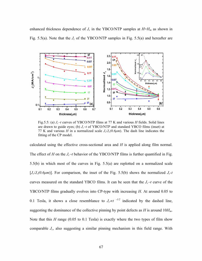
enhanced thickness dependence of Jc in the YBCO/NTP samples at H>Hm as shown in
Fig. 5.5(a). Note that the Jc of the YBCO/NTP samples in Fig. 5.5(a) and hereafter are
calculated using the effective cross-sectional area and H is applied along film normal.
The effect of H on the Jc−t behavior of the YBCO/NTP films is further quantified in Fig.
5.5(b) in which most of the curves in Fig. 5.5(a) are replotted on a normalized scale
[Jc/Jc(0.6μm)]. For comparison, the inset of the Fig. 5.5(b) shows the normalized Jc-t
curves measured on the standard YBCO films. It can be seen that the Jc−t curve of the
YBCO/NTP films gradually evolves into CP-type with increasing H. At around 0.05 to
0.1 Tesla, it shows a close resemblance to Jc∝t -1/2 indicated by the dashed line,
suggesting the dominance of the collective pinning by point defects as H is around 10Hm.
Note that this H range (0.05 to 0.1 Tesla) is exactly where the two types of film show
comparable Jc, also suggesting a similar pinning mechanism in this field range. With
Fig.5.5: (a) Jc−t curves of YBCO/NTP films at 77 K and various H fields. Solid lines are drawn to guide eyes; (b) Jc−t of YBCO/NTP and standard YBCO films (inset) at 77 K and various H in a normalized scale Jc/Jc(0.6μm). The dash line indicates the fitting of the CP model.
67

further increasing H, the effect of the TAFM becomes visible and more enhanced at
higher H, which continuously weakens the Jc−t of the YBCO/NTP samples in a similar
way as in the case of the standard YBCO samples shown in the inset. This complex effect
of H on Jc−t indicates the existence of dual pinning systems in the YBCO/NTP films and
suggests that higher density straight NTPs are necessary to extend a flat Jc−t to higher H
fields.
5.4 Conclusions
In summary, we have fabricated YBCO/NTPs films and studied their Jc−t
behavior at 77 K and various magnetic fields up to 5T. Since the NTPs are linear defects
aligned along the normal of the film and through nearly entire film thickness, they
provide an enhanced pinning force Fp on each vortex, which remains independent of film
thickness. The enhanced pinning by NTPs results in high Jc values and effectively
suppresses the TAFM. In addition, the t-dependence of Jc observed in the standard
YBCO films is much reduced in the YBCO/NTP samples at H<Hm and may be
completely eliminated when the NTPs’ lateral dimension is made constant. Interestingly,
the CP-type Jc−t behavior is resumed in YBCO/NTP samples at H>>Hm, which suggests
a switch from the stronger NTP pinning to the weaker point defect pinning.
Although Jc shows weak thickness dependence after NTP insertion, macroscopic
Jc still shows thickness dependence owing to NTP evolution with increasing thickness.
Therefor it brings complication to precisely quantifying the effect of linear defects on
Jc−t. It then necessitates the further Jc−t investigation in a system with consistent pinning
landscape at any given thickness.
68
CHAPTER 6: Jc−t Elimination Using BZO NRD Insertion
In previous chapter, we have demonstrated that thickness dependence of Jc could
be effectively weakened with NTP insertion. Since majority of NTP are through the
entire film thickness, they provide an optimized Fp which remains constant with changing
thickness. However, complication is generated since NTP’s diameter increases with
thickness. In order to obtain a uniform pinning structure less affected by thickness, we
will turn to the other widely used method to generate linear defects in YBCO films:
impurity insertion.
Among all the reported methods of impurity insertion in YBCO films, BaZrO3
(BZO) nano-particles (NP) insertion remains to be the most interesting one since the
BZO NPs are capable of self-aligning themselves into columnar shape [6.1]. However, it is
also known that the defect landscape of BZO doped YBCO films (YBCO/BZO) can be
very different for various BZO concentrations and fabrication methods. This of course,
would strongly influence superconducting properties for YBCO/BZO samples fabricated
using different methods. A systematica study on PLD YBCO/BZO films suggests that
both Tc and SF Jc linearly decreases with BZO volume fraction [6.2]. A significant 2 to 3 K
Tc and + 50% SF Jc degradation was reported in the PLDed YBCO films after only 2%
BZO NP insertion. However no such degradation was observed in the TFA-MOD YBCO
film even after 10% BZO NP insertion [6.3]. Microstructure study on these films revealed
that, for the latter case, BZO NPs randomly distributed in the YBCO matrix instead of
forming aligned nanorods (NRDs) as in the PLD films. In addition to that, the profile of
69
the angular dependence of Jc also indicated that, while the better ab-plane integrity was
observed in the latter case, the so-called “buckling effect” of ab-plane was much more
pronounced in the PLD YBCO/BZO films with self-assembled BZO NRDs [6.4].
The mechanism of BZO NRDs self-assembly is of great importance for the
application of 2G HTS wire since it holds the key to the optimized pinning structure and
elimination of Jc−t in HTS films. Computer simulation suggests that the tremendous
strain field caused by the +8.7% lattice mismatch between BZO and YBCO is critical for
the vertical alignment during the in-situ heteroepitaxial growth. Specifically this stress-
mediated ordering results in a simultaneous phase separation and grouping during the
layer-by-layer growth [6.4].In other words, the BZO NPs tend to align itself in the growth
front to maintain the lowest energy scheme. Therefore it is expected that growth
temperature may have a significant effect on the BZO NPs self-assembly since it dictates
the mobility of BZO NP. This immediately renders the possibility that the thickness
dependence of Jc could be very different for PLD YBCO/BZO films fabricated at
different temperatures due to the possible difference in the pinning landscape. In this
chapter, we report the growth temperature effect on Jc of the YBCO/BZO films followed
by the thickness dependence of Jc in these films.
70
6.1 Growth Temperature Effect on Jc of YBCO/BZO
Two groups of YBCO/BZO films were fabricated using PLD technique at 790
and 810oC on single crystal (100) LaAlO3 (LAO) substrates. In the rest of this chapter,
group A refers samples grown at 790 oC and group B, at 810 oC respectively. This sets
the only difference between these two groups of samples in terms of growth conditions.
The BZO volume fraction is 2% for both groups of films. The laser energy density on the
target was ~ 3.2 J/cm2 and the repetition rate was 8 Hz. The deposition was carried out in
300 mTorr oxygen partial pressure followed by the annealing in 760 Torr oxygen at
500oC. The samples selected for the Jc−t study have thicknesses only up to 0.6 µm to
avoid complication of the microstructure degradation in thicker films. Most of the
superconducting properties of the sample were characterized using a Quantum Design
SQUID magnetometer. For electrical transport measurement such as angular dependence
of Jc, a 20×400 μm bridge was patterned using photolithography. The I−V curve was
measured with the standard four-point configuration and the criterion of 1μV/cm was
applied to determine the Jc. The stage where samples were mounted can be rotated with
respect to the applied magnetic field H. The direction of J was always maintained
perpendicular to the H to enable the maximum Lorentz force scheme. The major
microstructural information was retrieved using cross-sectional transmission electron
microscopy (TEM).
Fig. 6.1 shows the comparison of Jc between the two groups of films as function
of applied magnetic field in a semi-log scale at 77 K. Each group includes two films with
thickness of 0.2 and 0.6 μm. Open symbols correspond to Jc measured on group A and
solid ones, on group B. It can be seen that, at field regime lower than 1500 Oe, Jcs are
71
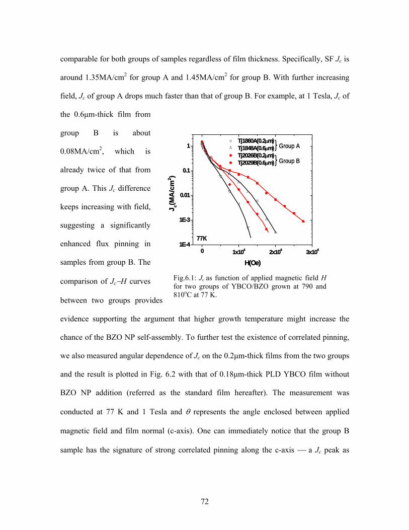
comparable for both groups of samples regardless of film thickness. Specifically, SF Jc is
around 1.35MA/cm2 for group A and 1.45MA/cm2 for group B. With further increasing
field, Jc of group A drops much faster than that of group B. For example, at 1 Tesla, Jc of
the 0.6μm-thick film from
group B is about
0.08MA/cm2, which is
already twice of that from
group A. This Jc difference
keeps increasing with field,
suggesting a significantly
enhanced flux pinning in
samples from group B. The
comparison of Jc−H curves
between two groups provides
evidence supporting the argument that higher growth temperature might increase the
chance of the BZO NP self-assembly. To further test the existence of correlated pinning,
we also measured angular dependence of Jc on the 0.2μm-thick films from the two groups
and the result is plotted in Fig. 6.2 with that of 0.18μm-thick PLD YBCO film without
BZO NP addition (referred as the standard film hereafter). The measurement was
conducted at 77 K and 1 Tesla and θ represents the angle enclosed between applied
magnetic field and film normal (c-axis). One can immediately notice that the group B
sample has the signature of strong correlated pinning along the c-axis ⎯ a Jc peak as
77K
0 1x10⁴ 2x10⁴ 3x1041E-4
1E-3
0.01
0.1
1
J c(MA
/cm
2 )
H(Oe)
Tj1860A(0.2μm) Tj1848A(0.6μm) Tj2026B(0.2μm) Tj2029B(0.6μm)
Group A
Group B
77K
0 1x10⁴ 2x10⁴ 3x1041E-4
1E-3
0.01
0.1
1
J c(MA
/cm
2 )
H(Oe)
Tj1860A(0.2μm) Tj1848A(0.6μm) Tj2026B(0.2μm) Tj2029B(0.6μm)
Group A
Group B
Fig.6.1: Jc as function of applied magnetic field H for two groups of YBCO/BZO grown at 790 and 810oC at 77 K.
72

H//c-axis. Due to the absence of this c-axis Jc peak, the presence of BZO NRDs in the
group A remains a question.
-20 0 20 40 60 80 100 1200.2
0.4
0.6
0.8
1.0
1.2
1.4
1.6 Standard Group A Group B
H//ab
J c(MA
/cm
2 )
θ(deg)
H//c
77K, 1T
However, intuitively one may wonder that the 20oC difference in the growth
temperature may not be enough to completely randomize the distribution of the BZO NPs.
Another possible reason responsible
for the absence of this Jc peak could be
the low density of BZO NRDs. This
seems to be a reasonable argument at
least based on the difference of Jc peak
between the two groups of samples as
H is parallel to the ab-plane. Owing to
the large stress field generated by the
+8.7% lattice mismatch between BZO
and YBCO, the damage of integrity
and continuity of ab-plane is inevitable
and therefore the intrinsic pinning as well as the Jc is suppressed when H//ab-plane.
Hence it is not hard to imagine that the “buckling effect” increases, or Jc(H//ab-plane)
decreases with the increasing density of BZO NRDs. For the standard sample, since
dominant defects are randomly distributed point pins (similar to the TFA-MOD
YBCO/BZO film), the ab-plane integrity is well maintained and an pronounced Jc(H//ab-
plane) peak is observed. This probably explains why Jc of group A falls just in between
that of the standard sample and group B when H//ab-plane.
Fig. 6.2: Jc as function of θ, which is the angle enclosed between applied magnetic field and film normal for two representative 0.2 μm-thick YBCO/BZO films from group A and B. A similar curved measured on a 0.18 μm-thick standard YBCO film is also plotted together.
73
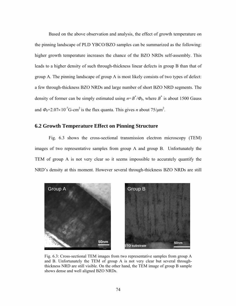
Based on the above observation and analysis, the effect of growth temperature on
the pinning landscape of PLD YBCO/BZO samples can be summarized as the following:
higher growth temperature increases the chance of the BZO NRDs self-assembly. This
leads to a higher density of such through-thickness linear defects in group B than that of
group A. The pinning landscape of group A is most likely consists of two types of defect:
a few through-thickness BZO NRDs and large number of short BZO NRD segments. The
density of former can be simply estimated using n=B*/Φ0, where B* is about 1500 Gauss
and Φ0=2.07×10⁻⁷G-cm2 is the flux quanta. This gives n about 75/μm2.
6.2 Growth Temperature Effect on Pinning Structure
Fig. 6.3 shows the cross-sectional transmission electron microscopy (TEM)
images of two representative samples from group A and group B. Unfortunately the
TEM of group A is not very clear so it seems impossible to accurately quantify the
NRD’s density at this moment. However several through-thickness BZO NRDs are still
50nmSTO substrate
50nm50nmSTO substrate
Group B
50nm
Group A
Fig. 6.3: Cross-sectional TEM images from two representative samples from group A and B. Unfortunately the TEM of group A is not very clear but several through-thickness NRD are still visible. On the other hand, the TEM image of group B sample shows dense and well aligned BZO NRDs.
74

visible, which confirms the existence of correlated pinning in the group A sample. On the
other hand, the TEM image of the group B sample shows well aligned BZO NRDs with
density around 1600/μm2, giving a match field around 3.2 Tesla.
6.3 Elimination of Jc−t in Low H Regime
Since samples from both groups share the same pinning mechanism ⎯ the strong
correlated pinning along c-axis in the low field regime less than 1500 Gauss, a thickness
independent Jc should be observed as already implicitly shown in Fig. 6.1 for t= 0.2 and
0.6 μm. To further illustrate this point,
Jcs of samples from both group A are
plotted as function of thickness at 77 K
and various fields in Fig. 6.4. The solid
lines and dashed lines are guides for
eyes of data points measured on group
A and group B, respectively. It can be
seen that both groups have thickness-
independent Jc in the low field regime
when B < 0.1 Tesla. As B further increases,
group A samples start to develop thickness
dependence while for group B sample, the thickness-independent Jc has been well
maintained even up to 0.5 Tesla. Note that the BZO NRD’s density of group B samples is
much higher than that of group A, it is not surprising that Jc could be maintained almost
Fig. 6.4: Jc as function of thickness measured on group A and B at 77 K and various magnetic fields. Solid lines and dashed lines are guides for eyes of data points from group A and group B respectively.
75

thickness-independent in a larger field range for sample grown at high temperature. On
the other hand, since thinner films are always more vulnerable to the pronounced TAFM
disregarding the pinning mechanism, it inevitably would result in a reversed Jc−t as
indicated by the both curves at 0.75 Tesla.
6.4 Lower SF Jc Observed After BZO Insertion
Note that Jc−t elimination using BZO NRD insertion again supports the
conclusion that the collective pinning mechanism has the strong correlation with the
observed Jc−t in standard YBCO films. This observation is consistent with our previous
results on YBCO/NTP samples shown in chapter 5. However a distinct difference
between YBCO/BZO and
YBCO/NTP is the SF Jc value.
Even comparing with standard
films at 77 K, Jcs of
YBCO/BZO films drop
typically 30% to 60%( depends
on film thickness) than that of
standard samples. Interestingly,
the Jc difference also depends
on temperature, as shown in
Fig. 6.5, in which Jc(SF) as
function of temperature of these
0 10 20 30 40 50 60 70 80 90
1
10
J c(MA
/cm
2 )
T(K)
YBCO/BZO(group A) standard YBCO
SF
Fig. 6.5: Jc−T measured on two 0.6μm-thick films with and without BZO NRD insertion. A Jc cross-over is observed at 70 K. A semi-log plot is applied to show the scaling behavior below 50 K.
76

two types of films with thickness of 0.6 μm are plotted together. It can be seen that the Jc
difference is rapidly vanishing with decreasing T and even reversed at T below 50 K. An
important observation here is that Jc of these two types of films can numerically scale to
each other at the same thickness below 50 K. The scaling factor Jc(YBCO/BZO)/Jc(YBCO)
is about 1.25. Since the pinning structure is not likely altered by varying temperature for
both types of film, this scaling correlation probably implies a difference in the
superconductor volume. Considering large stress field as well as slight poisoning in the
YBCO matrix around BZO NRDs, a shell of highly disordered YBCO layer could be
formed with Tc gradually degraded from 90 K to 50 K while approaching the BZO NRD.
Since the Tc of YBCO/BZO sample is only around 86 to 87 K, the disturbed YBCO
crystalline could be global for both group A and B regardless the growth temperature. In
addition to the suppressed Tc, Jc is also greatly reduced due to the limited superconductor
volume, which shrinks further with increasing temperature above 50 K. At T below 50 K,
the superconductor volume becomes T independent but could be still smaller than that of
standard YBCO film. This probably explains that YBCO/BZO film’s Jc is much lower
than that of YBCO/NTP film even though they share a similar pinning mechanism.
Another important feature in this low T region is that the Jc of both types of films
exponentially increases with decreasing T. This similar Jc−T dependence, as predicted by
flux creep model, seems to be independent of pinning mechanism [6.3].
Although the addition of BZO NPs can effectively eliminate the Jc−t by self-
assembling them into through-thickness linear defects, the large lattice strain also
generates unavoidable side effect ⎯ reducing the superconductor volume considerably. It
is worthy noticing that several attempts have been made to minimize this collateral
77

damage. One of them is to apply material with less lattice mismatch than that of
BZO/YBCO. Several works on BSnO3 addition in YBCO have been published and the
results indicate that at least Tc of ~ 90 K was recovered as the lattice mismatch is reduced
from 8.7% to 7.7% [6.5, 6.6] .Similar results have been also obtained when YBCO/BZO
film is grown on a small miscut angle (~ 5o) vicinal substrate [6.7]. It is also possible to
modify the post-annealing condition to minimize the lattice relaxation across the interface
between BZO and YBCO. Therefore the degraded YBCO matrix could be confined in the
vicinity of the BZO NRD. Practically this approach has been studied using the quench
annealing we developed earlier [6.8]. Our preliminary results indicated that Tc was
improved by 3 K to around 89 K and SF Jc by 28% as compares YBCO/BZO samples
with different annealing conditions.
6.5 Conclusions
In summary, we have fabricated YBCO/BZO films at different temperatures and
investigated its effect on the sample’s defect structure. Both superconductivity and
microstructure analysis suggest that higher growth temperature benefits the self-assembly
of BZO NRDs, which results in a higher density of through-thickness NRDs in group B
samples. Despite the difference in the NRD’s density, the correlated pinning along the c-
axis provides a constant pinning force Fp at variable thickness, hence results in a
thickness-independent Jc at low field regime for YBCO/BZO samples from both groups.
The contradiction between the enhanced pinning by BZO NRDs and relatively lower SF
Jc could be explained by the large stress field around the BZO NRD, which leads to a
considerably reduced superconductor volume. While this stress field is essential for the
78

BZO self-assembly, developing strategies to control the damage is crucial for further
improving the performance of the 2G YBCO coated conductor.
79

CHAPTER 7: CONCLUSIONS
Since the discovery of HTS materials in 1986, the promise of zero-dissipation
devices operating at liquid nitrogen boiling temperature has fuelled a world wide research
investment worth billions of US dollars. The major obstacle preventing its wider
commercialization is the high production cost owing to its ceramic nature. Even though it
is generally true that HTS coated conductor’s extraordinary current carrying capability
translates to lower cost, further improving its performance/cost ratio is still the focus
among the HTS community. However, the long standing issue of thickness dependence
of critical current density greatly jeopardizes these efforts. In order to shed light on the
underlying mechanism of this mysterious Jc−t, we systematically studied the temperature
and magnetic field effect on Jc−t. The remarkable consistency between the experimental
results and the CP theory suggests that Jc−t is most likely the result of the collective
pinning behavior of a random pinning potential, and thermal fluctuations systematically
change it in a predictable way. Therefore, the key to Jc−t elimination is to maintain a
thickness-independent pinning force line density, Fp, which can be realized by either
changing the vortex structure or the pinning structure.
We tested the first approach by constructing a HTS/Insulator/HTS trilayer
structure. Indeed we observed the Jc of the trilayer monotonically increases with the
insulator thickness tI, and at tI ~ 20 nm, the sub-layer Jc is restored in the trilayer structure.
However, this trilayer approach only gives a pseudo thickness-independent Jc, and most
importantly, its Jc is dominated by the random pinning potential which is not optimized.
80

The most effective approach to eliminate Jc−t would be directly overpowering the
point pins with strong linear defects. This approach has been realized with either NTP or
BZO NRD insertion. For the former case, Jc−t is still present even though it becomes
weaker. We attribute this weaker Jc−t to a smaller cross-sectional area in a thicker film
due to the NTP enlargement with increasing film thickness. Owing to NTP’s small
density, the thickness-independent Jc is only maintained in a very low field regime and by
further increasing the applied magnetic field, the CP-like Jc−t is restored. The latter case
of BZO NRD insertion provides a uniform pinning landscape across the entire thickness
range of interest. Consequently, the as-measured Jc shows nearly no thickness
dependence. Unfortunately, it is still not a perfect approach since the BZO nano-particles
significantly distort the surrounding YBCO matrix, leading to the considerably reduced Jc
at self-field.
Further improvement of the linear defect insertion relies on a better control of the
defect’s dimension, density and interface. Endeavors are being devoted to a thorough
understanding of the nucleation and growth mechanisms of these linear defects in our
group.
81

REFERENCES:
CHAPTER 1
[1.1] H. Kamerlingh Onnes, Leiden Comm. 120b, 122b, 124c(1911).
[1.2] W. Meissner and R. Ochsenfeld, Naturwissenschaften 21, 787(1933).
[1.3] J. Bardeen, L. N. Cooper and J. R. Schrieffer, Phys. Rev. 108, 1175(1957).
[1.4] G. Bednorz and K. A. Müller, Z. Phys. B64, 189(1986).
[1.5] F. and H. London, Proc. Roy. Soc. (London) A149, 71(1935).
[1.6] A. B. Pippard, Proc. Roy. Soc. (London) A216, 547(1953).
[1.7] V. L. Ginzburg and L. D. Landau, Zh. Eksperim. i Teor. Fiz. 20, 1064(1950).
[1.8] A. A. Abrikosov, Zh. Eksperim. i Teor. Fiz. 32, 1442(1957).
[1.9] J. Bardeen and M. J. Stephen, Phys. Rev. 140, A1197(1965).
[1.10] M. K. Wu et al., Phys. Rev. Lett. 58, 908(1987); Z. X. Zhao et al., Kexue Tongbao
33, 661(1987).
CHAPTER 2
[2.1] K. Heine, J. Tenbrink and M. Thoner, Appl. Phys. Lett. 55, 2441(1989).
[2.2] Y. Iijima, N. Tanabe, O. Kohno and Y. Ikeno, Appl. Phys. Lett. 60, 769(1992).
[2.3] V. Selvamanicam et al, Phys. C doi: 10.1016/j.physc.2007.04.236(2007).
[2.4] M. Rupich et al., presentated in US Department of Energy Wire Development and
Application Workshop 2007; available at www.energetics.com/wire07/agenda.html.
[2.5] A. Ibi et al.,Physica C 445-448, 525(2006).
[2.6] R. A. D’Errico, SuperPower announces first major wire shipment. The Business
Review (December 20, 2006).
[2.7] M. Tachiki and S. Takahashi, Solid State Communications 72, 1083(1989).
82

[2.8] B. Roas, L. Schultz and G. Saemann-Ischenko, Phys. Rev. Lett 64, 479(1990).
[2.9] M. Hawley, I. D. Raistrick, J. C. Beery et al, Science 251, 1587(1991).
[2.10] Ch. Gerber, D. Anselmetti, J.G. Bednorz et al, Nature 350, 280(1991).
[2.11] B. Dam, J. M. Huijbregtse, F. C. Klaassen et al, Nature 399, 439(1999).
[2.12] R. Griessen, Wen Hai-hu, A. J. J. Van Dalen et al, Phys. Rev. Lett. 72, 1910(1994).
[2.13] C. J. Can der Beek and M. Konczykowski, Phys, Rev. B. 66, 024523(2002).
[2.14] A. Catana, R. F. Broom, J. G. Bednorz, Appl. Phys. Lett. 60, 1016(1992).
[2.15] T. I. Selinder, U. Helmersson, Z. Han et al, Physica C 202, 69(1992).
[2.16] K. Verbist, A. Kule and A. Vassiliev, Physica C 269, 131(1996).
[2.17] D. Larbalestier et al, 2006 DOE Peer Review.
[2.18] R. L. S. Emergo, J. Z. Wu et al, Appl. Phys. Lett. 87, 232503 (2005).
[2.19] P. W. Anderson, Phys, Rev. Lett. 9, 309(1962).
[2.20] Y. Yeshurun and A. P. Malozemoff, Phys, Rev. Lett. 60, 2202(1988).
[2.21] Y. B. Kim, C. F. Hempstead and A.R. Strnad, Phys, Rev. Lett. 9, 306(1962).
[2.22] I. A. Campbell, L. Fruchter and R. Cabanel, Phys, Rev. Lett. 64, 1561(1990).
[2.23] H. M. Smith and A. F. Turner, Appl. Opt. 4,147(1965).
[2.24] D. Dijkkamp, T. Venkatesan and X. D. Wu et al., Appl. Phys. Lett. 51, 619 (1987).
[2.25] T. Aytug, M. Paranthaman and A.A.Gapud et al., J. Appl. Phys. 98, 114309(2005).
[2.26] P. Mele, K. Matsumoto and T. Horide et al., Physica C 445-448, 648(2006).
[2.27] T. Haugan, P. N. Barnes, and R. Wheeler et al., Nature 430, 867(2004).
[2.28] Y. Yamada, K. Takahashi, H. Kobayashi et al., Appl. Phys. Lett. 87,
132502(2005).
[2.29] J. G. Lin and C. Y. Huang et al., Phys. Rev. B 51, 12900(1995).
83

[2.30] A. K. Pradhan, M. Murakami and N. Koshizuki, Supercond. Sci. Technol. 13,
761(2000).
[2.31] C. P. Bean, Rev. Mod. Phys. 36, 31 (1964).
[2.32] E. M. Gyorgy, R. B. Vandover and K. A. Jackson et al., Appl. Phys. Lett. 55,
283(1989).
[2.33] A. Gurevich and E. H. Brandt, Phys, Rev. Lett. 73, 178(1994).
[2.34] J. R. Thompson, Ö. Polat and D. K. Christen et al., Appl. Phys. Lett. 93,
042506(2008).
[2.35] G. Blatter, M. V. Feigel’man, V. B. Geshkenbein, A. I. Larkin and V. M. Vinokur,
Rev. Mod. Phys. 66, 1125(1994).
[2.36] D. K. Christen and J. R. Thompson, Nature 364, 96(1993).
[2.37] S. R .Foltyn, P. Tiwari, R. C. Dye et al, Appl. Phys. Lett. 63, 1848(1993).
[2.38] S. R. Foltyn, Q.X. Jia, P. N. Arendt et al, Appl. Phys. Lett. 75, 3692(1999).
[2.39] B. W. Kang, A. Goyal, D. F. Lee et al, J. Mater. Res., 17, 1750(2002).
[2.40] Q. X. Jia, H. Wang and Y. Lin et al, IEEE Tran. Appl. Supercond. 17, 3234(2007).
[2.41] Q. X. Jia, S. R. Foltyn, P. N. Arendt et al, Appl. Phys. Lett. 80, 1601(2002).
[2.42] S. R. Foltyn, H. Wang, L. Civale et al, Appl. Phys. Lett. 87, 162505(2005).
[2.43] S. Miura, K. Hashimoto, F. Wang et al, Physica C 278, 201(1997).
[2.44] A. Ignatiev, Q. Zhong, P.C. Chou et al, Appl. Phys. Lett. 70, 1747(1997).
[2.45] D. M. Feldmann and D. C. Larbalestier, Appl. Phys. Lett. 83, 3951(2005).
[2.46] J. A .Smith, M. J. Cima, and N. Sonnenberg, IEEE Trans. Appl. Supercond. 9,
1531(1999).
[2.47] A. I. Larkin and Yu. Ovchinnikov, J. Low Temp. Phys. 21, 409(1979).
84
[2.48] R. Feenstra et al., Presented in DOE Peer Review 2003.
CHAPTER 3
[3.1] X. Wang and J. Z. Wu, Physica C 432, 287(2005).
[3.2] C. P. Bean, Rev. Mod. Phys. 36, 31 (1964).
[3.3] This scaling behavior is observed at 77 K and SF by measuring samples from a
same batch with these two techniques.
[3.4] M. Varela, Z. Sefrioui, and D. Arias et a., Phys. Rev. Lett. 83, 3936(1999).
[3.5]W. J. Lin, P. D. Hatton, F. Baudenbacher and J. Santiso, Appl. Phys. Lett. 72,
2966(1998).
[3.6]U. Welp, W. K. Kwok, G. W. Crabtree, K. G. Vandervoort, and J. Z. Liu, Phys. Rev.
Lett. 62, 1908(1989).
[3.7] M. Tinkham, Phys. Rev. Lett. 61, 1658(1988).
[3.8] C. J. Can der Beek and M. Konczykowski, Phys, Rev. B 66, 024523(2002).
[3.9] A. O. Ijaduola, J. R. Thompson, R. Feenstra, D. K. Christen, A. A. Gapud and X.
Song, Phys. Rev. B 73, 134502(2006).
[3.10] E. Sheriff, R. Prozorov, Y. Yeshurun, and A. Shaulov, J. Appl. Phys. 82,
4417(1997).
[3.11] Qiang Li, M. Suenaga, Z. Ye, S. R. Foltyn, and H. Wang, Appl. Phys. Lett. 84,
3528(2004).
[3.12] C. Cai, B. Holzapfel, J. Hänisch and L. Schultz, Phys, Rev. B 70, 064504(2004).
[3.13] A. Gurevich, Supercond. Sci. Technol. 20 (2007) S1–S8.
[3.14] K. Verbist, A. Kule and A. Vassiliev, Physica C 269, 131(1996).
[3.15] T. I. Selinder, U. Helmersson, Z. Han, J. E. Sundgren, H. Sjöström, and L. R.
85

Wallenberg, Physica C 202, 69(1992).
[3.16] A. Catana, R. F. Broom, J. G. Bednorz, J. Mannhart, and D. G. Schlom, Appl.
Phys. Lett. 60, 1016 (1992).
[3.17] Chang Jun Liu and Claire Schlenker, Phys, Rev. B 48, 13911(1993).
[3.18] A. Gurevich, 2004 presented at the Annual DOE Peer Review, July 28,
Washington DC.
CHAPTER 4
[4.1] Ivar Giaever, Phys. Rev. Lett. 15, 825(1965).
[4.2] J. Pearl, Appl. Phys. Lett. 16, 50(1966).
[4.3] J. R. Clem, Phys, Rev. B. 12, 1742(1975).
[4.4] K. A. Delin and A. W .Kleinsasser, Supercond. Sci. Technol. 9, 227(1996).
[4.5] S. Berger, K. Bouzehouane, D. Crete and J. –P. Contour, Eur .Phys. J. AP 6,
111(1999).
[4.6] S. R. Foltyn, H. Wang, L. Civale et al, Appl. Phys. Lett. 87, 162505(2005).
CHAPTER 5
[5.1] Judy Z. Wu, R. L. S. Emergo, Xiang Wang et al., Appl. Phys. Lett. 93,
062506(2008)
[5.2] R. L. S. Emergo, J. Z. Wu, T. J. Haugan and P. N. Barnes, Preprint.
[5.3] G. W. Xu and J. Z. Wu, Preprint.
[5.4] B. W. Kang, A. Goyal, D. R. Lee, J. E. Mathis, E. D. Specht, P. M. Martin, D. M.
Kroeger, M. Paranthaman, and S. Sathyamurthy, J. Mater. Res. 17, 1750 (2002).
[5.5] S. R. Foltyn, L. Civale, J. L. Macmanus-Driscoll, Q. X. Jia, B. Maiorov, H. Wang
and M. Maley, Nature Mater. 6, 631 (2007).
86

[5.6] C. J. Van der Beek, M. Konczykowski, A. Abaloshev ,I. Abalosheva, P. Gierlowski,
S. J. Lewandowski, M. V. Indenbom, and S. Barbanera, Phys. Rev. B 66, 024523(2002).
[5.7] X. Wang and J. Z. Wu, Phys. Rev. B 76, 184508 (2007).
[5.8] A. O. Ijaduola, J. R. Thompson, R. Feenstra, D. K. Christen, A. A. Gapud and X.
Song, Phys. Rev. B 73, 134502(2006).
[5.9] T. L. Hylton and M. R. Beasley, Phys. Rev. B 41, 11669 (1990).
[5.10] M. Tinkham, “Introduction to Superconductivity”, 2nd edition, (McGraw-Hill,
New York, 1996).
CHAPTER 6
[6.1] S. Kang, A. Goyal and J. Li et al, Science 311, 1911(2006).
[6.2] T. J. Haugan, P. N. Barnes, T. A. Campbell et al, IEEE Trans. Appl. Supercond. 17,
3724(2007).
[6.3] J. Gutiérrez, A. Llordés, J. Gázquez et al, Nature Materials 6, 367(2007).
[6.4] A. Goyal, D. K. Christen and M. Paranthaman, Presented in DOE Peer Review
2006.
[6.5] C. V. Varanasi, J. Burke, and L. Brunke et al, J. Appl. Phys. 102, 063909(2007).
[6.6] C. V. Varanasi, P. N. Barnes and J. Burke, Supercond. Sci. Technol. 20, 1071(2007).
[6.7] R. L. Emergo, J. F. Baca and J. Z. Wu, Preprint.
[6.8] X. Wang and J. Z. Wu, Physica C 432, 287-292(2005).
87

PUBLICATIONS
1. Judy Z. Wu, R.L.S. Emergo, Xiang Wang, G. W. Xu, T. J. Haugan and P. N.
Barnes, “Strong nanopore pinning enhances Jc in YBa2Cu3O7-x films”, Applied Physics
Letters 93, 062506(2008)
2. Hua Zhao, Xiang Wang and Judy Z. Wu, “Effect of Magnetic Pinning on
Microwave Nonlinearity in High Temperature Superconductor Thin Film Band-Pass
Filters”, Supercondutor Science and Technology 21, 085012(2008)
3. Xiang Wang and Judy Z. Wu, “Eliminating Jc thickness dependence in
YBa2Cu3O7-x films using nanotube insertion”, Physical Review B 77, 144525(2008)
(selected for the Virtual Journal of Applications of Superconductivity)
4. Xiang Wang and Judy Z. Wu, “Effect of temperature and magnetic field on the
thickness dependence of the critical current density of YBa2Cu3O7-x films”, Physical
Review B 76, 184508(2007) (selected for the Virtual Journal of Applications of
Superconductivity)
5. Jonathan R. Dizon, Xiang Wang, Roberto S. Aga, Jr., and Judy Z. Wu,
“Combining near-field scanning microwave microscopy with transport measurement for
imaging current-obstructing defects in HTS films”, IEEE Transactions on Applied
Superconductivity, Vol. 17, No.2, 3219(2007)
6. Xiang Wang and Judy Z. Wu, “Effect of interlayer magnetic coupling on the
YBa2Cu3O7/insulator/ YBa2Cu3O7 trilayers”, Applied Physics Letters 88,
062513(2006) (selected for the Virtual Journal of Applications of Superconductivity)
88

7. Xiang Wang and Judy Z. Wu, “Tailoring defect microstructure for better
magnetic flux pinning in YBa2Cu3O7-δ films using quench annealing”, Physica C 432,
287-292(2005)
8. Roberto S. Aga, Jr., Xiang Wang, Jonathan Dizon, Jesse Noffsinger, and Judy Z.
Wu, “Application of near-field scanning microwave microprobe to electrical current
density mapping”, Applied Physics Letters 86, 234101(2005) (selected for the Virtual
Journal of Applications of Superconductivity).
9. Judy Z. Wu, Xiang Wang, R.L.S. Emergo and A. Dibos, “Aligned Nanotube as
strong magnetic flux pins in superconducting YBa2Cu3O7-δ films”, in preparation.
10. Xiang Wang, Javier F. Baca and Judy Z. Wu, “The effect of strong linear defects
on Jc−thickness dependence”, in preparation.
89

University of Kansas
Downloaded from KU ScholarWorks https://kuscholarworks.ku.edu/
Dissertations and Theses Dissertations
http://hdl.handle.net/1808/4543
Share your story about how Open Access to this item benefits YOU at https://openaccess.ku.edu/you