
Thermopower and electrical conductivity studies in the ...
383
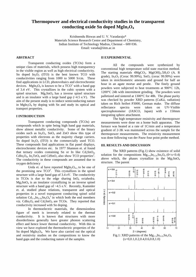
Thermopower and electrical conductivity studies in the transparent conducting oxide Sn doped MgIn 2 O 4 Krishnendu Biswas and U. V. Varadaraju* Materials Science Research Centre and Department of Chemistry, Indian Institute of Technology Madras, Chennai – 600 036. Email: [email protected] ABSTRACT Transparent conducting oxides (TCOs) form a unique class of materials, which possess high transparency in the visible region as well as high electrical conductivity. Sn doped In 2 O 3 (ITO) is the best known TCO with conductivities ranging from 1000 to 5000 S/cm. These find applications in LCD, photovoltaics and electrochromic devices. MgIn 2 O 4 is known to be a TCO 1 with a band gap of 3.4 eV. This crystallizes in the cubic system with a spinel structure. Mg 2 SnO 4 has a inverse spinel structure and is an insulator with a large band gap (~4.5 e.V). The aim of the present study is to induce semiconducting nature in MgIn 2 O 4 by doping with Sn and study its optical and transport properties. I INTRODUCTION Transparent conducting compounds (TCOs) are compounds which in spite being high band gap materials, show almost metallic conductivity. Some of the binary oxides such as In 2 O 3 , SnO 2 and ZnO show this type of properties with electrons as the majority charge carriers. Sn doped In 2 O 3 (ITO) is the commercially used TCO. These compounds find applications in flat panel displays, electrochromic devices etc. In 1977 Shannon et. al found that ternary oxides containing Sn or In like Cd 2 SnO 4 , CdIn 2 O 4 , In 2 TeO 6 and CdSnO 3 also show TCO properties 2 . The conductivity in these compounds are assumed due to oxygen deficiency Ueda et. al have reported MgIn 2 O 4-x to be one of the promising new TCO 2 . This crystallizes in the spinel structure with a large band gap of 3.4 eV. The conductivity in TCOs is due to the edge sharing InO 6 octahedra. Mg 2 SnO 4 is an insulator crystallizing in an inverse spinel structure with a band gap of ~4.5 e.V. Recently, Kammler et. al. studied phase relations, transparent and optical properties in a novel transparent conducting spinel solid solution Cd 1+x In 2-2x Sn x O 4 3 in which both the end members viz. CdIn 2 O 4 and Cd 2 SnO 4 are TCOs. They reported that conductivity increased with Sn doping. In thermoelectric materials, the dimensionless figure of merit is inversely related to the thermal conductivity. It is known that structures with more disorderliness generally have greater phonon scattering effect and hence lower thermal conductivity. With this in view we have explored the thermoelectric properties of the Sn doped MgIn 2 O 4 . We have also carried out the optical and resistivity studies on the compositions to know the band gaps and the conducting nature of the samples. II EXPERIMENTAL All the compounds were synthesized by conventional high temperature solid state reaction method. The starting materials 4MgCO 3 . Mg(OH) 2 .5H 2 O (A. R grade), In 2 O 3 (Cerac 99.99%), SnO 2 (cerac 99.99%) were taken in stoichiometric amounts and ground for half an hour in an agate mortar and pestle. The finely ground powders were subjected to heat treatments at 900°C 12h, 1200°C 24h with intermittent grinding. The powders were palletized and sintered at 1300°C for 48h. The phase purity was checked by powder XRD patterns (CuKá 1 radiation) taken on Rich Seifert P3000, German make. The diffuse reflectance spectra were taken on UV-Visible spectrophotometer (JASCO, Japan) with a 150mm integrating sphere attachment. The high temperature resistivity and thermopower measurements were done on a home built apparatus. The furnace was heated at a rate of 1C/min and a temperature gradient of 2-3K was maintained across the sample for the thermopower measurements. The resistivity measurement was done following van der Pauw four point probe method. III. RESULTS AND DISCUSSION The XRD patterns (Fig.1) show existence of solid solution for the compositions Mg 1+x In 2-2x Sn x O 4 (0<x<0.4) above which, the phases crystallize in the Mg 2 SnO 4 structure. The parent Fig.1: XRD patterns of the Mg 1+x In 2-2x Sn x O 4 (x=0,0.1,0.2,0.4,0.6,0.8,1.0)
-
Upload
khangminh22 -
Category
Documents
-
view
1 -
download
0
Transcript of Thermopower and electrical conductivity studies in the ...
Thermopower and electrical conductivity studies in the transparent conducting oxide Sn doped MgIn2O4
Krishnendu Biswas and U. V. Varadaraju*
Materials Science Research Centre and Department of Chemistry, Indian Institute of Technology Madras, Chennai – 600 036.
Email: [email protected]
ABSTRACT
Transparent conducting oxides (TCOs) form a unique class of materials, which possess high transparency in the visible region as well as high electrical conductivity. Sn doped In2O3 (ITO) is the best known TCO with conductivities ranging from 1000 to 5000 S/cm. These find applications in LCD, photovoltaics and electrochromic devices. MgIn2O4 is known to be a TCO1 with a band gap of 3.4 eV. This crystallizes in the cubic system with a spinel structure. Mg2SnO4 has a inverse spinel structure and is an insulator with a large band gap (~4.5 e.V). The aim of the present study is to induce semiconducting nature in MgIn2O4 by doping with Sn and study its optical and transport properties. I INTRODUCTION
Transparent conducting compounds (TCOs) are compounds which in spite being high band gap materials, show almost metallic conductivity. Some of the binary oxides such as In2O3, SnO2 and ZnO show this type of properties with electrons as the majority charge carriers. Sn doped In2O3 (ITO) is the commercially used TCO. These compounds find applications in flat panel displays, electrochromic devices etc. In 1977 Shannon et. al found that ternary oxides containing Sn or In like Cd2SnO4, CdIn2O4, In2TeO6 and CdSnO3 also show TCO properties2. The conductivity in these compounds are assumed due to oxygen deficiency
Ueda et. al have reported MgIn2O4-x to be one of the promising new TCO2. This crystallizes in the spinel structure with a large band gap of 3.4 eV. The conductivity in TCOs is due to the edge sharing InO6 octahedra. Mg2SnO4 is an insulator crystallizing in an inverse spinel structure with a band gap of ~4.5 e.V. Recently, Kammler et. al. studied phase relations, transparent and optical properties in a novel transparent conducting spinel solid solution Cd1+xIn2-2xSnxO4
3 in which both the end members viz. CdIn2O4 and Cd2SnO4 are TCOs. They reported that conductivity increased with Sn doping.
In thermoelectric materials, the dimensionless figure of merit is inversely related to the thermal conductivity. It is known that structures with more disorderliness generally have greater phonon scattering effect and hence lower thermal conductivity. With this in view we have explored the thermoelectric properties of the Sn doped MgIn2O4. We have also carried out the optical and resistivity studies on the compositions to know the band gaps and the conducting nature of the samples.
II EXPERIMENTAL All the compounds were synthesized by
conventional high temperature solid state reaction method. The starting materials 4MgCO3. Mg(OH)2.5H2O (A. R grade), In2O3 (Cerac 99.99%), SnO2 (cerac 99.99%) were taken in stoichiometric amounts and ground for half an hour in an agate mortar and pestle. The finely ground powders were subjected to heat treatments at 900°C 12h, 1200°C 24h with intermittent grinding. The powders were palletized and sintered at 1300°C for 48h. The phase purity was checked by powder XRD patterns (CuKá1 radiation) taken on Rich Seifert P3000, German make. The diffuse reflectance spectra were taken on UV-Visible spectrophotometer (JASCO, Japan) with a 150mm integrating sphere attachment.
The high temperature resistivity and thermopower measurements were done on a home built apparatus. The furnace was heated at a rate of 1C/min and a temperature gradient of 2-3K was maintained across the sample for the thermopower measurements. The resistivity measurement was done following van der Pauw four point probe method. III. RESULTS AND DISCUSSION
The XRD patterns (Fig.1) show existence of solid solution for the compositions Mg1+xIn2-2xSnxO4 (0<x<0.4) above which, the phases crystallize in the Mg2SnO4 structure. The parent
Fig.1: XRD patterns of the Mg1+xIn2-2xSnxO4
(x=0,0.1,0.2,0.4,0.6,0.8,1.0)
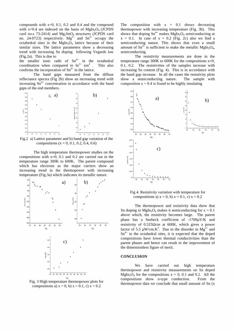
compounds with x=0, 0.1, 0.2 and 0.4 and the compound with x=0.4 are indexed on the basis of MgIn2O4 (JCPDS card no.s 73-2414) and Mg2SnO4 structures (JCPDS card no. 24-0723) respectively. Mg2+ and Sn4+ occupy the octahedral sites in the MgIn2O4 lattice because of their similar sizes. The lattice parameters show a decreasing trend with increasing Sn doping following Vegards law (Fig.2a). This is due to the smaller ionic radii of Sn4+ in the octahedral coordination when compared to In3+ ion4 . This also confirms the incorporation of Sn4+ in the lattice.
The band gaps measured from the diffuse reflectance spectra (Fig 2b) show an increasing trend with increasing Sn4+ concentration in accordance with the band gaps of the end members.
Fig.2 a) Lattice parameter and b) band gap variation of the compositions (x = 0, 0.1, 0.2, 0.4, 0.6)
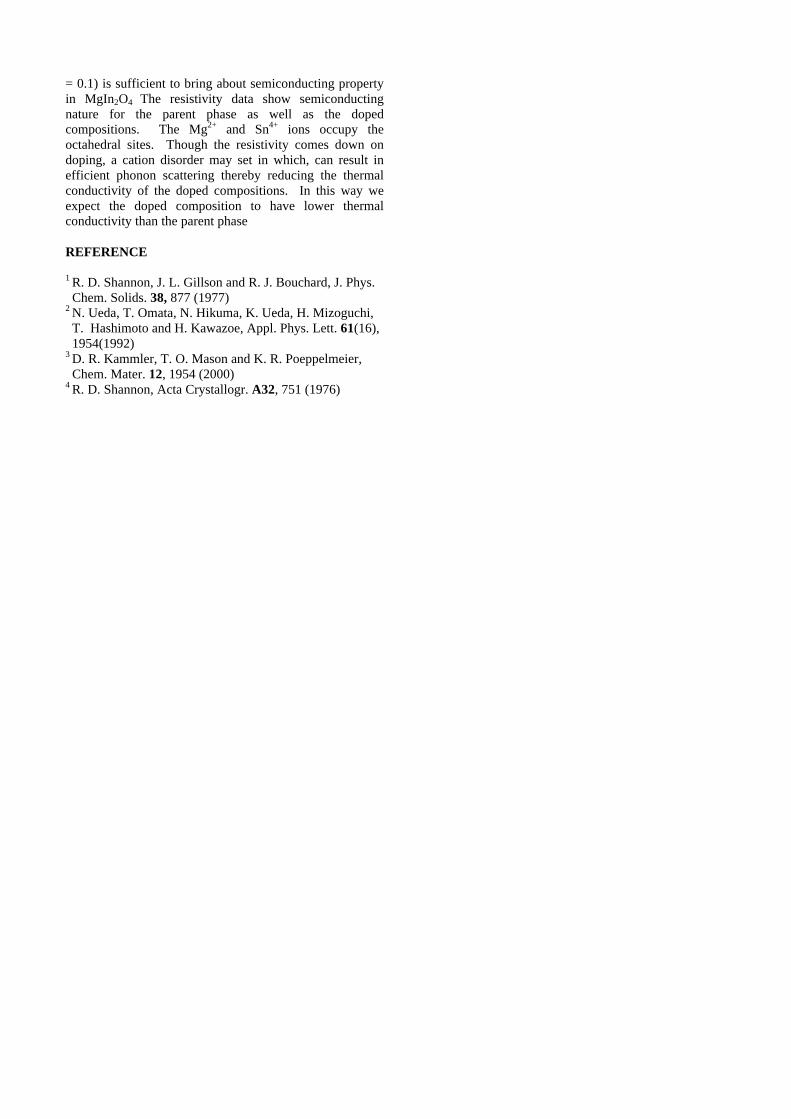
The high temperature thermopower studies on the
compositions with x=0, 0.1 and 0.2 are carried out in the temperature range 300K to 600K. The parent compound which has electrons as the major carriers show an increasing trend in the thermopower with increasing temperature (Fig.3a) which indicates its metallic nature.
Fig. 3 High temperature thermopower plots for compositions a) x = 0, b) x = 0.1, c) x = 0.2
The composition with x = 0.1 shows decreasing thermopower with increasing temperature (Fig. 3b). This shows that doping Sn4+ makes MgIn2O4 semiconducting at x = 0.1. In case of x = 0.2 (Fig. 2c) also we find a semiconducting nature. This shows that even a small amount of Sn4+ is sufficient to make the metallic MgIn2O4, semiconducting.
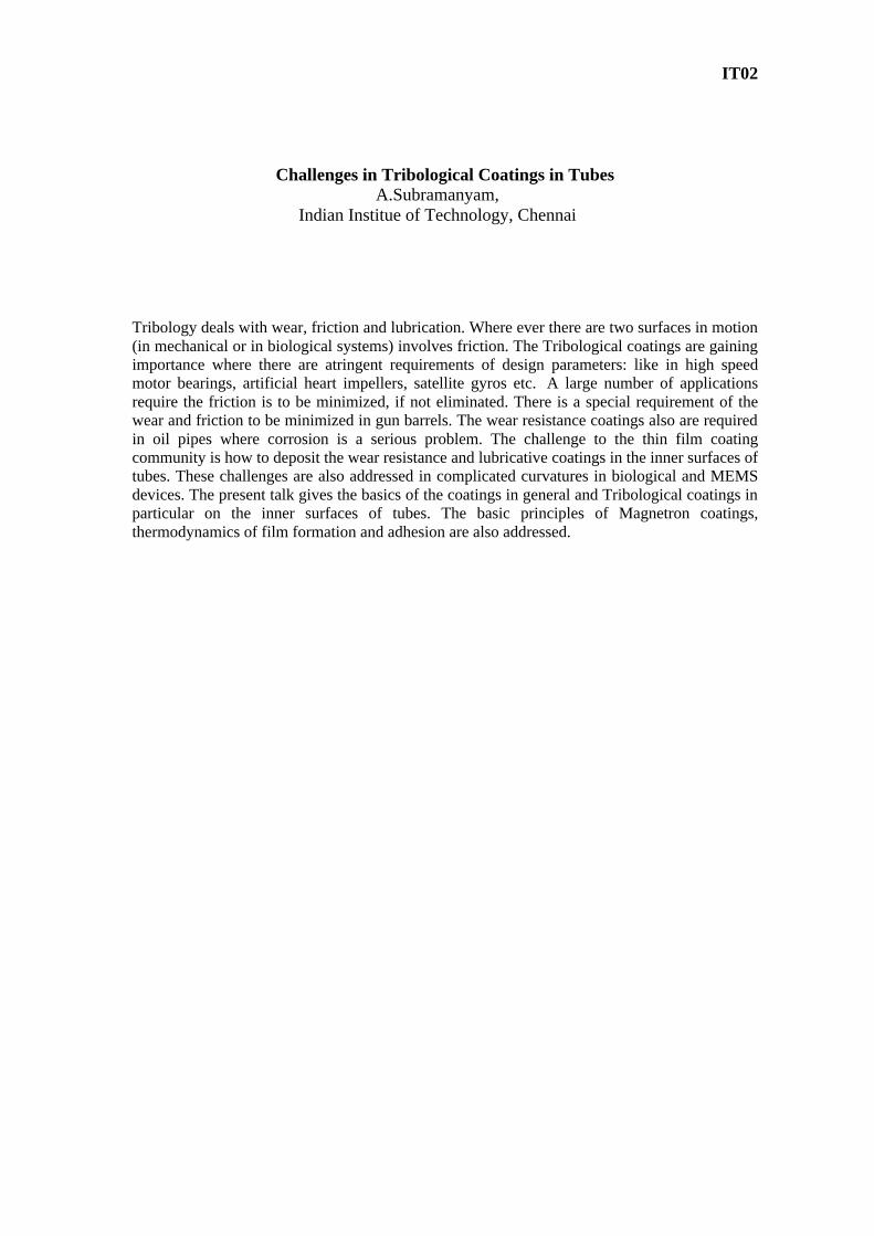
The resistivity measurements are done in the temperature range 300K to 600K for the compositions x=0, 0.1, 0.2. The resistivities of the samples increase with increasing Sn content (Fig. 4). This is in accordance with the band gap increase. In all the cases the resistivity plots show a semiconducting nature. The sample with composition x = 0.4 is found to be highly insulating
Fig 4. Resistivity variation with temperature for
compositions a) x = 0, b) x = 0.1, c) x = 0.2
The thermopower and resistivity data show that Sn doping in MgIn2O4 makes it semiconducting for x = 0.1 above which, the resistivity becomes large. The parent phase has a Seebeck coefficient of -1700µV/K and resistivity of 0.525Ωcm at 600K, which gives a power factor of 5.5 µW/cm.K2. Due to the disorder in Mg2+ and Sn4+ in the octahedral sites, it is expected that the doped compositions have lower thermal conductivities than the parent phases and hence can result in the improvement of the dimensionless figure of merit. CONCLUSION
We have carried out high temperature thermopower and resistivity measurements on Sn doped MgIn2O4 for the compositions x = 0, 0.1 and 0.2. All the compositions show n-type conduction. From the thermopower data we conclude that small amount of Sn (x
a) b)
a) b)
c)
a) b) a)
c)
= 0.1) is sufficient to bring about semiconducting property in MgIn2O4 The resistivity data show semiconducting nature for the parent phase as well as the doped compositions. The Mg2+ and Sn4+ ions occupy the octahedral sites. Though the resistivity comes down on doping, a cation disorder may set in which, can result in efficient phonon scattering thereby reducing the thermal conductivity of the doped compositions. In this way we expect the doped composition to have lower thermal conductivity than the parent phase REFERENCE 1 R. D. Shannon, J. L. Gillson and R. J. Bouchard, J. Phys. Chem. Solids. 38, 877 (1977) 2 N. Ueda, T. Omata, N. Hikuma, K. Ueda, H. Mizoguchi, T. Hashimoto and H. Kawazoe, Appl. Phys. Lett. 61(16), 1954(1992) 3 D. R. Kammler, T. O. Mason and K. R. Poeppelmeier, Chem. Mater. 12, 1954 (2000) 4 R. D. Shannon, Acta Crystallogr. A32, 751 (1976)
IT02
Challenges in Tribological Coatings in Tubes A.Subramanyam,
Indian Institue of Technology, Chennai Tribology deals with wear, friction and lubrication. Where ever there are two surfaces in motion (in mechanical or in biological systems) involves friction. The Tribological coatings are gaining importance where there are atringent requirements of design parameters: like in high speed motor bearings, artificial heart impellers, satellite gyros etc. A large number of applications require the friction is to be minimized, if not eliminated. There is a special requirement of the wear and friction to be minimized in gun barrels. The wear resistance coatings also are required in oil pipes where corrosion is a serious problem. The challenge to the thin film coating community is how to deposit the wear resistance and lubricative coatings in the inner surfaces of tubes. These challenges are also addressed in complicated curvatures in biological and MEMS devices. The present talk gives the basics of the coatings in general and Tribological coatings in particular on the inner surfaces of tubes. The basic principles of Magnetron coatings, thermodynamics of film formation and adhesion are also addressed.

Sorry!!
This Paper is NOT Available
IT04
Ion Assisted Deposition of Sputtered Thin Films – Bias Sputtering to ECR Assisted Growth
G. Mohan Rao, K. Deenamma Vargheese, S. Guruvenkat and S.K. Patra
Department of Instrumentation Indian Institute of Science
Bangalore 560012
Ion assisted deposition of thin films is a popular technique to achieve good quality thin films in terms of crystallinity, micro structure and physical properties. Ion flux and Ion energy play a dominant role in the process optimization. While conventional ion guns are used in evaporation technique, their use in sputter deposition is limited due to geometrical and pressure constraints. In this paper ion assistance on the growth of thin films of silicon nitride and titanium nitride would be discussed. The ion assistance in the form of bias magnetron sputtering, unbalanced magnetron sputtering and ECR assisted deposition would be discussed. These three techniques represent different degrees of ion flux and ion density. Their effect on the microstructure evolution and properties of the deposited films would be analyzed in detail.
IT05
Planar Active Waveguide Devices on Glass- Fabrication and Characteristics
Gin Jose
Department of Physics, Indian Institute of Technology Guwahati, Guwahati 781039, India.
E-mail: [email protected] Planar integrated lightwave circuits featuring active elements are a recent addition to the modern all-optical wavelength division multiplexed (WDM) networks. Integrated amplifiers and lasers operating in the conventional band (1530-1565nm) are by and large fabricated using erbium or erbium/ytterbium doped active glass. Technologies such as ion exchange, thin film sputtering, silica-on-silicon, sol-gel, PECVD, femtosecond laser writing were proved valid for device fabrication. In this talk a review of the development in the field will be presented. In particular, the design and fabrication of silver-sodium ion exchanged waveguides on Er-Yb phosphate glass and their lasing and amplifying properties are important. We investigated the design issues related to the dependence of ion exchange on the spectroscopic properties. Optical nonlinearities in silver diffused waveguides resulting from nanocluster formation, which are promising for all optical switching devices, will be discussed.
IT06
In-situ characterization of Silicon based Thin Film growth and Interface formation by Contactless Transient Photoconductivity measurements
H.C. Neitzert
Department of Electrical Engineering (DIIIE) Salerno University, Fisciano - 84084, ITALY
E-mail: [email protected]
A common deposition technique for thin silicon films, with industrial applications like solar cell and active matrix display production, is plasma enhanced chemical vapor deposition (PECVD). Thin film semiconductor growth is a rather complicated process and influenced by a large number of parameters. Therefore the application of in-situ measurement techniques is of great interest. There have been strong efforts to correlate the measured plasma parameters and the chemical precursor distribution in the gas phase with the deposited film properties 1. Another possible approach for in-situ process control and parameter optimization are direct measurements of the growing film properties. In this latter case non-invasive techniques, that do not require special test structures, are certainly of great advantage. Optical techniques, like spectroscopic ellipsometry 2,3 have been shown to give detailed information regarding the film structure. Microwave reflection based techniques can be used to measure important semiconductor parameters like charge carrier mobilities and minority carrier lifetimes and are common tools for silicon wafer inspection before processing. Here we will demonstrate the capabilities of transient photoconductivity measurements, based on the microwave reflection change of semiconductor films after generation of free carriers by short laser pulses 4, for the in-situ characterization during PECVD growth of amorphous hydrogenated silicon (a-Si:H) and for the kinetics of the formation of various interfaces.
The amplitude of the measured microwave reflection transients is proportional to the product of the number of photo generated charge carriers multiplied with their respective mobilities. In the initial phase of the growth of a-Si:H films on glass substrates we find consequently an increasing signal amplitude, observe interference peaks and can, by comparison of the measured amplitude changes with modeling of the optical absorption, use the technique for in-situ thickness control. Even a-Si:H films with thicknesses below 3nm can be characterized regarding their electrical properties, where we still observe island-like growth. This means that we can get information about transport properties of films, where classical electrical measurements with contacts cannot be applied. Depositing relatively thick layers with different plasma conditions on top of each other and using short wavelengths for optical excitation, it can be shown that parameter optimization is possible in a continuous deposition sequence, without necessity of preparing a large number of single thin films. Another interesting application is the determination of active dopant concentrations. This type of measurements are based either on the change of the charge carrier mobility with doping or on the change of the charge carrier decay kinetics. Diborane CVD deposition without plasma ignition and a possible defective interface layer between intrinsic and p-type a-Si:H have been detected. During the formation of heterojunctions for solar cells, based on amorphous silicon deposited on crystalline silicon substrates, transient microwave detected photoconductivity measurements permit to follow the kinetics of the initial crystalline silicon surface damaging and the subsequent defect passivation during amorphous silicon deposition in real time. A newly developed simulator enables us to model also the fast initial decay of the microwave transients 5.
Reference
1. J. Perrin, J. Non-Cryst. Solids, 137&138, 639 (1991)
2. R.W. Collins, J. Non-Cryst. Solids, 114, 160 (1989)
3. N. Layadi, P. Roca i Cabarrocas, J. Huc, J.Y. Parey and B. Drevillion, Solid State Phenom., 37&38, 281 (1994)
4. M. Kunst and G. Beck, J. Appl. Phys., 63, 1093 (1988)
5. G. Citarella, W. R. Fahrner, H. C. Neitzert, F. Wünsch, M. Kunst, Proc. of the Workshop on Modeling and Simulation of Electron Devices, Pisa (2005), to be published
1
NANOPHOSPHOR BASED DISPLAYS K. Manzoor, V. Aditya, S. R. Vadera, N. Kumar,*, T. R. N. Kutty†
Materials Development Group, Defence Laboratory, Jodhpur 342 011, Rajasthan, India
*E-mail:[email protected] †Materials Research Center, Indian Institute of Science, Bangalore560 012, India
ABSTRACT
Alternate-current electroluminescent (ac EL) devices based on doped ZnS nanocrystals emitting blue, green and orange-red colors are reported. ZnS nanocrystals doped with Cu+-Al3+ and Cu+-Al3+-Mn2+ combinations were synthesized by wet chemical method at room temperature. The ZnS:Cu+,Al3+ nanocrystals show blue (462nm) and green (530nm) EL emissions depending upon the presence and absence of sulphur vacancies, respectively. The orange EL emission (590nm) is realized from ZnS:Cu+,Al3+,Mn2+ nanoparticles by way of nonradiative energy transfer from AlZn-CuZn pairs to MnZn. The EL devices show low turn-on voltage of ~10V ac @100Hz. The mechanism of ac EL in ZnS nanocrystals has been explained wherein the excitation is attributed to the electric-field-assisted injection of electron-hole pairs from the surface regions into the interiors and their subsequent recombination therein causes emission.
1. INTRODUCTION
Novel optical, electronic and structural properties
of semiconducting nanocrystals have acquired considerable importance because of their great potential for many versatile applications ranging from DNA markers to light emitting displays1-4. The success in converting these novel properties into technologically viable products lies in the ability to synthesize highly pure, well characterized nanocrystals (NC) and fabricate device structures based on them. Recently, it has been shown that hybrid organic-inorganic light emitting devices consisting of semiconducting nanocrystals and polymeric materials can be constructed5. Further, quantum dot light emitting diodes based on single layer of CdSe6 or ZnS:Mn7 nanocrystals incorporated into hole injecting polymers have also been reported. All these studies are mainly based on the concept of realization of p-n junction in multi-layered structures, consisting of II-VI nanocrystals and organic polymers, operational under direct current (dc). In this letter, we report, the realization of alternate-current electroluminescence (ac EL) from doped ZnS nanocrystals showing blue, green and orange-red emission colors.
2. EXPERIMENTAL 2.1 Synthesis and Characterization
ZnS nanocrystals doped with Cu+-Al3+ and Cu+-Al3+-Mn2+ combinations have been prepared by an optimized aqueous colloidal precipitation method at room temperature8. Although the available literature on doping of Al3+ in ZnS phosphors reported only the high temperature (~9000C) doping processes9, the present
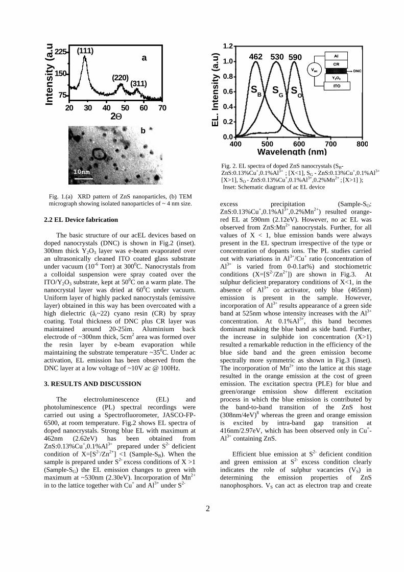
work report incorporation of Al3+ as a coactivator in Cu+ activated ZnS nanocrystals through wet chemical reaction at room temperature in which the activator–coactivator charge compensation conditions are effectively utilized to achieve the doping. During the co-precipitation reaction, substitutional occupation of Cu+ ion at Zn2+ site causes deficiency of one positive charge for the charge neutralization. This is compensated by the intake of one Al3+ ion (at Zn2+ site) having one excess positive charge. Therefore when co-doped, Cu+ and Al3+ ions can occupy the nearest-neighbor sites separated by one S2- ion so as to form an electrically neutral impurity complex (CuZn-S-AlZn). Strictly controlled reaction conditions, in which the copper is stabilized in Cu+ state rather than Cu2+, and the high surface reactivity of nanoparticles help to realize the doping. Further, to avoid any effect of halide ions, acting as another coactivator, we have used all halogen free chemicals for the synthesis. The stoichiometric ratio, X=[S2-/Zn2+], and doping concentrations were varied for each sample to realize the desired EL characteristics. Crystallinity of the samples, studied by using X–ray diffractometer-Philips XRG-3000 fitted with Cu-Ká (ë=1.54056nm) source, shown in Fig. 1(a) indicate the zinc-blende (â-ZnS) crystal structure. Transmission electron microscopic (TEM, JEOL-JEM-200CX) image, Fig. 1(b), shows well isolated particles of average size ~2nm. The concentrations of dopants present in the host lattice have been estimated by atomic absorption spectrophotometer (AAS, Perkin-Elmer-2380).
2
2.2 EL Device fabrication
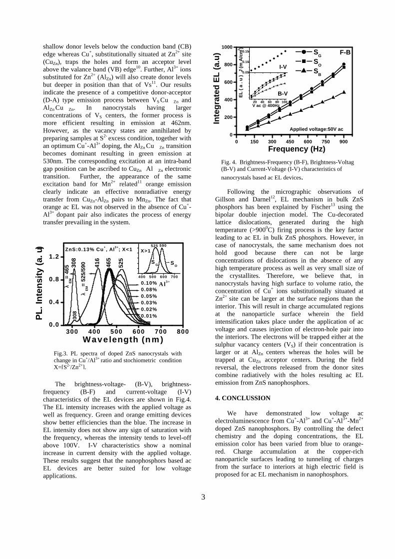
The basic structure of our acEL devices based on doped nanocrystals (DNC) is shown in Fig.2 (inset). 300nm thick Y2O3 layer was e-beam evaporated over an ultrasonically cleaned ITO coated glass substrate under vacuum (10-6 Torr) at 3000C. Nanocrystals from a colloidal suspension were spray coated over the ITO/Y2O3 substrate, kept at 500C on a warm plate. The nanocrystal layer was dried at 600C under vacuum. Uniform layer of highly packed nanocrystals (emissive layer) obtained in this way has been overcoated with a high dielectric (år~22) cyano resin (CR) by spray coating. Total thickness of DNC plus CR layer was maintained around 20-25ìm. Aluminium back electrode of ~300nm thick, 5cm2 area was formed over the resin layer by e-beam evaporation while maintaining the substrate temperature ~350C. Under ac activation, EL emission has been observed from the DNC layer at a low voltage of ~10V ac @ 100Hz. 3. RESULTS AND DISCUSSION
The electroluminescence (EL) and photoluminescence (PL) spectral recordings were carried out using a Spectrofluorometer, JASCO-FP-6500, at room temperature. Fig.2 shows EL spectra of doped nanocrystals. Strong blue EL with maximum at 462nm (2.62eV) has been obtained from ZnS:0.13%Cu+,0.1%Al3+
prepared under S2- deficient condition of X=[S2-/Zn2+] <1 (Sample-SB). When the sample is prepared under S2- excess conditions of X >1 (Sample-SG) the EL emission changes to green with maximum at ~530nm (2.30eV). Incorporation of Mn2+ in to the lattice together with Cu+ and Al3+ under S2-
excess precipitation (Sample-SO: ZnS:0.13%Cu+,0.1%Al3+,0.2%Mn2+) resulted orange-red EL at 590nm (2.12eV). However, no ac EL was observed from ZnS:Mn2+ nanocrystals. Further, for all values of X < 1, blue emission bands were always present in the EL spectrum irrespective of the type or concentration of dopants ions. The PL studies carried out with variations in Al3+/Cu+ ratio (concentration of Al3+ is varied from 0-0.1at%) and stochiometric conditions (X=[S2-/Zn2+]) are shown in Fig.3. At sulphur deficient preparatory conditions of X<1, in the absence of Al3+ co activator, only blue (465nm) emission is present in the sample. However, incorporation of Al3+ results appearance of a green side band at 525nm whose intensity increases with the Al3+ concentration. At 0.1%Al3+, this band becomes dominant making the blue band as side band. Further, the increase in sulphide ion concentration (X>1) resulted a remarkable reduction in the efficiency of the blue side band and the green emission become spectrally more symmetric as shown in Fig.3 (inset). The incorporation of Mn2+ into the lattice at this stage resulted in the orange emission at the cost of green emission. The excitation spectra (PLE) for blue and green/orange emission show different excitation process in which the blue emission is contributed by the band-to-band transition of the ZnS host (308nm/4eV)8 whereas the green and orange emission is excited by intra-band gap transition at 416nm/2.97eV, which has been observed only in Cu+-Al3+ containing ZnS.
Efficient blue emission at S2- deficient condition
and green emission at S2- excess condition clearly indicates the role of sulphur vacancies (VS) in determining the emission properties of ZnS nanophosphors. VS can act as electron trap and create
20 30 40 50 60 70
75
150
225
(311)(220)
(111)In
ten
sity
(a.
u)
2ΘΘ
a
b
Fig. 1.(a) XRD pattern of ZnS nanoparticles, (b) TEM micrograph showing isolated nanoparticles of ~ 4 nm size.
10nm
400 500 600 700 8000.0
0.2
0.4
0.6
0.8
1.0
1.2
SO
SG
SB
590530462
EL
. In
ten
sity
(a.
u)
Wavelength (nm)
Fig. 2. EL spectra of doped ZnS nanocrystals (SB-ZnS:0.13%Cu+,0.1%Al3+
; [X<1], SG - ZnS:0.13%Cu+,0.1%Al3+
[X>1], SO - ZnS:0.13%Cu+,0.1%Al3+,0.2%Mn2+ ; [X>1] ); Inset: Schematic diagram of ac EL device
3
shallow donor levels below the conduction band (CB) edge whereas Cu+, substitutionally situated at Zn2+ site (CuZn), traps the holes and form an acceptor level above the valance band (VB) edge10. Further, Al3+ ions substituted for Zn2+ (AlZn) will also create donor levels but deeper in position than that of Vs11. Our results indicate the presence of a competitive donor-acceptor (D-A) type emission process between VS Cu Zn and AlZn Cu Zn. In nanocrystals having larger concentrations of VS centers, the former process is more efficient resulting in emission at 462nm. However, as the vacancy states are annihilated by preparing samples at S2- excess condition, together with an optimum Cu+-Al3+ doping, the AlZn Cu Zn transition becomes dominant resulting in green emission at 530nm. The corresponding excitation at an intra-band gap position can be ascribed to CuZn Al Zn electronic transition. Further, the appearance of the same excitation band for Mn2+ related11 orange emission clearly indicate an effective nonradiative energy transfer from CuZn-AlZn pairs to MnZn. The fact that orange ac EL was not observed in the absence of Cu+-Al3+ dopant pair also indicates the process of energy transfer prevailing in the system.
The brightness-voltage- (B-V), brightness-
frequency (B-F) and current-voltage (I-V) characteristics of the EL devices are shown in Fig.4. The EL intensity increases with the applied voltage as well as frequency. Green and orange emitting devices show better efficiencies than the blue. The increase in EL intensity does not show any sign of saturation with the frequency, whereas the intensity tends to level-off above 100V. I-V characteristics show a nominal increase in current density with the applied voltage. These results suggest that the nanophosphors based ac EL devices are better suited for low voltage applications.
Following the micrographic observations of
Gillson and Darnel12, EL mechanism in bulk ZnS phosphors has been explained by Fischer13 using the bipolar double injection model. The Cu-decorated lattice dislocations, generated during the high temperature (>9000C) firing process is the key factor leading to ac EL in bulk ZnS phosphors. However, in case of nanocrystals, the same mechanism does not hold good because there can not be large concentrations of dislocations in the absence of any high temperature process as well as very small size of the crystallites. Therefore, we believe that, in nanocrystals having high surface to volume ratio, the concentration of Cu+ ions substitutionally situated at Zn2+ site can be larger at the surface regions than the interior. This will result in charge accumulated regions at the nanoparticle surface wherein the field intensification takes place under the application of ac voltage and causes injection of electron-hole pair into the interiors. The electrons will be trapped either at the sulphur vacancy centers (VS) if their concentration is larger or at AlZn
centers whereas the holes will be trapped at CuZn acceptor centers. During the field reversal, the electrons released from the donor sites combine radiatively with the holes resulting ac EL emission from ZnS nanophosphors. 4. CONCLUSSION
We have demonstrated low voltage ac
electroluminescence from Cu+-Al3+ and Cu+-Al3+-Mn2+
doped ZnS nanophosphors. By controlling the defect chemistry and the doping concentrations, the EL emission color has been varied from blue to orange-red. Charge accumulation at the copper-rich nanoparticle surfaces leading to tunneling of charges from the surface to interiors at high electric field is proposed for ac EL mechanism in nanophosphors.
0 150 300 450 600 750 9000
200
400
600
800
1000
20 40 60 80 100
0.05
0.10
0.15
F-B
EL
( a
. u
)
V ac @ 400Hz
Applied voltage:50V ac
Inte
gra
ted
EL
(a.
u) S
G
SO
SB
B-V
Frequency (Hz)
I-V
J (m
A/c
m2 )
300 400 500 600 700 8000.0
0.4
0.8
1.2
400 500 600 700
ZnS:0.13% Cu+, Al3+; X<1
308
λλ E
M=
525/
590
λλ E
M=
465 30
8
416
465
525
A l3+0.10% 0.08%0.05%0.03%0.02%0.01%P
L. I
nte
nsi
ty (
a. u
)
Wavelength (n m )
X>1
SO
SG
525 590
Fig.3. PL spectra of doped ZnS nanocrystals with change in Cu+/Al3+ ratio and stochiometric condition X=[S2-/Zn2+].
Fig. 4. Brightness-Frequency (B-F), Brightness-Voltag (B-V) and Current-Voltage (I-V) characteristics of
nanocrystals based ac EL devices.
4
Acknowledgments We thank Dr. M P Chacharkar, Director, Defence Laboratory, Jodhpur for his support to this work.
REFERENCES
1 A. P. Alivisatos, Science 271, 933 (1996). 2 R. N. Bhargava and D. Gallagher, Phys. Rev. Lett. 72, 416 (1994). 3 W. C. W. Chan and S. Nie, Science 281, 2016 (1998). 4 M. V. Artemyev, V. Sperling and U. Woggon, J. App. Phys. 81, 6975 (1997). 5 V. L. Colvin, M. C. Schlamp and A. P. Alivisatos, Nature 370, 354 (1994). 6 S. Coe, W. K Woo, M. G. Bawendi and V. Bulovic, Nature 420, 800 (2003). 7 H. Yang, P. H. Holloway, B. B. Ratna, J. Appl. Phys. 93, 586 (2003).
8 K Manzoor, S. R. Vadera, N. Kumar and T. R. N. Kutty, Mat. Chem. Phys. 82, 718 (2003) 9 S. Shinoya and W. M. Yen, Phosphor Handbook (C.R.C. Press, Washington, 1999). 10 A. S. Marfunin, Spectroscopy, Luminescence and Radiation centers in Minerals (Springer- Verlag, New- York, 1979). 11 R. N. Bahrgava, J. Lumi. 70, 85 (1996). 12 J. L. Gillson and F. J. Darnell, Phys. Rev. 125, 149 (1962). 13 A. G. Fischer, J. Electrochem. Soc. 113, 449 (1966).

IT08
Optical spectra of semiconductor quantum dots
Kailash Rustagi Physics Department,IITBombay, Mumbai 400 076
The modification of optical spectra due to quantum confinement is important for some of their
potential applications as well as for understanding their structure and physical properties. In this talk we will first review our present theoretical understanding of electronic and vibrational energy levels. We emphasisie in particular the differences between the spectra of quantum dots prepared by different methods and in different matrices. Thoretical expectations are compared with experimental observations for some specific cases.
IT09
p-type Transparent Conducting CuAlO2 Thin Films : Potential Candidate for Transparent Electronics
K.K. Chattopadhyay
Thin Film and Nanoscience Laboratory, Department of Physics Jadavpur University, Kolkata – 700 032, India
Transparent, p-type semiconducting crystalline thin films have recently gained tremendous interest
in the field of active devices. All-transparent junctional devices have begun a new generation in the opto-electronics technology called ‘Invisible Electronics’. Non-stoichiometric and doped versions of various new types of p-type transparent conducting oxides (p-TCO) with improved optical and electrical properties have been synthesized in the last few years in this direction. A wide range of deposition techniques has been adopted to prepare the films. The first and the most important material in this group is copper aluminium oxide (CuAlO2). Kawazoe and co-authors1 first prepared it in transparent thin film form for possible application in p-TCO technology. Its high transparency (~ 80 %) and moderate p-type conductivity (~ 0.34 S cm-1) makes it a promising material for “Transparent Electronics”. In this paper the origin of p-type conductivity in these transparent oxides is discussed. Also an up-to-date and comprehensive description of different p-type transparent conducting oxide thin films is presented. The structural, morphological and electro-optical properties of the CuAlO2 thin films are highly correlated with the deposition conditions. The effect of oxygen partial pressure, substrate temperature, post-deposition heat treatment under oxygen atmosphere etc. strongly influence the defect chemistry of the films, which, in turn, controls the properties of the films.
Electrical and optical properties of the films and fabrication of all-transparent diodes are discussed which are important in the development of ‘Transparent Electronics’. Also, recently, the research on nanostructured materials generates great interest in the scientific community and offers tremendous opportunities in the field of physics, chemistry, materials science and related interdisciplinary areas because of new properties exhibited by them and challenging problems thrown up for providing theoretical concepts in physics associated with it. Here, we have also discussed in brief, the formation of different nanocrystalline p-TCO films, which may open up an extremely important and interesting field of research for the fabrication of all-transparent nano-active devices and give a new dimension in the field of ‘Transparent Electronics’2,3. References :
1. H. Kawazoe, M. Yasukawa, H. Hyodo, M. Kurita, H. Yanagi and H. Hosono, Nature 389, 939 (1997). 2. A.N. Banerjee and K.K. Chattopadhyay, Journal of Applied Physics 97 (2005) 084308. 3. A.N. Banerjee and K.K. Chattopadhyay, Progress in Crystal Growth and Characterization of Materials,
(Review article) (In Press).
IT10
Tailored Thin Films and Nanomaterials K L Chopra
Thin Film Laboratory, IIT Delhi
By manipulating deposition parameters , a host of thin-film deposition techniques for ab-initio creation of solid matter, atom-by-atom, have been utilized to create 0, 1, or 2 dimensional nanomaterials and nanostructures such as thin-films , quantum dots,powders, wires, fibres, tubes,sponges ,etc in various shapes , sizes ,morphologies and structures . With decreasing size and dimensions, most physical and chemical properties of size constrained nanomaterials undergo considerable but tailorable changes. In some specially engineered, tailored and designer nanomaterials / nanostructures,novel physical ,chemical, or electronic phenomena are observed which offer exciting applications, some of which will be illustrated from our own work.

Sorry!!
This Paper is NOT Available
IT12
Diluted Magnetic Semiconductors: Emerging Frontiers of Spin-optoelectronics
Lalit M. Kukreja
Thin Film Laboratory Centre for Advanced Technology
P. O. CAT, Indore – 452 013, INDIA E-mail: [email protected]
Diluted magnetic semiconductors (DMS) are the semiconductors doped with transition metal
elements. Currently DMS are the materials for active research and development because these are potential candidates for high Curie temperature ferromagnetic semiconductors. This makes these DMS important to realize semiconductor spintronics and spin-optoelectronics utilizing electronically or optically controlled magnetism at room temperature. A review of the fundamentals, current status of research on DMS and its proposed applications will be presented. Recently we have carried out studies on structural, optical and some of the magnetic properties of oxides DMS of Mn and Co doped ZnO thin films grown on sapphire using Pulsed Laser Deposition. Results of these studies will also be presented and discussed.
IT13
Pulsed Laser Deposition of a few Oxide Thin Films
M.Joseph, P.Manoravi, N.Sivakumar Fuel Chemistry Division, Chemistry Group,
Indira Gandhi Center for Atomic Research, Kalpakkam-603 102. E-mail: [email protected]
Oxide thin films find many technological applications in different areas such as optoelectronic
and memory devices, batteries, fuel cells, sensors etc. In this paper, results on the preparation of few oxide thin films such as La0.9Sr0.1Ga0.8Mg0.2O2.85
1, CaZrO32, VO2
3, doped ZnO4, Bi2VO5.55,
LiCo0.85Cr0.15O26, etc by pulsed laser deposition (PLD) will be presented.
References
1. P.Manoravi, N.Sivakumar, M.Joseph, Tom Mathews, Ionics 10, 32 (2004) 2. M.Joseph, N.Sivakumar, P.Manoravi , S.Vana Varamban, Solid State Ionics 144, 339 (2001) 3. R. T. Rajendra Kumar, B. Karunagaran, D. Mangalaraj, Sa. K. Narayandass, P. Manoravi, M. Joseph, J.
Mater. Sci. 39, 2869 (2004) 4. M.Joseph, H. Tabata, H.Saeki, K.Ueda, T.Kawai, Physica B 302-303, 140 (2001) 5. M.Joseph, H.Y.Lee, H.Tabata, T.Kawai, J. Appl. Phys. 88, 1193 (2000) 6. R. Vasanthi, I. RuthMangani, P. Manoravi, M. Joseph, R. Kesavamoorthy, C.S. Sundar, S. Selladurai,
Scripta Materialia 50, 1329 (2004)
Development of phosphors for 21st Century - lighting and display devices
M.M.K.Samy
Materials Science Research Center, Indian Institute of Technology-Madras (IIT-M), Chennai - 600 036
India Email:[email protected]
Abstract Phosphors are solid-state inorganic luminescent materials widely applied in fluorescent lightings and display devices like color television, plasma displays, projection television etc. Recently phosphor converted light emitting diodes (pcLEDs), field emission displays (FEDs) and thick ceramic thin film electroluminescence displays (TCTFEL) are gaining a great attention for 21st century energy saving lighting system and high-resolution displays, respectively. Since, energy is produced maximum by fossil fuel and nuclear energy, energy saving leads the world free from many disasters and to save valuable natural resources. Due to the emergence of reading-intensive applications such as web browsing, e-mail and electronic books, display readability etc., display devices has gained importance with the challenge being to fabricate small and easily portable displays. To achieve this, development of high-resolution emissive display devices like FEDs and EL displays are nowadays gaining great importance because of their small thickness, ruggedness and wide viewing angle. For the success of these lightings and display devices, development of phosphors with a required characteristic is essential. This talk will cover the development of various phosphor materials in our laboratory with required characteristics to apply in the LED lighting, FEDs and EL displays. Introduction
Phosphors are widely applied in
fluorescent lamps (FL) and emissive displays because these generate visible light with high luminescent emission efficiencies. In FL lamps excitation takes place using UV photons generated by Hg discharge. The excitation takes place in CRT’s by electrons with a kinetic energy (35 kV) while in EL panels there are low kinetic energy electrons which are involved in the excitation. Similar to the FL lighting, LED lighting requires phosphors, which have absorbance in the blue or near UV region. The generation of near UV or blue light is possible by tuning the band gap of GaN based solid-state devices. For white light emitting LED applications, the generation of blue, green, yellow and red lights are important and combination of these phosphors gives white light or other colors. For the two color component system, blue converting yellow emitting YAG:Ce phosphor is widely used because of strong absorbance in the blue region. For a tri-component system with high colour rendering indexes SrGa2S4:Eu (green) and SrS:Eu (red) were generally used with blue LEDs [1-4].
For high-resolution display devices like FEDs and thin film Electro-luminescence (TFEL), the development of phosphor with required properties are crucial for the device applications. Field emission display (FED) is currently being
explored as one of the promising flat panel displays (FPDs) with all the futures of CRT tubes. The conventional sulfide based CRT blue, green and red phosphors show efficient emission for FEDs application. However, an electron-induced decomposition of these phosphors reduces the luminescent emission efficiency and the by-products of the sulfur are known to poison the electron emitter during operation [5-7]. By considering this aspect, in recent days, active research is being carried out on the development of wide band gap oxide semiconductor phosphor for the possible applications of display phosphors. It has been observed that the CL emission properties of these phosphors are enhanced at low voltage excitation due to the reduction of surface charge as well as generate more electron-hole pairs in the host crystal and subsequent energy transfer to the luminescent center resulting better luminous efficiency [8-10].
By considering the stability of oxide
phosphor thin films over the sulfides, there is a growing trend towards the development of high luminance thin film devices that consist of multi component oxides as the host materials for various display device applications. Recently there are reports available on phosphors with very high EL luminance efficiency almost equal to ZnS:Mn,
using binary oxide such as Y2O3 or combinations of Y2O3-Ga2O3 and Y2O3-GeO2 activated with Mn with a controlled chemical compositions, as EL layers [11-13]. In this paper, we are reporting various sulfide and oxide phosphors developed in our laboratory and their possible application to white light generating LEDS and FEDs and TCTFEL.
Phosphors for phosphor converted white light
emitting diodes (pcLEDs)
For the pcLEDs applications, YAG:Ce was prepared by sol-gel method and ZnS:Mn and SrS:Eu were prepared by solid state reaction. These phosphors were studied by photo luminescent excitation and emission spectroscopy. After confirming the various excitation levels, the phosphor was excited at the corresponding near UV (365 nm) and blue LED for their useful applications in generating white light. Rare earth luminescent centers like Ce and Eu in a suitable host lattices, shifting the emission and excitation spectra in the right spectral positions and appears to be the preferable luminescent centers [14,15]. They offer high oscillator strength and rapid decay. Y3Al5O12-Ce in short YAG:Ce is widely used as a color correction material for high-pressure Hg lamps because it absorbs blue light. For white LEDs, YAG-Ce is ideally suited since the 4f-5d transition of Ce ion absorbs in the blue spectral range. Because of this absorbance in the blue region, it is well suitable for white LED applications. In the market, white LEDs, with a combination of GaN LED with YAG-Ce phosphor is available. The excitation and emission spectra of YAG:Ce is shown in Fig 1.
300 400 500 600 700 800
Wavelength (nm)
PL in
tens
ity (
a.u)
YAG-Ce λ em = 540 nm
λexc=465 nm
Fig.1. Excitation and emission spectra of YAG:Ce
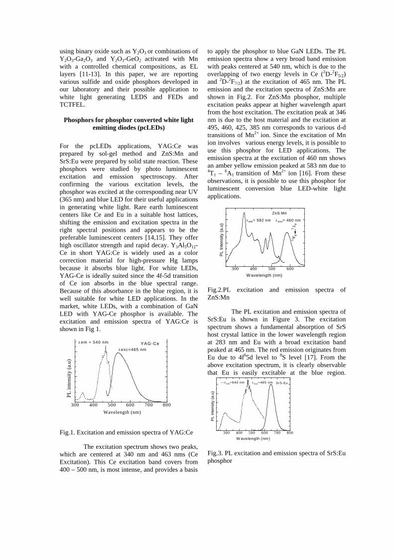
The excitation spectrum shows two peaks, which are centered at 340 nm and 463 nms (Ce Excitation). This Ce excitation band covers from 400 – 500 nm, is most intense, and provides a basis
to apply the phosphor to blue GaN LEDs. The PL emission spectra show a very broad band emission with peaks centered at 540 nm, which is due to the overlapping of two energy levels in Ce (2D-2F5/2) and 2D-2F7/2) at the excitation of 465 nm. The PL emission and the excitation spectra of ZnS:Mn are shown in Fig.2. For ZnS:Mn phosphor, multiple excitation peaks appear at higher wavelength apart from the host excitation. The excitation peak at 346 nm is due to the host material and the excitation at 495, 460, 425, 385 nm corresponds to various d-d transitions of Mn2+ ion. Since the excitation of Mn ion involves various energy levels, it is possible to use this phosphor for LED applications. The emission spectra at the excitation of 460 nm shows an amber yellow emission peaked at 583 nm due to 4T1 – 6A1
transition of Mn2+ ion [16]. From these observations, it is possible to use this phosphor for luminescent conversion blue LED-white light applications.
300 400 500 600
PL
Inte
nsity
(a.
u)
W avelength (nm)
ZnS:Mn
λexc= 460 nmλem= 582 nm 4T1
6A1
Fig.2.PL excitation and emission spectra of ZnS:Mn
The PL excitation and emission spectra of SrS:Eu is shown in Figure 3. The excitation spectrum shows a fundamental absorption of SrS host crystal lattice in the lower wavelength region at 283 nm and Eu with a broad excitation band peaked at 465 nm. The red emission originates from Eu due to 4f65d level to 8S level [17]. From the above excitation spectrum, it is clearly observable that Eu is easily excitable at the blue region.
300 400 500 600 700 800
PL
inte
nsity
(a.
u)
W avelength (nm )
λexc=465 nm ---λem=640 nm SrS-Eu
Fig.3. PL excitation and emission spectra of SrS:Eu phosphor
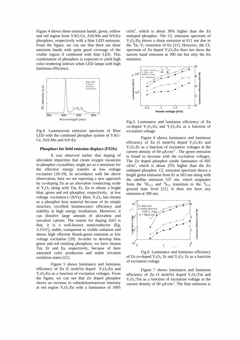
Figure 4 shows three emission bands, green, yellow and red region from YAG:Ce, ZnS:Mn and SrS:Eu phosphors, respectively with a blue LED emission. From the figure, we can see that there are three emission bands with quite good coverage of the visible region if combined with blue LED. This combination of phosphors is expected to yield high color rendering indexes white LED lamps with high luminous efficiency.
200 400 600 800
PL
int
ensi
ty (
a.u)
Wavelength (nm )
Blue LED YAG:Ce ZnS:Mn and SrS:Eu
Ce Mn Eu
Fig.4. Luminescent emission spectrum of Blue LED with the combined phosphor system of YAG-Ce, ZnS-Mn and SrS-Eu
Phosphors for field emission displays (FEDs)
It was observed earlier that doping of aliovalent impurities that create oxygen vacancies in phosphor crystallites, might act as a sensitizer for the effective energy transfer at low voltage excitation [18-19]. In accordance with the above observation, here we are reporting a new approach by co-doping Zn as an aliovalent conducting oxide in Y2O3 along with Tm, Er, Eu to obtain a bright blue, green and red phosphor, respectively, at low voltage excitation (<2kVs). Here, Y2O3, has chosen as a phosphor host material because of its simple structure, excellent luminescence efficiency and stability at high energy irradiations. Moreover, it can dissolve large amount of aliovalent and isovalent cations. The reason for doping ZnO is that, it is a well-known semiconductor (Eg, 3.37eV), stable, transparent to visible radiation and shows high efficient bluish-green emission at low voltage excitation [20]. In-order to develop blue green and red emitting phosphors, we have chosen Tm, Er and Eu respectively, because of their saturated color production and stable trivalent oxidation states [21].
Figure 5 shows luminance and luminous efficiency of Zn (5 mole%) doped Y2O3:Eu and Y2O3:Eu as a function of excitation voltages. From the figure, we can see that Zn doped phosphor shows an increase in cathodoluminescent intensity at red region Y2O3:Eu with a luminance of 1005
cd/m2, which is about 30% higher than the Zn undoped phosphor. The CL emission spectrum of Y2O3:Eu shows a sharp emission at 611 nm due to the 5D0-
7F2 transition of Eu [21]. However, the CL spectrum of Zn doped Y2O3:Eu does not show the narrow band emission at 390 nm but only the Eu emission.
0.5 1 1.5 2
102
103
0
2
4
6
8
Lum
inan
ce (
Cd
/m2)
Anode voltage (kVs)
L η Y 1 . 8 6Zn 0 . 1O 3:E u 0 . 0 4 Y 1 . 9 6E u 0 . 0 4O 3 1100 C , 4 hrs Js = 60 µA /cm 2
Lum
ino
us
effi
cien
cy (
lm/W
)
Fig.5. Luminance and luminous efficiency of Zn co-doped Y2O3:Eu and Y2O3:Eu as a function of excitation voltage
Figure 6 shows luminance and luminous efficiency of Zn (5 mole%) doped Y2O3:Er and Y2O3:Er as a function of excitation voltages at the current density of 60 µA/cm2 . The green emission is found to increase with the excitation voltages. The Zn doped phosphor yields luminance of 605 cd/m2, which is about 25% higher than the Zn undoped phosphor. CL emission spectrum shows a bright green emission from Er at 563 nm along with the satellite emission 537 nm, which originates from the 2H11/2 and 4S3/2 transition to the 4I15/2 ground state level [21]. It does not have any emission at 390 nm.
0 1 210
0
101
102
103
0
1
2
3
Lum
inan
ce (
cd/m
2)
Anode vo ltage (kV s )
Y1.98Er0.02O3 Y1.88Zn0.1Er0.02O3
1100 C, 4 hrsJs = 60µA/cm
2
Lum
inou
s ef
fici
ency
(lm
/W)
Fig.6. Luminance and luminous efficiency of Zn co-doped Y2O3: Er and Y2O3: Er as a function of excitation voltage
Figure 7 shows luminance and luminous efficiency of Zn (5 mole%) doped Y2O3:Tm and Y2O3:Tm as a function of excitation voltage at the current density of 60 µA/cm2. The blue emission is
found to increase with the excitation voltages. The Zn doped phosphor yields luminance of 38 cd/m2, which is about 35% higher than the Zn undoped phosphor. The CL emission consists of a strong emission at 455 nm along with the satellite emission 461 nm. The transition energy shown in the figure is based on the emission spectra of the free trivalent Tm [21]. The blue emission lines are produced by 1D2 to 3F4 transition ground states.
0 1 2100
101
102
0
0.1
0.2
0.3
Anode vo ltage (kVs)
Lum
inan
ce (
cd/m
2)
Js = 60µµA/cm2
L η Y1.98Tm0.02O3 Y1.88Zn0.1O3Tm0.02 1100 C, 4 hrs
Lum
inou
s ef
fici
ency
(lm
/W)
Fig.6. Luminance and luminous efficiency of Zn co-doped Y2O3:Tm and Y2O3:Tm as a function of excitation voltage
Thick Ceramic Thin film Electroluminescence Displays (TCTFEL)
It is well known that Y2O3, a binary
compound is a good host material for various rare earth dopants. Y2O3 exists in two crystallographic structures i.e. cubic and monoclinic [22]. Y2O3, which exists in cubic structure when doped with Eu, is an important phosphor material for cathode ray tubes and fluorescent lamps because of its high efficient red emission. However, it was reported earlier that for Mn when doped in cubic Y2O3 does not show any emission whereas in monoclinic phase, it emits a very bright yellow emission at both photo and electric field excitation. Because of that reason, monoclinic Y2O3:Mn has recently been demonstrated as a new yellow emitting phosphor material for PL and TFEL devices [23]. Here we are reporting a new method by the addition of Zn with Y2O3:Mn, which enhance the growth of monoclinic phase and significantly improve luminance of thin film phosphor. High-luminance yellow emitting Mn activated Y2O3 and Y2O3-ZnO composite thin-film electro-luminescent (TFEL) devices were fabricated on BaTiO3 thick ceramic substrate as given in Fig.10, employing less expensive sol-gel deposition coating. The material obtained at various deposition temperatures were annealed at elevated temperature in an inert atmosphere. The EL characteristics of the TFEL devices driven by an ac sinusoidal wave voltage at
a frequency of 1 kHz were measured using a Sawyer-Tower circuit, power meter and conventional luminance meter.
In order to investigate the Zn concentration dependent luminescent properties, crystallographic details of the Y2O3-ZnO:Mn thin film deposited on BaTiO3 substrate was evaluated. Figure 11, shows a XRD pattern for Y2O3-ZnO:Mn thin film deposited at 600oC and post annealed at 1020oC for 1 hr in Ar atmosphere with different concentration of Zn from 0 to 20 at%. All the XRD pattern are compared with a cubic (JCPDS file 43-1036) and monoclinic phase of Y2O3 (JCPDS file 44-0399 and 47-1274). Most of the diffraction peaks observed from Zn added Y2O3 thin films can be identified to the monoclinic phase where as Y2O3 with no Zn addition (Zn = 0%) shows cubic phase with a minor monoclinic phase formation.
Fig.10. Cross sectional structure of TFEL device
2 0 2 5 3 0 3 5 4 0 4 5 5 0 5 5
Y2O3:43-1036
Y2O3:44-0399
Y2O3:47-1274
c u b ic
m o n o c l in ic
m o n o c l in ic
( Y 2 O 3 )1 - x ( Z n O )x:M n (2 a t .% )
X R
AY
DIF
FR
AC
TIO
N I
NT
EN
SIT
Y (a
.u.)
Z n (2 0 a t .% )
Z n (1 5 a t .% )
Z n (1 0 a t .% )
Z n ( 5 a t .% )
Z n (0 a t .% )
D I F F A C T I O N A N G L E 2 (d e g r e e s ) Fig.11. XRD patterns for Y2O3-ZnOMn thin film prepared at different concentration of Zn
Figure 12 shows EL spectrum of Mn
activated Y2O3-ZnO (10 at%) at 200V at 1 kHz. The EL spectra shows a narrow band emission at 575 nm due to 4T1 (
4G) - 6A1(6S) transition of Mn
luminescent center doped in the Y2O3-ZnO composite thin film. L-V and Q-V characteristics of
200 400 600 800
W avelength ( nm )
EL
inte
nsi
ty (
a.u
)
(Y 2O 3)0.94 (ZnO ) 0.1: M n 2 a t %1 0 2 0o C 2 0 0 V , 1 kHz
Fig.12. EL emission spectrum from Y2O3-
ZnO(10at%):Mn(2at%)
Y2O3:Mn and (Y2O3)1-x -(ZnO)x:Mn, where the Zn content was 20 at % and is shown in Fig.13 and 14. From the figure it should be noted that the obtainable EL characteristics of the TFEL devices using Y2O3-ZnO:Mn thin film were correlated to the growth of monoclinic phase and its crystallinity of the thin film as evidenced from enhanced intensity of the diffraction peaks. The spectrum of yellow emission observed from the Y2O3-ZnO:Mn TFEL devices were approximately same that from standard yellow emitting Zn:Mn phosphor. The CIE chromaticity color co-ordinate (x = 0.512 & y = 0.438) is not changed at any Zn concentration.
Fig.13.L-V,Q-Vand ç-V of Y2O3:Mn dep.at 400oC.
Figure 15 shows maximum luminance (Lmax) as a function of Zn content for (Y2O3)1-x-(ZnO)x:Mn TFEL devices driven at 1 kHz. It should be noted that the highest L max about 2640 cd/m2 was obtained in a TFEL device prepared with a ZnO content of 20 at% where as Y2O3:Mn shows very low lumen of about 214 cd/m2 1 kHz.
Fig.14. L-V, Q-V and -V of Y2O3-ZnO:Mn dep.at 600oC
0 10 200
1000
2000
3000
Lm
ax c
d/m
2
Zn content X (at%)
(Y 2O 3)1-x -ZnO x:Mn(2at%)Sine w ave 1kHz
Fig.15 Lmax of Y2O3-ZnO:Mn as a function of Zn
content
4. Conclusions
Various phosphors based on sulfide and oxide powder as well as thin films were prepared and studied for its applications to PcLEDs, FEDs and TCTFEL devices. It was observed that instead of using single component phosphor, a combination of two or three color phosphors covers the entire visible region and this leads to the LEDs, which emit with high CRI and luminous efficiencies. For the FEDs phosphors, addition of Zn to the Y2O3 enhances the cathodoluminescence of Tm, Er and Eu at blue, green and red region, respectively, at low voltage cathode rays excitation and improves luminance and luminous efficiency. For the fabrication of TCTFEL, a new concept mixing of Y2O3-ZnO with Mn was reported first time using inexpensive solution coating techniques, which eliminate the need for vacuum. The addition of Zn in the Y2O3 enhances the growth of monoclinic phase and shows a drastic improvement in the luminance and luminous efficiency when compared with Y2O3:Mn
LU
MIN
AN
CE
L (
cd/m
2 )
CH
AR
GE
DE
NSI
TY
Q (
C
/cm
2 )
LU
MIN
OU
S E
FF
ICIE
NC
Y
(lm
/W)
0
15
200 400
3
6
9
12
600100
104
103
102
101
L
Q
0
102
100
10-1
101
APPLIED VOLTAGE Vop (V)
10-2
sine wave 1kHz
YY22 OO33 :: MMnn44 00 00 oo CC
0 200 400 6000
3
6
9
12
15
LU
MIN
OU
S E
FF
ICIE
NC
Y
(lm
/W)
CH
AR
GE
DE
NSI
TY
Q (
C
/cm
2 )
sine wave 1kHz
APPLIED VOLTAGE V0P (V)
100
101
102
103
LU
MIN
AN
CE
L
(c
d/m
2 )
10-2
104 100
10-1
10-3
(Y2O3)0.8(ZnO)0.2:Mn(2at.%)
: L: Q:
Acknowledgements
The author would like to thank DST (Govt. of India), SERC fast track Young Scientist Fellowship. Dr.M.S.Ramachandra Rao, MSRC, IIT, Madras providing the basic facilities. The author thanks Mr.P.Thiagarajan and Ms. N.Rama for their help during this work.
References: 1. S. Nakamura, T. Mukai and M. Senoh. Jpn. J. Appl. Phys. 32 (1993), p. L16. 2. R.Mueller-Mach, G.O.Mueller, M.R.Krames and T. Trottier, IEEE Journal of selected topics in quantuim electronics, 8, 339, 2002 3. T.Taguchi, International Display workshop, 817, 2000 4. M.Kottaisamy, Indo-Japan workshop crystal growth and applications of Advanced Materials for Optoelectrinics, Anna University, Chennai, 2004 5. S. Itoh, H.Toki, K.Tamura and F. Kataoka, Jpn J.Appl. Phys.Part 1,38, 6387,1999 6. H.Kominami, T.Nakamura, Y.Nakanishi, and Y.Hatanaka, Jpn J Appl Phy 35,1996 L1600 7. H.Kominami, C.Eguchi, M.Kottaisamy, Y.Nakanishi and Y.Hatanaka J.Vac.Sci.Technology, B22, 1386, 2004
8. S.W.Kang, B.S.Jeon, J.S.Yooand J.D.Lee, J.Vac.Sci.Techn. B15,520,1997 9. J.C.Park, H.K.Moon, D.K.Kim, S.H.Byeon, B.C.Kim and K.S. Suh, Appl.Phy.Lett., 77, 2162, 2000 10. L.E.Shea, J. McKittrick and M.F.Philips,
J.Electrochem.Soc., 145 (1998) 3165 11. A.H. Kitai, Thin solid films, 445, 367, 2003 12.T.Minami, solid state electronics, 47, 2237, 2003 13.Minami, Y.Kobayashi, T. Shirai, T.Miyata and S.S. Suzuki, Jpn, J.Appli phy 41, L- 478, 2002 14. Takahashi, K. Shibuya and A.Kondo, J.Crystal Growth 117, 979, 1992
15. C,J,Summer B.K.Wagner, w.Tong, W.Park M.Chichimansom Y.B. J.Crys.growth, 214, 918, 2000 16. C.B. Murray, D.J. Norris and M.G. Bewendi, J. Am. Chem. Soc. 115 (1993), p. 8706.
17.Yunsheng Hu, Weidong Zhuang, Hongqi Ye,Shusheng Zhang, Ying Fang and Xiaowei Huang, Journal of Luminescence, 111, 139, 2005
18. S.H.Cho, S.H.Kwon, J.S.Yoo, C.W. Oh, J.K. Lee, K.S. Ryu, S.J. Kwon,Y.C. Kang and S.B.
Park,Extended abstract of the Fifth International conference on the Science and Technology of Display Phosphors ( San Diego, CA,1999) p.205
19.J.H.Gwak, S.H.Park, J.E.Jang, S.J.Lee, J.E.Sung and J.M.Kim,Y.W.Jin, N.S.Lee, and w.k.Yi, V.A.Vorobyov,J.Vac.Sci.Technology, B(18), 1101, 2000 20. S.Bachir, K.Azuma. J.Kossanyi, P.Valet, J.C.Rornfart, J.Luminescence, 75,34,1997 21.G.H.Dieke in Spectra and energy levles of rare Herat ions in cristal , Edited by H.M.Crosswhite and H.Crosswhite, Wiley, New Cork, 1968 22. H.R.Hoestra, Science, 145, 1163, 1964 23.T.Minami Y.Kobayas, T.Miyata and M.Yama, Thin solid films, 443, 91, 2003
IT15
Materials for Wireless Communication
M.T. Sebastian Materials & Minerals Division Regional Research Laboratory
Trivandrum 695019 India
With the advent of ‘mobile phone mania’ and satellite communication revolution using microwave as the propagation media (where sky noise is minimum), the research and development in the field of device miniaturization has been one of the biggest challenges in contemporary Materials Science. To use a mobile phone to talk to someone, the message is sent from our phone to the nearest base station, and then on via a series of base stations to the other phone. At the heart of each base station is the combiner/filter unit. This has the job of receiving the messages, keeping them separate, amplifying the signals and sending then onto the next base station. For such a microwave circuit to work, part of it need to 'resonate' at the specific working frequency. The frequency determining component (resonator) used in such a high frequency device should satisfy certain criteria. It should have high dielectric constant, high quality factor, and high frequency stability with temperature. In early microwave systems, bulk metallic cavities were used as resonators, but were huge and not integrable in MIC. Although Richtmeyer in 1939 theoretically predicted that a suitably shaped dielectric could behave as a resonator it took about 20 years to experiment a Dielectric Resonator (DR). In 1960 Okaya found that a piece of rutile (TiO2) could act as a resonator. Historically, first temperature stable, low loss resonator was developed in 1971 by Masse who found that barium tetra-titanate (BaTi4O9) has excellent thermal stability and microwave dielectric characteristics. Since then about 1500 resonating materials have been reported in the literature. The search for new materials having optimum balance of dielectric properties is one of the most challenging problems in electronic ceramic research. The present talk focuses on what is a dielectric resonator, how it resonates, important DR materials, factors affecting the dielectric properties, how one can tailor the properties, DR database, and future directions.
IT17
Electrochemical Energy Systems for Space Applications
N Raveendran Pillai Vikram Sarabhai Space Centre
Thiruvananthapuram, Kerala, India
Electrochemical Energy is required for space applications in different categories of missions like launch vehicle, satellite, Re-entry Launch Vehicles (RLVs), interplanetary missions etc. Electric power is essential for all these missions for carrying out a number of functions in addition to normal house keeping. In the case of a rocket or launch vehicle, electric power is required throughout the flight duration (normally of the order of 17-20 minutes) for operations like ignition, navigation, guidance, control, separation, instrumentation and for destruction of the vehicle in case of an abnormal behavior. Each of these requirements is only for one time in any such mission and that too for short durations of the order of a few seconds to a few minutes. Onboard batteries meet these requirements.
However, in the case of satellites the requirements are of a different nature. Power is required for operating the orbit control systems and payloads like the icameras, transponders, radiometers and so on. This requirement is there during the entire mission duration which varies from 7 -15 years depending on the type of mission. Solar panels provide the electrical energy to satellites as long as the satellite is in the sunlit portion of the orbit. However, during the period when the satellite is eclipsed by the earth, no power is available from the solar panels. Batteries are used onboard to provide electrical energy to the various systems during such eclipse periods. In addition to this, batteries are required to support certain peak load operations where the power generated by the solar panel is not sufficient to meet such requirements. Also such onboard batteries have to provide power to the mission during transfer orbits prior to the solar panel deployment.
The Electrochemical Energy Systems used in space missions should meet certain specific requirements like high energy density, high rate capability, long cycle and calendar life in addition to very high reliability. The complex interplay of these factors make the choice of suitable energy systems difficult and only very few systems meet these demands. Batteries that are ideal for launch vehicles use do not satisfy the demands of a satellite and vice versa. The batteries used in launch vehicles and satellites are not viable choice for the long duration, higher energy demanding missions like Re-entry Launch Vehicles, interplanetary missions and manned missions. Fuel Cell system is the choice for such missions. This talk gives an overview of the various Electrochemical Energy Systems that are currently in use and the status of such systems in the country for the Indian Space programmes.

IT18
Structural Aspects of Ion Beam Modified Nanostructures
P. V. Satyam Institute of Physics, Bhubaneswar – 751005
In this talk, a brief introduction to the growth of nanostructures using various synthesis
experimental methods (i.e., using thermal evaporation, molecular beam epitaxy, chemical methods and ion beam sputtering) and their structural characterization with electron microscopy and ion scattering would be dealt. The main emphasis in this talk is the use of energetic heavy ion impacts for modifying the matrix and the nanostructures to tailor the properties. Examples on the use of energetic ion beams to synthesize optically interesting systems at interfaces (buried nanostructures) and modify the surface nanostructures to show embedding related phenomena would be discussed.
IITT1199
ZZnnOO BBaasseedd DDiilluutteedd MMaaggnneettiicc SSeemmiiccoonndduuccttoorrss
P. A. Joy
Physical and Materials Chemistry Division National Chemical Laboratory
Pune 411008, India
The recent discovery of diluted magnetic semiconductors (DMS) has raised tremendous interest in the development of these materials for future technological applications. Incorporation of ferromagnetism in the wide band gap III-V and II-VI nonmagnetic semiconductors have opened up a new area of research, because of the ability of DMSs to combine their transport and optical properties with magnetism. ZnO is a II-VI semiconductor with a band gap of ~3.3 eV at 300 K, almost comparable to that of GaN. Therefore, transition metal doped ZnO is considered as a potential candidate for transparent ferromagnetic materials. Based on theoretical calculations, it has been proposed that ZnO doped with 3d transition metal ions are suitable candidates for ferromagnetic semiconductors. Curie temperatures above 300 K have been predicted for Mn doped ZnO. Subsequent experimental results showed that ZnO doped with different transition metals such as Co, Mn, Ni, etc, are ferromagnetic at or above room temperature. Most of these studies are performed on thin films. However, there are controversial reports on the origin of ferromagnetism in doped ZnO, and especially in the case of Co and Mn doped materials. Some reports show the presence of secondary phases as the origin of ferromagnetism and some times the results are not reproducible. Hence, after so many extensive studies on ZnO based DMSs, still the origin of ferromagnetism is a big question. Our detailed studies on different polycrystalline samples of Co, Mn and Ni doped ZnO give evidence for different origins of ferromagnetism (spin) and the changes in the electronic structure (charge). The current status of the ZnO based DMS will be discussed.
IT20
Spin-Polarized Electron Scattering: A method to explore Magnetic Excitations on Surfaces and Thin Films
P.S. Anil Kumar1, M. Etzkorn2, W.Tang2, Y. Zhang2, and J. Kirschner2
1Dept. of Physics, Indian Institute of Science, Bangalore 560 012, India 2Max-Planck-Institut für Mikrostrukturphysik, Weinberg 2, D-06120 Halle, Germany
E-mail: [email protected]
Spin-Polarized electron scattering from ferromagnetic surfaces can be used to extract information about magnetic microstructures1, magnetic interactions2 and magnetic excitations3 on surfaces. Among the magnetic excitations, Stoner excitations were extensively studied using this method4. When one considers the collective excitations in magnetically ordered systems i.e. spin-wave excitations, this technique becomes more demanding due to the need for a highly monochromatic spin-polarized electron beam with well-defined spin orientation. Ferromagnetic resonance, Brillouin light scattering etc. are widely used to explore the spin waves in thin films and multilayers, but these methods can probe only low energy, long wavelength (wave vector <10-2Å-1) spin-waves. For probing large wave-vector high-energy spin waves i.e. the exchange-dominated spin waves, inelastic neutron scattering was the only technique available. However, this technique becomes intricate in ultra-thin films and surfaces. Hence, the high-energy spin waves in ultra-thin films were not explored due to the unavailability of a suitable technique. In this regard we explored the possibility of exciting spin-waves by the inelastic scattering of electrons (Spin Polarized Electron Energy Loss Spectroscopy (SPEELS)) and we found that it is possible to probe spin waves up to the surface Brillouin zone boundary (wave vector ~1.5 Å-1) in ultra-thin films.
This new methodology will be illustrated with the help of the results obtained from ultra-thin fcc and hcp Cobalt grown epitaxially on Cu(001) and W(110) crystals, respectively. A spin-polarized electron beam with transverse polarization is scattered off-specularly from the remanently magnetized Co surface. We find that the scattered electron suffers an energy loss due to spin-wave excitation giving rise to a loss peak in the energy loss spectrum. The parallel component of the wave vector difference between the incoming electron and scattered electron (∆K||) gives the corresponding wave-vector for the spin wave. The spin-wave peak in the energy loss spectrum shifts to higher energies as the ∆K|| is increased, resulting in a well-defined dispersion up to the surface Brillouin zone boundary5. The spin wave dispersion was found to agree surprisingly well to the dispersion relation of a surface spin wave calculated using a nearest neighbor Heisenberg model5. Using this model, we obtained a value for the product of the exchange coupling constant (J) and the magnetic moment (S) of JS for f.c.c and h.c.p Co 15±1 and 14.8±1 meV, respectively. We also found that the spin wave features measured by SPEELS are strongly broadened. The non-adiabatic theoretical descriptions expect a broadening of the spin-wave features as spin-waves of high wave vectors are damped by Stoner excitations.
In this lecture, the details of the SPEELS will be discussed along with results obtained from different thickness of the Co films in f.c.c. and h.c.p. form.
Reference
1. T. Duden and E. Bauer, Phy.Rev.Lett. 77, 2308 (1996) 2. G. Waller and U.Gradmann, Phys.Rev.B 26, 6330 (1982) 3. J. Kirschner, D. Rebenstorff and H. Ibach, Phys.Rev.Lett. 53, 698 (1984) 4. J. Kirschner, Phys.Rev.Lett. 55, 973 (1985) 5. R. Vollmer, M. Etzkorn, P.S. Anil Kumar, H. Ibach and J. Kirschner, Phys.Rev.Lett. 91, 147201 (2003)
IT21
From Metal-loaded Diblock-Copolymers to ordered Arrays of Size-selected Metallic Nanoparticles:
A route equally promising for fundamental questions as for applications
P. Ziemann, H.-G. Boyen, A. Ethirajan, G. Kästle, A. Plettl, F. Weigl Abteilung Festkörperphysik, Universität Ulm, D-89069 Ulm, FRG
E-mail: [email protected]
Ordered arrays of metallic nanoparticles with diameters between 1 and 10 nm and interparticle distances between 10 and 100 nm offer a large variety of possible applications for basic physics as well as device oriented experiments. As a first step, however, a reliable preparation method of such arrays has to be developed allowing a control of both distances1,2,3.
In this contribution, an unconventional bottom-up approach will be described based on the selforganization of metal-loaded diblock-copolymers. It will be demonstrated that after an optimized plasma treatment to remove the polymer matrix, one ends up with a highly hexagonally ordered array of metal nanoparticles of e.g. Au or Co exhibiting narrow Gaussian size distributions. Properties of such particles, which are supported on various substrates, will be reported with emphasis on their electronic behavior4,5,6.
Reference
1. H.-G. Boyen Th. Herzog, G. Kästle, F. Weigl, P. Ziemann, J. P. Spatz, M. Möller, R. Wahrenberg, P. Oelhafen, Phys. Rev. B 65, 075412 (2002)
2. H.-G. Boyen, G. Kästle, K. Zürn, Th. Herzog, F. Weigl, and P. Ziemann, O. Mayer, Ch. Jerome, J.P. Spatz, and M. Möller, M.G. Garnier and P. Oelhafen, Adv. Funct. Mat. Sci. 13, 359 (2003)
3. G. Kästle, H.-G. Boyen, F. Weigl, G. Lengl, Th. Herzog, P. Ziemann, S. Riethmüller, O. Meyer, C. Hart-mann, J. P. Spatz, M. Möller, M. Ozawa, F. Banhart, G. Garnier, P. Oelhafen, Adv. Funct. Mat. 13, 853 (2003)
4. H.-G. Boyen, G. Kästle, F. Weigl, P. Ziemann, G. Schmid, M. G. Garnier, P. Oelhafen, Phys. Rev. Lett. 87, 276401 (2001)
5. H.-G. Boyen, G. Kästle, F. Weigl, B. Koslowski, C. Dietrich, P. Ziemann, J. P. Spatz, S. Riethmüller, C. Hartmann, M. Möller, G. Schmid, M. G. Garnier, P. Oelhafen, Science 297, 1533 (2002)
6. H.-G. Boyen, A. Ethirajan, G. Kästle, F. Weigl, P. Ziemann, G. Schmid, M.G. Garnier, M. Büttner, P. Oelhafen, Phys. Rev. Lett. 94, 016804 (2005)
IT22
Observation of Magnetoelectric behavior in pulsed laser deposited Bi0.6Dy0.3La0.1FeO3 thin films
V.R. Palkar1, R. Anisha2, S.C. Purandare1, S.Gohil1, J.John1, R. Pinto2 and
S.Bhattacharya1
1Tata Institute of Fundamental Research, Mumbai 400005, India 2Indian Institute of Technology Bombay, Mumbai 400 076, India
E-mail: [email protected]
Magnetoelectrics, characterized by simultaneous ferroelectric and magnetic ordering, have potential applications in information storage, sensors, etc. However, there are very few materials exhibiting the coexistence of ferroelectric and ferromagnetic ordering at room temperature. Hence, in normal practice, desired magnetoelectric effect (ME) is achieved by growing heterostructures of ferroelectric and magnetic materials. Realization of heterostructures with desired properties is not only difficult but also involves complicated lengthy procedure. BiFeO3 is weakly ferroelectric and antiferromagnetic at and above room temperature. We have been successful in enhancing both the ferroelectric and the magnetic properties of BiFeO3 by partial substitution of Dy at Bi site. Thin films of Bi0.6Dy0.3La0.1FeO3, integrated on Si/SiO2/TiO2/Pt substrate by using pulsed laser deposition technique; show good ferroelectric and magnetic properties. We have also studied evolution of magnetic domain configuration with increase in film thickness Single step growth of thin films with desired magnetoelectric properties at room temperature is certainly cost effective, reliable and simple alternative to heterostructures.
IT23
Optical Studies of 200 MeV Ag+15 Ion Irradiated Co Implanted ZnO Thin Films
Ravi Kumar1, Fouran Singh1, M. Wasi Khan2, J.P. Srivastava2, Basavaraj Angadi3,
Y.S. Jung3 and W.K. Choi3 1Materials Science Division, Nuclear Science Centre, P.O. Box 10502, Aruna Asaf Ali Marg,
New Delhi 110067, India 2Department of Physics, Aligarh Muslim University, Aligarh 202002, India
3Thin Films Materials Research Center, Korea Institute of Science and Technology, P.O. Box 131, Cheongryang, Seoul 130-650, Korea
Email: [email protected]
We present the results of photoluminescence studies at low temperature on 200 MeV Ag+15 ion irradiated Co-implanted ZnO thin films. The c-axis oriented epitaxial ZnO thin films were grown using plasma assisted MBE on (001) Al2O3 substrate and implanted with 80keV Co ions with fluence values 1x10¹⁶ to 5x10¹⁶ ions/cm2, which show Co clusters. The Co clusters were dissolved using 200 MeV Ag+15 ions irradiation with fluence 1x10¹² ions/cm2. The photoluminescence spectrum of pure ZnO thin film was characterized by the I4 peak at 3.365 eV and the broad emission at 2.45 eV due to the vacancies and defect states. The Co-doped ZnO films show three sharp levels at 3.247eV, 3.211eV and 3.169eV due to t2g and two shoulders at 2.975eV and 2.815eV due to the eg levels of crystal field splitted Co d-orbitals lying in the band gap of ZnO. Their position is independent of the temperature, whereas, the I4 intensity is decreased with the increase in temperature due to the thermal quenching of this emission.
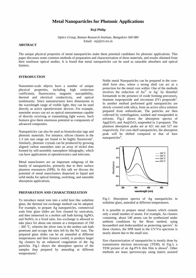
Metal Nanoparticles for Photonic Applications
Reji Philip
Optics Group, Raman Research Institute, Bangalore 560 080
Email: [email protected]
ABSTRACT
The unique physical properties of metal nanoparticles make them potential candidates for photonic applications. This
paper discusses some common methods of preparation and characterization of these materials, and results obtained from
their nonlinear optical studies. It is found that metal nanoparticles can be used as saturable absorbers and optical
limiters.
INTRODUCTION
Nanometer-scale objects have a number of unique
physical properties, including high extinction
coefficients, fluorescence, magnetic susceptibility,
thermal and electrical conductivity, and optical
nonlinearity. Since nanostructures have dimensions in
the wavelength range of visible light, they can be used
directly as active optoelectronic devices. For example,
nanotube arrays can act as optical nanoantennas capable
of directly receiving or transmitting light waves. Such
features give them enormous potential as components of
advanced composites.
Nanoparticles can also be used as biomolecular tags and
photonic materials. For instance, silicon clusters in the
1-3 nm size range are found to be highly fluorescent
1
.
Similarly, photonic crystals can be produced by growing
aligned carbon nanotubes onto an array of nickel dots
formed by self-assembly nanosphere lithography, which
can have applications in optoelectronics and telecoms.
Metal nanoclusters are an important subgroup of the
family of nanoparticles, primarily due to their surface
plasmon resonances (SPR). In this talk we discuss the
potential of metal nanoclusters dispersed in liquid and
solid media for optical limiting, switching, and saturable
absorption applications.
PREPARATION AND CHARACTERIZATION
To introduce metal ions into a solid host like sodalime
glass, the thermal ion exchange method can be adopted.
For example, to prepare Ag nanoparticles, commercial
soda lime glass slides are first cleaned by sonication,
and then immersed in a molten salt bath having AgNO3
and NaNO3
in a fixed ratio. Ion–exchange is allowed to
take place for about one minute at a temperature of 330
- 360
o
C, wherein the silver ions in the molten salt bath
penetrate and occupy the sites left by the Na
+
ions. The
prepared glass slides can be air annealed at different
temperatures and then furnace cooled, to produce larger
Ag clusters by an enhanced coagulation of the Ag
particles. Fig.1 shows the absorption spectra of the
samples thus prepared by annealing at different
temperatures
2
.
Noble metal Nanoparticles can be prepared in the core-
shell form also, where a strong shell can act as a
protection for the metal core within. One of the methods
involves the reduction of Au
3+
or Ag
+
by dimethyl
formamide in the presence of oxide forming precursors,
titanium isopropoxide and zirconium (IV) propoxide
3
.
In another method preformed gold nanoparticles are
slowly covered with silica, from an active silica solution
prepared from orthosilicate. The particles are then
collected by centrifugation, washed and resuspended in
solvents. Fig.2 shows the absorption spectra of
Ag@ZrO2
and Au@ZrO2
suspended in 2-propanol. The
plasmon absorption peaks are at 421 nm and 527 nm
respectively. For core-shell nanoparticles, the absorption
peak will be shifted compared to that of bare
nanoparticles
4
.
300 400 500 600
0.0
0.5
1.0
1.5
2.0
Absorbance
wavelength (nm)
350
0
C
450
0
C
500
0
C
550
0
C
Fig.1: Absorption spectra of Ag nanoparticles in
sodalime glass, annealed at different temperatures.
It is possible to prepare metal clusters which contain
only a small number of atoms. For example, Au clusters
containing about 140 atoms can be synthesized under
ambient conditions by the Brust method, using
hexanethiol and dodecanethiol as protecting species
5
. In
these clusters, the SPR band in the UV/Vis spectrum is
nearly absent due to the small size.
Size characterization of nanoparticles is mostly done by
transmission electron microscopy (TEM). In Fig.3, a
TEM picture of an Ag-PVA thin film is shown
6
. Other
methods are mass spectroscopy using matrix assisted
laser desorption (MALDI), and low frequency Raman
studies
7
.
400 500 600 700
0.0
0.5
1.0
1.5
2.0
ba
Absorbance
Wavelength (nm)
Fig.2: Absorption spectra of Ag@ZrO2
(a) and
Au@ZrO2
(b) suspended in 2-propanol.
Even though the chemistries for functionalizing
nanomaterials are practically unique for each material, a
universal approach can still be adopted, in which
polymerizable surfactants can be used which will
encapsulate the nanostructure and at the same time
provide additional reactive groups for further chemistry.
Because this approach does not require the surfactants to
be covalently anchored to the nanostructure surface, it
can be used on nanomaterials that have limited or no
surface reactivity
8
.
Fig.3: TEM picture of an Ag-PVA thin film.
NONLINEAR LIGHT TRANSMISSION
The optical nonlinearity in noble metal nanoparticles is
usually discussed on the basis of the Kerr nonlinearity,
multiphoton excitation and free carrier absorption in
them. Flytzanis
9
and co-workers have shown that there
are three major electronic contributions to the Kerr
nonlinearity. The first one, χ(3)
intra, is from the intra-band
conduction electrons in the s-p band. It is electric dipole
in nature, originates totally due to the confinement of
the free electrons, and is strongly size dependent. The
second is from inter-band transitions between the d-
bands and the conduction band which occurs when the
photon energy is larger than a gap energy, Eg
ωg
(which is 1.7eV for gold). Inter-band transitions can
saturate leading to a mostly imaginary and negative
χ(3)
inter, and this contribution is size and shape
independent down to very small sizes of about 2.5 nm.
The third and most important contribution χ(3)
sp arises
from surface plasmons. By photoexciting the plasmon
band, conduction electrons can be easily elevated to
temperatures of several hundred degrees as their specific
heats are very small. It takes a few picoseconds for these
electrons to thermalize with the lattice. During this time,
the Fermi-Dirac electron distribution is modified, since
part of the one-electron levels below the Fermi level is
emptied and part of those above is occupied. This leads
to a modification of the dielectric constant εm
, resulting
in a transient re-distribution of the equilibrium plasmon
band: the absorption around the peak is reduced and that
at the wings is increased. This reduction in absorption is
generally referred to as ”plasmon band bleach” in
literature
10
.
-15 -10 -5 0 5 10 15
0.4
0.6
0.8
1.0
1.2
1.4
1.6
circles - Au:PVA
triangles - Au:Ag-PVA
Norm
alized T
ransm
ittance
z (mm)
Fig.4: z-scan curves obtained for Au-PVA and Au:Ag-
PVA films, using 532 nm, 7 ns laser pulses.
In an z-scan experiment
11
, this bleach will appear in the
form of a positive-going peak, (saturable absorption) as
seen in Fig. 4 for an Au:PVA film
6
. However, an
obvious optical limiting behaviour is found in Au:Ag-
PVA films under the same excitation conditions. Such
changes in the sign of the nonlinearity can be seen to a
lesser degree in the same material itself at different
concentrations, as shown in Fig.5. These can be
explained on the basis of multiphoton excitation and
free carrier absorption phenomena
12
.
There is a large free electron concentration in metal
nanoparticles, which is orders of magnitude higher than
that in semiconductors. Laser-excited electrons in the
nanocluster are free carriers possessing a whole
spectrum of kinetic and potential energies, the potential
energies being those of the formerly unoccupied and
occupied states within the conduction band. In addition,
there exists a possibility of photoejection of electrons
from the parent cluster, which usually occurs by a two-
photon or multi-photon absorption process
10
when
excited in the visible. The total number density of free
carriers Nc(I) generated by these routes is an intensity-
dependent parameter, so that nonlinear absorption by
free carriers gains substantial strength at high laser
intensities. The resulting transmission can be expressed
as = - αI – σcN
c(I)I, where α is the linear
absorption and σc
is the free-carrier absorption cross-
section. The other possibility to be considered is that of
thermally induced nonlinear scattering which
contributes to optical limiting in a number of materials,
including carbon nanotube suspensions. From
comparative studies in gold clusters of 5 nm and 30 nm
average diameters, Mostafavi and co-workers
13
have
suggested that the nanosecond limiting in these samples
may be explained in the framework of nonlinear
scattering. Our own previous studies in thiol-capped Ag,
Au and Ag-Au alloy nanoclusters had revealed that for
the same laser fluence, nanosecond limiting is more
efficient than picosecond limiting, indicating the
possible role of nonlinear scattering
14
.
-12 -9 -6 -3 0 3 6 9 12
0.0
0.4
0.8
1.2
1.6
N
orm
alized T
ransm
ittance
z (mm)
Fig.5: z-scan curves obtained for Ag@ZrO2
suspensions
in 2-propanol, at different sample concentrations. Lower
concentrations show lesser saturation behaviour.
TEMPORAL BEHAVIOUR
Subsequent to SPR excitation, the excited electrons will
relax within a certain lifetime. This lifetime can be
measured from a pump-probe experiment using
femtosecond laser pulses. Results of our measurements
in Ag nanoparticles
2
is shown in Fig.6. The pump
energy is kept low so that the excitation is limited to the
low perturbation regime, where the decay rate is
independent of the pump fluence. Since the electron-
electron relaxation is too fast to be resolved, only the
electron-phonon relaxation is seen, and hence the
experimental points fit well to a single exponential
decay. This is consistent with the two-temperature
model of electron relaxation in the low perturbation
regime
15
. The relaxation lifetime is calculated to be 860
femtoseconds from the fit, which is in close agreement
with the value of 700 fs measured for 3 nm Ag clusters
in a glass matrix by Del Fatti et.al.
16
. An even smaller
time constant of about 530 fs was obtained by Arbouet
et.al.
17
for Ag clusters of the same size embedded in
various media. Such short lifetimes can be of potential
use in optical switching applications.
PHOTONIC CRYSTALS
Certain hydrogel-based nanoparticles can be used to
form photonic crystals whose optical properties can be
precisely tuned by thermally adjusting the water content
in the particles
18
. The soft and conformable spherical
particles could be the basis for a “photonic fluid” that
would be custom processed to form self-assembled
periodic structures able to transmit specific wavelengths
of light. Potential applications also include optical
switching and optical limiting in telecommunications.
-2 -1 0 1 2 3 4 5 6
-0.2
0.0
0.2
0.4
0.6
0.8
1.0Ag-550
∆T
/T
(N
orm
alized)
probe delay (ps)
Fig.6: Electron-phonon relaxation in Ag nanoclusters of
3 nm size, measured by a femtosecond pump-probe
experiment.
In another method to make photonic crystals, particles
of nickel catalyst are initially laid down by allowing a
monolayer of polystyrene nanospheres to self-assemble
onto a 10 mm-square silicon substrate. The nanospheres
are used as a mask for depositing nickel by electron-
beam evaporation: removal of the polystyrene particles
with toluene leaves a honeycomb pattern of nickel dots.
The nickel dots then act as a catalyst for the growth of
aligned carbon nanotubes by hot filament plasma-
enhanced chemical vapour deposition. Thus an
inexpensive selfassembly of nanotubes into highly
ordered arrays is possible. The resulting periodic array
of aligned nanotubes appears colourful because it
diffracts visible light. This also leads to photonic crystal
interactions that change dispersions of the photonic
modes, forming photonic bands and gaps
19
.
CONCLUSIONS
Metal nanoparticles are fascinating materials with
interesting physical properties. Studies indicate that they
have the potential to be used as saturable absorbers,
optical limiters and optical switches.
REFERENCES
1. G.Belomoin, J. Therrien, A. Smith, S.Rao, R.
Twesten, S. Chaeib, M. H. Nayfeh, L.wagner, L.
Mitas, Appl.Phys.Lett. 80, 841 (2002).
2. B.Karthikeyan, J. Thomas, R.Philip,
Chem.Phys.Lett. 414, 346 (2005).
3. R.T.Tom, A.S. Nair, N. Singh, M. Aslam, C.L.
Nagendra, R. Philip, K. Vijayamohanan, T.
Pradeep, Langmuir 19, 3439 (2003).
4. T.Ung, L.M. Liz-Marzan, P. Mulvaney,
J.Phys.Chem.B. 103, 6770 (1999).
5. T.G.Schaff, M.N. Shafigullin, J.T. Khouri, I.
Vezmar, R.L. Whetten, J.Phys.Chem.B. 105, 8785
(2001).
6. B.Karthikeyan, M.Anija, R.Philip, to be published.
7. P.Gangopadhyay, P.Magudapathy,
R.Kesavamoorthy, B.K.Panigrahi, K.G.M.Nair,
P.V.Satyam, Chem.Phys.Lett. 388, 416 (2004).
8. Y. Kang, T.A. Taton, Angew. Chem. Int. Ed. Engl.
44, 409 (2005).
9. F.Hache, D.Ricard, C.Flytzanis, U.Kreibig,
Appl.Phys.A. 47, 347 (1988).
10. P.V.Kamat, M.Flumiani, G.V.Hartland,
J.Phys.Chem.B.102, 3123 (1998).
11. M.Sheik Bahae, A.A.Said, T.M.Wei, D.J.hagan,
E.W.Van Stryland, IEEE J.Quant.Electron. 26, 760
(1990).
12. R.Philip, G.R.Kumar, N.Sandhyarani, T.Pradeep,
Phys.Rev.B. 62, 13160 (2000).
13. L.Francois, M.Mostafavi, J.Belloni, J.F.Delouis,
J.Delaire, P. Feneyrou, J.Phys.Chem.B. 104, 6133
(2000).
14. R.Philip, S. Mujumder, H.Ramachandran,
G.R.Kumar, N.Sandhyarani and T.Pradeep,
Nonlinear Optics 27, 357 (2001).
15. C.K.Sun, F.Vallee, L.H. Acioli, E.P.Ippen,
J.G.Fujimoto, Phys.Rev.B. 50, 15337 (1994).
16. N.Del Fatti, F.Vallee, C.Flytzanis, Y.hamanaka,
A.nakamura, Chem.Phys. 251, 215 (2000).
17. A.Arbouet, C.Viosin, M.Treguer, Phys.Rev.Lett.
90, 177401 (2003).
18. J. D. Debord, S. Eustis, S. Debord, M. T. Lofye, L.
A. Lyon, Adv. Mater. 14, 658 (2002).
19. K. Kempa, B. Kimball, J. Rybczynski, Z. P. Huang,
P. F. Wu, D. Steeves, M. Sennett, M. Giersig, D. V.
G. L. N. Rao, D. L. Carnahan, D. Z. Wang, J. Y.
Lao, W. Z. Li, Z. F. Ren, Nano Letters 3, 13 (2003).
IT25
ZnO light-emitting diode using phosphorus doped p-type ZnO
Seong-Ju Park
Department of Materials Science and Engineering
Gwangju Institute of Science and Technology, Gwangju, Korea
E-mail: [email protected]
p-Type ZnO films were grown by using phosphorus oxide as a p-type dopant source by RF sputtering
and a subsequent post annealing processes. Photoluminescence spectra of p-type ZnO:P thin films showed an
acceptor bound excitonic and phosphorus related peaks. We will report on the fabrication and characteristics of
heterojunction ZnO light-emitting diode (LED) which consists of p-type ZnO:P and n-type GaN:Si layers. The
current-voltage (I-V) and electroluminescence measurements of ZnO LED showed a threshold voltage of 5.4 V
and a band-edge emission of 409 nm at room temperature. We also fabricated a p-n homojunction LED with a
structure of p-ZnO:P/n-ZnO:Ga and it showed an emission peak at 380 nm corresponding to the near band gap
of ZnO for the first time. The I-V characteristics of ZnO LED showed a low threshold voltage of 3.2V and an
ideality factor of 2.5 were very similar to those of GaN LED.
Instructions to Authors Page 1 of 3 Proceedings of OMTAT2005
FORMATION OF HIGHLY LUMINESCENT AND THICK POROUS SILICON FILMS WITH SUPERIOR MORPHOLOGICAL PROPERTIES
AND STABILITY
Shailesh N. Sharma*
Electronic Materials Division, National Physical Laboratory, Dr. K.S. Krishnan Marg, New Delhi-110 012, India. * Corresponding author’s Email: [email protected]
ABSTRACT Highly luminescent, stable and mechanically strong thick porous silicon (PS) films have been obtained on textured silicon substrates. Porous silicon formed on textured substrates exhibits higher porosity, better mechanical strength, non-fractured surface morphology and lower stress compared to porous silicon formed on polished silicon substrates at the same current density, time of anodization and method of drying. The improved properties are attributed to the formation of localized highly porous macroscopic plastic regions.
1 INTRODUCTION
PS has been investigated for many optical and opto-electronic applications because of the easiness, simplicity and integratibility with the highly advanced Si technology. The quantum nature of Si nanostructures is the key to the development of the future nano-electronics 1,2. In PS films, Si nanocrystals remain attached to the Si substrate after partial electrochemical dissolution and are surrounded by large pores. The large surface area and the presence of large number of unpaired dangling bonds alter the surface reactivity and stability of PS 3,4. The presence of pores also causes lattice expansion and leads to elastic stress and curvature which often leads to fragility and long-term failure 5. Very few reports are there which has demonstrated the role of the surface morphology of silicon wafer on the properties of PS 6. For use as an anti-reflection coating, thin porous silicon layers were formed earlier on textured Si solar cells 7. However, an intensive study on the properties of PS formed on textured substrates and its effect on the stability of PS appears to be lacking. In this work, we have demonstrated that the texturization of silicon surface is a simple and effective method for the formation of thick films of porous silicon with reduced stress, improved stability and superior mechanical properties. SEM, AFM and XRD measurements have been used to demonstrate the superiority of porous silicon films formed on textured substrates.
2 EXPERIMENTAL
PS was formed by electrochemical anodization process on boron doped (100) p-Si wafers (8-10 Ω cm, 400 µm thick). Silicon wafer is used as the anode and Pt as the counter electrode in an acid resistant cell. PS films were made on both polished and textured substrates with current densities between 10 to 50 mA cm-2 range for 30 min. in HF-C2H5OH of 1:1 volume
ratio. The films were washed in deionized water and dried in nitrogen after anodization. Textured substrates were made using 2% NaOH at 85oC for 30 min. Formation of a proper texturized surface with pyramidal morphology was confirmed by SEM using a LEO 440 scanning electron microscope. A multicrystal X-ray diffractometer developed at NPL employing a fine focus X-ray generator has been used to determine local radius of curvature of PS films 8. 3 RESULTS AND DISCUSSION
Visual observation shows that the porous silicon films formed on textured surfaces appear more compact, uniform and strong even at higher current densities while the PS films formed on polished substrates appears to be rough, powdery and had a tendency of peeling off from the substrate particularly at high current densities. As evident from Fig.1, for Id = 20 mA cm-2, on exposure to UV-light, PS formed on textured substrate has a glowing dark reddish-orange color with uniform intensity while the PS formed on polished substrate has a light orange color with graded intensity from the centre toward the edges. The porosity and thickness of PS films are estimated from gravimetric measurements 1. These parameters for both the kinds of films are summarized in Table 1.
(a) (b) Fig. 1 A photograph of porous silicon samples prepared at Id = 20 mA cm-2 upon exposure to UV-light (a) Textured substrate; (b) Polished substrate.
(a) (b)
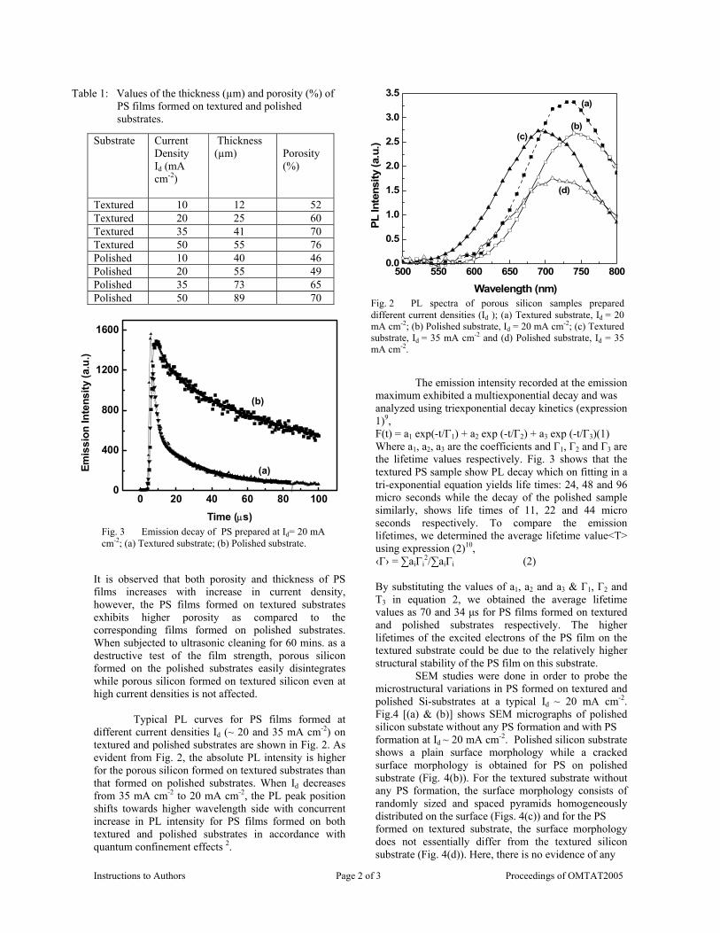
Instructions to Authors Page 2 of 3 Proceedings of OMTAT2005
It is observed that both porosity and thickness of PS films increases with increase in current density, however, the PS films formed on textured substrates exhibits higher porosity as compared to the corresponding films formed on polished substrates. When subjected to ultrasonic cleaning for 60 mins. as a destructive test of the film strength, porous silicon formed on the polished substrates easily disintegrates while porous silicon formed on textured silicon even at high current densities is not affected.
Typical PL curves for PS films formed at different current densities Id (~ 20 and 35 mA cm-2) on textured and polished substrates are shown in Fig. 2. As evident from Fig. 2, the absolute PL intensity is higher for the porous silicon formed on textured substrates than that formed on polished substrates. When Id decreases from 35 mA cm-2 to 20 mA cm-2, the PL peak position shifts towards higher wavelength side with concurrent increase in PL intensity for PS films formed on both textured and polished substrates in accordance with quantum confinement effects 2.
The emission intensity recorded at the emission
maximum exhibited a multiexponential decay and was analyzed using triexponential decay kinetics (expression 1)9, F(t) = a1 exp(-t/Γ1) + a2 exp (-t/Γ2) + a3 exp (-t/Γ3)(1) Where a1, a2, a3 are the coefficients and Γ1, Γ2 and Γ3 are the lifetime values respectively. Fig. 3 shows that the textured PS sample show PL decay which on fitting in a tri-exponential equation yields life times: 24, 48 and 96 micro seconds while the decay of the polished sample similarly, shows life times of 11, 22 and 44 micro seconds respectively. To compare the emission lifetimes, we determined the average lifetime value<T> using expression (2)10, ‹Γ› = ∑aiΓi
2/∑aiΓi (2) By substituting the values of a1, a2 and a3 & Γ1, Γ2 and T3 in equation 2, we obtained the average lifetime values as 70 and 34 µs for PS films formed on textured and polished substrates respectively. The higher lifetimes of the excited electrons of the PS film on the textured substrate could be due to the relatively higher structural stability of the PS film on this substrate.
SEM studies were done in order to probe the microstructural variations in PS formed on textured and polished Si-substrates at a typical Id ~ 20 mA cm-2. Fig.4 [(a) & (b)] shows SEM micrographs of polished silicon substate without any PS formation and with PS formation at Id ~ 20 mA cm-2. Polished silicon substrate shows a plain surface morphology while a cracked surface morphology is obtained for PS on polished substrate (Fig. 4(b)). For the textured substrate without any PS formation, the surface morphology consists of randomly sized and spaced pyramids homogeneously distributed on the surface (Figs. 4(c)) and for the PS formed on textured substrate, the surface morphology does not essentially differ from the textured silicon substrate (Fig. 4(d)). Here, there is no evidence of any
Substrate Current Density Id (mA cm-2)
Thickness (µm)
Porosity (%)
Textured 10 12 52 Textured 20 25 60 Textured 35 41 70 Textured 50 55 76 Polished 10 40 46 Polished 20 55 49 Polished 35 73 65 Polished 50 89 70 Fig. 2 PL spectra of porous silicon samples prepared
different current densities (Id ); (a) Textured substrate, Id = 20 mA cm-2; (b) Polished substrate, Id = 20 mA cm-2; (c) Textured substrate, Id = 35 mA cm-2 and (d) Polished substrate, Id = 35 mA cm-2.
0 20 40 60 80 1000
400
800
1200
1600
(b)
(a)Emis
sion
Inte
nsity
(a.u
.)
Time (µs)Fig. 3 Emission decay of PS prepared at Id= 20 mA cm-2; (a) Textured substrate; (b) Polished substrate.
500 550 600 650 700 750 8000.0
0.5
1.0
1.5
2.0
2.5
3.0
3.5
(b)(c)
(d)
(a)
Wavelength (nm)
PL In
tens
ity (a
.u.)
Table 1: Values of the thickness (µm) and porosity (%) of PS films formed on textured and polished substrates.
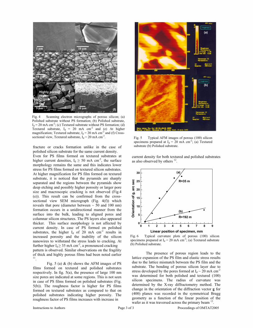
Instructions to Authors Page 3 of 3 Proceedings of OMTAT2005
fracture or cracks formation unlike in the case of polished silicon substrate for the same current density. Even for PS films formed on textured substrates at higher current densities, Id ≥ 50 mA cm-2, the surface morphology remains the same and this indicates lower stress for PS films formed on textured silicon substrates. At higher magnification for PS film formed on textured substrate, it is noticed that the pyramids are sharply separated and the regions between the pyramids show deep etching and possibly higher porosity or larger pore size and macroscopic cracking is not observed (Fig.4 (e)). This result can be confirmed from the cross- sectional view SEM micrograph (Fig. 4(f)) which reveals that pore (diameter between ~ 50 and 100 nm) formation occurs in a unidirectional manner from the surface into the bulk, leading to aligned pores and columnar silicon structures. The PS layers also appeared thicker. This surface morphology is not affected by current density. In case of PS formed on polished substrates, the higher Id of 20 mA cm-2 results in increased porosity and the inability of the silicon nanowires to withstand the stress leads to cracking. At further higher Id ≥ 35 mA cm-2, a pronounced cracking pattern is observed. Similar observations on the fragility of thick and highly porous films had been noted earlier 11.
Fig. 5 (a) & (b) shows the AFM images of PS films formed on textured and polished substrates respectively. In fig. 5(a), the presence of large 100 nm size pores are indicated at some regions. This is not seen in case of PS films formed on polished substrates (Fig. 5(b)). The roughness factor is higher for PS films formed on textured substrates as compared to that on polished substrates indicating higher porosity. The roughness factor of PS films increases with increase in
current density for both textured and polished substrates as also observed by others 12.
The presence of porous region leads to the lattice expansion of the PS film and elastic stress results due to the lattice mismatch between the PS film and the substrate. The bending of porous silicon layer due to stress developed by the pores formed at Id ~ 20 mA cm-2 was determined for both polished and textured (100) silicon specimens. The radius of curvature was determined by the X-ray diffractometry method. The change in the orientation of the diffraction vector g for (400) planes was recorded in the symmetrical Bragg geometry as a function of the linear position of the wafer as it was traversed across the primary beam 13.
Fig. 4 Scanning electron micrographs of porous silicon; (a) Polished substrate without PS formation; (b) Polished substrate, Id = 20 mA cm-2; (c) Textured substrate without PS formation; (d) Textured substrate, Id = 20 mA cm-2 and (e) At higher magnification; Textured substrate, Id = 20 mA cm-2 and (f) Cross-sectional view, Textured substrate, Id = 20 mA cm-2. Fig. 5 Typical AFM images of porous (100) silicon
specimens prepared at Id = 20 mA cm-2; (a) Textured substrate (b) Polished substrate.
Fig. 6 Typical curvature plots of porous (100) silicon specimens prepared at Id = 20 mA cm-2; (a) Textured substrate (b) Polished substrate.
(d)
0 1 2 3 4 5 6 7 8 90
5
10
15
20
25
30
(b)
(a)
R=192 m
R=35 m
Orie
ntat
ion
of g
, arc
sec
Linear position of specimen, mm
(a)
(b)
(a)
(b)
(c) (d)
(e) (f)
Highly porous region
10 µm
10 µm 10 µm
10 µm 5 µm
1 µm
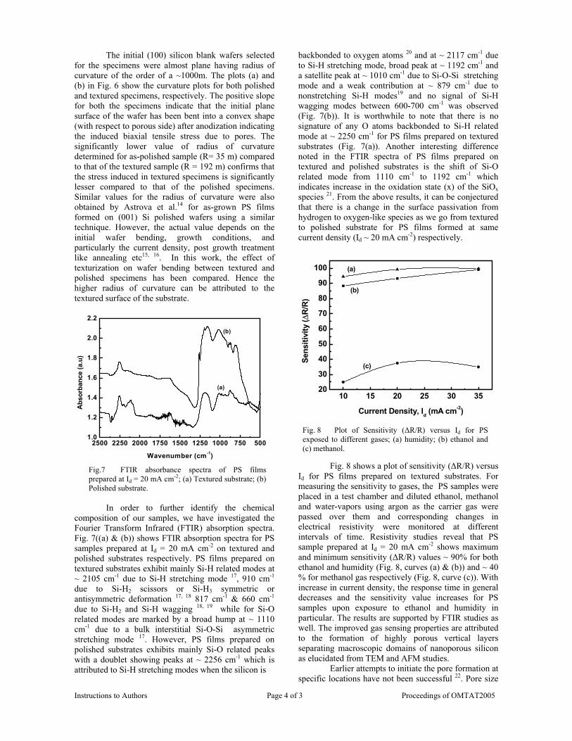
Instructions to Authors Page 4 of 3 Proceedings of OMTAT2005
The initial (100) silicon blank wafers selected for the specimens were almost plane having radius of curvature of the order of a ~1000m. The plots (a) and (b) in Fig. 6 show the curvature plots for both polished and textured specimens, respectively. The positive slope for both the specimens indicate that the initial plane surface of the wafer has been bent into a convex shape (with respect to porous side) after anodization indicating the induced biaxial tensile stress due to pores. The significantly lower value of radius of curvature determined for as-polished sample (R= 35 m) compared to that of the textured sample (R = 192 m) confirms that the stress induced in textured specimens is significantly lesser compared to that of the polished specimens. Similar values for the radius of curvature were also obtained by Astrova et al.14 for as-grown PS films formed on (001) Si polished wafers using a similar technique. However, the actual value depends on the initial wafer bending, growth conditions, and particularly the current density, post growth treatment like annealing etc15, 16. In this work, the effect of texturization on wafer bending between textured and polished specimens has been compared. Hence the higher radius of curvature can be attributed to the textured surface of the substrate.
In order to further identify the chemical
composition of our samples, we have investigated the Fourier Transform Infrared (FTIR) absorption spectra. Fig. 7((a) & (b)) shows FTIR absorption spectra for PS samples prepared at Id = 20 mA cm-2 on textured and polished substrates respectively. PS films prepared on textured substrates exhibit mainly Si-H related modes at ~ 2105 cm-1 due to Si-H stretching mode 17, 910 cm-1 due to Si-H2 scissors or Si-H3 symmetric or antisymmetric deformation 17, 18 817 cm-1 & 660 cm-1 due to Si-H2 and Si-H wagging 18, 19 while for Si-O related modes are marked by a broad hump at ~ 1110 cm-1 due to a bulk interstitial Si-O-Si asymmetric stretching mode 17. However, PS films prepared on polished substrates exhibits mainly Si-O related peaks with a doublet showing peaks at ~ 2256 cm-1 which is attributed to Si-H stretching modes when the silicon is
backbonded to oxygen atoms 20 and at ~ 2117 cm-1 due to Si-H stretching mode, broad peak at ~ 1192 cm-1 and a satellite peak at ~ 1010 cm-1 due to Si-O-Si stretching mode and a weak contribution at ~ 879 cm-1 due to nonstretching Si-H modes19 and no signal of Si-H wagging modes between 600-700 cm-1 was observed (Fig. 7(b)). It is worthwhile to note that there is no signature of any O atoms backbonded to Si-H related mode at ~ 2250 cm-1 for PS films prepared on textured substrates (Fig. 7(a)). Another interesting difference noted in the FTIR spectra of PS films prepared on textured and polished substrates is the shift of Si-O related mode from 1110 cm-1 to 1192 cm-1 which indicates increase in the oxidation state (x) of the SiOx species 21. From the above results, it can be conjectured that there is a change in the surface passivation from hydrogen to oxygen-like species as we go from textured to polished substrate for PS films formed at same current density (Id ~ 20 mA cm-2) respectively.
Fig. 8 shows a plot of sensitivity (∆R/R) versus
Id for PS films prepared on textured substrates. For measuring the sensitivity to gases, the PS samples were placed in a test chamber and diluted ethanol, methanol and water-vapors using argon as the carrier gas were passed over them and corresponding changes in electrical resistivity were monitored at different intervals of time. Resistivity studies reveal that PS sample prepared at Id = 20 mA cm-2 shows maximum and minimum sensitivity (∆R/R) values ~ 90% for both ethanol and humidity (Fig. 8, curves (a) & (b)) and ~ 40 % for methanol gas respectively (Fig. 8, curve (c)). With increase in current density, the response time in general decreases and the sensitivity value increases for PS samples upon exposure to ethanol and humidity in particular. The results are supported by FTIR studies as well. The improved gas sensing properties are attributed to the formation of highly porous vertical layers separating macroscopic domains of nanoporous silicon as elucidated from TEM and AFM studies.
Earlier attempts to initiate the pore formation at specific locations have not been successful 22. Pore size
10 15 20 25 30 3520
30
40
50
60
70
80
90
100
(c)
(b)
(a)
Sens
itivi
ty (∆
R/R
)
Current Density, Id (mA cm-2)
Fig.7 FTIR absorbance spectra of PS films prepared at Id = 20 mA cm-2; (a) Textured substrate; (b) Polished substrate.
(b)
2500 2250 2000 1750 1500 1250 1000 750 5001.0
1.2
1.4
1.6
1.8
2.0
2.2
(b)
(a)
Abs
orba
nce
(a.u
)
Wavenumber (cm-1)
Fig. 8 Plot of Sensitivity (∆R/R) versus Id for PS exposed to different gases; (a) humidity; (b) ethanol and (c) methanol.
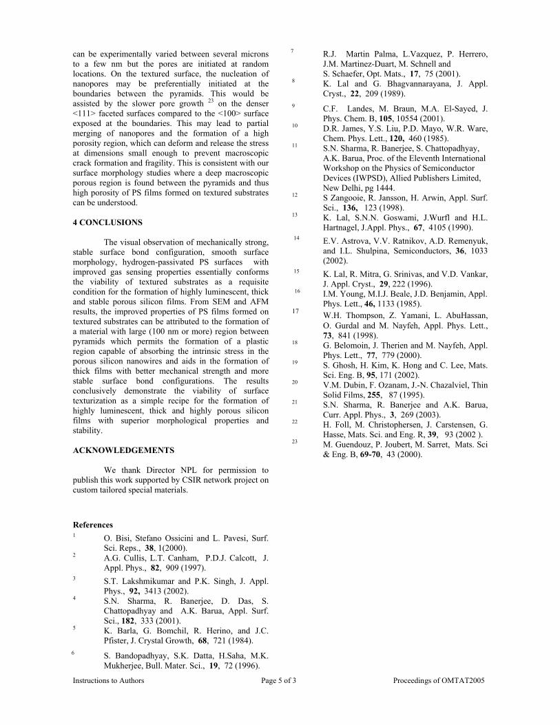
Instructions to Authors Page 5 of 3 Proceedings of OMTAT2005
can be experimentally varied between several microns to a few nm but the pores are initiated at random locations. On the textured surface, the nucleation of nanopores may be preferentially initiated at the boundaries between the pyramids. This would be assisted by the slower pore growth 23 on the denser <111> faceted surfaces compared to the <100> surface exposed at the boundaries. This may lead to partial merging of nanopores and the formation of a high porosity region, which can deform and release the stress at dimensions small enough to prevent macroscopic crack formation and fragility. This is consistent with our surface morphology studies where a deep macroscopic porous region is found between the pyramids and thus high porosity of PS films formed on textured substrates can be understood. 4 CONCLUSIONS
The visual observation of mechanically strong, stable surface bond configuration, smooth surface morphology, hydrogen-passivated PS surfaces with improved gas sensing properties essentially conforms the viability of textured substrates as a requisite condition for the formation of highly luminescent, thick and stable porous silicon films. From SEM and AFM results, the improved properties of PS films formed on textured substrates can be attributed to the formation of a material with large (100 nm or more) region between pyramids which permits the formation of a plastic region capable of absorbing the intrinsic stress in the porous silicon nanowires and aids in the formation of thick films with better mechanical strength and more stable surface bond configurations. The results conclusively demonstrate the viability of surface texturization as a simple recipe for the formation of highly luminescent, thick and highly porous silicon films with superior morphological properties and stability. ACKNOWLEDGEMENTS
We thank Director NPL for permission to publish this work supported by CSIR network project on custom tailored special materials.
References 1 O. Bisi, Stefano Ossicini and L. Pavesi, Surf.
Sci. Reps., 38, 1(2000). 2 A.G. Cullis, L.T. Canham, P.D.J. Calcott, J.
Appl. Phys., 82, 909 (1997). 3 S.T. Lakshmikumar and P.K. Singh, J. Appl.
Phys., 92, 3413 (2002). 4 S.N. Sharma, R. Banerjee, D. Das, S.
Chattopadhyay and A.K. Barua, Appl. Surf. Sci., 182, 333 (2001).
5 K. Barla, G. Bomchil, R. Herino, and J.C. Pfister, J. Crystal Growth, 68, 721 (1984).
6 S. Bandopadhyay, S.K. Datta, H.Saha, M.K. Mukherjee, Bull. Mater. Sci., 19, 72 (1996).
7 R.J. Martin Palma, L.Vazquez, P. Herrero, J.M. Martinez-Duart, M. Schnell and S. Schaefer, Opt. Mats., 17, 75 (2001).
8 K. Lal and G. Bhagvannarayana, J. Appl. Cryst., 22, 209 (1989).
9 C.F. Landes, M. Braun, M.A. El-Sayed, J. Phys. Chem. B, 105, 10554 (2001).
10 D.R. James, Y.S. Liu, P.D. Mayo, W.R. Ware, Chem. Phys. Lett., 120, 460 (1985).
11 S.N. Sharma, R. Banerjee, S. Chattopadhyay, A.K. Barua, Proc. of the Eleventh International Workshop on the Physics of Semiconductor Devices (IWPSD), Allied Publishers Limited, New Delhi, pg 1444.
12 S Zangooie, R. Jansson, H. Arwin, Appl. Surf. Sci., 136, 123 (1998).
13 K. Lal, S.N.N. Goswami, J.Wurfl and H.L. Hartnagel, J.Appl. Phys., 67, 4105 (1990).
14 E.V. Astrova, V.V. Ratnikov, A.D. Remenyuk, and I.L. Shulpina, Semiconductors, 36, 1033 (2002).
15 K. Lal, R. Mitra, G. Srinivas, and V.D. Vankar, J. Appl. Cryst., 29, 222 (1996).
16 I.M. Young, M.I.J. Beale, J.D. Benjamin, Appl. Phys. Lett., 46, 1133 (1985).
17 W.H. Thompson, Z. Yamani, L. AbuHassan, O. Gurdal and M. Nayfeh, Appl. Phys. Lett., 73, 841 (1998).
18 G. Belomoin, J. Therien and M. Nayfeh, Appl. Phys. Lett., 77, 779 (2000).
19 S. Ghosh, H. Kim, K. Hong and C. Lee, Mats. Sci. Eng. B, 95, 171 (2002).
20 V.M. Dubin, F. Ozanam, J.-N. Chazalviel, Thin Solid Films, 255, 87 (1995).
21 S.N. Sharma, R. Banerjee and A.K. Barua, Curr. Appl. Phys., 3, 269 (2003).
22 H. Foll, M. Christophersen, J. Carstensen, G. Hasse, Mats. Sci. and Eng. R, 39, 93 (2002 ).
23 M. Guendouz, P. Joubert, M. Sarret, Mats. Sci & Eng. B, 69-70, 43 (2000).

Sorry!!
This Paper is NOT Available
IT28
Phase Separation and Magnetostriction in LBMO Thin Films Tamio Endo1,2, Hong Zhu1 , Masanori Okada1, Atsuya Akiba1, Ken-ichi Nakanishi1 Josep
Nogues3, Juan S. Munoz3 Jose Colino4
1Faculty of Engineering, Mie University, Tsu, Mie 514-8507, Japan; 2National Institute of Advanced industrial Science and Technology (AIST), Tsukuba, Ibaraki
305-8568, Japan 3ICREA and Departament de Fisica, Universitat Autonoma de Barcelona, 08193 Bellaterra, Spain
4Department de Fisica Aplicada, Universidad de Castilla-La Mancha, Campus, Universitario, 13071 Ciudad Real, Spain
E-mail: [email protected]
Although much progress on understanding of the doped manganites has been reached in the last ten years, there still remain new phenomena unexplored. Here, we report on the ferromagnetic-insulating state and the positive magnetoresistance effect in (La,Ba)MnO3 (LBMO) films.
The samples were epitaxially grown on LaAlO3 (100) substrates using ion beam sputtering technique. As it is quite unusual in doped manganites, our result showed that the ferromagnetic transition occurs at a Curie temperature TC=174 K, whereas the metal transition at TP=84 K. This implies that a ferromagnetic-insulating state exists in a wide temperature range.
The result is interpreted in a percolative transport picture based on phase separation, in which the lattice mismatch between LBMO and LaAlO3 plays a crucial role. At T=TC, the isolated ferromagnetic-metal (FM) clusters develop in the film, accordingly it enters ferromagnetic state with insulating transport behavior. With decreasing temperature further, the FM clusters expand and connect with each other to form a FM network at T=TP, hence explaining why the metal transition occurs at a temperature much lower than TC. Furthermore, another unexpected result is the positive magnetoresistance effect at temperatures below TP, i.e. in the metallic state. This is ascribed to an anisotropic magnetostriction in the FM clusters, i.e., the application of magnetic field, the FM clusters expand at longitudinal direction, whereas they shrink at transversal direction. The decrease of transversal connection in the FM network results in the increase of resistance in the film, i.e., positive magnetoresistance. The observed saturation of positive magnetoresistance can also be attributed to the collapse of the FM network under a critical field in this picture.
Page 1 of 3 Proceedings of OMTAT2005
RECENT PROGRESS IN DEVICE APPLICATIONS OF TRANSPARENT OXIDE SEMICONDUCTORS
T. Kamiya1,2 and H. Hosono1,2,3
1Materials and Structures Laboratory, Tokyo Institute of Technology, Yokohama 226-8503, Japan
2ERATO-SORST, Japan Science and Technology Agency, in Frontier Collaborative Research Center, Tokyo Institute of Technology, Yokohama 226-8503, Japan
3Frontier Collaborative Research Center, Tokyo Institute of Technology, Yokohama 226-8503, Japan Email: [email protected]
ABSTRACT
Three new oxide semiconductors, (i) n-type amorphous oxide semiconductors (AOSs), (ii) layered oxychalcogenides LaCuOCh, and (iii) nano-porous semiconductor 12CaO· 7Al2O3 (C12A7), are introduced and their peculiar properties are discussed in comparison with conventional semiconductors based on their electronic structures. AOSs can have electron transport properties superior even to silicon if they are in amorphous states. Therefore AOSs are favorable for low-temperature thin film transistors. The layered oxychalcogenides are new transparent p-type semiconductors exhibiting large hole mobilities, degenerate p-type conduction, and room-temperature stable excitions, and is applied to an excitonic blue light-emitting diode. C12A7 have large electrical conductivities and low apparent work functions if electrons are doped. Applications to field-emission display devices and field-effect transistors are also shown. 1 INTRODUCTION In the last decade, there has been large progress in oxide electronics, which has been driven by finding of the first p-type transparent oxide semiconductor (TOS) CuAlO2
1, extensive development research on ZnO 2-4, fever of strong electron correlation systems 5 and so on. Many oxide-based optoelectronic devices, p-n junction rectifiers 6-11, ultraviolet (UV) light-emitting diodes 12,13, UV sensors 14-16, and thin film transistors 17-25, have been demonstrated to date. However, they have issues to be solved if we intend to apply them to practical devices, because similar devices are already in market using conventional semiconductors such as Si, GaAs and GaN with better performances. It would be difficult for the oxide-based devices to compete with the conventional devices if their targets are the same because electronic structures and opto-electronic properties of oxide semiconductors are very different from those of the conventional covalent semiconductors.
Therefore, we have to seek new applications that only oxides can realize or oxides can find a clear advantage over the conventional devices. Thus, we should consider why we need to use oxides for optoelectronic devices? To our opinion, the most important feature of oxides is associated with a variety of crystal structures and constituent elements. Therefore oxides have many chemical, optical, electronic and magnetic functions, which would be favorable for developing multi-/coupled functional materials and devices. In addition, some oxides have peculiar nanostructures embedded in crystal structures (e.g. see refs. 26-29). These are the distinguishing features from conventional semiconductors because Si, GaAs, GaN and so on have almost the same crystal structure (remind that zinc blend and wurtzite-type structures are derivatives of the diamond structure). Although the present device technology fabricates quantum wells using time & money-consuming artificial superlattice processes, oxides might provide natural systems for the
mesoscopic applications. Also we like to note that the other important feature is related to the strong ionicity of oxide: oxides can have large electron mobility even in amorphous structures due partly to the strong ionicity.
In this paper, we introduce three new oxide semiconductors: (i) large-mobility amorphous oxide semiconductors (AOSs), (ii) p-type layered oxychalcogenides LaCuOCh (Ch = chalcogen), and (iii) a nano-porous semiconductor, 12CaO· 7Al2O3 (C12A7). Associated device applications, (i) transparent flexible thin film transistors (TFTs) using AOSs, (ii) excitonic light-emitting diodes (LEDs) using LaCuOCh, and (iii) field-emission display (FED) devices and field-effect transistors, will be shown. 2 AMORPHOUS OXIDE SEMICONDUCTOR AND TRANSPARENT FLEXIBLE TFT
2.1 AOS: New materials for flexible electronics
We reported the fabrication and operation of fully transparent TFTs using InGaO3(ZnO)5 single-crystalline films for channels 22 (its crystal structure is shown in Fig. 1(A)). They exhibited large field-effect mobilities for oxide TFTs, ~ 80 cm2/Vs at room temperature. In spite of the good characteristics, it would not be applicable to practical applications because it needs very high process temperatures > 1300 oC to produce the single-crystalline layer 30,31 and expensive single-crystalline substrates of yttria-stabilized zirconia (YSZ). Although it is possible to fabricate polycrystalline oxide TFTs using ZnO and InGaO3(ZnO)m at low temperatures including room temperature 20,25, here we like to propose that AOSs are promising for low-temperature processed applications because some AOSs have electron mobilities much larger than those of hydrogenated amorphous silicon (a-Si:H) and organic semiconductors even if they are formed at room temperature 32-35.
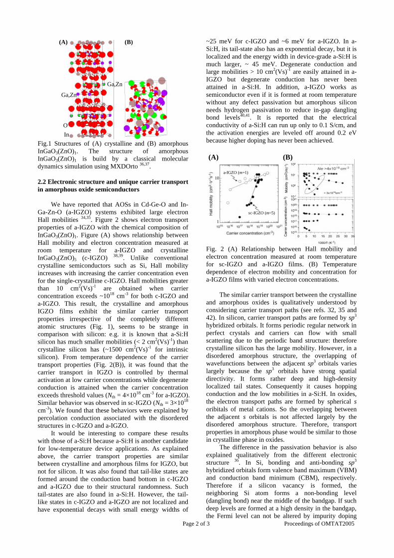
Page 2 of 3 Proceedings of OMTAT2005
(B)(A)
In
Ga,Zn
O
Ga,Zn
Fig.1 Structures of (A) crystalline and (B) amorphous InGaO3(ZnO)1. The structure of amorphous InGaO3(ZnO)1 is build by a classical molecular dynamics simulation using MXDOrto 36,37. 2.2 Electronic structure and unique carrier transport in amorphous oxide semiconductors
We have reported that AOSs in Cd-Ge-O and In-Ga-Zn-O (a-IGZO) systems exhibited large electron Hall mobilities 34,35. Figure 2 shows electron transport properties of a-IGZO with the chemical composition of InGaO3(ZnO)1. Figure (A) shows relationship between Hall mobility and electron concentration measured at room temperature for a-IGZO and crystalline InGaO3(ZnO)5 (c-IGZO) 38,39. Unlike conventional crystalline semiconductors such as Si, Hall mobility increases with increasing the carrier concentration even for the single-crystalline c-IGZO. Hall mobilities greater than 10 cm2(Vs)-1 are obtained when carrier concentration exceeds ~1018 cm-3 for both c-IGZO and a-IGZO. This result, the crystalline and amorphous IGZO films exhibit the similar carrier transport properties irrespective of the completely different atomic structures (Fig. 1), seems to be strange in comparison with silicon: e.g. it is known that a-Si:H silicon has much smaller mobilities (< 2 cm2(Vs)-1) than crystalline silicon has (~1500 cm2(Vs)-1 for intrinsic silicon). From temperature dependence of the carrier transport properties (Fig. 2(B)), it was found that the carrier transport in IGZO is controlled by thermal activation at low carrier concentrations while degenerate conduction is attained when the carrier concentration exceeds threshold values (Nth = 4×1018 cm-3 for a-IGZO). Similar behavior was observed in sc-IGZO (Nth = 3×1018 cm-3). We found that these behaviors were explained by percolation conduction associated with the disordered structures in c-IGZO and a-IGZO.
It would be interesting to compare these results with those of a-Si:H because a-Si:H is another candidate for low-temperature device applications. As explained above, the carrier transport properties are similar between crystalline and amorphous films for IGZO, but not for silicon. It was also found that tail-like states are formed around the conduction band bottom in c-IGZO and a-IGZO due to their structural randomness. Such tail-states are also found in a-Si:H. However, the tail-like states in c-IGZO and a-IGZO are not localized and have exponential decays with small energy widths of
~25 meV for c-IGZO and ~6 meV for a-IGZO. In a-Si:H, its tail-state also has an exponential decay, but it is localized and the energy width in device-grade a-Si:H is much larger, ~ 45 meV. Degenerate conduction and large mobilities > 10 cm2(Vs)-1 are easily attained in a-IGZO but degenerate conduction has never been attained in a-Si:H. In addition, a-IGZO works as semiconductor even if it is formed at room temperature without any defect passivation but amorphous silicon needs hydrogen passivation to reduce in-gap dangling bond levels40,41. It is reported that the electrical conductivity of a-Si:H can run up only to 0.1 S/cm, and the activation energies are leveled off around 0.2 eV because higher doping has never been achieved.
a-IGZO(m=1)10
1
10
1
a-IGZO (m=1)
sc-IGZO (m=5)
(B)(A)
Fig. 2 (A) Relationship between Hall mobility and electron concentration measured at room temperature for sc-IGZO and a-IGZO films. (B) Temperature dependence of electron mobility and concentration for a-IGZO films with varied electron concentrations.
The similar carrier transport between the crystalline and amorphous oxides is qualitatively understood by considering carrier transport paths (see refs. 32, 35 and 42). In silicon, carrier transport paths are formed by sp3 hybridized orbitals. It forms periodic regular network in perfect crystals and carriers can flow with small scattering due to the periodic band structure: therefore crystalline silicon has the large mobility. However, in a disordered amorphous structure, the overlapping of wavefunctions between the adjacent sp3 orbitals varies largely because the sp3 orbitals have strong spatial directivity. It forms rather deep and high-density localized tail states. Consequently it causes hopping conduction and the low mobilities in a-Si:H. In oxides, the electron transport paths are formed by spherical s oribitals of metal cations. So the overlapping between the adjacent s orbitals is not affected largely by the disordered amorphous structure. Therefore, transport properties in amorphous phase would be similar to those in crystalline phase in oxides.
The difference in the passivation behavior is also explained qualitatively from the different electronic structure 36. In Si, bonding and anti-bonding sp3 hybridized orbitals form valence band maximum (VBM) and conduction band minimum (CBM), respectively. Therefore if a silicon vacancy is formed, the neighboring Si atom forms a non-bonding level (dangling bond) near the middle of the bandgap. If such deep levels are formed at a high density in the bandgap, the Fermi level can not be altered by impurity doping
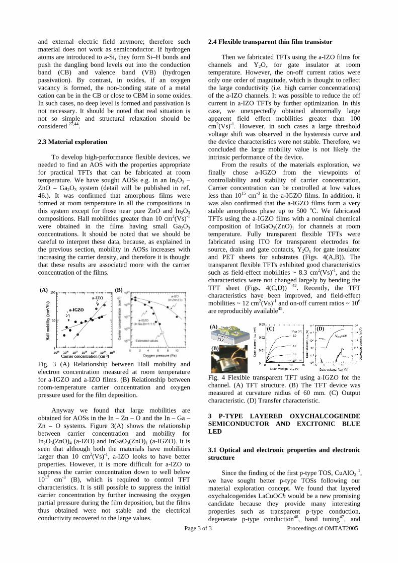
Page 3 of 3 Proceedings of OMTAT2005
and external electric field anymore; therefore such material does not work as semiconductor. If hydrogen atoms are introduced to a-Si, they form Si–H bonds and push the dangling bond levels out into the conduction band (CB) and valence band (VB) (hydrogen passivation). By contrast, in oxides, if an oxygen vacancy is formed, the non-bonding state of a metal cation can be in the CB or close to CBM in some oxides. In such cases, no deep level is formed and passivation is not necessary. It should be noted that real situation is not so simple and structural relaxation should be considered 27,44. 2.3 Material exploration
To develop high-performance flexible devices, we
needed to find an AOS with the properties appropriate for practical TFTs that can be fabricated at room temperature. We have sought AOSs e.g. in an In2O3 – ZnO – Ga2O3 system (detail will be published in ref. 46.). It was confirmed that amorphous films were formed at room temperature in all the compositions in this system except for those near pure ZnO and In2O3 compositions. Hall mobilities greater than 10 cm2(Vs)-1 were obtained in the films having small Ga2O3 concentrations. It should be noted that we should be careful to interpret these data, because, as explained in the previous section, mobility in AOSs increases with increasing the carrier density, and therefore it is thought that these results are associated more with the carrier concentration of the films.
Carrier concentration (cm-3)
Hal
l mob
ility
(cm
2 /V
s)
1
10
100
1015 1016 1017 1018 1019 1020 1021
a-IZO
a-IGZO
Carrier concentration (cm-3)
Hal
l mob
ility
(cm
2 /V
s)
1
10
100
1015 1016 1017 1018 1019 1020 1021
a-IZO
a-IGZO
(A) (B)
Fig. 3 (A) Relationship between Hall mobility and electron concentration measured at room temperature for a-IGZO and a-IZO films. (B) Relationship between room-temperature carrier concentration and oxygen pressure used for the film deposition.
Anyway we found that large mobilities are obtained for AOSs in the In – Zn – O and the In – Ga – Zn – O systems. Figure 3(A) shows the relationship between carrier concentration and mobility for In2O3(ZnO)4 (a-IZO) and InGaO3(ZnO)1 (a-IGZO). It is seen that although both the materials have mobilities larger than 10 cm2(Vs)-1, a-IZO looks to have better properties. However, it is more difficult for a-IZO to suppress the carrier concentration down to well below 1017 cm-3 (B), which is required to control TFT characteristics. It is still possible to suppress the initial carrier concentration by further increasing the oxygen partial pressure during the film deposition, but the films thus obtained were not stable and the electrical conductivity recovered to the large values.
2.4 Flexible transparent thin film transistor
Then we fabricated TFTs using the a-IZO films for channels and Y2Ox for gate insulator at room temperature. However, the on-off current ratios were only one order of magnitude, which is thought to reflect the large conductivity (i.e. high carrier concentrations) of the a-IZO channels. It was possible to reduce the off current in a-IZO TFTs by further optimization. In this case, we unexpectedly obtained abnormally large apparent field effect mobilities greater than 100 cm2(Vs)-1. However, in such cases a large threshold voltage shift was observed in the hysteresis curve and the device characteristics were not stable. Therefore, we concluded the large mobility value is not likely the intrinsic performance of the device.
From the results of the materials exploration, we finally chose a-IGZO from the viewpoints of controllability and stability of carrier concentration. Carrier concentration can be controlled at low values less than 1015 cm-3 in the a-IGZO films. In addition, it was also confirmed that the a-IGZO films form a very stable amorphous phase up to 500 oC. We fabricated TFTs using the a-IGZO films with a nominal chemical composition of InGaO3(ZnO)1 for channels at room temperature. Fully transparent flexible TFTs were fabricated using ITO for transparent electrodes for source, drain and gate contacts, Y2Ox for gate insulator and PET sheets for substrates (Figs. 4(A,B)). The transparent flexible TFTs exhibited good characteristics such as field-effect mobilities ~ 8.3 cm2(Vs)-1, and the characteristics were not changed largely by bending the TFT sheet (Figs. 4(C,D)) 42. Recently, the TFT characteristics have been improved, and field-effect mobilities ~ 12 cm2(Vs)-1 and on-off current ratios ~ 106 are reproducibly available45.
(C)(A)
(B)
VDS=4V
(D)
Fig. 4 Flexible transparent TFT using a-IGZO for the channel. (A) TFT structure. (B) The TFT device was measured at curvature radius of 60 mm. (C) Output characteristic. (D) Transfer characteristic. 3 P-TYPE LAYERED OXYCHALCOGENIDE SEMICONDUCTOR AND EXCITONIC BLUE LED
3.1 Optical and electronic properties and electronic structure
Since the finding of the first p-type TOS, CuAlO2 1,
we have sought better p-type TOSs following our material exploration concept. We found that layered oxychalcogenides LaCuOCh would be a new promising candidate because they provide many interesting properties such as transparent p-type conduction, degenerate p-type conduction46, band tuning47, and
Page 4 of 3 Proceedings of OMTAT2005
excitonic light emission at room temperature 47. And another similar material La2CdO2Se2 may be used for intrinsic light-emitting layer and electron blocking layer 48. It should be noted that their crystal structures, where (La2O2) layers and (Cu2Ch2) layers are alternately stacked (see Fig. 5 for LaCuOCh), are essentially important to understand the peculiar optoelectronic properties.
Cu
Ch
OLa
Fig. 5 Crystal structure of LaCuOCh.
As noted above, LaCuOCh exhibits good p-type
conduction. For example, undoped LaCuOS have a hole concentration of ~ 1019 cm-3 and Hall mobility of ~ 0.5 cm2(Vs)-1 at room temperature. Mobility becomes larger with an increase in the Se content in LaCuO(S1-xSex) and reaches ~ 8.0 cm2(Vs)-1 in LaCuOSe, which value is comparable to that of p-type GaN:Mg. Another important property of these materials is that degenerate p-type conduction is achieved in Mg-doped LaCuOSe, while undoped LaCuOSe shows thermally-activated behavior in hole concentration at around room temperature 46 (Fig. 6(A)). This is the first degenerate p-type conductor for wide bandgap semiconductors even including p-type Mg-doped GaN. (A) (B)
0 1 0 2 0 3 01 0 1 6
1 0 1 7
1 0 1 8
1 0 1 9
1 0 2 0
1 0 2 1
1 0 0
1 0 1
1 0 2
1 0 3
1000/T (K-1)
Hol
e de
nsity
(cm
-1)
Mob
ility
(cm
2 /V
s)
Fig. 6 (A) Temperature dependences of hole density and mobility for undoped LaCuOSe (open symbols) and Mg-doped LaCuOSe (closed symbols). (B) Optical absorption spectra of LaCuO(S1-xSex) measured at 10 K.
From the optical absorption spectra shown in Fig. 6(B), we can see that LaCuOS is a transparent semiconductor having a bandgap about 3.3 eV. The bandgap of LaCuOSe is smaller, but still large (~2.9 eV). The optical absorption spectra also show another interesting feature: step-wise structures with sharp peaks just on the edges of the steps are observed 49. Such structure is similar to those observed in semiconductor artificial superlattices 50, and would reflect two-dimensional density of states. The sharp peak features have been assigned to electron-hole pairs known as excitons from studies on photoluminescence (PL),
optical nonlinear measurements and so on 51,52. It should be emphasized that the excitons are stable even at room temperature, which would be interesting because excitons are usually not so stable in solid inorganic semiconductors. Only ZnO is known to have room-temperature stable exctions in oxide semiconductors.
Here, we discuss the origins of these properties based on their electronic structures. The increase in the mobility with selenium content in LaCuO(S1-xSex) is explained by larger hybridization between Se and Cu than that between S and Cu, which increases the VB widths and reduces the hole effective mass 46.
Next question is why the moderately large hole mobility of ~4 cm2(Vs)-1 is maintained in the heavily doped LaCuOSe:Mg having a carrier concentration greater than 1020 cm-3 although usually carrier mobility is significantly reduced by charged impurity scattering in such heavily-doped materials. Similarly, moderately intense excitonic PL is maintained in the heavily doped materials 47. The band structure in Fig. 7(A) shows that the VB dispersion of LaCuOCh is much smaller in Γ-Z direction than in Γ-X direction, suggesting that the electronic structure is highly two-dimensional 49,53. Partial density-of-state analysis showed that the band gap is formed almost solely of the (Cu2Ch2) layers (Fig. 7(B)). The two-dimensional electronic structure is more clearly seen in the density map of holes in the vicinity of the VBM (Fig. 7(C)). Here, whiter area has higher-density holes, showing that holes are confined in the (Cu2Se2) layers, which forms the hole transport paths. Multiple sharp peak features in the optical absorption spectra in Fig. 6(B) is explained by multiple excitonic levels split by spin-orbit interaction in Ch ions 49,54.
This structure also explains why the moderately large hole mobility is maintained in the heavily-doped LaCuOSe:Mg. In that case, Mg ions are doped in the LaO layers and generate holes. The generated holes are transferred to the (Cu2Se2) layer because of the local band offset (Fig. 7(B)). It consequently separates the charged acceptors and the mobile holes, and suppresses the charged impurity scattering, which is an analogue to modulation doping in high electron mobility transistors and semiconductor artificial superlattices.
LaOlayer
LaOlayer
CuSelayer
h+
higher
CuSelayer
LaOlayer
ΓΓM A Z X M ΓΓ
4.0
0.0
-4.0
-8.0
Ene
rgy
(eV
)
(A) (C)(B)
Fig. 8
Fig. 7 (A) Band structure of LaCuOSe. (B) Schematic energy diagram near the bandgap. (C) Density map of holes.
The energy structure analysis also explains why the layered chalcogenides have larger bandgaps than simple chalcogenides Cu2Ch: Cu2S and Cu2Se have rather small bandgaps of ~1.2 – 1.4 eV 55, but e.g. LaCuOS has much larger bandgap of ~ 3.1 eV at room temperature
Page 5 of 3 Proceedings of OMTAT2005
although both the bandgaps of Cu2Ch and LaCuOCh are mainly determined by the CuCh components as explained above. Here we employ a family compound with a similar crystal structure, La2CdO2Se2, to answer to this question, because its CdSe layer has a similar structure to that in CdSe 48,54. Band structure calculations of La2CdO2Se2 and CdSe showed that the VB widths are not largely different, but the CB width is much smaller in La2CdO2Se2 than in CdSe. That means, the two-dimensional network structure of the CdSe layer in La2CdO2Se2 reduces the CB dispersion and causes the large bandgap. It suggests that employing a low-dimensional structure is an effective approach to design new wide bandgap semiconductors. 3.2 Excitonic blue light-emitting diode
We reported the demonstration of the first UV LEDs using n-type light-emitting ZnO / p-type electron-injection SrCu2O2 junction 12. In this LED structure, holes must be injected to the n-type ZnO layer to emit light, but holes are much slower than electrons in usual oxides, which limits light-emission efficiency. Therefore it would be more favorable to use a p-layer for a light-emitting layer. Following this consideration, we expect that LaCuOCh would be a candidate for oxide-based LEDs.
We fabricated p / n junction LEDs using LaCuOSe for light-emitting p-layer (Fig. 8(A)). A-IGZO was employed for the electron-injection n-layer in this case. It exhibited sharp blue emission originating from the exction in LaCuOSe at room temperature (B) 56.
(A) (B)
300 400 500 600 700 800
4.0 3.5 3.0 2.5 2.0Photon energy (eV)
EL
or
PL in
tens
ity (
a.u.
)
Wavelength (nm)
MgO(001)
p-LaCuOSe
n-a-IGZO
Au
hνν
Au
V
EL
PL
Fig. 8 (A) LED structure. (B) PL and electroluminescence (EL) spectra from the LED. 4 NANOPOROUS SEMICONDUCTOR C12A7 AND ITS APPLICATIONS TO FED AND FET
4.1 Properties of C12A7-derived materials: Functions originating from clathrated anions
In this section, we introduce a crystal having a zero-dimensional natural nanostructure. The crystal structure of C12A7 is shown in Fig. 9(A). The cubic unit cell consists of twelve cages (~0.4 nm in inner diameter, (B)). As the cage framework is positively charged at +1/3e per cage, two cages out of the twelve cages clathrate an O2- ion each (free oxygen ions).
OAl
Ca
(A) (B)
Fig. 9 (A) Crystal structure of C12A7 and (B) a cage structure.
This exotic structure led to the appearance of many
new functions by replacing the free oxygen ions with other active anions. Abundant O- ions are formed at ~2×1020 cm-3 if C12A7 is annealed in a dry oxygen gas at 600 – 800 oC. O- ion is known as the ‘strongest oxidant’ among the known active oxygen species, and it is possible to oxidize even platinum metal 57. Substitution of the free oxygen ions with hydrogen creates high-density H- ions in the cages (C12A7:H-). C12A7:H- is an electrical insulator like stoichiometric C12A7 and C12A7:O-, while it exhibits persistent electronic conduction and coloration after irradiated with UV light 58 or electron beam 59 (mechanism is discussed in ref. 60). The conductivity increases to > 0.3 Scm-1 (Fig. 10(A)) and new optical absorption bands appear at the same time at ~0.4 eV and 2.8 eV (B). It is recovered to the insulating and colorless transparent state by heating at ~ 350 oC. Further it is possible to replace all the free oxygen ions with electrons (C12A7:e-), which forms a new inorganic electride 61 (“electride” is a crystalline salt in which stoichiometric amounts of electrons are served as anions 62,63). C12A7:e- exhibits electronic conduction with conductivities greater than 100 Scm-1 without UV irradiation (A).
0 10 20 30 40 50 6010
-910
-810
-710
-610
-510
-410
-310
-210
-110
010
110
2
1000/T (K )
Con
duct
ivity
(S/
cm)
-1
0
1
2
3
4
Photon energy / eV
Abs
orba
nce
0 1 2 3 40
200
400
600
800
1000
1200
Abs
orbt
ion
coef
fice
inet
(cm
)-1(A) (B)
C12A7:e-
C12A7:H-+UV-irradiated
as-prepared C12A7:H-
C12A7:H-+UV-irradiated2×1019
C12A7:e-
[F+]=2×1021 cm-3
C12A7:e-
1020
C12A7:e-
2×10¹⁸C12A7:e-
8×10¹⁶
Fig. 10 (A) Electronic conductor conversion and (B) coloration in C12A7:H- and C12A7:e-.
These functions originate from the exotic active
anions clathrated in the cages of C12A7. It was found that unusually shallow Madelung potential in the cages stabilizes these exotic anionic states 64,65. Carrier transport mechanism in C12A7:e- is discussed using ab-initio embedded cluster calculations and a polaron conduction mechanism is proposed 66,67.
4.2 Electronic structure and device applications
The band structure of C12A7:e- was calculated by an ab-initio code WIEN2k (Fig. 11(A)). It shows that
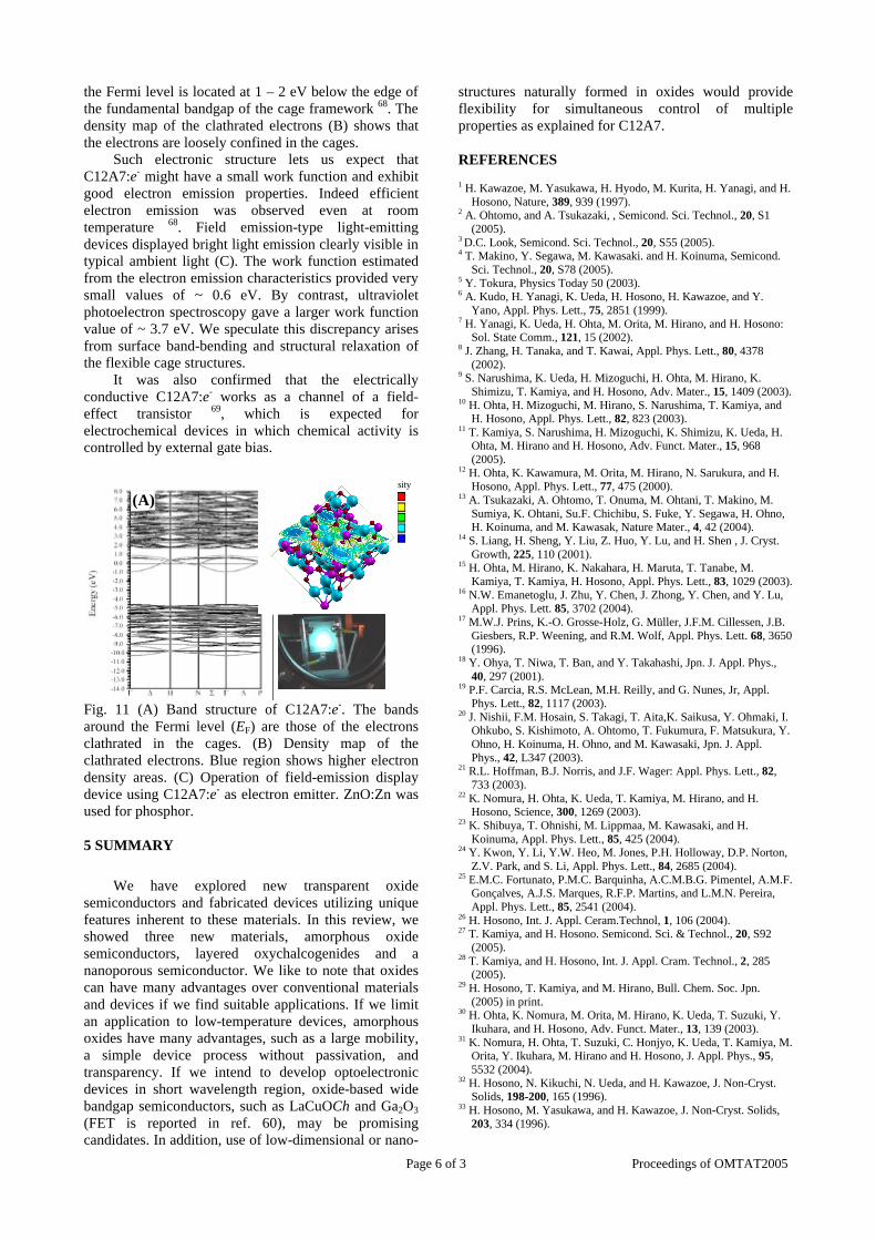
Page 6 of 3 Proceedings of OMTAT2005
the Fermi level is located at 1 – 2 eV below the edge of the fundamental bandgap of the cage framework 68. The density map of the clathrated electrons (B) shows that the electrons are loosely confined in the cages.
Such electronic structure lets us expect that C12A7:e- might have a small work function and exhibit good electron emission properties. Indeed efficient electron emission was observed even at room temperature 68. Field emission-type light-emitting devices displayed bright light emission clearly visible in typical ambient light (C). The work function estimated from the electron emission characteristics provided very small values of ~ 0.6 eV. By contrast, ultraviolet photoelectron spectroscopy gave a larger work function value of ~ 3.7 eV. We speculate this discrepancy arises from surface band-bending and structural relaxation of the flexible cage structures.
It was also confirmed that the electrically conductive C12A7:e- works as a channel of a field-effect transistor 69, which is expected for electrochemical devices in which chemical activity is controlled by external gate bias.
higher density
(A) (B)
(C)
Fig. 11 (A) Band structure of C12A7:e-. The bands around the Fermi level (EF) are those of the electrons clathrated in the cages. (B) Density map of the clathrated electrons. Blue region shows higher electron density areas. (C) Operation of field-emission display device using C12A7:e- as electron emitter. ZnO:Zn was used for phosphor. 5 SUMMARY
We have explored new transparent oxide
semiconductors and fabricated devices utilizing unique features inherent to these materials. In this review, we showed three new materials, amorphous oxide semiconductors, layered oxychalcogenides and a nanoporous semiconductor. We like to note that oxides can have many advantages over conventional materials and devices if we find suitable applications. If we limit an application to low-temperature devices, amorphous oxides have many advantages, such as a large mobility, a simple device process without passivation, and transparency. If we intend to develop optoelectronic devices in short wavelength region, oxide-based wide bandgap semiconductors, such as LaCuOCh and Ga2O3 (FET is reported in ref. 60), may be promising candidates. In addition, use of low-dimensional or nano-
structures naturally formed in oxides would provide flexibility for simultaneous control of multiple properties as explained for C12A7. REFERENCES 1 H. Kawazoe, M. Yasukawa, H. Hyodo, M. Kurita, H. Yanagi, and H.
Hosono, Nature, 389, 939 (1997). 2 A. Ohtomo, and A. Tsukazaki, , Semicond. Sci. Technol., 20, S1
(2005). 3 D.C. Look, Semicond. Sci. Technol., 20, S55 (2005). 4 T. Makino, Y. Segawa, M. Kawasaki. and H. Koinuma, Semicond.
Sci. Technol., 20, S78 (2005). 5 Y. Tokura, Physics Today 50 (2003). 6 A. Kudo, H. Yanagi, K. Ueda, H. Hosono, H. Kawazoe, and Y.
Yano, Appl. Phys. Lett., 75, 2851 (1999). 7 H. Yanagi, K. Ueda, H. Ohta, M. Orita, M. Hirano, and H. Hosono:
Sol. State Comm., 121, 15 (2002). 8 J. Zhang, H. Tanaka, and T. Kawai, Appl. Phys. Lett., 80, 4378
(2002). 9 S. Narushima, K. Ueda, H. Mizoguchi, H. Ohta, M. Hirano, K.
Shimizu, T. Kamiya, and H. Hosono, Adv. Mater., 15, 1409 (2003). 10 H. Ohta, H. Mizoguchi, M. Hirano, S. Narushima, T. Kamiya, and
H. Hosono, Appl. Phys. Lett., 82, 823 (2003). 11 T. Kamiya, S. Narushima, H. Mizoguchi, K. Shimizu, K. Ueda, H.
Ohta, M. Hirano and H. Hosono, Adv. Funct. Mater., 15, 968 (2005).
12 H. Ohta, K. Kawamura, M. Orita, M. Hirano, N. Sarukura, and H. Hosono, Appl. Phys. Lett., 77, 475 (2000).
13 A. Tsukazaki, A. Ohtomo, T. Onuma, M. Ohtani, T. Makino, M. Sumiya, K. Ohtani, Su.F. Chichibu, S. Fuke, Y. Segawa, H. Ohno, H. Koinuma, and M. Kawasak, Nature Mater., 4, 42 (2004).
14 S. Liang, H. Sheng, Y. Liu, Z. Huo, Y. Lu, and H. Shen , J. Cryst. Growth, 225, 110 (2001).
15 H. Ohta, M. Hirano, K. Nakahara, H. Maruta, T. Tanabe, M. Kamiya, T. Kamiya, H. Hosono, Appl. Phys. Lett., 83, 1029 (2003).
16 N.W. Emanetoglu, J. Zhu, Y. Chen, J. Zhong, Y. Chen, and Y. Lu, Appl. Phys. Lett. 85, 3702 (2004).
17 M.W.J. Prins, K.-O. Grosse-Holz, G. Müller, J.F.M. Cillessen, J.B. Giesbers, R.P. Weening, and R.M. Wolf, Appl. Phys. Lett. 68, 3650 (1996).
18 Y. Ohya, T. Niwa, T. Ban, and Y. Takahashi, Jpn. J. Appl. Phys., 40, 297 (2001).
19 P.F. Carcia, R.S. McLean, M.H. Reilly, and G. Nunes, Jr, Appl. Phys. Lett., 82, 1117 (2003).
20 J. Nishii, F.M. Hosain, S. Takagi, T. Aita,K. Saikusa, Y. Ohmaki, I. Ohkubo, S. Kishimoto, A. Ohtomo, T. Fukumura, F. Matsukura, Y. Ohno, H. Koinuma, H. Ohno, and M. Kawasaki, Jpn. J. Appl. Phys., 42, L347 (2003).
21 R.L. Hoffman, B.J. Norris, and J.F. Wager: Appl. Phys. Lett., 82, 733 (2003).
22 K. Nomura, H. Ohta, K. Ueda, T. Kamiya, M. Hirano, and H. Hosono, Science, 300, 1269 (2003).
23 K. Shibuya, T. Ohnishi, M. Lippmaa, M. Kawasaki, and H. Koinuma, Appl. Phys. Lett., 85, 425 (2004).
24 Y. Kwon, Y. Li, Y.W. Heo, M. Jones, P.H. Holloway, D.P. Norton, Z.V. Park, and S. Li, Appl. Phys. Lett., 84, 2685 (2004).
25 E.M.C. Fortunato, P.M.C. Barquinha, A.C.M.B.G. Pimentel, A.M.F. Gonçalves, A.J.S. Marques, R.F.P. Martins, and L.M.N. Pereira, Appl. Phys. Lett., 85, 2541 (2004).
26 H. Hosono, Int. J. Appl. Ceram.Technol, 1, 106 (2004). 27 T. Kamiya, and H. Hosono. Semicond. Sci. & Technol., 20, S92
(2005). 28 T. Kamiya, and H. Hosono, Int. J. Appl. Cram. Technol., 2, 285
(2005). 29 H. Hosono, T. Kamiya, and M. Hirano, Bull. Chem. Soc. Jpn.
(2005) in print. 30 H. Ohta, K. Nomura, M. Orita, M. Hirano, K. Ueda, T. Suzuki, Y.
Ikuhara, and H. Hosono, Adv. Funct. Mater., 13, 139 (2003). 31 K. Nomura, H. Ohta, T. Suzuki, C. Honjyo, K. Ueda, T. Kamiya, M.
Orita, Y. Ikuhara, M. Hirano and H. Hosono, J. Appl. Phys., 95, 5532 (2004).
32 H. Hosono, N. Kikuchi, N. Ueda, and H. Kawazoe, J. Non-Cryst. Solids, 198-200, 165 (1996).
33 H. Hosono, M. Yasukawa, and H. Kawazoe, J. Non-Cryst. Solids, 203, 334 (1996).
Page 7 of 3 Proceedings of OMTAT2005
34 M. Orita, H. Ohta, M. Hirano, S. Narushima, and H. Hosono, Phil. Mag. B, 81, 501 (2001).
35 S. Narushima, M. Orita, M. Hirano, and H. Hosono, Phys. Rev. B, 66, 035203 (2002).
36 K. Kawamura, Molecular dynamics simulation, Springer Series in Solid-State Sci. Vol. 103. (ed. F. Yonezawa, Springer-Verlag, Heidelberg, 1992).
37 K. Hirao and K. Kawamura, Pasokon ni yoru Zairyo Sekkei (Material Design using a Personal Computer) (Syoka-bo, Tokyo, 1994) [in Japanese].
38 K. Nomura, H. Ohta, K. Ueda, T. Kamiya, M. Hirano, and H. Hosono, Appl. Phys. Lett., 85, 1993 (2004).
39 A. Takagi, K. Nomura, H. Ohta, H. Yanagi, T. Kamiya, M. Hirano, and H. Hosono, Thin Solid Films, 486, 38 (2005).
40 W.E. Spear, and P.G. LeComber, Solid State Commun., 17, 1193 (1975).
41 W.E. Spear, G. Willeke, and P.G. LeComber, Physica B, 117-118, 908 (1983).
42 K. Nomura, H. Ohta, A. Takagi, T. Kamiya, M. Hirano, and H. Hosono, Nature, 432, 488 (2004).
43 T. Kamiya, H. Hiramatsu, K. Nomura, and H. Hoson, J. Electroceram. (2005) submitted.
44 F. Agullo-Lopez, C.R.A. Catlow, and P.D. Townsend, Point Defects in Materials (Academic Press, London, 1988).
45 K. Nomura, A. Takagi, T. Kamiya, H. Ohta, M. Hirano, and H. Hosono, Jpn. J. Appl. Phys. (2006) accepted.
46 H. Hiramatsu, K. Ueda, H. Ohta, M. Hirano, T. Kamiya, and H. Hosono, Appl. Phys. Lett., 82, 1048 (2003).
47 H. Hiramatsu, K. Ueda, K. Takafuji, H. Ohta, M. Hirano, T. Kamiya, and H. Hosono, J. Appl. Phys., 94, 5805 (2003).
48 H. Hiramatsu, K. Ueda, T. Kamiya, H. Ohta, M. Hirano, and H. Hosono, J. Phys. Chem. B, 108, 17344 (2004).
49 K. Ueda, H. Hiramatsu, H. Ohta, M. Hirano, T. Kamiya, and H. Hosono, Phys. Rev. B, 69, 155305 (2004).
50 e.g., A. Shink, Quantum Wells, (World Scientific, Singapore, 1997). 51 H. Kamioka, H. Hiramatsu, H. Ohta, M. Hirano, K. Ueda, T.
Kamiya, and H. Hosono, Appl. Phys. Lett., 84, 879 (2004). 52 H. Kamioka, H. Hiramatsu, M. Hirano, K. Ueda, T. Kamiya, and H.
Hosono, Opt. Lett., 29, 1659 (2004). 53 S. Inoue, K. Ueda, and H. Hosono, Phys. Rev. B, 64, 245211
(2001). 54 T. Kamiya, K. Ueda, H. Hiramatsu, H. Kamioka, H. Ohta, M.
Hirano, and H. Hosono, Thin Solid Films, 486, 98 (2005). 55 Semiconductors: Data Handbook (3rd Edition, Springer, pp. 454-
457). 56 H. Hiramatsu, K. Ueda, H. Ohta, T. Kamiya, M. Hirano, and H.
Hosono, Appl. Phys. Lett. (2005) in print. 57 K. Hayashi, M. Hirano, S. Matsuishi ,and H. Hosono; J. Am. Chem.
Soc., 124, 738 (2002). 58 K. Hayashi, S. Matsuishi, T. Kamiya, M. Hirano, and H. Hosono,
Nature, 419, 462 (2002). 59 K. Hayashi, Y. Toda, T. Kamiya, M. Hirano, M. Yamanaka, I.
Tanaka, T. Yamamoto, and H. Hosono, Appl. Phys. Lett., 86, 022109 (2005).
60 P.V. Sushko, A.L. Shluger, K. Hayashi, M. Hirano, and H. Hosono, Appl. Phys. Lett., 86, 092101 (2005).
61 S. Matsuishi, Y. Toda, M. Miyakawa, K. Hayashi, T. Kamiya, M. Hirano, I. Tanaka, and H. Hosono, Science, 301, 626 (2003).
62 J. L. Dye, Science, 247, 663 (1990). 63 J. L. Dye, Science, 301, 607 (2003). 64 T. Kamiya, H. Ohta, H. Hiramatsu, K. Hayashi, K. Nomura, S.
Matsuishi, K. Ueda, M. Hirano, and H. Hosono, Microelectr. Eng., 73-74, 620 (2004).
65 T. Kamiya, and H. Hosono, Jpn. J. Appl. Phys., 44, 774 (2005). 66 P.V. Sushko, A.L. Shluger, K. Hayashi, M. Hirano and H. Hosono,
Phys. Rev. Lett., 91, 126401 (2003). 67 P.V. Sushko, A.L. Shluger, K. Hayashi, M. Hirano and H. Hosono,
Thin Solid Films, 445, 161 (2003). 68 Y. Toda, S. Matsuishi, K. Hayashi, K. Ueda, T. Kamiya, M. Hirano
and H. Hosono, Adv. Mater., 16, 685 (2004). 69 T. Kamiya, S. Aiba, M. Miyakawa, K. Nomura, S. Matsuishi, K.
Hayashi, K. Ueda, M. Hirano, and H. Hosono, Chem. Mater. (2006) accepted.
70 K. Matsuzaki, H. Hiramatsu, K. Nomura, H. Yanagi, T. Kamiya, M. Hirano, and H. Hosono, Thin Solid Films (2006) accepted.
IT30
Magnetoelectrics: Current Status
V. R. Palkar Department of Condensed Matter Physics & Materials Science
Tata Institute of Fundamental Research, Mumbai 400005, INDIA E-mail: [email protected]
Magnetoelectrics are characterized by a coexistence of ferroelectric and ferromagnetic orderings. Discovery
of the induction of polarization by a magnetic field and of a magnetization by an electric field created a lot of excitement in the 1960s. The cross-link between magnetic and electric properties opened new degree of freedom for device designing. However, in real life the lack of materials exhibiting magnetoelectric behavior at room temperature restricted their usage in device applications. The shortage of magnetoelectric materials is due to the fact that transition metal d electrons, which are essential for the presence of magnetic moment, reduce lattice distortion, which is essential for ferroelectric behavior. As a result, additional structural or electronic driving force is required for ferroelectric and magnetic ordering to occur simultaneously at room temperature. The hetero-structures of piezoelectric and magnetostrictive phases, which could be electromagnetically coupled via stress mediation, are therefore used as an alternative to create ME effect. But the structural non-compatibility and reactivity between two materials and also with the substrate, generates immense difficulties in growing hetero-structures and achieving coupling between the two order parameters.
Recently, we have been able to show that Tb doping at Bi site induces ferrimagnetism in antiferromagnetic BiFeO3 without disturbing ferroelectric properties. We are also successful in converting ferroelectric PbTiO3 to a compound with superior magnetoelectric properties. Remarkably, in this newly synthesized compounds both magnetic (TM) and ferroelectric transitions (TC) occur above room temperature. The observed coupling between the two order parameters is an added advantage in device fabrications. The talk will cover the interesting observations made at both micro as well as microscopic levels in these novel compounds.
FERROMAGNETIC SEMICONDUCTING OXIDES AND SPINTRONICS
V.K.Sankaranarayanan
Electronic Materials Division, National Physical Laboratory, New Delhi-110 012, INDIA
E-mail: [email protected]
ABSTRACT Spintronic devices envisage to exploit the spin degree of freedom of charge carriers in new generation of ultra- low power, high speed memory, logic and photonic devices. Ferromagnetic semiconducting oxides which are magnetic at RT could be ideal spintronic materials on account of compatibility with existing semiconductor electronics. However, the lack of reproducibility and the question mark over the origin of ferromagnetism offer challenges in their development. Meanwhile development of devices based on existing spintronic devices based on magnetoresistance in multilayers has made substantial progress and magnetoresistive random access memories (MRAM) based on magnetic tunnel junctions may soon be hitting the market. In this paper the development various spintronic materials beginning with magnetoresistance based materials and the advantages and the challenges in the oxide based semiconductors is discussed. 1 INTRODUCTION At present, the semiconductor electronic and photonic devices utilize the charge on electrons and holes to perform the basic functions such as signal processing and light emission. Spintronic devices envisage to exploit, in addition, the spin degree of freedom of charge carriers in new generation of ultra- low power, high speed memory, logic and photonic devices1-2. The utility of such devices evidently depends on the availability of materials with magnetic ordering above room temperature. Ferromagnetic semiconducting oxides such as Co and Mn doped ZnO are among the few semiconducting materials which have exhibited ferromagnetism above room temperature with potential for realistic applications, albeit with question marks over the origin of ferromagnetism and reproducibility. A generic requirement for spintronics is the ability to store, transport and manipulate spin in semiconductors. The current interest in magnetic semiconductors can be traced to the difficulties in injecting spins from ferromagnetic metal to semiconductors. The compatibility of ferromagnetic semiconductors with existing semiconductor electronics and photonic technologies provide a strong motivation for their incorporation.
Ferromagnetism in dilute magnetic semiconducting oxides is hailed as the most intriguing and challenging discovery in magnetism so far in the 21st century3. The existence of ferromagnetism above room temperature on doping ZnO with a few percent of Co, which is well below the percolation threshold, cannot be explained by conventional theories of ferromagnetism. In the case of Mn doped III-V semiconductors such as GaMnAs, the observed ferromagnetism has been explained as hole mediated. However, ferromagnetism has been observed in samples that have very low hole concentrations, insulating materials and n-type materials4-5. Thus the study of ferromagnetic semiconducting oxides is equally fascinating from the point of view of fundamental physics. Although ferromagnetic semiconductors hold considerable promise as the ideal spintronic materials, there is still a long way to go before they actually reach the level of commercial application. In fact considerable progress has already been made in the commercialization of the concept of spitronics ever since the discovery of Giant Magnetoresistance (GMR) and we all have a spintronics based device on our desktop in the form of read heads in our computers, since all modern computers use GMR spin valves for the read heads of the hard disc. GMR is the result of spin dependent conduction and the existence of spin polarized currents in ferromagnetic metals. Our approach in this paper
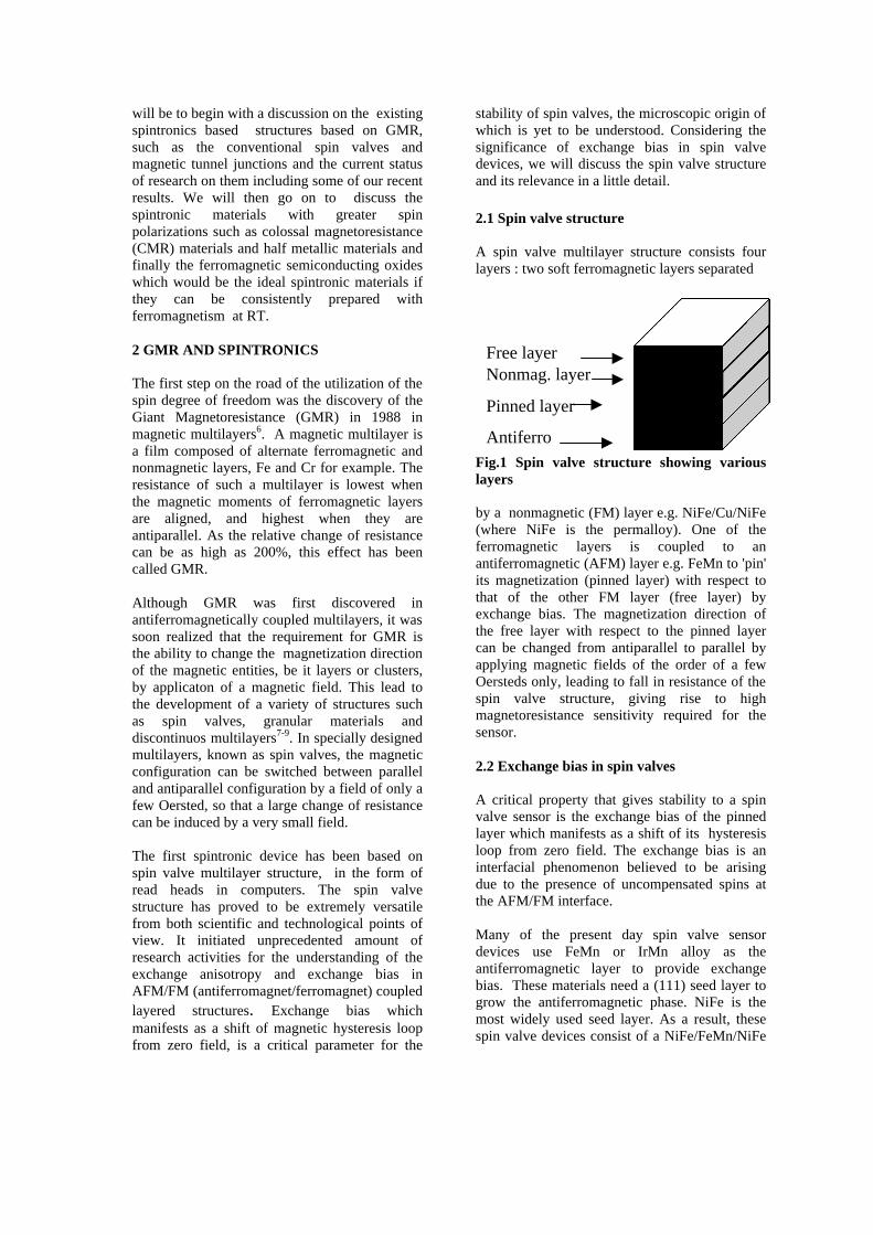
will be to begin with a discussion on the existing spintronics based structures based on GMR, such as the conventional spin valves and magnetic tunnel junctions and the current status of research on them including some of our recent results. We will then go on to discuss the spintronic materials with greater spin polarizations such as colossal magnetoresistance (CMR) materials and half metallic materials and finally the ferromagnetic semiconducting oxides which would be the ideal spintronic materials if they can be consistently prepared with ferromagnetism at RT. 2 GMR AND SPINTRONICS The first step on the road of the utilization of the spin degree of freedom was the discovery of the Giant Magnetoresistance (GMR) in 1988 in magnetic multilayers6. A magnetic multilayer is a film composed of alternate ferromagnetic and nonmagnetic layers, Fe and Cr for example. The resistance of such a multilayer is lowest when the magnetic moments of ferromagnetic layers are aligned, and highest when they are antiparallel. As the relative change of resistance can be as high as 200%, this effect has been called GMR. Although GMR was first discovered in antiferromagnetically coupled multilayers, it was soon realized that the requirement for GMR is the ability to change the magnetization direction of the magnetic entities, be it layers or clusters, by applicaton of a magnetic field. This lead to the development of a variety of structures such as spin valves, granular materials and discontinuos multilayers7-9. In specially designed multilayers, known as spin valves, the magnetic configuration can be switched between parallel and antiparallel configuration by a field of only a few Oersted, so that a large change of resistance can be induced by a very small field. The first spintronic device has been based on spin valve multilayer structure, in the form of read heads in computers. The spin valve structure has proved to be extremely versatile from both scientific and technological points of view. It initiated unprecedented amount of research activities for the understanding of the exchange anisotropy and exchange bias in AFM/FM (antiferromagnet/ferromagnet) coupled layered structures. Exchange bias which manifests as a shift of magnetic hysteresis loop from zero field, is a critical parameter for the
stability of spin valves, the microscopic origin of which is yet to be understood. Considering the significance of exchange bias in spin valve devices, we will discuss the spin valve structure and its relevance in a little detail. 2.1 Spin valve structure A spin valve multilayer structure consists four layers : two soft ferromagnetic layers separated
Fig.1 Spin valve structure showing various layers by a nonmagnetic (FM) layer e.g. NiFe/Cu/NiFe (where NiFe is the permalloy). One of the ferromagnetic layers is coupled to an antiferromagnetic (AFM) layer e.g. FeMn to 'pin' its magnetization (pinned layer) with respect to that of the other FM layer (free layer) by exchange bias. The magnetization direction of the free layer with respect to the pinned layer can be changed from antiparallel to parallel by applying magnetic fields of the order of a few Oersteds only, leading to fall in resistance of the spin valve structure, giving rise to high magnetoresistance sensitivity required for the sensor. 2.2 Exchange bias in spin valves A critical property that gives stability to a spin valve sensor is the exchange bias of the pinned layer which manifests as a shift of its hysteresis loop from zero field. The exchange bias is an interfacial phenomenon believed to be arising due to the presence of uncompensated spins at the AFM/FM interface. Many of the present day spin valve sensor devices use FeMn or IrMn alloy as the antiferromagnetic layer to provide exchange bias. These materials need a (111) seed layer to grow the antiferromagnetic phase. NiFe is the most widely used seed layer. As a result, these spin valve devices consist of a NiFe/FeMn/NiFe
Free layer Non mag. Layer Nonmag. layer
Antiferro layer
Pinned layer
trilayer. When this trilayer is present in spin valves, the seed NiFe layer gives rise to its own exchange biased hysteresis loop in addition to the loop corresponding to the pinned NiFe layer and has lead to conflicting results on pinned layer bias. Therefore a detailed understanding of the exchange bias development in this trilayer is of both basic and technological interest.
Fig. 2 Magnetic hysteresis loop of the NiFe/FeMn/NiFe trilayer for a seed layer thickness of 4 nm and pinned layer thickness of 5 nm showing the two biased loops and greater bias for the seed layer. We carried out a systematic investigation of exchange bias variation of the NiFe/FeMn/NiFe trilayer as a function the thickness of the three constituting layers in the 2 to 20 nm thickness range, in multilayers prepared by rf magnetron sputtering in presence of a constant magnetic field of 60 Oe. In the thickness variation studies of all the three magnetic layers, interestingly, we observed that the seed NiFe layer shows greater bias (150 Oe) than the top pinned NiFe layer (80 Oe only) as seen in Fig. 2. The greater bias observed for the seed NiFe layer is attributed to its growth over a saturated (111) oriented NiFe seed layer, which induces formation of interfacial FeMn layers with a net parallel spin ordering, in presence of the constant applied field. On the other hand, at the top FeMn/NiFe surface, the rigid FeMn surface with compensated bulk spin ordering formed already, is not easily biased and reoriented along the top NiFe layer to develop as much parallel net spins in the AFM and hence lower bias10. Consistently low bias observed for the top NiFe
layer in the trilayer which forms the pinned layer in the spin valve structure could have technological implication because a greater bias for the pinned layer is critical for the stability of spin valve based devices. The study underlines the importance of field cooling even if the MLs are grown under small applied fields. 3. MAGNETIC TUNNEL JUNCTIONS The magnetic tunnel junction (MTJ) is the second type of spintronic device with considerable potential. MTJs exhibiting large tunneling magnetoresistance (TMR) are promising nanostructures for magnetic random access memories (MRAMs) and they can also replace the conventional spin valves, discussed above. MTJ is a structure in which two ferromagnetic layers (electrodes) are separated by a very thin insulating layer, commonly aluminum oxide. The electrons can tunnel through the insulating layer and, because the probability of tunneling from a ferromagnetic electrode depends on the spin direction, the resistance of the MTJ is different for the parallel and antiparallel orientations of the magnetic moments of the electrodes. For electrodes of conventional ferromagnetic alloys, the relative change of resistance (Tunnel Magnetoresistance or TMR) can reach 70% at room temperature. MTJ of very small size, below the micron range, can be fabricated by lithographic techniques and an important application of these small size MTJ will be for the nonvolatile computer memory, MRAM (Magnetic Random Access Memory). 3.1 Interlayer Interactions in MTJs MTJs also have a spin valve multilayer structure for improved performance. They generally have a complicated multilayer structure to optimize several parameters related to tunneling conduction even though the basic requirement is just two ferromagnetic layers such as NiFe or CoFe separated by an insulating layer such as alumina. The insulating layer is prepared by oxidation of a thin Al layer of a few Å thickness and the formation a good insulating layer is key to achieving good tunneling conductance. MTJs exhibit two types of coupling between magnetic layers. An interlayer coupling between pinned layer and the free layer through the insulating Al2O3 layer which manifests as a shift in the magnetization loop of the free layer from zero field. It is supposed to be due to Neels
-300 -200 -100 0 100 200 300
-0.0020
-0.0015
-0.0010
-0.0005
0.0000
0.0005
0.0010
0.0015
0.0020
4 nm
5 nm
MA
GN
ET
IC M
OM
EN
T (
emu
)
MAGNETIC FIELD (Oe)
orange peel coupling originating from interfacial morphological corrugations. In addition to the interlayer coupling MTJs also exhibit the exchange bias of the AFM/FM bilayer characteristic of the spin valve structure which is known as the 'interfacial coupling'. We have investigated the development of interfacial and interlayer exchange coupling in MTJs synthesized at low deposition fields of 30 Oe in the as-deposited state and annealed state with the help of MR and magnetization measurements11. Tunnel junctions with the structure Ta (50 Å)/Cu (100 Å)/Ta (50 Å)/Ni-Fe (20 Å)/Cu (50 Å)/ IrMn (100 Å)/Co70Fe30 (25 Å)/Al-O/Co70Fe30 (25 Å)/ Ni-Fe (600 Å)/ Ta (50 Å) were prepared on thermally oxidized Si wafers using DC magnetron sputtering in a chamber with a base pressure of 3 × 10⁻⁹ Torr. For barrier formation, a 15 Å thick metallic Al film was deposited and subsequently oxidized in an oxidation chamber . The exchange bias coupling between the antiferromagnetic pinning IrMn layer and the CoFe ferromagnetic layer is negligible in the as-deposited sample presumably due to the small magnetic field of 30 Oe employed during sample deposition which apparently is not sufficient to develop exchange bias. After field annealing and cooling in presence of 1 kOe field MTJs develop exchange bias of 1.5 kOe and large TMR values. The Tunneling magnetoresistance (TMR) curve in Fig.3 shows a large TMR value around 35% and a sharp switching near zero field for the free layer with a small coercivity of 3Oe. The small shift of the center of the MR loop by about 5 Oe from zero field is indicative of the Neel interlayer coupling. This seemingly small shift affects the device performance because of the very sharp switching of magnetization in MTJs near zero field and the very high sensitivity. Efforts are on to neutralize its effect and improve device performance. 3.2 Investigations on patterned MTJs Magnetic, microstructural and magnetotransport studies are usually reported for the multilayer (ML) films as a whole and not for the micrometer sized patterned junctions. The size and shape of the junctions modify properties, and localized properties at the junction eventually determine the device stability and performance, irrespective of the properties attained in the initial film and hence s uch studies
Fig. 3 TMR curve of the MTJ after field annealing and cooling at 250 °°C. are extremely important for devices. We measured the local M-H loops on the free layer of magnetic tunnel junctions of different sizes, 180, 250, 320 and 380µm using a magneto-optic Kerr effect (MOKE) system with 2µm spatial resolution, and attempted its correlation with the surface roughness estimated from AFM observations12. The interlayer exchange coupling HE, measured from the zero field shift of minor MOKE loop, increases gradually from junction edge, reaches a maximum of about 7.5 Oe at the junction centre and then falls off gradually as we approach the other edge, in the as-deposited sample (Fig.4). After annealing, the relatively irregular variation in the as-deposited sample smoothes out and increases from 5 Oe at the edge to show a maximum of 20 Oe at the junction center.
0 50 100 150 200 250 300 350
0
5
10
15
20
HE (
Oe)
y-distance (µm)
Ta=200 oC
As-dep.
Fig.4 Variation of interlayer coupling over a ptterned junction. 4 CMR MATERIALS AND HALF METALS
-20 -10 0 10 20-5
0
5
10
15
20
25
30
35
MR
(%
)
Magnetic Field (Oe)
In 1994 a colossal magnetoresistance effect (CMR) was reported with observed MR ratios exceeding 100,000% in LaxCa1-xMnO3 type thin films with perovskite structure arising due to the presence of Mn3+/Mn4+ mixed valence state13. However, the effect is observed at low temperatures in presence of very high applied fields of the order of a few teslas and so the application potential is limited. Another important research direction in spintronics has been the search for ferromagnetic materials providing higher spin polarizations than conventional metals like cobalt or iron. The search has been on for half metallic materials with a spin polarization of 100% at their Fermi level. Apart from the Heusler alloys, Lanthanum strontium manganese oxide (LSMO), CrO2 and Fe3O4 are being investigated in detail. 5SPINTRONICS AND SEMICONDUCTORS Whereas the metallic spin devices just described provide new ways to store and read information in hard discs, tapes or MRAM, semiconductor-based spintronics may offer a greater wealth of possibilities. Why is spintronics with semiconductors interesting? Semiconductor-based spintronics could combine storage, detection, logic and communication capabilities on a single chip to produce a multifunctional device that could replace several components. For example, it could permit a better integration between MTJ and silicon-based electronics than in the present prototypes of MRAM. A longer term possibility is the exploitation of the truly quantum-mechanical nature of spin and the long spin-coherence time in confined geometry for quantum computing in an even more revolutionary application. As mentioned in the beginning, for practical applications, electrical injection and detection of spin currents is essential. The most direct way for spin injection would seem injecting from a classical ferromagnetic metal in a metal/semiconductor heterostructure but this raises difficult problems related to the difference in conductivity and spin relaxation time in metals and semiconductors. Magnetic semiconductors can be associated more easily with nonmagnetic semiconductors for spin injection. GaAs doped with Mn is an archetypal
DMS which presents ferromagnetic properties up to 150 K. 6 FERROMAGNETIC SEMICONDUCTING OXIDES In 2000, Dietl in his classic paper predicted several compounds which are promising for room temperature ferromagnetism including transition metal doped semiconducting oxides14. It lead to the great interest in these materials as potential spintronic materials. However, in the absence of an evident exchange mechanism which could account for a high Curie temperature at doping levels far below percolation threshold, the origin of ferromagnetism in these oxides is being debated on account of the lack of reproducibility and observation of TM nanoclusters in many cases. Recently we have prepared bulk ZnO doped with 5-20% Co by a citrate precursor method that shows no indication of any Co clusters or additional phases. The powder material shows ferromagnetism at room temperature and a clear indication of Co substitution at the tetrahedral site in the wurtzite structure in spectroscopic studies. 6.1Preparation of Co-ZnO The samples were prepared by decomposition of a citrate precursor. Aqueous solutions of zinc acetate and cobalt nitrate in required stoichiometric ratio were reacted with 1:1 molar ratio of citric acid in aqueous solution. The pH of the solution was controlled at 7. The dried precursor was heat treated in the temperature range of 300 to 700 °C to obtain the Co doped ZnO powder. 6.2 XRD studies The XRD patterns of all the powder samples showed reflections characteristic of wurtzite ZnO structure with no additional lines, as seen in the
Co0.1Zn0.9O
02000400060008000
10000120001400016000
0 20 40 60 80 100
2 Theta
Co
un
ts
Fig. 5 XRD pattern of the Co0.1Zn0.9O sample annealed at 500 °°C typical XRD pattern in Fig. 5 for the sample annealed at 500 °C. The d-values in the characteristic wurtzite spectra show a systematic shift towards lower values with increasing Co substitution, which is a clear indication of the substitution of Zn2+ ions with Co2+ ions. 6.3 Spectroscopic studies The UV-Vis-near IR spectra of the 5% Co substituted ZnO sample is shown in Fig. 6. The absorptions at the 570, 615, 660 nm and in the 1200 to 1600 nm range are identified as d-d absorptions corresponding to Co2+ ions in the tetragonal crystal field: Thus the spectra give clear evidence that the Co enters the tetrahedral site in the wurtzite structure.
Fig. 6 UV-Vis -near IR spectra of the 5% Co substituted ZnO sample.
Fig.7 Magnetization curve at RT of the 250 °°C annealed, 10% Co substituted ZnO sample 6.4 Magnetization studies A typical magnetization curve for the 10% Co substituted ZnO powder recorded on a vibrating sample magnetometer at RT show ferromagnetic
behavior with a coercivity of around 100 Oe. The samples show ferromagnetism for Co substitution up to 15% in our studies. The exchange interactions in these materials may be mediated by carriers in spin split impurity bands3. 7 CONCLUSIONS Ferromagnetic semiconductors do hold considerable promise as the ideal spintronic materials but there is still a long way to go before they actually reach the level of commercial application. The existing spintronic applications based on metallic magnetic multilayers are likely to be improved for realistic applications until the semiconducting oxides are produced with reliable and reproducible ferromagnetic properties above RT. 8 REFERENCES
1 G. A. Prinz, Science 282, 1660 (1998). 2I. Zutic, J. Fabian, and S. Das Sarma Rev. Mod. Phys. 76, 323 (2004). 3M. Venkatesan, C. B. Fitzgerald, J. G. Lunney and J. M. D. Coey, Phys. Rev. lett. 93, 177206 (2004). 4C. B. Fitzgerald , M. Venkatesan, , J. G. Lunney, L. S. Dorneles and J. M. D. Coey, Applied surface Science (In Press). 5K.A.Griffin, A. B. Pakhomov, C. M Wang, S. M. Heald, and K. M. Krishnan, Phys. Rev. Lett. 61, 2472 (1988). 6M. N. Baibich et al, Phys. Rev. Lett. 61, 2472 (1988). 7B. Dieny, V. S. Speriousu, S. S. P. Parkin, B. A. Gurney, D. R. Willhoit and D. Mauri, Phys. Rev. B43, 1297 (1991). 8A. E. Berkowitz, Phys. Rev. Lett. 68, 3745 (1992). 9T. L. Hylton Science, 261, 1021 (1992). 10V. K. Sankaranarayanan, S.M. Yoon, J. J. Lim, C. G. Kim and C. O. Kim, Journal of Applied Physics, 96, 7428 (2004). 11V.K.Sankaranarayanan, Y.K Hu, C.G. Kim, C.O. Kim, M.Tsunoda and M.Takahashi. Physica Status Solidi (a) 201, 1688 (2004). 12V.K.Sankaranarayanan, Y.K. Hu, C.G. Kim, C.O. Kim, M. Tsunoda and M. Takahashi J. Magn.Magn. Mater. 272-76, 1965 (2004). 13S. Jin et al, Science 264, 413 (1994). 14T.Dietl, H. Ohno, F. Matsukura, J. Cibert and D. Ferrand, Science 287, 1019 (2000).
Co05Zn95O 600 bulk
010203040506070
0 500 1000 1500 2000 2500
Wavelength (nm)
Ref
lect
ance
Co10Zn90O 250
-6
-4
-2
0
2
4
-10000 -5000 0 5000 10000
Magnetic Field (Oe)
Mag
net
ic M
om
ent
(mem
u)
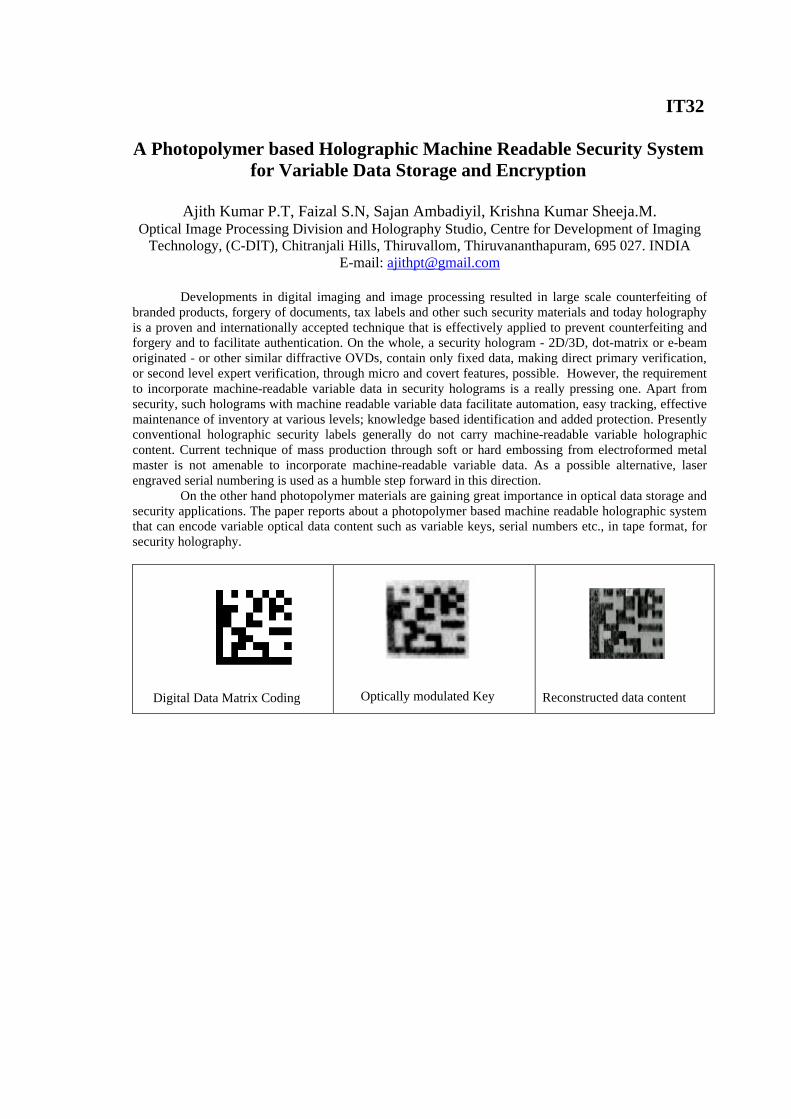
IT32
A Photopolymer based Holographic Machine Readable Security System for Variable Data Storage and Encryption
Ajith Kumar P.T, Faizal S.N, Sajan Ambadiyil, Krishna Kumar Sheeja.M.
Optical Image Processing Division and Holography Studio, Centre for Development of Imaging Technology, (C-DIT), Chitranjali Hills, Thiruvallom, Thiruvananthapuram, 695 027. INDIA
E-mail: [email protected]
Developments in digital imaging and image processing resulted in large scale counterfeiting of branded products, forgery of documents, tax labels and other such security materials and today holography is a proven and internationally accepted technique that is effectively applied to prevent counterfeiting and forgery and to facilitate authentication. On the whole, a security hologram - 2D/3D, dot-matrix or e-beam originated - or other similar diffractive OVDs, contain only fixed data, making direct primary verification, or second level expert verification, through micro and covert features, possible. However, the requirement to incorporate machine-readable variable data in security holograms is a really pressing one. Apart from security, such holograms with machine readable variable data facilitate automation, easy tracking, effective maintenance of inventory at various levels; knowledge based identification and added protection. Presently conventional holographic security labels generally do not carry machine-readable variable holographic content. Current technique of mass production through soft or hard embossing from electroformed metal master is not amenable to incorporate machine-readable variable data. As a possible alternative, laser engraved serial numbering is used as a humble step forward in this direction.
On the other hand photopolymer materials are gaining great importance in optical data storage and security applications. The paper reports about a photopolymer based machine readable holographic system that can encode variable optical data content such as variable keys, serial numbers etc., in tape format, for security holography.
Digital Data Matrix Coding
Optically modulated Key
Reconstructed data content
IT33
p-type Transparent Semiconducting Oxide Thin Films for Transparent Electronics
M.K.Jayaraj1, K.A.Vanaja1, A.S.Asha1 and K.Rajeev Kumar2
1Optoelectronics Device Laboratory, Department of Physics, 2Department of Instrumentation,
Cochin University of Science and Technology, Kochi 682022. E-mail: [email protected]
The need for optoelectronic devices operating in the blue and UV region has aroused much interest for
wide band gap semiconducting materials. Most of the transparent conductive oxides are n-type. The recent development of p-type transparent semiconducting oxides (TSO) provides a route for the realization of transparent electronic and optoelectronic device. The first observation of p-type conductivity in transparent CuAlO2
1 delafossite thin films was followed by reports of similar p-type TSO’s like CuScO2, CuGaO2, CuYO2, CuCrO2 etc. All oxide transparent pn junctions have been realized using n-ZnO/p-ZnO2, and p-CuYO2/n-ZnO3. Bipolarity has been reported for CuInO2
4 delafossite system with promise of a transparent pn homojunction. The AMO2 class of material has delafossite structure where M is trivalent ion and A is monovalent (Cu/Ag) ion. So far, p-type conductivity has been reported only for the copper delafossites. The silver delafossite (AgMO2) TSO’s are reported to be n-type. In this paper we report the synthesis of certain silver delafossite compounds by ion exchange reaction and by hydrothermal reaction. Thin films of these silver delafossites were prepared by rf magnetron sputtering and pulsed laser deposition of sintered targets. The films were about 50-60% transparent in the visible region and the carriers responsible for conduction are holes as evident from the thermo power measurements. All oxide transparent pn junctions were fabricated using the ZnO as the n-type TSO and the silver delafossite as the p-type TSO. The current voltage characteristics show that the junction is rectifying. The turn on voltage of the heterojunction is 1V. References
1. H.Kawazoe, M.Yausukawa, H.Hydo, M.Kurita, H.Yanagi and H.Hosono Nature 389 (1997) 939. 2. T.Aoki, Y.Hatanaka, D.C.Look Appl Phys Lett 76 (2000) 3257. 3. M.K.Jayaraj, A.D.Draeseke, J.Tate, A.W.Sleight 397 (2001) 244. 4. H.Yanagi, T.Hase, S.Ibuki, K.Ueda, H.Hosono Appl Phys Lett 78 (2001)1583.
INFLUENCE OF PROCESS PARAMETERS ON THE PROPERTIES OF ITO THIN FILMS
Nisha M., M.K.Jayaraj
Department of Physics, Cochin University of Science and Technology, Kochi-682 022
Email: [email protected] ABSTRACT
Indium Tin Oxide (ITO) thin films were deposited on glass substrates by RF magnetron sputtering of ITO target containing 95wt% In2O3 and 5wt% SnO2. The dependence of the process parameters such as target to substrate spacing, substrate temperature and RF power on the properties of the films was investigated. A target to substrate spacing of 4cm and a substrate temperature of 1500C was found to be better for getting good quality films. The ionic species present in the RF plasma were analyzed in detail by recording the Optical Emission Spectra (OES) of plasma plume generated by RF sputtering of Indium Tin Oxide (ITO) target using a 0.32m monochromator and CCD detector. INTRODUCTION
Materials displaying the remarkable
combination of high electrical conductivity and optical transparency form the basis of many important technological applications including Flat Panel Displays, solar energy captures and many other optoelectronic devices 1. These seemingly contradictory properties of close to metallic conductivity in a material simultaneously exhibiting almost complete non metallic transparency form the basis of numerous applications in contemporary and emerging technologies. Although partial transparency, with acceptable reduction in resistivity, can be obtained for very thin metallic films, these properties cannot be attained in intrinsic stoichiometric materials. The only way this can be achieved is by creating electron degeneracy in a wide bandgap material by controllably introducing non-stoichiometry and/or appropriate dopants. These conditions can be conveniently met for ITO as well as a number of other materials like Zinc oxide, Cadmium oxide etc. Of these, Indium Tin Oxide (ITO) is an attractive material for optoelectronic applications2. It has got an excellent adherence to glass substrate and is chemically inert. The electronic band structure is one of the important factors determining the unique interplay between the optical absorption and conductivity in this material 3.
Extensive work on the development of ITO films has been carried out by various workers4-8. Most of the thin film growth methods involve a relatively high substrate temperature in order to obtain films with a reasonably high conductivity and transmittance. Magnetron sputtering offers the possibility to prepare ITO thin films at low processing temperature and on large areas 9. Literature shows that the properties of ITO films are highly dependent on the deposition conditions and the method of deposition. In this paper, we report the dependence of process parameters such as target to substrate spacing, RF power, and substrate temperature on the properties of the films. The film properties such
as deposition rate, average transmission in the visible region, resistivity and figure of merit were investigated as a function of the above mentioned thin film growth parameters. EXPERIMENTAL
The film deposition was carried out in an RF magnetron sputtering system. The sputtering target has a diameter of 2 inch and it consists of 95wt% In2O3 and 5wt% SnO2.The base pressure prior to deposition was 1x10⁻⁵ mbar. The flow of Argon was adjusted in such a way that the sputtering pressure is 0.01 mbar. Substrate was heated using a halogen lamp. When the deposition was done onto preheated substrates, the substrate temperature was controlled within ± 20 C. When deposition was done onto unheated substrates, an increase in substrate temperature was observed during sputtering which was found to depend on the target to substrate spacing and RF power. The film thickness was determined using Tolansky technique. The transmittance of the films was recorded using Hitachi U-3410 UV-vis-NIR spectrophotometer. The resistivity of the films was determined using van der Pauw four-probe technique. RESULTS AND DISCUSSION
In order to study the dependence of target to substrate spacing (T-S spacing) on the film properties, film deposition was carried out at an RF power of 20W and an argon pressure of 0.01mbar.Target to substrate spacing was varied from 2cm to 8cm. The substrates were not heated intentionally during deposition, but the substrate temperature increased from 450C to 900C as the T-S spacing was decreased from 8cm to 2cm. The X-ray diffraction pattern (Fig.1) of the films showed that the films are polycrystalline. With increase in T-S spacing, a degradation of crystallinity was observed.
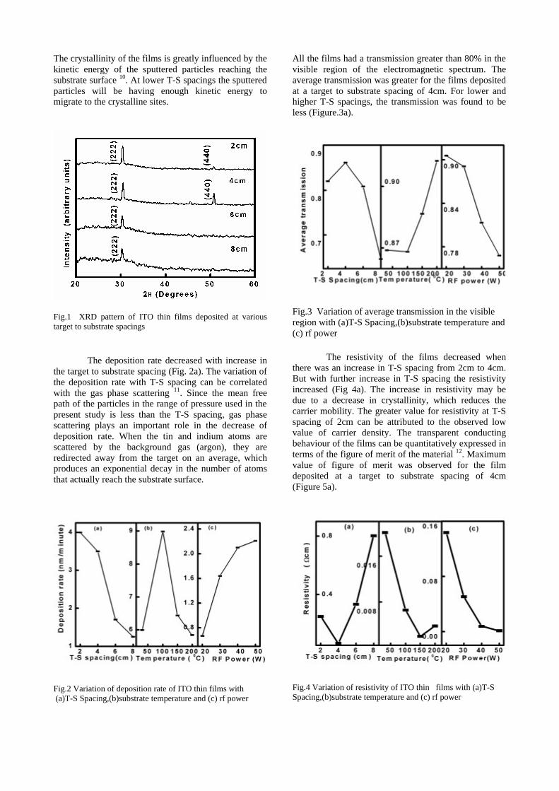
The crystallinity of the films is greatly influenced by the kinetic energy of the sputtered particles reaching the substrate surface 10. At lower T-S spacings the sputtered particles will be having enough kinetic energy to migrate to the crystalline sites.
Fig.1 XRD pattern of ITO thin films deposited at various target to substrate spacings
The deposition rate decreased with increase in
the target to substrate spacing (Fig. 2a). The variation of the deposition rate with T-S spacing can be correlated with the gas phase scattering 11. Since the mean free path of the particles in the range of pressure used in the present study is less than the T-S spacing, gas phase scattering plays an important role in the decrease of deposition rate. When the tin and indium atoms are scattered by the background gas (argon), they are redirected away from the target on an average, which produces an exponential decay in the number of atoms that actually reach the substrate surface.
Fig.2 Variation of deposition rate of ITO thin films with (a)T-S Spacing,(b)substrate temperature and (c) rf power
All the films had a transmission greater than 80% in the visible region of the electromagnetic spectrum. The average transmission was greater for the films deposited at a target to substrate spacing of 4cm. For lower and higher T-S spacings, the transmission was found to be less (Figure.3a).
Fig.3 Variation of average transmission in the visible region with (a)T-S Spacing,(b)substrate temperature and (c) rf power
The resistivity of the films decreased when there was an increase in T-S spacing from 2cm to 4cm. But with further increase in T-S spacing the resistivity increased (Fig 4a). The increase in resistivity may be due to a decrease in crystallinity, which reduces the carrier mobility. The greater value for resistivity at T-S spacing of 2cm can be attributed to the observed low value of carrier density. The transparent conducting behaviour of the films can be quantitatively expressed in terms of the figure of merit of the material 12. Maximum value of figure of merit was observed for the film deposited at a target to substrate spacing of 4cm (Figure 5a).
Fig.4 Variation of resistivity of ITO thin films with (a)T-S Spacing,(b)substrate temperature and (c) rf power
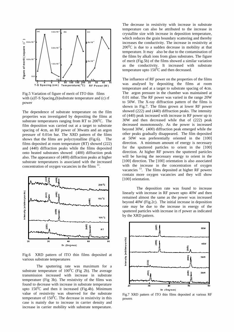
Fig.5 Variation of figure of merit of ITO thin films with (a)T-S Spacing,(b)substrate temperature and (c) rf power
The dependence of substrate temperature on the film properties was investigated by depositing the films at substrate temperatures ranging from RT to 2000C. The film deposition was carried out at a target to substrate spacing of 4cm, an RF power of 30watts and an argon pressure of 0.01m bar. The XRD pattern of the films shows that the films are polycrystalline (Fig.6). The films deposited at room temperature (RT) showed (222) and (440) diffraction peaks while the films deposited onto heated substrates showed (400) diffraction peak also. The appearance of (400) diffraction peaks at higher substrate temperatures is associated with the increased concentration of oxygen vacancies in the films 13.
Fig.6 XRD pattern of ITO thin films deposited at various substrate temperatures
The sputtering rate was maximum for a substrate temperature of 1000C (Fig 2b). The average transmission increased with increase in substrate temperature (Fig 3b). The resistivity of the films was found to decrease with increase in substrate temperature upto 1500C and then it increased (Fig.4b). Minimum value of resistivity was observed for the substrate temperature of 1500C. The decrease in resistivity in this case is mainly due to increase in carrier density and increase in carrier mobility with substrate temperature.
The decrease in resistivity with increase in substrate temperature can also be attributed to the increase in crystallite size with increase in deposition temperature, which reduces the grain boundary scattering and thereby increases the conductivity. The increase in resistivity at 2000C is due to a sudden decrease in mobility at that temperature. It may also be due to the contamination of the films by alkali ions from glass substrates. The figure of merit (Fig.5b) of the films showed a similar variation as the conductivity. It increased with substrate temperature upto 1500C and then decreased.
The influence of RF power on the properties of the films was analysed by depositing the films at room temperature and at a target to substrate spacing of 4cm. The argon pressure in the chamber was maintained at 0.01 mbar. The RF power was varied in the range 20W to 50W. The X-ray diffraction pattern of the films is shown in Fig.7. The films grown at lower RF power showed (222) and (440) diffraction peaks. The intensity of (440) peak increased with increase in RF power up to 30W and then decreased while that of (222) peak decreased monotonously. As the power is increased beyond 30W, (400) diffraction peak emerged while the other peaks gradually disappeared. The film deposited at 50W was preferentially oriented in the [100] direction. A minimum amount of energy is necessary for the sputtered particles to orient in the [100] direction. At higher RF powers the sputtered particles will be having the necessary energy to orient in the [100] direction. The [100] orientation is also associated with the increase in the concentration of oxygen vacancies 13. The films deposited at higher RF powers contain more oxygen vacancies and they will show [100] orientation.
The deposition rate was found to increase linearly with increase in RF power upto 40W and then remained almost the same as the power was increased beyond 40W (Fig.2c). The initial increase in deposition rate may be due to the increase in energy of the sputtered particles with increase in rf power as indicated by the XRD pattern.
Fig.7 XRD pattern of ITO thin films deposited at various RF powers
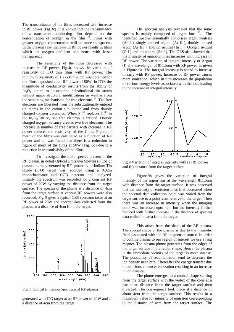
The transmittance of the films decreased with increase in RF power (Fig.3c). It is known that the transmittance of a transparent conducting film depend on the concentration of oxygen in the film 14. Films with greater oxygen concentration will be more transparent. In the present case, increase in RF power results in films which are oxygen deficient and hence with lesser transparency.
The resistivity of the films decreased with increase in RF power. Fig.4c shows the variation of resistivity of ITO thin films with RF power. The minimum resistivity of 1.27x10⁻³ Ω cm was obtained for the films deposited at an RF power of 50W. In ITO, the magnitude of conductivity results from the ability of In2O3 lattice to incorporate substitutional tin atoms without major structural modifications as well as from the scattering mechanisms for free electrons 15. The free electrons are liberated from the substitutionally entered tin atoms in the cation sub lattice and from doubly charged oxygen vacancies. When Sn4+ replaces In3+ in the In2O3 lattice, one free electron is created. Doubly charged oxygen vacancy creates two free electrons. The increase in number of free carriers with increase in RF power reduces the resistivity of the films. Figure of merit of the films was calculated as a function of RF power and it was found that there is a reduction in figure of merit of the films at 50W (Fig. 6d) due to a reduction in transmissivity of the films.
To investigate the ionic species present in the RF plasma in detail Optical Emission Spectra (OES) of plasma plume generated by RF sputtering of Indium Tin Oxide (ITO) target was recorded using a 0.32m monochromator and CCD detector and analyzed. Initially the spectrum was recorded for a constant RF power of 20W by varying the distance from the target surface. The spectra of the plume at a distance of 4cm from the target surface at various RF powers were also recorded. Fig. 8 gives a typical OES spectrum taken at an RF power of 20W and spectral data collected from the plasma at a distance of 4cm from the target.
Fig.8 Optical Emission Spectrum of RF plasma
generated with ITO target at an RF power of 20W and at a distance of 4cm from the target
The spectral analysis revealed that the ionic
species is mainly composed of argon ions 16. The identified species essentially comprises argon neutrals (Ar I ), singly ionised argon (Ar II ), doubly ionised argon (Ar III ), Indium neutral (In I ), Oxygen neutral (O I ) and tin neutral (Sn I ). The OES also showed that the intensity of emission lines increases with increase of RF power. The variation of integral intensity of Argon (I) at a wavelength of 811.5nm with RF power is given in Figure 9a. The integral intensity is found to increase linearly with RF power. Increase of RF power causes more ionization, which in turn increases the population of various energy levels associated with the ions leading to the increase in integral intensity.
Fig.9 Variation of integral intensity with (a) RF power and (b) distance from the target surface
Figure.9b gives the variation of integral
intensity of the argon line at the wavelength 811.5nm with distance from the target surface. It was observed that the intensity of emission lines first decreased when the spectral data collection point was varied from the target surface to a point 2cm relative to the target. Then there was an increase in intensity when the imaging point was increased upto 4cm but the intensity further reduced with further increase in the distance of spectral data collection area from the target.
This arises from the shape of the RF plasma.
The special shape of the plasma is due to the magnetic field associated with the RF magnetron source. In order to confine plasma to our region of interest we use a ring magnet. The plasma plume generates from the edges of the target surface in a circular shape. Hence the plasma in the immediate vicinity of the target is more intense. The possibility of recombination tend to decrease the ion density near 2cm. Thereafter the energy transfer due to collisions enhances ionization resulting in an increase in ion density.
The plume emerges in a conical shape starting from the target surface with the vertex of the cone at a particular distance from the target surface and then diverged. The convergence took place at a distance of about 4cm from the target surface. This results in a maximum value for intensity of emission corresponding to the distance of 4cm from the target surface. The
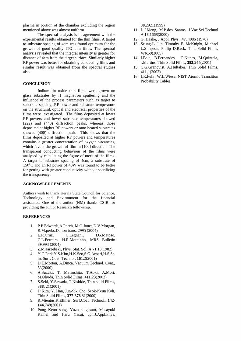
plasma in portion of the chamber excluding the region mentioned above was almost uniform.
The spectral analysis is in agreement with the experimental results obtained for the thin films. A target to substrate spacing of 4cm was found optimum for the growth of good quality ITO thin films. The spectral analysis revealed that the integral intensity is greater for distance of 4cm from the target surface. Similarly higher RF power was better for obtaining conducting films and similar result was obtained from the spectral studies also.
CONCLUSION
Indium tin oxide thin films were grown on glass substrates by rf magnetron sputtering and the influence of the process parameters such as target to substrate spacing, RF power and substrate temperature on the structural, optical and electrical properties of the films were investigated. The films deposited at lower RF powers and lower substrate temperatures showed (222) and (440) diffraction peaks, whereas those deposited at higher RF powers or onto heated substrates showed (400) diffraction peak. This shows that the films deposited at higher RF powers and temperatures contains a greater concentration of oxygen vacancies, which favors the growth of film in [100] direction. The transparent conducting behaviour of the films were analysed by calculating the figure of merit of the films. A target to substrate spacing of 4cm, a substrate of 150oC and an Rf power of 40W was found to be better for getting with greater conductivity without sacrificing the transparency.
ACKNOWLEDGEMENTS Authors wish to thank Kerala State Council for Science, Technology and Environment for the financial assistance. One of the author (NM) thanks CSIR for providing the Junior Research fellowship. REFERENCES
1. P.P.Edwards,A.Porch, M.O.Jones,D.V.Morgan, R.M.perks,Dalton trans, 2995 (2004)
2. L.R.Cruz, C.Legnani, I.G.Matoso, C.L.Ferreira, H.R.Moutinho, MRS Bulletin 39,993 (2004)
3. Z.M.Jarzebski, Phys. Stat. Sol. A,71,13(1982) 4. Y.C.Park,Y.S.Kim,H.K.Seo,S.G.Ansari,H.S.Sh
in, Surf. Coat. Technol. 161,2(2001) 5. D.E.Mortan, A.Dinca, Vacuum Technol. Coat.,
53(2000) 6. A.Suzuki, T. Matsushita, T.Aoki, A.Mori,
M.Okuda, Thin Solid Films, 411,23(2002) 7. S.Seki, Y.Sawada, T.Nishide, Thin solid Films,
388, 21(2001) 8. D.Kim, Y. Han, Jun-Sik Cho, Seok-Keun Koh,
Thin Solid Films, 377-378,81(2000) 9. R.Mientus,K.Ellmer, Surf.Coat. Technol., 142-
144,748(2001) 10. Pung Keun song, Yuzo shigesato, Masayuki
Kamei and Itaru Yasui, Jpn.J.Appl.Phys.
38,2921(1999) 11. L.J.Meng, M.P.dos Santos, J.Vac.Sci.Technol
A,18,1668(2000) 12. G. Haake, J.Appl. Phys., 47, 4086 (1976) 13. Seung-Ik Jun, Timothy E. McKnight, Michael
L.Simpson, Philip D.Rack, Thin Solid Films, 476,59(2005)
14. I.Baia, B.Fernandes, P.Nunes, M.Quintela, r.Martins, Thin Solid Films, 383,244(2001)
15. C.G.Granqvist, A.Hultaker, Thin Solid Films, 411,1(2002)
16. J.R.Fuhr, W.L.Wiese, NIST Atomic Transition Probability Tables
IT35
Ultra Thin Layers in Sub-micron Semiconductor Devices - An Overview of Challenges in Processing and Reliability
M.K. Radhakrishnan
CTO, NanoRel Consultants, Singapore. E-mail : [email protected]
As semiconductor device dimensions shrink, the processing technology becomes more challenging. One of the main challenges is the intricacies in the precise manufacturing of various very thin layers of high quality at different stages of device processing. The present silicon device technology ijn the sub 100nm node needs gate dielectrics in the thickness range 10-15A, with very high strength and reliability. Many a times, an atomic defect in such thin layers can be so detrimental that even the functionality of the device can be questionable. Interconnects with 8-10 metal layers and very precise vias require ultra thin barrier layers of different metals to form the nerve system of the devices. Intricacies in the barrier layer processing are so trivial at present with various ILD materials, especially the low K materials. Maintaining the quality in the process to achieve such precision is the challenge in the processing technology. This talk will give an overview of various challenges in the manufacturing of different ultra thin layers in silicon device processing and how that affects the device performance and reliability. The presentation will depict actual case studies from various process stages of deep sub-micron devices.
IT36 Development Of Inexpensive Thin Film Solar Cell Suitable For Indian
Condition: Necessities And Possibilities
K. P. Vijayakumar Department of Physics, Cochin University of Science and Technology,
Kochi-22, India E-mail: [email protected]
India being a tropical country is blessed with an abundance of sunlight and biomass. Vigorous
efforts during the past two decades are now bearing fruit as people in all walks of life are more aware of the benefits of renewable energy, especially decentralized energy required in villages and in urban or semi-urban centers. India has the world’s largest programme for renewable energy. More than 700000 PV systems generating 44 MW have been installed all over India. The market segment and usage is mainly for home lighting, street lighting, solar lanterns and water pumping for irrigation. Over 17 grid interactive solar photovoltaic generating more than 1400 KW are in operation in 8 states of India. As the demand for power grows exponentially and conventional fuel based power generating capacity grows arithmetically, SPV based power generation can be a source to meet the expected shortfall. Especially in rural, far-flung where the likelihood of conventional electric lines is remote, SPV power generation is the best alternative. The present PV modules are of crystalline silicon, but the drawback of silicon technology is that the production costs are still high and processing steps are sophisticated and complicated. Therefore the current emphasis is directed towards the development of high efficiency inexpensive solar cells. Here comes the importance of thin film technology which is cost effective, that can be deposited in required size and shape, for which large number of deposition techniques are available. Chalcopyrite based solar cells are attractive for next generation photovoltaic modules. They offer the highest efficiency obtained with thin films, excellent stability and radiation hardness together with competitive production costs. Presently CdTe, CuInSe2 and its alloys and amorphous silicon are available for thin film solar cells. Toxicity of cadmium, availability of tellurium and selection of suitable electrode are always disadvantageous for CdTe while the control of stoichiometry and toxicity of selenium are the difficulties in the case of CuInSe2. Moreover processing steps are complicated and costly for amorphous silicon. Recent developments in solar cell research proved that CuInS2 and In2S3 have a number of potential advantages in comparison with the more widely used chalcopyrite absorbers having selenium and buffer layers containing cadmium. These include very low toxicity as well as simple and inexpensive deposition process. Chemical Spray Pyrolysis (CSP) is such a process. The most important factor regarding the technique is that it offers precise control of stoichiometry (which is not possible in physical vapour deposition and rf sputtering) in a simple and easy way by controlling the concentration of constituents in the spray solution.
The fabrication and characterization details of a CuInS2/In2S3 solar cell made by chemical spray pyrolysis are discussed in this paper. CuInS2 and In2S3 thin films prepared using CSP technique were characterized structurally, optically and electrically using different techniques. Effect of variation of thickness and atomic concentration of absorber (CuInS2) and buffer layer (In2S3) on the performance of the cell was studied. Cu/In, S/Cu and In/S ratios of the films were controlled by varying molar concentrations of the respective compounds in the solutions. Effect of annealing on the characteristics of the cell was found to depend on thickness and atomic concentration of the layers. In the next level, thickness of the buffer layer was increased to compensate for copper diffusion from CuInS2 to In2S3. The top electrode was silver in this case with electrode area 1 mm2 and thickness ~ 45 nm. Silver, used as the top electrode, was found to improve the crystallinity of the In2S3 layer. The cell parameters obtained were Voc = 588 mV, Jsc = 48.2 mA/cm2, FF = 33.5% and η = 9.5%. To the best of our knowledge, this is the highest efficiency reported for a cell prepared entirely using CSP.
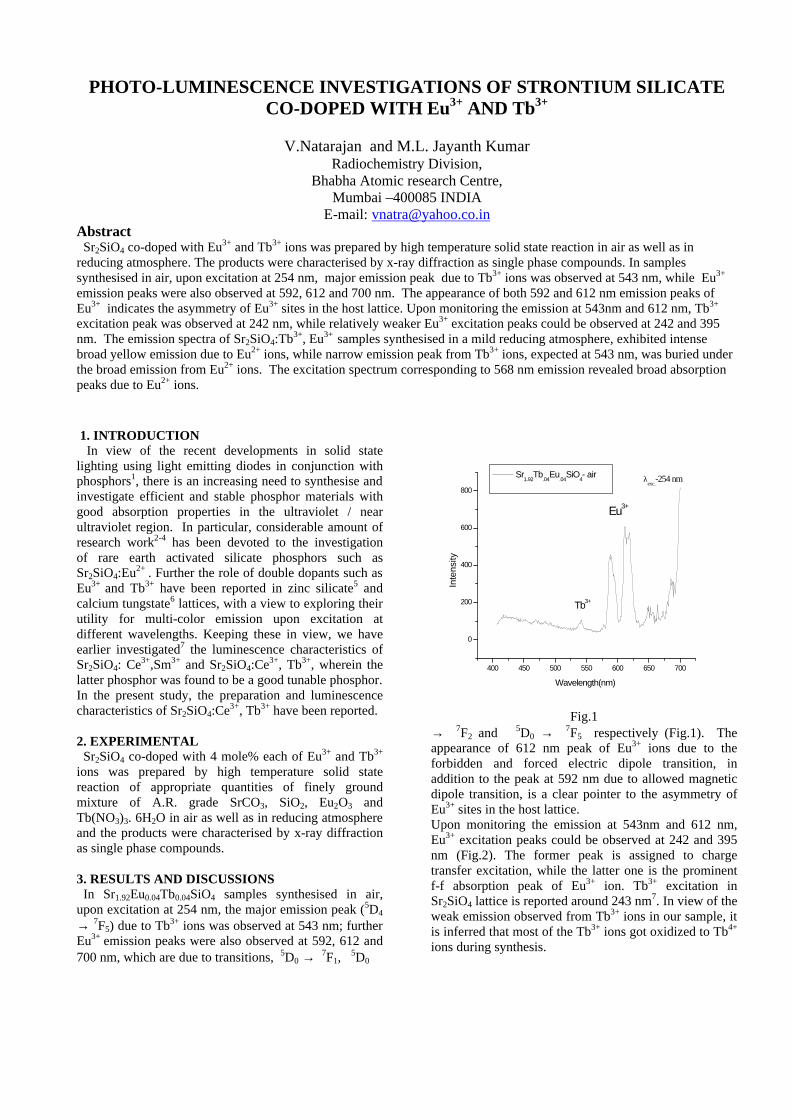
PHOTO-LUMINESCENCE INVESTIGATIONS OF STRONTIUM SILICATE CO-DOPED WITH Eu3+ AND Tb3+
V.Natarajan and M.L. Jayanth Kumar
Radiochemistry Division, Bhabha Atomic research Centre,
Mumbai –400085 INDIA E-mail: [email protected]
Abstract Sr2SiO4 co-doped with Eu3+ and Tb3+ ions was prepared by high temperature solid state reaction in air as well as in reducing atmosphere. The products were characterised by x-ray diffraction as single phase compounds. In samples synthesised in air, upon excitation at 254 nm, major emission peak due to Tb3+ ions was observed at 543 nm, while Eu3+
emission peaks were also observed at 592, 612 and 700 nm. The appearance of both 592 and 612 nm emission peaks of Eu3+ indicates the asymmetry of Eu3+ sites in the host lattice. Upon monitoring the emission at 543nm and 612 nm, Tb3+ excitation peak was observed at 242 nm, while relatively weaker Eu3+ excitation peaks could be observed at 242 and 395 nm. The emission spectra of Sr2SiO4:Tb3+, Eu3+ samples synthesised in a mild reducing atmosphere, exhibited intense broad yellow emission due to Eu2+ ions, while narrow emission peak from Tb3+ ions, expected at 543 nm, was buried under the broad emission from Eu2+ ions. The excitation spectrum corresponding to 568 nm emission revealed broad absorption peaks due to Eu2+ ions.
1. INTRODUCTION In view of the recent developments in solid state lighting using light emitting diodes in conjunction with phosphors1, there is an increasing need to synthesise and investigate efficient and stable phosphor materials with good absorption properties in the ultraviolet / near ultraviolet region. In particular, considerable amount of research work2-4 has been devoted to the investigation of rare earth activated silicate phosphors such as Sr2SiO4:Eu2+ . Further the role of double dopants such as Eu3+ and Tb3+ have been reported in zinc silicate5 and calcium tungstate6 lattices, with a view to exploring their utility for multi-color emission upon excitation at different wavelengths. Keeping these in view, we have earlier investigated7 the luminescence characteristics of Sr2SiO4: Ce3+,Sm3+ and Sr2SiO4:Ce3+, Tb3+, wherein the latter phosphor was found to be a good tunable phosphor. In the present study, the preparation and luminescence characteristics of Sr2SiO4:Ce3+, Tb3+ have been reported. 2. EXPERIMENTAL Sr2SiO4 co-doped with 4 mole% each of Eu3+ and Tb3+ ions was prepared by high temperature solid state reaction of appropriate quantities of finely ground mixture of A.R. grade SrCO3, SiO2, Eu2O3 and Tb(NO3)3. 6H2O in air as well as in reducing atmosphere and the products were characterised by x-ray diffraction as single phase compounds. 3. RESULTS AND DISCUSSIONS In Sr1.92Eu0.04Tb0.04SiO4 samples synthesised in air, upon excitation at 254 nm, the major emission peak (5D4 → 7F5) due to Tb3+ ions was observed at 543 nm; further Eu3+ emission peaks were also observed at 592, 612 and 700 nm, which are due to transitions, 5D0 → 7F1,
5D0
400 450 500 550 600 650 700
0
200
400
600
800
Tb3+
Eu3+
λexc.
-254 nm
Inte
nsity
Wavelength(nm)
Sr1.92
Tb.04
Eu.04
SiO4- air
Fig.1
→ 7F2 and 5D0 → 7F5 respectively (Fig.1). The appearance of 612 nm peak of Eu3+ ions due to the forbidden and forced electric dipole transition, in addition to the peak at 592 nm due to allowed magnetic dipole transition, is a clear pointer to the asymmetry of Eu3+ sites in the host lattice. Upon monitoring the emission at 543nm and 612 nm, Eu3+ excitation peaks could be observed at 242 and 395 nm (Fig.2). The former peak is assigned to charge transfer excitation, while the latter one is the prominent f-f absorption peak of Eu3+ ion. Tb3+ excitation in Sr2SiO4 lattice is reported around 243 nm7. In view of the weak emission observed from Tb3+ ions in our sample, it is inferred that most of the Tb3+ ions got oxidized to Tb4+
ions during synthesis.
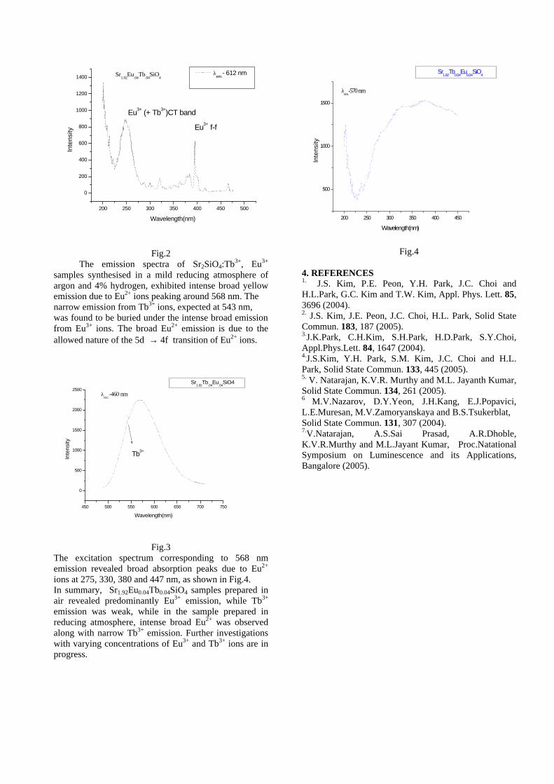
200 250 300 350 400 450 500
0
200
400
600
800
1000
1200
1400
Eu3+ f-f
Eu3+ (+ Tb3+)CT band
Sr1.92
Eu.04
Tb.04
SiO4
Inte
nsity
Wavelength(nm)
λem.
- 612 nm
Fig.2 The emission spectra of Sr2SiO4:Tb3+, Eu3+
samples synthesised in a mild reducing atmosphere of argon and 4% hydrogen, exhibited intense broad yellow emission due to Eu2+ ions peaking around 568 nm. The narrow emission from Tb3+ ions, expected at 543 nm, was found to be buried under the intense broad emission from Eu3+ ions. The broad Eu2+ emission is due to the allowed nature of the 5d → 4f transition of Eu2+ ions.
450 500 550 600 650 700 750
0
500
1000
1500
2000
2500
Tb3+
λexc.
-460 nm
Inte
nsity
Wavelength(nm)
Sr1.92
Tb.04
Eu.04
SiO4
Fig.3 The excitation spectrum corresponding to 568 nm emission revealed broad absorption peaks due to Eu2+ ions at 275, 330, 380 and 447 nm, as shown in Fig.4. In summary, Sr1.92Eu0.04Tb0.04SiO4 samples prepared in air revealed predominantly Eu3+ emission, while Tb3+ emission was weak, while in the sample prepared in reducing atmosphere, intense broad Eu2+ was observed along with narrow Tb3+ emission. Further investigations with varying concentrations of Eu3+ and Tb3+ ions are in progress.
200 250 300 350 400 450
500
1000
1500
λem.
-570 nm
Inte
nsity
Wavelength(nm)
Sr1.92
Tb0.04
Eu0.04
SiO4
Fig.4
4. REFERENCES 1. J.S. Kim, P.E. Peon, Y.H. Park, J.C. Choi and H.L.Park, G.C. Kim and T.W. Kim, Appl. Phys. Lett. 85, 3696 (2004). 2. J.S. Kim, J.E. Peon, J.C. Choi, H.L. Park, Solid State Commun. 183, 187 (2005). 3.J.K.Park, C.H.Kim, S.H.Park, H.D.Park, S.Y.Choi, Appl.Phys.Lett. 84, 1647 (2004). 4.J.S.Kim, Y.H. Park, S.M. Kim, J.C. Choi and H.L. Park, Solid State Commun. 133, 445 (2005). 5. V. Natarajan, K.V.R. Murthy and M.L. Jayanth Kumar, Solid State Commun. 134, 261 (2005). 6 M.V.Nazarov, D.Y.Yeon, J.H.Kang, E.J.Popavici, L.E.Muresan, M.V.Zamoryanskaya and B.S.Tsukerblat, Solid State Commun. 131, 307 (2004). 7.V.Natarajan, A.S.Sai Prasad, A.R.Dhoble, K.V.R.Murthy and M.L.Jayant Kumar, Proc.Natational Symposium on Luminescence and its Applications, Bangalore (2005).
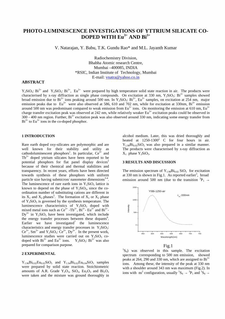
PHOTO-LUMINESCENCE INVESTIGATIONS OF YTTRIUM SILICATE CO-
DOPED WITH Eu3+ AND Bi3+
V. Natarajan, Y. Babu, T.K. Gundu Rao* and M.L. Jayanth Kumar
Radiochemistry Division, Bhabha Atomic research Centre,
Mumbai –400085, INDIA *RSIC, Indian Institute of Technology, Mumbai
E-mail: [email protected] ABSTRACT Y2SiO5: Bi3+ and Y2SiO5: Bi3+, Eu3+ were prepared by high temperature solid state reaction in air. The products were characterised by x-ray diffraction as single phase compounds. On excitation at 330 nm, Y2SiO5: Bi3+ samples showed broad emission due to Bi3+ ions peaking around 500 nm. In Y2SiO5: Bi3+, Eu3+ samples, on excitation at 254 nm, major emission peaks due to Eu3+ were also observed at 586, 610 and 702 nm, while for excitation at 330nm, Bi3+ emission around 500 nm was predominant compared to weak emission from Eu3+ ions. On monitoring the emission at 610 nm, Eu3+ charge transfer excitation peak was observed at 242 nm, while relatively weaker Eu3+ excitation peaks could be observed in 300 - 400 nm region. Further, Bi3+ excitation peak was also observed around 330 nm, indicating some energy transfer from Bi3+ to Eu3+ ions in the co-doped phosphor.
1 INTRODUCTION Rare earth doped oxy-silicates are polymorphic and are well known for their stability and utility as cathodoluminescent phosphors1. In particular, Ce3+ and Tb3+ doped yttrium silicates have been reported to be potential phosphors for flat panel display devices2 because of their chemical and thermal stabilities and transparency. In recent years, efforts have been directed towards synthesis of these phosphors with uniform particle size having submicron/ nanometer dimensions3-4. The luminescence of rare earth ions in Y2SiO5 lattice is known to depend on the phase of Y2SiO5, since the co-ordination number of substituting cations are different in its X1 and X2 phases5. The formation of X1 or X2 phase of Y2SiO5 is governed by the synthesis temperature. The luminescence characteristics of Y2SiO5 doped with mixed metal ions such as Ce3+ -Tb3+, Bi3+- Eu3+ and Bi3+-Dy3+ in Y2SiO5 have been investigated, which include the energy transfer processes between these dopants6. Earlier we have investigated7 the luminescence characteristics and energy transfer processes in Y2SiO5: Ce3+, Sm3+ and Y2SiO5: Ce3+, Dy3+. In the present work, luminescence studies were carried out on Y2SiO5 co-doped with Bi3+ and Eu3+ ions. Y2SiO5: Bi3+ was also prepared for comparison purpose. 2 EXPERIMENTAL Y1.96Bi0.02Eu0.02SiO5 and Y1.94Bi0.02Eu0.04SiO5 samples were prepared by solid state reaction. Stoichiometric amounts of A.R. Grade Y2O3, SiO2, Eu2O3 and Bi2O3 were taken and the mixture was ground thoroughly in
alcohol medium. Later, this was dried thoroughly and heated at 1250-1300o C for four hours in air. Y1.98Bi0.02SiO5 was also prepared in a similar manner. The products were characterised by x-ray diffraction as X1 phase Y2SiO5. 3 RESULTS AND DISCUSSION The emission spectrum of Y1.98Bi0.02 SiO5 for excitation at 330 nm is shown in Fig.1. As reported earlier5, broad emission around 500 nm (due to the transition 3P1 →
450 500 550 600 650 700 750
0
500
1000
1500
Inte
nsity
Wavelength(nm)
λex
-330nm
YSBi-1250-air
Fig.1 1S0) was observed in this sample. The excitation spectrum corresponding to 500 nm emission, showed peaks at 264, 290 and 330 nm, which are assigned to Bi3+ ions. Among these, the intensity of the peak at 330 nm with a shoulder around 343 nm was maximum (Fig.2). In ions with ns2 configuration, usually 1S0 → 3P1 and 1S0
→
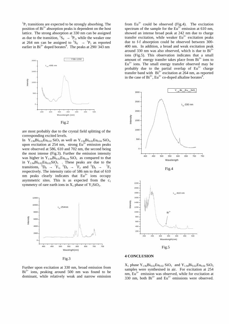
1P1 transitions are expected to be strongly absorbing. The position of Bi3+ absorption peaks is dependent on the host lattice. The strong absorption at 330 nm can be assigned as due to the transition, 1S0 → 3P1, while the weaker one at 264 nm can be assigned to 1S0 → 1P1 as reported earlier in Bi3+ doped borates8. The peaks at 290/ 343 nm
200 250 300 350 400 450 500
0
500
1000
1500
2000
Inte
nsity
W avelength (nm)
YSB-1250
λe m
-498 nm
Fig.2 are most probably due to the crystal field splitting of the corresponding excited levels. In Y1.96Bi0.02Eu0.02 SiO5 as well as Y1.94Bi0.02Eu0.04 SiO5, upon excitation at 254 nm, strong Eu3+ emission peaks were observed at 586, 610 and 702 nm, the second being the most intense (Fig.3). Further the emission intensity was higher in Y1.94Bi0.02Eu0.04 SiO5
as compared to that in Y1.94Bi0.02Eu0.02SiO5
. These peaks are due to the transitions, 5D0 → 7F1,
5D0 → 7F2 and 5D0 → 7F5 respectively. The intensity ratio of 586 nm to that of 610 nm peaks clearly indicates that Eu3+ ions occupy asymmetric sites. This is as expected from the c1 symmetry of rare earth ions in X1 phase of Y2SiO5.
400 450 500 550 600 650 700 750
0
2000
4000
6000
8000
10000
12000
Inte
nsity
Wavelngth(nm)
λex
-254nm
Fig.3
Further upon excitation at 330 nm, broad emission from Bi3+ ions, peaking around 500 nm was found to be dominant, while relatively weak and narrow emission
from Eu3+ could be observed (Fig.4). The excitation spectrum of the sample for the Eu3+ emission at 610 nm, showed an intense broad peak at 242 nm due to charge transfer excitation, while weaker Eu3+ excitation peaks due to f-f absorption could be observed between 300- 400 nm. In addition, a broad and weak excitation peak around 330 nm was also observed, which is due to Bi3+ ions (Fig.5). This observation indicates that a small amount of energy transfer takes place from Bi3+ ions to Eu3+ ions. The small energy transfer observed may be probably due to the partial overlap of Eu3+ charge transfer band with Bi3+ excitation at 264 nm, as reported in the case of Bi3+, Eu3+ co-doped alkaline borates8.
400 450 500 550 600 650 700 750
0
500
1000
1500
2000
2500
3000
Inte
nsity
Wavelength
Y1.96
Bi0.02
Eu0.02
SiO5
λex
-330 nm
Fig.4
200 250 300 350 400 450 500
200
400
600
800
1000
1200
1400
1600
1800
2000
2200
Bi3+
Inte
nsity
Wavelength(nm)
λem
-610 nm
Fig.5 4 CONCLUSION X1 phase Y1.96Bi0.02Eu0.02 SiO5 and Y1.94Bi0.02Eu0.04 SiO5
samples were synthesised in air. For excitation at 254 nm, Eu3+ emission was observed, while for excitation at 330 nm, both Bi3+ and Eu3+ emissions were observed.

There is some amount of energy transfer from Bi3+ to Eu3+; however, it is inefficient in this lattice. 5 REFERENCES 1T.E.Peters, J. Electrochem. Soc. 116 (1969) 985. 2Q.Y. Zhang, K.Pita, S.Buddhudu and C.H. Kam, J. Phys. D. Appl.Phys. 35, 3085 (2002). 3M. Yin, W. Zhang, L. Lon, S. Xia and J.C. Krupa, Physica B 254, 141 (1998). 4C.K. Duan, M. Yin, K. Yan and M.F. Reid, J. Alloys and compounds 303, 371 (2000). 5J. Lin, Q.Su, H.Zhang and S. Wang, Mat. Res. Bull. 31, 189 (1996).. 6J. Lin, Q.Su, H.Zhang and S.Wang, J. Mat. Chem. 6, 265 (1996). 7V. Natarajan, C.T. Chen and C.H. Lu, Proc. National Symposium on Luminescence and its Applications, Bangalore, India (2005) p.186. 8.P. Zhiwu and S. Qiang, Solid State Communications 86, 377 (1993).
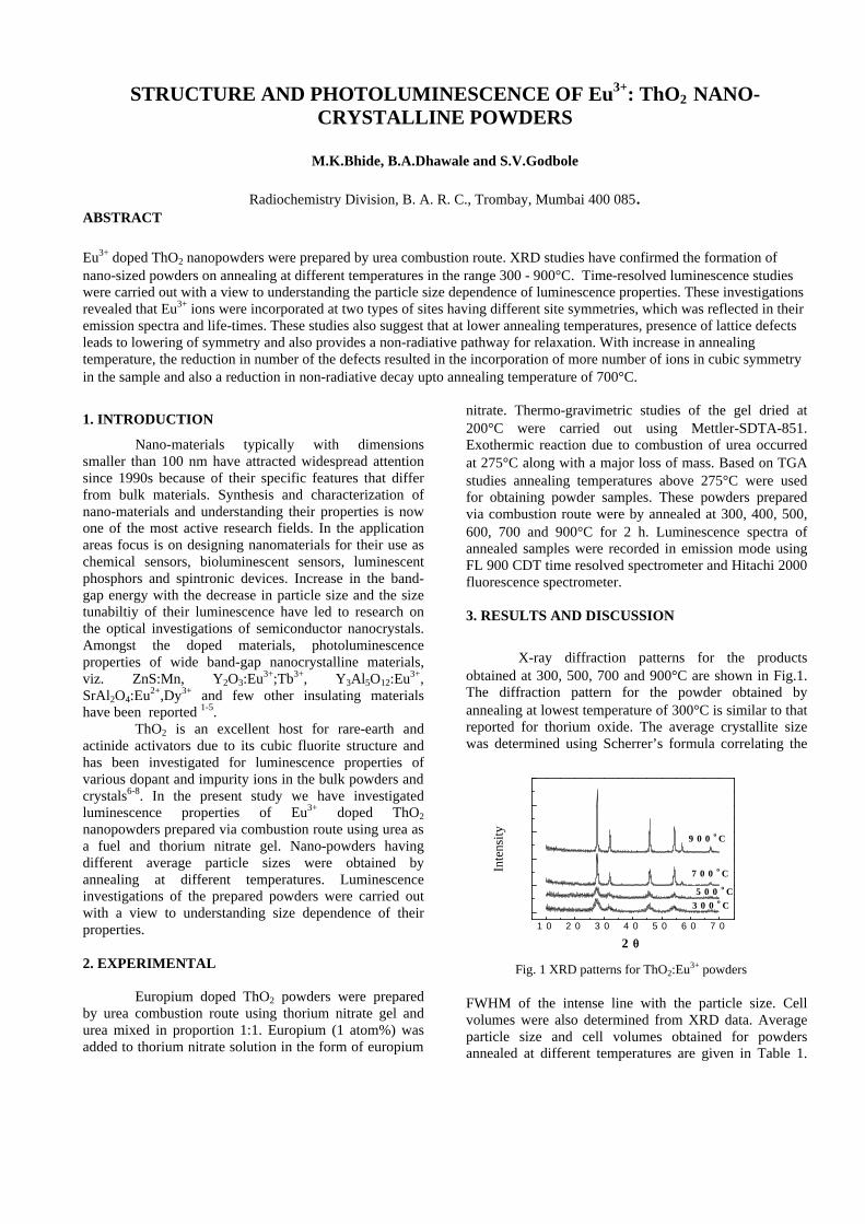
STRUCTURE AND PHOTOLUMINESCENCE OF Eu3+: ThO2 NANO-CRYSTALLINE POWDERS
M.K.Bhide, B.A.Dhawale and S.V.Godbole
Radiochemistry Division, B. A. R. C., Trombay, Mumbai 400 085. ABSTRACT
Eu3+ doped ThO2 nanopowders were prepared by urea combustion route. XRD studies have confirmed the formation of nano-sized powders on annealing at different temperatures in the range 300 - 900°C. Time-resolved luminescence studies were carried out with a view to understanding the particle size dependence of luminescence properties. These investigations revealed that Eu3+ ions were incorporated at two types of sites having different site symmetries, which was reflected in their emission spectra and life-times. These studies also suggest that at lower annealing temperatures, presence of lattice defects leads to lowering of symmetry and also provides a non-radiative pathway for relaxation. With increase in annealing temperature, the reduction in number of the defects resulted in the incorporation of more number of ions in cubic symmetry in the sample and also a reduction in non-radiative decay upto annealing temperature of 700°C.
1. INTRODUCTION
Nano-materials typically with dimensions smaller than 100 nm have attracted widespread attention since 1990s because of their specific features that differ from bulk materials. Synthesis and characterization of nano-materials and understanding their properties is now one of the most active research fields. In the application areas focus is on designing nanomaterials for their use as chemical sensors, bioluminescent sensors, luminescent phosphors and spintronic devices. Increase in the band-gap energy with the decrease in particle size and the size tunabiltiy of their luminescence have led to research on the optical investigations of semiconductor nanocrystals. Amongst the doped materials, photoluminescence properties of wide band-gap nanocrystalline materials, viz. ZnS:Mn, Y2O3:Eu3+;Tb3+, Y3Al5O12:Eu3+, SrAl2O4:Eu2+,Dy3+ and few other insulating materials have been reported 1-5.
ThO2 is an excellent host for rare-earth and actinide activators due to its cubic fluorite structure and has been investigated for luminescence properties of various dopant and impurity ions in the bulk powders and crystals6-8. In the present study we have investigated luminescence properties of Eu3+ doped ThO2 nanopowders prepared via combustion route using urea as a fuel and thorium nitrate gel. Nano-powders having different average particle sizes were obtained by annealing at different temperatures. Luminescence investigations of the prepared powders were carried out with a view to understanding size dependence of their properties.
2. EXPERIMENTAL
Europium doped ThO2 powders were prepared by urea combustion route using thorium nitrate gel and urea mixed in proportion 1:1. Europium (1 atom%) was added to thorium nitrate solution in the form of europium
nitrate. Thermo-gravimetric studies of the gel dried at 200°C were carried out using Mettler-SDTA-851. Exothermic reaction due to combustion of urea occurred at 275°C along with a major loss of mass. Based on TGA studies annealing temperatures above 275°C were used for obtaining powder samples. These powders prepared via combustion route were by annealed at 300, 400, 500, 600, 700 and 900°C for 2 h. Luminescence spectra of annealed samples were recorded in emission mode using FL 900 CDT time resolved spectrometer and Hitachi 2000 fluorescence spectrometer.
3. RESULTS AND DISCUSSION
X-ray diffraction patterns for the products obtained at 300, 500, 700 and 900°C are shown in Fig.1. The diffraction pattern for the powder obtained by annealing at lowest temperature of 300°C is similar to that reported for thorium oxide. The average crystallite size was determined using Scherrer’s formula correlating the
FWHM of the intense line with the particle size. Cell volumes were also determined from XRD data. Average particle size and cell volumes obtained for powders annealed at different temperatures are given in Table 1.
1 0 2 0 3 0 4 0 5 0 6 0 7 0
3 0 0 o C
5 0 0 o C
7 0 0 o C
9 0 0 o C
Inte
nsity
2 θθ
Fig. 1 XRD patterns for ThO2:Eu3+ powders
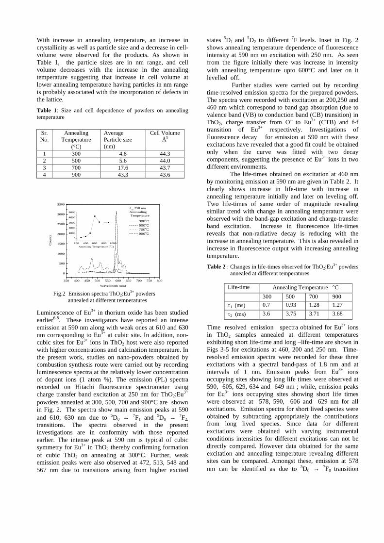
With increase in annealing temperature, an increase in crystallinity as well as particle size and a decrease in cell-volume were observed for the products. As shown in Table 1, the particle sizes are in nm range, and cell volume decreases with the increase in the annealing temperature suggesting that increase in cell volume at lower annealing temperature having particles in nm range is probably associated with the incorporation of defects in the lattice.
Table 1: Size and cell dependence of powders on annealing temperature
Luminescence of Eu3+ in thorium oxide has been studied earlier6-8. These investigators have reported an intense emission at 590 nm along with weak ones at 610 and 630 nm corresponding to Eu3+ at cubic site. In addition, non-cubic sites for Eu3+ ions in ThO2 host were also reported with higher concentrations and calcination temperature. In the present work, studies on nano-powders obtained by combustion synthesis route were carried out by recording luminescence spectra at the relatively lower concentration of dopant ions (1 atom %). The emission (PL) spectra recorded on Hitachi fluorescence spectrometer using charge transfer band excitation at 250 nm for ThO2:Eu3+ powders annealed at 300, 500, 700 and 900°C are shown in Fig. 2. The spectra show main emission peaks at 590 and 610, 630 nm due to 5D0 → 7F1 and 5D0 → 7F2,
transitions. The spectra observed in the present investigations are in conformity with those reported earlier. The intense peak at 590 nm is typical of cubic symmetry for Eu3+ in ThO2 thereby confirming formation of cubic ThO2 on annealing at 300°C. Further, weak emission peaks were also observed at 472, 513, 548 and 567 nm due to transitions arising from higher excited
states 5D1 and 5D2 to different 7F levels. Inset in Fig. 2 shows annealing temperature dependence of fluorescence intensity at 590 nm on excitation with 250 nm. As seen from the figure initially there was increase in intensity with annealing temperature upto 600°C and later on it levelled off.
Further studies were carried out by recording time-resolved emission spectra for the prepared powders. The spectra were recorded with excitation at 200,250 and 460 nm which correspond to band gap absorption (due to valence band (VB) to conduction band (CB) transition) in ThO2, charge transfer from O-- to Eu3+ (CTB) and f-f transition of Eu3+ respectively. Investigations of fluorescence decay for emission at 590 nm with these excitations have revealed that a good fit could be obtained only when the curve was fitted with two decay components, suggesting the presence of Eu3+ ions in two different environments.
The life-times obtained on excitation at 460 nm by monitoring emission at 590 nm are given in Table 2. It clearly shows increase in life-time with increase in annealing temperature initially and later on leveling off. Two life-times of same order of magnitude revealing similar trend with change in annealing temperature were observed with the band-gap excitation and charge-transfer band excitation. Increase in fluorescence life-times reveals that non-radiative decay is reducing with the increase in annealing temperature. This is also revealed in increase in fluorescence output with increasing annealing temperature.
Table 2 : Changes in life-times observed for ThO2:Eu3+ powders annealed at different temperatures
Life-time Annealing Temperature °C
300 500 700 900
τ1 (ms) 0.7 0.93 1.28 1.27
τ2 (ms) 3.6 3.75 3.71 3.68
Time resolved emission spectra obtained for Eu3+ ions in ThO2 samples annealed at different temperatures exhibiting short life-time and long –life-time are shown in Figs 3-5 for excitations at 460, 200 and 250 nm. Time-resolved emission spectra were recorded for these three excitations with a spectral band-pass of 1.8 nm and at intervals of 1 nm. Emission peaks from Eu3+ ions occupying sites showing long life times were observed at 590, 605, 629, 634 and 649 nm ; while, emission peaks for Eu3+ ions occupying sites showing short life times were observed at 578, 590, 606 and 629 nm for all excitations. Emission spectra for short lived species were obtained by subtracting appropriately the contributions from long lived species. Since data for different excitations were obtained with varying instrumental conditions intensities for different excitations can not be directly compared. However data obtained for the same excitation and annealing temperature revealing different sites can be compared. Amongst these, emission at 578 nm can be identified as due to 5D0 → 7F0 transition
Sr. No.
Annealing Temperature
(°C)
Average Particle size (nm)
Cell Volume Å3
1 300 4.8 44.3 2 500 5.6 44.0 3 700 17.6 43.7 4 900 43.3 43.6
350 400 450 500 550 600 650 700 750 800
0
500
1000
1500
2000
2500
3000
3500
200 400 600 800 1000
0
1000
2000
3000
4000
5000
Annealing Temperature (oC)
300oC 500oC 700oC 900oC
λex
258 nmAnnnealing Temperature
Counts
Wavelength (nm)
Fig.2 Emission spectra ThO2:Eu3+ powders annealed at different temperatures
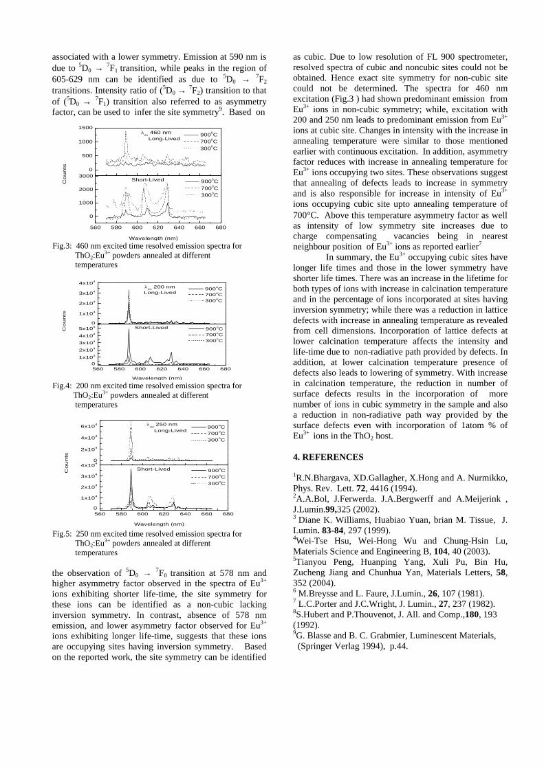
associated with a lower symmetry. Emission at 590 nm is due to 5D0 → 7F1 transition, while peaks in the region of 605-629 nm can be identified as due to 5D0 → 7F2 transitions. Intensity ratio of (5D0 → 7F2) transition to that of (5D0 → 7F1) transition also referred to as asymmetry factor, can be used to infer the site symmetry9. Based on
the observation of 5D0 → 7F0 transition at 578 nm and higher asymmetry factor observed in the spectra of Eu3+ ions exhibiting shorter life-time, the site symmetry for these ions can be identified as a non-cubic lacking inversion symmetry. In contrast, absence of 578 nm emission, and lower asymmetry factor observed for Eu3+ ions exhibiting longer life-time, suggests that these ions are occupying sites having inversion symmetry. Based on the reported work, the site symmetry can be identified
as cubic. Due to low resolution of FL 900 spectrometer, resolved spectra of cubic and noncubic sites could not be obtained. Hence exact site symmetry for non-cubic site could not be determined. The spectra for 460 nm excitation (Fig.3 ) had shown predominant emission from Eu3+ ions in non-cubic symmetry; while, excitation with 200 and 250 nm leads to predominant emission from Eu3+ ions at cubic site. Changes in intensity with the increase in annealing temperature were similar to those mentioned earlier with continuous excitation. In addition, asymmetry factor reduces with increase in annealing temperature for Eu3+ ions occupying two sites. These observations suggest that annealing of defects leads to increase in symmetry and is also responsible for increase in intensity of Eu3+ ions occupying cubic site upto annealing temperature of 700°C. Above this temperature asymmetry factor as well as intensity of low symmetry site increases due to charge compensating vacancies being in nearest neighbour position of Eu3+ ions as reported earlier7
In summary, the Eu3+ occupying cubic sites have longer life times and those in the lower symmetry have shorter life times. There was an increase in the lifetime for both types of ions with increase in calcination temperature and in the percentage of ions incorporated at sites having inversion symmetry; while there was a reduction in lattice defects with increase in annealing temperature as revealed from cell dimensions. Incorporation of lattice defects at lower calcination temperature affects the intensity and life-time due to non-radiative path provided by defects. In addition, at lower calcination temperature presence of defects also leads to lowering of symmetry. With increase in calcination temperature, the reduction in number of surface defects results in the incorporation of more number of ions in cubic symmetry in the sample and also a reduction in non-radiative path way provided by the surface defects even with incorporation of 1atom % of Eu3+ ions in the ThO2 host.
4. REFERENCES 1R.N.Bhargava, XD.Gallagher, X.Hong and A. Nurmikko, Phys. Rev. Lett. 72, 4416 (1994). 2A.A.Bol, J.Ferwerda. J.A.Bergwerff and A.Meijerink , J.Lumin.99,325 (2002). 3 Diane K. Williams, Huabiao Yuan, brian M. Tissue, J. Lumin. 83-84, 297 (1999). 4Wei-Tse Hsu, Wei-Hong Wu and Chung-Hsin Lu, Materials Science and Engineering B, 104, 40 (2003). 5Tianyou Peng, Huanping Yang, Xuli Pu, Bin Hu, Zucheng Jiang and Chunhua Yan, Materials Letters, 58, 352 (2004). 6 M.Breysse and L. Faure, J.Lumin., 26, 107 (1981). 7 L.C.Porter and J.C.Wright, J. Lumin., 27, 237 (1982). 8S.Hubert and P.Thouvenot, J. All. and Comp.,180, 193 (1992). 9G. Blasse and B. C. Grabmier, Luminescent Materials, (Springer Verlag 1994), p.44.
0
500
1000
1500
560 580 600 620 640 660 680
0
1000
2000
3000
Long-Lived
Wavelength (nm)
λex
460 nm
Counts
9000C
7000C
3000C
Short-Lived
9000C
7000C 3000C
0
1x10⁴
2x10⁴
3x10⁴
4x10⁴
560 580 600 620 640 660 6800
1x10⁴
2x10⁴
3x10⁴
4x10⁴
5x10⁴
Long-Lived
Wavelength (nm)
λex
200 nm
Counts
900oC 700oC 300oC
Short-Lived
900oC 700oC 300oC
Fig.4: 200 nm excited time resolved emission spectra for ThO2:Eu3+ powders annealed at different temperatures
0
2x10⁴
4x10⁴
6x10⁴
560 580 600 620 640 660 6800
1x10⁴
2x10⁴
3x10⁴
4x10⁴
Long-Lived
Wavelength (nm)
λex
250 nm
Co
un
ts
900oC
700oC
300oC
Short-Lived
900oC
700oC
300oC
Fig.5: 250 nm excited time resolved emission spectra for ThO2:Eu3+ powders annealed at different temperatures
Fig.3: 460 nm excited time resolved emission spectra for ThO2:Eu3+ powders annealed at different temperatures
1
Wide UV excitation and emission of Eu3+/ZnSe nanocrystal in Silica Hosts Siby Mathew, Rejikumar P R, Xavier Joseph, M A Ittyachen and N V Unnikrishnan
School of Pure & Applied Physics Mahatma Gandhi University, Kottayam-686 560,Kerala, India E-mail: [email protected]
ABSTRACT The wide bandgap semiconductor zinc selenide nanocrystallites together with europium ions were incorporated into the silica matrix using sol-gel method. The size distribution and optical bandgap of the nanoparticles were calculated from the absoroption spectrum.The TEM measurements yield the nanocrystal size to be around 6 nm and a crystal inter planar spacing to be 3.278 Å. The excitation spectra recorded for the sample gives a broad excitonic band around 370nm which could be assigned to the ZnSe nanocrystallites. The fluorescence spectra reveal that the intensity of characteristic emission of europium increases considerably in the presence of ZnSe particles. INTRODUCTION Recently nanoparticles have gained much interest due to the perceived need for miniaturization of both optical and electronic devices. Most II-VI semiconductors show quantum confinement behaviour in the 1-20nm size range, where nanocrystallites show optical, electronic and mechanical properties distinct from those of corresponding bulk material [1]. Nanoparticles are of great interest for sensing and electronic technologies due to their unique size dependent optical and electronic properties. Size quantization effect occurs when the size of the nanoparticle is smaller than the bulk exciton Bohr radius of the semiconductor [2]. The nanoparticles have high dispersity (large surface/volume ratio) and interface areas, which influence the electronic properties of the materials [3]. The development of new luminescent materials with complex composition is of interest for understanding of electronic excitation and relaxation phenomena with participation of two and more active centers. Doped Nanocrystals of semiconductor can yield both high luminescence efficiencies and lifetime shortening at the same time. Semiconductor nanocrystals in transparent media, especially in sol gel glasses, have received greater attention due to their promising applications in non-linear optics and optical switches [4], [5]. We report here the the size determination of nanocrystallites and the wide UV excitation range offered by the sample, intensification of fluorescence and resolution of excitation lines of the rare earth ions in the presence of zinc selenide particles prepared by the sol-gel method. EXPERIMENTAL Silica glasses with 3wt% of Europium concentration and varying ZnSe concentrations were prepared by the sol-gel process [6]. ZnSe nanoparticles were prepared from zinc acetate and selenic acid by their decomposition reaction and incorporated on to the SiO2-matrix through annealing. Eu3+(3wt%) ZnSe (7wt%)[Sample A], Eu3+(3 wt%) [Sample B] and ZnSe (7wt%) [Sample C] doped silica samples were prepared.. The luminescence spectra were taken using a spectrophotofluorimeter (Shimadzu-RFPC 5301) and the absorption with UV-visible
spectrophotometer (Shimadzu-UVPC2401) for all the samples heated to 500oC. RESULTS AND DISCUSSION The optical absorption spectra of ZnSe nanocrystallites doped glassy matrices heat treated at 500oC is shown in Figure1. The direct absorption band gap of the ZnSe nanoparticles can be determined by fitting the absorption
data to the equation ( ) 2/1gEhBh −= ννα (as shown
in the inset of Figure 1) in which hν is the photon energy, α is the absorption coefficient, Eg is the absorption band gap and B is a constant relative to the material. The absorption coefficient can be obtained from the equation
d
A303.2=α where A is the absorbance and d is the
thickness of the sample. The estimated band gap energy is 3.09eV. This is large compared to bulk ZnSe, a direct semiconductor, with band gap energy of 2.82eV [7,8]. Semiconductor nanocrystals are known to have an absorption edge, which is shifted with respect to the bulk
material, toward shorter wavelengths [9]. The blue shift of the absorption edge can be explained by the effective mass approximation model, developed by Brus [10] and Kayanuma [11]. In the strong exciton confinement regime of nanoparticles (particle radius < ab*), the energy E(R) for the lowest 1S excited state as a function of cluster radius (R) is given by
2.5 3.0 3.5 4.00.0
0.5
1.0
1.5
2.0
2.5
3.0
Abs
orba
nce
(a.u
.)
hν
2.8 2.9 3.0 3.1 3.2 3.3
0.0
5.0x10⁵
1.0x10⁶
1.5x10⁶
2.0x10⁶
2.5x10⁶
3.0x10⁶
3.5x10⁶
4.0x10⁶
ZnSe 7%
α2
hν
Figure 1. Absorption spectra of samples heated to 500oC taken at room temperature. Inset shows the (α)2 vs hν graph
2
R
bg E
R
e
R
eaERE 48.2
4
786.1
8
*)(
2
2+−+=
πεεπ .(1)
where ab*, Bohr radius of the exciton (for ZnSe 3.8nm), ε is the dielectric constant of the nanocrystallite (for ZnSe, 8.7) and ER is the bulk exciton Rydberg energy (for ZnSe 0.019eV). The second term is the quantum confinement localization for the electrons and holes, which leads to the blueshift. The third term is the Coulomb term leading to red shift, while the fourth term gives the spatial correlation energy, which is small and of minor importance. From the blueshift results, we could estimate that the quantum confinement effect of our ZnSe nanoparticles should be larger than the Coulomb effect. The band edge absorption in Figure 1 is used to calculate the average size distribution of the ZnSe nanoparticles in the silica matrix. The particle size is found to be 7.6nm from the absorption spectrum and using the Brus formula, by considering this to be in the strong confinement region. The TEM and HRTEM taken for the samples is shown in figures 2(a) and (b). Figure 2(b) shows the planes of the ZnSe nanocrystallites. The resulting particles are crystalline with an average diameter of 6nm (estimated from the TEM image).The magnified HRTEM of a single nanocrystallite with a line pattern shows the direct image of the periodic lattice.The plane was identified as(111)plane with a d value of 3.278 Å. This is in agreement with the value (d=3.244 Å) for bulk zinc selenide crystal[12].
The excitation spectrum taken with an emission wavelength of 614 nm [Figure 3] shows splitting of the weak absorption bands and appearance of new peaks which are characteristic of Eu3+ ions. The peaks are assigned to each transition, as 7F0→
5L6 (394nm) the most prominent one followed by 7F0→
5D2 (464nm), 7F1→5D1
(535nm) and 7F1→5D0 (591nm). The less pronounced
peaks are assigned as 7F1→5D3 (416nm), 7F0→
5D1 (526nm) and 7F0→
5D0 (579nm).The intense peak at 465nm is an indication of a rigid glassy network that is formed at comparatively low temperature in ZnSe + Eu3+ doped gel glass comparing to Eu3+ doped one. The strong excitation transition at 393nm hints at a possible enhancement in the principal emission line of Eu3+ in the ZnSe+Eu3+ doped silica. Figure 4 depicts the fluorescence spectra of the samples heated to 500oC recorded at room temperature with an excitation of 393nm corresponding to the 5L6 state of the Eu3+ ion. It
shows a considerable enhancement in the emission intensity corresponding to the 5D0→ 7F2 transition for ZnSe+Eu3+ doped silica glass. The structural features play a critical role on the fluorescent enhancement since the complex dielectric function of the composite medium depends directly on the structural features of the particles involved. In the case of Eu3+, the main emission lines occur between the 5D levels to the7Fj multiplets. The 5D0→ 7F2 transition of Eu3+ is hypersensitive to the chemical bond formed between Eu3+ and its surrounding ligands. The fluorescence intensity ratio of 5D0→ 7F2 to 5D0→ 7F1 transition indicates the degree of asymmetry in the vicinity of Eu3+ ions and Eu-O covalency which could be measured using the asymmetry ratio given as
∫∫
γ
γ=
→
→
dI
dIAS
10
20
where I0→j denotes the intensity of 5D0→ 7Fj transition. The asymmetry ratio estimated for the Eu3+ and the ZnSe+Eu3+ doped silica are 1.4539 and 2.421 respectively. This clearly indicates that the presence of the nanocrystallites is responsible for an increase of both the covalency and the polarization of the local vicinities of the Eu3+cations. A greater ratio corresponds to a more distorted or asymmetric local cation environment. This difference can be attributed to the change in chemical environment of Eu3+ in different media. [13] The latter transition is magnetic dipole allowed and its strength is not very site dependent; on the contrary 5D0→ 7F2
transition is forbidden and becomes electric dipole allowed in an odd field. The heat treated Eu3+ doped sol-gel glass shows four bands which belong to the 5D0à 7FJ(J=0,1,2,3) transitions. The branching ratios were calculated for all
350 400 450 500 550 6000
50
100
150
200
250
381.
2
394.
4
415.
6
464.
4
525.
653
5.2
579.
6
591.
4
Inte
nsity
(a.
u.)
Wavelength (nm)
Figure 3. Excitation spectra of samples heated to 500oC (λem =614nm) taken at room temperature.
500 600 7000
100
200
300
400
500
600
ZnSe 7 Eu 3
ZnSe 0 Eu 3
Inte
nsity
(a.
u.)
Wavelength (nm)
Figure 4. Emission spectra of samples heated to 500oC (λex =393nm) taken at room temperature
500 550 600 650 700 7500
50
100
150
200
250
300
350
578
590.
6
613.
8
649
697
ZnSe 7wt% Eu 3wt%
Inte
nsity
(a.
u.)
Wavelength (nm)
Figure 2(a) TEM and (b) HR-TEM images of ZnSe nanocrystals.
b a
3
the transitions using the standard procedure (Figure 4) [14]. It has already been established that an emission level with branching ratio value near 50% becomes a potential laser emission transition[15]. Branching ratio determined from emission spectrum for each transition is given in Table 1. The highest branching ratio corresponds to the experimentally observed strongest peak at 613 nm. Table I. The fluorescence branching ratio obtained for the samples (ZnSe + Eu3+) from the emission spectrum.
Transition Wavelength (nm)
Branching ratio
5D0à 7F0 578 0.01732 5D0à 7F1
590.6 0.2838 5D0à 7F2
613.8 0.6154 5D0à 7F3
649 0.00584 5D0à 7F4
697 0.04709 Thermal treatment allows to improve the crystalline quality of the clusters and to narrow their charecteristic optical features [16]. As a result of finite size, continuous bands of energy are replaced by molecule-like discrete energy levels. As the particle size increases the energy spacing between the states decreases. In nanoparticles, most ions at the surface are non-saturated in coordination. Electrons and holes may be easily excited and escape from the ion. Much more carriers trapped at the surface states or defect sites are released by
photoexcitation as excitonic or trapped luminescence [17,18]. The quantum confinement enhances the allowed energies resulting in from an increase in binding energy of shallow impurity [19]. Heat treatment leads to an increase in the inhomogeneities of the local environment owing to the cross-linking between silica chains and consequent shrinkage. As the densification continues, clustering of Eu3+ induces strong energy transfer even at lower concentrations. The low fluorescent intensity of the gels was due to electron-phonon coupling with C-H and O-H groups. Figure 5 gives the emission spectra corresponding to different excitation wavelengths varying by 10 nm. All these excitations gives the characteristic emission from europium ions. By exciting at 393nm the energy from the nonradiative recombination of electron-hole pairs of the ZnSe nanoparticles can be transferred to the higher energy levels of the Eu3+ ion. This will increase the population of the emitting levels and thereby increasing the fluorescence from the rare earth ion.
CONCLUSION The absorption spectra of ZnSe nanocrystallites/Eu3+
reveals the formation of ZnSe + Eu3+ sites in the gel matrix and the excitation spectra on the other hand confirms the densification of the gel and presence of strong excitation bands. The emission intensities of the europium ions are found to be considerably increased by codoping with nanoparticles of ZnSe. The adsorption of the semiconductor nanoparticles on to the SiO2 matrix provides local field enhancement, and the photogenerated electron trapped in the ZnSe strongly interact with Eu3+ ions located close to the nanocrystallites in the SiO2
matrix. The nonradiative energy transfer from the electron-hole recombination of the ZnSe nanoparticles to the rare earth ion will result in the observed fluorescence enhancement. ACKNOWLEDGMENT We would like to thank Dr. Gin Jose, Assistant Professor, IIT Gauwahatti and Dr. Gijo Jose, School of Pure & Applied Physics, Mahatma Gandhi University, Kottayam for their timely help. REFERENCES
1. M C Klein Phys.Rev. B 42,1123 .(1990). 2. D Nesheva Semi. Con. Sc. Tech. 12,1319.(1997). 3. AL. L. Efros, M. Rosen, M. Kuno, N. Nirmal, D.J.
Norris, M.G. Bawendi, Phys. Rev. B 54,4843.(1996).
4. S. Gorer, G. Hodes, Y. Sorek, R. Reisfeld, Mater. Lett. 31,209.(1997).
5. S Tamil Selvan, T Hayakawa And M Nogami J. Phys. Chem. B 103,7064. (1999).
6. Gijo Jose, K.A. Amrutha, T.F. Toney, V. Thomas, C. Joseph, M.A. Ittyachen and N.V. Unnikrishnan Mater.Chem.Phys.(in press)
7. R. Reisfeld, M Gaft, T Saridarov, G Panczer, M Zelner Mater.Lett.45,154.(2000).
8. A R Kortan, R Hull, Rl Opila, M G Bawendi, Le Brus, J. Am. Chem. Soc. 112 ,1327.(1990)
9. E Lifshitz, I Dag, S Gorer, R Reisfeld, Chem. Phys. Lett. 288,188(1998)
10. L E Brus, J. Chem. Phys. 79, 5566.(1983). 11. Y Kayanuma Phys. Rev. B 38, 9797.(1998). 12. C.Yeh et al., Phys.Rev B: 46,10086 (1992). 13. X Fan, M Wang Mat. Sci. & Engg. B21,
55.(1993). 14. R A Vellapodi Phys. Chem.Glasses 14 (1973)107 15. P K D Sagar, P Kistaiah, B A Rao, C V V Reddy,
K S N Murthy, N Veeraiah J. Mater. Sci. Lett. 18,55.(1999)
16. P Lefbvre Superlattices & Microstructures 15,447. (1994)
17. P Lefbvre Spie Vol.12288 Sol-Gel Opt. Iii,163. (1994)
18. P Yang, M Lu, Mater. Res. Bull. 36,1301.(2001) 19. S Tamil Selvan, T Hayakawa And M Nogami J.
Lumin.87,532.(2000)
Figure 5. Emission spectra of samples heated to 500oC with λex varying wavelength taken at room temperature
λex
= 320nm
λex
= 330nm
λex
= 350nm λ
ex= 360nm
λex
= 380nm
560 580 600 620 6400
50
100
150
Inte
nsity
(a.
u.)
Wavelength (nm)

4
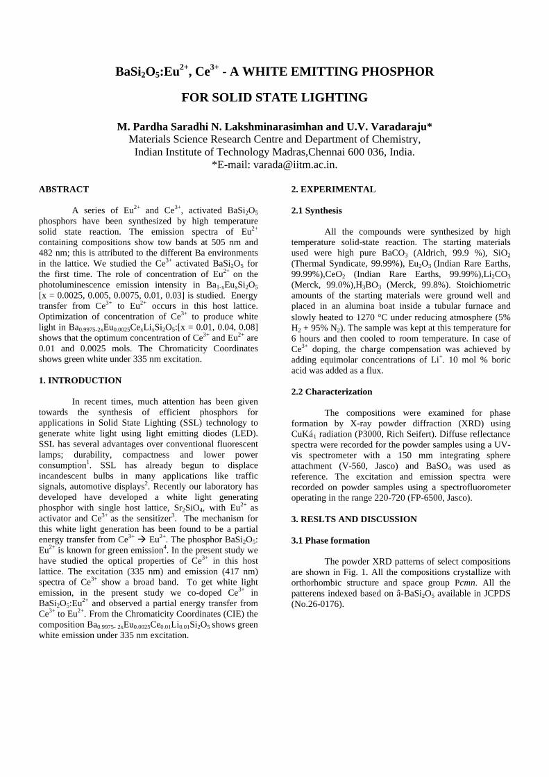
BaSi2O5:Eu2+, Ce3+ - A WHITE EMITTING PHOSPHOR
FOR SOLID STATE LIGHTING
M. Pardha Saradhi N. Lakshminarasimhan and U.V. Varadaraju* Materials Science Research Centre and Department of Chemistry,
Indian Institute of Technology Madras,Chennai 600 036, India. *E-mail: [email protected].
ABSTRACT
A series of Eu2+ and Ce3+, activated BaSi2O5 phosphors have been synthesized by high temperature solid state reaction. The emission spectra of Eu2+ containing compositions show tow bands at 505 nm and 482 nm; this is attributed to the different Ba environments in the lattice. We studied the Ce3+ activated BaSi2O5 for the first time. The role of concentration of Eu2+ on the photoluminescence emission intensity in Ba1-xEuxSi2O5
[x = 0.0025, 0.005, 0.0075, 0.01, 0.03] is studied. Energy transfer from Ce3+ to Eu2+ occurs in this host lattice. Optimization of concentration of Ce3+ to produce white light in Ba0.9975-2xEu0.0025CexLixSi2O5:[x = 0.01, 0.04, 0.08] shows that the optimum concentration of Ce3+ and Eu2+ are 0.01 and 0.0025 mols. The Chromaticity Coordinates shows green white under 335 nm excitation.
1. INTRODUCTION
In recent times, much attention has been given towards the synthesis of efficient phosphors for applications in Solid State Lighting (SSL) technology to generate white light using light emitting diodes (LED). SSL has several advantages over conventional fluorescent lamps; durability, compactness and lower power consumption1. SSL has already begun to displace incandescent bulbs in many applications like traffic signals, automotive displays2. Recently our laboratory has developed have developed a white light generating phosphor with single host lattice, Sr2SiO4, with Eu2+ as activator and Ce3+ as the sensitizer3. The mechanism for this white light generation has been found to be a partial energy transfer from Ce3+ à Eu2+. The phosphor BaSi2O5: Eu2+ is known for green emission4. In the present study we have studied the optical properties of Ce3+ in this host lattice. The excitation (335 nm) and emission (417 nm) spectra of Ce3+ show a broad band. To get white light emission, in the present study we co-doped Ce3+ in BaSi2O5:Eu2+ and observed a partial energy transfer from Ce3+ to Eu2+. From the Chromaticity Coordinates (CIE) the composition Ba0.9975- 2xEu0.0025Ce0.01Li0.01Si2O5 shows green white emission under 335 nm excitation.
2. EXPERIMENTAL 2.1 Synthesis
All the compounds were synthesized by high temperature solid-state reaction. The starting materials used were high pure BaCO3 (Aldrich, 99.9 %), SiO2 (Thermal Syndicate, 99.99%), Eu2O3 (Indian Rare Earths, 99.99%),CeO2 (Indian Rare Earths, 99.99%),Li2CO3 (Merck, 99.0%),H3BO3 (Merck, 99.8%). Stoichiometric amounts of the starting materials were ground well and placed in an alumina boat inside a tubular furnace and slowly heated to 1270 °C under reducing atmosphere (5% H2 + 95% N2). The sample was kept at this temperature for 6 hours and then cooled to room temperature. In case of Ce3+ doping, the charge compensation was achieved by adding equimolar concentrations of Li+. 10 mol % boric acid was added as a flux. 2.2 Characterization
The compositions were examined for phase formation by X-ray powder diffraction (XRD) using CuKá1 radiation (P3000, Rich Seifert). Diffuse reflectance spectra were recorded for the powder samples using a UV-vis spectrometer with a 150 mm integrating sphere attachment (V-560, Jasco) and BaSO4 was used as reference. The excitation and emission spectra were recorded on powder samples using a spectrofluorometer operating in the range 220-720 (FP-6500, Jasco). 3. RESLTS AND DISCUSSION 3.1 Phase formation
The powder XRD patterns of select compositions are shown in Fig. 1. All the compositions crystallize with orthorhombic structure and space group Pcmn. All the patterens indexed based on â-BaSi2O5 available in JCPDS (No.26-0176).
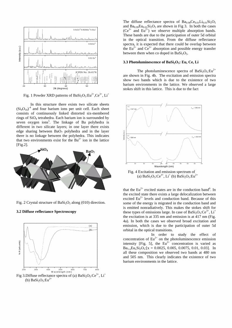
Fig. 1 Powder XRD patterns of BaSi2O5:Eu2+,Ce3+, Li+
In this structure there exists two silicate sheets
(Si4O10)-4 and four barium ions per unit cell. Each sheet
consists of continuously linked distorted six-membered rings of SiO4 tetrahedra. Each barium ion is surrounded by seven oxygen ions5. The linkage of Ba polyhedra is different in two silicate layers; in one layer there exists edge sharing between BaO7 polyhedra and in the layer there is no linkage between the polyhedra. This indicates that two environments exist for the Ba2+ ion in the lattice [Fig.2].
Fig. 2 Crystal structure of BaSi2O5 along (010) direction. 3.2 Diffuse reflectance Spectroscopy
Fig 3.Diffuse reflectance spectra of (a) BaSi2O5:Ce3+, Li+ (b) BaSi2O5:Eu2+
The diffuse reflectance spectra of Ba0.98Ce0.01Li0.01Si2O5 and Ba0.99Eu0.01Si2O5 are shown in Fig 3. In both the cases (Ce3+ and Eu2+) we observe multiple absorption bands. These bands are due to the participation of outer 5d orbital in the optical transition. From the diffuse reflectance spectra, it is expected that there could be overlap between the Eu2+ and Ce3+ absorption and possible energy transfer between them when co doped in BaSi2O5. 3.3 Photoluminescence of BaSi2O5: Eu, Ce, Li
The photoluminescence spectra of BaSi2O5:Eu2+
are shown in Fig. 4b. The excitation and emission spectra show two bands which is due to the existence of two barium environments in the lattice. We observed a large stokes shift in this lattice. This is due to the fact
Fig. 4 Excitation and emission spectrum of (a) BaSi2O5:Ce3+, Li+ (b) BaSi2O5:Eu2+
that the Eu2+ excited states are in the conduction band6. In the excited state there exists a large delocalization between excited Eu2+ levels and conduction band. Because of this some of the energy is migrated in the conduction band and is emitted nonradiatively. This makes the stokes shift for these types of emissions large. In case of BaSi2O5:Ce3+, Li+ the excitation is at 335 nm and emission is at 417 nm (Fig. 4a). In both the cases we observed broad excitation and emission, which is due to the participation of outer 5d orbital in the optical transitions.
In order to study the effect of concentration of Eu2+ on the photoluminescence emission intensity [Fig. 5], the Eu2+ concentration is varied as Ba1-xEuxSi2O5:[x = 0.0025, 0.005, 0.0075, 0.01, 0.03]. In all these composition we observed two bands at 480 nm and 505 nm. This clearly indicates the existence of two barium environments in the lattice.
SiO4
20 30 40 50
JCPDS No. 26-0176
( 4
4 0
)(
3 6
0 )
( 3
1 2
)(
2 4
2 )
( 1
7 1
)
( 2
6 1
)(
2 3
2 )
(4 2
0 )
(
1 4
2 )
( 3
4 1
)(
2 2
2 )
( 4
0 0
)
( 2
0 2
)(
1 3
2 )
( 0
6 1
)(
3 4
0 )
( 0
3 2
)(
1 2
2 )
( 3
2 1
)(1
6 0
)(
0 2
2 )
( 2
4 1
)(
1 5
1 )
( 3
0 1
)(
0 1
2 )
( 0
0 2
)(
0 5
1 )
( 3
2 0
)
( 2
4 0
)(
1 4
1 )
( 2
2 1
)
( 0
4 1
)
( 2
1 1
)
( 1
3 1
)(
1 4
0 )
( 0
3 1
)( 2
2 0
)(
0 4
0 )(1 2
1 )
( 1
0 1
)
( 2
0 0
)(
1 1
1 )
Inte
nsity
(a.
u.)
2θθ (degrees)
0.01 Eu2+
0.01Ce3+
0.01Ce3+0.0025Eu2+0.01Li+
2 0 0 3 0 0 4 0 0 5 0 0 6 0 0 7 0 0 8 0 0
(b)
(a)
% R
(ar
b.un
its)
W a v e leng th (nm )
( a )
λem
= 500 nm
Inte
nsity
(a.
u.)
Wavelength (nm)
λexc
= 335 nm
λexc
= 313 nm
250 300 350 400 450
( b )
λem
= 417 nm
350 400 450 500 550 600
BaO7
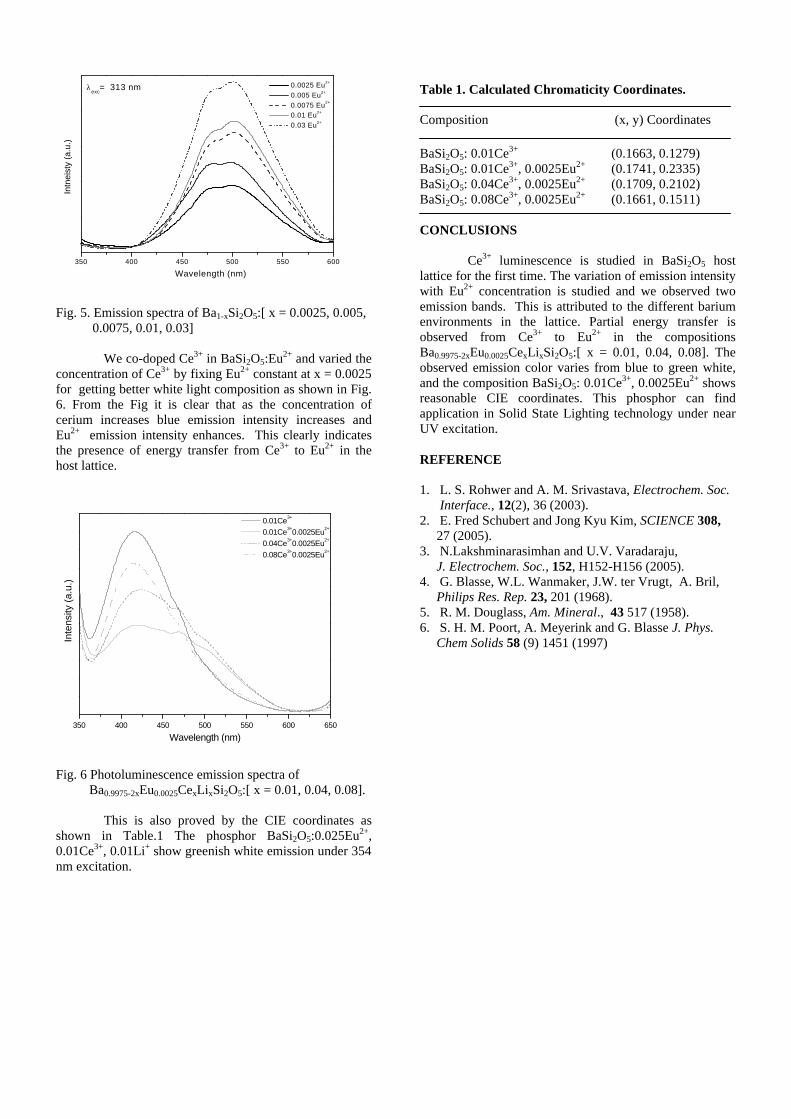
350 400 450 500 550 600
0.0025 Eu2+
0.005 Eu2+
0.0075 Eu2+
0.01 Eu2+
0.03 Eu2+
λexc
= 313 nm
In
tnei
sty
(a.u
.)
Wavelength (nm)
Fig. 5. Emission spectra of Ba1-xSi2O5:[ x = 0.0025, 0.005, 0.0075, 0.01, 0.03]
We co-doped Ce3+ in BaSi2O5:Eu2+ and varied the
concentration of Ce3+ by fixing Eu2+ constant at x = 0.0025 for getting better white light composition as shown in Fig. 6. From the Fig it is clear that as the concentration of cerium increases blue emission intensity increases and Eu2+ emission intensity enhances. This clearly indicates the presence of energy transfer from Ce3+ to Eu2+ in the host lattice.
Fig. 6 Photoluminescence emission spectra of Ba0.9975-2xEu0.0025CexLixSi2O5:[ x = 0.01, 0.04, 0.08].
This is also proved by the CIE coordinates as shown in Table.1 The phosphor BaSi2O5:0.025Eu2+, 0.01Ce3+, 0.01Li+ show greenish white emission under 354 nm excitation.
Table 1. Calculated Chromaticity Coordinates. Composition (x, y) Coordinates BaSi2O5: 0.01Ce3+ (0.1663, 0.1279)
BaSi2O5: 0.01Ce3+, 0.0025Eu2+ (0.1741, 0.2335) BaSi2O5: 0.04Ce3+, 0.0025Eu2+ (0.1709, 0.2102) BaSi2O5: 0.08Ce3+, 0.0025Eu2+ (0.1661, 0.1511) CONCLUSIONS Ce3+ luminescence is studied in BaSi2O5 host lattice for the first time. The variation of emission intensity with Eu2+ concentration is studied and we observed two emission bands. This is attributed to the different barium environments in the lattice. Partial energy transfer is observed from Ce3+ to Eu2+ in the compositions Ba0.9975-2xEu0.0025CexLixSi2O5:[ x = 0.01, 0.04, 0.08]. The observed emission color varies from blue to green white, and the composition BaSi2O5: 0.01Ce3+, 0.0025Eu2+ shows reasonable CIE coordinates. This phosphor can find application in Solid State Lighting technology under near UV excitation. REFERENCE 1. L. S. Rohwer and A. M. Srivastava, Electrochem. Soc. Interface., 12(2), 36 (2003). 2. E. Fred Schubert and Jong Kyu Kim, SCIENCE 308, 27 (2005). 3. N.Lakshminarasimhan and U.V. Varadaraju, J. Electrochem. Soc., 152, H152-H156 (2005). 4. G. Blasse, W.L. Wanmaker, J.W. ter Vrugt, A. Bril, Philips Res. Rep. 23, 201 (1968). 5. R. M. Douglass, Am. Mineral., 43 517 (1958). 6. S. H. M. Poort, A. Meyerink and G. Blasse J. Phys. Chem Solids 58 (9) 1451 (1997)
350 400 450 500 550 600 650
0.01Ce3+
0.01Ce3+
0.0025Eu2+
0.04Ce3+
0.0025Eu2+
0.08Ce3+0.0025Eu2+
Inte
nsity
(a.
u.)
Wavelength (nm)
SYNTHESIS AND OPTICAL PROPERTIES OF BiMgVO5:Eu3+
V. Sivakumar and U.V. Varadaraju*
Materials Science Research Centre and Department of Chemistry,
Indian Institute of Technology Madras,
Chennai 600 036, India.
Abstract
In the present study, we have synthesized BaMgVO5 and Ba0.95Eu0.05VO5 by high temperature solid state reaction. Characterization of these compounds has been carried out by powder X-ray diffraction, DRS and photoluminescence. The powder XRD patterns show that all the compositions crystallize in monoclinic symmetry with space group P21/n. The photoluminescence excitation spectra show an intense CT band, which is due to Bi-O charge transfer and V-O charge transfer and transitions with weak Eu3+ excitation lines. The emission spectrum shows yellow emission (due to Bi3+ ion) and weak red emission, which is due to Eu3+. The optical properties of the brilliantly colored compounds [L (brightness), a* (+ red – green), b* (+yellow –blue)] have been examined. These compounds can find application as potential yellow colorants.
1. Introduction Bismuth and Vanadium containing
compounds are of interest in many fields: bright yellow pigments, luminescent materials, oxide ion conductors and selective oxidation catalysts. Energy transfer may occur, when host lattice contains more than one activator ion. This emission is known as sensitized emission. It has been reported by Blasse (1) that the phosphors containing TaO4, VO4 and MoO4 tetrahedral units might give rather efficient luminescence via ligand to metal transitions (LMCT). In the present study, we have synthesized the powder samples of BaMgVO5 and Ba0.95Eu0.05VO5 by high temperature solid state reaction. Characterization of these compounds has been carried out by powder X-ray diffraction, DRS and photoluminescence. The optical properties of the brilliantly colored pigment [L (Brightness), a* (+Red –Green), b* (+Yellow –Blue)] have been examined.
2. Experimental 2.1 Synthesis Reagents Bi2O3 (Cerac 99.9%) Eu2O3 (Cerac 99.9%), MgO (Cerac 99.7%) and NH4VO3 (Sarabhai chemicals 99%) were used for sample preparation. The regents were weighed in stoichiometric ratio and the reactants were ground well to get homogenized mixture. The mixture was preheated at 200ºC/ 6h, 500ºC/ 6h. The obtained product was reground and heated again at 850ºC for 18h. 2.2 Characterization Powder X-ray diffraction was used to check the phase purity and crystalline nature of the phases (Rich Seifert - P3000 with Co radiation). Diffraction patterns were recorded in the 2θ range of 10 - 70º. The excitation and emission spectra were recorded by using fluorescence spectrophotometer (JASCO Spectrofluorometer). All the measurements were performed at room temperature. 3. Results and discussion 3.1. Structure of BiMgVO5 and phase formation
The Structure of BiMgVO5 is isostructural to that of BiMPO5 (M = Mn, Co and Ni). It is formed by [Mg2O10], [Bi2O10] and VO4 groups (2,3). Two MgO6 octahedra are edge shared to form [Mg2O10] and two BiO6 octahedra are edge shared to form [Bi2O10]. The structure can also be described as a three dimensional network of [Mg2O10] dimers and [Bi2O10] dimers linked by VO4 tetrahedra. This forms large tunnels along c-axis where Bi3+ is located. The powder XRD patterns of BiMgVO5 and Eu doped composition are shown in Fig.1. All the reflections could be indexed based on monoclinic structure with space group P21/n (4). No impurity lines were found in the XRD patterns, indicating single phase nature of the compound.
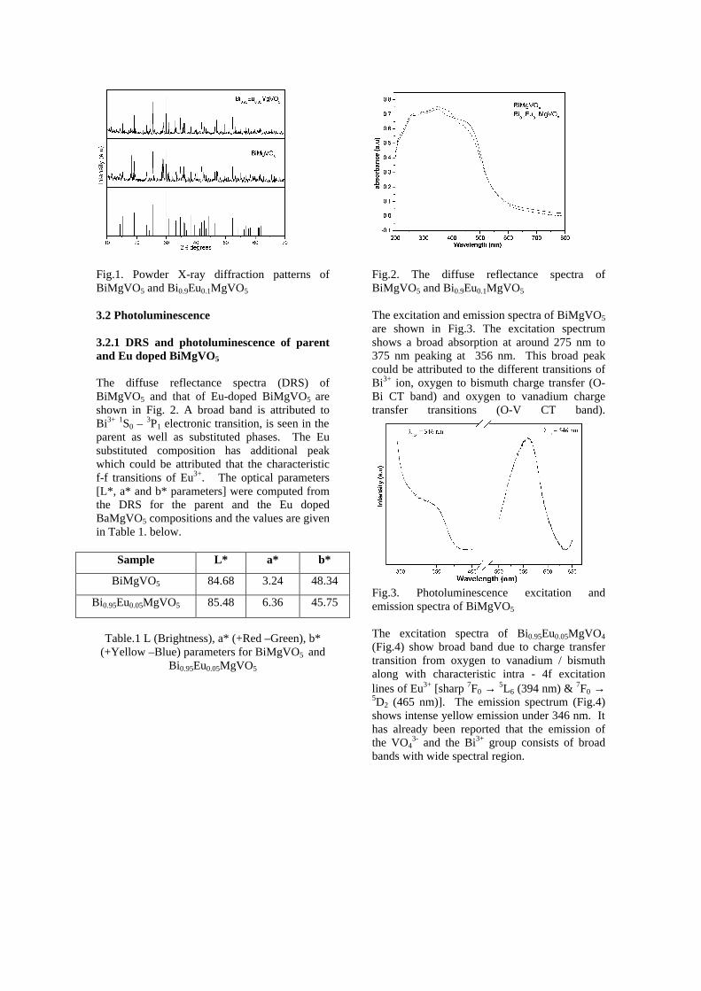
Fig.1. Powder X-ray diffraction patterns of BiMgVO5 and Bi0.9Eu0.1MgVO5 3.2 Photoluminescence 3.2.1 DRS and photoluminescence of parent and Eu doped BiMgVO5
The diffuse reflectance spectra (DRS) of BiMgVO5 and that of Eu-doped BiMgVO5 are shown in Fig. 2. A broad band is attributed to Bi3+ 1S0 – 3P1 electronic transition, is seen in the parent as well as substituted phases. The Eu substituted composition has additional peak which could be attributed that the characteristic f-f transitions of Eu3+. The optical parameters [L*, a* and b* parameters] were computed from the DRS for the parent and the Eu doped BaMgVO5 compositions and the values are given in Table 1. below.
Sample L* a* b*
BiMgVO5 84.68 3.24 48.34
Bi0.95Eu0.05MgVO5 85.48 6.36 45.75
Table.1 L (Brightness), a* (+Red –Green), b*
(+Yellow –Blue) parameters for BiMgVO5 and Bi0.95Eu0.05MgVO5
Fig.2. The diffuse reflectance spectra of BiMgVO5 and Bi0.9Eu0.1MgVO5
The excitation and emission spectra of BiMgVO5 are shown in Fig.3. The excitation spectrum shows a broad absorption at around 275 nm to 375 nm peaking at 356 nm. This broad peak could be attributed to the different transitions of Bi3+ ion, oxygen to bismuth charge transfer (O-Bi CT band) and oxygen to vanadium charge transfer transitions (O-V CT band).
Fig.3. Photoluminescence excitation and emission spectra of BiMgVO5 The excitation spectra of Bi0.95Eu0.05MgVO4 (Fig.4) show broad band due to charge transfer transition from oxygen to vanadium / bismuth along with characteristic intra - 4f excitation lines of Eu3+ [sharp 7F0 → 5L6 (394 nm) & 7F0 → 5D2 (465 nm)]. The emission spectrum (Fig.4) shows intense yellow emission under 346 nm. It has already been reported that the emission of the VO4
3- and the Bi3+ group consists of broad bands with wide spectral region.
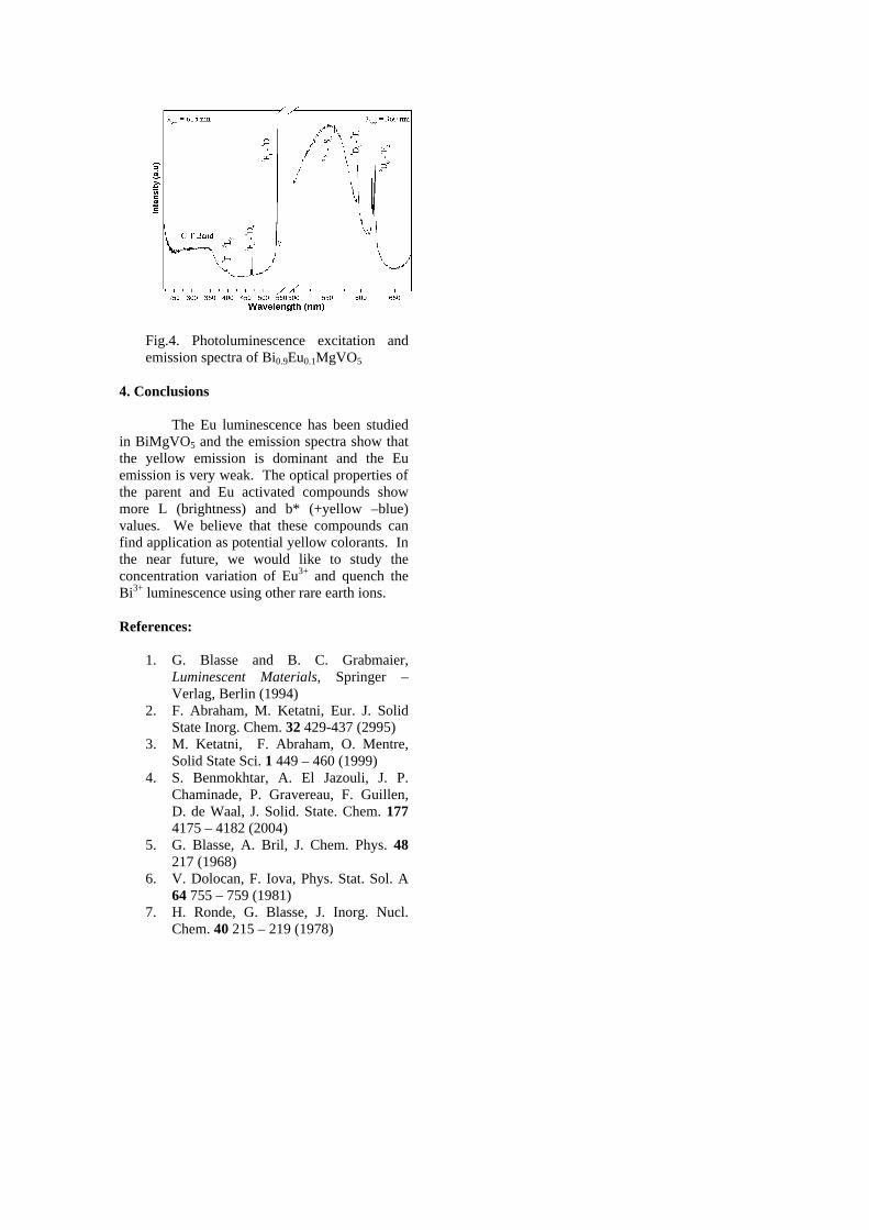
Fig.4. Photoluminescence excitation and emission spectra of Bi0.9Eu0.1MgVO5
4. Conclusions The Eu luminescence has been studied in BiMgVO5 and the emission spectra show that the yellow emission is dominant and the Eu emission is very weak. The optical properties of the parent and Eu activated compounds show more L (brightness) and b* (+yellow –blue) values. We believe that these compounds can find application as potential yellow colorants. In the near future, we would like to study the concentration variation of Eu3+ and quench the Bi3+ luminescence using other rare earth ions. References:
1. G. Blasse and B. C. Grabmaier, Luminescent Materials, Springer – Verlag, Berlin (1994)
2. F. Abraham, M. Ketatni, Eur. J. Solid State Inorg. Chem. 32 429-437 (2995)
3. M. Ketatni, F. Abraham, O. Mentre, Solid State Sci. 1 449 – 460 (1999)
4. S. Benmokhtar, A. El Jazouli, J. P. Chaminade, P. Gravereau, F. Guillen, D. de Waal, J. Solid. State. Chem. 177 4175 – 4182 (2004)
5. G. Blasse, A. Bril, J. Chem. Phys. 48 217 (1968)
6. V. Dolocan, F. Iova, Phys. Stat. Sol. A 64 755 – 759 (1981)
7. H. Ronde, G. Blasse, J. Inorg. Nucl. Chem. 40 215 – 219 (1978)
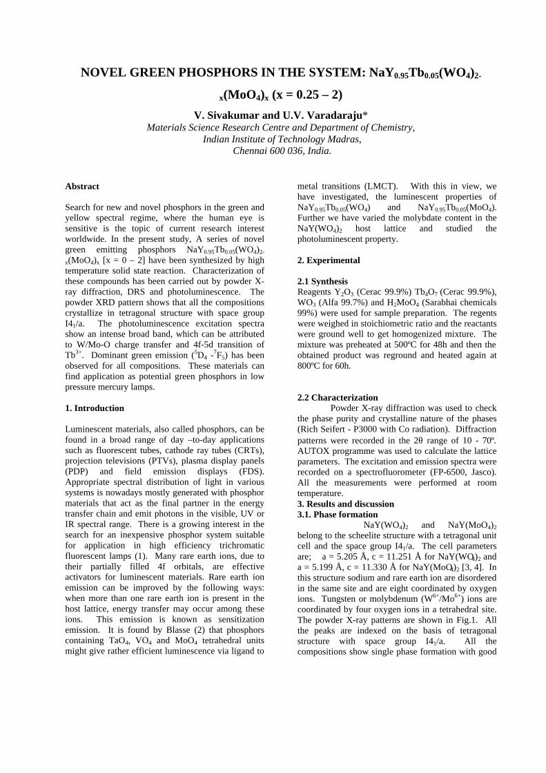
NOVEL GREEN PHOSPHORS IN THE SYSTEM: NaY0.95Tb0.05(WO4)2-
x(MoO4)x (x = 0.25 – 2)
V. Sivakumar and U.V. Varadaraju* Materials Science Research Centre and Department of Chemistry,
Indian Institute of Technology Madras, Chennai 600 036, India.
Abstract Search for new and novel phosphors in the green and yellow spectral regime, where the human eye is sensitive is the topic of current research interest worldwide. In the present study, A series of novel green emitting phosphors NaY0.95Tb0.05(WO4)2-
x(MoO4)x [x = 0 – 2] have been synthesized by high temperature solid state reaction. Characterization of these compounds has been carried out by powder X-ray diffraction, DRS and photoluminescence. The powder XRD pattern shows that all the compositions crystallize in tetragonal structure with space group I41/a. The photoluminescence excitation spectra show an intense broad band, which can be attributed to W/Mo-O charge transfer and 4f-5d transition of Tb3+. Dominant green emission (5D4 -7F5) has been observed for all compositions. These materials can find application as potential green phosphors in low pressure mercury lamps. 1. Introduction Luminescent materials, also called phosphors, can be found in a broad range of day –to-day applications such as fluorescent tubes, cathode ray tubes (CRTs), projection televisions (PTVs), plasma display panels (PDP) and field emission displays (FDS). Appropriate spectral distribution of light in various systems is nowadays mostly generated with phosphor materials that act as the final partner in the energy transfer chain and emit photons in the visible, UV or IR spectral range. There is a growing interest in the search for an inexpensive phosphor system suitable for application in high efficiency trichromatic fluorescent lamps (1). Many rare earth ions, due to their partially filled 4f orbitals, are effective activators for luminescent materials. Rare earth ion emission can be improved by the following ways: when more than one rare earth ion is present in the host lattice, energy transfer may occur among these ions. This emission is known as sensitization emission. It is found by Blasse (2) that phosphors containing TaO4, VO4 and MoO4 tetrahedral units might give rather efficient luminescence via ligand to
metal transitions (LMCT). With this in view, we have investigated, the luminescent properties of NaY0.95Tb0.05(WO4) and NaY0.95Tb0.05(MoO4). Further we have varied the molybdate content in the NaY(WO4)2 host lattice and studied the photoluminescent property. 2. Experimental 2.1 Synthesis Reagents Y2O3 (Cerac 99.9%) Tb4O7 (Cerac 99.9%), WO3 (Alfa 99.7%) and H2MoO4 (Sarabhai chemicals 99%) were used for sample preparation. The regents were weighed in stoichiometric ratio and the reactants were ground well to get homogenized mixture. The mixture was preheated at 500ºC for 48h and then the obtained product was reground and heated again at 800ºC for 60h. 2.2 Characterization Powder X-ray diffraction was used to check the phase purity and crystalline nature of the phases (Rich Seifert - P3000 with Co radiation). Diffraction patterns were recorded in the 2θ range of 10 - 70º. AUTOX programme was used to calculate the lattice parameters. The excitation and emission spectra were recorded on a spectrofluorometer (FP-6500, Jasco). All the measurements were performed at room temperature. 3. Results and discussion 3.1. Phase formation
NaY(WO4)2 and NaY(MoO4)2 belong to the scheelite structure with a tetragonal unit cell and the space group I41/a. The cell parameters are; a = 5.205 Å, c = 11.251 Å for NaY(WO4)2 and a = 5.199 Å, c = 11.330 Å for NaY(MoO4)2 [3, 4]. In this structure sodium and rare earth ion are disordered in the same site and are eight coordinated by oxygen ions. Tungsten or molybdenum (W6+/Mo6+) ions are coordinated by four oxygen ions in a tetrahedral site. The powder X-ray patterns are shown in Fig.1. All the peaks are indexed on the basis of tetragonal structure with space group I41/a. All the compositions show single phase formation with good
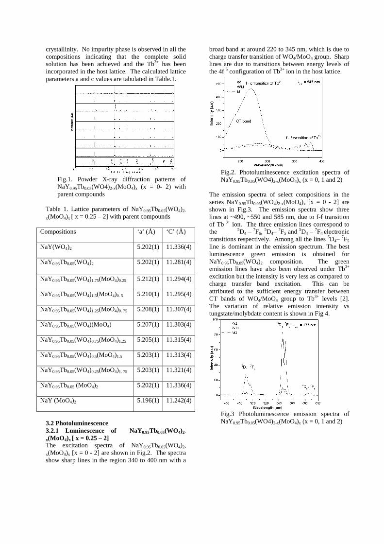
crystallinity. No impurity phase is observed in all the compositions indicating that the complete solid solution has been achieved and the Tb3+ has been incorporated in the host lattice. The calculated lattice parameters a and c values are tabulated in Table.1.
Fig.1. Powder X-ray diffraction patterns of NaY0.95Tb0.05(WO4)2-x(MoO4)x (x = 0- 2) with parent compounds
Table 1. Lattice parameters of NaY0.95Tb0.05(WO4)2-
x(MoO4)x [ x = 0.25 – 2] with parent compounds
Compositions
‘a’ (Å) ‘C’ (Å)
NaY(WO4)2
5.202(1) 11.336(4)
NaY0.95Tb0.05(WO4)2 5.202(1) 11.281(4)
NaY0.95Tb0.05(WO4)1.75(MoO4)0.25
5.212(1)
11.294(4)
NaY0.95Tb0.05(WO4)1.5(MoO4)0. 5
5.210(1)
11.295(4)
NaY0.95Tb0.05(WO4)1.25(MoO4)0. 75
5.208(1)
11.307(4)
NaY0.95Tb0.05(WO4)(MoO4)
5.207(1)
11.303(4)
NaY0.95Tb0.05(WO4)0.75(MoO4)1.25
5.205(1)
11.315(4)
NaY0.95Tb0.05(WO4)0.5(MoO4)1.5
5.203(1)
11.313(4)
NaY0.95Tb0.05(WO4)0.25(MoO4)1. 75
5.203(1)
11.321(4)
NaY0.95Tb0.05 (MoO4)2
5.202(1)
11.336(4)
NaY (MoO4)2
5.196(1)
11.242(4)
3.2 Photoluminescence 3.2.1 Luminescence of NaY0.95Tb0.05(WO4)2-
x(MoO4)x [ x = 0.25 – 2] The excitation spectra of NaY0.95Tb0.05(WO4)2-
x(MoO4)x [x = 0 - 2] are shown in Fig.2. The spectra show sharp lines in the region 340 to 400 nm with a
broad band at around 220 to 345 nm, which is due to charge transfer transition of WO4/MoO4 group. Sharp lines are due to transitions between energy levels of the 4f 5 configuration of Tb3+ ion in the host lattice.
Fig.2. Photoluminescence excitation spectra of NaY0.95Tb0.05(WO4)2-x(MoO4)x (x = 0, 1 and 2)
The emission spectra of select compositions in the series NaY0.95Tb0.05(WO4)2-x(MoO4)x [x = 0 - 2] are shown in Fig.3. The emission spectra show three lines at ~490, ~550 and 585 nm, due to f-f transition of Tb 3+ ion. The three emission lines correspond to the 5D4 – 7F6,
5D4– 7F5 and 5D4 – 7F4 electronic transitions respectively. Among all the lines 5D4– 7F5 line is dominant in the emission spectrum. The best luminescence green emission is obtained for NaY0.95Tb0.05(WO4)2 composition. The green emission lines have also been observed under Tb3+ excitation but the intensity is very less as compared to charge transfer band excitation. This can be attributed to the sufficient energy transfer between CT bands of WO4/MoO4 group to Tb3+ levels [2]. The variation of relative emission intensity vs tungstate/molybdate content is shown in Fig 4.
Fig.3 Photoluminescence emission spectra of NaY0.95Tb0.05(WO4)2-x(MoO4)x (x = 0, 1 and 2)
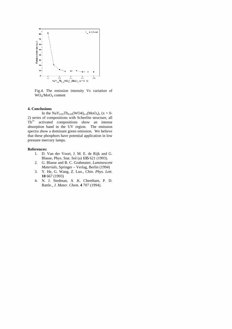
Fig.4. The emission intensity Vs variation of WO4/MoO4 content
4. Conclusions In the NaY0.95Tb0.05(WO4)2-x(MoO4)x (x = 0- 2) series of compositions with Scheelite structure, all Tb3+ activated compositions show an intense absorption band in the UV region. The emission spectra show a dominant green emission. We believe that these phosphors have potential application in low pressure mercury lamps. References:
1. D. Van der Voort, J. M. E. de Rijk and G. Blasse, Phys. Stat. Sol (a) 135 621 (1993).
2. G. Blasse and B. C. Grabmaier, Luminescent Materials, Springer – Verlag, Berlin (1994)
3. Y. He, G. Wang, Z. Luo., Chin. Phys. Lett. 10 667 (1993)
4. N. J. Stedman, A .K. Cheetham, P. D. Battle., J. Mater. Chem. 4 707 (1994).
Fluorescence Characterisation of a Dye Doped Graded Index Polymer Optical Fiber Preform
M.Kailasnath1, P.R.John2, Rajesh Kumar3, P.Radhakrishnan1, V.P.N.Nampoori1, S.Prathapan2,C.P.G.Vallabhan3
International School of Photonics1, Department of Applied Chemistry2, Centre of Excellence in Lasers and
Optoelectronic Sciences3. Cochin University of Science and Technology, Kochi- 682 022, INDIA
E-mail: [email protected]
ABSTRACT Graded index polymer optical fiber (GIPOF) is considered to be a good choice for providing inexpensive high bandwidth data link for local area networks and telecommunication applications due to their parabolic refractive index distribution. Development of interfacial-gel polymerization technique enabled the dramatic reduction in the total attenuation of the GIPOF. It is considered to be one of the potent methods to prepare GI preform. A novel graded index (GI) poly (methyl methacrylate)(PMMA) optical fiber preform was prepared by interfacial gel polymerization carried out in a PMMA tube. Diphenyl phthalate (DPP) a higher refractive index molecule was used to obtain a graded index distribution and Rhodamine B was used as a laser dye. The sample was illuminated laterally with a Diode Pumped Solid State laser (DPSS) emitting at 532 nm. The fluorescence emission was measured from one end of the rod by varying the point of excitation. We observe that the peaks exhibit a red shift of about 10 nm while varying the point of excitation through a distance of 3.5cm of the rod. The extend of doping of the Rh B was also studied by axially exciting a thin slice of the rod with white light and measuring the intensity of fluorescence at 590 nm at various points. The maximum fluorescence intensity was obtained at the axis due to the variation in the extend of doping and due to the light focusing property of the rod. 1 Introduction In the last few years, interest in polymer optical fibers (POFs) has increased significantly because of its ease of handling, flexibility and potential low cost. Although the loss of POF is still much higher than that of silica optical fiber, recent progress has led to poly (methyl methacrylate) based POF with a loss less than 100 dB/km, low enough for many short length applications[1] Vast majority of optical amplifiers are based on an optic fiber doped with a fraction of a percent of the rare-earth element erbium. Although rare-earth doping has been generally used in silica, research laboratories have been working to develop stable rare-earth doped polymer lasers and amplifiers. The main issue with rare earth doped polymer lasers and amplifiers have been pumping inefficiencies due to the de- excitation of the excited states caused by the IR absorption in the polymer. In bulk form, Polymer hosts impregnated with certain dye have now achieved an 80% conversion efficiency from pump power to signal power with tuning range close to those in solution. Dye –doped POF’s can be made into useful fiber amplifiers and lasers that operate at wavelengths other than 1300nm and 1550 nm[2-5]. Optical amplifiers and lasers made of dye doped fiber require much less pump power than in bulk material because of the effective confinement and long interaction length available in the fiber. Since photo bleaching increases with the increase of the exposure intensity, a low pump intensity would increase the life time of the gain medium. Also, the thin and long geometry of the fiber is ideal for good thermal
relaxation to minimize the thermally induced photo bleaching [6]. 2 Experimental The dye doped graded index polymer optical fiber preform was prepared by the well-known interfacial gel polymerization technique where initially a hollow cylinder of polymer is prepared. In the second phase of polymerization, diphenyl phthalate (DPP)a higher refractive index molecule, was added and the laser dye RhodamineB was introduced. To obtain, any particular refractive index profile in the core along the radial direction, a preform with the desired profile can be employed. The preform is a cylinder of polymer whose refractive index distribution can be made to coincide with that desired for the POF’s core, so this technique is very versatile [7]. Interferometry is an accurate method for determining the refractive index profile of both preforms and fibers. We have measured the refractive index profile of the solid rod using the slab method where a thin slice of the preform was cut, polished and kept in one of the arms of a Mach Zender interferometrer. The light passing through the slab undergoes a phase shift which depends on the optical path length. The field displacements for the points within the fiber core are then measured using the parallel fringes outside the fiber core in the cladding. The refractive index difference between the core and cladding can be calculated from the fringe shift S(r) and the parallel fringe spacing D (in the cladding) according to the relationship [8]
Page 1 of 3 Proceedings of OMTAT2005
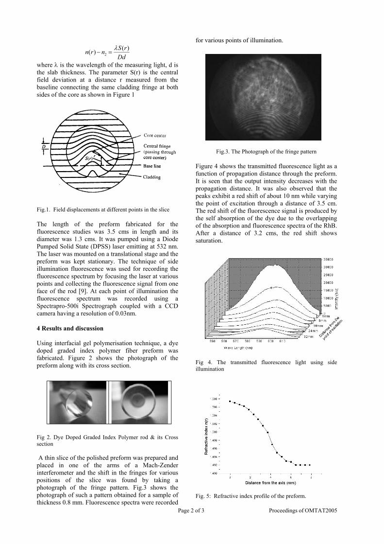
2( )( ) S rn r n
Ddλ
− =
where λ is the wavelength of the measuring light, d is the slab thickness. The parameter S(r) is the central field deviation at a distance r measured from the baseline connecting the same cladding fringe at both sides of the core as shown in Figure 1
Fig.1. Field displacements at different points in the slice The length of the preform fabricated for the fluorescence studies was 3.5 cms in length and its diameter was 1.3 cms. It was pumped using a Diode Pumped Solid State (DPSS) laser emitting at 532 nm. The laser was mounted on a translational stage and the preform was kept stationary. The technique of side illumination fluorescence was used for recording the fluorescence spectrum by focusing the laser at various points and collecting the fluorescence signal from one face of the rod [9]. At each point of illumination the fluorescence spectrum was recorded using a Spectrapro-500i Spectrograph coupled with a CCD camera having a resolution of 0.03nm. 4 Results and discussion Using interfacial gel polymerisation technique, a dye doped graded index polymer fiber preform was fabricated. Figure 2 shows the photograph of the preform along with its cross section.
Fig 2. Dye Doped Graded Index Polymer rod & its Cross section A thin slice of the polished preform was prepared and placed in one of the arms of a Mach-Zender interferometer and the shift in the fringes for various positions of the slice was found by taking a photograph of the fringe pattern. Fig.3 shows the photograph of such a pattern obtained for a sample of thickness 0.8 mm. Fluorescence spectra were recorded
for various points of illumination.
Fig.3. The Photograph of the fringe pattern
Figure 4 shows the transmitted fluorescence light as a function of propagation distance through the preform. It is seen that the output intensity decreases with the propagation distance. It was also observed that the peaks exhibit a red shift of about 10 nm while varying the point of excitation through a distance of 3.5 cm. The red shift of the fluorescence signal is produced by the self absorption of the dye due to the overlapping of the absorption and fluorescence spectra of the RhB. After a distance of 3.2 cms, the red shift shows saturation.
Fig 4. The transmitted fluorescence light using side illumination
Fig. 5: Refractive index profile of the preform.
Page 2 of 3 Proceedings of OMTAT2005
Fig 5 shows the refractive index profile of the fabricated preform. It was found that the maximum difference in the refractive indices between core and cladding is 0.015±(2) and it occurs along the axis of the preform and it gradually decreases towards the cladding. Figure 3 shows the photograph of the fringe pattern that is used for the calculation of refractive index profile. After proper calibration, the extent of doping of the dye rhodamine.B was also studied. The axial excitation of a thin slice of the rod using white light and measuring the fluorescence signal at 590 nm at various points shows that the maximum extent of doping of the dye molecules occur along the axis of the rod. The maximum fluorescence intensity along the axis is due to the variation of extent of doping and due to the light focusing property of the rod. Conclusions A graded index polymer optical fiber preform was fabricated using the interfacial gel polymerisation technique and its refractive index profile was measured using the interferometric technique. It was seen that the refractive index varies from the value 1.492 in the cladding to 1.507 at the axis. This suggests that one can fabricate cladded polymer optical fiber with dye doped core using this preform. Such dye doped optical fibre can be employed to develop fibre amplifier in the visible region. The fluorescence characterization of the preform shows that it exhibits a red shift of about 10 nm while varying the point of excitation through a distance of 3.5 cm. The variation of dye concentration incorporated in the core region of the preform has been studied by measuring the fluorescence intensity across the output end. results show maximum intensity along the axis, as expected. Dye doped fiber using this preform will be drawn in the next phase of the studies. References 1 Xinhua Dai ,Jun He, Zhimin Liu, Xicheng Ai, Guanying Yang, Buxing Han, Jian Xu, Journal of Applied Polymer Science 91,2330 (2004)
2 Jui-Hsiang Liu, Hung-Yu Wang and Chia-Haw Ho, Journal of Polymer Research,10,13 (2003) 3 E.De La rosa-Cruz C.W. Dirk and O. Rodriguez, V.M. Castano, Fiber and Integrated Optics, 20 (5),457 (2001) 4 “Plastic Optical Fiber of the year 2001” Market Survey, KMI Corp , 1994 5 Y.Koike, T.Ishigure, and E.Nihei J.Light. Technol., 13,1475 (1995) 6 Popov.S Appl.Opt. 37,6449 (1998) 7 J.S Vrentas etal, Macromolecules,27,5570 (1994) 8 C.K.Sarkar Optoelectronics and Fiber Optics Communication 2001, New Age International, New Delhi 9 Kruhlak,R.J, M G Kuzyk, J.Opt.Soc.Am.B 16,1749(1999) 10 Wen Ding, Lisheng Zhong, Chuanxiang Xu, Shoutal Wang: proceedings of 7thInternational conference on properties and Applications of Dielectric materials June 1-5 2003 Nagoya
Page 3 of 3 Proceedings of OMTAT2005
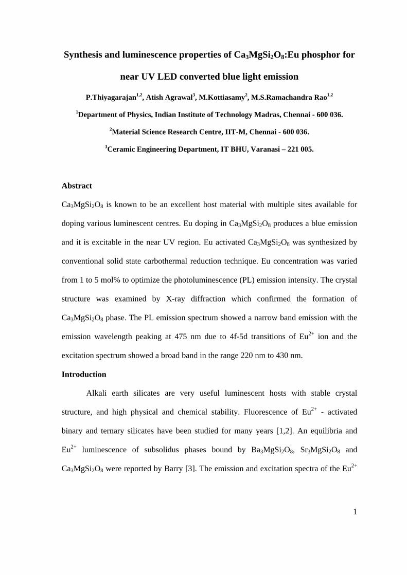
1
Synthesis and luminescence properties of Ca3MgSi2O8:Eu phosphor for
near UV LED converted blue light emission
P.Thiyagarajan1,2, Atish Agrawal3, M.Kottiasamy2, M.S.Ramachandra Rao1,2
1Department of Physics, Indian Institute of Technology Madras, Chennai - 600 036.
2Material Science Research Centre, IIT-M, Chennai - 600 036.
3Ceramic Engineering Department, IT BHU, Varanasi – 221 005.
Abstract
Ca3MgSi2O8 is known to be an excellent host material with multiple sites available for
doping various luminescent centres. Eu doping in Ca3MgSi2O8 produces a blue emission
and it is excitable in the near UV region. Eu activated Ca3MgSi2O8 was synthesized by
conventional solid state carbothermal reduction technique. Eu concentration was varied
from 1 to 5 mol% to optimize the photoluminescence (PL) emission intensity. The crystal
structure was examined by X-ray diffraction which confirmed the formation of
Ca3MgSi2O8 phase. The PL emission spectrum showed a narrow band emission with the
emission wavelength peaking at 475 nm due to 4f-5d transitions of Eu2+ ion and the
excitation spectrum showed a broad band in the range 220 nm to 430 nm.
Introduction
Alkali earth silicates are very useful luminescent hosts with stable crystal
structure, and high physical and chemical stability. Fluorescence of Eu2+ - activated
binary and ternary silicates have been studied for many years [1,2]. An equilibria and
Eu2+ luminescence of subsolidus phases bound by Ba3MgSi2O8, Sr3MgSi2O8 and
Ca3MgSi2O8 were reported by Barry [3]. The emission and excitation spectra of the Eu2+
2
ion usually consist of broad bands due to transition between the 8S7/2 (4f7) ground state
and the crystal field components of the 4f65d excited state configuration. One of the
advantages of the Eu2+ ion is its emission spectrum which varies from ultra-violet to red
depending on the nature of the host lattice. The other important parameters, that
influences the emission properties are covalency, size of the cation and crystal field
strength [4,5]. L. Huang and his coworker reported the Ca3MgSi2O8:Ce phosphor with
two kinds of emission maxima in the host [6]. Luminescent properties of long after glow
in Ca3MgSi2O8:Eu2+, Dy3+ phosphor was studied by L. Yuanhua et al. [7].
In this work, we report on the synthesis of Eu2+ activated Ca3MgSi2O8 by
conventional solid state reduction method. Optimization of luminescence properties were
carried out by varying the dopant concentration. The excitation spectrum covers a broad
band from 220 nm to 430 nm, and found promising for UV and near UV excitable
phosphor in the field of phosphor converted light emitting diode.
Experimental
Blue light emitting Eu2+ doped Ca3MgSi2O8 phosphor has been synthesized by
conventional solid state carbothermal reduction method using luminescent grade
chemicals (purity ~ 99.5+ %). The starting ingredients consisted of CaCO3 (STREM
Chemicals, 99.95%), 4MgCO3.Mg(OH)2.5H2O (Central Drug House (CDH), 99%), SiO2,
Eu2O3 (Indian Rare Earth, 99.9%) and carbon (analar reagent AR). Carbon is used as a
reducing agent. In order to optimize the emission intensity, the Eu concentration was
varied from 1 to 5 mol%. As per the calculation, the chemicals were weighed
stoichiometrically using the above chemical ingredients. The mixture was ground well in
an agate mortar into a fine powder. Subsequently, the powder mixtures was placed in a
3
crucible along with reducing agent (carbon), kept in a muffle furnace, fired at 1200oC for
12h. The calcined compounds were subjected to intermittent grinding followed by firing
at 1200oC for 12h to achieve the host crystallinity and proper doping of Eu2+.
Phase analysis was examined by X- ray powder diffraction (XRD) using Cu Kα
radiation (P3000, Rich Seifert, Germany) with a source power of 35kV and 20mA. The
phase was examined by analyzing XRD patterns and unit cell parameters were calculated
from the diffraction data using autox software. PL emission and PL excitation spectra
were recorded at room temperature using (Fluorolog) fluorescence spectrophotometer
operating in the wavelength region 200 to 700 nm using a 350W xenon lamp.
Result and Discussions
The XRD pattern of Eu2+ doped Ca3MgSi2O8 phosphor synthesized by calcining
at 1200oC for 12h followed by intermittent grinding, heated at 1200oC for 12h in a
reducing carbon atmosphere is shown in Fig.1.
30 35 40 45 502θθ in degrees
1200oC/12+12h
Ca3MgSi
2O
8:Eu
0.01
Inte
nsi
ty(a
.u)
Fig.1 Powder x-ray diffraction pattern of Ca3MgSi2O8:Eu0.01 in comparison with JCPDS.
The pattern conforms the formation of Ca3MgSi2O8 host (Merminite) in monoclinic
crystal structure.
4
Photoluminescence (PL) studies
The photoluminescence excitation and emission spectra are shown in Fig.2. The
excitation spectrum shows a very broad absorption in the UV region with an excitation
maximum at 330 nm and a shoulder at 300 nm. The emission spectrum showed a very
narrow band emission peaked at 475 nm. The optical transition is ascribed to the electric
transition from 4f7 4f 65d1 levels of Eu2+ ion.
200 300 400 500 600
Excitation spectrum Emission spectrum
λλem
= 475 nm
λλex
= 365 nm
Ca3MgSi
2O
8:Eu
0.01
Wavelength (nm)
Inte
nsi
ty (
a.u
)
Fig.2 Emission and excitation spectrum of Ca3MgSi2O8:Eu0.01 phopshors.
The 4f orbital is less affected by the crystal field because it is shielded by the
outer 5d and 6s orbitals, whereas the outer 5d orbital is strongly influenced by the crystal
field. The accounts for broadness in the excitation and emission spectra are predicted due
to the participation of 5d orbital in the optical absorption or emission phenomenon. There
is no appearance of emission from Eu3+, which confirms that Eu3+ has been converted to
Eu2+. The prediction of position in energy of emission has been calculated by VanUitert
[8] using the empirical relation
E = Q[1 – (Z/4)1/õ x 10-(n.ea.r/8)]
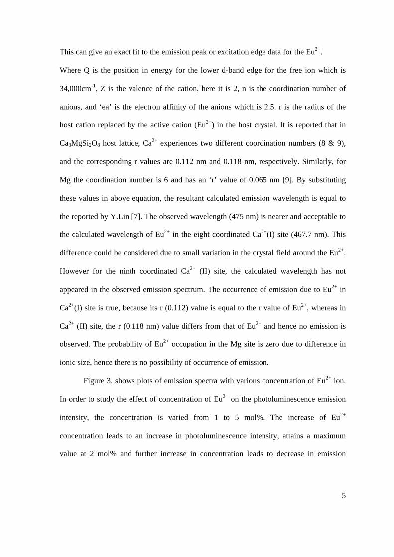
5
This can give an exact fit to the emission peak or excitation edge data for the Eu2+.
Where Q is the position in energy for the lower d-band edge for the free ion which is
34,000cm-1, Z is the valence of the cation, here it is 2, n is the coordination number of
anions, and ‘ea’ is the electron affinity of the anions which is 2.5. r is the radius of the
host cation replaced by the active cation (Eu2+) in the host crystal. It is reported that in
Ca3MgSi2O8 host lattice, Ca2+ experiences two different coordination numbers (8 & 9),
and the corresponding r values are 0.112 nm and 0.118 nm, respectively. Similarly, for
Mg the coordination number is 6 and has an ‘r’ value of 0.065 nm [9]. By substituting
these values in above equation, the resultant calculated emission wavelength is equal to
the reported by Y.Lin [7]. The observed wavelength (475 nm) is nearer and acceptable to
the calculated wavelength of Eu2+ in the eight coordinated Ca2+(I) site (467.7 nm). This
difference could be considered due to small variation in the crystal field around the Eu2+.
However for the ninth coordinated Ca2+ (II) site, the calculated wavelength has not
appeared in the observed emission spectrum. The occurrence of emission due to Eu2+ in
Ca2+(I) site is true, because its r (0.112) value is equal to the r value of Eu2+, whereas in
Ca2+ (II) site, the r (0.118 nm) value differs from that of Eu2+ and hence no emission is
observed. The probability of Eu2+ occupation in the Mg site is zero due to difference in
ionic size, hence there is no possibility of occurrence of emission.
Figure 3. shows plots of emission spectra with various concentration of Eu2+ ion.
In order to study the effect of concentration of Eu2+ on the photoluminescence emission
intensity, the concentration is varied from 1 to 5 mol%. The increase of Eu2+
concentration leads to an increase in photoluminescence intensity, attains a maximum
value at 2 mol% and further increase in concentration leads to decrease in emission
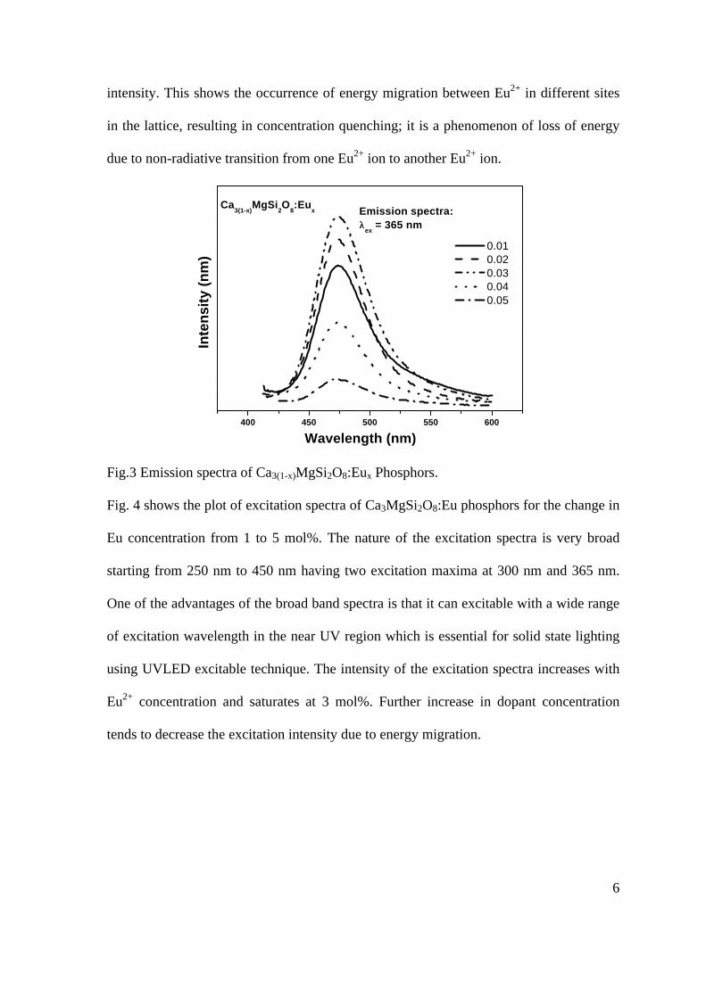
6
intensity. This shows the occurrence of energy migration between Eu2+ in different sites
in the lattice, resulting in concentration quenching; it is a phenomenon of loss of energy
due to non-radiative transition from one Eu2+ ion to another Eu2+ ion.
400 450 500 550 600
0.01 0.02 0.03 0.04 0.05
Wavelength (nm)
Inte
nsi
ty (
nm
)Emission spectra:λλ
ex = 365 nm
Ca3(1-x)
MgSi2O
8:Eu
x
Fig.3 Emission spectra of Ca3(1-x)MgSi2O8:Eux Phosphors.
Fig. 4 shows the plot of excitation spectra of Ca3MgSi2O8:Eu phosphors for the change in
Eu concentration from 1 to 5 mol%. The nature of the excitation spectra is very broad
starting from 250 nm to 450 nm having two excitation maxima at 300 nm and 365 nm.
One of the advantages of the broad band spectra is that it can excitable with a wide range
of excitation wavelength in the near UV region which is essential for solid state lighting
using UVLED excitable technique. The intensity of the excitation spectra increases with
Eu2+ concentration and saturates at 3 mol%. Further increase in dopant concentration
tends to decrease the excitation intensity due to energy migration.
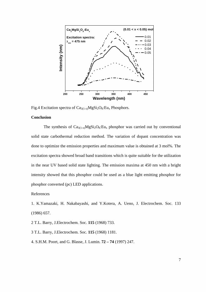
7
200 250 300 350 400 450
(0.01 < x < 0.05) mol
0.01 0.02 0.03 0.04 0.05
Inte
nsi
ty (
nm
)
Wavelength (nm)
Ca3MgSi
2O
8:Eu
x
Excitation spectra:λλ
em = 475 nm
Fig.4 Excitation spectra of Ca3(1-x)MgSi2O8:Eux Phosphors.
Conclusion
The synthesis of Ca3(1-x)MgSi2O8:Eux phosphor was carried out by conventional
solid state carbothermal reduction method. The variation of dopant concentration was
done to optimize the emission properties and maximum value is obtained at 3 mol%. The
excitation spectra showed broad band transitions which is quite suitable for the utilization
in the near UV based solid state lighting. The emission maxima at 450 nm with a bright
intensity showed that this phosphor could be used as a blue light emitting phosphor for
phosphor converted (pc) LED applications.
References
1. K.Yamazaki, H. Nakabayashi, and Y.Kotera, A. Ueno, J. Electrochem. Soc. 133
(1986) 657.
2 T.L. Barry, J.Electrochem. Soc. 115 (1968) 733.
3 T.L. Barry, J.Electrochem. Soc. 115 (1968) 1181.
4. S.H.M. Poort, and G. Blasse, J. Lumin. 72 – 74 (1997) 247.

8
5. G. Blasse, W.L. Wanmaker et al., Philips Res. Rep. 23 (1968) 189.
6. L. Huang, X. Zhang and X. Liu, J. Alloy. Comp., 14, 2000, 305.
7. Y. Lin, Z. Zhang, Z. Tang, X. Wang, J. Zhang, and Z. Zheng, J. Europ. Cer. Soc. 21
(2001) 683.
8. L.G. Van Uitert, J. Lumin., 29, 1984, 1.
9. K.H. Butler, Fluorescent Lamp Phosphors Technology and Theory, Pennsylvania State
University Press, 1980, p.278.
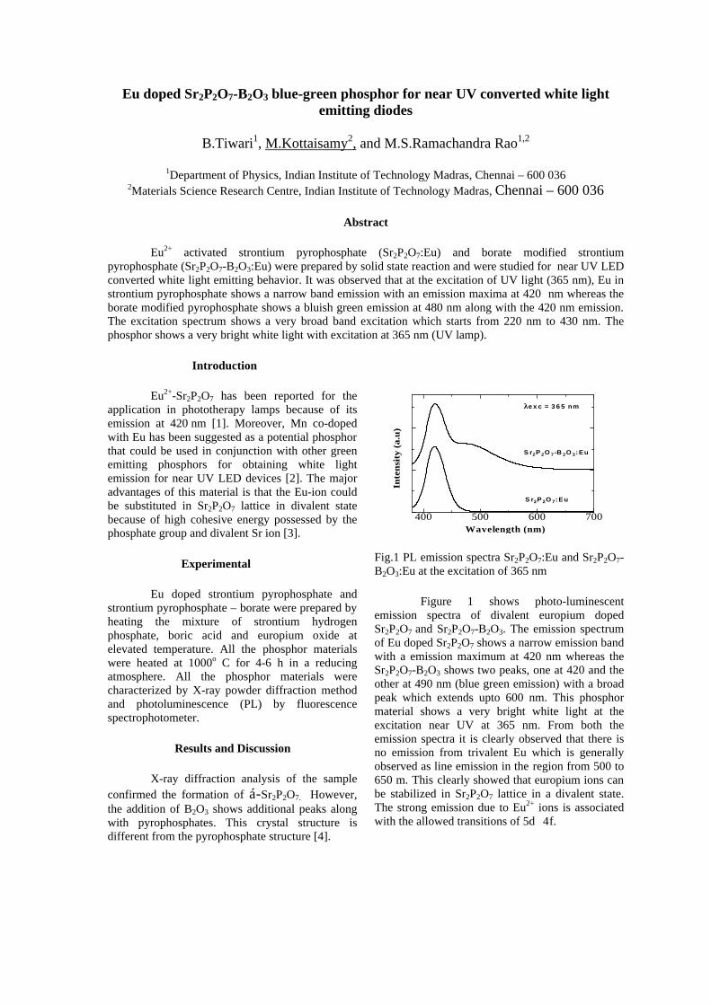
Eu doped Sr2P2O7-B2O3 blue-green phosphor for near UV converted white light emitting diodes
B.Tiwari1, M.Kottaisamy2, and M.S.Ramachandra Rao1,2
1Department of Physics, Indian Institute of Technology Madras, Chennai – 600 036
2Materials Science Research Centre, Indian Institute of Technology Madras, Chennai – 600 036
Abstract
Eu2+ activated strontium pyrophosphate (Sr2P2O7:Eu) and borate modified strontium pyrophosphate (Sr2P2O7-B2O3:Eu) were prepared by solid state reaction and were studied for near UV LED converted white light emitting behavior. It was observed that at the excitation of UV light (365 nm), Eu in strontium pyrophosphate shows a narrow band emission with an emission maxima at 420 nm whereas the borate modified pyrophosphate shows a bluish green emission at 480 nm along with the 420 nm emission. The excitation spectrum shows a very broad band excitation which starts from 220 nm to 430 nm. The phosphor shows a very bright white light with excitation at 365 nm (UV lamp).
Introduction
Eu2+-Sr2P2O7 has been reported for the application in phototherapy lamps because of its emission at 420 nm [1]. Moreover, Mn co-doped with Eu has been suggested as a potential phosphor that could be used in conjunction with other green emitting phosphors for obtaining white light emission for near UV LED devices [2]. The major advantages of this material is that the Eu-ion could be substituted in Sr2P2O7 lattice in divalent state because of high cohesive energy possessed by the phosphate group and divalent Sr ion [3].
Experimental
Eu doped strontium pyrophosphate and strontium pyrophosphate – borate were prepared by heating the mixture of strontium hydrogen phosphate, boric acid and europium oxide at elevated temperature. All the phosphor materials were heated at 1000o C for 4-6 h in a reducing atmosphere. All the phosphor materials were characterized by X-ray powder diffraction method and photoluminescence (PL) by fluorescence spectrophotometer.
Results and Discussion
X-ray diffraction analysis of the sample confirmed the formation of á-Sr2P2O7. However, the addition of B2O3 shows additional peaks along with pyrophosphates. This crystal structure is different from the pyrophosphate structure [4].
400 500 600 700
Wavelength (nm)
Inte
nsi
ty (
a.u
)
S r2P 2O 7-B 2O 3:E u
λλexc = 365 nm
S r2P 2O 7:E u
Fig.1 PL emission spectra Sr2P2O7:Eu and Sr2P2O7-B2O3:Eu at the excitation of 365 nm
Figure 1 shows photo-luminescent emission spectra of divalent europium doped Sr2P2O7 and Sr2P2O7-B2O3. The emission spectrum of Eu doped Sr2P2O7 shows a narrow emission band with a emission maximum at 420 nm whereas the Sr2P2O7-B2O3 shows two peaks, one at 420 and the other at 490 nm (blue green emission) with a broad peak which extends upto 600 nm. This phosphor material shows a very bright white light at the excitation near UV at 365 nm. From both the emission spectra it is clearly observed that there is no emission from trivalent Eu which is generally observed as line emission in the region from 500 to 650 m. This clearly showed that europium ions can be stabilized in Sr2P2O7 lattice in a divalent state. The strong emission due to Eu2+ ions is associated with the allowed transitions of 5d 4f.
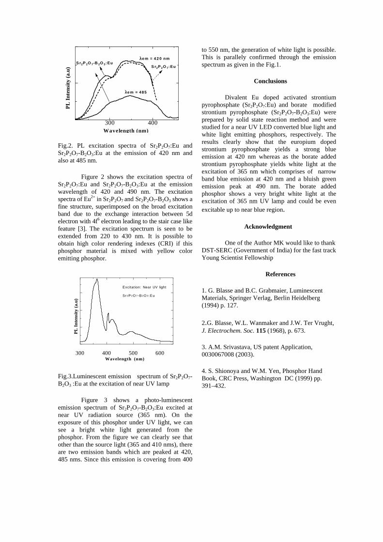
300 400
PL
Int
ensi
ty (
a.u)
Wavelength (nm)
λλem = 420 nm
λλem = 485
S r2P 2O 7-B 2O 3:E u S r2P 2O 7:E u
Fig.2. PL excitation spectra of Sr2P2O7:Eu and Sr2P2O7-B2O3:Eu at the emission of 420 nm and also at 485 nm.
Figure 2 shows the excitation spectra of Sr2P2O7:Eu and Sr2P2O7-B2O3:Eu at the emission wavelength of 420 and 490 nm. The excitation spectra of Eu2+ in Sr2P2O7 and Sr2P2O7-B2O3 shows a fine structure, superimposed on the broad excitation band due to the exchange interaction between 5d electron with 4f6 electron leading to the stair case like feature [3]. The excitation spectrum is seen to be extended from 220 to 430 nm. It is possible to obtain high color rendering indexes (CRI) if this phosphor material is mixed with yellow color emitting phosphor.
300 400 500 600
PL
Int
ensi
ty (
a.u)
Wavelength (nm)
E xcita tion: Near UV light
S r2P 2O 7 -B 2O 3 :E u
Fig.3.Luminescent emission spectrum of Sr2P2O7-B2O3 :Eu at the excitation of near UV lamp
Figure 3 shows a photo-luminescent emission spectrum of Sr2P2O7-B2O3:Eu excited at near UV radiation source (365 nm). On the exposure of this phosphor under UV light, we can see a bright white light generated from the phosphor. From the figure we can clearly see that other than the source light (365 and 410 nms), there are two emission bands which are peaked at 420, 485 nms. Since this emission is covering from 400
to 550 nm, the generation of white light is possible. This is parallely confirmed through the emission spectrum as given in the Fig.1.
Conclusions
Divalent Eu doped activated strontium pyrophosphate (Sr2P2O7:Eu) and borate modified strontium pyrophosphate (Sr2P2O7-B2O3:Eu) were prepared by solid state reaction method and were studied for a near UV LED converted blue light and white light emitting phosphors, respectively. The results clearly show that the europium doped strontium pyrophosphate yields a strong blue emission at 420 nm whereas as the borate added strontium pyrophosphate yields white light at the excitation of 365 nm which comprises of narrow band blue emission at 420 nm and a bluish green emission peak at 490 nm. The borate added phosphor shows a very bright white light at the excitation of 365 nm UV lamp and could be even excitable up to near blue region.
Acknowledgment
One of the Author MK would like to thank DST-SERC (Government of India) for the fast track Young Scientist Fellowship
References
1. G. Blasse and B.C. Grabmaier, Luminescent Materials, Springer Verlag, Berlin Heidelberg (1994) p. 127.
2.G. Blasse, W.L. Wanmaker and J.W. Ter Vrught, J. Electrochem. Soc. 115 (1968), p. 673.
3. A.M. Srivastava, US patent Application, 0030067008 (2003).
4. S. Shionoya and W.M. Yen, Phosphor Hand Book, CRC Press, Washington DC (1999) pp. 391–432.

Effect of co-dopants on the color tuning properties of YAG:Ce yellow phosphor for application in white light emitting phosphor converted Light Emitting Diodes
(pcLEDs)
J.Misra1, M.Kottaisamy2, P. Thiyagarajan1,2, and M.S. Ramachandra Rao1,2
1Department of Physics, Indian Institute of Technology Madras, Chennai – 600 036
2Materials Science Research Centre, Indian Institute of Technology Madras, Chennai – 600 036
Abstract
Gd and La co-doped YAG:Ce (Y3Al5O12:Ce) was prepared by citric acid sol-gel method and the effect of co-dopants was studied on the luminescent properties of Ce. YAG:Ce showed a broad band emission with a peak at 533 nm whereas the addition of Gd and La showed a significant red shift on the Ce emission with emission maxima at 556 and 576 nm respectively. Photoluminescent excitation and emission properties were studied on these materials with respect to the application in white light generation by converting blue light emitting LEDs at 465 nm.
Introduction
In general, all the semiconductor based LED emission are monochromatic in nature and tuning emission of colors including white light is possible only by applying phosphors which emit with different colors. Y3Al5O12-Ce, in short YAG: Ce, is widely used as a color correcting phosphor material for high pressure mercury lamps because it absorbs blue light. Recently, this phosphor has gained great deal of importance and has been found to be an efficient phosphor material for converting blue LED radiation into a very broad intense yellow emission band [1,2]. The solution sought by several manufacturers in the use of modified YAG in which part of yttrium is replaced by larger ionic size rare earth ions [3,4]. These larger ionic sized ions shift the Ce emission to longer wavelengths and color temperature could be changed. Because Ce emission in the YAG is lacks the coverage in the red region, the color rendering index (CRI) of this phosphor is lower. In this work, we have attempted to prepare YAG:Ce with various co-dopants like Gd or La at the Y-site and studied their effect on the spectral shift compared to that of parent YAG:Ce phosphor. To prepare YAG with homogenous mixing of Ce, Gd and La at molecular level, we applied citric acid gel method. This method leads to the formation of YAG phase at low temperatures.
Experimental
To prepare the phase pure YAG:Ce and co-doped with Gd and La, the required amounts of
corresponding metal nitrates were dissolved in water. Required amount of citric acid was then added. The solution was continuously stirred for several hours at 80°C to form a transparent gel. The gel was heated to 4000C an auto-combustion process took place yielding a yellowish fluffy precursor. All the precursors were heated at 1100oC for 6 h. X-ray diffraction data was collected using Seifert XRD 3000P powder diffractometer with Cu-Ká-radiation. The excitation and emission spectra were obtained by a Fluorolog (USA), fluorescence spectrophotometer by using a 1000 W Xe lamp as excitation source.
Results and discussion
The X-ray powder diffraction pattern of the YAG:Ce, co-doped with Ga (0.5 mole) and La (0.5 mole) are indexed as Y3Al5O12 phase (JCPDS file 33-40) and no impurity peaks are detected. No other diffraction peaks appeared for the Gd and La doped samples indicating that these elements are doped into the YAG lattice [5]. The addition of Gd and La to the YAG showed a clear shift to lower angle which clearly shows the doping of Gd and La at the Y site. The shift in 2è bragg reflection is due to the fact that Gd3+ (1.08Å) and La3+ (1.17 Å) are higher in ionic sizes than Y (1.04 Ao) which leads to the expansion of the lattice .
Figure 1, shows excitation spectra of YAG:Ce co-doped with Gd and La. There are two Ce3+ absorption bands in the region between 300 and 500 nm. They are centered at 342 and 462 nm due to the crystal-field splitting of the 5d state
[6].This Ce excitation band covers from 400 – 500 nm where this emission is found to be intense and and peaks provides a basis to apply the phosphor to blue GaN LEDs. The PL intensity of phosphors shows that there is a decrease in intensity for the Gd and La co-doped YAG:Ce.
300 400 500
PL
Int
ensi
ty (
a.u)
Wavelength (nm)
YA G :C e Y(G d)A G :C e Y(L a )A G :C e
λe m = 533 nm
Fig.1. PL Excitation spectra YAG:Ce co-doped with Gd and La.
500 600 700 800
PL
Int
ensi
ty (
a.u)
Wavelength (nm)
YA G :C e Y(G d)A G :C e Y(L a )A G :C e
λexc = 465 nm
x 2.6
x 2.1
Fig.2. Emission spectra YAG:Ce co- doped with Gd and La.
The photoluminescence (PL) emission spectra of YAG:Ce and co-doped with Gd and La are shown in Fig.2. From the emission spectra it was observed that the YAG:Ce showed a broad band emission with a peak at 533 nm whereas the addition of Gd and La showed a significant red shift on the Ce emission with a emission maxima at 556 and 576 nm, respectively. The PL emission spectra show a very broad band emission with peaks centered at 540 nm, which is due to the overlapping of two energy levels in Ce (2D-2F5/2 and 2D-2F7/2) at the excitation of 465 nm. The shift of peaks to a higher wavelength indicates that the lowest 5d has a shift to higher energy level due to the higher ionic size ions viz, Gd and La. It is reported that the change of unit cell affects the
crystal field around Ce3+, and causes the red shift of spectra [6]. As observed from the XRD patterns that the shift in the 2Ł value of diffraction peaks to left side due to Gd and La co-doping leads to increase in the lattice parameters. Therefore, the shift of peaks results from the change in crystal field around Ce3+ ions. However, the relative emission intensity for Gd and La co-doped phosphor is decreased about 2.1 and 2.5 times compared to that of YAG:Ce.
Conclusions
Gd and La co-doped YAG:Ce (Y3Al5O12:Ce) was prepared and their luminescent properties were studied at the excitation 465 nm for application in white light generation through blue LED excitation. The Gd co-doped samples showed a shift by about 20 nm and La co-doped one showed about 40 nm shift from that of YAG:Ce phosphors which emit at 533 nm. The La doped phosphor showed a warm white light emission and this phosphor could be mixed with YAG:Ce to generate more white color shades depends on the blend ratio.
Acknowlegment
One of the Author MK would like to thank DST-SERC (Government of India) for the fast track Young scientist fellowship
References
1.Schlotter.P, Schmidt.R, Schneider.J, Appl.Phys. 1997, A4, 417
2.Nakamura.S, Senob.M, Iwasa.N, Nagahama.S, Jpn.J.Appl.phyiscs, 1995, 34, L 797
3. 1.Y.-D. Huh, Y.-S. Cho and Y.R. Do, Bull. Korean Chem. Soc. 10 (2002), p. 435.
4. Schlotter.P, Schmidt.R, Schneider. J, Appl.Phys.1997, A4, 417
5.K.Ohno, Abe.T, J. Electrochem. Soc. 1986, 133, 638
6. Holloway, W. Kestigan. M, J. Opt. Soc. Amer. 1969, 59, 60

INTERESTING LUMINESCENCE BEHAVIOUR OBSERVED FOR POLYPYRROLE-POLYMETHYLMETHACRYLATE COMPOSITES
M.Amrithesh, S. Aravind, S.Jayalekshmi
Division for Research in Advanced Materials, Department of Physics, Cochin University of Science And Technology, Cochin-22, Kerala, India
R.S. Jayasree Department of radiology, S.C.T.I.M.S.T, Thiruvananthapuram, Kerala, India
Abstract
Polypyrrole (PPY) is one of the prominent conducting polymers owing to its high electromagnetic shielding properties, appreciable conductivity, interesting optical properties and good environmental stability. Yet its comparatively low mechanical strength and difficulty in processing limit its applications to some extent. It is reported that making composites of PPY with conventional polymers such as Polymethylmethacrylate (PMMA), significantly im proves the mechanical strength and processibility. Here we have used bulk polymerized PMMA to synthesize PPY-PMMA composites. The F.T.I.R spectrum reveals that PPY has been dispersed as an interpenetrating network in the PMMA matrix. We have also studied the variation in photoluminescence behaviour of PPY-PMMA composites with different pyrrole to PMMA feed ratios. It is observed that the photoluminescence intensity increases with increase in the PMMA content in the composite. Keywords
1.Exciton 2.Interpenetrating network 3 PPY-PMMA Composites
1.Introduction For the last two decades, conducting polymers
have emerged as one of the exciting areas of experimental research. The main reason for it is the possibility to control the electrical conductivity of these polymers from insulating to metallic and even to super conducting by proper doping with suitable dopants. [1] Most of the conducting polymers show good optical properties also. Hence there have been substantial efforts to synthesize conducting polymers for specific technological applications. Conducting polymers have several other advantages also such as plasticity, low cost, lightweight and ease of fabrication.
In spite of all these attractive properties, many of the conducting polymers have low mechanical strength and are difficult to process. The mechanical strength as well as processibility can be improved by making composites with suitable polymers. [2,3] In addition to it, the properties of the guest polymer can be beautifully blended with that of the host polymer. Mechanical blending and chemical insitu polymerization are the common methods to prepare polymer composites. Of the two, chemical polymerisation gives more uniform composition. [4]
Polypyrrole is easy to synthesise and has good electrical as well as electromagnetic shielding properties. In addition to it, it also shows photoluminescence. We have recently observed that the
luminescence intensity of polyaniline (PANI) can be enhanced considerably by making composites with PMMA.That is why we have extended our studies to PPY-PMMA composites also.
A major limitation of Polypyrrole is its low mechanical strength. The mechanical strength of PPY can be enhanced by making composites with PMMA.Also the excellent optical properties of PMMA can be suitably incorporated into the host polymer. In the present paper we report a novel synthesis route for the preparation of PPY-PMMA composites and the structural and optical characterization of these composites. 2.Experimental 2.1. Synthesis
In order to fully exploit the excellent optical properties and the mechanical strength of PMMA, we have worked with bulk polymerized PMMA instead of the widely used emulsion polymerized PMMA. Pyrrole was mixed with hydrochloric acid. PMMA dissolved in toluene was added to it. Ammonium peroxidisulphate was added drop wise to the resulting mixture with continuous stirring. The temperature was maintained at around –100C and stirring was allowed to proceed for 4-5 hours. The precipitate was filtered, washed several times and dried. The toxicity of PPY-PMMA composite is very low compared to pyrrole. Since the temperature is low and the molarity of the oxidant high, the amount of unutilized reagents is very small. Hence the synthesis is very much environment friendly 2.2.FT IR studies
The Fourier Transform Infra Red Spectrum of the composite was taken using an Avatar 370 spectrometer employing a DTGS KBr detector. The resolution was 4cm-1 and the laser frequency 15798.8cm-1 2.3.Photoluminescence studies
Photoluminescence studies were performed using a Jobin Yvon Fluorolog 3 Spectrofluorometer. (Model FL3-22). The instrument has a 450 W Xenon lamp as source and a PMT detector (Model R928P). The sample compartment module is T-box type. Double gratings are used for excitation and emission spectrometers. The slit width for excitation is 7 nm and that for emission 9 nm . 3.Results and Discussion 3.1.Spectral analysis
The FT-IR spectrum of PPY-PMMA composites (Fig 1) shows all the major peaks of HCl doped PPY as well as PMMA.This confirms the fact
that PPY has been dispersed as an interpenetrating network in the PMMA matrix.
-4500 -4000 -3500 -3000 -2500 -2000 -1500 -1000 -500 0
0
20
40
60
80
100
Abs
orba
nce
Wavenumber(cm-1)
Fig 1. F.T.I.R spectrum of PPY-HCl-PMMA
Composite The important peaks of PPY in the composite
are 3403 cm-1 (NH Stretching vibration), 1546.43cm-1 (C=C Stretching vibration) and 1463 cm-1 (C-N stretching vibration). The prominent peaks of PMMA in the composite are 1720 cm-1(C=O Stretching), 1298.6cm-1 (C-O stretch) and 964cm-1 (Skeletal vibration in PMMA).
3.2. Photoluminescence (P.L) results The photoluminescence spectra of PPY and PPY-PMMA composites with different feed ratios of pyrrole to PMMA are given in figure 2. The excitation wavelength was 300 nm. The emission peak observed at 500 nm may be due to π-π* transition. As seen in the figure below, the P.L intensity increases with increase in PMMA content in the composite. The electron donating group >NH in PPY in combination with the electron withdrawing group >C=O in PMMA enhances the π electron mobility. This favors the exciton formation. The singlet exciton state so formed decays radiatively to the ground state resulting in increased photoluminescence [5].
420 440 460 480 500 520 540 560
Inte
nsity
(C
PS
)
Wavelength(nm)
1:0.16 1:0.32 1:0.64
---------ppy
Fig2. Photoluminescence spectrum of PPY and PPY-PMMA composites synthesized with different pyrrole
to PMMA feed ratio. 4.Conclusions
The structural and photoluminescence studies of PPY-PMMA composites with different pyrrole to PMMA weight ratios have been carried out. The F.T.I.R spectrum of the composite shows that PPY has been dispersed as an interpenetrating network in the PMMA matrix. The photoluminescence intensity increases as the PMMA content in the composite increases, possibly due to greater chances of exciton formation. This aspect highlights the prospects of applications of these composites as emissive layers in light emitting devices. Acknowledgements The J.R.F given by K.S.C.S.T.E to Amrithesh.M is gratefully acknowledged. References 1.Current Applied Physics 1(2001), 269-279 2. Adv.Mater 13(July, 2001), No.12-13 3. Syn.Metals 132(2003), 239-244 4. Polymers for Adv.Technologies 13,615-625(April 2002) 5.Photonic Polymer Systems- Fundamentals, Methods and Applications, Donald.L.Wise, Gary.E.Wnek, Debra Trantlolo, Thomas.M.Cooper, Joseph.D.Gresser ( Marcel Dekker, Inc., MA 1998) p344
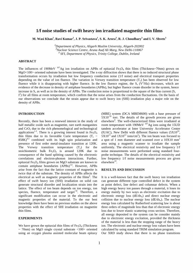
1
1/f noise studies of swift heavy ion irradiated magnetite thin films
M. Wasi Khan1, Ravi Kumar2, J. P. Srivastava1, S. K. Arora3, R. J. Choudhary3 and I. V. Shvets3
1Department of Physics, Aligarh Muslim University, Aligarh-202002
2Nuclear Science Centre, Aruna Asaf Ali Marg, New Delhi-110067 3 SFI, Department of Physics, Trinity College, Dublin, Ireland
ABSTRACT The influences of 190MeV 107Ag ion irradiation on APBs of epitaxial Fe3O4 thin films (Thickness~70nm) grown on MgO<100> oriented substrate have been investigated. The x-ray diffraction shows that there is no induced structural phase transformation occurs by irradiation but low frequency conduction noise (1/f noise) and electrical transport properties depending on the value of ion fluence. The variation in Verwey transition temperature (Tv) has been observed for low fluence while it is disappearing with higher fluence. In the low fluence regime, the Sv (V2/Hz) decreases, which are evidence of the decrease in density of antiphase boundaries (APBs), but higher fluence create disorder in the system, hence increase in Sv as well as in the density of APBs. The conduction noise is proportional to the square of the bias current (Sv ∝ I2) for all films at room temperature, which confirm that the noise arises from the conduction fluctuations. On the basis of our observations we conclude that the strain appear due to swift heavy ion (SHI) irradiation play a major role on the density of APBs.
INTRODUCTION Recently, there has been a renewed interest in the study of half metallic oxide such as magnetite, rare earth manganites and CrO2 due to the rich phenomelogical and technological applications1-3. There is a growing interest found in Fe3O4 thin films due to its favorable Curie temperature (Tc ~ 858K)4,5 combined with its high spin polarization and presence of first order metal-insulator transition at 120K. The Verwey transition temperature (Tv) for the stoichiometric bulk Fe3O4 is around 120K due to consequence of the band splitting caused by the electronic correlations and electron-phonon interactions. Further, epitaxial Fe3O4 films grown on MgO substrate are known to contain antiphase boundaries (APBs)1,6. However, APBs arise from the fact that the lattice constant of magnetite is twice that of the substrate. The density of APBs affects the electrical as well as magnetic properties of the films6. The effect of swift heavy ion (SHI) irradiation on solid can generate structural disorder and localization strain into the lattice. The effect of ion beam depends on ion energy, ion species, fluence, temperature and target7,8. Therefore, a significant modification can occur in the electronic and magnetic properties of the material. To the our best knowledge there have been no previous studies on the above properties with the effect of SHI irradiation on magnetite thin films. EXPERIMENTS We have grown the epitaxial thin films of Fe3O4 (Thickness ~ 70nm) on MgO single crystal substrate <100> oriented using an oxygen plasma assisted molecular beam epitaxy
(MBE) system (DCA MBEM600) with a base pressure of 5X10⁻¹⁰ torr. The details of the growth process are given elsewhere9. The well-characterized films were irradiated at room temperature with 190MeV 107Ag ions using the 15UD tandem accelerator at Inter University Accelerator Centre (IUAC), New Delhi with different fluence values (5X10¹⁰, 5X10¹¹ and 1X10¹² ions/cm2). The ion beam was focused to a spot of 1 mm diameter and scanned over a 10X10 mm2 area using a magnetic scanner to irradiate the sample uniformly. The electrical resistivity and low frequency 1/f noise measurements were performed using standard four-probe technique. The details of the electrical resistivity and low frequency 1/f noise measurements process are given elsewhere10. RESULTS AND DISCUSSION It is a well-known fact that the swift heavy ion irradiation can generate different type controlled defect in the system as point defect, line defect and columnar defects. When a high energy heavy ion passes through a material, it loses its energy mainly by two ways as electronic excitation due to electronic energy loss (dE/dxe) and direct nuclear energy collision due to nuclear energy loss (dE/dxe). The nuclear energy loss calculated by Rutherford scattering law is about three orders of magnitude less than that of electronic energy loss due to lower elastic scattering cross section. Therefore, all energy deposited to the system can be consider mainly due to electronic energy excitation, provided the thickness of the material is less than the stopping range of the heavy ion. The electronic and nuclear energy loss values have been calculated by using standard TRIM simulation program. Our XRD study shows that there is no phase transitions
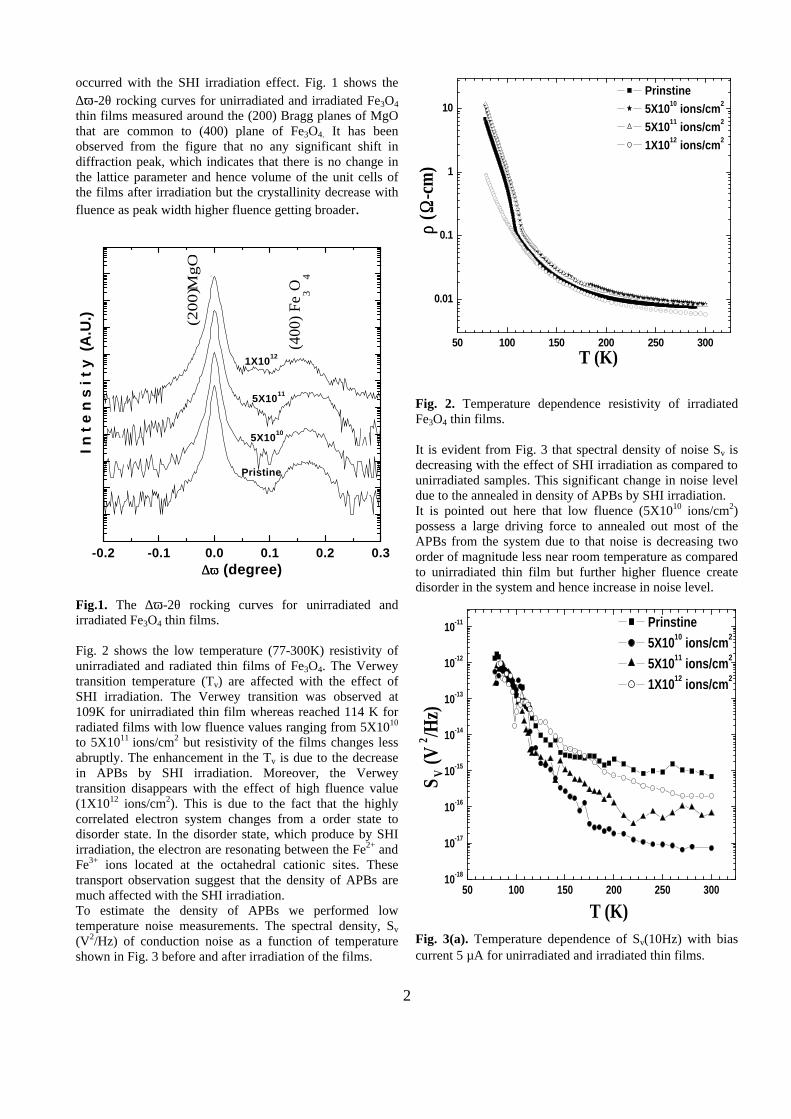
2
occurred with the SHI irradiation effect. Fig. 1 shows the ∆ω-2θ rocking curves for unirradiated and irradiated Fe3O4 thin films measured around the (200) Bragg planes of MgO that are common to (400) plane of Fe3O4. It has been observed from the figure that no any significant shift in diffraction peak, which indicates that there is no change in the lattice parameter and hence volume of the unit cells of the films after irradiation but the crystallinity decrease with fluence as peak width higher fluence getting broader. Fig.1. The ∆ω-2θ rocking curves for unirradiated and irradiated Fe3O4 thin films. Fig. 2 shows the low temperature (77-300K) resistivity of unirradiated and radiated thin films of Fe3O4. The Verwey transition temperature (Tv) are affected with the effect of SHI irradiation. The Verwey transition was observed at 109K for unirradiated thin film whereas reached 114 K for radiated films with low fluence values ranging from 5X10¹⁰ to 5X10¹¹ ions/cm2 but resistivity of the films changes less abruptly. The enhancement in the Tv is due to the decrease in APBs by SHI irradiation. Moreover, the Verwey transition disappears with the effect of high fluence value (1X10¹² ions/cm2). This is due to the fact that the highly correlated electron system changes from a order state to disorder state. In the disorder state, which produce by SHI irradiation, the electron are resonating between the Fe2+ and Fe3+ ions located at the octahedral cationic sites. These transport observation suggest that the density of APBs are much affected with the SHI irradiation. To estimate the density of APBs we performed low temperature noise measurements. The spectral density, Sv
(V2/Hz) of conduction noise as a function of temperature shown in Fig. 3 before and after irradiation of the films.
Fig. 2. Temperature dependence resistivity of irradiated Fe3O4 thin films. It is evident from Fig. 3 that spectral density of noise Sv is decreasing with the effect of SHI irradiation as compared to unirradiated samples. This significant change in noise level due to the annealed in density of APBs by SHI irradiation. It is pointed out here that low fluence (5X10¹⁰ ions/cm2) possess a large driving force to annealed out most of the APBs from the system due to that noise is decreasing two order of magnitude less near room temperature as compared to unirradiated thin film but further higher fluence create disorder in the system and hence increase in noise level. Fig. 3(a). Temperature dependence of Sv(10Hz) with bias current 5 µA for unirradiated and irradiated thin films.
50 100 150 200 250 30010-18
10-17
10-16
10-15
10-14
10-13
10-12
10-11 Prinstine 5X10¹⁰ ions/cm2
5X10¹¹ ions/cm2
1X10¹² ions/cm2
T (K)
S V
(V2 /H
z)
50 100 150 200 250 300
0.01
0.1
1
10 Prinstine 5X10¹⁰ ions/cm2
5X10¹¹ ions/cm2
1X10¹² ions/cm2
T (K)
ρρ ( ΩΩ
-cm
)
(400) Fe3O4 (200) MgO
-0.2 -0.1 0.0 0.1 0.2 0.3
1X10¹²
5X10¹¹
5X10¹⁰
Pristine
∆ω∆ω (degree)
I n t
e n
s i
t y
(A
.U.)
(4
00)
Fe3O
4
(20
0) M
gO
3
The quadratic dependence of the bias current as shown in the inset of Fig 3(b) at room temperature for 10Hz, which indicates that the noise originating from fluctuation in charge carriers. Fig. 3(b). Normalized spectral density of noise Sv/V
2 as a function of temperature for unirradiated and irradiated thin films. Fig. 3(b) shows the temperature dependence of normalized spectral density of noise, Sv/V
2 (which is an independent parameter of the electric current value used for the noise measurement) at 10Hz for unirradiated and irradiated films. It is also clear evident from the figure that the magnitude of Sv/V
2 decreasing with the effect of SHI irradiation. The SHI irradiation removes the strain from the system. Since the noise is very sensitive to the lattice distortion and hence on the density of APBs. In order to compare our noise measurement results with others we have used Hooge’s empirical relation for conductance fluctuations11. According to Hooge’s relation the spectral density of noise SV in a homogeneous material is given as Sv = (γV2/Nc fα ), where V is the dc voltage across the sample, Nc the number of carriers present in the sample α is a constant close to unity and γ is a dimensionless constant known as Hooge’s parameter. The value of the Hooge’s parameter has been found to decrease with low fluence and again increase for higher value of fluence as summarized in Table. The observed change in γ value suggests that the lattice get more ordered with the fluence results in the decrease of noise observed.
Table: The value of Hooge’s parameter ã(300K) estimated from the noise measurements as a function of ion fluence for the Fe3O4 films irradiated with 190MeV 107Ag ions. SUMMARY We have investigated the influence of 190MeV 107Ag ion irradiation on the transport and low frequency conduction noise properties of Fe3O4 thin films. The Verwey transition temperature Tv has been observed to be sensitive on ion fluence and shifted towards the higher temperature with fluence values 5X10¹⁰ and 5X10¹¹ ions/cm2. But for higher value of fluence the Verwey transition disappears and the sample exhibited a semiconducting nature. The 1/f conduction noise is found to vary with different value of fluence. The interesting thing, we have observed that the magnitude of normalized noise is lower for the irradiated samples than the unirradiated one which an increase in Verwey transition and goes towards single crystal Verwey transition temperature (123.5K). REFERENCES 1W. Eerenstein, T. T. M. Palstra, T. Hibma and C. Celotto, Phys. Rev. B 66, 201101 (2002) 2J. P. Hong, S.B. Lee, Y.W. Jung, J.H. Lee, K.S. Yoon, K.W. Kim, C.O. Kim and C.H. Lee, Appl. Phys. Lett. 83, 1590 (2003) 3M. Ziese, Phys. Rev. B 62, 1044 (2000) 4F. Walz, J. Phys. Condens. Matter 14, R285 (2002) 5M. Zeise, Rep. Prog. Phys. 65, 143 (2002) 6D. T. Margulies, F. T. Parker, F. E. Spada, R. S. Goldman, J. Li, R. Sinclair and A. E. Berkowitz, Phys. Rev. B 53, 9175 (1996) 7G. Szenes, Phys. Rev. B51, 8026 (1995) 8M. Toulemonde, Nucl. Instr. and Meth. B 65, 560 (1998) 9Y. Zhou, Xuesong Jin and I.V. Shvets, J. Appl. Phys. 95, 7357 (2004) 10S. K. Arora and A.K. Gupta, Solid State Commun. 90, 417 (1994) 11F.N. Hooge, T.G. Kleinpenning and L.K.J. Vandamme, Rep. Prog. Phys. 44, 31 (1981)
Fluence (ions/cm2) ã (300K)
Pristine 2.89X10⁷ 5X10¹⁰ 9.33X10⁴ 5X10¹¹ 7.87X10⁵ 1X10¹² 2.32X10⁵
-500 0 500 1000 1500 2000 2500 3000
0.0
2.0x10⁻¹⁴
4.0x10⁻¹⁴
6.0x10⁻¹⁴
8.0x10⁻¹⁴ Pristine 5X10¹¹ ions/cm2
S
v(10
Hz)
[I(µµA)]2
100 150 200 250 30010-20
10-18
10-16
10-14
10-12
10-10
10-8
10-6
S V
/V2 (1
/Hz)
T (K)
Unirradiate
5x10¹⁰ ions/cm2
5x10¹¹ ions/cm2
1x10¹² ions/cm2

Sorry!!
This Paper is NOT Available
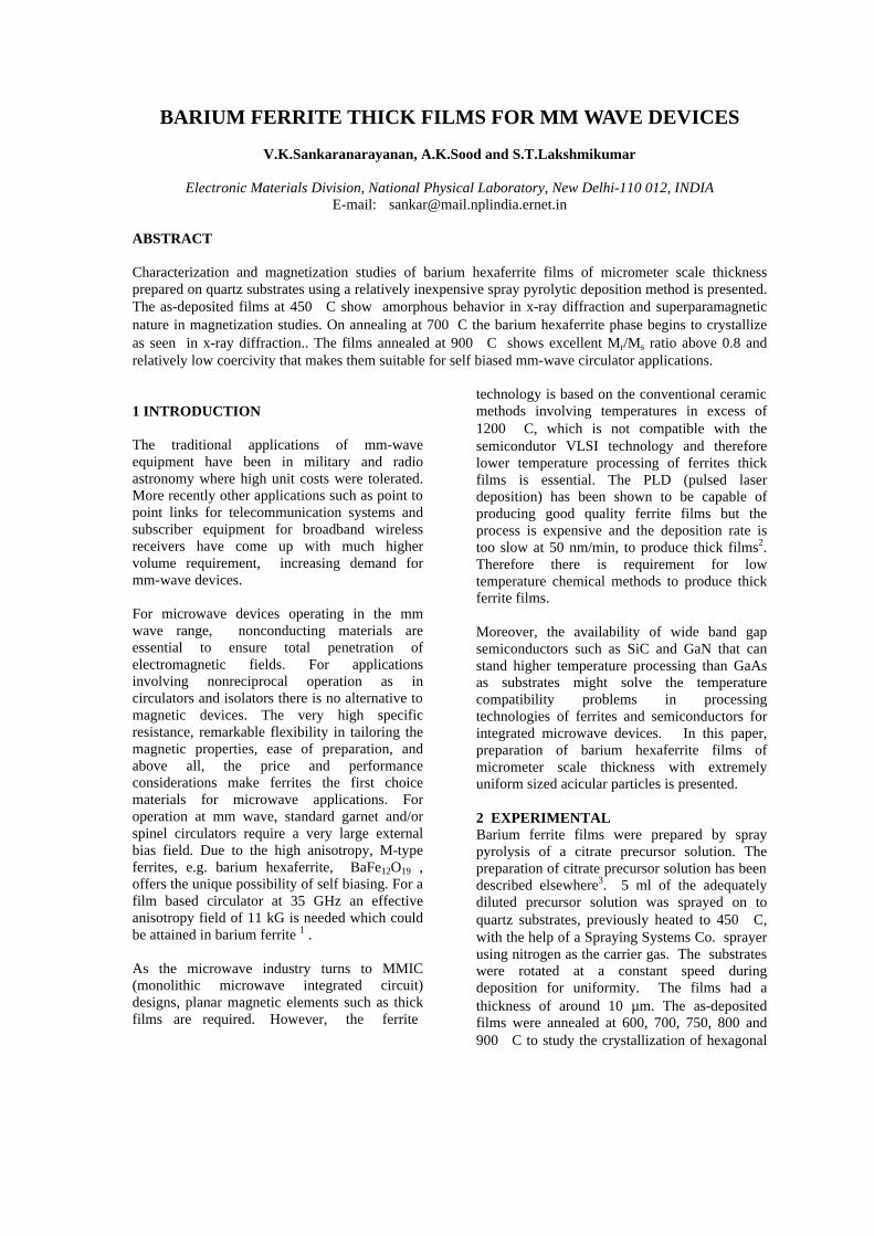
BARIUM FERRITE THICK FILMS FOR MM WAVE DEVICES
V.K.Sankaranarayanan, A.K.Sood and S.T.Lakshmikumar
Electronic Materials Division, National Physical Laboratory, New Delhi-110 012, INDIA E-mail: [email protected]
ABSTRACT Characterization and magnetization studies of barium hexaferrite films of micrometer scale thickness prepared on quartz substrates using a relatively inexpensive spray pyrolytic deposition method is presented. The as-deposited films at 450 C show amorphous behavior in x-ray diffraction and superparamagnetic nature in magnetization studies. On annealing at 700 C the barium hexaferrite phase begins to crystallize as seen in x-ray diffraction.. The films annealed at 900 C shows excellent Mr/Ms ratio above 0.8 and relatively low coercivity that makes them suitable for self biased mm-wave circulator applications. 1 INTRODUCTION The traditional applications of mm-wave equipment have been in military and radio astronomy where high unit costs were tolerated. More recently other applications such as point to point links for telecommunication systems and subscriber equipment for broadband wireless receivers have come up with much higher volume requirement, increasing demand for mm-wave devices. For microwave devices operating in the mm wave range, nonconducting materials are essential to ensure total penetration of electromagnetic fields. For applications involving nonreciprocal operation as in circulators and isolators there is no alternative to magnetic devices. The very high specific resistance, remarkable flexibility in tailoring the magnetic properties, ease of preparation, and above all, the price and performance considerations make ferrites the first choice materials for microwave applications. For operation at mm wave, standard garnet and/or spinel circulators require a very large external bias field. Due to the high anisotropy, M-type ferrites, e.g. barium hexaferrite, BaFe12O19 , offers the unique possibility of self biasing. For a film based circulator at 35 GHz an effective anisotropy field of 11 kG is needed which could be attained in barium ferrite 1 . As the microwave industry turns to MMIC (monolithic microwave integrated circuit) designs, planar magnetic elements such as thick films are required. However, the ferrite
technology is based on the conventional ceramic methods involving temperatures in excess of 1200 C, which is not compatible with the semicondutor VLSI technology and therefore lower temperature processing of ferrites thick films is essential. The PLD (pulsed laser deposition) has been shown to be capable of producing good quality ferrite films but the process is expensive and the deposition rate is too slow at 50 nm/min, to produce thick films2. Therefore there is requirement for low temperature chemical methods to produce thick ferrite films. Moreover, the availability of wide band gap semiconductors such as SiC and GaN that can stand higher temperature processing than GaAs as substrates might solve the temperature compatibility problems in processing technologies of ferrites and semiconductors for integrated microwave devices. In this paper, preparation of barium hexaferrite films of micrometer scale thickness with extremely uniform sized acicular particles is presented. 2 EXPERIMENTAL Barium ferrite films were prepared by spray pyrolysis of a citrate precursor solution. The preparation of citrate precursor solution has been described elsewhere3. 5 ml of the adequately diluted precursor solution was sprayed on to quartz substrates, previously heated to 450 C, with the help of a Spraying Systems Co. sprayer using nitrogen as the carrier gas. The substrates were rotated at a constant speed during deposition for uniformity. The films had a thickness of around 10 µm. The as-deposited films were annealed at 600, 700, 750, 800 and 900 C to study the crystallization of hexagonal
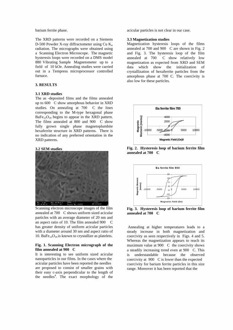
barium ferrite phase. The XRD patterns were recorded on a Siemens D-500 Powder X-ray diffractometer using Cu Kα radiation. The micrographs were obtained using a Scanning Electron Microscope. The magnetic hysteresis loops were recorded on a DMS model 880 Vibrating Sample Magnetometer up to a field of 10 kOe. Annealing studies were carried out in a Tempress microprocessor controlled furnace. 3. RESULTS 3.1 XRD studies The as -deposited films and the films annealed up to 600 C show amorphous behavior in XRD studies. On annealing at 700 C the lines corresponding to the M-type hexagonal phase BaFe12O19 begins to appear in the XRD pattern. The films annealed at 800 and 900 C show fully grown single phase magnetoplumbite hexaferrite structure in XRD patterns. There is no indication of any preferred orientation in the XRD patterns. 3.2 SEM studies
Scanning electron microscope images of the film annealed at 700 C shows uniform sized acicular particles with an average diameter of 20 nm and an aspect ratio of 10. The film annealed 900 C has greater density of uniform acicular particles with a diameter around 30 nm and aspect ratio of 10. BaFe12O19 is known to crystallize as platelets. Fig. 1. Scanning Electron micrograph of the film annealed at 900 C It is interesting to see uniform sized acicular nanoparticles in our films. In the cases where the acicular particles have been reported the needles are proposed to consist of smaller grains with their easy c-axis perpendicular to the length of the needles4. The exact morphology of the
acicular particles is not clear in our case. 3.3 Magnetization studies Magnetization hysteresis loops of the films annealed at 700 and 900 C are shown in Fig. 2 and Fig. 3. The hysteresis loop of the film annealed at 700 C show relatively low magnetization as expected from XRD and SEM data which show the initialization of crystallization of hexaferrite particles from the amorphous phase at 700 C. The coercivity is also low for these particles.
Fig. 2. Hysteresis loop of barium ferrite film annealed at 700 C
Fig. 3. Hysteresis loop of barium ferrite film annealed at 700 C Annealing at higher temperatures leads to a steady increase in both magnetization and coercivity as seen respectively in Figs. 4 and 5. Whereas the magnetization appears to reach its maximum value at 900 C the coercivity shows a steadily increasing trend even at 900 C. This is understandable because the observed coercivity at 900 C is lower than the expected coercivity for barium ferrite particles in this size range. Moreover it has been reported that the
Ba ferrite film 900
-15
-10
-5
0
5
10
15
-10000 -5000 0 5000 10000
Magnetic field (Oe)
Mag
net
ic M
om
ent
(mem
u)
Ba ferrite film 700
-4000
-2000
0
2000
4000
-10000 -5000 0 5000 10000
Magnetic Field (Oe)0M
agn
etic
M
om
ent
(mem
u)
Fig.4. Variation of magnetization with annealing temperature
Fig. 5. Variation of coercivity with annealing temperature acicular particles of barium ferrite consist of smaller grains with their easy c-axis perpendicular to the length of the needles4. These smaller individual grains may have lower coercivity that increase on annealing due to grain growth. The squareness of the films also increase with increasing annealing temperature from 0.6 for the film annealed at 700 C to a value above 0.8 for the film annealed at 900 C as is also evident in Fig. 3. Of particular interest for microwave applications are the coercivity (Hc), squareness Mr/Ms, saturation magnetization (4πMs) and magnetic anisotropy field (Ha). The loss is often proportional to Hc whereas magnetization and Ha determine the operational frequency and bandwidth, and the loop squareness indicates the degree to which the material is self biased. The hysteresis loop of the film recorded with the magnetic field applied perpendicular to the plane of the film is shown in Fig. 6. It may be noticed that the magnetization approaches saturation at the maximum applied field of 6 kOe. Along with the low coercivity, it is an indication of the relatively low anisotropy field
Fig. 6. Hysteresis loop of the film annealed at 900 C recorded with magnetic field perpendicular to the plane of the film. in this sample with acicular nanoparticles. In fact the anisotropy field of bulk barium ferrite is 17 kG and is too high for self biased circulator application in the mm-wave range of 35 GHz where an effective anisotropy field of 11kG is needed and it is usually attained by Sc substitution. The present films with relatively low Ha which is controllable by annealing treatments could be suitable for mm-wave applications without any substitution. The ability to process barium ferrite as self biased films may allow for elimination of the biasing magnets presently required in the design of microwave circulators, a significant step towards planar construction of these devices. 4 CONCLUSIONS Barium ferrite films of 10 µm thickness prepared by a relatively inexpensive spray pyrolytic deposition method show uniform acicular nanoparticles with 20 to 30 nm thickness and an aspect ratio of 10. The films show hysteresis loops with magnetization and coercivities that can be controlled by changing annealing temperatures. The relatively low anisotropy field, low coercivities and excellent squareness are useful properties for self biased mm wave circulators at 35 GHz. 5 REFERENCES 1M. Pardavi-Horvath, J. Magn. Magn. Mater. 215-216, 171 (2000). 2 S. A. Oliver, M. L. Chen, C.Vittoria and P. Lubitz, J. Appl. Phys. , 85, 4630 (1999) 3V.K.Sankaranarayanan, R.P.Pant and A.C.Rastogi J. Magn. and Magn. Mater. 220, 72 (2000).
Magnetization vs Annealing Temp
0
2
4
6
8
10
12
14
700 750 800 850 900
Annealing temperature (degree C)
Mag
net
ic M
om
ent
(em
u)
Ba ferrite film 900 perp
-20
-10
0
10
20
-10000 -5000 0 5000 10000
Magnetic Field (Oe)
Mag
net
ic M
om
ent
(mem
u)
Coercivity vs Anneling temp
1000
1400
1800
2200
700 800 900 1000
Annealing Temp (degree C)
Co
erci
vity
(O
e)

4K. Kakizaki, N. Hiratsuka, and T. Namikawa, J. Magn. and Magn. Mater. 176, 36 (1997).
UNIQUENESS OF THE SPIN GLASS FREEZING TEMPERATURE IN NANOCOMPOSITES OF La0.67Ca0.3Ba0.03MnO PEROVSKITES
D. K. Mishra, D. R. Sahu1, P. K. Mishra2 & B. K. Roul
Institute of Materials Science, Planetarium Building, Bhubaneswar-751013
1National Taiwan University, Taiwan, Taipei 2Technical Physics and Prototype Engineering Division, BARC, Mumbai-40085
E. Mail: [email protected]
Abstract The powder sample prepared by versatile chemical technique (pyrophoric technique) is found to be a low cost synthesis route for preparation of nanosized La0.67Ca0.3Ba0.03MnO3 (LCBMO) composites without any requirement of calcinations step of high temperature. The average sizes of the particles are independent of calcined temperature and are in the order of 50nm. The ZFC and FC magnetization measurements show the spin glass transition at low temperature (≈50°K) around the paramagnetic to ferromagnetic transition temperature which occurs at 50°K and independent of calcined temperature.
INTRODUCTION Mixed valent manganites have attracted considerable attention in recent years because of the observation of CMR and more generally due to the unusually strong coupling between their lattice, spin and charge/orbital degrees of freedom. The two important interactions between the Mn ions that are responsible for the observed properties in manganites are double exchange and super exchange. The transfer of an electron from Mn3+ to Mn4+ through oxygen ion is known as double exchange, creates ferromagnetic metallic state and transfer of an electron from Mn3+ to Mn3+ or Mn4+ to Mn4+ ions through oxygen ion is known as superexchange, creates antiferomagnetic insulator state. The presence of ferromagnetic and antiferromagnetic interactions leads to frustration in the system, resulting in the formation of a spin-glass state at very low temperature [1-6]. The spin glass property mainly found in binary liquid mixtures [7] and then observed and investigated in a variety of different physical systems e.g. magnets [8], superconductors [9], liquid crystals [10] and in CMR material [11-17] in which there is competition between spin glass order and long range ferromagnetic order, i.e. in systems where there is majority of ferromagnetic couplings between the individual spins but a sufficiently large number of antiferromagnetic couplings to create substantial frustration. When the temperature is lowered in such material, it exhibits a transition from a paramagnetic to a ferromagnetic phase and on further lowering the temperature typical spin glass, commonly called reentrant spin-glass (RSG), behavior appears.
From the viewpoint of potential future applications, the manganites with smaller grain size is required. For this type of materials lower sintered temperature will be necessary for inhibiting grain growth during sintering and hence to retain the initial particle size [18]. The effect of grain size on structural, Magnetic and transport properties in hole-doped manganites has been extensively studied. Many controversial results found concerning the influence of grain size on the magnetic properties of polycrystalline manganites. It has been studied that magnetisation and the transition temperature decreases with decreasing grain size [19]. But, also a contrary statement arose by researchers that both magnetisation and transition temperature decreases with increasing of grain size [20]. To understand the above phenomena we prepared our samples by chemical reaction route i.e. pyrophoric reaction technique for synthesis of different nano-sized order of powdered sample. Here, we present the results for the bulk sample La0.67Ca0.3Ba0.03MnO3 calcined at 500°C & 700°C, which shows spin glass behavior at very low temperature. EXPERIMENTAL The standard CMR powdered sample was prepared by chemical synthesis route in presence of polymer reagent TEA (Triethanol Amine) through pyrophoric reaction technique. In the first step Lanthanum Nitrate, Barium Nitrate, Calcium Carbonate and Manganese Acetate in appropriate ratios were dissolved in dilute nitric acid. To this solution, TEA is added approximately 7-mole% of the total metal ion to form the precursor solution, which resulted a
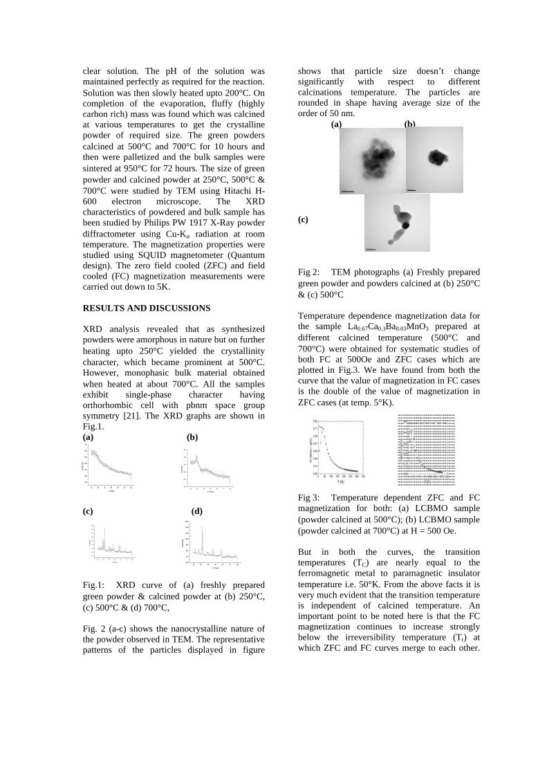
clear solution. The pH of the solution was maintained perfectly as required for the reaction. Solution was then slowly heated upto 200°C. On completion of the evaporation, fluffy (highly carbon rich) mass was found which was calcined at various temperatures to get the crystalline powder of required size. The green powders calcined at 500°C and 700°C for 10 hours and then were palletized and the bulk samples were sintered at 950°C for 72 hours. The size of green powder and calcined powder at 250°C, 500°C & 700°C were studied by TEM using Hitachi H-600 electron microscope. The XRD characteristics of powdered and bulk sample has been studied by Philips PW 1917 X-Ray powder diffractometer using Cu-Kα radiation at room temperature. The magnetization properties were studied using SQUID magnetometer (Quantum design). The zero field cooled (ZFC) and field cooled (FC) magnetization measurements were carried out down to 5K. RESULTS AND DISCUSSIONS XRD analysis revealed that as synthesized powders were amorphous in nature but on further heating upto 250°C yielded the crystallinity character, which became prominent at 500°C. However, monophasic bulk material obtained when heated at about 700°C. All the samples exhibit single-phase character having orthorhombic cell with pbnm space group symmetry [21]. The XRD graphs are shown in Fig.1. (a) (b) (c) (d) Fig.1: XRD curve of (a) freshly prepared green powder & calcined powder at (b) 250°C, (c) 500°C & (d) 700°C, Fig. 2 (a-c) shows the nanocrystalline nature of the powder observed in TEM. The representative patterns of the particles displayed in figure
shows that particle size doesn’t change significantly with respect to different calcinations temperature. The particles are rounded in shape having average size of the order of 50 nm. (a) (b) (c) Fig 2: TEM photographs (a) Freshly prepared green powder and powders calcined at (b) 250°C & (c) 500°C Temperature dependence magnetization data for the sample La0.67Ca0.3Ba0.03MnO3 prepared at different calcined temperature (500°C and 700°C) were obtained for systematic studies of both FC at 500Oe and ZFC cases which are plotted in Fig.3. We have found from both the curve that the value of magnetization in FC cases is the double of the value of magnetization in ZFC cases (at temp. 5°K). Fig 3: Temperature dependent ZFC and FC magnetization for both: (a) LCBMO sample (powder calcined at 500°C); (b) LCBMO sample (powder calcined at 700°C) at H = 500 Oe. But in both the curves, the transition temperatures (TC) are nearly equal to the ferromagnetic metal to paramagnetic insulator temperature i.e. 50°K. From the above facts it is very much evident that the transition temperature is independent of calcined temperature. An important point to be noted here is that the FC magnetization continues to increase strongly below the irreversibility temperature (Tr) at which ZFC and FC curves merge to each other.
20 30 40 50 60 70 80
100
200
300
400
500
600
700
Inte
nsity
2 Theta20 30 40 50 60 70 80
100
200
300
400
500
600
Inte
nsity
2 Theta
20 30 40 50 60 70 80
100
200
300
400
500
600
700
800
900
Inte
nsity
2 Theta
20 30 40 50 60 70 80200
400
600
800
1000
1200
1400
1600
Inte
nsity
2 Theta
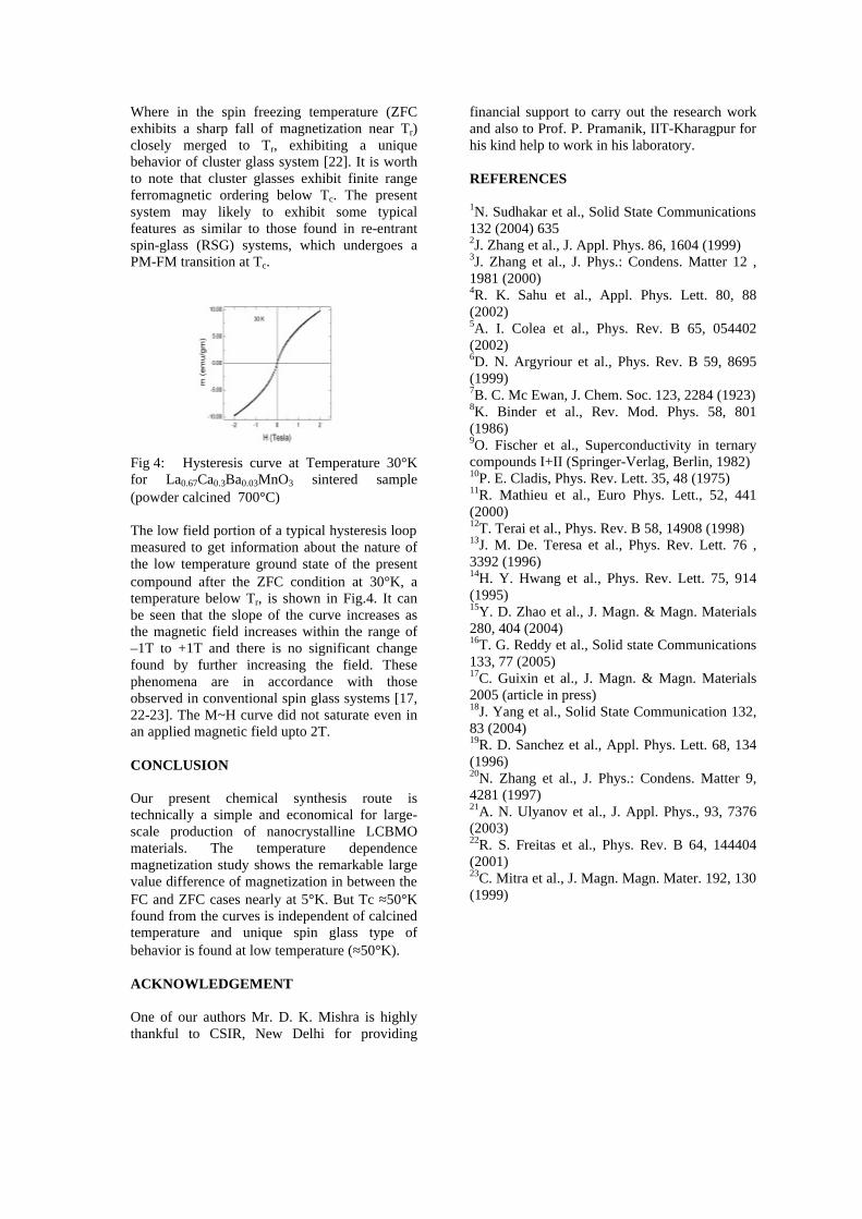
Where in the spin freezing temperature (ZFC exhibits a sharp fall of magnetization near Tr) closely merged to Tr, exhibiting a unique behavior of cluster glass system [22]. It is worth to note that cluster glasses exhibit finite range ferromagnetic ordering below Tc. The present system may likely to exhibit some typical features as similar to those found in re-entrant spin-glass (RSG) systems, which undergoes a PM-FM transition at Tc. Fig 4: Hysteresis curve at Temperature 30°K for La0.67Ca0.3Ba0.03MnO3 sintered sample (powder calcined 700°C) The low field portion of a typical hysteresis loop measured to get information about the nature of the low temperature ground state of the present compound after the ZFC condition at 30°K, a temperature below Tr, is shown in Fig.4. It can be seen that the slope of the curve increases as the magnetic field increases within the range of –1T to +1T and there is no significant change found by further increasing the field. These phenomena are in accordance with those observed in conventional spin glass systems [17, 22-23]. The M~H curve did not saturate even in an applied magnetic field upto 2T. CONCLUSION Our present chemical synthesis route is technically a simple and economical for large-scale production of nanocrystalline LCBMO materials. The temperature dependence magnetization study shows the remarkable large value difference of magnetization in between the FC and ZFC cases nearly at 5°K. But Tc ≈50°K found from the curves is independent of calcined temperature and unique spin glass type of behavior is found at low temperature (≈50°K). ACKNOWLEDGEMENT One of our authors Mr. D. K. Mishra is highly thankful to CSIR, New Delhi for providing
financial support to carry out the research work and also to Prof. P. Pramanik, IIT-Kharagpur for his kind help to work in his laboratory. REFERENCES 1N. Sudhakar et al., Solid State Communications 132 (2004) 635 2J. Zhang et al., J. Appl. Phys. 86, 1604 (1999) 3J. Zhang et al., J. Phys.: Condens. Matter 12 , 1981 (2000) 4R. K. Sahu et al., Appl. Phys. Lett. 80, 88 (2002) 5A. I. Colea et al., Phys. Rev. B 65, 054402 (2002) 6D. N. Argyriour et al., Phys. Rev. B 59, 8695 (1999) 7B. C. Mc Ewan, J. Chem. Soc. 123, 2284 (1923) 8K. Binder et al., Rev. Mod. Phys. 58, 801 (1986) 9O. Fischer et al., Superconductivity in ternary compounds I+II (Springer-Verlag, Berlin, 1982) 10P. E. Cladis, Phys. Rev. Lett. 35, 48 (1975) 11R. Mathieu et al., Euro Phys. Lett., 52, 441 (2000) 12T. Terai et al., Phys. Rev. B 58, 14908 (1998) 13J. M. De. Teresa et al., Phys. Rev. Lett. 76 , 3392 (1996) 14H. Y. Hwang et al., Phys. Rev. Lett. 75, 914 (1995) 15Y. D. Zhao et al., J. Magn. & Magn. Materials 280, 404 (2004) 16T. G. Reddy et al., Solid state Communications 133, 77 (2005) 17C. Guixin et al., J. Magn. & Magn. Materials 2005 (article in press) 18J. Yang et al., Solid State Communication 132, 83 (2004) 19R. D. Sanchez et al., Appl. Phys. Lett. 68, 134 (1996) 20N. Zhang et al., J. Phys.: Condens. Matter 9, 4281 (1997) 21A. N. Ulyanov et al., J. Appl. Phys., 93, 7376 (2003) 22R. S. Freitas et al., Phys. Rev. B 64, 144404 (2001) 23C. Mitra et al., J. Magn. Magn. Mater. 192, 130 (1999)
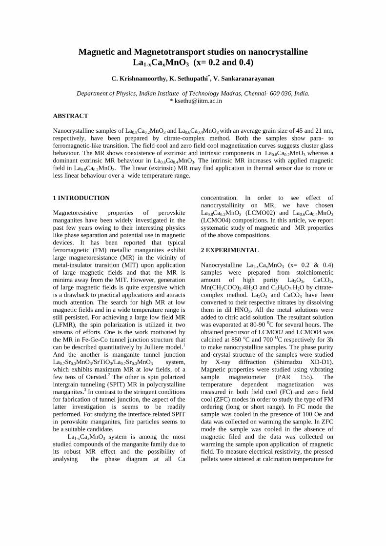
Magnetic and Magnetotransport studies on nanocrystalline La1-xCaxMnO3 (x= 0.2 and 0.4)
C. Krishnamoorthy, K. Sethupathi*, V. Sankaranarayanan
Department of Physics, Indian Institute of Technology Madras, Chennai- 600 036, India.
* [email protected] ABSTRACT Nanocrystalline samples of La0.8Ca0.2MnO3 and La0.6Ca0.4MnO3 with an average grain size of 45 and 21 nm, respectively, have been prepared by citrate-complex method. Both the samples show para- to ferromagnetic-like transition. The field cool and zero field cool magnetization curves suggests cluster glass behaviour. The MR shows coexistence of extrinsic and intrinsic components in La0.8Ca0.2MnO3 whereas a dominant extrinsic MR behaviour in La0.6Ca0.4MnO3. The intrinsic MR increases with applied magnetic field in La0.8Ca0.2MnO3. The linear (extrinsic) MR may find application in thermal sensor due to more or less linear behaviour over a wide temperature range. 1 INTRODUCTION Magnetoresistive properties of perovskite manganites have been widely investigated in the past few years owing to their interesting physics like phase separation and potential use in magnetic devices. It has been reported that typical ferromagnetic (FM) metallic manganites exhibit large magnetoresistance (MR) in the vicinity of metal-insulator transition (MIT) upon application of large magnetic fields and that the MR is minima away from the MIT. However, generation of large magnetic fields is quite expensive which is a drawback to practical applications and attracts much attention. The search for high MR at low magnetic fields and in a wide temperature range is still persisted. For achieving a large low field MR (LFMR), the spin polarization is utilized in two streams of efforts. One is the work motivated by the MR in Fe-Ge-Co tunnel junction structure that can be described quantitatively by Julliere model.1 And the another is manganite tunnel junction La0.7Sr0.3MnO3/SrTiO3/La0.7Sr0.3MnO3 system, which exhibits maximum MR at low fields, of a few tens of Oersted.2 The other is spin polarized intergrain tunneling (SPIT) MR in polycrystalline manganites.3 In contrast to the stringent conditions for fabrication of tunnel junction, the aspect of the latter investigation is seems to be readily performed. For studying the interface related SPIT in perovskite manganites, fine particles seems to be a suitable candidate. La1-xCaxMnO3 system is among the most studied compounds of the manganite family due to its robust MR effect and the possibility of analysing the phase diagram at all Ca
concentration. In order to see effect of nanocrystallinity on MR, we have chosen La0.8Ca0.2MnO3 (LCMO02) and La0.6Ca0.4MnO3 (LCMO04) compositions. In this article, we report systematic study of magnetic and MR properties of the above compositions. 2 EXPERIMENTAL Nanocrystalline La1-xCaxMnO3 (x= 0.2 & 0.4) samples were prepared from stoichiometric amount of high purity La2O3, CaCO3, Mn(CH3COO)2.4H2O and C6H8O7.H2O by citrate-complex method. La2O3 and CaCO3 have been converted to their respective nitrates by dissolving them in dil HNO3. All the metal solutions were added to citric acid solution. The resultant solution was evaporated at 80-90 0C for several hours. The obtained precursor of LCMO02 and LCMO04 was calcined at 850 oC and 700 OC respectively for 3h to make nanocrystalline samples. The phase purity and crystal structure of the samples were studied by X-ray diffraction (Shimadzu XD-D1). Magnetic properties were studied using vibrating sample magnetometer (PAR 155). The temperature dependent magnetization was measured in both field cool (FC) and zero field cool (ZFC) modes in order to study the type of FM ordering (long or short range). In FC mode the sample was cooled in the presence of 100 Oe and data was collected on warming the sample. In ZFC mode the sample was cooled in the absence of magnetic filed and the data was collected on warming the sample upon application of magnetic field. To measure electrical resistivity, the pressed pellets were sintered at calcination temperature for
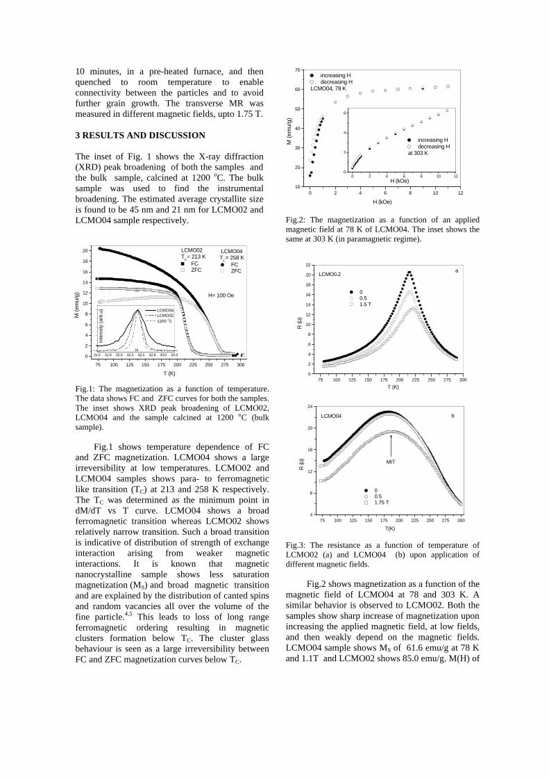
10 minutes, in a pre-heated furnace, and then quenched to room temperature to enable connectivity between the particles and to avoid further grain growth. The transverse MR was measured in different magnetic fields, upto 1.75 T. 3 RESULTS AND DISCUSSION The inset of Fig. 1 shows the X-ray diffraction (XRD) peak broadening of both the samples and the bulk sample, calcined at 1200 oC. The bulk sample was used to find the instrumental broadening. The estimated average crystallite size is found to be 45 nm and 21 nm for LCMO02 and LCMO04 sample respectively.
Fig.1: The magnetization as a function of temperature. The data shows FC and ZFC curves for both the samples. The inset shows XRD peak broadening of LCMO02, LCMO04 and the sample calcined at 1200 oC (bulk sample). Fig.1 shows temperature dependence of FC and ZFC magnetization. LCMO04 shows a large irreversibility at low temperatures. LCMO02 and LCMO04 samples shows para- to ferromagnetic like transition (TC) at 213 and 258 K respectively. The TC was determined as the minimum point in dM/dT vs T curve. LCMO04 shows a broad ferromagnetic transition whereas LCMO02 shows relatively narrow transition. Such a broad transition is indicative of distribution of strength of exchange interaction arising from weaker magnetic interactions. It is known that magnetic nanocrystalline sample shows less saturation magnetization (MS) and broad magnetic transition and are explained by the distribution of canted spins and random vacancies all over the volume of the fine particle.4,5 This leads to loss of long range ferromagnetic ordering resulting in magnetic clusters formation below TC. The cluster glass behaviour is seen as a large irreversibility between FC and ZFC magnetization curves below TC.
Fig.2: The magnetization as a function of an applied magnetic field at 78 K of LCMO04. The inset shows the same at 303 K (in paramagnetic regime). Fig.3: The resistance as a function of temperature of LCMO02 (a) and LCMO04 (b) upon application of different magnetic fields. Fig.2 shows magnetization as a function of the magnetic field of LCMO04 at 78 and 303 K. A similar behavior is observed to LCMO02. Both the samples show sharp increase of magnetization upon increasing the applied magnetic field, at low fields, and then weakly depend on the magnetic fields. LCMO04 sample shows MS of 61.6 emu/g at 78 K and 1.1T and LCMO02 shows 85.0 emu/g. M(H) of
75 100 125 150 175 200 225 250 275 3000
2
4
6
8
10
12
14
16
18
20
22a
LCMO0.2
R ( Ω
)
T (K)
0 0.5 1.5 T
75 100 125 150 175 200 225 250 275 300
0
2
4
6
8
10
12
14
16
18
20
H= 100 Oe
LCMO02 T
C= 213 K FC ZFC
M (
emu/
g)
T (K)
LCMO04 T
C= 258 K
FC ZFC
31.5 31.8 32.0 32.3 32.5 32.8 33.0 33.3
Inte
nsity
(ar
b.u)
2θ
LCMO04 LCMO02 1200 oC
75 100 125 150 175 200 225 250 275 3004
8
12
16
20
24
MIT
0 0.5 1.75 T
bLCMO04
R (Ω
)
T(K)
0 2 4 6 8 10 1210
20
30
40
50
60
70
M (
emu/
g)
H (kOe)
increasing H decreasing H
LCMO04, 78 K
0 2 4 6 8 10 120
2
4
6
H (kOe)
increasing H decreasing H
at 303 K
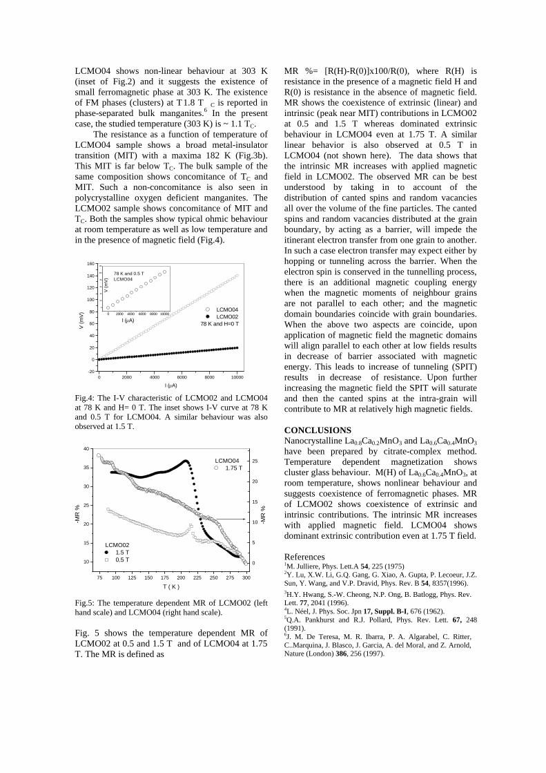
LCMO04 shows non-linear behaviour at 303 K (inset of Fig.2) and it suggests the existence of small ferromagnetic phase at 303 K. The existence of FM phases (clusters) at T 1.8 T C is reported in phase-separated bulk manganites.6 In the present case, the studied temperature (303 K) is ~ 1.1 TC. The resistance as a function of temperature of LCMO04 sample shows a broad metal-insulator transition (MIT) with a maxima 182 K (Fig.3b). This MIT is far below TC. The bulk sample of the same composition shows concomitance of TC and MIT. Such a non-concomitance is also seen in polycrystalline oxygen deficient manganites. The LCMO02 sample shows concomitance of MIT and TC. Both the samples show typical ohmic behaviour at room temperature as well as low temperature and in the presence of magnetic field (Fig.4). Fig.4: The I-V characteristic of LCMO02 and LCMO04 at 78 K and H= 0 T. The inset shows I-V curve at 78 K and 0.5 T for LCMO04. A similar behaviour was also observed at 1.5 T. Fig.5: The temperature dependent MR of LCMO02 (left hand scale) and LCMO04 (right hand scale). Fig. 5 shows the temperature dependent MR of LCMO02 at 0.5 and 1.5 T and of LCMO04 at 1.75 T. The MR is defined as
MR %= [R(H)-R(0)]x100/R(0), where R(H) is resistance in the presence of a magnetic field H and R(0) is resistance in the absence of magnetic field. MR shows the coexistence of extrinsic (linear) and intrinsic (peak near MIT) contributions in LCMO02 at 0.5 and 1.5 T whereas dominated extrinsic behaviour in LCMO04 even at 1.75 T. A similar linear behavior is also observed at 0.5 T in LCMO04 (not shown here). The data shows that the intrinsic MR increases with applied magnetic field in LCMO02. The observed MR can be best understood by taking in to account of the distribution of canted spins and random vacancies all over the volume of the fine particles. The canted spins and random vacancies distributed at the grain boundary, by acting as a barrier, will impede the itinerant electron transfer from one grain to another. In such a case electron transfer may expect either by hopping or tunneling across the barrier. When the electron spin is conserved in the tunnelling process, there is an additional magnetic coupling energy when the magnetic moments of neighbour grains are not parallel to each other; and the magnetic domain boundaries coincide with grain boundaries. When the above two aspects are coincide, upon application of magnetic field the magnetic domains will align parallel to each other at low fields results in decrease of barrier associated with magnetic energy. This leads to increase of tunneling (SPIT) results in decrease of resistance. Upon further increasing the magnetic field the SPIT will saturate and then the canted spins at the intra-grain will contribute to MR at relatively high magnetic fields. CONCLUSIONS Nanocrystalline La0.8Ca0.2MnO3 and La0.6Ca0.4MnO3 have been prepared by citrate-complex method. Temperature dependent magnetization shows cluster glass behaviour. M(H) of La0.6Ca0.4MnO3, at room temperature, shows nonlinear behaviour and suggests coexistence of ferromagnetic phases. MR of LCMO02 shows coexistence of extrinsic and intrinsic contributions. The intrinsic MR increases with applied magnetic field. LCMO04 shows dominant extrinsic contribution even at 1.75 T field. References 1M. Julliere, Phys. Lett.A 54, 225 (1975) 2Y. Lu, X.W. Li, G.Q. Gang, G. Xiao, A. Gupta, P. Lecoeur, J.Z. Sun, Y. Wang, and V.P. Dravid, Phys. Rev. B 54, 8357(1996). 3H.Y. Hwang, S.-W. Cheong, N.P. Ong, B. Batlogg, Phys. Rev. Lett. 77, 2041 (1996). 4L. Néel, J. Phys. Soc. Jpn 17, Suppl. B-I, 676 (1962). 5Q.A. Pankhurst and R.J. Pollard, Phys. Rev. Lett. 67, 248 (1991). 6J. M. De Teresa, M. R. Ibarra, P. A. Algarabel, C. Ritter, C..Marquina, J. Blasco, J. Garcia, A. del Moral, and Z. Arnold, Nature (London) 386, 256 (1997).
0 2000 4000 6000 8000 10000-20
0
20
40
60
80
100
120
140
160
I (µA)
LCMO04 LCMO02
78 K and H=0 T
V (
mV
)
I (µA)
0 2000 4000 6000 8000 10000
0
20
40
60
80
100
120
78 K and 0.5 TLCMO04
V (
mV
)
75 100 125 150 175 200 225 250 275 300
10
15
20
25
30
35
40
-MR
%
T ( K )
LCMO02 1.5 T 0.5 T
0
5
10
15
20
25
-MR
%
LCMO04 1.75 T
1
MM
SYNTHESIS ELECTRICAL AND MAGNETOTRANSPORT PROPERTIES OF NANOCRYSTALLINE Nd0.7Sr0.3MnO3 MANGANITES
C. Krishnamoorthy1, K. Sethupathi1,*, V. Sankaranarayanan1, R. Nirmala2, S.K. Malik2 1Department of Physics, Indian Institute of Technology Madras, Chennai-600 036, INDIA
2 Tata Institute of Fundamental Research, Mumbai- 400 005, INDIA * [email protected]
ABSTRACT Nanocrystalline Nd0.7Sr0.3MnO3 sample with an average particle size of 35 nm has been prepared by citrate-complex method. The ac magnetization shows a para- to ferromagnetic transition at 217 K. The sample shows smooth increase of magnetoresistivity (MR) upon decreasing temperature down to 80 K and weakly temperature dependence below 80 K. Isothermal MR shows ~ 20 % change at low fields and ~ 62 % change at high fields. The observed MR has been analyzed by spin dependent tunneling across the barrier between ferromagnetic grains. The analysis reveals that intra-grain contribution is more than inter-grain contribution.
1. INTRODUCTION Magnetoresistivity (MR) effect has been extensively applied in electronic devices such as magnetic read heads, storage devices and sensors, and it brings innovative impacts to information storage field. Since von Helmolt et al.1 observed MR of ~ 60 % in La2/3Ba1/3MnO3 at ambient temperature in 1993 with magnetic field being 5 T, colossal magnetoresistivity (CMR) effect of perovskite manganites R1-xAxMnO3 (R- rare earth ions; A- alkaline ions) has attracted intense research activity in recent years. The MR response of polycrystalline CMR manganites has been reported in detail for bulk and thin films, a different MR behavior from single crystals was observed. The isothermal MR shows a sharp increase at low fields and almost linear variation of MR at high fields.2 It was assumed that grain boundaries play an important role for low field MR (LFMR).2, 3 Some models such as spin polarized tunnelling (SPT), spin dependent scattering (SDS) and electron hopping have been applied successfully for specific situation.2-4 However, a final consensus on the basic physical mechanism behind the LFMR has not yet been reached. Structural modifications, such as the variation of Mn–O–Mn bond distance and bond angle, are suggested to be responsible for these effects.5 In order to shed some light on the applications of the polycrystalline perovskite manganites and enhance our knowledge of the MR mechanism of these materials, more detailed
investigations are still required. In this paper, we present a careful study on the MR of nanostructured Nd based manganites having more structural and magnetic disorders at grain boundaries and intra-grain. In order to understand the effect of reduction of grain size on CMR in manganites we have chosen optimally doped Nd0.7Sr0.3MnO3. 2 EXPERIMENT Nanocrystalline Nd0.7Sr0.3MnO3 sample was prepared from stoichiometric amount of high purity Nd2O3, SrCO3, Mn(CH3COO)2.4H2O and C6H8O7.H2O by citrate-complex method. Nd2O3 and SrCO3 have been converted to their respective nitrates by dissolving them in dil HNO3. All the metal solutions were added to citric acid solution. The resultant solution was evaporated at 80-90 0C for several hours. The obtained precursor was calcined at 600 oC for 3h to make nanoparticles. The phase purity and crystal structure of the sample was studied by X-ray diffraction (Shimadzu XD-D1). The morphology of the sample was determined by transmission electron microscopy (TEM, Phillips). AC magnetic measurement was measured using physical properties measuring system (PPMS, Quantum Design). To measure electrical resistivity, the pressed pellet was sintered at calcination temperature for 10 minutes, in a preheated furnace, and then quenched to room temperature to enable connectivity between the particles and to avoid further grain growth. The
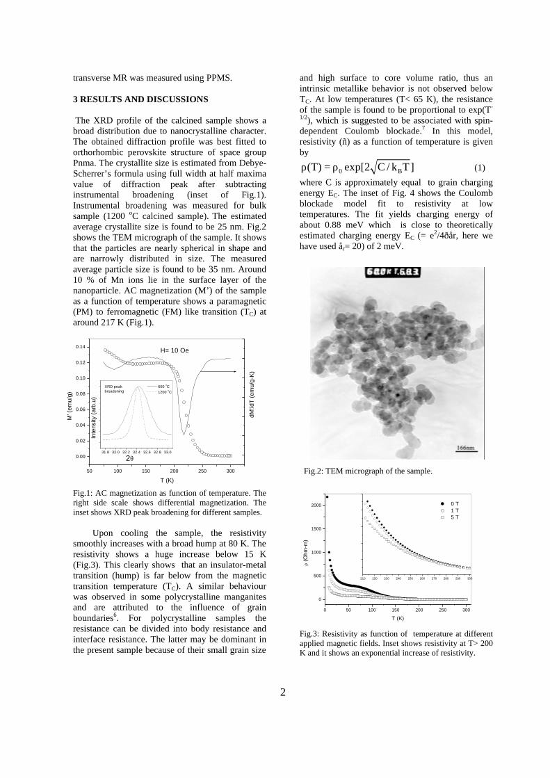
2
transverse MR was measured using PPMS. 3 RESULTS AND DISCUSSIONS The XRD profile of the calcined sample shows a broad distribution due to nanocrystalline character. The obtained diffraction profile was best fitted to orthorhombic perovskite structure of space group Pnma. The crystallite size is estimated from Debye-Scherrer’s formula using full width at half maxima value of diffraction peak after subtracting instrumental broadening (inset of Fig.1). Instrumental broadening was measured for bulk sample (1200 oC calcined sample). The estimated average crystallite size is found to be 25 nm. Fig.2 shows the TEM micrograph of the sample. It shows that the particles are nearly spherical in shape and are narrowly distributed in size. The measured average particle size is found to be 35 nm. Around 10 % of Mn ions lie in the surface layer of the nanoparticle. AC magnetization (M’) of the sample as a function of temperature shows a paramagnetic (PM) to ferromagnetic (FM) like transition (TC) at around 217 K (Fig.1). Fig.1: AC magnetization as function of temperature. The right side scale shows differential magnetization. The inset shows XRD peak broadening for different samples. Upon cooling the sample, the resistivity smoothly increases with a broad hump at 80 K. The resistivity shows a huge increase below 15 K (Fig.3). This clearly shows that an insulator-metal transition (hump) is far below from the magnetic transition temperature (TC). A similar behaviour was observed in some polycrystalline manganites and are attributed to the influence of grain boundaries6. For polycrystalline samples the resistance can be divided into body resistance and interface resistance. The latter may be dominant in the present sample because of their small grain size
and high surface to core volume ratio, thus an intrinsic metallike behavior is not observed below TC. At low temperatures (T< 65 K), the resistance of the sample is found to be proportional to exp(T-
1/2), which is suggested to be associated with spin-dependent Coulomb blockade.7 In this model, resistivity (ñ) as a function of temperature is given by
0 B(T) exp[2 C / k T]ρ = ρ (1)
where C is approximately equal to grain charging energy EC. The inset of Fig. 4 shows the Coulomb blockade model fit to resistivity at low temperatures. The fit yields charging energy of about 0.88 meV which is close to theoretically estimated charging energy EC (= e2/4ðår, here we have used år= 20) of 2 meV. Fig.2: TEM micrograph of the sample. Fig.3: Resistivity as function of temperature at different applied magnetic fields. Inset shows resistivity at T> 200 K and it shows an exponential increase of resistivity.
0 50 100 150 200 250 300
0
500
1000
1500
2000
ρ (O
hm-m
)
T (K)
0 T 1 T 5 T
210 220 230 240 250 260 270 280 290 300
50 100 150 200 250 300
0.00
0.02
0.04
0.06
0.08
0.10
0.12
0.14
M' (
emu/
g)
T (K)
H= 10 Oe
2θ
Inte
nsity
(ar
b.u)
dM'/d
T (
emu/
g-K
)
31.8 32.0 32.2 32.4 32.6 32.8 33.0
600 oC 1200 oC
XRD peak broadening
3
The magnetoresistivity is defined here as
(H,T) (0,T)MR% x100
(0,T)
ρ − ρ=
ρ (2)
where ñ(H, T) is the resistivity in the presence of an applied magnetic field H at temperature T and ñ(0, T) is the resistivity in the absence of H at T. Fig. 5 shows MR as a function of temperature at 1 T and 5 T.
Fig.4: MR as function of an applied field at 5 K. Inset shows Coulomb blockade fit to data at low temperature.
Fig.5: MR as a function of temperature at 1 and 5 T. The MR shows weakly temperature dependence below ~ 80 K. MR increases smoothly upon decreasing the temperature and shows a broad hump at around 90 K and then weakly temperature dependent below 80 K. Fig.4 shows MR as a function of H at 5 K. The data shows that MR increases very rapidly at low fields ( 0.5 T) and then increases smoothly upon increasing H. The obtained data can be best described by spin polarized tunneling across the barrier formed between ferromagnetic grains due to the
magnetically and structurally disordered layer at the surface of the nanoparticles. This model is similar to ferromagnetic granular materials.7 MR in these materials is due to increase of tunneling upon application of H by alignment of ferromagnetic domains (grains) parallel to each other at low fields. The increase of MR at high fields (>0.5 T), in manganites, is attributed to the alignment of canted spins at intra-grain.2 Fig.5 clearly shows that the change in MR upto 0.5 T is ~20 % and the change in MR between 0.5- 9 T (high field) is around 62 %. This clearly shows that high field MR (HFMR) is dominating the LFMR. This suggests that the canted spins at the intra-grain are contributing more to total MR . 4 CONCLUSIONS We have successfully prepared Nd0.7Sr0.3MnO3 with an average particle size of 35 nm by citrate-complex method at relatively low temperature. The sample shows para- to ferromagnetic like transition at 217 K and insulator-metal transition (hump) at around 100 K. Resistivity can be understood by tunneling mechanism. Magnetoresistivity shows spin polarized tunneling behaviour with more intra-grain contribution due to canted spins at the intra-grain.
REFERENCE
1R. von Helmolt, J. Wecker, B. Holzapfel, L. Schultz, K. Samwer, Phys. Rev. Lett. 71, 2331 (1993). 2H.Y. Hwang, S.-W. Cheong, N.P. Ong,
B. Batlogg, Phys. Rev. Lett. 77, 2041 (1996). 3A. Gupta, G.Q. Gong, G. Xiao, P.R. Duncombe,
P. Lecoeur, P. Trouilloud, Y.Y. Wang,
V.P. Dravid, J.Z. Sun, Phys. Rev. B. 54, R15629 (1996). 4J.E. Evetts, M.G. Blamire, N.D. Mathur, S.P. Isaac, B.-S. Teo, L.F. Cohen, J.L. Macmanus-Driscoll, Philos. Trans. R. Soc. Lond. A. 356, 1593 (1998). 5H.Y. Hwang, T.T.M. Palstra, S.-W. Cheong, B. Batlogg, Phys. Rev. B. 52, 15046 (1995). 6Z.H. Wang, T.H. Ji, Y.Q. Wang, X. Chen, R.W. Li, J.W. Cai, J.R. Sun, B.G. Shen, C.H. Yan, J. Appl. Phys. 87, 5582 (2000). 7B. Abeles, P. Sheng, M.D. Coutts, Y. Arie, Adv. Phys. 24, 407 (1975).
0 50 100 150 200 250 300
0
10
20
30
40
50
60
70
80
- M
R %
T (K)
5 T 1 T
0 1 2 3 4 5 6 7 8 9 10
-80
-70
-60
-50
-40
-30
-20
-10
0
MR
%
H (T)
5 K
0.10 0.15 0.20 0.25 0.30 0.35 0.40 0.4555
148
403
1097
2981
5 K
65 K
Data fit
slope= 6.47 K1/2
T-1/2 (K-1/2)
ρ (Ω
-m)
Monolayer Magnetism of Ru, Rh, Pd and Ag Transition metals
Anu Bala, Tashi Nautiyal, Sushil Auluck
Department of Physics, IIT Roorkee
Roorkee – 247667, INDIA. Email: [email protected], [email protected]
ABSTRACT
We explore ferromagnetism for the unsupported monolayers of late 4d transition metals ( Ru, Rh , Pd and Ag ) in the present study. We have taken into account the spin- orbit interactions for magnetism of these metals. The lattice constant decreases for the studied elements on going from three dimension to two dimension. The d-bands show shift towards Fermi level and band width narrowing due to reduction in coordination number in two dimension as compared to bulk case. We find unsupported monolayers of Ru, Rh and Pd metals are magnetic with magnetic moments 1.077 µB, 1.172 µB and 0.012 µB, respectively. The highest magnetic moment for Rh, among these, is in agreement with experimental studies. INTRODUCTION In the past, there has been speculation1 as to whether metallic elements that are paramagnetic as bulk materials may become magnetic as free standing monolayers or as over layers on top of a metallic substrate . One reason for this interest is undoubtedly the fact that the two dimensional (2D) magnetism of these systems need not be restricted to 3d transition metals alone. Ab –initio electronic structure calculations within the local spin density approximation predicted that monolayers of the late 4d and 5d transition metals placed on Ag (001) or Au (001) substrates should exhibit ferromagnetism with sizable magnetic moments 2- 4 . According to systematic studies by Blgüel 4, the high values of local magnetic moments among the 4d and 5d monolayers on Ag (001) are expected for Ru (1.7 ìB) , Rh(1.0 ìB ), and Ir ( 0.9 ìB) metals. Therefore, in addition to 3d transition metals, the good candidates for such a change in magnetic behavior can be late transition metals which have the largest exchange – enhanced susceptibility among the transition metals 5 and which, on account of their large state density at the Fermi level, n (Ef), are close to fulfilling the Stoner criterion (I. n (Ef) > 1) for ferromagnetism. The Stoner exchange parameter (I) depends only on atomic number, and the onset of magnetism in the late transition metals may also be induced by small enhancement of the state density. The state density may also be enhanced by the reduction in coordination number that follows the formation of thin films. For a single layer , simple tight – binding theory predicts 30 % increase in the state density, hence a Stoner product well above unity.The expectation is therefore that thin films , and in particular a single layer , of a late transition metal should be truly magnetic. In spite of this expectation, local – spin – density calculations show that the Stoner criterion is not satisfied for monolayer of some late transition metals6-8, which is
in agreement with our results for unsupported monolayer of Ag metal. The calculation of magnetic anisotropy of thin ferromagnetic over layers is thought to be of some practical importance because of the application of those over layers with perpendicular anisotropy to magneto-optical storage media. Much work has been done regarding the magnetism of these monolayers. The free-standing monolayer of Rh has been studied as a function of number of points sampled in the surface of the Brillouin zone showing effect of k-space integration on self –consistent surface magnetic anisotropy 9.The Plane- wave –basis partial-core pseudopotential approach find Rh (001) surface ferromagnetically unstable 10. However there is a series of theoretical investigations , which predicted magnetism for some of the 4d and 5d metals in the reduced dimensions, such as 4d and 5d metal monolyers on Ag ( 100 ) and Au ( 100) substrate 2-4,11,12, small clusters 13 and impurity in bulk Ag 14. In the present paper, we have studied the unsupported monolayers of late transition metals (Rh, Ru, Pd and Ag) and explored the possibility of magnetism. COMPUTATIONAL METHOD We have studied these metals in the ideal three – dimensional state (the bulk) and the ideal two dimensional states (an unsupported monolayer).For the metals Rh, Pd, Ag with FCC structure in bulk, the plane having hexagonal arrangement of atoms is found to be energetically most favorable and has been chosen as a representative of 2D structure for these metals. The base plane has been taken as the representative of 2D case for Ru metal which has hexagonal structure in bulk. Inclusion of scalar – relativistic (SR) effects has been found to be crucial predicting the correct ground state crystal structure of bulk Ag 15.The relativistic effects
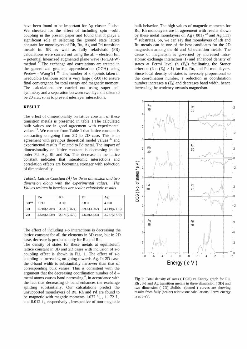
have been found to be important for Ag cluster 16 also. We checked for the effect of including spin –orbit coupling in the present paper and found that it plays a significant role in selecting the ground state lattice constant for monolayers of Rh, Ru, Ag and Pd transition metals in. SR as well as fully relativistic (FR) calculations were carried out using the all – electron full – potential linearized augmented plane wave (FPLAPW) method 17.The exchange and correlations are treated in the generalized gradient approximation (GGA) using Perdew - Wang’91 18. The number of k - points taken in irreducible Brillouin zone is very large (~500) to ensure final convergence for total energy and magnetic moment. The calculations are carried out using super cell symmetry and a separation between two layers is taken to be 20 a.u., so as to prevent interlayer interactions. RESULT The effect of dimensionality on lattice constant of these transition metals is presented in table 1.The calculated bulk values are in good agreement with experimental values 19. We can see from Table 1 that lattice constant is contracting on going from 3D to 2D case. This is in agreement with previous theoretical model values 20 and experimental results 21 related to Pd metal. The impact of dimensionality on lattice constant is decreasing in the order Pd, Ag, Rh and Ru. This decrease in the lattice constant indicates that interatomic interactions and correlation effects are becoming stronger with reduction of dimensionality. Table1: Lattice Constant (Å) for three dimension and two dimension along with the experimental values. The Values written in brackets are scalar relativistic results.
Ru Rh Pd Ag
3Dexp 2.711 3.801 3.891 4.090
3D 2.710(2.709) 3.831(3.824) 3.905(3.902) 4.119(4.113)
2D 2.546(2.539) 2.571(2.570) 2.608(2.623) 2.777(2.779)
The effect of including s-o interactions is decreasing the lattice constant for all the elements in 3D case, but in 2D case, decrease is predicted only for Ru and Rh. The density of states for these metals at equilibrium lattice constant in 3D and 2D cases with inclusion of s-o coupling effect is shown in Fig. 1. The effect of s-o coupling is increasing on going towards Ag. In 2D case, the d-band width is substantially narrower than that of corresponding bulk values. This is consistent with the argument that the decreasing coordination number of d – metal atoms causes band narrowing 8, in accordance with the fact that decreasing d- band enhances the exchange splitting substantially. Our calculations predict the unsupported monolayers of Ru, Rh and Pd are found to be magnetic with magntic moments 1.077 ìB , 1.172 ìB and 0.012 ìB, respectively , irrespective of non-magnetic
bulk behavior. The high values of magnetic moments for Ru, Rh monolayers are in agreement with results shown by these metal monolayers on Ag ( 001) 22 and Ag(111) 23 substrates. So, we can say that monolayers of Rh and Ru metals can be one of the best candidates for the 2D magnetism among the 4d and 5d transition metals. The cause of magnetism is governed by increased intra-atomic exchange interaction (I) and enhanced density of states at Fermi level (n (Ef)) facilitating the Stoner criterion (I. n (Ef) > 1) for Ru, Ru, and Pd monolayers. Since local density of states is inversely proportional to the coordination number, a reduction in coordination number increases n (Ef) and decreases band width, hence increasing the tendency towards magnetism.
0
2
4
6
R u3D
R h3D
-2
0
2R h2D
0
1
2
3
-2
0
2R h2D
0
1
2
3
Energy ( e V )
P d3D
DO
S ( N
o. o
f sta
tes
/ e V
)
-2
0
2P d2D
-8 -6 -4 -2 00
3
6
9
Ag3D
-8 -6 -4 -2 0 20
3
6
9Ag2D
Fig.1: Total density of sates ( DOS) vs Energy graph for Ru, Rh , Pd and Ag transition metals in three dimension ( 3D) and two dimension ( 2D) .Solids (dotted ) curves are showing results from fully (scalar) relativistic calculations .Fermi energy is at 0 eV.
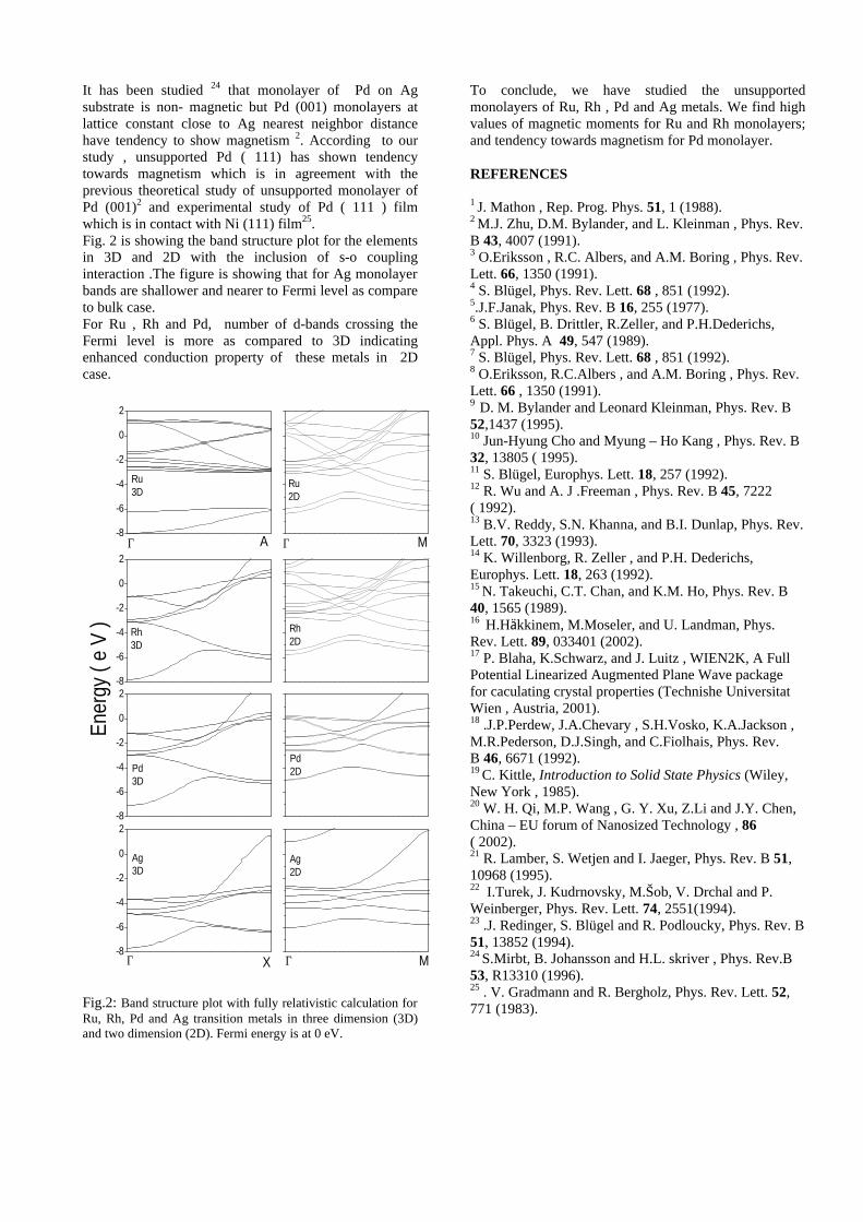
It has been studied 24 that monolayer of Pd on Ag substrate is non- magnetic but Pd (001) monolayers at lattice constant close to Ag nearest neighbor distance have tendency to show magnetism 2. According to our study , unsupported Pd ( 111) has shown tendency towards magnetism which is in agreement with the previous theoretical study of unsupported monolayer of Pd (001)2 and experimental study of Pd ( 111 ) film which is in contact with Ni (111) film25. Fig. 2 is showing the band structure plot for the elements in 3D and 2D with the inclusion of s-o coupling interaction .The figure is showing that for Ag monolayer bands are shallower and nearer to Fermi level as compare to bulk case. For Ru , Rh and Pd, number of d-bands crossing the Fermi level is more as compared to 3D indicating enhanced conduction property of these metals in 2D case.
-8
-6
-4
-2
0
2
Ru3D
MΓAΓ
MΓXΓ
Ru2D
-8
-6
-4
-2
0
2
Rh3D
Rh2D
-8
-6
-4
-2
0
2
Pd3D
Pd2D
-8
-6
-4
-2
0
2
Ag3D
Ener
gy (
e V
)
Ag2D
Fig.2: Band structure plot with fully relativistic calculation for Ru, Rh, Pd and Ag transition metals in three dimension (3D) and two dimension (2D). Fermi energy is at 0 eV.
To conclude, we have studied the unsupported monolayers of Ru, Rh , Pd and Ag metals. We find high values of magnetic moments for Ru and Rh monolayers; and tendency towards magnetism for Pd monolayer. REFERENCES 1 J. Mathon , Rep. Prog. Phys. 51, 1 (1988). 2 M.J. Zhu, D.M. Bylander, and L. Kleinman , Phys. Rev. B 43, 4007 (1991). 3 O.Eriksson , R.C. Albers, and A.M. Boring , Phys. Rev. Lett. 66, 1350 (1991). 4 S. Blügel, Phys. Rev. Lett. 68 , 851 (1992). 5.J.F.Janak, Phys. Rev. B 16, 255 (1977). 6 S. Blügel, B. Drittler, R.Zeller, and P.H.Dederichs, Appl. Phys. A 49, 547 (1989). 7 S. Blügel, Phys. Rev. Lett. 68 , 851 (1992). 8 O.Eriksson, R.C.Albers , and A.M. Boring , Phys. Rev. Lett. 66 , 1350 (1991). 9 D. M. Bylander and Leonard Kleinman, Phys. Rev. B 52,1437 (1995). 10 Jun-Hyung Cho and Myung – Ho Kang , Phys. Rev. B 32, 13805 ( 1995). 11 S. Blügel, Europhys. Lett. 18, 257 (1992). 12 R. Wu and A. J .Freeman , Phys. Rev. B 45, 7222 ( 1992). 13 B.V. Reddy, S.N. Khanna, and B.I. Dunlap, Phys. Rev. Lett. 70, 3323 (1993). 14 K. Willenborg, R. Zeller , and P.H. Dederichs, Europhys. Lett. 18, 263 (1992). 15 N. Takeuchi, C.T. Chan, and K.M. Ho, Phys. Rev. B 40, 1565 (1989). 16 H.Häkkinem, M.Moseler, and U. Landman, Phys. Rev. Lett. 89, 033401 (2002). 17 P. Blaha, K.Schwarz, and J. Luitz , WIEN2K, A Full Potential Linearized Augmented Plane Wave package for caculating crystal properties (Technishe Universitat Wien , Austria, 2001). 18 .J.P.Perdew, J.A.Chevary , S.H.Vosko, K.A.Jackson , M.R.Pederson, D.J.Singh, and C.Fiolhais, Phys. Rev. B 46, 6671 (1992). 19 C. Kittle, Introduction to Solid State Physics (Wiley, New York , 1985). 20 W. H. Qi, M.P. Wang , G. Y. Xu, Z.Li and J.Y. Chen, China – EU forum of Nanosized Technology , 86 ( 2002). 21 R. Lamber, S. Wetjen and I. Jaeger, Phys. Rev. B 51, 10968 (1995). 22 I.Turek, J. Kudrnovsky, M.Šob, V. Drchal and P. Weinberger, Phys. Rev. Lett. 74, 2551(1994). 23 .J. Redinger, S. Blügel and R. Podloucky, Phys. Rev. B 51, 13852 (1994). 24 S.Mirbt, B. Johansson and H.L. skriver , Phys. Rev.B 53, R13310 (1996). 25 . V. Gradmann and R. Bergholz, Phys. Rev. Lett. 52, 771 (1983).

Sorry!!
This Paper is NOT Available
REDUCTION OF SATURATION MAGNETIZATION OF NANOCRYSTALLINE CuFe2O4 by SnO2 COATING
R.Kalai Selvana,b*, C.O.Augustina, C.Sanjeevirajab
a Central Electrochemical Research Institute, Karaikudi –630 006, India
b Department of Physics, Alagappa University, Karaikudi – 630 006, India
*e-mail: [email protected]
ABSTRACT: In the present investigation, a novel approach is made to reduce the saturation magnetization of copper ferrite using SnO2 coating. The materials were prepared using urea-nitrate combustion method. The XRD patterns show that the 1100oC-sintered sample gives a tetragonal structure. The particle size of the as synthesized copper ferrite and its composites are 10-20nm and 30-40 nm respectively as evident from TEM and HRTEM. The saturation magnetization of CuFe2O4 is 30emu/gm, which has reduced to 11emu/gm on SnO2 coating, due to the dead layer formation as well as the reduction of magnetic particle- particle interaction.
1 INTRODUCTION
Nanomaterials are the privileged class of
materials that have very different novel properties, which differ from those of the bulk-structured materials due to quantum size effects [1]. Very recently, nanoferrites with the spinel structure are subjected to exhaustive studies owing to their unusual advantageous properties. The general formula of spinel ferrite is (M1-δ Feδ)[Mδ Fe2-δ] where ( ) and [ ] denote that the cations sites of tetrahedral and octahedral respectively, δ is the inversion parameter. When δ = 0, it gives a normal spinel and δ = 1, gives inverse spinel. The structural, electrical and magnetic properties of the ferrites are mainly depending upon the cation distribution on both the above sites. Among the privileged class of spinel ferrites, copper ferrite is of paramount importance because of its phase transition from cubic to tetragonal structure with temperature and the anomalous properties due to the Cu2+ Jahn –Teller ions.
Various methods for the synthesis of nanoferrites
and their composites such as combustion method [2], Reverse micelles [3], sol-gel method [4] and Mechano-synthesis [5] have been reported. Among the synthesis techniques, solution based combustion method is the most suitable for preparing nanomaterials with advantages properties. Considering the importance of ferrite-based nanocomposites as anode materials for replacement of conventionally used carbon anodes [6] an attempt has been made to reduce the magnetic properties by the SnO2 coating. 2 EXPERIMENTAL: The nanocrystalline CuFe2O4 and SnO2 coated CuFe2O4 have been prepared by using novel combustion method.
The detailed experimental procedure is given elsewhere [2]. The stoichiometric quantities of starting compounds like Cu(NO3)2. 6H2O, Fe(NO3)3.9H2O, SnCl4, HNO3 and CO(NH2)2 were dissolved in 100 ml triple distilled water. The mixed nitrate – urea solution was heated at 300oC, with uniform stirring and evaporated the excess water to form a highly viscous gel denoted as precursors. The gel was heated continuously, get ignited with evolution of large number of gaseous products, resulting the desired nanocomposite in the form of foamy powder. The powder was then pressed at a pressure of 3.5 tons/cm2 into 1 and 2.5cm diameter pellets under identical conditions. The pellets were sintered at 1100oC for 5 hours. The crystalline phases of the prepared powders were identified by powder X-ray diffraction technique using Cu-Kα radiation (α=1.5405Ao). The particle morphology of all the samples was determined by transmission electron microscopy (TEM; JEOL-JEM 100SX microscope) at an accelerating voltage of 200 kV. The TEM specimens were prepared by placing a drop of the sample suspension on a carbon-coated copper grid (400 mesh, Electron Microscopy Sciences) and allowing them to dry in air. High-resolution TEM (HRTEM) images were taken using a JEOL-3010 with 300 kV accelerating voltage. A conventional monochrome CCD camera, with resolution of 768×512 pixels, was used to digitalize the images. The digital images were processed with the digital micrograph software package (Gatan, Inc, Pleasanton, CA, USA). The effects of temperature and applied magnetic field on magnetization have been carried out using superconducting quantum interference device (SQUID) Quantum design.
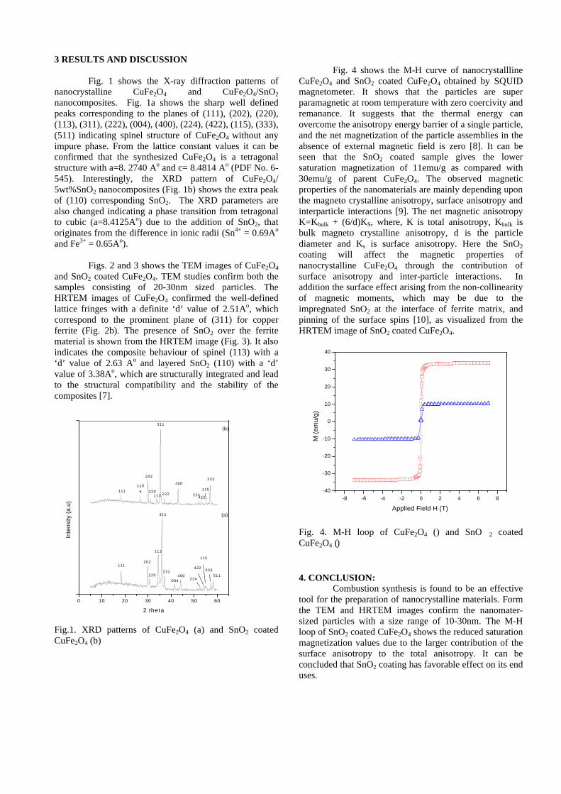
3 RESULTS AND DISCUSSION
Fig. 1 shows the X-ray diffraction patterns of nanocrystalline CuFe2O4 and CuFe2O4/SnO2 nanocomposites. Fig. 1a shows the sharp well defined peaks corresponding to the planes of (111), (202), (220), (113), (311), (222), (004), (400), (224), (422), (115), (333), (511) indicating spinel structure of CuFe2O4 without any impure phase. From the lattice constant values it can be confirmed that the synthesized CuFe2O4 is a tetragonal structure with a=8. 2740 Ao and c= 8.4814 Ao (PDF No. 6-545). Interestingly, the XRD pattern of CuFe2O4/ 5wt%SnO2 nanocomposites (Fig. 1b) shows the extra peak of (110) corresponding SnO2. The XRD parameters are also changed indicating a phase transition from tetragonal to cubic (a=8.4125Ao) due to the addition of SnO2, that originates from the difference in ionic radii (Sn4+ = 0.69Ao
and Fe3+ = 0.65Ao).
Figs. 2 and 3 shows the TEM images of CuFe2O4 and SnO2 coated CuFe2O4. TEM studies confirm both the samples consisting of 20-30nm sized particles. The HRTEM images of CuFe2O4 confirmed the well-defined lattice fringes with a definite ‘d’ value of 2.51Ao, which correspond to the prominent plane of (311) for copper ferrite (Fig. 2b). The presence of SnO2 over the ferrite material is shown from the HRTEM image (Fig. 3). It also indicates the composite behaviour of spinel (113) with a ‘d’ value of 2.63 Ao and layered SnO2 (110) with a ‘d’ value of 3.38Ao, which are structurally integrated and lead to the structural compatibility and the stability of the composites [7].
0 10 20 30 40 50 60
400
113
311
202111
Inte
nsity
(a.
u)
2 theta
333
115
422224
(b)
(a)
400
222220
511
333
115
422
224004
222220
113
311
202
*110
111
Fig.1. XRD patterns of CuFe2O4 (a) and SnO2 coated CuFe2O4 (b)
Fig. 4 shows the M-H curve of nanocrystallline
CuFe2O4 and SnO2 coated CuFe2O4 obtained by SQUID magnetometer. It shows that the particles are super paramagnetic at room temperature with zero coercivity and remanance. It suggests that the thermal energy can overcome the anisotropy energy barrier of a single particle, and the net magnetization of the particle assemblies in the absence of external magnetic field is zero [8]. It can be seen that the SnO2 coated sample gives the lower saturation magnetization of 11emu/g as compared with 30emu/g of parent CuFe2O4. The observed magnetic properties of the nanomaterials are mainly depending upon the magneto crystalline anisotropy, surface anisotropy and interparticle interactions [9]. The net magnetic anisotropy K=Kbulk + (6/d)KS, where, K is total anisotropy, Kbulk is bulk magneto crystalline anisotropy, d is the particle diameter and Ks is surface anisotropy. Here the SnO2 coating will affect the magnetic properties of nanocrystalline CuFe2O4 through the contribution of surface anisotropy and inter-particle interactions. In addition the surface effect arising from the non-collinearity of magnetic moments, which may be due to the impregnated SnO2 at the interface of ferrite matrix, and pinning of the surface spins [10], as visualized from the HRTEM image of SnO2 coated CuFe2O4.
-8 -6 -4 -2 0 2 4 6 8
-40
-30
-20
-10
0
10
20
30
40
M (
emu/
g)
Applied Field H (T)
Fig. 4. M-H loop of CuFe2O4 () and SnO 2 coated CuFe2O4 () 4. CONCLUSION:
Combustion synthesis is found to be an effective tool for the preparation of nanocrystalline materials. Form the TEM and HRTEM images confirm the nanomater-sized particles with a size range of 10-30nm. The M-H loop of SnO2 coated CuFe2O4 shows the reduced saturation magnetization values due to the larger contribution of the surface anisotropy to the total anisotropy. It can be concluded that SnO2 coating has favorable effect on its end uses.
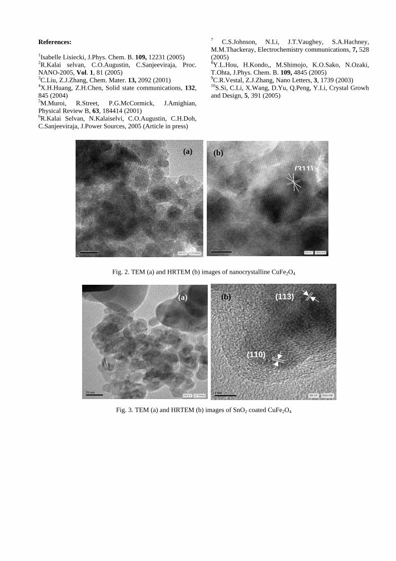
References: 1Isabelle Lisiecki, J.Phys. Chem. B. 109, 12231 (2005) 2R.Kalai selvan, C.O.Augustin, C.Sanjeeviraja, Proc. NANO-2005, Vol. 1, 81 (2005) 3C.Liu, Z.J.Zhang, Chem. Mater. 13, 2092 (2001) 4X.H.Huang, Z.H.Chen, Solid state communications, 132, 845 (2004) 5M.Muroi, R.Street, P.G.McCormick, J.Amighian, Physical Review B, 63, 184414 (2001) 6R.Kalai Selvan, N.Kalaiselvi, C.O.Augustin, C.H.Doh, C.Sanjeeviraja, J.Power Sources, 2005 (Article in press)
7 C.S.Johnson, N.Li, J.T.Vaughey, S.A.Hachney, M.M.Thackeray, Electrochemistry communications, 7, 528 (2005) 8Y.L.Hou, H.Kondo,, M.Shimojo, K.O.Sako, N.Ozaki, T.Ohta, J.Phys. Chem. B. 109, 4845 (2005) 9C.R.Vestal, Z.J.Zhang, Nano Letters, 3, 1739 (2003) 10S.Si, C.Li, X.Wang, D.Yu, Q.Peng, Y.Li, Crystal Growh and Design, 5, 391 (2005)
Fig. 2. TEM (a) and HRTEM (b) images of nanocrystalline CuFe2O4
Fig. 3. TEM (a) and HRTEM (b) images of SnO2 coated CuFe2O4
(a) (b)
(311)
(a) (b) (113)
(110)
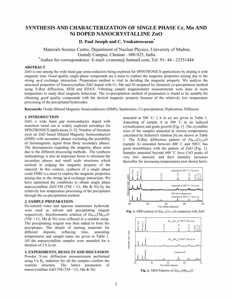
1
SYNTHESIS AND CHARACTERIZATION OF SINGLE PHASE Cr, Mn AND Ni DOPED NANOCRYSTALLINE ZnO
D. Paul Joseph and C. Venkateswaran*
Materials Science Centre, Department of Nuclear Physics, University of Madras, Guindy Campus, Chennai - 600 025, India.
*Author for correspondence: E-mail: cvunom@ hotmail.com, Tel: 91- 44 - 22351444
ABSTRACT ZnO is one among the wide band gap semiconductors being explored for SPINTRONICS applications by doping it with magnetic ions. Good quality single-phase compounds are a must to explore the magnetic properties arising due to the strong sp-d exchange interaction. Preparation method is vital in deciding the magnetic property. We analyze the structural properties of Nanocrystalline ZnO doped with Cr, Mn and Ni prepared by chemical co-precipitation method using X-Ray diffraction, SEM and EDAX. Vibrating sample magnetometer measurements were done at room temperature to study their magnetic behaviour. The co-precipitation method of preparation is found to be suitable for obtaining good quality compounds with the desired magnetic property because of the relatively low temperature processing of the precipitated hydroxides.
Keywords: Oxide Diluted Magnetic Semiconductors (DMS), Spintronics, Co-precipitation, Peptization, Diffusion 1. INTRODUCTION ZnO, a wide band gap semiconductor doped with transition metal ion is widely explored nowadays for SPINTRONICS applications [1-5]. Number of literature exist on ZnO based Diluted Magnetic Semiconductors (DMS) with secondary phases excluding the possibility of ferromagnetic signal from those secondary phases. The discrepancies regarding the magnetic phase arise due to the different processing methods. The synthesis methodology is also an important factor to eliminate the secondary phases and small scale structures which mislead in judging the magnetic property of the material. In this context, synthesis of a single phase oxide DMS is a must to explore the magnetic properties arising due to the strong sp-d exchange interaction. We have optimized the conditions to obtain single phase nanocrystalline ZnO:TM (TM = Cr, Mn & Ni) by the relatively low temperature processing of the precipitates through the co-precipitation method.
2. SAMPLE PREPARATION De-ionized water and aqueous ammonium hydroxide were used as solvent and precipitating reagent respectively. Stoichiometric solution of Zn0.95TM0.05O (TM = Cr, Mn & Ni) were refluxed in a suitable setup. The precipitating reagent was then added to form the precipitates. The details of starting materials for different dopants, refluxing time, annealing temperatures and sample name are given in Table 1. All the nanocrystalline samples were annealed for a duration of 2 h in air.
3. EXPERIMENTS, RESULTS AND DISCUSSION Powder X-ray diffraction measurements performed using Cu Kα radiation for all the samples confirm the wurtzite structure. The lattice parameters of nanocrystalline ZnO:TM (TM = Cr, Mn & Ni)
annealed at 500 °C/ 2 h in air are given in Table 1. Annealing of sample A at 500 °C in air induced crystallization and grain growth [Fig. 1]. The crystallite sizes of the samples annealed at various temperatures calculated by Scherrer's relation [6] are shown in Table 1. The X-Ray diffraction pattern of Zn0.95Cr0.05O (sample A) annealed between 400 °C and 500°C has good resemblance with the pattern of ZnO [Fig. 1]. Samples annealed beyond 600 oC have CrO peaks of very low intensity and their intensity increases thereafter for increasing temperatures (not shown here).
30 40 50 60 70
ZnO (for comparison)Annealed at 500 oC/ 2 hr in air
Inte
nsity
(arb
. uni
t)
Two theta (degree)
Annealed at 400 oC/ 2 hr in air
(2 0
1)
(1 1
2)
(2 0
0)
(1 0
3)
(1 1
0)
(1 0
2)(1
0 1
)(0
0 2
)
(1 0
0) Annealed at 500 oC/ 2 hr in air
Fig. 1. XRD pattern of Zn0 95Cr0 05O compared with ZnO
30 40 50 60 70
Undoped ZnO
Two theta (degree)
Zn0.95Mn0.05O 500 0C/2hr in air
Inte
nsity
(arb
. uni
t)
Zn0.95Mn0.05O 700 0C/2hr in air
(2 0
1)
(1 1
2)
(2 0
0)
(1 0
3)
(1 1
0)
(1 0
2)(1
0 1
)(0
0 2
)
(1 0
0)
Fig. 2. XRD Patterns of Zn0.95Mn0.05O
2
Similarly, Zn0.95Mn0.05O (sample B) and Zn0.95Ni0.05O (sample C) annealed beyond 700 °C show secondary peaks of very low intensity due to manganese oxide and nickel oxide respectively and their intensity was found to increase for increasing temperatures of annealing [Fig. 3 and Fig. 4]. Similar result had been reported by T. Wakano et al., for Ni doped ZnO thin films [7]. It is inferred from these observations that the TM doped nanocrystalline ZnO becomes inhomogeneous with increasing annealing temperatures, probably from the clustering of the dopants. Energy dispersive X-ray analysis spectrum indicated samples A, B and C to be nearly stoichiometric (Table 1). The nominal variation can be attributed to the random substitution of the magnetic dopants at the cationic site of the host lattice. The SEM micrographs of samples prepared by co-precipitation (Samples A, B & C) are shown in Fig. 5. Nanocrystalline Zn0.95Cr0.05O (sample C, 500°C /2 h in air) has relatively smaller crystallite size and different morphology with greater surface roughness due to high density of grain
boundaries compared to Mn and Ni doped ZnO. The aggregate of crystallites of various sizes indicating a size distribution was clearly evident from the SEM images of sample B and C. In the co-precipitation technique, the metal ions are mixed on an atomic scale leading to greater reactivity and hence homogeneous products result at relatively low processing temperatures. The precipitates have fine crystallites of the order of nanometers with diffusion distances smaller than that in the ceramic method. Hence annealing of these precipitates at relatively lower temperatures (500 °C-600 °C) and duration results in the formation of a single phase nanocrystalline ZnO:TM (TM = Cr, Mn & Ni). The ultimate purpose of this effort is not only to find a suitable method for the synthesis of single phase ZnO:TM compounds, but to synthesize a material with desirable magnetic properties. For this, we performed magnetization measurements on nanocrystalline Cr, Mn and Ni doped ZnO (each 5%).
The magnetization measurements were performed in a Vibrating Sample Magnetometer (VSM) at 300 K. Very few reports exist in literature on the magnetic characterization of ZnO DMS using a VSM [8, 9].
Table 1. Preparation details, crystallite size, composition and lattice parameters of Nanocrystalline Zn
0.95TM
0.05O (TM = Cr, Mn & Ni)
Sample name Starting materials
Refluxing time
Crystallite size Composition (EDAX)
Lattice parameters
Sample A Zn
0.95Cr
0.05O
Zinc Nitrate &
Chromium Nitrate
50 h
24 nm/400 °C
33 nm /500°C
38 nm/600 °C
40 nm/700 °C
43 nm/900 °C
5.06%
a = b = 3.260 Å c = 5.217 Å
Sample B Zn
0.95Mn
0.05O
Zinc Nitrate & Manganese
acetate
25 h 24 nm/500
°C
33 nm /700°C
4.0%
a = b = 3.261 Å
c = 5.210 Å Sample C
Zn0.95
Ni0.05
O Zinc Nitrate & Nickel Nitrate
50 h 34 nm/500
°C
41 nm /700°C
4.17%
a = b = 3.264 Å
c = 5.223 Å
30 40 50 60 70
Un doped ZnO for comparison
Inte
nsity
(arb
itrar
y un
it)
Two theta (Degree)
(0 0
4)
(2 0
1)
(1 1
2)
(2 0
0)(1 0
3)
(1 1
0)
(1 0
2)
(1 0
1)
(0 0
2)
(1 0
0)
Zn0.95Ni0.05O annealed at 700 0C
Zn0.95Ni0.05O annealed at 500 0C
Fig. 3. XRD patterns of Zn0.95Ni0.05O annealed at different temperatures
Fig. 4. Representative SEM image of Zn0.95Mn0.05O annealed at 500 °C/2 h in air
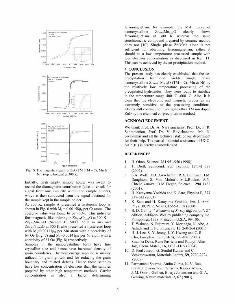
3
Initially, fresh empty sample holder was swept to record the diamagnetic contribution (also to check for signal from any impurity within the sample holder), which is then subtracted from the signal obtained for the sample kept in the sample holder. At 300 K, sample A presented a hysteresis loop as shown in Fig. 6 with Ms = 0.00158µB per Cr atom. The coercive value was found to be 95Oe. This indicates ferromagnetic-like ordering in Zn0.95Cr0.05O at 300 K. Zn0.95Mn0.05O (Sample B, 500°C /2 h in air) and Zn0.95Ni0.05O at 300 K also presented a hysteresis loop with Ms=0.00173µB per Mn atom with a coercivity of 64 Oe (Fig. 7) and Ms=0.00141µB per Ni atom with a coercivity of 81 Oe (Fig. 8) respectively. Samples in the nanocrystalline form have fine crystallite size and hence have increased density of grain boundaries. The heat energy supplied is mainly utilized for grain growth and for reducing the grain boundary and related defects. Hence these samples have low concentration of electrons than the samples prepared by other high temperature methods. Carrier concentration is also a factor determining
ferromagnetism: for example, the M-H curve of nanocrystalline Zn0.95Mn0.05O clearly shows ferromagnetism at 300 K whereas the same stoichiometric compound prepared by ceramic method does not [10]. Single phase ZnO:Mn alone is not sufficient for obtaining ferromagnetism, rather it should be a low temperature processed sample with low electron concentration as discussed in Ref. 11. This can be achieved by the co-precipitation method.
4. CONCLUSION The present study has clearly established that the co-precipitation technique yields single phase nanocrystalline Zn0.95TM0.05O (TM = Cr, Mn & Ni) by the relatively low temperature processing of the precipitated hydroxides. They were found to stabilize in the temperature range 400 °C -600 °C. Also, it is clear that the electronic and magnetic properties are extremely sensitive to the processing conditions. Efforts still continue to investigate other TM ion doped ZnO by the chemical co-precipitation method.
ACKNOWLEDGEMENT
We thank Prof. Dr. A. Narayanasamy, Prof. Dr. P. R. Subramanian, Prof. Dr. V. Ravichandran, Mr. N. Sivakumar and all the technical staff of our department for their help. The partial financial assistance of UGC-SAP (III) is hereby acknowledged. REFERENCES 1. H. Ohno, Science, 281 951-956 (1998). 2. T. Dietl, Semicond. Sci. Technol, 17(14) 377
(2002). 3. S.A. Wolf, D.D. Awschalom, R.A. Buhrman, J.M.
Daughton, S. Von Molna'r, M.L.Roukes, A.Y. Chtchelkanova, D.M.Treger, Science, 294 1488 (2001).
4. H. Katayama-Yoshida and K. Sato, Physica B, 327 337-343 (2003).
5. K. Sato and H. Katayama-Yoshida, Jpn. J. Appl. Phys. 39, Pt. 2, No.6B, L555-L558 (2000).
6. B. D. Cullity, " Elements of X- ray diffraction", 2nd edition, Addison- Wesley publishing company Inc. Philippines, 1978, Printed in U.S.A, 99-106.
7. T. Wakano, N. Fujimura, Y. Morinaga, N. Abe, A. Ashida and T. Ito, Physica E 10, 260-264 (2001).
8. H.-J. Lee, S.-Y. Jeong, J.-Y. Hwang and C. R. Cho, Europhys. Lett., 64(6), 797-802 (2003).
9. Sasanka Deka, Renu Pasricha and Pattayil Alias Joy, Chem. Mater., 16, 1168 -1169 (2004).
10. D. Paul Joseph, G. Senthil Kumar and C. Venkateswaran, Materials Letters, 59, 2720-2724 (2005). 11. Parmanand Sharma, Amita Gupta, K. V. Rao, Frank J. Owens, Renu Sharma, Rajeev Ahuja, J. M. Osorio Guillen, Boerje Johansson and G. A. Gehring, Nature materials, 2, 67 (2003).
-5000 0 5000-0.0004
-0.0003
-0.0002
-0.0001
0.0000
0.0001
0.0002
0.0003
0.0004
Zn0.9 5Ni0.0 5O 500 0C/2hDiamagnetic signal subtractedAt 300 K
Mag
netis
atio
n (e
mu)
Applied field (Oe)
-8000 -6000 -4000 -2000 0 2000 4000 6000 8000-0.0015
-0.0010
-0.0005
0.0000
0.0005
0.0010
- 400 0 400
0.0000
0.0006
Mag
neti
satio
n (e
mu)
Applied f iel d (Oe)
At 300 KMax. field = 7 kOe
Diamagnetic signal subtracted
Mag
netis
atio
n (e
mu)
Applied field (Oe)
-8000 -6000 -4000 -2000 0 2000 4000 6000 8000
-0.0004
-0.0002
0.0000
0.0002
0.0004 ZnO:Mn (5%)Chemical method(500 °C / 2 hr in air) @ 300 K
-500 -400 -300 -200 -100 0 100 200 300 400 500 600
-0.00020
-0.00015
-0.00010
-0.00005
0.00000
0.00005
0.00010
0.00015
0.00020
Mag
netis
atio
n (e
mu)
Applied field (Oe)
Mag
netis
atio
n (e
mu)
Applied field (Oe)
Fig. 5. The magnetic signal for ZnO:TM (TM = Cr, Mn & Ni) (top to bottom) at 300 K.
PREPARATION AND CHARACTERISATION OF NANOCRYSTALLINE AND BULK Zn0.95Fe0.05O DMS
D. Paul Joseph, S. Philip Raja and C. Venkateswaran*
Materials Science Centre, Department of Nuclear Physics, University of Madras, Guindy campus, Chennai – 600 025, India.
* E-mail: [email protected], Ph: 044 – 22351444
ABSTRACT
The materials design based on ab initio calculations predict Fe doped ZnO to be a high Tc Diluted Magnetic Semiconductor (DMS). We have synthesized ‘Fe’ doped ZnO by co-precipitation and ceramic methods. Structure and composition were confirmed by XRD, SEM and EDAX. Its magnetic property studied at 300 K using Vibrating Sample Magnetometer presented better hysteresis behavior for the nanocrystalline sample prepared by co-precipitation technique. The optical property of both the samples had been studied using diffuse reflectance (DRS) spectroscopy in the UV-VIS region. These studies indicate that the co-precipitation method of preparation has the advantage in tuning the magnetic, electrical and optical properties by way of controlling the particle size, dopant and carrier concentration.
Keywords: Diluted Magnetic Semiconductors, Spintronics, Zn0.95Fe0.05O, Diffuse Reflectance Spectroscopy (DRS), hysteresis
1. INTRODUCTION
ZnO, the transparent conducting oxide is a promising n-type material for opto electronic applications due to its wideband gap energy of 3.3 eV and a high exciton binding energy of 60 meV. ZnO is also emerging as a potential Diluted Magnetic Semiconductor (DMS) for SPINTRONICS applications. DMS are semiconducting compounds whose lattice is made up in part by substitutional magnetic ions.1-3 The materials design based on ab initio calculations predict Fe doped ZnO to be high Tc DMS in which the ferromagnetic states are stabilized by electron doping.4,5 Therefore stabilization of ferromagnetism in ZnO would lead to interesting magneto-optical applications as well. S. J. Han et al have demonstrated that additional Cu doping into Zn(1-
x)FexO aids the stabilization of FM6. We have synthesized ‘Fe’ doped ZnO by the chemical co-precipitation and ceramic methods to form Zn(1-
x)FexO with x = 0.05 and characterized them for structural, composition, magnetic and optical properties.
2. SAMPLE PREPARATION
ZnO was precipitated from zinc nitrate solution for the purpose of comparison. Sample A: Zinc Nitrate and Iron nitrate solutions for the stoichiometry Zn0.95Fe0.05O were prepared in de-ionized water, mixed and refluxed for 50 h in a suitable set up. Precipitation was done using aqueous ammonium hydroxide (NH4OH) after cooling the solution. The precipitates were washed using de-ionized water (peptization) to remove the water soluble by-product, ammonium nitrate. The spongy contents were filtered, dried and then powdered. Sample B: Polycrystalline Zn0.95Fe0.05O was synthesized by ceramic method from ZnO and Fe2O3
powders. The stoichiometric mixture was pelleted and sintered at temperatures varying from 900°C to 1200°C in air for periods ranging from 12 h to 48 h.
3. RESULTS AND DISCUSSION
Powder X-ray diffraction measurements on Sample A (500°C / 2 h in air) using Cu Kα radiation confirmed the wurtzite structure with lattice parameters, a = b = 3.260 Å and c = 5.217 Å. The as prepared sample had amorphous nature. Annealing at 500°C in air induced crystallization [Fig.1]. Annealing at higher temperatures induced grain growth.
The crystallite sizes from Scherrer's relation for sample A annealed at different temperatures (2 h in air) were: 24 nm for 500°C, 33 nm for 700°C. The X-Ray diffraction pattern of sample A annealed between 500°C - 700°C has good resemblance with the pattern of ZnO [Fig. 1]. Stability of Zn(1-x)FexO and secondary
Fig. 1. XRD Pattern of Zn0.95Fe0.05O (Sample-A) annealed at different temperatures
30 40 50 60 70
300 0C/2h
Two theta (degree)
Inte
nsity
(arb
. uni
t)
500 0C/2h
(2 0
1)
(1 1
2)
(2 0
0)
(1 0
3)
(1 1
0)
(1 0
2)
(1 0
1)
(0 0
2)
(1 0
0) * Fe3O4
***
700 0C/2h coprecipitated ZnO:Fe(5%)
phases are sensitive to changes in preparative method and synthesis temperature7. Sample A annealed beyond 700°C has secondary peaks of very low intensity due to iron oxides which increases thereafter for increasing temperatures of annealing. Fig. 2 shows the XRD patterns of Zn0.95Fe0.05O samples obtained by ceramic method for several sintering temperatures. Intensity of Fe2O3 peaks were found to suppress for sintering at 1200 0C/48 h but few Fe3O4 peaks emerge.
The Energy dispersive X-ray analysis (EDAX) spectrum indicated both the samples to be nearly stoichiometric with a composition of 4.5% for sample A and 4% for sample B. The nominal variation in composition from EDAX is attributed to the random alloying of the compounds. The SEM micrographs of sample A (top) and sample B (bottom) taken with the same magnification are shown in Fig. 3. Nanocrystalline Zn0.95Fe0.05O (sample A, 500°C /2 h in air) has relatively smaller crystallite size and a greater surface roughness (due to high density of grain boundaries) than sample B prepared by ceramic method. The aggregate of crystallites of various sizes indicating a size distribution is clearly evident for sample A from the SEM micrograph. Since the ceramic method (sample B) involves sintering of stoichiometric mixtures at higher temperatures, the crystallites are in the order of micrometer with relatively smooth surface. The magnetization measurements were performed in a Vibrating Sample Magnetometer (VSM) at 300 K for sample A (500°C /2 h in air) taken in the form of a small pellet. Few reports exist in literature on the magnetic characterization of ZnO DMS using a VSM8-
10. Initially, empty sample holder was swept to record the diamagnetic contribution, to apply appropriate correction for the signals obtained with samples. The signal at 300 K indicates ferromagnetic-like ordering in Nanocrystalline Zn0.95Fe0.05O [Fig. 4].
However, if Fe3O4 (Magnetite) is present as impurity (undetectable by XRD) and contributes to hysteresis, the magnitude of magnetization would have been larger. Since the magnitude is small, the contribution from magnetite is discarded. At 300 K, sample B (processed at 1200°C for 24 h) presents a loop with paramagnetic like behavior at higher applied fields [Fig. 5] and ferromagnetic like behavior at lower fields (inset) without saturation.
-8000 -6000 -4000 -2000 0 2000 4000 6000 8000
-0.0018
-0.0012
-0.0006
0.0000
0.0006
0.0012
0.0018
0.0024
Mag
netis
atio
n (e
mu)
Applied Field (Oe)
ZnO:Fe (5%) 500 0C/2h
Fig. 4. Loop obtained for Zn0.95Fe0.05O (sample A) at 300 K
Fig. 3. The SEM image of sample A & B (top & bottom) annealed & sintered at 500 °C/2 h and 1200 °C/24 h
in air respectively
30 40 50 60 70
###
Two theta (Degree)
1200 0C/12h
## #
Inte
nsity
(arb
. Uni
t)
1200 0C/24h(2
0 1
)(1
1 2
)(2
0 0
)
(1 0
3)
(1 1
0)
(1 0
2)
(1 0
1)
(0 0
2)
(1 0
0)
# Fe2O3 Solid state reaction ZnO:Fe (5%)
***
* Fe3O
4
1200 0C/48h
Fig. 2. XRD Pattern of Zn0.95Fe0.05O (Sample-B) sintered at different temperatures
This sample has traces of Fe2O3 as evident from the XRD pattern. Contribution from ferromagnetic γ-Fe2O3 (maghemite) can be neglected because beyond 400 0C, it is in α-Fe2O3 form (hematite), which is a canted antiferromagnet and may contribute to the paramagnetic like behavior for sample A at higher applied fields. The DRS UV-VIS spectrum of Zn0.95Fe0.05O prepared by both the techniques show decrease in percent reflectance than undoped ZnO [Fig. 6].The reflectance edge of samples A and B shift towards the visible region indicating the band gap excitations by visible light. Sample B, sintered at 1200°C for 24 h in air was deep red in color than the sample prepared by chemical method. The spectrum of Zn0.95Fe0.05O shown in Fig. 6 shows shift towards lower energies, with band gap value of 2.76 eV. This red shift is interpreted in terms of the sp-
d exchange interaction between the band electrons and the localized d electrons of the transition metal ion at the cationic site11. Sample A has a gradual fall in reflectance which implies that there is a distribution of crystallite size which is also confirmed from the SEM image. Since sample B is processed at high temperature, it has bulk crystallites with size falling in a narrow range resulting in a considerably sharp fall in percent reflectance than sample A (Fig. 6 inset). 4. SUMMARY AND CONCLUSION
Single phase Zn0.95Fe0.05O prepared by co-precipitation method which stabilizes around 500 °C shows room temperature ferromagnetism. Distribution in crystallite size for the sample prepared by co-precipitation technique is inferred from both SEM and DRS measurements. Fe substitution in ZnO affects the transparency considerably in the visible region. The DRS UV-VIS spectrum of Fe doped ZnO prepared by both the techniques presented reflectance edge in the visible region. This indicates the band gap excitations by visible light. Monodispersed Zn0.95Fe0.05O is to be prepared and studied by Moessbauer spectroscopy in the near future.
ACKNOWLEDGEMENT
We thank Prof. Dr. A. Narayanasamy and Mr. N. Sivakumar for their help. The partial financial assistance of UGC-SAP (III) is hereby acknowledged.
REFERENCES 1H. Ohno, Science, 281, 951-956 (1998). 2S.A. Wolf, D.D. Awschalom, R.A. Buhrman, J.M. Daughton, S. Von Molna'r, M.L.Roukes, A.Y. Chtchelkanova, D.M.Treger, Science, 294, 1488 (2001). 3T. Dietl, Semicond. Sci. Technol, 17(14) 377 (2002). 4Kazunori Sato and H. Katayama-Yoshida, Jpn. J. Appl. Phys., 40, L334–L336 (2001). 5H. Katayama-Yoshida and K. Sato, Physica B, 327, 337-343 (2003). 6S. J. Han, J. W. Song, C. H. Yang, S. H. Park, Y. H. Jeong and K. W. Rhie, App. Phys. Lett., 81(22), 4212-4214 (2002). 7S. Kolesnik, B. Dabrowski and J. Mais, 95(5), 2582-2586 (2004). 8H.-J. Lee, S.-Y. Jeong, J.-Y. Hwang and C. R. Cho, Europhys. Lett., 64(6), 797-802 (2003). 9Sasanka Deka, Renu Pasricha and Pattayil Alias Joy, Chem. Mater., 16 1168 -1169 (2004). 10D. Paul Joseph, G. Senthil Kumar and C. Venkateswaran, Materials Letters, 59 2720- 2724 (2005). 11Kwang Joo Kim and Young Ran Park, J. App. Phys, 96(8), 4150-4153 (2004).
300 400 500 600 700 800 900
0
20
40
60
80
100
400 500 600 700 80045
50
55
60
% R
efle
ctan
ce
Wavelength (nm)
Sample B
% R
efle
ctan
ce
Wavelength (nm)
Sample A Bulk ZnO Sample B
Fig. 6. Diffuse reflectance spectrum in the UV-Visible region for undoped ZnO, Zn0.95Fe0.05O: sample A and sample B (Inset shows the linear fit for sample B)
-8000 -6000 -4000 -2000 0 2000 4000 6000 8000
-0.004
-0.003
-0.002
-0.001
0.000
0.001
0.002
0.003
0.004
ZnO:Fe (5%) 1200 0C/24h
0
0.000
Mag
netis
ation
(em
u)
Applied Fie ld (Oe)
Mag
netis
ation
(em
u)
Applied Field (Oe)
Fig. 5. Loop obtained for Zn0.95Fe0.05O (sample B) at 300 K
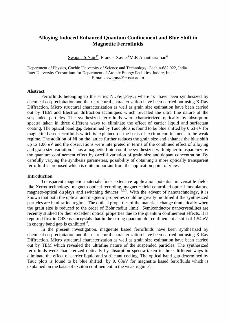
Alloying Induced Enhanced Quantum Confinement and Blue Shift in
Magnetite Ferrofluids
Swapna.S.Naira*, Francis XavieraM.R Anantharamana
Department of Physics, Cochin University of Science and Technology, Cochin-682 022, India Inter University Consortium for Department of Atomic Energy Facilities, Indore, India
E mail- [email protected]
Abstract Ferrofluids belonging to the series NixFe1-xFe2O4 where ‘x’ have been synthesized by chemical co-precipitation and their structural characterization have been carried out using X-Ray Diffraction. Micro structural characterization as well as grain size estimation have been carried out by TEM and Electron diffraction techniques which revealed the ultra fine nature of the suspended particles. The synthesized ferrofluids were characterized optically by absorption spectra taken in three different ways to eliminate the effect of carrier liquid and surfactant coating. The optical band gap determined by Tauc plots is found to be blue shifted by 0.63 eV for magnetite based ferrofluids which is explained on the basis of exciton confinement in the weak regime. The addition of Ni on the lattice further reduces the grain size and enhance the blue shift up to 1.06 eV and the observations were interpreted in terms of the combined effect of alloying and grain size variation. Thus a magnetic fluid could be synthesized with higher transparency by the quantum confinement effect by careful variation of grain size and dopant concentration. By carefully varying the synthesis parameters, possibility of obtaining a more optically transparent ferrofluid is proposed which is quite important from the application point of view. Introduction
Transparent magnetic materials finds extensive application potential in versatile fields like Xerox technology, magneto-optical recording, magnetic field controlled optical modulators, magneto-optical displays and switching devices 1,2,3. With the advent of nanotechnology, it is known that both the optical and magnetic properties could be greatly modified if the synthesized particles are in ultrafine regime. The optical properties of the materials change dramatically when the grain size is reduced to the order of Bohr radius limit4. Semiconductor nanocrystallites are recently studied for their excellent optical properties due to the quantum confinement effects. It is reported first in CdSe nanocrystals that in the strong quantum dot confinement a shift of 1.54 eV in energy band gap is exhibited 4.
In the present investigation, magnetite based ferrofluids have been synthesized by chemical co-precipitation and their structural characterization have been carried out using X-Ray Diffraction. Micro structural characterization as well as grain size estimation have been carried out by TEM which revealed the ultrafine nature of the suspended particles. The synthesized ferrofluids were characterized optically by absorption spectra taken in three different ways to eliminate the effect of carrier liquid and surfactant coating. The optical band gap determined by Tauc plots is found to be blue shifted by 0. 63eV for magnetite based ferrofluids which is explained on the basis of exciton confinement in the weak regime5.
Alloying with any other metals is also found to enhance the blue shift in Ni doped CdTe nanocrystalline thin films6. Here such an attempt is tried to synthesise ferrofluids with varying nickel doping for tuning the band gap. The addition of Ni on the lattice further reduces the grain size and enhance the blue shift up to 1.03 eV and the observations were interpreted in terms of the combined effect of alloying and grain size variation. By carefully varying the grain size and doping percentage, possibility of obtaining a more optically transparent ferrofluid is proposed which is quite important from the application point of view. Experimental Techniques 2.1 Preparation of magnetite ferrofluids
The magnetite ferrofluid samples were synthesized by standard co-precipitation of aqueous solutions of 2M Fe(NO3)3 9H2O and 1M FeSO4 7H2O at room temperature at a pH of 11.5 and insitu coating is provided with oleic acid and the wet slurry is washed with acetone and finally dispersed in kerosene.
2.2. Doping
Insitu doping with Ni was carried out using the standard co-precipitation technique using xM NiSO4 7H2O, 1-xM FeSO4 7H2O, 2M Fe(NO3) 3 9H2O for the synthesis of ferrofluids belonging to the series NixFe1-xFe2O4 where ‘x’ was varied from 0.1 to 0.7.
2.3 XRD Studies
The synthesized ferrofluids have been dried by the reversible flocculation technique using acetone and the slurry was dried in room temperature. The XRD spectra of the samples were recorded on an X-ray diffractometer (Rigaku D-max-C) using Cu Ká radiation (ë=1.5405Å). The particle size was estimated by employing Debye-Scherer’s formula 2.4. Transmission Electron Microscopy (TEM) The synthesized ferrofluids have been dried by washing with acetone and were analyzed for their grain size and grain size distribution using transmission electron microscopy (TEM). The electron diffraction (ED) spectrum was also recorded and the lattice planes were identified using the ED spectrum. 2.5. Optical studies Optical absorption spectrum was recorded using a Hitachi U-3410 UV-VIS-NIR spectrophotometer for the pure as well as nickel doped magnetite based ferrofluid samples and the band gap was determined for all the synthesized samples. Using an extrapolation to the X axis of the pot of “(αhν)2 vs hν”, gives the band gap of the material if it is a direct transition which is the Tauc plots . 3. Results and Discussions X Ray diffraction spectra (Fig. 1) of ferrofluids shows that synthesized particles are in the ultra fine regime.
10 20 30 40 50 60 70
331 42
2 53151
1 440
400
311
200
220
Inte
nsity
(A
rb U
nit)
2θ(deg)
Fig. 1 Typical X Ray Diffraction Spectrum of Ni0.1Fe0.9Fe2O4 ferrofluids
Lattice planes were identified using both XRD and Electron diffraction (ED) spectrum. Exact grain size and size distribution were estimated using Transmission Electron Micrograms. Representative TEM micrographs are depicted in Fig. 2.
Fig. 2 TEM Image of a representative ferrofluid sample (dried) Inset - Electron Diffraction spectrum.
The TEM images shows that the grain size distribution is narrow and grain sizes are in the
range 55-70Å. Lattice planes were also calculated using the Electron Diffraction Spectrum. (Inset Fig. 2) The grain sizes for all the samples have been estimated and plotted for all compositions (Fig. 3).
-0.1 0.0 0.1 0.2 0.3 0.4 0.5 0.6 0.7 0.8
50
55
60
65
70
75
80
85
Gra
in s
ize
(Αο )
'x' Composition
Fig. 3 Grain size vs composition in NixFe1-xFe2O4 (0 corresponds to Fe3O4)
Lattice parameters were evaluated and plotted for the variation in ‘x’ in the series NixFe1-
xFe2O4 (Fig. 4) using X ray diffraction data. The lattice parameter variation is as per Vegard’s law and parameter shows a linear decrease with increasing nickel doping.
0.1 0.2 0.3 0.4 0.5 0.6
8.380
8.385
8.390
8.395
8.400
8.405
8.410
8.415
8.420
Latti
ce p
aram
eter
A0
Composition
Fig. 4 Lattice Parameters vs Composition
The optical absorption spectra of the pristine and the doped samples were recorded. Absorption spectra of magnetite ferrofluids obtained using different techniques are provided (Fig. 5)
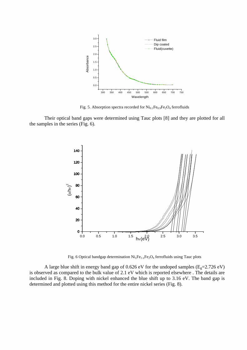
300 350 400 450 500 550 600 650 700 750
0.0
0.5
1.0
1.5
2.0
2.5
3.0 Fluid film Dip coated Fluid(cuvette)
Abs
orba
nce
Wavelength
Fig. 5. Absorption spectra recorded for Ni0.1Fe0.9Fe2O4 ferrofluids
Their optical band gaps were determined using Tauc plots [8] and they are plotted for all
the samples in the series (Fig. 6).
(αhν
)2
hν(eV)
0
20
40
60
80
100
120
140
0
20
40
60
80
100
120
140
0
20
40
60
80
100
120
140
0
20
40
60
80
100
120
140
0.0 0.5 1.0 1.5 2.0 2.5 3.0 3.50
20
40
60
80
100
120
140
Fig. 6 Optical bandgap determination NixFe1-xFe2O4 ferrofluids using Tauc plots
A large blue shift in energy band gap of 0.626 eV for the undoped samples (Eg=2.726 eV)
is observed as compared to the bulk value of 2.1 eV which is reported elsewhere . The details are included in Fig. 8. Doping with nickel enhanced the blue shift up to 3.16 eV. The band gap is determined and plotted using this method for the entire nickel series (Fig. 8).
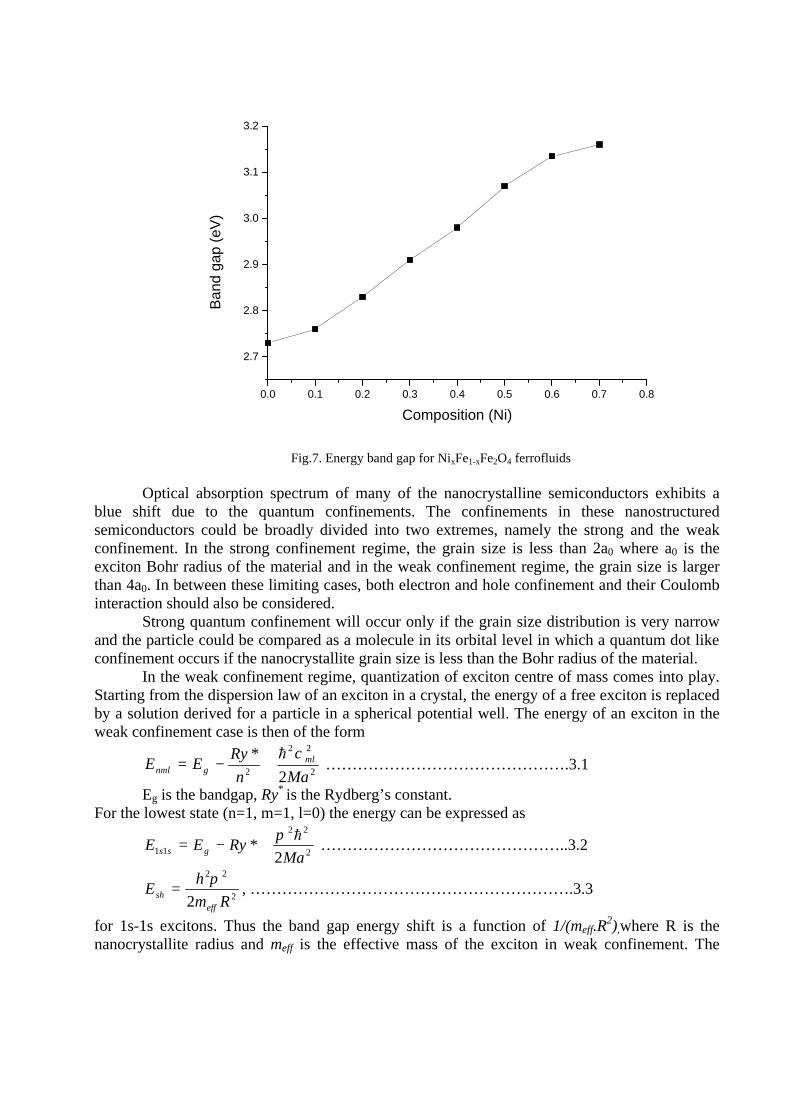
0.0 0.1 0.2 0.3 0.4 0.5 0.6 0.7 0.8
2.7
2.8
2.9
3.0
3.1
3.2
Ban
d ga
p (e
V)
Composition (Ni)
Fig.7. Energy band gap for NixFe1-xFe2O4 ferrofluids
Optical absorption spectrum of many of the nanocrystalline semiconductors exhibits a
blue shift due to the quantum confinements. The confinements in these nanostructured semiconductors could be broadly divided into two extremes, namely the strong and the weak confinement. In the strong confinement regime, the grain size is less than 2a0 where a0 is the exciton Bohr radius of the material and in the weak confinement regime, the grain size is larger than 4a0. In between these limiting cases, both electron and hole confinement and their Coulomb interaction should also be considered.
Strong quantum confinement will occur only if the grain size distribution is very narrow and the particle could be compared as a molecule in its orbital level in which a quantum dot like confinement occurs if the nanocrystallite grain size is less than the Bohr radius of the material.
In the weak confinement regime, quantization of exciton centre of mass comes into play. Starting from the dispersion law of an exciton in a crystal, the energy of a free exciton is replaced by a solution derived for a particle in a spherical potential well. The energy of an exciton in the weak confinement case is then of the form
2
22
2 2
*
Man
RyEE ml
gnml
χh+−= ……………………………………….3.1
Eg is the bandgap, Ry* is the Rydberg’s constant.
For the lowest state (n=1, m=1, l=0) the energy can be expressed as
2
22
11 2*
MaRyEE gss
hπ+−= ………………………………………..3.2
2
22
2 Rm
hE
eff
sh
π= , …………………………………………………….3.3
for 1s-1s excitons. Thus the band gap energy shift is a function of 1/(meff.R2),where R is the
nanocrystallite radius and meff is the effective mass of the exciton in weak confinement. The
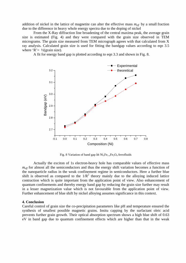
addition of nickel in the lattice of magnetite can alter the effective mass meff by a small fraction due to the difference in heavy whole energy spectra due to the doping of nickel From the X-Ray diffraction line broadening of the central maxima peak, the average grain size is estimated (Fig. 4) and they were compared with the grain size observed in TEM micrograms. The grain size measured from TEM micrograph agrees with that calculated from X ray analysis. Calculated grain size is used for fitting the bandgap values according to eqn 3.5 where ‘R’= ½ (grain size). A fit for energy band gap is plotted according to eqn 3.3 and shown in Fig. 8.
-0.1 0.0 0.1 0.2 0.3 0.4 0.5 0.6 0.7 0.8
2.7
2.8
2.9
3.0
3.1
3.2
Experimental theoretical
Ban
dgap
(eV
)
Composition (Ni)
Fig. 8 Variation of band gap in NixFe1-xFe2O4 ferrofluids
Actually the exciton of 1s electron-heavy hole has comparable values of effective mass meff for almost all the semiconductors and thus the energy shift variation becomes a function of the nanoparticle radius in the weak confinement regime in semiconductors. Here a further blue shift is observed as compared to the 1/R2 theory mainly due to the alloying induced lattice contraction which is quite important from the application point of view. Also enhancement of quantum confinements and thereby energy band gap by reducing the grain size further may result in a lesser magnetization value which is not favourable from the application point of view. Further enhancement of blue shift by nickel alloying assumes significance in this context. 4. Conclusion Careful control of grain size the co-precipitation parameters like pH and temperature ensured the synthesis of smallest possible magnetic grains. Insitu capping by the surfactant oleic acid prevents further grain growth. Their optical absorption spectrum shows a high blue shift of 0.63 eV in band gap due to quantum confinement effects which are higher than that in the weak

regime. Strong confinement in magnetite needs still lower grain size which may reduce magnetization and not favored under application point of view. Addition of nickel with varying percentage on the magnetite lattice still reduces the band gap by the alloying effect, which results in a blue shift higher than that in the weak confinement regime. The blue shift varies almost as the square inverse of the nanocrystallite’s grain size, but additional blue shift can be attributed to the alloying effect of nickel which introduces lattice contraction which is evidenced by the XRD studies. This enhanced blue shift in optical band gap by nickel alloying will enable us to obtain ferrofluids having a better transparency which can find potential applications. Acknowledgement
MRA and SSN thank Department of Science and Technology (File No- SP/S2/M-64/96 dated 22/04/2002) for necessary funding. MRA is grateful to TWAS (File No- 00-118 RG/PHYS/AS) and IUC-DEEF, Govt. of India (Ref No-IUC/ MUM/ CRS/ M-60) also for funding.
References 1. G.W Day and A.H Rose, Proc.SPIE 985 138 (1998) 2. L.L Beecroft and C.K Ober, Chem.Mater, 9, 1302 (1997) 3. H.E Horng, Chin-Yih-Hong, H.C Yang, I.J Jang, S.Y Yang, S.L Lee, and I.C Kuo, J. Magn. Magn. Mater. 201, 215,(1999) 4. George C Hadjipanayis and Richard W Siegel, Nanophase materials-synthesis, properties and applications, 432, kluwer
Academic Publishers 5. Richard Turton, The Physics of Solids, Oxford University Press, New York (2000) 6. O. Alvarez-Fregoso, J.G. Mendoza- Alvarez, and O. Zelaya-Angel, J. Appl. Phys, 82 (2), (1997 July), 708
Instructions to Authors Page 1 of 3 Proceedings of OMTAT2005
EVIDENCE FOR THE OCCURRENCE OF INTERGRANULAR TUNNELING IN PANI PASSIVATED á -Fe
Vijutha Sunny, T.N Narayanan, U.S. Sajeev, M.R.Anantharaman
Department of Physics, Cochin University of Science and Technology, Kochi-682 022
Email: [email protected], [email protected]
ABSTRACT
Ultrafine particles are of immense importance both from the fundamental and application point of view. Ultrafine magnetic particles exhibit size effects which are manifested in their improved magnetic and electric properties1,2. Mechanical attrition by high energy ball milling is a top down process to produce fine particles3. However, fineness is associated with high surface area and hence prone to oxidation which plays a detrimental role in the useful properties of these materials. Passivation of ultrafine particles is known to inhibit surface oxidation. At the same time, the coating of the polymer film4 on the inorganic substance modifies the surface properties drastically. In this work a modified setup consisting of an RF plasma polymerization technique is employed to coat a thin layer of a polymer film on ultrafine Fe particles produced by HEBM3. Ball milled particles having various particle size ranges are coated with PANI. Their electrical properties are investigated by measuring the dc conductivity in the temperature range 10 to 300K5,6. The low temperature DC conductivity (I-V) exhibited non-linearity. This non-linearity observed is explained on the basis of a critical path model5,6,7. There is clear cut evidence for the occurrence of inter granular tunneling. The results are presented here in this paper. 1 INTRODUCTION
Recently, as an essential component of nanotechnology in the 21st century, materials consisting of particles with diameter less than 100 nm have attracted a great deal of attention. Owing to their nanometer size, these particles exhibit dramatic changes in physical and chemical properties (i.e., novel properties that differ considerably from those of molecules as well as bulk materials), which could be utilized in many important applications. The demand for smaller materials for high density storage media is the fundamental motivation for the fabrication of nanoscale magnetic materials. The idea of nanoscale molecular device is not particularly new, and has been around since the earlier ideas of Feynman, who addressed the issue of quantum mechanical computers. 2 EXPERIMENTAL á-Fe power of mean diameter 230Å was purchased and using high energy ball mill the iron powders were milled for various durations. The powder was then coated with PANI using RF plasma polymerization technique. It was done in home built setup shown in figure 1.
Figure 1: RF Plasma polymerization setup for surface modification of nanoparticles
The powder was then pressed into cylindrical disks of 13mm diameter and around 1mm thickness in a tempered steel die under a pressure of 7.5 tones. 3 RESULTS AND DISCUSSIONS
3.1 Structural characterization using XRD Elemental iron is known to exhibit three phases. At room temperature, metallic iron exists in a cubic ferromagnetic form (á-Fe) or in a cubic paramagnetic form (ã-Fe). There is also another phase of iron, the ä-Fe which is not stable. á-Fe has a body centered cubic structure. Figure 2 shows the XRD of Fe at various milling time. The prominent lines are identified using JCPDS tables. The X-ray diffraction curve has two peaks at 2è = 44.6° and 65.01°, corresponding to (110) and (200) plane of the á-Fe lattice respectively. It is clear that as the milling time increases the diffraction peaks slightly broadens indicating the reduction of size of the particles.
10 20 30 40 50 60 70
10 20 30 40 50 60 70
10 20 30 40 50 60 70
2θ (Degree)
Fe as PurchasedSize=231.4 A
Fe 30minSize=165.2 A
Re
lative
In
ten
sity (
a.u
.)
Fe 20hrSize=156.2 A
Figure 2: XRD of Fe at various milling time
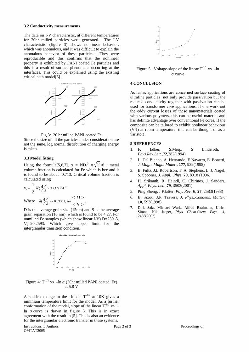
Instructions to Authors Page 2 of 3 Proceedings of OMTAT2005
3.2 Conductivity measurements The data on I-V characteristic, at different temperatures for 20hr milled particles were generated. The I-V characteristic (figure 3) shows nonlinear behavior, which was anomalous, and it was difficult to explain the anomalous behavior of these particles. They were reproducible and this confirms that the nonlinear property is exhibited by PANI coated Fe particles and this is a result of surface phenomena occurring at the interfaces. This could be explained using the existing critical path model[5].
-10 -5 0 5 10
-2.0x10⁻⁸
-1.5x10⁻⁸
-1.0x10⁻⁸
-5.0x10⁻⁹
0.0
5.0x10⁻⁹
1.0x10⁻⁸
1.5x10⁻⁸
I (A
mpe
re)
V(Volt)
10 K
-10 -5 0 5 10
-2.5x10⁻⁶
-2.0x10⁻⁶
-1.5x10⁻⁶
-1.0x10⁻⁶
-5.0x10⁻⁷
0.0
5.0x10⁻⁷
1.0x10⁻⁶
1.5x10⁻⁶
2.0x10⁻⁶ 50 K
I (A
mpe
re)
V(Volt)
-10 -5 0 5 10
-0.003
-0.002
-0.001
0.000
0.001
0.002
0.003
I(A
mpe
re)
V(Volt)
Fe 20hr milled PANI coated
200 K
-10 -5 0 5 10
-0.015
-0.010
-0.005
0.000
0.005
0.010
0.015
300 K
I(A
mpe
re)
V(Volt)
Fig.3: 20 hr milled PANI coated Fe
Since the size of all the particles under consideration are not the same, log normal distribution of charging energy is taken. 3.3 Model fitting
Using the formula[5,6,7], x = ND03 π 2 /6 , metal
volume fraction is calculated for Fe which is bcc and it is found to be about 0.713. Critical volume fraction is calculated using
Vc = 2
1Ã6( 3
4 )[(1+A/2)3-1]2
Where Ã( 34 ) = 0.89301, A=
><><
S
D,
D is the average grain size (15nm) and S is the average grain separation (10 nm), which is found to be 4.27. For unmilled Fe samples (which show linear I-V) D=230 Å, Vc=20.2593. Which give upper limit for the intergranular transition condition.
0.05 0.10 0.15 0.20 0.25 0.30 0.35
4
6
8
10
12
14
16
18
20
10 K
20hr milled pani coated Fe at 5.8V
-ln(σ
)
T (-1/2)
Figure 4: T-1/2 vs –ln σ (20hr milled PANI coated Fe) at 5.8 V
A sudden change in the –ln σ - T-1/2 at 10K gives a minimum temperature limit for the model. As a further conformation of the model, slope of the linear T-1/2 vs –ln σ curve is drawn in figure 5. This is in exact agreement with the result in [5]. This is also an evidence for the intergranular electronic transfer in these systems.
3.0 2.5 2.0 1.5 1.0 0.560
62
64
66
68
70
72
Slo
pe
Voltage
Figure 5 : Voltage-slope of the linear T-1/2 vs –ln σ curve
4 CONCLUSION As far as applications are concerned surface coating of ultrafine particles not only provide passivation but the reduced conductivity together with passivation can be used for transformer core applications. If one work out the eddy current losses of these nanomaterials coated with various polymers, this can be useful material and has definite advantage over conventional Fe cores. If the composite can be tailored to exhibit nonlinear behaviour (V-I) at room temperature, this can be thought of as a varistor! 5 REFERENCES 1. F. Bdker, S.Mrup, S Linderoth,
Phys.Rev.Lett.,72,282(1994)
2. L. Del Bianco, A. Hernando, E Navarro, E. Bonetti, J. Magn. Magn. Mater., 177, 939(1998)
3. B. Fultz, J.L Robertson, T. A. Stephens, L. J. Nagel, S. Spooner, J. Appl. Phys. 79, 8318 (1996)
4. H. Srikanth, R. Hajndl, C. Chirinos, J. Sanders, Appl. Phys. Lett.,79, 3503(2001)
5. Ping Sheng, J Klafter, Phy. Rev. B, 27, 2583(1983)
6. B. Sixou, J.P. Travers, J. Phys..Condens. Matter, 10, 593(1998)
7. Dirk Salz, Michael Wark, Alfred Baalmann, Ulrich Simon, Nils Jaeger, Phys. Chem.Chem. Phys. ,4, 2438(2002)
Instructions to Authors Page 1 of 3 Proceedings of OMTAT2005
PULSED ELECTRODEPOSITION OF NANOCRYSTALLINE SOFT MAGNETIC CoNiFe ALLOY THIN FILMS
I. Baskaran, T.S.N. Sankara Narayanan* and A. Stephen+
Materials Science Division, Department of Nuclear Physics, University of Madras, Chennai-600 025, India
*National Metallurgical Laboratory, Madras Centre CSIR Complex, Taramani, Chennai-600 113, India +Email: [email protected]
ABSTRACT
The discovery of nano scale phenomena and their potential application in different areas such as micro- or nano- electronics has led to a rapid increase in research on functional properties of nanostructures. CoNiFe alloy based soft magnetic materials have gained popularity over the FeNi alloy because of their superior properties as write head core materials in head disk drives. The objective of the present work is to prepare nanocrystalline CoNiFe alloy films by pulse current electrodeposition technique. The variation of the Fe content of the alloy films was investigated as a function of current density. The ratio of BCC/FCC phase is higher for such deposits, which increases the saturation magnetization of the film. The crystal structure, surface morphology, chemical composition and magnetic properties of the CoNiFe alloy thin films were determined by X-ray diffraction (XRD), scanning electron microscope (SEM), energy dispersive X-ray analysis (EDX) and vibrating sample magnetometer (VSM).
1. INTRODUCTION Magnetic materials play an outstanding role in the development of new technologies for magnetic recording media and information storage. Many alloy materials such as Co–Ni, Ni–Fe, Co–B, Co–Fe–B, Co–Ni–P and Co–Ni–Fe are being developed for use in modern high density recording [1-10]. In particular, the development of electrodepositied nanocrytalline soft magnetic thin films with high magnetic moment (Bs), low Coercivity (Hc), and high Permeability (µr) have great applications in several kinds of applications such as magnetic sensors and magnetic recording heads. Electrodeposition is the better option for the synthesis of such films, because it yields better soft magnetic properties at corresponding compositions, easily allows orientation of film anisotropy, and most importantly enables the production of pole tips of very high quality by means of the plating through-mask patterning process and also cost effective. Pulsed-current electrodeposition is a technique, which could reduce or completely avoid compositional gradients by regenerating the initial ion concentrations at the cathode/solution interface at the beginning of each pulse period. Moreover, by tailoring pulse shape and duration, this technique enables close control of the nucleation and growth processes and allows modification of film microstructure. The film composition as well as the ratio of BCC and FCC phases along with their magnetic properties will be discussed. 2. EXPERIMENTAL PROCEDURE The bath composition and operating conditions of the plating bath employed for preparing CoNiFe alloy films is given in Table 1. The CoNiFe films were prepared at different applied current densities (CD) in the range of 5-20 mA/cm2. The plating time was varied depending upon Ton and Toff. The duty cycle is defined as Ton/ (Ton + Toff), where Ton is the pulse-on period and Toff is the relaxation period (off-period). The
electrodeposited CoNiFe alloy films were characterized by X-ray diffraction (XRD) (Rich Siefert; Model 3000, using a Cukα1 = 1.5406 Å) radiation and scanning electron microscopy (SEM) to evaluate its structural characteristics and morphological features. The chemical composition of the CoNiFe alloy films was determined by energy dispersive spectrometry (EDAX) and the magnetization was measured using Vibrating Sample magnetometer (VSM). Table.1. Chemical composition and operating conditions of the plating baths used to electrodeposits
Chemical composition and Operating conditions NiSO4.6H2O 0.3M CoSO4.7H2O 0.08M FeSO4.6H2O 0.015M Tri-Sodium Citrate 0.2M Sodium Lauryl Sulphate 0.01g/l Boric acid 0.15M Temperature 27 ±1°C Current density (mA/cm2) 5.0 – 20.0
3. RESULTS AND DISCUSSION The CoNiFe alloy films were produced by pulse plating technique. The grain size of nano-structured CoNiFe films has been controlled by pulse parameters and Current density. The electrodeposition of nano-structured metals is expected if large number of nuclei on the electrode surface is created and the growth of nuclei is strongly impeded. Therefore very high current density should be applied for short time to enhance the nucleation. After this strong current pulse the electrolyte in the vicinity of the electrode is depleted from cations, but they will be supplied during the relaxation period (Toff). Effect of current density on the plating rate is shown in Fig.1. The deposition weight increases with current density. This can be described to the electrolytic nature. The electrodeposition of Co2+, Ni2+, Fe2+ ions and their alloys are always accompanied by hydrogen codeposition.
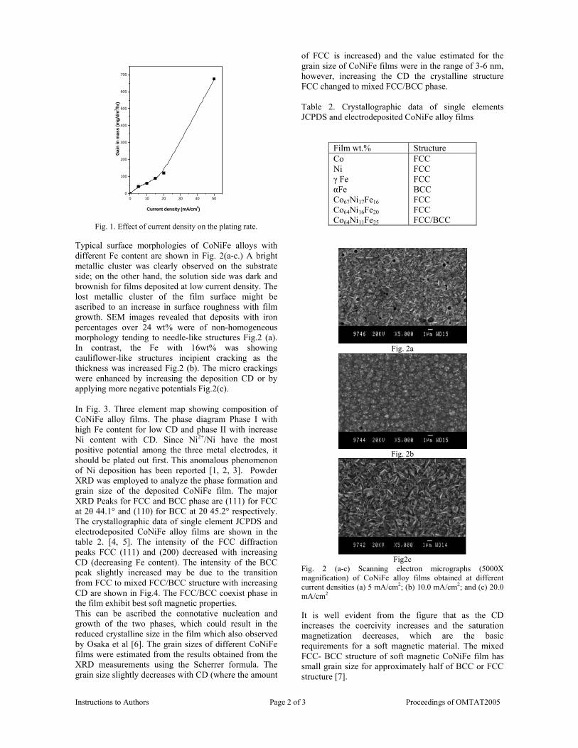
Instructions to Authors Page 2 of 3 Proceedings of OMTAT2005
Fig. 1. Effect of current density on the plating rate.
Typical surface morphologies of CoNiFe alloys with different Fe content are shown in Fig. 2(a-c.) A bright metallic cluster was clearly observed on the substrate side; on the other hand, the solution side was dark and brownish for films deposited at low current density. The lost metallic cluster of the film surface might be ascribed to an increase in surface roughness with film growth. SEM images revealed that deposits with iron percentages over 24 wt% were of non-homogeneous morphology tending to needle-like structures Fig.2 (a). In contrast, the Fe with 16wt% was showing cauliflower-like structures incipient cracking as the thickness was increased Fig.2 (b). The micro crackings were enhanced by increasing the deposition CD or by applying more negative potentials Fig.2(c). In Fig. 3. Three element map showing composition of CoNiFe alloy films. The phase diagram Phase I with high Fe content for low CD and phase II with increase Ni content with CD. Since Ni2+/Ni have the most positive potential among the three metal electrodes, it should be plated out first. This anomalous phenomenon of Ni deposition has been reported [1, 2, 3]. Powder XRD was employed to analyze the phase formation and grain size of the deposited CoNiFe film. The major XRD Peaks for FCC and BCC phase are (111) for FCC at 2θ 44.1° and (110) for BCC at 2θ 45.2° respectively. The crystallographic data of single element JCPDS and electrodeposited CoNiFe alloy films are shown in the table 2. [4, 5]. The intensity of the FCC diffraction peaks FCC (111) and (200) decreased with increasing CD (decreasing Fe content). The intensity of the BCC peak slightly increased may be due to the transition from FCC to mixed FCC/BCC structure with increasing CD are shown in Fig.4. The FCC/BCC coexist phase in the film exhibit best soft magnetic properties. This can be ascribed the connotative nucleation and growth of the two phases, which could result in the reduced crystalline size in the film which also observed by Osaka et al [6]. The grain sizes of different CoNiFe films were estimated from the results obtained from the XRD measurements using the Scherrer formula. The grain size slightly decreases with CD (where the amount
of FCC is increased) and the value estimated for the grain size of CoNiFe films were in the range of 3-6 nm, however, increasing the CD the crystalline structure FCC changed to mixed FCC/BCC phase. Table 2. Crystallographic data of single elements JCPDS and electrodeposited CoNiFe alloy films
Film wt.% Structure Co Ni γ Fe αFe Co67Ni17Fe16 Co64Ni16Fe20 Co64Ni11Fe25
FCC FCC FCC BCC FCC FCC FCC/BCC
Fig. 2a
Fig. 2b
Fig2c
Fig. 2 (a-c) Scanning electron micrographs (5000X magnification) of CoNiFe alloy films obtained at different current densities (a) 5 mA/cm2; (b) 10.0 mA/cm2; and (c) 20.0 mA/cm2
It is well evident from the figure that as the CD increases the coercivity increases and the saturation magnetization decreases, which are the basic requirements for a soft magnetic material. The mixed FCC- BCC structure of soft magnetic CoNiFe film has small grain size for approximately half of BCC or FCC structure [7].
0 10 20 30 40 500
100
200
300
400
500
600
700
G
ain
in m
ass
(mg/
dm2 /h
r)
Current density (mA/cm2)
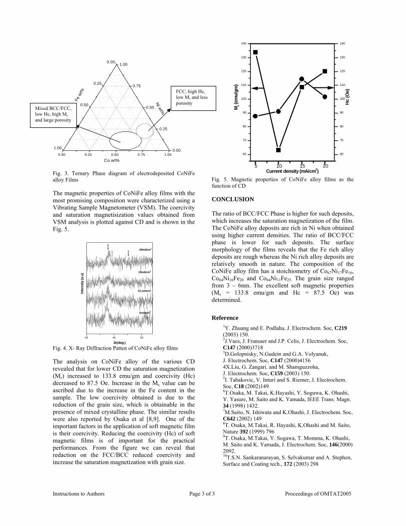
Instructions to Authors Page 3 of 3 Proceedings of OMTAT2005
0.00 0.25 0.50 0.75 1.00
0.00
0.25
0.50
0.75
1.00 0.00
0.25
0.50
0.75
1.00
Ni wt%
Fe w
t%
Co wt%
Fig. 3. Ternary Phase diagram of electrodeposited CoNiFe alloy Films The magnetic properties of CoNiFe alloy films with the most promising composition were characterized using a Vibrating Sample Magnetometer (VSM). The coercivity and saturation magnetisization values obtained from VSM analysis is plotted against CD and is shown in the Fig. 5.
Fig. 4. X- Ray Diffraction Patten of CoNiFe alloy films The analysis on CoNiFe alloy of the various CD revealed that for lower CD the saturation magnetization (Ms) increased to 133.8 emu/gm and coercivity (Hc) decreased to 87.5 Oe. Increase in the Ms value can be ascribed due to the increase in the Fe content in the sample. The low coercivity obtained is due to the reduction of the grain size, which is obtainable in the presence of mixed crystalline phase. The similar results were also reported by Osaka et al [8,9]. One of the important factors in the application of soft magnetic film is their coercivity. Reducing the coercivity (Hc) of soft magnetic films is of important for the practical performances. From the figure we can reveal that redaction on the FCC/BCC reduced coercivity and increase the saturation magnetization with grain size.
Fig. 5. Magnetic properties of CoNiFe alloy films as the function of CD CONCLUSION The ratio of BCC/FCC Phase is higher for such deposits, which increases the saturation magnetization of the film. The CoNiFe alloy deposits are rich in Ni when obtained using higher current densities. The ratio of BCC/FCC phase is lower for such deposits. The surface morphology of the films reveals that the Fe rich alloy deposits are rough whereas the Ni rich alloy deposits are relatively smooth in nature. The composition of the CoNiFe alloy film has a stoichiometry of Co67Ni17Fe16, Co64Ni16Fe20 and Co64Ni11Fe25. The grain size ranged from 3 – 6nm. The excellent soft magnetic properties (Ms = 133.8 emu/gm and Hc = 87.5 Oe) was determined.
Reference 1Y. Zhuang and E. Podlaha, J. Electrochem. Soc, C219 (2003) 150. 2J.Vaes, J. Fransaer and J.P. Celis, J. Electrochem. Soc, C147 (2000)3718 3D.Golopnisky, N.Gudein and G.A. Volyanuk, J. Electrochem. Soc, C147 (2000)4156 4X.Liu, G. Zangari. and M. Shamguzzoha, J. Electrochem. Soc, C159 (2003) 150. 5I. Tabakovic, V. Inturi and S. Riemer, J. Electrochem. Soc, C18 (2002)149 6T.Osaka, M. Takai, K.Hayashi, Y. Soguwa, K. Ohashi, Y. Yasure, M. Saito and K. Yamada, IEEE Trans. Magn. 34 (1998) 1432. 7M.Saito, N. Ishiwata and K.Ohashi, J. Electrochem. Soc, C642 (2002) 149 8T. Osaka, M.Takai, R. Hayashi, K.Ohashi and M. Saito, Nature 392 (1999) 796 9T. Osaka, M.Takai, Y. Sogawa, T. Momma, K. Ohashi, M. Saito and K. Yamada, J. Electrochem. Soc, 146(2000) 2092. 10T.S.N. Sankaranarayan, S. Selvakumar and A. Stephen, Surface and Coating tech., 172 (2003) 298
FCC, high Hc, low Ms and less porosity
Mixed BCC/FCC, low Hc, high Ms and large porosity
5 10 15 20
60
70
80
90
100
110
120
130
140
60
70
80
90
100
110
120
130
140
Hc (O
e)
M s (em
u/gm
)
Current density (mA/cm2)
40 45 50
20mA/cm2
15mA/cm2
10 mA/cm2
5mA/cm2
200
FCC
110
BCC
111
FCC
Inte
nsity
(a.u
)
2θ(deg.)

Instructions to Authors Page 4 of 3 Proceedings of OMTAT2005
TRANSFER OF COPYRIGHT Please complete as appropriate and return by fax/mail. If you do not provide a copyright clearance, we cannot include your paper in the proceedings. [ ] My employer has given clearance for this
paper to be published. OR [ ] I am the holder of the copyright for this
paper The author who sign the copyright
Signature: ......................................................... Date: 21. 09. 2005 ........................................................ Affiliation:
Lecturer Materials Science Division,
Department of Nuclear Physics, University of Madras,
Chennai-600 025, India
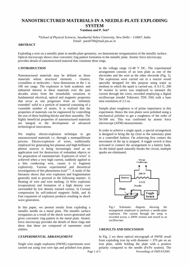
Page 1 of 3 Proceedings of OMTAT2005
NANOSTRUCTURED MATERIALS IN A NEEDLE-PLATE EXPLODING SYSTEM
Vandana and P. Sen*
*School of Physical Sciences, Jawaharlal Nehru University, New Delhi – 110067, India Email: [email protected]
ABSTRACT
Exploding a wire on a metallic plate in needle-plate geometry, we demonstrate reorganization of the metallic surface. Optical microscopy shows clear concentric ring pattern formation in the metallic plate. Atomic force microscopy provides details of nanostructured material that constitute these rings. 1 INTRODUCTION Nanostructured materials may be defined as those materials whose structural elements - clusters, crystallites or molecules – have dimensions in the 1 to 100 nm range. The explosion in both academic and industrial interest in these materials over the past decades arises from the remarkable variations in fundamental electrical, optical and magnetic properties that occur as one progresses from an ‘infinitely extended’ solid to a particle of material consisting of a countable number of atoms. It is realized that the properties of materials can be engineered by controlling the size of these building blocks and their assembly. The highly beneficial properties of nanostructured materials are integral to the development of advanced technological innovations. We employ electro-explosion technique to get nanostructured materials i.e. through a nonequilibrium process. Electro-explosion of wires, traditionally employed for generating hot plasmas and high-brilliance photon sources is being increasingly used as an application tool for destruction of redundant objects or for preparation of nanomaterials. Explosion of wires1 is achieved when a very high current, suddenly applied to a thin conducting wire, causes it to fragment explosively. Various experimental and theoretical investigations of this phenomena exist2-11. A study of the literature shows that wire explosion and fragmentation generally tend to proceed in the following manner: 1) Heating of wire and wire melting; 2) Wire explosion (evaporation) and formation of a high density core surrounded by low density ionized corona; 3) Coronal compression by self-induced magnetic fields, and 4) Fast expansion of explosion products resulting in shock wave generation. In this paper, we present results from exploding a metallic needle on a metal plate. The metallic surface reorganizes as a result of the shock waves generated and gives concentric ring pattern in the metal plate. Atomic force microscopy provides the details of these rings and show that these are composed of nanometer sized entities. 2 EXPERIMENTAL ARRANGEMENT Single wire single explosion (SWSE) experiments were carried out using iron wire tips and polished iron plates
in the voltage range 12-48 V DC. The experimental arrangement consists of an iron plate as one of the electrodes and the wire as the other electrode (Fig. 1). The explosions were carried out in a reactor vessel specially designed for this purpose using water as medium in which the spark is carried out. A 0.5 Ù, 200 W resistor in series was employed to measure the current through the wires, recorded employing a digital oscilloscope (model Tektronix TDS 350) with a base time resolution of 2.5 ns. Sample plate roughness is of prime importance in this experiment. Hence the iron plates were polished using a mechanical polisher to get a roughness of the order of 50-500 nm. This was confirmed by atomic force microscope (AFM) measurements. In order to achieve a single spark, a special arrangement is designed to bring the tip close to the stationary plate in a controlled fashion. On achieving first contact the movement of the tip is stopped. A toggle switch is then activated to connect the arrangement to a battery bank. As the initial spark naturally breaks the circuit, multiple sparks are eliminated. 3 RESULTS AND DISCUSSION In Fig. 2 we show optical micrograph of SWSE result from exploding iron tip with diameter = 370 µm on an iron plate, while holding the plate with a positive polarity compared to the needle (Fe/Fe system). The
Fig.1 Schematic diagram showing the arrangement employed to perform a needle-plate explosion. The current through the setup is recorded across a 200W resistor and stored in an oscilloscope.
Page 2 of 3 Proceedings of OMTAT2005
figure clearly shows rings emanating from the point of contact made by the iron tip with the iron plate. The rings die out at the extreme of a circle whose diameter for the Fe/Fe system is 1425 µm. The process leading to the formation of the rings can be outlined here. The exploding needle-plate system brings the plate instantaneously to its melting point. The shock wave generated after the explosion then travels through the melt. The ring patterns are a result of stationary waves set up in the melt, emanating naturally with cylindrical symmetry from the center of the figure, which resembles now a vibrating liquid surface. The boundary of the cylinder is limited to 1425 µm for Fe/Fe system. In order to confirm this process, we take a look at the microscopic details of 1-2 rings with the help of an AFM operating in the non-contact mode. The non-contact mode helps in providing information of the surface topography in a non-invasive procedure. A 10 µm × 10 µm picture for Fe/Fe system is presented in Fig. 3, taken from near the centre of the explosion shown in Fig. 2. The AFM picture shows details of the rings. Fig. 3 reveals that each ring is composed of small particles, predominantly circular in shape, whose average size is ~ 0.6 – 1 µm. Such circular particles are seen over the entire region where the rings are found as well as in the immediate vicinity where the rings terminate. When investigated under AFM, the reference region before explosion does not show such particles. The formation of these particles is a result of dissipation of energy following the needle-plate explosion, whereby the molten metal surface has re-crystallized in this form, allowing the shock waves to reconfigure the molten metal plate. The enhanced surface area (and hence formation of interfaces/defects) of the small metal particles is a result of the energy released by the shock waves, which gets stored in this manner. As this process takes place far away from equilibrium, the configuration gets frozen in a time scale shorter than the time
available for the individual particles to coalesce into a single mass again. While sizing down of materials as a result of shock waves are known, it is also established that resolidification of Fe at high pressures and temperatures induces pressure-temperature zones in the liquid with short range nano-scale local structures12. As an outcome of this experiment, we indeed collect nanoparticles of Fe in the water medium whose size is less than 15 nm as indicated by disappearance of the ferromagnetic Mössbauer signal13. We have observed that explosion voltage (keeping tip diameter same) does not have any major influence on grain size, whereas it scales with tip diameter14. We have recorded the current flowing through the needle-plate geometry using a storage oscilloscope. We have seen that the connect time is larger for the larger diameter wire. So, a larger diameter wire dissipates a larger amount of energy and hence survives longer. Hence it can be easily deduced that the melt survives longest in that case. During that time, any small particle produced due to the shock waves would coalesce, leading to larger particle size. This is a possible explanation for scaling of particle size with tip diameter. 4 CONCLUSIONS Our needle-plate exploding system allows us to introduce nonlinearity in a metal plate. The explosion transforms the region under consideration to a nanostructured surface that arrange due to instabilities introduced by the process. The microscopic elements themselves are a result of shock wave propagation and resolidification of the melt. 5 ACKNOWLEDGEMENT We thank the University Grants Commission, India for support under the COSIST programme. One of us (Vandana) thanks the Council for Scientific and Industrial Research (CSIR), India for fellowship.
Fig. 2 Optical micrograph showing results from explosions in the needle-plate configuration for Fe/Fe systems, wire diameter = 370 µm, voltage used = 48V, plate-positive.
Fig. 3 Atomic force microscopy of Fe/Fe systems (plate-positive), wire diameter = 370 µm, voltage = 48V. This 3D image shows the grain formation in the metallic surface.

Page 3 of 3 Proceedings of OMTAT2005
6 REFERENCES [1] P. Graneau, Phys. Lett. A 97, 253 (1983). [2] D. H. Kalantar, and D. A. Hammer, Phys. Rev. Lett. 71, 3806 (1993). [3] T. A. Shelkovenko, S. A. Pikuz, A. R. Mingaleev, and D. A. Hammer, Rev. Sci. Instrum. 70, 667 (1999). [4] S. Yu. Gus’kov, G. V. lvanenkov et al., JETP Paper 67, 559 (1998). [5] Ki-Tae Lee, Dong-Eon Kim, and Seong-Ho Kim, Phys. Rev. Lett. 85, 3834 (2000). [6] D. Mosher, S. J.Stephanakis, I. M. Vitkovitsky, C. M. Dozier, L. S. Levine, and D. J. Nagel, Appl. Phys. Lett. 23, 429 (1973). [7] G. S. Sarkisov, P.V. Sasorov, K. W. Struve, D. H. McDaniel, A. N. Gribov, and G. M. Oleinik, Phys. Rev. E 66, 046413 (2002). [8] Pavel Sunka, Phys. Plasmas 8, 2587 (2001). [9] Igor V. Lisitsyn, Taishi Muraki, and Hidenori Akiyama, Appl. Phys. Lett. 70, 1676 (1997). [10] Peter U. Duselis, and Bruce R. Kusse, Phys. Plasmas 10, 565 (2003). [11] William G. Chace, and Howard K. Moore, Exploding Wires (Plenum Press, Inc., New York, 1959), pp. 7-65. [12] G. C. Vezzoli, Mat. Res. Innovat 5, 222 (2002) and references therein. [13] P. Sen, Joyee Ghosh, Alqudami Abdullah, Prashant Kumar and Vandana, Proc. Indian Acad. Sci. (Chem. Sci.) 115, 499 (2003). [14] Vandana and P. Sen, J. Phys.: Condens. Matter 17, 5327 (2005).
Quantum size effect in silicon nanocrystals prepared by off axis PLD
J.R.Rani, R.S.Ajimsha*, V.P.Mahadevan Pillai and M K Jayaraj*
Department of Optoelectronics, University of Kerala, Thiruvananthapuram, Kerala, India - 695581
*Department of Physics Cochin University of Science And Technology, Kochi, Kerala, India - 682 022.
E mail : [email protected]
ABSTRACT
Multilayers of alumina capped Si nanoparticles were grown at room temperature by off axis pulsed laser deposition. The slope of log (hν) vs. log (á) graph shows that for Si multilayer quantum dots k selection rule is relaxed. Absorption blue shift of the dots up to 2 eV is observed in the optical absorption spectra. . PL emission consists of an intense broad emission extending over visible to UV region
. INTRODUCTION
Silicon is an indirect band gap material, which prevents efficient light emission from it. The accomplishment of efficient light emission from silicon at room temperature for optoelectronic application is one of the main issues in current material research. The main limitation of Si photonics is the lack of any practical Si based light source either efficient light emitting diodes or a laser. The quantum confinement effects in low dimensional Si nanostructures would play essential role in optical absorption and PL process [1] .The discovery of efficient light emission in porous Si by Canham and the intense research activity in the past decade has made Si as a suitable material for optoelectronic devices [2]. Silicon based optoelectronics brings the advantages of faster data transfer and higher integration densities at very low cost. On decreasing the size of Si particles band gap increases and electronic states become discrete. There is also a strong possibility of breaking the optical selection rule partially and the band gap become psudodirect [4]. In this paper, the growth of Si nanoparticles by off axis pulsed laser ablation techniques is discussed. EXPERIMENTAL DETAILS
Multilayers of Si and Al2O3 were grown on optically flat fused quartz (silica) substrate as well as on rough quartz substrate by pulsed laser ablation. High purity silicon target (<100>) and sintered pellet of Al2O3 were used as targets for ablation. The deposition was carried out using a Q-switched Nd: YAG laser with a fluence of 4x 10⁻⁶ J/m2 at 532nm, 9ns pulse width, 10hz repetition frequency .The Target was rotated with constant speed to ensure uniform ablation .The substrates were kept at target to substrate distance 5mm and 3cm off axis with respect to laser plume (figure 1).
Figure 1:Schematic diagram of off axis pulsed laser deposition set up
Plume
On-axis Substrate
Laser
Target
Off-axis Substrate
Substrate to target distance
Heightht
Deposition chamber was initially evacuated to a base pressure of 5x10⁻⁶mbar and deposition was done at room temperature. The ablation time of Al2O3was fixed as one minute while for sample A Si was deposited for 2 minutes ,for sample B it is 4 minutes and six minutes for sample C. The first layer grown was Al2O3 and Al2O3 also acting as capping layer for Si nanoparticles. In this way 4 layers of Al2O3 and 3 layers of Si were coated alternatively. At the time of deposition the growth occurs in its isolated islands, which constitute the quantum layers. Optical absorption spectra were recorded using a UV-VIS-NIR spectrophotometer (Hitachi U 3410) in the spectral range of 200 – 800 nm. For Transmission Electron Microscope (TEM) studies the film was deposited on Teepol coated quartz substrate. The Teepol was subsequently dissolved in water to float silicon nanoparticles, which was picked up on a copper grid for mounting in the TEM system. The nano structure of films was examined by a HITACHI H – 600 TEM operated at 75 KV The PL measurements were recorded by JobinYvon Spectro flurometer (Flurolog III)
DISCUSSION
Fig: (2) TEM picture for Si nano particles grown by off-axis PLD. Height 30mm and substarte to target distance 5 mm for the multi layer structure 2 minutes 3 layers .
The nanoscale structure of as deposited films were examined by TEM observations . Fig 2 (a) shows TEM images for multilayer structure of Si quantum dots prepared by a off axis distance of 5 mm .The quantum dots are uniformly dispersed in films and to have a spherical or occasionally ellipsoidal shape. For a substrate to target distance of 5 mm the average particle size is found to be 3 nm During the ablation of Si large crystals are formed in the center of the plasma plume, while smaller particles formed near the edge of the plasma. The larger nano-crystals are formed on the substrate kept at the center of the plume. In the present study, all the samples were deposited with substrate kept in the off axis geometry
The absorption coefficient (α) was determined from the transmittance vs. wavelength (ë) traces recorded in the region ë = 200–800 nm. The absorption coefficient (α) may be written as, αhν = A (hν– Egi)
m where Egi is the band gap corresponding to a particular transition occurring in the film and m characterizes the nature of transition [5].The value of m may be 1/2, 2, 3/2 and 3 corresponding to the allowed direct, allowed indirect, forbidden direct and forbidden indirect transitions, respectively [6]. For allowed forbidden transitions, the bandgap can be obtained from extrapolation of the straight-line portion of the (αhν)2/3 vs. hν, plot to α = 0.
0.2 0.3 0.4 0.5 0.6 0.7 0.8
6.5
7.0
7.5
(c)
(b)
(a)
log(
α)
log (hν)
Figure 2: Plot of log (hν) vs. log (α) for a) sample A , b) sample B , c ) sample C .
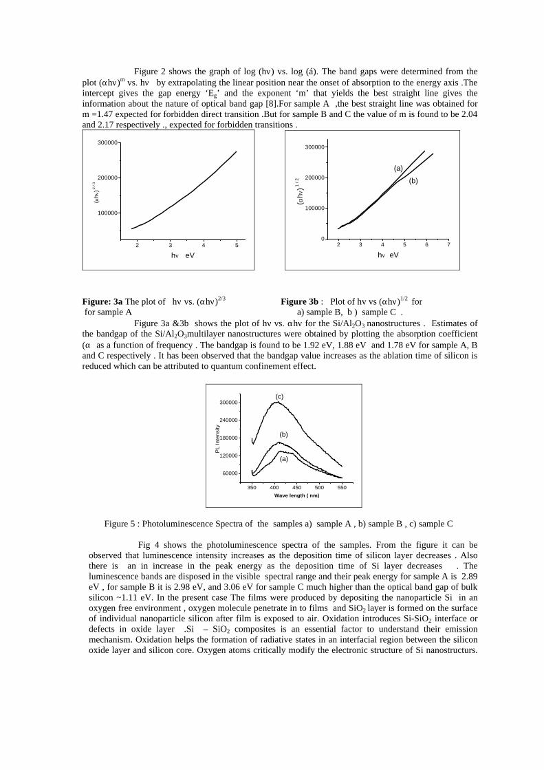
Figure 2 shows the graph of log (hν) vs. log (á). The band gaps were determined from the plot (αhν)m vs. hν by extrapolating the linear position near the onset of absorption to the energy axis .The intercept gives the gap energy ‘Eg’ and the exponent ‘m’ that yields the best straight line gives the information about the nature of optical band gap [8].For sample A ,the best straight line was obtained for m =1.47 expected for forbidden direct transition .But for sample B and C the value of m is found to be 2.04 and 2.17 respectively ., expected for forbidden transitions .
2 3 4 5
100000
200000
300000
(αhν
) 2 / 3
hν eV
2 3 4 5 6 70
100000
200000
300000
(b)
(a)
(αhν
) 1 /
2
hν eV
Figure: 3a The plot of hν vs. (αhν)2/3 Figure 3b : Plot of hv vs (αhν)1/2 for
for sample A a) sample B, b ) sample C . Figure 3a &3b shows the plot of hν vs. αhν for the Si/Al2O3 nanostructures . Estimates of
the bandgap of the Si/Al2O3multilayer nanostructures were obtained by plotting the absorption coefficient (α) as a function of frequency . The bandgap is found to be 1.92 eV, 1.88 eV and 1.78 eV for sample A, B and C respectively . It has been observed that the bandgap value increases as the ablation time of silicon is reduced which can be attributed to quantum confinement effect.
350 400 450 500 550
60000
120000
180000
240000
300000(c)
(b)
(a)
PL
In
ten
sity
Wave length ( nm)
Figure 5 : Photoluminescence Spectra of the samples a) sample A , b) sample B , c) sample C
Fig 4 shows the photoluminescence spectra of the samples. From the figure it can be observed that luminescence intensity increases as the deposition time of silicon layer decreases . Also there is an in increase in the peak energy as the deposition time of Si layer decreases . The luminescence bands are disposed in the visible spectral range and their peak energy for sample A is 2.89 eV , for sample B it is 2.98 eV, and 3.06 eV for sample C much higher than the optical band gap of bulk silicon ~1.11 eV. In the present case The films were produced by depositing the nanoparticle Si in an oxygen free environment , oxygen molecule penetrate in to films and SiO2 layer is formed on the surface of individual nanoparticle silicon after film is exposed to air. Oxidation introduces Si-SiO2 interface or defects in oxide layer .Si – SiO2 composites is an essential factor to understand their emission mechanism. Oxidation helps the formation of radiative states in an interfacial region between the silicon oxide layer and silicon core. Oxygen atoms critically modify the electronic structure of Si nanostructurs.

The interface region is assumed to have energy gap wider than that of Si core. So after the absorption of photon energy, the carriers are trapped in the Si=O bond and the PL results due to the transition from this level to ground state[9]. Reports shows that ground state energy varies with energy level of valence band . As the multilayer structure changes there may be a change in the oxidation state and which may change the ground state energy .
CONCLUSIONS Si nanoparticles were synthesized by off axis laser ablation. Studied the optical absorption of multilayer of silicon nanoparticles coated on smooth and roughed quartz. The TEM observations show the presence of nanoparticles of silicon. A blue shift of the absorption edge is observed for thinner Si films .This is due to the quantum confinement effect in silicon nanoparticles. From the absorption spectra it could be observed that the nature of transition depends on the nature the structure of multilayer . .The synthesized films exhibit PL peak around near UV - Visible region . We conclude that luminescence does not originate from localized states in gap but from extended states.
ACKNOWLEDGEMENTS
The authors thank Kerala State Council for Science Technology and Environment (KSCSTE) for their financial support . REFERENCES
[1] Xinwei etal, Phys.Rev .B 50, 18654 (1994). [2] L.T Canham, Appl. Phys. Lett, Vol 57, 1046 (1990) [3] Canham, Nature, 408, 411 (2000) [4] P. Kovakv et al, Phys.Rev .B 13, 2803 (1998) [5] Bhattacharya D, Chaudhuri S and A K Pal Vacuum 43 313 (1992) [6] Pankove J I, Optical processes in semiconductors, New
Jersey, USA, 1971, p. 34 [7] A. Goswami, Thin film Fundamentals, New Age International (p) Limited (1996). [8] P.Y.Yu, M. Kadona, Fundamentals of Semiconductor Physics and Material properties, Springer, Berlin (1996). [9] Y.Kanemitsu , T.O gawa ,K.Shiraishi and K.Takada : Phys . Rev.B 48 ( 1993 ) , 4883.
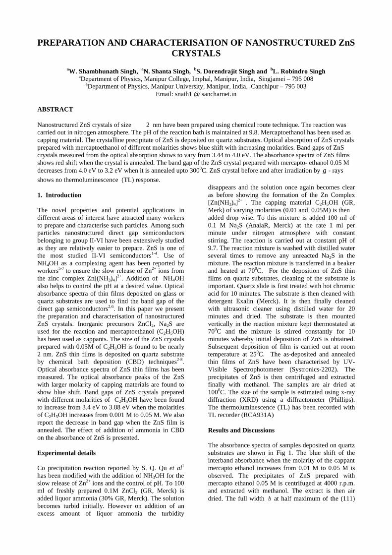
PREPARATION AND CHARACTERISATION OF NANOSTRUCTURED ZnS CRYSTALS
aW. Shambhunath Singh, aN. Shanta Singh, bS. Dorendrajit Singh and bL. Robindro Singh
aDepartment of Physics, Manipur College, Imphal, Manipur, India, Singjamei – 795 008 aDepartment of Physics, Manipur University, Manipur, India, Canchipur – 795 003
Email: snath1 @ sancharnet.in ABSTRACT Nanostructured ZnS crystals of size 2 nm have been prepared using chemical route technique. The reaction was carried out in nitrogen atmosphere. The pH of the reaction bath is maintained at 9.8. Mercaptoethanol has been used as capping material. The crystalline precipitate of ZnS is deposited on quartz substrates. Optical absorption of ZnS crystals prepared with mercaptoethanol of different molarities shows blue shift with increasing molarities. Band gaps of ZnS crystals measured from the optical absorption shows to vary from 3.44 to 4.0 eV. The absorbance spectra of ZnS films shows red shift when the crystal is annealed. The band gap of the ZnS crystal prepared with mercapto- ethanol 0.05 M decreases from 4.0 eV to 3.2 eV when it is annealed upto 3000C. ZnS crystal before and after irradiation by γ - rays
shows no thermoluminescence (TL) response. 1. Introduction The novel properties and potential applications in different areas of interest have attracted many workers to prepare and characterise such particles. Among such particles nanostructured direct gap semiconductors belonging to group II-VI have been extensively studied as they are relatively easier to prepare. ZnS is one of the most studied II-VI semiconductors1-4. Use of NH4OH as a complexing agent has been reported by workers5-7 to ensure the slow release of Zn2+ ions from the zinc complex Zn[(NH3)4]
2+. Addition of NH4OH also helps to control the pH at a desired value. Optical absorbance spectra of thin films deposited on glass or quartz substrates are used to find the band gap of the direct gap semiconductors2,6. In this paper we present the preparation and characterisation of nanostructured ZnS crystals. Inorganic precursors ZnCl2, Na2S are used for the reaction and mercaptoethanol (C2H5OH) has been used as cappants. The size of the ZnS crystals prepared with 0.05M of C2H5OH is found to be nearly 2 nm. ZnS thin films is deposited on quartz substrate by chemical bath deposition (CBD) techniques2-8. Optical absorbance spectra of ZnS thin films has been measured. The optical absorbance peaks of the ZnS with larger molarity of capping materials are found to show blue shift. Band gaps of ZnS crystals prepared with different molarities of C2H5OH have been found to increase from 3.4 eV to 3.88 eV when the molarities of C2H5OH increases from 0.001 M to 0.05 M. We also report the decrease in band gap when the ZnS film is annealed. The effect of addition of ammonia in CBD on the absorbance of ZnS is presented. Experimental details Co precipitation reaction reported by S. Q. Qu et al1 has been modified with the addition of NH3OH for the slow release of Zn2+ ions and the control of pH. To 100 ml of freshly prepared 0.1M ZnCl2 (GR, Merck) is added liquor ammonia (30% GR, Merck). The solution becomes turbid initially. However on addition of an excess amount of liquor ammonia the turbidity
disappears and the solution once again becomes clear as before showing the formation of the Zn Complex [Zn(NH3)4]
2+ . The capping material C2H5OH (GR, Merk) of varying molarities (0.01 and 0.05M) is then added drop wise. To this mixture is added 100 ml of 0.1 M Na2S (AnalaR, Merck) at the rate 1 ml per minute under nitrogen atmosphere with constant stirring. The reaction is carried out at constant pH of 9.7. The reaction mixture is washed with distilled water several times to remove any unreacted Na2S in the mixture. The reaction mixture is transferred in a beaker and heated at 700C. For the deposition of ZnS thin films on quartz substrates, cleaning of the substrate is important. Quartz slide is first treated with hot chromic acid for 10 minutes. The substrate is then cleaned with detergent Exalin (Merck). It is then finally cleaned with ultrasonic cleaner using distilled water for 20 minutes and dried. The substrate is then mounted vertically in the reaction mixture kept thermostated at 700C and the mixture is stirred constantly for 10 minutes whereby initial deposition of ZnS is obtained. Subsequent deposition of film is carried out at room temperature at 250C. The as-deposited and annealed thin films of ZnS have been characterised by UV-Visible Spectrophotometer (Systronics-2202). The precipitates of ZnS is then centrifuged and extracted finally with methanol. The samples are air dried at 1000C. The size of the sample is estimated using x-ray diffraction (XRD) using a diffractometer (Phillips). The thermoluminescence (TL) has been recorded with TL recorder (RCA931A) Results and Discussions The absorbance spectra of samples deposited on quartz substrates are shown in Fig 1. The blue shift of the interband absorbance when the molarity of the cappant mercapto ethanol increases from 0.01 M to 0.05 M is observed. The precipitates of ZnS prepared with mercapto ethanol 0.05 M is centrifuged at 4000 r.p.m. and extracted with methanol. The extract is then air dried. The full width β at half maximum of the (111)
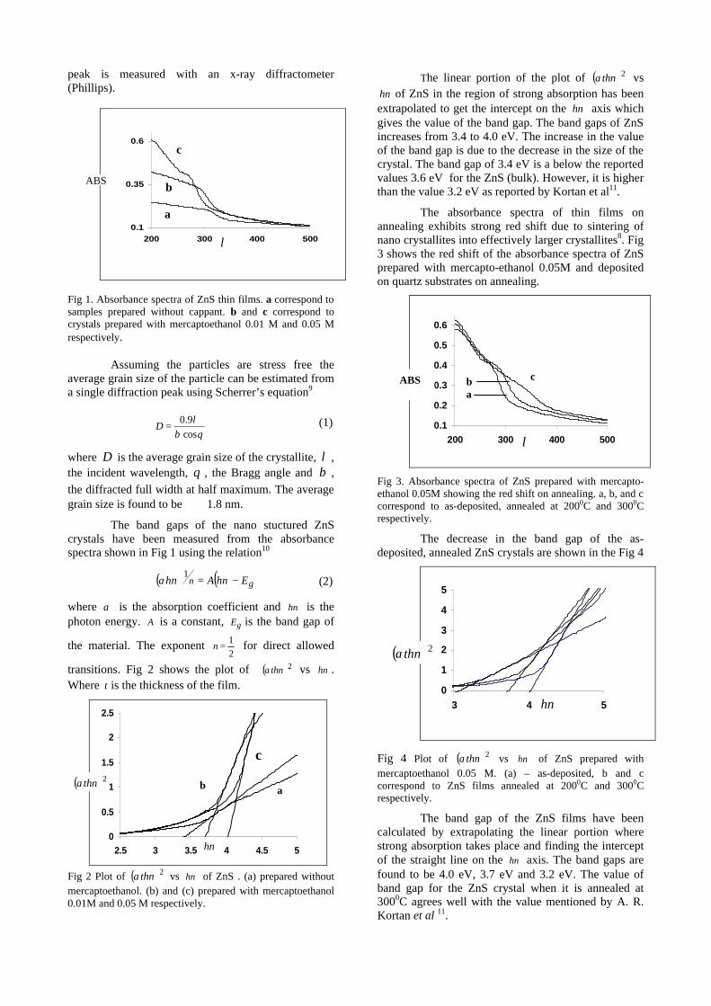
peak is measured with an x-ray diffractometer (Phillips).
Fig 1. Absorbance spectra of ZnS thin films. a correspond to samples prepared without cappant. b and c correspond to crystals prepared with mercaptoethanol 0.01 M and 0.05 M respectively.
Assuming the particles are stress free the average grain size of the particle can be estimated from a single diffraction peak using Scherrer’s equation9
θβλ
cos
9.0=D (1)
where D is the average grain size of the crystallite, λ , the incident wavelength, θ , the Bragg angle and β ,
the diffracted full width at half maximum. The average grain size is found to be 1.8 nm.
The band gaps of the nano stuctured ZnS crystals have been measured from the absorbance spectra shown in Fig 1 using the relation10
( ) ( )gn EhAh −= ννα1
(2)
where α is the absorption coefficient and νh is the photon energy. A is a constant, gE is the band gap of
the material. The exponent 2
1=n for direct allowed
transitions. Fig 2 shows the plot of ( )2ναth vs νh . Where t is the thickness of the film.
0
0.5
1
1.5
2
2.5
2.5 3 3.5 4 4.5 5
Fig 2 Plot of ( )2ναth vs νh of ZnS . (a) prepared without mercaptoethanol. (b) and (c) prepared with mercaptoethanol 0.01M and 0.05 M respectively.
The linear portion of the plot of ( )2ναth vs νh of ZnS in the region of strong absorption has been
extrapolated to get the intercept on the νh axis which gives the value of the band gap. The band gaps of ZnS increases from 3.4 to 4.0 eV. The increase in the value of the band gap is due to the decrease in the size of the crystal. The band gap of 3.4 eV is a below the reported values 3.6 eV for the ZnS (bulk). However, it is higher than the value 3.2 eV as reported by Kortan et al11.
The absorbance spectra of thin films on annealing exhibits strong red shift due to sintering of nano crystallites into effectively larger crystallites8. Fig 3 shows the red shift of the absorbance spectra of ZnS prepared with mercapto-ethanol 0.05M and deposited on quartz substrates on annealing.
0.1
0.2
0.3
0.4
0.5
0.6
200 300 400 500
Fig 3. Absorbance spectra of ZnS prepared with mercapto-ethanol 0.05M showing the red shift on annealing. a, b, and c correspond to as-deposited, annealed at 2000C and 3000C respectively.
The decrease in the band gap of the as- deposited, annealed ZnS crystals are shown in the Fig 4
0
1
2
3
4
5
3 4 5
Fig 4 Plot of ( )2ναth vs νh of ZnS prepared with mercaptoethanol 0.05 M. (a) – as-deposited, b and c correspond to ZnS films annealed at 2000C and 3000C respectively.
The band gap of the ZnS films have been calculated by extrapolating the linear portion where strong absorption takes place and finding the intercept of the straight line on the νh axis. The band gaps are found to be 4.0 eV, 3.7 eV and 3.2 eV. The value of band gap for the ZnS crystal when it is annealed at 3000C agrees well with the value mentioned by A. R. Kortan et al 11.
ABS
a
b
c
νh
( )2ναtha b
c
0.1
0.35
0.6
200 300 400 500
λ
ABS a b c
νh
( )2ναth
λ
a
b
c
The use NH3 as complexing agent for the good quality deposition of ZnS thin films by Chemical bath deposition (CBD) on quartz substrate has been analytically explained by Oladeji and Chow7. The CDB mechanism leading to a uniform nucleation and growth of thin films has been explained as due to the preferential adsorption of Zn2+ and S2- on the substrate by A. Antony et al5. In order to see the difference on the absorption spectra of ZnS thin films prepared with and without ammonia we have prepared ZnS with and without liquor ammonia and mercapto ethanol (0.05M). Fig 5 shows the absorption spectra of these two films. The substrates were kept for 20 minutes in
0.05
0.25
0.45
0.65
200 300 400 500
Fig 5. Absorption spectra of ZnS prepared with mercaptoethanol (0.05M)—(a) without NH3OH and (b)—with NH3OH
the reaction mixture separately obtained with and without ammonia. The absorbance of the film deposited using ammonia is found to be stronger than the one deposited without ammonia. Thus optimisation of the CBD using ammonia is obtained in agreement with reports of Antony et al5 and Oladeji and Chow7. The band gaps of these two samples have also been estimated and are found to lie very close to 4.0 eV. The band gap of the sample obtained with ammonia is found to be a little below that of the sample obtained without ammonia but the difference is in hundredth place of an eV and is not appreciable. The small decrease may be attributed to the increase in size due to the non formation of [Zn(NH3)4]
2+ complex and homogeneous precipitation of ZnS.
W. Chen et al4 reported TL response curves of ZnS without any irradiation before measurement. The TL response has been attributed to the traps and carriers which are produced during the sample processing as the particle size becomes small and ions at the surface increase rapidly giving rise to the existence long wavelength peak in the optical absorption spectrum of ZnS quantum dots. N. Kumbhjkar et al 3 could not observe such red shifted peak in the absorption spectrum. Attempts have been made to record the TL glow curves of the ZnS crystallites both before and after irradiation by γ -
rays. No TL response could be observed.
Conclusion
Nanostructured ZnS crystals have been prepared using mercaptoethanol as cappants. The crystals have been deposited on quartz substrates by chemical bath deposition method. The optical absorbance spectra of
films prepared with larger molarity shows blue shift. The band gap of ZnS lies in the range 3.4 – 4.0 eV. The absorbance spectra of ZnS thin films shows red shift on annealing. Optimisation of CBD using ammonia is obtained.Irradiated and un irradiated nano structured ZnS quantum dots could not show TL response.
Acknowledgement
One of us W. S. Singh would to thank the University Grants Commission, New Delhi, India for financial assistance. We wish to acknowledge USIC, Guwahati for XRD measurements.
References 1S. C. Qu, W. H. Zhou, F. Q. Liu, N. F. Chen, Z. G. Wang, H. Y. Pan and D. P. Yu, Appl. Phys. Lett. 19 3605 (2002) 2R. Maity and K. K. Chattoppadhyay, Nanotechnology 15 812 (2004) 3N. Kumbhojkar, V. V. Nikesh, Anjali Kshirsagar ans Shailaja Mahamuni, J. Appl. Phys. 88 6260 (2000) 4W. Chen, Z. Wang, Z. Lin and L. Lin, J. Appl. Phys. 82 (6) 3111 (1997) 5A. Antony, K. V. Murali, R. Manoj and M. K. Jayaraj, Matt. Chm and Phys. 90 106 (2005) 6P. K. Ghosh, M. K. Mitra and K. K. Chattopadhyay, Nanotechnology 16 107 (2005) 7 I. O. Oladeji and L. Chow, Thin Solid Films 339 148 (1999) 8R. B. Kale and C. D. Lokhande Appl. Surface. Sc. 223 343 (2004) 9A. Pandey, R. G. Sonkawade and P. D. Sahare J. Appl. Phys. 35 2744 (2002) 10 J. I. Pankove Optical Processes in Semiconductors (New Jersey, USA:Prentice Hall, 1971), p. 34 11A. R. Kortan, R. Hull, R. L. Opila, M. G. Bawendi, M. L. Steigerald, P. J. Carroll and L. E. Brus, J. Am. XChem. Soxc. 112 1327 (1990)
(nm)λ
ABS a
b
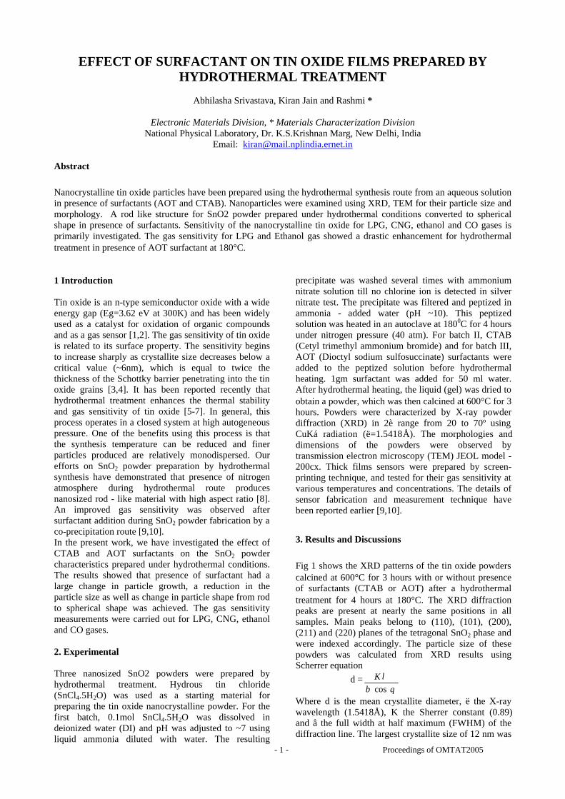
- 1 - Proceedings of OMTAT2005
EFFECT OF SURFACTANT ON TIN OXIDE FILMS PREPARED BY HYDROTHERMAL TREATMENT
Abhilasha Srivastava, Kiran Jain and Rashmi *
Electronic Materials Division, * Materials Characterization Division
National Physical Laboratory, Dr. K.S.Krishnan Marg, New Delhi, India Email: [email protected]
Abstract
Nanocrystalline tin oxide particles have been prepared using the hydrothermal synthesis route from an aqueous solution in presence of surfactants (AOT and CTAB). Nanoparticles were examined using XRD, TEM for their particle size and morphology. A rod like structure for SnO2 powder prepared under hydrothermal conditions converted to spherical shape in presence of surfactants. Sensitivity of the nanocrystalline tin oxide for LPG, CNG, ethanol and CO gases is primarily investigated. The gas sensitivity for LPG and Ethanol gas showed a drastic enhancement for hydrothermal treatment in presence of AOT surfactant at 180°C. 1 Introduction Tin oxide is an n-type semiconductor oxide with a wide energy gap (Eg=3.62 eV at 300K) and has been widely used as a catalyst for oxidation of organic compounds and as a gas sensor [1,2]. The gas sensitivity of tin oxide is related to its surface property. The sensitivity begins to increase sharply as crystallite size decreases below a critical value (~6nm), which is equal to twice the thickness of the Schottky barrier penetrating into the tin oxide grains [3,4]. It has been reported recently that hydrothermal treatment enhances the thermal stability and gas sensitivity of tin oxide [5-7]. In general, this process operates in a closed system at high autogeneous pressure. One of the benefits using this process is that the synthesis temperature can be reduced and finer particles produced are relatively monodispersed. Our efforts on SnO2 powder preparation by hydrothermal synthesis have demonstrated that presence of nitrogen atmosphere during hydrothermal route produces nanosized rod - like material with high aspect ratio [8]. An improved gas sensitivity was observed after surfactant addition during SnO2 powder fabrication by a co-precipitation route [9,10]. In the present work, we have investigated the effect of CTAB and AOT surfactants on the SnO2 powder characteristics prepared under hydrothermal conditions. The results showed that presence of surfactant had a large change in particle growth, a reduction in the particle size as well as change in particle shape from rod to spherical shape was achieved. The gas sensitivity measurements were carried out for LPG, CNG, ethanol and CO gases.
2. Experimental Three nanosized SnO2 powders were prepared by hydrothermal treatment. Hydrous tin chloride (SnCl4.5H2O) was used as a starting material for preparing the tin oxide nanocrystalline powder. For the first batch, 0.1mol SnCl4.5H2O was dissolved in deionized water (DI) and pH was adjusted to ~7 using liquid ammonia diluted with water. The resulting
precipitate was washed several times with ammonium nitrate solution till no chlorine ion is detected in silver nitrate test. The precipitate was filtered and peptized in ammonia - added water (pH ~10). This peptized solution was heated in an autoclave at 1800C for 4 hours under nitrogen pressure (40 atm). For batch II, CTAB (Cetyl trimethyl ammonium bromide) and for batch III, AOT (Dioctyl sodium sulfosuccinate) surfactants were added to the peptized solution before hydrothermal heating. 1gm surfactant was added for 50 ml water. After hydrothermal heating, the liquid (gel) was dried to obtain a powder, which was then calcined at 600°C for 3 hours. Powders were characterized by X-ray powder diffraction (XRD) in 2è range from 20 to 70º using CuKá radiation (ë=1.5418Å). The morphologies and dimensions of the powders were observed by transmission electron microscopy (TEM) JEOL model -200cx. Thick films sensors were prepared by screen-printing technique, and tested for their gas sensitivity at various temperatures and concentrations. The details of sensor fabrication and measurement technique have been reported earlier [9,10].
3. Results and Discussions
Fig 1 shows the XRD patterns of the tin oxide powders calcined at 600°C for 3 hours with or without presence of surfactants (CTAB or AOT) after a hydrothermal treatment for 4 hours at 180°C. The XRD diffraction peaks are present at nearly the same positions in all samples. Main peaks belong to (110), (101), (200), (211) and (220) planes of the tetragonal SnO2 phase and were indexed accordingly. The particle size of these powders was calculated from XRD results using Scherrer equation
d =θβ
λcos
K
Where d is the mean crystallite diameter, ë the X-ray wavelength (1.5418Å), K the Sherrer constant (0.89) and â the full width at half maximum (FWHM) of the diffraction line. The largest crystallite size of 12 nm was
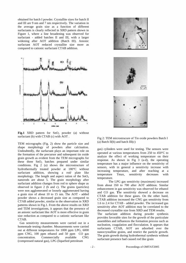
- 2 - Proceedings of OMTAT2005
obtained for batch I powder. Crystallite sizes for batch II and III are 9 nm and 7 nm respectively. The variation in the average grain size as a function of different surfactants is clearly reflected in XRD pattern shown in Figure 1, where a line broadening was observed for surfactant - added batches II and III, with a larger widening after AOT addition (Batch III). Anionic surfactant AOT reduced crystallite size more as compared to cationic surfactant CTAB addition.
Fig.1 XRD pattern for SnO2 powder (a) without surfactant (b) with CTAB (c) with AOT . TEM micrographs (Fig. 2) show the particle size and shape morphology of powders after calcination. Undoubtedly, the surfactant plays an important role on the formation of the precursor and subsequent tin oxide grain growth as evident from the TEM micrographs for these three SnO2 batches prepared under similar conditions. Fig 2 (a) shows the microstructure of hydrothermally treated powder at 180°C without surfactant addition, showing a rod/ plate like morphology. The length and aspect ration of the SnO2 nanorods are about 5. The grain morphology after surfactant addition changes from rod to sphere shape as observed in figure 2 (b and c). The grains (particles) were non agglomerated or loosely agglomerated having a grain size of about 10 to 15 nm. The AOT - added powder shows a decreased grain size as compared to CTAB added powder, similar to the observation in XRD patterns shown in Fig.1. From the above results on XRD and TEM investigations, it appears that the presence of an anionic surfactant like AOT is more effective in grain size reduction as compared to a cationic surfactant like CTAB. Gas sensitivity measurements were carried out in a homemade testing chamber. Measurements were carried out at different temperatures for 1000 ppm LPG, 6000 ppm CNG, 100 ppm ethanol and 50 ppm CO gas concentration. Commercially available CNG (compressed natural gas), LPG (liquefied petroleum
Fig 2: TEM microstrucure of Tin oxide powders Batch I (a) Batch II(b) and batch III(c) gas) cylinders were used for testing. The sensors were operated at various temperatures from 250 to 450°C to analyze the effect of working temperature on their response. As shown in Fig 3 (a-d), the operating temperature has a major influence on the sensitivity of sensors, with in general a sensitivity increase with increasing temperature, and after reaching at a temperature Tmax, sensitivity decreases with temperature.
The LPG gas sensitivity (maximum) increased from about 350 to 700 after AOT addition. Similar enhancement in gas sensitivity was observed for ethanol and CO gas. The sensitivity showed a decrease on CTAB addition for these gases. On the other hand, CTAB addition increased the CNG gas sensitivity from 1.6 to 2.4 for CTAB - added powder. The increased gas sensitivity after AOT addition may be correlated to the decreased crystallite size from XRD and TEM results. The surfactant addition during powder synthesis provides favorable sites for the growth of the particulate assemblies and influences the formation process such as nucleation, coagulation and flocculation. It appears that surfactants CTAB, AOT are adsorbed over the nanocrystalline grains, and restrict the particle growth. The grain growth during hydrothermal synthesis without surfactant presence had caused rod like grain
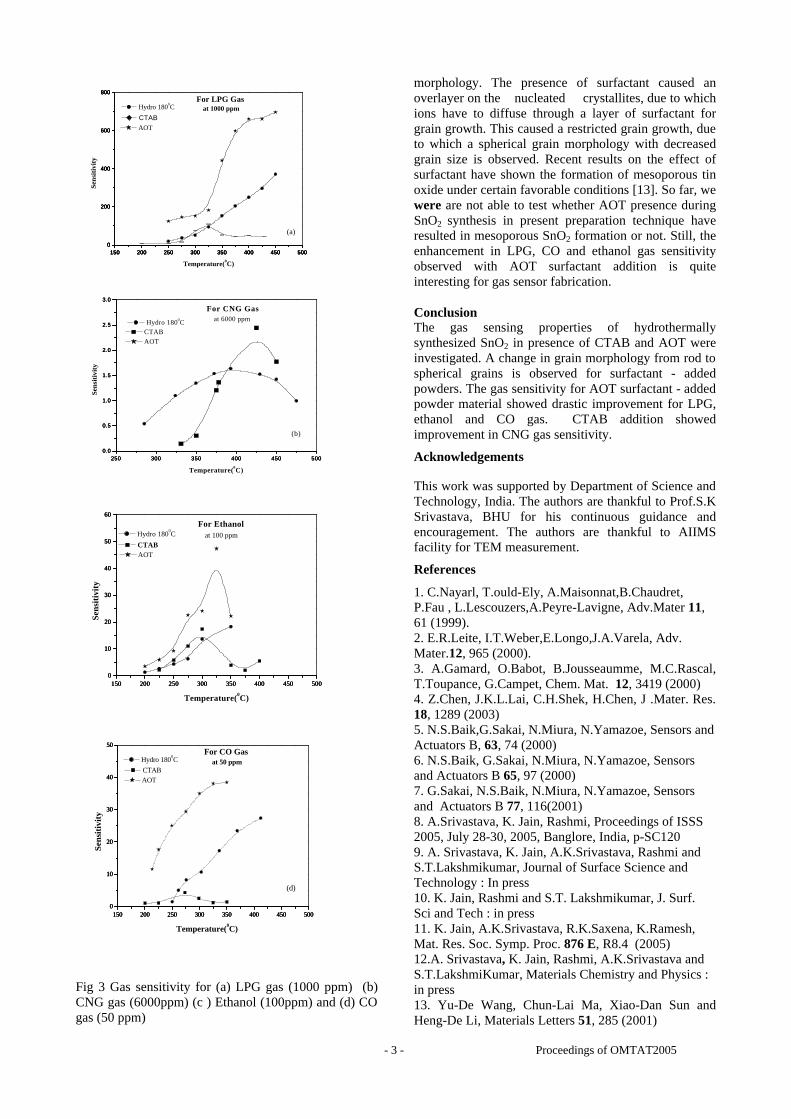
- 3 - Proceedings of OMTAT2005
150 200 250 300 350 400 450 5000
200
400
600
800
150 200 250 300 350 400 450 5000
200
400
600
800
150 200 250 300 350 400 450 5000
200
400
600
800
150 200 250 300 350 400 450 5000
200
400
600
800
Hydro 1800C
Sens
itiv
ity
CTAB
(a)
at 1000 ppmFor LPG Gas
Temperature(0C)
AOT
250 300 350 400 450 5000.0
0.5
1.0
1.5
2.0
2.5
3.0
250 300 350 400 450 5000.0
0.5
1.0
1.5
2.0
2.5
3.0
250 300 350 400 450 5000.0
0.5
1.0
1.5
2.0
2.5
3.0
at 6000 ppm
For CNG Gas
Temperature(0C)
Hydro 1800C
AOT
(b)
Sens
itiv
ity
CTAB
150 200 250 300 350 400 450 5000
10
20
30
40
50
60
150 200 250 300 350 400 450 5000
10
20
30
40
50
60
150 200 250 300 350 400 450 5000
10
20
30
40
50
60
Sens
itiv
ity
Temperature(0C)
Hydro 1800C
CTAB at 100 ppm
For Ethanol
AOT
150 200 250 300 350 400 450 5000
10
20
30
40
50
150 200 250 300 350 400 450 5000
10
20
30
40
50
150 200 250 300 350 400 450 5000
10
20
30
40
50
at 50 ppmFor CO Gas
Sens
itiv
ity
Temperature(0C)
AOT CTAB
(d)
Hydro 1800C
Fig 3 Gas sensitivity for (a) LPG gas (1000 ppm) (b) CNG gas (6000ppm) (c ) Ethanol (100ppm) and (d) CO gas (50 ppm)
morphology. The presence of surfactant caused an overlayer on the nucleated crystallites, due to which ions have to diffuse through a layer of surfactant for grain growth. This caused a restricted grain growth, due to which a spherical grain morphology with decreased grain size is observed. Recent results on the effect of surfactant have shown the formation of mesoporous tin oxide under certain favorable conditions [13]. So far, we were are not able to test whether AOT presence during SnO2 synthesis in present preparation technique have resulted in mesoporous SnO2 formation or not. Still, the enhancement in LPG, CO and ethanol gas sensitivity observed with AOT surfactant addition is quite interesting for gas sensor fabrication. Conclusion The gas sensing properties of hydrothermally synthesized SnO2 in presence of CTAB and AOT were investigated. A change in grain morphology from rod to spherical grains is observed for surfactant - added powders. The gas sensitivity for AOT surfactant - added powder material showed drastic improvement for LPG, ethanol and CO gas. CTAB addition showed improvement in CNG gas sensitivity.
Acknowledgements
This work was supported by Department of Science and Technology, India. The authors are thankful to Prof.S.K Srivastava, BHU for his continuous guidance and encouragement. The authors are thankful to AIIMS facility for TEM measurement.
References
1. C.Nayarl, T.ould-Ely, A.Maisonnat,B.Chaudret, P.Fau , L.Lescouzers,A.Peyre-Lavigne, Adv.Mater 11, 61 (1999). 2. E.R.Leite, I.T.Weber,E.Longo,J.A.Varela, Adv. Mater.12, 965 (2000). 3. A.Gamard, O.Babot, B.Jousseaumme, M.C.Rascal, T.Toupance, G.Campet, Chem. Mat. 12, 3419 (2000) 4. Z.Chen, J.K.L.Lai, C.H.Shek, H.Chen, J .Mater. Res. 18, 1289 (2003) 5. N.S.Baik,G.Sakai, N.Miura, N.Yamazoe, Sensors and Actuators B, 63, 74 (2000) 6. N.S.Baik, G.Sakai, N.Miura, N.Yamazoe, Sensors and Actuators B 65, 97 (2000) 7. G.Sakai, N.S.Baik, N.Miura, N.Yamazoe, Sensors and Actuators B 77, 116(2001) 8. A.Srivastava, K. Jain, Rashmi, Proceedings of ISSS 2005, July 28-30, 2005, Banglore, India, p-SC120 9. A. Srivastava, K. Jain, A.K.Srivastava, Rashmi and S.T.Lakshmikumar, Journal of Surface Science and Technology : In press 10. K. Jain, Rashmi and S.T. Lakshmikumar, J. Surf. Sci and Tech : in press 11. K. Jain, A.K.Srivastava, R.K.Saxena, K.Ramesh, Mat. Res. Soc. Symp. Proc. 876 E, R8.4 (2005) 12.A. Srivastava, K. Jain, Rashmi, A.K.Srivastava and S.T.LakshmiKumar, Materials Chemistry and Physics : in press 13. Yu-De Wang, Chun-Lai Ma, Xiao-Dan Sun and Heng-De Li, Materials Letters 51, 285 (2001)

- 4 - Proceedings of OMTAT2005
TRANSFER OF COPYRIGHT Please complete as appropriate and return by fax/mail. If you do not provide a copyright clearance, we cannot include your paper in the proceedings. [ ] My employer has given clearance for this
paper to be published. OR [ ] I am the holder of the copyright for this
paper The author who sign the copyright Signature: ......................................................... Date: 10-10-05 Affiliation: Dr.Kiran Jain Scientist, Electronic Materials Division National Physical Laboratory Dr.K.S.Krishnan Marg New Delhi-12
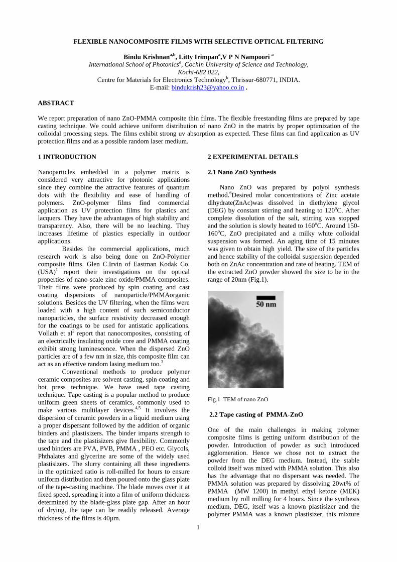
1
FLEXIBLE NANOCOMPOSITE FILMS WITH SELECTIVE OPTICAL FILTERING
Bindu Krishnana,b, Litty Irimpana,V P N Nampoori a International School of Photonicsa, Cochin University of Science and Technology,
Kochi-682 022, Centre for Materials for Electronics Technologyb, Thrissur-680771, INDIA.
E-mail: [email protected] .
ABSTRACT We report preparation of nano ZnO-PMMA composite thin films. The flexible freestanding films are prepared by tape casting technique. We could achieve uniform distribution of nano ZnO in the matrix by proper optimization of the colloidal processing steps. The films exhibit strong uv absorption as expected. These films can find application as UV protection films and as a possible random laser medium. 1 INTRODUCTION Nanoparticles embedded in a polymer matrix is considered very attractive for photonic applications since they combine the attractive features of quantum dots with the flexibility and ease of handling of polymers. ZnO-polymer films find commercial application as UV protection films for plastics and lacquers. They have the advantages of high stability and transparency. Also, there will be no leaching. They increases lifetime of plastics especially in outdoor applications.
Besides the commercial applications, much research work is also being done on ZnO-Polymer composite films. Glen C.Irvin of Eastman Kodak Co. (USA)1 report their investigations on the optical properties of nano-scale zinc oxide/PMMA composites. Their films were produced by spin coating and cast coating dispersions of nanoparticle/PMMAorganic solutions. Besides the UV filtering, when the films were loaded with a high content of such semiconductor nanoparticles, the surface resistivity decreased enough
for the coatings to be used for antistatic applications. Vollath et al2 report that nanocomposites, consisting of an electrically insulating oxide core and PMMA coating exhibit strong luminescence. When the dispersed ZnO particles are of a few nm in size, this composite film can act as an effective random lasing medium too.3
Conventional methods to produce polymer ceramic composites are solvent casting, spin coating and hot press technique. We have used tape casting technique. Tape casting is a popular method to produce uniform green sheets of ceramics, commonly used to make various multilayer devices.4,5 It involves the dispersion of ceramic powders in a liquid medium using a proper dispersant followed by the addition of organic binders and plastisizers. The binder imparts strength to the tape and the plastisizers give flexibility. Commonly used binders are PVA, PVB, PMMA , PEO etc. Glycols, Phthalates and glycerine are some of the widely used plastisizers. The slurry containing all these ingredients in the optimized ratio is roll-milled for hours to ensure uniform distribution and then poured onto the glass plate of the tape-casting machine. The blade moves over it at fixed speed, spreading it into a film of uniform thickness determined by the blade-glass plate gap. After an hour of drying, the tape can be readily released. Average thickness of the films is 40µm.
2 EXPERIMENTAL DETAILS 2.1 Nano ZnO Synthesis
Nano ZnO was prepared by polyol synthesis method.6Desired molar concentrations of Zinc acetate dihydrate(ZnAc)was dissolved in diethylene glycol (DEG) by constant stirring and heating to 120oC. After complete dissolution of the salt, stirring was stopped and the solution is slowly heated to 160oC. Around 150-160oC, ZnO precipitated and a milky white colloidal suspension was formed. An aging time of 15 minutes was given to obtain high yield. The size of the particles and hence stability of the colloidal suspension depended both on ZnAc concentration and rate of heating. TEM of the extracted ZnO powder showed the size to be in the range of 20nm (Fig.1).
Fig.1 TEM of nano ZnO 2.2 Tape casting of PMMA-ZnO One of the main challenges in making polymer composite films is getting uniform distribution of the powder. Introduction of powder as such introduced agglomeration. Hence we chose not to extract the powder from the DEG medium. Instead, the stable colloid itself was mixed with PMMA solution. This also has the advantage that no dispersant was needed. The PMMA solution was prepared by dissolving 20wt% of PMMA (MW 1200) in methyl ethyl ketone (MEK) medium by roll milling for 4 hours. Since the synthesis medium, DEG, itself was a known plastisizer and the polymer PMMA was a known plastisizer, this mixture
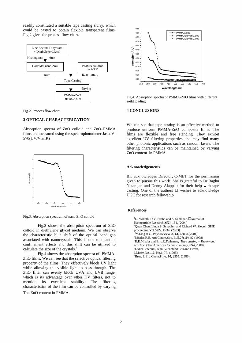
2
readily constituted a suitable tape casting slurry, which could be casted to obtain flexible transparent films. Fig.2 gives the process flow chart. Heating rate 4/min
160C Roll milling
Drying Fig.2. Process flow chart 3 OPTICAL CHARACTERIZATION Absorption spectra of ZnO colloid and ZnO–PMMA films are measured using the spectrophotometer JascoV-570(UV/Vis/IR)
300 320 340 360 380 400
0
1
2
3
4
Inte
nsity
A.U
w a ve length nm
Fig.3. Absorption spectrum of nano ZnO colloid
Fig.3 shows the absorption spectrum of ZnO colloid in diethylene glycol medium. We can observe the characteristic blue shift of the optical band gap associated with nanocrystals. This is due to quantum confinement effects and this shift can be utilized to calculate the size of the crystals.7
Fig.4 shows the absorption spectra of PMMA-ZnO films. We can see that the selective optical filtering property of the films. They effectively block UV light while allowing the visible light to pass through. The ZnO filter can evenly block UVA and UVB range, which is its advantage over other UV filters, not to mention its excellent stability. The filtering characteristics of the film can be controlled by varying
The ZnO content in PMMA.
250 300 350 400 450 500 550 600 650 700
0.05
0.10
0.15
0.20
0.25
0.30
0.35
0.40
0.45
0.50
0.55
0.60
0.65
Inte
nsi
ty (
A.U
)
Wavelength nm
PMMA alone PMMA+10 vol% ZnO PMMA+20 vol% ZnO
Fig.4. Absorption spectra of PMMA-ZnO films with different soild loading 4 CONCLUSIONS
We can see that tape casting is an effective method to produce uniform PMMA-ZnO composite films. The films are flexible and free standing. They exhibit excellent UV filtering properties and may find many other photonic applications such as random lasers. The filtering characteristics can be maintained by varying ZnO content in PMMA. Acknowledgements BK acknowledges Director, C-MET for the permission given to pursue this work. She is grateful to Dr.Raghu Natarajan and Denny Alappatt for their help with tape casting. One of the authors LI wishes to acknowledge UGC for research fellowship References
1D. Vollath, D.V. Szabó and S. Schlabac,, Journal of Nanoparticle Research ,6[2], 181. (2004) 2Quan Chen, Linda S. Schadler, and Richard W. Siegel , SPIE proceeding Vol.5222, B-34. (2003) 3Y.Ling et al, Phys.Review A, 64, 63808.(2001) 4Mistler.R.E, Am.Ceram.Soc. Bull.77(10), 82.(1998) 5R.E.Mistler and Eric.R.Twiname, Tape casting – Theory and practice, (The American Ceramic society,USA,2000) 6Didier Jezequel, Jean Guenotand Fernand Fievet, J.Mater.Res..10, No.1, 77. (1995)
7Brus. L.E, J.Chem.Phys. 90, 2555. (1986)
Colloidal nano ZnO
Zinc Acetate Dihydrate + Diethylene Glycol
PMMA solution in MEK
Tape Casting
PMMA-ZnO flexible film
ELECTRICAL PROPERTIES OF ELECTROSPUN FIBERS OF PANI-PMMA COMPOSITES
V.Jagadeesh Babu1, J.Subha2, R.Vasanthakumari3, V.R.K.Murthy1, T.S.Natarajan1
1Indian Institute of Technology Madras, Chennai-600 036,India. 2Department of Rubber and Plastics Technology, MIT, Chennai-600 044, India. 3Department of Polymer Technology, Crescent Engineering College Chennai-600 048,India. [email protected]
Abstract
Nano fibers of polymer composites can be prepared easily by the technique of electrospinning. The fibers prepared by this method are found to be superior in several applications compared to the films obtained from normal spin casting. One of the reasons is the large surface area to volume ratio in the case of the nano fibers. The conducting polymers like polyaniline, polypyrole etc., are difficult to form fibers on their own by electrospinning. Hence they are usually combined with other insulating polymers like poly (methylmethacrylate) (PMMA), polystyrene (PS), polyethyleneoxide (PEO) etc., thus forming conducting composites.
In the present work nano fibers of conducting composites of PANI-PMMA, with different weight percentages are prepared and characterized using XRD, SEM, etc. Their dc and ac conductivities are measured and the results are discussed. INTRODUCTION Conducting polymers have become the focus of research in material science in many laboratories. Among the different conducting polymers, polyaniline has received greater attention due to its favorable economics, easy synthesis, and environmental stability. This growing interest in Polyaniline is due to its electrical conductivity and its usage in electrical devices. Usually polymer based electrical devices like sensors [1] and electrodes [2] are manufactured in thin film or in bulk forms. In recent times attention is focused on to develop such devices using ultra fine and nano fibers. These fibers have many advantages over the thin films and they are useful in microelectronics [3], sensors [4], and electrodes for batteries [5]. The usage of the nano fibers are also more in high performance filters, and scaffolds in tissue engineering [6]. Ultra fine fibers can be obtained by several techniques like electrospinning [7], drawing [8], template synthesis [9], phase separation [10], self-assembly [11], etc. Electrospinning is one such simple and inexpensive technique to produce polymer nano fibers.
In the electro spinning process a very high electric field is applied between the Polymer solution (which is in the plastic syringe with fine needle tip) and a metallic collecting drum (which is connected to ground). As the electric field increases the
droplet formed at the tip of the needle elongates to form a conical shape known as the Taylor cone. At the critical field the electric field dominates the surface tension and a charged jet is ejected from tip of the cone and travels through air towards the counter-collecting electrode. During this stage, the solvent gets evaporate and the different polymer strands formed, all charged alike repel each other and hence the jet “splays” which means the jet splits into several smaller jets. Ultimately, on the collecting electrode we observe a large quantity of random coils of nano fibers.
Different polymer fibers have different conductivities. Mixing some filler materials like ceramics, metal particles etc. can vary the conductivity. The polyaniline alone could not get the fibers. Hence the Polyaniline (PANI) is doped with Hydrochloric acid (HCl). This conducting PANI is mixed with a definite weight percentage of Polymethlymethacrylate (PMMA) to get the composite fibers.
Present paper reports the preparation of such PANI (HCl)-PMMA composite fibers by electrospinning and the electrical conductivity studies of these fibers. The concentration of HCl doped PANI in PMMA is varied from 5%, 10%, 15%, 20%(w/w) which are shown in figures 1(a) to (d). We can also see the fiber diameter is varying with increasing concentrations.
EXPERIMENTAL Preparation Of Polymer Ammonium per sulphate (0.1 mole aqueous solutions in protonic acid) is added drop -wise to a stirred solution of 0.1mole aniline dissolved in 1 mole of aqueous solution of protonic acid precooled to 4 oC. Ammonium persulphate is added very slowly to prevent the warming of the solution. After completion of the addition, stirring is continued for 2-4 hours to ensure completion of the reaction.
The time of initial coloration on mixing of reactants depends upon the temperature and protonic acid used. When HCl is used as protonic acid, the coloration of solution occurs almost after 1 minute at room temperature and around 1-5oC it is 3 – 5 min. The sequence of coloration is light blue → blue green → Coppery tint → green Precipitate. The precipitated salt is filtered and washed repeatedly with distilled water containing acid until the filtrate is colorless and finally with methyl alcohol. The green Emeraldine salt thus obtained is dried under vacuum. The yield of the product Polyaniline (PANI) is found to be ~ 95% the polymerization method has been extended to bench scale to prepare a minimum quantity of 100-150 g per batch. The concentration of PANI (HCl) is varied from 5 % to 20%(w/w) in PMMA and the characterization is carried out.
Electro spinning process
In the electro spinning experimental setup we have used a high voltage power supply (0 to 5 kV). The 5ml disposable syringes with the needle diameters Less than 1mm are used (Dispovan India). Positive terminal of the high electric field is connected to the polymer solution, by introducing a very thin copper wire (40 SWG) into the syringe. The collecting drum is placed 3.5cm away from the tip of the needle. Aluminum foil is wrapped around the collecting drum. This is connected the ground which is the counter electrode. The drum can be rotated at high speed (3000 rpm) using a DC motor.
PANI (HCl)/PMMA Polymer solution is prepared and gently poured in to the syringe. This is used for the preparing of the fibers by electrospinning.
RESULTS & DISCUSSIONS
The SEM pictures of the fibers obtained are shown in figures 1(a) to (d). We can observe large number of fibers, which are very long and almost aligned. Their diameters are in the range of a few micrometers. They are not in nano scale. The reason can be because of low voltage like 5 kV. If we increase the voltage and also the distance we may get nanofibers. From the figures we can see that the fiber diameters are approximately 10µm
and the fiber diameter also varying with the concentration.
Figure 1 SEM images for
(a) 5% of PANI (HCl)
(b) 10% of PANI (HCl)
(c) 15% of PANI (HCl)
(d) 20% of PANI (HCl) in PMMA.
IMPEDANCE MEASUREMENTS
We prepared the fibers on silver electrodes. These electrodes are being used for impedance measurements. The AC impedance measurements are carried out for these fibers using 4192A LF Impedance Analyzer in the frequency range of 5HZ to 13MHz. The results are plotted in a graph between real part of the impedance (Z’) Vs imaginary part of the impedance (Z”) [See Fig 2]. And the frequency Vs capacitance plots for various concentrations (5%, 10%, 15%, 20%) are also shown in figure 3. The impedance plots do not show the usual semi-circle.
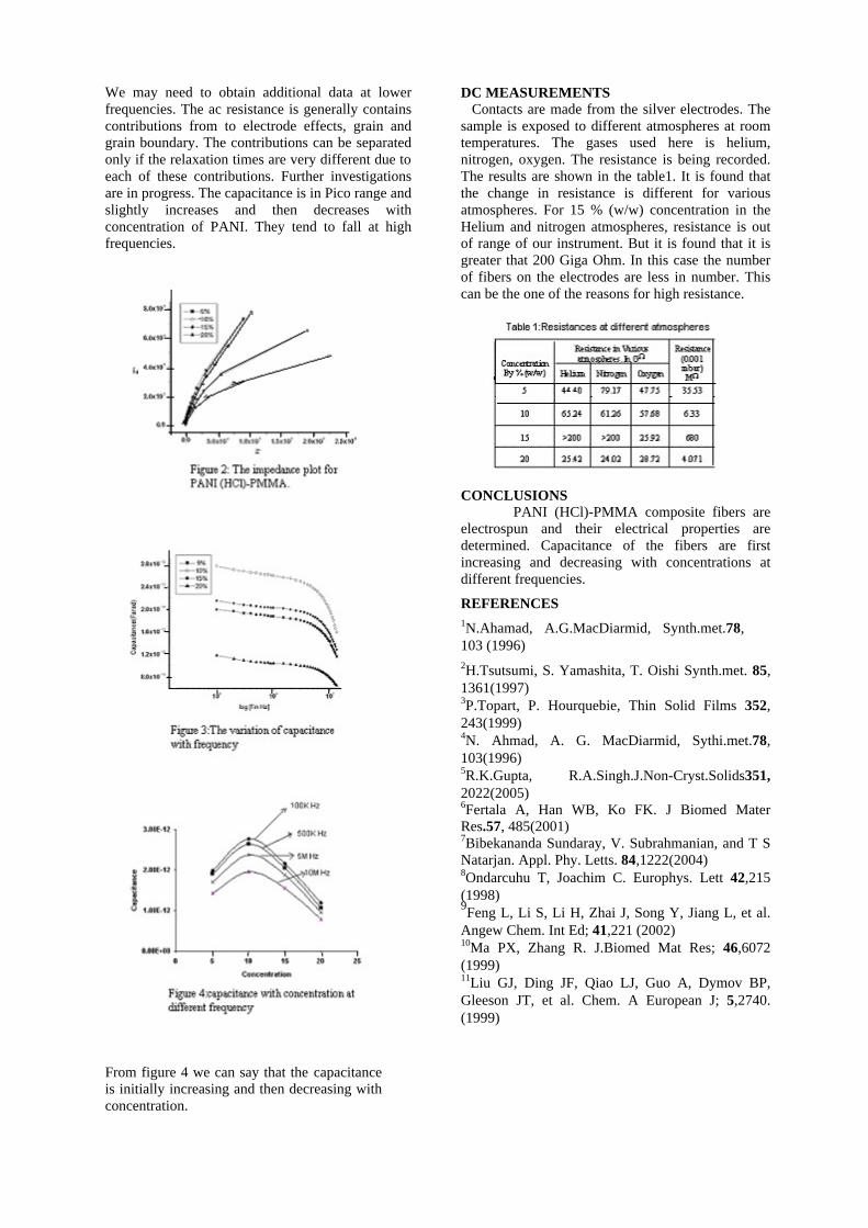
We may need to obtain additional data at lower frequencies. The ac resistance is generally contains contributions from to electrode effects, grain and grain boundary. The contributions can be separated only if the relaxation times are very different due to each of these contributions. Further investigations are in progress. The capacitance is in Pico range and slightly increases and then decreases with concentration of PANI. They tend to fall at high frequencies.
From figure 4 we can say that the capacitance is initially increasing and then decreasing with concentration.
DC MEASUREMENTS Contacts are made from the silver electrodes. The sample is exposed to different atmospheres at room temperatures. The gases used here is helium, nitrogen, oxygen. The resistance is being recorded. The results are shown in the table1. It is found that the change in resistance is different for various atmospheres. For 15 % (w/w) concentration in the Helium and nitrogen atmospheres, resistance is out of range of our instrument. But it is found that it is greater that 200 Giga Ohm. In this case the number of fibers on the electrodes are less in number. This can be the one of the reasons for high resistance. CONCLUSIONS
PANI (HCl)-PMMA composite fibers are electrospun and their electrical properties are determined. Capacitance of the fibers are first increasing and decreasing with concentrations at different frequencies.
REFERENCES 1N.Ahamad, A.G.MacDiarmid, Synth.met.78, 103 (1996) 2H.Tsutsumi, S. Yamashita, T. Oishi Synth.met. 85, 1361(1997) 3P.Topart, P. Hourquebie, Thin Solid Films 352, 243(1999) 4N. Ahmad, A. G. MacDiarmid, Sythi.met.78, 103(1996) 5R.K.Gupta, R.A.Singh.J.Non-Cryst.Solids351, 2022(2005) 6Fertala A, Han WB, Ko FK. J Biomed Mater Res.57, 485(2001) 7Bibekananda Sundaray, V. Subrahmanian, and T S Natarjan. Appl. Phy. Letts. 84,1222(2004) 8Ondarcuhu T, Joachim C. Europhys. Lett 42,215 (1998) 9Feng L, Li S, Li H, Zhai J, Song Y, Jiang L, et al. Angew Chem. Int Ed; 41,221 (2002) 10Ma PX, Zhang R. J.Biomed Mat Res; 46,6072 (1999) 11Liu GJ, Ding JF, Qiao LJ, Guo A, Dymov BP, Gleeson JT, et al. Chem. A European J; 5,2740. (1999)
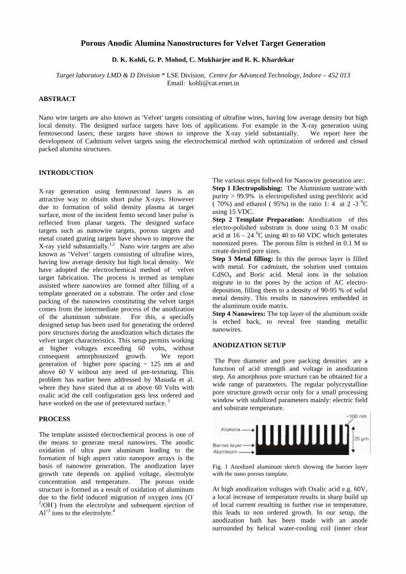
Porous Anodic Alumina Nanostructures for Velvet Target Generation
D. K. Kohli, G. P. Mohod, C. Mukharjee and R. K. Khardekar
Target laboratory LMD & D Division * LSE Division, Centre for Advanced Technology, Indore – 452 013 Email: [email protected]
ABSTRACT
Nano wire targets are also known as 'Velvet' targets consisting of ultrafine wires, having low average density but high local density. The designed surface targets have lots of applications. For example in the X-ray generation using femtosecond lasers; these targets have shown to improve the X-ray yield substantially. We report here the development of Cadmium velvet targets using the electrochemical method with optimization of ordered and closed packed alumina structures. INTRODUCTION
X-ray generation using femtosecond lasers is an attractive way to obtain short pulse X-rays. However due to formation of solid density plasma at target surface, most of the incident femto second laser pulse is reflected from planar targets. The designed surface targets such as nanowire targets, porous targets and metal coated grating targets have shown to improve the X-ray yield substantially.1,2 Nano wire targets are also known as ‘Velvet’ targets consisting of ultrafine wires, having low average density but high local density. We have adopted the electrochemical method of velvet target fabrication. The process is termed as template assisted where nanowires are formed after filling of a template generated on a substrate. The order and close packing of the nanowires constituting the velvet target comes from the intermediate process of the anodization of the aluminum substrate. For this, a specially designed setup has been used for generating the ordered pore structures during the anodization which dictates the velvet target characteristics. This setup permits working at higher voltages exceeding 60 volts, without consequent amorphousized growth. We report generation of higher pore spacing ~ 125 nm at and above 60 V without any need of pre-texturing. This problem has earlier been addressed by Masuda et al. where they have stated that at or above 60 Volts with oxalic acid the cell configuration gets less ordered and have worked on the use of pretextured surface. 3 PROCESS The template assisted electrochemical process is one of the means to generate metal nanowires. The anodic oxidation of ultra pure aluminum leading to the formation of high aspect ratio nanopore arrays is the basis of nanowire generation. The anodization layer growth rate depends on applied voltage, electrolyte concentration and temperature. The porous oxide structure is formed as a result of oxidation of aluminum due to the field induced migration of oxygen ions (O-
2/OH-) from the electrolyte and subsequent ejection of Al+3 ions to the electrolyte.4
The various steps follwed for Nanowire generation are:: Step 1 Electropolishing: The Aluminium sustrate with purity > 99.9% is electropolished using perchloric acid ( 70%) and ethanol ( 95%) in the ratio 1: 4 at 2 -3 0C using 15 VDC. Step 2 Template Preparation: Anodization of this electro-polished substrate is done using 0.3 M oxalic acid at 16 – 24 0C using 40 to 60 VDC which generates nanosized pores. The porous film is etched in 0.1 M to create desired pore sizes. Step 3 Metal filling: In this the porous layer is filled with metal. For cadmium, the solution used contains CdSO4 and Boric acid. Metal ions in the solution migrate in to the pores by the action of AC electro-deposition, filling them to a density of 90-95 % of solid metal density. This results in nanowires embedded in the aluminum oxide matrix. Step 4 Nanowires: The top layer of the aluminum oxide is etched back, to reveal free standing metallic nanowires. ANODIZATION SETUP The Pore diameter and pore packing densities are a function of acid strength and voltage in anodization step. An amorphous pore structure can be obtained for a wide range of parameters. The regular polycrystalline pore structure growth occur only for a small processing window with stabilized parameters mainly: electric field and substrate temperature.
Fig. 1 Anodized aluminum sketch showing the barrier layer with the nano porous tamplate. At high anodization voltages with Oxalic acid e.g. 60V, a local increase of temperature results in sharp build up of local current resulting in further rise in temperature, this leads to non ordered growth. In our setup, the anodization bath has been made with an anode surrounded by helical water-cooling coil (inner clear
diameter as 1”) maintained at required temperature. This along with air agitation creates a uniform temperature zone around the substrate. Under these conditions, we could get ordered pore structures at 60 volts with current densities ~ 20 mA/cm2 with current stability ~ 1%. The conditions for the self-organized formation of ordered hexagonal structures in anodic alumina were optimized for the oxalic acid as an electrolyte. In addition pre-conditioning of the samples was studied, and found that the electro-polishing plays vital role in the formation of ordered alumina growth. We have been able to obtain average surface roughness of the substrate in few angstroms which is shown in the figures 2 and 3. The stability for electrolyte concentration and operating voltage during the anodization are important which were controlled during the process.
Fig.2 AFM of Aluminum surface prior to electropolishing having surface roughness > 30 nm.
Fig.3 AFM of Aluminum surface after electro-polishing with surface finish ~ 1nm. RESULTS The samples of aluminum foil were analyzed using AFM at different stages. The regular porous structure at 60 is shown in figure 4. The close packed cadmium nanowires of diameter ~ 40 nm are shown in figure 5.
Fig.4 AFM of Aluminum surface after anodization with 0.3M Oxalic acid at 60 Volts and subsequent etching.
Fig.5 AFM of Cadmium Nanowires ( Velvet target). CONCLUSION The cadmium nano wire targets (diameters of ~40 nm) have been formed using the porous alumina samples by critically monitored electrochemical process. The use of a special anodization bath with circulating water helical coil around the anode results in a uniform temperature zone around the anode. The ordered pore structure at 60 volts has been confirmed using AFM and Cadmium Nanowires have been generated. References 1G. Kulcsar, D.AlMawlawi, F.W. Budnik, P.R. Herman, M. Moskovits, L. Zhao and R.S. Marjoribanks. Intense Picosecond X-Ray Pulses from Laser Plasmas by Use of Nanostructured “Velvet” Targets, Physical Review Letters, Vol. 84, No. 22, 5149 (2000). 2 T. Nishikawa, H. Nakano, K. Oguri, N. Uesugi, M. Nakao, K. Nishio, H. Masuda. Nanocylinder-array Structures Generation Greatly Increases the Soft X-ray Intensity Generated from Femtosecond-laser-produced Plasmas, , Appl. Phys. B 73, 185 (2001). 3 Hideki Masuda, Haruki Yamada, Masahiro Satoh and Hidetaka Asho. Appl. Phys. Lett. 71 Vol.19 (1997) 4 S. Wernick, R. Pinner and P.G. Sheasby. Surface Treatment and Finishing of Aluminum & its Alloys by Fifth edition, Vol. 1, ASM International (1987).
TRANSFER OF COPYRIGHT Please complete as appropriate and return by fax/mail. If you do not provide a copyright clearance, we cannot include your paper in the proceedings. [ ] My employer has given clearance for this
paper to be published. The author who sign the copyright Signature: D. K. Kohli. Date: 7th October, 2005. Affiliation: Target Laboratory, Laser Material Development & Devices Division, Centre for Advanced Technology, Indore – 452 013. India
1
Two Dimensional Analytical Modeling of Drain-Induced Barrier Lowering of Fully Depleted Short-Channel SOI MESFET
N.B.Balamurugan, Dr.K.SankaraNarayanan*, and K.Balasubadra **
Department of Electronics and Communication,Thiagarajar College of Engineering,
Madurai-625015 * Department of Electronics and Communication, V.L.B.Janakiammal College of Engineering & Technology
Coimbatore-641042 **Department of Electronics and Communication, K.L.N.College of Information and Technolgy
Madurai Email: [email protected]
ABSTRACT A numerical model of drain - induced barrier lowering of fully depleted short channel SOI MESFET is presented in this paper. The 2-D potential distribution functions in the active layer of the device is approximated as a parabolic function and the 2-D Poisson’s equation has been solved with suitable boundary to obtain the bottom potential at Si /oxide layer interface. The minimum bottom potential can be used to observe Drain-Induced Barrier Lowering effect (DIBL) in the short gate SOI MESFET. The model is compared with the simulated results obtained by solving 2-D Poisson’s equation numerically by using pde tool box in MATLAB. The obtained model can be used as a basic tool for accurate simulation of fully depleted short channel SOI-MESFET. Key words: Drain-Induced Barrier Lowering (DIBL), potential distribution, short channel, silicon-on insulator (SOI)-MESFET I.INTRODUCTION
In recent years, Si-MESFET fabricated on Silicon-On-Insulator (SOI) has drawn considerable attention in recent years due to its possibility as a good replacement of MOSFET for ULSI technology [1-6]. Vogt et.al.[1] have first investigated the I-V characteristics of SOI MESFET investigated experimentally. but they overlooked the short-channel effects of such devices. Hou and Wu [2] have reported a model for the two-dimensional distribution function and threshold voltage of SOI-MESFET by using the Green function technique. Recently,Chang et .al [3] have presented superposition based analytical model . Though accurate, this model is computationally expensive. In this paper, a simple analytical model for characterizing the DIBL in short-channel SOI-MESFET is developed analytically by solving poisson’s equation with suitable boundary conditions. The bottom potential is used to monitor the DIBL in the Short channel SOI MESFET. The proposed model has been verified by comparing the results with that of the simulated one obtained by solving the 2-D Poisson’s equation numerically by using the pde toolbox of the widely used software MATLAB.
II. ANALYTICAL MODEL FOR SURFACE POTENTIAL
The schematic structure of a fully depleted SOI MESFET under consideration has been shown Fig.1.The main interesting section of the structure is the completely depleted region below the schottky gate. The potential distribution function for the short-channel devices can be obtained by solving the 2-D poisson’s equation in the above region.
Fig.1.Cross-section view of an n – channel Si-SOI
MESFET device.
Assuming a uniform impurity doping density dN in
the channel region, the 2-D potential distribution ( , )x yΨ in the fully depleted silicon film
can be obtained by solving the 2D Poisson’s equation given by
2 2
2 2
( , ) ( , ) d
si
qNx y x y
x y ε∂ Ψ ∂ Ψ
+ = −∂ ∂
(1)
sityLx ≤≤≤≤ 0,0
Si- substrate
Back oxide (SiO2)
tsi
tox
Vbs
DG S
Vds
y
L
Vg
xn+ n-Si (Active Layer) n+
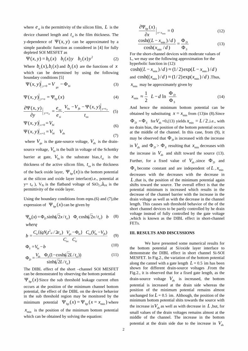
2
where siε is the permittivity of the silicon film, L is the
device channel length and sit is the film thickness. The
y-dependence of ( , )x yΨ can be approximated by a
simple parabolic function as considered in [4] for fully depleted SOI MESFET as
2210 )()()(),( yxbyxbxbyx ++=Ψ (2)
Where 1( ), ( )ob x b x and 2 ( )b x are the functions of x
which can be determined by using the following boundary conditions [5]
bigsy Vyx Φ−=Ψ =0),( (3)
(4)
(5)
(6)
(7)
where gsV is the gate-source voltage, dsV is the drain-
source voltage, biV is the built in voltage of the Schottky
barrier at gate, bsV is the substrate bias, sit is the
thickness of the active silicon film, oxt is the thickness
of the back oxide layer, ( )bp xΨ is the bottom potential
at the silicon and oxide layer interface(i.e., potential at y= tsi ), Vfb is the flatband voltage of SiO2,,åox is the permittivity of the oxide layer. Using the boundary conditions from eqns.(6) and (7),the
expression of ( )bp xΨ can be given by
(8)
(9)
(10)
(11)
The DIBL effect of the short –channel SOI MESFET can be demonstrated by observing the bottom potential
( )bp xΨ Since the sub threshold leakage current often
occurs at the position of the minimum channel bottom potential, the effect of the DIBL on the device behavior in the sub threshold region may be monitored by the
minimum potential min( ) ( )bp bpx x xΨ = Ψ = where
minx is the position of the minimum bottom potential
which can be obtained by solving the equation:
0)(
min=
∂
Ψ∂=xx
bp
x
x (12)
S
D
x
xL
ΦΦ
=−
)/cosh(
)/)cosh((
min
min
δδ
(13)
For the short-channel devices with moderate values of L, we may use the following approximation for the hyperbolic function in (12):
min mincosh(( ) / ) (1/ 2)exp( ) / )L x L xδ δ− ≈ −
and min mincosh(( ) / ) (1/ 2)exp( ) / )x xδ δ≈ .Thus,
minx may be approximately given by
ΦΦ
−≈S
DLx ln2
1min δ (14)
And hence the minimum bottom potential can be
obtained by substituting minx x= from (13)in (8).Since
DΦ = SΦ for dsV =0,(13) yields min / 2x L= ,i.e., with
no drain bias, the position of the bottom potential occurs at the middle of the channel. In this case, from (9), it
may be observed that DΦ is increased with the increase
in dsV and DΦ > SΦ resulting that minx decreases with
the increase in dsV and shift toward the source (13).
Further, for a fixed value of dsV ,since DΦ and
SΦ become constant and are independent of L , minx
decreases with the decreases with the decrease in L ,that is, the position of the minimum potential again shifts toward the source. The overall effect is that the potential minimum is increased which results in the decrease of the channel barrier with the increase in the drain voltage as well as with the decrease in the channel length. This causes sub threshold behavior of the of the short channel devices to be partly controlled by he drain voltage instead of fully controlled by the gate voltage ,which is known as the DIBL effect in short-channel FETs. III. RESULTS AND DISCUSSIONS
We have presented some numerical results for the bottom potential at Si/oxide layer interface to demonstrate the DIBL effect in short channel Si-SOI MESFET. In Fig.2., the variation of the bottom potential along the cannel with a gate length L = 0.5 ìm has been shown for different drain-source voltages .From the Fig.2., it is observed that for a fixed gate length, as the
drain-source voltage dsV is increased, the bottom
potential is increased at the drain side whereas the position of the minimum potential remains almost unchanged for L = 0.5 ìm. Although, the position of the minimum bottom potential shits towards the source with
the increase in dsV as well as with decrease in L ,but, for
small values of the drain voltages remains almost at the middle of the channel. The increase in the bottom
potential at the drain side due to the increase in dsV
dsbiLx
bix
ox
tyfbbs
si
oxty
bpoy
VVyx
Vyx
t
yxVV
y
yx
xyx
si
si
+=Ψ
=Ψ
Ψ−−=
∂Ψ∂
Ψ=Ψ
=
=
==
=
),(
),(
),(.
),(
)(),(
0
εε
)/2sinh(
))/2cosh(1(
)()2/(
,
)/2cosh()/2sinh()(
2
si
siSdsD
biS
siox
fbbsoxbigssisidsi
sissiDbp
tL
tLV
V
CC
VVCVtqNC
where
txtxx
−Φ+=Φ
−=Φ
+
−+Φ−+=
+Φ+Φ=Ψ
β
εβ
β
3
lowers the channel the channel barrier height (i.e., the potential difference between the channel and the source) of the device which is known as the DIBL in the short channel FETs. The bottom potential versus the normalized distance for different doping concentration in the silicon film is presented in Fig.3. It is observed from the figure that the DIBL effect is increased with the increase in the doping concentration.
Fig.2.Bottom potential distribution showing the DIBL
effect for gate length L =0.5 ìm with different dsV .
Fig.3.Bottom potential distribution versus normalized distance (x / L) for different doping concentration
Finally the variation of the bottom potential along the channel is presented for different thickness of the silicon film as shown in Fig.4. It can be observed that as the silicon film thickness is decreased, the DIBL effect is reduced. Thus, if the channel length length is reduced, the short-channel effect may be minimized by reducing the thickness of the active layer of the device. The result has been compared with the simulated one obtained by solving he 2-D poisson’s equation by using the pde toolbox of the MATLAB and a fair good agreement is observed between the two.
Fig.4. Variation of the bottom potential )/( LxbpΨ
along the channel at Si –SiO2 interface with normalized distance x/L for different silicon-film thicknesses. IV. CONCLUSION
A two-dimensional analytical model for the potential distribution and the drain-induced barrier lowering (DIBL) effect in short-channel SOI-MESFET is presented in this paper. It is shown that as the channel length is reduced, the minimum bottom potential is increased which further reduces the channel barrier. If the drain-source voltage is increased, the position of the minimum bottom potential is shifted towards the source. The model presented in this paper is very simple and can be used to predict accurately the channel barrier variation with the gate and drain voltages in the sub threshold regime including DIBL effects. REFERENCES [1] H.Vogt, G.Burbach, J.BBelzandZimmer, IEEE Electron Letters, 25,.1580,(1989). [2] Chin-shin Hou and Ching Yuan Wu,IEEE Trans.Electron Devices, 42, 2156, (1995). [3] T.K.Chiang, Y.h.Wang, and M.P.Houng, Solid State Electronics, 43, 123, (1999). [4] K.K.young, IEEE Trans.Electron Devices, 36, 399, (1989). [5] S.Jit, Prashant Pandey, B.B.Pal, IEEE Trans. Electron Devices, 51, 246,(2004). [6] P.Hashemi, A.Behnam, E.Fathi, A.Afzali-kusha, IEEE Trans.Electron Devices, 43, 372,(2004).
0 0.1 0.2 0.3 0.4 0.5 0.6 0.7 0.8 0.9 1-0.4
-0.3
-0.2
-0.1
0
0.1
0.2
0.3
Normalized Distance Along x,x/L
Nd = 9 x10²² m-3
Nd = 5x10²² m-3
Nd = 1x10²² m-3
Analytical Model : ----------Simulation Results : o
Normalized Distance along the channel x/L
Bot
tom
Pot
entia
l (v)
1
OMTAT 2005
Novel Method of Preparation of Tin (II) Sulphide Nanoparticles V.Aditya, M.K.Patra, S.R.Vadera and N.Kumar
Defence Laboratory, Jodhpur 342 011, India Email: [email protected]
_____________________________________________________________ ABSTRACT The present paper reports the synthesis of SnS nanoparticles using wet chemical route by complexing tin with hydrazine in an aqueous medium. In this reaction hydrazine act both as reducing as well as capping agent, thereby controlling the size of SnS nanoparticles formed. Linewidth broadening of XRD peaks suggest formation of nanoparticles of SnS, further with increase in quantity of hydrazine, increase in linewidths of XRD peaks has been observed, which suggests the reduction in the size of SnS nanoparticles formed. TEM studies confirm the formation of nanosize particle and ED pattern suggests polycrystalline nature of these particles. FTIR studies shows SnS-hydrazine complex. 1. INTRODUCTION In the past few decades, metal chalcogenides, have attracted significant interest due to their potential applications in electronic, optical and semiconductor devices [1-3]. Nanosized semiconductor chalcogenides provide greater opportunities to tailor material properties by crystal structure, size and shape. Further, these nanomaterials when taken in nanometer size provide great scope for tailoring their bandgap and electronic structure thereby rendering quite novel and unique electronic and optical properties useful for a number of technological applications such as solar cells, LEDs and Scanning Microscopy probe [4-6]. Among the chalcogenides, sulphides of tin viz. SnS and SnS2 are becoming increasingly important because of their specific semiconducting properties. SnS has a orthorhombic structure, and its direct and indirect band gap energies are reported to be 1.3-1.5 and 1.0-1.1 eV, respectively [7-10] which makes it ideal candidate for photovoltaic materials with high conversion efficiency[11], and a part of solar collectors[12]. In addition to this, both the constituent elements are abundant and nontoxic which leads to the development of devices that are environmentally safe. Various methods have been developed for the synthesis of tin monosulphide, such as reaction of metal tin powder with sulphur in liquid ammonia followed by post annealing to get crystalline SnS[13], thermal decomposition of precursor complex of (Ph2SnS)3
[14], by using cationic surfactant cetyl trimethyl ammonium bromide (CTAB) together with SnCl2, oxalic acid (H2C2O4) and sodium sulfide (Na2S)[15], microwave assisted polyol synthetic method[16], sulphurisation of thin metallic tin precursor layer in vacuum furnace followed by annealing at high temperature, solid state metathesis[17] and organic template mediated reaction[18]. In this paper we have reported the formation of SnS nanoparticles by simple wet chemical route through metal-hydrazine complexation. Here hydrazine, used as a cationic surfactant reducing agent, also acts as capping agent and controls the growth of SnS particles formed. Compared to earlier reported methods, the present method is relatively simple, without using complex apparatus or methodology. 2. EXPERIMENTAL
For the synthesis of SnS particles, chemicals of analytical grade i.e. Tin(II) chloride dihydrate (SnCl2.2H2O), hydrazine hydrate (N2H5OH) have been used as starting material. Firstly, SnCl2 solution is taken in a beaker and then hydrazine is added drop by drop in the solution with continuos stirring. As hydrazine is added a turbidity appears, which goes off on stirring. Hydrazine is added till the turbidity stabilizes which suggests completion of the complexation. H2S gas is passed in the resulting turbid solution for a specified duration. Brownish precipitate was obtained which was washed thoroughly by distilled water to remove impurities and then dried at 1000C in an oven under ambient conditions. In a typical synthesis : for sample A- 50ml of 0.1M solution of SnCl2 was taken in 250ml of beaker and 1ml of hydrazine hydrate was added. H2S is then passed in this tin-hydrazine complex for a duration of 30-35
2
minutes in a controlled way. The resulting brownish precipitates were washed thoroughly with distilled water and dried. Similarly, other two samples i.e. Sample B and C were also prepared by taking increased amount of hydrazine i.e. 1.5 ml and 2.5 ml respectively, while keeping the other reaction parameters unchanged. The structural characterization of the as prepared samples was carried out by powder X-ray diffraction method performed on X’pert PRO PANanalytical system with Cu Kα radiation, Morphology and size were measured by using transmission electron microscope (TEM) (JEOL-JEM-200CX) with an accelerating voltage of 200 kV and a double tilt sample holder. IR spectra of the samples were recorded using Shimadzu-8101A Fourier Transform Infrared Spectrometer.
3. RESULTS AND DISCUSSION
On hydrolysis tin shows +4 oxidation state and when excess of sulphur is passed through hydrolysed tin it results in SnS2 phase. In order to get SnS phase, tin +4 should be reduced to +2 state. A variety of reducing agents can be used to serve this purpose. Here hydrazine has been used for reducing Sn+4 to Sn+2 and it also complexes with Sn ions. It is well known that tin has ground state configuration of 5s25p2 and it can form covalent tin (II) compounds with the use of two unpaired p-electrons. In tin (II) chloride two sp2 orbitals form covalent bonds to halogen and one directional lone pair of electrons is present. On reacting with hydrazine tin forms complex, Sn (N2H4)xX2 which maintains tin in the reduced oxidation state of +2. SnCl2 + xN2H5OH→ [Sn(N2H5)xCl2]+ +OH-
Here x=1, 2, 3............., resulting in network formation Tin(II) in [Sn(N2H5)xCl2]+ ion may be regarded as sp3 hybridized, with the two tin chloride bonds and the directional lone pair of SnCl2, but with the coordination of [N2H5]+ into the vacant sp3 orbital. The directional lone pair of [Sn (N2H5)xCl2]+ behaves as an acceptor. In this latter case it is possible for the tin atom to act as a π-electron acceptor also, thus increasing the overall strength of the tin-sulphur bond[19].
+ H2N=NH2.HOH + OH-
The XRD spectra of as prepared samples are shown in Fig.2. For sample A XRD spectrum shows well crystalline peaks of SnS phase with orthorhombic crystal structure. The crystal planes of diffractions (020), (111), (131) are well matched with standard data of SnS (JCPDS file no. 75- 1803). The samples prepared by taking higher amount of hydrazine (samples B and C), also show the same set of XRD peaks, however, with increased line broadening thereby suggesting reduction in particle size with increasing amount of hydrazine.
Cl Cl
Sn
ClN2H5
Sn+
Cl
Sn
Cl
Cl
N2H5S
H2S
Fig.1 Formation of tin-hydrazine complex
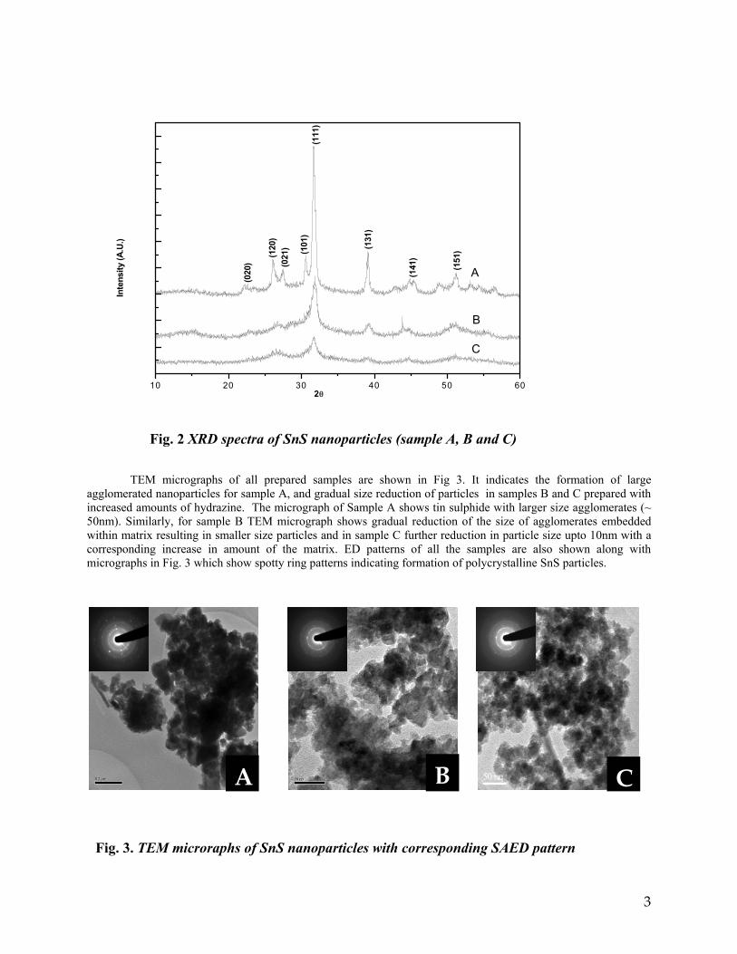
3
10 20 30 40 50 60
(120
)
(020
)
(101
)
(021
)
(151
)
(141
)
(131
)
(111
)
C
B
A
Inte
nsity
(A.U
.)
2θ
TEM micrographs of all prepared samples are shown in Fig 3. It indicates the formation of large agglomerated nanoparticles for sample A, and gradual size reduction of particles in samples B and C prepared with increased amounts of hydrazine. The micrograph of Sample A shows tin sulphide with larger size agglomerates (~ 50nm). Similarly, for sample B TEM micrograph shows gradual reduction of the size of agglomerates embedded within matrix resulting in smaller size particles and in sample C further reduction in particle size upto 10nm with a corresponding increase in amount of the matrix. ED patterns of all the samples are also shown along with micrographs in Fig. 3 which show spotty ring patterns indicating formation of polycrystalline SnS particles.
Fig. 3. TEM microraphs of SnS nanoparticles with corresponding SAED pattern
0.2 µm0.2 µm 50 nm50 nm 50 nmA B C
Fig. 2 XRD spectra of SnS nanoparticles (sample A, B and C)
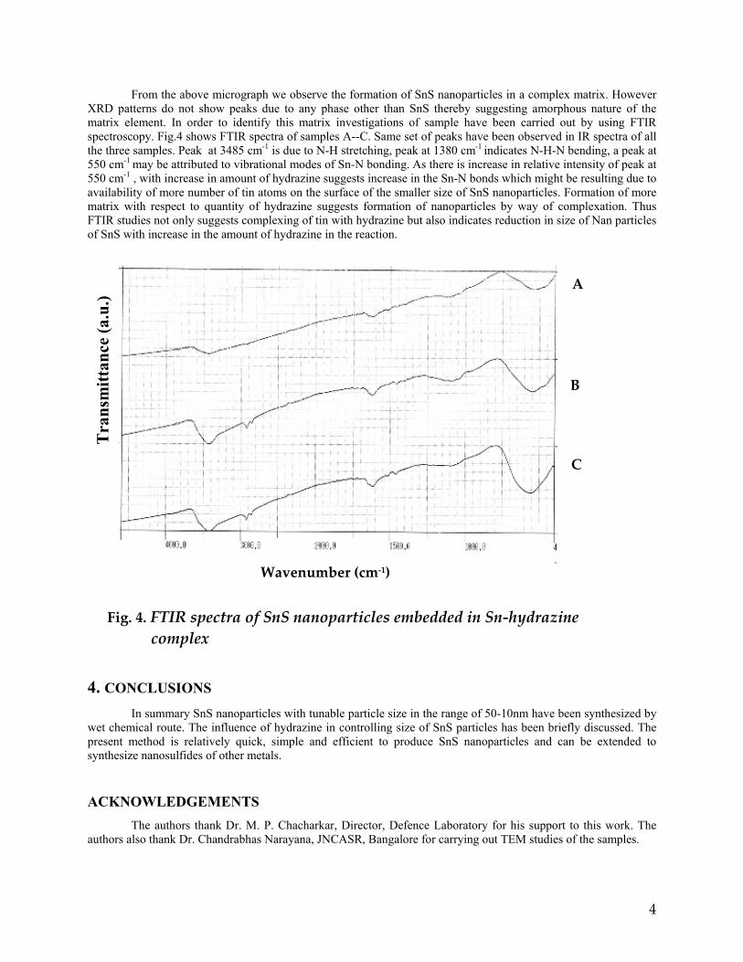
4
B
C
From the above micrograph we observe the formation of SnS nanoparticles in a complex matrix. However XRD patterns do not show peaks due to any phase other than SnS thereby suggesting amorphous nature of the matrix element. In order to identify this matrix investigations of sample have been carried out by using FTIR spectroscopy. Fig.4 shows FTIR spectra of samples A--C. Same set of peaks have been observed in IR spectra of all the three samples. Peak at 3485 cm-1 is due to N-H stretching, peak at 1380 cm-1 indicates N-H-N bending, a peak at 550 cm-1 may be attributed to vibrational modes of Sn-N bonding. As there is increase in relative intensity of peak at 550 cm-1 , with increase in amount of hydrazine suggests increase in the Sn-N bonds which might be resulting due to availability of more number of tin atoms on the surface of the smaller size of SnS nanoparticles. Formation of more matrix with respect to quantity of hydrazine suggests formation of nanoparticles by way of complexation. Thus FTIR studies not only suggests complexing of tin with hydrazine but also indicates reduction in size of Nan particles of SnS with increase in the amount of hydrazine in the reaction.
4. CONCLUSIONS
In summary SnS nanoparticles with tunable particle size in the range of 50-10nm have been synthesized by wet chemical route. The influence of hydrazine in controlling size of SnS particles has been briefly discussed. The present method is relatively quick, simple and efficient to produce SnS nanoparticles and can be extended to synthesize nanosulfides of other metals. ACKNOWLEDGEMENTS The authors thank Dr. M. P. Chacharkar, Director, Defence Laboratory for his support to this work. The authors also thank Dr. Chandrabhas Narayana, JNCASR, Bangalore for carrying out TEM studies of the samples.
Tra
nsm
ittan
ce (a
.u.)
Fig. 4. FTIR spectra of SnS nanoparticles embedded in Sn-hydrazine complex
A
Wavenumber (cm-1)

5
REFERENCES: 1. R. Suryanarayanan, Phys Status Solidi B 85, 9 (1978) 2. M. G. Bawendi, M.L. Steigerwald, L. E. Brus, Annu. Rev. Phys. Chem.41, 477 (1990) 3. N. Peyghambarian, B. Fluegel, D. Hulin, A. Migus, M. Joffre, A. Antonetti, S.W. Koch, M. Lindberg, IEEE J. Quantum Electron 25, 2516 (1989) 4. W. U. Huynh, J.J. Dittmer, A.P. Alivisatos, Science 295, 2425 (2002) 5. T.S. Ahmadi, Z. L. Wang, T. C. Green, A. Henglein, M.A. Elsayed, Science 272, 1924 (1996) 6. H. Mattoussi, L.H.Radzilowski, B.O.Dabbousi, E.L.Thomas, M.G. Bawendi, M.F. Rubner, J. Applied Phys. 83, 7965 (1998) 7. G. Valiukonis, D.A. Guseinova, G. Krivaite, A. Sileika, Phys. Stat. Sol. B 135, 299 (1986) 8. H. Noguchi, A. Setiyadi, H. Tanamura, T. Nagatomo, O. Otomo, Sol. Energy Mater. Sol. Cells 35, 325 (1994) 9. K. Mishra, K. Rajeshwar, A. Weiss, M. Murley, R.D.Engelken, M.Slayton, H.E. Mcloud, J. Electrochem. Soc. 136,1915 (1989) 10. Z. Zainal, M.Z. Hussein, A. Ghazali, Sol Energy Mater. Sol. Cell 40, 347 (1996) 11. J.P.Singh, R.K. Bedi, Thin Solid Films 199, (1991) 9. 12. A. Oritz, J.C. Alonso, M. Carcia, J.Toriz, Semicond. Sci. Technol. 11, (1996) 243. 13. J.J. Loferski, J. Appl. Phys. 27, 777 (1956) 14. Y. M. Gao, P. Wu, J. Baglio, K.M. Dwight, A. Wold, Mater. Res.Bull. 24 , 1215 (1989) 15. Yingkai Liu, Dedong Hou, Guanghou Wang, Chem. Phys Letters 379, 67-73 (2003) 16. Di Chen, Guozhen Shen, Kaibin Tang, Shuijin Lei, Huagui Zheng, Yitai Qian, J. Crystal Growth 260, 469-474 (2004) 17. R. Coustal, J. Chem. Phys. 31, 277 (1931) 18. T. Jiang, A.J. Lough, G. A. Ozin, D. Young, R.L. Bedard, Chem.Mater. 7, 245 (1995) 19. J.D. Donaldson, Progress in Inorganic Chemistry, 8, 287 (1967).
Formation and Distribution of Nanostructure on InP(111) Surfaces after MeV implantation.
Dipak Paramanik and Shikha Varma
Institute of Physics, Bhubaneswar-751005
Email: [email protected], [email protected] ABSTRACT
We have studied the InP(111) surfaces after MeV Sb ion implantation. Scanning Probe Microscope (SPM) has been utilized to investigate the ion implanted InP(111) surfaces as a function of ion fluence. We observe the formation of nanostructures on the InP surfaces. The density, height and the size distribution of the nanostructures have been investigated as a function of ion fluence. The size distribution indicates a decrease in size of the nanostructures as the fluence is increased. Scanning Force Microscopy has also been utilized to investigate the modifications in the surface roughness of the ion-implanted surfaces. We observe a non-linear increase in the rms surface roughness, as a function of ion fluence. Beyond a critical fluence, however, the roughness decreases suggesting the smoothening of the InP surfaces.
1 INTRODUCTION InP is a very promising candidate for the electronic and opto-electronic applications [1-3]. Due to its excellent physical properties like high thermal conductivity, high peak velocities for electrons and holes, InP is considered an important semiconductor material. It is being prominently utilized in the devices for high electron mobility transistors, high efficiency and high speed quantum well lasers, photo-detectors, photonic integrated circuits etc. Although InP is being extensively used in semiconductor based device technology, it has been investigated much less compared to GaAs. Due to the low thermal stability of the InP, MeV ion implantation is a prominent way to introduce and dope the materials in InP. MeV implantation is also important for forming thick buried layers with modified properties, modification of vertically limited layers as well as quantum well structures. In the MeV ion implantation the electronic energy deposition plays a crucial role and can influence the implantation induced damage formation. The formation of the surface structures, due to the ion implantation is also gaining importance because of the realization that the structures can be utilized for controlled fabrication of semiconductors similar to self-organized growths. However these surface studies on InP surfaces have been performed either after keV range implantations [4] or after Swift Heavy Ion (SHI) irradiations at several hundreds of MeV [5,6], and there are no studies in literature where MeV implantation energies have been utilized. Scanning Probe microscope (SPM) is a very effective tool for examining the surface structures. In the present study, using SPM, we have investigated the surface modifications of InP(111) created due to 1.5 MeV Sb ion implantation. After implantation, we find a presence of nano-sized defect structures on the InP surfaces. We have also studied the modifications in the surface roughness as a function of ion fluence. Our studies show the development and the changes of the surface
structures as a function of ion fluence. The surface roughness initially increases with ion fluence but beyond a critical fluence the surface roughness decreases. In comparing our results with the 100MeV SHI Au implantation [6] results we observe that the surface morphology is a complex function of ion mass, its energy and fluence. It is noticed that at fluence of 1x10¹⁴ions/cm2, rms surface roughness after SHI Au irradiation is higher than that observed here after 1.5 MeV implantation. However for the fluence of 1x10¹³ions/cm2, the results are opposite and a higher surface rms is observed after 1.5 MeV implantation of Sb. 2 EXPERIMENTAL A mirror polished InP(111) single crystal was implanted with a scanned beam of 1.5 MeV Sb ions at various fluences ranging from 1x10¹¹ to 5x10¹⁴ ions/cm2. The average flux was 0.02uA/cm2. The current was measured directly on the target after suppressing the secondary electrons by applying a negative bias of 200V to suppressor assembly around the target. The implantation was performed with samples oriented 7o off normal to the incident beam to avoid channeling effects. SPM Nanoscope IIIA from Veeco was used to image the implanted InP(111) sample surface with a silicon nitride cantilever operated in tapping mode. Images ranging from 0.2 to 10 um square were obtained. The roughness parameters peak/valley and root mean square (rms) were calculated by Nanoscope software. 3 RESULTS AND DISCUSSION Fig.1 shows the 2-dimensional SPM images from the InP surfaces of area 10 µm × 10 µm. Image from a virgin (un-implanted ) InP(111) sample is also shown here (Fig.1a). Other images of Fig. 1 show the InP
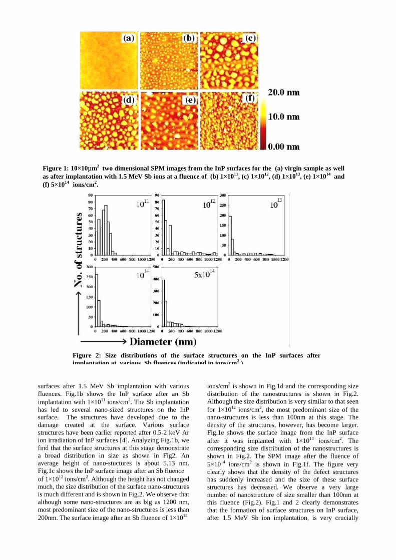
surfaces after 1.5 MeV Sb implantation with various fluences. Fig.1b shows the InP surface after an Sb implantation with 1×10¹¹ ions/cm2. The Sb implantation has led to several nano-sized structures on the InP surface. The structures have developed due to the damage created at the surface. Various surface structures have been earlier reported after 0.5-2 keV Ar ion irradiation of InP surfaces [4]. Analyzing Fig.1b, we find that the surface structures at this stage demonstrate a broad distribution in size as shown in Fig2. An average height of nano-stuctures is about 5.13 nm. Fig.1c shows the InP surface image after an Sb fluence of 1×10¹² ions/cm2. Although the height has not changed much, the size distribution of the surface nano-structures is much different and is shown in Fig.2. We observe that although some nano-structures are as big as 1200 nm, most predominant size of the nano-structures is less than 200nm. The surface image after an Sb fluence of 1×10¹³
ions/cm2 is shown in Fig.1d and the corresponding size distribution of the nanostructures is shown in Fig.2. Although the size distribution is very similar to that seen for 1×10¹² ions/cm2, the most predominant size of the nano-structures is less than 100nm at this stage. The density of the structures, however, has become larger. Fig.1e shows the surface image from the InP surface after it was implanted with 1×10¹⁴ ions/cm2. The corresponding size distribution of the nanostructures is shown in Fig.2. The SPM image after the fluence of 5×10¹⁴ ions/cm2 is shown in Fig.1f. The figure very clearly shows that the density of the defect structures has suddenly increased and the size of these surface structures has decreased. We observe a very large number of nanostructure of size smaller than 100nm at this fluence (Fig.2). Fig.1 and 2 clearly demonstrates that the formation of surface structures on InP surface, after 1.5 MeV Sb ion implantation, is very crucially
Figure 1: 10××10µµm2 two dimensional SPM images from the InP surfaces for the (a) virgin sample as well as after implantation with 1.5 MeV Sb ions at a fluence of (b) 1××1011, (c) 1××1012, (d) 1××1013, (e) 1××1014 and (f) 5××1014 ions/cm2.
Figure 2: Size distributions of the surface structures on the InP surfaces after implantation at various Sb fluences (indicated in ions/cm2 )
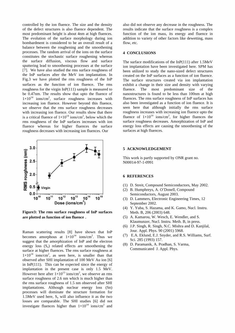
controlled by the ion fluence. The size and the density of the defect structures is also fluence dependent. The most predominant height is about 4nm at high fluences. The evolution of the surface morphology during ion bombardment is considered to be an overall result of a balance between the roughening and the smoothening processes. The random arrival of the ions on the surface constitutes the stochastic surface roughening whereas the surface diffusion, viscous flow and surface sputtering lead to smoothening processes at the surface [7]. We have also studied the rms surface roughness of the InP surfaces after the MeV ion implantation. In Fig.3 we have plotted the rms roughness of the InP surfaces as the function of ion fluence. The rms roughness for the virgin InP(111) sample is measured to be 0.47nm. The results show that upto the fluence of 1×10¹⁴ ions/cm2, surface roughness increases with increasing ion fluence. However beyond this fluence, we observe that the rms surface roughness decreases with increasing ion fluence. Our results show that there is a critical fluence of 1×10¹⁴ ions/cm2, below which the rms roughness of the InP surfaces increases with ion fluence whereas for higher fluences the surface roughness decreases with increasing ion fluences. Our
Figure3: The rms surface roughness of InP surfaces are plotted as function of ion fluence . Raman scattering results [8] have shown that InP becomes amorphous at 1×10¹⁴ ions/cm2. Thus we suggest that the amorphization of InP and the electron energy loss (Se) related effects are smoothening the surface at higher fluences. The rms surface roughness at 1×10¹⁴ ions/cm2, as seen here, is smaller than that observed after SHI implantation of 100 MeV Au ion [6] in InP(111). This can be expected since the energy of implantation in the present case is only 1.5 MeV. However here after 1×10¹³ ions/cm2, we observe an rms surface roughness of 2.6 nm which is much higher than the rms surface roughness of 1.5 nm observed after SHI implantations. Although nuclear energy loss (Sn) processes will dominate the structure formation for 1.5MeV used here, Se will also influence it as the two losses are comparable. The SHI studies [6] did not investigate fluences higher than 1×10¹⁴ ions/cm2 and
also did not observe any decrease in the roughness. The results indicate that the surface roughness is a complex function of the ion mass, its energy and fluence in addition to variety of other factors like dewetting, mass flow, etc. 4 CONCLUSIONS The surface modifications of the InP(111) after 1.5MeV ion implantation have been investigated here. SPM has been utilized to study the nano-sized defect structures created on the InP surfaces as a function of ion fluence. The surface structures created via ion implantation exhibit a change in their size and density with varying fluence. The most predominant size of the nanostructures is found to be less than 100nm at high fluences. The rms surface roughness of InP surfaces has also been investigated as a function of ion fluence. It is seen here that although initially the rms surface roughness increases with increasing ion fluence upto the fluence of 1×10¹⁴ ions/cm2, for higher fluences the surface roughness decreases. Amorphization of InP and energy loss effects are causing the smoothening of the surfaces at high fluences. 5 ACKNOWLEDGEMENT This work is partly supported by ONR grant no. N00014-97-1-0991 6 REFERENCES
(1) D. Streit, Compound Semiconductors, May 2002. (2) B. Humphreys, A. O’Donell, Compound
Semiconductors, August 2003. (3) D. Lammers, Electronic Engineering Times, 12
September 2002. (4) Y. Yuba, S. Hazama, and K. Gamo, Nucl. Instru.
Meth. B, 206 (2003) 648. (5) A. Kamarou, W. Wesch, E. Wendler, and S.
Klaumunzer, Nucl. Instru. Meth. B, in press. (6) J.P. Singh, R. Singh, N.C. Mishra and D. Kanjilal,
Jour. Appl. Phys. 90 (2001) 5968. (7) E.A. Eklund, E.J. Snyder, and R.S. Williams, Surf.
Sci. 285 (1993) 157. (8) D. Paramanik, A. Pradhan, S. Varma,
Communicated J. Appl. Phys.
NT 088
Synthesis, characterization and sensor application of sol gel derived SnO2 nano powder
N. Sankara Subramanian1, B. Santhi2 and K. Katheresan1
1.Department of Physics, Thiagarajar College of Engineering, Madurai-625 015, India 2.Department of Physics, Government Girls Hr. Sec. School, Melur, Madurai-625 106, India
E-mail: [email protected]
ABSTRACT Tin oxide is an n-type, wide band gap semiconducting material. Owing to its specific and combined electrical, optical and chemical properties, it finds major applications in electronic and optoelectronic devices, gas sensors, solar cells, selective absorber coatings, anti reflection coatings and heat reflecting mirrors etc. In this work, initially, aqueous (SnCl4 5H2O:H2O) and alcoholic (SnCl4 5H2O:C2H5OH) solution containing desired concentration of tin have been prepared and then mixed with preferred H2O / C2H5OH (2/8, 3/7, 4/6, 5/5, 6/4, 7/3, 8/2 and 9/1) ratio. The mixed aqueous – alcoholic stock solutions became increasingly cloudy, when allowed for aging at room temperature. This was followed by the formation of a gelatinous suspension, which slowly contracted and settled to the bottom of the container. The top portion of the solution is then discarded, with minimum disturbance of the gelatinous sediment underneath, and fresh alcohol of appropriate quantity is replenished. The solution was then aged for another 24 hour. The gelatinous sediment contracted further, after every cycle of solvent – replenishment and settling. The same procedures were repeated more than ten times to give a solution with pH value of 4.2. After the very last solution – removal step, the sludge was poured into a polyethylene container, in which it is further filtered to remove excess solvent using filter paper. When the sludge was slowly dried at 30 °C for 7 days, tin oxide xerogel have been formed. The replenishment and aging cycle prior to drying has been repeatedly carried out until the pH value remains below 4, to reduce both [Cl-] and [H+]. Subsequent heat treatment of the air-dried xerogel was found to improve its mechanical strength but results in the loss of specific surface area. Heat-treating the xerogel at 120 °C, for two hours in a closed furnace leads to the formation of gray coloured tin oxide powder. The dried powders were then calcined at 500 °C, for one hour in a furnace. After calcination, colour of the powder turned to light blue. The powder was then milled for about 16 hours in a ball mill, to get tin oxide nano powder. The Rheological behavior of the solution have been studied by the viscosity measurement, from which the solution to gel transition mechanism have been investigated and explained. The break off, saturation point and t1/2 have been estimated and the effect of H2O / Et-OH ratio on these parameters have been studied and reported. The optical properties of the as synthesized tin oxide powder have been studied in the visible region, which shows good transmittance. XRD analysis of the as synthesized SnO2 powder (with different H2O / Et-OH ratio) conforms tetragonal rutile structure with preferred orientation along the (101) plane. From the XRD data, the lattice constant a and c have been evaluated as 4.7351 Aº and 3.1714 Aº respectively, which are in agreement with the standard values of JCPDS - PDF data No. 41-1445, for SnO2
powder specimen. The mean grain size have been calculated using the Sherrer’s formula, lie between 100 nm and 600 nm and the variation of mean grain size with different H2O / Et-OH ratio have been studied and discussed. AFM investigations on the palletized SnO2 powder prepared from the aqueous alcoholic stock solution containing H2O / Et-OH in the ratio 2/8 shows grains of size ranging between 100 nm and 1000 nm. The palletized SnO2 powder adhered onto a quartz substrate have been used as a .(solid state) sensor active layer for LPG gas detection. The response and recovery characteristics of the active layer for LPG sensing have been studied and discussed. The detection sensitivity of the active layer have been evaluated using the relation S = (Ra – Rg) / Ra, where Ra and Rg are the resistance of active layer in air and reducing gas ambient. The variation of sensitivity with different operating temperature have also been studied and reported.
REFERENCES:
1. Nae-Lih Wu, Lih-Fu Wu, Ya-Chin Yang and Shu-Jiuan Huang, “Journal of Materials Research”,
Vol. 11, No.4, 813 (1996).
2. Yung-Jen Lin, Ching-Jiunn Wu, “Surface and Coatings Technology”, 88, 239 (1996).
3. G.Sberveglieri , "Sensors and Actuators B",Vol. 23, 103 (1995).
4. S.S.Kistler, “J. Phys. Chem.”, Vol. 36, 52 (1932).
5. E.W.Giesekke, H.S.Gutowsky, P.Kirrov, and H.A.Laitinen, “Inorg. Chem.” Vol. 6, 1294 (1967).
6. M.H. Madhusudhan reddy, A.N.Chandorkar, "Thin Solid films", Vol. 349, 260 (1999).
7. V.Ambrazeviciene, A.Galdikas, S.Grebinskij, A.Mironas, H.Tvardauskas, "Sensors and Actuators B"
Vol. 17, 27 (1993).
8. D.Kohl, "Sensors and Actuators", Vol. 18, 71 (1989).
9. J.Mizsei, "Sensors and Actuators B", Vol. 15-16, 328(1993).
10 E.W.Giesekke, H.S.Gutowsky, P.Kirrov, and H.A.Laitinen ,“Inorg. Chem.” Vol. 6, 1294 (1967). --------------------------------------------------------------------------------------------------------------------------------- Corresponding Author: N. Sankara Subramanian, Department of Physics, Thiagarajar College of Engineering, Madurai, Tamilnadu State, India. PIN – 625 015. E-mail: [email protected]. Phone: +91-9443477194. Fax: +91-452-248-3427
1
SOL-GEL SYNTHESIS AND STRUCTURAL CHARACTERIZATION OF NICKEL FERRITE NANOSYSTEMS
Jeevan Job Thomas and Nandakumar Kalarikkal
School of Pure and Applied Physics, Mahatma Gandhi University, Kottayam-686 560, Kerala, India
Email:[email protected]
ABSTRACT NiFe2O4 nanosystems have been prepared using the sol-gel pathway. The importance is in the use of poly acrylic acid (PAA) as the chelating agent by which we get more stoichiometric control and there is a reasonable decrease in the production cost. The XRD patterns for the samples calcined at 300oC with various molar ratios of PAA to total metal ions indicate the crystalline nature. The average particle size of each sample was calculated using the Scherrer equation. When the molar ratios of the PAA to the total metal ions were 0.5, 1, 1.5, 2, 2.5, the particle sizes were 28.78 nm, 28 nm, 25.15 nm, 16.22 nm, 21.95 nm respectively. The XRD analysis revealed that synthesis of pure NiFe2O4 could be achieved by sol-gel preparation method at a calcination temperature lower than the conventional solid-state reaction method. 1 INTRODUCTION
The nanosystems have become a new branch of materials research in recent years. A lot of areas like electronics, optics, catalysis, ceramics and magnetic data storage are attracted to this size regime because of its potential applications in those areas. The unique properties and the improved performances of nanomaterials are determined by their sizes, surface structures and interparticle interactions. The extremely small size or large specific area helps them to exhibit unusual physical and chemical properties1,2. The magnetic properties of nanosize particles considerably differ from those of bulk materials. The large surface-to-volume ratio results in a different local environment for the surface atoms in their magnetic coupling/interactions with neighboring atoms, leading to mixed volume and surface magnetic characteristics. The spinel ferrites with the general formula AB2O4 belong to an important group of magnetic materials because of their interesting magnetic properties and have attracted the attention of physicists and technologists3. In ferrites, the magnetic ion occupy the tetrahedral (A) and octahedral (B) sites of the spinel lattice and the exchange integrals (JAB, JBB and JAA) are generally negative with the antiferromagnetic interaction A-B stronger than B-B and A-A interactions3,4. 2 EXPERIMENTAL
Sol-gel technique is an attractive technique for preparing nanosized particles5. It has advantages such as good stoichiometric control and the production of ultra fine particles with a narrow size distribution in a relatively short processing time at lower temperatures. It is a useful and attractive technique for the preparation of nanosized nickel ferrite particles. Recently sol-gel synthesis of NiFe2O4 using poly acrylic acid (PAA) as chelating agent
is reported6. PAA has more carboxylic acid group to form chelates with mixed cations and results in a sol. It also greatly aids in the formation of cross-linked gel, which may provide more homogeneous mixing of the cations and less tendency for segregation during calcinations. We have prepared the NiFe2O4 nanoparticles using PAA as the chelating agent. Initially, an aqueous solution of nickel nitrate and ferric nitrate was prepared. For better stoichiometric control, the solution was prepared by taking 0.4M nickel nitrate and 0.8M ferric nitrate solutions. Then PAA is added to the solution. A phase separation can be observed. This phase separation can be removed by adding an appropriate amount of nitric acid with constant stirring until a transparent green solution is obtained. The pH of the solution is carefully noted during the addition of nitric acid and it is found that the green solution is obtained around the pH value between 2 and 1. The resulting solution was evaporated at about 50oC until a transparent sol was formed. The transparent sol, which also has a green color, was again heated at 50oC for further removal of water. The green sol then turned to a viscous brown gel. For the formation of gel from the original green solution, it takes a heating of about 6 hours at about 50oC. The gel is finally calcined in air at 300oC for 2 hours with a heating rate of 5oC/minute to eliminate organic content and spinel NiFe2O4 nanoparticles are obtained. The gel is prepared in various molar ratios of PAA to the total metal ions such as 0.5, 1.0, 1.5, 2 and 2.5 for getting the NiFe2O4 nanoparticle systems. The structural characterization of the prepared samples has been done using an x-ray diffractometer [Brunker, D8 Advance, wave length λ = 0.154056 nm].
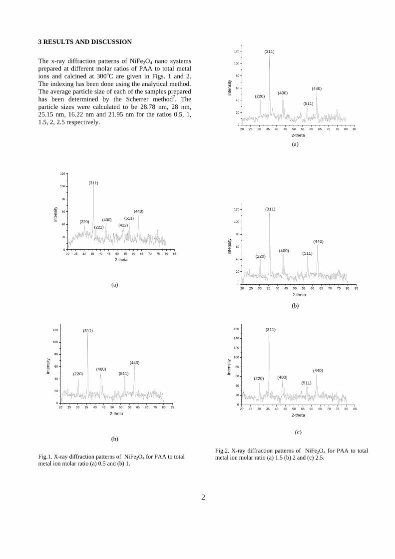
2
3 RESULTS AND DISCUSSION
The x-ray diffraction patterns of NiFe2O4 nano systems prepared at different molar ratios of PAA to total metal ions and calcined at 300oC are given in Figs. 1 and 2. The indexing has been done using the analytical method. The average particle size of each of the samples prepared has been determined by the Scherrer method7. The particle sizes were calculated to be 28.78 nm, 28 nm, 25.15 nm, 16.22 nm and 21.95 nm for the ratios 0.5, 1, 1.5, 2, 2.5 respectively.
20 25 30 35 40 45 50 55 60 65 70 75 80 850
20
40
60
80
100
120
(440)
(511)
(422)(400)
(222)
(311)
(220)inte
nsity
2-theta
(a)
20 25 30 35 40 45 50 55 60 65 70 75 80 850
20
40
60
80
100
120
(440)
(511)(400)
(311)
(220)inte
nsity
2-theta
(b)
Fig.1. X-ray diffraction patterns of NiFe2O4 for PAA to total metal ion molar ratio (a) 0.5 and (b) 1.
20 25 30 35 40 45 50 55 60 65 70 75 80 850
20
40
60
80
100
120
(440)
(511)
(311)
(400)(220)in
tens
ity
2-theta
20 25 30 35 40 45 50 55 60 65 70 75 80 850
20
40
60
80
100
120
(400)
(440)
(511)
(311)
(220)
inte
nsity
2-theta
20 25 30 35 40 45 50 55 60 65 70 75 80 850
20
40
60
80
100
120
140
160 (311)
(511)
(440)
(400)(220)
inte
nsity
2-theta
Fig.2. X-ray diffraction patterns of NiFe2O4 for PAA to total metal ion molar ratio (a) 1.5 (b) 2 and (c) 2.5.
(a)
(b)
(c)
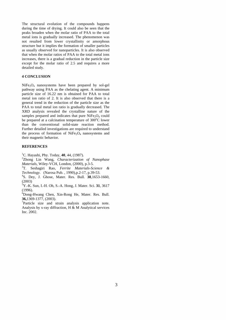
3
The structural evolution of the compounds happens during the time of drying. It could also be seen that the peaks broaden when the molar ratio of PAA to the total metal ions is gradually increased. The phenomenon was not resulted from lower crystallinity or amorphous structure but it implies the formation of smaller particles as usually observed for nanoparticles. It is also observed that when the molar ratios of PAA to the total metal ions increases, there is a gradual reduction in the particle size except for the molar ratio of 2.5 and requires a more detailed study. 4 CONCLUSION
NiFe2O4 nanosystems have been prepared by sol-gel pathway using PAA as the chelating agent. A minimum particle size of 16.22 nm is obtained for PAA to total metal ion ratio of 2. It is also observed that there is a general trend in the reduction of the particle size as the PAA to total metal ion ratio is gradually decreased. The XRD analysis revealed the crystalline nature of the samples prepared and indicates that pure NiFe2O4 could be prepared at a calcination temperature of 300oC lower than the conventional solid-state reaction method. Further detailed investigations are required to understand the process of formation of NiFe2O4 nanosystems and their magnetic behavior. REFERENCES 1C. Hayashi, Phy. Today, 40, 44, (1987). 2Zhong Lin Wang, Characterization of Nanophase Materials, Wiley-VCH, London, (2000), p.3-5. 3T. Seshagiri Rao, Ferrite Materials-Science & Technology. (Narosa Pub. , 1990),p.2-17, p.39-53. 4S. Dey, J. Ghose, Mater. Res. Bull. 38,1653-1660, (2003) 5Y.-K. Sun, I.-H. Oh, S.-A. Hong, J. Mater. Sci. 31, 3617 (1996). 6Dong-Hwang Chen, Xin-Rong He, Mater. Res. Bull. 36,1369-1377, (2003). 7Particle size and strain analysis application note. Analysis by x-ray diffraction, H & M Analytical services Inc. 2002.
GROWTH, MICROSTRUCTURE AND ELECTROCHROMIC PROPERTIES OF LASER ABLATED NANOCRYSTALLINE WO3 THIN FILMS
O.M.Hussaina*, A.S.Swapnasmithaa, R.Pintob & P.V.Ashritc
aThin Film Laboratory, Department of Physics, Sri Venkateswara University,
TIRUPATI – 517 502, India bCondensed Matter Physics and Materials Science, Tata Institute of Fundamental Research,
MUMBAI – 400 005, India. cPhysics Department, Universite de Moncton NB, Canada E1A 3E9
*e-mail:[email protected]
Abstract: Thin films of WO3 were prepared by pulsed laser deposition technique. The influence of substrate temperature (Ts) and oxygen partial pressure (pO2) on the microstructure and morphology was systematically studied. The films prepared at 673 K in an oxygen partial pressure of 100 mTorr exhibited predominantly (002) orientation representing triclinic structure with nanocrystalline nature. The electrochromic properties of these films were carried out by dry lithiation studies. These nanocrystalline WO3 thin films exhibited a high degree of optical modulation in the near infrared region. 1.INTRODUCTION In recent years, there has been a growing interest in the development of electrochromic devices (ECD) based on lithium intercalation in transition metal oxide thin films1. The electrochromic coloration/bleaching of the materials takes place through a double injection/extraction of electrons and positive ions. Among transition metal oxides, tungsten trioxide (WO3) is the most studied electrochromic material and it is considered as one of the best materials for ECD2 . WO3 thin films display a variety of interesting properties and have been investigated for applications in smart windows, electrochromic displays, sensors and other optoelectronic devices3-4.
The electrochromic properties and the performance of these devices based on WO3 thin films are dependent on the deposition technique and the deposition process parameters which inturn dependent on the growth, microstructure and surface morphology of the films. A variety of thin film deposition techniques such as thermal evaporation5, sputtering6 etc have been employed for the deposition of WO3 thin films. Recently, pulsed laser deposition technique has been recognized as a very promising, versatile and efficient method for the preparation of WO3 thin films because of its reproducibility, controllability of stoichiometry and crystal structure. Rougier et al.7 deposited WO3 thin films by pulsed laser deposition technique on SnO2:F coated glass and investigated the effect of deposition conditions on physical and electrochromic properties. Fang et al.8 deposited WO3 films on different substrates with different stoichiometry by pulsed laser deposition technique under different deposition
conditions and also studied their electrochromic behavior. However there is still a lack of microscopic information about the electrochromic properties of pulsed laser deposited WO3 thin films. It is said that the nanocrystalline WO3 thin films have better electrochromic properties than the conventional WO3 thin films. The degree and extinct of optical modulation of WO3 thin films depends on the composition (including water content), grain size, microstructure (porosity) and surface morphology. In the present investigation, WO3 thin films were deposited by pulsed laser deposition technique. The influence of oxygen partial pressure and the substrate temperature on the microstructure and morphology and the electrochromic properties of these films were systematically studied. 2.EXPERIMENTAL A KrF excimer laser (Luminics PM 882) with a wavelength of 248 nm and a pulse duration of 30 ns delivered an energy of 300 mJ per pulse was used for ablation. The energy density of laser beam was 3 J/cm2. The pulse repetition rate was set at 10 Hz. The distance between the target and the substrate was 4 cm. The WO3 target was prepared from a pressed pellet of 20 mm diameter, thickness of 3 mm and sintered in air at 1073 K for 20 h. The target was rotated at the rate of 10 rotations/min to avoid depletion of the material at the same spot during the deposition. The chamber was evacuated to a base pressure of 2x10⁻⁶ Torr before the film deposition. During the deposition pure oxygen was introduced into the chamber and the desired pressure was maintained with a flow controller. The substrates were maintained in the temperature range 373 – 873 K and the oxygen partial pressure was maintained in range 10 – 100 mTorr. The thickness of the laser ablated WO3 thin films was about 0.3 ìm. The substrates used were ITO coated glass substrates. A Siefert computerized X-ray diffractometer (Model 3003 TT) was employed for the microstructural analysis of the experimental films. Cu Kα target was used as the X-ray source with wavelength λ=1.542 Å. The speed of the chart was 1 cm/min and the counter rotation speed was 1 deg/min. Atomic force microscopy (AFM) (Digital instruments, Dimension 3100 series) was used to study the surface morphology of the films in a simple contact mode of
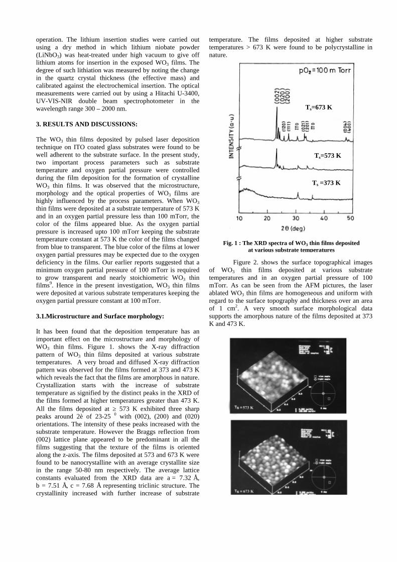
operation. The lithium insertion studies were carried out using a dry method in which lithium niobate powder (LiNbO3) was heat-treated under high vacuum to give off lithium atoms for insertion in the exposed WO3 films. The degree of such lithiation was measured by noting the change in the quartz crystal thickness (the effective mass) and calibrated against the electrochemical insertion. The optical measurements were carried out by using a Hitachi U-3400, UV-VIS-NIR double beam spectrophotometer in the wavelength range 300 – 2000 nm. 3. RESULTS AND DISCUSSIONS: The WO3 thin films deposited by pulsed laser deposition technique on ITO coated glass substrates were found to be well adherent to the substrate surface. In the present study, two important process parameters such as substrate temperature and oxygen partial pressure were controlled during the film deposition for the formation of crystalline WO3 thin films. It was observed that the microstructure, morphology and the optical properties of WO3 films are highly influenced by the process parameters. When WO3 thin films were deposited at a substrate temperature of 573 K and in an oxygen partial pressure less than 100 mTorr, the color of the films appeared blue. As the oxygen partial pressure is increased upto 100 mTorr keeping the substrate temperature constant at 573 K the color of the films changed from blue to transparent. The blue color of the films at lower oxygen partial pressures may be expected due to the oxygen deficiency in the films. Our earlier reports suggested that a minimum oxygen partial pressure of 100 mTorr is required to grow transparent and nearly stoichiometric WO3 thin films9. Hence in the present investigation, WO3 thin films were deposited at various substrate temperatures keeping the oxygen partial pressure constant at 100 mTorr. 3.1.Microstructure and Surface morphology:
It has been found that the deposition temperature has an important effect on the microstructure and morphology of WO3 thin films. Figure 1. shows the X-ray diffraction pattern of WO3 thin films deposited at various substrate temperatures. A very broad and diffused X-ray diffraction pattern was observed for the films formed at 373 and 473 K which reveals the fact that the films are amorphous in nature. Crystallization starts with the increase of substrate temperature as signified by the distinct peaks in the XRD of the films formed at higher temperatures greater than 473 K. All the films deposited at ≥ 573 K exhibited three sharp peaks around 2è of 23-25 0 with (002), (200) and (020) orientations. The intensity of these peaks increased with the substrate temperature. However the Braggs reflection from (002) lattice plane appeared to be predominant in all the films suggesting that the texture of the films is oriented along the z-axis. The films deposited at 573 and 673 K were found to be nanocrystalline with an average crystallite size in the range 50-80 nm respectively. The average lattice constants evaluated from the XRD data are a = 7.32 Å, b = 7.51 Å, c = 7.68 Å representing triclinic structure. The crystallinity increased with further increase of substrate
temperature. The films deposited at higher substrate temperatures > 673 K were found to be polycrystalline in nature. Figure 2. shows the surface topographical images of WO3 thin films deposited at various substrate temperatures and in an oxygen partial pressure of 100 mTorr. As can be seen from the AFM pictures, the laser ablated WO3 thin films are homogeneous and uniform with regard to the surface topography and thickness over an area of 1 cm2. A very smooth surface morphological data supports the amorphous nature of the films deposited at 373 K and 473 K.
Fig. 1 : The XRD spectra of WO3 thin films deposited at various substrate temperatures
Ts=573 K
Ts=673 K
Ts =373 K
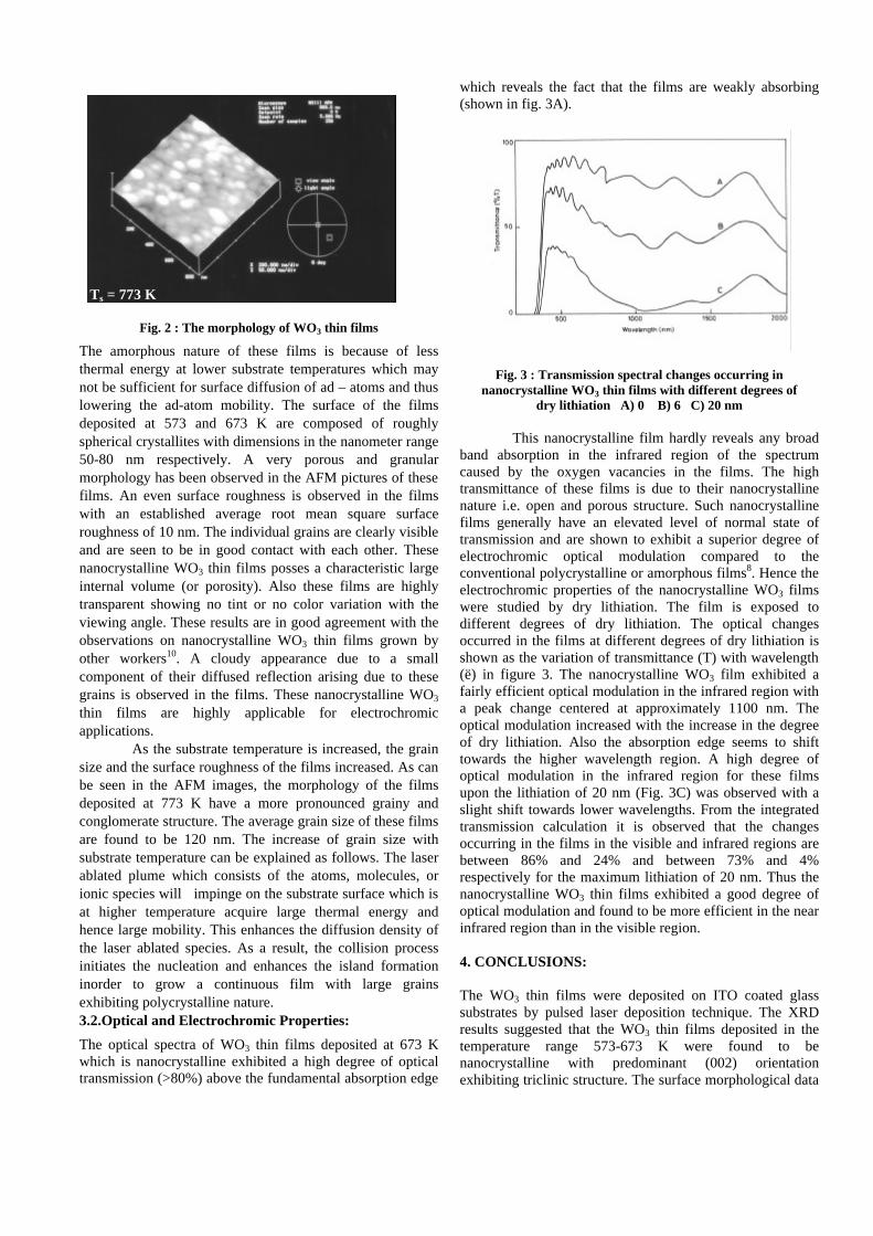
Fig. 2 : The morphology of WO3 thin films
The amorphous nature of these films is because of less thermal energy at lower substrate temperatures which may not be sufficient for surface diffusion of ad – atoms and thus lowering the ad-atom mobility. The surface of the films deposited at 573 and 673 K are composed of roughly spherical crystallites with dimensions in the nanometer range 50-80 nm respectively. A very porous and granular morphology has been observed in the AFM pictures of these films. An even surface roughness is observed in the films with an established average root mean square surface roughness of 10 nm. The individual grains are clearly visible and are seen to be in good contact with each other. These nanocrystalline WO3 thin films posses a characteristic large internal volume (or porosity). Also these films are highly transparent showing no tint or no color variation with the viewing angle. These results are in good agreement with the observations on nanocrystalline WO3 thin films grown by other workers10. A cloudy appearance due to a small component of their diffused reflection arising due to these grains is observed in the films. These nanocrystalline WO3 thin films are highly applicable for electrochromic applications. As the substrate temperature is increased, the grain size and the surface roughness of the films increased. As can be seen in the AFM images, the morphology of the films deposited at 773 K have a more pronounced grainy and conglomerate structure. The average grain size of these films are found to be 120 nm. The increase of grain size with substrate temperature can be explained as follows. The laser ablated plume which consists of the atoms, molecules, or ionic species will impinge on the substrate surface which is at higher temperature acquire large thermal energy and hence large mobility. This enhances the diffusion density of the laser ablated species. As a result, the collision process initiates the nucleation and enhances the island formation inorder to grow a continuous film with large grains exhibiting polycrystalline nature. 3.2.Optical and Electrochromic Properties:
The optical spectra of WO3 thin films deposited at 673 K which is nanocrystalline exhibited a high degree of optical transmission (>80%) above the fundamental absorption edge
which reveals the fact that the films are weakly absorbing (shown in fig. 3A).
Fig. 3 : Transmission spectral changes occurring in nanocrystalline WO3 thin films with different degrees of
dry lithiation A) 0 B) 6 C) 20 nm
This nanocrystalline film hardly reveals any broad band absorption in the infrared region of the spectrum caused by the oxygen vacancies in the films. The high transmittance of these films is due to their nanocrystalline nature i.e. open and porous structure. Such nanocrystalline films generally have an elevated level of normal state of transmission and are shown to exhibit a superior degree of electrochromic optical modulation compared to the conventional polycrystalline or amorphous films8. Hence the electrochromic properties of the nanocrystalline WO3 films were studied by dry lithiation. The film is exposed to different degrees of dry lithiation. The optical changes occurred in the films at different degrees of dry lithiation is shown as the variation of transmittance (T) with wavelength (ë) in figure 3. The nanocrystalline WO3 film exhibited a fairly efficient optical modulation in the infrared region with a peak change centered at approximately 1100 nm. The optical modulation increased with the increase in the degree of dry lithiation. Also the absorption edge seems to shift towards the higher wavelength region. A high degree of optical modulation in the infrared region for these films upon the lithiation of 20 nm (Fig. 3C) was observed with a slight shift towards lower wavelengths. From the integrated transmission calculation it is observed that the changes occurring in the films in the visible and infrared regions are between 86% and 24% and between 73% and 4% respectively for the maximum lithiation of 20 nm. Thus the nanocrystalline WO3 thin films exhibited a good degree of optical modulation and found to be more efficient in the near infrared region than in the visible region.
4. CONCLUSIONS: The WO3 thin films were deposited on ITO coated glass substrates by pulsed laser deposition technique. The XRD results suggested that the WO3 thin films deposited in the temperature range 573-673 K were found to be nanocrystalline with predominant (002) orientation exhibiting triclinic structure. The surface morphological data
Ts = 773 K

reveals that the films are composed of roughly spherical crystallites with the dimensions in the range 50-80 nm. Upon the maximum lithiation of 20 nm, the nanocrystalline WO3 thin films exhibited a high degree of optical modulation and found to be more efficient in the near infrared region than in the visible region. REFERENCES
1. S.K. Deb, Philos. Mag, 27, 801 (1973). 2. C.G. Granqvist, Hanbook of Inorganic
Electrochromic Materials, (Elsevier, Amsterdam, 1995).
3. X. Wang, G. Sakai, K. Shimanoe, N. Miura and N.Yamazoe, Sensors & Actuators B, 45, 141 (1997).
4. H.H. Kung, Transition Metal Oxides : Surface Chemistry and Catalysis, 45 (Elsevier, Amsterdam, 1989).
5. O.Bohnke, C. Bohnke, and Robert, Solid State Ionics, 6, 121 (1982).
6. M. Green, W.C. Smith and J.A. Weiner, J. Mater. Sci. Lett.,38, 86 (1976).
7. Rougier, F.Portemer, A. Quede and M.EI Marssi, Appl. Surf. Sci., 153, (1999).
8. G.J.Fang, Z.L.Liu, G.C.Sun and K.L.Yao, Phys. Status Solidi A, 184 , 129 (2001).
9. O.M .Hussain, A.S. Swapnasmitha, J.John and R.Pinto, Appl. Phys. A, 81, 1291 (2005).
10. P.V.Ashrit, Thin Solid Films, 385, 81 (2001).
CHARACTERISTICS STUDY OF SINGLE AND MULTIWALL CNTFETs
P.Gowrisankar1, R. Senthil Kumar2 and Dr. V. Sengoden3
1.Research scholar. S.N.R Sons College. 2.Research Scholar.P.S.G College of Arts and Science 3.Professor of Electronics and Principal, S.N.R. Sons College
Coimbatore. India Email: [email protected]
ABSTRACT
In this paper, we examine theoretically the recent data and the key questions to establish the upper limit performance that might be achievable for single and multi walled carbon nanotube field-effect transistors (CNTFETs)1. Device performance characteristics of CNTFETs are significantly above those of Si MOSFETs have recently been reported. CNTFET technology is still at an emerging stage, device structures are still shrinking and the device physics is still relatively explored. INTRODUCTION In 1959 there was a famous lecture on “There is plenty of room a bottom” by Nobel Prize winning Physicist Richard Feynman meant to stimulate new discoveries and capabilities at the atomic and molecular scale. Till the discovery of advanced microscopes not much happened in the analysis of atomic scale. During the last decade nanotechnology related research progress. The first report of single-walled carbon nanotubes (CNTs) in 1993 have been the subject of intense interest for basic and applied research. CNT is a tubular form of carbon with a diameter as small as 1nm1. There are two main types of CNTS, single-walled carbon nanotubes (SWCNT) and multi-walled carbon nanotubes (MWCNT).Carbon nanotubes are sheets of graphene (a semi-metal) rolled into a tube2. Depending on the way the sheet is rolled up the CNT may be metallic or semiconducting. Interest in carbon nanotubes is driven by their exceptional electronic, optical, thermal, and mechanical properties. Semiconducting nanotubes are direct bandgap semiconductors with EG ˜ 0.8/D eV,
where D is the nanotube diameter in nanometers. Typical diameters are 1-2nm, and the resulting bandgaps are suitable for room temperature electronics. Low-field transport is near-ballistic with mobilities as high as ~100,000 cm2/V-s (corresponding mean-free-paths greater than 1 µm). The direct bandgap means that they are optically active, so optoelectronic devices are possible. The conduction and valence bands are mirror images, which is advantageous for complementary circuits. When the first carbon nanotube field-effect transistors (CNTFETs) were reported in 1998, it was not even clear how they functioned, but subsequent progress has been rapid. CNTFET device physics is now rather well understood, and sophisticated transistor structures with high-performance operation are now being reported. Our purpose in this paper is to review the current understanding of CNTFET device characteristics and to discuss issues and possibilities for future CNTFET technologies.
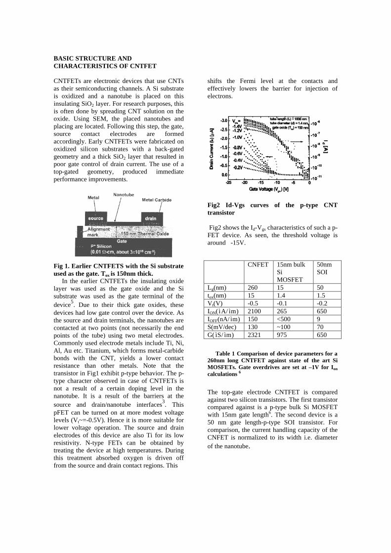
BASIC STRUCTURE AND CHARACTERISTICS OF CNTFET CNTFETs are electronic devices that use CNTs as their semiconducting channels. A Si substrate is oxidized and a nanotube is placed on this insulating SiO2 layer. For research purposes, this is often done by spreading CNT solution on the oxide. Using SEM, the placed nanotubes and placing are located. Following this step, the gate, source contact electrodes are formed accordingly. Early CNTFETs were fabricated on oxidized silicon substrates with a back-gated geometry and a thick SiO2 layer that resulted in poor gate control of drain current. The use of a top-gated geometry, produced immediate performance improvements.
Fig 1. Earlier CNTFETS with the Si substrate used as the gate. Tox is 150nm thick. In the earlier CNTFETs the insulating oxide layer was used as the gate oxide and the Si substrate was used as the gate terminal of the device5. Due to their thick gate oxides, these devices had low gate control over the device. As the source and drain terminals, the nanotubes are contacted at two points (not necessarily the end points of the tube) using two metal electrodes. Commonly used electrode metals include Ti, Ni, Al, Au etc. Titanium, which forms metal-carbide bonds with the CNT, yields a lower contact resistance than other metals. Note that the transistor in Fig1 exhibit p-type behavior. The p-type character observed in case of CNTFETs is not a result of a certain doping level in the nanotube. It is a result of the barriers at the source and drain/nanotube interfaces3. This pFET can be turned on at more modest voltage levels (Vt~=-0.5V). Hence it is more suitable for lower voltage operation. The source and drain electrodes of this device are also Ti for its low resistivity. N-type FETs can be obtained by treating the device at high temperatures. During this treatment absorbed oxygen is driven off from the source and drain contact regions. This
shifts the Fermi level at the contacts and effectively lowers the barrier for injection of electrons.
Fig2 Id-Vgs curves of the p-type CNT transistor Fig2 shows the Id-Vgs characteristics of such a p-FET device. As seen, the threshold voltage is around -15V.
Table 1 Comparison of device parameters for a
260nm long CNTFET against state of the art Si MOSFETs. Gate overdrives are set at –1V for Ion calculations 6
The top-gate electrode CNTFET is compared against two silicon transistors. The first transistor compared against is a p-type bulk Si MOSFET with 15nm gate length6. The second device is a 50 nm gate length-p-type SOI transistor. For comparison, the current handling capacity of the CNFET is normalized to its width i.e. diameter of the nanotube.
CNFET 15nm bulk Si MOSFET
50nm SOI
Lg(nm) 260 15 50 tox(nm) 15 1.4 1.5 Vt(V) -0.5 -0.1 -0.2 ION( ìA/ ìm) 2100 265 650 IOFF(nA/ ìm) 150 <500 9 S(mV/dec) 130 ~100 70 G( ìS/ ìm) 2321 975 650
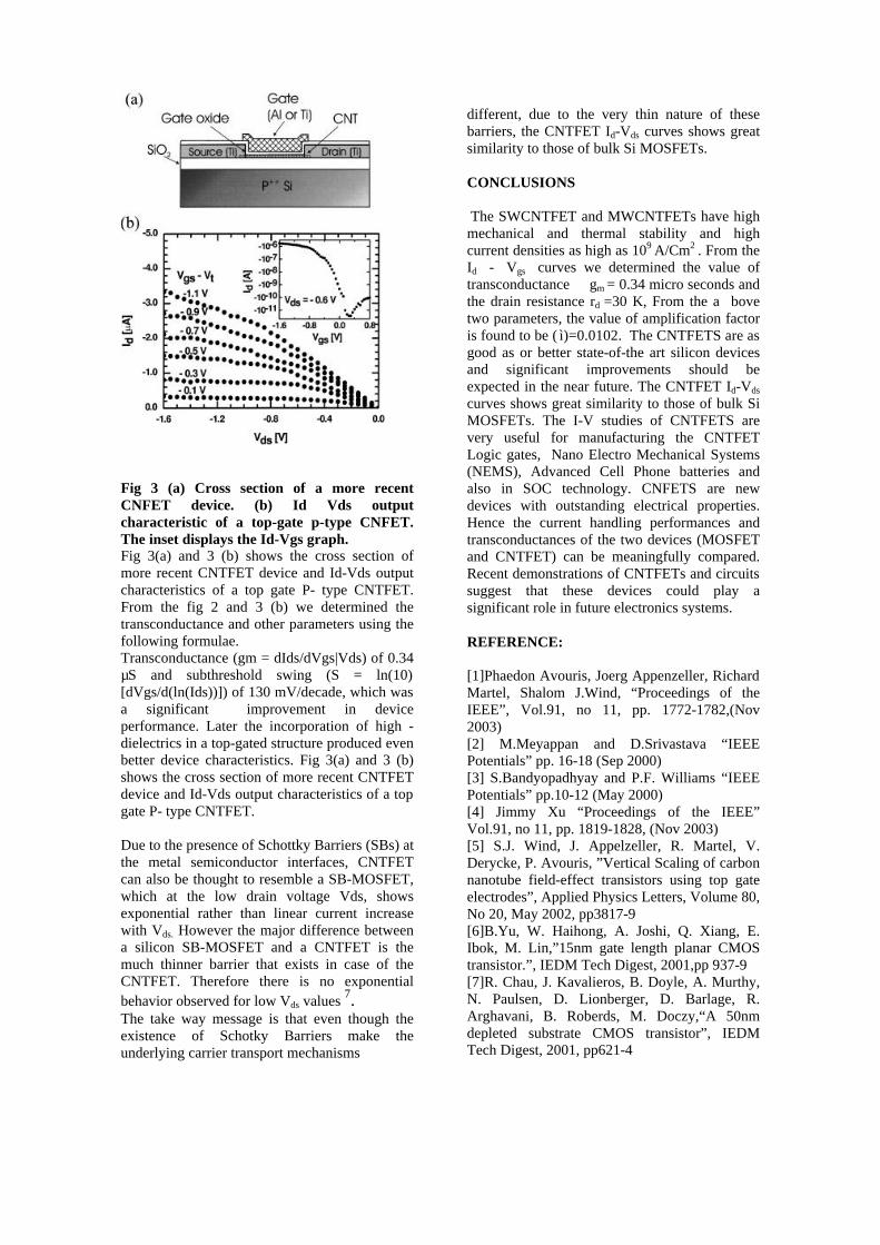
Fig 3 (a) Cross section of a more recent CNFET device. (b) Id Vds output characteristic of a top-gate p-type CNFET. The inset displays the Id-Vgs graph. Fig 3(a) and 3 (b) shows the cross section of more recent CNTFET device and Id-Vds output characteristics of a top gate P- type CNTFET. From the fig 2 and 3 (b) we determined the transconductance and other parameters using the following formulae. Transconductance (gm = dIds/dVgs|Vds) of 0.34 µS and subthreshold swing (S = ln(10) [dVgs/d(ln(Ids))]) of 130 mV/decade, which was a significant improvement in device performance. Later the incorporation of high - dielectrics in a top-gated structure produced even better device characteristics. Fig 3(a) and 3 (b) shows the cross section of more recent CNTFET device and Id-Vds output characteristics of a top gate P- type CNTFET. Due to the presence of Schottky Barriers (SBs) at the metal semiconductor interfaces, CNTFET can also be thought to resemble a SB-MOSFET, which at the low drain voltage Vds, shows exponential rather than linear current increase with Vds. However the major difference between a silicon SB-MOSFET and a CNTFET is the much thinner barrier that exists in case of the CNTFET. Therefore there is no exponential behavior observed for low Vds values 7. The take way message is that even though the existence of Schotky Barriers make the underlying carrier transport mechanisms
different, due to the very thin nature of these barriers, the CNTFET Id-Vds curves shows great similarity to those of bulk Si MOSFETs. CONCLUSIONS The SWCNTFET and MWCNTFETs have high mechanical and thermal stability and high current densities as high as 109 A/Cm2 . From the Id - Vgs curves we determined the value of transconductance gm = 0.34 micro seconds and the drain resistance rd =30 K, From the a bove two parameters, the value of amplification factor is found to be ( ì)=0.0102. The CNTFETS are as good as or better state-of-the art silicon devices and significant improvements should be expected in the near future. The CNTFET Id-Vds curves shows great similarity to those of bulk Si MOSFETs. The I-V studies of CNTFETS are very useful for manufacturing the CNTFET Logic gates, Nano Electro Mechanical Systems (NEMS), Advanced Cell Phone batteries and also in SOC technology. CNFETS are new devices with outstanding electrical properties. Hence the current handling performances and transconductances of the two devices (MOSFET and CNTFET) can be meaningfully compared. Recent demonstrations of CNTFETs and circuits suggest that these devices could play a significant role in future electronics systems. REFERENCE: [1]Phaedon Avouris, Joerg Appenzeller, Richard Martel, Shalom J.Wind, “Proceedings of the IEEE”, Vol.91, no 11, pp. 1772-1782,(Nov 2003) [2] M.Meyappan and D.Srivastava “IEEE Potentials” pp. 16-18 (Sep 2000) [3] S.Bandyopadhyay and P.F. Williams “IEEE Potentials” pp.10-12 (May 2000) [4] Jimmy Xu “Proceedings of the IEEE” Vol.91, no 11, pp. 1819-1828, (Nov 2003) [5] S.J. Wind, J. Appelzeller, R. Martel, V. Derycke, P. Avouris, ”Vertical Scaling of carbon nanotube field-effect transistors using top gate electrodes”, Applied Physics Letters, Volume 80, No 20, May 2002, pp3817-9 [6]B.Yu, W. Haihong, A. Joshi, Q. Xiang, E. Ibok, M. Lin,”15nm gate length planar CMOS transistor.”, IEDM Tech Digest, 2001,pp 937-9 [7]R. Chau, J. Kavalieros, B. Doyle, A. Murthy, N. Paulsen, D. Lionberger, D. Barlage, R. Arghavani, B. Roberds, M. Doczy,“A 50nm depleted substrate CMOS transistor”, IEDM Tech Digest, 2001, pp621-4

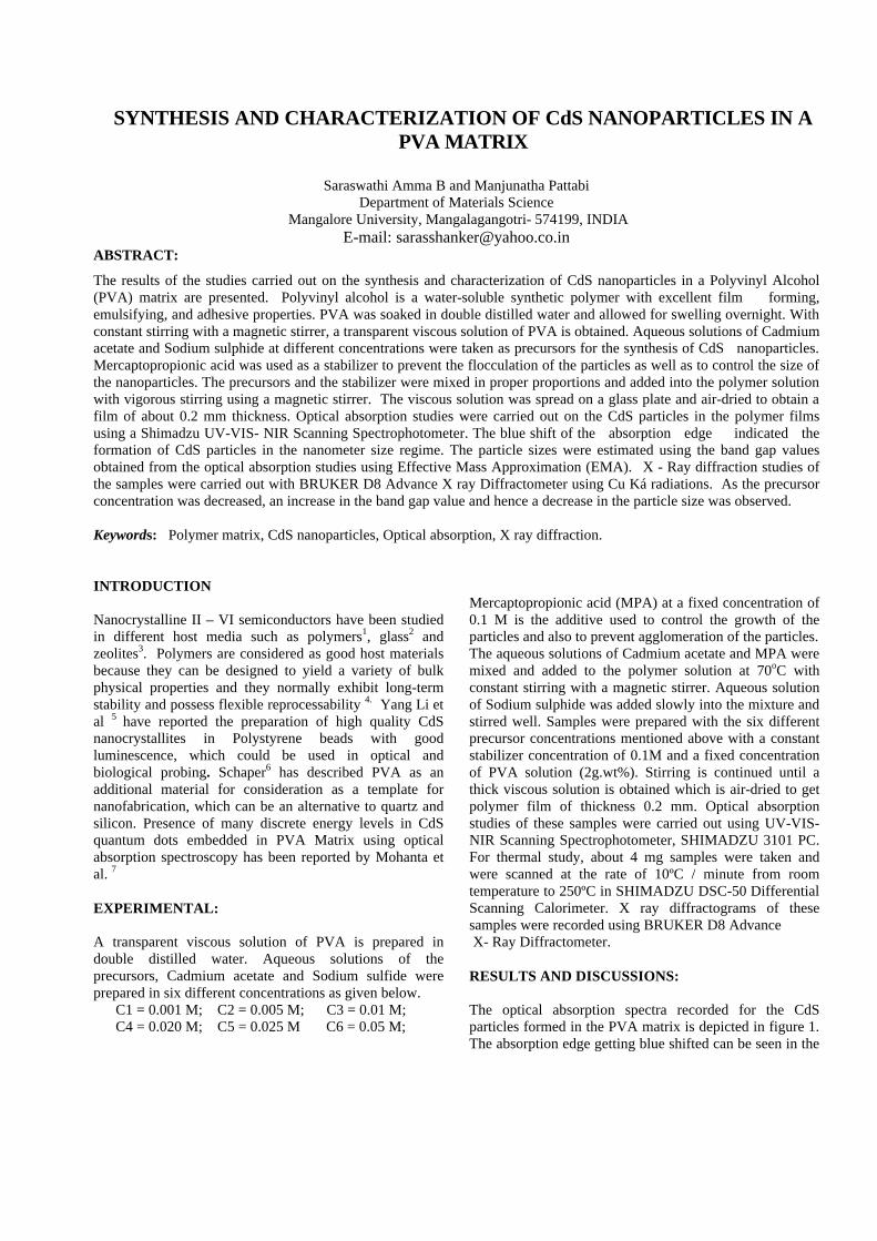
SYNTHESIS AND CHARACTERIZATION OF CdS NANOPARTICLES IN A
PVA MATRIX
Saraswathi Amma B and Manjunatha Pattabi Department of Materials Science
Mangalore University, Mangalagangotri- 574199, INDIA E-mail: [email protected]
ABSTRACT:
The results of the studies carried out on the synthesis and characterization of CdS nanoparticles in a Polyvinyl Alcohol (PVA) matrix are presented. Polyvinyl alcohol is a water-soluble synthetic polymer with excellent film forming, emulsifying, and adhesive properties. PVA was soaked in double distilled water and allowed for swelling overnight. With constant stirring with a magnetic stirrer, a transparent viscous solution of PVA is obtained. Aqueous solutions of Cadmium acetate and Sodium sulphide at different concentrations were taken as precursors for the synthesis of CdS nanoparticles. Mercaptopropionic acid was used as a stabilizer to prevent the flocculation of the particles as well as to control the size of the nanoparticles. The precursors and the stabilizer were mixed in proper proportions and added into the polymer solution with vigorous stirring using a magnetic stirrer. The viscous solution was spread on a glass plate and air-dried to obtain a film of about 0.2 mm thickness. Optical absorption studies were carried out on the CdS particles in the polymer films using a Shimadzu UV-VIS- NIR Scanning Spectrophotometer. The blue shift of the absorption edge indicated the formation of CdS particles in the nanometer size regime. The particle sizes were estimated using the band gap values obtained from the optical absorption studies using Effective Mass Approximation (EMA). X - Ray diffraction studies of the samples were carried out with BRUKER D8 Advance X ray Diffractometer using Cu Ká radiations. As the precursor concentration was decreased, an increase in the band gap value and hence a decrease in the particle size was observed. Keywords: Polymer matrix, CdS nanoparticles, Optical absorption, X ray diffraction. INTRODUCTION Nanocrystalline II – VI semiconductors have been studied in different host media such as polymers1, glass2 and zeolites3. Polymers are considered as good host materials because they can be designed to yield a variety of bulk physical properties and they normally exhibit long-term stability and possess flexible reprocessability 4. Yang Li et al 5 have reported the preparation of high quality CdS nanocrystallites in Polystyrene beads with good luminescence, which could be used in optical and biological probing. Schaper6 has described PVA as an additional material for consideration as a template for nanofabrication, which can be an alternative to quartz and silicon. Presence of many discrete energy levels in CdS quantum dots embedded in PVA Matrix using optical absorption spectroscopy has been reported by Mohanta et al. 7 EXPERIMENTAL: A transparent viscous solution of PVA is prepared in double distilled water. Aqueous solutions of the precursors, Cadmium acetate and Sodium sulfide were prepared in six different concentrations as given below. C1 = 0.001 M; C2 = 0.005 M; C3 = 0.01 M; C4 = 0.020 M; C5 = 0.025 M C6 = 0.05 M;
Mercaptopropionic acid (MPA) at a fixed concentration of 0.1 M is the additive used to control the growth of the particles and also to prevent agglomeration of the particles. The aqueous solutions of Cadmium acetate and MPA were mixed and added to the polymer solution at 70oC with constant stirring with a magnetic stirrer. Aqueous solution of Sodium sulphide was added slowly into the mixture and stirred well. Samples were prepared with the six different precursor concentrations mentioned above with a constant stabilizer concentration of 0.1M and a fixed concentration of PVA solution (2g.wt%). Stirring is continued until a thick viscous solution is obtained which is air-dried to get polymer film of thickness 0.2 mm. Optical absorption studies of these samples were carried out using UV-VIS-NIR Scanning Spectrophotometer, SHIMADZU 3101 PC. For thermal study, about 4 mg samples were taken and were scanned at the rate of 10ºC / minute from room temperature to 250ºC in SHIMADZU DSC-50 Differential Scanning Calorimeter. X ray diffractograms of these samples were recorded using BRUKER D8 Advance X- Ray Diffractometer. RESULTS AND DISCUSSIONS: The optical absorption spectra recorded for the CdS particles formed in the PVA matrix is depicted in figure 1. The absorption edge getting blue shifted can be seen in the
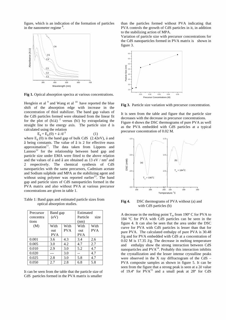
figure, which is an indication of the formation of particles in the nanometer regime 8.
300 400 500 600 700
C6
C5
C4
C3
C2
C1
Abs
orba
nce
(A.U
)
Wavelength (nm)
Fig 1. Optical absorption spectra at various concentrations. Henglein et al 9 and Wang et al 10 have reported the blue shift of the absorption edge with increase in the concentration of thiol stabilizer. The band gap values of the CdS particles formed were obtained from the linear fit for the plot of (híá) 2 versus (hí) by extrapolating the straight line to the energy axis. The particle size d is calculated using the relation Eg = Eg (0) + á /d â (1) where Eg (0) is the band gap of bulk CdS (2.42eV), á and â being constants. The value of â is 2 for effective mass approximation11. The data taken from Lippens and Lannoo12 for the relationship between band gap and particle size under EMA were fitted to the above relation and the values of á and â are obtained as 13 eV / nm2 and 2 respectively. The chemical synthesis of CdS nanoparticles with the same precursors, Cadmium acetate and Sodium sulphide and MPA as the stabilizing agent and without using polymer was reported earlier13. The band gap and particle sizes of CdS nanoparticles formed in the PVA matrix and also without PVA at various precursor concentrations are given in table 1. Table 1: Band gaps and estimated particle sizes from optical absorption studies.
Band gap (eV)
Estimated Particle size (nm)
Precursor concentra tions (M) With
out PVA
With PVA
With out PVA
With PVA
0.001 3.6 4.3 3.4 2.6 0.005 3.0 4.2 4.7 2.7 0.010 2.9 3.0 5.2 4.7 0.020 --- 3.0 -- 4.7 0.025 2.8 3.0 5.8 4.7 0.050 2.7 2.8 6.8 5.8
It can be seen from the table that the particle size of CdS particles formed in the PVA matrix is smaller
than the particles formed without PVA indicating that PVA controls the growth of CdS particles in it, in addition to the stabilizing action of MPA. Variation of particle size with precursor concentrations for the CdS nanoparticles formed in PVA matrix is shown in figure 3.
0.01 0.02 0.03 0.04 0.05
2.5
3.0
3.5
4.0
4.5
5.0
5.5
6.0
Par
ticle
Siz
e (n
m)
Precursor Concentrations (M)
Fig 3. Particle size variation with precursor concentration. It is seen from the table and figure that the particle size decreases with the decrease in precursor concentrations. Figure 4 shows the DSC thermograms of pure PVA as well as the PVA embedded with CdS particles at a typical precursor concentration of 0.02 M.
150 200 250-3.0
-2.5
-2.0
-1.5
(b)(a)
DS
C (
mW
)
Temperature oC
150 200 250-3.0
-2.5
-2.0
-1.5
Tm = 184oC
Tm = 190oC
Fig 4. DSC thermograms of PVA without (a) and with CdS particles (b) A decrease in the melting point Tm from 190º C for PVA to 184 ºC for PVA with CdS particles can be seen in the figure 4. It can also be seen that the area under the DSC curve for PVA with CdS particles is lesser than that for pure PVA. The calculated enthalpy of pure PVA is 30.48 J/g and for PVA embedded with CdS at a concentration of 0.02 M is 17.35 J/g. The decrease in melting temperature and enthalpy show the strong interaction between CdS nanoparticles and PVA14. Probably this interaction inhibits the crystallization and the lesser intense crystalline peaks were observed in the X ray diffractogram of the CdS – PVA composite samples as shown in figure 5. It can be seen from the figure that a strong peak is seen at a 2è value of 19.4º for PVA15 and a small peak at 28º for CdS
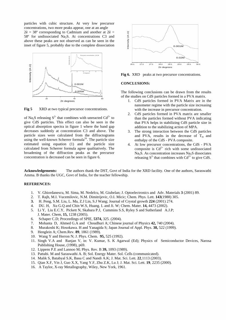
particles with cubic structure. At very low precursor concentrations, two more peaks appear, one at an angle 2è = 38º corresponding to Cadmium and another at 2è = 58º for undissociated Na2S. At concentrations C3 and above these peaks are not observed as can be seen in the inset of figure 5, probably due to the complete dissociation
20 40 60
10 20 30 40 50 60
Precursor concentration 0.02 M
Inte
nsity (
A.U
)
2θ degrees
0.005M
0.001M
Inte
nsity (
A.U
)
2θ degrees
Fig 5 XRD at two typical precursor concentrations. of Na2S releasing S2- that combines with unreacted Cd2+ to give CdS particles. This effect can also be seen in the optical absorption spectra in figure 1 where the band gap decreases suddenly at concentration C3 and above. The particle sizes were calculated from the diffractograms using the well-known Scherrer formula16. The particle size estimated using equation (1) and the particle size calculated from Scherrer formula agree qualitatively. The broadening of the diffraction peaks as the precursor concentration is decreased can be seen in figure 6.
26.5 27.0 27.5 28.0 28.5 29.0 29.5 30.0
0.02M
0.001M
Inte
nsity (
A.U
)
2θ degrees
Fig 6. XRD peaks at two precursor concentrations. CONCLUSIONS: The following conclusions can be drawn from the results of the studies on CdS particles formed in a PVA matrix.
1. CdS particles formed in PVA Matrix are in the nanometer regime with the particle size increasing with the increase in precursor concentration.
2. CdS particles formed in PVA matrix are smaller than the particles formed without PVA indicating that PVA helps in stabilizing CdS particle size in addition to the stabilizing action of MPA.
3. The strong interaction between the CdS particles and PVA, results in the decrease of Tm and enthalpy of the CdS - PVA composite.
4. At low precursor concentrations, the CdS - PVA composite is Cd2+ rich with some undissociated Na2S. As concentration increases Na2S dissociates releasing S2- that combines with Cd2+ to give CdS.
Acknowledgements: The authors thank the DST, Govt of India for the XRD facility. One of the authors, Saraswathi Amma. B thanks the UGC, Govt of India, for the teacher fellowship.
REFERENCES:
1. V. Ghiordanescu, M. Sima, M. Nedelcu, M. Giubelan; J. Optoelectronics and Adv. Materials 3 (2001) 89. 2. T. Rajh, M.I. Vucemilovic, N.M. Dimitrijevic, O.I. Micic; Chem. Phys. Lett. 143(1988) 305. 3. H. Peng, S.M. Liu, L. Ma, Z.J Lin, S.J Wang; Journal of Crystal growth 224 (2001) 274. 4. DU. H, Xu G.Q and Chin W.S, Huang. L and Ji. W; Chem. Mater. 14, 4473 (2002). 5. Li Y, Liu E.C.Y, Pickett N, Skabara P.J, Cummins S.S, Ryley S and Sutherland A.J.P; J. Mater. Chem, 15, 1238 (2005). 6. Schaper C.D; Proceedings of SPIE, 5374, 325. (2004). 7. Mohanta D, Ahmed G.A and Choudhuri A; Chinese journal of Physics 42, 740 (2004). 8. Murakoshi K; Hosokawa. H and Yanagida S; Japan Journal of Appl. Phys. 38, 522 (1999). 9. Henglein A; Chem.Rev. 89, 1861 (1989). 10. Wang Y and Herron N; J. Phys. Chem. 95, 525 (1992). 11. Singh V.A and Ranjan V, in: V. Kumar, S. K Agarwal (Ed); Physics of Semiconductor Devices, Narosa
Publishing House, (1998), p69. 12. Lippens P.E and Lannoo M; Phys. Rev. B 39, 1093 (1989). 13. Pattabi. M and Saraswathi A. B; Sol. Energy Mater. Sol. Cells (communicated). 14. Malik S, Batabyal S.K, Basu C and Nandi A.K; J. Mat. Sci. Lett. 22,1113 (2003). 15. Qian X.F, Yin J, Guo X.X, Yang Y.F, Zhu Z.K, Lu J; J. Mat. Sci. Lett. 19, 2235 (2000). 16. A Taylor, X-ray Metallography, Wiley, New York, 1961.
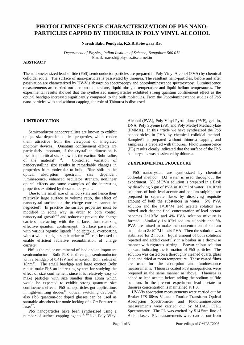
Page 1 of 3 Proceedings of OMTAT2005
PHOTOLUMINESCENCE CHARACTERIZATION OF PbS NANO-PARTICLES CAPPED BY THIOUREA IN POLY VINYL ALCOHOL
Naresh Babu Pendyala, K.S.R.Koteswara Rao
Department of Physics, Indian Institute of Science, Bangalore-560 012
Email: [email protected] ABSTRACT
The nanometer-sized lead sulfide (PbS) semiconductor particles are prepared in Poly Vinyl Alcohol (PVA) by chemical colloidal route. The surface of nano-particles is passivated by thiourea. The resultant nano-particles, before and after passivation are characterized by UV-Vis absorption spectroscopy and photoluminescence spectroscopy. Luminescence measurements are carried out at room temperature, liquid nitrogen temperature and liquid helium temperatures. The experimental results showed that the synthesized nano-particles exhibited strong quantum confinement effect as the optical bandgap increased significantly compared to the bulk molecules. From the Photoluminescence studies of PbS nano-particles with and without capping, the role of Thiourea is discussed. 1 INTRODUCTION
Semiconductor nanocrystallites are known to exhibit unique size-dependent optical properties, which render them attractive from the viewpoint of integrated photonic devices. Quantum confinement effects are particularly important, if the crystalline dimension is less than a critical size known as the exciton Bohr radius of the material1, 2. Controlled variation of nanocrystalline size results in remarkable changes in properties from molecular to bulk. Blue shift in the optical absorption spectrum, size dependent luminescence, enhanced oscillator strength, nonlinear optical effects are some examples of the interesting properties exhibited by these nanocrystals. Due to the small size of nanocrystals and hence their relatively large surface to volume ratio, the effect of nanocrystal surface on the charge carriers cannot be neglected3. In practice the surface properties must be modified in some way in order to both control nanocrystal growth4-6 and reduce or prevent the charge carriers interacting with the surface, thus realizing effective quantum confinement. Surface passivation with various organic ligands7-9 or epitaxial overcoating with a wide-bandgap semiconductor10-13 can be used to enable efficient radiative recombination of charge carriers. PbS is the major ore mineral of lead and an important semiconductor. Bulk PbS is directgap semiconductor with a bandgap of 0.41eV and an exciton Bohr radius of 18nm14. The small bandgap and large exciton Bohr radius make PbS an interesting system for studying the effect of size confinement since it is relatively easy to make particles with size smaller than 18nm which would be expected to exhibit strong quantum size confinement effect. PbS nanoparticles got applications in light-emitting diodes15, optical switching devices16, also PbS quantum-dot doped glasses can be used as saturable absorbers for mode locking of a Cr: Foresterite laser17. PbS nanoparticles have been synthesized using a number of surface capping agents18, 19 like Poly Vinyl
Alcohol (PVA), Poly Vinyl Pyrrolidone (PVP), gelatin, DNA, Poly Styrene (PS), and Poly Methyl Methacrylate (PMMA). In this article we have synthesized the PbS nanoparticles in PVA by chemical colloidal method. Sample#1 is prepared without thiourea capping and sample#2 is prepared with thiourea. Photoluminescence (PL) results clearly indicated that the surface of the PbS nanocrystals was passivated by thiourea. 2 EXPERIMENTAL PROCEDURE PbS nanocrystals are synthesized by chemical colloidal method. D.I water is used throughout the experiment. 5% of PVA solution is prepared in a flask by dissolving 5 gm of PVA in 100ml of water. 1×10⁻²M solutions of both lead acetate and sodium sulphide are prepared in separate flasks by dissolving requisite amount of both the substances in water. 5% PVA solution and the 1×10⁻²M lead acetate solution are mixed such that the final concentration of lead acetate becomes 2×10⁻³M and 4% PVA solution mixture is formed. Similarly 1×10⁻²M sodium sulphide and 5% PVA are mixed to make the concentration of sodium sulphide to 2×10⁻³M in 4% PVA. Then the solution was stabilized for 2 hours. Equal amount of both solutions pipetted and added carefully in a beaker in a dropwise manner with rigorous stirring. Brown colour solution appears indicating the formation of PbS particles. The solution was casted on a thoroughly cleaned quartz glass slide and dried at room temperature. These casted films are used for the absorption and luminescence measurements. Thiourea coated PbS nanoparticles were prepared in the same manner as above. Thiourea is added to lead acetate before adding the sodium sulfide solution. In the present experiment lead acetate to thiourea concentration is maintained at 1:3. UV-Vis absorption measurements were carried out by Bruker IFS 66v/s Vacuum Fourier Transform Optical Absorption Spectrometer and Photoluminescence measurements were carried out by MIDAC FTPL Spectrometer. The PL was excited by 514.5nm line of Ar-ion laser. PL measurements were carried out from
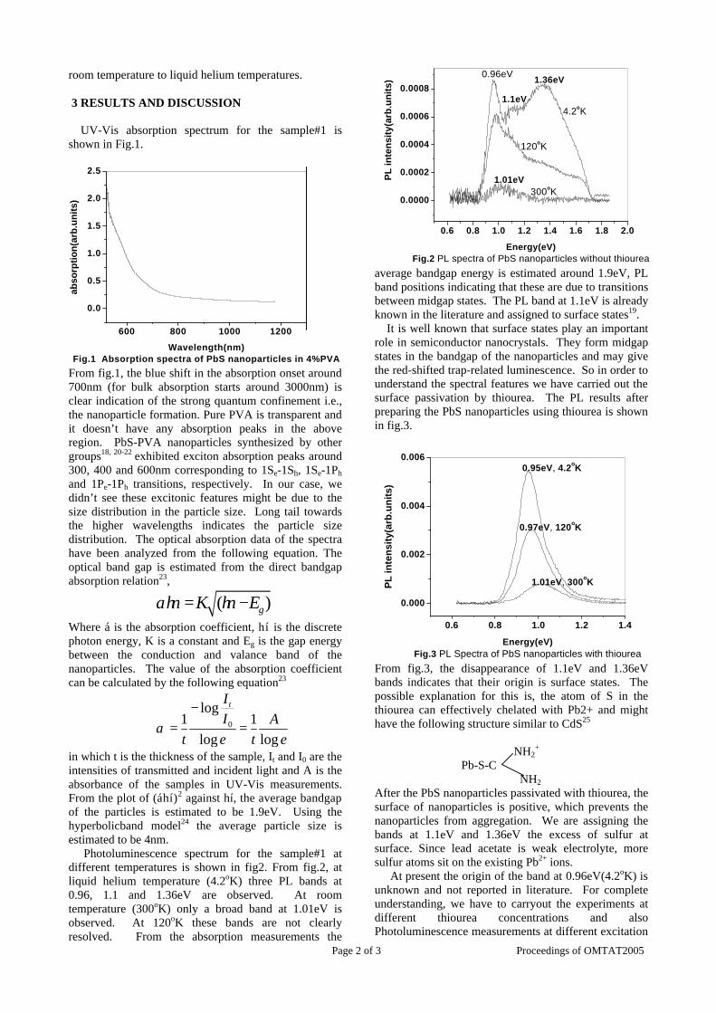
Page 2 of 3 Proceedings of OMTAT2005
room temperature to liquid helium temperatures. 3 RESULTS AND DISCUSSION UV-Vis absorption spectrum for the sample#1 is shown in Fig.1.
600 800 1000 1200
0.0
0.5
1.0
1.5
2.0
2.5
abso
rpti
on
(arb
.un
its)
Wavelength(nm)Fig.1 Absorption spectra of PbS nanoparticles in 4%PVA
From fig.1, the blue shift in the absorption onset around 700nm (for bulk absorption starts around 3000nm) is clear indication of the strong quantum confinement i.e., the nanoparticle formation. Pure PVA is transparent and it doesn’t have any absorption peaks in the above region. PbS-PVA nanoparticles synthesized by other groups18, 20-22 exhibited exciton absorption peaks around 300, 400 and 600nm corresponding to 1Se-1Sh, 1Se-1Ph and 1Pe-1Ph transitions, respectively. In our case, we didn’t see these excitonic features might be due to the size distribution in the particle size. Long tail towards the higher wavelengths indicates the particle size distribution. The optical absorption data of the spectra have been analyzed from the following equation. The optical band gap is estimated from the direct bandgap absorption relation23,
( )gh K h Eα ν ν= −
Where á is the absorption coefficient, hí is the discrete photon energy, K is a constant and Eg is the gap energy between the conduction and valance band of the nanoparticles. The value of the absorption coefficient can be calculated by the following equation23
0
log1 1
log log
tI
I A
t e t eα
−= =
in which t is the thickness of the sample, It and I0 are the intensities of transmitted and incident light and A is the absorbance of the samples in UV-Vis measurements. From the plot of (áhí)2 against hí, the average bandgap of the particles is estimated to be 1.9eV. Using the hyperbolicband model24 the average particle size is estimated to be 4nm. Photoluminescence spectrum for the sample#1 at different temperatures is shown in fig2. From fig.2, at liquid helium temperature (4.2oK) three PL bands at 0.96, 1.1 and 1.36eV are observed. At room temperature (300oK) only a broad band at 1.01eV is observed. At 120oK these bands are not clearly resolved. From the absorption measurements the
average bandgap energy is estimated around 1.9eV, PL band positions indicating that these are due to transitions between midgap states. The PL band at 1.1eV is already known in the literature and assigned to surface states19. It is well known that surface states play an important role in semiconductor nanocrystals. They form midgap states in the bandgap of the nanoparticles and may give the red-shifted trap-related luminescence. So in order to understand the spectral features we have carried out the surface passivation by thiourea. The PL results after preparing the PbS nanoparticles using thiourea is shown in fig.3.
From fig.3, the disappearance of 1.1eV and 1.36eV bands indicates that their origin is surface states. The possible explanation for this is, the atom of S in the thiourea can effectively chelated with Pb2+ and might have the following structure similar to CdS25 NH2
+ Pb-S-C NH2 After the PbS nanoparticles passivated with thiourea, the surface of nanoparticles is positive, which prevents the nanoparticles from aggregation. We are assigning the bands at 1.1eV and 1.36eV the excess of sulfur at surface. Since lead acetate is weak electrolyte, more sulfur atoms sit on the existing Pb2+ ions. At present the origin of the band at 0.96eV(4.2oK) is unknown and not reported in literature. For complete understanding, we have to carryout the experiments at different thiourea concentrations and also Photoluminescence measurements at different excitation
0.6 0.8 1.0 1.2 1.4 1.6 1.8 2.0
0.0000
0.0002
0.0004
0.0006
0.0008
300oK
120oK
4.2oK
1.01eV
1.1eV
1.36eV0.96eV
PL
inte
nsi
ty(a
rb.u
nit
s)
Energy(eV)Fig.2 PL spectra of PbS nanoparticles without thiourea
0.6 0.8 1.0 1.2 1.4
0.000
0.002
0.004
0.006
1.01eV, 300oK
0.97eV, 120oK
0.95eV, 4.2oK
PL
inte
nsi
ty(a
rb.u
nit
s)
Energy(eV)Fig.3 PL Spectra of PbS nanoparticles with thiourea
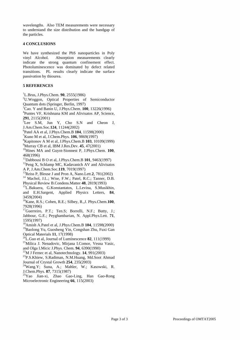
Page 3 of 3 Proceedings of OMTAT2005
wavelengths. Also TEM measurements were necessary to understand the size distribution and the bandgap of the particles. 4 CONCLUSIONS We have synthesized the PbS nanoparticles in Poly vinyl Alcohol. Absorption measurements clearly indicate the strong quantum confinement effect. Photoluminescence was dominated by defect related transitions. PL results clearly indicate the surface passivation by thiourea. 5 REFERENCES 1L.Brus, J.Phys.Chem. 90, 2555(1986) 2U.Woggon, Optical Properties of Semiconductor Quantum dots (Springer, Berlin, 1997) 3Cao. Y and Banin U, J.Phys.Chem. 100, 13226(1996) 4Puntes VF, Krishnana KM and Alivisatos AP, Science, 291, 2115(2001) 5Lee S.M, Jun Y, Cho S.N and Cheon J, J.Am.Chem.Soc.124, 11244(2002) 6Patel AA et al, J.Phys.Chem.B 104, 11598(2000) 7Kuno M et al, J.Chem.Phys. 106, 9869(1997) 8Kapitonov A M et al, J.Phys.Chem.B 103, 10109(1999) 9Murray CB et al, IBM J.Res.Dev. 45, 47(2001) 10Hines MA and Guyot-Sionnest P, J.Phys.Chem. 100, 468(1996) 11Dabbousi B O et al, J.Phys.Chem.B 101, 9463(1997) 12Peng X, Schlamp MC, Kadavanich AV and Alivisatos A P, J.Am.Chem.Soc.119, 7019(1997) 13Reiss P, Bleuse J and Pron A, Nano.Lett.2, 781(2002) 14 Machol, J.L.; Wise, F.W.; Patel, R.C.; Tanner, D.B. Physical Review B.Condens.Matter 48, 2819(1993) 15L.Bakuera, G.Konstantatos, L.Levina, S.Musikhin, and E.H.Sargent, Applied Physics Letters, 84, 3459(2004) 16Kane, R.S.; Cohen, R.E.; Silbey, R.,J. Phys.Chem.100, 7928(1996) 17Guerreiro, P.T.; Ten.S; Borrelli, N.F.; Butty, J.; Jabbour, G.E.; Peyghambarian, N. Appl.Phys.Lett. 71, 1595(1997) 18Amish A.Patel et al, J.Phys.Chem.B 104, 11598(2000) 19Baolong Yu, Guosheng Yin, Congshan Zhu, Fuxi Gan Optical Materials 11, 17(1998) 20L.Guo et al, Journal of Luminescence 82, 111(1999) 21Milica J. Nenadovic, Mirjana I.Comor, Vesna Vasic, and Olga I.Micic J.Phys. Chem. 94, 6390(1990) 22M J Fernec et al, Nanotechnology. 14, 991(2003) 23P.S.Khiew, S.Radiman, N.M.Huang, Md.Soot Ahmad Journal of Crystal Growth 254, 235(2003) 24Wang.Y; Suna, A.; Mahler, W.; Kasowski, R. J.Chem.Phys. 87, 7315(1987) 25Yao Jian-xi, Zhao Gao-Ling, Han Gao-Rong Microelectronic Engineering 66, 115(2003)
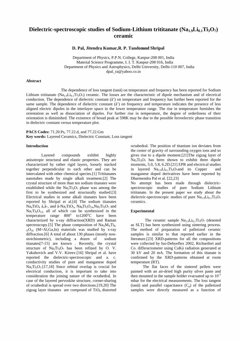
Dielectric-spectroscopic studies of Sodium-Lithium trititanate (Na1.9Li0.1Ti3O7) ceramic
D. Pal, Jitendra Kumar, R. P. Tandon and Shripal
Department of Physics, P.P.N. College, Kanpur-208 001, India Material Science Programme, I. I. T. Kanpur-208 016, India
Department of Physics and Astrophysics, Delhi University, Delhi-110 007, India [email protected]
Abstract The dependence of loss tangent (tanä) on temperature and frequency has been reported for Sodium Lithium trititanate (Na1.9Li0.1Ti3O7) ceramic. The losses are the characteristic of dipole mechanism and of electrical conduction. The dependence of dielectric constant (å’) on temperature and frequency has further been reported for the same sample. The dependence of dielectric constant (å’) on frequency and temperature indicates the presence of less aligned electric dipoles in the interlayer space in the lower temperature range. The rise in temperature furnishes the orientation as well as dissociation of dipoles. For further rise in temperature, the degree of orderliness of their orientation is diminished. The existence of broad peak at 598K may be due to the possible ferroelectric phase transition in dielectric constant versus temperature plot. PACS Codes: 71.20.Ps, 77.22.d, and 77.22.Gm Key words: Layered Ceramics, Dielectric Constant, Loss tangent Introduction Layered compounds exhibit highly anisotropic structural and elastic properties. They are characterized by rather rigid layers, loosely stacked together perpendicular to each other and can be intercalated with other chemical species.[1] Trititanates nanotubes made by single alkali treatment.[2] The crystal structure of more than ten sodium titanates were established while the Na2Ti3O7 phase was among the first to be synthesized and structurally studied.[3] Electrical studies in some alkali titanates have been reported by Shripal et al.[4] The sodium titanates Na4TiO4 á,â-, and ã-Na2TiO3, Na8Ti5O14,Na2Ti3O7 and Na2Ti6O13, all of which can be synthesized in the temperature range 800o to1200oC have been characterized by x-ray diffraction(XRD) and Raman spectroscopy.[5] The phase composition of NaXMXTi8-
XO16 (M=Al,Ga,In) materials was studied by x-ray diffraction.[6] A total of about 130 phases (mostly non-stoichiometric), including a dozen of sodium titanates[7-15] are known . Recently, the crystal structure of Na2Ti3O7 has been refined by O. V. Yakubovich and V.V. Kireev.[16] Shripal et al. have reported the dielectric-spectroscopic and a. c. conductivity studies of pure and manganese doped Na2Ti3O7.[17,18] Since orbital overlap is crucial for electrical conduction, it is important to take into consideration the joining nature of the octahedral. In case of the layered pervoskite structure, corner-sharing of octahedral is spread over two directions.[19,20] The zigzag layer titanates are composed of TiO6 distorted
octahedral. The position of titanium ion deviates from the center of gravity of surrounding oxygen ions and so gives rise to a dipole moment.[21]The zigzag layer of Na2Ti3O7 has been shown to exhibit three dipole moments, 5.0, 5.8, 6.2D.[21] EPR and electrical studies in layered Na1.9Li0.1Ti3O7and its Copper and manganese doped derivatives have been reported by Dharmendra Pal et al. [22,23] No attempt has been made through dielectric-spectroscopic studies of pure Sodium Lithium trititanate. In the present paper we study about the dielectric-spectroscopic studies of pure Na1.9Li0.1Ti3O7 ceramics. Experimental The ceramic sample Na1.9Li0.1Ti3O7 (denoted as SLT) has been synthesized using sintering process. The method of preparation of palletized ceramic samples is similar to that reported earlier in the literature.[23] XRD-patterns for all the compositions were collected by Iso-Debyeflex 2002, Richseifert and Co. differactometer using CuKá radiation generated at 30 kV and 20 mA. The formation of this titanate is confirmed by the XRD-patterns obtained at room temperature (RT). The flat faces of the sintered pellets were painted with an air-dried high purity silver paste and then mounted in the sample holder evacuated up to 10-3 mbar for the electrical measurements. The loss tangent (tanä) and parallel capacitance (Cp) of the palletized samples were directly measured as a function of
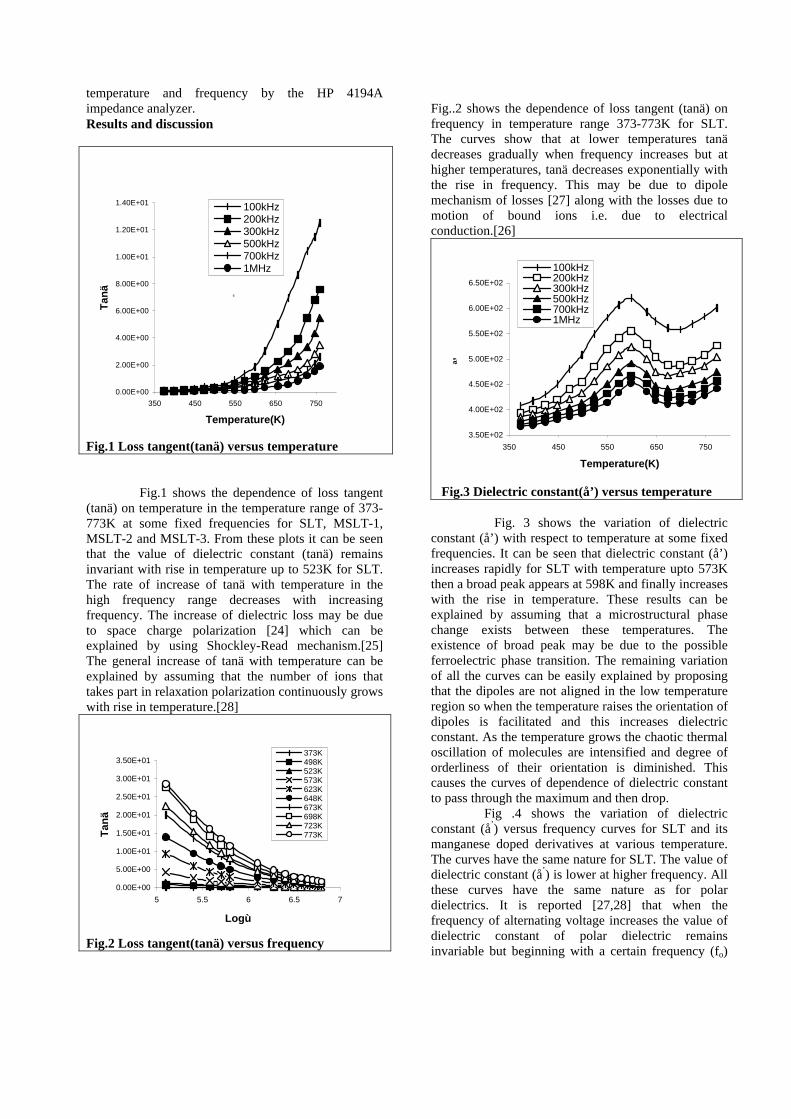
temperature and frequency by the HP 4194A impedance analyzer. Results and discussion
0.00E+00
2.00E+00
4.00E+00
6.00E+00
8.00E+00
1.00E+01
1.20E+01
1.40E+01
350 450 550 650 750
Temperature(K)
Tan
ä
100kHz200kHz300kHz500kHz700kHz1MHz
6
Fig.1 Loss tangent(tanä) versus temperature Fig.1 shows the dependence of loss tangent (tanä) on temperature in the temperature range of 373-773K at some fixed frequencies for SLT, MSLT-1, MSLT-2 and MSLT-3. From these plots it can be seen that the value of dielectric constant (tanä) remains invariant with rise in temperature up to 523K for SLT. The rate of increase of tanä with temperature in the high frequency range decreases with increasing frequency. The increase of dielectric loss may be due to space charge polarization [24] which can be explained by using Shockley-Read mechanism.[25] The general increase of tanä with temperature can be explained by assuming that the number of ions that takes part in relaxation polarization continuously grows with rise in temperature.[28]
0.00E+00
5.00E+00
1.00E+01
1.50E+01
2.00E+01
2.50E+01
3.00E+01
3.50E+01
5 5.5 6 6.5 7
Logù
Tan
ä
373K498K523K573K623K648K673K698K723K773K
Fig.2 Loss tangent(tanä) versus frequency
Fig..2 shows the dependence of loss tangent (tanä) on frequency in temperature range 373-773K for SLT. The curves show that at lower temperatures tanä decreases gradually when frequency increases but at higher temperatures, tanä decreases exponentially with the rise in frequency. This may be due to dipole mechanism of losses [27] along with the losses due to motion of bound ions i.e. due to electrical conduction.[26]
3.50E+02
4.00E+02
4.50E+02
5.00E+02
5.50E+02
6.00E+02
6.50E+02
350 450 550 650 750
Temperature(K)ª’
100kHz200kHz300kHz500kHz700kHz1MHz
Fig.3 Dielectric constant(å’) versus temperature Fig. 3 shows the variation of dielectric constant (å’) with respect to temperature at some fixed frequencies. It can be seen that dielectric constant (å’) increases rapidly for SLT with temperature upto 573K then a broad peak appears at 598K and finally increases with the rise in temperature. These results can be explained by assuming that a microstructural phase change exists between these temperatures. The existence of broad peak may be due to the possible ferroelectric phase transition. The remaining variation of all the curves can be easily explained by proposing that the dipoles are not aligned in the low temperature region so when the temperature raises the orientation of dipoles is facilitated and this increases dielectric constant. As the temperature grows the chaotic thermal oscillation of molecules are intensified and degree of orderliness of their orientation is diminished. This causes the curves of dependence of dielectric constant to pass through the maximum and then drop. Fig .4 shows the variation of dielectric constant (å’) versus frequency curves for SLT and its manganese doped derivatives at various temperature. The curves have the same nature for SLT. The value of dielectric constant (å’) is lower at higher frequency. All these curves have the same nature as for polar dielectrics. It is reported [27,28] that when the frequency of alternating voltage increases the value of dielectric constant of polar dielectric remains invariable but beginning with a certain frequency (fo)
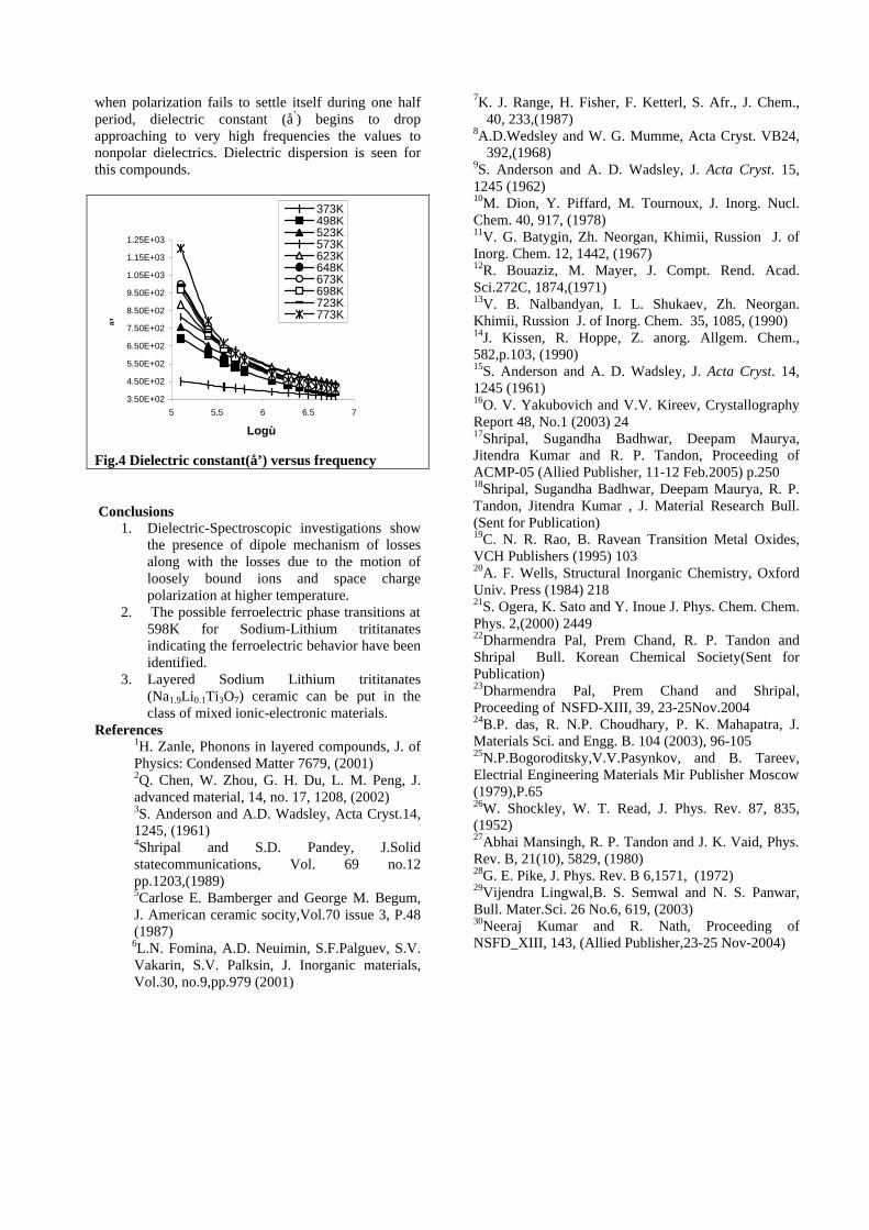
when polarization fails to settle itself during one half period, dielectric constant (å’) begins to drop approaching to very high frequencies the values to nonpolar dielectrics. Dielectric dispersion is seen for this compounds.
3.50E+02
4.50E+02
5.50E+02
6.50E+02
7.50E+02
8.50E+02
9.50E+02
1.05E+03
1.15E+03
1.25E+03
5 5.5 6 6.5 7
Logù
ª’
373K498K523K573K623K648K673K698K723K773K
Fig.4 Dielectric constant(å’) versus frequency Conclusions
1. Dielectric-Spectroscopic investigations show the presence of dipole mechanism of losses along with the losses due to the motion of loosely bound ions and space charge polarization at higher temperature.
2. The possible ferroelectric phase transitions at 598K for Sodium-Lithium trititanates indicating the ferroelectric behavior have been identified.
3. Layered Sodium Lithium trititanates (Na1.9Li0.1Ti3O7) ceramic can be put in the class of mixed ionic-electronic materials.
References 1H. Zanle, Phonons in layered compounds, J. of Physics: Condensed Matter 7679, (2001) 2Q. Chen, W. Zhou, G. H. Du, L. M. Peng, J. advanced material, 14, no. 17, 1208, (2002) 3S. Anderson and A.D. Wadsley, Acta Cryst.14, 1245, (1961) 4Shripal and S.D. Pandey, J.Solid statecommunications, Vol. 69 no.12 pp.1203,(1989) 5Carlose E. Bamberger and George M. Begum, J. American ceramic socity,Vol.70 issue 3, P.48 (1987)
6L.N. Fomina, A.D. Neuimin, S.F.Palguev, S.V. Vakarin, S.V. Palksin, J. Inorganic materials, Vol.30, no.9,pp.979 (2001)
7K. J. Range, H. Fisher, F. Ketterl, S. Afr., J. Chem., 40, 233,(1987)
8A.D.Wedsley and W. G. Mumme, Acta Cryst. VB24, 392,(1968)
9S. Anderson and A. D. Wadsley, J. Acta Cryst. 15, 1245 (1962) 10M. Dion, Y. Piffard, M. Tournoux, J. Inorg. Nucl. Chem. 40, 917, (1978) 11V. G. Batygin, Zh. Neorgan, Khimii, Russion J. of Inorg. Chem. 12, 1442, (1967) 12R. Bouaziz, M. Mayer, J. Compt. Rend. Acad. Sci.272C, 1874,(1971) 13V. B. Nalbandyan, I. L. Shukaev, Zh. Neorgan. Khimii, Russion J. of Inorg. Chem. 35, 1085, (1990) 14J. Kissen, R. Hoppe, Z. anorg. Allgem. Chem., 582,p.103, (1990) 15S. Anderson and A. D. Wadsley, J. Acta Cryst. 14, 1245 (1961) 16O. V. Yakubovich and V.V. Kireev, Crystallography Report 48, No.1 (2003) 24 17Shripal, Sugandha Badhwar, Deepam Maurya, Jitendra Kumar and R. P. Tandon, Proceeding of ACMP-05 (Allied Publisher, 11-12 Feb.2005) p.250 18Shripal, Sugandha Badhwar, Deepam Maurya, R. P. Tandon, Jitendra Kumar , J. Material Research Bull. (Sent for Publication) 19C. N. R. Rao, B. Ravean Transition Metal Oxides, VCH Publishers (1995) 103 20A. F. Wells, Structural Inorganic Chemistry, Oxford Univ. Press (1984) 218 21S. Ogera, K. Sato and Y. Inoue J. Phys. Chem. Chem. Phys. 2,(2000) 2449 22Dharmendra Pal, Prem Chand, R. P. Tandon and Shripal Bull. Korean Chemical Society(Sent for Publication) 23Dharmendra Pal, Prem Chand and Shripal, Proceeding of NSFD-XIII, 39, 23-25Nov.2004 24B.P. das, R. N.P. Choudhary, P. K. Mahapatra, J. Materials Sci. and Engg. B. 104 (2003), 96-105 25N.P.Bogoroditsky,V.V.Pasynkov, and B. Tareev, Electrial Engineering Materials Mir Publisher Moscow (1979),P.65 26W. Shockley, W. T. Read, J. Phys. Rev. 87, 835, (1952) 27Abhai Mansingh, R. P. Tandon and J. K. Vaid, Phys. Rev. B, 21(10), 5829, (1980) 28G. E. Pike, J. Phys. Rev. B 6,1571, (1972) 29Vijendra Lingwal,B. S. Semwal and N. S. Panwar, Bull. Mater.Sci. 26 No.6, 619, (2003) 30Neeraj Kumar and R. Nath, Proceeding of NSFD_XIII, 143, (Allied Publisher,23-25 Nov-2004)
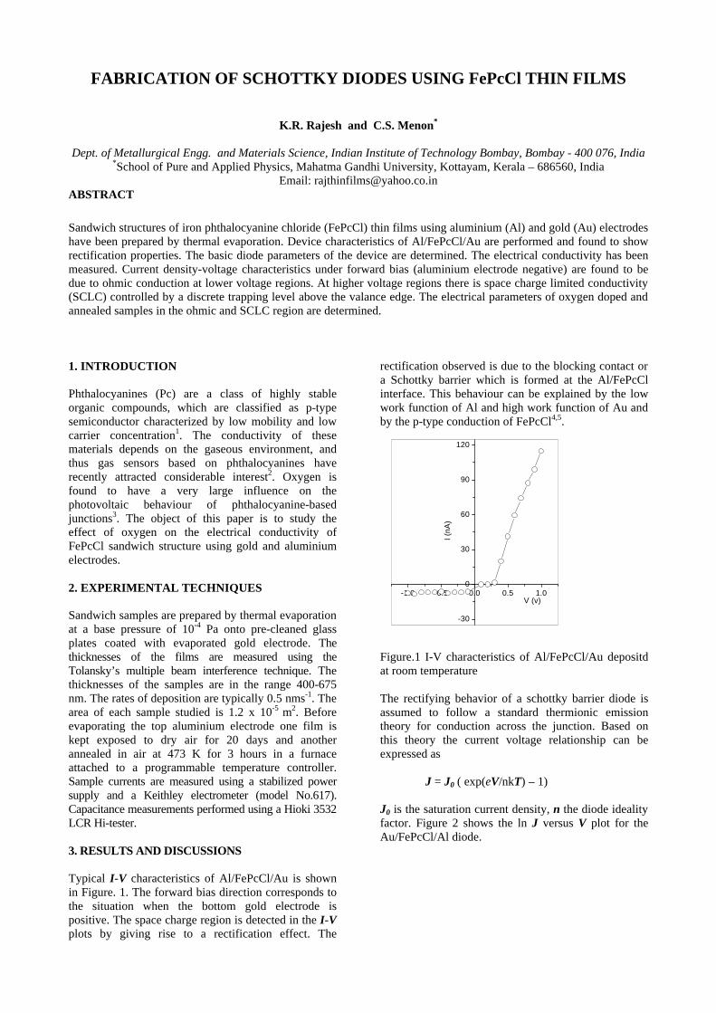
FABRICATION OF SCHOTTKY DIODES USING FePcCl THIN FILMS
K.R. Rajesh and C.S. Menon*
Dept. of Metallurgical Engg. and Materials Science, Indian Institute of Technology Bombay, Bombay - 400 076, India *School of Pure and Applied Physics, Mahatma Gandhi University, Kottayam, Kerala – 686560, India
Email: [email protected] ABSTRACT
Sandwich structures of iron phthalocyanine chloride (FePcCl) thin films using aluminium (Al) and gold (Au) electrodes have been prepared by thermal evaporation. Device characteristics of Al/FePcCl/Au are performed and found to show rectification properties. The basic diode parameters of the device are determined. The electrical conductivity has been measured. Current density-voltage characteristics under forward bias (aluminium electrode negative) are found to be due to ohmic conduction at lower voltage regions. At higher voltage regions there is space charge limited conductivity (SCLC) controlled by a discrete trapping level above the valance edge. The electrical parameters of oxygen doped and annealed samples in the ohmic and SCLC region are determined. 1. INTRODUCTION Phthalocyanines (Pc) are a class of highly stable organic compounds, which are classified as p-type semiconductor characterized by low mobility and low carrier concentration1. The conductivity of these materials depends on the gaseous environment, and thus gas sensors based on phthalocyanines have recently attracted considerable interest2. Oxygen is found to have a very large influence on the photovoltaic behaviour of phthalocyanine-based junctions3. The object of this paper is to study the effect of oxygen on the electrical conductivity of FePcCl sandwich structure using gold and aluminium electrodes. 2. EXPERIMENTAL TECHNIQUES Sandwich samples are prepared by thermal evaporation at a base pressure of 10-4 Pa onto pre-cleaned glass plates coated with evaporated gold electrode. The thicknesses of the films are measured using the Tolansky’s multiple beam interference technique. The thicknesses of the samples are in the range 400-675 nm. The rates of deposition are typically 0.5 nms-1. The area of each sample studied is 1.2 x 10⁻⁵ m2. Before evaporating the top aluminium electrode one film is kept exposed to dry air for 20 days and another annealed in air at 473 K for 3 hours in a furnace attached to a programmable temperature controller. Sample currents are measured using a stabilized power supply and a Keithley electrometer (model No.617). Capacitance measurements performed using a Hioki 3532 LCR Hi-tester. 3. RESULTS AND DISCUSSIONS Typical I-V characteristics of Al/FePcCl/Au is shown in Figure. 1. The forward bias direction corresponds to the situation when the bottom gold electrode is positive. The space charge region is detected in the I-V plots by giving rise to a rectification effect. The
rectification observed is due to the blocking contact or a Schottky barrier which is formed at the Al/FePcCl interface. This behaviour can be explained by the low work function of Al and high work function of Au and by the p-type conduction of FePcCl4,5.
-1.0 -0.5 0.0 0.5 1.0
-30
0
30
60
90
120I (
nA)
V (v)
Figure.1 I-V characteristics of Al/FePcCl/Au depositd at room temperature The rectifying behavior of a schottky barrier diode is assumed to follow a standard thermionic emission theory for conduction across the junction. Based on this theory the current voltage relationship can be expressed as J = J0 ( exp(eV/nkT) – 1) J0 is the saturation current density, n the diode ideality factor. Figure 2 shows the ln J versus V plot for the Au/FePcCl/Al diode.
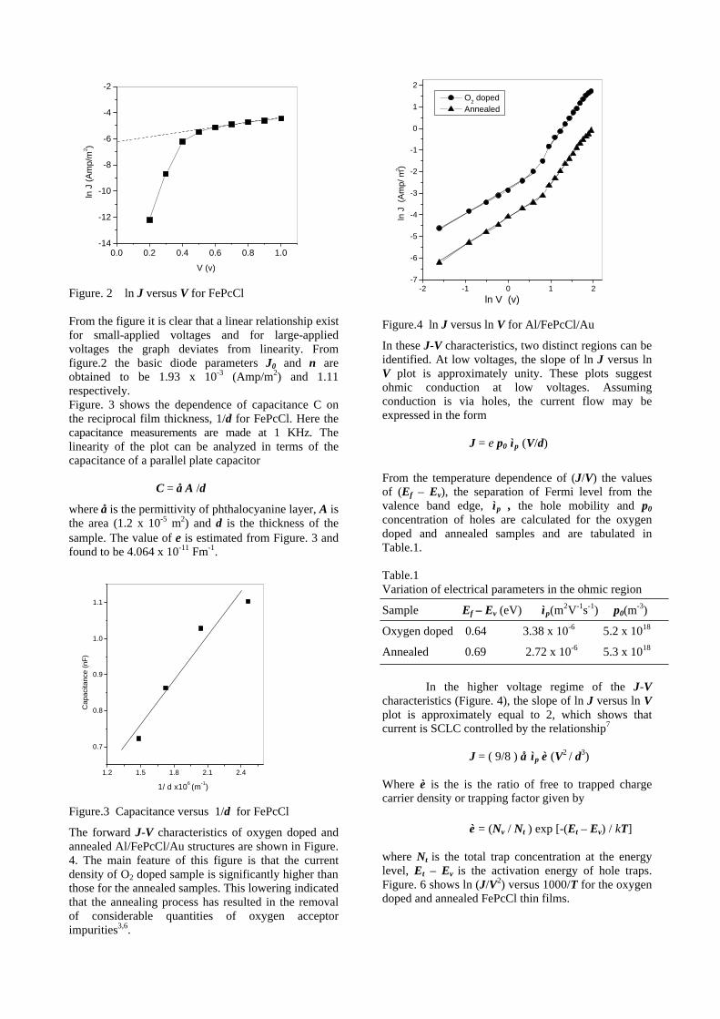
0.0 0.2 0.4 0.6 0.8 1.0-14
-12
-10
-8
-6
-4
-2ln
J (
Am
p/m
2 )
V (v)
Figure. 2 ln J versus V for FePcCl From the figure it is clear that a linear relationship exist for small-applied voltages and for large-applied voltages the graph deviates from linearity. From figure.2 the basic diode parameters J0 and n are obtained to be 1.93 x 10⁻³ (Amp/m2) and 1.11 respectively. Figure. 3 shows the dependence of capacitance C on the reciprocal film thickness, 1/d for FePcCl. Here the capacitance measurements are made at 1 KHz. The linearity of the plot can be analyzed in terms of the capacitance of a parallel plate capacitor
C = å A /d
where å is the permittivity of phthalocyanine layer, A is the area (1.2 x 10⁻⁵ m2) and d is the thickness of the sample. The value of εε is estimated from Figure. 3 and found to be 4.064 x 10⁻¹¹ Fm-1.
1.2 1.5 1.8 2.1 2.4
0.7
0.8
0.9
1.0
1.1
1/ d x106 (m
-1)
Cap
acita
nce
(nF
)
Figure.3 Capacitance versus 1/d for FePcCl
The forward J-V characteristics of oxygen doped and annealed Al/FePcCl/Au structures are shown in Figure. 4. The main feature of this figure is that the current density of O2 doped sample is significantly higher than those for the annealed samples. This lowering indicated that the annealing process has resulted in the removal of considerable quantities of oxygen acceptor impurities3,6.
-2 -1 0 1 2-7
-6
-5
-4
-3
-2
-1
0
1
2
O2 doped
Annealed
ln V (v)
ln J
(A
mp/
m2 )
Figure.4 ln J versus ln V for Al/FePcCl/Au
In these J-V characteristics, two distinct regions can be identified. At low voltages, the slope of ln J versus ln V plot is approximately unity. These plots suggest ohmic conduction at low voltages. Assuming conduction is via holes, the current flow may be expressed in the form
J = e p0 ìp (V/d)
From the temperature dependence of (J/V) the values of (Ef – Ev), the separation of Fermi level from the valence band edge, ìp , the hole mobility and p0 concentration of holes are calculated for the oxygen doped and annealed samples and are tabulated in Table.1. Table.1 Variation of electrical parameters in the ohmic region
Sample Ef – Ev (eV) ìp(m2V-1s-1) p0(m
-3)
Oxygen doped 0.64 3.38 x 10⁻⁶ 5.2 x 10¹⁸
Annealed 0.69 2.72 x 10⁻⁶ 5.3 x 10¹⁸
In the higher voltage regime of the J-V
characteristics (Figure. 4), the slope of ln J versus ln V plot is approximately equal to 2, which shows that current is SCLC controlled by the relationship7
J = ( 9/8 ) å ìp è (V2 / d3)
Where è is the is the ratio of free to trapped charge carrier density or trapping factor given by
è = (Nv / Nt ) exp [-(Et – Ev) / kT] where Nt is the total trap concentration at the energy level, Et – Ev is the activation energy of hole traps. Figure. 6 shows ln (J/V2) versus 1000/T for the oxygen doped and annealed FePcCl thin films.
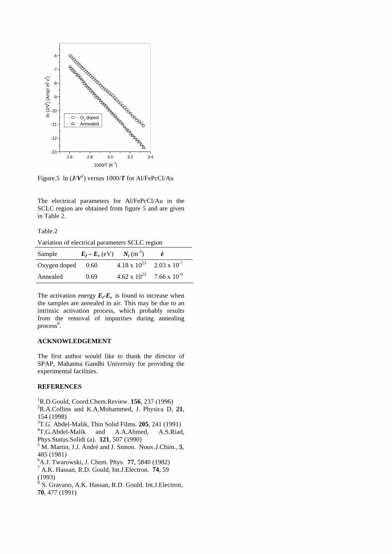
2.6 2.8 3.0 3.2 3.4-13
-12
-11
-10
-9
-8
-7
-6
O2 doped Annealed
1000/T (K -1)
ln (
J/V2 )
(Am
p/ m
2 -v2 )
Figure.5 ln (J/V2) versus 1000/T for Al/FePcCl/Au
The electrical parameters for Al/FePcCl/Au in the SCLC region are obtained from figure 5 and are given in Table 2. Table.2
Variation of electrical parameters SCLC region
Sample Ef – Ev (eV) Nt (m-3) è
Oxygen doped 0.60 4.18 x 10²³ 2.03 x 10⁻⁷
Annealed 0.69 4.62 x 10²³ 7.66 x 10⁻⁹
The activation energy Et-Ev is found to increase when the samples are annealed in air. This may be due to an intrinsic activation process, which probably results from the removal of impurities during annealing process8. ACKNOWLEDGEMENT The first author would like to thank the director of SPAP, Mahatma Gandhi University for providing the experimental facilities. REFERENCES 1R.D.Gould, Coord.Chem.Review. 156, 237 (1996) 2R.A.Collins and K.A.Mohammed, J. Physica D, 21, 154 (1998) 3T.G. Abdel-Malik, Thin Solid Films. 205, 241 (1991) 4T.G.Abdel-Malik and A.A.Ahmed, A.S.Riad, Phys.Status.Solidi (a). 121, 507 (1990) 5 M. Martin, J.J. André and J. Simon. Nouv.J.Chim., 5, 485 (1981) 6A.J. Twarowski, J. Chem. Phys. 77, 5840 (1982) 7 A.K. Hassan, R.D. Gould, Int.J.Electron. 74, 59 (1993) 8 S. Gravano, A.K. Hassan, R.D. Gould. Int.J.Electron, 70, 477 (1991)
EFFECT OF AIR ANNEALING ON THE OPTICAL AND ELECTRICAL PROPERTIES OF TITANIUM PHTHALOCYANINE DICHLORIDE THIN
FILMS Regimol.C.Cherian, C.S.Menon, K.Indulekha
School of Pure and Applied Physics, Mahatma Gandhi University, Priyadarshini Hills P. O, Kottayam, Kerala-686560, India
E-mail: [email protected]
ABSTRACT
The optical absorption spectra of thermally evaporated titanium phthalocyanine dichloride thin films have been studied. The optical band gap have been investigated using spectro -photometric measurements of absorbance in the wavelength range 300nm to 900nm. The absorption spectra recorded in UV-VIS-NIR region for the as-depositd and annealed samples shows two absorption bands, viz the Q- band and the Soret band. Both fundamental and the indirect energy gaps decreases during annealing. Since the interactions of the molecules are of Vander Waals type, the re-arrangement of molecules alters the energy gap .The electrical conductivity studies are conducted in the temperature range 300K to 525K. The electrical conductivity is plotted as a function of absolute temperature. The conduction mechanism is found to be hopping. The thermal activation energy is calculated in different cases and is observed to vary with annealing temperature. 1 INTRODUCTION The history of synthesis and study of properties of phthalocyanines(Pc’s) have been started since 1907 , the interest in their properties is still great because of their application in the field of opto-electronics, sensors and molecular electronics 1,2,3.Pc’s are organic compounds exhibiting high chemical and thermal stability and can thus be sublimed without decomposition to form high quality thin film by thermal evaporation technique. Pc’s form stable combination with many metal atom. The planar Pc molecule consists of four isoindole units linked by nitrogen atoms and surrounding two hydrogen atoms4. Metal Pc’s (MPc) are formed when the two hydrogen atoms are replaced by single metal atom. The role of metal is of interest in several fields of Pc application such as dyes,pigments, photocopying agents5 in photovoltaic energy conversion, electrochemical reduction processes6. Although there is evidence that halogenated MPc’s exhibit similar properties as that of MPc’s, only very few studies have been reported so far. The halogenated Pc’s exhibit remarkable morphological and thermal stability over a larger temperature range compared to unhalogenated Pc’s 7. One of major advantage of using organic semi-conducting material is their ability to modify their molecular structure and hence their electrical and optical properties. Since the discovery of Pc’s , a great effort has been made to study the optical and electrical properties of Pc’s and associated compounds8,9.It is reported that the central metal atom of phthalocyanines influences the optical absorption spectrum6. It is observed that the electrical and optical
2.EXPERIMENTAL DETAILS Spectroscopically pure TiPcCl2 powder with a purity of 95% supplied by Aldrich Company (USA) is used as the source material for the preparation of thin films .Thin films of varying thickness are prepared by vacuum sublimation from a resistively heated molybdenum boat using a Hind Hi-Vac coating unit. Films are deposited onto thoroughly cleaned rectangular glass substrate of dimension 4x1.2x1.3mm at room temperature at a pressure of 10-5 Torr. The thickness of the films are measured by Tolansky’s multiple beam interference technique12Thin films prepared at room temperature has been annealed at different temperature for one hour in a furnace and the temperature is controlled by a programmable temperature controller. UV- Visible absorption spectra are recorded using a Shimadzu 160A UV-Visible Spectro-photometer. The absorption edge is analyzed to get the optical band gap of TiPcCl2 . Electrical conductivity measurements are performed using a programmable Keithley electrometer [model No. 617]. Thin copper strands are fixed by silver Paste as contact electrode and the films are mounted on the sample holder of the conductivity cell, which can be externally heated. The electrical conductivity studies are done at a pressure of 10-3 torr to avoid the possible contamination in the temperature range 300K to 525 K and the resistance is measured. The temperature is monitored by a Chromel- Alumel thermocouple
Properties of Pc's depend on film morphology, which in turn is determined by preparation parameters such as deposition rate, substrate temperature and post-deposition annealing1011Out of The halogenated MPc's Titanium phthalocyanine dichloride(TiPcCl2) has received less attention. In the present work we focus on the optical and electrical properties of TiPcCl2 thinfilms
3 RESULTS AND DISCUSSION 3.1Optical Studies :- The optical absorption spectra of different thickness of TiPcCl2 thin films in the wavelength range 300 to 900 nm recorded using the Shimadzu 160A spectro- photometer .
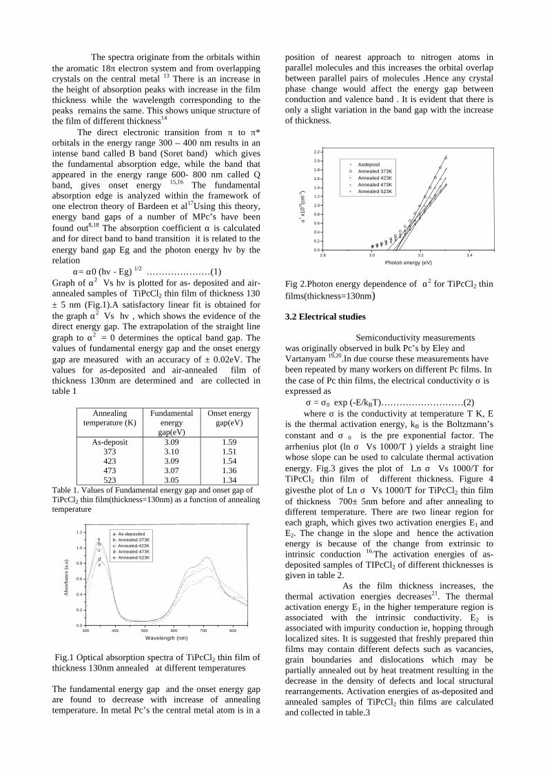
The spectra originate from the orbitals within the aromatic 18π electron system and from overlapping crystals on the central metal 13 There is an increase in the height of absorption peaks with increase in the film thickness while the wavelength corresponding to the peaks remains the same. This shows unique structure of the film of different thickness14 The direct electronic transition from π to π* orbitals in the energy range 300 – 400 nm results in an intense band called B band (Soret band) which gives the fundamental absorption edge, while the band that appeared in the energy range 600- 800 nm called Q band, gives onset energy 15,16 The fundamental absorption edge is analyzed within the framework of one electron theory of Bardeen et al17Using this theory, energy band gaps of a number of MPc’s have been found out8,18 The absorption coefficient α is calculated and for direct band to band transition it is related to the energy band gap Eg and the photon energy hν by the relation α= α0 (hν - Eg) 1/2 …………………(1) Graph of α2 Vs hν is plotted for as- deposited and air-annealed samples of TiPcCl2 thin film of thickness 130 ± 5 nm (Fig.1).A satisfactory linear fit is obtained for the graph α2 Vs hν , which shows the evidence of the direct energy gap. The extrapolation of the straight line graph to α2 = 0 determines the optical band gap. The values of fundamental energy gap and the onset energy gap are measured with an accuracy of ± 0.02eV. The values for as-deposited and air-annealed film of thickness 130nm are determined and are collected in table 1
Annealing temperature (K)
Fundamental energy
gap(eV)
Onset energy gap(eV)
As-deposit 373 423 473 523
3.09 3.10 3.09 3.07 3.05
1.59 1.51 1.54 1.36 1.34
Table 1. Values of Fundamental energy gap and onset gap of TiPcCl2 thin film(thickness=130nm) as a function of annealing temperature
300 400 500 600 700 8000.0
0.2
0.4
0.6
0.8
1.0
1.2
ed
cba
a- As-depositedb- Annealed-373Kc- Annealed-423Kd- Annealed-473Ke- Annealed-523K
Abs
orba
nce
(a.u
)
Wavelength (nm)
Fig.1 Optical absorption spectra of TiPcCl2 thin film of thickness 130nm annealed at different temperatures The fundamental energy gap and the onset energy gap are found to decrease with increase of annealing temperature. In metal Pc’s the central metal atom is in a
position of nearest approach to nitrogen atoms in parallel molecules and this increases the orbital overlap between parallel pairs of molecules .Hence any crystal phase change would affect the energy gap between conduction and valence band . It is evident that there is only a slight variation in the band gap with the increase of thickness.
2.8 3.0 3.2 3.40.0
0.2
0.4
0.6
0.8
1.0
1.2
1.4
1.6
1.8
2.0
2.2
Asdeposit Annealed 373K Annealed 423K Annealed 473K Annealed 523K
α2 x
1010
(cm
-2)
Photon energy (eV)
Fig 2.Photon energy dependence of α2 for TiPcCl2 thin films(thickness=130nm) 3.2 Electrical studies Semiconductivity measurements was originally observed in bulk Pc’s by Eley and Vartanyam 19,20.In due course these measurements have been repeated by many workers on different Pc films. In the case of Pc thin films, the electrical conductivity σ is expressed as σ = σ0 exp (-E/kBT)………………………(2) where σ is the conductivity at temperature T K, E is the thermal activation energy, kB is the Boltzmann’s constant and σ 0 is the pre exponential factor. The arrhenius plot (ln σ Vs 1000/T ) yields a straight line whose slope can be used to calculate thermal activation energy. Fig.3 gives the plot of Ln σ Vs 1000/T for TiPcCl2 thin film of different thickness. Figure 4 givesthe plot of Ln σ Vs 1000/T for TiPcCl2 thin film of thickness 700± 5nm before and after annealing to different temperature. There are two linear region for each graph, which gives two activation energies E1 and E2. The change in the slope and hence the activation energy is because of the change from extrinsic to intrinsic conduction 16.The activation energies of as-deposited samples of TIPcCl2 of different thicknesses is given in table 2. As the film thickness increases, the thermal activation energies decreases21. The thermal activation energy E1 in the higher temperature region is associated with the intrinsic conductivity. E2 is associated with impurity conduction ie, hopping through localized sites. It is suggested that freshly prepared thin films may contain different defects such as vacancies, grain boundaries and dislocations which may be partially annealed out by heat treatment resulting in the decrease in the density of defects and local structural rearrangements. Activation energies of as-deposited and annealed samples of TiPcCl2 thin films are calculated and collected in table.3
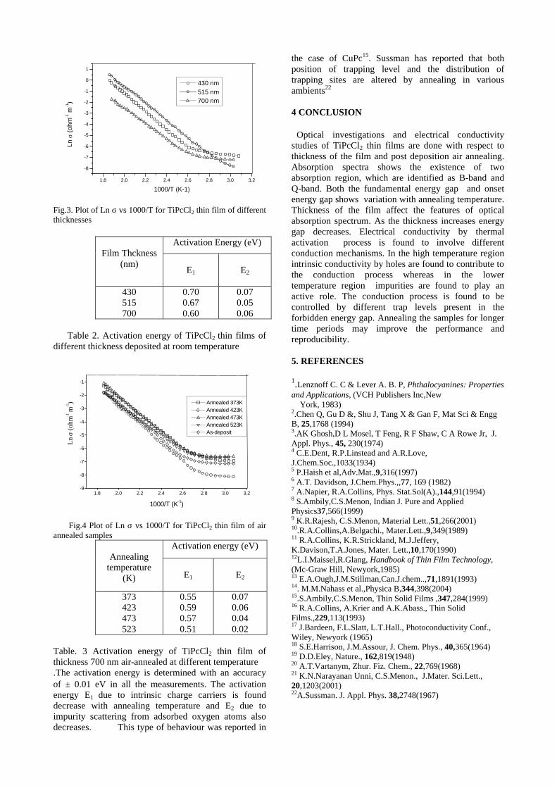
1.8 2.0 2.2 2.4 2.6 2.8 3.0 3.2
-8
-7
-6
-5
-4
-3
-2
-1
0
1
430 nm 515 nm 700 nm
Ln σ
(oh
m-1 m
-1)
1000/T (K-1)
Fig.3. Plot of Ln σ vs 1000/T for TiPcCl2 thin film of different thicknesses
Table 2. Activation energy of TiPcCl2 thin films of different thickness deposited at room temperature
1.8 2.0 2.2 2.4 2.6 2.8 3.0 3.2-9
-8
-7
-6
-5
-4
-3
-2
-1
Ln
σ (o
hm-1 m
-1)
Annealed 373K Annealed 423K Annealed 473K Annealed 523K As-deposit
1000/T (K-1)
Fig.4 Plot of Ln σ vs 1000/T for TiPcCl2 thin film of air annealed samples
Activation energy (eV) Annealing
temperature (K)
E1
E2
373 423 473 523
0.55 0.59 0.57 0.51
0.07 0.06 0.04 0.02
Table. 3 Activation energy of TiPcCl2 thin film of thickness 700 nm air-annealed at different temperature .The activation energy is determined with an accuracy of ± 0.01 eV in all the measurements. The activation energy E1 due to intrinsic charge carriers is found decrease with annealing temperature and E2 due to impurity scattering from adsorbed oxygen atoms also decreases. This type of behaviour was reported in
the case of CuPc15. Sussman has reported that both position of trapping level and the distribution of trapping sites are altered by annealing in various ambients22 4 CONCLUSION Optical investigations and electrical conductivity studies of TiPcCl2 thin films are done with respect to thickness of the film and post deposition air annealing. Absorption spectra shows the existence of two absorption region, which are identified as B-band and Q-band. Both the fundamental energy gap and onset energy gap shows variation with annealing temperature. Thickness of the film affect the features of optical absorption spectrum. As the thickness increases energy gap decreases. Electrical conductivity by thermal activation process is found to involve different conduction mechanisms. In the high temperature region intrinsic conductivity by holes are found to contribute to the conduction process whereas in the lower temperature region impurities are found to play an active role. The conduction process is found to be controlled by different trap levels present in the forbidden energy gap. Annealing the samples for longer time periods may improve the performance and reproducibility. 5. REFERENCES 1.Lenznoff C. C & Lever A. B. P, Phthalocyanines: Properties and Applications, (VCH Publishers Inc,New York, 1983) 2.Chen Q, Gu D &, Shu J, Tang X & Gan F, Mat Sci & Engg B, 25,1768 (1994) 3.AK Ghosh,D L Mosel, T Feng, R F Shaw, C A Rowe Jr, J. Appl. Phys., 45, 230(1974) 4 C.E.Dent, R.P.Linstead and A.R.Love, J.Chem.Soc.,1033(1934) 5 P.Haish et al,Adv.Mat.,9,316(1997) 6 A.T. Davidson, J.Chem.Phys.,,77, 169 (1982) 7 A.Napier, R.A.Collins, Phys. Stat.Sol(A).,144,91(1994) 8 S.Ambily,C.S.Menon, Indian J. Pure and Applied Physics37,566(1999) 9 K.R.Rajesh, C.S.Menon, Material Lett.,51,266(2001) 10.R.A.Collins,A.Belgachi., Mater.Lett.,9,349(1989) 11 R.A.Collins, K.R.Strickland, M.J.Jeffery, K.Davison,T.A.Jones, Mater. Lett.,10,170(1990) 12L.I.Maissel,R.Glang, Handbook of Thin Film Technology, (Mc-Graw Hill, Newyork,1985) 13 E.A.Ough,J.M.Stillman,Can.J.chem..,71,1891(1993) 14. M.M.Nahass et al.,Physica B,344,398(2004) 15.S.Ambily,C.S.Menon, Thin Solid Films ,347,284(1999) 16 R.A.Collins, A.Krier and A.K.Abass., Thin Solid Films.,229,113(1993) 17 J.Bardeen, F.L.Slatt, L.T.Hall., Photoconductivity Conf., Wiley, Newyork (1965) 18 S.E.Harrison, J.M.Assour, J. Chem. Phys., 40,365(1964) 19 D.D.Eley, Nature., 162,819(1948) 20 A.T.Vartanym, Zhur. Fiz. Chem., 22,769(1968) 21 K.N.Narayanan Unni, C.S.Menon., J.Mater. Sci.Lett., 20,1203(2001) 22A.Sussman. J. Appl. Phys. 38,2748(1967)
Activation Energy (eV) Film Thckness
(nm) E1
E2
430 515 700
0.70 0.67 0.60
0.07 0.05 0.06

.
TRANSFER OF COPYRIGHT Please complete as appropriate and return by fax/mail. If you do not provide a copyright clearance, we cannot include your paper in the proceedings. [ ] My employer has given clearance for this
paper to be published. OR [ ] I am the holder of the copyright for this
paper The author who sign the copyright Signature: ......................................................... Date: ........................................................ Affiliation: ……………………………………. …………………………………………………

………………………………………………… …………………………………………………
Optical and Electrical properties of vacuum deposited Anthracene thin films
Sreejith K.Pisharady, C.S.Menon and C.Sudarshana Kumar School of Pure and Applied Physics
Mahatma Gandhi University, Kottayam, Kerala-656 560, India E mail address [email protected]
ABSTRACT Anthracene is one of a promising organic semiconductor widely studied in the recent years. In this work we investigate the optical and electrical properties of vacuum deposited Anthracene thin films. The UV–Vis spectrum of Anthracene is recorded and the optical band gap is determined is 2.98eV. For studying electrical properties we use a Metal- Semiconductor-Metal structure. Anthracene thin film is sandwiched between two Silver electrodes. The J-V characteristics show ohmic type conduction in the lower applied voltages and conduction is space charge limited in the higher applied
voltages. From the observed J-V characteristics the concentration of thermally generated charge carriers 0ρ is determined.
The temperature depended J-V characteristics yield information about depth of traps below the valence band edge and total trap density.
1 INTRODUCTION
The study of charge transport through a thin film is important for understanding the conduction through the film and also reveals a number of semiconductor parameters along with the information about the trap distribution. Anthracene (Ac) is an organic semiconductor extensively investigated over many decades. It is a model system to study the optical and some peculiar electrical properties of organic molecular crystals. Early studies on anthracene reveal several typical semi-conducting effects like photoconductivity, photovoltaic effect, and electro luminescence1. The mobility of Ac extended up to 1cm2/V depending on the purity and the quality of single crystals. This made them as a promising candidate for fabricating organic field effect transistors (OFETs) 2.
Two types of conductions are studied transverse and longitudinal. In the former case conduction is perpendicular to the substrate plane and in later conduction is along the surface of the film. The study of longitudinal conductivity is desirable for applications, which relay on surface conductivity. On studying the Current voltage characteristics in the transverse direction can provide information about the conduction mechanism through the film and the temperature dependent conductivity can be used to calculate a number of parameters such as trap density (Nt), number of states in the valence band (Nv) and activation energy. These parameters are very useful for understanding the semi conducting property of the material and in designing thin film devices. Several authors investigate the hole trapping in single crystal anthracene by thermally stimulated currents and by photon induced detrapping and also found various ohmic contacts suitable for effective injection of charge carriers3-5. In this work we investigate the optical and electrical properties of vacuum deposited Ac thin films.
2 EXPERIMENTAL
Natural Ac is originally procured from Aldrich chemical company (U.S.A). Highly polished and thoroughly cleaned micro glass slides are used as substrates. The evaporation is carried in a molybdenum boat using Hind Hivac12A4 vacuum coating machine, under a base pressure of 5×10⁻⁶ Torr. Thick nesses of the films are counter checked by Tolansky’s multiple beam interference technique6. U.V-Visible absorption spectrum is recorded using a Shimadzu 160A spectrophotometer. For studying J-V characteristics we use a Metal-Semiconductor-Metal structure -Silver/Anthracene/Silver (Ag/Ac/Ag) structure. For this a thin film of Ag is vacuum deposited on to a pre cleaned glass substrate as bottom electrode. Over this Ac layer is vacuum deposited. Finally a thin layer of Ag is vacuum deposited as top electrode. The electrical characteristics are studied using a programmable Keithley electrometer (Model NO.617). Since Ac is a photosensitive material, conductivity study is made in darkness and in a rough vacuum of the order 10-3torr to avoid any possible contamination of the films. 3 RESULTS AND DISCUSSIONS 3.1 Optical properties Figure 1 shows the optical absorption spectrum of Ac thin film of thickness 1800A0 prepared at room temperature. It shows a flat absorption peak around 390nm originates from π-π* transitions in free anthracene molecule. The broadening of absorption
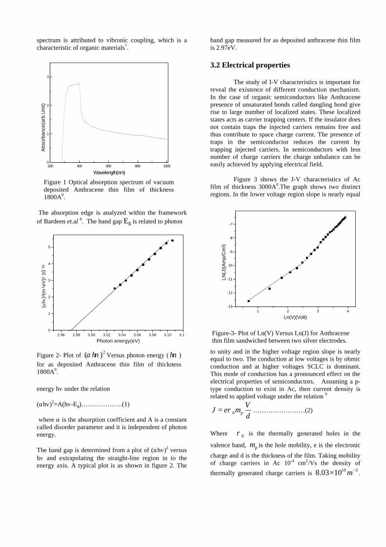
spectrum is attributed to vibronic coupling, which is a characteristic of organic materials7.
The absorption edge is analyzed within the framework of Bardeen et.al 8. The band gap Eg is related to photon
energy hν under the relation (αhν)2=A(hν-Eg)……………….(1) where α is the absorption coefficient and A is a constant called disorder parameter and it is independent of photon energy. The band gap is determined from a plot of (αhν)2 versus hν and extrapolating the straight-line region in to the energy axis. A typical plot is as shown in figure 2. The
band gap measured for as deposited anthracene thin film is 2.97eV. 3.2 Electrical properties
The study of I-V characteristics is important for reveal the existence of different conduction mechanism. In the case of organic semiconductors like Anthracene presence of unsaturated bonds called dangling bond give rise to large number of localized states. These localized states acts as carrier trapping centers. If the insulator does not contain traps the injected carriers remains free and thus contribute to space charge current. The presence of traps in the semiconductor reduces the current by trapping injected carriers. In semiconductors with less number of charge carriers the charge unbalance can be easily achieved by applying electrical field.
Figure 3 shows the J-V characteristics of Ac
film of thickness 3000A0.The graph shows two distinct regions. In the lower voltage region slope is nearly equal
to unity and in the higher voltage region slope is nearly equal to two. The conduction at low voltages is by ohmic conduction and at higher voltages SCLC is dominant. This mode of conduction has a pronounced effect on the electrical properties of semiconductors. Assuming a p-type conduction to exist in Ac, then current density is related to applied voltage under the relation 9
d
VeJ pµρ0= ……………………(2)
Where 0ρ is the thermally generated holes in the
valence band, pµ is the hole mobility, e is the electronic
charge and d is the thickness of the film. Taking mobility of charge carriers in Ac 10-4 cm2/Vs the density of
thermally generated charge carriers is 10 38.03 10 m−× .
200 400 600 800 10000
1
2
3
Abs
orba
nce(
arb.
Uni
t)
Wavelength(nm)
Figure 1 Optical absorption spectrum of vacuum deposited Anthracene thin film of thickness 1800A0.
Figure 2- Plot of 2( )hα ν Versus photon energy ( hν )
for as deposited Anthracene thin film of thickness 1800A0.
2.96 2.98 3.00 3.02 3.04 3.06 3.08 3.10 3.120
1
2
3
4
5
( αh ν
)2(m
-1eV
)2 1
0 16
Photon energy(eV)
1 2 3 4-13
-12
-11
-10
-9
-8
-7LN
(J)(
Am
p/C
m2 )
Ln(V)(Volt)
Figure-3- Plot of Ln(V) Versus Ln(J) for Anthracene thin film sandwiched between two silver electrodes.
The carrier density determined in the present work deviate nearly one order of magnitude from the value reported by M.Gamoudi et.al3. This deviation is attributed to the difference in ohmic contacts used in the present work. For low applied voltages the thermally generated carriers is smaller than the injected carriers, the above equation can be modified as
−−
=kT
EvEf
d
VNveJ p
)(exp)(0 µ …(3)
Where Nv is the effective density of states in the
valence band and )( EvEf − is the separation between
valence band edge and Fermi level.
From the equation (3) it is clear that a plot of
ln
V
J versus
T
1 is a straight line whose slope gives
)( EvEf − and the intercept at
T
1=0 gives Nvpµ .
A typical plot of Ac film of thickness 3000A0 with a constant biasing voltage of 15V is shown in figure -4.
The value of Nvpµ and )( EvEf − are
1.97×10¹⁰m-1V-1s-1 and 0.17eV.
The expression for current density described by the equation 2 is true only in the case of a trap less insulator or for small-applied voltages. But above a particular value of voltage, called threshold voltage the expression for current density can be modified as 9
=
3
2
8
9
d
VJ pθεµ …………….(3)
Where ε is the permittivity of Ac, which is equal to 11 2 1 22.8 10 C N m− − −× and θ is the ratio of free to
trapped charge carriers. The value of θ determined is
4.17×10⁻¹³. The determination of θ directly yields the trap density and the trap level (activation energy foe holes) below the valence band edge. The trap density and activation energy for holes determined 4.85×10²³ m-3 and 0.16eV respectively. 4CONCLUSION
The optical absorption spectrum shows a broad absorption peak originates due to π-π* transition and the analysis of the fundamental absorption edge gives the band gap of vacuum deposited anthracene thin film. The determined band gap is 2.97eV. From the electrical studies it is found that the conduction in the lower applied voltages is ohmic while higher voltage regions the conduction is space charge limited. References 1R.Resel, M. Ochzelt, K. Shimizu, Atsuko and N. K. Takemura Solid-state communications.129, 163 (2004). 2Y.Inoue and S.Tokito J.Appl.Phy.95, 5795 (2004) 3M.Gamoudi,N.Rosenberg, G.Guillaud, M.Maitrot and G.Mesnard.J.Phys.C.Solid State.Phy, 7,1149(1974) 4 G.T.Pott and D.F.Williams J.Chem.Phys51, 1901(1969). 5G.M.Parkinson,J.M.Thomas and J.O.Williams J.Phys.C.Solid.State.Phys 7,L310 (1974). 6 L.I. Maissel and Glang. Hand Book of Thin Film Technology. (Mc Graw.Hill, New York, 1983) P. 11. 7 J.J.M. Halls, D.R. Baigent, F. CaciaUi, N.C. Greenham, R.H. Friend, S.C. Moratti and A.B. Holmes, Thin solid Films 276,13(1996) 8 Bardeen, F.J. Slatt and L.J. Hall, Photoconductivity Conf. (Wiley, New York (1956) 146. 9 M.A.Lampet.Rep.Phys.27, 329 (1964)
2.5 2.6 2.7 2.8 2.9 3.0 3.1
-11.2
-11.0
-10.8
-10.6
-10.4
-10.2
-10.0
Ln(J
/V)(
Am
p/m
2 -V
)
1000/T(k-1)
Figure 4 Plot of lnJ
VVersus
1000
T for Anthracene
thin film sandwiched between two silver electrodes.
Electrical properties of Hot Wall Epitaxy grown
1-(2-amino-ethylamino)-9,10-anthraquinone Films
Sonik Bhatia, R.K Bedi, Subodh Kumar1
Material Science Laboratory, Department of Physics, Guru Nanak Dev University, Amritsar-143 005, India
1Department of Chemistry, Guru Nanak Dev University, Amritsar-143 005, India.
E mail: [email protected]
Abstract : Among organic compounds , the electronic properties of 9-10- anthraquinones are strongly influenced by the nature and the position of the substituent. In the present paper the compound 1-(2-amino-ethylamino)-9,10-anthraquinone has been synthesized. Films are deposited onto the glass substrates at different substrate temperatures(318,333&348K) in a vacuum of 10-5 torr .The current – voltage characteristic of these films show ohmic conduction with in the investigated field (5-60V) and temperature range (295-400K) The electrical conductivity films were determined in a vacuum of 10-5 torr using two probe technique. It is observed that both the electrical conductivity and carrier concentration increases with increase in absolute temperature and also films grown at higher substrate temperature shows higher conductivity and carrier concentration. The activation energies of carriers has been found to be in the range of 0.472-0.414eV. The dielectric constant of the compound at various frequencies is also calculated and is found to be 15.79 Fm-1 at 2KHz. 1. INTRODUCTION The structural features of the substituents among organic compounds plays a vital role in designing molecular electronic devices. Among these the increase in electron donating ability of the substituents at various positions of 9,10-anthraquinones remarkably affect the colour and redox properties of the molecules. Moreover these anthraquinone derived compounds have a great deal of interest because of their optical and photosemiconducting properties1,2. Pohl et al3. studied resistivity and activation energy of some polyacene quinone radical polymers. Latef et.al.4,5 reported the electrical, optical and structural properties of 9,10-anthraquinone films. Different functional derivatives of 9,10- anthraquinone have been synthesized and studied by Aman et.al6-8 . The Properties of the films are greatly influenced by the deposition conditions and technique employed in depositing thin films It is observed that improvement in grain size and reduced structural defects occurs when deposition is done under thermodynamical equilibrium. Hot Wall Epitaxy (HWE) studied by Lopez Oterio permits film deposition near thermodynamical equilibrium9. In this communication we report the electrical properties of 1-(2-amino-ethylamino)-9,10-anthraquinone films prepared by Hot wall Epitaxy technique(HWE)10 onto the glass substrate kept at different temperatures (318,333,348K). 2. EXPERIMENTAL
2.1Synthesis of 1-(2-amino-ethylamino)-9,10-anthraquinone compound The solution of 1-chloroanthraquinone (1g,.004 mol) and ethylenediamine(3.48ml,.05mol ) in acetonitrile (25 ml ) containing suspension of anhydrous potassium carbonate (1.08g ) was refluxed with stirring at 363 K for 24-30 hours. After the completion of the reaction, the suspended solid was filtered off and the residue was washed with methanol and chloroform. The combined filtrate and washing were distilled off under vacuum and residue was crystallized. The crystallized residue was again chromatographed on silica gel column by using hexane, chloroform, ethyl acetate and their mixtures as eluents to isolate pure 1-(2-amino-ethylamino)-9,10-anthraquinone.The structure of the compound is shown in Fig. 1 2.2.Preparation of 1-(2-amino-ethylamino)-9,10-anthraquinone films: The compound 1-(2-amino-ethylamino)-9,10-anthraquinone in powder form was placed in a HWE set up described earlier [9]. Glass slides used as substrates were first cleaned chemically and then ultrasonically to ensure that films may not be contaminated. The vacuum chamber (of Hind High vacuum coating unit (12A4H) was baked at high temperature for degassing. After attaining suitable experimental conditions the films were deposited in a vacuum of order of 10-5 torr. After depositing films at
particular substrate temperature the system was allowed to attain room temperature in that vacuum only after that films were removed from the chamber for further studies.
O
O
HN
H 2N
Fig. 1 2.3 Measurements The thickness of the films were determined using depth profiler (Dektek 3030-XT). The temperature of glass substrates were controlled by a closed loop PID temperature controller using a K-type thermocouple. The steady state value of current was recorded at regular intervals of 5 K using an electrometer (Keithley 6517 A). Silver contacts were used to connect electrical leads to the films. Dielectric measurements were made using A.C impedance spectrometer (Helwett Packered). For these measurements the compound was taken in pellet form of thickness 3.5x10⁻⁴m and diameter 1.3x10⁻²m and then measurements were made using the above mentioned spectrometer. 3. RESULTS AND DISCUSSION The variation of the electrical conductivity vs. inverse of temperature for the 1-(2-amino-ethylamino)-9,10-anthraquinone films kept at different substrate temperatures is shown in Fig. 2 and the variation suggest that the sample under investigation is semiconducting in nature. With increase in temperature of these films, (kept at particular substrate temperature) the conductivity is found to rise as shown in fig.2 with almost straight line, suggesting the applicability of well known Arrhenius relation ó = óo exp(-ÄE/2kT) where ÄE is the activation energy, k is Boltzmann’s constant and T is absolute temperature. Higher substrate temperature (348K) grown film shows higher conductivity than observed for the film at lower substrate (318K), which can be explained using Petritz’s barrier model 11. As at higher substrate temperature, the nucleation centers are fewer which results in large crystallites and thus decreases the barrier size which results in increase in conductivity. It has been suggested12 that films of aromatic organic compounds can be considered as an array of potential wells separated by intermolecular barriers. In this model, charge carrier motion occurs by hopping
mechanism. The conductivity observed for this sample is found to be larger by a factor of 102 than that obtained for 9,10-anthraquinoe films6(at higher temperatures) The activation energy has been calculated from the slope of log of conductivity vs. inverse of temperature and is found to lie in the range 0.472-0.414eV.The activation energy is found to decrease with increase in substrate temperature thus indicating the formation of more ordered films at higher substrate temperatures. The charge carrier concentration is determined using the relation 13 n=2(2Πm+ kT/h2)3/2exp(-Eρ/2kT) where m+ is the effective mass of a charge carrier which is assumed to be equal to the real mass of a free electron and h is Planck' s constant. The variation of charge carrier concentration vs. inverse absolute temperature is shown in the Fig. 3. Here also carrier concentration increases with increase in temperature and also carrier concentration is found to be more for the films grown at higher substrate temperatures. The value of carrier concentration for 1-(2-amino-ethylamino)-9,10-anthraquinone films prepared by this technique is found to be larger by a factor of 102 than compared with 9,10-anthraquinone films6 Fig. 2
Fig. 3
-8
-7
-6
-5
-4
-3
2.4 2.6 2.8 3 3.2 3.4
1000/T (K-1)
Log σ
(ohm
-1cm
-1) 348K
333K318K
0
0.5
1
1.5
2
2.5
3
3.5
4
4.5
2.6 2.8 3 3.2 3.4
1000/T (K-1)
nx10
16 (
cm-3)
348K
333K
318K
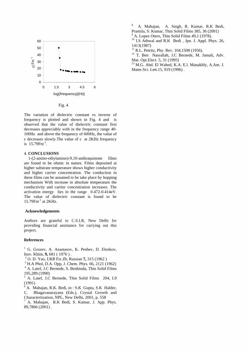
Fig. 4 The variation of dielectric constant vs inverse of frequency is plotted and shown in Fig. 4 and is observed that the value of dielectric constant first decreases appreciably with in the frequency range 40-100Hz and above the frequency of 600Hz, the value of ε decreases slowly.The value of ε at 2KHz frequency is 15.79Fm-1. 4. CONCLUSIONS 1-(2-amino-ethylamino)-9,10-anthraquinone films are found to be ohmic in nature. Films deposited at higher substrate temperature shows higher conductivity and higher carrier concentration. The conduction in these films can be assumed to be take place by hopping mechanism With increase in absolute temperature the conductivity and carrier concentration increases. The activation energy lies in the range 0.472-0.414eV. The value of dielectric constant is found to be 15.79Fm-1 at 2KHz. Acknowledgements Authors are grateful to C.S.I.R, New Delhi for providing financial assistance for carrying out this project. References 1 G. Grozev, A. Anastasov, K. Peshev, D. Elenkov, Insv. Khim, 9, 681 ( 1976 ) . 2 O. D. Yao, UKR Fiz Zh, Russian 7, 315 (1962 ) 3 H.A Phol, D.A. Opp, J. Chem. Phys. 66, 2121 (1962) 4 A. Latef, J.C Bernede, S. Benhinda, Thin Solid Films 195,289 (1990) 5 A. Latef, J.C Bernede, Thin Solid Films 204, L9 (1991) 6 A. Mahajan, R.K. Bedi, in : S.K Gupta, S.K Halder, C. Bhagavanarayana (Eds.), Crystal Growth and Charactertization, NPL, New Delhi, 2001, p. 558 7 A. Mahajan, R.K Bedi, S. Kumar, J. App. Phys. 89,7866 (2001) .
8 A. Mahajan, A. Singh, R. Kumar, R.K Bedi, Pramila, S. Kumar, Thin Solid Films 385, 36 (2001) 9 A. Lopez Otero, Thin Solid Films 49,1 (1978). 10 I.S Athwal and R.K Bedi , Jpn. J. Appl. Phys. 26, 1413(1987) 11 R.L. Petritz, Phy. Rev. 104,1508 (1956). 12 T. Ben Nasrallah, J.C Bernede, M. Jamali, Adv. Mat. Opt.Elect. 5, 31 (1995) 13 M.G. Abd. El Wahed, K.A. E.l. Manakhly, A.Am. J. Mater.Sci. Lett.15, 919 (1996) .
0
10
20
30
40
50
60
0 1.5 3 4.5 6
log(frequency)(Hz)
ε( F
m−1
)
HALL EFFECT AT MICROWAVE FREQUNCIES USING CAVITY
PERTURBATION TECHNIQUE
D.V.B.Murthy, V.Subramanian and V.R.K.Murthy Microwave Laboratory, Department of Physics, Indian Institute of Technology, Madras, Chennai-
600 036. Email: [email protected]
ABSTRACT: An experimental technique for the measurement of mobility of carriers in semiconductors at microwave frequencies is explained. The interaction between the electromagnetic radiation and the charge carriers in semiconductors under the external steady state magnetic field intensity results in the coupling of between two orthogonally polarized electric fields in a bimodal microwave cavity. In this paper, the design and analysis of the TE111 circular bimodal cavity is described. Probe coupling is chosen for the excitation of the bimodal cavity. Tuning procedure for attaining the mode degeneracy and orthogonality is also explained. A canceling channel, which is having attenuator and phase shifter, is used to increase the sensitivity of the measurement. Measurements on the n-type silicon and compound semiconductors were done and found the calibration constant. 1. INTRODUCTION :
Most of the techniques at microwave frequencies are non contact and non destructive in nature. Microwave Hall effect is one such technique which is used to evaluate the transport properties of the semiconductor materials. Microwave Hall effect was first discovered by S. P. Cooke in 1948 [1]. N.Watnabe (1960) & (1961) [2-3] was developed this technique to measure the electrical transport properties of low mobility samples and to verify high frequency effects on Hall mobility. Pethig and South (1974) [4] used circular bimodal cavity. Introduction of network analysers helped a lot in improving this technique further [5]. Linfeng Chen et.al (1998) [6] used this technique to study the electrical transport properties of fine magnetic particles. Recently Prati et.al (2003) [7] applied this technique successfully in calculating the mobility of the heterostructures. M.Schrape et.al [8] used this technique to characterize the pyrite crystals. 1.1 Theory: The interaction between the electromagnetic radiation and the charge carriers in semiconductors under the external steady state magnetic field intensity results in the coupling of between two orthogonally polarized electric fields in a bimodal microwave cavity. In order to observe this Hall effect, one requires a bimodal cavity and a canceling channel which consists of attenuator and phase shifter. The coupled power has to be nullified by using a canceling channel. The change in the transmitted power with the application of external d.c.magnetic field is directly proportional to the mobility of the carriers. The Scattering matrix of the degenerate bimodal cavity containing a sample relates the amplitudes of the reflected waves a1, a2, to the amplitudes of the incident waves b1, b2 as follows.
=
2
1
22
12
21
11
2
1
b
b
S
S
S
S
a
a 1
Where S11 is the reflection coefficient at port1, S22 is the reflection coefficient at port2, S12, S21 are the transmission coefficients from input 2 to input 1 and Vice Versa. The following assumptions are made in deriving the scattering matrix of the bimodal cavity containing the sample: 1) The skin depth (δ ) of the sample is larger than the sample thickness. 2) 1<<ωτ , where ω is the field angular frequency and τ is the carrier relaxation time.
3) 1<<Bµ , where µ is the microwave Hall mobility
and B is the d.c.magnetic field. 4) The frequency of both the modes of the cavity should be same after placing the sample. ( 0=∆ω ) The expression for the microwave Hall mobility is obtained from the transmission coefficient of the scattering matrix .The mobility values are calculated using M.M.Sayed and Westgate approach [9] and the equation is given below.
( )( )1
211 21
11 21 1210 20
1 1 1 1Q QK
SB Q Q
µ−
= − − − Γ − Γ
Where K is calibration constant, S21 =122
1
P
P
;
10Q , 20Q , 11Q and 21Q are the loaded and unloaded
quality factors at port1 and port2; 11Γ and 21Γ are the
unloaded and loaded reflection coefficients of the input1 and output 2. The above equation is valid for non-equal input and output coupling.
2
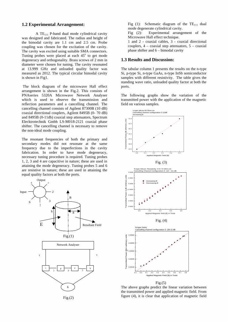
1.2 Experimental Arrangement:
A TE111 P-band dual mode cylindrical cavity was designed and fabricated. The radius and height of the bimodal cavity are 1.1 cm and 2.5 cm. Probe coupling was chosen for the excitation of the cavity. The cavity was excited using suitable SMA connectors. Tuning probes were placed at each 45o to get mode degeneracy and orthogonality. Brass screws of 2 mm in diameter were chosen for tuning. The cavity resonated at 13.999 GHz and unloaded quality factor was measured as 2012. The typical circular bimodal cavity is shown in Fig1.
The block diagram of the microwave Hall effect arrangement is shown in the Fig.2. This consists of PNAseries 5320A Microwave Network Analyser which is used to observe the transmission and reflection parameters and a cancelling channel. The cancelling channel consists of Agilent 87300B (10 dB) coaxial directional couplers, Agilent 8495B (0- 70 dB) and 8495B (0-11db) coaxial step attenuators, Spectrum Elecktrotechnik Gmbh LS-M018-2121 coaxial phase shifter. The cancelling channel is necessary to remove the non-ideal mode coupling. The resonant frequencies of both the primary and secondary modes did not resonate at the same frequency due to the imperfections in the cavity fabrication. In order to have mode degeneracy, necessary tuning procedure is required. Tuning probes 1, 2, 3 and 4 are capacitive in nature; these are used in attaining the mode degeneracy. Tuning probes 5 and 6 are resistive in nature; these are used in attaining the equal quality factors at both the ports.
Fig.(1) Fig.(2)
Fig (1): Schematic diagram of the TE111 dual mode degenerate cylindrical cavity. Fig (2): Experimental arrangement of the Microwave Hall effect technique. 1 and 2 - coaxial cables, 3 - coaxial directional couplers, 4 – coaxial step attenuators, 5 – coaxial phase shifter and 6 – bimodal cavity
1.3 Results and Discussion: The tabular column 1 presents the results on the n-type Si, p-type Si, n-type GaAs, n-type InSb semiconductor samples with different resistivity. The table gives the standing wave ratio, unloaded quality factor at both the ports. The following graphs show the variation of the transmitted power with the application of the magnetic field on various samples.
0.0 0.1 0.2 0.3 0.4 0.5
-63.0
-62.8
-62.6
-62.4
-62.2
-62.0
-61.8
Tra
nsm
itte
d P
ow
er
S1
2 in
arb
itra
ry u
nits
Applied Magnetic Field (B)
n-type silicon-50 Ohm-cmCancelling channel configuration-3 11dBIncreasing B
Fig. (3)
0.0 0.2 0.4 0.6 0.8
0.0002
0.0003
0.0004
0.0005
0.0006
0.0007
0.0008
N-type Silicon; Resistivity: 4.0-7.0 Ohm-cmCancelling Channel Configuration-2: (10 - 11) dB
Tra
nsm
itte
d P
ow
er
in S 12 in
Arb
itra
ry u
nits
Applied Magnetic field (B) in Tesla
Increasing B Decreasing B
Fig. (4)
-0.1 0.0 0.1 0.2 0.3 0.4 0.5 0.6 0.7 0.8
0.00040
0.00045
0.00050
0.00055
0.00060
N-type GaAs;Cancelling channel configuration-2: (30-2) dB
Tra
nsm
itte
d P
ow
er
(S 12)
in a
rbitr
ary
un
its
Applied Magnetic Field (B) in Tesla
Fig.(5) The above graphs predict the linear variation between the transmitted power and applied magnetic field. From figure (4), it is clear that application of magnetic field
2 2
Network Analyser
3 34 5
6
1 1
2
B
E Resultant Field
a h
1
2
3
45
6
Input
Output
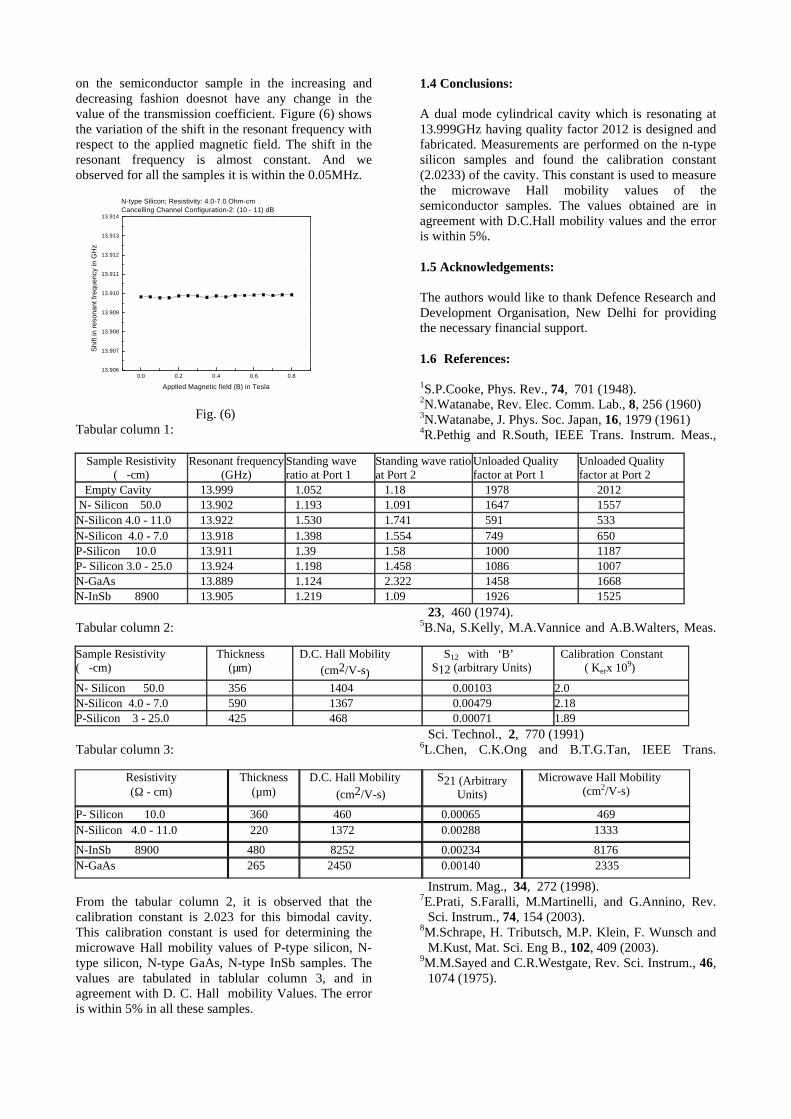
on the semiconductor sample in the increasing and decreasing fashion doesnot have any change in the value of the transmission coefficient. Figure (6) shows the variation of the shift in the resonant frequency with respect to the applied magnetic field. The shift in the resonant frequency is almost constant. And we observed for all the samples it is within the 0.05MHz.
0.0 0.2 0.4 0.6 0.813.906
13.907
13.908
13.909
13.910
13.911
13.912
13.913
13.914
Shi
ft in
res
onan
t fre
quen
cy in
GH
z
Applied Magnetic field (B) in Tesla
N-type Silicon; Resistivity: 4.0-7.0 Ohm-cmCancelling Channel Configuration-2: (10 - 11) dB
Fig. (6) Tabular column 1:
Tabular column 2:
Tabular column 3:
From the tabular column 2, it is observed that the calibration constant is 2.023 for this bimodal cavity. This calibration constant is used for determining the microwave Hall mobility values of P-type silicon, N-type silicon, N-type GaAs, N-type InSb samples. The values are tabulated in tablular column 3, and in agreement with D. C. Hall mobility Values. The error is within 5% in all these samples.
1.4 Conclusions: A dual mode cylindrical cavity which is resonating at 13.999GHz having quality factor 2012 is designed and fabricated. Measurements are performed on the n-type silicon samples and found the calibration constant (2.0233) of the cavity. This constant is used to measure the microwave Hall mobility values of the semiconductor samples. The values obtained are in agreement with D.C.Hall mobility values and the error is within 5%. 1.5 Acknowledgements: The authors would like to thank Defence Research and Development Organisation, New Delhi for providing the necessary financial support. 1.6 References:
1S.P.Cooke, Phys. Rev., 74, 701 (1948). 2N.Watanabe, Rev. Elec. Comm. Lab., 8, 256 (1960) 3N.Watanabe, J. Phys. Soc. Japan, 16, 1979 (1961) 4R.Pethig and R.South, IEEE Trans. Instrum. Meas.,
23, 460 (1974). 5B.Na, S.Kelly, M.A.Vannice and A.B.Walters, Meas.
Sci. Technol., 2, 770 (1991) 6L.Chen, C.K.Ong and B.T.G.Tan, IEEE Trans.
Instrum. Mag., 34, 272 (1998). 7E.Prati, S.Faralli, M.Martinelli, and G.Annino, Rev.
Sci. Instrum., 74, 154 (2003). 8M.Schrape, H. Tributsch, M.P. Klein, F. Wunsch and
M.Kust, Mat. Sci. Eng B., 102, 409 (2003). 9M.M.Sayed and C.R.Westgate, Rev. Sci. Instrum., 46,
1074 (1975).
Sample Resistivity ( -cm)
Resonant frequency (GHz)
Standing wave ratio at Port 1
Standing wave ratio at Port 2
Unloaded Quality factor at Port 1
Unloaded Quality factor at Port 2
Empty Cavity 13.999 1.052 1.18 1978 2012 N- Silicon 50.0 13.902 1.193 1.091 1647 1557 N-Silicon 4.0 - 11.0 13.922 1.530 1.741 591 533 N-Silicon 4.0 - 7.0 13.918 1.398 1.554 749 650 P-Silicon 10.0 13.911 1.39 1.58 1000 1187 P- Silicon 3.0 - 25.0 13.924 1.198 1.458 1086 1007 N-GaAs 13.889 1.124 2.322 1458 1668 N-InSb 8900 13.905 1.219 1.09 1926 1525
Sample Resistivity ( -cm)
Thickness (µm)
D.C. Hall Mobility (cm2/V-s)
S12 with ‘B’ S12 (arbitrary Units)
Calibration Constant ( Kerx 109)
N- Silicon 50.0 356 1404 0.00103 2.0 N-Silicon 4.0 - 7.0 590 1367 0.00479 2.18 P-Silicon 3 - 25.0 425 468 0.00071 1.89
Resistivity (Ω - cm)
Thickness (µm)
D.C. Hall Mobility
(cm2/V-s)
S21 (Arbitrary Units)
Microwave Hall Mobility (cm2/V-s)
P- Silicon 10.0 360 460 0.00065 469 N-Silicon 4.0 - 11.0 220 1372 0.00288 1333
N-InSb 8900 480 8252 0.00234 8176 N-GaAs 265 2450 0.00140 2335
EFFECT OF DIELECTRIC CONSTANT ON THE Q-FACTOR OF FABRY-PEROT RESONATORS CONSTRUCTED FROM PHOTONIC CRYSTALS
E. D. V. Nagesh1, V. Subramanian1, V. Sivasubramanian2 and V. R. K. Murthy1
1Microwave Laboratory, Indian Institute of Technology Madras, Chennai 600 036, India. 2Materials Science Division, Indira Gandhi Centre for Atomic Research, Kalpakkam
603 102, India. Email: [email protected]
ABSTRACT Two dimensional photonic band gap structures (Photonic Crystals) that work in the microwave frequency region were constructed using three different materials, viz; glass, Poly Vinyl Chloride (PVC) and Poly Tetra Fluoro Ethylene (PTFE). The dielectric constants measured were 5.50, 2.38 and 2.10 respectively at 10 GHz. In all the cases only square lattice was considered and the lattice spacing was so chosen that the gap width and / or gap to mid-gap ratio are maximum. Fabry-Perot resonators were constructed by creating line defects in an otherwise pure structure in all the cases. The defect spacing was varied from 1.2 cm to 1.6 cm in all the cases and the quality factor was measured for all the defect modes. The obtained results were explained in terms of the dielectric constant of the samples used. 1. INTRODUCTION The interest in the field of photonic crystals is growing every year because of numerous applications [1-3]. Photonic crystals are the periodic structures in which the lattice sites are occupied by either dielectric and / or magnetic materials. The material at the lattice site acts as a potential and whenever the dielectric constant is greater than unity one can expect a band gap [4]. Within this band gap, the propagation of electromagnetic waves is forbidden. This is similar to the electronic band gaps in a crystal lattice where the periodicity is of the order of Angstroms and the lattice sites are occupied by the ionic cores. In general, the periodicity should be maintained of the order of the wavelength of the source. Thus, in microwave region, the periodicity will be of the order of centimeters thus making it easier to construct manually. While the pure structures act as perfect band reject filters for the electromagnetic waves within a certain frequency range, depending on the applications, it is also possible to create defects and obtain a defect mode within the band gap. The main idea is to obtain a narrow window through which propagation can take place. The defect mode is seen when the resonant condition is satisfied and also it depends on the material that is being used. Also the appearance of the defect mode depends on the position of the defect [5]. While low dielectric constant materials may not be useful in obtaining the resonant modes by creating the point defects, line defects will certainly give rise to resonant modes. This is because with low dielectric constant materials, one may get weak modes and so may not be visible whereas with line defects, the modes couple together giving rise to a vivid resonant mode. There are a number of ways by which we can create defects such as removing the material, inserting a material in the interstitial position, changing the lattice
constant at a certain position and by changing the refractive index of the material at a certain position [6]. In this paper we report the effect of dielectric constant on the Q-factor of the defect modes obtained from the Fabry-Perot resonators constructed from photonic crystals by creating the line defects. The line defects were created by changing the lattice spacing between the 5th and 6th layers of a 10 layer structure so that each five layer set acts as a mirror. With the direction of propagation perpendicular to the defect, the structure acts as a Fabry-Perot resonator [7]. The defect spacing was varied from 1.2 to 1.6 cm in all the cases and the Q-factor values are analyzed in terms of the dielectric constant of the materials used. 1.1 Experimental arrangement A microwave vector network analyzer (HP 8720A) was used to obtain the S12 parameter for the frequency region between 10 and 18 GHz with the help of two horn antennas kept on either side of the structure. The antennas were separated by a distance of 50 cm. The fringe effects of the electric field were assumed to be minimum. Initially, the S12 parameter was normalized without any structure between the antennas. In all the cases, only E-polarized beam (with electric field parallel to the length of the rod) and the normal direction alone (Γ- X direction of first Brillouin zone) was considered. 1.2 Results and discussion Initially, the gap to mid-gap ratio was calculated for different lattice spacings using plane wave expansion method [8] and found to be maximum near 0.9 cm for the
structure made of glass, 1.0 cm for the structure made of PVC and PTFE rods and the lattice spacings were chosen accordingly. 1.2.1 PTFE rods The transmission spectrum obtained for a square lattice of PTFE rods shows a band gap at 13.48 GHz with a gap width of 2.68 GHz that agrees well with the theoretically predicted values of 13.14 GHz and 2.02 GHz. Fig. 1 shows the transmission spectra obtained for a pure structure and the structure with defects with defect spacing varied from 1.2 to 1.6 cm. Line defect was created such that the spacing between the 5th and 6th layer is ‘L’ that is different from the actual lattice spacing. The experiments were done by varying ‘L’ from 1.2 to 1.6 cm and the transmission spectra were as shown in fig. 1. It can be observed that the defect mode shifts towards lower frequency side as the defect spacing is increased indicating the behaviour of a resonator. The Q-factor of the defect mode was calculated to be 18, 17 and 22 for the defect spacing of 1.2, 1.4 and 1.6 cm respectively. It can be observed that the Q-factor is very low.
10 11 12 13 14 15-10
-8
-6
-4
-2
0
2
4
6
8
10
13.24 GHz
13.92 GHz14.38 GHz
Tra
nsm
issi
on (
dB)
Frequency (GHz)
Without defect L=1.2 cm L=1.4 cm L=1.6 cm
Fig. 1 1.2.2 PVC rods In case of PVC rods, the transmission spectrum for a pure structure shows a band gap at 11.65 GHz with a gap width of 3.16 GHz as shown in fig. 2. Theoretically, a band gap is predicted at 12.54 GHz with a gap width of 2.13 GHz which shows a good agreement with the experimentally observed value. Fig. 2 also shows the transmission spectra obtained for the defective structure with the defect spacing varied from 1.2 to 1.6 cm. In this case also, the defect mode is observed to shift towards lower frequency side as the spacing is increased. The Q-factor values of the defect mode for different defect spacings in this case were found to be 52, 53 and 68 respectively. It can be observed that there is an
improvement in Q-factor when compared to that of PTFE case though these values are low.
8 10 12 14
-50
-40
-30
-20
-10
0
10
12.20 GHz12.68 GHz
13.12 GHz
Tra
nsm
issi
on (
dB)
Frequency (GHz)
Without defect L=1.2 cm L=1.4 cm L=1.6 cm
Fig. 2 1.2.3 Glass rods The transmission spectrum taken for a square lattice of glass rods without any defect shows a band gap between 11.19 GHz and 15.59 GHz with a mid-gap frequency of 13.39 GHz. Theoretically a band gap is predicted at 12.90 GHz which shows a good agreement with the experimental value of 13.39 GHz. Fig. 3 shows the transmission spectra for a pure structure as well as for the structure in which the defect spacing is varied from 1.2 to 1.6 cm. The Q-factor of the defect mode calculated from the 3 dB points was found to be 119, 175 and 131 for the separation distance of 1.2, 1.4 and 1.6 cm respectively. The Q-factor in case of glass rods is better than that of PVC case as can be clearly seen from the values given above.
11 12 13 14 15 16 17 18
-50
-40
-30
-20
-10
0
10
13.16 GHz14.00 GHz14.50 GHz
Tra
nsm
issi
on (
dB)
Frequency (GHz)
Without defect L=1.2 cm L=1.4 cm L=1.6 cm
Fig. 3
Fig. 4 shows the variation in the Q-factor for all the
defect spacings for all the three materials. As mentioned above, the dielectric constants of PTFE, PVC and glass were 2.10, 2.38 and 5.50 respectively. By creating a defect, the structure acts like a local resonator and whenever a resonant condition is satisfied, one can get a defect mode. In all the cases, the lattice spacing was chosen in such a way that the gap width is maximum and the experiments were done in a similar manner. The only difference is in the value of dielectric constant.
1.2 1.3 1.4 1.5 1.6
30
60
90
120
150
180
Q-f
acto
r
Defect Spacing (L)
PTFE rods PVC rods Glass rods
Fig. 4 By increasing the dielectric constant, the reflectivity
increases and thus the amount of energy stored in the cavity obtained by creating the defect will be increased. In this case, the increase in the dielectric constant increases the reflectivity of the mirrors and so the Q-factor increases. While PTFE is having very low loss, PVC and glass has a considerable amount of loss (å ”=0.12 and 0.10). The loss involved in the structure also reduces the Q-factor of the defect mode. Simulations were done in case of 1D structures and it was found that an imaginary part of 0.10 in the material decreases the Q-factor by five times. Thus still higher Q-factors could be achieved by using a material of high dielectric constant and very low loss. Thus increase in dielectric constant increases the Q-factor of the resonant mode of Fabry-Perot resonators constructed from photonic crystals.
1.3 Conclusions Photonic Band Gap structures suitable for microwave frequencies were constructed using three different materials of dielectric constant 2.10, 2.38 and 5.50. Line defects were created in the structures and made in the form of Fabry-Perot resonators. The defect spacing was varied and the defect mode was observed to move towards lower frequency side as the defect spacing was increased which is the feature of a resonator. The results
also show that the Q-factor of the defect mode increases with increase in dielectric constant of the material used in constructing the photonic crystals. 1.4 Acknowledgements One of the authors EDVN acknowledges the Defence Research and Development Organization (DRDO), New Delhi, India for providing the financial support in the form of Senior Research Fellowship. References 1Eli Yablonovitch, Phys. Rev. Lett. 58, 2059 (1987). 2S. John and R. Rangarajan, Phys. Rev. B 38, 10101 (1988). 3G. Romo and T. Smy J. Appl. Phys. 94, 2177 (2003). 4J. D. Joannopoulos, R. D. Meade and J. N. Winn, Photonic Crystals: Molding the Flow of Light (Princeton University Press, Princeton, New Jersey, 1995). 5E. D. V. Nagesh, G. Santosh Babu, V. Subramanian, V. Sivasubramanian and V. R. K. Murthy, Eur. Phys. J. B, 41, 177 (2004). 6P. R. Villeneuve, S. Fan and J. D. Joannopoulos, Phys. Rev. B. 54, 7837 (1996). 7B. Temelkuran and E. Ozbay, Appl. Phys. Lett. 74, 486 (1999). 8M. Plihal, A. Shambrook and A. A. Maradudin, Optics Communications 80, 199 (1991).
DIELECTRIC STUDIES OF BINARY MIXTURES IN THE MICROWAVE REGION
T.Vishwam, V.Subramanian and V.R.K.Murthy
Microwave Laboratory, Department of Physics, Indian Institute of Technology, Madras, Chennai-600 036. INDIA
The complex permittivity of the pure systems and pure binary systems and their dilute solutions in a non-polar solvent are measured in the microwave frequency region by using the cavity perturbation technique at X band region (8 -12 GHz) and open-ended coaxial probe technique for contineous range of frequencies from (8-12GHz) by using the 8720A network analyzer and their results are compared. The limitations, advantages and disadvantages of each method are discussed. Dipole moment of the binary systems is calculated from the dielectric data using Guggenhiem's, Higasi's and Gopala Krishna method. The samples under study are benzene, isobutanol, isobutyraldehyde and their binary mixtures.
Introduction: Microwave energy has been directly applied in many fields especially in scientific research such as communication, microwave assisted chemistry and in the development of microwave tomographic imaging imaging systems for medical applications [1].The successful application of microwave is directly associated with the dielectric properties of the materials. The characterization of dielectric materials may include the measurement of complex permittivity as function of frequency at a given temperature or as a function of temperature at a given frequency. The measurement of dielectric properties at a wide frequency range can provide information on the low frequency conduction mechnism, interfacial polarization and molecular dynamics [2] Dielectric dispersion studies of polar liquids and their binary mixtures were carried out with a view for determining the electric dipole moment and relaxation time. The presence of hydrogen bonding brings a considerable change in the relaxation time and dipole moment of the binary system. In the determination of dipole moment, the dipole-dipole interactions are minimized by dilution in a non-polar solvent. In this paper we measured the complex permittivity and dipole moment of aldehyde and alcohol which are the functional groups present in the amino acids and their binary mixtures in solvent medium at X band (8 - 12 GHz) by using two characterization techniques namely cavity perturbation technique [3], and open-ended coaxial probe technique [4, 5, 6] and their results are compared, and limitation of each method is discussed.
Experimental arrangement: The samples used in all the measurements are analytical grade samples and double distilled before measurement. All the measurements are carried out at room temperature and at X band (8-12 GHz) region. We measured the complex permittivity of two different parent liquids, isobutanol and isobutyraldehyde and also its binary mixtures in a non-polar solvent, benzene with different concentrations. The characterization was done using two different techniques and the techniques are described below. 1. Cavity perturbation technique: The experiments were carried out using an HP8720A Network analyzer, which will generate a continuous range of frequencies from 130 MHz-20 GHz. The cavity used here is a reflection type TE106 mode rectangular cavity with resonance frequency at 9.125GHz. A specially designed sample holder is used to keep the sample at the electric field maximum in the cavity. Both the resonance and the quality factor of the cavity will be disturbed with the insertion of the sample and the cavity is said to be perturbed. From the shift in the resonant frequency and from the change in Q factor, one can determine the complex permittivity of the sample at that frequency. 2. Open-ended coaxial probe technique: Open-ended coaxial probes were developed as a type of sensors for broadband and nondestructive measurement of the permittivity of the biological substances. This method is also useful in measuring the dielectric properties of liquids and solids
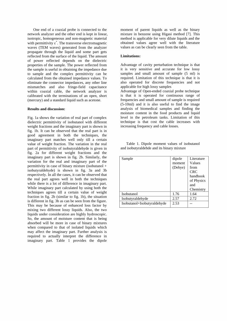
One end of a coaxial probe is connected to the network analyzer and the other end is kept in linear, isotropic, homogeneous and non-magnetic material with permittivity ε*. The transverse electromagnetic waves (TEM waves) generated from the analyzer propagate through the liquid and some part gets reflected from the surface of the liquid. The amount of power reflected depends on the dielectric properties of the sample. The power reflected from the sample is useful in obtaining the impedance due to sample and the complex permittivity can be calculated from the obtained impedance values. To eliminate the connector impedances, any other line mismatches and also fringe-field capacitance within coaxial cable, the network analyzer is calibrated with the terminations of an open, short (mercury) and a standard liquid such as acetone. Results and discussion:
Fig. 1a shows the variation of real part of complex dielectric permittivity of isobutanol with different weight fractions and the imaginary part is shown in fig. 1b. It can be observed that the real part is in good agreement in both the techniques, the imaginary part matches well only till a certain value of weight fraction. The variation in the real part of permittivity of isobutyraldehyde is given in fig. 2a for different weight fractions and the imaginary part is shown in fig. 2b. Similarly, the variation for the real and imaginary part of the permittivity in case of binary mixture (isobutanol + isobutyraldehyde) is shown in fig. 3a and 3b respectively. In all the cases, it can be observed that the real part agrees well in both the techniques while there is a lot of difference in imaginary part. While imaginary part calculated by using both the techniques agrees till a certain value of weight fraction in fig. 2b (similar to fig. 1b), the situation is different in fig. 3b as can be seen from the figure. This may be because of enhanced loss factor by mixing two different lossy liquids. Also, the two liquids under consideration are highly hydroscopic. So, the amount of moisture content that is being absorbed will be more in case of binary mixtures when compared to that of isolated liquids which may affect the imaginary part. Further analysis is required to actually interpret the difference in imaginary part. Table 1 provides the dipole
moment of parent liquids as well as the binary mixture in benzene using Higasi method [7]. This method is applicable for very dilute liquids and the obtained values agree well with the literature values as can be clearly seen from the table. Limitations: Advantage of cavity perturbation technique is that it is very sensitive and accurate for low lossy samples and small amount of sample (5 ml) is required. Limitation of this technique is that it is also operated for discrete frequencies and not applicable for high lossy samples Advantage of Open-ended coaxial probe technique is that it is operated for continuous range of frequencies and small amount of sample is required (5-10ml) and it is also useful to find the image analysis of biomedical samples and finding the moisture content in the food products and liquid level in the petroleum tanks. Limitation of this technique is that cost the cable increases with increasing frequency and cable losses. Table 1. Dipole moment values of isobutanol and isobutyraldehde and its binary mixture
Sample dipole moment (Debye)
Literature Values from CRC handbook of Physics and Chemistry
Isobutanol 1.76 1.64 Isobutyraldehyde 2.57 2.72 Isobutanol+Isobutyraldehyde 2.53 --
0.00 0.02 0.04 0.06 0.08 0.10
2.25
2.30
2.35
2.40
2.45
2.50
2.55
2.60
2.65
2.70 Solute-IsobutanolSolvent-Benzene
Rea
l par
t of d
iele
ctric
per
mitt
ivity
Weight fraction of solute in solvent
Coaxial probe (9.125 GHz) Cavity perturbation (9.125 GHz)
0.04 0.05 0.06 0.07 0.08 0.09 0.100.00
0.02
0.04
0.06
0.08
0.10
0.12 Solute-IsobutanolSolvent-Benzene
Imag
inar
y pa
rt o
f die
ctric
per
mitt
ivity
Weight fraction of solute in solvent
Coaxial probe (9.125 GHz) Cavity perturbation (9.125 GHz)
Fig 1.a) Real and b) Imaginary part of complex dielectric permittivity of Isobutanol in Benzene
0.00 0.02 0.04 0.06 0.08 0.102.2
2.4
2.6
2.8
3.0
3.2
3.4
Solute-IsobutyraldehydeSolvent-Benzene
Rea
l par
t of d
iele
ctric
per
mitt
ivity
Weight fraction of solute in solvent
Cavity perturbation technique (9.125 GHz) Coaxial probe technique (9.125 GHz)
0.04 0.05 0.06 0.07 0.08 0.09 0.100.02
0.03
0.04
0.05
0.06
0.07
0.08
0.09
0.10
0.11
Solute-IsobutyraldehydeSolvent-Benzene
Imag
inar
y pa
rt o
f die
lect
ric p
erm
ittiv
ity
Weight fraction of solute in solvent
Cavity perturbation technique (9.125 GHz) Coaxial probe technique (9.125 GHz)
Fig 2.a) Real and b) Imaginary part of complex dielectric permittivity of Isobutyraldehyde in Benzene.
0.00 0.02 0.04 0.06 0.08 0.102.25
2.30
2.35
2.40
2.45
2.50
2.55
2.60
2.65 Solute-(Isobutanol+Isobutyraldehyde)Solvent-Benzene
Rea
l par
t of d
ilect
ric p
erm
ittiv
ity
Weight fraction of solute in solvent
Coaxial probe (9.125 GHz) Cavity perturbation (9.125 GHz)
0.05 0.06 0.07 0.08 0.09 0.10
0.00
0.02
0.04
0.06
0.08
0.10
Solute-(Isobutanol+Isobutyraldehyde)Solvent-Benzene
Imag
inar
y pa
rt o
f die
lect
ric p
erm
ittiv
ity
Weight fraction of solute in solvent
Coaxial probe (9.125 GHz) Cavity perturbation (9.125 GHz)
Fig3.a) Real and b) Imaginary part of complex dielectric permittivity of (Isobutanol+Isobutyraldehyde) in Benzene References 1. J.C.Bolomey and C.Pichot,"Some applications of
diffraction tomography to electromagnetics -particular case of microwaves,” Inverse problems in scattering and imaging, M.Berto and E.R.Pike, Eds.New York: Adam Hilger, pp.319-344 (1992).
2. A.R.von Hippel, “Dielectric Materials and Applications”, Cambridge, MA: M.I.T press, 1954
3. V R K Murthy and R Raman, Solid State Communication, 70, No.8, 847(1989).
4. Yan-Zhen Wei and S.Sridhar, Rev.Sci.Instrum., 60,3041(1989). 5. A.Boughriet, Z.Wu, H.McCann and L.E.Davis,
1st World Congress on Industrial process Tomography, Buxton, Greater Manchester, April 14-17 (1999).
6. J P Grant, R N Clarkes, G T Symm and N M Spyrou,J.Phys.E.Instrum.22, 757(1989). 7. Higasi.K., Y.Koga and M.Nakamura.,Bull.Chem.Soc.Jpn., 44,988(1971).
OTH OMTAT 2005
Investigation on Porous Silicon based gas sensors
N. Sankara Subramanian1, R. Sriram2, R.Vivek Sabaapathy2
and B. Santhi3 1.Department of Physics, Thiagarajar College of Engineering, Madurai-625 015, India 2.Department of Mechatronics, Thiagarajar College of Engg, Madurai-625 015, India.
3.Department of Physics, Government Girls Hr. Sec. School, Melur, Madurai-625 106, India E-mail: [email protected]
ABSTRACT Porous silicon based gas sensors are employed to detect inflammable and toxic gases. These sensors generally present a high sensibility with detection at low levels of pollutants [1]. The large surface to volume ratio of PS gives it, the capability to sense any gas-induced atmosphere [1,2]. The physical properties of porous Silicon gas sensors, viz., electrical resistance, current have been observed to change in the presence of inorganic gases and organic vapors like LPG, ethanol, methanol and acetone [6-8]. The gas-induced modifications of PS properties like Conductance/current [3,4], capacitance [5] are the sensing parameters of these devices. The advantages of PS gas sensors are low cost, low power consumption compared with metal oxide gas sensors, due to its working at room temperature, and its compatibility with silicon device fabrication technology. In the present work, p-type porous silicon (p-PS) structure was prepared by anodic electrochemical etching process. The p – type silicon wafer of area 1.5 x 1.5 cm2 and a platinum foil of area 1 x 1 cm2 were used as the electrode and immersed in an electrolyte, containing a mixture of water, ethanol and hydrofluoric acid in the ratio 3:6:1. The optimized anodization parameters set in this process were electrode distance 0.75 cm, current density 80 mA and etching duration 40 minutes. The unexposed region of the silicon wafer was coated with wax. Porosity in the nano scale was formed on the exposed area of the silicon wafer, which has been confirmed from the surface analysis using AFM and pore density evaluation. Photoluminescence properties of the p-PS structure have been studied using a Hitachi 650-10S Fluorescence Spectrophotometer and the results have also been presented. Structure of the p-PS has been investigated by XRD analysis and the results have been analyzed. A gas sensor (device) has been fabricated by the establishment of aluminum contacts over the edge of the porous layer and p – type Silicon substrate, by PVD method. Sensing properties of the device structure towards NO2 and CO gas have been investigated in a specially designed sensor test rig. The dynamic characteristics of the device after its exposure to LPG and CO gas have been studied and reported. The response and recovery characteristics of the device under gas on and gas off state have been studied and reported. Maximum sensitivity and optimum operating temperature of the device towards CO and NO2 has been estimated as 30 % and 450 ºC and 41 % and 400 ºC respectively. Studies indicate that high sensitivity and short response time of the device makes it attractive for gas sensing applications. Reference 1. C. Baratto, G. Faglia, E. Comini, G. Sberveglieri, A. Taroni, V. La Ferrara, L. Quercia, G.Di Francia, Sensors and Actuators B: Chem. 77 62 (2001). 2. K. Watanabe, T. Okada, I. Choe, Y. Sato, Senors and Actuators B: Chem., 33, 194 (1996). 3. D. Stievenard, D. Deresmes, Appl. Phys. Lett. 67, 11,1570 (1995). 4. K. Watanabe, T. Okada, I. Choe, Y. Satoh, Proceedings of the Transducers ’95, Stockholm, Sweden, June (1995). 5. J. Das, S.M. Hossain, S. Chakraborty, H. Saha, Sensors and Actuators A, 94, 44 (2001). 6. A. Foucaran, F. Pascal-Delannoy, A. Giani, A. Sackda, P. Combette, A. Boyer Thin Solid films, 297, 317 (1997). 7. C. Baratto, E. Comini, G. Faglia, G. Sberveglieri, G. Di Francia, F.De Filippo, V. La Ferrara, L. Quercia, L.Lancellotti, Sensors and Actuators B: Chem, 65, 257 (2000). 8. I. Schechter, M. Ben-Chorin, A. Kux, Anal.Chem,67, 3727 (1995).
MATHEMATICAL MODELLING FOR THICKNESS OPTIMISATION
OF SPIN COATED FILMS N. Sankara Subramanian1, M.Jayachandran2, S.Ramamurthy3.
R. Krishnamoorthy4, S. Srivatsan4 and B. Santhi5, 1 Department of Physics, Thiagarajar College of Engineering, Madurai - 625 015, Tamilnadu, India 2 ECMS Division, Central Electrochemical Research Institute Karaikudi – 630006, TamilNadu, India 3 Department of Physics, Gandhigram Rural Institute, Gandhigram – 624302, Tamilnadu, India. 4 Department of Mechatronics, Thiagarajar College of Engineering, Madurai - 625 015, Tamilnadu, India. 5 Department of Physics, Government Girls Higher Sec. School, Melur – 625 106, Tamilnadu, India
ABSTRACT
In this paper we have developed a mathematical model based on the fundamental concepts of fluid mechanics and dimensioning, using which an attempt has been made to reduce the incidence of defects and optimisation of thickness in the spin coated thin films. The results shown in this paper are simulated using the MATLAB software. The resin was chosen to be a mixture of ethyl alcohol, tin chloride and antimony tri chloride (dopant) with a density of 1200 kg/m3 and a viscosity of 5 kgm/s. The most expected defects viz., edge bead, striations, and comet in the spin coating process and their minimizations have been discussed in detail. This paper also deals with the optimization of the initial spin coating conditions, which yield maximum surface and thickness uniformity. The experimental results are found to be well in agreement with the simulated results. Studies indicate that 1) optimized film thickness and defect reduction can be obtained for ATO thin film coated at a spin rate of 3500 rpm with a spin time of 10 seconds.2) usage of recessed chuck can minimize the edge bead effect, 3) Striations can be minimized by reducing uneven evaporation during the initial spinning process, which can be achieved by using solvent of low volatility and 4) Comets can be minimized by using the resin of relatively low viscosity without any insoluble solid particles or impurities.
1. INTRODUCTION
Spin coating is a versatile and commercially used process for thin film fabrication. This method is widely used to coat the photo resist on silicon wafers for integrated circuits, magnetic storage disks, magnetic paint coating on the substrate, coating of colour television screens1,2, active layers of gas sensors3 and in solar cell development4. It was observed, when a small amount of resin is placed at the center of a rotating flat substrate, the resin is thinned over the entire substrate, resulting in the formation of a thin film of quite uniform thickness5.
The spin coating technique also has its own limitations, namely the presence of a variety of defects such as comets, striations, edge bead, chuck marks, streaks or flares and air bubbles, non uniform film thickness, which lead to the malfunction of the system built on the film. The parameters that influence the occurrence of above defects are fluid viscosity, dispense rate, exhaust rate, spinning speed, acceleration, skew in the dispense of the fluid at the center of the substrate, surface tension effects, difference in temperature between the metal chuck and the substrate, humidity and substrate geometry. To reduce these defects and to produce device quality spin coated films, some experimental studies and mathematical modeling have been already carried out.
This includes EBP5, modeled spin coating with the assumption that evaporation is negligible. Meyerhofer6 obtained an approximate solution for final film thickness, by considering that the film is thinned initially by centrifugal forces and later due to evaporation. L.W.Schwartz7 has obtained numerical solutions for a complicated phenomenon of fingering.
The proposed model offers a novel and simple approach to the optimization of a complex process. We have made an assumption that the resin is a Newtonian fluid. In this modeling, we have elaborated on a number of defects but the most serious defects have been discussed in detail and their solutions have been given.
2. MATHEMATICAL MODEL FOR THICKNESS OPTIMIZATION
If the number of variables involved in a physical phenomenon are known, then the relation among the variables can be determined by the methods viz., Rayleigh’s method and Buckingham’s π - theorem.
The final thickness (hf-h0) of the film is taken as the dependent variable based on a number of variables, namely angular velocity (ω), spin time (t), resin viscosity (µ) and density
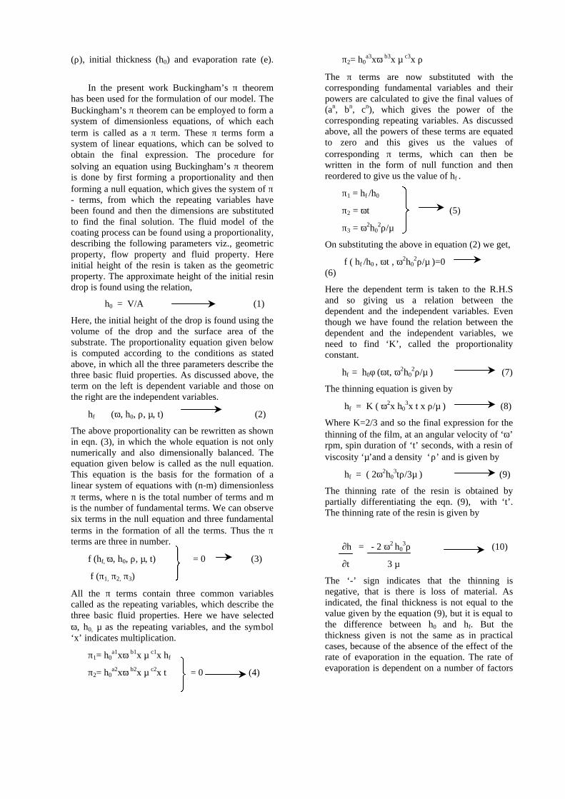
(ρ), initial thickness (h0) and evaporation rate (e).
In the present work Buckingham’s π theorem has been used for the formulation of our model. The Buckingham’s π theorem can be employed to form a system of dimensionless equations, of which each term is called as a π term. These π terms form a system of linear equations, which can be solved to obtain the final expression. The procedure for solving an equation using Buckingham’s π theorem is done by first forming a proportionality and then forming a null equation, which gives the system of π - terms, from which the repeating variables have been found and then the dimensions are substituted to find the final solution. The fluid model of the coating process can be found using a proportionality, describing the following parameters viz., geometric property, flow property and fluid property. Here initial height of the resin is taken as the geometric property. The approximate height of the initial resin drop is found using the relation,
h0 = V/A (1)
Here, the initial height of the drop is found using the volume of the drop and the surface area of the substrate. The proportionality equation given below is computed according to the conditions as stated above, in which all the three parameters describe the three basic fluid properties. As discussed above, the term on the left is dependent variable and those on the right are the independent variables.
hf ∝ (ω, h0, ρ, µ, t) (2)
The above proportionality can be rewritten as shown in eqn. (3), in which the whole equation is not only numerically and also dimensionally balanced. The equation given below is called as the null equation. This equation is the basis for the formation of a linear system of equations with (n-m) dimensionless π terms, where n is the total number of terms and m is the number of fundamental terms. We can observe six terms in the null equation and three fundamental terms in the formation of all the terms. Thus the π terms are three in number.
f (hf, ω, h0, ρ, µ, t) = 0 (3)
f (π1, π2, π3)
All the π terms contain three common variables called as the repeating variables, which describe the three basic fluid properties. Here we have selected ω, h0, µ as the repeating variables, and the symbol ‘x’ indicates multiplication.
π1= h0a1xω b1x µ c1x hf
π2= h0a2xω b2x µ c2x t = 0 (4)
π2= h0a3xω b3x µ c3x ρ
The π terms are now substituted with the corresponding fundamental variables and their powers are calculated to give the final values of (an, bn, cn), which gives the power of the corresponding repeating variables. As discussed above, all the powers of these terms are equated to zero and this gives us the values of corresponding π terms, which can then be written in the form of null function and then reordered to give us the value of hf .
π1 = hf /h0
π2 = ωt (5)
π3 = ω2h02ρ/µ
On substituting the above in equation (2) we get,
f ( hf /h0 , ωt , ω2h02ρ/µ )=0
(6)
Here the dependent term is taken to the R.H.S and so giving us a relation between the dependent and the independent variables. Even though we have found the relation between the dependent and the independent variables, we need to find ‘K’, called the proportionality constant.
hf = h0φ (ωt, ω2h02ρ/µ ) (7)
The thinning equation is given by
hf = K ( ω2x h03x t x ρ/µ ) (8)
Where K=2/3 and so the final expression for the thinning of the film, at an angular velocity of ‘ω’ rpm, spin duration of ‘t’ seconds, with a resin of viscosity ‘µ’and a density ‘ρ’ and is given by
hf = ( 2ω2h03tρ/3µ ) (9)
The thinning rate of the resin is obtained by partially differentiating the eqn. (9), with ‘t’. The thinning rate of the resin is given by
∂h = - 2 ω2 h03ρ (10)
∂t 3 µ
The ‘-’ sign indicates that the thinning is negative, that is there is loss of material. As indicated, the final thickness is not equal to the value given by the equation (9), but it is equal to the difference between h0 and hf. But the thickness given is not the same as in practical cases, because of the absence of the effect of the rate of evaporation in the equation. The rate of evaporation is dependent on a number of factors
starting from the diffusion rate to the partial pressure of the solvent in the junction layer7. Neither of the above can be found out analytically which leads to only one dependent parameter, namely the angular velocity. It has been shown that the rate of evaporation bears a direct relationship with the angular velocity and so by applying the Rayleigh’s method, the rate of evaporation has a square root relationship with angular velocity as given below.
e = Ce √ ω (11 ) Thus the final expression for the thinning of the film is given by,
hf = ( 2ω2h03tρ/3µ )+ e (12)
The equation (12) governs the amount of thinning of resin during the entire spinning process. The factor Ce (co-efficient of evaporation of the resin) is a combination of all the above parameters, which is then calculated using the Ce of the pure solvent11. Actually the equation (12) gives the total amount of fluid resin which was dispensed or lost from the substrate and so the final expression for the thickness is given by the difference between the approximate initial thickness and the value of hf. Final thickness of the thin film, which has been coated with the above said rheological parameters at an angular velocity of ω, for t seconds, is then given by
h0 – hf = h0 – (2ω2h03tρ/3µ+ Ce √ ω) (13)
3.DEFECT REDUCTION USING SIMULATION
The defects, which cause important effect on the surface morphology of the spin coated film are the edge beads 11,12,13,18, striations12,16, comets8,13, presence of air bubbles13 and chuck marks13. Here we are going to discuss in detail about first three of the above defects and their reduction techniques. The paper has also experimentally established that the conditions as described are authentic and can be used in all spin coating instrument for defect reduction.
In this model, the edge bead and striations are simulated using the MATLAB software and the simulated results are found to be at par with the experimental results. The conditions used in the simulation are that the fluid resin was a mixture of ethyl alcohol, tin Chloride and antimony tri chloride, with a density (ρ) of 1200 kg/m3, a viscosity (µ) of 5 kg/ms. and the substrate being a rectangular mineral glass plate. The spin speed and duration was set at 3500 rpm and 10 seconds respectively.
3.1. Edge Bead
During the initial spin up stage, the resin gets stacked up at the unsymmetrical edges of the
substrate and goes on building up, causing the edge build up, to be more than twice as that in the other areas of the substrate.
This is attributed to the poor wetability of the resin and also due to the uncontrolled inlet and exhaust of the carrier gasses 10,14. Figure (1) shows the formation of an edge bead at the start of the spin up stage, where the flow controlled thinning
dominates, thereby resulting in the formation of the bead at the periphery of the substrate. The final structure of edge bead after evaporation is shown in figure (2).
The edge bead can be minimized by reducing the gradual build up, during the initial spin up and also by the use of recessed chuck, which reduces the gradient of carrier gas velocity at the edge of the plate, with respect to the center of the substrate.
Figure (2): Simulated result showing Edge bead after evaporation.
Figure (1): Simulated result showing Edge bead during spin up
The schematic view of edge bead observed in spin coated ATO thin film after evaporation is shown in figure (3), which indicates a close coincidence with the simulated plot.
3.2. Striations
Striations are radially oriented lines of thickness variation, generated on the surface of the spin coated films. They are quite smoothly varying in thickness and variations with a spacing or periodicity, in the range of 50-200 micron10. Their orientation corresponds to the direction of major fluid flow. These defects occur due to the evaporation driven surface tension effects.
The early evaporation of light solvents can cause an enrichment of less volatile species in the surface layer15. If the surface tension of this layer is larger than the starting solution then instability
exists, where the higher surface tension actually draws material in, at regular intervals and the spaces in between are more able to evaporate, and surface relief develops17.
0.03[V]
0.00500.00 nm 1.00 x 1.00 um
This is essentially due to the Marangoni effect, which caused striations and streaks or flares. The formation of striations is predominantly due to the uneven evaporation of the solvent in the various parts of the substrate. This may lead to greater solvent concentration at the deeper portions. Figure (4) shows simulated result of striations formed on a symmetrical substrate with radial outflow9, from which it is obvious that the striations formed are more uniform at the center than at the periphery. These results are well in agreement with the experimental observations of the ATO thin film, as shown in figure (5)
Figure (5): AFM image showing the Striations with radial outflow of resin (experimentally observed in ATO thin film spin coated on glass substrate)
Figure (4): Simulated result showing striations formed on a symmetrical substrate with radial outflow.
Figure (6): Simulated result showing striations formed on an asymmetrical substrate with normal outflow.
Figure (3) Experimentally observed edge bead in ATO thin films after evaporation.
The figure (6) shows the formation of striations, in which the outflow of the resin is normal to the substrate. Striations can be minimized by reducing uneven evaporation during the initial spinning process, which can be achieved by using solvent of low volatility.
3.3 Comets
These are pits found on the spin coated films, when relatively larger solid particle impede the resin on the wafer. The view of a comet observed in a spin coated ATO thin film is shown in the figure (7). The presence of comets can be eliminated by working in cleaner environments and by filtering coating solutions during the dispense process. The other parameters for the occurrence of comets are higher fluid velocity, dispense rate, exhaust rate, spinning speed, acceleration.
The above said are the factors, which affect almost all the properties of the film. But the major factors for the formation of the comet are the presence of solid particle or impurities in the spin coater, or may be due the high viscosity of the resin. Studies indicate that comets can be minimized by using the resin of relatively low viscosity without any insoluble solid particles or impurities.
4. Results and Discussion The simulated results of film thickness obtained
from the mathematical model, are compared with the observed film thickness of Antimony doped tin oxide thin films spin coated at different spin rate and spin duration. The influence spin time on the simulated and experimental values of film thickness, at
constant spin rate (3500 RPM) is shown in the table 1.
Table - 1 Effect of spin rate on simulated and
experimentally observed film thickness at constant spin rate ( 3500 RPM )
4.1 Effect of spin rate on film thickness
Film thickness is largely a balance between
the force applied to shear the resin towards the edge of the substrate and drying rate. As the resin dries, viscosity increases, until the radial centrifugal force of the spin process can no longer appreciably move the sol over the surface. At this point, the film thickness will not decrease significantly with increased spin time 8. The variation of film thickness with spin rate at different spin time is shown in the figure (8). The plot shows a parabolic fall in film thickness at lower spin rate (upto 3500 rpm) and saturation behaviour at higher spin rate (beyond 3500 rpm) and this kind of variation in film thickness may be attributed as follows.
Figure (8) Variation of simulated and experimentally observed film thickness with
spin rate at constant spin time t = 10 sec
300
450
600
750
900
1500 2000 2500 3000 3500 4000 4500 5000 5500Spin rate ( RPM )
Th
ickn
ess
( n
m )
Simulated result Experimental result
Spin rate ( 3500 RPM )
Time (sec) Simulated
Result for thickness nm
Experimental Result for thickness
nm 4 676 714 6 537 576 8 408 448
10 272 350 12 214 324 14 168 300 16 138 280
Figure (7) A view of the comet experimentally noticed in spin coated ATO thin film
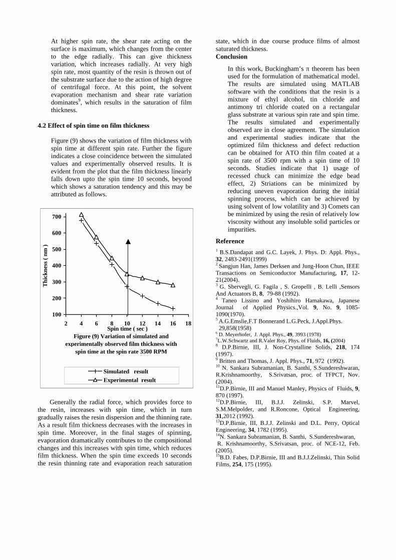
At higher spin rate, the shear rate acting on the surface is maximum, which changes from the center to the edge radially. This can give thickness variation, which increases radially. At very high spin rate, most quantity of the resin is thrown out of the substrate surface due to the action of high degree of centrifugal force. At this point, the solvent evaporation mechanism and shear rate variation dominates9, which results in the saturation of film thickness.
4.2 Effect of spin time on film thickness
Figure (9) shows the variation of film thickness with spin time at different spin rate. Further the figure indicates a close coincidence between the simulated values and experimentally observed results. It is evident from the plot that the film thickness linearly falls down upto the spin time 10 seconds, beyond which shows a saturation tendency and this may be attributed as follows.
Figure (9) Variation of simulated and experimentally observed film thickness with
spin time at the spin rate 3500 RPM
100
200
300
400
500
600
700
2 4 6 8 10 12 14 16 18 Spin time ( sec )
Thi
ckne
ss (
nm
)
Simulated resultExperimental result
Generally the radial force, which provides force to
the resin, increases with spin time, which in turn gradually raises the resin dispersion and the thinning rate. As a result film thickness decreases with the increases in spin time. Moreover, in the final stages of spinning, evaporation dramatically contributes to the compositional changes and this increases with spin time, which reduces film thickness. When the spin time exceeds 10 seconds the resin thinning rate and evaporation reach saturation
state, which in due course produce films of almost saturated thickness. Conclusion
In this work, Buckingham’s π theorem has been used for the formulation of mathematical model. The results are simulated using MATLAB software with the conditions that the resin is a mixture of ethyl alcohol, tin chloride and antimony tri chloride coated on a rectangular glass substrate at various spin rate and spin time. The results simulated and experimentally observed are in close agreement. The simulation and experimental studies indicate that the optimized film thickness and defect reduction can be obtained for ATO thin film coated at a spin rate of 3500 rpm with a spin time of 10 seconds. Studies indicate that 1) usage of recessed chuck can minimize the edge bead effect, 2) Striations can be minimized by reducing uneven evaporation during the initial spinning process, which can be achieved by using solvent of low volatility and 3) Comets can be minimized by using the resin of relatively low viscosity without any insoluble solid particles or impurities.
Reference 1 B.S.Dandapat and G.C. Layek, J. Phys. D: Appl. Phys., 32, 2483-2491(1999) 2 Sangjun Han, James Derksen and Jung-Hoon Chun, IEEE Transactions on Semiconductor Manufacturing, 17, 12-21(2004). 3 G. Sbervegli, G. Fagila , S. Gropelli , B. Lelli ,Sensors And Actuators B, 8, 79-88 (1992). 4 Taneo Lissino and Yoshihiro Hamakawa, Japanese Journal of Applied Physics.,Vol. 9, No. 9, 1085-1090(1970). 5 A.G.Emslie,F.T Bonnerand L.G.Peck, J.Appl.Phys. 29,858(1958) 6 D. Meyerhofer, J. Appl. Phys., 49, 3993 (1978) 7L.W.Schwartz and R.Valer Roy, Phys. of Fluids, 16, (2004)
8 D.P.Birnie, III, J. Non-Crystalline Solids, 218, 174 (1997). 9 Britten and Thomas, J. Appl. Phys., 71, 972 (1992). 10 N. Sankara Subramanian, B. Santhi, S.Sundereshwaran, R.Krishnamoorthy, S.Srivatsan, proc. of TFPCT, Nov. (2004). 11D.P.Birnie, III and Manuel Manley, Physics of Fluids, 9, 870 (1997). 12D.P.Birnie, III, B.J.J. Zelinski, S.P. Marvel, S.M.Melpolder, and R.Roncone, Optical Engineering, 31,2012 (1992). 13D.P.Birnie, III, B.J.J. Zelinski and D.L. Perry, Optical Engineering, 34, 1782 (1995). 14N. Sankara Subramanian, B. Santhi, S.Sundereshwaran, R. Krishnamoorthy, S.Srivatsan, proc. of NCE-12, Feb. (2005). 15B.D. Fabes, D.P.Birnie, III and B.J.J.Zelinski, Thin Solid Films, 254, 175 (1995).

16M.A. Uddin, H.P. Chan, C.K.Chow and Y.C. han, J. of Electronic Materials, 33, 224(2004) 17J. H. Lai, Polymer Engineering and Science, 19, 1117 (1979). 18D. P. Birnie, R. N. Vogt, M. N. Orr, and J. R. Schifko, Microelectron Engg. 29, 189(1982). Acknowledgement The authors wish to thank the management and principal of Thiagarajar college of Engineering, Madurai, for their encouragement and support in the successful completion of this project Corresponding Author N. Sankara Subramanian, Department of Physics, Thiagarajar College of Engineering, Madurai – 625 015, Tamil Nadu State, India. E-mail: [email protected], Telephone: +91-94434-77194, Fax: +91-452-248-3427

Sorry!!
This Paper is NOT Available
Ion Beam Modification of Ferric Oxalate Dispersed Polymer Films N. L. Singh1*, Anjum Qureshi1, A. K. Rakshit2, F. Singh3, D. K. Avasthi3
1 Physics Department, M.S. University of Baroda, Vadodara-390002, India.
2Chemistry Department, M.S. University of Baroda, Vadodara-390002, India. 3 Nuclear Science Centre, Aruna Asaf Ali Marg, New Delhi-110067, India.
. Abstract Thin films of ferric oxalate dispersed in poly vinyl chloride (PVC) were synthesized. Ferric oxalate was dispersed in PVC films at various concentrations. These films were irradiated with 80MeV O6+ ions at a fluence of 1× 10¹¹ ions/cm2.The radiation induced changes in dielectric properties and microhardness were studied in the paper. The dielectric properties namely; electrical conductivity and dielectric constant were measured as a function of frequency. It is observed that hardness and electrical conductivity of the film increases with the concentration of dispersed ferric oxalate and also with the fluence. It indicates that ion beam irradiation promote the metal to polymer adhesion, and to convert the polymeric structure in to hydrogen depleted carbon network, which make polymer more harder and more conductive. Key words: Polyvinyl chloride, Ferric oxalate, Ion irradiation, Electrical properties, Microhardness. *Corresponding author: Tel: +91-265-2783924, Fax: +91-265-2787556, E-mail: [email protected].
1. Introduction Polymer composites filled with metal fillers are of interest of many fields of engineering. It is widely used for different applications: packaging, decorative, coatings, capacitors, magnetic tapes, electromagnetic interface (EMI) shielding, adhesives and sensors etc. The use of organic and inorganic fillers is a common practice in the polymer industry to improve the mechanical properties of thermoplastic materials such as heat distortion temperature, hardness, roughness, stiffness and mold shrinkage or to decrease other properties such as permeability and often material price. The filler effect on the composite properties strongly depends on its shape, size, aggregation state, surface characteristics and degree of dispersion. Ion beam modification is well known established and economical method for modifying the properties of polymer composites. Important properties of such polymer composites, i.e. mechanical properties thermal stability, chemical resistance, melt flow, process ability and surface properties can be significantly improved by ion beam irradiation. A filed polymer differs substantially from the free one in wide range of properties. These materials can be cross-linked by radiation to obtain useful properties. Our interest in dispersion of organometallic compound is mainly because of ion irradiation induced enhancement of both electrical conductivity and mechanical (microhardness) properties of polymers. In this study, the PVC films were dispersed with different concentrations (i.e. 5%, 10% and 15%) of ferric oxalate compound and irradiated with 80MeV O6+ ions at the fluence of 1x 10¹¹
ions/cm2. We have studied the mechanical property (i.e. micro hardness), and electrical properties by means of Vickers’ microhardness indentation, and LCR meter respectively. 2. Experimental Detail As an organometallic compound we took ferric oxalate. It was formed by taking 6.24g of oxalic acid and 5.24g of ferric chloride with ethanol as a solvent in a round bottom flask, and it was refluxed for 4h at 600C. The excess of ethanol was then distilled out and the substance was dried at 750C for 3h in an oven. The PVC and ferric oxalate compound of 5%, 10%, and 15% were dissolved using toluene and the solutions were mixed and stirred thoroughly for about an hour and poured on clean glass trough. The solvent was evaporated at room temperature (250C+ 10C) to get thin films (thickness ~50ì m) of dispersed PVC with 5%, 10%, and 15% concentration of ferric oxalate compound. The films were used for irradiation. All films were irradiated with 80 MeV O6+ ions at a fluence of 1× 10¹¹ ions/cm2 from the pelletron of the Nuclear Science Centre (NSC), New Delhi. A Carl Zeiss microscope and accessories were used to investigate Vickers’micro hardness of all samples. The electrical properties of all samples were measured in the frequency range 0 .05-100kHz at ambient temperature using variable frequency LCR meter (General Radio, USA; model-1689). The conductivity was calculated using the relation ó = t /R A (¿ -1 cm-1), where R is resistance measured, A is the cross-sectional area of the electrode and t is the thickness of the polymeric film. The dielectric
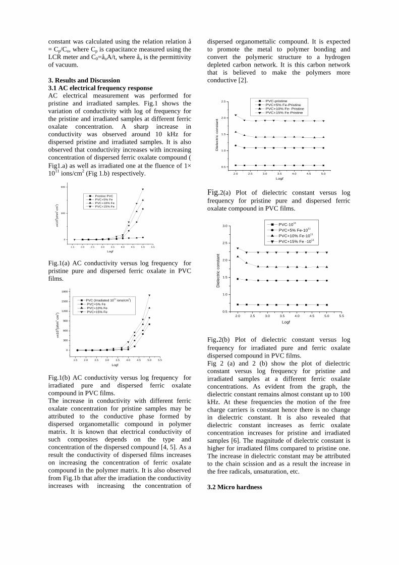
constant was calculated using the relation relation å = Cp/Co, where Cp is capacitance measured using the LCR meter and C0=åoA/t, where åo is the permittivity of vacuum. 3. Results and Discussion 3.1 AC electrical frequency response AC electrical measurement was performed for pristine and irradiated samples. Fig.1 shows the variation of conductivity with log of frequency for the pristine and irradiated samples at different ferric oxalate concentration. A sharp increase in conductivity was observed around 10 kHz for dispersed pristine and irradiated samples. It is also observed that conductivity increases with increasing concentration of dispersed ferric oxalate compound ( Fig1.a) as well as irradiated one at the fluence of 1× 10¹¹ ions/cm2 (Fig 1.b) respectively.
1.5 2.0 2.5 3.0 3.5 4.0 4.5 5.0 5.5
0
300
600
σx1
0-9(o
hm
-1 c
m-1)
Logf
Pristine PVC PVC+5% Fe PVC+10% Fe PVC+15% Fe
Fig.1(a) AC conductivity versus log frequency for pristine pure and dispersed ferric oxalate in PVC films.
1.5 2.0 2.5 3.0 3.5 4.0 4.5 5.0 5.5
0
300
600
900
1200
1500
1800
σx10-9
(ohm
-1 c
m-1)
Logf
PVC (Irradiated 1011 ions/cm2) PVC+5% Fe PVC+10% Fe PVC+15% Fe
Fig.1(b) AC conductivity versus log frequency for irradiated pure and dispersed ferric oxalate compound in PVC films. The increase in conductivity with different ferric oxalate concentration for pristine samples may be attributed to the conductive phase formed by dispersed organometallic compound in polymer matrix. It is known that electrical conductivity of such composites depends on the type and concentration of the dispersed compound [4, 5]. As a result the conductivity of dispersed films increases on increasing the concentration of ferric oxalate compound in the polymer matrix. It is also observed from Fig.1b that after the irradiation the conductivity increases with increasing the concentration of
dispersed organomettalic compound. It is expected to promote the metal to polymer bonding and convert the polymeric structure to a hydrogen depleted carbon network. It is this carbon network that is believed to make the polymers more conductive [2].
2.0 2.5 3.0 3.5 4.0 4.5 5.0
0.5
1.0
1.5
2.0
2.5
Die
lectr
ic c
onsta
nt
Logf
PVC-pristine PVC+5% Fe-Pristine PVC+10% Fe- Pristine PVC+15% Fe Pristine
Fig.2(a) Plot of dielectric constant versus log frequency for pristine pure and dispersed ferric oxalate compound in PVC films.
2.0 2.5 3.0 3.5 4.0 4.5 5.0 5.50.5
1.0
1.5
2.0
2.5
3.0
Die
lect
ric
const
ant
Logf
PVC-1011
PVC+5% Fe-1011
PVC+10% Fe-1011
PVC+15% Fe -1011
Fig.2(b) Plot of dielectric constant versus log frequency for irradiated pure and ferric oxalate dispersed compound in PVC films. Fig 2 (a) and 2 (b) show the plot of dielectric constant versus log frequency for pristine and irradiated samples at a different ferric oxalate concentrations. As evident from the graph, the dielectric constant remains almost constant up to 100 kHz. At these frequencies the motion of the free charge carriers is constant hence there is no change in dielectric constant. It is also revealed that dielectric constant increases as ferric oxalate concentration increases for pristine and irradiated samples [6]. The magnitude of dielectric constant is higher for irradiated films compared to pristine one. The increase in dielectric constant may be attributed to the chain scission and as a result the increase in the free radicals, unsaturation, etc. 3.2 Micro hardness
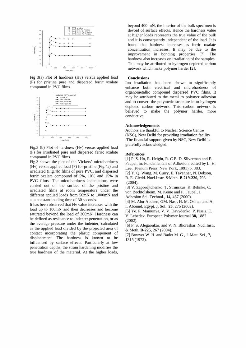
0 200 400 600 800 1000
48
49
50
51
52
53
54
55
56
Hv(M
Pa
)
Load(mN)
PVC-pristine PVC+5% Fe-Pristine PVC+10% Fe- Pristine PVC+15% Fe Pristine
Fig 3(a) Plot of hardness (Hv) versus applied load (P) for pristine pure and dispersed ferric oxalate compound in PVC films.
0 200 400 600 800 1000
50
51
52
53
54
55
56
57
58
59
60
Hv(
MP
a)
Load(mN)
Irradiated (1011 ions/cm2) Pure PVC PVC+5% Fe PVC+10% Fe PVC+15% Fe
Fig.3 (b) Plot of hardness (Hv) versus applied load (P) for irradiated pure and dispersed ferric oxalate compound in PVC films. Fig.3 shows the plot of the Vickers’ microhardness (Hv) versus applied load (P) for pristine (Fig.4a) and irradiated (Fig.4b) films of pure PVC, and dispersed ferric oxalate compound of 5%, 10% and 15% in PVC films. The microhardness indentations were carried out on the surface of the pristine and irradiated films at room temperature under the different applied loads from 50mN to 1000mN and at a constant loading time of 30 seconds. It has been observed that Hv value increases with the load up to 100mN and then decreases and become saturated beyond the load of 300mN. Hardness can be defined as resistance to indenter penetration, or as the average pressure under the indenter, calculated as the applied load divided by the projected area of contact incorporating the plastic component of displacement. The hardness is known to be influenced by surface effects. Particularly at low penetration depths, the strain hardening modifies the true hardness of the material. At the higher loads,
beyond 400 mN, the interior of the bulk specimen is devoid of surface effects. Hence the hardness value at higher loads represents the true value of the bulk and it is consequently independent of the load. It is found that hardness increases as ferric oxalate concentration increases. It may be due to the improvement in bonding properties [7]. The hardness also increases on irradiation of the samples. This may be attributed to hydrogen depleted carbon network which make polymer harder [2]. Conclusions
Ion irradiation has been shown to significantly enhance both electrical and microhardness of organometallic compound dispersed PVC films. It may be attributed to the metal to polymer adhesion and to convert the polymeric structure in to hydrogen depleted carbon network. This carbon network is believed to make the polymer harder, more conductive. Acknowledgements Authors are thankful to Nuclear Science Centre (NSC), New Delhi for providing irradiation facility .The financial support given by NSC, New Delhi is gratefully acknowledged. References [1] P. S. Ho, R. Height, R. C B. D. Silverman and F. Faupel, in: Fundamentals of Adhesion, edited by L. H. Lee, (Plenum Press, New York, 1991) p. 383. [2] Y. Q. Wang, M. Curry, E. Tavenner, N. Dobson, R. E. Giedd. Nucl.Instr. &Meth. B 219-220, 798. (2004). [3] V. Zaporojtchenko, T. Strunskus, K. Behnke, C. von Bechtolsheim, M. Keine and F. Faupel, J. Adhesion Sci. Technol., 14, 467 (2000). [4] M. Abu-Abdeen, GM. Nasr, H. M. Osman and A. I. Abound. Egypt. J. Sol., 25, 275 (2002). [5] Ye. P. Mamunya, V. V. Davydenko, P. Pissis, E. V. Lebedev. European Polymer Journal 38, 1887 (2002). [6] P. S. Alegaonkar, and V. N. Bhoraskar. Nucl.Instr. & Meth. B-225, 267 (2004). [7] Bowyer W. H. and Bader M. G., J. Matt. Sci., 7, 1315 (1972).
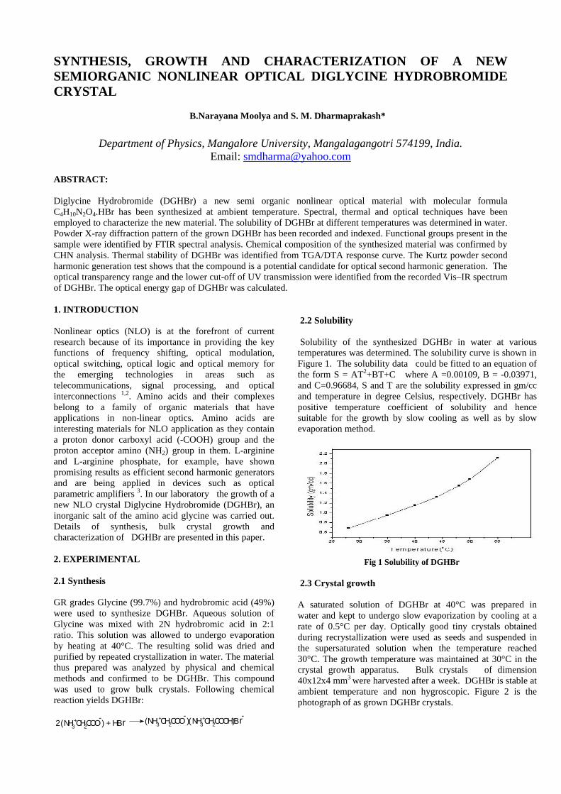
SYNTHESIS, GROWTH AND CHARACTERIZATION OF A NEW SEMIORGANIC NONLINEAR OPTICAL DIGLYCINE HYDROBROMIDE CRYSTAL
B.Narayana Moolya and S. M. Dharmaprakash*
Department of Physics, Mangalore University, Mangalagangotri 574199, India.
Email: [email protected]
ABSTRACT: Diglycine Hydrobromide (DGHBr) a new semi organic nonlinear optical material with molecular formula C4H10N2O4.HBr has been synthesized at ambient temperature. Spectral, thermal and optical techniques have been employed to characterize the new material. The solubility of DGHBr at different temperatures was determined in water. Powder X-ray diffraction pattern of the grown DGHBr has been recorded and indexed. Functional groups present in the sample were identified by FTIR spectral analysis. Chemical composition of the synthesized material was confirmed by CHN analysis. Thermal stability of DGHBr was identified from TGA/DTA response curve. The Kurtz powder second harmonic generation test shows that the compound is a potential candidate for optical second harmonic generation. The optical transparency range and the lower cut-off of UV transmission were identified from the recorded Vis–IR spectrum of DGHBr. The optical energy gap of DGHBr was calculated. 1. INTRODUCTION Nonlinear optics (NLO) is at the forefront of current research because of its importance in providing the key functions of frequency shifting, optical modulation, optical switching, optical logic and optical memory for the emerging technologies in areas such as telecommunications, signal processing, and optical interconnections 1,2. Amino acids and their complexes belong to a family of organic materials that have applications in non-linear optics. Amino acids are interesting materials for NLO application as they contain a proton donor carboxyl acid (-COOH) group and the proton acceptor amino (NH2) group in them. L-arginine and L-arginine phosphate, for example, have shown promising results as efficient second harmonic generators and are being applied in devices such as optical parametric amplifiers 3. In our laboratory the growth of a new NLO crystal Diglycine Hydrobromide (DGHBr), an inorganic salt of the amino acid glycine was carried out. Details of synthesis, bulk crystal growth and characterization of DGHBr are presented in this paper. 2. EXPERIMENTAL 2.1 Synthesis GR grades Glycine (99.7%) and hydrobromic acid (49%) were used to synthesize DGHBr. Aqueous solution of Glycine was mixed with 2N hydrobromic acid in 2:1 ratio. This solution was allowed to undergo evaporation by heating at 40°C. The resulting solid was dried and purified by repeated crystallization in water. The material thus prepared was analyzed by physical and chemical methods and confirmed to be DGHBr. This compound was used to grow bulk crystals. Following chemical reaction yields DGHBr:
2 ( NH3+CH2COO
- ) + HB r ( NH3+CH2COO
- )( NH3
+CH2COOH )B r-
2.2 Solubility Solubility of the synthesized DGHBr in water at various temperatures was determined. The solubility curve is shown in Figure 1. The solubility data could be fitted to an equation of the form S = AT2+BT+C where A =0.00109, B = -0.03971, and C=0.96684, S and T are the solubility expressed in gm/cc and temperature in degree Celsius, respectively. DGHBr has positive temperature coefficient of solubility and hence suitable for the growth by slow cooling as well as by slow evaporation method.
Fig 1 Solubility of DGHBr
2.3 Crystal growth A saturated solution of DGHBr at 40°C was prepared in water and kept to undergo slow evaporization by cooling at a rate of 0.5°C per day. Optically good tiny crystals obtained during recrystallization were used as seeds and suspended in the supersaturated solution when the temperature reached 30°C. The growth temperature was maintained at 30°C in the crystal growth apparatus. Bulk crystals of dimension 40x12x4 mm3 were harvested after a week. DGHBr is stable at ambient temperature and non hygroscopic. Figure 2 is the photograph of as grown DGHBr crystals.
Fig 2. Single crystals of DGHBr 3. CHARACTERIZATION 3.1 CHN Analysis In order to confirm the chemical composition of the synthesized compound CHN analysis was carried out on the recrystallized sample using the instrument Elementar Vario EL III CHNS analyzer. The result of the analysis is presented in Table1.Theoretical values of CHN were found by the molecular formula C4H10N2O4.HBr. The experimental and calculated values of C, H and N agree each other confirming the formation of DGHBr.
Table.1 Microanalysis of DGHBr
Element Experimental Computed Carbon % 21.24 20.8 Hydrogen % 4.64 4.76 Nitrogen% 12.08 12.12
3.2 Powder X-ray diffraction studies Powder X-ray diffraction pattern of the grown DGHBr was recorded using BRUKER D8 ADVANCE powder diffractometer with Cu Ká radiation (ë =1.5418). The sample was scanned at a rate of 1° per minute in the range10° to 70°. Figure 3 shows the powder X-ray diffraction pattern of DGHBr. From the X-ray diffraction pattern, the lattice parameters and the cell volume have been calculated (Table 2). These reveal a close agreement with the reported values [8]. The prominent peaks in the XRD pattern have been indexed. The X-ray diffraction pattern has the highest intensity corresponding to ( 220) plane.
Fig 3. Powder XRD pattern of DGHBr
Table 2 Unit cell parameters of DGHBr
Parameter Experimental Literature4
Space Group P212121 P212121
a () 8.20976 8.21
b () 18.43097 18.42 c () 5.40423 5.40 V ( 3 ) 817.73541 807.68
3.4 FTIR studies Functional groups present in the sample were analyzed using FT-IR spectrum. The spectrum was recorded using the AVTAR 370DTGS FT-IR spectrophotometer in the wave number range 400 - 4000 cm-1 with KBr pallet method. The FT-IR absorption spectrum of DGHBr is shown in Figure 4. Different molecular groups present in DGHBr were identified with the help of the available data [5,6,7] on the vibrational frequencies of amino acids and their complexes. The broad and strong bands lying between 3116cm-1 and 2230cm-1 are due to the absorption of the superimposed O-H and NH3
+ stretching. The bands observed at 1624 cm-1 and at 1494cm-1 are assigned to asymmetrical and symmetrical NH3
+ bending respectively. The strong band observed at 1731cm-1 is assigned to protonated carbonyl group of one of the glycine an ion. The band observed at 1441cm-1 is assigned to carbonyl group of the other glycine an ion. The band at 1938cm-1 is assigned to a combination of the asymmetrical NH3
+ observed at 1624 cm-1 and torsional oscillation band observed at 501cm-1.
Fig 4 FTIR spectra of DGHBr 3.5 TGA/DTA analysis Thermal properties of grown DGHBr were studied in powder form by recording TGA/DTA response curve in the temperature range 28°C and 800°C using the STA 409C Thermal analyzer under nitrogen atmosphere. Figure 6 shows the TG /DTA graph of DGHBr. Heating was carried out at a rate of 20°C/min. DGHBr shows two major peaks. The first peak appearing at 170°C may be assumed to be due to the melting. The melting point of the sample measured by standard methods was 169°C. The sharpness of the thermogram is also illustrative of the crystal purity without association of any impurities8. The second peak appearing at 266°C curve may be due to the decomposition
of the compound. There is no loss of weight below 125°C in illustrating the absence of any absorbed water in the sample. Thus from the thermal analysis it may be noted that DGHBr is stable up to 170 °C.
Fig 5 TG/DTA graph of DGHBr 3.6 UV- vis-IR spectra A good optical transmittance is highly desirable in an NLO crystal since the absorptions, if any in an NLO material near the fundamental or the second harmonic will lead to the loss of conversion efficiency in UV region. The UV-Visible spectrum of DGHBr was recorded with Varian Cary-5E UV-Vis-NIR spectrophotometer in the range 200- 1000 nm with a crystal of thickness 2mm. The response curve (Figure 6) shows that there is very small absorption in the visible and NIR region. The lower cut off DGHBr is 230 nm. The lower cutoff wavelength of DGHBr is relatively lower compared other standard semi organic NLO crystals. Because of this DGHBr is useful for optoelectronics applications and the second harmonic generation from the Nd: YAG, GaAlAs laser diodes etc. which are emitting fundamental in the wavelength region down to 500 nm. Energy gap was calculated by the graph of (áE) ½ Vs E. The optical energy gap obtained from the graph is 4.6eV
Fig 6 UV- vis-NIR spectra DGHBr 3.8 Second harmonic generation The second harmonic generation efficiency was determined by the modified version of the powder technique developed by Kurtz and Perry9 using Quanta Ray Spectra Physics model: Prolab170 Nd: YAG 10 ns laser with a pulse repetition rate of 10Hz working at 1064 nm. The sample was ground into fine powder and tightly packed in a micro capillary tube. It was mounted in the path of the laser beam of pulse energy 9.6 mJ obtained by splitting the original laser beam.
The transmitted light is passed through 532 nm monochromator (TRIACS 550). The green light at double the incident frequency was collected by photo multiplier tube (PMT-Philips Photonics XP 2020) and converted into electrical signal. This signal was displayed on the oscilloscope (Textronics TDS 3052B). Signal amplitude in milli volts on the oscilloscope indicates the SHG efficiency of the sample. Potassium dihydrogen phosphate (KDP) ground into the identical size was used as reference material in the SHG measurement. The SHG efficiency of the grown DGHBr crystal was found to be equal to 0.8 times that of KDP. 4. CONCLUSION Diglycine hydrobromide has been synthesized and bulk single crystals of size 40x12x4 mm3 of were grown by slow evaporation of aqueous solution at constant temperature. DGHBr crystals were characterized by chemical analysis, XRD and FTIR studies. DGHBr crystallizes in orthorhombic system with a = 8.20976Å, b=18.43097Å, c=5.40423Å; space group P212121. DGHBr is thermally stable up to 170°C. Second harmonic generation efficiency of the grown crystals was found to be 0.8 times that of KDP. DGHBr has good optical transparency range and its lower cutoff wavelength is 230 nm. The optical energy gap estimated from the optical response curve was found to be 4.6 eV.
ACKNOWLEDGEMENT Authors acknowledge Prof. P. K. Das, IISc, Bangalore for having extended the laser facilities to determine the SHG efficiency. NM is thankful to the University Grants Commission, Bangalore and New Delhi, for providing teacher fellowship under FIP in X Plan period. Authors acknowledge the STIC, Cochin University for carrying out the characterization of the crystal. REFERENCES 1. D.S. Chemla, J. Zyss, Eds. Nonlinear Optical Properties of Organic Molecules and Crystals, Academic Press: New York, 1987. 2. P. N. Prasad and D. J. Williams, Introduction to Nonlinear Optical Effects in molecules and Polymers, Wiley-Interscience, New York, 1991 3. S.B.Monaco, L.E. Davis, S.P.Velsko,. T.Wang, D.Eimerl, A.J.Zalkin, J.Crystal Growth 85,252 (1987) 4. M.J.Buerger, E.Barney and T.Hahn ,Z.Krist 108,130,(1956),. 5. R.S .Krishnan,K. Sankaranarayanan, K.J. Krishnan, Indian Inst. Sci., 55, 66 , (1973). 6. Spectrometric identification of organic compounds, Silverstein, Bassler and Morrill, IV Edn, John Wiley & Sons, New York, 1981. 7. C.H.Wang and R.D. Storms, J.Chem.Phys 55,3291, (1971) .
8. A.S.H.Hameed,G.R.Ravi,R.Dhanashekaran, P.Ramasamy, .J.Crystal Growth 212,227 (2000). 9. S.K.Kurtz and T.T.Perry, J.Appl.Phys. 39,3798, (1968)

Page 1 of 3 Proceedings of OMTAT2005
URBACH TAIL ANALYSIS OF PRISTINE AND IODINE DOPED
POLYPYRROLE THIN FILMS PREPARED BY AC PLASMA
POLYMERISATION
Joseph John, U.S.Sajeev, M.R.Anatharaman, S.Jaylekshmi*
Department of Physics, Cochin University of Science and Technology, Kochi-682 022
Email: jayalekshmi @cusat.ac.in ABSTRACT
The structural disorders form localized states with in the band tails of electronic states, which cause changes of the optical and electrical transport processes in amorphous materials, and the amount of disorder is significant to control the physical properties of these materials. In this study polypyrrole thin films in the pristine and iodine doped forms have been prepared by ac plasma polymerisation. The insitu doping of iodine in these films affects the optical absorption behavior of the thin films due to the incorporation of charged defects in the film structure. The Urbach tail analysis of the pure and doped thin films shows the defect levels created when the polymerisation is carried out in the iodine atmosphere. The optical band gap decreased and electrical conductivity enhanced in the case of iodine doped films, when compared to the pristine films. The results are correlated with the structural difference of these thin films evolved during the polymerisation with the help of FTIR analysis.
Key words: Urbach tail, plasma polymerisation, polypyrrole, Iodine doping, band gap.
1. INTRODUCTION
Plasma polymerization is an excellent technique for the preparation of organic and inorganic thin films on various substrates from a starting monomer [1] This technique is used not only to deposit thin films on appropriate substrates but to control the composition of the surface layer for suitable applications also. Plasma assisted deposition of thin films is a fast growing area in the field of polymer film deposition due to its inexpensiveness and processing versatility. Plasma polymerisation is used to modify the surface properties of various materials like thin films, nanopartices, nanotubes etc. The morphology and composition of the plasma polymers is a function of the plasma parameters like power in put, monomer flow rate, monomer vapor pressure, substrate temperature and the positioning of the substrates relative to the plasma zone. The thin films prepared by the plasma polymerisation technique is generally amorphous, pinhole free, chemically inert and thermally stable. The potential applications of plasma polymers, due to their interesting photonic and electronic properties, include anti-reflection coatings, polymer LEDs, optical sensors, surface passivation coatings and low dielectric intermetallics. Enhancement of the charge carrier injection by the plasma treatment of the ITO electrodes used in the fabrication of organic LEDs is another interesting application of the plasma polymerisation.[2.] Plasma polymer thin films of various materials like polyaniline, polypyrrole, polythiophene etc have been found to have a variety of potential applications in various fields.
Polypyrrole is a widely studied polymer in its bulk and thin film forms due to its excellent thermal stability in air. In monomer form it is a simple hetero cyclic organic compound. [3] Even though some reports on plasma polymerized pyrrole thin films in its pure and doped form are available in the literature, a systematic
study on the stability and structure of the insitu iodine doped plasma polymerized pyrrrole thin films, and the effect of doping on its optical and structural properties due to the charged defects created during the polymerisation process has not been reported. An attempt to explain the modification of the optical and structural properties and the Urbach tail analysis of the absorption spectrum is made in this paper.
The structural disorders incorporated in amorphous solids are important factors which can affect their physical properties. The electric transport and optical properties in amorphous materials show changes according to the disorders frozen in these materials. Effects of the structural disorders on the electronic structure of amorphous solids can be clearly observed at the band edges.[ The signature of a disordered system is the narrowing of band gap and the formation of localized states with in the band tails. The reflections of these effects in the electronic structure can be represented by two separate regions called Tauc and Urbach regions. In a doped polymer the electron accepting or withdrawing groups incorporated during the doping process form defect levels due to the incorporation of charged species, which will reduce or enhance the binding energy of the carriers, and that results in the modification of the optical and structural properties of the solids[4] The optical absorption spectrum shows a tail below the absorption edge at a finite temperature. The tail part near the absorption edge in various non metallic amorphous materials can be expressed empirically as[5]
( ) ( ) ( )00, exp
B
T E EE T
k T
σα α
−= −
where the absorption coefficient á is a function of the photon energy E and the temperature T. E0 is the
Page 2 of 3 Proceedings of OMTAT2005
photon energy, á0 is the absorption coefficient at E=E0 , and ( )Tσ is the steepness coefficient and depends on
the temperature and is a measure of the defect states frozen in an amorphous solid.. From the analysis of the absorption spectrum, the defect levels of doped and pristine thin films are compared. 2. EXPERIMENTAL 2.1 ac plasma polymerization
The experimental set up for ac plasma polymerization unit (home built) is depicted in fig 1. It consists of two parallel stainless steel electrodes, each of diameters 0.23 m and placed 0.05 m apart. Ultrasonically cleaned glass substrates were placed on the lower electrode for the polymer thin film deposition. The ac plasma polymerization chamber was evacuated using a rotary pump. Monomer is injected into the glass chamber between the electrodes by means of a glass sprayer at a monomer vapour pressure of 0.25 Torr. Plasma discharge was obtained in the chamber by applying a potential of 500-800V between the electrodes with electrode current lying in the range 50-70 mA. In the present study metal- polymer-metal sandwich structures of cross sectional area 0.25x 10⁻⁵ m2 were used for the conductivity studies.
Fig1. Set up for ac plasma polymerisation
2.2 Insitu doping of iodine Iodine doping of plasma polymerized pyrrole
thin films was carried out by introducing iodine vapour in to the plasma polymerization chamber along with the monomer vapour by means of a separate feed through. The introduction of iodine vapour into the chamber is in such a way that this does not affect the pressure inside the vacuum chamber. The thin films prepared in the iodine atmosphere are heated at 330 K for expelling the part of the iodine not incorporated in the polymer matrix 2.3 UV-Vis –NIR and FTIR spectroscopy.
The FTIR spectra of pure and doped polypyrrole thin film were recorded by a Nicolet Avatar 360 FTIR Spectrophotometer in the wavelength range of 400 cm-1- 4000cm-1 under identical conditions. The UV-Vis-NIR absorption spectra of the samples were recorded using a JASCO-V-570 UV-Vis-NIR spectrophotometer. The optical band gap of these samples was evaluated from the photon energy -absorption plot. DC electrical conductivity studies were carried out using Keithley 236 SMU.
3. RESULTS AND DISCUSSION
3.1 FTIR Studies
After doping with iodine, there is a shift in the N-H stretching and C-N stretching bands. The shifts observed in the N-H and C-N stretching bands indicate that the dopant atoms might be getting attached to the nitrogen sites of polypyrrole. The frequencies assigned for different peaks obtained in the FTIR spectra of pyrrole and pristine and iodine doped polypyrrole are given in table 1. Pyrrole Monomer (cm-1)
Polypyrrole (cm-1)
Iodine doped polypyrrole (cm-1)
Assignment
3388.5 3403.80 3390 N – H Stretch
2940.24 2925.88 2920.37 CH3 Stretch
2289.49 2216.88 2217.03 C≡N stretch
17.4.23 1675.5 1635.07 C=C stretch of pyrrole ring
1285.25,1222.7
1262.18 1252.16 C–N stretch
710.5 732.5 729.69
Out-of-plane CH frequencies of aromatic pyrrole ring
Table 1. Assignments of FTIR absorption bands of undoped and iodine doped polypyrrole
From the analysis of the FTIR peaks it can be concluded that iodine doping modifies the structure of the plasma polymerized pyrrole. Some extent of conjugation is also there in the structure of the plasma polymer, evidenced by the presence of C = C stretch of the pyrrole ring. Because of this extent of conjugation in the structure of plasma polymer, iodine doping shows frequency shifts in the FTIR spectrum and brings about reduction in the optical band gap and enhancement in the d.c. electrical conductivity [6]
3.2 UV-Vis-NIR and dc conductivity studies
The optical absorption shows an exponential behavior and considerable difference in the case of pure and doped samples. It is found that the sharp absorption edges are not present in the case of the doped samples.
The Mott equation describes the relationship between energy E and the absorption coefficientα for amorphous semiconductors with a linear relation ship between 1
2( )Eα and E. The Mott plot
for the polypyrrole is given in figure 2 and from it the band gap is determined by the equation[7]
12
( ) ( )gh B h Eα ν ν= −, where B is a constant and Eg is the
bang gap.
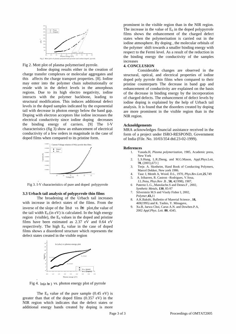
Page 3 of 3 Proceedings of OMTAT2005
0.0 0.5 1.0 1.5 2.0 2.5 3.0 3.5 4.0 4.5
50
100
150
200
250
300
350
400
450
Fig 2. Mott plot of plasma polymerised pristine and iodine doped pyrrole.
2.4 eV 3.1 eV
Pure Doped
(αhυ
)1/2
Photon energy (eV)
Fig 2. Mott plot of plasma polymerised pyrrole.
Iodine doping results either in the creation of charge transfer complexes or molecular aggregates and this affects the charge transport properties. [8]. Iodine may enter into the polymer chain substitutionally or reside with in the defect levels in the amorphous regions. Due to its high electro negativity, iodine interacts with the polymer backbone, leading to structural modification. This induces additional defect levels in the doped samples indicated by the exponential tail with decrease in photon energy below the band gap. Doping with electron acceptors like iodine increases the electrical conductivity since iodine doping decreases the binding energy of carriers. [9] The I-V characteristics (fig 3) show an enhancement of electrical conductivity of a few orders in magnitude in the case of doped films when compared to its pristine form.
.10 20 30 40 50 60
0.00001
0.00002
0.00003
0.00004
0.00005
0.00006
0.00007 Current Voltage relation of Poly pyrrole thin films.
Doped Pure
Cur
rent
(A
)
Voltage (V)
Fig 3. I-V characteristics of pure and doped polypyrrole
3.3 Urbach tail analysis of polypyrrole thin films
The broadening of the Urbach tail increases with increase in defect states of the films. From the inverse of the slope of the lnα vs hν plot,the value of the tail width E0 (in eV) is calculated. In the high energy region (visible), the E0 values in the doped and pristine films have been estimated as 2.37 eV and 0.64 eV respectively. The high E0 value in the case of doped films shows a disordered structure which represents the defect states created in the visible region
. 0.5 1.0 1.5 2.0 2.5 3.0 3.5 4.0 4.5
6
7
8
9
10
11
12
13
14 ln (αhυ) vs photon energy plot
E02=0.45eV
E01=0.64eVE02=0.357eV
E01=2.37 eV
ln α (pure) ln α (doped)
ln( α
h ν)
Photon energy (eV)
Fig 4. ln( )hα ν vs. photon energy plot of pyrrole
The E0 value of the pure sample (0.45 eV) is
greater than that of the doped films (0.357 eV) in the NIR region which indicates that the defect states or additional energy bands created by doping is more
prominent in the visible region than in the NIR region. The increase in the value of E0 in the doped polypyrrole films shows the enhancement of the charged defect states when the polymerisation is carried out in the iodine atmosphere. By doping , the molecular orbitals of the polymer shift towards a smaller binding energy with respect to the Fermi level. As a result of the reduction in the binding energy the conductivity of the samples increases 4. CONCLUSION
Considerable changes are observed in the structural, optical, and electrical properties of iodine doped poly pyrrole thin films when compared to their pristine counterparts The decrease in band gap and enhancement of conductivity are explained on the basis of the decrease in binding energy by the incorporation of charged defects. The enhancement of defect levels by iodine doping is explained by the help of Urbach tail analysis. It is found that the disorders created by doping are more prominent in the visible region than in the NIR region. Acknoldgements MRA acknowledges financial assistance received in the form of a project under ISRO-RESPOND, Government of India (File. No. 10/03/354 dtd.23-02-1999). References
1. Yasuda.H, Plasma polymerization, 1985, Academic press, New York
2. L.S.Hung, L.R.Zheng, and M.G.Mason, Appl.Phys.Lett, 78, (2001),673 ]
3. Terje. A. Skotheim, Hand Book of Conducting Polymers, Marcel Dekker, New york 1986.
4. Tauc J, Menth A, Wood. D.L, 1970, Phys.Rev.Lett,25,749 5. A. Iribarren, R. Castron –Rodrigues, V.Sosa, J.L.Pena, Phys.Rev .B , 58, 4(1998), 1907, 6 Paterno L.G.,.Manolache.S and Denes.F , 2002, Synthetic Metals, 130, 85-97
7. Silverstein M.S and Visoly Fisher I, 2002, Polymer,43,11 8. A.K.Bakshi, Bullettin of Marerial Science , 18, 469(1995) and K. Tashio, Y. Minagave,
9. Xu.B, Jaewu Choi, Carus A.N. and Dowben.P.A, 2002 Appl.Phys. Lett. 80, 4345.
Poly Phosphazene With Pendant 4-(4-Nitro phenyl azo)-2-Pentadecinyl Phenol
Non Linear Optical Polymer for Electro -Optic Applications
A computational approach
T.Vijayakumar1
, I. Hubert Joe1
, T. Shrisudha2
, Dona Mathew2
C.P Reghunadhan Nair2
and V.S. Jayakumar1*
1
Centre for Molecular and Biophysics Research, Department of Physics, Mar Ivanios College, Thiruvananthapuram - 695 015, kerala, India
2 Polymers and Special Chemicals Group, Vikram Sarabhai Space Centre, Thiruvananthapuram-695 022, kerala, India * E-mail: [email protected]
ABSTRACT
A comprehensive investigation of the polyphosphazene NLO polymer with pendant NPADP has been carried out to determine their linear and non-linear optical properties. These molecular systems show very large non-linear optical activity. The static hyperpolarizabilities (âtot), entropies and the frontier molecular orbital energies are calculated. The relationship of HOMO–LUMO gap with the total static hyperpolarizability is analysed based on computed results. The enormous enhancement of the hyperpolarizability for a particular dihedral angle is predicted in these novel molecular systems. The structural features responsible for the very large non-linear optical activity in these polymeric systems have also been discussed. 1. INTRODUCTION
Nonlinear optical (NLO) polymeric materials have been subject of tremendous interest in recent years for potential applications in photonic devices, such as optical switches, electro-optic (EO) modulators, and high-density optical data storage media1-4. Due to their high intrinsic nonlinearities, low dielectric constants, fast response times, ease-of-processibility, and low cost, several types of polymeric NLO systems have been proposed, including guest-host5, side-chain6, main-chain, and cross-linkable systems7-8. The value of the second order optical susceptibility ÷ (2), in a given NLO system depends on the molecular hyperpolarizability â, the number of chromophores, and the degree of non-centrosymmetry. The major impediment in using devices based on these materials commercially is the development of NLO polymer materials with simultaneous high nonlinearity and good thermal stability. Understanding the physical mechanisms of chromophore orientation and the static properties of NLO polymers is essential to develop such systems with high nonlinearity and excellent long term stability. Ab initio quantum-chemical calculations can be used to predict the NLO properties, solvation effects and electron correlation at the MP2 or DFT levels accurately, even for very large molecules. Hence, quantum chemical modeling of poly phosphazene based non linear optical polymer with pendant 4-(4-Nitro phenyl azo)-2-Pentadecinyl Phenol (NPADP) is taken up as part of design of high efficiency NLO polymeric films suited for photonic applications.
2. COMPUTATIONAL DETAILS
Computations have been performed at HF/ STO-3G level of theory to optimize the molecular structure and predict the molecular first hyperpolarizabilities of NPADP, Poly phosphazene with pendant NPADP (PPNPADP) using the Gaussian ’98 program Package9. The HOMO-LUMO energy gap, thermodynamic parameters, dihedral angle based static hyperpolarizabilities and ground state dipole moments have also been calculated. The optimized molecular structure of the polymer PPNPADP and the NLO chromophore NPADP are given in Figs. 1 and 2 respectively.
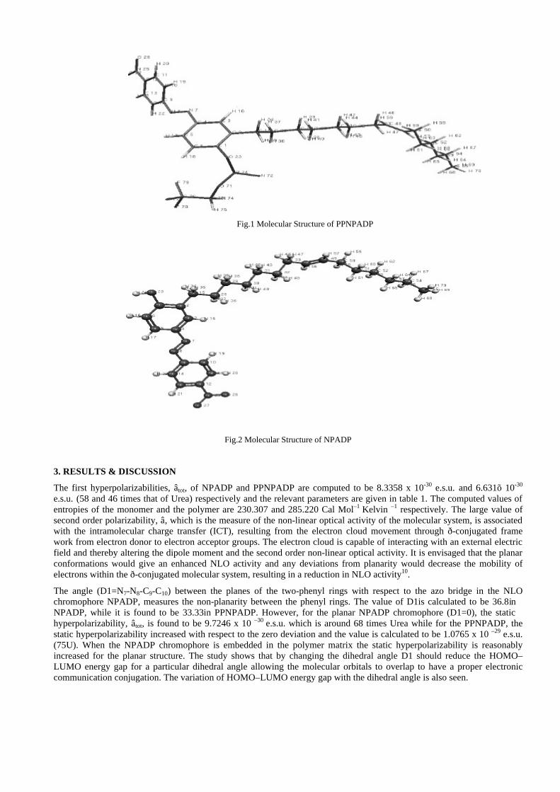
Fig.1 Molecular Structure of PPNPADP
Fig.2 Molecular Structure of NPADP
3. RESULTS & DISCUSSION
The first hyperpolarizabilities, âtot, of NPADP and PPNPADP are computed to be 8.3358 x 10⁻³⁰ e.s.u. and 6.631õ 10-30 e.s.u. (58 and 46 times that of Urea) respectively and the relevant parameters are given in table 1. The computed values of entropies of the monomer and the polymer are 230.307 and 285.220 Cal Mol–1 Kelvin –1 respectively. The large value of second order polarizability, â, which is the measure of the non-linear optical activity of the molecular system, is associated with the intramolecular charge transfer (ICT), resulting from the electron cloud movement through ð-conjugated frame work from electron donor to electron acceptor groups. The electron cloud is capable of interacting with an external electric field and thereby altering the dipole moment and the second order non-linear optical activity. It is envisaged that the planar conformations would give an enhanced NLO activity and any deviations from planarity would decrease the mobility of electrons within the ð-conjugated molecular system, resulting in a reduction in NLO activity10.
The angle (D1=N7-N8-C9-C10) between the planes of the two-phenyl rings with respect to the azo bridge in the NLO chromophore NPADP, measures the non-planarity between the phenyl rings. The value of D1is calculated to be 36.8 in NPADP, while it is found to be 33.33 in PPNPADP. However, for the planar NPADP chromophore (D1=0), the static hyperpolarizability, âtot, is found to be 9.7246 x 10 –30 e.s.u. which is around 68 times Urea while for the PPNPADP, the static hyperpolarizability increased with respect to the zero deviation and the value is calculated to be 1.0765 x 10 –29 e.s.u. (75U). When the NPADP chromophore is embedded in the polymer matrix the static hyperpolarizability is reasonably increased for the planar structure. The study shows that by changing the dihedral angle D1 should reduce the HOMO–LUMO energy gap for a particular dihedral angle allowing the molecular orbitals to overlap to have a proper electronic communication conjugation. The variation of HOMO–LUMO energy gap with the dihedral angle is also seen.
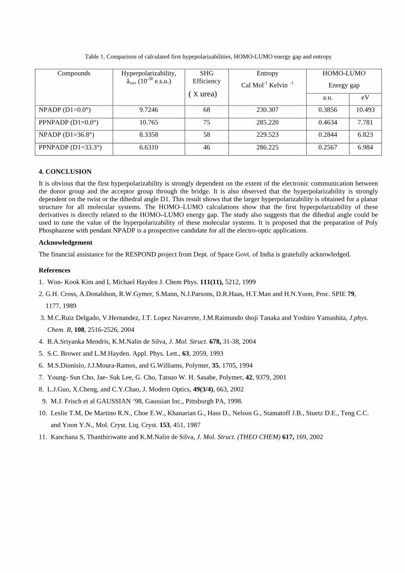
Table 1. Comparison of calculated first hypepolarizabilities, HOMO-LUMO energy gap and entropy
4. CONCLUSION
It is obvious that the first hyperpolarizability is strongly dependent on the extent of the electronic communication between the donor group and the acceptor group through the bridge. It is also observed that the hyperpolarizability is strongly dependent on the twist or the dihedral angle D1. This result shows that the larger hyperpolarizability is obtained for a planar structure for all molecular systems. The HOMO–LUMO calculations show that the first hyperpolarizability of these derivatives is directly related to the HOMO–LUMO energy gap. The study also suggests that the dihedral angle could be used to tune the value of the hyperpolarizability of these molecular systems. It is proposed that the preparation of Poly Phosphazene with pendant NPADP is a prospective candidate for all the electro-optic applications.
Acknowledgement
The financial assistance for the RESPOND project from Dept. of Space Govt. of India is gratefully acknowledged.
References
1. Won- Kook Kim and L Michael Hayden J. Chem Phys. 111(11), 5212, 1999
2. G.H. Cross, A.Donaldson, R.W.Gymer, S.Mann, N.J.Parsons, D.R.Haas, H.T.Man and H.N.Yoon, Proc. SPIE 79,
1177, 1989
3. M.C.Ruiz Delgado, V.Hernandez, J.T. Lopez Navarrete, J.M.Raimundo shoji Tanaka and Yoshiro Yamashita, J.phys.
Chem. B, 108, 2516-2526, 2004
4. B.A.Sriyanka Mendris, K.M.Nalin de Silva, J. Mol. Struct. 678, 31-38, 2004
5. S.C. Brower and L.M.Hayden. Appl. Phys. Lett., 63, 2059, 1993
6. M.S.Dionisio, J.J.Moura-Ramos, and G.Williams, Polymer, 35, 1705, 1994
7. Young- Sun Cho, Jae- Suk Lee, G. Cho, Tatsuo W. H. Sasabe, Polymer, 42, 9379, 2001
8. L.J.Guo, X.Cheng, and C.Y.Chao, J. Modern Optics, 49(3/4), 663, 2002
9. M.J. Frisch et al GAUSSIAN ‘98, Gaussian Inc., Pittsburgh PA, 1998.
10. Leslie T.M, De Martino R.N., Choe E.W., Khanarian G., Hass D., Nelson G., Stamatoff J.B., Stuetz D.E., Teng C.C.
and Yoon Y.N., Mol. Cryst. Liq. Cryst. 153, 451, 1987
11. Kanchana S, Thanthiriwatte and K.M.Nalin de Silva, J. Mol. Struct. (THEO CHEM) 617, 169, 2002
HOMO-LUMO
Energy gap
Compounds Hyperpolarizability, âtot, (10-30 e.s.u.)
SHG Efficiency
( X urea)
Entropy
Cal Mol-1 Kelvin –1
a.u. eV
NPADP (D1=0.0°) 9.7246 68 230.307 0.3856 10.493
PPNPADP (D1=0.0°) 10.765 75 285.220 0.4634 7.781
NPADP (D1=36.8°) 8.3358 58 229.523 0.2844 6.823
PPNPADP (D1=33.3°) 6.6310 46 286.225 0.2567 6.984
X-RAY DIFFRACTION STUDY ON THE STRUCTURAL PHASE TRANSITION IN SrXBa1-XNb2O6 CERAMICS
Shajahan Thangal and Nandakumar Kalarikkal
School of Pure & Applied Physics, Mahatma Gandhi University, Kottayam-686 560, Kerala, India
Email:[email protected] ABSTRACT The tetragonal tungsten bronze SrxBa1-xNb2O6 samples for 0.35 ≤ x ≤ 0.60 have been synthesized using the solid-state reaction method. The FTIR studies indicate that the samples prepared are almost single phase in nature. The phase assemblage of the samples for different compositions was identified by Bruker D8 Advance Diffractometer. The unit cell dimensions of the samples were precisely calculated based on XRD data by analytical method. The structural phase transition of SBN ceramics as a function of Sr/Ba ratio was examined. The results indicate the coexistence of orthorhombic and tetragonal phases in the range 0.35 < x < 0.60. The average particle size of each of the samples has been calculated using Scherrer method and is around 23 nm. 1 INTRODUCTION Strontium barium niobate SrxBa1-xNb2O6 abbreviated as SBN is a mixed solid solution of the SrNb2O6 and BaNb2O6 binary system1. It belongs to the class of oxygen octahedral relaxor ferroelectrics possessing tetragonal tungsten bronze structure2. The physical properties of SBN vary with compositions and the solid solution of SBN is of immense importance in many technological applications such as electro-optic, pyroelectric, piezoelectric and photorefractive devices3. The idealized structure with generalized formula of the tungsten bronze structure is [(A1)2(A2)4C4] [(B1)2(B2)8]O30, where A, B and C sites can be filled by different valence cations or may be partially empty. The SBN structure is built by Nb-O octahedra linked by their corners in such a way that three different types of channels are formed along the tetragonal c axis4. One channel is always empty, the second is partially filled only by Sr atoms, while the third one is partially occupied by Sr and Ba. The distribution of Sr and Ba atoms in the channels depends on the composition of the compound. A typical SBN unit cell structure is shown in Fig.1. In this paper we report the results of our XRD investigations on SrxBa1-xNb2O6 solid solutions for 0.35 < x < 0.6 in order to investigate in detail the structural phase transition behaviour.
Fig.1. The average structure of SBN: View on (001) face.
2 EXPERIMENTAL The samples of SrxBa1-xNb2O6 for 0.35 < x < 0.6 were prepared by the conventional solid state reaction method with repeated grinding and calcinations of highest purity elemental constituents in the desired stoichometric proportions. The starting materials were strontium carbonate, barium carbonate and niobium pentoxide. The stoichometric compositions of the starting materials were taken and mixed thoroughly in an agate mortar for nearly 5 h in the presence of methanol to ensure homogeneity. Each dried mixture was then heat treated at 1100oC in platinum crucibles for 24 h and finally cooled to room temperature by furnace shut off. The FTIR analysis of the prepared samples indicated almost single phase nature. The x-ray diffraction studies were carried out using an x-ray diffractometer [Bruker, D8 Advance, λ = 0.154056 nm]. 3 RESULTS AND DISCUSSION The x-ray diffraction patterns of the samples investigated are shown in Figs. 2-4. The diffraction patterns were indexed and the lattice parameters were calculated by the analytical method. The average particle size of each of the samples was calculated using Scherrer equation. The lattice parameters and the calculated average particle size of each of the compounds are given in Table. 1. Our investigations show that the system exhibits the coexistence of orthorhombic and tetragonal phases in the composition range of 0.35 < x < 0.60, dominated by the orthorhombic phase. The present studies indicate that there is no sharp demarkation between these two phases at x = 0.55 as reported in the previous literature5,6. The average particle size of each of the sample is calculated to be around 23 nm, indicating the fact that standard solid state reaction method can be employed for the preparation of nanosized structures of this class of materials.
Fig.2. XRD patterns of SBN for x = 0.35, 0.40, 0.45 and 0.50
Fig.3. XRD patterns of SBN for x = 0.52, 0.54, 0.55 and 0.56
(a)
20 30 40 50 60 70
0
20
40
60
80
100 (311)
(410)
(211)
(320)
Sr0.35
Ba0.65
Nb2O
6In
tens
ity
2θ
(b)
20 30 40 50 60 70
0
10
20
30
40
50
60
70
(550)(620)
(311)
(330)
(410)
(211)
(320)
Sr0.40
Ba0.60
Nb2O6
Inte
nsity
2θ
(c)
20 30 40 50 60 70-10
0
10
20
30
40
50
60
70
80
(320) (551)(730)
(540)
(311)
(410)(211)
Sr0.45Ba0.55Nb2O6
Inte
nsity
2θ
(d)
20 30 40 50 60 70-20
0
20
40
60
80
100
120
140
160
180
(320)
(211)(410)
(311)
(540)(551)
(541)
Sr0.50
Ba0.50
Nb2O
6
Inte
nsity
2θ
(e)
20 30 40 50 60 70
0
50
100
150
200
250
(211)
(541)(551)
(540)
(321)
(311)
(410)
(320)
Sr0.52
Ba0.48
Nb2O
6
Inte
nsity
2θ
(f)
20 30 40 50 60 70
0
50
100
150
200
(211)
(541)(540)
(311)
(410)
(320)
Sr0.54Ba0.46Nb2O6
Inte
nsity
2θ
(g)
20 30 40 50 60 70-20
0
20
40
60
80
100
120
140
160
180
(541)(540)
(311)
(410)(400)
(320)
Sr0.55
Ba0.45
Nb2O
6
Inte
nsity
2θ
(h)
20 30 40 50 60 70
0
50
100
150
200
(551)
(730)
(541)(540)
(321)
(311)
(330)
(410)
(400)
(320)
Sr0.56
Ba0.44
Nb2O
6
Inte
nsity
2θ
(i)
20 30 40 50 60 70
0
20
40
60
80
100
120
(730)
(541)(540)
(530)
(410)
(400)
(320)
(311) Sr0.58
Ba0.42
Nb2O
6In
tens
ity
2θ
(j)
20 30 40 50 60 70
0
20
40
60
80
100
(320)
(730)
(541)(540)
(311)
(410)
(400)
Sr0.60
Ba0.40
Nb2O
6
Inte
nsity
2θ
Fig.4. XRD patterns of SBN for x = 0.58 and 0.60
Table 1. Lattice parameters and particle sizes of SBN 4 CONCLUSIONS X-ray diffraction studies on different compositions of SrxBa1-xNb2O6 solid solutions in the range 0.35 ≤ x ≤ 0.6 have been performed. Our investigations indicate the coexistence of orthorhombic and tetragonal phases in the composition range investigated. The orthorhombic phase is found to dominate in the composition range studied. The average particle size of the samples is found to be around 23 nm. The detailed refinement of the data is underway and it will throw more light into the structural information exhibited by this exotic class of materials.
REFERENCES 1A. M. Prokorov and J. S. Kuzminov, Ferroelectric Crystals for Laser Radiation Control, Adam Hilger, Bristol (1990). 2T. S. Chernaya et al., Cryst. Reports 48, 375 (1997) 3C.David et al., J.Appl.Phys. 95, 5522 (2004). 4Particle size and strain analysis application note. Analysis by x-ray diffraction, H & M Analytical services Inc. 2002. 5M. H. Francombe, Acta. Cryst. 13, 131 (1960). 6H. Li et al., J. Phys. Chem. Solids 52, 647 (1991).
x a nm
b nm
c A0
Particle size nm
0.35 1.5770 1.4948 3.4128 23.4411 0.40 1.2387 1.2317 3.8965 23.2522 0.45 1.2236 1.3978 3.5925 23.6388 0.50 1.1863 1.3181 3.9167 23.1532 0.52 1.2402 1.2596 3.9275 23.5770 0.54 1.2271 1.3125 3.9794 23.9844 0.55 1.2226 1.3872 3.9995 23.2084 0.56 1.2335 1.2344 3.8886 23.9173 0.58 1.2479 1.1634 3.9091 23.4011 0.60 1.2529 1.1926 3.9512 23.8660
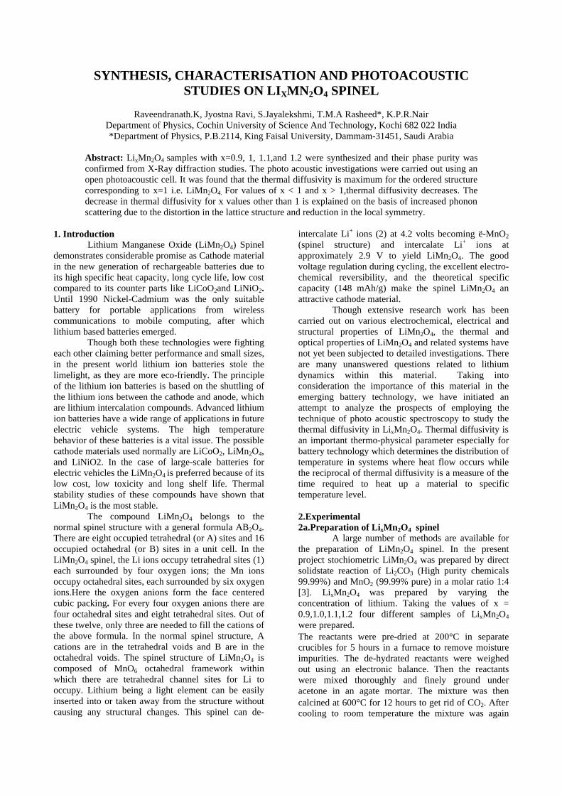
SYNTHESIS, CHARACTERISATION AND PHOTOACOUSTIC STUDIES ON LIXMN2O4 SPINEL
Raveendranath.K, Jyostna Ravi, S.Jayalekshmi, T.M.A Rasheed*, K.P.R.Nair
Department of Physics, Cochin University of Science And Technology, Kochi 682 022 India *Department of Physics, P.B.2114, King Faisal University, Dammam-31451, Saudi Arabia
Abstract: LixMn2O4 samples with x=0.9, 1, 1.1,and 1.2 were synthesized and their phase purity was confirmed from X-Ray diffraction studies. The photo acoustic investigations were carried out using an open photoacoustic cell. It was found that the thermal diffusivity is maximum for the ordered structure corresponding to x=1 i.e. LiMn2O4. For values of x < 1 and x > 1,thermal diffusivity decreases. The decrease in thermal diffusivity for x values other than 1 is explained on the basis of increased phonon scattering due to the distortion in the lattice structure and reduction in the local symmetry.
1. Introduction Lithium Manganese Oxide (LiMn2O4) Spinel
demonstrates considerable promise as Cathode material in the new generation of rechargeable batteries due to its high specific heat capacity, long cycle life, low cost compared to its counter parts like LiCoO2and LiNiO2. Until 1990 Nickel-Cadmium was the only suitable battery for portable applications from wireless communications to mobile computing, after which lithium based batteries emerged.
Though both these technologies were fighting each other claiming better performance and small sizes, in the present world lithium ion batteries stole the limelight, as they are more eco-friendly. The principle of the lithium ion batteries is based on the shuttling of the lithium ions between the cathode and anode, which are lithium intercalation compounds. Advanced lithium ion batteries have a wide range of applications in future electric vehicle systems. The high temperature behavior of these batteries is a vital issue. The possible cathode materials used normally are LiCoO2, LiMn2O4, and LiNiO2. In the case of large-scale batteries for electric vehicles the LiMn2O4 is preferred because of its low cost, low toxicity and long shelf life. Thermal stability studies of these compounds have shown that LiMn2O4 is the most stable. The compound LiMn2O4 belongs to the normal spinel structure with a general formula AB2O4. There are eight occupied tetrahedral (or A) sites and 16 occupied octahedral (or B) sites in a unit cell. In the LiMn2O4 spinel, the Li ions occupy tetrahedral sites (1) each surrounded by four oxygen ions; the Mn ions occupy octahedral sites, each surrounded by six oxygen ions.Here the oxygen anions form the face centered cubic packing. For every four oxygen anions there are four octahedral sites and eight tetrahedral sites. Out of these twelve, only three are needed to fill the cations of the above formula. In the normal spinel structure, A cations are in the tetrahedral voids and B are in the octahedral voids. The spinel structure of LiMn2O4 is composed of MnO6 octahedral framework within which there are tetrahedral channel sites for Li to occupy. Lithium being a light element can be easily inserted into or taken away from the structure without causing any structural changes. This spinel can de-
intercalate Li+ ions (2) at 4.2 volts becoming ë-MnO2 (spinel structure) and intercalate Li+ ions at approximately 2.9 V to yield LiMn2O4. The good voltage regulation during cycling, the excellent electro-chemical reversibility, and the theoretical specific capacity (148 mAh/g) make the spinel LiMn2O4 an attractive cathode material.
Though extensive research work has been carried out on various electrochemical, electrical and structural properties of LiMn2O4, the thermal and optical properties of LiMn2O4 and related systems have not yet been subjected to detailed investigations. There are many unanswered questions related to lithium dynamics within this material. Taking into consideration the importance of this material in the emerging battery technology, we have initiated an attempt to analyze the prospects of employing the technique of photo acoustic spectroscopy to study the thermal diffusivity in LixMn2O4. Thermal diffusivity is an important thermo-physical parameter especially for battery technology which determines the distribution of temperature in systems where heat flow occurs while the reciprocal of thermal diffusivity is a measure of the time required to heat up a material to specific temperature level. 2.Experimental 2a.Preparation of LixMn2O4 spinel A large number of methods are available for the preparation of LiMn2O4 spinel. In the present project stochiometric LiMn2O4 was prepared by direct solidstate reaction of Li2CO3 (High purity chemicals 99.99%) and MnO2 (99.99% pure) in a molar ratio 1:4 [3]. LixMn2O4 was prepared by varying the concentration of lithium. Taking the values of x = 0.9,1.0,1.1,1.2 four different samples of LixMn2O4 were prepared. The reactants were pre-dried at 200°C in separate crucibles for 5 hours in a furnace to remove moisture impurities. The de-hydrated reactants were weighed out using an electronic balance. Then the reactants were mixed thoroughly and finely ground under acetone in an agate mortar. The mixture was then calcined at 600°C for 12 hours to get rid of CO2. After cooling to room temperature the mixture was again
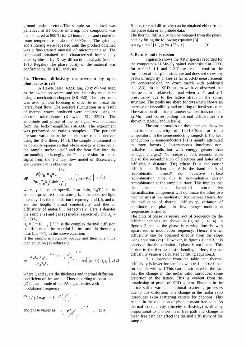
ground under acetone.The sample so obtained was pelletized at 5T before sintering. The compound was then sintered at 800°C for 24 hours in air and cooled to room temperature at about 0.33°C/min. The grinding and sintering were repeated until the product obtained was a fine-grained material of micrometer size. The compound obtained was characterized immediately after synthesis by X-ray diffraction analysis (model: 1710 Regaku) The phase purity of the material was confirmed by the XRD analysis. . 2b. Thermal diffusivity measurement by open photoacoustic cell
A He-Ne laser (632.8 nm, 20 mW) was used as the excitation source and was intensity modulated using a mechanical chopper (SR 450). The laser beam was used without focusing in order to minimize the lateral heat flow. The pressure fluctuations as a result of thermal waves produced were detected using an electret microphone (Knowles FG 3392). The amplitude and phase of the pa signal was obtained from the lock-in-amplifier (SR830). The experiment was performed on various samples. The periodic pressure variation in the air chamber can be derived using the R-G theory [4,5]. The sample is assumed to be optically opaque so that whole energy is absorbed at the sample surface itself and the heat flux into the surrounding air is negligible. The expression for the pa signal from the 1-d heat flow model of Rosencwaig and Gersho [4] is obtained as
( ) ( )[ ]2texps
lsinhfs
k0
T2
2/1
0I
0P
P πωσπ
ααγδ −
= jsg
l
sg …..(1)
where γ is the air specific heat ratio, P0(T0) is the ambient pressure (temperature), I0 is the absorbed light intensity, f is the modulation frequency, and li, ki and αI are the length, thermal conductivity and thermal diffusivity of material I respectively. Here s denotes the sample (s) and gas (g) media respectively and σg = (1+ j) ag , ag = π f/ ∝ g 1 / 2 is the complex thermal diffusion co-efficient of the material If the samle is thermally thin, (lsas <<1) in the above equation. If the sample is optically opaque and thermally thick then equation (1) reduces to
( )[ ]s
as
l2ùexpf
2/1
slexp
sk
0T
2/1
0I
0P
P −−
−
≅ πα
π
π
ααγδ tjs
f
gl
sg
where ls and as are the thickness and thermal diffusion coefficient of the sample. Thus according to equation (2) the amplitude of the PA signal varies with modulation frequency
as
−
21
exp)1(s
sflf α
π
and phase varies as 2/1
−
s
fs
l απ .… (2.a)
Hence, thermal diffusivity can be obtained either from the phase data or amplitude data. The thermal diffusivity can be obtained from the phase data by fitting the following equation [3]. φ = φ0 + tan-1 [1/ls (πf/αs)
1/2 – 1] …..(3)
3. Results and discussion Figures 5 shows the XRD spectra recorded for the compounds LixMn2O4 spinel synthesised at 800oC
for x=0.9,1 1.1 and 1.2.These results confirm the formation of the spinel structure and does not show any peaks of impurity phases(as far as XRD measurements are concerned)and an exact match with published data[2,3] . In the XRD pattern we have observed that the peaks are relatively broad when x >1 and x<1 presumably due to the lattice strain in the spinel structure. The peaks are sharp for x=1which shows an increase of crystallinity and ordering of local structure. The variation of lattice parameter with various ratios of Li:Mn and corresponding thermal diffusivities are shown in table(1)and in fig(6).
The earlier studies on these samples show an electrical conductivity of 1.9x10⁻⁵S/cm at room temperature, in the semiconducting range.[6]. The heat conduction in semiconductors [7] is mainly attributed to three factors.1) Instantaneous intraband non-radiative thermalisation with energy greater than bandgap energy.2) Non-radiative bulk recombination due to the recombination of electrons and holes after diffusing a distance (Dé) where D is the carrier diffusion coefficient and é is the band to band recombination time.3) non radiative surface recombination time due to non-radiative carrier recombination at the sample surface. This implies that the instantaneous intraband non-radiative thermalisation component will dominate the other two mechanisms at low modulation frequencies. Hence, for the evaluation of thermal diffusivity, variation of amplitude or phase in low range modulation frequencies is studied. The plots of phase vs square root of frequency for the different samples are shown in figures (1 to 4). In figures 2 and 4, the phase is varying linearly with square root of modulation frequency. Hence, thermal diffusivity can be obtained directly from the slope using equation (2a). However, in figures 1 and 3, it is observed that the variation of phase is not linear. This is due to the thermo elastic bending. Here, thermal diffusivity value is calculated by fitting equation.3. It is observed from the table that thermal diffusivity is lower for samples with x<1 and x>1 than for sample with x=1.This can be attributed to the fact that the change in the molar ratio introduces some distortion in the lattice. This is evident from the broadening of peaks of XRD pattern. Phonons in the lattice suffer various additional scattering processes due to this distortion. The change in the molar ratio introduces extra scattering centers for phonons. This results in the reduction of phonon mean free path. As thermal conductivity (thereby diffusivity) is directly proportional to phonon mean free path any change in mean free path can affect the thermal diffusivity of the sample.
….(2)
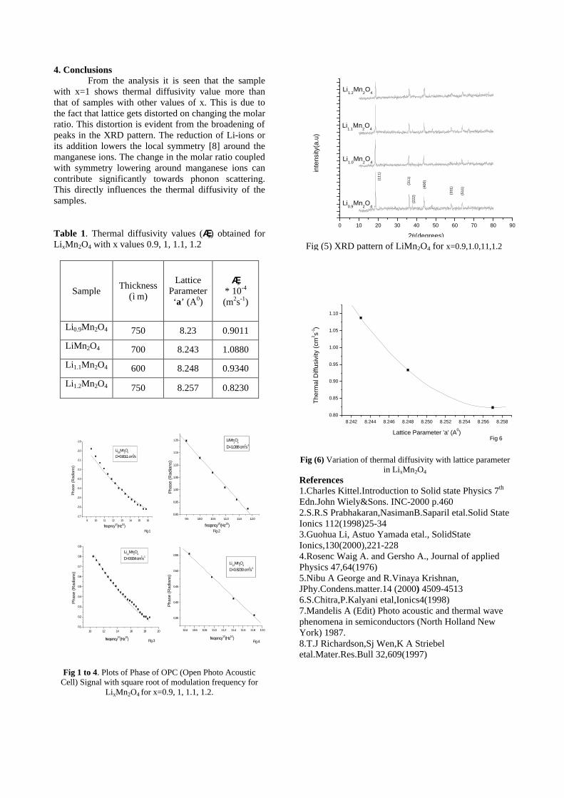
4. Conclusions From the analysis it is seen that the sample with x=1 shows thermal diffusivity value more than that of samples with other values of x. This is due to the fact that lattice gets distorted on changing the molar ratio. This distortion is evident from the broadening of peaks in the XRD pattern. The reduction of Li-ions or its addition lowers the local symmetry [8] around the manganese ions. The change in the molar ratio coupled with symmetry lowering around manganese ions can contribute significantly towards phonon scattering. This directly influences the thermal diffusivity of the samples. Table 1. Thermal diffusivity values (Æs) obtained for LixMn2O4 with x values 0.9, 1, 1.1, 1.2
Sample Thickness
(ì m)
Lattice Parameter ‘a’ (A0)
Æs * 10-4 (m2s-1)
Li0.9Mn2O4 750 8.23 0.9011
LiMn2O4 700 8.243 1.0880
Li1.1Mn2O4 600 8.248 0.9340
Li1.2Mn2O4 750 8.257 0.8230
9 10 11 12 13 14 15 16-2.7
-2.6
-2.5
-2.4
-2.3
-2.2
-2.1
-2.0
-1.9
Fig 1
Pha
se (
Rad
ians
)
freqency1/2(Hz1/2)
Li0.9
Mn2O
4
D=0.9011 cm2/s
10.4 10.6 10.8 11.0 11.2 11.4 11.6 11.8 12.0
0.35
0.40
0.45
0.50
0.55
Fig 4
Pha
se (
Rad
ians
)
freqency1/2(Hz1/2)
Li1.2
Mn2O
4
D=0.8230 cm2s-1
10 12 14 16 18 200.1
0.2
0.3
0.4
0.5
0.6
0.7
0.8
0.9
Fig 3
Pha
se (
Rad
ians
)
freqency1/2(Hz1/2)
Li1.1
Mn2O
4
D=0.934 cm2s-1
9.5 10.0 10.5 11.0 11.5 12.00.90
0.95
1.00
1.05
1.10
1.15
1.20
Fig 2
LiMn2O
4
D=1.088 cm2s-1
Pha
se (
Rad
ians
)
freqency1/2(Hz1/2)
Fig 1 to 4. Plots of Phase of OPC (Open Photo Acoustic Cell) Signal with square root of modulation frequency for
LixMn2O4 for x=0.9, 1, 1.1, 1.2.
0 10 20 30 40 50 60 70 80 90
(511
)
(331
)(400
)
(222
)(3
11)
Li1.2
Mn2O
4
Li1.1
Mn2O
4
Li1.0
Mn2O
4
Li0.9
Mn2O
4
(111
)inte
nsity
(a.u
)
2θ(degrees)
8.242 8.244 8.246 8.248 8.250 8.252 8.254 8.256 8.2580.80
0.85
0.90
0.95
1.00
1.05
1.10
Fig 6
The
rmal
Diff
usiv
ity (
cm2 s-1
)
Lattice Parameter 'a' (A0)
Fig (6) Variation of thermal diffusivity with lattice parameter in LixMn2O4
References 1.Charles Kittel.Introduction to Solid state Physics 7th Edn.John Wiely&Sons. INC-2000 p.460 2.S.R.S Prabhakaran,NasimanB.Saparil etal.Solid State Ionics 112(1998)25-34 3.Guohua Li, Astuo Yamada etal., SolidState Ionics,130(2000),221-228 4.Rosenc Waig A. and Gersho A., Journal of applied Physics 47,64(1976) 5.Nibu A George and R.Vinaya Krishnan, JPhy.Condens.matter.14 (2000) 4509-4513 6.S.Chitra,P.Kalyani etal,Ionics4(1998) 7.Mandelis A (Edit) Photo acoustic and thermal wave phenomena in semiconductors (North Holland New York) 1987. 8.T.J Richardson,Sj Wen,K A Striebel etal.Mater.Res.Bull 32,609(1997)
Fig (5) XRD pattern of LiMn2O4 for x=0.9,1.0,11,1.2
SELF-ENHANCEMENT OF DIFFRACTION EFFICIENCY IN MBPVA/ACRYLAMIDE FILMS
Beena Mary John a, Rani Joseph b, K. Sreekumar c, C. Sudha Karthaa*
a Department of Physics, b Department of polymer Science &Rubber Technology,
c Department of Applied Chemistry, Cochin University of Science and Technology, Cochin-682 022, Kerala, India, Ph: 0484-2575404
Email: [email protected] * ABSTRACT
In the present study the existing Methylene blue sensitized Poly (vinyl alcohol)/Acrylamide recording medium was modified by incorporating ammonium dichromate. The dichromated sample (just after recording) showed a diffraction efficiency of 21% for an exposure of 500mJ/cm2 without any pre exposure and chemical fixing. Interestingly, this film with ammonium dichromate showed a self-enhancement in diffraction efficiency on storage. The diffraction efficiency was found to slowly increase to 42% by 3 months without any fixing process. After three months the efficiency remained constant and the material is still under observation. 1. INTRODUCTION The self enhancement (SE) of a hologram is the increase in its Diffraction efficiency (DE) after the recording over time under light illumination or in the dark. SE both during and after the recording can together be regarded as a two stage holographic recording method, which is profitable when the recording energy or the exposure time is limited at the first stage. Such a recording method has the advantage of large vibration stability at the second stage. The SE was reported in LiNbO3: Fe crystals1, KBr crystals 2, amorphous AS2S3 films3, thionine-PVA4, Dichromated PVA (DCPVA) 5-6 and dichromated Gelatin (after chemical fixing) 7. According to the mechanism and properties of the effect, enhancement can be of coherent SE, incoherent SE and dark SE. Coherent type SE occurs when the gratings recorded is read out with a reference beam, the diffracted beam and the reference beams interfere, causing further recording. The incoherent SE is due to the transmission increase of a hologram by incoherent light. The enhancement takes place when the hologram works and selects light at the Bragg angle. The procedure is similar to coherent SE, but it is less effective. Dark or relaxational SE is due to the transmission increase of a hologram by thermo-stimulated relaxation process. Light induced SE takes place in all real time recording media, but dark SE is a special property of only some materials. SE both during and after the recording can together be regarded as a two stage holographic recording method, which is profitable when the recording energy or the exposure time is limited at the first stage. Such a recording method has the advantage of large vibration stability at the second stage. In the case of dichromated polymers, those are less sensitive and need long exposure times, Dark SE is more important. In thionine- PVA, the enhancement is due to the Borrmann effect or the effect caused by excited dye molecules4. In this a transient grating made of metastable molecules interferes destructively with
a permanent grating made of final photochemical products. Loughnot etal8 observed that after recording thermal post polymerization enhances the spatial modulation of segment density between bright and dark areas. This goes along with an increase of modulation of refractive index in dark and an improvement of the DE. The key phenomenon is the balance between the chemical initiation of the polymerization and the diffusion of unreacted species. Keinonen etal6 studied the dependence of the SE of DCPVA on the dichromate concentration, exposure energy and pH. In DCPVA the SE increases with pH, but decreases with dichromate concentration and exposure energy. The SE which was observed in DCG gratings (after fixing) was much higher than that observed in DCPVA7. This increase is reported to be due to the hardening of gelatin during chemical fixing. But the increase is slower for higher pH values than for lower pH values. Dye sensitized poly (vinyl alcohol)/Acrylamide with or without additional monomers are the most widely used photopolymer recording media for holographic applications. But DE of PVA/Acrylamide films decreases on storage and permanent storage is not possible 10-12. In the present study MBPVA/ Acrylamide system with dichromate as a crosslinker was fabricated and its DE was determined. Unlike the conventional PVA/Acrylamide films, the films even without any fixing technique showed self-enhancement in diffraction efficiency on storage. 2. EXPERIMENTAL 2.1 Film preparation The photopolymer solution was prepared by sensitizing 10% PVA solution (M.wt.1, 25,000) with acrylamide (.375M), Triethanolamine (.05M) and methylene blue (2.8 x 10⁻⁴ mol/l). The concentration of ammonium dichromate (ADC) was selected such that the product of the concentrations of Methylene blue (MB) and ADC should be less than the solubility product 2x10⁻² (mol/l) 2.It is reported that, if this value exceeds the solubility product,
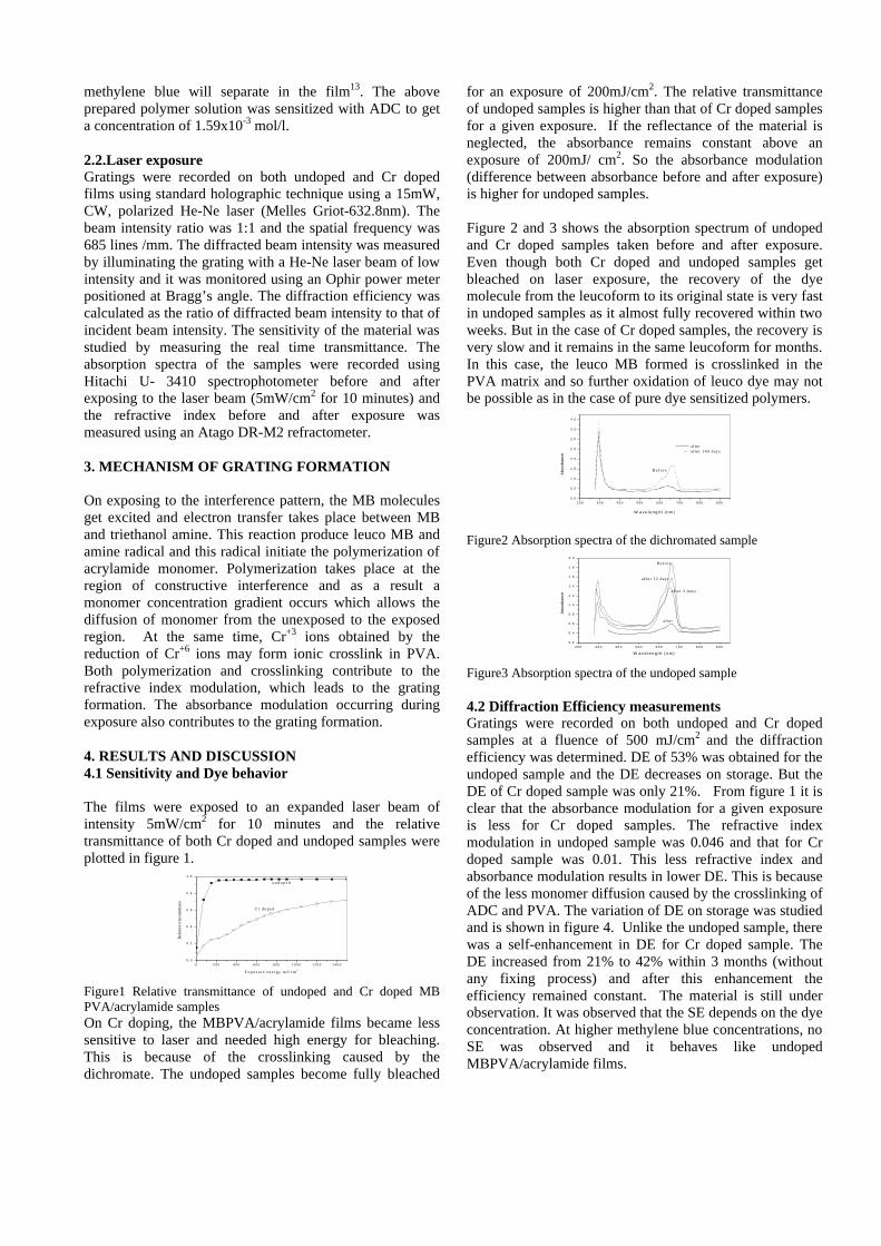
methylene blue will separate in the film13. The above prepared polymer solution was sensitized with ADC to get a concentration of 1.59x10⁻³ mol/l. 2.2.Laser exposure Gratings were recorded on both undoped and Cr doped films using standard holographic technique using a 15mW, CW, polarized He-Ne laser (Melles Griot-632.8nm). The beam intensity ratio was 1:1 and the spatial frequency was 685 lines /mm. The diffracted beam intensity was measured by illuminating the grating with a He-Ne laser beam of low intensity and it was monitored using an Ophir power meter positioned at Bragg’s angle. The diffraction efficiency was calculated as the ratio of diffracted beam intensity to that of incident beam intensity. The sensitivity of the material was studied by measuring the real time transmittance. The absorption spectra of the samples were recorded using Hitachi U- 3410 spectrophotometer before and after exposing to the laser beam (5mW/cm2 for 10 minutes) and the refractive index before and after exposure was measured using an Atago DR-M2 refractometer. 3. MECHANISM OF GRATING FORMATION On exposing to the interference pattern, the MB molecules get excited and electron transfer takes place between MB and triethanol amine. This reaction produce leuco MB and amine radical and this radical initiate the polymerization of acrylamide monomer. Polymerization takes place at the region of constructive interference and as a result a monomer concentration gradient occurs which allows the diffusion of monomer from the unexposed to the exposed region. At the same time, Cr+3 ions obtained by the reduction of Cr+6 ions may form ionic crosslink in PVA. Both polymerization and crosslinking contribute to the refractive index modulation, which leads to the grating formation. The absorbance modulation occurring during exposure also contributes to the grating formation. 4. RESULTS AND DISCUSSION 4.1 Sensitivity and Dye behavior The films were exposed to an expanded laser beam of intensity 5mW/cm2 for 10 minutes and the relative transmittance of both Cr doped and undoped samples were plotted in figure 1.
0 2 0 0 4 0 0 6 0 0 8 0 0 1 0 0 0 1 2 0 0 1 4 0 00 . 0
0 . 2
0 . 4
0 . 6
0 . 8
1 . 0
C r d o p e d
u n d o p e d
Rel
ativ
e tr
ansm
ittan
ce
E x p o s u r e e n e r g y m J / c m2
Figure1 Relative transmittance of undoped and Cr doped MB PVA/acrylamide samples On Cr doping, the MBPVA/acrylamide films became less sensitive to laser and needed high energy for bleaching. This is because of the crosslinking caused by the dichromate. The undoped samples become fully bleached
for an exposure of 200mJ/cm2. The relative transmittance of undoped samples is higher than that of Cr doped samples for a given exposure. If the reflectance of the material is neglected, the absorbance remains constant above an exposure of 200mJ/ cm2. So the absorbance modulation (difference between absorbance before and after exposure) is higher for undoped samples. Figure 2 and 3 shows the absorption spectrum of undoped and Cr doped samples taken before and after exposure. Even though both Cr doped and undoped samples get bleached on laser exposure, the recovery of the dye molecule from the leucoform to its original state is very fast in undoped samples as it almost fully recovered within two weeks. But in the case of Cr doped samples, the recovery is very slow and it remains in the same leucoform for months. In this case, the leuco MB formed is crosslinked in the PVA matrix and so further oxidation of leuco dye may not be possible as in the case of pure dye sensitized polymers.
2 0 0 3 0 0 4 0 0 5 0 0 6 0 0 7 0 0 8 0 0 9 0 00 . 0
0 . 5
1 . 0
1 . 5
2 . 0
2 . 5
3 . 0
3 . 5
4 . 0
a f te r a f t e r 1 4 0 d a y s
B e f o r e
W a v e l e n g t h ( n m )
Abs
orba
nce
Figure2 Absorption spectra of the dichromated sample
2 0 0 3 0 0 4 0 0 5 0 0 6 0 0 7 0 0 8 0 0 9 0 00 . 2
0 . 4
0 . 6
0 . 8
1 . 0
1 . 2
1 . 4
1 . 6
1 . 8
2 . 0
a f t e r 1 2 d a y s
a f t e r 3 d a y s
B e f o r e
a f t e r
Abs
orba
nce
W a v e l e n g t h ( n m )
Figure3 Absorption spectra of the undoped sample 4.2 Diffraction Efficiency measurements Gratings were recorded on both undoped and Cr doped samples at a fluence of 500 mJ/cm2 and the diffraction efficiency was determined. DE of 53% was obtained for the undoped sample and the DE decreases on storage. But the DE of Cr doped sample was only 21%. From figure 1 it is clear that the absorbance modulation for a given exposure is less for Cr doped samples. The refractive index modulation in undoped sample was 0.046 and that for Cr doped sample was 0.01. This less refractive index and absorbance modulation results in lower DE. This is because of the less monomer diffusion caused by the crosslinking of ADC and PVA. The variation of DE on storage was studied and is shown in figure 4. Unlike the undoped sample, there was a self-enhancement in DE for Cr doped sample. The DE increased from 21% to 42% within 3 months (without any fixing process) and after this enhancement the efficiency remained constant. The material is still under observation. It was observed that the SE depends on the dye concentration. At higher methylene blue concentrations, no SE was observed and it behaves like undoped MBPVA/acrylamide films.
0 2 0 4 0 6 0 8 0 1 0 0 1 2 00
5
1 0
1 5
2 0
2 5
3 0
3 5
4 0
4 5
5 0
5 5
C r d o p e d
u n d o p e d%
Dif
frac
tion
effi
cien
cy
T i m e ( d a y s )
Figure 4 Diffraction efficiency on storage for both Cr doped and undoped films The SE process can be characterized by the self-enhancement coefficient, î=ç t/ç0 and by the self enhancement rate, â= dî/dt, where ç0 is the initial DE immediately after the recording and çt is the DE after time t. Figure 5 and 6 shows the SE coefficient with time and the self enhancement rate with time respectively. In this case the SE increases with time and becomes constant after 3 months. But in DCPVA, it was reported that the efficiency increases within 1-3 days depending on the pH and then it decrease6. Here the enhancement is similar to that observed in DCG, where no decrease in DE was observed7on storage. But in DCG, the SE was observed only after chemical fixing where the DE increases from 0.05% to 2.5 % within 180 days. From figure 6 it is found that the SE rate increases in the first 10 days and then it decreases slightly and remains constant for months.
0 2 0 4 0 6 0 8 0 1 0 0 1 2 00 . 0
0 . 2
0 . 4
0 . 6
0 . 8
1 . 0
1 . 2
1 . 4
1 . 6
1 . 8
2 . 0
self
enha
ncem
ent c
oeffi
cien
t
t i m e ( d a y s )
Figure 5 Self-enhancement coefficient with time: dichromated MBPVA/acrylamide
0 1 0 2 0 3 0 4 0 5 0 6 0 7 0 8 0 9 0 1 0 0 1 1 0 1 2 0
- 0 . 2 0
- 0 . 1 5
- 0 . 1 0
- 0 . 0 5
0 . 0 0
0 . 0 5
0 . 1 0
0 . 1 5
self
enha
ncem
ent r
ate
t im e ( d a y s )
Figure (6) Self enhancement rate with time: Dichromated MBPVA/acrylamide The SE observed may be due to the dark reaction, diffusion, polymerization and internal stresses as observed in DCPVA5. Cr+6 reduced slowly during photochemical reaction induced during the exposure. All the Cr+5 (produced by the reduction of Cr+6) is not reduced to Cr+3 during exposure, but this reduction may continue in the dark. This reduction is large in the more exposed regions than in the less exposed regions. The number of crosslinkage between Cr+3 and the PVA therefore increases and thus the index modulation also increases which induces an increase in DE. This dark reaction may be the major reason for the SE.Cr+3 or unreacted Cr+5 may diffuse from the less exposed regions to the more exposed regions. This
diffusion may produce a refractive index modulation and hence an increase in DE. Diffusion of Cr+3 ions is possible only if all the Cr+3 ions are not bound in the crosslinkage. The polymerization of acrylamide monomer in the system may not complete during the recording period. Further polymerization is also responsible for the grating formation. During drying and also on exposure there can be an increase in the internal stress in the film. But when the coating expands by absorbing moisture at room temperature, the internal strain is relaxed and this may also contribute to the increase in DE. Thus it is felt that in Cr doped MBPVA/acrylamide system all these factors together contribute to the observed self-enhancement of which the crosslinking may be contributing more. Thus addition of crosslinker makes the system more stable and helps in long term storage. Even though there is a decrease in DE on incorporating the crosslinker, the self-enhancement observed makes the system regain the diffraction efficiency and helps in maintaining the efficiency constant for several months. The material is still under observation. 5. CONCLUSION
To the authors’ knowledge, this is the first report of the fabrication of Methylene blue sensitized dicromated PVA- acrylamide films for holographic recording. Due to the self enhancement effect, the DE increased from 21% to 42 % within 3 months. So unlike the dye sensitized PVA/acrylamide films, long term storage is possible in this material with double the initial diffraction efficiency.
Acknowledgement The authors acknowledge DRDO for the financial assistance through a project. 6.REFERENCE 1. T.K.Gaylord, T.A Rabson, F.K.Tittel, C.R. Quick,
J.Appl. Phys. 44, 896-897 (1973) 2. A Ozoles, Latv.J.Phys.Tech.Sci. 5,45-52 (1979) 3. A Ozoles, O Salminen, M.Reinfelde, J.Appl. Phys. 75,
3326-33 (1994) 4. S.Caron, J.J.A Conture, R.A.Lessard, Appl. Opt. 29, 599-
603 (1990) 5. R. Grazymala, T. Keinonen, Appl. Opt.37, 6623-26
(1998) 6. T.Keinonen, R. Grazymala, Appl.Opt 38, 7214-21 (1999) 7. R. Grazymala, T.Keinonen, Appl. Opt. 38, 7222-27
(1999) 8. D.J. Loughnot, C.Turch, Pure Appl. Opt. 1. 269-278
(1992) 9. T Galcera, X.Jouan, M.Bolte, J.Photochem Photobio A,
45, 249-259 (1988) 10. S.Blaya, M.Murciano, P.Acebal, L Carretero, M.
Ulibarrena, A.Fimia, Appl. Phys. Let, 84, 4765 (2004) 11. S.Gallego, M.Ortuno, C.Neipp, C.Garcia, A.Belendez
and I.Pascual, Optic Express, 11, 181 (2003) 12. V.Weiss, E Millul, Appl. Surf. Sci. 106, 293-300
(1996). 13. K. Kurokawa, S. Koike, S.Namba, T.Mizuno, T.
Kubota, Appl. Opt, 37, 3038-43(1998).
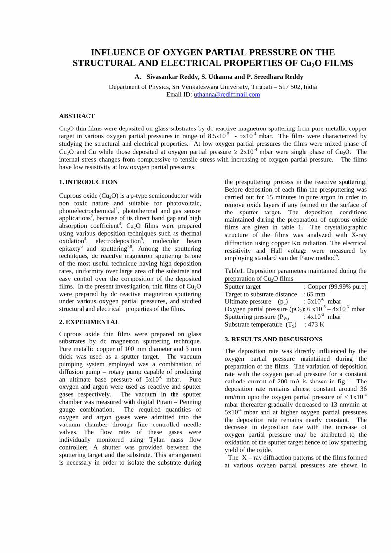
INFLUENCE OF OXYGEN PARTIAL PRESSURE ON THE STRUCTURAL AND ELECTRICAL PROPERTIES OF Cu2O FILMS
A. Sivasankar Reddy, S. Uthanna and P. Sreedhara Reddy
Department of Physics, Sri Venkateswara University, Tirupati – 517 502, India Email ID: [email protected]
ABSTRACT
Cu2O thin films were deposited on glass substrates by dc reactive magnetron sputtering from pure metallic copper target in various oxygen partial pressures in range of 8.5x10⁻⁵ - 5x10⁻⁴ mbar. The films were characterized by studying the structural and electrical properties. At low oxygen partial pressures the films were mixed phase of Cu2O and Cu while those deposited at oxygen partial pressure ≥ 2x10⁻⁴ mbar were single phase of Cu2O. The internal stress changes from compressive to tensile stress with increasing of oxygen partial pressure. The films have low resistivity at low oxygen partial pressures. 1. INTRODUCTION Cuprous oxide (Cu2O) is a p-type semiconductor with non toxic nature and suitable for photovoltaic, photoelectrochemical1, photothermal and gas sensor applications2, because of its direct band gap and high absorption coefficient3. Cu2O films were prepared using various deposition techniques such as thermal oxidation4, electrodeposition5, molecular beam epitaxty6 and sputtering7,8. Among the sputtering techniques, dc reactive magnetron sputtering is one of the most useful technique having high deposition rates, uniformity over large area of the substrate and easy control over the composition of the deposited films. In the present investigation, thin films of Cu2O were prepared by dc reactive magnetron sputtering under various oxygen partial pressures, and studied structural and electrical properties of the films.
2. EXPERIMENTAL
Cuprous oxide thin films were prepared on glass substrates by dc magnetron sputtering technique. Pure metallic copper of 100 mm diameter and 3 mm thick was used as a sputter target. The vacuum pumping system employed was a combination of diffusion pump – rotary pump capable of producing an ultimate base pressure of 5x10⁻⁶ mbar. Pure oxygen and argon were used as reactive and sputter gases respectively. The vacuum in the sputter chamber was measured with digital Pirani – Penning gauge combination. The required quantities of oxygen and argon gases were admitted into the vacuum chamber through fine controlled needle valves. The flow rates of these gases were individually monitored using Tylan mass flow controllers. A shutter was provided between the sputtering target and the substrate. This arrangement is necessary in order to isolate the substrate during
the presputtering process in the reactive sputtering. Before deposition of each film the presputtering was carried out for 15 minutes in pure argon in order to remove oxide layers if any formed on the surface of the sputter target. The deposition conditions maintained during the preparation of cuprous oxide films are given in table 1. The crystallographic structure of the films was analyzed with X-ray diffraction using copper Kα radiation. The electrical resistivity and Hall voltage were measured by employing standard van der Pauw method9.
Table1. Deposition parameters maintained during the preparation of Cu2O films Sputter target : Copper (99.99% pure) Target to substrate distance : 65 mm Ultimate pressure (pu) : 5x10⁻⁶ mbar Oxygen partial pressure (pO2): 6 x10⁻⁵ – 4x10⁻³ mbar Sputtering pressure (PW) : 4x10⁻² mbar Substrate temperature (TS) : 473 K 3. RESULTS AND DISCUSSIONS
The deposition rate was directly influenced by the oxygen partial pressure maintained during the preparation of the films. The variation of deposition rate with the oxygen partial pressure for a constant cathode current of 200 mA is shown in fig.1. The deposition rate remains almost constant around 36 nm/min upto the oxygen partial pressure of ≤ 1x10⁻⁴ mbar thereafter gradually decreased to 13 nm/min at 5x10⁻⁴ mbar and at higher oxygen partial pressures the deposition rate remains nearly constant. The decrease in deposition rate with the increase of oxygen partial pressure may be attributed to the oxidation of the sputter target hence of low sputtering yield of the oxide. The X – ray diffraction patterns of the films formed at various oxygen partial pressures are shown in
fig.2. The films were polycrystalline in nature with cubic structure. The films deposited at oxygen partial pressures ≤ 1x10⁻⁴ mbar showed a peak at 2θ = 36.54o corresponding to the (111) plane of Cu2O and
Fig.1. Variation of deposition rate of Cu2O films with
the oxygen partial pressure
another peak at 41.25o related to the (111) plane of unoxidized copper. The presence of mixed phase of Cu2O along with copper at oxygen partial pressures ≤ 1x10⁻⁴ mbar was due to the nonavailability of sufficient oxygen. The films formed at oxygen partial pressures ≥ 2x10⁻⁴ mbar exhibited a single phase Cu2O with out the presence of Cu phase. This indicates an oxygen partial pressure of 2x10⁻⁴ mbar is an optimum to produce single phase films of Cu2O. It is seen from the figure that the intensity of the X-ray diffraction peak increased with the increase of oxygen partial pressure upto 2x10⁻⁴ mbar and decreased with further increase of oxygen partial pressure.
2 0 3 0 4 0 5 0 6 0 7 0 8 0
1 x 1 0- 4
m b a r
C u ( 1 1 1 )
2 θ ( d e g r e e )
2 x 1 0- 4
m b a r
Inte
nsity
(ar
b.un
its)
T s = 4 7 3 K
p O2 =
5 x 1 0- 4
m b a r
C u2O ( 1 1 1 )
Fig.2. X-ray diffraction patterns of Cu2O films
The evaluated lattice parameter from the X-ray diffraction peak increased from 0.4258 nm to 0.4281 nm with increase of oxygen partial pressure from 8x10⁻⁵ mbar to 5x10⁻⁴ mbar. At low oxygen partial pressures ≤ 1x10⁻⁴ mbar the lattice parameter was lower than the standard lattice parameter (0.4269 nm) these films were of inferior in crystallinity and low electrical resistivity. Further increase of oxygen partial pressure the crystallinity of the films improved along with the increase of lattice constant. The similar behavior also notice in rf sputtered copper nitrate films10 The lattice parameter of the films formed at an oxygen partial pressure of 2x10⁻⁴ mbar was 0.427 nm, and in good agreement with the JCPDS data11. Fig.3. shows the dependence of stress on the oxygen partial pressure of the films. The stress (σ) developed in the films was calculated from the X-ray diffraction data employing the relation12.
σ = -E (a – ao) / 2ν ao --------- 1
where E is the Young’s Modules of the Cu2O (30 GPa), ‘a’ the lattice parameter of the bulk material, ao the measured lattice parameter and ν the Poisson’s ratio (0.455). The information regarding the stress developed in the films was obtained by the shift in the interplanar spacing thereby changing in the lattice parameter.
0 1 2 3 4 5
-0.10
-0.08
-0.06
-0.04
-0.02
0.00
0.02
0.04
0.06
0.08
0.10Ts = 473 K
In
tern
al s
tres
s (G
Pa)
co
mpr
essi
ve
ten
sile
oxygen partial pressure (x10-4 mbar)
Fig.3.Variation of stress with the oxygen partial
pressure of Cu2O films
At low oxygen partial pressure (≤1x10⁻⁴ mbar) the films contain compressive stress. The stress free films were formed at an oxygen partial pressure of 2x10⁻⁴ mbar. Further increase of oxygen partial pressure beyond 2x10⁻⁴ mbar the films were in tensile stress. The tensile stress in the films increased from 0.007 GPa to 0.092 Gpa with increased of oxygen partial pressure from 2x10⁻⁴ mbar to 5x10⁻⁴ mbar. The electrical properties of the films were also influenced by the oxygen partial pressure. The sheet resistance (ρs) of the films was calculated using the equation.
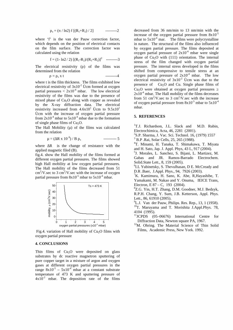
ρs = (π / ln2) f [(R1+R2) / 2] ---------2 where ‘f’ is the van der Pauw correction factor, which depends on the position of electrical contacts on the film surface. The correction factor was calculated using the relation
f = (1- ln2 / 2) [(R1-R2)/(R1+R2)]2 ---------3
The electrical resistivity (ρ) of the films was determined from the relation ρ = ρs x t ---------4
where t is the film thickness. The films exhibited low electrical resistivity of 3x10⁻² Ùcm formed at oxygen partial pressures < 2x10⁻⁴ mbar. The low electrical resistivity of the films was due to the presence of mixed phase of Cu2O along with copper as revealed by the X-ray diffraction data. The electrical resistivity increased from 4.6x101 Ùcm to 9.5x101 Ùcm with the increase of oxygen partial pressure from 2x10⁻⁴ mbar to 5x10⁻⁴ mbar due to the formation of single phase films of Cu2O. The Hall Mobility (µ) of the films was calculated from the relation
µ = (∆R x 10 8) / B ρs ---------- 5
where ∆R is the change of resistance with the applied magnetic filed (B). fig.4. show the Hall mobility of the films formed at different oxygen partial pressures. The films showed high Hall mobility at low oxygen partial pressures. The Hall mobility of the films decreased from 51 cm2/V.sec to 3 cm2/V.sec with the increase of oxygen partial pressure from 8x10⁻⁵ mbar to 5x10⁻⁴ mbar.
0 1 2 3 4 5
0
10
20
30
40
50 Ts = 473 K
mob
ility
, µ (
cm2 /V
.sec
)
oxygen partial pressures (x10-4 mbar)
Fig.4. variation of Hall mobility of Cu2O films with oxygen partial pressure
4. CONCLUSIONS Thin films of Cu2O were deposited on glass substrates by dc reactive magnetron sputtering of pure copper target in a mixture of argon and oxygen gases at different oxygen partial pressures in the range 8x10⁻⁵ – 5x10⁻⁴ mbar at a constant substrate temperature of 473 K and sputtering pressure of 4x10⁻² mbar. The deposition rate of the films
decreased from 36 nm/min to 13 nm/min with the increase of the oxygen partial pressure from 8x10⁻⁵ mbar to 5x10⁻⁴ mar. The films were polycrystalline in nature. The structural of the films also influenced by oxygen partial pressure. The films deposited at oxygen partial pressure of 2x10⁻⁴ mbar were single phase of Cu2O with (111) orientation. The internal stress of the film changed with oxygen partial pressure. The internal stress developed in the films shifted from compressive to tensile stress at an oxygen partial pressure of 2x10⁻⁴ mbar. The low electrical resistivity of 3x10⁻² Ùcm was due to the presence of Cu2O and Cu. Single phase films of Cu2O were obtained at oxygen partial pressures ≥ 2x10⁻⁴ mbar. The Hall mobility of the films decreases from 51 cm2/V.sec to 3 cm2/V.sec with the increase of oxygen partial pressure from 8x10⁻⁵ mbar to 5x10⁻⁴ mbar. 5. REFERENCES 1T.J. Richardson, J.L. Slack and M.D. Rubin, Electrochimica, Acta, 46, 2281 (2001). 2S.P. Sharma, J. Vac. Sci. Technol. 16, (1979) 1557 3 B.P .Rai, Solar Cells, 25, 265 (1988). 4T. Minami, H. Tanaka, T. Shimakawa, T. Miyata and H. Sato, Jap. J. Appl. Phys, 43 L, 917 (2004). 5J. Morales, L. Sanchez, S. Bijani, L. Martizez, M. Gabas and JR. Ramos-Barrado Electrochem. Solid.State Lett., 8, 159 (2005). 6I.L Yubinetsky, S. Thevulhasan, D E. McCready and D.R .Baer, J.Appl. Phys., 94, 7926 (2003). 7K. Kamimura, H. Sano, K. Abe, R,Hayashibe, T. Yamakami, M. Nakao and Y. Onuma, IEICE Trans, Electron, E 87 – C, 193 (2004). 8Z.G. Yin, H.T. Zhang, D.M. Goodner, M.J. Bedzyk, R.P.H. Chang, Y. Sum, J.B. Ketterson, Appl. Phys. Lett., 86, 61910 (2005). 9L.J. Van der Pauw, Philips. Res. Rep., 13, 1 (1958). 10T. Maruyama and T. Morishita J.Appl.Phys. 78, 4104 (1995). 11JCPDS (05–06676) International Centre for
Diffraction Data, Newton square PA, 1967. 12M. Ohring. The Material Science of Thin Solid
Films, Academic Press, New York. 1992.
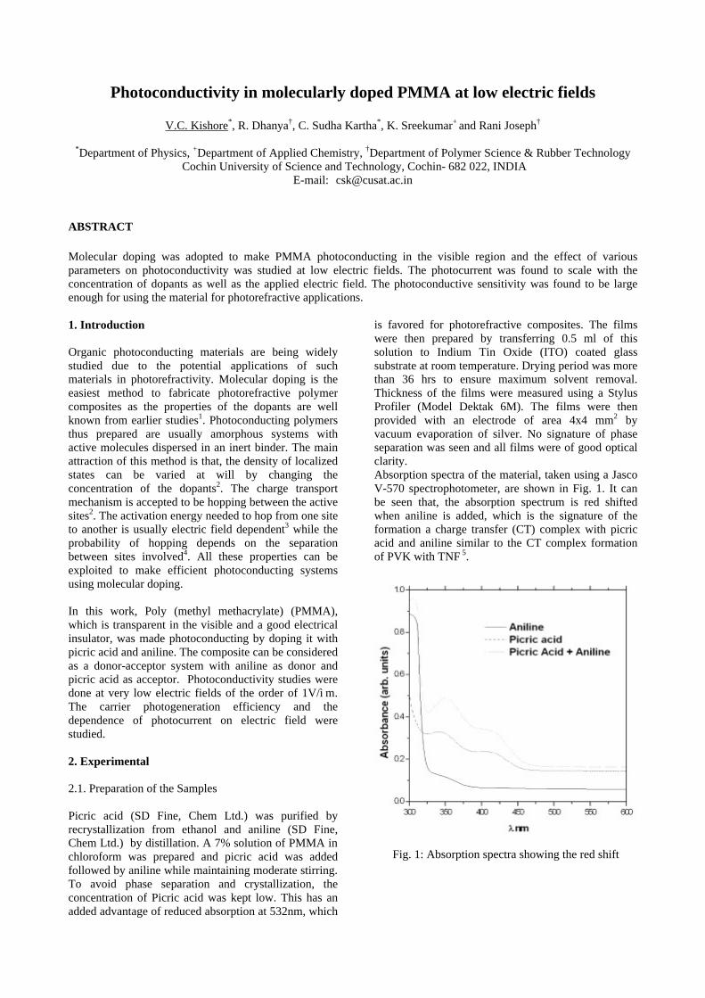
Photoconductivity in molecularly doped PMMA at low electric fields
V.C. Kishore*, R. Dhanya†, C. Sudha Kartha*, K. Sreekumar+ and Rani Joseph†
*Department of Physics, +Department of Applied Chemistry, †Department of Polymer Science & Rubber Technology Cochin University of Science and Technology, Cochin- 682 022, INDIA
E-mail: [email protected] ABSTRACT Molecular doping was adopted to make PMMA photoconducting in the visible region and the effect of various parameters on photoconductivity was studied at low electric fields. The photocurrent was found to scale with the concentration of dopants as well as the applied electric field. The photoconductive sensitivity was found to be large enough for using the material for photorefractive applications. 1. Introduction Organic photoconducting materials are being widely studied due to the potential applications of such materials in photorefractivity. Molecular doping is the easiest method to fabricate photorefractive polymer composites as the properties of the dopants are well known from earlier studies1. Photoconducting polymers thus prepared are usually amorphous systems with active molecules dispersed in an inert binder. The main attraction of this method is that, the density of localized states can be varied at will by changing the concentration of the dopants2. The charge transport mechanism is accepted to be hopping between the active sites2. The activation energy needed to hop from one site to another is usually electric field dependent3 while the probability of hopping depends on the separation between sites involved4. All these properties can be exploited to make efficient photoconducting systems using molecular doping. In this work, Poly (methyl methacrylate) (PMMA), which is transparent in the visible and a good electrical insulator, was made photoconducting by doping it with picric acid and aniline. The composite can be considered as a donor-acceptor system with aniline as donor and picric acid as acceptor. Photoconductivity studies were done at very low electric fields of the order of 1V/ì m. The carrier photogeneration efficiency and the dependence of photocurrent on electric field were studied. 2. Experimental 2.1. Preparation of the Samples Picric acid (SD Fine, Chem Ltd.) was purified by recrystallization from ethanol and aniline (SD Fine, Chem Ltd.) by distillation. A 7% solution of PMMA in chloroform was prepared and picric acid was added followed by aniline while maintaining moderate stirring. To avoid phase separation and crystallization, the concentration of Picric acid was kept low. This has an added advantage of reduced absorption at 532nm, which
is favored for photorefractive composites. The films were then prepared by transferring 0.5 ml of this solution to Indium Tin Oxide (ITO) coated glass substrate at room temperature. Drying period was more than 36 hrs to ensure maximum solvent removal. Thickness of the films were measured using a Stylus Profiler (Model Dektak 6M). The films were then provided with an electrode of area 4x4 mm2 by vacuum evaporation of silver. No signature of phase separation was seen and all films were of good optical clarity. Absorption spectra of the material, taken using a Jasco V-570 spectrophotometer, are shown in Fig. 1. It can be seen that, the absorption spectrum is red shifted when aniline is added, which is the signature of the formation a charge transfer (CT) complex with picric acid and aniline similar to the CT complex formation of PVK with TNF 5.
Fig. 1: Absorption spectra showing the red shift
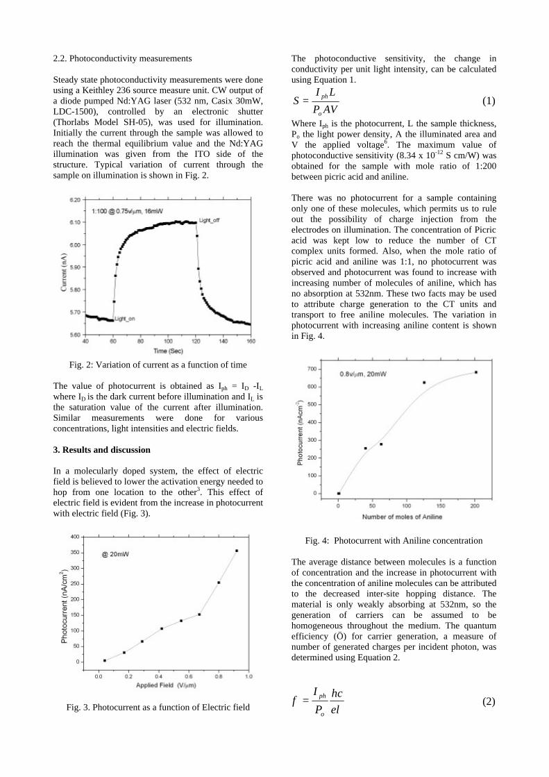
2.2. Photoconductivity measurements Steady state photoconductivity measurements were done using a Keithley 236 source measure unit. CW output of a diode pumped Nd:YAG laser (532 nm, Casix 30mW, LDC-1500), controlled by an electronic shutter (Thorlabs Model SH-05), was used for illumination. Initially the current through the sample was allowed to reach the thermal equilibrium value and the Nd:YAG illumination was given from the ITO side of the structure. Typical variation of current through the sample on illumination is shown in Fig. 2.
Fig. 2: Variation of current as a function of time
The value of photocurrent is obtained as Iph = ID -IL where ID is the dark current before illumination and IL is the saturation value of the current after illumination. Similar measurements were done for various concentrations, light intensities and electric fields. 3. Results and discussion In a molecularly doped system, the effect of electric field is believed to lower the activation energy needed to hop from one location to the other3. This effect of electric field is evident from the increase in photocurrent with electric field (Fig. 3).
Fig. 3. Photocurrent as a function of Electric field
The photoconductive sensitivity, the change in conductivity per unit light intensity, can be calculated using Equation 1.
AVP
LIS
o
ph= (1)
Where Iph is the photocurrent, L the sample thickness, Po the light power density, A the illuminated area and V the applied voltage6. The maximum value of photoconductive sensitivity (8.34 x 10⁻¹² S cm/W) was obtained for the sample with mole ratio of 1:200 between picric acid and aniline. There was no photocurrent for a sample containing only one of these molecules, which permits us to rule out the possibility of charge injection from the electrodes on illumination. The concentration of Picric acid was kept low to reduce the number of CT complex units formed. Also, when the mole ratio of picric acid and aniline was 1:1, no photocurrent was observed and photocurrent was found to increase with increasing number of molecules of aniline, which has no absorption at 532nm. These two facts may be used to attribute charge generation to the CT units and transport to free aniline molecules. The variation in photocurrent with increasing aniline content is shown in Fig. 4.
Fig. 4: Photocurrent with Aniline concentration
The average distance between molecules is a function of concentration and the increase in photocurrent with the concentration of aniline molecules can be attributed to the decreased inter-site hopping distance. The material is only weakly absorbing at 532nm, so the generation of carriers can be assumed to be homogeneous throughout the medium. The quantum efficiency (Ö) for carrier generation, a measure of number of generated charges per incident photon, was determined using Equation 2.
λφ
e
hc
P
I
o
ph= (2)
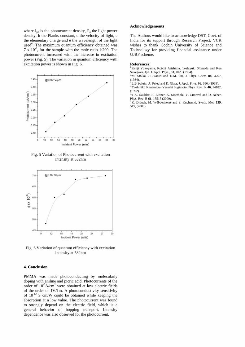
where Iph is the photocurrent density, Po the light power density, h the Planks constant, c the velocity of light, e the elementary charge and ë the wavelength of the light used6. The maximum quantum efficiency obtained was 7 x 10⁻⁸, for the sample with the mole ratio 1:200. The photocurrent increased with the increase in excitation power (Fig. 5). The variation in quantum efficiency with excitation power is shown in Fig. 6.
Fig. 5 Variation of Photocurrent with excitation intensity at 532nm
Fig. 6 Variation of quantum efficiency with excitation intensity at 532nm
4. Conclusion PMMA was made photoconducting by molecularly doping with aniline and picric acid. Photocurrents of the order of 10-7A/cm2 were obtained at low electric fields of the order of 1V/ì m. A photoconductivity sensitivity of 10-12 S cm/W could be obtained while keeping the absorption at a low value. The photocurrent was found to strongly depend on the electric field, which is a general behavior of hopping transport. Intensity dependence was also observed for the photocurrent.
Acknowledgements The Authors would like to acknowledge DST, Govt. of India for its support through Research Project. VCK wishes to thank Cochin University of Science and Technology for providing financial assistance under UJRF scheme. References: 1.Kenji Yokoyama, Koichi Arishima, Toshiyuki Shimada and Ken Sukegava, Jpn. J. Appl. Phys., 33, 1029 (1994). 2.M. Stolka, J.F.Yanus and D.M. Pai, J. Phys. Chem 88, 4707, (1984). 3.L.B Schein, A. Peled and D. Glatz, J. Appl. Phys. 66, 686, (1989). 4.Yoshihiko Kanemitsu, Yasushi Sugimoto, Phys. Rev. B, 46, 14182, (1992). 5.T.K. Däubler, R. Bittner, K. Meerholz, V. Cimrovà and D. Neher, Phys. Rev. B 61, 13515 (2000). 6.K. Diduch, M. Wübbenhorst and S. Kucharski, Synth. Met. 139, 515, (2003).
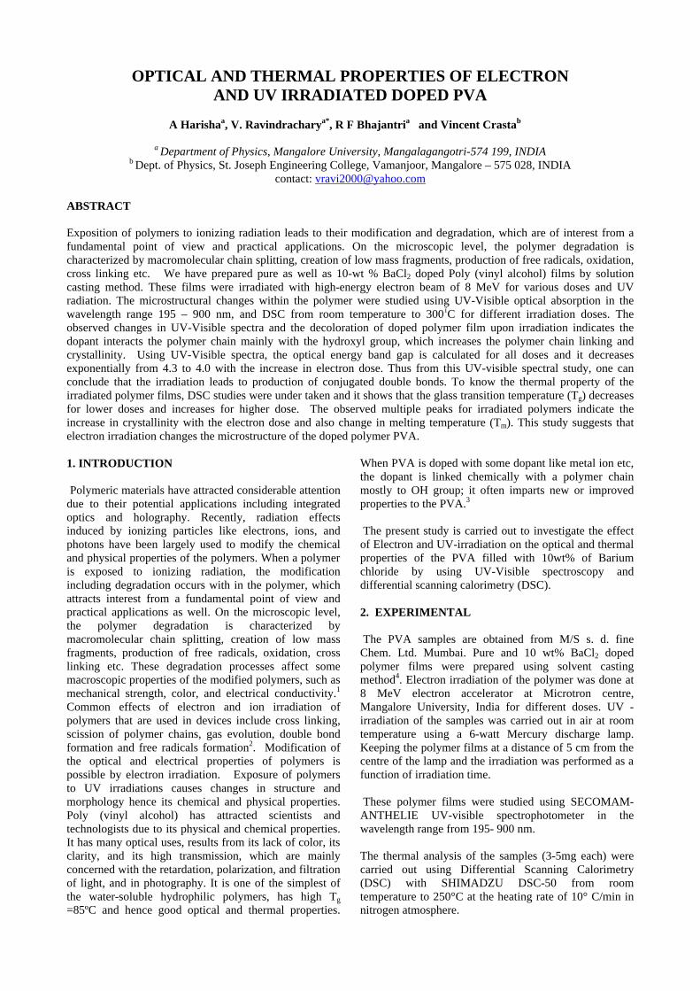
OPTICAL AND THERMAL PROPERTIES OF ELECTRON AND UV IRRADIATED DOPED PVA
A Harishaa, V. Ravindracharya*, R F Bhajantria and Vincent Crastab
a Department of Physics, Mangalore University, Mangalagangotri-574 199, INDIA
b Dept. of Physics, St. Joseph Engineering College, Vamanjoor, Mangalore – 575 028, INDIA contact: [email protected]
ABSTRACT
Exposition of polymers to ionizing radiation leads to their modification and degradation, which are of interest from a fundamental point of view and practical applications. On the microscopic level, the polymer degradation is characterized by macromolecular chain splitting, creation of low mass fragments, production of free radicals, oxidation, cross linking etc. We have prepared pure as well as 10-wt % BaCl2 doped Poly (vinyl alcohol) films by solution casting method. These films were irradiated with high-energy electron beam of 8 MeV for various doses and UV radiation. The microstructural changes within the polymer were studied using UV-Visible optical absorption in the wavelength range 195 – 900 nm, and DSC from room temperature to 300 ïC for different irradiation doses. The observed changes in UV-Visible spectra and the decoloration of doped polymer film upon irradiation indicates the dopant interacts the polymer chain mainly with the hydroxyl group, which increases the polymer chain linking and crystallinity. Using UV-Visible spectra, the optical energy band gap is calculated for all doses and it decreases exponentially from 4.3 to 4.0 with the increase in electron dose. Thus from this UV-visible spectral study, one can conclude that the irradiation leads to production of conjugated double bonds. To know the thermal property of the irradiated polymer films, DSC studies were under taken and it shows that the glass transition temperature (Tg) decreases for lower doses and increases for higher dose. The observed multiple peaks for irradiated polymers indicate the increase in crystallinity with the electron dose and also change in melting temperature (Tm). This study suggests that electron irradiation changes the microstructure of the doped polymer PVA. 1. INTRODUCTION Polymeric materials have attracted considerable attention due to their potential applications including integrated optics and holography. Recently, radiation effects induced by ionizing particles like electrons, ions, and photons have been largely used to modify the chemical and physical properties of the polymers. When a polymer is exposed to ionizing radiation, the modification including degradation occurs with in the polymer, which attracts interest from a fundamental point of view and practical applications as well. On the microscopic level, the polymer degradation is characterized by macromolecular chain splitting, creation of low mass fragments, production of free radicals, oxidation, cross linking etc. These degradation processes affect some macroscopic properties of the modified polymers, such as mechanical strength, color, and electrical conductivity.1
Common effects of electron and ion irradiation of polymers that are used in devices include cross linking, scission of polymer chains, gas evolution, double bond formation and free radicals formation2. Modification of the optical and electrical properties of polymers is possible by electron irradiation. Exposure of polymers to UV irradiations causes changes in structure and morphology hence its chemical and physical properties. Poly (vinyl alcohol) has attracted scientists and technologists due to its physical and chemical properties. It has many optical uses, results from its lack of color, its clarity, and its high transmission, which are mainly concerned with the retardation, polarization, and filtration of light, and in photography. It is one of the simplest of the water-soluble hydrophilic polymers, has high Tg =85ºC and hence good optical and thermal properties.
When PVA is doped with some dopant like metal ion etc, the dopant is linked chemically with a polymer chain mostly to OH group; it often imparts new or improved properties to the PVA.3 The present study is carried out to investigate the effect of Electron and UV-irradiation on the optical and thermal properties of the PVA filled with 10wt% of Barium chloride by using UV-Visible spectroscopy and differential scanning calorimetry (DSC). 2. EXPERIMENTAL The PVA samples are obtained from M/S s. d. fine Chem. Ltd. Mumbai. Pure and 10 wt% BaCl2 doped polymer films were prepared using solvent casting method4. Electron irradiation of the polymer was done at 8 MeV electron accelerator at Microtron centre, Mangalore University, India for different doses. UV - irradiation of the samples was carried out in air at room temperature using a 6-watt Mercury discharge lamp. Keeping the polymer films at a distance of 5 cm from the centre of the lamp and the irradiation was performed as a function of irradiation time. These polymer films were studied using SECOMAM- ANTHELIE UV-visible spectrophotometer in the wavelength range from 195- 900 nm. The thermal analysis of the samples (3-5mg each) were carried out using Differential Scanning Calorimetry (DSC) with SHIMADZU DSC-50 from room temperature to 250°C at the heating rate of 10° C/min in nitrogen atmosphere.
200 225 250 275 300
1.0
1.5
2.0
2.5
3.0
432
10hrs
30hrs
20hrs
10hrs
4.
3.
2.1.
Ab
sorp
tio
n
Wavelength(nm)
2 0 0 2 5 0 3 0 0 3 5 0 4 0 0 4 5 0 5 0 01 .0
1 .5
2 .0
2 .5
3 .0a ) 0 kG y e ) 1 5 0 k G yb ) 1 0 k G y f ) 2 0 0 k G yc ) 5 0 k G y g ) 3 0 0 k G yd ) 1 0 0 k G y
g
f
e
dcba
Abs
orba
nce
W a v e len g th ( nm )
0 5 0 1 0 0 1 5 0 2 0 03 .8
4 .0
4 .2
4 .4
Ban
d ga
p( E
g ) (
eV)
D o s e ( k G y )
Figure 2:Variation of band gap for doped PVA
3. RESULTS AND DISCUSSION 3.1 Optical Studies The measured optical absorption spectra for electron irradiated 10wt % Bacl2 doped PVA is shown in Figure 1. In the UV-Vis spectra, we observed a significant increase in absorbance and shift of absorption edges towards longer wavelengths with the electron dose. In addition at higher doses a small hump appeared around a wavelength of 280nm, suggesting the formation of new bonds with in the polymer composite. It is also observed physically that the white colored doped PVA film is turned to faint yellow after high dose of electron irradiation. The appearance of additional peak may be attributed to the formation of unsaturation and cross-linking. These observed changes with in the doped PVA may be understood by invoking the interaction between PVA and BaCl2, the dopant mainly Ba+2 ion interacts with the hydroxyl group of the polymer chain as a result the crystallinity increases. Upon on electron irradiation, weakening of some bonds and evolution of radicals takes place, as a result there is a production of conjugated double bonds with in the composite film. This formation of conjugated double is manifested in the form of increased absorbance and shift of absorption edge towards longer wavelengths in the UV-Vis specta1.
Similar type of observation are reported for PE and PS films irradiated with 14.89MeV electrons by others1, in P4VP/PTSA complex irradiated with 8 MeV electrons5
Figure 1: UV-Vis spectra of electron-irradiated BaCl2 doped PVA
and PVDF irradiated with 3 MeV electrons 6. The change in color of the film also supports that the electron irradiation has induced certain changes in the properties of the polymer.
Using UV-Vis spectra the optical energy band gap has been estimated by converted it into a Tauc,s graph7. The variation of energy band gap with electron dose for the irradiated composite is shown in figure 2. From the figure it is clear that the optical energy band gap decreases from 4.3 eV to 4 eV with increasing electron dose. This exponential decrease of energy band gap E g may be due to enhancement in free radicals, ions and electrons with the increasing electron dose6.
Figure 3: UV-Vis spectra of UV- irradiated BaCl2 doped PVA for different exposure times The Figure 3 shows UV -Visible absorption spectra for UV-irradiated Bacl2 doped PVA with different irradiation time. From the figure it is clear that, the absorption coefficient decreases with the exposure time for lower wavelengths. This suggests that the UV irradiation induce some modification with in the polymer like electron irradiation. 3.2 DSC studies
The DSC thermograms of electron irradiated doped PVA films are shown in Figure 4. It shows multiple endothermic peaks for all samples and are attributed to glass transition temperature (Tg) resulting from the micro-Brownian motion of the main chain backbone, α-relaxation (Tα) associated with crystalline regions and melting temperature (Tm) similar to the results reported earlier3. Using Figure 4, the Tg for all samples were estimated and its variation is shown in Figure 5. We note that the Tg for unirradiated polymer is 61ºC and it decreases to 57.7ºC with increasing electron dose up to 200 kGy, further, increases slightly to 58.3ºC for 300kGy.
Figure 4 also shows that the Tá shifts slightly towards lower temperature up to 200kGy and increases with a broadening for 300kGy. The other two peaks are attributed to melting temperatures, first melting temperature (Tm1) around 123ºC and second (Tm2) around 160.2ºC are almost constant for all samples except 300 KGy. For 300 kGy, Tm1 decreases slightly from 123ºC to 114.8ºC. Our earlier DSC studies on doped PVA, shows that Bacl2 doping increase the crystallinity of PVA and is observed in the form of multiple peaks.
0 100 200 30057
58
59
60
61
62
Tg( o C
)
Dose (kGy)
Figure 5: Variation of Tg for different electron dose
0 50 100 150 200 250
T e mperature ( oC )
T g = 5 6 . 5 ° C
T g = 6 1 ° C
T g = 5 7 . 1 ° C
Hea
t F
low
(ar
b. u
nits
)
3 0 h r s
2 0 h r s
0hrs
0 5 0 1 0 0 1 5 0 2 0 0 2 5 0
Hea
t F
low
(ar
b. u
nits
)
T e m p e r a t u r e ( o C )
3 0 0 k G y
2 0 0 k G y
1 5 0 k G y
5 0 k G y
0 k G y
Figure 4: DSC curves of electron irradiated BaCl2 doped PVA
This is mainly due to the fact that the dopant interacts with PVA via hydrogen bonding and forms a complex4.
In view of this the present observed results are explained as follows: The decrease in Tg is generally indicates the increase in molecular mobility of the polymer. It is a known fact that below Tg, molecules do not have segmental motion, and some portions of the molecules may not wiggle around, but may only be able to vibrate slightly. Near Tg, the molecules can start vibrating and segmental motion increases. In this context, the electron irradiation causes chain scissions of the molecules and leads to the decrease in the average molecular chains length. These chain scissions increases the molecular mobility; as a result, Tg decreases up to 200kGy. For 300kGy the increase in Tg and other transition temperatures can be understood by invoking the onset of the formation of new radicals, which are the precursors of cross linking of the polymer chains. It is reasonable to consider the shift in Tg to higher temperature due to restriction of chain mobility caused by network structure formed due to irradiation at higher doses. This also indicates the structural changes with in the amorphous regions of the polymer, due to crosslinking. A sharpening of Tm1 indicates the thermal degradation and may be due to the prolonged heating causes a random breaking of bonds and sometimes, the detachment of the low molecular products in the polymer. The initial chain scission caused by the impinging electron further adds to the process, thus lowering the thermal stability8.
The DSC thermograms for the UV-irradiated BaCl2 doped PVA sample for different exposure times of 0, 20,
and 30hrs are shown in figure 6. From the figure 6, it is clear that the DSC results of UV-irradiated polymer are almost similar to that of electron irradiated results. This indicates that as for as the thermal properties of the polymer is concerned the electron irradiation is similar to the UV irradiation.
Figure 6: DSC curves of UV- irradiated BaCl2 doped PVA for different exposure times
4. CONCLUSIONS
This study shows that electron irradiation induces chain scissoring mainly in amorphous region of the polymer at lower doses. This chain scissioning results in the formation of conjugated double bonds and it increases in the chain mobility of the polymer as a result a decrease in Tg. This is also a decrease in band gap energy with increase of irradiation dose. The same results are also reflected in UV irradiated polymer. The thermal study indicates that, electron and UV irradiation makes significant modification with in the polymer. At higher doses, irradiation causes cross-linking
5. ACKNOWLEDGEMENTS
The authors are thankful to the Director, Microtron center, Mangalore University for providing electron exposure of the polymer films and UV-Vis facility.
6. REFERENCES [1] V Svorcik, V Rybka, V Hnatowicz, M Novotna, M
Vognar, J App. Poly. Sci. 64, 2529, (1997) [2] G Mladinov, Indo-Bulgarian workshop on Electron
Beam Technology and Applications, (2003) [3] H M Zidan, Polymer Testing 18, 449, (1999) [4] R F Bhajantri, V Ravindrachary, Vincent Crasta, A
Harisha,solidstate physics symp.(India), 46, 61, (2003). [5] R Vijayalakshmi Rao, P Mohan Rao, MH Shridhar,
Nul..Inst.& Meth.in Physics ,B 187, 331 (2002). [6] Mohamed Mahmoud Nasef, Hamdani Saidi, Khairul
Zaman M. Dahlan, Poly. Deg. & stab. 75, 85 (2002). [7] G P Joshi, N S Saxena, T P Sharma, V Dixit, S C K
Misra, Ind. J Pure & Appl. Phys., 41, 462, (2003). [8] R Mishra, S P Tripathy, K K Dwivedi, D TKhathing,
S Ghosh, M Millar and D Fink, Radiation Measurements, 37 247 (2003).
EFFECT OF DOPANT KCl ON THE MICROSTRUCTURE OF THE POLYMER PVA
R F Bhajantria, V Ravindracharya*, Vincent Crastab and A Harishaa
a Department of Physics, Mangalore University, Mangalagangotri-574 199, INDIA
b Dept. of Physics, St. Joseph Engineering College, Vamanjoor, Mangalore – 575 028, INDIA Contact: [email protected]
ABSTRACT
In many applications, the observation of changes in polymer structure allows the best polymer composition and preparation conditions to be chosen to achieve the desired properties of the final product. There is a considerable interest in fabricating the doped polymer films both point of view of fundamental property determination and the development of applications. In this paper we have studied the effect of dopant KCl on optical and structural properties of a semicrystalline Poly (Vinyl Alcohol). The pure and KCl doped PVA films were prepared using solvent casting method. The prepared films were characterized using UV-Visible, FTIR and XRD techniques. The UV-Visible studies indicates the absorption bands around 196 nm shoulders around 208 nm with different absorption intensities for doped PVA and assigned to n ð* transition. This is indicates to presence of unsaturated bonds C==O and/or C==C mainly in the tail-head of the polymer. Using UV-visible spectra the optical energy band gap is estimated and it decreases with increasing dopant concentration. The FTIR spectra show a broad peak around 3425 cm-1, corresponding to O—H vibrations. The peaks corresponding to C—H stretching is observed at 2940 cm-1and intense bands at 1730 and 1640cm-
1 indicates the presence of an acetyle C==O groups. This result can be explained on the basis of intra/inter molecular hydrogen bonding of dopant molecules with the adjacent –OH groups. A sharp band at 1026 cm-1 corresponds to C—O stretching of acetyle group present in the PVA back bone. The powder XRD shows an increase in crystallinity in the doped PVA, which arises due to the interaction of dopant KCl with the PVA, causes a molecular rearrangement within the amorphous phase of polymer matrix. This modification also influences the optical property of the doped polymer. INTRODUCTION Polymeric materials have attracted the scientific and technological researchers, because of their wide applications mainly due to their lightweight, good mechanical strength, and optical properties makes them as multifunctional materials. These are also traditionally been considered as excellent host materials for composites. Recently several advanced polymer composites have been synthesized with a wide variety of inclusions like metals, nanoparticles etc. Doping a polymer with metal salts has significant effect on their physical properties including charge storage, charge carrier mobility etc. These change in physical properties, depends on the chemical nature of the dopant and the way in which they interact with the host polymer matrix. This is to tailor the composition, structure and function of the polymeric materials for new applications1.
Poly (vinyl alcohol) (PVA) is a polymer that has been studied intensively because of its several interesting chemical and physical properties. It is a semicrystalline polymer, which exhibits certain physical properties resulting from the crystal-amorphous interfacial effects. The origin of its crystallinity is mainly due to strong hydrogen bonds between the hydroxyl groups2, 3. The optical absorption studies of polymer films are very important because it provide information on the electronic band structure and the optical energy band gap Eg
2. These properties are particularly interesting and important for device applications4. In recent years the variation of optical, structural and other properties of PVA were studied by others with different dopant like, I/KI, MnCl2, MgCl2, MgBr2, CrF3, FeCl3, Fe3O4 using
different techniques have been reported1-6. In addition it is known that the KCl is an excellent material widely used in optical studies from infrared to UV-region.
In view of this the present work is to understand the effect of monovalent metal salt KCl on the microstructural and optical properties of PVA using XRD, UV-Visible, and FTIR techniques. EXPERIMENTAL Sample Preparation and Characterization The PVA with a molecular weight 1,25,000 is obtained from M/s. s. d. fine chem. Ltd Mumbai. The pure and KCl doped PVA films were prepared by solution casting method. The thicknesses of the films were in the range of 0.05 mm - 0.2mm.
Optical studies were carried out using UV-Visible and FTIR Spectrophotometers. The UV-visible spectra were recorded using SECOMAM ANTHELIE - 284 UV-VIS Spectrophotometer in the wavelength range 195-1000 nm. The infrared spectra were recorded using SHIMADZU FTIR-8700 Spectrophotometer in the wave number range from 400 to 4000 cm-1
with a resolution of 4 cm-1
. The X-ray diffraction study was carried out using a Bruker D8 Advance X-ray diffractometer with Ni-filtered, CuKá radiation with graphite monochromator. The scan was taken in the 2è range of 5-45o with a scanning speed and step size of 1o/min and 0.01o respectively.
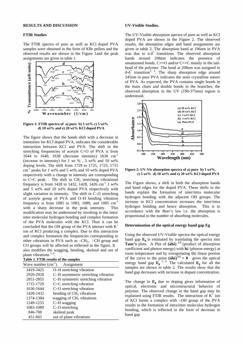
4 0 0 0 3 5 0 0 3 0 0 0 2 5 0 0 2 0 0 0 1 5 0 0 1 0 0 0 5 0 0
1 4 2 84 6 6
7 8 8
1 0 8 5
1 3 8 41 6 4 4
1 7 2 92 8 5 5
29 2 8
3425
W a v e n u m b e r ( 1 / c m )% T
rans
mit
tanc
e (a
rb u
nits
)
4 6 66 6 5
8 4 6
1 0 8 31 3 8 2
1 6 4 01 7 2 52 8 5 3
29 2 6
3423
c
b
a1 2 5 5
1 4 3 2
4 6 46 6 5
8 4 6
1 0 8 91 2 4 5
1 3 7 21 4 2 8
1 6 3 81 7 2 3
2 8 5 129 2 2
3421
d
4 5 15 6 1
6 6 5
1 0 8 51 2 4 9
1 4 2 61 6 3 6
1 7 1 52 8 5 12 9 2 0
3419
200 250 300 350 400 450 500-0.5
0.0
0.5
1.0
1.5
2.0
2.5
3.0
ab
dc
e
Abs
orba
nce
Wavelength (nm)
(e) 20 wt% KCl(d) 10 wt% KCl(c) 5 wt% KCl(b) 1 wt% KCl(a) Pure PVA
RESULTS AND DISCUSSION FTIR Studies The FTIR spectra of pure as well as KCl doped PVA samples were obtained in the form of KBr pellets and the observed results are shown in the Figure 1and the peak assignments are given in table 1. Figure 1: FTIR spectra of a) pure b) 1 wt% c) 5 wt% d) 10 wt% and e) 20 wt% KCl doped PVA The figure shows that the bands shift with a decrease in intensities for KCl doped PVA, indicates the considerable interaction between KCl and PVA. The shift in the stretching frequencies of acetyle C=O of PVA is from 1644 to 1640, 1638 (decrease intensity) 1636 cm-1 (increase in intensity) for 1 wt % , 5 wt% and 10 wt% doping levels. The shift from 1729 to 1725, 1723, 1715 cm-1 peaks for 1 wt% and 5 wt% and 10 wt% doped PVA respectively with a change in intensity are corresponding to C=C peak. The shift in CH2 stretching vibrational frequency is from 1428 to 1432, 1428, 1426 cm-1 1 wt% and 5 wt% and 10 wt% doped PVA respectively with slight variation in intensity. The shift in C–O stretching of acetyle group of PVA and O–H bending vibration frequency is from 1085 to 1083, 1089, and 1085 cm-1 with a sharp decrease in the peak intensity. This modification may be understood by invoking to the intra/ inter molecular hydrogen bonding and complex formation of the PVA molecules with the KCl. Thus it can be concluded that the OH group of the PVA interact with K+ ion of KCl producing a complex. Due to this interaction and complex formation the frequencies corresponding to other vibrations in PVA such as –CH2, –CH group and CO groups will be affected as reflected in the figure. It also modifies the wagging, bending, skeletal and out of plane vibrations 5, 6. Table 1. FTIR results of the samples Wave number (cm-1) Assignment 3419-3425 O–H stretching vibration 2920-2928 C–H asymmetric stretching vibration 2851-2855 C–H symmetric stretching vibration 1715-1729 C=C stretching vibration 1636-1644 C=O stretching vibration 1428-1432 bending of CH2 vibrations 1374-1384 wagging of CH2 vibrations 1249-1255 C–H wagging 1083-1089 C–O stretching 846-788 skeletal peak 451-665 out of plane vibrations
UV-Visible Studies. The UV-Visible absorption spectra of pure as well as KCl doped PVA are shown in the Figure 2. The observed results, the absorption edges and band assignments are given in table 2. The absorption band at 196nm in PVA was due to n-ð* transitions. The observed absorption bands around 208nm indicates the presence of unsaturated bonds, C==O and/or C==C mainly in the tail-head of the polymer. The band at 208nm was assigned to ð-ð* transition3, 4. The sharp absorption edge around 245nm in pure PVA indicates the semi crystalline nature of PVA. As expected, the PVA contains single bonds in the main chain and double bonds in the branches; the observed absorption in the UV (190-375nm) region is understood. Figure 2: UV-Vis absorption spectra of a) pure b) 1 wt%, c) 5 wt% d) 10 wt% and e) 20 wt% KCl doped PVA The Figure shows, a shift in both the absorption bands and band edges for the doped PVA. These shifts in the bands explain the formation of inter/intra molecular hydrogen bonding with the adjacent OH groups. The increase in KCl concentration increases the inter/intra hydrogen bonding and hence absorption. This is in accordance with the Beer’s law i.e. the absorption is proportional to the number of absorbing molecules. Determination of the optical energy band gap Eg Using the observed UV-Visible spectra the optical energy band gap Eg is estimated by translating the spectra into Tauc’s plots. A Plot of (áhí) 1/2 (product of absorption coefficient and photon energy) with hí (photon energy) at room temperature and by extrapolating the linear portion of the curve to the point (áhí)1/2 = 0 gives the optical energy band gap Eg
5, 8. The calculated Eg for all the
samples are shown in table 2. The results show that the band gap decreases with increase in dopant concentration. The change in Eg due to doping gives information of optical, electronic and microstructural behavior of polymer. The observed change in the band gap may be explained using FTIR results. The interaction of K+ ion of KCl forms a complex with –OH group of the PVA results in the formation of intra/inter molecular hydrogen bonding, which is reflected in the form of decrease in band gap
1 2 3 4 5 6 70
100
200
300
400
500
600
d
a
b
c
(e) 20 wt% KCl(d) 10 wt% KCl(c) 5 wt% KCl(b) 1 wt% KCl(a) Pure PVA
e
hνν(eV )
( ααh νν
)1/2
5 10 15 20 25 30 35 40 45
Inte
nsit
y (
Cou
nts
)
Angle ( 2θ θ )
c
b
d
e
a
Figure 3: Optical Band Gap of a) pure b) 1 wt% c) 5 wt% d) 10 wt% and e) 20 wt% KCl doped PVA Table2. Optical absorption data of pure & doped PVA Sample (wt%) ëmax ëedg Eg (PVA+KCl) (nm) assignment (nm) (eV) 0 196 n ð* 245 4.96 208 ðð *
1 197 n ð* 248 4.83 207 ðð *
5 197 n ð* 257 4.41 209 ðð *
10 200 n ð* 259 4.25 210 ðð *
20 205 ðð * 265 4.17 XRD studies The WXRD patterns of pure as well as KCl doped PVA are shown in the Figure 3 and results are tabulated in table 3. From the result it is clear that as dopant concentration increases, the amorphous broad band shifts towards higher angles with a decreased in its intensity compared to pure PVA. In addition appearance of new sharp crystalline peaks starts from 5 wt% doped samples onwards.
Figure 4: WXRD spectra of a) pure b) 1 wt%, c) 5 wt%, d) 10 wt% and e) 20 wt% KCl doped PVA This results suggests that the dopant KCl interacts with the polymer PVA via intra/intermolecular hydrogen bonding as a result the molecular rearrangement takes place within the polymer matrix This interaction of dopant leads to a structural repositioning of the PVA chains mainly with the hydroxyl group (similar to the results explained in the FTIR spectra) as a result the
amorphous peak shifts towards higher angles with a decrease in intensity1, 6. The observed sharp peaks may be due to the formation of crystalline phases of the dopant molecules. Table 3. WXRD data of the samples Sample 2è(deg) d-spacing(Å) Assignment 1) Pure PVA 19.563 4.53476 broad peak 2) 1 wt% 15.859 5.58366 small peak
19.642 4.51592 strong and broad peak 3) 5 wt% 19.864 4.46615 strong and broad peak 28.339 3.14672 strong and sharp peak 4)10 wt% 20.640 4.29985 strong and broad peak 29.294 3.04633 strong and sharp peak 41.428 2.17781 small and sharp peak 5)20 wt% 20.458 4.33769 strong and broad peak 28.339 3.14677 small and sharp peak 28.951 3.08162 strong and sharp peak Conclusions We have studied the optical and structural properties of a PVA doped with KCl. The FTIR study shows that the dopant KCl forms a complex with OH group of the PVA results in the formation of intra/inter molecular hydrogen bonding. The UV-Visible optical studies also reflect the complex formation and its effects on the band gap as well as the other optical properties. The XRD results shows that due to the interaction of dopant and hence complex formation the structural repositioning takes place as a result crystallinity increases.
Acknowledgement
The authors are thankful to The Director, Microtron Center, The Research Coordinator, OSTC and The Chairman, Department of Materials Science, Mangalore University for providing the experimental facilities for this work References [1] H M Zidan, J. Appl. Polym. Sci.88, 1115, (2003) [2] Blaise Lobo and M. R. Ranganath T. S. G. Ravi Chandran G Venugopal Rao V Ravindrachary and S Gopal. Physical Review B 59, 13693 (1999) [3] Kamal M. Abd El-Kader, J. Appl Polym Sci 88, 589(2003) [4] M. Soliman Selim, R Seoudi, A A Shabaka, Mater. Lett, 59, 2650,(2005) [5] H. M. Zidan, J. Appl Polym Sci, 88, 104(2003) [6] Eun Joo Shin, Yang Hun Lee, Suk Chul Choi J. Appl. Polym. Sci. 91, 2407, (2004) [7] Prakash R Somania, R Marimuthua, A K Viswanatha, S Radhakrishnan, Polym Deg & Stab, 79, 77, (2003) [8] R F Bhajantri, V Ravindrachary Vincent Crasta and Harisha A, Solid State Phys Symp. (India), 49,191(2004)
OPTICAL AND STRUCTURAL STUDIES ON A NOVEL ORGANIC NON-LINEAR OPTICAL CRYSTAL
Vincent Crastaa, V Ravindracharyb*, R F Bhajantrib, A Harishab, S Lakshmic, M A Shridarc,
J Shashidara Prasadc aDept. of Physics, St. Joseph Engineering College, Vamanjoor, Mangalore – 575 028, India
b Department of Physics, Mangalore University, Mangalagangotri-574 199, India cDept. of Studies in Physics, University of Mysore , Manasagangotri, Mysore – 570 006, India
Contact: [email protected]
ABSTRACT
Recently second order nonlinear optical materials have attracted much due to their potential applications in the emerging area of science and technology like opto-electronic, Photonic, data storage technologies. Generally organic molecules possessing electron donating and accepting groups connected by extended ð-electron pathways have large hyperpolarisabilities (â). Among the organic materials, Chalcone derivatives are some of the notable nonlinear optical materials in which, one can grow relatively bulk crystals up to a certain size. These crystals are mechanically hard, chemically stable, transparent in the blue green region and possess second harmonic generation (SHG) property. We have synthesized a Chalcone derivative; 1-(4-methylphenyl)-3-(4-methoxyphenyl)-2-propen-1-one, a novel organic non-linear optical material and single crystals were grown by slow evaporation technique at room temperature. The grown crystals were characterized by UV-Visible spectra and single crystal XRD. The recorded UV-Visible spectra reveal that the grown crystals were transparent in the visible region and absorption takes place only in the UV region. From the single crystal X-ray diffraction studies, it was found that, crystals of this compound belong to monoclinic crystal system with a space group P21/a. The estimated cell parameters for this crystal are a = 11.678(1) Å, b = 11.113(2) Å, c = 11.720(1) Å, beta = 115.36 (10). The second harmonic generation (SHG) efficiency of the crystal was obtained from Kurtz powder technique using a ND-YAG laser (ë = 1064 nm), which is found to be 0.5 times that of Urea.
INTRODUCTION Non-linear optical materials are expected to be active material for optical communication and optoelectronic devices. These include both organic as well as inorganic materials. Organic materials have been synthesized based on the predictive molecular engineering approach and are crystallized and studied extensively due to the nonlinear optical (NLO) coefficients being often larger than those of inorganic materials. Some of the advantages of organic materials over the inorganic materials are the scope for altering the properties by functional substitutions, high degree of non-linearity and high damage resistance. Recently, there is a considerable interest in the synthesis of new materials with large second-order optical nonlinearities, because of their potential use in applications including telecommunications, optical computing, optical data storage, and optical information processing1-5. Many of such applications require materials with very large macroscopic second-order susceptibilities, which are usually constituted from molecules with large molecular first orger hyperpolarizability and oriented in a non-centrosymmetric arrangement6-7. The practical applications of the organic crystals are limited by poor chemical stability, due to the presence of large organic n-conjugated system, which causes the red-cut off wavelength. This also due to poor phase matching properties caused by large birefringence, which results from the layer stacking of the structure and other factors. Owing to the high polar nature of the molecules, they
often tend to crystallize as long needles or thin platelets7,8. Among many organic compounds reported for their second harmonic generation (SHG), chalcone derivatives are noticeable materials for their excellent blue light transmittance and good crystal stability9, 10. It is known that the low temperature solution growth technique is widely used for the growth of organic and inorganic compounds to get good crystals. In this paper we report the optical properties such as UV-visible, SHG etc. and single crystal X-ray diffraction studies on a chalcone derivative, 1-(4-methylphenyl)-3-(4-methoxyphenyl)-2-propen-1-one single crystals. Crystal Growth
The compound 1-(4-methylphenyl)-3-(4-methoxy phenyl)-2-propen-1-one was synthesized from chaisen schimt reaction method 9. Single crystals were obtained by slow evaporation using acetone as a solvent11 and crystal structure analysis was carried out using single crystal XRD.
Characterization
The molecular formula of the synthesized compound is found to be C17H16O2 and its molecular weight is 252. The density of the compound was measured using the Archimde’s principle, considering the weight of the crystal in air and water, which is found to be 1.2245
gm/cm3. The melting point of the grown crystals is measured and it is found to be 1120C.
Optical Studies
UV-Visible: The UV-Visible absorption spectrum of the grown crystal was recorded using SECOMAM UV-Vis spectrophotometer in the wavelength range of 200 –1000 nm and is shown in figure 1. From the Figure, it is clear that the crystal is transparent in the visible region and the absorption takes place in the UV range. In the UV region we observe three absorption bands; less than 300nm, around 350nm and around 400nm. The maximum absorption around 400nm wavelength may be assigned to n-π* transition and may be attributed to the excitation in the aromatic ring and C=O group. The maximum absorption edge is found to be 450nm. Figure 1: UV-Vis spectrum of 1-(4-methylphenyl)-3-(4-
methoxyphenyl)-2-propen-1-one Measurement of SHG efficiency The SHG conversion efficiency of the compound was measured using Kurtz powder technique. In this technique, the powder sample with a average particle size of 100-150 ì m was illuminated using Q-switched Nd:YAG laser emitting a fundamental wavelength of 1064nm with 10ns pulse width. The SHG of the crystal was confirmed with the emission of green radiation (ë=532nm) and the parent ray 1064nm was filtered using an IR filter. The amplitude of the SHG out put voltage was measured using a photomultiplier and a digitalizing oscilloscope assembly. The measured value was compared with the SHG amplitude of the standard organic NLO material Urea. The SHG efficiency of this compound has been measured as 0.5 times that of urea. Crystal structure analysis Single crystal structural studies were carried out using single crystal x ray diffractometer. A defect free single crystal with approximate dimension 0.3 x 0.3 x 0.4 mm3 was selected for this study. The crystal chosen was mounted in the diffractometer and three-dimensional x-ray diffraction data was collected in frames using oscillation method in theta ranging between 3.75 - 32.43
deg. The measurements were made on a DIP Labo Imaging plate diffractometer with kappa geometry using graphite monochromated Mo-Kα radiation. The image processing and data reduction were done by using Denzo12-13 method. The structure was solved and refined using maXus program. Full matrix least squares refinement were done using SHELXL-97 with isotropic temperature factors for all the non-hydrogen atoms converged residuals. Refinement of non-hydrogen atoms with anisotropic thermal parameters was started at this stage. All the non-hydogen atoms were revealed in the first map. The hydrogen atoms were placed at the calculated positions.
Figure 2: The ORTEP of the molecule 1-(4-methylphenyl)-3- (4-methoxyphenyl)-2-propen-1-one
Figure 3: The packing of the molecules down b-axis
Thirty-six frames of data were collected by the oscillation method with each frame being exposed for around 300 seconds. Successive frames were scanned in steps of 50 per min with an oscillation range of 50. All the frames could index using primitive monoclinic lattice. All the non-hydrogen atoms were revealed in the first map itself. They were isotropically refined using SHELXL97 till the R1 value converged to 0.1967. Anisotropic refinement was commenced at this stage. H atoms were placed at chemically acceptable positions. The final cycle of the full-matrix least squares refinement was carried out for 7304 reflections with 172 parameters. The final R1 value converged to 0.0630. The data collection and crystal structure details are given in Table 1. Figure 2 shows the ORTEP of the molecule at
200 400 600 800 10000.0
0.5
1.0
1.5
2.0
2.5
3.0
Abs
orpt
ion
Wavelength (nm)
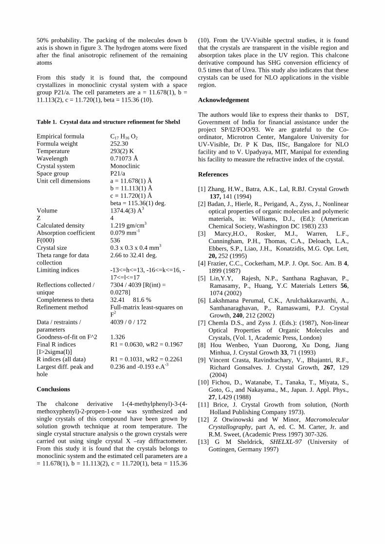
50% probability. The packing of the molecules down b axis is shown in figure 3. The hydrogen atoms were fixed after the final anisotropic refinement of the remaining atoms From this study it is found that, the compound crystallizes in monoclinic crystal system with a space group P21/a. The cell parameters are a = 11.678(1), b = 11.113(2), c = 11.720(1), beta = 115.36 (10). Table 1. Crystal data and structure refinement for Shelxl Empirical formula C17 H16 O2 Formula weight 252.30 Temperature 293(2) K Wavelength 0.71073 Å Crystal system Monoclinic Space group P21/a Unit cell dimensions a = 11.678(1) Å
b = 11.113(1) Å c = 11.720(1) Å beta = 115.36(1) deg.
Volume 1374.4(3) A3 Z 4 Calculated density 1.219 gm/cm3 Absorption coefficient 0.079 mm-1 F(000) 536 Crystal size 0.3 x 0.3 x 0.4 mm3
Theta range for data collection
2.66 to 32.41 deg.
Limiting indices -13<=h<=13, -16<=k<=16, -17<=l<=17
Reflections collected / unique
7304 / 4039 [R(int) = 0.0278]
Completeness to theta 32.41 81.6 % Refinement method Full-matrix least-squares on
F2
Data / restraints / parameters
4039 / 0 / 172
Goodness-of-fit on F^2 1.326 Final R indices [I>2sigma(I)]
R1 = 0.0630, wR2 = 0.1967
R indices (all data) R1 = 0.1031, wR2 = 0.2261 Largest diff. peak and hole
0.236 and -0.193 e.A-3
Conclusions
The chalcone derivative 1-(4-methylphenyl)-3-(4-methoxyphenyl)-2-propen-1-one was synthesized and single crystals of this compound have been grown by solution growth technique at room temperature. The single crystal structure analysis o the grown crystals were carried out using single crystal X –ray diffractometer. From this study it is found that the crystals belongs to monoclinic system and the estimated cell parameters are a = 11.678(1), b = 11.113(2), c = 11.720(1), beta = 115.36
(10). From the UV-Visible spectral studies, it is found that the crystals are transparent in the visible region and absorption takes place in the UV region. This chalcone derivative compound has SHG conversion efficiency of 0.5 times that of Urea. This study also indicates that these crystals can be used for NLO applications in the visible region. Acknowledgement The authors would like to express their thanks to DST, Government of India for financial assistance under the project SP/I2/FOO/93. We are grateful to the Co-ordinator, Microtron Center, Mangalore University for UV-Visible, Dr. P K Das, IISc, Bangalore for NLO facility and to V. Upadyaya, MIT, Manipal for extending his facility to measure the refractive index of the crystal.
References
[1] Zhang, H.W., Batra, A.K., Lal, R.BJ. Crystal Growth 137, 141 (1994)
[2] Badan, J., Hierle, R., Perigand, A., Zyss, J., Nonlinear optical properties of organic molecules and polymeric materials, in: Williams, D.J., (Ed.): (American Chemical Society, Washington DC 1983) 233
[3] Marcy,H.O., Rosker, M.J., Warren, L.F., Cunningham, P.H., Thomas, C.A., Deloach, L.A., Ebbers, S.P., Liao, J.H., Konatzidis, M.G. Opt. Lett, 20, 252 (1995)
[4] Frazier, C.C., Cockerham, M.P. J. Opt. Soc. Am. B 4, 1899 (1987)
[5] Lin,Y.Y, Rajesh, N.P., Santhana Raghavan, P., Ramasamy, P., Huang, Y.C Materials Letters 56, 1074 (2002)
[6] Lakshmana Perumal, C.K., Arulchakkaravarthi, A., Santhanaraghavan, P., Ramaswami, P.J. Crystal Growth, 240, 212 (2002)
[7] Chemla D.S., and Zyss J. (Eds.): (1987), Non-linear Optical Properties of Organic Molecules and Crystals, (Vol. 1, Academic Press, London)
[8] Hou Wenbeo, Yuan Duorong, Xu Dong, Jiang Minhua, J. Crystal Growth 33, 71 (1993)
[9] Vincent Crasta, Ravindrachary, V., Bhajantri, R.F., Richard Gonsalves. J. Crystal Growth, 267, 129 (2004)
[10] Fichou, D., Watanabe, T., Tanaka, T., Miyata, S., Goto, G., and Nakayama., M., Japan. J. Appl. Phys., 27, L429 (1988)
[11] Brice, J. Crystal Growth from solution, (North Holland Publishing Company 1973).
[12] Z Otwinowski and W Minor, Macromolecular Crystallography, part A, ed. C. M. Carter, Jr. and R.M. Sweet, (Academic Press 1997) 307-326.
[13] G M Sheldrick, SHELXL-97 (University of Gottingen, Germany 1997)
Three-Dimensional Self -Written Optical Waveguide in a photopolymer C.P. Jisha, Beena Mary John, Kishore V.C, V.C. Kuriakose
K. Porsezian *, and C. Sudha Kartha Department of Physics, Cochin University of Science and Technology, Kochi-682 022
* Department Physics, Pondicherry University, Pondicherry - 605014 Email: [email protected]
ABSTRACT
We report the observation of self-written waveguide inside a bulk Methylene Blue sensitized poly (Vinyl Alcohol)/Acrylamide photopolymer material. Light from a low power He-Ne laser was focused into the material and the evolution of the beam was monitored. The beam propagated through the medium without any diffraction effects. 1 INTRODUCTION
Light induced or self-written waveguide formation is a recognized technology by which we can form an optical waveguide as a result of the self-trapping action of a laser beam passed through a converging lens or a single mode fiber. Self-writing is a relatively new area of research and the first experiment was done by Frisken in 19931. Since then the phenomenon of self-writing has been observed in a number of photosensitive optical materials including UV-cured epoxy, germano-silicate glass2, planar chalcogenide glass etc. Monro et al. theoretically showed that the refractive-index changes that occur in photosensitive glass are large enough to form self-written channel waveguides as long as the input beam is not too narrow3. The physics of self-writing in all cases is very similar to the physics of spatial solitons4 and is based on the self-action of light. The waveguides thus formed are of particular interest as these waveguides can be formed at low power levels and the material response is wavelength sensitive; therefore a weak beam can guide an intense beam at a less photosensitive wavelength. Scattering losses due to surface roughness can be significantly reduced in buried waveguides. Many processing steps are needed to form buried waveguides using. But, if the buffer layer is transparent at the writing wavelength, direct writing can be used to form buried waveguides. The major obstacles in the widespread use of single mode fibers in the telecommunication industry are effective low cost coupling of light into single mode optical fibers and the incorporation of bulk devices into optical fibers. A self-written waveguide structure induced by laser-light irradiation is considered as a candidate for convenient coupling technique between the optical fiber and waveguide5-7. Polymer optical waveguides have attracted considerable attention for their possible application as optical components in optical communication systems; be-cause fabricating waveguides from polymers is much easier than fabricating them from inorganic materials8-11. In recent years, experiments with photopolymerizable materials have produced promising results. Kewitsch and Yariv12 demonstrated both experimentally and theoretically, self-trapping and self-focusing in photopolymerizable materials (a liquid diacrylate photopolymer). They observed these phenomena after
an initial diffraction period lasting approximately 20s. Friedrich et. al13 fabricated a directional coupler using a three-dimensional waveguide structure. Recently, Jaeyoun et.al14 successfully fabricated artificial ommatidia (imaging unit of insect’s compound eyes) by use of self-writing and polymer integrated optics. These biomimetic structures were obtained by configuring microlenses to play dual roles for self-writing of waveguides (during the fabrication) and collection of light (during the operation). In this work, we report the observation of self-writing in a bulk photopolymer (Methylene Blue sensitized poly (Vinyl Alcohol)/Acrylamide (MBPVA/Acrylamide)). When the photopolymer is illuminated with light of appropriate wavelength (632.8nm), the polymer chains begin to join. The length of these chains determines the density of these polymers. As a result the refractive index of the exposed part of the material changes. The change in refractive index is much larger than that of traditional nonlinear optical phenomena such as Kerr or photorefractive effects. However, the index change upon illumination is not instantaneous as compared to these two effects. The initial refractive index of the photopolymer is 1.5167. 2 THEORETICAL MODEL The evolution of the beam inside the photopolymerizable material can be described by a paraxial wave equation of the form15,
,022
100
20
20 =+∆+∇+
∂∂
⊥ Enki
nEnkEz
Enik oo α
Where k0 is the free space wave number, n is the change in refractive index, n0 is the initial refractive index and á accounts for the attenuation of the beam. The effect of photosensitive refractive index changes on light propagation is given by the third term and that of material loss by the fourth term of Eq. 1. For a bulk
material, 2⊥∇ = 2/ x 2 + 2/ y 2 and E is the amplitude
of the electric field. The phenomenological model for the evolution of refractive index has the form,
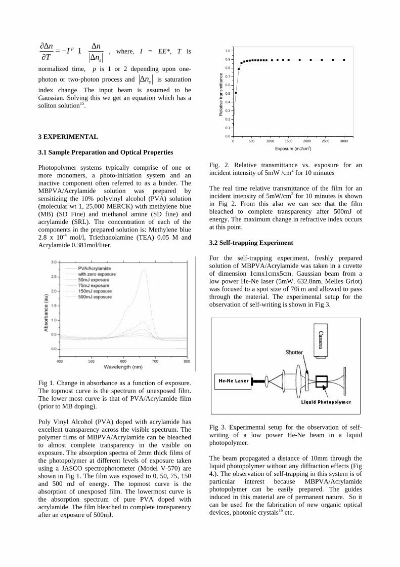
∆∆
+−=∂∆∂
s
p
n
nI
T
n1 , where, I = EE*, T is
normalized time, p is 1 or 2 depending upon one-
photon or two-photon process and sn∆ is saturation
index change. The input beam is assumed to be Gaussian. Solving this we get an equation which has a soliton solution15. 3 EXPERIMENTAL 3.1 Sample Preparation and Optical Properties Photopolymer systems typically comprise of one or more monomers, a photo-initiation system and an inactive component often referred to as a binder. The MBPVA/Acrylamide solution was prepared by sensitizing the 10% polyvinyl alcohol (PVA) solution (molecular wt 1, 25,000 MERCK) with methylene blue (MB) (SD Fine) and triethanol amine (SD fine) and acrylamide (SRL). The concentration of each of the components in the prepared solution is: Methylene blue 2.8 x 10⁻⁴ mol/l, Triethanolamine (TEA) 0.05 M and Acrylamide 0.381mol/liter.
Fig 1. Change in absorbance as a function of exposure. The topmost curve is the spectrum of unexposed film. The lower most curve is that of PVA/Acrylamide film (prior to MB doping). Poly Vinyl Alcohol (PVA) doped with acrylamide has excellent transparency across the visible spectrum. The polymer films of MBPVA/Acrylamide can be bleached to almost complete transparency in the visible on exposure. The absorption spectra of 2mm thick films of the photopolymer at different levels of exposure taken using a JASCO spectrophotometer (Model V-570) are shown in Fig 1. The film was exposed to 0, 50, 75, 150 and 500 mJ of energy. The topmost curve is the absorption of unexposed film. The lowermost curve is the absorption spectrum of pure PVA doped with acrylamide. The film bleached to complete transparency after an exposure of 500mJ.
0 500 1000 1500 2000 2500 30000.0
0.1
0.2
0.3
0.4
0.5
0.6
0.7
0.8
0.9
1.0
Rel
ativ
e tr
ansm
ittan
ce
Exposure (mJ/cm2)
Fig. 2. Relative transmittance vs. exposure for an incident intensity of 5mW /cm2 for 10 minutes The real time relative transmittance of the film for an incident intensity of 5mW/cm2 for 10 minutes is shown in Fig 2. From this also we can see that the film bleached to complete transparency after 500mJ of energy. The maximum change in refractive index occurs at this point. 3.2 Self-trapping Experiment For the self-trapping experiment, freshly prepared solution of MBPVA/Acrylamide was taken in a cuvette of dimension 1cmx1cmx5cm. Gaussian beam from a low power He-Ne laser (5mW, 632.8nm, Melles Griot) was focused to a spot size of 70ì m and allowed to pass through the material. The experimental setup for the observation of self-writing is shown in Fig 3.
Fig 3. Experimental setup for the observation of self-writing of a low power He-Ne beam in a liquid photopolymer. The beam propagated a distance of 10mm through the liquid photopolymer without any diffraction effects (Fig 4.). The observation of self-trapping in this system is of particular interest because MBPVA/Acrylamide photopolymer can be easily prepared. The guides induced in this material are of permanent nature. So it can be used for the fabrication of new organic optical devices, photonic crystals16 etc.

Fig 4. Propagation of the beam through the medium without any diffraction effects. 4 CONCLUSION We have shown the stable propagation of a low power He-Ne laser beam through a liquid MBPVA/Acrylamide photopolymer material. The beam propagated through the medium without any diffraction effects. The propagation of the beam can be described by the previously studied theoretical models. The guides in induced in this material are of particular interest owing to the fact that MBPVA/Acrylamide can be easily prepared and has low cost as compared to the materials used by previous researchers. ACKNOWLEDGEMENTS The authors would like to thank DST, Govt. of India, for its support through Research project and FIST scheme. KP wishes to acknowledge CSIR, UGC, and DST for financial support through projects.
REFERENCES 1. S. J. Frisken, Opt. Lett., 18, 1035 (1993). 2. T.M. Monro, D. Moss, M. Bazylenko, C. Martijn de Sterke, and L. Poladian, Phys. Rev. Lett., 80, 4072 (1998). 3. T. M. Monro, C. M. de Sterke and L. Poladian, J. Opt. Soc. Am. B. 13, 2824 (1996). 4. Yuri S. Kivshar and Govind P. Agrawal, Optical Solitons - From Fibers to Photonic Crystals (Academic Press, New York, 2003). 5. T. Yamashita, M. Kagami, and H. Ito, J. Lightwave Technol. 20, 1556 (2002). 6. T. Yamashita and M. Kagami, J. Lightwave Technol. 23, 2542 (2005). 7. K. Yamashita, T. Kuro, K. Oe, K. Mune, T. Hikita, and A. Mochizuki, IEEE Photon. Technol. Lett., 16, 801 (2004). 8. H. Ma, A. K.-Y. Jen, and L. R. Dalton, Adv. Mater. 14, 1339 (2002). 9. L. Eldada and L. W. Shacklette, IEEE J. Sel. Top. Quantum Electron. 6, 54 (2000). 10. J.-W. Kang, J.-J. Kim, and E. Kim, Appl. Phys. Lett. 80, 1710 (2002). 11. J.-W. Kang, M.-J. Kim, J.-P. Kim, S.-J. Yoo, J.-S. Lee, D. Y. Kim, and J.-J. Kim, Appl. Phys. Lett. 82, 3823 (2003). 12. S. Kewitsch and A. Yariv, Opt. Lett. 21, 24 (1996). 13. L. Friedrich, P. Dannberg, C. Wkhter, Th. Hennig, A. Brker, W. Karthe, Opt. Comm, 137, 239 (1997). 14. Jaeyoun Kim, Ki-Hun Jeong, and Luke P. Lee, Opt. Lett, 30, 5 (2005). 15. T. M. Monro, C. M. de Sterke and L. Poladian, J. Mod. Opt. 48, 191 (2001). 16. Satoru Shoji and Hong-Bo Sun, Appl. Phys. Lett. 83, 608 (2003).
L ALANINIUM OXALATE SINGLE CRYSTALS FOR NLO APPLICATIONS :- A SIMPLE AND
NOVEL SYNTHESIS ROUTE
Arun. K.J, S.Jayaleksmi
Division for Research in advanced Materials, Dept: of physics, Cochin university of Science &
Technology, Cochin- 22. Kerala, India.
Abstract
A potential organic NLO single crystal based on amino acids; L alaninium oxalate was grown
using the simple chiral amino acid L Alanine and L oxalic acid by slow evaporation method. Grown
crystals had an optimum dimension of 40 x15 x 5 mm3 with good optical quality and were characterized
using powder XRD, FTIR spectroscopy, TGA- DTA, UV/ VIS/ NIR Diffuse reflectance spectroscopy and
Photoluminescence studies.
Key Words
Seeded crystal growth, Organic NLO, Photoluminescence, DRS, FTIR, TGA-DTA
1.Introduction.
Over the past two decades much
attention has been paid to the search of novel
high quality NLO materials that can generate
high second order optical non linearities which is
important for potential applications including
telecommunication, optical computing, optical
data storage and processing. ( 1 ) – ( 6).
Organic NLO materials are formed by
weak Van Der Waals and hydrogen bonds with
FRQMXJDWHG HOHFWURQV DQG DUH PRUHadvantageous than their inorganic counterparts
due to high conversion efficiency for second
harmonic generation and transparency in the
visible region, high resistance to optical damage
and so on.
7KH. DPLQRDFLG/DODQLQHFU\VWDOKDVshown strong non linear behaviour and
anomalous phonon coupling and is a system
exhibiting vibrational solitons ( 7 ).An attempt is
made to synthesise and grow an organic NLO
material
L alaninium oxalate (LAO ) using L
alanine and L oxalic acid . The seed grown
crystals of LAO were characterized by XRD,
TGA- DTA, FTIR, DRS and photoluminescence
studies and the results are reported.
2. Experimental.
2.1 Synthesis and seeded crystal growth.
L alaninium oxalate was synthesised
from equimolar solution of L alanine and L
oxalic acid by evaporation preventing
decomposition. Synthesised samples were
crystallised repeatedly to get a pure, colourless
crystalline powder. Good quality seed crystals
were prepared using this powder. One or two
seed crystals were then placed in its
supersaturated solution kept in a bath at 35 °C.
Seed crystals were grown to big crystals by slow
evaporation to a size of about 40x 15 x 8 mm3
with good transparency in a time of about three
weeks. To the best of our knowledge; growth of
big LAO crystals of such size is not reported by
any worker so far.
2.2 Characterisation methods
Powdered XRD scan of the crystals was
done using Rigaku X ray diffractometer using
&X .. UDGLDWLRQ WR LGHQWLI\ WKH FRPSRXQG DQGstructure.
FTIR spectrum of the crystals was taken
with AVTAR 370 spectrometer having DTGS
KBr detector with a resolution of 4 cm-1
.
TGA- DTA studies were carried out in
nitrogen atmosphere at a heating rate of 10°c/
min for a range 28 - 600°c to assess the thermal
stability.
DRS studies were done using a JASCO
V 570 spectrophotometer in the range from 190
to 2500nm .
Photoluminescence spectrum was taken
with Jobin Yvon Flurolog 3 spectrophotometer.
The slit width for excitation was 7 nm and for
emission 9 nm
3.Results and Discussion.
3.1 Crystal Structure.
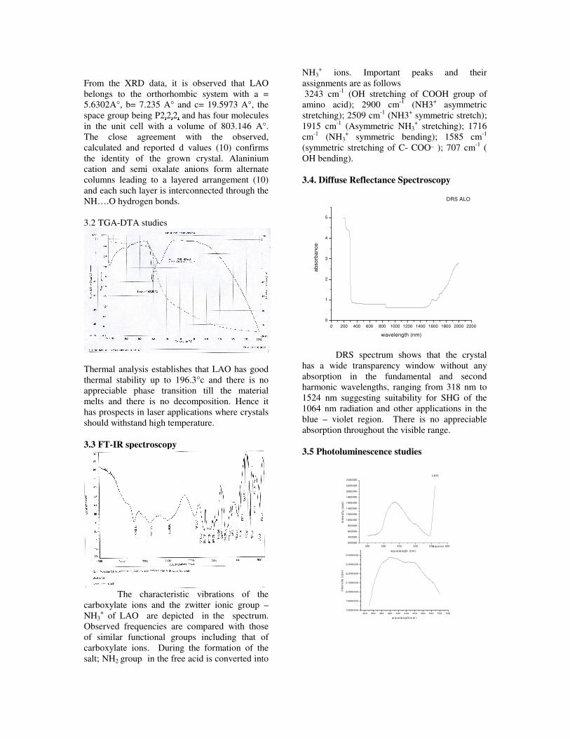
From the XRD data, it is observed that LAO
belongs to the orthorhombic system with a =
5.6302A°, b= 7.235 A° and c= 19.5973 A°, the
space group being P2Õ2Õ2Õ and has four molecules
in the unit cell with a volume of 803.146 A°.
The close agreement with the observed,
calculated and reported d values (10) confirms
the identity of the grown crystal. Alaninium
cation and semi oxalate anions form alternate
columns leading to a layered arrangement (10)
and each such layer is interconnected through the
NH….O hydrogen bonds.
3.2 TGA-DTA studies
Thermal analysis establishes that LAO has good
thermal stability up to 196.3°c and there is no
appreciable phase transition till the material
melts and there is no decomposition. Hence it
has prospects in laser applications where crystals
should withstand high temperature.
3.3 FT-IR spectroscopy
The characteristic vibrations of the
carboxylate ions and the zwitter ionic group –
NH3+ of LAO are depicted in the spectrum.
Observed frequencies are compared with those
of similar functional groups including that of
carboxylate ions. During the formation of the
salt; NH2 group in the free acid is converted into
NH3+ ions. Important peaks and their
assignments are as follows
3243 cm-1
(OH stretching of COOH group of
amino acid); 2900 cm-1
(NH3+ asymmetric
stretching); 2509 cm-1
(NH3+ symmetric stretch);
1915 cm-1
(Asymmetric NH3+ stretching); 1716
cm-1
(NH3+ symmetric bending); 1585 cm
-1
(symmetric stretching of C- COO_ ); 707 cm
-1 (
OH bending).
3.4. Diffuse Reflectance Spectroscopy
0 200 400 600 800 1000 1200 1400 1600 1800 2000 2200
0
1
2
3
4
5
ab
so
rba
nce
wavelength (nm)
DRS ALO
DRS spectrum shows that the crystal
has a wide transparency window without any
absorption in the fundamental and second
harmonic wavelengths, ranging from 318 nm to
1524 nm suggesting suitability for SHG of the
1064 nm radiation and other applications in the
blue – violet region. There is no appreciable
absorption throughout the visible range.
3.5 Photoluminescence studies
350 400 450 500 550 600
200000
400000
600000
800000
1000000
1200000
1400000
1600000
1800000
2000000
2200000
2400000
inte
ns
ity
(c
ps
)
wavelength (nm )
LA O
340 360 380 40 0 420 440 460 480 50 0 520 540
1 800000 0
1 900000 0
2 000000 0
2 100000 0
2 200000 0
2 300000 0
2 400000 0
inte
ns
ity
(c
ps
)
w a ve le ng th (n m )
a la n in e
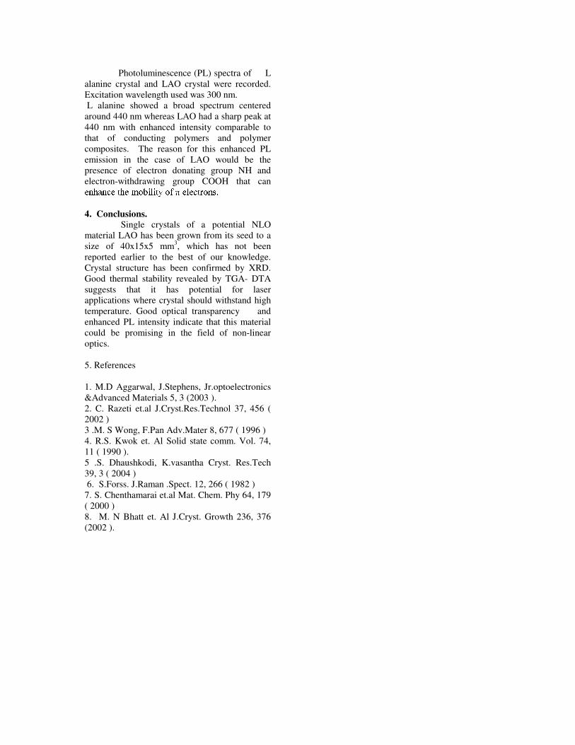
Photoluminescence (PL) spectra of L
alanine crystal and LAO crystal were recorded.
Excitation wavelength used was 300 nm.
L alanine showed a broad spectrum centered
around 440 nm whereas LAO had a sharp peak at
440 nm with enhanced intensity comparable to
that of conducting polymers and polymer
composites. The reason for this enhanced PL
emission in the case of LAO would be the
presence of electron donating group NH and
electron-withdrawing group COOH that can
HQKDQFHWKHPRELOLW\RIHOHFWURQV
4. Conclusions.
Single crystals of a potential NLO
material LAO has been grown from its seed to a
size of 40x15x5 mm3, which has not been
reported earlier to the best of our knowledge.
Crystal structure has been confirmed by XRD.
Good thermal stability revealed by TGA- DTA
suggests that it has potential for laser
applications where crystal should withstand high
temperature. Good optical transparency and
enhanced PL intensity indicate that this material
could be promising in the field of non-linear
optics.
5. References
1. M.D Aggarwal, J.Stephens, Jr.optoelectronics
&Advanced Materials 5, 3 (2003 ).
2. C. Razeti et.al J.Cryst.Res.Technol 37, 456 (
2002 )
3 .M. S Wong, F.Pan Adv.Mater 8, 677 ( 1996 )
4. R.S. Kwok et. Al Solid state comm. Vol. 74,
11 ( 1990 ).
5 .S. Dhaushkodi, K.vasantha Cryst. Res.Tech
39, 3 ( 2004 )
6. S.Forss. J.Raman .Spect. 12, 266 ( 1982 )
7. S. Chenthamarai et.al Mat. Chem. Phy 64, 179
( 2000 )
8. M. N Bhatt et. Al J.Cryst. Growth 236, 376
(2002 ).
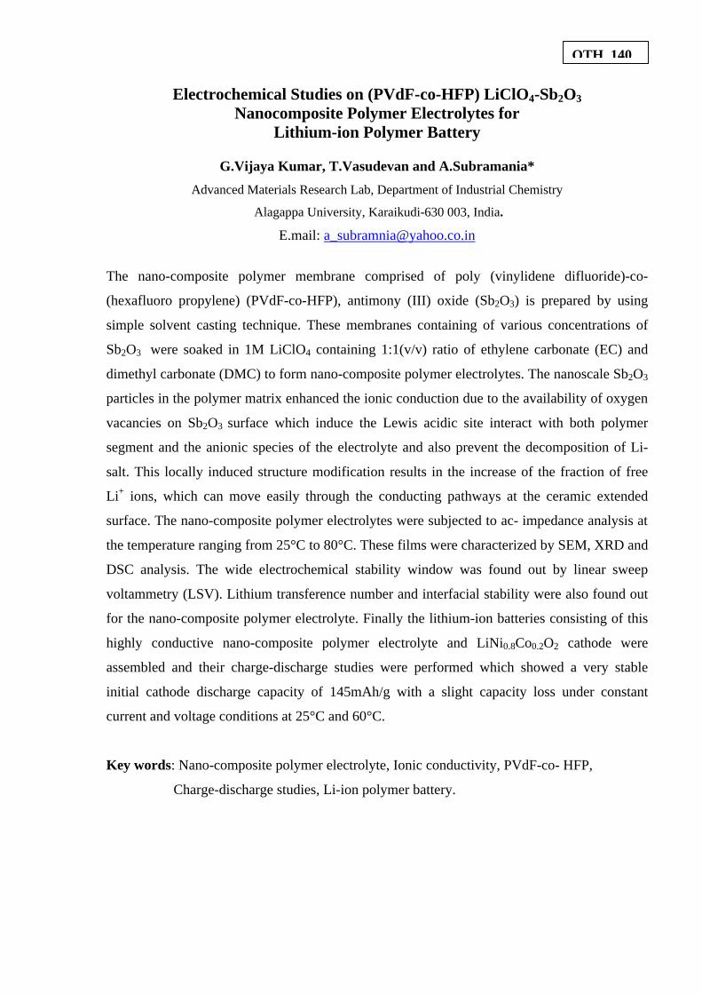
Electrochemical Studies on (PVdF-co-HFP) LiClO4-Sb2O3 Nanocomposite Polymer Electrolytes for
Lithium-ion Polymer Battery
G.Vijaya Kumar, T.Vasudevan and A.Subramania*
Advanced Materials Research Lab, Department of Industrial Chemistry
Alagappa University, Karaikudi-630 003, India.
E.mail: [email protected]
The nano-composite polymer membrane comprised of poly (vinylidene difluoride)-co-
(hexafluoro propylene) (PVdF-co-HFP), antimony (III) oxide (Sb2O3) is prepared by using
simple solvent casting technique. These membranes containing of various concentrations of
Sb2O3 were soaked in 1M LiClO4 containing 1:1(v/v) ratio of ethylene carbonate (EC) and
dimethyl carbonate (DMC) to form nano-composite polymer electrolytes. The nanoscale Sb2O3
particles in the polymer matrix enhanced the ionic conduction due to the availability of oxygen
vacancies on Sb2O3 surface which induce the Lewis acidic site interact with both polymer
segment and the anionic species of the electrolyte and also prevent the decomposition of Li-
salt. This locally induced structure modification results in the increase of the fraction of free
Li+ ions, which can move easily through the conducting pathways at the ceramic extended
surface. The nano-composite polymer electrolytes were subjected to ac- impedance analysis at
the temperature ranging from 25°C to 80°C. These films were characterized by SEM, XRD and
DSC analysis. The wide electrochemical stability window was found out by linear sweep
voltammetry (LSV). Lithium transference number and interfacial stability were also found out
for the nano-composite polymer electrolyte. Finally the lithium-ion batteries consisting of this
highly conductive nano-composite polymer electrolyte and LiNi0.8Co0.2O2 cathode were
assembled and their charge-discharge studies were performed which showed a very stable
initial cathode discharge capacity of 145mAh/g with a slight capacity loss under constant
current and voltage conditions at 25°C and 60°C.
Key words: Nano-composite polymer electrolyte, Ionic conductivity, PVdF-co- HFP,
Charge-discharge studies, Li-ion polymer battery.
OTH 140
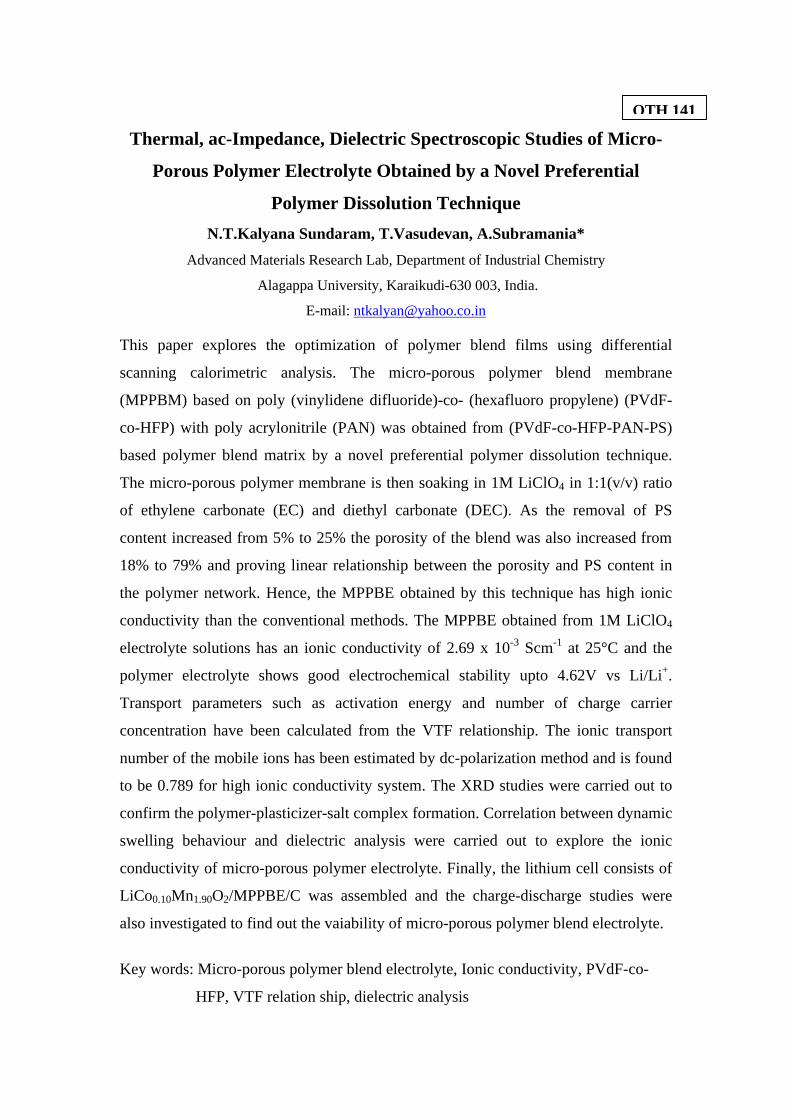
OTH
Thermal, ac-Impedance, Dielectric Spectroscopic Studies of Micro-
Porous Polymer Electrolyte Obtained by a Novel Preferential
Polymer Dissolution Technique
N.T.Kalyana Sundaram, T.Vasudevan, A.Subramania*
Advanced Materials Research Lab, Department of Industrial Chemistry
Alagappa University, Karaikudi-630 003, India.
E-mail: [email protected]
This paper explores the optimization of polymer blend films using differential
scanning calorimetric analysis. The micro-porous polymer blend membrane
(MPPBM) based on poly (vinylidene difluoride)-co- (hexafluoro propylene) (PVdF-
co-HFP) with poly acrylonitrile (PAN) was obtained from (PVdF-co-HFP-PAN-PS)
based polymer blend matrix by a novel preferential polymer dissolution technique.
The micro-porous polymer membrane is then soaking in 1M LiClO4 in 1:1(v/v) ratio
of ethylene carbonate (EC) and diethyl carbonate (DEC). As the removal of PS
content increased from 5% to 25% the porosity of the blend was also increased from
18% to 79% and proving linear relationship between the porosity and PS content in
the polymer network. Hence, the MPPBE obtained by this technique has high ionic
conductivity than the conventional methods. The MPPBE obtained from 1M LiClO4
electrolyte solutions has an ionic conductivity of 2.69 x 10⁻³ Scm-1 at 25°C and the
polymer electrolyte shows good electrochemical stability upto 4.62V vs Li/Li+.
Transport parameters such as activation energy and number of charge carrier
concentration have been calculated from the VTF relationship. The ionic transport
number of the mobile ions has been estimated by dc-polarization method and is found
to be 0.789 for high ionic conductivity system. The XRD studies were carried out to
confirm the polymer-plasticizer-salt complex formation. Correlation between dynamic
swelling behaviour and dielectric analysis were carried out to explore the ionic
conductivity of micro-porous polymer electrolyte. Finally, the lithium cell consists of
LiCo0.10Mn1.90O2/MPPBE/C was assembled and the charge-discharge studies were
also investigated to find out the vaiability of micro-porous polymer blend electrolyte.
Key words: Micro-porous polymer blend electrolyte, Ionic conductivity, PVdF-co-
HFP, VTF relation ship, dielectric analysis
OTH 141
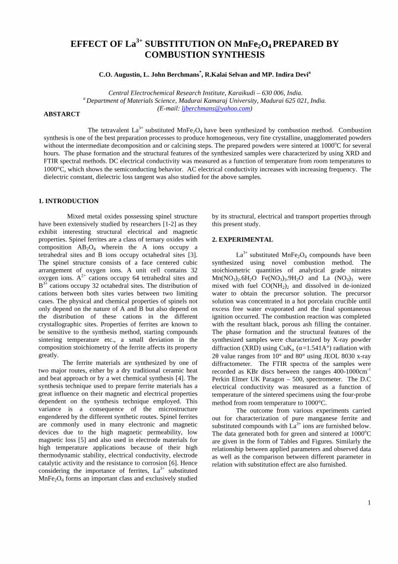
1
EFFECT OF La3+ SUBSTITUTION ON MnFe2O4 PREPARED BY COMBUSTION SYNTHESIS
C.O. Augustin, L. John Berchmans*, R.Kalai Selvan and MP. Indira Devia
Central Electrochemical Research Institute, Karaikudi – 630 006, India.
a Department of Materials Science, Madurai Kamaraj University, Madurai 625 021, India. (E-mail: [email protected])
1. INTRODUCTION
Mixed metal oxides possessing spinel structure have been extensively studied by researchers [1-2] as they exhibit interesting structural electrical and magnetic properties. Spinel ferrites are a class of ternary oxides with composition AB2O4 wherein the A ions occupy a tetrahedral sites and B ions occupy octahedral sites [3]. The spinel structure consists of a face centered cubic arrangement of oxygen ions. A unit cell contains 32 oxygen ions. A2+ cations occupy 64 tetrahedral sites and B3+ cations occupy 32 octahedral sites. The distribution of cations between both sites varies between two limiting cases. The physical and chemical properties of spinels not only depend on the nature of A and B but also depend on the distribution of these cations in the different crystallographic sites. Properties of ferrites are known to be sensitive to the synthesis method, starting compounds sintering temperature etc., a small deviation in the composition stoichiometry of the ferrite affects its property greatly.
The ferrite materials are synthesized by one of two major routes, either by a dry traditional ceramic heat and beat approach or by a wet chemical synthesis [4]. The synthesis technique used to prepare ferrite materials has a great influence on their magnetic and electrical properties dependent on the synthesis technique employed. This variance is a consequence of the microstructure engendered by the different synthetic routes. Spinel ferrites are commonly used in many electronic and magnetic devices due to the high magnetic permeability, low magnetic loss [5] and also used in electrode materials for high temperature applications because of their high thermodynamic stability, electrical conductivity, electrode catalytic activity and the resistance to corrosion [6]. Hence considering the importance of ferrites, La3+ substituted MnFe2O4 forms an important class and exclusively studied
by its structural, electrical and transport properties through this present study. 2. EXPERIMENTAL La3+ substituted MnFe2O4 compounds have been synthesized using novel combustion method. The stoichiometric quantities of analytical grade nitrates Mn(NO3)2.6H2O Fe(NO3)3.9H2O and La (NO3)3 were mixed with fuel CO(NH2)2 and dissolved in de-ionized water to obtain the precursor solution. The precursor solution was concentrated in a hot porcelain crucible until excess free water evaporated and the final spontaneous ignition occurred. The combustion reaction was completed with the resultant black, porous ash filling the container. The phase formation and the structural features of the synthesized samples were characterized by X-ray powder diffraction (XRD) using CuKα (α=1.541A°) radiation with 2θ value ranges from 10° and 80° using JEOL 8030 x-ray diffractometer. The FTIR spectra of the samples were recorded as KBr discs between the ranges 400-1000cm-1 Perkin Elmer UK Paragon – 500, spectrometer. The D.C electrical conductivity was measured as a function of temperature of the sintered specimens using the four-probe method from room temperature to 1000°C.
The outcome from various experiments carried out for characterization of pure manganese ferrite and substituted compounds with La3+ ions are furnished below. The data generated both for green and sintered at 1000oC are given in the form of Tables and Figures. Similarly the relationship between applied parameters and observed data as well as the comparison between different parameter in relation with substitution effect are also furnished.
ABSTARCT
The tetravalent La3+ substituted MnFe2O4 have been synthesized by combustion method. Combustion synthesis is one of the best preparation processes to produce homogeneous, very fine crystalline, unagglomerated powders without the intermediate decomposition and or calcining steps. The prepared powders were sintered at 1000oC for several hours. The phase formation and the structural features of the synthesized samples were characterized by using XRD and FTIR spectral methods. DC electrical conductivity was measured as a function of temperature from room temperatures to 1000°C, which shows the semiconducting behavior. AC electrical conductivity increases with increasing frequency. The dielectric constant, dielectric loss tangent was also studied for the above samples.
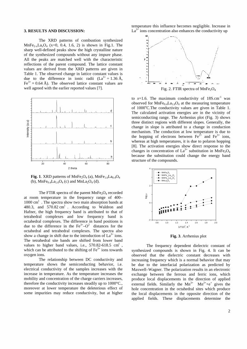
2
3. RESULTS AND DISCUSSION:
The XRD patterns of combustion synthesized MnFe2-xLaxO4 (x=0, 0.4, 1.6, 2) is shown in Fig.1. The sharp well-defined peaks show the high crystalline nature of the synthesized compounds without any impure phase. All the peaks are matched well with the characteristic reflections of the parent compound. The lattice constant values are derived from the XRD patterns are given in Table 1. The observed change in lattice constant values is due to the difference in ionic radii (La3+ = 1.36 Å, Fe3+ = 0.64 Å). The observed lattice constant values are well agreed with the earlier reported values [7].
The FTIR spectra of the parent MnFe2O4 recorded
at room temperature in the frequency range of 400–1000 cm1 . The spectra show two main absorption bands at 480.3, and 570.82 cm1 . According to Waldron and Hafner, the high frequency band is attributed to that of tetrahedral complexes and low frequency band is octahedral complexes. The difference in band positions is due to the difference in the Fe3+–O2 distances for the octahedral and tetrahedral complexes. The spectra also show a change in shift due to the introduction of La3+ ions. The tetrahedral site bands are shifted from lower band values to higher band values, i.e., 570.82-618.5 cm1 , which can be attributed to the shifting of Fe3+ ions towards oxygen ions.
The relationship between DC conductivity and temperature shows the semiconducting behavior, i.e. electrical conductivity of the samples increases with the increase in temperature. As the temperature increases the mobility and concentration of the charge carriers increases, therefore the conductivity increases steadily up to 1000°C., moreover at lower temperature the deleterious effect of some impurities may reduce conductivity, but at higher
temperature this influence becomes negligible. Increase in La3+ ions concentration also enhances the conductivity up
Fig. 2. FTIR spectra of MnFe2O4
to x=1.6. The maximum conductivity of 18S.cm-1 was observed for MnFe0.4La1.6O4 at the measuring temperature of 1000oC.The conductivity values are given in Table 1. The calculated activation energies are in the vicinity of semiconducting range. The Arrhenius plot (Fig. 3) shows three distinct regions with different slopes. Generally, the change in slope is attributed to a change in conduction mechanism. The conduction at low temperature is due to the hopping of electrons between Fe2+ and Fe3+ ions, whereas at high temperatures, it is due to polaron hopping [8]. The activation energies show direct response to the changes in concentration of La3+ substitution in MnFe2O4 because the substitution could change the energy band structure of the compounds.
0.8 1.0 1.2 1.4 1.6 1.8 2.0-2
0
2
4
log
ρ
1/T103, K-1
MnFe2O
4
MnFe1.6
La0.4
O4
MnFe0.4
La1.6
O4
MnLa2O
4
Fig. 3. Arrhenius plot
The frequency dependent dielectric constant of
synthesized compounds is shown in Fig. 4. It can be observed that the dielectric constant decreases with increasing frequency which is a normal behavior that may be due to the interfacial polarization as predicted by Maxwell–Wagner. The polarization results in an electronic exchange between the ferrous and ferric ions, which produce local displacements in the direction of applied external fields. Similarly the Mn3+⇔Mn2++e+ gives the hole concentration in the octahedral sites which produce the local displacements in the opposite direction of the applied fields. These displacements determine the
20 40 60 80
2 theta
d
c
b
a
Inte
nsity
(a.
u)
Fig. 1. XRD patterns of MnFe2O4 (a), MnFe1.6La0.4O4 (b), MnFe0.4La1.6O4 (c) and MnLa2O4 (d).
3
polarization as well as the dielectric properties. The compositional dependence of dielectric constant is also shown in same Figure. Among all the specimens the lower dielectric constant value is observed for the MnFe0.4La1.6O4 sample, which shows the higher conductivity.
0 2000 4000 6000 8000 10000200
300
400
500
600
700
800
900
1000
1100
1200
1300
Die
lect
ric c
onst
ant
ν, Hz
MnFe2O
4
MnFe1.6
La0.4
O4
MnFe0.4
La1.6
O4
MnLa2O
4
Fig. 4. Frequency Vs Dielectric constant
Fig. 5 shows the frequency Vs loss tangent. It can
be observed that the values increase steeply at first and then decreases to a steady value with high frequency for all the materials. The relaxations peaks are appeared at different tan ä values as well as different frequencies are show in Figure. The relaxation peak for MnFe2O4 is resulted at a tan ä value of 5.61 at 0.1 KHz whereas for substituted ferrites of x=0.4 at 0.5 KHz (tan ä value 15.5). But in the case of MnFe0.4 La1.6O4 the relaxation peak is obtained at the highest value of 42.8 and an applied frequency of 0.1KHz. This shows the difference in interaction of the applied frequency with the localized electric charge carrier of the compounds.
0 2000 4000 6000 8000 10000
0
10
20
30
40
50
tan
δ
ν, Hz
MnFe2O
4
MnFe1.6
La0.4
O4
MnFe0.4
La1.6
O4
MnLa2O
4
Fig. 5. Frequency Vs loss tangent
The frequency dependence of AC electrical conductivity of all the samples is shown in Fig. 6. It is observed that the AC conductivity increases with increasing applied frequency. Since the increase in frequency enhances the hopping frequency of the charge carriers Fe2+ and Fe3+, the conduction is increased. The conduction mechanism of ferrite is explained on the basis
of hopping of charge carriers between the Fe2+ and Fe3+on the octahedral sites [9].
0 2000 4000 6000 8000 10000
0.0000
0.0002
0.0004
0.0006
0.0008
0.0010 MnFe2O4 MnFe
1.6La
0.4O
4
MnFe0.4
La1.6
O4
MnLa2O
4
σ, a
.c.,
S.c
m-1
ν Hz
Fig.6. A.C conductivity Vs frequency
Table 1: XRD data for MnFe2-xLaxO4 Sl.No Sample a, Ao σd.c at 1000oC
S.cm-1
1 MnFe2O4 8.50 5.6
2 MnFe1.6La0.4O4 9.0825 14.0
3 MnFe0.4La1.6O4 9.0825 18.0
4 MnLa2O4 8.6093 10.21
4. CONCLUSIONS
Combustion synthesis has been found to be a convenient method for preparation of new materials. XRD Analysis confirms the cubic nature of the compound synthesized. The lattice parameter is observed to increase with increase in La3+ ion substitution. The FTIR spectra show the characteristic features of spinel compounds. D.C electrical conductivity confirms the synthesized materials are in semiconductors and the maximum conductivity of 18S. cm-1obtained for MnFe0.4La1.6O4 composition. REFERENCES: 1R.Kalai Selvan, C.O.Augustin, L.John Berchmans, R.Saraswathi, Materials Research Bulletin, 38, 41 (2003) 2M.U.Rana,M.Islam,T.Abbas, Materials Chemistry and Physics. 65, 345 (2000) 3S.P.Ghorphade,V.S.Darshana,S.G.Dixit Applied Catalysis a General 166, 135 (1998) 4 C.O.Augustin, R.Kalai Selvan, Bull. Electrochem.19, 319 (2003) 5Toshiyuki Suzuki T.Tanaka, K.Ikemizu J.Magn.Magn.Mater.235, 159 (2001) 6L.John Berchmans, R.Kalai Selvan , C.O.Augustin, Material letters 58, 1928 (2004). 7M.A.Gabal, S.S.Ata-Allah, J. Phys. Chem. Solids 65, 995 (2004) 8S.Balaji, R.Kalai Selvan, L. John Berchmans, S. Angappan, C.O. AugustinMat. Sci. Engg. B. 119, 119(2005) 9L.John Berchmans, R.Kalai Selvan, P.N. Selva Kumar , C.O.Augustin, J. Magn. Magn. Mater. 279, 103 (2004).
Pressure Sensitive Adhesive Film in Transdermal Delivery Device of 6-Mercaptopurine.
Chandrashekar.N.S, ShobhaRani.R.H
Al-Ameen College of Pharmacy, Near Lalbagh main gate, Hosur main road, Bangalore-560027
Email: [email protected]
Introduction: Transdermal drug delivery (TDD) patches are designed to deliver a therapeutically effective amount of drug across a patient skin. A transdermal drug delivery device consists of several components including active ingredients, pressure sensitive adhesive backing membrane and release liner. A pressure sensitive adhesive (PSA) is a material that adheres with no more than applied finger pressure, is aggressively and permanently tacky, exerts a strong holding force, and should be removable from a smooth surface without leaving a residue1. Adhesion refers to the force required to remove the adhesive from a substrate once the bond has reached equilibrium. The PSA must hold the TDD at the appropriate body site for long periods of time without causing skin irritation that might discourage patients. The objective of this study is to prepare a pressure sensitive adhesive film for transdermal delivery of 6-mercaptopurine (6-MP) purine analog which available as tablets. It is incompletely absorbed from GIT (50%) with bioavailability of 5-37%. It also undergoes extensive “First Pass metabolism”. The common adverse effects include GI irritation and hepatotoxicity. Transdermal drug delivery systems of 6-mercaptopurine will overcome the first pass metabolism, common adverse effects of the oral route and thereby improve patient compliance.
Materials and Methods: 6-mercaptopurine was purchased from Sigma chemical Co. (St. Louis, MO) Pressure sensitive adhesives (PSA) Duro-Tak®- 387-2052 was gift sample (National Starch and Chemical Co., Netherlands) 3M, SCOTCHPACK® backing membrane and 3M release liner 1022® was gift sample form (3M St.Paul USA) and remaining chemicals were analytical grade. Preparation of the pressure sensitive adhesives film: The formulations were prepared according to 24 factorial design2. 6-mercaptopurine was dispersed in the PSA Duro-Tak®- 387-2052. The release liner (Fluoropolymer coated polyester film) was held in a place on a flat surface. A sample from each formulation was placed across the top edge of release liner. The mixture was casted onto the release liner by multiple clearance film applicator AR 5315 (pacific Scientific, Silver Spring, MD). The wet adhesive film was dried for 24 hours in the air and backing membrane was used to prevent from external environment. Evaluation of films: The films were evaluated for the following physicochemical parameters: Thickness: The thickness of uniform area (2x 4 cm2) of the films were measured using film thickness measuring instrument (Links, India). The thickness was found to be 0.403±8.52mm.
Weight: The weight of the films (2x4cm2) was determined using digital electronic balance (Sartoruis, India) the weight was found to be 802±6.24 mg. Folding endurance: For determining the folding endurance, a film (2x 4 cm2) was folded in the center between finger and thumb and the opened. This was called as "one folding”. The procedure was repeated until the film showed breakage or cracks in the center. The total number of folding operations was termed the “folding endurance value”. The values found to be more the 500 folding. Tensile strength: The tensile strength of the films was determined by the percentage elongation at break value. Rectangular pieces of 1 inch width 15 cms long strips of film were cut using a sharp blade and scale and marked 2.5 cms from the edges lengthwise. The film was held between the jaws of an apparatus (Instron, Germany). One jaw was kept stationary and another was pulled slowly a definite speed and weight until the film just broke. Percent elongation at break was calculated using eq (1) the % of elongation at break was 75 Percentage elongation at break = (IB - IA) X 100 (1)
IA Where IA = Initial length of film (cm) and IB Length of film (cm) at break. Invitro skin permeation studies: A modified Franz diffusion cell3 with a diffusional area of 2.065 cm2 was used. The human cadaver skin was collected from abdominal portion of male 53 years (Department of forensic medicine, Victoria hospital , Bangalore) skin was heat treated. After removing the subcutaneous fat, the
stratum corneum side of the skin was kept in intimate contact with the release liner surface. The donor compartment was filled with 5ml and receptor compartment with 20ml 7.4 pH phosphate buffer stirred at 100 rpm on a magnetic sitter. The contents of the receiver compartment were kept at 37±10C with pre warmed water flowing through a jacket lined with the receiver compartment. The amount of the drug permeated was determined sampling at regular intervals and analyzed spectrophotometrically at 321nm using the UV-spectrophotometer. The volume was replaced with equal volume of the receptor solution. The flux (skin permeation rate of the drug) was determined directly as the slope of the curve between the steady state values of the amount of drug permeated (mg cm-2) Vs time in hours4. The transdermal flux was185±12ìg/h/cm -2. Results and discussion: There was an increase in thickness and weight as the PSAs was increased. The folding endurance value could be defined as “the number of times” a film can be folded at the same place without breaking”. This test is an index of the brittleness of the film, the lower the folding endurance value, the more brittle the film is, the films showed more than 500 folding. It is important test to assess the integrity of the film. An assessment of the tensile strength of the films was made by “percent elongation at break” value which could be described as “the percentage in change in length when film specimen breaks”. The % of elongation was about 75, The films was found to be more elegant smooth and transparent. The transdermal flux was found to be very less to attain the therapeutic concentration, the films is having good mechanical strength and flexibility to adhere to the skin. The basic design can be altered to deliver the therapeutic amount of drug for 24 hours by including some excipients like penetration enhancers. The materials have shown their inhertness and biocompatible with drug.

Where as some progress has been made in the delivery device, invitro flux suggests that pressure sensitive adhesive contribute greatly to the cancer chemotherapy, exploration of this approach. Conclusions: Technological progress in these pressure sensitive adhesives films filed has mainly driven the unmet medical needs. References: 1. A.V.Pocius adhesives in Krik-Othmer
Encyclopedia of chemical technology, M.Howe-Grants, Ed. (Wiely-Interscience, Newyork, NY, 4th ed., 1991),445-466.
2. Dimitrios A.Dimas, Paraskevas P.Dallas, Dimitrios M.Rekkas and Nikolaos H.Choulis, AAPS, Vol 1,2, 2000.
3. T.Franz. J Invest Dermatol.64,190-195(1975)
4. F.P.Bonina,V.Carellii,G.D.Cols, L.Montenergo,E.Nanipieri. Int J Pharm Sci.100,41-47(1993).
EFFECT OF GAMMA RAY IRRADIATION ON THE SPECTROSCOPIC PROPERTIES OF RARE EARTH DOPED LITHIUM BORATE GLASS
SYSTEMS Win Mathew John, V. Sasidharan, N. Radha Krishnan Nair a, C. S. Menon b,
K. Shreekrishna Kumar*
School of Technology & Applied Sciences, Mahatma Gandhi University, Kottayam. a Rubber Research Institute of India, Kottayam.
b School of Pure & Applied Physics, Mahatma Gandhi University, Kottayam.
Abstract
Glasses containing rare earth ions are sensitive to gamma radiation. Effect of gamma
ray irradiation on the optical absorption of Lithium borate glass containing rare earth
oxides (Nd, Dy, La, Sm, Pr, Gd and Ce) was investigated in the spectral range 200 - 900
nm. Gamma ray irradiations yield a linear response in the UV-VIS region for all samples
except those containing Ce. Direct and indirect band gap energy and the Urbach edge of
rare earth doped lithium borate glass irradiated with gamma ray were also calculated.
Marked changes in spectroscopic properties, band edge of the samples were shifted
towards the longer wavelength region and a shoulder formation, was observed in the
studied samples on gamma ray irradiation. The shift towards the longer wavelength side
for the glass subjected for g irradiation is discussed.
1. Introduction Presence of inner-shielded rare earth ions affect the optical property of glassy
systems to a large extent. A large variety of glasses have been developed with these rare
earth ions as one of the doping material [1]. The optical absorption in the glassy material
is mainly due to the structural defects and probe ions. It is possible to distinguish the
absorption band resulting from the structural network defects and due to probe ions. A
structural defect in a solid is assumed to occur, because admitting a certain amount of
disorder in the structure minimizes the free energy. Rare earth ions, when added to a
glassy material as impurities, compete with the intrinsic defects in the glassy material to
trap the electrons and holes produced by irradiation. The electron and hole trapping
capability of these ions strongly depends on the chemical nature, valance state and
concentration of the rare earth ions as well as on the glass composition. The electronic
transitions of the rare earth ions occur among the inner shielded 4f electrons. Hence both
* Corresponding Author
the absorption and emission bands are relatively sharp and are not significantly affected
by their surroundings [1].
Exposure of glasses to radiation is known to cause essential changes in its optical
characteristics. Radiation induce the generation of free charge carriers in the glass matrix.
The passage of energetic photons through insulating solid cause extensive ionization and
electronic excitation leading to the production of colour centers, luminescence and other
related phenomena [2-5].
2. Experimental 2.1 Sample Preparation Glass samples are prepared by the versatile method of melt quenching. Analar grade
chemicals of composition as specified in Table 1 are taken and mixed thoroughly with
mortar and pestle. Seven different glass samples are prepared by varying the rare earth
metal oxide content. It is then heated slowly in a muffle furnace, by increasing the
temperature at regular intervals of 50 K till it melts. The melting point of the mixture is
around 1148 K. The melt is kept at that temperature for half an hour, to make it
homogenous. It is then quenched into a brass mould at room temperature to form the
glass samples. After quenching, the samples are annealed at 673 K for 31/2 hours to
remove the stress developed during the quenching process. The amorphous nature of the
glass samples is confirmed with the help of X-ray diffraction.
2.2 Irradiation and optical measurements Gamma rays from Co60 source of dose rate 0.3226 MRad /hr at room temperature is used
for irradiating the prepared samples. The samples are exposed to 5 MRad gamma
radiation at room temperature. The absorption spectra of these glass samples are taken
before and after irradiation using the UV-VIS spectrophotometer ranging from 200 - 900
nm.
3. Results Absorption spectra of rare earth (Nd, Dy, La, Sm, Pr, Gd and Ce) doped lithium borate
glass samples before radiation are shown in figures (1-7). Glass samples show absorption
peaks, which are due to the presence of inner-shielded rare earth ions. Figures (1-7) show
the absorption spectra of the corresponding samples after irradiation. All the glass
samples are exposed to the same dose of radiation. Samples irradiated with g radiation
are found to have a shoulder formation in the wave length range of 400 to 700 nm except
for glass samples containing Ce ions. Shift in absorption edge towards the longer wave
length is also found to occur after irradiation.
Figure 1 shows the absorption spectra of dysprosium (Dy) doped lithium borate
glass. It has prominent characteristic absorption at 790 nm and small absorption bands at
448 nm, 421 nm, 383 nm and 359 nm. With irradiation the absorption peak at 790 nm is
not affected, however the small peaks are disappeared. The transparent specimen is
changed to brown colour after irradiation.
No prominent characteristic absorptions are observed with cerium (Ce) doped
lithium borate glass ( Figure 2). The shoulder obtained in other specimen is not seen in
this sample. Pale yellow colour of the specimen is unchanged due to irradiation, however
a shift towards longer wavelength region in the band edge of the specimen is observed.
Absorption spectra of gadolinium (Gd) doped lithium borate glass is shown in
figure 3. It has no prominent characteristic absorption in the 200-900 nm range. Due to
irradiation the absorption of the specimen is found to increase gradually as the wave
length decreases from 750 nm to 350 nm. The transparent specimen is changed to brown
colour after irradiation.
Figure 4 shows the absorption spectra of lanthanum (La) doped lithium borate
glass. Similar to Gd doped glass system, no prominent characteristic absorption is
observed in the 200-900 nm range studied. After irradiation the absorption of the
specimen is found to increase gradually as the wave length decrease from 750nm to 350
nm. It is also noticed that the transparent specimen is changed to brown after irradiation.
The absorption spectra of neodymium (Nd) doped lithium borate glass before and
after irradiation is shown in figure 5. Sharp bands with high intensities are present at
wavelengths 360 nm, 580 nm, 750 nm and 805 nm. Small bands of low intensities are
found at 430 nm, 475 nm, 525 nm 680 nm & 880 nm. After irradiation broadening of the
high intensity peaks is observed. Small peaks are not found in samples irradiated with
gamma rays. It is also noticed that the colour of the specimen is changed from pale violet
to dark brown.
Figure 6 shows the absorption spectra of praseodymium (Pr) doped lithium borate
glass. Figure shows prominent characteristic absorption at 570 nm and three absorption
bands at 480nm, 460nm and 430nm. After irradiation the absorption peaks disappeared
due to shoulder formation. The pale green colour of the specimen is changed to dark
brown colour after irradiation.
The absorption spectra of samarium (Sm) doped lithium borate glass is as shown
in figure 7. It has prominent characteristic absorption at 400 nm and small absorptions at
370 nm and 350 nm. After irradiation the absorption peaks remain unaffected, the
increase in absorbance is because of the shoulder formation. The small peaks
disappeared. The transparent specimen had changed to brown colour after irradiation.
The absorption wavelength of the samples remain the same after irradiation.
There is a lateral shift in absorption of all irradiated samples and the band edges of the
samples are shifted towards the longer wavelength region.
4. Discussions When glass samples are subjected to ionizing radiation such as gamma rays or X-
rays, the principal effects results from purely electronic process. Specifically these effects
will occur because electrons are excited sufficiently to leave their normal position and
move through the glass network. In particular the addition or removal of one or more
electrons from defects or impurity centres results in the formation of colour centres,
which can absorb light. The Urbach Rule modified for the glassy specimen describes the
optical absorption edge of the specimen under study
α = α0expγ [ hν- Eg(0) + βT ] / kT (1)
where α is the absorption coefficient, which depends on temperature T and light energy
hν; α0 and γ are constants, Eg(0) is the energy gap value at 0K and β is the energy gap
temperature coefficient, which is determined from the equation Eg(T) = Eg(0) - βT.
A detailed analysis of the absorption edge of lithium borate glass system doped with
various rare earths ( Ce, La, Dy, Nd, Sm, Pr and Gd) is presented in this paper. The study
of fundamental absorption edge in the UV region is a useful method for the investigation
of optical transition and electronic band structure in crystalline and non crystalline
materials. There are two types of transitions that can occur at the fundamental absorption
edge, they are direct and indirect transitions. In both cases, the electromagnetic waves
interact with the electrons in the valance band, which are raised across the fundamental
gap of the conduction band. The absorption coefficient follows the equation
α(ν) = B( hν - E opt)n / hν (2)
where n = ½ for allowed direct transitions and n = 2 for indirect transitions. A plot of
(αhν) 2 and (αhν) 1/2 with hν shows a substantial linear region from which a value of E0,
the optical gap or optical absorption edge can be calculated by the extrapolation of the
linear region to the (αhν) = 0 line [5,7]. The obtained values for the direct and indirect
transitions for both irradiated and non-irradiated samples are given in the Table 2. The
shift in the band edge towards the shorter wavelength region is more prominent for Sm-,
Pr- and Gd- doped lithium borate glasses than Dy-, La- and Nd- doped lithium borate
glasses. The Ce doped glass shows the minimum shift towards the shorter wavelength
region. Ce ion shows an important role in improving the radiation hardness among the
analyzed specimen. Ce ion exhibits its extraordinary ability to improve radiation hardness
of glasses. This ability may be explained in terms of the electronic structure of the Ce ion,
it has only one electrons above the 4f shell and hence have the tendency to lose it to take
the more stable empty state [10].
The Urbach energy of the irradiated and non-irradiated glass samples are subjected for a
detailed analysis. The absorption coefficient, a (ν), in amorphous materials, in the optical
region near the absorption edge, at a particular temperature, obeys an empirical relation
known as Urbach rule (Urbach 1953) given by
α(n) = α0 exp (hν/Ee) (3)
where hν is the photon energy, α0 a constant, and Ee an energy which is interpreted as the
width of the localized state in the normally forbidden band gap and which is also known
as the Urbach energy. Urbach energy (Ee) is the slope of the Urbach plots, are given in
table 3. Fig. 10 shows the variation of the Urbach energy with the atomic number of the
rare earth element doped in the samples under study. (before & after irradiation).From the
figure it is clear that the variation does not obey any rule of thumb and this suggests that
the disorder occurring due to irradiation does not depend on the doping element.
Irradiation produce sufficient distortion of some sites to cause admixing of the orbital and
this seems to affect the absorption at low doses. Also the destruction of non bridging
oxygen by irradiation shifts the absorption edge to the longer wave length region [1]. It
has been suggested that because of the high energy of the gamma rays, the electrons may
be released from the atomic sites. This may be due to the displacement of atoms or ions
from their equilibrium positions to interstitial positions, the displacement involves an
energy change in the state of the electrons [9]. These displaced electrons migrate through
the glass network until they are trapped in the intrinsic defects of the glass matrix. The
overall effects described above can cause noticeable changes in the physical properties,
which may account for the observed increase in the absorbance. The gamma irradiation
may also result in the rearrangement in the bridging and non-bridging oxygen [8].
5. Conclusion
Investigations on the absorption spectra of lithium borate glasses containing rare
earth metal oxides were carried out before and after irradiation by gamma rays. It is seen
that the gamma irradiation leads to a long wave shift of their fundamental absorption
edge. The effect is supposed to be connected with bond rearrangements and changes in
electronic disorder in the investigated glassy specimen. The effect of irradiation on the
rare earth ions was studied by varying the concentration of rare earth metal oxides. Ce ion
exhibits its extraordinary ability to improve radiation hardness of glasses and hence it can
be used for window panes of space shuttles. Interaction of gamma rays with the glass
specimen cause displacement of electrons from the atomic arrangement. These displaced
electrons are trapped in the intrinsic defects, which can produce colour centers,
luminescence etc.
References 1. A. F. Abbas, F. M. Ezz-Eldin, Nucl. Instr. And Meth. In Phys. Res. B 93 (1994) 457.N.
2. Yu M. Azhnick et.al., FIZIKA A 11 (2002) 51
3. S. Baccaro, Nucl. Instr. And Meth. In Phys. Res. B 191 (2002) 352.
4. Kulwant Singh et.al., Nucl. Instr. And Meth. In Phys. Res. B 194 (2002) 1.
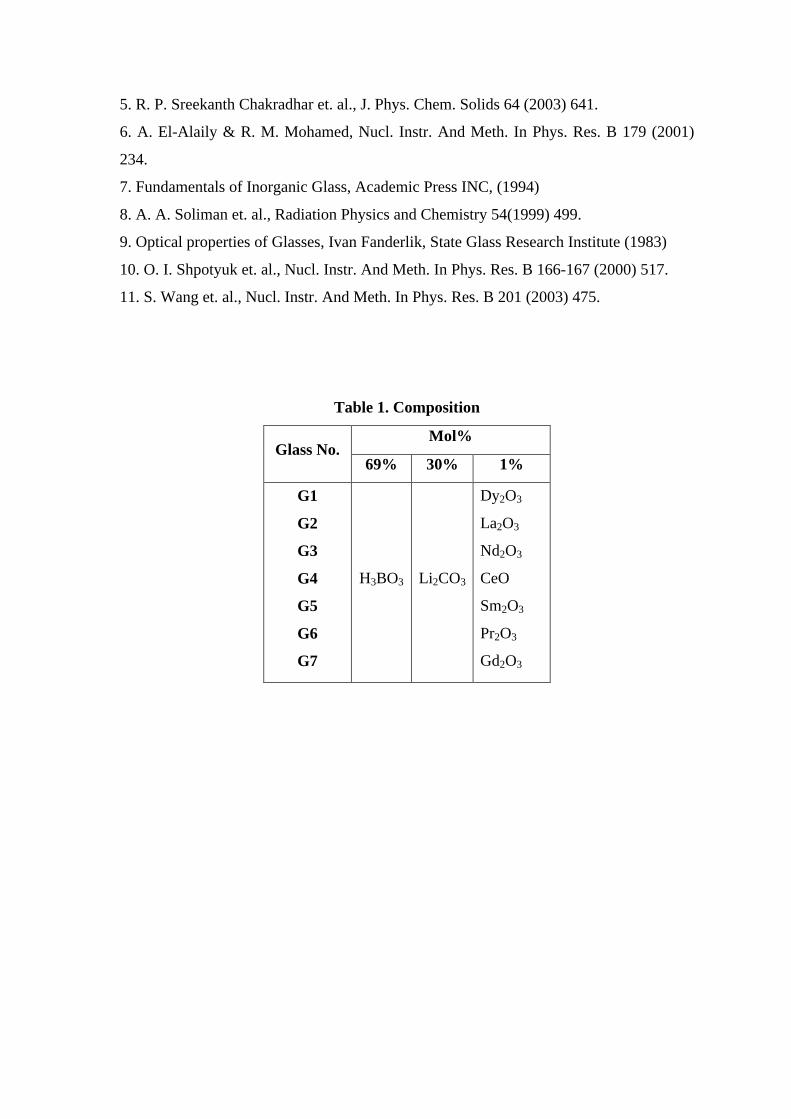
5. R. P. Sreekanth Chakradhar et. al., J. Phys. Chem. Solids 64 (2003) 641.
6. A. El-Alaily & R. M. Mohamed, Nucl. Instr. And Meth. In Phys. Res. B 179 (2001)
234.
7. Fundamentals of Inorganic Glass, Academic Press INC, (1994)
8. A. A. Soliman et. al., Radiation Physics and Chemistry 54(1999) 499.
9. Optical properties of Glasses, Ivan Fanderlik, State Glass Research Institute (1983)
10. O. I. Shpotyuk et. al., Nucl. Instr. And Meth. In Phys. Res. B 166-167 (2000) 517.
11. S. Wang et. al., Nucl. Instr. And Meth. In Phys. Res. B 201 (2003) 475.
Table 1. Composition
Mol% Glass No.
69% 30% 1%
G1
G2
G3
G4
G5
G6
G7
H3BO3 Li2CO3
Dy2O3
La2O3
Nd2O3
CeO
Sm2O3
Pr2O3
Gd2O3
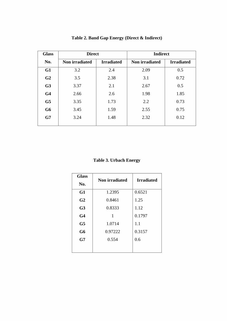
Table 2. Band Gap Energy (Direct & Indirect)
Direct Indirect Glass
No. Non irradiated Irradiated Non irradiated Irradiated
G1
G2
G3
G4
G5
G6
G7
3.2
3.5
3.37
2.66
3.35
3.45
3.24
2.4
2.38
2.1
2.6
1.73
1.59
1.48
2.09
3.1
2.67
1.98
2.2
2.55
2.32
0.5
0.72
0.5
1.85
0.73
0.75
0.12
Table 3. Urbach Energy
Glass
No. Non irradiated Irradiated
G1
G2
G3
G4
G5
G6
G7
1.2395
0.8461
0.8333
1
1.0714
0.97222
0.554
0.6521
1.25
1.12
0.1797
1.1
0.3157
0.6
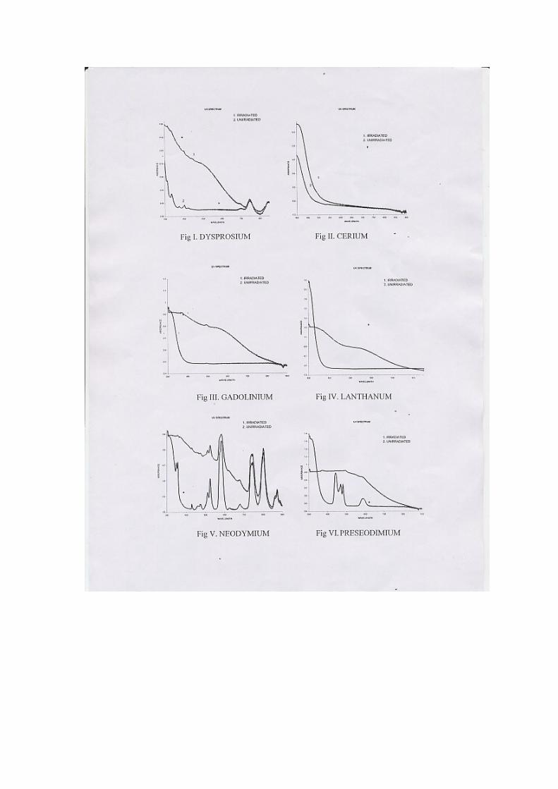

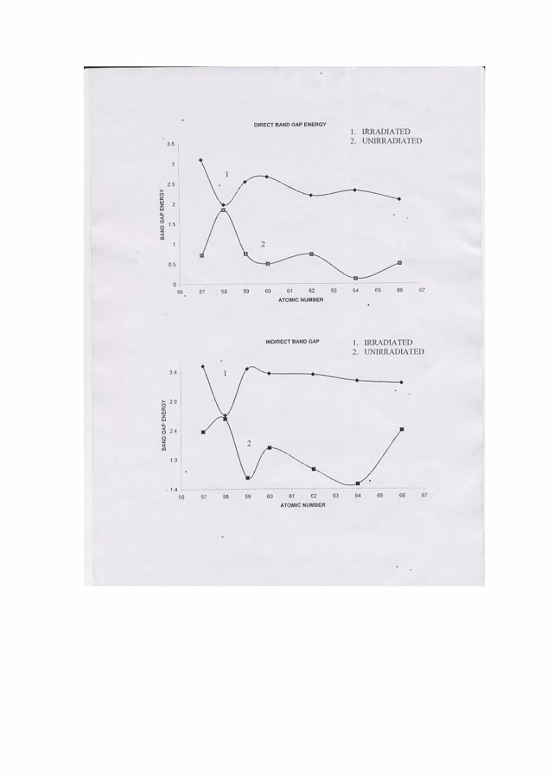
PROBE BEAM DEFLECTION TECHNIQUE APPLIED TO STUDY HEAT DIFFUSION IN POLYANILINE FILMS
Thomas P. Zachariah 1 and T. M A. Rasheed 2 *
1. Department of Physics, Union Christian College, Aluva-2, India; 2. Department of Physics, Cochin University of Science and Technology, Cochin-22, India.
E-mail: [email protected]
Abstract
Undoped and iodine doped polyaniline (PANI) films are prepared by radio frequency (RF) plasma polymerisation technique. Transverse probe beam deflection (PBD) method is used to investigate the effect of variation of reactor pressure and the effect of iodine doping on the thermal diffusivity of these films. * Present affiliation: Department of Physics, King Faisal University, P.B. No.2114, Dammam-31451, Saudi Arabia. 1. INTRODUCTION
Conducting polymer films have been of much interest over the last couple of decades because of their role in diverse fields extending from microelectronics to sensor technology1-5. Many of the studies are concentrated on the conduction mechanisms in these polymers. Most of these polymers are prepared by the conventional chemical or electrochemical synthesis route. Usually such polymer samples are made conducting by a suitable doping process6. In the case of films, plasma polymerization is a widely used technique for the polymerization of organic and inorganic monomers. Among plasma polymerization techniques, RF plasma polymerization enjoys the unique advantage of producing pinhole-free films. But these films are usually of the highly cross-linked type, unlike those obtained from the conventional chemical synthesis route.
In applications where thin films play a significant role, their thermal management is of high priority, as a poor thermal design may result in a device failure. For a proper thermal design, it is desirable to have a prior knowledge of the thermal parameters of the films. An account of the heat diffusion in a film can be adequately represented by its thermal diffusivity value. It is defined as the ratio of thermal conductivity to the thermal capacity per unit volume, given by k Cα ρ= ; where k , ρ and
C are the respective thermal conductivity, density and specific heat capacity values of the material. There are several well-established methods for the thermal characterization of a substance and some of these are nondestructive. Photothermal methods are, in general, noninvasive. Of the various photothermal methods in use, photothermal beam deflection (also called probe beam deflection) technique is a superior noncontact nondestructive technique for optical and thermal characterization7-9. Its contactless nature makes it particularly suitable for thin films and single
crystals. Thermal diffusivity measurements constitute one of the most successful applications of the photothermal technique. This method can be applied to both bulk and thin film samples. This technique is based on the periodic heating produced by an intensity-modulated laser beam (called the pump beam) focused on to the sample surface. The induced oscillating temperature distribution gives rise to thermal waves in the sample. These waves are of the same frequency as the modulating pump beam and have wavelengths determined by the modulating frequency and the thermal diffusivity of the sample. The thermal waves propagating along the surface of the sample gives rise to a refractive index gradient in the fluid medium adjacent to the sample surface. A second laser beam (probe beam) directed parallel to the sample surface is deflected at the same frequency as the thermal wave. The magnitude and phase of the deflection is closely related to the thermal wave. The thermal diffusivity of the sample can be determined from the phase data.
Polyaniline (PANI) in the bulk as well as film form is a widely probed conducting polymer because of its applications in diverse fields. Among its various forms, only one form which is the partially oxidized protonated emaraldine, is conducting in the undoped condition. The electrical conductivity of PANI is tailored by different doping techniques10. It is well established that doping increases the electrical conductivity by several orders of magnitude. Iodine doping is a popular technique used in the case of PANI. The variation of heat diffusion properties with doping, though relevant in thermal design, is not much explored. Also in the case of thin polymer films, the preparation conditions play an important role in determining their structure and properties. Although the film structure and composition depend primarily on the monomer, in RF plasma polymerization, the deposition parameters such as monomer flow rate, the reactor pressure, RF power and substrate temperature are equally relevant in determining the structure as well as the thermo-
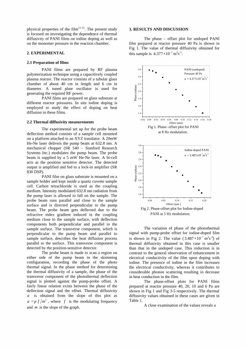
physical properties of the film11-12. The present study is focused on investigating the dependence of thermal diffusivity of PANI films on iodine doping as well as on the monomer pressure in the reaction chamber. 2. EXPERIMENTAL 2.1 Preparation of films
PANI films are prepared by RF plasma polymerization technique using a capacitively coupled plasma reactor. The reactor consists of a tubular glass chamber of about 40 cm in length and 6 cm in diameter. A tuned plate oscillator is used for generating the required RF power.
PANI films are prepared on glass substrate at different reactor pressures. In situ iodine doping is employed to study the effect of doping on heat diffusion in these films. 2.2 Thermal diffusivity measurements
The experimental set up for the probe beam deflection method consists of a sample cell mounted on a platform attached to an XYZ translator. A 20mW He-Ne laser delivers the pump beam at 632.8 nm. A mechanical chopper (SR 540 – Stanford Research Systems Inc.) modulates the pump beam. The probe beam is supplied by a 5 mW He-Ne laser. A bi-cell acts as the position sensitive detector. The detected output is amplified and fed to a lock-in amplifier (SR 830 DSP). PANI film on glass substrate is mounted on a sample holder and kept inside a quartz cuvette sample cell. Carbon tetrachloride is used as the coupling medium. Intensity modulated 632.8 nm radiation from the pump laser is allowed to fall on the sample. The probe beam runs parallel and close to the sample surface and is directed perpendicular to the pump beam. The probe beam gets deflected due to the refractive index gradient induced in the coupling medium close to the sample surface, with deflection components both perpendicular and parallel to the sample surface. The transverse component, which is perpendicular to the pump beam and parallel to sample surface, describes the heat diffusion process parallel to the surface. This transverse component is detected by the position-sensitive detector. The probe beam is made to scan a region on either side of the pump beam in the skimming configuration, recording the phase of the photo thermal signal. In the phase method for determining the thermal diffusivity of a sample, the phase of the transverse component of the photothermal deflection signal is plotted against the pump-probe offset. A fairly linear relation exists between the phase of the deflection signal and the offset. Thermal diffusivity α is obtained from the slope of this plot as
2f mα π= , where f is the modulating frequency
and m is the slope of the graph.
3. RESULTS AND DISCUSSION
The phase – offset plot for undoped PANI film prepared at reactor pressure 40 Pa is shown in Fig 1. The value of thermal diffusivity obtained for this sample is 74.377 10−× m2s-1.
-0.02 0.00 0.02 0.04 0.06 0.08 0.10 0.12 0.14 0.16 0.18
1.4
1.6
1.8
2.0
2.2
2.4
2.6
Fig 1. Phase- offset plot for PANI at 8 Hz modulation.
PANI (undoped)Pressure 40 Pa
α = 4.377x10⁻⁷
m2s
-1
Phas
e (r
adia
n)
Offset (mm)
0.00 0.05 0.10 0.15 0.20
1.6
1.8
2.0
2.2
2.4
2.6
2.8
3.0
Fig 2. Phase-offset plot for Iodine-doped PANI at 5 Hz modulation.
Iodine-doped PANI
α = 3.487x10⁻⁷
m2s
-1
Phas
e (r
adia
n)
Offset (mm )
The variation of phase of the photothermal
signal with pump-probe offset for iodine-doped film is shown in Fig 2. The value ( 73.487 10−× m2s-1) of thermal diffusivity obtained in this case is smaller than that in the undoped case. This reduction is in contrast to the general observation of enhancement in electrical conductivity of the film upon doping with iodine. The presence of iodine in the film increases the electrical conductivity, whereas it contributes to considerable phonon scattering resulting in decrease in heat conduction in the film.
The phase-offset plots for PANI films prepared at reactor pressure 40, 20, 10 and 6 Pa are shown in Fig 1 and Fig 3-5 respectively. The thermal diffusivity values obtained in these cases are given in Table 1.
A close examination of the values reveals a
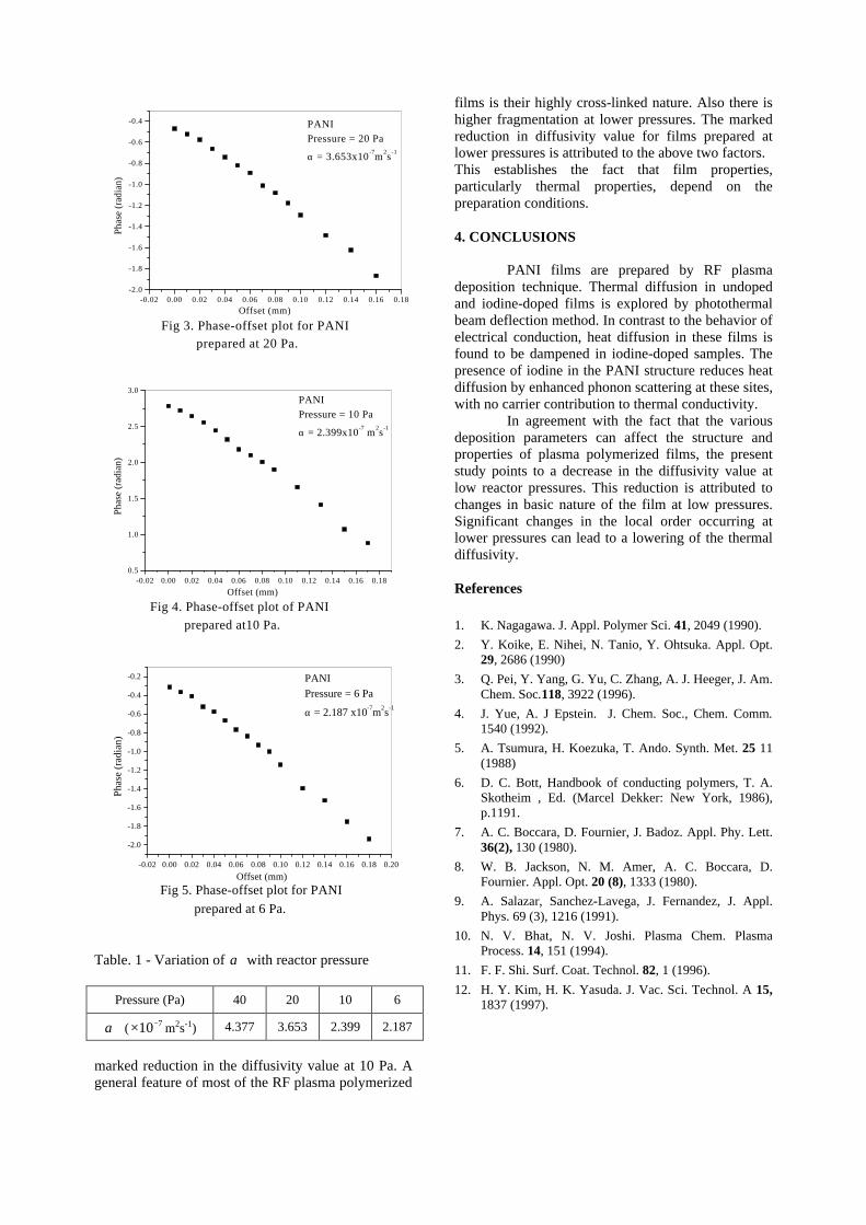
-0.02 0.00 0.02 0.04 0.06 0.08 0.10 0.12 0.14 0.16 0.18-2.0
-1.8
-1.6
-1.4
-1.2
-1.0
-0.8
-0.6
-0.4
Fig 3. Phase-offset plot for PANI prepared at 20 Pa.
PANIPressure = 20 Pa
α = 3.653x10⁻⁷
m2s
-1
Phas
e (r
adia
n)
Offset (mm)
-0.02 0.00 0.02 0.04 0.06 0.08 0.10 0.12 0.14 0.16 0.180.5
1.0
1.5
2.0
2.5
3.0
Fig 4. Phase-offset plot of PANI
prepared at10 Pa.
PANIPressure = 10 Pa
α = 2.399x10⁻⁷
m2s
-1
Phas
e (r
adia
n)
Offset (mm)
-0.02 0.00 0.02 0.04 0.06 0.08 0.10 0.12 0.14 0.16 0.18 0.20
-2.0
-1.8
-1.6
-1.4
-1.2
-1.0
-0.8
-0.6
-0.4
-0.2
Fig 5. Phase-offset plot for PANI
prepared at 6 Pa.
PANIPressure = 6 Pa
α = 2.187 x10⁻⁷m2s-1
Phas
e (r
adia
n)
Offset (mm)
Table. 1 - Variation of α with reactor pressure
Pressure (Pa) 40 20 10 6
α ( 710−× m2s-1) 4.377 3.653 2.399 2.187
marked reduction in the diffusivity value at 10 Pa. A general feature of most of the RF plasma polymerized
films is their highly cross-linked nature. Also there is higher fragmentation at lower pressures. The marked reduction in diffusivity value for films prepared at lower pressures is attributed to the above two factors. This establishes the fact that film properties, particularly thermal properties, depend on the preparation conditions. 4. CONCLUSIONS PANI films are prepared by RF plasma deposition technique. Thermal diffusion in undoped and iodine-doped films is explored by photothermal beam deflection method. In contrast to the behavior of electrical conduction, heat diffusion in these films is found to be dampened in iodine-doped samples. The presence of iodine in the PANI structure reduces heat diffusion by enhanced phonon scattering at these sites, with no carrier contribution to thermal conductivity. In agreement with the fact that the various deposition parameters can affect the structure and properties of plasma polymerized films, the present study points to a decrease in the diffusivity value at low reactor pressures. This reduction is attributed to changes in basic nature of the film at low pressures. Significant changes in the local order occurring at lower pressures can lead to a lowering of the thermal diffusivity. References 1. K. Nagagawa. J. Appl. Polymer Sci. 41, 2049 (1990).
2. Y. Koike, E. Nihei, N. Tanio, Y. Ohtsuka. Appl. Opt. 29, 2686 (1990)
3. Q. Pei, Y. Yang, G. Yu, C. Zhang, A. J. Heeger, J. Am. Chem. Soc.118, 3922 (1996).
4. J. Yue, A. J Epstein. J. Chem. Soc., Chem. Comm. 1540 (1992).
5. A. Tsumura, H. Koezuka, T. Ando. Synth. Met. 25 11 (1988)
6. D. C. Bott, Handbook of conducting polymers, T. A. Skotheim , Ed. (Marcel Dekker: New York, 1986), p.1191.
7. A. C. Boccara, D. Fournier, J. Badoz. Appl. Phy. Lett. 36(2), 130 (1980).
8. W. B. Jackson, N. M. Amer, A. C. Boccara, D. Fournier. Appl. Opt. 20 (8), 1333 (1980).
9. A. Salazar, Sanchez-Lavega, J. Fernandez, J. Appl. Phys. 69 (3), 1216 (1991).
10. N. V. Bhat, N. V. Joshi. Plasma Chem. Plasma Process. 14, 151 (1994).
11. F. F. Shi. Surf. Coat. Technol. 82, 1 (1996).
12. H. Y. Kim, H. K. Yasuda. J. Vac. Sci. Technol. A 15, 1837 (1997).
1
CURRENT TRANSPORT AND INTERFACE PROPERTIES OF CdTe/CdS THIN FILM HETEROJUNCTION
S.Chandramohan, R.Sathyamoorthy*, S.Lalitha, P.Sudhagar, S.Senthilarasu
R&D Department of Physics, Kongunadu Arts & Science College, Coimbatore – 641 029,Tamil Nadu,
INDIA. * Department of Physics, Kongunadu Arts & Science College, Coimbatore – 641 029,
Tamil Nadu, INDIA. E-mail: [email protected]; [email protected]
ABSTRACT
This paper reports the experimental analysis of the electrical and interface characteristics of CdTe/CdS heterojunction formed by thermal evaporation. Temperature dependent dark current – voltage studies were carried out on Al-CdTe/CdS-Al structure and current transport by thermally assisted tunneling of holes from CdTe into interface states followed by interface recombination has been identified with an activation energy of 0.5 eV. The interface parameters acceptor density, built-in potential, depletion layer width in the vicinity of CdTe/CdS junction and back contact has been calculated from the capacitance-voltage analysis. The frequency dispersion of capacitance has also suggests the presence of a continuous distribution of defect states, leading to a progressive decrease of the response of the defect states to the applied ac voltage. A density of traps has been estimated to be about 9.5x1014 cm-3. INTRODUCTION
Cadmium telluride continuous to be a leading candidate for the development of cost effective photovoltaics for terrestrial applications. The two key properties of this material are its near ideal band gap of 1.45 eV and its high optical absorption coefficient. CdTe solar cells are usually fabricated as heterostructures due to the short optical absorption length and the difficulty in forming a shallow thin film junction with a high conductivity surface layer 1. The heterojunction partner should have a large band gap and good lattice and electron affinity match to minimize interface states and to avoid deleterious conduction band spikes. Among the various heterojunction window materials, CdS with a band gap of 2.4 eV is the most extensively studied and is best-suited for CdTe solar cells due to the fact that these two materials are miscible, and a reaction between them during the cell fabrication process leads to the formation of an interfacial layer CdS1-xTex
2. The formation of this layer is believed to be responsible for lowering the interfacial defect density resulting in high efficiency devices and the maximum-recorded efficiency attained so far is 16.5 % 3. The understanding of electrical conduction through such semiconductor heterojunctions is of basic interest because the performance of the
device is determined by the efficiency of the conduction mechanism. The electrical conduction in these systems cannot be in all cases interpreted by a classical drift-diffusion mechanism. Tunneling through defect states in the interface region is often suggested as a possible conduction path 4. In this paper we have reported the electrical conduction and interface properties of thermally evaporated CdTe/CdS heterojunction. FILM PREPARATION AND CHARACTERIZATION
CdTe/CdS heterojunctions were formed by successive evaporation of CdTe and CdS powder materials (of 99.99+% and 99.995% pure respectively) under a pressure of about 6x10⁻⁶
mbar. The thickness of the films was measured in-situ by quartz crystal thickness monitor and is about 2 ì m for CdTe and 0.1 ì m for CdS. In order to carryout electrical measurements metal-semiconductor-metal structures were formed by evaporating Al metal before and after CdTe/CdS heterojunction was made. The dark current-voltage measurements were made at different temperatures ranging between 297-423 K using digital pico ammeter. The dark capacitance–voltage characteristics were studied at room temperature using digital multifrequency LCR meter (INSTEC LCR 819).
2
RESULTS AND DISCUSSION (a) Current-Voltage characteristics
Current-voltage characteristics as a function of the junction temperature provide valuable information about the junction properties. The forward I-V characteristics are expressed by the standard diode equation
I=I exp (qV/nkT)o (1)
where n is the diode ideality factor, oI is the
reverse saturation current. The current mechanism present was explored from semi-logarithmic plots of the forward dark I-V characteristics at different temperatures. Fig.1 shows such a plot, from which the value of n and
oI has been evaluated by fitting the exponential
data to the eqn (1). The estimated value of n is greater than one for all the temperatures studied and the slope of the curve is temperature dependent. The forward current shows an exponential increase with the applied voltage. However, at high forward potential the characteristics show a linear behaviour which is often attributed to the effect of junction series resistance 1,5.
0 2 4 6 8 1 0- 5
- 4
- 3
- 2
- 1
0
1
J (
A/m
2 )
V ( v o l t s )
2 9 7 K 3 2 3 K 3 4 3 K 3 6 3 K 3 8 3 K 4 0 3 K 4 2 3 K
Fig.1. Log J versus V plot at different temperatures
In order to identify the dominant current transport mechanism through the junction, log
oI was plotted as a function of 1/T and is
illustrated in fig.2. The variation is found to be linear indicating the presence of single transport mechanism in the whole temperature range studied. This is indicative of a thermally
activated phenomenon rather than direct
tunneling for which oI is expressed as
I =I exp (-ÄE/kT)o oo (2)
where ÄE is the thermal activation energy of the
process. From the slope of log oI versus 1000/T
plot the activation energy was calculated to be about 0.5 eV.
2 . 2 2 . 4 2 . 6 2 . 8 3 . 0 3 . 2 3 . 4- 5 . 0
- 4 . 5
- 4 . 0
- 3 . 5
- 3 . 0
- 2 . 5
- 2 . 0
∆∆ E = 0 . 5 0 e V
Log
Jo (
A/m
2 )
1 0 0 0 / T ( K - 1 )
Fig.2. Log Jo vs 1000/T plot showing linear variation of Jo with temperature.
Theoretically, an impurity concentration of 1019-1020 cm-3 is necessary for direct band-to-band tunneling 6,7. However, the density of acceptor states in the CdTe estimated from C-V measurement is about 1015 cm-3. This density is too low to allow single-step tunneling through the energy barrier. Hence, the tunneling might have occurred via the multiple-step process. Junction recombination through the interface states is known to be of particular importance in CdS/CdTe heterojunctions because of the large lattice mismatch (9.7 %) 8. For interface recombination-dominated current transport the value of n should be approximately unity because the carrier density in CdS is much larger than that of CdTe, and the product ÄEn should be around 1.18 eV which is the built-in voltage (Vbi) of the junction 9. Neither of these conditions was met in the present case and hence it is concluded that interface recombination is not the dominant transport mechanism. If recombination through localized states within the CdTe depletion region is dominant, then a plot of
-2.5log (J T ) vs 1000/To should yield an
activation energy approximately equal to half of the CdTe band gap 10,11. The validity of this mechanism seems doubtful since the calculated activation energy of 0.42 eV lies far from the
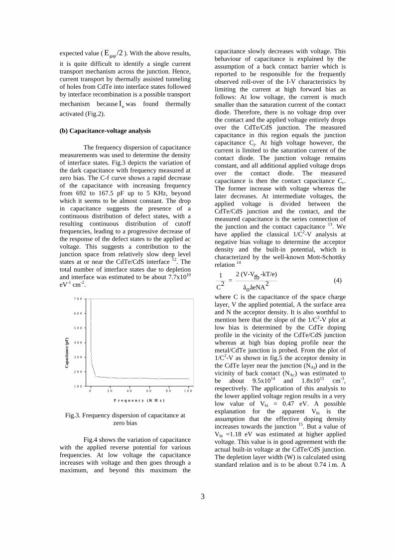
3
expected value ( gapE /2 ). With the above results,
it is quite difficult to identify a single current transport mechanism across the junction. Hence, current transport by thermally assisted tunneling of holes from CdTe into interface states followed by interface recombination is a possible transport
mechanism because oI was found thermally
activated (Fig.2). (b) Capacitance-voltage analysis
The frequency dispersion of capacitance measurements was used to determine the density of interface states. Fig.3 depicts the variation of the dark capacitance with frequency measured at zero bias. The C-f curve shows a rapid decrease of the capacitance with increasing frequency from 692 to 167.5 pF up to 5 KHz, beyond which it seems to be almost constant. The drop in capacitance suggests the presence of a continuous distribution of defect states, with a resulting continuous distribution of cutoff frequencies, leading to a progressive decrease of the response of the defect states to the applied ac voltage. This suggests a contribution to the junction space from relatively slow deep level states at or near the CdTe/CdS interface 12. The total number of interface states due to depletion and interface was estimated to be about 7.7x10¹⁰ eV-1 cm-2.
0 2 0 4 0 6 0 8 0 1 0 01 0 0
2 0 0
3 0 0
4 0 0
5 0 0
6 0 0
7 0 0
Cap
acit
ance
(pF
)
F r e q u e n c y ( K H z )
Fig.3. Frequency dispersion of capacitance at zero bias
Fig.4 shows the variation of capacitance with the applied reverse potential for various frequencies. At low voltage the capacitance increases with voltage and then goes through a maximum, and beyond this maximum the
capacitance slowly decreases with voltage. This behaviour of capacitance is explained by the assumption of a back contact barrier which is reported to be responsible for the frequently observed roll-over of the I-V characteristics by limiting the current at high forward bias as follows: At low voltage, the current is much smaller than the saturation current of the contact diode. Therefore, there is no voltage drop over the contact and the applied voltage entirely drops over the CdTe/CdS junction. The measured capacitance in this region equals the junction capacitance Cj. At high voltage however, the current is limited to the saturation current of the contact diode. The junction voltage remains constant, and all additional applied voltage drops over the contact diode. The measured capacitance is then the contact capacitance Cc. The former increase with voltage whereas the later decreases. At intermediate voltages, the applied voltage is divided between the CdTe/CdS junction and the contact, and the measured capacitance is the series connection of the junction and the contact capacitance 13. We have applied the classical 1/C2-V analysis at negative bias voltage to determine the acceptor density and the built-in potential, which is characterized by the well-known Mott-Schottky relation 14
2 (V-V -kT/e)1 fb = 2 2C å åeNAo (4)
where C is the capacitance of the space charge layer, V the applied potential, A the surface area and N the acceptor density. It is also worthful to mention here that the slope of the 1/C2-V plot at low bias is determined by the CdTe doping profile in the vicinity of the CdTe/CdS junction whereas at high bias doping profile near the metal/CdTe junction is probed. From the plot of 1/C2-V as shown in fig.5 the acceptor density in the CdTe layer near the junction (NAj) and in the vicinity of back contact (NAc) was estimated to be about 9.5x10¹⁴ and 1.8x1015 cm-3, respectively. The application of this analysis to the lower applied voltage region results in a very low value of Vbi = 0.47 eV. A possible explanation for the apparent Vbi is the assumption that the effective doping density increases towards the junction 15. But a value of Vbi =1.18 eV was estimated at higher applied voltage. This value is in good agreement with the actual built-in voltage at the CdTe/CdS junction. The depletion layer width (W) is calculated using standard relation and is to be about 0.74 ì m. A
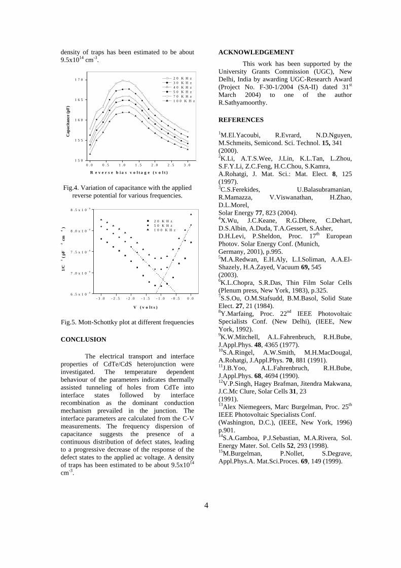
4
density of traps has been estimated to be about 9.5x1014 cm-3.
0 . 0 0 . 5 1 . 0 1 . 5 2 . 0 2 . 5 3 . 01 5 0
1 5 5
1 6 0
1 6 5
1 7 0
Cap
acit
ance
(pF
)
R e v e r s e b i a s v o l t a g e ( v o l t )
2 0 K H z 3 0 K H z 4 0 K H z 5 0 K H z 7 0 K H z 1 0 0 K H z
Fig.4. Variation of capacitance with the applied reverse potential for various frequencies.
- 3 . 0 - 2 . 5 - 2 . 0 - 1 . 5 - 1 . 0 - 0 . 5 0 . 06 . 5 x 1 0
- 8
7 . 0 x 1 0- 8
7 . 5 x 1 0- 8
8 . 0 x 1 0 - 8
8 . 5 x 1 0 - 8
1/C
2 (
pF
-2 c
m4 )
V ( v o l t s )
2 0 K H z 5 0 K H z 1 0 0 K H z
Fig.5. Mott-Schottky plot at different frequencies CONCLUSION The electrical transport and interface properties of CdTe/CdS heterojunction were investigated. The temperature dependent behaviour of the parameters indicates thermally assisted tunneling of holes from CdTe into interface states followed by interface recombination as the dominant conduction mechanism prevailed in the junction. The interface parameters are calculated from the C-V measurements. The frequency dispersion of capacitance suggests the presence of a continuous distribution of defect states, leading to a progressive decrease of the response of the defect states to the applied ac voltage. A density of traps has been estimated to be about 9.5x1014 cm-3.
ACKNOWLEDGEMENT
This work has been supported by the University Grants Commission (UGC), New Delhi, India by awarding UGC-Research Award (Project No. F-30-1/2004 (SA-II) dated 31st March 2004) to one of the author R.Sathyamoorthy. REFERENCES 1M.El.Yacoubi, R.Evrard, N.D.Nguyen, M.Schmeits, Semicond. Sci. Technol. 15, 341 (2000). 2K.Li, A.T.S.Wee, J.Lin, K.L.Tan, L.Zhou, S.F.Y.Li, Z.C.Feng, H.C.Chou, S.Kamra, A.Rohatgi, J. Mat. Sci.: Mat. Elect. 8, 125 (1997). 3C.S.Ferekides, U.Balasubramanian, R.Mamazza, V.Viswanathan, H.Zhao, D.L.Morel, Solar Energy 77, 823 (2004). 4X.Wu, J.C.Keane, R.G.Dhere, C.Dehart, D.S.Albin, A.Duda, T.A.Gessert, S.Asher, D.H.Levi, P.Sheldon, Proc. 17th European Photov. Solar Energy Conf. (Munich, Germany, 2001), p.995. 5M.A.Redwan, E.H.Aly, L.I.Soliman, A.A.El-Shazely, H.A.Zayed, Vacuum 69, 545 (2003). 6K.L.Chopra, S.R.Das, Thin Film Solar Cells (Plenum press, New York, 1983), p.325. 7S.S.Ou, O.M.Stafsudd, B.M.Basol, Solid State Elect. 27, 21 (1984). 8Y.Marfaing, Proc. 22nd IEEE Photovoltaic Specialists Conf. (New Delhi), (IEEE, New York, 1992). 9K.W.Mitchell, A.L.Fahrenbruch, R.H.Bube, J.Appl.Phys. 48, 4365 (1977). 10S.A.Ringel, A.W.Smith, M.H.MacDougal, A.Rohatgi, J.Appl.Phys. 70, 881 (1991). 11J.B.Yoo, A.L.Fahrenbruch, R.H.Bube, J.Appl.Phys. 68, 4694 (1990). 12V.P.Singh, Hagey Brafman, Jitendra Makwana, J.C.Mc Clure, Solar Cells 31, 23 (1991). 13Alex Niemegeers, Marc Burgelman, Proc. 25th IEEE Photovoltaic Specialists Conf. (Washington, D.C.), (IEEE, New York, 1996) p.901. 14S.A.Gamboa, P.J.Sebastian, M.A.Rivera, Sol. Energy Mater. Sol. Cells 52, 293 (1998). 15M.Burgelman, P.Nollet, S.Degrave, Appl.Phys.A. Mat.Sci.Proces. 69, 149 (1999).
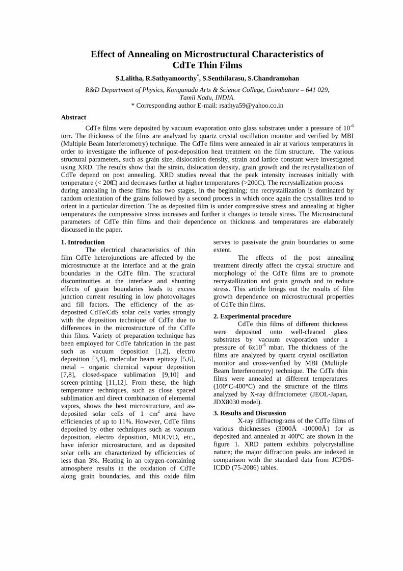
Effect of Annealing on Microstructural Characteristics of CdTe Thin Films
S.Lalitha, R.Sathyamoorthy*, S.Senthilarasu, S.Chandramohan
R&D Department of Physics, Kongunadu Arts & Science College, Coimbatore – 641 029, Tamil Nadu, INDIA.
* Corresponding author E-mail: [email protected]
Abstract
CdTe films were deposited by vacuum evaporation onto glass substrates under a pressure of 10-6
torr. The thickness of the films are analyzed by quartz crystal oscillation monitor and verified by MBI (Multiple Beam Interferometry) technique. The CdTe films were annealed in air at various temperatures in order to investigate the influence of post-deposition heat treatment on the film structure. The various structural parameters, such as grain size, dislocation density, strain and lattice constant were investigated using XRD. The results show that the strain, dislocation density, grain growth and the recrystallization of CdTe depend on post annealing. XRD studies reveal that the peak intensity increases initially with temperature (< 200C) and decreases further at higher temperatures (>200C). The recrystallization process during annealing in these films has two stages, in the beginning; the recrystallization is dominated by random orientation of the grains followed by a second process in which once again the crystallites tend to orient in a particular direction. The as deposited film is under compressive stress and annealing at higher temperatures the compressive stress increases and further it changes to tensile stress. The Microstructural parameters of CdTe thin films and their dependence on thickness and temperatures are elaborately discussed in the paper.
1. Introduction The electrical characteristics of thin
film CdTe heterojunctions are affected by the microstructure at the interface and at the grain boundaries in the CdTe film. The structural discontinuities at the interface and shunting effects of grain boundaries leads to excess junction current resulting in low photovoltages and fill factors. The efficiency of the as-deposited CdTe/CdS solar cells varies strongly with the deposition technique of CdTe due to differences in the microstructure of the CdTe thin films. Variety of preparation technique has been employed for CdTe fabrication in the past such as vacuum deposition [1,2], electro deposition [3,4], molecular beam epitaxy [5,6], metal – organic chemical vapour deposition [7,8], closed-space sublimation [9,10] and screen-printing [11,12]. From these, the high temperature techniques, such as close spaced sublimation and direct combination of elemental vapors, shows the best microstructure, and as-deposited solar cells of 1 cm2 area have efficiencies of up to 11%. However, CdTe films deposited by other techniques such as vacuum deposition, electro deposition, MOCVD, etc., have inferior microstructure, and as deposited solar cells are characterized by efficiencies of less than 3%. Heating in an oxygen-containing atmosphere results in the oxidation of CdTe along grain boundaries, and this oxide film
serves to passivate the grain boundaries to some extent.
The effects of the post annealing treatment directly affect the crystal structure and morphology of the CdTe films are to promote recrystallization and grain growth and to reduce stress. This article brings out the results of film growth dependence on microstructural properties of CdTe thin films.
2. Experimental procedure CdTe thin films of different thickness
were deposited onto well-cleaned glass substrates by vacuum evaporation under a pressure of 6x10⁻⁶ mbar. The thickness of the films are analyzed by quartz crystal oscillation monitor and cross-verified by MBI (Multiple Beam Interferometry) technique. The CdTe thin films were annealed at different temperatures (100°C-400°C) and the structure of the films analyzed by X-ray diffractometer (JEOL-Japan, JDX8030 model).
3. Results and Discussion X-ray diffractograms of the CdTe films of
various thicknesses (3000Å -10000Å) for as deposited and annealed at 400ºC are shown in the figure 1. XRD pattern exhibits polycrystalline nature; the major diffraction peaks are indexed in comparison with the standard data from JCPDS-ICDD (75-2086) tables.
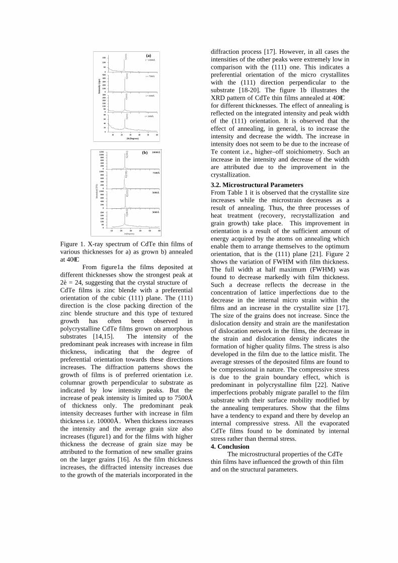
10 20 30 40 50 60
0
20
40
60
80
C(1
11)
t = 3000Å
2θθ (Degrees)
0
50
100
150
200
250
300
C(1
11)
t = 5000Å
0
100
200
300
400
500
C(1
11)
t = 7500Å
Inte
nsit
y (c
ps)
0
50
100
150(a)
C(1
11)
t = 10000Å
10 20 30 40 50 60
0
50
100
150
200
250
C(1
11)
3000Å
2θ(Degrees)
0
200
400
600
800
1000
C(1
11)
5000Å
0
200
400
600
800
1000
C(1
11)
7500Å
Inte
nsity
(CPS
)
0
200
400
600
800
1000
1200 (b)
C(1
11) 10000Å
Figure 1. X-ray spectrum of CdTe thin films of various thicknesses for a) as grown b) annealed at 400C From figure1a the films deposited at different thicknesses show the strongest peak at 2è = 24, suggesting that the crystal structure of CdTe films is zinc blende with a preferential orientation of the cubic (111) plane. The (111) direction is the close packing direction of the zinc blende structure and this type of textured growth has often been observed in polycrystalline CdTe films grown on amorphous substrates [14,15]. The intensity of the predominant peak increases with increase in film thickness, indicating that the degree of preferential orientation towards these directions increases. The diffraction patterns shows the growth of films is of preferred orientation i.e. columnar growth perpendicular to substrate as indicated by low intensity peaks. But the increase of peak intensity is limited up to 7500Å of thickness only. The predominant peak intensity decreases further with increase in film thickness i.e. 10000Å. When thickness increases the intensity and the average grain size also increases (figure1) and for the films with higher thickness the decrease of grain size may be attributed to the formation of new smaller grains on the larger grains [16]. As the film thickness increases, the diffracted intensity increases due to the growth of the materials incorporated in the
diffraction process [17]. However, in all cases the intensities of the other peaks were extremely low in comparison with the (111) one. This indicates a preferential orientation of the micro crystallites with the (111) direction perpendicular to the substrate [18-20]. The figure 1b illustrates the XRD pattern of CdTe thin films annealed at 400C for different thicknesses. The effect of annealing is reflected on the integrated intensity and peak width of the (111) orientation. It is observed that the effect of annealing, in general, is to increase the intensity and decrease the width. The increase in intensity does not seem to be due to the increase of Te content i.e., higher–off stoichiometry. Such an increase in the intensity and decrease of the width are attributed due to the improvement in the crystallization.
3.2. Microstructural Parameters From Table 1 it is observed that the crystallite size increases while the microstrain decreases as a result of annealing. Thus, the three processes of heat treatment (recovery, recrystallization and grain growth) take place. This improvement in orientation is a result of the sufficient amount of energy acquired by the atoms on annealing which enable them to arrange themselves to the optimum orientation, that is the (111) plane [21]. Figure 2 shows the variation of FWHM with film thickness. The full width at half maximum (FWHM) was found to decrease markedly with film thickness. Such a decrease reflects the decrease in the concentration of lattice imperfections due to the decrease in the internal micro strain within the films and an increase in the crystallite size [17]. The size of the grains does not increase. Since the dislocation density and strain are the manifestation of dislocation network in the films, the decrease in the strain and dislocation density indicates the formation of higher quality films. The stress is also developed in the film due to the lattice misfit. The average stresses of the deposited films are found to be compressional in nature. The compressive stress is due to the grain boundary effect, which is predominant in polycrystalline film [22]. Native imperfections probably migrate parallel to the film substrate with their surface mobility modified by the annealing temperatures. Show that the films have a tendency to expand and there by develop an internal compressive stress. All the evaporated CdTe films found to be dominated by internal stress rather than thermal stress. 4. Conclusion The microstructural properties of the CdTe thin films have influenced the growth of thin film and on the structural parameters.
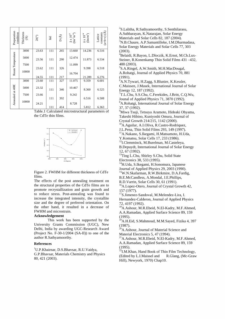
Prep
arat
ion
cond
ition
Thi
ckne
ss
(Å)
2è(°
)
hkl
D (
Å)
å x
10-4
(lin
-2m
-4)
ä x
1014
(l
in/m
2 )
Lat
tice
cons
tant
s (a
=b=
c) (
Å)
Roo
m T
empe
ratu
re 3000
5000
7500
10000
23.63
23.56
23.62
24.55
111
111
111
111
265
290
326
217
13.660
12.474
11.099
16.704
14.236
11.873
9.398
21.289
6.516
6.534
6.518
6.276
Ann
eale
d at
400
C 3000
5000
7500
10000
23.60
23.32
23.66
24.21
111
111
111
111
327
346
392
414
11.075
10.467
9.242
8.728
9.359
8.360
6.516
5.812
6.601
6.525
6.508
6.363
Table.1 Calculated microstructural parameters of the CdTe thin films.
2000 4000 6000 8000 10000
3.5
4.0
4.5
5.0
5.5
6.0
FWH
M (
10-3
)
2θ (Degrees)
As Grown Annealed
Figure 2. FWHM for different thickness of CdTe films. The effects of the post annealing treatment on the structural properties of the CdTe films are to promote recrystallization and grain growth and to reduce stress. Post-annealing was found to increase the integrated intensity, the crystallite size and the degree of preferred orientation. On the other hand, it resulted in a decrease of FWHM and microstrain. Acknowledgement This work has been supported by the University Grants Commission (UGC), New Delhi, India by awarding UGC-Research Award (Project No. F-30-1/2004 (SA-II)) to one of the author R.Sathyamoorthy.
References 1U.P.Khairnar, D.S.Bhavsar, R.U.Vaidya, G.P.Bhavsar, Materials Chemistry and Physics 80, 421 (2003).
2S.Lalitha, R.Sathyamoorthy, S.Senthilarasu, A.Subbarayan, K.Natarajan, Solar Energy Materials and Solar Cells 82, 187 (2004). 3N.B.Chaure, A.P.Samantilleke, I.M.Dharmadasa, Solar Energy Materials and Solar Cells 77, 303 (2003). 4Belaidi, R.Bayon, L.Dloczik, K.Ernst, M.Ch.Lux-Steiner, R.Konenkamp Thin Solid Films 431 –432, 488 (2003). 5S.A.Ringel, A.W.Smith, M.H.MacDougal, A.Rohatgi, Journal of Applied Physics 70, 881 (1991). 6A.N.Tywari, H.Zagg, S.Blunier, K.Kessler, C.Maissen, J.Masek, International Journal of Solar Energy 12, 187 (1992). 7T.L.Chu, S.S.Chu, C.Ferekides, J.Britt, C.Q.Wu, Jounal of Applied Physics 71, 3870 (1992). 8A.Rohatgi, International Journal of Solar Energy 37, 37 (1992). 9Miwa Tsuji, Tetsuya Aramoto, Hideaki Ohyama, Takeshi Hibino, Kuniyoshi Omura, Journal of Crystal Growth 214/215, 1142 (2000). 10A.Aguilar, A.I.Oliva, R.Castro-Rodriquez, J.L.Pena, Thin Solid Films 293, 149 (1997). 11A.Nakano, S.Ikegami, H.Matsumoto, H.Uda, Y.Komatsu, Solar Cells 17, 233 (1986). 12I.Clemminck, M.Burelman, M.Casteleya, B.Depuydt, International Journal of Solar Energy 12, 67 (1992). 13Ting L.Chu, Shirley S.Chu, Solid State Electronics 38, 533 (1995). 14H.Uda, S.Ikegami, H.Sonomura, Japanese Journal of Applied Physics 29, 2003 (1990). 15W.N.Skafarman, R.W.Birkmire, D.A.Fardig, B.E.McCandless, A.Mondal, J.E.Phillips, R.D.Varrin, Solar Cells 30, 61 (1991). 16A.Lopez-Otero, Journal of Crystal Growth 42, 157 (1977). 17S.Jimenez-Sandoval, M.Melendez-Lira, I. Hernandez-Calderon, Journal of Applied Physics 72, 4197 (1992). 18A.Ashour, M.R.Ebeid, N.El-Kadry, M.F.Ahmed, A.A.Ramadan, Applied Surface Science 89, 159 (1995). 19A.H.Eid, S.Mahmoud, M.M.Sayed, Fizika 4, 397 (1987). 20A.Ashour, Journal of Material Science and Material Electronics 5, 47 (1994). 21A.Ashour, M.R.Ebeid, N.El-Kadry, M.F.Ahmed, A.A.Ramadan, Applied Surface Science 89, 159 (1995). 22I.M.Khan, Hand Book of Thin Film Technology, (Edited by L.I.Maissel and R.Glang, (Mc-Graw Hill), Newyork, 1970) Chap10.
Effect of swift heavy ion irradiation on the structural and optical
properties of CdS thin films deposited by modified chemical bath
deposition MCBD.
R.R.Ahirea, S.D.Chavhanb, F. Singhc, A. Tripathic, D.Phased, J.C.Vyase and
R. P.Sharmab* bThin Film and Semiconductor Laboratory, Dept. of Physics, G.T.Patil College, Nandurbar - 425412. India
a On leave under FIP. UGC Xth plan, S.G.Patil College Sakri-424304 India c Nuclear Science Centre, New Delhi – 110067 India.
dUGC-DAE Consortium for scientific research- Indore eBhaba Atomic Research Centre, Anushakti Nagar- Mumbai.
Abstract
CdS thin films have been grown using modified chemical bath deposition
(MCBD). The condition for the formation of good quality films such as concentration,
pH of anionic and cationic precursor solutions, immersion and rinsing times and
immersion cycles were optimized. The deposited films have been annealed at 3000C for
1h in air and characterized by EDAX, AFM and XRD. EDAX analysis revealed that film
has same elemental composition as initial taken in solution. The surface roughness rm =
3.16 nm of the film was examined by AFM. The effect of swift heavy ion irradiation on
the structural and optical properties of thin films has been investigated in an Ag and Au
ion irradiations with doses 5 x 10¹² ions/cm2. XRD studies show the as-deposited film
has cubic structure and it turns to hexagonal after annealing, Au and Ag ion irradiations.
The estimated optical bandgap energies for as deposited, annealed, Au and Ag ion
irradiated CdS thin films are 2.45 eV, 2.38 eV, 2.21 eV and 2.11 eV respectively
Keywords: Thin Films, Ion Irradiation, Chemical Bath Deposition, AFM, EDAX, X-ray
Diffraction, optical band gap.
•• Corresponding author: E-mail address [email protected]
1. Introduction:
Cadmium sulfied (CdS) thin films have been employed in solar cells [1,2],
electrochemical cell [3], gas sensor [4], photosensor [5], thin films were prepared using
various chemical deposition methods including elelctrodeposition [6], chemical bath
deposition [7,8], spray pyrolysis [9], solution growth [5], screen printing [10] and SILAR
[11]. The new trends of investigations are produced the defects by high-energy radiations
in semiconductors have becomes an important area of research and development in view
of opto-electronic devices. The major advantage of high-energy irradiation is precise
control over the spatial distribution of defects. The few reports are available on the
influence of high-energy ion irradiation on II-VI compound semiconductors like CdS,
CdSe, and CdTe etc. [12-14]. Exposure to the light and other radiation that excites
electron hole pair produced structural changes in nearly all chalcogenide glasses and
amorphous films. These results change in the physical and chemical properties such as
structural and optical properties of material [15].
Recently, deposition of CdS thin film was carried out by MCBD methods [18]. In
this method, glass substrates are immersed in solution containing metallic ions and then
into solution containing chalcogen ions. Repetition of such immersion in metallic ions
and chalcogen ions results into film formation on the substrate. Preparative conditions
such as concentration, immersion cycles, immersion time, rinsing time and temperature
are optimized to get good quality and well adherent CdS thin films onto glass substrates.
The present paper is described new results on changes of structural and optical
properties of MBCD CdS thin films by swift ion irradiation.
2. Experimental:
The modified chemical bath deposition (MCBD) is mainly based on immersion of
substrate into separate cation and anion precursor solution and rinsing between every
immersion with ion exchange water to avoid homogenous precipitation. The CdS thin
films were deposited by MCBD onto precleaned glass substrates. The process involved
following procedure. The Cd2+ ions in solution were released from the cadmium acetate
[(CH3COO)2Cd2H2O] with 0.06 M concentration of solution [pH ~ 11] i.e. cationic
precursor. The S2- ions have been released from the sodium sulfied (Na2S.H2O) solution
having 0.1M concentration (pH ~ 11). CdS films were deposited by surface adsorption
and chemical reaction at room temperature by immersing the substrates in the above
cationic and anionic precursors. The substrates were rinsed in deionised water for 40 sec
to remove loosely bound or excess ions after each immersion.
Film thickness of thin film was determined by weight difference method using
sensitive microbalance and assumptions was made that the density of film is equal to that
of the bulk material of CdS (4.8g/cm3). As deposited film was annealed at 3000C for 1h,
in air. The chemical compositions of annealed films have been confirmed by EDAX and
surface morphology by SEM (Oxford Instrument analytical Limited 2000). The AFM
unit (Vecco digital instrument, NSC, New Delhi, India) was used to study surface
roughness of the films. The annealed CdS thin film of about 1cm2 area was then exposed
to swift heavy ion radiation using 15 UD Pelletron, NSC, New Delhi, India. CdS thin
films were irradiated with 100 MeV, 197 Au 8+ and 107 Ag8+ ions (5 x 10¹² ions/cm2).
The crystal structure of unirradiated (as-deposited and air annealed) and irradiated
films was determined with Bruker AXS Germany, (Model D8 Advance, NSC, New
Delhi, India) X-ray diffractometer with CuKá target. The optical absorption spectra were
recorded on UV-VIS spectrophotometer (Systronic-117) within wavelength range 350-
1000nm.
3. Results and discussion:
3.1 Optimization of preparative parameters:
Fig.1a shows plot of film thickness against concentration of cadmium acetate. The
CdS film formation starts from concentration of 0.02 M of cadmium acetate, when ionic
product exceeds than the solubility product and reaches maximum film thickness value at
concentration 0.06M after which film thickness goes on decreasing which may be due to
formation of outer porous layer as discussed by Desai and Lokhande [19].
Fig.1b shows the variation of film thickness with number of immersion cycles for
optimized concentration of cadmium acetate (0.06) and sodium sulfied (0.1M). The film
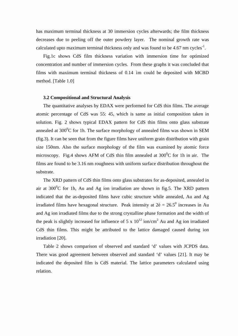
has maximum terminal thickness at 30 immersion cycles afterwards; the film thickness
decreases due to peeling off the outer powdery layer. The nominal growth rate was
calculated upto maximum terminal thickness only and was found to be 4.67 nm cycles-1.
Fig.1c shows CdS film thickness variation with immersion time for optimized
concentration and number of immersion cycles. From these graphs it was concluded that
films with maximum terminal thickness of 0.14 ìm could be deposited with MCBD
method. [Table 1.0]
3.2 Compositional and Structural Analysis
The quantitative analyses by EDAX were performed for CdS thin films. The average
atomic percentage of CdS was 55: 45, which is same as initial composition taken in
solution. Fig. 2 shows typical EDAX pattern for CdS thin films onto glass substrate
annealed at 3000C for 1h. The surface morphology of annealed films was shown in SEM
(fig.3). It can be seen that from the figure films have uniform grain distribution with grain
size 150nm. Also the surface morphology of the film was examined by atomic force
microscopy. Fig.4 shows AFM of CdS thin film annealed at 3000C for 1h in air. The
films are found to be 3.16 nm roughness with uniform surface distribution throughout the
substrate.
The XRD pattern of CdS thin films onto glass substrates for as-deposited, annealed in
air at 3000C for 1h, Au and Ag ion irradiation are shown in fig.5. The XRD pattern
indicated that the as-deposited films have cubic structure while annealed, Au and Ag
irradiated films have hexagonal structure. Peak intensity at 2è = 26.50 increases in Au
and Ag ion irradiated films due to the strong crystalline phase formation and the width of
the peak is slightly increased for influence of 5 x 10¹² ion/cm2 Au and Ag ion irradiated
CdS thin films. This might be attributed to the lattice damaged caused during ion
irradiation [20].
Table 2 shows comparison of observed and standard ‘d’ values with JCPDS data.
There was good agreement between observed and standard ‘d’ values [21]. It may be
indicated the deposited film is CdS material. The lattice parameters calculated using
relation.
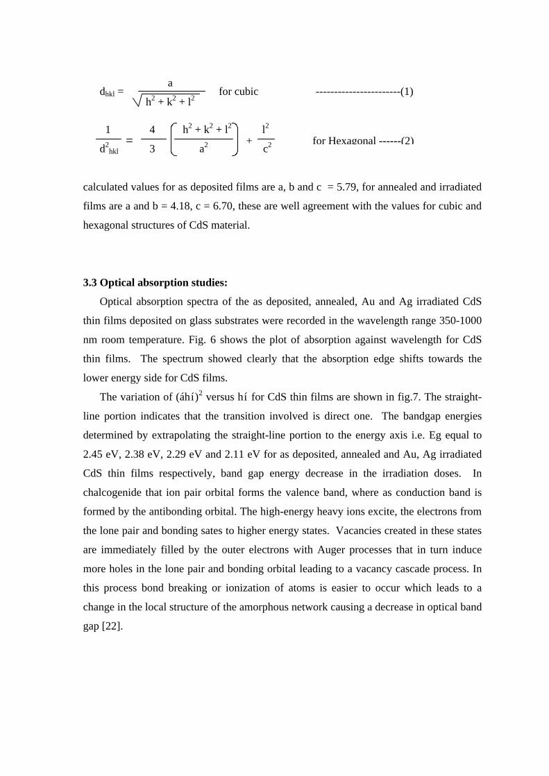
dhkl = for cubic -----------------------(1)
1 4 h2 + k2 + l2 l2
d2hkl 3 a2 c2
calculated values for as deposited films are a, b and c = 5.79, for annealed and irradiated
films are a and b = 4.18, c = 6.70, these are well agreement with the values for cubic and
hexagonal structures of CdS material.
3.3 Optical absorption studies:
Optical absorption spectra of the as deposited, annealed, Au and Ag irradiated CdS
thin films deposited on glass substrates were recorded in the wavelength range 350-1000
nm room temperature. Fig. 6 shows the plot of absorption against wavelength for CdS
thin films. The spectrum showed clearly that the absorption edge shifts towards the
lower energy side for CdS films.
The variation of (áhí)2 versus hí for CdS thin films are shown in fig.7. The straight-
line portion indicates that the transition involved is direct one. The bandgap energies
determined by extrapolating the straight-line portion to the energy axis i.e. Eg equal to
2.45 eV, 2.38 eV, 2.29 eV and 2.11 eV for as deposited, annealed and Au, Ag irradiated
CdS thin films respectively, band gap energy decrease in the irradiation doses. In
chalcogenide that ion pair orbital forms the valence band, where as conduction band is
formed by the antibonding orbital. The high-energy heavy ions excite, the electrons from
the lone pair and bonding sates to higher energy states. Vacancies created in these states
are immediately filled by the outer electrons with Auger processes that in turn induce
more holes in the lone pair and bonding orbital leading to a vacancy cascade process. In
this process bond breaking or ionization of atoms is easier to occur which leads to a
change in the local structure of the amorphous network causing a decrease in optical band
gap [22].
a
h2 + k2 + l2
+ for Hexagonal ------(2)
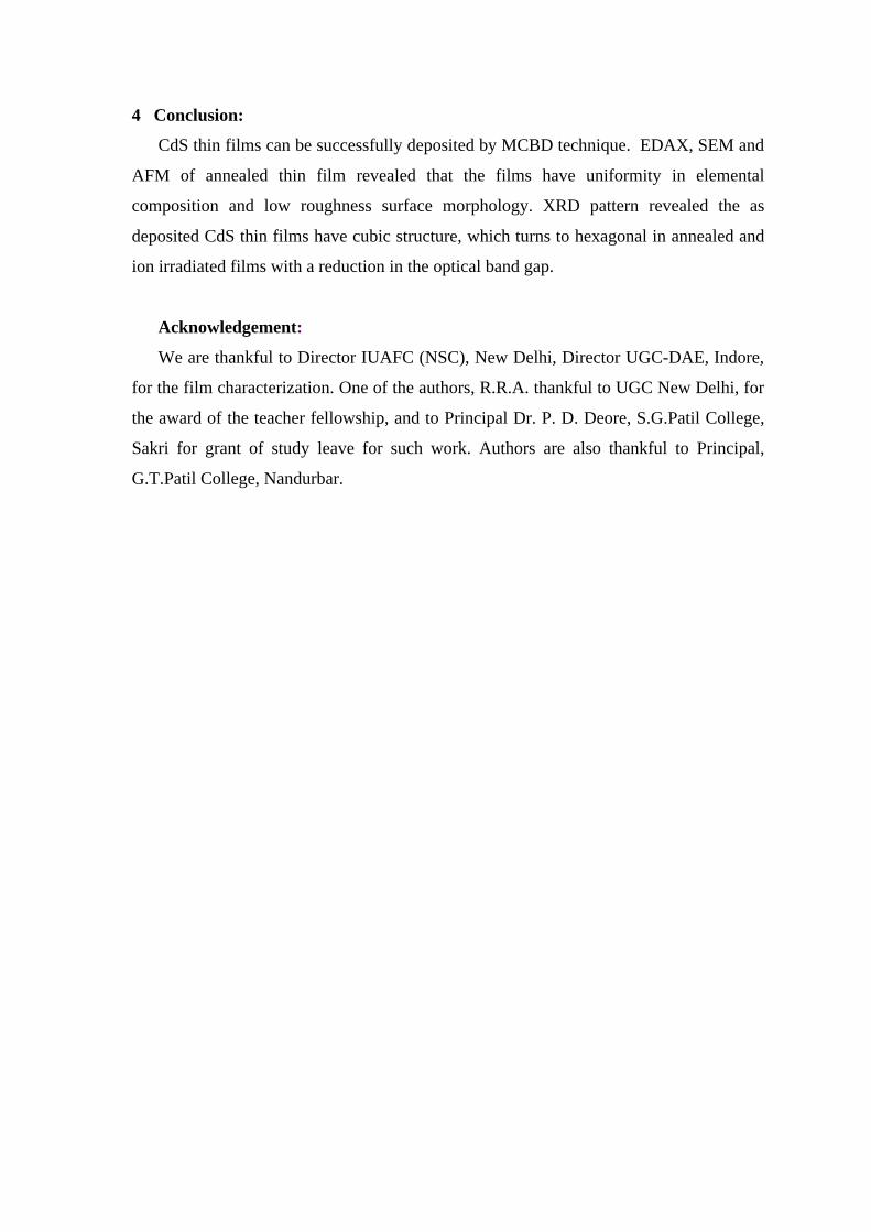
4 Conclusion:
CdS thin films can be successfully deposited by MCBD technique. EDAX, SEM and
AFM of annealed thin film revealed that the films have uniformity in elemental
composition and low roughness surface morphology. XRD pattern revealed the as
deposited CdS thin films have cubic structure, which turns to hexagonal in annealed and
ion irradiated films with a reduction in the optical band gap.
Acknowledgement:
We are thankful to Director IUAFC (NSC), New Delhi, Director UGC-DAE, Indore,
for the film characterization. One of the authors, R.R.A. thankful to UGC New Delhi, for
the award of the teacher fellowship, and to Principal Dr. P. D. Deore, S.G.Patil College,
Sakri for grant of study leave for such work. Authors are also thankful to Principal,
G.T.Patil College, Nandurbar.
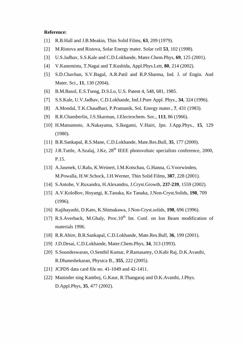
Reference:
[1] R.B.Hall and J.B.Meakin, Thin Solid Films, 63, 209 (1979).
[2] M.Ristova and Ristova, Solar Energy mater. Solar cell 53, 102 (1998).
[3] U.S.Jadhav, S.S.Kale and C.D.Lokhande, Mater.Chem.Phys, 69, 125 (2001).
[4] V.Kanemistu, T.Nagai and T.Kushida, Appl.Phys.Lett, 80, 214 (2002).
[5] S.D.Chavhan, S.V.Bagul, A.R.Patil and R.P.Sharma, Ind. J. of Engin. And
Mater. Sci., 11, 130 (2004).
[6] B.M.Basol, E.S.Tseng, D.S.Lo, U.S. Patent 4, 548, 681, 1985.
[7] S.S.Kale, U.V.Jadhav, C.D.Lokhande, Ind.J.Pure Appl. Phys., 34, 324 (1996).
[8] A.Mondal, T.K.Chaudhari, P.Pramanik, Sol. Energy mater., 7, 431 (1983).
[9] R.R.Chamberlin, J.S.Skarman, J.Electrochem. Soc., 113, 86 (1966).
[10] H.Matsumoto, A.Nakayama, S.lkegami, V.Hairi, Jpn. J.App.Phys., 15, 129
(1980).
[11] B.R.Sankapal, R.S.Mane, C.D.Lokhande, Mate.Res.Bull, 35, 177 (2000).
[12] J.R.Tuttle, A.Szalaj, J.Ke, 28th IEEE photovoltaic specialists conference, 2000,
P.15.
[13] A.Jasenek, U.Ralu, K.Weinert, I.M.Kotschau, G.Hanna, G.Voorwinden,
M.Powalla, H.W.Schock, J.H.Werner, Thin Solid Films, 387, 228 (2001).
[14] S.Antohe, V.Ruxandra, H.Alexandru, J.Cryst.Growth, 237-239, 1559 (2002).
[15] A.V.KoloBov, Hoyangi, K.Tanaka, Ke Tanaka, J.Non-Cryst.Solids, 198, 709
(1996).
[16] Kajihayashi, D.Kato, K.Shimakawa, J.Non-Cryst.solids, 198, 696 (1996).
[17] R.S.Averback, M.Ghaly, Proc.10th Int. Conf. on Ion Beam modification of
materials 1996.
[18] R.R.Ahire, B.R.Sankapal, C.D.Lokhande, Mate.Res.Bull, 36, 199 (2001).
[19] J.D.Desai, C.D.Lokhande, Mater.Chem.Phys, 34, 313 (1993).
[20] S.Soundeswaran, O.Senthil Kumar, P.Ramasamy, O.Kabi Raj, D.K.Avasthi,
R.Dhaneshekaran, Physica B., 355, 222 (2005).
[21] JCPDS data card file no. 41-1049 and 42-1411.
[22] Maninder sing Kamboj, G.Kaur, R.Thangaraj and D.K.Avasthi, J.Phys.
D.Appl.Phys, 35, 477 (2002).
Table 1. Preparative parameters for the deposition of CdS thin films
Precursors Cationic Anionic
Cadmium acetate Sodium sulfied
Parameters (CH3COO)2 Cd2H2O Na2SH2O
Concentration (M) 0.06 0.1 PH ~ 11 11
Immersion cycles 30 30 Immersion time (sec) 15 15
Rinsing time (sec) 40 40 Deposition temp. (0C) 27 27
Table 2.Comparison of the observed ‘d’ value of CdS thin film with JCPDS data card file no. 41-1049 and 42-1411.
Sample Observed
‘d’ Values Å
Standard ‘d’ values Å
Plane (hkl)
3.3476 3.3590 111 2.0607 2.057 220
As deposited
1.7446 1.7542 331 3.6230 3.5861 100 3.3505 3.3599 002 2.4725 2.4519 102
Annealed at 3000C for 1h 2.0922 2.0705 110
1.8076 1.7931 200 1.7651 1.7627 112 1.7386 1.7325 201 3.3641 3.5861 100 3.3438 3.3599 002 2.0892 2.0705 110 1.9054 1.8998 103 1.7850 1.7931 200
Au ion irradiated
1.6709 1.6799 004 3.3479 3.3599 002 2.4564 2.4519 102 2.0649 2.0705 110 1.8942 1.8998 103 1.7569 1.7627 112 1.6766 1.6799 004
Ag ion irradiated
1.5849 1.5819 202
Caption
Fig. 1a. Plot of CdS thin film thickness as a function of concentration of cadmium
acetate.
Fig. 1b. Plot of variation of CdS thin film thickness with immersion cycles.
Fig. 1c. Plot of CdS thin film thickness as a function of immersion time (sec)
Fig. 2. A typical EDAX pattern of CdS thin film onto glass substrate annealed at 3000C
for 1h
Fig. 3. SEM of CdS thin film annealed at 3000C for 1h in air.
Fig.4. AFM of CdS thin film annealed at 3000C for 1h.
Fig. 5. XRD patterns of CdS onto glass substrates
Fig. 6. Plot of absorption Vs wavelength for CdS thin film.
Fig. 7. Plot of (áhí)2 Vs hí for CdS thin film (derived from fig.5)
Fig.1a
0
0.03
0.06
0.09
0.12
0.15
0 0.02 0.04 0.06 0.08 0.1 0.12
Concentration (M)
Thi
ckne
ss (
µm)
Fig.1b
0
0.03
0.06
0.09
0.12
0.15
5 10 15 20 25 30 35 40
Immersion cycle
Thi
ckne
ss (
µm)
Fig.1c
0.06
0.08
0.1
0.12
0.14
0.16
0 5 10 15 20 25 30
Immersion time (sec)
Thi
ckne
ss( µ
m)
Fig.2
Fig.3
Fig.3 Fig. 4
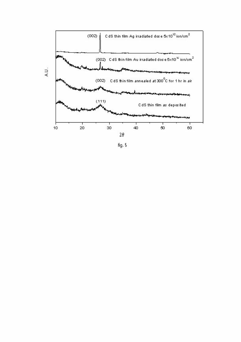
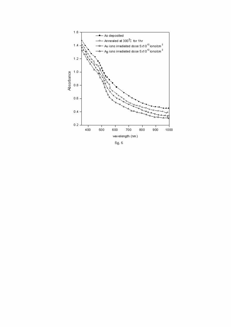
fig. 6
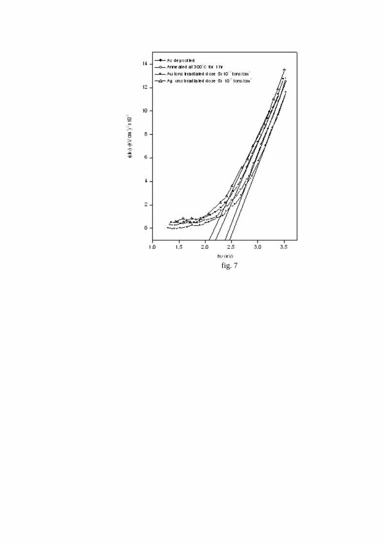
fig. 7
FABRICATION OF n-SI/P-CuIn (S1-XSeX)2 THIN FILM SOLAR CELL BY BY SOLUTION GROWTH TECHNIQUE.
S.D.Chavhan, R.R.Ahirea and R.P.Sharma* Thin Film and Semiconductor Laboratory
Department of Physics, G.T.Patil College, Nandurbar-425412. a On leave under FIP. UGC Xth plan, S.G.Patil College Sakri-424304 India
Email: [email protected] ABSTRACT The p-CuIn(S1-xSex)2 (CISS) thin films have been grown on n-Si substrate by solution growth technique. The deposition parameters such as pH (10.5), deposition time (60min), deposition temperature (500C), and concentration of bath solution (0.1M) were optimized. Elemental analysis of the p-CuIn(S1-xSex)2 thin film was confirmed by energy dispersive analysis of x-ray (EDAX). The SEM study of absorber layer shows the uniform morphology of film as well as the continuous smooth deposition onto the n-Si substrates and the grain size is 130 nm. CuIn(S1-xSex )2 (x = 0.5) reveals (112) orientation peak and exhibit the chalcopyrite structure with lattice constant a = 5.28Å and c = 11.45 Å. The J-V characteristics was measured in dark and light. The device parameters have been calculated for solar cell fabrication, Voc = 411.09 mV, Jsc = 14.55 mA/cm2. FF = 46.55 % and η = 4.64% under an illumination of 60 mW/cm2. The J-V characteristics of the device under dark condition were also studied and calculated the ideality factor, which is equal to 2.2 for n-Si/p-CuIn(S0.5Se0.5)2 heterojunction thin film. 1. INTRODUCTION The PV technology is one of most important for harness the solar energy. The device fabricated for solar cell are a-Si, crystalline silicon, CdTe, CdSe, Cu(InGa)Se2, CuInSe2, CuInS2 compounds. The elemental silicon has been used for several years in space applications and appears to be the most practical material for terrestrial use. The highest solar conversion efficiencies have been observed in cells using gallium aresenide, which may be considered as the second most favored material. However, the high efficiency cells of both a-Si and GaAs are in the form of single crystal material, which is relatively expensive to prepare. Economics dictate the use of a minimum amount of semiconductor material with low cost preparational techniques. This means the cells should be of thin film form, with the material in a polycrystalline or amorphous state. There is much interest, in amorphous Si; but stability problem remains with this material. Nevertheless, in the last decade, a relatively new material has emerged with promising characteristics. These are the ternary chalcopyrite compounds such as CuInSe2 and its quaternary alloy Cu(InGa)Se2, CuIn(S1-xSex)2 , etc. These include p-n junction PV detectors [1,2], light emitting diode [2,3] and solar cells [4-5]. It has a direct band gap of 1.04 eV and falls in the optimum range for terrestrial PV applications [3,4]. Owing to its high absorption coefficient order of 104 cm-1 it requires at the most a few microns of material thickness to make devices. Besides, inexpensive thin film deposition techniques can be used in the fabrication. CuInSe2, when paired with CdS, has a lattice structure with a lattice mismatch of 1.16% and electron affinity difference is 0.1 eV [2,6,7]. Polycrystalline thin film solar cells based on p-CuInSe2 and its alloy with n-CdS heterojunction have emerged as major contenders for PV device technology. Though widely used CdS with a band gap of 2.4 eV is not the ideal material since it absorbs the blue portion of the spectrum and the lattice mismatch at the junction. Development of single crystal silicon and
CdZnS the films over coated with window materials like ZnO (3.3eV), ZnS and SnO2 are considered more useful and it is an important for R & D work area. Varieties of fabrication techniques have been employed to improve upon this basic structure reported by earlier workers [8-21]. These include single source evaporation, sputtering, electrodeposition, chemical vapour deposition, screen-printing, spray pyrolysis, laser induced synthesis. The status of the technology in each of the above reported cases may be judged by the best reported active area solar conversion efficiencies in single junction cells based on CuInSe2 films [19]. In the Cu-In- S-Se chalcopyrite system, CuInSe2 <==>CuInS2 can be developed to yield band gaps from 1.0 to 1.48 eV. New trends to fabricate the n-Si /p-CuIn(S1-xSex)2 heterojunction thin film solar is a recent research and development area for higher efficiency solar cell by chemical deposition technique. However, all the thin film deposition techniques used for the fabrication of high efficiency CIS or its compounds cells are costly and require sophisticated instruments. In some deposition techniques, H2Se and H2S vapors are used as the source materials for Selenium and Sulphur, which are more poisonous gases. Many authors have been prepared the heterojunction thin films by different sophisticated methods such as sulphurization, selenization process [22], spray pyrolysis [23] and elelctrodeposition [24] but there is rare information in the literature of the solution growth technique for the deposition of quaternary thin films and also for the fabrication of the heterojunction of thin films [25]. Among all the deposition technique, the solution growth technique is the simplest, capable of large area fabrication technique at low cost [25]. In this technique, wastage of material is minimum and there is no need to handle the poisonous gases like H2Se and H2S. In the present paper, we have reported the development of solution growth technique to deposit the quaternary p- CuIn(S1-xSex)2 thin films on n-Si substrate and
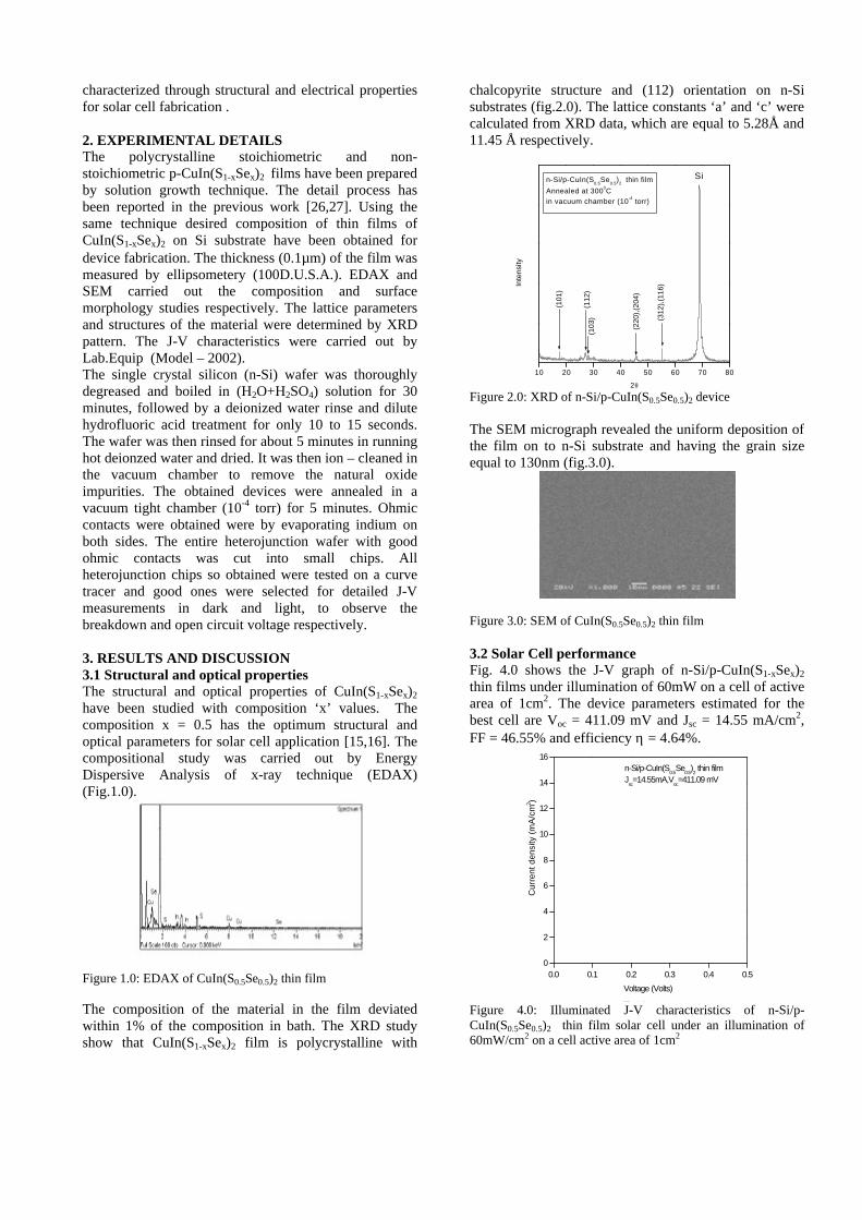
characterized through structural and electrical properties for solar cell fabrication . 2. EXPERIMENTAL DETAILS The polycrystalline stoichiometric and non-stoichiometric p-CuIn(S1-xSex)2 films have been prepared by solution growth technique. The detail process has been reported in the previous work [26,27]. Using the same technique desired composition of thin films of CuIn(S1-xSex)2 on Si substrate have been obtained for device fabrication. The thickness (0.1µm) of the film was measured by ellipsometery (100D.U.S.A.). EDAX and SEM carried out the composition and surface morphology studies respectively. The lattice parameters and structures of the material were determined by XRD pattern. The J-V characteristics were carried out by Lab.Equip (Model – 2002). The single crystal silicon (n-Si) wafer was thoroughly degreased and boiled in (H2O+H2SO4) solution for 30 minutes, followed by a deionized water rinse and dilute hydrofluoric acid treatment for only 10 to 15 seconds. The wafer was then rinsed for about 5 minutes in running hot deionzed water and dried. It was then ion – cleaned in the vacuum chamber to remove the natural oxide impurities. The obtained devices were annealed in a vacuum tight chamber (10-4 torr) for 5 minutes. Ohmic contacts were obtained were by evaporating indium on both sides. The entire heterojunction wafer with good ohmic contacts was cut into small chips. All heterojunction chips so obtained were tested on a curve tracer and good ones were selected for detailed J-V measurements in dark and light, to observe the breakdown and open circuit voltage respectively. 3. RESULTS AND DISCUSSION 3.1 Structural and optical properties The structural and optical properties of CuIn(S1-xSex)2 have been studied with composition ‘x’ values. The composition x = 0.5 has the optimum structural and optical parameters for solar cell application [15,16]. The compositional study was carried out by Energy Dispersive Analysis of x-ray technique (EDAX) (Fig.1.0).
Figure 1.0: EDAX of CuIn(S0.5Se0.5)2 thin film The composition of the material in the film deviated within 1% of the composition in bath. The XRD study show that CuIn(S1-xSex)2 film is polycrystalline with
chalcopyrite structure and (112) orientation on n-Si substrates (fig.2.0). The lattice constants ‘a’ and ‘c’ were calculated from XRD data, which are equal to 5.28Å and 11.45 Å respectively.
10 20 30 40 50 60 70 80
n-Si/p-CuIn(S0.5
Se0.5
)2 thin film
Annealed at 3000C in vacuum chamber (10-4 torr)
Si
(312
),(1
16)
(220
),(2
04)
(103
)(1
12)
(101
)
2θ
Inte
nsity
Figure 2.0: XRD of n-Si/p-CuIn(S0.5Se0.5)2 device
The SEM micrograph revealed the uniform deposition of the film on to n-Si substrate and having the grain size equal to 130nm (fig.3.0).
Figure 3.0: SEM of CuIn(S0.5Se0.5)2 thin film 3.2 Solar Cell performance Fig. 4.0 shows the J-V graph of n-Si/p-CuIn(S1-xSex)2 thin films under illumination of 60mW on a cell of active area of 1cm2. The device parameters estimated for the best cell are Voc = 411.09 mV and Jsc = 14.55 mA/cm2, FF = 46.55% and efficiency η = 4.64%.
0.0 0.1 0.2 0.3 0.4 0.50
2
4
6
8
10
12
14
16
Fig.4.0
n-Si/p-CuIn(S0.5
Se0.5
)2 thin film
Jsc=14.55mA,V
oc=411.09 mV
Voltage (Volts)
Cur
rent
den
sity
(m
A/c
m2 )
Figure 4.0: Illuminated J-V characteristics of n-Si/p-CuIn(S0.5Se0.5)2 thin film solar cell under an illumination of 60mW/cm2 on a cell active area of 1cm2
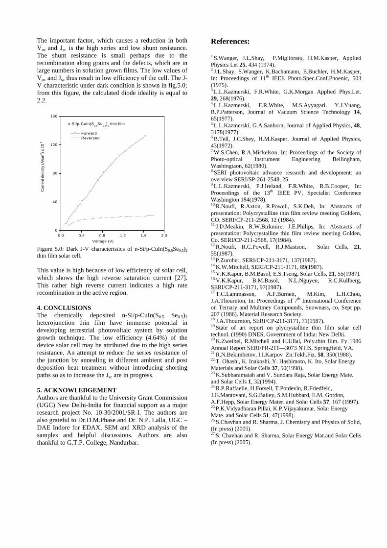
The important factor, which causes a reduction in both Voc and Jsc is the high series and low shunt resistance. The shunt resistance is small perhaps due to the recombination along grains and the defects, which are in large numbers in solution grown films. The low values of Voc and Jsc thus result in low efficiency of the cell. The J-V characteristic under dark condition is shown in fig.5.0; from this figure, the calculated diode ideality is equal to 2.2.
0.0 0.4 0.8 1.2 1.6 2.00
40
80
120
160
n-Si/p-CuIn(S0.5
Se0.5
)2 thin film
Forward Reversed
Voltage (V)
Cur
rent
den
sity
(A
/cm
2 ) x
10-6
Figure 5.0: Dark J-V characteristics of n-Si/p-CuIn(S0.5Se0.5)2 thin film solar cell. This value is high because of low efficiency of solar cell, which shows the high reverse saturation current [27]. This rather high reverse current indicates a high rate recombination in the active region. 4. CONCLUSIONS The chemically deposited n-Si/p-CuIn(S0.5 Se0.5)2 heterojunction thin film have immense potential in developing terrestrial photovoltaic system by solution growth technique. The low efficiency (4.64%) of the device solar cell may be attributed due to the high series resistance. An attempt to reduce the series resistance of the junction by annealing in different ambient and post deposition heat treatment without introducing shorting paths so as to increase the Jsc are in progress. 5. ACKNOWLEDGEMENT Authors are thankful to the University Grant Commission (UGC) New Delhi-India for financial support as a major research project No. 10-30/2001/SR-I. The authors are also grateful to Dr.D.M.Phase and Dr. N.P. Lalla, UGC – DAE Indore for EDAX, SEM and XRD analysis of the samples and helpful discussions. Authors are also thankful to G.T.P. College, Nandurbar.
References: 1.S.Wanger, J.L.Shay, P.Migliorato, H.M.Kasper, Applied Physics Let 25, 434 (1974). 2.J.L.Shay, S.Wanger, K.Bachamann, E.Buchler, H.M.Kasper, In: Proceedings of 11th IEEE Photo.Spec.Conf.Phoenic, 503 (1975). 3.L.L.Kazmerski, F.R.White, G.K.Morgan Applied Phys.Let. 29, 268(1976). 4.L.L.Kazmerski, F.R.White, M.S.Ayyagari, Y.J.Yuang, R.P.Patterson, Journal of Vacuum Science Technology 14, 65(1977). 5.L.L.Kazmerski, G.A.Sanborn, Journal of Applied Physics, 48, 3178(1977). 6.B.Tell, J.C.Shey, H.M.Kasper, Journal of Applied Physics, 43(1972). 7.W.S.Chen, R.A.Mickelson, In: Proceedings of the Society of Photo-optical Instrument Engineering Bellingham, Washingtaon, 62(1980). 8.SERI photovoltaic advance research and development: an overview SERI/SP-261-2548, 25. 9.L.L.Kazmerski, P.J.Ireland, F.R.White, R.B.Cooper, In: Proceedings of the 13th IEEE PV, Specialist Conference Washington 184(1978). 10.R.Noufi, R.Axton, R.Powell, S.K.Deb, In: Abstracts of presentation: Polycrystalline thin film review meeting Goldern, CO. SERI/CP-211-2568, 12 (1984). 11.J.D.Meakin, R.W.Birkmire, J.E.Philips, In: Abstracts of presentation: Polycrystalline thin film review meeting Golden, Co. SERI/CP-211-2568, 17(1984). 12.R.Noufi, R.C.Powell, R.J.Mastson, Solar Cells, 21, 55(1987). 13.P.Zuroher, SERI/CP-211-3171, 137(1987). 14.K.W.Mitchell, SERI/CP-211-3171, 89(1987). 15.V.K.Kapur, B.M.Basol, E.S.Tseng, Solar Cells, 21, 55(1987). 16.V.K.Kapur, B.M.Basol, N.L.Nguyen, R.C.Kullberg, SERI/CP-211-3171, 97(1987). 17.T.C.Lammasson, A.F.Burnett, M.Kim, L.H.Chou, J.A.Thournton, In: Proceedings of 7th International Conference on Ternary and Multiney Compounds, Snownass, co, Sept pp. 207 (1986). Material Research Society. 18.J.A.Thournton, SERI/CP-211-3171, 71(1987). 19.State of art report on plycrystalline thin film solar cell technol. (1990) DNES, Government of India: New Delhi. 20.K.Zweibel, R.Mitchell and H.Ullal, Poly.thin film. Fy 1986 Annual Report SERI/PR-211—3073 NTIS, Springfield, VA. 21.R.N.Bekimbetov, I.I.Karpov Zn.Tekh.Fiz. 58, 350(1988). 22.T. Ohashi, K. Inakoshi, Y. Hashimoto, K. Ito, Solar Energy Materials and Solar Cells 37, 50(1998). 23.K.Subbaramaiah and V. Sundara Raja, Solar Energy Mate. and Solar Cells 1, 32(1994). 24.R.P.Raffaelle, H.Forsell, T.Potdevin, R.Friedfeld, J.G.Mantovani, S.G.Bailey, S.M.Hubbard, E.M. Gordon, A.F.Hepp, Solar Energy Mater. and Solar Cells 57, 167 (1997). 25.P.K.Vidyadharan Pillai, K.P.Vijayakumar, Solar Energy Mate. and Solar Cells 51, 47(1998). 26.S.Chavhan and R. Sharma, J. Chemistry and Physics of Solid, (In press) (2005). 27.S. Chavhan and R. Sharma, Solar Energy Mat.and Solar Cells (In press) (2005).

TRANSFER OF COPYRIGHT Please complete as appropriate and return by fax/mail. If you do not provide a copyright clearance, we cannot include your paper in the proceedings. [ y ] My employer has given clearance for this
paper to be published. OR [y ] I am the holder of the copyright for this
paper The author who sign the copyright
Signature: Date: 14/10/2005 Affiliation: Thin Film and Semiconductor Laboratory Department of Physics, G.T.Patil College, Nandurbar-425412. Ph.No. –02564 – 225255 E-mail:[email protected]
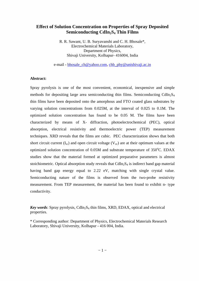
− 1 −
Effect of Solution Concentration on Properties of Spray Deposited Semiconducting CdIn2S4 Thin Films
R. R. Sawant, U. B. Suryavanshi and C. H. Bhosale*,
Electrochemical Materials Laboratory, Department of Physics,
Shivaji University, Kolhapur- 416004, India
e-mail - [email protected], [email protected] Abstract: Spray pyrolysis is one of the most convenient, economical, inexpensive and simple
methods for depositing large area semiconducting thin films. Semiconducting CdIn2S4
thin films have been deposited onto the amorphous and FTO coated glass substrates by
varying solution concentrations from 0.025M, at the interval of 0.025 to 0.1M. The
optimized solution concentration has found to be 0.05 M. The films have been
characterized by means of X- diffraction, photoelectrochemical (PEC), optical
absorption, electrical resistivity and thermoelectric power (TEP) measurement
techniques. XRD reveals that the films are cubic. PEC characterization shows that both
short circuit current (Isc) and open circuit voltage (Voc) are at their optimum values at the
optimized solution concentration of 0.05M and substrate temperature of 350oC. EDAX
studies show that the material formed at optimized preparative parameters is almost
stoichiometric. Optical absorption study reveals that CdIn2S4 is indirect band gap material
having band gap energy equal to 2.22 eV, matching with single crystal value.
Semiconducting nature of the films is observed from the two-probe resistivity
measurement. From TEP measurement, the material has been found to exhibit n- type
conductivity.
Key words: Spray pyrolysis, CdIn2S4 thin films, XRD, EDAX, optical and electrical properties. * Corresponding author: Department of Physics, Electrochemical Materials Research Laboratory, Shivaji University, Kolhapur - 416 004, India.
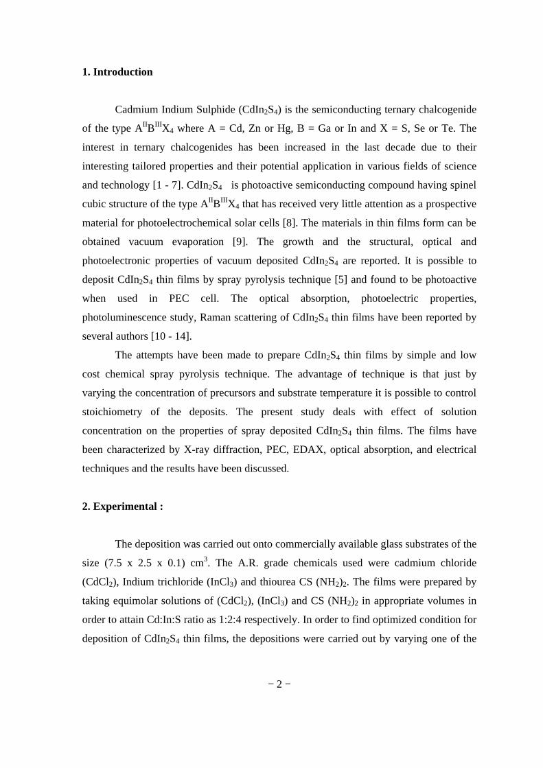
− 2 −
1. Introduction
Cadmium Indium Sulphide (CdIn2S4) is the semiconducting ternary chalcogenide
of the type AIIBIIIX4 where A = Cd, Zn or Hg, B = Ga or In and X = S, Se or Te. The
interest in ternary chalcogenides has been increased in the last decade due to their
interesting tailored properties and their potential application in various fields of science
and technology [1 - 7]. CdIn2S4 is photoactive semiconducting compound having spinel
cubic structure of the type AIIBIIIX4 that has received very little attention as a prospective
material for photoelectrochemical solar cells [8]. The materials in thin films form can be
obtained vacuum evaporation [9]. The growth and the structural, optical and
photoelectronic properties of vacuum deposited CdIn2S4 are reported. It is possible to
deposit CdIn2S4 thin films by spray pyrolysis technique [5] and found to be photoactive
when used in PEC cell. The optical absorption, photoelectric properties,
photoluminescence study, Raman scattering of CdIn2S4 thin films have been reported by
several authors [10 - 14].
The attempts have been made to prepare CdIn2S4 thin films by simple and low
cost chemical spray pyrolysis technique. The advantage of technique is that just by
varying the concentration of precursors and substrate temperature it is possible to control
stoichiometry of the deposits. The present study deals with effect of solution
concentration on the properties of spray deposited CdIn2S4 thin films. The films have
been characterized by X-ray diffraction, PEC, EDAX, optical absorption, and electrical
techniques and the results have been discussed.
2. Experimental :
The deposition was carried out onto commercially available glass substrates of the
size (7.5 x 2.5 x 0.1) cm3. The A.R. grade chemicals used were cadmium chloride
(CdCl2), Indium trichloride (InCl3) and thiourea CS (NH2)2. The films were prepared by
taking equimolar solutions of (CdCl2), (InCl3) and CS (NH2)2 in appropriate volumes in
order to attain Cd:In:S ratio as 1:2:4 respectively. In order to find optimized condition for
deposition of CdIn2S4 thin films, the depositions were carried out by varying one of the
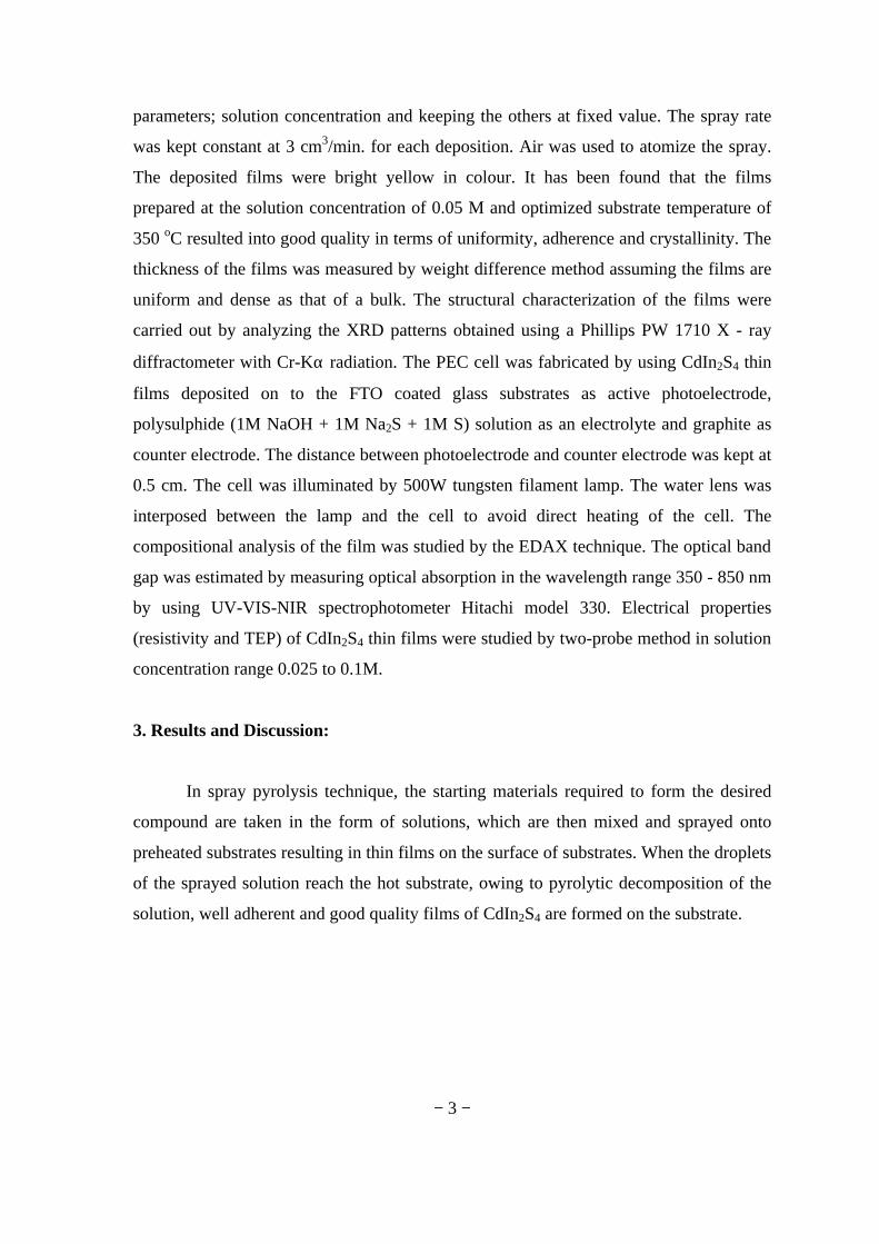
− 3 −
parameters; solution concentration and keeping the others at fixed value. The spray rate
was kept constant at 3 cm3/min. for each deposition. Air was used to atomize the spray.
The deposited films were bright yellow in colour. It has been found that the films
prepared at the solution concentration of 0.05 M and optimized substrate temperature of
350 oC resulted into good quality in terms of uniformity, adherence and crystallinity. The
thickness of the films was measured by weight difference method assuming the films are
uniform and dense as that of a bulk. The structural characterization of the films were
carried out by analyzing the XRD patterns obtained using a Phillips PW 1710 X - ray
diffractometer with Cr-Kα radiation. The PEC cell was fabricated by using CdIn2S4 thin
films deposited on to the FTO coated glass substrates as active photoelectrode,
polysulphide (1M NaOH + 1M Na2S + 1M S) solution as an electrolyte and graphite as
counter electrode. The distance between photoelectrode and counter electrode was kept at
0.5 cm. The cell was illuminated by 500W tungsten filament lamp. The water lens was
interposed between the lamp and the cell to avoid direct heating of the cell. The
compositional analysis of the film was studied by the EDAX technique. The optical band
gap was estimated by measuring optical absorption in the wavelength range 350 - 850 nm
by using UV-VIS-NIR spectrophotometer Hitachi model 330. Electrical properties
(resistivity and TEP) of CdIn2S4 thin films were studied by two-probe method in solution
concentration range 0.025 to 0.1M.
3. Results and Discussion:
In spray pyrolysis technique, the starting materials required to form the desired
compound are taken in the form of solutions, which are then mixed and sprayed onto
preheated substrates resulting in thin films on the surface of substrates. When the droplets
of the sprayed solution reach the hot substrate, owing to pyrolytic decomposition of the
solution, well adherent and good quality films of CdIn2S4 are formed on the substrate.
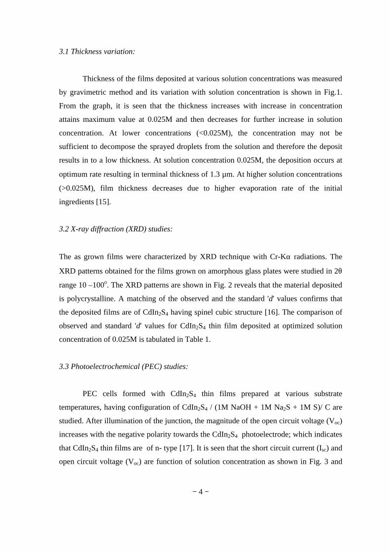
− 4 −
3.1 Thickness variation:
Thickness of the films deposited at various solution concentrations was measured
by gravimetric method and its variation with solution concentration is shown in Fig.1.
From the graph, it is seen that the thickness increases with increase in concentration
attains maximum value at 0.025M and then decreases for further increase in solution
concentration. At lower concentrations (<0.025M), the concentration may not be
sufficient to decompose the sprayed droplets from the solution and therefore the deposit
results in to a low thickness. At solution concentration 0.025M, the deposition occurs at
optimum rate resulting in terminal thickness of 1.3 µm. At higher solution concentrations
(>0.025M), film thickness decreases due to higher evaporation rate of the initial
ingredients [15].
3.2 X-ray diffraction (XRD) studies:
The as grown films were characterized by XRD technique with Cr-Kα radiations. The
XRD patterns obtained for the films grown on amorphous glass plates were studied in 2θ
range 10 –100o. The XRD patterns are shown in Fig. 2 reveals that the material deposited
is polycrystalline. A matching of the observed and the standard 'd' values confirms that
the deposited films are of CdIn2S4 having spinel cubic structure [16]. The comparison of
observed and standard 'd' values for CdIn2S4 thin film deposited at optimized solution
concentration of 0.025M is tabulated in Table 1.
3.3 Photoelectrochemical (PEC) studies:
PEC cells formed with CdIn2S4 thin films prepared at various substrate
temperatures, having configuration of CdIn2S4 / (1M NaOH + 1M Na2S + 1M S)/ C are
studied. After illumination of the junction, the magnitude of the open circuit voltage (Voc)
increases with the negative polarity towards the CdIn2S4 photoelectrode; which indicates
that CdIn2S4 thin films are of n- type [17]. It is seen that the short circuit current (Isc) and
open circuit voltage (Voc) are function of solution concentration as shown in Fig. 3 and
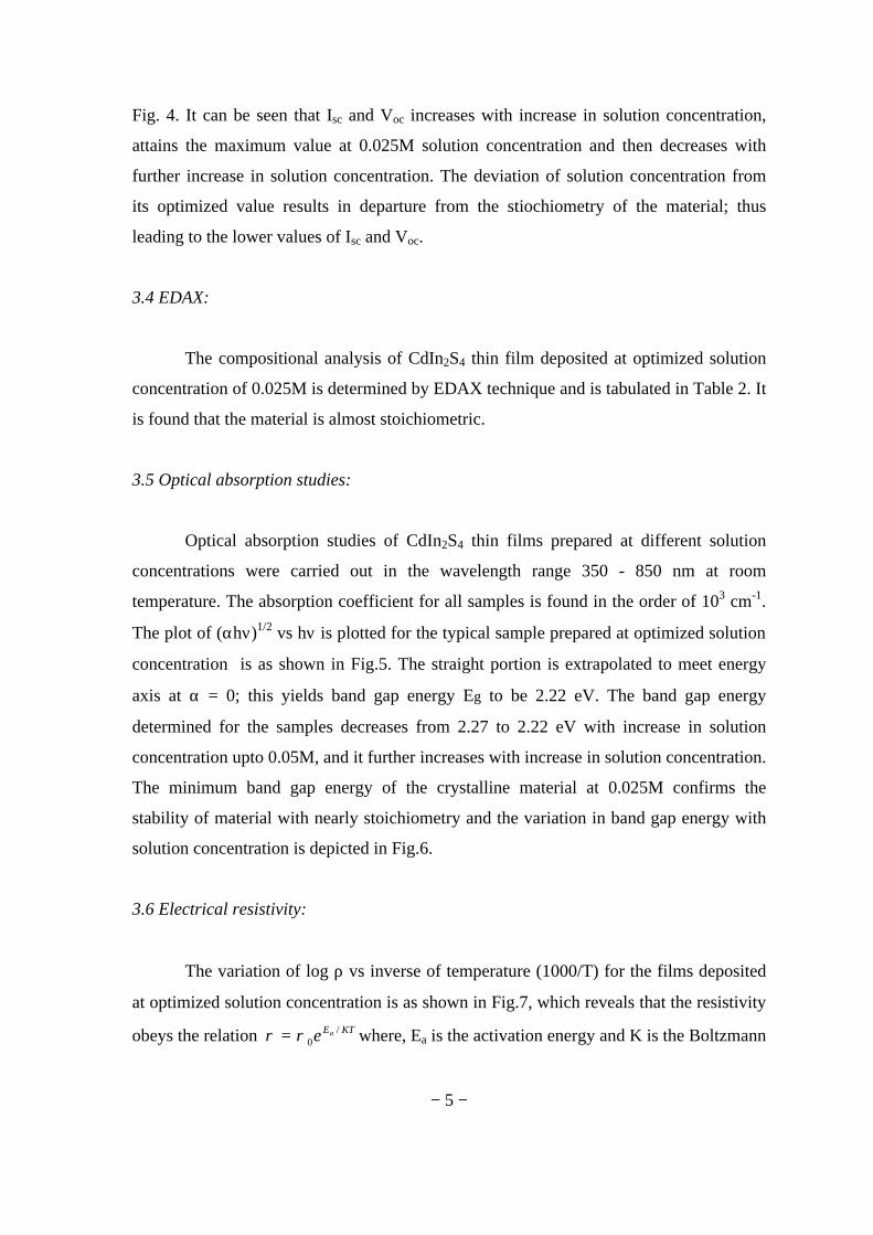
− 5 −
Fig. 4. It can be seen that Isc and Voc increases with increase in solution concentration,
attains the maximum value at 0.025M solution concentration and then decreases with
further increase in solution concentration. The deviation of solution concentration from
its optimized value results in departure from the stiochiometry of the material; thus
leading to the lower values of Isc and Voc.
3.4 EDAX:
The compositional analysis of CdIn2S4 thin film deposited at optimized solution
concentration of 0.025M is determined by EDAX technique and is tabulated in Table 2. It
is found that the material is almost stoichiometric.
3.5 Optical absorption studies:
Optical absorption studies of CdIn2S4 thin films prepared at different solution
concentrations were carried out in the wavelength range 350 - 850 nm at room
temperature. The absorption coefficient for all samples is found in the order of 103 cm-1.
The plot of (αhν)1/2 vs hν is plotted for the typical sample prepared at optimized solution
concentration is as shown in Fig.5. The straight portion is extrapolated to meet energy
axis at α = 0; this yields band gap energy Eg to be 2.22 eV. The band gap energy
determined for the samples decreases from 2.27 to 2.22 eV with increase in solution
concentration upto 0.05M, and it further increases with increase in solution concentration.
The minimum band gap energy of the crystalline material at 0.025M confirms the
stability of material with nearly stoichiometry and the variation in band gap energy with
solution concentration is depicted in Fig.6.
3.6 Electrical resistivity:
The variation of log ρ vs inverse of temperature (1000/T) for the films deposited
at optimized solution concentration is as shown in Fig.7, which reveals that the resistivity
obeys the relation KTEae /0ρρ = where, Ea is the activation energy and K is the Boltzmann
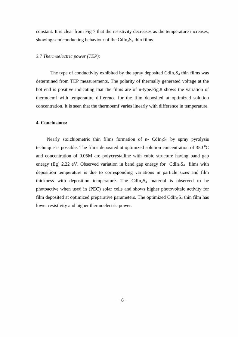
− 6 −
constant. It is clear from Fig 7 that the resistivity decreases as the temperature increases,
showing semiconducting behaviour of the CdIn2S4 thin films.
3.7 Thermoelectric power (TEP):
The type of conductivity exhibited by the spray deposited CdIn2S4 thin films was
determined from TEP measurements. The polarity of thermally generated voltage at the
hot end is positive indicating that the films are of n-type.Fig.8 shows the variation of
thermoemf with temperature difference for the film deposited at optimized solution
concentration. It is seen that the thermoemf varies linearly with difference in temperature.
4. Conclusions:
Nearly stoichiometric thin films formation of n- CdIn2S4 by spray pyrolysis
technique is possible. The films deposited at optimized solution concentration of 350 oC
and concentration of 0.05M are polycrystalline with cubic structure having band gap
energy (Eg) 2.22 eV. Observed variation in band gap energy for CdIn2S4 films with
deposition temperature is due to corresponding variations in particle sizes and film
thickness with deposition temperature. The CdIn2S4 material is observed to be
photoactive when used in (PEC) solar cells and shows higher photovoltaic activity for
film deposited at optimized preparative parameters. The optimized CdIn2S4 thin film has
lower resistivity and higher thermoelectric power.
− 7 −
References:
1. K.Y. Rajpure, C.D. Lokhande and C.H. Bhosale, Mater. Chem. Phys. 252,
51(1997).
2. K.Y. Rajpure, C.D. Lokhande and C.H. Bhosale, Thin solid films, 311(1997) 144.
3. K.Y. Rajpure, A.L. Dhebe, C.D. Lokhande and C.H. Bhosale, Mater. Chem. Phys.
56 (1999) 114.
4. K.Y. Rajpure, P.A. Anarase, C.D. Lokhande and C.H. Bhosale, phys. stat. sol.
(A),172 (1999) 415.
5. V.L. Mathe, K.Y. Rajpure and C.H. Bhosale, Bull. Mater. Sci., 22 (1999) 927.
6. V.D. Das and L. Damodare, Solid state communication, 99(1996) 723.
7. V.D. Das and L. Damodare, J. Appl. Phys. 81(1997) 1522.
8. G.F. Epps and R.S. Becker, J. Electrochem. Soc. 129(1982) 2628.
9. R. Horiba, H. Nakanishi, S. Endo and T. Irie, Surface Science, 86 (1979) 498.
10. H. Naknishi, S. Eudo and T. Trie, Jap. J. Appl. Phys., 12 (1973) 1646.
11. K. Kambas, A. Anagno Stropoulos, S. Ves, B. Ploss and J. Spyrides, phys. stat.
sol. (B), 127 (1985) 201.
12. S. I. Radauston, I. P. Molodyan, N. N. Syrba, V. E. Fezievanl and M. A. Shipitka,
Phys. Stat. Sol. (b) 49 (1972) K175.
13. R. Krishnakumar, V. Subramanian, Y. Ramprakash and A.S. Lakshmanan, Mater.
Chem. Phys. 15(1987) 385.
14. J.B. Mooney, and S.B. Radding, Ann. Rev. Materials Sci., 12 (1982) 81.
15. V.M. Nikale, N.S. Gaikwad, K.Y. Rajpure and C.H. Bhosale, J. Mater. Chem.
Phys. 78 (2003) 363.
16. JCPDS diffraction data, file Nos. 31-229 and 27- 60.
17. K.Y. Rajpure and C.H. Bhosale, Mater. Chem. Phys. 63 (2000) 263.
− 8 −
Figure Captions: Fig.1: Variation of film thickness of CdIn2S4 thin films with solution concentration. Fig. 2: XRD patterns for spray deposited CdIn2S4 thin films at different solution concentration from aqueous medium. Fig. 3: Variation of photocurrent (Isc) versus solution concentration for CdIn2S4. Fig. 4: Variation of photovoltage (Voc) versus solution concentration for CdIn2S4. Fig. 5: Variation of (áhí)1/2
versus hí for the CdIn2S4 thin film deposited at optimized
solution concentration.
Fig. 6: Variation of band gap energy with solution concentration for CdIn2S4 thin films. Fig. 7: Plot of log ρ vs. 1000/T for CdIn2S4 thin film deposited at optimized solution concentration. Fig. 8: Variation of thermo-emf with temperature difference for spray deposited CdIn2S4 thin film.
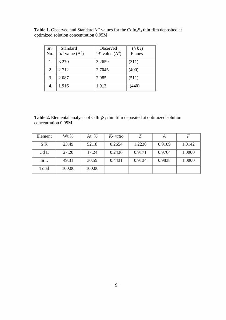
− 9 −
Table 1. Observed and Standard ‘d’ values for the CdIn2S4 thin film deposited at optimized solution concentration 0.05M.
Sr. No.
Standard ‘d’ value (Ao)
Observed ‘d’ value (Ao)
(h k l) Planes
1. 3.270 3.2659 (311)
2. 2.712 2.7045 (400)
3. 2.087 2.085 (511)
4. 1.916 1.913 (440)
Table 2. Elemental analysis of CdIn2S4 thin film deposited at optimized solution concentration 0.05M.
Element Wt % At. % K- ratio Z A F
S K 23.49 52.18 0.2654 1.2230 0.9109 1.0142
Cd L 27.20 17.24 0.2436 0.9171 0.9764 1.0000
In L 49.31 30.59 0.4431 0.9134 0.9838 1.0000
Total 100.00 100.00
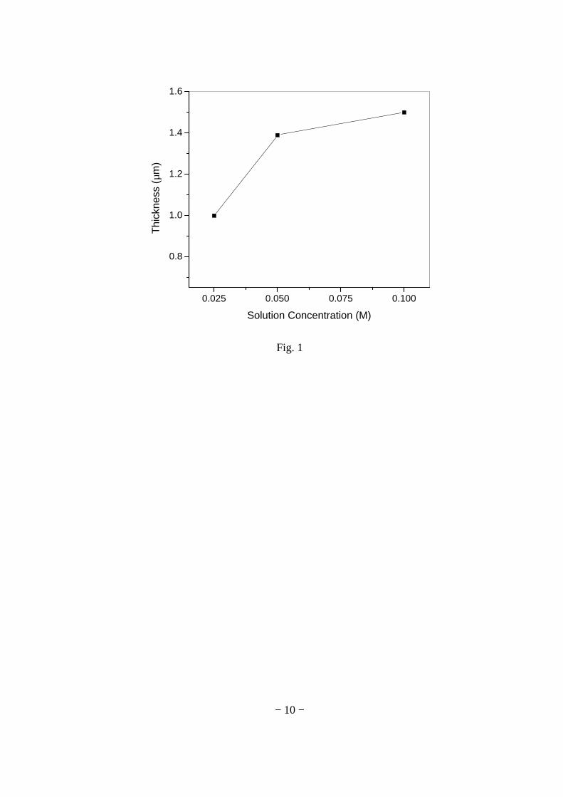
− 10 −
0.025 0.050 0.075 0.100
0.8
1.0
1.2
1.4
1.6
Thi
ckne
ss (
µm)
Solution Concentration (M)
Fig. 1
− 11 −
Fig. 2
− 12 −
0.025 0.050 0.075 0.1000
200
400
600
800
1000
I sc (
µA)
Solution Concentration (M)
Fig. 3
0.025 0.050 0.075 0.100200
250
300
350
400
Voc
(m
V)
Solution Concentration (M)
Fig. 4
− 13 −
2.0 2.2 2.4 2.6 2.8 3.00
50
100
150
200
Eg (indirect) = 2.22 eV
(αhν
)1/2 (
eV/c
m)1/
2
hν (eV)
Fig. 5
0.025 0.050 0.075 0.100
2.22
2.23
2.24
2.25
2.26
2.27
2.28
Ban
d ga
p en
ergy
(eV
)
Solution Concentration (M)
Fig. 6
− 14 −
2.0 2.2 2.4 2.6 2.8 3.0 3.2 3.4 3.61.2
1.4
1.6
1.8
2.0
2.2
2.4
2.6
2.8
3.0
Log
ρ (Ω
.cm
)
1000 / T (K-1)
Fig. 7
0 20 40 60 80 100 120 140 160
0.5
1.0
1.5
2.0
2.5
3.0
The
rmo
emf (
mV
)
Temperature Difference (oC)
Fig. 8
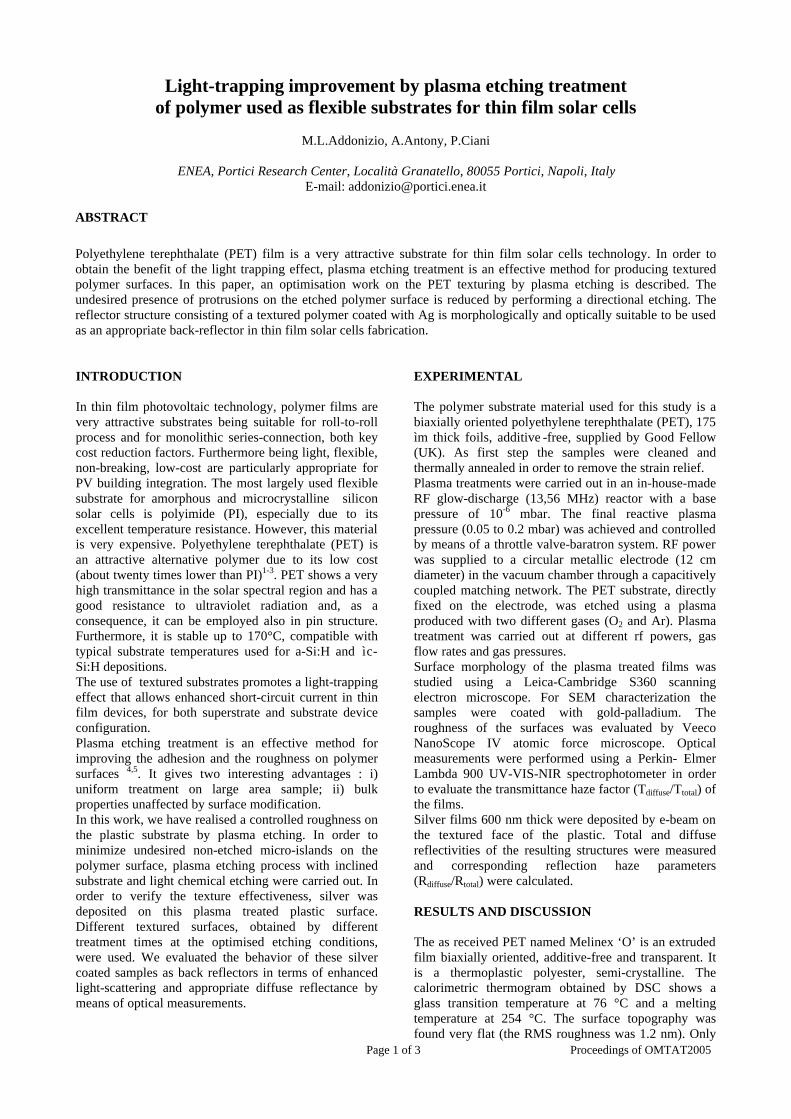
Page 1 of 3 Proceedings of OMTAT2005
Light-trapping improvement by plasma etching treatment of polymer used as flexible substrates for thin film solar cells
M.L.Addonizio, A.Antony, P.Ciani
ENEA, Portici Research Center, Località Granatello, 80055 Portici, Napoli, Italy
E-mail: [email protected]
ABSTRACT
Polyethylene terephthalate (PET) film is a very attractive substrate for thin film solar cells technology. In order to obtain the benefit of the light trapping effect, plasma etching treatment is an effective method for producing textured polymer surfaces. In this paper, an optimisation work on the PET texturing by plasma etching is described. The undesired presence of protrusions on the etched polymer surface is reduced by performing a directional etching. The reflector structure consisting of a textured polymer coated with Ag is morphologically and optically suitable to be used as an appropriate back-reflector in thin film solar cells fabrication. INTRODUCTION In thin film photovoltaic technology, polymer films are very attractive substrates being suitable for roll-to-roll process and for monolithic series-connection, both key cost reduction factors. Furthermore being light, flexible, non-breaking, low-cost are particularly appropriate for PV building integration. The most largely used flexible substrate for amorphous and microcrystalline silicon solar cells is polyimide (PI), especially due to its excellent temperature resistance. However, this material is very expensive. Polyethylene terephthalate (PET) is an attractive alternative polymer due to its low cost (about twenty times lower than PI)1-3. PET shows a very high transmittance in the solar spectral region and has a good resistance to ultraviolet radiation and, as a consequence, it can be employed also in pin structure. Furthermore, it is stable up to 170°C, compatible with typical substrate temperatures used for a-Si:H and ìc-Si:H depositions. The use of textured substrates promotes a light-trapping effect that allows enhanced short-circuit current in thin film devices, for both superstrate and substrate device configuration. Plasma etching treatment is an effective method for improving the adhesion and the roughness on polymer surfaces 4,5. It gives two interesting advantages : i) uniform treatment on large area sample; ii) bulk properties unaffected by surface modification. In this work, we have realised a controlled roughness on the plastic substrate by plasma etching. In order to minimize undesired non-etched micro-islands on the polymer surface, plasma etching process with inclined substrate and light chemical etching were carried out. In order to verify the texture effectiveness, silver was deposited on this plasma treated plastic surface. Different textured surfaces, obtained by different treatment times at the optimised etching conditions, were used. We evaluated the behavior of these silver coated samples as back reflectors in terms of enhanced light-scattering and appropriate diffuse reflectance by means of optical measurements.
EXPERIMENTAL The polymer substrate material used for this study is a biaxially oriented polyethylene terephthalate (PET), 175 ìm thick foils, additive -free, supplied by Good Fellow (UK). As first step the samples were cleaned and thermally annealed in order to remove the strain relief. Plasma treatments were carried out in an in-house-made RF glow-discharge (13,56 MHz) reactor with a base pressure of 10-6 mbar. The final reactive plasma pressure (0.05 to 0.2 mbar) was achieved and controlled by means of a throttle valve-baratron system. RF power was supplied to a circular metallic electrode (12 cm diameter) in the vacuum chamber through a capacitively coupled matching network. The PET substrate, directly fixed on the electrode, was etched using a plasma produced with two different gases (O2 and Ar). Plasma treatment was carried out at different rf powers, gas flow rates and gas pressures. Surface morphology of the plasma treated films was studied using a Leica-Cambridge S360 scanning electron microscope. For SEM characterization the samples were coated with gold-palladium. The roughness of the surfaces was evaluated by Veeco NanoScope IV atomic force microscope. Optical measurements were performed using a Perkin- Elmer Lambda 900 UV-VIS-NIR spectrophotometer in order to evaluate the transmittance haze factor (Tdiffuse/Ttotal) of the films. Silver films 600 nm thick were deposited by e-beam on the textured face of the plastic. Total and diffuse reflectivities of the resulting structures were measured and corresponding reflection haze parameters (Rdiffuse/Rtotal) were calculated. RESULTS AND DISCUSSION The as received PET named Melinex ‘O’ is an extruded film biaxially oriented, additive-free and transparent. It is a thermoplastic polyester, semi-crystalline. The calorimetric thermogram obtained by DSC shows a glass transition temperature at 76 °C and a melting temperature at 254 °C. The surface topography was found very flat (the RMS roughness was 1.2 nm). Only
Page 2 of 3 Proceedings of OMTAT2005
some surface scratches, presumably due to the manufacturing process, were visible. Plasma treatments were carried out using two different gases: Ar as inert gas and O2 as reactive gas in order to investigate the role that the nature of the gas plays on the removal mechanism and, as consequence, on the resulting surface morphology. In order to enhance the etching rate, all the treatments were carried out at very low pressure 6. Indeed, at lower pressure, the mean free path of excited species in the plasma is longer and the probability for theirs being in an excited state (capable of bond breaking) upon arrival at the surface would be greater. With regard to PET films etched in oxygen plasma at fixed values of RF-power and etching time, Fig. 1 shows the behavior of the average haze (Tdiffuse/Ttotal
integrated in the range 300 to 1000 nm) versus the pressure process. It is interesting to note there is an optimal oxygen pressure value (0.1 mbar) for which we obtained the maximum haze value, corresponding to the best scattering properties.
5
6
7
8
9
10
0.05 0.1 0.15 0.2 0.25 0.3 0.35
Haz
e (%
)
Oxygen pressure (mbar)
Rf-power = 50 WO
2 flow rate = 30 sccm
Etching time = 30 min
Fig. 1 – Variation of the optical haze factor for PET films etched under different oxygen pressures. Furthermore, at a fixed value of the process pressure, we have investigated the role of the oxygen on the etching effectiveness. In this case, we verified that the diffuse transmittance continuously increases with the increase in oxygen flow rate from 20 to 50 sccm.
4
5
6
7
8
9
10
11
12
0 5 10 15 20 25 30 35
Haz
e (%
)
Etching time (min)
Rf-Power = 70 WPressure = 0.1 mbarO
2 flow rate= 30 sccm
Fig. 2 – Variation of the optical haze factor for plasma etched PET films with different etching times. We verified that RF-power and etching time give the same effect on the surface modifications. Plasma treatments at 0.1 mbar O2 pressure, 70 W RF-power and
30 sccm O2 flow rate were carried out for different etching times, up to 30 min. Large modifications in the surface topography and in the scattering properties were observed. The optical haze parameter increased following a quite exponentially behavior with the increase in duration of etching (Fig.2). In Fig. 3, SEM pictures show that at lower etching time the surface is uniformly composed of a dense packing of spherical aggregates that are 50-60 nm wide. This structure can be attributed to preferential erosion of amorphous material. At about 8 min of treatment the surface starts to drastically modify and the aggregates becomes less rounded and a rod-like structure appears. This structure becomes more pronounced with the increase the etching time and becomes totally porous after 30 min of treatment. We have evaluate about 2 ìm of material removed at this treatment time. The plasma-modified
Fig. 3 – SEM images of etched PET surfaces for different etching times with oxygen plasma: (a) 4 min, (b) 10 min, (c) 30 min respectively and with argon plasma: (d) 30 min (pressure: 0.1 mbar; RF-power: 70 W; oxygen flow rate: 30 sccm). material is softer than the untreated polymer. We have also carried out PET surface treatments using Argon as process gas. It is generally reported that a noble gas gives a different removal mechanism 7, by means of only physical interactions. We have verified that the etching rate is about ten times lower respect to the oxygen plasma removal. A honey-comb surface structure appears (Fig. 3d) with a very low surface roughness. The corresponding optical scattering properties are too poor for an effective light trapping in thin film silicon solar cells. On the surface of plasma treated PET, large rod-like protrusions of non etched material and snow-ball formations of melted PET remain as process micro-defects (Fig. 4a). By means of x-ray microanalysis
a) b)
c) d)
Page 3 of 3 Proceedings of OMTAT2005
technique, we verified that this undesired phenomenon was due to the presence on the polymer surface of residual agents (especially CaF2) used during the polymer manufacturing process. These chemically contaminated micro-regions are not plasma etched giving rod-like protrusions. Furthermore, some of these protrusions, during the plasma etching, give arc formation producing melted material (snow-ball features). It can be easily understood that it is difficult to deposit solar cells without creating large shunt on such a surface. In order to reduce this phenomenon we have carried out a directional etching (sample tilted respect to the electrode) realizing a reduction of about 70% of such features (see Fig. 4b). We are also trying a chemical etching (alkaline solutions) on the polymer surface prior to the plasma etching. Preliminary results are encouraging and the work is in progress.
Fig. 4 – SEM images showing the reduction of protrusion formation with directional etching. Horizontal (a) and inclined (b) substrate configuration. Subsequently, silver layer was deposited by e-beam evaporation on the textured face of the plastic. Polymer substrates treated in oxygen plasma for different etching times, were used in order to obtain the most appropriate textured back reflector. The total and diffuse reflectivities of the resulting structures have been measured.
0
20
40
60
80
100
300 400 500 600 700 800 900 1000
Dif
fuse
Ref
lect
ivity
(%
)
Wavelength (nm)
30 min
20
12
4
Asahi-U
Fig. 5 –Diffuse reflectivity of the structure Ag/etched PET. The scattering properties obtained on textured PET surfaces at different etching time are compared with Ag/Asahi-U TCO structure. Fig. 5 shows that with the increase in etching time, the diffuse reflectance of the structure increases and reaches the best value after 30 min of the substrate treatment.
This value is compared with the reflectance measured on a silver coated TCO (Asahi-U) used as reference textured structure. Fig. 6 shows AFM image of a silver coated PET treated for 30 min. For this structure we evaluated a RMS roughness of 35 nm. This optimized silver coated PET can be evaluated as appropriate textured back-reflector able to obtain a large light-trapping in a thin film silicon solar cells.
Fig. 6 – AFM surface topography of the structure Ag/etched PET. This PET substrate was treated in plasma for 30 min. CONCLUSIONS PET is a low-cost substrate and it can resist to temperatures compatible with those required in the deposition of device quality silicon thin films. Plasma etching with reactive gas is a viable technique to reproduce nanometer size texturing on the polymer surface of PET. RF-power and etching time were the most meaningful process parameters, able to produce appreciable modifications on the polymer surface. The morphological and optical analysis show that with the increase in etching time, the surface structure evolves from spherical grains to fiber-like structure having a very high porosity and correspondly the diffuse light component increases. The undesired presence of protrusions on the etched polymer surface is reduced about 70% by performing a directional etching (sample tilted respect to the electrode). A pre-treatment of the PET with alkaline solutions gave encouraging preliminary results. The reflector structure consisting of a textured polymer coated with Ag is morphologically and optically suitable to be used in solar cells. ACKNOWLEDGMENTS One of the authors (AA) thanks, ICS-UNIDO for the fellowship under the project "Capacity building of human resources for energy production from renewable sources", funded by the Italian Ministry of Foreign Affairs. References
1 P.Pernet, R.Felder, M.Goetz, H.Keppner, D.Fisher, A.Shah, Proceedings of the 14th ECPSEC, Barcelona, July 1997, 2339. 2 V.Terrazzoni-Daudrix et al., Proc.of 3td WCPEC (2003) 5O-D14-03 3 Vanessa Terrazzoni-Daudrix et al., Proceedings of the MRS vol.769, 195 (2004). 4 M.C.Coen, R.Lehmann, P.Groening, L.Schlapbach, Applied Surface Science 207,276 (2003). 5 Ben D.Beake,J.S.G.Ling and G.J.Leggett, J. Mater. Chem. 8(8),1735(1998). 6 Gottlieb S.Oehrein, Surface Science 386, 222 (1997) 7 M.C.Coen et al., Applied Surface Science 103, 27 (1996)
a) b)
SM 089 OMTAT 2005
Influence of heat treatment temperature on the
photovoltaic properties of spin coated SnO2: Sb thin Films
N. Sankara Subramanian1, M. Jeyachandran2 and S. Ramamurthy3
1. Department of Physics, Thiagarajar College of Engineering, Madurai - 625 015. 2. ECMS Division,Central Electro Chemical Research Institute, Karaikudi- 630 006.
3. Department of Physics, Gandhigram Rural Institute, Gandhigram – 624 302. E-mail: [email protected]
ABSTRACT Antimony doped tin oxide thin films of different thickness have been prepared on mineral glass substrate by spin coating method via sol-gel route, at different heat treatment temperature viz., 350 °C, 375 °C, 400 °C, 425 °C and 450 °C respectively. From the viscosity measurement, rheological properties of the sol solution have been studied and the optimum coating period have been evaluated as 3 days. In this work, ATO films have been developed under optimized coating conditions viz., number of coatings (8), turn table spin rate (300 rpm), spin time (10 seconds) and dopant concentration (5.46 mol % of Sb in SnO2), at different heat treatment temperature. The influence of heat treatment temperature on the structural, optical, electrical and surface properties of the films have been investigated and reported. XRD studies of the films confirm tetragonal rutile structure with preferred orientation along the (110) plane. The lattice constant a and c have been evaluated as 4.7329 A and 3.1921 A respectively, which are well in agreement with the standard values of JCPDS – PDF data (No. 41 – 1445) for SnO2 powder specimen. The mean grain size evaluated from the sherrer’s formula show a non-linear increase up to the optimum heat treatment temperature (400 °C) and beyond which a fall in mean grain size is observed. Optical properties of the films have been investigated in the wavelength region 300nm to 800 nm. All the ATO films show good transmittance in the visible region and the fundamental absorption edge lies in the UV region. A maximum Transmittance of 96 % at 700 nm has been observed for the ATO film heat treated at 400 °C. From the optical absorption data, the direct band gap energy of the films has been evaluated and it lies between 3.2 eV to 3.8 eV. The variation of refractive index with wavelength for different heat treatment temperature have been studied and reported. The minimum value of sheet resistance and electrical resistivity come to 36 Ω/ and 6.7 x 10⁻³ Ω-cm respectively, for the ATO film prepared with the optimum heat treatment temperature. The influence of heat treatment temperature on carrier concentration and mobility of the as coated ATO films have been investigated and the results are discussed. The AFM micrographs of the ATO film prepared with optimum heat treatment temperature (400 °C) shows uniform surface pattern, with the grains of size 1000 nm to 5000 nm. Studies indicate that the sol gel spin coated ATO films prepared under the optimized heat treatment temperature (400 °C) and coating conditions exhibit good optical and electrical properties, indicating it as a potential candidates for the photovoltaic applications. REFERENCES 1. Yung – jen Lin and Ching – Jiunn Wu, Surface and Coating Technology, 88, 239 (1996). 2. H.Viirola, L.Niinisto, Thin Solid Films, 251, 127 (1994) 3. Nae-Lih Wu, Lih-Fu Wu, Ya-Chin Yang and Shu-Jiuan Huang, J. of Materials Res. , Vol. 11, No. 4, 813

(1996). 4. Yung-Jen Lin, Ching-Jiunn Wu, Surface and Coatings Technology, 88, 239 (1996). 5. J.C. Manifacier, Thin Solid Films, 90, 297(1982). 6. K.L. Chopra, S. Major, and D.K. Pandya, Thin Solid Films, 102, 1 (1983). 7. E. Shanthi, V. Dutta, A. Banerjee and K.L. Chopra, Journal of Applied Physics, 51(12), 6243 (Dec. 1980). 8. E. Shanthi, A. Banerjee and K.L. Chopra, Thin Solid Films, 88, 93(1982). 9. E. Shanthi, A. Banerjee and K.L.Chopra, Thin Solid Films, 88, 93 (1982). 10. E. Shanthi, V. Dutta, A.Banerjee and K.L.Chopra, Journal of Applied Physics, 51, 6243 (1980). 11. E. Shanthi, A. Banerjee V. Dutta and K.L. Chopra, Journal of Applied Physics, Vol. 53, No. 3, 1615 (1982). 12. E. Shanthi, A. Banerjee, V. Dutta and K.L.Chopra, Thin Solid Films, 71, 237 (1980). 13. J.C. Manifacier, L. Szepessy, J.F. Bresse, M. Perotin and R. Stuk, Materials Research Bulletin, 14, 109 (1979). 14. J.C.Manifacier, L.Szepessy, J.F. Bresse, M. Perotin and R. Stuck, Materials Research Bulletin, 14, 163 (1979). 15. Geeta Sanon, Raj Rup and Abhai Mansingh, Thin Solid Films, 190, 287 (1990). 16. Chitra Agashe, M.G. Takwale, V.G. Bhide, Shailaja Mahamuni and S.K. Kulkarni, J. Applied Physics, Vol. 70, No. 12, 7382 (1991). 17. N. Srinivasa murthy and S.R. Jawalekar, Thin Solid Films, 102, 283 (1983). --------------------------------------------------------------------------------------------------------------------------------- Corresponding Author: N. Sankara Subramanian, Department of Physics, Thiagarajar College of Engineering, Madurai, Tamilnadu State, India. PIN – 625 015. E-mail: [email protected]. Phone: +91-9443477194. Fax: +91-452-248-3427
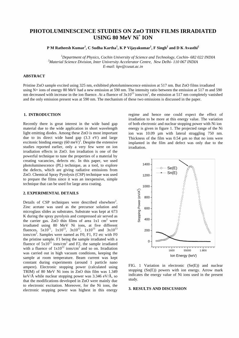
PHOTOLUMINESCENCE STUDIES ON ZnO THIN FILMS IRRADIATED USING 80 MeV Ni+ ION
P M Ratheesh Kumar1, C Sudha Kartha1, K P Vijayakumar1, F Singh2 and D K Avasthi2
1Department of Physics, Cochin University of Science and Technology, Cochin- 682 022 INDIA 2Material Science Division, Inter University Accelerator Centre, New Delhi- 110 067 INDIA
E-mail: [email protected]
ABSTRACT
Pristine ZnO sample excited using 325 nm, exhibited photoluminescence emission at 517 nm. But ZnO films irradiated using N+ ions of energy 80 MeV had a new emission at 590 nm. The intensity ratio between the emission at 517 m and 590 nm decreased with increase in the ion fluence. At a fluence of 3x10¹³ ions/cm2, the emission at 517 nm completely vanished and the only emission present was at 590 nm. The mechanism of these two emissions is discussed in the paper.
1. INTRODUCTION
Recently there is great interest in the wide band gap material due to the wide application in short wavelength light emitting diodes. Among these ZnO is most important due to its direct wide band gap (3.3 eV) and large excitonic binding energy (60 meV)1. Despite the extensive studies reported earlier, only a very few were on ion irradiation effects in ZnO. Ion irradiation is one of the powerful technique to tune the properties of a material by creating vacancies, defects etc. In this paper, we used photoluminescence (PL) technique, as a tool, to explore the defects, which are giving radiative emissions from ZnO. Chemical Spray Pyrolysis (CSP) technique was used to prepare the films since it was an inexpensive, simple technique that can be used for large area coating. 2. EXPERIMENTAL DETAILS Details of CSP techniques were described elsewhere2. Zinc acetate was used as the precursor solution and microglass slides as substrates. Substrate was kept at 673 K during the spray pyrolysis and compressed air served as the carrier gas. ZnO thin films of area 1x1 cm2 were irradiated using 80 MeV Ni ions, at five different fluences, 5x10¹¹, 1x10¹², 3x10¹², 1x10¹³ and 3x10¹³ ions/cm2. Samples were named as F0, F1, F2 etc with F0 the pristine sample. F1 being the sample irradiated with a fluence of 5x10¹¹ ions/cm2 and F2, the sample irradiated with a fluence of 1x10¹² ions/cm2 and so on. Irradiation was carried out in high vacuum conditions, keeping the sample at room temperature. Beam current was kept constant during experiments (around 1 particle nano ampere). Electronic stopping power (calculated using TRIM) of 80 MeV Ni ions in ZnO thin film was 1.349 keV/Å while nuclear stopping power was 3.346 eV/Å, so that the modifications developed in ZnO were mainly due to electronic excitation. Moreover, for the Ni ions, the electronic stopping power was highest in this energy
regime and hence one could expect the effect of irradiation to be more at this energy value. The variation of both electronic and nuclear stopping power with Ni ion energy is given in figure 1. The projected range of the Ni ion was 10.09 µm with lateral straggling 750 nm. Thickness of the film was 0.54 µm so that no ions were implanted in the film and defect was only due to the irradiation.
1600 55000 1.8E6
0
200
400
600
800
1000
1200
1400
Sto
ppin
g P
ower
(eV
/A0 )
Ion Energy (keV)
Se(E) Sn(E)
FIG. 1 Variation in electronic (Se(E)) and nuclear stopping (Sn(E)) powers with ion energy. Arrow mark indicates the energy value of Ni ions used in the present study. 3. RESULTS AND DISCUSSION
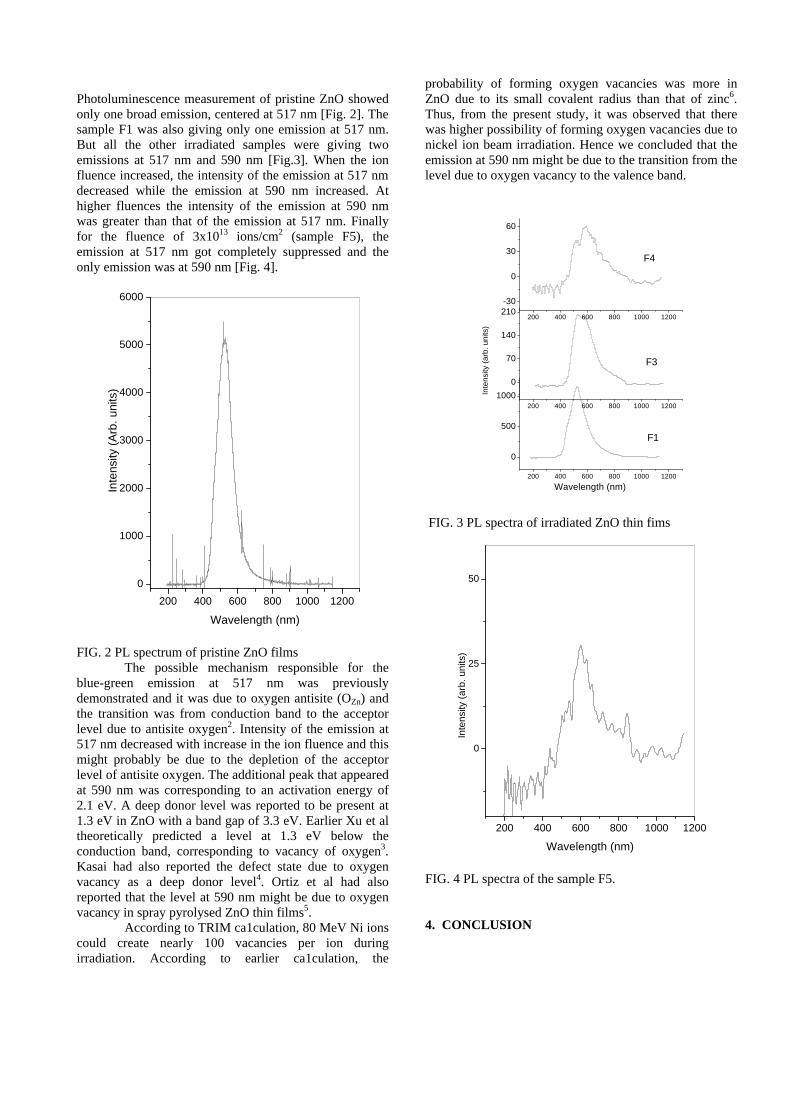
Photoluminescence measurement of pristine ZnO showed only one broad emission, centered at 517 nm [Fig. 2]. The sample F1 was also giving only one emission at 517 nm. But all the other irradiated samples were giving two emissions at 517 nm and 590 nm [Fig.3]. When the ion fluence increased, the intensity of the emission at 517 nm decreased while the emission at 590 nm increased. At higher fluences the intensity of the emission at 590 nm was greater than that of the emission at 517 nm. Finally for the fluence of 3x10¹³ ions/cm2 (sample F5), the emission at 517 nm got completely suppressed and the only emission was at 590 nm [Fig. 4].
200 400 600 800 1000 1200
0
1000
2000
3000
4000
5000
6000
Inte
nsity
(A
rb. u
nits
)
Wavelength (nm)
FIG. 2 PL spectrum of pristine ZnO films The possible mechanism responsible for the blue-green emission at 517 nm was previously demonstrated and it was due to oxygen antisite (OZn) and the transition was from conduction band to the acceptor level due to antisite oxygen2. Intensity of the emission at 517 nm decreased with increase in the ion fluence and this might probably be due to the depletion of the acceptor level of antisite oxygen. The additional peak that appeared at 590 nm was corresponding to an activation energy of 2.1 eV. A deep donor level was reported to be present at 1.3 eV in ZnO with a band gap of 3.3 eV. Earlier Xu et al theoretically predicted a level at 1.3 eV below the conduction band, corresponding to vacancy of oxygen3. Kasai had also reported the defect state due to oxygen vacancy as a deep donor level4. Ortiz et al had also reported that the level at 590 nm might be due to oxygen vacancy in spray pyrolysed ZnO thin films5.
According to TRIM ca1culation, 80 MeV Ni ions could create nearly 100 vacancies per ion during irradiation. According to earlier ca1culation, the
probability of forming oxygen vacancies was more in ZnO due to its small covalent radius than that of zinc6. Thus, from the present study, it was observed that there was higher possibility of forming oxygen vacancies due to nickel ion beam irradiation. Hence we concluded that the emission at 590 nm might be due to the transition from the level due to oxygen vacancy to the valence band.
200 400 600 800 1000 1200
0
500
1000200 400 600 800 1000 1200
0
70
140
210200 400 600 800 1000 1200
-30
0
30
60
Inte
nsity
(ar
b. u
nits
)Wavelength (nm)
F1
F3
F4
FIG. 3 PL spectra of irradiated ZnO thin fims
200 400 600 800 1000 1200
0
25
50
Inte
nsity
(ar
b. u
nits
)
Wavelength (nm)
FIG. 4 PL spectra of the sample F5. 4. CONCLUSION
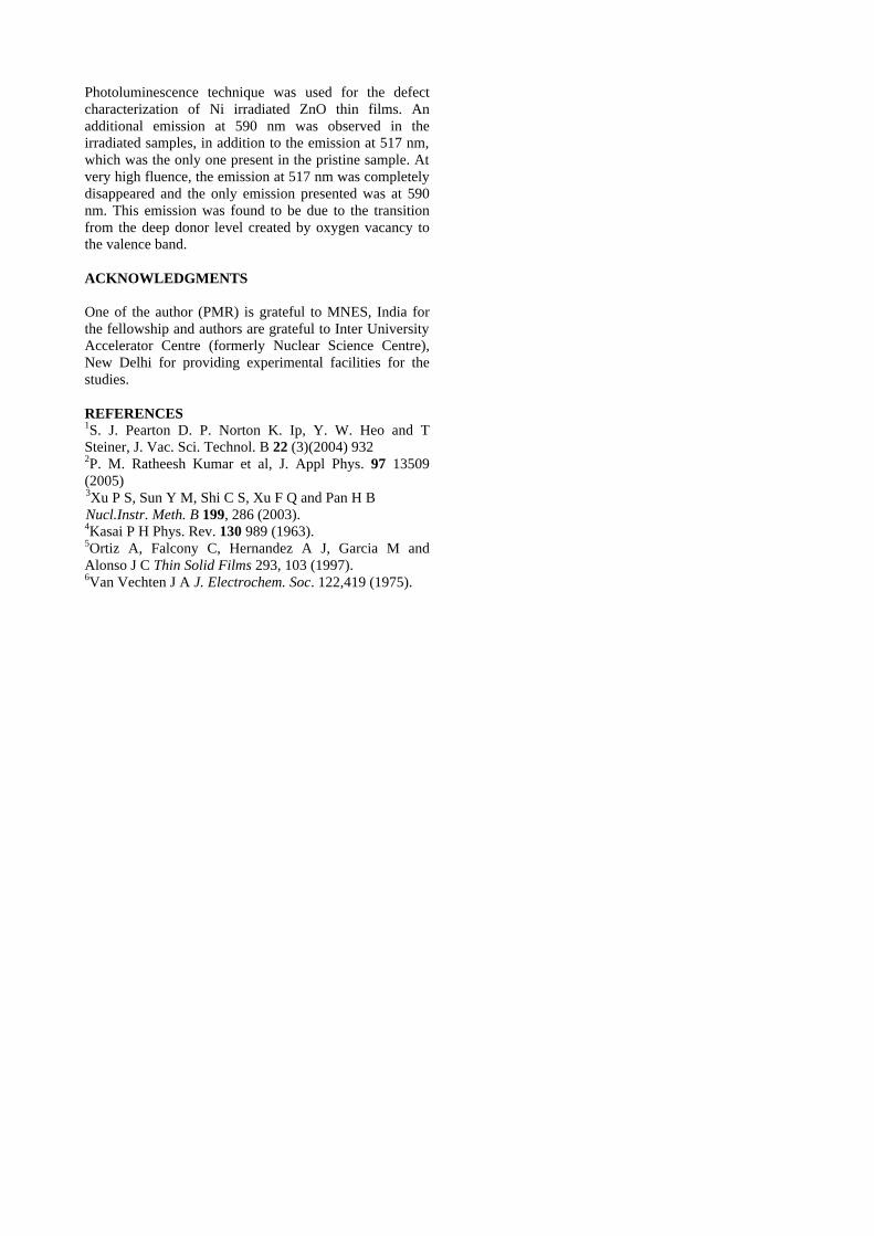
Photoluminescence technique was used for the defect characterization of Ni irradiated ZnO thin films. An additional emission at 590 nm was observed in the irradiated samples, in addition to the emission at 517 nm, which was the only one present in the pristine sample. At very high fluence, the emission at 517 nm was completely disappeared and the only emission presented was at 590 nm. This emission was found to be due to the transition from the deep donor level created by oxygen vacancy to the valence band. ACKNOWLEDGMENTS One of the author (PMR) is grateful to MNES, India for the fellowship and authors are grateful to Inter University Accelerator Centre (formerly Nuclear Science Centre), New Delhi for providing experimental facilities for the studies. REFERENCES 1S. J. Pearton D. P. Norton K. Ip, Y. W. Heo and T Steiner, J. Vac. Sci. Technol. B 22 (3)(2004) 932 2P. M. Ratheesh Kumar et al, J. Appl Phys. 97 13509 (2005) 3Xu P S, Sun Y M, Shi C S, Xu F Q and Pan H B Nucl.Instr. Meth. B 199, 286 (2003). 4Kasai P H Phys. Rev. 130 989 (1963). 5Ortiz A, Falcony C, Hernandez A J, Garcia M and Alonso J C Thin Solid Films 293, 103 (1997). 6Van Vechten J A J. Electrochem. Soc. 122,419 (1975).
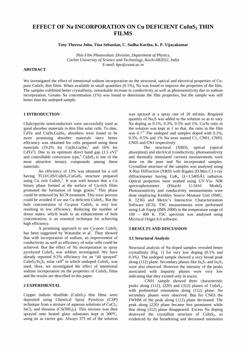
EFFECT OF Na INCORPORATION ON Cu DEFICIENT CuInS2 THIN FILMS
Teny Theresa John, Tina Sebastian, C. Sudha Kartha, K. P. Vijayakumar
Thin Film Photovoltaic Division, Department of Physics,
Cochin University of Science and Technology, Kochi-682022, India E-mail: [email protected]
ABSTRACT
We investigated the effect of intentional sodium incorporation on the structural, optical and electrical properties of Cu-poor CuInS2 thin films. When available in small quantities (0.1%), Na was found to improve the properties of the film. The samples exhibited better crystallinity, remarkable increase in conductivity as well as photosensitivity due to sodium incorporation. Greater Na concentration (1%) was found to deteriorate the film properties, but the sample was still better than the undoped sample. 1 INTRODUCTION Chalcopyrite semiconductors were successfully used as good absorber materials in thin film solar cells. To date, CdTe and Cu(In,Ga)Se2 absorbers were found to be more promising absorber materials since better efficiency was obtained for cells prepared using these materials (19.2% for Cu(In,Ga)Se2
1 and 16% for CdTe2). Due to its optimum direct band gap (1.5 eV)3 and controllable conversion type,4 CuInS2 is one of the most attractive ternary compounds among these materials.
An efficiency of 13% was obtained for a cell having TCO/CdS/CuInS2/CuGaS2 structure prepared using Cu rich CuInS2
5. It was well known that a Cu binary phase formed at the surface of Cu-rich films promoted the formation of large grains.6 This phase could be removed by KCN treatment. This toxic process could be avoided if we use Cu deficient CuInS2. But the hole concentration of Cu-poor CuInS2 is very low resulting in low efficiency. Reducing the number of donor states, which leads to an enhancement of hole concentration, is an essential technique for achieving high efficiency.
A promising approach to use Cu-poor CuInS2 has been suggested by Watanabe et al.7 They showed that with incorporation of sodium, an improvement of conductivity as well as efficiency of solar cells could be achieved. But the effect of Na incorporation in spray pyrolysed CuInS2 was seldom investigated. We have already reported 9.5% efficiency for an “all sprayed” CuInS2/In2S3 solar cell8 in which undoped CuInS2 was used. Here, we investigated the effect of intentional sodium incorporation on the properties of CuInS2 films and the results are described in this paper.
2 EXPERIMENTAL Copper indium disulfide (CuInS2) thin films were deposited using Chemical Spray Pyrolysis (CSP) technique from a mixture of aqueous solutions of CuCl2, InCl3 and thiourea (CS(NH2)2). This mixture was then sprayed onto heated glass substrates kept at 300ºC, using air as carrier gas. Always 375 ml of the solution
was sprayed at a spray rate of 20 ml/min. Required quantity of Na2S was added to the solution so as to vary Na doping as 0.1%, 0.3%, 0.5% and 1%. Cu/In ratio in the solution was kept at 1 so that, the ratio in the film was 0.7.9 The undoped and samples doped with 0.1%, 0.3%, 0.5% and 1% Na were named C1, CN01, CN03, CN05 and CN1 respectively.
The structural (XRD), optical (optical absorption) and electrical (conductivity, photosensitivity and thermally stimulated current) measurements were done on the pure and Na incorporated samples. Crystalline structure of the samples was analysed using X-Ray Diffraction (XRD) with Rigaku (D.Max.C) x-ray diffractometer having CuKα (λ=1.5405Å) radiation. Optical properties were studied using UV-Vis- NIR spectrophotometer (Hitachi U-3410 Model). Photosensitivity and conductivity measurements were done employing Keithley Source Measure Unit (SMU, K 1236) and Metric’s Interactive Characterization Software (ICS). TSC measurements were performed using Lab Equip (IMS 2000) in the temperature range of 100 – 400 K. TSC spectrum was analyzed using Microcal Origin 6.0 software.
3 RESULTS AND DISCUSSION 3.1 Structural Analysis Structural analysis of Na doped samples revealed better crystallinity [Fig. 1] for very low doping (0.1% and 0.3%). The undoped sample showed a very broad peak along (112) plane. Secondary phases like In6S7 and In2S3 were also observed. However the intensity of the peaks associated with impurity phases were very low indicating that they existed only in traces.
CN01 sample showed three characteristic peaks along (112), (220) and (312) planes of CuInS2, with preferential orientation along (112) plane. No secondary phases were observed. But for CN03 the FWHM of the peak along (112) plane decreased. The peak along (220) plane became less prominent while that along (312) plane disappeared. Excess Na doping destroyed the crystalline structure of CuInS2, as evidenced by the broadening and decreased intensities
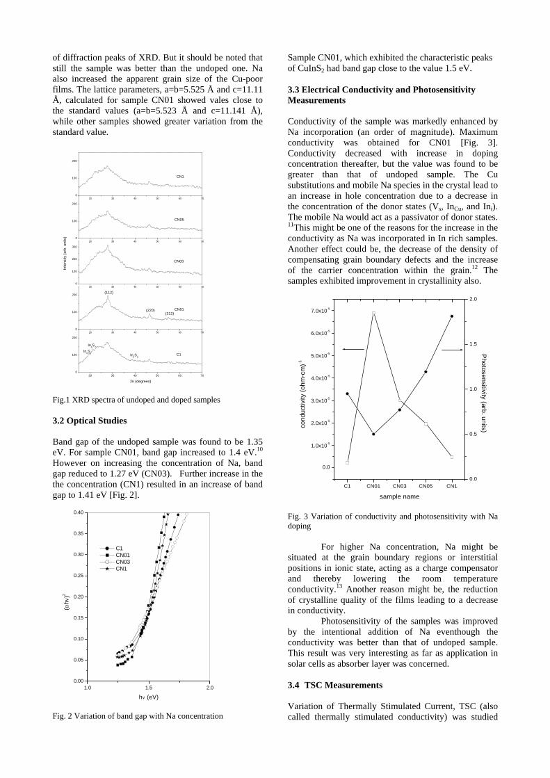
of diffraction peaks of XRD. But it should be noted that still the sample was better than the undoped one. Na also increased the apparent grain size of the Cu-poor films. The lattice parameters, a=b=5.525 Å and c=11.11 Å, calculated for sample CN01 showed vales close to the standard values (a=b=5.523 Å and c=11.141 Å), while other samples showed greater variation from the standard value.
20 30 40 50 60 700
100
200
20 30 40 50 60 700
100
200
20 30 40 50 60 700
100
200
300
20 30 40 50 60 700
100
200
20 30 40 50 60 700
100
200
In2S
3
In6S
7
In6S
7
2θ (degrees)
C1
(312)(220)
(112)
CN01
Inte
nsity
(ar
b. u
nits
)
CN03
CN05
CN1
Fig.1 XRD spectra of undoped and doped samples 3.2 Optical Studies Band gap of the undoped sample was found to be 1.35 eV. For sample CN01, band gap increased to 1.4 eV.10 However on increasing the concentration of Na, band gap reduced to 1.27 eV (CN03). Further increase in the the concentration (CN1) resulted in an increase of band gap to 1.41 eV [Fig. 2].
1.0 1.5 2.00.00
0.05
0.10
0.15
0.20
0.25
0.30
0.35
0.40
(αhν
)2
hν (eV)
C1 CN01 CN03 CN1
Fig. 2 Variation of band gap with Na concentration
Sample CN01, which exhibited the characteristic peaks of CuInS2 had band gap close to the value 1.5 eV. 3.3 Electrical Conductivity and Photosensitivity Measurements Conductivity of the sample was markedly enhanced by Na incorporation (an order of magnitude). Maximum conductivity was obtained for CN01 [Fig. 3]. Conductivity decreased with increase in doping concentration thereafter, but the value was found to be greater than that of undoped sample. The Cu substitutions and mobile Na species in the crystal lead to an increase in hole concentration due to a decrease in the concentration of the donor states (Vs, InCu, and Ini). The mobile Na would act as a passivator of donor states. 11This might be one of the reasons for the increase in the conductivity as Na was incorporated in In rich samples. Another effect could be, the decrease of the density of compensating grain boundary defects and the increase of the carrier concentration within the grain.12 The samples exhibited improvement in crystallinity also.
C1 CN01 CN03 CN05 CN1
0.0
1.0x10⁻⁵
2.0x10⁻⁵
3.0x10⁻⁵
4.0x10⁻⁵
5.0x10⁻⁵
6.0x10⁻⁵
7.0x10⁻⁵
sample name
cond
uctiv
ity (
ohm
-cm
)-1
0.0
0.5
1.0
1.5
2.0
Photosensitivity (arb. units)
Fig. 3 Variation of conductivity and photosensitivity with Na doping
For higher Na concentration, Na might be situated at the grain boundary regions or interstitial positions in ionic state, acting as a charge compensator and thereby lowering the room temperature conductivity.13 Another reason might be, the reduction of crystalline quality of the films leading to a decrease in conductivity.
Photosensitivity of the samples was improved by the intentional addition of Na eventhough the conductivity was better than that of undoped sample. This result was very interesting as far as application in solar cells as absorber layer was concerned.
3.4 TSC Measurements Variation of Thermally Stimulated Current, TSC (also called thermally stimulated conductivity) was studied
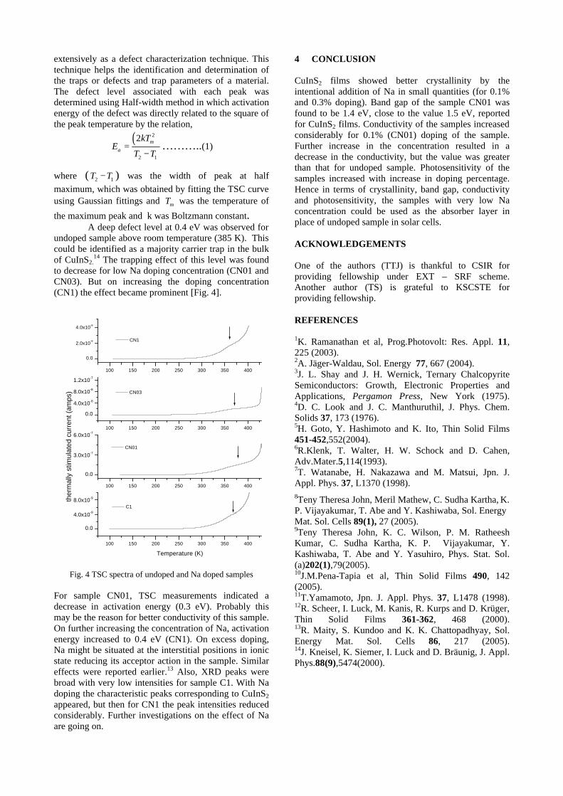
extensively as a defect characterization technique. This technique helps the identification and determination of the traps or defects and trap parameters of a material. The defect level associated with each peak was determined using Half-width method in which activation energy of the defect was directly related to the square of the peak temperature by the relation,
( )2
2 1
2 m
a
kTE
T T=
−………..(1)
where ( 2 1T T− ) was the width of peak at half
maximum, which was obtained by fitting the TSC curve using Gaussian fittings and mT was the temperature of
the maximum peak and k was Boltzmann constant. A deep defect level at 0.4 eV was observed for undoped sample above room temperature (385 K). This could be identified as a majority carrier trap in the bulk of CuInS2.
14 The trapping effect of this level was found to decrease for low Na doping concentration (CN01 and CN03). But on increasing the doping concentration (CN1) the effect became prominent [Fig. 4].
100 150 200 250 300 350 400
0.0
4.0x10⁻⁹
8.0x10⁻⁹
100 150 200 250 300 350 400
0.0
3.0x10⁻⁷
6.0x10-7100 150 200 250 300 350 400
0.0
4.0x10⁻⁸
8.0x10⁻⁸
1.2x10⁻⁷
100 150 200 250 300 350 400
0.0
2.0x10⁻⁹
4.0x10⁻⁹
Temperature (K)
C1
CN01
ther
mal
ly s
timul
ated
cur
rent
(am
ps) CN03
CN1
Fig. 4 TSC spectra of undoped and Na doped samples For sample CN01, TSC measurements indicated a decrease in activation energy (0.3 eV). Probably this may be the reason for better conductivity of this sample. On further increasing the concentration of Na, activation energy increased to 0.4 eV (CN1). On excess doping, Na might be situated at the interstitial positions in ionic state reducing its acceptor action in the sample. Similar effects were reported earlier.13 Also, XRD peaks were broad with very low intensities for sample C1. With Na doping the characteristic peaks corresponding to CuInS2 appeared, but then for CN1 the peak intensities reduced considerably. Further investigations on the effect of Na are going on.
4 CONCLUSION CuInS2 films showed better crystallinity by the intentional addition of Na in small quantities (for 0.1% and 0.3% doping). Band gap of the sample CN01 was found to be 1.4 eV, close to the value 1.5 eV, reported for CuInS2 films. Conductivity of the samples increased considerably for 0.1% (CN01) doping of the sample. Further increase in the concentration resulted in a decrease in the conductivity, but the value was greater than that for undoped sample. Photosensitivity of the samples increased with increase in doping percentage. Hence in terms of crystallinity, band gap, conductivity and photosensitivity, the samples with very low Na concentration could be used as the absorber layer in place of undoped sample in solar cells. ACKNOWLEDGEMENTS One of the authors (TTJ) is thankful to CSIR for providing fellowship under EXT – SRF scheme. Another author (TS) is grateful to KSCSTE for providing fellowship. REFERENCES 1K. Ramanathan et al, Prog.Photovolt: Res. Appl. 11, 225 (2003). 2A. Jäger-Waldau, Sol. Energy 77, 667 (2004). 3J. L. Shay and J. H. Wernick, Ternary Chalcopyrite Semiconductors: Growth, Electronic Properties and Applications, Pergamon Press, New York (1975). 4D. C. Look and J. C. Manthuruthil, J. Phys. Chem. Solids 37, 173 (1976). 5H. Goto, Y. Hashimoto and K. Ito, Thin Solid Films 451-452,552(2004). 6R.Klenk, T. Walter, H. W. Schock and D. Cahen, Adv.Mater.5,114(1993). 7T. Watanabe, H. Nakazawa and M. Matsui, Jpn. J. Appl. Phys. 37, L1370 (1998). 8Teny Theresa John, Meril Mathew, C. Sudha Kartha, K. P. Vijayakumar, T. Abe and Y. Kashiwaba, Sol. Energy Mat. Sol. Cells 89(1), 27 (2005). 9Teny Theresa John, K. C. Wilson, P. M. Ratheesh Kumar, C. Sudha Kartha, K. P. Vijayakumar, Y. Kashiwaba, T. Abe and Y. Yasuhiro, Phys. Stat. Sol. (a)202(1),79(2005). 10J.M.Pena-Tapia et al, Thin Solid Films 490, 142 (2005). 11T.Yamamoto, Jpn. J. Appl. Phys. 37, L1478 (1998). 12R. Scheer, I. Luck, M. Kanis, R. Kurps and D. Krüger, Thin Solid Films 361-362, 468 (2000). 13R. Maity, S. Kundoo and K. K. Chattopadhyay, Sol. Energy Mat. Sol. Cells 86, 217 (2005). 14J. Kneisel, K. Siemer, I. Luck and D. Bräunig, J. Appl. Phys.88(9),5474(2000).
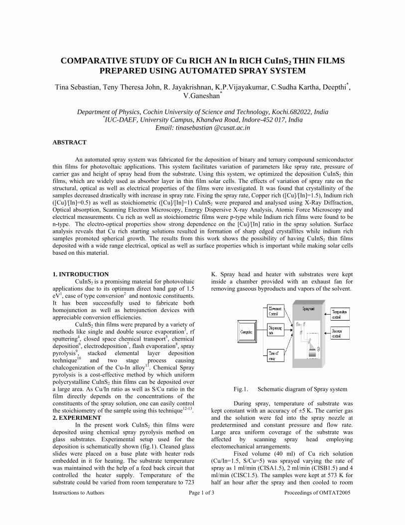
Instructions to Authors Page 1 of 3 Proceedings of OMTAT2005
COMPARATIVE STUDY OF Cu RICH AN In RICH CuInS2 THIN FILMS PREPARED USING AUTOMATED SPRAY SYSTEM
Tina Sebastian, Teny Theresa John, R. Jayakrishnan, K.P.Vijayakumar, C.Sudha Kartha, Deepthi*,
V.Ganeshan*
Department of Physics, Cochin University of Science and Technology, Kochi.682022, India
*IUC-DAEF, University Campus, Khandwa Road, Indore-452 017, India Email: tinasebastian @cusat.ac.in
ABSTRACT
An automated spray system was fabricated for the deposition of binary and ternary compound semiconductor thin films for photovoltaic applications. This system facilitates variation of parameters like spray rate, pressure of carrier gas and height of spray head from the substrate. Using this system, we optimized the deposition CuInS2 thin films, which are widely used as absorber layer in thin film solar cells. The effects of variation of spray rate on the structural, optical as well as electrical properties of the films were investigated. It was found that crystallinity of the samples decreased drastically with increase in spray rate. Fixing the spray rate, Copper rich ([Cu]/[In]=1.5), Indium rich ([Cu]/[In]=0.5) as well as stoichiometric ([Cu]/[In]=1) CuInS2 were prepared and analysed using X-Ray Diffraction, Optical absorption, Scanning Electron Microscopy, Energy Dispersive X-ray Analysis, Atomic Force Microscopy and electrical measurements. Cu rich as well as stoichiometric films were p-type while Indium rich films were found to be n-type. The electro-optical properties show strong dependence on the [Cu]/[In] ratio in the spray solution. Surface analysis reveals that Cu rich starting solutions resulted in formation of sharp edged crystallites while indium rich samples promoted spherical growth. The results from this work shows the possibility of having CuInS2 thin films deposited with a wide range electrical, optical as well as surface properties which is important while making solar cells based on this material. 1. INTRODUCTION
CuInS2 is a promising material for photovoltaic applications due to its optimum direct band gap of 1.5 eV1, ease of type conversion2 and nontoxic constituents. It has been successfully used to fabricate both homojunction as well as hetrojunction devices with appreciable conversion efficiencies.
CuInS2 thin films were prepared by a variety of methods like single and double source evaporation3, rf sputtering4, closed space chemical transport5, chemical deposition6, electrodeposition7, flash evaporation8, spray pyrolysis9, stacked elemental layer deposition technique10 and two stage process causing chalcogenization of the Cu-In alloy11. Chemical Spray pyrolysis is a cost-effective method by which uniform polycrystalline CuInS2 thin films can be deposited over a large area. As Cu/In ratio as well as S/Cu ratio in the film directly depends on the concentrations of the constituents of the spray solution, one can easily control the stoichiometry of the sample using this technique12-13. 2. EXPERIMENT
In the present work CuInS2 thin films were deposited using chemical spray pyrolysis method on glass substrates. Experimental setup used for the deposition is schematically shown (fig.1). Cleaned glass slides were placed on a base plate with heater rods embedded in it for heating. The substrate temperature was maintained with the help of a feed back circuit that controlled the heater supply. Temperature of the substrate could be varied from room temperature to 723
K. Spray head and heater with substrates were kept inside a chamber provided with an exhaust fan for removing gaseous byproducts and vapors of the solvent.
Fig.1. Schematic diagram of Spray system During spray, temperature of substrate was
kept constant with an accuracy of ±5 K. The carrier gas and the solution were fed into the spray nozzle at predetermined and constant pressure and flow rate. Large area uniform coverage of the substrate was affected by scanning spray head employing electomechanical arrangements.
Fixed volume (40 ml) of Cu rich solution (Cu/In=1.5, S/Cu=5) was sprayed varying the rate of spray as 1 ml/min (CISA1.5), 2 ml/min (CISB1.5) and 4 ml/min (CISC1.5). The samples were kept at 573 K for half an hour after the spray and then cooled to room
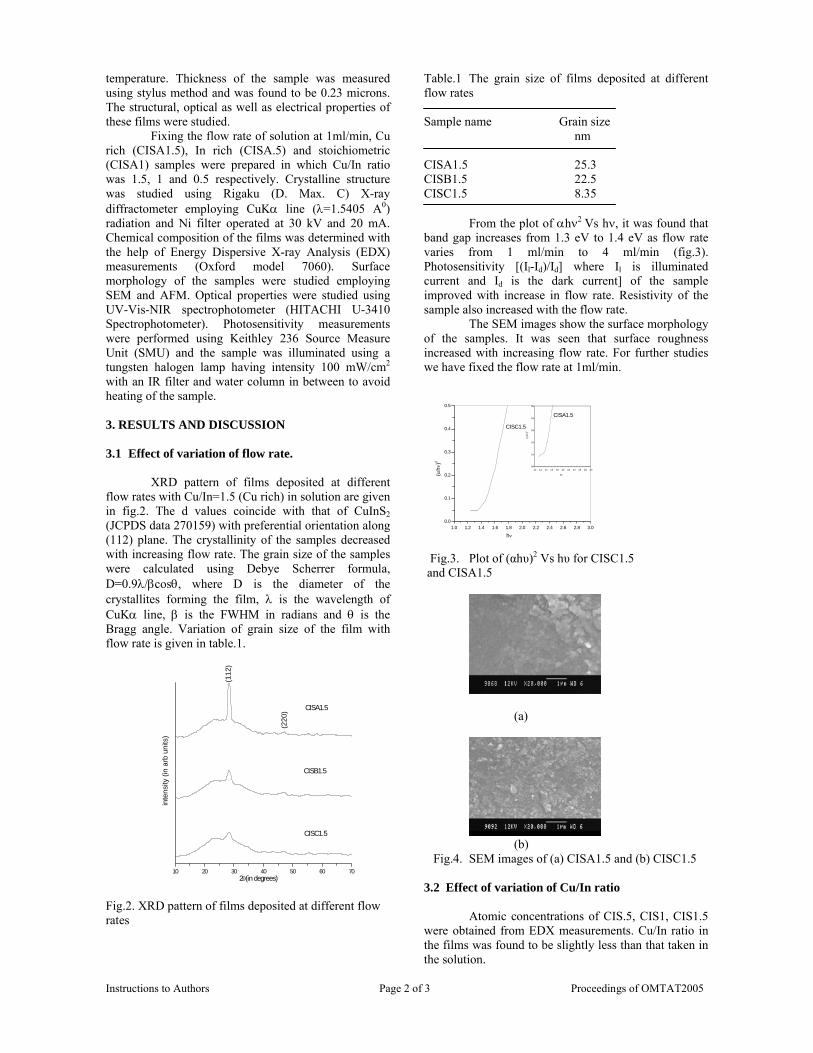
Instructions to Authors Page 2 of 3 Proceedings of OMTAT2005
temperature. Thickness of the sample was measured using stylus method and was found to be 0.23 microns. The structural, optical as well as electrical properties of these films were studied.
Fixing the flow rate of solution at 1ml/min, Cu rich (CISA1.5), In rich (CISA.5) and stoichiometric (CISA1) samples were prepared in which Cu/In ratio was 1.5, 1 and 0.5 respectively. Crystalline structure was studied using Rigaku (D. Max. C) X-ray diffractometer employing CuKα line (λ=1.5405 A0) radiation and Ni filter operated at 30 kV and 20 mA. Chemical composition of the films was determined with the help of Energy Dispersive X-ray Analysis (EDX) measurements (Oxford model 7060). Surface morphology of the samples were studied employing SEM and AFM. Optical properties were studied using UV-Vis-NIR spectrophotometer (HITACHI U-3410 Spectrophotometer). Photosensitivity measurements were performed using Keithley 236 Source Measure Unit (SMU) and the sample was illuminated using a tungsten halogen lamp having intensity 100 mW/cm2 with an IR filter and water column in between to avoid heating of the sample.
3. RESULTS AND DISCUSSION 3.1 Effect of variation of flow rate.
XRD pattern of films deposited at different flow rates with Cu/In=1.5 (Cu rich) in solution are given in fig.2. The d values coincide with that of CuInS2 (JCPDS data 270159) with preferential orientation along (112) plane. The crystallinity of the samples decreased with increasing flow rate. The grain size of the samples were calculated using Debye Scherrer formula, D=0.9λ/βcosθ, where D is the diameter of the crystallites forming the film, λ is the wavelength of CuKα line, β is the FWHM in radians and θ is the Bragg angle. Variation of grain size of the film with flow rate is given in table.1.
Fig.2. XRD pattern of films deposited at different flow rates
Table.1 The grain size of films deposited at different flow rates Sample name Grain size nm CISA1.5 25.3 CISB1.5 22.5 CISC1.5 8.35
From the plot of αhν2 Vs hν, it was found that
band gap increases from 1.3 eV to 1.4 eV as flow rate varies from 1 ml/min to 4 ml/min (fig.3). Photosensitivity [(Il-Id)/Id] where Il is illuminated current and Id is the dark current] of the sample improved with increase in flow rate. Resistivity of the sample also increased with the flow rate.
The SEM images show the surface morphology of the samples. It was seen that surface roughness increased with increasing flow rate. For further studies we have fixed the flow rate at 1ml/min.
1.0 1.2 1.4 1.6 1.8 2.0 2.2 2.4 2.6 2.8 3.00.0
0.1
0.2
0.3
0.4
0.5
CISA1.5
CISC1.5
1.0 1.2 1.4 1.6 1.8 2.0 2.2 2.4 2.6 2.8 3.00.0
0.1
0.2
0.3
0.4
0.5
hν
(αhν
)2
(αhν
)2
hν
Fig.3. Plot of (αhυ)2 Vs hυ for CISC1.5 and CISA1.5
(a)
(b)
Fig.4. SEM images of (a) CISA1.5 and (b) CISC1.5 3.2 Effect of variation of Cu/In ratio Atomic concentrations of CIS.5, CIS1, CIS1.5 were obtained from EDX measurements. Cu/In ratio in the films was found to be slightly less than that taken in the solution.
10 20 30 40 50 60 70
CISC1.5
2θ(in degrees)
inte
nsity
(in
arb
units
)
CISB1.5
(220
)
(112
)
CISA1.5
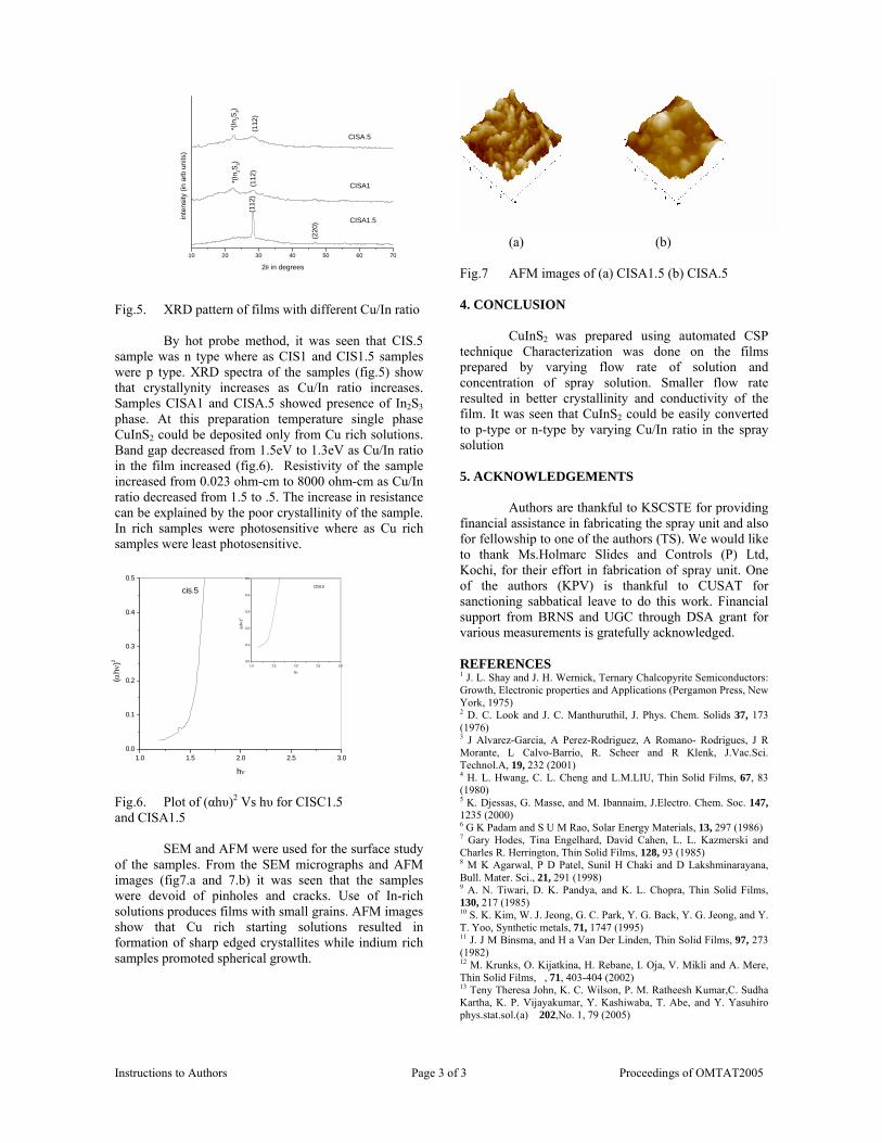
Instructions to Authors Page 3 of 3 Proceedings of OMTAT2005
Fig.5. XRD pattern of films with different Cu/In ratio
By hot probe method, it was seen that CIS.5
sample was n type where as CIS1 and CIS1.5 samples were p type. XRD spectra of the samples (fig.5) show that crystallynity increases as Cu/In ratio increases. Samples CISA1 and CISA.5 showed presence of In2S3 phase. At this preparation temperature single phase CuInS2 could be deposited only from Cu rich solutions. Band gap decreased from 1.5eV to 1.3eV as Cu/In ratio in the film increased (fig.6). Resistivity of the sample increased from 0.023 ohm-cm to 8000 ohm-cm as Cu/In ratio decreased from 1.5 to .5. The increase in resistance can be explained by the poor crystallinity of the sample. In rich samples were photosensitive where as Cu rich samples were least photosensitive.
Fig.6. Plot of (αhυ)2 Vs hυ for CISC1.5 and CISA1.5
SEM and AFM were used for the surface study
of the samples. From the SEM micrographs and AFM images (fig7.a and 7.b) it was seen that the samples were devoid of pinholes and cracks. Use of In-rich solutions produces films with small grains. AFM images show that Cu rich starting solutions resulted in formation of sharp edged crystallites while indium rich samples promoted spherical growth.
(a) (b) Fig.7 AFM images of (a) CISA1.5 (b) CISA.5 4. CONCLUSION
CuInS2 was prepared using automated CSP technique Characterization was done on the films prepared by varying flow rate of solution and concentration of spray solution. Smaller flow rate resulted in better crystallinity and conductivity of the film. It was seen that CuInS2 could be easily converted to p-type or n-type by varying Cu/In ratio in the spray solution
5. ACKNOWLEDGEMENTS Authors are thankful to KSCSTE for providing financial assistance in fabricating the spray unit and also for fellowship to one of the authors (TS). We would like to thank Ms.Holmarc Slides and Controls (P) Ltd, Kochi, for their effort in fabrication of spray unit. One of the authors (KPV) is thankful to CUSAT for sanctioning sabbatical leave to do this work. Financial support from BRNS and UGC through DSA grant for various measurements is gratefully acknowledged. REFERENCES 1 J. L. Shay and J. H. Wernick, Ternary Chalcopyrite Semiconductors: Growth, Electronic properties and Applications (Pergamon Press, New York, 1975) 2 D. C. Look and J. C. Manthuruthil, J. Phys. Chem. Solids 37, 173 (1976) 3 J Alvarez-Garcia, A Perez-Rodriguez, A Romano- Rodrigues, J R Morante, L Calvo-Barrio, R. Scheer and R Klenk, J.Vac.Sci. Technol.A, 19, 232 (2001) 4 H. L. Hwang, C. L. Cheng and L.M.LIU, Thin Solid Films, 67, 83 (1980) 5 K. Djessas, G. Masse, and M. Ibannaim, J.Electro. Chem. Soc. 147, 1235 (2000) 6 G K Padam and S U M Rao, Solar Energy Materials, 13, 297 (1986) 7 Gary Hodes, Tina Engelhard, David Cahen, L. L. Kazmerski and Charles R. Herrington, Thin Solid Films, 128, 93 (1985) 8 M K Agarwal, P D Patel, Sunil H Chaki and D Lakshminarayana, Bull. Mater. Sci., 21, 291 (1998) 9 A. N. Tiwari, D. K. Pandya, and K. L. Chopra, Thin Solid Films, 130, 217 (1985) 10 S. K. Kim, W. J. Jeong, G. C. Park, Y. G. Back, Y. G. Jeong, and Y. T. Yoo, Synthetic metals, 71, 1747 (1995) 11 J. J M Binsma, and H a Van Der Linden, Thin Solid Films, 97, 273 (1982) 12 M. Krunks, O. Kijatkina, H. Rebane, I. Oja, V. Mikli and A. Mere, Thin Solid Films, , 71, 403-404 (2002) 13 Teny Theresa John, K. C. Wilson, P. M. Ratheesh Kumar,C. Sudha Kartha, K. P. Vijayakumar, Y. Kashiwaba, T. Abe, and Y. Yasuhiro phys.stat.sol.(a) 202,No. 1, 79 (2005)
10 20 30 40 50 60 70
CISA1.5
(220
)
CISA1
(112
)
*(In
2S 3)
(112
)
2θ in degrees
inte
nsity
(in
arb
units
)
CISA.5
*(In
2S3)
(112
)
1.0 1.5 2.0 2.5 3.00.0
0.1
0.2
0.3
0.4
0.5
1.0 1.5 2.0 2.5 3.00.0
0.1
0.2
0.3
0.4
0.5
CIS1.5
(αhν
)2
hν
cis.5
(αhν
)2
hν
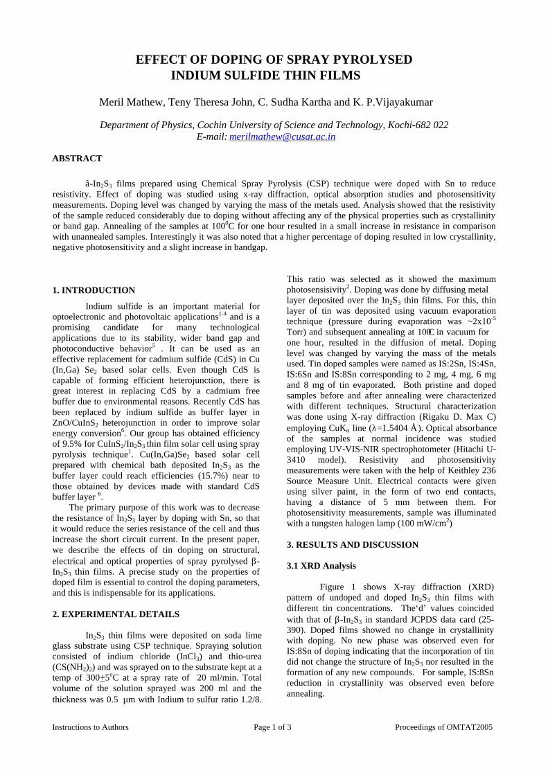
Instructions to Authors Page 1 of 3 Proceedings of OMTAT2005
EFFECT OF DOPING OF SPRAY PYROLYSED INDIUM SULFIDE THIN FILMS
Meril Mathew, Teny Theresa John, C. Sudha Kartha and K. P.Vijayakumar
Department of Physics, Cochin University of Science and Technology, Kochi-682 022
E-mail: [email protected]
ABSTRACT
â-In2S3 films prepared using Chemical Spray Pyrolysis (CSP) technique were doped with Sn to reduce
resistivity. Effect of doping was studied using x-ray diffraction, optical absorption studies and photosensitivity measurements. Doping level was changed by varying the mass of the metals used. Analysis showed that the resistivity of the sample reduced considerably due to doping without affecting any of the physical properties such as crystallinity or band gap. Annealing of the samples at 1000C for one hour resulted in a small increase in resistance in comparison with unannealed samples. Interestingly it was also noted that a higher percentage of doping resulted in low crystallinity, negative photosensitivity and a slight increase in bandgap.
1. INTRODUCTION
Indium sulfide is an important material for optoelectronic and photovoltaic applications1-4 and is a promising candidate for many technological applications due to its stability, wider band gap and photoconductive behavior5 . It can be used as an effective replacement for cadmium sulfide (CdS) in Cu (In,Ga) Se2 based solar cells. Even though CdS is capable of forming efficient heterojunction, there is great interest in replacing CdS by a cadmium free buffer due to environmental reasons. Recently CdS has been replaced by indium sulfide as buffer layer in ZnO/CuInS2 heterojunction in order to improve solar energy conversion6. Our group has obtained efficiency of 9.5% for CuInS2/In2S3 thin film solar cell using spray pyrolysis technique1. Cu(In,Ga)Se2 based solar cell prepared with chemical bath deposited In2S3 as the buffer layer could reach efficiencies (15.7%) near to those obtained by devices made with standard CdS buffer layer 6.
The primary purpose of this work was to decrease the resistance of In2S3 layer by doping with Sn, so that it would reduce the series resistance of the cell and thus increase the short circuit current. In the present paper, we describe the effects of tin doping on structural, electrical and optical properties of spray pyrolysed β-In2S3 thin films. A precise study on the properties of doped film is essential to control the doping parameters, and this is indispensable for its applications.
2. EXPERIMENTAL DETAILS
In2S3 thin films were deposited on soda lime
glass substrate using CSP technique. Spraying solution consisted of indium chloride (InCl3) and thio-urea (CS(NH2)2) and was sprayed on to the substrate kept at a temp of 300+5oC at a spray rate of 20 ml/min. Total volume of the solution sprayed was 200 ml and the thickness was 0.5 µm with Indium to sulfur ratio 1.2/8.
This ratio was selected as it showed the maximum photosensisivity2. Doping was done by diffusing metal layer deposited over the In2S3 thin films. For this, thin layer of tin was deposited using vacuum evaporation technique (pressure during evaporation was ~2x10⁻⁵ Torr) and subsequent annealing at 100C in vacuum for one hour, resulted in the diffusion of metal. Doping level was changed by varying the mass of the metals used. Tin doped samples were named as IS:2Sn, IS:4Sn, IS:6Sn and IS:8Sn corresponding to 2 mg, 4 mg, 6 mg and 8 mg of tin evaporated. Both pristine and doped samples before and after annealing were characterized with different techniques. Structural characterization was done using X-ray diffraction (Rigaku D. Max C) employing CuKα line (λ=1.5404 Å). Optical absorbance of the samples at normal incidence was studied employing UV-VIS-NIR spectrophotometer (Hitachi U-3410 model). Resistivity and photosensitivity measurements were taken with the help of Keithley 236 Source Measure Unit. Electrical contacts were given using silver paint, in the form of two end contacts, having a distance of 5 mm between them. For photosensitivity measurements, sample was illuminated with a tungsten halogen lamp (100 mW/cm2)
3. RESULTS AND DISCUSSION 3.1 XRD Analysis Figure 1 shows X-ray diffraction (XRD) pattern of undoped and doped In2S3 thin films with different tin concentrations. The‘d’ values coincided with that of β-In2S3 in standard JCPDS data card (25-390). Doped films showed no change in crystallinity with doping. No new phase was observed even for IS:8Sn of doping indicating that the incorporation of tin did not change the structure of In2S3 nor resulted in the formation of any new compounds. For sample, IS:8Sn reduction in crystallinity was observed even before annealing.
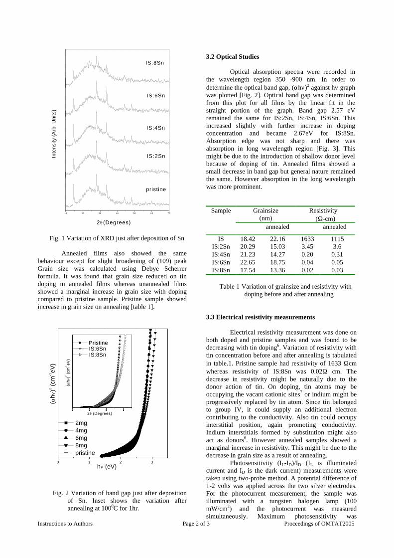
Instructions to Authors Page 2 of 3 Proceedings of OMTAT2005
10 20 30 40 50 60 70
IS:2Sn
IS:4Sn
Inte
nsity
(A
rb. U
nits
)
IS:6Sn
IS:8Sn
2θ (Degrees)
pristine
Fig. 1 Variation of XRD just after deposition of Sn Annealed films also showed the same behaviour except for slight broadening of (109) peak Grain size was calculated using Debye Scherrer formula. It was found that grain size reduced on tin doping in annealed films whereas unannealed films showed a marginal increase in grain size with doping compared to pristine sample. Pristine sample showed increase in grain size on annealing [table 1].
0 1 2 3
0 1 2 30 1 2 30 1 2 30 1 2 3
Pristine
2θ (Degrees)
(αhν
)2 (cm
-1eV
)
IS:6Sn IS:8Sn
(αhν
)2 (cm
-1eV
)
hν (eV)
2mg 4mg 6mg 8mg pristine
Fig. 2 Variation of band gap just after deposition
of Sn. Inset shows the variation after annealing at 1000C for 1hr.
3.2 Optical Studies Optical absorption spectra were recorded in the wavelength region 350 -900 nm. In order to determine the optical band gap, (αhν)2 against hν graph was plotted [Fig. 2]. Optical band gap was determined from this plot for all films by the linear fit in the straight portion of the graph. Band gap 2.57 eV remained the same for IS:2Sn, IS:4Sn, IS:6Sn. This increased slightly with further increase in doping concentration and became 2.67eV for IS:8Sn. Absorption edge was not sharp and there was absorption in long wavelength region [Fig. 3]. This might be due to the introduction of shallow donor level because of doping of tin. Annealed films showed a small decrease in band gap but general nature remained the same. However absorption in the long wavelength was more prominent.
Grainsize (nm)
Resistivity (Ω-cm)
Sample
annealed annealed
IS 18.42 22.16 1633 1115 IS:2Sn 20.29 15.03 3.45 3.6 IS:4Sn 21.23 14.27 0.20 0.31 IS:6Sn 22.65 18.75 0.04 0.05 IS:8Sn 17.54 13.36 0.02 0.03
Table 1 Variation of grainsize and resistivity with doping before and after annealing 3.3 Electrical resistivity measurements
Electrical resistivity measurement was done on both doped and pristine samples and was found to be decreasing with tin doping6. Variation of resistivity with tin concentration before and after annealing is tabulated in table.1. Pristine sample had resistivity of 1633 Ωcm whereas resistivity of IS:8Sn was 0.02Ω cm. The decrease in resistivity might be naturally due to the donor action of tin. On doping, tin atoms may be occupying the vacant cationic sites7 or indium might be progressively replaced by tin atom. Since tin belonged to group IV, it could supply an additional electron contributing to the conductivity. Also tin could occupy interstitial position, again promoting conductivity. Indium interstitials formed by substitution might also act as donors6. However annealed samples showed a marginal increase in resistivity. This might be due to the decrease in grain size as a result of annealing.
Photosensitivity (IL-ID)/ID (IL is illuminated current and ID is the dark current) measurements were taken using two-probe method. A potential difference of 1-2 volts was applied across the two silver electrodes. For the photocurrent measurement, the sample was illuminated with a tungsten halogen lamp (100 mW/cm2) and the photocurrent was measured simultaneously. Maximum photosensitivity was
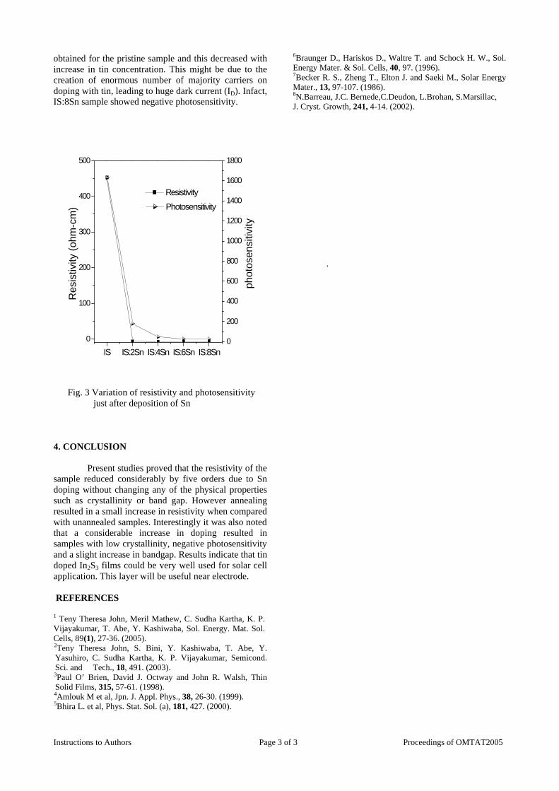
Instructions to Authors Page 3 of 3 Proceedings of OMTAT2005
obtained for the pristine sample and this decreased with increase in tin concentration. This might be due to the creation of enormous number of majority carriers on doping with tin, leading to huge dark current (ID). Infact, IS:8Sn sample showed negative photosensitivity.
0
200
400
600
800
1000
1200
1400
1600
1800
IS IS:2Sn IS:4Sn IS:6Sn IS:8Sn
0
100
200
300
400
500
Res
istiv
ity (
ohm
-cm
)
phot
osen
sitiv
ity
Resistivity
Photosensitivity
Fig. 3 Variation of resistivity and photosensitivity just after deposition of Sn 4. CONCLUSION
Present studies proved that the resistivity of the sample reduced considerably by five orders due to Sn doping without changing any of the physical properties such as crystallinity or band gap. However annealing resulted in a small increase in resistivity when compared with unannealed samples. Interestingly it was also noted that a considerable increase in doping resulted in samples with low crystallinity, negative photosensitivity and a slight increase in bandgap. Results indicate that tin doped In2S3 films could be very well used for solar cell application. This layer will be useful near electrode.
REFERENCES 1 Teny Theresa John, Meril Mathew, C. Sudha Kartha, K. P. Vijayakumar, T. Abe, Y. Kashiwaba, Sol. Energy. Mat. Sol. Cells, 89(1), 27-36. (2005). 2Teny Theresa John, S. Bini, Y. Kashiwaba, T. Abe, Y. Yasuhiro, C. Sudha Kartha, K. P. Vijayakumar, Semicond. Sci. and Tech., 18, 491. (2003). 3Paul O’ Brien, David J. Octway and John R. Walsh, Thin Solid Films, 315, 57-61. (1998). 4Amlouk M et al, Jpn. J. Appl. Phys., 38, 26-30. (1999). 5Bhira L. et al, Phys. Stat. Sol. (a), 181, 427. (2000).
6Braunger D., Hariskos D., Waltre T. and Schock H. W., Sol. Energy Mater. & Sol. Cells, 40, 97. (1996). 7Becker R. S., Zheng T., Elton J. and Saeki M., Solar Energy Mater., 13, 97-107. (1986). 8N.Barreau, J.C. Bernede,C.Deudon, L.Brohan, S.Marsillac, J. Cryst. Growth, 241, 4-14. (2002).
.
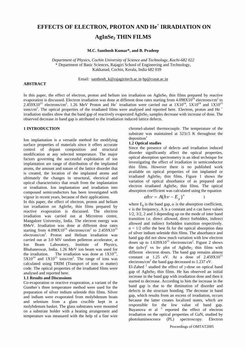
EFFECTS OF ELECTRON, PROTON AND He+ IRRADIATION ON
AgInSe2 THIN FILMS
M.C. Santhosh Kumar*, and B. Pradeep
Department of Physics, Cochin University of Science and Technology, Kochi-682 022 * Department of Basic Sciences, Rajagiri School of Engineering and Technology,
Kakkanad, Cochin, Kerala, India 682 039
Email: [email protected] [email protected] In this paper, the effect of electron, proton and helium ion irradiation on AgInSe2 thin films prepared by reactive evaporation is discussed. Electron irradiation was done at different dose rates starting from 4.098X10¹⁴ electrons/cm2 to 2.459X10¹⁵ electrons/cm2. 1.26 MeV Proton and He+ irradiation were carried out at 1X10¹⁴, 5X10¹⁴ and 1X10¹⁵ ions/cm2. The optical properties of the irradiated films were analysed and reported here. Electron, proton and He +
irradiation studies show that the band gap of reactively evaporated AgInSe2 samples decrease with increase of dose. The observed decrease in band gap is attributed to the irradiation induced lattice defects. 1 INTRODUCTION Ion implantation is a versatile method for modifying surface properties of materials since it offers accurate control of dopant composition and structural modification at any selected temperature. The major factors governing the successful exploitation of ion implantation are range of distribution of the implanted atoms, the amount and nature of the lattice disorder that is created, the location of the implanted atoms and ultimately the changes in structural, electrical and optical characteristics that result from the implantation or irradiation. Ion implantation and irradiation into compound semiconductors has been investigated with vigour in recent years, because of their applications. In this paper, the effect of electron, proton and helium ion irradiation on AgInSe2 thin films prepared by reactive evaporation is discussed. The electron irradiation was carried out at Microtron centre, Mangalore University, India. The electron energy was 8MeV. Irradiation was done at different dose rates starting from 4.098X10¹⁴ electrons/cm2 to 2.459X10¹⁵ electrons/cm2. Proton and Helium irradiation was carried out at 3.0 MV tandom pelletron accelerator, at Ion Beam Laboratory, Institute of Physics, Bhubaneswar, India. 1.26 MeV ion beam was used for the irradiation. The irradiation was done at 1X10¹⁴, 5X10¹⁴ and 1X10¹⁵ ions/cm2. The range of ions was calculated using TRIM (Transport of ions in matter) code. The optical properties of the irradiated films were analysed and reported here. 1.1 Results and Discussions Co-evaporation or reactive evaporation, a variant of the Gunther`s three temperature method were used for the preparation of silver indium selenide thin films. Silver and indium were evaporated from molybdenum boats and selenium from a glass crucible kept in a molybdenum basket. The glass substrates were mounted on a substrate holder with a heating arrangement and temperature was measured with the help of a fine wire
chromel-alumel thermocouple. The temperature of the substrate was maintained at 523±5 K throughout the deposition1
1.2 Optical studies Since the presence of defects and irradiation induced disorder significantly affect the optical properties, optical absorption spectrometry is an ideal technique for investigating the effect of irradiation in semiconductor thin films. However there is no published work available on optical properties of ion implanted or irradiated AgInSe2 thin films. Figure 1 shows the variation of optical absorbance of as prepared and electron irradiated AgInSe2 thin films. The optical absorption coefficient was calculated using the equation
ngEhAh )( −= ννα 1
where Eg is the band gap, α is the absorption coefficient, ν is the frequency, A is a constant and n can have values 1/2, 3/2, 2 and 3 depending up on the mode of inter band transition i.e. direct allowed, direct forbidden, indirect allowed and indirect forbidden transition respectively. n = 1/2 offer the best fit for the optical absorption data of silver indium selenide thin films. The absorbance and band gap did not show much variation with low electron doses up to 1.639X10¹⁵ electrons/cm2. Figure 2 shows the (αhν)2 vs hν plot of AgInSe2 thin films with different electron doses. The band gap remains almost constant at 1.25 eV. At a dose of 2.459X10¹⁵ electrons/cm2 the band gap decreased to 1.237 eV. El-Zahed 2 studied the effect of γ-dose on optical band gap of AgInSe2 thin films. He has observed an initial increase in the band gap with irradiation dose and then it started to decrease. According to him the increase in the band gap is due to the diminution of disorder and defects in the structure bonding. The decrease in band gap, which results from an excess of irradiation, occurs because the latter creates localized states, which are responsible for the low value of band gap. Buyanova et al 3 reported the effect of electron irradiation on the optical properties of GaN, studied by photoluminescence (PL) spectroscopy. Electron
Proceedings of OMTAT2005
irradiation at low dose < 1017 cm-2 was found to have minor effect. For higher doses, two major effects of electron irradiation on PL properties are observed; radiation-induced quenching and radiation-induced formation/activation of new optically active centres.
400 600 800 1000 1200 1400 16000
1
2
3
4
5
6
7 as deposited 4.10X10¹⁴electrons/cm2
8.20X10¹⁴electrons/cm2
1.64X10¹⁵electrons/cm2
2.45X10¹⁵electrons/cm2
Abso
rban
ce (α
t)
Wavelength (nm)
Figure 1: Absorption spectra of AgInSe2 thin films with
different electron doses
Another parameter, which is significantly affected by irradiation-induced disorder, is the sharpness of the band edge. The band tail observed to be increased with increase of electron dose. The observed band gap and calculated band tail is given in table 1 with electron irradiation dose.
0.50 0.75 1.00 1.25 1.50 1.750
1x10¹³
2x10¹³
3x10¹³
4x10¹³
as deposited 4.10X10¹⁴electrons/cm2
8.20X10¹⁴electrons/cm2
1.64X10¹⁵electrons/cm2
2.45X10¹⁵electrons/cm2
(αhν
)2 (e
V2 m-2)
hν (eV)
Figure 2: (αhν)2 vs hν plot of AgInSe2 thin films with different electron doses.
Sample Band Gap
(eV)
Band
Tail (eV)
Un irradiated 1.250 0.620
4.098X10¹⁴ electrons/cm2 1.249 0.624
8.197X10¹⁴ electrons/cm2 1.248 0.624
1.639X10¹⁵ electrons/cm2 1.245 0.671
2.459X10¹⁵ electrons/cm2 1.237 0.702
Proceedings of OMTAT2005
Table 1: Band gap and band tail variation of electron irradiated AgInSe2 samples
Figure 3 gives the absorption spectra of proton irradiated AgInSe2 thin films. It is observed that the absorbance slowly increased with proton dose. The band gap was found to decrease from 1.25 eV, for as prepared samples, to 1.133 eV for a proton dose of 1x10¹⁵ ions/cm2. The band tail is found to increase gradually. The band gap and band tail variation is given in table 2. Figure 4 shows (αhν)2 vs hν plot of AgInSe2 thin films with different proton doses.
400 600 800 1000 1200 1400 16000
1
2
3
4
5 Unirradiated 1x10¹⁴ ions/cm2
5x10¹⁴ ions/cm2
1x10¹⁵ ions/cm2
Abs
orba
nce
(αt)
Wavelength (nm)
Figure 3: Absorption spectra of AgInSe2 thin films with different proton doses
0.75 1.00 1.25 1.50 1.750
2x10¹³
4x10¹³
6x10¹³
8x10¹³
Unirradiated 1x10¹⁴ ions/cm2
5x10¹⁴ ions/cm2
1x10¹⁵ ions/cm2
(αhν
)2 (e
V2 m-2)
hν (eV)
Figure 4: (αhν)2 vs hν plot of AgInSe2 thin films with different proton doses
Sample Band Gap
(eV)
Band Tail
(eV)
Un irradiated 1.250 0.620
1x10¹⁴ ions/cm2 1.191 0.636
5x10¹⁴ ions/cm2 1.160 0.758
1x10¹⁵ ions/cm2 1.133 0.774
Table 2: Band gap and band tail variation of proton irradiated AgInSe2 samples He+ irradiation produces systematic increase in the absorbance with the increase of irradiation dose (figure 5). The increased absorption during irradiation can arise due to several factors, such as increased carrier concentration due to implantation, production of
metallic silver clusters due to the loss of selenium and production of defect levels in the band gap. The clear exponential increase of absorbance with energy in this case strongly suggests that the increased absorption is primarily due to the production of defect levels in the band gap4. From the (αhν)2 versus hν plots (figure 6) the band gap energy was evaluated. Table 3 give the band gap energy and extent of band tail. The band gap decreased from 1.25 eV to 1.074 eV with increase of He+ dose.
400 600 800 1000 1200 1400 16000
1
2
3
4
5 Unirradiated 1x10¹⁴ ions/cm2
5x10¹⁴ ions/cm2
1x10¹⁵ ions/cm2
Abs
orba
nce(αt
)
Wavelenth (nm)
Figure 5: Absorption spectra of AgInSe2 thin films with different He+ doses
0.50 0.75 1.00 1.25 1.500
1x10¹³
2x10¹³
3x10¹³
4x10¹³
Unirradiated 1x10¹⁴ ions/cm2
5x10¹⁴ ions/cm2
1x10¹⁵ ions/cm2
(αhν
)2 (
eV2 m
-2)
hν (eV)
Figure 6: (αhν)2 vs hν plot of AgInSe2 thin films with different He+ doses
Sample Band Gap
(eV)
Band Tail
(eV)
Un irradiated 1.250 0.620
1x10¹⁴ ions/cm2 1.175 0.693
5x10¹⁴ ions/cm2 1.107 0.738
1x10¹⁵ ions/cm2 1.074 0.769
Proceedings of OMTAT2005
Table 3: Band gap and band tail variation of He+ irradiated AgInSe2 samples The band gap energy of the films was found to decrease with electron, proton and He+ doses. The extent of band
tail is found to increase with dose. The increase in band tail indicates the creation of defects during irradiation. According to Narayanan et al 4 irradiation with Ar+ ions produce point defects such as vacancies, interstitials and antisite defects. Defect clusters such as argon bubbles, dislocation loops, etc. can also be expected to form during irradiation. The defects produce band tailing. The observed reduction in band gap arises due to this band tailing. Senthil et al 5 also observed the decrease in band gap of CdS thin films during Ar+ and N+ ion irradiation. Kamboj et al 6 reported the shift of optical band gap towards the lower energy, as dose of heavy ion (C and Ag) increased from 1012 to 1013 ions cm-2 . Pankey and Davey 7 observed drastic changes in the optical band gaps of GaAs and GaP in thin film form as well as bulk form after neutron irradiation. 1.3 Conclusions In this paper we reports the effects of electron, proton and He+ irradiation on AgInSe2 thin films prepared by reactive evaporation. The experimental observations are: Electron-irradiation studies show that the band gap of reactively evaporated AgInSe2 samples decrease with increase of dose. Band gap variation with proton irradiation showed a decreasing trend with increase of irradiation dose. He+ irradiation also shows a decreasing behaviour in the band gap with increase of dose. The observed decrease in band gap is attributed to the irradiation induced lattice defects. 1.4 References 1. M.C. Santhosh Kumar and B. Pradeep, Vacuum 72, 369 (2004) 2. H. El-Zahed, J. Phys. Chem. Solids 62, 641 (2001) 3. A. Buyanova, Mt. Wagner, W. M. Chen, L. Lindstrom, B. Monemar, H. Amano and Akasaki, Appl. Phys. Lett. 73, 2968 (1998) 4. K.L. Narayanan, K.P. Vijayakumar, K.G.M. Nair, and N.S. Thampi, Physica B 240, 8 (1997) 5. K. Senthil, D. Mangalaraj, Sa. K. Narayanadass, B. Hong, Y. Roh, C. S. Park and J. Yi, Semicond. Sci. Technol. 17, 97 (2002) 6. M. S. Kamboj, G. Kaur, R. Thangaraj and D .K. Avasthi, J. Phys. D. Appl. Phys. 35, 477 (2002) 7. T. Pankey, Jr. and John E. Davey, J. Appl. Phys. 41, 697 (1970)

Proceedings of OMTAT2005
TRANSFER OF COPYRIGHT Please complete as appropriate and return by fax/mail. If you do not provide a copyright clearance, we cannot include your paper in the proceedings. [ ] My employer has given clearance for this
paper to be published. OR [ ] I am the holder of the copyright for this
paper The author who sign the copyright Signature: ......................................................... Date: ........................................................ Affiliation: Lecturer Department of Basic Sciences Rajagiri School of Engineering and Technology, Kakkanad, Kochi, Kerala, India Pin code: 682 022

Sorry!!
This Paper is NOT Available
Page 1 Proceedings of OMTAT2005
Chalcogenide Thin Film Fabrication by Pulse Electrodeposition Technique
Kiran Jain, Rashmi*
Electronic Materials Division, * Materials Characterization Division Dr.K.S.Krishnan Marg, National Physical Laboratory, New Delhi, India
Email: [email protected]
ABSTRACT
Thin films of chalcogenide semiconductor CdSe have been prepared by pulse electrodeposition process on
fluorine doped SnO2 coated glass plates. The electrodeposition bath consisted of aqueous solution including CdSO4, SeO2 and pH of 2.4. Growth of CdSe was accomplished under wide range of variables like current density, pulse on and off time in order to elucidate the effect on crystalline structure, grain size and optical properties. Increased current density and on time favored grain size reduction, showing a blue shift in optical band gap due to quantum confinement effect. 1 Introduction II-VI semiconductor nanocrystals are presently of great technical interest as optical emitting materials for thin film electroluminescent devices [1-3] and as optical amplifier media for telecommunication networks because of their strong bandgap luminescence and size dependent optical properties due to quantum confinement effect [4]. Even though various preparation techniques exist for powder preparation, formation of smooth film with nanocrystalline size is difficult. Among the various thin film preparation techniques, electrochemical technique is advantageous since it involves relatively simple and inexpensive equipment, the process can be precisely controlled, no toxic gases are involved, capability to fabricate on large and irregular surfaces. Cadmium selenide CdSe is well known II-VI compound, having a band gap of 1.74 eV. CdSe thin films have been prepared by conventional electrodeposition technique by a number of researchers [5.6]. Pulse electrodeposition is one of the novel processing technique utilizing the advantages of high current density. It is similar to conventional direct current electroplating except that the plating current is turned on and off in a periodic fashion resulting in a square wave with pulse duration Ton between pulse durations Toff. Nanocrystalline metal deposition of Cd, Ni, Pd have been reported using pulse electrodeposition technique [7-8], however less attention was paid towards semiconductor film deposition. We have obtained stoichiometric CdTe films using a high off time during which dissolution of elemental Cd or Te takes place [9-10]. In the present work, we report the effect of pulse parameters on the optical properties of CdSe thin films. Importance of present work lies in demonstration of the optical band gap dependence on the pulse parameters.
2. Experimental
CdSe thin films were synthesized using unipolar cathodic rectangular pulses (current). A three-electrode cell was used for electrochemical deposition with a saturated calomel electrode (SCE) as the reference electrode, a fluorine doped tin-oxide (TCO)-coated glass
sheet as the working electrode (cathode), a platinum sheet as the counter electrode (anode). The deposition area was about 1cm×2cm. The deposition was carried out in an aqueous bath containing 0.25 M CdSO4 , 0.25 mM SeO2 and 0.25 M K2SO4. The pH of the solution was adjusted using H2SO4 to about 2.4. Temperature of the solution was kept constant at 80°C. During pulse electrodeposition, solution was not stirred. After the deposition experiment, CdSe thin films were washed in pure water, and dried in the air. Keithley current source -220 was used to control constant current pulses. Applied current density was varied from 2.5 to 15 mA / cm2. On time (Ton) of the current pulses was varied from 3 ms to 9 ms, and off time (Toff ) from 40 ms to 600 ms. Changes in crystalline structure and phases were analyzed by powder X ray diffraction patterns using Bruker -AXS D8 advance diffractometer using Cu-Kα radiation. Optical absorption measurements were performed using a Shimadzu 3101 UV-VIS spectrophotometer. 3. Results and Discussions
Figure 1 XRD pattern of CdSe film by pulse electrodeposition
A number of samples were prepared by pulse electrodeposition (PE) under varied current density, on and off time. XRD patterns for all sample consisted of
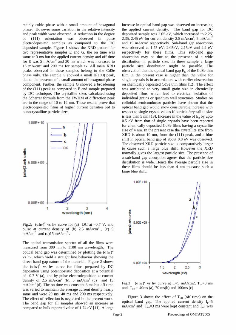
Page 2 Proceedings of OMTAT2005
mainly cubic phase with a small amount of hexagonal phase. However some variation in the relative intensity and peak width were observed. A reduction in the degree of (111) orientation was observed in pulse electrodeposited samples as compared to the DC deposited sample. Figure 1 shows the XRD pattern for two representative samples E and G, the on time was same at 3 ms but the applied current density and off time for E was 5 mA/cm2 and 30 ms which was increased to 15 mA/cm2 and 200 ms for sample G. All main XRD peaks observed in these samples belong to the CdSe phase only. The sample G showed a small H(100) peak, due to the presence of a small amount of hexagonal phase component. Further, the sample G showed a broadening of the (111) peak as compared to E and sample prepared by DC technique. The crystallite sizes calculated using the Scherrer formula from the FWHM of diffraction peak are in the range of 10 to 12 nm. These results prove that electrodeposited films at higher current densities led to nanocrystalline particle sizes.
Fig.2: (αhν)2 vs hν curve for (a) DC at –0.7 V, and pulse at current density of (b) 2.5 mA/cm2 , (c) 5 mA/cm2 and (d)15 mA/cm2 . The optical transmission spectra of all the films were measured from 300 nm to 1100 nm wavelength. The optical band gap was determined by plotting the (αhν)2 vs hν, which yield a straight line behavior showing the direct band gap nature of the material. Figure 2 shows the (αhν)2 vs hν curve for films prepared by DC deposition using potentiostatic deposition at a potential of –0.7 V (a), and by pulse electrodeposition at current density of 2.5 mA/cm2 (b), 5 mA/cm2 (c) and 15 mA/cm2 (d). The on time was constant 3 ms but off time was varied to maintain the average current density nearly same and were 20 ms, 40 ms and 200 ms respectively. The effect of reflection is neglected in the present work. The band gap for all samples showed an increase as compared to bulk reported value of 1.74 eV [11]. A large
increase in optical band gap was observed on increasing the applied current density. The band gap for DC deposited sample was 2.05 eV, which increased to 2.25, 2.35, 2.45 eV for current density 2.5 mA/cm2, 5 mA/cm2 and 15 mA/cm2 respectively. Sub-band gap absorption was observed at 1.75 eV, 2.05eV, 2.15eV and 2.2 eV respectively for these films. This sub-band gap absorption may be due to the presence of a wide distribution in particle size. In these sample a large particle size distribution might be possible. The observation that the optical band gap Eg of the CdSe thin film in the present case is higher than the value for single crystals is in accordancre with earlier observation on chemically deposited CdSe thin films [12]. The effect was attributed to very small grain size in chemically deposited films, which lead to electrical isolation of individual grains or quantum well structures. Studies on colloidal semiconductor particles have shown that the optical band gap would show considerable increase with respect to single crystal values if particle /crystallite size is less than 5 nm [13]. Increase in the value of Eg by upto 0.5 eV from that of single crystals have been reported for chemically deposited CdSe films having a crystallite size of 4 nm. In the present case the crystallite size from XRD is about 10 nm, from the (111) peak, and a blue shift in optical band gap of about 0.8 eV was observed. The observed XRD particle size is comparatively larger to cause such a large blue shift. However the XRD normally gives the largest particle size. The presence of a sub-band gap absorption agrees that the particle size distribution is wide. Hence the average particle size in these films should be less than 4 nm to cause such a large blue shift.
Fig.3 (αhν)2 vs hν curve at Ip=5 mA/cm2, Ton=3 ms and Toff = 40ms (a), 70 ms(b) and 100ms (c) Figure 3 shows the effect of Toff (off time) on the optical band gap. The applied current density Ip=5 mA/cm2 and Ton=3 ms were kept constant and Toff was
Page 3 Proceedings of OMTAT2005
varied from 40 ms to 100 ms. Optical band gap for off time (Toff) 40ms (a) , 70 ms (b) and 100ms (c) were 2.3 eV, 2.4 eV and 2.42 eV respectively. A subband gap absorption was observed at 2.05 eV in these films. Hence the increased off time also increases the optical band gap.
Similarly an increase in the optical band gap was observed on increasing the pulse on time Ton from 3 ms to 9 ms. The optical band gap for a sample prepared at current density Ip of 15 mA/cm2, on time of 3 ms and off time 200 ms showed a band gap of 2.45 eV (Fig.2 d). The optical band gap for another sample prepared at current density Ip of 15 mA/cm2, on time 9 ms and off time of 600 ms showed an increased band gap of 2.5 eV.
We can summarize the effects of pulsed deposition as follows. Increase in pulse on time, off time, as well as pulse current density increases the optical band gap of CdSe thin films. This increase in optical band gap may be attributed to the decrease in crystallite size. XRD results (Fig.1) confirm the formation of nanocrystalline sized films, with a crystallite size of about 10 to 12 nm. Hence, with a control of pulse parameters nanocrystalline CdSe films can be prepared showing a blue shift of about 0.8 eV from its bulk value resulted from quantum confinement effect The smallest size is obtained at increased on time of 9 ms and off time of 600 ms., where most of the time the current is off. Selenium deposition potential is more positive than Cd, hence in order to get required stoichiometry, Se concentration in the bath is kept low. CdSe formation occurs when the growth rate is limited by selenium ion transport and when the cadmium is underpotentially deposited. The deposition process can be described in two steps. First selenious ions are reduced at the cathode interface according to
adsSeeSe →+ + _4 4 1
Then two reactions are possible, either pure Se clusters form by association of several selenium adatoms or reduction of cadmium ions takes place in the presence of Se ads adatoms
)(2( 2adsadsads CdSeeCdSe +→++ −+ 2
According to equation (2), in the final step, selenium and Cd adatoms diffuse and react to form CdSe. Thus depending on the deposition conditions either Se or CdSe may form, therefore in general CdSe formation may contain excess Se. The effect of pulse electrodeposition on CdSe deposition can be understood as follows. In order to produce nanocrystalline material by electrodeposition process, the rate of nucleation of new crystals must be made very large so that there is a high concentration of nuclei on the surface, resulting in a very fine crystallite size. The dominant parameter affecting the nucleation rate is the applied overpotential. The high instantaneous current density allows many atoms to arrive at the substrate surface simultaneously. During the on time there is high current density resulting in high nucleation rate, and consequently the structure of the pulsed deposited film is very dense. During the off time, the region of the solution near the film surface is replenished with Cd and Se ions owing to their
diffusion. The decreased grain size on increasing the off time is explained by adsorption mechanism. In case of adsorption, during the off period crystal growth is low, so nucleation and crystal growth take place during the pulse on time only. The nucleation rate is kept high throughout the deposition process by controlling the deposition parameters. The increase in pulse on time increases the number of nuclei, by increasing the adatom population, hence the increase in pulse current, increased off time and increased on time all favor the reduction in crystallite size. Further the pulse electrodeposition conditions helps in maintaining the stoichiometry of the films. During the off time Se once deposited will get dissolved back, because the off potential is less cathodic. The decreased the grain size by a control of pulse parameters, high current density, increased on time, increased off time, favor formation of nanocrystalline grains, the effect of which is reflected as a blue shift in optical band gap. Conclusion Nanocrystalline CdSe thin films showing quantum effects were prepared by unipolar current pulse electrodeposition technique. Pulse electrodeposition process of CdSe thin films demonstrated that this process is advantageous for binary semiconductor deposition. Proper control of pulse parameters will lead to highly stoichiometric films, with a reduction in grain size, showing a blue shift in optical band gap. This is because the formation of a large number of initial nuclei provides more growth sites REFERENCES 1.M.C.Schlamp, X.Peng, A.P.Alivistos, J. Appl. Phys. 82, 5837 (1997) 2. M.Y.Gao, C.Lesser, S.Kirstein, H.Mohwald, A.L.Rogach, H.Weller, J. Appl. Phys. 87 , 2297, (2000) 3. H. Mattoussi, L.H.Radzilowski, B.O.Dabbousi, E.L.Thomas, M.G.Bawendi, M.F.Rubner, J. Appl. Phys. 83, 7965 (1998) 4. Y.Golan, G.Hodes,J.Rubenstein, J. Phys.Chem. 100, 2220 (1996) 5. Z.Loizos and N.Spyrellis, Thin Solid Films, 204, 139 (1991) 6. G.Hodes, A.A.Yaron, F.Decker, P.Motisuke, Phys.Rev. B 36, 4215 (1987) 7. .J.Cl Puippe and N.Ibl, J.Appl. Electrochem. 10, 775 (1980) 8. N.Ibl. J.Cl.Puippe and H.Angerer, Surface Tech. 6, 287 (1978) 287 9. R.K.Sharma, K.Jain, K.S.Balakrishnan, A.C.Rastogi, Physics of semiconductor devices, ed. V.Kumar and S.K.Agarwal, p 833(1998) 10 R.K.Sharma, K.Jain, K.S.Balakrishnan, A.C.Rastogi, Bull. Elec. Chem, 14, 382 (1998) 11. M.Bouroushian, Z.Loizos, N.Spyrellis, G.Mourin, App. Surf. Sci. 115, 103 (1997) 12. M.T.S.Nair, P.K.Nair, R.A.Zingaro, E.A.Meyers, J.Appl. Phys. 74 , 1879 (1993) 13. C.B.Murray, D.J.Norris and M.G.Bawendi, J.Am. Chem. Soc. 115, 8706 (1993)

Page 4 Proceedings of OMTAT2005
TRANSFER OF COPYRIGHT Please complete as appropriate and return by fax/mail. If you do not provide a copyright clearance, we cannot include your paper in the proceedings. [ ] My employer has given clearance for this
paper to be published. OR [ ] I am the holder of the copyright for this
paper The author who sign the copyright Signature: ......................................................... Date: ........................................................ Affiliation: Dr Mrs Kiran Jain Scientist, Electronic Materials Division National Physical Laboratory, New Delhi-12 ………………………………………………… ………………………………………………… …………………………………………………
Thickness dependence on the photo-electronic properties of thermally evaporated CdS thin films.
*K. Kunjabali Singh and H.L.Das
Department of Physics, Gauhati University,
Guwahati-781014, Assam. * E-mail: [email protected].
Abstract Photo-electronic properties of thermally vacuum evaporated CdS thin films of thickness 1500Å, 2000 Å, 2500 Å, 3000 Å and 3500 Å at substrate temperature [Ts] 473K were studied under different thicknesses, intensity of light and bias at constant ambient temperature in vacuum.A gap-type film geometry with an effective gap of 7mm between two evaporated silver electrodes was used for photoconductivity measurements. Dark and photocurrents were measured with the help of an ECIL high input impedence (~1014Ù) electrometer amplifier (model EA 815) within an
accuracy of 3%). The intensity of light illumination of the films were measured with the help of a high sensitive APLAB luxmeter (model 5011S).Photocurrents, Iph=(IL-ID) and photosensitivity, S=Iph/ID of the films of different thicknesses were measured with respect to intensity of light and applied bias at the same ambient conditions. The photocurrent and photosensitivity of the films were found to increase with increase of thickness, intensity of illumination and bias. Keywords: Cadmium sulphide, thin films, film thickness, photoconduction, vacuum deposition.
1. Inroduction: The A II-B II compound semiconductor CdS is a promising host material for Its potential applications for light emitting devices (LED) [1] due to its capability to emit green light closed to the highest sensitivity to human eye. Because of its direct band gap (Eg =2.42eV), it interacts strongly with light [2,3] and can be used for successful fabrication of high efficient solar cells, heterojunction cells, photo-electrochemical cells, photo-transist0rs, X-rays and U.V. detectors [4]. Thus, the photo-response characteristics of CdS polycrystalline material in its thin film forms is one of the direct interest for understanding the basic physics involved in photoconductivity process. In general, polycrystalline CdS thin films posses fairly good photosensitivity which depends on thin film parameters like film thickness [5], substrate temperature [6] and other growth parameters [7]. The photosensitivity in thin films is essentially determined by the free life time of the carriers in the conduction band and is determined mostly by the recombination processes via defect states. The variation of life time
and hence photosensitivity depends on the ambient temperature as well as on the intensity of light [8]. In the present work, thickness dependence on photo-electronic properties of CdS thin films is presented.
2. Experimental details:
High purity CdS powder procured from Koch Light Lab., U.K. was vacuum evaporated from Ta- boat on chemically and ultrasonically cleaned glass substrates at substrate temperature 473K (Ts) with the help of HINDHIVAC 12A4 unit. The vacuum maintained was 1.33 x10⁻⁴ Pa.The rate of deposition of the films of thicknesses ranging from 1500 -3500 was maintained at 2.14 S-1 under varied deposition times. After deposition of the films, highly photo-grade Ag electrodes were deposited on the films at room temperature with inter-electrode spacing of 7mm. Ôhus, we get films of gap-type cell configuration of film area 10 x 7mm2. Ôhe source .to substrate distance was kept fixed at 5cm. The thickness of the films were measured with a suitably assembled multiple beam interferometer.
The sample was mounted on a suitably designed sample mount and then suspended vertically inside a continuously evacuated glass jacket under a vacuum of 2.67 Pa with the help of thin enameled copper wires. A double stage rotary pump was used for this purpose. A suitable optical arrangement was made to illuminate the sample uniformly with white light for which a tungsten halogen lamp (250W-24V) attached with a parabolic focusing mirror was used as the light source. The light intensity was measured with the help of a APLAB luxmeter (model 5011S). High ambient temperatures were achieved by means of a resistive heater connected to a stabilized power supply. The temperatures of the films were measured with the help of a copper- constantant thermocouple in conjunction with a digital micro-voltmeter. The dark currents [ID] and the current under illumination [IL] were measured with the help of a high input impedence (~1014 Ù) ECIL electrometer amplifier under different applied positive bias obtained from a number of dry cells each of e.m.f. 9 volts connected in series. The whole set up including the observer was housed inside a suitably grounded Faraday Cage to minimize external ground loop currents and pick up noises.
3. Results and Discussion: 3.1. Effect of film thickness and bias on photocurrent.
Fig.1(a). Variation of InIph vs Inφφ of a CdS thin films of thickness 1500 (t) grown at 473K (Ts).
-2 5.0 3
-2 4 .0 3
-2 3 .0 3
-2 2 .0 3
-2 1.0 3
-2 0 .0 3
-19 .0 3
7 8 .9 9 .1 9 .5 10 11 12
Inφ (Ix)
In I ph
(A)
36V
63V
90V
Fig.1(b). Variation of In Iph vs In φφ of a CdS thin films having thickness 2000 (t) grown at 473K (Ts).
-22.52
-21.52
-20.52
-19.52
-18.52
-17.52
-16.52
-15.52
7 8 9 10 11 12
Inφ (Ix)
In I p
h (A
)
36V
63V
90V
Fig 1(c).Variation of In Iph vs In φφ of a CdS thin films of thickness 2560 (t) grown at 473K (Ts).
- 2 0
-19
-18
-17
-16
-15
-14
-13
7 8 9 10 11 12 13
Inφφ (Ix)
In I p
h (A
)
36V
63V
90V
Fig 1(d).Variation of In Iph vs Inφφ of a CdS thin films having thickness 3500 (t) grown at 473K (Ts).
-20-19-18-17-16-15-14-13-12-11-10
7 8 9 10 11 12 13
Inφ( Ix)
In I p
h (A
)
36V
63V
90V
Fig. 1(a-d) show the variation of In Iph vs InÖ of the films grown at 473K (Ts) under different applied bias. We define Iph= (IL-ID), where IL is the current under illumination and ID the current under dark. The plots show that Iph increases almost linearly with increase of film thickness and bias. The power law relationship between Iph and Ö is expressed as Iph Öã
(1) where Ö is the intensity of white light in Ix and the exponent ã depends on the imperfection levels contained in the films and is determined from the slopes of the graphs as shown in the table below:
Value of γ Film thickness
( ) Bias=36V Bias=63V Bias=90V
1500 0.60 0.65 0.68 2000 0.60 0.67 0.63 2500 0.63 0.64 0.643 3500 0.65 0.68 0.70 It may be noted that the values of ã in CdS thin films under various experimental conditions are found to be less than unity. The observations clearly indicates that bimolecular recombination process predominates the photoconductivity in these films[ 9 ].
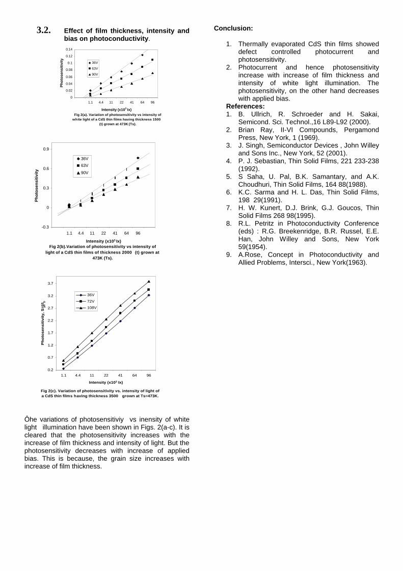
3.2. Effect of film thickness, intensity and bias on photoconductivity.
Fig 2(a). Variation of photosensitivity vs intensity of white light of a CdS thin films having thickness 1500
(t) grown at 473K (Ts).
0
0.02
0.04
0.06
0.08
0.1
0.12
0.14
1.1 4.4 11 22 41 64 96
Intensity (x103 Ix)
Ph
oto
sen
siti
vity
36V
63V
90V
Fig 2(b).Variation of photosensitivity vs intensity of light of a CdS thin films of thickness 2000 (t) grown at
473K (Ts).
-0.3
0
0.3
0.6
0.9
1.1 4.4 11 22 41 64 96
Intensity (x103 Ix)
Ph
oto
sen
siti
vity
36V
63V
90V
Fig 2(c). Variation of photosensitivity vs. intensity of light of a CdS thin films having thickness 3500 grown at Ts=473K.
0.2
0.7
1.2
1.7
2.2
2.7
3.2
3.7
1.1 4.4 11 22 41 64 96
Intensity (x103 Ix)
Ph
oto
se
ns
itiv
ity
, S
=I
ph/
I D
36V
72V
108V
Ôhe variations of photosensitiviy vs inensity of white light illumination have been shown in Figs. 2(a-c). It is cleared that the photosensitivity increases with the increase of film thickness and intensity of light. But the photosensitivity decreases with increase of applied bias. This is because, the grain size increases with increase of film thickness.
Conclusion:
1. Thermally evaporated CdS thin films showed defect controlled photocurrent and photosensitivity.
2. Photocurrent and hence photosensitivity increase with increase of film thickness and intensity of white light illumination. The photosensitivity, on the other hand decreases with applied bias.
References: 1. B. Ullrich, R. Schroeder and H. Sakai,
Semicond. Sci. Technol.,16 L89-L92 (2000). 2. Brian Ray, II-VI Compounds, Pergamond
Press, New York, 1 (1969). 3. J. Singh, Semiconductor Devices , John Willey
and Sons Inc., New York, 52 (2001). 4. P. J. Sebastian, Thin Solid Films, 221 233-238
(1992). 5. S Saha, U. Pal, B.K. Samantary, and A.K.
Choudhuri, Thin Solid Films, 164 88(1988). 6. K.C. Sarma and H. L. Das, Thin Solid Films,
198 29(1991). 7. H. W. Kunert, D.J. Brink, G.J. Goucos, Thin
Solid Films 268 98(1995). 8. R.L. Petritz in Photoconductivity Conference
(eds) : R.G. Breekenridge, B.R. Russel, E.E. Han, John Willey and Sons, New York 59(1954).
9. A.Rose, Concept in Photoconductivity and Allied Problems, Intersci., New York(1963).
GROWTH OF CuInSe2 THIN FILMS BY TWO-STAGE PROCESS
Rahana Yoosuf, Jincy Jose, R. Ratheesh Kumar, K. Rajeev Kumar*, M.K.Jayaraj
Department of Physics, *Department of Instrumentation,
Cochin University of Science And Technology, Kochi 682 022 Email:[email protected]
ABSTRACT CuInSe2 thin films were made by cost –effective two-stage process with the thermal evaporation of metallic bilayers followed by selenization. A systematic study was conducted varying the duration of selenization and the selenization temperature. The X-ray diffraction pattern revealed the presence of single-phase chalcopyrite with (112) preferred orientation for stoichiometric samples (Cu/In=1) selenized at 350oC for 3 hours. The CuInSe2 thin films prepared under this optimum condition showed a band gap energy of 1.05eV and a resistivity of 10-2Ωcm. Both energy gap values and resistivity showed an increasing trend with increasing Cu/In ratios. The information gained from the study plays a significant role in the fabrication of CuInSe2 thin films as absorber layer for thin film solar cells. 1. INTRODUCTION Polycrystalline CuInSe2 thin films have received considerable interest for photovoltaic application. The two main reason for this increasing interest are, first CuInSe2 has an optical bandgap of about 1 eV, which lies at the frequency interval of visible solar illumination and second, this material has a large absorption coefficient for frequencies that are higher than its band gap. Because of this large absorption coefficient, even a 1 µm thick CuInSe2 film can absorb 93% of radiation falling upon it 1-3
Several methods have been used for the deposition of CuInSe2 thin films 4-6. A small –area CuInSe2 thin film, which an efficiency of higher than 15% was deposited using a co-evaporation technique4. However co evaporation technique has high production cost in comparison with other techniques. In terms of large-scale applications, one of the promising approach is two-stage processing of thin chalcopyrite films, involving deposition of Cu-In-Ga precursors in the first step followed by their selenization using H2Se gas or Se vapour7. In this technique, both steps, the precursor preparation and the selenization, are important for the quality and the adherence of the CuInSe2 film to substrate.
In this paper we report the preparation of CuInSe2 thin films on glass substrates by selenizing evaporated Cu-In alloy layers. The selenization process was carried out in N2 atmosphere. The processing conditions for the growth of single phase CuInSe2 formation and their structural and electrical characteristics were investigated. 2. EXPERIMENTAL For the preparation of CuInSe2 by two-stage process, the first step was the preparation of Cu-In precursors. Cu-In bilayers were prepared by sequential deposition of In followed by Cu by thermal evaporation. For better adhesion of, a thin layer of Gallium of thickness of about 100Ao was deposited prior to indium deposition. The thickness of the In layer was maintained at 0.4µm
and that of Cu layer was varied to obtain various Cu/In ratios. The thickness of individual layers and evaporation rates were measured during deposition using a digital thickness monitor. The Cu-In bilayer films prepared were annealed at 153oC for 2hrs in high vacuum 8.
The Cu-In precursors were then exposed to Se vapour in a split furnace, which allowed rapid heating and cooling of samples. The selenization temperature was varied from 250oC to 400oC. The selenization time was also varied from one to three hours. N2 was used as the carrier gas.
After optimising the selenization temperature and duration of selenization as 350oC and 3 hours respectively, the experiments were repeated using precursor of various Cu/In ratios ranging from 0.8 to 1.2. Single phase CuInSe2 films were obtained for Cu/In =1 with a preferred orientation along (112) plane having a band gap of 1.05 eV.
The structural, optical, morphological and electrical characterizations of the CuInSe2 films were carried out by X-ray diffractometer(XRD)., UV-VIS-NIR spectrophotometer and resistivity measurement respectively. 3. RESULTS AND DISCUSSIONS The crystallinity of the films was studied by recording the X-ay diffraction pattern. The Cu-In precursors with Cu/In ratio=1, prepared by annealing at 153oC under vacuum [8] (Cu/In=1) were selenized for different duration varying from 1 to 3 hours. The XRD patterns of samples (Cu/In=1) selenized at 350oC for duration of 1 hour, 2 hours and 3 hours are shown in figure 1. In all the three cases, the dominant peak corresponds to CuInSe2 (112). For 1-hour selenization, some alloy peaks and one In2Se3 binary peak were identified in addition to CuInSe2 peaks. When the duration of selenisation was increased to 2 hours, then the In2Se3 peak disappeared and CuInSe2 peak (200) emerged.
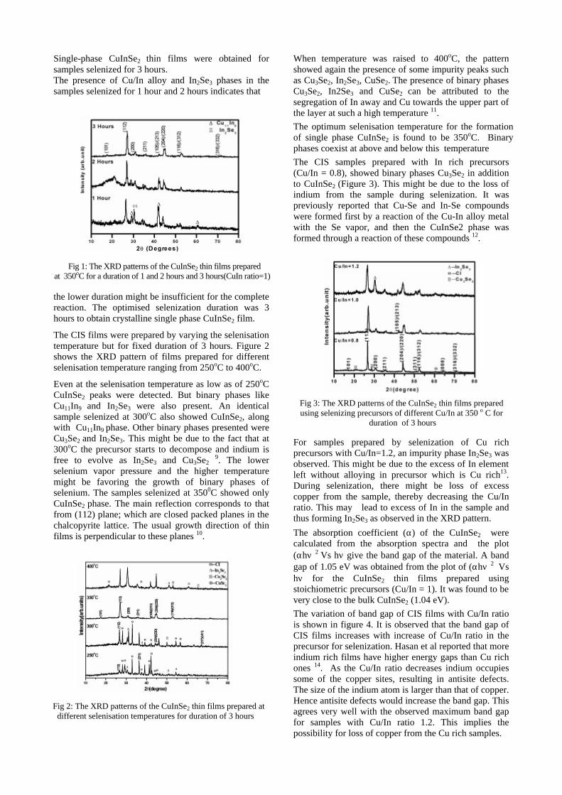
Single-phase CuInSe2 thin films were obtained for samples selenized for 3 hours. The presence of Cu/In alloy and In2Se3 phases in the samples selenized for 1 hour and 2 hours indicates that
the lower duration might be insufficient for the complete reaction. The optimised selenization duration was 3 hours to obtain crystalline single phase CuInSe2 film.
The CIS films were prepared by varying the selenisation temperature but for fixed duration of 3 hours. Figure 2 shows the XRD pattern of films prepared for different selenisation temperature ranging from 250oC to 400oC.
Even at the selenisation temperature as low as of 250oC CuInSe2 peaks were detected. But binary phases like Cu11In9 and In2Se3 were also present. An identical sample selenized at 300oC also showed CuInSe2, along with Cu11In9 phase. Other binary phases presented were Cu3Se2 and In2Se3. This might be due to the fact that at 300oC the precursor starts to decompose and indium is free to evolve as In2Se3 and Cu3Se2
9. The lower selenium vapor pressure and the higher temperature might be favoring the growth of binary phases of selenium. The samples selenized at 3500C showed only CuInSe2 phase. The main reflection corresponds to that from (112) plane; which are closed packed planes in the chalcopyrite lattice. The usual growth direction of thin films is perpendicular to these planes 10.
When temperature was raised to 400oC, the pattern showed again the presence of some impurity peaks such as Cu3Se2, In2Se3, CuSe2. The presence of binary phases Cu3Se2, In2Se3 and CuSe2 can be attributed to the segregation of In away and Cu towards the upper part of the layer at such a high temperature 11.
The optimum selenisation temperature for the formation of single phase CuInSe2 is found to be 350oC. Binary phases coexist at above and below this temperature
The CIS samples prepared with In rich precursors (Cu/In = 0.8), showed binary phases Cu3Se2 in addition to CuInSe2 (Figure 3). This might be due to the loss of indium from the sample during selenization. It was previously reported that Cu-Se and In-Se compounds were formed first by a reaction of the Cu-In alloy metal with the Se vapor, and then the CuInSe2 phase was formed through a reaction of these compounds 12.
For samples prepared by selenization of Cu rich precursors with Cu/In=1.2, an impurity phase In2Se3 was observed. This might be due to the excess of In element left without alloying in precursor which is Cu rich13. During selenization, there might be loss of excess copper from the sample, thereby decreasing the Cu/In ratio. This may lead to excess of In in the sample and thus forming In2Se3 as observed in the XRD pattern.
The absorption coefficient (α) of the CuInSe2 were calculated from the absorption spectra and the plot (αhν)2 Vs hν give the band gap of the material. A band gap of 1.05 eV was obtained from the plot of (αhν)2 Vs hν for the CuInSe2 thin films prepared using stoichiometric precursors (Cu/In = 1). It was found to be very close to the bulk CuInSe2 (1.04 eV).
The variation of band gap of CIS films with Cu/In ratio is shown in figure 4. It is observed that the band gap of CIS films increases with increase of Cu/In ratio in the precursor for selenization. Hasan et al reported that more indium rich films have higher energy gaps than Cu rich ones 14. As the Cu/In ratio decreases indium occupies some of the copper sites, resulting in antisite defects. The size of the indium atom is larger than that of copper. Hence antisite defects would increase the band gap. This agrees very well with the observed maximum band gap for samples with Cu/In ratio 1.2. This implies the possibility for loss of copper from the Cu rich samples.
Fig 1: The XRD patterns of the CuInSe2 thin films prepared at 350oC for a duration of 1 and 2 hours and 3 hours(CuIn ratio=1)
Fig 2: The XRD patterns of the CuInSe2 thin films prepared at different selenisation temperatures for duration of 3 hours
Fig 3: The XRD patterns of the CuInSe2 thin films prepared using selenizing precursors of different Cu/In at 350 o C for
duration of 3 hours
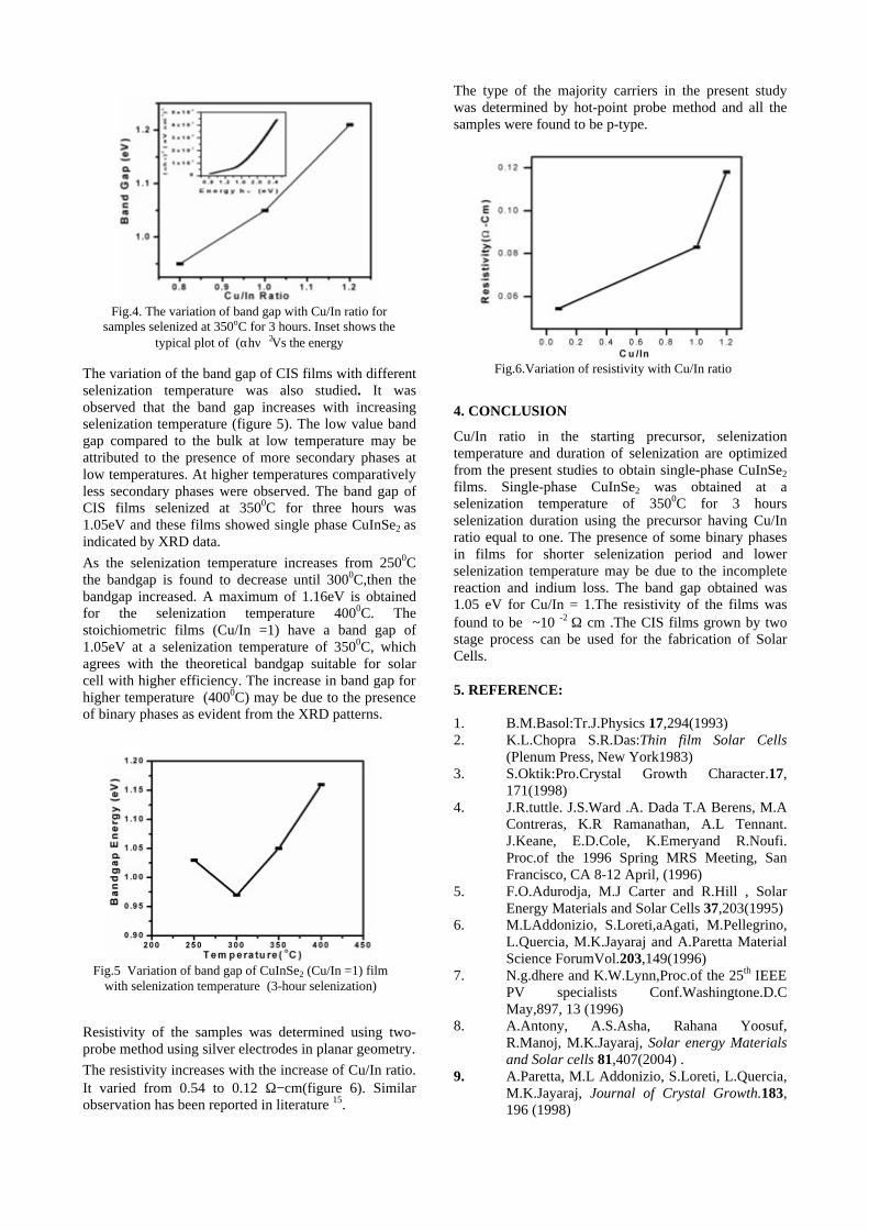
The variation of the band gap of CIS films with different selenization temperature was also studied. It was observed that the band gap increases with increasing selenization temperature (figure 5). The low value band gap compared to the bulk at low temperature may be attributed to the presence of more secondary phases at low temperatures. At higher temperatures comparatively less secondary phases were observed. The band gap of CIS films selenized at 3500C for three hours was 1.05eV and these films showed single phase CuInSe2 as indicated by XRD data.
As the selenization temperature increases from 2500C the bandgap is found to decrease until 3000C,then the bandgap increased. A maximum of 1.16eV is obtained for the selenization temperature 4000C. The stoichiometric films (Cu/In =1) have a band gap of 1.05eV at a selenization temperature of 3500C, which agrees with the theoretical bandgap suitable for solar cell with higher efficiency. The increase in band gap for higher temperature (4000C) may be due to the presence of binary phases as evident from the XRD patterns.
Resistivity of the samples was determined using two-probe method using silver electrodes in planar geometry.
The resistivity increases with the increase of Cu/In ratio. It varied from 0.54 to 0.12 Ω−cm(figure 6). Similar observation has been reported in literature 15.
The type of the majority carriers in the present study was determined by hot-point probe method and all the samples were found to be p-type.
4. CONCLUSION
Cu/In ratio in the starting precursor, selenization temperature and duration of selenization are optimized from the present studies to obtain single-phase CuInSe2
films. Single-phase CuInSe2 was obtained at a selenization temperature of 3500C for 3 hours selenization duration using the precursor having Cu/In ratio equal to one. The presence of some binary phases in films for shorter selenization period and lower selenization temperature may be due to the incomplete reaction and indium loss. The band gap obtained was 1.05 eV for Cu/In = 1.The resistivity of the films was found to be ~10 -2 Ω cm .The CIS films grown by two stage process can be used for the fabrication of Solar Cells. 5. REFERENCE: 1. B.M.Basol:Tr.J.Physics 17,294(1993) 2. K.L.Chopra S.R.Das:Thin film Solar Cells
(Plenum Press, New York1983) 3. S.Oktik:Pro.Crystal Growth Character.17,
171(1998) 4. J.R.tuttle. J.S.Ward .A. Dada T.A Berens, M.A
Contreras, K.R Ramanathan, A.L Tennant. J.Keane, E.D.Cole, K.Emeryand R.Noufi. Proc.of the 1996 Spring MRS Meeting, San Francisco, CA 8-12 April, (1996)
5. F.O.Adurodja, M.J Carter and R.Hill , Solar Energy Materials and Solar Cells 37,203(1995)
6. M.LAddonizio, S.Loreti,aAgati, M.Pellegrino, L.Quercia, M.K.Jayaraj and A.Paretta Material Science ForumVol.203,149(1996)
7. N.g.dhere and K.W.Lynn,Proc.of the 25th IEEE PV specialists Conf.Washingtone.D.C May,897, 13 (1996)
8. A.Antony, A.S.Asha, Rahana Yoosuf, R.Manoj, M.K.Jayaraj, Solar energy Materials and Solar cells 81,407(2004) .
9. A.Paretta, M.L Addonizio, S.Loreti, L.Quercia, M.K.Jayaraj, Journal of Crystal Growth.183, 196 (1998)
Fig.6.Variation of resistivity with Cu/In ratio
Fig.4. The variation of band gap with Cu/In ratio for
samples selenized at 350oC for 3 hours. Inset shows the typical plot of (αhν) 2Vs the energy
Fig.5 Variation of band gap of CuInSe2 (Cu/In =1) film
with selenization temperature (3-hour selenization)

10. ‘Semiconductors for Solar Cells’-Hans Joachim Moller (Artech House,London,1993)
11. V.Alberts, M.Klenk and E.Bucher : Jpn.J.Appl.Phys.39,5776 (2000) .
12. S.Yamanaka, B.E.Mc Candless and R.W.Birkmire, Proc.23rd IEEE PV Specialists Conf., 607 (1993).
13. ASTM X-ray Powder Data Cards, 2-1188,26-0523, 2-1178.
14. S.M.Firoz Hasan, M.A.Subhan, Kh.M.Mannan: Optical Materials, 14 , 329 (2000)
15. O.F.Yuksel, B.M.Basol, H.Safak, H.Karabiyik: Appl.Phys.A, 73, 387(2001) .
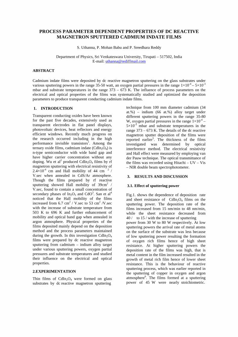
PROCESS PARAMETER DEPENDENT PROPERTIES OF DC REACTIVE MAGNETRON SPUTTERED CADMIUM INDATE FILMS
S. Uthanna, P. Mohan Babu and P. Sreedhara Reddy
Department of Physics, Sri Venkateswara University, Tirupati – 517502, India
E-mail: [email protected] ABSTRACT Cadmium indate films were deposited by dc reactive magnetron sputtering on the glass substrates under various sputtering powers in the range 35-50 watt, an oxygen partial pressures in the range 1×10⁻⁴ – 5×10⁻³ mbar and substrate temperatures in the range 373 – 673 K. The influence of process parameters on the electrical and optical properties of the films was systematically studied and optimized the deposition parameters to produce transparent conducting cadmium indate films.
1. INTRODUCTION
Transparent conducting oxides have been known for the past five decades, extensively used as transparent electrodes in flat panel displays, photovoltaic devices, heat reflectors and energy efficient windows. Recently much progress on the research occurred including in the high performance invisible transistors1. Among the ternary oxide films, cadmium indate (CdIn2O4) is n-type semiconductor with wide band gap and have higher carrier concentration without any doping. Wu et al2 produced CdIn2O4 films by rf magnetron sputtering with electrical resistivity of 2.4×10⁻⁴ cm and Hall mobility of 44 cm 2 / V.sec when annealed in CdS/Ar atmosphere. Though the films prepared by rf reactive sputtering showed Hall mobility of 39cm2 / V.sec, found to contain a small concentration of secondary phases of In2O3 and CdO3. San et al4 noticed that the Hall mobility of the films increased from 6.7 cm2 / V.sec to 53 cm2 /V.sec with the increase of substrate temperature from 503 K to 696 K and further enhancement of mobility and optical band gap when annealed in argon atmosphere. Physical properties of the films deposited mainly depend on the deposition method and the process parameters maintained during the growth. In this investigation CdIn2O4
films were prepared by dc reactive magnetron sputtering from cadmium – indium alloy target under various sputtering powers, oxygen partial pressures and substrate temperatures and studied their influence on the electrical and optical properties.
2.EXPERIMENTATION
Thin films of CdIn2O4 were formed on glass substrates by dc reactive magnetron sputtering
technique from 100 mm diameter cadmium (34 at.%) – indium (66 at.%) alloy target under different sputtering powers in the range 35-80 W, oxygen partial pressures in the range 1×10⁻⁴ – 5×10⁻³ mbar and substrate temperatures in the range 373 – 673 K. The details of the dc reactive magnetron sputter deposition of the films were reported earlier5. The thickness of the films investigated was determined by optical interference method. The electrical resistivity and Hall effect were measured by employing van der Pauw technique. The optical transmittance of the films was recorded using Hitachi – UV – Vis – NIR double beam spectrophotometer. 3. RESULTS AND DISCUSSION 3.1. Effect of sputtering power Fig.1. shows the dependence of deposition rate and sheet resistance of CdIn2O4 films on the sputtering power. The deposition rate of the films increased from 15 nm/min to 48 nm/min, while the sheet resistance decreased from 40 / to 15 / with the increase of sputtering power from 30 W to 80 W respectively. At low sputtering powers the arrival rate of metal atoms on the surface of the substrate was less because of low sputtering power resulting the formation of oxygen rich films hence of high sheet resistance. At higher sputtering powers the deposition rate of the films was high, that is metal content in the film increased resulted in the growth of metal rich film hence of lower sheet resistance. This is the behaviour of reactive sputtering process, which was earlier reported in the sputtering of copper in oxygen and argon atmosphere6. The films formed at a sputtering power of 45 W were nearly stoichiometric.
Fig.1. Dependence of sheet resistance and deposition rate of CdIn2O4 films on the sputtering power. Therefore further studies were carried out on the films formed at sputtering power of 45 W under different oxygen partial pressures and substrate temperatures. 3.2. Effect of oxygen partial pressure Fig.2. shows the dependence of electrical resistivity and Hall mobility of the films formed at various oxygen partial pressures. An initial decrease in the electrical resistivity with increase of oxygen partial pressure indicated an optimum requirement of oxygen to produce low resistive films. At higher oxygen partial pressures the excess oxygen may be chemisorbed on the surface of the films and bonded as defect centers causing an increase in the electrical resistivity. It was confirmed from the composition analysis by energy dispersive X-ray analysis that the stoichiometric of the films was maintained at an oxygen partial pressure of 5×10⁻⁴ mbar5. The Hall voltage measurements indicated that the films were n-type. The Hall mobility of the films increased from 10 cm2 / V.sec to 23 cm2 / V.sec with the increase of
Fig.2. Dependence of electrical resistivity on Hall mobility of CdIn2O4 films on the oxygen partial pressure.
oxygen partial pressure from 1×10⁻⁴ mbar to 5×10⁻⁴ mbar afterwards decreased to 6 cm2 / V.sec at higher oxygen partial pressure of 5×10⁻³
mbar. The carrier concentration of the films increased from 1.2×1020 cm-3 to 2.3×1020 cm-3 with the increase of oxygen partial pressure thereafter it decreased to 1.4×1020 cm-3 at higher oxygen partial pressure of 5×10⁻³ mbar which might be due to the reduction in the mobility of the charge carriers. 3.3. Effect of substrate temperature Variation of electrical resistivity and Hall mobility of the films with the substrate temperature is shown in fig.3. The films formed at 373 K showed high electrical resistivity of 1×10⁻² Ùcm due to amorphous in nature. When the films deposited at 423 K the resistivity reduced to 4.5×10⁻³ Ùcm due to polycrystalline nature of the films. Further increase of substrate temperature to 673 K the electrical resistivity decreased to 3.5×10⁻⁴ Ùcm due to improvement in the crystallinity of the films.
Fig.3. Dependence of electrical resistivity on Hall mobility of CdIn2O4 films on the substrate temperatures. Hall mobility of the films increased from 13 cm2 / V.sec to 29 cm2 / V.sec with the increase of substrate temperature from 373 K to 673 K respectively. The carrier mobility was also increased from 7×1019 cm-3 to 6×1020 cm-3 with the increase of substrate temperature from 373 K to 673 K. The increase of carrier mobility and concentration was due to the improvement in the grain size hence decrease in the grain boundary, which minimizes the trapping and / or scattering of charge carriers at the grain boundary. The achieved electrical resistivity and Hall mobility values are in agreement with the reported values of rf magnetron sputtered films2. The optical transmittance of the films formed at different substrate temperatures is shown in
fig.4. The optical transmittance at wavelength greater than 500 nm increased from 76% to 88% with the increase of substrate temperature from 373 K to 673 K. A sharp decrease in the transmittance at shorter wavelength resulted from the excitation of the charge carriers across the optical band gap. The optical absorption edge shifted towards lower wavelength side with the increase of substrate temperature.
Fig.4. Optical transmittance spectra of CdIn2O4
films. The optical band of the films evaluated from the transmittance data increased from 3.20 eV to 3.28 eV with the increase of substrate temperature from 373 K to 673 K. The Hall mobility measurements indicated that the carrier concentration increased with the increase of substrate temperature. Blocking of the lower states by the free carriers may attribute the widening of the optical band gap with the increase of substrate temperature to the partial fulfillment of the conduction band7. 4. CONCLUSIONS Thin films of cadmium indate were deposited on glass substrates by dc reactive magnetron sputtering from metallic cadmium–indium alloy target under various sputtering powers, oxygen partial pressures and substrate temperatures. The films were characterized by studying their electrical and optical properties. The influence of process parameters such as sputtering power, oxygen partial pressure and substrate temperature was systematically studied. Transparent conducting cadmium indate films formed at sputtering power of 45 W, oxygen partial pressure of 5×10⁻⁴ mbar and substrate temperature of 673 K exhibited low electrical
resistivity of 3.5×10⁻⁴ Ùcm high Hall mobility of 29 cm2 / V.sec high optical transmittance of 88% in the visible wavelength range and a wide band gap of 3.28 eV. REFERENCES 1J. F. Wager, Science 300, 1245 (2003). 2X. Wu, T. J. Coutts and W. Mulligan, J. Vac. Sci. Technol A.15, 1057 (1997). 3B.Li, L.Zeng and F. Zheng, Phys. Stat. Sol.(a) 205,960 (2004). 4H. San, B. Li, B. Feng, Y. He and C. Chen, Thin Solid Films, 483,245 (2005). 5P. Mohan Babu, G. Venkata Rao and S. Uthanna, Mater. Chem. Phys. 78, 208 (2002). 6G. Mohan Rao, T. S. Panchapagesan and S. Mohan, Appl.Phys. A51,423 (1990). 7C. G. Granqvist and A. Hultaker, Thin Solid Films, 411,1 (2002).

Sorry!!
This Paper is NOT Available