Thermally cross-linkable copolymer and its evaluation as a hole transport layer in organic...
8
Thermally cross-linkable copolymer and its evaluation as a hole transport layer in organic light-emitting diode devices Raju Adhikari Almar Postma Juo-Hao Li Tadahiko Hirai Mark Bown Kazunori Ueno (SID Member) Abstract — This study reports on the synthesis of new thermally cross-linkable copolymers containing a reactive cross-linking comonomer. Synthesized polymers showed narrow molecular weight distribution (polydispersity) between 1.18 to 1.22 and 54 to 67% monomer conversion and incorporation of 2 to 7mol% vinylbenzylcyclobutene comonomer. The polymer was soluble in nonpolar organic solvents such as chloroform, dichloromethane, toluene, and chlorobenzenes, and when cross-linked, showed resistance to solubility in the previously listed solvents. The cross-linked films exhibited uniform surface roughness below 1 nm. A polymer containing ~3.6 mol% vinylbenzylcyclobutene was thermally cross-linked and evaluated as a hole-transporting layer in green organic light-emitting diode devices. The devices showed a maximum current efficiency of 39.5 cd/A at a current density of 2.7 mA/cm 2 and a brightness of 1000 cd/m 2 with an International Commission on Illumination coordinate (0.33, 0.62). The device performances are found comparable with the ones with the conventional hole-transporting layer material, NPD. Keywords — hole transport polymer, OLED, device, phosphorescent. DOI # 10.1002/jsid.159 1 Introduction The most efficient organic light-emitting diode (OLED) devices reported in the literature are multilayer structures with heavy metal phosphorescent emitters, in which the hole-transporting layer (HTL), the phosphorescent emitting layer (EL), and the electron-transporting layer are sandwiched between two electrodes. 1 The advantages of a multilayer structure are to facilitate charge carrier injection, enhance recombination of electrons and holes in the EL, and decrease exciton quenching by the electrodes. The alignments of the lowest unoccupied molecular orbital/ highest occupied molecular orbital energy levels of the light- emitting materials and the adjacent layers are the essential requirements for lowering the injection barrier and carrier confinement purpose. On the other hand, the interface between the indium tin oxide (ITO) surface and the light- emitting materials also plays an important role in the carrier transport and the exciton quenching effects. The HTL is a significant part of the OLEDs device structure to improve its performance, in lowering the driving voltage and improving the power efficiency. So far, the research focus has been on vacuum-deposited HTL materials; however, the solution process materials have the potential to make the fabrication processes simple and cost effective. Although the fabrication of devices from solution processable polymer is being considered as an attractive option, the major challenge is that each deposited layer must be resistant to the solvent used to deposit subsequent layers. The current approach relies on material solubility in orthogonal solvent systems using an organic soluble polymer as EL and water soluble copolymer as electron-transporting layer. 2–4 An alternative approach that has been reported recently in the literature is the use of cross-linkable materials, which can be solution processed by spin casting or ink jet printing and transformed into an insoluble film by light or heat treatment. 5–27 To date, most of the reported thermally cross-linkable hole transport materials are based on the perfluorocyclobutane and vinylbenzylcyclobutene (VBCB) cross-linking unit. 22–26,28,34 Herein, we like to report a new class of hole-transporting polymer containing the thermally reactive VBCB comonomer. The synthesis and characterization of this novel copoly- mer as well as its evaluation as a hole-transporting material in green OLED devices is discussed and compared with the monomer and conventional HTL material, N,N-di(1-naphthyl)-N,N-diphenyl-(1,1 0 -biphenyl) 4,4 0 - diamine (NPD). 29 In our initial studies, we found the de- vice performance is comparable with thermally deposited HTL material NPD. Because there is an inherent problem associated with the solubility of the polymer surface, we were interested in using a cross-linked polymer and to compare the effect of cross-linking on solubility and device performance. Received 12/06/12; accepted 04/19/13. The authors are with the CSIRO Materials Science and Engineering, Bayview Avenue, Clayton South 3168, Victoria, Australia; e-mail: [email protected]. © Copyright 2013 Society for Information Display 1071-0922/13/2104-0159$1.00. Journal of the SID 21/4, 2013 151
-
Upload
independent -
Category
Documents
-
view
3 -
download
0
Transcript of Thermally cross-linkable copolymer and its evaluation as a hole transport layer in organic...
Thermally cross-linkable copolymer and its evaluation as a hole transport layer inorganic light-emitting diode devices
Raju Adhikari Abstract — This study r
Almar PostmaJuo-Hao LiTadahiko HiraiMark BownKazunori Ueno (SID Member)
eports on the synthesis of new thermally cross-linkable copolymers containing areactive cross-linking comonomer. Synthesized polymers showed narrow molecular weight distribution(polydispersity) between 1.18 to 1.22 and 54 to 67% monomer conversion and incorporation of 2 to7mol% vinylbenzylcyclobutene comonomer. The polymer was soluble in nonpolar organic solventssuch as chloroform, dichloromethane, toluene, and chlorobenzenes, and when cross-linked, showedresistance to solubility in the previously listed solvents. The cross-linked films exhibited uniformsurface roughness below 1nm. A polymer containing ~3.6mol% vinylbenzylcyclobutene was
Received 12/06/12; accepted 04/19/13.The authors are with the CSIROMaterials Science an© Copyright 2013 Society for Information Display 1
thermally cross-linked and evaluated as a hole-transporting layer in green organic light-emitting diode
devices. The devices showed a maximum current efficiency of 39.5 cd/A at a current density of2.7mA/cm2 and a brightness of 1000 cd/m2 with an International Commission on Illuminationcoordinate (0.33, 0.62). The device performances are found comparable with the ones with theconventional hole-transporting layer material, NPD.
Keywords — hole transport polymer, OLED, device, phosphorescent.
DOI # 10.1002/jsid.159
1 Introduction
The most efficient organic light-emitting diode (OLED)devices reported in the literature are multilayer structureswith heavy metal phosphorescent emitters, in which thehole-transporting layer (HTL), the phosphorescent emittinglayer (EL), and the electron-transporting layer aresandwiched between two electrodes.1 The advantages of amultilayer structure are to facilitate charge carrier injection,enhance recombination of electrons and holes in the EL,and decrease exciton quenching by the electrodes. Thealignments of the lowest unoccupied molecular orbital/highest occupied molecular orbital energy levels of the light-emitting materials and the adjacent layers are the essentialrequirements for lowering the injection barrier and carrierconfinement purpose. On the other hand, the interfacebetween the indium tin oxide (ITO) surface and the light-emitting materials also plays an important role in the carriertransport and the exciton quenching effects.
The HTL is a significant part of the OLEDs devicestructure to improve its performance, in lowering the drivingvoltage and improving the power efficiency. So far, theresearch focus has been on vacuum-deposited HTL materials;however, the solution process materials have the potential tomake the fabrication processes simple and cost effective.Although the fabrication of devices from solution processablepolymer is being considered as an attractive option, the major
d Engineering, Bayview Aven071-0922/13/2104-0159$1.0
challenge is that each deposited layer must be resistant to thesolvent used to deposit subsequent layers. The currentapproach relies on material solubility in orthogonal solventsystems using an organic soluble polymer as EL and watersoluble copolymer as electron-transporting layer.2–4 Analternative approach that has been reported recently in theliterature is the use of cross-linkable materials, which can besolution processed by spin casting or ink jet printing andtransformed into an insoluble film by light or heattreatment.5–27 To date, most of the reported thermallycross-linkable hole transport materials are based on theperfluorocyclobutane and vinylbenzylcyclobutene (VBCB)cross-linking unit.22–26,28,34
Herein, we like to report a new class of hole-transportingpolymer containing the thermally reactive VBCB comonomer.The synthesis and characterization of this novel copoly-mer as well as its evaluation as a hole-transportingmaterial in green OLED devices is discussed andcompared with the monomer and conventional HTLmaterial, N,N-di(1-naphthyl)-N,N-diphenyl-(1,10-biphenyl) 4,40-diamine (NPD).29 In our initial studies, we found the de-vice performance is comparable with thermally depositedHTL material NPD. Because there is an inherent problemassociated with the solubility of the polymer surface, wewere interested in using a cross-linked polymer and tocompare the effect of cross-linking on solubility and deviceperformance.
ue, Clayton South 3168, Victoria, Australia; e-mail: [email protected].
Journal of the SID 21/4, 2013 151
2 Experimental
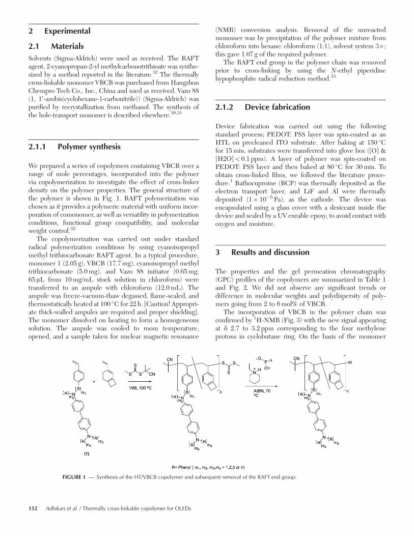
2.1 MaterialsSolvents (Sigma-Aldrich) were used as received. The RAFTagent, 2-cyanopropan-2-yl methylcarbonotrithioate was synthe-sized by a method reported in the literature.32 The thermallycross-linkable monomer VBCB was purchased from HangzhouChempro Tech Co., Inc., China and used as received. Vazo 88(1, 10-azobis(cyclohexane-1-carbonitrile)) (Sigma-Aldrich) waspurified by recrystallization from methanol. The synthesis ofthe hole-transport monomer is described elsewhere.30,31
2.1.1 Polymer synthesis
We prepared a series of copolymers containing VBCB over arange of mole percentages, incorporated into the polymervia copolymerization to investigate the effect of cross-linkerdensity on the polymer properties. The general structure ofthe polymer is shown in Fig. 1. RAFT polymerization waschosen as it provides a polymeric material with uniform incor-poration of comonomer, as well as versatility in polymerizationconditions, functional group compatibility, and molecularweight control.32
The copolymerization was carried out under standardradical polymerization conditions by using cyanoisopropylmethyl trithiocarbonate RAFT agent. In a typical procedure,monomer 1 (2.05 g), VBCB (17.7mg), cyanoisopropyl methyltrithiocarbonate (5.0mg), and Vazo 88 initiator (0.65mg;65 mL from 10mg/mL stock solution in chloroform) weretransferred to an ampule with chloroform (12.0mL). Theampule was freeze-vacuum-thaw degassed, flame-sealed, andthermostatically heated at 100 �C for 22 h. [Caution! Appropri-ate thick-walled ampules are required and proper shielding].The monomer dissolved on heating to form a homogeneoussolution. The ampule was cooled to room temperature,opened, and a sample taken for nuclear magnetic resonance
FIGURE 1 — Synthesis of the HT/VBCB copolymer and subsequ
152 Adhikari et al. / Thermally cross-linkable copolymer for OLEDs
(NMR) conversion analysis. Removal of the unreactedmonomer was by precipitation of the polymer mixture fromchloroform into hexane: chloroform (1:1), solvent system 3�;this gave 1.07 g of the required polymer.
The RAFT end group in the polymer chain was removedprior to cross-linking by using the N-ethyl piperidinehypophosphite radical reduction method.33
2.1.2 Device fabrication
Device fabrication was carried out using the followingstandard process; PEDOT: PSS layer was spin-coated as anHTL on precleaned ITO substrate. After baking at 150 �Cfor 15min, substrates were transferred into glove box ([O] &[H2O]< 0.1 ppm). A layer of polymer was spin-coated onPEDOT: PSS layer and then baked at 80 �C for 30min. Toobtain cross-linked films, we followed the literature proce-dure.1 Bathocuproine (BCP) was thermally deposited as theelectron transport layer, and LiF and Al were thermallydeposited (1� 10�5 Pa), as the cathode. The device wasencapsulated using a glass cover with a desiccant inside thedevice and sealed by a UV curable epoxy, to avoid contact withoxygen and moisture.
3 Results and discussion
The properties and the gel permeation chromatography(GPC) profiles of the copolymers are summarized in Table 1and Fig. 2. We did not observe any significant trends ordifference in molecular weights and polydispersity of poly-mers going from 2 to 6mol% of VBCB.
The incorporation of VBCB in the polymer chain wasconfirmed by 1H-NMR (Fig. 3) with the new signal appearingat d 2.7 to 3.2 ppm corresponding to the four methyleneprotons in cyclobutane ring. On the basis of the monomer
ent removal of the RAFT end group.
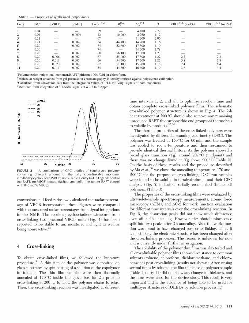
TABLE 1 — Properties of synthesized (co)polymers.
Entry [M]a [VBCB] [RAFT] Conv. NMR MnCalc Mn
GPCb Ð VBCBCalc (mol%)c VBCBNMR (mol%)d
1 0.04 — — 9 — 4 180 2.72 — —2 0.04 — 0.0004 12 10 000 2 760 1.12 — —3 0.21 — — 67 — 31 200 2.06 — —4 0.21 — 0.002 54 44 400 14 200 1.16 — —5 0.20 — 0.002 64 52 600 17 500 1.19 — —6 0.20 — — 74 — 34 300 1.78 — —7 0.20 — 0.002 68 56 100 17 300 1.23 — —8 0.20 0.006 0.002 67 55 000 17 500 1.22 2.2 2.39 0.20 0.011 0.002 66 54 500 17 300 1.22 3.8 2.810 0.20 0.023 0.002 62 51 100 15 200 1.18 7.4 6.411 0.20 0.011 0.002 54 44 300 16 600 1.19 3.6 4.4
aPolymerization ratio = total monomer/RAFT/initiator; 100/1/0.01 in chloroform.bMolecular weight obtained from gel permeation chromatography in tetrahydrofuran against polystyrene calibration.cCalculated from conversion data from the integration values of 1H-NMR vinyl signals of both monomers.dMeasured form integration of 1H-NMR signals at d 2.7 to 3.2 ppm.
FIGURE 2 — A comparison of GPC profiles of synthesized polymercontaining different amount of thermally cross-linkable monomervinylbenzylcyclobutene (VBCB) units (Table 1 entry 6–10).Legend: control(no RAFT, no VBCB) dotted, dashed, and solid line (under RAFT controlwith 0–6mol% VBCB).
conversions and feed ratios, we calculated the molar percent-age of VBCB incorporation; these figures were comparedwith the measured molar percentages from signal integrationsin the NMR. The resulting cyclooctadiene structure fromcross-linking two proximal VBCB units (Fig. 4) has beenreported to be stable to air, moisture, and light as well asbeing nonreactive.28
4 Cross-linking
To obtain cross-linked films, we followed the literatureprocedure.34 A thin film of the polymer was deposited onglass substrates by spin-coating of a solution of the copolymerin toluene. The thin film samples were then thermallyannealed at 170 �C inside the glove box for 2 h prior tocross-linking at 200 �C to allow the polymer chains to relax.Then, the cross-linking reaction was investigated at different
time intervals 1, 2, and 4 h to optimize reaction time andobtain complete cross-linked polymer films. The schematiccross-linked polymer structure is shown in Fig. 4. The 2-hheat treatment at 200 �C should also remove any remainingunreduced RAFT thiocarbonylthio end groups via thermolysisto volatile by-products.35,36
The thermal properties of the cross-linked polymers wereinvestigated by differential scanning calorimetry (DSC). Thepolymer was treated at 150 �C for 60min, and the samplewas cooled to room temperature and then rescanned toprovide identical thermal history. As the polymer showed abroad glass transition (Tg) around 207 �C (midpoint) andthere was no change found in Tg above 200 �C (Table 2).On the basis of these results and the procedure describedby Ma et al.,34 we chose the annealing temperature 170 and200 �C for the purpose of cross-linking. DSC run sampleswere found to be soluble in tetrahydrofuran, and their GPCanalysis (Fig. 5) indicated partially cross-linked (branched)polymers. (Table 3)
The properties of the cross-linking films were evaluated byultraviolet–visible spectroscopy measurements, atomic forcemicroscopy (AFM), and AC-2 for work function evaluationfor different time intervals over the cross-linking reaction. InFig. 6, the absorption peaks did not show much differenceeven after 4 h annealing. However, the photoluminescencesplit into two peaks after 3 h annealing. Also, the work func-tion was found to have changed post cross-linking. Thus, itis most likely the electronic structure has been changed afterthe cross-linking processes. The reason is unknown for nowand is currently under further investigation.
The solubility of the polymer thin films was also tested andall cross-linkable polymer films showed resistance to commonsolvents (toluene, chloroform, dichloromethane, and chloro-benzene) post cross-linking (results not shown). After rinsingseveral times by toluene, the film thickness of polymer sample(Table 1, entry 11) did not show any change in thickness, andthe films were used for the device study. This result is veryimportant and is the evidence of being able to be used formultilayer structures of OLEDs by solution processing.
Journal of the SID 21/4, 2013 153

FIGURE 3 — A comparison of 1H-NMR spectra of synthesized copolymers showing vinylbenzylcyclobutene (VBCB)cyclobutyl protons signals at 2.8 ppm (from lowest to highest spectra; Table 1, entry 7–10). Spectra were normalized to thearomatic signals at 7 ppm.
FIGURE 4 — Schematic for the thermal cross-linking process.
TABLE 2 — DSC results of as-synthesized polymer with RAFT end groupremoved.
Sample
TgOnset TgMidpoint Delta Cp
(�C) (�C) (Jg�1)
Table 1, entry 11 194 207 466
In addition to solvent resistance, surface topology of thepolymer films after thermal cross-linking is critical to deviceperformance. Smooth surface of HTL can provide bettercoverage of the anode material, ITO; reducing the microspikeswill mitigate undesired contact between the emission layer and
154 Adhikari et al. / Thermally cross-linkable copolymer for OLEDs
the anode. These kinds of defects eventually cause excitonquenching and decrease light emission. AFM was used toinvestigate the surface properties of the films before and aftercross-linking. Figure 7 clearly showed that the surface mor-phology of the film post cross-linking improved significantly(root mean square (rms) surface roughness of 0.47 nm), whichis of a lower surface roughness than typical values of >1.0 nmreported for PEDOT:PSS films on ITO surfaces.29
5 Device fabrication and evaluations
To evaluate the new synthesized HTL material, a greenOLED device was prepared using the thermally cross-linkable hole-transport polymer, and its device structure isshown in Fig. 8. The device structure comprised of 145 nmITO (anode)/40 nm hole injection layer (HIL)/15 nm polymer(Table 1, entry 11) (hole transport layer)/40 nm CBP:Ir(ppy)3(emission layer)/10 nm BCP/30 nm Alq3 (electron transportlayers)/1 nm LiF/120 nm Al (cathode); in accordance. In atypical process, Plexcore OC1200 layer was spin-coated as anHIL on top of a precleaned ITO substrate (in air). After bakingat 150 �C for 15min, substrates were transferred into a glovebox, where the amount of oxygen and moisture were con-trolled to less than 0.1 ppm. The polymer (Table 1, entry 11)was first dissolved in toluene and then spin-coated on top ofthe PEDOT: PSS layer to form a hole transport layer. This filmwas then annealed at 170 �C for 2 h and 200 �C for 4 h to com-plete the cross-linking process (Table 3). The emission layer
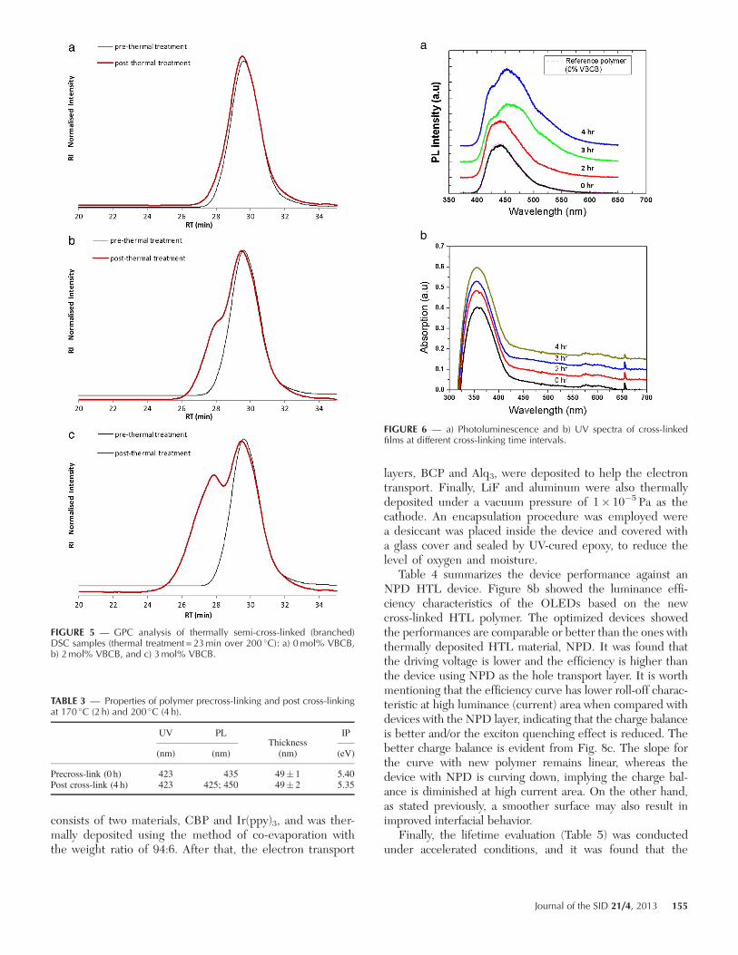
FIGURE 5 — GPC analysis of thermally semi-cross-linked (branched)DSC samples (thermal treatment = 23min over 200 �C): a) 0mol% VBCB,b) 2mol% VBCB, and c) 3mol% VBCB.
TABLE 3 — Properties of polymer precross-linking and post cross-linkingat 170 �C (2 h) and 200 �C (4 h).
UV PLThickness
(nm)
IP
(nm) (nm) (eV)
Precross-link (0 h) 423 435 49� 1 5.40Post cross-link (4 h) 423 425; 450 49� 2 5.35
b
a
FIGURE 6 — a) Photoluminescence and b) UV spectra of cross-linkedfilms at different cross-linking time intervals.
consists of two materials, CBP and Ir(ppy)3, and was ther-mally deposited using the method of co-evaporation withthe weight ratio of 94:6. After that, the electron transport
layers, BCP and Alq3, were deposited to help the electrontransport. Finally, LiF and aluminum were also thermallydeposited under a vacuum pressure of 1� 10�5 Pa as thecathode. An encapsulation procedure was employed werea desiccant was placed inside the device and covered witha glass cover and sealed by UV-cured epoxy, to reduce thelevel of oxygen and moisture.
Table 4 summarizes the device performance against anNPD HTL device. Figure 8b showed the luminance effi-ciency characteristics of the OLEDs based on the newcross-linked HTL polymer. The optimized devices showedthe performances are comparable or better than the ones withthermally deposited HTL material, NPD. It was found thatthe driving voltage is lower and the efficiency is higher thanthe device using NPD as the hole transport layer. It is worthmentioning that the efficiency curve has lower roll-off charac-teristic at high luminance (current) area when compared withdevices with the NPD layer, indicating that the charge balanceis better and/or the exciton quenching effect is reduced. Thebetter charge balance is evident from Fig. 8c. The slope forthe curve with new polymer remains linear, whereas thedevice with NPD is curving down, implying the charge bal-ance is diminished at high current area. On the other hand,as stated previously, a smoother surface may also result inimproved interfacial behavior.
Finally, the lifetime evaluation (Table 5) was conductedunder accelerated conditions, and it was found that the
Journal of the SID 21/4, 2013 155
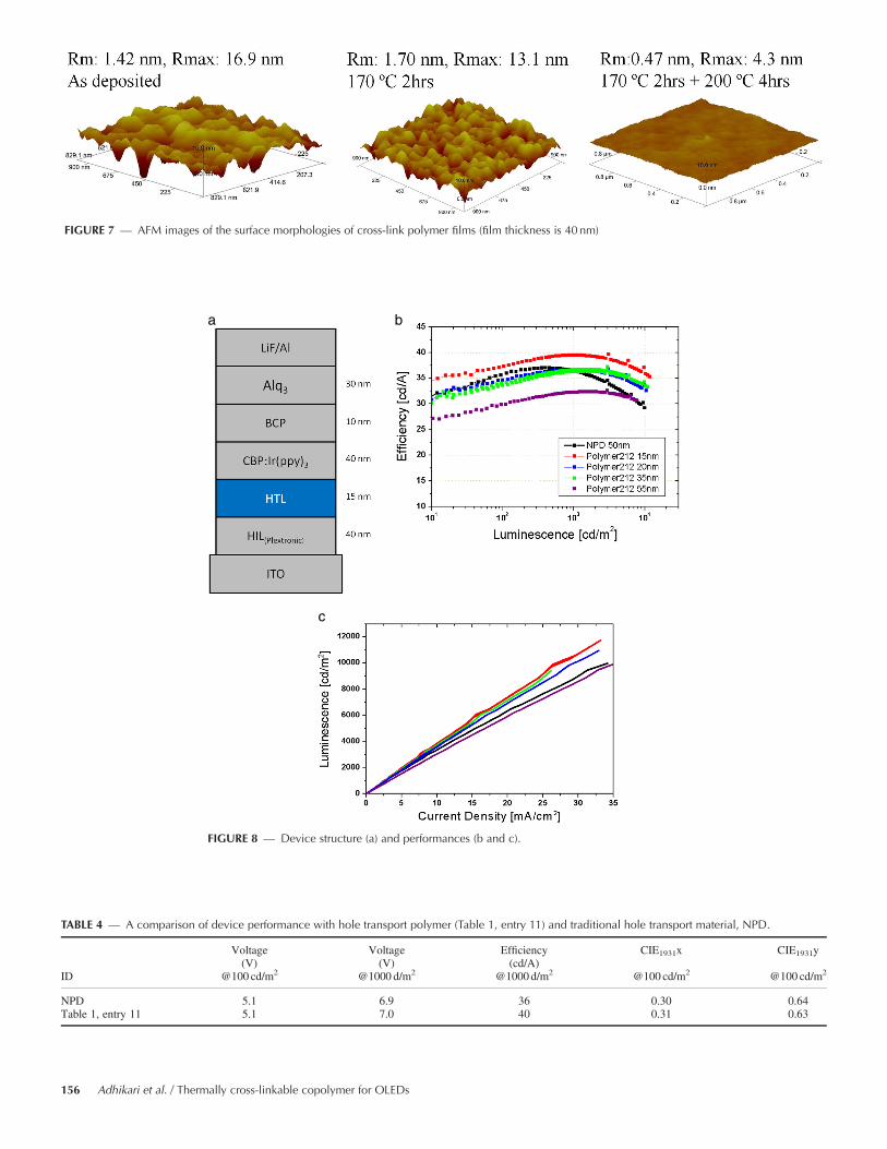
FIGURE 7 — AFM images of the surface morphologies of cross-link polymer films (film thickness is 40 nm)
a b
c
FIGURE 8 — Device structure (a) and performances (b and c).
TABLE 4 — A comparison of device performance with hole transport polymer (Table 1, entry 11) and traditional hole transport material, NPD.
ID
Voltage Voltage Efficiency CIE1931x CIE1931y(V) (V) (cd/A)
@100 cd/m2 @1000 d/m2 @1000 d/m2 @100 cd/m2 @100 cd/m2
NPD 5.1 6.9 36 0.30 0.64Table 1, entry 11 5.1 7.0 40 0.31 0.63
156 Adhikari et al. / Thermally cross-linkable copolymer for OLEDs
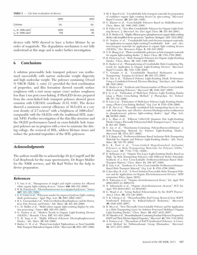
TABLE 5 — Life time evaluation of device.
Lifetime
NPD HTC
(h) (h)
t½ @ 1000 cd/m2 2850 456t½ @ 3000 cd/m2 556 89
devices with NPD showed to have a better lifetime by anorder of magnitude. The degradation mechanism is not fullyunderstood at this stage and is under further investigation.
6 Conclusions
A solution processable hole transport polymer was synthe-sized successfully with narrow molecular weight dispersityand high molecular weight. The polymer containing 3.6mol% VBCB (Table 1, entry 11) provided the best combinationof properties, and film formation showed smooth surfaceroughness with a root mean square (rms) surface roughnessless than 1 nm post cross-linking. P-PhoLED device preparedfrom the cross-linked hole transport polymer showed greenemission with CIE1931 coordinate (0.33, 0.62). The deviceshowed a maximum current efficiency of 39.5 cd/A at a cur-rent density of 2.7mA/cm2 with a brightness of 1000 cd/m2,comparable with the OLEDs with the traditional HTL mate-rial, NPD. Further investigation of the thin film structure andthe OLED performances based on cross-linkable hole trans-port polymer are in progress with a view to minimize the driv-ing voltage, the removal of HIL, address lifetime issues andreduce the potential impurities of the HTL polymers.
Acknowledgments
The authors would like to acknowledge Dr Jo Cosgriff and MrCarl Braybrook for the mass spectrometry, Dr Roger Mulderfor the NMR services, and Mr Karl Weber for the help indevice preparation.
References1 Y. Sun et al., “Management of singlet and triplet excitons for efficientwhite organic light-emitting devices,” Nature 440, 908–912 (2006).
2 R. H. Friend et al., “Electroluminescence in conjugated polymers,”Nature397, 121–128 (1999).
3 S. A. Carter et al., “Polymeric anodes for improved polymer light-emittingdiode performance,” Appl. Phys. Lett. 70, 2067–2069 (1997).
4 B. L. Groenendaal et al., “Poly(3,4-ethylenedioxythiophene) and Its Deriva-tives: Past, Present, and Future,” Adv. Mater. 12, 481–494 (2000).
5 C. D. Muller et al., “Multi-colour organic light-emitting displays by solu-tion processing,” Nature 421, 829–833 (2003).
6 O. Nuyken et al., “Modern Trends in Organic Light-Emitting Devices(OLEDs),” Monatsh. Chem. 137, 811–824 (2006).
7 X. H. Yang et al., “Highly Efficient Polymeric ElectrophosphorescentDiodes,” Adv. Mater. 18, 948 (2006).
8 Bacher, C. H. et al., “Photo-Cross-Linked Triphenylenes as Novel InsolubleHole TransportMaterials in Organic LEDs,”Macromol. 32, 4551–4557 (1999).
9 M. S. Bayerl et al., “Crosslinkable hole-transport materials for preparationof multilayer organic light emitting devices by spin-coating,” Macromol.Rapid Commun. 20, 224–228 (1999).
10 G. Klarner et al., “Cross-linkable Polymers Based on Dialkylfluorenes,”Chem. Mater. 11, 1800–1805 (1999).
11 R. Faber et al., “New Blue Crosslinkable Polymers for Organic Light Emit-ting Devices,” J. Macromol. Sci.: Pure Appl. Chem. 38, 353–364 (2001).
12 R.D. Hreha et al., “Highly efficient green phosphorescent organic light-emittingdiodeswith simplified device geometry,” Synthesis (Stuttgart), 1201–1212 (2002).
13 O. Nuyken et al., “Crosslinkable-hole-and-electron-transport-materials-for-application-in-organic-light-emitting"Crosslinkable hole- and elec-tron-transport materials for application in organic light emitting devices(OLEDs),” Des. Monomers Polym. 5, 195–210 (2002).
14 Y. D. Zhang et al., “Photo-crosslinkable polymers as hole-transport materialsfor organic light-emitting diodes,” J. Mater. Chem. 12, 1703–1708 (2002).
15 B. Domercq et al., “Hole-Transport Polymers for Organic Light-EmittingDiodes,” Chem. Mater. 15, 1491–1496 (2003).
16 E. Bacher et al., “Photopatterning of Crosslinkable Hole-Conducting Ma-terials for Application in Organic Light-Emitting Devices,” Macromol.Rapid Commun. 25, 1191–1196 (2004).
17 V. Getautis et al., “Crosslinkable Branched Hydrazones as HoleTransporting,” Imaging Sci.Technol. 48, 265–272 (2004).
18 H. Yan et al., “Enhanced Polymer Light-Emitting Diode PerformanceUsing a Crosslinked-Network Electron-Blocking,” Interlayer, Adv. Mater.16, 1948 (2004).
19 E. Bacher et al., “Synthesis and Characterization of Photo-Cross-LinkableHole-Conducting Polymers,” Macromol. 38, 1640–1647 (2005).
20 J. Li et al., “Fabrication of Multi-layer Polymer Light Emitting Diodesusing a Photo Cross-linking Method,” J. Photopolym. Sci. Technol.19, 187–192 (2006).
21 B. Lim et al., “Fabrication of Multi-layer Polymer Light Emitting Diodesusing a Photo Cross-linking Method,” Org. Lett. 8, 4703–4706 (2006).
22 Y. H. Niu et al., “Thermally crosslinked hole-transporting layers for cas-cade hole-injection and effective electron-blocking/exciton-confinementin phosphorescent polymer light-emitting diodes,” Appl. Phys. Lett.88, 093505 (2006).
23 J. L. Zhao et al., “Efficient CdSe/CdS Quantum Dot Light-EmittingDiodes Using a Thermally Polymerized Hole Transport Layer,” Nano Lett.6, 463–467 (2006).
24 S. Liu et al., “Triarylamine-Containing Poly(perfluorocyclobutane) asHole-Transporting Material for Polymer Light-Emitting Diodes,”Macromol. 33, 3514–3517 (2002).
25 X. Z. Jiang et al., “Perfluorocyclobutane-Based Arylamine Hole-TransportingMaterials for Organic and Polymer Light-Emitting Diodes,” Adv. Funct.Mater. 12, 745–751 (2002).
26 G. K. Paul et al., “Cross-Linked Hyperbranched ArylaminePolymers as Hole-Transporting Materials for Polymer LEDs,”Macromol. 39, 7789–7792 (2006).
27 E. Bellmann et al., “Organic Two-Layer Light-Emitting Diodes Based onHigh- Tg Hole-Transporting Polymers with Different Redox Potentials;Synthesis of a New Cross-Linkable Perfluorocyclobutane-Based Hole-Transport Materia,” Chem. Mater. 11, 399–407 (1999).
28 B. Lim et al., “Synthesis of a New Cross-Linkable Perfluorocyclobutane-Based Hole-Transport Material,” Org. Lett. 8, 4703–4706 (2006).
29 Li Juo-Hao, R. et al., “A Novel Solution Processable Hole-Transport Poly-mer and Its Applications on Organic Electroluminescent Devices,” IDWsymposium Tokyo, Japan (2010).
30 N. Yokoyama et al., “Organic electroluminescent device,” Int. Appl. WO2009139475 A1 20091119.
31 N. Yabunouchi et al., “Organic electroluminescent element,” PCT Int.Appl. WO 2010114017, A1 20101007.
32 G. Moad et al., “Living Radical Polymerization by the RAFT Process,”Aust J. Chem. 58, 379–140 (2005).
33 Y. K. Chong et al., “Thiocarbonylthio End Group Removal from RAFT-Synthesized Polymers by Radical-Induced Reduction,” Macromol.40, 4446–4455 (2007).
34 B. Ma et al., “New Thermally Cross-Linkable Polymer and Its Applicationas a Hole-Transporting Layer for Solution Processed Multilayer OrganicLight Emitting Diodes,” Chem. Mater. 19, 4827–4832 (2007).
35 M.Häussler et al., “Benzothiadiazole-Containing Pendant Polymers Prepared byRAFTand Their Electro-Optical Properties,”Macromol. 43, 7101–7110 (2010).
36 A. Postma et al., “Thermolysis of RAFT-Synthesized Polymers. A Conve-nient Method for Trithiocarbonate Group Elimination,” Macromol.38, 5371–5374 (2005).
Journal of the SID 21/4, 2013 157

Tadahiko Hirai currently is a leader of the devicegroup of organic semiconductor including OLEDin CSIRO and a visiting professor of YokohamaCity University. Before that, he had been a man-ager and scientist of R&D group at Canon Inc.Tokyo, Japan from 1999 to 2008. He obtained aBS of Physics at Tokyo University of Science (Ja-pan) in 1984, an MS of Applied Physics at Uni-versity of Electro-Communications (Japan) in1986, and a PhD of semiconductor physics andengineering at Waseda University (Japan) in1997. His current interests are on physics andmechanisms of organic and oxide semiconduc-tors for display technologies.
Mark Bown is currently the stream leaderresponsible for OLED and OFET research in theFlexible Electronics Theme at CSIRO MaterialsScience & Technology in Melbourne, Australia.He obtained a BS in Chemistry from ImperialCollege, London in 1984, and his PhD inInorganic and Structural Chemistry from theUniversity of Leeds in 1987. He has held post-doctoral appointments in Massey University(New Zealand) Oxford of University (UK) andThe Australian National University (Australia).His current interests are in the development ofnew materials for flexible electronics.
Ueno Kazunori is currently working as a projectleader of OLED research project at CSIRO MaterialsScience and Engineering. From 1992 to 2008, heworked as a principal staff engineer at OD Develop-ment Centre, Canon Inc. leading OLED group, whichfocused on materials study, display development,and associatedmanufacturing processes. Prior to this,from 1974 to 1988, he was a research associate at theResearch Institute of Industrial Science, KyushuUniversity/Institute of Advanced Material Study,Kyushu University for lecturing master course anddoctor course students and conducting research inthe areas of heterocyclic compounds.
Juo-Hao Li currently is working on flexibledisplay in Corning Inc. He was a technology re-searcher at Nanowin Technology Inc., in Taiwan2011. Before that, he had been a device scientistat the Flexible Electronics group in CSIRO from2009 to 2011. He obtained a BS andMS at ChengKung University (Taiwan) in 1999 and 2001, anda PhD in Materials Science and Engineering atUniversity of California, Los Angeles in 2009,focusing on organic light-emitting devices (OLEDs).His current interests are on the technical marketingin the field of flexible display.
Almar Postma received his BSc in Chemistryfrom The University of Surrey, UK (1996) andobtained his PhD from The University of NewSouth Wales under the supervision of Prof. T. P.Davis and Drs G. Moad and M. O’Shea (2005)in the fields of controlled radical polymerizationand reactive extrusion. From 2005 to 2008, heheld a postdoctoral fellow position with Prof. F.Caruso at The University of Melbourne workingon polymer-based capsular drug delivery vehi-cles and with a start-up company (iCeutica) onpharmaceutical nanosizing. He rejoined CSIROas a research scientist in 2008. His currentresearch interests lie at the interface of polymerdesign/synthesis and their applications inelectroactive materials and nanobiomedicine.
Raju Adhikari completed his PhD (organicChemistry) from University of Delhi (1986). Hejoined CSIROMolecular Science in 1992 to workon Dunlena project in the area of herbicidalcompound. He later worked at University ofHohenheim, Germany under a DADD programand rejoined the Division in 1995. He workedin Biomaterials for over 14 years and is one ofthe coinventors of Elast-Eon™ and NovoSorb™
family of biostable and biodegradable polyure-thanes. He is presently a principal research scien-tist with CSIROMaterial Science and Engineeringand working towards the development of smallmolecules, iridium complexes and polymers forOLED and cosmetic applications.
158 Adhikari et al. / Thermally cross-linkable copolymer for OLEDs