Micro-light-emitting diodes with quantum dots in ... - Nature
Red-emitting fluorescent Organic Light emitting Diodes with low sensitivity to self-quenching S.Forget(1)*, S.Chenais(1), D.Tondelier(2), B.Geffroy(2), I.Gozhyk(3), M.Lebental(3), and E.Ishow(4)
(1) Laboratoire de Physique des Lasers, Université Paris 13 / CNRS UMR 7538,
Villetaneuse, France (2) Laboratoire de Physique des Interfaces et Couches Minces, Ecole Polytechnique,
CNRS UMR 7647, Palaiseau, France (3) Laboratoire de Photonique Quantique et Moléculaire, ENS Cachan, CNRS UMR 8537,
France (4) Laboratoire de Photophysique et Photochimie Supramoléculaires et
Macromoléculaires, ENS Cachan, CNRS UMR 8531, France *E-mail : [email protected] Keywords: OLED, quenching, doping, red-emitting organic material Abstract
Concentration quenching is a major impediment to efficient organic light-emitting devices.
We herein report on Organic Light-Emitting Diodes (OLEDs) based on a fluorescent
amorphous red-emitting starbust triarylamine molecule (4-di(4’-tert-butylbiphenyl-4-yl)amino-
4’-dicyanovinylbenzene, named FVIN), exhibiting a very small sensitivity to concentration
quenching. OLEDs are fabricated with various doping levels of FVIN into Alq3, and show a
remarkably stable external quantum efficiency of 1.5% for doping rates ranging from 5% up
to 40%, which strongly relaxes the technological constraints on the doping accuracy. An
efficiency of 1% is obtained for a pure undoped active region, along with deep red emission
(x=0.6; y=0.35 CIE coordinates). A comparison of FVIN with the archetypal DCM dye is
presented in an identical multilayer OLED structure.
1. Introduction
Organic Light Emitting Diodes (OLEDs) have proven their potential as efficient and low-cost
sources for lighting and flat panel displays1,2. Their efficiency strongly depends on the
properties of the organic materials used for each layer of the OLED architecture, including
light-emitting and charge carrier transporting materials. More specifically, the fluorescence
efficiency of blue, green and red emitters is a crucial parameter to design high performance
1 1

OLEDs for full-color displays and solid-state lighting applications. In this perspective, one of
the greatest challenges remains to find red emitters with saturated colors (CIE coordinates x >
0.62 and y < 0.34), high quantum efficiency, and robustness against thermal evaporation
allowing a very fine and repeatable control of the device performances3-6. Indeed, most of the
existing red fluorophores either exhibit strong dipolar structure to form low-energy charge
transfer excited states, or possess extensively π-conjugated backbones. This results in strong
Van der Waals intermolecular interactions (charge transfer, π−π stacking) causing crystalline
aggregates which are often deleterious for optical applications. A related troublesome effect
known as “concentration quenching”7 arises with the increase in molecular density and the
appearance of non-radiative complexes. This well-known effect is serious for small-molecule
based OLEDs as it becomes highly detrimental as soon as concentration exceeds a few
percents. As a consequence, many red-emitting materials exhibit fluorescence quantum yield
close to unity in solution, but become either weakly or even not emissive at all in the solid
state. Therefore, a universal solution to solve the concentration quenching problem is to use
them as dopants in a host material at a very low doping ratio. The archetypal example of such
a structure is given by DCM (4-dicyanomethylene-2-methyl-6-(p-dimethylaminostyryl)-4H-
pyran) doped into Alq3 (tris(8-hydroxyquinolinate)aluminum(III)). Red emission can here be
obtained through direct excitation of the DCM fluorophores or through Förster energy transfer
from the excited Alq3 host matrix. The optimal dopant concentration (resulting from the trade-
off between efficient energy transfer and reduced concentration quenching) is often very low,
commonly not greater than 2%. In practice, the effective doping range requested to keep the
OLED efficiency unchanged is very narrow, and limited to a few tenths of percent of the
optimal concentration3,4,8. From an experimental point of view, doping is by no means a
trivial task and controlling the doping level with this level of accuracy is very challenging.
This severe drawback strongly limits the repeatability of devices with identical performances
in a mass-production process. To our knowledge, systematic studies about the effects of
doping level in red-emitting materials have never been deeply explored.
Such investigations stir a tremendous interest for deep-red-emitting materials having a very
limited dependence of their properties on the doping rate (when incorporated in a host matrix),
or even being able to emit light efficiently in a non-doped configuration (neat films), which
would ultimately simplify manufacturing control.
In this paper, we report on a fluorescent red-emitting unsymmetrical starbust triarylamine
molecule exhibiting a very small sensitivity to concentration quenching. This molecule9 was
2 2

shown to exhibit laser operation under optical pumping in a neat film configuration10,
suggesting high robustness against concentration quenching. We present in this paper a study
of the performances (efficiency, spectrum and CIE coordinates) of this material in OLED
structures, with various levels of doping in a host system as well as in a non-doped
configuration. Comparison with archetypal DCM-based systems presenting a similar
multilayer configuration is presented.
2. Chemical properties
Several attempts were reported in the literature to obtain red-emitting organic materials with
limited sensitivity to quenching effects. Two strategies are commonly adopted consisting
either in elaborating molecules presenting a large Stokes shift so as reabsorption effects in
concentrated media are minimized, or in introducing sterically crowded substituents or highly
branched backbones to avoid the formation of non-radiative π-stacked aggregates. The first
approach has been developed in the case of 4-dicyanomethylene-2-methyl-6-[2-(2,3,6,7-
tetrahydro-1H,5H-benzo[ij]quinolizin-8-yl)vinyl]-4H-pyran (DCM2), 4-(dicyanomethylene)-
2-t-butyl-6(1,1,7,7-tetramethyljulolidyl-9-enyl)-4H-pyran (DCJTB), or 4,4’,4’’-tris[2-(4-
dicyanomethylene-6-t-butyl-4H-pyran-2-yl)-ethylene]triphenylamine (TDCM), while the
second one concerns 3-(N-phenyl-N-p-tolylamino)-9-(N-p-styrylphenyl-N-p-
tolylamino)perylene ((PPA)(PSA)Pe)11, anthracen-9-yl-(8-{4-[anthracen-9-yl-(4-
ethylphenyl)amino]-phenyl}-benzo[a]-aceant-hrylen-3-yl)-(4-ethylphenyl)amine (ACEN)12,
bis(4-(N-(1-naphthyl)-phenylamino)phenyl)fumaronitrile (NPAFN)13, 2,3-bis(N, N-1-
naphthyl-phenylamino)-N-methylmaleimide (NPAMLI)14 or benzo[1,2,5]thiadiazole based
polymers (BZTA)15.
Those materials also need to be amorphous since isotropic, homogeneous and grain-
boundaries-free systems favor high OLED performances16.
To this aim, we retained 4-di(4’-tert-butylbiphenyl-4-yl)amino-4’-dicyanovinylbenzene, named
FVIN, for its efficient fluorescence emission in the solid state and glass-forming properties. It
was synthesized according to a five-step synthetic protocol which was described in earlier
study9. The presence of a twisted triphenylamino core substituted by terminal bulky tert-butyl
groups prevents the molecules from interacting with each others and creating deleterious
radiationless aggregates. Additionally, this reduces the risks of forming scattering defects
known to limit the device optical performances.
Thermal properties were measured by using differential scanning calorimetry (Perkin Elmer
Pyris Diamond) in alumina caps under a nitrogen flow at a scan rate of 10 °C.min-1 over the
3 3

temperature range [25 °C - 250 °C]. Thermal analyses actually revealed a glass transition
temperature Tg of 86 °C with no further recrystallization. Accordingly thin films obtained
under thermal vacuum evaporation from pre-fused powder at a 10 Ås-1 (P = 10-5 mbar)
evaporation scan rate showed excellent time-stable amorphous properties after months of
storage at room temperature.
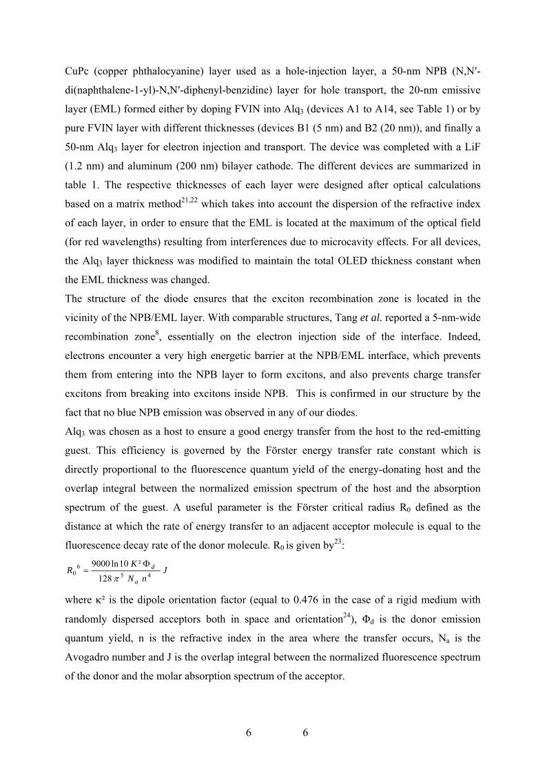
The push-pull character of FVIN induced by the presence of the electron-withdrawing
dicyanovinylene moiety ensured the formation of a low-energy charge transfer (CT) singlet
excited state S1 which absorbs in the visible around 480 nm. S1 relaxes back to the S0 ground
state by emitting red light with a maximum at 630 nm (fig. 1a) after having evolved toward a
more distorted geometry as evidenced from preliminary femtosecond transient absorption
spectroscopy measurements. Consequently, the large Stokes shift (5030 cm-1) measured for
FVIN avoids strong emission quenching in the solid state due to inner filter effects as usually
encountered for most of fluorophores, making the emission intensity of FVIN little sensitive
to concentration quenching effects. UV-visible absorption spectra were recorded using a
Varian Model Cary 5E spectrophotometer. Corrected emission spectra were obtained using a
Spex Fluorolog 1681 spectrofluorimeter. Fluorescence quantum yield in cyclohexane solution
was determined from a solution of Coumarine 540 A in EtOH (Φf = 0.38) absorbing equally
at the excitation wavelength with an absorbance less than 0.1 to avoid reabsorption effects.
Measurements of fluorescence quantum yield in the solid state were carried out using a Jobin-
Yvon. Inc spectrofluorimeter (Fluoromax 4) equipped with a hollow integrating sphere coated
on its internal surface with a diffusely reflecting material (reflecting efficiency: 95% in the
spectral range 250-2500 nm).
From theoretical computations conducted in the gas phase (time-dependent density functional
theory TDDFT (B3LYP ; 6-31G(d) as a basis set)), the S0-S1 absorption and emission
transitions occuring in the visible range involved the highest occupied molecular orbital
(HOMO) and lowest unoccupied molecular orbital (LUMO) located at -5.416 eV and -2.483
eV respectively (see Fig. 1b). Their electronic densities were mainly spread on the
triphenylamino core and the dicyanovinylene moiety respectively, hence the strong CT
character of the corresponding transition ( = 451 nm) with an oscillator strength f
calculated to be 0.813. Additionally, a second intense transition ascribed to S0→S2 was
observed in the UV range of the experimental absorption spectrum around 319 nm, and could
calcmaxλ
be accounted for by the HOMO→LUMO+1 transition (f = 0.635; = 335 nm) with the calcmaxλ
4 4

LUMO+1 mainly localized onto the biphenyl groups. This latter excited state quantitatively
deactivated toward the low-energy S1 state since fluorescence quantum yield Φf
measurements (Φf = 0.20 in the solid state) showed no wavelength dependence.
The oxidation properties of FVIN were evaluated by cyclic voltammetry in dichloromethane -1
m Fl
e
VIN closely
.1 OLED structure
he main objective of this study is to show that the FVIN molecule is an efficient fluorophore
with 0.1 M NBu4ClO4 as a supporting electrolyte at a 100 mVs potential scan rate. Cyclic
voltammetry was performed using a EG&G PAR 273 potentiostat interfaced to a PC
computer. The reference electrode used was an Ag+/Ag electrode filled with 0.01 M AgNO3.
This reference electrode was checked versus ferrocene, as recommended by IUPAC (here
E°Fc+/Fc = 0.045 V in dichloromethane with 0.1 M tetrabutylammonium perchlorate purchased
fro uka (puriss). Dichloromethane (SDS, 99.9 %) was used as received. All solutions were
deaerated by bubbling with argon for a few minutes prior to electrochemical measurements.
The reversible oxidation of the triphenylamino unit into its cation occurs at a half-wav
oxidation potential E°ox = 0.57 V vs ferrocene (ΔEp = 72 mV), substantially higher than those
of unsubstituted triarylamine as logically expected from the electron-withdrawing effects
induced by the dicyanovinylene unit located in the para-phenyl position. A second oxidation
wave corresponding to the amino dication could be observed at 1.14 V using a higher scan
rate (10 Vs-1), albeit less reversible (ΔEp = 185 mV) than the first oxidation step.
Obviously, through its oxido-reduction properties, the ambipolar compound F
resembles electron-transporting materials rather than hole-transporting ones17. The energetic
and electronic descriptions of the HOMO and LUMO will help us to interpret further the
experimental OLED features since both molecular orbitals actively participate to the
processes of exciton recombination and charge carrier transport.
3. OLED studies
3
T
under electrical driving. Its potential as a red-emitter in organic light-emitting devices was
analyzed in a classical multilayer architecture18-21 realized by vacuum thermal evaporation on
ITO coated glass substrates. The isotropic, homogeneous and grain-boundary free properties
of the amorphous FVIN material allows easy evaporation in a standard thermal vacuum
evaporator. The multilayer structure, depicted in fig. 2, successively consisted of a 10-nm
5 5
CuPc (copper phthalocyanine) layer used as a hole-injection layer, a 50-nm NPB (N,N′-
di(naphthalene-1-yl)-N,N′-diphenyl-benzidine) layer for hole transport, the 20-nm emissive
layer (EML) formed either by doping FVIN into Alq3 (devices A1 to A14, see Table 1) or by
pure FVIN layer with different thicknesses (devices B1 (5 nm) and B2 (20 nm)), and finally a
50-nm Alq3 layer for electron injection and transport. The device was completed with a LiF
(1.2 nm) and aluminum (200 nm) bilayer cathode. The different devices are summarized in
table 1. The respective thicknesses of each layer were designed after optical calculations
based on a matrix method21,22 which takes into account the dispersion of the refractive index
of each layer, in order to ensure that the EML is located at the maximum of the optical field
(for red wavelengths) resulting from interferences due to microcavity effects. For all devices,
the Alq3 layer thickness was modified to maintain the total OLED thickness constant when
the EML thickness was changed.
The structure of the diode ensures that the exciton recombination zone is located in the
e host to the red-emitting
vicinity of the NPB/EML layer. With comparable structures, Tang et al. reported a 5-nm-wide
recombination zone8, essentially on the electron injection side of the interface. Indeed,
electrons encounter a very high energetic barrier at the NPB/EML interface, which prevents
them from entering into the NPB layer to form excitons, and also prevents charge transfer
excitons from breaking into excitons inside NPB. This is confirmed in our structure by the
fact that no blue NPB emission was observed in any of our diodes.
Alq3 was chosen as a host to ensure a good energy transfer from th
guest. This efficiency is governed by the Förster energy transfer rate constant which is
directly proportional to the fluorescence quantum yield of the energy-donating host and the
overlap integral between the normalized emission spectrum of the host and the absorption
spectrum of the guest. A useful parameter is the Förster critical radius R0 defined as the
distance at which the rate of energy transfer to an adjacent acceptor molecule is equal to the
fluorescence decay rate of the donor molecule. R0 is given by23:
JK
R d60
²10ln9000 Φ=
nN a45128 π
where κ² is the dipole orientation factor (equal to 0.476 in the case of a rigid medium with
randomly dispersed acceptors both in space and orientation24), Φd is the donor emission
quantum yield, n is the refractive index in the area where the transfer occurs, Na is the
Avogadro number and J is the overlap integral between the normalized fluorescence spectrum
of the donor and the molar absorption spectrum of the acceptor.
6 6

In our case, R0 is calculated to be 30.2 Å, comparable to that obtained for the archetypal
Alq3:DCM blend (31.8 Å). An almost complete energy transfer is thus expected at a doping
level of a few percents, leading to efficient diodes.
3.2 OLED measurements
The glass substrate covered with ITO was cleaned by sonication and prepared by a UV-ozone
treatment. The layers were then deposited by sublimation under high vacuum (10−6- 10−7
mbar) at a rate of 0.1-0.2 nm/s in a thermal evaporator. An in situ quartz crystal was used to
monitor the thickness of the layer depositions with an accuracy of 5 %. The organic materials
and the LiF/Al cathode were deposited in a one-step process without breaking the vacuum.
The doping rate was controlled by simultaneous co-evaporation of the host and the dopant.
After deposition, all the measurements were performed at room temperature and under
ambient atmosphere, without any encapsulation. The current–voltage–luminance (I–V–L)
characteristics of the devices were measured with a regulated power supply (ACT100
Fontaine) combined with a multimeter (Keithley 4200) and a calibrated silicon photodiode of
area 1 cm² (Hamamatsu). The spectral emission was recorded with a SpectraScan PR650
spectrophotometer, with a spectral resolution of 4 nm. The OLED active area is 0.3 cm².
3.3 Results and discussion
3.3.1 Influence of the doping level on color properties
To be interesting as red-emitting sources for display applications, organic devices should
exhibit emission with CIE coordinates verifying x > 0.6 and y < 0.35. It is then interesting to
study the conditions leading to deep-red emission. A bathochromic shift of the main emission
maximum from 582 nm to 625 nm is observed when the doping concentration of FVIN is
increased from 0.5 % to 28 %, as commonly observed with DCM25, while the spectrum
remained unchanged for doping levels above 30%. The evolution of the electroluminescence
spectra is plotted in fig. 3 for various levels of doping, as well as for undoped devices B1 and
B2 (EML made of 100% of FVIN).. When a neat film of FVIN was used as an EML (devices
B), a small additional shift of the maximum wavelength was also observed (up to 635 nm for
device B1), but the main feature in this case relied on the disappearance of the small
7 7

remaining band around 500 nm. This band is clearly attributed to residual Alq3 emission,
which may originate a priori either from incomplete energy transfer from Alq3 excitons to
FVIN, or from the direct recombination in the pure Alq3 layer of electrons with holes having
flowed through the EML. The fact that Alq3 emission intensity remains almost constant
instead of decreasing when increasing the doping level tends to discard the first
hypothesis,that is incomplete transfer is not the prevailing phenomenon. To check the second
hypothesis, we designed a new configuration (device C) incorporating an additional
bathocuproine (BCP) hole-blocking layer: for devices C1 and C2, a 10 nm layer of BCP was
used between the EML and Alq3 layers to block both holes and excitons. Two diodes were
fabricated, with a Alq3:FVIN EML presenting the same doping level as that of devices A2 and
A5 for comparison. We observed the suppression of the Alq3 emission band when BCP was
introduced (see fig. 4). The green emission observed in the Alq3:FVIN blend consequently
stems from holes that do not recombine with electrons in the EML, flow through it within
Alq3 and then recombine in the neat Alq3 layer. The absence of a green emission shoulder in
the devices made of pure FVIN as EML with no BCP suggests that either FVIN molecules do
not efficiently transport holes or alternatively that holes accumulate at the FVIN/Alq3
interface because of the 0.4 eV energetic barrier. We plotted in the fig. 5 the JVL curves (J is
the current density in mA/cm², V the voltage and L the luminance) for a low-doped EML
(device A1, 0.5% of FVIN in Alq3) and for a pure FVIN EML (device B1, with a thickness of
20 nm for the neat FVIN layer). Even though the slope efficiency of the non-doped device
was smaller, the threshold voltage was found to be roughly the same, indicating that the
behavior of the diode is still good with a thick pure FVIN layer inserted in the middle of the
device.
The CIE coordinates of the doped OLED were affected by the presence of residual Alq3 green
emission, hence the resulting emission was not red enough. However, upon addition of BCP a
deep red-emission with CIE coordinates of x = 0.59 and y = 0.40 was eventually obtained
(device C2). When non-doped OLEDs were used, the red emission was even more saturated,
with x = 0.613 and y = 0.37. The evolution of the x and y CIE coordinates as a function of the
doping level with or without BCP is presented in fig. 6.
It is worth noting that no color shift was observed when varying the injected current for the
doped or non-doped device (fig. 7). This requirement is essential and sometimes poorly filled
with doped systems because of a possible shift of the recombination zone location with
increasing injected current.
8 8

3.3.2 Influence of the doping level on OLED efficiency
The evolution of the external quantum efficiency of the investigated OLEDs as a function of
the doping level is presented in fig. 8. The external quantum efficiency η increased up to a
maximum of 2.1% for a doping level of around 2%. This correspond to a power and current
efficiency of 1.7 lm/W and 4.8 cd/A respectively. η then slightly decreased but still stayed
high (more than 2%) until the doping level reached 4%, where concentration quenching starts
playing a significant role. The most striking feature here is that η remains constant (around
1.5%) over a very broad doping range from 5% up to 40%. This may have important practical
implications since setting the doping ratio in this range guarantees both reasonable efficiency
and insensitivity to doping level fluctuations. After 40%, the decreasing slope is small, since
the efficiency is still 1% for non-doped devices. For comparison purposes, two DCM-based
OLEDs with Alq3:DCM as the EML were fabricated at two different levels of doping in DCM
(2% and 40%). We can clearly see in fig. 9 that the decrease of the external quantum
efficiency is much faster, down to 0.7% for the 40%-doped DCM-based OLED, which is less
than half the value obtained for the FVIN-based OLED with an equivalent doping level.
We have shown with this study that FVIN exhibits high potential for electroluminescent
devices. First of all, the amorphous structure of the material with relatively low Tg enables a
very easy, controllable and reproducible evaporation process.. Moreover, the structure of the
molecule leads to reduced sensitivity to quenching effects: it is possible to achieve high
efficiency (up to 2.1%, comparable to the well known Alq3:DCM system), with a constant
external quantum efficiency of 1.5% obtained over a range of doping ratios between 5% and
40%, which strongly relaxes the technological constraints on the doping accuracy. Finally,
FVIN can be used in neat films (without doping) with standard hole transporting materials
such as NPB to form an efficient heterostructure.
5. Conclusion
We studied in this paper a new fluorescent electroluminescent material emitting in the red in
OLED configuration. We showed that the structure of the molecule provides a reduced
9 9
sensitivity to quenching effects: in OLED experiments, a constant external quantum
efficiency of 1.5% was measured for doping rates ranging from 5% up to 40% in an Alq3
matrix, while a maximum efficiency of 2.1% was obtained for a doping rate of 2%. This
represents a strong improvement compared to classical DCM blends where the doping rate
must be controlled with an accuracy of less than one percent. The evaporation process can
thus be simplified to allow for larger fluctuations in the doping rate in the perspective of a
mass production process. We also showed that an OLED containing pure FVIN as the
emission layer can still be efficient. In this kind of undoped structure, the evaporation process
is straightforward as no doping is required at all. Noteworthy a deep-red emission is obtained
with CIE coordinates of (0.62; 0.37), which sets FVIN among the rare electroluminescent
small-molecules able to efficiently emit in this color area in neat films. The studies conducted
here on concentration quenching effects will help the further fabrication of small molecule-
based white OLEDs involving doped or stacked multilayers of blue, green and red emitters.
Acknowledgements
The authors acknowledge financial support from the ANR (JC/JC call, “BACHELOR”
project) and Paris 13 University (BQR credits). We thank A. Beausset for technical
assistance, and J.Zyss for fruitful discussions. F.Miomandre is gratefully thanked for the
electrochemical measurements in solution.
10 10
Figures :
Fig 1 : (a) (from [9]) Normalized absorption and emission spectra of FVIN in thin films
(inset : FVIN chemical structure). (b) TDDFT computations (B3LYP, 6-31G(d)) of FVIN in
the gas phase. Representation of the electronic density of the HOMO, LUMO and LUMO+1.
11 11

The image cannot be displayed. Y
ITO
LiF/Al
CuPc NPB EML Alq3
5.6
2.53.6
5.2
3.1
5.8
The
image
ca
BCP
2.9
6.4
3.45
5.42
fig 2 : OLED architecture used in the experiments together with HOMO-LUMO levels in eV.
For FVIN (EML), the LUMO level is deduced from the HOMO and the optical gap. The other
levels are taken from the literature.
The BCP layer in present only in device C. Thicknesses are (10-nm / 50-nm / 20-nm / 50-nm)
for the CuPc/NPB/EML/Alq3 layers respectively.
12 12

fig 3 : evolution of the fluorescence OLED emission spectra in A and B configurations for
different doping levels of FVIN in Alq3.
fig 4 : Emission spectra of devices A (without BCP) and C (with BCP) for the same level of
doping (here around 1.3 and 2.7 % for devices A2/C1 and A5/C2, respectively).
13 13

fig 5 : J-V and L-V curves for a low-doped (0.5% of FVIN in Alq3, device A1) and a pure
(20 nm neat film, device B1) EML.
14 14

Fig 6 : Evolution of the CIE (x,y) coordinates with the doping level for devices A, B and C.
The dots are the doped devices (filled ones without BCP (A), empty ones with BCP (C))
whereas the triangles are the pure-EML devices (B). Inset : photos of four OLEDs with
different doping level (color online).
15 15

fig 7 : Evolution of the spectrum with injected current for device B1 (20 nm of pure FVIN as
EML)
16 16
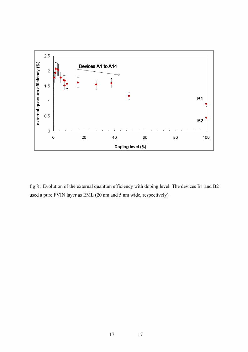
fig 8 : Evolution of the external quantum efficiency with doping level. The devices B1 and B2
used a pure FVIN layer as EML (20 nm and 5 nm wide, respectively)
17 17

fig 9 : Comparison of external quantum efficiency in FVIN:Alq3 and DCM:Alq3 OLEDs at
low and high doping level.
Name Doping level (%)
of FVIN into Alq3 Structure
A1 0.5 CuPc/NPB/Alq3:FVIN/Alq3
A2 1.3 idem
A3 2.3 idem
A4 2.6 idem
A5 2.7 idem
A6 3.2 idem
A7 4.8 idem
A8 6.8 idem
A9 7.3 idem
A10 7.5 Idem
18 18

A11 16 idem
A12 28 idem
A13 32 idem
A14 49.5 idem
B1 100 CuPc/NPB/FVIN (20nm) /Alq3
B2 100 CuPc/NPB/FVIN (5nm) /Alq3
C1 1.2 CuPc/NPB/Alq3:FVIN/BCP/Alq3
C2 2.6 CuPc/NPB/Alq3:FVIN/BCP/Alq3
Table 1 : list of the different devices
References :
1 B. W. D'Andrade and S. R. Forrest, Advanced Materials 16, 1585-1595 (2004). 2 S. Reineke, F. Lindner, G. Schwartz, N. Seidler, K. Walzer, B. Lussem, and K. Leo,
Nature 459, 234-U116 (2009). 3 C. T. Chen, Chemistry Of Materials 16, 4389-4400 (2004). 4 Y. S. Yao, J. Xiao, X. S. Wang, Z. B. Deng, and B. W. Zhang, Advanced Functional
Materials 16, 709-718 (2006). 5 J. Huang, X. F. Qiao, Y. J. Xia, X. H. Zhu, D. G. Ma, Y. Cao, and J. Roncali,
Advanced Materials 20, 4172-+ (2008). 6 L. S. Hung and C. H. Chen, Materials Science & Engineering R-Reports 39, 143-222
(2002). 7 C. H. Chen, J. Shi, and C. W. Tang, Macromolecular Symposia 125, 1-48 (1998). 8 C. W. Tang, S. A. Vanslyke, and C. H. Chen, Journal Of Applied Physics 65, 3610-
3616 (1989). 9 E. Ishow, A. Brosseau, G. Clavier, K. Nakatani, P. Tauc, C. Fiorini-Debuisschert, S.
Neveu, O. Sandre, and A. Leaustic, Chemistry Of Materials 20, 6597-6599 (2008). 10 H. Rabbani-Haghighi, S. Forget, S. Chenais, A. Siove, M. C. Castex, and E. Ishow,
Applied Physics Letters 95 (2009). 11 S. Toguchi, Y. Morioka, H. Ishikawa, A. Oda, and E. Hasegawa, Synthetic Metals
111-112, 57 (2000). 12 T.-H. Huang, J. T. Lin, Y.-T. Tao, and C.-H. Chuen, Chemistry of Materials 15, 4854
(2003). 13 W. Zhang, Z. He, L. Mu, Y. Zou, Y. Wang, and S. Zhao, Dyes and Pigments 85, 86
(2010).
19 19

20 20
14 W. C. Wu, H. C. Yeh, L. H. Chan, and C. T. Chen, Advanced Materials 14, 1072-1075 (2002).
15 K. R. J. Thomas, J. T. Lin, M. Velusamy, Y. T. Tao, and C. H. Chuen, Advanced Functional Materials 14, 83-90 (2004).
16 Z.-Y. Xia, J.-H. Su, H.-H. Fan, K.-W. Cheah, H. Tian, and C. H. Chen, The Journal of Physical Chemistry C 114, 11602.
17 Z. J. Ning, Z. Chen, Q. Zhang, Y. L. Yan, S. X. Qian, Y. Cao, and H. Tian, Advanced Functional Materials 17, 3799-3807 (2007).
18 A. Fischer, S. Chenais, S. Forget, M. C. Castex, D. Ades, A. Siove, C. Denis, P. Maisse, and B. Geffroy, Journal Of Physics D-Applied Physics 39, 917-922 (2006).
19 H. Choukri, A. Fischer, S. Forget, S. Chenais, M. C. Castex, B. Geffroy, D. Ades, and A. Siove, Synthetic Metals 157, 198-204 (2007).
20 H. Choukri, A. Fischer, S. Forget, S. Chenais, M. C. Castex, D. Ades, A. Siove, and B. Geffroy, Applied Physics Letters 89, 183513 (2006).
21 M. Lebental, H. Choukri, S. Chenais, S. Forget, A. Siove, B. Geffroy, and E. Tutis, Physical Review B 79 (2009).
22 B. Ruhstaller, T. Beierlein, H. Riel, S. Karg, J. C. Scott, and W. Riess, Ieee Journal Of Selected Topics In Quantum Electronics 9, 723-731 (2003).
23 T. Forster, Ann. Phys. 2, 55 (1948). 24 J. Lakowicz, Principles of Fluorescence Spectroscopy (Springer, New York, NY,
USA, 2006). 25 V. Bulovic, A. Shoustikov, M. A. Baldo, E. Bose, V. G. Kozlov, M. E. Thompson,
and S. R. Forrest, Chemical Physics Letters 287, 455-460 (1998).
Copyright © 2022 FDOKUMEN