Light-emitting diode spherical packages: an equation for the light transmission efficiency
Upload
independentCategory
view
2download
0
A microfluidic device using a green organic light emitting diode as anintegrated excitation source
Bo Yao,a Guoan Luo,*a Liduo Wang,bc Yudi Gao,c Gangtie Lei,b Kangning Ren,a Lingxin Chen,a
Yiming Wang,a Yan Hub and Yong Qiubc
Received 11th April 2005, Accepted 8th July 2005
First published as an Advance Article on the web 5th August 2005
DOI: 10.1039/b504959h
A simply fabricated microfluidic device using a green organic light emitting diode (OLED) and
thin film interference filter as integrated excitation source is presented and applied to fluorescence
detection of proteins. A layer-by-layer compact system consisting of glass/PDMS microchip,
pinhole, excitation filter and OLED is designed and equipped with a coaxial optical fiber and for
fluorescence detection a 300 mm thick excitation filter is employed for eliminating nearly 80%
of the unwanted light emitted by OLEDs which has overlaped with the fluorescence spectrum of
the dyes. The distance between OLED illuminant and microchannels is limited to y1 mm for
sensitive detection. The achieved fluorescence signal of 300 mM Rhodamine 6G is about 13 times
as high as that without the excitation filter and 3.5 times the result of a perpendicular detection
structure. This system has been used for fluorescence detection of Rhodamine 6G, Alexa 532 and
BSA conjugates in 4% linear polyacrymide (LPA) buffer (in 1 6 TBE, pH 8.3) and 1.4 fmol and
35 fmol mass detection limits at 0.7 nl injection volume for Alexa and Rhodamine dye have been
obtained, respectively.
Introduction
Although more and more measurement schemes besides laser
induced fluorescence (LIF),1 including electrochemistry (EC),2
chemilluminescence (CL)3/electrical chemilluminescence
(ECL),4 mass spectrumetry (MS),5 and nuclear magnetic
resonance (NMR),6 have been developed for microfluidic or
‘‘lab-on-a-chip’’ (LOC) systems in the past decade, the
performance of laser induced fluorescence detectors is still
enormously important especially in the area of life science
research. As opposed to the original, large 488 nm argon
ion lasers, small, low cost laser diodes are now commonly
being used as the excitation source as first reported by
Harrison and co-workers1 in order to produce a more compact
overall system.
Further simplification of the fluorescence detection could be
obtained by employing a light emitting diode (LED) pre-
sumably at a reduced sensitivity. Webster et al.7 presented a
monolithic device fabricated by 13 steps of lithography which
had integrated photodiodes built on a silicon substrate and
optical interference filter with a parylene based microchip.
Whitesides and co-workers8 also reported an integrated
fluorescence detection system consisting of a microavalanche
photodiode (mAPD), a thin film of polymeric colored filters
and a PDMS microchip. Blue LEDs were employed as external
light sources in both systems. Recently LEDs with a very
high output power and shorter wavelength have become
commercially available. Since LED is not very expensive and
can be driven at low power, we can even use it as a disposable
light source.
Compared with inorganic LEDs, organic light emitting
diodes (OLEDs) have a flat surface which makes it easy to
integrate with microfluidic devices and flexible to fabricate
into any size and shape by photolithography techniques. A
recent review showed high interests in this field since OLEDs
offer the potential of on-chip light source arrays with
controlled spectral characteristics and in principle are cheap
to integrate on a microchip.10 Kopelman et al. reported a
fluorescent chemical sensor platform integrating an OLED
device light-source with a fluorescent probe for an oxygen
sensor.11 Fujii and co-workers first presented an integrated
PDMS microfluidic device with a 510 nm (peak wavelength)
OLED and optical fibers.12 In order to minimize the distance
between OLED and microchannel they placed a channel cast
in PDMS directly on the rear side of the glass substrate of the
OLED. Unfortunately, no fluorescence signal of Rhodamine B
was obtained in their system and the design could be further
optimized. Kim et al. reported an advanced and compact
microchip coupled with a green OLED of 530 nm (peak
wavelength) and a PIN photodiode for fluorescence detection
which achieving a detection limit of 0.01 mM Rhodamine 6G
as reported.13 Edel and co-workers presented a polyfluorene-
based thin-film polymer light emitting diode (pLED) which
had a peak emission wavelength at 488 nm as an integrated
excitation source for microfabricated capillary electro-
phoresis.14 For fluorescein and 5-carboxyfluorescein
detection concentrations as low as 1 mM were achieved with
lock-in-amplifier equipment. Later they employed an organic
aDepartment of Chemistry, Tsinghua University, Beijing, 100084, China.E-mail: [email protected]; Fax: +86-10-62781688;Tel: +86-10-62781688bKey Lab of Organic-Optoelectronics & Molecular Engineering ofMinistry of Education, Department of Chemistry, Tsinghua University,Beijing, 100084, China. E-mail: [email protected];Fax: +86-10-62795137; Tel: +86-10-62788802cBeijing Visionox Technology Co. Ltd, Beijing, 100085, China.E-mail: [email protected]; Tel: +86-10-62968822-221
PAPER www.rsc.org/loc | Lab on a Chip
This journal is � The Royal Society of Chemistry 2005 Lab Chip, 2005, 5, 1041–1047 | 1041
photodiode for detecting and monitoring a peroxyoxalate
based chemiluminescence reaction.15
OLEDs as a promising light source for integrated micro-
fluidic devices and fluorescence measurements are attracting
more and more attention. However, only a few groups have
so far entered this field probably because OLEDs are not
commercially available up to now. There are still several
critically unresolved problems including spectrum purity and
intensity which also exist in LED detection systems and block
the way for a wide application. Scientists have made enormous
efforts to improve the sensitivity of LED and OLED systems
such as employing a lock-in-amplifier,7,14 a liquid core
waveguide,16 an emission interference filter7 and high sensitive
confocal structures.17 Compared with lasers, the output power
of LEDs and OLEDs is fairly low and has a wider bandwidth
of emission spectrum. So it is very important to eliminate as
much as possible the part of the excitation light which overlaps
with the emission spectrum of analytes in order to supress the
background interference and at the same time confirm that the
distance between light source and microchannels is minimized.
In our previous reported work, an argon ion laser and red
diode laser were both employed as light sources for fluores-
cence detection in microfluidics18–20 with high sensitivity yet
large size. Now we are presenting a glass/PDMS microchip
device using a green OLED which has a peak wavelength at
520 nm as the excitation source. Between the light source and
microchannel a 300 mm-thick TiO2/SiO2 interference filter is
inserted to get rid of unwanted excitation light. A conventional
photomultiplier tube and optical fiber are employed for
fluorescence detection of Rhodamine 6G and Alexa 532 dye
on the microchip. The influence of pinhole size, excitation light
filtering on detection sensitivity and stability of OLED at
different driving voltage has been studied and under optimized
conditions the obtained S/N ratio of 50 mM Rhodamine
6G and 7 mM Alexa 532 is 16.9 and 10.2 respectively. Using
this system Alexa 532 and its bovine serum albumin
(BSA) conjugates have been separated and fluorescence
detected in modified microchannels and 4% linear poly-
acrylamide (LPA) buffer.
Experimental
Reagents and protein derivation
AlexaFluor1532 carboxylic acid, succinimidyl ester (532/554
nm) was purchased from Molecular Probes (Eugene, OR,
USA). Tris(hydroxymethyl)aminomethane (Tris), bovine
serum albumin (BSA, 66 200Da), EDTA and Rhodamine 6G
(526/555 nm) were all obtained from Sigma-Aldrich (St. Louis,
MO, USA). Acrylamide monomer, and N,N,N9,N9-tetra-
methylethylenediamine (TEMED) were both bought from
Promega (Madison, WI, USA) while ammonium persulfate
(APS) was from Amresco (Solon, Oh, USA) and [c-(metha-
cryloyloxy)propyl] trimethoxysilane (MAPS) was a product
of Fluka (Buchs, Switzerland). All other chemicals were
of analytical reagent grade, and Milli-Q water (18.2 MV,
Millipore, MA, USA) was used throughout.
The running buffer of 4% (w/v) LPA in 1 6 TBE was
prepared by dissolving 1.6 g acrylamide and 0.076 g APS in
10 ml of water, slightly different from the reported work of
Schmalzing et al.21 and Gomis et al.22 Then the solution was
mixed with 20 ml of 2 6 TBE (89 mM Tris, 89 mM boric acid
and 2 mM EDTA, pH 8.3) and the volume was adjusted
to 40 ml. Immediately 24 ml of TEMED was added and the
solution was degassed with an ultrasonic bath and left
overnight at room temperature for complete polymerization.
For protein labeling, the Alexa 532 dye was stored and
handled as instructed on the web site of Molecular Probes.23 In
brief, the dye was dissolved in dimethylsulfoxide (DMSO) at
10 mg ml21 (13.8 mM) and stored at 220 uC. For derivation,
5 ml of dye was added into 45 ml of 20 mg ml21 BSA (in 0.1 M
bicarbonate buffer, pH 8.3) and immediately stirred gently
for an hour at room temperature. The conjugate solution
was then stored at 4 uC protected from light without further
purification.
Microchip fabrication and coating
The glass substrate with microchannels used in the following
experiments was designed and home-made by standard
photolithography and wet chemical etching techniques.19,24
The cover plate was a piece of 100 mm thick PDMS replica
from a flat glass wafer which was silanized in 3% (v/v)
octadecyl trichlorosilane (Sigma, St.Louis, MO, USA) in dry
toluene for 2 h beforehand.25 10 : 1 of the silicone elastomer
and curing agent (Sylgard 184, Dow Corning, Midland, MI,
USA) were mixed and poured onto the wafer after stirring and
degassing. The solution was baked in a vacuum oven at 65 uCfor 4 h. Immediately PDMS was sealed to the glass substrate
after peeling off the wafer and then the microchip was
exposed to ultraviolet light (UV) which had a peak emission
at 253.7 nm (X-30G, Spectroline, USA) and average intensity
of 1.85 mW cm22 with the PDMS side face up for 9 h for
further combination and oxidization of PDMS as described
elsewhere.26
The final chip had a cross-linked microchannel which was
70 mm deep and 100 mm wide (at half depth) with 1.5 cm of
sample channel and 3 cm of separation channel and a distance
between cross channel to detection point of 1.5 cm. 5 ml of
MAPS was added to each reservoir of S, SW and B (Fig. 1a)
and 0.1 atm of vacuum was applied to the BW reservoir and
the microchannels were soon filled with MAPS. After that it
was left at room temperature for reaction overnight. This was
followed by rinsing with methanol followed by water for 2 min
and 10 min respectively and dipping in freshly prepared
reaction buffer (3% acrylamide, 0.6% ammonium persulfate
and 0.2% TEMED in water) for 3 h as reported by Han et al.27
Finally the substrate was rinsed with water for 10 min and
dried with nitrogen for 10 min, ready for usage.
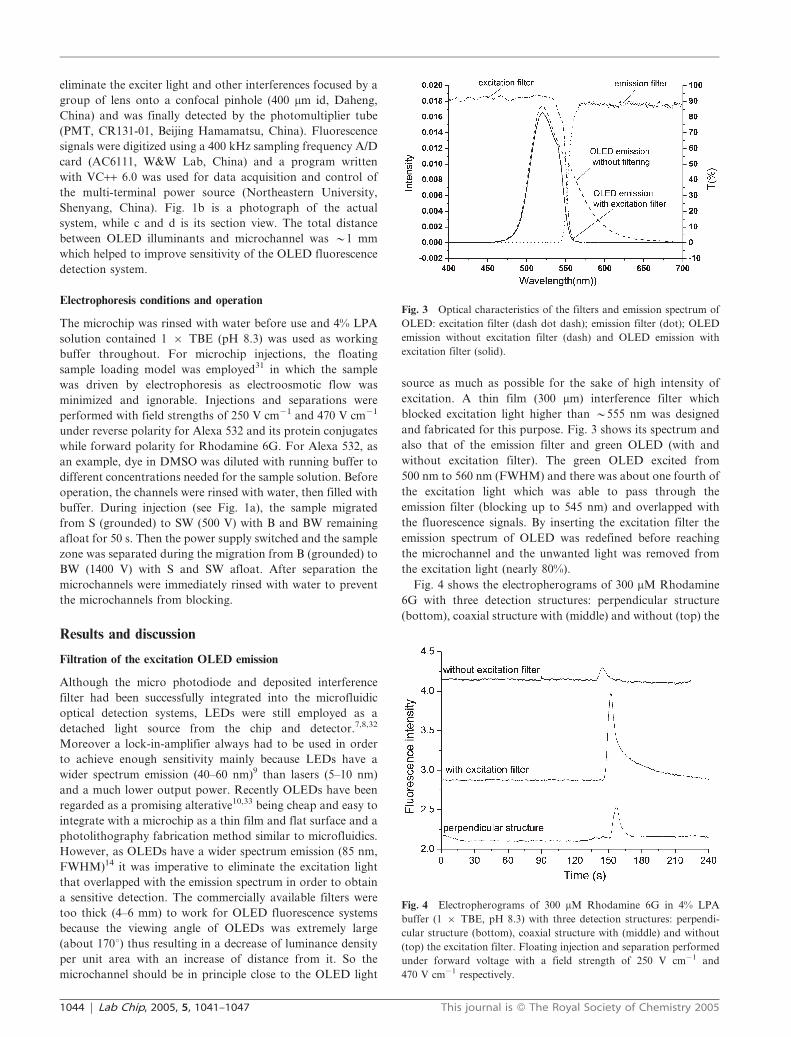
OLED fabrication
The OLEDs used in the experiments consisting of a typical p–n
diode bottom emitting structure of ITO/NPB/Alq3/Mg:Ag/Ag
were fabricated by organic molecular beam deposition on a
lithographically patterned indium tin oxide (ITO) coated glass
substrate as described previously.28–30 The ITO substrate was
routinely cleaned by ultra-sonication in acetone, ethanol,
rinsed in de-ionized water and isopropyl alcohol, and finally
irradiated in an oxygen plasma chamber. Then, the organic
1042 | Lab Chip, 2005, 5, 1041–1047 This journal is � The Royal Society of Chemistry 2005
films, 40 nm of a-napthylphenylbiphenyl (NPB) and 60 nm of
tris(8-hydroxyquinoline) aluminium (Alq3) were deposited on
the ITO substrate layer by layer in high vacuum as the hole
injection layer and the electron transport layer respectively.
After deposition of the organic layers, the top cathode was
prepared by sequential deposition of 100 nm Mg:Ag and 50 nm
Ag layers without breaking the vacuum. The sandwich
structure of OLEDs is shown in Fig. 2.
When 4.5–12 V direct current was applied to the metal
cathode and ITO anode the energy barriers between the
highest occupied molecular orbital and lowest unoccupied
molecular orbital levels were about 0.4 and 0.9 eV, respec-
tively, which were high enough to localize the holes in the NPB
layer and electrons in the Alq3 layer. Recombination of these
charges occurred across the barriers, with holes primarily
moving into Alq3. The green OLED had a 0.5 mm thick glass
substrate and an array of 250 mm 6 250 mm illuminants
controlled by parallels of deposited electrodes which emitted
an intensity of 20000 cd m22 and irradiance of 7.5 mW cm22
(at 12 V driving voltage) green fluorescence with a peak
emission at 520 nm and y60 nm bandwidth (FWHM).
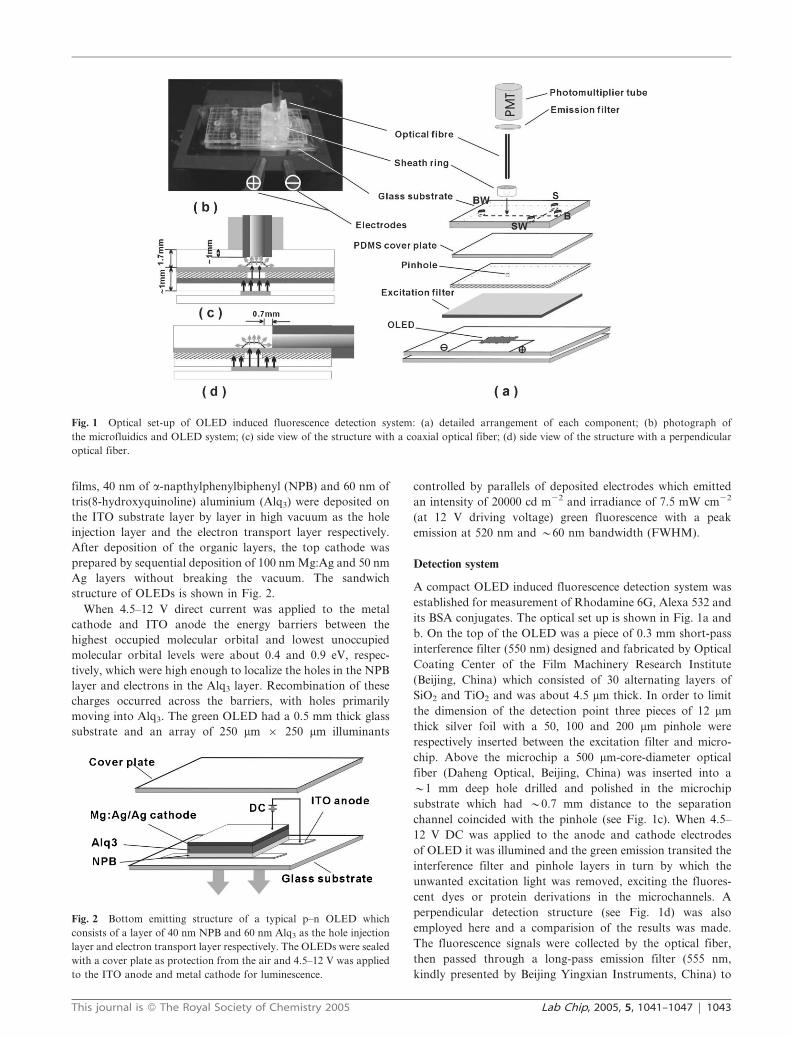
Detection system
A compact OLED induced fluorescence detection system was
established for measurement of Rhodamine 6G, Alexa 532 and
its BSA conjugates. The optical set up is shown in Fig. 1a and
b. On the top of the OLED was a piece of 0.3 mm short-pass
interference filter (550 nm) designed and fabricated by Optical
Coating Center of the Film Machinery Research Institute
(Beijing, China) which consisted of 30 alternating layers of
SiO2 and TiO2 and was about 4.5 mm thick. In order to limit
the dimension of the detection point three pieces of 12 mm
thick silver foil with a 50, 100 and 200 mm pinhole were
respectively inserted between the excitation filter and micro-
chip. Above the microchip a 500 mm-core-diameter optical
fiber (Daheng Optical, Beijing, China) was inserted into a
y1 mm deep hole drilled and polished in the microchip
substrate which had y0.7 mm distance to the separation
channel coincided with the pinhole (see Fig. 1c). When 4.5–
12 V DC was applied to the anode and cathode electrodes
of OLED it was illumined and the green emission transited the
interference filter and pinhole layers in turn by which the
unwanted excitation light was removed, exciting the fluores-
cent dyes or protein derivations in the microchannels. A
perpendicular detection structure (see Fig. 1d) was also
employed here and a comparision of the results was made.
The fluorescence signals were collected by the optical fiber,
then passed through a long-pass emission filter (555 nm,
kindly presented by Beijing Yingxian Instruments, China) to
Fig. 1 Optical set-up of OLED induced fluorescence detection system: (a) detailed arrangement of each component; (b) photograph of
the microfluidics and OLED system; (c) side view of the structure with a coaxial optical fiber; (d) side view of the structure with a perpendicular
optical fiber.
Fig. 2 Bottom emitting structure of a typical p–n OLED which
consists of a layer of 40 nm NPB and 60 nm Alq3 as the hole injection
layer and electron transport layer respectively. The OLEDs were sealed
with a cover plate as protection from the air and 4.5–12 V was applied
to the ITO anode and metal cathode for luminescence.
This journal is � The Royal Society of Chemistry 2005 Lab Chip, 2005, 5, 1041–1047 | 1043
eliminate the exciter light and other interferences focused by a
group of lens onto a confocal pinhole (400 mm id, Daheng,
China) and was finally detected by the photomultiplier tube
(PMT, CR131-01, Beijing Hamamatsu, China). Fluorescence
signals were digitized using a 400 kHz sampling frequency A/D
card (AC6111, W&W Lab, China) and a program written
with VC++ 6.0 was used for data acquisition and control of
the multi-terminal power source (Northeastern University,
Shenyang, China). Fig. 1b is a photograph of the actual
system, while c and d is its section view. The total distance
between OLED illuminants and microchannel was y1 mm
which helped to improve sensitivity of the OLED fluorescence
detection system.
Electrophoresis conditions and operation
The microchip was rinsed with water before use and 4% LPA
solution contained 1 6 TBE (pH 8.3) was used as working
buffer throughout. For microchip injections, the floating
sample loading model was employed31 in which the sample
was driven by electrophoresis as electroosmotic flow was
minimized and ignorable. Injections and separations were
performed with field strengths of 250 V cm21 and 470 V cm21
under reverse polarity for Alexa 532 and its protein conjugates
while forward polarity for Rhodamine 6G. For Alexa 532, as
an example, dye in DMSO was diluted with running buffer to
different concentrations needed for the sample solution. Before
operation, the channels were rinsed with water, then filled with
buffer. During injection (see Fig. 1a), the sample migrated
from S (grounded) to SW (500 V) with B and BW remaining
afloat for 50 s. Then the power supply switched and the sample
zone was separated during the migration from B (grounded) to
BW (1400 V) with S and SW afloat. After separation the
microchannels were immediately rinsed with water to prevent
the microchannels from blocking.
Results and discussion
Filtration of the excitation OLED emission
Although the micro photodiode and deposited interference
filter had been successfully integrated into the microfluidic
optical detection systems, LEDs were still employed as a
detached light source from the chip and detector.7,8,32
Moreover a lock-in-amplifier always had to be used in order
to achieve enough sensitivity mainly because LEDs have a
wider spectrum emission (40–60 nm)9 than lasers (5–10 nm)
and a much lower output power. Recently OLEDs have been
regarded as a promising alterative10,33 being cheap and easy to
integrate with a microchip as a thin film and flat surface and a
photolithography fabrication method similar to microfluidics.
However, as OLEDs have a wider spectrum emission (85 nm,
FWHM)14 it was imperative to eliminate the excitation light
that overlapped with the emission spectrum in order to obtain
a sensitive detection. The commercially available filters were
too thick (4–6 mm) to work for OLED fluorescence systems
because the viewing angle of OLEDs was extremely large
(about 170u) thus resulting in a decrease of luminance density
per unit area with an increase of distance from it. So the
microchannel should be in principle close to the OLED light
source as much as possible for the sake of high intensity of
excitation. A thin film (300 mm) interference filter which
blocked excitation light higher than y555 nm was designed
and fabricated for this purpose. Fig. 3 shows its spectrum and
also that of the emission filter and green OLED (with and
without excitation filter). The green OLED excited from
500 nm to 560 nm (FWHM) and there was about one fourth of
the excitation light which was able to pass through the
emission filter (blocking up to 545 nm) and overlapped with
the fluorescence signals. By inserting the excitation filter the
emission spectrum of OLED was redefined before reaching
the microchannel and the unwanted light was removed from
the excitation light (nearly 80%).
Fig. 4 shows the electropherograms of 300 mM Rhodamine
6G with three detection structures: perpendicular structure
(bottom), coaxial structure with (middle) and without (top) the
Fig. 3 Optical characteristics of the filters and emission spectrum of
OLED: excitation filter (dash dot dash); emission filter (dot); OLED
emission without excitation filter (dash) and OLED emission with
excitation filter (solid).
Fig. 4 Electropherograms of 300 mM Rhodamine 6G in 4% LPA
buffer (1 6 TBE, pH 8.3) with three detection structures: perpendi-
cular structure (bottom), coaxial structure with (middle) and without
(top) the excitation filter. Floating injection and separation performed
under forward voltage with a field strength of 250 V cm21 and
470 V cm21 respectively.
1044 | Lab Chip, 2005, 5, 1041–1047 This journal is � The Royal Society of Chemistry 2005
excitation filter. Since no excitation filter has been employed
with previously reported work on OLEDs, optical fiber
collected fluorescence signals perpendicular to the light source
and microchannel (see Fig. 1d) was accepted in order to
supress the background interferences by preventing the
detector from facing directly towards the OLED source,
although there was still a part of interferences that reached the
detector. When an appropriate excitation filter was designed
and used for eliminating interference excitation light a coaxial
framework as shown in Fig. 1c remarkably improves its
sensitivity by collecting more fluorescence signals and less
interferences, only if the distance between light source and
microchannel is limited as much as possible. In this experi-
ment, the achieved sensitivity of Rhodamine 6G with the
excitation filter (middle spectrum in Fig. 4) was about 13 times
as high as that without the filter (top) where a piece of 300 mm
thick glass slide was inserted instead for keeping the distance
and 3.5 times as the perpendicular detection structure
(bottom). For Rhodamine 6G, a forward voltage was applied
for injection and separation and it needed a longer migration
time (150 s) due to a weak EOF existing in the microchannels
or a small plus charge in the buffer.
However, a layer of directly deposited interference filter
onto the OLED surface was not achieved because of the
difficulties in fabrication. A thin film filter (300 mm thick)
sacrificed sensitivity to some extend, whereas, it could be kept
on being used even when the OLED did not work and was
abandoned. Furthermore, optical characteristics of the filter
were better than when deposited.7
Microchip fabrication and modification
A glass/PDMS microfluidic chip was employed in this research
because a common glass substrate available in our lab was not
less than 1.7 cm thick which resulted in a long distance
between OLED and microchannels and was disadvantageous
for high sensitivity detection. A piece of 100 mm thick PDMS
was polymerized and immediately sealed with the glass
substrate with microchannels after which the channels were
modified by MAPS. However, no methanol should be added
to the modification solution as done usually because it would
be absorbed by the PDMS material and make it fragile. When
LPA solution is polymerized in the microchip it would fill the
porous surface of PDMS and form a layer of physical coating
as well as the chemical effect of modification of glass channels.
This kind of glass/PDMS chip proved to be strong under
normal pressure as well as rinsing the microchannels and could
be used for several weeks.
Stability of OLEDs at different voltages
70 mM of Alexa 532 dye was filled into the microchannels
in order to study the influence of driving voltages of OLED
on fluorescence signals and stability. When output of the
power supply increased every 5 min from 4.5 V to 13.5 V, the
fluorescence intensity skipped upwards accordingly (see Fig. 5).
When the driving voltage was as high as 13.5 V, fluorescence
signals sharply declined 80% in 5 min which is mainly because
the working current between metal cathode and ITO anode
has exceeded its rated upper limit and excessive Joule heat
production leading to irreversible damage. Therefore, in the
following experiments 12 V of driving voltage was used as the
power supply of the OLED unless stated otherwise for the sake
of high sensitivity and several days stably output of OLEDs
could be obtained at a 12 V driving voltage.
Optimization of the pinhole
Three pieces of silver foil with about 50 mm, 100 mm and
200 mm pinholes were prepared and inserted between excita-
tion filter and microchip for confining the detection spot (see
Fig. 1a). Fig. 6 illustrates the detection of 140 mM Alexa 532
dye solution with 50 mm, 100 mm and 200 mm pinhole
respectively (from bottom to top). Two components of this dye
(hydrolytes or photolytes) were successfully separated and
fluorescently detected in the microchip. Different signal to
noise (S/N) ratios of 21.1, 132.3 and 272.5 were obtained
respectively according to the variety of the pinhole size. A
Fig. 5 Stability of OLED emission at different driving voltages
where 70 mM Alexa 532 dye in 4% LPA buffer (1 6 TBE, pH8.3)
was used as analyte and was filled into the microchannels for studying.
The power supply output increased from 4.5 V to 13.5 V every 5 min at
a step of 1.5 V.
Fig. 6 Fluorescence detection of 140 mM Alexa 532 dye in 4% LPA
buffer (1 6 TBE, pH 8.3) with 50 mm, 100 mm and 200 mm pinhole
respectively (from bottom to top); different S/N ratios of 21.1, 132.3
and 272.5 were achieved according to the increase of pinhole diameter.
This journal is � The Royal Society of Chemistry 2005 Lab Chip, 2005, 5, 1041–1047 | 1045
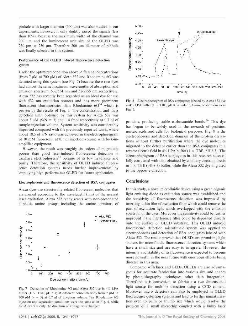
pinhole with larger diameter (300 mm) was also studied in our
experiments, however, it only slightly raised the signals (less
than 10%), because the maximum width of the channel was
200 mm and the luminescent unit size of the OLED was
250 mm 6 250 mm. Therefore 200 mm diameter of pinhole
was finally selected in this system.
Performance of the OLED induced fluorescence detection
system
Under the optimized condition above, different concentrations
(from 7 mM to 700 mM) of Alexa 532 and Rhodamine 6G was
detected using this system (see Fig. 7) because these two dyes
had almost the same maximum wavelengths of absorption and
emission spectrum, 532/554 nm and 526/555 nm respectively.
Alexa 532 has recently been regarded as an ideal dye for use
with 532 nm excitation sources and has more prominent
fluorescent characteristics than Rhodamine 6G34 which is
proven by the results of Fig. 7. The concentration and mass
detection limit obtained by this system for Alexa 532 was
about 3 mM (S/N 5 3) and 1.4 fmol respectively at 0.7 nl of
sample injection volume. System sensitivity was considerably
improved compared with the previously reported work, where
about 18.5 of S/N ratio was achieved in the electrophoregram
of 10 mM fluorescein at 0.1 nl injection volume with lock-in-
amplifier equipment.
However, the result was roughly six orders of magnitude
poorer than good laser-induced fluorescence detection in
capillary electrophoresis35 because of its low irradiance and
purity. Therefore, the sensitivity of OLED induced fluores-
cence detection systems needs further improvements by
employing high performance OLED for future application.
Electrophoresis and fluorescence detection of BSA conjugates
Alexa dyes are structurally related fluorescent molecules that
are named according to the wavelength (nm) of the nearest
laser excitation. Alexa 532 ready reacts with non-protonated
aliphatic amine groups including the amine terminus of
proteins, producing stable carboxamide bonds.36 This dye
has begun to be widely used in the research of proteins,
nucleic acids and cells for biological purposes. Fig. 8 is the
electrophoresis and detection diagram of the protein deriva-
tions without further purification where the dye molecules
migrated to the detector earlier than the BSA conjugates in a
reverse electric field in 4% LPA buffer (1 6 TBE, pH 8.3). The
electropherogram of BSA conjugates in this research success-
fully correlated with that obtained by capillary electrophoresis
in 1 6 TBE (pH 8.3) buffer, while the Alexa 532 dye migrated
to the opposite direction.
Conclusions
In this study, a novel microfluidic device using a green organic
light emitting diode as excitation source was established and
the sensitivity of fluorescence detection was improved by
inserting a thin film of excitation filter which could remove the
part of excitation light which overlapped with the emission
spectrum of the dyes. Moreover the sensitivity could be further
improved if the interference filter could be deposited directly
onto the surface of OLED substrate. This OLED induced
fluorescence detection microfluidic system was applied to
electrophoresis and detection of BSA conjugates labeled with
Alexa 532. The results proved that OLEDs are promising light
sources for microfluidic fluorescence detection systems which
have a small size and are easy to integrate. However, the
intensity and stability of its fluorescence is expected to become
more powerful in the near future with enormous efforts being
directed in this area.
Compared with laser and LEDs, OLEDs are also advanta-
geous for accurate fabrication into various size and shapes
by photolithography techniques other than integration.
Therefore, it is convenient to fabricate a two dimensional
light source for multiple detection using a CCD camera.
Moreover micro detectors can also be employed in OLED
fluorescence detection systems and lead to further miniaturiza-
tion even to palm or thumb size which would resolve the
problem of a small microchip coupled with a bulky laser
Fig. 7 Detection of Rhodamine 6G and Alexa 532 dye in 4% LPA
buffer (1 6 TBE, pH 8.3) at different concentrations from 7 mM to
700 mM (n 5 3) at 0.7 nl of injection volume. For Rhodamine 6G
injection and separation conditions were the same as in Fig. 4, while
for Alexa 532 only the direction of voltage was changed.
Fig. 8 Electropherogram of BSA conjugates labeled by Alexa 532 dye
in 4% LPA buffer (1 6 TBE, pH 8.3) under optimized conditions as in
Fig. 7.
1046 | Lab Chip, 2005, 5, 1041–1047 This journal is � The Royal Society of Chemistry 2005

source for microfluidic fluorescence detections. We plan to
explore these avenues further.
Acknowledgements
This research was supported by National Science Foundations
of China (Grant No. 20299036 and 20475031) projects. The
authors would like to thank Dr Deqiang Zhang of Beijing
Visionox Technology Co., Ltd for OLED fabrication and
graduate students Peng Wei and Shiliang Han of Prof. Yong
Qiu’s group for helping to test optical characteristics of the
OLEDs.
References
1 G. F. Jiang, S. Attiya, G. Ocvirk, W. E. Lee and D. J. Harrison,Biosens. Bioelectron., 2000, 14, 861.
2 A. T. Woolley, K. Q. Lao, A. N. Glazer and R. A. Mathies, Anal.Chem., 1998, 70, 684.
3 S. D. Mangru and D. J. Harrison, Electrophoresis, 1998, 19, 2301.4 H. B. Qiu, J. L. Yan, X. H. Sun, J. F. Liu, W. D. Cao, X. R. Yang
and E. K. Wang, Anal. Chem., 2003, 75, 5435.5 J. J. Li, P. Thibault, N. H. Bings, C. D. Skinner, C. Wang,
C. Colyer and J. Harrison, Anal. Chem., 1999, 71, 3036.6 H. Wensink, F. Benito-Lopez, D. C. Hermes, W. Verboom,
H. J. G. E. Gardeniers, D. N. Reinhoudt and A. van den Berg, LabChip, 2005, 5, 280.
7 J. R. Webster, M. A. Burns, D. T. Burke and C. H. Mastrangelo,Anal. Chem., 2001, 73, 1622.
8 M. L. Chabinyc, D. T. Chiu, J. C. McDonald, A. D. Stroock,J. F. Christian, A. M. Karger and G. M. Whitesides, Anal. Chem.,2001, 73, 4491.
9 K. Uchiyama, H. Nakajima and T. Hobo, Anal. Bioanal. Chem.,2004, 379, 375.
10 K. B. Mogensen, H. Klank and J. P. Kutter, Electrophoresis, 2004,25, 3498.
11 V. Savvate’ev, Z. Chen-Esterlit, J. W. Aylott, B. Choudhury,C. H. Kim, L. Zou, J. H. Friedl, R. Shinar, J. Shinar andR. Kopelman, Appl. Phys. Lett., 2002, 81, 4652.
12 S. Camou, M. Kitamura, Y. Arakawa and T. Fujii, 7thInternational Conference on Miniaturized Chemical andBlochemlcal Analysts Systems, ed. M.A. Northrup, K.F. Jensenand D.J. Harrison, Transducers Research Foundation, Inc.,California, USA, p. 383.
13 J. H. Kim, K. S. Shin, K. K. Paek, Y. H. Kim, Y. M. Kim,Y. K. Kim, T. S. Kim, J. Y. Kang, E. G. Yang, S. S. Kim andB. K. Ju, Proceedings of micro TAS 2004 (8th International
Conference on Miniaturized System for Chemistry and LifeScience), ed. T. Laurell, J. Nilsson, K. Jensen, D.J. Harrison andJ.P. Kutter, The Royal Society of Chemistry, Cambridge, UK,p. 428.
14 J. B. Edel, N. P. Beard, O. Hofmann, J. C. deMello,D. D. C. Bradley and A. J. deMello, Lab Chip, 2004, 4, 136.
15 O. Hofmann, P. Miller, J. C. deMello, D. D. C. Bradley andA. J. deMello, Proceedings of micro TAS 2004 (8th InternationalConference on Miniaturized System for Chemistry and LifeScience), ed. T. Laurell, J. Nilsson, K. Jensen, D.J. Harrison andJ.P. Kutter, The Royal Society of Chemistry, Cambridge, UK,p. 506.
16 F. Q. Dang, L. Zhang, H. Hagiwara, Y. Mishina and Y. Baba,Electrophoresis, 2003, 24, 714.
17 S. L. Wang, X. J. Huang, Z. L. Fang and P. K. Dasgupta, Anal.Chem., 2001, 73, 4545.
18 Y. Jin and G. A. Luo, Electrophoresis, 2003, 24, 1242.19 B. Yao, G. A. Luo, X. Feng, W. Wang, L. X. Chen and
Y. M. Wang, Lab Chip, 2004, 4, 603.20 B. Yao, X. Feng, G. A. Luo and Y. M. Wang, Chem. J. Chin.
Univ., 2005, 25, 43.21 D. Schmalzing, A. Adourian, L. Koutny, L. Ziaugra,
P. Matsudaira and D. Ehrlich, Anal. Chem., 1998, 70, 2303.22 D. B. Gomis, S. Junco, Y. Exposito and M. D. Gutierrez,
Electrophoresis, 2003, 24, 1391.23 www.probes.com.24 X. F. Yin, H. Shen and Z. L. Fang, Chin. J. Anal. Chem., 2003, 31,
116.25 L. Ceriotti, N. F. de Rooij and E. Verpoorte, Anal. Chem., 2002,
74, 639.26 D. Q. Xiao, T. Van Le and M. J. Wirth, Anal. Chem., 2004, 76, 2055.27 F. T. Han, Y. Wang, C. E. Sims, M. Bachman, R. S. Chang,
G. P. Li and N. L. Allbritton, Anal. Chem., 2003, 75, 3688.28 Y. Qiu, Y. D. Gao, L. D. Wang, P. Wei, L. Duan, D. Q. Zhang
and G. F. Dong, Appl. Phys. Lett., 2002, 81, 3540.29 Y. Qiu, Y. D. Gao, P. Wei and L. D. Wang, Appl. Phys. Lett.,
2002, 80, 2628.30 G. T. Lei, L. D. Wang and Y. Qiu, Appl. Phys. Lett., 2004, 85, 22,
5403.31 S. C. Jacobson, R. Hergenroder, L. B. Koutny, R. J. Warmack and
J. M. Ramsey, Anal. Chem., 1994, 66, 1107.32 V. Namasivayam, R. S. Lin, B. Johnson, S. Brahmasandra,
Z. Razzacki, D. T. Burke and M. A. Burns, J. Micromech.Microeng., 2004, 14, 81.
33 E. Verpoorte, Lab Chip, 2003, 3, 42N.34 N. Panchuk-Voloshina, R. P. Haugland, J. Bishop-Stewart,
M. K. Bhalgat, P. J. Millard, F. Mao, W. Y. Leung andR. P. Haugland, J. Histochem. Cytochem., 1999, 47, 1179.
35 Y. F. Gheng and N. J. Dovichi, Science, 1988, 242, 562.36 M. Brinkley, Bioconjugate Chem., 1992, 3, 2.
This journal is � The Royal Society of Chemistry 2005 Lab Chip, 2005, 5, 1041–1047 | 1047
Copyright © 2022 FDOKUMEN