Light-emitting metasurfaces - De Gruyter
48
Nanophotonics 2019; 8(7): 1151–1198 Review article Aleksandr Vaskin a , Radoslaw Kolkowski a , A. Femius Koenderink a and Isabelle Staude a, * Light-emitting metasurfaces https://doi.org/10.1515/nanoph-2019-0110 Received April 9, 2019; revised June 6, 2019; accepted June 11, 2019 Abstract: Photonic metasurfaces, that is, two-dimensional arrangements of designed plasmonic or dielectric reso- nant scatterers, have been established as a successful concept for controlling light fields at the nanoscale. While the majority of research so far has concentrated on passive metasurfaces, the direct integration of nanoscale emitters into the metasurface architecture offers unique opportunities ranging from fundamental investigations of complex light-matter interactions to the creation of flat sources of tailored light fields. While the integration of emitters in metasurfaces as well as many fundamental effects occurring in such structures were initially studied in the realm of nanoplasmonics, the field has recently gained significant momentum following the develop- ment of Mie-resonant dielectric metasurfaces. Because of their low absorption losses, additional possibilities for emitter integration, and compatibility with semi- conductor-based light-emitting devices, all-dielectric systems are promising for highly efficient metasurface light sources. Furthermore, a flurry of new emission phe- nomena are expected based on their multipolar resonant response. This review reports on the state of the art of light-emitting metasurfaces, covering both plasmonic and all-dielectric systems. Keywords: metasurfaces; all-dielectric nanophotonics; active nanoplasmonics; flat light sources; nanoantenna arrays. 1 Introduction Optical metasurfaces are often described as the two- dimensional versions of bulk metamaterials [1]. They typi- cally consist of a single or a few layers of designed nanoscale building blocks, called meta-atoms, arranged in a plane (Figure 1). Metasurfaces have been widely recognized for their capability to realize flat and lightweight optical com- ponents, including efficient blazed gratings [2], lenses [3–6], beam shapers [7–10], holographic phase masks [11–14], and polarizing elements [12, 15, 16], to name just a few. Their potential to control not only the propagation – as in wavefront shaping applications – but also the emission of light at the nanoscale is far less established. Light-emitting metasurfaces can be created by directly integrating emit- ters such as quantum dots (QDs), dye molecules, or direct- bandgap semiconductors into the metasurface architecture. The key idea is that the meta-atoms can be designed not only to scatter light impinging from the far-field but also to act as nanoantennas that efficiently couple the emis- sion from the integrated nanoscale sources to the far-field, while imprinting the desired properties onto the emitted light field. To optimize the coupling between the nano- antennas and the emitters, the latter should be localized in optical near-fields of the nanoantennas. As such, light- emitting metasurfaces can be regarded as two-dimensional arrangements of designed nanoantennas driven by local- ized sources. Thereby, light-emitting metasurfaces inherit most of the functionalities provided by optical nanoanten- nas, such as emission enhancement via the Purcell effect [17] and excitation enhancement, as well as spectral and directional shaping of the emitted light [18, 19]. Moreover, the two-dimensional arrangement offers many additional degrees of freedom, for example, in the precise arrange- ment (e.g. the lattice constant in the typical case of regular arrays) and variations in the nanoantenna geometry as a function of in-plane position. In-plane coupling between the individual meta-atoms furthermore leads to a more complex mode structure of the metasurface as compared to the individual building blocks. Most prominently, surface lattice resonances [20–26], delocalized Fano-resonances [27], and embedded eigenstates [28, 29] can be supported by suitably designed metasurface structures. These collec- tive modes are particularly interesting for light-emission a Aleksandr Vaskin, Radoslaw Kolkowski, A. Femius Koenderink and Isabelle Staude: These authors contributed equally to this work. *Corresponding author: Isabelle Staude, Institute of Applied Physics, Abbe Center of Photonics, Friedrich Schiller University Jena, Albert-Einstein-Strasse 15, 07745 Jena, Germany, e-mail: [email protected]. https://orcid.org/0000-0001- 8021-572X Aleksandr Vaskin: Institute of Applied Physics, Abbe Center of Photonics, Friedrich Schiller University Jena, Albert-Einstein- Strasse 15, 07745 Jena, Germany Radoslaw Kolkowski and A. Femius Koenderink: Center for Nanophotonics, AMOLF, Dutch Research Council, Science Park 104, NL-1098XG, Amsterdam, The Netherlands. https://orcid.org/0000- 0003-3866-9394 (R. Kolkowski); https://orcid.org/0000-0003-1617- 5748 (A. F. Koenderink) Open Access. © 2019 Isabelle Staude et al., published by De Gruyter. This work is licensed under the Creative Commons Attribution 4.0 Public License.
-
Upload
khangminh22 -
Category
Documents
-
view
1 -
download
0
Transcript of Light-emitting metasurfaces - De Gruyter

Nanophotonics 2019; 8(7): 1151–1198
Review article
Aleksandr Vaskina, Radoslaw Kolkowskia, A. Femius Koenderinka and Isabelle Staudea,*
Light-emitting metasurfaceshttps://doi.org/10.1515/nanoph-2019-0110Received April 9, 2019; revised June 6, 2019; accepted June 11, 2019
Abstract: Photonic metasurfaces, that is, two-dimensional arrangements of designed plasmonic or dielectric reso-nant scatterers, have been established as a successful concept for controlling light fields at the nanoscale. While the majority of research so far has concentrated on passive metasurfaces, the direct integration of nanoscale emitters into the metasurface architecture offers unique opportunities ranging from fundamental investigations of complex light-matter interactions to the creation of flat sources of tailored light fields. While the integration of emitters in metasurfaces as well as many fundamental effects occurring in such structures were initially studied in the realm of nanoplasmonics, the field has recently gained significant momentum following the develop-ment of Mie-resonant dielectric metasurfaces. Because of their low absorption losses, additional possibilities for emitter integration, and compatibility with semi-conductor-based light-emitting devices, all-dielectric systems are promising for highly efficient metasurface light sources. Furthermore, a flurry of new emission phe-nomena are expected based on their multipolar resonant response. This review reports on the state of the art of light-emitting metasurfaces, covering both plasmonic and all-dielectric systems.
Keywords: metasurfaces; all-dielectric nanophotonics; active nanoplasmonics; flat light sources; nanoantenna arrays.
1 Introduction
Optical metasurfaces are often described as the two- dimensional versions of bulk metamaterials [1]. They typi-cally consist of a single or a few layers of designed nanoscale building blocks, called meta-atoms, arranged in a plane (Figure 1). Metasurfaces have been widely recognized for their capability to realize flat and lightweight optical com-ponents, including efficient blazed gratings [2], lenses [3–6], beam shapers [7–10], holographic phase masks [11–14], and polarizing elements [12, 15, 16], to name just a few. Their potential to control not only the propagation – as in wavefront shaping applications – but also the emission of light at the nanoscale is far less established. Light-emitting metasurfaces can be created by directly integrating emit-ters such as quantum dots (QDs), dye molecules, or direct-bandgap semiconductors into the metasurface architecture. The key idea is that the meta-atoms can be designed not only to scatter light impinging from the far-field but also to act as nanoantennas that efficiently couple the emis-sion from the integrated nanoscale sources to the far-field, while imprinting the desired properties onto the emitted light field. To optimize the coupling between the nano-antennas and the emitters, the latter should be localized in optical near-fields of the nanoantennas. As such, light-emitting metasurfaces can be regarded as two-dimensional arrangements of designed nanoantennas driven by local-ized sources. Thereby, light-emitting metasurfaces inherit most of the functionalities provided by optical nanoanten-nas, such as emission enhancement via the Purcell effect [17] and excitation enhancement, as well as spectral and directional shaping of the emitted light [18, 19]. Moreover, the two-dimensional arrangement offers many additional degrees of freedom, for example, in the precise arrange-ment (e.g. the lattice constant in the typical case of regular arrays) and variations in the nanoantenna geometry as a function of in-plane position. In-plane coupling between the individual meta-atoms furthermore leads to a more complex mode structure of the metasurface as compared to the individual building blocks. Most prominently, surface lattice resonances [20–26], delocalized Fano-resonances [27], and embedded eigenstates [28, 29] can be supported by suitably designed metasurface structures. These collec-tive modes are particularly interesting for light-emission
aAleksandr Vaskin, Radoslaw Kolkowski, A. Femius Koenderink and Isabelle Staude: These authors contributed equally to this work.*Corresponding author: Isabelle Staude, Institute of Applied Physics, Abbe Center of Photonics, Friedrich Schiller University Jena, Albert-Einstein-Strasse 15, 07745 Jena, Germany, e-mail: [email protected]. https://orcid.org/0000-0001-8021-572X Aleksandr Vaskin: Institute of Applied Physics, Abbe Center of Photonics, Friedrich Schiller University Jena, Albert-Einstein-Strasse 15, 07745 Jena, GermanyRadoslaw Kolkowski and A. Femius Koenderink: Center for Nanophotonics, AMOLF, Dutch Research Council, Science Park 104, NL-1098XG, Amsterdam, The Netherlands. https://orcid.org/0000-0003-3866-9394 (R. Kolkowski); https://orcid.org/0000-0003-1617-5748 (A. F. Koenderink)
Open Access. © 2019 Isabelle Staude et al., published by De Gruyter. This work is licensed under the Creative Commons Attribution 4.0 Public License.

1152 A. Vaskin et al.: Light-emitting metasurfaces
applications, as they can exhibit high quality factors. Light-emitting metasurfaces are thus a versatile platform to study light-matter interactions in systems of high spatial complex-ity while preserving full optical access due to their planar nature. However, they also offer important opportunities for applications as flat sources of complex light fields. Conven-tional areal light sources or displays work with incoherent light. In light-emitting metasurfaces, in contrast, the inter-action of the meta-atoms in the plane establishes a degree of spatial coherence even if the individual emitters are inco-herent, as it is the case for thermal radiation [30] or spon-taneous emission [31]. This allows for light emission with defined pattern and directionality, with further potential for the emission of spatially complex light fields. Together with their planar nature and the possibility to realize struc-tures with macroscopic lateral dimensions, this makes light-emitting metasurfaces interesting candidates for advanced display applications and areal light sources. Addition-ally, their near-field properties may open new avenues for sensing applications or smart substrates.
In this article, we review the current state of the art of light-emitting metasurfaces. Throughout the article, we con-centrate on emission originating from electronic transitions, in most cases spontaneous emission processes. Note that, thus, metasurfaces emitting nonlinear generated light are not covered by this article and have been recently reviewed elsewhere [32, 33]. Also, light-emitting metasurfaces based on electron-induced radiation [34] or thermal radiation [35] are not in the focus of this review. However, many of the fun-damental principles discussed here for spontaneous and stimulated emission also apply to light-emitting metasur-faces based on these alternative light-emission processes, as will be discussed in some more detail in the concluding
section. The rest of this review is structured as follows. In Section 2 we start by introducing the fundamental physi-cal concepts governing the properties of light-emitting metasurfaces. Next, Sections 3 and 4, respectively, focus on the methods to simulate and measure the performance of light-emitting metasurfaces. In Section 5 we review the research work performed on light-emitting metasurfaces so far, covering the literature first on plasmonic and then on all-dielectric implementations. Finally, in Section 6, we outline possible future research directions and potential applications of light-emitting metasurfaces.
However, before proceeding along these lines, we wish to provide a working definition of metasurfaces, contrasting to, for instance, two-dimensional photonic crystal slabs, or gratings. Based on our earlier definition of a metasurface as a two-dimensional (usually subwavelength) arrange-ment of designed nanoscale building blocks, metasurfaces can be any arrangement in between, on the one hand, spa-tially highly inhomogeneous, with generally non-identical building blocks placed on a generally aperiodic lattice, and, on the other, essentially periodic with identical build-ing blocks placed in a periodic lattice. While the former are required for wavefront shaping, research on light-emit-ting metasurfaces still almost exclusively uses periodic arrangements of identical meta-atoms, due to their lower complexity. Clearly, our definition includes two-dimen-sional photonic crystal slab geometries, which are periodic arrangements of the refractive index. However, it also goes beyond it, as it allows for inhomogeneous arrangements, i.e. spatially variant or disordered designs. In our view, the main distinguishing feature of light-emitting metasur-faces as opposed to gratings and photonic crystals is that metasurfaces dominantly inherit properties from their individual building blocks or “meta-atoms” and their reso-nant properties. Finally, for metasurfaces for wavefront shaping, it is often imposed that the metasurfaces operate in a non-diffractive regime. However, the requirement of non-diffractive operation is not practical for all-dielectric metasurfaces, and fundamentally does not easily apply to emission phenomena. For dielectric metasurfaces with Mie-resonant building blocks, the non-diffractive regime can usually only be reached for near-normal incidence, since the minimal size of the nanoresonators is limited by the maximum refractive indices of their constituent materi-als [36]. More fundamentally, when dealing with emission, the driving is not by one well-defined finite wave vector as in scattering: the emission in itself naturally contains high-wave vector evanescent components which upon interac-tion with a metasurface will diffract into the far-field. Thus diffractive effects will always be present and contribute to the emission properties.
Figure 1: Artist’s impression of a light-emitting metasurface.The pump beam (blue) excites fluorescent emitters integrated with periodically arranged nanoantennas. The direction of emitted light (orange) can be controlled by proper design of individual nanoantennas and their arrangement. In the illustrated example, the emission is strongly off-normal.

A. Vaskin et al.: Light-emitting metasurfaces 1153
2 Concept of light-emitting metasurfaces
The purpose of this section is to provide a didactic primer in the main physical mechanisms underlying the response of light-emitting metasurfaces, primarily using illustra-tions from the most mature branch of this family, namely plasmonic antenna array systems. The common denomina-tor for all light-emitting metasurfaces is that their response derives from a combination of two ingredients. The first is the subwavelength yet resonantly scattering nano-objects with a polarizability that is tailored in amplitude, phase, and multipole content. The second ingredient is the place-ment of many such objects in a regular, i.e. correlated, fashion in order to engineer coherent multiple scattering.
The first and most basic ingredient of metasurface functionality is the optical polarizability αbare of indi-vidual scatterers, i.e. the linear response function quan-tifying locally induced dipole and multipole moments in response to incident electric and magnetic fields. For didactic purposes, we focus here on the most accessible level, i.e. the dipole approximation. This approximation assumes αbare to take the form of bare ,α
� a 6 × 6 dyadic tensor of rank 2. This tensor explicitly relates the induced vectors of electric and magnetic dipole moments to the vectors of electric and magnetic components of an incoming optical
field via bare .p Em H
α
=
� The polarizability can further be
separated into an electric, magnetic, and cross-coupling
response as .E EH
HE H
α α
α α
This formalism already derives
from the early work by Lindell et al., who examined the electrostatic polarizability of perfectly conductive, deep subwavelength wire loops, helices, and so forth [37]. It was expanded to electrodynamic scattering in [38] and is a for-mulation that provides an enormous variety of means for tailoring the optical response of an assembly. Plasmonics has mainly focused on engineering the electric part of the polarizability, using the scatterer size, shape, and mate-rial composition to designing the spectral dependence of the local resonances (Mie and local surface plasmon (LSP) resonances), the strength (magnitude of bareα
� ), and anisot-ropy. Adding the magnetic polarizability then gives access to many phenomena of current interest in nano-optics that hinge on magnetic and coupled magnetic-electric responses (Figure 2A). For instance, Huygens/Kerker and Janus dipoles are scatterers with directional far-field scattering properties due to balanced electric-magnetic responses [13, 39–42]. Finally, the off-diagonal terms can encode chirality through engineered phase relations between electric and magnetic responses [43, 44], and
nonreciprocal effects. Some metasurface implementa-tions go further beyond this approximation and include electric multipoles in individual building blocks [45, 46]; then, a simple mathematical treatment of systems with multiple scatterers (such as the one presented below) often becomes quite intractable. Retrieving what the polarizability of a particular nano-object is, especially in the general case, is actually a challenging and partially still open problem [47–49].
While bareα� can vary for different scatters within the
arrangement, as is typically the case for inhomogeneous metasurfaces employed for wavefront shaping, in the following we concentrate on the more tractable case of arrays composed of identical scatterers, corresponding to homogeneous metasurfaces.
Once a set of scatterers with properties encoded in bareα�
are placed in close proximity – subwavelength distances in the case of metasurfaces – each of them responds not only to any incoming optical field but also to all optical fields generated by all other scatterers in the arrange-ment. This leads to a self-consistent scattering problem of the form (P and F shorthand for electric and magnetic moments and fields, respectively)
α in[ ( ) ( , ) ],i i i i j j
j i≠
= + ∑P F r G r r P�� (1)
where G�
defines the dipole-dipole interactions of each scatterer i with all other scatterers j, and is formally
Figure 2: Typical metasurface building blocks.(A) Examples of metasurface scatterers: plasmonic nanoantenna for tailoring electric dipolar response (left); dielectric Mie resonator for tailoring electric and magnetic dipoles (middle); plasmonic split-ring resonator for tailoring magneto-electric coupling (right). (B) Illustration of the Huygens principle: wavefront shaping by phase gradient across the sources of spherical waves (phased array).

1154 A. Vaskin et al.: Light-emitting metasurfaces
known as the Green function. This form essentially defines an effective polarizability α eff
� [20, 50–54] for the
whole arrangement of particles through (tensor notation suppressed, scatterers supposed identical)
1 1
eff bare( ) .α α− −= −G (2)
Here, the dipole-dipole interactions between all par-ticles are encoded in the term ,G which contains only the spatial arrangement and not the bare particle response. One way to view this result is as a multiple scattering series
1 1 2
eff bare bare bare bare bare bare( ) ( ) ,α α α α α α α− −= − ≈ + + +�G G G (3)
where each higher power in αbare denotes a higher scatter-ing order. Equation (3) really brings out that the essence of metasurfaces is how building block resonances (in polarizability) mix with structural resonances encoded in the arrangement .G. For a simply periodic system dis-cussed below, this is equivalent to the mixing of particle resonances and diffraction conditions, giving rise to the so-called surface lattice resonances.
2.1 Huygens principle, structure, and form factors
The zero-order approach to understanding the far-field optical response of active metasurfaces, such as the radia-tion pattern of embedded spontaneous emission sources or the diffraction pattern upon illumination, is to simply ignore multiple scattering interactions altogether, keeping only the very first term of Eq. (3). This is, in essence, the well-known first Born approximation for scattering, which, for instance, underlies the textbook understanding of X-ray diffractometry. An alternative viewpoint is that it equates to Huygens principle, taking the dipole moments impressed by the driving field on each scatterer as (secondary) sources of scattering, leading to, for instance, directional scatter-ing (Figure 2B) according to the principles of phased-array antenna science [55]. An effective language for this limit of noninteracting scatterers is to separate the response in momentum space into so-called “structure factors” (X-ray term; in antenna theory it is called the “array factor”) that describe the spatial arrangement of scatterers, and “form factors” that encode for the properties of each individual scatterer [56]. In a scalar picture, if one supposes that a set of scatterers located at positions rj and polarizability αbare is driven by a drive field Edrive(r), the far-field reads
bare drive
scatterers( ) ( )e .
ikR i j
jE
Rα
⋅
∑k r
M k re (4)
This result is simply obtained by adding the spherical waves emitted by each scatterer, i.e. by the Huygens prin-ciple. Here, M(k) is the far-field as a function of viewing direction (wave vector k) of each single element, i.e. the form factor. If all the elements are driven with the same amplitude and phase (constant Edrive), the second term is simply proportional to the Fourier transform (denoted F ) of the particle arrangement
scatterers( ) e ( ) ,
i jj
j jS δ
⋅ = = −
∑ ∑k r
k r rF
which is the structure factor. By way of example, a planar arrangement of noninteracting particles illuminated under normal incidence presents a diffraction pattern that is simply the product of the single-element radiation pattern and the Fourier transform of the particle arrange-ment. For a grating (structure factor of a lattice is its recip-rocal lattice), this immediately predicts the grating orders as the diffraction pattern, where the diffraction efficiency traces the single-element response. This result is easy to generalize to any driving field, since
drive drivescatterers
drive
( )e ( ) ( )
[ ( )] ( ).
i jj
j jE E
E S
δ⋅
= × − = ∗
∑ ∑k r
r r r r
k
F
F
In other words, the radiation pattern now is expected to be the convolution of the structure factor and the momentum distribution of the source.
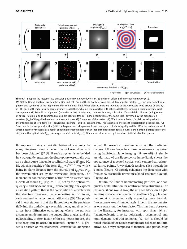
Disentangling structure and form factors is straight-forward if the scatterers are arranged in a two-dimensional primitive lattice, i.e. a lattice that has just one scatterer per unit cell. In complex lattices (honeycomb, Kagome, Lieb, etc.), where each unit cell contains two or more scatter-ers, one can either assign the form factor to the radiation pattern of each individual scatterer and derive the struc-ture factor based on the spatial locations of all scatterers, as it is expressed in Eq. (4), or, alternatively, combine the form factors of all unit cell constituents into a resultant form factor, and then attribute the structure factor purely to the reciprocal lattice. Since the first approach applies only when all scatterers in the unit cell have identical form factors, the second approach is more general. It is presented in Figure 3, where the resultant form factor (Figure 3F) of all unit cell scatterers (Figure 3A) is sepa-rated from the structure factor assigned to the recipro-cal lattice (Figure 3G) of the primitive real-space lattice (Figure 3B).
The above methodology directly applies to homo-geneous light-emitting metasurfaces, i.e. the case of a
A. Vaskin et al.: Light-emitting metasurfaces 1155
fluorophore driving a periodic lattice of scatterers. In many literature cases, excellent control over directivity has been obtained [57, 58] if such a system is embedded in a waveguide, meaning the fluorophore essentially acts as a point source that emits a cylindrical wave (Figure 3C, D), which is roughly of the form drive
ik r i tWGE e rω−= / with r
being in-plane distance from the source, and kWG = ω/cnWG the wavenumber set by the waveguide dispersion. The momentum-content spectrum of this driving is essentially a circle of radius kWG (Figure 3H, I) set by the optical fre-quency ω and mode index nWG. Consequently, one expects a radiation pattern that is the convolution of a circle with the structure transform, i.e. a repeating set of circles, each centered on a reciprocal lattice site [59]. The physi-cal interpretation is that the fluorophore emits preferen-tially into the underlying waveguide mode, and directivity arises from diffractive outcoupling, where the particle arrangement determines the outcoupling angles, and the polarizablity, or form factor, of the scatterers imposes the efficiency and polarization behavior. Figure 4A, B pre-sents a sketch of this geometrical construction alongside
actual fluorescence measurements of the radiation pattern of fluorophores in a plasmon antenna array taken using back-focal-plane imaging (Figure 4D). A simple angular map of the fluorescence immediately shows the appearance of repeated circles, each centered at recipro-cal lattice points. A wavelength-resolved slice through the k-space (Figure 4C) directly evidences the dispersion with frequency, essentially providing a band structure diagram (Figure 4E).
Within the limit of noninteracting particles, one can quickly build intuition for nontrivial meta-structures. For instance, if one would swap the unit cell blocks in a light-emitting surface from symmetric scatterers (e.g. plasmon nanorods) to asymmetrically scattering ones, far-field fluorescence would immediately inherit the asymmetry as one swaps out the form factor. This has been observed in the literature, for instance, with split rings [46, 61] (magnetoelectric dipoles, polarization asymmetry) and multielement Yagi-Uda antennas [62, 63]. It should be noted that all of the above examples are based on uniform arrays, i.e. arrays composed of identical and periodically
Figure 3: Shaping the metasurface emission pattern: real-space factors (A–E) and their effect in the momentum space (F–J).(A) Distribution of scatterers within the lattice unit cell. Each of these scatterers can have different polarizability αbare, including amplitude, phase, and symmetry of the response to electromagnetic field. When all scatterers are repeated by lattice vectors [read arrows (a1 and a2) in (B)], each of them forms a separate primitive sublattice, which is then overlaid with other sublattices, forming a complex geometrical arrangement. (B) Periodic arrangement (primitive lattice) of unit cells, common for every sublattice. (C) Spatial distribution (in log scale) of optical field amplitude generated by a single light emitter. (D) Phase distribution of the same field, governed by the propagation constant (kWG) of the guided mode of luminescent layer. (E) Truncation of the system. (F) Effective form factor: far-field envelope due to the interference of form factors of individual scatterers – unit cell constituents. This factor also encodes the polarization dependence. (G) Structure factor: reciprocal lattice (with the k-space unit cell spanned by vectors b1 and b2), showing all possible diffracted orders, some of which become evanescent as a result of having momentum larger than that of the free space radiation. (H–I) Momentum distribution of the single emitter optical field Edrive, forming a circle of radius kWG. (J) Momentum blur caused by truncation (finite size) of the system.

1156 A. Vaskin et al.: Light-emitting metasurfaces
repeating unit cells, while the radiation pattern engineer-ing is accomplished at the level of a repeated nanostruc-ture. Such design underlies the majority of experimental demonstrations of light-emitting metasurfaces, in con-trast to the original concept of wavefront shaping using nonuniform arrays illustrated in Figure 2B, which is widely discussed in theoretical works but remains strongly underrepresented in experiments, and hence should be considered more as a perspective for future research (Section 6.1.1).
As another example, truncating a metasurface to a finite patch is mathematically equivalent to multiplying the geometry with a finite windowing function (Figure 3E), meaning, according to the convolution theorem, that any radiation pattern would simply be convoluted with the windowing Fourier transform. In plasmonics, this has been observed as a progressive blurring of radiation pat-terns (Figure 3J) with reduction in patch size for metal hole array antennas [64]. Furthermore, shifting the source driving the active system relative to the scatterers simply gives a phase shift over the radiation pattern, according to the Fourier shift theorem. Finally, this approach also extends to designing the radiation pattern of sources based on quasiperiodic and aperiodic systems [65], simply
by designing the structure factor. For example, hyperuni-form arrangements [66] and Vogel spirals [67] are not periodic but spatially correlated, such that their struc-ture factor presents distinct circular bands in the k-space. These can be used for broadband directional outcoupling of light from emissive metasurfaces, as shown for plas-monic realizations [68–70].
2.2 Beyond nearly free photons
A powerful insight from the structure factor/form factor analysis is that the response of a lattice of scatterers driven by a point source essentially involves the convolu-tion of the reciprocal lattice with the dispersion relation of the background system. This construction is equivalent to constructing a repeated zone scheme dispersion rela-tion in solid-state physics from the “free-particle” dis-persion relation (simply cones ω = c | k | for light in free space, where c is the speed of light). The repeating cones (Figure 4A) are equivalent to a discrete band structure across momentum space (Figure 4B and C). Depending on the actual strength of the periodic scattering poten-tial, stop gaps will open up in this repeated zone scheme
Figure 4: Repeated zone scheme. (A) Cones representing the optical mode dispersion (in a waveguide, if considering the case described in Section 2.1, or in free space, if following the considerations in Section 2.2), repeated along the reciprocal lattice vectors of a hexagonal array (black points). In this scheme, the horizonal axes correspond to the in-plane momentum, while the vertical axis is the frequency. The first Brillouin zone is represented by the blue hexagon at the origin of kx–ky coordinate system. (B) Discrete bands “folded” into the central cone (orange) can be viewed as a horizontal slice of the intersecting cones in (A), i.e. across the k-space at a fixed frequency. (C) Vertical slice corresponds to the frequency-momentum map and shows the band structure resulting from cone intersections. (D) Experimental back focal plane (Fourier) image of the light extracted from a light-emitting metasurface. Republished with permission of the Royal Society of Chemistry (Great Britain) from [57]; permission conveyed through Copyright Clearance Center, Inc. (E) Experimental k–ω extinction map of a silver nanoparticle array. Reprinted with permission from [60] Copyright (2017) by the American Physical Society.

A. Vaskin et al.: Light-emitting metasurfaces 1157
dispersion, wherever bands cross [71, 72]. These openings are not contained in the first Born approximation, and hence need the full multiple scattering series in Eq. (3). In the optical case, the equivalent formulation for the mixing of lattice effects and the strength of the scattering potential is that collective resonances arise as a result of the mixing of diffraction conditions and polarizability [20]. These hybrids are known as “surface lattice resonances” [21, 23] for lattices in homogeneous backgrounds, and as “wave-guide plasmon polaritons” [73] if a waveguide mode is involved. Similar collective modes are formed in nanohole arrays, where the nanoholes play the role of scatterers for surface plasmon polaritons (SPPs) of the metal-dielectric interface [72, 74]. All these collective resonances form the workhorse of efforts in the use of (plasmonic) metasur-faces for spontaneous emission directivity control [58, 64,
75–77] and strong coupling with excitonic materials [78]. The underlying reason is that the lattice resonances can be far sharper than the individual scatterer response, as first realized by Zou et al. [50].
To understand the appearance of lattice resonances, we examine the effective polarizability per particle in a 2D lattice that is driven by a plane wave of parallel momentum ||k
1 1
eff || bare ||( ) [ ( )] ,α α− −= −k kG (5)
where ||( )kG is the sum over all dipole-dipole interac-tions. Such a dipole sum can be calculated using Ewald summations [20, 50–54]. Importantly, the dipole sum of a lattice is characterized by very sharp resonances, the so-called Rayleigh anomalies, right at the locus of
Figure 5: Illustration of an interplay between the terms of Eq. (5) over the parameter space spanned by in-plane momentum (horizontal axis) and frequency (vertical axis). (A) Real and imaginary part of G corresponding to diffraction conditions in a square lattice of out-of-plane dipoles. (B) Real and imaginary parts of αbare, representing local resonance of a scatterer, which depends only on the frequency. (C) Effective polarizability αeff of each scatterer in the lattice in the “metamaterial regime”, i.e. when the lattice pitch is smaller than the resonant wavelength. In this case, the local particle resonance forms a photonic Bloch band (lattice resonance), which anti-crosses with the light cone edges and extends beyond them to become a guided mode. (D) When the resonant wavelength is shorter than the lattice pitch, the Bloch band is entirely captured by the light cone and intersects with the folded neighboring cones, giving rise to first-order diffraction. This setting is commonly used to couple light into surface plasmon polaritons (SPPs) via diffraction gratings. (E) When the lattice pitch significantly exceeds the resonant wavelength, the lattice scatters light into many diffraction orders, which can be used to control the direction of light by metasurface-based optical elements.
1158 A. Vaskin et al.: Light-emitting metasurfaces
frequency-wavevector combinations that describe the repeated free-photon dispersion relation (Figure 5A). In contrast, the bare polarizability αbare of building blocks in the unit cell of a metasurface usually has a strongly resonant frequency dependence (Figure 5B) but no strong dependence on angle/parallel momentum ||k by virtue of being deep-subwavelength in size.
The full effective polarizability contains the hybridiza-tion between particle resonances and lattice geometry. An effective visualization of this physics is to plot the imagi-nary part of αeff (or the sum of its eigenvalues in case of a full tensor) [53], such as in Figure 5C–E. The imaginary part of polarizability directly relates to extinction, the sum of particle Ohmic loss, and the scattering loss of the array due to radiation in the various diffraction orders. The example is for a square lattice where the particle scattering reso-nances were tuned below any diffraction condition (Figure 5C), as well as above the first- and second-order Bragg condition (Figure 5D and E, respectively), corresponding to different regimes set by the pitch-to-wavelength ratio. Evidently, Fano features appear in the effective polariz-ability where the narrow grating anomalies in the lattice sum and the broad resonant polarizability mix. These Fano features also appear in derived observables such as lattice extinction [52] and fluorescence from embedded sources. These Fano features can lead to the appearance of strong coupling signatures, i.e. avoided crossings relative to the free-photon dispersion that appear in observables [79]. If the hybridization involves multiple localized resonances, e.g. electric and magnetic dipole resonances [53], or reso-nances corresponding to different Cartesian components or different unit cell constituents (in case of complex lat-tices) [54], the emerging lattice resonances may anti-cross with one another [53], as well as, in some geometries, form interesting degeneracies akin to those known in solid-state physics [80]. It should be noted that the true metasurface regime usually corresponds to small pitch relative to oper-ation wavelength (no Bragg diffraction) yet tuned near building block resonance. This corresponds to Figure 5C (frequency below 1.5 eV in the example). Experiments that use resonant scattering lattices for directional emis-sion generally use the regime in between Figure 5D and E, where the pitch is approximately equal to the free-space wavelength.
2.3 Local density of states and Purcell enhancement
The analysis of lattices of resonant scatterers in terms of the Huygens principle, or even with multiple scattering
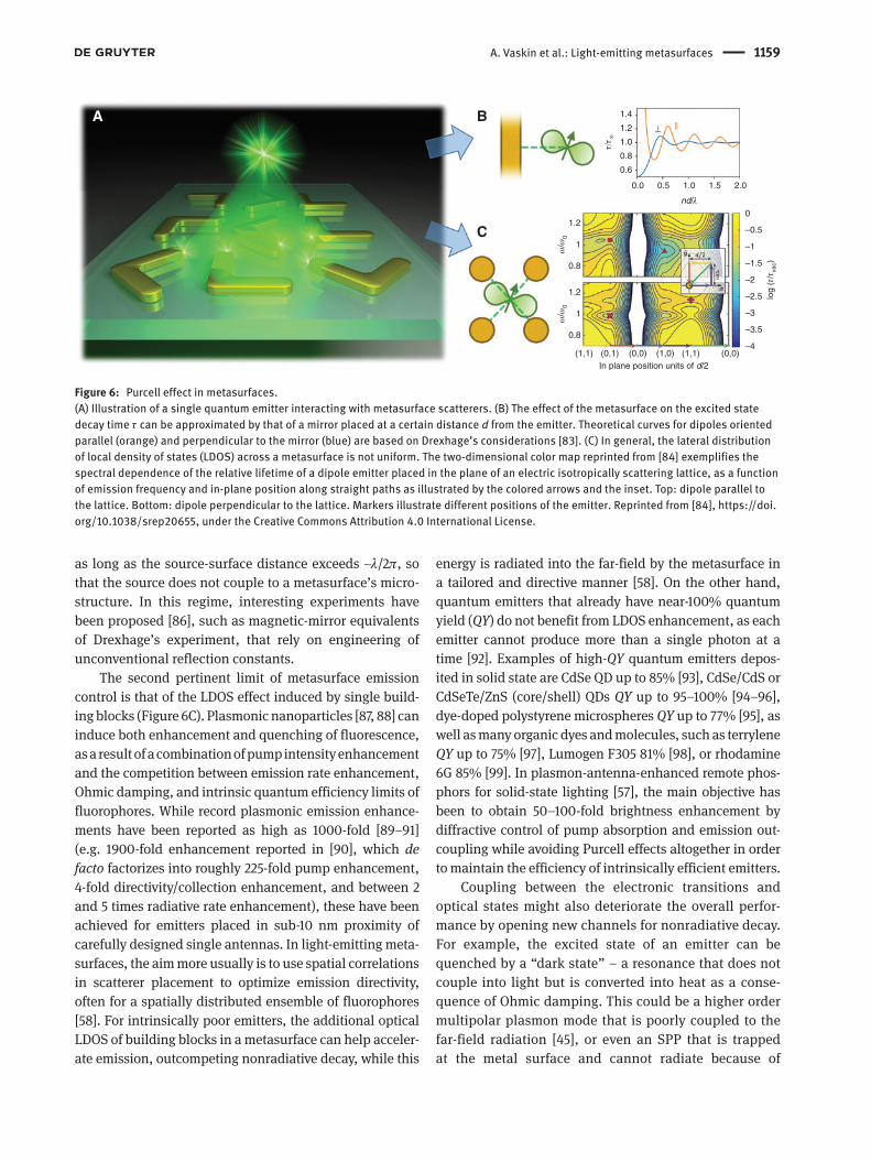
included to describe surface lattice resonances, is effective for scattering, diffraction, and even predictions for fluores-cence directivity of embedded light sources. However, it does not describe modifications of the quantum processes responsible for the generation of photons by fluorophores. One can distinguish two regimes of such emitter-scatterer coupling. By definition, a system is strongly coupled when the exchange of energy between scatterers and emitters occurs much faster than the spontaneous decay of emit-ter’s excited state [81]. This may give rise to hybridization (anti-crossing) of metasurface resonances and emitter’s electronic transitions. This regime is an emerging field of research in studies using plasmon antenna lattices and dense excitonic materials [78], discussed in Section 6.1.5. Most of the light-emitting metasurfaces operate in the weak coupling regime. In this case, excited fluorophores decay irreversibly by photon emission at an accelerated spontaneous decay rate Г given by Fermi’s Golden Rule: Г∝| μ | 2ρ(μ, ω, r). Here, the first term is the electronic tran-sition dipole moment ˆ| |g e= ⟨ ⟩μ μ between the ground state |g⟩ and the excited state |e⟩, which defines the elec-tric dipole interaction Hamiltonian ˆ ˆˆ= − ⋅EH μ between the quantum emitter and the optical field. The second term, ρ(μ, ω, r), which is referred to as the local density of optical states (LDOS), quantifies the contribution of the photonic environment to the spontaneous decay rate [81]. In other words, the emitter can convert its excited state energy to a photon faster when more states are available to radiate into [82]. LDOS depends on the transition dipole moment orien-tation μ, frequency ω, and position r, and can be obtained by purely classical calculations. The dimensionless LDOS (normalized to the LDOS of free space) is often called the Purcell factor (after Edward Mills Purcell who was the first to notice this effect in 1946 for high-Q resonators [17]).
In the context of metasurfaces (Figure 6A), two dis-tinct limits of LDOS control are pertinent. The first follows from the seminal experiment of Drexhage in the late 1960s [83], in which the LDOS was modified by changing the distance between the quantum emitter and a flat metal-lic mirror (Figure 6B). Similar experiments were repeated for dielectric interfaces, waveguides, and thin metallic films, showing the Purcell effect associated with coupling to SPPs [85]. The magnitude of the LDOS effect in such cases of flat interfaces is directly contained in the inter-face reflection coefficient. Indeed, classically, the LDOS modulation can also be viewed as back action due to work that the emitting dipole source needs to do against its own reflected field. This amount of work hence depends on the strength of the reflection as well as the phase of the reflection. It was shown in [53] that this picture remains accurate for sources coupled to structured metasurfaces
A. Vaskin et al.: Light-emitting metasurfaces 1159
as long as the source-surface distance exceeds ~λ/2π, so that the source does not couple to a metasurface’s micro-structure. In this regime, interesting experiments have been proposed [86], such as magnetic-mirror equivalents of Drexhage’s experiment, that rely on engineering of unconventional reflection constants.
The second pertinent limit of metasurface emission control is that of the LDOS effect induced by single build-ing blocks (Figure 6C). Plasmonic nanoparticles [87, 88] can induce both enhancement and quenching of fluorescence, as a result of a combination of pump intensity enhancement and the competition between emission rate enhancement, Ohmic damping, and intrinsic quantum efficiency limits of fluorophores. While record plasmonic emission enhance-ments have been reported as high as 1000-fold [89–91] (e.g. 1900-fold enhancement reported in [90], which de facto factorizes into roughly 225-fold pump enhancement, 4-fold directivity/collection enhancement, and between 2 and 5 times radiative rate enhancement), these have been achieved for emitters placed in sub-10 nm proximity of carefully designed single antennas. In light-emitting meta-surfaces, the aim more usually is to use spatial correlations in scatterer placement to optimize emission directivity, often for a spatially distributed ensemble of fluorophores [58]. For intrinsically poor emitters, the additional optical LDOS of building blocks in a metasurface can help acceler-ate emission, outcompeting nonradiative decay, while this
energy is radiated into the far-field by the metasurface in a tailored and directive manner [58]. On the other hand, quantum emitters that already have near-100% quantum yield (QY) do not benefit from LDOS enhancement, as each emitter cannot produce more than a single photon at a time [92]. Examples of high-QY quantum emitters depos-ited in solid state are CdSe QD up to 85% [93], CdSe/CdS or CdSeTe/ZnS (core/shell) QDs QY up to 95–100% [94–96], dye-doped polystyrene microspheres QY up to 77% [95], as well as many organic dyes and molecules, such as terrylene QY up to 75% [97], Lumogen F305 81% [98], or rhodamine 6G 85% [99]. In plasmon-antenna-enhanced remote phos-phors for solid-state lighting [57], the main objective has been to obtain 50–100-fold brightness enhancement by diffractive control of pump absorption and emission out-coupling while avoiding Purcell effects altogether in order to maintain the efficiency of intrinsically efficient emitters.
Coupling between the electronic transitions and optical states might also deteriorate the overall perfor-mance by opening new channels for nonradiative decay. For example, the excited state of an emitter can be quenched by a “dark state” – a resonance that does not couple into light but is converted into heat as a conse-quence of Ohmic damping. This could be a higher order multipolar plasmon mode that is poorly coupled to the far-field radiation [45], or even an SPP that is trapped at the metal surface and cannot radiate because of
0.8
(1,1) (0,1) (0,0) (1,0) (1,1) (0,0)–4
–3.5
–3
–2.5 log
(τ/τ
vac)
τ/τ ∞
–2
–1.5
–1
–0.5
0
0.0
0.6
0.8
1.0
1.2
1.4
0.5 1.0 1.5
nd/λ
2.0
In plane position units of d/2
ω/ω
0
1
1.2
0.8
A B
C
ω/ω
0
1
1.2
Figure 6: Purcell effect in metasurfaces. (A) Illustration of a single quantum emitter interacting with metasurface scatterers. (B) The effect of the metasurface on the excited state decay time τ can be approximated by that of a mirror placed at a certain distance d from the emitter. Theoretical curves for dipoles oriented parallel (orange) and perpendicular to the mirror (blue) are based on Drexhage’s considerations [83]. (C) In general, the lateral distribution of local density of states (LDOS) across a metasurface is not uniform. The two-dimensional color map reprinted from [84] exemplifies the spectral dependence of the relative lifetime of a dipole emitter placed in the plane of an electric isotropically scattering lattice, as a function of emission frequency and in-plane position along straight paths as illustrated by the colored arrows and the inset. Top: dipole parallel to the lattice. Bottom: dipole perpendicular to the lattice. Markers illustrate different positions of the emitter. Reprinted from [84], https://doi.org/10.1038/srep20655, under the Creative Commons Attribution 4.0 International License.

1160 A. Vaskin et al.: Light-emitting metasurfaces
momentum mismatch [100]. All of that should be taken into account to ensure successful design of light-emit-ting metasurfaces.
3 Simulating system performanceThis section deals with methods for numerical computa-tion of the performance of light-emitting metasurfaces, focusing on predicting the emission properties of ensem-bles of fluorophores and single fluorophores, coupled to a metasurface. A more general description of the different employed computational techniques including a discus-sion of their specific advantages and drawbacks can be found, e.g. in Chari and Salon [101].
Four factors contribute to the measured fluorescence count rate from a metasurface with a single emitter placed at the position rem on it:
( , , ) ( , ) ( , )( , ) ( , )
em exc em exc em exc em em ext
em em coll em em
I QYω ω Γ ω ω η
ω η ω
∝ ⋅ ⋅⋅
r r rr r (6)
As common in the literature [92], we also refer to this quantity as brightness in the following. In the first place, we have the excitation rate, which can be enhanced by the metasurface because of its ability to strongly confine the excitation field, thus providing the effective incoupling and field localization in an emissive layer [57, 58, 102]. For the emitter at the position rem, the excitation rate enhance-ment is 0 2 2
0( , ) / | ( , ) | / | | ,exc em exc exc em excΓ ω Γ ω= r E r E where 0excΓ is the excitation rate of the emitter in free space, |E0 |
and ωexc are the amplitude and the frequency of the excita-tion field, respectively, and E(rem, ωexc) is local electric field strength at the position rem in the metasurface. The excita-tion rate enhancement is thus tantamount to local field enhancement of the incident pump light, as controlled by the metasurface geometry, and it can be varied inde-pendently of the other factors in Eq. (6) through the pump incidence angle and pump wavelength. Note that in this paragraph we assume a weak excitation regime far below saturation, so the fluorescence count rate stays linearly dependent on excitation rate enhancement and excitation input power.
The excited emitter can decay upon emitting a photon at the Stokes-shifted frequency ωem at a radiative decay rate 0 ,radΓ or without emitting the photon following intra-molecular dissipation with a decay rate 0.iΓ The intrinsic QY of the emitter is defined as the ratio 0 0 0 0/( ),rad rad iΓ Γ Γ= +QY and is a property solely of the emitting species. Once the emitter is coupled to a metasurface, the decay rate 0
radΓ associated with the intrinsically radiative channel will be modified to Г in accordance with Fermi’s Golden Rule
(Section 2.3). The decay rate Г can be expressed as a sum of a radiative decay rate Гrad and a nonradiative decay rate Гnr corresponding to quenching. The modified QY now reads 0/( ).rad rad nr iQY Γ Γ Γ Γ= + +
The estimation of the decay rate enhancement in electromagnetic simulations is based on the fact that the enhancement of the decay rate Г of the emitter by the photonic environment can be related to the enhance-ment of the power Pd dissipated by a classical point elec-tric dipole pem placed in the same photonic environment:
0 0/ /d d radP P Γ Γ= [18, 102, 103]. The classical mechanism of the radiated power enhancements can be derived from Poynting’s theorem [102, 104]. When a point electric dipole is placed in the proximity of a metasurface, it is affected by its own field scattered back by the nanostructure. In par-ticular, while maintaining an oscillating dipole moment of constant magnitude, the oscillating current does work against its own field. The associated power (work per unit time) can be calculated according to
*00 2 3
6 11 { ( , )},| |
dem scat em em
d em
PP k
πεεω= + ⋅p E r
pIm (7)
where Escat(rem, ωem) is the scattered electric field excited by the dipole pem oscillating at the frequency ωem and placed in rem, and 0
dP is the power radiated by the emitter placed in free space. The power Pd dissipated by the dipole is a sum of the radiated power Prad and the power Ploss quenched because of the Ohmic damping:
2 31 ( , ) | ( , ) | ,2loss em emV
P dσ ω ω= ∫ r E r r where E(r, ωem) is the local electric field excited by the dipole pem, σ is the elec-trical conductivity proportional to the imaginary part of the dielectric permittivity: σ(r, ω) = ε0ε̋ (r, ω)ω, and the integration is over the whole metasurface.
The third factor ηext(rem, ωem) denotes the extraction efficiency, indicating the probability that a photon emitted by the fluorophore can escape the metasurface [58, 105]. The extraction efficiency ηext(r, ωem) is the ratio between the power radiated to free space out
radP and the total power radiated by the emitter: ext( , ) / .out
em em rad radP Pη ω =r The total power radiated in free space can be calculated by integrat-ing the flux of the Poynting vector S(r, ωem) through two planes parallel to the metasurface plane and positioned above (∑1) and below (∑2) it:
1,2= ( , ) .out
rad emP dΣ
ω ⋅∫∫ S r A (8)
The remaining part of Prad is captured by other electro-magnetic modes such as the guided modes and cannot be extracted.
A. Vaskin et al.: Light-emitting metasurfaces 1161
The emission pattern is another property of the emitter that is modified by the photonic environment. In a typical experiment, the fluorescence signal depends on the collection efficiency, that is, the ratio between the power harvested by the collection optics (CO) and the total power radiated in free space out
radP :
1 ( , ) sin ,coll out COrad
P d dP
η θ φ θ φ θ= ∫∫ (9)
where P(θ, φ) is the angular power density radi-ated in free space along the direction defined by the polar angle θ and azimuthal angle φ. At this point, it is important to emphasize that P(θ, φ) is power per stera-dian, as opposed to the time-averaged Poynting vector
*1( , ) { ( , ) ( , )},2em em emω ω ω= ×S r E r H rRe which quantifies
directional flux (power per square meter, not steradian). The power per steradian emitted in the far-field can be cal-culated from the Poynting vector on a far-field spherical surface in the limit of infinite radius as
2
/( , ) = ( , ),lim em
rP r
rλ ∞θ φ ω
→⋅r S r (10)
where r = (r sin θ cos φ, r sin θ sin φ, r cos θ) and λ = 2πc/ωem. Converting from a classical fixed-current source in simula-tions, which radiates a certain power per steradian, to the physics of a quantum emitter, which upon fluorescence decay into the far-field radiates exactly one quantum of light, it is useful to divide out the total angle-integrated power to obtain an angle-dependent probability density per steradian that describes the far-field radiation pattern.
Commonly, in experiments with light-emitting meta-surfaces, ensembles of fluorophores are distributed over the whole metasurface and are arbitrarily oriented. In a weak coupling regime, the behavior of each emitter can be considered as independent from all the others, and their fluorescence adds incoherently to the overall metasurface fluorescence. Thus, if for a single emitter at location rem and dipole orientation pem emitting at frequency ωem and pumped at frequency ωexc the angle-resolved radiated flux in photons per second, per steradian, per watt per square meter of input intensity is Φ(rem, pem, ωexc, ωem), then the total radiated flux of a metasurface incorporating many emitters in photons per second per steradian, per unit area of metasurface, and per watt per square meter of input intensity, is
unit cell volume all orientations
3 3
1( , ) = ( ,unit cell area
, , ) ( ) .
tot exc em em
em exc em em em emd d
Φ ω ω Φ
ω ω ρ
⟨ ⟩ ∫ ∫ r
p r p r (11)
Here, ρ(rem) is the number distribution of fluorophores (units 1/m3, assumed the same in each unit cell). It is crucial that when dealing with fluorescence, the emission from all emitters adds incoherently since there is no phase relation between fluorophores. Therefore, care must be taken to first determine the emission characteristics from the individual emitters and then to sum up the intensities, not the fields.
In case of a single emitter on the metasurface with a fixed pump power, the photon flux Φ(rem, pem, ωexc, ωem) integrated over the numerical aperture (NA) of the col-lection optics can be used to estimate the right-hand side of Eq. (6). In the same way, one can estimate the total number of photons per second collected from a metas-urface containing many emitters by integrating the total angular resolved photon flux ⟨Φtot(ωexc, ωem)⟩ multiplied by the illumination power density in watt per square meter as a function of coordinate over the area of the whole meta-surface and over the NA of the collection optics. Note that to obtain the total fluorescent count rate, one addition-ally has to take the efficiency of the detector system (i.e. coupling efficiencies, quantum efficiency) into account. In order to identify the proportionality constant correctly, one needs to perform a proper calibration of the experi-mental setup.
Also note that in experiments, usually enhancements of the various factors in Eq. (6) contributing to the overall fluorescence count rate cannot be compared to their free-space counterparts but rather to a suitable reference sce-nario, such as the emitters placed on a bare, unstructured substrate. By considering this reference case also in the simulations, one can resort to comparing the relative enhancement factors.
3.1 Calculations based on local dipole sources
Full-wave numerical tools such as the finite-difference time-domain method, the finite element method, and the boundary element method solve the classical electrody-namic response of structures in real space, and are hence well suited to deal with local dipole sources. Nonetheless, it is not trivial to properly simulate spontaneous emission properties. For instance, Eq. (7) for LDOS requires the field right at the point source, which in a total field simulation is singular. Also, one has to be sure that the numerical tool simulates a constant current source (fixed magnitude of p). The first works [106, 107] that used real-space solvers for spontaneous emission studied numerically the modifi-cation of spontaneous emission in 2D photonic crystal membrane structures (3D simulations) were using the

1162 A. Vaskin et al.: Light-emitting metasurfaces
point electric dipole method by Hwang et al. [108], and highlighted the issues with implementation and conver-gence. The possibility to use a point electric dipole as the excitation source is now included in most computational packages. It may be didactic to consider an example from the commercial software package CST Microwave Studio, which utilizes the principle of a Hertzian dipole. Similar strategies can be implemented in most other commercial Maxwell solvers accordingly. The implementation com-prises two identical PEC (perfect electric conductor) cyl-inders placed next to each other along a shared axis and separated by a gap in between. The cylinders are driven by an impedance discrete port that produces an electric current oscillating between the cylinders. The sizes of the cylinders are much smaller than the wavelength cor-responding to the oscillation frequency. LDOS is best cal-culated by evaluating the Poynting flux into the far-field, plus absorption in all the scatterers in the simulation, or alternatively by evaluating the Poynting flux through a small spherical surface enclosing the source (and no scat-terer). Apart from the common case of electric dipole emit-ters, certain simulations may also require a magnetic point dipole source. This is the case when emitters exhibiting magnetic dipole transitions are considered, such as triva-lent lanthanide ions [109]. In the CST package, the mag-netic point dipole emitter can be modeled as a PEC ring with a gap, in which the excitation impedance discrete port is placed. The oscillating circular current driven by the impedance discrete port produces a magnetic moment perpendicular to the plane of the ring. In a finite element package like COMSOL, electric and magnetic dipole point sources are directly implemented, or can alternatively be programmed by imposing currents on line/curve seg-ments. If the point magnetic dipole source is not imple-mented in a particular computational package, it can be indirectly simulated as a point electric dipole exploiting the duality of Maxwell’s equations [110, 111].
3.1.1 Finite array simulations
The far-field emission from the point source coupled to a single nanoantenna can be calculated using standard near- to far-field transformation tools implemented in computational packages. For example, the commercial software package COMSOL uses the Stratton-Chu formula, which rests on the assertion that, if fields are known on a closed surface within which the complex scattering physics takes place, then these fields can be converted into equivalent surface currents from which the far-field can be reconstructed by calculating how the currents radiate.
An excellent explanation of this method, its restrictions, and implementation can be found in the seminal book of Taflove and Hagness [112], Chapter 8. For most metasur-face scenarios, this approach strictly fails for two reasons. First, calculating how the currents radiate presupposes that outside the closed surface the space is homogeneous. Instead, often infinite planar interfaces intersect the entire simulation. Second, if one takes not a closed surface but only, say, one detection plane, the Stratton-Chu formula strictly does not apply. To resolve this issue, one requires generalized methods for calculating the far-field emis-sion patterns based on the Green’s function method [113] and the reciprocity principle [114]. Since metasurfaces are periodic arrangements of nanoresonators and infinitely extended compared to the wavelength of the emission, direct simulation of the metasurface will require huge computational resources. In particular, while diffraction calculations (plane wave impinging on periodic systems) can be efficiently implemented with periodic bound-ary conditions, calculations where a single point source excites a lattice are very demanding.
A standard approach of simulating the metasurface with a single coupled point source is utilizing the finite array method [22]. While the whole periodic structure cannot be simulated, it is possible to build a finite array consisting of several unit cells in the computational domain with PML (perfectly matched layer) or open bound-ary conditions (Figure 7A). However, the accuracy of this straightforward method is limited by the computational resources. The modes of the metasurface that define the emission patterns and the radiative decay rate enhance-ment are affected by the finite size of the array. Indeed, it was shown that the Q-factor and the resonant wavelength depend on the number of unit cells comprised within the finite array [27, 115]. The increase in the number of the unit cells requires additional computational resources. A fun-damental problem of this approach is that there is no guar-antee that truncations to a finite array actually converge to the infinite-array response. This is intrinsic to Eq. (1), which describes multiple scattering between dipolar scat-terers, since the radiative interactions only decay as 1/r.
Figure 7B–G show the simulated patterns P(θ, φ) of the emission into the upper hemisphere (z > 0) from an x-oriented point electric dipole located at the center of a finite array (lattice constant 1000 nm) consisting of a gradu-ally increasing number of unit cells. Each unit cell includes a nanocylinder with a refractive index of 3.5 and a diameter and a height both of 400 nm. The surrounding medium has a refractive index of 1. The point electric dipole is oscillating at the frequency corresponding to the excita-tion of the electric dipole resonance of the nanocylinders.

A. Vaskin et al.: Light-emitting metasurfaces 1163
The 3 × 3 finite array (Figure 7B) shows a broad emis-sion pattern, which, with increasing number of unit cells, initially becomes more tightly confined in the k-space. For finite arrays consisting of 9 × 9 and more unit cells (Figure 7E–G), only the fine features of the emission pat-terns still show slight changes with the increase in the number of the unit cells for this particular example.
3.1.2 Inverse Floquet transformation for far-field emission calculations
The main obstacle to efficient calculations involving periodic metasurfaces driven by a single source is that the single source breaks the periodicity. A method that employs an inverse Floquet transformation allows for
the reconstruction of the emission response of a single dipole p(r) in a periodic metasurface by combining the response for periodically arranged dipoles with varying phase relation ,i Be ⋅k r where kB is swept through the entire Brillouin zone (Figure 8). Each of the required calcula-tions is performed for a single unit cell incorporating p(r) using Bloch-periodic boundary conditions with a wavevector kB. In antenna engineering, this approach is also known as the array scanning method [116, 117] (ASM).
A simulated periodic arrangement of point electric dipoles ( )
Bkp r is related to a single point electric dipole
p(r) via the Floquet transform
( )1 1 2 21 1 2 2
1 2
( ) ( ( )),i l lB
B l le l l⋅ +
∈ ∈
= − +∑ ∑ k a akp r p r a a
N N (12)
–1
0
sin
θ si
n φ
1
–1
0
sin
θ si
n φ
1
–1
0
sin
θ si
n φ
1
–1
0
sin
θ si
n φ
1
–1
0
sin
θ si
n φ
1
–1–1
0
0
sin
θ si
n φ
1
1
sin θ cos φ
x
z
y –1 0 1
sin θ cos φ
–1 0 1
sin θ cos φ
P(θ, φ)+
0
–1 0 1
sin θ cos φ
–1 0 1
sin θ cos φ
–1 0 1
sin θ cos φ
A B C
D E F G
Figure 7: Finite array simulations. (A) Finite array consisting of 5 × 5 dielectic nanocylinders and excited by the point electric dipole px oriented along the x-axis and placed at the center of the central nanocylinder. Emission pattern P(θ, φ) in the upper semisphere (z > 0) from a finite array consisting of (B) 3 × 3 unit cells, (C) 5 × 5 unit cells, (D) 7 × 7 unit cells, (E) 9 × 9 unit cells, (F) 11 × 11 unit cells, and (G) 13 × 13 unit cells.
Figure 8: Schematic illustrating the array scanning method.A single dipole on the periodic metasurface is modeled as a sum of lattices of phased dipoles. Each dipole is represented as a black arrow and a corresponding phase.
1164 A. Vaskin et al.: Light-emitting metasurfaces
where a1 and a2 are the lattice vectors. The solution Bk
E cor-responding to
Bkp can be calculated directly using simula-
tions assuming Bloch periodicity. The solution E for the original source p(r) can then be obtained via the inverse Floquet transform [118], performing the integration over the Brillouin zone (BZ):
21 d .| | BBZ BBZ
= ∫ kE E k (13)
3.2 Calculating radiative enhancements using the reciprocity principle
The reciprocity principle (Figure 9) is applicable in linear media with symmetric dielectric permittivity and perme-ability tensors. It states that for any two source distribu-tions J1(r) and J2(r) placed in the system
3 3
1 2 2 1( ) ( ) ( ) ( ) ,d d⋅ = ⋅∫∫∫ ∫∫∫J r E r r J r E r r (14)
where E1(r) and E2(r) are electric fields produced by J1(r) and J2(r), respectively. If we consider two point electric dipole sources Jm = −iωpmδ(r − rm), where m = 1, 2, Eq. (14) will simplify into the commonly encountered expression
2 1 2 1 2 1( ) ( ).⋅ = ⋅p E r p E r (15)
A formulation of the reciprocity principle for the two cases of magnetic dipole and electric quadrupole sources can be found in Landau et al. [119].
If we place the first dipole p1 on the periodic metas-urface at the location of the hypothetical emitter that we wish to consider, and displace the second dipole p2 far
away along the direction (θ, φ), then E1(r2) represents the far-field emitted by the first dipole coupled to the metas-urface and radiated into the direction (θ, φ). Conversely, E2(r1) represents the local electric field at the metasurface excited by a plane wave incident from the second dipole along the same direction (θ, φ) (Figure 10A). The orien-tation of the second dipole p2 defines the polarization of the incident plane wave. Therefore, the reciprocity prin-ciple allows us to calculate the far-field radiated power and polarization due to a single dipole in the near field, without any calculation that actually includes the dipole. Instead, one simply needs to calculate the near field in response to far-field driving. This allows us to overcome the usual difficulties associated with the simulation of single dipole sources coupled to a periodic structure and to limit the computational domain to an elementary cell with periodic boundary conditions.
The power P(θ, φ; r1) emitted along the direction (θ, φ) by a randomly fluctuating dipole p1, which on average is isotropically oriented, placed at r1 on the metasurface in far-field can then be calculated as [18, 120]
2 221 2 1 12 0 0
,2
( , ; ) | ( ) | sin ,| | p p p
TE TMP d d
π πεθ φ θ θ φ ∝ ⋅
∑∫ ∫r E r p
p (16)
where TE, TM denote the TE and TM polarization of the plane wave incident along (θ, φ), which excites E2(r1), ε2 is the dielectric permittivity of the medium surrounding p2. The integration is performed to average over all pos-sible orientations of p1 = (p1 sin θp cos φp, p1 sin θp sin φp, p1 cos θp). If the point dipole emitter p1 is effectively isotropi-cally oriented, the integration in Eq. (16) is proportional to |E2 | 2. In other cases, the integration needs to be adjusted to take only the relevant field orientations into account.
Figure 9: The concept of the calculations based on the reciprocity principle.The far-field emission from the metasurface with integrated incoherent emitters is reciprocal to the intensity of the near-field excited in the metasurface by the incident external light averaged over the positions of the emitters.
A. Vaskin et al.: Light-emitting metasurfaces 1165
Finally, we can sum up the emission from all emitters contained in the metasurface architecture via the follow-ing integration:
3
1 1( , ) ( , ; ) ,V
P P dθ φ θ φ= ∫∫∫ r r (17)
where V is the volume within the unit cell that contains the emitters. Here we assume that all emitters are excited with the same efficiency. If this is not the case, one can in principle define appropriate weight functions for the dif-ferently excited emitter regions.
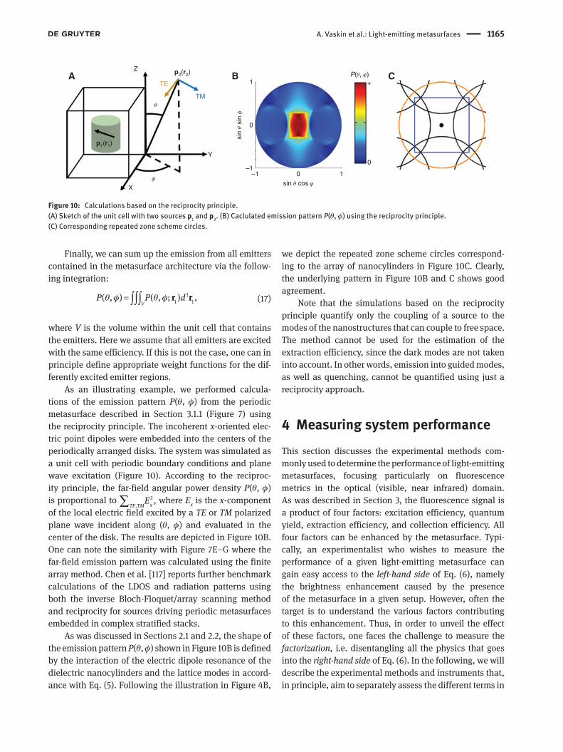
As an illustrating example, we performed calcula-tions of the emission pattern P(θ, φ) from the periodic metasurface described in Section 3.1.1 (Figure 7) using the reciprocity principle. The incoherent x-oriented elec-tric point dipoles were embedded into the centers of the periodically arranged disks. The system was simulated as a unit cell with periodic boundary conditions and plane wave excitation (Figure 10). According to the reciproc-ity principle, the far-field angular power density P(θ, φ) is proportional to 2
,,xTE TM
E∑ where Ex is the x-component of the local electric field excited by a TE or TM polarized plane wave incident along (θ, φ) and evaluated in the center of the disk. The results are depicted in Figure 10B. One can note the similarity with Figure 7E–G where the far-field emission pattern was calculated using the finite array method. Chen et al. [117] reports further benchmark calculations of the LDOS and radiation patterns using both the inverse Bloch-Floquet/array scanning method and reciprocity for sources driving periodic metasurfaces embedded in complex stratified stacks.
As was discussed in Sections 2.1 and 2.2, the shape of the emission pattern P(θ, φ) shown in Figure 10B is defined by the interaction of the electric dipole resonance of the dielectric nanocylinders and the lattice modes in accord-ance with Eq. (5). Following the illustration in Figure 4B,
we depict the repeated zone scheme circles correspond-ing to the array of nanocylinders in Figure 10C. Clearly, the underlying pattern in Figure 10B and C shows good agreement.
Note that the simulations based on the reciprocity principle quantify only the coupling of a source to the modes of the nanostructures that can couple to free space. The method cannot be used for the estimation of the extraction efficiency, since the dark modes are not taken into account. In other words, emission into guided modes, as well as quenching, cannot be quantified using just a reciprocity approach.
4 Measuring system performanceThis section discusses the experimental methods com-monly used to determine the performance of light- emitting metasurfaces, focusing particularly on fluorescence metrics in the optical (visible, near infrared) domain. As was described in Section 3, the fluorescence signal is a product of four factors: excitation efficiency, quantum yield, extraction efficiency, and collection efficiency. All four factors can be enhanced by the metasurface. Typi-cally, an experimentalist who wishes to measure the performance of a given light-emitting metasurface can gain easy access to the left-hand side of Eq. (6), namely the brightness enhancement caused by the presence of the metasurface in a given setup. However, often the target is to understand the various factors contributing to this enhancement. Thus, in order to unveil the effect of these factors, one faces the challenge to measure the factorization, i.e. disentangling all the physics that goes into the right-hand side of Eq. (6). In the following, we will describe the experimental methods and instruments that, in principle, aim to separately assess the different terms in
–1
0
sin
θ si
n φ
1
p2(r2)
p1(r1)
ZA
TM
TE
–1 0 1sin θ cos φ
X
Y
P(θ, φ)+
0
B C
θ
φ
Figure 10: Calculations based on the reciprocity principle. (A) Sketch of the unit cell with two sources p1 and p2. (B) Caclulated emission pattern P(θ, φ) using the reciprocity principle. (C) Corresponding repeated zone scheme circles.

1166 A. Vaskin et al.: Light-emitting metasurfaces
Eq. (6). Note, however, that in light-emitting metasurface we face a fundamental issue which makes the measure-ment of the factorization difficult: typically, many emitters contribute to the light emission, and the experimentally measured emission enhancement is averaged over an ensemble of emitters. Importantly, each factor in Eq. (6) is dependent on, e.g. the position and orientation of the emitter. As a result, the total measured emission enhance-ment cannot be trivially factorized anymore. For instance, if one examines fluorescence decay traces of ensembles, since one sums photon counts, one effectively samples a biased sub-ensemble of the brightest emitters, where, for instance, quenched or unpumped emitters are underrep-resented. Similar considerations hold for other observa-bles. An interesting approach to overcome this problem is to isolate the emission from individual emitters that inter-act with the metasurface. According strategies include the dilution of the emitters that allows singling out an indi-vidual response, as well as superresolution approaches, as discussed below.
4.1 Brightness enhancement
The workhorse tool for measuring the overall fluores-cence enhancement and the factorization of its constitu-ent factors depicted in Eq. (6) is based on fluorescence spectroscopy and imaging. In this technique, the sample is optically excited by a laser or light-emitting diode (LED), which is focused on the sample by a lens or a micro-scope objective. The same (reflection mode) or a differ-ent (transmission mode measurements) objective collects the fluorescence emission from the sample. The collected emission propagates through a dichroic mirror and/or a spectral filter that rejects pump light, and then is directed to a spectrometer or a photodetector. This arrangement is most efficient for active metasurfaces emitting in the silicon detector range (wavelength from 400 to 1000 nm), owing to the availability of complementary metal-oxide-semiconductor (CMOS) cameras with near-single-photon detection capabilities. This general setup is suited for measuring the overall fluorescence enhancement relative to emitters placed in the same setup in a reference envi-ronment (in solution or on a plain substrate), and with extensions suited to explore factorization in various con-tributing physical mechanisms (see below). An important caveat is that literature reports on fluorescence enhance-ments are meaningless unless a full specification of set-up parameters is given, which at least includes the collection NA, the orientation of the sample relative to collection and excitation, and the precise geometry of the pump
spot in terms of spot size, opening angle, and polariza-tion. For instance, even simple systems (e.g. fluorophores on plasmon particle antennas) can appear to give fluo-rescence enhancement in one measurement geometry, yet fluorescence suppression when the sample is placed upside down in the same setup.
As another complication, the materials used for nanoantenna and metasurface fabrication may show sig-nificant autofluorescence in the spectral region of inter-est, thus complicating the determination of the correct brightness enhancement. If the autofluorescence is weak compared to the fluorescence from the target emitters, performing a measurement of the emission from the struc-ture under the same experimental conditions but without any emitters and subtracting this pure autofluorescence signal from the emission of the coupled system can be an option.
4.2 Role of the excitation field
Fluorescence enhancement can result from local enhance-ment of the excitation field, for instance, through exci-tation of resonances in the metasurface scatterers, or through diffractive incoupling. It is a challenge to sepa-rate this absorption enhancement effect from effects at the emission wavelength, owing to the fact that it is very difficult to measure the fraction of absorbed pump light directly. Pump light extinction can generally be meas-ured, but cannot be generally traced back to the amount of absorption in the fluorescing species. Indeed, the extinc-tion is usually largely due to intrinsic dissipative losses in the materials of the metasurface and scattering of light out of the collection beam path. Only in samples with dense layers of emitters do the emitters themselves contribute measurably to absorption. As rule of thumb, the absorp-tion cross-section of a room-temperature emitter is 10−20 m2, meaning you would need 1 molecule every 0.1 nm2 for complete absorption (area measure) [121]. Instead, typical fluorophore-doped films for metasurface lasing experi-ments have 1 molecule every 3 nm3, at the limit of con-centration-quenching (pump light experiences just a few percent absorption for a film 100 nm thick) [122]. Most fluorescence experiments operate at or below that regime, and strong coupling experiments at 10 times higher density [123]. A very useful tool to gain insight into pump enhancement effects without directly measuring pump light absorption in the emitters is, instead, to monitor fluorescence count rate while varying the parameters of the pump. Resonances in the metasurface responsible for the excitation enhancement are typically sensitive to

A. Vaskin et al.: Light-emitting metasurfaces 1167
the excitation wavelength, incident angle, spot size, and polarization. In order to separate the effect attributed to the excitation enhancement in Eq. (6), one can hence vary the parameters of the excitation. To this end, spectrally filtered supercontinuum lasers provide convenient access to tuneable pump light for excitation spectroscopy. Also, in a microscope setting, one can vary between focused illumination (parallel beam offered to microscope objec-tive, leading to a diffraction-limited focus) and angled incidence of parallel beams (laser focused to a point in the objective back focal plane). A caveat when working with ensembles of emitters is that such manipulations affect the spatial distribution of the local electric field and thereby the subset of emitters in the ensemble that con-tribute to the signal.
4.3 Quantum yield enhancement
Quantum yields of fluorophores are among the most chal-lenging parameters to measure, even for fluorophores in simple, unstructured samples (solutions). For such simple systems, one either uses a brightness comparison relative to a fluorescence standard (relying on a precise knowledge of concentration and absorption cross-sections) or meas-ures QY as a ratio of the number of the emitted photons Nem and the number of the absorbed photons Nabs:
.em
abs
NQY
N= (18)
In a typical experiment, this requires a radiometrically calibrated determination of absorbed excitation flux (pro-portional to Nabs) and an integrating-sphere measurement of the number of emitted photons Nem [124]. This approach is prone to a suite of artefacts, such as reabsorption (at high concentration), incomplete collection of all photons by the integrating sphere, calibration artefacts due to the spectral dependence of responsivities of detection chan-nels, and signal-to-noise ratio artefacts at low absorption or emission. Metasurfaces typically have parasitic absorp-tion, obscuring Nabs, and guided modes, keeping the emitted light from reaching the integrating sphere. There-fore, external quantum efficiency determination (far-field-collected photons out divided by the total number of offered pump photons in) is well possible, but determi-nation of absolute internal quantum efficiencies of emis-sion for the light-emitting species is nearly impossible. Two routes to progress are apparent. First, integrating-sphere methods have recently been extended to nanoscale mapping of quantum efficiency in nanophotonic systems [125]. Second, an alternative method to obtain information
on the effect of a metasurface on QY of fluorophores is to study the same metasurface with fluorophores of very dif-ferent intrinsic quantum efficiencies. In essence, QY of an intrinsically efficient (QY0 = 1) emitter can be deteriorated only by a metasurface. In contrast, an intrinsically poor emitter (QY0 < 1) coupled to the metasurface can exhibit QY enhancement of up to 1/QY0. Thus, measurements con-ducted on the same structure but with different emitters at opposing ends of the QY scale would, in principle, allow to systematically modulate the contribution of the QY enhancement to the total brightness enhancement. This approach has been succesfully applied for single plasmon antenna systems [92].
4.4 Decay rate enhancement
An important performance characteristic is the LDOS enhancement, as expressed in an acceleration of fluo-rescent decay. Once an emitter is excited by absorbing a pump photon, it will decay to its ground state, emitting a single photon at a random time t after excitation, accord-ing to an exponential probability distribution set by the fluorescence lifetime τ. By averaging over many excita-tion-emission cycles, one expects to measure a fluores-cence decay trace
/
0( ) e ,tI t I τ−= (19)
where I0 is the emission intensity at zero time, and the life-time of the excited state is the reciprocal of the total decay rate: 01 /( ).rad nr iτ Γ Γ Γ= + + The total decay rate is a func-tion of the photonic environment surrounding the emitter through its dependence on LDOS. Typical lifetimes of excited states are in the low nanosecond regime for typical organic dyes, color centers, and colloidal QDs.
Time-correlated single-photon counting (TCSPC) is a common experimental technique for measuring the fluo-rescence decay of emitters (Eq. (19)). It uses the fact that detectors such as avalanche photodiodes can have a very fast electrical response upon optical detection of a single photon (50 ps), and mitigates against the fact that both the detector and processing electronics typically have a long (10–100 ns) deadtime after detecting one photon. The technique is based on periodic excitation by a pulse train and data collection over many cycles of excitation, where the probability of collecting a single photon per excitation pulse is deliberately kept in the sub-1% range. Figure 11 illustrates the typical scheme. A pulsed laser generates a 1–50 MHz repetition rate (chosen an order of magnitude slower than the fluorophore decay rate) pulse

1168 A. Vaskin et al.: Light-emitting metasurfaces
train for excitation and a synchronized electronic signal which triggers the time interval analyzer. The laser pulse propagates to the sample and excites the emitter. After a certain time ∆t, the emitter relaxes to a ground state emit-ting the photon. Once and if the photon has reached the detector, it generates the electrical signal that stops the time interval analyzer. The time delays between excita-tion and detection are accumulated in a histogram, which represents the fluorescent decay trace. The photon count rate must be kept low to ensure that the probability of two photons on the detector for one pulse is negligible to avoid skewing of the histogram, since the detection system is blind until the next laser pulse.
In principle, TCSPC is directly applicable to meta-surface experiments. However, several caveats apply. First, as in any spontaneous emission rate enhancement experiment, the acquired information concerns only the total decay rate, i.e. the sum of radiative and nonradia-tive contributions. Ambiguity in separating these contri-butions can be partially resolved by corroborating with QY or at least brightness enhancement measurements. Second, except in the case of single fluorphore experi-ments, ensemble averaging can significantly hamper interpretation. The measured photoluminescence (PL) decay curves obtained from metasurfaces containing a large number of emitters usually have multi- or non-exponential behavior as a result of the inhomogeneous photonic environment. It is a challenge to fit such data uniquely with a distribution of rates. This challenge is even more significant if the emitters themselves have a wide distribution of lifetimes, as is the case for QDs, and, e.g. color centers in nanodiamonds. Furthermore, if the metasurface has absorbing constituents, then the ensemble signal will not weigh all emitters equally, on average. Indeed, those emitters that are accelerated most are likely also quenched most, and hence contrib-ute least. Section 5.2 reports on super-resolution TCSPC imaging to circumvent this issue.
4.5 Fourier imaging
Since an important function of light-emitting metasur-faces is to redirect light, a method is required to quan-titatively map the radiation patterns. Fourier imaging, or back-focal-plane imaging, in a microscope provides angular mapping over a large angular range (over 70° from the sample normal) with good resolution (as good as 0.5°) in a setup with no rotating parts, and directly on a camera. It is suited for systems ranging from single nano-objects and single molecules, to metasurfaces spanning 200 × 200 μm in size, as limited by the aberration-free field of view of microscope objectives.
Fourier imaging is based on the property of a lens to create a Fourier transform of the optical field in its front focal plane at the back focal plane of the lens [126]. In a typical Fourier imaging system (Figure 12A), a high-NA objective is used for collecting the emission from the sample. Since the back focal plane of the typical objective is inside the objective body, an additional lens system is used to image the back focal plane of the objective on the camera sensor. Kurvits et al. [129] describe various other possible imaging configurations for Fourier microscopy.
The intensity distribution P(kx, ky) at the back focal plane of the objective is defined by the angular distribu-tion of the emission P(θ, φ) according to the following equations [127, 130]:
1( , ) ( , ) ,cosx yP k k P θ φ θ−= (20)
(2 / ) sin cos ,xk π λ θ φ= (21)
(2 / ) sin sin ,yk π λ θ φ= (22)
where λ is the wavelength of the emission, and cos−1 θ is the apodization factor due to the conservation of energy for the projection (see Figure 12B for illustration). The NA of the objective defines the highest angle θ at which the emission can be collected, and thereby limits the part of
Figure 11: The sketch of the time-correlated single-photon counting (TCSPC) system.The pulsed laser excites the sample. The detector registers the photons emitted from the sample. The time interval analyzer is used to measure the time delay between the sync electronic signal from the laser producing the pulse and the electrical signal from the detector corresponding to the registered photon. The delay histogrammer collects and processes the statistical data.
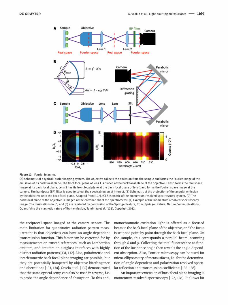
A. Vaskin et al.: Light-emitting metasurfaces 1169
the reciprocal space imaged at the camera sensor. The main limitation for quantitative radiation pattern meas-urement is that objectives can have an angle-dependent transmission function. This factor can be corrected for by measurements on trusted references, such as Lambertian emitters, and emitters on air/glass interfaces with highly distinct radiation patterns [131, 132]. Also, polarimetric and interferometric back focal plane imaging are possible, but they are potentially hampered by objective birefringence and aberrations [133, 134]. Grzela et al. [135] demonstrated that the same optical setup can also be used in reverse, i.e. to probe the angle dependence of absorption. To this end,
monochromatic excitation light is offered as a focused beam to the back focal plane of the objective, and the focus is scanned point by point through the back focal plane. On the sample, this corresponds a parallel beam, scanning through θ and φ. Collecting the total fluorescence as func-tion of the incidence angle then reveals the angle-depend-ent absorption. Also, Fourier microscopy can be used for micro-ellipsometry of metasurfaces, i.e. for the determina-tion of angle-dependent and polarization-resolved specu-lar reflection and transmission coefficients [136–138].
An important extension of back focal plane imaging is momentum-resolved spectroscopy [122, 128]. It allows for
Figure 12: Fourier imaging.(A) Schematic of a typical Fourier imaging system. The objective collects the emission from the sample and forms the Fourier image of the emission at its back focal plane. The front focal plane of lens 1 is placed at the back focal plane of the objective. Lens 1 forms the real space image at its back focal plane. Lens 2 has its front focal plane at the back focal plane of lens 1 and forms the Fouirer space image at the camera. The bandpass (BP) filter is used to select the spectral region of interest. (B) Schematic of the projection of the angular emission by the objective onto the back focal plane. Adapted from [127]. (C) Schematic of the momentum-resolved spectroscopy system. (D) The back focal plane of the objective is imaged at the entrance slit of the spectrometer. (E) Example of the momentum-resolved spectroscopy image. The illustrations in (D) and (E) are reprinted by permission of the Springer Nature, from: Springer Nature, Nature Communications, Quantifying the magnetic nature of light emission, Taminiau et al. [128], Copyright 2012.

1170 A. Vaskin et al.: Light-emitting metasurfaces
the analysis of emission patterns at different wavelengths. This is useful, since many emitters have rather broad emis-sion spectra and the typical metasurfaces exhibit resonant behavior. Taking both aspects together, the emission pat-terns can strongly depend on the wavelength. In this tech-nique, the back focal plane of the objective is imaged on the entrance slit of an imaging spectrometer (Figure 12C). The slit selects a thin line of the back focal plane image (Figure 12D), and the spectrometer projects the image of the slit on the camera sensor (Figure 12E) through the dis-persive element of the spectrometer.
To obtain similar information, alternatively, one can also perform conventional back focal plane imaging as described above and place an interferometric tunable band-pass (BP) filter in the beam path, analogous to hyperspec-tral imaging techniques. However, such filters are sensitive to the angle of incidence and polarize the transmitted light, thus limiting the applicability and accuracy of this method. Alternatively, one could obtain simultaneously spectral and directional information about the light emitted by the metasurface using a fiber mounted on a rotating arm. The method is typically used in the analysis of LEDs [105], but it requires a strong signal and is cumbersome and slow for full 2D maps of both θ and φ dependences.
5 Light-emitting metasurfaces: state of the art
In this section we review the state of the art in experiments on light-emitting plasmonic and dielectric metasurfaces.
The section is structured as follows. First we review the common approaches to making metasurfaces active by integration of emitters. These strategies are largely shared between plasmonic and dielectric realizations. Next, in Section 5.2 we review active plasmonic antenna array systems, specifically also addressing how the conceptual ideas of Section 2 come to fruition (unit cell polarizability engineering, and lattice engineering). Finally, Section 5.3 turns to all-dielectric metasurfaces.
5.1 Integration of emitters with metasurfaces
Various ways have been explored to integrate emitters with nanoantennas and metasurfaces. Some typical pos-sibilities are conceptually illustrated in Figure 13. Both for plasmonic and dielectric implementations, the emitters can be situated in the environment of the nanostructures. Because of the large number of demonstrations of emit-ters coupled to plasmonic nanoantennas and metasur-faces in the literature, here we do not attempt to provide a comprehensive review but limit our discussion to a few illustrative examples. A common way to bring emitters in the immediate environment of a metasurface is to disperse them in a host material, a thin film of which is then coated onto the nanostructures. For example, Tanaka et al. dis-persed lead sulfide (PbS) semiconductor QDs in polymeth-ylmethacrylate (PMMA), and the QD/PMMA solution was then spin-coated onto a plasmonic metasurface, forming a 180-nm-thick layer [139]. An early work in the realm of dielectric metasurfaces dispersed PbS QDs in polystyrene and spin-coated it onto a silicon nanocylinder array [140].
Figure 13: Schematic illustration of different possibilities to integrate emitters with metasurfaces.(A) Covering of the metasurface with a light-emitting thin-film. (B) Immersing the metasurface into a liquid containing fluorophores. (C) Placing the meta-atoms on a fluorescent substrate. (D) Precise placement of nanoemitters at specific positions on or next to the meta-atoms. (E) Fabrication of the metasurfaces from high-refractive-index materials incorporating nanoscale emitters. (F) Fabrication of the metasurfaces from luminescent materials.

A. Vaskin et al.: Light-emitting metasurfaces 1171
Similarly, Caldarola et al. covered silicon nanodimers with a PMMA thin film doped with molecules of the dye Nile Red [141]. Eu3+-doped polymer layers were applied to plasmonic [142] and silicon [111] metasurfaces using the Langmuir-Blodgett technique and spin coating, respec-tively. Light-emitting two-dimensional materials such as monolayers of transition-metal dichalcogenides, which can be viewed as thin films in their fundamental thickness limit, can also be integrated with both plasmonic and die-lectric metasurfaces. To this end, metal nanofabrication on as-grown monolayer crystals, stamping of exfoliated mon-olayers, or wet transfer procedures can be used [143–145]. Instead of applying thin layers of the active material, one can also immerse the nanostructures into a liquid medium containing a dye [146, 147]. Another option is to start the nanostructure fabrication from substrates that already contain the emitters, such as wafers containing near- surface self-assembled QDs [148] or a fluorescent glass substrate [149]. However, all the approaches mentioned so far do not by themselves allow for a precise placement of the emitters with respect to the nanostructures, e.g. in their hot-spot area. Such precise placement is important to maximize emission enhancement or control direc-tional effects. Several suitable techniques to couple dif-ferent quantum systems to plasmonic antennas have been presented [150]. For example, a viable route for precise emitter placement combines a two-step electron-beam lithography procedure with a chemical surface function-alization to immobilize emitters in predefined nanoscale areas only. This method was introduced by Curto et al. [62] to demonstrate coupling of a single QD to a Yagi-Uda nano-antenna. A self-assembled monolayer of mercaptound-ecanoic acid was applied after the second electron beam step, functionalizing exclusively the exposed areas. After activation with carbodiimide, the sample was immersed into a solution of CdSeTe/ZnS QDs, resulting in covalently bound QDs in defined areas on the gold surface. To apply this technique for dielectric metasurfaces, different chem-icals for surface functionalization have to be employed to allow binding to the dielectric materials or the substrate. For example, Peter et al. used QDs coated with a polymer providing carboxyl surface groups, which could selec-tively bind to defined areas of a silanized substrate [151]. Binding of colloidal streptavidin-coated CdSe QDs to a silica surface can be achieved using silane-PEG-biotin as a linker molecule [152]. Another interesting technique for the selective placement of emitters is dip-pen lithography. In a recent work [153], core/thick-shell “giant” nanocrys-tal quantum dots (gQDs) of various compositions were dispersed in a liquid ink, and a scanning probe tip was used to “write” small dots of the material onto silicon
nanoantennas. High-resolution electro-hydrodynamic printing of QDs on plasmonic nanostructures with a few nanometer precision was also demonstrated [154]. In addition to placing the emitters in the nanostructure environment, all-dielectric implementations also offer the opportunity of integrating them directly into the dielec-tric nanoantennas. For plasmonic nanostructures this is usually not possible, although it should be mentioned that light emission from metallic nanostructures, such as two-photon PL and cathodoluminescence, offers power-ful opportunities for their characterization, especially their near-field properties [155, 156]. These light emis-sion mechanisms are, however, usually not sufficiently efficient to be interesting for light-emitting devices. For dielectric metasurfaces, an elegant way to integrate emitters into the nanoresonators is to start the fabrica-tion from epitaxial wafers containing quantum wells or self-assembled QDs. Using lithographic techniques in combination with reactive ion etching, these wafers can then be nanostructured into the desired nanoantenna or metasurface geometries. This was demonstrated for silicon nanoantennas [157] and metasurfaces [158] con-taining germanium QDs, as well as for GaAs metasurfaces containing InAs QDs [159]. Alternatively, the fabrication of hierarchical metasurfaces with meta-atoms composed of densely packed QDs in a polymer matrix was also demon-strated [160]. Another simple but effective solution is to fabricate the metasurface building blocks from homoge-neous thin films of direct-bandgap semiconductors such as GaAs and to use the bandgap luminecence as a light source [161]. The beauty of incorporating the emitters into the nanoantennas is that the emitters are well protected from possibly detrimental environmental influences, and that a good overlap with the electromagnetic near fields of Mie-resonant dielectric building blocks can be achieved.
5.2 Plasmonic light-emitting metasurfaces
Incorporating extended plasmonic nanostructures for emission control has been of main interest for light-emit-ting devices, for instance in framework of LEDs, organic LEDS, and blue-LED-pumped phosphors for white light emission [58]. In the last 5 years, this research area evolved to also include coherent emission phenomena [31], such as lasing [162], and plasmon exciton-polariton physics [78, 123]. The main premise is that periodic diffractive plasmon structures combine strong light-matter interactions from field enhancement with narrow resonance linewidths due to diffraction. Improvement of light sources gener-ally involves (i) highest possible brightness and/or energy
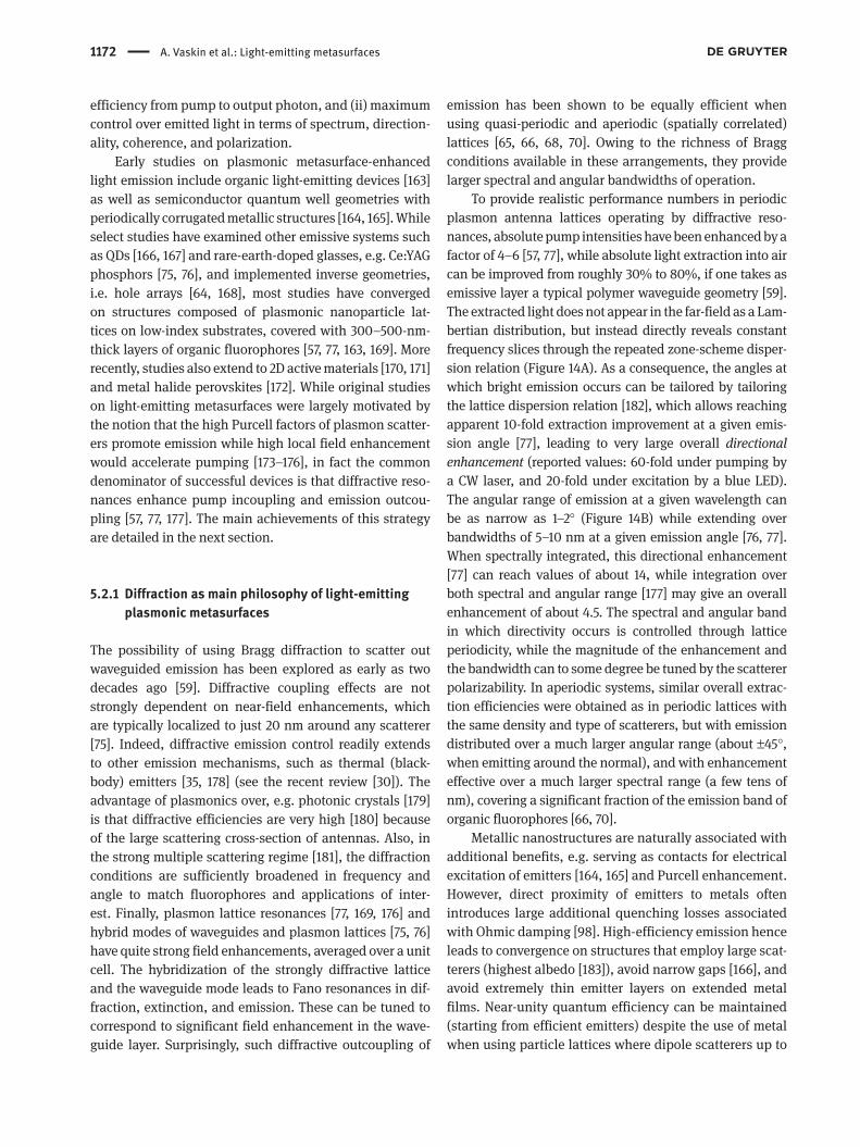
1172 A. Vaskin et al.: Light-emitting metasurfaces
efficiency from pump to output photon, and (ii) maximum control over emitted light in terms of spectrum, direction-ality, coherence, and polarization.
Early studies on plasmonic metasurface-enhanced light emission include organic light-emitting devices [163] as well as semiconductor quantum well geometries with periodically corrugated metallic structures [164, 165]. While select studies have examined other emissive systems such as QDs [166, 167] and rare-earth-doped glasses, e.g. Ce:YAG phosphors [75, 76], and implemented inverse geometries, i.e. hole arrays [64, 168], most studies have converged on structures composed of plasmonic nanoparticle lat-tices on low-index substrates, covered with 300–500-nm-thick layers of organic fluorophores [57, 77, 163, 169]. More recently, studies also extend to 2D active materials [170, 171] and metal halide perovskites [172]. While original studies on light-emitting metasurfaces were largely motivated by the notion that the high Purcell factors of plasmon scatter-ers promote emission while high local field enhancement would accelerate pumping [173–176], in fact the common denominator of successful devices is that diffractive reso-nances enhance pump incoupling and emission outcou-pling [57, 77, 177]. The main achievements of this strategy are detailed in the next section.
5.2.1 Diffraction as main philosophy of light-emitting plasmonic metasurfaces
The possibility of using Bragg diffraction to scatter out waveguided emission has been explored as early as two decades ago [59]. Diffractive coupling effects are not strongly dependent on near-field enhancements, which are typically localized to just 20 nm around any scatterer [75]. Indeed, diffractive emission control readily extends to other emission mechanisms, such as thermal (black-body) emitters [35, 178] (see the recent review [30]). The advantage of plasmonics over, e.g. photonic crystals [179] is that diffractive efficiencies are very high [180] because of the large scattering cross-section of antennas. Also, in the strong multiple scattering regime [181], the diffraction conditions are sufficiently broadened in frequency and angle to match fluorophores and applications of inter-est. Finally, plasmon lattice resonances [77, 169, 176] and hybrid modes of waveguides and plasmon lattices [75, 76] have quite strong field enhancements, averaged over a unit cell. The hybridization of the strongly diffractive lattice and the waveguide mode leads to Fano resonances in dif-fraction, extinction, and emission. These can be tuned to correspond to significant field enhancement in the wave-guide layer. Surprisingly, such diffractive outcoupling of
emission has been shown to be equally efficient when using quasi-periodic and aperiodic (spatially correlated) lattices [65, 66, 68, 70]. Owing to the richness of Bragg conditions available in these arrangements, they provide larger spectral and angular bandwidths of operation.
To provide realistic performance numbers in periodic plasmon antenna lattices operating by diffractive reso-nances, absolute pump intensities have been enhanced by a factor of 4–6 [57, 77], while absolute light extraction into air can be improved from roughly 30% to 80%, if one takes as emissive layer a typical polymer waveguide geometry [59]. The extracted light does not appear in the far-field as a Lam-bertian distribution, but instead directly reveals constant frequency slices through the repeated zone-scheme disper-sion relation (Figure 14A). As a consequence, the angles at which bright emission occurs can be tailored by tailoring the lattice dispersion relation [182], which allows reaching apparent 10-fold extraction improvement at a given emis-sion angle [77], leading to very large overall directional enhancement (reported values: 60-fold under pumping by a CW laser, and 20-fold under excitation by a blue LED). The angular range of emission at a given wavelength can be as narrow as 1–2° (Figure 14B) while extending over bandwidths of 5–10 nm at a given emission angle [76, 77]. When spectrally integrated, this directional enhancement [77] can reach values of about 14, while integration over both spectral and angular range [177] may give an overall enhancement of about 4.5. The spectral and angular band in which directivity occurs is controlled through lattice periodicity, while the magnitude of the enhancement and the bandwidth can to some degree be tuned by the scatterer polarizability. In aperiodic systems, similar overall extrac-tion efficiencies were obtained as in periodic lattices with the same density and type of scatterers, but with emission distributed over a much larger angular range (about ±45°, when emitting around the normal), and with enhancement effective over a much larger spectral range (a few tens of nm), covering a significant fraction of the emission band of organic fluorophores [66, 70].
Metallic nanostructures are naturally associated with additional benefits, e.g. serving as contacts for electrical excitation of emitters [164, 165] and Purcell enhancement. However, direct proximity of emitters to metals often introduces large additional quenching losses associated with Ohmic damping [98]. High-efficiency emission hence leads to convergence on structures that employ large scat-terers (highest albedo [183]), avoid narrow gaps [166], and avoid extremely thin emitter layers on extended metal films. Near-unity quantum efficiency can be maintained (starting from efficient emitters) despite the use of metal when using particle lattices where dipole scatterers up to
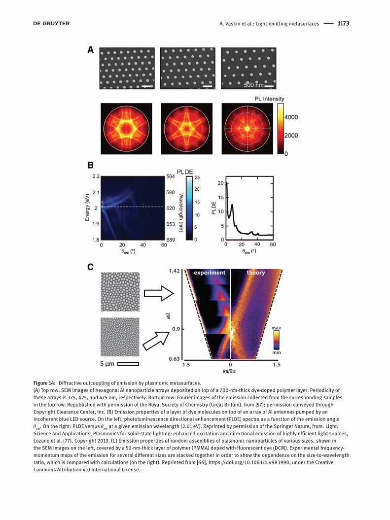
A. Vaskin et al.: Light-emitting metasurfaces 1173
Figure 14: Diffractive outcoupling of emission by plasmonic metasurfaces. (A) Top row: SEM images of hexagonal Al nanoparticle arrays deposited on top of a 700-nm-thick dye-doped polymer layer. Periodicity of these arrays is 375, 425, and 475 nm, respectively. Bottom row: Fourier images of the emission collected from the corresponding samples in the top row. Republished with permission of the Royal Society of Chemistry (Great Britain), from [57]; permission conveyed through Copyright Clearance Center, Inc. (B) Emission properties of a layer of dye molecules on top of an array of Al antennas pumped by an incoherent blue LED source. On the left: photoluminescence directional enhancement (PLDE) spectra as a function of the emission angle θem. On the right: PLDE versus θem at a given emission wavelength (2.01 eV). Reprinted by permission of the Springer Nature, from: Light: Science and Applications, Plasmonics for solid-state lighting: enhanced excitation and directional emission of highly efficient light sources, Lozano et al. [77], Copyright 2013. (C) Emission properties of random assemblies of plasmonic nanoparticles of various sizes, shown in the SEM images on the left, covered by a 50-nm-thick layer of polymer (PMMA) doped with fluorescent dye (DCM). Experimental frequency-momentum maps of the emission for several different sizes are stacked together in order to show the dependence on the size-to-wavelength ratio, which is compared with calculations (on the right). Reprinted from [66], https://doi.org/10.1063/1.4983990, under the Creative Commons Attribution 4.0 International License.

1174 A. Vaskin et al.: Light-emitting metasurfaces
100 × 100 × 40 nm occupy unit cells of 400 × 400 × 400 nm in size. This choice optimizes the polarizability per unit cell for scattering, while just 1% of the unit cell volume is occupied by the metal. The internal emission efficiency of emitters in such a structure, averaged over the unit cell, is maintained essentially above 75% [98].
Another benefit of large polarizability is that already small patches of periodically arranged plasmonic scatter-ers, just a few scatterers across, are sufficient to bring out the collective effects of infinite lattices [184], such as dif-fractive directional in- and out-coupling of emission. This has been elegantly demonstrated by several groups [64, 185, 186]. One of the studies investigated the emission from fluorophores located at the central scatterer (hole-in-film) in a hexagonal lattice, adding rows of the lattice one by one around the central hole [64]. The far-field emission direc-tivity was observed to sharpen with increasing lattice size, already showing the typical repeated zone scheme features of Figure 4 for systems as small as just five holes across.
5.2.2 Single-antenna contributions to emission control in plasmonic metasurfaces
While the strength of collective diffractive effects is in light extraction and directivity control, it is not evident how fluorophores in plasmon antenna arrays benefit from the
localized resonances of individual scatterers, beyond the notion of strong diffractive effects through large polariza-bility. The most obvious benefit of single plasmon scatters on emission that one would hope to transpose to meta-surfaces is in near-field enhancement of pump light and in Purcell enhancement [174, 175]. These typically occur at emitter-antenna separations in the 0–20 nm distance range, as has been widely studied at the level of individual plasmonic nanoparticles and reviewed in a recent article [92]. State-of-the-art literature reports of experimental single-nanoantenna emission enhancements use single emitters at a time, with large efforts taken by top-down and bottom-up methods to establish controlled antenna-emitter separations [87, 88] and avoid averaging over this separation. Many of these studies have evidenced 1000-fold emission enhancements per molecule [187–189], often using emitters that are intrinsically inefficient. In these studies, the emission enhancement factorized in approxi-mately two orders of magnitude pump field enhancement and one order of magnitude emission efficiency enhance-ment obtained by outpacing intrinsic nonradiative decay by accelerating emission. Beyond simple dipole nanoreso-nators such as nanospheres [87, 88] and nanorods [188], similar numbers were obtained in bowtie antennas [187] and other kinds of nanoparticle dimers [189–191]. The most pronounced success was obtained in gap antenna systems composed of metallic nanocubes placed above
Figure 15: Emission engineering at the level of individual plasmonic nanostructures. (A) Time-resolved photoluminescence from a single quantum dot (QD) coupled to a nanocavity (red), showing a biexponential decay with a fast component of 13 ps and a slow component of 680 ps. The fast component is limited by the instrument response function (IRF) of the avalanche photodiode detector, also shown (light gray). The lifetime of a single QD on glass is 6.8 ns (blue). Reprinted with permission from [90], https://pubs.acs.org/doi/abs/10.1021/acs.nanolett.5b03724. Copyright (2016) American Chemical Society. Requesting further permissions related to the material excerpted should be directed to the American Chemical Society. (B) Top: plasmonic split-ring resonator driven by a QD can act as a spin-polarized photon emitter, i.e. emitting photons with opposite spin in different (opposite) directions at oblique angles. Bottom: theoretical and experimental k-space maps of polarization states of emission. Adapted with permission from [46]. Copyright (2014) American Chemical Society. (C) Top: angular radiation pattern showing directional off-normal emission from a QD-driven plasmonic Yagi-Uda antenna. Bottom: SEM image of the antenna. Republished with permission of the American Association for the Advancement of Science, from [62]; permission conveyed through Copyright Clearance Center, Inc. (D) Top: breaking up-down symmetry of photoluminescence emission enhancement (PLE) by pyramidal aluminum nanoparticles. Black line shows emission towards the top, while red line corresponds to emission towards the bottom. The dashed line indicates the Rayleigh anomaly. Bottom: SEM image of the array before deposition of luminescent layer. Reprinted figure with permission from [192]. Copyright (2014) by the American Physical Society.
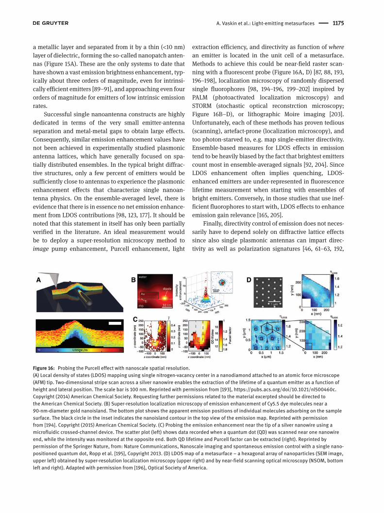
A. Vaskin et al.: Light-emitting metasurfaces 1175
a metallic layer and separated from it by a thin (<10 nm) layer of dielectric, forming the so-called nanopatch anten-nas (Figure 15A). These are the only systems to date that have shown a vast emission brightness enhancement, typ-ically about three orders of magnitude, even for intrinsi-cally efficient emitters [89–91], and approaching even four orders of magnitude for emitters of low intrinsic emission rates.
Successful single nanoantenna constructs are highly dedicated in terms of the very small emitter-antenna separation and metal-metal gaps to obtain large effects. Consequently, similar emission enhancement values have not been achieved in experimentally studied plasmonic antenna lattices, which have generally focused on spa-tially distributed ensembles. In the typical bright diffrac-tive structures, only a few percent of emitters would be sufficiently close to antennas to experience the plasmonic enhancement effects that characterize single nanoan-tenna physics. On the ensemble-averaged level, there is evidence that there is in essence no net emission enhance-ment from LDOS contributions [98, 123, 177]. It should be noted that this statement in itself has only been partially verified in the literature. An ideal measurement would be to deploy a super-resolution microscopy method to image pump enhancement, Purcell enhancement, light
extraction efficiency, and directivity as function of where an emitter is located in the unit cell of a metasurface. Methods to achieve this could be near-field raster scan-ning with a fluorescent probe (Figure 16A, D) [87, 88, 193, 196–198], localization microscopy of randomly dispersed single fluorophores [98, 194–196, 199–202] inspired by PALM (photoactivated localization microscopy) and STORM (stochastic optical reconstrction microscopy; Figure 16B–D), or lithographic Moire imaging [203]. Unfortunately, each of these methods has proven tedious (scanning), artefact-prone (localization microscopy), and too photon-starved to, e.g. map single-emitter directivity. Ensemble-based measures for LDOS effects in emission tend to be heavily biased by the fact that brightest emitters count most in ensemble-averaged signals [92, 204]. Since LDOS enhancement often implies quenching, LDOS-enhanced emitters are under-represented in fluorescence lifetime measurement when starting with ensembles of bright emitters. Conversely, in those studies that use inef-ficient fluorophores to start with, LDOS effects to enhance emission gain relevance [165, 205].
Finally, directivity control of emission does not neces-sarily have to depend solely on diffractive lattice effects since also single plasmonic antennas can impart direc-tivity as well as polarization signatures [46, 61–63, 192,
Figure 16: Probing the Purcell effect with nanoscale spatial resolution. (A) Local density of states (LDOS) mapping using single nitrogen-vacancy center in a nanodiamond attached to an atomic force microscope (AFM) tip. Two-dimensional stripe scan across a silver nanowire enables the extraction of the lifetime of a quantum emitter as a function of height and lateral position. The scale bar is 100 nm. Reprinted with permission from [193], https://pubs.acs.org/doi/10.1021/nl500460c. Copyright (2014) American Chemical Society. Requesting further permissions related to the material excerpted should be directed to the American Chemical Society. (B) Super-resolution localization microscopy of emission enhancement of Cy5.5 dye molecules near a 90-nm-diameter gold nanoisland. The bottom plot shows the apparent emission positions of individual molecules adsorbing on the sample surface. The black circle in the inset indicates the nanoisland contour in the top view of the emission map. Reprinted with permission from [194]. Copyright (2015) American Chemical Society. (C) Probing the emission enhancement near the tip of a silver nanowire using a microfluidic crossed-channel device. The scatter plot (left) shows data recorded when a quantum dot (QD) was scanned near one nanowire end, while the intensity was monitored at the opposite end. Both QD lifetime and Purcell factor can be extracted (right). Reprinted by permission of the Springer Nature, from: Nature Communications, Nanoscale imaging and spontaneous emission control with a single nano-positioned quantum dot, Ropp et al. [195], Copyright 2013. (D) LDOS map of a metasurface – a hexagonal array of nanoparticles (SEM image, upper left) obtained by super-resolution localization microscopy (upper right) and by near-field scanning optical microscopy (NSOM, bottom left and right). Adapted with permission from [196], Optical Society of America.
1176 A. Vaskin et al.: Light-emitting metasurfaces
206, 207]. The key asset is that appropriately designed antennas support magnetic and multipolar resonances [45, 46, 61, 192], aside from the expected dipolar plasmon resonance. Driven by an emitter, mutually coherent super-positions of these multipole moments can be excited, which in the far-field express as non-isotropic radiation patterns. In the context of metasurfaces, these single building-block radiation patterns are, to first order, super-imposed on the collective diffractive effects, as per Eq. (4). The most obvious signature is that directive emission of fluorophores that arises from surface lattice resonances derives preferential linear polarization from the unit cell building blocks, if these are nanorod antennas (linear electric dipoles) [169]. More advanced signatures [46, 61] have been observed with split-ring antenna arrays with coupled magneto-electric or dipolar-quadrupolar polariz-ability (Figure 15B), and with 2D chiral antennas driven by fluorophores [207]. In these experiments, emitting layers of randomly oriented fluorophores that intrinsically provide unpolarized and achiral far-field emission inherit strong circular polarization in their radiation pattern at oblique angles (maximum degree of circular polarization about 0.7), as well as overall enhancement asymmetry of around 20% between left- and right-handed polariza-tion (integrated over full angular detection range), which directly derive from the single building block resonances. Also, the notion of phase-gradient (Yagi-Uda antenna-type) unit cells from metasurfaces has been incorporated into emissive plasmon antenna lattices to break left-right symmetry (Figure 15C) [62, 63]. Up-down symmetry break-ing by antennas is associated with the Kerker condition [39], whereby electric and magnetic dipoles are simul-taneously excited. Rodriguez et al. [192] identified that this effect occurs in aluminum nanopyramid plasmonic resonators (Figure 15D). For fluorescent layers on top of diffractive arrays of nanopyramids, the diffractively out-coupled emission indeed inherits a significant up-down asymmetry of about 1:1.5 at the spectral peaks of plas-monic resonances. Here, the vertical position of the emit-ters relative to the nanopyramids is integral to realizing the asymmetry.
5.2.3 Reconfigurable plasmonic light-emitting metasurfaces
Dynamic control of emission might be of vital interest in applications such as optical switching and display technologies. Plasmonic resonators have been promoted as excellent candidates for applications requiring ultra-fast response, owing to the very short ring-down time (10–100 fs) of plasmon oscillations [208]. However,
sub-picosecond deterministic modulation of plasmonic metasurface emission has been rarely reported, likely because it is very difficult to optically switch the response of metals. Mostly, researchers have hence focused on modulation of the emitters, or of the dielectric surround-ing the emitters at the microseconds to milliseconds time scale, which is too slow for data processing but may suffice in lighting and display applications. Indeed, one strategy relies on tuning the emission spectrum, which can be done by electrostatically shifting the energy levels of light emitters by an external bias voltage [182]. Another approach to tune plasmonic resonances is by changing the refractive index via molecular reorientation or phase transition in liquid crystals [167, 209], or by exchanging the active medium in a microfluidic device [210]. One notable exception to the rule that modulation is through recon-figuration of matter around the plasmon resonators is the work of Pirruccio et al. [211], who demonstrated coherent control of absorption accomplished by the interference of two phase-controlled counter-propagating pump beams exciting dye molecules coupled to a plasmonic array [211]. This has the potential to modulate emission as fast as the emitter decay time allows. Going beyond the modulation of emission intensity and directivity, one can envision that ultimately one could also dynamically modify emis-sion decay rates. This has recently been demonstrated using very rapid insulator-to-metal phase transition in VO2 [212] and field-effect-induced permittivity changes in TiN [213]. Upgrading from planar interfaces to structured metasurfaces is presumably the upcoming step in this research.
5.2.4 Effective medium regime: hyperbolic metafilms
Another strategy for achieving large Purcell enhancement and emission directivity is to exploit nanostructures in deeply sub-diffractive regimes, which do not utilize plas-monic resonances but instead combine metals and dielec-trics to form an effective composite medium. Although this type of media is commonly assigned to the family of metamaterials and falls outside the most popular clas-sification of metasurfaces, we provide a brief overview of one interesting kind of such media: hyperbolic metafilms. These artificial optical materials are extremely anisotropic, behaving either like metals or like dielectrics depending on the direction of light propagation inside the medium. The underlying hyperbolic dispersion relation gives rise to peculiar light-matter interaction effects. First, in the effective medium limit, the dispersion cones host electro-magnetic states with unbounded momentum, and have been proposed to offer high (even infinite) LDOS for Purcell
A. Vaskin et al.: Light-emitting metasurfaces 1177
enhancement over a broad spectral range. In actual struc-tures, the LDOS enhancement and the utility thereof for bright emission are limited by a breakdown of the effective-medium picture at finite momentum and by quenching. A second remarkable prediction is that the group velocity vectors are locked to the surface normal of the dispersion cones, imposing inherently directional propagation in such media [214, 215]. Indeed, notable Purcell factors have been reported for light-emitting media such as dye-doped polymers [216] and nitrogen-vacancy centers in nanodia-monds deposited on top of hyperbolic media [217] as well as in their volume [218, 219]. For emitters in bulk hyperbolic media, it is not evident that outcoupling of light into free space can be efficient, which is due to the large momentum mismatch between the modes contributing to LDOS and free space. Just like in conventional light-emitting devices, this problem has been solved by diffractive outcoupling through patterning of the hyperbolic medium [220, 221]. Recently, improved light extraction has also been reported without relying on diffractive effects but purely by engi-neering the effective medium dispersion [222].
5.3 All-dielectric light-emitting metasurfaces
All-dielectric metasurfaces have been receiving an increasing amount of research attention recently, mainly due to their low absorption losses, which favor high-efficiency devices, as well as to the multipolar Mie-resonant [223] response of the high-index dielec-tric scatterers that can be used as their building blocks [224, 225]. Dielectric metasurfaces composed of such Mie-resonant building blocks are of particular interest in the context of light emission owing to the enhancement of the optical near-fields associated with the resonant response. As such, in analogy to plasmonic metasurfaces, the building blocks can act as dielectric nanoantennas able to enhance and tailor emission properties [226]. For example, by tailoring interferences of the light scattered by different resonant multipoles, interesting directional scattering effects can be obtained even from individual scatterers having very simple shapes. The low material losses translate to a high radiation efficiency and less heat generated by absorption [141] as compared to plasmonic nanoantennas. Nevertheless, the principal mechanisms governing the emission from dielectric metasurfaces are in principle identical to those outlined for plasmonic light-emitting metasurfaces in the previous sections. Therefore, in this section, we will not repeat an explanation of these mechanisms but will rather concentrate on providing an overview of the recently published work in this young field of light-emitting dielectric metasurfaces.
5.3.1 Coupling of emitters to single dielectric Mie resonators
Before considering the emission from dielectric metasur-faces, we briefly review the recent progress in coupling emitters to individual dielectric nanoantennas supporting Mie-like resonances. The Purcell factor of spherical Mie resonators was theoretically calculated for both electric and magnetic dipole emitters by Zambrana-Puyalto and Bonod [227]. It depends on the orientation and location of the dipoles, as well as on the multipolar order of the Mie mode. Typically, the dipole modes of an individual dielec-tric nanoresonator provide only moderate enhancement. Experimental mappings of the LDOS of a dipolar resonant silicon nanocylinder were performed by Bouchet et al. [228] by attaching a 100-nm-diameter fluorescent sphere to a scanning probe and scanning it over the sample. Increased or decreased total spontaneous decay rates by up to 15% and a gain in the collection efficiency of emitted photons by up to 85% were observed, in good agreement with theoretical expectations. Fluorescence manipula-tion was furthermore investigated for single Mie-resonant cylinders composed of germanium, directly using the Ge indirect-bandgap PL as emitter [229], and in silicon cylin-ders containing Ge QDs [157]. Another interesting mate-rial class that can be directly used to create Mie-resonant all-dielectric nanoantennas comprises halide perovskites [230]. Halide perovskites have a high refractive index and support excitons at room temperature with high binding energies and QY of luminescence. Making use of these properties, Tingutseva et al. realized light-emitting halide perovskite nanoantennas with enhanced PL based on the coupling of excitons to dipolar and multipolar Mie reso-nances [230]. Directional light emission from monolayer MoS2 coupled to a Mie-resonant silicon nanocylinder was studied by Cihan et al. [231]. Magnetic dipole enhance-ment by dipolar Mie resonators was also studied, as will be discussed in more detail in Section 5.3.5. The quadrupolar and higher order Mie modes, in contrast, were identified as a viable platform for enhancing both electric and mag-netic dipole transitions [227, 232, 233]. About two orders of magnitude radiative decay rate enhancement was pre-dicted by numerical simulations. For individual nanoan-tennas, we are not aware of any experiments that have shown this effect. A popular nanoantenna geometry for enhancing emission of electric and magnetic dipole emit-ters are dielectric dimer antennas. In the small feedgap between two Mie-resonant nanoantenna elements, hot spots of both the electric and the magnetic field can be obtained [234]. Emission enhancement from dielectric dimers has been observed in several experimental works. Fluorescence enhancement by up to a factor of 270 of

1178 A. Vaskin et al.: Light-emitting metasurfaces
single molecules of the dye crystal violet diffusing in solu-tion was also obtained using a silicon dimer nanoantenna optimized to confine the near-field intensity in its 20-nm gap [147] (Figure 17A–D). Enhancement of emission from the fluorescent dyes Nile Red and Star 635P in a PMMA matrix has been achieved using silicon dimers [141] and GaP dimers [235], respectively. An estimated enhancement factor of approximately 1900 was achieved for the silicon dimers, and a 3600-fold enhancement in combination with a fluorescence lifetime reduction of approximately 22 times was found for emitters confined in the gap region of the GaP dimers (Figure 17E–G). More complex nanoan-tenna structures such as silicon trimers containing germa-nium QDs were also considered [157] (Figure 17H).
5.3.2 Emission enhancement by dielectric metasurfaces
First indications of emission enhancement by metasur-faces composed of Mie-resonant dielectric building blocks were seen in a system consisting of silicon nanocylinder arrays exhibiting electric and magnetic dipole resonances covered by a thin layer of polystryrene containing PbS QDs [140]. Although the enhancement could not be quantified
in this work, the QD PL signal was clearly higher in the metasurface areas than in the unstructured reference areas. Enhancement of both linear and nonlinear PL by about a factor of eight under one-photon photoexcitation (up to 70 under three-photon photoexcitation) was also observed in metasurfaces based on nanoimprinted per-ovskite films supporting Mie-like resonances [236]. The moderate enhancement values under one-photon pho-toexcitation are consistent with the low Purcell factor of the dipolar Mie modes of the metasurface building blocks. Metasurfaces engineered to support more complex modes such as Fano resonances, embedded eigenstates, or surface lattice resonances offer important opportunities for much stronger enhancement. Liu et al. observed PL enhancement of up to nearly 110-fold from metasurfaces consisting of asymmetrically shaped GaAs nanoresona-tors incorporating InAs QDs [159], not taking into account the reduction of the active material due to nanostructur-ing (Figure 18B). Yuan et al. even found PL enhancements of more than 1000-fold from inverse metasurfaces con-sisting of arrays of asymmetric holes in a silicon thin film containing Ge QDs [158]. In both cases, controlled far-field coupling to a usually dark mode, which for a symmetric structure would be confined in the metasurface plane,
Figure 17: Coupling of emitters to single dielectric Mie resonators. (A) Sketch of a silicon nanogap antenna to enhance fluorescence from single molecules diffusing in solution. (B) Scanning electron micrograph of a fabricated silicon dimer with a gap size of 20 nm. (C) Numerically simulated electric field intensity enhancement in a horizontal plane through the center of the silicon dimer for normally incident light impinging from the glass substrate side, which is polarized parallel to the dimer axis. (D) Fluorescence intensity time trace showing bursts from single crystal violet molecules, which indicate fluorescence enhancement by the silicon nanogap antennas. (A–D) reprinted with permission from [147]. Copyright (2016) American Chemical Society. (E) Scheme of experimental configuration of GaP nanodimers embedded in a dye-doped PMMA layer. The inset shows a scanning electron micrograph of a fabricated GaP dimer with 35 nm gap size (scale bar: 100 nm). (F) Fluorescence spectra from the PMMA/dye-coated GaP nanodimer for the excitation polarized parallel (IX) and perpendicular (IY ) to the dimer axis. For reference, fluorescence spectra from a region of dye molecules not interacting with the nanoantenna (Iref ) and from bare PMMA/GaP (I0) are also included. (G) Fluorescence intensity decay curves for the PMMA/dye-coated GaP nanodimer. The instrument response function (IRF) is shown for reference. (E–G) reprinted with permission from [235]. Copyright (2017) American Chemical Society. (H) PL spectra of a Ge QD containing trimer (solid black line), of a single Ge QD containing nanocylinder (circles), and of the corresponding reference Ge(Si) QDs (triangles). Reprinted with permission from [157]. Copyright (2017) American Chemical Society.

A. Vaskin et al.: Light-emitting metasurfaces 1179
was established by the defined symmetry break in the metasurface unit cell. Note that, as already discussed in detail in Section 2.3, the absolute enhancement factors also depend on the QE of the emitters, where the lower QE emitters (the germanium QDs) experience higher enhancements under otherwise similar conditions than the higher QE emitters (InAs QDs).
5.3.3 Spectral and spatial tailoring of emission by dielectric metasurfaces
Apart from enhancing the emission, preferential emission of light in specific metasurface modes associated with the Purcell effect also allows tailoring the spectrum and spatial characteristics, including polarization and direc-tional behavior, of the emitted light. A strong dependence of the emission spectrum on the metasurface geometrical parameters, which in turn determine the spectral position of the Mie resonances, was already observed in the very simple system of PbS QDs coupled to a silicon nanocyl-inder metasurface [140]. However, the spectra were sig-nificantly broadened and thus no clear assignment of the resonances responsible for the spectral reshaping was pro-vided. A stronger spectral reshaping effect was observed by Vaskin et al. [149]. The maxima of the emission from
a fluorescent glass substrate used as the substrate of a silicon nanocylinder metasurface were demonstrated to coincide with the spectral positions of the magnetic dipole resonances in the 800–900 nm wavelength range for a systematic variation of the nanocylinder radius. Even more pronounced spectral reshaping effects were associ-ated with the Fano resonant metasurfaces discussed in the previous section [158, 159] (Figure 18B, C). In accord-ance with the high quality factor of the resonances, the strong emission enhancement happens within a narrow spectral range only, thereby drastically changing the emission from a rather broad to a very narrow spectrum. Spatial reshaping of emission has been experimentally studied for only few dielectric metasurfaces so far. The method of choice to record the emission patterns within a certain solid angle defined by the NA of the microscope objective used for collecting the emitted light is back focal plane imaging (Section 4.5). Using this technique, direc-tional emission of light out of the metasurface plane was observed for the emission of the previously described system consisting of a fluorescent substrate coupled to a silicon nanocylinder metasurface. This effect originated from an interplay of emission enhancement by the dipolar Mie resonances of the nanocylinders with the diffractive modes of the periodic arrangement. An emission nor-mally out of the substrate plane is often favored, as it can
Figure 18: All-dielectric metasurfaces for spectral and spatial shaping of emission.(A) Scanning electron micrograph of an asymmetric GaAs metasurface containing InAs quantum dots and supporting a high-quality-factor Fano resonance. (B) Measured photoluminescence (PL) from the metasurface as compared to that from the unpattered wafer, showing strong emission enhancement at the wavelength of the Fano resonance. (C) Measured reflectance and PL spectra for asymmetric GaAs metasurfaces featuring a variation of their geometrical parameters, which allows spectral tuning of the wavelength of the emission peak. (D) Measured (top row) and numerically calculated (bottom row) back focal plane images of the metasurface emission for three different emission wavelengths. Figures (A–D) Reprinted with permission from [159]. Copyright (2018) American Chemical Society. (E) Sketch of a silicon nanocylinder metasurface decorated with monolayer crystals of MoS2. (F) True-color light microscope image of a corresponding fabricated sample. (G, H) Experimentally measured back-focal plane image of the monolayer MoS2 emission for a nanocylinder diameter of (G) 260 nm and (H) 300 nm. Figures (E–H) Reprinted with permission from [145]. Copyright (2019) American Chemical Society.

1180 A. Vaskin et al.: Light-emitting metasurfaces
enhance the collection efficiency for low-NA collection optics. The directional emission properties of the emission enhanced by high-quality-factor Fano resonances sup-ported by the asymmetric GaAs metasurface containing InAs QDs were investigated by Liu et al. [159] as a function of the emission wavelength (Figure 18D). It was shown that, owing to the dispersive properties of the Fano mode, directional emission out of the substrate plane could be achieved for a particular emission wavelength defined by the metasurface design. For larger wavelengths, the emis-sion pattern viewed in the back focal plane changed into a rhombohedral ring (corresponding to an asymmetric cone in real space) characterized by an increase of the radius with increasing emission wavelength. Directional shaping of the emission from monolayer crystals of the transition-metal dichalcogenide MoS2 using a metasurface composed of square arrays of silicon nanocylinders was also recently demonstrated (Figure 18E–H). By tuning the resonance wavelength of the metasurface with respect to the MoS2 emission wavelength via a systematic change of the nano-cylinder diameter, the emission could be spatially redis-tributed from preferential emission under large angles for the off-resonant case to preferential out-of-plane emission for the resonant case. Finally, directional emission from metasurfaces supporting an embedded eigenstate was studied in Ha et al. [161], as discussed in more detail below in the context of lasing effects in metasurfaces.
5.3.4 Dynamic control of emission
Similar to plasmonic metasurfaces, resonant dielec-tric metasurfaces also offer interesting opportunities for dynamic tuning of their emission properties. Active tuning of dielectric metasurface resonances is an active field of research, and several different tuning mecha-nisms have been explored already. Typically, either the geometry of the metasurface is dynamically adjusted, e.g. by stretching of a flexible metasurface substrate or matrix [237], or the optical properties of the nanoreso-nators or their surroundings are tuned by some control parameter. In the latter case, functional materials with optical properties that are sensitive to external stimuli such as temperature, applied voltage, or optical fields have to be integrated into the metasurface architec-ture. Typical examples for such materials, which have already been integrated with dielectric metasurfaces and have been demonstrated to allow for spectral tuning of metasurface resonances, are liquid crystals [238, 239], phase-change materials [240], and direct-bandgap semi-conductors [241]. In the latter case, the refractive index
of the nanoresonator material can be changed by (all-optical) generation of charge carriers. Note that while the possibilities for geometry changes of the lattice and changes in the environment are largely analogous to the methods used for tuning of plasmonic metasurfaces (compare Section 5.2.3), the possibility of dynamically and reversibly changing the resonator optical properties themselves is usually not offered by plasmonic systems. The general rationale for tuning of emission, however, is fully analogous to that of plamonic metasurfaces: Since spontaneous emission from nanoscale sources situated inside or near the resonant meta-atoms is enhanced at the spectral position of the metasurface Mie-type reso-nances due to the Purcell effect, dynamic tuning of the resonance position should naturally allow for dynamic control of their emission spectra. For dielectric metas-urfaces, this was recently observed by Bohn et al. [242], where a silicon nanocylinder metasurface situated on a fluorescent substrate was integrated into a nematic liquid crystal cell. Upon heating the system over a criti-cal temperature Tc, the liquid crystal changes its state from nematic to isotropic (Figure 19A), which is associ-ated with a pronounced change of its optical properties. In the considered system, this then resulted in a spec-tral shift of the electric and magnetic dipole resonances of the metasurface (Figure 19B) and, consequently, in a clear change of the substrate’s emission spectrum up to roughly a factor of two around 900 nm wavelength (Figure 19C).
5.3.5 Magnetic emission enhancement
The interaction of materials with the magnetic compo-nent of light is several orders of magnitude weaker than that with the electric component of light. Therefore, when considering light emission, magnetic dipole transitions can usually be safely disregarded. However, in material systems such as trivalent lanthanide ions, where certain electronic transitions are electric-dipole-forbidden by specific selection rules, the magnetic dipole can become dominant [128]. In analogy to the more common Purcell enhancement of electric dipole emitters, a suit-ably designed photonic environment can also enhance the radiative rate of magnetic dipole transitions [243]. Following initial theoretical studies [227, 232, 233], the magnetic photonic density of states of a Mie-resonant silicon nanocylinder supporting a magnetic dipole mode was recently experimentally recorded [244]. This was accomplished by fabricating the antenna at the tip of a scanning probe and moving it over a sample containing

A. Vaskin et al.: Light-emitting metasurfaces 1181
trivalent europium ions. In accordance with theoretical expectations, a moderate magnetic emission enhance-ment of about 3, as estimated by the authors, was observed. In another work [245], a homogeneous 10-nm-thick film of Eu3+-doped nanoclusters was deposited on single silicon nanorods and dimers. The samples were raster-scanned under a tightly focused laser beam, and the PL maps were recorded. This way, the spatial vari-ations of the electric dipole (ED) and magnetic dipole (MD) emissions around the silicon nanostructures were probed. The experimental far-field PL maps were com-pared with computed maps of the electric and magnetic radiative LDOS, showing good agreement. Finally, mag-netic emission enhancement by dielectric metasurfaces was recently demonstrated for a system composed of silicon nanocylinders exhibiting Mie-type resonances with strong quadrupole contributions covered by a thin layer of a Eu3+-containing polymer [111] (Figure 19D–I). The magnetic emission enhancement was found to depend systematically on the nanocylinder radius, which in turn determines the spectral position of the metasur-face resonances. An absolute brightness enhancement of the magnetic transition of up to 6.5-fold was observed for the optimal choice of geometry.
5.4 Metasurface-based lasers
5.4.1 Plasmonic metasurface lasers
Employing plasmonic modes in lasing devices is based on two paradigms: distributed feedback (DFB) and surface plasmon lasing (SPASER). Since the concept of SPASER [208] relies on localized resonances of individual nano-structures, and by itself constitutes a very rich research field, we refer to the recent review on this topic [162], and instead, we focus here on the metasurface lasers based on DFB.
In the DFB mechanism, multiple scattering of light in a periodic lattice supports standing waves whenever Bragg conditions are met. Lasing can occur in geometries such as periodically corrugated waveguides with gain when the gain overcomes the loss due to scattering and absorption. This concept has been combined with the diffractive outcoupling mechanism in the early work of Stehr et al. [246], who used the second-order Bragg scat-tering in a gold nanodisk array to accomplish feedback in an active polymer layer, and the first-order to scatter the laser light into normal direction. In subsequent research works, DFB plasmon lattice lasers have been shown to
Figure 19: Dynamic control of emission and magnetic emission enhancement. (A) Schematic of a light-emitting silicon nanocylinder metasurface integrated into a nematic liquid crystal cell for temperature tuning. (B) Measured temperature dependent linear-optical transmittance spectra of the metasurface, showing a drastic change as the liquid crystal undergoes a phase transition from nematic to isotropic at its critical temperature Tc. (C) Measured fluorescence spectra of the metasurface for the nematic and the isotropic state of the embedding liquid crystal. The corresponding transmittance spectra are also shown. (A–C) reprinted with permission from [242]. Copyright (2018) American Chemical Society. (D) Artist’s impression of a silicon nanocylinder metasurface covered by a polymer layer containing Eu3+ ions, which exhibit both electric and magnetic transitions. (E) Cross-sectional electron micrograph of a corresponding fabricated structure. (F, G) Fluorescence microscopy images of 20 fabricated metasurfaces (bright squares) covered by a polymer layer containing Eu3+ ions, observed through narrowband spectral transmission filters tuned to the (F) magnetic and (G) electric transition at 590 nm/610 nm, respectively. Clearly, the emission of both transitions is enhanced by the metasurfaces. (H) Experimentally measured and (I) numerically calculated ratio of the emission enhancement of the magnetic versus the electric transition in dependence of the nanocylinder radius. (D–I) reprinted with permission from [111]. Copyright (2019) American Chemical Society.
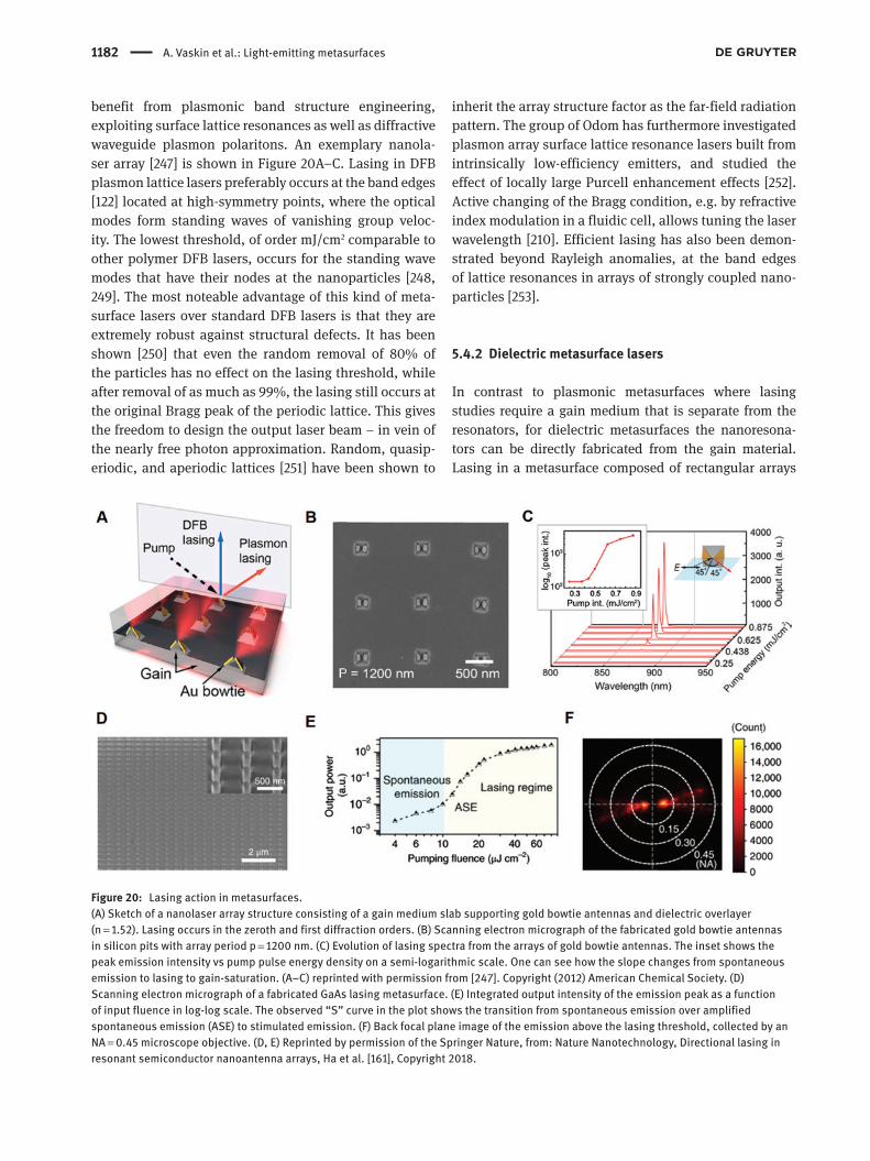
1182 A. Vaskin et al.: Light-emitting metasurfaces
benefit from plasmonic band structure engineering, exploiting surface lattice resonances as well as diffractive waveguide plasmon polaritons. An exemplary nanola-ser array [247] is shown in Figure 20A–C. Lasing in DFB plasmon lattice lasers preferably occurs at the band edges [122] located at high-symmetry points, where the optical modes form standing waves of vanishing group veloc-ity. The lowest threshold, of order mJ/cm2 comparable to other polymer DFB lasers, occurs for the standing wave modes that have their nodes at the nanoparticles [248, 249]. The most noteable advantage of this kind of meta-surface lasers over standard DFB lasers is that they are extremely robust against structural defects. It has been shown [250] that even the random removal of 80% of the particles has no effect on the lasing threshold, while after removal of as much as 99%, the lasing still occurs at the original Bragg peak of the periodic lattice. This gives the freedom to design the output laser beam – in vein of the nearly free photon approximation. Random, quasip-eriodic, and aperiodic lattices [251] have been shown to
inherit the array structure factor as the far-field radiation pattern. The group of Odom has furthermore investigated plasmon array surface lattice resonance lasers built from intrinsically low-efficiency emitters, and studied the effect of locally large Purcell enhancement effects [252]. Active changing of the Bragg condition, e.g. by refractive index modulation in a fluidic cell, allows tuning the laser wavelength [210]. Efficient lasing has also been demon-strated beyond Rayleigh anomalies, at the band edges of lattice resonances in arrays of strongly coupled nano-particles [253].
5.4.2 Dielectric metasurface lasers
In contrast to plasmonic metasurfaces where lasing studies require a gain medium that is separate from the resonators, for dielectric metasurfaces the nanoresona-tors can be directly fabricated from the gain material. Lasing in a metasurface composed of rectangular arrays
Figure 20: Lasing action in metasurfaces. (A) Sketch of a nanolaser array structure consisting of a gain medium slab supporting gold bowtie antennas and dielectric overlayer (n = 1.52). Lasing occurs in the zeroth and first diffraction orders. (B) Scanning electron micrograph of the fabricated gold bowtie antennas in silicon pits with array period p = 1200 nm. (C) Evolution of lasing spectra from the arrays of gold bowtie antennas. The inset shows the peak emission intensity vs pump pulse energy density on a semi-logarithmic scale. One can see how the slope changes from spontaneous emission to lasing to gain-saturation. (A–C) reprinted with permission from [247]. Copyright (2012) American Chemical Society. (D) Scanning electron micrograph of a fabricated GaAs lasing metasurface. (E) Integrated output intensity of the emission peak as a function of input fluence in log-log scale. The observed “S” curve in the plot shows the transition from spontaneous emission over amplified spontaneous emission (ASE) to stimulated emission. (F) Back focal plane image of the emission above the lasing threshold, collected by an NA = 0.45 microscope objective. (D, E) Reprinted by permission of the Springer Nature, from: Nature Nanotechnology, Directional lasing in resonant semiconductor nanoantenna arrays, Ha et al. [161], Copyright 2018.
A. Vaskin et al.: Light-emitting metasurfaces 1183
of GaAs nanopillars was recently demonstrated by Ha et al. [161] (Figure 20D–F). In this study, one period of the array was subdiffractive while the other was chosen suffi-ciently large to support diffractive orders, thereby provid-ing a mechanism for directional outcoupling as in regular DFB lasers. In order to achieve a low lasing threshold, the nanostructure was engineered to support a collective ver-tical electric dipole resonance, which has a high experi-mentally measured quality factor of up to about 1500 because of the weak coupling of the vertical dipoles to the far-field. Lasing was observed in these structures at liquid nitrogen temperature with a threshold of ~14 μJ cm−2, as confirmed by observing the characteristic kink in the output intensity in log-log scale of the PL as a function of the pumping fluence, and by the second-order photon correlation function of emitted photons. The lasing direc-tivity and wavelength were controlled by the design of the nanopillar array and by modifying the gain spectrum of GaAs with temperature. An interesting viewpoint put forward in this work is that the lasing mode, which in conventional and plasmonic DFB lasers is always a Bloch mode at a high-symmetry point in the k-space that is dark, can be viewed as a bound state in the continuum (BIC) that is made leaky by opening a diffraction channel. This viewpoint connects to the work of Kodigala et al. [254], who reported lasing in square arrays (period comparable to wavelength) of InGaAs resonators (gain from embedded multiple quantum well structure), right at a geometrical condition for the existence of a BIC.
5.5 Chiral emission
The possibility to construct metasurfaces from complex building blocks exhibiting broken inversion symmetry makes them attractive systems for studying chiral light-matter interaction processes. As such, both plasmonic and dielectric passive chiral metasurfaces have been dem-onstrated to support strong circular dichroism (CD) and polarization conversion effects [255–259]. However, meas-urement of far-field properties such as CD does not probe the chiral properties of the electromagnetic near-fields, which are very different from those of circularly polar-ized light [260–262]. They exhibit phase-shifted electric and magnetic field vector components without tempo-ral vector rotation, which can be engineered to occur in the near-fields of designed nanostructures. Formally, the chiral nature of an electromagnetic field can be expressed
by the electromagnetic chirality 0 (2
Cε
ω= − ∗E BIm ), where
E and B denote the complex electric and magnetic field
vectors, respectively. To investigate the chiral properties of near-fields around plasmonic nanostructures and their relation to the electromagnetic chirality C, Meinzer et al. measured the far-field polarization state of the enhanced luminescence from achiral emitters situated in the near-field of an array of 2D chiral nanorod pairs [262]. They found a clear dissymmetry for left- and right-handed emis-sion enhancement depending on the handedness of the nanorod pairs. In a follow-up study, Cotrufo et al. reported that these handed signatures of scatterers imprinted on achiral fluorophores are strongly enhanced at diffractive features, i.e. at surface lattice resonances [207]. Control of the polarization of emission of QDs embedded in an active layer of an all-dielectric planar microcavity exhib-iting a chiral gammadion layer structure was studied by Maksimov et al. [263]. A circular polarization degree reaching 81% was achieved. Apart from controlling the circular polarization of emission, asymmetric plasmonic and dielectric metasurfaces were also shown to enable the separation of photons of different helicity in the momen-tum space. Kruk et al. demonstrated this effect for achiral emitters, namely QDs, using plasmonic split-ring resona-tors [46] (Section 5.2.2). More recently, the concept has received an increasing amount of attention due to the prospect of applying it for selectively addressing valley-polarized excitons in two-dimensional transition-metal dichalcogenides at the nanoscale. These can be excited, and emit by, absorption and emission, respectively, of circularly polarized light. Separation of valley excitons in a MoS2 monolayer was recently demonstrated using a subwavelength asymmetric plasmonic groove array [264]. Valley-selective optical control of excitons in 2D WS2 using chiral all-dielectric metasurface generating chiral near-field for linear polarized incidence was demonstrated by Guddala et al. [265].
5.6 Performance comparison
Direct comparison of plasmonic and dielectric metas-urfaces in terms of their light-emitting performance is a challenge, as most existing literature focuses exclusively on either the first or the second type of meta-structures. Ideally, a back-to-back quantitative comparison should be done using identical theoretical and experimental tools and conditions, such that the inferred performance of a metasurface is not affected, e.g. by the variable per-formance of a measurement setup. Very few theoreti-cal and experimental works pursue such back-to-back comparison of light-emitting metasurfaces. For instance, Ding et al. [266] reported on computational studies of

1184 A. Vaskin et al.: Light-emitting metasurfaces
local field enhancement and emission enhancement in nanopillar arrays made of silicon, silver, and aluminum, predicting superior performance of Si meta-structures as compared to their metallic counterparts. Very recently, similar meta-structures have been investigated experi-mentally by Murai et al. [267]. In this work, directional emission enhancement was addressed, showing that Si nanocylinder arrays offer significantly narrower angular distribution of emission enhancement compared to the identical meta-structures made of Al. Another example of a comparative experimental study is the investigation of Purcell enhancement in nano-patterned metallic and hyperbolic films [220], which has shown impressive per-formance of a hyperbolic medium grating as compared to a silver grating. Significant further work is needed, since in the available reports the comparisons typically assume that metallic and dielectric (or hyperbolic) samples are fabricated according to the same, not individually opti-mized, design. Not performing this system-dependent optimization easily leads to biased performance assess-ments. Whether one or the other type of metasurface materials is superior also does not have a unique answer, since it depends strongly on the eventual application. For example, realization of advanced optical function is pos-sible in very compact plasmonic nanostructures, because metallic nanoparticles support localized dipolar plasmon resonances independent of their size, whereas dipolar Mie resonances require large nanoparticles. Conversely, all-dielectric Mie resonators intrinsically offer access to sig-nificantly larger quality factors and more versatile emitter integration opportunities.
6 Outlook
6.1 Future research directions
6.1.1 Wavefront shaping of emission
As described in the previous sections, light-emitting meta-surfaces offer manifold opportunities for manipulating spontaneous and stimulated emission phenomena. Various directional effects were triggered based on the emission pattern of the individual metasurface elements, the spatial coherence of emission mediated by diffractive coupling in the array, and the interplay of both these factors. However, while directional spontaneous and stimulated emission and a certain complexity of the dependence on the metas-urface design and the emission wavelength were observed, to date, a demonstration of complex arbitrary emission
patterns is still missing. One could, e.g. imagine metasur-faces that directly emit a focused beam or a holographic image. To reach this goal, spatially inhomogeneous meta-surfaces would certainly be required. The performance limits of such an approach still need to be investigated. The degree of spatial coherence that can be achieved, and which is expected to correlate with the range of the in-plane couplings, will likely be a limiting factor. For thermal emission, where, as in the case of spontaneous emission, different points of the thermal source usually emit uncorrelated fields that do not interfere, it was previ-ously pointed out that spatially coherent emission can be established by sources supporting surface waves, such as plasmonic gratings [268], in combination with diffractive outcoupling. It was shown that the directivity of the source is directly linked to the propagation length of the surface waves. It will be interesting to further investigate this con-nection for plasmonic and dielectric light-emitting meta-surfaces incorporating spontaneously emitting sources. Another major challenge will be the development of viable design methodologies for spatially inhomogeneous light-emitting metasurfaces, considering that numerical simu-lations of emission processes are already computationally demanding for periodic structures. A possible recipe to design inhomogeneous metasurfaces emitting complex tailored emission profiles was suggested by Schokker and Koenderink for plasmonic particle arrays operated above the lasing threshold [251]. Various particle arrange-ments were investigated, which supported robust lasing action based on diffractive lattice effects, thus establish-ing spatial coherence. It was experimentally demonstrated that the angular distribution of laser emission inherits its shape from the Fourier transform of the underlying lattice. As a deterministic aperiodicity is introduced, it manifests itself in a speckle pattern with distinct autocorrelations. This suggests that beam-shaping of the output of periodic plasmon lasers can be achieved by selectively removing particles from the array, thereby imprinting the Fourier transform of the resulting binary amplitude mask on the angular characteristics of the output.
6.1.2 Programming emission
The possibility to dynamically tune the emission from both plasmonic and dielectric metasurfaces as reviewed in Sec-tions 5.2.3 and 5.3.4 represents a first step in the direction of freely programming their emission. For this purpose, approaches that rely on more controlled stimuli, such as application of a voltage, are advantageous. Voltage control of resonances is, e.g. possible by integration of the

A. Vaskin et al.: Light-emitting metasurfaces 1185
light-emitting metasurface into a liquid crystal cell [239], and electrostatic shifting of the emitter’s energy levels by an applied bias voltage can also be achieved [182]. In com-bination with pixellated or otherwise suitably patterned electrodes, such an approach would enable local address-ing of the emission. The ability to locally switch the emis-sion on and off, change the colour, the directional behavior, or other emission properties is essential for the deployment of light-emitting metasurfaces in display and projector app-plications, or as smart substrates (Section 6.2).
6.1.3 Hybrid metal-dielectric light-emitting metasurfaces
While in this article we have reviewed the state of the art of light-emitting metasurfaces separately for plasmonic and dielectric implementations regarding most aspects, inter-esting opportunities for enhancing and tailoring emission phenomena arise from combining plasmonic and dielec-tric building blocks to form hybrid metal-dielectric archi-tectures. For individual nanoantennas, it was already demonstrated that combining a metallic feed element with one or several dielectric director elements allows the creation of nanoantennas combining strong emis-sion enhancement with highly directional behavior, and a fairly high radiation efficiency [269–271]. For plasmonic nanoantennas coupled to microscale photonic resonators, it was furthermore demonstrated that, for a critical cou-pling condition, the Purcell enhancement can be higher for the coupled system than for each of its individual components [272]. Hybrid metal-dielectric metasurfaces have also been studied, e.g. for their interesting mode structure and asymmetric reflection properties [273, 274]. At the time of writing, we are, however, not aware of any experiment studying emission from hybrid metal-dielec-tric metasurfaces. Similar to the individual hybrid nano-antennas, such hybrid metasurfaces could offer favorable performance regarding enhancement, directional proper-ties, and radiation efficiency. They would also offer more degrees of freedom to individually tailor the excitation and emission properties of the metasurfaces.
6.1.4 Electrical driving schemes
Most of the light-emitting metasurfaces demonstrated so far relied on optical pumping of the integrated fluoro-phores, with few exceptions that demonstrated electri-cally pumped devices [275]. For several of the envisioned applications, however, the development of electrical pumping schemes is desirable. From this viewpoint,
active semiconductor-based metasurface architectures hold the highest potential, as technical solutions could be adapted from existing solutions employed in optoelec-tronics and semiconductor lasers. Other promising pos-sibilities include the use of electroluminescent materials or hybridization of metasurfaces with van der Waals het-erostructures [276] incorporating both 2D direct-bandgap semiconductors and graphene for contacting.
6.1.5 Strong coupling and excitonic metasurfaces
In the strong coupling regime, quantum emitters do not decay irreversibly by spontaneous emission but can transfer their population to a photonic mode and receive it back multiple times before the energy of excitation is lost upon spontaneous decay or mode damping. This leads to anti-crossing of the electronic and optical reso-nances, which signifies hybrid quasiparticles known as exciton polaritons. In order to achieve strong coupling, the coupling rate must be large compared to the rate of all decay channels (spontaneous decay and photonic losses), which can be accomplished by coinciding material and optical resonances of very narrow line widths [78], while also targeting large oscillator strength of the dipole transi-tion. An emerging field in plasmonics is collective strong coupling, where the concentration of emitters is taken as high as possible to boost the (collective) oscillator strength. Indeed, the signatures of strong coupling have been reported in systems that coupled organic dye exci-tons with SPP Bloch modes in nanohole arrays [277–279] and collective resonances of plasmonic nanoparticle arrays [79, 280, 281]. This is an exciting research direction for metal and dielectric metasurfaces, as the hybrid meta-surface-exciton states can support effects such as conden-sation [282, 283], concomitantly coherent emission [123, 284], optical nonlinearity [285, 286], and magneto-optical response [287] allowing, e.g. the achievement of photonic (polaritonic) topological insulator phase [288, 289]. It has been suggested that the usual concentration quenching at high emitter concentration, which limits bright light emis-sion, is overcome in the limit of strongly coupled systems [290] and plasmon exciton polariton lasing [123]. Also, the strong coupling regime is relevant for domains outside light emission, such as “polaritonic” chemistry [291, 292], where strong coupling shifts the energetics of levels and thereby affects chemical reactions. Dielectric metasur-faces could add new means to control light-matter interac-tion through their multipolar building block resonances [293, 294]. One could envision that these tie into chiral and photon-spin degrees of freedom [295].

1186 A. Vaskin et al.: Light-emitting metasurfaces
Recently, excitonic materials alone (in the absence of conventional metal or dielectric scatterers) are of growing interest in the metasurface context. It has been shown that nanostructured excitonic media exhibit metallic properties, which may lead to plasmon-like optical field confinement in the forms akin to propagating SPP modes [296] as well as localized resonances [297, 298]. Collective lattice resonances originating from such localized modes are predicted [299] in analogy to plasmonic lattice reso-nances. Therefore, excitonic nanostructures can be con-sidered as an attractive route toward novel kinds of active metasurfaces, which are at the very beginning of their experimental exploration [300].
6.1.6 PT symmetry
If one rigorously considers optical modes of any metas-urface, it becomes clear that the radiative damping and intrinsic material losses render their eigenvalue problem non-Hermitian. This means that optical modes of metas-urfaces may diverge from their one-to-one analogy with electronic bands of crystalline solids. In particular, the band structure of some metasurfaces may contain uncon-ventional singularities known as exceptional points [301], where two distinct eigenmodes have identical eigenvalues and eigenvectors, breaking down the completeness of the eigenstate basis. These “Hamiltonian defects” have been observed experimentally near accidental Г-point degen-eracy (Dirac point) of dipolar and quadrupolar modes, resulting from the difference in their radiative damping [302]. The above example is a peculiar photonic system, in which coupling between optical eigenmodes of different damping rates (i.e. different imaginary parts of their eigen-frequencies) gives rise to the properties equivalent to the properties associated with the parity-time (PT) symmetry. In the most common settings, PT symmetry means that the optical properties of a metasurface are invariant under simultaneously mirror-reflecting (space) and reversing gain and loss (time), even though they are not invariant under only one of these operations. PT-symmetric Ham-iltonians are known to possess purely real eigenvalues in some region of parameter space, while outside this region at least two eigenstates become complex-valued and mutu-ally self-conjugated, corresponding to a PT-symmetry broken phase.
Two-dimensional plasmonic and dielectric metasur-face lattices imbued with active light-emitting material could be an exciting venue to study PT symmetry. In certain PT metasurfaces, the unbroken-PT and broken-PT phases have been predicted to coexist in different regions of the
same band structure, separated by PT-phase transition, i.e. a line of exceptional points. Such a scenario has been pro-posed to occur in periodic arrangements of alternating gain and loss overlaid with a photonic crystal [303], where it is predicted to enable unprecedented functions such as all-angle supercollimation and superprismatic effect without necessarily being limited in efficiency by traditional imped-ance-mismatch arguments [55]. Beyond the photonic crystal regime, PT-symmetric arrangements of nanoscatterers have also been predicted to provide control over the asymmetry of far-field emission [304]. Studying this type of effects would require optical scattering experiments at some probe frequency, while simultaneously applying optical gain, for instance, using a spatially structured pump beam excit-ing a spatially structured gain medium. Recent theoretical work further suggests that exceptional points are associ-ated with LDOS enhancements, fundamentally surpassing those available with usual resonances [305]. These predic-tions show that active metasurfaces around conditions of PT symmetry are an unexplored new venue for spontane-ous emission enhancement, new types of lasers, as well as for realizing optical surfaces with unidirectional and non-reciprocal responses.
6.1.7 Beyond light emission by fluorescence and stimulated emission
While this review focuses on light-emitting metasurfaces based on fluorescence and stimulated emission, other light-emission processes including thermal emission, electron-induced emission, and nonlinear generation can also be enhanced and tailored by metasurfaces. We provide a brief overview of metasurfaces utilizing these alternative light-emission processes in the following without going into details:
– Thermal: Thermal light-emitting sources such as the incandescent filament of a light bulb or infra-red sources based on glow bars or hot membranes are usually broadband, omnidirectional, and have low efficiency. Also, they often serve as the typical example of an incoherent source. However, suit-able structuring allows enhancement of the effi-ciency, narrowing down the emission spectrum, establishment of coherence, and controlling the directivity of thermal sources [268, 306]. Utilizing this approach, simultaneous control of the spec-trum and the directivity of blackbody radiation was demonstrated using a plasmonic metasurface [35]. Thermal emission of metasurfaces was also used for spatially resolved terahertz (THz) detection [307].

A. Vaskin et al.: Light-emitting metasurfaces 1187
Beyond applications as sources and detectors, ther-mal emission by metasurfaces can also be used for radiative cooling. By designing the metasurfaces to have strong reflectivity in the solar radiation spec-trum and enhanced emissivity in the thermal radia-tion spectrum, passive cooling of objects below the ambient air temperature under direct sunlight could be experimentally demonstrated [308]. A compact review of radiative-cooling metasurfaces can be found in [309].
– Electron-driven: Fast electrons can drive light emis-sion from nanophotonic structures. Particularly in plasmonics, the two complementary techniques cathodoluminescence (CL) and electron energy loss spectroscopy (EELS) have seen wide use [310, 311]. In the first case, spectroscopy is performed on light, such as transition radiation, that is generated when fast electrons (5–20 keV typically) approach a sur-face or nano-object. It is generally agreed that this method maps the radiative part of the LDOS, where the spatial resolution comes from the electron beam focus (typically in a commercial scanning elec-tron mciroscope). Instead, EELS examines electron energy loss incurred by electrons (100–200 keV range) in a transmission electron geometry. This is understood to map the LDOS (projected in terms of polarization on the electron beam axis, as in CL). Both capabilities directly extend to mapping the L(R)DOS in metasurfaces. In particular, CL allows also mapping the angular distribution of emission as in Fourier microscopy, and with full polarimetric reso-lution [312, 313]. This is one of the few techniques for mapping radiation patterns and spin-orbit/chiral effects therein with high resolution over where the emitting object sits in the structure. Going beyond characterization techniques based on electrons, metasurfaces may also provide entirely new venues for light generation by electrons. Particularly, several authors have examined the possibility of table-top free-electron-based sources of photons by relativis-tic (high-energy photons) as well as slower (coher-ent Smith-Purcell radiation) electrons [34, 314–318]. Here, the key is not just near-field enhancement but also dispersion engineering for velocity matching of electrons to photons, as well as holographic princi-ples for source design.
– Nonlinear: Other sources of light emission in metasur-faces are nonlinear frequency generation processes, including harmonic generation, downconversion, and frequency mixing. Following the pioneering work by Klein et al. [319], who observed second harmonic
generation from plasmonic metasurfaces composed of split-ring resonators excited at 1.5 μm wavelength, many experiments involving nonlinear frequency generation processes in plasmonic metasurfaces have been reported. More recently, nonlinear frequency generation in all-dielectric metasurfaces composed of Mie-resonant semiconductor nanoparticles has also become an active field of research. Typically, the non-linear conversion efficiencies in the all-dielectric sys-tems are enhanced by several orders of magnitude as compared to their plasmonic counterparts. This can be explained by the lower absorption losses in com-bination with the concentration of the optical near-fields inside the nanoresonators, giving access to the high bulk nonlinear susceptibilities of the semicon-ductor materials. Since nonlinear metasurfaces were recently reviewed elsewhere [32, 33], here we will not go into further details. However, we wish to point out one fundamental difference of such nonlinear meta-surfaces as compared to light-emitting metasurfaces based on fluorescence or thermal emission. In the lat-ter case, the emission from different emitters within the metasurface is incoherent. Nonlinear frequency generation, however, is a coherent process, such that the coherence of the impinging light at the fundamen-tal frequency is inherited by the generated nonlinear waves. As a consequence, nonlinear light-emitting metasurfaces allow for easier wavefront shaping [320, 321] than their fluorescence-based cousins. Finally, nonlinear absorption processes resulting in multi-photon-induced PL should be mentioned, for which resonant nanoparticles [322] and metasurfaces [323] can greatly enhance the excitation rate if the pump laser frequency coincides with the nanostructure resonances.
– Raman scattering: The electromagnetic field enhance-ment provided by metasurfaces can furthermore be exploited in surface-enhanced Raman spectroscopy (SERS), where light at new frequencies is emitted via inelastic scattering of photons by molecules. The dif-ference in energy between the incident and the scat-tered photons provides a fingerprint of the vibrational modes of the scattering molecule, making Raman spectroscopy a powerful tool for label-free spectro-scopic imaging in life sciences. Raman scattering is a weak process, which scales with the near-field inten-sity of the pump laser. Therefore, locally enhancing the pump intensity by suitable nanostructures is a com-mon strategy. Metasurfaces are especially attractive in this context, since they allow for precise tailoring of the near-field properties. Examples of metasurfaces

1188 A. Vaskin et al.: Light-emitting metasurfaces
employed as “smart substrates” for Raman spectro-scopy include a plasmonic metasurface tailored to enhance the SERS signal for excitation wavelengths in an ultrabroad spectral region [324] and a visible wave-length plasmonic metasurface that achieves near-total power absorption, exhibiting single-molecule sen-sitivity [325]. More recently, an all-dielectric silicon nitride metasurface supporting bound states in the continuum was also demonstrated [326]. The enhance-ment factor of the Raman signal was estimated to be on the order of 103, while the low losses of the dielec-tric material at the pump wavelength of 532 nm helped in keeping the local heating at bay, thus reducing photodegradation of the probed molecules. Similar to enhancing Raman spectrocopy with metasurfaces, other surface-sensitive spectroscopy techniques like surface-enhanced infrared absorption spectroscopy can also be boosted by metasurfaces [327].
6.1.8 Fundamental performance bounds
A research direction of large interest for the metasur-face community in general, and that of active metasur-faces specifically, should be the study of fundamental bounds on the performance of desired functions. For instance, for phase-gradient metasurfaces, Estakhri and Alù predicted that passivity fundamentally limits the efficiency with which a metasurface can perform a given wavefront transformation [55]. Unit efficiency, in general, would require access to structured loss and gain (breaking passivity). In a similar vein, linearity, passiv-ity, and reciprocity limit the multipolar polarizability tensors of metasurface building blocks (Onsager con-straints), thereby, for instance, constraining the degree to which magneto-electric responses can be engineered [38, 43]. This notion also directly ties into chirality and spin-orbit coupling and the notion that the generation and dissipation of chirality in terms of density (local chiral field enhancement) and flux (helicity conversion in scattering) satisfy conservation laws similar to the optical theorem for extinction, absorption, and scatter-ing [260]. Finally, there are fundamental limits on per-formance and performance-bandwidth products from causality (frequency sum rules on response functions) and thermodynamics [328]. For instance, directivity in emission is related through Kirchhoff’s law to directivity in absorption [329], and the second law of thermodynam-ics places constraints on the degree to which LDOS in a structure, and directive outcoupling to the far-field, are independent parameters [330, 331].
6.2 Prospective applications
6.2.1 Solid-state lighting
Current solid-state lighting devices based on blue LEDs operate at levels nearing watts per square millimeter (W/mm2) of optical output. This corresponds to opera-tion at very high currents of order 100 A/cm2, and, con-comitantly, the efficiency becomes limited by many-body quenching effects (e.g. Auger recombination, generally believed to cause droop) in the active region [332]. Also, conversion of blue to white light by remote phosphors – for consumers visible as the yellow diffusing mate-rial covering the LED module itself – is associated with huge challenges: complete absorption of very large input optical powers typically requires thick phosphors and is associated intrinsically with the 1 eV/photon energy dif-ference between absorbed (blue) and emitted (green to red) photons, with large dissipation in the material. The harsh thermal and photostability requirements dictate the use of rare earth-doped ceramics as phosphor, which have a poor absorption coefficient [58]. Future applica-tions in high-power lighting target even higher output powers than the currently typical 100–200 lm/W. Clearly, the basic understanding of how to use metasurfaces for directivity engineering and Purcell enhancement control is already all in place. In order to harness these effects for actual next-generation lighting, the challenge ahead is to combine these notions with exceptional emitting mate-rials that have the sheer density of oscillator strength to viably replace phosphors by thin films. This large emitter density likely also mandates operation in regimes of cooperative emission or strong coupling, rather than engineering the usual fluorescence control of incoherent emitter ensembles. Also at the level of blue LEDs pumping phosphors, there could be gains from metamaterials for directivity and efficiency, but only if the full performance tradeoff budget in actual device geometries and operat-ing conditions is accounted for. Arguably, passive meta-surfaces can also have a role in lighting as replacements of bulky secondary optics (lenses, mirrors, collimators). This would pose new challenges compared to the usual application of metasurfaces to shape well-defined incom-ing phasefronts: in LEDs, the input is neither spatially nor temporally coherent and is unpolarized.
Finally, market analysis shows that organic LEDs (OLEDs) are rather display and specialty lighting techno-logy, and seemingly they are not an alternative to inor-ganic LEDs in the solid-state lighting applications. Nevertheless, improvement of the emission performance of OLEDs by metasurfaces is still a target of extensive
A. Vaskin et al.: Light-emitting metasurfaces 1189
research [333–336], which could one day make OLEDs a successful technology in the solid-state lighting industry.
6.2.2 Beaming, projection, and displays
Light-emitting metasurfaces equipped with the capabil-ity to locally and dynamically control their emission offer new opportunities for bright, smart, and efficient dis-plays. Possible smart features that could be implemented include control of the emission direction, e.g. for adjust-able privacy settings, and projection of different images for different viewing angles for 3D displays or shared use of single displays, e.g. in cars. Lasing metasurfaces with dynamically controlled emission wavelength and emis-sion angle would furthermore enable compact all-solid-state projectors for integration in hand-held devices like smartphones. Depending on the progress in achieving true wavefront shaping of emission, light-emitting metas-urfaces could also offer new opportunities for holographic displays.
6.2.3 Optical communications
Along similar lines as for smart displays and projectors, active metasurfaces could also find applications as light sources for spatial multiplexing using vortex beams of different topologigal charges as independent commu-nication channels [337]. To this end, two requirements would have to be fulfilled: the coherence of light emitted from different parts of the metasurfaces would have to be established by exploiting long-range in-plane coupling effects, and methods for fast switching of the metasurface response have to be implemented. Further research is nec-essary in order to find out to what extend these require-ments can be met.
6.2.4 Smart substrates
Another interesting possibility is the use of light-emitting metasurfaces as smart substrates for enhanced imaging of microscopic objects such as cells. The idea is to combine the metasurfaces’ light-emitting properties with their capabilities for sensing [338, 339]. By functionalizing the metasurfaces to make their optical response sensitive to the presence of certain substances, such as particu-lar hormones or antibodies, they have the potential to image the presence or concentration of these substances as a function of in-plane position. In a different scheme,
light-emitting substrates, which are programmable with high spatial resolution, could be used as smart substrates, enabling local manipulation of (biological) samples using light for applications in optogenetics [340].
Acknowledgments: AV and IS gratefully acknowledge the financial support by the Thuringian State Government within its ProExcellence initiative (ACP2020) and by the Ger-man Research Foundation (STA 1426/2-1). The work of RK and AFK is part of the research programme “Hybrid Nano-photonic Architectures for Ultrafast Quantum Optics” with project number 680.47.621, and the research programme “Nanophotonics for Solid-state Lighting” with project number FOM-i33/680.93.33, which are (partly) financed by the Dutch Research Council (NWO).
References[1] Yu N, Capasso F. Flat optics with designer metasurfaces. Nat
Mater 2014;13:139–50.[2] Lalanne P, Astilean S, Chavel P, Cambril E, Launois H. Blazed
binary subwavelength gratings with efficiencies larger than those of conventional échelette gratings. Opt Lett 1998;23:1081–3.
[3] Aieta F, Genevet P, Kats MA, et al. Aberration-free ultrathin flat lenses and axicons at telecom wavelengths based on plas-monic metasurfaces. Nano Lett 2012;12:4932–6.
[4] Arbabi A, Horie Y, Ball AJ, Bagheri M, Faraon A. Subwavelength-thick lenses with high numerical apertures and large effi-ciency based on high-contrast transmit arrays. Nat Commun 2015;6:7069.
[5] Khorasaninejad M, Chen WT, Devlin RC, Oh J, Zhu AY, Capasso F. Metalenses at visible wavelengths: diffraction-limited focusing and subwavelength resolution imaging. Science 2016;352:1190–4.
[6] Grote RR, Huang TY, Mann SA, et al. Imaging a nitrogen-vacancy center with a diamond immersion metalens. 2017:28. arXiv:1711.00901.
[7] Genevet P, Yu N, Aieta F, et al. Ultra-thin plasmonic optical vortex plate based on phase discontinuities. Appl Phys Lett 2012;100:013101.
[8] Yang Y, Wang W, Moitra P, Kravchenko II, Briggs DP, Valentine J. Dielectric meta-reflect array for broadband linear polariza-tion conversion and optical vortex generation. Nano Lett 2014;14:1394–9.
[9] Chong KE, Staude I, James A, et al. Polarization-independent silicon metadevices for efficient optical wavefront control. Nano Lett 2015;15:5369–74.
[10] Shalaev MI, Sun J, Tsukernik A, Pandey A, Nikolskiy K, Litch-initser NM. High-efficiency all-dielectric metasurfaces for ultracompact beam manipulation in transmission mode. Nano Lett 2015;15:6261–6.
[11] Zheng G, Mühlenbernd H, Kenney M, Li G, Zentgraf T, Zhang S. Metasurface holograms reaching 80% efficiency. Nat Nano-technol 2015;10:308–12.

1190 A. Vaskin et al.: Light-emitting metasurfaces
[12] Arbabi A, Horie Y, Bagheri M, Faraon A. Dielectric metasurfaces for complete control of phase and polarization with subwave-length spatial resolution and high transmission. Nat Nanotech-nol 2015;10:937–43.
[13] Chong KE, Wang L, Staude I, et al. Efficient polarization- insensitive complex wavefront control using Huygens’ metas-urfaces based on dielectric resonant meta-atoms. ACS Photon 2016;3:514–9.
[14] Wang L, Kruk S, Tang H, et al. Grayscale transparent metasur-face holograms. Optica 2016;3:1504–5.
[15] Yu N, Aieta F, Genevet P, Kats MA, Gaburro Z, Capasso F. A broadband, background-free quarter-wave plate based on plasmonic metasurfaces. Nano Lett 2012;12:6328–33.
[16] Khorasaninejad M, Zhu W, Crozier KB. Efficient polarization beam splitter pixels based on a dielectric metasurface. Optica 2015;2:376–82.
[17] Purcell EM. Spontaneous emission probabilities at radio fre-quencies. Phys Rev 1946;69:681.
[18] Bharadwaj P, Deutsch B, Novotny L. Optical antennas. Adv Opt Photon 2009;1:438–83.
[19] Biagioni P, Huang JS, Hecht B. Nanoantennas for visible and infrared radiation. Rep Prog Phys 2012;75:024402.
[20] de Abajo FJG. Colloquium: light scattering by particle and hole arrays. Rev Mod Phys 2007;79:1267–90.
[21] Meinzer N, Barnes WL, Hooper IR. Plasmonic meta-atoms and metasurfaces. Nat Photon 2014;8:889–98.
[22] Laux F, Bonod N, Gérard D. Single emitter fluorescence enhancement with surface lattice resonances. J Phys Chem C 2017;121:13280–9.
[23] Kravets VG, Kabashin AV, Barnes WL, Grigorenko AN. Plasmonic surface lattice resonances: a review of properties and applica-tions. Chem Rev 2018;118:5912–51.
[24] Wang X, Kogos LC, Paiella R. Giant distributed optical-field enhancements from Mie-resonant lattice surface modes in dielectric metasurfaces. OSA Contin 2019;2:32–42.
[25] Marino G, Gigli C, Rocco D, et al. Zero-order second harmonic generation from AlGaAs-on-insulator metasurfaces. ACS Pho-ton 2019;6:1226–31.
[26] Evlyukhin AB, Reinhardt C, Seidel A, Luk’yanchuk BS, Chichkov BN. Optical response features of Si-nanoparticle arrays. Phys Rev B 2010;82:045404.
[27] Yang Y, Kravchenko II, Briggs DP, Valentine J. All-dielectric metasurface analogue of electromagnetically induced transpar-ency. Nat Commun 2014;5:5753.
[28] Hsu CW, Zhen B, Stone AD, Joannopoulos JD, Soljačić M. Bound states in the continuum. Nat Rev Mater 2016;1:16048.
[29] Koshelev K, Lepeshov S, Liu M, Bogdanov A, Kivshar Y. Asym-metric metasurfaces with high- q resonances governed by bound states in the continuum. Phys Rev Lett 2018;121:193903.
[30] Li W, Fan S. Nanophotonic control of thermal radiation for energy applications [Invited]. Opt Express 2018;26: 15995–6021.
[31] Shi L, Yuan X, Zhang Y, et al. Coherent fluorescence emission by using hybrid photonic-plasmonic crystals. Laser Photon Rev 2014;8:717–25.
[32] Krasnok A, Tymchenko M, Alú A. Nonlinear metasurfaces: a paradigm shift in nonlinear optics. Mater Today 2018;21:8–21.
[33] Rahmani M, Leo G, Brener I, et al. Nonlinear frequency conver-sion in optical nanoantennas and metasurfaces: materials evo-lution and fabrication. Opto-Electron Adv 2018;1:18002101–12.
[34] Rosolen G, Wong LJ, Rivera N, Maes B, Soljačić M, Kaminer I. Metasurface-based multi-harmonic free-electron light source. Light Sci Appl 2018;7:64.
[35] Costantini D, Lefebvre A, Coutrot AL, et al. Plasmonic metasur-face for directional and frequency-selective thermal emission. Phys Rev Appl 2015;4:014023.
[36] Rybin M, Filonov DS, Samusev KB, Belov PA, Kivshar YS, Limonov MF. Phase diagram for the transition from photonic crystals to dielectric metamaterials. Nat Commun 2015;6:10102.
[37] Lindell IV, Tretyakov SA, Vitanen AJ, et al. Electromagnetic waves in chiral and bi-isotropic media. Norwood: Artech House Inc, 1994.
[38] Sersic I, Tuambilangana C, Kampfrath T, Koenderink AF. Magne-toelectric point scattering theory for metamaterial scatterers. Phys Rev B 2011;83:245102.
[39] Kerker M, Wang DS, Giles CL. Electromagnetic scattering by magnetic spheres. J Opt Soc Am 1983;73:765–7.
[40] Rolly B, Stout B, Bonod N. Boosting the directivity of optical antennas with magnetic and electric dipolar resonant particles. Opt Express 2012;20:20376–86.
[41] Pfeiffer C, Grbic A. Metamaterial Huygens’ surfaces: tailor-ing wave fronts with reflectionless sheets. Phys Rev Lett 2013;110:197401.
[42] Picardi MF, Zayats AV, Rodrıíguez-Fortuño FJ. Janus and Huy-gens dipoles: near-field directionality beyond spin-momentum locking. Phys Rev Lett 2018;120:117402.
[43] Sersic I, van de Haar MA, Arango FB, Koenderink AF. Ubiquity of optical activity in planar metamaterial scatterers. Phys Rev Lett 2012;108:223903.
[44] Fernandez-Corbaton I, Fruhnert M, Rockstuhl C. Objects of maximum electromagnetic chirality. Phys Rev X 2016;6:031013.
[45] Giannini V, Vecchi G, Rivas JG. Lighting up multipolar surface plasmon polaritons by collective resonances in arrays of nano-antennas. Phys Rev Lett 2010;105:266801.
[46] Kruk SS, Decker M, Staude I, et al. Spin-polarized photon emission by resonant multipolar nanoantennas. ACS Photon 2014;1:1218–23.
[47] Arango FB, Koenderink AF. Polarizability tensor retrieval for magnetic and plasmonic antenna design. New J Phys 2013;15:073023.
[48] Alaee R, Rockstuhl C, Fernandez-Corbaton I. An electromag-netic multipole expansion beyond the long-wavelength approximation. Opt Commun 2018;407:17–21.
[49] Varault S, Rolly B, Boudarham G, Demésy G, Stout B, Bonod N. Multipolar effects on the dipolar polarizability of magneto-electric antennas. Opt Express 2013;21:16444–54.
[50] Zou S, Janel N, Schatz GC. Silver nanoparticle array structures that produce remarkably narrow plasmon lineshapes. J Chem Phys 2004;120:10871.
[51] Gallinet B, Kern AM, Martin OJF. Accurate and versatile modeling of electromagnetic scattering on periodic nano-structures with a surface integral approach. J Opt Soc Am A 2010;27:2261–71.
[52] Kwadrin A, Koenderink AF. Diffractive stacks of metamaterial lattices with a complex unit cell: self-consistent long-range bianisotropic interactions in experiment and theory. Phys Rev B 2014;89:045120.
[53] Lunnemann P, Koenderink AF. Dispersion of guided modes in two-dimensional split ring lattices. Phys Rev B 2014;90:245416.
A. Vaskin et al.: Light-emitting metasurfaces 1191
[54] Baur S, Sanders S, Manjavacas A. Hybridization of lattice reso-nances. ACS Nano 2018;12:1618–29.
[55] Estakhri NM, Alù A. Wave-front transformation with gradient metasurfaces. Phys Rev X 2016;6:041008.
[56] Balanis CA. Antenna theory: analysis and design. Hoboken, NJ: Wiley-Interscience, 2005.
[57] Lozano G, Grzela G, Verschuuren MA, Ramezani M, Rivas JG. Tailor-made directional emission in nanoimprinted plasmonic-based light-emitting devices. Nanoscale 2014;6:9223–9.
[58] Lozano G, Rodriguez SR, Verschuuren MA, Rivas JG. Metal-lic nanostructures for efficient LED lighting. Light Sci Appl 2016;5:e16080.
[59] Rigneault H, Lemarchand F, Sentenac A, Giovannini H. Extrac-tion of light from sources located inside waveguide grating structures. Opt Lett 1999;24:148–50.
[60] Guo R, Hakala TK, Törmä P. Geometry dependence of surface lattice resonances in plasmonic nanoparticle arrays. Phys Rev B 2017;95:155423.
[61] Hancu IM, Curto AG, Castro-López M, Kuttge M, Hulst NF. Multipolar interference for directed light emission. Nano Lett 2013;14:166–71.
[62] Curto AG, Volpe G, Taminiau TH, Kreuzer MP, Quidant R, Hulst NF. Unidirectional emission of a quantum dot coupled to a nanoantenna. Science 2010;329:930–3.
[63] Langguth L, Schokker AH, Guo K, Koenderink AF. Plasmonic phase-gradient metasurface for spontaneous emission control. Phys Rev B 2015;92:205401.
[64] Langguth L, Punj D, Wenger J, Koenderink AF. Plasmonic band structure controls single-molecule fluorescence. ACS Nano 2013;7:8840–8.
[65] Negro LD, Boriskina S. Deterministic aperiodic nanostructures for photonics and plasmonics applications. Laser Photon Rev 2011;6:178–218.
[66] Castro-Lopez M, Gaio M, Sellers S, Gkantzounis G, Florescu M, Sapienza R. Reciprocal space engineering with hyperuniform gold disordered surfaces. APL Photon 2017;2:061302.
[67] Trevino J, Liew SF, Noh H, Cao H, Negro LD. Geometrical structure, multifractal spectra and localized optical modes of aperiodic Vogel spirals. Opt Express 2012;20:3015–33.
[68] Trevino J, Cao H, Negro LD. Circularly symmetric light scattering from nanoplasmonic spirals. Nano Lett 2011;11:2008–16.
[69] Gaio M, Castro-Lopez M, Renger J, Hulst N, Sapienza R. Perco-lating plasmonic networks for light emission control. Faraday Discuss 2015;178:237–52.
[70] Guo K, Du M, Osorio CI, Koenderink AF. Broadband light scat-tering and photoluminescence enhancement from plasmonic Vogel’s golden spirals. Laser Photon Rev 2017;11:1600235.
[71] Russell PSJ, Birks TA, Lloyd-Lucas FD. Photonic bloch waves and photonic band gaps. In: Burstein E, Weisbuch C, editors. Confined electrons and photons – new physics and applica-tions. Springer, 1995:585–633.
[72] Kitson SC, Barnes WL, Sambles JR. Full photonic band gap for surface modes in the visible. Phys Rev Lett 1996;77:2670–3.
[73] Christ A, Tikhodeev SG, Gippius NA, Kuhl J, Giessen H. Waveguide-plasmon polaritons: strong coupling of photonic and electronic resonances in a metallic photonic crystal slab. Phys Rev Lett 2003;91:183901.
[74] Ebbesen TW, Lezec HJ, Ghaemi HF, Thio T, Wolff PA. Extraordi-nary optical transmission through sub-wavelength hole arrays. Nature 1998;391:667–9.
[75] Rodriguez SRK, Murai S, Verschuuren MA, Rivas JG. Light-emitting waveguide-plasmon polaritons. Phys Rev Lett 2012;109:166803.
[76] Murai S, Verschuuren MA, Lozano G, Pirruccio G, Rodriguez SRK, Rivas JG. Hybrid plasmonic-photonic modes in diffrac-tive arrays of nanoparticles coupled to light-emitting optical waveguides. Opt Express 2013;21:4250–62.
[77] Lozano G, Louwers DJ, Rodríguez SR, et al. Plasmonics for solid-state lighting: enhanced excitation and directional emis-sion of highly efficient light sources. Light Sci Appl 2013;2:e66.
[78] Törmä P, Barnes WL. Strong coupling between surface plasmon polaritons and emitters: a review. Rep Prog Phys 2014;78:013901.
[79] Väkeväinen AI, Moerland RJ, Rekola HT, et al. Plasmonic surface lattice resonances at the strong coupling regime. Nano Lett 2013;14:1721–7.
[80] Weick G, Woollacott C, Barnes WL, Hess O, Mariani E. Dirac-like plasmons in honeycomb lattices of metallic nanoparticles. Phys Rev Lett 2013;110:106801.
[81] Marquier F, Sauvan C, Greffet JJ. Revisiting quantum optics with surface plasmons and plasmonic resonators. ACS Photon 2017;4:2091–101.
[82] Barnes WL. Fluorescence near interfaces: the role of photonic mode density. J Mod Opt 1998;45:661–99.
[83] Drexhage K. Influence of a dielectric interface on fluorescence decay time. J Lumin 1970;1–2:693–701.
[84] Lunnemann P, Koenderink AF. The local density of optical states of a metasurface. Sci Rep 2016;6:20655.
[85] Amos RM, Barnes WL. Modification of the spontaneous emis-sion rate of Eu3+ ions close to a thin metal mirror. Phys Rev B 1997;55:7249–54.
[86] Ruppin R, Martin OJF. Lifetime of an emitting dipole near vari-ous types of interfaces including magnetic and negative refrac-tive materials. J Chem Phys 2004;121:11358.
[87] Anger P, Bharadwaj P, Novotny L. Enhancement and quenching of single-molecule fluorescence. Phys Rev Lett 2006;96:113002.
[88] Kühn S, Håkanson U, Rogobete L, Sandoghdar V. Enhancement of single-molecule fluorescence using a gold nanoparticle as an optical nanoantenna. Phys Rev Lett 2006;97:017402.
[89] Akselrod GM, Argyropoulos C, Hoang TB, et al. Probing the mechanisms of large Purcell enhancement in plasmonic nano-antennas. Nat Photon 2014;8:835–40.
[90] Hoang TB, Akselrod GM, Mikkelsen MH. Ultrafast room-tem-perature single photon emission from quantum dots coupled to plasmonic nanocavities. Nano Lett 2016;16: 270–5.
[91] Huang J, Akselrod GM, Ming T, Kong J, Mikkelsen MH. Tailored emission spectrum of 2D semiconductors using plasmonic nanocavities. ACS Photon 2017;5:552–8.
[92] Koenderink AF. Single-photon nanoantennas. ACS Photon 2017;4:710–22.
[93] Leistikow MD, Johansen J, Kettelarij AJ, Lodahl P, Vos WL. Size-dependent oscillator strength and quantum efficiency of CdSe quantum dots controlled via the local density of states. Phys Rev B 2009;79:045301.
[94] Dam B, Osorio CI, Hink MA, Muller R, Koenderink AF, Dohnalova K. High internal emission efficiency of silicon nanoparticles emitting in the visible range. ACS Photon 2018;5:2129–36.

1192 A. Vaskin et al.: Light-emitting metasurfaces
[95] Kwadrin A, Koenderink AF. Gray-tone lithography implemen-tation of Drexhage’s method for calibrating radiative and nonradiative decay constants of fluorophores. J Phys Chem C 2012;116:16666–73.
[96] Lunnemann P, Rabouw FT, van Dijk-Moes RJA, Pietra F, Vanmaekelbergh D, Koenderink AF. Calibrating and control-ling the quantum efficiency distribution of inhomogeneously broadened quantum rods by using a mirror ball. ACS Nano 2013;7:5984–92.
[97] Buchler BC, Kalkbrenner T, Hettich C, Sandoghdar V. Measur-ing the quantum efficiency of the optical emission of single radiating dipoles using a scanning mirror. Phys Rev Lett 2005;95:063003.
[98] Guo K, Lozano G, Verschuuren MA, Rivas JG. Control of the external photoluminescent quantum yield of emit-ters coupled to nanoantenna phased arrays. J Appl Phys 2015;118:073103.
[99] Bechger L, Koenderink AF, Vos WL. Emission spectra and lifetimes of R6G dye on silica-coated titania powder. Langmuir 2002;18:2444–7.
[100] Gontijo I, Boroditsky M, Yablonovitch E, Keller S, Mishra UK, DenBaars SP. Coupling of InGaN quantum-well photolumines-cence to silver surface plasmons. Phys Rev B 1999;60:11564.
[101] Sheppard Salon MVKC. Numerical methods in electromagne-tism. USA: Academic PR Inc., 1999:767 pp.
[102] Novotny L, Hecht B. Principles of nano-optics. UK: Cambridge University Press, 2012.
[103] Kaminski F, Sandoghdar V, Agio M. Finite-difference time-domain modeling of decay rates in the near field of metal nanostructures. J Comput Theor Nanosci 2007;4:635–43.
[104] Novotny L. Single molecule fluorescence in inhomogeneous environments. Appl Phys Lett 1996;69:3806–8.
[105] Wierer JJ, David A, Megens MM. III-nitride photonic-crystal light-emitting diodes with high extraction efficiency. Nat Photon 2009;3:163–9.
[106] Lee RK, Xu Y, Yariv A. Modified spontaneous emission from a two-dimensional photonic bandgap crystal slab. J Opt Soc Am B 2000;17:1438–42.
[107] Koenderink AF, Kafesaki M, Soukoulis CM, Sandoghdar V. Spontaneous emission rates of dipoles in photonic crystal membranes. J Opt Soc Am B 2006;23:1196–206.
[108] Hwang JK, Ryu HY, Lee YH. Spontaneous emission rate of an electric dipole in a general microcavity. Phys Rev B 1999;60:4688–95.
[109] Karaveli S, Zia R. Spectral tuning by selective enhancement of electric and magnetic dipole emission. Phys Rev Lett 2011;106:193004.
[110] Fernandez-Corbaton I, Molina-Terriza G. Role of duality sym-metry in transformation optics. Phys Rev B 2013;88:085111.
[111] Vaskin A, Mashhadi S, Steinert M, et al. Manipulation of mag-netic dipole emission from Eu3+ with Mie-resonant dielectric metasurfaces. Nano Lett 2019;19:1015–22.
[112] Taflove A, Hagness SC. Computational electrodynamics: the finite-difference time-domain method. Norwood: Artech House, 2005.
[113] Miljković VD, Shegai T, Johansson P, Käll M. Simulating light scattering from supported plasmonic nanowires. Opt Express 2012;20:10816–26.
[114] Yang J, Hugonin JP, Lalanne P. Near-to-far field transfor-mations for radiative and guided waves. ACS Photon 2016;3:395–402.
[115] Campione S, Liu S, Basilio LI, et al. Broken symmetry dielec-tric resonators for high quality factor Fano metasurfaces. ACS Photon 2016;3:2362–7.
[116] Capolino F, Jackson DR, Wilton DR, Felsen LB. Comparison of methods for calculating the field excited by a dipole near a 2-D periodic material. IEEE Trans Antennas Propag 2007;55:1644–55.
[117] Chen Y, Zhang Y, Koenderink AF. General point dipole theory for periodic metasurfaces: magnetoelectric scattering lat-tices coupled to planar photonic structures. Opt Express 2017;25:21358–78.
[118] Zschiedrich L, Greiner HJ, Burger S, Schmidt F. Numerical analy-sis of nanostructures for enhanced light extraction from OLEDs. Light-emitting diodes: materials, devices, and applications for solid state lighting XVII, 8641. In: Streubel KP, Jeon H, Tu LW, Strassburg M, editors. Society of photo-optical instrumentation engineers (SPIE) conference series (April 16, 2013), 86410B.
[119] Landau LD, Pitaevskii LP, Lifshitz EM. Electrodynamics of continuous media. Netherlands: Elsevier, 1984:460 pp.
[120] Zhang S, Martins ER, Diyaf AG, Wilson JI, Turnbull GA, Samuel ID. Calculation of the emission power distribution of micro-structured OLEDs using the reciprocity theorem. Synth Met 2015;205:127–33.
[121] Brackmann U. Lambdachrome laser dyes. Göttingen: Lambda Physik GmbH, 1997.
[122] Schokker AH, Koenderink AF. Lasing at the band edges of plasmonic lattices. Phys Rev B 2014;90:155452.
[123] Ramezani M, Halpin A, Fernández-Domínguez AI, et al. Plasmon-exciton-polariton lasing. Optica 2017;4:31–7.
[124] Laverdant J, de Marcillac WD, Barthou C, et al. Experimental determination of the fluorescence quantum yield of semicon-ductor nanocrystals. Materials 2011;4:1182–93.
[125] Mann SA, Sciacca B, Zhang Y, et al. Integrating sphere microscopy for direct absorption measurements of single nanostructures. ACS Nano 2017;11:1412–8.
[126] Born M, Wolf E, Bhatia AB, et al. Principles of optics. UK: Cambridge University Press, 1999.
[127] Hartmann N. Coupling of emitters to surface plasmons inves-tigated by back focal plane microscopy. Dissertation, LMU Munich, 2013.
[128] Taminiau TH, Karaveli S, van Hulst NF, Zia R. Quantifying the magnetic nature of light emission. Nat Commun 2012;3:979.
[129] Kurvits JA, Jiang M, Zia R. Comparative analysis of imaging configurations and objectives for Fourier microscopy. J Opt Soc Am A 2015;32:2082–92.
[130] Lieb MA, Zavislan JM, Novotny L. Single-molecule orientations determined by direct emission pattern imaging. J Opt Soc Am B 2004;21:1210–5.
[131] Sersic I, Tuambilangana C, Koenderink AF. Fourier microscopy of single plasmonic scatterers. New J Phys 2011;13:083019.
[132] Dai L, Gregor I, Hocht I, Ruckstuhl T, Enderlein J. Measuring large numerical apertures by imaging the angular distribu-tion of radiation of fluorescing molecules. Opt Express 2005;13:9409–14.
[133] Osorio CI, Mohtashami A, Koenderink AF. K-space polarimetry of bullseye plasmon antennas. Sci Rep 2015;5:9966.
[134] Röhrich R, Hoekmeijer C, Osorio CI, Koenderink AF. Quan-titative single nano-antenna far fields through interfero-metric and polarimetric k-space microscopy. Light: Sci Appl 2018;7:65.

A. Vaskin et al.: Light-emitting metasurfaces 1193
[135] Grzela G, Paniagua-Domínguez R, Barten T, Dam D, Sánchez-Gil JA, Rivas JG. Nanowire antenna absorption probed with time-reversed Fourier microscopy. Nano Lett 2014;14:3227–34.
[136] Fallet C, Novikova T, Foldyna M, et al. Overlay measurements by Mueller polarimetry in back focal plane. J Micro/Nano-lithogr MEMS MOEMS 2011;10:033017.
[137] DeCrescent RA, Brown SJ, Schlitz RA, Chabinyc ML, Schuller JA. Model-blind characterization of thin-film optical con-stants with momentum-resolved reflectometry. Opt Express 2016;24:28842.
[138] Doeleman HM, Monticone F, Hollander W, Alu A, Koenderink AF. Experimental observation of a polarization vortex at an optical bound state in the continuum. Nat Photon 2018;12:397.
[139] Tanaka K, Plum E, Ou JY, Uchino T, Zheludev NI. Multifold enhancement of quantum dot luminescence in plasmonic metamaterials. Phys Rev Lett 2010;105:227403.
[140] Staude I, Khardikov VV, Fofang NT, et al. Shaping photoluminescence spectra with magnetoelectric resonances in all-dielectric nanoparticles. ACS Photon 2015;2:172–7.
[141] Caldarola M, Albella P, Cortés E, et al. Non-plasmonic nano-antennas for surface enhanced spectroscopies with ultra-low heat conversion. Nat Commun 2015;6:7915.
[142] Hussain R, Kruk SS, Bonner CE, et al. Enhancing Eu3+ magnetic dipole emission by resonant plasmonic nanostructures. Opt Lett 2015;40:1659–62.
[143] Lee B, Park J, Han GH, et al. Fano resonance and spectrally modified photoluminescence enhancement in monolayer MoS2 integrated with plasmonic nanoantenna array. Nano Lett 2015;15:3646–53.
[144] Chen H, Yang J, Rusak E, et al. Manipulation of photolumines-cence of two-dimensional MoSe2 by gold nanoantennas. Sci Rep 2016;6:22296.
[145] Bucher T, Vaskin A, Mupparapu R, et al. Tailoring photolumi-nescence from MoS2 monolayers by Mie-resonant metasur-faces. ACS Photon 2019;6:1002–9.
[146] Punj D, Regmi R, Devilez A, et al. Self-assembled nanoparticle dimer antennas for plasmonic-enhanced single-molecule fluo-rescence detection at micromolar concentrations. ACS Photon 2015;2:1099–107.
[147] Regmi R, Berthelot J, Winkler PM, et al. All-dielectric silicon nanogap antennas to enhance the fluorescence of single molecules. Nano Lett 2016;16:5143–51.
[148] Pfeiffer M, Atkinson P, Rastelli A, et al. Coupling a single solid-state quantum emitter to an array of resonant plasmonic antennas. Sci Rep 2018;8:3415.
[149] Vaskin A, Bohn J, Chong KE, et al. Directional and spectral shaping of light emission with Mie-resonant silicon nanoan-tenna arrays. ACS Photon 2018;5:1359–64.
[150] Dregely D, Lindfors K, Dorfmüller J, et al. Plasmonic antennas, positioning, and coupling of individual quantum systems. Phys Status Solidi B 2012;249:666–77.
[151] Peter M, Hildebrandt A, Schlickriede C, et al. Directional emission from dielectric leaky-wave nanoantennas. Nano Lett 2017;17:4178–83.
[152] Staude I, Sreenivasan VKA, Shishkin I, et al. Selective place-ment of quantum dots on nanoscale areas of metal-free substrates. Phys Status Solidi RRL 2014;8:710–3.
[153] Dawood F, Wang J, Schulze PA, et al. The role of liquid ink transport in the direct placement of quantum dot emitters
onto sub-micrometer antennas by dip-pen nanolithography. Small 2018;14:1801503.
[154] Kress SJP, Richner P, Jayanti SV, et al. Near-field light design with colloidal quantum dots for photonics and plasmonics. Nano Lett 2014;14:5827–33.
[155] Ghenuche P, Cherukulappurath S, Taminiau TH, van Hulst NF, Quidant R. Spectroscopic mode mapping of resonant plasmon nanoantennas. Phys Rev Lett 2008;101:116805.
[156] Coenen T, Vesseur EJR, Polman A, Koenderink AF. Directional emission from plasmonic Yagi-Uda antennas probed by angle-resolved cathodoluminescence spectroscopy. Nano Lett 2011;11:3779–84.
[157] Rutckaia V, Heyroth F, Novikov A, Shaleev M, Petrov M, Schilling J. Quantum dot emission driven by Mie resonances in silicon nanostructures. Nano Lett 2017;17: 6886–92.
[158] Yuan S, Qiu X, Cui C, et al. Strong photoluminescence enhancement in all-dielectric Fano metasurface with high quality factor. ACS Nano 2017;11:10704–11.
[159] Liu S, Vaskin A, Addamane S, et al. Light-emitting metasur-faces: simultaneous control of spontaneous emission and far-field radiation. Nano Lett 2018;18:6906–14.
[160] Capretti A, Lesage A, Gregorkiewicz T. Integrating quantum dots and dielectric Mie resonators: a hierarchical metamate-rial inheriting the best of both. ACS Photon 2017;4:2187–96.
[161] Ha ST, Fu YH, Emani NK, et al. Directional lasing in reso-nant semiconductor nanoantenna arrays. Nat Nanotechnol 2018;13:1042–7.
[162] Wang D, Wang W, Knudson MP, Schatz GC, Odom TW. Structural engineering in plasmon nanolasers. Chem Rev 2017;118:2865–81.
[163] Lupton JM, Matterson BJ, Samuel IDW, Jory MJ, Barnes WL. Bragg scattering from periodically microstructured light emit-ting diodes. Appl Phys Lett 2000;77:3340–2.
[164] Vuckovic J, Loncar M, Scherer A. Surface plasmon enhanced light-emitting diode. IEEE J Quantum Electron 2000;36:1131–44.
[165] Okamoto K, Niki I, Shvartser A, Narukawa Y, Mukai T, Scherer A. Surface-plasmon-enhanced light emitters based on InGaN quantum wells. Nat Mater 2004;3:601–5.
[166] Biteen JS, Sweatlock LA, Mertens H, Lewis NS, Polman A, Atwater HA. Plasmon-enhanced photoluminescence of silicon quantum dots: simulation and experiment. J Phys Chem C 2007;111:13372–7.
[167] Abass A, Rodriguez SRK, Ako T, et al. Active liquid crystal tuning of metallic nanoantenna enhanced light emis-sion from colloidal quantum dots. Nano Lett 2014;14: 5555–60.
[168] Song JH, Atay T, Shi S, Urabe H, Nurmikko AV. Large enhance-ment of fluorescence efficiency from CdSe/ZnS quantum dots induced by resonant coupling to spatially controlled surface plasmons. Nano Lett 2005;5:1557–61.
[169] Vecchi G, Giannini V, Rivas JG. Shaping the fluorescent emis-sion by lattice resonances in plasmonic crystals of nanoanten-nas. Phys Rev Lett 2009;102:146807.
[170] Butun S, Tongay S, Aydin K. Enhanced light emission from large-area monolayer MoS2 using plasmonic nanodisc arrays. Nano Lett 2015;15:2700–4.
[171] Tran TT, Wang D, Xu ZQ, et al. Deterministic coupling of quan-tum emitters in 2D materials to plasmonic nanocavity arrays. Nano Lett 2017;17:2634–9.
1194 A. Vaskin et al.: Light-emitting metasurfaces
[172] Zhang S, Liang Y, Jing Q, Lu Z, Lu Y, Xu T. Broadband enhance-ment of photoluminance from colloidal metal halide perovs-kite nanocrystals on plasmonic nanostructured surfaces. Sci Rep 2017;7:14695.
[173] Biteen JS, Pacifici D, Lewis NS, Atwater HA. Enhanced radiative emission rate and quantum efficiency in coupled silicon nanocrystal-nanostructured gold emitters. Nano Lett 2005;5:1768–73.
[174] Pompa PP, Martiradonna L, Torre AD, et al. Metal-enhanced fluorescence of colloidal nanocrystals with nanoscale control. Nat Nanotechnol 2006;1:126–30.
[175] Tam F, Goodrich GP, Johnson BR, Halas NJ. Plasmonic enhancement of molecular fluorescence. Nano Lett 2007;7:496–501.
[176] Rivas JG, Vecchi G, Giannini V. Surface plasmon polariton-mediated enhancement of the emission of dye molecules on metallic gratings. New J Phys 2008;10:105007.
[177] Nikitin A, Remezani M, Rivas JG. Luminescent metamateri-als for solid state lighting. ECS J Solid State Sci Technol 2016;5:R3164–9.
[178] Gall JL, Olivier M, Greffet JJ. Experimental and theoretical study of reflection and coherent thermal emission by a SiC grating supporting a surface-phonon polariton. Phys Rev B 1997;55:1010.
[179] Wiesmann C, Bergenek K, Linder N, Schwarz U. Photonic crystal LEDs – designing light extraction. Laser Photon Rev 2009;3:262–86.
[180] Pellegrini G, Mattei G, Mazzoldi P. Nanoantenna arrays for large-area emission enhancement. J Phys Chem C 2011;115:24662–5.
[181] Barnes W. Electromagnetic crystals for surface plasmon polaritons and the extraction of light from emissive devices. J Lightwave Technol 1999;17:2170–82.
[182] Jun YC, Huang KC, Brongersma ML. Plasmonic beaming and active control over fluorescent emission. Nat Commun 2011;2:283.
[183] Mertens H, Polman A. Strong luminescence quantum-efficiency enhancement near prolate metal nanoparticles: dipolar versus higher-order modes. J Appl Phys 2009;105:044302.
[184] Rodriguez S, Schaafsma M, Berrier A, Rivas JG. Collective resonances in plasmonic crystals: size matters. Physica B 2012;407:4081–5.
[185] Wang D, Yang A, Hryn AJ, Schatz GC, Odom TW. Superlattice plasmons in hierarchical Au nanoparticle arrays. ACS Photon 2015;2:1789–94.
[186] Zundel L, Manjavacas A. Finite-size effects on periodic arrays of nanostructures. J Phys Photon 2018;1:015004.
[187] Kinkhabwala A, Yu Z, Fan S, Avlasevich Y, Müllen K, Moerner WE. Large single-molecule fluorescence enhancements pro-duced by a bowtie nanoantenna. Nat Photon 2009;3:654–7.
[188] Yuan H, Khatua S, Zijlstra P, Yorulmaz M, Orrit M. Thousand-fold enhancement of single-molecule fluorescence near a single gold nanorod. Angew Chem Int Ed 2012;52:1217–21.
[189] Punj D, Mivelle M, Moparthi SB, et al. A plasmonic ‘ antenna-in-box’ platform for enhanced single-molecule analysis at micromolar concentrations. Nat Nanotechnol 2013;8:512–6.
[190] Muskens OL, Giannini V, Sánchez-Gil JA, Rivas JG. Strong enhancement of the radiative decay rate of emitters by single plasmonic nanoantennas. Nano Lett 2007;7:2871–5.
[191] Ringler M, Schwemer A, Wunderlich M, et al. Shaping emis-sion spectra of fluorescent molecules with single plasmonic nanoresonators. Phys Rev Lett 2008;100:203002.
[192] Rodriguez SRK, Arango FB, Steinbusch TP, Verschuuren MA, Koenderink AF, Rivas JG. Breaking the symmetry of forward-backward light emission with localized and collective magne-toelectric resonances in arrays of pyramid-shaped aluminum nanoparticles. Phys Rev Lett 2014;113:247401.
[193] Schell AW, Engel P, Werra JFM, Wolff C, Busch K, Benson O. Scanning single quantum emitter fluorescence lifetime imaging: quantitative analysis of the local density of photonic states. Nano Lett 2014;14:2623–7.
[194] Wertz E, Isaacoff BP, Flynn JD, Biteen JS. Single-molecule super-resolution microscopy reveals how light couples to a plasmonic nanoantenna on the nanometer scale. Nano Lett 2015;15:2662–70.
[195] Ropp C, Cummins Z, Nah S, Fourkas JT, Shapiro B, Waks E. Nanoscale imaging and spontaneous emission control with a single nano-positioned quantum dot. Nat Commun 2013;4:1447.
[196] Guo K, Verschuuren MA, Koenderink AF. Superresolution imaging of the local density of states in plasmon lattices. Optica 2016;3:289–98.
[197] Frimmer M, Chen Y, Koenderink AF. Scanning emitter lifetime imaging microscopy for spontaneous emission control. Phys Rev Lett 2011;107:123602.
[198] Krachmalnicoff V, Cao D, Cazé A, et al. Towards a full charac-terization of a plasmonic nanostructure with a fluorescent near-field probe. Opt Express 2013;21:11536–45.
[199] Mack DL, Cortés E, Giannini V, Török P, Roschuk T, Maier SA. Decoupling absorption and emission processes in super-resolution localization of emitters in a plasmonic hotspot. Nat Commun 2017;8:14513.
[200] Trabesinger W, Kramer A, Kreiter M, Hecht B, Wild UP. Single-molecule near-field optical energy transfer microscopy. Appl Phys Lett 2002;81:2118–20.
[201] Johlin E, Solari J, Mann SA, Wang J, Shimizu TS, Garnett EC. Super-resolution imaging of light–matter interactions near single semiconductor nanowires. Nat Commun 2016;7:13950.
[202] Hamans RF, Parente M, Castellanos GW, Ramezani M, Gómez Rivas J, Baldi A. Super-resolution mapping of enhanced emission by collective plasmonic resonances. ACS Nano 2019;13:4514–21.
[203] Koller DM, Hohenester U, Hohenau A, et al. Superresolution Moiré mapping of particle plasmon modes. Phys Rev Lett 2010;104:143901.
[204] Wenger J. Fluorescence enhancement factors on optical anten-nas: enlarging the experimental values without changing the antenna design. Int J Opt 2012;2012:828121.
[205] Kwon MK, Kim JY, Kim BH, et al. Surface-plasmon-enhanced light-emitting diodes. Adv Mater 2008;20:1253–7.
[206] DiMaria J, Dimakis E, Moustakas TD, Paiella R. Plasmonic off-axis unidirectional beaming of quantum-well luminescence. Appl Phys Lett 2013;103:251108.
[207] Cotrufo M, Osorio CI, Koenderink AF. Spin-dependent emis-sion from arrays of planar chiral nanoantennas due to lattice and localized plasmon resonances. ACS Nano 2016;10:3389–97.
[208] Stockman MI. The spaser as a nanoscale quantum generator and ultrafast amplifier. J Opt 2010;12:024004.

A. Vaskin et al.: Light-emitting metasurfaces 1195
[209] Caligiuri V, De Sio L, Petti L, et al. Electro-/all-optical light extraction in gold photonic quasi-crystals layered with photo-sensitive liquid crystals. Adv Opt Mater 2014;2:950–5.
[210] Yang A, Hoang TB, Dridi M, et al. Real-time tunable lasing from plasmonic nanocavity arrays. Nat Commun 2015;6:6939.
[211] Pirruccio G, Ramezani M, Rodriguez SRK, Rivas JG. Coher-ent control of the optical absorption in a plasmonic lattice coupled to a luminescent layer. Phys Rev Lett 2016;116:103002.
[212] Cueff S, Li D, Zhou Y, et al. Dynamic control of light emission faster than the lifetime limit using VO2 phase-change. Nat Commun 2015;6:8636.
[213] Lu YJ, Sokhoyan R, Cheng WH, et al. Dynamically controlled Purcell enhancement of visible spontaneous emission in a gated plasmonic heterostructure. Nat Commun 2017;8:1631.
[214] Jacob Z, Smolyaninov II, Narimanov EE. Broadband Purcell effect: Radiative decay engineering with metamaterials. Appl Phys Lett 2012;100:181105.
[215] Krishnamoorthy HNS, Jacob Z, Narimanov E, Kretzschmar I, Menon VM. Topological transitions in metamaterials. Science 2012;336:205–9.
[216] Noginov MA, Li H, Barnakov YA, et al. Controlling spontaneous emission with metamaterials. Opt Lett 2010;35:1863–5.
[217] Shalaginov MY, Ishii S, Liu J, et al. Broadband enhancement of spontaneous emission from nitrogen-vacancy centers in nanodiamonds by hyperbolic metamaterials. Appl Phys Lett 2013;102:173114.
[218] Tumkur T, Zhu G, Black P, Barnakov YA, Bonner CE, Nogi-nov MA. Control of spontaneous emission in a volume of functionalized hyperbolic metamaterial. Appl Phys Lett 2011;99:151115.
[219] Roth DJ, Krasavin AV, Wade A, et al. Spontaneous emission inside a hyperbolic metamaterial waveguide. ACS Photon 2017;4:2513–21.
[220] Lu D, Kan JJ, Fullerton EE, Liu Z. Enhancing spontaneous emission rates of molecules using nanopatterned multilayer hyperbolic metamaterials. Nat Nanotechnol 2014;9:48–53.
[221] Galfsky T, Krishnamoorthy HNS, Newman W, Narimanov EE, Jacob Z, Menon VM. Active hyperbolic metamaterials: enhanced spontaneous emission and light extraction. Optica 2015;2:62–5.
[222] Ferrari L, Smalley JST, Fainman Y, Liu Z. Hyperbolic metama-terials for dispersion-assisted directional light emission. Nanoscale 2017;9:9034–48.
[223] Mie G. Beiträge zur Optik trüber Medien, speziell kolloidaler Metallösungen. Ann Phys 1908;25:377–445.
[224] Kuznetsov AI, Miroshnichenko AE, Brongersma ML, Kivshar YS, Luk’yanchuk B. Optically resonant dielectric nanostruc-tures. Science 2016;354:aag2472.
[225] Staude I, Schilling J. Metamaterial-inspired silicon nanopho-tonics. Nat Photon 2017;11:274–84.
[226] Krasnok AE, Maksymov IS, Denisyuk AI, et al. Optical nanoan-tennas. Phys Uspekhi 2013;56:539–64.
[227] Zambrana-Puyalto X, Bonod N. Purcell factor of spherical Mie resonators. Phys Rev B 2015;91:195422.
[228] Bouchet D, Mivelle M, Proust J, et al. Enhancement and inhibi-tion of spontaneous photon emission by resonant silicon nanoantennas. Phys Rev Appl 2016;6:064016.
[229] Celebrano M, Baselli M, Bollani M, et al. Emission engineering in germanium nanoresonators. ACS Photon 2015;2:53–9.
[230] Tiguntseva EY, Zograf GP, Komissarenko FE, et al. Light-emitting halide perovskite nanoantennas. Nano Lett 2018;18:1185–90.
[231] Cihan AF, Curto AG, Raza S, Kik PG, Brongersma ML. Silicon Mie resonators for highly directional light emission from monolayer MoS2. Nat Photon 2018;12:284–90.
[232] Rolly B, Bebey B, Bidault S, Stout B, Bonod N. Promoting magnetic dipolar transition in trivalent lanthanide ions with lossless Mie resonances. Phys Rev B 2012;85:245432.
[233] Schmidt MK, Esteban R, Sáenz JJ, Suárez-Lacalle I, Mack-owski S, Aizpurua J. Dielectric antennas – a suitable platform for controlling magnetic dipolar emission. Opt Express 2012;20:13636–50.
[234] Bakker RM, Permyakov D, Yu YF, et al. Magnetic and electric hotspots with silicon nanodimers. Nano Lett 2015;15: 2137–42.
[235] Cambiasso J, Grinblat G, Li Y, Rakovich A, Cortés E, Maier SA. Bridging the gap between dielectric nanophotonics and the visible regime with effectively lossless gallium phosphide antennas. Nano Lett 2017;17:1219–25.
[236] Makarov SV, Milichko V, Ushakova EV, et al. Multifold emission enhancement in nanoimprinted hybrid perovskite metasur-faces. ACS Photon 2017;4:728–35.
[237] Gutruf P, Zou C, Withayachumnankul W, Bhaskaran M, Sriram S, Fumeaux C. Mechanically tunable dielectric resonator metasurfaces at visible frequencies. ACS Nano 2015;10:133–41.
[238] Sautter J, Staude I, Decker M, et al. Active tuning of all-dielectric metasurfaces. ACS Nano 2015;9:4308–15.
[239] Komar A, Fang Z, Bohn J, et al. Electrically tunable all-dielec-tric optical metasurfaces based on liquid crystals. Appl Phys Lett 2017;110:071109.
[240] Karvounis A, Gholipour B, MacDonald KF, Zheludev NI. All-dielectric phase-change reconfigurable metasurface. Appl Phys Lett 2016;109:051103.
[241] Shcherbakov MR, Liu S, Zubyuk VV, et al. Ultrafast all-optical tuning of direct-gap semiconductor metasurfaces. Nat Com-mun 2017;8:17.
[242] Bohn J, Bucher T, Chong KE, et al. Active tuning of spontane-ous emission by Mie-resonant dielectric metasurfaces. Nano Lett 2018;18:3461–5.
[243] Baranov DG, Savelev RS, Li SV, Krasnok AE, Alú A. Modifying magnetic dipole spontaneous emission with nanophotonic structures. Laser Photon Rev 2017;11:1600268.
[244] Sanz-Paz M, Ernandes C, Esparza JU, et al. Enhancing mag-netic light emission with all-dielectric optical nanoantennas. Nano Lett 2018;18:3481–7.
[245] Wiecha PR, Majorel C, Girard C, et al. Enhancement of electric and magnetic dipole transition of rare-earth-doped thin films tailored by high-index dielectric nanostructures. Appl Opt 2019;58:1682–90.
[246] Stehr J, Crewett J, Schindler F, et al. A low threshold polymer laser based on metallic nanoparticle gratings. Adv Mater 2003;15:1726–9.
[247] Suh JY, Kim CH, Zhou W, et al. Plasmonic Bowtie nanolaser arrays. Nano Lett 2012;12:5769–74.
[248] Schokker AH, van Riggelen F, Hadad Y, Alù A, Koenderink AF. Systematic study of the hybrid plasmonic-photonic band structure underlying lasing action of diffractive plasmon particle lattices. Phys Rev B 2017;95:085409.
1196 A. Vaskin et al.: Light-emitting metasurfaces
[249] Hakala TK, Rekola HT, Väkeväinen AI, et al. Lasing in dark and bright modes of a finite-sized plasmonic lattice. Nat Commun 2017;8:13687.
[250] Schokker AH, Koenderink AF. Statistics of randomized plas-monic lattice lasers. ACS Photon 2015;2:1289–97.
[251] Schokker AH, Koenderink AF. Lasing in quasi-periodic and aperiodic plasmon lattices. Optica 2016;3:686.
[252] Zhou W, Dridi M, Suh JY, et al. Lasing action in strongly coupled plasmonic nanocavity arrays. Nat Nanotechnol 2013;8:506–11.
[253] Hoang TB, Akselrod GM, Yang A, Odom TW, Mikkelsen MH. Millimeter-scale spatial coherence from a plasmon laser. Nano Lett 2017;17:6690–5.
[254] Kodigala A, Lepetit T, Gu Q, Bahari B, Fainman Y, Kanté B. Lasing action from photonic bound states in continuum. Nat 2017;541:196–9.
[255] Decker M, Zhao R, Soukoulis CM, Linden S, Wegener M. Twisted split-ring-resonator photonic metamaterial with huge optical activity. Opt Lett 2010;35:1593–5.
[256] Liu N, Liu H, Zhu S, Giessen H. Stereometamaterials. Nat Photon 2009;3:157–62.
[257] Fasold S, Linß S, Kawde T, et al. Disorder-enabled pure chirality in bilayer plasmonic metasurfaces. ACS Photon 2018;5:1773–8.
[258] Wu C, Arju N, Kelp G, et al. Spectrally selective chiral silicon metasurfaces based on infrared Fano resonances. Nat Com-mun 2014;5:3892.
[259] Zhu AY, Chen WT, Zaidi A, et al. Giant intrinsic chiro-optical activity in planar dielectric nanostructures. Light: Sci Appl 2018;7:17158.
[260] Tang Y, Cohen AE. Optical chirality and its interaction with matter. Phys Rev Lett 2010;104:163901.
[261] Bliokh KY, Nori F. Characterizing optical chirality. Phys Rev A 2011;83:021803.
[262] Meinzer N, Hendry E, Barnes WL. Probing the chiral nature of electromagnetic fields surrounding plasmonic nanostruc-tures. Phys Rev B 2013;88:041407(R).
[263] Maksimov AA, Tartakovskii II, Filatov EV, et al. Circularly polar-ized light emission from chiral spatially-structured planar semiconductor microcavities. Phys Rev B 2014;89:045316.
[264] Sun L, Wang CY, Krasnok A, et al. Separation of valley excitons in a MoS2 monolayer using a subwavelength asymmetric groove array. Nat Photon 2019;13:180–4.
[265] Guddala S, Bushati R, Li M, Khanikaev AB, Menon VM. Valley selective optical control of excitons in 2D semiconductors using chiral metasurface. 2019;arXiv:181100071 [physicsop-tics].
[266] Ding P, Li M, He J, Wang J, Fan C, Zeng F. Guided mode caused by silicon nanopillar array for light emission enhancement in color-converting LED. Opt Express 2015;23:21477–89.
[267] Murai S, Saito M, Kawachiya Y, Ishii S, Tanaka K. Compari-son of directionally outcoupled photoluminescences from luminous layers on Si and Al nanocylinder arrays. J Appl Phys 2019;125:133101.
[268] Greffet JJ, Carminati R, Joulain K, Mulet JP, Mainguy S, Chen Y. Coherent emission of light by thermal sources. Nature 2002;416:61–4.
[269] Devilez A, Stout B, Bonod N. Compact metallo-dielectric optical antenna for ultra directional and enhanced radiative emission. ACS Nano 2010;4:3390–6.
[270] Rusak E, Staude I, Decker M, et al. Hybrid nanoanten-nas for directional emission enhancement. Appl Phys Lett 2014;105:221109.
[271] Ho J, Fu YH, Dong Z, et al. Highly directive hybrid metal-dielec-tric Yagi-Uda nanoantennas. ACS Nano 2018;12:8616–24.
[272] Doeleman HM, Verhagen E, Koenderink AF. Antenna–cavity hybrids: matching polar opposites for Purcell enhancements at any linewidth. ACS Photon 2016;3:1943–51.
[273] Miroshnichenko AE, Filonov D, Lukyanchuk B, Kivshar Y. Anti-ferromagnetic order in hybrid electromagnetic metamaterials. New J Phys 2017;19:083013.
[274] Guo R, Rusak E, Staude I, et al. Multipolar coupling in hybrid metal–dielectric metasurfaces. ACS Photon 2016;3:349–53.
[275] Le-Van Q, Roux XL, Aassime A, Degiron A. Electrically driven optical metamaterials. Nat Commun 2016;7:12017.
[276] Geim AK, Grigorieva IV. Van der Waals heterostructures. Nature 2013;499:419–25.
[277] Dintinger J, Klein S, Bustos F, Barnes WL, Ebbesen TW. Strong coupling between surface plasmon-polaritons and organic molecules in subwavelength hole arrays. Phys Rev B 2005;71:035424.
[278] Salomon A, Wang S, Hutchison JA, Genet C, Ebbesen TW. Strong light-molecule coupling on plasmonic arrays of differ-ent symmetry. Chem Phys Chem 2013;14:1882–6.
[279] Kang ESH, Chen S, Sardar S, et al. Strong plasmon–exciton coupling with directional absorption features in optically thin hybrid nanohole metasurfaces. ACS Photon 2018;5:4046–55.
[280] Rodriguez S, Rivas JG. Surface lattice resonances strongly coupled to Rhodamine 6G excitons: tuning the plasmon-exciton-polariton mass and composition. Opt Express 2013;21:27411–21.
[281] Wang S, Le-Van Q, Vaianella F, et al. Limits to strong coupling of excitons in multilayer WS2 with collective plasmonic reso-nances. ACS Photon 2019;6:286–93.
[282] Rodriguez SRK, Feist J, Verschuuren MA, Vidal FJG, Rivas JG. Thermalization and cooling of plasmon-exciton polaritons: towards quantum condensation. Phys Rev Lett 2013;111:166802.
[283] Hakala TK, Moilanen AJ, Väkeväinen AI, et al. Bose–Einstein condensation in a plasmonic lattice. Nat Phys 2018;14: 739–44.
[284] Guebrou SA, Symonds C, Homeyer E, et al. Coherent emis-sion from a disordered organic semiconductor induced by strong coupling with surface plasmons. Phys Rev Lett 2012;108:066401.
[285] Chang DE, Sørensen AS, Demler EA, Lukin MD. A single-photon transistor using nanoscale surface plasmons. Nat Phys 2007;3:807–12.
[286] Vasa P, Wang W, Pomraenke R, et al. Real-time observation of ultrafast Rabi oscillations between excitons and plas-mons in metal nanostructures with J-aggregates. Nat Photon 2013;7:128–32.
[287] Melnikau D, Govyadinov AA, Sánchez-Iglesias A, Grzelczak M, Liz-Marzán LM, Rakovich YP. Strong magneto-optical response of nonmagnetic organic materials coupled to plasmonic nano-structures. Nano Lett 2017;17:1808–13.
[288] Yuen-Zhou J, Saikin SK, Zhu T, et al. Plexciton Dirac points and topological modes. Nat Commun 2016;7:11783.
[289] Klembt S, Harder TH, Egorov OA, et al. Exciton-polariton topo-logical insulator. Nature 2018;562:552–6.

A. Vaskin et al.: Light-emitting metasurfaces 1197
[290] Yuen-Zhou J, Saikin SK, Menon VM. Molecular emission near metal interfaces: the polaritonic regime. J Phys Chem Lett 2018;9:6511–6.
[291] Luk HL, Feist J, Toppari JJ, Groenhof G. Multiscale molecular dynamics simulations of polaritonic chemistry. J Chem Theory Comput 2017;13:4324–35.
[292] Martínez-Martínez LA, Ribeiro RF, Campos-González-Angulo J, Yuen-Zhou J. Can ultrastrong coupling change ground-state chemical reactions? ACS Photon 2017;5:167–76.
[293] Tserkezis C, Gonçalves PAD, Wolff C, Todisco F, Busch K, Mortensen NA. Mie excitons: understanding strong coupling in dielectric nanoparticles. Phys Rev B 2018;98:155439.
[294] Ruan Q, Li N, Yin H, Cui X, Wang J, Lin HQ. Coupling between the Mie resonances of Cu2O nanospheres and the excitons of dye aggregates. ACS Photon 2018;5:3838–48.
[295] Melnikau D, Savateeva D, Gun’ko YK, Rakovich YP. Strong enhancement of circular dichroism in a hybrid material con-sisting of J-aggregates and silver nanoparticles. J Phys Chem C 2013;117:13708–12.
[296] Gentile MJ, Núñez-Sánchez S, Barnes WL. Optical field-enhancement and subwavelength field-confinement using excitonic nanostructures. Nano Lett 2014;14:2339–44.
[297] Gentile MJ, Horsley SAR, Barnes WL. Localized exciton–polari-ton modes in dye-doped nanospheres: a quantum approach. J Opt 2015;18:015001.
[298] Cacciola A, Triolo C, Di Stefano O, et al. Subdiffraction light concentration by J-aggregate nanostructures. ACS Photon 2015;2:971–9.
[299] Humphrey AD, Gentile MJ, Barnes WL. Excitonic surface lattice resonances. J Opt 2016;18:085004.
[300] Seo IC, Woo BH, An SC, et al. Electron-beam-induced nanopat-terning of J-aggregate thin films for excitonic and photonic response control. Adv Opt Mater 2018;6:1800583.
[301] Miri MA, Alù A. Exceptional points in optics and photonics. Science 2019;363:eaar7709.
[302] Zhen B, Hsu CW, Igarashi Y, et al. Spawning rings of excep-tional points out of Dirac cones. Nature 2015;525:354–8.
[303] Cerjan A, Raman A, Fan S. Exceptional contours and band structure design in parity-time symmetric photonic crystals. Phys Rev Lett 2016;116:203902.
[304] Manjavacas A. Anisotropic optical response of nanostructures with balanced gain and loss. ACS Photon 2016;3:1301–7.
[305] Pick A, Zhen B, Miller OD, et al. General theory of spon-taneous emission near exceptional points. Opt Express 2017;25:12325–48.
[306] Laroche M, Arnold C, Marquier F, et al. Highly directional radiation generated by a tungsten thermal source. ACS Pho-ton 2005;30:2623–5.
[307] Fan K, Suen JY, Liu X, Padilla WJ. All-dielectric metasur-face absorbers for uncooled terahertz imaging. Optica 2017;4:601–4.
[308] Raman AP, Anoma MA, Zhu L, Rephaeli E, Fan S. Passive radiative cooling below ambient air temperature under direct sunlight. Nature 2014;515:540–4.
[309] Chen HT, Taylor AJ, Yu N. A review of metasurfaces: physics and applications. Rep Prog Phys 2016;79:076401.
[310] de Abajo FJG. Optical excitations in electron microscopy. Rev Mod Phys 2010;82:209–75.
[311] Coenen T, Haegel NM. Cathodoluminescence for the 21st cen-tury: learning more from light. Appl Phys Rev 2017;4:031103.
[312] Atre AC, Brenny BJM, Coenen T, García-Etxarri A, P olman A, Dionne JA. Nanoscale optical tomography with cathodoluminescence spectroscopy. Nat Nanotech 2015;10:429–36.
[313] Osorio CI, Coenen T, Brenny BJM, Polman A, Koenderink AF. Angle-resolved cathodoluminescence imaging polarimetry. ACS Photon 2015;3:147–54.
[314] Adamo G, MacDonald KF, Fu YH, et al. Light well: a tun-able free-electron light source on a chip. Phys Rev Lett 2009;103:113901.
[315] Adamo G, Ou JY, So J, et al. Electron-beam-driven col-lective-mode metamaterial light source. Phys Rev Lett 2012;109:217401.
[316] Talebi N. A directional, ultrafast and integrated few-photon source utilizing the interaction of electron beams and plas-monic nanoantennas. New J Phys 2014;16:053021.
[317] Li G, Clarke BP, So JK, MacDonald KF, Zheludev NI. Holo-graphic free-electron light source. Nat Commun 2016;7: 13705.
[318] Talebi N, Meuret S, Guo S, et al. Merging transformation optics with electron-driven photon sources. Nat Commun 2019;10:599.
[319] Klein MW, Enkrich C, Wegener M, Linden S. Second-harmonic generation from magnetic metamaterials. Science 2006;313:502–4.
[320] Almeida E, Bitton O, Prior Y. Nonlinear metamaterials for holography. Nat Commun 2016;7:12533.
[321] Gao Y, Fan Y, Wang Y, Yang W, Song Q, Xiao S. Nonlinear holo-graphic all-dielectric metasurfaces. Nano Lett 2018;18: 8054–61.
[322] Zhang C, Xu Y, Liu J, et al. Lighting up silicon nanoparticles with Mie resonances. Nat Commun 2018;9:2964.
[323] Fan Y, Wang Y, Zhang N, et al. Resonance-enhanced three-photon luminescence via lead halide perovskite metasurfaces for optical encoding. Nat Commun 2019;10:2085.
[324] Zhang N, Liu K, Liu Z, et al. Ultrabroadband metasurface for efficient light trapping and localization: a universal surface-enhanced Raman spectroscopy substrate for “all” excitation wavelengths. Adv Mater Interf 2015;2:1500142.
[325] Wang D, Zhu W, Best MD, Camden JP, Crozier KB. Wafer-scale metasurface for total power absorption, local field enhance-ment and single molecule Raman spectroscopy. Sci Rep 2013;3:2867.
[326] Romano S, Zito G, Managò S, et al. Surface-enhanced raman and fluorescence spectroscopy with an all-dielectric metasur-face. J Phys Chem C 2018;122:19738–45.
[327] Leitis A, Tittl A, Liu M, et al. Angle-multiplexed all-dielectric metasurfaces for broadband molecular fingerprint retrieval. Sci Adv 2019;5:eaaw2871.
[328] Yu Z, Raman A, Fan S. Thermodynamic upper bound on broad-band light coupling with photonic structures. Phys Rev Lett 2012;109:173901.
[329] Greffet JJ, Nieto-Vesperinas M. Field theory for generalized bidirectional reflectivity: derivation of Helmholtz’s reciprocity principle and Kirchhoff’s law. J Opt Soc Am A 1998;15: 2735–44.
[330] Yablonovitch E. Statistical ray optics. J Opt Soc Am 1982;72:899–907.
[331] Callahan DM, Munday JN, Atwater HA. Solar cell light trapping beyond the ray optic limit. Nano Lett 2012;12:214–8.

1198 A. Vaskin et al.: Light-emitting metasurfaces
[332] Pattison PM, Bardsley JN, Elliott C, Hansen M. Solid-state lighting R&D opportunities. Technical Report. U.S. Depart-ment of Energy, Office of Energy Efficiency and Renewable Energy, 2018.
[333] Kim J, Lee J, Moon C, Kim S, Kim J. Highly enhanced light extraction from surface plasmonic loss minimized organic light-emitting diodes. Adv Matter 2013;25:3571–7.
[334] Ding W, Wang Y, Chen H, Chou SY. Plasmonic nanocavity organic light-emitting diode with significantly enhanced light extraction, contrast, viewing angle, brightness, and low-glare. Adv Funct Matter 2014;24:6329–39.
[335] Lee S, Cho Y, Kim D, Chae J, Choi KC. Enhanced light extraction from mechanically flexible, nanostructured organic light-emitting diodes with plasmonic nanomesh electrodes. Adv Opt Matter 2015;3:1240–7.
[336] Munkhbat B, Pöhl H, Denk P, Klar TA, Scharber MC, Hrelescu C. Performance boost of organic light-emitting diodes with plasmonic nanostars. Adv Opt Matter 2016;4:772–81.
[337] Bozinovic N, Yue Y, Ren Y, et al. Terabit-scale orbital angular momentum mode division multiplexing in fibers. Science 2013;340:1545–8.
[338] Bontempi N, Chong KE, Orton HW, et al. Highly sensitive biosensors based on all-dielectric nanoresonators. Nanoscale 2017;9:4972–80.
[339] Tittl A, Leitis A, Liu M, et al. Imaging-based molecular barcoding with pixelated dielectric metasurfaces. Science 2018;360:1105–9.
[340] Endo M, Ozawa T. Strategies for development of optogenetic systems and their applications. J Photochem Photobiol C: Photochem Rev 2017;30:10–23.