The silicon sensors for the Compact Muon Solenoid tracker—design and qualification procedure
18
Available on CMS information server CMS NOTE 2003/015 The Compact Muon Solenoid Experiment Mailing address: CMS CERN, CH-1211 GENEVA 23, Switzerland CMS Note The Silicon Sensors for the Compact Muon Solenoid Tracker - Design and Qualification Procedure J.-L. Agram 1) , M. M. Angarano 2) , S. Assouak 3) , T. Bergauer 4) , G. M. Bilei 5) , L. Borrello 6) , M. Brianzi 7) , C. Civinini 7) , A. Dierlamm 8) , N. Dinu 2) , N. Demaria 9) , L. Feld 5) , E. Focardi 7) , J.-C. Fontaine 1) , E. Forton 3) , A. Furgeri 8) , Gh. Gregoire 3) , F. Hartmann 8) , A. Honma 5) , P. Juillot 10) , D. Kartashov 6) , M. Krammer 4) , A. Macchiolo 7) , M. Mannelli 5) , A. Messineo 6) , E. Migliore 9) , O. Militaru 6,a) , C. Piasecki 8) , R. Santinelli 2) , D. Sentenac 6) , L. Servoli 2) , A. Starodumov 6) , G. Tonelli 6) , J. Wang 6,b) Abstract The Compact Muon Solenoid (CMS) is one of the experiments at the Large Hadron Collider (LHC) under construction at CERN. Its inner tracking system consist of the world largest Silicon Strip Tracker (SST). In total it implements 24244 silicon sensors covering an area of 206 m 2 . To construct a large system of this size and ensure its functionality for the full lifetime of ten years under LHC condition, the CMS collaboration developed an elaborate design and a detailed quality assurance program. This paper describes the strategy and shows first results on sensor qualification. 1) Groupe de Recherches en Physique des Hautes Energies, UHA Mulhouse, France 2) INFN-Perugia and University of Perugia, Perugia, Italy 3) Institute of Physics, University of Louvain, Louvain-la-Neuve, Belgium 4) Institute for High Energy Physics, Austrian Academie of Sciences, Vienna, Austria 5) CERN, European Laboratory for Particle Physics, Geneva, Switzerland 6) INFN-Pisa and University of Pisa, Pisa, Italy 7) INFN-Florence and University of Florence, Florence, Italy 8) Institut f¨ ur Experimentelle Kernphysik, University of Karlsruhe, Germany 9) INFN-Torinoand University of Torino, Torino, Italy 10) Institut de Recherches Subatomiques, ULP/CNRS, Strasbourg, France a) on leave from NIPNE-HH, Bucharest, Romania b) on leave from Institute of Modern Physics Chinese Academy of Sciences ,Lanzhou, P.R.China
-
Upload
independent -
Category
Documents
-
view
0 -
download
0
Transcript of The silicon sensors for the Compact Muon Solenoid tracker—design and qualification procedure
Available on CMS information server CMS NOTE 2003/015
The Compact Muon Solenoid Experiment
Mailing address: CMS CERN, CH-1211 GENEVA 23, Switzerland
CMS Note
The Silicon Sensors for the Compact MuonSolenoid Tracker - Design and Qualification
Procedure
J.-L. Agram1), M. M. Angarano2), S. Assouak3), T. Bergauer4), G. M. Bilei5), L. Borrello6), M. Brianzi7), C.Civinini7), A. Dierlamm8), N. Dinu2), N. Demaria9), L. Feld5), E. Focardi7), J.-C. Fontaine1), E. Forton3), A.
Furgeri8), Gh. Gregoire3), F. Hartmann8), A. Honma5), P. Juillot10), D. Kartashov6), M. Krammer4), A.Macchiolo7), M. Mannelli5), A. Messineo6), E. Migliore9), O. Militaru6,a), C. Piasecki8), R. Santinelli2), D.
Sentenac6), L. Servoli2), A. Starodumov6), G. Tonelli6), J. Wang6,b)
Abstract
The Compact Muon Solenoid (CMS) is one of the experiments at the Large Hadron Collider (LHC)under construction at CERN. Its inner tracking system consist of the world largest Silicon Strip Tracker(SST). In total it implements 24244 silicon sensors covering an area of 206 m2. To construct a largesystem of this size and ensure its functionality for the full lifetime of ten years under LHC condition,the CMS collaboration developed an elaborate design and a detailed quality assurance program. Thispaper describes the strategy and shows first results on sensor qualification.
1) Groupe de Recherches en Physique des Hautes Energies, UHA Mulhouse, France2) INFN-Perugia and University of Perugia, Perugia, Italy3) Institute of Physics, University of Louvain, Louvain-la-Neuve, Belgium4) Institute for High Energy Physics, Austrian Academie of Sciences, Vienna, Austria5) CERN, European Laboratory for Particle Physics, Geneva, Switzerland6) INFN-Pisa and University of Pisa, Pisa, Italy7) INFN-Florence and University of Florence, Florence, Italy8) Institut fur Experimentelle Kernphysik, University of Karlsruhe, Germany9) INFN-Torino and University of Torino, Torino, Italy
10) Institut de Recherches Subatomiques, ULP/CNRS, Strasbourg, Francea) on leave from NIPNE-HH, Bucharest, Romaniab) on leave from Institute of Modern Physics Chinese Academy of Sciences ,Lanzhou, P.R.China
1 Introduction1.1 Tracker LayoutThe CMS tracker consists of ten barrel layers, plus two set of nine endcap disks, altogether covering a pseu-dorapidity range of |η| ≤2.5. The layout is shown in Fig. 1. Four inner barrel layers (TIB) are assembled inshells complemented by two inner endcaps each composed of three small disks (TID). The outer barrel structure(TOB) consists of six concentric layers closing the tracker towards the calorimeter. The endcap modules (TEC)are mounted in seven rings on nine disks per each side consisting of sectors, each covering 1/16 of a full disk.
0 200 400 600 800 1000 1200 1400 1600 1800 2000 2200 2400 2600 2800
0
100
200
300
400
500
600
700
800
900
1000
1100
1200
0.1 0.2 0.3 0.4 0.5 0.6 0.7 0.8 0.9 1 1.1 1.2 1.3 1.4 1.5
1.6
1.7
1.8
1.922.12.22.32.42.5
z [mm]
η
r [m
m]
TECTOB
TIDTIB
PIXEL
Figure 1: One quarter longitudinal view of the CMS Silicon Tracker Layout
The inner four barrel and four innermost rings of the forward detector are composed of silicon sensors of 320 µmthickness, while the outer six barrel layers and the three outermost rings of the endcaps are designed to housesensors of 500 µm thickness. All thin silicon wafers will be fabricated using silicon of relatively low resistivity(1.5 - 3.0 kΩ cm) whereas the ‘thick’ wafers will be made of silicon with high resistivity (3.5 - 7.5 kΩ cm). Eachdetection unit in the inner region (TIB, TID and the first four ring of TEC) is composed of a single micro-stripsensor, with two daisy-chained sensors in the outer region (TOB and the last three rings of TEC). The first twolayers in TIB and TOB, the first two rings in TID and rings 1, 2, 5 in TEC are instrumented with double-sidedmodules. These are made with two independent single-sided detection units, mounted back to back, with thesecond one being rotated by 100 mrad with respect to the first.
A pixel vertex detector will be mounted further inside of the strip detector. The complete tracking volume will restin an inert Nitrogen atmosphere at -10C to avoid the effects of reverse annealing.
1.2 The Quality Assurance SchemeThe large number of sensors forces CMS to develop a quality assurance procedure to ensure the full complianceof all delivered sensors with the technical specifications. Fig. 2 shows the sensor flow during production betweenthe laboratories involved. The contracts for the procurement of the silicon sensors contains a comprehensive listof tests to be performed and the correspondingly specified acceptance criteria to be checked by the companies. Itis the goal of these tests to ensure that at least 99% of the delivered sensors will later pass the CMS quality tests.
After receiving and registrating sensors at CERN, the sensors and the corresponding test structures are shipped tothe ‘Quality Test Centers’ (QTC see section 3). These four centers are responsible for the overall quality. In theseQTC centres samples of sensors are fully characterised. A given percentage of the test structures and some sensorswill be distributed to the ‘Process Qualification Centers’ (PQC see section 4) were several parameters related to theproduction process are measured and long-term tests are done. Further test structures and sensors are sent to the‘Irradiation Qualification Centers’ (IQC see section 5). In the IQC centres test structures and sensors are irradiatedwith neutrons or protons. The adhesion of wire bonds is also checked using test structures at the laboratoriesresponsible for module bonding.
2 Design of Sensors and Test StructuresBoth the 500 µm thick silicon sensors and the 320 µm thick sensors will be manufactured using 6” technology,with the standard planar process usually employed in the IC industry. One single detector is produced from eachwafer and it is requested to lie inside a fiducial circle of about 13.5 cm diameter. The wafer thickness must be
2
Control &
Distribution Center
CERN
Quality
Test Center
Pisa
Quality
Test Center
Karlsruhe
Quality
Test Center
Perugia
Quality
Test Center
Module Assembly Centers
Sensor Fabrication
Center
Sensor Fabrication
Center
Bonding and Module Quality Assurance
plus later burn -in
100% sensors
25% sensors 25%25% 25%
5% teststructures
5% sensors
5 % teststructures
1% sensors94% sensors
5% sensors
100% modules
Vienna
Irradiation
Qualification
Centers
Louvain, Karlsruhe
Process Qualification
Centres
Strasbourg, Vienna,
Florence
Figure 2: Logistics of the CMS Quality Assurance and Production. A reasonable large percentage of sensorswill be continuously checked during the full production with respect to the aspects of quality, process stability,bondability and radiation hardness.
within 20 µm of the specification, the flatness such that the wafer warp is less than 100 µm, the dicing accuracy atthe level of 20 µm. The mask alignment tolerance is 1 µm, as is the requested precision of the implants dimensions.The producers are requested to supply sensors polished in the front and acid etched in the back side.
The main strategies of CMS to ensure the radiation hardness of the silicon sensors consist of reducing the surfacedamage, delaying the bulk type inversion and using stable sensors with respect to high voltage. CMS will usesilicon with 〈100〉 lattice orientation which has fewer dangling bonds than standard 〈111〉 silicon. This leads toa suppression of surface damage resulting in reduced increase of interstrip capacitance, i.e. capacitive noise afterirradiation, which is the main noise contribution at working temperature of -10oC. Implementation of a metaloverhang over the p+ strip (improved field configuration) results in a more stable detector with respect to highbias voltages of up to 500 V. Using low resistivity silicon delays the inversion point in time resulting in a lowerdepletion voltage after ten years of LHC operation. An overview of radiation hardening features implemented inthe CMS sensors are summarized in [1].
An uniform, metallized, n+ layer is present on the sensor backside providing an ohmic contact between the bulkand the metal contact. Moreover, the presence of this highly doped n+ layer acts as a barrier for minority carrierscoming from the depleted bulk and for majority carriers injected from the metal contacts, keeping the overallleakage current very low. In addition, on the junction side, an n+ implant is required along the edges of the device,in order to prevent the space charge region from reaching the cutting edge, thus protecting the active area frominjection of charges originating in this heavily damaged region.The distance of the implanted region from the cutting edge, twice the thickness plus 110 µm, minimizes theoccurrence of breakdown phenomena. The active region is surrounded by two p+ rings. The external one preventsthe flowing of leakage current from the sensor edges to the internal ring, used to bias the strips. The metal fieldplates extend beyond the implantation, to avoid high fields at its edge. The very large metal over-hang on the guardring external side acts as a multi-guard structure, allowing electric field smoothing. Also the ring geometry, with
3
rounded corners, helps to avoid discharges while operating the device at high voltage.
The passivation of the front side improves the detector stability and reduces the handling fragility.
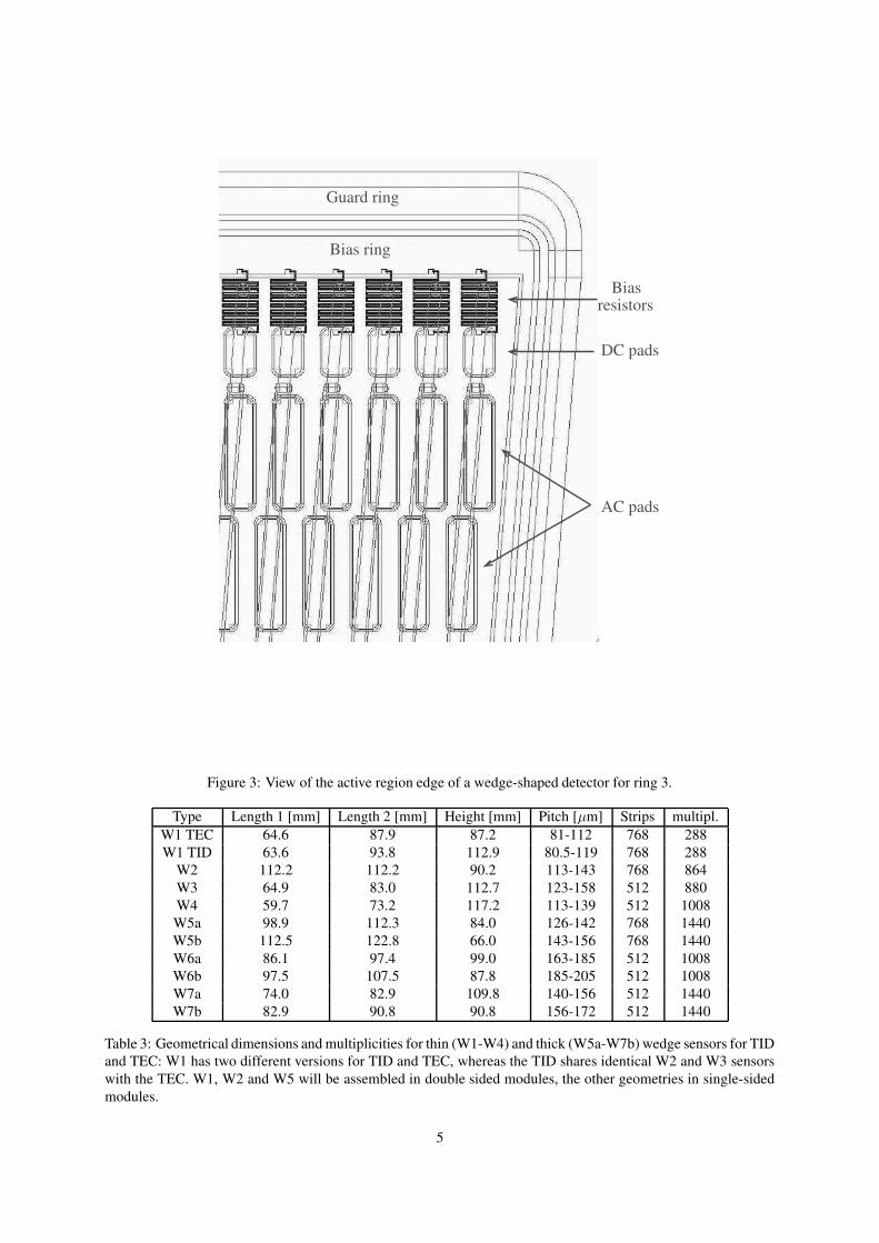
2.1 Sensorsp+ implantations are performed on the front side of the sensor in order to define the strip shaped diodes. Thewidth of the implant strips depends on the strip pitch; a constant width/pitch ratio of 0.25 is used. This value is acompromise between an high width/pitch ratio that reduces the field peak located at the p+ edge and a low valuethat reduces the total strip capacitance. Aluminum read-out strips, capacitatively coupled over the p+-implants,are 15 % wider than the width of the implant underneath. The overhang ranges from 4 to 8 µm, depending on thestrip pitch. As in the case of the bias and guard rings, this design choice moves the high edge electric field fromthe silicon into the much more resistant oxide layer, reducing the risk of electrical breakdown. The thickness ofthe metal layer is required to be greater than 1.2 µm to limit the noise contribution due to the resistance of theelectrode.An array of polysilicon resistors is used to bias the implant strips. These resistors are aligned and connected toeach strip from the bias ring, on the same side of the sensor, where a metallised probe pad (DC pad), contactingthe implant, is foreseen. The choice of poly-silicon as biasing technique is mainly due to its established radiationresistance, and it relies on the capability of producers in defining the resistance value by means of controlled dopingby implantation or diffusion. The resistor value is requested to be 1.5 ± 0.5 MΩ.The strips are AC coupled using integrated coupling capacitors. The manufacturers have implemented multiplethin layers of SiO2 and Si3N4. A thicker oxide fills the interstrip gap.Two rows of AC pads are used at the edges of the strips on each side of the detector to allow for bonding andtesting. An example of a wedge shaped sensor design is shown in Fig. 3.
A series of reference marks is drawn in the n+ implanted region, for assembling and mechanical survey purposes.Every sensor is identified by a binary code created by scratching dedicated pads in the non-active region.
The CMS tracker sensors are foreseen in 15 different geometries: two rectangular detectors for the TIB (seedimensions in Tab.1), two for the TOB (Tab.2), and eleven wedge-shaped detectors for the TID and the TEC(Tab.3).
The strip pitch varies from the inner to the outer layers. The pitch is tuned in order to match the electronic modu-larity of 256 channels. Moreover the range of the chosen strip pitch is also driven by two particle separation andthe achievable two-hit resolution, whereas the range of strip lengths is driven by minimum bias event occupancyand noise levels.The wedge detectors measuring the φ-coordinate are designed, ring by ring, with the strips pointing to the interac-tion point. This results in a constant angular pitch in each ring and in a slightly varying linear pitch along the sensor.
Type Length [mm] Height [mm] Pitch [µm] Strips multipl.IB1 63.3 119.0 80 768 1536IB2 63.3 119.0 120 512 1188
Table 1: Inner Barrel thin sensors, geometrical dimensions and multiplicities: IB1 will be mounted on 768 double-sided modules in the two inner layers of the TIB, IB2 in 1188 single modules in the two outer layers.
Type Length [mm] Height [mm] Pitch [µm] Strips multipl.OB1 96.4 94.4 122 768 3360OB2 96.4 94.4 183 512 7056
Table 2: Outer Barrel thick sensors, geometrical dimensions and multiplicities: OB1 will be mounted on 1680single-sided modules in the layers 5 and 6 of the TOB, OB2 in the inner TOB layers (1-4) in single and doublemodules. All the TOB detectors are composed of two daisy-chained sensors.
Thick sensors will be supplied to the Tracker Collaboration by STM1) and thin sensors by HPK2). They differ in
1) ST Microelectronics, Catania, Italy2) Hamamatsu Photonics K.K., Hamamatsu-City, Japan
4
Guard ring
Bias ring
Bias resistors
DC pads
AC pads
Figure 3: View of the active region edge of a wedge-shaped detector for ring 3.
Type Length 1 [mm] Length 2 [mm] Height [mm] Pitch [µm] Strips multipl.W1 TEC 64.6 87.9 87.2 81-112 768 288W1 TID 63.6 93.8 112.9 80.5-119 768 288
W2 112.2 112.2 90.2 113-143 768 864W3 64.9 83.0 112.7 123-158 512 880W4 59.7 73.2 117.2 113-139 512 1008W5a 98.9 112.3 84.0 126-142 768 1440W5b 112.5 122.8 66.0 143-156 768 1440W6a 86.1 97.4 99.0 163-185 512 1008W6b 97.5 107.5 87.8 185-205 512 1008W7a 74.0 82.9 109.8 140-156 512 1440W7b 82.9 90.8 90.8 156-172 512 1440
Table 3: Geometrical dimensions and multiplicities for thin (W1-W4) and thick (W5a-W7b) wedge sensors for TIDand TEC: W1 has two different versions for TID and TEC, whereas the TID shares identical W2 and W3 sensorswith the TEC. W1, W2 and W5 will be assembled in double sided modules, the other geometries in single-sidedmodules.
5
the distance from the active region to the sensor edge, calculated on the basis of the wafer thickness, and for slightvariations in the dimensions of the bias and guard ring, of the DC and AC pads, of the bias resistors, in the shapeof the reference marks and of the openings in the passivation layer.Details of the process are under the provider responsibility and hence can vary for thin and thick sensors, so longas the fabrication process is kept constant for all the production.
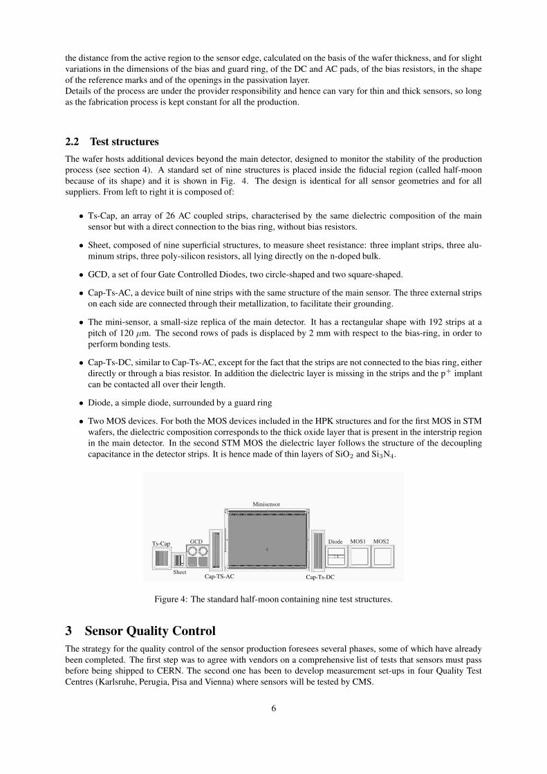
2.2 Test structuresThe wafer hosts additional devices beyond the main detector, designed to monitor the stability of the productionprocess (see section 4). A standard set of nine structures is placed inside the fiducial region (called half-moonbecause of its shape) and it is shown in Fig. 4. The design is identical for all sensor geometries and for allsuppliers. From left to right it is composed of:
• Ts-Cap, an array of 26 AC coupled strips, characterised by the same dielectric composition of the mainsensor but with a direct connection to the bias ring, without bias resistors.
• Sheet, composed of nine superficial structures, to measure sheet resistance: three implant strips, three alu-minum strips, three poly-silicon resistors, all lying directly on the n-doped bulk.
• GCD, a set of four Gate Controlled Diodes, two circle-shaped and two square-shaped.
• Cap-Ts-AC, a device built of nine strips with the same structure of the main sensor. The three external stripson each side are connected through their metallization, to facilitate their grounding.
• The mini-sensor, a small-size replica of the main detector. It has a rectangular shape with 192 strips at apitch of 120 µm. The second rows of pads is displaced by 2 mm with respect to the bias-ring, in order toperform bonding tests.
• Cap-Ts-DC, similar to Cap-Ts-AC, except for the fact that the strips are not connected to the bias ring, eitherdirectly or through a bias resistor. In addition the dielectric layer is missing in the strips and the p+ implantcan be contacted all over their length.
• Diode, a simple diode, surrounded by a guard ring
• Two MOS devices. For both the MOS devices included in the HPK structures and for the first MOS in STMwafers, the dielectric composition corresponds to the thick oxide layer that is present in the interstrip regionin the main detector. In the second STM MOS the dielectric layer follows the structure of the decouplingcapacitance in the detector strips. It is hence made of thin layers of SiO2 and Si3N4.
Sheet
GCD
Minisensor
Diode MOS1 MOS2
Cap-Ts-DC
Ts-Cap
Cap-TS-AC
Figure 4: The standard half-moon containing nine test structures.
3 Sensor Quality ControlThe strategy for the quality control of the sensor production foresees several phases, some of which have alreadybeen completed. The first step was to agree with vendors on a comprehensive list of tests that sensors must passbefore being shipped to CERN. The second one has been to develop measurement set-ups in four Quality TestCentres (Karlsruhe, Perugia, Pisa and Vienna) where sensors will be tested by CMS.
6
The sensor production is divided into two stages. The first is a pre-series and amounts to 5% of the whole produc-tion. During pre-series all sensors delivered will be tested. Once these have been qualified, it is the responsibilityof the vendor to ensure that no changes in the processing or in the substrate material properties, which could com-promise the sensor performances occur during production. The pre-series has been delivered end of 2002 and theresults and experience presented in this paper are based on these pre-series sensors. In the last phase -the fullproduction- we will continue to monitor the quality on a sample basis (5 - 10 %) only.
In order to ensure the quality of the sensors used for the module construction, we have defined a detailed list oftests to be done by QTC. They can be divided in two categories: optical inspection and electrical characterization.Hereafter a description of each test and of relative acceptance criteria is given.
3.1 Optical inspectionThe optical inspection consists in a survey by eye, an inspection under a microscope and a metrology of a fewcharacteristic distances.
In the survey by eye the packaging is checked for damage and the sensor is checked for big scratches, anomalouscoloration or any evident defect. Afterwards, the sensor undergoes a detailed inspection of its edges under amicroscope. This is because the edges are a zone of potential fragility during some operations (like cutting,packaging and manipulation in general) where breaks can occur. If the damage is large (the limit set for the CMSsensor is 40 µm), there can be an injection of charge and a considerable increase of the leakage current or aninstability in the electrical behaviour of the sensor. Finally, the precision of the cut is checked, measuring thedistance between the edge and the active area at eight points near the four corners of the sensor. The precisionrequired in the cut is ±20 µm.
3.2 Electrical characterizationThe equipment required to perform the electrical characterization consists in a computer controlled set-up with aprobe-station, a high voltage supply, an electrometer, a capacitance meter and a switching device.
Two main goals drove the design of the set-up for the electrical characterization. Firstly, to automate and speedup the measurements as much as possible; secondly, to touch sensors with probes as little as possible. In orderto achieve the first goal, two different strategies have been adopted. The probe-stations in Perugia and Pisa areequipped with an automatic loader and pattern recognition software, that permits testing of sensors 24 hours perday without human intervention (up to 25 sensors can be loaded in a single cassette). These probe-stations alsouse probe-cards, that permit to contact and test several strips (up to 29) at once, but need to ramp up and down thebias voltage when moving from one group of strips to another one. Fig. 5 shows the probe-station used in Perugia.The probe-stations in Karlsruhe and Vienna (without automatic loader), use single needles to contact the strips andone needle is attached to the chuck to contact the bias ring; in that way it is not necessary to ramp up and downthe voltage during the measurement of every strip. Both systems make a complete electrical test of a sensor in3-4 hours (depending on the number of strips). The second goal has been reached by using a switching device, towhich all instruments are connected. This permits us to perform all measurements on every strip in sequence, sothat each strip is contacted only once.
All parameters needed to perform the tests and the analysis are stored in an input file, which is centrally maintainedat the Vienna QTC and, in case of agreed changes, re-distributed to all QTCs. The results of a quality control teston a sensor is written into a XML file which is inserted into the CMS Tracker database.
The electrical characterization consists of two global (IV, CV) and four strip-by-strip (Istrip, Rpoly , Idiel, CAC)tests. The electrical characterization is performed in a clean room with controlled temperature and humidity.
- IV: Measurement of the total leakage current of the sensor from 0 to 550 V reverse bias. The current is measuredbetween the back-plane and bias-line, keeping the guard-ring floating, in steps of 5V/s. The leakage current mustfulfill three criteria: 1) maximum value at 300 V less than 5 µA, 2) maximum value at 450 V less than 10 µA, 3)maximum increase in the range 450 V - 550 V less than 10 µA.
- CV: Measurement of the total capacitance of the sensor from 0 to 350 V reverse bias. The capacitance is measuredbetween the back-plane and bias-line, keeping the guard-ring floating, in step of 5V/s, at a frequency of 1 kHz.From this measurement it is possible to extract the depletion voltage of the sensor and to check its thickness.
Strip-by-strip tests are performed at a bias voltage of 400 V, and are aimed at the identification of defective strips.
7
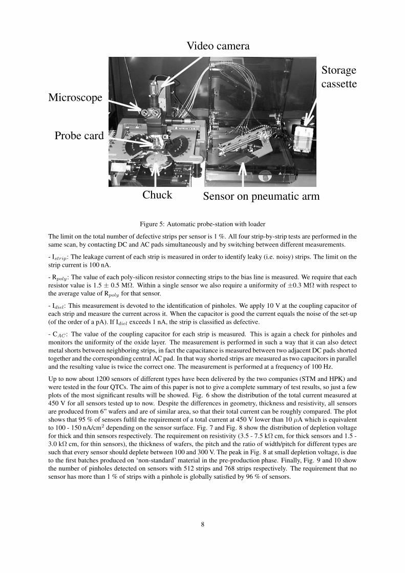
Video camera
Microscope
Probe card
Chuck Sensor on pneumatic arm
Storagecassette
Figure 5: Automatic probe-station with loader
The limit on the total number of defective strips per sensor is 1 %. All four strip-by-strip tests are performed in thesame scan, by contacting DC and AC pads simultaneously and by switching between different measurements.
- Istrip: The leakage current of each strip is measured in order to identify leaky (i.e. noisy) strips. The limit on thestrip current is 100 nA.
- Rpoly : The value of each poly-silicon resistor connecting strips to the bias line is measured. We require that eachresistor value is 1.5 ± 0.5 MΩ. Within a single sensor we also require a uniformity of ±0.3 MΩ with respect tothe average value of Rpoly for that sensor.
- Idiel: This measurement is devoted to the identification of pinholes. We apply 10 V at the coupling capacitor ofeach strip and measure the current across it. When the capacitor is good the current equals the noise of the set-up(of the order of a pA). If Idiel exceeds 1 nA, the strip is classified as defective.
- CAC : The value of the coupling capacitor for each strip is measured. This is again a check for pinholes andmonitors the uniformity of the oxide layer. The measurement is performed in such a way that it can also detectmetal shorts between neighboring strips, in fact the capacitance is measured between two adjacent DC pads shortedtogether and the corresponding central AC pad. In that way shorted strips are measured as two capacitors in paralleland the resulting value is twice the correct one. The measurement is performed at a frequency of 100 Hz.
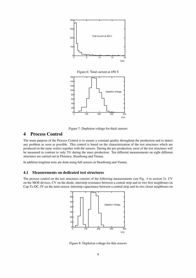
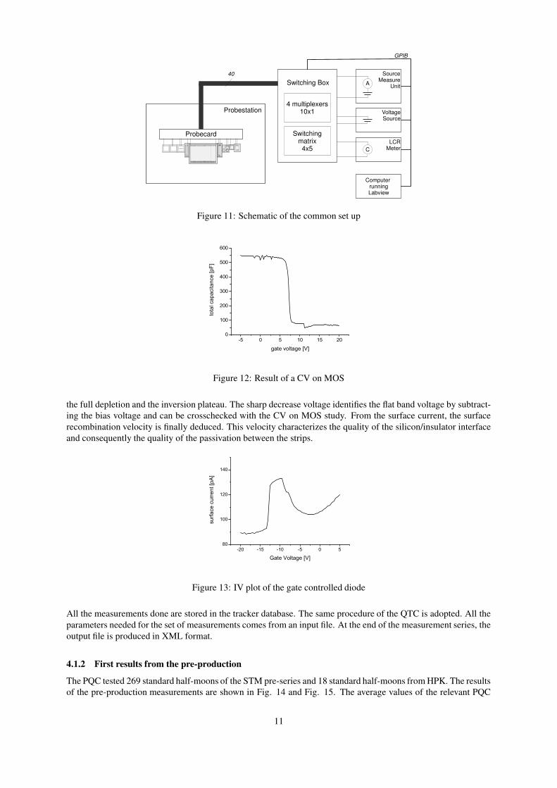
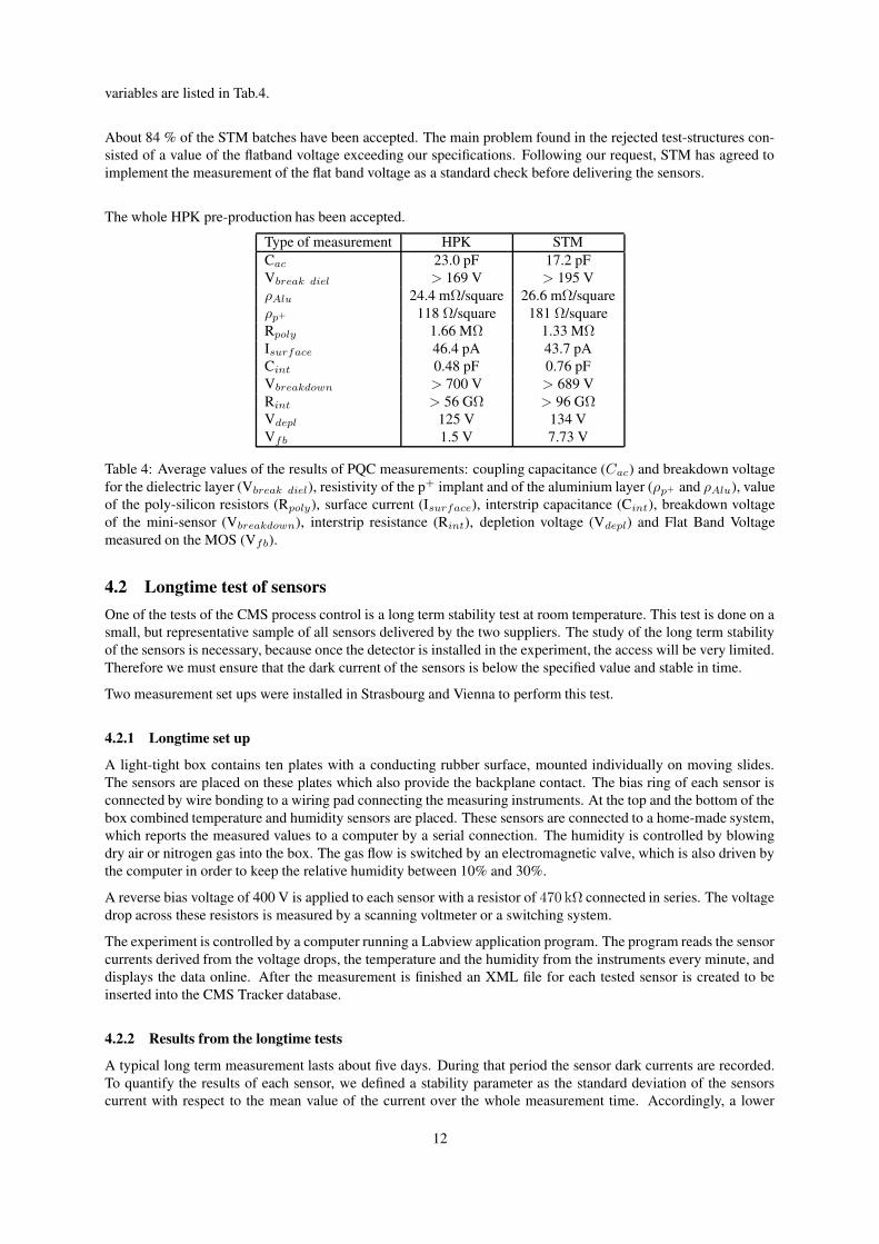
Up to now about 1200 sensors of different types have been delivered by the two companies (STM and HPK) andwere tested in the four QTCs. The aim of this paper is not to give a complete summary of test results, so just a fewplots of the most significant results will be showed. Fig. 6 show the distribution of the total current measured at450 V for all sensors tested up to now. Despite the differences in geometry, thickness and resistivity, all sensorsare produced from 6” wafers and are of similar area, so that their total current can be roughly compared. The plotshows that 95 % of sensors fulfil the requirement of a total current at 450 V lower than 10 µA which is equivalentto 100 - 150 nA/cm2 depending on the sensor surface. Fig. 7 and Fig. 8 show the distribution of depletion voltagefor thick and thin sensors respectively. The requirement on resistivity (3.5 - 7.5 kΩ cm, for thick sensors and 1.5 -3.0 kΩ cm, for thin sensors), the thickness of wafers, the pitch and the ratio of width/pitch for different types aresuch that every sensor should deplete between 100 and 300 V. The peak in Fig. 8 at small depletion voltage, is dueto the first batches produced on ‘non-standard’ material in the pre-production phase. Finally, Fig. 9 and 10 showthe number of pinholes detected on sensors with 512 strips and 768 strips respectively. The requirement that nosensor has more than 1 % of strips with a pinhole is globally satisfied by 96 % of sensors.
8
400
300
200
100
020151050
I(µA)
Total Current at 450 V
Figure 6: Total current at 450 V160
140
120
100
80
60
40
20
04003002001000
V(V)
Depletion Voltage
Figure 7: Depletion voltage for thick sensors
4 Process ControlThe main purpose of the Process Control is to ensure a constant quality throughout the production and to detectany problem as soon as possible. This control is based on the characterization of the test structures which areproduced on the same wafers together with the sensors. During the pre-production, most of the test structures willbe measured in contrast to only 5% during the mass production. Ten different measurements on eight differentstructures are carried out in Florence, Strasbourg and Vienna.
In addition longtime tests are done using full sensors in Strasbourg and Vienna.
4.1 Measurements on dedicated test structuresThe process control on the test structures consists of the following measurements (see Fig. 4 in section 2): CVon the MOS devices, CV on the diode, interstrip resistance between a central strip and its two first neighbours onCap-Ts-DC, IV on the mini-sensor, interstrip capacitance between a central strip and its two closer neighbours on
70
60
50
40
30
20
10
04003002001000
V(V)
Depletion Voltage
Figure 8: Depletion voltage for thin sensors
9

500
400
300
200
100
020151050
# pinholes
Number of Pinholes
Figure 9: Number of pinholes for 512 strips sensors100
80
60
40
20
020151050
# pinholes
Number of Pinholes
Figure 10: Number of pinholes for 768 strips sensors
Cap-Ts-AC, IV on one of the square gate controlled diode, the set of resistances of poly, aluminum and p+ on thesheet structure, six coupling capacitances in Ts-Cap, and finally the breakdown voltage of the decoupling capacitoroxide.
In the following the set up, the common software and finally the measurements together with the results from thepre-series will be described.
4.1.1 The process control set-up
To contact all 49 pads on the test structure a probecard was designed. The probecard output is connected via aswitching matrix to the four measurement devices (LCR-meter, ammeter and two voltage sources). In Fig. 11 isshown a schematic of the electrical layout. To avoid possible bad contacts, the probes have been doubled each timeit seemed useful. As we are using mostly common equipment in the three labs, a common software has also beenadopted based on Labview and made of three components: acquisition, analysis and database interface.
The acquisition part manages the ten measurements. The sequence of the measurements is done automatically butif needed, a single measurement can also be done manually. An emergency stop is implemented and if any currentcompliance is reached, the measurement is stopped.
After some measurements are performed, an analysis is needed to extract relevant parameters; This is the case forCV on MOS, CV on diode and IV on gate controlled diode. The basic tool for the analysis is the linear fit, whichis used to find kinks between different linear regions.
An example of a CV on MOS is shown in Fig. 12. We first check the maximum capacitance. The flat band voltageVfb is then obtained by fitting the position of the sharp drop of the capacitance value.
The IV curve on the gate controlled diode usually shows three regions as shown in Fig. 13. Starting to decreasethe gate voltage from the plateau of electrons accumulated under the gate, an increase of the current from the flatband voltage can be seen, corresponding to a growing depletion. There is then a plateau of maximum current(full depletion under the gate) and finally, at a voltage value (Vbias + Vfb), a sharp decrease down to low valuescorresponding to the inversion regime. The surface current is directly extracted from the height difference between
10
Switching BoxSource
MeasureUnitA
VoltageSource
LCRMeterC
Probestation
ComputerrunningLabview
4 multiplexers10x1
Switchingmatrix4x5
Probecard
GPIB
40
Figure 11: Schematic of the common set up
Figure 12: Result of a CV on MOS
the full depletion and the inversion plateau. The sharp decrease voltage identifies the flat band voltage by subtract-ing the bias voltage and can be crosschecked with the CV on MOS study. From the surface current, the surfacerecombination velocity is finally deduced. This velocity characterizes the quality of the silicon/insulator interfaceand consequently the quality of the passivation between the strips.
Figure 13: IV plot of the gate controlled diode
All the measurements done are stored in the tracker database. The same procedure of the QTC is adopted. All theparameters needed for the set of measurements comes from an input file. At the end of the measurement series, theoutput file is produced in XML format.
4.1.2 First results from the pre-production
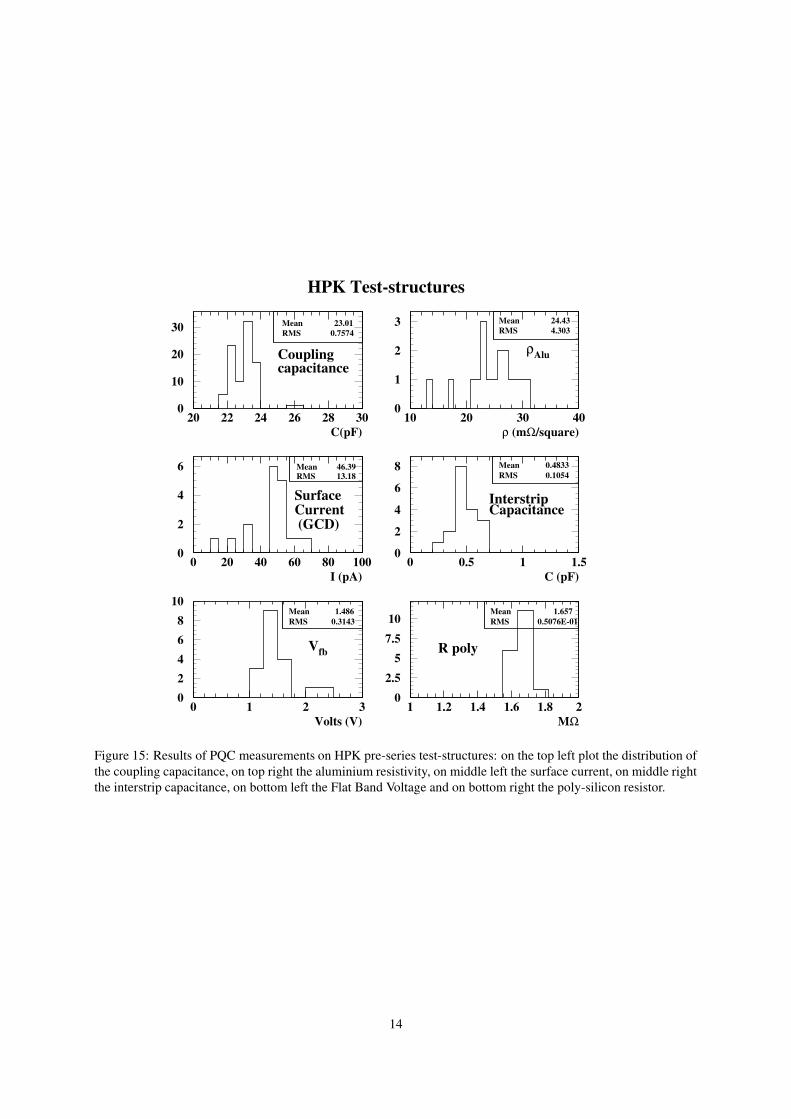
The PQC tested 269 standard half-moons of the STM pre-series and 18 standard half-moons from HPK. The resultsof the pre-production measurements are shown in Fig. 14 and Fig. 15. The average values of the relevant PQC
11
variables are listed in Tab.4.
About 84 % of the STM batches have been accepted. The main problem found in the rejected test-structures con-sisted of a value of the flatband voltage exceeding our specifications. Following our request, STM has agreed toimplement the measurement of the flat band voltage as a standard check before delivering the sensors.
The whole HPK pre-production has been accepted.
Type of measurement HPK STMCac 23.0 pF 17.2 pFVbreak diel > 169 V > 195 VρAlu 24.4 mΩ/square 26.6 mΩ/squareρp+ 118 Ω/square 181 Ω/squareRpoly 1.66 MΩ 1.33 MΩ
Isurface 46.4 pA 43.7 pACint 0.48 pF 0.76 pFVbreakdown > 700 V > 689 VRint > 56 GΩ > 96 GΩ
Vdepl 125 V 134 VVfb 1.5 V 7.73 V
Table 4: Average values of the results of PQC measurements: coupling capacitance (Cac) and breakdown voltagefor the dielectric layer (Vbreak diel), resistivity of the p+ implant and of the aluminium layer (ρp+ and ρAlu), valueof the poly-silicon resistors (Rpoly), surface current (Isurface), interstrip capacitance (Cint), breakdown voltageof the mini-sensor (Vbreakdown), interstrip resistance (Rint), depletion voltage (Vdepl) and Flat Band Voltagemeasured on the MOS (Vfb).
4.2 Longtime test of sensorsOne of the tests of the CMS process control is a long term stability test at room temperature. This test is done on asmall, but representative sample of all sensors delivered by the two suppliers. The study of the long term stabilityof the sensors is necessary, because once the detector is installed in the experiment, the access will be very limited.Therefore we must ensure that the dark current of the sensors is below the specified value and stable in time.
Two measurement set ups were installed in Strasbourg and Vienna to perform this test.
4.2.1 Longtime set up
A light-tight box contains ten plates with a conducting rubber surface, mounted individually on moving slides.The sensors are placed on these plates which also provide the backplane contact. The bias ring of each sensor isconnected by wire bonding to a wiring pad connecting the measuring instruments. At the top and the bottom of thebox combined temperature and humidity sensors are placed. These sensors are connected to a home-made system,which reports the measured values to a computer by a serial connection. The humidity is controlled by blowingdry air or nitrogen gas into the box. The gas flow is switched by an electromagnetic valve, which is also driven bythe computer in order to keep the relative humidity between 10% and 30%.
A reverse bias voltage of 400 V is applied to each sensor with a resistor of 470 kΩ connected in series. The voltagedrop across these resistors is measured by a scanning voltmeter or a switching system.
The experiment is controlled by a computer running a Labview application program. The program reads the sensorcurrents derived from the voltage drops, the temperature and the humidity from the instruments every minute, anddisplays the data online. After the measurement is finished an XML file for each tested sensor is created to beinserted into the CMS Tracker database.
4.2.2 Results from the longtime tests
A typical long term measurement lasts about five days. During that period the sensor dark currents are recorded.To quantify the results of each sensor, we defined a stability parameter as the standard deviation of the sensorscurrent with respect to the mean value of the current over the whole measurement time. Accordingly, a lower
12

STM Test-structures
MeanRMS
17.18 0.7115Coupling
Capacitance
C(pF)
MeanRMS
26.62 4.961
ρAlu
ρ (mΩ/square)
MeanRMS
43.74 12.11
SurfaceCurrent (GCD)
I (pA)
MeanRMS
0.764 3
0.1189
InterstripCapacitance
C (pF)
MeanRMS
7.732 5.614
Volts (V)
Vfb
MeanRMS
1.326 0.1034
R poly
MΩ
0
200
400
12 14 16 18 20 220
10
20
30
10 20 30 40
0
20
40
60
0 20 40 60 80 1000
20
40
60
80
0.25 0.5 0.75 1 1.25
0
25
50
75
100
0 10 20 30 400
25
50
75
100
1 1.2 1.4 1.6 1.8 2
Figure 14: Results of PQC measurements on STM pre-series test-structures: on the top left plot the distribution ofthe coupling capacitance, on top right the aluminium resistivity, on middle left the surface current, on middle rightthe interstrip capacitance, on bottom left the Flat Band Voltage and on bottom right the poly-silicon resistor.
13
HPK Test-structures
MeanRMS
23.01 0.7574
C(pF)
Couplingcapacitance
MeanRMS
24.43 4.303
ρAlu
ρ (mΩ/square)
MeanRMS
46.39 13.18
SurfaceCurrent (GCD)
I (pA)
MeanRMS
0.4833 0.1054
InterstripCapacitance
C (pF)
MeanRMS
1.486 0.3143
Volts (V)
Vfb
MeanRMS
1.657 0.5076E-01
R poly
MΩ
0
10
20
30
20 22 24 26 28 300
1
2
3
10 20 30 40
0
2
4
6
0 20 40 60 80 1000
2
4
6
8
0 0.5 1 1.5
02468
10
0 1 2 30
2.55
7.510
1 1.2 1.4 1.6 1.8 2
Figure 15: Results of PQC measurements on HPK pre-series test-structures: on the top left plot the distribution ofthe coupling capacitance, on top right the aluminium resistivity, on middle left the surface current, on middle rightthe interstrip capacitance, on bottom left the Flat Band Voltage and on bottom right the poly-silicon resistor.
14
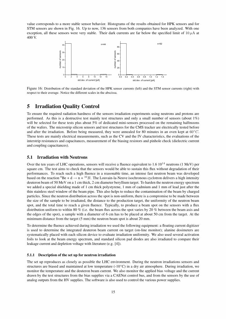
value corresponds to a more stable sensor behavior. Histograms of the results obtained for HPK sensors and forSTM sensors are shown in Fig. 16. Up to now, 136 sensors from both companies have been analyzed. With oneexception, all these sensors were very stable. Their dark currents are far below the specified limit of 10 µA at400 V.
µ µ
Figure 16: Distribution of the standard deviation of the HPK sensor currents (left) and the STM sensor currents (right) withrespect to their average. Notice the different scales in the abscissa.
5 Irradiation Quality ControlTo ensure the required radiation hardness of the sensors irradiation experiments using neutrons and protons areperformed. As this is a destructive test mainly test structures and only a small number of sensors (about 1%)will be selected for these tests plus about 5% of dedicated mini-sensors processed on the remaining halfmoonsof the wafers. The microstrip silicon sensors and test structures for the CMS tracker are electrically tested beforeand after the irradiation. Before being measured, they were annealed for 80 minutes in an oven kept at 60C.These tests are mainly electrical measurements, such as the CV and the IV characteristics, the evaluations of theinterstrip resistances and capacitances, measurement of the biasing resistors and pinhole check (dielectric currentand coupling capacitances).
5.1 Irradiation with NeutronsOver the ten years of LHC operations, sensors will receive a fluence equivalent to 1.6 1014 neutrons (1 MeV) persquare cm. The test aims to check that the sensors would be able to sustain this flux without degradation of theirperformances. To reach such a high fluence in a reasonable time, an intense fast neutron beam was developedbased on the reaction 9Be + d → n + 10B. The Louvain-la-Neuve isochronous cyclotron delivers a high intensitydeuteron beam of 50 MeV on a 1 cm thick, 2 cm diameter beryllium target. To harden the neutron energy spectrumwe added a special shielding made of 1 cm thick polystyrene, 1 mm of cadmium and 1 mm of lead just after thethin stainless steel window of the beam pipe. This also helps to reduce the contamination of the beam by chargedparticles. Since the neutron distribution across the spot is non-uniform, there is a compromise to be made betweenthe size of the sample to be irradiated, the distance to the production target, the uniformity of the neutron beamspot, and the total time to reach a given fluence. Typically, to produce a beam spot on the sensors with a fluxdistribution uniform to within 80 % (i.e. the beam flux across the spot varies by 20 % between the beam axis andthe edges of the spot), a sample with a diameter of 6 cm has to be placed at about 50 cm from the target. At theminimum distance from the target (5 mm) the neutron beam spot is about 20 mm.
To determine the fluence achieved during irradiation we used the following equipment: a floating current digitizeris used to determine the integrated deuteron beam current on target (on-line monitor); alanine dosimeters aresystematically placed with each silicon device to evaluate irradiation uniformity. We also used several activationfoils to look at the beam energy spectrum, and standard silicon pad diodes are also irradiated to compare theirleakage current and depletion voltage with literature (e.g. [4]).
5.1.1 Description of the set up for neutron irradiation
The set up reproduces as closely as possible the LHC environment. During the neutron irradiations sensors andstructures are biased and maintained at low temperature (-10C) in a dry air atmosphere. During irradiation, wemonitor the temperature and the deuteron beam current. We also monitor the applied bias voltage and the currentdrawn by the test structures from the bias supplies via a CAENet control bus, and from the sensors by the use ofanalog outputs from the HV supplies. The software is also used to control the various power supplies.
15

The sensors or test structures are supported by specially prepared polycarbonate frames (Lexan) 3 mm thick. Theframes have an opening of 12 cm: this is large enough to ensure a uniform fluence of the elements to be tested(diodes and mini-sensors on the standard test structure). The electrical contacts to the bias line are done usingwire bonds. Several such frames can be stacked for the irradiation of as many as ten halfmoons (or five full sizesensors). According to this scheme, the fluence variation across the different plates is below 10 % with respect tothe fluence of the central layer (set to be the nominal LHC fluence).
The set up for measuring the structures before and after the irradiation uses a semi-automatic probe station. Its air-tight enclosure is fed with dry air: the relative humidity inside the enclosure is about 1-2 % corresponding to a dewpoint of about -40C. The chuck can be regulated with Peltier elements to -10C corresponding to the operatingconditions of the CMS tracker. To connect the structures with the instruments, a set of five needles is arrangedaround the chuck. Two voltage sources, a switching device, a LCR and an electrometer are used to perform thetests. A LabView program, running on a separate PC, controls everything from the probe station to the temperatureof the chuck. The test parameters are easily modified by the use of global variables. After irradiation, results arecompiled in a XML file to be put into the Tracker database.
5.1.2 Results of first neutron irradiations
The results presented here were obtained with sensors and test structures irradiated up to 2.1 ·1014 neq
cm2 . Apart fromannealing and test periods, the devices were kept at low temperature in a refrigerator.
After irradiation, the thin sensors (HPK) as well as the thick sensors (STM) showed no significant changes in thestrip parameters, although it is sometimes observed that the coupling capacitances show a slight decrease of about1 %.
The total leakage current between the backplane and the bias ring, has been measured as a function of the reversebias voltage from 0 to 800 V. As expected, we notice that the leakage current is much higher after irradiation andreaches saturation at around 600 V. The devices show a leakage current below the acceptance criteria of α ≤ 4.510−17 A/cm, if tested after 80 minutes of annealing at 60C.
To extract the depletion voltage, we measured the backplane capacitance as a function of the reverse bias voltagefrom 0 to 800 V. We have compared the results before and after neutron irradiation. As the capacitance at thedepletion voltage decreases after irradiation, the depletion voltage itself increases. The obtained depletion voltagesare all below the permitted maximum value of 300 V after beneficial annealing.
5.2 Irradiation with ProtonsIrradiations with protons take place at the isochrone cyclotron of the Forschungszentrum Karlsruhe. It provides26 MeV protons at beam currents of up to 2 µA. This allows to irradiate a 100 cm2 sensor up to 1 ·1014 p
cm2 within20 min using a scanning device. To ensure the desired fluence (0.35 and 1.6 · 1014 neq
cm2 for outer and inner barrelrespectively [3]) an online current control and calibrated nickel foil dosimetry for integral measurement is used.
5.2.1 Description of the set up for proton irradiation
The sensors and test structures are arranged in a cold box where a maximum number of three frames can be fitted.One frame can contain up to four test structures or one sensor. Each structure is clamped between a metal foil onthe back and a conductive rubber strip on the front (Fig. 17), which sets the AC pads and the bias ring to groundas in the experiment, where the read-out chip grounds the AC pads.
5.2.2 Results of first proton irradiations
One outer barrel sensor from STM, one wedge shaped sensor from HPK and several additional test structures weretested in a first irradiation.
Both sensors were biased with 1 V and several voltages were used for the test structures (0 V, 1 V, 12 V, 100 V). Thevalue of 1 V is the estimated potential drop over the oxide after ten years of LHC operation. Since the developmentof oxide charges depends on the electric field, the structures are biased with at minimum 1 V. During irradiationthey are kept below -10C to avoid annealing and thermal runaway due to the higher leakage current.The irradiation was performed up to 2.6 · 1014 neq
cm2 and 0.9 · 1014 neq
cm2 for the HPK and STM stack respectively
16

Figure 17: Sensors and test structures mounted in frames. Electrical contact was made by conductive rubber onthe front.
(derived from leakage current measurements).After irradiation the structures are stored at -18C to stop all annealing processes.
Strip values (such as coupling capacitance, bias resistance and interstrip capacitance) showed no changes afterirradiation. The leakage current of the strips increased according to the expected rise of the total leakage current.For the measured values one can extrapolate the maximum leakage current for 500 µm sensors to be 280 µA for alarge outer barrel sensor (Fig. 18).
µ Ω
µ
α
Figure 18: Specific leakage currents and extrapolated value for 500 µm sensors with maximal fluence for thismaterial.
The resulting full depletion voltages match the calculated voltages from the ‘Hamburg model’ using close to meanvalues from reference [4]. From these values a full depletion voltage for 500 µm sensors after ten years of LHCoperation (0.5 · 1014 neq
cm2 ) is estimated to about 280 V (Fig. 19).
Since there are identical minisensors on every test structure, independent of the sensor geometry, it is possible tomeasure all parameters of interest on several strips on the mini-sensors, thus achieving a good statistical signifi-cance for the measurements.
6 SummaryWe have presented the design of the silicon sensors for the CMS tracker. The design follows several years ofresearch and development together with silicon sensor manufacturers. The performances of the prototypes haveproven that the design is safe and robust. Nevertheless CMS has developed an elaborate quality assurance proce-dure to assure the quality of all sensors delivered during the production period. The seven institutes involved inthese tests have developed fully automatic set-ups to cope with the large number of sensors.
The CMS test centres for the Quality, the Process and the Irradiation Controls have tested more than a thousandsensors and test structures during the pre-series production. About 10% of the sensors received in 2002 were
17

Figure 19: Full depletion voltages fitted with Hamburg model and calculation for 10 years LHC with 28 days atroom temperature each year.
measured with values outside the technical specifications. These non-compliances were discussed with the supplierand were subsequently solved.
The full series-production of more than 24000 sensors has started and the first sensors arrived towards the end of2002.
7 AcknowledgmentWe would like to thank D.Gagliardi (Pisa) for the technical support and C. Hoffmann (Strasbourg), C. Menge(Karlsruhe), M. Oberegger (Vienna) and T. Punz (Karlsruhe) for their help obtaining the measurement results.
References[1] S. Braibant et al., Investigation of design parameters for radiation hard silicon microstrip detectors, Nucl.
Instrum. Methods A, 485 (2002) 343-361
[2] The CMS All-Silicon Tracker - Strategies to ensure a high quality and radiation hard Silicon Detector, FrankHartmann on behalf of the CMS Silicon Tracker Collaboration, Nucl. Instrum. Methods A 478 (2002)
[3] CMS Tracker TDR, CERN/LHCC 98-6 CMS TDR 5 (1998)
[4] M. Moll, Ph.D. Thesis, DESY-THESIS-1999-040 (1999)
18