Thin nanodiamond membranes and their microstructural, optical and photoelectrical properties

Journal of Alloys and Compounds 416 (2006) 2–10
The growth-induced microstructural origin ofthe optical black state of Mg2NiHx thin films
R.J. Westerwaal a,∗, A. Borgschulte a, W. Lohstroh a, B. Dam a,B. Kooi b, G. ten Brink b, M.J.P. Hopstaken c, P.H.L. Notten c
a Faculty of Sciences, Department of Physics and Astronomy, Condensed Matter Physics, Vrije Universiteit,De Boelelaan 1081, 1081 HV Amsterdam, The Netherlands
b University of Groningen, Department of Applied Physics, Nijenborgh 4, 9747 AG Groningen, The Netherlandsc Philips Research Laboratories, Prof. Holstlaan 4, 5656 AA Eindhoven, The Netherlands
Received 10 May 2005; received in revised form 22 July 2005; accepted 25 July 2005Available online 30 September 2005
Abstract
Hydrogen absorption by a thin Mg2Ni film capped with Pd results in the nucleation of the Mg2NiH4 phase at the film/substrate interface. OnfTusfictt©
K
1
dmaietofit[tt
0d
urther hydrogenation, a self-organized two-layer system consisting of a Mg2NiH0.3/Mg2NiH4 bottom-layer and a Mg2NiH0.3 top-layer is formed.his leads to an intermediate optical black state in Mg2Ni thin films, which transforms from metallic/reflective to semiconducting/transparentpon hydrogenation. This hydrogen absorption behavior is completely unexpected, since the hydrogen enters the film through the Pd-capped filmurface. To explain the preferential nucleation of Mg2NiH4 at the substrate/film interface, we determine the chemical homogeneity of these thinlms by RBS and SIMS. Furthermore by STM, TEM and SEM, we analyze the microstructure. We find that up to a film thickness of 50 nm, the filmonsists of small grains and clusters of small grains. On further growth, a columnar structure develops. We propose that the nucleation barrier forhe formation of the Mg2NiH4 phase is smaller for the small loosely packed grains at the interface, while the columnar grain boundaries promotehe hydrogen diffusion to the substrate.
2005 Elsevier B.V. All rights reserved.
eywords: Hydrogen storage materials; Thin films; Vapor deposition; Scanning and transmission electron microscopy; Light absorption and reflection
. Introduction
Mg2NiH4 is an interesting example of a complex metal hy-ride with potential both as a storage material and as a switchableirror. Though its thermodynamical properties are less favor-
ble than that of NaAlH4, its hydrogenation properties may holdmportant clues for the optimization of the hydrogenation prop-rties of complex metal hydrides in general. Upon hydrogena-ion, Mg2Ni transforms into Mg2NiH4 which contains 3.6 wt.%f hydrogen. Richardson et al. have shown that Mg2NiHx thinlms show reversible optical switching at room temperature be-
ween a shiny metallic and a transparent semiconducting state1,2]. Later, we discovered a third optical state. In films thickerhan 50 nm, we observe a highly absorbing optical state at in-ermediate hydrogen concentration. This so-called ‘black state’
∗ Corresponding author.E-mail address: [email protected] (R.J. Westerwaal).
is characterized by low reflection <25% over the whole visi-ble spectrum when measured from the substrate side, while thetransmission, <0.01%, is negligible. As a result, the film has ananomalously high absorption of 75%. The fact that Mg2NiHx
can be switched between a reflective metal, an absorbing blackand a transparent semiconducting state makes Mg2NiHx poten-tially attractive for smart coating applications [3]. The black stateoriginates from a self-organized double layering of the Mg2Nifilm during hydrogen absorption [4,5]. After a solid solutionMg2NiH0.3 is formed, further hydrogenation leads to a preferrednucleation of Mg2NiH4 near the substrate/film interface. Theformation of the double layer is evident from the fact that thefilm surface retains its metallic appearance, while it looks blackwhen seen from the substrate side. Indeed, 15N hydrogen depthprofiling measurements [5] reveal an enhanced hydrogen con-centration at the substrate–film interface in the black state. Op-tical modelling indicates that the black state is due to a highlyabsorbing initial 30 nm layer (of mixed Mg2NiH0.3/Mg2NiH4particles) which produces an interference effect with the reflec-
925-8388/$ – see front matter © 2005 Elsevier B.V. All rights reserved.oi:10.1016/j.jallcom.2005.07.068

R.J. Westerwaal et al. / Journal of Alloys and Compounds 416 (2006) 2–10 3
tive Mg2NiH0.3 top-layer. On further hydrogenation, the filmtransforms into transparent Mg2NiH4 [5]. The black state per-sists on all substrates used so far (Si, SiO2, CaF2, sapphire, quartzand ITO covered glass) and does not depend on composition forMg/Ni ratios between 1.5 and 6 [6].
The black state remains visible also after many switching cy-cles. In order to judge the applicability of this effect for smartwindow applications, it is important to understand the originof the self-organized double layering. Secondly, for the use ofMg2NiH4 as a storage material, any effect that appears to cat-alytically enhance the formation of this phase is of interest.
As shown by electrochemical loading, the thermodynamicbehavior of the thin films is similar to that in bulk. In the pressurecomposition isotherms, similar plateau pressures were reported[5]. Kinetically, thin films behave differently from bulk samples.Hydrogen absorption of Pd-capped thin Mg2Ni films alreadytakes place at room temperature (RT) and a hydrogen gas pres-sure below 1 mbar. In bulk, such samples usually require elevatedtemperatures (598 K) and high hydrogen pressures (2 × 10⁶ Pa)to form a hydride [7]. The (kinetically/thermodynamically) pre-ferred formation of Mg2NiH4 at the film–substrate interfacepoints to a locally reduced nucleation barrier. This can havemany causes. A local change in strain, grain morphology or com-position might affect the nucleation barrier. Even the presence ofthe substrate itself may affect the nucleation process as it couldprovide the nucleating hydride phase with a lower interface freeepfi
otiMofitoe
2
2
sf(msPditaRc
spectroscopy (SIMS) depth profiling. The ToF–SIMS depthprofiling is performed with a dual beam in interlaced mode (al-ternating sputtering and analysis) on an IONTOF IV instrumentusing time-of-flight detection of secondary ions. The instrumentis equipped with a high-current sputter gun and a 3-Lens Ga gun.For scanning tunnelling microscopy (STM) measurements, theMg2Ni samples are transported in situ from the UHV chamberto the STM chamber consisting of an Omicron UHV scanningprobe microscope. For topographical images of the surface, theconstant current mode is used. Atomic force microscopy (AFM)measurements were performed ex situ with a Digital InstrumentsNanoscope III AFM. Secondary electron microscopy (SEM)was performed using a Philips FEG XL series xl30s apparatusworking in TLD mode at a background pressure of 10−4 Pa. Thecross-section TEM images are made with a JEOL 4000 EX/IIworking at 400 kV, which has a point-resolution of 0.17 nm. Thecross-section samples are made by cutting, polishing and ionmilling with 4 kV Ar-ions with an Gatan PIPS. The plane-viewimages are made with a JEOL 2010F working at 200 kV (point-resolution 0.23 nm and an information limit of 0.11 nm). ThisTEM also contains a Gatan imaging filter (GIF) model 2000.
3. Experimental results
3.1. Structural properties
aMcUt[abtrlfgoadpp
3
fsd=ac
a
nergy. It is noteworthy to point out that the dehydrogenationrocess is not anomalous: the metallic phase nucleates at thelms surface on dehydrogenation.
To gain a better understanding of the preferred nucleationf the Mg2NiH4 phase, we investigated the chemical composi-ion and homogeneity of as-grown films. In addition, we stud-ed the initial growth and development of the microstructure in
g2NiHx. While the Mg/Ni ratio is found to be uniform through-ut the layer thickness, we find that the grain size of the as-grownlms at the interface is extremely small as compared to that of
he ensuing columnar growth. We argue that this microstructuref the as-deposited film is responsible for the self-organized lay-ring upon hydrogen absorption.
. Experiment
.1. Experimental setup
Mg2Ni thin films are prepared in a ultra high vacuum (UHV)ystem with a base pressure of <10−8 Pa by coevaporationrom a Knudsen cell (Mg, purity 99.98%) and an electron gunNi, purity 99.98%). The deposition rate during evaporation isonitored using two separate quartz-crystal monitors. For ex
itu experiments, the samples are protected from oxidation by ad caplayer (purity 99.98%). This layer also promotes hydrogenissociation and absorption. During deposition, the resistances continuously measured to find the electrical percolationhickness of the nucleating phases. The chemical compositionnd the thickness of the as-deposited films is measured byutherford backscattering spectrometry (RBS). The chemicalomposition depth profile is investigated by secondary ion mass
Mg2Ni has a hexagonal crystal structure with a = 0.5216 nmnd c = 1.320 nm. Upon hydrogen absorption, a solid solutiong2NiH0.3 is formed and a lattice expansion mainly along the
-axis with a = 0.523 nm and c = 1.343 nm is observed [8].pon further hydrogenation, the atoms in Mg2NiH0.3 rearrange
o form the complex hydride structure Mg2NiH4, where theNiH4]4− complex is essentially ionically bound to the Mg2+toms [9]. This reversible phase transformation is accompaniedy a 32 vol.% expansion. X-ray diffraction, in a θ–2θ configura-ion, of the as-prepared thin Mg2Ni films show only two X-rayeflections, (0 0 3) and (0 0 6), corresponding to the hexagonalattice of Mg2Ni with c = 1.323 nm. As no other reflections areound, this is an indication that the Mg2Ni film has a texturedrowth with the c-axis of the hexagonal lattice in the directionf the layer normal. The coherence length in growth directionmounts to 20–30 nm. Upon hydrogenation, no new reflectionsevelop while the (0 0 3) and (0 0 6) reflections of the Mg2Nihase disappear. This indicates that the semiconducting trans-arent Mg2NiH4 phase is X-ray amorphous [5].
.2. RBS and SIMS measurements
The homogeneity of the chemical composition is determinedrom RBS and SIMS. For RBS measurements, we use carbonubstrates. We find a Mg:Ni ratio close to 2 and no perceptibleepth gradients. The relative amount of oxygen is less than O/Mg0.006, and is mainly concentrated at the film/substrate interface
nd at the film surface. No contamination with other elementsould be detected.
Using SIMS, we investigated the composition depth profilend the influence of hydriding in more detail. We compare films

4 R.J. Westerwaal et al. / Journal of Alloys and Compounds 416 (2006) 2–10
in different hydrogen loading states. To obtain depth informa-tion, the film is bombarded with 2 keV O2
+ ions in the positivemode or 1 keV Cs+ ions in the negative mode, to remove thesurface layer step by step. Between each sputter step, the chem-ical composition is probed by using a 15 keV Ga+ ion beam.Therefore, the x-axis (representing sputter and analyzing time)in Figs. 1–3 corresponds to the depth in the sample, starting from0 s at the Pd caplayer.
Results for the as-prepared Mg2Ni film are shown in Figs. 1aand 2a for the positive and negative mode, respectively. The Mg,Ni and MgNi profiles are constant over the whole layer thick-ness with some decay towards the sapphire (Al2O3 (1 1 0 2))substrate. The latter is possibly caused by ion-beam-inducedroughening of the metallic layers. The increased Ni-intensity atthe Mg2Ni/Al2O3 interface is attributed to matrix effects dueto the presence of oxygen. The low intensity of the Mg andNi profiles at the surface indicates that the 5 nm Pd caplayer isclosed. The tail in the Pd profile is most likely an artefact dueto roughening, induced by sputter bombardment. RBS measure-ments do not show diffusion of the Pd caplayer into the Mg2Nifilm. Figs. 1b and 2b show the profiles for the sample that hasbeen loaded to Mg2NiH4 and subsequently unloaded back to theblack state. It is obvious that the Mg, Ni and MgNi profiles haveremained constant throughout the sample. No indication is foundfor a hydrogenation-induced segregation within the metallicphase.
F2Mdtm
Fig. 2. (a) ToF–SIMS depth profile Pd/Mg2Ni/Al2O3 (negative mode) of an200 nm Mg2Ni thin film covered by 5 nm Pd in the as-prepared state. Pd, Ni,Mg and Mg2Ni intensities are shown together with Al and AlO. (b) ToF–SIMSdepth profile Pd/Mg2Ni/Al2O3 (negative mode) hydrogenated to Mg2NiH4 andthen unloaded back to the black state.
The contamination level (C,O) is generally low (in agreementwith RBS measurements) and depends on the storage conditions.Sample 1, Fig. 3, which was exposed to ambient air severaltimes, shows enhanced impurity levels at the surface. At thefilm/substrate interface, always some oxygen contamination isobserved. Since we have impurities at both the surface and thesubstrate interface, we do not consider them to be related tothe preferential nucleation of the hydride near the substrate/filminterface.
We conclude that the Mg/Ni ratio is roughly constant through-out the Mg2Ni film for the as-prepared film as well as for the films
ig. 1. (a) ToF–SIMS depth profile Pd/Mg2Ni/Al2O3 (positive mode) of an00 nm Mg2Ni thin film covered by 5 nm Pd in the as-prepared state. Pd, Ni,g and Mg2Ni intensities are shown together with Al and AlO. (b) ToF–SIMS
epth profile Pd/Mg2Ni/Al2O3 (positive mode) of the same film hydrogenatedo Mg2NiH4 and then unloaded back to the black state. The MgNi signal isultiplied by 10 and 3 in (a and b), respectively.
Fig. 3. Overlay of selected contaminations C and MgO for a film often exposedto
2
o air (sample 1). Samples 2 and 3 were kept under argon and have been cycledne time.

R.J. Westerwaal et al. / Journal of Alloys and Compounds 416 (2006) 2–10 5
that have absorbed and desorbed hydrogen. However, as depthprofiling by ion sputtering always causes a certain intermixing,SIMS cannot exclude the presence of a chemical gradient withinthe first 30 nm.
3.3. Resistance percolation measurements
The nature of the first stages of growth may be the causefor local deviations in stoichiometry. The sticking of imping-ing adatoms to the substrate may be different from the stick-ing to a growing Mg2Ni film. Thus, as long as we do not havea closed layer, sticking differences could result in composi-tional deviations near the substrate. To investigate the natureof the initial growth stages of Mg, Ni and Mg2Ni, we measurein situ the electrical resistance during growth. Before evapo-ration, two electrical contacts are made to the non-conductingsapphire substrate. After a certain deposition time, the thin filmbecomes electrically connected, resulting in a drastic decreaseof the electrical resistance. Extrapolating the resistivity to zerodefines the so-called percolation thickness (see Fig. 4d–f), re-spectively.
The growth of a Ni thin film results in an electrical percolationthickness of 0.54 nm (Fig. 4d). This small value (approximately3–5 monolayers) is related to the high density of small nuclei asindicated in Fig. 4a. For Mg, however, we observe a low density
Ni (s for
and Mg (2073, 1033 and 923 K), respectively. We conclude thata sticking-induced chemical deviation from the average stoi-chiometry is only likely during the first 2.5 nm of Mg2Ni growth.Since the preferred hydride phase formation responsible for theblack state takes place in a 30 nm thick layer adjacent to the sub-strate, it is not plausible that this is due to a chemical gradientin the first 2.5 nm.
3.4. STM investigation of the growth of Mg2Ni
To investigate how the microstructure of a thin Mg2Ni filmevolves, we studied the surface morphology of as-depositedfilms in various stages of growth by UHV-STM. Since the opti-cal black state is observed for a variety of substrates, we assumethat the results obtained on silicon substrates are representa-tive for the microstructural development of thin Mg2Ni films ingeneral. STM micrographs of Mg2Ni films with a thickness of20, 50 and 150 nm, respectively, are shown in Fig. 5. On 20 nmfilms (Fig. 5a and d), islands with a grain size of ∼30 nm areobserved. These grains are dispersed over the substrate surfaceand on top of the islands, the onset of a vague substructure ofsmaller grains can be seen. When the film thickness is increasedto 50 nm (see Fig. 5b and e), the diameter of the grains has in-creased to around 50 nm. Moreover, it is clear now that the grainsconsist of a cluster of smaller grains. These subgrains have a sizeof approximately 10 nm. Increasing the film thickness leads toel(rets
�z =5 nm), Mg (�z =30 nm) and Mg2Ni (�z =10 nm), respectively. In (d–f),Ni = 0.54 nm, Mg = 20 nm and Mg2Ni = 2.5 nm.
xtensive grain growth. The initial growth clusters develop intoarge grains with a diameter of over 100 nm on 150 nm Mg2Nisee Fig. 5c and f). The hexagonal shape of these large grainseflects the hexagonal unit cell of Mg2Ni and indicates a prefer-ntial orientation of the c-axis normal to the substrate. Betweenhe large grains, often smaller grains are observed with a typicalize between 10 and 30 nm.
of large nuclei. We find an electrical percolation thickness of20 nm (Fig. 4e), confirming a pronounced island growth (Fig.4b). Remarkably, when Mg and Ni are co-deposited in 2:1 ratio,a much smaller percolation thickness of 2.5 nm is obtained (Fig.4f). The percolation thickness is thus strongly reduced with re-spect to the percolation thickness of Mg only, this is also evidentfrom Fig. 4c. It appears that the nucleation and growth behav-ior scales roughly with the melting temperature of Ni, Mg2Ni
Fig. 4. The AFM images (a–c) show the surface morphology for a 5 nm layer oflogarithmic resistance is plotted vs. thickness, resulting in a percolation thicknes

6 R.J. Westerwaal et al. / Journal of Alloys and Compounds 416 (2006) 2–10
Fig. 5. STM micrographs of in situ grown thin Mg2Ni films with thicknesses: (a) 20 nm (�z = 1.92 nm), (b) 50 nm (�z = 4.44 nm) and (c) 150 nm (�z =10 nm).Panels (a–c) depict a scan range of 500 nm, while panels (d–f) show a 200 nm × 200 nm area of the same samples. The maximum height difference from low (darkcolor) to high (white) is given by �z. For a thickness of 20 nm (a and d), the islands are well dispersed over the substrate and at d = 50 nm (b and e), clusters ofsmall grains are observed. At d = 150 nm (c and f), the grains are coalesced into crystallites.
3.5. AFM surface structure investigation of Mg2Ni
To investigate the surface morphology of these thin films ona larger scale, we performed AFM measurements. AFM micro-graphs of Mg2Ni films with a thickness of 5 and 200 nm areshown in Fig. 6a–c and d–f, respectively. Since these measure-ments are performed ex situ, these thin films are capped with a5 nm Pd caplayer to prevent oxidation effects. The 5 nm thickMg2Ni film (Fig. 6a–c) consists of equally dispersed small grainsof 30 nm in diameter. A 200 nm thick Mg2Ni film (Fig. 6d–f)shows extensive grain growth up to 100 nm, i.e. the same char-acteristic grain growth is observed as in the STM measurementsshown in Fig. 5. Furthermore, the 5 nm Pd caplayer which ispresent on top of these films as 5 nm small grains cannot be dis-tinguished due to the limited resolution of the AFM apparatus.This is also the reason why the 10–30 nm small grains surround-ing the columns cannot be observed. The structural evolution ofthe initial grown grains to large structures is an important indi-cation for a columnar growth mode.
3.6. TEM measurements on Mg2Ni
The microstructural development observed by STM is fur-ther investigated by TEM. Fig. 7 shows a TEM cross-sectionof a 330 nm Mg2Ni thin film covered by 10 nm Pd. The imageclearly shows vertical columnar structures. Note that a differ-eod
contrast, a slight increase in brightness occurs from bottom totop of the Mg2Ni film due to a locally decreasing thickness ofthe TEM sample. These columns extend from the substrate tothe top of the film, where the column causes a local protrusion.Close to the Si substrate, a more irregular structure can be seen,consisting of grains or clusters of grains. Some of these largerinterfacial grains appear to act as a pedestal or seed for columnargrowth. After a certain film thickness, these clusters disappearinto the columnar structures. High-resolution images (Fig. 8aand b) both within the columns and the interfacial grains allowthe identification of the 0 0 3-lattice planes of Mg2NiH0.3 with ac-lattice parameter of 1.34 nm, which is almost the same valueas obtained from X-ray measurements [5]. A TEM plane-viewmeasurement of the film surface on the same Mg2Ni sample isshown in Fig. 9. A pattern of diffuse black lines can be seendelineating areas with an average diameter of 50–100 nm. Weidentify this pattern to the grain boundaries resulting from thecolumnar growth observed in cross-section. Overall, the obser-vations are in agreement with the textured growth observed byX-ray measurements, with the c-axis of the hexagonal lattice per-pendicular to the substrate and a coherence length in the growthdirection of around 30 nm [5]. This implies that the columnarstructures are not single crystalline but consist of densely packedgrains with aligned c-axis.
3.7. SEM measurements on Mg2Ni
fi
nce in brightness indicates a difference in intensity diffractedutside the objective aperture (i.e. dark grains are in stronglyiffracting condition). On top of this predominant diffraction
To obtain a more direct image of the granular nature of thelm, we used SEM on cleaved 200 nm Mg2Ni films deposited

R.J. Westerwaal et al. / Journal of Alloys and Compounds 416 (2006) 2–10 7
Fig. 6. AFM micrographs of Pd-capped Mg2Ni films of (a–c) d = 5 nm, �z =10 nm and (d–f) d = 200 nm, �z = 60 nm thickness for different scan sizes and heightscale �z. At a thickness of 5 nm, the film consists of finely dispersed small grains, while at d = 200 nm, large grains of 100 nm diameter are observed.
on Si substrates. The micrographs (Fig. 10) show again a pro-nounced columnar microstructure.
The columns have almost the same dimensions and the diam-eter of the columns increases with increasing distance from thesubstrate. The orientation of the columns is almost perpendicu-lar to the substrate surface. Adjacent columns are separated bywhat seem to be ‘open’ channels indicated in Fig. 11. Close to the
Fig. 7. TEM cross-section micrographs of 10 nm Pd-capped 330 nm Mg2Ni film.This film was hydrogenated and unloaded again to the Mg2NiH0.3 phase. Cleardark columnar structures indicate a distinct local microstructure. Some of thesecolumnar structures develop from a cluster of grains at the film/substrate inter-face. The inset shows a high-resolution image of a column with the Mg2NiH0.3
lattice planes along the c-axis (c = 1.34 nm).
film/substrate interface, a 40 nm layer with a distinct microstruc-ture can be seen. This layer consists of a more irregular structureof grains and clusters of grains, resulting in an increased grainboundary density and more disorder at the substrate interface.Some of these grains seem to serve as seed point for the growth ofa column. We clearly see that the top of the columns correspondsto a local protrusion at the film surface. When we compare thisstructure with the STM results, we can identify the crystallitesin Fig. 5c and f as the protrusions at the film surface.
4. Discussion
We have found no evidence for a compositional change atthe substrate interface. However, in the microstructure, two sub-layers can be distinguished. First, we discuss the origin of thismicrostructure. Then, we argue how it could relate to the pref-erential nucleation of the complex hydride.
4.1. Microstructural growth of Mg2Ni
The columnar microstructure (Fig. 12a) we find for Mg2Nithin films is consistent with the predictions of structure zonemodels, which categorize self-organized structural evolutionduring physical vapor deposition as a function of film growthparameters [10]. The most important parameter is the reducedtemperature TR defined as the ratio of the substrate temperature(=tT
TS) and the melting temperature of the deposited film (TM), TRTS/TM. The thin Mg2Ni films are deposited at room tempera-
ure, while the incongruent melting point equals 1063 K, henceR ∼ 0.3. Indeed, the columns we observe are expected only

8 R.J. Westerwaal et al. / Journal of Alloys and Compounds 416 (2006) 2–10
Fig. 8. (a and b) HR-TEM micrographs of a larger grain close to the substrateinterface, which shows the characteristic layering of the Mg2NiH0.3 structurealong 〈1 1 0〉 with c = 1.34 nm.
Fig. 9. TEM plane-view measurement of the film surface showing a networkof diffuse black lines indicating the boundaries of the columns, with an averagediameter of 50–100 nm.
Fig. 10. SEM micrograph of the cross-section of an as-prepared 200 nm Mg2Nifilm capped by 5 nm Pd. A clear columnar structure is observed. The columnsare perpendicular to the substrate.
for TR > 0.3. At this temperature, small nuclei are formed ran-domly on the substrate. The temperature is high enough for acertain coalescence of the grains, but too low to achieve com-plete epitaxy. The columnar growth results from a competitionin growth rate between neighboring grains. In addition, geomet-rical shadowing plays an important role [10–19]. As a result, thecolumns are usually tilted towards the deposition source. How-ever, in our co-deposited samples, such a tilt is not observed.The two sources are symmetrically tilted by an angle of plus orminus 15◦ with respect to the substrate normal. It appears thatthese two sources have the same ‘deposition strength’. Since themelting point of Ni (1726.15 K) is much higher than the meltingpoint of Mg (923.15 K), this suggests that the adatom mobil-ity in this case is not the growth rate determining factor for thecolumnar growth.
So far, we were not able to produce a distinctly differentmicrostructure in our Mg2Ni films. When increasing the sub-
Fg
ig. 11. SEM micrograph of the same film as in Fig. 10, showing the columnar
rain boundaries as ‘open’ channels.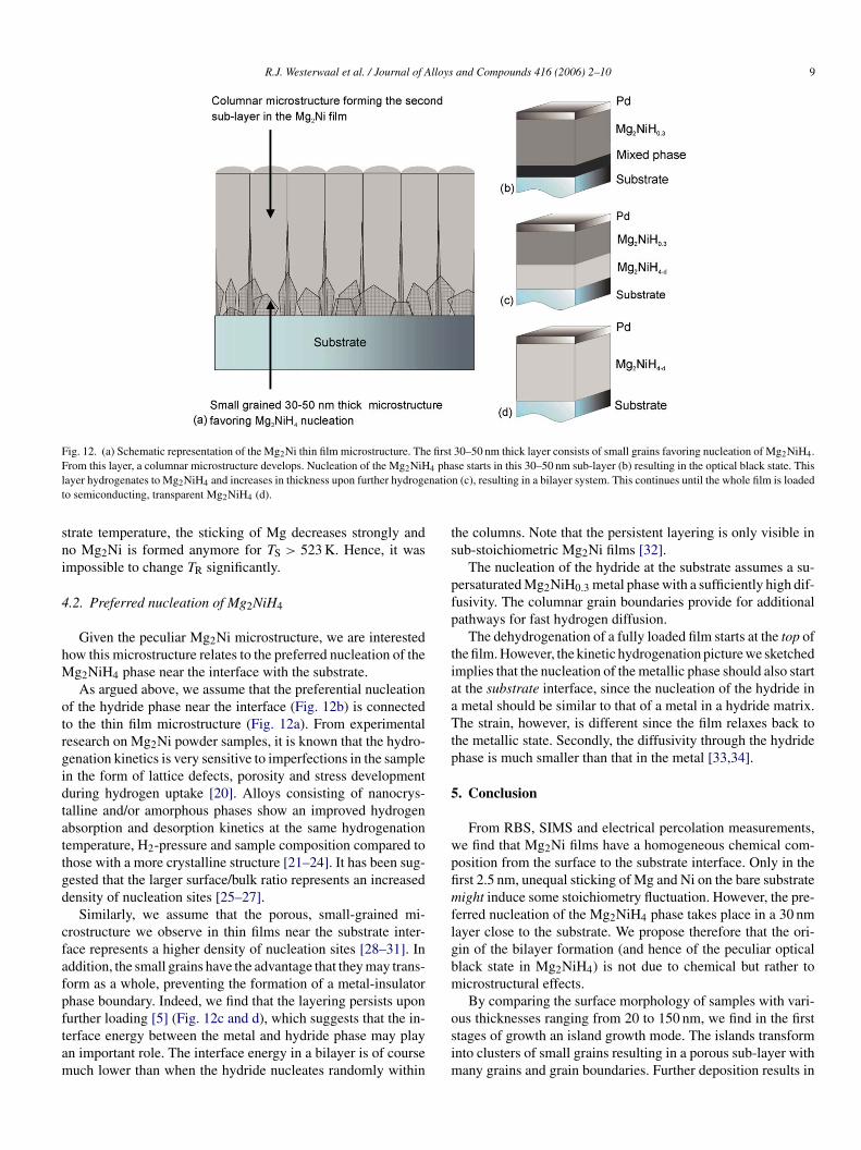
R.J. Westerwaal et al. / Journal of Alloys and Compounds 416 (2006) 2–10 9
Fig. 12. (a) Schematic representation of the Mg2Ni thin film microstructure. The first 30–50 nm thick layer consists of small grains favoring nucleation of Mg2NiH4.From this layer, a columnar microstructure develops. Nucleation of the Mg2NiH4 phase starts in this 30–50 nm sub-layer (b) resulting in the optical black state. Thislayer hydrogenates to Mg2NiH4 and increases in thickness upon further hydrogenation (c), resulting in a bilayer system. This continues until the whole film is loadedto semiconducting, transparent Mg2NiH4 (d).
strate temperature, the sticking of Mg decreases strongly andno Mg2Ni is formed anymore for TS > 523 K. Hence, it wasimpossible to change TR significantly.
4.2. Preferred nucleation of Mg2NiH4
Given the peculiar Mg2Ni microstructure, we are interestedhow this microstructure relates to the preferred nucleation of theMg2NiH4 phase near the interface with the substrate.
As argued above, we assume that the preferential nucleationof the hydride phase near the interface (Fig. 12b) is connectedto the thin film microstructure (Fig. 12a). From experimentalresearch on Mg2Ni powder samples, it is known that the hydro-genation kinetics is very sensitive to imperfections in the samplein the form of lattice defects, porosity and stress developmentduring hydrogen uptake [20]. Alloys consisting of nanocrys-talline and/or amorphous phases show an improved hydrogenabsorption and desorption kinetics at the same hydrogenationtemperature, H2-pressure and sample composition compared tothose with a more crystalline structure [21–24]. It has been sug-gested that the larger surface/bulk ratio represents an increaseddensity of nucleation sites [25–27].
Similarly, we assume that the porous, small-grained mi-crostructure we observe in thin films near the substrate inter-face represents a higher density of nucleation sites [28–31]. Inaddition, the small grains have the advantage that they may trans-fpftam
the columns. Note that the persistent layering is only visible insub-stoichiometric Mg2Ni films [32].
The nucleation of the hydride at the substrate assumes a su-persaturated Mg2NiH0.3 metal phase with a sufficiently high dif-fusivity. The columnar grain boundaries provide for additionalpathways for fast hydrogen diffusion.
The dehydrogenation of a fully loaded film starts at the top ofthe film. However, the kinetic hydrogenation picture we sketchedimplies that the nucleation of the metallic phase should also startat the substrate interface, since the nucleation of the hydride ina metal should be similar to that of a metal in a hydride matrix.The strain, however, is different since the film relaxes back tothe metallic state. Secondly, the diffusivity through the hydridephase is much smaller than that in the metal [33,34].
5. Conclusion
From RBS, SIMS and electrical percolation measurements,we find that Mg2Ni films have a homogeneous chemical com-position from the surface to the substrate interface. Only in thefirst 2.5 nm, unequal sticking of Mg and Ni on the bare substratemight induce some stoichiometry fluctuation. However, the pre-ferred nucleation of the Mg2NiH4 phase takes place in a 30 nmlayer close to the substrate. We propose therefore that the ori-gin of the bilayer formation (and hence of the peculiar opticalblack state in Mg NiH ) is not due to chemical but rather tom
osim
orm as a whole, preventing the formation of a metal-insulatorhase boundary. Indeed, we find that the layering persists uponurther loading [5] (Fig. 12c and d), which suggests that the in-erface energy between the metal and hydride phase may playn important role. The interface energy in a bilayer is of courseuch lower than when the hydride nucleates randomly within
2 4icrostructural effects.By comparing the surface morphology of samples with vari-
us thicknesses ranging from 20 to 150 nm, we find in the firsttages of growth an island growth mode. The islands transformnto clusters of small grains resulting in a porous sub-layer with
any grains and grain boundaries. Further deposition results in

10 R.J. Westerwaal et al. / Journal of Alloys and Compounds 416 (2006) 2–10
an increasing grain size, which develops into a columnar mi-crostructure. This columnar structure is forming the upper partof the film.
This two-layer microstructure is most probably the origin ofthe unusual hydrogen uptake and corresponding optical blackstate. The small-grained layer close to the substrate may lowerthe activation energy for hydrogenation, resulting in a preferrednucleation of Mg2NiH4. This double layer formation is respon-sible for the optical characteristics of the black state. Hence, itappears that this particular optical property is closely related tothe growth-induced microstructure of the thin film.
Our result shows that the simple diffusion pictures for hydro-genation often used in the hydrogen storage literature may notalways reflect the hydrogen distribution in a sample. Dependingon the microstructure, the hydride may nucleate from the insideof a grain. Apart from grain size engineering, it might there-fore also be worthwhile to try to engineer the defect structure toenhance the hydrogen absorption rate.
Acknowledgments
This work is part of the research program of the Stichtingvoor Fundamenteel Onderzoek der Materie (FOM), financiallysupported by the Nederlandse Organisatie voor Wetenschap-pelijk Onderzoek (NWO). The authors are grateful to H.Schreuders and J.H. Rector for technical support, Y. TammingafwFpO
R
[4] W. Lohstroh, R.J. Westerwaal, B. Noheda, I.A.M.E. Giebels, B. Dam, R.Griessen, Phys. Rev. Lett. 93 (2004) 197404.
[5] W. Lohstroh, R.J. Westerwaal, J.L.M. van Mechelen, C. Chacon, E. Jo-hansson, B. Dam, R. Griessen, Phys. Rev. B 70 (2004) 165411.
[6] W. Lohstroh, J.L.M. van Mechelen, R. Gremaud, W.J. Lustenhouwer, S.M.Kars, J.M. Rector, H. Schreuders, B. Dam, R. Griessen, private communi-cation.
[7] J.J. Reilly, R.H. Wiswall, Inorg. Chem. 7 (1968) 2254.[8] J. Schefer, P. Fischer, W. Halg, F. Stucki, L. Schlappbach, J.J.
Didisheim, K. Yvon, A.F. Andresen, J. Less Common Met. 74 (1980)1980.
[9] G.N. Garcia, J.P. Abriata, J.O. Sofo, Phys. Rev. B 59 (1999) 11746.[10] M. Ohring, The Materials Science of Thin Films, Academic Press, 1991.[11] P. Ramanlal, L.M. Sander, Phys. Rev. Lett. 54 (1985) 1828.[12] I. Petrov, P.B. Barna, L. Hultman, J.E. Greene, J. Vac. Sci. Technol. A 21
(5) (2003).[13] G.H. Gilmer, H. Huang, T.D. de la Rubia, J.D. Torre, F. Baumann, Thin
Solid Films 365 (2000) 189.[14] A. Mazor, D.J. Srolovitz, P.S. Hagan, B.G. Bukiet, Phys. Rev. Lett. 60
(1988) 424.[15] Zs. Czigany, G. Radnoczi, Thin Solid Films 347 (1999) 133.[16] J. Krug, P. Meakin, Phys. Rev. A 40 (1989) 2064.[17] C. Tang, S. Alexander, R. Bruinsma, Phys. Rev. Lett. 64 (1990) 772.[18] S.M. Paik, S. Kim, I.K. Schuller, Phys. Rev. B 43 (1991) 1843.[19] A.G. Dirks, H.J. Leamy, Thin Solid Films 47 (1977) 219.[20] L. Zaluski, A. Zaluska, J.O. Strom-Olsen, J. Alloys Compd. 253–254
(1997) 70.[21] T. Spassov, U. Koster, J. Alloys Compd. 287 (1999) 243.[22] C. Iwakura, S. Nohara, S.G. Zhang, H. Inoue, J. Alloys Compd. 285 (1999)
246.[23] S. Orimo, K. Ikeda, H. Fujii, Y. Fujikawa, Y. Kitano, K. Yamamoto, Acta
or RBS measurements at Philips Research Laboratories. Thisork is part of the research program of the Stichting voorundamenteel Onderzoek der Materie (FOM), financially sup-orted by the Nederlandse Organisatie voor Wetenschappelijknderzoek (NWO).
eferences
[1] T.J. Richardson, J.L. Slack, R.D. Armitage, R. Kostecki, B. Farangis, M.D.Rubin, Appl. Phys. Lett. 78 (2001) 3047.
[2] T.J. Richardson, J.L. Slack, B. Farangis, M.D. Rubin, Appl. Phys. Lett. 80(2002) 1349.
[3] J.L.M. van Mechelen, B. Noheda, W. Lostroh, R.J. Westerwaal, J.H. Rector,B. Dam, R. Griessen, Appl. Phys. Lett. 84 (2004) 3651.
Mater. 45 (1997) 2271.[24] S. Orimo, H. Fujii, Appl. Phys. A 72 (2001) 167.[25] Y. Ben-Eliyahu, M. Brill, J. Chem. Phys. 111 (1999) 6053.[26] R. Arkush, A. Venkert, M. Aizenshtein, S. Zalkind, D. Moreno, M. Brill,
M.H. Mintz, N. Shamir, J. Alloys Compd. 244 (1996) 197.[27] M. Brill, J. Bloch, H. Mintz, J. Alloys Compd. 266 (1998) 180.[28] H. Blomqvist, E. Ronnebro, D. Noreus, T. Kuji, J. Alloys Compd. 330
(2002) 268.[29] H. Blomqvist, D. Noreus, J. Appl. Phys. 91 (2002) 5141.[30] T.T. Ueda, M. Tsukahara, Y. Kamiya, S. Kikuchi, J. Alloys Compd. 386
(2005) 253.[31] U. Haussermann, H. Blomqvist, D. Noreus, Inorg. Chem. 41 (2002)
3684.[32] D.M. Borsa, private communication.[33] N. Cui, J.L. Luo, K.T. Chuang, J. Electroanal. Chem. 503 (2001) 92.[34] F. Feng, D.O. Northwood, J. Power Sources 136 (2004) 346.
Copyright © 2022 FDOKUMEN