
Terabit/s-Class Optical PCB Links Incorporating 360Gb/s Bidirectional 850 nm Parallel Optical...
12
560 JOURNAL OF LIGHTWAVE TECHNOLOGY, VOL. 30, NO. 4, FEBRUARY 15, 2012 Terabit/s-Class Optical PCB Links Incorporating 360-Gb/s Bidirectional 850 nm Parallel Optical Transceivers Fuad E. Doany, Clint L. Schow, Senior Member, IEEE, Benjamin G. Lee, Member, IEEE, Member, OSA, Russell A. Budd, Christian W. Baks, Cornelia K. Tsang, John U. Knickerbocker, Roger Dangel, Benson Chan, How Lin, Chase Carver, Jianzhuang Huang, Jessie Berry, David Bajkowski, Frank Libsch, Member, IEEE, and Jeffrey A. Kash, Fellow, IEEE Abstract—We report here on the design, fabrication, and char- acterization of highly integrated parallel optical transceivers designed for Tb/s-class module-to-module data transfer through polymer waveguides integrated into optical printed circuit boards (o-PCBs). The parallel optical transceiver is based on a through-silicon-via silicon carrier as the platform for integration of 24-channel vertical cavity surface-emitting laser and photodiode arrays with CMOS ICs. The Si carrier also includes optical vias (holes) for optical access to conventional surface-emitting 850 nm optoelectronic devices. The 48-channel 3-D transceiver optochips are flip-chip soldered to organic carriers to form transceiver opto- modules. Fully functional optomodules with 24 transmitter receiver channels were assembled and characterized with trans- mitters operating up to 20 Gb/s/ch and receivers up to 15 Gb/s/ch. At 15 Gb/s, the 48-channel optomodules provide a bidirectional aggregate bandwidth of 360 Gb/s. In addition, o-PCBs have been developed using a 48-channel flex waveguide assembly attached to FR4 electronic boards. Incorporation of waveguide turning mir- rors and lens arrays facilitates optical coupling to/from the o-PCB. Assembly of optomodules to the o-PCB using a ball grid array process provides both electrical and optical interconnections. An initial demonstration of the full module-to-module optical link achieved bidirectional links at 10 Gb/s. At 15 Gb/s, operation at a bit error ratio of was demonstrated for 15 channels in each direction, realizing a record o-PCB link with a 225 Gb/s bidirectional aggregate data rate. Index Terms—CMOS analog integrated circuits, integrated op- toelectronics, optical interconnections, optical planar waveguides, optical receivers, optical transmitters. Manuscript received July 29, 2011; revised November 01, 2011; accepted November 07, 2011. Date of publication November 23, 2011; date of current version February 01, 2012. This work was supported by the Defense Advanced Research Projects Agency under the C2OI Program, Contract MDA972-03-3- 0004. F. E. Doany, C. L. Schow, B. G. Lee, R. A. Budd, C. W. Baks, C. K. Tsang, J. U. Knickerbocker, F. Libsch, and J. A. Kash are with the IBM Thomas J. Watson Research Center, Yorktown Heights, NY 10598 USA (e-mail: [email protected]; [email protected]; [email protected]; rbudd@us. ibm.com; [email protected]; [email protected]; [email protected]; [email protected]; [email protected]). R. Dangel is with IBM Zurich Research Laboratory, 8803 Rüschlikon, Switzerland (e-mail: [email protected]). B. Chan, H. Lin, C. Carver, J. Huang, J. Berry, and D. Bajkowski are with Endicott InterConnect Technologies, Endicott, NY 13760 USA (e-mail: [email protected]; [email protected]; [email protected]; [email protected]; [email protected]; [email protected]). Color versions of one or more of the figures in this paper are available online at http://ieeexplore.ieee.org. Digital Object Identifier 10.1109/JLT.2011.2177244 I. INTRODUCTION P ARALLEL optical transceivers have become common- place in large servers and switch/router systems due to their ability to provide greater interconnect bandwidth and sup- port longer links (several meters) at lower power consumption than comparable electrical links. Most rack-to-rack intercon- nects in these systems employ commercial fiber-coupled op- tical modules [1]–[5] with data rates of 5–10 Gb/s. In 2008, the IBM Roadrunner supercomputer at the Lawrence Livermore National Laboratory utilized active optical cables packaged at the edge of the board to provide all 40 000 rack-to-rack high- speed links [1]. The IBM Power 775 Supercomputer recently introduced realizes the next generation of optical interconnects, in which all board-to-board high-speed links, both interrack and intrarack, are optical [3], [4]. The system can be expanded up to 1000 nodes interconnected with an unprecedented number of optical links, more than 2 000 000, using compact, 12-channel -POD optical modules [5] that are densely packaged directly onto a high-performance ceramic multichip module (MCM). As the demand for interconnectivity continues to increase to new levels, the communication bottlenecks have moved from interrack to board to board within a rack and are now ap- proaching board-level distances. Today’s optical interconnect technologies have been successful at alleviating the interrack and interboard interconnect bottlenecks, but the relatively large module size, the high power consumption, and the fiber-based transmission medium preclude the use of conventional op- tical modules for on-board applications. New technologies are required to scale toward multi-Tb/s on-board data buses with complex and flexible module-to-module routing. Op- tical-printed circuit boards (o-PCBs) with integrated polymer waveguides driven by optical transceivers directly packaged into MCMs are promising technologies for meeting the de- mands for low-cost, low-power, dense and flexible board-level optical links. The IBM Terabus/DARPA C2OI program has focused on the development of highly integrated parallel optical interconnect technologies that are designed to fulfill the high density, low power, and high speed requirements for module-to-module board-level interconnects. Polymer waveguide interconnects are a topic of worldwide research with recent reports of a 12-channel polymer waveguide interconnect operating at 0733-8724/$26.00 © 2011 IEEE
Transcript of Terabit/s-Class Optical PCB Links Incorporating 360Gb/s Bidirectional 850 nm Parallel Optical...

560 JOURNAL OF LIGHTWAVE TECHNOLOGY, VOL. 30, NO. 4, FEBRUARY 15, 2012
Terabit/s-Class Optical PCB Links Incorporating360-Gb/s Bidirectional 850 nm Parallel
Optical TransceiversFuad E. Doany, Clint L. Schow, Senior Member, IEEE, Benjamin G. Lee, Member, IEEE, Member, OSA,
Russell A. Budd, Christian W. Baks, Cornelia K. Tsang, John U. Knickerbocker, Roger Dangel, Benson Chan,How Lin, Chase Carver, Jianzhuang Huang, Jessie Berry, David Bajkowski, Frank Libsch, Member, IEEE, and
Jeffrey A. Kash, Fellow, IEEE
Abstract—We report here on the design, fabrication, and char-acterization of highly integrated parallel optical transceiversdesigned for Tb/s-class module-to-module data transfer throughpolymer waveguides integrated into optical printed circuitboards (o-PCBs). The parallel optical transceiver is based on athrough-silicon-via silicon carrier as the platform for integrationof 24-channel vertical cavity surface-emitting laser and photodiodearrays with CMOS ICs. The Si carrier also includes optical vias(holes) for optical access to conventional surface-emitting 850 nmoptoelectronic devices. The 48-channel 3-D transceiver optochipsare flip-chip soldered to organic carriers to form transceiver opto-modules. Fully functional optomodules with 24 transmitterreceiver channels were assembled and characterized with trans-mitters operating up to 20 Gb/s/ch and receivers up to 15 Gb/s/ch.At 15 Gb/s, the 48-channel optomodules provide a bidirectionalaggregate bandwidth of 360 Gb/s. In addition, o-PCBs have beendeveloped using a 48-channel flex waveguide assembly attached toFR4 electronic boards. Incorporation of waveguide turning mir-rors and lens arrays facilitates optical coupling to/from the o-PCB.Assembly of optomodules to the o-PCB using a ball grid arrayprocess provides both electrical and optical interconnections. Aninitial demonstration of the full module-to-module optical linkachieved bidirectional links at 10 Gb/s. At 15 Gb/s, operationat a bit error ratio of was demonstrated for 15 channelsin each direction, realizing a record o-PCB link with a 225 Gb/sbidirectional aggregate data rate.
Index Terms—CMOS analog integrated circuits, integrated op-toelectronics, optical interconnections, optical planar waveguides,optical receivers, optical transmitters.
Manuscript received July 29, 2011; revised November 01, 2011; acceptedNovember 07, 2011. Date of publication November 23, 2011; date of currentversion February 01, 2012. This work was supported by the Defense AdvancedResearch Projects Agency under the C2OI Program, Contract MDA972-03-3-0004.F. E. Doany, C. L. Schow, B. G. Lee, R. A. Budd, C. W. Baks, C. K. Tsang,
J. U. Knickerbocker, F. Libsch, and J. A. Kash are with the IBM ThomasJ. Watson Research Center, Yorktown Heights, NY 10598 USA (e-mail:[email protected]; [email protected]; [email protected]; [email protected]; [email protected]; [email protected]; [email protected];[email protected]; [email protected]).R. Dangel is with IBM Zurich Research Laboratory, 8803 Rüschlikon,
Switzerland (e-mail: [email protected]).B. Chan, H. Lin, C. Carver, J. Huang, J. Berry, and D. Bajkowski
are with Endicott InterConnect Technologies, Endicott, NY 13760 USA(e-mail: [email protected]; [email protected]; [email protected];[email protected]; [email protected]; [email protected]).Color versions of one or more of the figures in this paper are available online
at http://ieeexplore.ieee.org.Digital Object Identifier 10.1109/JLT.2011.2177244
I. INTRODUCTION
P ARALLEL optical transceivers have become common-place in large servers and switch/router systems due to
their ability to provide greater interconnect bandwidth and sup-port longer links (several meters) at lower power consumptionthan comparable electrical links. Most rack-to-rack intercon-nects in these systems employ commercial fiber-coupled op-tical modules [1]–[5] with data rates of 5–10 Gb/s. In 2008,the IBMRoadrunner supercomputer at the Lawrence LivermoreNational Laboratory utilized active optical cables packaged atthe edge of the board to provide all 40 000 rack-to-rack high-speed links [1]. The IBM Power 775 Supercomputer recentlyintroduced realizes the next generation of optical interconnects,in which all board-to-board high-speed links, both interrack andintrarack, are optical [3], [4]. The system can be expanded upto 1000 nodes interconnected with an unprecedented number ofoptical links, more than 2 000 000, using compact, 12-channel-POD optical modules [5] that are densely packaged directlyonto a high-performance ceramic multichip module (MCM).As the demand for interconnectivity continues to increase
to new levels, the communication bottlenecks have movedfrom interrack to board to board within a rack and are now ap-proaching board-level distances. Today’s optical interconnecttechnologies have been successful at alleviating the interrackand interboard interconnect bottlenecks, but the relatively largemodule size, the high power consumption, and the fiber-basedtransmission medium preclude the use of conventional op-tical modules for on-board applications. New technologiesare required to scale toward multi-Tb/s on-board data buseswith complex and flexible module-to-module routing. Op-tical-printed circuit boards (o-PCBs) with integrated polymerwaveguides driven by optical transceivers directly packagedinto MCMs are promising technologies for meeting the de-mands for low-cost, low-power, dense and flexible board-leveloptical links.The IBM Terabus/DARPA C2OI program has focused on the
development of highly integrated parallel optical interconnecttechnologies that are designed to fulfill the high density, lowpower, and high speed requirements for module-to-moduleboard-level interconnects. Polymer waveguide interconnectsare a topic of worldwide research with recent reports of a12-channel polymer waveguide interconnect operating at
0733-8724/$26.00 © 2011 IEEE

DOANY et al.: TERABIT/S-CLASS OPTICAL PCB LINKS INCORPORATING 360-GB/S BIDIRECTIONAL 850 NM PARALLEL OPTICAL TRANSCEIVERS 561
14 Gb/s/ch [6] and a 48-channel, four layer polymer waveguideinterconnect fabric [7].In the first generation Terabus optical transceiver, a
single-chip CMOS transceiver IC with flip-chip attachedvertical cavity surface-emitting laser (VCSEL) and photodiode(PD) arrays operating at 985 nm was demonstrated [8], [9]. Thesubstrate-emitting, 985-nm optoelectronic (OE) arrays withintegrated collimating lenses enabled a simple and compact“optochip,” which was then flip-chip attached to a high-speed,high-density organic carrier forming a first-generation Terabusoptomodule. The optomodule was surface mounted to an o-PCBusing a conventional ball grid array (BGA) solder process. Thefirst-generation o-PCB consisted of a conventional electroniccircuit board with a dense array polymer waveguides fabricateddirectly on the top surface. A second lens array coupled withan array of turning mirrors fabricated into the waveguidelayer, collimated and directed the light perpendicular to theo-PCB. The two-lens optical system provided efficient opticalcoupling between the optomodule and the waveguide coreswith relaxed assembly tolerances. The first-generation o-PCBdata bus achieved a 160 Gb/s bidirectional aggregate data rateusing optomodules with 16 transmitter (TX) receiver (RX)channels operating at 10 Gb/s/ch at a power efficiency of 13.5pJ/bit/link [10], [11].
II. OVERVIEW
The second-generation board-level optical data bus reportedhere is designed to facilitate transference of both the transceiverand the o-PCB technologies from research laboratories towardcommercial manufacturing. Although the first-generation back-side-emitting 985 nm OE devices provide simplified packaging,they are not commercially available. Migrating the o-PCB tech-nology to 850 nm offers both greater commercial availabilityof OE devices and compatibility with the latest generation mul-timode fiber (MMF). Additionally, typical polymer waveguideloss at the industry-standard 850 nm wavelength is substantiallylower than at 985 nm [12], [13]. However, at 850 nm, the OEdevices are top emitting since the substrate (GaAs or InP) is notoptically transparent, as it is for 985 nm devices. A complete re-design of the optomodule packaging was therefore required toincorporate standard top-emitting 850 nm components. The pro-cessing of the second-generation o-PCB was also transferred toa commercial PCB facility to demonstrate commercial viability.Significant design changes were introduced to the o-PCB fab-rication process for compatibility with the high-volume manu-facturing facility at Endicott Interconnect Technologies [14].The concept of an optically enabled MCM (OE-MCM,
enhanced optomodule) coupled to a second-generationboard-level optical data bus is schematically depicted inFig. 1. The transceiver optochip is incorporated onto a chipcarrier along with conventional ICs (i.e., logic, memory, andapplication-specified integrated circuits) to create an OE-MCM.Within this MCM, the high-speed, high-density organic carriersupports high-bandwidth electrical interconnectivity betweenchips on the module. All high-speed off-module I/O is per-formed optically through the integrated optochip connectedto polymer waveguides incorporated on the o-PCB. Althoughthe components within the optomodule have been completelyredesigned compared to the first 985 nm generation, the overall
Fig. 1. Schematic representation of the Terabus vision of an OE-MCM (or op-tomodule) incorporating an 850 nm transceiver optochip as well as conventionalICs.
concept of an organic carrier that is surface mounted to ano-PCB is retained. The primary difference is in the construc-tion details of the optochip and the implementation of theoptical waveguides in a separately fabricated polymer wave-guide-on-flex layer that is added to a conventional PCB.The 850 nm transceiver optochips reported here utilize a
through-silicon via (TSV) silicon carrier to enable heteroge-neous integration of CMOS integrated circuits and OE devices.The silicon carrier performs the key functions of mechanicallysupporting the OE and CMOS chips and providing all of theon- and off-carrier dc and high-speed electrical connections.Optical I/O from the optochip is made possible through “opticalvias,” or holes, etched through the Si carrier under the locationsof each VCSEL and PD array element.The 850 nm transceiver optochip is designed for flip-chip at-
tachment to an organic laminate high-density carrier to forman optomodule, as depicted in Fig. 1. The optomodule is sub-sequently surface mounted to the o-PCB using a BGA solderprocess that simultaneously establishes optical and electricalconnectivity. A two-lens system: one lens array incorporatedinto the optochip and a second onto the o-PCB facilitates the op-tical coupling between the optomodule and the polymer wave-guide flex. Electrical power and low-speed bias and control sig-nals for the module are provided through the BGA connections.In addition to the significant design changes that make the
current 850 nm o-PCB implementation more amenable to high-volume manufacturing, performance increases have been real-ized: a 225 Gb/s aggregate bandwidth in both directions through15 TX and 15 RX at 15 Gb/s/ch and 9.7 pJ/bit/link. The trans-ceiver optochip, optomodule, and o-PCB technologies are de-scribed in detail in the following sections.
III. TRANSCEIVER OPTOCHIP
The current embodiment of the optochip consists of a Sicarrier with four flip-chip attached components: two 24-channel850 nm OE arrays (VCSELs and PDs) and two 24-channelCMOS ICs (RXs and laser drivers). Electrical TSVs in the Sicarrier enable the backside of the optochip to be soldered to anorganic carrier. Since the OE devices are flip-chip attached tothe Si carrier, optical I/O is made possible through optical viasetched into the silicon under each of the 48 OE devices.
A. Si-Carrier Design and Fabrication
The Si carrier is the assembly platform for the Terabus 850nm optochip. Three Cu wiring levels on the top side of the car-

562 JOURNAL OF LIGHTWAVE TECHNOLOGY, VOL. 30, NO. 4, FEBRUARY 15, 2012
Fig. 2. Photograph of through-via silicon carrier. Inset shows expanded viewof optical vias and OE bond pads.
rier are used for power, ground, and control signal distributionas well as to interconnect the OE arrays to the CMOS driverICs. The top surface wiring is similar to that used in the pre-vious probe-able carrier and has been described in detail else-where [15]. The carrier measures 10.4 mm 6.4 mm. Fabrica-tion of electrical TSVs involves a deep reactive ion etch (RIE)of multiple bars per via with dimensions of 3 m 55–70 mand a depth m. Chemically vapor-deposited tungsten isused to metalize these high-aspect-ratio via bars. In the opticalvia process, 150 m diameter features are lithographically pat-terned, followed by RIE of the dielectric layers and the deep sil-icon etch to a depth m.Wafer finishing includes thinningthrough grinding and polishing to the final thickness of 150 mto uncover the optical vias and the electrical TSVs. The backsideof the silicon carrier is then insulatedwith oxide and under bumpmetallurgy is deposited on the electrical TSVs on the bottom ofthe carrier.Numerous TSVs are required for operation of the optochip,
828 in total. These include the 96 high-speed I/O signals (48 dif-ferential pairs) and associated ground pins as well as the powerand control signals for the two 24-channel CMOS ICs.A photograph of a TSV Si carrier is shown in Fig. 2. Visible
in the center of the carrier are the 24 24 optical vias locateddirectly below the sites where the VCSEL (left) and PD (right)arrays will be attached. The optical vias are arranged in a 12 2array with a 250 m pitch between rows and a 350 m pitchbetween columns. Each column is offset by 62.5 m to enablecoupling to the linear array of waveguides on the o-PCB. Theinner columns of VCSELs and PDs are separated by 700 m.The site for the laser diode driver (LDD) is adjacent to the
VCSEL array on the left and the RX IC is adjacent to the PDarray on the right (see Fig. 2). Transmission lines of 2–2.7 mmlength, routed in the topmost metal layer on the carrier, inter-connect the CMOS chips to the OE arrays. For each channel,these lines run from pairs of bond pads at the OE sites to LDDoutputs/RX inputs at the IC site. The LDD inputs and RX out-puts are also routed in the top metal level (1–4 mm in length) toTVSs at the periphery of the carrier on all four sides, and termi-nate at bond pads on the bottom of the carrier. The top surfacebond pads with a diameter of 35–50 m are electroplated with
Fig. 3. Photograph of (top) 24-channel PD and (bottom) VCSEL arrays.
NiAu to a thickness of about 1–2 m to enable soldering of theOEs and ICs.
B. Optochip Components and Assembly
The complete optochip assembly requires attachment of four24-channel array chips to the silicon carrier: an LDD IC, aVCSEL chip, a PD chip, and an RX IC.The OE arrays used in the optochip assemblies are 12 2
arrays of 850 nm VCSELs and PDs fabricated by EmcoreCorporation [16], [17]. The chips, pictured in Fig. 3, mea-sure 0.9 mm 3.5 mm. Active devices are arranged on a250 m 350 m pitch with a 62.5 m offset betweencolumns (note that the chips are turned by 90 degrees in thephotos in Fig. 3 compared to the carrier orientation in Fig. 2).Soldering the laser and PD arrays to the TSV carrier yieldsa 12 4 array of OE devices with a 62.5 m offset betweeneach of the four columns of devices (two VCSELs and twoPDs). This configuration enables coupling from the 2-D 4 12composite array of OE devices to a linear array of waveguideson a 62.5 m pitch.The VCSELs used in the optochips reported here have an
oxide aperture of m in diameter. Two types of detectorarrays were used in optochip assemblies: the first type has a35 m PD active area diameter while the second type has adiameter of 40 m. Dual topside contacts are employed for boththe PDs and the lasers. The pads are 40 m on a 100 m pitch.In addition to these 48 pads, the top edge of the array includes anadditional 13 bond pads at a 250 m pitch for extra mechanicalsupport in the bonding process. An AuSn solder layer about5 m thick is predeposited on all the bond pads of the OE arrays.The CMOS ICs were fabricated in the 130-nm IBM
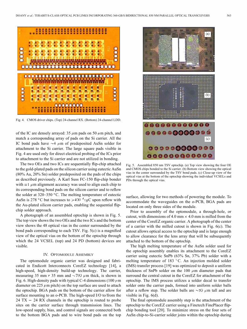
CMOS8RF-LM technology. The LDD and RX circuits aresimilar to those used in earlier Terabus designs [8], but withthe layouts and pad locations designed specifically for the 850nm TSV Si carrier. The 24-channel LDD and RX ICs measure1.6 mm 3.9 mm and are shown in Fig. 4.Both ICs share a common layout that includes the 12 2
array of circuits in the center of the IC and dense arraysof bond pads on the sides. The circuits are arranged on a250 m 350 m pitch, and the center area of each circuitincludes a pair of 35–40 m bond pads on 120 m pitch thatconnect each circuit to its OE device. The I/O pads on the edges
DOANY et al.: TERABIT/S-CLASS OPTICAL PCB LINKS INCORPORATING 360-GB/S BIDIRECTIONAL 850 NM PARALLEL OPTICAL TRANSCEIVERS 563
Fig. 4. CMOS driver chips. (Top) 24-channel RX. (Bottom) 24-channel LDD.
of the IC are densely arrayed: 35 m pads on 50 m pitch, andmatch a corresponding array of pads on the Si carrier. All theIC bond pads have m of predeposited AuSn solder forattachment to the Si carrier. The large square pads visible inFig. 4 are used only for direct electrical probing of the ICs priorto attachment to the Si carrier and are not utilized in bonding.The two OEs and two ICs are sequentially flip-chip attached
to the gold-plated pads on the silicon carrier using eutectic AuSn(80% Au, 20% Sn) solder predeposited on the pads of the chipsas described previously. A Karl Suss FC-150 flip-chip bonderwith m alignment accuracy was used to align each chip toits corresponding bond pads on the silicon carrier and to reflowthe solder at 320–350 C. The melting temperature of eutecticAuSn is 278 C but increases to C upon reflow withthe Au-plated silicon carrier pads, enabling the sequential flip-chip solder approach.A photograph of an assembled optochip is shown in Fig. 5.
The top view shows the two OEs and the two ICs and the bottomview shows the 48 optical vias in the center surrounded by thebond pads corresponding to each TSV. Fig. 5(c) is a magnifiedview of the optical vias on the bottom of the optochip throughwhich the 24 VCSEL (top) and 24 PD (bottom) devices arevisible.
IV. OPTOMODULE ASSEMBLY
The optomodule organic carrier was designed and fabri-cated in Endicott Interconnects CoreEZ technology [14], ahigh-speed, high-density build-up technology. The carrier,measuring 35 mm 35 mm and m thick, is shown inFig. 6. High-density pads with typical C-4 dimensions (100 mdiameter on 225 m pitch) on the top surface are used to attachthe optochip. BGA pads on the bottom of the carrier allow forsurface mounting to an o-PCB. The high-speed I/O to/from the24 TX 24 RX channels in the optochip is routed to probesites on the carrier surface through transmission lines. Thelow-speed supply, bias, and control signals are connected bothto the bottom BGA pads and to wire bond pads on the top
Fig. 5. Assembled 850 nm TSV optochip. (a) Top view showing the four OEand CMOS chips bonded to the Si carrier. (b) Bottom view showing the opticalvias in the center surrounded by the TSV bond pads. (c) Close-up view of theoptical vias at the bottom of the optochip showing the individual VCSELs andPDs through the optical vias.
surface, allowing for two methods of powering the module. Toaccommodate the waveguides on the o-PCB, BGA pads arelocated on only three sides of the module.Prior to assembly of the optomodule, a through-hole, or
cutout, with dimensions of 4.0 mm 4.0 mm is milled from thecenter of the CoreEZ organic carrier. A photograph of the centerof a carrier with the milled cutout is shown in Fig. 6(c). Thecutout allows optical access to the optochip and is large enoughto allow clearance for the lens array that will be subsequentlyattached to the bottom of the optochip.The high melting temperature of the AuSn solder used for
the optochip assembly enables its attachment to the CoreEZcarrier using eutectic SnPb (63% Sn, 37% Pb) solder with amelting temperature of 183 C. An injection molded solder(IMS) transfer process [19] was optimized to deposit a uniformthickness of SnPb solder on the 100 m diameter pads thatsurround the central cutout in the CoreEZ for attachment of theoptochip. The IMS process utilizes a solder decal to transfersolder onto the carrier pads, formed into uniform solder ballsafter a reflow step. The solder balls are m tall and arevisible in Fig. 6(d).The final optomodule assembly step is the attachment of the
optochip to the CoreEZ carrier using a Finetech FinePlacer flip-chip bonding tool [20]. To minimize stress on the four sets ofAuSn chip-to-Si-carrier solder joins within the optochip during

564 JOURNAL OF LIGHTWAVE TECHNOLOGY, VOL. 30, NO. 4, FEBRUARY 15, 2012
Fig. 6. Photographs of the CoreEZ optomodule carrier. (a) Top view illus-trating high-speed probe and wire bond power pads. (b) Bottom view showingBGA pads on three sides. (c) Cutout at the center of the optochip bond site.(d) Expanded view of the bond pads with IMS transferred solder.
Fig. 7. Fully assembled optochip on CoreEZ carrier. Inset shows expandedview of optochip edge showing first row of solder columns.
the attachment to the CoreEZ, a bonding process without theapplication of force was developed. The Finetech split opticalsystem is used to align the C4 pads at the bottom of the optochipto the solder balls on the CoreEZ and to place the optochip on thecarrier. Following reflow at about 200 C, the optochip is sol-dered to the CoreEZ carrier yielding a completed optomodule.A photograph of an assembled module is shown in Fig. 7.
V. OPTOMODULE CHARACTERIZATION
Fully functional Terabus optomodules have been assembledand their dc and high-speed performance verified. For the dcmeasurements of the TX, each laser output was measured usingan MMF optical probe, and uniform output power was observedfor all 24 channels [15]. For the RX, an 850 nm continuous wave(CW) laser source was directed to each individual PD using acleaved single-mode fiber probe. Themeasured photocurrent for
Fig. 8. Measured eye diagrams. (a) TX optical outputs at 20 Gb/s measuredwith a reference PD. (b) Single-ended RX electrical outputs at 15 Gb/s.
each device under 2 V bias also indicated uniform performancefor all 24 channels [15].High-speed characterization of TX and RX channels in fully
packaged optical modules was undertaken using a coplanar mi-crowave probe to access the top-side electrical I/O and an op-tical fiber probe to access bottom-side optical I/O. Power andcontrol signals were provided to the module through wire bondsfrom a test card.For the TX characterization, the chip was supplied with
1.75 V for the predriver and 2.7 V for the output stage, resultingin a total power consumption of 55 mW/ch. Under these con-ditions, the average VCSEL output power was about 0.3 dBm,with a spread of dB observed across all 24 VCSELs. TheVCSEL output was captured using a lensed 62.5 m coreMMF probe. A 30 GHz sampling oscilloscope and a NewportD-25XR PD were used to record the eye diagrams. TX channelsoperate with wide-open eyes up to 20 Gb/s. Fig. 8(a) shows theTX output eye diagrams for a pseudorandom bit stream (PRBS)pattern of length obtained for all 24 channels within themodule at 20 Gb/s.For the RX section, a lensed 50 m MMF was utilized
to couple light from a separate directly modulated reference

DOANY et al.: TERABIT/S-CLASS OPTICAL PCB LINKS INCORPORATING 360-GB/S BIDIRECTIONAL 850 NM PARALLEL OPTICAL TRANSCEIVERS 565
Fig. 9. RX sensitivity curves for the optomodule RX channels at data rates of10, 12.5, and 15 Gb/s.
VCSEL into each RX channel for high-speed characterization.Open eye diagrams were measured for data rates up 15 Gb/s,and are shown in Fig. 8(b). As with the TX section, aPRBS pattern was used. The total power consumption for theRXs is 67 mW/ch with the following RX power supplies: 2.2 Vfor the core circuits, 1.8 V for the output stage, and a PD biasof 3 V.The sensitivity characteristics of the optomodule RX chan-
nels were measured and are presented in Fig. 9 at data ratesfrom 10 to 15 Gb/s. The average sensitivity at a bit error ratio( at 10 Gb/s is about dB m with a uni-form distribution: a spread of only 0.8 dB across all channels.At the higher data rates of 12.5 and 15 Gb/s, the average sen-sitivity decreases to about and dB m, respectively.Compared to operation at 10 Gb/s, the penalties of 2 dB m at12.5 Gb/s and 5 dB at 15 Gb/s are attributed to RX bandwidthlimitations.
VI. O-PCBS
The second generation o-PCB technology is focused oncommercialization and toward that end waveguide fabricationwas transferred to a commercial facility at Endicott Intercon-nects [21]. In a departure from the first-generation o-PCB, inwhich the polymer waveguides were directly fabricated on thesurface of a PCB [10], [11], the o-PCB is now fabricated bylaminating a flexible optical waveguide assembly onto an FR4PCB. The electrical circuit board contains all the wiring forpower and control signal distribution. The optical waveguideassembly is fabricated on a flexible polyimide substrate withadded polymer layers on its surface processed to form theoptical waveguides. An additional substantial modificationfrom the first-generation acrylate-based waveguide technologywas the transition to poly-siloxane material that providesgreater thermal stability and compatibility with standard solderprocesses. An advantage of the second-generation approach isthat the flexible waveguides and the FR4 boards can be man-ufactured separately and independently as two subassemblies.Each of these two components can be fully tested before thefinal lamination step, in which the two pieces are accuratelyjoined by matching complementary mechanical alignment pinsand holes in the subassemblies. This “parallel” manufacturing
Fig. 10. (a) 48-channel flex waveguide. (b) Cross section of individual wave-guide cores.
process with known good subassemblies can reduce waste andimprove final yield, and is described in detail elsewhere [21].An inkjet process was utilized for optical waveguide mate-
rial deposition due to the flexibility and accuracy of the layerthickness control, as well as the ability for coarse patterning ofthe layers. Experimental data show that the optical layer thick-ness can be tightly controlled to within 2 m and the resolutionof the lithographically printed features similarly controlled to2 m. After deposition onto the flexible substrate, the bottomclad layer is prebaked briefly followed by UV exposure to pro-mote polymer cross-linking and a final postexpose cure bake.The waveguide core material is deposited using the inkjet toa total layer thickness of 35 m. Following a brief prebake,the waveguide channels are defined using projection printingwith UV exposure through a quartz photomask. To completethe waveguide core layer, the assembly is subject to a brief pos-texpose bake then developed using a filtered, contaminant-freeetch solution. After the waveguide channels are developed, afinal bake at about 145 C fully cures the waveguide cores. Thelast layer, the top cladding, is inkjet printed to a thickness of35 m. The steps used to deposit and cure the top clad are sim-ilar to the bottom clad.Multiple flex waveguide array strips are processed simulta-
neously and then singulated. A flex waveguide sample is shownin Fig. 10(a), with a cross-sectional view of the waveguidecores in Fig. 10(b). The waveguide link is 15 cm long andcontains 48 channels with 35 m cores. The pitch is 62.5 mat either end and is fanned out to 250 m pitch in the centerof the link to demonstrate routing capability. Since the coresare formed lithographically, any arbitrary pattern can be fab-ricated. Although Fig. 10(a) shows a linear flex waveguide tointerconnect two modules, flex structures have been designedto interconnect multiple modules, such as four modules onone o-PCB in a square configuration. In this example, 24 ofthe 48 waveguides from each module are routed to the twoneighboring modules.The full flex waveguide assembly includes thin metal plates
laminated to the bottom of the flex at the two ends for mechan-ical stability. Copper features at both ends are fabricated intothe flex allowing passive alignment of the flex waveguide to theFR4 substrate with about 50 m placement accuracy.Following waveguide fabrication, angled cavities are laser
ablated individually in each waveguide core to realize totalinternal reflection turning mirrors. An amplified femtosecondlaser source is focused to a m spot and scanned in aserpentine pattern to form air cavities arranged in a 12 4array corresponding to the OE devices. The laser power and
566 JOURNAL OF LIGHTWAVE TECHNOLOGY, VOL. 30, NO. 4, FEBRUARY 15, 2012
Fig. 11. (a) Laser-ablated 12 4 array of mirrors illuminated with a red laser.Inset shows expanded view of single mirror/cavity. (b) Fully processed flexwaveguide with turning mirrors and lens array.
the number of scan cycles were optimized to achieve a smoothmirror surface, achieving a low optical loss of approximately0.5–0.7 dB per mirror. A photograph of the laser-processedturning mirrors is shown in Fig. 11(a).After the formation of the laser-ablated cavities that form the
turning mirrors, they are sealed with a thin glass plate and a12 4 lens array is aligned to the mirror array and attached tothe glass plate. The fully assembled flex waveguide is shown inFig. 11(b). Once the waveguide ends have been prepared, theoptical loss of each waveguide channel is measured to ensurethat the assembly is fully functional and suitable for pairing witha known good PCB to yield a fully functional o-PCB.The final step of the build process is to attach the flex wave-
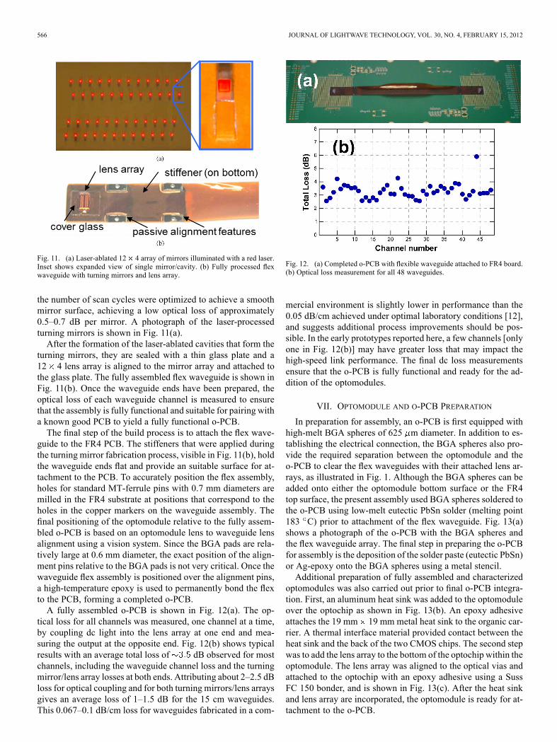
guide to the FR4 PCB. The stiffeners that were applied duringthe turning mirror fabrication process, visible in Fig. 11(b), holdthe waveguide ends flat and provide an suitable surface for at-tachment to the PCB. To accurately position the flex assembly,holes for standard MT-ferrule pins with 0.7 mm diameters aremilled in the FR4 substrate at positions that correspond to theholes in the copper markers on the waveguide assembly. Thefinal positioning of the optomodule relative to the fully assem-bled o-PCB is based on an optomodule lens to waveguide lensalignment using a vision system. Since the BGA pads are rela-tively large at 0.6 mm diameter, the exact position of the align-ment pins relative to the BGA pads is not very critical. Once thewaveguide flex assembly is positioned over the alignment pins,a high-temperature epoxy is used to permanently bond the flexto the PCB, forming a completed o-PCB.A fully assembled o-PCB is shown in Fig. 12(a). The op-
tical loss for all channels was measured, one channel at a time,by coupling dc light into the lens array at one end and mea-suring the output at the opposite end. Fig. 12(b) shows typicalresults with an average total loss of dB observed for mostchannels, including the waveguide channel loss and the turningmirror/lens array losses at both ends. Attributing about 2–2.5 dBloss for optical coupling and for both turning mirrors/lens arraysgives an average loss of 1–1.5 dB for the 15 cm waveguides.This 0.067–0.1 dB/cm loss for waveguides fabricated in a com-
Fig. 12. (a) Completed o-PCB with flexible waveguide attached to FR4 board.(b) Optical loss measurement for all 48 waveguides.
mercial environment is slightly lower in performance than the0.05 dB/cm achieved under optimal laboratory conditions [12],and suggests additional process improvements should be pos-sible. In the early prototypes reported here, a few channels [onlyone in Fig. 12(b)] may have greater loss that may impact thehigh-speed link performance. The final dc loss measurementsensure that the o-PCB is fully functional and ready for the ad-dition of the optomodules.
VII. OPTOMODULE AND O-PCB PREPARATION
In preparation for assembly, an o-PCB is first equipped withhigh-melt BGA spheres of 625 m diameter. In addition to es-tablishing the electrical connection, the BGA spheres also pro-vide the required separation between the optomodule and theo-PCB to clear the flex waveguides with their attached lens ar-rays, as illustrated in Fig. 1. Although the BGA spheres can beadded onto either the optomodule bottom surface or the FR4top surface, the present assembly used BGA spheres soldered tothe o-PCB using low-melt eutectic PbSn solder (melting point183 C) prior to attachment of the flex waveguide. Fig. 13(a)shows a photograph of the o-PCB with the BGA spheres andthe flex waveguide array. The final step in preparing the o-PCBfor assembly is the deposition of the solder paste (eutectic PbSn)or Ag-epoxy onto the BGA spheres using a metal stencil.Additional preparation of fully assembled and characterized
optomodules was also carried out prior to final o-PCB integra-tion. First, an aluminum heat sink was added to the optomoduleover the optochip as shown in Fig. 13(b). An epoxy adhesiveattaches the 19 mm 19 mm metal heat sink to the organic car-rier. A thermal interface material provided contact between theheat sink and the back of the two CMOS chips. The second stepwas to add the lens array to the bottom of the optochip within theoptomodule. The lens array was aligned to the optical vias andattached to the optochip with an epoxy adhesive using a SussFC 150 bonder, and is shown in Fig. 13(c). After the heat sinkand lens array are incorporated, the optomodule is ready for at-tachment to the o-PCB.

DOANY et al.: TERABIT/S-CLASS OPTICAL PCB LINKS INCORPORATING 360-GB/S BIDIRECTIONAL 850 NM PARALLEL OPTICAL TRANSCEIVERS 567
Fig. 13. (a) Photograph of o-PCB, showing BGA site with high-melt spheresand attached flex waveguide. (b) Optomodule with added heat sink over op-tochip. (c) Bottom view of optomodule showing incorporated lens array.
Optical coupling from the optomodule to the waveguides in-tegrated on the o-PCB is carried out using a dual-lens system asschematically depicted in Fig. 1. The two-lens system provides
magnification between the OE devices and the wave-guide cores. The lens arrays were implemented in GaP, chosenfor its transparency and high optical index. Two 4 12 lens ar-rays, one for the optochip and one for the waveguide array, werefabricated by MEMS Optical, Inc., using a lithographic processon 300 m thick GaP wafers [22]. For the TX, the lens magni-fication from the VCSEL to waveguide core results in a 0.6Xreduction in the numerical aperture (NA). This NA reductionprovides better matching to the waveguide core NA and yieldshigher optical coupling efficiency. On the RX side, the opticalsystem provides a 0.6X reduction in the image of the waveguidecore to the PD, enabling efficient optical coupling to smaller di-ameter high-speed PDs.The lensed components shown in Fig. 13 were used to mea-
sure the alignment tolerances between the optomodule and theo-PCB. A lensed module was attached to an X–Y–Z stage andaligned over the o-PCB lens array. By varying the relative posi-tion of the two components, the optical coupling efficiency as afunction of offset was determined. DC electrical connections tothe module were used to either power a bank of VCSELs or tobias a bank of PDs. For the TX, the VCSEL output coupled intothe waveguide using the dual-lens optical system was measuredat the output waveguide lens array on the opposite edge of thecard using a power meter. For the RX, a CW 850 nm laser sourcewas directed into the opposite waveguide lens array. The pho-tocurrent generated by light exiting the o-PCB coupled to one ofthe 40 m diameter PDs in the optomodule was measured. At a2 V PD bias, the photocurrent at the PD was recorded as a func-tion of relative offset between the optomodule and the o-PCB.Fig. 14 presents the measured optical coupling dependence
on in-plane offset: meaning the two orthogonal axes parallel tothe plane of the o-PCB. The measurements were carried out fora lens-to-lens separation of about 500 m. For the RX, the datain Fig. 14(a) show that even with offsets up to m the op-tical coupling is highly efficient with dB loss compared toideal alignment. Similarly, the TX data in Fig. 14(b) show thatoffsets of up to m resulted in only 1 dB coupling loss.These results verify the relaxed alignment tolerances afforded
Fig. 14. Optical coupling dependence of alignment offset for (a) RX and(b) TX.
Fig. 15. Photograph of the o-PCB with an attached optomodule.
by the dual-lens optical system. The availability of greater thanm for assembly of the optomodule to the o-PCB sug-
gests that standard low-cost packaging tools can be used for finalo-PCB assembly.
VIII. FULL O-PCB LINK ASSEMBLY AND DEMONSTRATION
Assembly of two optomodules to an o-PCB was carried outsequentially using the Finetech flip-chip bonding tool describedpreviously. This packaging tool provides m alignment ac-curacy, which is adequate for the dual-lens optical system. Themodule is brought into contact with the BGA spheres and thealignment maintained during the bonding thermal cycle. In theassembly demonstrated here, Ag-epoxywas used as the bondingagent. However, the same assembly procedure can be used forlow-melt solder attachment. Ag-epoxy was used in these initialbuilds to limit optomodule and o-PCB temperature to Cto determine optimum performance. Based on earlier first-gen-eration o-PCB studies, similar performance is anticipated for as-semblies using eutectic PbSn solder reflowed at about 200 C.Fig. 15 shows one site of the o-PCB with an attached opto-module.The attachment process was repeated for the second opto-
module on the opposite site on the o-PCB to complete the as-sembly of the full link. Fig. 16 shows a photograph of the o-PCBlink with all 24 lasers on the left module powered. The minutelight scattered out of the waveguides as the optical signals prop-agate through the polymer waveguides is visible using an in-frared-sensitive camera.Each TX-to-RX link in the fully assembled o-PCB was char-
acterized with high-speed test equipment. Visible in Fig. 16

568 JOURNAL OF LIGHTWAVE TECHNOLOGY, VOL. 30, NO. 4, FEBRUARY 15, 2012
Fig. 16. Photograph of the o-PCB with assembled optomodules. The leftmodule is powered to activate 24 lasers. Scattered light is evident along entirewaveguide path. Also visible are the high-speed electrical probes used tocharacterize each individual TX-to-RX link.
are the single-channel microwave probes used to access theoptomodule electrical I/O. As with the optomodule testingdescribed previously, the test pattern used was . Inthe initial prototype reported here, open eye diagrams wereobtained for a total of 22 channels in one direction and 21 chan-nels in the opposite direction at 10 Gb/s. Both optomoduleswere characterized prior to assembly and each showed one ortwo nonfunctional channels. In addition, o-PCB characteriza-tion showed one waveguide channel with significantly higherloss and a few channels showing greater loss than the typicalaverage of about 3.5 dB. Nonetheless, the 22 21 channeloptomodule-to-optomodule full link over o-PCB represents themost integrated o-PCB demonstration to date.At an increased data rate of 12.5 Gb/s, a total of 22 19 chan-
nels operated at , and the eye diagrams for thesechannels are shown in Fig. 17. Compared to 10 Gb/s, two chan-nels did meet the criteria, indicating the wave-guide loss exceeded the optical budget for 12.5 Gb/s operationof these links. An approximate 2 dB penalty in RX sensitivityis incurred moving from 10 to 12.5 Gb/s, as seen in Fig. 9.At 12.5 Gb/s, the unidirectional link power consumption was11.6 pJ/bit.At the center of Fig. 17 (and Fig. 18), there is a block arrow
representation of the 48 waveguide channels, with green indi-cating links from right to left and blue from left to right. The 22(green) 19 (blue) error-free waveguide linksare indicated using blue and green color-filled boxes, while theremaining waveguide channels are shown in white.Finally, the TX and RX driving conditions were re-optimized
for 15 Gb/s operation resulting in the eye diagrams shown inFig. 18. At 15 Gb/s, a total of 15 15 waveguide channels op-erated error free. The total number of error-free channels is re-duced compared to the 12.5 Gb/s results, again indicating thatthe waveguide loss for these channels exceeded the availablelink budget with the additional dB sensitivity penalty in-curred in moving from 12.5 to 15 Gb/s (see Fig. 9). The totalpower consumption per link was 9.7 pJ/bit. The 15 15 channelwaveguide link through the o-PCB between the two optomod-ules represents a 225 Gb/s bidirectional aggregate data rate.At the 9.7 pJ/bit setting that supports 15 Gb/s/ch operation,
the total module power consumption is 3.5 W. Under these con-ditions, with all TX and RX channels powered, the temperatureof an optomodule with and without the added thermal lid wasmeasured.Without the thermal lid, the temperature of the Si car-rier was 55 C, and the backside IC temperature was 68 C.
Fig. 17. Eye diagrams for the bidirectional full o-PCB link at 12.5 Gb/s. 22channels in one direction and 19 channels in the other direction operated with
.
Fig. 18. Eye diagrams for the bidirectional full o-PCB link at 15 Gb/s. 15 chan-nels in each direction operated at a .
With the thermal lid added, the lid temperature was 47 C, andadding a finned heat sink and mild airflow should reduce the op-tomodule temperature even further.The timing margin of a typical link in each direction on the
o-PCB was measured, with the results shown in Fig. 19. Evenat 15 Gb/s, the eye opening at exceeds 0.4 UI(27 ps) indicating low-jitter operation. In order to assess the im-pact of the thermal environment on the o-PCB performance, thetiming margin at 12.5 Gb/s of a typical channel was measured asa function of module temperature, measured at the thermal lid.Different operating temperatures were achieved by poweringvarying numbers of TX and RX banks and adjusting the bankpower supplies. Fig. 20 presents the measured decrease in hor-izontal eye opening as a function of temperature. Even with allTX and RX channels powered on with the module at its max-imum power dissipation of 3.5 W, the eye closure is less than6 ps (0.07 UI).

DOANY et al.: TERABIT/S-CLASS OPTICAL PCB LINKS INCORPORATING 360-GB/S BIDIRECTIONAL 850 NM PARALLEL OPTICAL TRANSCEIVERS 569
Fig. 19. Timing margin measured on a typical link in each direction in the o-PCB at data rates of 10, 12.5, and 15 Gb/s. Channels A and B are indicated in Figs. 17and 18.
Fig. 20. Horizontal eye closure measured at 12.5 Gb/s for a typical link in theo-PCB as a function of optomodule temperature.
IX. CONCLUSION
We have demonstrated a second-generation technology solu-tion for highly integrated module-to-module board-level opticalinterconnects. The integrated optical data bus simultaneouslysatisfies the critical requirements of high data rates, high-den-sity, low power consumption, as well as low-cost manufactureand assembly processes. We have successfully designed and as-sembled optochips, optomodules, and optical PCBs and charac-terized each of these components individually and as a completeboard-level link.The parallel optical transceivers rely on an Si carrier with
electrical and optical TSVs to integrate industry-standard, top-emitting 850 nmOE arrays with CMOS ICs. Flip-chip assemblyof the components provides a dense optochip that is furtherflip-chip soldered to a conventional organic chip carrier. Fullyfunctional 24 TX and 24 RX optomodules were fabricated andhigh-speed characterization showed TX channels operating upto 20 Gb/s/ch and RX channels up to 15 Gb/s/ch.For the optical-PCB, a process was developed to laminate
a flexible optical waveguide assembly onto a standard FR4PCB. The 48-channel flex-waveguide assembly is fabricatedusing a lithographic process fully realized in a manufacturingenvironment. Mechanical features are also fabricated in theflex assembly to facilitate accurate alignment to the FR4 board.Waveguide turning mirrors and collimating lens arrays are thenadded to complete the flex waveguide assembly. The approach
to independently process the flex waveguide assembly andthe electrical PCB, followed by integration of the two sub-assemblies, greatly enhances the yield and provides a path forlow-cost o-PCB manufacturing.Finally, a full module-to-module link through an optical
data bus was realized by assembling two optomodules ontoan o-PCB. The relaxed alignment tolerances provided by thedual-lens optical system enabled surface mounting of themodules using a low-cost packaging tool. All but one of thecomponents in the o-PCB link were built in commercial fa-cilities, including: the CMOS chips, OEs, lens arrays, PCBs,organic carriers, and polymer WG flexes. The Si-carrier isthe only component specifically fabricated for this project in aresearch laboratory, but was made using standard Si processing.The aggregate (225 Gb/s) and per-channel data rates
(15 Gb/s) are the highest reported for waveguide-basedoptical interconnects with an unprecedented power effi-ciency of 9.7 pJ/bit/link. The 24-channel transceiver modulesachieve a bidirectional aggregate bandwidth of 360 Gb/s(24 15 Gb/s/ch) that is also a record for multimode par-allel optics. Demonstrating these levels of performance usingcomponents that are either commercially available today orthat are readily built with established manufacturing pro-cesses illustrates the potential of o-PCB technology to supportthe Tb/s-class interconnect requirements for next-generationsystems.
ACKNOWLEDGMENT
The PDs and VCSELs were designed and manufactured byEmcore Corporation, and the authors’ would like to thank N. Li,K. Jackson, and the rest of the team at Emcore.
REFERENCES
[1] D. Grice, H. Brandt, C. Wright, P. McCarthy, A. Emerich, T. Schimke,C. Archer, J. Carey, P. Sanders, J. A. Fritzjunker, S. Lewis, and P. Ger-mann, “Breaking the petaflops barrier,” IBM J. Res. Dev., vol. 53, no.5, pp. 1–16, Sep. 2009, paper 1.
[2] National Center for Computational Sciences. Oak Ridge, TN, Jul. 09,2010 [Online]. Available: http://www.nccs.gov/jaguar/
[3] National Center for Supercomputing Applications, University of Illi-nois at Urbana-Champaign, Urbana, IL, Jun. 9, 2010 [Online]. Avail-able: http://www.ncsa.illinois.edu/BlueWaters/

570 JOURNAL OF LIGHTWAVE TECHNOLOGY, VOL. 30, NO. 4, FEBRUARY 15, 2012
[4] A. F. Benner, D. M. Kuchta, P. K. Pepeljugoski, R. A. Budd, G.Hougham, B. V. Fasano, K. Marston, H. Bagheri, E. J. Seminaro, H.Xu, D. Meadowcroft, M. H. Fields, L. McColloch, M. Robinson, F.W. Miller, R. Kaneshiro, R. Granger, D. Childers, and E. Childers,“Optics for high-performance servers and supercomputers,” in Proc.Opt. Fiber Commun. Conf./Nat. Fiber Opt. Eng. Conf., San Diego,CA, Mar. 21–25, 2010, pp. 1–3, paper OTuH1.
[5] M. H. Fields, J. Foley, R. Kaneshiro, L. McColloch, D. Meadowcroft,F. W. Miller, S. Nassar, M. Robinson, and H. Xu, “Transceivers andoptical engines for computer and datacenter interconnects,” in Opt.Fiber Commun. Conf./Nat. Fiber Opt. Eng. Conf., San Diego, CA,Mar.21-25, 2010, pp. 1–2, paper OTuP1.
[6] T. Shiraishi, T. Yagisawa, T. Ikeuchi, S. Ide, and K. Tanaka, “Cost-effective on-board optical interconnection using waveguide sheet withflexible printed circuit optical engine,” in Proc. Opt. Fiber Commun.Conf. Expo./Nat. Fiber Opt. Eng. Conf., Los Angeles, CA, Mar. 6–10,2011, pp. 1–3, paper OTuQ5.
[7] H. Numata, F. Yamada, Y. Taira, and S. Nakagawa, “MT-like multi-layer 48-channel polymer waveguide connector using novel passivealignment structure,” in Proc. Opt. Fiber Commun. Conf. Expo./Nat.Fiber Opt. Eng. Conf., Los Angeles, CA, Mar. 6–10, 2011, pp. 1–3,paper OTuQ4.
[8] C. L. Schow, F. E. Doany, C. Baks, Y. H. Kwark, D. M. Kuchta, andJ. A. Kash, “A single-chip CMOS-based parallel optical transceivercapable of 240 Gb/s bi-directional data rates,” J. Lightw. Technol., vol.27, no. 7, pp. 915–929, Apr. 2009.
[9] F. E. Doany, C. L. Schow, C. Baks, R. Budd, Y.-J. Chang, P. Pepelju-goski, L. Schares, D. Kuchta, R. John, J. A. Kash, F. Libsch, R. Dangel,F. Horst, and B. J. Offrein, “160-Gb/s bidirectional parallel opticaltransceiver module for board level interconnects using a single-chipCMOS IC,” in Proc. 57th Electron. Compon. Technol. Conf., Reno,NV, May/Jun. 2007, pp. 1256–1261.
[10] F. E. Doany, C. L. Schow, R. Budd, C. Baks, D. M. Kuchta, P.Pepeljugoski, F. Libsch, J. A. Kash, R. Dangel, F. Horst, and B. J.Offrein, “Chip-to-chip board-level optical data buses,” in Proc. Opt.Fiber Commun. Conf./Nat. Fiber Opt. Eng. Conf., San Diego, CA,Feb. 24–28, 2008, pp. 1–3, paper OThS4.
[11] F. E. Doany, C. L. Schow, C. W. Baks, D. M. Kuchta, P. Pepeljugoski,L. Schares, R. Budd, F. Libsch, R. Dangel, F. Horst, B. J. Offrein, andJ. A. Kash, “160 Gb/s bidirectional polymer waveguide board-leveloptical interconnects using CMOS-based transceivers,” IEEE Trans.Adv. Packag., vol. 32, no. 2, pp. 345–359, May 2009.
[12] R. Dangel, U. Bapst, C. Berger, R. Beyeler, L. Dellmann, F. Horst, B.Offrein, and G.-L. Bona, “Development of a low-cost low-loss polymerwaveguide technology for parallel optical interconnect applications,”in Tech. Dig. IEEE/LEOS Summer Topical Meet., San Diego, CA, Jun.2004, pp. 1–2.
[13] R. Dangel, C. Berger, R. Beyeler, L. Dellmann, M. Gmur, R. Hamelin,F. Horst, T. Lamprecht, T. Morf, S. Oggioni, M. Spreafico, and B. J.Offrein, “Polymer-waveguide-based board-level optical interconnecttechnology for datacom applications,” IEEE Trans. Adv. Packag., vol.31, no. 4, pp. 759–767, Nov. 2008.
[14] Endicott Interconnect Technologies, Inc. Endicott, NY, Jun. 09, 2010[Online]. Available: http://www.endicottinterconnect.com/
[15] F. E. Doany, B. G. Lee, C. L. Schow, C. K. Tsang, C. Baks, Y. Kwark,J. U. Knickerbocker, and J. A. Kash, “Terabit/s-Class 24-channel bidi-rectional optical transceiver module based on TSV Si carrier for board-level interconnects,” in Proc. 60th Electron. Compon. Technol. Conf.,Las Vegas, NV, Jun. 2010, pp. 58–65.
[16] Emcore Corp. Albuquerque, NM, Jun. 09, 2010 [Online]. Available:http://www.emcore.com/fiber_optics/emcoreconnects
[17] N. Y. Li, C. L. Schow, D. M. Kuchta, F. E. Doany, B. G. Lee, W. Luo,C. Xie, X. Sun, K. P. Jackson, and C. Lei, “High-performance 850 nmVCSEL and photodetector arrays for 25 Gb/s parallel optical intercon-nects,” in Proc. Opt. Fiber Commun. Conf./Nat. Fiber Opt. Eng. Conf.,San Diego, CA, Mar. 21–25, 2010, pp. 1–3, paper OTuP2.
[18] N. Y. Li, C. Xie;, C. Lei, W. Luo, X. Sun, D. Kuchta, C. Schow, and F.Doany, “Development of high-speed VCSELs beyond 10 Gb/s at Em-core,” presented at the SPIE Photon., San Francisco, CA, Jan. 23–28,2010.
[19] P. A. Gruber, L. Belanger, G. P. Brouillette, D. H. Danovitch, J.-L.Landreville, D. T. Naugle, V. A. Oberson, D.-Y. Shih, C. L. Tessler,and M. R. Turgeon, “Low-cost wafer bumping,” IBM J. Res. Dev., vol.49, no. 4--5, pp. 621–639, Jul. 2005.
[20] Finetech Corp., Finetech USA-EAST. Manchester, NH, Jul. 29,2011 [Online]. Available: http://www.finetechusa.com/bonders/prod-ucts/fineplacerr-pico-ma.html
[21] B. Chan, H. Lin, C. Carver, J. Huang, and J. Berry, “Organic opticalwaveguide fabrication in a manufacturing environment,” in Proc. 60thElectron. Compon. Technol. Conf., Las Vegas, NV, Jun. 2010, pp.2012–2018.
[22] MEMS Optical Inc. Huntsville, AL, Jun. 09, 2010 [Online]. Avail-able: http://www.memsoptical.com/
Fuad E. Doany received the B.S. degree from Haverford College and the Ph.D.degree in physical chemistry from the University of Pennsylvania, Philadelphia,PA, in 1984.From 1984 to 1985, he was a Postdoctoral Fellow at the California Institute of
Technology. He subsequently joined IBM Thomas J. Watson Research Center,Yorktown Heights, NY, as a Research Staff Member, where he worked on laserspectroscopy, applied optics, projection displays, and laser material processingfor electronic packaging. He is the author or coauthor of more than 100 technicalpapers/presentations and holds more than 50 U.S. patents.
Clint L. Schow (SM’10) received the B.S., M.S., and Ph.D. degrees from theUniversity of Texas at Austin, Austin, TX, in 1994, 1997 and 1999, respectively,all in electrical engineering.In 1999, he joined IBM, Rochester, MN, assuming responsibility for the op-
tical receivers used in IBM’s optical transceiver business. From 2001 to 2004, hewas with Agility Communications, Santa Barbara, CA, developing high-speedoptoelectronic modulators and tunable laser sources for optical communica-tions. In 2004, he joined as a Research Staff Member at the IBM Thomas J.Watson Research Center, Yorktown Heights, NY, where he is currently involvedin parallel optical interconnect technologies and high-speed CMOS circuits forfiber-optic data links.
Benjamin G. Lee (M’04) received the B.S. degree from Oklahoma State Uni-versity, Stillwater, OK, in 2004, and the M.S. and Ph.D. degrees from ColumbiaUniversity, New York, NY, in 2006 and 2009, respectively, all in electrical en-gineering.In 2009, he became a Postdoctoral Researcher at IBM Thomas J. Watson Re-
search Center, Yorktown Heights, NY, where he is currently a Research StaffMember. He is an Assistant Adjunct Professor of Electrical Engineering at Co-lumbia University. His research interests include silicon photonic devices, inte-grated optical switches and networks for high-performance computing systemsand datacenters, and highly parallel multimode transceivers.Dr. Lee is a member of the IEEE Photonics Society and the Optical Society
of America. He has served on the technical program committee for the Fourthand Fifth ACM/IEEE International Symposium on Networks-on-Chip.
Russell A. Budd received the B.S. degree in mechanical engineering fromMichigan State University, Lansing, in 1977.He then joined IBM, Boulder, CO, where he developed high-speed laser scan-
ners for IBM’s high end printers. He joined IBM Research in 1990 and fo-cused on emerging phase shift mask design and simulation. He developed thewidely used AIMS (Aerial Image Measurement System) tool, a photomask de-fect review tool that analyzes and accurately predicts the imaging performanceof phase shift and sub-resolution mask features, and in 2002 was awarded theSPIE BACUS Prize for his work. Since then, he’s developed a miniature headmounted display for IBM’s wearable PC prototype and led a team to developnew lead-free wafer bumping technologies. He is currently working on polymerwaveguide and optoelectronic device packaging. He is an author or coauthor ofnumerous technical papers, holds 35 U.S. patents and has 15 patents pending.He is currently a Senior Technical Staff Member at IBM Thomas J. Watson Re-search Center, Yorktown Heights, NY.
ChristianW. Baks received the B.S. degree in applied physics from the FontysCollege of Technology, Eindhoven, The Netherlands, and the M.S. degree inphysics from the State University of New York at Albany, Albany, NY, in 2000and 2001, respectively.In 2001, he joined as an Engineer at the IBM Thomas J. Watson Research
Center, Yorktown Heights, NY, where he is currently involved in high-speedoptoelectronic package and backplane interconnect design.

DOANY et al.: TERABIT/S-CLASS OPTICAL PCB LINKS INCORPORATING 360-GB/S BIDIRECTIONAL 850 NM PARALLEL OPTICAL TRANSCEIVERS 571
Cornelia K. Tsang received the B.S. and M.S. degrees in materials science andengineering from the Massachusetts Institute of Technology, Cambridge, MA,in 2000 and 2001, respectively.She is currently a Senior Engineer at the IBM Thomas J. Watson Research
Center, Yorktown Heights, NY. Since joining the IBM Research Division in2001, she has been in the System-on-Package/3D Integration Group, whereshe is involved in novel process development and integration of silicon-basedpackages and 3-D chip stacks. She has contributed to the implementation ofthrough-silicon vias (TSV) in IBM’s SiGe technology, used in RF power ampli-fier applications. She is the author or coauthor of more than 30 papers publishedin journals or conference proceedings, and is the holder of more than 35 issuedor pending patents. Her research interests include TSV technology, silicon car-rier integration, 3-D integrated circuits, chip stacking, and wafer-level bonding.Ms. Tsang is the recipient of the 2008 National Women of Color Rising Star
of Technology Award and has also received an IBM Research Division Award.
John U. Knickerbocker received the Ph.D. degree in materials scienceand engineering from the University of Illinois at Urbana-Champaign,Urbana-Champaign, in 1982.He is with the IBM Research Division, Thomas J. Watson Research Center,
Yorktown Heights, NY, where he is currently an IBM Distinguished Engineer.He is the Manager of 3-D integration including die stacking and silicon pack-aging at IBMResearch. He has more than 28 years of experience in IBMMicro-electronics and IBMResearch. He has authored or coauthored about 180 patentsor patent applications and more than 50 technical papers and publications.Dr. Knickerbocker serves as a member of the SEMATECH 3-D working
group and is an active member of the IEEE Technical Society.
Roger Dangel received the diploma (with distinction) in physics and the Ph.Ddegree from the Swiss Federal Institute of Technology, Zurich, Switzerland, in1991 and 1997, respectively.His diploma research as well as the Postdoctoral Research with the title
“Electro-nanomechanically actuated integrated-optical interferometers asintensity modulators and space switches” were research projects in the field ofintegrated optics. From 1998 to 2000, he was with the Swiss Center for Elec-tronics and Microtechnology, Switzerland, on the realization of a miniaturizedspectrometer based on liquid crystal technology. At the end of 2000, he joinedthe Photonic Networks Group, IBM Zurich Research Laboratory, Rüschlikon,Switzerland, and was involved in the design and characterization of opticalcomponents in SiON technology. In 2002, he became part of the newly formedPhotonics Group that currently develops an optical interconnect technology,whereas he is responsible for the polymer material evaluation, the design andfabrication and the characterization of the polymer waveguides.
BensonChan received the B.S. degree in mechanical engineering from the Uni-versity of Buffalo, Buffalo, NY, and theM.S. degree in engineering science fromRensselaer Polytechnic Institute, Troy, NY.He is a Chief Scientist in Research and Development for Endicott Intercon-
nect Technologies, Endicott, NY, responsible for High Speed Applications, Ad-vanced Connectors and the development of electronic packages including SIPand SOP. He has published articles on electronic packaging and connectors andholds numerous patents.
HowLin received the B.E.E. andM.S.E.E. degrees from the Georgia Institute ofTechnology, Atlanta, and the Ph.D. degree in electrical engineering from Rens-selaer Polytechnic Institute, Troy, NY.From 1977 to 2001, he was with IBM, responsible for developing advanced
precisions artwork generators utilizing massively parallel graphics processorsand novel high-speed process equipments. In 2001, he joined Endicott Inter-connect Technologies, Endicott, NY, as Chief Scientist/Systems Architect. Heis responsible for developing high-performance computing architectures andflexible custom accelerator systems for HPC applications. His current researchinterests include high-speed electrical/optical interconnects, electronic/electro-optical packaging technologies, and custom supercomputing systems. He hasauthored more than 50 journal/conference papers, two book chapters, and 44U.S. patents.
Chase Carver received the B.S. degree in electrical engineering from Bing-hamton University, Binghamton, NY, in 2008, where he is currently workingtoward the M.S. degree in electrical engineering.He has worked with Endicott Interconnect Technologies, Endicott, NY, since
2005. In his most recent position as a Research and Development Engineer,he conducts research in PWB level optical interconnects, including waveguidefabrication and light coupling devices. His research also includes low-loss di-electric materials and high-speed electrical packaging for super computer appli-cations. He has authored or coauthored multiple journal and conference papers.
Jianzhuang Huang received the B.S.C.E. and M.S.E.E. degrees from Bin-hamton University, Binghamton, NY, in 2007 and 2009, respectively, where heis currently working toward the Ph.D. degree in electrical engineering.He joined Endicott Interconnect Technologies, Endicott, NY, in 2007 as an RF
Signal Integrity Engineer. Since then, he has been involved in developing high-speed electrical/optical interconnects, high-performance computing (HPC) sys-tems, and FPGA accelerator systems for HPC applications. He has authoredseven conference papers and one journal paper.
Jessie Berry received the B.S. degree in electrical engineering from the Uni-versity of Buffalo, Buffalo, NY, in 2008. She is currently working toward theM.S. degree at Binghamton University, Binghamton, NY.From 2005 to 2010, she was with Endicott Interconnect Technologies as an
Electrical Engineer. She was responsible for research and development of op-tical waveguides, lead engineer responsible for AOI Production Test equipmentand reliability calculations for various programs. She is currently with Lock-heed Martin Corporation.
David Bajkowski is currently with Endicott Interconnect Technologies, Inc.,Endicott, NY.
Frank Libsch (M’11) received the M.S. and Ph.D. degrees in electrical en-gineering from the Sherman Fairchild Center for Solid-State Studies, LehighUniversity, Bethlehem, PA.He is a Research Staff Member and manager of the Advanced Optical Inter-
connect and Packaging Group at the IBM Thomas J. Watson Research Center,Yorktown Heights, NY, where he is responsible for managing the wide range oftechnical activities from silicon-based light modulators and detectors to PCB in-tegrated single- and multi-mode optical waveguides and coupling packages forhigh bandwidth sever and emerging technologies. He holds over 30 U.S. andforeign patents and is the author or coauthor of over 100 technical publications,including recent book chapters to two books, and served as guest editor to theIEEE and MRS.Dr. Libsch is a member of the MRS, NY Academy of Science, and Sigma Xi
and is a Senior Member of SID.
Jeffrey A. Kash (SM’94–F’05) received the Ph.D. degree in physics from theUniversity of California, Berkeley.In 1981, he joined the IBM Thomas J. Watson Research Center, where he
currently manages the Optical Link and Systems Design Group, which exploresadvanced optical links for future servers. He is the Principal Investigator for theTerabus project. In his past research, he has investigated the optical propertiesof hot electrons in semiconductors, including the development of picosecondimaging circuit analysis, which is used by major semiconductor manufacturerstoday to debug CMOS ICs.Dr. Kash is a Fellow of the American Physical Society.