TDI TMS TCK TDO TRST* TDI TMS TCK TDO TRST* TDI TMS TCK TDO TRST* TDI TMS TCK TDO TRST* TDI TMS TCK...
11
1 of 11 TT = 10 sec TT = 10 sec TT = 10 sec TRST TCK TMS TDI TDO 1149.1 Controller Total TCKs = 1x10 8 + 1x10 8 + 1x10 8 = 3x10 8 = 30s at 10Mhz TDI TMS TCK TDO TRST* TDI TMS TCK TDO TRST* TDI TMS TCK TDO TRST* CJTAG: Enhancement to IEEE 1149.1 uses concurrent test to reduce test times CJ Clark, Intellitech Corporation, 70 Main Street, Durham, NH 03824 Abstract PCBs continue to become more complex each year with higher ball count BGA devices, larger memories and larger FPGAs. IEEE Std. 1149.1 has been instrumental in meeting the challenge of testing complex digital assemblies and maintaining high fault coverage. The complexity, however, has also caused test times using IEEE 1149.1 to increase since it is a serial protocol. Modern PCBs can now take three to six minutes to test and configure. These long test times have a direct influence on the test cost of a product. This paper describes an enhancement to IEEE 1149.1, called Concurrent JTAG that can be designed into an IC, PCB or System to reduce test and configuration times. Case studies are provided with test time reduction results. Motivation Since the adoption of IEEE 1149.1, the standard has been used in many more ways than originally envisioned. On-board programming of FPGAs and FLASH are methods that add to the test data volume needed for the modern PCB. Today, IEEE 1149.1 PCB tests include a ‘scan path integrity test’, 1149.1 & 1149.6 IC interconnect tests, Programming FPGAs, Programmed FPGA interconnect (to enable LVDS drivers for instance), SDRAM/DDR Memory Interconnect, FLASH programming, SPI memory programming, ASIC Memory and Logic BIST. New advanced 1149.1 board test techniques now include at-speed interconnect testing of FPGA SERDES connections and at-speed FPGA to DDR memory interconnect tests. IEEE P1687, a standard in the works proposes to standardize how the IEEE 1149.1 TAP talks to OCI (On chip instrumentation). [2] Standardization will most likely help proliferate new types of TAP accessible tests (PLL jitter, internal memory,) and configure (clock ratios, embedded instruments, fault insertion) and other IC internals when connected to the rest of the PCB ecosystem. Moore’s law is also contributing to the length of the tests, FLASH memory doubles in density every eighteen months, DDR memory as well. FPGAs are slower in increasing density and pins but increasing at a steady pace. All of these advances and the tests contribute to the number of test clocks (TCK) needed to fully test a PCB and hence the test time. The total test time being the TCK period * number of TCKs + software/hardware processing overhead. The problem is exacerbated at the system level, as the system level 1149.1 test time with multiple PCBs in the chassis increases linearly. Reducing the system test time is not just needed for production test but also when embedded 1149.1 tests are incorporated. Product self-test must meet boot- up times and in the field test time requirements – areas where multiple PCs running multiple boundary-scan controllers are not a viable solution for speeding up test. This has motivated the authors to invent a scalable method of IEEE 1149.1 based test that can work at the system, board and IC level. [3][4][5] Test Time for Multiple PCBs One test engineer once quipped, “I thought JTAG allowed concurrent testing already? I can just link the TDO output of the TDI input for each board and test them simultaneously.” Yes, traditional IEEE 1149.1 enables this form of concurrent test; however, there is no test time reduction over testing each PCB in the scan-chain one at a time. If each PCB is ‘daisy’ chained together, the total test time will be equivalent to the sum of the test times of each PCB. Figure 1. Daisy Chained PCBs - No Test Time Reduction Daisy chains present problems when used in a system. When a board is not present it leaves an open slot in the backplane, and this would break the scan chain if we simply chained the boards in series. This can be solved with dummy cards or special connectors that keep TDI-TDO connected after card removal, however, because each PCB is responsible for driving to the next PCB, one faulty scan- chain on a PCB could make the entire system untestable. One solution to this problem originally was proposed by IEEE 1149.5. IEEE 1149.5 was an effort, through a complex protocol and system resources, to enable system level test. It received little industry support, and was administratively withdrawn by the IEEE, that is to say, it’s no longer a standard. Part of the shortcomings of IEEE 1149.5 was that it did not solve the signal integrity problem (merely check when there was a problem) and did not scale, as the system grew, the test times increased as well. IEEE 1149.1 has been used in multi-PCB systems. Many implementations use what is commonly referred to as a multi-drop 1149.1 bus to connect all of the PCBs in the system backplane through an addressable device. This is done by including special ‘addressable’ devices on each PCB. [6][7][8][9][10][11][12][13][14][21]. As with the serial 1149.1 bus configuration shown in Figure 1, the global TAP signals (i.e. TCK, TMS and TRSTN) are bussed CJTAG Concurrent JTAG multi-site PCB test techique for reducing test cost and programming time
-
Upload
independent -
Category
Documents
-
view
1 -
download
0
Transcript of TDI TMS TCK TDO TRST* TDI TMS TCK TDO TRST* TDI TMS TCK TDO TRST* TDI TMS TCK TDO TRST* TDI TMS TCK...

1 of 11
TT = 10 sec TT = 10 sec TT = 10 sec
TRSTTCKTMSTDITDO
1149.1 Controller
Total TCKs = 1x10⁸ + 1x10⁸ + 1x108 = 3x108 = 30s at 10Mhz
TDI TMS TCK TDOTRST*TDI TMS TCK TDOTRST* TDI TMS TCK TDOTRST*TDI TMS TCK TDOTRST* TDI TMS TCK TDOTRST*TDI TMS TCK TDOTRST*
CJTAG: Enhancement to IEEE 1149.1 uses concurrent test to reduce test times CJ Clark, Intellitech Corporation, 70 Main Street, Durham, NH 03824
Abstract
PCBs continue to become more complex each year with higher ball count BGA devices, larger memories and larger FPGAs. IEEE Std. 1149.1 has been instrumental in meeting the challenge of testing complex digital assemblies and maintaining high fault coverage. The complexity, however, has also caused test times using IEEE 1149.1 to increase since it is a serial protocol. Modern PCBs can now take three to six minutes to test and configure. These long test times have a direct influence on the test cost of a product. This paper describes an enhancement to IEEE 1149.1, called Concurrent JTAG that can be designed into an IC, PCB or System to reduce test and configuration times. Case studies are provided with test time reduction results.
Motivation Since the adoption of IEEE 1149.1, the standard has been
used in many more ways than originally envisioned. On-board programming of FPGAs and FLASH are methods that add to the test data volume needed for the modern PCB. Today, IEEE 1149.1 PCB tests include a ‘scan path integrity test’, 1149.1 & 1149.6 IC interconnect tests, Programming FPGAs, Programmed FPGA interconnect (to enable LVDS drivers for instance), SDRAM/DDR Memory Interconnect, FLASH programming, SPI memory programming, ASIC Memory and Logic BIST. New advanced 1149.1 board test techniques now include at-speed interconnect testing of FPGA SERDES connections and at-speed FPGA to DDR memory interconnect tests. IEEE P1687, a standard in the works proposes to standardize how the IEEE 1149.1 TAP talks to OCI (On chip instrumentation). [2] Standardization will most likely help proliferate new types of TAP accessible tests (PLL jitter, internal memory,) and configure (clock ratios, embedded instruments, fault insertion) and other IC internals when connected to the rest of the PCB ecosystem. Moore’s law is also contributing to the length of the tests, FLASH memory doubles in density every eighteen months, DDR memory as well. FPGAs are slower in increasing density and pins but increasing at a steady pace. All of these advances and the tests contribute to the number of test clocks (TCK) needed to fully test a PCB and hence the test time. The total test time being the TCK period * number of TCKs + software/hardware processing overhead. The problem is exacerbated at the system level, as the system level 1149.1 test time with multiple PCBs in the chassis increases linearly. Reducing the system test time is not just needed for production test but also when embedded 1149.1 tests are incorporated. Product self-test must meet boot-up times and in the field test time requirements – areas where multiple PCs running multiple boundary-scan controllers are not a viable solution for speeding up test. This has motivated the authors to invent a scalable method of IEEE 1149.1 based test that can work at the system, board and IC level. [3][4][5]
Test Time for Multiple PCBs One test engineer once quipped, “I thought JTAG allowed concurrent testing already? I can just link the TDO output of the TDI input for each board and test them simultaneously.” Yes, traditional IEEE 1149.1 enables this form of concurrent test; however, there is no test time reduction over testing each PCB in the scan-chain one at a time. If each PCB is ‘daisy’ chained together, the total test time will be equivalent to the sum of the test times of each PCB.
Figure 1. Daisy Chained PCBs - No Test Time Reduction
Daisy chains present problems when used in a system. When a board is not present it leaves an open slot in the backplane, and this would break the scan chain if we simply chained the boards in series. This can be solved with dummy cards or special connectors that keep TDI-TDO connected after card removal, however, because each PCB is responsible for driving to the next PCB, one faulty scan-chain on a PCB could make the entire system untestable. One solution to this problem originally was proposed by IEEE 1149.5. IEEE 1149.5 was an effort, through a complex protocol and system resources, to enable system level test. It received little industry support, and was administratively withdrawn by the IEEE, that is to say, it’s no longer a standard. Part of the shortcomings of IEEE 1149.5 was that it did not solve the signal integrity problem (merely check when there was a problem) and did not scale, as the system grew, the test times increased as well.
IEEE 1149.1 has been used in multi-PCB systems. Many implementations use what is commonly referred to as a multi-drop 1149.1 bus to connect all of the PCBs in the system backplane through an addressable device. This is done by including special ‘addressable’ devices on each PCB. [6][7][8][9][10][11][12][13][14][21]. As with the serial 1149.1 bus configuration shown in Figure 1, the global TAP signals (i.e. TCK, TMS and TRSTN) are bussed
CJTAG Concurrent JTAG multi-site PCB test techique for reducing test cost and programming time

2 of 11
TDI TMS TCK TDO
ADDR
LFSR
TRST*
ScanBridge/ASP
TDI TMS TCK TDO
ADDR
LFSR
TRST*
ScanBridge/ASP
TDI TMS TCK TDO
ADDR
LFSR
TRST*
ScanBridge/ASP
TDI TMS TCK TDO
ADDR
LFSR
TRST*
ScanBridge/ASP
TDI TMS TCK TDO
ADDR
LFSR
TRST*
ScanBridge/ASP
TDI TMS TCK TDO
ADDR
LFSR
TRST*
ScanBridge/ASP
TT = 10 sec TT = 10 sec TT = 10 sec
Total Test Time = 30 sec
1 2 3TDOTCKTMSTDITRST
1149.1 Controller
LSP1 LSP2 LSPN
through the backplane. However, in forming a multi-drop 1149.1 bus, the TDI and TDO are also bussed, rather than daisy chained as in Figure 2
Figure 2. Multi-drop Test – No Test Time Reduction
. The multi-drop 1149.1 bus implementation provides a single TAP bus across the backplane and allows each board to make connections to the same set of wires on that bus, i.e. in parallel. Consequently, an open slot in the backplane will not break the TDI or TDO connections to other boards in the system. As with the serial 1149.1 bus configuration, all of the primary TAPs on each UUT receive the same set of input signals and therefore they operate in lock step with each other. However, as TDI is also bussed, it means that each of the PCBs in Figure 2 will now receive the exact same test data input stream on TDI, including instruction register (IR) scan data. Note, TDO is also bussed, it means that only one PCB can be driving TDO at a time and only one board’s TDO test data can be received back at the 1149.1 controller at a time. With TDI and TDO bussed in this way, boards must be addressed or ‘selected’ to enable which boards are receiving configuration and test data on TDI and which board is driving responses back on TDO. Each addressable device (not shown to scale in Figure 2) has a unique address, typically the slot address. Slot addressing is necessary so when failures occur, the location of the failing PCB can be determined. Multi-drop ICs allow ‘broadcast’ addressing, a mode where all of the PCBs in the broadcast group receive test data simultaneously from the 1149.1 controller. In this mode the TDO is off, so broadcast is typically an ‘apply only’ function, not a test function. ‘Addressable’ multi-drop devices typically include a certain number of local scan paths or LSPs. These LSPs enable access to the PCBs scan-chains individually or concatenated together (typically for on-board interconnect tests).
Designers of the multi-drop IC ScanBridge attempted to be resolved by. ScanBridge includes a Linear Feedback Shift Register (LFSR) circuit that can be used to take a signature on the TDO data stream of each UUT on the 1149.1 multi-drop bus. The intention is that TDI data could be sent to all UUTs of the same type during a ‘broadcast’ where PCBs with the correct broadcast address would be receiving the TDI data sent on the backplane. As TDI data is shifted in on each TCK, the LFSR compacts the TDO data to a signature. The LFSR is then checked
for a pass/fail signature value at the end of the tests. LFSRs have been successfully used for BIST testing of ICs. PCBs have many characteristics that an IC does not have, such as tri-state busses, boundary-scan cells that capture internal IC logic values and non-1149.1 components that drive unpredictable logic values to the boundary-scan inputs. PCB level interconnect tests contain many “X” or values that cannot be predetermined just due to the nature and architecture of IEEE 1149.1 SAMPLE/PRELOAD. Unless all of the ICs have separate SAMPLE and PRELOAD instructions and the IC is designed such that during PRELOAD it captures constant values, it would impossible to have a predictable LFSR value for an interconnect test for this reason alone. Any place in the BSDL file where capture values can contain an ‘X” such as an instruction register, will allow different results to be compacted for different PCBs and ICs. In practice, using an LFSR to collect scan data from a PCB interconnect or memory cluster test does not work, as there is inevitably non-deterministic scan data (i.e., X’ or don’t care values in the expected scan-out data of the UUT) that will end up in the LFSR. The LFSR value is not repeatable over all of the PCBs that will be tested.
The LFSR approach also limits diagnostics. If it was possible to get a good LFSR, it is impossible to understand from the LFSR value what precisely failed. 1149.1 based software tools, typically do not know how to use this LFSR to recreate what bits were failing and hence pin level diagnostics are not possible. The advocated approach using LFSRs is that after a failure is detected, the PCB could be re-tested stand-alone and the pin level diagnostics given. This can work as long as the faults are constant stuck-at faults that are repeatable, which is not always possible. Many faults manifest themselves as intermittent, for instance, opens that occur when the PCB is flexed. During ESS (Environmental Stress Screening), open faults can occur intermittently, as the PCB, connectors and ICs contract/expand at different rates. The failures are not always repeatable and may only happen momentarily during an entire multi-hour or multi-day testing period. To further clarify the difference in our approach for those readers new to the serial test and configuration, the IEEE 1532 standard describes a method to perform “Concurrent” programming. Concurrent programming is a method to speed up in-system configuration of programmable devices. The operation that is concurrent, however, is the time it takes the device to ‘blow’ its internal fuses to perform the program operation. This ‘cook time’ is usually done on a per DR shift/update basis and with clever software control, multiple devices on a PCB can be programmed a little bit at a time in a round-robin fashion, taking advantage of a small speed-up by shifting data to one device, while another is ‘cooking’ the data that was sent to it. In short, the “concurrent” portion of IEEE 1532 is not concurrently delivering data to the devices and testing the responses, the portion of the test that is concurrent is the ‘wait’ time inherent in the non-volatile architecture of the device.
CJTAG Concurrent JTAG multi-site PCB test techique for reducing test cost and programming time

3 of 11
MASK
TRST*
SAD[7:0]
TAD[7:0]
Instruction Register
BOUNDARY
TDI
EXP
BypassDevice ID
Results
Enable
MDIEDI ADI
PATH SELECT
CJTAG_ON*
SHIFTIR*SHIFTDR* Enable
Enable
SLOT_ADDR
TAPController
ClockIRUpdateIRShiftIR*Reset*SelectTDOENShiftDR*UpdateDRClockDR
TMS
TCK
TDO
LSP0 LSP1 LSPN
UUT_TYPE_ADDRALIAS/GROUP_ADDRCJTAG_CFG/CMP CNTRL
FAILSHIFTIR*SHIFTDR* LSP
TLRSHIFTIR*SHIFTDR* LSP
TLR
. . .
CMP
Local Scan Path Matrix
Path Select
TDOTDI Brake
TRST* TMS TCK
Parallel Test and Configuration with CJTAG
In order to minimize test clocks and test times, we began work on a PTA (Parallel Test Architecture) in 1999 that became a patent in 2006[3]. Later the term “CJTAG” was used to describe the PTA architecture for 1149.1 implementations since some engineers were confused by the word ‘parallel’ in a serial type architecture. The goal of the PTA was simultaneous test wherever multiple PCBs of the same type or multiple duplicate circuits exist in a PCB without significant increases in test time. Another design goal was to enable the concurrent test capability of these circuits and PCBs but be backwards compatible with IEEE 1149.1 based desktop software and test bus controllers. Standard 1149.1 controllers would operate as they normally would, however, CJTAG enabled test bus controllers would be able to take advantage of the extended capabilities and test many UUTs concurrently. The next two sections of the paper describe how this was done at the System level and then the board level. PC based IEEE 1149.1 software and a test bus controller were modified to drive data over a newly created “Parallel Test Bus” or PTB. The PTB (in one form) contains the IEEE 1149.1 signals plus two additional signals EXP (expected) and MASK. EXP and MASK come from the test patterns. A test pattern that describes an 1149.1 data register scan operation is as follows:
SDR 8 TDI (01) TDO (05) MASK (0f);
The information describes shifting in 8 bits of 0x01 and expecting to receive a 0x5 in 4 bits of the received data, the remaining 4 bits are ignored. TRST*TMSTCKTDITDO
F C 47 E A 9 B 8 A 9 D 7 6 2 1 3 0 5 C 7 4 F
MASKEXP
TRST*TMSTCKTDITDO
F C 47 E A 9 B 8 A 9 D 7 6 2 1 3 0 5 C 7 4 F
MASKEXP
Figure 3. EXP/MASK sent during SHIFT-DR/SHIFT-IR
A traditional 1149.1 controller received actual data from a UUT, compares it with the TDO data in the vector. The corresponding bits in the MASK field that are ‘0’ tell the 1149.1 controller and software to ignore any failure in the comparison for those bit positions. With a CJTAG test bus controller and software, rather than receiving TDO data back from the UUT and comparing the received data with “05”, a CJTAG controller sends the TDI data (01), “05” as expected signal and the “0f” as a mask signal, see the timing in Figure 3.
In addition to the CJTAG controller and PTB, an IC was designed to accept the PTB signals of the CJTAG controller. The basic feature set of an ‘addressable multi-drop’ controller IC was implemented, with additional logic for CJTAG (shown highlighted in red). Figure 4.
Figure 4. Multi-drop IC internals with CJTAG
Those familiar with the inner workings of a multi-drop IC will recognize the registers depicted for multi-drop addressing (SLOT_ADDR) by slot and support for multiple local scan-paths (LSP). In our implementation, we chose to have eight local scan paths and a slot address width of eight bits. There are obvious trade-offs that can be made in cost of larger pin count packages with more local scan-chains, more address pins and lower cost packages with less scan-chains.
The TAP controller for the IC contains instructions and target test data registers for accessing the IC in ‘traditional’ multi-drop fashion. The PATH_SELECT register is used for controlling which local scan paths (LSPs) are included by concatenating them with the IC instruction and data registers, similar to other scan-path linking devices. The IR and DR registers of the CJTAG IC are always the last registers to receive data during IR and DR scan operations out to the LSPs thereby making it possible to load instructions and data into the IC even when faults exist on the LSPs. All of the connections to the instruction register, the “sync cells” and the LSP details are not shown for simplification. The CJTAG_CFG/CMP_CNTRL register is accessed by an 1149.1 instruction. Its purpose is to enable
CJTAG operation and control the comparator logic in the CMP block. The CMP block accepts the MASK and EXP (expected) data from the PTB bus and compares it with the received TDO data of the LSPs on ADI (Actual Data In). The CMP_CNTRL register can be configured to enable an
CJTAG Concurrent JTAG multi-site PCB test techique for reducing test cost and programming time

4 of 11
optional ‘stop on first fail’. When the CMP detects a failure during a SHIFT-DR or SHIFT-IR operation, the failure is seen by the LSP/TLR block which ‘brakes’ the LSP activity. All LSPs can have their TCKs stop or have the LSPs forced to Test-Logic-Reset (TLR) state within 5 TCK cycles. This allows concurrent tests to continue for non-failing PCBs while failing PCBs remain in a ‘safe’ state. Multi-drop broadcast techniques have always been at a disadvantage in that you can apply a lot of potentially damaging data and not be able to have the test controller respond with a reset until many patterns and possibly multiple minutes have gone by. A choice has to be made as to whether “Stop on first fail” is enabled as it is mutually exclusive with robust diagnostics.
The Results block contains a memory and a number of counters. It performs the necessary operations to store the results of the CMP compare process. If a comparison fails, the SHIFTDR/SHIFTIR counts and TCK counts are stored. At the end of the test, these counts and other results are accessed through IR scan and DR scan operations by the CJTAG controller so that pin level or other types of diagnostics can be performed. In order to minimize the time to access the failure data, the FAC (Fast Access Controller) technique presented in [15][16] was implemented. The extra scans do add to the total test time, however the time impact is only present when pin level or other detailed diagnostics are needed and only when a failure occurs.
Figure 5. CJTAG System level architecture.
Figure 5 illustrates the CJTAG architecture with each UUT in the backplane having the IC on board and the PTB also connected to the CJTAG enabled scan controller (and PC software) developed. In some applications it maybe preferable to implement the CJTAG architecture in an ASIC that is part of the PCB function in order to achieve concurrent test without adding a extra part. In Figure 5, the PTB is a 7-wire 1149.1 multi-drop bus, including the standard TMS, TCK, TRSTN, TDI and TDO signals. When the CJTAG controller and CJTAG IC operate in parallel test mode, the EXP and MASK lines enable the IC to perform a
hardware comparison on the PCB level returned scan data. TDO is not enabled during concurrent test operations, the UUT TDO data is compared locally by the IC. The CJTAG controller must be aware of when the IC is in CJTAG mode (accepting EXP and MASK) and when the IC is individually addressed for returning the failure results. The CJTAG controller must disable EXP and MASK and enable comparison and collection of TDO at the controller and software at the end of the testing.
Enabling CJTAG mode in the IC is similar to the ‘broadcast’ instruction that is in other multi-drop systems. By default, the IC is powered up in a ‘reset’ state. The CJTAG controller then puts all PCBs of one type into concurrent test mode by addressing all of the like PCBs using the UUT_TYPE address so they are enabled to receive additional instructions and data. Then the CJTAG instruction and CJTAG_CFG/CMP_CNTRL register of each participating IC is accessed simultaneously to configure the PCBs to receive test data concurrently. TDO from the IC is not driven in this mode. Target test data to the PCBs is applied concurrently by the CJTAG controller. The target test data includes the controls for the LSPs, so all PCBs selected get the scan-chain configuration IR and DR scans. During SHIFT-DR and SHIFT-IR states, data is shifted into the UUTs as per the IEEE 1149.1 standard, the CJTAG enabled controller also delivers the bit-by-bit expected and mask data to each IC compare circuit. At the end of the test, CJTAG mode is turned off in each IC concurrently through another IR/DR scan. Each PCB that participated in the test is then addressed individually by loading the SLOT_ADDR that uniquely identifies each PCB. The contents of the Results register or a simple pass/fail bit is returned to the CJTAG controller. System constraints may make it desirable to only include certain PCBs during concurrent test. Rather than including PCBs in the system based on UUT_TYPE, the ALIAS/GROUP_ADDR can be used to selectively assign PCBs to be included in the concurrent test. PCBs with the IC also maintain their ability to be controlled by the CJTAG controller for board-to-board interconnect tests. The IC maintains all of the basic PARK/UNPARK capability similar to a Scanbridge device that enables each PCB to receive scan information, stop in PAUSE-DR and then have all the PCBs simultaneously go through update-DR. It is interesting to note that during SHIFT operations of the IEEE 1149.1 TAP in a multi-drop environment, TDO is not active nor is TRST active. See timing diagram Figure 3. It is possible to reduce the number of physical pins and traces by combining TRST* and MASK as well as TDO and EXP. This is accomplished by making TDO bidirectional on the CJTAG IC. During CJTAG test, TDO is high-z so now it can be used to bring the expected data in to the EDI (Expected Data In) of the CMP comparator. “Enable” is a signal that is active when the IC is in CJTAG mode and in either SHIFTDR*/SHIFTIR*. This signal enables the CMP comparator but can also be logically OR’d with the TRST* input. This allows the TAP controller to ignore the 1 and 0 inputs of the MASK data to enter into the MDI of the CMP comparator. See Figure 6.
Total Test Time = ~10 sec
1TDOTCKTMSTDITRSTEXPMASK
CJTAG Controller
ADDR
CJTAG IC
TT = 10 sec
LSP1 LSP2 LSPN
ADDR
CJTAG IC
TT = 10 sec
LSP1 LSP2 LSPN
ADDR
CJTAG IC
TT = 10 sec
LSP1 LSP2 LSPN
2 N
CompareCircuit
CompareCircuit
CompareCircuit
CJTAG Parallel Test Bus implemented in 7 wires
CJTAG Concurrent JTAG multi-site PCB test techique for reducing test cost and programming time

5 of 11
Total Test Time = ~10 sec
1TDO/EXP
TCKTMSTDI
TRST/MASK
CJTAG Controller
ADDR
CJTAG IC
TT = 10 sec
LSP1 LSP2 LSPN
ADDR
CJTAG IC
TT = 10 sec
LSP1 LSP2 LSPN
ADDR
CJTAG IC
TT = 10 sec
LSP1 LSP2 LSPN
2 N
CompareCircuit
CompareCircuit
CompareCircuit
CJTAG Parallel Test Bus implemented in 5 wires
MASKTRST*
SAD[7:0]
TAD[7:0]
Instruction Register
BOUNDARY
TDI
EXP
BypassDevice ID
Results
EnableMDI EDI
ADI
PATH SELECT
CJTAG_ON*
SHIFTIR*SHIFTDR*
SLOT_ADDR
TAPController
ClockIRUpdateIRShiftIR*Reset*SelectTDOENShiftDR*UpdateDRClockDR
TMS
TCK
TDO
LSP0 LSP1 LSPN
UUT_TYPE_ADDRALIAS/GROUP_ADDRCJTAGCFG/CMPCF/LINK
FAIL SHIFTIR*SHIFTDR* ATL
TLRSHIFTIR*SHIFTDR* ATL
TLR
CMP
Local Scan Path Matrix
Path Select
TDOTDIBrake
TRST* TMS TCK
EnableOR
TRST*
TDOEN1
TDOEN1
Enable
Figure 6. CJTAG implementation with 5 pins
As shown in Figure 6, concurrent test can be enabled on 5 wire backplanes. For PCBs of the same type, the test time does not increase for each instance of the PCB. A 5-wire implementation supports legacy systems and is more palatable to designers who are considering multi-drop choices. CJTAG is also compatible with legacy PCBs that incorporate ScanBridge provided that the instruction length of the CJTAG IC is the same. It is also compatible with ASP devices. CJTAG doesn’t interfere with the ASP protocol and vice-versa.
Figure 7. 5 Wire CJTAG bus implementation
Implementations of CJTAG will vary depending on the technology of the backplanes and the silicon. A uni-directional technology would be better suited for the 7-wire implementation. GTL+ (Gunning Transistor Logic) has been implemented by one user and offers fast response, high drive strength and low noise immunity without resorting to a more expensive 10-wire implementation that supports LVDS (five 1149.1 wires x 2 for positive and negative of differential driver/receivers) in the backplane. LVTTL will work well with just a 5-wire implementation for many backplane types. The problem with multi-drop is that as more PCBs are added to the system, regardless if they participate in the test or not, the more loading that is seen by the 1149.1 drivers. “N” is not an infinite number in Figure 7. Multi-drop ICs claim to support addresses of 32 or more PCBs in a system however in practice this is difficult to achieve without significantly lowering the TCK frequency. Problems with decreasing TCK frequencies in multi-drop systems with extremely long distances to the controller are discussed and addressed with a unique solution in [17]. The authors of [17] are correct in that there is only a ½ TCK period available in order for TDO to meet the setup time of the next 1149.1 TDI input. However, that is a restriction on 1149.1 compliant devices, not on 1149.1 test controllers. Test controllers can capture the returning TDO at any time they are designed to do so. This can be multiple TCK clock periods after the last shift operation to compensate for TDO values still in the transmission line. The ½ TCK period limitation is more applicable to daisy-chained systems than multi-drop. In practice, the bigger challenge with multi-drop is the
capacitance, loading and signal integrity of numerous multi-point inputs limiting the maximum frequency of TCK. Overshoot and undershoot also must be contained when driving over long transmission lengths with multiple endpoints (IC inputs). If typical LVTTL is used then as N becomes greater than 4, capacitance and loading of each PCB has a dramatic affect on the rise-time and hence the frequency of TCK. It is common to see a four slot PCI Bus. The four slots limitation is not arbitrary, that is the maximum allowed in order to meet the specified bus frequency of 33 MHz. A bussed LVTTL TCK is going to have a similar limitation. Simulations show the impedance of the backplane, the capacitance of the connectors, stub lengths (the length of trace from the connector to the first input device) and slot pitch (the distance between the PCBs) all affect the quality of the TCK signal. If the technology is LVTTL, our experimentation indicates N is roughly somewhere between 4 or 8 depending on these factors before the TCK frequency must be lowered. Since our goal is lowering
test times, testing two boards concurrently at ½ the TCK frequency is no better than testing one in a single board test at the full frequency.
CJTAG Concurrent JTAG multi-site PCB test techique for reducing test cost and programming time

6 of 11
MASKTRST*
SAD[7:0]
TAD[7:0]
Instruction Register
BOUNDARY
TDI
EXP
BypassDevice ID
Results
EnableMDI EDI
ADI
PATH SELECT
CJTAG_ON*
SHIFTIR*SHIFTDR*
SLOT_ADDR
TAPController
ClockIRUpdateIRShiftIR*Reset*SelectTDOENShiftDR*UpdateDRClockDR
TMS
TCK
TDO
LSP0 LSP1 LSPN
UUT_TYPE_ADDRALIAS/GROUP_ADDRCJTAGCFG/CMPCF/LINK
FAIL SHIFTIR*SHIFTDR* ATL
TLRSHIFTIR*SHIFTDR* ATL
TLR
CMP
Local Scan Path Matrix
Path Select
TDOTDIBrake
TRST* TMS TCK
EnableOR
TRST*
TDOEN1
Enable
TDOEN1
TCK
TDI
TMS
TDO/EXP
TDI_LINK
TMS_LINK
TRST*/MASK_LINK
TDO/EXP_LINK
TCK_LINK
SYNCTRST*/MASK_LINK
TDO/EXP
ATL_LINK
Figure 8. CJTAG IC with PTB Synchronizer
To minimize the loading an 1149.1 signal driver sees and the distance TDO must travel before being captured a PTB “Synchronizer” was developed. Figure 8 shows the CJTAG IC with the added PTB synchronizer. The details of the synchronizer are shown in Figure 9. Test bus signals received by the IC are re-aligned with TCK and driven off the IC. The synchronizer adds 5 more pins to the package. The synchronizer connects PTB segments (or plain 1149.1 multi-drop segments) together so there is no loss of bandwidth or shift rate for the test data.
TCK
TDI
TMS
TRST*/MASK
TDO/EXP
SRC_REG LNK_REG TDI_LINK
TMS_LINK
TRST*/MASK_LINK
TDO/EXP_LINK
TCK_LINKEnable
Enable
D Q
D Q
D Q
D Q
D Q
D Q
D Q
D Q
Q DQ D
TCK
TDI
TMS
TRST*/MASK
TDO/EXP
SRC_REG LNK_REG TDI_LINK
TMS_LINK
TRST*/MASK_LINK
TDO/EXP_LINK
TCK_LINKEnable
Enable
D Q
D Q
D Q
D Q
D Q
D Q
D Q
D Q
Q DQ D
Figure 9. PTB Synchronizer Details
Additional 1149.1 instructions were added to the IC called ATL_LINK and ATL_UNLINK and a test data register to hold the configuration. During CJTAG based concurrent test, the “Enable” signal is active allowing TDO/EXP to be an input to the Synchronizer. TDOEN1 is inactive allowing EXP data to be delivered to the CMP comparator and out through the Synchronizer. The PTB signals, TRST*_MASK, TDI, TMS, EXP/TDO are registered and re-aligned with TCK (not registered) and driven out for use by additional PTB segments. Figure 10 shows an example of how the PTB bus can be segmented.
Typically, the goal is to allow only 1 to 4 inputs to be seen by the TAP Link outputs that drive the connected PTB busses. Capacitive loading, distance and TDO travel time is then minimized. In a typical system, 4 PCB slots with a 2-inch pitch each add only 8 inches of trace. Using low cost LVTTL technology, 8 inches of trace does not delay TDO significantly and enables TCK frequencies of 20 MHz or more. The synchronizer eliminates the ‘additive’ effects of capacitance and trace length. Note also that the returned TDO from the last UUT is synchronized all the way back to the CJTAG controller. The TDO travel distance is never greater than the distance from the first synchronized PCB (Address 2 in Figure 10). The length and capacitance limits can be designed in by limiting the number of PCBs or length of each segment. In practice the TCK limit typically comes from the LSP paths and devices in the LSPs not from the PTB bus. Much of functional design today is
moving away from ‘busses’ and using more point-to-point connections, the CJTAG architecture with synchronizer follows this trend to maximize performance.
This CJTAG implementation is done without losing individual PCB access for diagnostics or for programming unique numbers into the UUT (a Ethernet MAC address for instance). When a PCB is addressed by slot, the ATL_UNLINK instruction can be scanned. This command enables the multiplexer to select to data from the IC and LSPs to be driven on TDO/EXP and returned to the CJTAG controller. When PCBs on different segments need to be accessed, the ATL_LINK command is issued to the CJTAG IC to enable the return of TDO from the PTB Synchronizer. In this mode, CJTAG_ON* is not asserted and the enable signal is low, allowing TDO/EXP to be received through the link interface.
The synchronizer delays one clock cycle (more with more synchronizer registers) between the PTB segments. One TCK can be enough to change the characteristics of the in-rush current needed by the UUTs. We experienced an added benefit that while the UUTs are tested ‘concurrently’, each is really going through a different clock cycle of the test. This intentionally causes the PCBs to go through UPDATE-DR at different times and reduces the instantaneous current needed for the UUTs. Note, this is the instantaneous current and not the steady state or operational current needed by the PCB. The total test time for the Nth UUT is only increased by the number of UUTs that are being tested multiplied by the number of clock cycles injected by the synchronizer.
The PC based software was also modified to account for the extra TCKs injected by the synchronizer. It is necessary to make sure that all down stream PCBs received a sufficient number of TCKs to complete their test operations before retrieving their test results. These TCKs also must be accounted for to receive diagnostic results from these downstream PCBs.
CJTAG Concurrent JTAG multi-site PCB test techique for reducing test cost and programming time

7 of 11
PATH0
PATH1
PATHN
PATH0
PATH1
PATHN
ADDR
ADDR
5 6
… …
TRST TMS TCK TDITDOTRSTTRST TMSTMS TCKTCK TDITDITDOTDO TRST TMS TCK TDITDOTRSTTRST TMSTMS TCKTCK TDITDITDOTDO TRST TMS TCK TDITDOTRSTTRST TMSTMS TCKTCK TDITDITDOTDO
PATH0
PATH1
PATHN
PATH0
PATH1
PATHN
ADDR
ADDR
3 4
… …
TRST TMS TCK TDITDOTRSTTRST TMSTMS TCKTCK TDITDITDOTDO
CJTAG ICTRST TMS TCK TDITDOTRSTTRST TMSTMS TCKTCK TDITDITDOTDO TRST TMS TCK TDITDOTRSTTRST TMSTMS TCKTCK TDITDITDOTDO
Segmented PTB Bus Segmented PTB Bus
CJTAG IC CJTAG IC CJTAG IC
1 TCK behind
1 2 3 4
1 TCK delay fromPCB 1 & 2
1 TCK delay fromPCB 1 & 2
$5.8374%123s476s*W=105s, R=14 s
10Mhz16AFlashProgramming system
D
$6.4584%69s456sS=1, I=65s
10Mhz1S + 7IcPCI system
C
$1.8074%41s152s*38secs5Mhz16TTelecom PCB in‘mockup’ backplane
B
$4.5681%64s338sS = 25s, I = 36s
20Mhz2S + 8ITelecom System
A
Est. Cost savings per test
run
Test Time Reduction
CJTAG Test Time
1149.1Test Time
Test/ConfigTime per
PCB
TCK Freq.
PCB Configuration(board types)
System Description
S = System Board I = I/O Board T=Telecom A= Automotive
* Note: Test Time using 1149.1 controller with four independent scan-chains
Figure 10. Segmented CJTAG Bus
Disadvantages The first disadvantage one may note is that the IR and DR registers of the CJTAG IC add extra TCKs to the PCB based tests. However, this is common to all multi-drop devices, so a comparison between CJTAG and multi-drop would be the same. The extra TCKs amount to 1 bit on DR scans and 5 bits on IR scans, a small percentage of the number of TCKs needed for a modern PCB. One disadvantage of combining the TRST* and MASK on one input is that the IC that supports CJTAG will not have an asynchronous method of resetting, all shift operations must continue to the end. This appears to be a minor limitation, however. TRST* was added to the 1149.1 standard initially to appease defense/military groups who expressed concerns that 1149.1 ICs would accidentally interrupt functional operation. In practice, many devices today, especially FPGAs do not have TRST*. Having separate TRST* and MASK input pins on a CJTAG device would not have much benefit since it may not be a good idea to reset some of the ICs on the LSP paths and not others while in the middle of a shift operation.
It should be noted that in order to achieve concurrent test over the standard 5 wire 1149.1 bus, the CJTAG controller and IC must have bidirectional capabilities on TDO. It maybe impossible to adapt some 1149.1 controllers to 5 wire CJTAG without a re-design since they handle TDO as an input only. We have also noted that when the PTB segments are linked with the synchronizer it is not possible to stop or ‘end’ in the SHIFT-DR or SHIFT-IR state. Although the CJTAG controller may have gated TCK capabilities, adding the synchronizer essentially makes the PTB segments look like they have (or need) a free running TCK. This makes leaving ICs on the local scan-paths in the SHIFT-DR or SHIFT-IR states impossible. This could be overcome by adding PARK/UNPARK like instruction for SHIFTDR/SHIFTIR states. The same holds true for ‘single stepping’ the TCK in a 1149.1 state machine debug mode. These two limitations appear to be
manageable; however non-compliant devices on a PCB may be problematic with this approach. Another disadvantage present when only using the synchronizer is that an open ‘slot’ between linked concurrent PTB bus would prevent the downstream PCBs from being tested. This also seems manageable during the system architecture phase. PCBs that connect segments must be present at all times so connected segments must
be chosen accordingly with PCB types that must be in the system rather than being optional. Another
way to solve the problem would be to insert ‘dummy’ PCB cards with a populated CJTAG IC in these slots. This would be preferred over just passive connection of the signals as they would not limit the PCB trace lengths or TDO delays.
Results Results of the test times with CJTAG for a number of
systems are shown in Table 1. When the architecture is in-system, it is easy to contrast with multi-drop ICs as the CJTAG IC can be run in non-CJTAG mode to compare the test times. System B and D where not true multi-drop systems in the sense that the CJTAG ICs were not embedded but placed in a fixture or inside of an ATE interface. There is nothing restricting the CJTAG architecture that the IC must be mounted on the UUT. In these cases, comparisons in test time were done against an 1149.1 controller that supports four simultaneous scan-chains. Some 1149.1 controllers allow you to test 4 PCBs at a time and additional comparisons will be discussed in a later section. The FLASH programming system (D) required writing to the FLASH and
Table 1. Test Time Reduction Results
CJTAG Concurrent JTAG multi-site PCB test techique for reducing test cost and programming time

8 of 11
verifying the contents. The PCB configuration is just the count of each PCB type in the system, the rest of the columns are self-explanatory. Test time reductions range from 74-84%. A rough cost per run savings is calculated by estimating test time at $1.00/per minute
Comparison with deterministic PCB BIST Deterministic PCB BIST based on 1149.1 as described in [18] could be considered a better concurrent 1149.1 test. Using this approach where test patterns are stored on the PCB enables many PCBs can be tested concurrently and they don’t have to be of the same type. Only if a failure occurs do they need to be accessed by external software to perform diagnostics. Non-deterministic BIST ‘sequencers’ have been described [19]. They instead rely on LFSR signatures and don’t compare well with the CJTAG approach. They are limited in their applications due to the LFSR corrupting “X” constructs allowed in IEEE 1149.1 architectures. The LFSR approach also assumes that the fault is a constant stuck-at fault and repeatable (not intermittent) so an 1149.1 based controller can re-run the tests to get diagnostics. BIST sequencers are not useful for getting large amounts of scan data onto a PCB such as would be needed for FPGA and FLASH programming. A CPU and eTBC (embedded Test Bus Controller) [21] could be embedded as well to perform on-board tests. The disadvantages of using the mission mode CPU, software and eTBC are known [5][18]. CPU and eTBC requires different test vectors than the single PCB test, and much of what we are trying to test is connected to the CPU in the first place. Today, the CPU that is needed for executing tests through the eTBC is inside of an FPGA, implying that local FPGA configuration devices are also needed on each PCB so the embedded tests can take place. Whatever individual PCB self-test method is preferred by the reader, it still requires some type of linking or multi-drop IC to enable board-to-board interconnect tests. What we have found is that when there are many ‘similar’ PCBs in a system, it appears to take less infrastructure to have a single master test controller (of whatever type you prefer) in the system and a CJTAG enabled multi-drop device on each board, rather than one master system test controller, an embedded test controller per PCB, storage for the test patterns on each PCB and a multi-drop architecture on each PCB. For many applications, CJTAG compares well with on-board deterministic BIST controllers; the methods are more complementary than competitive. CJTAG enabled multi-drop devices can be added ‘after the fact’ where CPU based software and eTBCs cannot be added. They can be external from the mission-mode PCB when design teams are not as DFT friendly as we would like them to be.
PCB level test times Not all systems are made of multiple PCBs plugged into backplanes. Single PCBs and active motherboards with plug in daughter/mezzanine cards can also pose test time challenges. Interconnect test from an IEEE 1149.1 compliant device to a complex external memory such as SDRAM or DDR Memory is common today. Typically this is only a test of solder connections between the devices, not the entire memory. The basic concept is to perform a series of writes and reads of data across the data lines and address lines, walking a one and/or zero across the lines.
Figure 11. SDRAM/DDR test with standard 1149.1
Writing data to the SDRAM/DDR requires emulating the SDRAM/DDR memory protocol in slow speed, performing an IEEE 1149.1 DR Shift operation and Update DR operation for each signal change needed. A SDRAM/DDR memory will require eight (8) to twelve (12) or more scans through the entire boundary-scan register of the device just to perform a single write of data. With a boundary-scan register of 1000 register bits, it will take a total of 8000 TCKs to just write one 16 bit value to the memory. Testing of the IC-to-Memory interconnect requires thousands of scan operations. The number of scans will vary from memory to memory and from IEEE 1149.1 software vendor to another. PC based software contributes also to some overhead in applying the typical memory interconnect test. Figure 11 shows traditional IEEE 1149.1 devices in a daisy chain. While the writes and reads to the memories may be done simultaneously, the number of TCKs needed to perform the same operations of a single IC/DDR combination has tripled. If the time for a single memory interconnect test is five seconds, then the total test time for three memories would be 15 seconds. Other examples exist such as programming FPGAs, programming FLASH/SPI memory or programming CPLDs. When IC test functions are accessible from the 1149.1 TAP this is also an excellent area for test time reduction through concurrent test if more than one of an IC type exists on a PCB. On a modern telecom or DSP based PCB today, there are multiple instances of the same circuit used throughout the PCB. One example is a video processing PCB with eight TI DSPs each connected to four DDR memories.
TDOTMSTCKTRSTTDI
1149.1 Controller
Boundary-Scan Register = 3 x 1000 bitsTest Time = 3 * 5 seconds = 15 seconds
TDITAP
TDO
TMS TCK TRST
CS
CLK
CKE
WE
CAS
RAS
A0-A12,BA0,BA1 D0-
D15
DQM
SDRAM/DDR
TDITAP
TDO
TMS TCK TRST
CS
CLK
CKE
WE
CAS
RAS
A0-A12,BA0,BA1 D0-
D15
DQM
SDRAM/DDR
TDITAP
TDO
TMS TCK TRST
CS
CLK
CKE
WE
CAS
RAS
A0-A12,BA0,BA1 D0-
D15
DQM
SDRAM/DDR
CJTAG Concurrent JTAG multi-site PCB test techique for reducing test cost and programming time

9 of 11
TDO/EXPTCKTMSTDI
TRST/MASK
CJTAG Controller
DDRDDRDDR
DSP
DDR
DDRDDRDDR
DSP
DDRDDRDDRDDR
DSP
DDR
DDRDDRDDR
DSP
DDRDDRDDRDDR
DSP
DDR
DDRDDRDDR
DSP
DDR
DDRDDRDDR
DSP
DDR
DDRDDRDDR
DSP
DDR
DDRDDRDDR
DSP
DDR
DDRDDRDDR
DSP
DDR
DDRDDRDDR
DSP
DDR
DDRDDRDDR
DSP
DDR
DDRDDRDDR
DSP
DDR
DDRDDRDDR
DSP
DDR
DDRDDRDDR
DSP
DDR
DDRDDRDDR
DSP
DDR
CJTAG Linker
IC
ATL TLRATL TLR
ATL TLRATL TLRMASK
TRST*
SAD[7:0]
Instruction Register
BOUNDARY
TDI
EXP
BypassDevice ID
Results[n:1]
EnableMDI
EDIADI[n:0]
PATH SELECT
CJTAG_ON*
SHIFTIR*SHIFTDR*
SLOT_ADDR
TAPController
ClockIRUpdateIRShiftIR*Reset*SelectTDOENShiftDR*UpdateDRClockDR
TMS
TCK
TDO
LSP0 LSP1 LSPN
ATL_ADDR[n:0]CJTAGCFG/CMPCF
FAIL[n:0] SHIFTIR*SHIFTDR* ATL0
TLRATL0 TLR
CMP
Path Select
TDO
TDIBrake[n:0]
TRST* TMS TCK
EnableOR
TRST*
TDOEN1
TDOEN1
Enable
Local Scan Path Matrix
ATL0
ATL_ADDR[n:0]
ATL1 ATLN
Figure 12. IC level implementation of CJTAG
PCB level CJTAG Solution The CJTAG architecture was also implemented in a single IC. This would allow concurrent testing on each LSP port. The design is shown in Figure 12. Duplicate logic from each addressable IC such as the TAP was optimized and combined where possible. Operation is similar to what is described for the system level. UUT_TYPE addresses are not needed. The SLOT_ADDR is also not needed. ATL_ADDR can be as simple as having a single bit for each ATL that is in the IC.
Figure 13. PCB with CJTAG enabled LSPs
The ATL_ADDR is necessary to indicate which LSPs will be included in the test. It maybe desired to only enable six of the LSPs for concurrent test as the other LSPs do not contain the same circuit design. In our implementation, we included 8 LSPs, each connected to an ATL so each LSP could be driven concurrently. Path selection works as with other ‘linker’ ICs[20], when for example it is necessary to link the LSPs together for PCB interconnect test (no time savings there).
After concurrent tests are broadcast to each LSP that
is activated, failures can be scanned out from the ‘Results’ registers for each individual LSP. The results could be a pass/fail or information needed for pin-level diagnostics. Each LSP has the same ‘brake’ mechanism so LSPs go to test logic reset optionally upon a first failure.
Results On the video processing PCB, the test time for each DDR memory is approximately 4 seconds. Each DSP contributes 16 seconds of test when the memories are tested sequentially. Using the CJTAG IC in ‘Scan Path Linker’ mode, without concurrent test, the total test time for the PCB memory test is 128 seconds. With CJTAG enabled on the IC the memory test is only 16 seconds, an 87.5% reduction in test time. If $1/minute is assigned as a cost, then the cost would be $2.13 without CJTAG and $0.27 cents with CJTAG.
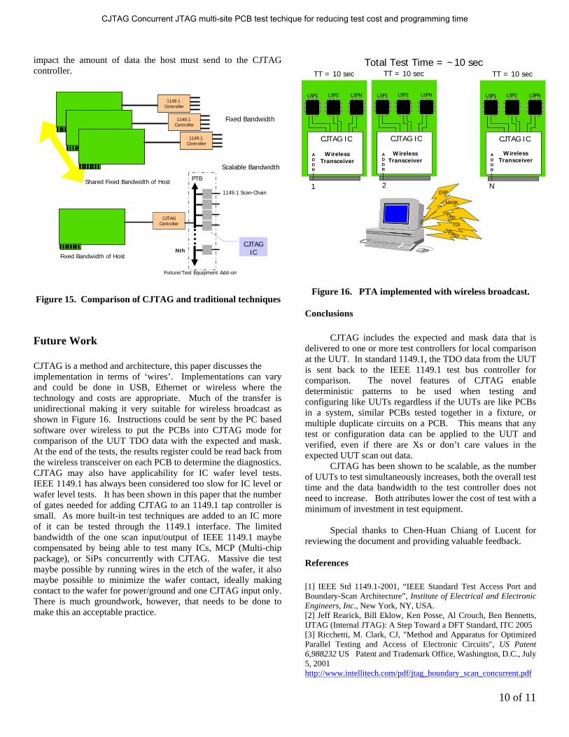
It should be obvious that the CJTAG IC does not need to reside on the PCB. A CJTAG IC with eight or more scan-chains could reside in a fixture or on an ‘interface’ PCB to enable testing of eight or more PCBs at a time with just a single 1149.1 controller enabled for CJTAG test. The test technique also compares favorably with using “four TAP” 1149.1 controllers. Rather than locate two host cards in a PC and share the host bandwidth to make the two “4 TAP” 1149.1 controllers run concurrently, a low cost single TAP 1149.1 controller, enhanced with CJTAG capability and a CJTAG scan linker could test eight PCBs concurrently. CJTAG has scalable bandwidth so it compares well against traditional ‘big iron’ ATE or PC card based 1149.1 controllers (See Figure 15). The host PC has a fixed I/O bandwidth so techniques that rely on the TDO to be sent back to the 1149.1 controller will always be non-scalable, there’s no way to get more bandwidth at the UUTs than is available on the host. These methods also suffer in that there is bandwidth loss turning busses around since traditional 1149.1 is bidirectional, as many ‘bits’ sent out must be returned back. CJTAG changes all of that in that the bandwidth to the UUTs becomes scalable and more efficient. The host could only support 1 Gb/sec of data I/O yet with CJTAG there could easily be 2 Gb/sec of test data bandwidth arriving at the UUTs. Each UUT added to be tested with CJTAG does not
CJTAG Concurrent JTAG multi-site PCB test techique for reducing test cost and programming time
10 of 11
TRST
TMS
Total Test Time = ~10 sec
11
ADDR
CJTAG IC
TT = 10 sec
LSP1 LSP2 LSPN
ADDR
CJTAG IC
TT = 10 sec
LSP1 LSP2 LSPN
ADDR
CJTAG IC
TT = 10 sec
LSP1 LSP2 LSPN
WirelessTransceiver
WirelessTransceiver
WirelessTransceiver
2 NEXP
MASK
TDI
impact the amount of data the host must send to the CJTAG controller.
Figure 15. Comparison of CJTAG and traditional techniques
Future Work CJTAG is a method and architecture, this paper discusses the implementation in terms of ‘wires’. Implementations can vary and could be done in USB, Ethernet or wireless where the technology and costs are appropriate. Much of the transfer is unidirectional making it very suitable for wireless broadcast as shown in Figure 16. Instructions could be sent by the PC based software over wireless to put the PCBs into CJTAG mode for comparison of the UUT TDO data with the expected and mask. At the end of the tests, the results register could be read back from the wireless transceiver on each PCB to determine the diagnostics. CJTAG may also have applicability for IC wafer level tests. IEEE 1149.1 has always been considered too slow for IC level or wafer level tests. It has been shown in this paper that the number of gates needed for adding CJTAG to an 1149.1 tap controller is small. As more built-in test techniques are added to an IC more of it can be tested through the 1149.1 interface. The limited bandwidth of the one scan input/output of IEEE 1149.1 maybe compensated by being able to test many ICs, MCP (Multi-chip package), or SiPs concurrently with CJTAG. Massive die test maybe possible by running wires in the etch of the wafer, it also maybe possible to minimize the wafer contact, ideally making contact to the wafer for power/ground and one CJTAG input only. There is much groundwork, however, that needs to be done to make this an acceptable practice.
Figure 16. PTA implemented with wireless broadcast.
Conclusions CJTAG includes the expected and mask data that is
delivered to one or more test controllers for local comparison at the UUT. In standard 1149.1, the TDO data from the UUT is sent back to the IEEE 1149.1 test bus controller for comparison. The novel features of CJTAG enable deterministic patterns to be used when testing and configuring like UUTs regardless if the UUTs are like PCBs in a system, similar PCBs tested together in a fixture, or multiple duplicate circuits on a PCB. This means that any test or configuration data can be applied to the UUT and verified, even if there are Xs or don’t care values in the expected UUT scan out data.
CJTAG has been shown to be scalable, as the number of UUTs to test simultaneously increases, both the overall test time and the data bandwidth to the test controller does not need to increase. Both attributes lower the cost of test with a minimum of investment in test equipment.
Special thanks to Chen-Huan Chiang of Lucent for
reviewing the document and providing valuable feedback.
References
[1] IEEE Std 1149.1-2001, “IEEE Standard Test Access Port and Boundary-Scan Architecture”, Institute of Electrical and Electronic Engineers, Inc., New York, NY, USA. [2] Jeff Rearick, Bill Eklow, Ken Posse, Al Crouch, Ben Bennetts, IJTAG (Internal JTAG): A Step Toward a DFT Standard, ITC 2005 [3] Ricchetti, M. Clark, CJ, "Method and Apparatus for Optimized Parallel Testing and Access of Electronic Circuits", US Patent 6,988232 US Patent and Trademark Office, Washington, D.C., July 5, 2001 http://www.intellitech.com/pdf/jtag_boundary_scan_concurrent.pdf
1149.1 Controller1149.1
Controller
1149.1 Controller1149.1
Controller
1149.1 Controller1149.1
Controller
Shared Fixed Bandwidth of Host
Fixed Bandwidth
CJTAGController
PTB
Fixed Bandwidth of Host
Fixture/Test Equipment Add-on
1149.1 Scan-Chain
Scalable Bandwidth
NthCJTAG
IC
CJTAG Concurrent JTAG multi-site PCB test techique for reducing test cost and programming time

11 of 11
[4] Clark, CJ, Ricchetti, M., "Method and Apparatus for Optimized Parallel Testing and Access of Electronic Circuits", PCT Patent Application WO03005050, World Intellectual Property Organization, Geneva, Switzerland, July 5, 2001. [5] Clark, CJ, Ricchetti, M., “Infrastructure IP for Configuration and Test of Boards and Systems”, IEEE Design and Test 2003 http://www.intellitech.com/pdf/ieeedandt.pdf [6] Anon., “7-Port Multidrop IEEE 1149.1 (JTAG) Multiplexer”, National Semiconductor Corp., Data Sheet, http://www.national.com/ds.cgi/SC/SCANSTA112.pdf [7] Whetsel, "A Proposed Method of Accessing 1149.1 in a Backplane Environment", 1992 IEEE International Test Conference, paper 8.1. [8] Whetsel, "Hierarchically Accessing 1149.1 in System Environment", 1993 IEEE International Test Conference, paper 23.1. [9] Rakesh N. Joshi, Kenneth L. Williams, Lee Whetsel, “Evolution of IEEE 1149.1 Addressable Shadow Protocol Devices”, ITC 1996 [10]John Andrews: “Using SCANTM Bridge as an IEEE 1149.1 Protocol Addressable, Multi-Drop, Backplane Test Bus”, ITC 1994 [11] Cary Champlin: Backplane Test Bus Selection Criteria. ITC 1994 [12] Anon., "10-Bit Addressable Scan Ports Multidrop-Addressable IEEE Std", Texas Instruments Data Sheets, SCBS489C, April 1999. [13] Anon., "Scan Bridge Hierarchical and Multidrop Addressable JTAG Port", National Semiconductor Corp., Data Sheet SCANPSC110F, October 1999. [14] Gibbs, Clayton Backplane Test Bus Applications for IEEE Std. 1149.1, ITC 2003 [15] Clark, CJ, Ricchetti, M., "A Fast Access Controller for In-System
Programming of FLASH Memory Devices”, BTW ‘03 [16] Ricchetti, M. Clark, CJ, "Method and Apparatus for Providing Optimized Access to Circuits for Debug, Programming and Test", US Patent 6,594,802 US Patent and Trademark Office, Washington, D.C., Nov, 2000. http://www.intellitech.com/pdf/on-board-Device-Programming-patent.pdf [17] Peter Collins, Ilkka Reis, Mikko Simonen, Marc van Houcke, “A Transparent Solution for Providing Remote Wired or Wireless Communication to Board and System Level Boundary-Scan Architectures [18] Clark, CJ, Ricchetti, M., "A Code-less BIST Processor for Embedded Test and in-system configuration of Boards and Systems”, International Test Conference (ITC), October 2004. [19] Harrison, Stephen, et. al. “Hierarchical Boundary-Scan – A chip-set solution”, International Test Conference 2001, Baltimore, Maryland. [20]Anon., "Scan Path Linkers With 4-Bit Identification Buses Scan-Controlled IEEE Std", Texas Instruments Data Sheets, SCAS157D, December 1996 [21]Bennets, Ben,”Practical Applications of Boundary-Scan Technology: Single-Board and Multi-Board Systems”, Tutorial 3, ITC 2004. [22] IEEE Std 1532-2000, “IEEE Standard for In-System Configuration of Programmable Devices”, Institute of Electrical and Electronic Engineers, Inc., New York, NY, USA.
CJTAG Concurrent JTAG multi-site PCB test techique for reducing test cost and programming time