
T H IE B JE L L SYSTEM - bitsavers.org
291
T H IE B JE L L SYSTEM DEVOTED TO THE SCIENTIFIC AND ENGINEERING ASPECTS OF ELECTRICAL COMMUNICATION VOLUME XLVI JANUARY 1967 NUMBER 1 Surface Effects of Radiation on Semiconductor Devices J. P. MITCHELL AND D. K. WILSON 1 A High-Quality 'Vaveguide Directional Filter T. A. ABELE 81 Oil Some Proposed IHodels for Traffic in Connecting Networks v. E. BENES 105 Serics of l\Iiniature Wire Spring Relays C. B. BROWN 117 Oll'-Axis 'Vave-Optics Transmission in a Lens-Like Medium with E. A. J. MARCATILI 149 Low-Resolution TV: An Experimental Digital System for Evaluat- ing Bandwidth-Reduction Techniques F. W. MOUNTS 167 Low-Resolution TV: Subjective Comparison of Interlaced and Noninterlaced Pictures E. F. BROWN 199 Low-Resolution TV: Subjective Effects of Noise Added to a Signal R. C. BRAINARD I .. ow-Resolution TV: Subjective Effects of Frame Repetition and Picture Replenishment R. C. BRAINARD, F. W. MOUNTS AND B. PRASADA = Contributors to This Issue B.S.T.J. Briefs: The Effect of Noise Correlation on Binary Differ- entially Coherent PSK Communication Systems, w. 1\1. HUBBARD; Excited Level Populations in High Current Density Argon Discharges, R. c. MILLER, E. F. LABUDA AND C. E. WEBB; CvV Opera- tion of LSA Oscillator Diodes--44 to 88 GHz, J. A. COPELAND COl'YltiGHT © 1967 AMERICAN TELEPHONE AND TELEGRAPH COMPANY
-
Upload
khangminh22 -
Category
Documents
-
view
0 -
download
0
Transcript of T H IE B JE L L SYSTEM - bitsavers.org

T H IE B JE L L SYSTEM
DEVOTED TO THE SCIENTIFIC AND ENGINEERING
ASPECTS OF ELECTRICAL COMMUNICATION
VOLUME XLVI JANUARY 1967 NUMBER 1
Surface Effects of Radiation on Semiconductor Devices J. P. MITCHELL AND D. K. WILSON 1
A High-Quality 'Vaveguide Directional Filter T. A. ABELE 81
Oil Some Proposed IHodels for Traffic in Connecting Networks v. E. BENES 105
~\ Serics of l\Iiniature Wire Spring Relays C. B. BROWN 117
Oll'-Axis 'Vave-Optics Transmission in a Lens-Like Medium with ~\berratioll E. A. J. MARCATILI 149
Low-Resolution TV: An Experimental Digital System for Evaluat-ing Bandwidth-Reduction Techniques F. W. MOUNTS 167
Low-Resolution TV: Subjective Comparison of Interlaced and Noninterlaced Pictures E. F. BROWN 199
Low-Resolution TV: Subjective Effects of Noise Added to a Signal R. C. BRAINARD ~33
I .. ow-Resolution TV: Subjective Effects of Frame Repetition and Picture Replenishment
R. C. BRAINARD, F. W. MOUNTS AND B. PRASADA ~Gl
=
Contributors to This Issue ~73
B.S.T.J. Briefs: The Effect of Noise Correlation on Binary Differentially Coherent PSK Communication Systems, w. 1\1. HUBBARD;
Excited Level Populations in High Current Density Argon Discharges, R. c. MILLER, E. F. LABUDA AND C. E. WEBB; CvV Opera-tion of LSA Oscillator Diodes--44 to 88 GHz, J. A. COPELAND ~77
COl'YltiGHT © 1967 AMERICAN TELEPHONE AND TELEGRAPH COMPANY

THE BELL SYSTEM TECHNICAL JOURN AL
ADVISORY BOARD
P. A. GORMAN, President, lVestern Electric Company
J. B. FISK, President, Bell Telephone Laboratdries
B. S. GILMER, Executive Vice President, American Telephone and Telegraph Company
EDITORIAL C01IM ITTEE
W. E. DANIELSON, Chairman
F. T. ANDRE"'\YS, JR. E. D. REED
E. E. DAVID M. TANENBAUM
C. W. HOOVER, JR. S. W. WASHBURN
D. H. LOONEY Q. W. WIEST
E. C. READ C. R. WILLIAMSON
EDITORIAL ST AFF
G. E. SCHINDLER, JR., Editor L. A. HOWARD, JR., Assistant Editor
H. J\L PURVI A N CE, Prodllction and Illustrations
F. J. SCHWETJE, Circulation
THE BELL SYSTEM TECHNICAL JOURNAL is published ten times a year by the American Telephone and Telegraph Company, H. 1. Romnes, President, C. E. Wampler, Vice President and Secretary, J. J. Scanlon, Vice President and Treasurer. Checks for subscriptions should be made payable to American Telephone and Telegraph Company and should be addressed to the Treasury Department, Room 2312C, 195 Broadway, New York, N. y. 10007. Subscriptions $5.00 per year; single copies $1.25 each. Foreign postage $1.08 per year; 18 cents per copy. Printed in U.S.A.

THE BELJ~ SYSTEM
TECHNICAL JOURNAL VOLUME XLVI JANUARY 1967
Copyright © 1967, American Telephone and Telegraph Company
Surface Effects of Radiation 011
Senliconductor Devices*
By J. P. MITCHELL and D. K. WILSON
(Manuscript received June 21, 1966)
NUMBER 1
A brief review of surface physics is given as background for the subsequent discussion on the role of surfaces in the behavior of sem,iconductor devices. The effects of channels and surface generation-recOJnbination on p-n junctions and transistor characteristics are discussed.
The observed effects of ionizing radiation on nonpassivated, gas-filled transistors are interpreted in tenns of a 17wdel in which ions fonned in the gas mnbient deposit charge on the device surface. The resultant surface charge buildup creates channels on the device surface which cause a decrease in hF E and increase in I CBO • Saturation, recovery, and the effects of dose rate and bias are also discussed.
Degradation of planar passivated transistors and other devices employing Si02 layers due to radiation is silrtilar to that observed for nonpassivated devices. Surface charge buildup affects the device surface and leads to degradation. The bulk of experinwntaZ evidence points to accUlnulation of positive charge at the Si02-Si interface as the cause of degradation. Several possible 1Jwans of charge buildup at the interface are discussed. However, the process responsible has not, as yet, been identified.
The direction of future experiments is discussed, particularly of those experinwnts which may yield information about the part played by radiation in positive charge accUlnulation at the Si0 2-Si interface.
* The research reported in this paper was sponsored by, but does not necessarily constitute the opinion of, the Air Force Cambridge Research Laboratories, Office of Aerospace Research, under contract AF 19(628)-4157.
1

2 THE BELL SYSTEM TECHNICAL JOURNAL, JANUARY 1967
I. IN'l'RODUC'l'ION
When a semiconductor is exposed to nuclear radiation, two basically different effects may occur. First, the radiation will cause ionization through one of a number of electronic excitation processes. Second, if the radiation energy exceeds a threshold value which depends on the nature of the irradiating particle, some of the atoms in the semiconductor lattice will be displaced. If the semiconductor exposed to radiation ]s part of a device, the device characteristics will change; the changes depend on such factors as the nature and energy of the radiation, the materials and geometry of the device, and even the processes used in manufacturing the device. The changes in characteristics which occur when these effects take place in the bulk of a device have been investigated for some time and are quite well understood in terms of the usual physics of solids. However, effects can also occur at the surface of a device, giving rise to the so-called surface effects which have only more recently received attention and which are governed by the less well understood physics of surfaces.
The failure of the Telstar® satellite in 1962 was explained in terms of surface damage to transistors in the command circuits, damage caused by radiation received during transit through the Van Allen belt. l
From the experience gained in analyzing this failure, it is apparent that surface effects of radiation may often control the behavior of solid state devices subjected to nuclear radiation. In present-day semiconductor technology, the effects of radiation damage in the bulk have been reduced in transistors by using very shallow, diffused junctions. As a result, the surfaces have become the most radiation sensitive areas of these devices. Thus, a knowledge of surface effects is necessary if the decrease in sensitivity to bulk radiation effects is to be fully exploited.
The purpose of this paper is to present as unified and comprehensive a picture as possible of the work done to date on the surface effects of radiation on semiconductor devices. The task is hampered somewhat by the way in which much of the information on radiation effects is presented in the literature. Many authors do not distinguish between bulk and surface effects, and indeed in many experiments it is virtually impossible to do so. For this reason this paper will be, for the most part, restricted to those experiments which deal specifically with surface effects.
Some areas of the surface problem appear to be fairly well understood. The degradation process in nonpassivated devices in gaseous ambients has been satisfactorily explained in terms of surface channeling at exposed p-n junction surfaces. On the other hand, no such satisfactory

RADIATION EFFECTS 3
picture has been published for planar transistors. The results at the moment are somewhat confused, contradictory, and incomplete. It is hoped that this summary n1.ay help to illuminate the problem and suggest paths for future studies.
A brief discussion of the present physical theory of surfaces, as required for an understanding of device degradation, will be given before starting a discussion of experimental results and specific models for radiation effects on surfaces since it is against this background that radiation effects n1.ust be explained. For a more complete discussion of surfaces, the reader is referred to works by Many, Goldstein and Grover,2 Watkins,3 and Law. 4
II. SURFACE PHYSICS
2.1 Surface Charges and Surface Potential
An atomically clean crystal surface, such as might be found upon cleaving a crystal, would show broken or dangling bonds associated with the surface atoms. If the bonds are covalent, then presumably each bond, which could hold two electrons, would be half-filled and, therefore, is able to act as an acceptor state. If these acceptor states become filled, the crystal surface would then have a net negative charge. One might, therefore, expect to find a negative surface charge of ~1015 electrons per cm2
, i.e., one excess electron per surface atom. If the crystal is a metal, the surface charge would be neutralized in a depth of a few angstrom units since metals have a high density of charge carriers. For a semiconductor, however, the much smaller concentration of charge carriers means that the effects of the surface charge will be present as far as ~lJL into the crystal. It should be noted that in this surface region the charge carriers will be holes regardless of the conductivity type of the bulk; i.e., the surface will always be p-type.
Such atomically clean surfaces have been achieved on both silicon and germanium, but they can only be maintained in a very clean vaCUum. In any other ambient, the highly reactive surfaces of these semiconductors will readily absorb several atomic layers from the ambient. These layers (usually oxide) will neutralize most of the surface states due to broken bonds. Some energy states will still exist at the crystal surface, however, either as a result of unsaturated lattice bonds or as a result of impurities or imperfections at the semiconductor surface. The density of these states is typically 1011 to 1012 per cm2
• These states, called "fast" states, are in good electrical contact with the bulk material and have relaxation times of about 10-7 s. As a consequence, the fast surface
4 THE BELL SYSTEM TECHNICAL JOURNAL, JANUAHY 1967
states are often the controlling centers of minority carrier recombination and generation.
In addition to the states at the interface, states arise which are caused by ions in or on the surface of the film adsorbed on a semiconductor. These states may be sources or sinks for mobile carriers. Because of poor electrical contact between these states and the semiconductor, mobile carriers are exchanged slowly between the two, presumably by some tunneling or diffusion process. These ionic states are called the "slow" surface states and have relaxation times from 10-3 seconds up to many minutes. Since the states may be positively or negatively charged, they can give rise to surface layers of either p- or n-type. Although little quantitative information is available, it is believed that the densities of slow states are of the order of 1012 to 1013 per cm2.
For Si surfaces covered by a thick layer (~103 -104 A) of deliberately grown oxide, so-called passivated surfaces, the situation is more complicated and the distinction between fast and slow surface states is not a very meaningful one. Surface charges may arise in these thick oxides for several different reasons and may be located on either surface of the oxide or anywhere within the oxide itself. It is customary, therefore, to discuss effects on passivated Si surfaces in terms of surface charge in the oxide and states at the Si02-Si interface. These interface states are essentially fast states similar to those discussed above for nonpassivated surfaces.
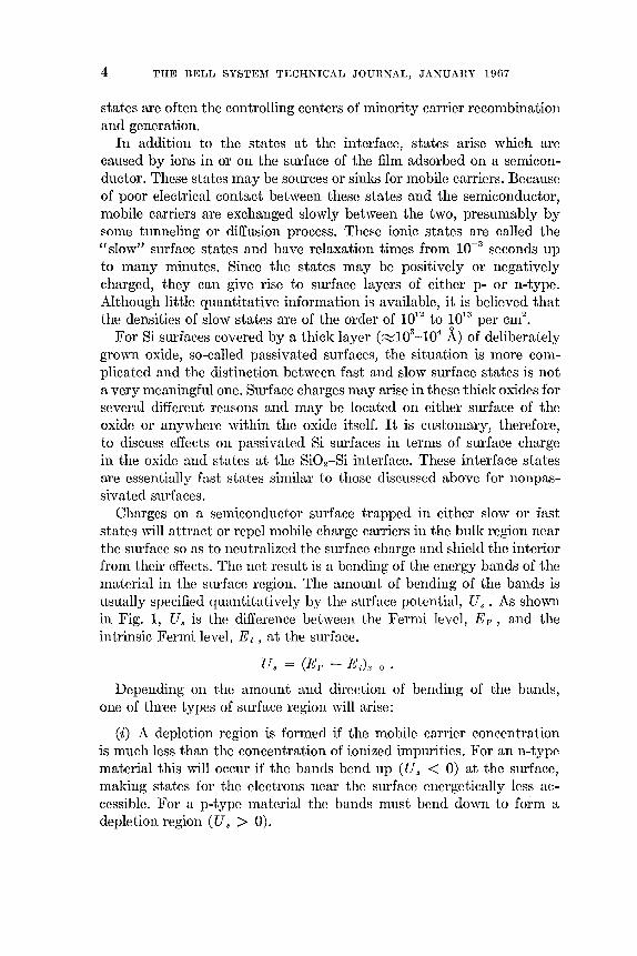
Charges on a semiconductor surface trapped in either slow or fast states will attract or repel mobile charge carriers in the bulk region near the surface so as to neutralized the surface charge and shield the interior from their effects. The net result is a bending of the energy bands of the material in the surface region. The amount of bending of the bands is usually specified quantitatively by the surface potential, Us. As shown in Fig. 1, Us is the difference between the Fermi level, E p, and the intrinsic Fermi level, Ei , at the surface.
Us = (Ep - Ei)x=o .
Depending on the amount and direction of bending of the bands, one of three types of surface region will arise:
(i) A depletion region is formed if the mobile carrier concentration is much less than the concentration of ionized impurities. For an n-type material this will occur if the bands bend up (Us < 0) at the surface, making states for the electrons near the surface energetically less accessible. For a p-type nlaterial the bands must bend down to form a depletion region (Us> 0).

x
x
x x
OXIDE
RADIATION EFFEC'l'S
- ELECTRONS X SLOW STATES
+ HOLES !J. FAST STATES
I CONDUCTION I BAND
~--------J---~ I
I---~-'-------------EF FERMI LEVEL :
I I I
~------- EL FEI~~~I~~~~L ENG~~GY I I I I I I
~-------EV ___ ---t.
+ + lALENCE :x: DISTANCE INTO CRYSTAL : BAND
I
Fig. 1-Band structure at the surface of a semiconductor.
5
(ii) A depletion layer may become an inversion layer if the bending of the bands is increased sufficiently. This case is illustrated in Fig. 1 for an n-type material where the minority carriers dominate in the surface region. An inversion layer will, of course, have a depletion region behind it.
(iii) If for any reason the bands bend down for an n-type (or up for a p-type) semiconductor, excess majority carriers will collect in the surface region and an accumulation layer will result. The three cases are illustrated for both n- and p-type materials in Fig. 2.
It is apparent from the above discussion that the concentration of charge carriers and hence the conductivity of the surface layer of a semiconductor may differ considerably from the bulk values. In practice it is possible to obtain valuable information about surface effects by purposely changing the surface potential (and hence the bending of the bands) of a semiconductor and observing the resultant changes in surface conductivity.
2.2 Control of Surface Potential
The surface potential of a semiconductor is controlled through the charge in the surface states. In this regard the slow states are the more

6 THE BELL SYSTEM TECHNICAL JOURNAL, JANUARY 19G7
n-TYPE
e e - - - - - - - Ec
e 1:------------E F
e e e
--------+---------+-Ev
0 C±> C±> C±> ®
+
p-TYPE
- Ec
EF
+ + + + + Ey
(a) DEPLETION
e e e e e ~---------------Ec
e~~ ________ _ e e e e
----+-----+-Ey
C±> ------------------ Ec
® C±> (±) /-------EL C±> 1--7-=:...---------- EF ®
(±) + + + + + + Ey (±)
®
(b) INVERSION
------------------Ec
® f------------ EF (±) /--------EL ® ® ® ®
__ --+-------+-------Ey
e e e
~--------------- Ec
~ '-------- EL e 1:----------- EF
--+----+----+---+----- Ev
(c) ACCUMULATION
- ELECTRONS
+ HOLES e NEGATIVE IONS
C±> POSITIVE IONS
Fig. 2 - Depletion, inversion, and accumulation surface layers for ll- and p-type semiconductors.
important since they are usually at least an order of magnitude more numerous than the fast states. There are two methods commonly used for controlling surface charge. In one method the charge is determined by the choice of ambient. For example, gaseous ambients such as oxygen or ozone have strong electron affinities and induce a negative charge

RADIATION EFFECTS 7
on the surface which attracts to it mobile holes. Water vapor and ammonia, on the other hand, produce a positive surface charge, i.e., contribute donor states. Thus, by exposing a semiconductor to the appropriate ambient it is possible to produce, within reasonable limits, a desired surface potential.
The thermally grown Si02 layer on Si devices is a particular type of ambient widely used in device fabrication. This oxide stabilizes the I:lurface by saturating the dangling bonds of the Si surface and by separating the Si from the slow states by the thickness of the oxide. This so-called passivation technique, although it does not completely isolate the semiconductor from the ambient, does reduce its sensitivity to ambient variations.
A second method of controlling surface potential is through the use of a field plate. As shown in Fig. 3, a metal field plate is placed parallel to the semiconductor surface so as to form a capacitor between it and the semiconductor. The space between the field plate and the semiconductor is filled with some insulator such as Si02 • The conductivity type of the semiconductor surface layer may be controlled by the applied potential. For example, if the field plate is positive with respect to the semiconductor, electrons will be attracted to and holes repelled from the surface, with the result that the surface layer tends to become more n-type. By the same argument, if the polarity of the potential is reversed, a tendency toward a p-type surface results. The field effect method of controlling surface conductivity is the operating principle of the metal-oxide-semiconductor field effect transistor (MOS-FET). In this device the conductivity of the base, and hence the source-todrain current, is controlled by the gate (field plate) potential.
2.3 Surface ReC01nbination Velocity
The fast states at a semiconductor surface are very important from a device standpoint since they act as recombination centers. These
METAL FIELD PLATE ......
" + + + + ++
INSULATOR
,/-~~~~~~ I
/ SURFACE
REGION
Fig. 3 - Fielu plate methou of wntrolling surface potential.
+ APPLIED
POTENTIAL
8 THE BELL SYSTEM TECHNICAL JOURNAL, JANUARY 1967
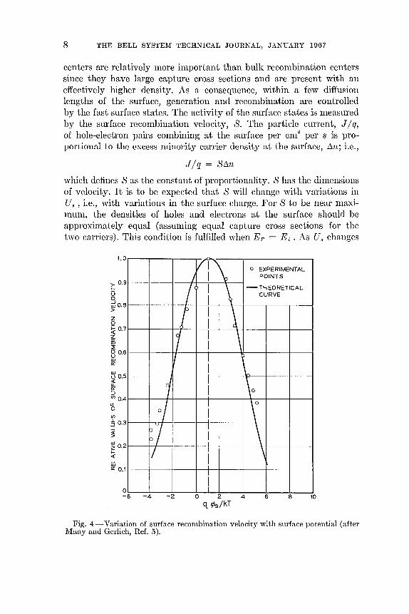
centers are relatively more important than bulk recombination centers since they have large capture cross sections and are present with an effectively higher density. As a consequence, within a few diffusion lengths of the surface, generation and recombination are controlled by the fast surface states. The activity of the surface states is measured by the surface recombination velocity, S. The particle current, J / q, of hole-electron pairs combining at the surface per cm2 per s is proportional to the excess minority carrier density at the surface, ~n; i.e.,
J/q = S~n
which defines S as the constant of proportionality. S has the dimensions of velocity. It is to be expected that S will change with variations in U 8 , i.e., with variations in the surface charge. For S to be near maximum, the densities of holes and electrons at the surface should be approximately equal (assuming equal capture cross sections for the two carriers). This condition is fulfilled when Ep = Ei . As U8 changes
1.0 .... /1' o EXPERIMENTAL
>- 0.9 l-
/ I ~ POINTS
V g w O.8 > Z o ~ 0.7 z iIi ~ 8 0.6 w 0::
~ 0.5 ~ 0:: :J i
I ! 1 I
CI) 0.4 IL o (/)
~ 0.3 .J
0/ ~
~ 0.2 j::: ~ .J W a:: 0.1
o
~7 II
-6 -4 -2
I \ -THEORETICAL
I CURVE
I ~ I 1 \ 1
I ~
l
I \0 I \0 I I \ I I
i \ I I
! o 2 4 6 8
q ct>s/kT 10
Fig. 4 - Variation of surface recombination velocity with surface potential (after Many and Gerlich, Ref. 5).
RADIATION EFFECTS 9
in either direction from zero, the bands bend up or down causing the concentration of one type of carrier to increase and the other to decrease. The result in either case is a decrease in S. Fig. 4 shows, as an illustration, the variation of S with surface potential, CPa, for a Ge surface as reported by Many and Gerlich. 5 It is apparent that changes in S of almost an order of magnitude are possible. The recombination velocity for Si surfaces has been found to be larger than that for Ge, but shows a similar dependence on Us .6
2.4 Channeling
An important result of surface states which are sufficiently dense to produce an inversion layer at the surface is the effect known as channeling. Brown7 discovered that the anomalous leakage current between the n-regions of an npn structure was the result of channels, i.e., inversion layers, formed across the p-region, which provided a conduction path of the same conductivity type as the end regions. Channel formation may occur at any p-n junction, generally on the low conductivity side of the junction. Channels have the effect of adding currents in parallel with the main junction currents. The times involved in channel formation indicate that the phenomenon is connected with the slow surface states. It will become apparent that channeling is the dominant surface effect for many semiconductor devices.
111. EFFECTS OF SURFACES ON DEVICES
3.1 p-n Junction Forward Characteristics
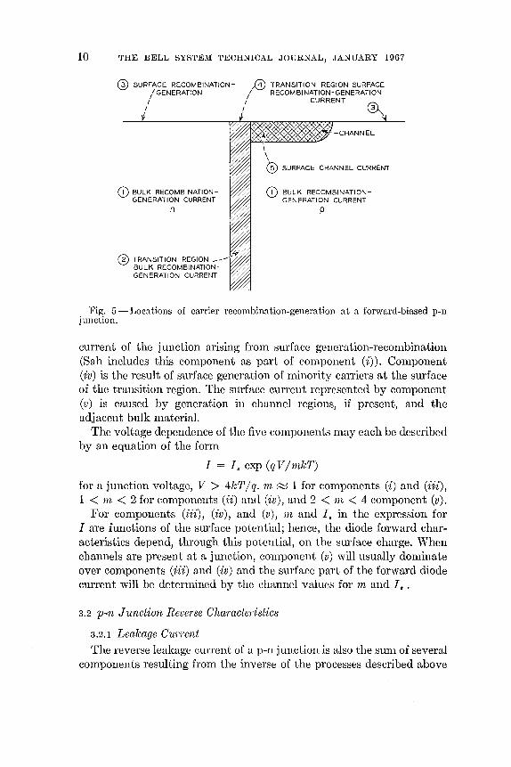
The effect of surface recombination and channel formation on p-n junction forward characteristics has been discussed by Sah.s The junction current can be divided into several components based on the location of the carrier recombination-generation. The components are (see Fig. 5):
(i) bulk recombination-generation on either side of the junction, (ii) transition region bulk recombination-generation current, (iii) surface recombination-generation current on either side of the
junction, (iv) transition region surface recombination-generation current, and (v) surface channel current.
The first component is the usual diffusion current of a forward-biased junction. The second component arises from electron-hole generation by traps located in the bulk of the transition region. These two components are not affected by surface conditions. Component (iii) is the diffusion
10 THE BELL SYSTEM TECHNICAL JOURNAL, JANUARY 1967
@ SURFACE RECOMBINATION" GENERATION
I I
CD BULK RECOMBINATIONGENERATION CURRENT
n
~ o TRANSITION REGION ---"" BULK RECOMBINATIONGENERATION CURRENT
,@ TRANSITION REGION SURFACE / RECOMBINATION-GENERATION
/ CURRENT ® , ,
-CHANNEL I \ \
GD SURFACE CHANNEL CURRENT
CD BULK RECOMBINATIONGENERATION CURRENT
P
Fig. 5 - Locations of carrier recombination-generation at a forward-biased p-n junction.
current of the junction arising from surface generation-recombination (Sah includes this component as part of component (i». Component (iv) is the result of surface generation of minority carriers at the surface of the transition region. The surface current represented by component (v) is caused by generation in channel regions, if present, and the adjacent bulk material.
The voltage dependence of the five components may each be described by an equation of the form
I = I. exp (q V /mk71)
for a junction voltage, V > 4kT / q. m ~ 1 for components (i) and (iii), 1 < m < 2 for components (ii) and (iv), and 2 < m < 4 component (v).
For components (iii), (iv) , and (v), 1n and I. in the expression for I are functions of the surface potential; hence, the diode forward characteristics depend, through this potential, on the surface charge. When channels are present at a junction, component (v) will usually dominate over components (iii) and (iv) and the surface part of the forward diode current will be determined by the channel values for m and Ia .
3.2 p-n Junction Reverse Characteristics
3.2.1 Leakage Current
The reverse leakage current of a p-n junction is also the sum of several components resulting from the inverse of the processes described above

RADIATION EFFECTS 11
for the forward current. Thus, a bulk component arises from thermally generated minority carriers which are created within or diffuse to the space charge region and are swept across the junction by the reverse bias field. The surface near the junction is also a source of minority carriers and produces components of reverse current from the surface both outside and inside and junction space charge region.
If channeling is present when a diode is under reverse bias, the reverse current will be increased for two reasons. First, the channel increases the effective area of the junction and thereby increases the number of thermally generated minority carriers diffusing across the junction. Second, an increase in area takes place at the surface which, because of surface sites, has a high generation of carriers. A further result of the increased junction area is an increased junction capacity (which provides a convenient means of detecting the presence of channels).
The above explanation appears to be satisfactory to explain the reverse current observed in most Si and Ge junctions. However, for some Si junctions, particularly of the p + n type, the reverse leakage currents is often too large to be explained as entirely the result of generationrecombination in the increased junction area at the surface. Grove and Fitzgerald9 have explained the anomalous current as the result of breakdown through the narrow depletion layer of the induced p-n junction caused by the channel.
3.2.2 Breakdown
The breakdown voltage of a reverse-biased junction is, in many cases, reduced below the value expected for bulk breakdown by surface conditions at the junction. Surface breakdown, like bulk breakdown, is an avalanche process and takes place at localized areas of the surface. It has been found that an inversion layer formed on the high resistivity side of a junction raises the breakdown voltage, while formation of an accumulation layer tends to lower it.
3.2.3 1/! Noise
Semiconductor devices often exhibit a noise whose spectral output is inversely proportional to frequency and which is referred to as l/t noise. It is believed that this noise originates at the semiconductor surface; certainly it is very sensitive to surface conditions. According to McWhorter,lO 1/! noise is the result of fluctuations in the charge in the slow states which cause corresponding changes in the semiconductor conductivity. Experimentally, it is known that l/t noise increases when the semiconductor surface layer changes from accumulation to inver-

12 'l'HE BELL SYSTEM TECHNICAL JOUHNAL, JANUAHY 1907
sion. Atalla and his associatesll have found that Si02 passivation significantly reduces l/f noise.
3.3 Effects of Surface Recombination and Channeling on Junction Transistors
The effects of channeling and surface recombination on transistors are somewhat more complicated than for simple p-n junctions. As might be expected, 1 CBO for the transistor behaves in a similar way to a diodejunction reverse current. 1 CBO may also be increased by the formation of a channel across the base region so as to provide a leakage path from emitter to collector.
The current gain of a transistor may be affected by both channel and surface recombination in the region of the emitter-base junction. The common emitter gain, hpB = (1 C - 1 cEo)/1B is influenced through 1 B. If the base transport factor ({J) of a transistor is decreased because of increased surface recombination at the base surface, then 1 B is increased to supply majority carriers for recombination. This recombination corresponds to an increase in a component of the emitter ClITrent with an exp (q V /mkT) dependence where m ~ 1. Generation-recombination at the surface of the emitter-base transition region lowers the emitter efficiency ('Y) and also decreases hp E • This corresponds to an increase in an emitter current component with an exp (qV /mkr) dependence with 1 < 1rt < 2. These effects of surface recombination and channeling on junction transistor characteristics have received experimental support from the work on Sah,8 Kuper,12 and I wersen et a1. 13 Kuper found that the base current, 1 B, of diffused base Ge transistors was quite sensitive to surface traps at the surface of the emitter-space charge region. The effect of these traps on recombination could be increased by removing water from the slITface oxide, resulting in an order of magnitude decrease in h pE • The surface region of the emitter-base junction would thus appear to be the region which controls the common emitter current gain in Ge transistors.
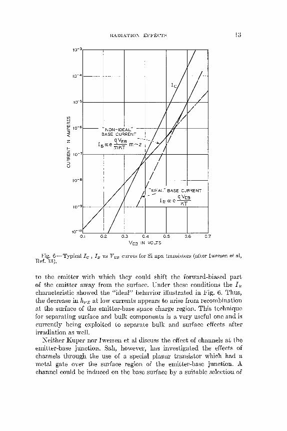
The gain degradation in Si transistors at low currents was investigated by I wersen. Fig. G shows a typical dependence obtained by I wersen of 1 C and 1 B on V E B for silicon npn transistors. The 1 B
characteristic has two components, an "ideal" one at high currents with 1 B 0:: exp (q V EB/kT) and a "nonideal" one at low currents with 1 B 0:: exp (q V EB/mkT) with m ~ 2. The latter component according to Sah's model could come from recombination in the emitter-base space charge region either in the bulk or at the surface. I wersen et al used transistor-like structures with an additional electrode connected
(f) w a::
HADIATIO~ EFFECTS
10-0l------I------I------f----t-I--____,I------r---t
~ 10- 6
2 \\ NON-IDEAL" BASE CURRENT <{
~
f
qVEB ---~ ISoce mKT m"'2
~ 10-7~--.---.--____,~~~~--~-~ a:: a:: ::> u
10-B~--~--~+_-~--~--r_-~
A "IDEAL" BASE CURRENT
-- qVEB IBOCe~
1O-9~------,lf----~~---L-I__--.---.--___j
0.2 0.3 0.4 0.5 0.6 0.7
VES IN VOLTS
1') .,
Fig. 6-Typical Ie, IB vs VEB curves for Si npn transistors (after Iwersen et aI, Ref. 13).
to the emitter with which they could shift the forward-biased part of the emitter away from the surface. Under these conditions the I B
characteristic showed the "ideal" behavior illustrated in Fig. 6. Thus, the decrease in hFE at low currents appears to arise from recombination at the surface of the emitter-base space charge region. This technique for separating surface and bulk components is a very useful one and is currently being exploited to separate bulk and surface effects after irradiation as well.
N either Kuper nor I wersen et al discuss the effect of channels at the emitter-base junction. Sah, however, has investigated the effects of channels through the use of a special planar transistor which had a metal gate over the surface region of the emitter-base junction. A channel could he induced on the base surface by a suitable selection of

14 THE BELL SYSTEM TECHNICAL JOURNAL, JANUARY 1967
(f) w n:: w 0... ~ <1:
~ (J)
......
2
10-5~~~~~~4-----4-~--~~~~--~-+~~~
10-7H-----+_--~+__4--~_+--~--_+~~~~----~
10-8~ ____ L-__ ~~~~~~ __ ~ __ ~~~ __ ~ ____ ~
o 0.1 0.2 0.3 0.4 0.5 0.6 0.7
VEB IN VOLTS
Fig. 7-Forward emitter characteristics for a surface channel (VGB = +20V) and for no surface channel (VGB = -20V) (after Sah, Ref. 8).
gate potential, V GB • Fig. 7 shows the junction current, I B , as a function of junction voltage, V EB , for temperatures ranging from - 26 ° to IS0°C. The solid curves correspond to the absence of channels (V GB = - 20V) while the dashed curves are for the case of channels present (V GB =
+20V). It is apparent from Fig. 7 that m is much larger (m ~ 9 for channels as compared with m ~ 1.4 for no channels) when channels are present and that when channels are present the channel components of the junction current will dominate. It is apparent that IBis much less temperature dependent when channels are present.
According to Sah, the surface recombination current is considerably
RADIATION EFFECTS 15
higher on a bare surface than on an oxide-protected surface. Hence, we should expect to find a higher hF E for protected devices. As predicted, Sah finds the gains for Si planar transistors are higher at all collector currents for oxide-protected devices than for the same devices after the oxide has been removed.
IV. SURFACE EFFECTS OF RADIATION ON NONPASSIVATED MATERIALS AND
DEVICES
4.1 Introduction
There are two types of effects on the bulk of a semiconductor resulting from irradiation by energetic particles or photons. First, new defects are created which introduce additional energy levels in the energy gap of the semiconductor. Second, intense ionization is produced, most of which decays quickly, but a certain fraction of which may be trapped in rather long-lived excited states. The kind and number of defect states introduced into the bulk are very sensitive to the nature of the bombarding particle and its energy. On the other hand, the ionization produced in the bulk is presumably sensitive only to the total energy adsorbed.
The surface of a semiconductor is presumed to be a highly imperfect structure. Hence, it has been tacitly assumed that the radiation levels which significantly affect the number of bulk defect states could not similarly affect the number of surface defect states. This assumption may be invalid for the reasons discussed in the following paragraphs.
It is believed that the primary defects introduced by radiation are vacancies and interstitials. However, there is strong experimental evidence that these primary defects interact almost immediately with existing crystal defects. If they do not do so, there appears to be a strong likelihood that the vacancies and interstitials annihilate one another, i.e., that frozen-in vacancies and interstitials per se do not exist. There is also strong experimental evidence indicating that existing defects in the semiconductor crystal may often be electrically inactive but become electrically active when attached to a primary radiation defect. Hence, the surface, with its high concentration of existing defects, may be a sink for primary radiation defects. The result of such an interaction could be a significant change in the number of impurity levels at the surface upon irradiation, i.e., an increase in the density of fast states at the interface of the semiconductor and any adsorbed surface layer. In addition, the density of active (charged) slow states can be increased by purely electronic processes produced by ionizing
16 THE BELL SYSTEM TECHNICAL JOUHNAL, JAKUAHY 19()7
radiation effects within or on the adsorbed surface layer. These change::; in charge state of the surface defects can be very long-lived because of the weak electronic interaction of these surface defects and the bulk of the semiconductor.
The evidence on nonpassivated devices tends to support the picture that the predominant effects of radiation on nonpassivated surfaces are changes in the charge in slow states rather than the creation of new defects. Hence, most experiments on surface effects have not concerned themselves with the nature of the ionizing particle but only with the energy absorbed (dose) at the surface. Most experiments have, therefore, been done with C060 gamma rays as a matter of convenience, with a few investigations using energetic electrons. (The calculation of absorbed dose for an electron beam is discussed in Appendix B.) The possibility outlined above for the creation of additional defect states by the interaction of primary defects with existing defects and their dependence on the nature of the bombarding particle has not been adequately explored.
4.2 Effects of Radiation on Selniconductor Surfaces
There have been limited experimental studies on single crystal semiconductor sanlples of the effects of ionizing radiation on surface phenomena. Among the studies that could be cited is the work of Spear,14.15 who investigated the effects of radiation on the photoconductive response in germanium down to energies of O.S e V, i.e., well below the absorption band edge. This response arises from deep-lying surface states. Irradiation with very low energy electrons (~S ke V) was found to quench this photoconductivity. Spear attributed this quenching to radiation-induced changes in the surface potential with the result that the surface became more n-type. Similar changes in surface potential of n-type Si were found by Spear for both 3 and SOO ke V electron irradiation.
The effects of irradiation by C060 gamma rays and energetic electrons on the surface recombination velocity in n-type Ge have been studied by Komatsubara.16 .17 He used alloyed p-n junctions with a nickel field plate on the opposite side of the Ge wafer from the alloyed junction. By using a wafer whose thickness was small compared to a diffusion length, he made the reverse current of the junction, 1 8 , proportional to the surface recombination velocity, S. In this way he was able to obtain directly an oscilloscope presentation of the variation of recombination velocity with surface potential, Us , using a SO-Hz ac voltage on the field plate. His results before and after various levels of 'Y bombardment are shown in Fig. 8 and can be compared with the theoretical

t tors (s)
RADIATION EFFECTS
-us + Us
17
PHOTONs/em 2
3.33 Xl015
8.22 X 10¹⁵
1.13x 10¹⁶
2.8 X lO16
4.03 X 10¹⁶
4.8x 10 16
7.3 X 10¹⁶
8.6xl0 16
Fig. 8-Change of Is vs Us eurves of 30 ohm-em n-type Ge with radiation (after Komatsllbara, Ref. 17).
18 THE BELL SYSTEM TECHNICAL JOURNAL, JANUARY 1967
variation shown in Fig. 4. There is obviously a considerable shift in the surface potential, which Komatsubara attributed to new fast surface states produced by the radiation.
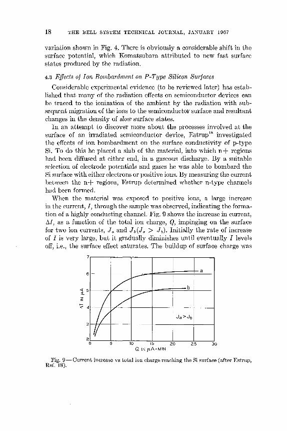
4.3 Effects of Ion Bmnbardnwnt on P-Type Silicon Surfaces
Considerable experimental evidence (to be reviewed later) has established that many of the radiation effects on semiconductor devices can be traced to the ionization of the ambient by the radiation with subsequent migration of the ions to the semiconductor surface and resultant changes in the density of slow surface states.
In an attempt to discover more about the processes involved at the surface of an irradiated semiconductor device, Estrup18 investigated the effects of ion bombardment on the surface conductivity of p-type 8i. To do this he placed a slab of the material, into which n + regions had been diffused at either end, in a gaseous discharge. By a suitable selection of electrode potentials and gases he was able to bombard the 8i ~urface with either electrons or positive ions. By measuring the current between the n + regions, Estrup determined whether n-type channels had been formed.
When the material was exposed to positive ions, a large increase in the current, I, through the sample was observed, indicating the formation of a highly conducting channel. Fig. 9 shows the increase in current, ~I, as a function of the total ion charge, Q, impinging on the surface for two ion currents, J a and Jb(Ja > J b). Initially the rate of increase of I is very large, but it gradually diminishes until eventually I levels off, i.e., the surface effect saturates. The buildup of surface charge was
7
6
« 5 ::t
H <l 4
3
2 o
a
/' :....--
b
/ / ~
!/v Ja>Jb
r 5 10 15 20 25 30
Q IN J.LA.MIN
Fig. 9 - Current increase vs total ion charge reaching the Si surface (after Estrup, Ref. 18).

<t: ::t
4.0
3.5
3.0
~ 2.5 ..... <l
2.0
1.5
1.0
I~ -a\ "\
'" "
RADIATION EFFECTS
~ I
}j Ie
" (
I
"'- I
',,- I /
r-..... It
" ~
"'--I r--I r---I -- ---.§
1""'---r---1"---_ I c I -,
..... b
o 2.5 5.0 7.5 10.0 12.5 15.0 17.5 20.0 22.5 25.0
TIME IN MINUTES
Fig. 10 - Current increase as a function of time (after Estrup, Ref. 18).
19
found to depend primarily on the ion current, the bulk material conductivity type, and the surface condition.
The surface effects of ions were found to be similar to those produced by chemical treatments except that the surface charge induced by the ions was unstable. The effects of positive ions could be counteracted by exposure to gases, such as O2 , which tend to produce a negative surface charge but were little affected by those, such as NH3 , which produce a positive surface charge.
At the termination of the discharge, the excess current recovered as shown in curve (a) of Fig. 10. It was found that heating or exposure to ultraviolet radiation accelerated the recovery rate. Exposure to electrons caused an instantaneous decrease in I as shown by curves (b) and (c), Fig. 10.
Estrup proposed that the accumulation of surface charge results from two competing processes, a buildup and a simultaneous decay of charge. The charge on the surface increases until the two processes reach equilibrium. The charge buildup results from the impinging ions depositing charge in surface sites. From the details of the investigation,

20 THE BELL SYSTEM TECHNICAL JOURNAL, JANUARY 1967
Estrup estimates that an impinging ion has about a 10-4 chance of creating a charged surface site. These sites are presumably connected with some type of surface imperfection such as a chemical impurity, since clean surfaces or surfaces with only a few layers of "pure" oxide do not show the surface effects. The decay of surface charge is apparently determined by the transport of electrons from the space charge layer to the surface. The transport of electrons, and hence the recovery process, is sensitive to heat, light, and exposure to bombarding electrons.
If a Si surface which had been "recovered" by exposure to electrons was subsequently exposed to positive ions, the current rapidly increased as indicated in curve (d), Fig. 10. The increase was found to be much more rapid than the normal increase indicated by curve (e). Estrup explained this" memory" effect as resulting from a two-step decay process. A charged site decays to a neutral but active site and Inay remain in this condition for some tinle before decaying to a normal site. It is easier to charge these active sites than to charge originally the normal sites, hence a surface once charged will "remember" its condition for a considerable length of time. This memory effect is quite important and is also seen in irradiated transistors.
4.4 General Effects of Radiation on N onpassivated Devices
A discussion of radiation effects on semiconductor devices is complicated somewhat by the wide variety of responses found for various devices. Even two supposedly identical transistors may behave quite differently when exposed to radiation. When different manufacturing processes and different experimental procedures are added, the task of extracting a useful picture of the processes involved becomes more difficult. However, it is possible to make some rather broad statements about surface effects of radiation on devices. The predominant effect of irradiation appears to be the formation of channels on the device surfaces which lead to degradation of the device characteristics. The process by which such channels are formed is essentially that studied by Estrup and is due to ions produced in the ambient which diffuse or drift under the fields arising from junction reverse biasing to the semiconductor device surface. Generally speaking, surface effects become noticable at radiation doses ~103 rads (the units of radiation commonly used in surface effects studies are defined in Appendix A) as compared to ~107 rads for bulk effects. Generally, the surface effects saturate at doses ~107 rads. (Saturation has been observed at doses as low as 103 - 104 rads in lightly doped particle detectors.)36 The most radiation-sensitive parameters have been found to be the reverse-bias

RADIA'l'ION EFFECTS 21
leakage current for diodes and Ie B 0 and h FE for transistors. These parameters usually degrade when the device is exposed to radiation although in some isolated cases they have been observed to improve.
For diodes the leakage currents may increase as much as several orders of magnitude and mayor may not saturate. The collector leakage current, I CBO , for transistors shows a similar behavior. Transistor gain, hF E , generally decreases with dose and may, at sufficiently large doses, drop below unity. It is frequently found that the degraded characteristics show partial and sometimes complete recovery. Apparently, recovery is promoted by baking, forward biasing, and exposure to radiation without bias.
It is important to note that semiconductor devices operated at low injection levels, such as transistors used inlow-level logic, are inherently more sensitive to surface conditions and hence are the most susceptible to surface effects due to radiation. Devices operated at high injection levels, on the other hand, are relatively less affected by surface effects of radiation.
4.5 Radiation Effects on Diodes
The amount of work done on nonpassivated diodes which may be discussed in terms of the surfaee effects of radiation is rather limited. Nevertheless, some interesting effects have been observed on diodes and deserve a discussion at this point.
Freyer19 and Verrelli20 have performed the most comprehensive experiments on the surface effects of ambient and radiation on diodes. Freyer subjected Ge diodes, both with and without encapsulation, to C060 gamma irradiation. For the encapsulated devices he found an increase in reverse-bias leakage current during irradiation; he attributed this to bulk ionization which increased the bulk reverse current. To determine the effects of the ambient, he etched the surfaces of decapsulated devices and irradiated them in a controlled atmosphere. The results are indicated in Fig. 11.
Two points are apparent from Fig. 11. First, the magnitude of the reverse current, I, depends on the ambient, i.e., on the relative humidity. As seen in the figure, the reverse current decreases as the relative humidity increases from a percent (dry oxygen), passes through a minimum (10 to 35 percent relative humidity), and then increases steadily as the relative humidity approaches 100 percent. Second, at low values of the relative humidity the reverse current increases initially with voltage, reaches a peak at some critical voltage, then drops rapidly to a lower value and remains almost constant for further increases in voltage.

22 THE BELL SYSTEM TECHNICAL JOURNAL, JANUARY 1967
600
400
200
100
80
160
~ H
40
20
10
8
6
4 o
/" / /---
I / I / / I I / '/ / 1/ I ,
20
100 0/0
/'\. ""-
"'-.. """-__ 66 0/0
\ ~ -------~ 0 --
---- ./ --.. ~"
40 60 80 100 REVERSE BIAS IN VOLTS
Fig. 11-Reverse current-voltage characteristics in dry ambient and 10, 66, and 100 percent relative humidity during irradiation (after Freyer, Ref. 19).
Similar results were also obtained by Verrelli under somewhat different experimental conditions, and thus confirm Freyer's observations to be the results of surface rather than procedural effects. Both Freyer and Verrelli explain their results as follows: A Ge diode surface is presumed to be covered with a few layers of oxide which give rise to slow acceptor surface states. In a dry ambient these states are unoccupied, but irradiation causes ionization which supplies electrons to the states. The resultant negative surface charge causes channel formation on the n side of the diode with an accompanying increase in reverse current. If the relative humidity increases, moisture forms on the surface of the diode; this tends to produce a positive surface charge and reduce channel formation and hence the reverse current. As the relative humidity increases to 100 percent, the net surface charge becomes positive because of further moisture collection and a channel now fornls on the p side of the junction. The result is an increase in the leakage current.
The peak in the reverse-bias I-V characteristics for dry ambients can be explained in terms of a different mechanism. Verrelli proposes the model shown in Fig. 12. As the reverse-bias voltage is increased, the electric field at the surface near the junction increases and, at some critical value, becomes strong enough to cause desorption of the negative
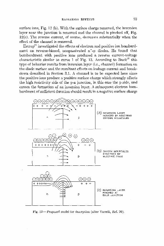
RADIATION EFFECTS 23
surface ions, Fig. 12 (b). With the surface charge removed, the inversion layer near the junction is removed and the channel is pinched off, Fig. 12(c). The reverse current, of course, decreases substantially when the effect of the channel is removed.
Estrup21 investigated the effects of electron and positive ion bombardment on reverse-biased, nonpassivated n + -p diodes. He found that bombardment with positive ions produced a reverse current-voltage characteristic similar to curve 1 of Fig. 13. According to Buck22 this type of behavior results from inversion layer (i.e., channel) formation on the diode surface and the resultant effects on leakage current and breakdown described in Section 3.1. A channel is to be expected here since the positive ions produce a positive surface charge which strongly affects the high resistivity side of the p-n junction, in this case the p side, and causes the formation of an inversion layer. A subsequent electron bombardment of sufficient duration should result in a negative surface charge
n p
888 + + +
n p
888 + +++++++ + + +
n p
(a) INVERSION LAYER INDUCED BY ADSORBED OXYGEN MOLECULES
(b) OXYGEN MOLECULES DESORB ED BY ELECTRIC FIELD
(c) INVERSION LAYER PINCHED AT BULK JUNCTION
Fig. 12 -Proposed model for desorption (after Verrelli, Ref. 20).

24 'l.'HE BELL SYSTEM TECHNICAL JOUHNAL, JANUARY 1967
and hence an accumulation layer on the p side. Buck predicts for this case a reverse current characteristic as shown by curve 2 of Fig. 13. Estrup did, in fact, observe the predicted change in the characteristic when the diodes were irradiated with electrons. These observations are consistent with Estrup's findings discussed earlier and furthermore support the model for surface effects of radiation on transistors which will be described in the next section.
4.6 1110del fo}' N onpassivated rpransistors with Gas Ambients
A model which qualitatively explains many of the experimental observations of radiation effects on gas-encapsulated semiconductor devices has been developed by Peck et a1. 23 Their model describes the degradation of transistor parameters in terms of the surface inversion layers and channels caused by ionized ambient gas.
This m.odel is best discussed by referring to a typical nonpassivated transistor, as shown in Fig. 14. The device itself is enclosed in a can and surrounded by a gas. The basic process of degradation is explained as follows: Upon exposure to radiation, the gas in the can becomes ionized, and the ions arc attracted to the device surface by the electric field created by the collector junction reverse bias and by fields which may exist between the device and the can. As a result, the surface beCOlnes charged either by absorption of the ions onto the surface or by the process, proposed by Estrup/S,19 of charge transfer from the ions to surface impurities already present. The surface charge layer thus created causes an inversion layer in the region of the collector junction which leads to device degradation.
The model proposed by Peck et al can be elaborated to give a some-
t fZ W IX: IX: :::> u w (/)
IX: W > W a:
VOLTAGE ~
Fig. 13 - Schematic representation of diode characteIi3tics. Type 1 = inversion layer, Type 2 = enhancement layer (after Estrup, Ref. 21).

RADIATION EFFECTS 25
0_ e 0
0 0- 0-
0
0 0
0 0 0
CAN C
+ -II
Fig. 14-Cross section of a typical nonpassivated transistor (after Peck et aI, Ref. 23).
what more detailed description of degradation. Consider Fig. 15, which shows channel formation on npn and pnp devices in more detail. For the npn device, Fig. 15(a), the channel is shown extending part way from the collector to the emitter while the base surface near the emitter is depleted. Since, by design, the base width of a transistor is quite small, the change in the collector junction area due to the channel will not be sufficient to cause a large increase in I CBO unless breakdown thTough the narrow depletion layer of the induced p-n junction occurs. 9 However, the positive surface charge near the emitter-base junction will alter the surface potential and hence the surface recombination velocity may be increased resulting in a decrease in hF E •
If the channel should extend across the entire base surface frOln the collector to the emitter, the surface recombination would be reduced (because the concentration of holes would be greatly reduced). However, a large increase in I CEO would obviously result. Under these conditions, hFE may actually appear to increase since the increase in I CEO
would appear as an increase in I C without a corresponding increase in I B •
As pointed out in Section 3.2, changes in hFE and I CEO could also arise from changes in generation and recombination at the surface of the base or transition regions. For most devices, however, these effects

26 THE BELL SYSTEM TECHNICAL JOURNAL, JANUARY 1967
DEPLETED REGION
\ \ \
(a)
ELECTRIC FIELD
A II 1\ 1\ I \ I
(b)
Fig. 15 - Channel formation on (a) npn, (b) pnp transistors by positive surface charge.
are believed to be small compared to the effects resulting fronl channel formation.
For a pnp device, Fig. 15(b), the positive surface charge will create a channel on the collector surface. The area of such a channel may be quite large and cause a significant increase in lena because of the increased area of the junction. On the other hand, recombination at the base surface should be relatively unaffected and consequently hF B
should be comparatively stable. It should be pointed out that the above predictions are necessarily
of a general nature. While irradiated devices will follow the general pattern of degradation, the detailed behavior of a specific device will depend upon such factors as the device geometry and surface treatment received during fabrication.
Estrup21 has verified the essential correctness of this model by a series of experiments on Si npn transistors in which he exposed the devices under reverse bias to positive ion and electron bombardment. The effect on I eno is shown in Fig. 16. The positive ion bombardment starts at point a and continues to point b. During this time, leBo increases more than two orders of magnitude. According to the model, the ions deposit a positive surface charge on the p-type base of the transistor. This surface charge creates a channel from collector to emitter, which in turn causes the increase in lena. From points b to c the device is under no bombardment and a partial recovery is observed, presumably due to some neutralization of the positive surface charge. At c an elec-
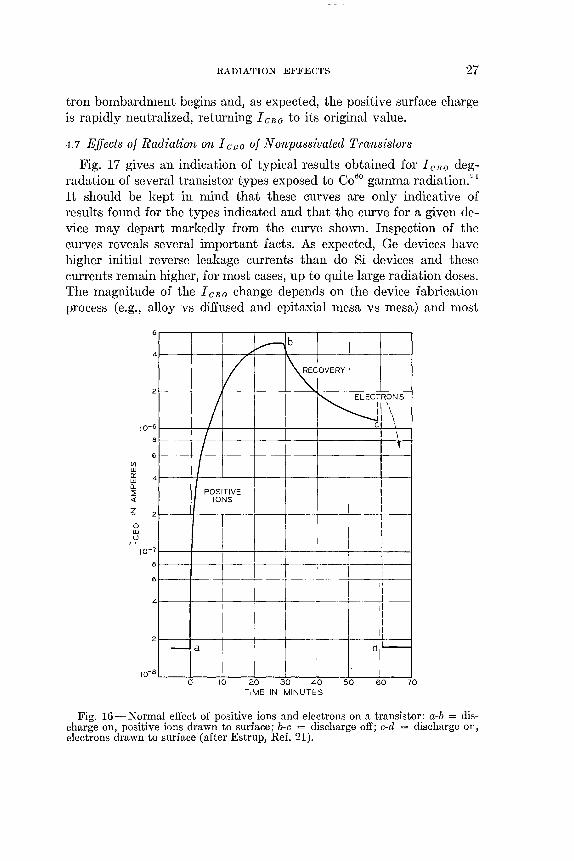
HADIATION EFFECTS 27
tron bombardment begins and, as expected, the positive surface charge is rapidly neutralized, returning leBo to its original value.
4.7 Effects of Radiation on leBo of N onpassivated Transistors
Fig. 17 gives an indication of typical results obtained for leBo degradation of several transistor types exposed to C060 gamma radiation.:!! It should be kept in mind that these curves are only indicative of results found for the types indicated and that the curve for a given device may depart markedly from the curve shown. Inspection of the curves reveals several important facts. As expected, Ge devices have higher initial reverse leakage currents than do Si devices and these currents remain higher, for most cases, up to quite large radiation doses. The magnitude of the leBo change depends on the device fabrication process (e.g., alloy vs diffused and epitaxial mesa vs mesa) and most
6
4
2
10-6
~b ./
V I~~OVERY
/ '" ELECTRONS
II \ NI\ c'li \ / J \
6 (f) UJ cr 4 UJ n.. L « ~
/ I " I I Ii
I POSITIVE
Ii IONS
0 (J)
..':! 10-7
6
4
I
I
I
Ii I
I I 1 I .~. ---j---~
i I -~__;~-~--t-
_ i 'I
I
II Ii I I I
2 d -a dlL--
10-8
o 10 20 30 40 50 60 70 TIME IN MINUTES
Fig. 16-Normal effect of positive ions and electrons on a transistor: a-b = discharge on, positive ions drawn to surface; b-c = discharge off; c-d = discharge OIl,
electrons drawn to surface (after Estrup, Ref. 21).

28 THE BELL SYSTEM TECHNICAL JOURNAL, JANUARY 1967
importantly, upon the ambient in the trallsistor can (e.g., gas-filled vs evacuated).
4.8 Dose Rate and Saturation Effects
It has been found that Ge pnp transistors show a saturation of I CBO
with increasing radiation dose.25 ,26 Furthermore, it appears that the saturation value of I cno may be dose-rate dependent.25 On the other hand, a decrease in I CBO for two Ge npn devices has been reported.26
The improvement appeared to be permanent with I CBO decreasing to one-half its original value. Blair27 has reported I CBO measurements on a Ge mesa transistor which showed no signs of saturation up to a dose of 107 rads. The results for Si transistors are somewhat different from
~ V ~ VGe ALLOY /v J..-- TRANS.
- [7 (fJ
10-5 w c:: w a.. ~ <:
.IV l--
f.---~ -r DIFF. Ge -~ TRANS.
~ I- 10- 6 Z -V ~ / w c:: / c:: ::> u z 0 i= 10- 7 U Z ::>
MESA Si. TRANS. V GAS- FILLED I
/ MESA S L DIODE, V .L..--GAS FILLED
J I
0 W (fJ
<: 2 II / iIi w 10- 8 (fJ c:: w > w c::
J EPITAXIAL J.--~
V MESA SL TRANS., 1--...... V EVACUATE,£..-+--
/ V /
17 ./
10- 9
2
,.r /v v"'" V PLANAR SL TRANS., -~ I--~ GAS-FILLED
V L-+-tI /MESA SL TRANS., EVACUATED
,/ V
J 5 104 2 5 105 2 5 106 2
TOTAL DOSE IN RADS
Fig. 17 -Typical results for ICBo degradation of several transistor types (after Peck and Schmid, Ref. 24).

RADIATION EFFEC'fS 29
2 I 1 -r I I 1
DOSE RATES IN RADS PER HOUR Va B.5x f0 5 - ..... f.4 X 10 5 ~- 8.5 X f0 5 .' ?
/e/
I / L,-V
ld' V
I (
v· 7 I / I
/e--
(f) w a::: w 4 a.. ~ « ~ 0
2 III U
10-8
/ U
2 4 8 f04 2 4 6
RADIATION DOSE IN RADS
Fig. IS-Reciprocity of dose rate and time at two high radiation dose rate levels (after Peck et aI, Ref. 23).
those for Ge in that there is usually no tendency for I CBO to saturate with increasing dose. 26 Saturation has been observed in grease-filled Si transistors.28
On the basis of the proposed model, it is to be expected that as the total radiation dose received by a device increases, the number of ions which have reached the device surface will also increase. As a result, the charge accumulated on the device surface and hence the degradation is expected to be, at least approximately, proportional to the total radiation dose. To some extent Peck et ae3 observe this dependence through a reciprocity of dose rate and time for dose rates not too different in magnitude, as shown in Fig. 18. Reciprocity is also observed at dose rates as low as 5 rads/hr.
There are, however, reasons why the degradation should not necessarily follow this simple dependence on total dose. Devices do show recovery, so there must be some leakage process at the surface which counteracts charge accumulation. Recovery, however, usually takes place at rather slow rates and it is likely that at all but very low dose rates such leakage processes are negligible. At sufficiently high dose rates, on the other hand, it is possible that virtually all the ambient

30 THE BELL SYSTEM TECHNICAL JOURNAL, JANUARY 1967
NO Y NO Y NO RADIATION RADIATION RADIATION RADIATION RADIATION
BIAS NO BIAS BIAS BIAS BIAS 10 1
/
1 / ~ V
1 2 3 4 5
TIME IN HOURS
Fig. 19-The response of I CBO of a diffused Si transistor to either radiation or bias alone or both together. Radiation dose rate 8.5 X 10⁵ rads/hr. (after Peck et aI, Ref. 23).
gas atoms are ionized and a further increase in dose rate will not cause a corresponding increase in the rate of degradation.
A saturation effect is also expected from the model discussed above. There is a limit on the amount of charge which can be accumulated on the device surface, because of the limited number of slow states available or the electrostatic repulsion of additional incoming ions. When this point is reached, the degradation will saturate.
Both dose rate and saturation effects are inherent in the model, but, at present, there are too many variables which could influence these effects to allow even qualitative predictions. It is impossible, for instance, to explain why Ge transistors (particularly pnp) show saturation of I CBO while Si transistors, in general, do not.
4.9 Effect of Bias and Can Potential
Since the electric fields created by the collector junction bias are intimately involved in the degradation process, one should expect the increase in I CBO to be strongly dependent on applied bias. Experimentally, it is generally found that nonpassivated devices experience degradation only when subjected simultaneously to radiation and reverse bias on the collector junction. The necessity of the combination was pointed out by Peck et a1.23 Fig. 19, which schematically illustrates their results, shows that separately neither bias nor irradiation produces degradation; in combination, however, severe I CBO degradation is produced. The effect of bias voltage is further illustrated in Fig. 20,
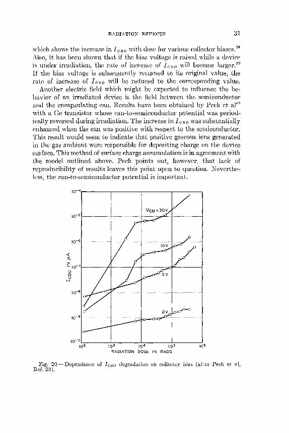
RADIATION EFFECTS 31
which shows the increase in I CBO with dose for various collector biases.23 Also, it has been shown that if the bias voltage is raised while a device is under irradiation, the rate of increase of I CHO will become larger. 29
If the bias voltage is subsequently returned to its original value, the rate of increase of I CBO will be reduced to the corresponding value.
Another electric field which might be expected to influence the behavior of an irradiated device is the field between the semiconductor and the encapsulating can. Results have been obtained by Peck et a123
with a Ge transistor whose can-to-semiconductor potential was periodically reversed during irradiation. The increase in I CBO was substantially enhanced when the can was positive with respect to the semiconductor. This result would seem to indicate that positive gaseous ions generated in the gas ambient were responsible for depositing charge on the device surface. This method of surface charge accumulation is in agreement with the model outlined above. Peck points out, however, that lack of reproducibility of results leaves this point open to question. Nevertheless, the can-to-semiconductor potential is important.
« ::t
10-4~------~ ____ --~ __ ----~~--__ ~
10- 5l__----+___
~10-7l__--~+---~~------~=-----~ o m .:i
10-81---l:;.....-=...-f---------+--------1---------I
10-10L-::-______ ...J....,-______ ......L-.,---____ ---'-:-____ ---'
102 103 10 4 105 106
RADIATION DOSE IN RADS
Fig. 20 - Dependence of I CBO degradation on collector bias (after Peck et aI, Ref. 23).

32 THE BELL SYSTEM TECHNICAL JOURNAL, JANUARY 19G7
4.10 Recovery
From the model, one would expect a transistor to show recovery of I CBO degradation under certain circumstances. Reducing the bias and hence the electric field at the junction should release the charge trapped on the surface and allow it to disperse. The presence of radiation with the bias removed should further enhance the recovery rate by providing electrons to help remove the positive surface charge.
Experimentally, the degraded I CBO shows various rates and degrees of recovery depending on several factors. The effects of bias and radiation on recovery rate of gas-filled Si transistors, as reported by Blair, 27
are shown in Fig. 21. In part A of the curve, the transistor has been removed from radiation but is still under bias. When the bias is removed (part B), the rate of recovery is increased, but upon reapplication of the bias (part C), the recovery rate is again reduced. The most rapid recovery is achieved (prior to parts D, E, and F), if the device is irradiated at 0 volt bias.
Although I CBO usually appears to recover its original value after a sufficient length of time, it is found that subsequent, relatively small doses of radiation will bring I CBO rapidly back to its previous high value. This so-called memory effect is illustrated in Fig. 22 for a device irradiated after one nlonth of shelf recovery time.27 Apparently the re-
---- OUT OF CELL ----__ BIAS ON
4
~ 2 a: w c.. ~ « 10-7 z o III U .....
4 I---
2
10-8 O.t 0.2
A -, r-__
D,E AND F AFTER 30 SECOND PERIODS IN CELL AT 0 VOLTS BIAS AND 8.5 X 10 5 RADS/HR. MEASUREMENTS MADE OUT OF CELL
0.4 0.6 1.0
h.. \" BIAS OFF , ~ ,,- BIAS REAPPLIED , ----, l/ c r--_ ........ , I
, BIAS ON
~I , 'BIAS ON ~
E \ I I i.BIAS ON
T
2 4 6 8 to 20 40 60 tOO
TIME IN MINUTES
Fig. 21-Influence of bias and radiation on ICBO recovery (after Blair, Ref. 27).

f/) w c:: w a. :::E
10-4
<I: 10-6
~
o aJ U
H
10-7
RADIATION EFFEC'l'S
I ......... VCB = 5 VOLTS ....... .......
/~
",/ 1/'
/"
REPEAT AFTER // /' i'~EEL~~~T~G ",/ /B
",
/V
%ITIAL RUN / // / IN y CELL
---V 104 105 10 6
RADIATION DOSE IN RADS
--33
~---
f-
Fig. 22-Si transistor "memory" of radiation after annealing at room temperature (after Blair, Ref. 27).
covery was only superficial and some part of the original damage was still present. Blair reports that even after an additional 15 months of aging the memory effect persisted. However, several authors report the memory effect can be eliminated if the devices are exposed to elevated temperature (~100°C).
This memory effect is quite similar to that mentioned above in the work of Estrup for Si exposed to positive ion bombardment (see Fig. 10). Estrup suggested that the effect was caused by a two-step discharge process which left the surface states in an "active" but uncharged condition for long periods of time before returning to the normal condition. Estrup offered no elaboration on the nature of these" active" states. However, the fact that the memory can be eliminated by rather small increases in temperature would indicate that the cause of the effect is some small difference between" active" and normal states which anneals out easily.
4.11 Dependence of Surface Effects on Radiation Type
Since the primary effect of the radiation is ionization of the gas in the transistor can, it would seem likely that the degradation should be independent of the type of radiation. Peck et al23 have compared the effects of C060 gamma rays and 18 lVIeV protons and find that the radiation dose is significant, but can discern no great difference between the effects of the two types of radiation.
34 THE BELL SYSTEM TECHNICAL JOURNAL, JANUARY 1967
4.12 Effects of Device Ambient
Many nlanufacturers attempt, for various reasons, to control the nature of the device ambient by using vacuum, various types of gases, or greases inside the can. These ambients, while in some cases performing the function of passivation, are not an integral part of the device surface and should not be confused with passivation techniques to be discussed later. Although the model discussed previously treated a gaseous ambient specifically, the same general approach should be applicable to other ambients.
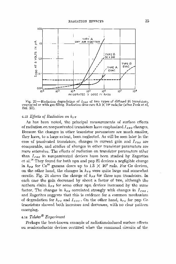
The model should be most easily extrapolated to the case of a vacuum ambient. One would expect a marked decrease in radiation sensitivity for this ambient since gaseous ions are no longer present to create a surface charge. Fig. 23 shows a comparison between gas and vacuum ambients for two types of device.23 As expected, the evacuated devices are less sensitive to radiation.
The situation with grease-filled cans is somewhat more uncertain, and the simple model put forward above would require some refinement to account for the observations. Steele25 reports that for Ge pnp alloy transistors the presence of silicone grease increases leBo degradation over values found for the same transistor without grease.
For Si grown junction npn transistors encapsulated in a silicone grease, on the other hand, leBo was found to saturate with dose, and the saturation value was significantly smaller with grease present. Infrared transmission studies of the grease from Ge devices before and after a 5 X 10⁷
roentgen radiation dose showed that irradiation caused an increase of available hydrogen bonds which were presumably able to interact with the surface. The mechanism causing the change in radiation sensitivity would thus appear to be a surface one, but the reason for the opposite effect on Ge and Si devices is not clear.
A saturation effect for leBo for silicone grease-filled Si alloy transistors has also been reported by Peck et a1.23 In fact, it was found that leBo decreased with dose after reaching a maximum. These devices, when exposed to short periods of high intensity radiation, showed only minor changes in leBo, but showed severe degradation in the periods subsequent to irradiation. These results might indicate production of ions in the grease which require time to migrate to the device surface.
It has been reported that silicone grease also decreased the radiation sensitivity of one type of Si grown junction transistor.3o After a study of several types of transistors and various case fillings, however, no direct correlation was found between the presence or absence of grease and sensitivity to radiation.
100
110
~ (/)
~ ~ 1.0 lI)
~ o B 0.1
t-I
------
0.01 10 2
---
RADIATION EFFECTS 35
TVjA DRY AIR + GETTER I
/ TYPE B N + He
1//1 TYPE B / TYPE A EVAC ,;'
,;
/ / EVAC " " / " ~ 7
--/ I ------ --:/r ------_/
------ ./ 10 4 105 106
INTEGRATED Y DOSE IN RADS
Fig. 23-Radiation degradation of ICRO of two types of diffused Si transistors, evacuated or with gas filling. Radiation dose rate 8.5 X 10⁵ rads/hr (after Peck et aI, Ref. 23).
4.13 Effects of Radiation on hpE
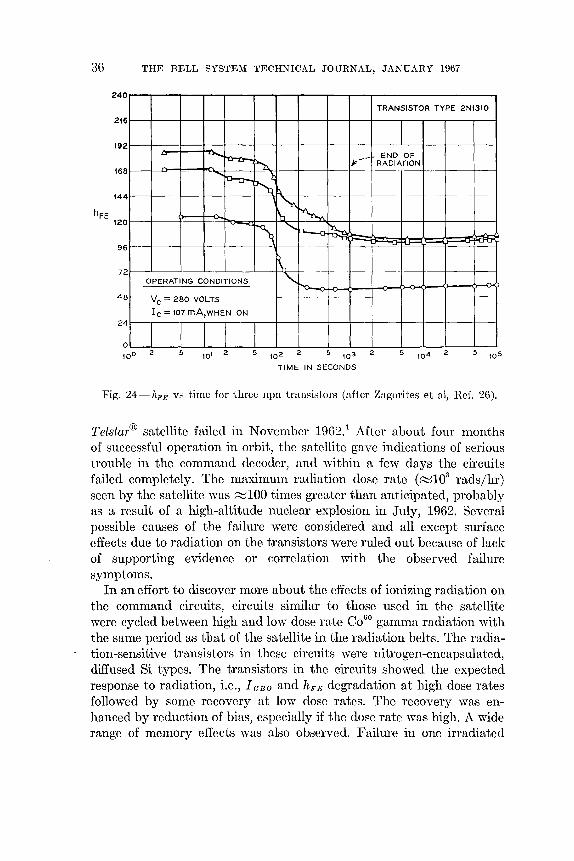
As has been noted, the principal measurements of surface effects of radiation on nonpassivated transistors have emphasized I CRO changes. Because the changes in other transistor parameters are much smaller, they have, to a large extent, been neglected. As will be seen later in the case of passivated transistors, changes in current gain and I CRO are comparable, and studies of changes in other transistor parameters are more extensive. The effects of radiation on transistor parameters other than I CRO in nonpassivated devices have been studied by Zagorites et al. 26 They found for both npn and pnp Si devices a negligible change in hpE for Co60 gamma doses up to 1.3 X 10⁴ rads. For Ge devices, on the other hand, the changes in hpE were quite large and somewhat erratic. Fig. 24 shows the change of hpE for three npn transistors. In each case the gain decreased by about a factor of two, although the authors claim h pE for some other npn devices increased by the same factor. The changes in hpE correlated strongly with changes in I CRO ,
and Zagorites suggests that this is evidence for a common mechanism of degradation for hpE and I CRO • On the other hand, hpE for pnp Ge transistors showed both increases and decreases, with no clear pattern emerging.
4.14 Telstar® Experiment
Perhaps the best-known example of radiation-induced surface effects on semiconductor devices occurred when the command circuits of the
36 THE BELL SYSTEM TECHNICAL JOURNAL, JANUARY 1967
240
TRANSISTOR TYPE 2N13tO
216
192
168
144
hFE 120
96
....- .......... ~ jt:-- END OF
~ RADIATION
...... ru--o-, ~~
rb~ ~ ~ --u
r\ 'h.. ~ .A ~
72 f\
OPERATING CONDITIONS "-""'" -'"
48 r- Ve = 280 VOLTS
Ie = t07 mA,WHEN ON 24
2 5 5 102 2 5 103 2 5
TIME IN SECONDS
Fig. 24-hFE Vi'> time for three llpn transistors (after Zagorites et aI, Hef. 26).
Telstar® satellite failed in November 1962.1 After about four months of successful operation in orbit, the satellite gave indications of serious trouble in the command decoder, and within a few days the circuits failed completely. The maximum radiation dose rate (~103 rads/hr) seen by the satellite was ~100 times greater than anticipated, probably as a result of a high-altitude nuclear explosion in July, 1962. Several possible causes of the failure were considered and all except surface effects due to radiation on the transistors were ruled out because of lack of supporting evidence or correlation with the observed failure symptoms.
In an effort to discover more about the effects of ionizing radiation on the command circuits, circuits similar to those used in the satellite were cycled between high and low dose rate C060 gamma radiation with the same period as that of the satellite in the radiation belts. The radiation-sensitive transistors in these circuits were nitrogen-encapsulated, diffused Si types. The transistors in the circuits showed the expected response to radiation, i.e., I CBO and hFE degradation at high dose rates followed by some recovery at low dose rates. The recovery was enhanced by reduction of bias, especially if the dose rate was high. A wide range of memory effects was also observed. Failure in one irradiated

RADIATION EFFECTS 37
circuit was traced to h pB degradation of one transistor, while failure in another circuit was attributed to an I aBO increase.
After a careful analysis of these laboratory tests, attempts were made to rejuvenate the Telstar® satellite circuits. Several unsuccessful attempts were made using various approaches. Finally, success was achieved with nlodified commands designed to circumvent one particular circuit which was assumed to have failed. The satellite then responded to subsequent commands and after some further manipulation the circuits were fully operational.
The exact reason for recovery is not known but was probably a combination of two effects. First, the dose rate seen by the satellite had decreased significantly from the value which first produced failure, with a consequent decrease in surface effects. Second, the suspected circuits were given a series of continuous commands. This manner of operation caused the normally off transistors (high V a E and high rate of degradation) to have a decreased average bias voltage. Under these conditions, the surface degradation is decreased and recovery proceeds more rapidly.
4.15 111 iscellaneous Non passivated Devices
4.15.1 Introduction
The discussion thus far has been limited to transistors and diodes. However, other semiconductor devices, not necessarily junction devices, are also sensitive to surface effects and are just as likely to be exposed to radiation. Unfortunately, there has been very little investigation of these devices, at least as far as surface effects of radiation are concerned.
4.15.2 Solar Cells
Solar cells will be exposed to radiation mainly in space applicatiollf:l, and studies of radiation effects on these devices have been made with these applications in mind.31
,32,33,34 Results obtained by Rosenzweig et al34 indicate that the Si nip cells presently used are most likely to degrade from bulk rather than surface radiation damage because most of the minority carrier generation in these devices takes place well below the surface. The importance of bulk damage is illustrated in Fig. 25, which shows the percent quantum efficiency as a function of wavelength for an nip Si solar cell after various doses of 1 Me V electrons. It is evident that the efficiency is most affected at the longer wavelengths, those at which carrier generation occurs well below the surface, i.e., in the bulk damage region. It should be pointed out that similar optical

38 THE BELL SYSTEM TECHNICAL JOURNAL, JANUARY 1967
>u z w Q lL. lL. W
~ ::> tz « ::> a tz w U cr: W Q..
0.5 0.6 0.7 WAVELENGTH IN fL
1.0
Fig. 25 - Percent quantum efficiency vs wavelength after various levels of bombardment for nip cells (after Rosenzweig et aI, Ref. 34).
studies could be quite useful for investigating surface effects in other semiconductor devices. In particular, they can be used to distinguish between surface and bulk effects as illustrated here for solar cells.
There has been recent interest in GaAs solar cells, since these devices approach Si solar cells jn conversion efficiency and may, for some applications, be IrlOre radiation resistant.31
,35 Minority carrier generation near the surface is more important for GaAs solar cells, however, and it is possible that changes in surface recombination due to radiation are important on these devices.

RADIATION EFFECTS 39
4.15.3 Radiation Detectors
Radiation detectors in the form of specially designed reverse-biased diodes require stable surface properties to keep the noise level as low as possible.
Detectors used in Telstar® satellites used bare, etched, diffused p-n junctions inside a tight can back-filled with nitrogen containing tL
trace of oxygen. It was found necessary to add the trace of oxygen to stabilize the diodes against gradual increases in reverse current.
These detectors were tested for surface effects due to radiation by exposing them to 50 rads/hr gamma radiation while under intermittent reverse bias. The devices showed a wide range of responses as observed in reverse current measurements. However, none of the devices showed serious permanent effects due to irradiation. In space, on the other hand, two detectors out of 18 did show significant surface-generated noise after several nlonths of operation at radiation levels higher than expected.
Oxide-passivated surfaces in place of bare, etched surfaces have not been tested for these devices, but based on the experience with passivated transistors one might expect to find problems in the form of charge storage effects at the Sj-Si02 interface.
4.15.4 111 etal-Se1l1,iconductor Junctions and H eterojunctions
The region of the interface between two materials, such as a metal and a semiconductor, is obviously not a true "bulk" region fronl a radiation effects point of view since it is a small region not typical of either material. Similarly, it is not a" surface" region in the usual sense of the word. Nevertheless, such interfaces are important and it is worthwhile here to broaden the definition of a surface to include interfaces and to discuss interfaces as they concern radiation effects.
It is difficult to predict what effect radiation will have on an interface regjon, since little is known about these regions and almost no experimental investigations have been carried out. However, it is known that, at metal-semiconductor junctions and heterojunctions, the crystallinity is either nonexistent or at least badly disturbed. As a result, these regions are likely to contain numerous trapping centers. Radiation may alter the number of these centers or the charge they contain, and hence may alter the characteristics of the device containing the interface. There has been an indication that radiation does affect a metal-semiconductor interface.37 The saturation current of an Ag surface barrier GaAs varactor was found to decrease 10 to 20 times after receiving a

40 THE BELL SYSTEM TECHNICAL JOURNAL, JANUARY 1967
fast neutron dose of 1015/cm2. Similar diffused GaAs varactors, on the other hand, showed the more typical increase in the saturation current, presumably caused by usual bulk effects. The unexpected decrease in saturation current of the surface barrier devices, however, is suspected to result from an increase in the barrier height of the interface. Such an increase could result from a change in the charge contained in the interface states as a result of irradiation.
Such radiation-induced changes in the metal-seluiconductor barrier height could also affect the characteristics of commonplace p-n junction devices through their many metal-semiconductor junctions. However, no direct study of such effects has yet been made.
V. PASSIVATED DEVICES
5.1 Introduction
In recent years Si planar devices have assumed an increasing importance in the transistor industry. There are several advantages of planar devices over other device types such as alloy or mesa. One of these advantages is that the Si planar device lends itself naturally to an oxide surface passivation, which is quite effective in reducing the surface stability problems encountered in other types. At present only Si devices are commercially available with this oxide passivation; a comparable passivation technique for Ge devices is still in the experimental stage. The discussions in this section are understood, therefore, to apply to Si and Si devices.
As far as the effects of radiation on planar devices are concerned, it will be seen that the surface passivation layer itself plays a very important role. For this reason a short discussion of Si surface passivation and its effects on devices will be given to serve as a basis for the subsequent discussion of radiation effects.38
The electrical requirements of an ideal passivation material have been given by Young and Seraphim39 as follows:
(i) The semiconductor surface potential must not change significantly with time under the stress conditions that are encountered by the device.
(ii) The semiconductor surface potential should be optimum for the particular device under consideration.
(iii) In those types of devices which require reasonably small values of the surface charge density and the surface recombination velocity, these characteristics should also be accomplished by the passivation.
The passivation used on planar devices is by no means perfect, but it does approach these ideals reasonably closely.
RADIATION EFFECTS 41
In practice, passivation of silicon devices is accomplished with a film of the oxide, 8i02 , which is thermally grown on the device surface. Because of the intimate contact between the oxide and semiconductor surface, this film stabilizes the surface and isolates it from the ambient. However, this type of passivation places the surface of the device in contact with a material which interacts in a complicated way with it and with the ambient. It has become apparent that if one is to understand the behavior of passivated devices one nlust understand the charge storage and transport mechanisms which occur in the thin layer of passivation material.
5.2 Silicon Dioxide as a Passivation JJ1 aterial
5.2.1 Effect of Si02 on a Si Surface
An extensive experimental study of 8i02 as a passivation material has been made by Atalla et a1.11.40.41 They found that oxides grown at about 1000 0 e in dry or wet oxygen arc continuous, amorphous, and stable over long periods of time. Atalla discussed their observations on the 8i02-8i system in terms of fast and slow surface states. By using field effect techniques it was found that the passivated surfaces showed no apparent effects due to slow surface states. Furthermore, the presence of either wet or dry nitrogen caused no shifts in the surface conductivity resulting from the introduction of slow surface states.
Atalla reported the presence of fast surface states with densities ~1010 - lOll cm -2 and suggested the following model to account for their presence. At the 8i02-8i interface, a region of gradual transition from crystalline 8i to amorphous 8i02 occurs, and it is assumed that Tamm-like states exist in this transition region. These states together with states arising from vacancies caused by mismatch between the 8i and 8i02 are acceptor states. Donor states arise only from the presence of impurities at the interface.
5.2.2 Charge Storage Effects in Si02
Recent investigations have revealed charge storage effects in 8i02
films such as those used for surface passivation on 8i devices. Yamin 42.43 has studied the charges in thermally grown 8i02 films using a 8i-8i02 -
metal sandwich. The 8i used was either n- or p-type, the oxide was typically 6000 A thick, and the metal was usually Al or Au in the form of a circular dot. Yamin investigated the charge flow in and out of these devices for 8i potentials between ±5 volts with respect to the metal at temperatures from 200 0 e to 400 oe. At negative 8i potentials, it was observed that the amount of charge entering the device was much
42 THE BELL SYSTEM TECHNICAL JOURNAL, JANUARY 1907
greater than expected from the device capacitance. Furthermore, the excess charge could be recovered if the Si potential was again made more positive, or it could be stored almost indefinitely in the device if the leads were opened. Yamin demonstrated that the charge storage was associated only with the oxide directly under the metal dot and estimated the density to be 4 X 10¹² to 2 X 10¹⁴ charges/cm2, depending primarily on the method of preparation of the oxide. Devices which were baked for 15 minutes at 1000°C in dry oxygen, nitrogen or hydrogen showed a spontaneous discharge at 400°C corresponding to charge densities in the oxide of ~1012 charges/cm2. Since these devices had not been previously voltage-stressed, it appears that thermally produced oxides may contain a built-in charge. A study of the conductivity of the Si beneath the oxide showed that the conductivity became more n-type, indicating that positive charge was being stored.
Charge accumulation and instability effects in Si02 films exposed to elevated temperatures and electric fields have been observed by others44.45.46.47.48.49 and various mechanisms have been proposed to explain the observations. It is now generally believed that the effects are due to the presence of mobile positive ions in the oxide. Snow et al44 have observed changes in the capacitance-voltage characteristics of metal-oxide-semiconductor structures under temperature and voltage stress. These observations have been explained in terms of alkali ion (in particular N a +) transport through the oxide. Using radioactive tracer techniques, Yon et al50 have observed changes in the N a impurity profile in Si02 films which correlated with observed changes in the charge contained in the oxide. Hofstein,47 on the other hand, has observed similar charge storage effects in Si02 but his results suggest hydrogen ions as the mobile positive charge carrier. Furthermore, it has been shown that the presence of hydrogen during the heat treatment of Si02 films, either as an ambient gas or as moisture on the surface, has a considerable effect on the behavior of the oxide.46 .47
Both explanations may be substantially correct, however, since it appears that charge storage effects are very dependent on the conditions of oxide preparation and on subsequent heat treatments.46 With our present limited knowledge of the processes occurring in Si02 one must be very cautious in applying the results of an investigation on one type of oxide to another oxide prepared under different or unknown conditions.
It has been found that a P 205 treatment of the Si02 passivation layer reduces the charge storage effect and increases device stability.52.53.54 Pliskin55 has suggested that the P 2 0 5 treatment increases the poly-

RADIATION EFFECTS 43
merization of the Si02 tetrahedra. The result is a denser Si02 layer through which the positive ions have more difficulty diffusing. It has also been suggested that a phosphate glass layer on the surface of the Si02 acts as a getter and reduces the effective impurity concentration in the underlying oxide. 54
5.3 Electrical Behavior of Si02 Passivated Devices
Atalla41 has studied Si02 passivated p-n junctions under various conditions of bias and relative humidity and has proposed a model which satisfactorily explains his findings. Briefly, he found the reverse leakage current of the junction unaffected by moisture when the junctions were subjected to extended periods of forward or zero bias. For a steady reverse bias, however, the reverse current increased with time and saturated in a few hours at a value of about five times its initial value. The increase in current was a function of relative humidity, bias voltage, and oxide thickness. By optically scanning the junctions, Atalla observed that the increase of reverse current occurred simultaneously with the formation of channels on both sides of the junction.
The following model was proposed by Atalla to explain the above observations. When the Si02 surface is exposed to moisture, a layer of water containing mobile ions is formed. When a reverse bias is applied to the junction, an electric field appears at the oxide surface in the region of the junction, Fig. 26(a). This field causes mobile ions on the surface of the oxide to migrate, positive ions toward the p side, negative ions toward the n side. If the charge separation is severe enough, the semiconductor surface near the junction will become inverted and channels will form, Fig. 26(b). It is apparent that the effect depends on the humidity and the field strength at the oxide surface, and in turn on the bias voltage and oxide thickness. As with nonpassivated devices, the channels cause an increase in reverse leakage current.
Failure mechanisms in Si02 passivated planar transistors were also studied by Metz56 who observed changes in the I CBO vs bias voltage characteristics as the devices were aged under operating conditions (emitter junction forward-biased, collector junction reverse-biased). Again, I CBO degradation occurred at elevated junction temperatures, with I CBO increasing several orders of magnitude in some cases. Metz found that the current increases were reversible and that I CBO could be returned to its original value by heating for several minutes without bias or by removing the bias and opening the can, exposing the device to normal ambient atmosphere. The model discussed by Metz is essentially the model proposed by Atalla and satisfactorily explains the

44 THE BELL SYSTEM TECHNICAL JOURNAL, JANUARY tUfi7
NEGATIVE ION MIGRATION ---+--- POSITIVE ION MIGRATION
OXIDE
n p
+ (a) ELECTRIC FIELD AT THE OXIDE SURFACE
e (±) ee (±)(±)
eGG (±)(±)® GGGG ®(±)®®
++++
n p
+ (b) FORMATION OF CHANN ELS CAUSED
BY CHARGE SEPARATION
OXIDE
Fig. 26-Separation of the charge on the surface of a reverse-biased p-n junction,
observed recovery. Heating without bias increases surface ion mobility, and the separated ions redistribute themselves to a neutral condition through their mutual attraction field. Exposing the surface to ambient atmosphere (and hence moisture) also increases the ion mobility and hence promotes a neutralization of surface charge.
Atalla's model has received support from the work of Shockley et a157
,58 who investigated contact potential variations on Si02-covered Si surfaces using a Kelvin probe. They were able to account entirely for the observed variations by assuming the presence of mobile charges on the outer surface of the Si02 which migrated under the influence of applied electric fields.
In contrast to Atalla's model, in which the surface potential of the device is controlled by charges on the surface of the passivation layer,
RADIATION EFFECTS 45
the most recent studies indicate that charge storage and transport effects within the Si02 passivation are responsible for device degradation. Electric fields exist in regions of the oxide near biased junctions and these fields may cause charges within the oxide to accumulate at the Si-Si02 interface. Such a charge accumulation would, of course, strongly influence the surface potential of the adjacent Si and lead to degradation by the methods discussed earlier.
This model is supported by the work of lVlathews et al59 who have investigated the effect of N a contamination of the passivation layer on device stability. They concluded that N a ion migration through the oxide was an important cause of degradation of their devices. Snow et al44 have also suggested that trace alkali impurities in the passivation oxide may cause reliability problems in devices operated at high temperatures and voltages.
Basically, then, it appears that surface conditions in passivated devices can be controlled by two possible mechanisms, charge storage in the Si02 layer and charge separation on the surface. However, the first mechanism appears to be the important one in most types of planar devices. Of course, it is possible that under some circumstances both mechanisms may be operative.
5,4 Results of Device Passivation
In spite of the problems of charges present in or on the surface of the Si02 film, passivation has unquestionably improved the performance of many silicon devices. I CBO values are relatively low and very stable, surface recombination near the emitter junction is low and, consequently, achievable current gains are quite high. Surface recombination velocities as low as 10 cm/s for oxidized Si surfaces have been reported by Grove and Fitzgerald. 6o
Under almost all conditions of preparation, the charges stored in or on the oxide are positive and hence tend to induce n-type surface conductivity in any underlying material. In the case of npn transistors, such surface layers will tend to reduce the collector breadkown voltage and increase recombination in the emitter-base region (i.e., lower hpE).
On the other hand, for pnp transistors such surface conductivity results in unstable collector channels and very low recombination at the base interface. Current manufacturing processes for pnp devices stabilize the collector channels with a p + diffused guard ring about the collector junction. Because of the low recombination currents in the emitterbase region, passivated pnp transistors have very high h pE values down to very low emitter currents.

46 THE BELL SYSTEM TECHNICAL JOURNAL, JANUARY 1967
5.5 Radiation Effects on Passivated Devices
5.5.1 Introduction
The question of importance here is, of course, what effect passivation will have on the response of devices to radiation. Unfortunately, although a considerable amount of investigation has been carried out on passivation per se, the amount of work done on the effects of radiation on passivated devices is rather scant. Despite this handicap, however, some facts are fairly well established. In general, the effects observed are quite similar to those observed in nonpassivated devices and seem to be associated again with channels resulting from the formation of ions in the neighborhood of the surface. However, because of the variety of ways in which SiOz layers are produced, the nature and charge state of the ions before and after ionizing radiation are not reproducible.
5.5.2 Experimental Results
The effects of radiation on diffused planar diodes and npn transistors passivated with 1.3JL of thermally grown oxide followed by 1.3JL of fused lead borosilicate glass have been reported by Kerr. 61 Typical results for the devices, under 20 volts of reverse bias, are shown in Fig. 27. The reverse current appears to saturate at a dose of 105 to 106 rads, and further investigation showed little change for doses up to 108 rads. There is no obvious explanation why the diodes are more sensitive to radiation than the transistors. Kerr also reports recovery of the leakage current degradation in one hour in radiation at a 1.9 X 10⁵ rads/hr dose rate with no bias and recovery in longer periods with bias and no radiation or with no bias and no radiation. This author has also compared Si02-
protected devices, with similar varnish-protected Si mesa diodes and finds the degradation is about an order of magnitude smaller for the oxide-covered diodes.
Mathews et al59 have exposed p7rn diodes, with and without alkali contamination in the glass envelope, to C060 gamma radiation. The results indicated that the presence of alkali atoms considerably enhanced the reverse leakage current degradation. The excess reverse current was found to be associated with channels on the diode surface. These channels were eliminated only when the last of the protective oxide was removed.
The effects of low-energy X-rays (150 keY) on the ac and dc current gains of SiOz-passivated npn planar transistors have been investigated by Taulbee et a1. 62 At such low X-ray energies, atomic displacement effects should be negligible. The degradation of de gain for three
2
(J') 10-7
w a: w a.. :iE <t
~ I-z ~ 10-8
a: ::> U w (J') a: w > w a:.
2
10-9
5
2
RADIATION EFFECTS
I I I I I f- SL PLANAR DIFFUSED
DEVICES, OXIDE GLASS
I-COVERED,20V BIAS
/ ,/'
k'" VV I '" 'L..--<J
./
/ DIODES -
" L,
~ ~ -~
"-
- TRANSISTORS { I CBO
~ -~ I I I
2 103 2 5 104 2 5 105 2
GAMMA RADIATION DOSE IN RADS
47
---.'I.
/"" -.r.
~ --~ ..... >--rl: .....--~
~ - -u
~ ... - _-6: ~ -
Fig. 27 -Degradation produced by reverse bias and y-irradiation of oxide-glass covered planar diodes and transistors. Dose rate 1.9 X 10⁵ rads/hr (after Kerr, Ref. 61).
devices irradiated in the passive condition (i.e., with no bias applied to either junction) appeared to saturate at a dose of about 107 rads. The effect of the degradation was strongly dependent on the emitter current, Ie , as shown in Fig. 28. In this figure, 1000jhFE is shown as a functioll of lefor the three devices before and after exposure to 107 rads of 150 ke V X-rays. The effective degradation is much more severe at low emitter currents with current gains falling to as low as unity at 1 j.lA.
Taulbee found that the effects were also dependent on junction bias applied during the irradiation. The gain degradation increased if either junction was reverse-biased and decreased if either junction was forwardbiased.
The X-ray-induced damage appears to be relatively stable under shelf-life conditions. Over a period of 200 days, the irradiated devices recovered about 20 percent with no significant difference observed between devices with and without cans. Recovery was achieved if bias was applied to the transistor, high values of emitter current producing the most rapid recovery. The amount of damage exhibited by a given type

48 THE BELL SYSTEM TECHNICAL JOURNAL, JANUARY 1967
1000
800
~ 600 ..c .......... o o o - 400
200
~ \ W ;::3AFTER X-R(Y
'< I~ ~ I
DEVICE B
I'-.. ~~
~ I"--...
,,-' ~
....... -DEVICE A - DEVICE C ~ ....... ~ -- I I --
~C ........... r-:::::::---f.:;: -::~ ~RAY '1 DEVICE A- r-c- -- 1 J .. ~'" / ~
2 4 6 810
- 5 4 6 810
- 4 2 4 6 810
-3 2
EMITTER CURRENT, Ie, IN AMPERES
Fig. 28-Dependence of hFE degradation on emitter current after =4 X 10⁷ rads x-ray dose. (after Taulbee et aI, Ref. 62).
of device appeared to vary with the manufacturer; five lots of the same devices supplied by five manufacturers showed widely varying responses. It is, of course, natural to suspect that the cause is the different surface treatments given the devices by each manufacturer.
An extensive and systematic study of passivated planar devices has been made by Schmid,63 who finds a predictable pattern of response to C060 gamma radiation for many types. All npn devices exhibit a rapid drop in dc current gain (to as low as 10 percent of the initial value at doses of 106 rads) accompanied by a slow increase in I ClIO' The pnp structures, on the other hand, show little decrease in gain, but I CBO
increases as much as six orders of magnitude at doses of 106 rads. In some cases, I CBO saturates and actually recovers slightly with increasing dose. The response of a given device is found to be characteristic of the manufacturer, and it has been shown that changes in the device surface structure will significantly change the response. High-gain devices were found to degrade proportionally faster than devices with low gain.
Contrary to the findings of Taulbee,62 the hFE degradation was found by Schmid, to a first approximation, to be independent of bias. In fact, the decrease in gain was sometimes greater without bias. Schmid did not examine the effects of reverse emitter bias. Over relatively long periods, the degradation appeared to be permanent under shelf-life conditions. However, a two-hour bake at about 300°C restored the original characteristics, and a second exposure to radiation repeated the previous degradation.
RADIATION EFFECTS 49
Schmid explained the difference between the behavior of npn and pnp transistors as follows: Ionizing radiation creates a positive charge in the oxide layer or at the oxide-semiconductor interface which affects the base regions of the transistors. For an npn device, the positive surface charge increases the surface recombination at emitter-base region. The result is an increase in base current required to maintain a given collector current and hence a decrease in gain. For pnp transistors, the positive surface charge creates a collector channel which results in an increased I C BOas discussed previously.
Many of the degradation features observed by Pecle23 on gammairradiated nonpassivated device have also been observed by Stanley64
in high-gain pnp and npn Si planar transistors irradiated with 1.5 lYle V electrons. (See Appendix B for a discussion of the dose equivalence of electrons). The degradation was found to be most pronounced in the collector-to-emitter leakage current, I CEO' (Large increases in I CBO
for an npn transistor result from channel formation across the base from emitter to collector.) Fig. 29 shows the I C EO increase for an npn transistor as a function of the total electron dose. It appears that I CEO will saturate after increasing several orders of magnitude. It is also apparent that both radiation and bias, V CE , must be present for degradation to occur. During the times AA, BB, etc., when V CE = 0, the transistor shows recovery. As with nonpassivated devices, the recovery is much more pronounced when radiation is present (compare DD with EE). Stanley reported that forward-biasing the emitter junction also improved the recovery of the leakage current and in many cases restored I CEO to its preirradiation value.
Fig. 29 also shows evidence of a memory effect similar to that observed by Peck;23 i.e., after the annealing periods BB, CC, DD, and EE, I CEO returns to its preannealing value very quickly (compared with the overall rate at which I CEO is increasing) as though it "remembered" its previous irradiated condition.
The transistors examined by Stanley also showed hFE degradation under electron bombardment. The degradation was much more severe at low emitter currents, 5 to 10 p,A, than at higher currents, ~1 mAo The final gain at 1015 e/cm2 dose was about the same (~10) for many units and showed no correlation with preirradiation values. One type of transistor encapsulated in a high-density silicone compound did not exhibit such severe gain reduction, presumably because of increased shielding which was able to stop 1 .. 5 lYle V electrons. However, two other types of plastic encapsulated transistors showed severe gain degradation at low current.

50 THE BELL SYSTEM TECHNICAL JOURNAL, JANUARY 1967
10-3
5
(/)
~ 10-6
W c.. ~ <t
?: fa 10-7 U
H
5
I I I I I I I I I I I-
ELECTRON TRANSISTOR DURATION
H/ ! BEAM VOLTAGE
AA OFF OFF 2 HR. I I-- BB OFF OFF 14 HR.
/ -~
11 l-cc ON OFF 50 MIN. D DD OFF OFF 114.5 HR. I EE ON OFF 1 HR.
C If V
J J I
VCE =10V S1
} /
~ / B C
ro.
E
AI FLUX
I
(4.5±0.5) X 108 e/cm 2/s 4 X 10⁹ e/cm2/s fE----1-----1---,--,-,----1----1--1-1-1----iT--i- -1-1
2 4 6 8 10'2 2 4 6 8 10'3 4
TOTAL DOSE (e/cm 2 )
Fig. 29-IcEo vs total electron dose (1965-11 Fig. 2. Lincoln Laboratory, MIT Reprinted by permission) (after Stanley, Ref. 64).
The effects of electrons and Co 60 gamma rays on the dc gain of npn and pnp 8i transistors have also been reported by Brucker et al. 65
,66
They found the loss of gain caused by increased surface recombination effects to be nonlinear with radiation dose. By irradiating npn planar transistors with 125 keV and 1 MeV electrons they found
t!.(l/hpE) = K.(fEY + Kb Jj , where Ks and Kb are the surface and bulk damage constants respectively, cJ> the integrated electron flux, and lEis the emitter current. The degradation is greater at lower values of lEas expected from previous discussions. The equation holds for cJ> ~ 5 X 10¹⁴ e/cm
2• At larger values
RADIA'rION EFFECTS 51
of ¢ the surface component was observed to saturate. Brucker attributes the surface part of the degradation to charge accumulation in the oxide which results in an increase in the surface recombination velocity at the emitter-depletion layer surface. Brucker also reported that the surface effects readily annealed out at 250°C.
For Si planar transistors Hughes67 has found that a dose of 106 rads of C060 radiation can cause I CBO to increase four orders of magnitude and hFE to decrease to 25 percent of its preirradiation values. The response of the devices to radiation was found to be quite dependent on bias conditions but, interestingly enough, independent of whether the ambient was a gas or a high vacuum. This last observation lends support to the view that charges within the oxide rather than on the oxide surface are responsible for degradation. The effect of surface charge was observed to be severe enough to invert even the highly doped p +
guard ring on pnp transistors. The degradation of hFE and other parameters in both npn and pnp Si planar-passivated transistors exposed to electron beams (5 to 50 keY) has been observed by Green and others.68 The degradation was found to be reversible in that it could be removed completely by annealing for several hours at 250°C. Partial recovery was observed at lower temperatures. The interesting point in these experiments is that the degradation only occurred when the electrons had sufficient energy to penetrate to the Si-Si02 interface; electrons stopped in the oxide away from the interface had no effect. Subsequent measurements with a small scanning light spot showed that the surface recombination velocity had increased in the base region of the transistors.* The minimum electron energy required to cause hFE degradation of npn and pnp Si transistors has been measured by Stanley.71 He also found that degradation occurred only when the electrons penetrated to the Si-Si02 interface.
5.G Radiation Effects in lYI etal-Oxide-Semiconductol' Field Effect Transistors
Field effect transistors are majority carrier or unipolar devices and as such were originally believed to be relatively insensitive to radiation effects because their characteristics did not depend on minority carrier
* Schmidt69 has suggested for these experiments that the irradiation has interacted in some manner with a hydrogen-containing species (presumably resulting from moisture trapped at the Si-Si02 interface when the Si02 layer was stream grown) at the Si-Si02 interface. Schmidt based this suggestion on his discovery that protons incorporated into anodically grown oxide films on Si cause the formation of a large number of surface recombination centers.70 The effect in transistors was observed to decrease with more irradiation annealing cycles, perhaps indicating that the limited supply of hydrogen in the oxide was being reduced.
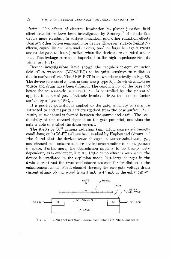
52 THE BELL SYSTEM TECHNICAL JOURNAL, JANUARY 19G7
lifetime. The effects of electron irradiation on planar junction field effect transistors have been investigated by Stanley.72 He finds this device more resistant to surface ionization and other radiation effects than any other active semiconductor device. However, surface ionization effects, especially on n-channel devices, produce large leakage currents across the gate-to-drain junction when the devices are operated under bias. This leakage current is important in the high-impedance circuits which use FETs.
Recent investigations have shown the metal-oxide-semiconductor field effect transistor (MOS-FET) to be quite sensitive to radiation due to surface effects. The MOS-FET is shown schematically in Fig. 30. The device consists of a base, in this case p-type Si, into which an n-type source and drain have been diffused. The conductivity of the base and hence the source-to-drain current, I D, is controlled by the potential applied to a metal gate electrode insulated from the semiconductor surface by a layer of Si02 •
If a positive potential is applied to the gate, minority carriers are attracted to and majority carriers repelled from the base surface. As a result, an n-channel is formed between the source and drain. The conductivity of this channel depends on the gate potential, and thus the gate is able to control the drain current.
The effects of eoGO gamma radiation (simulating space environment conditions) on MOS-FETs have been studied by Hughes and Giroux73
•74
who found that the devices show changes in transconductance, gm, and channel conductance at dose levels corresponding to short periods in space. Furthermore, the degradation appears to be bias-polarity dependent, as is evident in Fig. 31. Little or no effect is seen when the device is irradiated in the depletion mode, but large changes in the drain current and the transconductance are seen for irradiation in the enhancement mode. For n-channel devices, the zero gate voltage drain current ultimately increased from 1 mA to 45 mA in the enhancement
GATE
DRAIN
P-8ASE
/' SEMICONDUCTOR
SOURCE
Fig. 30 - N-channel metal-oxide-semiconductor field effect transistor.
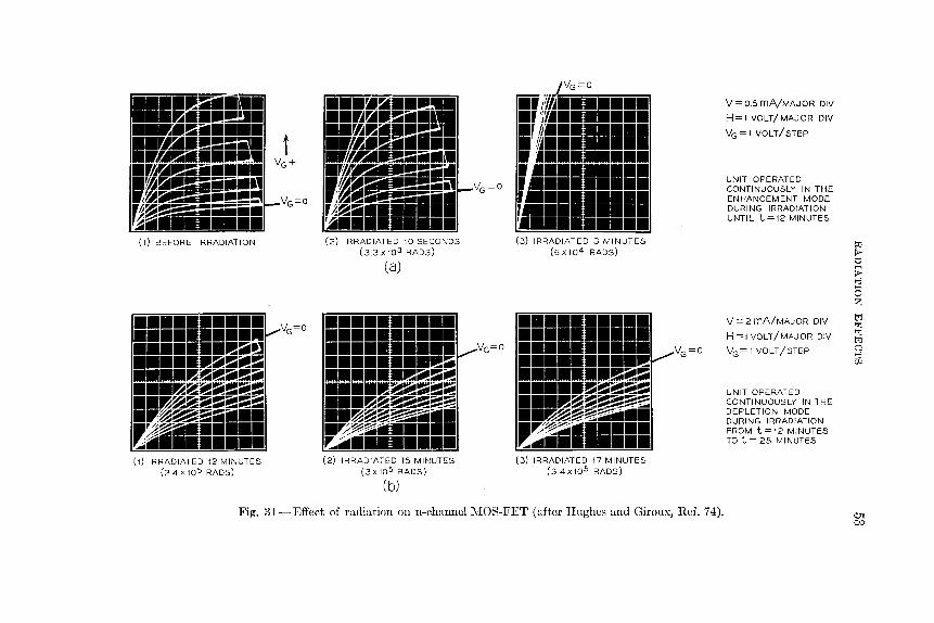
~!'.ii;;;o. ~1 ~ ~ !'!:!] II ~
~~ 1I!!!:!::ii !::ii ~
~ I!iIi ~r.I 1II!:ii!:iii
~~ 1II'!::ii :::iiiiiii ., r! !ill ~ :iji:iiii ~
'~~ !Ii: ~::iiiII
(1) BEFORE IRRADIATION
•••••••••• ........... ••••••• IIJ.!r.~ •••••• ~~~!':i •••• ~~i!ij!:ij ••• II~i!:i!!:;ii!!: •• ~~2:i!~~~~ •• ~a~~:iiil •• .~~a •••••• ~iII •••••••• (1) IRRADIATED 12 MINUTES
(24 x 105 RADS)
t
VG=O
VVG=O
-. -.. ~~ ~:t
~~ ~ l1 ~ ~ !::i ~
~ !':Ii:' 'h~ ~ !:O!:iiii :iiiiiI
1J~ !':iIi !::ii !::ii !::ii
fJ !!':iii !::ii ::iii =-i1 r ~'1I!:i ~ :iiii!::ii :: :iiiiiii !:
r~ ~:'iii ill II (2) IRRADIATED 10 SECONDS
(33 x 103 RADS)
(a)
(2) IRRADIATED 15 MINUTES (3x 10⁵ RADS)
(b)
(3) IRRADIATED 3 MINUTES (6 X 10⁴ RADS)
(3) IRRADIATED t7 MINUTES (34x10 5 RADS)
Fig. 31-Effect of radiation on n-channel MOS-FET (after Hughes and Giroux, Ref. 74).
v = 0.5 rnA/MAJOR DIV
H=1 VOLT/MAJOR DIV
VG=1 VOLT/STEP
UNIT OPERATED CONTINUOUSLY IN THE ENHANCEMENT MODE DURING IRRADIATION UNTIL t = 12 MINUTES
V =2 rnA/MAJOR DIV
H=t VOLT/MAJOR DIV
VG:= 1 VOLT/STEP
UNIT OPERATED CONTINUOUSLY IN THE DEPLETION MODE DURING IRRADIATION FROM t = 12 MINUTES TO t = 25 MINUTES
~ ;;.. d H ;;.. 8 o Z t;:::I ":; "'.l t;:::I () 8 Ul
<:;1 C;.;I
.54 THE BELL SYSTEM TECHNICAL JOURNAL, JANUARY 1967
mode (gate biased positively with respect to the source) but showed little change in depletion mode (gate biased negatively with respect to the source) for a total dose of 106 rads. The effects of the radiation appear to be permanent with no apparent annealing after six months at room temperature.
The degradation of the M08-FET can be explained if it is assumed, as in the case of passivated transistors discussed earlier, that positive charges can be produced in the 8i02 layer by radiation. In the enhancement mode, with the gate electrode positive, a strong electric field is set up which causes positive charge to migrate toward the 8i-8i02
interface. Positive charge accumulation at this interface would, of course, increase the channel conductivity and drain current. In the depletion mode, the field in the oxide will be reversed and positive charges will be attracted to the gate (where they have much less effect on the channel). Negative charge (in the form of electrons) migrating to the 8i-8i02 interface will enter the 8i and no negative charge will build up at the interface.
To support this picture, Hughes and Giroux observed the gate capacities of n-channel M08-FETs biased in both the enhancement and depletion modes as a function of gate-to-source potential, V GS , before and after 106 rads of C060 gamma irradiation. The results are shown in Fig. 32. The capacitance minimum, which is observed as the gate voltage is increased from large negative values, occurs when the surface layer changes from depletion to inversion. If there were no charge stored at the 8i-8i02 interface, the minimum should occur near Vas = O.
In the enhancement mode, Fig. 32(a), the irradiation causes the minimum to shift -11.5 volts. This is to be expected if, as proposed above, a positive charge collects at the 8i-8i02 interface. For the depletion mode, Fig. 32(b), the minimum shifted only -1 volt indicating, as expected, relatively little positive charge accumulation. From these results, Hughes and Giroux estimated that the capacity minimum shift for the enhancement mode corresponds to a positive charge layer of 1012 charges/cm2
at the interface (this charge density would result from 10-3 monolayers of singly charged ions). The experiment was, however, incapable of giving information about the charge accumulation process or the nature of charge carriers.
The behavior of n-channel M08 devices in a radiation environment has been studied by Kooi using 150 keY X_rays.54.75.76 The oxides used by Kooi were prepared in several different ways and were all subjected to a P 205 treatment. He found that irradiation caused a redistribution of charge within the oxide which depended strongly on the presence of electric fields. For positive values of gate potential Kooi observed a

C Co
~ Co
RADIATION EFFECTS 55
1.1 ...-------.-------,------r------,----.-----,
(a)
0.9 i----'Q----CH------+----1'r-f------cI-----t---------1
0.6
1.1
1.0
0.9 ~ 0.8
0.7
0.6 o
,Vr \\ I ! \V X °V
4 8
-'"'
o BEFORE IRRADIATION
/:, ~~D~~~I~~~i~~06 RADS)
12
-VGS IN VOLTS
16
(b)
20 24
Fig. 32-Gate capacitance of an n-channel MOS-FET vs VGS (after Hughes and Giroux, Ref. 74). (a) Enhancement mode, (b) depletion mode.
positive charge buildup in the oxide. The buildup was quite rapid and did not saturate. For negative gate potentials, on the other hand, a smaller positive charge buildup was observed which saturated after a few minutes exposure at 104 r/min. The saturation value was bias dependent.
Kooi explained his observations by supposing that the radiation caused the Si02 to become a photo conductor. For positive gate potentials electrons were removed from the oxide at the gate electrode. The Si was unable to supply electrons to the Si02 across the Si-Si02 interface. As a result a positive charge built up in the oxide. For a negative gate potential the electrons leave the Si02 and enter the Si. The metal-

56 THE BELL SYSTEM TECHNICAL JOURNAI1, JANUARY 1967
oxide interface is now supposed blocking and thus prevents electrons from entering the oxide. The result is again a positive charge buildup. In both cases the buildup will continue until the applied gate potential is entirely across the positive charge at which time the electric field elsewhere in the oxide will be zero. Thus, the buildup should reach a saturation value dependent on the applied gate potential.
Kooi has also irradiated oxidized Si surfaces. Using MOS devices without gate electrodes he observed a positive charge buildup when the oxide was irradiated with 150 ke V X-rays. However, when the oxide was subsequently exposed to ultraviolet light with photon energy ~ 4.2 eV the positive charge was observed to decrease. Kooi explained the action of the ultraviolet light as follows: The ultraviolet light was only capable of exciting electrons onto the conduction band in the Si because the energy gap of Si02 is several e V greater than 4.2. The excited electrons in the Si then enter the oxide and neutralize the trapped positive charge. A similar effect has been observed by Williams.77
Kooi also reported that the effects of radiation on Si02 depend strongly on the method of oxide preparation and on any subsequent heat treatment given the oxide. Furthermore, irradiation was able, in some cases, to alter the density of states at the Si-Si02 interface.
The degradation of enhancement mode, p-channel MOS-FETs irradiated with 1.5 lVleV electrons has been studied by Stanley.78 With a drain-to-source potential of -5 volts and the gate connected through 100 MQ to the source, the drain current remained 5 X 10⁻¹⁰ A until the dose reached 5 X 10+12 e/cm2
• At this dose, ID increased rapidly and then saturated at ~ 4 X 10⁻⁵ A at ~ 1014 e/cm2
•
The drain current as a function of the gate-to-source voltage, V GS ,
is shown in Fig. 33 for three dose levels. Before irradiation, the turn-on voltage (i.e., the minimum value of V G at which a channel is destroyed for a p-channel device or created for an n-channel device) is ~ - 3 volts. (This corresponds to the gate-source voltage where the drain current begins to increase rapidly.) After 1014 e/cm2
, however, the turn-on voltage has decreased to ~ -10 volts and the current for positive V GS
values has substantially increased. At 5 X 10¹⁴ e/ cm2 it is impossible to turn the device on.
The decrease in turn-on voltage can be explained in this case if it is again assumed that positive charge carriers are produced in the oxide by radiation. The electric field in the oxide is in such a direction as to cause a positive charge buildup at the Si-Si02 interface. In this case, however, the positive charges cause an inversion layer (n-channel) on the p-type drain where it is overlapped by the gate (see Fig. 34). A high density of positive charge must be present in the oxide, since it is difficult

(f) w ffi 10- 5 CL L « ~ o 10-(;
H
10-10
-60
RADIATION EFFECTS 57
'\ o e/cm 2\
\
1014e / cm 2
j
I ~ ~
ib 1/
V 5X10 14 e/cm2
-40 -20 o 20
VGS IN VOLTS
Fig. 33 - Effects of electron irradiation on transfer characteristics; I D VS V G 8 at VDS = -20V (after Stanley, Ref. 78).
to invert a highly-doped material such as the drain. As a result, the p-channel is isolated from the drain until the gate potential becomes negative enough to produce a p-channel deeper than the drain channel. vVith increasing radiation dose, the drain channel becomes deeper and the device more difficult to turn on.
The effect of low-energy electrons (10 to 20 ke V) on the charge in an Si02 film on Si has been studied by Szedon and Sandor using an MOS capacitor.79 As in the experiments of Hughes and Giroux, Szedon, and Sandor observed a shift in the C-V curve of the capacitor as a result of irradiation. From the results they estimated the density of surface states at the Si02-Si interface for two capacitors before and after radia-

58 THE BELL SYSTEM TECHNICAL JOURNAL, JANUARY 1967
SOURCE GATE DRAIN (
I OXIDE I
1\ I ¥, p '\ P
\ \
I \ P - CHANNEL INVERSION
LAYER N
Fig. 34-P-channel MOS-FET after irradiation (after Stanley, Ref. 78).
tion. The results are shown as a function of position in the energy gap of Si in Fig. 35. It can be seen for both capacitors that a significant number of stutes have been added, ~2 X 10¹² states/cm2 -eV, over considerable portion of the energy gap. Szedon and Sandor also report that the effects of irradiation could be removed by a H)-minute anneal at 150-200°C with the capacitor shorted.
Speth and Fang80 have observed the changes in n-channel MOS-FET characteristics due to 5 ke V electron bombardment. They irradiated the devices to a dose of ~1014 e/cm2 at successively larger positive values of gate voltage. At each gate potential value, V G , the turn-on voltage of the device, V 7', stabilized at a more negative value indicating a buildup of positive charge in the oxide. The stable values of turn-on voltage were found to decrease linearly with increasing values of V G
used during irradiation. The effects of the radiation could be annealed out in several hours at 200°C.
The effects of neutron irradiation on MOS transistors have been reported by Messenger and Steele.81 They find the most important effect to be a positive charge buildup in the oxide, which causes the gate capacity minimum to move to more negative values of V GS • They define the gate voltage at which the capacity minimum occurs as the turn-on voltage, V T • Fig. 36 shows the change in V T with neutron flux. According to IVlessenger, the tendency of V T to saturate indicates a decreasing net accumulation rate of positive charge which may be caused by a diffusion or recombination process. The existence of such processes implies that the degradation should be dose-rate dependent and also the diffusion or recombination process has a substantially higher rate during irradiation since the degradation appears to be permanent after irradiation. At present there is no independent evidence to support this view. Annealing at elevated temperatures was found to

RADIATION EFFECTS 59
remove the degradation; typically, V T showed 90 percent recovery after 70 hours at 150°C.
A study by Kuchne82 of insulated gate thin-film transistors using polycrystalline CdS has revealed similar surface effects due to ionizing radiation. These devices showed bias-dependent semipermanent changes in transconductance and channel conductivity at doses of 105 rads. Analysis showed that interface trapping states are at least partly responsible.
5.7 Integrated Circuits
The direction of present-day semiconductor device technology is towards increased use of integrated circuits. These circuits contain many passivated areas where surface effects due to radiation may cause degradation. Unfortunately, very little work has yet been reported on surface effects of ionizing radiation on these devices. Stanley83 has studied
I
> <lJ
N
IE u V) LU I-
~ V)
9
8
7
6
5
V) 4 LU I-
~ V)
/ /
I
SAMPLE NO.1 II ORIGINAL--~J
ADDED ..... ~ ~ 3 ------ ------ ------ -------f-o------- ----~t. >lii)
aJ 2 o
1
o -0.3 -0.2
SAMPLE NO.2 ~~ , -''\ ORIGINAL _, ----- / -,
\ ADDED" "", "'......-~/~ , ----r-7 1\
~ ~ V ,J \ / ~/ r-.--0.1 a 0.1 0.2 0.3 0.4
POSITION WITHIN THE FORBIDDEN GAP IN eV
Fig. 35 - Typical densities of states added by low energy electron bombardment of Al-SiQ 2-Si capacitors, compared with original densities. Sample 1: 5 n-cm n-type Si, 1600 A oxide grown in wet 002 , capacitance-voltage data taken at 600 MHz. Sample 2: 50n-cm n-type Si, 1500 A oxide grown in dry O2 ; capacitance-voltage data taken at 1 MHz (after Szedon and Sandor, Ref. 79).
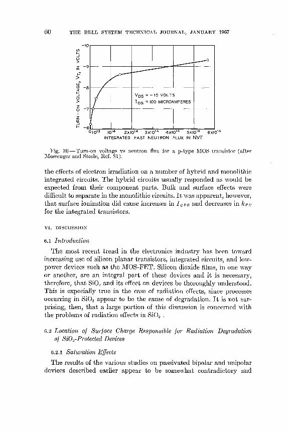
60 THE BELL SYSTEM TECHNICAL JOURNAL, JANUARY 1967
(/)
~ o >
-10
?; -9
t-=' > w'" t!> -8 ~ ..J o >
5 -7 1 z 0: :J I- -6
/
I IT rl
---~ L-----~ ~
VDS = -IS VOLTS
IDS = 100 MICROAMPERES
010 '3 1014 2XIO '4 3xl014 4xtO '4 5xtO l4 6XtO'4
INTEGRATED FAST NEUTRON FLUX IN NVT
Fig. 36-Turn-on voltage vs neutron flux for a p-type MOS transistor (after Messenger and Steele, Ref. 81).
the effects of electron irradiation on a number of hybrid and monolithic integrated circuits. The hybrid circuits usually responded as would be expected from their component parts. Bulk and surface effects were difficult to separate in the monolithic circuits. It was apparent, however, that surface ionization did cause increases in I CEO and decreases in h pE
for the integrated transistors.
VI. DISCUSSION
6.1 Introduction
The most recent trend in the electronics industry has been toward increasing use of silicon planar transistors, integrated circuits, and lowpower devices such as the MOS-FET. Silicon dioxide films, in one way or another, are an integral part of these devices and it is necessary, therefore, that Si02 and its effect on devices be thoroughly understood. This is expecially true in the case of radiation effects, since processes occurring in Si02 appear to be the cause of degradation. It is not surprising, then, that a large portion of this discussion is concerned with the problems of radiation effects in Si02 •
6.2 Location of Surface Charge Responsible for Radiation Degradation of Si02-Protected Devices
6.2.1 Saturation Effects
The results of the various studies on passivated bipolar and unipolar devices described earlier appear to be somewhat contradictory and

RADIATION EFFECTS 61
irreconcilable. The question is whether the surface charge which controls the degradation process is located on the outer surface of the oxide (Atalla's model41), or in the oxide at the Si-Si02 interface. It is not inconceivable, of course, that both views are valid and that under some circumstances charge on the Si02 surface dominates while in other cases charge within the oxide is more important. For some observations, both models are capable of an explanation. For example, Kerr,61 Stanley/4 Taulbee et al,62 Brucker et al,65.66 Speth and Fang80 and to some extent Schmid63 observe a saturation of degradation. Intuitively one would expect both models to predict saturation since both processes, surface charge separation and charge accumulation, are self-limiting.
6.2.2 I1nportance of Bias
vVith the exception of Schmid's observations, the experimental evidence indicates that bias is an important factor in degradation due to radiation. This result is not surprising since both models require an electric field; Atalla's model requires a parallel field component at the oxide surface, the other a transverse component in the oxide. These field components may arise from bias voltages across p-n junctions or from overlaying contacts. * It is also possible that built-in fields are produced in the Si02 layers during their formation. Built-in fields may reduce the dependence of degradation on bias voltage. At present it is difficult to predict quantitatively how degradation should depend on bias conditions and hence it is difficult to distinguish between the two models from the experimental results given above.
6.2.3 Recovery of Surface EjJects
Recovery of passivated devices from surface effects due to radiation is to be expected under proper conditions for reasons similar to those for nonpassivated devices. Some recovery is expected to start as soon as the device is removed from the radiation. Removal of bias and increase in temperature should contribute to recovery; under these conditions, recovery has been observed as discussed above. One might, however, expect to see a difference in recovery depending on where the surface charge responsible for degradation is located. If the charge is located on the oxide surface, recovery might be somewhat easier than
* In most planar passivated transistors the evaporated emitter contact overlays the base region. Under reverse emitter bias, the field in the oxide may approach = 105 V per cm. In the case of an npn transistor, this field will tend to move positive eharges in the oxide toward the oxide-semiconductor interface. For a pnp device, the positive eharge will tend to move away from the interface. Base eontacts do not generally overlay the collector and so comparable fields in the oxide at the base-collector interface do not oceur.

62 THE BELL SYSTEM TECHNICAL JOURNAL, JANUARY 1967
it would be for a charge located inside the oxide, well isolated from the ambient. For example, simply exposing a nonpassivated device to the atmosphere can cause considerable recovery. For passivated devices, however, the bulk of the evidence points to a charge in the oxide, since recovery usually requires elevated temperatures; the degradation appears quite stable under shelf conditions, and exposure to the atmosphere does not produce noticeable recovery.
6.2.4 Additional Evidence
'1'he model of charge storage in the oxide is further supported by Estrup's84 finding that ion bombardment of passivated diodes did not produce the leakage current degradation observed with nonpassivated diodes. The strongest support, however, has come from the observation that degradation of irradiated passivated devices occurs even with a high vacuum ambient. 67
All in all, the bulk of evidence supports the model of ionizable defects located in the oxide, apparently quite close to the Si02-Si interface, as being the principal source of degradation in these devices.
6.3 N aiure of the Charge in the Oxide
Various defects and impurities, including sodium, aluminum, hydrogen, oxygen vacancies and trivalent silicon,85 have been suggested, at one time or an other, as the species responsible for the positive charge buildup in Si02 layers. For Si02 layers subjected to elevated temperatures and electric fields, it appears that the accumulation of positive charge at the Si02-Si interface is the result of Na+ or H+ ion drift in the oxide. However, the questions of why a previously unstressed S102 film should contain a positive charge and how radiation produces a charge buildup in the oxide are still not completely answered.
6.4 Proposed Models of Charge Accumulation in Si02 Layers Exposed to Ionizing Radiation
6.4.1 Electron Drift Model
Grove and Snow86 ,87 have used MOS capacitance-voltage measurements to observe the buildup of positive charge in Si02 layers in MOS capacitors and transistors exposed to 35 ke V X-rays. With negative values of gate voltage, V G, (gate negative with respect to the silicon) they observed little change in the charge contained in the oxide. With positive values of V G , on the other hand, appreciable buildup of positive charge was observed. For a given value of V G , ,the charge density in

RADIATION EFFECTS G3
the oxide, Q. , was observed to saturate with increasing radiation dose. The saturation value of charge density, Q. (sat), was found to be proportional to V J for lower values of V G •
Grove and Snow have proposed a quantitative model similar to the qualitative model suggested by Kooi,75.76 which satisfactorily explains their findings. They assume the Si02 layer contains traps which are normally neutral. Upon irradiation the traps become positively ionized and the excited electrons drift to the positive gate under the action of the field in the oxide. The electrons are discharged at the gate. However, since the Si cannot supply electrons to the oxide, a positive space charge builds up at the Si02-Si interface.
The buildup of positive charge is best described with the aid of Fig. 37. Initially there is no charge in the oxide, Fig. 37(a), and consequently the field throughout the oxide is constant. As the positive charge accumulates in the oxide, Fig. 37(b), the charge on the gate decreases, the electric field in the oxide between the gate and space charge decreases, and the potential drop across the space charge region increases. After sufficient irradiation equilibrium will be achieved, Fig. 37(c), when the entire potential drop, V G , appears across the space charge region. The electric field in the oxide between the gate and space charge will, of course, be zero. Further irradiation will not cause an increase in the space charge region unless V G is increased.
To simplify calculations, Grove and Snow assumed that the density of traps, Nt, was constant throughout the oxide. Furthermore, they assumed all traps within a distance d of the Si02-Si interface were charged and that the traps elsewhere in the oxide were neutral. vVith these assumptions it can readily be shown that
d = (2KoEo V Gj qNt)!,
where I{o is the dielectric constant of Si02 , Eo is the permittivity of free space, and q is the charge on the electron. If V G is reduced to zero, Q. (sat) (= qNtd) will induce a negative charge, Q~ (sat), in the silicon surface where
-Q:(sat) = qNtd(l - dj2xo) ,
xo is the thickness of the oxide. (Q: (sat) is the quantity which is observed experimentally.) The observed values of Q~ (sat) vs VJ are shown in Fig. 38. Also plotted in this figure are three curves corresponding to the expression for Q~ (sat) above with three different values of Nt assumed. Although the scatter of points is rather large, Q: (sat) appears to vary as V J for lower values of V G as expected from the equa-

6:+ THE BELL SYSTEM TECHNICAJ~ JOURNAL, JANUARY 19Gi
p
k-d-
E
(a) INITIAL (b) INTERMEDIATE (c) FINAL STEADY STATE
Fig. 37 -Space charge buildup as a function of time during irradiation of aMOS structure under positive gate bias (after Grove and Snow, Ref. 87).
tion given above. The agreement with theory seems to be best for Nt ~ 2 X 1018 cm-3
•
Speth and Fang80 have also employed a model which postulates a space charge buildup at the Si02-Si interface to explain their observations of the effects of low energy electrons (5 ke V) on n-channel MOSFET discussed previously, (Section 5.6). Using the calculations of Thomas and Young,88 Speth and Fang predict that the turn-on voltage, V T , of the MOS-FET should decrease linearly with increasing gate bias used during irradiation according to the equation
V T = - Va(2xo/d - 1) + V~ ,
where V ~ is the turn-on voltage prior to irradiation. The basic difference between this model and the model of Grove and
Snow is in the behavior of the space charge width, d. Speth and Fang assume d is independent of V G • In other words, the space charge layer remains constant in width while the charge density within the space charge layer increases with irradiation. If, on the other hand, one follows Grove and Snow and allows d to increase while the charge density in the
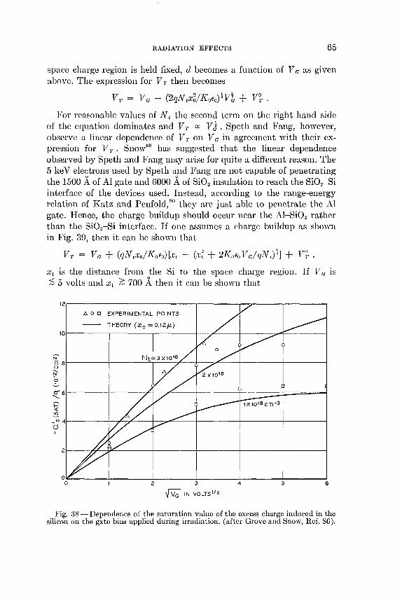
RADIATION EFFECTS 65
space charge region is held fixed, d becomes a function of Va as given above. The expression for V 7' then becomes
V T = Va - (2qNtx~/Kofo)!Vb + V~, .
For reasonable values of Nt the second term on the right hand side of the equation dominates and V 1' 0: VJ. Speth and Fang, however, observe a linear dependellee of V 7' on Vain agreement with their expression for V'1" SnowS\) has suggested that the lineal' dependence observed by Speth and Fang may arise for quite a different reason. The 5 ke V electrons used by Speth and Fang are not capable of penetrating the 1500 A of Al gate and 6000 A of Si02 insulation to reach the Si02-Si interface of the devices used. Instead, according to the range-energy relation of Katz and Penfold,90 they are just able to penetrate the Al gate. Hence, the charge buildup should occur near the AI-Si02 rather than the Si02-Si interface. If one assumes a charge buildup as shown in Fig. 39, then it can be shown that
V 1' = Va + (qNtxo/Kofo)[Xl - (x; + 2KofoVa/qNt)!] + y~" Xl is the distance from the Si to the space charge region. If Va IS
$ 5 volts and Xl 2: 700 A then it can be shown that
12~------------------------~------~~~----~------~
t:. 0 0 EXPERIMENTAL POINTS
tOr-------~------~r-------~~~--_4------~~------~
N E 8r-------~------~~---F--4_--~--~--------~------~ u
;;;-9
~6J-------1-----~~~~---Ir-------f---~~~~~==~
~ ~ _~4r-------~~~--~r-~~--~------~--------~------~
o I
2~---~~~~----~--------4_------_4--------1_------~
2 3 4 :. 6
vv;;: IN VOLTS '/2
Fig. 38 - Dependence of the saturation value of the excess charge induced in the silicon on the gate bias applied during irradiation. (after Grove and Snow, Ref. 86).

66 THE BELL SYSTEM TECHNICAL JOURNAL, JANUARY 1967
V T r-v - VaeXO/XI - 1) + V~ . The approximate expression for V T should apply to the results of Speth
and Fang and V T is expected to be linear with Va. For the devices used, the slope of the graph of V T VS Va yields XO/Xl - 1 = 13 which, for Xo = 6000 A, gives Xl ~ 400 A. In other words, the positive charge accumulation in the Si02 may be far enough away from the Si-Si02
interface to make V T appear linear with Va. The models employed by Grove and Snow and by Speth and Fang
are, of course, oversimplifications of the true picture. The most obvious shortcomings are the neglect of the almost certain variation of Nt throughout the oxide and the assumption of an abrupt interface between the space charge and the neutral oxide. Nevertheless, such approximations are necessary in view of our very limited knowledge of the oxide.
The electron drift model requires further elaboration to explain what happens in the oxide when irradiation occurs with no applied electric field present in the oxide. The explanation may lie in the heterojunction picture of the Si02-Si interface proposed by Lindmayer and Busen.91
•92 According to this picture, Si02 is viewed as a wide gap
insulator with a work function somewhat smaller than that of Si. When Si02 is grown on Si the work function difference, D.¢, is accommodated by a transfer of electrons from the Si02 to the Si surface. These electrons come mainly from deep lying traps in the oxide. Hence, regardless of the conductivity type of the Si, the Si surface always tends to be n-type. The heterojunction picture thus offers an explanation of why the surface of freshly oxidized Si is invariably accumulated for n-type and depleted or inverted for p-type Si.
Initially the Si02-Si system may not be in equilibrium, i.e., insuf-
SL
CHARGE DENSITY
SLOz METAL
Fig. 39 - Assumed charge distribution in the oxide.

RADIATION EFFECTS 67
SL
Fig. 40 - Transfer of electrons from Si0 2 to Si as a result of irradiation.
ficient positive charge may exist in the oxide after the growth of the film. Elevated temperatures or the presence of ionizing radiation may permit the system to equilibrate. Electrons excited into the conduction band of the oxide will diffuse to the interface and pass into the Si, see Fig. 40. Thus, positive charge may build up in the oxide even though no bias is applied to the gate. This buildup of positive charge will saturate, of course, when equilibrium is achieved. The positive charge density required for equilibrium for A¢ ~ 0.3 e V is 1010
- 1011 charges cm -2. Lindmayer and Busen report that annealing at 250°C for ~103 hours brought oxidized Si samples to equilibrium with positive charge densities in the oxide ~lOll charges cm -2 even though the initial charge densities varied from 106 to 1011 charges cm -2.
This particular heterojunction picture, is probably an over-simplification. A true heterojunction requires an abrupt interface between the two crystalline materials and the absence of a significant number of interface states.93 For Si02 and Si, especially in the case of thermally grown oxide, the interface will not be abrupt; rather, there will be a transition region Si02-SiOx-Si where x changes continuously from 0 to 2 on passing from the region of pure Si to the region of pure Si02 • Furthermore, the charge storage effect should depend, quite noticeably, on the position of the Fermi level in the Si. Lindmayer and Busen, however, only discuss results on near intrinsic Si. Grove et al,94 on the other hand, have examined oxidized p-type Si with a wide range of boron concentrations and report no appreciable variation of positive charge density.

68 THE BELL SYSTEM TECHNICAL JOURNAL, JANUARY 1967
6.4.2 Positive Ion Drift 1I10del
As mentioned previously, positive ion drift is now widely believed to be the cause of charge buildup in 8i02 layers exposed to elevated temperatures and positive gate bias. HO'wever, there is at present, little direct evidence that the effects of radiation on oxidized 8i surfaces at room temperature are due to the migration of such ions. Nevertheless, it is interesting to speculate on a possible mechanism for radiation-induced charge buildup involving positive ions.
If one assumes that ionized (but not neutral) impurities arc mobile in 8i02 at sufficiently low temperatures then it is possible to construct a model for charge buildup. In this model the only requirement of the radiation is that it ionize a sufficient number of impurity atoms. The positively charged ions so produced would then drift through the oxide under the action of the applied field to the vicinity of the 8i02-8i interface.
It is interesting to note that concentrations of Na50 and H 47, two
possible charge carriers, are known to be highest near the metal-oxide interface. Thus, if the radiation has sufficient energy to penetrate the metal gate, it will be able to produce a large number of mobile positive ions. The ions will drift through the oxide and cause a buildup of charge at the 8i02-8i interface. This model could, therefore, explain why the results of 8peth and Fang indicate a charge buildup near the 8i02-8i interface even though the radiation they used hardly penetrated to the oxide. Other results of electron irradiation on semiconductor devices indicate that degradation may occur at energies as low as 2J5 ± 0.5 keV71
•
At present the experiments of Grove and 8now support the view that charge buildup is primarily the result of ionization of existing traps rather than by the motion of ions. It may well be that both processes are possible and that the more important process in a given situation will depend on the energy of the radiation used.
6.5 Recommendations for Future Surface Radiation Ejj'ects Studies
6.5.1 Fundamental Studies
There is, at present, little information on radiation-induced changes of the surface potential at a clean semiconductor surface. In principle, it would be relatively easy to study these changes by comparing the effects of radiation with those produced by, say, known ambient changes. In practice, reproducibly clean surfaces would be required and these are difficult to prepare and maintain. The radiation used should, of
RADIATION EFFECTS 69
course, be of low enough energy to prevent bulk damage effects (lowenergy electrons might be suitable).
The effects of radiation-induced lattice damage at a semicondudor surface are unknown. Usually it is assumed that this type of damage is unimportant in a region such as a surface where lattice irregularities are already numerous. It is possible, however, that lattice damage sites may be created at energies significantly lower than in the bulk, and that these additional sites do, in fact, lead to an increase in the surface state density.
6.5.2 Device Studies
Continued emphasis should undoubtedly be placed on device studies, both for the role such studies play in validating the various models presented here and because the preparation of semiconductor surfaces by most of the device manufacturers has been a constantly evolving process. A short time ago a simple but satisfactory model of surface effects on (nonpassivated) devices existed. Today, however, the situation is, in a certain sense, worse since the problems of passivated devices are just beginning to be resolved.
Particular emphasis should be placed on understanding radiation surface effects in lVIOS-FETs, high-frequency transistors, thin-film transistors, metal-semiconductor junctions, and other low-level logic devices that are especially useful for low-power space applications. A model of the processes involved in the radiation-induced degradation of these devices should be developed. Ideally, such a model would of course, be most useful to device designers who could then design devices in such a way as to minimize the effects of radiation.
An important step in the development of a model would be the development of a surface stabilization technique which would reduce surface effects as much as possible. The charge transport mechanism in Si02
is now better understood and it may be possible to improve the passivation process to provide even better and more stable surfaces. Perhaps the P 20 S treatment of Si02 or the use of other passivation materials such as silicon nitride will provide the improved stability.
At present, the method of oxide preparation varies from manufacturer to manufacturer, making it difficult to interpret results from different sources. It may prove necessary to develop a standard procedure for device passivation, at least for devices exposed to radiation. Other manufacturing steps, such as the deposition of contacts or the bonding of leads, may lead to local damage areas. These areas may be more sensitive to radiation effects and should be investigated.

70 THE BELL SYSTEM TECHNICAL JOURNAL, JANUARY 19G7
It is essential that the effects of ionizing radiation on metal-semiconductor and heterojunction interfaces be understood. This important area has heretofore been neglected. Studies of noise arising from surface effects in both unipolar and bipolar devices is another area that has unfortunately been neglected. Noise in lUOS structures has been discussed by Sah95 and by Jordan and Jordan,96 but a study of the effects of radiation on noise in MOS devices has not been reported.
6.5.3 Procedures for Selecting Devices for a Radiation Environment
Ultimately, the device studies outlined above should lead to procedures for selecting both the type and individual device best suited with respect to surface effects for use in a radiation environment. To date, very little has been done to evolve such procedures. Peck et al,23 in choosing transistors for the Telstar® satellite, devised a straightforward selection process. The various device types were subjected to a gamma exposure of 1.4 X 10⁴ rads (8.5 X 10⁵ rads/hr for 1 min) followed by an exposure at 3 rads/hr for at least one week. Device types showing no significant changes in I CBO and hFE were considered satisfactory.
Peck et al also studied screening and selection procedures using diffused Si transistors. They showed that, by selecting devices which had an I CBO value of less than 10-8 A after a screening dose of ~104 rads, they could eliminate 90 percent of the devices whieh ultimately suffered severe I CBO or hFE degradation.
A selection procedure for planar Si transistors which uses microplasma noise measurements in addition to a screening radiation procedure has been developed by Bostian and Manning.97 According to these investigators, microplasma noise is an indicator of the presence of surface defects which act as acceptor states. These acceptor states aid in channel formation on pnp devices and oppose it on npn. Thus pnp transistors exhibiting the least microplasma noise and npn exhibiting the highest should be least susceptible to radiation.
Based on the above model, Bostian and lVlanning give a selection procedure. First, select transistor types with the highest upper frequency limit to reduce gain degradation due to bulk radiation damage. Next, select the pnp transistor type with the lowest or the npn type with the highest average microplasma noise level. Then, select the individual devices by choosing the pnp's with lowest and the npn's with the highest noise levels. Finally, expose the devices to a screening dose of 5 X 10⁴
rads and reject any showing I aBO values significantly above average. Using the procedure outlined above, the authors report improvement

RADIATION EFFECTS 71
factors (defined as the ratio of average leakage current of all devices in a group to the average current for selected devices) of about 10, depending on device type.
VII. SUMMARY
The degradation of many semiconductor devices resulting from surface effects of radiation may be explained, qualitatively at least, using the presently accepted model of semiconductor surfaces. The explanations are based on the creation by ionizing radiation of localized charged energy states on semiconductor surfaces.
These states are created both at the termination of a semiconductor lattice itself, the so-called "fast" states, and in any surface layer, such as an oxide, the so-called "slow" states. The slow states are usually the more numerous and the charge they contain controls the surface potential and hence the number and type of charge carriers in the surface region. The fast states, on the other hand, are the states which actually interact directly with the charge carriers in the semiconductor. They act as generation and recombination centers for holes and electrons, and their activity is measured by the surface recombination velocity, which depends on the surface potential.
As a result of irradiation, a device accumulates charge principally in the slow states, and this charge affects the underlying semiconductor surface. As a result of changes in the surface potential, the surface recombination-generation may be increased (because of changes in both the surface recombination velocity and the number of fast states), causing device degradation. Inversion layers (channels) may also be formed at p-n junctions, leading to increased reverse leakage currents and degraded emitter efficiency.
For nonpassivated devices, the slow states are in close proximity to the surface and hence strongly influence the surface layer. These devices are, therefore, very sensitive to ambient changes such as those caused by radiation. In passivated devices, the slow states tend to be further removed from the semiconductor surface, and hence these devices are generally one or two orders of magnitude less sensitive to radiation.
For nonpassivated devices in a gaseous ambient, the mechanism by which radiation produces charge in the slow surface states is reasonably well established. Radiation produces gaseous ions, some of which are attracted by electric fields to the device surface, where they subsequently deposit charge. When sufficient ionic charge (generally positive) has been collected on the surface, inversion layers (channels) form on the underlying semiconductor which in turn alter junction

72 THE BEIJL SYSTEM TECHNICAL JOURNAL, JANUARY 1967
leakage currents and transistor gain. For a pnp device, channels tend to form on the p-type collector side, causing large increases in I cno .
The surface recombination in the emitter-base region is relatively unaffected by this positive surface charge, and therefore the h pE degradation is usually small. For npn transistors, on the other hand, the channel forms on the base. Because the base width of a transistor is usually small, this channel is restricted in size and hence I cno does not generally increase as much as for pnp devices. However, generation-recombination current at the emitter-base surface is increased, causing a large decrease in hpE • If the base channel extends from the collector to the emitter, then I CEO will increase and hp E may appear to increase because of the increase in I C •
The simple model used to explain the degradation of nonpassivated devices is of somewhat limited usefulness. It does predict the bias dependence of degradation and also the recovery of devices under proper conditions. However, this model at present does not explain the observed memory effects, nor does it generally apply to devices with grease or similar ambients.
The number of passivated Si planar devices has greatly increased in the past few years and will most likely continue to do so in the future. Thermally grown Si02 films are used to passivate the surfaces of these devices by stabilizing the interface structure and isolating the Si from the ambient. The Si02 film becomes, therefore, an integral part of the device and it is necessary to understand the role this passivation layer plays when the device is subjected to radiation.
It is well established that passivated devices degrade in ways quite similar to nonpassivated devices when exposed to radiation, although they are generally less sensitive than their nonpassivated counterparts. The degradation appears to result from the formation of positive surface charge in or on the oxide, with the consequent production of channels on the device surface. The channels manifest themselves by increased junction leakage currents and reduced transistor gain. The behavior of npn and pnp transistors follows the pattern outlined above for the nonpassivated case. Passivated devices also exhibit memory and recovery effects similar to those observed with nonpassivated devices.
The main point of controversy among the models used to explain the degradation is the process by which the positive slIrface charge accumulates. In one view, the charge is created by ionization of impurities on the surface of the oxide, and these ions are then separated by surface electric fields. The majority of experiments, however, indicate

RADIATION EFFECTS 73
that the charge exists within the Si02 , probably close to the Si02-Si interface. Several species of charge carrier, including N a + and H+ ions and electrons, have been suggested as the means by which charge is transported through the oxide. None of these has, as yet, been conclusively demonstrated as the responsible carrier, nor has the role played by radiation in the accumulation process been clarified.
MOS-FETs have been shown to be quite sensitive to radiation, more sensitive than conventional passivated devices. The cause again appears to be positive charge accumulation in the oxide near the Si02-Si interface. Presumably, the explanations of degradation in MOS-FETs and passivated devices will be very similar, since the same oxide is used in both cases.
It has been found experimentally that oxide-covered Si surfaces invariably tend to be n-type regardless of the conductivity type of the Si. This fact implies the existence of a rather large built-in positive charge in the oxide after the growth of the film. If the Si02-Si interface is viewed as a heterojunction, it can be shown that, as a natural result of the work function difference between the Si02 and the Si, the Si surface should have an equilibrium charge density of ~lOll electronscm -2. The oxide will, of course, have a positive charge density of equal magnitude.
It may well be that, during growth of an Si02 film, the equilibrium charge density is not attained. Furthermore, it cannot be attained after growth at room temperature since the oxide cannot supply sufficient electrons to the Si because of the large energy gap of the oxide. Radiation will, however, cause ionization in the Si02 and allow at least some equilibration of charge, i.e., further accumulation of positive charge in the oxide.
A model has been suggested by Rooi and elaborated by Grove and Snow for an oxide irradiated in the presence of an applied electric field in which electrons excited out of traps drift out of the oxide into the gate for positive and into the Si for negative gate potentials. For positive gate bias the electrons which leave the oxide are not replaced since the Si cannot supply electrons to the oxide. A positive charge buildup at the Si02-Si interface results. For a negative gate bias, on the other hand, the gate replaces electrons which leave the oxide and enter the Si. Hence, there is no charge buildup. An alternative model for which there is as yet little evidence assumes that positive ions may be sufficiently mobile at low temperatures (:s 100°C) to drift under the action of applied electric fields and build up a positive charge at the Si02-Si interface.

74 THE BELL SYSTEM TECHNICAL JOURNAL, JANUARY 1967
The need for further work on both fundamental and practical problems in surface radiation effects is self-evident. Devices, particularly those suitable for low-level logic in space applications, will require extensive study, since these device types are likely to be quite sensitive to surface radiation effects.
VIII. ACKNOWLEDGMENTS
The authors would like to thank T. M. Buck, A. S. Grove, J. T. Nelson, D. S. Peck, and A. G. Stanley for reading the manuscript and for their valuable comments. The authors also wish to thank J. F. Aschner, R. R. Blair, and E. R. Schmid for their assistance and helpful discussions.
APPENDIX A
Units of Radiation Commonly Used in Surface Effects Studies
There are two units of radiation in common use in surface effects studies. The roentgen (r) is a unit of radiation exposed dose and is defined as that quantity of X- or gamma-radiation which produces 2.083 X 10⁹ ion pairs per cc of air at standard conditions. The amount of radiation absorbed from a given exposed dose, however, will depend on the absorbing material. An irradiated material is said to have received an absorbed dose of one rad when it has absorbed 100 ergs per gram of irradiated material. Calculation of an absorbed dose requires a knowledge of the energy of the radiation and the appropriate absorption coefficients of the material. For Si devices exposed to Co60 gamma radiation it is usually assumed that an exposure dose of 1 roentgen results in an absorbed dose of ~1 rad.
APPENDIX B
Calculation of Absorbed Dose from Electron Irradiation
The purpose of this appendix is to illustrate a method of calculating the radiation absorbed dose (in rads, say) for an Si02-protected Si planar device exposed to a beam of mono-energetic electrons. To simplify the calculations we will consider that device degradation (due to surface effects) occurs only as the result of ionization produced in the Si02 layer and that ionization produced anywhere in the oxide is equally effective. In other words, only the total energy absorbed by the oxide is important.

RADIATION EFFECTS 75
For the purposes of calculating the absorbed dose, one of three possible situations will occur depending on the energy of the electrons and the thickness of the oxide. The three cases are:
(i) The electrons are completely stopped in the oxide. (ii) The electrons penetrate the oxide and lose a significant fraction
of their energy in so doing, i.e., the oxide thickness is comparable to but less than the range of the electrons.
(iii) The electrons penetrate the oxide without a significant loss of energy, i.e., the oxide thickness « the range of the electrons.
To decide which of the three cases is applicable it is necessary to know the range, R, of electrons in Si02 as a function of electron energy, E. Fig. 41 shows this relationship according to the range-energy equation of Katz and Penfold.90 A density of 2.66 gm/cm3 has been assumed for Si02 • The curve has been extrapolated to an energy of 10-3 MeV although Katz and Penfold give 10-2 MeV as the lower limit of accuracy for their equation.
For the sake of a concrete example, let us assume that we wish to know the absorbed dose as a function of electron energy for a l,u thick oxide layer on a semi-infinite Si substrate when a beam of 1 electron/ cm2
is incident normally on the oxide (see insert in Fig. 43). From Fig. 41 it is apparent that electrons with energies ~ 1.3 X 10⁻² MeV will be completely stopped by the oxide, case (i) above. For this case it is assumed that all the energy of the electrons is absorbed by the oxide and hence the calculation of the absorbed dose is quite straightforward.
For electron energies ~ 4.2 X 10⁻² MeV the range of the electrons is ~ 10,u compared to the l,u thickness of the oxide and therefore the electrons will lose only _a small fraction of their energy in passing through the oxide, case (iii) above. For this case we need to know the stopping power, (-dE / dx), of the oxide as a function of electron energy. According to Bethe98
, the stopping power for electrons of energy E is given by,
E/ 27re4 [ 2 / 2( 2) -d dx = -2 N e In mv E 21 1 - {3 mv
- (2 VI - {32 - 1 + (3'J) In 2 + 1 - {32
+ HI - Vl=if/ - 0] ergs/em,
where
e electronic charge in esu 111, = electron rest mass in grams

76 THE BELL SYSTEM TECHNICAL JOURNAL, JANUARY 1967
/
/ J
/ V
~10 I / / a:
II I
I
I / I
I I
I
/ I
I
10.-3 -10. 3 - -10. 2 10. I 10.0
E IN Mev
Fig. 41- Range-energy relationship for electrolls in Si0 2 •
v electron velocity in cmls N. density of electrons in stopping material 1 mean excitation potential of stopping material (3 vic c velocity of light in cmls 8 correction for density effect.
The stopping power for electrons in Si02 , as calculated from the above expression, is shown in Fig. 42. N. for Si02 was estimated to be 7.96 X 10²³ e/cm3 and a value of 1.2 X 10² eV was assumed for I. The density effect correction term, 8, was taken as zero for the solid curve. However, 8 becomes important for E ~ 0.5 MeV and can amount to ~10 - 15 percent at 10 MeV. The dashed curve indicates the effect of this correction.
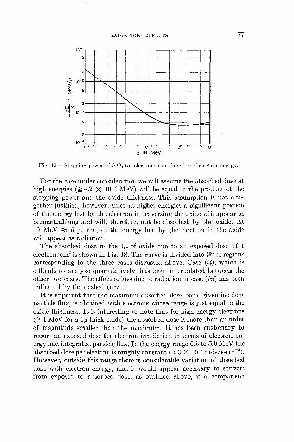
2
~ lO-2 > (l)
L ~
2 W\X -0 -0 10-3
I
2
10-4
~
RADIATION EFFECTS
I ------- -- ---- ---- -i-j , ....
"'-i
I" ~
"-
" "-- -_.- ~r-.. .-r-
-10-3 2 5 10 2 2 5 10-1 2 5 100 2 5 lOt
E IN MeV
77
Fig. 42-Stoppillg power of Si0 2 for electrons as a function of electroll energy.
For the case under consideration we will assume the absorbed dose at high energies (~4.2 X 10⁻² lVleV) will be equal to the product of the stopping power and the oxide thickness. This assumption is not altogether justified, however, since at higher energies a significant portion of the energy lost by the electron in traversing the oxide will appear as bremsstrahlung and will, therefore, not be absorbed by the oxide. At 10 MeV ~15 percent of the energy lost by the electron in the oxide will appear as radiation.
The absorbed dose in the l,u of oxide due to an exposed dose of 1 electron/ cm2 is shown in Fig. 43. The curve is divided into three regions corresponding to the three cases discussed above. Case (ii) , which is difficult to analyze quantitatively, has been interpolated between the other two cases. The effect of loss due to radiation in case (iii) has been indicated by the dashed curve.
It is apparent that the maximum absorbed dose, for a given incident particle flux, is obtained with electrons whose range is just equal to the oxide thickness. It is interesting to note that for high energy electrons (~1 MeV for a l,u thick oxide) the absorbed dose is more than an order of magnitude smaller than the maximum. It has been customary to report an exposed dose for electron irradiation in terms of electron energy and integrated particle flux. In the energy range 0.5 to 5.0 MeV the absorbed dose per electron is roughly constant (~3 X 10⁻⁸ rads/e-cm- 2
).
However, outside this range there is considerable variation of absorbed dose with electron energy, and it would appear necessary to convert from exposed to absorbed dose, as outlined above, if a comparison

78 THE BELL SYSTEM TECHNICAL JOURNAL, JANUARY 1967
cf) o <l: cr:
4
r---l/"'"
..... V
VI
1/1\ 1\
I \ I \
1
I I I 1_
SLP21 _ - ~ -SL
--f----+-- - W -\ , -~ 1P. ~-~ 10-7
W V
/ ..... I I
, I I, I
4
1'-...
~ 1 f'..~ CASE - 4:- CASE ->k- CASE r::::: r-(a) (b) (c) t-+-1--
if)
o o
1' ..
2 4 2 4 2 4
Fig. 43 - Absorbed dose per e/cm2 for a 1,u thick Si0 2 layer as a function of electron energy.
among results reported at different energies is to be made. If a metal layer is present on the surface of the oxide it will be necessary to make an appropriate correction. This correction will be most important for cases (i) and (ii) above.
REFERENCES
1. Mayo, J. S., Mann, H., Witt, F. J., Peck, D. S., Gummel, H. K., and Brown, W. L., B.S.T.J., 42, July, 1963, pp. 1631-1657.
2. Many, A., Goldstein, Y., and Grover, N. B., Semiconductor Surfaces, John Wiley and Sons, New York, 1965.
3. Watkins, T. B., Progress in Semiconductor Physics, 5, ed. A. F. Gibson, John Wiley and Sons, New York, 1960.
4. Law, J. T., Semiconductors, ed. N. B. Hannay, Reinhold Publishing Co., New York, 1959.
5. Many, A. and Gerlich, D., Phys. Rev., 107, 1957, p. 404. 6. Buck, T. M. and McKim, F. S., J. Electro Chern. Soc., 105, 1955, pp. 709-714. 7. Brown, W. L., Phys. Rev., 91, 1953, p. 51S. S. Sah, C. T., IRE Trans Electron Devices, ED-9, 1962, pp. 94-lOS. 9. Grove, A. S. and Fitzgerald, D. J., IEEE Trans Electron Devices, ED-12,
1965, pp. 619-626. 10. McWhorter, A. L., Semiconductor Surface Physics, ed. R. H. Kingston, Uni
versity of Pennsylvania Press, 1957. 11. Atalla, M. M., Tannenbaum, E., and Scheibner, E. J., B.S.T.J., 38, May, 1959,
pp. 749-784. 12. Kuper, A. B., Solid State Electronics, 6, 1963, pp. 71-94. 13. Iwersen, J. E., Bray, A. R., and Kleimack, J. J., IRE Trans Electron Devices,
ED-9, 1962, pp. 474-478. 14. Spear, W. E., MacKay, J. W., Klontz, E. E., and Lark-Horovitz, K., Bu!. Am.
Phys. Soc., 3, 1958, p. 141. 15. Spear, W. E., Phys. Rev., 112, 1958, pp. 362-369. 16. Komatsubara, K., J. Phys. Soc. Japan, 16, 1961, pp. 125-126. 17. Komatsubara, K., Ibid., 17, 1962, pp. 62-69.

RADIATION EFFECTS 79
18. Estrup, P. J., Solid State Electronics, 8, 1965, pp. 535-541. 19. Freyer, G. J., Thesis, Air Force Institute of Technology, Wright-Patterson Air
Force Base, Astia AD 236496, 1960. 20. Verrelli, D. M., Thesis, Air Force Institute of Technology, Wright-Patterson
Air Force Base, Astia AD 259720, 1961. 21. Estrup, P. J., IEEE Trans Nuclear Science, NS-12, 1965, pp. 431-436. 22. Buck, T. M., Nuclear Science Series Report No. 32, National Academy of
Sciences, Washington, D. C., 1961, p. 111. 23. Peck, D. S., Blair, R R, Brown, W. L., and Smits, F. S., B.S.T.J., 42, January,
1963, pp. 95-130. 24. Peck, D. S. and Schmid, E. R, Electronics, October 4, 1963, pp. 34-36. 25. Steele, H. L., Jr., Transistor Reliability Symposium, New York, September 17
and 18, 1956. 26. Zagorites, H. A., Lee, D. Y., Ramstedt, C. F., and Carr, E. A., IEEE Trans
Nuclear Science, NS-I0, 1963, pp. 45-53. 27. Blair, R R, IEEE Trans Nuclear Science, NS-I0, 1963, pp. 35-44. 28. Peck, D. S., private communication. 29. Peck, D. S. and Schmid, E. R, Nature, 199, August 24, 1963, pp. 741-744. 30. Keister, G. L. and Steward, H. V., Proc. IRE, 45, July 1957, pp. 931-937. 31. Loferski, J. J., Proc. IEEE, 51, 1963, pp. 667-674. 32. Waddel, R. C., IEEE Trans Nuclear Science, NS-ll, 1964, pp. 60-69. 33. Smits, F. M., IEEE Trans Nuclear Science, NS-I0, 1963, pp. 88-96. 34. Rosenzweig, W., Gummel, H. K., and Smits, F. M., B.S.T.J., 42, March, 1963,
pp. 399-414. 35. Applied Research Program on High Temperature Radiation Resistant Solar
Cell Array, 1, AD-411257, June, 1963. 36. Buck, T. M., Wheatley, G. H., and Rodgers, J. W., IEEE Trans Nuclear
Science, NS-ll, 1964, pp. 294-301. 37. Irvin, J. C., private communication. 38. The September 1964 issue of the IBM Journal and the March 1965 issue of the
IEEE Transactions on Electron Devices are devoted to current problems in passivation technology.
39. Young, D. R. and Seraphim, D. P., IBM J., September, 1964, pp. 366-367. 40. Atalla, M. M., Properties of Elemental and Compound Semiconductors, 5,
Metallurgical Society Conferences, pp. 163-181. 41. Atalla, M. M., Bray, A. R, and Lindner, R, Proc. IEEE, 106, Part B Suppl.
No. 17, 1959, pp. 1130-1137. 42. Yamin, M. and Worthing, F. L., Presented at the Electrochemical Society,
May, 1964, Toronto, Abstract No. 75. 43. Yamin, M.,IEEE Trans Electron Devices, ED-12, 1965, pp. 88-96. 44. Snow, E. H., Grove, A. S., Deal, B. E., and Sah, C. T., J. Appl. Phys., 36, 1965,
pp. 1664-1673. 45. Seraphim, D. P., Brennemann, A. E., d'Heurle, F. M., and Friedman, H. L.,
IBM J., September, 1964, pp. 400-409. 46. Kooi, E., Philips Res. Repts, 20, 1965, pp. 578-594. 47. Hofstein, S. R, IEEE Trans Electron Devices, ED-13, 1966, pp. 222-237. 48. Lindmayer, J., Solid State Electronics, 9, 1966, pp. 225-235. 49. Collins, F. C., J. Electrochem. Soc., 112, 1965, pp. 786-791. 50. Yon, E., Ko, W. H., and Kuper, A. B., IEEE Trans Electron Devices, ED-13,
1966, pp. 276-280. 51. Revesz, A. G., and Zaininger, K. H., IEEE Trans Electron Devices, ED-13,
1966, pp. 246-255. 52. Kerr, D. R, Logan, J. S., Burkhardt, P. J., and Pliskin, W. A., IBM J., Sep-
tember, 1964, pp. 376-384. 53. Yamin, M., IEEE Trans Electron Devices, ED-13, 1966, pp. 256-259. 54. Kooi, E., IEEE Trans Electron Devices, ED-13, 1966, pp. 238-245. 55. Pliskin, W. A., Appl. Phys. Letters, 7, 1965, pp. 158-159. 56. Metz, E. D., Physics of Failure in Electronics, ed. M. R Goldberg and
J. Vaccaro, RADC Series in Reliability (AD 434329), 2, 1963, pp. 163-172. 57. Shockley, W., Queisser, H. J., and W. W., Hooper, Phys. Rev. Letters, 11,
1963, pp. 489-490. 58. Shockley, W., Hooper, W. W., Queisser, H. J., andSchroen, W., Surface Science,
2, 1964, pp. 277-287.

80 THE BELL SYSTEM TECHNICAL JOURNAL, JANUARY 1967
59. Mathews, J. R, Griffin, W. A., and Olson, K. H., J. Electrochem. Soc., 112, 1965, pp. 899-902.
60. Grove, A. S., and Fitzgerald, D. J., Solid State Electronics, 9, 1966, pp. 783-806. 61. Kerr, D. R, Proc. IEEE, 51, 1963, p. 1142. 62. Taulbee, C. D., Nelson, D. L., and Southward, B. G., paper presented at the
ANS-ASTM Conference on Radiation Effects on Electronics, Syracuse, N. Y. (October 6, 1964).
63. Schmid, E. R, private communication. 64. Stanley, A., Space Radiation Effects on High Gain Low Current Silicon Planar
Transistors, Lincoln Laboratory Report 1965-11, 9 February, 1965. 65. Brucker, G. H., Dennehy, W., and Holmes-Siedel, A. G., Proc. IEEE, 53,1965,
p. 1800. 66. Brucker, G. J., Holmes-Seidel, A. G., and Dennehy, W., IEEE Conf. Nuclear
Space Radiation Effects, Ann Arbor, Michigan, July 12-15, 1965. 67. Hughes, H. L., Bul. Am. Phys. Soc., 9, 1965, p. 655. 68. Green, D., Sandor, J. E., O'Keefe, T. W., and Matta, R. K., Appl. Phys. Letters,
6, 1965, pp. 3-4. 69. Schmidt, P. F., private communication. 70. Schmidt, P. F., IEEE Trans Electron Devices, ED-12, 1965, pp. 102-104. 71. Stanley, A. G., Bul. Am. Phys. Soc., 11, 1966, p. 240. 72. Stanley, A. G., to be published. 73. Hughes, H. L. and Giroux, R A., Electronics, December 28, 1964, pp. 58-60. 74. Hughes, H. L. and Giroux, R A., IEEE Conf. Nuclear Space Radiation Effects,
Ann Arbor, July 12-15, 1965. 75. Kooi, E., Philips Res. Repts., 20, 1965, pp. 306-314. 76. Kooi, E., Philips Res. Repts., 20, 1965, pp. 595-619. 77. Williams, R, Phys. Rev., 140, 1965, p. 569-575. 78. Stanley, A. G., Proc. IEEE, 53, 1965, pp. 627-8. 79. Szedon, J. R. and Sandor, J. E., Appl. Phys. Letters, 6, 1965, pp. 181-182. 80. Speth, A. J., and Fang, F. F., Appl. Phys. Letters, 7, 1965, pp. 145-146. 81. Messenger, G. C. and Steele, E. J., IEEE Conf. Nuclear Space Radiation
Effects, Ann Arbor, July 12-15, 1965. 82. Kuehne, B. M., IEEE Conf. Nuclear Space Radiation Effects, Ann Arbor,
July 12-15, 1965. 83. Stanley, A. G., private communication. 84. Estrup, P. J., private communication. 85. Revesz, A., IEEE Trans. Electron Devices, ED-12, 1965, p. 97. 86. Grove, A. S., and Snow, E. H., Proc. IEEE, 54, 1966, pp. 894-895. 87. Deal, B. E., Snow, E. H., and Grove, A. S., Paper presented at the Symp.
Manufacturing In-Process Control Measuring Tech. Semiconductors, March 9-11, 1966, Phoenix, Arizona.
88. Thomas, J. E., and Young, D. R, IBM J., September, 1964, pp. 369-375. 89. Snow, E. H., private communication. 90. Katz, L., and Penfold, A. S., Rev. Mod. Phys., 24, 1952, pp. 28-44. 91. Lindmayer, J., Solid State Electronics, 8, 1965, pp. 523-528. 92. Lindmayer, J. and Busen, K. M., Trans. Met. Soc. AIME, 233, 1965, pp.
530-535. 93. Anderson, R L., Solid-State Electronics, 5, 1962, pp. 341-351. 94. Grove, A. S., Deal, B. E., Snow, E. H., and Sah, C. T., Solid-State Electronics,
8, 1965, pp. 145-163. 95. Sah, C. T., Proc. IEEE, 52, 1964, pp. 795-814. 96. Jordan, A. G. and Jordan, N. A., IEEE Trans Electron Devices, ED-12, 1965,
pp. 148-156. 97. Bostian, D. W. and Manning, E. G., IEEE Trans Nuclear Science, NS-12,
1965, pp. 437-443. 98. Bethe, H. A., Handbllch det Physik, Julius Springer, Berlin, 1933, 24, p. 273.
A High-Quality Waveguide Directional Filter
By T. A. ABELE
(Manuscript received July 29, 1966)
A high-quality, narrow-band, bandpass-bandstop directional filter for use in the microwave frequency range is described. This new design does not require any hybrid junctions or circulators; the directional filter merely consists of one waveguide T -junction and a pair of complementary waveguide filters. The configuration is structurally simple and quite compact.
After presenting some of the considerations pertaining to the choice of the new structure, a c01nplete synthesis procedure is developed. In the final section, experinwntal results obtained from a trial design at 4- GH z are reported. The agreement between theory and experiment is very good.
I. INTRODUCTION
The purpose of this paper is to describe at high-quality, narrow-band bandpass-bandstop directional filter for use in the microwave frequency range. Filters of this type are commonly used for channel separation and channel combination in microwave radio systems. *
In rather general terms, a bandpass-bandstop directional filter can be described as a passive 3-port (Fig. 1), whose I S11 I = 0 for all frequencies, whereas I S21 I exhibits a bandpass characteristic and I S31 I exhibits a bandstop characteristic around a midband frequency fo. The 3-port may be reciprocal or nonreciprocal, lossless or lossy. t
For quite a number of applications in the microwave frequency range, the bandwidth of low attenuation (~3 dB) between port 1 and port 2 and of high attenuation (;;; 3 dB) between port 1 and port 3
* For a rather complete account on microwave directional filters see Ref. 1 (diplexers and directional filters). Additional references may be found there.
t From an even more general viewpoint the strict condition 18111 = 0 might be replaced by 18111 = O. Such "approximately constant resistance directional filters" are of technical interest and have been developed by lumped element network synthesis. However, in order to properly limit the following discussion, the strict condition 18111 = 0 is applied throughout and the term "directional filter" shall be synonymous to such a network.
81

82 THE BELL SYSTEM TECHNICAL JOURNAL, JANUARY 1967
® IS211
~ E 0
PASSIVE
0 IS311
0 "- .J IStd=o fa f-...
Fig. 1-General bandpass-bandstop directional filter.
is less than one percent of 10 . Such filters may be classified as "narrowband, bandpass-bandstop directional filters". The following discussion pertains to these filters with 10 located in the microwave frequency range.
II. DEVELOPMENT OF THE STRUCTURE
In reviewing the techniques used in lumped-element network synthesis, two realizations are found for bandpass-bandstop directional filters which are particularly attractive for their simplicity, namely, the front series and the front parallel connection of a lossless bandpass-bandstop filter pair (Figs. 2(a) and (b)).2 In order to have 1 8 11 1 = 0 for all frequencies, the two filters in each case have to be a "complementary pair". 3
An attempt will be made to "translate" these structures into microwave directional filters, since it is expected that the microwave realizations will also be attractive for their simplicity. To this end, suitable microwave configurations must be selected to replace the three "building blocks" of the lumped-element bandpass-bandstop directional filter, namely, the bandpass filter, the bandstop filter, and the front series or the front parallel connection. The remaining paragraphs of this section are concerned with these selections, the considerations motivating them and the limitations imposed by them.
There are many structures realizing microwave bandpass and bandstop filters. However, only a few of these can be used as "building

WAVEGUIDE FILTER 83
blocks" of a narrow-band microwave directional filter as it is considered here, since the resonators for filters of such narrow bandwidth must possess high intrinsic Q's, otherwise the dissipation losses would quickly become intolerably high. At present only waveguide filters offer a reasonable compromise between the required high intrinsic Q's and mechanical complication and size. * It is therefore decided to use waveguide filters.
There are various well established design techniques for waveguide bandpass and bandstop filters, of which the structures described by Refs. 5 and 6 are most widely used, because they represent very good compromises between performance, size, and mechanical precision required. Therefore, the structure described in Ref. 5 shall be used to
® ®
CD o (a) (b)
Fig. 2-Bandpass-bandstop directional filter configurations.
realize the waveguide bandpass filter and the structure described III
Ref. 6 shall be used to realize the waveguide bandstop filter. This choice, however, imposes restrictions on the obtainable response
characteristics of the microwave directional filter. These restrictions originate from the fact that the waveguide filters described in Refs. 5 and 6 are related to lumped-element, low-pass prototype filters with all transmission zeros at 00 (see Ref. 5) and to lumped-element high-pass prototype filters with all transmission zeros at 0 (see Ref. 6). The pertinent frequency transformation is, in both cases,
(1)
* Filters employing dielectric resonators as described by Ref. 4 are still much too temperature sensitive.

84 THE BELL SYSTEM TECHNICAL JOURNAL, JANUARY 1967
where
n = normalized frequency of the prototype filter, '11.0 = waveguide wavelength, '11.00 = waveguide wavelength at fo , QT = selectivity factor of the waveguide filter.
Since the two waveguide filters of the microwave directional filter have to be a complementary pair, the same frequency transformation (1) (i.e., with the same '11.00 , QT and '11. 0) has to be valid for the bandpass filter and for the bandstop filter, and this transformation has to transform the microwave bandpass-bandstop directional filters of Fig. 2 into the lumped-element low-pass high-pass prototype directional filters shown in Fig. 3. The low-pass prototype filter and the high-pass prototype filter must be a complementary pair, and all transmission zeros of the low-pass prototype filter must be at 00 and all transmission zeros of the high-pass prototype filter must be at O.
The only lumped-element prototype directional filter, which satisfies all these eonditions, is obviously the maximally flat amplitude (both around n = 0 and around n = 00) low-pass high-pass directional filter. Fig. 4 (compiled from Ref. 7) summarizes the necessary information for these prototype filters for the degrees n from 1 to 5. The networks are normalized with respect to frequency and impedance in the usual fashion, i.e., the normalized impedance of land c is jQl and lliQc and the networks behave according to the following equations:
8 11 = 0,
(2)
N ow a suitable choice must be made for the third "building block", namely, the front series or the front parallel connection of the two

WAVEGUIDE FILTER 85
® ®
(a) (b)
Fig. 3 - Low-pass high-pass directional filter configurations.
waveguide filters. For each of these a realization possibility is shown in Fig. 5. These realizations are very promising for the following reasons:
(i) All three ports are of the same waveguide cross section. This is usually required.
(ii) The bandpass filter is coupled to a straight waveguide run by
®
r--....-.---... - - --:J
L...-...... ___ .. __ - -0
C' 2
(a)
n = 1: C, = 1.000
n = 2: C, = 1.414 l2 = 0.7071
C, = 1.500 n = 3: l2 = 1.333
C3 = 0.5000
---~
n = 4:
c, = 1.531
l2 = 1.577 c3 = 1.082
l4 = 0.3827
C, = 1.545 1.2 = 1.694
n = 5: c3 = 1.382
l4 = 0.8944 Cs = 0.3090
,.---....... --- - - --0
-------.--- - - - -0
l'
I~t-----o c' ,
(b)
C3
cv =Lv=_I_, =+ Cv lv
Fig. 4- Lumped element low-pass high-pass prototype directional filters.
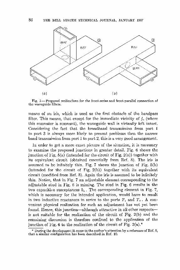
86 THE BELL SYSTEM TECHNICAL JOURNAL, JANUARY 1967
(a) (b)
Fig. 5-Proposed realizations for the front series and front parallel connection of the waveguide filters.
means of an iris, which is used as the first obstacle of the bandpass filter. This means, that except for the immediate vicinity of fo (where this resonator is resonant), the waveguide wall is virtually left intact. Considering the fact that the broadband transmission from port 1 to port 3 is always more likely to present problems then the narrow band transmission from port 1 to port 2, this is a very good arrangement.
In order to get a more exact picture of the situation, it is necessary to examine the proposed junctions in greater detail. Fig. 6 shows the junction of Fig. 5(a) (intended for the circuit of Fig. 2(a)) together with its equivalent circuit (obtained essentially from Ref. 8). The iris is assumed to be infinitely thin. Fig. 7 shows the junction of Fig. 5(b) (intended for the circuit of Fig. 2(b)) together with its equivalent circui t (modified from Ref. 8). Again the iris is assumed to be infinitely thin. Notice, that in Fig. 7 an adjustable element corresponding to the adjustable stud in Fig. 6 is missing. The stud in Fig. 6 results in the two capacitive susceptances ba • The corresponding element in Fig. 7, which is necessary for the intended application, would have to result in two inductive reactances in series to the ports Tl and T2 . A convenient physical realization for such an adjustment has not yet been found. Hence, this junction-although attractive in all other respectsis not suitable for the realization of the circuit of Fig. 2(b) and the remaining discussion is therefore confined to the application of the junction of Fig. 6 to the realization of the circuit of Fig. 2(a). *
* During the development it came to the author's attention by a reference of Ref. 9, that a similar configuration has been described in Ref. 10.

WAVEGUIDE
ba = ADJUSTA OF THE BLE BY THE OPPOSIT~Y~INDRICAL PSE~UEDTRATION o THE IRIS
bb= _ Bb Yo OF REF. 8, S ECTION 6.8, (3a)
FILTER
o TI
F' 19. 6-JUll t' e lOll of F' ~ 19 . .'J(a).
87
bb = _ ( ~ag )2 ( ZXb _ ~) T2 o >"g WITH ~ Z 0 OF REF. 8, SECTION 6.9, (3a)
lle lOll of Fig. 5(b). Fig.7-Ju t"

88 THE BELL SYSTEM TECHNICAL JOURNAL, JANUARY 1967
III. SYNTHESIS
In this section, the synthesis procedure for the proposed directional filter is presented. However, before embarking on this subject, the important steps of the synthesis procedure for the waveguide bandpass filter5 and for the waveguide bandstop filter6 have to be described. Parts of both these synthesis procedures will be used in the synthesis of the directional filter. In addition, two circuit identities have to be derived, which also will be used later in the synthesis of the directional filter.
Fig. 8 shows the important steps of the synthesis procedure for the
@ --0
-----0
o
::0
ALL RELATIVE CHARACTERISTIC IMPEDANCES OF THE LINES AND ALL RELATIVE REFERENCE 1M PEDANCES ARE 1
Fig. 8-Synthesis steps for waveguide bandpass filters.
(a)
(c)
(d)

WAVEGUIDE FILTER 89
waveguide bandpass filter. 5 Fig. 8(a) shows the transformed prototype circuit. The quantities IC I , k2 ••• are positive real numbers. In Fig. 8(b) both ports have been shifted by the indicated line lengths. The length L11 is usually less than O.lAoD . The following two steps, the step from Fig. 8(b) to 8(c) and the step from Fig. 8(c) to 8(d) (actual physical structure with all dimensions), are those needed for the synthesis of the microwave directional filter. They are discussed in detail by Ref. f)
and hence, need not be repeated here. It is emphasized, however, that all these steps can be performed successively, provided that the circuit of Fig. 8(a) is given, that the frequency transformation (1) is known and that the cross-sectional dimensions of the waveguide are given.
Fig. 9 shows the important steps of the synthesis procedure for the waveguide bandstop filter.6 Fig. 9(a) shows the transformed prototype eircuit. The quantities lc~ , k~ ... are positive real numbers. In Fig. D(b) port 2 has been shifted by the indicated line length. The following two steps, the step from Fig. 9(b) to 9(c) and the step from Fig. 9(c) to Q(d) (actual physical structure with all dimensions), are those needed for the synthesis of the microwave directional filter. They are discussed in detail by Ref. 6 and hence, need not be repeated here. Again it is emphasized that all these steps can be performed successively, provided that the circuit of Fig. 9(a) is given, that the frequency transformation (1) is known and that the cross-seetional dimensions of the waveguide are given.
Fig. 10 shows two cireuits. If
(3a)
and
L ' Ag (1 27r L ) 11 = 27r arc tan "2 tan Ao 11 , (3b)
then the two circuits are identical, if
(3c)
The reader himself may verify this identity by direct comparison of the two circuits. For the purposes of the synthesis procedure of the directional filter (3) are approximated as follows. If, for I Lll I « ArlQ
ancI for Au ~ Auo ,
(4 a)
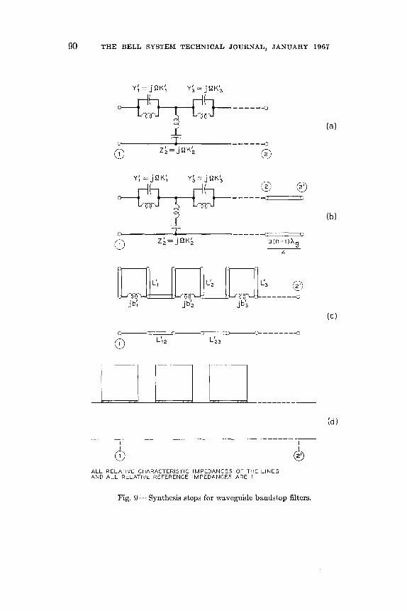
90 THE BELL SYSTEM TECHNICAL JOURNAL, JANUARY 1967
o~--------lC+_---------Z~=jflK~
Y~=jflK~
o~--------lC+_---------CD Z~=jflK~
I I
CD
L',
------{)
---0
o
-------() ()
..... Ql ======:DP 3(n-I)Ag
4
-------0
I I
® ALL RELATIVE CHARACTERISTIC IMPEDANCES OF THE LINES AND ALL RELATIVE REFERENCE IMPEDANCES ARE 1
Fig. 9-Synthesis steps for waveguide bandstop filters.
(a)
(b)
(c)
(d)

WAVEGUIDE FILTER
0..---1----------..1-0 jba jba a l
'" l',,®
ALL RELATIVE CHARACTERISTIC IMPEDANCES OF THE LINES AND ALL RELATIVE REFERENCE IMPEDANCES ARE 1
(I
()
(2m +1)Ag
4
Fig. IO-Circuit transformation.
Y! =jnt: y~=jnl~
CJIE!J T
o
(2m+I)Ag
4
j)
Zb~a::(I) ===Y=b =~::::o---+th 1 Y~5t-l_~ ___ --a=====0::D~ Zd
()
(2m +I)A90
4
T Z~=jnC2
ALL RELATIVE CHARACTERISTIC IMPEDANCES OF THE LINES AND ALL RELATIVE REFERENCE IMPEDANCES ARE 1
Fig. 11-Circuit transformation.
()
91

92 THE BELL SYSTEM TECHNICAL JOURNAL, JANUARY 1967
then the two circuits are approximately equal, if
I f') L11 II, = - ... /lr~·
/\r,;o
(4b)
(4c)
Fig. 11 again shows two circuits. The reader's attention is called to the fact that for the first circuit, the line length at port 1 is (2m + l)Au/4, whereas it is (2m + I)Auo/4 for the second circuit. m is a nonnegative integer. The line length at port 2 is the same for both circuits. The input impedances Za and Zb of the two circuits (both terminated with 1 at port 2) are approximately equal for Au ~ Ago. This is seen by the following argument:
JTf -!J -
and
1 + 1
'Q(Zf _ 2m + 1 ~) -:-~, + ] 1 4 QT ]Qc2
1 + in tan [(2m + 1)~ ~~J n + jtan [(2m + 1) H~ ]
n - j cot [(2m + 1) ~ ~ ] 1 - in cot [(2m + 1) ~ ~ ]
(5a)
(5c)
Equation (5c) combined with (5b) and with the following approximation valid for Au ~ Auo

WAVEGUIDE FILTER 93
-(2m + 1) 4~T [2, (,jd)
results in the desired approximate relation
(6)
Since furthermore-as is readily seen-the impedances Zc and Zd of the two circuits (both terminated with 1 at port 1) are also approximately equal in the vicinity of Aao , the unitary condition for the scattering matrix of lossless reciprocal 2-port networks permits the conclusion, that the two networks shown in Fig. 11 are approximately equal in the vicinity of Aao • This is the desired result, which will be used later in the synthesis of the directional filter.
This synthesis procedure can now be explained. First a prototype filter (Fig. 4, circuit a) and a frequency transformation (1) must be determined; i.e., n, QT and A(Jo must be computed. This can be done with the aid of (1) and (2), provided that the wide dimension a of the rectangular waveguide is given or chosen and that sufficient requirements are imposed on the amplitude response of the directional filter
®~ I I I I
C2 '
~----~
c __ ------------~ __________ ~l~----~ 8 0 ALL RELATIVE REFERENCE IMPEDANCES ARE I
Fig. 12 - Lumped-element low-pass high-pass prototype directional filter.

94 THE BELL SYSTEM TECHNICAL JOURNAL, JANUARY 1967
®9 I I I I I
~ I I I I I
/
BANDPASS ___ PORTION
II I I I I )
/ ~ __ -----o
~o------------~-----------J[~-----~ CD Z,'=jgL,' Z/=jgL 3 ' 0 ALL RELATIVE REFERENCE IMPEDANCES ARE 1
Fig. 13 - Lumped-element bandpass-bandstop directional filter.
®~ II II II II II II II
rl_(n-1)A g _L U 4 nn
II II II II II II II
-----_o
O~----~~~--------~-------_o
(0 Z3=jDL'3 0 BANDSTOP PORTION
ALL RELATIVE CHARACTERISTIC IMPEDANCES OF THE LINES AND ALL RELATIVE REFERENCE IMPEDANCES ARE 1
Fig. 14-Transformed circuit of Fig. 13.

WAVEGUIDE FILTER 95
(magnitudes of the scattering matrix elements of (2)). The specific procedure to determine n, QT and Aoo varies largely with the way the amplitude response of the filter is specified. It is, however, always a straightforward and simple procedure, and hence, need not be discussed any further.
I t can, therefore, be assumed that a prototype filter as shown in Fig. 12 is known. The frequency transformation, which is also known, transforms this circuit immediately into the circuit shown in Fig. 13. All elements are known. Now the step from Fig. S(b) to S(c), described in Ref. 5, is made for the bandpass portion of Fig. 13. This results in the circuit shown in Fig. 14 with all elements being known. The length L\I is usually very small compared to Aoo , as was already
0~
L,
I: II II II II II II
~ (n-l)Ag
---4-- Lnn II II II II II II II II
Y,' =jQt;
G~------~~==~~------~~--------(2 m +1).\9
4
ALL RELATIVE CHARACTERISTIC IMPEDANCES OF THE LINES AND ALL RELATIVE REFERENCE IMPEDANCES ARE 1
Fig. IS-Transformed circuit of Fig. 14.
()
(2m +1)A9
4
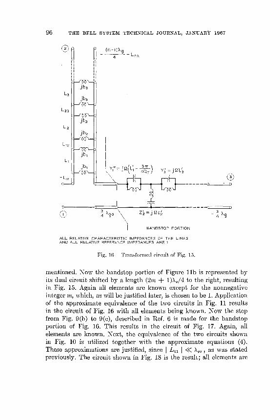
mentioned. Now the bandstop portion of Figure llb is represented by its dual circuit shifted by a length (2m, + I)Ao/4 to the right, resulting in Fig. 15. Again all elements are known except for the nonnegative integer 1n, which, as will be justified later, is chosen to be 1. Application of the approximate equivalence of the two circuits in Fig. 11 results in the circuit of Fig. 16 with all elements being known. Now the step from Fig. 9(b) to 9(c), described in Ref. 6 is made for the bandstop portion of Fig. 16. This results in the circuit of Fig. 17. Again, all elements are known. Next, the equivalence of the two circuits shown in Fig. 10 is utilized together with the approximate equations (4). These approximations are justified, since I Lll I « Aoo , as was stated previously. The circuit shown in Fig. 18 is the result; all elements are

WAVEGUIDE FILTER 97
known. Appropriate line lengths are added now to eaeh of the three ports of the circuit to cancel the negative lengths present in Fig. 18. This procedure only changes the phase characteristics of the network, and hence, is of no consequence, since the filter requirements pertain only to the amplitude response. The resulting circuit is shown in Fig. 19. This circuit, of which all elements are known, is reduced to the physical structure shown in Fig. 20 by the following procedure:
(i) The bandstop portion is realized as described in Ref. 6. This is the step from Fig. 9(c) to 9(d).
(ii) The bandpass portion is realized as described in Ref. 5. This is the step from Fig. 8(c) to 8(d).
(iii) Of the remaining circuit the line length 3Auo/4 - L ll /2 is realized as such, and the junction is realized as shown in Fig. 6 by consulting Ref. 8, or better (finite thickness of the iris!) by using meas-
®~ II II
L,
- L'1
I' II II II II
A (n-I) Ag ~ - 4 - Lnn II II II II II II II
L', L' 2
ALL RELATIVE CHARACTERISTIC IMPEDANCES OF THE LINES AND ALL RELATIVE REFERENCE IMPEDANCES ARE 1
L~ o ------() ()
Fig. 17 -Transformed circuit of Fig. 16.

98 THE BELL SYS'l'EM 'l'ECHNICAL JOURNAL, JANUARY 1967
®n 0H
II II II II II II
I
n I (n-I)Ag ~ --4--- Lnn
II II II II II II
-------<) (»
jb',
jJ ___ 1a:=j=b=a==:o-__ a=:====no=:==:r:-_--<I==:=r:>--_o- _ ---- -< Ii,
1 L 3 \ 1 L"2 L'23 -"2 II 4I\go-"2L"
b - '7T'Ll1 a - A9 0
ALL RELATIVE CHARACTERISTIC IMPEDANCES OF THE LINES AND ALL RELATIVE REFERENCE IMPEDANCES ARE i
Fig. 1S-Transformed circuit of Fig. 17.
ured data. The penetration of the stud opposite the iris (Fig. 6, adjustment of jb a ) must always be found experimentally.
For these three steps, the knowledge of the narrow dimension b of the rectangular waveguide is required. Therefore, this quantity must either be known or be chosen.
This completes the synthesis procedure. The only remaining detail is to explain why the nonnegative integer 'In of Fig. 15 was chosen to be 1. As has been shown by experiments described in Ref. 6, m = 0 is inadvisable because of excessive interaction of the higher-order modes excited at adjacent coupling holes, in this case, the hole of the junction and the hole of the first bandstop cavity. Since it is desirable to keep the total length of the filter as small as possible, m = 1 was chosen.

0p. R I: II I' II " II II II II II II II
z a ~ ex: a n.
WAVEGUIDE FILTER
L; ------0
jb,' jb~
jJ ___ T.Q::=jb=a===!t't-_-a~====D-_--CC===D-__ o-_____ -o
f.i\ 3 1 \ L;2 L23 \.0 4" ~go- 2"LI1 \
\ )
BANDSTOP PORTION
I
ALL RELATIVE CHARACTERISTIC IMPEDANCES OF THE LINES AND ALL RELATIVE REFERENCE IMPEDANCES ARE 1
Fig. 19-Reduced circuit of Fig. 18.
IV. EXPERIMENTAL RESULTS
A trial filter was designed for the following specifications:
Midband frequency: f 0
Upper 3-dB crossover frequency: f 1
n = 3, Waveguide: a = 2.290", b = 1.145".
3950 MHz, 3967 MHz,
Since the upper 3-dB crossover frequency corresponds to Q
results in
QT = 67.05.
99
1, (1)
Fig. 21 shows a sketch of the constructed filter. All irises are 0.040 inch thick and all cavities are foreshortened by 0.050 inch and equipped with tuning screws to provide sufficient tuning range. The studs op-
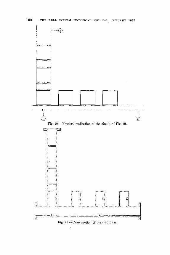
100 THE BELL SYSTEM TECHNICAL JOURNAL, JANUARY 1967
n I I I
(0
!---0 I I I I I I
Fig. 20-Physical realization of the circuit of Fig. 19.
Fig. 21- Cross section of the trial filter.
I I I o

WAVEGUIDE FILTER 101
posite to the irises are also realized as screws in order to be adjustable. Both filters were first tuned individually. Then the bandpass filter
was attached to the junction and-after retuning the first cavity-the response of the resulting 3-port was compared to the theoretical behaviour. This comparison indicated that the hole diameter of the iris in the junction should be changed from 0.871 to 0.900 inch. After this change was made, the 3-port performed very close to the theoretical expectations. Then the bandstop filter was attached and the complete
Fig. 22 - Photograph of the trial filter.
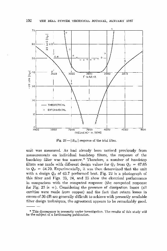
102 THE BELL SYSTEM TECHNICAL JOURNAL, JANUARY 1967
o o -1
o
o 70~------~----~--~------~--------~--r----'--------~
60
N V)
o So.8r-----+--+--------+-------_To-r-----~------~
50t---- o 0 000
~9L3~0--~-~~-----3~9~5~0----~~~--~~~~----~
f IN MHz
N 30r-------~-------~w_------_+--------~------~--------~ I
20r--------r--------+-~----_T----~r-~------_,--------~
- THEORETICAL
o EXPERIMENTAL
10r--------r--------+---~--_+--~r---~------~--------~
O~ ____ ~~------~~------~~----~~~----~~------~ 3800 3850 3900 3950 4000 4050 4100
FREQUENCy IN MHz
Fig. 23-1821 1 response of the trial filter.
unit was measured. As had already been noticed previously from measurements on individual bandstop filters, the response of the bandstop filter was too narrow. * Therefore, a number of bandstop filters was made with different design values for QT from QT = 67.05 to QT = 54.70. Experimentally, it was then determined that the unit with a design QT of 63.7 performed best. Fig. 22 isa photograph of this filter and Figs. 23, 24, and 25 show the electrical performance in comparison with the computed response (the computed response for Fig. 25 is (0). Considering the presence of dissipation losses (all cavities were made from copper) and the fact that return losses in excess of 30 dB are generally difficult to achieve with presently available filter design techniques, the agreement appears to be remarkably good.
* This discrepancy is presently under investigation. The results of this study will be the subject of a forthcoming publication.

Pi ~ ~ 0 ...J
0 C\J I
2.4
2.0 I--- 30
-Pi
V)
~
1.6 r-- 320 0 C\J I
1.2 I--- 10
I
O.B I--- 0 3930
0.4
o 3800 3850
WAVEGUIDE FILTER
I
J ~ - THEORETICAL
o EXPERIMENTAL
I \ V '\
r\n 5i
/ (
~o P
3940 3950 3960 3970 (
P f IN MHz
~
) ~ 3900 3950 4000 4050
FREQUENCY IN MHz
Fig. 24-1 S31 1 response of the trial filter.
V. ACKNOWLEDGMENTS
103
4100
The author would like to acknowledge the assistance of J. A. Flynn who did some of the calculations on the trial filter and who performed the measurements. Acknowledgments are also due to Mrs. T. V. Gaudet and W. G. Scheerer, who furnished computed data on the theoretical response very promptly.
50
:f 40
o o ...J
o C\J I 30
20 3800
------ I II --- - I I I
l IfV
I 3850 3900 3950 4000 4050 4100
FREQUENCY IN MHz
Fig. 25-1 Sui response of the trial filter.

104 THE BELL SYSTEM 'fECHNICAL JOURNAL, JANUARY 1967
REFERENCES
1. Young, L., Microwave Filters, IEEE Trans. Microwave Theory and Techniques, "kITT 13, September, 1965, pp. 489-508.
2. Cauer, W., Theorie der linearen lVechselstromschaltungen, Akademie Verlagsgesellschaft, Leipzig, 1941.
a. Guillemin, E. A., Synthesis of Passive Networks, John Wiley and Sons, Inc., New York, 1957.
4. Cohn, S. B., Microwave Filters Containing High Q Dielectric Resonators, G-MTT Symposium, May, 1965.
fl. Mumford, W. W., Maximally Flat Filters in Waveguide, B. S. T. J., 27, October, 1948, pp. 684-713.
G. Young, L., Matthaei, G. L., and Jones, E. M. T., Microwave Bandstop Filters with Narrow Stop Bands, IRE Trans. Microwave Theory and Techniques, MTT 10, November, 1962, pp. 416-427.
7. Glowatzki, E., Katalog der Potenz und Tschebyscheff Filter bis zum Grade n = 5, Telefunken Zeitung Jahrgang 28, March, 1955, pp. 14-22 (continued in Jahrgang 34, June, 1961, pp. 180-185).
8. l\Iarcuvitz, N., Waveguide Handbook-Radiation Laboratory Series, 10, McGraw-Hill Book Company Inc., New York, 1951.
U. Cristal, E. G., A Method for the Design of Nonreflecting High Power Microwave Bandpass Filters, Microwave J., 9, June, 1966, pp. 69-74.
HI. Cristal, E. G., and Matthaei, G. L., Novel Microwave Filter Design Techniques, Fourth Quarterly Progress Report, Section IV, SRI Project 4344, Contract DA 36-039 AMC-00084 (E), Stanford Research Institute, Menlo Park, California, January, 1964.

On Some Proposed Models for Traffic in Conllectillg Networl(s
By V. E. BENES
(Manuscript received August 17, 1966)
'Three stochastic models /01' traffic, forming a progression of decreasing simplicity, are discussed with a view to discerning in what ways the various assumptions they depend on affect the formula fo}' blocking probability. 'Phese models are the probability linear graph (due to C. Y. Lee), the thermodynamic l1wdel, and a l1wdel based on J11 arkov processes (both proposed by the author).
Certain basic inadequacies of the l1wdels are described. Lee's model lacks a sufficiently broad assignment of probabilities to events of interest, with the result that the blocking probability is improperly defined; at the same time it bases congestion formulas on network conditions never achieved in practice. The thermodynamic model deals only with genuine system states, but makes calling rates depend unrealistically on available paths. Neither the graph model as originally proposed, nor the thermodynamic model, can take into account routing procedures. The author's Markov model is free of these drawbacks, but at this price: in nearly all practical situations in which losses occur, it leads to hitherto insurmounted combinatorial and computational difficulties.
To stress and illustrate the effect that routing has on loss, the blocking probability fonnulas of all three l1wdels are compared at low traffic: it often turns out that when the first two models indicate that (with A = offered traffic) loss = O(A m), A ~ 0, an analysis based on routing shows that in fact loss = O(Am), A ~ O.
1. INTRODUCTION AND SUMMARY
In recent years several stochastic models for random traffic in large telephone connecting networks have been proposed. In 1955, C. Y. Lee l
described what has come to be known as the "probability linear graph" model, an outgrowth of earlier work of Kittredge and lVlolina. In 1957, P. Le Ga1l2 developed and used essentially the same model as Lee. In
105

106 THE BELL SYSTEM TECHNICAL JOURNAL, JANUARY 1967
1963 the author presented another model,3 which he called "thermodynamic" because of its resemblance to statistical mechanics, and a third one4 that was formulated in an effort to take routing methods into account and to meet certain drawbacks of the thermodynamic model.
These three models form a progression of decreasing simplicity and increasing realism, and they exhibit the trade-off between verisimilitude and computational difficulty: the more realistic the model, the harder it is to calculate anything in it. Their existence also affords a limited opportunity for trying to make comparisons, e.g., to see in what ways the various assumptions made affect the formula for blocking probability.
Our object here is to discuss the respective inadequacies of all three models, to compare their blocking probability formulas at low traffic, and to stress and illustrate the point that routing has a basic structural effect on the probability of loss: in particular, it often turns out that when the first two models indicate that, with A = offered traffic, loss = O(A m) as A ~ 0, an analysis actually based on reasonable routing shows that loss = o(A m), A ~ o.
II. DISCUSSION OF LEE'S" PROBABILITY LINEAR GRAPH" METHOD
The 'probability linear graph" approach to the study of connecting networks has been extensively described by its proposer C. Y. Lee/ and more recently by R. F. Grantges and N. R. Sinowitz.5 Therefore, we include only the following resume of the method: to calculate the congestion incurred by traffic between an inlet u and an outlet v, a ttention is focussed on the graph G defined by the possible (i.e., permitted) paths through the network from u to v; G consists of all nodes and branches through which some path from u to v passes. Naturally, G is connected. Given any assignment of occupancies to the branches of G, i.e., any (complete) specification of which branches of G are busy and which are idle (at a particular juncture of network operation), it is possible to examine G to see if there is a path from u to v (no branch of which is busy). The method now assigns a probability distribution to the possible occupancies by postulating that a link l of G is busy with probability PI independently of all other links. The congestion for u and v is then calculated as the probability that this distribution assigns to the event "There is no path from u to v". The probabilities {Pz , l a link of G} are chosen to reflect the loads carried by the links in the network.
A foremost merit of the Molina-Kittredge-Lee proposal is of course that it provides a simple way of at least approaching the massive prob-

TRAFFIC MODELS FOR CONNECTING NETWORKS 107
lem of theoretically determining the grade of service in a connecting network. For small networks the calculations can be done by hand, and for large ones, in which the graph G is complex, it is feasible to use computers to evaluate the polynomials that arise, 5 or to use approximations. 6
For these reasons alone Lee's model merits serious consideration. Indeed, R. F. Grantges and N. R. Sinowitz claim: "The utility of the results obtainable from Lee's model is well known. When the specific [average] branch occupancies are chosen rationally, the calculated blocking agrees well enough with real blocking figures (ohtained from full-scale simulation or measurement) for many engineering and design purposes." (Ref. 5, p. 977.) However, these same authors, while using Lee's model, also state explicitly: "Unfortunately, in complex switching networks, substantial differences may exist between the estimates obtained with Lee's analytical technique and actual performance determined by field measurement or full-scale (complete) simulation." (Ref. 5, p. 1000.) It appears, then, that some discussion and evaluation of the basis of Lee's model might help to indicate where and why it departs from reality.
It is often stated (e.g., Ref. 5, p. 969) that a principal unrealistic feature of Lee's model is the assumption that the occupancies of the links are statistically independent. However, the Kittredge-Molina-Lee approach involves some problems most of which are independent of this assumption:
(i) It does not assign probability to enough events of interest, so that there is difficulty in properly defining the probability of blocking.
(ii) It may assign substantial probability to (and base congestion calculations on) events which can never occur in real life. (This fact depends, of course, on the independence assumption.)
(iii) It does not recognize (wide or strict sense) nonblocking networks. (iv) It does not take into account the effects of routing decisions.
Noting most of these difficulties, Grantges and Sinowitz5 have devised ingenious modifications of Lee's basic method in order to meet them, and to increase the realism of the graph model. When each procedure is compared against full-scale simulation, these refinements give a remarkable improvement in accuracy over Lee's original proposal. The modifications are suitable for computer simulation of Lee's method, and do not give rise to a formula for analysis; thus, we are not able to include them in the low traffic comparison at the end of this paper.
Problems (i) and (ii) are discussed in the next two sections; (iii) and (iv) are considered after a description of the thermodynamic model, which also has such drawbacks.

108 THE BELL SYSTEM TECHNICAL JOURNAL, JANUARY 1967
III. INCOMPLETENESS
By a full-fledged stochastic model for network operation, we mean one in which every event observable in the real-life system has a counterpart in the model which is assigned a probability. If this seems an excessive requirement, let us agree that at least any event depending on the busy Of idle condition of crosspoints and links in the network is to be assigned probability. It is a pertinent comment that Lee's calculation is not based on such a model, not even in the weak sense agreed on.
The incomplete character of the assignment of probability in Lee's model has serious consequences. For example, not all events depending on what inlets or outlets are busy or idle are assigned probability. In particular, when the congestion for traffic from inlet u to outlet v is lInder consideration, the model does not assign a probability to the event.
{the call from u to v is blocked},
in the customary sense of 'blocked'. This is because it may he true, at a particular moment, that there is no path from u to v on G in the sense that every possible path from u to v has at least one busy link, while u or v or both may be busy talking to other terminals over other links. In such a case, we would not say that a u, v call was blocked; only if there was no path and both u, v were idle would we say they were blocked. However, the event that u is idle, or that v is idle, is not (and cannot be) considered, since no event of this form has been assigned probability. Lee's model assigns probability to so few events that it cannot distinguish between the above two cases. Indeed, this circumstance is directly responsible for the model's inability to recognize a nonblocking network when it sees it. In such a network the event
{every path from 'It to v has at least one busy link}
will in a reasonable stochastic model have positive probability, but the event
{the call from u to v is blocked}
has probability zero. It is in part because Lee's model calculates the probability of the former event that it gives the wrong answer for nonblocking networks; to the latter event it does not even assign probability.
The problem just discussed has been treated by Grantges and Sinowitz5 in their prefatory remarks, and at considerable length by E. Wolman. 7

'l'RAFFIC MODELS FOR CONNECTING NETWORKS 109
IV. IlUtELEV AN 'I' S'l'A'I'ES
The probability linear graph model not only fails to a::;sign probability to events like blocking which should have it; it also does assign it to events which never occur in an operating exchange. It bases congestion calculations on situations, i.e., conditions of the network, which never arise in practice. lYloreover, these irrelevant situations can be so numerous as to greatly outnumber the relevant ones. The model assigns these irrelevant situations probabilities that arc comparable to those assigned to the relevant states. The applicability of any calculation depending so heavily on irrelevant material is open to question: it is very hard to see why these irrelevant states do not swamp the ones of real interest.
To illustrate our point about irrelevant situations, suppose that for some inlct u and outlet v the graph G determined by the paths from u to v includes every inlet and outlet on some square switch, deep in the middle of the network. Now, in every physically meaningful state of the network, reachable under normal operation, this switch will have as many idle inlets as outlets. However, in this case, Lee's method will also base congestion on situations with m inlets busy, n outlets busy, and m ~ n. It is easily seen that these are in the vast majority, and that Lee's model assigns them probabilities comparable with those assigned to situations with 1n = n. (The second of these facts depends, of course, on the "independence of links" assumption.)
Assessing the effect of the irrelevant states is difficult, but their presence may help to explain the variable agreement of Lee's model with experiment: when the proportion of blocking states is the same in the set of relevant states as in that of all states, the model may be accurate; when the inclusion of irrelevant situations produces biaseither too low or too high a proportion of blocking states in the set of all states-the model is inaccurate.
V. DISCUSSION OF THE THERMODYNAMIC MODEL
The thermodynamic model3 for equilibrium traffic in a telephone connecting network is obtained as follows: the physically meaningful states of the network are collected in a partially ordered set (8, ~), and a distribution {q .. , x c: 8} of probability over 8 is defined by the condition that q maximize the entropy functional
H(q) = - L q .. log q .. xeS
subject to the condition that L .. es i x iqx = carried load (a given number).

110 THE BELL SYSTEM TECHNICAL JOURNAL, JANUARY 1967
With <ll(z) = LXES Zlxl and ~ the positive solution of
carried load = ~ :~ log cp(~), (1)
q has the form
(2)
An extensive discussion of the thermodynamic model is given in Ref. 3. We confine ourselves here to a brief presentation of points relevant to comparing it with Lee's model, and with that of Ref. 4.
(i) It provides a full-fledged stochastic model for traffic in the network: each possible meaningful state is assigned probability in a simple way [formula (2)]. This great advantage is of course obtained at the considerable price of introducing the complicated set S of states; for many purposes, calculation with 8 can be replaced by calculation with the numbers I Ln I , where Ln is the set of states with n calls in progress, and I . I indicates cardinality. While this replacement is an enormous simplification over use of S, the determination of the numbers I Ln I is nevertheless a formidable and unsolved problem; however, it is also one on which virtually no effort has been expended except in unpublished work of A. J. Goldstein.
(ii) In order to construct a realistic model, it is not enough to take into account all and only the meaningful states in some full-fledged stochastic model. It is also necessary that the model be based on a realistic description of the rates at which the system moves from state to state. In this second respect the thermodynamic model falls quite short. It was pointed out in Ref. 4 that the thermodynamic model corresponds closely to random choices of routes for calls, together with the artificial feature that the calling-rate of a call depended on the number of paths available for it.
(iii) The thermodynamic model shares with Lee's the drawback that it is incapable of describing the effect of general routing policies. It is known that these effects can change substantially the probability of blocking, in some cases by a factor of ten.8 The reason for this is, roughly, that proper routing largely avoids the disastrous states in which many calls are blocked. Oblivious of routing, the thermodynamic model gives positive probability to any path on (8, ~), the "bad" paths receiving probabilities comparable to those of the "good" ones.
(iv) Since the thermodynamic model assigns probability to every meaningful state, it is possible to give a reasonably satisfactory definition of blocking probability in it. In analogy with Ref. 4 we define it as

TRAFFIC MODELS FOR CONNECTING NETWORKS 111
Pr {bl}o
where ~ is as in (1), () stands for 'thermodynamic',
/3x = number of idle inlet-outlet pairs in x that are blocked, ax = number of idle inlet-outlet pairs in x.
(3)
This formula holds an advantage over Lee's in that it gives the value zero for a strictly nonblocking network. However if the network is only nonblocking in the wide sense, i.e., if it is only nonblocking if the right routing is used, then the blocking as given by (3) will not distinguish this behavior: it will give a positive answer that does not depend on how routing is actually carried out.
VI. LOW TRAFFIC BEHAVIOR: CALIBRATION
The differences between the three models being considered here are particularly evident when they are used for studying a network that is nonblocking, whether strictly or in the wide sense. Needless to say Lee's method cannot distinguish the nonblocking behavior at all, while the thermodynamic model can recognize a strictly nonblocking network (/3x == 0), but cannot distinguish lack of blocking due to proper routing (nonblocking in the wide sense.)
In an effort to provide an analytical comparison between Lee's model, the thermodynamic model, and the Markov process model of Ref. 4, we shall examine the leading terms of the blocking probability formula in each model for low traffic in a Clos 3-stage network with r n X m outer switches, m r X r middle switches, N = rn inlets (outlets), and n ~ m ~ 2n - 2. This network is depicted in Fig. 1.
Such a comparison can only be sensible if the link occupancies in the models agree asymptotically. In many ways it would be more desirable to calibrate by requiring the same carried load in each model; but in Lee's model the only way of defining this requirement is by reference to the link occupancies, a procedure equivalent to ours.
It is to be kept in mind that the comparison to be made is carried out on the basis of asymptotic formulas valid only for sufficiently small values of r... The range of loss probabilities over which the comparisons are performed is not known and could conceivably fall entirely outside the domain of practical relevance.
In the model of Ref. 4 the inlet occupancy is reasonably defined as

112 THE BELL SYSTEM TECHNICAL JOURNAL, JANUARY 1967
n
n
Fig. 1-3-sLage Cl08 network.
carried load q = --N--'
Since it is elementary that
carried load = XN 2 + o(X),
it is reasonable that the link occupancy p in Lee's model be
P = carried load X ~ = "Arn
2 + o(X) N m m '
"A~O.
n
n
'Vith this calibration the blocking in Lee's model for the network of Fig. 1 is
[1 - (1 - p)2)''' = (2p)m + o(p)
= X m(2:~2) m + o(X) , X~O.
For the thermodynamic model the calibration is a little more involved. The basic requirement is that the parameter ~ used in that model satisfy
carried load = N q .reS
L~'x' xfS
It is easy to see that the ratio has the form
I L1 I ~ + w(~), I L1 I = number of states with one call in progress,

TRAFFIC MODELS FOR CONNECTING NETWORKS 113
with 'lr(~) o(~) as ~ ~ o. Since for complex z small enough
I 'lr(z) I < 1 _ N q 1
ILl' = Z , Ll ,
it follows from Lagrange's theorem9 that for q small enough,
N q 00 1 d,,-l (W(x) )"1 ~ = -, L ,+ L, d n-1 -, L , '
1 11=1 n. x 1 x=Na/IL,1
t _ Nq _ AN2 .. - 'L1
, + o( q) - ,L1
, + O(A) , A ~ O.
It is easily verified that'Ll' = nl'mrn = N 21n, whence
A ~ = - + o (A) ,
m A ~ O. (4)
(This formula exhibits the sense in which at equal carried loads the parameter ~ of the thermodynamic model is about 11m times the parameter A as a result of the increased calling-rate in that model due to its proportionality to the number of available routes.)
VII. LOW TRAFFIC BEHAVIOR: THE EFFECTS OF ROUTING
It can be seen that, for the Clos network under discussion here, ao = N 2
, so that (3) and (4) give
In the model of Ref. 4, the blocking probability for this same network has the form
where
/Jx = number of calls blocked in state x 1'.., = number of ways of ascending from 0 to x along paths permitted
by the routing rule in use.
We thus arrive at three low traffic formulas for loss all expressed in terms of A: as A ~ 0,

114 THE BELL SYSTEM TECHNICAL JOURNAL, JANUARY 1967
(5)
Pr {bl} Lee = (2;:2) "'-;..:n + o (A"') , (6)
Pr {bl} = N- 2 A~ L (3xr x + o(Am). m'lxl=m
(7)
The sums in these formulas are in general not easy to calculate, depending as they do on network structure and routing. Our point, though, is precisely that the dependence on routing is crucial, since by making the bad states relatively inaccessible we can make the sum
small, even to the point of being zero. In such a case the first two block-ing formulas do not even have the right leading term. -
To see how this comes about, we refer to Fig. 2, which shows a typical blocking state of dimension m of the Clos network of Fig. 1. It is clear that if some of the cal1s were to double up on the middle switches, in-
n n
r m r
n n
Fig. 2-Typical state with dimension m and some blocked calls.
'l'RAFFIC MODELS FOR CONNECTING NETWORKS 115
TABLE I
Network parameter Coefficient of Am in blocking formula
n m r Lee 0 Ref. 4
2 2 2 64 4 0 3 3 2 1728 27 0
stead of wastefully each using a middle switch, there need be no blocking. Now for r = 2, m ~ [3n/2] the network under study is nonblocking in the wide sense. That is, these conditions on r, m, and n ensure that as long as correct routing decisions are made, no call need be blocked. The "correct" routing that achieves this performance consists precisely in not using an empty middle switch when a partly-filled one is available. It is highly likely, as the results of Ref. 8 suggest, that this advice is good even when r > 2, 1n < [3n/2]. Let then R be a routing matrix for the network of Fig. 1 which embodies the above advice. It can be seen that
rx = (R'x')ox = 0
for I x I = m and (3x > o. I.e., all the blocking states of dimension mare unreachable from 0 in m steps under R, because R insists that empty middle switches be used only when partly-filled ones are unavailable. This very reasonable routing makes the coefficient of 'Am in Pr {bl} vanish.
Table I shows the coefficient of 'Am in the low traffic formulas (5) to (7) for two very small networks; for (7) it has been assumed that no unblocked call is rejected and that routing is optimal, i.e., minimizes loss.
VIII. CONCLUSION
This paper has provided one more illustration of a situation that traffic experts are well aware of, namely, that blocking probabilities in connecting networks can be computed only under assumptions that are not satisfied in practice. There is concrete evidence indicating that results obtained within the framework of such approximate models can be of practical value. By considering the respective advantages and drawbacks of a spectrum of models, it is possible to discern to some extent the effect of the various assumptions made on the structure of the formula for loss.

116 'fUE BELIJ SYSTEM TECHNICAL JOURNAL, JANUARY 1967
IX. ACKNOWLEDGMENT
The author is indebted to A. Descloux and E. 'Volman for constructive suggestions.
REFERENCES
1. Lee, C. Y., Analysis of Switching Networks, B.S:r.J., 34, November, 1955, pp. 1287-1315.
2. Le Gall, P., Methode de Calcul de l'Encombrement dans les Systemes Telephoniques Automatiques a Marquage, Ann. Telecomm., 12, 1957, pp. 374-386.
3. Benes, V. E., A "Thermodynamic" Theory of Traffic in Connecting Networks, B.S.T.J., 42, May 1963, pp. 567-607.
4. Benes, V. E., Markov Processes Representing Traffic in Connecting Networks, B.S.T.J'z.....42, November, 1963, pp. 2795-2837.
5. Grantges,!t. F. and Sinowitz, N. R., NEASIM: A General-Purpose Computer Simulation Program for Load-Loss Analysis of Multistage Central Office Switching Networks, B.S.T.J., 43, May, 1964, pp. 965-1004.
6. Lee, L. and Brzozowski, J. A., An Approximate Method for Computing Blocking Probability in Switching Networks, IEEE Trans. Commun. Tech., COllf-14, April, 1966, pp. 85-93.
7. Wolman, E., On Definitions of Congestion in Communication Networks, B.S.T.J., 44, December, 1965, pp. 2271-2294.
8. Benes, V. E., Programming and Control Problems Arising from Optimal Routing in Telephone Networks. Abstract in SIAM J. Control, 4, February, 1966, pp. 6-18. Text in B.S.T.J., 45, November, 1966, pp. 1373-1438.
9. Whittaker, E. T. and Watson, G. N., Modern Analysis, 4th Ed. Cambridge, at the University Press, 1948, p. 133.

A Series of Miniature Wire Spring Relays
By C. B. BRO\VN
(Manuscript received September 2, 1966)
The BF, BG, BJ, and BL miniature wire spring relays have recently been added to the faJnily of AF, AG, AJ, AK, AL, and A.Ll1 wire spring relays. The lniniature series has been developed for use in central office equipl1wnt to be cOJnpatible with printed wiring board mounting and semiconductor devices. A description of the developl1wnt, features, and perfonnance of the BF lniniature wire spring relay is presented along with a brief COl1l1nent on the BG, BJ, and BL types. Production has been started on the lniniature types and a nwnber of codes have been issued for various projects.
I. INTRODUCTION
The Western Electric Company has recently started production of the BF miniature wire spring relay (Fig. 1) and its variations. It is the intent of this paper to describe in some detail the background and eourse of development for these families of relays.
Two basic pressures have been responsible for a growing demand for miniature relays in the telephone plant. The first of these is the modern trend toward miniaturization. Because of the premium on space in the telephone plant, there has been increased effort to put more equipment into less volume. This has been directly responsible for a need for smaller components, and relays are one of the maj or building blocks of telephone systems.
The second pressure for miniature relays has come from the large scale introduction of semiconductor devices. These devices are generally small and mounted on printed wiring boards. However, for many circuit functions and for interfaces with existing equipment, relays are needed. Equipment designers have found it both difficult and impractical to use large relays in conjunction with printed wiring boards and small components such as diodes and transistors. This has resulted in a demand fQr a miniature relay which can be mounted compatibly with the semiconductor devices on printed wiring boards.
117

118 THE BELL SYSTEM TECHNICAL JOURNAL, JANUARY 1967
TERMINAL VIEW
BF RELAY
CONTACT VIEW.
Fig. 1-BF miniature 'wire spring relay.
COVER
Thus, we see a large and continuing demand for miniature relays of all types. For use in telephone equipment which is mounted on customer premises, such as key telephone systems, the MA and MB miniature relays have been developed.1 For some other general areas of application, specific requirements and objectives have led to the development of miniature wire spring relays. In telephone central offices, it is important to be able to conduct relay and circuit tests using the relay itself. It is also desirable in this environment that relays be maintained in those rare instances when such action is necessary. Generally speaking, in central offices there are skilled craftsmen available with experience in the maintenance of the large wire spring relays (Fig. 2).2 Considering these factors, and the outstanding performance which has been demonstrated by the large wire spring relay over the past several years, the development of a miniature wire spring relay was undertaken. It was the intent of this development to make use of all of the experience that has been gained from the manufacture and use of the large wire spring relay.
II. OBJECTIVES
Taking into consideration the factors discussed above, seven basic obpectives evolved for the design of miniature wire spring relays as follows:
(i) To provide in a miniature relay the proven outstanding performance of the large wire spring relay.
(ii) To provide large margins for manufacture, long operating life, and high reliability.

MINIATURE WIRE SPRING RELAYS 119
(iii) To use established manufacturing techniques as far as possible. (iv) To provide a broad range of operating characteristics for both
general purpose and special purpose application. (v) To provide a relay that can be maintained and tested in the
field as well as allow for circuit testing. (vi) To provide for mechanically secure printed wiring board mount
ing with adaptability to hard wiring. (vii) To provide a design capable of being manufactured at a low
unit cost.
The following sections of this paper will describe the design and its capabilities, and thus show how these objectives have largely been met. Throughout the text, comparisons will be made to the large wire spring relay which is now accepted in the Bell System as the standard building block relay.
III. MECHANICAL DESIGN
There are many similarities between the large2 and miniature wire spring relays in the design of the actuating mechanisms and wire
Fig. 2 - Comparison of BF relay (left) and AF relay (right).

120 THE BELL SYSTEM TECHNICAL JOURNAL, JANUARY 1967
mountings. However, as the result of experience with the large relay, and because of the necessity of miniaturization, there are also numerous differences.
In any relay where the movable springs operate in the same plane, such as the wire spring types, it is extremely difficult to adjust individual springs for contact force or closure point. In the large (AF) relay, the need for contact force adjustment has been eliminated by the use of low-stiffness springs with large predefiection bends as shown in Fig. 3. This results in minimizing the effect of dimensional variations in; (i), the spacing A between fixed and movable wires; (ii) , the angle B between the movable wire and mounting block; (iii), the pre-tension bend C and; (iv), the "Z" shape D of the contact tip that bridges the operating card. Since the ratio of the summation of all of these variables to the large predefiection bend permitted by the low-stiffness spring is small, these variations have small effect on contact force and it does not have to be adjusted.
Spring stiffness varies inversely as the cube of the spring length, and directly as the fourth power of the diameter. Thus, as the springs are made shorter, there is a rapid increase in spring stiffness which must be compensated for by a reduction in diameter. With the allowable spring length in the miniature wire spring relay it 'would be necessary to use movable springs 0.006 inch in diameter to achieve the same stiffness as the springs of the large wire spring relay. It was felt that 0.006-inch diameter springs would present unreasonably difficult manufacturing problems, so it was decided to use O.OOg-inch springs in the miniature wire spring relay. This results in a spring stiffness approximately 4 times that of the springs in the large relay. To compensate for
r< FIXED I ---- .... s CONTACT
.------, \ \
t ----F==='=' ======~;:.====='\=<iO--l DEFLECTION
I I
D I I
~ -r-t MOVING/ VARIATION NOMINAL
CONTACT FREE
POSITION
Fig. 3 - AF relay movable twin wire deflection.

MINIATURE WIRE SPRING RELAYS 121
FREE POSITION OF MOVABLE SPRING
'_ REAR OF SINGLE - - WIRE BLOCK
~ \ ',SINGLE WIRE
ASSEMBLY
A I I
CONTACT
MOLDED CLAMP -- BLOCK
/ I
NOMINAL POSI TION OF MOVABLE SPRING / ON ASSEMBLY
______ FIXED
CONTACT
'- ___ ADJUSTING BRACKET
Fig. 4 - Miniature wire spring relay movable twin wire deflection.
this increase in stiffness it was necessary to use a different deflection system to minimize the effects of possible variations. This deflection scheme is illustrated in Fig. 4. The upper portion of the figure shows the profile of the movable twin wires in the un assembled condition. The phosphor bronze wires are molded in a phenolic block with terminals formed on one end and with contacts welded to the opposite end. No pretension bend is applied to the straight springs prior to assembly. In the relay, as shown in the center section of the figure, the twin "'ires are deflected downward by a molded clamp block which also clamps the wires against the rear portion of the single wire block. This results in two advantages: first, all of the wires are clamped in the same plane at their point of emergence from the pile-up. Thus, any variability in their angle to the pile-up is reduced to essentially zero. Secondly, by deflecting the wires with a molded block, which can readily be held to close tolerances, variations in predeflection bend are mini-

122 THE BELL SYSTEM TECHNICAL JOURNAL, JANUARY 1967
mized. With predeflection bends, variations from wire to wire result from differences in wire diameter, yield strength and modulus, and deflection by means of a molded clamp block negates these effects. As shown in the bottom of the figure, when the twin wire contact is brought into engagement with the fixed contact, the spring is deflected upward to develop the desired contact force. No "Z" bend at the tip of the spring is required in the miniature relay since the operating card has been placed in front of the contacts instead of to the rear as is done in the large relay. This deflecting block technique has one additional advantage in that it results in the terminals of the fixed and movable springs being separated to a greater degree for wiring purposes.
The movable twin wire blocks, which in a full position relay have 12 individual phosphor-bronze springs that are paired for 6 contact positions, can be molded in a continuous process. The contact assembly used for the make contacts and for the break contacts are identical. For break contact use, the movable springs are assembled upside down to that shown in the figure.
The single wire or fixed contact assemblies are very similar to those used in the large relay. A molded block in the front provides guidance for the movable twin wires. The front of the fixed wire block is tensioned against an adjusting bracket so that bending the adjusting bracket will move the fixed contacts up or down. This provides an adjustment for the contact closure points.
As in the large (AF type) wire spring relay the contacts are of the card release or permissive actuation type.3 That is, when open, the movable contacts are tensioned against a molded actuating card and they are permitted to close against the fixed contacts by motion of the card (Fig. 5). In the unoperated position, the movable make (normally open) contacts are tensioned against the card and the movable break (normally closed) contacts are tensioned against the fixed contacts. When the card moves, as the relay is operated, the make contacts are permitted to move against the fixed contacts and lose contact with the card. At about the same time, which varies according to coding, the opposite surface of the card makes contact with the break contacts and lifts them off the fixed contacts. When the relay is released the card moves in the opposite direction and the procedure is reversed. The width of the operating card bar determines the sequence of make and break contacts. By having different widths across the card breakbefore-make and make-before-break (continuity) transfer contact combinations are obtained as shown in Fig. 5.
The actuating card is linked to the relay armature by two tabs that

MINIATURE WIRE SPRING RELAYS
MAKE BEFORE BREAK TRANSFER I BREAK BEFORE MAKE TRANSFER
t o~n MOVABLE MAKE TWIN CONTACT
I I / l I
~TATIONARY OPERATING~---CONTACT
CARD
t
t ol%ln
\
MOVABLE BREAK TWIN CONTACT
ARMATURE
UNOPERATED
:EE PARTIALLY OPERATED
t o~n
:m: FULLY OPERATED
t o~n
IF; ,!iE
UNOPERATED
t o~n
:m: PARTI ALLY OPERATED
t o~n
:m: FULLY OPERATED
Fig. 5 - BF relay contact sequence operation.
123
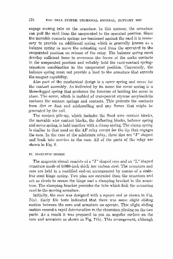
124 THE BELL SYSTEM TECHNICAL JOURNAl" JANUARY 19G7
engage mating tabs on the armature. In this manner, the armature can pull the card' from the unoperated to the operated position. Since the movable contacts springs are tensioned against the card it is necessary to provide an additional spring which is generally known as a balance spring to move the actuating card from the operated to the unoperated position on release of the relay. The balance spring must develop sufficient force to overcome the forces of the make contacts in the unoperated position and reliably hold the card-contact springarmature combination in the unoperated position. Conversely, the balance spring must not provide a load to the armature that exceeds the magnet capability.
Also part of the mechanical design is a cover spring and cover for the contact assembly. As indicated by its name the cover spring is a three-legged spring that performs the function of holding the cover in place. The cover, which is molded of transparent styrene acrylonitrile encloses the contact springs and contacts. This protects the contacts from dirt or dust and mishanc1ling and any fumes that might be generated by the coil.
The contact pile-up, which includes the fixed wire contact blocks, the movable wire contact blocks, the deflecting blocks, balance spring and cover spring, is held together with a clamp spring. The clamp spring is similar to that used on the AF relay except for the tip that engages the core. In the case of the miniature relay, these tips arc ".T" shaped and hook into notches in the core. All of the parts of the relay are shown in Fig. 6.
IV. MAGNETIC DESIGN
The magnetic circuit consists of a ".T" shaped core and an "L" shaped armature made of O.OSO-inch thick low carbon ~teel. The armature and core are held in a modified end-on arrangement by means of a stainless steel hinge spring. Two pins are extruded from the armature and act as rivets to secure the hinge and a clamping bracket to the annature. The clamping bracket provides the tabs which link the actuating card to the moving armature.
Initially, the core was designed with a square end as shown in Fig. 7 (a). Early life tests indicated that there was some slight sliding motion between the core and armature on operate. This slight sliding motion caused a rapid deterioration in the chromium plating on the two parts. As a result it was proposed to put an angular surface on the core and armature as shown in Fig. 7 (b). This arrangement, although

MINIATURE WIRE SPRING RELAYS
COVER
COVER CLAMP SPRING
1 CARD
DEFLECTING BLOCK
BALANCE SPRING
BREAK TWINS
ARMATURE ASSEMBLY
ASSEMBLED RELAY
DEFLECTING BLOCK
CLAMP SPRING
MAKE TWINS
SINGLE WIRE BLOCK
ADJUSTING BRACKET
Fig. 6 - BF relay parts.
125
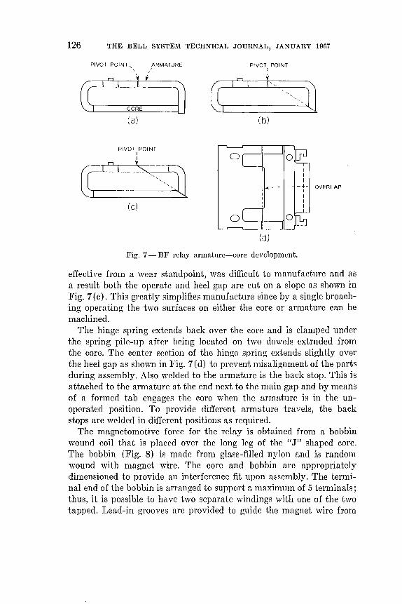
126 THE BELL SYSTEM TECHNICAL JOURNAL, JANUARY 1967
PIVOT POINT" ,ARMATURE \ I
11 .,
(a)
PIVOT POINT I I
(c)
10
1
PIVOT POINT I I 'f
(b)
(d)
Fig. 7 - BF relay armature-core development.
effective from a wear standpoint, was difficult to manufacture and as a result both the operate and heel gap are cut on a slope as shown in Fig. 7 (c). This greatly simplifies manufacture since by a single broaching operating the two surfaces on either the core or armature can be machined.
The hinge spring extends back over the core and is clamped under the spring pile-up after being located on two dowels extruded from the core. The center section of the hinge spring extends slightly over the heel gap as shown in Fig. 7(d) to prevent misalignment of the parts during assembly. Also welded to the armature is the back stop. This is attached to the armature at the end next to the main gap and by means of a formed tab engages the core when the armature is in the unoperated position. To provide different armature travels, the back stops are welded in different positions as required.
The magnetomotive force for the relay is obtained from a bobbin wound coil that is placed over the long leg of the "J" shaped core. The bobbin (Fig. 8) is made from glass-filled nylon and is random wound with magnet wire. The core and bobbin are appropriately dimensioned to provide an interference fit upon assembly. The terminal end of the bobbin is arranged to support a maximum of 5 terminals; thus, it is possible to have two separate windings with one of the two tapped. Lead-in grooves are provided to guide the magnet wire from
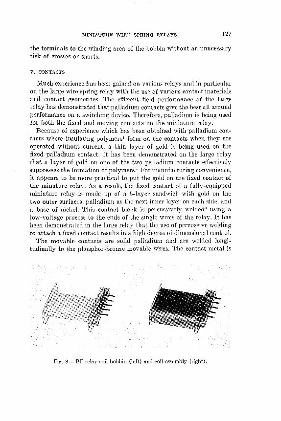
MINIA'l'URE WIRE SPRING RELAYS 127
the terminals to the winding area of the bobbin without an unncessary risk of crosses or shorts.
v. CONTACTS
Much experience has been gained on various relays and in particular on the large wire spring relay with the use of various contact materials and contact geometries. The efficient field performance of the large relay has demonstrated that palladium contacts give the best all around performance on a switching device. Therefore, palladium is being used for both the fixed and moving contacts on the miniature relay.
Because of experience which has been obtained with palladium contacts where insulating polymers4 form on the contacts when they are operated without current, a thin layer of gold is being used on the fixed palladium contact. It has been demonstrated on the large relay that a layer of gold on one of the two palladium contacts effectively suppresses the formation of polymers.[j For manufacturing convenience, it appears to be more practical to put the gold on the fixed contact of the minature relay. As a result, the fixed contact of a fully-equipped miniature relay is made up of a 5-layer sandwich with gold on the two outer surfaces, palladium as the next inner layer on each side, and a base of nickel. This contact block is percussively weldedu using a low-voltage process to the ends of the single wires of the relay. It has been demonstrated in the large relay that the use of percussive welding to attach a fixed contact results in a high degree of dimensional control.
The movable contacts are solid palladium and are welded longitudinally to the phosphor-bronze movable wires. The contact metal is
Fig. 8 - BF relay coil bobbin (left) and coil assembly (right).

128 THE BELL SYSTEM TECHNICAL JOURNAL, JANUARY 1967
long enough to bridge both the fixed contact and the operating card. By this technique, dimensional variation in the height of the contact as it affects contact gauging is minimized. It will also be seen later that this is of major importance in the maintenance of the relay. In order to insure uniformity of the mating points of the two contacts in the miniature relay, the fixed contact surface is cylindrical. This helps to minimize the possibility of open contacts caused by dust or small particles of insulating material which may stick to the contacts. Fig. 9 shows the size of the fixed and movable contacts and their relative orientation.
In miniaturizing the relay, it was necessary to have closer spacing of the movable wires than is used in the large relay. This has forced some reduction in the volume of precious metal. As a result, the miniature wire spring relay has only 2/3 of the erodible volume of the large relay. This results from the movable contacts being only 2/3 as wide as the movable contacts on the large relay. In other respects the dimensions are similar.
VI. PARTS STANDARDIZATION AND CODING
By variation of some parts, many different codes can be achieved in the BF miniature relay. Regardless of code, however, the same basic parts are used and the same basic number of pieces must be used to assemble a complete relay. A variety of codes is achieved by using different coils, varying the number of movable contacts, both make and break, varying the number of fixed contacts and using different operating cards.
The same coil bobbin is used for all coil resistances and windings. For a single wound coil only two terminals are used on the bobbin and coil resistance from 16 to 3400 ohms with a fully-wound coil can be achieved by variations in wire size. Double-wound coils with four terminals on the bobbin are used for other codes, and finally a fifth terminal can be attached to the bobbin to provide a tap for one winding if required.
Both the movable twin wires and the fixed single wires are molded in continuous strips as shown in Fig. 10 in a process similar to that used for the large relay. The long strips of contact assemblies are then cut apart and contacts provided as needed for various codes. The movable twin contact assemblies for both make and break contacts are symmetrical and the same details can be used for either purpose. 'Vhen a twin wire block is coded for less than a full complement of

MINIATURE WIRE SPRING RELAYS 129
contacts, the contact springs are clipped-off approximately 1/16 inch from the phenolic block on the contact and terminal sides. Typical assemblies of coded twin wire blocks are shown in Fig. II. lt is necessary to leave a short length of wire in the unused positions since the clamp blocks bear on the twin wires in the assembly as shown in Fig. 4.
In the single wire blocks all six wires are always provided on the contact side. This provides constant tension against the adjusting bracket as well as support for the front molded section for the wire guide slots. Contacts, however, are not welded to the ends of the wires in those positions that will not be used in a particular code. In order to minimize the use of the expensive palladium contact material, the contact block welded to the tip of the single wires can have contact metal on either side or both sides depending on the mating contacts being used. For mounting and wiring purposes, which will be discussed later, the terminal ends of all unused contacts are removed from the single wire block. Samples of several coded single wire assemblies are shown in Fig. 12.
The final part which contributes to coding of relays is the actuating card. By providing different widths for the actuating bar of the card, different sequences of contact actuations can be obtained. By using a relatively wide bar a break-be fore-make (EBM) transfer contact can
0.020 PHOSPHOR '---~======~~====~~==:j
BRONZE - - _ ----;r SPRI NG WIRE' ~ L..c:==================l I
FIXED// CONTACT
14 /
/
I I~~~ ...... I
MOVING CONTACT
"", .... OPERATING -- CARD
0.009 r---- -----0.140 --- - ----:./ IJ 0.010
: ~ I l~ ~ ____ L I
p-~ --==k- - -~, --r r-- -7 ----""PALLADIUM I i GOLD- ~
-- ~ Fig. 9 - BF relay contact configuration.

130 THE BELL SYSTEM TECHNICAL JOURNAL, JANUARY 1967
, I Fig. 10 - BF relay movable twin wire molded ladder (bottom) and fixed single
wire molded ladder (top).
d I! II II " !
III ~
j
I
'I 1\
II
Fig. 11 - BF relay typical coded movable twin wire assemblies.

MINIATURE WIRE SPRING RELAYS 131
be achieved (see Fig. 5) and by using a relatively narrow bar a makebefore-break (EMB) continuity transfer contact can be obtained. Also, by having different widths to the bar across the card, these different contact sequences can be obtained on the same relay.
Theoretically, it is possible to have 36 or 729 different operating cards, i.e., with either an EMB, EBM or a BM (nonsequenced) set of contacts in each of the six positions. This is a prohibitive number of molded cards to provide tooling and controls, therefore, eight different cards have been standardized for use in miniature relays. 'Vhenever an early contact of either the make or break variety is required on a relay, all positions of that relay will have one early contact. This is possible since when a circuit designer specifies a simple make or a
Fig. 12 - BF relay typical fixed single wire contact assemblies.
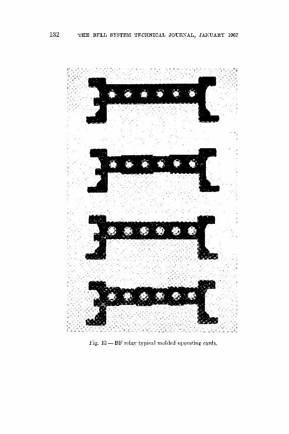
132 THE BELL SYSTEM TECHNICAL JOURNAL, JANUARY 1967
Fig. 13 - BF relay typical molded operating cards.
MINIATURE WIRE SPRING RELAYS 133
simple break contact, he is not concerned with where in the stroke of the relay it operates. Also, a sequence transfer can always be used in place of a nonspecified sequence transfer. Samples of several coded actuating cards are shown in Fig. 13.
VII. ASSEMBLY AND ADJUSTING
The pile-up of the BF miniature relay is designed so that the various parts are either keyed or doweled together successively on assembly. The base for the contact pile-up is the magnet core which has two dowels which locate the armature assembly and the adjusting bracket. The armature assembly is located only in a sideways direction by these dowels. The magnet coil is normally energized when the armature is assembled to the core so as to produce a minimum heel air gap between the armature and core, and the dowel holes in the hinge spring are slotted to allow the armature to assume its natural position. The adjusting bracket on top of the hinge spring has close fitting holes to locate it in both directions.
The contact assembly is built up on top of the adjusting bracket. This bracket has two dowels which serve to locate the lower deflecting block. The deflecting block in turn has an inner grove which locates the break twin wire assembly. The opposite side of the molded section of the break twin wire assembly serves to locate the single wire block by means of another groove. In the top of the single wire block, the balance spring is located by appropriate projections. Similar to the break twin wire assembly, the make twin wire assembly and deflecting block are keyed to the single wire block by means of grooves. On top of the make contact deflecting block, grooves locate the cover clamp spring and the relay clamp spring. When all of the parts are stacked in the proper order, the clamp spring is snapped into place over the pile-up to securely lock it in its proper position.
After the pile-up is assembled and clamped, the movable make and break contacts are spread apart by means of a spacer or wedge and the operating card is inserted. It is held in place as described earlier by lugs on the armature clamp bracket and the balance spring.
After assembly there are three adjustments that may be made to assure that a particular relay meets its requirements. The armature travel may be adjusted by bending the armature backstop lug. This adjustment is only required if the armature backstop detail is inaccurately welded to the front of the armature. The twist tabs on the front of the adjusting bracket are bent to position the single wire block.
134 THE BELL SYSTEM TECHNICAL JOURNAL, JANUARY 19G7
By moving the single wire block either up or down in this fashion, the closure points for the make and break contacts can be varied relative to the single contacts. This allows for adjustment of the point of make or break of the moving contacts in the stroke of the armature. The third adjustment that can be performed on the finished relay is that of balance spring tension. Three different balance springs are provided for the relay. However, since a relay may have anywhere from one to six movable make contacts, it is sometimes necessary to adjust the tension in the balance spring after assembly to the specified range. It is impractical to have a balance spring for each contact combination since in addition to the variation in relay contact load, it is difficult to accurately control the pretension bends in the balance spring to the point where no adjustment is required.
VIII. PERFORMAN CE
As indicated earlier the broad objective in the design of a miniature wire spring relay was to achieve as far as possible the good performance that has been demonstrated by the large wire spring relay. Therefore, in evaluating the performance of the BF relay, the large AF type wire spring relay has been used for comparison. Tests and evaluations have been made of all of the various performance characteristics of the BF relay. These studies have been conducted both on model shop samples in the course of development and production samples as they became available. In the following paragraphs, the major aspects of the relays performance will be described and discussed.
8.1 Load and Pull Characteristics
Fig. 14 shows a typical set of load and pull curves7 for a BF relay with six early-make-break transfer contacts. The travel of the operating card is plotted on the abscissa and the load and pull at the operating card is plotted on the ordinate. Actually, two load curves are shown; one as measured with the relay armature moving in the operate direction and the second as the relay is released. The load curve begins at approximately 0.033 inch of travel with a load of approximately 60 grams which is the force holding the armature against its backstop. There is then a gradual build-up to approximately 80 grams at which point a very rapid change in load takes place. This rapid change is the result of the operation of the early-make contacts and takes place between 0.022 and 0.018 inch of travel in this particular case. From this point, the load again increases gradually to approximately 0.012

MINIATURE WIRE SPRING RELAYS 135
inch of travel at which point the break contacts open causing a rapid increase in load until the travel is reduced to 0.008 inch. From this point, until the armature strikes the core the load build-up is again quite gradual and ends with a maximum load of approximately 270 grams. The release load curve closely parallels the operating curve but is slightly lower. The difference between the operate and release curve is a measure of the mechanical hysteresis or friction of the structure. It can be seen from the curve that in the case of the BF relay this hysteresis is quite small.
Also plotted on the figure are four typical pull curves for different values of ampere turns. The 135 NI curve is the lowest of the four that does not fall below the load curve at the point of maximum travel. Thus, it can be concluded that any value of ampere turns less than 135 will not result in any motion of the armature. The 135 NI curve,
350
325
300
275
o ~ 250 u LL 0225
-B-1 I-<{ 200 <I)
2 <{ n: 175 t.!)
z :::; 150 ...J :::> n. n: 125 o
~ 100 o ...J
75
50
25
a
\ ~ \1
~REAK \ i--CONTACTS
IV OPERATE IN
THIS INTERVAL I-:=] --145 NI PULL CURVE
~ i l\ I :::::-- --140 NI
~~ \ I \~13~NI
/~\ \\\ RELE'ASE .~
~ ~" LOAD CURvE -, MAKE CONTACTS
I\=/~ '\ ~ i OPERATE IN
~ THIS INTERVAL
l'--.. OPERATE _-_/\ '-... ~~ \1 LOAD CURVE \
\ \~ "' ~~ 92N~ ~::: ~ ~ ~ ::::::--
~~ ...... ::::::::: ~ t:=:::::: t::::== ~ :---
......... r'----r--
\. o 2.5 5.0 7.5 10.0 12.5 15.0 17.5 20.0 22.5 25.0 27.5 30.0 32.5· 35.0
TRAVEL AT CARD xfO-3 INCHES
Fig. 14 - Typical BF relay load and pull curves with six early-make-break transfer contacts.

136 THE BELL SYSTEM TECHNICAL JOURNAL, JANUARY 1967
however, intercepts the load curve at approximately 0.020 inch of travel. Thus, the application of 135 NI to this relay will result in hesitation of the armature at this point in the stroke. The 140 NI curve just passes above the load curve over its entire length. Thus, the justoperate current of this relay is that current which is equivalent to 140 NI. For margin in operating, it is customary to specify a test value somewhat higher than the just-operate value; for example, in the order of 145 NI. Also plotted is a 92 NI curve which has more than sufficient pull to hold the relay operated once the armature is in contact with the core. Thus, a hold current equivalent to 92 NI would prevent this typical relay from releasing.
8.2 Speed of Operation and Release
The operate time of a relay structure is a function of the load, the armature air gap, and the applied power. Fig. 15 shows the operate time of three typical BF relays. The upper curve is a long travel 6 transfer contact relay with the operate time plotted versus coil input power. The second curve is slightly below the 6 transfer contact curve and indicates the effect of contact load. Long travel for the relay armature is required when the transfer contacts are of the sequenced variety such as EMBs or EBMs. The third and lowest curve in the figure is for a short travel two transfer contact relay. The only difference between the latter two curves is that with the short travel relay no assured sequence exists in the transfer contacts. This typical curve shows that with a lightly loaded short travel relay the operate time
14.----,~--~----~--~----~----~--~----~--~ <f) o z o U ~12~---+--~4-----~---i----~-----~---+----~--~ ::J ..J
~ ~10~--_+~--~~--~--_+----~----+-----+---~~---j
~ LONG TRAVEL 1= 2 TRANSFER
CONTACTS ~ 8 ~--~----~-------=k-~':-+----~--=/ rr I w I n. o ..J 6~--_+----4-----~~~-----F~~+~--~----~--~ « ~ n. >-~ 4~ __ ~ ____ ~ ____ L-__ ~ ____ -L ____ L-__ ~ ____ -L __ ~
o 0.5 1.0 1.5 2.0 2.5 3.0 3.5 4.0 4.5 POWER INPUT IN WATTS
Fig. 15 - Typical operate time curves for BF relays.
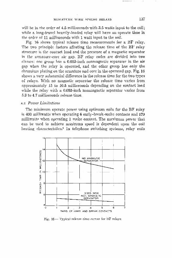
MINIATURE WIRE SPRING RELAYS 137
will be in the order of 4.5 milliseconds with 3.5 watts input to the coil; while a long-travel heavily-loaded relay will have an operate time in the order of 11 milliseconds with 1 watt input to the coil.
Fig. 16 shows typical release time measurements for a BF relay. The two principle factors affecting the release time of the BF relay structure is the contact load and the presence of a magnetic separator in the armature-core air gap. BF relay codes are divided into two classes: one group has a 0.003-inch nonmagnetic separator in the air gap when the relay is operated, and the other group has only the chromium plating on the armature and core in the operated gap. Fig. 16 shows a very substantial difference in the release time for the two types of relays. With no magnetic separator the release time varies from approximately 15 to 10.5 milliseconds depending on the contact load while the relay with a 0.003-inch nonmagnetic separator varies from 5.3 to 4.7 milliseconds release time.
8.3 Power Lim,itations
The minimum operate power using optimum coils for the BF relay is 400 milliwatts when operating 6 early-break-make contacts and 170 milliwatts when operating 1 make contact. The maximum power that can be used to achieve maximum speed is dependent upon the coil heating characteristics.s In telephone switching systems, relay coils
16
14 Cf)
o z o u ~ 12 ::J ...J
i ~ 10 UJ
~ i=
~ 8 <{ UJ ...J UJ a:
6
4 o
1\ ~ ~ NO MAGNETIC
~RATOR
I---r----
0.003 INCH NON-MAGNETIC
SEPARATOR
2 3 4 5 6
PAIRS OF MAKE AND BREAK CONTACTS
Fig. 16 - Typical release time curves for BF relays.
7

138 THE BELL SYSTEM TECHNICAL JOURNAL, JANUARY 1967
1-140
[j :c z w a::t20 :c ~ I/) w ~tOO l!) w o
~ 80 w U)
a: w a: 60 => ~ a:: w ~ 40 I-..J
o U Z 20 <{ w ~
o
/~
/ /
V /
/ J
I I
o 1 2 3 4 5 INITIAL WATTS AT ROOM TEMPERATURE
Fig. 17 - Typical heating curve for a BF relay coil assembly.
are designed to withstand an exposure to 360°F for a maximum of 48 hours of cumulative exposure. They also shall withstand an indefinite exposure to 225°F. The temperatures referred to are the mean winding temperatures. Fig. 17 shows a typical BF relay coil heating curve where input power at room temperatue is plotted versus change in mean coil temperature.
For this particular coil, an initial power input of 4 watts results in a temperature rise of approximately 135°F. To maintain a maximum temperature of 225°F at an ambient temperature of 100°F, there would be a maximum 125°F temperature rise. From the curve a 125°F rise will result from 3.6 watts of initial power.
8.4 Contact Performance
The use of the wire spring technique produced in the BF relay all of the proven advantages of the large wire spring relay with regard to contact performance.2 These include such things as full twin action in the movable springs, card release actuation to prevent contact locking, cylindrical surface on one of the contacts to minimize the effective contact area that contaminants can occupy to affect contact per-

MINIATURE WIRE SPRING RELAYS 139
formance. Also, the BF relay makes use of palladium contacts for both the fixed and movable members to take advantage of the long experience in the Bell System of the use of this material. In addition, one of the contact members has a O.OOl-inch thick gold layer to minimize the formation of polymers.
8.5 Life
Life studies have been conducted on the BF relay and have shown that the mechanical life of the moving parts is at least 200 million operations. This life is limited by operating card and armature backstop wear. Replacement of the card and readjustment of the armature backstop can probably extend this life. Generally speaking, the electrical life of the contacts is determined by factors outside of the relay such as the size and inductance of the load and whether contact protection is employed. With a non-inductive load or with optimum contact protection on an inductive load, the contact life will be equal to or greater than the mechanical life of the relay. A subsequent paper will describe the development of contact protections specifically for use with miniature relays.
8.6 Stability
BF relays have been subjected to shock, vibration, temperature change and humidity tests to determine their stability in shipment and in use. The shock and vibration tests have used levels of severity that have been established by various military specifications for normal shipping conditions. The temperature and humidity tests have used levels of severity which have proven satisfactory for many years in the Bell System. These exposures are as follows:
Shock -30G II-millisecond pulses with six shocks in each direc-tion of each of the three mutually perpendicular axes or the relay.
V ibration -Cycled from 10 to 55 to 10 Hz in one minute with an amplitude of 0.060 inch peak-to-peak. Cycled for a period 'of two hours in each of the three mutually perpendicular axes.
Tempera~ure-Tempreature cycles of from -40°F to + 140°F.
Humidity -Six days of exposure at 90 percent relative humidity and 85°F followed by six days at 120°F dry.
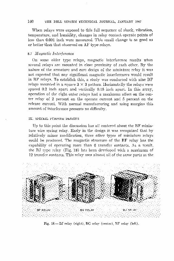
140 THE BELL SYSTEM TECHNICAL JOURNAL, JANUARY 1967
When relays were exposed to this full sequence of shock, vibration, temperature, and humidity, changes in relay contact operate points of less than 0.001 inch were measured. This small change is as good as or better than that observed on AF type relays.
8.7 Magnetic Interference
On some older type relays, magnetic interference results when several relays are mounted in close proximity of each other. By the nature of the armature and core design of the miniature relay it was not expected that any significant magnetic interferences would result in BF relays. To establish this, a study was conducted with nine BF relays mounted in a square 3 X 3 pattern. Horizontally the relays were spaced 0.2 inch apart and vertically 0.15 inch apart. In this array, operation of the eight outer relays had a maximum affect on the center relay of 2 percent on the operate current and 5 percent on the release current. 'Vith normal manufacturing and using margins this amount of interference presents no difficulty.
IX. SPECIAL PURPOSE DESIGNS
Up to this point the discussion has all centered about the BF miniature wire spring relay. Early in the design it was recognized that by relatively minor modification, three other types of miniature relays could be produced. The magnetic structure of the BF relay has the capability of operating more than 6 transfer contacts. As a result, the B.T type relay (Fig. 18) has been developed with a maximum of 12 transfer contacts. This relay uses almost all of the same parts as the
SF RELAY SG RELAY BJ RELAY
Fig. 18-BJ relay (right), BG relay (center), BF relay (left).
MINIATURE WIRE SPRING RELAYS 141
BF relay. For the 12 transfer contacts, 4 twin wire assemblies and 2 single wire assemblies identical to those used in the BF relay are required. Three new parts are required for the BJ type and these are: a new cover, a larger clamp spring, and an adjusting and spacer block to separate the two levels of contacts.
By reducing the length of the coil and bobbin, copper washers can be placed on the core to provide a slow release capability for the relay. When copper washers with a short coil are used, the relay is known as the BG type (Fig. 18).
Similar to the large wire spring relay, if a semi-permanent magnetic material is used for the core and armature, a magnetic latching relay will result and this is known as the BL type. The BL relay is identical to the BF in appearance. Subsequent papers will describe the details of both the slow release and magnetic latching types of relays.
In the design of the miniature relay, it was necessary to make some sacrifices in sensitivity to achieve the small size. This has resulted in a hardship in some applications where it is necessary to work a relay in conjunction with long subscriber loops or with low current semiconductor devices. As a result a slightly larger relay has been designed and proposed for manufacture for those applications where maximum sensitivity is required. This proposal uses the same contact and pile-up parts as the BF relay but has a slightly larger core and armature to provide the increased sensitivity. It will therefore, require a slightly larger mounting area.
x. FIELD TESTING AND MAINTENANCE
As indicated earlier, the BF type relay has been designed primarily for use in telephone central office equipments. In such an environment, a relay is expected to have a long and relatively trouble-free life. However, on those occasions when relay maintenance is necessary, it is expected that they can be repaired or adjusted either in place or locally. Also, for circuit testing, it is often useful to use the relay as a test point in the circuit. In telephone central offices there normally are skilled craftsman available to perform both circuit testing and relay maintenance functions. As a result, the ability to perform all of the essential field testing and relay maintenance functions has been built into the BF relay.
Under field testing there are three major functions to be performed:
(i) Contact Insulating-For circuit testing it is often useful to the maintenance man to be able to insulate a contact to isolate a portion
142 THE BELL SYSTEM TECHNICAL JOURNAL, JANUARY 19G7
of a circuit. Since the twin contact of the BF relay is smooth and continuous from the contact area out over the operating card to the tip, it is possible to insert a small piece of lint free parchment paper between the fixed and movable contacts to effectively insulate them from each other.
(ii) Armature Blocking-To study circuit performance in the course of testing, it is often useful to block a relay armature in either the operated or unoperated position. The BF relay has its armature in the front and uncovered. It is thus possible to insert a simple plastic wedge-shaped tool between the armature and core to hold the relay unoperated, or between the armature backstop and the core to hold the relay in the operated position.
(iii) Contact Test Points-When the relay is blocked either operated or unoperated, or when contacts are insulated, as well as in normal performance, it is often desirable to be able to test for battery or ground conditions on relay contacts. With the BF relay cover removed, a test pick can be touched to either the make or break movable contact springs to test for potential conditions. The fixed contacts are behind the operating card, but to allow for testing, a series of holes has been provided in the movable card. These holes are located so that a test pick can be inserted to touch the end of the fixed contact.
The foregoing comprises the principal circuit testing functions that are performed on the relay. In addition to these, there are five principal relay maintenance functions which can be performed if required:
(i) Contact Cleaning-As described under contact insulating, a piece of parchment paper moistened with an appropriate solvent can be inserted between the fixed and movable contacts and moved back and forth to effectively clean the two contact surfaces.
(ii) Operating Card Replacement-In long life applications, it may sometimes be necessary to replace the relay operating card. Being of plastic, this card will probably wear more than the various metal parts. vVith the cover removed, a replacement card can be installed with the use of rather simple tools that have been developed.
(iii) Armature Travel Adjustment-With wear, it may be necessary in some cases to adjust the armature travel of the relay in order to keep it within its operating requirements. The backstop which is welded to the armature provides an adjustment slot. The use of a screw driver twisted in the slot will change the armature travel and thus compensate for wear.

MINIATURE WIRE SPRING RELAYS 143
(iv) Contact Gauging Adjustment-To permit the readjustment of the pick-up points of the make or break contacts, two twist tabs are provided at the front of the relay to change the position of the single wire contacts. By twisting the two tabs, the fixed or single contacts can be moved either up or down thus changing the point in the armature stroke where contacts either open or close.
(v) Back Tension Adjustment-Due to wear on relatively long life relays it may sometimes be necessary to adjust the armature balance spring tension. In the BF relay the balance spring is accessible from the front and can be adjusted with a spring-bending tool.
Most of these maintenance and testing features are possible in a relatively simple manner since the contacts and armature air gap of the relay are exposed. The contacts are normally covered with a transparent plastic cover. This cover is designed so that it will remain securely in place during the shipping and handling of the relay but can be readily removed with the fingers. It will be noted that a number of the maintenance and test functions require access to the contacts or contact area of the relay; thus, the cover must be readily removed when required. Special or new testing or adjusting tools have been designed to perform all of the functions described above and are available for the central office craftsman's use.
XI. MOUNTING AND WIRING
The BF relay is designed to be mounted on a printed wiring board with all of the terminals mass soldered to circuit paths. The terminal spacing is sufficient to allow for economical printed wiring board manufacture and the soldering can be performed by conventional mass soldering techniques. The relay occupies 1.081 square inches of space on a printed wiring board. Generally speaking, the minimum distance between two relays on a board is limited by the circuit paths on the wiring side rather than by the area occupied by the relay on the apparatus side. The terminals are of sufficient length to be used on both 1/16 and 3/32-inch printed wiring boards. Thus, the relay can be mounted on circuit boards in conjunction with other miniature devices such as semiconductor units.
When the relay is mounted, the core comes in direct contact with the printed board and a tapped hole is provided in the core for mounting security. It is recommended that a screw always be used to support the relay. In this fashion, strains are avoided on the soldered joints at the terminals. On a relay with a maximum complement of
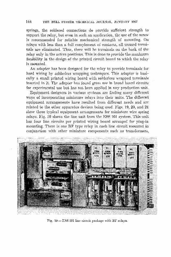
144 THE BELL SYSTEM TECHNICAL JOURNAL, JANUARY 1967
springs, the soldered connections do provide sufficient strength to support the relay, but even in such an application, the use of the screw is recommended for reliable mechanical strength of mounting. On relays with less than a full complement of contacts, all unused terminals are eliminated. Thus, there will be terminals on the back of the relay only in the active positions. This is done to provide the maximum flexibility in the design of the printed circuit board to which the relay is mounted.
An adapter has been designed for the relay to provide terminals for hard wiring by solderless wrapping techniques. This adapter is basically a small printed wiring board with solderless wrapped terminals inserted in it. The adapter has found great use in bread board circuits for experimental use but has not been applied in any production unit.
Equipment designers in various systems are finding many different ways of incorporating miniature relays into their units. The different equipment arrangements have resulted from different needs and are related to the other apparatus devices being used. Figs. 19, 20, and 21 show three typical equipment arrangements for miniature wire spring relays. Fig. 19 shows the line unit from the ESS 101 system. This unit has four line circuits per printed wiring board arranged for plug-in mounting. There is one BF type relay in each line circuit mounted in conjunction with other miniature components such as transformers,
Fig. 19 - ESS 101 line circuit package with BF relays.
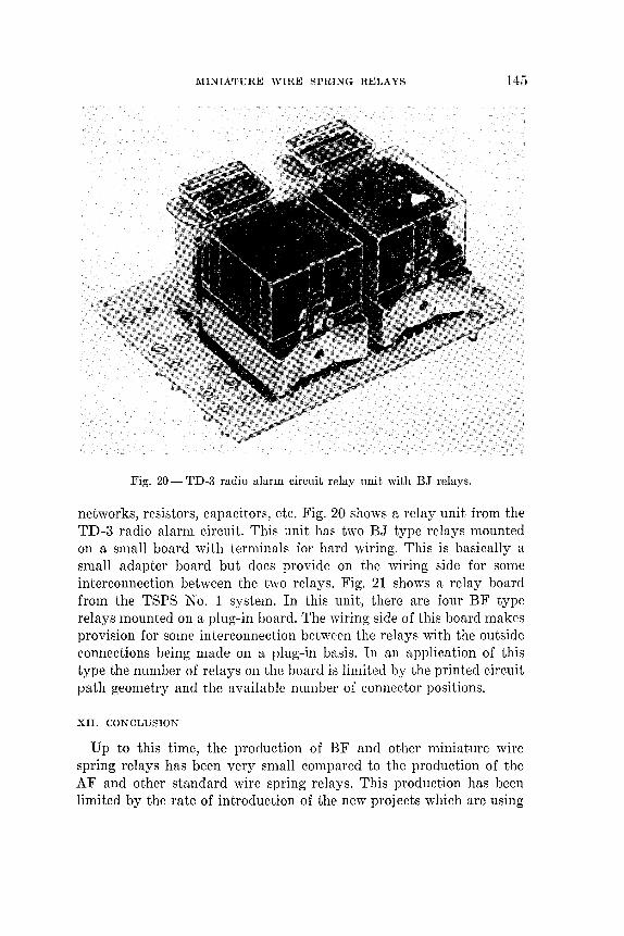
MINIATURE WIRE SPRING RELAYS 145
Fig. 20 - TD-3 radio alarm circuit relay unit with BJ relays.
networks, resistors, capacitors, etc. Fig. 20 shows a relay unit from the TD-3 radio alarm circuit. This unit has two BJ type relays mounted on a small board with terminals for hard wiring. This is basically a small adapter board but does provide on the wiring side for some interconnection between the two relays. Fig. 21 shows a relay board from the TSPS No. 1 system. In this unit, there are four BF type relays mounted on a plug-in board. The wiring side of this board makes provision for some interconnection between the relays with the outside connections being made on a plug-in basis. In an application of this type the number of relays on the board is limited by the printed circuit path geometry and the available number of connector positions.
XII. CONCLUSION
Up to this time, the production of BF and other miniature wire spring relays has been very small compared to the production of the AF and other standard wire spring relays. This production has been limited by the rate of introduction of the new projects which are using
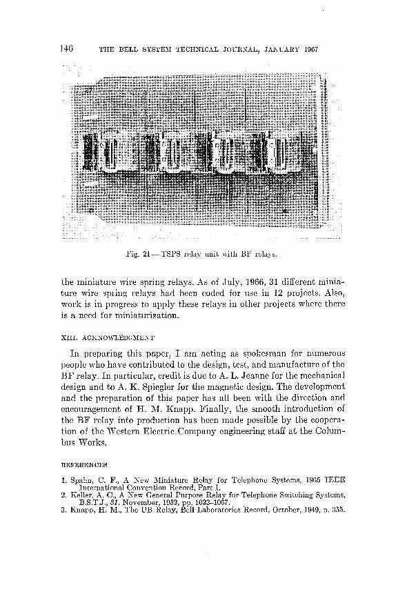
146 THE BELL SYSTEM TECHNICAL JOURNAL, JANUARY 1967
Fig. 21- TSPS relay unit with BF relays.
the miniature wire spring relays. As of July, 1966, 31 different miniature wire spring relays had been coded for use in 12 projects. Also, work is in progress to apply these relays in other projects where there is a need for miniaturization.
XIII. ACKNOWLEDGMENT
In preparing this paper, I am' acting as spokesman for numerous people who have contributed to the design, test, and manufacture of the BF relay. In particular, credit is due to A. L. Jeanne for the mechanical design and to A. K. Spiegler for the magnetic design. The development and the preparation of this paper has all been with the direction and encouragement of H. M. Knapp. Finally, the smooth introduction of the BF relay into production has been made possible by the cooperation of the ,Vestern Electric Company engineering staff at the Columbus Works.
REFERENCES
1. Spahn, C. F., A New Miniature Relay for Telephone Systems, 1965 IEEE International Convention Record, Part 1.
2. Keller, A. C., A New General Purpose Relay for Telephone Switching Systems, B.S.T.J., 31, November, 1952, pp. 1023-1067.
3. Knapp, H. M., The UB Relay, Bell Laboratories Record, October, 1949, p. 355.

MINIATUHE WIHE SPHIN G RELAYS 147
4. Hermance, H. W. and Egan, T. F., Organic Deposits On Precious Metal Contacts, B.S.T.J., 37, May, 1958, pp. 739-776.
5. Keefer, H. J. and Gumley, R. H., Relay Contact Behavior Under Non-Eroding Circuit Conditions, B.S.T.J., 37, May, 1958, pp. 777-814.
6. Quinlan, A. L., Automatic Contact Welding in Wire Spring Relay Manufacture, B.S.T.J., 33, July, 1954, pp. 897-923.
7. Wagar, H. N., Relay Measuring Equipment, B.S.T.J., 33, January, 1954, pp. 3-22.
8. Peek, R. L., Jr., Internal Temperatures of Relay Windings, B.S.T.J., 30, January, 1951, pp. 141-148.


Off-Axis Wave-Optics Transmissioll in a Lens-Lil(e Medium witll Aberration
By E. A. J. MARCATILI
(Manuscript received August 31, 1966)
N onnal modes and their propagation constants have been found for a two-dimensional lens-like lnedium in which the transverse refractive index varies essentially with quadratic law but has perturbing terms of higher order. In such a realistic guiding medium with aberrations, those modes are used to find the field configuration of a Gaussian beam of half width JV entering off-axis.
Close to the input the beam oscillates periodically with amplitude Xi
as if the medium were aberration-free, but slowly the beam cross-section changes shape, breaking up in several maxima, and increases size, reaching a maximum approximately equal to 2(W + xJ. Afterwards the beam slowly shrinks back to the starting field configuration and the process repeats again.
These results are applicable to a sequence of lenses with aberrations and become intportant when the lenses are closely spaced. If redirectors are to be used to compensate for lens misaligmnents, the corrections must be 17wde before a large break-up of the beam, occurs.
I. INTRODUCTION
Transmission through a lens-like medium consisting of a dielectric rod in which the dielectric constant decreases radially with quadratic law has been studied because, first, it is closely related to light transmission in a periodic sequence of gaseous lenses, 1,2,3 second, it helps to understand the filamentary nature of the oscillations in ruby lasers,4 and third, if the dielectric constant is complex, it describes the gain medium in a gaseous laser. 5
Whenever the radial dependence of the dielectric constant is quadratic, any paraxial beam propagates undulating periodically about the axis, and the field reproduces itself after each period. This is true only within
149

150 THE BELL SYSTEM TECHNICAL JOURNAL, JANUARY 1967
some approximations. * Part of the object of this paper is to find the distance over which the approximations hold and how it depends upon the beam shape and displacement from the axis. The mathematical description of Gaussian beams in such an aberration-free lens-like quadratic medium has been achieved via two techniques. The first consists of expanding the input beam in terms of on-axis normal modes1
and summing them up everywhere. The second technique consists of solving differential equations that elegantly relate the location of the beam axis, the spot size, and the curvature of the phase front at any place along the beam. 7 Nevertheless, we show in this paper that if the lens-like medium has aberrations, no matter how small, the electromagnetic field of a paraxial beam changes shape radically as it travels along the guide. The distorted beam cannot be described any more by the beam axis location, the spot size, and the phase front curvature, and consequently, the off-axis beam must be calculated following the first technique.
The on-axis normal modes and their propagation constants are found in Section II using a first-order perturbation technique; the off-axis beam is calculated in Section III; the limits of validity of the previous results are given in Section IV and conclusions are reached in Section V.
The modes in lens-like media with arbitrarily large perturbations have been studied by S. E. MillerS and J. P. Gordon. 9 However, they have not given a quantitative description of an off-axis beam.
Beam deformations similar to those analyzed in this paper have been obtained by D. Marcuse10 who calculated, via a computer, the transmission of an off-axis Gaussian beam through a sequence of curved and distorted lenses.
II. MODES IN A LENS-LIKE MEDIUM WITH SMALL ABERRATION
Consider a lens-like medium in which the refractive index
(1)
* A. H. Carter has found 6 that if the dielectric constant of the lens-like medium varies radially, not with quadratic law, but with the square of the hyperbolic secant law, the periodicity is not restricted to paraxial beams and since there are no approximations involved, the results hold for any length. Unfortunately, the functions describing the modes are hypergeometric and they cannot be easily handled as the parabolic cylinder functions of the quadratic medium. Because of this and also because our main interest is the study of transmission through non-ideal media anyhow, we will keep on basing our calculations on the quadratic medium and we will even call it ideal.

TRANSMISSION IN A LENS-LIKE MEDIU:M 151
varies only in the transverse direction X; no is the refractive index at x = 0, and Land aa are constants whose physical significance will be shown later. The quadratic law of the dielectric constant is slightly perturbed by the summation in the integers a = 1,2, 3 ....
We study here modes propagating along z in a medium with variation only in the x direction; nevertheless, the extension to the case in which the dielectric constant varies also along the other transverse direction y, can be easily achieved as shown in Ref. 1.
Assuming that the only component of electric field E is parallel to the y axis and independent of y the wave equation is
~~ + ~:! + (~7rr[ 1 - (~xr - ~ aa(~T)aJE = 0, (2)
where A. is the plane wave wavelength in a medium of refractive index no .
Let us call
~ = 2x W
a new transverse variable normalized to the beam half-width
in the unperturbed medium, and also
E = Ep exp (-i'YvZ).
(3)
(4)
(5)
E p , the transverse field distribution of the pth mode, is a function of ~ exclusively and
27r I ( (A)aI2-1) A 'Yp = >: '\j 1 - p + ! + ~ aa! aLL (6)
is the propagation constant of the pth mode along the z axis. The summation La aa!a(A./L)a/2-t, is the perturbation due to the aberrations and the unknown f a will be determined later.
Now we substitute (3), (4), and (5) in (2) and obtain an equation in ~ exclusively for the transverse field Ep ,
(7)
For aa = 0, the solution 11 is the parabolic cylinder function Dp(~) = exp (_~2 /4)Hp(~) which is a product of the Gaussian function exp (-e/4) and the Hermite polynomial of integer and positive order p.

152 THE BELL SYSTEM TECHNICAL JOURNAL, JANUARY 1967
For act ~ 0 it is shown in Appendix A that if
(A )",/2-1
~ aa "L P «1 (8)
the differential equation (7) can be solved by using first-order stationary perturbation theory.12 Then, the transverse field distribution of the pth mode in the perturbed medium expressed in terms of the normal modes of the unperturbed medium is
Ep = Dp(~) + L cnDn(~) ; (9) nr'p
the sum extends from 0 to 00 excluding n = p and the values of Cn
are given in (54). We also find in (55) that
j2-3a/2a! p! I: 2
m
m=O (m !)\p - m)! (~ - m)!
o
if a is even, (10)
if a is odd.
Further on, specific values of f a will be needed, so some of them are given in Table 1. From the table and (6) we conclude that if the medium has only antisymmetric perturbation (a odd), the propagation constants of its modes are identical to those of the modes in tho unperturbed medium. Physically, this means that to a first order, the change in phase velocity introduced by the perturbation on one side of the guide is canceled by the other.
III. BEAM IN THE PERTURBED MEDIUM
We want to calculate the field F(z) everywhere in the perturbed medium such that at the origin it coincides with a prescribed function
TABLE I-SOME SPECIFIC VALUES OF fa
a f",
1 0
2 HI + 2p)
3 0
4 h(l + 2p + 2p2)
5 0
6 H(l + ip + 2p2 + t p3)

TRANSMISSION IN A LENS-LIKE MEDIUM 153
F(O). In terms of the normal modes E p , the field is
00
F(z) = L ApEp exp (-i'Ypz) , (11) p=o
and at the origin
00
F(D) = L ApEp . (12) p=o
We simplify next ApEp and the propagation constant 'Yp . Since the approximately calculated normal modes of the medium
with aberration are orthogonal to the first order of the perturbations aa(A/L)a/2-t, we calculate, with the help of (9), each term of the summation to be
(13)
where
B ~ f F(O)Dp(~) d~ p L: D!(~) d~ (14)
is the amplitude of the pth mode of an expansion of the input field F(O) in terms of modes of the unperturbed guide and the term of the order of aa(A/L)a/2-\ given only for completeness, is
i:c. D.(~) f F(O)Dp(~)mdH Dp(~) f F(O)D.(~) d~.
~=~ Loo D!(~) d~
Substituting (13) in (11) one obtains
00 co [ (A)a/2-1] F(z) = ~ BpDp(~) exp (-i'YvZ) + ~ 0 aa L exp (-i'YvZ). (15)
We will find that for large z the first summation yields configurations which depart grossly from the field in the unperturbed medium, therefore, according to (8), the second summation whose amplitude is of the order of aa (A/ L) a/2-1 will be neglected.
Furthermore, the propagation constant 'Yp , (6), which is exact for the ideal quadratic medium and good to first order of La aa(A/L)a/2-1

154 'fHE BELL SYSTEM TECHNICAL JOURNAL, JANUARY 1967
can be expanded in series
27r{ 1 [1 (A)a/2-1] A 1'1' = X 1 - 2 p + 2 + Z; all'fll' L L
1 [1 (A)a/2-1]2 A2 } - 8 p + 2 + Z; all'fa L L2 - .... (16)
The third and higher-order terms can be neglected only if their eOll
tribution to the phaseshift of the highest-order mode P of signifieant amplitude is small, that iEl, if
According to (47) in the Appendix, once the inequality (8) is satisfied, the summation is negligible compared to P and consequently the inequality above reduces to
(17)
This expression establishes the range of validity z, of the description of a beam composed essentially of P modes at wavelength A, traveling in a lens-like medium characterized by L. Since the inequality is independent of aa we conclude that the finite range of validity z is determined not by the perturbation of the medium, but by the approximation involved in the expansion (16) of the propagation constants thus affecting the description of the beam even in the ideal quadratic medium.
Once P is known, the inequality (8) determines the magnitude of the perturbation aa for which the calculations are valid. Then, provided that inequalities (8) and (17) are satisfied the simplified version of the field (15) becomes
ex> { [ (A)"'/2-1] } F(z) = ~ BpDp(~) exp -i I'pi - I Z; aaf a L z, (18)
in which
I'pi = ~7r [1 - 2~ (p + !) ] (19)
is the propagation constant of the pth mode in the unperturbed ideal quadratic medium.
Therefore, the field F(z) is described by a summation of modes of the ideal quadratic law medium but with phase constants corresponding to

TRANSMISSION IN A LENS-LIKE MEDIUM 155
modes in the perturbed medium. Actually, if aa = 0, we derive from (18) the field in the ideal quadratic medium
co
fez) = L BpDp(~) exp (-iYPiZ). (20) p=o
In order to find out more about the field distribution along the perturbed guide, we will work out a typical example assuming that the only perturbation of the dielectric is of order 4. Dropping the subscript from a4 and with the help of Table I we find that
(A)a/2-1 A 3 A 2 L; aafa L = af4 L = 16 a L (1 + 2p + 2p).
The field (18) then results
F(z) = exp (i ~ ~) t, BpDp(~) exp {-{YPi - ~ (p + p') J} . (21)
where the distance
8L2
D=-3aA
has a physical significance to be described later.
(22)
I do not know how to add (21) in general but the summation can be performed for discrete and significant values of z. They are
(23)
where J.L is an arbitrary integer and ]J is a positive integer. The summation can also be performed for z = (J.L - 2- V )D but the results are quite similar to those found for Z}J.V • For the particular values of z, given in (23), the exponential in (21) containing p2 can be expressed as a sum of exponentials containing only p. As a matter of fact,
exp [i7rl/(J.L + 2- V)]
= exp {-hrl{JL + (~v) J} '~ G, exp (-i2'-'"qp) (24)
and
2>-1 G q = 2- V L exp [i7r2- Vs(s + 2q)]. (25)
s~o
The correctness of this expansion can be verified by substituting (25) in (24) and performing the summation first in q and then in s.
156 THE BELL SYSTEM TECHNICAL JOURNAL, JANUARY 1967
The field (21) at Z = ZIJV results with the help of (24)
F(z,,) = exp [i ~ (I' + 2-') ] '~ G, exp (i'P,,)I('m). (26)
where
7r ( 4L)[1 1 q ] 'PVq = -2 1 - T 21' - (-v)! - 2"-1 (27)
and
tIJVq = (p, + 2-V)D + (!-. - -( 1 )' - L1)L. (28) 21' -p. 2v -
Ignoring the overall uninteresting phase 7r/2(p, + 2-1'), equation (26) establishes that the field at ZIJV is made of 21' terms, each given by a factor Gq exp i'Pvq times the field distribution I(5IJvq). As we saw before, this field (20) coincides with the field distribution that the input F(O) would have in the aberration free medium at a distance Z = 5 IJvq given in (28). Therefore, in the perturbed medium, at Z = ZIJV, the field F(zIJv) due to an arbitrary input F(O) is described by the superposition of field distributions that the same input F(O) would produce in the unperturbed medium at 2V cross-sections located at distances 5IJ V Q from the origin, mUltiplied by certain phase shifts and amplitudes.
Let us extend the example assuming the input F(O) to be an off-axis Gaussian of half-width W = V\.L/7r. In the aberration-free medium the beam trajectory is a sinusoid of period 2L, and at all cross-sections the field is Gaussian of half-width lV (see Fig. l(a». Now we proceed to calculate the field F(zIJv) in the perturbed medium at the specific abscissas ZIJV (23) assuming the same off-axis Gaussian input F(O).
For v = 0, that is at abscissas
ZIJO = (p, + l)D (29)
the field in the perturbed medium is derived from (26) and (25) to be
F(zIJo) = exp [i ~ (p, + 1) ]I(5IJOO). (30)
Except for the phase shift 7r/2(p, + 1) the field in the perturbed medium, F(zIJo) coincides with the Gaussian field in the unperturbed medium, 1(5 IJoo) at the same abscissa
(31)
The distance D 8L 2/3aA is then the distance between successive

INPUT FIELD
E =e-(~)2
1/e1 1<-
< ~ d<-
TRANSMISSION IN A LENS-LIKE MEDIUM 157
----------------- r 000 = ZOO -----------------~
D L I -------- r01O =""2 + "2 -------~ I I
HORIZONTAL SCALE IS GROSSLY REDUCED
Fig. 1 - (a ) Off-axis beam in ideal medium, n = n o[ 1 - (1rX / L )2J t. (b ) Off-axis beam in perturbed medium, n = no[l - (1rX/L)2 - a(1rx/L)4]t. D = 8L2/3aX and w = -v'}J;/1r.
Gaussian field distribution in the perturbed medium. We will call D a, pseudo-period because the fields at abscissas Zp.o , in general, do not have the same position with respect to the axis as the input field. Only if 4L/3aA is an integer those fields are identical and the pseudo-period becomes a true period.
Do we know about the field close to Zp.o , say within a few L? The perturbed medium differs only slightly from the quadratic one, therefore close to Zp.o, the field in both media must be quite similar. The similarity of fields in both media in the neighborhood of abscissas (p. + l)D for p. equal to -1 and 0 is depicted in Figs. l(a) and l(b).
For v = 1, that is at abscissas
Zp.l = (p. + !)D (32)
158 'rHE BELL SYSTEM TECHNICAL JOURNAL, JANUARY 1967
half way between the previous ones (29), the field derived again from (26) and (25) is
Ignoring the phases the field in the perturbed medium F(ZJll) is made of the superposition of the fields J(tJlIO) and J(tJjll) in the unperturbed medium, reduced in amplitude by v!2 and found at abscissas derived from (28) to be
(34)
and
(3.1)
Again, since the medium is only slightly perturbed, the two Gaussians can be treated independently. Therefore, within a few L from ZJjl , the field in the perturbed medium consists of two Gaussian beams interleaving. In Fig. l(a), for f.l= 0, the fields at abscissas to 10 = (D+L)/2 and tOll = (D - L)/2 are located, and then used in Fig. l(b) to construct the field in the perturbed medium around ZOI = D /2.
For v = 2 we find that the field at ZJj2 = (f.l + i)D, can be synthesized by the superposition of four fields that, except for the amplitude and phase, are found in the unperturbed medium at abscissas
L tJj20 = ZJj2 + 4: '
(36)
and
The field close to ZJl2 consists of four Gaussian beams weaving as shown in Fig. l(b).

TRANSMISSION IN A LENS-LIKE MEDIUM 159
Within a pseudo-period the field in the perturbed medium differs substantially from the Gaussian input, and at a single cross-section it can exhibit several maximas if the peaks of the several Gaussians that depict the field at that cross-section are resolved. Furthermore, the cross-section of the beam becomes at most as wide as twice the half-width of the input beam plus twice the amplitude of the beam oscillation in the unperturbed medium.
Even though the fields in the perturbed medium at distances close to D/2 and D/4, Fig. l(b), are made of symmetrically interleaving beams it must not be concluded that the fields at D/8, D/16, etc. must be symmetric with respect to the x = 0 plane. As soon as the interleaving beams overlap, the relative phases become important and the apparent symmetry breaks up. As a matter of fact, close to z = 0, the field (26) can be expressed in two ways. Either choosing J1. = -1 and /J = 0 in which case the field is that of a single beam or else picking JL = 0 and /J ~ ex>, in which case the same field is made by the superposition of 2" interleaving beams with deceiving symmetry.
If instead of Gaussian the input field has another shape such as that in Fig. 2(a), the field in the unperturbed medium reproduces the input at even multiples of L, while it repeats the input mirrored in the plane
FIELD ~ AT INPUT AND AT A
FIELD AT B
HORIZONTAL SCALE IS GROSSLY REDUCED
Fig. 2-(a) Off-axis beam in ideal medium,n = no[l - (7rX/L)2Jt. (b) Off-axis beam in perturbed medium, n = no[l - (7rX/L)2 - a(7rx/L)4J!. D = 8L2/3a,,- and 4L/3a,,- integer.

160 THE BELL SYSTEM TECHNICAL JOURNAL, JANUARY 1967
x = 0, at odd multiples of L. In between the beamwidth varies periodically with period L and we represent it qualitatively in Fig. 2(a).
The field in the perturbed medium at Zoo:> , Zoo, ZOl , and their neighborhood is depicted in Fig. 2(b) following similar steps to those taken for the previous example.
If the perturbation of the medium were of sixth-order, instead of fourth, the pseudo-period, deduced from (18) and Table I, would be 32/5 L3/a6A2 and as before, an off-axis beam would periodically deform itself exhibiting several maxima and the largest beam cross-section would be roughly twice the input beam half-width plus twice the input beam displacement from the axis.
V. LIMITS OF APPLICABILITY
Over what length z is the field in the unperturbed medium (20) valid? That length, calculated from the inequality (17), is
4L2 z «7rAp2 ' (37)
We need the value of P, that is the highest-order mode of significant amplitude.
Continuing with the example, the input
is a Gaussian beam of half-width W, displaced Xi (normalized ~i) from the z axis. Then according to (14) the amplitude of the pth mode is
B = p
f o:> [(~ - ~i)2J ( ~~) -0:> exp - 4 Dp(~) d~ = (~)p exp - 8 .
fo:> 2'
-0:> D!(~) d~ .
For
p» 1
the asymptotic value of Bp results13 in
= exp ( - ~) (e~i)P Bp _I 2·
v 27rp P
(38)
(39)
Obviously Bp decreases rapidly for p such that the second parenthesis is smaller than one. Therefore, we select the highest-order mode of
TRANSMISSION IN A LENS-LIKE MEDIUM
significant amplitude to be
p = e~i 2
or substituting ~i by its equivalent in (3)
p = eXi.
TV
161
(40)
With this value and that for W given in (4) the range of validity (37) results
(41)
I t depends on the characteristic of the medium L and the beam input displacement Xi but is independent of wavelength. Let us put some typical numbers for a sequence of closely spaced gas lenses. 3 For
L = 1m
Xi = 2mm
the range of validity results
z« 4300m.
The inequality (8) determines the amount of perturbation for which the calculations are applicable. For a = 4, that inequality reads
and with the help of (40)
A 1 a- «L P
A W a-«-' L eXi
(42)
The physical significance of aA/L can be derived from (1). With only fourth-order aberration the refractive index of the perturbed medium is
The ratio between the perturbing term and the quadratic term at an ordinate X is

162 THE BELL SYSTEM TECHNICAL JOURNAL, JANUARY 1967
For x equal to a beam half-width W = ~/7r, A
rw = a"L·
With (42) the following self-explanatory inequality is derived
W rw «-.
eXi
Let us continue with the previous example. For
A = 1,u and
we obtain
W rw = 0.1-,
eXi
rw = 0.0058.
The pseudo-period (22) results
D = ~£ 3 rw '
that is D = 4601n.
VI. CONCLUSIONS
(44)
(45)
(46)
An off-axis beam oscillates and reproduces itself periodically for any arbitrary length only when it propagates in the hyperbolic secant square lens-like medium described by A. H. Carter.6 Nevertheless, within some approximations the quadratic law yields similar results with much simpler mathematics. For example, a Gaussian beam whioh is properly matched to maintain a constant spot size will oscillate periodically with period 2L and amplitude Xi • We have found that this approximation holds for a distance z that obeys the inequality
4 L3 z «322·
7r e Xi
We surmise that the inequality is valid also if the width of the beam is not perfectly matched and if the guiding medium is not continuous but made of a sequence of square law lenses. For a typical sequence of gas lenses with half natural period L = 1 m and beam displacement Xi = 2 mm the range of validity is
z« 4300m.
A more realistic lens-like medium though, is one in which the quadratic law is perturbed by aberration terms of higher order. Again, a Gaussian beam of half-width lV = VAL/7r entering parallel to the axis at a

TRANSMISSION IN A LENS-LIKE MEDIUM 163
distance Xi from it oscillates at the beginning with period 2L, but changes shape slowly as it travels along, increasing the width of the beam up to 2(Xi + W), after which the beamwidth shrinks back to the starting value 2W. This process repeats at intervals D that depend on the nature of the aberration. For fourth-order aberration
D = ~£ 3 rw '
where rw is the ratio between the fourth-order term and the quadratic term of the refractive index at a distance from the axis equal to the natural half beamwidth W = VX£/7r of the medium. These results hold as long as
W rw «-.
eXi
Where the beam is large and distorted, the field intensity at one crosssection exhibits several maxima. The number of them and their resolution varies along the trajectory. Both increase with the ratio of xJW.
We saw that one of the effects of the aberrations is to smear the beam size to roughly twice the displacement that the same beam would have in an ideal quadratic medium; furthermore, it is known that in a sequence of perfect but randomly misaligned lenses the rms deviation of a beam from the axis grows proportionally to the square root of the number of lenses. 14 Therefore, if the lenses have aberrations we conclude tentatively that the rms beam size grows with the same law. If redirectors 15 are to be used to compensate for misalignment of the lenses the corrections probably must be made before a large break-up of the beam occurs.
APPENDIX
A pproximate Solution of
L aa(A/L)'~/2-1fa «p + ! (47) a
and L aa(A/L)a/2-1(~/2)a-2 « 1 (48)
a
up to a value of ~ to be defined later, the differential equation can be solved using the stationary perturbation theory.12

164 THE BELL SYSTEM TECHNICAL JOURNAL, JANUARY 1967
The solution given in terms of parabolic cylinder functions is
Ep = Dp(~) + 2: cnDn(~). m"p
(49)
The summation is a perturbation on Dp(~) and it extends from 0 to 00
excluding the pth term. The eigenvalue corresponding to the pth eigenfunction Ep is
p + 2: aa('A/L)aI2-1ta. a
In order to find Cn and fa we substitute Ep given by (49) in the differential equation. Neglecting terms containing products of aaCn and knowing that the parabolic cylinder equation is
d'fl~) + [p + ~ - ~)']D.(~) ~ 0, (50)
(51)
The functions Dq(~) with integer index q, are orthogonal, therefore, multiplying (51) by Dq(O and integrating from - 00 to + 00 one derives
and i: (~) a D!(~) d~
i: D!(~) d~
(52)
(53)
After integration 16 the explicit results of the last two expressions are
"" a (~)a/2-1 2(p+n-3a)/2ex I pI ~aL p-n
Cn =
o
n 2-m .2:---------------
m=O (p _ m) I (n - m) I m I (m _ p + ~ - ex) I
if p + n + ex is even,
if p + n + ex is odd
(54)

TRANSMISSION IN A LENS-LIKE MEDIUM 165
and
j2-3"'/2 , ,~ 2
m
'f' 0: P L..t 1 0: IS even, f",= 0 . 'm=o(m!)\p_m)!(~_m)! (55)
if 0: is odd.
These results are applicable as long as the inequalities (47) and (48) are satisfied. Both are harder to satisfy for large values of f", and ~
which we proceed to find next. According to (55), f", increases with the order of the mode p and
for large va ues of p
f", "-' (0:. )2P"'/2. 2 '" ~,
2'
(56)
The function Ep given in (49) has significant amplitude essentially in the same range of ~ than the unperturbed solution Dp(~). Sincell
p (~2) dP (e) Dp(~) = (-1) exp 4 d~P exp - 2 (57)
a good approximation for ~ » 1 is
(58)
This function has significant amplitude for values of ~ smaller than that of the second inflexion point. We find it by making the second derivative of (58) equal to zero and by finding the largest solution of that equation. The result, again for large p is
~max = 2vp. (59)
Substituting f", and ~max of (56) and (59) in (47) and (48) we obtain
(60)
and
fA )"'/2-1
~a"'\LP «1. (61)

166 THE BELL SYSTEM TECHNICAL JOURNAL, JANUARY 1967
Furthermore,
for
a> o. Therefore, condition (61) is the most stringent. Given aO/, A, and L it establishes which is the highest-order mode p for which the perturbation calculations apply.
REFERENCES
1. Marcatili, E. A. J., Modes in a Sequence of Thick Astigmatic Lens-Like Focusers, B.S.T.J., 43, November, 1964, pp. 2887-2903.
2. Berreman, D. W., A Lens or Light Guide Using Convectively Distorted Thermal Gradients in Gases, B.S.T.J., 43, July, 1964, pp. 1469-1475.
3. Marcuse, D. and Miller, S. E., Analysis of a Tubular Gas Lens, B.S.T.J., 43, July, 1964, pp. 1759-1782.
4. Tonks, L., Filamentary Standing-Wave Pattern in a Solid State Maser, J. Appl. Phys., June, 1962, pp. 1980-1986.
5. Kogelnik, H., On The Propagation of Gaussian Beams of Light Through Lenslike Media Including Those With a Loss or Gain Variation, Appl. Opt., 4, December, 1965, pp. 1562-1569.
6. Carter, A. H., An Optimum Guiding Medium for Coherent Light Propagation, to be published.
7. Tien, P. K., Gordon, J. P., and Whinnery, J. R., Focusing of a Light Beam of Gaussian Field Distribution in Continuous and Periodic Lenslike Media, Proc. IEEE, 53, February, 1965, pp. 129-136.
8. Miller, S. E., Light Propagation in Generalized Lenslike Media, B.S.T.J., 44, November, 1965, pp. 2017-2064.
9. Gordon, J. P., Optics of General Guiding Media, B.S.T.J., 45, February, 1966, pp. 321-332.
10. Marcuse, D., Deformation of Fields Propagating Through Gas Lenses, B.S.T.J., 45, October, 1966, pp. 1345-1368.
11. Magnus, Wand Oberhettinger, F., Formulas and Theorems for the Functions of Mathematical Physics, Chelsea Publ. Co., New York, 1954, pp. 91-94.
12. Schiff, L. I., Quantum Mechanics, McGraw-Hill Book Co., Second Edition, 1955, pp. 151-153.
13. Ref. 11, p. 4. 14. Hirano, J. and Fukatsu, Y., Stability of a Light Beam in a Beam Waveguide,
Proc. IEEE, 52, November, 1964, pp. 1284-1292. 15. Marcatili, E. A. J. Ray Propagation in Beam Waveguides with Redirectors,
B.S.T.J., 45, January, 1966, pp. 105-116. 16. Erdelyi, A., et aI, Higher Transcendental Functions, Vol. II, McGraw-Hill Book
Co., 1953, pp. 116-124.
Low-Resolution TV: An Experimental Digital System for Evaluating
Bandwidth-Reductiol1 Techniques
By F. W. MOUNTS
(Manuscript received September 19, 1966)
An experimental digital television system, has been constructed for evaluating digital techniques which involve storage and which may be used to reduce the bandwidth required for the transmission of television signals. The basic configuration of this system is presented.
The system is composed of a television Ca1nera chain, synchronizing generator, 8-digit analog-to-digital Gray code converter, Gray to naturalbinary code translator, high-speed large capacity ultrasonic delay-line memory, digital control logic, 8-digit digital-to-analog converter, television display l1wnitors, and video-tape recording equipl1wnt.
The picture format consists of 160 lines per frame sequentially scanned at 60 frames per second. The video signal is band-limited to less than 768 kHz, corresponding to a horizontal resolution of 160 samples per line. The required timing and synchronization signals for all equipment are derived from a common clock source.
I. INTRODUCTION
It is well known that redundancy is inherent in television signals. This fact invites the use of many coding techniques for the removal of redundancy in order to achieve bandwidth compression for increased efficiency of transmission. In the search for these techniques the human receiver must not be ignored since man is a constituent part of visual communication systems. For this reason, it is imperative that promising methods of coding be demonstrated in real time before final conclusions are drawn. This permits careful judgment to be made of picture impairment introduced by the coding scheme or transmission errors.
Subjective testing may also be performed to determine and evaluate
167

168 THE BELL SYSTEM TECHNICAL JOURNAL, JANUARY 1967
the factors affecting the acceptability of various bandwidth compression techniques. In the process of subjective testing, new knowledge of the perceptual properties of the human receiver may be gained which will be of value in the design of a communication system matched to the human channel.
Many effective techniques of removing the redundancy inherent in television signals require digitalization and storage of the picture signal. 'ro explore this approach, an experimental low-resolution television system, which employs both digital and storage techniques, has been constructed to demonstrate various bandwidth compression techniques in real time.
The description of this facility is presented in its use to show frame repetition and uniform density picture replenishment systems. Experiments using this equipment have been described in a separate paper.1
II. GENERAL SYSTEM DESCRIPTION
The basic configuration of the system is shown in Fig. 1. A standard television camera chain, modified to produce a picture format consisting of 160 lines per frame sequentially scanned at a rate of 60 frames per second, is used to generate a video signal. The required synchronization pulses for the camera are derived from the synchronizing generator. All timing pulses required throughout the system are likewise derived from the synchronizing generator-all signals being derived from a common clock source.
SYSTEM SYNCHRONIZING
GENERATOR
(
8-HIGH-SPEED GATES) REPRESENTED AS
SPDT SWITCH \ , .----t--1
.--------,', 8-DIGIT
GRAY TO BINARY CODE TRANSLATOR
8-DIGIT D/A CONVERTER
Fig. 1 - Basic configuration of experimental system.
LOW-RESOLUTION TELEVISION SYSTEM 169
The video signal from the camera is bandlimited to less than 768 kHz, corresponding to a horizontal resolution of 160 picture elements per line. This signal is presented to an 8-digit analog-to-digital (AID) converter for conversion to the digital format.
Some bandwidth compression schemes to be investigated require logical operations to be performed on the digital encoded signal. Sufficiently small quantum steps are therefore required to allow flexibility of operation with a signal-to-noise ratio such that the PCM quantization noise is not visible. Results from such a system are then applicable to an equivalent system realized as a completely analog system.
The AID converter converts the video signal to eight parallel digits of Gray code at a 1.536-MHz sampling rate. Since it is significantly easier to decode a natural binary encoded signal, translation from Gray code to natural binary code in parallel form is performed by a code translator. The output of the code translator is conveyed to highspeed gates controlled by digital logic which can be programmed for various system functions. These gates are represented as a single SPDT switch "s" in Fig. 1. With the switch S closed for transmission through path A, the output signal of the translator is coupled to the input of a delay line memory. With the switch S closed for transmission through path B, the digital output signal of the memory is coupled back to the input of the memory. Thus, by controlling the transmission path through the switch, either new information via path A is inserted into the memory or information previously stored in the memory is recirculated via path B. The digital storage media has sufficient capacity to store one complete frame of pictorial information in an 8-digit binary pulse code at the 1.536-MHz sampling rate.
The information coupled to the input of the memory is also conveyed to the 8-digit digital-to-analog (D I A) decoder in parallel form. The analog output signal from the decoder is filtered and displayed on a monitor.
All circuits are transistorized except the camera chain and monitors. A plug-in logic block approach has been used in the digital processing equipment to provide flexibility for system experimentation. Different encoding schemes may be readily tried and quickly modified.
III. CAMERA CHAIN
The composite video signal used for these experiments departs from television standards by operating at 60 frames per second with noninterlaced scanning, 160 lines per frame at a 9600-Hz line rate. A modified synchronizing and blanking pulse structure is employed which
170 THE BELL SYSTEM TECHNICAL JOUHNAL, JANUAHY 1967
eliminates equalizing pulses and serrated vertical synchronizing pulses. AI: 1 aspect ratio scanning format is used for the camera.
Major modifications of an RCA TK-21B vidicon camera chain were made to allow this operation, give stabilized pedestal and video levels, improve low frequency response, and to provide optional AGC of the output video signal. Further modifications of the camera include a transistorized gating circuit directly coupled to the vidicon cathode to provide beam current cutoff during the storage periods of an integrate mode of operation. This mode of operation will be discussed later.
IV. INPUT FILTER
The video signal from the camera is bandlimited by the input filter prior to sampling and encoding. The requirements imposed on this filter are discussed later with those of the output filter.
V. ANALOG-TO-DIGITAL (A/D) CONVERTER
The A/D converter used in the system converts the video information into an 8-digit Gray code (256 levels) at a 1.536-MHz sampling rate. The A/D converter is an all solid-state encoder of the "folding" type similar to an exploratory modeF developed by the Digital Transmission Laboratory at Bell Telephone Laboratories.
The A/D converter, shown in Fig. 2, consists of four basic types of functional modules:
(i) Synchronized clamping circuit module. (ii) Sample-and-hold circuit module.
(iii) Coder modules. (iv) Digit amplifier modules.
The coder modules are essentially the same as the original design described by F. D. Waldhauer3 while all the remaining modules were designed by E. M. Cherry.
BANDLIMITED
VIDEO
KEYING SIGNAL
(LINE RATE)
CLOCK (SAMPLE RATE)
8-DIGIT GRAY
ENCODER
Fig. 2 - A/D converter.
DIGIT AMPLIFIERS
1
}
UNLOCKED DIGITAL
OUTPUTS
LOW-RESOLUTION TELEVISION SYSTEM
DIODE BRIDGE NETWORK
XI BUFFER
(DC COUPLED)
KEYING SIGNAL (LINE RATE)
Fig. 3 - Synchronized clamping circuit block diagram.
5.1 Synchronized Clamping Circuit
171
VIDEO OUT
To prevent dc wander, the dc component of the video signal is restored by the synchronized clamping circuit prior to sampling. A block diagram of this circuit is shown in Fig. 3. A 6-microsecond keying signal is applied to the clamp circuit. The keying signal is synchronous with the line rate and is timed to occur after the leading edge of the horizontal sync signal. The clamp level to which the sync tips are held when keyed is adjustable over a ±1 volt range. The synchronized clamping circuit was designed with unity gain and is capable of driving a I-volt peak-to-peak signal within a ±I volt range into a 75-ohm load. The overall bandwidth of this circuit is approximately 30 Th1Hz.
5.2 Sample-and-H old
In order to allow the coder modules to settle to a unique code, the input signal must be held constant during the sample interval. This function is performed by the sample-and-hold circuit. The sampling error of this circuit is less than 1 percent of the peak-to-peak signal amplitude for a 20-nanosecond sampling time, taken at a 1.536-MHz rate, and the variation of the held signal is less than 1 percent in 30 microseconds. The circuit was designed for a signal input of 1 volt peak-to-peak, symmetrical about zero, and is capable of driving 1 volt peak-to-peak into a 75-ohm load.
Three adjustments are provided for in the sample-and-hold circuit.
(i) A dc balance control is used to set the dc shift between the input and output terminals to zero.
(ii) A switching balance control is adjusted with no input signal to give the same output potential with the gate open or closed.

172 THE BELL SYSTEM TECHNICAL JOURNAL, JANUARY 1967
(iii) A drift control is adjusted so that the integrator drifts toward zero output. This gives the "flattest" held output waveform.
The sample-and-hold circuit is clocked at the master clock rate of 1.536 MHz. The camera sweeps are synchronized to the same clock so that the noise defects associated with sampling and encoding will not drift through the reconstructed picture.
5.3 Coder Modules
Eight coder modules, one for each digit, are used as shown in Fig. 4. Each coder stage is composed of two precision wideband operational amplifiers using nonlinear feedback. High-speed diodes are placed in the feedback network of each operational amplifier in such a way as to direct positive input signals to one output terminal and negative input signals to a second output terminal. The corresponding output terminals of each operational amplifier are coupled to separate summing nodes together with appropriate reference voltages which shift the residue signals, thus providing the "folding" action. Cascading each stage in a "balanced rail" arrangement, as shown in Fig. 4, allows coding into the Gray code. Balanced signals are provided to the input of the first coder stage by use of an inverter stage in one rail of the "balanced rail" arrangement.
An unclocked digit output signal and its inverse are generated by each stage of the coder. Although two outputs are available from each stage, only one output signal is used. The output amplitude characteristic for this signal is linear over a voltage range of ±1.75 volts except for a small discontinuity near zero. This discontinuity in the output signal occurs where the digital information changes in value.
5.4 Digit Amplifier
A logical decision must be made on the digital output signal of the coder to provide a signal which has one of two possible voltage levels. This function is performed by the digit amplifier circuit. A block diagram of this circuit is shown in Fig. 5. This circuit clips the signal from the coder stage to effectively flatten the output voltage characteristics of the coder and is designed to have a ±10 m V hysteresis in the threshold switching level of the tunnel diode regenerator which drives the output stage. The threshold setting of the digit amplifier is adjustable and is set to trigger about zero volts. The signal output of the digit amplifier, working into a 75-ohm load, is an unclocked voltage of 0 volts whenever the digit output signal of the coder is 0 + Qr

SIGNAL INPUT
~
7Sfl
Dn Dn - DIGITAL OUTPUT , INFORMATION
OF CODER MODULE
-REFERENCE VOLTAGE
,," /
I I I I I + REFERENCE VOLTAGE I I I
I I ______ JNVERTER ________ I ___ lSTCODER ___ I __ -.?ND CODE~ __ I __ ~RD CODE~ __ +_~~H-6TH CODE~ __ I __ -.7TH CODE~ __ I __ ~TH CODER ___ I ~ STAGE *- MODULE ~ MODULE * MODULE MODULES * MODULE * MODULE >1
Fig. 4 - Balanced coder system.

174 THE BELL SYS'I'EM TECHNICAL JOUHNAL, JANUAHY 1967
OUTPUT SIGNAL
OF CODER 3-STAGE
DC AMPLIFIER NON
OVERLOADING
THRESHOLD REFERENCE
VOLTAGE
TUNNEL DIODE DECISION CIRCUIT
Fig. 5 - Digit amplifier block diagram.
DIGITAL OUTPUT SIGNAL
greater and +2 volts whenever the coder digit output signal is 0 - or less.
A voltage standard method was used to perform the static alignment of the coder and to adjust the threshold setting of the digit amplifiers.
VI. CODE THANSLATOR
The logical functions performed by the code translator are shown in Fig. 6. These functions are performed using high-speed (5 MHz) commercially available logic circuits.
The 8-digit Gray code output of the AID converter is coupled in parallel form to the translator. All digits are clocked in parallel into an 8-bit flip-flop store at a 1.536-MHz rate. This allows the maximum time of one sample period to perform the Gray to binary code translation.
The exclusive OR logic function is used to perform the parallel translation as shown in Fig. 7. Although the translation is performed in parallel, the operation is inherently serial since the decisions made in the exclusive -OR circuits are dependent upon the decisions made in the circuits of previous digits. By providing a clocked digit store of one sample interval preceding the translation, timing problems and translation errors are not encountered. The output digits of the actual translation are clocked at the 1.536-MHz rate and stored in parallel for one sample interval in a second 8-digit flip-flop store. The digital output of the translator in parallel form represents the video information encoded as 8-digit PCM in the conventional binary code pattern at 1.536-MHz rate.
VII. DIGITAL STORAGE MEDIA
The digital frame memory assembled for the system has sufficient capacity to store one complete frame of video information encoded as 8-digit PCM-a total of 204.8 kilobits at a rate of 1.536 MHz per
DIGIT AMPLIFIER
OUTPUT DATA
CLOCK (SAMPLE RATE)
INPUT FLIP-FLOP
STORE
S
FF C 0
GRAYTO
BINARY CODE
TRANSLATOR
CLOCK (SAMPLE RATE)
Fig. 6 - Code translator system.
OUTPUT FLIP-FLOP
STORE
S
FF
C 0
FF C 0
S
FF C 0
2
---~
8
8-DIGIT CLOCKED PARALLEL
OUTPUT DATA
~ o ::::: I' ~ trJ UJ o t" d >-3 8 % >-3 trJ ~ trJ ~ Ui 8 z UJ -< UJ >-3 trJ ;:::
I-' -l C.n

176 THE BELL SYSTEM TECHNICAL JOURNAL, JANUARY 1967
GRAY CODE BINARY CODE DIGIT DIGIT
2 2
3 3
4 4
5 5
6 6
7 7
8 8
Fig. 7 - Parallel Gray-to-binary translation.
second. The frame storage period is 1/60 of a second. The basic configuration of the frame memory is shown in Fig. 8.
High-speed ultrasonic delay lines4 are used as the storage media, each line having a delay of 4.2 milliseconds with an insertion loss of 34 dB and a bandwidth of 3 MHz at a mid-band frequency of 5 MHz. To give a total delay of one frame period for each digit, four such lines with associated clocked regenerators are connected in tandem, the output of which is directed into the first stage of a four-stage register. The shift register is considered a constituent part of the frame delay period. The data stored in the shift register is stepped along at the sample rate of 1.536 MHz, to the final stage of the shift register which is considered the output stage of the delay lines.
A total of 32 ultrasonic delay lines with associated clocked regenerators are required as part of the frame memory since the data is stored in parallel form. These lines are assembled in four temperatureregulated ovens, in groups of eight lines per oven, for accurate control of the temperature and hence the delay interval.
Additional logic is associated with the frame memory in the form

NEW INFORMATION FROM CODE
TRANSLATOR
DIGIT 1
2
8
r----------I II HIGH SPEE6i
I A ~ GATE I
CLOCK (SAMPLE RATE)
I I
CLOCK (SAMPLE RATE)
DELAY LINE
TO= 1/60 SEC
DELAY LINE
TO= 1/60 SEC
DELAY LINE
TO = 1/60 SEC
Fig. 8 - Basic configuration of frame memory.
DC LEVEL CONVERTERS
DIGITAL OUTPUT INFORMATION
TO D/A CONVERTER
t"4 o ~ I ~ trl U1 o t"4 c1 1-3 ~
o Z 1-3 trl t"4 trl j U1 ~
o Z U1 ~
~ trl ~
I-' -l -l

178 THE BELL SYSTEM TECHNICAL JOURNAL, JANUARY 1967
of high-speed gates. The function of the high-speed gates is to convey to the input of the delay lines, in parallel form, either new information scanned from the vidicon camera which has been encoded, or previously stored data read from the output of the frame-memory shift registers.
Logically, a high-speed gate is comprised of two, two-input AND circuits feeding a two-input OR circuit. A separate high-speed gate is used to convey each digit to the frame memory with all AND circuits being controlled by a single flip-flop as shown in Fig. 8. Only one AND circuit per gate is enabled at any given time. The controlling flip-flop will hereafter be referred to as the memory control flip-flop (MCFF). Thus, by controlling the output state of the MCFF, either new information or data previously stored in the memory is coupled to the input of the delay lines. The information coupled to the input of the delay lines is also simultaneously decoded, filtered, and displayed on a television monitor for subjective evaluation. The information to be displayed on the monitor is taken from the input terminal of the frame memory rather than the output terminal to avoid the nonsimultaneous presentation of the visual signal and the corresponding speech signal to the observer.
Once data is inserted into the delay lines, it can be stored for any desired number of integral frame periods or replaced with new information. Thus, two modes of operation are considered to exist for the frame memory-a write mode of operation and a repeat mode of operation. In the write mode, new information, read from the vidicon camera and encoded, is inserted into delay lines via the high-speed gates. The output of the MCFF assumes the I-state for this mode of operation. In the repeat mode of operation, the digital output of the frame memory is directed to the input of the delay lines via the high-speed gates to recirculate the data previously stored in the memory. For this mode of operation, the 1 output of the MCFF assumes the O-state.
Control logic is programmed to regulate the output state of the l\1CFF to realize frame-repeating and replenishment systems and will be discussed later.
VIII. DC LEVEL CONVERTERS
To provide the proper coupling between the output of the high-speed gates and the digit inputs to the decoder, output dc-level-converters are utilized. The function of this stage is to convert the digital processing logic voltage levels of 0 and -4 volts to +2 and 0 volts when working into the 75-ohm load presented by the decoder.

LOW-RESOLUTION TELEVISION SYSTEM 179
IX. DIGITAL-TO-ANALOG CONVERTER
The D / A converter used to convert the 8-digit binary code into its analog equivalent is similar to an exploratory model li designed for the high-speed PCM coaxial transmission system and is shown in Fig. 9. Some modifications were made with respect to the method of clocking the control circuitry, the choice of the network switching diodes, and the resampler circuit used.
The decoder is composed of an eight section 75-ohm balanced resistive ladder network controlled by appropriate digital logic. Since the decoder is operated at a lower sampling rate than required in the design of the original model by Kovanic, matched pairs of Fairchild type FDIOO diodes proved adequate for the network switching diodes.
The control of the resistive ladder network is performed by clocked flip-flops, one flip-flop per digit. By using diode steering logic associated with each flip-flop, on command of a clock pulse a 1 is stored in the flip-flop whenever a I-state signal is applied to the digit input of the flip-flop and a 0 is stored whenever a O-state signal is present.
The input impedance for the clock input of each flip-flop was modified to give 75 ohms when all inputs were paralleled to permit use of a common pulse driver for the clock signal.
Since the output of the decoder exhibits transient effects as a function of level transitions, these transient disturbances would contribute to in-band noise. By resampling at a 1.536-lVIHz rate prior to low-pass filtering (the samples being taken at that portion of the output waveform which is free of transient disturbances), new transient disturbances will be generated which are not a function of level transitions and hence will contribute only out-of-band noise. The noise introduced by the resampling process will be removed by the system's low-pass output filter.
{
I 2
PARALLEL 3 DIGITAL 4
INF6~~~iION 5 (BINARY CODE) ~
DIGITAL CONTROL CIRCUITS
CLOCK (SAMPLE RATE)
RESISTIVE LADDER
NETWORK DECODER
Fig. 9 - D / A converter.
GATE SIGNAL (SAMPLE RATE)
PAM SIGNAL

180 THE BELL SYSTEM TECHNICAL JOURNAL, JANUARY 1967
OUTPUT SIGNAL
OF DECODER
FEEDBACK
~ I
DIODE BRIDGE " NETWORKS (
(ONLY ONE CLOSED \ AT A TIME) \
GATE SIGNAL
\ ~
>---... __ RESAMPLED VIDEO
NOTE:
GT-SINGLE-STAGE SERIES FEEDBACK AMPLIFIER
RT -SINGLE -STAGE SHUNT FEEDBACK AMPLIFIER
Fig. 10 - Resampler block diagram.
A block diagram of the resampler circuit is shown in Fig. 10 and is a two-input switch. Means are provided for switching one of the twoinput signals to the output terminal by using diode bridge networks. The transmission path for each input signal is comprised of a series feedback amplifier, diode bridge network, and shunt feedback amplifier. The shunt feedback amplifier is common to both signal paths. Only one diode bridge network is closed at a time. Overall negative feedback is used to improve the transmission linearity. Switching rates of up to 5 MHz can be achieved with a 20-nanosecond changeover time. The transmission passband for each path is dc to 60 MHz. The circuit presents a 75-ohm input impedance and is capable of driving a 1 volt peak-to-peak signal within a ±1 volt range into a 75-ohm load.
Using the two-input switch as a resampler circuit, the video output signal of the decoder is applied to one input terminal and a dc reference level voltage is applied to the other input terminal. A 1.536-MHz switching rate is used to alternately switch the input signals to the output terminal, thus res amp ling the video signal.
X. VIDEO FILTERS
In the encoding process the video signal is sampled at a 1.536-MHz rate. Foldover distortion can result, causing spurious patterns in the recovered television pictures, unless the high-frequency end of the camera signal spectrum is sufficiently suppressed. Subjective tests have been conducted to determine the loss required by the filters, at half
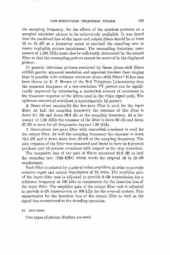
LOW-RESOLUTION TELEVISION SYSTEM 181
the sampling frequency, for the effects of the spurious patterns on a sampled television picture to be subjectively negligible. It was found that the combined loss of the input and output filters should be at least 16 to 19 dB at a frequency equal to one-half the sampling rate to insure negligible picture impairment. The resampling frequency component of 1.536 MHz must also be sufficiently attenuated by the output filter so that the resampling pattern cannot be resolved in the displayed picture.
In general, television pictures restricted by linear phase-shift filters exhibit greater apparent resolution and apparent freedom from ringing than is possible with ordinary minimum phase-shift filters.6 It has also been shown by E. F. Brown of the Bell Telephone Laboratories that the apparent sharpness of a low-resolution TV picture can be significantly improved by introducing a controlled amount of overshoot in the transient response of the filters used in the video signal path. The optimum amount of overshoot is approximately 12 percent.
A linear-phase maximally-fiat low-pass filter is used for the input filter. At half the sampling frequency the response of this filter is down 9.1 dB and down 38.8 dB at the sampling frequency. At a frequency of 1.39 MHz the response of the filter is down 59 dB and down 37 dB or more for all frequencies beyond 1.39 MHz.
A linear-phase low-pass filter with controlled overshoot is used for the output filter. At half the sampling frequency the response is down 10.5 dB and is down more than 60 dB at the sampling frequency. The step response of the filter was measured and found to have an 8 percent preshoot and 10 percent overshoot with respect to the step transition.
The composite loss of the pair of filters measured 19.6 dB at half the sampling rate (768 kHz) which meets the original 16 to 19-dB requirement.
Each filter is isolated by a pair of video amplifiers in order to provide resistive input and output impedances of 75 ohms. The amplifier gain of the input filter unit is adjusted to provide O-dB transmission for a reference frequency at 100 kHz to compensate for the insertion loss of the input filter. The amplifier gain of the output filter unit is adjusted to provide O-dB transmission at 100 kHz for the over-all system. This compensates for the insertion loss of the output filter as well as the signal loss encountered in the decoding operation.
XI. MONITORS
Two types of picture displays are used.

182 THE BELL SYSTEM 'fECHNICAL JOURNAL, JANUARY 1967
11.1 Type I
A Conrac CNA8 television monitor, modified to operate at the line rate of 9.6 kHz, is used as a general purpose monitor. This unit is completely self-contained and may be operated with a composite video signal with means provided for internal sync or separate horizontal and vertical external sync. The picture information is displayed on a five-inch square raster. The amplitude-frequency response of the video amplifier is flat to within ±2 dB to 8 MHz. Provision for switching dc restoration in or out is also provided.
11.2 Type II
To facilitate the subjective testing of various television bandwidth reduction techniques, a variable parameter display system has been constructed which consists of two television monitors designed so that one functions as a master control unit and the other as a slave unit.
Test conditions are initially preset and viewed by the operator at the master monitor. The subject being tested views the pictorial information presented on the slave monitor. A-B control is permitted by the subject for viewing alternately any two given test conditions.
The two displays are capable of operating over a wide range of sweep rates, 3 kHz to 16 kHz for the horizontal rate and 30 Hz to 120 Hz for the vertical rate. Driven sweeps are employed, separate horizontal and vertical drive pulses being required.
The amplitude-frequency response of the video amplifiers is down 3 dB at 13.5 MHz. Using a sine wave response measuring technique, it has been determined that the frequency response of the kinescope is down 6 dB at 5 MHz at a highlight luminance of 10 footlamberts.
'¥henever this display system is used in conjunction with the experimental television facility described herein, the horizontal line rate is restricted to 9.6 kHz and the vertical rate to 60 Hz. The video signal displayed on the monitors is band-limited to less than 768 kHz by the video filters.
XII. SYNCHRONIZING GENERATOR
All timing, gating, and blanking signals required are generated by the synchronizing generator as shown in Fig. 11. The required signal characteristics and timing sequences are described.
The precise sampling rate is determined by the storage capacity and delay period required for the frame memory, and is equal to the storage capacity divided by the delay period. The delay period is con-

8-STAGE BINARY
COUNTER
I
IN
OUT
INCOMING CLOCK PULSES } (SAMPLE RATE) 1 MASTER~' VARIOUS CLOCK PHASES RESAMPLING
.----------------i CLOCK ' FOR TIMING EQUIPMENT .1 SS 1 GATE SIGNAL
L~1.5~3~6~M~~H~Z------------------------~ 400~S I~------------_
HORIZONTAL COUNT-DOWN ( -:-160)
9.6 kHz LINE RATE I
I
X} FF-HB
~s B --C' --D' FF E
C
A}~ FF-HS
B -- S
~, --1-- A FF
C
l TD smS J
SS 6~S
1 DURATION
1
I A
0
1
0
I DURATION
COMPOSITE BLANKING SIGNAL
HORIZONTAL SYNC SIGNAL
KEYING SIGNAL
z' Z
y' y
I ~--I----l nl I ~~i __ ~
~u~ A ~I S} __ ~S 8-STAGE BINARY
COUNTER
X'
W'
V'
U'
T'
S'
X
W
V
U
T
S
IN
FF-VB
GV
' -- - A FF
I ~ ~ ~-+---~C -----,0
~ FF-VS L~LER LOGIC ______ -.J S}-~S
VERTICAL COUNT-DOWN '0' -- f-- A (-;-160) FF
1 ~-;_-----l
II---
COMPOSITE SYNC SIGNAL A
VERTICAL SYNC SIGNAL RST (
t OUT o-+------------------------------4-+--------------~C o
I GRATING I
I INCOMING CLOCK PULSES}
APPLIED TO SCALER LOGIC
CLOCK PULSES APPLIED} TO COUNTER'S INPUT
CLOCK PULSES· APPLIED} TO COUNTER'S RESET
COUNTER'S OUTPUT} CLOCK PULSES
I I I I I I I I I I I I I I I I I I I I I I I I I I I I I I I I I 1 I I I I
_---+1---- _____ ~I ______ _ k------- 160 CLOCK PERIODS -------~
L-___ --'
PATTERN ~----------------~, GENERATOR
1 OUTPUT FF -HB t<-----20TS ---~ HORIZONTAL}
II r------ ~~}t~~~.ttG 9.6 kHz 1 OUTPUT FF-HS -~ ~ITS HORIZONTAL ~~---------~I I SYNC
1 OUTPUT FF-VB
I r----- INTERVAL
~---16 TS---~ }
~-------12 TC------~ ~E~~I~~~ 60 Hz
_ _______ I_T...::L=--_~..!._-i~-- 6 TL---~ VERTICAL
I OUTPUT FF - VS I I SYNC
NOTE: TS - SAMPLE PERIOD
TL - LINE PERIOD
Fig. 11- Synchronizing generator.
LOW - RESOLUTION TELEVISION SYSTEM 183
stant and is equivalent to one TV frame period 0/60 second). The required storage capacity is determined by the picture format and at the present time is 25,600 samples. This results in a I.536-lVIHz sampling rate. A temperature-controlled crystal oscillator is used to establish the sampling rate.
Digital count-down circuits are used to generate the synchronizing and blanking signals required for the operation of the camera chain and monitors. Separate horizontal sync and vertical sync signals are derived and are combined to generate a composite sync signal. A separate composite blanking signal is also established for system blanking while the composite sync signal serves to blank the camera.
The horizontal line rate of 9.6 kHz is derived by counting down from the sampling rate by a factor of 160. Since this factor is not an integer power of two, pulse steering techniques are used to alter the counting sequence of the counter to give the desired factor. The operations thus performed result in 160 samples per line, of which 20 samples are used to define the horizontal blanking interval, with 16 of the 20 samples being used to specify the horizontal sync period. The leading edge of the horizontal blanking interval precedes the horizontal sync period by one sample interval.
An additional count-down by a factor of 160 from the 9.6-kHz line rate is performed to generate the frame rate of 60 frames per second. Out of the total of 160 lines per frame thus established, 12 lines are used to define the vertical blanking interval with 6 of the 12 lines being used to specify the vertical sync period. The leading edge of the vertical blanking interval precedes the vertical sync period by one line interval. The composite blanking and composite sync signals are derived by using the AND operation to combine the horizontal and vertical blanking signals and the horizontal and vertical sync signals as shown in Fig. II.
The results of the above operations limit the active region of the picture format to 140 samples per line and 148 lines per frame, all lines being scanned in sequential order each frame period.
Timing of the AID converter, code translator, frame memory, and D I A converter is adjusted with respect to the 20-nanosecond sampling time of the AID converter's sample-and-hold circuit which is used as reference. Each time that the sample-and-hold circuit is clocked at the sampling rate, sufficient time must be alloted for the AID converter's coder modules to settle to a unique code before digital output information of the coder is clocked, in parallel, into the input flip-flop store of the code translator. Maximum time is allowed by storing in-
184 THE BELL SYSTEM TECHNICAL JOURNAL, JANUARY 1967
formation in the code translator just prior to clocking the following sample-and-hold operation.
The Gray-to-natural binary code conversion operation by the code translator is also allotted maximum time to settle to the binary code value by clocking results of the code conversion, in parallel form, into the output flip-flop store of the code translator just prior to inserting new information into the input flip-flop store. The digital output information of the code translator expresses encoded video information in the conventional binary code in parallel form.
Output information of the code translator is conveyed to both the input of the frame memory and the D/ A converter by high-speed gates which are controlled by the MCFF. Change of state of the MCFF is timed to occur during the transition time of the output flip-flop store of the code translator so as to maximize the interval of time in which each code word is presented to the frame memory.
In order to allow for any limited drift in frequency of the master oscillator and for slight changes in the delay period of the frame memory's delay lines, due to temperature effects, clocking of information into delay lines of the frame memory is adjusted under stable operating conditions to occur midway between transition periods of digital information which is presented to it.
Pulse output information of the delay lines which occurs in phase with clocking of the input information is inserted into the first stage of a four-stage shift register which is considered a constituent part of the frame delay period. The clock signal applied to the shift terminal of the shift register is timed to perform the shift operation one-half of a sample period later; therefore, timing of the frame memory's digital output information, taken from the last stage of the shift register, corresponds to the timing of the digital output of the code translator. Thus, the phase relationship of information conveyed to the input of the delay lines by high-speed gates is independent of the mode of operation of the frame memory.
The same relationship of clocking information into the flip-flop store of the D / A converter with respect to timing of the digital data applied, is the same as that maintained for the input of the delay lines. , Two additional gating signals, shown in Fig. 11, are generated by
the sync generator. A 6-microsecond keying signal is required for operation of the synchronized clamping circuit. The keying signal is synchronous with the line rate and is timed to occur after the leading edge of the horizontal sync signal. The signal delay caused by the
LOW-RESOLUTION TELEVISION SYSTEM 185
system's input filter must be compensated for. The remaining gating signal required for the system's operation is used by the resampler circuit employed in the D / A converter. A 400-nanosecond gating signal is applied to the resampler and timed to occur during that portion of the decoder output waveform which is free of transient disturbances.
A grating pattern for use in determining geometric linearity of both camera and monitor sweeps is also provided by the synchronizing generator.
XIII. SYSTEM APPLICATIONS
The application of this equipment to perform various system functions will be discussed in terms of the logic used to control the flow of information conveyed to the frame memory since this information is also simultaneously decoded and displayed on the system's TV monitor.
The information corresponding to a given picture point is available for processing only once each frame period, since the information is stored in delay lines. The information pertaining to all picture points which comprise any given frame of video information stored in the delay lines or any subset of picture points, thereof, can thus be updated with new information at a rate corresponding to the frame rate or a submultiple of the frame rate. The display rate of information conveyed to the monitor is kept constant at 60 frames per second to avoid the flicker problem, but the pattern and rate of displaying new information can be governed by direct control of the MCFF.
Frame repeating and selective replenishment systems have been demonstrated using this equipment. Their evaluation has been discussed in a separate paper.1 The basic principles employed to implement these systems will now be discussed.
XIV. FRAME REPEATING SYSTEM
The basic frame repeating principle is illustrated by Fig. 12. The vidicon camera is sequentially scanned each frame period, resulting in an integration time of 1/60 second, but only every nth frame is simultaneously stored in the frame memory and displayed on the monitor. Every new frame of encoded information stored in the frame memory is repeated (n - 1) times and is displayed on the monitor each time. Thus, every nth frame of video information scanned from the camera is displayed n times on the monitor. The display rate is
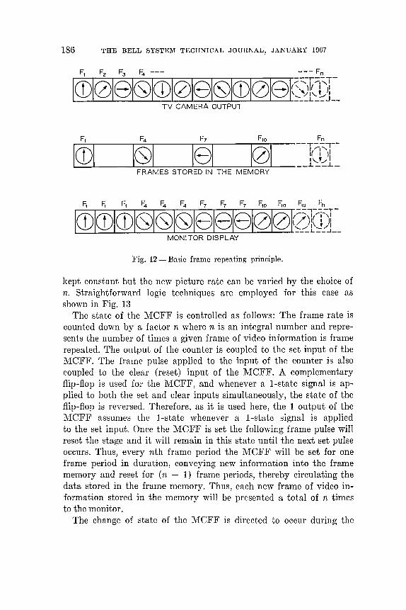
186 'fHE BELL SYSTEM TECHNICAL JOURNAL, JANUARY 1967
Fl F2 F3 F4 --- --- Fn
ICDI0181(S)ICDI0181CS)ICDI0181(~t~~r TV CAMERA OUTPUT
ICDI FRAMES STORED IN THE MEMORY
Fn ,---,--I """-1" I I( I \1 1,-',./ 1. __ .1._
~ ~ Fl F4 F.t F4 F7 F7 F7 FlO Fio Fio Fn
ICDICDICDI(S)I(S)I(S)18181810Q)1(Z21Q~t MONITOR DISPLAY
Fig. 12 - Basic frame repeating principle.
kept constant but the new picture rate can be varied by the choice of n. Straightforward logic techniques are employed for this case as shown in Fig. 13
The state of the MCFF is controlled as follows: The frame rate is counted down by a factor n where n is an integral number and represents the number of times a given frame of video information is frame repeated. The output of the counter is coupled to the set input of the MCFF. The frame pulse applied to the input of the counter is also coupled to the clear (reset) input of the MCFF. A complementary flip-flop is used for the MCFF, and whenever a I-state signal is applied to both the set and clear inputs simultaneously, the state of the flip-flop is reversed. Therefore, as it is used here, the 1 output of the MCFF assumes the I-state whenever a I-state signal is applied to the set input. Once the MCFF is set the following frame pulse will reset the stage and it will remain in this state until the next set pulse occurs. Thus, every nth frame period the MCFF will be set for one frame period in duration, conveying new information into the frame memory and reset for (n - 1) frame periods, thereby circulating the data stored in the frame memory. Thus, each new frame of video information stored in the memory will be presented a total of n times to the monitor.
The change of state of the MCFF is directed to occur during the

LOW-RESOLU'l'ION TELEVISION SYSTEl\1 187
vertical retrace period so that an integral frame of video information is stored in the frame memory. In this manner, a break in continuity of the video information will not occur in the active region of the picture.
With a vidicon integration time of 1/60 second, frame repeating was observed using rates of 30, 20, 15, 12, 10, 8.6, 7.5, 6.7, and 6 new pictures/second. A single frame of processed video information can be stored indefinitely in the frame memory by removing the set pulse applied to the MCFF after the information has been stored in the memory. This feature allows a photograph to be taken of a single frame of video information displayed on the monitor each frame period. Because the stored picture is available for long periods of time, any particular area of interest in the picture may be examined on the monitor under different contrast and brightness conditions. An oscilloscope may be used for observing any particular waveform characteristic in detail.
In the frame repeating experiment the vidicon camera is sequentially scanned every frame period with every nth frame being stored in the frame memory in digital form. By scanning the vidicon every frame period, each picture read out has been integrated on the vidicon photocathode for 1/60 of a second. The integration time of the vidicon may be varied by scanning the vidicon every nth frame period instead of every frame period. Each picture read from the camera is stored in the memory and repeated n times on the monitor. In this manner, the visual signal is integrated on the vidicon photocathode for n/60 of a second for each picture read out. This type of camera operation is defined as the integrate mode of operation.
r-------MCFF
FRAME RATE --...--r t----+-~s
FF ~--------+~C 0
VIDICON BLANKING SIGNAL FOR INTEGRATE MODE OF OPERATION
Fig. 13 - Control logic for frame repeating system.

188 THE BELL SYSTEM TECHNICAL JOURNAL, JANUARY 1967
An effort has been made to control the integration time of the vidicon for a frame repeat system where each frame is repeated four times. A special gating signal is provided for the vidicon in the integrate mode of operation. For this mode of operation, the vidicon beam current is gated on for one frame period every four frames. During the frame read-out of the vidicon, the frame memory is also gated to store new information into the memory as it is being read from the camera.
The gating signal for the vidicon is derived from the 1 output of the MCFF. A composite sync signal is combined with the MCFF signal by the AND circuit, as shown in Fig. 13 and the resultant signal is directly coupled to the vidicon cathode. Normal blanking signals are provided in this manner during the frame read-out.
xv. REPLENISHMENT SYSTEMS
In a replenishment system, only O/n)th of the total amount of information stored in the frame memory is replaced with new information each frame period, a total of n frame periods being required to replenish all of the information stored in the memory. In each succeeding group of n frame periods, the same pattern of replenishment is repeated.
Six different replenishment patterns have been demonstrated. In five cases, total replenishment of the information stored in the frame memory is accomplished over four frame periods 0/15 second), onequarter of the information being replenished each frame period according to a given pattern. For the remaining case, total replenishment is accomplished every two frame periods 0/30 second), one-half of the total information stored in the memory being replenished with new information each frame period.
The various replenishment patterns are shown in Fig. 14. The numbers represent the frame period relative to the total replenishment period during which a particular picture element is replenished in the picture format. The basic principles employed to implement these various patterns are described.
Logic is programmed to control the MCFF in such a manner that the data stored in the frame memory is replenished with new information according to the desired pattern. The MCFF is clocked at specified multiples of the sampling, line, and frame rates for replenishment patterns 1 through 5. The remaining pseudo-random pattern is dependent only on the order in which a sequence of pseudo-random

LOW-RESOLUTION TELEVISION SYSTEM
4 3 2 1 4 3 4 3 2 I 4 4 3 2 1 4 3 2 4 3 4
(a) PATTERN t
1 2 t 2 t 2 •• 4 3 4 3 4 1 2 1 2
4 3 4 1 2 4 ••
(d) PATTERN 4
432143 3 2 1 4 3 2 1 4 3 t 4 3 4 3 3
(b) PATTERN 2
t 2 1 2 1 2 34343 •• t 2 t 2 3 4 3 t 2 3
(e) PATTERN 5
t 2 t 212 2 1 2 1 2
t 2 1 2 2 1 2 1 2 2
(c) PATTERN 3
PSEUDO RANDOM
(f) PATTERN 6
Fig. 14 - Various replenishment patterns implemented.
189
digits is generated at the sampling rate. This pattern is inherently locked to the frame rate.
The control logic requires clock pulses which occur at the sample, line, and frame rate. The clock pulses which occur at the line and frame rate are shifted in phase so as not to coincide with each other or with the clock pulses occurring at the sample rate. Pulse steering techniques are used in the control logic to direct the incoming pulses occurring at the sample rate to the set or clear inputs of the MCFF, depending on whether the write or repeat mode of operation for the memory is to be established. This allows a change of state of the MCFF to be clocked to the correct phase of the master clock independent of the line and frame rates which have been shifted in phase.
15.1 Pattern 1
The first replenishment pattern is shown in Fig. 14(a). For this pattern, the picture elements replenished each frame period lie in vertical lines spaced every fourth picture element. In each succeeding frame period, the replenishment pattern for a single frame is shifted horizontally one picture element in the picture format. Thus, in four frame periods, all information stored in the frame memory is replenished once. The pattern of replenishment then repeats itself. Logically, this may be accomplished as shown in Fig. 15.
The input sample rate is scaled down by a factor of four by using

190 THE BELL SYSTEM TECHNICAL JOURNAL, JANUARY 1967
INPUT {FRAME RATE CLOCK
SIGNALS SAMPLE RATE I I I
o
I FRAME MEMORY L ________ _
Fig. 15 - Control logic for replenishment pattern 1.
a 2-stage counter and a two-input AND to recognize the all l's state of the counter. Each time that the counter is advanced through the all l's state, the output of the AND assumes a I-state. This condition causes the pulse steering logic to direct the next sample pulse to the set input of the MCFF. When this occurs, the write mode of operation is established for the frame memory and the counter is advanced to the all O's state. The output of the AND which recognizes the state of the counter now assumes a O-state. This condition causes the, pulse steering logic to direct the sample pulses to the clear input of the MCFF, which establishes the repeat mode of operation for the frame memory. In this manner, the MCFF is set for only one sample interval corresponding to every fourth sample in the frame. Each frame period, the same corresponding picture elements of each line is replenished with new information, since the number of picture elements per line (160) is a multiple of four. Hence, this process establishes the vertical pattern of replenishment. At the end of each frame period, a pulse corresponding to the frame rate is used to advance the state of the counter one count. This is accomplished by the OR operation which is used to couple both the sample pulses and frame pulses to the input of the counter. This effectively shifts the single frame replenishment pattern horizontally one sample period each frame period. After four frame periods, the four frame replenishment patterns will be repeated.
15.2 Pattern 2
The second replenishment pattern is shown in Fig. 14 (b). In this case, the picture elements replenished each frame period lie on diagonal lines spaced every fourth sample. Each succeeding frame period, the replenishment pattern for a single frame is shifted horizontally one picture element with respect to the previous frame. In four frame periods all information stored in the frame memory will be replenished

LOW-RESOLUTION TELEVISION SYSTEM 191
once. The pattern of replenishment will then repeat itself. Logically, this may be accomplished as shown in Fig. 16.
The logic required to generate this pattern of replenishment is the same as in the preceding case with one exception: means must be provided to shift the pattern horizontally one picture element each line period. This is accomplished by advancing the state of the counter one count at the end of each line period. Clock pulses corresponding to the line rate are coupled to the input of the counter through the OR operation which precedes the counter.
During each frame period the replenishment pattern repeats itself every four lines. Since this factor is a submultiple of the number of lines in a frame (160 lines/frame), the same corresponding picture elements would be replenished in every frame unless an additional horizontal shift in the replenishment pattern was employed at the end of each frame period. This is accomplished by advancing the state of the counter one count at the end of each frame period as in the preceding case. After four frame periods, all information stored in the frame memory will be replenished only once and the replenishment pattern will then be repeated.
15.3 Pattern 3
The third replenishment pattern is shown in Fig. 14 (c). This pa ttern is equivalent to pattern 2 except the rate of replenishment is increased by a factor of two, thus requiring only two frame periods rather than four to replenish all information stored in the frame memory before the pattern repeats itself. The logic required to generate this pattern of replenishment is the same as for pattern 2 with one exception: a divide-by-two counter is used rather than a divideby-four counter. All other logical functions and operations remain the same.
INPUT {FRAME RATE CLOCK LINE RATE
SIGNALS SAMPLE RATE
PULSE STEERING
OGIC ~----------
~ MCFF
FRAME MEMORY L ________ _
Fig. 16 - Control logic for replenishment pattern 2.
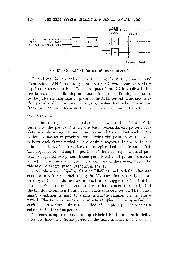
192 THE BELL SYSTEM TECHNICAL JOURNAL, JANUARY 1967
INPUT { FRAME RATE CLOCK LINE RATE
SIGNALS SAMPLE RATE
PULSE STEERING
LOGIC
~
,....-----------: MCFF I
FF
C 0
FRAME MEMORY L __________ _
Fig. 17 - Control logic for replenishment pattern 3.
This change is accomplished by replacing the 2-stage counter and its associated AND, used to generate pattern 2, with a complementary flip-flop as shown in Fig. 17. The output of the OR is applied to the toggle input of the flip-flop and the output of the flip-flop is applied to the pulse steering logic in place of the AND output. This modification permits all picture elements to be replenished only once in two frame periods rather than the four frame periods required by pattern 2.
15.4 Pattern 4 The fourth replenishment pattern is shown in Fig. 14 (d). vVith
respect to the picture format, the basic replenishment pattern consists of replenishing alternate samples on alternate lines each frame period. A means is provided for shifting the position of the basic pattern each frame period in the desired sequence to insure that a different subset of picture elements is replenished each frame period. The sequence of shifting the position of the basic replenishment pattern is repeated every four frame periods after all picture elements stored in the frame memory have been replenished once. Logically, this may be accomplished as shown in Fig. 18.
A complementary flip-flop (labeled FF-S) is used to define alternate samples in a frame period. Using the OR operation, clock signals occurring at the sample rate are applied to the toggle (T) input of the flip-flop. 'Vhen operating the flip-flop in this manner, the 1 output of the flip-flop assumes a I-state every other sample interval. The 1-state signal condition is used to define alternate samples in the frame period. The same sequence of alternate samples will be specified for each line in a frame since the period of sample replenishment is a submultiple of the line period.
A second complementary flip-flop (labeled FF-L) is used to define alternate lines in a frame period in the same manner as above. The

INPUT
LINE RATE ------------------1 ,----------------1
: I~ I I I
FF-L
CLOCK -I FRAME RATE I. SIGNALS
INPUT CLOCK
SIGNALS
I I
: ILJ I I L _______________ J
SAMPLE RATE -_---------------4~-
Fig. 18 - Control logic for replenishment pattern 4.
FF-L LINE RATE
FRAME RATE --~~-
SAMPLE RATE --+-------------~~
Fig. 19 - Control logic for replenishment pattern 5.
,-------------I MCFF I I I
I I I I I FRAME MEMORY L ____________ _
r-----------
: MCFF I I
liS
FF
i---i--.jl I C 0 I I I
I FRAME MEMORY L ___________ _
t" o ~ I ~ trJ U1 o t" ~ 1-3 ...... o Z 1-3 trJ t" trJ -< ...... U1 ...... o Z U1 ~ U1 1-3 trJ ~
I-" co C..:I

194 THE BELL SYSTEM TECHNICAL JOURNAL, JANUARY 1967
OR operation is used to apply clock pulses, occurring at the line rate, to the toggle input. The 1 output of the flip-flop assumes a I-state every other line period which is used to define alternate lines in the frame period. Since the picture format is comprised of an even number of lines, the line replenishment pattern will normally repeat itself each frame period unless a shift operation is employed.
In order to replenish a different subset of picture elements each frame over a four frame period, in the required sequence, the basic replenishment pattern for a single frame is shifted one sample interval at the end of each frame period, alternating between a horizontal and vertical shift operation with respect to the picture format. Only one shift operation is performed each frame period. The horizontal shifting of the replenishment pattern's position is accomplished by reversing the state of FF-S at half the frame rate. The vertical shift operation is achieved by reversing the state of FF-L at half the frame rate but timed to occur in alternate frame periods in which the horizontal shift operation is not performed.
In each case, to reverse the state of the flip-flop, the OR operation is used to convey clock pulses, occurring at half the frame rate, to the toggle input of the flip-flop.
Pulse steering techniques are used to derive the clock pulses required for the shifting operations. Alternate clock pulses derived from the frame rate are steered to the respective inputs of the OR's in the correct sequence.
By performing the AND operation on the I-output of both flipflop's (FF-S and FF-L) , alternate samples on alternate lines each frame period are specified in the required sequence when the output of the AND assumes a I-state. This condition occurs only when both inputs assume a I-state. The output signal of the AND is applied to the pulse steering logic which controls the MCFF. The write mode of operation will be established for the frame memory each time the output of the AND assumes a I-state; otherwise the repeat mode of operation is established.
15.5 Pattern 5
The fifth replenishment pattern is shown in Fig. 14 (e). The basic single-frame replenishment pattern for this system is identical with that of pattern 4. The sequence of shifting the basic pattern over a four-frame period differs from pattern 4 in one respect. The horizontal shifting of the replenishment pattern's position is performed every frame period rather than every other frame period. All other logical

LOW-RESOLUTION TELEVISION SYSTEM 195
operations remain the same as shown in Fig. 19. The OR operation preceding FF-S is used to convey clock pulses, occurring at the frame rate, to the toggle input of FF -So The state of FF -S is thus reversed every frame period, as required, to generate the desired replenishment pattern over a four-frame period.
15.6 Pattern 6 The six replenishment pattern is not regular over blocks of four
picture elements as in the other 4: 1 replenishment systems described above, but is pseudo-random. The same average bit rate is maintained by replenishing one-quarter of the total amount of informa-:tion stored in the memory each frame period. In four frame periods all information stored in the frame memory is replenished only once. The pattern of replenishment then repeats itself. Logically, this may be accomplished as shown in Fig. 20.
A quasi-random binary digit generator is used to generate a sequence of random binary digits at the system's sampling rate. The sequence is periodic with 210 digits in each period. During each period of this sequence of random digits, everyone of the 210 possible strings of ten digits appears exactly once as a block of ten consecutive digits. The period of this sequence of digits is chosen to be a multiple of the system's frame period so that the same sequence of digits is generated each frame period.
A logical operation is performed on the output of the random digit generator to remap the sequence over four frame periods. In the process of generating the quasi-random sequence, each time that two consecutive digits in the random sequence corresponds with a specific
FRAME RATE--------------------------------------------------------------------------------~
QUASI-RANDOM I---~ BINARY DIGIT GENERATOR
SAM P L E RATE -------..---------------------------------....... -.l
REFERENCE SEQUENCE GENERATOR
(2-STAGE COUNTER)
r-----------MCFF
FRAME MEMORY L __________ _
Fig. 20 - Control logic for pseudo-random replenishment pattern.

196 THE BELL SYSTEM TECHNICAL JOURNAL, JANUARY 1967
two digit reference sequence new information is inserted into the frame memory; otherwise, the previous information stored in the frame memory is recirculated. During four consecutive frame periods, a different two digit sequence is used as reference each frame period. The order of generating the reference sequence is then repeated.
Only four different two digit reference sequences are possible-DO, 01, 10, and 11. Considering consecutive digits in the random digit sequence, each of these combinations of two digits occurs at random an equal number of times during each period of the random digit sequence. The replenishment pattern thus generated directs replenishment, in a random manner, of one-quarter of the total amount of information stored in the frame memory each frame period. All information stored in the memory is replenished only once during any four consecutive frame periods.
The pseudo-random digit generator consists of control logic and a ten-stage shift register advanced at the system's sampling rate. The output of all stages of the register is fed to the control logic as shown in Fig. 21. The output of the exclusive OR and its prime is coupled to the input of the first stage of the register. The control logic normally functions as an exclusive OR operation with the output of the tenth and seventh stages of the shift register coupled to the input except when the string of 000' .. 001 digits appears. For this condition, the output of the seventh stage, coupled to the input of the exclusive OR by the OR operation, is temporarily over-ridden by the output of the AND which assumes a I-state, permitting the string of 000· . ·00 digits to be generated. For a ten-stage shift register, everyone of 210
possible strings of ten digits appears exactly once, as a block of ten consecutive digits each period of the sequence.
In spite of the fact that the nth digit is completely determined by the digits which precede it, the sequence of digits resembles, in some respects, sequences which are produced when the nth digit is chosen at random with probabilities 112 for 0 and 112 for 1 and independently of other digits.
The remapping operation is performed by comparing the output of the ninth and tenth stages of the shift register with the logical state of a 2-stage binary counter which serves as the reference sequence generator. The binary counter is advanced at the frame rate. When in agreement with each other, a I-state exists at the output of the comparison circuit. This condition permits a sample pulse to be coupled to the set input of the MCFF by the pulse steering logic allowing new information to be inserted into the frame memory. If no agreement
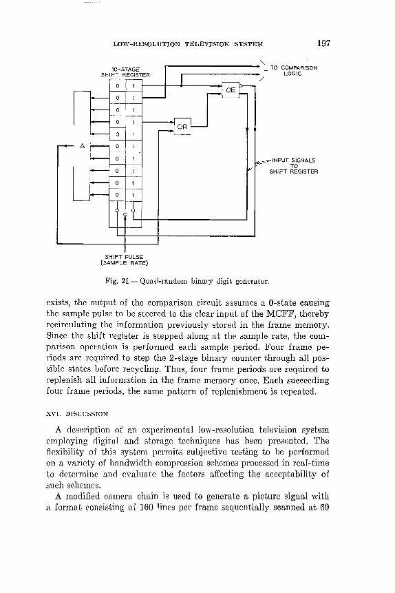
A
LOW-RESOLUTION TELEVISION SYSTEM
10-STAGE SHIFT REGISTER
o
) TO COMPARISON
r--------- LOGIC
_.,-INPUT SIGNALS ,... TO
197
SHIFT REGISTER
SHIFT PULSE (SAMPLE RATE)
Fig. 21 - Quasi-random binary digit generator.
exists, the output of the comparison circuit assumes a O-state causing the sample pulse to be steered to the clear input of the MCFF, thereby recirculating the information previously stored in the frame memory. Since the shift register is stepped along at the sample rate, the comparison operation is performed each sample period. Four frame periods are required to step the 2-stage binary counter through all possible states before recycling. Thus, four frame periods are required to replenish all information in the frame memory once. Each succeeding four frame periods, the same pattern of replenishment is repeated.
XVI. DISCUSSION
A description of an experimental low-resolution television system employing digital and storage techniques has been presented. The flexibility of this system permits subjective testing to be performed on a variety of bandwidth compression schemes processed in real-time to determine and evaluate the factors affecting the acceptability of such schemes.
A modified camera chain is used to generate a picture signal with a format consisting of 160 lines per frame sequentially scanned at 60

198 THE BELL SYSTEM TECHNICAL JOURNAL, JANUARY 1967
frames per second. The picture information is processed in real-time in a digital format. A digital memory is employed with sufficient capacity to store one complete frame of video information encoded as 8-digit PCM-a total of 204.8 kilobits at a rate of 1.536 MHz per second. Means are provided to introduce into the memory whole new pictures or selected picture elements at any interval which is a multiple of the frame rate. The information inserted into the memory is decoded and displayed on a monitor at a rate of 60 pictures per second in order to avoid flicker.
A number of frame repeating and replenishment systems have been demonstrated in real time using this equipment, however the system is in no way limited to those applications which have been discussed.
XVII. ACKNOWLEDGMENTS
The successful construction of this equipment has been the result of the efforts of many people who have contributed in many ways, and it is impossible to properly extend thanks to all of them for their efforts.
All work on this project was done under the direction of "\V. T. Wintringham. Other members of Bell Laboratories who have worked directly on this project and their responsibilities are: R. L. Eilenberger-TV camera equipment, E. M. Cherry-circuit design, J. E. Berrang-testing and alignment of encoder, R. C. Brainard and E. S. Bednar-frame memory, and J. A. ~1:urphy-display system.
Much of the mechanical design work was done by H. T. Webber. I also wish to thank J. O. Edson, F. D. Waldhauer, J. H. Davis, E. F. Kovanic, and R. L. Klenk who assisted me in the duplication of their exploratory model PCM encoder-decoder equipment. The able help of the mechanical and wiring branch shops is also greatly appreciated.
REFERENCES
1. Brainard, R. C., Mounts, F. 'V., and Prasada, B., Low-Resolution TV: Subjective Effects of Frame Repetition and Picture Replenishment, B.S.T.J., 45, this issue, pp. 301-311.
2. Edson, J. O. and Henning, H. H., Broadband Codecs for an Experimental 224 Mb/s PCM Terminal, B.S.T.J., 44, November, 1965, pp. 1887-1940.
3. Waldhauer, F. D., Analog-to-Digital Converter, U. S. Patent 3-187-325, applied for July 2, 1962; issued June 1, 1965.
4. Meitzler, A. H., Ultrasonic Delay Lines for Digital Data Storage, Trans. IRE Prof. Group Ultrasons Eng., VE-9, December, 1962, pp. 1-8.
5. Kovanic, E. F., A High Accuracy Nine-Bit Digital-to-Analog Converter Operating at 12 mc, IEEE Trans. Commun. Electron., March, 1964, pp. 185-191.
6. Fredendall, G. L. and Kennedy, R. C., Linear Phase Shift Video Filters, RCA Review, 11, September, 1950, pp. 418--430.

Low-Resolutioll TV: Subjective Comparison of Interlaced and
N onillterlaced Pictures
By EARL F. BROWN
(Manuscript received September 19, 1966)
A subjective comparison of line-interlaced television pictures and noninterlaced television pictures has shown that the line-interlacing of lowresolution television pictures provides a bandwidth saving of considerably less than 2:1 when the line structure of the picture is visible.
A [line-interlaced television picture was subjectively compared with several noninterlaced television pictures in an effort to determine their subjective equivalency in terms of bandwidth. Several other variables-noise, spot-wobble, line-width to line-pitch ratio, different models, illumination and luminance--were also employed in the experiments. The televised pictures consisted of a head-and-shoulder view of a l1wdel pantomiming a two-way conversation.
The results indicate that the line-interlacing of low-resolution television pictures provides about a 37 percent saving in terms of bandwidth at a relatively low value of high-light luminance of 40 fL (140 cd/m2) and as little as a 6 percent savings at a high-light luminance of 100 fL (340 cd/m,2). When the line-width to line-pitch ratio is set at its preferred value for all pictures, a significant difference is obtained when the highlight luminance is decreased from 60 fL (200 cd/m2) to 40 fL (140 cd/m2). The effects of Gaussian noise, spot-wobble, illumination, and different types of nwdels did not alter the subjective equivalence of line-interlaced and noninterlaced television pictures significantly. The addition of noise to a spot-wobbled picture was found to be more detrimental to the quality of the noninterlaced pictures than to the line-interlaced picture.
1. INTRODUCTION
The lower limit of the picture repetition rate for television pictures is dictated by the critical-fusion frequency (CFF).!,2 The CFF is approximately proportional to the logarithm of the luminance over a wide range. It is also approximately proportional to the logarithm
199

200 THE BELL SYSTEM TECHNICAL JOURNAL, JANUARY 1967
of the size of the flickering area. The CFF is on the order of 60 pictures per second for present day television luminances and picture sizes.
The television engineers of the 1930's experimented with two-fold line-interlaced pictures as a means of saving bandwidth. In two-fold line-interlaced pictures, alternate lines are scanned during successive vertical deflection cycles. Engstrom3 found that the vertical deflection cycle should be greater than 50 Hz and should be a multiple of the power line frequency. In 1941 the National Television System Committee (NTSC)4 adopted a vertical deflection frequency of 60 Hz for two-fold line-interlaced commercial broadcast systems. Two-fold line interlace has since been adopted by virtually all television systems, regardless of the application.
One-half of the lines in a line-interlaced television picture are scanned during alternate half-cycles of the frame rate which is 30 Hz. The result is essentially two light pulses for each frame period, i.e., an apparent rate of 60 light pulses per second. Thus, large-area flicker is negligible if present at all.
When all of the lines except one of a line-interlaced television raster are masked that line appears stationary and nonflickering. When all of the lines except two of a line-interlaced television raster are masked the two lines appear to jump back and forth as if in motion. When the masking is removed the whole raster appears to shimmer. When a picture is reproduced on the raster the shimmering is confined to small isolated areas of roughly equal brightness. The shimmering effect in these areas is most pronounced at brightness boundaries. This phenomena of apparent-motion is due to the out of phase relationship between adjacent lines of the raster and appears to be affected by the same laws as flicker. These apparent-motion defects are called interline flicker by the television industry.
Engstrom3 found that interline flicker was visible at the same distance at which the line structure becomes visible. His conclusion was that the observer must be seated at a distance equal to or greater than that distance at which the line structure becomes resolvable.
Line crawling is another subjective defect associated with line-interlaced pictures. This stroboscopic defect takes the form of an apparent crawling of the lines either up or down depending on which direction the eye tends to track. Line crawling is related to the perceptibility of interline flicker and becomes increasingly perceptible with increasing picture brightness and angle subtended by the eye of adjacent line centers.
A third defect inherent to line interlaced pictures is SUbjective line-

LINE-INTERLACED AND NONINTERLACED TV PICTURES 201
pairing. Subjective line-pairing produces the same subjective impression as physical line-pairing, i.e., when adjacent lines are physically superimposed on each other by the deflection circuitry. Subjective line-pairing occurs when either the televised image or the observer's visual center of attention moves in a direction other than parallel to the scanning lines. This defect also occurs when the observer blinks his eyes or effectively strobes the picture. Subjective line-pairing is most evident when the motion is parallel to the vertical scan direction and at a rate equal to the field rate.
The question arises, "Do the degrading effects associated with interline flicker nullify the advantage of being able to present twice as much information in each picture when the line sturcture is visible"? Accordingly three subjective experiments were conducted in an attempt to answer this question.
The experiments were conducted on low-resolution television pictures. In the first experiment, a 225-line interlaced picture was compared with four noninterlaced pictures ranging from a 225-line picture to a I35-line picture in steps with ratios of V2. Additional variables at two values each-noise, illumination, spot-wobble, and picture materialwere also introduced. Two types of observers, skilled and nonskilled, were used.
The second experiment was performed in order to determine the effects of a change in luminance on the subjective relationship between the interlaced picture and the noninterlaced pictures. Five noninterlaced pictures were compared with the 225-line interlaced picture starting with a IS9-line picture and decreasing in steps with ratios of 0 to a I35-line picture. The subjective relationship between the noninterlaced pictures was also investigated.
For the third experiment, the preferred line-width to line-pitch ratio was determined in a separate experiment. In this experiment, the linewidth to line-pitch ratio was set at the preferred value for each picture. The 225-line interlaced picture was compared with 5 noninterlaced pictures starting at a 225-line picture and decreasing to a I47-line picture in steps with ratios of 0. Two levels of luminance were introduced as a second variable.
The bandwidth in each of the above cases was adjusted such that the vertical to horizontal resolution ratio was approximately I: 1. 5
A-B testing techniques were used. Each A-B pair consisted of the interlaced picture and one of the noninterlaced pictures except for that portion of the second experiment where the noninterlaced pictures were compared against each other.
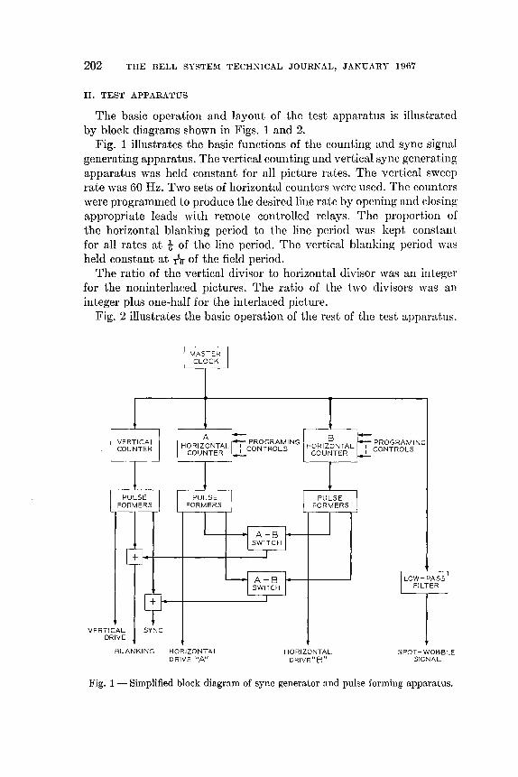
202 THE BELL SYSTEM TECHNICAL JOURNAL, JANUARY 1967
II. TEST APPARATUS
The basic operation and layout of the test apparatus is illustrated by block diagrams shown in Figs. 1 and 2.
Fig. 1 illustrates the basic functions of the counting and sync signal generating apparatus. The vertical counting and vertical sync generating apparatus was held constant for all picture rates. The vertical sweep rate was 60 Hz. Two sets of horizontal counters were used. The counters were programmed to produce the desired line rate by opening and closing appropriate leads with remote controlled relays. The proportion of the horizontal blanking period to the line period was kept constant for all rates at 1 of the line period. The vertical blanking period was held constant at lo of the field period.
The ratio of the vertical divisor to horizontal divisor was an integer for the noninterlaced pictures. The ratio of the two divisors was an integer plus one-half for the interlaced picture.
Fig. 2 illustrates the basic operation of the rest of the test apparatus.
VERTICAL SYNC DRIVE
BLANKING HORIZONTAL DRIVE "A"
HORIZONTAL DRIVE"B"
PROGRAMING CONTROLS
SPOT-WOBBLE SIGNAL
Fig. 1- Simplified block diagram of sync generator and pulse forming apparatus.
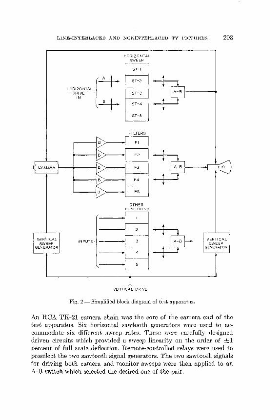
LINE-INTERLACED AND NONINTERLACED TV PICTURES 203
HORIZONTAL SWEEP
ST-f
HORIZONTAL {-4- ST-2 t t
$ DRIVE ST-3
IN -y--ST-4 t
• ST-5
FI LTERS
~ /
Ff
~ F2 t
~ • $ CAMERA 1 F3 L- CRT V ~ F4 t ~ t
F5 V OTHER
FUNCTIONS
/ I
2
~ VERTICAL INPUTS 3 VERTICAL
SWEEP SWEEP GENERATOR GENERATOR
4
5
L VERTICAL DRIVE
Fig. 2 - Simplified block diagram of test apparatus.
An RCA TK-21 camera chain was the core of the camera end of the test apparatus. Six horizontal sawtooth generators were used to accommodate six different sweep rates. These were carefully designed driven circuits which provided a sweep linearity on the order of ±1 percent of full scale deflection. Remote-controlled relays were used to preselect the two sawtooth signal generators. The two sawtooth signals for driving both camera and monitor sweeps were then applied to an A-B switch which selected the desired one of the pair.

204 THE BELL SYSTEM TECHNICAL JOURNAL, JANUARY 1967
Great care was taken in the design and construction of the sweep and associated circuits to insure that line spacing on the pick-up tube and display tube was correct in all cases.
Six low-pass filters were provided for processing the picture signals of the six different sweep rates. The filters were isolated from each other with buffer amplifiers. The appropriate filter for each sweep rate was selected by remote-controlled relays. Each filter had an ad-
fd = fco/1.S7 , R\
L = 0.9S2fd
Ll = 0.1195 L'
L 2 =0.1600L'
L3 =0.1303L'
L4 = 0.0357 L'
Ls= 0.05568 L'
(a)
(b)
R2 = 0.3257 Rt
C'= 1 0.952 Rlfd
C\ = 0.04709C'
C 2 = 0.1581 C'
C 3 = 0.03189C'
C 4 = 0.4856 C'
C s = 1.438 C'
C6 = 0.1292 C'
Fig. 3 - Low-pass filter: (a) circuit diagram, (b) design data.
justable attenuator which permitted balancing for the difference 1Il
insertion losses. Each filter had a near Gaussian roll-off, had linear phase, and ex
hibited a preshoot and overshoot in its step response. * The preshoot and overshoot were each 12 percent of the step-signal amplitude. The cutoff frequency for the filters was arbitrarily selected as the - 20-dB point on their response curve. Fig. 3 shows the circuit configuration and design data for the filter. t Fig. 4 shows the typical amplitude
* An earlier experiment (unpublished) indicated subjectively that this type of filter gave the preferred picture rendition.
t Designed by G. Szentermai of Bell Telephone Laboratories, Incorporated.

LINE-INTERLACED AND NONINTERLACED TV PICTURES 205
o
co 15 -0
~
W I/) 30 Z o n. I/) w a:
45
60~ __ ~ __ ~ __ ~ __ ~ __ ~ ____ ~ __ ~ __ ~ __ ~ __ ~ o 0.5 1.0 1.5 2.0 2.5
FREQUENCY, feo
Fig. 4 - Relative amplitude versus frequency response characteristics of low-pass filter.
versus frequency characteristics of these filters and Fig. 5 the typical step response. After adjustment of the effective vertical resolution by applying a Kell factor of 0.7 and allowing for the difference between vertical and horizontal blanking periods, the cutoff frequency ( - 20 dB) of the low-pass filters was selected to provide approximately equal horizontal and vertical resolution. 5
Three other functions were selected and switched in much the same manner. These were spot-wobble, line-width to line-pitch ratio and camera raster centering. Each of these functions had its individual balancing controls.
The spot-wobble signal was a 7.1442-MHz sine wave locked to the master clock. The spot-wobble signal was applied to the picture tube through an auxiliary yoke. The line broadening by the spot-wobble signal was subjectively optimized for and by the experimenter for each test picture. In general, the line broadening was adjusted such that a minute gap appeared between adjacent lines.
The line-width to line-pitch ratio without line broadening was about 0.33 for the 225-line interlaced picture. The line-width was measured at the half-luminance level of the line profile. The line-width to linepitch ratio for the other pictures may be determined by
LW/LP = 0.33(;25) , (1)
,yhere Lp is the number of lines in the picture. Fig. 6 shows line profiles of the scanning lines perpendicular to the direction of scan for an interlaced and noninterlaced picture.

206 THE BELL SYSTEM TECHNICAL JOURNAL, JANUARY 1967
(a)
( b)
Fig. 5-Step response of low-pass filter: (a) input to filter, (b) output of filter illustrating 12 percent preshoot and overshoot about step.
Fig. 7 shows line profiles of spot-wobbled scanning lines perpendicular to the direction of scan for an interlaced and noninterlaced picture. (The asymmetry of the spot profile is due to a slight misalignment in the position of the auxiliary yoke.) At the juncture of adjacent lines the luminance level of each line was about 25 percent of its maximum luminance. Since the period between adjacent lines for the interlaced picture is 1/60 second the observer will see the sum of the contributions of each line at their juncture.2 Therefore, in the spotwobbled line-interlaced pictures the brightness at the juncture of adjacent lines was about
(2)
where B i = brightness at the junction of adjacent lines, B 1 = maximum brightness of line one, and B2 is the maximum brightness of line two.
The Talbot-Plateau Law2 says that an observer watching flashing lights above the CFF will sense an apparently constant mean value of the luminance of the lights over the period of the flashes. Equation (2) is a special case of the Talbot-Plateau Law. The law must be expressed

LINE-INTERLACED AND NONINTERLACED TV PICTURES 207
in its complete form to cover the spot-wobbled noninterlaced pictures. The Talbot-Plateau Law is
1 1t Lm = - L dt To'
(3)
where Lm is the mean value of the real luminance taken over one period or over any time t comprising an integral number of periods.
With spot-wobbled noninterlaced pictures the period between successive excitations of the phosphor at the juncture of adjacent lines is one line period. Since the phosphor has a finite decay time, -it will still be luminescing at the juncture of adjacent lines when excited the second time. Thus, the luminance generated by the second excitation will add to that remaining from the first excitation. The second excita-
(a)
(b)
Fig. 6-Experiment I-profiles of picture-tube scanning lines. (a) 225-line interlaced picture with line width to line-pitch ratio of 0.33, (b) 189-line noninterlaced picture with line-width to line-pitch ratio of 0.28.
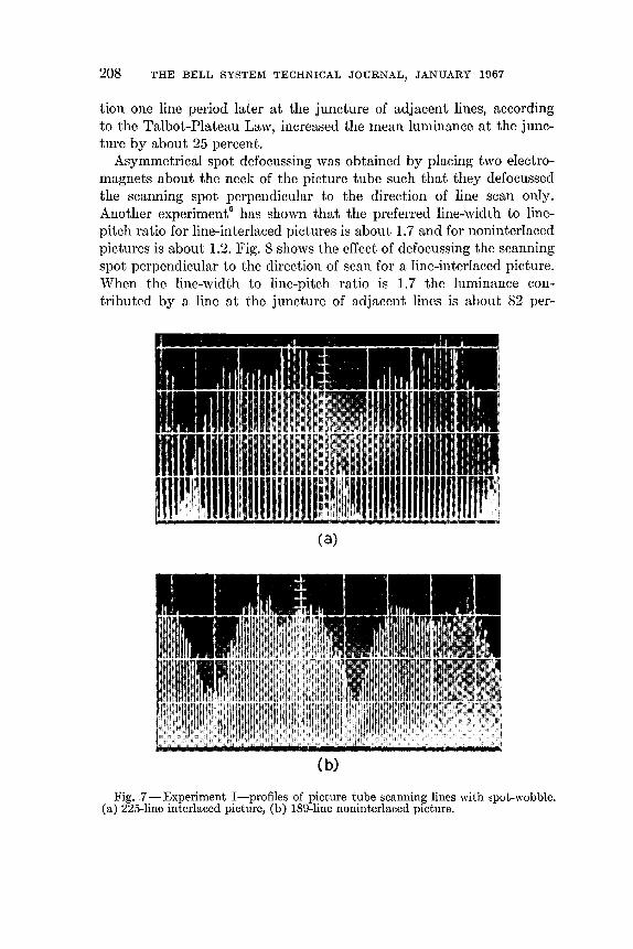
208 THE BELL SYSTEM TECHNICAL JOURNAL, JANUARY 1967
tion one line period later at the juncture of adjacent lines, according to the Talbot-Plateau Law, increased the mean luminance at the juncture by about 25 percent.
Asymmetrical spot defocussing was obtained by placing two electromagnets about the neck of the picture tube such that they defocussed the scanning spot perpendicular to the direction of line scan only. Another experiment6 has shown that the preferred line-width to linepitch ratio for line-interlaced pictures is about 1.7 and for noninterlaced pictures is about 1.2. Fig. 8 shows the effect of defocussing the scanning spot perpendicular to the direction of scan for a line-interlaced picture. When the line-width to line-pitch ratio is 1.7 the luminance contributed by a line at the juncture of adjacent lines is about 82 per-
(a)
(b)
Fig. 7 --Experiment I -profiles of picture tube scanning lines with spot-wobble. (a) 225-line interlaced picture, (b) 189-line noninterlaced picture.
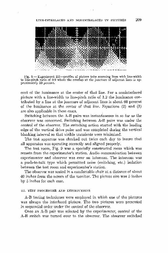
LINE-INTERLACED AND NON INTERLACED TV PICTURES 209
Fig. 8 - Experiment III-profiles of picture tube scanning lines with line-width to line-pitch ratio of 0.9 where the overlap at the juncture of adjacent lines is approximately 50 percent.
cent of the luminance at the center of that line. For a noninterlaced picture with a line-width to line-pitch ratio of 1.2 the luminance contributed by a line at the juncture of adjacent lines is about 60 percent of the luminance at the center of that line. Equations (2) and (3) are also applicable in these cases.
Switching between the A-B pairs was instantaneous in so far as the observer was concerned. Switching between A-B pairs was under the control of the observer. The switching action started with the leading edge of the vertical drive pulse and was completed during the vertical blanking interval so that visible transients were minimized.
The test appartus was checked out twice each day to insure that all apparatus was operating correctly and aligned properly.
The test room, Fig. 9 was a specially constructed room which was remote from the experimenter's station. Audio communication between experimenter and observer was over an intercom. The intercom was a push-to-talk type which permitted noise (switching, etc.) isolation between the test room and experimenter's station.
The observer was seated in a comfortable chair at a distance of about 40 inches from the screen of the monitor. The picture size was 5 inches by 5 inches for each case.
III. TEST PROCEDURE AND INSTRUCTIONS
A-B testing techniques were employed in which one of the pictures was always the interlaced picture. The two pictures were presented in sequential order under the control of the observer.
Once an A-B pair was selected by the experimenter, control of the A-B switch was turned over to the observer. The observer switched
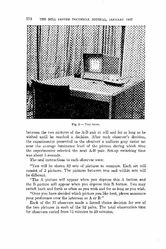
210 THE BELL SYSTEM TECHNICAL JOURNAL, JANUARY 1967
Fig. {) - Test room.
between the two pictures of the A-B pair at will and for as long as he wished until he reached a decision. After each observer's decision, the experimenter presented to the observer a uniform gray raster set near the average lumlnance level of the picture during which time the experimenter selected the next A-B pair. Set-up switching time was about 5 seconds.
The oral instructions to each observer were:
"You will be shown 32 sets of pictures to compare. Each set will consist of 2 pictures. The pictures between sets and within sets will be different.
"The A picture will appear when you depress this A button and the B picture will appear when you depress this B button. You may switch back and forth as often as you wish and for as long as you wish.
"Once you have decided which picture you like best, please announce your preference over the intercom as A or B."
Each of the 25 observers made a forced choice decision for one of the two pictures in each of the 32 pairs. The total observation time for observers varied from 15 minutes to 30 minutes.
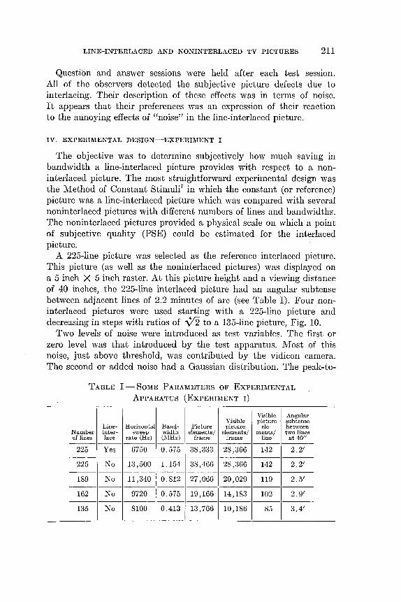
LINE-INTERLACED AND NONINTERLACED TV PICTURES 211
Question and answer sessions were held after each test session. All of the observers detected the subjective picture defects due to interlacing. Their description of these effects was in terms of noise. It appears that their preferences was an expression of their reaction to the annoying effects of "noise" in the line-interlaced picture.
IV. EXPERIMENTAL DESIGN-EXPERIMENT I
The objective was to determine subjectively how much saving in bandwidth a line-interlaced picture provides with respect to a noninterlaced picture. The most straightforward experimental design was the lVIethod of Constant Stimulr in which the constant (or reference) picture was a line-interlaced picture which was compared with several noninterlaced pictures with different numbers of lines and bandwidths. The noninterlaced pictures provided a physical scale on which a point of subjective quality (PSE) could be estimated for the interlaced picture.
A 225-line picture was selected as the reference interlaced picture. This picture (as well as the noninterlaced pictures) was displayed on a 5 inch X 5 inch raster. At this picture height and a viewing distance of 40 inches, the 225-line interlaced picture had an angular sub tense between adjacent lines of 2.2 minutes of arc (see Table I). Four noninterlaced pictures were used starting with a 225-line picture and decreasing in steps with ratios of V2 to a 135-line picture, Fig. 10.
Two levels of noise were introduced as test variables. The first or zero level was that introduced by the test apparatus. Most of this noise, just above threshold, was contributed by the vidicon camera. The second or added noise had a Gaussian distribution. The peak-to-
TABLE I-SOME PARAMETERS OF EXPERIMENTAL
ApPARATUS (EXPERIMENT I)
Visible Angular Visible picture sub tense
Line- Horizontal Band- Picture picture ele- between Number inter- sweep width elements/ elements/ ments/ two lines of lines lace rate (Hz) (MHz) frame frame line at 40" ---
225 Yes 6750 0.575 38,333 28,366 142 2.2' ---
225 No 13,500 1.154 38,466 28,:166 142 2.2' ---
189 No 11 ,340 0.812 27,066 20,029 119 2.5' ---
162 No 9720 0.575 19,166 14,183 102 2.9' ---
135 No 8100 0.413 13,766 10,186 85 3.4'
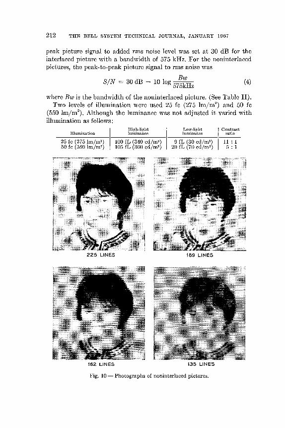
212 THE BELL SYSTEM TECHNICAL JOURNAL, JANUARY 1967
peak picture signal to added rms noise level was set at 30 dB for the interlaced picture with a bandwidth of 575 kHz. For the noninterlaced pictures, the peak-to-peak picture signal to rms noise was
Bw SIN = 30 dB - 10 log 575kHz (4)
where Bw is the bandwidth of the noninterlaced picture. (See Table II). Two levels of illumination were used 25 fc (275 Im/m2) and 50 fc
(550 lm/m2). Although the luminance was not adjusted it varied with
illumination as follows:
Illumination
25 fc (275 Im/m2) 50 fc (550 Im/m2)
225 LINES
162 LINES
High-light luminance
100 fL (340 cd/m2) 105 fL (360 cd/m2)
Low-light Contrast luminance ratio
9 fL (30 cd/m2) 11 : 1 20 fL (70 cd/m2 ) 5 : 1
189 LINES
135 LINES
Fig. 10 - Photographs of noninterlaced pictures.
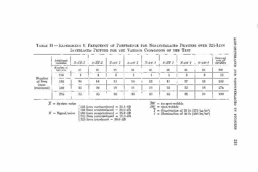
TABLE II - EXPERIMENT I: FREQUENCY OF PREFERENCE FOR NONINTERLACED PICTURES OVER 225-LINE
INTERLACED PICTURE FOR THE VARIOUS CONDITIONS OF THE TEST
Additional variables N-sw-l N-sw-l N-sw-I N-sw-I
Number of test sets 25 25 25
135 1 1 3 Number of lines 162 10 14 13 (non-
interlaced) 189 23 20 25
225 25 25 25
N = System noise
[
135 lines noninterlaced = 31.4 dB 162 lines noninterlaced = 30.0 dB
N = Signal/noise- 189 lines noninterlaced = 28.6 dB 225 lines noninterlaced = 27.0 dB 225 lines interlaced = 30.0 dB
25
1
10
21
25
N-SJV-I N-SW-I N-SW-I
25 25
1 1
12 11
23 22
25 25
SW = no spot-wobble SW = spot-wobble
25
3
17
22
25
N-SW-I
25
2
15
18 -----
24
7 = illumination of 25 fc (275 lm/m2) I = illumination of 50 fc (550 lm/m2)
Summed over all
variables
200
13
102
174 ----
199
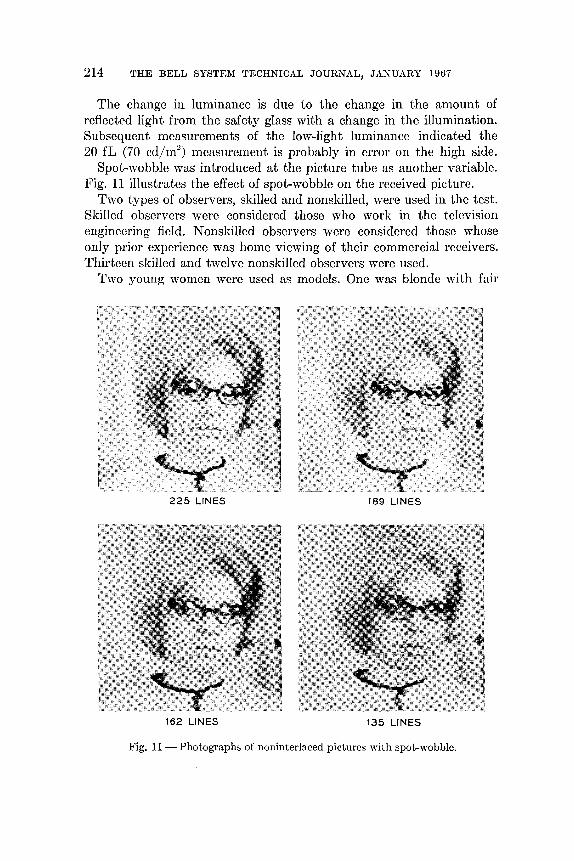
214 THE BELL SYSTEM TECHNICAL JOURNAL, JANUARY 1967
The change in luminance is due to the change in the amount of reflected light from the safety glass with a change in the illumination. Subsequent measurements of the low-light luminance indicated the 20 fL (70 cd/m2
) measurement is probably in error on the high side. Spot-wobble was introduced at the picture tube as another variable.
Fig. 11 illustrates t.he effect of spot-wobble on the received picture. Two types of observers, skilled and nonskilled, were used in the test.
Skilled observers were considered those who work in the television engineering field. Nonskilled observers were considered those whose only prior experience was home viewing of their commercial receivers. Thirteen skilled and twelve nonskilled observers were used.
Two young women were used as models. One was blonde with fail'
225 LINES 189 LINES
162 LINES 135 LINES
Fig. 11 - Photographs of noninterlaced pictures with spot-wobble.

LINE-INTERLACED AND NONINTERLACED TV PICTURES 215
complexion who wore black horn-rimmed glasses and the other waR brunette with dark complexion. During the test, the models pantomimed what might be considered a face-to-face conversation. Subjective linepairing, not investigated in this experiment, was mini~ized by instructing the models not to make rapid movements or movements which were perpendicular to the scanning lines. The observers were partially immobilized in the same sense by requiring them to operate the A-B switch whose position was fixed. The observers were not cautioned as to their movements otherwise. Fig. 10 shows the brunette model for the four noninterlaced pictures. Fig. 11 shows the blonde model for the four noninterlaced pictures with spot-wobble. The 225-line interlaced picture is not shown since photographically it would appear the same as the 225-line noninterlaced picture.
The order in which the interlaced picture and the noninterlaced pictures appeared in the A-B po~itions on the buttons was determined by a random number table.
Each observer saw 32 A-B pairs where each pair consisted of the interlaced picture and one of the 4 noninterlaced pictures. When used, the additional variables noise, spot-wobble, illumination and combinations thereof were added to both pictures of the A-B pair. The order of presentation of the noise and spot-wobble variables was also randomized with random number tables. The level of illumination was set at one value during the first half of each session and set at the other value during the second half of each session. Successive observers started their test session with alternate levels of illumination.
Seven of the skilled observers and six of the nonskilled observers saw the blonde model and six of each saw the brunette model.
v. EXPERIMENT I-RESULTS AND CONCLUSIONS
Table II lists the ferquency of preference for the noninterlaced pictures over the 225-line interlaced picture for the variables employed in this experiment.
In the tables and the text, the response data is generally related in terms of the number of noninterlaced lines, whereas the objective is to determine the bandwidth savings of interlaced pictures over noninterlaced pictures. However, on the data graphs the ordinate of the curves is expressed in terms of the number of noninterlaced lines, Ln, and the bandwidth improvement ratio with line-interlace, Bi. The reference for the bandwidth improvement factor is a hypothetical 159-line noninterlaced picture with a bandwidth of 575 KHz. The number of noninterlaced lines, Ln, may be converted to bandwidth

216 THE BELL SYSTEM TECHNICAL JOURNAL, JANUARY 1967
improvement ratio with line-interlace, Bi, by
B. Ln2 ~ = 1592 '
(5)
The frequency of preference data listed in Table II was converted to percentiles. On the hypothesis that the percentile score was cumulative normal a maximum likelihood probit8 regression line was computed for each set of data. A x2 test was performed on each of the regression lines. Since none of the x2 values exceeded the value of the number of degrees of freedom less one, there appears to be no conflict with the hypothesis that the data is cumulative normal.
The probit regression line and the original data points are plotted on each of the graphs. * In addition, the following information is listed in tabular form on each graph, (i) the point of subjective equality (PSE) in terms of number of noninterlaced lines, (ii) the standard deviation of the distribution, (J, and (iii) the standard error of the PSE, SEP.t
The method of the standard error of the difference9 was used in determining the significance of a difference between two PSE's in the following manner. The standard error of the difference between two independent random variables, is equal to the square root of the sum of their variances. Therefore, assuming independence,
(JPSE = VSEPi + SEP; , (6)
where (JPSE is the standard error of the difference between PSE's and SEp2 is the variance of the PSE's. The x 2 test indicated no conflict with the hypothesis that the PSE's are from a normal distribution, thus the distribution of the difference between the distributions of the curves from which the PSE's will be drawn is normal.
The test for significance was made in terms of T which is the difference between the PSE's expressed in terms of (JPSE as
T = 1 PSE1 - PSE2 I. (7) (JPSE
Adopting a null hypothesis that the two PSE's belong to the same parent distribution, we may set our confidence limits at a probability level of 0.05. Thus, a value of the normal deviate T of 1.96 or greater will indicate a significant difference between two PSE's.
* When data points are missing from the data plots they represent a zero or 100 percentile score, which is not visible on the graphs.
t Each of these values are weighted best estimates. Finney, Ref. 8, gives an excellent description of the statistical techniques used in arriving at these values.
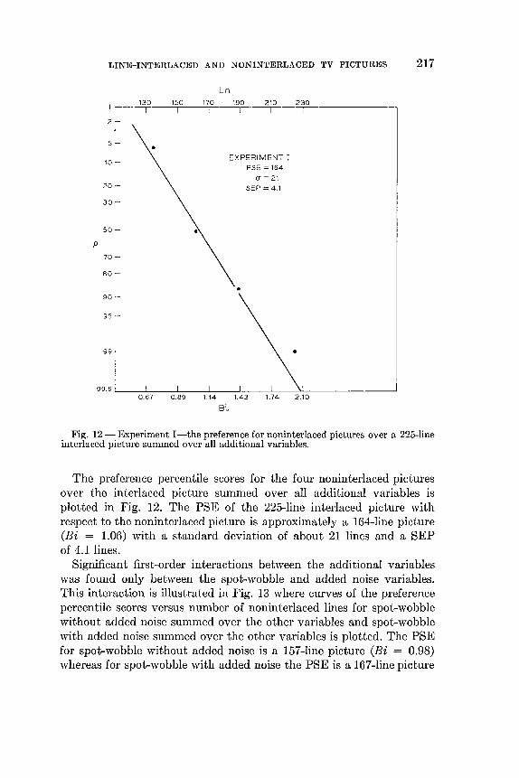
p
LINE-INTERLACED AND NONINTERLACED TV PICTURES 217
2
5
10
20
30
50
70
80
90
95
99
Ln
EXPERIMENT I PSE = 164
a=21
SEP = 4.1
•
99.9 l.--_--"--__ L-_--"--__ l.--_--"--_----"-l.--______ -'
0.67 0.89 1.14 1.43 1.74 2.10
BL
Fig. 12 - Experiment I-the preference for noninterlaced pictures over a 225-line interlaced picture summed over all additional variables.
The preference percentile scores for the four noninterlaced pictures over the interlaced picture summed over all additional variables is plotted in Fig. 12. The PSE of the 225-line interlaced picture with respect to the noninterlaced picture is approximately a 164-line picture (Bi = 1.06) with a standard deviation of about 21 lines and a SEP of 4.1 lines.
Significant first-order interactions between the additional variables was found only between the spot-wobble and added noise variables. This interaction is illustrated in Fig. 13 where curves of the preference percentile scores versus number of noninterlaced lines for spot-wobble without added noise summed over the other variables and spot-wobble with added noise summed over the other variables is plotted. The PSE for spot-wobble without added noise is a 157-line picture (Bi = 0.98) whereas for spot-wobble with added noise the PSE is a 167-line picture
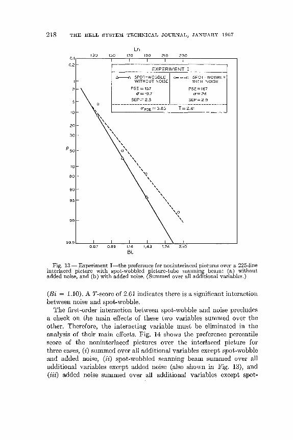
218 THE BELL SYSTEM TECHNICAL JOURNAL, JANUARY 19G7
Ln 130
0.1.-------r---,------r---r----=-,:..----=-;...-=-----------.
0.2
2
5
° 10
\ \
20 , ,
\
30
70
80
90
95
99
EXPERIMENT I
b----{::,. SPOT-WOBBLE 0---0 SPOT-WOBBLE
\ , \
\ , , 0\
\
WITHOUT NOISE WITH NOISE
PSE = 157 CT= 19.7
SEP= 2.5
CTpSE =3.83
, \ , , ,
\
~ , , , , , , , , , \ , ,
PSE= 167 CT= 26
SEP=2.9
T=2.61
',0 , , ,
99. 9 ~_-'-____ --'----'---'-::___-"--->----'----------' 1.74 2.10
Fig. 13 - Experiment I-the preference for noninterlaced pictures over a 225-line interlaced picture with spot-wobbled picture-tube scanning beam: (a) without added noise, and (b) with added noise. (Summed over all additional variables.)
(Bi = 1.10). A T-score of 2.61 indicates there is a significant iuteraction between noise and spot-wobble.
The first-order interaction between spot-wobble and noise precludes a check on the main effects of these two variables summed over the other. Therefore, the interacting variable must be eliminated in the analysis of their main effects. Fig. 14 shows the preference percentile score of the noninterlaced pictures over the interlaced picture for three cases, (i) summed over all additional variables except spot-wobble and added noise, (ii) spot-wobbled scanning beam summed over all additional variables except added noise (also shown in Fig. 13), and (iii) added noise summed over all additional variables except spot-

LINE-INTERLACED AND NONINTERLACED TV PICTURES 219
wobble. The results are itemized below: Case 1 Case 2 Case 3
PSE 165 157 166 Bi 1.08 0.98 1.09 (J' 17 20 20 SEP 5.1 2.5 5.6
A T-score of 1.4 for case 1 versus case 2 indicates that spot-wobbling of the scanning beam does not significantly effect the results. Also the
0.05
0.2
\ \ \
2 - \
5 \ '\
Ln
EXPERIMENT I
(a) .-. (b) L:r---6 (c) C--<:J
WITHOUT SPOT-WOBBLE NOISE NOISE OR WITHOUT WITHOUT
SPOT-WOBBLE NOISE SPOT -WOBBLE
PSE = 165 PSE = 157 PSE = 166 (T = 17 (T = 20 (T = 20
SEP = 5.1 SEP = 2.5 SEP = 5.6 r--------------------------------
(a) Vs (b) (TPSE = 5.69 T = 1.4
\ \ (al Vs (C) (TPSE = 7.57 T =0.13
10
20
30
P 50
70
80
90
95
99
99.9
\ '\ ~ ~ \ , ,
\ , , , \ .
, 0
\ ~ 2\., ~
\ \ \ \ \ '\
\ \ ,. \ '\ \
\ \ '\ \
\ \
1\ \
0.89 1.14 1.43 1.74 2.10
BL
Fig. 14 - Experiment I-the preference for noninterlaced pictures over a 225-line interlaced picture: (a) summed over all additional variables except added noise and spot-wobble, (b) spot-wobbled picture-tube scanning beam, summed over all additional variables except noise, and (c) added noise summed over all additional variables except spot-wobble.

220 THE BELL SYSTEM TECHNICAL JOURNAL, JANUARY 1967
T-score of 0.13 indicates that added Gaussian noise does not significantly effect the results.
Spot-wobbling the scanning beam of a noisy picture increases the visible size of the noise which is analogous to lowering the frequency of the noise. It is a well-known fact that low frequency noise is more detrimental to the quality of a television picture than high frequency noise. When the pictures were spot-wobbled without added noise, the PSE was 157 lines indicating a strong preference for the noninterlaced pictures in this case. When noise was added to the spot-wobbled pictures, there was an increase in the preference for the line-interlaced picture, PSE = 167 lines. This indicates that a combination of noise and spot-wobble is more detrimental to the quality of a noninterlaced picture than a line-interlaced picture by a significant amount. Interline flicker associated with the line-interlaced picture appears subjectively as noise to the observer. Could it be that the added noise in a spotwobbled picture is partially confounded with the interline-flicker of the line-interlaced picture and therefore is not as visible as such as it is in the noninterlaced pictures?
Fig. 15 shows graphs of the preference percentile scores for the noninterlaced pictures over the interlaced picture for two levels of illumination summed over the additional variables. A significant difference was not detected for the change in illumination. Thus, one may conclude that a change in illumination will not change the subjective equivalency between line-interlaced and noninterlaced television pictures under the conditions of this experiment.
Fig. 16 shows the preference percentile score of the noninterlaced pictures over the interlaced picture for the skilled observers and the nonskilled observer. The PSE for the skilled observers is a 166-line picture (Bi = 1.09) with a standard deviation of 21 lines. The PSE for the unskilled observers is a 163-line picture (Bi = 1.05) with a standard deviation of 21 lines. A T-score of 0.37 indicates there is no significant difference between the two groups of observers. However, an interesting significant difference was found within the skilled group of observers. The skilled observers were drawn from two television engineering groups at these laboratories which work more or less independently of each other. One group had a significantly stronger preference for the line-interlaced picture than the other. Yet when the data of the two groups were pooled the PSE of the skilled group and the PSE of the nonskilled group were not significantly different. This implies that when conducting subjective tests of this type where the results are applicable to a lay population, the possibility of a strong bias in a skilled group should not be overlooked.
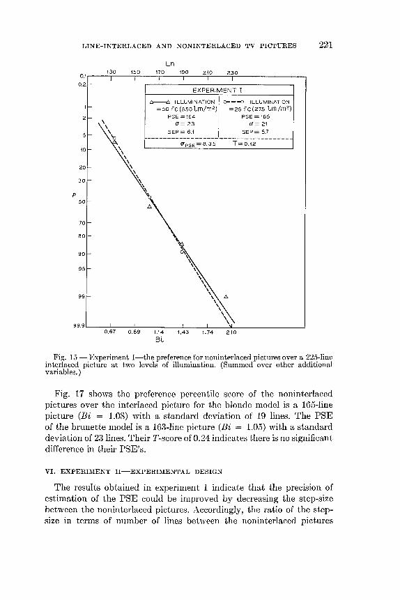
LINE-INTERLACED AND NONINTERLACED TV PICTURES 221
Ln 130 150 170
0.1r----r--r----r--,-----=-r.:...----...:=-r=~-----__,
0.2 EXPERIMENT I
t::r---t:-. ILLUMINATION 0- - -0 ILLUMINATION =50fc(5501..m/m2) =25fc(275lm/m2)
2 PSE = 164 PSE = 165 (1=23 (1=21
5 SEP = 6.1 SEP = 5.7 ------------------------------------
(1P5E=8.35 T=0.12 10
20
30
P 50
70
80
90
95
99
99.9 0.89 1.14
BL 1.43 1.74 2.10
Fig. 15 - Experiment I-the preference for noninterlaced pictures over a 225-line interlaced picture at two levels of illumination. (Summed over other additional variables. )
Fig. 17 shows the preference percentile score of the noninterlaced pictures over the interlaced picture for the blonde model is a 165-line picture (Bi = 1.08) with a standard deviation of 19 lines. The PSE of the brunette model is a 163-line picture (Bi = 1.05) with a standard deviation of 23 lines. Their T-score of 0.24 indicates there is no significant difference in their PSE's.
VI. EXPERIMENT II-EXPERIMENTAL DESIGN
The results obtained in experiment I indicate that the precision of estimation of the PSE could be improved by decreasing the step-size between the noninterlaced pictures. Accordingly, the ratio of the stepsize in terms of number of lines between the noninterlaced pictures
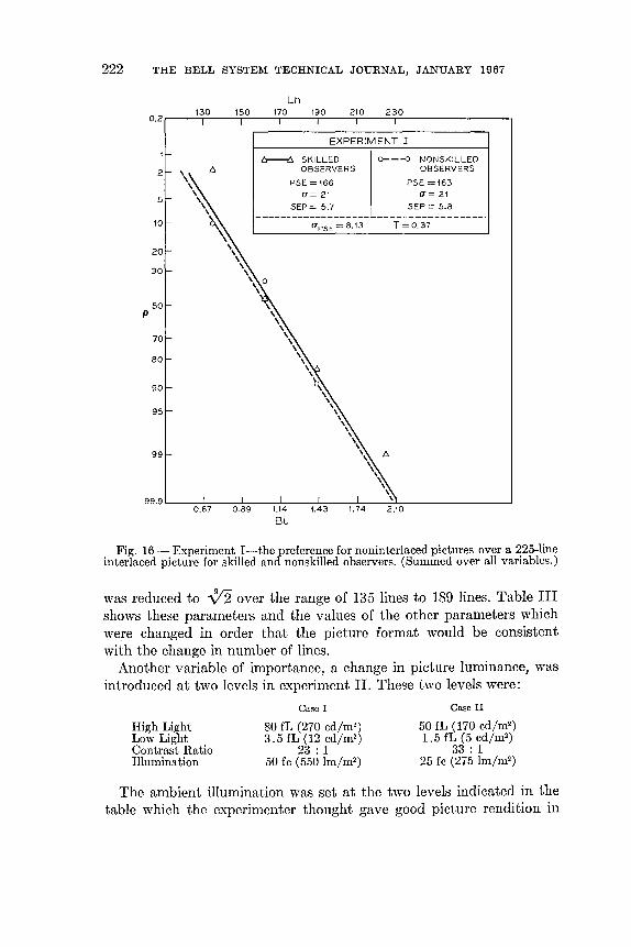
222 THE BELL SYSTEM TECHNICAL JOURNAL, JANUARY 1967
Ln
0.2 r--~---r-.:.--......,.~-..:..r----=;":---=T=--------.,
2
5
10
20
30
50 P
70
80
90
95
99
EXPERIM ENT I
t::r-----6 SKI LLE D OBSERVERS
PSE = 166 (1'= 21
SEP = 5.7
0- --0 NONSKILLED OBSERVERS
PSE =163 (1'= 21
SEP= 5.8
T =0.37
99.9l...--~::----:-~---,--L..,.--....l...:,--J,--....:L--_____ -1
Fig. 16 - Experiment I-the preference for noninterlaced pictures over a 225-line interlaced picture for skilled and nonskilled observers. (Summed over all variables.)
was reduced to V2 over the range of 135 lines to 189 lines. Table III shows these parameters and the values of the other parameters which were changed in order that the picture format would be consistent with the change in number of lines.
Another variable of importance, a change in picture luminance, was introduced at two levels in experiment II. These two levels were:
High Light Low Light Contrast Ratio Illumination
Case I
80 fL (270 cd/m2) 3.5 fL (12 cd/m2)
23 : 1 50 fc (550 Im/m2)
Case II
50 fL (170 cd/m2) 1.5 fL (5 cd/m2)
33 : 1 25 fc (275 Im/m2)
The ambient illumination was set at the two levels indicated in the table which the experimenter thought gave good picture rendition in
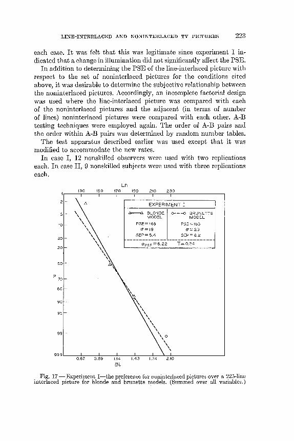
LINE-INTERLACED AND NONINTERLACED rI'V PICTURES 223
each case. It was felt that this was legitimate since experiment I indicated that a change in illumination did not significantly affect the PSE.
In addition to determining the PSE of the line-interlaced picture with respect to the set of noninterlaced pictures for the conditions cited above, it was desirable to determine the subjective relationship between the noninterlaced pictures. Accordingly, an incomplete factorial design was used where the line-interlaced picture was compared with each of the noninterlaced pictures and the adjacent (in terms of number of lines) noninterlaced pictures were compared with each other. A-B testing techniques were employed again. The order of A-B pairs and the order within A-B pairs was determined by random number tables.
The test apparatus described earlier was used except that it was modified to accommodate the new rates.
In case I, 12 nonskilled observers were used with two replications each. In case II, 9 nonskilled subjects were used with three replications each.
2
5
10
20
30
50
P 70
80
90
95
99
Ln
EXPERIMENT I
~ BLONDE 0---0 BRUNETTE MODEL MODEL
PSE= 165 PSE=163
a=19
SEP= 5.4
a=23
SEP= 6.2
-----------------------------
\ ,
apSE = 8. 22 T = 0.24
\ , \ , , , ,
\ \ \0 ,
\ , \
99.9 L....-_---'-__ ....L...-_---' __ --'-__ -'----->---I.. _______ ~
0.67 0.89 1.14
BL 1.43 1.74 2.10
Fig. 17 -Experiment I-the preference for noninterlaced pictures over a 225-line interlaced picture for blonde and brunette models. (Summed over all variables.)

224 THE BELL SYSTEM TECHNICAL JOURNAL, JANUARY 1967
The test procedure and instructions to the observer were the same as those described in Section IV except for the necessary change in the number of "sets of pictures".
VII. EXPERIMENT II-RESULTS AND CONCLUSIONS
Each of the observers made a forced choice decision for one of the two pictures in each A-B pair presented to him. In addition to recording his preference, the time it took each observer to reach a decision was recorded for each A-B pair. It was assumed that time would vary
TABLE III-SOME PARAMETERS OF EXPERIMENTAL
ApPARATUS (EXPERIMENT II)
Visible Angular Visible picture subtense
Line- Horizontal Band- Picture picture ele- between Number inter- sweep wdth elements/ elements/ ments/ two lines of lines lace rate (Hz) (MHz) frame frame line at 40" ---
225 Yes 6750 0.575 38,333 28,366 142 2.2' ---
189 No 11 ,340 0.812 27,066 20,029 119 2.5' ---
175 No 10,500 0.695 23,166 17,143 110 2.7' ---
162 No 9720 0.575 19,166 14,183 102 2.9' ---
147 No 8820 0.495 16,500 12,210 92 3.2' ---
135 No 8100 0.415 13,766 10,186 85 3.4'
proportionately with the difficulty of reaching a decision,' i.e., time would be well correlated with the first derivative of the percentile score.
Using time as the variable, control charts10 were set up for the experiment. The control charts for the mean time indicated that the experimental apparatus was under control at all times. Range control charts indicated that all of the observers were within population control limits.
Table IV (a) lists the frequency of preference for the noninterlaced pictures over the 225-line interlaced picture for the two levels of luminance. Listed in Table IV (b) is the preference of the noninterlaced picture with the larger number lines over the adjacent noninterlaced picture with the lesser number of lines.
The data listed in Table IV (a) relating the interlaced picture to the noninterlaced pictures was converted to percentile scores and plotted on normal-probability paper as shown in Fig. 18. * Again assuming
* When the fifth data point is missing from the graph, it occurred at the 100th percentile for the 225-line noninterlaced picture.

LINE-INTERLACED AND NONINTERLACED TV PICTURES 225
TABLE IV - EXPERIMENT II
(a) (b)
Frequency of preference for Noninterlaced pictures: fre-noninterlaced pictures over quency of preference for 225-line interlaced picture picture A over picture B in
terms of number of lines
Case I II Case I II -- -
No. of No. of Total observers 12 9 observers 12 9 out of 51
- -- observations Replications 2 3 Replications
-- - ---- 2 3 189 22 24 Pix A Pix B
- ---- -
Number 175 12 10 189 175 22 26 48 of lines - ---- -
(non- 162 7 2 175 162 22 26 48 interlaced - ---- -
pictures) 147 1 1 162 147 21 23 44 ---- - - ---- -
135 2 0 147 135 21 26 47
a normal distribution, a pro bit regression line was determined for each case. Chi-square tests indicated no conflict with thc hypothesis of a normal distribution.
The data of experiment II was tested for significance in the same manner of experiment I.
For a high-light luminance of 50 fL (170 cd/m2) the PSE was a
177 -line noninterlaced picture (Bi = 1.24) with a (j of 12 lines and a SEP of 2.0 lines. For a high-light luminance of 80 fL (270 cd/m2
),
the PSE was 171 line noninterlaced picture (Bi = 1.16) with a (j of 18 lines and a SEP of 2.6 lines.
In addition to the graphs of experiment II, Fig. 18 shows the graph of the results from experiment I (see Fig. 12) for a high-light luminance of about 100 fL (340 cd/m2) summed over all variables. Thus, three values of high-light luminance are available in checking for a significant difference between high-light luminances.
The T-score for changes in high-light luminances of 50 fL (170 cd/m2) to 80 fL (270 cd/m2
) and 80 fL (270 cd/m2) to 100 fL (340 cd/m2) is 1.83 and 1.44, respectively. These T-scores approach the significant value of 1.96. Thus, we may conclude that a change in high-light luminance of less than 30 fL (100 cd/m2) over the range of 50 fL (170 cd/m2) and 100 fL (340 cd/m2) will not quite produce a significant difference in the PSE when comparing line-interlaced and

226 THE BELL SYS'rEM TECHNICAL JOURNAL, JANUARY 1967
Ln 130 150 170 190 210 230
0.01,.-----,---.------,----,-----,---,...----------,
0.05
0.2
2
5
10
20
30
p
50
70
80
90
95
99
\ \ \ \ \ \ \ \
EXPERIMENT :II 0--0 e-e
LUMINANCE LUMINANCE =50fL =80fL
(170 cd/m2) (270 cd/m2)
PSE = 177 PSE = 171 a= 12 a= 18
SEP = 2.0 SEP = 2.6
LUMINANCE apSE
50 - 80 3.28 \0 80 -100 4.85
\ \
50- 100 4.56
\ - \ \ \0
\ \ f:,' -\ \ \
\ \ \
\ \
\
EXPERIMENT I 6---6
LUMINANCE =loofL
(340 cd/m2)
PSE = 164 a= 2 1
SEP = 4.1
T
1.83 1.44 2.85
99.9'---_:-'::-::-----:--':-:--_-'-__ --'-_---'-'------'''-1.-______ ---1
1.74 2.10
Fig. 18 - Experiment I and II-the preference for noninterlaced pictures over a 225-line interlaced picture for three levels of luminance.
noninterlaced television pictures under the conditions of these experiments.
The T-score for a change in high-light luminance of 50 fL (170 cd/m2) to 100 fL (340 cd/m2) is 2.85. This value of T is highly significant. We may conclude that a change in high-light luminance from 50 fL (170 cd/m2) to 100 fL (340 cd/m2) will produce a highly significant difference in the PSE when line-interlaced and noninterlaced television pictures are compared under the conditions of these experiments.
The preference of the noninterlaced picture with the larger number of lines over the adjacent noninterlaced picture with the lesser number of lines is not shown in graphic form. Table IV-B shows that about

LINE-INTERLACED AND NONINTERLACED '.rV PICTURES 227
90 percent of the observers preferred the pictures with the larger number of lines over the picture with the lesser number of lines. The exact meaning of these results is not obvious. Although the observers were asked to make their decisions on the basis of picture quality, we may instead have a measure of the observers ability to detect a difference in the number of lines between two pictures. * In other words, the observer in detecting which picture had the greater number of lines, may have assumed that this picture must also have the better quality. We may conclude that about 90 percent of the observers will be able to determine which of two llonillterlaced television pictures has the greater number of lines when the ratio of the number of lines in the picture is V2 over the range of 135-line pictures to 225-line pictures.
VIII. EXPERIMENT III-EXPERIMENTAL DESIGN
The fact that the image of a television picture is reproduced in lines on the picture tube screen is objectionable to most people. This is particularly true of low-resolution television systems with coarse line structures. Broadening of the scanning lines will aid in reducing the objectionable effects of the line structure. Asymmetrical defocussing of the scanning spot with a magnet attached to the neck of the picture tube is one of the most economical approaches to this problem though Monteathll has shown that it is not the best esthetic solution.
Asymmetrical spot defocussing was used in this experiment as described in Section II. The line-width to line-pitch ratio was set at approximately 1.7 for the interlaced picture and approximately 1.2 for the noninterlaced pictures. 6 Fig. 19 shows photographs of a line interlaced and noninterlaced picture with the line-width to line pitch ratios set for the preferred values.
The 225-line interlaced picture was compared with the five noninterlaced pictures described in Table III except that the 225-line noninterlaced picture described in Table I was exchanged for the 135-line nOllinterlaced picture of Table III.
Two levels of luminance and illumination were introduced as follows:
High-Light low-Light Contrast Ratio Illumination
Case I
60 fL (200 cd/m2) 3.5 fL (12 cd/m2)
17.2 : 1 100 fc (1100 Im/m2)
Case II
40 fL (140 cd/m2)
1.5 fL (5 cd/m2)
27.4 : 1 50 fc (550 Im/m2)
* The experimenter found that the change in the number of lines (about 9 percent) was quite evident in each case, whereas the change in bandwidth (about 18 percent) was difficult to detect. Baldwin,5 found that a change in bandwidth of 16 percent was not perceptible in his experiments.

228 THE BELL SYSTEM TECHNICAL JOURNAL, JANUARY 1967
(a)
(b)
Fig. 19 - Experiment III-photographs of asymmetrically defocussed pictures. (a) 225-line interlaced picture, (b) 225-1ine noninterlaced picture.
On the assumption that a change in illumination did not have a significant effect on the PSE, the illumination was changed to give good picture rendition with the levels of luminance used.
The order of presentation of A-B pairs for each case and the order within pairs was determined by random number tables.
In case I, 16 nonskilled observers were used with 3 replications each. In case II, 15 nonskilled observers were used with 3 replications each.
The test procedure and instructions to the observers were the same as those described in Section IV except for the necessary change in th~ "number of sets of pictures."
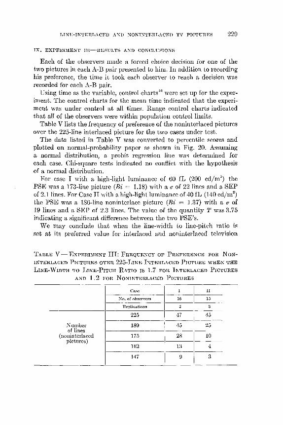
LINE-INTERLACED AND NONINTERLACED TV PICTURES 229
IX. EXPERIMEN'f III-RESULTS AND CONCLUSIONS
Each of the observers made a fOf(~ed ehoice deeision for one of the two pictures in each A-B pair presented to him. In addition to recording his preference, the time it took each observer to reach a decision was recorded for each A-B pair.
Using time as the variable, control charts lO were set up for the experiment. The control charts for the mean time indicated that the experiment was under control at all times. Range control charts indicated that all of the observers were within population control limits.
Table V lists the frequency of preference of the noninterlaced pictures over the 225-line interlaced picture for the two cases under test.
The data listed in Table V was converted to pereentile scores and plotted on normal-probability paper as shown in Fig. 20. Assuming a normal distribution, a probit regression line was determined for each case. Chi-square tests indicated no conflict with the hypothesis of a normal distribution.
For case I with a high-light luminance of 60 fL (200 cd/m2) the
PSE was a 173-line picture (Bi = 1.18) with a (J of 22 lines and a SEP of 2.1 lines. For Case II with a high-light luminance of 40 fL (140 cd/m2
)
the PSE was a 186-line noninterlace picture (Bi = 1.37) with a (J of 19 lines and a SEP of 2.3 lines. The value of the quantity Twas 3.75 indicating a significant difference between the two PSE's.
We may conclude that when the line-width to line-pitch ratio is set at its preferred value for interlaced and noninterlaced television
TABLE V -EXPERIMENT III: FREQUENCY OF PREFERENCE FOR NONINTERLACED PICTURES OVER 225-LINE INTERLACED PICTURE WHEN THE LINE-WIDTH TO LINE-PITCH RATIO lS 1.7 FOR INTERLACED PICTURES
AND 1.2 FOR N ON INTERLACED PICTURES
Case I II
No. of observers 16 15
Replications 3 3 ----
225 47 45 ----
Number 189 45 25 of lines --------
( noninterlaced 175 28 10 pictures)
162 13 4
147 9 3

230 THE BELL SYSTEM TECHNICAL JOURNAL, JANUARY 1967
0.05
0.2
2
5
10
20
30
P 50
70
80
90
95
99
99.9
\ \ \
\ \
\ \
\
Ln
EXPERIM ENT III
\ \ \
\ \ \
\
tr---t:;. LUMI NANCE =60 fL(200 cd/m2 )
PSE=173 a= 22
SEP = 2.1
apSE =3.47
~ \ \
\ \0
\ \ \ \ \
\ \
~ \ \
\ \ \ \ \
\ \
\ \ \
\ \
\ \ \
0---0 LUMINANCE =40 fL(140 cd/m2 )
PSE = 186 a= 19
SEP= 2.3
T =3.75
~ \
\ \
Fig. 20 - Experiment III -the preference for noninterlaced pictures over a 225-line interlaced picture for two levels of high-light luminance with the line-width to linepitch ratio set to its preferred value.
pictures there will be a significant difference in the PSE when the highlight luminance is changed from 60 fL (200 cd/m2) to 40 fL (140 cd/m2) or vice versa under the conditions of this experiment.
x. SUMMARY AND CONCLUSIONS
It has been found that the line interlacing of low-resolution television pictures provide the observer with substantially less than a 2 : 1 savings in bandwjdth under the conditions of these experiments. In the most optimistic case where the high-light luminance was 40 fL (140 cdjm2)
LINE-INTEBLACED AND NON INTERLACED TV PICTURES 231
and in which the line-width to line-pitch had been optimized the subjective bandwidth savings was about 37 percent.
I t was found that high-light luminance had a significant effect on the subjective equivalence between line-interlaced and noninterlaced television pictures. In the worst case with a high-light luminance of 100 fL (340 cd/m2
) the line-interlacing of a 225-line television picture provided a savings in subjective bandwidth of about 6 precent. Under similar test conditions at a high-light luminance of 50 fL (170 cd/m2
),
the subjective bandwidth savings was about 24 percent. The main effects of the variables added Gaussian noise, spot-wobble
illumination, two types of models, and two types of observers did not produce a significant difference in their results. The first-order interaction between each of these variables with the exception of noise and spot-wobble was not significant.
A significant first-order interaction was found between added Gaussian noise and a sinusoidally spot-wobbled scanning beam. When the scanning beam of the test pictures was spot-wobbled with a 7.14-MHz sine wave, the 225-line interlaced picture did not provide any subjective savings in bandwidth. However, when noise with a Gaussian distribution was added to the spot-wobbled picture the subjective bandwidth savings was about 10 precent. This indicates that added noise is more detrimental to the quality of a spot-wobbled noninterlaced picture than to a spot-wobbled line-interlaced picture.
It was found that about 90 percent of the observers preferred the noninterlaced picture with the greater number of lines when the ratio of the number of lines of the two pictures was V2 and the vertical resolution in each picture was approximately equal to the horizontal resolution.
The same amount of picture information is presented in both the 225-line interlaced picture and the 225-line noninterlaced picture. The noninterlaced picture is a quiet picture in which the small details may be easily detected and tracked by the observer. This same detail is visible in the interlaced picture, but the observer must look "through" the interline flicker effects and resist the intrinsic desire of the eye to track stroboscopic patterns in order to see the detail. It is highly probable that the results of this experiment would have been quite different if the observers task was to recognize and identify fine detail, such as the recognition and identification of alphanumerical material.
In the design of a low-resolution television system the choice between line-interlace and noninterlace is not completely resolved by these experiments. These experiments provide us with a long awaited measure

232 THE BELL SYSTEM TECHNICAL JOURNAL, JANUARY 1967
of the subjective equivalence between line-interlaced and noninterlaced television pictures under the conditions described. Before a final decision is made many other factors such as cost of implementation, the subjective effects of PCM processing, repeater spacing, the subjective effects of crosstalk, etc. if applicable, must be considered. Finally, although the full benefits of a 2 : 1 savings in bandwidth is not realized by line-interlacing it does provide some bandwidth savings in all of the cases studied except one and furthermore, line-interlacing appears to partially mask the affects of added noise.
XI. ACKNOWLEDGMENTS
Most of the members of the Visual Systems Research Department of Bell Laboratories have made some contribution to this experiment. W. T. Wintringham has directed and assisted this experiment from its beginning. J. A. Murphy and F. C. Bollwage designed and built the display terminal. Consultations with P. D. Bricker, M. W. Baldwin, Jr., C. C. Cutler, B. Prasada, and H. Levitt were most helpful in the design and analysis of the experiment.
REFERENCES
1. de Lange Dzn, H., Relationship Between Critical Flicker-Frequency and a Set of Low-Frequency Characteristics of the Eye, J. Opt. Soc. Amer., 44, May, 1954, p. 380.
2. LeGrand, Y., Light, Colour and Vision, First Edition, John Wiley & Sons Inc., New York City, 1957.
3. Engstrom, E. W., A Study of Television Image Characteristics, Proc. IRE, 23, April, 1935, p. 295.
4. Fink, D. G., Television Standards and Practice, (Selected papers from the Proceedings of the National Television System Committee and its panels.) First Edition, McGraw-Hill Book Company, Inc., New York City, 1943.
5. Baldwin, M. W., Jr., The Subjective Sharpness of Simulated Television Images, B.S.T.J., 19, October, 1940, p. 563.
6. Brown, E. F., unpublished work. 7. Guilford, J. P., Psychometric Methods, 2nd Edition, McGraw-Hill Book Com
pany, Inc., New York City, 1954. 8. Finney, D. J., Probit Analysis, 2nd Edition, Cambridge University Press, Cam
bridge, England, 1964. 9. Mills, F. C., Statistical Methods, Third Edition, Holt, Rinehart and Winston,
New York City. 10. Burr, 1. W., Engineering Statistics and Quality Control, First Edition, McGraw
Hill Book Company, Inc., New York City. 11. Monteath, G. D., Vertical Resolution and Line Broadening, BBC Engineering
Division Monograph No. 45, December, 1962.

Low-Resolution TV: Subjective Effects of Noise Added to a Signal
By R. C. BRAINARD
(Manuscript received September 19, 1966)
The visibility of noise in a television presentation is related to the spatialfrequency and flicker-frequency c01nponents of the noise display. The visibility of sine wave interference, which generates a sine wave grating on a TV screen, demonstrates remarkable linearity by giving a good approxinwtion to the visibility function measured with narrow bands of noise.
A difference in visibility between moving and stationary gratings produces a difference between noise visibility in TV and photographs. This fact is important in evaluating the computer simulation of a system by calculations for a single TV frame. The variation of visibility with lrwtion predicts increased visibility for additive noise in a television fTa1ne repeating system. Applications to predistortion and reconstruction filters for transmission of analog and digital TV signals are discussed.
I. INTRODUCTION
For the design of a television communication channel it is desirable to have a figure of merit for comparison of channels. As our sophistication in the design of communication channels increases, so we must also increase our sophistication in defining and measuring a suitable figure of merit. As a measure of merit we may use the power spectrum N(w) of the error, or noise, added in the channel which can be measured for all frequencies, w, in a given transmission system. However, the ultimate receiver is a person viewing the picture, and his sensitivity to noise superimposed on the picture depends upon the distribution with frequency of that noise. This dependence of the viewer's sensitivity to noise can be considered equivalent to a linear filter and a linear detector. We will call this sensitivity function a subjective noise-weighting function, W(w), defined on the video bandwidth, 0 to n. 1
•2
•3
•4 This
subjective noise-weighting function gives the value at each frequency of the relative contribution of noise to an overall figure of merit. We define this figure of merit as liP, where
233

234 THE BELL SYSTEM TECHNICAL JOURNAL, JANUARY 1967
p == if! N(w)W(w) dw,
and P the weighted noise.
(1)
The subjective noise-weighting function is the transfer function of the system consisting of the television kinescope and human visual system specified as a function of the electrical video-signal frequencies. The input is an electrical signal; the output is the response of the viewer. It is convenient for discussion to divide this function into three parts.
The first portion of this function, which we call Ta , is the transfer function of the kinescope. It is a mapping of a I-dimensional electrical signal to a 2-dimensional picture. The second part of the functjon, Tb , is the modulation transfer function of human vision. This function, which has been called the sine-wave response, is the transmission from object to interpreted image in the brain. The third part, T c , is the translation from the image in the brain to a verbal response. The weighting function is the product of these 3 functions:
where
T a = transfer function of kinescope, T b = transfer function of vision, T c = translation to words.
(2)
Measurements are made of the complete transfer function W(w) and are accomplished by comparing the viewer's subjective response to noise bands having different frequency components. If two noise bands with power spectral densities N 1 and N 2 are found to be subjectively equivalent, then and only then, we have
(3)
By using a sufficient set of noise bands we can calculate W(w) to any desired accuracy. 2
By making subjective comparisons between the interfering effects of sine waves and white noise of various power levels, we would expect to be able to evaluate the subjective noise-weighting function most easily. Results with sine wave interference have been obtained by others. 5 The weighting function as determined by using sine waves exhibits rather extensive structure related to horizontal-line and frame or field-rate multiples.
It is possible to subjectively compare the interfering effect of wide
SUBJECTIVE EFFECTS OF NOISE 235
bands of noise to that of flat noise. By this procedure we smooth out all the fine structure. Results of such experiments have been published.2
,3 ,4 This smoothed version of the weighting function shows a reduced visibility for high video frequencies.
The purpose of this paper is to clarify the effect of random noise on a video presentation by examining in more detail the subjective effects of noise added to a video signal. In particular, it is desired to determine the fine structure and microstructure of the subjective noise-weighting function related to multiples of the horizontal line rate and the frame rate, respectively. This requires measurements with noises whose bandwidths are small compared to the horizontal line rate but wide enough to appear as noise. Noises of bandwidths which are small compared to the frame rate are also required. These are effectively sine waves
Applying measurements of sine wave visibility to the noise-weighting function requires an approximate linearity of the system. The question of linearity is considered through all the following discussion.
II. NONLINEARITY
The use of the noise-weighting function in (1) implies linearity of the system. There is a problem because, in fact, the system is not linear; the translation from electrical signal voltage to luminance in the kinescope is nonlinear, and vision is not linearly sensitive to luminance. This fact disavows the linear superposition of noise power in (1). However, for a reasonable transmission system the signal-tonoise ratio must be sufficiently large, say 30 to 40 dB, that this nonlinearity will not be significant in regard to luminance variation due to the noise. This approximation is justified by the consistency of the results. It must be remembered that the kinescope nonlinearity results in a dependence of the transmission factor for small signal variations superimposed on the average luminance level. These nonlinearities give the well-known result that a small signal is most visible when superimposed on a dark gray area of a kinescope presentation.
The translation of a scene into a verbal response is obviously a nonlinear function. By proper choice of test procedure the effect of this nonlinearity can be made small.
III. T a, TRANSFER FUNCTION OF KINESCOPE DISPLAY SYSTEM
3.1 Spatial Noise
In a television receiver the scanning procedure generates a picture with 2 spatial dimensions and 1 time dimension from a video signal

236 THE BELL SYSTEM TECHNICAL JOURNAL, JANUARY 1967
with 1 voltage and 1 time dimension. The noise superimposed on the video signal is also mapped onto the picture with 2 spatial dimensions and 1 time dimension.
In order to relate spatial frequencies to video frequencies, we can refer to Mertz and Gray6 or to Huang7 where a complete theoretical description of the scanning process is given. Although we will later use some of their results we will here consider a different viewpoint that will, we hope, aid our understanding of noise in a television system.
The reconstruction of the 2-dimensional picture from a video signal involves aligning successive segments of the signal (translated to brightness values) below one another to form a raster on the kinescope. For convenience we consider a square raster; results are easily extended to a rectangular raster. This square raster is shown in Fig. 1. The segments of the signal appear as gently sloping lines almost parallel to the horizontal or x direction. For the square picture, the picture height equal to the picture width is taken as the unit of linear measure. Let L be the number of lines in a complete picture. It must be recalled that in a real system a portion of the picture is blanked for retrace.
For a single frame, consider a narrow strip along a scan line. This strip is merely a segment of the video signal. Therefore, there is a linear relation between video frequencies, f, and spatial frequencies along the raster line designated r. This is written
i = r fh
(4)
for spatial frequencies measured in cycles per picture width, where f" is the horizontal line scanning frequency.
Now consider a narrow vertical strip of the frame. Successive points down this strip represent samples of the original signal spaced at l/fh intervals. Sampling and modulation principles can be used to derive information about the presentation in the vertical direction as a function of the original signal.
The original video signal may contain time-varying components from very low frequencies to several hundred times fl.' In the sampled signal appropriate sidebands at each sampling frequency multiple will contain components that fall in the frequency band between 0 and (t)fh' To understand this, consider the triangular-shaped power spectrum of a video signal shown in Fig. 2 (a). This signal is centered on the fourth harmonic of fl.' With a sampling frequency of f I., the sampled version contains this triangular shaped power spectrum centered at each multiple of fh as shown in Fig. 2 (b). Since the original band of
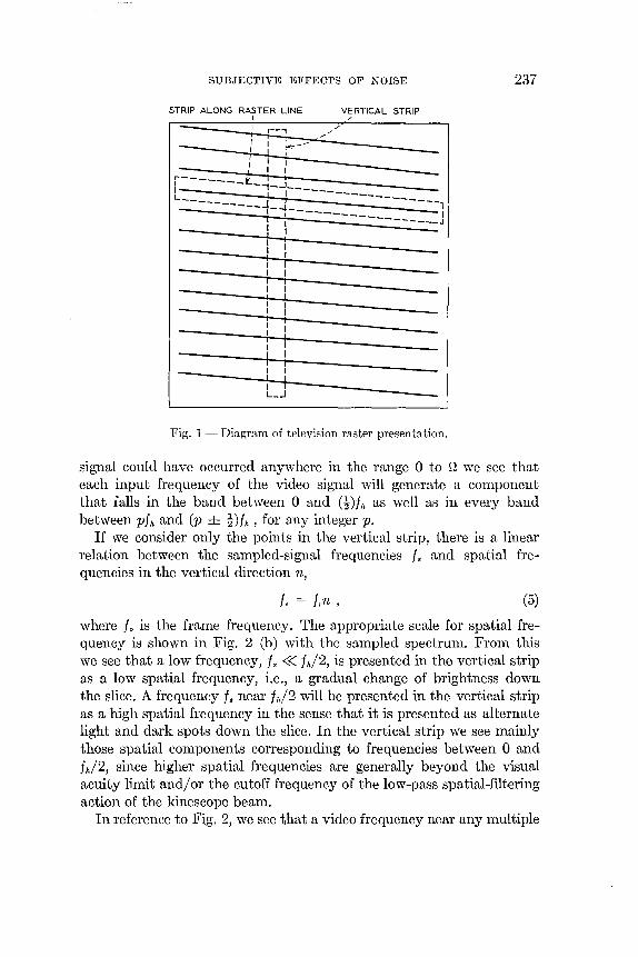
SUBJECTIVE EFFECTS OF NOISE
STRIP ALONG RASTER LINE VERTICAL STRIP
'" ~ __ I /.//
li-rl;~~------__ __ j
.' I I r--___ 1:. i I I -- -,-.J __ L ! I
--~-J- --~ -=---------rl -f:==::::::-:-:-:-::-:-:-~-~_J - : I
I I I i
I [ I i i i I i , !
I i I I : I
I I I I I I
I :
I I
: I
Fig. 1 - Diagram of television raster presentation.
237
signal could have occurred anywhere in the range 0 to n we see that each input frequency of the video signal will generate a component that falls in the band between 0 and (!)/h as well as in every band between plh and (p ± !)/h' for any integer p.
If we consider only the points in the vertical strip, there is a linear relation between the sampled-signal frequencies 18 and spatial frequencies in the vertical direction n,
Is = Ivn , (5)
where I~ is the frame frequency. The appropriate scale for spatial frequency is shown in Fig. 2 (b) with the sampled spectrum. From this we see that a low frequency, Is « Ih/2, is presented in the vertical strip as a low spatial frequency, i.e., a gradual change of brightness down the slice. A frequency la near h/2 will be presented in the vertical strip as a high spatial frequency in the sense that it is presented as alternate light and dark spots down the slice. In the vertical strip we see mainly those spatial components corresponding to frequencies between 0 and h/2, since higher spatial frequencies are generally beyond the visual acuity limit and/or the cutoff frequency of the low-pass spatial-filtering action of the kinescope beam.
In reference to Fig. 2, we see that a video frequency near any multiple
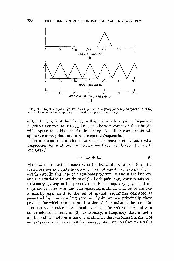
238 THE BELL SYSTEM TECHNICAL JOURNAL, JANUARY 1967
I I I /\ I I 0 fh 2fh 3fh 4fh sfh 6fh
VIDEO FREQUENCY
(a)
o fh 2fh 3fh 4fh Sfh 6fh VIDEO FREQUENCY
o L 2L 3L sL 6L VERTICAL SPATIAL FREQUENCY
( b)
Fig. 2 - (a) Triangular spectrum of input video signal; (b) sampled spectrum of (a) as function of video frequency and vertical spatial frequency.
of Ih , at the peak of the triangle, will appear as a low spatial frequency. A video frequency near (p ± !)Ih, at a bottom corner of the triangle, will appear as a high spatial frequency. All other components will appear as appropriate intermediate spatial frequencies.
For a general relationship between video frequencies, I, and spatial frequencies for a stationary picture we have, as derived by Mertz and Gray,6
I = hm + Ivn, (6)
where m is the spatial frequency in the horizontal direction. Since the scan lines are not quite horizontal m is not equal to r except when n equals zero. In this case of a stationary picture, m and n are integers, and I is restricted to multiples of I~ . Each pair (m,n) corresponds to a stationary grating in the presentation. Each frequency, I, generates a sequence of pairs (m,n) and corresponding gratings. This set of gratings is exactly equivalent to the set of spatial frequencies described as generated by the sampling process. Again we see principally those gratings for which m and n are less than L/2. Motion in the presentation can be considered as a modulation on the values of m and n or as an additional term in (6). Conversely, a frequency that is not a multiple of ttl produces a moving grating in the reproduced scene. For our purposes, given any input frequency, I, we want to select that value

SUBJECTIVE EFFECTS OF NOISE
of m such that n < L12. If we choose m such that
m - ! ~ III" ~ m + !, then (6) gives the desired value of n such that n < L12.
3.2 A pplicalion to M easuremenls
239
(7)
Given as the input to the video presentation a narrow band of noise with a flat power spectrum between plh and (p ± !)Ih for any integer p, that is, flat noise replacing one-half the triangle spectrum of Fig. 2(a), then in a strip along y this would appear in the same way as a band of noise extending from 0 to (!)/" , that is, a flat band of spatial frequencies between 0 and LI2 cycles per picture height, abbreviated clph. For an input noise signal flat over a bandwidth a few times I" , we can assume the spatial noise as it appears in the vertical strip to be nearly flat over its entire range, since the effects of the edges of the input would be small. For an input noise of sufficient bandwidth, the vertical spatial-noise spectrum is nearly independent of the center frequency and bandwidth of the input noise. Therefore, the gross character of the noise-weighting function measured with wide bands of noise depends almost entirely on the horizontal spatial frequencies.
To examine the procedure for measuring the fine structure, consider an input noise with bandwidth narrow compared to f". If the center of the band is near pi" , for integer p, the vertical spatial-noise spectrum consists of low spatial frequencies only. But if the center of the band is at (p ± !)/" , then the vertical spatial-noise spectrum consists of high spatial frequencies. For variations in the center frequency between pi" and (p ± !)I" , the horizontal spatial-power spectrum would have a relatively small change, while in the vertical direction the change is from one extreme to the other; from low spatial frequencies to high spatial frequencies. The above should hold true regardless of the value of p. Therefore, the fine structure of the noise-weighting function depends on vertical spatial frequencies.
It is of interest to note that with an input noise bandwidth of I" we should expect to find almost no variation in subjective response for a center frequency variation from pi" to (p + !)Ih , since in all cases the vertical spatial-noise spectrum would be flat over its entire range and the change in the horizontal direction would be small.
To predict the weighting-function variations between multiples of the horizontal-line frequency, we have to resort to the constituent gratings described above. For the grating where the horizontal frequency

240 THE BELL SYSTEM TECHNICAL JOURNAL, JANUARY 1967
is m and the vertical frequency is n, then the spacing between bars, A, is given by
(8)
Consider the video frequency range from f h to 1.5 f h . At f h , m = 1 and n = 0 gives A = 1. At 1.5 fh , m = 1, and n = L/2 gives A ~ 2/L (since L » 1). For a similar frequency range at the top of the band between Lfh/2 and (L + 1)fh/2, at Lfh/2 then m = L/2 and n = 0 gives A = 2/L, and at (L + l)fh/2 then m = L/2 and n = L/2 gives A = V2/L.
From these numbers, we predict that for low m the variation of W with n, the fine structure, will be large and roughly equivalent to the variation over the complete range of m. For large m, the variation of W with n should be rather small.
3.3 Fliclcer Noise
Consider a succession of frames, again assuming that there is no interlace. Each frame constitutes a sample of the input noise. Any single point in the picture represents a time sample of the noise voltage translated to a luminance value spaced l/f. in time where fv is the frame or vertical frequency. Sidebands at multiples of the sampling frequency fv contain components that appear as flicker frequencies between zero and (!)f • . For any integer p, input frequencies near pf. appear as low flicker frequencies and frequencies near (p ± !)fv appear as flicker frequencies near (!)f • . For these flicker frequencies varying from zero to (!)fv we should expect a subjective variation in visibility. The higher frequencies of the sampled function we expect to be insignificant due to the sharp cutoff of human vision. Because of this variation we expect a microstructure to be imposed on the noise-weighting function. By measurements with sine wave interference, one can determine this microstructure, whereas with relatively wide bands of noise greater than fv , the effect of this microstructure is smoothed out.
3.4 Small-Signal Transfer Function of Kinescope
We can now give a general discussion of the operation in the kinescope at the system receiver considering only the principal gratings seen. For any sine wave component of the input video signal a sine wave grating is presented on the kinescope screen. The grating has horizontal and vertical spatial-frequency components m and n given by (6) and (7). The spacing between grating bars A is given by (8).
The grating has an apparent movement in a direction perpendicular

SUBJECTIVE EFFECTS OF NOISE 241
to the bars of the grating. This apparent motion can be described as a traveling wave. The luminance is given by
I = A + B sin 27r(Ft + x/A). (9)
The constants A and B depend on the average luminance and modulation amplitude. The variable x is along the direction of apparent motion. The frequency F is given in terms of the input video frequency I by
F = I - plv , (10)
where p is an integer such that IFI < 1./2. The velocity of the grating v is given by
v = FA (11)
in picture heights per second. For small changes in I, F can be made to vary from 0 to F./2. Since A is almost unchanged, then v varies over a large range.
Since the translation from input voltage to kinescope luminance is nonlinear, for a given small superimposed input signal voltage variation the transmission to luminance depends on the average signal level, or luminance level, in the area under consideration.
IV. T b , MODULATION TRANSFER FUNCTION OF VISION
The response of the visual system to sine wave gratings is called the modulation transfer function. This function is a subj ective effect and can only be determined by subj ective measurements. The general subject of visual response is of interest to many people and extensive data on this function have been published, some of which is described below.
The visual response as a function of spatial frequency has a peak at an intermediate spatial frequency. The psychophysical phenomenon that leads to this response has been described8 as a negative contribution to the response corresponding to a point on the retina due to luminance values at surrounding points. The visual effect is apparent as overshoot at luminance edges and is called Mach bands after Mach who first described it.
Lowry and DePalma9 ,lO have measured Tb for step-function and sine wave inputs. Their measurements, at an average luminance of 68 cd/m2, show a peak in visual response at about 15 c/mm measured on the retina. This is not what might at first be expected from

242 THE BELL SYSTEM TECHNICAL JOURNAL, JANUARY 1967
consideration of the smoothed form of the noise-weighting function where the response has been shown to decrease with frequency. This has led to published discussionsll,12 concerning this difference.
We find from data presented by Schade13 and by Schober and Hilz14 that the location of the response peak is a function of average luminance. Schade's measurements were made with a television system, but, unfortunately, his data are normalized and the curves at different luminance levels cannot be compared.
For moving gratings Fowler15 has reported measurements at one luminance level and one spatial frequency. His results show a peak in the visibility of a moving grating on a TV screen with motion corresponding to a frequency of luminance change at one point in the scene of 5 to 7 Hz. Davson16 has reported Strughold's measurements that show an increase in acuity of the visual system when the target is illuminated by a source flickering at 5 Hz. This increase in response to a frequency of 5 Hz can be attributed to a negative after-image at a delay of 0.1 second as reported by BryngdahlY
Measurements at zero spatial frequency, when the entire field flickers, show a peak in response at a flicker frequency of 10 to 15 Hz.18 The response to flicker at zero spatial frequency is dependent on the angle subtended by the flickering field and on the average luminance of the area surrounding this field.18
The effect of orientation of a grating on visual acuity has been reported by Higgins and StultZ.19 They find equal acuity for horizontal and vertical orientation, but a 12 percent reduction in acuity for a grating oriented at 45° to horizontal or vertical.
The modulation level of experiments must be considered. Measurements of the modulation transfer function have been made at threshold and suprathreshold levels. Some measurements over a very wide modulation range8 show some variation with the magnitude of modulation. We are here considering only very low modulation levels where we expect visual response to vary linearly with input modulation.
Adding two spatial frequencies not harmonically related offers no problem of linearity due to relative phase. However, adding of harmonic spatial frequencies which can form sharp edges in a picture may well be a function of relative phase. Campbell and Robson20 find that harmonically related spatial frequencies are detected independently.
It is apparent that the visibility of a grating depends on many variables. For a complete understanding of the modulation transfer function, we require knowledge of the variation of visibility with each of these independent variables.
SUBJECTIVE EFFECTS OF NOISE 243
v. T e , TRANSLATION TO WORDS
In the design of communication channels, the prime consideration is for best communication in spite of degrading noise. The weighting function should be a measure of the degradation or annoyance of the superimposed noise. In actual measurements, the viewer is instructed to make his decisions by considering his ability to see the picture information in the presence of the noise. Since it is readily apparent that the noise is the variable, this noise becomes of major interest to the viewer. Hence, his decision tends to be based on visibility of the noise. For this reason, measurements are reported as a measure of visibility of noise. In the application of the subjective noise-weighting function it must be assumed that a linear relation exists between visibility and annoyance.
Absolute value judgments of a viewer are not very reliable, though they can be improved by comparisons to a set of standards. When noise power can be easily changed as in the work reported here, it is useful to make direct comparisons of noise bands; one noise band is attenuated until equally visible to another. One noise band, say flat noise, can be used as a standard in all measurements. An easily measurable level of visibility is the threshold of visibility. Both these latter procedures use an easily identified visual response that minimizes the effect of translation to words.
VI. NOISE-WEIGHTING FUNCTION MEASUREMENT
6.1 Procedure
The video system used presents a square picture with 160 lines and a video bandwidth to correspond to 160 samples per line. Approximately 10 percent of each line and frame time is blanked for retrace. Sixty frames per second are presented with no interlace. The horizontal line frequency fh is 9.6 kHz. Synchronization of the monitor was accomplished by a sync signal separate from the video signal. The picture transmitted was obtained from a slide of "checkered lady." This presentation is shown in Fig. 3. Viewing was from a distance of 8 times the 4.5-inch picture height. Room illumination was about 400 lux and picture highlight luminance about 170 cd/m2. The test was to determine the relative visibility of the noise in the presence of this still picture.
Fig. 4 shows a block diagram of the equipment assembled for this experiment. The output of a white-noise generator was passed through
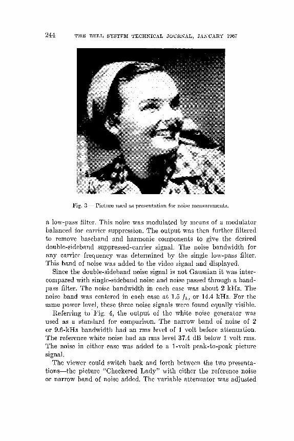
244 THE BELL SYSTEM TECHNICAL JOURNAL, JANUARY 1967
Fig. 3 - Picture used as presentation for noise measurements.
a low-pass filter. This noise was modulated by means of a modulator balanced for carrier suppression. The output was then further filtered to remove baseband and harmonic components to give the desired double-sideband suppressed-carrier signal. The noise bandwidth for any carrier frequency was determined by the single low-pass filter. This band of noise was added to the video signal and displayed.
Since the double-sideband noise signal is not Gaussian it was intercompared with single-sideband noise and noise passed through a bandpass filter. The noise bandwidth in each case was about 2 kHz. The noise band was centered in each case at 1.5 ill, or 14.4 kHz. For the same power level, these three noise signals were found equally visible.
Referring to Fig. 4, the output of the white noise generator was used as a standard for comparison. The narrow band of noise of 2 or 9.6-kHz bandwidth had an rms level of 1 volt before attenuation. The reference white noise had an rms level 37.4 dB below 1 volt rms. The noise in either case was added to a I-volt peak-to-peak picture signal.
The viewer could switch back and forth between the two presentations-the picture "Checkered Lady" with either the reference noise or narrow band of noise added. The variable attenuator was adjusted
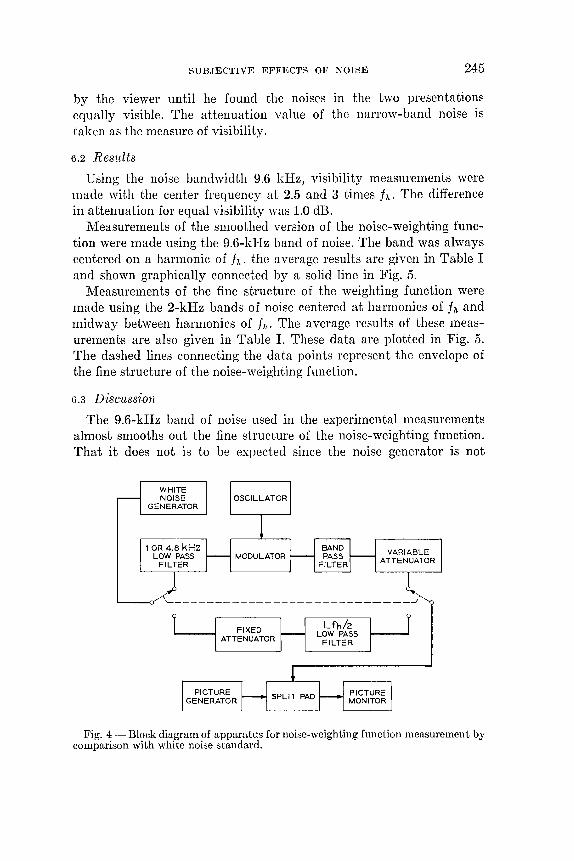
SUBJECTIVE EFFECTS OF NOISE 245
by the viewer until he found the noises in the two presentations equally visible. The attenuation value of the narrow-band noise is taken as the measure of visibility.
6.2 Results
Using the noise bandwidth 9.G kHz, visibility measurements were made with the center frequency at 2.5 and 3 times j". The difference in attenuation for equal visibility was 1.0 dB.
Measurements of the smoothed version of the noise-weighting function were made using the 9.G-kHz band of noise. The band was always centered on a harmonic of j". the average results are given in Table I and shown graphically connected by a solid line in Fig. 5.
Measurements of the fine structure of the weighting function were made using the 2-kHz bands of noise centered at harmonics of 111, and midway between harmonics of 111,. The average results of these measurements are also given in Table 1. These data are plotted in Fig. 5. The dashed lines connecting the data points represent the envelope of the fine structure of the noise-weighting function.
6.3 Discussion
The 9.6-kHz band of noise used in the experimental measurements almost smooths out the fine structure of the noise-weighting function. That it does not is to be expected since the noise generator is not
~----------------------------~
Fig. 4 - Block diagram of apparatus for noise-weighting function measurement by comparison with white noise standard.

246 THE BELL SYSTEM TECHNICAL JOURNAL, JANUARY 1967
TABLE I-COMPARISON OF NARROW-BAND NOISES TO WHITE
NOISE STANDARD
Noise bandwidth 9.6 kHz Noise bandwidth 2 kHz
Attenuation for Attenuation for Center frequency equal visibility Center frequency equal visibility
kHz fh harmonic dB kHz fh harmonic dB
0 0 43.8 19.2 2 49.6 19.2 2 43.7 24.0 2.5 38.2 48.0 5 44.7 48.0 5 48.6 96.0 10 42.3 .52.8 5.5 36.8
192 20 40.7 96.0 10 48.2 384 40 39.2 100.8 10.5 38.4 768 80 36.3 192.0 20 47.7
196.8 20.5 38.8 384.0 40 44.6 388.8 40.5 37.7 768.0 80 40.8
exactly flat due to flicker noise, the low-frequency cutoff of the noise amplifier, and the low-pass filter to bandlimit the noise to 4.8 kHz.
The experimental results agree qualitatively with the noise-weighting function expected by treating the noise as a sampled function. That is, spatial noise in the horizontal direction can be related to the overall frequency characteristic of the noise-weighting function, and spatial noise in the vertical direction can be related to the fine structure of the weighting function with a period equal to the horizontal frequency. From Fig. 5 we see that the fine structure of the noise-weighting function measured with 2-kHz bands of noise for low
50
If)
>- ~ 48 t::~ -.Ju ~~ 46
~z > ~ 44 ((If) 0-u..g 42 ZUJ
2t-t:ii 40 :d~
~o 38 t-t-t--.J 4::§ 36
Cf UJ
34 1
-,:",
~.
-
2
,-L_ r-~ I I I I I I
6 r--- -, r-, -~ ~
" 0 r,
I
OVERALL r--.. ........... ENVELOPE OF'~
VARIATION ~ FI NE STRUCTURE
~ .~ ~ I
I \. r'.... I
'---' -L~~ 6--- ~
6 ..... r-..::::::::
~ ......
I I I I [ I I I 4 6 8 10 20 40 60 80 100
HARMONIC OF fh,
Fig. 5 - Noise-weighting function.
SUBJECTIVE EFFECTS OF NOISE 247
harmonics of Ill, has a variation about equal to its overall change across the band, about 12 dB in either case. For the higher harmonics, the variation is roughly as expected from the calculated grating spacings involved.
VII. VISIBILI'rY OF SINE WAVE INTERFERENCE
7.1 Experimental Procedures
For these measurements, the same system was utilized as for measuring noise weighting, the reduced-resolution TV system which has 160 lines per frame and 60 frames per second with no interlace. The viewer sat 8 times picture height from the 4.5-inch TV presentation. The gratings were presented on the TV screen with no additional picture signal present. The input frequencies for generating the desired gratings were obtained by counting down from a common high frequency oscillator from which the horizontal and vertical drive rates were determined. In this manner, anyone of a set of gratings could be reproduced precisely as desired. The input frequencies used in these measurements were all below one half the horizontal line rate. Thus, all gratings used had a horizontal spatial frequency m equal to zero and vertical spatial frequency n corresponding to the input-signal frequency,
f = f~ n.
The threshold of visibility was used as a convenient measure for the visibility function. Since the noise levels of interest for the weighting function are very low, the threshold of visibility is a reasonable measure.
The tests were conducted by having the viewers, knowledgeable colleagues, attenuate the grating signal by means of a step attenuator until the grating was just invisible; the attenuatar gave calibrated one dB attenuation steps. The data taken for each grating were averaged over all viewers.
The measurements made were of TaTbTc, as for the noise measurements; the complete transfer function was measured. We call this sine-wave visibility function V to distinguish it from the noise visibility function VV.
7.2 Motion
To measure the dependence of V with motion, a set of measurements was made at an average screen luminance of 15 cd/m2. Four

248 THE BELL SYSTEM TECHNICAL JOURNAL, JANUARY 1967
TABLE II - DIFFERENCE FREQUENCY AND ATTENUATION FOR
THRESHOLD VISIBILITY OF MOVING SINE WAVE GRATINGS
Video frequency 2.4 kHz 1.2 kHz 480 Hz 120 Hz
----F dB F dB F dB F dB
--------
0 65.00 0 72.14 0 71.00 0 58.14 1.88 65.85 0.94 73.57 0.95 75.57 0.49 62.42 3.75 67.57 1.88 73.57 2.05 76.00 1.01 66.14 5.62 67.71 2.81 74.57 2.99 78.28 1.41 67.00 9.34 67.42 5.60 74.42 5.05 78.14 2.00 69.71
16.76 61.85 10.2 73.28 10.0 76.57 3.00 70.28 29.63 47.71 16.65 67.00 15.0 71.71 5.00 72.28
29.27 56.71 22.0 64.71 10.0 70.85 30.0 57.71 15.0 65.85
23.0 61.14 29.4 55.16
input frequency ranges were selected: 2, 4, 10, and 20 times the frame rate of 60 Hz producing gratings with spatial frequencies of 2, 4, 10, and 20 cycles per picture height. A set of frequencies near each of the selected frequencies was used to present the desired moving gratings on the screen. Room lighting was adjusted only to reduce reflections from the TV screen.
The average of the data for all viewers is given in Table II and is shown in Fig. 6. In Fig. 6, we see that for any spatial frequency there is an increase in V with motion for difference frequencies F less than 5 or 6 Hz.
From these measurements above and the measurements of Fowler16
it appears that this peak at F = 5 to 6 cycles per second is independent of the spatial frequency and the average luminance.
For F = 0, or stationary gratings, we see that there is a peak in transmission vs. spatial frequency as found by Lowry and DePalma.9 • 10
The peak as shown in Fig. 7 occurs at a lower spatial frequency corresponding to the lower luminance level, at about 15 cycles per picture height. For moving gratings with luminance changes at 5 Hz, the peak in transmission with spatial frequency is shifted to lower spatial frequency, at about 8 or less cycles per picture height. This is also shown in Fig. 7. Integrating over frequencies F from (p - -i)jv to (p + !) f v, as would be done for random noise inputs according to (1), it is evident from Fig. 7 that the peak for W, if it exists, would be shifted to much lower frequencies than is evident from stationary grating measurements.

SUBJECTIVE EFFECTS OF NOISE
8or-----.------r-----,------,-----,------,------,
III ...J W en U 751-#-----;=.--1 W o ~
~ 70 ::J CD iii > 65~~---+------~~~~~~~~¥r--4_------r_----~ o ...J o I III w OC60~----4_----_4------4_--~_+----~~~~_+----~ I t-OC o u. Z55~----4-----~------4-----_+--~--+_----~----~
o ~ ~
~50~----4------4------4------+------+-~r--+----~ t-
~
450L-----~5L-----J10------J15------2~0------2~5------3~0~--~35
FREQUENCY SEPARATION FROM FRAME MULTIPLE IN Hz
Fig. 6 -- Threshold visibility of sine wave grating with motion.
80r----.-----.-----.----.-----.-__ --,
~ 75r-----,-~~+_----+_--~~----~----~
~~ IIlW
~fQ F ~ 70t-----t------t--/-'--4_----4_~~__+----_I
o ~z 11.-
z>Q j 65 t-----t---T--t------t-----4_----4----_I ~CD ~~ w> t- 60t---~~----4_----4_----~----__+----~ ~
55~--~~----~----~----~----~----~ 1.25 2.5 5 10 20 40 80
SPATIAL FREQUENCY IN c/ph
249
Fig. 7 - Threshold visibility of sine wave grating vs spatial frequency for F = 0 and 5 Hz.

250 THE BELL SYSTEM TECHNICAL JOURNAL, JANUARY 1967
7.3 Average Luminance
Assuming that the peak with motion occurs at .5 Hz independent of the average luminance, a series of measurements was undertaken using in all cases F = 5 Hz. 1\1easurements were made at average luminance values of 0.86, 3.4, 15, and 51 cd/m2. Room lighting was reduced and arranged such that the low reflection kinescope screen gave a luminance by reflection of room lighting of 0.086 cd/m2.
The results of these measurements are given in Table III and shown in Fig. 8. As in Schade's results,13 the peak in visibility with spatial frequency at anyone luminance value moves to lower spatial frequencies as the average luminance is decreased. There is a peak in visibility as a function of luminance. This peak occurs at a luminance value of about 3.4 cd/m2 independent of spatial frequency.
7.4 Orientation
We consider the dependence of the acuity of vision on the angle of a test chart. Threshold measurements by Higgins and Stultz19 show that a 12 percent increase in grating spacing or decrease in spatial frequency is required for a grating oriented at 45° to the horizontal to appear equivalent (just visible) to a grating oriented either horizontally or vertically. If we assume that for the particular circumstances of measurements reported above there is a similar variation of visibility with angle, that is, a 12 percent decrease in spatial frequency for 45° orientation to appear equivalent to horizontal or vertical orientation, than we can estimate the effects on the weighting function.
We need to know the maximum change in the measured weighting function for a 12 percent change in spatial frequency for a given orien-
TABLE III - ATTENUATION FOR THRESHOLD VISIBILITY OF SINE
WAVE GRATINGS
Average luminance 51 15.4 3.4 0.86 cd/m2
Spatial frequency
(dB) (dB) (c/ph) (dB) (dB) 80 49.6 56.0 59.0 56.4 40 66.2 68.6 73.4 70.4 20 75.2 77.0 80.2 78.0 8 73.4 79.8 84.8 83.6 2 63.2 70.4 79.8 78.6

SUBJECTIVE EFFECTS OF NOISE
~85r----r----.-~~----.-----.----.--~ --l W co 880r-~~~--+-~~~~~----~---+--~ o
~ ~75r----r~~T----+~~~~~r----+--~ t: --l ai ~70r-~-r---,~---+----~~~~---+--~ ;; o 665r---~----.---~----~----~~_+----~ I ~ W 0: I6or----r----+---~----~----~~~----~ I-
0: o ~55r----r----+---~----~----~_4_+----~ z o
~50r----r----+----+----~----~---*----~ z w I-
~45~--~----~--~~--~----~--~~--~ 1.25 2.5 5 10 20 40 80 160
SPATIAL FREQUENCY IN c/ph
251
Fig. 8 - Threshold visibility of sine wave grating vs spatial frequency for F = 5 Hz and various average luminance values.
tation of grating. This will give us the maximum effect on the weighting function that we should expect as a result of eye anisotropy.
For narrow band noise located at harmonics of /h for relatively large harmonics, these noise bands produce mainly gratings with vertical bars, i.e., large m and small n. From (6), with small n, then m and video frequency are linearly related and hence the spatial frequency of the grating is linearly related to video frequency. From the data in Fig. 5, the maximum change of the curve through these points is about 0.6 dB for a 12 percent change in frequency. Thus, we expect this curve to reflect everywhere less than I-dB variation due to a phenomenon related to the variation of eye acuity with orientation.
7.5 Modulation Level
The threshold measurements with sine waves were all made with the signal more than 45 dB below 1 volt rms at a gain setting corresponding to a I-volt peak-to-peak video signal. The suprathreshold noise measurements were all made with noise-power levels below 35 dB below I volt rms for a I-volt peak-to-peak video signal. We do not believe that this difference would be significant in regard to the
252 THE BELL SYSTEM TECHNICAL JOURNAL, JANUARY 1967
transfer function on a relative basis. A constant ratio should exist between the two curves.
VIII. RELA'l'ION BETWEEN V AND W
It has been considered by many that the modulation transfer function as measured with sine waves and bands of random noise were quite incommensurate. 'Vith all the known nonlinearities involved, (1) certainly cannot give an accurate statement of the noise-weighting function from measurements made with sine-wave interference.
However, the data on sine waves presented here indicate that a very reasonable estimate of the noise-weighting function can be obtained. Ignoring grating orientation and modulation level we are considering visibility in a 4-dimensional space. The visibility V of each video frequency component of the interference has been discussed as a function of the corresponding spatial frequency l/A and motion v of that component and the average luminance 1 at which it is viewed. This is written as
V = YeA, v, I).
Many values of V for particular values of the parameters have been measured which indicate the form of the function. Through our knowledge of the scanning procedure we can transform YeA, v, I) to a function of video frequency f and I, V(f, I).
For normal television viewing, the noise signal is superimposed on a picture such that the noise is seen at a continuum of brightness levels in the various parts of the TV screen. Thus, for V to correspond to noise-weighting we require an integration over the range of average luminance. Measurements of amplitude statistics on the electrical video signal voltage indicate a rather flat density function. This is equivalent to saying that the area in the picture from a small signal voltage range is independent of the voltage. We expect from this that an integration of V should be performed over luminance levels specified as video signal voltage levels. This problem is easily solved by the measurement of visibility of sine waves superimposed on a TV picture.
The resulting function V (f), after smoothing average luminance effects, contains all the structure of the noise-weighting function. The microstructure stems from the motion of gratings and the overall function and fine structure are due to the constituent gratings as described in Section III. Wand V are qualitatively alike.
The fine structure of W measured with narrow bands of noise
SUBJECTIVE EFFECTS OF NOISE 253
discussed in Section VI stems from smoothing the variations at multiples of the frame rate. There is also a partial smoothing of the fine structure due to the actual bandwidth of noise, 2 kHz, which is not small compared to the period of this structure occurring at multiples of 9.6 kHz. The corresponding version of V is obtained from the sine wave data by first integrating with respect to v, or equivalently F, since the microstructure stems from this variation. This involves integration over the curves displayed in Fig. 6. The curves have a logarithmic scale. Since these curves are all similar but displaced vertically the integral would be approximately a constant times the peak value. This constant is applied to the average curve of visibility with spatial frequency as in Fig. 8.
The average of the curves of Fig. 8 should approximately represent the first portion of the fine structure of the weighting function, that is, for m = 0 and n varying from 2 to 80 c/ph.
For the smoothing due to the 2-kHz noise bandwidth, we consider the curves of Fig. 8. The data points between 0 and 10 c/ph and between 60 and 80 c/ph can be "visually averaged." The difference between these two average values indicates less than a 17 -dB variation for the fine structure of the weighting function. This is 4 dB larger than the 13-dB measurement of W. Considering that there were two "integrations" performed over average luminance and motion and not all luminance values are considered, this difference should be expected.
There is a peak in visibility in the "average" of the curves of Fig. 8 . at about 4 c/ph or less. A rather narrow band of noise, 60 Hz, would be required to verify the existence of this peak in the fine structure of W.
The overall weighting function is obtained by smoothing out the fine structure. There is a substantial difference in the fine structure of the weighting function across the band. The fine structure at the low end of the band corresponds to gratings of spatial frequencies varying from 1 to 80 c/ph. At the high end of the band there are spatial frequencies varying from 80 to 80 y2 c/ph. We do not expect the integration to lead to a constant times the peak of the fine structure.
The peaks of the fine structure measured with 2-kHz bands of noise as shown in Fig. 5 give only a 10-dB variation for m varying from 2 to 80 compared to the 12 to 14-dB variations measured for the equivalent change in n. For complete smoothing of the fine structure, Fig. 5 shows that only an 8 or 9-dB variation was obtained for m varying from 2 to 80.

254 THE BELL SYSTEM TECHNICAL JOURNAL, JANUARY 1967
IX. APPLICATIONS AND IMPLICATIONS
9.1 Noise Weighting for Photographs and TV
The data of Section 7.2 show a significant difference in the noiseweighting function depending on the presence or absence of motion. Huang's measurementsll with still pictures verifies this difference. His weighting function has peaks at spatial frequencies that correspond approximately with those measured for stationary gratings.
Signal processing of a single TV frame can be conveniently accomplished on a multipurpose computer to quickly examine some of the many possible processing procedures. It must be remembered that the resultant noise viewed on the single output picture has a different noise weighting than the completed system processing a sequence of TV frames to be viewed.
9.2 TV Frame Storage and Repetition
Consider a frame-repeated television presentation21 where one frame of a television signal is stored in a memory such that it can be repetitively flasked k times on the kinescope, then another frame is accepted, stored and repetitively shown, etc. Examine anyone point on the kinescope presentation, as in Section 3.3. For human vision, which does not see the 60-cycle flicker, there is presented a luminance value which is held constant for k frames, then a new luminance value is presented. As a sampling function this represents one sample for every k frames of the original TV signal without frame repeating.
We wish to examine the visibility of noise for TV frame repetition. All frequencies of the video input have been shown to contribute to the flicker at a point in the frequency band from 0 to 30 Hz for the nonrepetitive (k = 1) TV presentation. Each frequency also contributes to each 30-Hz wide band above 30 Hz but vision filters out almost all contributions above 30 Hz.
The frame repetition procedure samples the video signal at each point on the screen at 60/k Hz. Each input video frequency contributes to flicker in a band from 0 to 60/2k Hz. The repetition of frames, in effect, holds this sampled value for k frame times. This filter action reduces flicker frequencies above 60/2k Hz; the 60-Hz frame frequency is filtered by the visual process. Considered as a true sample and hold filter the response would be (sin x) /x where x = 7r kF /60. The first zero would be at F = 60/k.
The net effect of frame repetition is to fold noise from the 0 to 30-Hz band into the 0 to 30/k-Hz band. From Fig. 6 it is evident that for

SUBJECTIVE EFFEC'l'S OF NOISE 255
k = 2 the flicker noise is in a frequency region, 0 15 Hz, where on the average it is more visible. For k = 4, the noise is in the band o - 7.5 Hz where it may be somewhat more visible than for k = 2. For k > 4, the data of Fig. 7 indicates that the noise limited to a band < 7.5 Hz will be less visible than for k ~ 4.
9.3 Wand Average Luminance
The data for the sine wave interference visibility at various values of average luminance show a substantial variation. However, the noiseweighting function is to be used as a relative measure. Since the curves of Fig. 8 are all similar except at very low spatial frequencies, it appears that W measured at anyone luminance value is reasonable.
9.4 W Applied to TV Transmission System
Two examples are given below of the application of the nOlse\veighting function as a figure of merit for television systems.
9.4.1 Analog Transmission
Thermal noise, assumed flat over the video bandwidth, is added to the signal in the analog channel. A TV signal has extensive structure in its power spectrum.6 The power is densely packed at harmonics of frame and horizontal line rates and predominately at low frequencies. Most of the frequency band has very low signal power.
It is possible to increase the signal-to-noise ratio by linear preemphasis of the signal before transmission with the inverse reconstruction operation at the receiver.22 The pre-emphasis filter increases the signal power where it is very low with a corresponding reduction in power where the original signal power was high to maintain the transmitted power constant. The reconstruction filter performs the inverse action on the signal plus noise. Thus, where the original signal was of low power the noise is substantially reduced, whereas, where the original signal was of high power the noise is increased. Since the usual TV transmission channel is actually peak-power limited, the expected improvement is further limited by this constraint.
However, if we consider the signal-to-weighted-noise ratio as a criterion23 a quite different result is obtained. Wherever the TV signal power is high, at harmonics of In. and Iv and at low frequencies, the noise-weighting function is also high. The filtering procedure above increases the noise power where it is most visible. Even with the optimum filter pair23 designed for maximum signal-to-weightednoise ratio there is very little improvement possible.

256 THE BELL SYSTEM TECHNICAL JOURNAL, JANUARY 1967
9.4.2 Bandwidth Reduction for PCJVJ-TV Noise in a pulse code modulation (PCM) system is principally
due to amplitude quantization. It is possible to shape the power spectrum of this noise. This fact is utilized in differential PCM24 and error-feedback coding.25,26 The combination of pre-emphasis and reconstruction filters with noise-power-spectrum shaping has proved effective when using horizontal picture correlation which corresponds to the smoothed power spectrum of the video signa1.22,26
The pre-emphasis and reconstruction filters are employed as in the analog transmission system of Section 904.1 to boost signal where it was originally low keeping total power constant. Noise-spectrum shaping is used to reduce the noise at frequencies where the original video-signal power was high. This noise filtering is accomplished by a feedback loop around a quantizer and gives an increase in total quantization noise power.
A differential system incorporates the signal pre-emphasis and quantizing-noise shaping in the one filtering path of the quantizer feedback loop. O'N ea}27 has calculated the signal-to-noise ratio for some differential systems. He considers operation on the overall signal-power spectrum and on the power peaks at horizontal line harmonics both separately and combined. He finds that either operation separately gives a substantial increase in signal-to-noise ratio, but that the combined operation does not give any additional improvement.
Since this combined operation redistributes the noise power to regions where it is less visible we expect that the signal-to-weightednoise ratio should be increased for the combined filtering operations over that obtained for either filter operation separately.
9.5 111 easurement of Smoothed W Previous measurements of W have been with relatively wide bands
of noise.2,3,4 The bands of noise chosen for these measurements have not always been the best. With noise bands selected on an octave basis2 there is a confounding of the results by the fine structure at the low frequency end of the band. With an input noise bandwidth of exactly fh the spatial-noise power spectrum along y would be flat, independent of the center frequency of the input noise band. Using these relatively narrow bands of noise we expect to smooth out the fine structure of the noise-weighting function and make a more precise measurement of the gross noise-weighting function than with wider bands of noise.

SUBJECTIVE EFFECTS OF NOISE 257
9.6 Disproving an Hypothesis
The hypothesis2s has been suggested that anisotropy of the noise is important in visual response. We take as a definition of anisotropy that the spatial power spectra in orthogonal directions are not the same. The hypothesis states that the more anisotropic a noise is the more objectionable it is. However, judging from our results, this cannot be true. If we examine our experimental results for frequencies about 1.5 IlL and 2 Ih' then we have low horizontal spatial frequencies. Near 2 IlL the narrow band of noise is folded to appear as low vertical spatial frequencies. The result for this noise, which is fairly isotropic, is that it is annoying. Near 1.5 IlL the narrow band of noise is folded to appear as high vertical spatial frequencies. Our result for this anisotropic noise is that it is less annoying than the isotropic noise. This is in contradiction to the hypothesis under consideration.2s
x. CONCLUSION
The subjective noise-weighting function consists of the transfer functions of the kinescope and the visual process. The scanning procedure of the kinescope produces a complicated variation in the spatial and flicker frequencies of the display as a function of the input video frequency. A rather extensive discussion has been given for the scanning process for a ~quare picture. These results are applicable to any rectangular picture also. A change in the picture height control to form a rectangular picture requires only that a constant factor be applied to all vertical spatial frequencies. The modulation transfer function of vision is strongly dependent on spatial and flicker frequencies. The resultant weighting function has a fine structure related to scan-line-frequency harmonics and a microstructure related to frame-frequency harmonics.
Subjective measurements were made to determine the fine structure and microstructure of the noise-weighting function. Noise near a multiple of the horizontal line frequency is much more visible than similar noise between multiples of the horizontal line frequency. Sine waves differing by 5 Hz fro111 a multiple of the frame frequency are much more visible than sine waves midway between multiples of the frame frequency and, particularly for low spatial frequencies, are much more visible than sine waves at multiples of the frame frequency.
The measured visibility of noise and sine-wave interference in television is in good agreement with that expected from considering

258 THE BELL SYSTEM TECHNICAL JOURNAL, JANUARY 19U7
the TV presentation due to scanning. This indicates a quite linear system for the small additive interferences. This linearity leads to rejection of a hypotheses that visibility of noise in TV may be a function of anisotropy of the spatial noise power spectrum.
The subjective noise-weighting function is valuable in determining a figure of merit in many applications. When considering the results of calculations on only one frame of a television sequence, as is done in computer simUlations, one can be lead to erroneous results of visibility of noise due to a significant difference in visibility between stationary and moving patterns in a TV presentation. The variation in visibility with motion leads to conclusions about the visibility of noise with television frame repeating which have been tentatively verified by others.21 A variation in visibility with average luminance must be considered for noise-weighting function measurements on a flat screen at only one average luminance level.
The use of weighted noise as a measure of merit for television transmission, as an analog or PCM signal, leads to a significantly different result in either case from published results considering only the noise as a measure of merit.
XI. ACKNOWLEDGMENT
Thanks are due to my colleagues, C. J. Candy, L. H. Enloe, B. Prasada, and W. T. Wintringham for their helpful discussions and constructive criticisms and to E. S. Bednar for his efforts in the subjective measurements reported.
TABLE OF SYMBOLS
c/ ph cycles per picture height f video frequency fh horizontal-line scanning frequency f v frame scanning frequency f. frequency components of sampled video signal F frequency associated with moving grating patterns 1 luminance L number of lines in picture m horizontal spatial frequency n vertical spatial frequency N noise power spectrum P weighted noise power r spatial frequency in direction parallel to horizontal-scan lines

SUBJECTIVE EFFECTS OF NOISE
T a transfer function of kinescope T b transfer function of vision T c translation to words v velocity of moving grating patterns V sine wave visibility function TV subjective noise-weighting function A spatial wavelength of grating patterns
HEFERENCES
259
1. Mertz, P., Perception of Television Random Noise, J SMPTE, 54, January, 1950, pp. 8-34.
2. Brainard, R. C., Kammerer, F. W., and Kimme, E. G., Estimation of the Subjective Effects of Noise in Low Resolution Television Systems, IRE Trans. Inform. Theor., IT-8, February, 1962, pp. 99-106.
3. Barstow, J. M. and Christopher, H. N., The Measurement of Random Video Interference to Monochrome and Color Television Pictures, Trans. AlEE, Part I, Commun. Electron., 81, 1962, pp. 313-320.
4. Muller, J. and Demus, E., Ermittlung Eines Rauschbewertungs-filters fur das Femsehen, Nachrichtentech Z, 12, April, 1959, pp. 181-186.
5. Christopher, H. N., private communication. 6. Mertz, P. and Gray, F., Theory of Scanning, B.S.T.J., 13, July, 1934, pp. 464-
515. 7. Huang, T. S., The Power Density Spectrum of Television Random Noise,
J. Appl. Opt., 4, May, 1965, pp. 597-601. 8. Bryngdahl, 0., Characteristics of the Visual System: Psychophysical Measure
ments of the Response to Spatial Sine-Wave Stimuli in the Mesopic Region, J. Opt. Soc. Amer., 54, September, 1964, pp. 1152-1160.
9. Lowry, E. M. and DePalma, J. J., Sine Wave Response of the Visual System I. The Mach Phenomenon, J. Opt. Soc. Amer., 51, July, 1961, pp. 740-6.
10. DePalma, J. J. and Lowry, E. M., Sine-Wave Response of the Visual System II. Sine Wave and Square Wave Contrast Sensitivity, J. Opt. Soc. Amer., 52, March, 1962, pp. 382-35.
11. Huang, T. S., The Subjective Effect of Two-Dimensional Pictorial Noise, IEEE Trans. Inform. Theor. IT-ll, January, 1965, pp. 43-53.
12. Budrikis, Z. L., Visual Thresholds and The Visibility of Random Noise in TV, Proc. IRE Austral, 22, December, 1961, pp. 751-9.
13. Schade, O. H., Sr., Optical and Photoelectric Analog of the Eye, J. Opt. Soc. Amer., 46, September, 1956, pp. 721-739.
14. Schober, H. A. W. and Hilz, R., Contrast Sensitivity of the Human Eye for Square-Wave Gratings, J. Opt. Soc. Amer., 55, September, 1965, pp. 1086-1091.
15. Fowler, A. D., Low-Frequency Interference in Television Pictures, Proc. IRE, 39, October, 1951, pp. 1332-1336.
16. Davson, H., The Physiology of the Eye, Second Edition, Boston: Little and Brown, 1963, p. 165.
17. Bryngdahl, 0., Effect of Retinal Image Motion on Visual Acuity, Opt. Acta, 8, 1961, pp. 1-16.
18. Kelly, D. H., Effects of Sharp Edges in a Flickering Field, J. Opt. Soc. Amer., 49, 1959, p. 730.
19. Higgins, G. C. and Stultz, K., Visual Acuity as Measured with Various Orientations of a Parallel-Line Test Object, J. Opt. Soc. Amer., 38, September, 1948, pp. 756-8.
20. Campbell, F. W. and Robson, J. G., Application of Fourier Analysis to the Modulation Response of the Eye, J. Opt. Soc. Amer., 54, 1964, p. 581.
21. Brainard, R. C., Mounts, F. W., and Prasada, B., Low-Resolution TV: Sub-
260 THE BELL SYSTEM TECHNICAL JOURNAL, JANUARY 1967
jective Effects of Frame Repetition and Picture Replenishment, B.S.T.J., this issue, pp. 301-311.
22. Franks, L. E., A Model for the Random Video Process, B.S.T.J., 45, April, 1966, pp. 609-30.
23. Shtein, V. M., Computation of Linear Pre distorting and Correcting Systems, Radiotekhnika, 11 (2), 1956, pp. 60-3.
24. Cutler, C. C., Differential Quantization of Communication Signals, Patent No. 2,605,361, July 29, 1952.
25. Cutler, C. C., Transmission Systems Employing Quantization, Patent No. 2,927,962, March 8, 1960. '
26. Kimme, E. G. and Kuo, F. F., Synthesis of Optimal Filters for a Feedback Quantization System, IEEE Trans. Circuit Theor., CT-lO, September, 1963, pp. 405-13.
27. O'Neal, J. B., Jr., Predictive Quantizing Systems (Differential Pulse Code Modulation) for the Transmission of Television Signals, B.S.T.J., 45, 1966, pp. 689-721.
28. Huang, T. S., Two Dimensional Power Spectrum of Television Random Noise, MIT Res. Lab. Electron., QPR, No. 69, pp. 143-149.
29. van den Brink, G., The Visibility of Details of a Moving Object, Acta Electron, 2, 1957-58, pp. 44-49.
Low-Resolution TV: Subjective Effects of Frame Repetitioll and
Picture Replenishm.ent
By R. C. BRAINARD, F. W. MOUNTS AND B. PRASADA
(Manuscript received September 19, 1966)
Using the experimental television facility described in a companion paper, frame repeating and point-by-point selective replenishment of picture elements have been accomplished in real time. On the basis of initial experiments, using the head-and-shoulder view of a person as the picture source, such as is likely to be encountered in a visual communication system, the following tentative conclusions have been reached:
(i) The lnotion rendition with a 15 new pictures/second fTalne repeating system, while not flawless, is reasonably good.
(ii) Selectively replenishing one-quarter of the picture points per frame gives a better continuity of motion but results in objectionable patterns.
(iii) Picture quality greatly depends on the pattern of picture replenishment. Of the five replenishment patterns tested, two result in pictures which are significantly better than the other three.
(iv) In informal viewings, opinion has been so divided that no preference has been established between simple 15 new pictures/second frame Tepeating and the more satisfying schemes for picture replenishment.
(v) The frame repeating and replenishment systems produce gross impairment during zooming and panning; consequently, these systems in their present form are unlikely to be useful for broadcast television.
The impairments observed in these systems are subjective and not yet predictable. This emphasizes the importance of subjective testing of systems in real time.
261

2G2 THE BELL SYS'l'EM 'l'ECHNICAL JOURNAL, JANUARY 19G7
1. INTRODUCTION
Experiments on real-time operation of various frame repeating and replenishment systems were performed with a low-resolution TV system described in a companion paper.1 The head-and-shoulder view of a person was used as the picture source as might be used in a visual communication system.
As is well-known, the lower bound on the number of presentations per second in a television system is set by the flicker requirements. No systematic study of motion in TV pictures has been possible in the past because the flicker requirements dictate that for a screen luminance of, say, 85 cd/m2 (25 fL), something of the order of 60 presentations must be presented every second to alleviate the flicker problem. The presentation requirements for producing smooth perceived motion for most of the common types of movements are much less than this. In the past, suitable means have not been available for the study of the lower bound on the picture rate necessary, for the satisfactory rendition of motion in television systems.
With the availability of large-capacity, high-speed ultrasonic delay lines,2 it is now possible to store, in digital form, large quantities of information. Delay lines with a total storage capacity of 25 kilobits and an input-output rate of approximately 1.5 megabits/second are readily available now. Using eight assemblies of lines and a picture format of 160 samples per line, 160 lines per frame sequentially scanned at 60 frames per second, allows storage of one complete picture frame encoded as 8-digit PCM at a sampling rate of 1.536 MHz.
The stored information can be displayed several times on the display monitor at a suitable rate to satisfy the requirements for display flicker. This allows sending new information through the channel to satisfy only the condition of suitable rendition of motion. The availability of frame storage has made it possible to study motion rendition separated from display flicker effects.
The rendition of motion by rapid superimposition of a sequence of still pictures is based on the exploitation of a perceptual property of the viewer, namely, the persistence of vision. Our knowledge of the human perceptual mechanism is still quite incomplete and primitive. Hence, it is obvious that a system exploiting perceptual redundancy can only be evaluated by obtaining the subjective responses of the viewers in controlled experiments. To obtain the subjective responses, the operation or simulation of the systems on the time scale identical to the original motion is imperative and its importance cannot be overemphasized.

FRAME REPE'rITION AND PICTURE REPLENISHMENT 263
Frame repetition is taken to mean that one complete frame is transmitted to the receiver, stored in the memory and then shown repetitively a number of times on the TV screen. In a replenishment system a portion of the picture information from each frame is transmitted during that frame time. At the receiver this information must be inserted in the memory in the appropriate time slots. Complete pictures are read out of the memory each frame time for display, but the picture changes from frame to frame as the new information is added.
II. SYSTEM DESCRIPTION
A block diagram of the basic system is shown in Fig. 1. The details of the system's components are described elsewhere.1 The video signal is generated by a vidicon camera system designed to sequentially scan the vidicon at 60 frames per second with a square raster of 160 lines. Suitable low-pass filtering limits the bandwidth of the signal to less than 768 kHz. Unless otherwise stated, the picture was restricted to a head-und-shoulder view of a person.
The video signal is sampled at the rate of 1.536 MHz and the samples are encoded by an 8-digit PCM encoder. The output digits of the encoder are in parallel form. Each digit is routed to a 1/60 second delay line. The switch S in Fig. 1, at any instant, connects each delay line input either to the respective encoder output or to its own output. If the switch is at position A, new data is inserted into each delay line and is also decoded and displayed. If the switch is at position B, the
8- BIT PARALLEL OUTPUT
\
SCANNING BEAM GATING SIGNAL
\ \ I 'f
~,
'8-BIT PARALLEL INPUT
Fig. 1 - Basic frame repeating and replenishment systems.

264 THE BELL SYSTEM TECHNICAL JOURNAL, JANUARY 1967
data, which has been previously stored and displayed, is displayed again and is recirculated through the delay lines. Whatever the switch position, the monitor display rate remains constant at 60 frames/second. The switch S operates fast enough that any selected sample or group of samples can be replaced.
By generating different switch control waveforms, we can make the basic system operate as different frame repeating or replenishment systems. By constraining switch S to remain at position B, we can operate the memory in the circulating mode and store its contents indefinitely. This feature allows close scrutiny of any particular frame and also eases the problem of taking still photographs.
While the subject is producing exaggerated hand and head motion, the memory may be placed in the circulating mode. This ensures that a single frame is frozen in the memory and is available for photographing. This procedure has been followed for taking all the photographs included in this paper.
Observations were conducted in the laboratory at a reduced room illumination of approximately 300 lux (30 fc). The monitor was adjusted to have a highlight luminance of approximately 340 cd/m2 (100 fL).
2.1 Frame Repeating Systenl,s
The basic frame repeating principle can be illustrated by Fig. 2. The vidicon is sequentially scanned every 1/60 second. However, only every nth frame is displayed on the monitor and stored in the memory. This frame is then repeated (n - 1) times on the monitor. The presentation rate is maintained at 60 frames per second to combat flicker. In other words, every nth frame is sent to the receiver which uses zero-order interpolation to fill in the missing frames.
In the basic experiment described above, the camera is sequentially scanned every 1/60 second. Switch S' is open. Thus, the visual signal is integrated on the camera photo-cathode for 1/60 second. The problem of the optimum integration period will be discussed later. Switch S" from the noise generator is open for these experiments.
2.2 Replenishment Systems
In a replenishment system, only a fraction of the total picture information is replenished during each frame period. Using signal storage, replenishment systems build up a picture by sending l/n of the total number of samples contained in a frame in one frame period. Thereafter, in every presentation, l/n of the samples are new while

FRAME REPETITION AND PICTURE REPLENISHMENT 265
the rest are old.;} Thus, new samples continually replenish old ones according to some predetermined scheme.
III. SOME RESULTS
Several frame repeating and replenishment systems have been operated in real time. Impairments are produced only in those areas where there is real or apparent movement, i.e., where the luminance at
Fl F2 F3 F4 --- --- Fn
ICDI0181CS)ICDI0181C9ICDI0181(~Ktr TV CAMERA OUTPUT
ICDI FRAMES STORED IN THE MEMORY
Fn ,--.--1(---1", , , I 1 '\...'./' .1. __ .L_
Fj F; Fl F4 F.; F4 F7 F7 F7 FlO Fio Fio Fn
ICDICDICDICS)ICS)ICS)18181810101(2~(Xr MONITOR DISPLAY
Fig. 2 - Frame repeating.
a point changes from frame-to-frame. Further, the type of impairment for a particular system depends on the type of motion. The impairments introduced in motion rendition are subjective and are extremely difficult to describe. However, these will be described as best as possible. Photographs will be used to illustrate the effects wherever possible. As all the impairments are produced only in the presence of motion, photographs are not :very satisfactory. Fig. 3 (a) and 4 (a) show a picture when no frame repeating or replenishment is used.
3.1 Frame Repeating Systetns
Using a vidicon integration time of 1/60 second, frame repeating was observed using rates of 30, 20, 15, 12, 10, 8.6, 7.5, 6.7, and 6 new pictures/ second.
* This assumes replenishment of equal number of samples every frame time. This assumption is not necessary in a general case.

266 THE BELL SYSTEM TECHNICAL JOURNAL, JANUARY 1967
As we go from higher rates to lower rates, the impairment, which appears in the form of a jerky motion, increases. For the head-andshoulder view of a person conversing, no impairment is noted at 30 new pictures/second. At 20 new pictures/second, fast large-area motion produces a slight amount of jerkiness. At 15 new pictures/second, noticeable jerkiness is observed for large-area motion, such as head motion. However, the lip motion still appears natural. At 12 new pictures/second, the jerkiness is quite pronounced and some discrepancy can be noticed in the lip region also. As we go down to lower rates, further gradual increase in jerkiness occurs. At 6 new pictures/second the picture is quite jerky. The coordination between the lip motion and the sound is almost completely lacking.
Responses of several engineers after informal viewing suggests that the threshold of acceptability may be between 12 and 15 new pictures/ second. The change in quality as we go from 15 new pictures/second to 12 new pictures/second seems more drastic than for any other pair of adjacent rates. It is proposed to check this observation by careful subjective experiments.
In another experiment, a broadcast TV program was displayed on a TV receiver and was used as the picture source for the system's vidicon camera. Everything else remained the same. It was observed that frame repeating produced gross impairment during zooming and panning of the broadcast studio camera which is quite common in entertainment TV programs.
3.2 Replenishment Systems
The following replenishment systems have been observed in real time:
3.2.1 2 : 1 Replenishment.
The replenishment pattern is shown in Fig. 3 (b). The camera was scanned sequentially at the rate of 60 frames/second. The samples marked 1 were replenished in frame 1 and the samples marked 2 were replenished in frame 2. Thus, the total replenishment time was 1/30 second. A still photograph depicting the system output is shown in Fig. 3 (b).
Very slight impairment in the rendition of motion was observed for this condition.
3.2.2 4 : 1 Replenishment.
The camera was scanned sequentially at the rate of 60 frames/second. Samples were replenished according to five different replenishment
FRAME REPETITION AND PICTURE REPLENISHMENT 267
(a) ( b) ORIGINAL 2:1 REPLENISHMENT
PATTERN: 1 2 121 2 1 2 1 • 1 2 2 1 •
( c) (d) 4:1 REPLENISHMENT 4:1 REPLENISHMENT
PATTERN: PATTERN: 4 3 2 1 4 4 3 2 1 4 4 3 2 1 . 1 4 3 2 . 4 3 2 . 2 1 4 • 4 3 . 3 2 4 4 .
Fig. 3 - Photographs illustrating replenishment patterns.
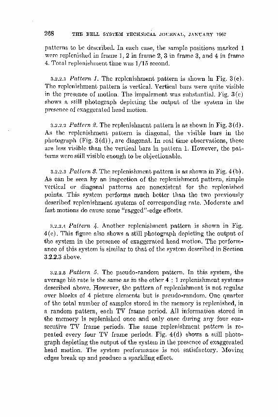
268 THE BELL SYSTEM TECHNICAL JOURNAL, JANUARY 1967
patterns to be described. In each case, the sample positions marked 1 were replenished in frame 1, 2 in frame 2, 3 in frame 3, and 4 in frame 4. Total replenishment time was 1/15 second.
3.2.2.1 Pattern 1. The replenishment pattern is shown in Fig. 3 (c). The replenishment pattern is vertical. Vertical bars were quite visible in the presence of motion. The impairment was substantial. Fig. 3 (c) shows a still photograph depicting the output of the system in the presence of exaggerated head motion.
3.2.2.2 Pattern 2. The replenishment pattern is as shown in Fig. 3 (d). As the replenishment pattern is diagonal, the visible bars in the photograph (Fig. 3 (d)), are diagonal. In real time observations, these are less visible than the vertical bars in pattern 1. However, the patterns were still visible enough to be objectionable.
3.2.2.3 Pattern 3. The replenishment pattern is as shown in Fig. 4(b). As can be seen by an inspection of the replenishment pattern, simple vertical or diagonal patterns are nonexistent for the replenished points. This system performs much better than the two previously described replenishment systems of corresponding rate. Moderate and fast motions do cause some "ragged"-edge effects.
3.2.2.4 Pattern 4. Another replenishment pattern is shown in Fig. 4 (c). This figure also shows a still photograph depicting the output of the system in the presence of exaggerated head motion. The performance of this system is similar to that of the system described in Section 3.2.2.3 above.
3.2.2.5 Pattern 5. The pseudo-random pattern. In this system, the average bit rate is the same as in the other 4 : 1 replenishment systems described above. However, the pattern of replenishment is not regular over blocks of 4 picture elements but is pseudo-random. One quarter of the total number of samples stored in the memory is replenished, in a random pattern, each TV frame period. All information stored in the memory is replenished once and only once during any four consecutive TV frame periods. The same replenishment pattern is repeated every four TV frame periods. Fig. 4 (d) shows a still photograph depicting the output of the system in the presence of exaggerated head motion. The system performance is not satisfactory. Moving edges break up and produce a sparkling effect.

FRAME REPETITION AND PICTURE REPLENISHMEN'r 2GU
(a) ORIGINAL
(c) 4:1 REPLENISHMENT
PATTERN: 21212 3434. 212 34. 2 • • •
(b) 4:1 REPLENISHMENT
PATTERN: 4 1 4 1 4 • 2 3 2 3 • 4 1 4 • 2 3 4 •
(d)
4: 1 REPLENISHMENT PATTERN:
PSEUDO RANDOM
Fig. 4 - Photographs illustrating replenishment patterns.

270 THE BELL SYSTEM TECHNICAL JOUHNAL, JANUAHY 1967
3.3 Frame Repeating With Increased Vidicon Integration Time
The vidicon is a storage type of camera tube. In the standard sequential operation, the light distribution of the scene is integrated on the camera photosensitive element for 1/60 second. For fast motions this integration produces a blur. This effect can be contrasted with a shuttered or a nonstorage type of camera unit that would have produced jerkiness in such a situation. It is felt that a trade-off between sharp but jerky pictures and blurred but smooth pictures exists and there may be a sUbjectively optimum integration time and characteristic for different uses of television.
In the frame repeating experiments described in Section 3.1, the integration time was 1/60 second. On the other hand, if the camera is read out only when a new picture is desired, the image will be integrated on the camera photosensitive element for the full n/60 second if the system uses 60/n new pictures/second. Possibilities exist to obtain any arbitrary integration characteristic if we use external storage.
A preliminary experiment was tried using the vidicon itself as the integration element. No conclusive results were obtained. The Switch S' in Fig. 1 is closed to pass a gating signal to the vidicon to read out the integrated picture every fourth frame time for storage in the memory. However, the nonlinear brightness-current characteristic of the vidicon, the increased stickiness, and the effect of lateral leakage in a vidicon system with increased integration time could have contributed more detrimentally to the resulting display than the improvement from the anticipated integration characteristic.
3.4 Frame Repeating With Noisy Signal
The effect of frame repeating on the visibility of additive noise was observed. The switch S" in Fig. 1 was closed to add noise to the picture signal.
For a reduced number of pictures per second, the noise pattern remained frozen and then suddenly changed to another pattern as a new picture was read in. The noisy picture lost its "busy" look to a certain extent. The impression gained was one of a superimposed noise pattern moving jerkily. The visibility of the noise increased as the number of new pictures/second was decreased.
IV. DISCUSSION
The impairments produced by the frame repeating systems and the replenishment systems are very different.

FRAME REPETITION AND PICTURE REPLENISHMENT 271
In the frame repeating systems, the impairments are in the form of jerky motions. These are most visible where the moving edges are the outlining contours of large areas. There also seems to be a correlation between the average brightness of the area and the visibility of jerkiness. It is an apparent flicker effect.
In the replenishment systems, the jerkiness is missing. However, the impairment appears in the form of ragged edges of the moving objects and the superimposition of visible patterns. The replenishment experiments described clearly bring out the importance of operation or simulation of systems on the time scale identical to the original motion for the purpose of subjective evaluation. It may be recalled that for the same bit rate, the performance of the replenishment systems varied widely depending on slight changes in the replenishment patterns. On the basis of observations made so far, there seems to exist a correlation between the visibility of undesired patterns and the spacing of the points replenished in the same frame. For example, in Fig. 3 (c), all the points replenished in any particular frame, say those designated by 1, are in a vertical column, and this produces a vertical bar pattern. In Fig. 3 (d), all the points replenished in frame 1 are along a diagonal. In this case, we see spurious diagonal bar patterns.
In Figs. 4 (b) and (c), all the picture points designated 1 are separated by only one sample of another frame in both horizontal and vertical directions. Of the five cases studied, patterns are least visible in these cases. It is interesting to note that the pseudo-random replenishment pattern did not perform as well.
v. ACKNOWLEDGMENTS
We wish to thank J. E. Berrang and R. L. Eilenberger for their help and cooperation in carrying out the experiment. We would like to express our appreciation to 'V. T. Wintringham for his leadership and many helpful discussions and suggestions.
REFERENCES
1. Mounts, F. VV., Low-Resolution TV: An Experimental Digital System for Evaluating Bandwidth-Reduction Techniques, B.S.T.J., this issue, pp. 207-238.
2. Meitzler, A. H., Ultrasonic Delay Lines for Digital Data Storage, Trans. IRE Prof. Group Ultrason. Eng., UE-9, December, 1962, pp. 1-8.

Contributors to This Issue T. A. ABELE, Diplomvorprufung, 1955, Dipl.-Ing., 1958, Dr. Ing.,
1960, Technische Hochschule, Aachen; Institute for High Frequency Techniques, Technische Hochschule, Aachen, 1958-1962; Bell Telephone Laboratories, 1963-. At the Institute for High Frequency Techniques, Mr. Abele was engaged in teaching and research. At Bell Telephone Laboratories he has been concerned with the development of microwave transmission components for the TM and TD-3 radio relay systems. He presently supervises a group which is responsible for the design and development of microwave networks and circuits. Member, NTG.
VACLAV E. BENES, A.B., 1950, Harvard College; M.A. and Ph.D., 1953, Princeton University; Bell Telephone Laboratories, 1953-. lVIr. Benes has been engaged in mathematical research on stochastic processes, traffic theory, and servomechanisms. In 1959-60 he was visiting lecturer in mathematics at Dartmouth College. He is the author of General Stochastic Process in the Theory of Queues (Addison-Wesley, 1963), and of Mathematical Theory of Connecting Networks and Telephone Traffic (Academic Press, 1965). Member, American Mathematical Society, Association for Symbolic Logic, Institute of Mathematical Statistics, SIAM, Mind Association, Phi Beta Kappa.
R. C. BRAINARD, B.S., 1951, M.S., 1954, Case Institute of Technology; Ph.D., 1959, University of Cincinnati; Bell Telephone Laboratories, 1958-. Mr. Brainard has been concerned with signal processing for digital communication systems. Member, IEEE, SMPTE, American Physical Society, Tau Beta Pi.
CLAYTON B. BROWN, B.S.E.E., 1952, Polytechnic Institute of Brooklyn; Bell Telephone Laboratories, 1937-. Mr. Brown has been engaged in the development of central office switching apparatus and solderless wrapped connections. He is currently a supervisor at the Columbus Laboratory responsible for the development of crossbar switches and wire spring and miscellaneous relays.
273

274 THE BELL SYSTEM TECHNICAL JOURNAL, JANUARY 1967
EARL F. BROWN, RCA Institutes Inc., 1955; Bell Telephone Laboratories, 1955-. Since joining Bell Telephone Laboratories Mr. Brown has been engaged in means to improve the quality of television pictures, subjective evaluation of te.levision pictures, and means to compress the bandwidth of television signals.
E. A. J. MARCATILI, Aeronautical Engineer, 1947, and E.E., 1948, University of Cordoba (Argentina); research staff, University of Cordoba, 1947-54; Bell Telephone Laboratories, 1954-. Mr. Marcatili has been engaged in the theory and design of filters in multimode waveguides and in wave-guide systems research. More. recently he has concentrated in the ,study of optical transmission media. Fellow, IEEE.
J. PETER MITCHELL, B.A., 1955, M.A., 1957, Ph.D., 1960, University of Toronto; Bell Telephone Laboratories, 1963-. Mr. Mitchell was first engaged in the study of thin insulating films for use in superconducting computer circuits. Recently, he has been concerned with problems of radiation effects in semiconductor devices. lVIember, American Physical Society, IEEE.
F. W. MOUNTS, E.E., 1953, and M.S., 1956, University of Cincinnati; Bell Telephone Laboratories, 1956-. Mr. Mounts has been primarily concerned with research in efficient methods of encoding pictorial information for digital television systems. Member, IEEE, Eta Kappa Nu.
BIRENDRA PRASADA, LS., 1951, Central Hindu College; B.S., 1953, Banaras Hindu University; Masters in Physics, 1955, Barnaras Hindu University; Ph.D., 1960, University of London; Bell Telephone Laboratories, 1963-1965. Mr. Prasada was engaged in studies of picture processing to find more efficient methods for transmitting television images.
DONALD K. WILSON, B.S., 1950 and M.S., 1951, Pennsylvania State University; Ph.D., 1963, Rutgers University; Bell Telephone Laboratories, 1951-1954, 1956-. Mr. Wilson has worked on alloyed and diffused silicon diodes and transistors, measurements of bulk semi con-

CONTRIBUTORS TO THIS ISSUE 275
ductor properties using optical spectroscopy and electron spin resonance, and the development of diffused GaAs devices including injection lasers. He is currently engaged in the study of radiation damage phenomenae in semiconductor materials and devices. Member, Phi Beta Kappa, Sigma Xi, Sigma Pi Sigma, American Physical Society, IEEE.


B. S. T. J. BRIEFS
The Effect of Noise Correlation on Binary Differentially Coherent PSK Communication Systems
By W. M. HUBBARD
(Manuscript received October 6, 1966)
Several authors have calculated the probability of error in binary differentially coherent phase-shift-keyed (DCPSK) communication systems. 1
•2
•3
•4 All of these calculations make the assumption that the
sample values of the noise at the sampling instants in adjacent time slots are statistically independent random variables. * Because the noise is band-limited this assumption is not strictly true. The purpose of this note is to justify the assumption for most cases of interest and to point out where the assumption introduces some discrepancy.
Consider a signal of the form
s(t) = Qc(t) cos wt + Qs(t) sin wt (1)
which is corrupted by additive, band-limited, Gaussian noise which can be expressed in the form
x(t) = xc(t) cos wt - xsCt) sin wt. (2)
The properties of such noise are well-known. They are given, for example, in Davenport and Root5 on page 158 ff. We follow their notation and state their results without proof.
We assume that the signal is processed by an ideal product demodulator.6 The output of this device is
Vet) = {s(t) + xU)}{ Set - r) + xU - r)}, (3)
where T is the differential delay of the product demodulator. Therefore, we are interested in x(t) at the times t and t - T. Set
XcI = xc(t) X.I = x.(t) (4) Xc2 = xc(t - r) X.2 = X.U - T).
The covariance matrix of these variables and its various cofactors are given in Davenport and Root (loc. cit.). The joint probability density
* Noise correlation in other types of systems has been considered, for example, R. R. Anderson, et. al., Differential Detection of Binary FM, B.S.T.J., 44, January, 1965, pp. 111-159.
277

278 THE BELL SYSTEM TECHNICAL JOURNAL, JANUARY 1967
function of Xci, X. 1 , Xc2, X.2 is given in Davenport and Rooe in equation 8-101, page 162. From this joint probability density function, one can obtain the probability density function of VI where
and
VI = Vet)
Qcl = Qc(t)
QC2 = Qc(t - 7)
Q81 = Q.,(t)
Q82 = Q.(t - 7)
A = H(Qc2 + Xc2) cos W7 - (Q.2 - x.2) sin W7]
B = H(Qc2 + XC2) sin W7 + (Q82 - x. 2) cos W7].
I t is given by
1 foo fcc 1 p(VI ) = (2 )! 2 dXC2 dX.2 -
11" (I -00 -00 (Ix
where
Va = A(Qcl + tfXc2 + CPX.2) + B(Q'2 - tfXS2 + cpXc2).
(5)
Following the method of Bennett and Salz3 as extended in Ref. 6 one obtains the probability of error
.{erfc Va + € + erfc Va - €} , V2 (Ix V2 (Ix
(7)
where 10 Log € = SIT = ratio (in dB) of expected signal power to minimum signal power required for proper functioning of the regenerator.
In order to proceed further, it is necessary to make some assumptions about the spectral density of the noise. As an illustrative example we assume a raised cosine noise spectrum centered at fe with full bandwidth

B.S.T.J. BRIEFS 279
~. One then obtains
cp = 0 1.f; = sin 7r ~T 2'
7r ~T(l - (~T) )
Ordinarily one is interested, in a DCPSK system, with either a signal that changes phase by an amount 0 or 7r between sampling points or one which changes phase by 7r/2 or -7r/2 between sampling points. In the first case, one chooses WT = n7r, in the second WT = (n + !)7r in order that the possible signal states be anticorrelated in the product
1.5r------,~----,----__,_----_,
(a) 41T= I~.O--'T'"__
1.0 1------t7"------t---~:_+----__1
f=OO 0.51--~~-+__= __ --"""""-_=_-_+-~--~
O~---~------~--------_+---~~~
-0.5 L-.. ___ --I. _____ --I. ____ --'-____ ......
1.5.------r-----r------,-----_, (b)
1.01-------+-'-----+------F'.....,.....----j
.§ =12 dB O'51----+~-____:;;;;11""".....,::::::=j=~-oo;;::::_+----_==! T
411'= 1.8
-0.5 L-.. ___ --I. ____ --I. ____ --'-____ ......
1.5.------,-----,------,------,
1.0t------t---r'----t-----t-----==j
!IT= 1.4 0.5t----7f'-------=:::;;I;--------t-~;;:;:;;=::j
~=9dB O~-~~~----~----_+----~
!IT= 1.8
-.1.0'--___ ~;-----~----=-=_;_:_-_-~ o '11'/4 ."./2 3'11'/4 .'Ir
WT-..
Fig. 1- (a) Degradation in signal-to-noise ratio for 10-9 error probability for SIT = 00. (b) Degradation in signal-to-noise ratio for 10-9 error probability for SIT = 12 dB. (c) Degradation in signal-to-noise ratio for 10-9 error probability for SIT = 9 dB.

280 THE BELL SYSTEM TECHNICAL JOURNAL, JANUARY 1967
demodulator. These cases can be specified for the purpose of this calculation as
Case I: Qsl Qs2 =0 WT = n7r. (8)
Case II: QS2 Qc1 =0 WT = (n + !)7r. (9)
If we assume S (t) has constant amplitude then we can write
Qc1 = Q cos (}l Qc2 = Q cos (}2
QSl = Q sin (}l Qs2 = Q sin (}2, Q a constant. (10)
Rather than imposing the constraints (8) and (9) we impose a weaker constraint which includes (among other possibilities) the situations specified by Case I and Case II. Namely, in (10), we put
(11)
Introducing (10) and (11) into (7) and performing the indicated integration numerically gives the results shown in Fig. 1. This figure shows the change in signal-to-noise ratio, SIN, which is required for a 10-9 error rate due to the effects of noise correlation as a function of WT for various values of SIT and ~. The graphs are plotted for WTE[O, 7r] only since inspection of the integrand reveals that the integral is symmetric about 7r and periodic in WT with period 27r.
From this figure one concludes that the error rate is not significantly affected for noise bandwidth greater than about 1.4 times the bit rate, whereas if the noise is limited to bandwidths smaller than this the effect does become appreciable for WT = (n + !)7r. For WT = n7r the effect is small if n is even regardless of SIT, whereas for n odd, the effect is comparable to that for (n + !)7r if SIT is small.
REFERENCES
1. Lawton, J. G., Comparison of Binary Data Transmission, Proc. 1958, Conference on Military Electronics.
2. Cahn, Charles R., Performance of Digital Phase Modulation Communication Systems, IRE Trans. CS, May, 1959, pp. 3-6.
3. Bennett, W. R. and Salz, J., Binary Data Transmission by FM Over a Real Channel, B.S.T.J., 42, September, 1963, pp. 2387-2426.
4. Bussgang, J. J. and Leiter, M., Error-Rate Approximation for Differential Phase Shift Keying, IEEE Trans., CS 12, March, 1964, pp. 18-27.
5. Davenport, Wilbur B., Jr. and Root, William L., An Introduction to The Theory of Random Signals and Noise, McGraw-Hill Book Co., Inc. 1958.
6. Hubbard, W. M., The Effect of a Finite-Width Decision Threshold on Binary Differentially Coherent PSK Systems, B.S.T.J., 45, February, 1966, pp. 307-320.
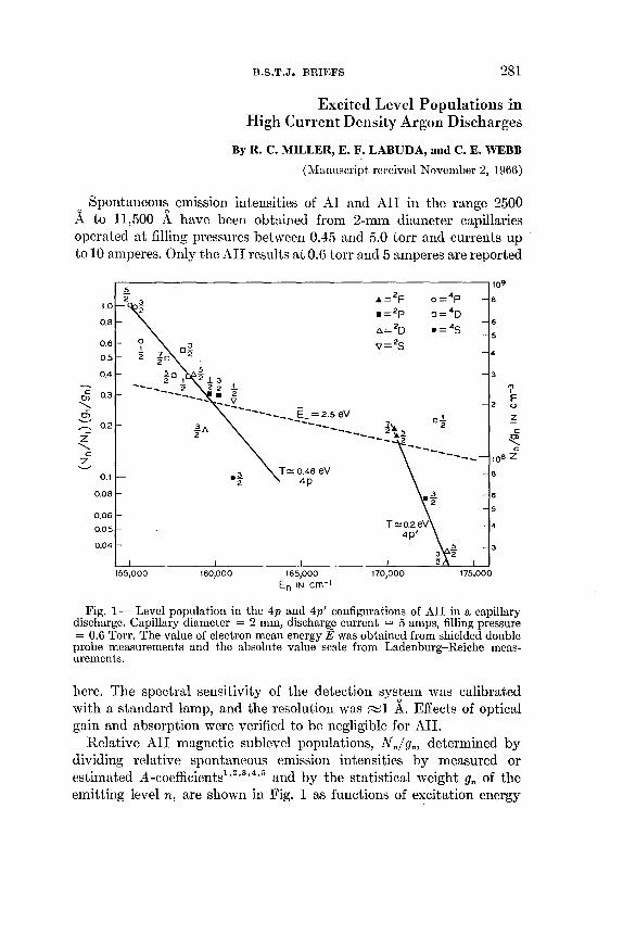
B.S.T.J. BRIEFS 281
Excited Level Populations in High Current Density Argon Discharges
By R. C. MILLER, E. F. LABUDA, and C. E. WEBB
(Mannscript received November 2, 1966)
Spontaneous emISSIOn intensities of AI and All in the range 2500 A to 11,500 A have been obtained from 2-mm diameter capillaries operated at filling pressures between 0.45 and 5.0 torr and currents up to 10 amperes. Only the All results at 0.6 torr and 5 amperes are reported
LO
0.8
0.6
0.5
0.4
0.1
0.08
0.06
0.05
0.04
.--------------------------------------------------;109 5 "2
155,000
.~ 2
160,000
T~ 0.46 eV 4p
165,000 En IN cm- t
.=2F _=2p
.o.=2D '17=25
170,000
O.!.. 2
8
5
4
3
8
5
4
3
175.000
Fig. 1- Level population in the 4p and 4p' configurations of All in a capillary discharge. Capillary diameter = 2 mm, discharge current = 5 amps, filling pressure = 0.6 Torr. The value of electron mean energy jjj was obtained from shielded double probe measurements and the absolute value scale from Ladenburg-Reiche measurements.
here. The spectral sensitivity of the detection system was calibrated with a standard lamp, and the resolution was ~1 A. Effects of optical gain and absorption were verified to be negligible for All.
Relative All magnetic sublevel populations, N n/ gn, determined by dividing relative spontaneous emission intensities by measured or estimated A-coefficients1
•2
,3,4,5 and by the statistical weight gn of the emitting level n, are shown in Fig. 1 as functions of e~citation energy

282 THE BELL SYSTEM TECHNICAL JOURNAL, JANUARY 1967
En above the All ground state. The results have been normalized to the 4p4p 5/2 population, designated (Nt! gl), at El = 155,044.07 cm -1.
Hence, the quantity plotted is (Nn/N 1 ) (gl/gn)' An approximate absolute value scale of N n/ gn , obtained from optical absorption measurements, 6
is also shown. * When A-coefficient estimatest existed for several transitions originating from the same level, their self-consistency was checked,t and the average value was used.
The 4p and 4p' populations appear to be grouped along straight lines in the semilogarithmic plot of Fig. 1. Thus, for each of these configurations it is possible to define a" configuration temperature" T (measured in energy units) by the relation
This yields T ~ 0.45 and 0.2 eV for the 4p and 4p' levels, respectively. A line corresponding to T = 2.5 eV (the measured value6 of electron mean energy) has been included for reference.
The existence of an approximately common "temperature", considerably smaller than the prevailing electron" temperature", for all levels within a given configuration (regardless of spin) implies that intra-configuration thermal equilibrium is achieved by rearrangement of configurational populations in a time short compared to All 4p and 4p' radiative lifetimes, and does not involve charged particle impact. §
Our present belief is that although the excitation energy of All states is provided by electron impact on the ion, these states can interact rapidly by collisions with the ground and excited states of- AI, the final state ion being in the initial All configuration but not necessarily in the initial level of that configuration. The existence of such collisions might account for part of the large Lorentz broadening of All line profiles at high current densities.s The present experiments yield no information on actual details of these collisions, but there are experimentally documented processes such as formation of molecular ions
* These measurements show that All 48 metastable populations are in approximate Boltzman equilibrium with the All ground state at the prevailing electron mean energy.
t The lifetime measurements of Ref. 1 and the calculations of Ref. 2, because of their generally excellent consistency, were adopted in preference to earlier estimates whenever such choice was possible.
t This check was possible only for the All 4p - 48 calculations of Ref. 2 where, with one exception, the self-consistency was better than 30 percent.
§ This latter restriction is required by the AI and All spontaneous emission radial profiles,7 provided that All excited level populations are derived ab initio from electron impact on the All ground state. The fact that "configuration temperatures" are much lower than the electron mean energy independently suggests that electron impact is not resp(;msible for the rearrangement.
B.S.T.J. BRIEFS 283
(regarded here as a non-stationary intermediate state) which provide a basis for discussing population rearrangement.
If a resonant nature is supposed for the proposed interaction, * then All levels are expected to interchange populations rapidly if their excitation energy differences are no larger than the measured 0.1-0.2 eV ion and atom thermal energies. 6
•9 The maximum energy differences of
0.1 and 0.2 eV which exist between adjacent levels of the 4p and 4p' configurations, respectively, imply that the achievement of intraconfigurational thermal equilibrium is plausible. Inter-configuration interaction rates, on the other hand, will be small if the energy gap between them is much larger than ~0.1-0.2 eV (true for the 1.1 eV energy difference between the highest 4p and the lowest 4p' levels), so that different configurations may very well attain different" temperatures". Also selection rules may reduce or prohibit inter-configuration interactions, core changes, e.g., being difficult to achieve from impact parameter considerations. The existence of an approximately common "temperature" for doublet and quartet 4p levels implies that at least some rearrangement cross-sections involving spin change are comparable to those involving no spin change.
From measured discharge parameters6•10 it can be shown that, if
the AI ground state were the sole source of rearrangement collisions, cross-sections ~2 X 10- 14 cm2 would provide" thermalization" times shorter than typical 4p radiative lifetimes (5 X 10⁻⁹ sec). This value is experimentally plausible for resonant collisions between heavy particles,l1 particularly if one of them is in an excited state. Finally, it should be noted that if the above collisions are predominant over radiation, then the determination of cascade contributions to individual levels cannot, in general, be made simply by comparing the total spontaneous emission rates ont of and into the level.
Note added in Proof: vVhere comparison is possible, the absolute level populations of Fig. 1 are in fair agreement with values obtained by Bennett, et al 12 at somewhat lower (pd).
* We do not wish to imply that the suggested collisions must necessarily be treated as a charge-exchange process.
REFERENCES
1. Bennett, W. R., Kindlmann, P. J., Mercer, G. N., and Sunderland, J., Appl. Phys. Letters, 5, 1964, p. 158.
2. Statz, H., Horrigan, F. A., and Koozekanani, S. H., J. Appl. Phys., 36, 1965, p.2278.
3. Garstang, R. H., Mon. Not. R. Astr. Soc., 114-, 1954, p. 118. 4. Olsen, H. N., J. Quant. Spectr. Radiative Transfer, 3, 1963, p. 59.

284 THE BELL SYS'l'EM TECHNICAL JOURNAL, JANUARY 1967
5. Griem, H. A., Coulomb Approximation Oscillator Strengths of . .. Medium Elements, NRL Report 6085, U. S. Dept. of Commerce, Office of Technical Services, Washington 25, D. C., 1964.
6. Labuda, E. F., Webb, C. E., Miller, R. C., and Gordon, E. 1., Bull. Am. Phys. Soc., 11, 1966, p. 497.
7. Webb, C. E., Bull. Am. Phys. Soc., in press. 8. Bennett, W. R., Ballik, E. A., and Mercer, G. N., Phys. Hev. Letters, 16, 196G,
p.603. 9. Ballik, E. A., Bennett, W. R, and Mercer, G. N., App. Phys. Letters, 8, 1966,
p.214. 10. Webb, C. E., Labuda, E. F., Miller, R. C., and Gordon, E. r., 23rd Annual
Conference on Electron Devices Research, Univ. of Illinois, June, 1965. 11. McDaniel, E. W., Collision Phenomena in Ionized Gases, John Wiley & Sons,
Inc., New York, 1964, Fig. 6-2-6, p. 252. 12. Bennett, W. R., Mercer, G. N., Kindlmann, P. J. Wexler, B., and Hyman, H.,
Phys. Rev. Letters, 17, November, 1966, p. 987.
CW Operation of LSA Oscillator Diodes-44 to 88 GHz
By JOHN A. COPELAND
(Manuscript received November 14, 1966)
Bulk n-GaAs oscillator diodes have been operated on a continuous basis in the LSA (Limited Space-charge Accumulation) model at frequencies from 44 to 88 GHz. This is the first time a practical solidstate oscillator has operated continuously in this high-frequency range. The reason the LSA diode can produce millimeter wave power at higher frequencies than other solid-state devices such as transistors, tunnel diodes, IMP ATT diodes, and Gunn diodes is because it is the first device which is not subject to the" transit-time limitation."
The" transit-time limitation" exists for these other devices because they must be designed so that the time required for a charge carrier to move from the source contact to the drain contact must be shorter than or on the order of one RF cycle. A common principle of all these devices is the bunching of space charge which remains until it drifts into a contact. Since carriers in semiconductors such as silicon, germanium, and gallium arsenide have maximum drift velocities on the order of 107 cm/sec, devices for higher frequencies must be designed with proportionally thinner active regions. The power and impedance of such a device both decrease proportionally to the thickness of the active region, so the maximum value of the product of power and impedance decreases as the square of the thickness or as the reciprocal of the square of the frequency, f. The lowest impedance which is practical increases with frequency at microwave frequencies because of skin effect. The

B.S.T.J. BRIEFS 285
result of all these considerations is that the transit-time limitation causes the maximum power of a given device to decrease faster than r 2 as t increases.2
•3
The LSA diode is not subject to the transit-time limitation because it derives its ability to transform dc to ac directly from the negative differential of drift velocity of the individual electrons with respect to electric field4
•5 rather than to the movement of space charge across
the device. There are two main requirements for preventing space charge from accumulating and distorting the electric field which would lead to Gunn oscillations at a lower frequency: The ratio of doping to frequency must be within a certain range, which for n-GaAs appears to be 104 to 2 X 10⁵ sec/cm3
• Also, the resonant circuit must be properly loaded so that the electric field swings into the positive conductance region below 3000 V / cm for part of each cycle to quench out any space charge which has started to accumulate. 1
The existence of the LSA mode was first verified on a pulse basis at 1, 10, and 30 GHz, then the experimental effort was directed toward producing a 50-GHz CW oscillator. In interpretation of the results shown in Table I and Fig. 1, it should be kept in mind that these are only preliminary results. In particular, no attempt was made to obtain high pulse powers, the pulse powers reported are from the same devices that operated CW at lower voltages and much lower efficiencies.
Table I gives the results obtained from the first diodes that operated on a continuous basis. All of these devices were made from a wafer of epitaxially grown n-GaAs with a carrier density of about 8 X 1015 cm -3.
The active region was 5 microns thick, and the current maximum occurred at 2 volts. Noise due to the diodes could not be detected on the HP-851A spectrum analyzer, indicating the carrier-to-noise ratio was
TABLE 1-LSA DIODE EXPERIMENTAL RESULTS
Diode Voltage RF Power Frequency Efficiency (V) (mW) GHz (%)
Continuous D1 3.5 20 84-88 2.0 D2 3.6 15 51 0.7 D3 3.3 20 44-51 0.7
(40*) (1.4) Pulsed
D1 5.0 50 84 4.0 D2 7.0 400 51 9.0 D3 11.0 500 44-51 3.0
(700*) (4.0)
* Holder cooled with dry ice.
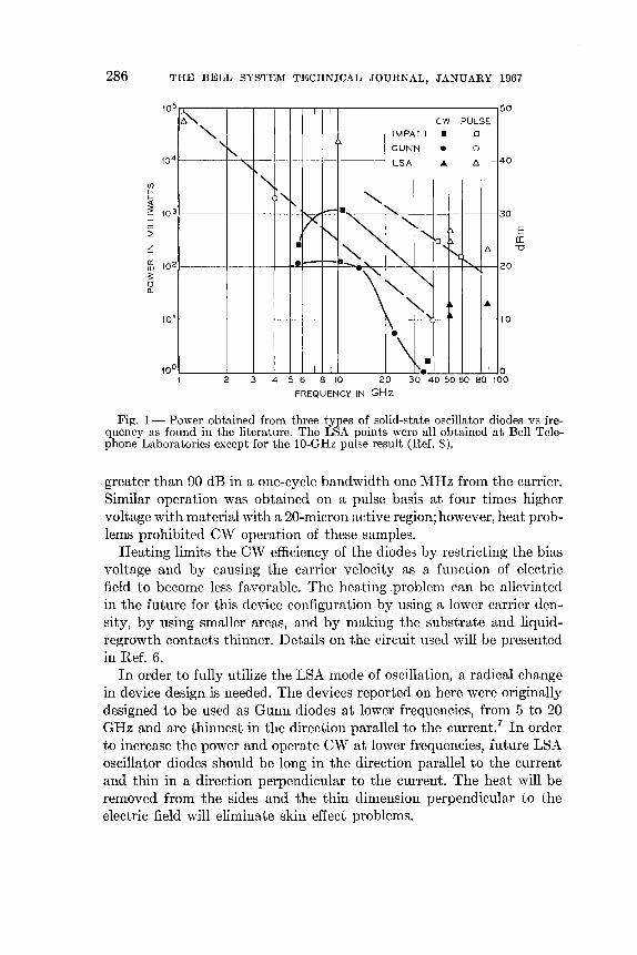
286 THE BELL SYSTEM TECHNICAL JOURNAL, JANUARY 1967
105
104
(/) I-
~ 3 t0 3 :J -I
~
~ a: t02 w 3: 0 CL
tO I
~. I I
CW PULSE
""-, IMPATT • 0
i' GUNN • 0
'r- LSA A t::. -
"
50
40
)'-, "-_. ~
l}<' ~ ~
"'-~"'- ~
• ~
'0, ~ t::. 'r
II , "--'\ "', '" r'--, It. A
1\ -\ .
I I 1'. I I
30
20
to
o 2 3 4 5 6 8 to 20 30 40 50 60 80 100
FREQUENCY IN GHz
E CO -0
Fig. 1- Power obtained from three types of solid-state oscillator diodes vs frequency as found in the literature. The LSA points were all obtained at Bell Telephone Laboratories except for the 10-GHz pulse result (Ref. 8).
greater than 90 dB in a one-cycle bandwidth one MHz from the carrier. Similar operation was obtained on a pulse basis at four times higher voltage with material with a 20-micron active region; however, heat problems prohibited CW operation of these samples.
Heating limits the CW efficiency of the diodes by restricting the bias voltage and by causing the carrier velocity as a function of electric field to become less favorable. The heating .problem .can be alleviated in the future for this device configuration by using a lower carrier density, by using smaller areas, and by making the substrate and liquidregrowth contacts thinner. Details on the circuit used will be presented in Ref. 6.
In order to fully utilize the LSA mode of oscillation, a radical change in device design is needed. The devices reported on here were originally designed to be used as Gunn diodes at lower frequencies, from 5 to 20 GHz and are thinnest in the direction parallel to the current. 7 In order to increase the power and operate CW at lower frequencies, future LSA oscillator diodes should be long in the direction parallel to the current and thin in a direction perpendicular to the current. The heat will be removed from the sides and the thin dimension perpendicular to the electric field will eliminate skin effect problems.

B.S.T.J. BRIEFS 287
The author would like to acknowledge that the results could not have been obtained without the engineering assistance of R. R. Spiwak and R. G. Voss, the material supplied by K. L. Lawley and B.Schwartz, the device preparation by C. R. Paola and Mrs. M. W. Lange, and the general advice and encouragement given by S. Knight, M. Uenohara, and R. S. Engelbrecht.
REFERENCES
1. Copeland, J. A., Proc. IEEE, 54, October, 1966, pp. 1479-1480. 2. Johnson, E. 0., RCA Review, June, 1965, pp. 163-177. 3. DeLoach, B. C., Recent Advances in Solid State Microwave Generators, Advances
in Microwaves, Academic Press, New York (to be published, 1966). 4. Ridley, B. K. and Watkins, T. B., Proc. Phys. Soc. (London), 78, August, 1961,
pp. 293-304. 5. Hilsum, C., Proc., IRE 50, February, 1962, pp. 185-189. 6. Copeland, J. A. and Spiwak, R. R., LSA Operation of n-GaAs Diodes, to be given
at 1967 International Solid-State Circuits Conference, Philadelphia, Pa., February 15-17, 1967.
7. Brady, D. P., Knight, S., Lawley, K. L., and Uenohara, M., Proc. IEEE, 54, October, 1966, pp. 1499-1500.
8. Kennedy, W. K., M.S. Thesis, Cornell University, September, 1966.