
Switching strategy for six switches forced commutated cycloconverter with several advantages
8
Published in IET Power Electronics Received on 24th January 2013 Revised on 6th May 2013 Accepted on 8th June 2013 doi: 10.1049/iet-pel.2013.0065 ISSN 1755-4535 Switching strategy for six switches forced commutated cycloconverter with several advantages Hossein Khoun Jahan 1 , Mohamad Reza Banaei 2 1 Azarbayjan Regional Electric Company 2 Electrical Engineering Department, Faculty of Engineering, Azarbaijan Shahid Madani University, Tabriz, Iran E-mail: [email protected] Abstract: Forced commutated cycloconverters (FCCs) are very popular topics today which can generate variable frequency and variable voltage in output. These converters include six switches in each phase where operation of these converters depends on switching strategy. This study describes a novel switching strategy for six switches FCC where this strategy transfers seven input voltages to FCC output. In each switching period, among seven input voltages, there are only two input voltages which surround reference output voltage. Hence, the proposed strategy makes these two input voltages around reference voltage transfer to FCC output in each switching period. As a result, average value of FCC output voltage is the same as reference voltage. Main benefits of this switching strategy are minimisation of total harmonic distortion, reduction of dv/dt stresses on the load, lower harmonic components, high-voltage modulation index and performance in unbalance or non-sinusoidal input voltage condition. The operation and performance of the proposed switching strategy has been verified by the simulation and measurement results which were carried out for three-phase to single-phase converter. The proposed switching strategy serves as the conceptual platform for extending the principles to other FCC topologies. 1 Introduction Matrix converter is a device which can generate variable frequency and variable voltage output directly from an AC input. The matrix converter provides bidirectional power flow and allows a compact design because of the lack of DC-link capacitors for energy storage. Three phase matrix converters have received considerable attention in recent years because they may become a good alternative to voltage-source inverter topology. The concept of matrix converter topology was introduced by Venturini [1]. The performance of matrix converters depends on modulation strategy. The complexity of the matrix converter topology makes the modulation strategies a difficult task. Various modulation strategies have been proposed for matrix converter [2–16]. The most relevant control and modulation methods developed up to now, for the matrix converter topology, are direct transfer function approach (also known as the Venturini method), scalar method [2, 3], pulse-width modulation (PWM) techniques [4, 5], direct torque and flux control [6] and predictive control [7]. Firstly, Alesina and Venturini [8, 9] derived duty ratio functions which can be modulated by the carrier signal. The scalar method proposed in 1987 by Roy and April [10]. In both methods, a reduction of the voltage transfer ratio is observed as the power displacement factor is reduced, as indicated in [10]. Many control strategies based on PWM methods have been applied to different kinds of matrix converters [11–14]. In [11, 12] space vector PWM (SVPWM) for the matrix converters tries to understand the operation of the matrix converter. The SPPWM approach has been successively developed in [13]. However, SPPWM has some problems to distinguish gating signal generation form each selection of space vectors and it requires look-up tables with the previously initialised and stored switching patterns. Carrier-based PWM is the other famous modulation strategy for the matrix converter [14]. This method does not use complex calculation and look-up tables but it introduces offset for references and discontinuous carrier signal. A different concept of PWM for the matrix converter has been introduced. In a carrier-based modulation technique, which is mathematically proven to be identical with SVPWM is presented. In [15], a carrier-based PWM strategy, called direct duty ratio PWM, is presented which does not require the reference offset and employs continuous triangular carrier waveform. Today, direct torque control and predictive control schemes are established as a high performance for different applications such as AC machines drives [7, 16]. The matrix converters have some disadvantages such as lower voltage modulation index, higher sensitivity to power supply disturbances, complexity control, switching losses, dv/dt stresses on the load and switches, higher harmonic components and output voltage with high total harmonic distortion (THD) [17–20]. Three-phase to single-phase forced commutated cycloconverters (FCCs) is one type of direct AC–AC matrix converter [21, 22]. The FCCs have been used to eliminate the DC links of the conventional AC–DC–AC systems. The FCCs need no energy storage components except for small www.ietdl.org IET Power Electron., pp. 1–8 doi: 10.1049/iet-pel.2013.0065 1 © The Institution of Engineering and Technology 2013
Transcript of Switching strategy for six switches forced commutated cycloconverter with several advantages

www.ietdl.org
IE
d
Published in IET Power ElectronicsReceived on 24th January 2013Revised on 6th May 2013Accepted on 8th June 2013doi: 10.1049/iet-pel.2013.0065
T Power Electron., pp. 1–8oi: 10.1049/iet-pel.2013.0065
ISSN 1755-4535
Switching strategy for six switches forcedcommutated cycloconverter with several advantagesHossein Khoun Jahan1, Mohamad Reza Banaei2
1Azarbayjan Regional Electric Company2Electrical Engineering Department, Faculty of Engineering, Azarbaijan Shahid Madani University, Tabriz, Iran
E-mail: [email protected]
Abstract: Forced commutated cycloconverters (FCCs) are very popular topics today which can generate variable frequency andvariable voltage in output. These converters include six switches in each phase where operation of these converters depends onswitching strategy. This study describes a novel switching strategy for six switches FCC where this strategy transfers seven inputvoltages to FCC output. In each switching period, among seven input voltages, there are only two input voltages which surroundreference output voltage. Hence, the proposed strategy makes these two input voltages around reference voltage transfer to FCCoutput in each switching period. As a result, average value of FCC output voltage is the same as reference voltage. Main benefitsof this switching strategy are minimisation of total harmonic distortion, reduction of dv/dt stresses on the load, lower harmoniccomponents, high-voltage modulation index and performance in unbalance or non-sinusoidal input voltage condition. Theoperation and performance of the proposed switching strategy has been verified by the simulation and measurement resultswhich were carried out for three-phase to single-phase converter. The proposed switching strategy serves as the conceptualplatform for extending the principles to other FCC topologies.
1 Introduction
Matrix converter is a device which can generate variablefrequency and variable voltage output directly from an ACinput. The matrix converter provides bidirectional powerflow and allows a compact design because of the lack ofDC-link capacitors for energy storage. Three phase matrixconverters have received considerable attention in recentyears because they may become a good alternative tovoltage-source inverter topology.The concept of matrix converter topology was introduced
by Venturini [1]. The performance of matrix convertersdepends on modulation strategy. The complexity of thematrix converter topology makes the modulation strategies adifficult task. Various modulation strategies have beenproposed for matrix converter [2–16]. The most relevantcontrol and modulation methods developed up to now, forthe matrix converter topology, are direct transfer functionapproach (also known as the Venturini method), scalarmethod [2, 3], pulse-width modulation (PWM) techniques[4, 5], direct torque and flux control [6] and predictivecontrol [7]. Firstly, Alesina and Venturini [8, 9] derivedduty ratio functions which can be modulated by the carriersignal. The scalar method proposed in 1987 by Roy andApril [10]. In both methods, a reduction of the voltagetransfer ratio is observed as the power displacement factoris reduced, as indicated in [10]. Many control strategiesbased on PWM methods have been applied to differentkinds of matrix converters [11–14]. In [11, 12] space vectorPWM (SVPWM) for the matrix converters tries to
understand the operation of the matrix converter. TheSPPWM approach has been successively developed in [13].However, SPPWM has some problems to distinguish gatingsignal generation form each selection of space vectors andit requires look-up tables with the previously initialised andstored switching patterns. Carrier-based PWM is the otherfamous modulation strategy for the matrix converter [14].This method does not use complex calculation and look-uptables but it introduces offset for references and discontinuouscarrier signal. A different concept of PWM for the matrixconverter has been introduced. In a carrier-based modulationtechnique, which is mathematically proven to be identicalwith SVPWM is presented. In [15], a carrier-based PWMstrategy, called direct duty ratio PWM, is presented whichdoes not require the reference offset and employs continuoustriangular carrier waveform.Today, direct torque control and predictive control schemes
are established as a high performance for differentapplications such as AC machines drives [7, 16].The matrix converters have some disadvantages such as
lower voltage modulation index, higher sensitivity to powersupply disturbances, complexity control, switching losses,dv/dt stresses on the load and switches, higher harmoniccomponents and output voltage with high total harmonicdistortion (THD) [17–20].Three-phase to single-phase forced commutated
cycloconverters (FCCs) is one type of direct AC–AC matrixconverter [21, 22]. The FCCs have been used to eliminatethe DC links of the conventional AC–DC–AC systems. TheFCCs need no energy storage components except for small
1© The Institution of Engineering and Technology 2013
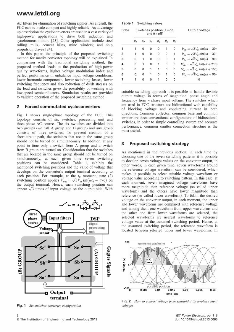
Table 1 Switching values
State Switches position [1 = onand 0 = off]
Output voltage
sa sb sc s′a s′b s′c
1 1 0 0 0 1 0 Vab = ��3
√Vmsin(vt + 30)
2 1 0 0 0 0 1 Vac = ��3
√Vmsin(vt − 30)
3 0 1 0 0 0 1 Vbc = ��3
√Vmsin(vt − 90)
4 0 1 0 1 0 0 V ′ab = ��
3√
Vmsin(vt + 210)
5 0 0 1 1 0 0 V ′ac = ��
3√
Vmsin(vt + 150)
6 0 0 1 0 1 0 V ′bc = ��
3√
Vmsin(vt + 90)
7 1 0 0 1 0 0 0
www.ietdl.org
AC filters for elimination of switching ripples. As a result, theFCC can be made compact and highly reliable. As advantageup description the cycloconverters are used in a vast variety ofhigh-power applications to drive both induction andsynchronous motors [23]. Other applications include steelrolling mills, cement kilns, mine winders; and shippropulsion drives [24].In this paper, the principle of the proposed switchingmethod for matrix converter topology will be explained. Incomparison with the traditional switching method, theproposed method leads to the production of high-powerquality waveforms, higher voltage modulation index andperfect performance in unbalance input voltage conditions,lower harmonic components, lower switching losses, lowerswitching frequency and also reduction of dv/dt stresses onthe load and switches gives the possibility of working withlow-speed semiconductors. Simulation results are providedto validate operation of the proposed switching method.
2 Forced commutated cycloconverters
Fig. 1 shows single-phase topology of the FCC. Thistopology consists of six switches, processing unit andthree-phase AC source. The six switches are divided intotwo groups (we call A group and B group) and any groupconsists of three switches. To prevent creation of ashort-circuit path, the switches that are in the same groupshould not be turned on simultaneously. In addition, at anypoint in time only a switch from A group and a switchfrom B group are turned on. Consideration that the switchesthat are located in the same group should not be turned onsimultaneously, at each given time seven switchingpositions can be considered. Table 1, exhibits thementioned switching positions and the value of voltage thatdevelops on the converter’s output terminal according toeach position. For example, at the t0 moment, state (2)switching position applies Vout =
��3
√Vm sin vt0 − p/6
( )on
the output terminal. Hence, each switching position canappear
��3
√times of input voltage on the output side. With
Fig. 1 Six switches converter configuration
2© The Institution of Engineering and Technology 2013
suitable switching approach it is possible to handle flexibleoutput voltage in terms of magnitude, phase angle andfrequency from n phase input voltage. The switches whichare used in FCC structure are bidirectional with capabilityof blocking voltage and conducting current in bothdirections. Common collector, common base and commonemitter are three conventional configurations of bidirectionalswitches, in order to simple controlling system and accurateperformance, common emitter connection structure is themost useful.
3 Proposed switching strategy
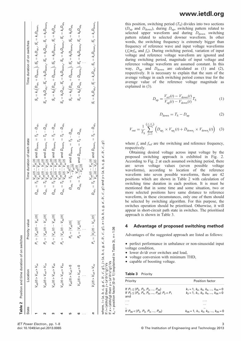
As mentioned in the previous section, in each time bychoosing one of the seven switching patterns it is possibleto develop seven voltage values on the converter output, inother words, in each given time, seven waveforms aroundthe reference voltage waveform can be considered, whichmakes it possible to select suitable voltage waveform orvoltage value according to switching pattern. In this case, ateach moment, seven imagined voltage waveforms havemore magnitude than reference voltage (so called upperwaveform) and the others have lower magnitude thanreference (so called lower waveform). To fulfill the desiredvoltage on the converter output, in each moment, the upperand lower waveforms are compared with reference voltageand among them one waveform from upper waveforms andthe other one from lower waveforms are selected, theselected waveforms are nearest waveforms to referencevoltage value at the assumed switching period. Hence, atthe assumed switching period, the reference waveform islocated between selected upper and lower waveforms. In
Fig. 2 How to convert voltage from sinusoidal three-phase inputvoltages
IET Power Electron., pp. 1–8doi: 10.1049/iet-pel.2013.0065
Table
2Po
sitio
nan
dtim
eduratio
nofonsw
itches
State
Loca
tion
Priority
value
Tim
eduratio
nofea
chstate
Tim
eduratio
nofonsw
itches
1Vab(t)>
Vref>Vac
P1=
Vab(t)−
Vac(t)
∣ ∣∣ ∣
Dup1=
TSVref(t)−
Vac(t)
Vac(t)−
Vab(t)an
dD
down 1
=TS−D
up1
Sa=
k1D
up1+D
down1
() ,S
′ b=
k1D
up1,S
′ c=
k1D
down 1
2Vab(t)>
Vref>Vca
P2=
Vab(t)−
Vca(t)
∣ ∣∣ ∣
Dup1=
TSVref(t)−Vca(t)
Vca(t)−
Vab(t)an
dD
down2=
TS−D
up2
Sa=
k2D
up2,S
′ a=
k2D
down2,S
′ b=
k2D
up2,S
c=
k2D
down 2
3Vac(t)>
Vref>Vab
P3=
Vac(t)−
Vab(t)
∣ ∣∣ ∣
Dup3=
TSVref(t)−Vab(t)
Vab(t)−
Vac(t)an
dD
down3=
TS−D
up3
Sa=
k3D
up3+D
down3
() ,S
′ b=
k3D
down3,S
′ c=
k3D
up3
4Vac(t)>
Vref>Vba
P4=
Vac(t)−
Vba(t)
∣ ∣∣ ∣
Dup4=
TSVref(t)−Vba(t)
Vba(t)−
Vac(t)an
dD
down4=
TS−D
up 4
Sa=
k4D
up4,S
′ a=
k4D
down4,S
b=
k4D
down4,S
′ c=
k4D
up4
5Vab(t)>
Vref>0
P5=
Vab(t)
∣ ∣∣ ∣
Dup5=
TS
Vref(t)
−Vab(t)an
dD
down 5
=TS−D
up5
Sa=
k5D
up5+D
down5
() ,S
′ a=
k5D
down5,S
′ b=
k5D
up5
6Vac(t)>
Vref>0
P6=
Vac(t)
∣ ∣∣ ∣
Dup6=
TS
Vref(t)
−Vac(t)an
dD
down6=
TS−D
up 6
Sa=
k6D
up6+
Ddown 6
() ,S
′ a=
k6D
down 6,S
′ c=
k6D
up6
. ... ..
. ... ..
. ..
nVij(t)>
Vref>Vxy
Pn=
Vij(t)−
Vxy(t)
∣ ∣ ∣∣ ∣ ∣
Dupn=
TSVref(t)−Vxy(t)
Vxy(t)−
Vij(t)an
dD
downn=
TS−
Dupn
Si=
knD
upn,S
′ j=
knD
upn,S
x=
knD
downn,S
′ y=
knD
down n
where,
i={a,b
,c,g
,a′,b′,c′,g′},
j={a,b
,c,g
,a′,b′,c′,g′},
x={a,b
,c,g
,a′,b′,c′,g′}an
dy={a,b
,c,g
,a′,b′,c′,g′}
Ifi={a|b|c|g}then
j={a′|b
′|c′|g
′}Vs
Ifx={a|b|c|g}then
y={a′|b
′|c′|g
′}Vs
kn→
positio
nfactor[0
or1]
(exp
lained
inTa
ble
3),n
=1:36
www.ietdl.org
IET Power Electron., pp. 1–8doi: 10.1049/iet-pel.2013.0065
this position, switching period (TS) divides into two sections(Dup and Ddown), during Dup, switching pattern related toselected upper waveform and during Ddown switchingpattern related to selected downer waveform. In otherwords, the switching frequency is extremely bigger thanfrequency of reference wave and input voltage waveforms( fs≫fin and fo). During switching period, variation of inputvoltage and reference voltage waveform are ignored andduring switching period, magnitude of input voltage andreference voltage waveform are assumed constant. In thisway, Dup and Ddown are calculated as (1) and (2),respectively. It is necessary to explain that the sum of theaverage voltage in each switching period comes true for theaverage value of the reference voltage magnitude asexplained in (3).
Dup =Vref (t)− Vdown(t)
Vup(t)− Vdown(t)TS (1)
Ddown = TS − Dup (2)
Vout =1
TS
∑fs/fo( )
j=1
Dupj× Vupj
(t)+ Ddownj× Vdownj
(t)( )
(3)
where fs and fref are the switching and reference frequency,respectively.Obtaining desired voltage across input voltage by the
proposed switching approach is exhibited in Fig. 2.According to Fig. 2 at each assumed switching period, thereare seven voltage values (seven possible voltagewaveforms), according to location of the referencewaveform into seven possible waveforms, there are 42positions which are shown in Table 2 with calculation ofswitching time duration in each position. It is must bementioned that in some time and some situation, two ormore selected positions have same distance to referencewaveform, in these circumstances, only one of them shouldbe selected by switching algorithm. For this purpose, theswitches operation should be prioritised. Otherwise, it willappear in short-circuit path state in switches. The prioritisedapproach is shown in Table 3.
4 Advantage of proposed switching method
Advantages of the suggested approach are listed as follows:
† perfect performance in unbalance or non-sinusoidal inputvoltage condition,† lower dv/dt over switches and load,† voltage conversion with minimum THD,† capable of boosting voltage.
Table 3 Priority
Priority Position factor
If P1≤ {P2, P3, P4, ..., P36} k1 = 1, k2, k3, k4, ..., k36 = 0If P2≤ {P3, P4, P5, ..., P36} P2 < P1and
k2 = 1, k1, k3, k4, ..., k36 = 0
….…..
….…..
If P36 < {P2, P3, P4, ..., P35} k36 = 1, k1, k2, k3, ..., k35 = 0
3© The Institution of Engineering and Technology 2013
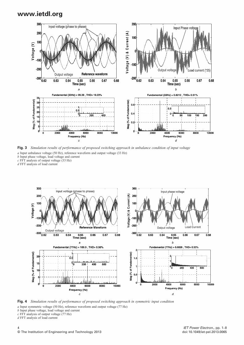
Fig. 3 Simulation results of performance of proposed switching approach in unbalance condition of input voltage
a Input unbalance voltage (50 Hz), reference waveform and output voltage (33 Hz)b Input phase voltage, load voltage and currentc FFT analysis of output voltage (33 Hz)d FFT analysis of load current
Fig. 4 Simulation results of performance of proposed switching approach in symmetric input condition
a Input symmetric voltage (50 Hz), reference waveform and output voltage (77 Hz)b Input phase voltage, load voltage and currentc FFT analysis of output voltage (77 Hz)d FFT analysis of load current
www.ietdl.org
4© The Institution of Engineering and Technology 2013
IET Power Electron., pp. 1–8doi: 10.1049/iet-pel.2013.0065

Table 4 Prototype component parameters
switches IRFP460driver TLP250input filter 3*(54.22 µf + 0.47 Ω)snubber 0.02 µf + 10 Ωswitching frequency 3 kHzbuffer 74HC573
www.ietdl.org
4.1 Performance in unbalance or non-sinusoidalinput voltage condition
One of the most important advantages of the suggested methodis its capability of high quality voltage conversion independentof input voltage waveform. Hence, if at all the time, the twowaveforms of the incoming voltage waveforms slight inmagnitude are able to surround the reference waveform, inother words, at all the time, there exist two voltage valuesin under and upper of the reference waveform, it is possibleto have high quality conversion voltage in condition ofunbalance or non-sinusoidal input voltage.
4.2 Lower dv/dt over switches and load
Reduction of dv/dt over switches and load is the othercharacteristic of the proposed method. As discussed before,in the proposed switching method, switching drive betweentwo nearest voltage waveforms results in reduction ofvoltage variety over switches and load. Reduction of dv/dtalso reduces energy losses, that is, a great effect onconverter longevity.
4.3 Lower THD of converted voltage
According to Figs. 2 and (3), and knowing that switching isperformed between two nearest voltage waveforms, it iseasy to understand that to develop desired voltage
Fig. 5 Prototype force commutated cycloconverter
IET Power Electron., pp. 1–8doi: 10.1049/iet-pel.2013.0065
waveform, the bulk of the area under curve of desiredvoltage occurs without switching action, (A and B area inFig. 2). In other words, switching is done in the borderregion of desired voltage waveform. For this reason, theproposed approach can convert voltage with lower THDcompared with conventional switching approach where theydrive between maximum and minimum voltage value ormaximum and zero voltage value. Reduction of THD limitsswitching frequency which causes decrease of convertercomponent cast. Also, it increases speed of convertercontrol system.
4.4 Voltage boosting characteristic
FCCs employ phase-to-phase voltage to develop desiredvoltage. For this reason, it is possible to convert voltagewith boosted magnitude, therefore with regard to thesuggested switching approach feature which employsnearest voltage waveform to reference voltage waveform,FFCs by applying the suggested switching approach, cangive the most accurate boosted voltage at the output.
5 Simulation results
To evaluate the performance of the proposed switchingtechnique, it is simulated using the MATLAB/Simulinkpackage and under various input voltage conditions, theaccorded output voltage waveforms are obtained.As previously mentioned, one of the important advantages
of the proposed switching method is its ability to convertsource voltage to desired voltage neglecting source voltageoscillations. Also, the other remarkable advantages of thediscussed switching approach are converting voltage withlow THD, voltage boosting ability, minimum dv/dt appearon components and low-switching frequency. In order todemonstrate the effectiveness of the proposed method intoconversion oscillating source voltage with respect to thereference voltage, according to Fig. 3a, unbalance source
5© The Institution of Engineering and Technology 2013
www.ietdl.org
voltages are converted to desired voltage by FFC converter.As can be seen in Fig. 3a, reference voltage, regardless ofinput voltage fluctuations, with minimum THD and dv/dt, isobtained. Input phase-to-phase voltages and referencesingle-phase voltage and converted output voltage arepresented in Fig. 3a. Also, Fig. 3b shows the input voltagewith single-phase output voltage and load current. TheTHD analysis of output voltage and load current are shownin Figs. 3c and d, respectively.In order to assess the effect of switching method ondiscussed converter operation into converting sinusoidalvoltage with flexible magnitude and frequency, thereference voltage with 110 amplitude and 77 Hz isconsidered. The load which connected to the converterterminal is series connected R–L load (110 Ω and 243 mh).
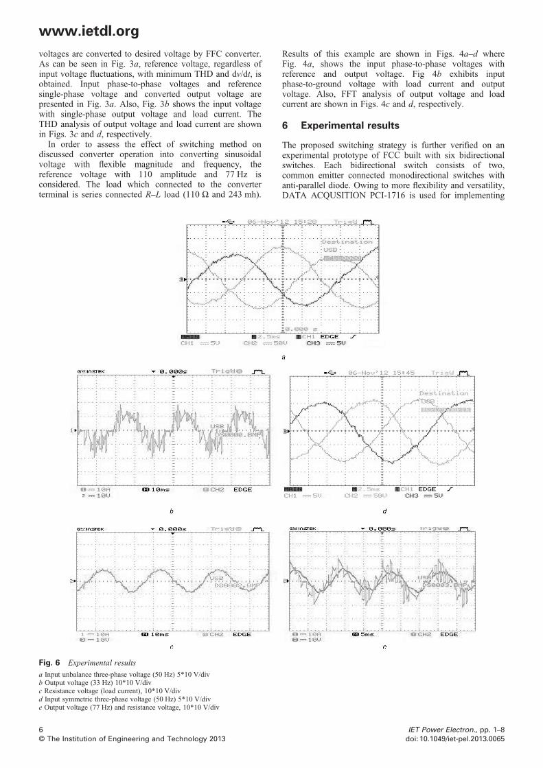
Fig. 6 Experimental results
a Input unbalance three-phase voltage (50 Hz) 5*10 V/divb Output voltage (33 Hz) 10*10 V/divc Resistance voltage (load current), 10*10 V/divd Input symmetric three-phase voltage (50 Hz) 5*10 V/dive Output voltage (77 Hz) and resistance voltage, 10*10 V/div
6© The Institution of Engineering and Technology 2013
Results of this example are shown in Figs. 4a–d whereFig. 4a, shows the input phase-to-phase voltages withreference and output voltage. Fig 4b exhibits inputphase-to-ground voltage with load current and outputvoltage. Also, FFT analysis of output voltage and loadcurrent are shown in Figs. 4c and d, respectively.
6 Experimental results
The proposed switching strategy is further verified on anexperimental prototype of FCC built with six bidirectionalswitches. Each bidirectional switch consists of two,common emitter connected monodirectional switches withanti-parallel diode. Owing to more flexibility and versatility,DATA ACQUSITION PCI-1716 is used for implementing
IET Power Electron., pp. 1–8doi: 10.1049/iet-pel.2013.0065

www.ietdl.org
the modulation program and switching patterns. Analogueinput (AI) ports of data acquisition have been used toidentify three phase input voltage waveform position atonline condition. Received data from AI ports have beensent to the PC where they have been processed in Simulinkenvironment of Matlab software and appropriate signals forswitches have been produced. These signals have beenbrought out by digital output ports of data acquisition. Inthe meantime, they have been magnified by IC 74HC573.At the end, the signals have reached switches by ICTLP250 where these ICs are used to create isolationbetween processor circuit and switches. It is necessary tosay that sample rate of processing in PC is 5 × 10⁻⁴ s. Thispaper attempts to refine FCCs switching approach and,therefore optimisation of snubber and filter design are notconsidered. The snubber circuits that are used to protectsetup component are a series connected RC and Yconnected capacitors are used as input filter. The prototypecomponent parameters are listed in Table 4, and itsphotographs are shown in Fig. 5.As discussed before, one of the important advantages of thesuggested approach is that it has excellent performanceregardless of input voltage conditions. To assess thisfeature, in the first case, according to Fig. 6a, unbalancethree-phase voltage with 125 V maximum peak voltage andfrequency of 50 Hz is applied to the input terminal of FCCand series connected RL load (110 Ω and 243 mh) isconnected to the output terminals. A sinusoidal waveform isconsidered as reference voltage waveform, (Vref = 100 sin(207.24t)). Experimental result of the output voltage andresistant voltage (load current) are shown in Figs. 6b and c.According to listed advantages by employing suggestedswitching method FCCs which are used in a vast variety ofhigh power applications to drive both induction andsynchronous motors, such as steel rolling mills, cementkilns, mine winders and ship propulsion drives, cause toimprove their performance.In the second case, according to Fig. 6d, a symmetric
three-phase voltage with peak magnitude of 110 V isemployed. In this condition, reference voltage is desired asVref = 110 sin(483.56t) Fig. 6e shows experimental results ofoutput voltage and resistance (100 Ω) voltage (load current).As mentioned earlier, in the proposed approach in each
switching period, among seven input voltages, there areonly two input voltages which surround reference outputvoltage. Hence, the proposed strategy makes these twoinput voltages around reference voltage transfer to FCCoutput in each switching period. These acts can be seeneasily in Figs. 6e and b. As discussed before, the mainbenefits of this switching strategy are minimisation of THD,reduction of voltage stresses on the load and performance inunbalance or non-sinusoidal input voltage condition.Considering the simulation and experimental results inFigs. 3b and 6b, it is found that either converted voltage indesired conditions is independent from input voltageconditions or converted voltage by proposed methodimposes lower deviation of voltage over switches.
7 Conclusion
The primary purpose of this paper is to present a newPWM-based switching strategy for FCCs. The suggestedstrategy employs two nearest voltage values to the referencewaveform, to conversion act at each point in time.Switching between two nearest voltage values which
IET Power Electron., pp. 1–8doi: 10.1049/iet-pel.2013.0065
surround reference voltage value, causes decrease of dv/dtover switches and load, output voltage THD and switchingfrequency. For this reason, energy losses with the proposedmethod are deservedly down, thereby, the discussedswitching algorithm increases converter lifetime. Voltageboosting character and perfect performance in unbalanceand non-sinusoidal input voltage conditions are the otheradvantage of the proposed approach. According to the listedadvantages, by employing the suggested switching methodin FFCs which are used in a vast variety of high-powerapplications to drive both induction and synchronousmotors, include steel rolling mills, cement kilns, minewinders and ship propulsion drives, cause to improve theirperformance. The validity of the modulation strategy hasbeen demonstrated by using simulation and experimentalresults.
8 References
1 Venturini, M.: ‘A new sine wave in sine wave out conversion techniquewhich eliminates reactive elements’, Proc. Powerconvers., 1980, 7,pp. E3-1–E3-15
2 Lopez Arevalo, S., Zanchetta, P., Wheeler, P., Trentin, A., Empringham,L.: ‘Control and implementation of a matrix-converter based AC-groundpower-supply unit for aircraft servicing’, IEEE Trans. Ind. Electron.,2010, 57, (6), pp. 2076–2084
3 Mei, Y., Huang, L.: ‘Improved switching function modulation strategyfor three-phase to single-phase matrix converter’. Proc. IEEE IPEMC,May 2009, pp. 1734–1737
4 Loh, P., Rong, R., Blaabjerg, F., Shan, L., Wang, P.: ‘Carrier-basedmodulation schemes for various three-level matrix converters’. Proc.IEEE Power Electronics Specialist Conf., June 2008, pp. 1720–1726
5 Thuta, S., Mohapatra, K., Mohan, N.: ‘Matrix converterover-modulation using carrier-based control: maximizing the voltagetransfer ratio’. Proc. IEEE Power Electronics Specialist Conf., June2008, pp. 1727–1733
6 Xiao, D., Rahman, F.: ‘A modified DTC for matrix converter drivesusing two switching configurations’. Proc. 13th EPE, September 2009,pp. 1–10
7 Kouro, S., Cortes, P., Vargas, R., Ammann, U., Rodriguez, J.: ‘Modelpredictive control, a simple and powerful method to control powerconverters’, IEEE Trans. Ind. Electron., 2009, 56, (6), pp. 1826–1838
8 Alesina, A., Venturini, M.: ‘Solid-state power conversion: a Fourieranalysis approach to generalized transformer synthesis’, IEEE Trans.Circuits Syst., 1981, 28, (CS-4), pp. 319–330
9 Alesina, A., Venturini, M.: ‘Analysis and design of optimum amplitudenine-switch direct AC-AC converters’, IEEE Trans. Power Electron.,1989, PE-4, (1), pp. 101–112
10 Roy, G., April, G.-E.: ‘Cycloconverter operation under a new scalarcontrol algorithm’, Proc. 20th Annual IEEE Power ElectronicsSpecialist Conf., 1989, 1, pp. 368–375
11 Huber, L., Borojevic, D.: ‘Space vector modulated three-phase tothree-phase matrix converter with input power factor correction’, IEEETrans. Ind. Appl., 1995, 31, (6), pp. 1234–1246
12 Casadei, D., Serra, G., Tani, A., Zarri, L.: ‘Matrix converter modulationstrategies: a new general approach based on space-vector representationof the switch state’, IEEE Trans. Ind. Appl., 2002, 49, (2), pp. 370–381
13 Casadei, D., Serra, G., Tani, A.: ‘Reduction of the input currentharmonic content in matrix converters under input/output unbalance’,IEEE Trans. Ind. Electron., 1998, 45, pp. 401–411
14 Yoon, Y.-D., Sul, S.-K.: ‘Carrier-based modulation technique for matrixconverter’, IEEE Trans. Power Electron., 2006, 21, (6), pp. 1691–1703
15 Li, Y., Choi, N.-S., Han, B.-M., Kim, K.M., Lee, B., Park, J.-H.: ‘Directduty ratio pulse width modulation method for matrix converters’,Int. J. Control Autom. Syst., 2008, 6, (5), pp. 660–669
16 Ortega, C., Arias, A., Caruana, C., Balcells, J., Asher, G.: ‘Improvedwaveform quality in the direct torque control of matrix-converter-fedPMSM drives’, IEEE Trans. Ind. Electron., 2010, 57, (6),pp. 2101–2110
17 Fang, X.P., Qian, Z.M., Peng, F.Z.: ‘Single-phase z-source pwm ac-acconverters’, IEEE Power Electron. Lett., 2005, 3, (4), pp. 121–124
18 Tang, Y., Zhang, C., Xie, S.: ‘Single-phase four switches z-source ac-acconverters’. Proc. IEEE Appllications Power Electronics Conf., 2007,pp. 621–625
7© The Institution of Engineering and Technology 2013

www.ietdl.org
19 Ponnaluri, B.S., Teichmann, R.: ‘Design and loss comparison of matrixconverters and voltage-source converters for modern AC drives’, IEEETrans. Ind. Electron., 2002, 49, (2), pp. 304–314
20 Wang, D., Mao, C., Lu, J., Fan, S., Peng, F.: ‘Theory and application ofdistribution electronic power transformer’, Electr. Power Syst. Res. J.,2007, 77, (3–4), pp. 219–226
21 Ziogas, P.D., Khan, S.I., Rashid, M.H.: ‘Analysis and design of forcedcommutated cycloconverter structures with improved transfercharacteristics’, IEEE Trans. Ind. Electron., 1986, 1E-33, pp. 271–280
8© The Institution of Engineering and Technology 2013
22 Ishiguro, A., Furuhashi, T., Okuma, S.: ‘A novel control method for forcedcommutated cycloconverters using instantaneous values of input line-to-line voltages’, IEEE Trans. Ind. Electron., 1991, 38, (3), pp. 166–171
23 Karaca, H., Akkaya, R.: ‘Modelling and simulation of matrix converterunderdistorted input voltage conditions’, Simul. Model. Pract. Theory,2011, 19, (2), pp. 673–684
24 Cook, J.D., Halpin, M., Nelms, M.: ‘Digital control of a three-phase tosingle-phase cycloconverter motor drive’. Proc. Second Int. EnergyConversion Engineering Conf., Providence, Rhode Island, 2001
IET Power Electron., pp. 1–8doi: 10.1049/iet-pel.2013.0065