Study of PDMS Microchannels for Liquid Crystalline ... - MDPI
11
Citation: Baczy ´ nski, S.; Sobotka, P.; Marchlewicz, K.; Juchniewicz, M.; Dybko, A.; Rutkowska, K.A. Study of PDMS Microchannels for Liquid Crystalline Optofluidic Devices in Waveguiding Photonic Systems. Crystals 2022, 12, 729. https:// doi.org/10.3390/cryst12050729 Academic Editor: Alessandro Chiasera Received: 21 April 2022 Accepted: 17 May 2022 Published: 19 May 2022 Publisher’s Note: MDPI stays neutral with regard to jurisdictional claims in published maps and institutional affil- iations. Copyright: © 2022 by the authors. Licensee MDPI, Basel, Switzerland. This article is an open access article distributed under the terms and conditions of the Creative Commons Attribution (CC BY) license (https:// creativecommons.org/licenses/by/ 4.0/). crystals Article Study of PDMS Microchannels for Liquid Crystalline Optofluidic Devices in Waveguiding Photonic Systems Szymon Baczy ´ nski 1 , Piotr Sobotka 1 , Kasper Marchlewicz 2 , Marcin Juchniewicz 3 , Artur Dybko 2 and Katarzyna A. Rutkowska 1, * 1 Faculty of Physics, Warsaw University of Technology, 00-662 Warsaw, Poland; [email protected] (S.B.); [email protected] (P.S.) 2 Faculty of Chemistry, Warsaw University of Technology, 00-664 Warsaw, Poland; [email protected] (K.M.); [email protected] (A.D.) 3 Centre for Advanced Materials and Technologies (CEZAMAT), Warsaw University of Technology, 02-822 Warsaw, Poland; [email protected] * Correspondence: [email protected] Abstract: Microchannels in LC:PDMS structures must be of good quality and suitable geometry to achieve the desired orientation of the liquid crystalline molecules inside. When applying a casting technique, with the molds obtained even by the most accurate method, i.e., photolithography, it is still crucial to inspect the cross-section of the structure and the surface roughness of the PDMS material. This paper presents a study of PDMS microchannels using a Scanning Electron Microscope (SEM) to make such a characterization as accurate as possible. By comparing images of the samples taken using standard polarized light microscopy and SEM, it is likely to understand the mechanism of the liquid crystal molecular orientation occurring in the samples. The results obtained in this work may be used for numerical simulations and further development of LC:PDMS structures. Keywords: PDMS; LC:PDMS; liquid crystalline devices; LC alignment; optofluidics; Scanning Electron Microscopy 1. Introduction Adaptation of the technologies known from other fields of science in optical appli- cations has become extremely important in recent years. Specifically, the combination of microfluidics used in biotechnology or chemical analysis with the ability to control optical properties has created a new branch of research called optofluidics [1]. Various configurations, including Lab-on-a-Chips (LOCs), microfluidic chips, micro-total-analysis- systems (μ-TASs), or Photonic Lab-on-a-Chips (PhLoCs), allow for more rapid and less expensive research in many areas [2–5]. One of the basic materials used in microfluidics is polydimethylsiloxane (PDMS) [6]. Due to its parameters such as refractive index of about 1.41 @ 589 nm [7], isotropy, homogeneity, and high optical transparency in the spectral range covering UV, VIS, and NIR [8], PDMS is used in the development of many optofluidic structures, e.g., dye lasers [9] or reconfigurable optical waveguides [10]. Importantly, a mold with sufficient quality and specific geometry is needed to fabricate optofluidic struc- tures in PDMS using a casting technique. There are many methodologies to manufacture molds [11], including 3D printing [12–14], micromilling [11,12,15,16], and capillary film processing [17]. In the same context, photolithography is the most widely used for complex and precise structures [18,19]. One of the subjects studied in the area of optofluidics is related to PDMS structures filled with liquid crystals (LCs). The resulting LC:PDMS systems combine the capabilities of microfluidics with extraordinary properties such as anisotropy and birefringence (which are typical for liquid crystalline materials). In particular, cholesteric liquid crystals (CLCs) may be used in PDMS systems to form lasers [20] or biosensing chips [21]. On the other Crystals 2022, 12, 729. https://doi.org/10.3390/cryst12050729 https://www.mdpi.com/journal/crystals
-
Upload
khangminh22 -
Category
Documents
-
view
1 -
download
0
Transcript of Study of PDMS Microchannels for Liquid Crystalline ... - MDPI

Citation: Baczynski, S.; Sobotka, P.;
Marchlewicz, K.; Juchniewicz, M.;
Dybko, A.; Rutkowska, K.A. Study of
PDMS Microchannels for Liquid
Crystalline Optofluidic Devices in
Waveguiding Photonic Systems.
Crystals 2022, 12, 729. https://
doi.org/10.3390/cryst12050729
Academic Editor: Alessandro Chiasera
Received: 21 April 2022
Accepted: 17 May 2022
Published: 19 May 2022
Publisher’s Note: MDPI stays neutral
with regard to jurisdictional claims in
published maps and institutional affil-
iations.
Copyright: © 2022 by the authors.
Licensee MDPI, Basel, Switzerland.
This article is an open access article
distributed under the terms and
conditions of the Creative Commons
Attribution (CC BY) license (https://
creativecommons.org/licenses/by/
4.0/).
crystals
Article
Study of PDMS Microchannels for Liquid CrystallineOptofluidic Devices in Waveguiding Photonic SystemsSzymon Baczynski 1 , Piotr Sobotka 1 , Kasper Marchlewicz 2, Marcin Juchniewicz 3, Artur Dybko 2
and Katarzyna A. Rutkowska 1,*
1 Faculty of Physics, Warsaw University of Technology, 00-662 Warsaw, Poland;[email protected] (S.B.); [email protected] (P.S.)
2 Faculty of Chemistry, Warsaw University of Technology, 00-664 Warsaw, Poland;[email protected] (K.M.); [email protected] (A.D.)
3 Centre for Advanced Materials and Technologies (CEZAMAT), Warsaw University of Technology,02-822 Warsaw, Poland; [email protected]
* Correspondence: [email protected]
Abstract: Microchannels in LC:PDMS structures must be of good quality and suitable geometry toachieve the desired orientation of the liquid crystalline molecules inside. When applying a castingtechnique, with the molds obtained even by the most accurate method, i.e., photolithography, it is stillcrucial to inspect the cross-section of the structure and the surface roughness of the PDMS material.This paper presents a study of PDMS microchannels using a Scanning Electron Microscope (SEM)to make such a characterization as accurate as possible. By comparing images of the samples takenusing standard polarized light microscopy and SEM, it is likely to understand the mechanism of theliquid crystal molecular orientation occurring in the samples. The results obtained in this work maybe used for numerical simulations and further development of LC:PDMS structures.
Keywords: PDMS; LC:PDMS; liquid crystalline devices; LC alignment; optofluidics; ScanningElectron Microscopy
1. Introduction
Adaptation of the technologies known from other fields of science in optical appli-cations has become extremely important in recent years. Specifically, the combinationof microfluidics used in biotechnology or chemical analysis with the ability to controloptical properties has created a new branch of research called optofluidics [1]. Variousconfigurations, including Lab-on-a-Chips (LOCs), microfluidic chips, micro-total-analysis-systems (µ-TASs), or Photonic Lab-on-a-Chips (PhLoCs), allow for more rapid and lessexpensive research in many areas [2–5]. One of the basic materials used in microfluidics ispolydimethylsiloxane (PDMS) [6]. Due to its parameters such as refractive index of about1.41 @ 589 nm [7], isotropy, homogeneity, and high optical transparency in the spectralrange covering UV, VIS, and NIR [8], PDMS is used in the development of many optofluidicstructures, e.g., dye lasers [9] or reconfigurable optical waveguides [10]. Importantly, amold with sufficient quality and specific geometry is needed to fabricate optofluidic struc-tures in PDMS using a casting technique. There are many methodologies to manufacturemolds [11], including 3D printing [12–14], micromilling [11,12,15,16], and capillary filmprocessing [17]. In the same context, photolithography is the most widely used for complexand precise structures [18,19].
One of the subjects studied in the area of optofluidics is related to PDMS structuresfilled with liquid crystals (LCs). The resulting LC:PDMS systems combine the capabilitiesof microfluidics with extraordinary properties such as anisotropy and birefringence (whichare typical for liquid crystalline materials). In particular, cholesteric liquid crystals (CLCs)may be used in PDMS systems to form lasers [20] or biosensing chips [21]. On the other
Crystals 2022, 12, 729. https://doi.org/10.3390/cryst12050729 https://www.mdpi.com/journal/crystals

Crystals 2022, 12, 729 2 of 11
hand, PDMS structures filled with nematics (NLCs) have been, for instance, explored inoptofluidic modulators [22], optofluidic grating switches [23], and tunable optofluidic bire-fringent lenses [24]. Research on LC:PDMS-based optical waveguides also emerged [25–29].The latter may be potentially applied as reconfigurable optical interconnectors, switches,and wavelength demultiplexers [27,30,31]. It should be emphasized that the performanceand operation of LC:PDMS structures are highly dependent on the orientation of the liquidcrystal molecules inside. Although orientation layers are typically required in LC-basedphotonic devices, it has been proven that the rod-like NLC molecules align themselvesvertically to the PDMS surface in stationary conditions [32,33]. These stiff boundary con-ditions within LC:PDMS systems are routinely used in numerical simulations performedusing different computational methods [25–28,34]. However, the overall alignment of NLCmolecules in PDMS-embedded microchannels is dependent on their aspect ratio [35]. More-over, a so-far unexpressed but essential condition for successful fabrication of LC:PDMSstructures is the quality of the mold. Because of the ultimate dimensions and high preci-sion requirements for the microchannels acting as the waveguides, the detailed studies ofthe NLC molecular orientation in PDMS structures fabricated using various molds (i.e.,obtained by applying different technologies) have been performed [12,36]. On this basis, ithas been concluded that reproducible results with the channels of desired geometry andthe NLC molecules aligned perpendicularly to the PDMS surfaces are possible only whenthe photolithography process is used for molds’ fabrication [36]. In addition, there aremany possible methods for bonding the PDMS structures to a substrate [37], which alsoaffects the surface quality [38]. Based on intentional physical and chemical modificationsof the PDMS surface [39], it is feasible to make it superhydrophobic, but at the cost ofits roughness [40]. In this context, research on the plasma treatment, reducing the PDMSsurface roughness [38,41], may be crucial for studying LC:PDMS structures.
This paper shows further investigations on the NLC molecular orientation in PDMSmicrostructures. Specifically, previously studied microchannels fabricated using a SU-8photoresist mold [36] are compared with the redesigned structures (of reduced transversaldimensions), also manufactured based on the photolithography process. The main aspectsof this work were investigating the orientation of the NLC molecules at PDMS surfacesand analyzing the elastomer surface roughness from the images taken with a ScanningElectron Microscope (SEM). This insight into the fabricated microchannels allows for amore accurate determination of the influence of the PDMS surface quality on the orientationof the NLC molecules and for finding possible sources of defects.
2. Materials and Methods2.1. Molds Manufacturing
In the current studies, two different molds were used to check the performance ofthe PDMS structures and compare them with previous samples described in [36]. Thisapproach was decided to optimize the PDMS structures fabricated in the photolithographyprocess and to check the NLC molecular orientation in the microchannels characterizedby different aspect ratios. The structures were designed in AutoCAD software (Autodesk,Dublin, Ireland) and then transferred to the chrome masks in the electron-beam lithographyprocess. In this way, two molds were created using different SU-8 photoresists. Thenine-step procedure, including silicon substrate preparation, photoresist spin-coating,soft-baking, UV-light illumination, and post-processing, is precisely described in [36].A SU-8 25 was used in the first case, while the second mold was fabricated using SU-8 2010, with both negative photoresists provided by the Kayaku Advanced MaterialsInc. (Westborough, MA, USA) The differences in the photoresists’ characteristics madeit necessary to modify some steps in the fabrication process. Specifically, in terms of theparameters that were applied for the second mold, (i) the spin speed in the spin cycle wasincreased from 1700 to 3000 rpm; (ii) post-exposure baking (PEB) was performed for 210 sat 95 ◦C (instead of two-step contact hotplate process with PEB time of 60 s at 65 ◦C and360 s at 95 ◦C); (iii) the time of immersing the structure in a dedicated SU-8 developer

Crystals 2022, 12, 729 3 of 11
was reduced from about 180 to 150 s to dissolve unexposed portions of the photoresists.Eventually, after checking by several methods, the height of the structure from the firstmold was estimated to be about 30 µm. It was decided to be reduced by applying a SU-82010. Following the given steps of the fabrication procedure [36] with suitable modificationsdescribed above, a mold with a height of about 12 µm was successfully manufactured. Forboth molds, no damages or deformations were observed during their fabrication and whenmanufacturing the PDMS structures, which allowed them to be used repetitively, givingreproducible results.
2.2. LC:PDMS Structures Manufacturing
PDMS material was prepared by mixing the prepolymer (SYLGARD™ 184 SiliconeElastomer Base) with the crosslinker (SYLGARD™ 184 Silicone Curing Agent), both fromDow Corning (Dow Polska, Warsaw, Poland), in a weight ratio of 10:1 [7]. A vacuum pumpwas used to eliminate air bubbles from PDMS in a liquid form. Then, the prepared mixturewas poured onto the mold in a glass container (i.e., a Petri dish), and baked in an oven at atemperature of 75 ◦C for 90 min. After detaching the cross-linked PDMS from the mold,an elastomer layer with intended microchannels was obtained. A biopsy puncher wasused to make inlets and outlets to enable the filling of the channels with liquid crystallinematerial. The next step in the fabrication process was to bond the PDMS structure to aflat surface (made of a PDMS layer or a glass plate), properly prepared and cleaned. Bothelements to be combined were inserted into the chamber with oxygen plasma (Atto PlasmaCleaner, Diener Electronic, Ebhausen, Germany) for 20 s at a reduced pressure of 0.3 mbar.Eventually, the building components of the structure were merged, resulting thus in thetarget PDMS:PDMS or PDMS:glass samples, respectively, depending on the substrate used.
The nematic liquid crystal (NLC) used for the experimental tests was the E7 LC mix-ture [42], available from Merck (Darmstadt, Germany). This typical liquid crystallinematerial was injected into the fabricated PDMS structures using a syringe at room temper-ature (about 20 ◦C). The whole volumes of the microchannels were infiltrated using thecapillary forces. The transition temperature to the isotropic phase is about 58.3 ◦C, which isone of the characteristics of the selected LC. Therefore, E7, even in the isotropic state, is notexpected to have any impact on the properties of PDMS. The chemical structures of PDMSand the nematic liquid crystal E7 are shown in Figure 1.
Crystals 2022, 12, x FOR PEER REVIEW 3 of 12
increased from 1700 to 3000 rpm; (ii) post-exposure baking (PEB) was performed for 210 s at 95 °C (instead of two-step contact hotplate process with PEB time of 60 s at 65 °C and 360 s at 95 °C); (iii) the time of immersing the structure in a dedicated SU-8 developer was reduced from about 180 to 150 s to dissolve unexposed portions of the photoresists. Even-tually, after checking by several methods, the height of the structure from the first mold was estimated to be about 30 µm. It was decided to be reduced by applying a SU-8 2010. Following the given steps of the fabrication procedure [36] with suitable modifications described above, a mold with a height of about 12 µm was successfully manufactured. For both molds, no damages or deformations were observed during their fabrication and when manufacturing the PDMS structures, which allowed them to be used repetitively, giving reproducible results.
2.2. LC:PDMS Structures Manufacturing PDMS material was prepared by mixing the prepolymer (SYLGARD™ 184 Silicone
Elastomer Base) with the crosslinker (SYLGARD™ 184 Silicone Curing Agent), both from Dow Corning (Dow Polska, Warsaw, Poland), in a weight ratio of 10:1 [7]. A vacuum pump was used to eliminate air bubbles from PDMS in a liquid form. Then, the prepared mixture was poured onto the mold in a glass container (i.e., a Petri dish), and baked in an oven at a temperature of 75 °C for 90 min. After detaching the cross-linked PDMS from the mold, an elastomer layer with intended microchannels was obtained. A biopsy puncher was used to make inlets and outlets to enable the filling of the channels with liquid crystalline material. The next step in the fabrication process was to bond the PDMS structure to a flat surface (made of a PDMS layer or a glass plate), properly prepared and cleaned. Both elements to be combined were inserted into the chamber with oxygen plasma (Atto Plasma Cleaner, Diener Electronic, Ebhausen, Germany) for 20 s at a reduced pressure of 0.3 mbar. Eventually, the building components of the structure were merged, resulting thus in the target PDMS:PDMS or PDMS:glass samples, respectively, depending on the substrate used.
The nematic liquid crystal (NLC) used for the experimental tests was the E7 LC mix-ture [42], available from Merck (Darmstadt, Germany). This typical liquid crystalline ma-terial was injected into the fabricated PDMS structures using a syringe at room tempera-ture (about 20 °C). The whole volumes of the microchannels were infiltrated using the capillary forces. The transition temperature to the isotropic phase is about 58.3 °C, which is one of the characteristics of the selected LC. Therefore, E7, even in the isotropic state, is not expected to have any impact on the properties of PDMS. The chemical structures of PDMS and the nematic liquid crystal E7 are shown in Figure 1.
Figure 1. (a) Molecular structures and composition of E7 liquid crystal and (b) chemical structure of poly(dimethylsiloxane) (PDMS).
Figure 1. (a) Molecular structures and composition of E7 liquid crystal and (b) chemical structure ofpoly(dimethylsiloxane) (PDMS).
2.3. Optical Measurements and Observations
A digital microscope (KEYENCE VHX-5000, Keyence International, Mechelen, Bel-gium) equipped with a VH-Z50 long-working-distance zoom lens (50−500×) allowed forthe sample’s observations based on the high-resolution images (1600 × 1200 pixels). Specifi-cally, the examined structures placed on the glass stage could be observed in the transmittedand/or reflected light (independently if required). This research used the ability to adaptthe mentioned microscope for standard polarizing microscope (POM) measurements. In

Crystals 2022, 12, 729 4 of 11
fact, the main part of the experimental investigations was performed with white lighttransmitted through the sample located between the crossed polarizers. Additionally, anOlympus LEXT OLS4100 (Olympus Corporation, Tokyo, Japan) microscope was used toacquire preliminary data related to the measurements of the height of the microchannelsin PDMS samples. Moreover, a Scanning Electron Microscope (SEM), namely Hitachi SU8230 (Hitachi Europe Limited, Buckinghamshire, UK), was used to obtain the images ofthe cross-sections and surfaces of PDMS structures with high magnification. With suchadvanced equipment, it was possible to examine the samples with the magnification of25,000× without any problems. However, several steps were taken before observing thesamples in the SEM to make this possible. Specifically, the section of the structure to beviewed had to be of appropriate size (with a maximum area of 2 × 2 cm2 and a height upto 2 cm) and sputtered with a layer of Au-Pd (80:20 ratio, thickness < 100 nm).
3. Results3.1. LC:PDMS Structures with a Height of 30 µm
Based on the results related to the orientation of NLC molecules in PDMS samplesreported in our previous work [36], only a limited number of the structures fabricatedusing a SU-8 mold with a height of about 30 µm are presented in this paper. Specifically, asample consisting of a series of microchannels with the widths of 10, 20, 25, 30, 35, 40, 45,and 50 µm (Figure 2a,b) was selected to be further compared with the samples obtainedfrom the optimized mold of reduced size (i.e., with a height of 12 µm, see Section 3.2).The channels in the PDMS:glass structure were filled with E7 NLC (with an estimatedvolumetric flow rate from 3 to 30 nL/min depending on the channel width) and were leftto obtain the fixed orientation of the liquid crystalline molecules in the sample. After about5 min, the NLC molecules were aligned perpendicular to each microchannel wall. Fromthe previously mentioned studies and simulations [25–28,34], it is clear that the channel’saspect ratio (height/width, h/w) strongly influences the orientation of the LC molecules.This fact was also confirmed by our previous observations [36], as well as by the results ofcurrent studies. In principle, for the channels with a width smaller than a height (i.e., withthe aspect ratio h/w > 1), the resulting orientation of the molecules within the whole volumeof the channel is strongly dependent on the forces that orient the molecules perpendicularto the sidewalls. It may be proven that for the channels with an aspect ratio greater than1, molecules across the width of the channel are oriented perpendicular to the side walls(homeotropic orientation), which can be observed as a bright color within the channelregion when the structure is rotated by 45 degrees to the polarizers’ axes (Figure 2b).
Crystals 2022, 12, x FOR PEER REVIEW 5 of 12
the depth of the optical field is too small, and other phenomena such as diffraction strongly distort the image. However, it can be confirmed with high confidence that the depth of the channels in the PDMS is about 30 µm in tested sample.
Figure 2. The PDMS:glass structure with microchannels of different widths (i.e., 10, 20, 25, 30, 35, 40, 45, and 50 µm, starting from the top of the photo) filled with E7 NLC and observed under the polarizing microscope (POM). The structure on the left is aligned with the polarizer axis, while the one on the right is rotated by an angle of about 45 degrees.
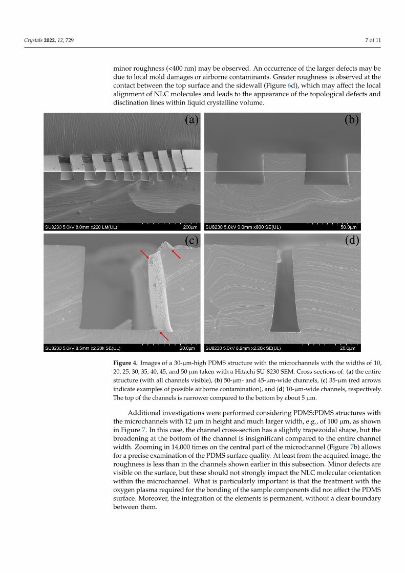
One of the critical aspects of the current research was determining the exact cross-section of the microchannels’ geometry. It should be noted that the images taken with the SEM allowed not only to dimension the fabricated channels (determining the level of the design reproduction) but also to analyze the PDMS surface roughness. A cross-section of PDMS structure (of the same geometry as one shown in Figures 2 and 3a‒c) without the substrate is presented in Figure 4a. It can be seen that the channels with a smaller aspect ratio (i.e., the widest ones) are well reproduced, and no significant defects are seen. Due to the technological process of removing non-hardened SU-8 photoresist when forming the mold, the sidewalls of the channels are not perfectly perpendicular to the base, and thus the shape of the cross-section is somewhat trapezoidal. In the analyzed structure, the microchannels with assumed widths of 50 µm and 45 µm (see Figure 4b) are reproduced with a slight deviation (± 2 µm). However, at the base of the further microchannels (i.e., at the top openings visible in the photos), channels are narrower by about 5 µm. The same is for the 35-µm-wide channel presented in Figure 4c. On the other hand, the microchannel with the designed width of 10 µm (Figure 4d) is an excellent example of trapezoidal ge-ometry, with its width varying from 12 µm to 7 µm at the narrowest point. It is worth noting that the smoothness of the PDMS surface is clearly visible in Figure 4. The porosity of the PDMS surface is negligible, although some larger defects may be airborne contam-inants (see, e.g., Figure 4c). When examining the photos shown in Figure 4, one must also consider the Au-Pd layer that allowed charges to dissipate from the sample, so the image may be slightly distorted. Due to the fine-tuning of the mold and the use of another SU-8 photoresist in further studies, the issue of PDMS roughness is discussed in more detail for 12-µm-high structures.
Figure 2. The PDMS:glass structure with microchannels of different widths (i.e., 10, 20, 25, 30, 35,40, 45, and 50 µm, starting from the top of the photo) filled with E7 NLC and observed under thepolarizing microscope (POM). The structure on the left is aligned with the polarizer axis, while theone on the right is rotated by an angle of about 45 degrees.

Crystals 2022, 12, 729 5 of 11
An Olympus LEXT OLS4100 microscope was used first to measure the microchannels’heights. Specifically, an attempt was made to avoid interfering with the fabricated PDMSstructure, which was done by taking advantage of the device’s ability to scan the depthaccurately. For this purpose, several top view images were taken (see, e.g., Figure 2a),and a depth scan was performed (Figure 2b). Using the microscope software tools, it waspossible to select a specific linear section to build an accurate profile of the structure cross-section from the collected data (Figure 2c). The roughness of the microchannels present insuch a cross-section visualization pushed the research towards a detailed inspection withthe SEM technique (as discussed further below). In addition, a cross-section of anotherstructure (made with the same mold) was examined using the KEYENCE VHX-5000 digitalmicroscope (Figure 2d). Unfortunately, at such relatively small dimensions, the depth ofthe optical field is too small, and other phenomena such as diffraction strongly distort theimage. However, it can be confirmed with high confidence that the depth of the channelsin the PDMS is about 30 µm in tested sample.
One of the critical aspects of the current research was determining the exact cross-section of the microchannels’ geometry. It should be noted that the images taken with theSEM allowed not only to dimension the fabricated channels (determining the level of thedesign reproduction) but also to analyze the PDMS surface roughness. A cross-section ofPDMS structure (of the same geometry as one shown in Figures 2 and 3a–c) without thesubstrate is presented in Figure 4a. It can be seen that the channels with a smaller aspectratio (i.e., the widest ones) are well reproduced, and no significant defects are seen. Dueto the technological process of removing non-hardened SU-8 photoresist when formingthe mold, the sidewalls of the channels are not perfectly perpendicular to the base, andthus the shape of the cross-section is somewhat trapezoidal. In the analyzed structure, themicrochannels with assumed widths of 50 µm and 45 µm (see Figure 4b) are reproducedwith a slight deviation (±2 µm). However, at the base of the further microchannels (i.e., atthe top openings visible in the photos), channels are narrower by about 5 µm. The same isfor the 35-µm-wide channel presented in Figure 4c. On the other hand, the microchannelwith the designed width of 10 µm (Figure 4d) is an excellent example of trapezoidalgeometry, with its width varying from 12 µm to 7 µm at the narrowest point. It is worthnoting that the smoothness of the PDMS surface is clearly visible in Figure 4. The porosity ofthe PDMS surface is negligible, although some larger defects may be airborne contaminants(see, e.g., Figure 4c). When examining the photos shown in Figure 4, one must also considerthe Au-Pd layer that allowed charges to dissipate from the sample, so the image maybe slightly distorted. Due to the fine-tuning of the mold and the use of another SU-8photoresist in further studies, the issue of PDMS roughness is discussed in more detail for12-µm-high structures.
3.2. LC:PDMS Structures with a Height of 12 µm
In the previous subsection, the PDMS structures with a height of about 30 µm wereshown. After their examination, it was decided to tweak the mold and create structuresof approximately 12 µm in height. Several different structures were fabricated using thenew mold with one of them containing the microchannels with designed widths of 15 µmand 21 µm, which corresponded in reality to about 11 µm and 17 µm (±1 µm), respectively.The aspect ratio of the structures was about 1 for the first channel and 0.7 for the secondone. The structures shown in Figure 5 were bonded to a glass plate substrate to form aPDMS:glass system. Both channels were filled with E7 NLC and observed using POM.The estimated volumetric flow rate in the filling process of these microchannels rangedfrom 0.1 to 1 nL/min. By reducing the height of the structure (from 30 µm to 12 µm), adark color within the channel regions assigned to the molecules aligned perpendicularlyto the substrate plane is visible through the center of the 11-µm-wide microchannel (inFigure 5a,b, when viewing the sample placed at a 0- and a 45-degree angle to the polarizeraxis, respectively). Such a molecular arrangement was not observed in a similar structurewith a height of 30 µm (please see Figure 2 for comparison). A homeotropic orientation

Crystals 2022, 12, 729 6 of 11
was also observed in the 17-µm-wide microchannel (presented in Figure 5c,d), confirmingprevious studies linking the possibility of the stable molecular orientation with the aspectratio of the microchannels in PDMS filled with liquid crystalline material [36].
Crystals 2022, 12, x FOR PEER REVIEW 6 of 12
Figure 3. PDMS structures (before bonding) with a depth of about 30 µm (and widths of 10, 20, 25, 30, 35, 40, 45, and 50 µm) observed with an Olympus LEXT OLS4100, where (a) top view, (b) 3D visualization of the structure, and (c) a cross-section profile taken along the line marked in the pre-vious panel. (d) A photo of the cross-section of another PDMS structure (produced using mold from the same series) with a height of 30 µm obtained using a KEYENCE VHX-5000 microscope.
Figure 3. PDMS structures (before bonding) with a depth of about 30 µm (and widths of 10, 20,25, 30, 35, 40, 45, and 50 µm) observed with an Olympus LEXT OLS4100, where (a) top view, (b)3D visualization of the structure, and (c) a cross-section profile taken along the line marked in theprevious panel. (d) A photo of the cross-section of another PDMS structure (produced using moldfrom the same series) with a height of 30 µm obtained using a KEYENCE VHX-5000 microscope.
SEM images of the mentioned channels (Figure 6) allow for the analysis of the PDMSgeometry and surface roughness to be performed. In the PDMS:PDMS sample with the11-µm-wide channel (Figure 6a), bonded using the low-pressure plasma, the joining linebetween the PDMS piece with the channel and the PDMS substrate is almost invisible. Finemeasurements based on the SEM images confirmed the dimensions of the channel cross-section, giving the values of 12 µm and 11 µm in height and width, respectively. The onlydefect that may be considered problematic for further orientation of the NLC moleculesis the irregular expansion of the channel at its bottom. The latter issue is characteristic ofthe photolithography processes and is most noticeable in the channels with considerablysmall dimensions and an aspect ratio close to 1. For the channel with a width of 17 µm,the cross-section is almost rectangular (Figure 6b). Additional images of the 17-µm-widechannel sections were taken at a magnification of 25,000 to investigate the surface roughnessof the PDMS material. In a close-up of the upper surface of the PDMS surface (Figure 6c), a
Crystals 2022, 12, 729 7 of 11
minor roughness (<400 nm) may be observed. An occurrence of the larger defects may bedue to local mold damages or airborne contaminants. Greater roughness is observed at thecontact between the top surface and the sidewall (Figure 6d), which may affect the localalignment of NLC molecules and leads to the appearance of the topological defects anddisclination lines within liquid crystalline volume.
Crystals 2022, 12, x FOR PEER REVIEW 7 of 12
Figure 4. Images of a 30-µm-high PDMS structure with the microchannels with the widths of 10, 20, 25, 30, 35, 40, 45, and 50 µm taken with a Hitachi SU-8230 SEM. Cross-sections of: (a) the entire structure (with all channels visible), (b) 50-µm- and 45-µm-wide channels, (c) 35-µm (red arrows indicate examples of possible airborne contamination), and (d) 10-µm-wide channels, respectively. The top of the channels is narrower compared to the bottom by about 5 µm.
3.2. LC:PDMS Structures with a Height of 12 µm In the previous subsection, the PDMS structures with a height of about 30 µm were
shown. After their examination, it was decided to tweak the mold and create structures of approximately 12 µm in height. Several different structures were fabricated using the new mold with one of them containing the microchannels with designed widths of 15 µm and 21 µm, which corresponded in reality to about 11 µm and 17 µm (±1 µm), respectively. The aspect ratio of the structures was about 1 for the first channel and 0.7 for the second one. The structures shown in Figure 5 were bonded to a glass plate substrate to form a PDMS:glass system. Both channels were filled with E7 NLC and observed using POM. The estimated volumetric flow rate in the filling process of these microchannels ranged from 0.1 to 1 nL/min. By reducing the height of the structure (from 30 µm to 12 µm), a dark color within the channel regions assigned to the molecules aligned perpendicularly to the substrate plane is visible through the center of the 11-µm-wide microchannel (in Figure 5a,b, when viewing the sample placed at a 0- and a 45-degree angle to the polarizer axis, respectively). Such a molecular arrangement was not observed in a similar structure with a height of 30 µm (please see Figure 2 for comparison). A homeotropic orientation was also observed in the 17-µm-wide microchannel (presented in Figure 5c,d), confirming
Figure 4. Images of a 30-µm-high PDMS structure with the microchannels with the widths of 10,20, 25, 30, 35, 40, 45, and 50 µm taken with a Hitachi SU-8230 SEM. Cross-sections of: (a) the entirestructure (with all channels visible), (b) 50-µm- and 45-µm-wide channels, (c) 35-µm (red arrowsindicate examples of possible airborne contamination), and (d) 10-µm-wide channels, respectively.The top of the channels is narrower compared to the bottom by about 5 µm.
Additional investigations were performed considering PDMS:PDMS structures withthe microchannels with 12 µm in height and much larger width, e.g., of 100 µm, as shownin Figure 7. In this case, the channel cross-section has a slightly trapezoidal shape, but thebroadening at the bottom of the channel is insignificant compared to the entire channelwidth. Zooming in 14,000 times on the central part of the microchannel (Figure 7b) allowsfor a precise examination of the PDMS surface quality. At least from the acquired image, theroughness is less than in the channels shown earlier in this subsection. Minor defects arevisible on the surface, but these should not strongly impact the NLC molecular orientationwithin the microchannel. What is particularly important is that the treatment with theoxygen plasma required for the bonding of the sample components did not affect the PDMSsurface. Moreover, the integration of the elements is permanent, without a clear boundarybetween them.

Crystals 2022, 12, 729 8 of 11
Crystals 2022, 12, x FOR PEER REVIEW 8 of 12
previous studies linking the possibility of the stable molecular orientation with the aspect ratio of the microchannels in PDMS filled with liquid crystalline material [36].
Figure 5. PDMS:glass structures with a single microchannel filled with E7 NLC and observed under the polarizing microscope. Channels with the widths of approximately 11 µm (designed to be 15 µm) (a,b), and of approximately 17 µm (assumed to be 21 µm) (c,d). The orientation of polarizers’ axes is indicated in each photo.
SEM images of the mentioned channels (Figure 6) allow for the analysis of the PDMS geometry and surface roughness to be performed. In the PDMS:PDMS sample with the 11-µm-wide channel (Figure 6a), bonded using the low-pressure plasma, the joining line between the PDMS piece with the channel and the PDMS substrate is almost invisible. Fine measurements based on the SEM images confirmed the dimensions of the channel cross-section, giving the values of 12 µm and 11 µm in height and width, respectively. The only defect that may be considered problematic for further orientation of the NLC mole-cules is the irregular expansion of the channel at its bottom. The latter issue is character-istic of the photolithography processes and is most noticeable in the channels with con-siderably small dimensions and an aspect ratio close to 1. For the channel with a width of 17 µm, the cross-section is almost rectangular (Figure 6b). Additional images of the 17-µm-wide channel sections were taken at a magnification of 25,000 to investigate the sur-face roughness of the PDMS material. In a close-up of the upper surface of the PDMS surface (Figure 6c), a minor roughness (<400 nm) may be observed. An occurrence of the larger defects may be due to local mold damages or airborne contaminants. Greater roughness is observed at the contact between the top surface and the sidewall (Figure 6d),
Figure 5. PDMS:glass structures with a single microchannel filled with E7 NLC and observed underthe polarizing microscope. Channels with the widths of approximately 11 µm (designed to be 15 µm)(a,b), and of approximately 17 µm (assumed to be 21 µm) (c,d). The orientation of polarizers’ axes isindicated in each photo.
Crystals 2022, 12, x FOR PEER REVIEW 9 of 12
which may affect the local alignment of NLC molecules and leads to the appearance of the topological defects and disclination lines within liquid crystalline volume.
Figure 6. Images of PDMS:PDMS structures with the microchannels with the height of 12 µm taken with a Hitachi SU-8230 SEM in a case of 11-µm- (a) and 17-µm- (b) wide microchannel and high-lighted the regions in which the images with the higher magnification were taken, representing a top surface (c) and a top corner (d) of the microchannel. The width difference at the top and bottom of the channels is about 2 µm.
Additional investigations were performed considering PDMS:PDMS structures with the microchannels with 12 µm in height and much larger width, e.g., of 100 µm, as shown in Figure 7. In this case, the channel cross-section has a slightly trapezoidal shape, but the broadening at the bottom of the channel is insignificant compared to the entire channel width. Zooming in 14,000 times on the central part of the microchannel (Figure 7b) allows for a precise examination of the PDMS surface quality. At least from the acquired image, the roughness is less than in the channels shown earlier in this subsection. Minor defects are visible on the surface, but these should not strongly impact the NLC molecular orien-tation within the microchannel. What is particularly important is that the treatment with the oxygen plasma required for the bonding of the sample components did not affect the PDMS surface. Moreover, the integration of the elements is permanent, without a clear boundary between them.
Figure 6. Images of PDMS:PDMS structures with the microchannels with the height of 12 µm takenwith a Hitachi SU-8230 SEM in a case of 11-µm- (a) and 17-µm- (b) wide microchannel and highlightedthe regions in which the images with the higher magnification were taken, representing a top surface(c) and a top corner (d) of the microchannel. The width difference at the top and bottom of thechannels is about 2 µm.

Crystals 2022, 12, 729 9 of 11Crystals 2022, 12, x FOR PEER REVIEW 10 of 12
Figure 7. Images of a 100-µm-wide microchannel in a PDMS:PDMS structure taken using a Hitachi SU-8230 SEM, showing a cross-section of the entire channel (a) and a close-up on the central part of the bottom surface of the channel (which was exposed to the oxygen plasma during the bounding process) (b).
4. Discussion and Conclusions Further research related to the studies on the quality of microchannels fabricated in
PDMS to be filled with liquid crystalline material and described in [36] has been per-formed in this paper. A SU-8 mold with a height of 12 µm was used to validate the orien-tation of NLC molecules in such structures. The obtained results were compared with a previously fabricated SU-8 mold with a height of 30 µm. The fine-tuned mold allowed for the fabrication of channels with widths of about 11 µm (resulting in an aspect ratio of around 1) while maintaining an appropriate channel geometry. Images taken with Hitachi SU-8230 SEM were used to verify the size and the quality of the structures in the PDMS. Specifically, a close inspection of the PDMS:PDMS structures’ surface was made. The roughness of the sidewalls of the PDMS channels fabricated using the SU-8 mold was proven to be negligible (<400 nm). Keeping in mind that the PDMS surface quality may be affected by many factors, including the mold used, the structure development process, and the bonding technique, the performed studies are of particular importance as any change in the structure development process may lead to geometrical changes or defect creation. The issues addressed in this paper are significant in the LC:PDMS systems de-velopment, ensuring that the LC molecular orientation is well defined. The further chal-lenges are to refine the cross-section geometry and obtain surfaces without any defects which are still visible in the presented microchannels.
Author Contributions: Conceptualization, K.A.R.; methodology, K.A.R., A.D. and M.J.; investiga-tion, S.B., P.S., K.M.; data curation, S.B.; writing—original draft preparation, S.B. and K.A.R.; writ-ing—review and editing, K.A.R.; visualization, S.B. and K.A.R.; supervision, K.A.R.; project admin-istration, K.A.R.; funding acquisition, K.A.R. All authors have read and agreed to the published version of the manuscript.
Funding: Studies have been funded by FOTECH-1 project “Electrically-driven waveguiding sys-tems in LC:PDMS structures” granted by the Warsaw University of Technology under the Excel-lence Initiative: Research University (ID-UB) program.
Data Availability Statement: Not applicable.
Acknowledgments: The work has been completed using the Hitachi SU 8230 ultra-high resolution scanning-transmission electron microscope made available by the Centre for Advanced Materials and Technologies CEZAMAT, Warsaw University of Technology, Poleczki 19, 02-822 Warsaw, Po-land.
Figure 7. Images of a 100-µm-wide microchannel in a PDMS:PDMS structure taken using a HitachiSU-8230 SEM, showing a cross-section of the entire channel (a) and a close-up on the central part ofthe bottom surface of the channel (which was exposed to the oxygen plasma during the boundingprocess) (b).
4. Discussion and Conclusions
Further research related to the studies on the quality of microchannels fabricated inPDMS to be filled with liquid crystalline material and described in [36] has been performedin this paper. A SU-8 mold with a height of 12 µm was used to validate the orientation ofNLC molecules in such structures. The obtained results were compared with a previouslyfabricated SU-8 mold with a height of 30 µm. The fine-tuned mold allowed for the fabri-cation of channels with widths of about 11 µm (resulting in an aspect ratio of around 1)while maintaining an appropriate channel geometry. Images taken with Hitachi SU-8230SEM were used to verify the size and the quality of the structures in the PDMS. Specifically,a close inspection of the PDMS:PDMS structures’ surface was made. The roughness ofthe sidewalls of the PDMS channels fabricated using the SU-8 mold was proven to benegligible (<400 nm). Keeping in mind that the PDMS surface quality may be affectedby many factors, including the mold used, the structure development process, and thebonding technique, the performed studies are of particular importance as any change inthe structure development process may lead to geometrical changes or defect creation.The issues addressed in this paper are significant in the LC:PDMS systems development,ensuring that the LC molecular orientation is well defined. The further challenges are torefine the cross-section geometry and obtain surfaces without any defects which are stillvisible in the presented microchannels.
Author Contributions: Conceptualization, K.A.R.; methodology, K.A.R., A.D. and M.J.; investigation,S.B., P.S., K.M.; data curation, S.B.; writing—original draft preparation, S.B. and K.A.R.; writing—review and editing, K.A.R.; visualization, S.B. and K.A.R.; supervision, K.A.R.; project administration,K.A.R.; funding acquisition, K.A.R. All authors have read and agreed to the published version ofthe manuscript.
Funding: Studies have been funded by FOTECH-1 project “Electrically-driven waveguiding systemsin LC:PDMS structures” granted by the Warsaw University of Technology under the ExcellenceInitiative: Research University (ID-UB) program.
Data Availability Statement: Not applicable.
Acknowledgments: The work has been completed using the Hitachi SU 8230 ultra-high resolutionscanning-transmission electron microscope made available by the Centre for Advanced Materialsand Technologies CEZAMAT, Warsaw University of Technology, Poleczki 19, 02-822 Warsaw, Poland.
Conflicts of Interest: The authors declare no conflict of interest.

Crystals 2022, 12, 729 10 of 11
References1. Psaltis, D.; Quake, S.R.; Yang, C. Developing Optofluidic Technology through the Fusion of Microfluidics and Optics. Nature 2006,
442, 381–386. [CrossRef] [PubMed]2. Chen, A.; Wang, R.; Bever, C.R.S.; Xing, S.; Hammock, B.D.; Pan, T. Smartphone-Interfaced Lab-on-a-Chip Devices for Field-
Deployable Enzyme-Linked Immunosorbent Assay. Biomicrofluidics 2014, 8, 064101. [CrossRef] [PubMed]3. Xiao, J.; Liu, Y.; Su, L.; Zhao, D.; Zhao, L.; Zhang, X. Microfluidic Chip-Based Wearable Colorimetric Sensor for Simple and Facile
Detection of Sweat Glucose. Anal. Chem. 2019, 91, 14803–14807. [CrossRef] [PubMed]4. Arora, A.; Simone, G.; Salieb-Beugelaar, G.B.; Kim, J.T.; Manz, A. Latest Developments in Micro Total Analysis Systems. Anal.
Chem. 2010, 82, 4830–4847. [CrossRef] [PubMed]5. Mattio, E.; Lamadie, F.; Rodriguez-Ruiz, I.; Cames, B.; Charton, S. Photonic Lab-on-a-Chip Analytical Systems for Nuclear
Applications: Optical Performance and UV–Vis–IR Material Characterization after Chemical Exposure and Gamma Irradiation. J.Radioanal. Nucl. Chem. 2020, 323, 965–973. [CrossRef]
6. Raj, M.K.; Chakraborty, S. PDMS Microfluidics: A Mini Review. J. Appl. Polym. Sci. 2020, 137, 48958. [CrossRef]7. SYLGARD™ 184 Silicone Elastomer. Technical Data Sheet. Available online: https://www.dow.com/en-us/documentviewer
(accessed on 15 April 2022).8. Stankova, N.E.; Atanasov, P.A.; Nikov, R.G.; Nikov, R.G.; Nedyalkov, N.N.; Stoyanchov, T.R.; Fukata, N.; Kolev, K.N.; Valova, E.I.;
Georgieva, J.S. Optical properties of polydimethylsiloxane (PDMS) during nanosecond laser processing. Appl. Surf. Sci. 2016, 374,96–103. [CrossRef]
9. Song, W.; Vasdekis, A.E.; Li, Z.; Psaltis, D. Low-order distributed feedback optofluidic dye laser with reduced threshold. Appl.Phys. Lett. 2009, 94, 051117. [CrossRef]
10. Chung, A.J.; Erickson, D. Optofluidic waveguides for reconfigurable photonic systems. Opt. Express 2011, 19, 8602–8609.[CrossRef]
11. Carugo, D.; Lee, J.Y.; Pora, A.; Browning, R.J.; Capretto, L.; Nastruzzi, C.; Stride, E. Facile and Cost-Effective Production ofMicroscale PDMS Architectures Using a Combined Micromilling-Replica Moulding (MMi-REM) Technique. Biomed. Microdevices2016, 18, 4. [CrossRef]
12. Baczynski, S.; Sobotka, P.; Marchlewicz, K.; Dybko, A.; Rutkowska, K. Low-cost, widespread and reproducible mold fabricationtechnique for PDMS-based microfluidic photonic systems. Photonics Lett. Pol. 2020, 12, 22–24. [CrossRef]
13. Venzac, B.; Deng, S.; Mahmoud, Z.; Lenferink, A.; Costa, A.; Bray, F.; Otto, C.; Rolando, C.; Le Gac, S. PDMS Curing Inhibition on3D-Printed Molds: Why? Also, How to Avoid It? Anal. Chem. 2021, 93, 7180–7187. [CrossRef] [PubMed]
14. Hwang, Y.; Paydar, O.H.; Candler, R.N. 3D Printed Molds for Non-Planar PDMS Microfluidic Channels. Sens. Actuators A Phys.2015, 226, 137–142. [CrossRef]
15. Chen, P.-C.; Zhang, R.-H.; Chen, L.-T. Using Micromachined Molds, Partial-Curing PDMS Bonding Technique, and MultipleCasting to Create Hybrid Microfluidic Chip for Microlens Array. Micromachines 2019, 10, 572. [CrossRef]
16. Javidanbardan, A.; Azevedo, A.M.; Chu, V.; Conde, J.P. A Systematic Approach for Developing 3D High-Quality PDMSMicrofluidic Chips Based on Micromilling Technology. Micromachines 2021, 13, 6. [CrossRef]
17. Chudy, M.; Grabowska, I.; Ciosek, P.; Filipowicz-Szymanska, A.; Stadnik, D.; Wyzkiewicz, I.; Jedrych, E.; Juchniewicz, M.;Skolimowski, M.; Ziolkowska, K.; et al. Miniaturized Tools and Devices for Bioanalytical Applications: An Overview. Anal.Bioanal. Chem. 2009, 395, 647–668. [CrossRef]
18. Wu, M.-H.; Park, C.; Whitesides, G.M. Generation of Submicrometer Structures by Photolithography Using Arrays of SphericalMicrolenses. J. Colloid Interface Sci. 2003, 265, 304–309. [CrossRef]
19. Tong, J.; Simmons, C.A.; Sun, Y. Precision Patterning of PDMS Membranes and Applications. J. Micromech. Microeng. 2008,18, 037004. [CrossRef]
20. Schmidtke, J.; Terentjev, E.M. Polydimethylsiloxane-Enclosed Liquid Crystal Lasers for Lab-on-Chip Applications. Appl. Phys.Lett. 2010, 96, 151111. [CrossRef]
21. Wang, I.-T.; Lee, Y.-H.; Chuang, E.-Y.; Hsiao, Y.-C. Sensitive, Color-Indicating and Labeling-Free Multi-Detection CholestericLiquid Crystal Biosensing Chips for Detecting Albumin. Polymers 2021, 13, 1463. [CrossRef]
22. Cuennet, J.G.; Vasdekis, A.E.; De Sio, L.; Psaltis, D. Optofluidic Modulator Based on Peristaltic Nematogen Microflows. Nat.Photon 2011, 5, 234–238. [CrossRef]
23. Vasdekis, A.E.; Cuennet, J.G.; Psaltis, D. Liquid Crystal Optofluidics; Khoo, I.C., Ed.; SPIE Digital Library: San Diego, CA, USA,2012; p. 847507. [CrossRef]
24. Wee, D.; Hwang, S.H.; Song, Y.S.; Youn, J.R. Tunable Optofluidic Birefringent Lens. Soft Matter 2016, 12, 3868–3876. [CrossRef][PubMed]
25. d’Alessandro, A.; Asquini, R.; Chiccoli, C.; Martini, L.; Pasini, P.; Zannoni, C. Liquid Crystal Channel Waveguides: A MonteCarlo Investigation of the Ordering. Mol. Cryst. Liq. Cryst. 2015, 619, 42–48. [CrossRef]
26. Asquini, R.; Chiccoli, C.; d’Alessandro, A.; Pasini, P.; Zannoni, C. Monte Carlo Study of Slot-Waveguide Liquid Crystal PhaseShifters. Mol. Cryst. Liq. Cryst. 2019, 683, 46–55. [CrossRef]
27. Asquini, R.; Chiccoli, C.; Pasini, P.; Civita, L.; d’Alessandro, A. Low Power Photonic Devices Based on Electrically ControlledNematic Liquid Crystals Embedded in Poly(Dimethylsiloxane). Liq. Cryst. 2018, 45, 2174–2183. [CrossRef]
Crystals 2022, 12, 729 11 of 11
28. d’Alessandro, A.; Martini, L.; Civita, L.; Beccherelli, R.; Asquini, R. Liquid Crystal Waveguide Technologies for a New Generationof Low-Power Photonic Integrated Circuits; Chien, L.-C., Coles, H.J., Kikuchi, H., Smalyukh, I.I., Eds.; SPIE Digital Library: SanFrancisco, CA, USA, 2015; p. 93840L. [CrossRef]
29. Asquini, R.; Martini, L.; d’Alessandro, A. Fabrication and Characterization of Liquid Crystal Waveguides in PDMS Channels forOptofluidic Applications. Mol. Cryst. Liq. Cryst. 2015, 614, 11–19. [CrossRef]
30. Civita, L.; Quaranta, S.; Asquini, R.; d’Alessandro, A. Design of a Multi Mode Interferometer using LC: PDMS technology. Mol.Cryst. Liq. Cryst. 2019, 684, 58–65. [CrossRef]
31. d’Alessandro, A.; Civita, L.; Asquini, R.; Chiccoli, C.; Pasini, P. Optical Waveguides and Tunable Devices Made of a Liquid CrystalCore in PDMS Channels. In Proceedings of the Liquid Crystals XXIII; Khoo, I.C., Ed.; SPIE: San Diego, CA, USA, 2019; p. 31.[CrossRef]
32. Zheng, W.; Yang, L.; Lee, M. Vertical alignment of liquid crystals on polydimethylsiloxane thin films. Photonics Lett. Pol. 2011, 3,8–10. [CrossRef]
33. Zheng, W.J.; Huang, M.H. Use of polydimethylsiloxane thin film as vertical liquid crystal alignment layer. Thin Solid Film. 2012,520, 2841–2845. [CrossRef]
34. Rutkowska, K.A.; Wolinski, T.R.; Asquini, R.; Civita, L.; Martini, L.; d’Alessandro, A. Electrical tuning of the LC: PDMS channels.Photonics Lett. Pol. 2017, 9, 48–50. [CrossRef]
35. Zheng, W.; Hu, Y.-T. Orientation of liquid crystal molecules in polydimethylsiloxane micro-channels. Liq. Cryst. 2016, 43, 327–335.[CrossRef]
36. Baczynski, S.; Sobotka, P.; Marchlewicz, K.; Słowikowski, M.; Juchniewicz, M.; Dybko, A.; Rutkowska, K.A. Orientation of LiquidCrystalline Molecules on PDMS Surfaces and within PDMS Microfluidic Systems. Appl. Sci. 2021, 11, 11593. [CrossRef]
37. Borók, A.; Laboda, K.; Bonyár, A. PDMS Bonding Technologies for Microfluidic Applications: A Review. Biosensors 2021, 11, 292.[CrossRef] [PubMed]
38. Tohnishi, M.; Matsutani, A. Surface Treatment of Polydimethylsiloxane and Glass Using Solid-Source H2O Plasma for Fabricationof Microfluidic Devices. Sens. Mater. 2021, 33, 569. [CrossRef]
39. Cabrera, J.; Ruiz, M.; Fascio, M.; D’Accorso, N.; Mincheva, R.; Dubois, P.; Lizarraga, L.; Negri, R. Increased Surface Roughness inPolydimethylsiloxane Films by Physical and Chemical Methods. Polymers 2017, 9, 331. [CrossRef]
40. Wu, Y.; Wang, J.; Zhang, D.; Li, L.; Zhu, Y. Preparation and Characterization of Superhydrophobic Surface Based on Polydimethyl-siloxane (PDMS). J. Adhes. Sci. Technol. 2019, 33, 1870–1881. [CrossRef]
41. Kim, H.T.; Jeong, O.C. PDMS Surface Modification Using Atmospheric Pressure Plasma. Microelectron. Eng. 2011, 88, 2281–2285.[CrossRef]
42. Mouquinho, A.; Saavedra, M.; Maiau, A.; Petrova, K.; Barros, M.T.; Figueirinhas, J.L.; Sotomayor, J. Films Based on NewMethacrylate Monomers: Synthesis, Characterisation and Electro-Optical Properties. Mol. Cryst. Liq. Cryst. 2011, 542, 132/[654]–140/[662]. [CrossRef]