Studies on Current Commutation in Hybrid DC-breakers
149
Studies on Current Commutation in Hybrid DC-breakers JESPER MAGNUSSON Doctoral Thesis Stockholm, Sweden 2017
-
Upload
khangminh22 -
Category
Documents
-
view
1 -
download
0
Transcript of Studies on Current Commutation in Hybrid DC-breakers
Studies on Current Commutationin Hybrid DC-breakers
JESPER MAGNUSSON
Doctoral ThesisStockholm, Sweden 2017
TRITA-EE 2017:045ISSN 1653-5146ISBN 978-91-7729-429-0
KTH Skolan för Elektro- och SystemteknikAvd. Elektroteknisk teori och konstruktion
SE-100 44 StockholmSWEDEN
Akademisk avhandling som med tillstånd av Kungl Tekniska högskolan framläggestill offentlig granskning för avläggande av teknologie doktorsexamen i elektro- ochsystemteknik fredagen den 9 juni 2017 klockan 10.00 i Hörsal E2, Lindstedsvägen 3,Kungliga Tekniska högskolan, Stockholm.
© Jesper Magnusson, juni 2017
Tryck: Universitetsservice US AB
iii
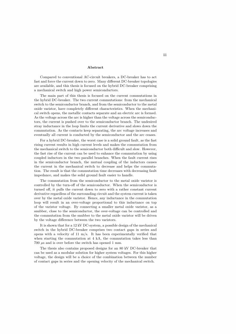
Abstract
Compared to conventional AC-circuit breakers, a DC-breaker has to actfast and force the current down to zero. Many different DC-breaker topologiesare available, and this thesis is focused on the hybrid DC-breaker comprisinga mechanical switch and high power semiconductors.
The main part of this thesis is focused on the current commutations inthe hybrid DC-breaker. The two current commutations: from the mechanicalswitch to the semiconductor branch, and from the semiconductor to the metaloxide varistor, have completely different characteristics. When the mechani-cal switch opens, the metallic contacts separate and an electric arc is formed.As the voltage across the arc is higher than the voltage across the semiconduc-tors, the current is pushed over to the semiconductor branch. The undesiredstray inductance in the loop limits the current derivative and slows down thecommutation. As the contacts keep separating, the arc voltage increases andeventually all current is conducted by the semiconductor and the arc ceases.
For a hybrid DC-breaker, the worst case is a solid ground fault, as the fastrising current results in high current levels and makes the commutation fromthe mechanical switch to the semiconductor both difficult and slow. However,the fast rise of the current can be used to enhance the commutation by usingcoupled inductors in the two parallel branches. When the fault current risesin the semiconductor branch, the mutual coupling of the inductors causesthe current in the mechanical switch to decrease and helps the commuta-tion. The result is that the commutation time decreases with decreasing faultimpedance, and makes the solid ground fault easier to handle.
The commutation from the semiconductor to the metal oxide varistor iscontrolled by the turn-off of the semiconductor. When the semiconductor isturned off, it pulls the current down to zero with a rather constant currentderivative regardless of the surrounding circuit and the system current is takenover by the metal oxide varistor. Hence, any inductance in the commutationloop will result in an over-voltage proportional to this inductance on topof the varistor voltage. By connecting a smaller metal oxide varistor, as asnubber, close to the semiconductor, the over-voltage can be controlled andthe commutation from the snubber to the metal oxide varistor will be drivenby the voltage difference between the two varistors.
It is shown that for a 12 kV DC-system, a possible design of the mechanicalswitch in the hybrid DC-breaker comprises two contact gaps in series andopens with a velocity of 11 m/s. It has been experimentally verified thatwhen starting the commutation at 4 kA, the commutation takes less than700 µs and is over before the switch has opened 1 mm.
The thesis also contains proposed designs for an 80 kV DC-breaker thatcan be used as a modular solution for higher system voltages. For this highervoltage, the design will be a choice of the combination between the numberof contact gaps in series and the opening velocity of the mechanical switch.

v
Sammanfattning
Till skillnad från konventionella brytare i växelspänningssystem behöveren brytare för likström (DC) reagera fortare och tvinga ner strömmen. Detfinns många olika topologier för hur man kan designa en DC-brytare, mendenna avhandling fokuserar på en hybridbrytare som består av en mekaniskkontakt och halvledarkomponenter.
Huvuddelen av denna avhandling fokuserar på kommuteringen av ström-mar mellan hybridbrytarens grenar. Brytförloppet består av två kommute-ringar: från den mekaniska kontakten till halvledarna och från halvledarnatill en metalloxidvaristor och dessa två kommuteringar har helt olika karakte-ristik. När den mekaniska kontakten öppnar bildas en ljusbåde. Eftersom ljus-bågsspänningen är högre än spänningsfallet över halvledarna, flyttas ström-men över till halvledargrenen. Den oönskade induktansen som finns i kret-sen kommer begränsa kommuteringen och förlänga tiden det tar att flyttaströmmen från den mekaniska kontakten till halvledarna. Tack vare att denmekaniska kontakten öppnar med hög hastighet förlängs ljusbågen och ljus-bågsspänningen fortsätter att öka tills all ström flyttats över till halvledarnaoch ljusbågen slocknar.
För hybridbrytaren är ett solitt jordfel det värsta felfallet eftersom densnabbt ökande felströmmen leder till en svårare och mer utdragen kommute-ring till halvledarna. Den höga strömderivatan kan dock utnyttjas genom attinstallera två kopplade spolar i serie med den mekaniska kontakten och halvle-darna. När strömmen ökar i halvledargrenen skapar den kopplade induktansenen motspänning som leder till en minskad ström genom den mekaniska kon-takten och snabbar på kommuteringen. Resultatet är att kommuteringstidenblir kortare ju snabbare felströmmen växer.
Kommuteringen från halvledarna till varistorn styrs av halvledarkompo-nenternas karakteristik. När halvledaren stänger av tvingas strömmen nermed en näst intill konstant derivata oberoende av komponenterna i kretsenoch strömmen tas över av varistorn. Den oönskade induktansen i kretsen kom-mer då ge upphov till en överspänning proportionell till induktansen som ökarkraven på halvledaren. Genom att installera en liten varistor nära halvledarenkan överspänningen kontrolleras och kommuteringen kommer istället drivasav spänningsskillnaden mellan de två varistorerna.
För ett 12 kV likströmssystem är en möjlig design av den mekaniska kon-takten att ha två kontaktgap i serie och en öppningshastighet på 11 m/s.Experiment har verifierat att om kommuteringen startar vid 4 kA tar denmidre än 700 µs och är avslutad innan kontakten öppnats 1 mm.
Avhandlingen innehåller även förslag på hur en 80 kV brytare kan designasför att användas som en modul i system med högre spänning. I det fallet är de-signen en avvägning mellan antalet kontakter i serie och öppningshastighetenpå kontakten.

vii
Acknowledgements
Att doktorera kan vara ett ensamt jobb ibland, men som tur är har jag haft en heldel bra folk omkring mig som har en stor del i att jag kommit fram till slutet.
Jag vill tacka min huvudhandledare Göran Engdahl för att du varit med migfrån start till slut i projektet och stöttat mig genom alla idéer. Jag vill även tackaMarley Becerra för att du tog över det officiella ansvaret även om det inte blev såmycket mer i praktiken. Mikael Dahlgren för att du fick mig in på det här spåretfrån början, och Magnus Backman för att du stöttat mig hela vägen igenom.
Professor Juan Martinez förtjänar ett tack för att du accepterade att handledamig under min utbytestid i Barcelona, utan att egentligen veta vem jag var, ochför att jag fick komma tillbaka en andra period och utbyta erfarenheter och breddamina kunskaper.
Lars Liljestrand ska ha ett stort tack för att du funnits där som en mentor förmig, för diskussioner och inspiration varje gång jag kommit till Västerås.
Tack till alla mina nuvarande och tidigare kollegor på KTH för en väldigt trevligoch stimulerande miljö. Särskilt Daniel för den första koppen kaffe när ingen annanvar vaken, Cong-Toan för att du delat kontor med mig och diskuterat alla möjligaoch omöjliga ämnen, Mrunal för all tid i labbet och för att du driver projektetvidare och Martin för alla bittra luncher och glada utlandsvistelser.
Jag vill även tacka alla mina kollegor på ABB för att ni gett mig ett avbrott frånden akademiska världen både på arbetet, men kanske framför allt under luncherna.Ett särskilt tack till Robert Saers, för att en betydligt större del än väntat av mittarbete kom att bygga på dina idéer.
Tack till Dr. Sundling, Dr. Bissal, Dr. Bonn, Dr. Rosqvist, Dr. Magnusson ochDr Wåhlander för att ni visat att det är möjligt att komma ut på andra sidan.
Tack Ara för alla idéer, diskussioner och samarbeten under dessa år. Jag kom-mer verkligen att sakna dig!
Tack till mamma, pappa och syster för att ni alltid tror på mig, delar minaintressen och stöttar mig när jag behöver det. Och tack till min utökade familj föratt ni kommit in och blivit en såstor och naturlig del av mitt liv.
Sist men inte minst, tack till min fru Jessica och mina döttrar Laura och Ellinorför att ni ger mig en anledning att inte jobba för mycket, men även för att ni inteklagat de senaste månaderna när jag inte varit där...

Contents
Contents ix
1 Introduction 11.1 Background . . . . . . . . . . . . . . . . . . . . . . . . . . . . . . . . 11.2 Scope of the thesis . . . . . . . . . . . . . . . . . . . . . . . . . . . . 41.3 Thesis outline . . . . . . . . . . . . . . . . . . . . . . . . . . . . . . . 51.4 Main contributions . . . . . . . . . . . . . . . . . . . . . . . . . . . . 61.5 Publications . . . . . . . . . . . . . . . . . . . . . . . . . . . . . . . . 6
2 Fault currents in power systems 92.1 Fault currents in AC-systems . . . . . . . . . . . . . . . . . . . . . . 92.2 Current interruption in AC-systems . . . . . . . . . . . . . . . . . . 112.3 Fault currents in DC-systems . . . . . . . . . . . . . . . . . . . . . . 142.4 Current interruption in DC-systems . . . . . . . . . . . . . . . . . . 19
3 DC-breaker topologies 233.1 Mechanical DC-breaker . . . . . . . . . . . . . . . . . . . . . . . . . 243.2 Solid state circuit breaker . . . . . . . . . . . . . . . . . . . . . . . . 243.3 Resonant DC-breaker . . . . . . . . . . . . . . . . . . . . . . . . . . 263.4 The Z-source breaker . . . . . . . . . . . . . . . . . . . . . . . . . . . 273.5 Hybrid DC-breaker . . . . . . . . . . . . . . . . . . . . . . . . . . . . 293.6 Other possibilities . . . . . . . . . . . . . . . . . . . . . . . . . . . . 30
4 The studied hybrid DC-breaker 334.1 Basic operation . . . . . . . . . . . . . . . . . . . . . . . . . . . . . . 334.2 The topology . . . . . . . . . . . . . . . . . . . . . . . . . . . . . . . 364.3 The components in the test set-up . . . . . . . . . . . . . . . . . . . 39
5 Experimental set-up 495.1 The physical build-up . . . . . . . . . . . . . . . . . . . . . . . . . . 495.2 The test circuit . . . . . . . . . . . . . . . . . . . . . . . . . . . . . . 505.3 The control system . . . . . . . . . . . . . . . . . . . . . . . . . . . . 525.4 Instrumentation . . . . . . . . . . . . . . . . . . . . . . . . . . . . . . 55
ix
x CONTENTS
6 Voltage driven commutation 596.1 The development of the arc voltage . . . . . . . . . . . . . . . . . . . 606.2 The different regimes of the current commutation . . . . . . . . . . . 616.3 Commutation within one millisecond . . . . . . . . . . . . . . . . . . 666.4 Voltage withstand after the commutation . . . . . . . . . . . . . . . 706.5 Conclusions . . . . . . . . . . . . . . . . . . . . . . . . . . . . . . . . 74
7 Current driven commutation 757.1 Low power experiments . . . . . . . . . . . . . . . . . . . . . . . . . 787.2 High power experiments . . . . . . . . . . . . . . . . . . . . . . . . . 807.3 Modelling . . . . . . . . . . . . . . . . . . . . . . . . . . . . . . . . . 897.4 Conclusions . . . . . . . . . . . . . . . . . . . . . . . . . . . . . . . . 101
8 Inductance driven commutation 1038.1 The commutation booster . . . . . . . . . . . . . . . . . . . . . . . . 1038.2 Other concepts . . . . . . . . . . . . . . . . . . . . . . . . . . . . . . 1048.3 Design of the commutation booster . . . . . . . . . . . . . . . . . . . 1068.4 Conclusions . . . . . . . . . . . . . . . . . . . . . . . . . . . . . . . . 111
9 Designs for different systems 1139.1 The 12 kV system . . . . . . . . . . . . . . . . . . . . . . . . . . . . 1139.2 The 80 kV system . . . . . . . . . . . . . . . . . . . . . . . . . . . . 1179.3 The 80 kV system with commutation booster . . . . . . . . . . . . . 119
10 Conclusions 123
11 Future Work 125
List of Figures 127
Bibliography 131
Chapter 1
Introduction
1.1 Background
The use and interest of direct current (DC) in power transmission and distributionsystems has increased rapidly in the last years. Even though alternating current(AC) is still dominant, and will most likely remain dominant for a long time tocome, DC has its benefits in specific applications. When AC became dominantin the late 19th century, it was mainly due to two important components: thetransformer and the AC-machine. In a power system, the voltage at the load ischosen to be relatively harmless to people and, even though this level is specifiedto below 50 V, the most common voltages are around 250 V [1]. If the power wouldbe transmitted with this low voltage, the transmission distance would be limited toa few kilometres. The transformer enabled an efficient way to increase the voltageused in the transmission, and hence made it possible to place the power generationfurther away from the loads. This in turn enabled larger generators and higherproduction efficiency as well as better environmental conditions in the cities. Withthe introduction of the AC-generator and AC-motor, the power could be generateddirectly at 50 Hz, transformed to a higher voltage, transmitted with low losses overa relatively long distance, transformed back to low voltage, and used directly in theAC-motor at 50 Hz.
When power is transmitted over long distances, the current will lead to resistivelosses dissipated as heat in the lines. The resistance of the line can be consideredconstant and the losses are proportional to the square of the current. If the powertransmitted by the line is kept constant, an increase in the system voltage leads toa corresponding decrease in the system current. Hence, if the voltage is increasedby a factor of 10, the current decreases with a factor of 10 and the losses decreaseswith a factor of 100.
1
2 CHAPTER 1. INTRODUCTION
1.1.1 Benefits of DC compared to AC
An interesting part is that in the applications where DC is mostly used today,it is motivated with the exact same arguments. The development of high powersemi-conductor components [2] and converter topologies [3] has enabled efficientconversion between AC and DC and has made high voltage direct current (HVDC)the standard for transmission of high power over long distances [4]. The increasein the voltage is generally still performed with transformers on the AC side beforeit is rectified to DC by the converter and transmitted. In the receiving end, theDC voltage is converted to AC before stepped down again by a 50 Hz transformer.If this system should be more efficient than the AC system, the losses in the lineshave to be lower with DC. For large conductors this is true as the resistance forAC is higher than for DC due to the skin effect. However, the more importantdifference is that the DC-line can be operated at a higher voltage than the sameAC-line. When discussing AC, voltages and currents one usually refers to the RMSvalues, which is the effective values for the transmitted power. Since the voltage issinusoidal, the line still has to be insulated for the peak voltage, i.e.
√2VRMS . As
the DC-system can utilize the full voltage, the power transmission capability willincrease. On the other hand, the losses are higher in the DC conductors as a threephase AC-system uses three conductors to carry the current, and the DC-systemonly uses two [5]. It can be shown that the capacity of a double circuit AC-line,i.e. a line comprising 6 conductors, can be increased with 47% if the line is usedwith DC [6]. Hence, for equal power rating of AC and DC-systems, the losses inthe DC-system will be about 30% lower.
For long distance power transmission, there is a breaking point where DC be-comes better than AC, but it can be seen from two perspectives. The DC trans-mission will have a higher investment cost in the converters, but lower losses, i.e.lower running costs. In the same way, the DC system will have increased losses inthe AC/DC conversion, but lower conduction losses in the lines. Hence, the DCtransmission line will be more cost effective than the AC line only if the distance islong enough. The breaking point for the distance depends on the design parametersof the losses in the converters and the lines, but also the type of line. For AC, acable under ground or under water has higher losses than an overhead line, andhence the break even distance for cables is shorter than that for over-head lines [7].
Systems with DC also have the benefit that they are much less affected by theinductance and capacitance than with AC. One example is in cables where thecapacitive currents limits the maximal length of the cable where AC power can betransmitted. For a 380 kV cable carrying 600 A, the capacitive current exceedsthe current rating of the cable at a length of 40 km. Above this length, no powercan be transferred through the cable without taking other measures. One optionis to compensate the capacitance with one inductor in each end and extend themaximal length to 80 km [6]. If more inductors are installed along the cable, thelength can be further increased, however this might not be possible, e.g. in sub-seacables. In a DC cable, the capacitance of the cable will be charged as the voltage
1.1. BACKGROUND 3
is applied, but it will not affect the flow of the current in steady-state. Hence thereis no strict limit for the maximal length of the cable. The same reasoning holdsfor overhead lines, where the inductance of the line will result in a voltage dropduring steady state operation in AC, but not in DC. Hence, the DC over head linedoes not require any capacitive series compensation. Even though a large part ofthe small scale renewable generation is distributed as small scale photovoltaic (PV)systems, much of the renewable energy is also located remotely. This will increasethe use of HVDC links [8], as HVDC makes is possible to transfer the energy overlong distances with low losses and hence enables more remote sources of renewableenergy. In China, a 2000 km link has been built to connect the hydro power in thewestern parts to the load centres in the eastern part [9].
1.1.2 DC-gridsThe use of HVDC is not limited to transfer bulk power from one point to aother.It can also be used to stabilize weak AC-networks [10] and to interconnect AC-systems that are asynchronous or have different frequencies [11]. Even though ithas been discussed for some time, HVDC systems with more than two terminalsare still vary rare, and there is no clear standard how they will look [12]. However,the first real multi terminal HVDC networks have already been build in China [13].There are also ideas to build a DC-backbone across Europe to further stabilize thenetwork and increase the flow of renewable power [14, 15]. Another project is theidea to build a large HVDC network to interconnect Europe to the huge amount ofsolar energy available in the Sahara desert [11].
The AC-motor and AC-generators are still dominant over their DC counterparts,but the way they are used has changed. Most motors today that are used infans [16], pumps [17] or even in traction [18] are frequency controlled. The speedof the motor is then controlled via the frequency of the applied voltage that isgenerated by a DC/AC converter. As the converter is fed by a DC-voltage it needsto be complemented with an AC/DC converter if it is installed in an AC-system.The same kind of effect is seen in the power generation in wind power plants. Tomaximize the power output from the wind power plant, it should be controlled for anoptimal combination of rotational speed and the pitch angle of the blades. One wayto solve this is to generate the power at the optimal frequency and rectify the output.This has lead to interest in creating DC systems to avoid unnecessary conversionsbetween AC and DC. Such applications include distribution grids on-board ships[19–21], and collection grids for off-shore wind power farms [22, 23]. A mediumvoltage distribution network would also make the integration of energy storageseasier and reduce the number of conversion steps when connecting generation thatis naturally DC, e.g. PV-systems.
Also at lower voltage levels, the area of DC grids is an interesting topic. Whencollection grids for connecting wind or solar power plants together are located closeto the loads, it might be beneficial at some points to disconnect from the grid andrun the system as a DC-microgrid [24]. Another example is ongoing research in
4 CHAPTER 1. INTRODUCTION
Finland, where a large part of the 20 kV distribution network could be replaced byLVDC [25]. By replacing the 20 kV network and part of the 400 V AC networkwith 1 kV DC lines, the over-head lines can be replaced by a cable system whichincreases the reliability and reduces faults due to weather conditions. Data-centresare one application where the whole centre can be build up as a low voltage DC-grid.Such a network can be fed by fewer, and larger, rectifiers that results in a morecost effective system. It also makes the implementation of battery-storages andun-interruptible power supplies more straightforward. Another example is tractionor metro systems where the trains use regenerative braking, so that electric poweris generated when the trains decelerate. The power is then fed back into the systemand used by another train.
1.1.3 DC-breakersA lot of research has been conducted on the topic of DC-breakers during the years.However, the demands on the DC-breaker depends very much on in which kind ofsystem it is installed. For the low voltage networks, the low system voltage makes iteasier to interrupt the fault current. Further, since most of the possible low voltageDC system are close to the loads, the fault currents are lower and the whole systemcan be disconnected in the case of a fault. Also in point to point DC-links, thereis no need for DC-breakers as the whole link can be taken off-line in the case of afault. The current is then interrupted by conventional breakers on the AC side.
In the recent discussions of multi terminal HVDC grids, the short circuit poweris very high and the low impedance of the DC-grid [26] gives a very fast rising faultcurrent. To protect the semiconductors in the converters and to maintain a stablenetwork, the faulted section needs to be isolated within a few milliseconds. Therequirement of such a fast response makes most mechanical breaker solutions tooslow. Further, as one of the main drivers for the DC-networks are the lower losses,a breaker with low on-state losses will be required.
One such breaker topology is the hybrid DC-breaker that combines the lowon-state losses in a mechanical commutation switch with the switching capabilityof high power semiconductors. A lot of work has been done on the research ofthe hybrid DC-breaker, both for medium voltage and high voltage applications.However, not much effort has been put on studying the commutation of the currentbetween the parallel branches in the hybrid DC-breaker.
1.2 Scope of the thesis
The scope of this work is to:
• build up a functioning lab infrastructure suitable for the desired experiments.
• increase the understanding of the design and the limitations of the hybridDC-breaker.

1.3. THESIS OUTLINE 5
• validate the concept to separate the over-voltage protection from the energyabsorption, during the semiconductor turn-off, with high power experiments.
• build and test a design of a hybrid DC-breaker under realistic stresses.
1.3 Thesis outline
The thesis is outlined as follows:
• Chapter 1 (this chapter), states the motivation and main contributions ofthe thesis and papers the thesis is based on.
• Chapter 2 describes different fault cases in AC and DC systems, and howthey are interrupted.
• Chapter 3 summarizes different possible DC-breaker topologies and theirbenefits and drawbacks.
• Chapter 4 describes the operation of the hybrid DC-breaker and its differentcomponents.
• Chapter 5 presents the lab and the experimental set-up used to perform theexperiments.
• Chapter 6 describes the commutation from the the mechanical switch tothe semiconductor branch that is driven by the arc voltage in the mechanicalswitch.
• Chapter 7 is focused on the commutation from the semiconductors to thevaristor that is driven by the decreasing current in the semiconductors.
• Chapter 8 presents a solution where coupled inductors are used to supportthe commutation of the current from the mechanical switch to the semicon-ductors in the case of a rapidly rising fault current.
• Chapter 9 suggests two DC-breaker designs, for a 12 kV medium voltagesystem, and for an 80 kV module for higher voltage levels.
• Chapters 10 and 11 summarizes the main conclusions of the work and statessome future work.
6 CHAPTER 1. INTRODUCTION
1.4 Main contributions
The main contributions of this thesis to the state of the art are:
• An experimental analysis to increase the understanding of the complex processof the current commutation from the mechanical commutation switch to thesemiconductor branch in hybrid DC-breakers.
• An enhanced analysis, with high power experiments and simulations, of thepossibility to use a small scale metal oxide varistor as a reliable snubber forthe semiconductor part in hybrid and solid-state DC-breakers.
• Proposed design parameters for hybrid DC-breakers for a 12 kV medium volt-age system and an 80 kV module for higher voltage levels.
1.5 Publications
A large part of the content is not yet published, but some parts are based on thefollowing papers:
I) J. Magnusson, “On the design of hybrid DC-breakers consisting of a me-chanical switch and semiconductor devices”, Licentiate Thesis, defended May8th 2015.
II) J. Magnusson, R. Saers, L. Liljestrand, and G. Engdahl, “Separation of theEnergy Absorption and Over-voltage Protection in Solid-State Breakers by theUse of Parallel Varistors”, IEEE Transactions on Power Electronics vol. 29,num. 6, June 2014.
III) J. Magnusson, A. Bissal, G. Engdahl, and J. A. Martinez-Velasco, “De-sign Aspects of a Medium Voltage Hybrid DC-breaker”, IEEE ISGT Europe,Istanbul, October 2014.
IV) J. Magnusson, R. Saers, and L. Liljestrand, “The Commutation Booster,a New Concept to Aid Commutation in Hybrid DC-Breakers”, Cigré HVDCsymposium, Lund, May 2015.
V) J. Magnusson, A. Bissal, G. Engdahl, J. A. Martinez-Velasco, and L. Lilje-strand, “Experimental Study of the Current Commutation in Hybrid DC-breakers”, ICEPE-ST, Busan, October 2015.
The author has also contributed to the following relevant papers that are not di-rectly part of the thesis:
VII) A. Bissal, J. Magnusson, G. Engdahl, and E. Salinas, “Loadability and scal-ing aspects of Thomson based ultra-fast actuators”, Actuator Conference, Bre-men, June 2012.
1.5. PUBLICATIONS 7
VIII) A. Bissal, J. Magnusson, E. Salinas, G. Engdahl, and A. Eriksson, “On theDesign of Ultra-Fast Electromechanical Actuators: A Comprehensive Multi-Physical Simulation Model”, ICEF, Dalian, June 2012.
IX) A. Bissal, J. Magnusson, and G. Engdahl, “Comparison of Two Ultra-FastActuator Concepts”, IEEE Transactions on Magnetics, vol. 48, num. 11, pp3315-3318, Nov 2012.
X) A. Bissal, J. Magnusson, and G. Engdahl, “Optimal Energizing Source De-sign for Ultra-Fast Actuators”, Soft magnetic materials conference, Budapest,Sept 2013.
XI) J. Magnusson, A. Bissal, G. Engdahl, R. Saers, Z. Zhang, and L. Lilje-strand, “On the use of metal oxide varistors as a snubber circuit in solid-statebreakers”, ISGT Europe, Copenhagen, Oct 2013.
XII) J. Magnusson, J.A. Martinez-Velasco, A. Bissal, G. Engdahl, and L. Lilje-strand, “Optimal design of a medium voltage hybrid fault current limiter”,EnergyCon, Cavtat, May 2014.
XIII) A. Bissal, J. Magnusson, E. Salinas, and G. Engdahl, “Multiphysics model-ing and experimental verification of ultra-fast electro-mechanical actuators”,International Journal of Applied Electromagnetics and Mechanics, vol. 49,num. 1, pp 51-59, 2015.
XIV) A. Bissal, J. Magnusson, and G. Engdahl, “Electric to mechanical energyconversion of linear ultrafast electromechanical actuators based on stroke re-quirements”, IEEE Transactions on Industry Applications, vol. 51, num. 4,pp 3059-3067, March 2015.
XV) J.A. Martinez, and J. Magnusson, “EMTP modeling of hybrid HVDC break-ers”, IEEE PES General Meeting, July 2015.
XVI) A. Bissal, E. Salinas, J. Magnusson, G. Engdahl, “On the design of a linearcomposite magnetic damper”, IEEE Transactions on Magnetics, vol. 51, num.11, pp 1-5, Nov 2015.
XVII) A. Bissal, A. Eriksson, J. Magnusson, G. Engdahl, “Hybrid Multi-PhysicsModeling of an Ultra-Fast Electro-Mechanical Actuator”, Actuators, vol. 4,num. 4, pp 314-335, Dec 2015.
XVIII) J.A. Martinez-Velasco, J. Magnusson, “Parametric analysis of the hybridHVDC circuit breaker”, International Journal of Electrical Power & EnergySystems, vol. 84, pp 284-295, Jan 2017.
XIX) J.A. Corea-Araujo, J. Martinez, J. Magnusson, “Optimum Design of HybridHVDC Circuit Breakers Using a Parallel Genetic Algorithm and a MATLAB-EMTP Environment”, IET Generation, Transmission & Distribution, 2017.

Chapter 2
Fault currents in power systems
This chapter is intended to provide a background and some understanding of thedifferences in the fault currents in AC and DC systems, and how these are handledby the circuit breakers.
2.1 Fault currents in AC-systems
In an AC-system, the voltage is sinusoidal with a frequency of 50 or 60 Hz depend-ing on where in the world the system is located. In some systems, e.g. in air-planes,a higher frequency of 400 Hz is used. The benefit of a higher frequency is that themagnetic flux in a transformer will be lower due to the faster change in voltage andmakes it possible to use a smaller iron core without saturation. Hence the trans-former will be both smaller, lighter and cheaper. The drawback of a high frequencyis that the inductive and capacitive effects increase with increased frequency. Oneexample is that the inductive voltage drop in a transmission line is proportional tothe frequency, and hence the power transfer capability would decrease rapidly withincreasing frequency.
Since the voltage alternates with a period time of 20 ms in a 50 Hz system,the system reacts differently to a fault depending on when it occurs. Usually,the system can be considered to be resistive and inductive, where the ratio of theinductance and resistance (L/R) represents the time constant of the damping in thesystem. For transmission lines the time constant is high so that the resistance isoften neglected in power flow simulations, while for distribution systems it is lowerand the resistance is dominant in the system.
A simplified three phase system with 5.5 kV Y-connected sources, and a resistiveload has been simulated to study the fault currents. The source is connected inseries with a resistor and an inductor to provide a 25 kA fault current in thesource and a time constant of 50 ms. This results in a inductance of 700 µH andresistance of 14 mΩ in each phase. The load resistance is calculated to give anominal current of 2 kA. A fault is applied at the time 0, and the source voltage
9
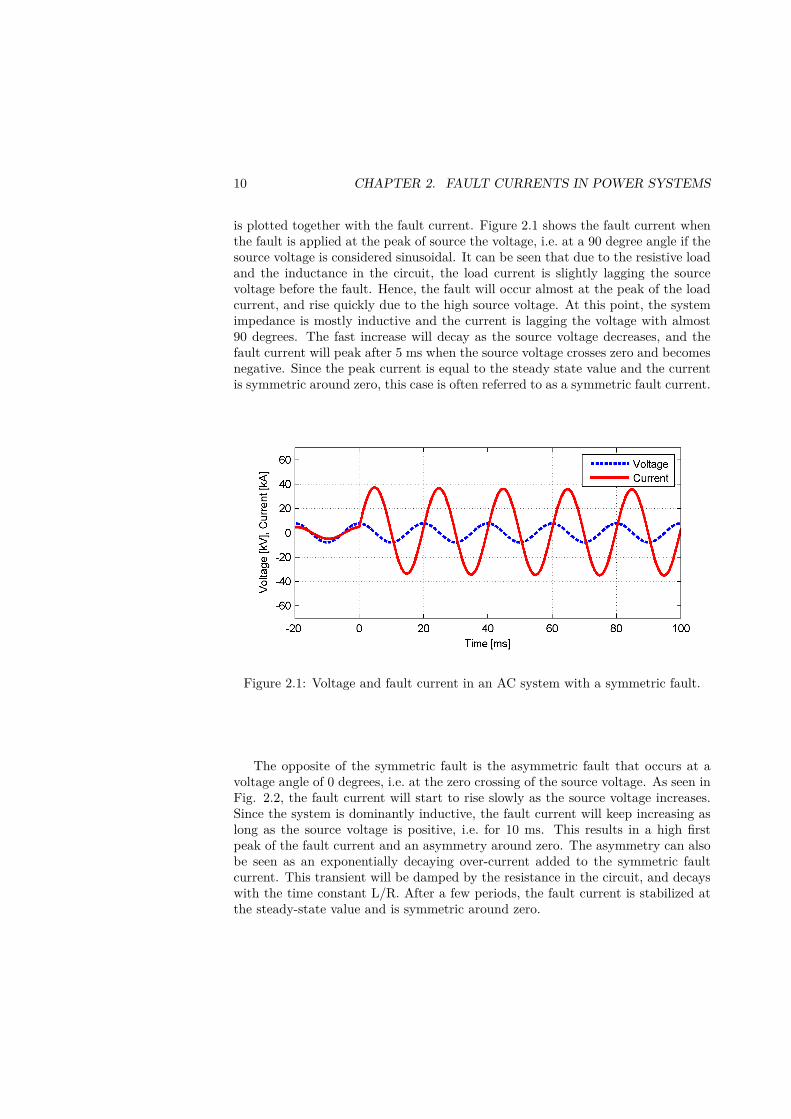
10 CHAPTER 2. FAULT CURRENTS IN POWER SYSTEMS
is plotted together with the fault current. Figure 2.1 shows the fault current whenthe fault is applied at the peak of source the voltage, i.e. at a 90 degree angle if thesource voltage is considered sinusoidal. It can be seen that due to the resistive loadand the inductance in the circuit, the load current is slightly lagging the sourcevoltage before the fault. Hence, the fault will occur almost at the peak of the loadcurrent, and rise quickly due to the high source voltage. At this point, the systemimpedance is mostly inductive and the current is lagging the voltage with almost90 degrees. The fast increase will decay as the source voltage decreases, and thefault current will peak after 5 ms when the source voltage crosses zero and becomesnegative. Since the peak current is equal to the steady state value and the currentis symmetric around zero, this case is often referred to as a symmetric fault current.
Figure 2.1: Voltage and fault current in an AC system with a symmetric fault.
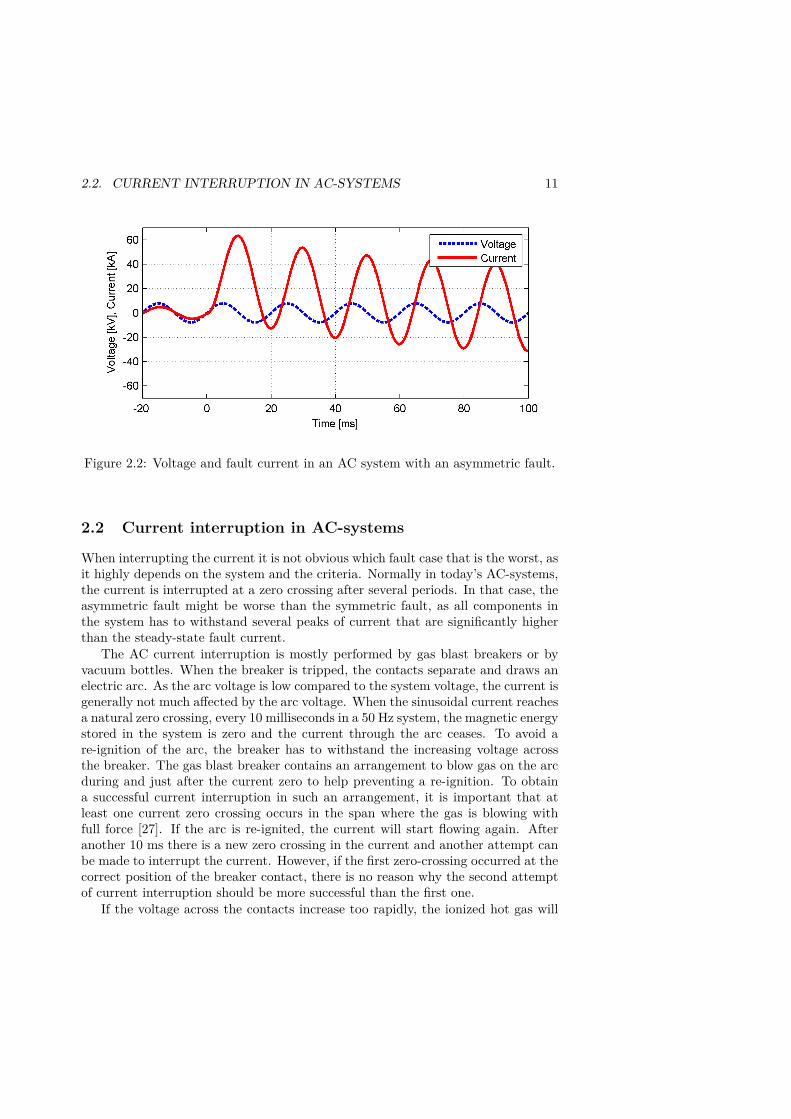
The opposite of the symmetric fault is the asymmetric fault that occurs at avoltage angle of 0 degrees, i.e. at the zero crossing of the source voltage. As seen inFig. 2.2, the fault current will start to rise slowly as the source voltage increases.Since the system is dominantly inductive, the fault current will keep increasing aslong as the source voltage is positive, i.e. for 10 ms. This results in a high firstpeak of the fault current and an asymmetry around zero. The asymmetry can alsobe seen as an exponentially decaying over-current added to the symmetric faultcurrent. This transient will be damped by the resistance in the circuit, and decayswith the time constant L/R. After a few periods, the fault current is stabilized atthe steady-state value and is symmetric around zero.
2.2. CURRENT INTERRUPTION IN AC-SYSTEMS 11
Figure 2.2: Voltage and fault current in an AC system with an asymmetric fault.
2.2 Current interruption in AC-systems
When interrupting the current it is not obvious which fault case that is the worst, asit highly depends on the system and the criteria. Normally in today’s AC-systems,the current is interrupted at a zero crossing after several periods. In that case, theasymmetric fault might be worse than the symmetric fault, as all components inthe system has to withstand several peaks of current that are significantly higherthan the steady-state fault current.
The AC current interruption is mostly performed by gas blast breakers or byvacuum bottles. When the breaker is tripped, the contacts separate and draws anelectric arc. As the arc voltage is low compared to the system voltage, the current isgenerally not much affected by the arc voltage. When the sinusoidal current reachesa natural zero crossing, every 10 milliseconds in a 50 Hz system, the magnetic energystored in the system is zero and the current through the arc ceases. To avoid are-ignition of the arc, the breaker has to withstand the increasing voltage acrossthe breaker. The gas blast breaker contains an arrangement to blow gas on the arcduring and just after the current zero to help preventing a re-ignition. To obtaina successful current interruption in such an arrangement, it is important that atleast one current zero crossing occurs in the span where the gas is blowing withfull force [27]. If the arc is re-ignited, the current will start flowing again. Afteranother 10 ms there is a new zero crossing in the current and another attempt canbe made to interrupt the current. However, if the first zero-crossing occurred at thecorrect position of the breaker contact, there is no reason why the second attemptof current interruption should be more successful than the first one.
If the voltage across the contacts increase too rapidly, the ionized hot gas will
12 CHAPTER 2. FAULT CURRENTS IN POWER SYSTEMS
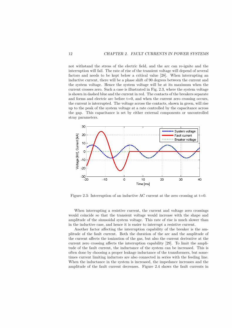
not withstand the stress of the electric field, and the arc can re-ignite and theinterruption will fail. The rate of rise of the transient voltage will depend of severalfactors and needs to be kept below a critical value [28]. When interrupting aninductive current, there will be a phase shift of 90 degrees between the current andthe system voltage. Hence the system voltage will be at its maximum when thecurrent crosses zero. Such a case is illustrated in Fig. 2.3, where the system voltageis shown in dashed blue and the current in red. The contacts of the breakers separateand forms and electric arc before t=0, and when the current zero crossing occurs,the current is interrupted. The voltage across the contacts, shown in green, will riseup to the peak of the system voltage at a rate controlled by the capacitance acrossthe gap. This capacitance is set by either external components or uncontrolledstray parameters.
Figure 2.3: Interruption of an inductive AC current at the zero crossing at t=0.
When interrupting a resistive current, the current and voltage zero crossingswould coincide so that the transient voltage would increase with the shape andamplitude of the sinusoidal system voltage. This rate of rise is much slower thanin the inductive case, and hence it is easier to interrupt a resistive current.
Another factor affecting the interruption capability of the breaker is the am-plitude of the fault current. Both the duration of the arc and the amplitude ofthe current affects the ionization of the gas, but also the current derivative at thecurrent zero crossing affects the interruption capability [29]. To limit the ampli-tude of the fault current, the inductance of the system can be increased. This isoften done by choosing a proper leakage inductance of the transformers, but some-times current limiting inductors are also connected in series with the feeding line.When the inductance in the system is increased, the impedance increases and theamplitude of the fault current decreases. Figure 2.4 shows the fault currents in
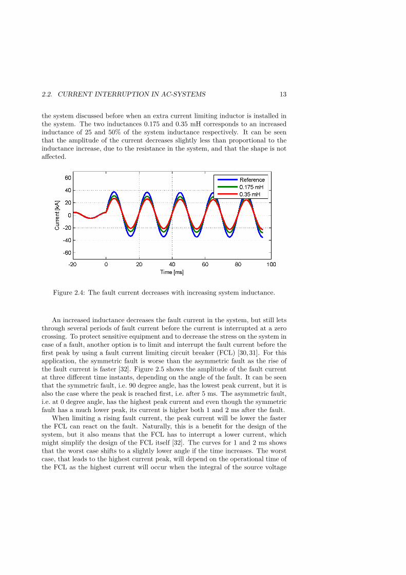
2.2. CURRENT INTERRUPTION IN AC-SYSTEMS 13
the system discussed before when an extra current limiting inductor is installed inthe system. The two inductances 0.175 and 0.35 mH corresponds to an increasedinductance of 25 and 50% of the system inductance respectively. It can be seenthat the amplitude of the current decreases slightly less than proportional to theinductance increase, due to the resistance in the system, and that the shape is notaffected.
Figure 2.4: The fault current decreases with increasing system inductance.
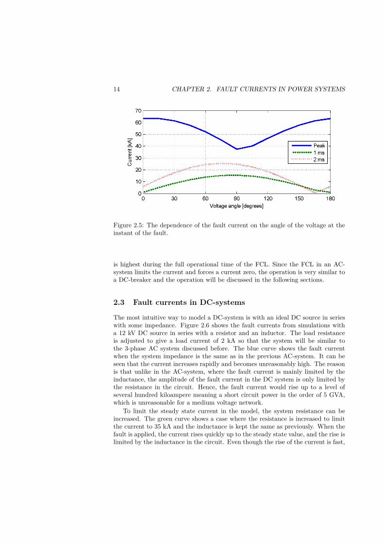
An increased inductance decreases the fault current in the system, but still letsthrough several periods of fault current before the current is interrupted at a zerocrossing. To protect sensitive equipment and to decrease the stress on the system incase of a fault, another option is to limit and interrupt the fault current before thefirst peak by using a fault current limiting circuit breaker (FCL) [30, 31]. For thisapplication, the symmetric fault is worse than the asymmetric fault as the rise ofthe fault current is faster [32]. Figure 2.5 shows the amplitude of the fault currentat three different time instants, depending on the angle of the fault. It can be seenthat the symmetric fault, i.e. 90 degree angle, has the lowest peak current, but it isalso the case where the peak is reached first, i.e. after 5 ms. The asymmetric fault,i.e. at 0 degree angle, has the highest peak current and even though the symmetricfault has a much lower peak, its current is higher both 1 and 2 ms after the fault.
When limiting a rising fault current, the peak current will be lower the fasterthe FCL can react on the fault. Naturally, this is a benefit for the design of thesystem, but it also means that the FCL has to interrupt a lower current, whichmight simplify the design of the FCL itself [32]. The curves for 1 and 2 ms showsthat the worst case shifts to a slightly lower angle if the time increases. The worstcase, that leads to the highest current peak, will depend on the operational time ofthe FCL as the highest current will occur when the integral of the source voltage
14 CHAPTER 2. FAULT CURRENTS IN POWER SYSTEMS
Figure 2.5: The dependence of the fault current on the angle of the voltage at theinstant of the fault.
is highest during the full operational time of the FCL. Since the FCL in an AC-system limits the current and forces a current zero, the operation is very similar toa DC-breaker and the operation will be discussed in the following sections.
2.3 Fault currents in DC-systems
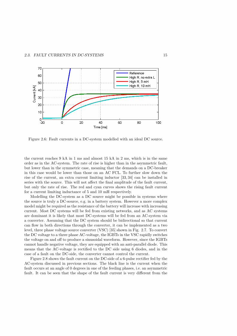
The most intuitive way to model a DC-system is with an ideal DC source in serieswith some impedance. Figure 2.6 shows the fault currents from simulations witha 12 kV DC source in series with a resistor and an inductor. The load resistanceis adjusted to give a load current of 2 kA so that the system will be similar tothe 3-phase AC system discussed before. The blue curve shows the fault currentwhen the system impedance is the same as in the previous AC-system. It can beseen that the current increases rapidly and becomes unreasonably high. The reasonis that unlike in the AC-system, where the fault current is mainly limited by theinductance, the amplitude of the fault current in the DC system is only limited bythe resistance in the circuit. Hence, the fault current would rise up to a level ofseveral hundred kiloampere meaning a short circuit power in the order of 5 GVA,which is unreasonable for a medium voltage network.
To limit the steady state current in the model, the system resistance can beincreased. The green curve shows a case where the resistance is increased to limitthe current to 35 kA and the inductance is kept the same as previously. When thefault is applied, the current rises quickly up to the steady state value, and the rise islimited by the inductance in the circuit. Even though the rise of the current is fast,
2.3. FAULT CURRENTS IN DC-SYSTEMS 15
Figure 2.6: Fault currents in a DC-system modelled with an ideal DC source.
the current reaches 9 kA in 1 ms and almost 15 kA in 2 ms, which is in the sameorder as in the AC-system. The rate of rise is higher than in the asymmetric fault,but lower than in the symmetric case, meaning that the demands on a DC-breakerin this case would be lower than those on an AC FCL. To further slow down therise of the current, an extra current limiting inductor [33, 34] can be installed inseries with the source. This will not affect the final amplitude of the fault current,but only the rate of rise. The red and cyan curves shows the rising fault currentfor a current limiting inductance of 5 and 10 mH respectively.
Modelling the DC-system as a DC source might be possible in systems wherethe source is truly a DC-source, e.g. in a battery system. However a more complexmodel might be required as the resistance of the battery will increase with increasingcurrent. Most DC systems will be fed from existing networks, and as AC systemsare dominant it is likely that most DC-systems will be fed from an AC-system viaa converter. Assuming that the DC system should be bidirectional so that currentcan flow in both directions through the converter, it can be implemented as a twolevel, three phase voltage source converter (VSC) [35] shown in Fig. 2.7. To convertthe DC voltage to a three phase AC-voltage, the IGBTs in the VSC rapidly switchesthe voltage on and off to produce a sinusoidal waveform. However, since the IGBTscannot handle negative voltage, they are equipped with an anti-parallel diode. Thismeans that the AC-voltage is rectified to the DC side using 6 diodes, and in thecase of a fault on the DC-side, the converter cannot control the current.
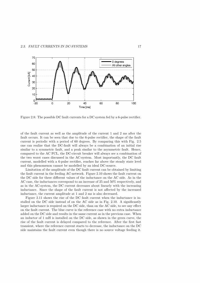
Figure 2.8 shows the fault current on the DC-side of a 6-pulse rectifier fed by theAC-system discussed in previous sections. The black line is the current when thefault occurs at an angle of 0 degrees in one of the feeding phases, i.e. an asymmetricfault. It can be seen that the shape of the fault current is very different from the
16 CHAPTER 2. FAULT CURRENTS IN POWER SYSTEMS
+
-
L1
L2
L3
Figure 2.7: A two level, three phase voltage source converter.
ideal DC-case shown in Fig. 2.6.The initial rise of the DC-fault current will be determined by the phase with
the highest voltage. As one of the phases in this case is at zero, the other twophases have voltages equal to about 87% of the peak voltage. One of the voltagesis negative, but due to the rectifier, it will also contribute to a positive rise ofthe DC-fault current. After a few milliseconds, the voltage in the phase with anasymmetric fault exceeds the other ones and pushes the current up to a peak valueclose to the peak value of the asymmetric fault current in the AC-system. Afterthe peak, the DC fault current will decrease, as none of the other phases experiencesuch a high fault current. The DC fault current will then reach a local minimumthat is determined by the absolute value of the negative peak of the asymmetricfault current in the AC system, i.e. much lower than the peak of the steady-statecurrent. Yet again one of the other voltages will become higher and the currentwill start to increase again. The oscillation is damped, as in the asymmetric faultcurrent in the AC-system, and settles at a level close to the peak of the steady-statecurrent, determined by the short circuit power of the AC-network.
The grey area shows the fault currents for all other angles, and hence representsall possible fault currents for a zero impedance fault on the DC side. It can beseen by the thickness of the grey area that the difference is not too large betweendifferent possible fault currents.
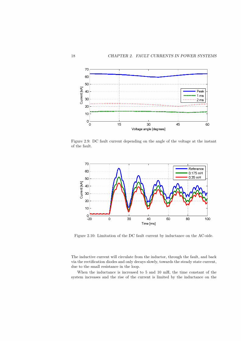
When the fault occurs on the DC-side, one of the phases will be within ±30 de-grees of a symmetric fault due to the symmetry of the 3-phase system. In thebeginning, the DC-fault current will then rise similar to the symmetric fault cur-rent in the AC-system. Within 5 ms, the voltage in the first phase is exceeded bythe voltage of one of the other phases, and the DC-current will keep rising. Anotherof the phases will always be within ±30 degrees of an asymmetric fault an causesthe peak current to be close to the asymmetric case. Figure 2.9 shows the peak
2.3. FAULT CURRENTS IN DC-SYSTEMS 17
Figure 2.8: The possible DC fault currents for a DC system fed by a 6-pulse rectifier.
of the fault current as well as the amplitude of the current 1 and 2 ms after thefault occurs. It can be seen that due to the 6-pulse rectifier, the shape of the faultcurrent is periodic with a period of 60 degrees. By comparing this with Fig. 2.5one can realize that the DC-fault will always be a combination of an initial risesimilar to a symmetric fault, and a peak similar to the asymmetric fault. Hence,compared to the AC FCL, the DC-circuit breaker will always see a combination ofthe two worst cases discussed in the AC-system. Most importantly, the DC faultcurrent, modelled with a 6-pulse rectifier, reaches far above the steady state leveland this phenomenon cannot be modelled by an ideal DC-source.
Limitation of the amplitude of the DC fault current can be obtained by limitingthe fault current in the feeding AC-network. Figure 2.10 shows the fault current onthe DC side for three different values of the inductance on the AC side. As in theAC case, the inductances correspond to an increase of 25 and 50% respectively, andas in the AC-system, the DC current decreases about linearly with the increasinginductance. Since the shape of the fault current is not affected by the increasedinductance, the current amplitude at 1 and 2 ms is also decreased.
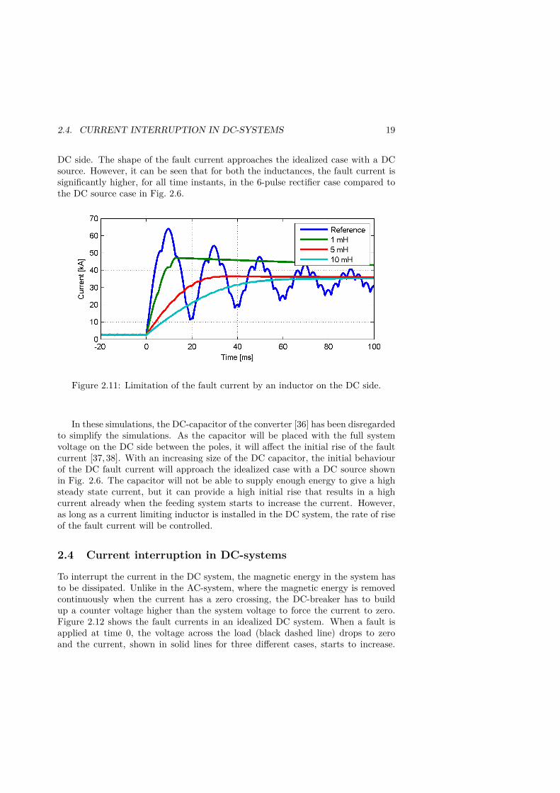
Figure 2.11 shows the rise of the DC fault current when the inductance is in-stalled on the DC side instead of on the AC side as in Fig. 2.10. A significantlylarger inductance is required on the DC side, than on the AC side, to see any effecton the fault current. The blue curve is the reference case with no extra inductanceadded on the DC side and results in the same current as in the previous case. Whenan inductor of 1 mH is installed on the DC side, as shown in the green curve, therise of the fault current is delayed compared to the reference. After the first fasttransient, where the reference current starts to decrease, the inductance on the DCside maintains the fault current even though there is no source voltage feeding it.
18 CHAPTER 2. FAULT CURRENTS IN POWER SYSTEMS
Figure 2.9: DC fault current depending on the angle of the voltage at the instantof the fault.
Figure 2.10: Limitation of the DC fault current by inductance on the AC-side.
The inductive current will circulate from the inductor, through the fault, and backvia the rectification diodes and only decays slowly, towards the steady state current,due to the small resistance in the loop.
When the inductance is increased to 5 and 10 mH, the time constant of thesystem increases and the rise of the current is limited by the inductance on the
2.4. CURRENT INTERRUPTION IN DC-SYSTEMS 19
DC side. The shape of the fault current approaches the idealized case with a DCsource. However, it can be seen that for both the inductances, the fault current issignificantly higher, for all time instants, in the 6-pulse rectifier case compared tothe DC source case in Fig. 2.6.
Figure 2.11: Limitation of the fault current by an inductor on the DC side.
In these simulations, the DC-capacitor of the converter [36] has been disregardedto simplify the simulations. As the capacitor will be placed with the full systemvoltage on the DC side between the poles, it will affect the initial rise of the faultcurrent [37, 38]. With an increasing size of the DC capacitor, the initial behaviourof the DC fault current will approach the idealized case with a DC source shownin Fig. 2.6. The capacitor will not be able to supply enough energy to give a highsteady state current, but it can provide a high initial rise that results in a highcurrent already when the feeding system starts to increase the current. However,as long as a current limiting inductor is installed in the DC system, the rate of riseof the fault current will be controlled.
2.4 Current interruption in DC-systems
To interrupt the current in the DC system, the magnetic energy in the system hasto be dissipated. Unlike in the AC-system, where the magnetic energy is removedcontinuously when the current has a zero crossing, the DC-breaker has to buildup a counter voltage higher than the system voltage to force the current to zero.Figure 2.12 shows the fault currents in an idealized DC system. When a fault isapplied at time 0, the voltage across the load (black dashed line) drops to zeroand the current, shown in solid lines for three different cases, starts to increase.
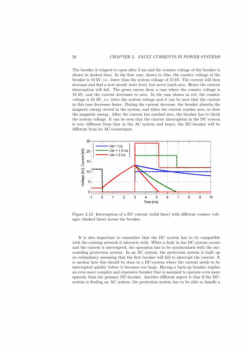
20 CHAPTER 2. FAULT CURRENTS IN POWER SYSTEMS
The breaker is tripped to open after 3 ms and the counter voltage of the breaker isshown in dashed lines. In the first case, shown in blue, the counter voltage of thebreaker is 10 kV, i.e. lower than the system voltage of 12 kV. The current will thendecrease and find a new steady state level, but never reach zero. Hence the currentinterruption will fail. The green curves show a case where the counter voltage is18 kV, and the current decreases to zero. In the case shown in red, the countervoltage is 24 kV, i.e. twice the system voltage and it can be seen that the currentin this case decreases faster. During the current decrease, the breaker absorbs themagnetic energy stored in the system, and when the current reaches zero, so doesthe magnetic energy. After the current has reached zero, the breaker has to blockthe system voltage. It can be seen that the current interruption in the DC systemis very different from that in the AC system and hence, the DC-breaker will bedifferent from its AC-counterpart.
Figure 2.12: Interruption of a DC current (solid lines) with different counter volt-ages (dashed lines) across the breaker.
It is also important to remember that the DC system has to be compatiblewith the existing network it interacts with. When a fault in the DC system occursand the current is interrupted, the operation has to be synchronized with the sur-rounding protection system. In an AC system, the protection system is built upon redundancy assuming that the first breaker will fail to interrupt the current. Itis unclear how this should be done in a DC-system where the current needs to beinterrupted quickly before it becomes too large. Having a back-up breaker impliesan even more complex and expensive breaker that is assumed to operate even moresparsely than the primary DC-breaker. Another different aspect is that if the DC-system is feeding an AC system, the protection system has to be able to handle a

2.4. CURRENT INTERRUPTION IN DC-SYSTEMS 21
fault on the AC side and be able to provide enough power into the AC system forthe AC protection system to detect and clear the fault. One example is that whenthe AC system in a house is fed from a DC distribution system, the DC systemhas to provide enough short circuit current for the fuses to operate when there is afault in the house [39].

Chapter 3
DC-breaker topologies
Almost all DC-lines installed until today are point to point connections, wherepower is transferred from one AC-grid to another AC-grid. Even though the powerflow can go in both directions, the system is not meshed and hence the whole systemis lost in the case of a fault. Hence, there is no need for DC-breakers as the currentcan be interrupted on the AC-side and the whole system is taken off-line. Whenmeshed networks with more than two terminals are built, another solution willbe required to isolate faulted parts of the system and keep the rest of the systemenergized [40].
Voltage source converters based on IGBTs are commonly used to control thepower flow in the HVDC line. This gives good controllability of the power duringnormal operation, but in the case of a fault on the DC side, the voltage will dropand the current will flow through the free-wheeling diodes in the inverter. Thismeans all control of the current is lost when a fault occurs on the DC-side. Oneoption is to replace the inverters with full bridge converters [41] so that the currentcan be controlled by the converter also in the case of a fault on the DC-side. Thisincreases the controllability but also increases the losses as another controllablesemiconductor component is added in the current conduction path. To handleisolation and sectioning in meshed DC-grids, the full bridge converters can be usedin combination with fast disconnectors. In the case of a fault on the DC-side, thecurrent is interrupted by the converter, and the disconnector can open withoutvoltage and current stress to isolate the faulted section. Once the faulted sectionis disconnected, the converter can turn on again and the system can run in a newconfiguration.
Another option is to use circuit breakers on the DC-side. A large number ofdifferent topologies exist for DC-breakers and the optimal choice depends stronglyon the system voltage and current levels. Also the expected number of faults and theshort circuit power will have a large impact as it sets the demands on operationalspeed and number of consecutive operations. In systems with a high number offaults, e.g. over-head lines, the required number of total operations during the
23
24 CHAPTER 3. DC-BREAKER TOPOLOGIES
breaker lifetime will be high. Further, if the breakers are located in remote anddifficult areas, e.g. in offshore wind farms, the breaker has to be reliable to minimizethe need for maintenance.
3.1 Mechanical DC-breaker
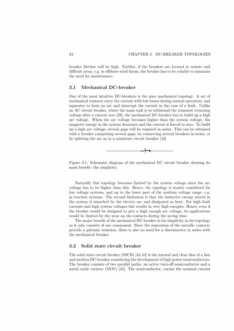
One of the most intuitive DC-breakers is the pure mechanical topology. A set ofmechanical contacts carry the current with low losses during normal operation, andseparates to form an arc and interrupt the current in the case of a fault. Unlikean AC circuit breaker, where the main task is to withstand the transient returningvoltage after a current zero [29], the mechanical DC-breaker has to build up a higharc voltage. When the arc voltage becomes higher than the system voltage, themagnetic energy in the system decreases and the current is forced to zero. To buildup a high arc voltage, several gaps will be required in series. This can be obtainedwith a breaker comprising several gaps, by connecting several breakers in series, orby splitting the arc as in a miniature circuit breaker [42].
Figure 3.1: Schematic diagram of the mechanical DC circuit breaker showing itsmain benefit: the simplicity.
Naturally this topology becomes limited by the system voltage since the arcvoltage has to be higher than this. Hence, the topology is mostly considered forlow voltage systems, and up to the lower part of the medium voltage range, e.g.in traction systems. The second limitation is that the inductive energy stored inthe system is absorbed by the electric arc and dissipated as heat. For high faultcurrents and high system voltages this results in very high energies. Hence, even ifthe breaker would be designed to give a high enough arc voltage, its applicationswould be limited by the wear on the contacts during the arcing time.
The major benefit of the mechanical DC-breaker is the simplicity in the topologyas it only consists of one component. Since the separation of the metallic contactsprovide a galvanic isolation, there is also no need for a disconnector in series withthe mechanical breaker.
3.2 Solid state circuit breaker
The solid state circuit breaker (SSCB) [43,44] is the natural and clear idea of a fastand modern DC-breaker considering the development of high power semiconductors.The breaker consists of two parallel paths: an active turn-off semiconductor and ametal oxide varistor (MOV) [45]. The semiconductor, carries the nominal current
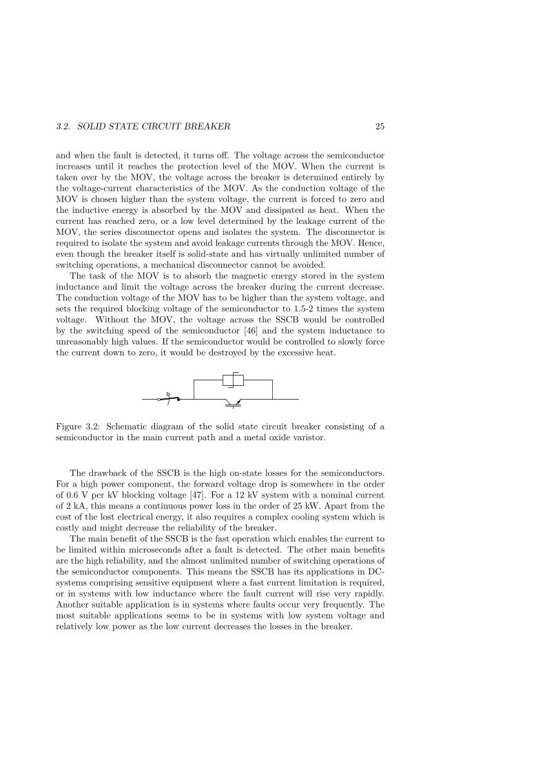
3.2. SOLID STATE CIRCUIT BREAKER 25
and when the fault is detected, it turns off. The voltage across the semiconductorincreases until it reaches the protection level of the MOV. When the current istaken over by the MOV, the voltage across the breaker is determined entirely bythe voltage-current characteristics of the MOV. As the conduction voltage of theMOV is chosen higher than the system voltage, the current is forced to zero andthe inductive energy is absorbed by the MOV and dissipated as heat. When thecurrent has reached zero, or a low level determined by the leakage current of theMOV, the series disconnector opens and isolates the system. The disconnector isrequired to isolate the system and avoid leakage currents through the MOV. Hence,even though the breaker itself is solid-state and has virtually unlimited number ofswitching operations, a mechanical disconnector cannot be avoided.
The task of the MOV is to absorb the magnetic energy stored in the systeminductance and limit the voltage across the breaker during the current decrease.The conduction voltage of the MOV has to be higher than the system voltage, andsets the required blocking voltage of the semiconductor to 1.5-2 times the systemvoltage. Without the MOV, the voltage across the SSCB would be controlledby the switching speed of the semiconductor [46] and the system inductance tounreasonably high values. If the semiconductor would be controlled to slowly forcethe current down to zero, it would be destroyed by the excessive heat.
Figure 3.2: Schematic diagram of the solid state circuit breaker consisting of asemiconductor in the main current path and a metal oxide varistor.
The drawback of the SSCB is the high on-state losses for the semiconductors.For a high power component, the forward voltage drop is somewhere in the orderof 0.6 V per kV blocking voltage [47]. For a 12 kV system with a nominal currentof 2 kA, this means a continuous power loss in the order of 25 kW. Apart from thecost of the lost electrical energy, it also requires a complex cooling system which iscostly and might decrease the reliability of the breaker.
The main benefit of the SSCB is the fast operation which enables the current tobe limited within microseconds after a fault is detected. The other main benefitsare the high reliability, and the almost unlimited number of switching operations ofthe semiconductor components. This means the SSCB has its applications in DC-systems comprising sensitive equipment where a fast current limitation is required,or in systems with low inductance where the fault current will rise very rapidly.Another suitable application is in systems where faults occur very frequently. Themost suitable applications seems to be in systems with low system voltage andrelatively low power as the low current decreases the losses in the breaker.
26 CHAPTER 3. DC-BREAKER TOPOLOGIES
The development of new semiconductor materials as gallium nitride (GaN), sil-icon carbide (SiC) [48], and diamond [49] is also increasing the applications for theSSCB. As SiC has lower losses than the current silicon crystals, can be made withhigher voltage withstand in each component, and can operate at higher tempera-tures than its silicon counterparts, it has the possibility to reduce the losses as wellas the complexity of the SSCB and its cooling system.
3.3 Resonant DC-breaker
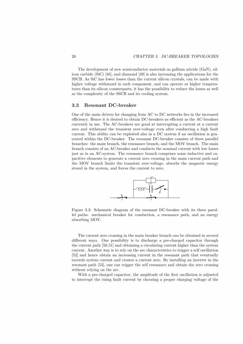
One of the main drivers for changing from AC to DC networks lies in the increasedefficiency. Hence it is desired to obtain DC-breakers as efficient as the AC-breakerscurrently in use. The AC-breakers are good at interrupting a current at a currentzero and withstand the transient over-voltage even after conducting a high faultcurrent. This ability can be exploited also in a DC system if an oscillation is gen-erated within the DC-breaker. The resonant DC-breaker consists of three parallelbranches: the main branch, the resonance branch, and the MOV branch. The mainbranch consists of an AC-breaker and conducts the nominal current with low lossesjust as in an AC-system. The resonance branch comprises some inductive and ca-pacitive elements to generate a current zero crossing in the main current path andthe MOV branch limits the transient over-voltage, absorbs the magnetic energystored in the system, and forces the current to zero.
Figure 3.3: Schematic diagram of the resonant DC-breaker with its three paral-lel paths: mechanical breaker for conduction, a resonance path, and an energyabsorbing MOV.
The current zero crossing in the main breaker branch can be obtained in severaldifferent ways. One possibility is to discharge a pre-charged capacitor throughthe current path [50,51] and obtaining a circulating current higher than the systemcurrent. Another way is to rely on the arc characteristics to trigger a self oscillation[52] and hence obtain an increasing current in the resonant path that eventuallyexceeds system current and creates a current zero. By installing an inverter in theresonant path [53], one can trigger the self resonance and obtain the zero crossingwithout relying on the arc.
With a pre-charged capacitor, the amplitude of the first oscillation is adjustedto interrupt the rising fault current by choosing a proper charging voltage of the
3.4. THE Z-SOURCE BREAKER 27
capacitor. When interrupting a significantly lower current, the amplitude of theoscillating current is much higher than the system current resulting in a muchhigher current derivative at the zero-crossing, compared to when interrupting thefull fault current. This might make the interruption of the nominal current, or lowfault currents, harder for the AC-breaker to interrupt than a high fault current. Ifthe current is not interrupted at the first zero crossing, the current derivative inthe consecutive zero-crossings will be lower as the amplitude of the oscillation indamped by the resistance in the circuit. This should make it easier to interrupt thecurrent as the oscillation decays. However, since the delayed interruption leads tosignificantly longer arcing times, the stress on the AC-breaker increases.
In the other two topologies, where the oscillation grows larger and larger, theincreasing oscillation will cause a zero crossing eventually as long as the increasein the amplitude of the oscillation is faster than the rise of the fault current. Thisresults in a guaranteed low current derivative at the first zero crossing, since theamplitude of the oscillation in that case will be only slightly higher than the systemcurrent. However, it also delays the current interruption compared to the firsttopology. The delay results in a higher current to interrupt in the case of a risingfault current and also increases the arcing time of the mechanical breaker.
In all three topologies, the current zero crossing is only local in the breakerbranch and the MOV is still responsible of forcing the system current to zero. Hence,a disconnector is required also in this topology to obtain the galvanic isolation afterthe current is interrupted.
The main drawback of the resonant DC-breaker is the complexity as is con-tains both an AC-breaker, a charged capacitor or an inverter, and a closing switch.There is a trade-off in the design of the resonant circuit as a high oscillation fre-quency results in an earlier current zero, but a higher derivative of the current tobe interrupted. In the topology containing a charged capacitor, the amplitude ofthe discharge current has to be chosen higher than the system current to providea current zero, but not too high as this results in a high derivative of the currentat the zero crossing. In the other two topologies, the resonance frequency has tobe chosen high enough to obtain a high amplitude on the resonance fast enough toensure a fast current interruption.
Apart from the low losses in the conduction path, the resonant DC-breakerhas an advantage in that it can be built from conventional components. All thecomponents, as capacitors and AC-breakers, are already available on the market.This makes it a relatively cost effective solution, with high reliability and greatmarket acceptance.
3.4 The Z-source breaker
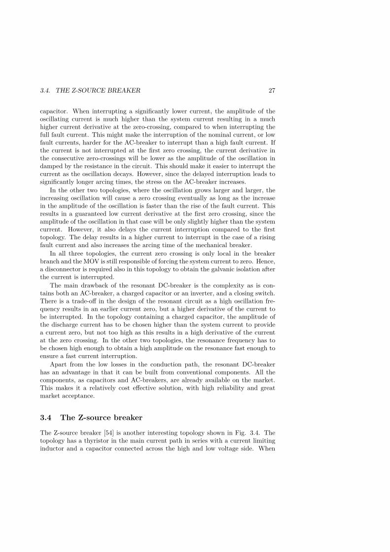
The Z-source breaker [54] is another interesting topology shown in Fig. 3.4. Thetopology has a thyristor in the main current path in series with a current limitinginductor and a capacitor connected across the high and low voltage side. When
28 CHAPTER 3. DC-BREAKER TOPOLOGIES
there is a drop in the impedance on the load side, the current will increase. Initially,the series inductors will keep the current constant, and the load side current willincrease through the capacitors. When the capacitor current reach the level of theinductor current, the feeding current from the grid becomes zero and the seriesthyristor will turn off. The current on the fault side is allowed to oscillate untilit becomes zero and is taken over by the resistor and diode that is in parallelto the inductor and the energy is dissipated in the resistor. The inductance andcapacitance should be balanced so that a current zero, occurs only if the transientis high enough and not unintentionally on normal changes in the load.
Figure 3.4: Schematic diagram of the Z-source breaker.
As with the solid state breaker, the drawback with this solution is the semi-conductor in the current path. However, the thyristor has significantly lower lossesthan the IGBT and is also a much cheaper and a robust component. The otherdrawback is the rather complex topology with several inductors, capacitors andsemiconductors that all have to handle high voltages and currents. In many casesit might simply not be possible to connect the required capacitors between the pos-itive and negative terminals, although there are variations of the Z-source breakerthat provides solutions to that problem [55]. Further, as the current switching isperformed with a thyristor, there is no possibility to interrupt a nominal current.One possibility is to use a closing switch to short circuit the load side to obtain arushing current and hence force an interruption. Another disadvantage is that thistopology only can conduct current in one direction, and hence cannot be used inbidirectional systems.
As discussed above, the benefit of the Z-source breaker lies partly in the compar-ison with other topologies with semiconductors in the conduction path, and thatthe topology allows the use of a passive turn-off component. The topology alsooffers a system where the detection of the fault and the interruption of the faultcurrent is performed automatically. Like the SSCB, the topology is also free frommechanical breakers, except for the disconnector, which increases the rated numberof operations for the breaker.
3.5. HYBRID DC-BREAKER 29
3.5 Hybrid DC-breaker
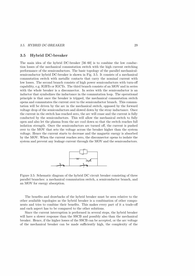
The main idea of the hybrid DC-breaker [56–60] is to combine the low conduc-tion losses of the mechanical commutation switch with the high current switchingperformance of the semiconductors. The basic topology of the parallel mechanical-semiconductor hybrid DC-breaker is shown in Fig. 3.5. It consists of a mechanicalcommutation switch with metallic contacts that carry the nominal current withlow losses. The second branch consists of high power semiconductors with turn-offcapability, e.g. IGBTs or IGCTs. The third branch consists of an MOV and in serieswith the whole breaker is a disconnector. In series with the semiconductor is aninductor that symbolizes the inductance in the commutation loop. The operationalprinciple is that once the breaker is tripped, the mechanical commutation switchopens and commutates the current over to the semiconductor branch. This commu-tation will be driven by the arc in the mechanical switch, opposed by the forwardvoltage drop of the semiconductors and slowed down by the stray inductance. Oncethe current in the switch has reached zero, the arc will cease and the current is fullyconducted by the semiconductors. This will allow the mechanical switch to fullyopen and also let the plasma from the arc cool down so that the switch reaches fullisolation strength. Once the semiconductors are turned off, the current is pushedover to the MOV that sets the voltage across the breaker higher than the systemvoltage. Hence the current starts to decrease and the magnetic energy is absorbedby the MOV. When the current reaches zero, the disconnector opens to isolate thesystem and prevent any leakage current through the MOV and the semiconductors.
Figure 3.5: Schematic diagram of the hybrid DC circuit breaker consisting of threeparallel branches: a mechanical commutation switch, a semiconductor branch, andan MOV for energy absorption.
The benefits and drawbacks of the hybrid breaker must be seen relative to theother available topologies as the hybrid breaker is a combination of other compo-nents and tries to combine their benefits. This makes every part of it a trade-offand each aspect has to be compared to the other solutions.
Since the current interruption is performed in several steps, the hybrid breakerwill have a slower response than the SSCB and possibly also than the mechanicalbreaker. Hence, if the higher losses of the SSCB can be accepted, or the arc voltageof the mechanical breaker can be made sufficiently high, the complexity of the
30 CHAPTER 3. DC-BREAKER TOPOLOGIES
hybrid breaker makes it a bad choice.The hybrid breaker offers low on-state losses as the other mechanical solutions
and one of the major benefits of the hybrid breaker is that its mechanical commu-tation switch never has to interrupt the current, only commutate it to a parallelbranch. Hence it can be made lighter and thereby faster than the mechanicalbreaker and the resonant breaker. Also, the forward voltage drop of the semicon-ductors is just a fraction of the system voltage, so the required arc voltage in thecommutation switch is much lower than the required arc voltage of the mechanicalbreaker. This makes the hybrid breaker more suitable for higher system voltagesthan the mechanical breaker. Since the commutation of the current is rather fast,only a limited energy is absorbed by the contact system during the arcing whichleads to lower wear of the contacts compared to the mechanical breaker and theresonant breaker.
For high system voltages, many semiconductors are required in series and thisresults in a high voltage drop during the commutation and semiconductor conduc-tion period. Hence a high arc voltage is required in the mechanical switch to ensurea fast and successful commutation of the fault current. ABB has suggested anotherapproach [61] where a small semiconductor component, a load commutation switch(LCS), is placed in the conduction path. This way a response is obtained in justsome microseconds and fast commutation is ensured by the LCS. The mechanicalswitch is opened without arcing after the current is commutated, only to isolatethe LCS and protect it from the transient MOV voltage. The LCS provides a fastresponse in the breaker, but also increases the losses with a semiconductor compo-nent in the nominal current path. However, compared to the SSCB, these lossesare very small since the voltage rating of the LCS is much lower than the systemvoltage.
3.6 Other possibilities
As the interruption of direct currents is a difficult task, perhaps one should approachthe problem in a different manner. One possibility is to limit the fault current to avalue not to far from the nominal current. The circuit breaker then only has to bedesigned to handle the lower current, and hence the requirements on a fast operationare decreased. The super conducting fault current limiter [62] is such a solution.A component containing super conducting wire is connected in the main currentpath and conducts the current with negligible losses. When the fault occurs in thenetwork and the current rises, the higher current density will cause the componentto lose its super conductive ability. The resistance increases and the fault currentis limited and can be interrupted by a series connected breaker. The main issue forthe super conductive FCL is the high cost of the super conductive material [42], thecomplexity of the system with cooling and liquid nitrogen, but also the time it takesto cool down the component and regain the super conductivity to reset the breaker.A similar concept is the use of a positive temperature coefficient resistor [63], where
3.6. OTHER POSSIBILITIES 31
the resistance increases rapidly in the case of an increased current and hence limitsthe current.
Another, more passive solution is the use of high voltage fuses [64, 65]. Thefuse conducts the nominal current with low losses, and automatically changes fromconducting to blocking by the higher amplitude of the fault current. After thefuse is burnt, it blocks the system voltage. The obvious drawback of the fuse itthat the fuse is a one-operational device that has to be replaced after each use.One possibility is to replace the semiconductor branch of the hybrid breaker witha component that contains a fuse, and automatically changes to a new fuse aftereach operation. The benefit of having the mechanical switch in parallel is thatthe breaker can allow transient over-currents without risking to burn the fuse.Further, a faster fuse with lower current rating can be used as the fuse never hasto conduct the nominal current. The feasibility of the system is dependent onthe expected number of operations of the DC-breaker, as the number of fuses inthe breaker have to be large enough so that the fuses can be replaced during theplanned maintenance. The operation of the fuse can be enhanced by connecting itin parallel with an MOV to let the MOV absorb the magnetic energy in the system,as in most DC-breaker topologies.

Chapter 4
The studied hybrid DC-breaker
The hybrid DC-breaker is not a new invention. Different similar concepts havebeen discussed, ever since the high power semiconductors became commerciallyavailable, due to the inherently high on-state losses in all semiconductor compo-nents. However, due to the increased use of DC-systems, the need for high powerDC-breakers has become more and more relevant in the recent years. The hybridDC-breaker is one of the most promising options for such a breaker as it combinesthe low conduction losses in the mechanical switch with the high switching per-formance of the semiconductors. Further, the continuous development in the highpower semiconductor technology has made the breaker topology more cost effective.The continued increase of semiconductors in motor drives, rectifiers and convertersin the power system has proven the reliability and increased the market acceptanceof high power semiconductors.
The schematic drawing of the hybrid DC-breaker is shown in Fig. 3.5 and it con-sists of three parallel branches, each with a specific task in the current interruption.The nominal current branch consists of a mechanical switch, where the current canbe conducted with low losses during normal operation. The semiconductor branch,often referred to as the main breaker branch, consists of high power semiconductors.The third branch consists of a non-linear resistor, generally in the form of a metaloxide varistor (MOV) that can absorb the magnetic energy stored in the system.
4.1 Basic operation
The principle operation of the hybrid DC-breaker is best summarized by the twographs in Fig. 4.1 and 4.2, showing the current and voltage waveforms during theinterruption of a rising fault current.
The black line in Fig. 4.1 shows the total current in the system. At the time 0,a fault is applied to the system, and the fault current starts to rise. Initially, therise of the current is limited by the inductance in the system and the rise is almostlinear. Before the fault is detected, the current is conducted by the mechanical
33
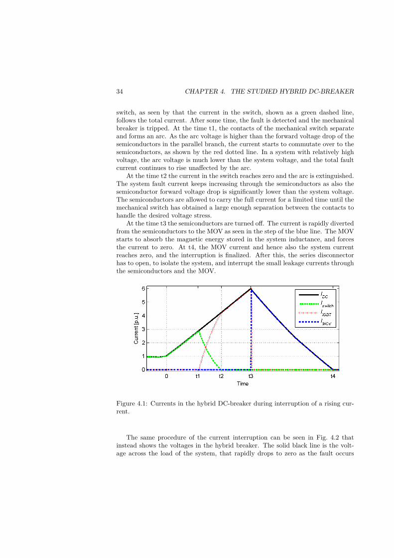
34 CHAPTER 4. THE STUDIED HYBRID DC-BREAKER
switch, as seen by that the current in the switch, shown as a green dashed line,follows the total current. After some time, the fault is detected and the mechanicalbreaker is tripped. At the time t1, the contacts of the mechanical switch separateand forms an arc. As the arc voltage is higher than the forward voltage drop of thesemiconductors in the parallel branch, the current starts to commutate over to thesemiconductors, as shown by the red dotted line. In a system with relatively highvoltage, the arc voltage is much lower than the system voltage, and the total faultcurrent continues to rise unaffected by the arc.
At the time t2 the current in the switch reaches zero and the arc is extinguished.The system fault current keeps increasing through the semiconductors as also thesemiconductor forward voltage drop is significantly lower than the system voltage.The semiconductors are allowed to carry the full current for a limited time until themechanical switch has obtained a large enough separation between the contacts tohandle the desired voltage stress.
At the time t3 the semiconductors are turned off. The current is rapidly divertedfrom the semiconductors to the MOV as seen in the step of the blue line. The MOVstarts to absorb the magnetic energy stored in the system inductance, and forcesthe current to zero. At t4, the MOV current and hence also the system currentreaches zero, and the interruption is finalized. After this, the series disconnectorhas to open, to isolate the system, and interrupt the small leakage currents throughthe semiconductors and the MOV.
Figure 4.1: Currents in the hybrid DC-breaker during interruption of a rising cur-rent.
The same procedure of the current interruption can be seen in Fig. 4.2 thatinstead shows the voltages in the hybrid breaker. The solid black line is the volt-age across the load of the system, that rapidly drops to zero as the fault occurs
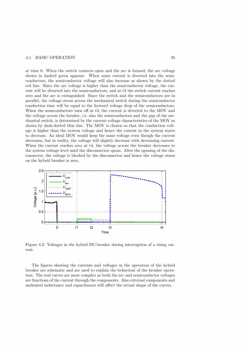
4.1. BASIC OPERATION 35
at time 0. When the switch contacts open and the arc is formed, the arc voltageshown in dashed green appears. When some current is diverted into the semi-conductors, the semiconductor voltage will also increase as shown by the dottedred line. Since the arc voltage is higher than the semiconductor voltage, the cur-rent will be diverted into the semiconductors, and at t3 the switch current reacheszero and the arc is extinguished. Since the switch and the semiconductors are inparallel, the voltage stress across the mechanical switch during the semiconductorconduction time will be equal to the forward voltage drop of the semiconductors.When the semiconductors turn off at t3, the current is diverted to the MOV andthe voltage across the breaker, i.e. also the semiconductors and the gap of the me-chanical switch, is determined by the current-voltage characteristics of the MOV asshown by dash-dotted blue line. The MOV is chosen so that the conduction volt-age is higher than the system voltage and hence the current in the system startsto decrease. An ideal MOV would keep the same voltage even though the currentdecreases, but in reality, the voltage will slightly decrease with decreasing current.When the current reaches zero at t4, the voltage across the breaker decreases tothe system voltage level until the disconnector opens. After the opening of the dis-connector, the voltage is blocked by the disconnector and hence the voltage stresson the hybrid breaker is zero.
Figure 4.2: Voltages in the hybrid DC-breaker during interruption of a rising cur-rent.
The figures showing the currents and voltages in the operation of the hybridbreaker are schematic and are used to explain the behaviour of the breaker opera-tion. The real curves are more complex as both the arc and semiconductor voltagesare functions of the current through the components. Also external components andundesired inductance and capacitances will affect the actual shape of the curves.
36 CHAPTER 4. THE STUDIED HYBRID DC-BREAKER
4.2 The topology
The design of a hybrid DC-breaker is not straight forward as all the componentsaffect each other. The design of the hybrid DC-breaker topology, and the compo-nents used, are described in detail in the licentiate thesis [66]. There is a benefitfrom a system point of view to limit the current at a low value. One reason it thatthe semiconductors in the AC/DC converters are very much stressed by the highfault current, and it would be very expensive to dimension the converter to handlethe high fault currents. Also, the system requires a fast operation of the breakerto keep the system stable. When meshed HVDC systems are built as backbonesto strengthen the existing AC networks, it will be essential that the DC grid ismaintained in operation after a fault. As seen in chapter 2, the peak of the faultcurrent might be reached within 8 ms after the fault occurs, so for a fast operationto make sense, the current should be limited before this.
For a hybrid DC-breaker it is also interesting to limit the current even earlier.One reason is that with a higher current, it takes longer time to commutate thecurrent from the mechanical switch into the semiconductors. Also, due to theresistive component in the semiconductors, a higher current requires a higher arcvoltage for a successful commutation. But most importantly, the semiconductorshave to conduct and switch the peak current. Hence, if the peak current can bekept lower with a faster reaction of the breaker, the semiconductors can be chosenwith lower current ratings, and hence much less expensive.
4.2.1 The mechanical commutation switch
The mechanical switch in the hybrid breaker has three different tasks: conductthe current with low losses, commutate the current into the semiconductors, andwithstand the transient voltage when the current is limited by the MOV.
The low conduction losses should not be a big problem since the mechanicalswitch should have metallic contacts and hence the losses can be expected in thesame range as for conventional AC-breakers.
To properly commutate the current into the semiconductor branch, the arc volt-age has to be higher than the conduction voltage of the semiconductors. Further,as the fault current is rapidly increasing, the reaction time of the switch is critical.The faster the contacts can separate to form the arc, the faster the commutationcan start. This means there is a lower current to be commutated which is beneficialboth as it results in a lower opposing voltage from the semiconductors, but alsobecause the lower current is faster to commutate.
The final task, to withstand the transient voltage also requires a fast operation.With a high velocity of the contacts, it takes less time to obtain the required sep-aration distance to be able to withstand the voltage. Also, since the commutationwill be faster, it allows for a longer time, after the commutation has finished, bothto separate the contacts, and to let the ionized gas cool down.
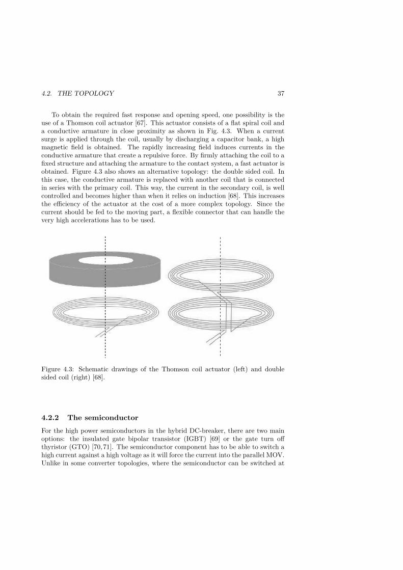
4.2. THE TOPOLOGY 37
To obtain the required fast response and opening speed, one possibility is theuse of a Thomson coil actuator [67]. This actuator consists of a flat spiral coil anda conductive armature in close proximity as shown in Fig. 4.3. When a currentsurge is applied through the coil, usually by discharging a capacitor bank, a highmagnetic field is obtained. The rapidly increasing field induces currents in theconductive armature that create a repulsive force. By firmly attaching the coil to afixed structure and attaching the armature to the contact system, a fast actuator isobtained. Figure 4.3 also shows an alternative topology: the double sided coil. Inthis case, the conductive armature is replaced with another coil that is connectedin series with the primary coil. This way, the current in the secondary coil, is wellcontrolled and becomes higher than when it relies on induction [68]. This increasesthe efficiency of the actuator at the cost of a more complex topology. Since thecurrent should be fed to the moving part, a flexible connector that can handle thevery high accelerations has to be used.
Figure 4.3: Schematic drawings of the Thomson coil actuator (left) and doublesided coil (right) [68].
4.2.2 The semiconductorFor the high power semiconductors in the hybrid DC-breaker, there are two mainoptions: the insulated gate bipolar transistor (IGBT) [69] or the gate turn offthyristor (GTO) [70,71]. The semiconductor component has to be able to switch ahigh current against a high voltage as it will force the current into the parallel MOV.Unlike in some converter topologies, where the semiconductor can be switched at
38 CHAPTER 4. THE STUDIED HYBRID DC-BREAKER
zero current or zero voltage, the semiconductor in the hybrid DC-breaker will switchthe full current under full voltage stress.
The GTO is based on a thyristor structure, but unlike the thyristor, it has anactive turn-off capability. By injecting a current into the gate, the GTO can beswitched off. However, the magnitude of the gate-current has to be as large as20-30% of the forward current. Even though this is 70-80% lower than the currentthat would be required to turn off a thyristor, it is still a significant current andresults in that the drive circuit for a GTO needs 100 times more power than thatfor an IGBT [72]. The benefit of the GTO is that is has slightly lower forwardvoltage drop than the IGBT, and is also available with higher power ratings.
The IGBT is a bipolar component that is controlled via a MOS-structure [73].Hence, it is turned on and off by applying and removing a voltage of 15-20 V onthe gate. This makes it possible to use a rather simple and compact gate driveunit. When several components are connected in series, the increase and decreaseof the gate voltage can also be regulated to control the turn-on and turn-off speedof each IGBT to even out unbalances in the voltage distribution. The IGBT cannothandle a negative voltage and usually has an anti-parallel diode included in the samepackage. This makes it easy to build a system that is bidirectional by connectingtwo such components in anti-series. The current will then flow through one of theIGBTs and the other IGBT’s anti-parallel diode.
As the GTO is based on a thyristor structure, it has been considered morereliable as the thyristors have proven their reliability in the field for many years.However, the disbelief in the reliability of the IGBTs is exaggerated as they havebeen in commercial use in the converter stations for HVDC since 1999 [74,75].
4.2.3 The metal oxide varistorThe MOV has two important tasks in the current interruption in the hybrid DC-breaker. Firstly, it limits the voltage across the IGBT after the IGBT has turnedoff. Secondly, it absorbs the magnetic energy stored in the inductive system andbrings the system current down to zero. Being in parallel to the mechanical switchand also the IGBT, it is actually the MOV that performs the real interruption ofthe system current, while the other two branches only commutate the current intothe parallel branch.
The MOV is a highly non-linear resistor than consists of grains of a metaloxide, usually zinc oxide (ZnO) or silicon oxide (SiO), separated by an insulatingboundary. When a voltage is applied across the component, the voltage will fallacross the insulating boundaries rather than the conductive grains. If the electricfield across the boundaries is increased above the limit, the current through thecomponent will increase rapidly. The relationship between the electric field andthe current density is a pure material parameter [76] which makes it possible tomanufacture components with a large variety of voltage and current ratings.
The voltage rating of the component is determined by the thickness of thematerial, as a thicker material results in a lower electric field across the boundaries
4.3. THE COMPONENTS IN THE TEST SET-UP 39
for the same voltage. As the most common application for the MOV is as over-voltage protection in power systems [77], the voltage rating is defined as the highestvoltage the component can be continuously exposed to without over-heating dueto the leakage currents. In the hybrid DC-breaker, the component is not exposedto any continuous voltage since it is bypassed by the parallel branches with themechanical switch and the IGBT. Hence, the dimensioning parameter is the voltagelevel when the MOV is conducting the full current, as this defines the voltage stresson the IGBT. Also, the voltage rating has to be chosen high enough so that theseries disconnector is able to interrupt the leakage current after the interruption iscomplete.
The diameter of the MOV controls the current density and is an important fac-tor as this affects the voltage for high conduction currents. Since the absorptionof energy during the current interruption is performed in just a few milliseconds,the energy is absorbed by the MOV before it is dissipated as heat. Hence, the en-ergy absorption capability is proportional to the volume of the component materialand increases with increasing voltage rating. If the energy absorbed in the MOVrepeatedly exceeds its rating, the material will slowly degrade so that its leakagecurrent will increase [78], and if the pulse is large enough, the MOV will fail due toover-heating [79].
By integrating the power absorbed in the MOV during the time the currentdecreases from its peak value, I0, to zero and neglecting the system resistance, thetotal energy absorbed in the MOV can be expressed as [66]:
Wtot = 12LsystemI
20 (1 + Usystem
UMOV − Usystem), (4.1)
where UMOV is the MOV conduction voltage that is assumed constant. The ab-sorbed energy in the MOV is larger than the magnetic energy stored in the systeminductance since the system will keep feeding energy into the system during thewhole time where the current decreases to zero. The total energy decreases with anincreased MOV voltage rating since the time to reach the current zero decreases. Ifthe MOV conduction voltage is chosen below the system voltage, the current willnever reach zero, as was shown in Fig. 2.12, and the MOV will absorb energy untilit is over-heated and destroyed. Hence, the equation is only valid for MOV voltageslarger than the system voltage since this is necessary to force a current zero.
4.3 The components in the test set-up
4.3.1 The mechanical switch prototypeFigure 4.4 shows a drawing of the switch prototype seen from the side. To allowfor a flexible test set-up, the current prototype of the mechanical switch consistsof a frame cut in aluminium and solid steel plates attached to the frame. Thisframe allows a rigid base of the switch, but also works as a modular set-up whereparts can be replaced without the need to rebuild the whole set-up. The contact
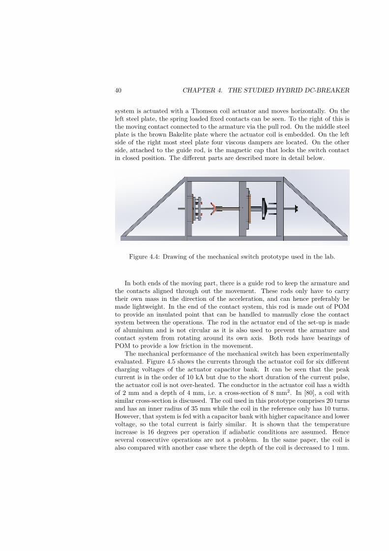
40 CHAPTER 4. THE STUDIED HYBRID DC-BREAKER
system is actuated with a Thomson coil actuator and moves horizontally. On theleft steel plate, the spring loaded fixed contacts can be seen. To the right of this isthe moving contact connected to the armature via the pull rod. On the middle steelplate is the brown Bakelite plate where the actuator coil is embedded. On the leftside of the right most steel plate four viscous dampers are located. On the otherside, attached to the guide rod, is the magnetic cap that locks the switch contactin closed position. The different parts are described more in detail below.
Figure 4.4: Drawing of the mechanical switch prototype used in the lab.
In both ends of the moving part, there is a guide rod to keep the armature andthe contacts aligned through out the movement. These rods only have to carrytheir own mass in the direction of the acceleration, and can hence preferably bemade lightweight. In the end of the contact system, this rod is made out of POMto provide an insulated point that can be handled to manually close the contactsystem between the operations. The rod in the actuator end of the set-up is madeof aluminium and is not circular as it is also used to prevent the armature andcontact system from rotating around its own axis. Both rods have bearings ofPOM to provide a low friction in the movement.
The mechanical performance of the mechanical switch has been experimentallyevaluated. Figure 4.5 shows the currents through the actuator coil for six differentcharging voltages of the actuator capacitor bank. It can be seen that the peakcurrent is in the order of 10 kA but due to the short duration of the current pulse,the actuator coil is not over-heated. The conductor in the actuator coil has a widthof 2 mm and a depth of 4 mm, i.e. a cross-section of 8 mm2. In [80], a coil withsimilar cross-section is discussed. The coil used in this prototype comprises 20 turnsand has an inner radius of 35 mm while the coil in the reference only has 10 turns.However, that system is fed with a capacitor bank with higher capacitance and lowervoltage, so the total current is fairly similar. It is shown that the temperatureincrease is 16 degrees per operation if adiabatic conditions are assumed. Henceseveral consecutive operations are not a problem. In the same paper, the coil isalso compared with another case where the depth of the coil is decreased to 1 mm.
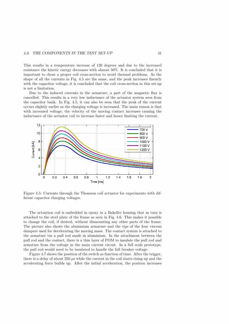
4.3. THE COMPONENTS IN THE TEST SET-UP 41
This results in a temperature increase of 120 degrees and due to the increasedresistance the kinetic energy decreases with almost 50%. It is concluded that it isimportant to chose a proper coil cross-section to avoid thermal problems. As theshape of all the currents in Fig. 4.5 are the same, and the peak increases linearlywith the capacitor voltage, it is concluded that the coil cross-section in this set-upis not a limitation.
Due to the induced currents in the armature, a part of the magnetic flux iscancelled. This results in a very low inductance of the actuator system seen fromthe capacitor bank. In Fig. 4.5, it can also be seen that the peak of the currentoccurs slightly earlier as the charging voltage is increased. The main reason is thatwith increased voltage, the velocity of the moving contact increases causing theinductance of the actuator coil to increase faster and hence limiting the current.
Figure 4.5: Currents through the Thomson coil actuator for experiments with dif-ferent capacitor charging voltages.
The actuation coil is embedded in epoxy in a Bakelite housing that in turn isattached to the steel plate of the frame as seen in Fig. 4.6. This makes it possibleto change the coil, if desired, without dismounting any other parts of the frame.The picture also shows the aluminium armature and the tips of the four viscousdampers used for decelerating the moving mass. The contact system is attached tothe armature via a pull rod made in aluminium. In the attachment between thepull rod and the contact, there is a thin layer of POM to insulate the pull rod andarmature from the voltage in the main current circuit. In a full scale prototype,the pull rod would need to be insulated to handle the full breaker voltage.
Figure 4.7 shows the position of the switch as function of time. After the trigger,there is a delay of about 250 µs while the current in the coil starts rising up and theaccelerating force builds up. After the initial acceleration, the position increases
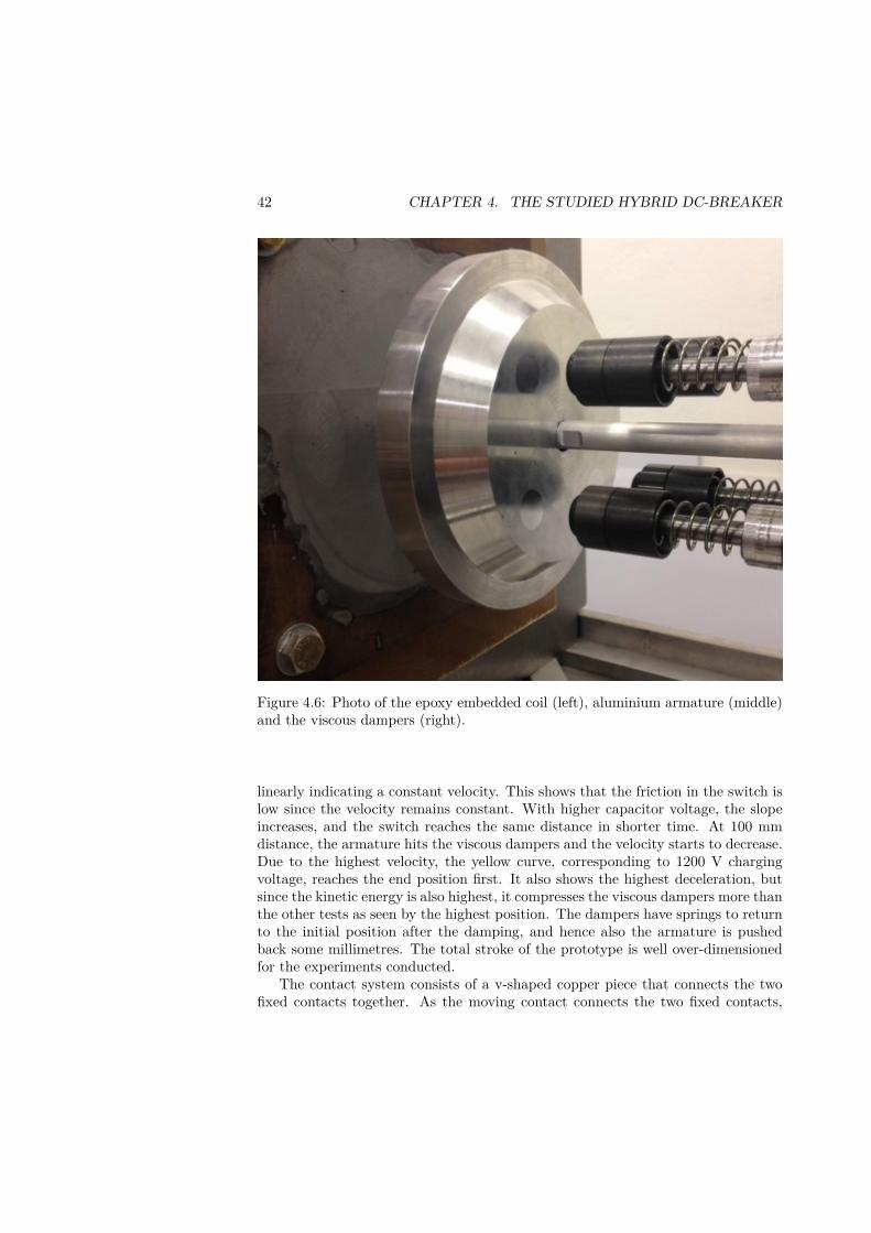
42 CHAPTER 4. THE STUDIED HYBRID DC-BREAKER
Figure 4.6: Photo of the epoxy embedded coil (left), aluminium armature (middle)and the viscous dampers (right).
linearly indicating a constant velocity. This shows that the friction in the switch islow since the velocity remains constant. With higher capacitor voltage, the slopeincreases, and the switch reaches the same distance in shorter time. At 100 mmdistance, the armature hits the viscous dampers and the velocity starts to decrease.Due to the highest velocity, the yellow curve, corresponding to 1200 V chargingvoltage, reaches the end position first. It also shows the highest deceleration, butsince the kinetic energy is also highest, it compresses the viscous dampers more thanthe other tests as seen by the highest position. The dampers have springs to returnto the initial position after the damping, and hence also the armature is pushedback some millimetres. The total stroke of the prototype is well over-dimensionedfor the experiments conducted.
The contact system consists of a v-shaped copper piece that connects the twofixed contacts together. As the moving contact connects the two fixed contacts,
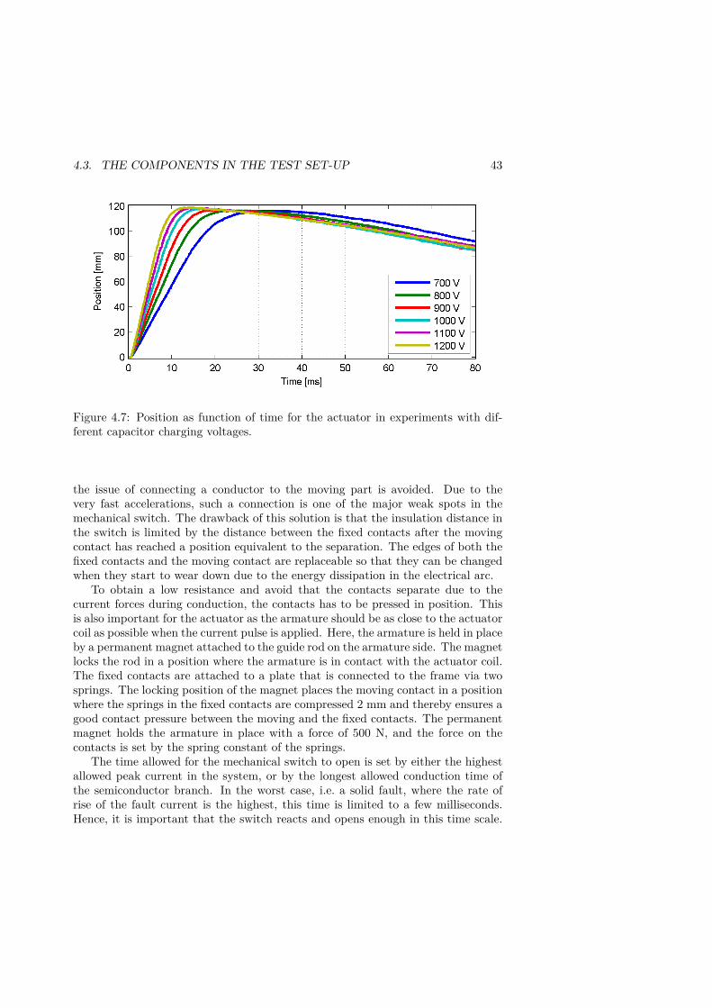
4.3. THE COMPONENTS IN THE TEST SET-UP 43
Figure 4.7: Position as function of time for the actuator in experiments with dif-ferent capacitor charging voltages.
the issue of connecting a conductor to the moving part is avoided. Due to thevery fast accelerations, such a connection is one of the major weak spots in themechanical switch. The drawback of this solution is that the insulation distance inthe switch is limited by the distance between the fixed contacts after the movingcontact has reached a position equivalent to the separation. The edges of both thefixed contacts and the moving contact are replaceable so that they can be changedwhen they start to wear down due to the energy dissipation in the electrical arc.
To obtain a low resistance and avoid that the contacts separate due to thecurrent forces during conduction, the contacts has to be pressed in position. Thisis also important for the actuator as the armature should be as close to the actuatorcoil as possible when the current pulse is applied. Here, the armature is held in placeby a permanent magnet attached to the guide rod on the armature side. The magnetlocks the rod in a position where the armature is in contact with the actuator coil.The fixed contacts are attached to a plate that is connected to the frame via twosprings. The locking position of the magnet places the moving contact in a positionwhere the springs in the fixed contacts are compressed 2 mm and thereby ensures agood contact pressure between the moving and the fixed contacts. The permanentmagnet holds the armature in place with a force of 500 N, and the force on thecontacts is set by the spring constant of the springs.
The time allowed for the mechanical switch to open is set by either the highestallowed peak current in the system, or by the longest allowed conduction time ofthe semiconductor branch. In the worst case, i.e. a solid fault, where the rate ofrise of the fault current is the highest, this time is limited to a few milliseconds.Hence, it is important that the switch reacts and opens enough in this time scale.
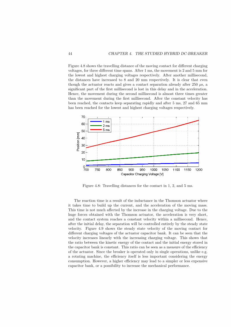
44 CHAPTER 4. THE STUDIED HYBRID DC-BREAKER
Figure 4.8 shows the travelling distance of the moving contact for different chargingvoltages, for three different time spans. After 1 ms, the movement is 2 and 5 mm forthe lowest and highest charging voltages respectively. After another millisecond,the distances have increased to 8 and 20 mm respectively. It is clear that eventhough the actuator reacts and gives a contact separation already after 250 µs, asignificant part of the first millisecond is lost in this delay and in the acceleration.Hence, the movement during the second millisecond is almost three times greaterthan the movement during the first millisecond. After the constant velocity hasbeen reached, the contacts keep separating rapidly and after 5 ms, 27 and 65 mmhas been reached for the lowest and highest charging voltages respectively.
Figure 4.8: Travelling distances for the contact in 1, 2, and 5 ms.
The reaction time is a result of the inductance in the Thomson actuator whereit takes time to build up the current, and the acceleration of the moving mass.This time is not much affected by the increase in the charging voltage. Due to thehuge forces obtained with the Thomson actuator, the acceleration is very short,and the contact system reaches a constant velocity within a millisecond. Hence,after the initial delay, the separation will be controlled entirely by the steady statevelocity. Figure 4.9 shows the steady state velocity of the moving contact fordifferent charging voltages of the actuator capacitor bank. It can be seen that thevelocity increases linearly with the increasing charging voltage. This shows thatthe ratio between the kinetic energy of the contact and the initial energy stored inthe capacitor bank is constant. This ratio can be seen as a measure of the efficiencyof the actuator. Since the breaker is operated only in single operations, unlike e.g.a rotating machine, the efficiency itself is less important considering the energyconsumption. However, a higher efficiency may lead to a simpler or less expensivecapacitor bank, or a possibility to increase the mechanical performance.
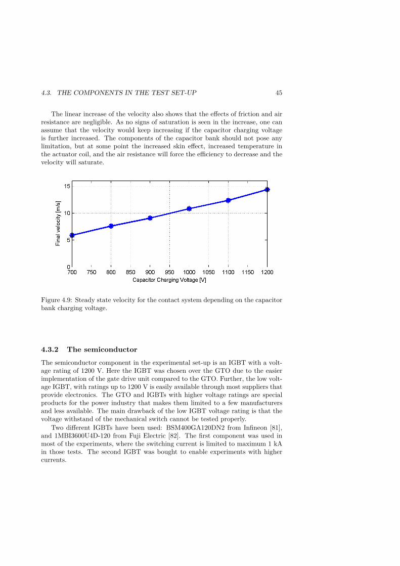
4.3. THE COMPONENTS IN THE TEST SET-UP 45
The linear increase of the velocity also shows that the effects of friction and airresistance are negligible. As no signs of saturation is seen in the increase, one canassume that the velocity would keep increasing if the capacitor charging voltageis further increased. The components of the capacitor bank should not pose anylimitation, but at some point the increased skin effect, increased temperature inthe actuator coil, and the air resistance will force the efficiency to decrease and thevelocity will saturate.
Figure 4.9: Steady state velocity for the contact system depending on the capacitorbank charging voltage.
4.3.2 The semiconductor
The semiconductor component in the experimental set-up is an IGBT with a volt-age rating of 1200 V. Here the IGBT was chosen over the GTO due to the easierimplementation of the gate drive unit compared to the GTO. Further, the low volt-age IGBT, with ratings up to 1200 V is easily available through most suppliers thatprovide electronics. The GTO and IGBTs with higher voltage ratings are specialproducts for the power industry that makes them limited to a few manufacturersand less available. The main drawback of the low IGBT voltage rating is that thevoltage withstand of the mechanical switch cannot be tested properly.
Two different IGBTs have been used: BSM400GA120DN2 from Infineon [81],and 1MBI3600U4D-120 from Fuji Electric [82]. The first component was used inmost of the experiments, where the switching current is limited to maximum 1 kAin those tests. The second IGBT was bought to enable experiments with highercurrents.
46 CHAPTER 4. THE STUDIED HYBRID DC-BREAKER
The former has a rated continuous current of 400 A and a maximum currentrating of 1100 A for a duration of 1 ms. The forward voltage drop is stated totypically 2.5 V for the rated current and a cold component. The turn-off timeconsists of a turn-off delay of 550 ns and a fall time of 80 ns. However, these timesare stated for 600 V and the rated current of 400 A, so the times in the experimentswill be longer than these.
The second IGBT module consists of a package with three IGBTs in parallel.The module has a rated continuous current of 3600 A and a maximum 1 ms pulseof 9600 A. The typical forward voltage drop is 2.22 V for the rated current. Theturn-off delay is 800 ns and the fall time is 200 ns. Even though the turn-off isslower than for the first IGBT, the current derivative during the turn-off is threetimes higher due to the higher switching current.
Figure 4.10 shows the larger IGBT mounted on its heat sink. At full ratedcurrent, the losses in the IGBT is in the order of 3 kW according to the datasheet. The heat sink consists of aluminium and has a thermal resistance to theair of 0.33C/W. This, together with the data in the IGBT datasheet concludesthat to keep the temperature of the IGBT below its critical temperature of 125C,the maximum continuous current in the IGBT is around 200 A. However, dueto the short current conduction in the IGBT in the hybrid DC-breaker topology,the dissipated energy in each operation will be rather low. The heat-sink weighs2.4 kg and hence has a thermal capacity of 2.7 kJ. During conduction of its maximalcurrent the IGBT has losses close to 21 kW and if the system is considered adiabaticduring the IGBT conduction, this will cause a temperature rise of the heat-sink atonly 7.8C/s. Hence the temperature rise during the few milliseconds the IGBTconducts current will be negligible.
4.3.3 The MOV
The voltage level of the MOV is controlled by the voltage rating of the IGBT inthe test circuit. The MOV has to be chosen so that the conduction voltage of theMOV is below the voltage rating of the IGBT. In this test set-up, three differentMOVs have been used. All three are of the model Polim-R 1ND from ABB andwith three different voltage ratings as shown in table 4.1. The conduction voltagesare given for a short current pulse of 60 µs. It can be noted that the MOV with thelowest voltage rating has a conduction voltage equal to double the rated voltage for250 A, whereas the other two MOVs have conduction voltages slightly below doubletheir respective rated voltages. The energy rating of the components is stated as10.5 kJ/kV, where the voltage is the rated voltage. The energy rating increaseswith increasing voltage as the volume of the ZnO material increases as discussedbefore.
The conduction voltage of the Polim-R0 56-ND is slightly below 1200 V, whichmakes it an ideal choice for the 1200 V IGBT in the set-up. The IGBT will thenbe stressed by a voltage close to the rating, without exceeding it.
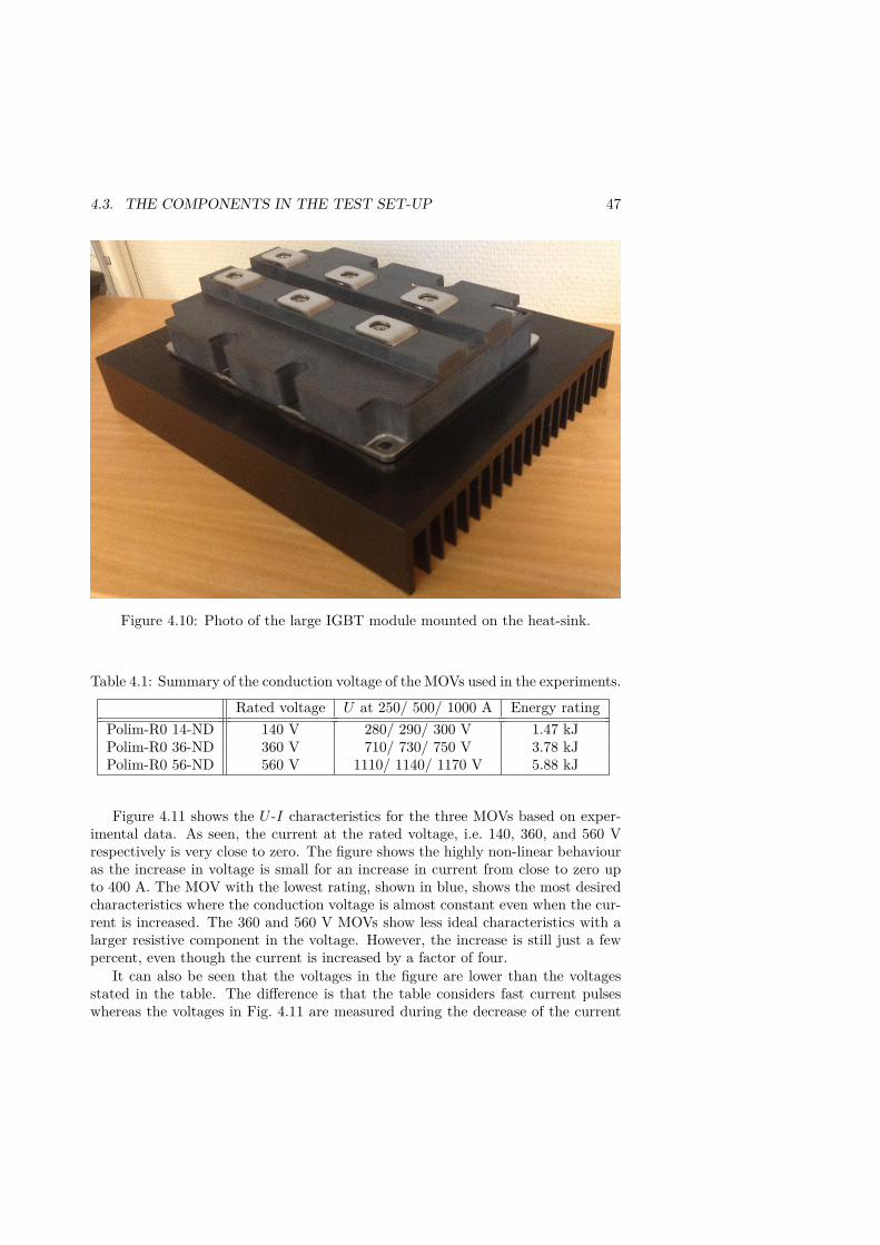
4.3. THE COMPONENTS IN THE TEST SET-UP 47
Figure 4.10: Photo of the large IGBT module mounted on the heat-sink.
Table 4.1: Summary of the conduction voltage of the MOVs used in the experiments.
Rated voltage U at 250/ 500/ 1000 A Energy ratingPolim-R0 14-ND 140 V 280/ 290/ 300 V 1.47 kJPolim-R0 36-ND 360 V 710/ 730/ 750 V 3.78 kJPolim-R0 56-ND 560 V 1110/ 1140/ 1170 V 5.88 kJ
Figure 4.11 shows the U -I characteristics for the three MOVs based on exper-imental data. As seen, the current at the rated voltage, i.e. 140, 360, and 560 Vrespectively is very close to zero. The figure shows the highly non-linear behaviouras the increase in voltage is small for an increase in current from close to zero upto 400 A. The MOV with the lowest rating, shown in blue, shows the most desiredcharacteristics where the conduction voltage is almost constant even when the cur-rent is increased. The 360 and 560 V MOVs show less ideal characteristics with alarger resistive component in the voltage. However, the increase is still just a fewpercent, even though the current is increased by a factor of four.
It can also be seen that the voltages in the figure are lower than the voltagesstated in the table. The difference is that the table considers fast current pulseswhereas the voltages in Fig. 4.11 are measured during the decrease of the current
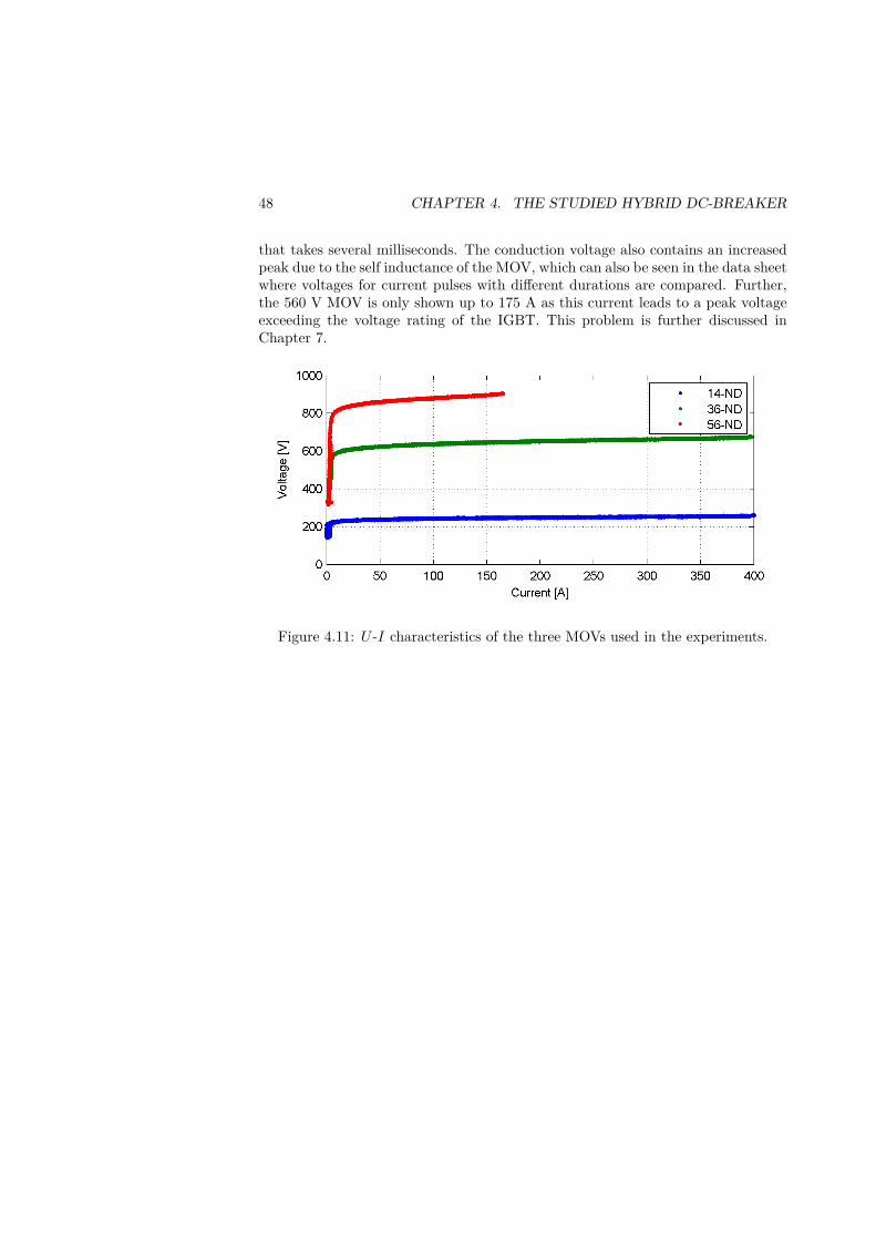
48 CHAPTER 4. THE STUDIED HYBRID DC-BREAKER
that takes several milliseconds. The conduction voltage also contains an increasedpeak due to the self inductance of the MOV, which can also be seen in the data sheetwhere voltages for current pulses with different durations are compared. Further,the 560 V MOV is only shown up to 175 A as this current leads to a peak voltageexceeding the voltage rating of the IGBT. This problem is further discussed inChapter 7.
Figure 4.11: U -I characteristics of the three MOVs used in the experiments.
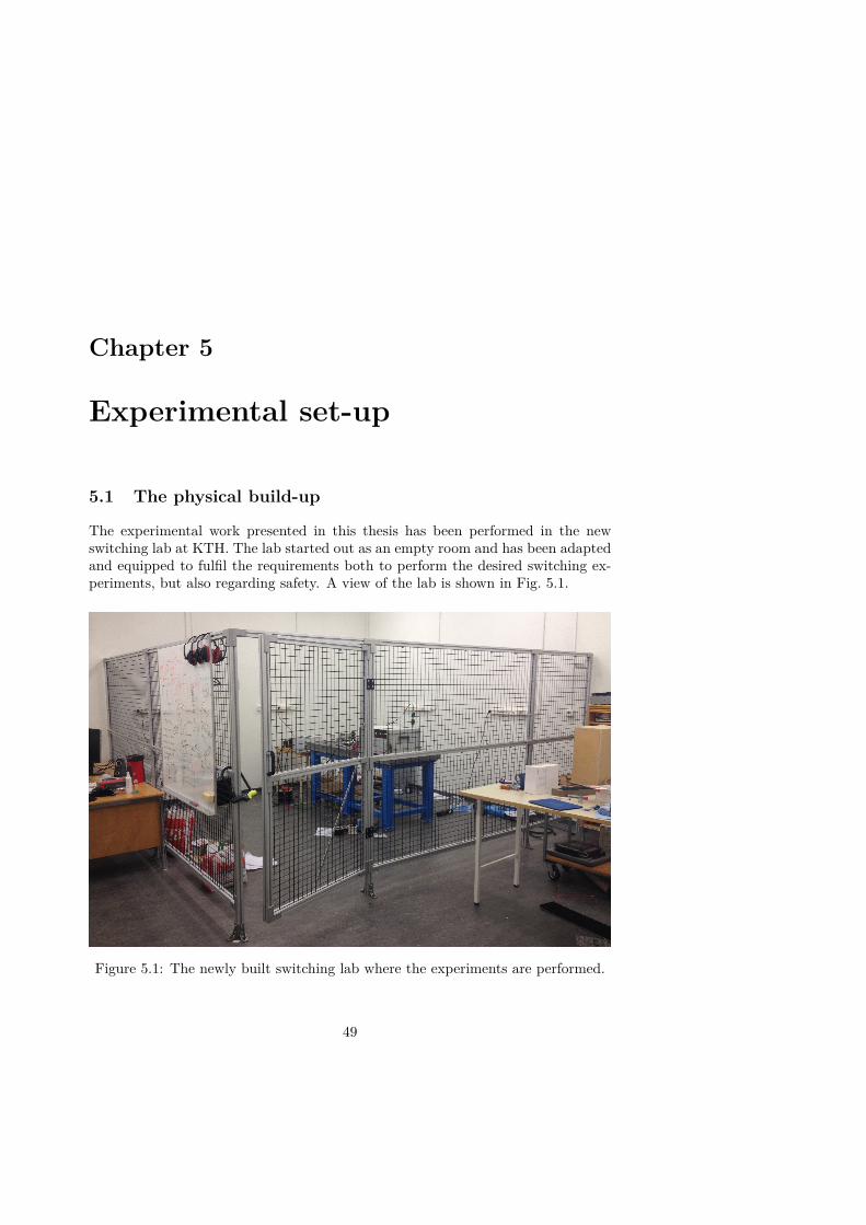
Chapter 5
Experimental set-up
5.1 The physical build-up
The experimental work presented in this thesis has been performed in the newswitching lab at KTH. The lab started out as an empty room and has been adaptedand equipped to fulfil the requirements both to perform the desired switching ex-periments, but also regarding safety. A view of the lab is shown in Fig. 5.1.
Figure 5.1: The newly built switching lab where the experiments are performed.
49
50 CHAPTER 5. EXPERIMENTAL SET-UP
The use of high speed actuators, and the extreme forces and accelerations itleads to, requires a rigid test set-up. Therefore, the basis of the experimental set-up is a custom made steel table, seen in the middle of the cage in Fig. 5.1. Thetable measures 120 by 80 cm and weights about 2 tonnes. The surface containsslots to allow solid attachments of screws to firmly clamp down the test set-up.
The test area is surrounded by a fence with a lockable door. The purpose isto make sure no one can get close to the test set-up, when it is not in use, andget injured in the case some part of the test set-up is not properly de-energized.The fence also serves as a protective barrier during the experiments as the fenceis reinforced with both an aluminium mesh and 5 mm polycarbonate sheets. Thealuminium mesh is grounded to provide protection against any electrical danger,and the polycarbonate was installed to protect against possible flying projectilesin the case of a mechanical malfunction. Outside of the fence, to the left in thepicture, there is a desk with a computer, from where the experiments are controlledand monitored.
5.2 The test circuit
Electrically, the experimental set-up consists of two separate circuits: the maincurrent that is switched by the breaker; and the current through the actuator ofthe mechanical switch. Also the drive circuit of the IGBT could be considereda separate circuit and this is described further down. The different parts of thesystem are shown in Fig. 5.2 and each part is described in detail further down.
5.2.1 Capacitor bank for the main currentIn an AC-breaker, interruption tests are performed with a synthetic test circuitwhere the current through the breaker and the returning voltage are applied sep-arately. The current is applied using a short circuit generator, but this does notstress the breaker after the current is interrupted. Instead, a controlled voltagepulse is applied from another circuit to mimic the transient recovery voltage (TRV)in the system. Testing of a DC circuit-breaker is different in the sense that thetransient interruption voltage (TIV) is defined by the breaker it self. The topologyof the DC-breaker and the voltage level of the MOV during conduction of the cur-rent will set the voltage across the breaker during the current decrease and hencealso the voltage across the IGBTs and the mechanical switch. This means the test-ing circuit for the DC-breaker becomes more simple and only has to provide thesufficient current to test the full function of the DC-breaker set-up. Naturally, theonly thing that is not tested is the energy absorption capability of the MOV.
The current in the main circuit is provided by a capacitor bank. The bankconsists of 10 electrolytic capacitors of 3.3 mF each, providing a total capacitanceof 33 mF. The capacitor bank is charged to a desired voltage via an adjustabletransformer and a current limiting resistor. The rated voltage of the capacitors is
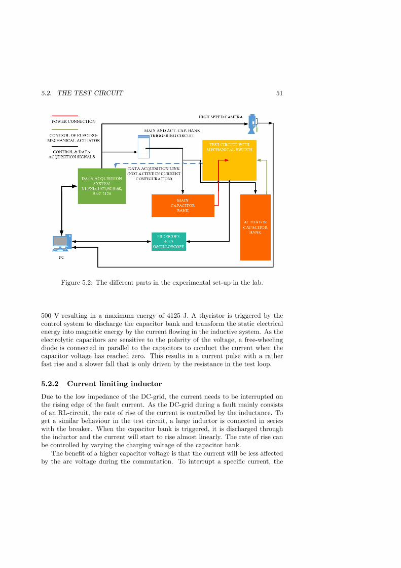
5.2. THE TEST CIRCUIT 51
Figure 5.2: The different parts in the experimental set-up in the lab.
500 V resulting in a maximum energy of 4125 J. A thyristor is triggered by thecontrol system to discharge the capacitor bank and transform the static electricalenergy into magnetic energy by the current flowing in the inductive system. As theelectrolytic capacitors are sensitive to the polarity of the voltage, a free-wheelingdiode is connected in parallel to the capacitors to conduct the current when thecapacitor voltage has reached zero. This results in a current pulse with a ratherfast rise and a slower fall that is only driven by the resistance in the test loop.
5.2.2 Current limiting inductorDue to the low impedance of the DC-grid, the current needs to be interrupted onthe rising edge of the fault current. As the DC-grid during a fault mainly consistsof an RL-circuit, the rate of rise of the current is controlled by the inductance. Toget a similar behaviour in the test circuit, a large inductor is connected in serieswith the breaker. When the capacitor bank is triggered, it is discharged throughthe inductor and the current will start to rise almost linearly. The rate of rise canbe controlled by varying the charging voltage of the capacitor bank.
The benefit of a higher capacitor voltage is that the current will be less affectedby the arc voltage during the commutation. To interrupt a specific current, the
52 CHAPTER 5. EXPERIMENTAL SET-UP
level is set by the combination of the capacitor charging voltage and the time delayfrom triggering the capacitor discharge and tripping the breaker.
5.2.3 Current limiting resistor
To limit the current in the test circuit in the case of tests with rather low currents,a resistor is connected in series with the breaker. The resulting RC-circuit will havea rather small time constant due to the low capacitance. However, since these testsare made with low currents, and in the time-range of a few milliseconds, a timeconstant in the order of some hundred milliseconds is acceptable. A 200 W resistoris used where the resistance can be adjusted from about 20 up to 100 Ω to obtainthe desired current.
5.2.4 Capacitor bank for actuation
To provide the required energy to actuate the contact system, a capacitor bankis used. Compared to the capacitor bank used in the main current circuit, thecapacitor bank for the actuator provides a lower internal stray inductance and alower resistance in the capacitors. As the inductance of the actuator coil is very lowwhen the armature is close, the current pulse is very fast, i.e. the rise time is in theorder of a few hundred microseconds. To obtain a high efficiency of the actuator,it is important that the internal losses are low and that the rise of the current islimited by the inductance of the actuator coil.
The capacitor bank is charged via a switched high voltage power supply thatenables charging with a constant current. It comprises a maximum of 10 kJ andcan be connected in parallel mode with 5 mF and a maximum voltage of 2000 V orin series mode with a capacitance of 1.25 mF and a maximum voltage of 4000 V.All components are rated to handle a current surge of 85 kA. However, to obtainsuch a current high peak would require a lossless system and an inductance in theorder of 2 µH.
The capacitors can handle both positive and negative voltages which makes itpossible to use the capacitor bank also to generate sinusoidal currents. However,when it is used to power the Thomson coil actuator, a free-wheeling diode is used inparallel to the capacitors to maximize the energy input to the mechanical system.
5.3 The control system
The test sequence in the lab is controlled from a computer outside the cage. Sincethe fence consists of a mesh and transparent polycarbonate sheets, the experimentcan be visually followed from the control space. The sequence is controlled byrunning a Lab-view script that sends timed signals to the different parts of the labset-up via a data acquisition (DAQ) system from National Instruments (NI).
5.3. THE CONTROL SYSTEM 53
5.3.1 The NI systemThe heart of the control system is the PXI6368 system from NI. The DAQ consistsof an external control box connected to the inside of the computer. It controls thetiming of the test set-up with 6 digital output signals, but has the possibility tocontrol up to 48 digital in- and outputs. It also has the possibility to acquire 16simultaneous analog signals with 16 bit resolution and 2 Mega sample (MS) persecond. However, it turned out that the analogue bandwidth was too low for someof the measurements in the current set-up. Another drawback is that all inputsignals are limited to be 0-10 V which makes it complicated to use standardizedprobes.
The original idea was to use the NI DAQ to acquire the analogue measurements.The main issue was the IGBT switching, where the voltage across the IGBT risesfrom almost zero to above 1 kV in about 1 µs. Even though the 2 MS sampling ratecould be enough to capture this, since the actual switching of the IGBT voltageis not too interesting, the fast transients caused large internal oscillations in theDAQ. Also, the large internal capacitance of the DAQ made it impossible to get agood impedance match for the voltage probes.
5.3.2 The Lab-view programThe DAQ is controlled by a program written in Lab-view. The program can berun directly, or set in an armed mode where it is triggered externally by any of theanalog input signals. The code has been built up so that it can acquire the analoguesignals from the DAQ, even though this feature is not used at the moment. In thegraphical user interface, the timing for all the control signals can be set. Currentlyfive different signals are used:
• Start the acquisition
• Discharge the capacitor for the main current
• Trigger the mechanical switch
• Trigger the high-speed camera
• Turn the IGBT on and off
When the program runs, a vector is set up for each of the signals containing theLOW and HIGH values for the signal according to a time-vector with a time stepof 1 µs. The vectors are combined into a matrix that is sent to the DAQ where theoutput of each digital channel is controlled. This way, the relative times betweeneach event in the experiment is controlled with a microsecond precision which issufficient for this type of experiment. The first output signal is connected back toone of the digital inputs of the DAQ and is used to trigger the acquisition and isused as a time reference.
54 CHAPTER 5. EXPERIMENTAL SET-UP
It is also possible to run the system continuously and base the control signals onthe measurements of the analogue and digital inputs. However, it turned out thatsince Lab-view runs under Windows, the time response it limited by the responseof Windows, which is in the order of some milliseconds. The time intervals in theseexperiments are in the order of some hundred microseconds, so a better precisionthan that is required.
5.3.3 The IGBT driverA gate drive unit for semiconductors that are used in high speed switching, e.g. inconverters, has to be properly designed to maintain low losses in the semiconduc-tor during the switching [83]. This however is not as critical in a circuit breakerapplication since the number of switching operations are very limited. In a con-verter, the switching frequency is generally in the kilohertz range, while the circuitbreaker only operates occasionally, and then not more than a few consequtive op-erations separated by several milliseconds. This means that the gate drive unit canbe simplified and hence made more cost-effective. For low power MOSFETs andIGBTs, small electronic gate drivers are available that convert a digital signal toa sufficient voltage to switch the semiconductor. However, for larger components,the capacitance of the gate is too high so that it requires more current to chargethe gate and turn the IGBT on.
In this lab set-up the gate drive unit has been designed according to Fig. 5.3.The driver consists of two low power MOSFETs that are controlled by a bridgedriver via a small gate resistor. The control signal for the IGBT consists of twoseparate digital outputs from the control system: one for the upper MOSFET andone for the lower. When the IGBT is turned on, the control signals are set toturn the lower MOSFET off and then turn the upper MOSFET on. This results inthat the voltage of the voltage source is put across the IGBT gate and charges it.To limit the charging current, a small resistor, in the order of 10 Ω, is connectedbetween the source and the gate. Once the gate is charged, the whole voltage ofthe voltage source is across the gate and the IGBT is kept in conduction mode.
To turn the IGBT off, the upper MOSFET is turned off and the lower MOSFETis turned on so that the gate is discharged through the resistor and the lowerMOSFET. Ideally, the gate should be discharged with a constant current, but sincethe IGBT turns off at a relatively high gate voltage, i.e. around 6-7 V, this gatedischarge circuit is sufficient to turn the IGBT off. When the gate is discharged,the low resistance of the MOSFET keeps the IGBT in a non conductive mode.
Some precautions have to be taken to guarantee a safe switching of the IGBT. Atany switching, a dead time of 2 µs is introduced to make sure the two MOSFETS arenot ON at the same time as this would short circuit the voltage source. To isolatethe IGBT gate drive from the rest of the circuit, batteries are used to provide thegate voltage. To extend the life of the batteries, the IGBT is kept in a floating mode,i.e. both the upper and the lower MOSFETs are off, except during the test. Sincethis means the IGBT is in an undefined state, a high ohmic resistor is connected
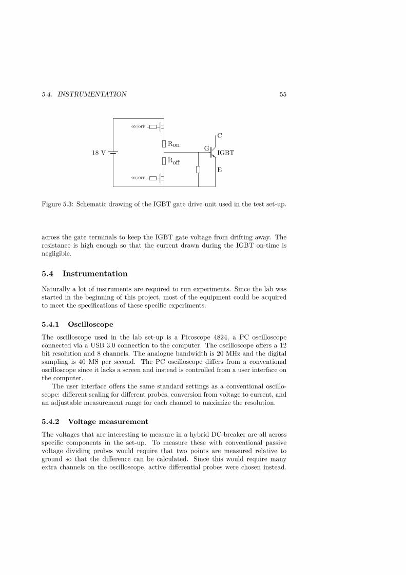
5.4. INSTRUMENTATION 55
18 V
Ron
Roff
IGBT
C
E
G
ON/OFF
ON/OFF
Figure 5.3: Schematic drawing of the IGBT gate drive unit used in the test set-up.
across the gate terminals to keep the IGBT gate voltage from drifting away. Theresistance is high enough so that the current drawn during the IGBT on-time isnegligible.
5.4 Instrumentation
Naturally a lot of instruments are required to run experiments. Since the lab wasstarted in the beginning of this project, most of the equipment could be acquiredto meet the specifications of these specific experiments.
5.4.1 OscilloscopeThe oscilloscope used in the lab set-up is a Picoscope 4824, a PC oscilloscopeconnected via a USB 3.0 connection to the computer. The oscilloscope offers a 12bit resolution and 8 channels. The analogue bandwidth is 20 MHz and the digitalsampling is 40 MS per second. The PC oscilloscope differs from a conventionaloscilloscope since it lacks a screen and instead is controlled from a user interface onthe computer.
The user interface offers the same standard settings as a conventional oscillo-scope: different scaling for different probes, conversion from voltage to current, andan adjustable measurement range for each channel to maximize the resolution.
5.4.2 Voltage measurementThe voltages that are interesting to measure in a hybrid DC-breaker are all acrossspecific components in the set-up. To measure these with conventional passivevoltage dividing probes would require that two points are measured relative toground so that the difference can be calculated. Since this would require manyextra channels on the oscilloscope, active differential probes were chosen instead.
56 CHAPTER 5. EXPERIMENTAL SET-UP
The probes are driven by battery power and measures a voltage of ±1400 V betweenits two connectors, which is enough in the conducted experiments. The frequencyrange goes from zero up to 25 MHz which is sufficient considering both the transientsin the set-up and the bandwidth of the oscilloscope. The probes output is isolatedfrom the input and gives an output of ±7 V that is measured with the oscilloscope.The differential probes provide a big advantage compared to passive probes asthe parasitic inductances in the measurements can be minimized when both themeasurement points are on a floating potential.
5.4.3 Current measurementThe currents in the breaker set-up are measured using Rogowski current probes ofthe model CWT30B/4/700 from PEM. The probes have a frequency range from0.6 Hz to 16 MHz and can measure currents of ±6 kA. The CWT current probesmeasures the derivative of the current and integrates it before converting the currentinto a voltage that is measured by the oscilloscope. The drawback with this is thatthe probes become relatively sensitive to disturbances. This means that if theoutput amplitude is suddenly changed by a step, the measurement will stay wrongwith this offset as it is not affected by the integration. The other drawback is thatthe probe cannot measure a constant current. However, the lower bandwidth is aslow as 0.6 Hz so with the fast transients in these tests, this is not a limitation.
The current through the Thomson actuator is measured with a Pearson currentmonitor model 301X. This probe consists of an iron core that surrounds the conduc-tor and measures the current by magnetic induction. Compared to the Rogowskiprobe, the Pearson probe is much less sensitive to disturbances due to the iron core.The model 301X can measure peak currents up to 50 kA, and has lower and upperbandwidth limits of 5 Hz and 2 MHz respectively.
5.4.4 Laser sensorThe position of the contact system is measured with a laser sensor from Keyence,model LK-G402. This sensor can measure the position within a 200 mm span witha precision of 2 µm and a sampling rate of 50 kS per second. Even though thesampling rate is rather low, it is sufficient to measure the position of the contact asthe velocity is not higher than 15 m/s.
5.4.5 High speed cameraA high speed camera has also been used in the experiments both to film the contactsto verify the measurements of the laser sensor but also to study the arc during thecommutation. The camera is a model Y4S3 from IDT and can handle 1024x1024pixels in full colour at a frame rate of 7000 frames per second (fps). By decreasingthe width of the recorded picture, the frame rate can be increased. The maximumframe rate increases linearly with the decreased recording area to a maximum of

5.4. INSTRUMENTATION 57
385000 fps at a resolution of 1024x8 pixels. To get a clear picture without blur,it is important that the exposure time is short. With this camera it can be set to1 µs which in turn requires sufficient lighting. This is solved with two high powerLED spotlights that can be controlled to pulse in phase with the camera exposureto maximize the light intensity. The camera settings are controlled from a softwareon the computer and the acquisition is triggered with a digital signal input directlyinto the camera.

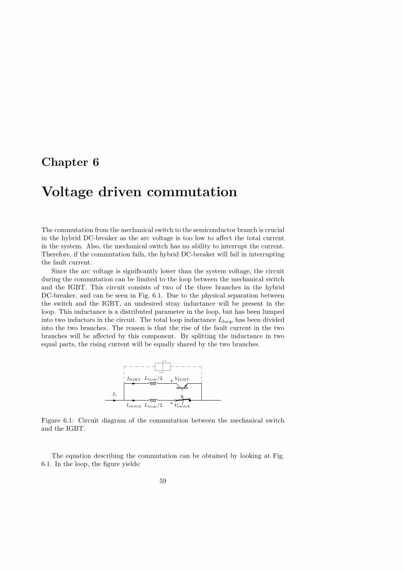
Chapter 6
Voltage driven commutation
The commutation from the mechanical switch to the semiconductor branch is crucialin the hybrid DC-breaker as the arc voltage is too low to affect the total currentin the system. Also, the mechanical switch has no ability to interrupt the current.Therefore, if the commutation fails, the hybrid DC-breaker will fail in interruptingthe fault current.
Since the arc voltage is significantly lower than the system voltage, the circuitduring the commutation can be limited to the loop between the mechanical switchand the IGBT. This circuit consists of two of the three branches in the hybridDC-breaker, and can be seen in Fig. 6.1. Due to the physical separation betweenthe switch and the IGBT, an undesired stray inductance will be present in theloop. This inductance is a distributed parameter in the loop, but has been lumpedinto two inductors in the circuit. The total loop inductance Lloop has been dividedinto the two branches. The reason is that the rise of the fault current in the twobranches will be affected by this component. By splitting the inductance in twoequal parts, the rising current will be equally shared by the two branches.
Is
Iswitch Lloop/2+ Vswitch
IIGBT Lloop/2 + VIGBT
Figure 6.1: Circuit diagram of the commutation between the mechanical switchand the IGBT.
The equation describing the commutation can be obtained by looking at Fig.6.1. In the loop, the figure yields:
59
60 CHAPTER 6. VOLTAGE DRIVEN COMMUTATION
Uarc + Lloop
2dIswitch
dt= UIGBT + Lloop
2dIIGBT
dt. (6.1)
If the rise in the system current is neglected, the commutation can be seen asa superimposed current in the loop, going in negative direction through the switchand in positive direction through the IGBT branch. Using the commutation currentand (6.1), the commutation can be described as:
Uarc − UIGBT = LloopdIcom
dt. (6.2)
This equation shows that the commutation is driven by the arc voltage, andopposed by the voltage across the IGBT. The total current to be commutated isthe system current at the start of the commutation plus the increase in the currentduring the commutation. The inductance Lloop does not oppose the commutation,but it delays it. Since the fault current is still rising during the commutation, itis desired that the commutation is fast and hence, it is desired to have a high arcvoltage and a low loop inductance. It can also be noted that even if the differencebetween the arc voltage and the IGBT voltage is kept constant, the commutationtime will increase with increasing current. Hence a fast mechanical switch is desired.
Since the voltage across the IGBT branch will contain a resistive component,the voltage drop will increase with the increasing system current. This means thatthe longer time the commutation takes, the higher arc voltage will be required tofinalize the commutation. Since the time available for the commutation is limited,it is important that the arc voltage is high enough to ensure a fast commutation.
The following sections summarizes an experimental study of the commutationfrom the mechanical switch to the IGBT.
6.1 The development of the arc voltage
When the switch contacts separate, the electrical arc will form. The voltage dependson several factors as contact material, media between the contacts and the currentlevel. Figure 6.2 shows the arc voltage as function of the separation between thecontacts for six different charging levels of the actuator capacitor bank. Here theswitch is opened with the IGBT off so that the switch will draw an arc beforethe IGBT is turned on to bypass and extinguish the arc. Naturally the switchparameter are the same, and the current in all the tests are slightly above 100 A.It can be seen that the arc voltage can be estimated quite well with an initialvoltage as the contacts separate and then with a linear increase proportional to thelength of the arc [84]. When the arc becomes longer, it also tends to become quiteunstable, and this stochastic behaviour of the arc is one of the things that makethe measurement and research on electric arcs difficult.
For the first 3 tests, i.e. 5.5, 7.5, and 9 m/s, the time before the IGBT is turnedon is the same. It can be seen that due to the higher velocity, the arc in the 9 m/s
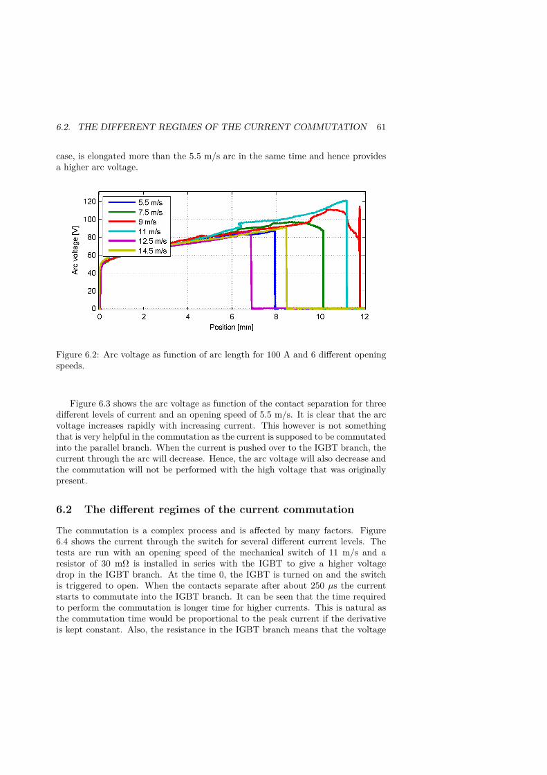
6.2. THE DIFFERENT REGIMES OF THE CURRENT COMMUTATION 61
case, is elongated more than the 5.5 m/s arc in the same time and hence providesa higher arc voltage.
Figure 6.2: Arc voltage as function of arc length for 100 A and 6 different openingspeeds.
Figure 6.3 shows the arc voltage as function of the contact separation for threedifferent levels of current and an opening speed of 5.5 m/s. It is clear that the arcvoltage increases rapidly with increasing current. This however is not somethingthat is very helpful in the commutation as the current is supposed to be commutatedinto the parallel branch. When the current is pushed over to the IGBT branch, thecurrent through the arc will decrease. Hence, the arc voltage will also decrease andthe commutation will not be performed with the high voltage that was originallypresent.
6.2 The different regimes of the current commutation
The commutation is a complex process and is affected by many factors. Figure6.4 shows the current through the switch for several different current levels. Thetests are run with an opening speed of the mechanical switch of 11 m/s and aresistor of 30 mΩ is installed in series with the IGBT to give a higher voltagedrop in the IGBT branch. At the time 0, the IGBT is turned on and the switchis triggered to open. When the contacts separate after about 250 µs the currentstarts to commutate into the IGBT branch. It can be seen that the time requiredto perform the commutation is longer time for higher currents. This is natural asthe commutation time would be proportional to the peak current if the derivativeis kept constant. Also, the resistance in the IGBT branch means that the voltage
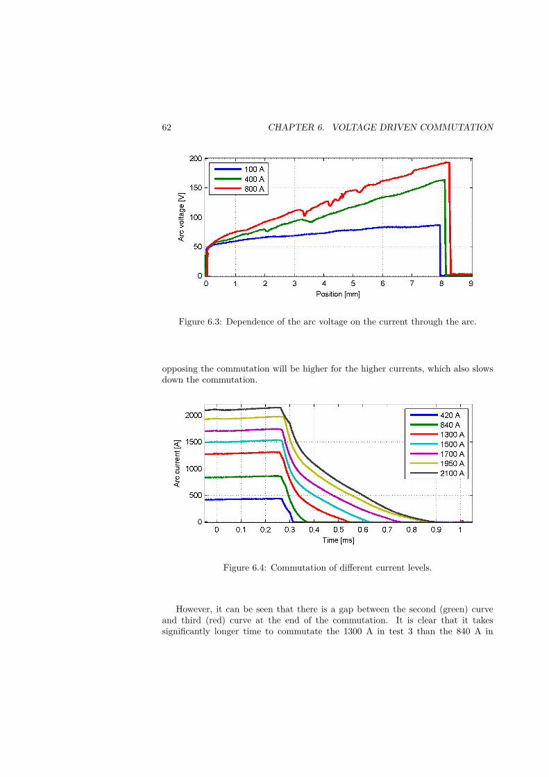
62 CHAPTER 6. VOLTAGE DRIVEN COMMUTATION
Figure 6.3: Dependence of the arc voltage on the current through the arc.
opposing the commutation will be higher for the higher currents, which also slowsdown the commutation.
Figure 6.4: Commutation of different current levels.
However, it can be seen that there is a gap between the second (green) curveand third (red) curve at the end of the commutation. It is clear that it takessignificantly longer time to commutate the 1300 A in test 3 than the 840 A in
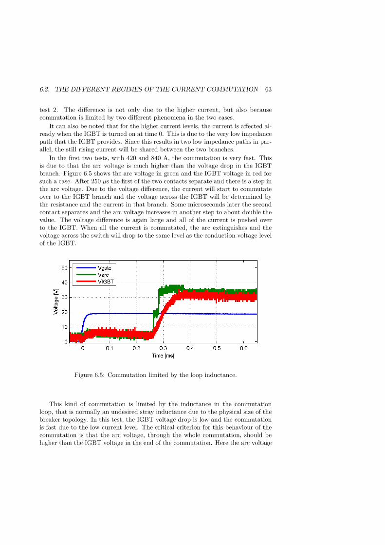
6.2. THE DIFFERENT REGIMES OF THE CURRENT COMMUTATION 63
test 2. The difference is not only due to the higher current, but also becausecommutation is limited by two different phenomena in the two cases.
It can also be noted that for the higher current levels, the current is affected al-ready when the IGBT is turned on at time 0. This is due to the very low impedancepath that the IGBT provides. Since this results in two low impedance paths in par-allel, the still rising current will be shared between the two branches.
In the first two tests, with 420 and 840 A, the commutation is very fast. Thisis due to that the arc voltage is much higher than the voltage drop in the IGBTbranch. Figure 6.5 shows the arc voltage in green and the IGBT voltage in red forsuch a case. After 250 µs the first of the two contacts separate and there is a step inthe arc voltage. Due to the voltage difference, the current will start to commutateover to the IGBT branch and the voltage across the IGBT will be determined bythe resistance and the current in that branch. Some microseconds later the secondcontact separates and the arc voltage increases in another step to about double thevalue. The voltage difference is again large and all of the current is pushed overto the IGBT. When all the current is commutated, the arc extinguishes and thevoltage across the switch will drop to the same level as the conduction voltage levelof the IGBT.
Figure 6.5: Commutation limited by the loop inductance.
This kind of commutation is limited by the inductance in the commutationloop, that is normally an undesired stray inductance due to the physical size of thebreaker topology. In this test, the IGBT voltage drop is low and the commutationis fast due to the low current level. The critical criterion for this behaviour of thecommutation is that the arc voltage, through the whole commutation, should behigher than the IGBT voltage in the end of the commutation. Here the arc voltage
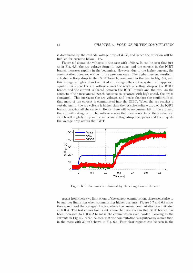
64 CHAPTER 6. VOLTAGE DRIVEN COMMUTATION
is dominated by the cathode voltage drop of 30 V, and hence the criterion will befulfilled for currents below 1 kA.
Figure 6.6 shows the voltages in the case with 1300 A. It can be seen that justas in Fig. 6.5, the arc voltage forms in two steps and the current in the IGBTbranch increases rapidly in the beginning. However, due to the higher current, thecommutation does not end as in the previous case. The higher current results ina higher voltage drop in the IGBT branch, compared to the test in Fig. 6.5, andthis voltage is higher than the initial arc voltage. Hence, the system will approachequilibrium where the arc voltage equals the resistive voltage drop of the IGBTbranch and the current is shared between the IGBT branch and the arc. As thecontacts of the mechanical switch continue to separate with high speed, the arc iselongated. This increases the arc voltage, and hence changes the equilibrium sothat more of the current is commutated into the IGBT. When the arc reaches acertain length, the arc voltage is higher than the resistive voltage drop of the IGBTbranch carrying all the current. Hence there will be no current left in the arc, andthe arc will extinguish. The voltage across the open contacts of the mechanicalswitch will slightly drop as the inductive voltage drop disappears and then equalsthe voltage drop across the IGBT.
Figure 6.6: Commutation limited by the elongation of the arc.
Apart from these two limitations of the current commutation, there seems also tobe another limitation when commutating higher currents. Figure 6.7 and 6.8 showthe current and the voltages of a test where the current commutation was initiatedat 600 A. The test comes from a set where the resistance in the IGBT branch hasbeen increased to 100 mΩ to make the commutation even harder. Looking at thecurrents in Fig. 6.7 it can be seen that the commutation is significantly slower thanin the cases with 30 mΩ shown in Fig. 6.4. Four clear regimes can be seen in the
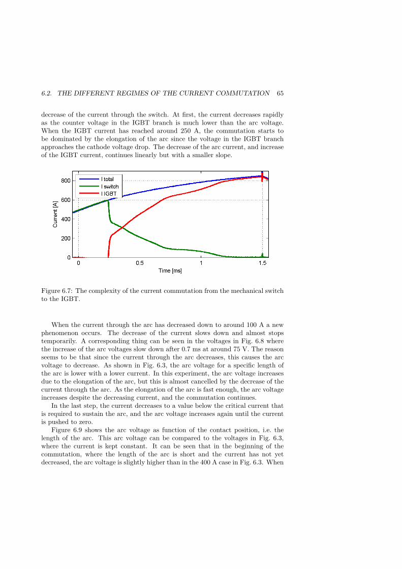
6.2. THE DIFFERENT REGIMES OF THE CURRENT COMMUTATION 65
decrease of the current through the switch. At first, the current decreases rapidlyas the counter voltage in the IGBT branch is much lower than the arc voltage.When the IGBT current has reached around 250 A, the commutation starts tobe dominated by the elongation of the arc since the voltage in the IGBT branchapproaches the cathode voltage drop. The decrease of the arc current, and increaseof the IGBT current, continues linearly but with a smaller slope.
Figure 6.7: The complexity of the current commutation from the mechanical switchto the IGBT.
When the current through the arc has decreased down to around 100 A a newphenomenon occurs. The decrease of the current slows down and almost stopstemporarily. A corresponding thing can be seen in the voltages in Fig. 6.8 wherethe increase of the arc voltages slow down after 0.7 ms at around 75 V. The reasonseems to be that since the current through the arc decreases, this causes the arcvoltage to decrease. As shown in Fig. 6.3, the arc voltage for a specific length ofthe arc is lower with a lower current. In this experiment, the arc voltage increasesdue to the elongation of the arc, but this is almost cancelled by the decrease of thecurrent through the arc. As the elongation of the arc is fast enough, the arc voltageincreases despite the decreasing current, and the commutation continues.
In the last step, the current decreases to a value below the critical current thatis required to sustain the arc, and the arc voltage increases again until the currentis pushed to zero.
Figure 6.9 shows the arc voltage as function of the contact position, i.e. thelength of the arc. This arc voltage can be compared to the voltages in Fig. 6.3,where the current is kept constant. It can be seen that in the beginning of thecommutation, where the length of the arc is short and the current has not yetdecreased, the arc voltage is slightly higher than in the 400 A case in Fig. 6.3. When
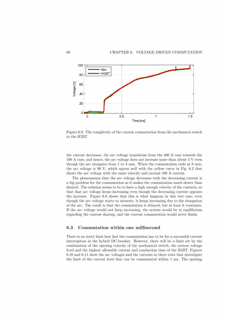
66 CHAPTER 6. VOLTAGE DRIVEN COMMUTATION
Figure 6.8: The complexity of the current commutation from the mechanical switchto the IGBT.
the current decreases, the arc voltage transitions from the 400 A case towards the100 A case, and hence, the arc voltage does not increase more than about 5 V eventhough the arc elongates from 1 to 4 mm. When the commutation ends at 9 mm,the arc voltage is 90 V, which agrees well with the yellow curve in Fig. 6.2 thatshows the arc voltage with the same velocity and around 100 A current.
The phenomenon that the arc voltage decreases with the decreasing current isa big problem for the commutation as it makes the commutation much slower thandesired. The solution seems to be to have a high enough velocity of the contacts, sothat that arc voltage keeps increasing even though the decreasing current opposesthe increase. Figure 6.8 shows that this is what happens in this test case; eventhough the arc voltage starts to saturate, it keeps increasing due to the elongationof the arc. The result is that the commutation is delayed, but at least it continues.If the arc voltage would not keep increasing, the system would be in equilibriumregarding the current sharing, and the current commutation would never finish.
6.3 Commutation within one millisecond
There is no strict limit how fast the commutation has to be for a successful currentinterruption in the hybrid DC-breaker. However, there will be a limit set by thecombination of the opening velocity of the mechanical switch, the system voltagelevel and the highest allowable current and conduction time of the IGBT. Figures6.10 and 6.11 show the arc voltages and the currents in three tests that investigatethe limit of the current level that can be commutated within 1 ms. The opening
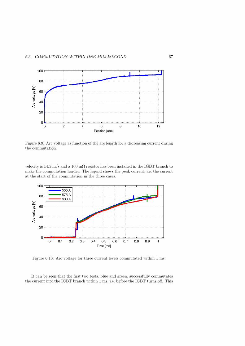
6.3. COMMUTATION WITHIN ONE MILLISECOND 67
Figure 6.9: Arc voltage as function of the arc length for a decreasing current duringthe commutation.
velocity is 14.5 m/s and a 100 mΩ resistor has been installed in the IGBT branch tomake the commutation harder. The legend shows the peak current, i.e. the currentat the start of the commutation in the three cases.
Figure 6.10: Arc voltage for three current levels commutated within 1 ms.
It can be seen that the first two tests, blue and green, successfully commutatesthe current into the IGBT branch within 1 ms, i.e. before the IGBT turns off. This
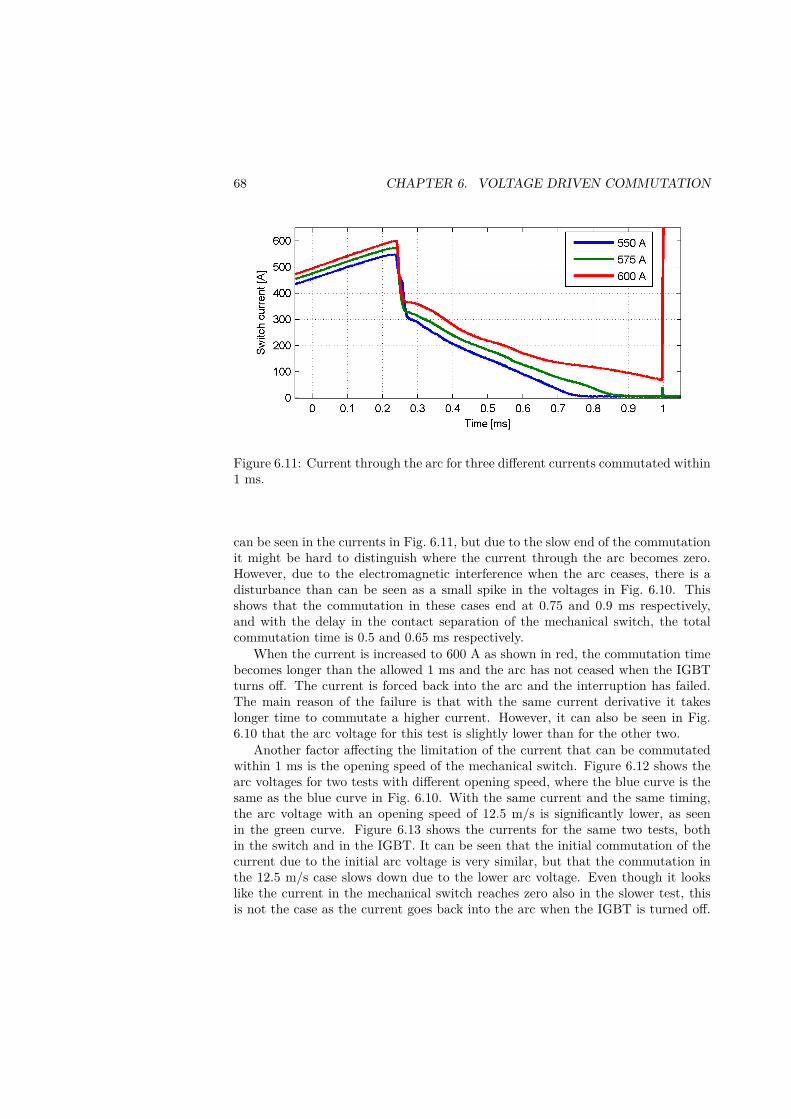
68 CHAPTER 6. VOLTAGE DRIVEN COMMUTATION
Figure 6.11: Current through the arc for three different currents commutated within1 ms.
can be seen in the currents in Fig. 6.11, but due to the slow end of the commutationit might be hard to distinguish where the current through the arc becomes zero.However, due to the electromagnetic interference when the arc ceases, there is adisturbance than can be seen as a small spike in the voltages in Fig. 6.10. Thisshows that the commutation in these cases end at 0.75 and 0.9 ms respectively,and with the delay in the contact separation of the mechanical switch, the totalcommutation time is 0.5 and 0.65 ms respectively.
When the current is increased to 600 A as shown in red, the commutation timebecomes longer than the allowed 1 ms and the arc has not ceased when the IGBTturns off. The current is forced back into the arc and the interruption has failed.The main reason of the failure is that with the same current derivative it takeslonger time to commutate a higher current. However, it can also be seen in Fig.6.10 that the arc voltage for this test is slightly lower than for the other two.
Another factor affecting the limitation of the current that can be commutatedwithin 1 ms is the opening speed of the mechanical switch. Figure 6.12 shows thearc voltages for two tests with different opening speed, where the blue curve is thesame as the blue curve in Fig. 6.10. With the same current and the same timing,the arc voltage with an opening speed of 12.5 m/s is significantly lower, as seenin the green curve. Figure 6.13 shows the currents for the same two tests, bothin the switch and in the IGBT. It can be seen that the initial commutation of thecurrent due to the initial arc voltage is very similar, but that the commutation inthe 12.5 m/s case slows down due to the lower arc voltage. Even though it lookslike the current in the mechanical switch reaches zero also in the slower test, thisis not the case as the current goes back into the arc when the IGBT is turned off.
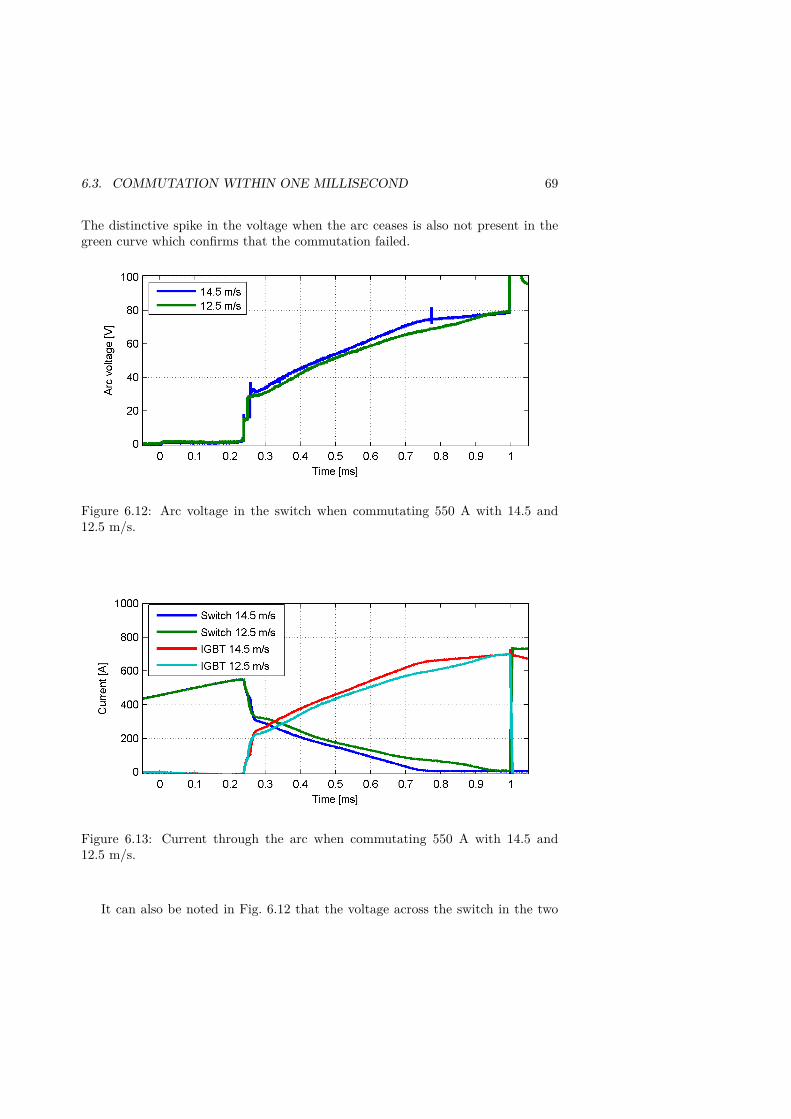
6.3. COMMUTATION WITHIN ONE MILLISECOND 69
The distinctive spike in the voltage when the arc ceases is also not present in thegreen curve which confirms that the commutation failed.
Figure 6.12: Arc voltage in the switch when commutating 550 A with 14.5 and12.5 m/s.
Figure 6.13: Current through the arc when commutating 550 A with 14.5 and12.5 m/s.
It can also be noted in Fig. 6.12 that the voltage across the switch in the two
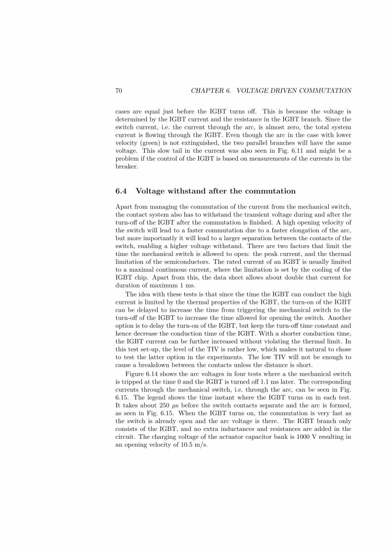
70 CHAPTER 6. VOLTAGE DRIVEN COMMUTATION
cases are equal just before the IGBT turns off. This is because the voltage isdetermined by the IGBT current and the resistance in the IGBT branch. Since theswitch current, i.e. the current through the arc, is almost zero, the total systemcurrent is flowing through the IGBT. Even though the arc in the case with lowervelocity (green) is not extinguished, the two parallel branches will have the samevoltage. This slow tail in the current was also seen in Fig. 6.11 and might be aproblem if the control of the IGBT is based on measurements of the currents in thebreaker.
6.4 Voltage withstand after the commutation
Apart from managing the commutation of the current from the mechanical switch,the contact system also has to withstand the transient voltage during and after theturn-off of the IGBT after the commutation is finished. A high opening velocity ofthe switch will lead to a faster commutation due to a faster elongation of the arc,but more importantly it will lead to a larger separation between the contacts of theswitch, enabling a higher voltage withstand. There are two factors that limit thetime the mechanical switch is allowed to open: the peak current, and the thermallimitation of the semiconductors. The rated current of an IGBT is usually limitedto a maximal continuous current, where the limitation is set by the cooling of theIGBT chip. Apart from this, the data sheet allows about double that current forduration of maximum 1 ms.
The idea with these tests is that since the time the IGBT can conduct the highcurrent is limited by the thermal properties of the IGBT, the turn-on of the IGBTcan be delayed to increase the time from triggering the mechanical switch to theturn-off of the IGBT to increase the time allowed for opening the switch. Anotheroption is to delay the turn-on of the IGBT, but keep the turn-off time constant andhence decrease the conduction time of the IGBT. With a shorter conduction time,the IGBT current can be further increased without violating the thermal limit. Inthis test set-up, the level of the TIV is rather low, which makes it natural to choseto test the latter option in the experiments. The low TIV will not be enough tocause a breakdown between the contacts unless the distance is short.
Figure 6.14 shows the arc voltages in four tests where a the mechanical switchis tripped at the time 0 and the IGBT is turned off 1.1 ms later. The correspondingcurrents through the mechanical switch, i.e. through the arc, can be seen in Fig.6.15. The legend shows the time instant where the IGBT turns on in each test.It takes about 250 µs before the switch contacts separate and the arc is formed,as seen in Fig. 6.15. When the IGBT turns on, the commutation is very fast asthe switch is already open and the arc voltage is there. The IGBT branch onlyconsists of the IGBT, and no extra inductances and resistances are added in thecircuit. The charging voltage of the actuator capacitor bank is 1000 V resulting inan opening velocity of 10.5 m/s.
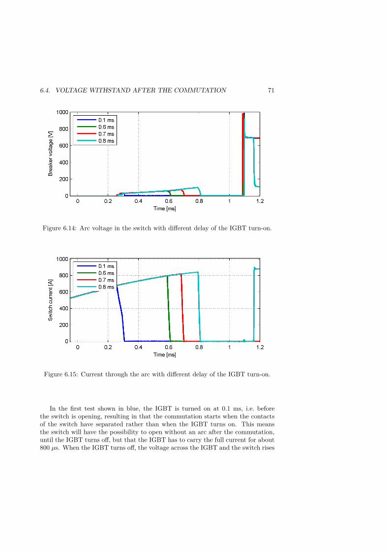
6.4. VOLTAGE WITHSTAND AFTER THE COMMUTATION 71
Figure 6.14: Arc voltage in the switch with different delay of the IGBT turn-on.
Figure 6.15: Current through the arc with different delay of the IGBT turn-on.
In the first test shown in blue, the IGBT is turned on at 0.1 ms, i.e. beforethe switch is opening, resulting in that the commutation starts when the contactsof the switch have separated rather than when the IGBT turns on. This meansthe switch will have the possibility to open without an arc after the commutation,until the IGBT turns off, but that the IGBT has to carry the full current for about800 µs. When the IGBT turns off, the voltage across the IGBT and the switch rises
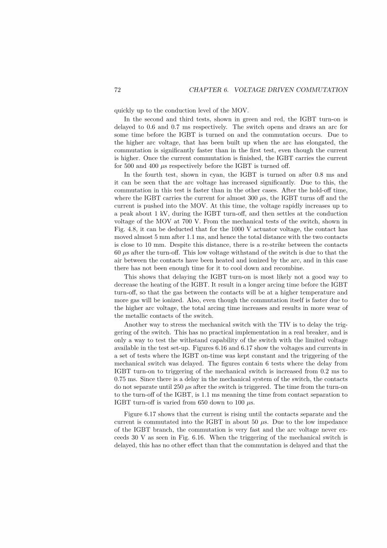
72 CHAPTER 6. VOLTAGE DRIVEN COMMUTATION
quickly up to the conduction level of the MOV.In the second and third tests, shown in green and red, the IGBT turn-on is
delayed to 0.6 and 0.7 ms respectively. The switch opens and draws an arc forsome time before the IGBT is turned on and the commutation occurs. Due tothe higher arc voltage, that has been built up when the arc has elongated, thecommutation is significantly faster than in the first test, even though the currentis higher. Once the current commutation is finished, the IGBT carries the currentfor 500 and 400 µs respectively before the IGBT is turned off.
In the fourth test, shown in cyan, the IGBT is turned on after 0.8 ms andit can be seen that the arc voltage has increased significantly. Due to this, thecommutation in this test is faster than in the other cases. After the hold-off time,where the IGBT carries the current for almost 300 µs, the IGBT turns off and thecurrent is pushed into the MOV. At this time, the voltage rapidly increases up toa peak about 1 kV, during the IGBT turn-off, and then settles at the conductionvoltage of the MOV at 700 V. From the mechanical tests of the switch, shown inFig. 4.8, it can be deducted that for the 1000 V actuator voltage, the contact hasmoved almost 5 mm after 1.1 ms, and hence the total distance with the two contactsis close to 10 mm. Despite this distance, there is a re-strike between the contacts60 µs after the turn-off. This low voltage withstand of the switch is due to that theair between the contacts have been heated and ionized by the arc, and in this casethere has not been enough time for it to cool down and recombine.
This shows that delaying the IGBT turn-on is most likely not a good way todecrease the heating of the IGBT. It result in a longer arcing time before the IGBTturn-off, so that the gas between the contacts will be at a higher temperature andmore gas will be ionized. Also, even though the commutation itself is faster due tothe higher arc voltage, the total arcing time increases and results in more wear ofthe metallic contacts of the switch.
Another way to stress the mechanical switch with the TIV is to delay the trig-gering of the switch. This has no practical implementation in a real breaker, and isonly a way to test the withstand capability of the switch with the limited voltageavailable in the test set-up. Figures 6.16 and 6.17 show the voltages and currents ina set of tests where the IGBT on-time was kept constant and the triggering of themechanical switch was delayed. The figures contain 6 tests where the delay fromIGBT turn-on to triggering of the mechanical switch is increased from 0.2 ms to0.75 ms. Since there is a delay in the mechanical system of the switch, the contactsdo not separate until 250 µs after the switch is triggered. The time from the turn-onto the turn-off of the IGBT, is 1.1 ms meaning the time from contact separation toIGBT turn-off is varied from 650 down to 100 µs.
Figure 6.17 shows that the current is rising until the contacts separate and thecurrent is commutated into the IGBT in about 50 µs. Due to the low impedanceof the IGBT branch, the commutation is very fast and the arc voltage never ex-ceeds 30 V as seen in Fig. 6.16. When the triggering of the mechanical switch isdelayed, this has no other effect than that the commutation is delayed and that the
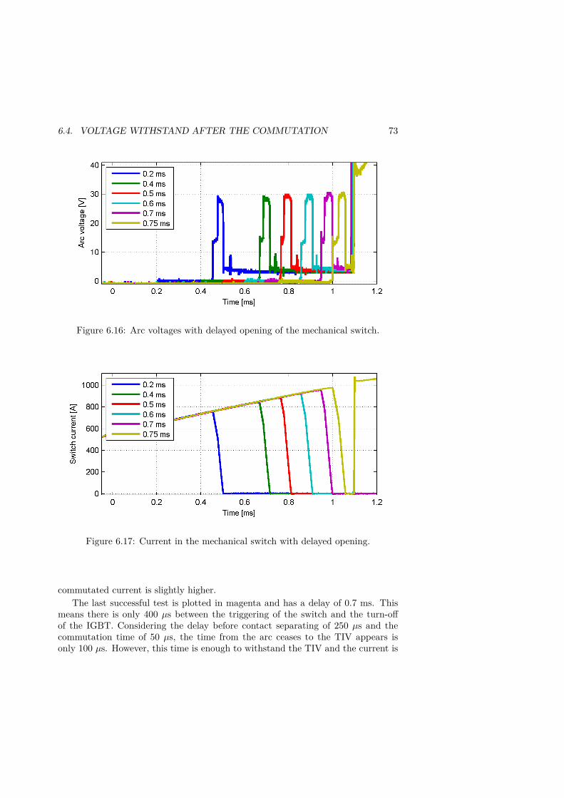
6.4. VOLTAGE WITHSTAND AFTER THE COMMUTATION 73
Figure 6.16: Arc voltages with delayed opening of the mechanical switch.
Figure 6.17: Current in the mechanical switch with delayed opening.
commutated current is slightly higher.The last successful test is plotted in magenta and has a delay of 0.7 ms. This
means there is only 400 µs between the triggering of the switch and the turn-offof the IGBT. Considering the delay before contact separating of 250 µs and thecommutation time of 50 µs, the time from the arc ceases to the TIV appears isonly 100 µs. However, this time is enough to withstand the TIV and the current is
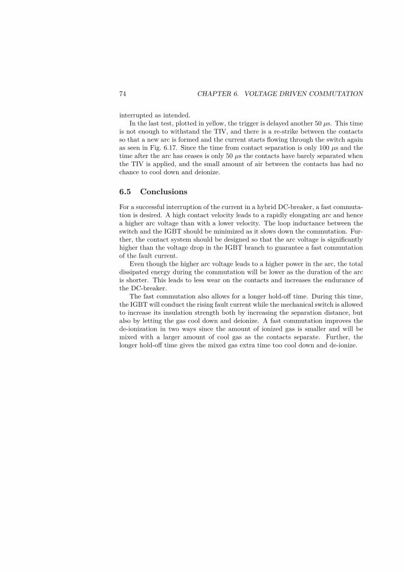
74 CHAPTER 6. VOLTAGE DRIVEN COMMUTATION
interrupted as intended.In the last test, plotted in yellow, the trigger is delayed another 50 µs. This time
is not enough to withstand the TIV, and there is a re-strike between the contactsso that a new arc is formed and the current starts flowing through the switch againas seen in Fig. 6.17. Since the time from contact separation is only 100 µs and thetime after the arc has ceases is only 50 µs the contacts have barely separated whenthe TIV is applied, and the small amount of air between the contacts has had nochance to cool down and deionize.
6.5 Conclusions
For a successful interruption of the current in a hybrid DC-breaker, a fast commuta-tion is desired. A high contact velocity leads to a rapidly elongating arc and hencea higher arc voltage than with a lower velocity. The loop inductance between theswitch and the IGBT should be minimized as it slows down the commutation. Fur-ther, the contact system should be designed so that the arc voltage is significantlyhigher than the voltage drop in the IGBT branch to guarantee a fast commutationof the fault current.
Even though the higher arc voltage leads to a higher power in the arc, the totaldissipated energy during the commutation will be lower as the duration of the arcis shorter. This leads to less wear on the contacts and increases the endurance ofthe DC-breaker.
The fast commutation also allows for a longer hold-off time. During this time,the IGBT will conduct the rising fault current while the mechanical switch is allowedto increase its insulation strength both by increasing the separation distance, butalso by letting the gas cool down and deionize. A fast commutation improves thede-ionization in two ways since the amount of ionized gas is smaller and will bemixed with a larger amount of cool gas as the contacts separate. Further, thelonger hold-off time gives the mixed gas extra time too cool down and de-ionize.
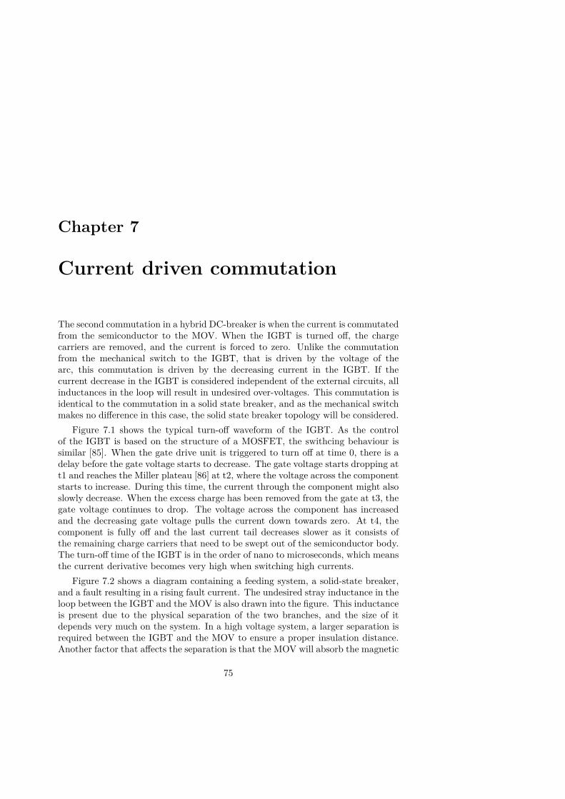
Chapter 7
Current driven commutation
The second commutation in a hybrid DC-breaker is when the current is commutatedfrom the semiconductor to the MOV. When the IGBT is turned off, the chargecarriers are removed, and the current is forced to zero. Unlike the commutationfrom the mechanical switch to the IGBT, that is driven by the voltage of thearc, this commutation is driven by the decreasing current in the IGBT. If thecurrent decrease in the IGBT is considered independent of the external circuits, allinductances in the loop will result in undesired over-voltages. This commutation isidentical to the commutation in a solid state breaker, and as the mechanical switchmakes no difference in this case, the solid state breaker topology will be considered.
Figure 7.1 shows the typical turn-off waveform of the IGBT. As the controlof the IGBT is based on the structure of a MOSFET, the swithcing behaviour issimilar [85]. When the gate drive unit is triggered to turn off at time 0, there is adelay before the gate voltage starts to decrease. The gate voltage starts dropping att1 and reaches the Miller plateau [86] at t2, where the voltage across the componentstarts to increase. During this time, the current through the component might alsoslowly decrease. When the excess charge has been removed from the gate at t3, thegate voltage continues to drop. The voltage across the component has increasedand the decreasing gate voltage pulls the current down towards zero. At t4, thecomponent is fully off and the last current tail decreases slower as it consists ofthe remaining charge carriers that need to be swept out of the semiconductor body.The turn-off time of the IGBT is in the order of nano to microseconds, which meansthe current derivative becomes very high when switching high currents.
Figure 7.2 shows a diagram containing a feeding system, a solid-state breaker,and a fault resulting in a rising fault current. The undesired stray inductance in theloop between the IGBT and the MOV is also drawn into the figure. This inductanceis present due to the physical separation of the two branches, and the size of itdepends very much on the system. In a high voltage system, a larger separation isrequired between the IGBT and the MOV to ensure a proper insulation distance.Another factor that affects the separation is that the MOV will absorb the magnetic
75
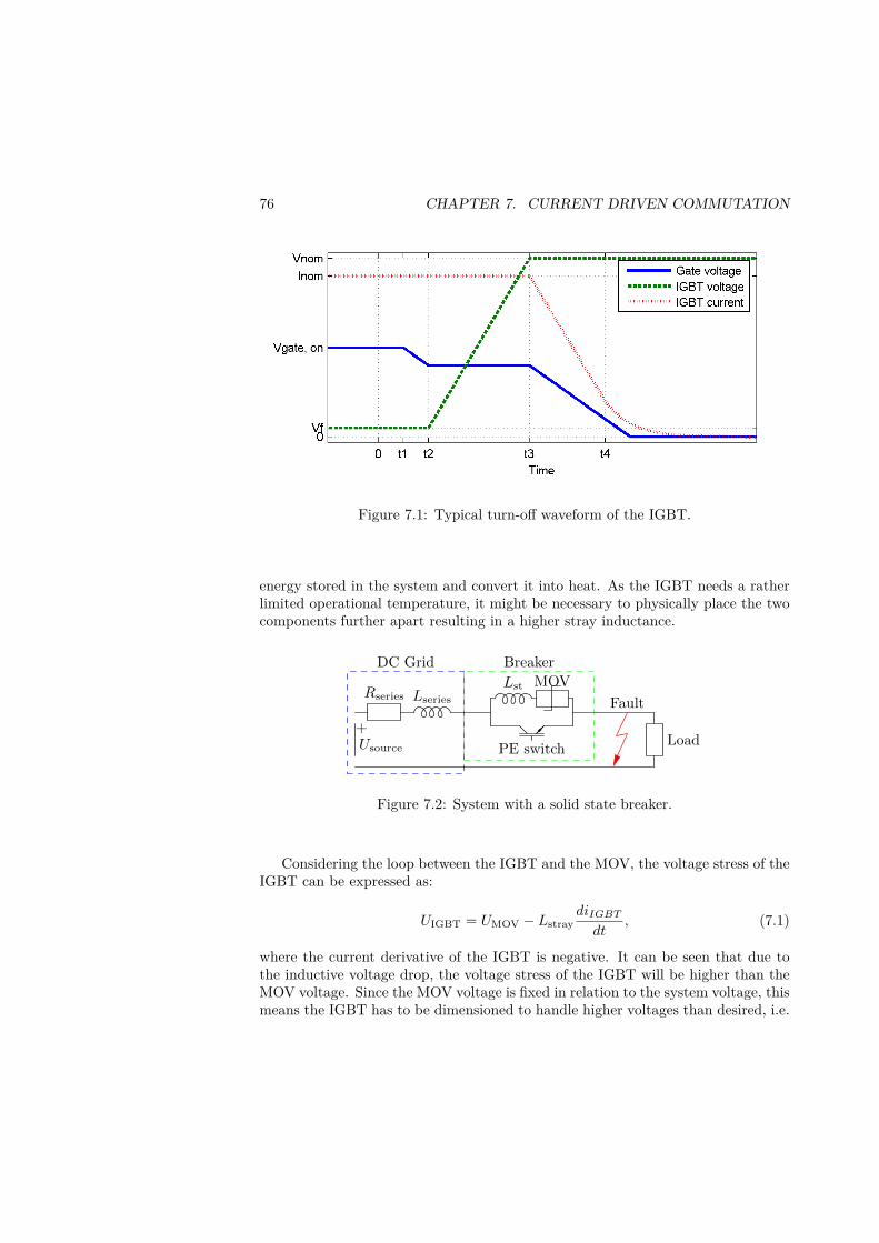
76 CHAPTER 7. CURRENT DRIVEN COMMUTATION
Figure 7.1: Typical turn-off waveform of the IGBT.
energy stored in the system and convert it into heat. As the IGBT needs a ratherlimited operational temperature, it might be necessary to physically place the twocomponents further apart resulting in a higher stray inductance.
Usource
+
Rseries Lseries
Lst MOV
PE switchLoad
DC Grid Breaker
Fault
Figure 7.2: System with a solid state breaker.
Considering the loop between the IGBT and the MOV, the voltage stress of theIGBT can be expressed as:
UIGBT = UMOV − LstraydiIGBT
dt, (7.1)
where the current derivative of the IGBT is negative. It can be seen that due tothe inductive voltage drop, the voltage stress of the IGBT will be higher than theMOV voltage. Since the MOV voltage is fixed in relation to the system voltage, thismeans the IGBT has to be dimensioned to handle higher voltages than desired, i.e.
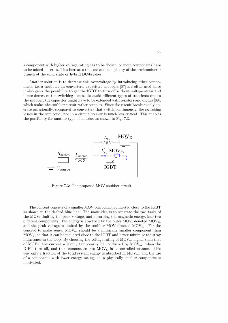
77
a component with higher voltage rating has to be chosen, or more components haveto be added in series. This increases the cost and complexity of the semiconductorbranch of the solid state or hybrid DC-breaker.
Another solution is to decrease this over-voltage by introducing other compo-nents, i.e. a snubber. In converters, capacitive snubbers [87] are often used sinceit also gives the possibility to get the IGBT to turn off without voltage stress andhence decreases the switching losses. To avoid different types of transients due tothe snubber, the capacitor might have to be extended with resistors and diodes [88],which makes the snubber circuit rather complex. Since the circuit breakers only op-erate occasionally, compared to converters that switch continuously, the switchinglosses in the semiconductor in a circuit breaker is much less critical. This enablesthe possibility for another type of snubber as shown in Fig. 7.3.
Usource
Rseries Lseries
IGBT
L′st MOVov
LstMOVE
Figure 7.3: The proposed MOV snubber circuit.
The concept consists of a smaller MOV component connected close to the IGBTas shown in the dashed blue line. The main idea is to separate the two tasks ofthe MOV: limiting the peak voltage, and absorbing the magnetic energy, into twodifferent components. The energy is absorbed by the outer MOV, denoted MOVE,and the peak voltage is limited by the snubber MOV denoted MOVov. For theconcept to make sense, MOVov should be a physically smaller component thanMOVE, so that it can be mounted close to the IGBT and hence minimize the strayinductance in the loop. By choosing the voltage rating of MOVov higher than thatof MOVE, the current will only temporarily be conducted by MOVov, when theIGBT turn off, and then commutate into MOVE in a controlled manner. Thisway only a fraction of the total system energy is absorbed in MOVov, and the useof a component with lower energy rating, i.e. a physically smaller component ismotivated.
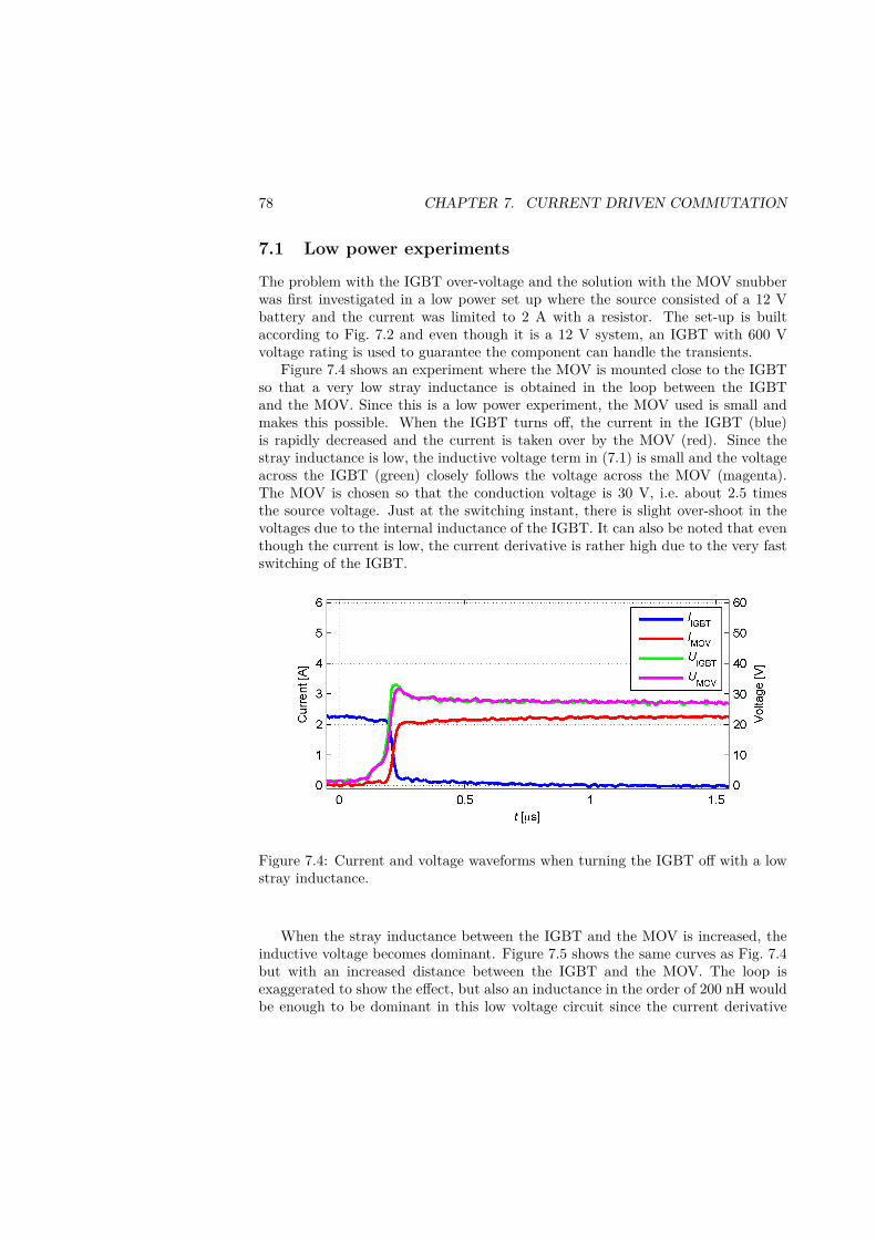
78 CHAPTER 7. CURRENT DRIVEN COMMUTATION
7.1 Low power experiments
The problem with the IGBT over-voltage and the solution with the MOV snubberwas first investigated in a low power set up where the source consisted of a 12 Vbattery and the current was limited to 2 A with a resistor. The set-up is builtaccording to Fig. 7.2 and even though it is a 12 V system, an IGBT with 600 Vvoltage rating is used to guarantee the component can handle the transients.
Figure 7.4 shows an experiment where the MOV is mounted close to the IGBTso that a very low stray inductance is obtained in the loop between the IGBTand the MOV. Since this is a low power experiment, the MOV used is small andmakes this possible. When the IGBT turns off, the current in the IGBT (blue)is rapidly decreased and the current is taken over by the MOV (red). Since thestray inductance is low, the inductive voltage term in (7.1) is small and the voltageacross the IGBT (green) closely follows the voltage across the MOV (magenta).The MOV is chosen so that the conduction voltage is 30 V, i.e. about 2.5 timesthe source voltage. Just at the switching instant, there is slight over-shoot in thevoltages due to the internal inductance of the IGBT. It can also be noted that eventhough the current is low, the current derivative is rather high due to the very fastswitching of the IGBT.
Figure 7.4: Current and voltage waveforms when turning the IGBT off with a lowstray inductance.
When the stray inductance between the IGBT and the MOV is increased, theinductive voltage becomes dominant. Figure 7.5 shows the same curves as Fig. 7.4but with an increased distance between the IGBT and the MOV. The loop isexaggerated to show the effect, but also an inductance in the order of 200 nH wouldbe enough to be dominant in this low voltage circuit since the current derivative
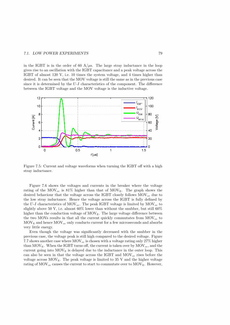
7.1. LOW POWER EXPERIMENTS 79
in the IGBT is in the order of 60 A/µs. The large stray inductance in the loopgives rise to an oscillation with the IGBT capacitance and a peak voltage across theIGBT of almost 120 V, i.e. 10 times the system voltage, and 4 times higher thandesired. It can be seen that the MOV voltage is still the same as in the previous casesince it is determined by the U -I characteristics of the component. The differencebetween the IGBT voltage and the MOV voltage is the inductive voltage.
Figure 7.5: Current and voltage waveforms when turning the IGBT off with a highstray inductance.
Figure 7.6 shows the voltages and currents in the breaker where the voltagerating of the MOVov is 81% higher than that of MOVE. The graph shows thedesired behaviour that the voltage across the IGBT closely follows MOVov due tothe low stray inductance. Hence the voltage across the IGBT is fully defined bythe U -I characteristics of MOVov. The peak IGBT voltage is limited by MOVov toslightly above 50 V, i.e. almost 60% lower than without the snubber, but still 60%higher than the conduction voltage of MOVE. The large voltage difference betweenthe two MOVs results in that all the current quickly commutates from MOVov toMOVE and hence MOVov only conducts current for a few microseconds and absorbsvery little energy.
Even though the voltage was significantly decreased with the snubber in theprevious case, the voltage peak is still high compared to the desired voltage. Figure7.7 shows another case where MOVov is chosen with a voltage rating only 27% higherthan MOVE. When the IGBT turns off, the current is taken over by MOVov, and thecurrent going into MOVE is delayed due to the inductance in the outer loop. Thiscan also be seen in that the voltage across the IGBT and MOVov rises before thevoltage across MOVE. The peak voltage is limited to 35 V and the higher voltagerating of MOVov causes the current to start to commutate over to MOVE. However,
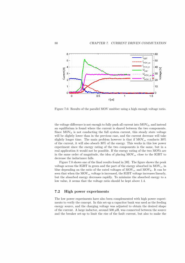
80 CHAPTER 7. CURRENT DRIVEN COMMUTATION
Figure 7.6: Results of the parallel MOV snubber using a high enough voltage ratio.
the voltage difference is not enough to fully push all current into MOVE, and insteadan equilibrium is found where the current is shared between the two components.Since MOVE is not conducting the full system current, this steady state voltagewill be slightly lower than in the previous case, and the current decrease will takeslightly longer time. The main problem however is that if MOVov conducts 30%of the current, it will also absorb 30% of the energy. This works in this low powerexperiment since the energy rating of the two components is the same, but in areal application it would not be possible. If the energy rating of the two MOVs arein the same order of magnitude, the idea of placing MOVov close to the IGBT todecrease the inductance falls.
Figure 7.8 shows one of the final results found in [89]. The figure shows the peakvoltage across the IGBT in green and the part of the energy absorbed in MOVov inblue depending on the ratio of the rated voltages of MOVov and MOVE. It can beseen that when the MOVov voltage is increased, the IGBT voltage increases linearly,but the absorbed energy decreases rapidly. To minimize the absorbed energy to alow value, it seems that the voltage ratio should be kept above 1.4.
7.2 High power experiments
The low power experiments have also been complemented with high power experi-ments to verify the concept. In this set-up a capacitor bank was used as the feedingenergy source, and the charging voltage was adjusted to obtain the desired shapeof the current. A large inductor, around 500 µH, was connected between the sourceand the breaker set-up to limit the rise of the fault current, but also to make the
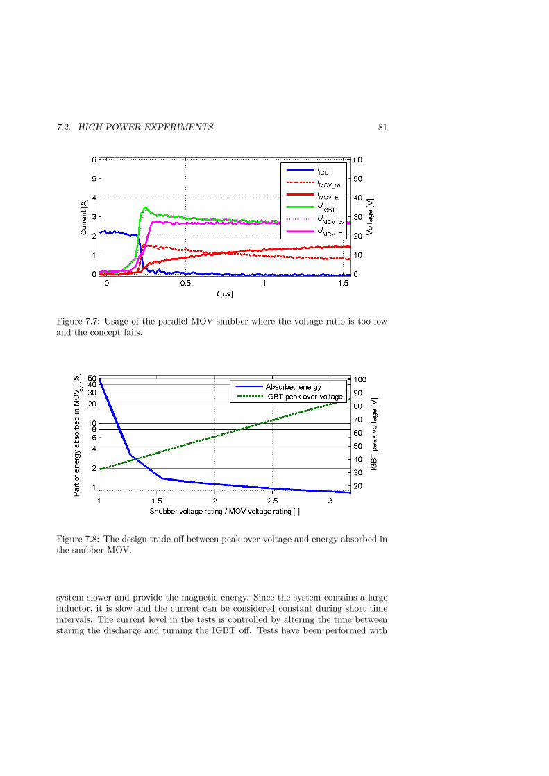
7.2. HIGH POWER EXPERIMENTS 81
Figure 7.7: Usage of the parallel MOV snubber where the voltage ratio is too lowand the concept fails.
Figure 7.8: The design trade-off between peak over-voltage and energy absorbed inthe snubber MOV.
system slower and provide the magnetic energy. Since the system contains a largeinductor, it is slow and the current can be considered constant during short timeintervals. The current level in the tests is controlled by altering the time betweenstaring the discharge and turning the IGBT off. Tests have been performed with
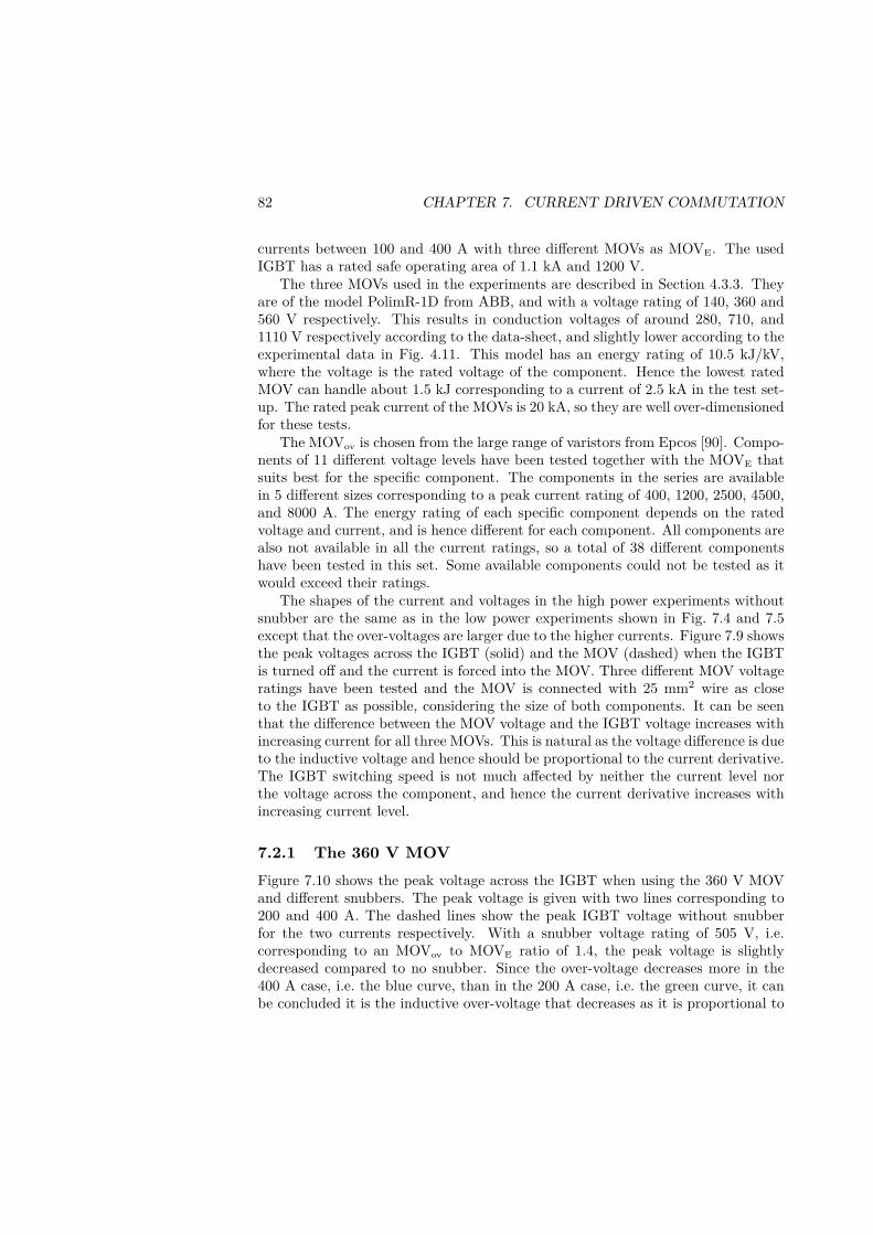
82 CHAPTER 7. CURRENT DRIVEN COMMUTATION
currents between 100 and 400 A with three different MOVs as MOVE. The usedIGBT has a rated safe operating area of 1.1 kA and 1200 V.
The three MOVs used in the experiments are described in Section 4.3.3. Theyare of the model PolimR-1D from ABB, and with a voltage rating of 140, 360 and560 V respectively. This results in conduction voltages of around 280, 710, and1110 V respectively according to the data-sheet, and slightly lower according to theexperimental data in Fig. 4.11. This model has an energy rating of 10.5 kJ/kV,where the voltage is the rated voltage of the component. Hence the lowest ratedMOV can handle about 1.5 kJ corresponding to a current of 2.5 kA in the test set-up. The rated peak current of the MOVs is 20 kA, so they are well over-dimensionedfor these tests.
The MOVov is chosen from the large range of varistors from Epcos [90]. Compo-nents of 11 different voltage levels have been tested together with the MOVE thatsuits best for the specific component. The components in the series are availablein 5 different sizes corresponding to a peak current rating of 400, 1200, 2500, 4500,and 8000 A. The energy rating of each specific component depends on the ratedvoltage and current, and is hence different for each component. All components arealso not available in all the current ratings, so a total of 38 different componentshave been tested in this set. Some available components could not be tested as itwould exceed their ratings.
The shapes of the current and voltages in the high power experiments withoutsnubber are the same as in the low power experiments shown in Fig. 7.4 and 7.5except that the over-voltages are larger due to the higher currents. Figure 7.9 showsthe peak voltages across the IGBT (solid) and the MOV (dashed) when the IGBTis turned off and the current is forced into the MOV. Three different MOV voltageratings have been tested and the MOV is connected with 25 mm2 wire as closeto the IGBT as possible, considering the size of both components. It can be seenthat the difference between the MOV voltage and the IGBT voltage increases withincreasing current for all three MOVs. This is natural as the voltage difference is dueto the inductive voltage and hence should be proportional to the current derivative.The IGBT switching speed is not much affected by neither the current level northe voltage across the component, and hence the current derivative increases withincreasing current level.
7.2.1 The 360 V MOVFigure 7.10 shows the peak voltage across the IGBT when using the 360 V MOVand different snubbers. The peak voltage is given with two lines corresponding to200 and 400 A. The dashed lines show the peak IGBT voltage without snubberfor the two currents respectively. With a snubber voltage rating of 505 V, i.e.corresponding to an MOVov to MOVE ratio of 1.4, the peak voltage is slightlydecreased compared to no snubber. Since the over-voltage decreases more in the400 A case, i.e. the blue curve, than in the 200 A case, i.e. the green curve, it canbe concluded it is the inductive over-voltage that decreases as it is proportional to
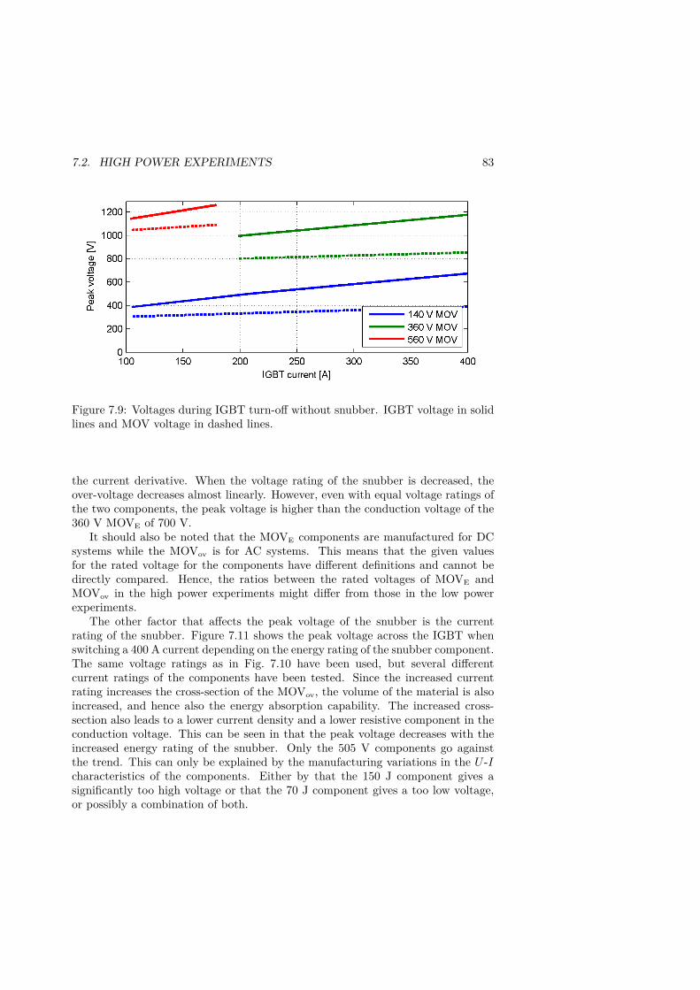
7.2. HIGH POWER EXPERIMENTS 83
Figure 7.9: Voltages during IGBT turn-off without snubber. IGBT voltage in solidlines and MOV voltage in dashed lines.
the current derivative. When the voltage rating of the snubber is decreased, theover-voltage decreases almost linearly. However, even with equal voltage ratings ofthe two components, the peak voltage is higher than the conduction voltage of the360 V MOVE of 700 V.
It should also be noted that the MOVE components are manufactured for DCsystems while the MOVov is for AC systems. This means that the given valuesfor the rated voltage for the components have different definitions and cannot bedirectly compared. Hence, the ratios between the rated voltages of MOVE andMOVov in the high power experiments might differ from those in the low powerexperiments.
The other factor that affects the peak voltage of the snubber is the currentrating of the snubber. Figure 7.11 shows the peak voltage across the IGBT whenswitching a 400 A current depending on the energy rating of the snubber component.The same voltage ratings as in Fig. 7.10 have been used, but several differentcurrent ratings of the components have been tested. Since the increased currentrating increases the cross-section of the MOVov, the volume of the material is alsoincreased, and hence also the energy absorption capability. The increased cross-section also leads to a lower current density and a lower resistive component in theconduction voltage. This can be seen in that the peak voltage decreases with theincreased energy rating of the snubber. Only the 505 V components go againstthe trend. This can only be explained by the manufacturing variations in the U -Icharacteristics of the components. Either by that the 150 J component gives asignificantly too high voltage or that the 70 J component gives a too low voltage,or possibly a combination of both.
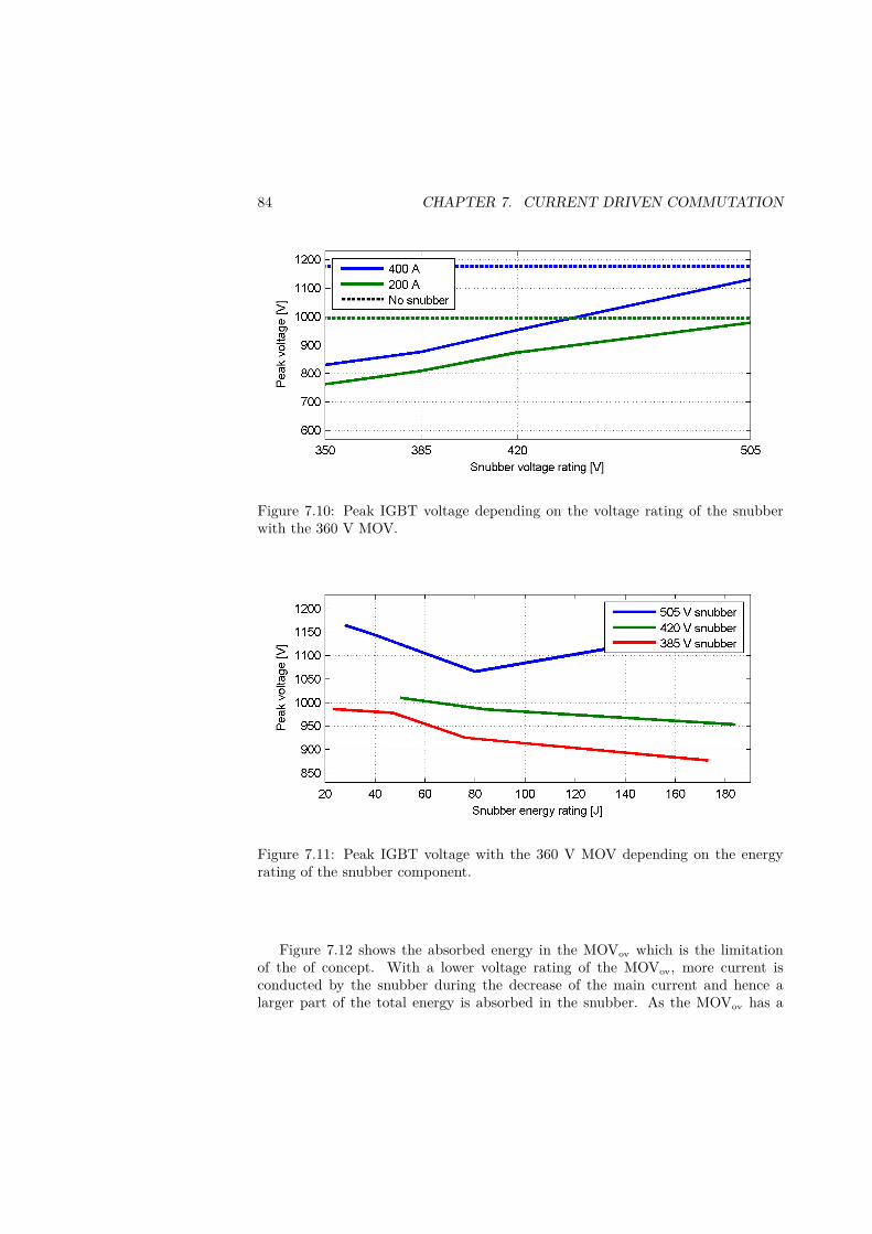
84 CHAPTER 7. CURRENT DRIVEN COMMUTATION
Figure 7.10: Peak IGBT voltage depending on the voltage rating of the snubberwith the 360 V MOV.
Figure 7.11: Peak IGBT voltage with the 360 V MOV depending on the energyrating of the snubber component.
Figure 7.12 shows the absorbed energy in the MOVov which is the limitationof the of concept. With a lower voltage rating of the MOVov, more current isconducted by the snubber during the decrease of the main current and hence alarger part of the total energy is absorbed in the snubber. As the MOVov has a
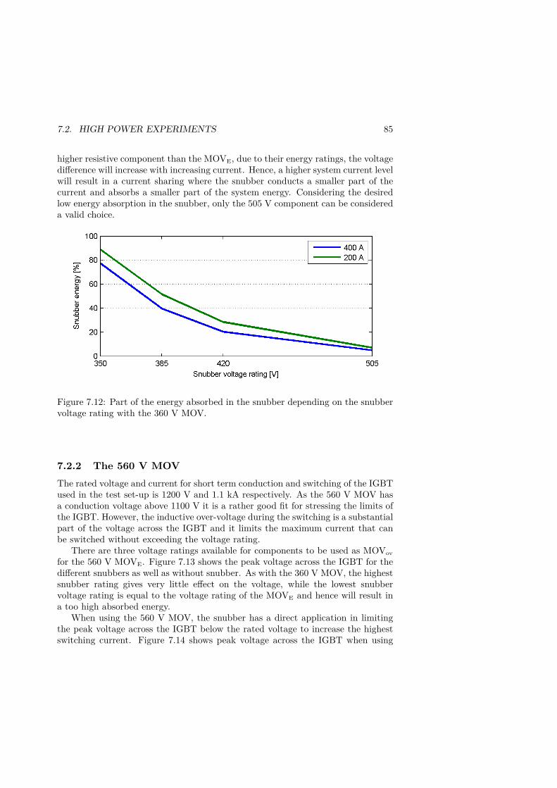
7.2. HIGH POWER EXPERIMENTS 85
higher resistive component than the MOVE, due to their energy ratings, the voltagedifference will increase with increasing current. Hence, a higher system current levelwill result in a current sharing where the snubber conducts a smaller part of thecurrent and absorbs a smaller part of the system energy. Considering the desiredlow energy absorption in the snubber, only the 505 V component can be considereda valid choice.
Figure 7.12: Part of the energy absorbed in the snubber depending on the snubbervoltage rating with the 360 V MOV.
7.2.2 The 560 V MOVThe rated voltage and current for short term conduction and switching of the IGBTused in the test set-up is 1200 V and 1.1 kA respectively. As the 560 V MOV hasa conduction voltage above 1100 V it is a rather good fit for stressing the limits ofthe IGBT. However, the inductive over-voltage during the switching is a substantialpart of the voltage across the IGBT and it limits the maximum current that canbe switched without exceeding the voltage rating.
There are three voltage ratings available for components to be used as MOVov
for the 560 V MOVE. Figure 7.13 shows the peak voltage across the IGBT for thedifferent snubbers as well as without snubber. As with the 360 V MOV, the highestsnubber rating gives very little effect on the voltage, while the lowest snubbervoltage rating is equal to the voltage rating of the MOVE and hence will result ina too high absorbed energy.
When using the 560 V MOV, the snubber has a direct application in limitingthe peak voltage across the IGBT below the rated voltage to increase the highestswitching current. Figure 7.14 shows peak voltage across the IGBT when using
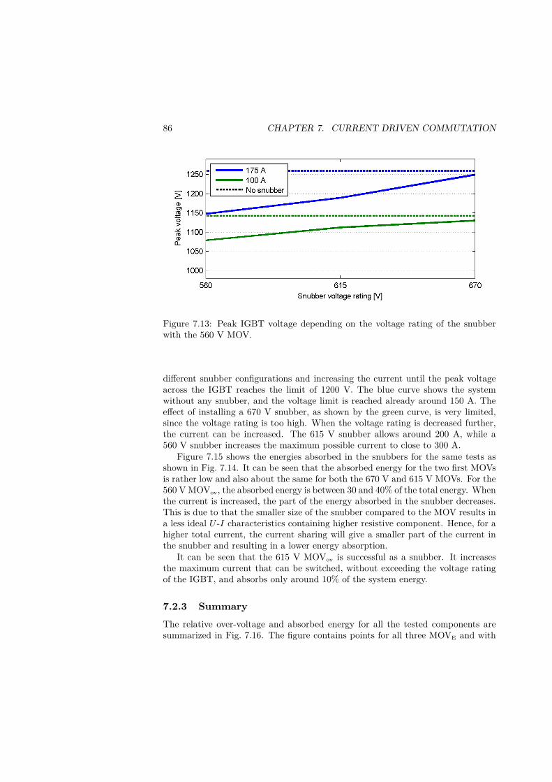
86 CHAPTER 7. CURRENT DRIVEN COMMUTATION
Figure 7.13: Peak IGBT voltage depending on the voltage rating of the snubberwith the 560 V MOV.
different snubber configurations and increasing the current until the peak voltageacross the IGBT reaches the limit of 1200 V. The blue curve shows the systemwithout any snubber, and the voltage limit is reached already around 150 A. Theeffect of installing a 670 V snubber, as shown by the green curve, is very limited,since the voltage rating is too high. When the voltage rating is decreased further,the current can be increased. The 615 V snubber allows around 200 A, while a560 V snubber increases the maximum possible current to close to 300 A.
Figure 7.15 shows the energies absorbed in the snubbers for the same tests asshown in Fig. 7.14. It can be seen that the absorbed energy for the two first MOVsis rather low and also about the same for both the 670 V and 615 V MOVs. For the560 VMOVov, the absorbed energy is between 30 and 40% of the total energy. Whenthe current is increased, the part of the energy absorbed in the snubber decreases.This is due to that the smaller size of the snubber compared to the MOV results ina less ideal U -I characteristics containing higher resistive component. Hence, for ahigher total current, the current sharing will give a smaller part of the current inthe snubber and resulting in a lower energy absorption.
It can be seen that the 615 V MOVov is successful as a snubber. It increasesthe maximum current that can be switched, without exceeding the voltage ratingof the IGBT, and absorbs only around 10% of the system energy.
7.2.3 SummaryThe relative over-voltage and absorbed energy for all the tested components aresummarized in Fig. 7.16. The figure contains points for all three MOVE and with
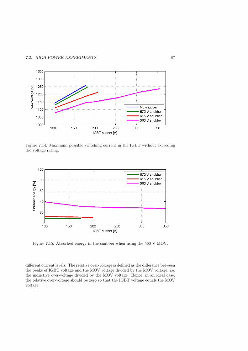
7.2. HIGH POWER EXPERIMENTS 87
Figure 7.14: Maximum possible switching current in the IGBT without exceedingthe voltage rating.
Figure 7.15: Absorbed energy in the snubber when using the 560 V MOV.
different current levels. The relative over-voltage is defined as the difference betweenthe peaks of IGBT voltage and the MOV voltage divided by the MOV voltage, i.e.the inductive over-voltage divided by the MOV voltage. Hence, in an ideal case,the relative over-voltage should be zero so that the IGBT voltage equals the MOVvoltage.
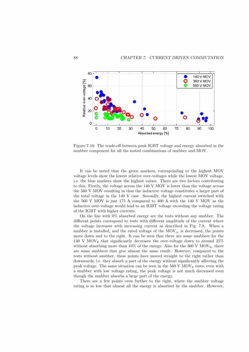
88 CHAPTER 7. CURRENT DRIVEN COMMUTATION
Figure 7.16: The trade-off between peak IGBT voltage and energy absorbed in thesnubber component for all the tested combinations of snubber and MOV.
It can be noted that the green markers, corresponding to the highest MOVvoltage levels show the lowest relative over-voltages while the lowest MOV voltage,i.e. the blue markers show the highest values. There are two factors contributingto this. Firstly, the voltage across the 140 V MOV is lower than the voltage acrossthe 560 V MOV resulting in that the inductive voltage constitutes a larger part ofthe total voltage in the 140 V case. Secondly, the highest current switched withthe 560 V MOV is just 175 A compared to 400 A with the 140 V MOV as theinductive over-voltage would lead to an IGBT voltage exceeding the voltage ratingof the IGBT with higher currents.
On the line with 0% absorbed energy are the tests without any snubber. Thedifferent points correspond to tests with different amplitude of the current wherethe voltage increases with increasing current as described in Fig. 7.9. When asnubber is installed, and the rated voltage of the MOVov is decreased, the pointsmove down and to the right. It can be seen that there are some snubbers for the140 V MOVE that significantly decreases the over-voltage down to around 25%without absorbing more than 10% of the energy. Also for the 360 V MOVE, thereare some snubbers that give almost the same result. However, compared to thetests without snubber, these points have moved straight to the right rather thandownwards, i.e. they absorb a part of the energy without significantly affecting thepeak voltage. The same situation can be seen in the 560 V MOVE tests; even witha snubber with low voltage rating, the peak voltage is not much decreased eventhough the snubber absorbs a large part of the energy.
There are a few points even further to the right, where the snubber voltagerating is so low that almost all the energy is absorbed by the snubber. However,
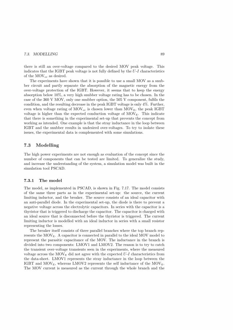
7.3. MODELLING 89
there is still an over-voltage compared to the desired MOV peak voltage. Thisindicates that the IGBT peak voltage is not fully defined by the U -I characteristicsof the MOVov as desired.
The experiments have shown that it is possible to use a small MOV as a snub-ber circuit and partly separate the absorption of the magnetic energy from theover-voltage protection of the IGBT. However, it seems that to keep the energyabsorption below 10%, a very high snubber voltage rating has to be chosen. In thecase of the 360 V MOV, only one snubber option, the 505 V component, fulfils thecondition, and the resulting decrease in the peak IGBT voltage is only 4%. Further,even when voltage rating of MOVov is chosen lower than MOVE, the peak IGBTvoltage is higher than the expected conduction voltage of MOVE. This indicatethat there is something in the experimental set-up that prevents the concept fromworking as intended. One example is that the stray inductance in the loop betweenIGBT and the snubber results in undesired over-voltages. To try to isolate theseissues, the experimental data is complemented with some simulations.
7.3 Modelling
The high power experiments are not enough as evaluation of the concept since thenumber of components that can be tested are limited. To generalize the study,and increase the understanding of the system, a simulation model was built in thesimulation tool PSCAD.
7.3.1 The modelThe model, as implemented in PSCAD, is shown in Fig. 7.17. The model consistsof the same three parts as in the experimental set-up: the source, the currentlimiting inductor, and the breaker. The source consists of an ideal capacitor withan anti-parallel diode. In the experimental set-up, the diode is there to prevent anegative voltage across the electrolytic capacitors. In series with the capacitor is athyristor that is triggered to discharge the capacitor. The capacitor is charged withan ideal source that is disconnected before the thyristor is triggered. The currentlimiting inductor is modelled with an ideal inductor in series with a small resistorrepresenting the losses.
The breaker itself consists of three parallel branches where the top branch rep-resents the MOVE. A capacitor is connected in parallel to the ideal MOV model torepresent the parasitic capacitance of the MOV. The inductance in the branch isdivided into two components: LMOV1 and LMOV2. The reason is to try to catchthe transient over-voltage transients seen in the experiments, where the measuredvoltage across the MOVE did not agree with the expected U -I characteristics fromthe data-sheet. LMOV1 represents the stray inductance in the loop between theIGBT and MOVE, whereas LMOV2 represents the self inductance of the MOVE.The MOV current is measured as the current through the whole branch and the
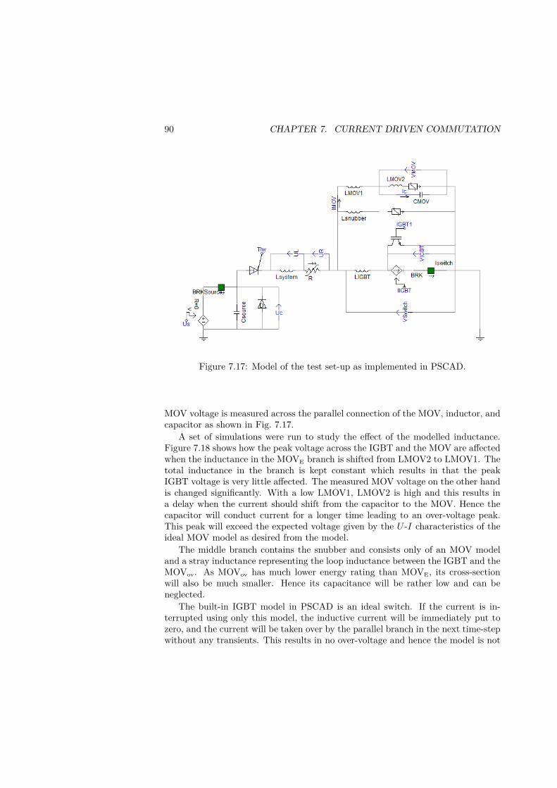
90 CHAPTER 7. CURRENT DRIVEN COMMUTATION
Figure 7.17: Model of the test set-up as implemented in PSCAD.
MOV voltage is measured across the parallel connection of the MOV, inductor, andcapacitor as shown in Fig. 7.17.
A set of simulations were run to study the effect of the modelled inductance.Figure 7.18 shows how the peak voltage across the IGBT and the MOV are affectedwhen the inductance in the MOVE branch is shifted from LMOV2 to LMOV1. Thetotal inductance in the branch is kept constant which results in that the peakIGBT voltage is very little affected. The measured MOV voltage on the other handis changed significantly. With a low LMOV1, LMOV2 is high and this results ina delay when the current should shift from the capacitor to the MOV. Hence thecapacitor will conduct current for a longer time leading to an over-voltage peak.This peak will exceed the expected voltage given by the U -I characteristics of theideal MOV model as desired from the model.
The middle branch contains the snubber and consists only of an MOV modeland a stray inductance representing the loop inductance between the IGBT and theMOVov. As MOVov has much lower energy rating than MOVE, its cross-sectionwill also be much smaller. Hence its capacitance will be rather low and can beneglected.
The built-in IGBT model in PSCAD is an ideal switch. If the current is in-terrupted using only this model, the inductive current will be immediately put tozero, and the current will be taken over by the parallel branch in the next time-stepwithout any transients. This results in no over-voltage and hence the model is not
7.3. MODELLING 91
Figure 7.18: Effect of the division of the inductance in the loop between the IGBTand the MOV on the peak voltages.
sufficient. Instead, a controllable current source and a circuit breaker model in putin parallel to the ideal IGBT. This way the current can be fully controlled to matchthe experiments.
When the IGBT is triggered to turn off, the momentary current through thesystem, I0, is sampled by dividing the voltage across the system resistance UR withthe resistance R. The ideal IGBT model is turned off, causing the current, I0,to be taken over by the current source and the circuit breaker branch. After adelay, representing the turn-off delay of the IGBT, the circuit breaker is tripped.This causes the model to change the current in the current source to decrease asI = I0 −At2. The decrease constant A is calculated so that I = 0 at t = t0, wheret0 = 0.4µs is the turn-off time of the IGBT set in the model. The commutationof the current from the ideal IGBT model to the current source is not seen by thesystem as the current I0 is kept constant. When the current in the current sourcedecreases, the current it forced into the MOV branch, as the large system inductorkeeps the system current constant in this short time span.
7.3.2 Extracting the model parameters
Some of the model parameters can be calculated directly from the experiments. Onesuch parameter is the current limiting inductance that can be calculated from therate of rise of the current and the voltage of the capacitor bank, in the beginning ofthe current pulse, where the resistive voltage drop can be neglected. The inductanceis calculated to 490 µH.
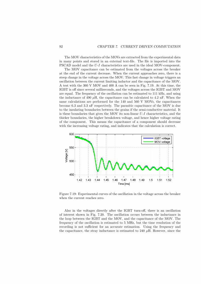
92 CHAPTER 7. CURRENT DRIVEN COMMUTATION
The MOV characteristics of the MOVs are extracted from the experimental datain many points and stored in an external text-file. The file is imported into thePSCAD model and the U -I characteristics are used in the ideal MOV-component.
The MOV capacitance can be estimated from the voltages across the breakerat the end of the current decrease. When the current approaches zero, there is asteep change in the voltage across the MOV. This fast change in voltage triggers anoscillation between the current limiting inductor and the capacitance of the MOV.A test with the 360 V MOV and 400 A can be seen in Fig. 7.19. At this time, theIGBT is off since several milliseconds, and the voltages across the IGBT and MOVare equal. The frequency of the oscillation can be estimated to 111 kHz, and usingthe inductance of 490 µH, the capacitance can be calculated to 4.2 nF. When thesame calculations are performed for the 140 and 560 V MOVs, the capacitancesbecome 6.3 and 3.3 nF respectively. The parasitic capacitance of the MOV is dueto the insulating boundaries between the grains if the semi-conductive material. Itis these boundaries that gives the MOV its non-linear U -I characteristics, and thethicker boundaries, the higher breakdown voltage, and hence higher voltage ratingof the component. This means the capacitance of a component should decreasewith the increasing voltage rating, and indicates that the calculation is correct.
Figure 7.19: Experimental curves of the oscillation in the voltage across the breakerwhen the current reaches zero.
Also in the voltages directly after the IGBT turn-off, there is an oscillationof interest shown in Fig. 7.20. The oscillation occurs between the inductance inthe loop between the IGBT and the MOV, and the capacitance of the MOV. Thefrequency of the oscillation is estimated to 5 MHz, but the time resolution of therecording is not sufficient for an accurate estimation. Using the frequency andthe capacitance, the stray inductance is estimated to 240 µH. However, since the
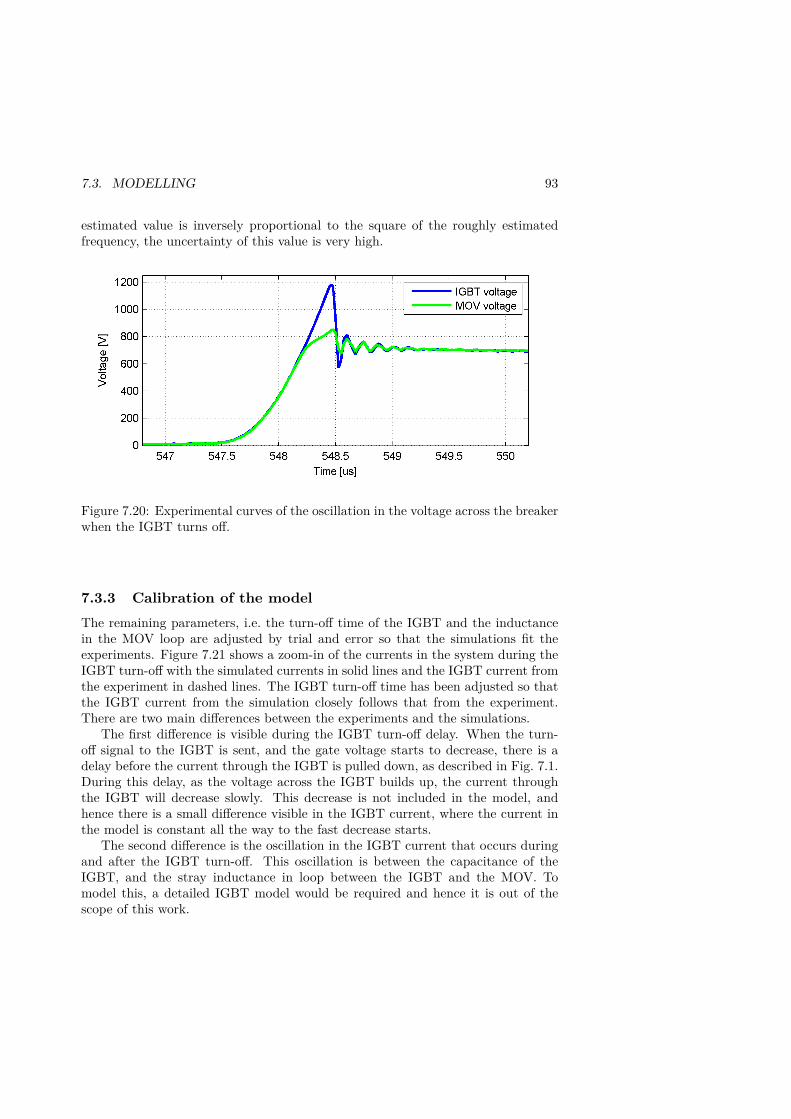
7.3. MODELLING 93
estimated value is inversely proportional to the square of the roughly estimatedfrequency, the uncertainty of this value is very high.
Figure 7.20: Experimental curves of the oscillation in the voltage across the breakerwhen the IGBT turns off.
7.3.3 Calibration of the modelThe remaining parameters, i.e. the turn-off time of the IGBT and the inductancein the MOV loop are adjusted by trial and error so that the simulations fit theexperiments. Figure 7.21 shows a zoom-in of the currents in the system during theIGBT turn-off with the simulated currents in solid lines and the IGBT current fromthe experiment in dashed lines. The IGBT turn-off time has been adjusted so thatthe IGBT current from the simulation closely follows that from the experiment.There are two main differences between the experiments and the simulations.
The first difference is visible during the IGBT turn-off delay. When the turn-off signal to the IGBT is sent, and the gate voltage starts to decrease, there is adelay before the current through the IGBT is pulled down, as described in Fig. 7.1.During this delay, as the voltage across the IGBT builds up, the current throughthe IGBT will decrease slowly. This decrease is not included in the model, andhence there is a small difference visible in the IGBT current, where the current inthe model is constant all the way to the fast decrease starts.
The second difference is the oscillation in the IGBT current that occurs duringand after the IGBT turn-off. This oscillation is between the capacitance of theIGBT, and the stray inductance in loop between the IGBT and the MOV. Tomodel this, a detailed IGBT model would be required and hence it is out of thescope of this work.
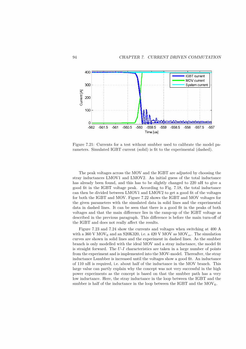
94 CHAPTER 7. CURRENT DRIVEN COMMUTATION
Figure 7.21: Currents for a test without snubber used to calibrate the model pa-rameters. Simulated IGBT current (solid) is fit to the experimental (dashed).
The peak voltages across the MOV and the IGBT are adjusted by choosing thestray inductances LMOV1 and LMOV2. An initial guess of the total inductancehas already been found, and this has to be slightly changed to 220 nH to give agood fit in the IGBT voltage peak. According to Fig. 7.18, the total inductancecan then be divided between LMOV1 and LMOV2 to get a good fit of the voltagesfor both the IGBT and MOV. Figure 7.22 shows the IGBT and MOV voltages forthe given parameters with the simulated data in solid lines and the experimentaldata in dashed lines. It can be seen that there is a good fit in the peaks of bothvoltages and that the main difference lies in the ramp-up of the IGBT voltage asdescribed in the previous paragraph. This difference is before the main turn-off ofthe IGBT and does not really affect the results.
Figure 7.23 and 7.24 show the currents and voltages when switching at 400 Awith a 360 V MOVE and an S20K320, i.e. a 420 V MOV as MOVov. The simulationcurves are shown in solid lines and the experiment in dashed lines. As the snubberbranch is only modelled with the ideal MOV and a stray inductance, the model fitis straight forward. The U -I characteristics are taken in a large number of pointsfrom the experiment and is implemented into the MOV-model. Thereafter, the strayinductance Lsnubber is increased until the voltages show a good fit. An inductanceof 110 nH is required, i.e. about half of the inductance in the MOV branch. Thislarge value can partly explain why the concept was not very successful in the highpower experiments as the concept is based on that the snubber path has a verylow inductance. Here, the stray inductance in the loop between the IGBT and thesnubber is half of the inductance in the loop between the IGBT and the MOVE.
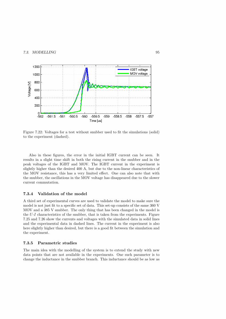
7.3. MODELLING 95
Figure 7.22: Voltages for a test without snubber used to fit the simulations (solid)to the experiment (dashed).
Also in these figures, the error in the initial IGBT current can be seen. Itresults in a slight time shift in both the rising current in the snubber and in thepeak voltages of the IGBT and MOV. The IGBT current in the experiment isslightly higher than the desired 400 A, but due to the non-linear characteristics ofthe MOV resistance, this has a very limited effect. One can also note that withthe snubber, the oscillations in the MOV voltage has disappeared due to the slowercurrent commutation.
7.3.4 Validation of the modelA third set of experimental curves are used to validate the model to make sure themodel is not just fit to a specific set of data. This set-up consists of the same 360 VMOV and a 385 V snubber. The only thing that has been changed in the model isthe U -I characteristics of the snubber, that is taken from the experiments. Figure7.25 and 7.26 show the currents and voltages with the simulated data in solid linesand the experimental data in dashed lines. The current in the experiment is alsohere slightly higher than desired, but there is a good fit between the simulation andthe experiment.
7.3.5 Parametric studiesThe main idea with the modelling of the system is to extend the study with newdata points that are not available in the experiments. One such parameter is tochange the inductance in the snubber branch. This inductance should be as low as
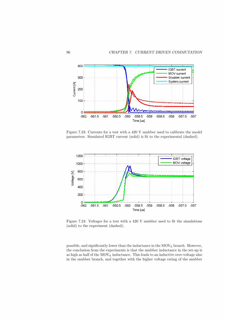
96 CHAPTER 7. CURRENT DRIVEN COMMUTATION
Figure 7.23: Currents for a test with a 420 V snubber used to calibrate the modelparameters. Simulated IGBT current (solid) is fit to the experimental (dashed).
Figure 7.24: Voltages for a test with a 420 V snubber used to fit the simulations(solid) to the experiment (dashed).
possible, and significantly lower than the inductance in the MOVE branch. However,the conclusion from the experiments is that the snubber inductance in the set-up isas high as half of the MOVE inductance. This leads to an inductive over-voltage alsoin the snubber branch, and together with the higher voltage rating of the snubber
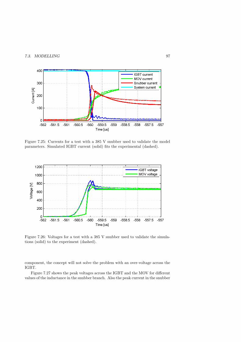
7.3. MODELLING 97
Figure 7.25: Currents for a test with a 385 V snubber used to validate the modelparameters. Simulated IGBT current (solid) fits the experimental (dashed).
Figure 7.26: Voltages for a test with a 385 V snubber used to validate the simula-tions (solid) to the experiment (dashed).
component, the concept will not solve the problem with an over-voltage across theIGBT.
Figure 7.27 shows the peak voltages across the IGBT and the MOV for differentvalues of the inductance in the snubber branch. Also the peak current in the snubber
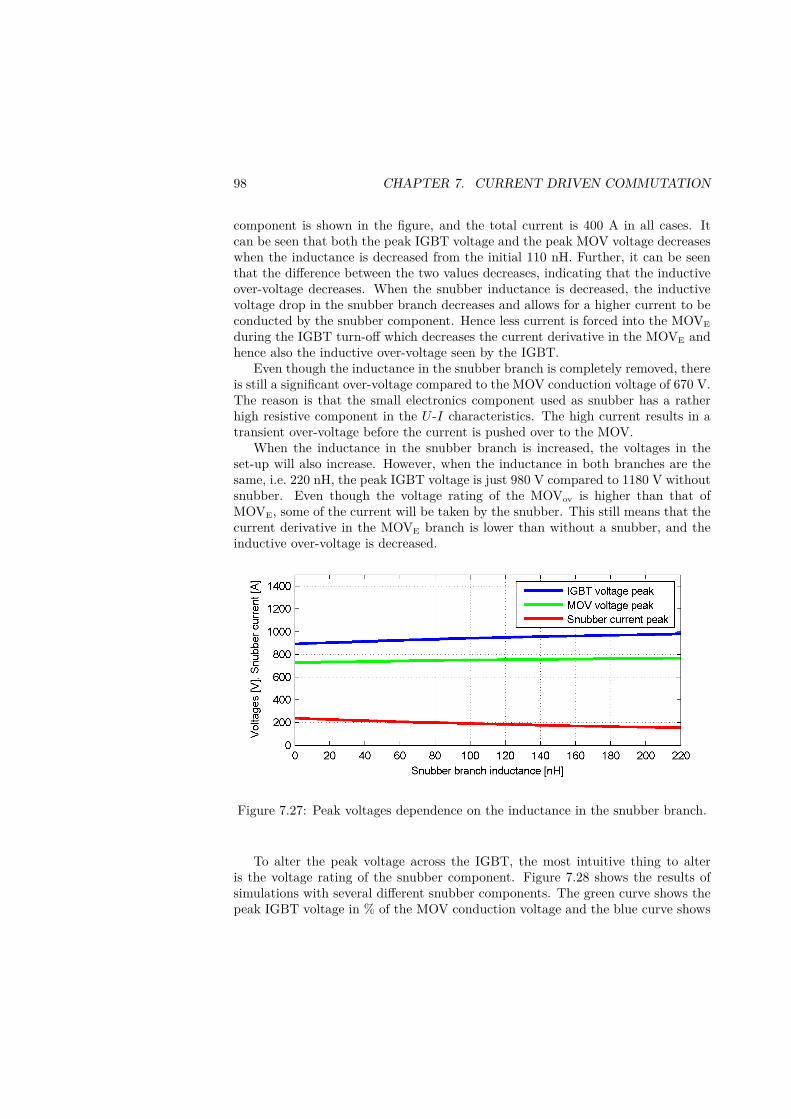
98 CHAPTER 7. CURRENT DRIVEN COMMUTATION
component is shown in the figure, and the total current is 400 A in all cases. Itcan be seen that both the peak IGBT voltage and the peak MOV voltage decreaseswhen the inductance is decreased from the initial 110 nH. Further, it can be seenthat the difference between the two values decreases, indicating that the inductiveover-voltage decreases. When the snubber inductance is decreased, the inductivevoltage drop in the snubber branch decreases and allows for a higher current to beconducted by the snubber component. Hence less current is forced into the MOVE
during the IGBT turn-off which decreases the current derivative in the MOVE andhence also the inductive over-voltage seen by the IGBT.
Even though the inductance in the snubber branch is completely removed, thereis still a significant over-voltage compared to the MOV conduction voltage of 670 V.The reason is that the small electronics component used as snubber has a ratherhigh resistive component in the U -I characteristics. The high current results in atransient over-voltage before the current is pushed over to the MOV.
When the inductance in the snubber branch is increased, the voltages in theset-up will also increase. However, when the inductance in both branches are thesame, i.e. 220 nH, the peak IGBT voltage is just 980 V compared to 1180 V withoutsnubber. Even though the voltage rating of the MOVov is higher than that ofMOVE, some of the current will be taken by the snubber. This still means that thecurrent derivative in the MOVE branch is lower than without a snubber, and theinductive over-voltage is decreased.
Figure 7.27: Peak voltages dependence on the inductance in the snubber branch.
To alter the peak voltage across the IGBT, the most intuitive thing to alteris the voltage rating of the snubber component. Figure 7.28 shows the results ofsimulations with several different snubber components. The green curve shows thepeak IGBT voltage in % of the MOV conduction voltage and the blue curve shows
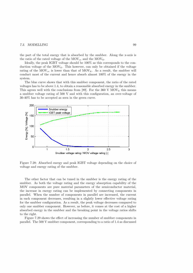
7.3. MODELLING 99
the part of the total energy that is absorbed by the snubber. Along the x-axis isthe ratio of the rated voltage of the MOVov and the MOVE.
Ideally, the peak IGBT voltage should be 100% as this corresponds to the con-duction voltage of the MOVE. This however, can only be obtained if the voltagerating of the MOVov is lower than that of MOVE. As a result, the snubber willconduct most of the current and hence absorb almost 100% of the energy in thesystem.
The blue curve shows that with this snubber component, the ratio of the ratedvoltages has to be above 1.4, to obtain a reasonable absorbed energy in the snubber.This agrees well with the conclusions from [89]. For the 360 V MOVE this meansa snubber voltage rating of 500 V and with this configuration, an over-voltage of30-40% has to be accepted as seen in the green curve.
Figure 7.28: Absorbed energy and peak IGBT voltage depending on the choice ofvoltage and energy rating of the snubber.
The other factor that can be tuned in the snubber is the energy rating of thesnubber. As both the voltage rating and the energy absorption capability of theMOV components are pure material parameters of the semiconductor material,the increase in energy rating can be implemented by connecting components inparallel. When the number of components in parallel are increased, the currentin each component decreases, resulting in a slightly lower effective voltage ratingfor the snubber configuration. As a result, the peak voltage decreases compared toonly one snubber component. However, as before, it comes at the cost of a higherabsorbed energy in the snubber and the breaking point in the voltage ratios shiftsto the right.
Figure 7.29 shows the effect of increasing the number of snubber components inparallel. The 500 V snubber component, corresponding to a ratio of 1.4 as discussed
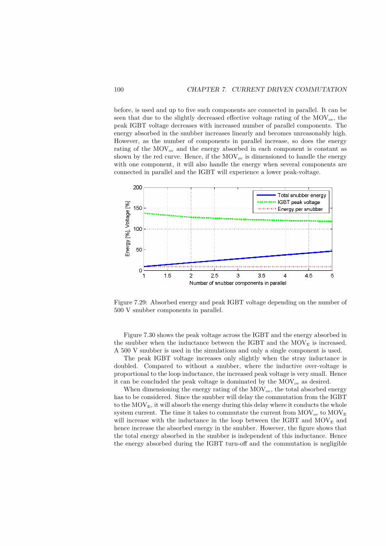
100 CHAPTER 7. CURRENT DRIVEN COMMUTATION
before, is used and up to five such components are connected in parallel. It can beseen that due to the slightly decreased effective voltage rating of the MOVov, thepeak IGBT voltage decreases with increased number of parallel components. Theenergy absorbed in the snubber increases linearly and becomes unreasonably high.However, as the number of components in parallel increase, so does the energyrating of the MOVov and the energy absorbed in each component is constant asshown by the red curve. Hence, if the MOVov is dimensioned to handle the energywith one component, it will also handle the energy when several components areconnected in parallel and the IGBT will experience a lower peak-voltage.
Figure 7.29: Absorbed energy and peak IGBT voltage depending on the number of500 V snubber components in parallel.
Figure 7.30 shows the peak voltage across the IGBT and the energy absorbed inthe snubber when the inductance between the IGBT and the MOVE is increased.A 500 V snubber is used in the simulations and only a single component is used.
The peak IGBT voltage increases only slightly when the stray inductance isdoubled. Compared to without a snubber, where the inductive over-voltage isproportional to the loop inductance, the increased peak voltage is very small. Henceit can be concluded the peak voltage is dominated by the MOVov as desired.
When dimensioning the energy rating of the MOVov, the total absorbed energyhas to be considered. Since the snubber will delay the commutation from the IGBTto the MOVE, it will absorb the energy during this delay where it conducts the wholesystem current. The time it takes to commutate the current from MOVov to MOVE
will increase with the inductance in the loop between the IGBT and MOVE andhence increase the absorbed energy in the snubber. However, the figure shows thatthe total energy absorbed in the snubber is independent of this inductance. Hencethe energy absorbed during the IGBT turn-off and the commutation is negligible
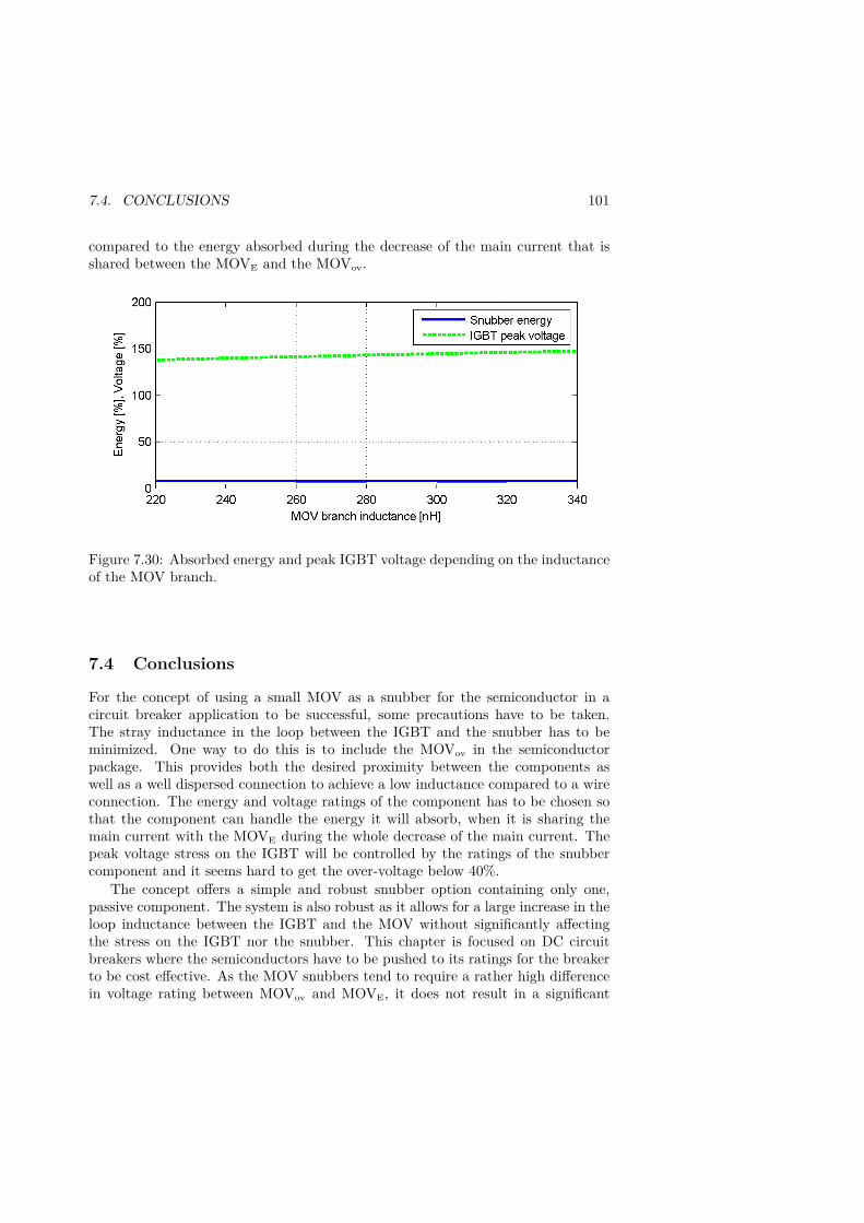
7.4. CONCLUSIONS 101
compared to the energy absorbed during the decrease of the main current that isshared between the MOVE and the MOVov.
Figure 7.30: Absorbed energy and peak IGBT voltage depending on the inductanceof the MOV branch.
7.4 Conclusions
For the concept of using a small MOV as a snubber for the semiconductor in acircuit breaker application to be successful, some precautions have to be taken.The stray inductance in the loop between the IGBT and the snubber has to beminimized. One way to do this is to include the MOVov in the semiconductorpackage. This provides both the desired proximity between the components aswell as a well dispersed connection to achieve a low inductance compared to a wireconnection. The energy and voltage ratings of the component has to be chosen sothat the component can handle the energy it will absorb, when it is sharing themain current with the MOVE during the whole decrease of the main current. Thepeak voltage stress on the IGBT will be controlled by the ratings of the snubbercomponent and it seems hard to get the over-voltage below 40%.
The concept offers a simple and robust snubber option containing only one,passive component. The system is also robust as it allows for a large increase in theloop inductance between the IGBT and the MOV without significantly affectingthe stress on the IGBT nor the snubber. This chapter is focused on DC circuitbreakers where the semiconductors have to be pushed to its ratings for the breakerto be cost effective. As the MOV snubbers tend to require a rather high differencein voltage rating between MOVov and MOVE, it does not result in a significant

102 CHAPTER 7. CURRENT DRIVEN COMMUTATION
improvement of the peak voltage. However, there might be applications where thedifference can be acceptable to enable other possibilities. One example is that thehigher allowed loop inductance gives the possibility to place the main MOVE muchfurther away from the IGBT, e.g. outdoors even if the IGBTs are indoors.
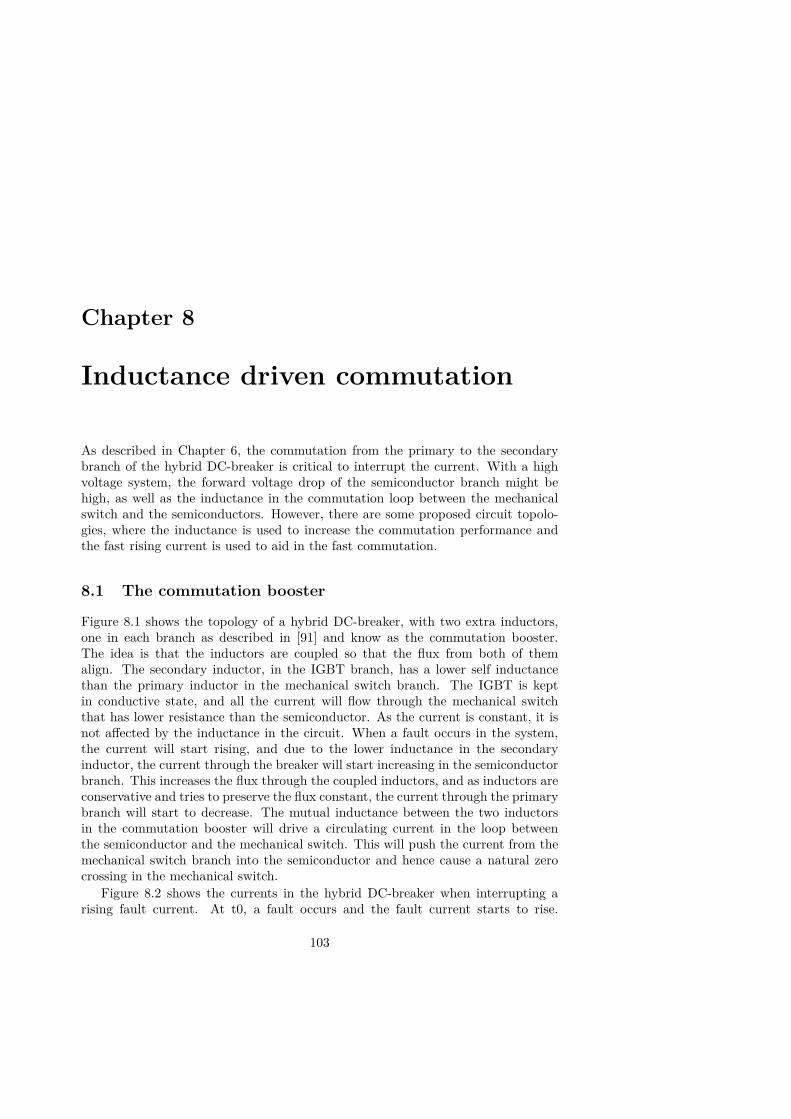
Chapter 8
Inductance driven commutation
As described in Chapter 6, the commutation from the primary to the secondarybranch of the hybrid DC-breaker is critical to interrupt the current. With a highvoltage system, the forward voltage drop of the semiconductor branch might behigh, as well as the inductance in the commutation loop between the mechanicalswitch and the semiconductors. However, there are some proposed circuit topolo-gies, where the inductance is used to increase the commutation performance andthe fast rising current is used to aid in the fast commutation.
8.1 The commutation booster
Figure 8.1 shows the topology of a hybrid DC-breaker, with two extra inductors,one in each branch as described in [91] and know as the commutation booster.The idea is that the inductors are coupled so that the flux from both of themalign. The secondary inductor, in the IGBT branch, has a lower self inductancethan the primary inductor in the mechanical switch branch. The IGBT is keptin conductive state, and all the current will flow through the mechanical switchthat has lower resistance than the semiconductor. As the current is constant, it isnot affected by the inductance in the circuit. When a fault occurs in the system,the current will start rising, and due to the lower inductance in the secondaryinductor, the current through the breaker will start increasing in the semiconductorbranch. This increases the flux through the coupled inductors, and as inductors areconservative and tries to preserve the flux constant, the current through the primarybranch will start to decrease. The mutual inductance between the two inductorsin the commutation booster will drive a circulating current in the loop betweenthe semiconductor and the mechanical switch. This will push the current from themechanical switch branch into the semiconductor and hence cause a natural zerocrossing in the mechanical switch.
Figure 8.2 shows the currents in the hybrid DC-breaker when interrupting arising fault current. At t0, a fault occurs and the fault current starts to rise.
103
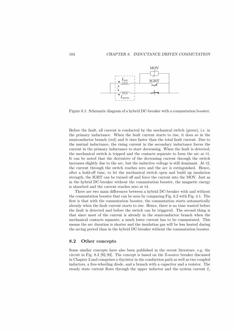
104 CHAPTER 8. INDUCTANCE DRIVEN COMMUTATION
MOV
Lsec IGBT
Lprim
Figure 8.1: Schematic diagram of a hybrid DC-breaker with a commutation booster.
Before the fault, all current is conducted by the mechanical switch (green), i.e. inthe primary inductance. When the fault current starts to rise, it does so in thesemiconductor branch (red) and it rises faster than the total fault current. Due tothe mutual inductance, the rising current in the secondary inductance forces thecurrent in the primary inductance to start decreasing. When the fault is detected,the mechanical switch is tripped and the contacts separate to form the arc at t1.It can be noted that the derivative of the decreasing current through the switchincreases slightly due to the arc, but the inductive voltage is still dominant. At t2,the current through the switch reaches zero and the arc is extinguished. Hence,after a hold-off time, to let the mechanical switch open and build up insulationstrength, the IGBT can be turned off and force the current into the MOV. Just asin the hybrid DC-breaker without the commutation booster, the magnetic energyis absorbed and the current reaches zero at t4.
There are two main differences between a hybrid DC-breaker with and withoutthe commutation booster that can be seen by comparing Fig. 8.2 with Fig. 4.1. Thefirst is that with the commutation booster, the commutation starts automaticallyalready when the fault current starts to rise. Hence, there is no time wasted beforethe fault is detected and before the switch can be triggered. The second thing isthat since most of the current is already in the semiconductor branch when themechanical contacts separate, a much lower current has to be commutated. Thismeans the arc duration is shorter and the insulation gas will be less heated duringthe arcing period than in the hybrid DC-breaker without the commutation booster.
8.2 Other concepts
Some similar concepts have also been published in the recent literature, e.g. thecircuit in Fig. 8.3 [92, 93]. The concept is based on the Z-source breaker discussedin Chapter 3 and comprises a thyristor in the conduction path as well as two coupledinductors, a free-wheeling diode, and a branch with a capacitor and a resistor. Thesteady state current flows through the upper inductor and the system current Is
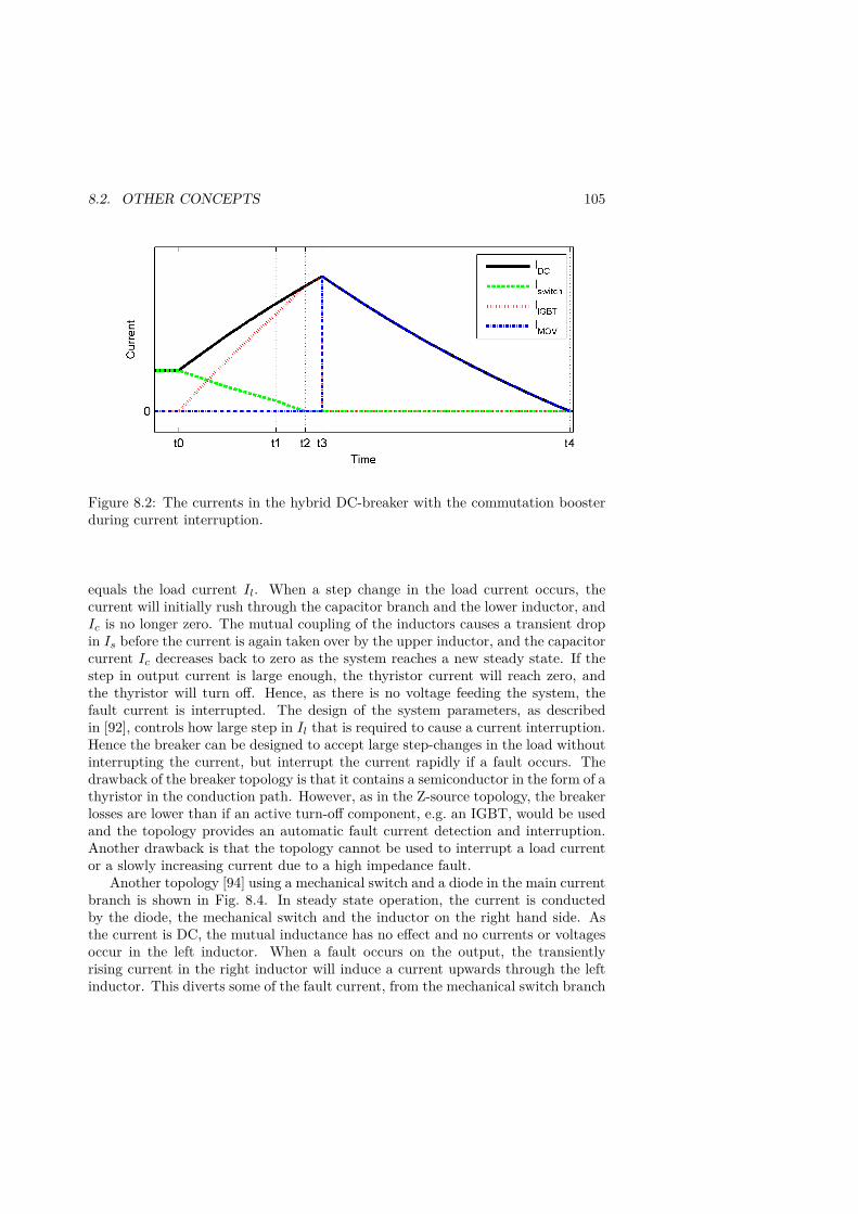
8.2. OTHER CONCEPTS 105
Figure 8.2: The currents in the hybrid DC-breaker with the commutation boosterduring current interruption.
equals the load current Il. When a step change in the load current occurs, thecurrent will initially rush through the capacitor branch and the lower inductor, andIc is no longer zero. The mutual coupling of the inductors causes a transient dropin Is before the current is again taken over by the upper inductor, and the capacitorcurrent Ic decreases back to zero as the system reaches a new steady state. If thestep in output current is large enough, the thyristor current will reach zero, andthe thyristor will turn off. Hence, as there is no voltage feeding the system, thefault current is interrupted. The design of the system parameters, as describedin [92], controls how large step in Il that is required to cause a current interruption.Hence the breaker can be designed to accept large step-changes in the load withoutinterrupting the current, but interrupt the current rapidly if a fault occurs. Thedrawback of the breaker topology is that it contains a semiconductor in the form of athyristor in the conduction path. However, as in the Z-source topology, the breakerlosses are lower than if an active turn-off component, e.g. an IGBT, would be usedand the topology provides an automatic fault current detection and interruption.Another drawback is that the topology cannot be used to interrupt a load currentor a slowly increasing current due to a high impedance fault.
Another topology [94] using a mechanical switch and a diode in the main currentbranch is shown in Fig. 8.4. In steady state operation, the current is conductedby the diode, the mechanical switch and the inductor on the right hand side. Asthe current is DC, the mutual inductance has no effect and no currents or voltagesoccur in the left inductor. When a fault occurs on the output, the transientlyrising current in the right inductor will induce a current upwards through the leftinductor. This diverts some of the fault current, from the mechanical switch branch
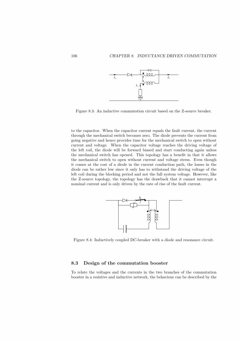
106 CHAPTER 8. INDUCTANCE DRIVEN COMMUTATION
Is
Ic
Il
Figure 8.3: An inductive commutation circuit based on the Z-source breaker.
to the capacitor. When the capacitor current equals the fault current, the currentthrough the mechanical switch becomes zero. The diode prevents the current fromgoing negative and hence provides time for the mechanical switch to open withoutcurrent and voltage. When the capacitor voltage reaches the driving voltage ofthe left coil, the diode will be forward biased and start conducting again unlessthe mechanical switch has opened. This topology has a benefit in that it allowsthe mechanical switch to open without current and voltage stress. Even thoughit comes at the cost of a diode in the current conduction path, the losses in thediode can be rather low since it only has to withstand the driving voltage of theleft coil during the blocking period and not the full system voltage. However, likethe Z-source topology, the topology has the drawback that it cannot interrupt anominal current and is only driven by the rate of rise of the fault current.
Figure 8.4: Inductively coupled DC-breaker with a diode and resonance circuit.
8.3 Design of the commutation booster
To relate the voltages and the currents in the two branches of the commutationbooster in a resistive and inductive network, the behaviour can be described by the

8.3. DESIGN OF THE COMMUTATION BOOSTER 107
following two equations:
(Ls + L1)di1dt
+ (Ls +M)di2dt
= Us −Rs(i1 + i2)−R1i1 − Uswitch, and (8.1)
(Ls +M)di1dt
+ (Ls + L2)di2dt
= Us −Rs(i1 + i2)−R2i2 − Usemiconductor, (8.2)
where the indices 1, 2, and s refer to the primary branch, the secondary branch,and the source respectively. Further, to make the design more general, the circuitcomponents can be parametrized using:
L2 = αL1, and (8.3)
M = k√L1L2) = L1k
√α. (8.4)
For the concept to make sense, so that the fault current will rise through thesemiconductor branch, the self inductance in the secondary branch has to be lowerthan the self inductance in the primary branch, i.e. α < 1. Further it can be shown,that to also obtain a decreasing current in the mechanical switch, the requirementon alpha is tightened to α < k2.
The side effect of the commutation booster is that it introduces an extra loopinductance between the mechanical switch and the IGBT. This inductance slowsdown the commutation, as described in Chapter 6, and hence it is desirable to keepit low. The extra loop inductance can be described as
Lcom = L1 + L2 − 2M, (8.5)
and its dependence on the design parameters k and α can be seen in Fig. 8.5. Somespecific points can be studied to verify the correctness of the graph. If α is zero,there is no inductance in the secondary branch, and the loop only consists of theprimary inductance L1. If k = 0, there is no magnetic coupling between the twoinductors and the total inductance in the circuit increases linearly as α and henceL2 increases. When there is a good coupling between the inductors, the inductanceswill partially cancel, and with two identical inductors and a perfect coupling, theloop inductance would be zero. It can be concluded that from the loop inductancepoint of view, a high k and a high α is desired. Since the loop inductance alsoincreases with L1, a low primary inductance is desired. The loop inductance willhave a large impact on the breaker as this inductance will put high stresses on themechanical switch when interrupting the nominal current. As there is no risingcurrent, the commutation booster will not provide any help in that case, and thearcing time will increase with an increasing inductance.
Apart from the loop inductance that opposes the commutation, the commu-tation booster should provide a voltage that enhances the commutation from the
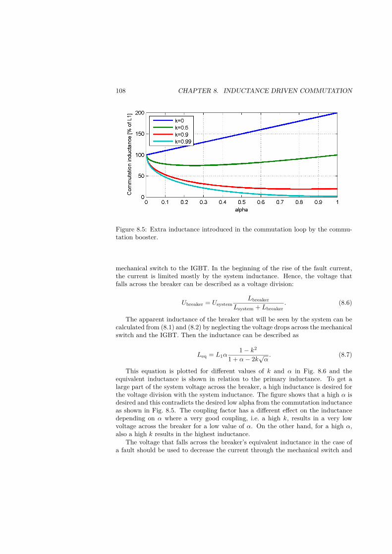
108 CHAPTER 8. INDUCTANCE DRIVEN COMMUTATION
Figure 8.5: Extra inductance introduced in the commutation loop by the commu-tation booster.
mechanical switch to the IGBT. In the beginning of the rise of the fault current,the current is limited mostly by the system inductance. Hence, the voltage thatfalls across the breaker can be described as a voltage division:
Ubreaker = UsystemLbreaker
Lsystem + Lbreaker. (8.6)
The apparent inductance of the breaker that will be seen by the system can becalculated from (8.1) and (8.2) by neglecting the voltage drops across the mechanicalswitch and the IGBT. Then the inductance can be described as
Leq = L1α1− k2
1 + α− 2k√α. (8.7)
This equation is plotted for different values of k and α in Fig. 8.6 and theequivalent inductance is shown in relation to the primary inductance. To get alarge part of the system voltage across the breaker, a high inductance is desired forthe voltage division with the system inductance. The figure shows that a high α isdesired and this contradicts the desired low alpha from the commutation inductanceas shown in Fig. 8.5. The coupling factor has a different effect on the inductancedepending on α where a very good coupling, i.e. a high k, results in a very lowvoltage across the breaker for a low value of α. On the other hand, for a high α,also a high k results in the highest inductance.
The voltage that falls across the breaker’s equivalent inductance in the case ofa fault should be used to decrease the current through the mechanical switch and
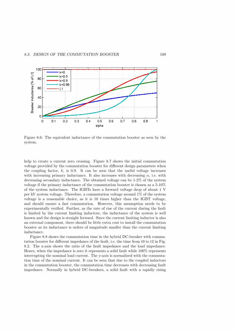
8.3. DESIGN OF THE COMMUTATION BOOSTER 109
Figure 8.6: The equivalent inductance of the commutation booster as seen by thesystem.
help to create a current zero crossing. Figure 8.7 shows the initial commutationvoltage provided by the commutation booster for different design parameters whenthe coupling factor, k, is 0.9. It can be seen that the useful voltage increaseswith increasing primary inductance. It also increases with decreasing α, i.e. withdecreasing secondary inductance. The obtained voltage can be 1-2% of the systemvoltage if the primary inductance of the commutation booster is chosen as a 5-10%of the system inductance. The IGBTs have a forward voltage drop of about 1 Vper kV system voltage. Therefore, a commutation voltage around 1% of the systemvoltage is a reasonable choice, as it is 10 times higher than the IGBT voltage,and should ensure a fast commutation. However, this assumption needs to beexperimentally verified. Further, as the rate of rise of the current during the faultis limited by the current limiting inductors, the inductance of the system is wellknown and the design is straight forward. Since the current limiting inductor is alsoan external component, there should be little extra cost to install the commutationbooster as its inductance is orders of magnitude smaller than the current limitinginductance.
Figure 8.8 shows the commutation time in the hybrid DC-breaker with commu-tation booster for different impedance of the fault, i.e. the time from t0 to t2 in Fig.8.2. The x-axis shows the ratio of the fault impedance and the load impedance.Hence, when the impedance is zero it represents a solid fault while 100% representsinterrupting the nominal load current. The y-axis is normalized with the commuta-tion time of the nominal current. It can be seen that due to the coupled inductorsin the commutation booster, the commutation time decreases with decreasing faultimpedance. Normally in hybrid DC-breakers, a solid fault with a rapidly rising
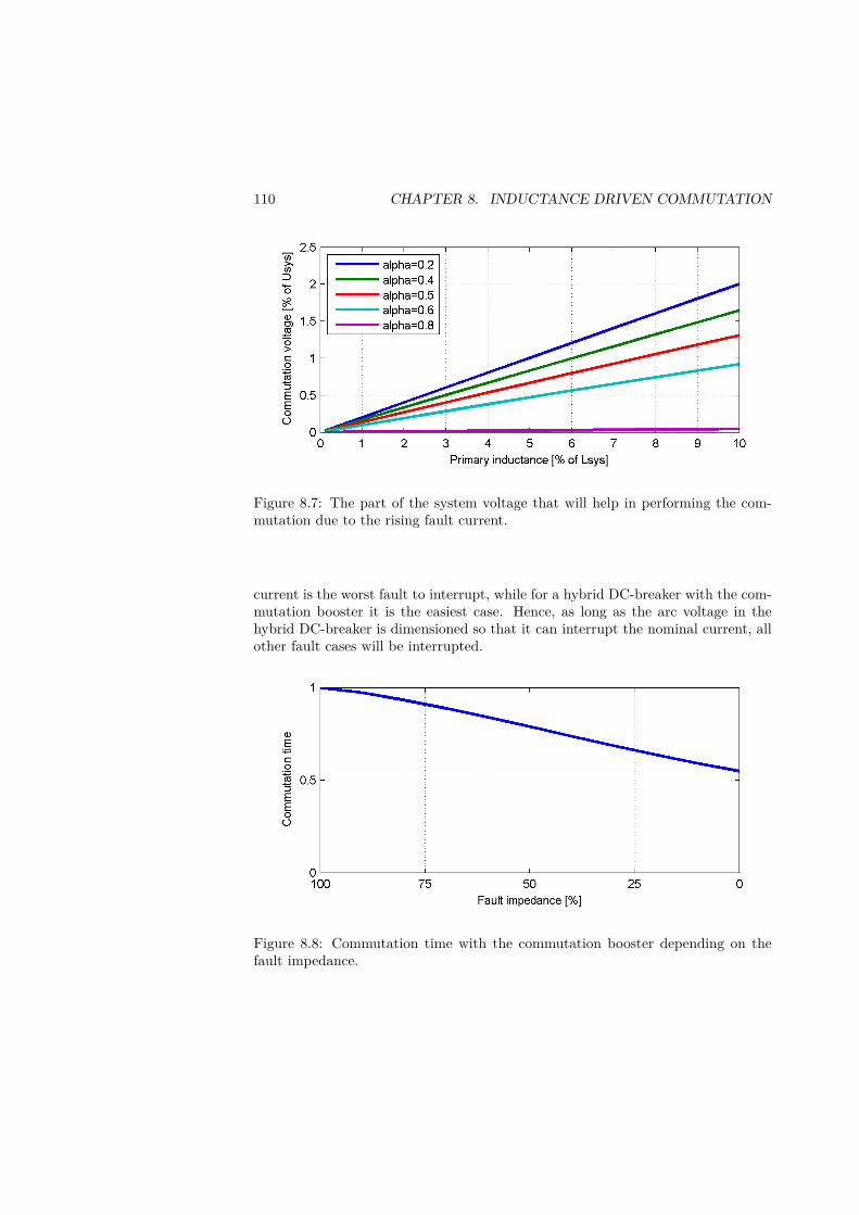
110 CHAPTER 8. INDUCTANCE DRIVEN COMMUTATION
Figure 8.7: The part of the system voltage that will help in performing the com-mutation due to the rising fault current.
current is the worst fault to interrupt, while for a hybrid DC-breaker with the com-mutation booster it is the easiest case. Hence, as long as the arc voltage in thehybrid DC-breaker is dimensioned so that it can interrupt the nominal current, allother fault cases will be interrupted.
Figure 8.8: Commutation time with the commutation booster depending on thefault impedance.
8.4. CONCLUSIONS 111
8.4 Conclusions
The design of the commutation booster in the hybrid DC-breaker comes down tochoosing the values of the two inductors. The calculations suggest a high primaryinductance and a low secondary inductance. However, the design is contradictoryand requires a trade-off.
8.4.1 The primary inductance+ A high primary inductance leads to a large part of the system voltage available
to drive the commutation.
- A high primary inductance leads to a larger commutation inductance andhence a longer commutation time.
- A larger inductance leads to a larger and more expensive component.
8.4.2 The secondary inductance+ A low secondary inductance leads to a large current rush in the case of a fault,
and hence a higher driving voltage.
- A low secondary inductance leads to a larger commutation inductance sinceless of the primary inductance is cancelled.

Chapter 9
Designs for different systems
The design of the hybrid DC-breaker for a specific system will depend on severalparameters such as the system voltage, the current limiting inductance and thehighest allowable time of interruption. This chapter presents two designs based onthe lab results for two specific target systems: a medium voltage system with asystem voltage of 12 kV, and an 80 kV case that is intended as a modular breakersolution for HVDC systems.
9.1 The 12 kV system
A future application for a hybrid DC-breaker can be a DC-grid on distribution level.In the Nordic countries, a lot of the faults in the distribution system occur on thelong medium voltage over-head lines due to lightning strikes. If the lines would bereplaced with cables, it would make sense to run the cables with DC to increase thetransferable power and decrease the losses. Another benefit is the easier integrationof renewable power on the MVDC level. As much of the production is in DC, oneconversion step from DC to AC would be avoided.
Since such networks does not yet exist, one has to estimate the system parame-ters. For a system level of 12 kV and a nominal current of 2 kA, a suitable currentlimiting inductance would be 6 mH as it limits the rate of rise to 2 kA/ms. Withan interruption time of 3 ms, the peak current would reach 8 kA, i.e. 4 p.u.
For the semiconductors in the proposed hybrid DC-breaker topology, the ABBIGBT component 5SNA2000K450300 can be used. The component has a currentrating of 2 kA, but can handle up to 4 kA for short time. The voltage rating is4500 V, and hence 5 components in series [95], i.e. 22.5 kV, should be sufficientto handle the transient voltage of the set by the MOV. The data-sheet [47] statesthat the voltage drop of each IGBT is 1.6 V in series with 0.5 mΩ. In addition,since the breaker should be bidirectional, the anti-parallel diode of each componentcontributes with another 1.9 V and 0.15 mΩ. Considering the peak current of
113
114 CHAPTER 9. DESIGNS FOR DIFFERENT SYSTEMS
8 kA, two stacks are required in parallel resulting in a voltage drop of 30.5 V atthe current peak.
As it is critical for the DC-breaker to react quickly and interrupt the faultcurrent rather early on the rising edge, an efficient fault current detection algorithmis required. Here, the breaker is tripped to interrupt the fault current when thecurrent crosses twice the nominal current, i.e. 4 kA. Once the fault is detected, theIGBT is turned on and the mechanical switch is triggered. Since the fault currentcontinues to rise also during the commutation it is important that the switch opensquickly to ensure a fast commutation. To fulfil the requirement of a peak currentof 8 kA, the IGBT should be on for 2 ms, and after this time the open contacts ofthe switch has to withstand the TIV of 22 kV. Assuming an insulation strength ofthe partly heated and ionized gas of 1 kV/mm, the total contact separation needsto be 22 mm.
To test the prototype in the lab, some adjustments have to be made. Thecapacitor feeding the main circuit current has a limitation in maximum 500 Vmeaning a 250 µH series inductor would give the desired rise of current. However,due to the too low capacitance in the source, the current would not reach thedesired peak. Instead the inductance is decreased to 100 µH which gives a fasterrising current and a peak of around 6 kA prospective current. This is lower than theexpected system current, but enough to test the commutation from the mechanicalswitch to the IGBT. Considering that the switch has two series contacts, the totalmovement of the contacts has to be 11 mm, which is fulfilled with a charging voltageof the actuator capacitor bank of 850 V as shown in section 4.3. However, sincethe switch can handle higher velocities, a charging voltage of 1000 V is chosen toprovide some margin.
Since the IGBT part of this set-up is only a low voltage component with a ratedvoltage of 1200 V, the voltage drop in the IGBT branch is obtained with an externalresistor. Further, to compensate for a possible stray inductance, an inductance of1 µH is installed in the loop between the mechanical contact and the IGBT.
Figure 9.1 shows the voltages involved in the test of the designed 12 kV system.At the time 0, the current crosses 4 kA and the breaker is tripped. The IGBT isturned on within a few microseconds as seen by the gate voltage shown in blue.After the mechanical switch is tripped, there is a delay of just above 250 µs beforethe contacts separate and the arc is formed. It can be seen that the arc voltage,shown in green, increases in two fast steps as the two contacts separate with aslight delay. When the current starts commutating over to the IGBT branch, thevoltage across the IGBT and the resistor, shown in red, starts to increase. As thecontacts keep separating with high velocity, the arc voltage increases linearly. Dueto the inductance in the circuit and the high currents, the voltage in the IGBTbranch cannot reach the arc voltage until the commutation is finished about 350 µsafter the contact separation. To make sure the prototype was stressed properly,the resistance in the IGBT branch was chosen to give a voltage drop slightly higherthan the desired 30 V, as seen in the figure.
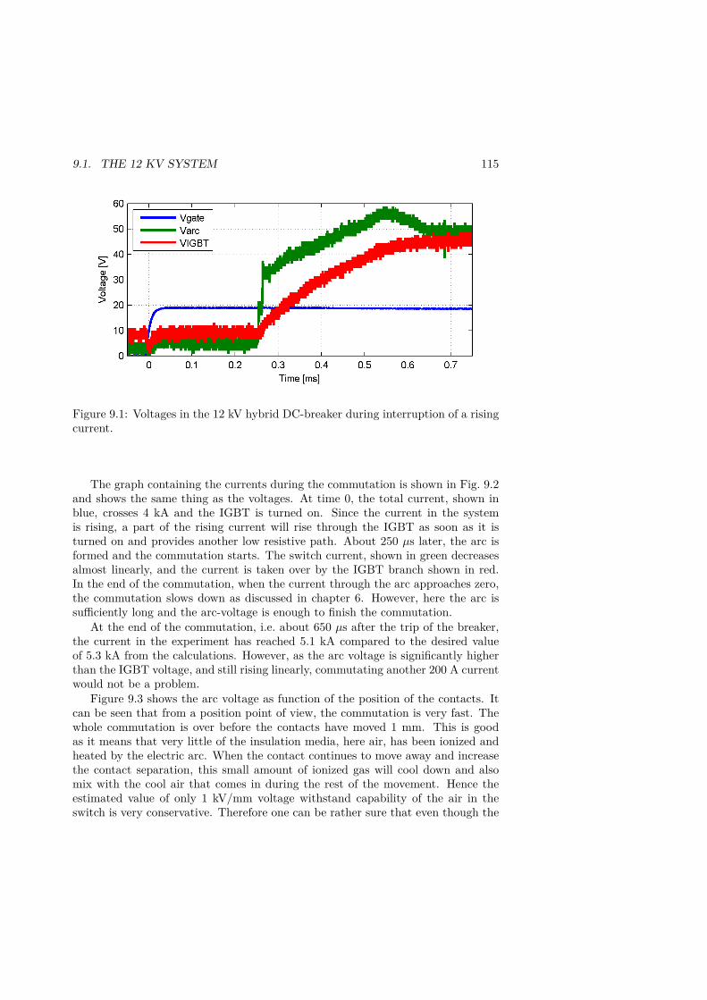
9.1. THE 12 KV SYSTEM 115
Figure 9.1: Voltages in the 12 kV hybrid DC-breaker during interruption of a risingcurrent.
The graph containing the currents during the commutation is shown in Fig. 9.2and shows the same thing as the voltages. At time 0, the total current, shown inblue, crosses 4 kA and the IGBT is turned on. Since the current in the systemis rising, a part of the rising current will rise through the IGBT as soon as it isturned on and provides another low resistive path. About 250 µs later, the arc isformed and the commutation starts. The switch current, shown in green decreasesalmost linearly, and the current is taken over by the IGBT branch shown in red.In the end of the commutation, when the current through the arc approaches zero,the commutation slows down as discussed in chapter 6. However, here the arc issufficiently long and the arc-voltage is enough to finish the commutation.
At the end of the commutation, i.e. about 650 µs after the trip of the breaker,the current in the experiment has reached 5.1 kA compared to the desired valueof 5.3 kA from the calculations. However, as the arc voltage is significantly higherthan the IGBT voltage, and still rising linearly, commutating another 200 A currentwould not be a problem.
Figure 9.3 shows the arc voltage as function of the position of the contacts. Itcan be seen that from a position point of view, the commutation is very fast. Thewhole commutation is over before the contacts have moved 1 mm. This is goodas it means that very little of the insulation media, here air, has been ionized andheated by the electric arc. When the contact continues to move away and increasethe contact separation, this small amount of ionized gas will cool down and alsomix with the cool air that comes in during the rest of the movement. Hence theestimated value of only 1 kV/mm voltage withstand capability of the air in theswitch is very conservative. Therefore one can be rather sure that even though the
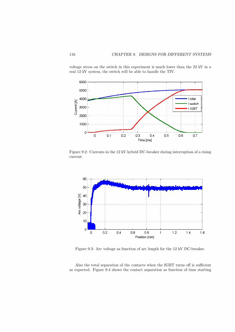
116 CHAPTER 9. DESIGNS FOR DIFFERENT SYSTEMS
voltage stress on the switch in this experiment is much lower than the 22 kV in areal 12 kV system, the switch will be able to handle the TIV.
Figure 9.2: Currents in the 12 kV hybrid DC-breaker during interruption of a risingcurrent.
Figure 9.3: Arc voltage as function of arc length for the 12 kV DC-breaker.
Also the total separation of the contacts when the IGBT turns off is sufficientas expected. Figure 9.4 shows the contact separation as function of time starting
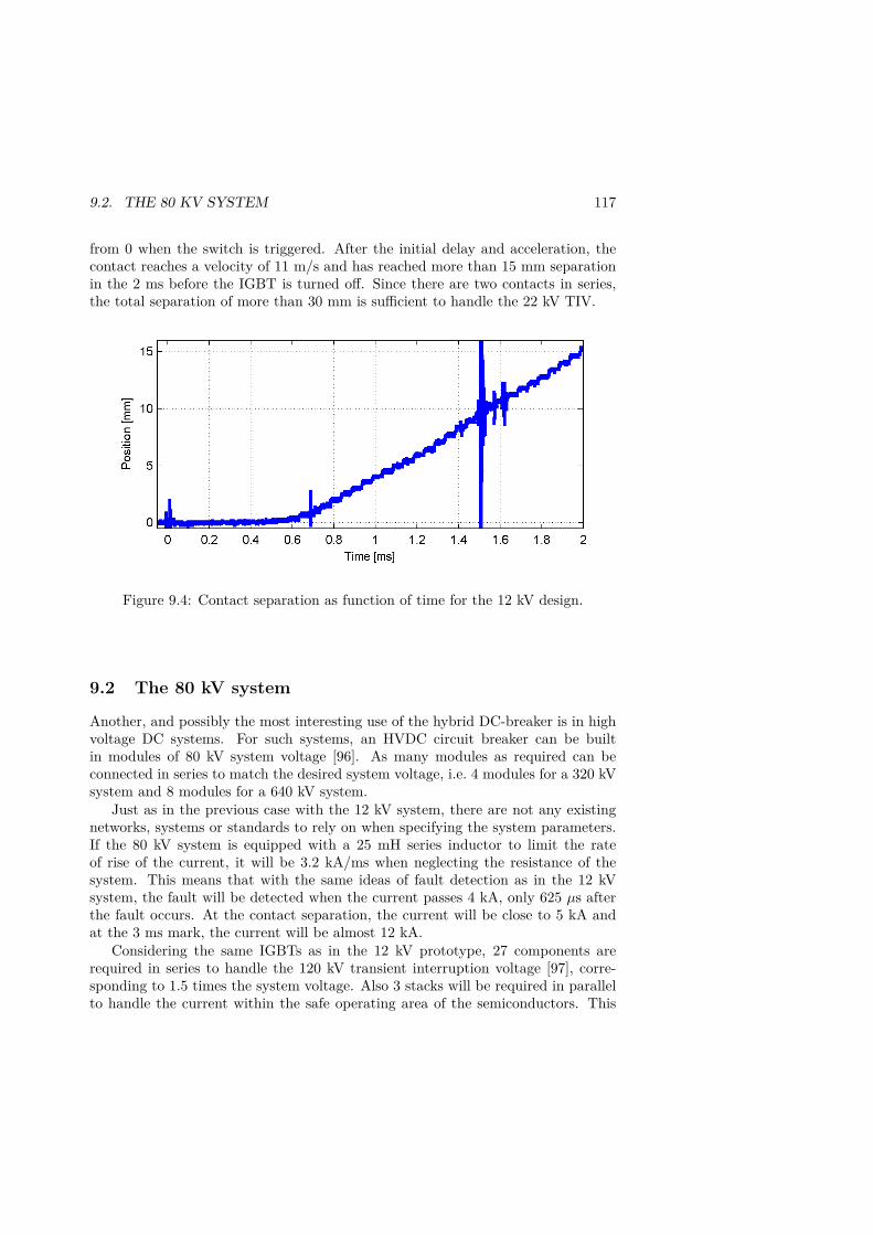
9.2. THE 80 KV SYSTEM 117
from 0 when the switch is triggered. After the initial delay and acceleration, thecontact reaches a velocity of 11 m/s and has reached more than 15 mm separationin the 2 ms before the IGBT is turned off. Since there are two contacts in series,the total separation of more than 30 mm is sufficient to handle the 22 kV TIV.
Figure 9.4: Contact separation as function of time for the 12 kV design.
9.2 The 80 kV system
Another, and possibly the most interesting use of the hybrid DC-breaker is in highvoltage DC systems. For such systems, an HVDC circuit breaker can be builtin modules of 80 kV system voltage [96]. As many modules as required can beconnected in series to match the desired system voltage, i.e. 4 modules for a 320 kVsystem and 8 modules for a 640 kV system.
Just as in the previous case with the 12 kV system, there are not any existingnetworks, systems or standards to rely on when specifying the system parameters.If the 80 kV system is equipped with a 25 mH series inductor to limit the rateof rise of the current, it will be 3.2 kA/ms when neglecting the resistance of thesystem. This means that with the same ideas of fault detection as in the 12 kVsystem, the fault will be detected when the current passes 4 kA, only 625 µs afterthe fault occurs. At the contact separation, the current will be close to 5 kA andat the 3 ms mark, the current will be almost 12 kA.
Considering the same IGBTs as in the 12 kV prototype, 27 components arerequired in series to handle the 120 kV transient interruption voltage [97], corre-sponding to 1.5 times the system voltage. Also 3 stacks will be required in parallelto handle the current within the safe operating area of the semiconductors. This
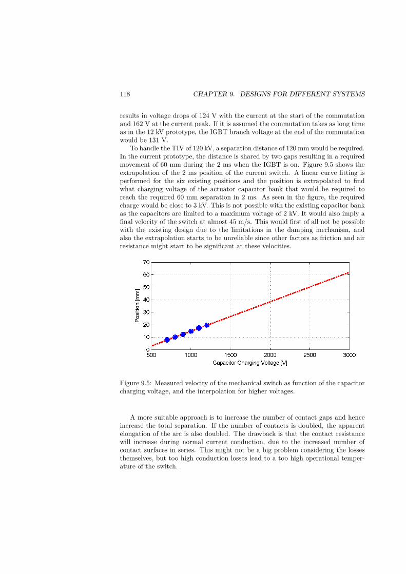
118 CHAPTER 9. DESIGNS FOR DIFFERENT SYSTEMS
results in voltage drops of 124 V with the current at the start of the commutationand 162 V at the current peak. If it is assumed the commutation takes as long timeas in the 12 kV prototype, the IGBT branch voltage at the end of the commutationwould be 131 V.
To handle the TIV of 120 kV, a separation distance of 120 mm would be required.In the current prototype, the distance is shared by two gaps resulting in a requiredmovement of 60 mm during the 2 ms when the IGBT is on. Figure 9.5 shows theextrapolation of the 2 ms position of the current switch. A linear curve fitting isperformed for the six existing positions and the position is extrapolated to findwhat charging voltage of the actuator capacitor bank that would be required toreach the required 60 mm separation in 2 ms. As seen in the figure, the requiredcharge would be close to 3 kV. This is not possible with the existing capacitor bankas the capacitors are limited to a maximum voltage of 2 kV. It would also imply afinal velocity of the switch at almost 45 m/s. This would first of all not be possiblewith the existing design due to the limitations in the damping mechanism, andalso the extrapolation starts to be unreliable since other factors as friction and airresistance might start to be significant at these velocities.
Figure 9.5: Measured velocity of the mechanical switch as function of the capacitorcharging voltage, and the interpolation for higher voltages.
A more suitable approach is to increase the number of contact gaps and henceincrease the total separation. If the number of contacts is doubled, the apparentelongation of the arc is also doubled. The drawback is that the contact resistancewill increase during normal current conduction, due to the increased number ofcontact surfaces in series. This might not be a big problem considering the lossesthemselves, but too high conduction losses lead to a too high operational temper-ature of the switch.
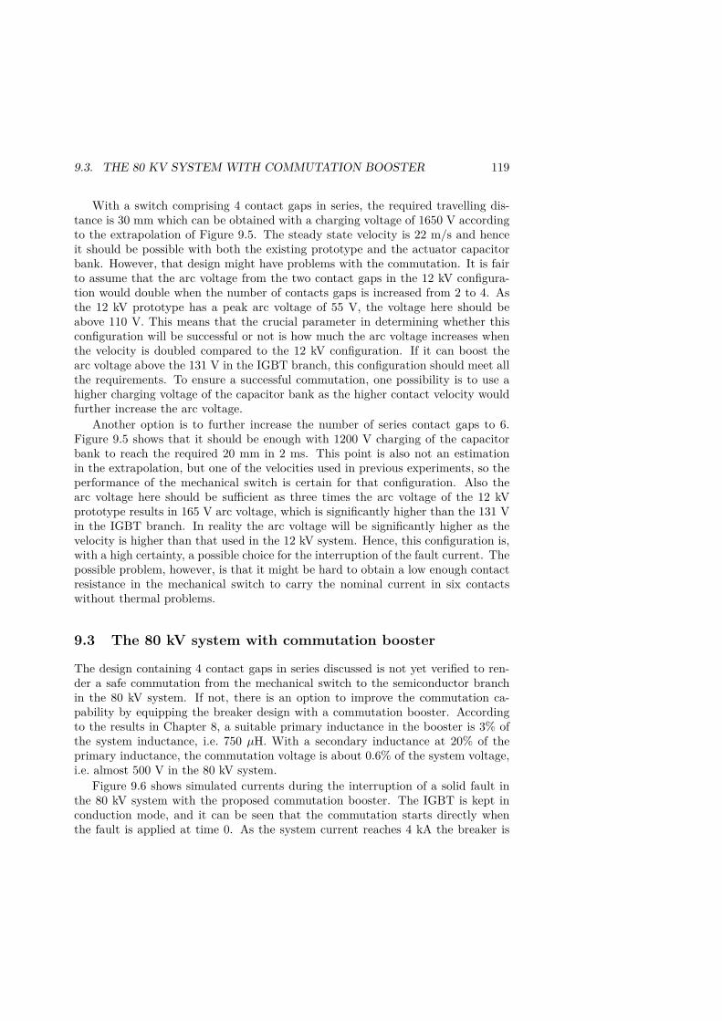
9.3. THE 80 KV SYSTEM WITH COMMUTATION BOOSTER 119
With a switch comprising 4 contact gaps in series, the required travelling dis-tance is 30 mm which can be obtained with a charging voltage of 1650 V accordingto the extrapolation of Figure 9.5. The steady state velocity is 22 m/s and henceit should be possible with both the existing prototype and the actuator capacitorbank. However, that design might have problems with the commutation. It is fairto assume that the arc voltage from the two contact gaps in the 12 kV configura-tion would double when the number of contacts gaps is increased from 2 to 4. Asthe 12 kV prototype has a peak arc voltage of 55 V, the voltage here should beabove 110 V. This means that the crucial parameter in determining whether thisconfiguration will be successful or not is how much the arc voltage increases whenthe velocity is doubled compared to the 12 kV configuration. If it can boost thearc voltage above the 131 V in the IGBT branch, this configuration should meet allthe requirements. To ensure a successful commutation, one possibility is to use ahigher charging voltage of the capacitor bank as the higher contact velocity wouldfurther increase the arc voltage.
Another option is to further increase the number of series contact gaps to 6.Figure 9.5 shows that it should be enough with 1200 V charging of the capacitorbank to reach the required 20 mm in 2 ms. This point is also not an estimationin the extrapolation, but one of the velocities used in previous experiments, so theperformance of the mechanical switch is certain for that configuration. Also thearc voltage here should be sufficient as three times the arc voltage of the 12 kVprototype results in 165 V arc voltage, which is significantly higher than the 131 Vin the IGBT branch. In reality the arc voltage will be significantly higher as thevelocity is higher than that used in the 12 kV system. Hence, this configuration is,with a high certainty, a possible choice for the interruption of the fault current. Thepossible problem, however, is that it might be hard to obtain a low enough contactresistance in the mechanical switch to carry the nominal current in six contactswithout thermal problems.
9.3 The 80 kV system with commutation booster
The design containing 4 contact gaps in series discussed is not yet verified to ren-der a safe commutation from the mechanical switch to the semiconductor branchin the 80 kV system. If not, there is an option to improve the commutation ca-pability by equipping the breaker design with a commutation booster. Accordingto the results in Chapter 8, a suitable primary inductance in the booster is 3% ofthe system inductance, i.e. 750 µH. With a secondary inductance at 20% of theprimary inductance, the commutation voltage is about 0.6% of the system voltage,i.e. almost 500 V in the 80 kV system.
Figure 9.6 shows simulated currents during the interruption of a solid fault inthe 80 kV system with the proposed commutation booster. The IGBT is kept inconduction mode, and it can be seen that the commutation starts directly whenthe fault is applied at time 0. As the system current reaches 4 kA the breaker is

120 CHAPTER 9. DESIGNS FOR DIFFERENT SYSTEMS
tripped after 600 µs and the contacts of the mechanical switch open 250 µs later.As the arc voltage of 110 V is much lower than the inductive voltage driving thecommutation, the opening of the switch barely affects the commutation. When thecurrent in the switch branch reaches zero after 1.6 ms, the arc ceases. The switchcontinues to open and blocks the TIV when the IGBT turns off 2 ms after the trip.
Figure 9.6: Currents during interruption of a solid fault in the 80 kV system usinga hybrid DC-breaker with the commutation booster.
To protect the whole hybrid DC-breaker, and to avoid a long conduction timein the secondary branch during the current decrease, two MOVs are used in thistopology. The main MOV, with a conduction voltage of 120 kV, i.e. the same TIVas in the previous 80 kV design, is installed across the whole breaker. AnotherMOV, with 15% higher voltage rating is installed close to the IGBT to limit thepeak over-voltage during the turn-off. It can be seen in Fig. 9.6 that the componentclose to the IGBT acts as a snubber and takes care of the current when the IGBTturns off, and that most of the current is rapidly pushed out to the outer MOVwhere it is limited and the current is forced to zero. Due to the large inductancein the loop between the two MOVs, this commutation takes about 100 µs.
The drawback of this configuration is that it is unable to interrupt the nominalcurrent. For the current configuration, the inductance in the commutation loopis about 40% of the primary inductance, i.e. 300 µH. Hence, to commutate 2 kAwithin one millisecond requires a driving voltage of 600 V. As the arc voltage isonly about 110 V and the forward voltage drop of the IGBT is above 100 V for thenominal current, the voltage difference is too low for a fast commutation with thishigh loop inductance.
Figure 9.7 shows the commutation times in the hybrid DC-breaker with com-mutation booster depending on the impedance of the fault. It can be seen that as
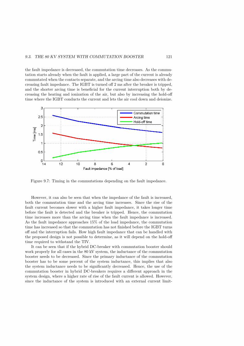
9.3. THE 80 KV SYSTEM WITH COMMUTATION BOOSTER 121
the fault impedance is decreased, the commutation time decreases. As the commu-tation starts already when the fault is applied, a large part of the current is alreadycommutated when the contacts separate, and the arcing time also decreases with de-creasing fault impedance. The IGBT is turned off 2 ms after the breaker is tripped,and the shorter arcing time is beneficial for the current interruption both by de-creasing the heating and ionization of the air, but also by increasing the hold-offtime where the IGBT conducts the current and lets the air cool down and deionize.
Figure 9.7: Timing in the commutations depending on the fault impedance.
However, it can also be seen that when the impedance of the fault is increased,both the commutation time and the arcing time increases. Since the rise of thefault current becomes slower with a higher fault impedance, it takes longer timebefore the fault is detected and the breaker is tripped. Hence, the commutationtime increases more than the arcing time when the fault impedance is increased.As the fault impedance approaches 15% of the load impedance, the commutationtime has increased so that the commutation has not finished before the IGBT turnsoff and the interruption fails. How high fault impedance that can be handled withthe proposed design is not possible to determine, as it will depend on the hold-offtime required to withstand the TIV.
It can be seen that if the hybrid DC-breaker with commutation booster shouldwork properly for all cases in the 80 kV system, the inductance of the commutationbooster needs to be decreased. Since the primary inductance of the commutationbooster has to be some percent of the system inductance, this implies that alsothe system inductance needs to be significantly decreased. Hence, the use of thecommutation booster in hybrid DC-breakers requires a different approach in thesystem design, where a higher rate of rise of the fault current is allowed. However,since the inductance of the system is introduced with an external current limit-

122 CHAPTER 9. DESIGNS FOR DIFFERENT SYSTEMS
ing inductor, the inductance can be easily decreased, which should also lead to asignificant decrease in cost.
Chapter 10
Conclusions
The main conclusions from this thesis can be summarized as:
• The commutation from the mechanical switch to the semiconductor branchis critical for the current interruption in the hybrid DC-breaker. Dependingon the opposing voltage, set by the semiconductor branch, the commutationwill look very different. If the arc voltage at the start of the commutationis higher than the semicondcutor voltage, at the end of the commutation,the commutation will be fast and limited by the stray inductance in thecommutation loop.
• When the voltage drop across the semiconductor branch is high, the commu-tation is limited by the increase in the arc voltage due to the elongation of thearc. Even though the arc voltage is high when the arc forms, in the beginningof the commutation, the voltage decreases when the current is taken over bythe semiconductor branch. To compensate for the decrease in arc voltage,and to ensure a fast commutation of the current, a rapid elongation of thearc is necessary.
• The proposed snubber based on an MOV with low energy rating, mountedclose to the IGBT, has shown to be able to separate the absorption of themagnetic energy from the over-voltage protection of the IGBT. However, arather high voltage ratio is required between the snubber and the MOV tokeep the absorbed energy low in the snubber. The energy absorbed by thesnubber is decided by the ratio of the rated voltages of the snubber and theMOV, and is almost independent of the inductance in the loop between theIGBT and the MOV. Hence, the snubber MOV concept seems to be mostsuitable in systems where this inductance is high.
• A design for a hybrid DC-breaker for a 12 kV DC-system has been proposed,and the commutation from the mechanical switch to the IGBT has beenvalidated experimentally. Two contacts in series and an opening velocity of
123
124 CHAPTER 10. CONCLUSIONS
11 m/s is enough to perform the commutation and keep the system peakcurrent below 8 kA. The voltage withstand capability has not been tested,but the opening velocity results in a total contact separation of above 30 mmwhen the IGBT turns off after 2 ms. As the commutation is performed withinthe first millimetre of the contact movement, and 700 µs, the temperature ofthe air between the contacts at the IGBT turn-off should not be a problem.
• To enhance the commutation capability in fault cases with low impedance,coupled inductors can be used in the hybrid DC-breaker. The mutual cou-pling between the inductors results in that the rushing fault current throughthe semiconductor branch causes a decrease of the current in the mechanicalswitch branch. As the commutation starts automatically, the switch has toopen before the current zero crossing occurs, but the requirements on the arcvoltage are decreased. With the commutation booster, the system is changedso that the commutation time is shorter the lower the fault impedance is.Hence, as long as the arc voltage is enough to commutate the nominal cur-rent, all fault cases will be handled.
Chapter 11
Future Work
The field of research is never ending and for every result, there are always morequestions that need answers. This section summarizes some of the things thatshould be investigated further with respect to the results presented in this thesis.
• The first thing that should be done is to experimentally validate the voltagewithstand capability of the proposed 12 kV hybrid DC-breaker. Even thoughthe distance between the contacts is sufficiently large, the withstand capabilityshould be tested and validated.
• Even though the breakdown strength of air is fairly well known under staticconditions, the commutation of the current changes the conditions. Duringthe commutation of the current from the mechanical switch to the semi-conductor, part of the air volume is heated and ionized by the electric arc.It should be further investigated how the time and increasing separation dis-tance between the contacts affect the breakdown strength of the hot gas. Alsothe influence of the input energy, i.e. the duration of the commutation shouldbe investigated.
• The proposed 80 kV hybrid DC-breaker design should be tested to validateits function. As the calculations of both the arc-voltage and the voltagewithstand capability are extrapolated from the existing experiments, theyneed to be experimentally validated.
• In the prototype used in the experiments of this work, the contact systemconsists of a rather simple moving contact giving two contact gaps in series.To further increase the commutation capability of the mechanical switch,more advanced contact configurations should be investigated. The voltagewithstand capability of the switch can be increased if one of the contacts isconnected to the moving part. However, this requires to design a connectionto the electrical system with sufficient endurance.
125
126 CHAPTER 11. FUTURE WORK
• For the design of the mechanical switch, more effort can be put on the de-sign of the damping system. A good damping system is necessary to increasethe endurance and ensure a high number of operations, but also to stop thecontact movement and enable a fast re-closing of the switch. As the fast open-ing velocities seems to exceed the ratings of commercially available viscousdampers, other approaches has to be found. Many possible damping systemsare available, such as passive magnetic dampers, active magnetic dampers,and the possibility to use the Thomson coil actuator to damp the movement.
• Possible alternatives in the parallel branch, now containing semiconductors,should be investigated. As the main task of this branch is to delay the turn-offof the breaker until the mechanical switch has opened sufficiently, it shouldbe possible to use a less advanced component than the IGBT. The IGBT isa high-tech component capable of switching high currents thousands of timesper second and hence it is over-qualified for this task. A simpler configurationof this parallel branch enables a significant decrease of the cost for a hybridDC-breaker.
List of Figures
2.1 Voltage and fault current in an AC system with a symmetric fault. . . . 102.2 Voltage and fault current in an AC system with an asymmetric fault. . 112.3 Interruption of an inductive AC current at the zero crossing at t=0. . . 122.4 The fault current decreases with increasing system inductance. . . . . . 132.5 The dependence of the fault current on the angle of the voltage at the
instant of the fault. . . . . . . . . . . . . . . . . . . . . . . . . . . . . . . 142.6 Fault currents in a DC-system modelled with an ideal DC source. . . . . 152.7 A two level, three phase voltage source converter. . . . . . . . . . . . . . 162.8 The possible DC fault currents for a DC system fed by a 6-pulse rectifier. 172.9 DC fault current depending on the angle of the voltage at the instant of
the fault. . . . . . . . . . . . . . . . . . . . . . . . . . . . . . . . . . . . 182.10 Limitation of the DC fault current by inductance on the AC-side. . . . . 182.11 Limitation of the fault current by an inductor on the DC side. . . . . . 192.12 Interruption of a DC current (solid lines) with different counter voltages
(dashed lines) across the breaker. . . . . . . . . . . . . . . . . . . . . . . 20
3.1 Schematic diagram of the mechanical DC circuit breaker showing itsmain benefit: the simplicity. . . . . . . . . . . . . . . . . . . . . . . . . . 24
3.2 Schematic diagram of the solid state circuit breaker consisting of a semi-conductor in the main current path and a metal oxide varistor. . . . . . 25
3.3 Schematic diagram of the resonant DC-breaker with its three parallelpaths: mechanical breaker for conduction, a resonance path, and anenergy absorbing MOV. . . . . . . . . . . . . . . . . . . . . . . . . . . . 26
3.4 Schematic diagram of the Z-source breaker. . . . . . . . . . . . . . . . . 283.5 Schematic diagram of the hybrid DC circuit breaker consisting of three
parallel branches: a mechanical commutation switch, a semiconductorbranch, and an MOV for energy absorption. . . . . . . . . . . . . . . . . 29
4.1 Currents in the hybrid DC-breaker during interruption of a rising current. 344.2 Voltages in the hybrid DC-breaker during interruption of a rising current. 354.3 Schematic drawings of the Thomson coil actuator (left) and double sided
coil (right) [68]. . . . . . . . . . . . . . . . . . . . . . . . . . . . . . . . . 37
127
128 List of Figures
4.4 Drawing of the mechanical switch prototype used in the lab. . . . . . . . 404.5 Currents through the Thomson coil actuator for experiments with dif-
ferent capacitor charging voltages. . . . . . . . . . . . . . . . . . . . . . 414.6 Photo of the epoxy embedded coil (left), aluminium armature (middle)
and the viscous dampers (right). . . . . . . . . . . . . . . . . . . . . . . 424.7 Position as function of time for the actuator in experiments with different
capacitor charging voltages. . . . . . . . . . . . . . . . . . . . . . . . . . 434.8 Travelling distances for the contact in 1, 2, and 5 ms. . . . . . . . . . . 444.9 Steady state velocity for the contact system depending on the capacitor
bank charging voltage. . . . . . . . . . . . . . . . . . . . . . . . . . . . . 454.10 Photo of the large IGBT module mounted on the heat-sink. . . . . . . . 474.11 U -I characteristics of the three MOVs used in the experiments. . . . . . 48
5.1 The newly built switching lab where the experiments are performed. . . 495.2 The different parts in the experimental set-up in the lab. . . . . . . . . 515.3 Schematic drawing of the IGBT gate drive unit used in the test set-up. 55
6.1 Circuit diagram of the commutation between the mechanical switch andthe IGBT. . . . . . . . . . . . . . . . . . . . . . . . . . . . . . . . . . . . 59
6.2 Arc voltage as function of arc length for 100 A and 6 different openingspeeds. . . . . . . . . . . . . . . . . . . . . . . . . . . . . . . . . . . . . . 61
6.3 Dependence of the arc voltage on the current through the arc. . . . . . . 626.4 Commutation of different current levels. . . . . . . . . . . . . . . . . . . 626.5 Commutation limited by the loop inductance. . . . . . . . . . . . . . . . 636.6 Commutation limited by the elongation of the arc. . . . . . . . . . . . . 646.7 The complexity of the current commutation from the mechanical switch
to the IGBT. . . . . . . . . . . . . . . . . . . . . . . . . . . . . . . . . . 656.8 The complexity of the current commutation from the mechanical switch
to the IGBT. . . . . . . . . . . . . . . . . . . . . . . . . . . . . . . . . . 666.9 Arc voltage as function of the arc length for a decreasing current during
the commutation. . . . . . . . . . . . . . . . . . . . . . . . . . . . . . . . 676.10 Arc voltage for three current levels commutated within 1 ms. . . . . . . 676.11 Current through the arc for three different currents commutated within
1 ms. . . . . . . . . . . . . . . . . . . . . . . . . . . . . . . . . . . . . . . 686.12 Arc voltage in the switch when commutating 550 A with 14.5 and 12.5 m/s. 696.13 Current through the arc when commutating 550 A with 14.5 and 12.5 m/s. 696.14 Arc voltage in the switch with different delay of the IGBT turn-on. . . . 716.15 Current through the arc with different delay of the IGBT turn-on. . . . 716.16 Arc voltages with delayed opening of the mechanical switch. . . . . . . . 736.17 Current in the mechanical switch with delayed opening. . . . . . . . . . 73
7.1 Typical turn-off waveform of the IGBT. . . . . . . . . . . . . . . . . . . 767.2 System with a solid state breaker. . . . . . . . . . . . . . . . . . . . . . 767.3 The proposed MOV snubber circuit. . . . . . . . . . . . . . . . . . . . . 77
List of Figures 129
7.4 Current and voltage waveforms when turning the IGBT off with a lowstray inductance. . . . . . . . . . . . . . . . . . . . . . . . . . . . . . . . 78
7.5 Current and voltage waveforms when turning the IGBT off with a highstray inductance. . . . . . . . . . . . . . . . . . . . . . . . . . . . . . . . 79
7.6 Results of the parallel MOV snubber using a high enough voltage ratio. 807.7 Usage of the parallel MOV snubber where the voltage ratio is too low
and the concept fails. . . . . . . . . . . . . . . . . . . . . . . . . . . . . 817.8 The design trade-off between peak over-voltage and energy absorbed in
the snubber MOV. . . . . . . . . . . . . . . . . . . . . . . . . . . . . . . 817.9 Voltages during IGBT turn-off without snubber. IGBT voltage in solid
lines and MOV voltage in dashed lines. . . . . . . . . . . . . . . . . . . 837.10 Peak IGBT voltage depending on the voltage rating of the snubber with
the 360 V MOV. . . . . . . . . . . . . . . . . . . . . . . . . . . . . . . . 847.11 Peak IGBT voltage with the 360 V MOV depending on the energy rating
of the snubber component. . . . . . . . . . . . . . . . . . . . . . . . . . 847.12 Part of the energy absorbed in the snubber depending on the snubber
voltage rating with the 360 V MOV. . . . . . . . . . . . . . . . . . . . . 857.13 Peak IGBT voltage depending on the voltage rating of the snubber with
the 560 V MOV. . . . . . . . . . . . . . . . . . . . . . . . . . . . . . . . 867.14 Maximum possible switching current in the IGBT without exceeding the
voltage rating. . . . . . . . . . . . . . . . . . . . . . . . . . . . . . . . . 877.15 Absorbed energy in the snubber when using the 560 V MOV. . . . . . . 877.16 The trade-off between peak IGBT voltage and energy absorbed in the
snubber component for all the tested combinations of snubber and MOV. 887.17 Model of the test set-up as implemented in PSCAD. . . . . . . . . . . . 907.18 Effect of the division of the inductance in the loop between the IGBT
and the MOV on the peak voltages. . . . . . . . . . . . . . . . . . . . . 917.19 Experimental curves of the oscillation in the voltage across the breaker
when the current reaches zero. . . . . . . . . . . . . . . . . . . . . . . . 927.20 Experimental curves of the oscillation in the voltage across the breaker
when the IGBT turns off. . . . . . . . . . . . . . . . . . . . . . . . . . . 937.21 Currents for a test without snubber used to calibrate the model param-
eters. Simulated IGBT current (solid) is fit to the experimental (dashed). 947.22 Voltages for a test without snubber used to fit the simulations (solid) to
the experiment (dashed). . . . . . . . . . . . . . . . . . . . . . . . . . . 957.23 Currents for a test with a 420 V snubber used to calibrate the model
parameters. Simulated IGBT current (solid) is fit to the experimental(dashed). . . . . . . . . . . . . . . . . . . . . . . . . . . . . . . . . . . . 96
7.24 Voltages for a test with a 420 V snubber used to fit the simulations(solid) to the experiment (dashed). . . . . . . . . . . . . . . . . . . . . . 96
7.25 Currents for a test with a 385 V snubber used to validate the model pa-rameters. Simulated IGBT current (solid) fits the experimental (dashed). 97
7.26 Voltages for a test with a 385 V snubber used to validate the simulations(solid) to the experiment (dashed). . . . . . . . . . . . . . . . . . . . . . 97
130 List of Figures
7.27 Peak voltages dependence on the inductance in the snubber branch. . . 987.28 Absorbed energy and peak IGBT voltage depending on the choice of
voltage and energy rating of the snubber. . . . . . . . . . . . . . . . . . 997.29 Absorbed energy and peak IGBT voltage depending on the number of
500 V snubber components in parallel. . . . . . . . . . . . . . . . . . . . 1007.30 Absorbed energy and peak IGBT voltage depending on the inductance
of the MOV branch. . . . . . . . . . . . . . . . . . . . . . . . . . . . . . 101
8.1 Schematic diagram of a hybrid DC-breaker with a commutation booster. 1048.2 The currents in the hybrid DC-breaker with the commutation booster
during current interruption. . . . . . . . . . . . . . . . . . . . . . . . . . 1058.3 An inductive commutation circuit based on the Z-source breaker. . . . . 1068.4 Inductively coupled DC-breaker with a diode and resonance circuit. . . 1068.5 Extra inductance introduced in the commutation loop by the commu-
tation booster. . . . . . . . . . . . . . . . . . . . . . . . . . . . . . . . . 1088.6 The equivalent inductance of the commutation booster as seen by the
system. . . . . . . . . . . . . . . . . . . . . . . . . . . . . . . . . . . . . 1098.7 The part of the system voltage that will help in performing the commu-
tation due to the rising fault current. . . . . . . . . . . . . . . . . . . . . 1108.8 Commutation time with the commutation booster depending on the
fault impedance. . . . . . . . . . . . . . . . . . . . . . . . . . . . . . . . 110
9.1 Voltages in the 12 kV hybrid DC-breaker during interruption of a risingcurrent. . . . . . . . . . . . . . . . . . . . . . . . . . . . . . . . . . . . . 115
9.2 Currents in the 12 kV hybrid DC-breaker during interruption of a risingcurrent. . . . . . . . . . . . . . . . . . . . . . . . . . . . . . . . . . . . . 116
9.3 Arc voltage as function of arc length for the 12 kV DC-breaker. . . . . . 1169.4 Contact separation as function of time for the 12 kV design. . . . . . . . 1179.5 Measured velocity of the mechanical switch as function of the capacitor
charging voltage, and the interpolation for higher voltages. . . . . . . . 1189.6 Currents during interruption of a solid fault in the 80 kV system using
a hybrid DC-breaker with the commutation booster. . . . . . . . . . . . 1209.7 Timing in the commutations depending on the fault impedance. . . . . 121
Bibliography
[1] European Commission, “Low voltage directive, LVD 2006/95/EC,” 2006.
[2] M. Rahimo and S. Klaka, “High voltage semiconductor technologies,” in 13thEuropean Conference Power Electronics and Applications, Sep. 2009, pp. 1 –10.
[3] Z. Zhang, Z. Xu, and Y. Xue, “Valve losses evaluation based on piecewiseanalytical method for mmc-hvdc links,” Power Delivery, IEEE Transactionson, vol. 29, no. 3, pp. 1354–1362, June 2014.
[4] N. Hingorani, “High-voltage dc transmission: a power electronics workhorse,”Spectrum, IEEE, vol. 33, no. 4, pp. 63–72, Apr 1996.
[5] D. Nilsson and A. Sannino, “Efficiency analysis of low- and medium- voltage dcdistribution systems,” in Power Engineering Society General Meeting, 2004.IEEE, June 2004, pp. 2315–2321 Vol.2.
[6] J. Arrillaga, High Voltage Direct Current Transmission, ser. Energy Engineer-ing. Institution of Engineering and Technology, 1998.
[7] V. K. Sood, HVDC and FACTS controllers: applications of static convertersin power systems. Springer Science & Business Media, 2006.
[8] C. Franck, “HVDC circuit breakers: A review identifying future researchneeds,” IEEE Trans. Power Del., vol. 26, no. 2, pp. 998–1007, April 2011.
[9] W. Zhang, H. Liang, Z. Bin, W. Li, and R. Guo, “Review of dc technology infuture smart distribution grid,” in Innovative Smart Grid Technologies - Asia(ISGT Asia), 2012 IEEE, May 2012, pp. 1–4.
[10] J. Setreus and L. Bertling, “Introduction to hvdc technology for reliable electri-cal power systems,” in Probabilistic Methods Applied to Power Systems, 2008.PMAPS ’08. Proceedings of the 10th International Conference on, May 2008,pp. 1–8.
[11] J. Dorn, H. Gambach, and D. Retzmann, “Hvdc transmission technology forsustainable power supply,” in Systems, Signals and Devices (SSD), 2012 9thInternational Multi-Conference on, March 2012, pp. 1–6.
131
132 BIBLIOGRAPHY
[12] V. Akhmatov, M. Callavik, C. M. Franck, S. E. Rye, T. Ahndorf, M. K. Bucher,H. Müller, F. Schettler, and R. Wiget, “Technical guidelines and prestandard-ization work for first HVDC grids,” IEEE Transactions on Power Delivery,vol. 29, no. 1, pp. 327–335, Feb 2014.
[13] G. Bathurst and P. Bordignan, “Delivery of the Nan’o multi-terminal VSC-HVDC system,” in Proc. CIGRE Int. Symp. Lund, May 2015.
[14] M. Callavik, J. Corbett, N. Kuljaca, N. Macleod, F. Schettler, B. Sonerud,and M. J. Boden, “Roadmap of the first phase of the european supergrid,” inCigré Belgium Conference, 2014.
[15] N. MacLeod, M. Callavik, M. Boden, M. Dhesi, R. Huuva, N. Kuljaca, andF. Schettler, “A technological roadmap for the development of the europeansupergrid,” in Proc. CIGRE Int. Symp. Lund, May 2015.
[16] V. R. Babu, T. Maity, and S. Burman, “Optimization of energy use for mineventilation fan with variable speed drive,” in 2016 International Conferenceon Intelligent Control Power and Instrumentation (ICICPI), Oct 2016, pp.148–151.
[17] C. H. Lee, Z. W. Liu, C. N. Chen, M. Y. Cho, F. T. Lin, and J. A. Jiang,“Assessment of energy savings with variable speed drives in ship’s coolingpumps,” IEEE Transactions on Energy Conversion, vol. 30, no. 4, pp. 1288–1298, Dec 2015.
[18] K. Itani, A. D. Bernardinis, Z. Khatir, A. Jammal, and M. Oueidat, “Regen-erative braking modeling, control, and simulation of a hybrid energy storagesystem for an electric vehicle in extreme conditions,” IEEE Transactions onTransportation Electrification, vol. 2, no. 4, pp. 465–479, Dec 2016.
[19] G. Reed, B. Grainger, A. Sparacino, and Z.-H. Mao, “Ship to grid: Medium-voltage dc concepts in theory and practice,” Power and Energy Magazine,IEEE, vol. 10, no. 6, pp. 70–79, Nov 2012.
[20] S. Yeleti and Y. Fu, “Load flow and security assessment of vsc based mvdcshipboard power systems,” in North American Power Symposium (NAPS),2011, Aug 2011, pp. 1–7.
[21] R. Faulkner and R. Karnes, “Electromechanical ballistic DC breaker for useon ships,” in 2011 IEEE Electric Ship Technologies Symp. (ESTS), 2011, pp.339–344.
[22] J. Robinson, D. Jovcic, and G. Joos, “Analysis and design of an offshore windfarm using a MV DC grid,” IEEE Trans. Power Del., vol. 25, no. 4, pp. 2164–2173, Oct 2010.
BIBLIOGRAPHY 133
[23] J. Yang, J. Fletcher, and J. O’Reilly, “Multiterminal dc wind farm collec-tion grid internal fault analysis and protection design,” Power Delivery, IEEETransactions on, vol. 25, no. 4, pp. 2308–2318, Oct 2010.
[24] F. Katiraei, M. R. Iravani, and P. W. Lehn, “Micro-grid autonomous operationduring and subsequent to islanding process,” IEEE Transactions on PowerDelivery, vol. 20, no. 1, pp. 248–257, Jan 2005.
[25] T. Kaipia, P. Salonen, J. Lassila, and J. Partanen, “Possibilities of the lowvoltage dc distribution systems,” in Nordac, Nordic Distribution and AssetManagement Conf., 2006.
[26] T. Jonsson, P. Lundberg, S. Maiti, and Y. Jiang-Häfner, “Converter tech-nologies and functional requirements for reliable and economical HVDC griddesign,” in 2013 CIGRÉ Canada Conference, September 2013.
[27] E. Jonsson, N. S. Aanensen, and M. Runde, “Current interruption in air fora medium-voltage load break switch,” IEEE Transactions on Power Delivery,vol. 29, no. 2, pp. 870–875, April 2014.
[28] E. Jonsson and M. Runde, “Interruption in air for different medium-voltageswitching duties,” IEEE Transactions on Power Delivery, vol. 30, no. 1, pp.161–166, Feb 2015.
[29] G. Frind, Experimental Investigation of Limiting Curves for CurrentInterruption of Gas Blast Breakers. Boston, MA: Springer US, 1978, pp.67–94. [Online]. Available: http://dx.doi.org/10.1007/978-1-4757-1685-6_3
[30] P. Slade, J.-L. Wu, E. Stacey, W. Stubler, R. Voshall, J. Bonk, J. Porter, andL. Hong, “The utility requirements for a distribution fault current limiter,”IEEE Trans. Power Delivery, vol. 7, no. 2, pp. 507 –515, Apr. 1992.
[31] A. Abramovitz and K. Smedley, “Survey of solid-state fault current limiters,”IEEE Trans. Power Electron., vol. 27, no. 6, pp. 2770–2782, 2012.
[32] J. Magnusson, J. Martinez-Velasco, A. Bissal, G. Engdahl, and L. Liljestrand,“Optimal design of a medium voltage hybrid fault current limiter,” in EnergyConference (ENERGYCON), 2014 IEEE International, May 2014, pp. 431–438.
[33] S. Breugelmans, W. Leterme, D. Van Hertem, and R. Marcelis, “Comparisonof different methods to limit short circuit currents in dc traction networks,” inDevelopments in Power System Protection (DPSP 2014), 12th IET Interna-tional Conference on, March 2014, pp. 1–6.
[34] F. Page, S. Finney, D. Holliday, L. Xu, B. Williams, K. Tahata, M. Sato,R. Yamamoto, and H. Ito, “Optimisation of passive system components tominimize dc circuit breaker stresses in multi-terminal systems,” in CIGREsymposium Lund, 2015.
134 BIBLIOGRAPHY
[35] N. Mohan, T. M. Undeland, and W. P. Robbins, Power Electronics - Convert-ers, Applications, and Design. John Wiley & sons, Inc, 2003.
[36] K. Ilves, S. Norrga, L. Harnefors, and H.-P. Nee, “On energy storage require-ments in modular multilevel converters,” Power Electronics, IEEE Transac-tions on, vol. 29, no. 1, pp. 77–88, Jan 2014.
[37] M. Bucher, R. Wiget, G. Andersson, and C. Franck, “Multiterminal hvdc net-works - what is the preferred topology?” Power Delivery, IEEE Transactionson, vol. 29, no. 1, pp. 406–413, Feb 2014.
[38] N. Ahmed, L. Angquist, S. Mehmood, A. Antonopoulos, L. Harnefors, S. Nor-rga, and H. Nee, “Efficient modeling of an mmc-based multiterminal dc sys-tem employing hybrid hvdc breakers,” Power Delivery, IEEE Transactions on,vol. PP, no. 99, pp. 1–1, 2015.
[39] P. Nuutinen, P. Peltoniemi, and P. Silventoinen, “Short-circuit protection ina converter-fed low-voltage distribution network,” Power Electronics, IEEETransactions on, vol. 28, no. 4, pp. 1587–1597, April 2013.
[40] M. Bucher, M. Walter, M. Pfeiffer, and C. Franck, “Options for ground faultclearance in hvdc offshore networks,” in Energy Conversion Congress and Ex-position (ECCE), 2012 IEEE, Sept 2012, pp. 2880–2887.
[41] G. P. Adam and B. W. Williams, “Half- and full-bridge modular multilevelconverter models for simulations of full-scale HVDc links and multiterminal DCgrids,” IEEE Journal of Emerging and Selected Topics in Power Electronics,vol. 2, no. 4, pp. 1089–1108, Dec 2014.
[42] X. Pei, A. C. Smith, and M. Barnes, “Superconducting fault current limitersfor HVDC systems,” Energy Procedia, vol. 80, pp. 47 – 55, 2015. [Online]. Avail-able: http://www.sciencedirect.com/science/article/pii/S1876610215021372
[43] C. Meyer, S. Schroder, and R. De Doncker, “Solid-state circuit breakers andcurrent limiters for medium-voltage systems having distributed power sys-tems,” Power Electronics, IEEE Transactions on, vol. 19, no. 5, pp. 1333–1340,2004.
[44] T. Podlesak, J. McMurray, and J. Carter, “Solid state switch utilizing GTOsin series,” in Proc. 24th Intersociety Energy Conversion Engineering Conf.,Aug. 1989, pp. 651 –655 vol.1.
[45] E. Sakshaug, J. Kresge, and J. Miske, S.A., “A new concept in station arresterdesign,” IEEE Trans. Power App. Syst., vol. 96, no. 2, pp. 647 – 656, Mar.1977.
BIBLIOGRAPHY 135
[46] B. Wittig and F. Fuchs, “Analysis and comparison of turn-off active gatecontrol methods for low-voltage power MOSFETs with high current ratings,”IEEE Trans. Power Electron., vol. 27, no. 3, pp. 1632–1640, 2012.
[47] ABB, “S5SNA 2000K450300 StakPak IGBT module,” 2013. [Online].Available: http://www.abb.com/product/us/9AAC30200001.aspx
[48] D. Johannesson, M. Nawaz, K. Jacobs, S. Norrga, and H. P. Nee, “Potentialof ultra-high voltage silicon carbide semiconductor devices,” in 2016 IEEE 4thWorkshop on Wide Bandgap Power Devices and Applications (WiPDA), Nov2016, pp. 253–258.
[49] C. J. Wort and R. S. Balmer, “Diamond as an electronic material,”Materials Today, vol. 11, no. 1-2, pp. 22–28, 2008. [Online]. Available://www.sciencedirect.com/science/article/pii/S1369702107703498
[50] T. Eriksson, M. Backman, and S. Halén, “A low loss mechanical HVDC breakerfor HVDC grid applications,” in Cigré, 2014.
[51] L. Liljestrand, M. Backman, L. Jonsson, E. Dullni, and M. Riva, “Mediumvoltage DC vacuum circuit breaker,” in 2015 3rd International Conference onElectric Power Equipment - Switching Technology (ICEPE-ST), Oct 2015, pp.495–500.
[52] H. Nakao, Y. Nakagoshi, M. Hatano, T. Koshizuka, S. Nishiwaki,A. Kobayashi, T. Murao, and S. Yanabu, “DC current interruption in HVDCSF6 gas MRTB by means of self-excited oscillation superimposition,” IEEETransactions on Power Delivery, vol. 16, no. 4, pp. 687–693, Oct 2001.
[53] L. Ängquist, S. Norrga, and T. Modéer, “A new dc breaker with reduced needfor semiconductors,” in 2016 18th European Conference on Power Electronicsand Applications (EPE’16 ECCE Europe), Sept 2016, pp. 1–9.
[54] K. A. Corzine and R. W. Ashton, “A new z-source dc circuit breaker,” in2010 IEEE International Symposium on Industrial Electronics, July 2010, pp.585–590.
[55] K. A. Corzine and R. W. Ashton, “Structure and analysis of the z-sourceMVDC breaker,” in 2011 IEEE Electric Ship Technologies Symposium, April2011, pp. 334–338.
[56] M. Francis, J. Dupraz, R. Besrest, and J. Armata, “New topology of hy-brid circuit breaker/current limiter for mv aes networks,” in All Electric Ship(AES2005), International Conference on, 2005, pp. 13–14.
[57] H. Kurioka, T. Genji, M. Isozaki, H. Iwai, and M. Yamada, “Development ofa high-speed current limiter for a 6 kv distribution system and evaluation ofits effectiveness,” Electrical Engineering in Japan, vol. 125, no. 3, pp. 11–20,1998.
136 BIBLIOGRAPHY
[58] J.-M. Meyer and A. Rufer, “A dc hybrid circuit breaker with ultra-fast con-tact opening and integrated gate-commutated thyristors (igcts),” IEEE Trans.Power Del., vol. 21, no. 2, pp. 646–651, April 2006.
[59] A. M. S. Atmadji and J. G. J. Sloot, “Hybrid switching: a review of currentliterature,” in 1998 Int. Conf. on Energy Management and Power Delivery,1998. Proceedings of EMPD ’98, vol. 2, 1998, pp. 683–688 vol.2.
[60] L. Liljestrand, L. Jonsson, M. Backman, and M. Riva, “A new hybrid mediumvoltage breaker for DC interruption or AC fault current limitation,” in 201618th European Conference on Power Electronics and Applications (EPE’16ECCE Europe), Sept 2016, pp. 1–10.
[61] J. Häfner and B. Jacobson, “Proactive hybrid HVDC breakers - a key inno-vation for reliable HVDC grids,” in The electric power system of the future -Integrating supergrids and microgrids Int. symp., Bologna, Sep. 2011.
[62] W. Paul, M. Lakner, J. Rhyner, P. Unternahrer, T. Baumann, M. Chen,L. Widenhorn, and A. Guerig, “Test of 1.2 mva high-tc superconducting faultcurrent limiter,” Superconductor Science and Technology, vol. 10, no. 12, pp.914–918, 1997.
[63] J. Skindhoj, J. Glatz-Reichenbach, and R. Strumpler, “Repetitive current lim-iter based on polymer PTC resistor,” IEEE Transactions on Power Delivery,vol. 13, no. 2, pp. 489–494, 1998.
[64] A. W. P.G. Newbery, “Electric fuses,” Proceedings of the Institution of Elec-trical Engineers, vol. 124, pp. 909–924(15), November 1977.
[65] K. Leix, L. A. Kojovic, M. Marz, and G. Lampley, “Applying current-limitingfuses to improve power quality and safety,” in Transmission and DistributionConference, 1999 IEEE, vol. 2, 1999, pp. 636–641 vol.2.
[66] J. Magnusson, “On the design of hybrid DC-breakers consisting of a mechanicalswitch and semiconductor devices,” in Licentiate thesis in Electrical Engineer-ing, May 2015, pp. 1–90.
[67] S. Basu and K. Srivastava, “Analysis of a fast acting circuit breaker mechanismpart i: Electrical aspects,” IEEE Trans. Power App. Syst., vol. PAS-91, no. 3,pp. 1197–1203, May 1972.
[68] A. Bissal, J. Magnusson, and G. Engdahl, “Comparison of two ultra-fast ac-tuator concepts,” IEEE Trans. Magn., vol. 48, no. 11, pp. 3315–3318, Nov2012.
[69] B. J. Baliga, M. S. Adler, R. love, P. Gray, and N. Zommer, “The insulatedgate transistor: A new three-terminal MOS-controlled bipolar power device,”Electron Devices, IEEE Transactions on, vol. 31, no. 6, pp. 821–828, Jun 1984.
BIBLIOGRAPHY 137
[70] H. Gruening and A. Zuckerberger, “Hard drive of high power GTOs: betterswitching capability obtained through improved gate-units,” in Industry Appli-cations Conference, 1996. Thirty-First IAS Annual Meeting, IAS ’96., vol. 3,Oct 1996, pp. 1474–1480 vol.3.
[71] P. Steimer, H. Gruning, J. Werninger, E. Carroll, S. Klaka, and S. Linder,“Igct-a new emerging technology for high power, low cost inverters,” IndustryApplications Magazine, IEEE, vol. 5, no. 4, pp. 12–18, Jul 1999.
[72] M. H. Rashid, Power electronics handbook: devices, circuits and applications.Academic press, 2010.
[73] Y. Cheng and C. Hu, MOSFET modeling & BSIM3 user’s guide. Springer,1999.
[74] U. Axelsson, A. Holm, C. Liljegren, K. Eriksson, and L. Weimers, “GotlandHVDC light transmission-world’s first commercial small scale DC transmis-sion,” in Cired Conference, vol. 32, 1999.
[75] L. Weimers, “Hvdc light: A new technology for a better environment,” PowerEngineering Review, IEEE, vol. 18, no. 8, pp. 19–20, Aug 1998.
[76] S. Roy, C. Roy, P. Bhattacharya, and T. Gangopadhyay, “Development ofmetal oxide varistor element for power systems,” in Industrial Electronics,1996. ISIE ’96., Proceedings of the IEEE International Symposium on, vol. 1,Jun 1996, pp. 537–541 vol.1.
[77] W. Niebuhr, “Application of metal-oxide-varistor surge arresters on distribu-tion systems,” IEEE Trans. Power App. Syst., vol. PAS-101, no. 6, pp. 1711–1715, Jun. 1982.
[78] K. Mardira, T. Saha, and R. Sutton, “The effects of electrical degradation onthe microstructure of metal oxide varistor,” in Transmission and DistributionConference and Exposition, 2001 IEEE/PES, vol. 1, 2001, pp. 329–334 vol.1.
[79] K. Eda, A. Iga, and M. Matsuoka, “Degradation mechanism of non-Ohmiczinc oxide ceramics,” J. Appl. Phys., vol. 51, no. 5, pp. 2678–2684, May 1980.
[80] A. Bissal, J. Magnusson, E. Salinas, G. Engdahl, and A. Eriksson, “On the de-sign of ultra-fast electromechanical actuators: A comprehensive multi-physicalsimulation model,” in 2012 Sixth International Conference on ElectromagneticField Problems and Applications, June 2012, pp. 1–4.
[81] Infineon, “BSM400GA120DN2 IGBT module,” 1997. [Online]. Available:https://www.elfa.se/Web/Downloads/m_/en/wtInfineon_IGBT-M_EN.pdf
[82] Fuji Electronics, “1MBI3600U4D-120 IGBT module,” 2008. [Online].Available: http://www.farnell.com/datasheets/1676910.pdf
138 BIBLIOGRAPHY
[83] J. Colmenares, D. Peftitsis, J. Rabkowski, D. P. Sadik, and H. P. Nee, “Dual-function gate driver for a power module with SiC junction field-effect transis-tors,” IEEE Transactions on Power Electronics, vol. 29, no. 5, pp. 2367–2379,May 2014.
[84] S. Ramakrishnan and A. D. Stokes, “E-I characteristic of stable free-burningarcs at high currents,” J. Appl. Phys., vol. 45, no. 12, pp. 5480–5481, 1974.
[85] J. Brown, “Modeling the switching performance of a mosfet in the high sideof a non-isolated buck converter,” Power Electronics, IEEE Transactions on,vol. 21, no. 1, pp. 3–10, Jan 2006.
[86] Y. Teng, J. Tan, Q. Yu, and Y. Zhu, “Analysis of the negative miller capaci-tance during switching transients of IGBTs,” in TENCON 2015 - 2015 IEEERegion 10 Conference, Nov 2015, pp. 1–4.
[87] R. Naayagi, R. Shuttleworth, and A. Forsyth, “Investigating the effect of snub-ber capacitor on high power IGBT turn-off,” in 1st Int. Conf. Electrical EnergySystems (ICEES), Jan. 2011, pp. 50 –55.
[88] R. Chokhawala and S. Sobhani, “Switching voltage transient protectionschemes for high-current IGBT modules,” IEEE Trans. Ind. Appl., vol. 33,no. 6, pp. 1601 –1610, Dec. 1997.
[89] J. Magnusson, R. Saers, L. Liljestrand, and G. Engdahl, “Separation of theenergy absorption and overvoltage protection in solid-state breakers by theuse of parallel varistors,” IEEE Trans. Power Electron., vol. 29, no. 6, pp.2715–2722, June 2014.
[90] Epcos, “SIOV metal oxide varistors,” 2011. [Online]. Available:http://www.epcos.com/inf/70/db/var_11/SIOV_Leaded_StandarD.pdf
[91] J. Magnusson, R. Saers, and L. Liljestrand, “The commutation booster, a newconcept to aid commutation in hybrid dc-breakers,” Cigré HVDC Symposium,Lund, 2015.
[92] K. A. Corzine, “A new-coupled-inductor circuit breaker for DC applications,”IEEE Transactions on Power Electronics, vol. 32, no. 2, pp. 1411–1418, Feb2017.
[93] K. A. Corzine, “Circuit breaker for DC micro grids,” in 2015 IEEE FirstInternational Conference on DC Microgrids (ICDCM), June 2015, pp. 221–221c.
[94] Y. Liu, X. Wei, C. Gao, and J. Cao, “Topological analysis of HVDC circuitbreaker with coupling transformer,” in 2015 IEEE First International Confer-ence on DC Microgrids (ICDCM), June 2015, pp. 129–134.
BIBLIOGRAPHY 139
[95] J. Magnusson, A. Bissal, G. Engdahl, and J. A. Martinez-Velasco, “Designaspects of a medium voltage hybrid dc breaker,” in Innovative Smart GridTechnologies Europe (ISGT Europe), 2014 5th IEEE/PES, Oct 2014.
[96] A. Hassanpoor, J. Häfner, and B. Jacobson, “Technical assessment of loadcommutation switch in hybrid HVDC breaker,” IEEE Transactions on powerelectronics, vol. 30, no. 10, pp. 5393–5400, 2015.
[97] R. Derakhshanfar, T. Jonsson, U. Steiger, and M. Habert, “Hybrid HVDCbreaker-a solution for future HVDC system,” Proc. CIGRÉ Session, Paris,France, pp. 1–12, 2014.