Safe Commutation Strategy in Single Phase Matrix Converter
6
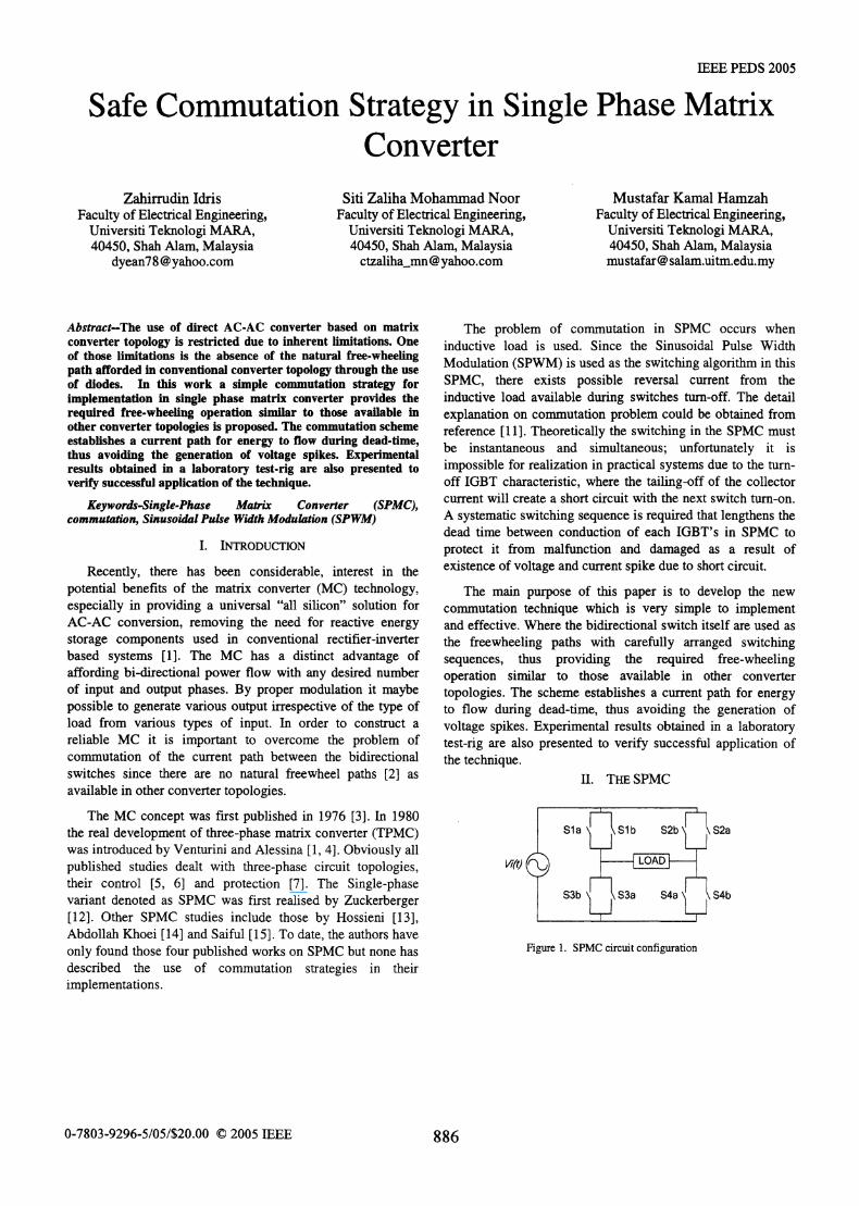
IEEE PEDS 2005 Safe Commutation Strategy in Single Phase Matrix Converter Zahirrudin Idris Siti Zaliha Mohammad Noor Mustafar Kamal Hamzah Faculty of Electrical Engineering, Faculty of Electrical Engineering, Faculty of Electrical Engineering, Universiti Teknologi MARA, Universiti Teknologi MARA, Universiti Teknologi MARA, 40450, Shah Alam, Malaysia 40450, Shah Alam, Malaysia 40450, Shah Alam, Malaysia [email protected] [email protected] [email protected] Abstract-The use of direct AC-AC converter based on matrix The problem of commutation in SPMC occurs when converter topology is restricted due to inherent limitations. One inductive load is used. Since the Sinusoidal Pulse Width of those limitations is the absence of the natural free-wheeling path afforded in conventional converter topology through the use MoW the s algorithm thi of diodes. In this work a simple commutation strategy for SPMC, there exists possible reversal current from the implementation in single phase matrix converter provides the inductive load available during switches turn-off. The detail required free-wheeling operation similar to those available in explanation on commutation problem could be obtained from other converter topologies is proposed. The commutation scheme reference [11]. Theoretically the switching in the SPMC must establishes a current path for energy to flow during dead-time thus avoiding the generation of voltage spikes. Experimental binstnaefou .an simultianeous;euforunathe it is results obtained in a laboratory test-rig are also presented to impossible for realization i practical systems due to the turn- verify successful application of the technique. off IGBT characteristic, where the tailing-off of the collector Keywords-Single-Phase Matrx Converter (SPMC) current will create a short circuit with the next switch turn-on. commutation, Sinusoidal Pulse Width Modulation (SPWM) A systematic switching sequence is required that lengthens the dead time between conduction of each IGBT's in SPMC to I. INTRODUCTION protect it from malfunction and damaged as a result of Recently, there has been considerable, interest in the existence of voltage and current spike due to short circuit. potential benefits of the matrix converter (MC) technology, The main purpose of this paper is to develop the new especially in providing a universal "all silicon" solution for commutation technique which is very simple to implement AC-AC conversion, removing the need for reactive energy and effective. Where the bidirectional switch itself are used as storage components used in conventional rectifier-inverter the freewheeling paths with carefully arranged switching based systems [1]. The MC has a distinct advantage of sequences, thus providing the required free-wheeling affording bi-directional power flow with any desired number operation similar to those available in other converter of input and output phases. By proper modulation it maybe topologies. The scheme establishes a current path for energy possible to generate various output irrespective of the type of to flow during dead-time, thus avoiding the generation of load from various types of input. In order to construct a voltage spikes. Experimental results obtained in a laboratory reliable MC it is important to overcome the problem of test-rig are also presented to verify successful application of commutation of the current path between the bidirectional the technique. switches since there are no natural freewheel paths [2] as II. THE SPMC available in other converter topologies. The MC concept was first published in 1976 [3]. In 1980 7it the real development of three-phase matrix converter (TPMC) Sla Slb S2b \S2a was introduced by Venturini and Alessina [1, 4]. Obviously all published studies dealt with three-phase circuit topologies, V(polO their control [5, 6] and protection [7]. The Single-phase r X n variant denoted as SPMC was first realised by Zuckerberger S3b S3a S4a S4b [12]. Other SPMC studies include those by Hossieni [13], Abdollah Khoei [14] and Saiful [15]. To date, the authors have only found those four published works on SPMC but none has Figure 1. SPMC circuit configuration described the use of commutation strategies in their implementations. 0-7803-9296-5/05/$20.00 © 2005 IEEE 886
-
Upload
independent -
Category
Documents
-
view
1 -
download
0
Transcript of Safe Commutation Strategy in Single Phase Matrix Converter
IEEE PEDS 2005
Safe Commutation Strategy in Single Phase MatrixConverter
Zahirrudin Idris Siti Zaliha Mohammad Noor Mustafar Kamal HamzahFaculty of Electrical Engineering, Faculty of Electrical Engineering, Faculty of Electrical Engineering,
Universiti Teknologi MARA, Universiti Teknologi MARA, Universiti Teknologi MARA,40450, Shah Alam, Malaysia 40450, Shah Alam, Malaysia 40450, Shah Alam, Malaysia
[email protected] [email protected] [email protected]
Abstract-The use of direct AC-AC converter based on matrix The problem of commutation in SPMC occurs whenconverter topology is restricted due to inherent limitations. One inductive load is used. Since the Sinusoidal Pulse Widthof those limitations is the absence of the natural free-wheelingpath afforded in conventional converter topology through the use MoW the s algorithm thiof diodes. In this work a simple commutation strategy for SPMC, there exists possible reversal current from theimplementation in single phase matrix converter provides the inductive load available during switches turn-off. The detailrequired free-wheeling operation similar to those available in explanation on commutation problem could be obtained fromother converter topologies is proposed. The commutation scheme reference [11]. Theoretically the switching in the SPMC mustestablishes a current path for energy to flow during dead-timethus avoiding the generation of voltage spikes. Experimental binstnaefou .an simultianeous;euforunathe it isresults obtained in a laboratory test-rig are also presented to impossible for realization i practical systems due to the turn-verify successful application of the technique. off IGBT characteristic, where the tailing-off of the collector
Keywords-Single-Phase Matrx Converter (SPMC) current will create a short circuit with the next switch turn-on.commutation, Sinusoidal Pulse Width Modulation (SPWM) A systematic switching sequence is required that lengthens the
dead time between conduction of each IGBT's in SPMC toI. INTRODUCTION protect it from malfunction and damaged as a result of
Recently, there has been considerable, interest in the existence of voltage and current spike due to short circuit.potential benefits of the matrix converter (MC) technology, The main purpose of this paper is to develop the newespecially in providing a universal "all silicon" solution for commutation technique which is very simple to implementAC-AC conversion, removing the need for reactive energy and effective. Where the bidirectional switch itself are used asstorage components used in conventional rectifier-inverter the freewheeling paths with carefully arranged switchingbased systems [1]. The MC has a distinct advantage of sequences, thus providing the required free-wheelingaffording bi-directional power flow with any desired number operation similar to those available in other converterof input and output phases. By proper modulation it maybe topologies. The scheme establishes a current path for energypossible to generate various output irrespective of the type of to flow during dead-time, thus avoiding the generation ofload from various types of input. In order to construct a voltage spikes. Experimental results obtained in a laboratoryreliable MC it is important to overcome the problem of test-rig are also presented to verify successful application ofcommutation of the current path between the bidirectional the technique.switches since there are no natural freewheel paths [2] as II. THE SPMCavailable in other converter topologies.
The MC concept was first published in 1976 [3]. In 1980 7itthe real development of three-phase matrix converter (TPMC) SlaSlb S2b \S2awas introduced by Venturini and Alessina [1, 4]. Obviously allpublished studies dealt with three-phase circuit topologies, V(polOtheir control [5, 6] and protection [7]. The Single-phase rX nvariant denoted as SPMC was first realised by Zuckerberger S3b S3a S4a S4b[12]. Other SPMC studies include those by Hossieni [13],Abdollah Khoei [14] and Saiful [15]. To date, the authors haveonly found those four published works on SPMC but none has Figure 1. SPMC circuit configurationdescribed the use of commutation strategies in theirimplementations.
0-7803-9296-5/05/$20.00 © 2005 IEEE 886
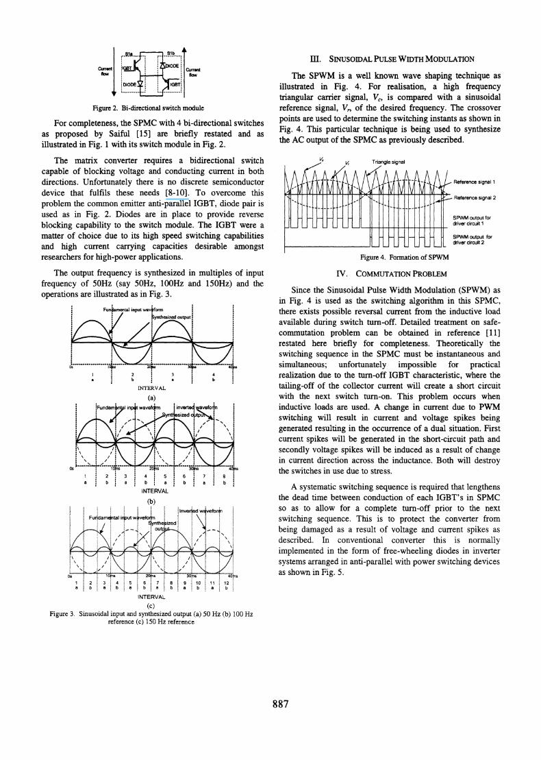
Sibc 1j~L~ODEIII. SINUSOIDAL PULSE WIDTH MODULATION
Cunn ZTff MD ,CurrntThe SPWM is a well known wave shaping technique as
INODEF, IOBTI illustrated in Fig. 4. For realisation, a high frequencytriangular carrier signal, V,, is compared with a sinusoidal
Figure 2. Bi-directional switch module reference signal, V1, of the desired frequency. The crossover
For completeness, the SPMC with 4 bi-directional switches points are used to determine the switching instants as shown in
as proposed by Saiful [15) are briefly restated and as Fig. 4. This particular technique is being used to synthesizeillustrated in Fig. 1 with its switch module in Fig. 2. the AC output of the SPMC as previously described.
The matrix converter requires a bidirectional switch vo v, Triangle signalcapable of blocking voltage and conducting current in bothdirections. Unfortunately there is no discrete semiconductor \ X -, . Reference signal 1
device that fulfils these needs [8-10]. To overcome this - Referencesignal2problem the common emitter anti-parallel IGBT, diode pair is - - -used as in Fig. 2. Diodes are in place to provide reverse SPWM output forblocking capability to the switch module. The IGBT were a J 1- dnverdrcuitlmatter of choice due to its high speed switching capabilities SPWM output forand high current carrying capacities desirable amongst driver crcuit 2
researchers for high-power applications. Figure 4. Formation of SPWM
The output frequency is synthesized in multiples of input IV. COMMUTATION PROBLEMfrequency of 50Hz (say 50Hz, 10OHz and 150Hz) and theoperations are illustrated as in Fig. 3. Since the Sinusoidal Pulse Width Modulation (SPWM) as
twavf~em
in Fig. 4 is used as the switching algorithm in this SPMC,there exists possible reversal current from the inductive loadavailable during switch turn-off. Detailed treatment on safe-commutation problem can be obtained in reference [11]restated here briefly for completeness. Theoretically theswitching sequence in the SPMC must be instantaneous and
35-........................... simultaneous; unfortunately impossible for practical2 3 *4 | realization due to the turn-off IGBT characteristic, where the
a ' b a b
INTERVAL tailing-off of the collector current will create a short circuit(a) with the next switch turn-on. This problem occurs when
1Fundam inptwaW invert a foTn ' inductive loads are used. A change in current due to PWM4. gr' j teda,t. t switching will result in current and voltage spikes being
,I/ ,\., /\ ,/ ', \ . , , " . generated resulting in the occurrence of a dual situation. Firstcurrent spikes will be generated in the short-circuit path and
't/\ tX ': ~ secondly voltage spikes will be induced as a result of change,".:,/' ' < / " . ' \ , .in current direction across the inductance. Both will destroy
2! 310"st 20fis t sobs . 40trs the switches in use due to stress.1 t 2 . 3 * 4 t 5 t 6 t 7 8 ts bI a ? b. sIb is:a b ! a , b a, b a , b A systematic switching sequence is required that lengthens
INTERVAL(b) the dead time between conduction of each IGBT's in SPMC
* ' 'Invertedwveforin so as to allow for a complete turn-off prior to the nextFurdamQflal rr4putwevelorhii d \switching sequence. This is to protect the converter from.ou2tze being damaged as a result of voltage and cufrent spikes as
described. In conventional converter this is normallyk p\ t , implemented in the form of free-wheeling diodes in inverter
systems arranged in anti-parallel with power switching devicesOi 2 3 . s as shown in Fig. 5.Os l ns 2 ns 30n ; g40ss
1 i2 3 4 5 6 7 58 .9 10 11 i12b a b a b a b a b a
INTERVAL(c)
Figure 3. Sinusoidal input and synthesized output (a) 50 Hz (b) 100 Hzreference (c) 150 Hz reference
887
The sequences of switching and commutation switchingstrategies are dependent on the time interval and state of the
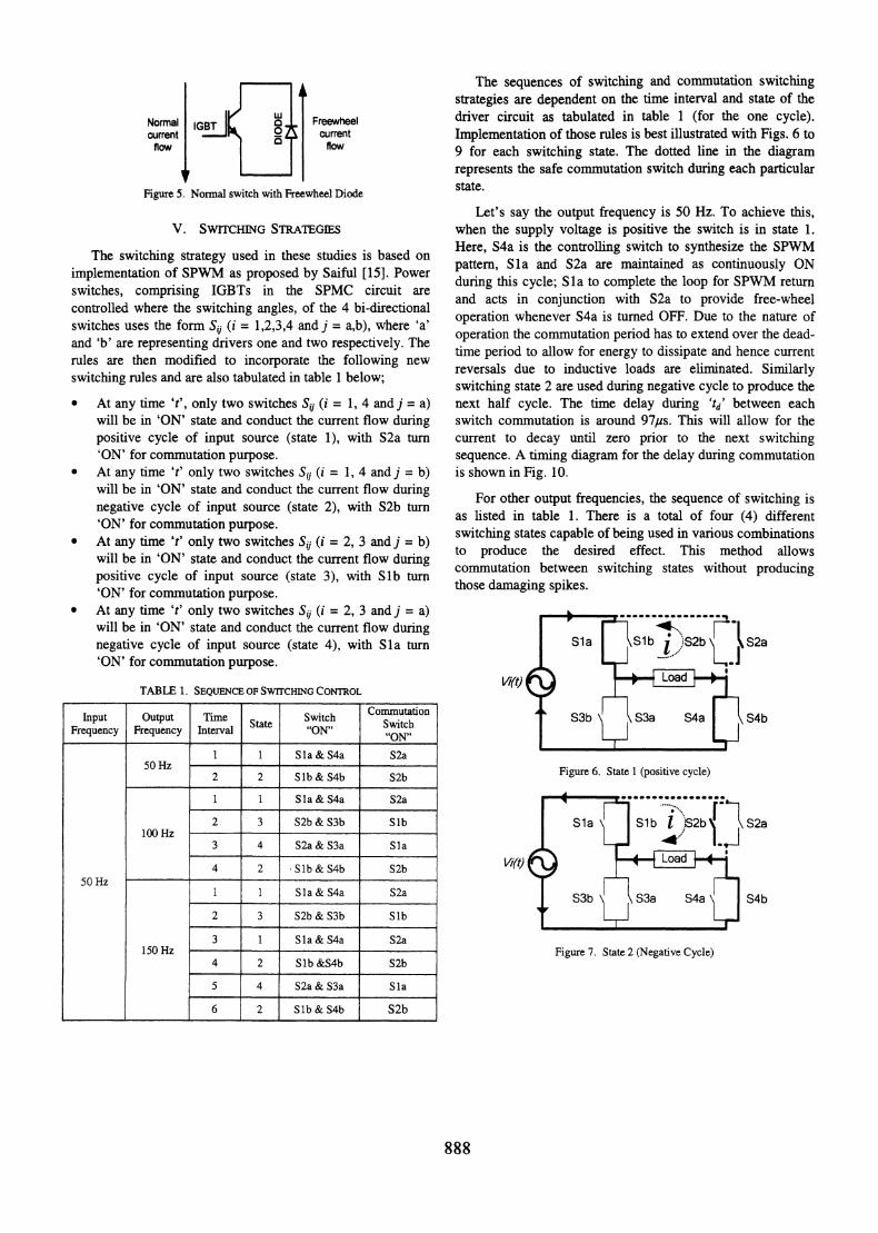
Normal JGBT Freewheel driver circuit as tabulated in table 1 (for the one cycle).current current Implementation of those rules is best illustrated with Figs. 6 toflow flow 9 for each switching state. The dotted line in the diagram
L........1 trepresents the safe commutation switch during each particularFigure 5. Normal switch with Freewheel Diode state.
Let's say the output frequency is 50 Hz. To achieve this,V. SWITCHING STRATEGES when the supply voltage is positive the switch is in state 1.
Here, S4a is the controlling switch to synthesize the SPWMThe switching strategy used in these studies iS based on pattern Sl1a and S2a are maintained as continuously ONimplementation of SPWM as proposed by Saiful [151. Power dithis cle; Sla to cmpleteith lo fortSPWM r Nswitches copisn IGT inteSM.ici r
during this cycle; Sla to complete the loop for SPWM returnswitches,comprising IGBTs in the SPMC circuit are and acts in conjunction with S2a to provide free-wheelcontrolled where the switching angles, of the 4 bi-directional operation whenever S4a is turned OFF. Due to the nature of
switches uses the form S (i = 1,2,3,4 and]j = a,b), where 'a operation the commutation period has to extend over the dead-and 'b' are representing drivers one and two respectively. The time period to allow for energy to dissipate and hence currentrules are then modified to incorporate the following new reversals due to inductive loads are eliminated. Similarlyswitching rules and are also tabulated in table 1 below; switching state 2 are used during negative cycle to produce the* At any time 't', only two switches Sij (i = 1, 4 and j = a) next half cycle. The time delay during 'td' between each
will be in 'ON' state and conduct the current flow during switch commutation is around 97,us. This will allow for thepositive cycle of input source (state 1), with S2a turn current to decay until zero prior to the next switching'ON' for commutation purpose. sequence. A timing diagram for the delay during commutation
* At any time 't' only two switches Sij (i = 1, 4 and j = b) is shown in Fig. 10.will be in 'ON' state and conduct the current flow during For other output frequencies, the sequence of switching isnegative cycle of input source (state 2), with S2b turn'n'gafor commutationputsorpo (se. as listed in table 1. There is a total of four (4) different'OAt any timmeut'tonly twrposwithes S(i =2,3andj=b) switching states capable of being used in various combinations* At any time 't' only two switches Sij (i = 2, 3 and j = b) topdue he esrd fec.Ti mtodalw'. ~~to produce the desired effect. This method allowswill be in 'ON' state and conduct the current flow during commutation between switching states without producingpositive cycle of input source (state 3), with Slb turn those damaging spikes.'ON' for commutation purpose.
* At any time 't' only two switches Sij (i = 2, 3 and j = a)will be in 'ON' state and conduct the current flow duringnegative cycle of input source (state 4), with Sla turn Sla Slb i S2b S2a'ON' for commutation purpose.
TABLE 1. SEQUENCE OF SWITCHING CONTROL V4't)
Input Output Time State Switch Commutation S3b S3a S4a S4bFrequency Frequency Interval "ON" "whON"
1 I Sla & S4a S2a50Hz 2 2 Sib & S4b S2b Figure 6. State 1 (positive cycle)
1 1 Sla & S4a S2a
2 3 S2b& S3b Slb S1a Slb i 2b S2a100Hz
3 4 S2a & S3a Sla
4 2 Slb&4b S2b Vt)50Hz
1 1 Sla & S4a S2a S3b S3a S4a S4b
2 3 |S2bh&S3b Slb
3 1 Sla & S4a S2a150 Hz - Figure 7. State 2 (Negative Cycle)
4 2 Slb&S4b S2b
5 4 S2a& S3a Sla
6 2 Slb&S4b S2b
888
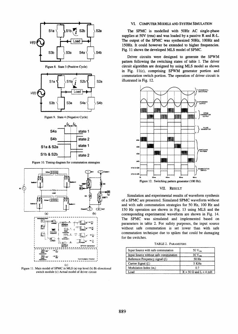
VI. COMPUTER MODELS AND SYSTEM SIMULATION
S1a r \Sib: S2b S2a The SPMC is modelled with 50Hz AC single-phaseI..* Jsupplies at 50V (rms) and was loaded by a passive R and R-L.
i(t) Load The output of the SPMC was synthesized 50Hz, 1OOHz and15OHz. It could however be extended to higher frequencies.
S3b S3a S4a S4b Fig. 1I shows the developed MLS model of SPMC.
Driver circuits were designed to generate the SPWMpattern following the switching states of table 1. The driver
Figure 8. State 3 (Positive Cycle) circuit algorithm are designed by using MLS model as shownin Fig. 11(c), comprising SPWM generator portion andcommutation switch portion. The operation of driver circuit is
Sla \ kS1bf ' S2bX S2a illustrated in Fig. 12.
FUNDAMENTAL
KMg LoaYUAVEFORM
S3b S3a S4a S4b SYUTPUTED
Figure 9. State 4 (Negative Cycle) b 1- - gJ¶il} GEERAUTOR
tdoy tdo1 I ~~~~~~~~~~~~~~~~~~~~~~~~~~~~~~~~~~~PULSES4a state 1
ENERATOR
S4 stte 1 4
S4b state 2 Su
Sla&S2asatell t ~~~~~~~~~~~~~~~~~~~~~~~~~~~~~~SWJTCHING
Slb&S2b s3tte2A
Figure 10. Timing diagram for commutation strategies s4b
sla & - - - - COMMUTATION
lrwer5-f ll tCann1 Czb{<{9}C05HTCH
S3 ISwitch 2 TD
Figure 12. Switching pattem generator (100 Hz).CT _ VII. RESULT> ~~~~~-MlAI-- , I 1
Dl Ter1 Simulation and experimental results of waveform synthesis
m au m r4 of a SPMC are presented. Simulated SPMC waveform withoutSWIICh3 cht\^4 b r and with safe commutation strategies for 50 Hz, 100 Hz and
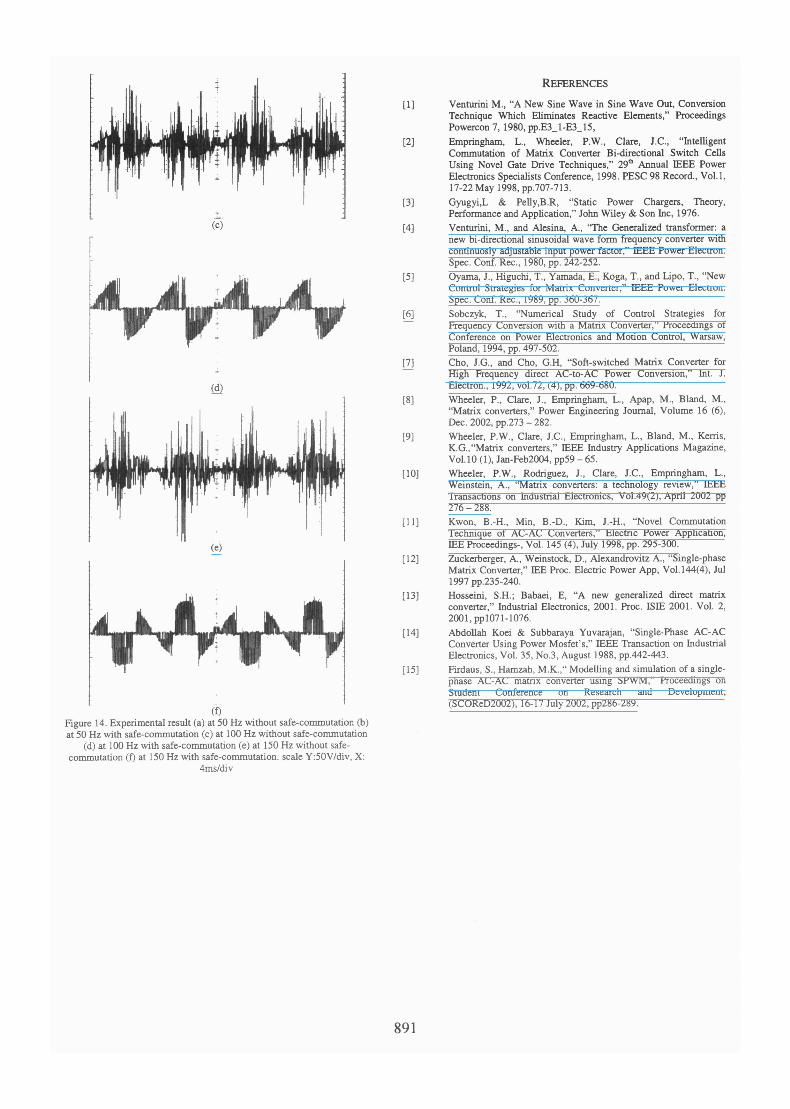
CAm2 w 150 Hz operation are shown in Fig. 13 using MLS and the(a) (b) corresponding experimental waveform are shown in Fig. 14.
------------------------------
The SPMC was simulated and implemented based onX Rt7 ' parameters in table 2. For safety purposes, the input source
^LLi)' [,,. without safe commutation is set lower than with safeE@71 f F -~>-|commutation technique due to spikes that could be damaging
' t } F ,,,,s<"0s, ' > ~~~forthe switches.L>-; - ITABLE 2. PARAMETERS
Op*,-*,, S~PW GneratorI_S__ _ ___ _ _ _ _____
E ,~ Input Source with safe commutation 50 V,",", Iu1_2 , Input Source without safe commutation 30 V,
Commutation SwitchA Reference Frequency signal (f,) 50HzL--______________________________
(c) Carrier Signal (fc) 5 KHzFigure 11. Main model of SPMC in MIS (a) top level (b) Bi-directional Modulation Index (i;) 0.7
switch module (c) Actual model of driver circuit Load R = 50 Q and L = 4 mH
889
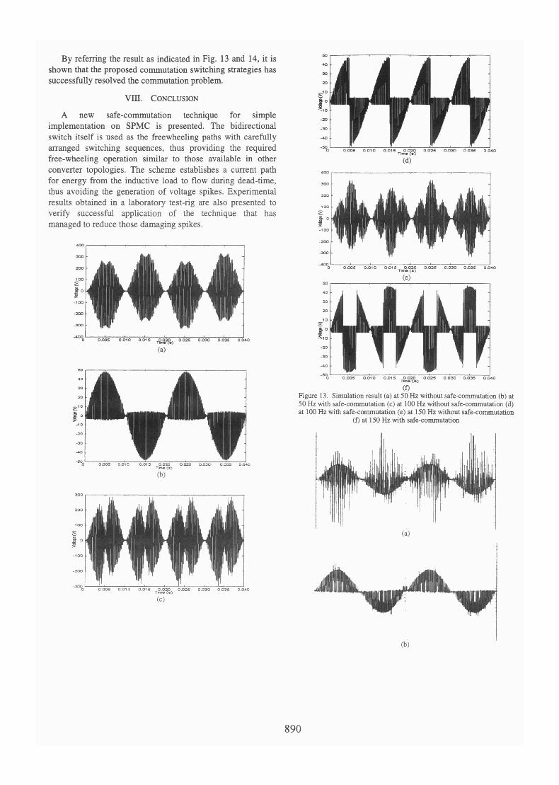
By referring the result as indicated in Fig. 13 and 14, it is 5shown that the proposed commutation switching strategies hassuccessfully resolved the commutation problem.
Vy . CONCLUSION
A new safe-commutation technique for simple ,0implementation on SPMC is presented. The bidirectionalswitch itself is used as the freewheeling paths with carefully -40arranged switching sequences, thus providing the required -5 0.0'05 0.0.10 0 0.020 0.02A5 0.0o30 or 0.04free-wheeling operation similar to those available in other (d)converter topologies. The scheme establishes a current pathfor energy from the inductive load to flow during dead-time, 300thus avoiding the generation of voltage spikes. Experimental 200results obtained in a laboratory test-rig are also presented to 100verify successful application of the technique that hasmanaged to reduce those damaging spikes.
200 jiz_ C~~~~~~~~~~~~~~0.005 0.010 0.015Tav0.020 05 0.030 0.035 0540
_400 t _ __ _~~~~~~~~~~~~~~~~~~0
4000°
0 0 .00m 0015s
O4t, 0.025 0.030 0.030 0.0400
.00~~~~~~~~~~~~~~~~~~~~~~~~~~~4-300 w w r
20000 0.005 0.010 0.015 0.T20 0.025 0.030 0.035 0.040
40 _-_ (f)20 _ ~~~~~~~~~~~~~~~~Figure 13. Simulation result (a) at 50 Hz without safe-commutation (b) at*o ~~~~~~~~~~~~~~~~~50 Hz with safe-commutation (c) at 100 Hz without safe-commutation (d)
$ 0 l ~~~~~~~~~~~~~~~~at100 Hz with safe-commutation (e) at 150 Hz without safe-comsmutation.10 _ ~~~~~~~~~~~~~~~~~~~~(f)at 150 Hz with safe-commutation
E___ ~~~~~~~~~~~~~~~~~~~~~~~~~~~~~~~~(a)
_100 w w-200 1w!=
-300 E _-
O4% Tieows0l _L >_0000 0.010 0.015 ~.j 0.020 0.030 0.030 0.040
(c)~~~ ~ ~ ~
890
REFERENCES
. .'T,[1] Venturini M., "A New Sine Wave in Sine Wave Out, ConversionTechnique Which Eliminates Reactive Elements," ProceedingsPowercon 7, 1980, pp.E3_1-E3_15,
[2] Empringham, L., Wheeler, P.W., Clare, J.C., "IntelligentCommutation of Matrix Converter Bi-directional Switch Cells
t ~~~~~~~~~~~~UsingNovel Gate Drive Techniques," 29's' Annual IEEE PowerElectronics Specialists Conference, 1998. PESC 98 Record., Vol.1,17-22 May 1998, pp.707-713.
[3] Gyugyi,L & Pelly,B.R, "Static Power Chargers, Theory,Performance and Application," John Wiley & Son Inc, 1976.
(c) [4] Venturini, M., and Alesina, A., "The Generalized transformer: anew bi-directional sinusoidal wave form frequency converter withcontinuosly adjustable input power factor," IEEE Power Electron.Spec. Conf. Rec., 1980, pp. 242-252.
[5] Oyama, J., Higuchi, T., Yamada, E., Koga, T., and Lipo, T., "NewControl Strategies for Matrix Converter," IEEE Power Electron.Spec. Conf. Rec., 1989, pp. 360-367.
[6] Sobczyk, T., "Numerical Study of Control Strategies forFrequency Conversion with a Matrix Converter," Proceedings ofConference on Power Electronics and Motion Control, Warsaw,Poland, 1994, pp. 497-502.
[7] Cho, J.G., and Cho, G.H, "Soft-switched Matrix Converter for|High Frequency direct AC-to-AC Power Conversion," Int. J.
(d) Electron., 1992, vol.72, (4), pp. 669-680.[8] Wheeler, P., Clare, J., Empringham, L., Apap, M., Bland, M.,
"Matrix converters," Power Engineering Joumal, Volume 16 (6),Dec. 2002, pp.273-282.
[9] Wheeler, P.W., Clare, J.C., Empringham, L., Bland, M., Kerris,K.G.,"Matrix converters," IEEE Industry Applications Magazine,Vol.10 (1), Jan-Feb2004, pp59 -65.
r-i [10] Wheeler, P.W., Rodriguez, J., Clare, J.C., Empringham, L.,Weinstein, A., "Matrix converters: a technology review," IEEETransactions on Industrial Electronics, Vol.49(2), April 2002 pp276-288.
[11] Kwon, B.-H., Min, B.-D., Kim, J.-H., "Novel CommutationTechnique of AC-AC Converters," Electric Power Application,
(e) EE Proceedings-, Vol. 145 (4), July 1998, pp. 295-300.[12] Zuckerberger, A., Weinstock, D., Alexandrovitz A., "Single-phase
Matrix Converter," IEE Proc. Electric Power App, Vol.144(4), Jul1997 pp.235-240.
[13] Hosseini, S.H.; Babaei, E, "A new generalized direct matrixconverter," Industrial Electronics, 2001. Proc. ISIE 2001. Vol. 2,2001, pp1O71-1076.
4iVL1 [14] Abdollah Koei & Subbaraya Yuvarajan, "Single-Phase AC-ACConverter Using Power Mosfet's," IEEE Transaction on IndustrialElectronics, Vol. 35, No.3, August 1988, pp.442-443.
[15] Firdaus, S., Hamzah, M.K.," Modelling and simulation of a single-phase AC-AC matrix converter using SPWM," Proceedings on
Student Conference on Research and Development,f() (SCOReD2002), 16-17 July 2002, pp286-289.
Figure 14. Experimental result (a) at 50 Hz without safe-commutation (b)at 50 Hz with safe-commutation (c) at 100 Hz without safe-commutation
(d) at 100 Hz with safe-commutation (e) at 150 Hz without safe-commutation (f) at 150 Hz with safe-commutation. scale Y:50V/div, X:
4ms/div
891