Structure and Morphology of PDI8-CN2 for n-Type Thin-Film Transistors
11
www.afm-journal.de FULL PAPER www.MaterialsViews.com © 2012 WILEY-VCH Verlag GmbH & Co. KGaA, Weinheim 943 wileyonlinelibrary.com Fabiola Liscio, Silvia Milita,* Cristiano Albonetti, Pasquale D’Angelo, Antonietta Guagliardi, Norberto Masciocchi, Raffaele Guido Della Valle, Elisabetta Venuti, Aldo Brillante, and Fabio Biscarini appealing characteristics, such as light weight, mechanical flexibility and low-cost production. These advantages make them promising candidates for a wide range of applications such as displays, [10–12] radio- frequency identification (RF-ID) tags, [13] and sensors. [14–17] To make full use of organic electronic circuitry, it is necessary to combine p-channel and n-channel transistors to produce complementary circuits, which show greater speed, reliability and stability than ambipolar ones. [18–21] While highly pure, stable and solution-processable p-type materials with a charge mobility of 1–10 cm 2 V −1 s −1 are nowadays available in production amounts, [22–27] n-type organic semiconductors of high air-stability and mobility are still a topic of research. Indeed, in the past few years, several high-performance n-type semiconductors have been developed, which also exhibit a high stability in ambient conditions, mostly used as films obtained from vapor deposition methods. [28,29] More recently, solution- processable and printable n-type semiconductors, both small molecules and polymers, [30–33] have been reported, allowing unprecedented OTFT characteristics. Perylene di-imide deriva- tives are considered to be among the most important n-type organic materials because of their relatively strong electron affinities and the tailoring of the charge-transport properties upon changing the substituents on the imide N atoms or on the perylene backbone. [34–42] In this paper, we focus on N,N′-bis(n- ctyl)-x:y,dicyanoperylene- 3,4:9,10-bis(dicarboximide), PDI8-CN2, a derivative having two cyano groups directly bound to the aromatic core, which has been proved to be a suitable material for complementary cir- cuits [43] and shown to yield high-performance devices by subli- mation or from solution methods. [44] In spite of the potential of PDI8-CN2 and the importance attributed to the control of grain boundary effects in small- molecule device performance and reproducibility, experimen- tally derived knowledge of the crystal structure and molecular conformation and how these factors affect the multiscale organ- ization and microstructure in the film phase are still missing. The packing motif proposed by Rivnay et al. [44] relies on the combination of the X-ray scattering of thin films and pseudo- potential calculations, which is not as robust or conclusive as Structure and Morphology of PDI8-CN2 for n-Type Thin-Film Transistors A multiscale investigation of N,N′-bis(n-octyl)-x:y, dicyanoperylene-3,4:9,10- bis(dicarboximide), PDI8-CN2, shows the same molecular arrangement in the bulk and in thin films sublimated on SiO 2 /Si wafers. Non-conventional powder diffraction methods and theoretical calculations concur to provide a coherent picture of the crystalline structure. X-ray diffraction (XRD) and atomic force microscopy (AFM) analyses of films of different thickness depos- ited at different substrate temperatures indicate the existence of two temper- ature-dependent deposition regimes: a low-temperature (room temperature) regime and a high-temperature (80–120 °C) one, each characterized by dif- ferent growth mechanisms. These mechanisms eventually result in different morphological and structural features of the films, which appear to be highly correlated with the trend of the electrical parameters that are measured in PDI8-CN2-based field-effect transistors. DOI: 10.1002/adfm.201101640 Dr. F. Liscio, Dr. S. Milita CNR-IMM, Istituto per la Microelettronica e Microsistemi Via P. Gobetti 101, I-40129 Bologna, Italy E-mail: [email protected] Dr. C. Albonetti, Dr. P. D’Angelo, [+] Prof. F. Biscarini CNR–ISMN, Istituto per lo Studio dei Materiali Nanostrutturati Via P. Gobetti 101, I-40129 Bologna, Italy Dr. A. Guagliardi [++] CNR-IC, Istituto di Cristallografia Via Amendola 122/O, 70126 Bari, Italy Prof. N. Masciocchi Dipartimento di Scienze Chimiche e Ambientali Università dell’Insubria Via Valleggio 11, I-22100 Como, Italy Prof. R. G. Della Valle, Dr. E. Venuti, Prof. A. Brillante Dipartimento Chimica Fisica Inorganica Viale Risorgimento 4, I-40136 Bologna, Italy [+] Present address: Chemistry Department, Imperial College London, Exhibition Road, South Kensington, London SW7 2AZ, UK [++] Present address: Dipartimento di Scienze Chimiche e Ambientali, Università dell’Insubria, Via Valleggio 11, I-22100 Como, Italy 1. Introduction In recent years, polycrystalline organic thin-film transistors (OTFTs) have been the subject of growing scientific and tech- nological interest. [1–9] Compared with traditional silicon elec- tronics, devices based on organic semiconductors certainly have Adv. Funct. Mater. 2012, 22, 943–953
-
Upload
independent -
Category
Documents
-
view
1 -
download
0
Transcript of Structure and Morphology of PDI8-CN2 for n-Type Thin-Film Transistors

www.afm-journal.de
FULL P
APER
www.MaterialsViews.com
Fabiola Liscio, Silvia Milita,* Cristiano Albonetti, Pasquale D’Angelo, Antonietta Guagliardi, Norberto Masciocchi, Raffaele Guido Della Valle, Elisabetta Venuti, Aldo Brillante, and Fabio Biscarini
Structure and Morphology of PDI8-CN2 for n-Type Thin-Film Transistors
A multiscale investigation of N,N′-bis(n-octyl)-x:y, dicyanoperylene-3,4:9,10-bis(dicarboximide), PDI8-CN2, shows the same molecular arrangement in the bulk and in thin films sublimated on SiO2/Si wafers. Non-conventional powder diffraction methods and theoretical calculations concur to provide a coherent picture of the crystalline structure. X-ray diffraction (XRD) and atomic force microscopy (AFM) analyses of films of different thickness depos-ited at different substrate temperatures indicate the existence of two temper-ature-dependent deposition regimes: a low-temperature (room temperature) regime and a high-temperature (80–120 °C) one, each characterized by dif-ferent growth mechanisms. These mechanisms eventually result in different morphological and structural features of the films, which appear to be highly correlated with the trend of the electrical parameters that are measured in PDI8-CN2-based field-effect transistors.
1. Introduction
In recent years, polycrystalline organic thin-film transistors (OTFTs) have been the subject of growing scientific and tech-nological interest.[1–9] Compared with traditional silicon elec-tronics, devices based on organic semiconductors certainly have
© 2012 WILEY-VCH Verlag GmbH & Co. KGaA, Weinheim
DOI: 10.1002/adfm.201101640
Dr. F. Liscio, Dr. S. MilitaCNR-IMM, Istituto per la Microelettronica e Microsistemi Via P. Gobetti 101, I-40129 Bologna, Italy E-mail: [email protected]. C. Albonetti, Dr. P. D’Angelo,[+] Prof. F. BiscariniCNR–ISMN, Istituto per lo Studio dei Materiali Nanostrutturati Via P. Gobetti 101, I-40129 Bologna, ItalyDr. A. Guagliardi[++]
CNR-IC, Istituto di Cristallografia Via Amendola 122/O, 70126 Bari, ItalyProf. N. MasciocchiDipartimento di Scienze Chimiche e Ambientali Università dell’Insubria Via Valleggio 11, I-22100 Como, ItalyProf. R. G. Della Valle, Dr. E. Venuti, Prof. A. BrillanteDipartimento Chimica Fisica Inorganica Viale Risorgimento 4, I-40136 Bologna, Italy[+] Present address: Chemistry Department, Imperial College London, Exhibition Road, South Kensington, London SW7 2AZ, UK[++] Present address: Dipartimento di Scienze Chimiche e Ambientali, Università dell’Insubria, Via Valleggio 11, I-22100 Como, Italy
Adv. Funct. Mater. 2012, 22, 943–953
appealing characteristics, such as light weight, mechanical flexibility and low-cost production. These advantages make them promising candidates for a wide range of applications such as displays,[10–12] radio-frequency identification (RF-ID) tags,[13] and sensors.[14–17]
To make full use of organic electronic circuitry, it is necessary to combine p-channel and n-channel transistors to produce complementary circuits, which show greater speed, reliability and stability than ambipolar ones.[18–21] While highly pure, stable and solution-processable p-type materials with a charge mobility of 1–10 cm2 V−1 s−1 are nowadays available in production amounts,[22–27] n-type organic semiconductors of high air-stability and mobility are still a topic of research.
Indeed, in the past few years, several high-performance n-type semiconductors have been developed, which also exhibit a high stability in ambient conditions, mostly used as films obtained from vapor deposition methods.[28,29] More recently, solution-processable and printable n-type semiconductors, both small molecules and polymers,[30–33] have been reported, allowing unprecedented OTFT characteristics. Perylene di-imide deriva-tives are considered to be among the most important n-type organic materials because of their relatively strong electron affinities and the tailoring of the charge-transport properties upon changing the substituents on the imide N atoms or on the perylene backbone.[34–42]
In this paper, we focus on N,N′-bis(n- ctyl)-x:y,dicyanoperylene-3,4:9,10-bis(dicarboximide), PDI8-CN2, a derivative having two cyano groups directly bound to the aromatic core, which has been proved to be a suitable material for complementary cir-cuits[43] and shown to yield high-performance devices by subli-mation or from solution methods.[44]
In spite of the potential of PDI8-CN2 and the importance attributed to the control of grain boundary effects in small- molecule device performance and reproducibility, experimen-tally derived knowledge of the crystal structure and molecular conformation and how these factors affect the multiscale organ-ization and microstructure in the film phase are still missing. The packing motif proposed by Rivnay et al.[44] relies on the combination of the X-ray scattering of thin films and pseudo-potential calculations, which is not as robust or conclusive as
943wileyonlinelibrary.com

FULL
PAPER
www.afm-journal.dewww.MaterialsViews.com
944
Table 1. Lattice parameters of PDI8-CN2, refined from powders (XRPD) and thin films (GID).[44] The last row refers to calculated values from MM simulations.
a [Å]
b [Å]
c [Å]
α [°]
β [°]
γ [°]
V [Å3]
XRPD 5.019 8.841 20.195 101.51 92.33 100.15 862
GID, Rivnay (reduced) 5.028 8.930 19.944 99.8 90.6 100.7 867
MM, this work 5.081 8.516 21.260 97.8 99.0 96.5 892
single-crystal and powder diffraction crystal-lographic structure determination methods. A correlation between the structural and charge transport properties in PDI8-CN2 films has not yet exhaustively been estab-lished. Sublimation was chosen as the most controllable fabrication method, although the obtained results could easily be applied to systems obtained from solution. Indeed, the
Figure 1. a) Schematic drawing of the crystal structure of PDI8-CN2, viewed down [ 100]; horizontal axis = b. The absence of alkyl-chain inter-digitation in the c direction, originally proposed by Rivnay et al.[44] is evi-dent. b) π–π stacking of the flat perylene cores in the ABCA sequence (side chains omitted for clarity). The molecules stack along the [−651] vector.
presence of the same crystal phase in films prepared from solu-tion and by sublimation has been reported recently, although vapor-phase deposition affords films that are more highly tex-tured than those from solution processing.[45] This evidence entitled Revnay et al. to study evaporated thin films suitable for quantitative analysis, in order to propose their crystal-phase model.[44]
Since we were not able to grow crystalline samples of suit-able size and quality for a complete, single-crystal structural analysis, we opted for a less conventional structural powder diffraction method, from which we successfully retrieved oth-erwise inaccessible structural information. This approach is possible when the molecular complexity is not too high. Due to the accuracy level inherent in the collapse of the 3D diffraction pattern to a single axis, which is typical of a powder diffraction trace, and due to the limited scattering power of the organic material, we decided to further validate the structural model by means of ab initio and molecular-mechanics (MM) calcu-lations. Once the crystal structure of the bulk material was assessed, a fruitful comparison with the structure of the thin film phase was established by ancillary diffraction methods; finally, the dependence of the device performance on the film structure, morphology and growth mechanism was investi-gated for different thicknesses and substrate temperatures during the deposition.
The paper is organized as follows: the crystal structure of PDI8-CN2 in the bulk material and in the film is described in Section 2; Section 3 deals with the structural and morpholog-ical dependence of PDI8-CN2 films on substrate temperature and thickness; Section 4 is dedicated to the discussion of the experimental results with the purpose of elucidating the OTFT performances and the main conclusions are also drawn in this section.
2. The Crystal Structure of PDI8-CN2
2.1. The Crystal Structure of the Bulk
A convincing crystal structure arrangement was extracted by coupling diffraction data from two different experimental set-ups (a conventional parafocusing Bragg–Brentano θ:θ goniom-eter and a Debye-Scherrer diffractometer)[46] in order to limit undesired experimental effects imposed by the acicular shape of the crystals (vide infra). These data were analyzed by the fairly complex approach described in the Supporting Information, with the aid of the theoretical prediction/validation reported below. The parameters of the reduced unit cell of powder PDI8-CN2 (P-PD), shown in Table 1, are somewhat similar, but not
© 2012 WILEY-VCH Verlag Gwileyonlinelibrary.com
identical, to those previously reported for thin films[44] after cell reduction (TF-PD). Both the proposed unit cells are triclinic and share two axes (a,b) and interaxial angle (here γ), whereas they slightly differ in c-axis length and, to a minor extent, direc-tion. These results suggest that the TF-PD and P-PD materials likely belong to the same crystal phase. However, the molecular arrangement of the structural model that best fits the observed powder diffraction traces, derived by the non-conventional struc-ture solution and full pattern refinements performed by simul-taneously using both the datasets discussed above (Figure SI.1 and Table SI.1, Supporting Information), is markedly different from that originally proposed and is shown, in projection, in the drawing in Figure 1a.
In the crystal structure of P-PD that we have derived, the planar centrosymmetric perylene cores stack cofacially by the short π–π contact of approximately 3.40 Å, a typical intermolecular distance between adjacent aromatic planes of perylene cores.[47] It is noteworthy that the hexagonal rings generating this infinite stack are shifted on top of each other in the ABCABC sequence, typical of the rhombohedral stacking of graphene sheets[48] and not of ordinary hexagonal graphite. Figure 1b shows a molecular stack (along the [−651] direction) of the aromatic cores with the
mbH & Co. KGaA, Weinheim Adv. Funct. Mater. 2012, 22, 943–953

FULL P
APER
www.afm-journal.dewww.MaterialsViews.com
Figure 2. a) Experimental 2D-GID image of PDI8-CN2 film (t = 100 nm and Tsub = 120 °C) performed with X-ray wavelength λ = 0.8499 Å and an incidence angle αi = 0.15°. Simulated 2D-GID image reproduced by using the P-PD structure (b) and a structure with interdigitated alkylic chains (c).[44]
short van der Waals interactions drawn as dotted lines.[49–51] The slippage angle (i.e., the angle between the vector normal to the aromatic planes and the vector joining the centers of the two adjacent PDI8-CN2 molecules) is 51°. This value approaches the magic angle value of 54.7°,[52] suggesting that the packing of PDI8-CN2 molecules in the film resembles a J-type aggregation. This result is in agreement with the reported UV–vis absorption spectrum of PDI8-CN2 films,[53] red shifted with respect to that of the molecules in diluted solution.
Interestingly, the prototypical all-trans conformation of the long alkyl chains[44] is absent here. The pertinent refined tor-sion angles, reported in the Supporting Information, result in an approximate tttgtt chain conformation (t = trans, g = gauche). In the crystal, a few weak H-bond interactions exist, involving the cyano (CH…NC = 2.43 Å) and the oxo (CH…OC = 2.43 Å) residues, falling in the range of weakly attractive (stabilizing) contacts. The slip-stacked motif and the intermolecular contacts between the aromatic planes are similar to those observed in related perylene derivatives, namely PTCDI-C8[54] and PDI4-CN2.[35] However, due to the absence of CN groups in the former case and the shorter alkyl chains in the latter, the men-tioned intermolecular interactions do not take place and a dif-ferent alkyl-chain configuration is favored.
Our P-PD refined model does not match the entropically dis-favored interdigitation pattern of the long alkyls proposed on the basis of molecular modeling simulations.[44] Coupled with the possible reduced accuracy inherent to the powder method, this prompted us to investigate the origin of such a discrep-ancy in depth. Therefore, the experimentally derived crystal structure was validated by means of ab initio (gas-phase) and molecular mechanics (in the crystal) energy-minimization calculations, together with a crystal structure search[55,56] in a reduced subspace. Such a subspace was defined by the assessed information about the crystal (namely, the unit cell parameters and the symmetry). This procedure was aimed at identifying the position of the P-PD model in the energy land-scape of the many energetically accessible structures of this compound.
Ab initio calculations performed on isolated PDI8-CN2 molecules showed that the experimentally determined P-PD conformation converges to a local energy minimum, less stable by 1.58 kcal mol−1 than the all-trans isomer. In lattice energy calculations, the experimental P-PD structure was found to converge to the deepest minimum of the potential energy surface. The attained minimum was also the most frequently encountered in the structure search, and must therefore corre-spond to a large attraction basin of the energy surface. Finally, the X-ray diffraction pattern computed for this calculated struc-ture showed a very good agreement with the P-PD data. These results test the quality of the adopted potential model and enable a separate check of the reliability of the experimental molecular packing and geometry. Once the constraints on the lattice parameters were finally removed, a new deep minimum was attained, with lattice parameters shown in Table 1 and in fair agreement with the P-PD ones, but with a slightly inflated volume, by about 3%. It is worth noting that the computed versus the experimental cell volumes of the PDI-n analogues (Table SI.2, Supporting Information) show similar inflation, and therefore appear to be inherent in the computational
© 2012 WILEY-VCH Verlag GAdv. Funct. Mater. 2012, 22, 943–953
model. Moreover, the alkyl chains of the compound in the computed structure are still in a bent conformation, much like the experimental one.
2.2. The Crystal Structure of the Thin Films
After determining the P-PD structure, we turned our atten-tion to the PDI8-CN2 films, combining X-ray diffraction (XRD) measurements performed in specular and grazing incidence diffraction (GID) geometries. As an example, we consid-ered a 100 nm-thick film sublimed on a 200 nm-thick SiO2/Si substrate at Tsub = 120 °C, whose typical 2D-GID image is shown in Figure 2a. The perfect symmetry of the spot distri-bution with respect to the central vertical line implies a fiber-like symmetry of the molecular orientation,[57] with the long inertial axis almost normal to the substrate surface, (i.e., with the ab plane parallel to the substrate surface and c* normal to it), as confirmed by the specular scans (vide infra). Thanks to the knowledge of the domain orientation and of the triclinic lattice symmetry, all of the reflections could be indexed. The presence of the 010 reflection in the 2D-GID image indicates that the projection of the structure on the a*b* plane did not
mbH & Co. KGaA, Weinheim 945wileyonlinelibrary.com

FULL
PAPER
www.afm-journal.dewww.MaterialsViews.com
946
Figure 3. AFM images of PDI8-CN2 films of different thicknesses (10 nm, 40 nm and 100 nm) deposited at Tsub = RT, 80 °C and 120 °C.
have p2gg symmetry, excluding a molecular arrangement in the herringbone configuration,[58] in agreement with the bulk phase structure. The unit cell parameters extracted from the Bragg positions in the 2D-GID image (qxy and qz values) and in the specular scan[59] fairly match those of the bulk phase that are reported in Table 1. The simulated 2D-GID image[60] for a polycrystalline film with the P-PD crystal structure is shown in Figure 2b. The good agreement between the simulated and the experimental images, in particular, of their spot intensities, allowed us to establish that the molecular packing in the film was the same as the powder bulk phase. Indeed, a small devia-tion in the atomic positions and in the molecular orientation has a pronounced effect on the intensity distribution and a sub-stantial discrepancy was observed when a crystal structure with interdigitated chains (such as that proposed by Rivnay et al.[44]) was considered (see Figure 2c).
The invariance of the molecular packing in the films and in the bulk differs from what is observed for other perylene deriva-tives (i.e., PTCDI-C8[61,62] and PTCDI-C5[37,63,64]), where the c lat-tice parameter of the thin-film structure is found to be signifi-cantly larger and the tilt angle of the aromatic core relative to the ab plane is found to be slightly smaller than those of the bulk case. For PTCDI-C5 molecules,[37] a thin film phase was observed for films deposited at Tsub < 125 °C, whereas films grown at a higher temperature possessed the bulk phase structure. In such a case, the thin-film structure was identified as being a metast-able growth-limited phase of a thermodynamically stable poly-morph. Liquid crystalline phases and polymorphism are indeed well documented in the perylene di-imide family of molecules.[64] Differently, our results can be interpreted by the presence of the CN groups, which impose geometrically stiff intermolecular interactions, basically unaffected by molecule-substrate interac-tions. The structural similarity of the film and bulk materials and knowledge of their common crystalline structure allows us to evaluate the tilting of the average polyaromatic molecular planes with respect to the surface of the film (taken as the ab plane), estimated to be 68.1°. It follows that the molecules stack with π–π interactions almost perpendicular to the substrate surface, which is relevant information for interpreting the charge carrier trans-port mechanism. However, as discussed in the following sec-tion, a small variability of the lattice parameters was observed for films prepared under different conditions, but, on the basis of the extracted values, we consider it too small to invoke the pres-ence of an independent thin-film phase; accordingly, we prefer to interpret this effect as a slight distortion of the bulk phase, rather than as the existence of new polymorphic forms.
3. The Dependence of the PDI8-CN2 Film Structure and Morphology on Tsub and the Film Thickness t
PDI8-CN2 films of three different thicknesses (10, 40, and 100 nm) were deposited by high-vacuum sublimation (HVS) (P = 2 × 10⁻⁸ mbar) at a rate of 12.5 Å min−1 on a 200 nm-thick SiO2 substrate thermally grown on a (001) Si wafer. Three series of films were prepared by keeping the substrate temperature, Tsub, at 25 °C (room temperature (RT)), 80 °C and 120 °C during the deposition.
© 2012 WILEY-VCH Verlag Gwileyonlinelibrary.com
3.1. Morphology Variability of the PDI8-CN2 Films on Tsub and t
The morphology of the PDI8-CN2 films was characterized using atomic force microscopy (AFM) in intermittent contact mode configuration. The topographic images, recorded on sur-face regions with a lateral size of 5 μm (Figure 3) show a clear dependence on both Tsub and the film thickness t.
For all of the Tsub values, the grain and island sizes increased with t without any significant changes in shape.
The films grown at RT were formed by small grains with sizes ranging from 60 nm (t = 10 nm) to 100 nm (t = 100 nm), whereas those grown at 80°C and 120 °C consisted of large terraces, a few micrometers long. The terraces were character-ized by molecular steps 17 ± 2 Å high, a value close to the d(001) spacing (≈19.7 Å), as determined by the XRD measurements (see above). In the thicker ones (t = 100 nm), the terraces were covered by elongated islands, which are commonly observed in other perylene derivatives, and are due to an anisotropic 2D growth.[61]
In addition, we noticed that films grown at 120 °C revealed crack formation. The thermal expansion coefficient for the organic film is likely to be more than an order of magnitude larger than that of the SiO2 substrate. Therefore, upon cooling, the film was put under tension and underwent cracking. As expected, films with severe cracking yielded OTFTs with dimin-ished carrier mobility and significant threshold instability.
For each sample, the root-mean-square roughness, σsurf, was determined as the standard deviation of the film height distribu-tion averaged over three topographic images with a lateral size of 30 μm (Table SI.3, Supporting Information). Figure 4a shows a log–log plot of σsurf as a function of t for the films deposited at the three values of Tsub. Regardless of Tsub, σsurf increased with t, and the surface roughening was faster at RT. Indeed, in the films 10 and 40 nm thick, σsurf attained approximately ≈14 Å and ≈20 Å, respectively, for all of the values of Tsub, while at RT,
mbH & Co. KGaA, Weinheim Adv. Funct. Mater. 2012, 22, 943–953
FULL P
APER
www.afm-journal.dewww.MaterialsViews.com
Figure 4. a) Log–log plot of σ surf versus film thickness. The blue dots indicate data for Tsub = RT, the red squares for Tsub = 80 °C and the green diamonds for Tsub = 120 °C. The fitting lines are reported as dashed lines of the corresponding colours. b) Log–log plot of σsurf versus L for PDI8-CN2 films, 100 nm thick, grown at Tsub = 80 °C. Inset: PDI8-CN2 terraces with step ξ/2 wide and ≈17 Å high.
2.6 2.8 3.0 3.2 3.4 3.6 3.8
1.0
1.2
1.4
1.6 a)
log 10
( σsu
rf )
log10
(t)
120°C 80°C RT
4.0 4.4 4.8 5.2 5.6
0.8
1.0
1.2
1.4
0 200 4006
8
10ξ/2
h (n
m)
L (nm)
b)
log 10
( σsu
rf )
log10
(L)
the σsurf of the 100 nm film was almost twice (≈42 Å) the value measured at 80 °C (25 Å) and 120 °C (23 Å). As predicted by dynamic scaling theory (DST),[65] σsurf evolves with t according to a power law σsurf ∝ tβ, where β is the growth exponent. β spans the interval [0, 1] and generally varies from 0 to 0.5 for compact and flat surfaces, while it exceeds 0.5 for mounded surfaces. In our case, for films grown at RT, β was 0.69 ± 0.09, suggesting an anomalous growth, commonly termed rapid roughening and previously reported for both organic[66–68] and inorganic thin films.[69] This roughening is induced by morphological insta-bilities of the film, usually associated with a reduced interlayer transport[70] and is typical of mounded surfaces formed by small grains and highly crystalline clusters (white points in the AFM images of Figure 3). On the other hand, the β values for films grown at higher values of Tsub (80 °C and 120 °C) were lower and similar (0.21 ± 0.02 and 0.15 ± 0.04, respectively), indicating the permanence of their very compact and flat surfaces. In this case, the growth mechanism was close to layer-by-layer, because
© 2012 WILEY-VCH Verlag GmAdv. Funct. Mater. 2012, 22, 943–953
the higher T promotes surface smoothening by enhancing the surface diffusion of the organic molecules.[71–73]
Furthermore, DST predicts that σsurf increases with the lat-eral size L of the image for a fixed t and follows a power law, σsurf(L,t) = μLα, where α is the roughness exponent. α was extracted by plotting σsurf versus L in log–log scale, where σsurf was measured from topographic images with different L, ranging from 1 to 30 μm. Figure 4b shows the plot for the 100 nm-thick PDI8-CN2 film, grown at 80 °C. Similar results were observed for the other cases. Regardless of Tsub, for the thickest films (i.e., 100 nm), multiscale surface evolution was high-lighted by the appearance of two different slopes in the curve (αI and α) with a characteristic length scale ζ ≈ 5 μm (dashed line in Figure 4b). This effect suggests two different regimes of surface fluctuations with respect to the lateral size L, which are identified by global (α) and local (αI) roughness exponents in the ranges 1 μm ≤ L ≤ 5 μm and 5 μm ≤ L ≤ 30 μm, respec-tively. Note that the global and local surface fluctuation images represent the height undulation of the grains and molecular-step accumulations. The global roughness exponent α ≈ 0.12 ± 0.04, averaged for all of the samples, suggests that all the films were smooth over large areas. The local roughness exponent was observed only for the 100 nm films for growth at RT and 80 °C, and for all thicknesses at 120 °C. For the film grown at RT, the αI value of 0.30 ± 0.09 is in agreement with the observed anomalous scaling behavior,[73] while at the higher values of Tsub (80 °C and 120 °C), the value of 0.59 ± 0.09 is consistent with a lamella growth mechanism.[71,74,75] These results are supported by a measure of the correlation length, ξ, extracted from AFM images[76] (Supporting Information). As suggested by Biscarini et al.,[75] ξ increases by increasing both t and Tsub. At RT, ξ ranges from 70 to 170 nm with increasing t, in agree-ment with the average grain sizes evaluated by statistics on the grain diameter distribution (the diameters run from 60 to 100 nm with increasing t).[77] At 80 °C and 120 °C, ξ increases from 300 to 650 nm with increasing t as a consequence of the highly diffusive motion induced by Tsub.[75,77–79] At the highest Tsub, the width of the flat terraces is given by ξ/2 (corresponding to the averaged step width, α, see inset in Figure 4b) and σsurf is comparable to that of SiO2 (5 Å). The values of the exponents β and α of all of the films investigated are reported in Table SI.4, Supporting Information.
3.2. Evolution of the Structure of the PDI8-CN2 Films with Tsub and t
The crystalline structures of the three series of PDI8-CN2 films (Tsub = RT, 80 °C and 120 °C) were investigated using XRD measurements performed in specular and GID geometries.
The 2D-GID images of the films prepared at RT and 120 °C, collected with λ = 0.8499 Å and αi = 0.15°, are reported in Figure 5. Since αi > αc,film = 0.12°, the beam penetration depth exceeded the film thickness, and the resulting data provide structural information on the whole organic film. All of the films were polycrystalline with the <001> fiber-like texturing described before (see Section 2. 1) (i.e., the crystallites were organized with the ab plane parallel to the surface and with a random in-plane orientation). In spite of the markedly different
bH & Co. KGaA, Weinheim 947wileyonlinelibrary.com

FULL
PAPER
www.afm-journal.dewww.MaterialsViews.com
948
Figure 6. Specular XRD scans of PDI8-CN2 films of different nominal thicknesses (10, 40 and 100 nm) sublimated on SiO2 at RT (black line), 80 °C (blue line) and 120 °C (red line). The arrows and the stars indicate the reflections generated by the undesired W Lα and Cu Kβ wavelengths.
102
104
102
104
106
0.2 0.4 0.6 0.8 1.0 1.2 1.4 1.6 1.8 2.0 2.2 2.4
102
104
106
t = 10 nm
*
120°C 80°C RT
t = 40 nm
*
120°C 80°C RT
Inte
nsity
(cp
s)
qz (Å-1)
** 006005
004003002
001
t = 100 nm
*
120°C 80°C RT
Figure 5. a–f) 2D-GID images of PDI8-CN2 films with nominal thickness of 10, 40 and 100 nm, sublimated on SiO2 at RT (a–c) and 120 °C (d–f). The measurements were carried out with λ = 0.8499 Å, an incidence angle αi = 0.15° and using a 2D Pilatus detector.
film morphologies of the films deposited at the two Tsub (see Figure 3), the invariance of the qxyz positions of the reflections, in the limit of the technique’s resolution, indicates that the same crystalline structure was present and persisted for all of the thicknesses (10, 40 and 100 nm). The fact that the crystal-line structure remained almost unchanged (with the caveats discussed later), from the substrate up to the film surface, was confirmed by the lack of any significant difference in the reflec-tion positions in the 2D-GID images recorded at αi = 0.03°, αi << αc,film (not shown here), where the signals originated from a surface layer a few Ångstroms thick. However, a pronounced difference between the two values of T sub could be observed regarding both the shape and intensity of the diffraction peaks. For the RT films, the arched shape of the Bragg spots,
Figure 7. (004) RCs of the PDI8-CN2 films of nominal thicknesses 10, 40 and 100, sublimated at RT (black dots), 80 °C (blue dots) and 120 °C (red dots).
-2 -1 0 1 2-2 -1 0 1 2-2 -1 0 1 2101
102
103
ω (deg) ω (deg)
t = 100 nm 120°C 80°C RT
ω (deg)
120°C 80°C RT
t = 40 nm
Inte
nsity
(cp
s)
t = 10 nm 120°C 80°C RT
together with the presence of reflections in the specular region (qxy = 0), indicate a large distribution of orientations of the ab plane (Figure SI.3, Supporting Information), otherwise negligible at 120 °C. The lower peak inten-sity values observed for the RT films are then likely attributed to a much wider peak width in the azimuthal (and not radial) direction, although structural effects, such as modi-fied static Debye–Waller factors, which would point to disorder or significantly enhanced molecular mobility, are not precluded.
High-resolution XRD measurements pro-vided interesting additional information. For all of the films, the specular scans (ω/2θ
© 2012 WILEY-VCH Verlag Gwileyonlinelibrary.com
scans reported in qz scale, where qz = 4πsinθ/λ, in Figure 6) and the (004) rocking curves (RCs) (ω scans recorded around the 004 peak shown in Figure 7) allowed the extraction of several microstructural parameters, which are reported in Table 2.
A close inspection of the specular scans indicates that the absolute intensities nearly scale with t2, as expected for a mass effect, and that the RT films show systematically lower values, probably because of the mentioned wide spread in the recip-rocal space. This effect is clearly observed in the plots collected in Figure 7, which show that the peak widths (full width at half-maximum (FWHM) of the (004) RCs), a measure of the angular spread of the orientations of the crystallites, approach or exceed the 2.0° value for the RT films, and shrink to nearly 0.03° for the 80 °C and 120 °C films. In other words, Tsub drives the film texturing, manifested by the change of the widths of the (004) RCs, which is a direct measure of the spreading of orientations of the (00l) lattice plane about the substrate normal. For the two higher values of Tsub, a broad component due to diffusive scat-tering (DS) is also observed and can be ascribed to structural
mbH & Co. KGaA, Weinheim Adv. Funct. Mater. 2012, 22, 943–953
FULL P
APER
www.afm-journal.dewww.MaterialsViews.com
Table 2. Structural parameters determined by specular scans and (004) RC measurements of PDI8-CN2 films: thickness, t; d(001); domain size along the surface normal, Dperp; and FWHM of (004) RCs.
T sub [°C]
t [nm]
d (001) [Å]
D perp [nm]
FWHM(004) [°]
RT 9.50 ± 0.03 19.99 ± 0.03 11 ± 1 1.9 ± 0.1
RT 42.5 ± 0.2 19.90 ± 0.03 33 ± 1 1.70 ± 0.02
RT 100.9 ± 0.2 19.85 ± 0.03 35 ± 1 2.59 ± 0.07
80 10.23 ± 0.08 19.92 ± 0.03 12 ± 1 0.033 ± 0.001
80 38.9 ± 0.3 19.77 ± 0.03 40 ± 1 0.0321 ± 0.0003
80 88.4 ± 0.3 19.75 ± 0.03 50 ± 1 0.0356 ± 0.0006
120 11.19 ± 0.02 19.85 ± 0.03 13 ± 1 0.034 ± 0.001
120 44.58 ± 0.01 19.73 ± 0.03 40 ± 1 0.0339 ± 0.0005
120 103.7 ± 0.1 19.71 ± 0.03 50 ± 1 0.0352 ± 0.0008
defects present in the crystalline domains.[80,81] In pentacene films, the width of the DS contribution was related to the den-sity of dislocations[58] created during the film growth. Interest-ingly, in our case, the DS width was found to decrease with increasing film thickness, attaining ≈1.0° (t = 10 nm), ≈0.34° (t = 40 nm) and 0.25° (t = 100 nm), at the two higher values of Tsub. This suggests that at higher values of Tsub, structural defects are generated mainly in the first stage of the growth (thinner films) and partially anneal during deposition (thicker films).[79,82]
The presence of the Laue oscillations around the (001) peak in the specular scans was observed for all of the samples except the thickest, where the oscillation period was too short to be experimentally resolved. These oscillations, more pronounced for the higher values of Tsub (80 °C and 120 °C), are evidence of the coherent nature of the film (along the depth profile), built upon a regular stacking of ordered monolayers (ML).
The PDI8-CN2 d(001) interlayer spacing was determined by accurate analysis of the (004) Bragg peak, which was intense and not affected by the overlapping of the Laue fringes. The d(001) values determined for all of the films (Table 2) showed a slight dependence on both t and Tsub. As pictorially shown in Figure 8, d(001) decreased with increasing t; for constant t, it decreased with Tsub, approaching the value measured for P-PD (d(001) = 19.73 Å). It is noteworthy that such small changes in
© 2012 WILEY-VCH Verlag GmAdv. Funct. Mater. 2012, 22, 943–953
Figure 8. Plot of the d(001) spacing (Å) versus thickness (Å) for the dif-ferent films and temperature of the substrate during deposition. The thin solid lines are a guide to the eye. The horizontal line at 19.73 Å refers to the value determined for bulk powders from XRPD.
0 200 400 600 800 100019.7
19.8
19.9
20.0
d 001
(Å)
Film thickness (Å)
120°C 80°C RT
the d spacing could not be detected when using the GID geom-etry with the 2D-detector setup, and, consistently, did not make the purported constancy of the lattice metrics, and hence the crystal structure, vanish.
The observed structural features can be explained by assuming a progressive molecular rearrangement along the film thickness. This is a common phenomenon for organic molecules where a thin-film phase is often identified by a d(001) value larger than that of the bulk-phase[83–87] (i.e., molecules align more perpen-dicularly to the substrate due to the stronger molecules-substrate interaction), resulting into a positively strained c value.
High-resolution diffraction measurements allowed the domain sizes, Dperp(par), to be determined along the directions perpendicular and parallel to the substrate surface, via the rela-tion Dperp(par) = 2π/Δqz(xy).[57] The D perp values, estimated from analysis of the (004) peaks, are reported in Table 2. For all of the values of Tsub, the Dperp value of the 10 nm film matched the film thickness (≈5 ML), whereas that of the thickest (100 nm) did not attain the thickness value and was larger (50 nm (i.e., ≈25 ML)) at the higher Tsub values (80 °C and 120 °C) than at RT (35 nm (i.e., 16 ML)). This indicates that the molecules were stacked perfectly in the first 16 ML (RT) and 25 ML (80 °C and 120 °C), on average, before the occurrence of defects inducing the loss of X-ray diffraction coherence.
On the other hand, for the thickest films, the mean lateral size, Dpar, of the crystalline domains was estimated by analysis of the (hk0) reflections, recorded through the high-resolution GID in-plane measurements (shown in Figure 9). For the RT films, Dpar = 19 nm (averaged along three different crystallo-graphic directions, 010, 100 and 1−10), whereas for the 120 °C films, Dpar was approximately 40% larger. Although the Dpar values were found to be larger than those observed for the RT film, they were considerably smaller than the characteristic grain length of few micrometers, observed by AFM (Figure 3). This means that the grains were formed by several crystallo-graphic domains, a result consistent with previous experimental evidence on sexithienyl films.[88]
4. Discussion and Conclusions
The structural and morphological results enable the inter-pretation of the behavior of PDI8-CN2-based field-effect
bH & Co. KGaA, Weinheim 949wileyonlinelibrary.com
Figure 9. High-resolution GID in-plane scans of 100 nm-thick PDI8-CN2 films deposited at RT (black) and 120 °C (red). The scans are vertically shifted for clarity.
0.6 0.8 1.0 1.2 1.4 1.6
1
10 (1-10)(100)
(010)
120°C RT
Inte
nsity
(cp
s)
qxy
(Å-1)

FULL
PAPER
www.afm-journal.dewww.MaterialsViews.com
9
Figure 10. a,b) Performances of OTFTs based on 40 nm PDI8-CN2 film recorded in air: transfer characteristics for films grown at RT (a) and 120 °C (b) in the saturation regime (VDS = 50 V). The arrows indicate the gate-voltage-scan sweep direction. The layout of the used bottom-contact bottom-gate OTFT is shown in the inset to (a). c,d) Output characteristics for films grown at RT (c) and at 120 °C (d).
-60 -40 -20 0 20 40 6010-9
10-8
10-7
10-6
10-5
10-4
a)
GSiO2
S DPDI-8CN2
GSiO2
S DPDI-8CN2
I DS (
A)
VGS
(V)-60 -40 -20 0 20 40 60
10-12
10-10
10-8
10-6
10-4
10-2
b)
I DS (
A)
VGS
(V)
0 10 20 30 40 50
0.0
0.5
1.0
1.5
2.0
2.5
VGS
=-10V
VGS
=50V
I DS (
A)
x10-5
VDS
(V)
c)
0 10 20 30 40 50
0
3
6
9
12 d)
VGS
=-10V
VGS
=50V
I DS (
A)
x10-5
VDS
(V)
transistors (FETs). The electrical characteristics of OTFTs in bottom-contact geometry (a sketch of which is reported in the inset of Figure 10a), were measured both in air and under vacuum (10−4 mbar) by averaging the values over four devices for two representative values of Tsub (i.e., RT and 120 °C).
Figure 10a,b present the typical transfer curves recorded in air for OTFTs based on 40 nm-thick PDI8-CN2 films depos-ited at RT and 120 °C, respectively. An enhancement of the IDS values and a reduction of the hysteresis loop are observed for the higher Tsub samples. The output curves for the homologue devices recorded in the saturation regime (i.e., using a drain-source voltage, VDS, fixed to 50 V) at different gate-source volt-ages, VGS, (from −10 V to 50 V), are reported in Figure 10c,d. The ideal n-type behavior is evidenced by the presence of the crossover between the linear and saturation regime, predicted at VGS − VTH = VDS,
[89] where VDS is the drain-source voltage and VTH is the threshold voltage, indicated by the dotted lines in the pictures. Similar behavior was observed under vacuum con-ditions (Figure SI.4, Supporting Information). All of the para-meters of the devices, working either in air or under vacuum and either in the linear or saturation regimes, were determined as described in the Supporting Information and are reported in Table SI.3.
Technological processes commonly performed for device optimization, such as chemical purification of the commercial semiconductor material, postdeposition annealing, electrode and dielectric fuctionalization, were not carried out and are beyond the goal of this work. These are likely to be the reason for the relatively poor performance of the transistors.[28,44,53,90] However, our main finding, obtained for the PDI8-CN2 films deposited on the SiO2/Si substrate, can be generalized to films
© 2012 WILEY-VCH Verlag GmbH & Co. KGaA, We50 wileyonlinelibrary.com
on functionalized Si substrates. Indeed, the structural (by XRD) and morphological (by AFM) features of the PDI-8CN2 films on the bare SiO2, and on hexamethyldisilazane (HMDS) and octadeciltriclorosilano (OTS) treated SiO2 substrates have been shown to be very similar, and the electron mobility of the PDI-8CN2 devices remains relatively con-stant for all of these substrates.[53] The insen-sitivity of PDI-8CN2 to the chemical nature of the dielectric has to be ascribed to its high electron affinity, which prevents an efficient electron trapping by the silanol groups present at the SiO2 dielectric interface, quenching the n-channel FET activity.[28,91]
The Tsub dependence of the device per-formance was evidenced by the analysis of the charge-carrier mobility, μ, and of the ION/IOFF ratio calculated from the transfer curves. Regardless of the measurement condi-tions (i.e., in air or under vacuum, and both in the linear and the saturation regimes) and film thickness, by increasing Tsub, both μ and ION/IOFF ratios increased by one order of magnitude. For instance, in the case of the measurements performed in air, in the linear regime (VDS = 5 V), μ increased from ≈2 × 10⁻³ cm2 V−1 s−1 to ≈1 × 10⁻² cm2 V−1 s−1
and ION/IOFF ratio changed from ≈2 × 10⁴ to ≈1 × 10⁵, with the values having been averaged over the three film t.
The observed dependence of μ and of ION/IOFF ratio on Tsub can be ascribed to the crystalline structure, morphology and growth mode of the PDI8-CN2 films. Indeed, the higher Tsub was shown to induce: i) a higher crystalline order, lower mosaicity and larger lateral domains (as found from XRD measurements); and ii) a lower grain-boundary density, a larger correlation length and a 2D growth mode (as determined by analysis of the AFM images). All of these features contribute to the improvement of the device performance, μ and ION, but they do not alter the OFF currents (the OFF current was calculated in device depletion mode and attained values of 10−10 A in air and 10−9–10−8 A under vacuum, as limited by the electrometer resolution). The intimate relationship between high structural order and efficient transport has been widely reported,[92–94] and, in particular, the FWHM of the RCs is taken as a key parameter of the degree of structural order,[95,96] having a very strong influence on mobility: in fact, the width mobility varies over orders of magnitude for small variations of the rocking width. In our system, the dependence of μ on the FWHM is clearly shown when comparing the data recorded at Tsub = RT and 120 °C in all of the measurements conditions (Figure SI.5, Supporting Information).
Interestingly, μ values measured in air, μair, maintained the same order of magnitude as those in vacuum μvac, never decreasing by more than half the value of the μvac. This is a strong indication of the ambient stability of the PDI8-CN2 FETs reported in the literature.[35]
To conclude, in this paper we have established, by means of non-conventional powder diffraction methods, the arrangement
inheim Adv. Funct. Mater. 2012, 22, 943–953
FULL P
APER
www.afm-journal.dewww.MaterialsViews.com
of PDI8-CN2 molecules in the bulk material. We have verified that the same crystal phase forms in thin films sublimated on SiO2/Si wafer, the pronounced thermodynamic stability of the bulk phase preventing the formation of a thin-film phase and the occurrence of polymorphism, detrimental to the tran-sistor performances.[37] The PDI8-CN2 molecules orient with the π-stacking direction parallel to the surface, resulting in good mobility characteristics for OTFTs in parallel configura-tion. Knowledge of the molecular organization was the starting point to exploring the relationship between the structural and morphological features of the thin films and their perform-ance in devices. With this aim, we tuned the film structure and morphology by changing the substrate temperature (RT, 80 °C and 120 °C) and film thickness. By combining XRD and AFM analyses, we identified the two Tsub regimes, at low temperature (RT) and high temperature (80 °C and 120 °C), characterized by quite different features. The analysis of the AFM images allowed us to extract the parameters essential for identifying the molecular growth mechanism, namely the exponents (β and α) of the power laws predicted by DST: at high Tsub a layer-by-layer mechanism dominates, whereas a 3D-growth mode occurs at RT. The different growth mechanisms result in the morpho-logical and structural features of the films and appear to be cor-related with the trend of the electrical parameters measured in PDI8-CN2-based OTFTs.
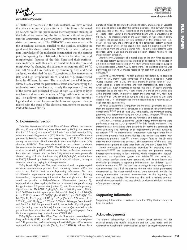
5. Experimental SectionThin-Film Deposition: PDI8-CN2 films of three different thicknesses
(10 nm, 40 nm and 100 nm) were deposited by HVS (base pressure P = 8 × 10⁻⁸ mbar) at a rate of 12.5 Å min−1 on a 200 nm-thick SiO2 substrate, thermally grown on a (001) Si wafer. Three series of films were prepared by keeping the substrates, respectively, at RT, 80 °C and 120 °C during the deposition. Simultaneously, in the same high-vacuum (HV) chamber, PDI8-CN2 films were deposited on test patterns to obtain bottom-contact bottom-gate OTFTs. The PDI8-CN2 source powder was used as provided by BASF without any further purification processes. Both the test patterns and the bare SiO2 substrates were previously cleaned using a 15 min piranha etching (1:1 H2O2:H2SO4 solution kept at 150°C) followed by a fast-lasting bath in 4% HF solution, rinsing in deionized water and drying in a nitrogen stream.
X-Ray Powder Diffraction: The non-conventional and complete crystal structure determination process from laboratory powder diffraction data is described in detail in the Supporting Information. Two sets of diffraction experimental set-ups were used, aimed at obtaining independent, complementary information that a single data collection could not provide: a Debye–Scherrer diffractometer (pattern 1), equipped with a glass capillary holder, and a conventional parafocusing Bragg–Brentano θ:θ goniometer (pattern 2), with flat-sample geometry. Crystal data for PDI8-CN2: C42H40N4O4, f.w. = 664.81 g mol−1, 298 K, λ = 1.540596 Å, triclinic, space group P-1, a = 5.0194(4) Å, b = 8.8409(7) Å, c = 20.195(1) Å, α = 101.507(5)°, β = 92.328(5)°, γ = 100.154(5)°, V = 861.7(1) Å3, Z = 1, ρcalc = 1.281 g cm−3, μ (Cu Kα) = 0.66 mm−1, Rp = 0.073, Rwp = 0.107; RBragg = 0.052 and 0.036 and 2θ ranges from 6 to 60° and from 6 to 80°, for patterns 1 and 2, respectively. Crystallographic data (excluding structure factors) for the structure(s) reported in this paper have been deposited with the Cambridge Crystallographic Data Centre as supplementary publication no. CCDC-833431.
X-Ray Diffraction on Thin Films: The thin films were characterized by X-ray reflectivity (XRR) and XRD measurements, both in out-of-plane and GID geometries, performed using a SmartLab-Rigaku diffractometer equipped with a rotating anode (Cu Kα, λ = 1.54180 Å), followed by a
© 2012 WILEY-VCH Verlag GmAdv. Funct. Mater. 2012, 22, 943–953
parabolic mirror to collimate the incident beam, and a series of variable slits (placed before and after the sample position). The 2D-GID images were recorded at the XRD1 beamline at the Elettra synchrotron facility at Trieste (Italy) using a monochromatic beam with a wavelength of 0.8499 Å. The incident angle of the X-ray beam, αi, was chosen below or above the critical angle for total reflection of the organic film (i.e., 0.12°). In this way, the contribution to the diffraction pattern coming from the upper layers of the organic film could be discriminated from that coming from the whole organic film. The diffraction patterns were recorded using a 2D camera (Pilatus detector) placed normal to the incident beam direction.
Atomic Force Microscopy: The morphology of the thin films deposited on the test pattern substrates was studied by collecting AFM images in air in semicontact mode using an NT-MDT Smena microscope equipped with Nanosensors GmbH NSG10 cantilevers. The statistical analysis was performed on four AFM images recorded for each film using Gwyddion software.[97]
Electrical Measurements: The test patterns, fabricated by Fondazione Bruno Kessler, Trento, were composed of a heavily n-doped Si wafer (Gate) covered with a 200 nm-thick thermally grown layer of SiO2, which acted as a gate dielectric, and with interdigitated, gold source-drain contacts. Each substrate contained two pairs of active channels characterized by the ratio W/L = 550, where W is the channel width, and L the channel length. In order to obtain the same high W/L ratio, two values of W (11 200 μm and 22 400 μm) and L (20 μm and 40 μm) were chosen. The OTFT characteristics were measured using a Keithley 2612A dual-channel Source Meter.
Ab Initio Calculations: Starting from the molecular geometry extracted from the experimental crystal structures of a series of PDI-n benchmark compounds[46,51,52] and of PDI8-CN2 (this work), the minimum-energy geometry was determined using the GAUSSIAN03 program,[98] with the B3LYP/6-31G* combination of density functional and basis set.
Molecular Mechanics Calculations: Lattice energy minimizations were performed using the GULP program[99] for fully flexible molecules. The intramolecular interactions were described by harmonic potentials for bond stretching and bending, or by trigonometric potential functions for torsions.[100] The intermolecular interactions were represented by an atom-atom potential with Lennard-Jones and electrostatic terms with electrostatic potential (ESP)[98] atomic charges fitted to the ab initio B3LYP/6-31G* electrostatic potential. The parameters of the intra- and intermolecular potentials were taken from the DREIDING force field.[100]
Search Procedure: In our standard procedure for predicting crystal structures,[55,56,101] we systematically searched the potential energy hypersurface to identify its local minima, which represent the “natural” structures the crystalline system can exhibit.[102] For PDI8-CN2, 5000 crystal configurations were generated, with known lattice and molecular parameters (Supporting Information), but different quasi-random orientations.[103] The total lattice energy for each configuration was minimized and all of the distinct minima, with lattice parameters constrained to the experimental values, were identified. Finally, the energy minimization continued unconstrained, by also adjusting the unit cell axes and angles. The idea was, that, with a realistic potential model, the experimental structures should be close to the local minima of the potential energy.
Supporting InformationSupporting Information is available from the Wiley Online Library or from the author.
AcknowledgementsThe authors acknowledge Dr. Silke Koehler (BASF Schweiz AG) for material supply and fruitful discussion and Dr. Luisa Barba and Dr. Gianmichele Arrighetti for their excellent support during the experiments
bH & Co. KGaA, Weinheim 951wileyonlinelibrary.com

FULL
PAPER
www.afm-journal.dewww.MaterialsViews.com
95
[1] C. D. Dimitrakopoulos, P. R. L. Malenfant, Adv. Mater. 2002, 14, 99.
[2] S. R. Forrest, Nature 2004, 428, 911. [3] M. Halik, H. Klauk, U. Zschieschang, G. Schmid, C. Dehm,
M. Schutz, S. Maisch, F. Effenberger, M. Brunnbauer, F. Stellacci, Nature 2004, 431, 963.
[4] C. Kim, A. Facchetti, T. J. Marks, Science 2007, 318, 76. [5] Y. Y. Noh, N. Zhao, M. Caironi, H. Sirringhaus, Nat. Nanotechnol.
2007, 2, 784. [6] M. F. Calhoun, J. Sanchez, D. Olaya, M. E. Gershenson,
V. Podzorov, Nat. Mater. 2008, 7, 84. [7] J. H. Cho, J. Lee, Y. Xia, B. Kim, Y. Y. He, M. J. Renn, T. P. Lodge,
C. D. Frisbie, Nat. Mater. 2008, 7, 900. [8] D. J. Gundlach, J. E. Royer, S. K. Park, S. Subramanian,
O. D. Jurchescu, B. H. Hamadani, A. J. Moad, R. J. Kline, L. C. Teague, O. Kirillov, C. A. Richter, J. G. Kushmerick, L. J. Richter, S. R. Parkin, T. N. Jackson, J. E. Anthony, Nat. Mater. 2008, 7, 216.
[9] M. Novak, A. Ebel, T. Meyer-Friedrichsen, A. Jedaa, B. F. Vieweg, G. A. Yang, K. Voitchovsky, F. Stellacci, E. Spiecker, A. Hitsch, M. Halik, Nano Lett. 2011, 11, 156.
[10] J. A. Rogers, Z. Bao, K. Baldwin, A. Dodabalapur, B. Crone, V. R. Raju, V. Kuck, H. Katz, K. Amundson, J. Ewing, P. Drzaic, Proc. Natl. Acad. Sci. USA 2001, 98, 4835.
[11] G. H. Gelinck, H. E. A. Huitema, E. Van Veenendaal, E. Cantatore, L. Schrijnemakers, J. B. P. H. Van der Putten, T. C. T. Geuns, M. Beenhakkers, J. B. Giesbers, B. H. Huisman, E. J. Meijer, E. M. Benito, F. J. Touwslager, A. W. Marsman, B. J. E. Van Rens, D. M. De Leeuw, Nat. Mater. 2004, 3, 106.
[12] M. A. McCarthy, B. Liu, E. P. Donoghue, I. Kravchenko, D. Y. Kim, F. So, A. G. Rinzler, Science 2011, 332, 570.
[13] A. R. Brown, A. Pomp, C. M. Hart, D. M. Deleeuw, Science 1995, 270, 972.
[14] B. Crone, A. Dodabalapur, A. Gelperin, L. Torsi, H. E. Katz, A. J. Lovinger, Z. Bao, Appl. Phys. Lett. 2001, 78, 2229.
[15] J. Janata, M. Josowicz, Nat. Mater. 2003, 2, 19. [16] X. F. Guo, M. Myers, S. X. Xiao, M. Lefenfeld, R. Steiner,
G. S. Tulevski, J. Y. Tang, J. Baumert, F. Leibfarth, J. T. Yardley, M. L. Steigerwald, P. Kim, C. Nuckolls, Proc. Natl. Acad. Sci. USA 2006, 103, 11452.
[17] M. E. Roberts, S. C. B. Mannsfeld, N. Queralto, C. Reese, J. Locklin, W. Knoll, Z. N. Bao, Proc. Natl. Acad. Sci. USA 2008, 105, 12134.
[18] B. Crone, A. Dodabalapur, Y. Y. Lin, R. W. Filas, Z. Bao, A. LaDuca, R. Sarpeshkar, H. E. Katz, W. Li, Nature 2000, 403, 521.
[19] T. D. Anthopoulos, S. Setayesh, E. Smits, M. Colle, E. Cantatore, B. de Boer, P. W. M. Blom, D. M. de Leeuw, Adv. Mater. 2006, 18, 1900.
[20] H. Klauk, U. Zschieschang, J. Pflaum, M. Halik, Nature 2007, 445, 745.
[21] A. Facchetti, Nat. Mater. 2008, 7, 839. [22] M. M. Payne, S. R. Parkin, J. E. Anthony, C. C. Kuo, T. N. Jackson, J.
Am. Chem. Soc. 2005, 127, 4986. [23] H. Ebata, T. Izawa, E. Miyazaki, K. Takimiya, M. Ikeda, H. Kuwabara,
T. Yui, J. Am. Chem. Soc. 2007, 129, 15732. [24] P. Gao, D. Beckmann, H. N. Tsao, X. L. Feng, V. Enkelmann,
M. Baumgarten, W. Pisula, K. Mullen, Adv. Mater. 2009, 21, 213. [25] A. S. Dhoot, J. D. Yuen, M. Heeney, I. McCulloch, D. Moses,
A. J. Heeger, Proc. Natl. Acad. Sci. USA 2006, 103, 11834.
performed at Elettra. This work was supported by the EU Large Project One-P (FP7-NMP-2007–212311).
Received: July 16, 2011 Revised: October 9, 2011
Published online: December 20, 2011
© 2012 WILEY-VCH Verlag G2 wileyonlinelibrary.com
[26] H. L. Pan, Y. N. Li, Y. L. Wu, P. Liu, B. S. Ong, S. P. Zhu, G. Xu, J. Am. Chem. Soc. 2007, 129, 4112.
[27] I. Mcculloch, M. Heeney, C. Bailey, K. Genevicius, I. Macdonald, M. Shkunov, D. Sparrowe, S. Tierney, R. Wagner, W. M. Zhang, M. L. Chabinyc, R. J. Kline, M. D. Mcgehee, M. F. Toney, Nat. Mater. 2006, 5, 328.
[28] B. A. Jones, A. Facchetti, M. R. Wasielewski, T. J. Marks, J. Am. Chem. Soc. 2007, 129, 15259.
[29] Y. G. Wen, Y. Q. Liu, Adv. Mater. 2010, 22, 1331. [30] H. E. Katz, A. J. Lovinger, J. Johnson, C. Kloc, T. Siegrist, W. Li,
Y. Y. Lin, A. Dodabalapur, Nature 2000, 404, 478. [31] H. Yan, Z. H. Chen, Y. Zheng, C. Newman, J. R. Quinn, F. Dotz,
M. Kastler, A. Facchetti, Nature 2009, 457, 679. [32] H. Usta, C. Risko, Z. M. Wang, H. Huang, M. K. Deliomeroglu,
A. Zhukhovitskiy, A. Facchetti, T. J. Marks, J. Am. Chem. Soc. 2009, 131, 5586.
[33] B. Yoo, B. A. Jones, D. Basu, D. Fine, T. Jung, S. Mohapatra, A. Facchetti, K. Dimmler, M. R. Wasielewski, T. J. Marks, A. Dodabalapur, Adv. Mater. 2007, 19, 4028.
[34] Z. J. Chen, M. G. Debije, T. Debaerdemaeker, P. Osswald, F. Wurthner, ChemPhysChem 2004, 5, 137.
[35] B. A. Jones, M. J. Ahrens, M. H. Yoon, A. Facchetti, T. J. Marks, M. R. Wasielewski, Angew. Chem. Int. Ed. 2004, 43, 6363.
[36] R. J. Chesterfield, J. C. McKeen, C. R. Newman, P. C. Ewbank, D. A. da Silva, J. L. Bredas, L. L. Miller, K. R. Mann, C. D. Frisbie, J. Phys. Chem. B 2004, 108, 19281.
[37] R. J. Chesterfield, J. C. McKeen, C. R. Newman, C. D. Frisbie, P. C. Ewbank, K. R. Mann, L. L. Miller, J. Appl. Phys. 2004, 95, 6396.
[38] D. J. Gundlach, K. P. Pernstich, G. Wilckens, M. Gruter, S. Haas, B. Batlogg, J. Appl. Phys. 2005, 98, 064502.
[39] R. Schmidt, J. H. Oh, Y. S. Sun, M. Deppisch, A. M. Krause, K. Radacki, H. Braunschweig, M. Konemann, P. Erk, Z. A. Bao, F. Wurthner, J. Am. Chem. Soc. 2009, 131, 6215.
[40] C. Piliego, F. Cordella, D. Jarzab, S. Lu, Z. Chen, A. Facchetti, M. A. Loi, Appl. Phys. A - Mater. Sci. Process. 2009, 95, 303.
[41] A. S. Molinari, H. Alves, Z. Chen, A. Facchetti, A. F. Morpurgo, J. Am. Chem. Soc. 2009, 131, 2462.
[42] B. Yoo, T. Jung, D. Basu, A. Dodabalapur, B. A. Jones, A. Facchetti, M. R. Wasielewski, T. J. Marks, Appl. Phys. Lett. 2006, 88, 082104.
[43] B. Yoo, A. Madgavkar, B. A. Jones, S. Nadkarni, A. Facclietti, K. Dimmler, M. R. Wasielewski, T. J. Marks, A. Dodabalapur, IEEE Electron. Device Lett. 2006, 27, 737.
[44] J. Rivnay, L. H. Jimison, J. E. Northrup, M. F. Toney, R. Noriega, S. F. Lu, T. J. Marks, A. Facchetti, A. Salleo, Nat. Mater. 2009, 8, 952.
[45] H. Yan, Y. Zheng, R. Blache, C. Newman, S. Lu, J. Woerle, A. Facchetti, Adv. Funct. Mat. 2008, 20, 3393.
[46] Parafocusing Bragg–Brentano grants high-resolution and quite narrow peaks but high preferred-orientation effects, whereas Debye–Scherrer geometry, mounting a glass capillary loaded with ground PD18-CN2 crystals, affords correct estimates of the meas-ured intensities, at the expense of evident peak broadening (by sample-effect contribution).
[47] E. Hadicke, F. Graser, Acta Crystallogr. C 1986, 42, 195. [48] H. Lipson, A. R. Stokes, Proc. R. Soc. London. A 1942, 181, 101. [49] Apparently, as derived from the preferred orientation coefficients
employed in matching the experimental versus the calculated data for the X-ray trace collected in flat-plate geometry, the needles elongate approximately in the [100] direction, a not-so-obvious, and difficult-to-interpret, direction. However, a few tests performed with different preferred orientation poles within the March– Dollase formulation show that the alternative [−651]. choice is only partially detrimental to the overall fitting, thus suggesting the pos-sible coincidence of the stacking and needle growth directions.
mbH & Co. KGaA, Weinheim Adv. Funct. Mater. 2012, 22, 943–953

FULL P
APER
www.afm-journal.dewww.MaterialsViews.com
[50] A. Z. March, Kristallografiya 1932, 81, 285. [51] W. A. Dollase, J. Appl. Crystallogr. 1987, 19, 267. [52] M. Kasha, H. R. Rawls, M. A. El-Bayoumi, Pure Appl. Chem. 1965,
11, 371. [53] B. A. Jones, A. Facchetti, M. R. Wasielewski, T. J. Marks, Adv. Funct.
Mater. 2008, 18, 1329. [54] A. L. Briseno, S. C. B. Mannsfeld, C. Reese, J. M. Hancock, Y. Xiong,
S. A. Jenekhe, Z. Bao, Y. Xia, Nano Lett. 2007, 7, 2847. [55] R. G. Della Valle, E. Venuti, A. Brillante, A. Girlando, J. Phys. Chem.
A 2006, 110, 10858. [56] R. G. Della Valle, E. Venuti, A. Brillante, A. Girlando, J. Phys. Chem.
A 2008, 112, 6715. [57] B. E. Warren, X-Ray Diffraction, Dover, New York 1990. [58] B. Nickel, R. Barabash, R. Ruiz, N. Koch, A. Kahn, L. C. Feldman,
R. F. Haglund, G. Scoles, Phys. Rev. B: Condens. Matter 2004, 70, 125401.
[59] J. A. Merlo, C. R. Newman, C. P. Gerlach, T. W. Kelley, D. V. Muyres, S. E. Fritz, M. F. Toney, C. D. Frisbie, J. Am. Chem. Soc. 2005, 127, 3997.
[60] D. W. Breiby, O. Bunk, J. W. Andreasen, H. T. Lemke, M. M. Nielsen, J. Appl. Crystallogr. 2008, 41, 262.
[61] T. N. Krauss, E. Barrena, D. G. de Oteyza, X. N. Zhang, J. Major, V. Dehm, F. Wurthner, H. Dosch, J. Phys. Chem. C 2009, 113, 4502.
[62] T. N. Krauss, E. Barrena, X. N. Zhang, D. G. de Oteyza, J. Major, V. Dehm, F. Wurthner, L. P. Cavalcanti, H. Dosch, Langmuir 2008, 24, 12742.
[63] R. A. Cormier, B. A. Gregg, J. Phys. Chem. B 1997, 101, 11004. [64] C. W. Struijk, A. B. Sieval, J. E. J. Dakhorst, M. van Dijk, P. Kimkes,
R. B. M. Koehorst, H. Donker, T. J. Schaafsma, S. J. Picken, A. M. van de Craats, J. M. Warman, H. Zuilhof, E. J. R. Sudholter, J. Am. Chem. Soc. 2000, 122, 11057.
[65] J. Krug, Physica A 2004, 340, 647. [66] A. C. Durr, F. Schreiber, K. A. Ritley, V. Kruppa, J. Krug, H. Dosch,
B. Struth, Phys. Rev. Lett. 2003, 90, 647. [67] S. Kowarik, A. Gerlach, A. Hinderhofer, S. Milita, F. Borgatti,
F. Zontone, T. Suzuki, F. Biscarini, F. Schreiber, Phys. Status Solidi Rapid Res. Lett. 2008, 2, 120.
[68] G. X. Zhang, B. L. Weeks, M. Holtz, Surf. Sci. 2011, 605, 463. [69] J. P. Schlomka, M. Tolan, W. Press, Appl. Phys. Lett. 2000, 76,
2005. [70] J. Krug, M. Plischke, M. Siegert, Phys. Rev. Lett. 1993, 70,
v3271. [71] Z. W. Lai, S. Dassarma, Phys. Rev. Lett. 1991, 66, 2348. [72] J. M. Kim, S. Dassarma, Phys. Rev. E 1995, 51, 1889. [73] A. E. Lita, J. E. Sanchez, Phys. Rev. B: Condens. Matter 2000, 61,
7692. [74] S. Dassarma, S. V. Ghaisas, Phys. Rev. Lett. 1992, 69, 3762. [75] F. Biscarini, P. Samori, O. Greco, R. Zamboni, Phys. Rev. Lett. 1997,
78, 2389. [76] G. Rasigni, M. Rasigni, J. Palmari, C. Dussert, F. Varnier, A. Llebaria,
J. Opt. Soc. Am. A 1988, 5, 99. [77] F. Biscarini, R. Zamboni, P. Samori, P. Ostoja, C. Taliani, Phys. Rev.
B: Condens. Matter 1995, 52, 14868. [78] F. Biscarini, O. Greco, A. Lauria, R. Zamboni, C. Taliani, Mol. Cryst.
Liq. Cryst. A 1996, 290, 203. [79] M. Beigmohamadi, P. Niyamakom, A. Farahzadi, C. Effertz,
S. Kremers, D. Brueggemann, M. Wuttig, J. Appl. Phys. 2008, 104, 013505.
[80] P. H. Dederichs, Phys. Rev. B: Condens. Matter 1971, 4, 1041. [81] P. Ehrhart, H. Trinkaus, Phys. Rev. B: Condens. Matter 1982, 52,
834.
© 2012 WILEY-VCH Verlag GAdv. Funct. Mater. 2012, 22, 943–953
[82] M. Beigmohamadi, P. Niyamakom, A. Farahzadi, S. Kremers, T. Michely, M. Wuttig, Phys. Status Solidi Rapid Res. Lett 2008, 2, 1.
[83] R. Ruiz, A. C. Mayer, G. G. Malliaras, B. Nickel, G. Scoles, A. Kazimirov, H. Kim, R. L. Headrick, Z. Islam, Appl. Phys. Lett. 2004, 85, 4926.
[84] A. Brillante, I. Bilotti, R. G. Della Valle, E. Venuti, A. Girlando, CrystEngComm 2008, 10, 937.
[85] A. Brillante, I. Bilotti, R. G. Della Valle, E. Venuti, S. Milita, C. Dionigi, F. Borgatti, A. N. Lazar, F. Biscarini, M. Mas-Torrent, N. S. Oxtoby, N. Crivillers, J. Veciana, C. Rovira, M. Leufgen, G. Schmidt, L. W. Molenkamp, CrystEngComm 2008, 10, 1899.
[86] R. Pfattner, M. Mas-Torrent, I. Bilotti, A. Brillante, S. Milita, F. Liscio, F. Biscarini, T. Marszalek, J. Ulanski, A. Nosal, M. Gazicki-Lipman, M. Leufgen, G. Schmidt, L. W. Molenkamp, V. Laukhin, J. Veciana, C. Rovira, Adv. Mater. 2010, 22, 4198.
[87] S. Milita, M. Servidori, F. Cicoira, C. Santato, A. Pifferi, Nucl. Instrum. Methods B 2006, 246, 101.
[88] J. F. Moulin, F. Dinelli, M. Massi, C. Albonetti, R. Kshirsagar, F. Biscarini, Nucl. Instrum. Methods Phys. Res. B 2006, 246, 122.
[89] Z. Bao, J. Locklin, Organic Field-Effect Transistors, CRC Press, Boca Raton, FL 2007.
[90] K. J. Baeg, D. Khim, J. H. Kim, M. Kang, I. K. You, D. Y. Kim, Y. Y. Noh, Org. Electron. 2011, 12, 634.
[91] L. L.Chua, J. Zaumseil, J. F Chang, E. C. W. Ou, P. K.-H. Ho, H. Sirringhaus, R. H. Friend, Nature 2005, 434, 194.
[92] G. Horowitz, Adv. Mater. 1998, 10, 365. [93] M. C. J. M. Vissenberg, M. Matters, Phys. Rev. B: Condens. Matter
1998, 57, 12964. [94] A. C. Durr, F. Schreiber, M. Munch, N. Karl, B. Krause, V. Kruppa,
H. Dosch, Appl. Phys. Lett. 2002, 81, 2276. [95] N. Karl, Synth. Met. 2003, 133, 649. [96] A. R. Brown, D. M. Deleeuw, E. J. Lous, E. E. Havinga, Synth. Met.
1994, 66, 257. [97] Gwyddion Scan Probe Microscopy data analysis software. [98] M. J. Frisch, G. W. Trucks, H. B. Schlegel, G. E. Scuseria,
M. A. Robb, J. R. Cheeseman, J. A. Montgomery Jr., T. Vreven, K. N. Kudin, J. C. Burant, J. M. Millam, S. S. Iyengar, J. Tomasi, V. Barone, B. Mennucci, M. Cossi, G. Scalmani, N. Rega, G. A. Petersson, H. Nakatsuji, M. Hada, M. Ehara, K. Toyota, R. Fukuda, J. Hasegawa, M. Ishida, T. Nakajima, Y. Honda, O. Kitao, H. Nakai, M. Klene, X. Li, J. E. Knox, H. P. Hratchian, J. B. Cross, V. Bakken, C. Adamo, J. Jaramillo, R. Gomperts, R. E. Stratmann, O. Yazyev, A. J. Austin, R. Cammi, C. Pomelli, J. W. Ochterski, P. Y. Ayala, K. Morokuma, G. A. Voth, P. Salvador, J. J. Dannenberg, V. G. Zakrzewski, S. Dapprich, A. D. Daniels, M. C. Strain, O. Farkas, D. K. Malick, A. D. Rabuck, K. Raghavachari, J. B. Foresman, J. V. Ortiz, Q. Cui, A. G. Baboul, S. Clifford, J. Cioslowski, B. B. Stefanov, G. Liu, A. Liashenko, P. Piskorz, I. Komaromi, R. L. Martin, D. J. Fox, T. Keith, M. A. Al-Laham, C. Y. Peng, A. Nanayakkara, M. Challacombe, P. M. W. Gill, B. Johnson, W. Chen, M. W. Wong, C. Gonzalez, J. A. Pople, Gaussian 03, Revision D.02, Gaussian, Inc., Wallingford, CT 2004.
[99] J. D. Gale, A. L. Rohl, Mol. Simul. 2003, 29, 291.[100] S. L. Mayo, B. D. Olafson, W. A. Goddard, J. Phys. Chem. 1990, 94,
8897.[101] R. G. Della Valle, E. Venuti, A. Brillante, A. Girlando, J. Chem. Phys.
2003, 118, 807.[102] F. H. Stillinger, T. A. Weber, Phys. Rev. A: At. Mol. Optical Phys.
1982, 25, 978.[103] W. H. Press, S. A. Teukolsky, W. T. Vetterling, B. P. Flannery, Numer-
ical Recipes in Fortran, Cambridge University Press, Cambridge, UK 1992.
mbH & Co. KGaA, Weinheim 953wileyonlinelibrary.com