Spin-orbit and exchange interaction in surface quantum wells on gapless semimagnetic semiconductor...
28
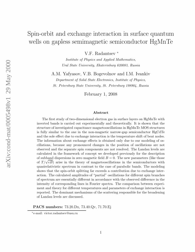
arXiv:cond-mat/0005498v1 29 May 2000 Spin-orbit and exchange interaction in surface quantum wells on gapless semimagnetic semiconductor HgMnTe V.F. Radantsev ∗ Institute of Physics and Applied Mathematics, Ural State University, Ekaterinburg 620083, Russia A.M. Yafyasov, V.B. Bogevolnov and I.M. Ivankiv Department of Solid State Electronics, Institute of Physics, St. Petersburg State University, St. Petersburg 198904, Russia February 1, 2008 Abstract The first study of two-dimensional electron gas in surface layers on HgMnTe with inverted bands is carried out experimentally and theoretically. It is shown that the structure of investigated capacitance magnetooscillations in HgMnTe MOS structures is fully similar to the one in the non-magnetic narrow-gap semiconductor HgCdTe and the sole effect due to exchange interaction is the temperature shift of beat nodes. The information about exchange effects is obtained only due to our modeling of os- cillations, because any pronounced changes in the position of oscillations are not observed and the separate spin components are not resolved. The Landau levels are calculated in the framework of concept we developed previously for the description of subband dispersions in zero magnetic field B = 0. The new parameters (like those of T/ √ eB) arise in the theory of magnetooscillations in the semiconductors with quasirelativistic spectrum in contrast to the case of parabolic bands. The modeling shows that the spin-orbit splitting far exceeds a contribution due to exchange inter- action. The calculated amplitudes of “partial” oscillations for different spin branches of spectrum are essentially different in accordance with the observed difference in the intensity of corresponding lines in Fourier spectra. The comparison between experi- ment and theory for different temperatures and parameters of exchange interaction is reported. The dominant mechanisms of the scattering responsible for the broadening of Landau levels are discussed. PACS numbers: 73.20.Dx, 73.40.Qv, 71.70.Ej * e-mail: [email protected] 1
-
Upload
independent -
Category
Documents
-
view
4 -
download
0
Transcript of Spin-orbit and exchange interaction in surface quantum wells on gapless semimagnetic semiconductor...
arX
iv:c
ond-
mat
/000
5498
v1 2
9 M
ay 2
000
Spin-orbit and exchange interaction in surface quantum
wells on gapless semimagnetic semiconductor HgMnTe
V.F. Radantsev ∗
Institute of Physics and Applied Mathematics,
Ural State University, Ekaterinburg 620083, Russia
A.M. Yafyasov, V.B. Bogevolnov and I.M. IvankivDepartment of Solid State Electronics, Institute of Physics,
St. Petersburg State University, St. Petersburg 198904, Russia
February 1, 2008
Abstract
The first study of two-dimensional electron gas in surface layers on HgMnTe withinverted bands is carried out experimentally and theoretically. It is shown that thestructure of investigated capacitance magnetooscillations in HgMnTe MOS structuresis fully similar to the one in the non-magnetic narrow-gap semiconductor HgCdTeand the sole effect due to exchange interaction is the temperature shift of beat nodes.The information about exchange effects is obtained only due to our modeling of os-cillations, because any pronounced changes in the position of oscillations are notobserved and the separate spin components are not resolved. The Landau levels arecalculated in the framework of concept we developed previously for the descriptionof subband dispersions in zero magnetic field B = 0. The new parameters (like thoseof T/
√eB) arise in the theory of magnetooscillations in the semiconductors with
quasirelativistic spectrum in contrast to the case of parabolic bands. The modelingshows that the spin-orbit splitting far exceeds a contribution due to exchange inter-action. The calculated amplitudes of “partial” oscillations for different spin branchesof spectrum are essentially different in accordance with the observed difference in theintensity of corresponding lines in Fourier spectra. The comparison between experi-ment and theory for different temperatures and parameters of exchange interaction isreported. The dominant mechanisms of the scattering responsible for the broadeningof Landau levels are discussed.
PACS numbers: 73.20.Dx, 73.40.Qv, 71.70.Ej
∗e-mail: [email protected]
1
1 Introduction
There are two aspects that cause the peculiar features of, and the interest in, the two-dimensional (2D) electron gas in narrow-gap diluted magnetic (semimagnetic) semicon-ductors (DMS). One stems from the s, p − d exchange interaction between band electronsand localized magnetic moments [1]. This interaction results in changed spin splittingof the band states, which can be varied by such external factors as a magnetic field andtemperature. The other is due to the peculiarities inherent to Kane semiconductors withsmall gap, leading to such relativisticlike effects as non-parabolicity, kinetic confinement(motional binding [2]), spin-orbit (SO) splitting and resonant interband mixing by surfaceelectric field [3, 4, 5]. What is important in the context of the specificity of 2D electronicsystems involving DMS, is that both exchange and SO interaction cause the rearrangementof the spin structure of Landau levels (LL’s). Although historically the first studies of 2Delectron gas in DMS were performed for metal-insulator-semiconductor (MIS) structuresbased on HgMnTe, [6] the available experimental results are mostly for the grain bound-aries in HgMnTe and HgCdMnTe with positive Kane gap Eg > 100meV at Mn contenttypically x = 0.02 (for the higher x, the exchange interaction exhibited itself poorly, thatwas attributed to antiferromagnetic interaction betwen Mn ions) [1, 7, 8, 9]. This is dueto low electron mobility in previously investigated MIS structures. At the same time, theinversion layers in MIS structures are of particular experimental interest because of thepossibility of controlling the depth of surface quantum well by gate voltage, and becauseof the relative ease and accuracy of the description of surface potential (in the case of thebicrystals, the additional poorly verified assumptions have to be used to describe a self-consistent potential near grain boundaries [10]). An important point is that these resultscan be compared with the data for MIS structures based on narrow-gap HgCdTe [4, 11],being non-magnetic analogue of narrow-gap DMS.
As regards their theoretical description, the subband calculations were carried out onlyfor DMS with direct but not inverted bands and without allowance for spinorlike effects[1, 6]. However, the SO splitting in asymmetrical quantum wells at zero magnetic field(this phenomenon in itself is of much current interest [4, 5, 12, 13, 14, 15, 16, 17, 18, 19])leads to the rearrangement of subband magnetic levels. In narrow-gap semiconductors, theperturbation of magnetic spectrum is so drastic that SO interaction cannot be neglected inthe theoretical treatment. It must be stressed that SO splitting, as we shall see in Sec. III,exceeds by far exchange interaction contribution so it cannot be considered as a correctionto the exchange interaction. It is clear also that a treatment based on the quasiclassicalquantization in a magnetic field of subband spectrum (calculated at B = 0) is unsuitable forthe description of exchange interaction effects. A more rigorous theoretical considerationof the LL’s structure is required.
In this paper, the peculiarities of 2D electron gas due to exchange and SO interaction arestudied in inversion layers on Hg1−xMnxTe. with a small Mn content. At x < 0.08 HgMnTehas inverted bands (i.e. becomes semimetal) and traditional galvanometric methods can-not be used because of the shunting of surface conductance by the bulk. We employed themagnetocapacitance spectroscopy method, which is applicable to semiconductors with anysign of the Kane gap. The parameters of the samples and the experimental data relatingto the capacitance oscillations versus gate voltage and magnetic field and their tempera-
2
ture evolution are presented in Sec. II. In Sec. III, we present the theoretical model. Thetreatment of LL’s in 2D subbands is based on the further development of the concept weoffered previously for the description of subband spectrum at B = 0. The density of states(DOS) in a magnetic field is described neglecting the mixing between LL’s and assuminga Gaussian shape of each level. In this section an analytical expression for oscillationsof the differential capacitance of space charge region in the low-temperature range is alsoobtained using WKB approach. In Sec. IV, the results of the computer modeling of capac-itance oscillations are presented. The results of a comparison of the experimental data andtheoretical calculations for different temperatures and parameters of exchange interactionare discussed. The parameters of the broadening of LL’s are determined from a fittingof the amplitudes of calculated oscillations to their experimental values. The dominantmechanisms of the scattering responsible for broadening of LL’s are discussed.
2 Samples and experimental results
2.1 Samples and experimental methods
In this work the inversion layers in MIS structures fabricated from p-Hg1−xMnxTe sin-gle crystals were investigated. No impurities were introduced intentionally and no postgrowth annealing was performed. Deviations from stoichiometry, and thus the type ofthe conductivity, were controlled by mercury partial pressure during the growth process.The Hall-effect measurements were performed at variable temperatures and magnetic fieldstrengths. After removing the Hall and tunnel contacts (see below), the substrates weremechanically polished and etched in a 0.5 bromine-methanol solution. Several methodssuch as anodic oxide formation, silicon oxide and Al2O3 deposition, and the Langmuir-Blodgett film technique have been used for forming an insulating film in MIS structures.The gate electrodes of the typical area ∼ 5 × 10⁻⁴ cm2 were formed evaporating Pb. Thedifferential capacitance C and derivative dC/dVg on gate voltage Vg of the capacitors weremeasured in the dark, typically at 1MHz and a test signal amplitude of 5mV.
The capacitance magnetooscillations due to the magnetic quantization of 2D electrongas were observed in all the above HgMnTe MIS structures. It was shown that the generalshapes of the oscillations at the same carrier surface density and Mn content are similar.In the following we present the results for the structures with a ∼ 80 nm thick anodic oxidefilm, grown in a solution of 0.1MKOH in 90% ethylene glycol / 10% H2O at 0.1mA·cm−2.There are several reasons for such a choice: (i) the amplitudes of oscillations in thesestructures are the highest owing to the large value of insulator capacitance (this is causedby the large value of dielectric constant of the anodic oxide), (ii) the highest surface carrierdensities are achieved at low gate voltages Vg = 10− 15V, and (iii) the dielectric constantof oxide is close to that of a semiconductor so the contribution of image forces in surfacepotential can be neglected in the calculations.
We investigated samples with different Mn content (x = 0.024, 0.040, 0.060 and 0.1).Kane gap Eg and Kane effective mass mb (and therefore x) were determined independentlyby the tunnel spectroscopy method for a comparison of band parameters in the bulk withthose in the vicinity of the surface. The discrepancy is within the accuracy of the analysis(∆x ∼ 0.002 ÷ 0.003). Because the tunnel contacts and studied MIS capacitors were
3
produced using identical technology and differ only by thickness of insulator (Langmuir-Blodgett film or an oxide) this agreement testifies that the surface layers are chemicallyclose to the bulk. The similarity of the results for the structures with different insulators(with different fabrication methods) supports this conclusion. The fact that in the smallsurface concentration range the measured cyclotron masses in 2D subbands extrapolate tothe bulk value mb is direct evidence of an absence of noticeable decomposition in 2D layerduring the structure fabrication process.
In the following we shall restrict our consideration to the results for HgMnTe withx ≈ 0.04 (Eg = −100 ± 5meV). The amplitudes of the oscillations for other samples aremuch less even at 4.2K and rapidly decrease with increasing temperature. In the case ofx ≈ 0.024 this is caused by the small cyclotron energy due to a large Kane gap. In the casesx ≈ 0.06 and x ≈ 0.1 it is due to the large doping level of available materials. As a result,we could not obtain reasonably accurate information about the oscillation’s temperatureevolution, in which the specificity of DMS is manifested. As to the measurements atT = 4.2K, the subband parameters extracted from oscillations for these samples are similarto those for HgCdTe with the same band parameters and agree well with the theory. Onthe other hand, the samples with x = 0.04 are best suited to the purpose of this first studyaimed at investigating the peculiarities of 2D electron gas in DMS with inverted bands,in which (i) the effects of SO and exchange interaction are expected to be more clearlypronounced and (ii) the results can be compared with those for well studied surface layerson gapless HgCdTe with Eg ∼ −(50÷ 100)meV [4, 20]. For small gap |Eg| < 100meV theparameters of 2D subbands depend only weakly on Eg (except in the case of small subbandoccupancies).[4, 20] By contrast, the subband parameters are more sensitive to the dopinglevel. For this reason, we present the results for two samples with NA−ND = 1.2×1016 cm−3
(sample S1) and NA − ND = 1.5 × 1017 cm−3 (sample S2). The Hall mobility of holesis of the order of 2500 cm2/Vs at 4.2K. The experimental data are presented below forcapacitors with the gate area S = 7.2×10⁻⁴ cm2 and insulator capacitance Cox = 136.5 pFfor sample S1, and with S = 7.7 × 10⁻⁴ and Cox = 155.1 pF for sample S2.
2.2 Capacitance measurements in perpendicular magnetic fields
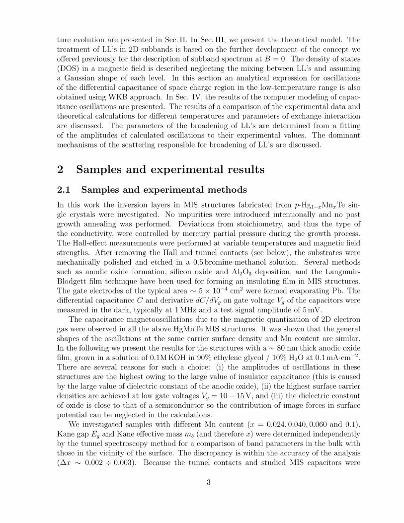
Fig. 1 shows the capacitance-voltage characteristics at T = 4.2K in magnetic field B = 4.5Tperpendicular to the 2D layer for the sample S2. C(Vg) characteristics are those of typicallow-frequency behavior. This is due to the absence of a gap between conduction andvalence (heavy hole) band in gapless semiconductors. As a result, 2D electrons in inversionslayers are in equilibrium with the ac ripple and contribute predominantly to the measuredcapacitance under inversion band bending. The low-frequency conditions with respect tothe minority carriers are satisfied in all the investigated frequency range 30 kHz÷5MHz.The wide hysteresis loop and the dependence of C(Vg) characteristics on the rate of voltagesweep are observed. The capacitance changes in time because of flat-band voltage shift∆Vfb, which is close to logarithmic in time. The time constant is of the order of a fewminutes and is almost independent of the temperature. The hysteresis effects point tocharge tunnel exchange between the semiconductor and the slow traps in insulator [21]. Ahistory dependence and instability are manifested in all the investigated HgMnTe-basedMIS structures. Such behavior is contrary to that of HgCdTe and HgTe-based structures
4
-2 0 2 4
130
135
140
145
150
155
C (
pF)
Vg (V)
Figure 1: Capacitance-voltage dependencies in magnetic field B = 4.5T perpendicular to2D plane for sample S2 at different gate voltage sweep. The arrows indicate the sweepdirection. The sweep rate is 2V/Min.
with the same insulators.The voltage dependence of the charge density eNs(Vg) induced in inversion layer is
sublinear. This is well demonstrated by the non-equidistance of quantum oscillations ofthe capacitance C(Vg) (see Fig. 1). The tunneling of electrons from the 2D layer intooxide causes a saturation of Ns(Vg) dependence at Vg − Vfb ≈ (10 ÷ 15)V. As a result,the Ns range accessible for investigations is limited by the value (3 ÷ 4) × 1012 cm−2
(in HgCdTe, values of Ns up to 1013 cm−2 can be obtained). Although the hysteresiseffects hamper the measurements, the discussed physical results are not affected by theinstability of band bending. Such instability is caused by the transient processes but notby degradation. In order to assure the stability of band bending during the measurement ofC(B) oscillations, the sample was held at given capacitance (or voltage) for 5-15 minutes.The identity of C(B) plots registered at increasing and decreasing magnetic field (i.e. atdifferent times) was examined for each C(B) curve. When the temperature (or angle)dependencies of C(B) oscillations were measured, the long term stability was checkedby the repetitive measurement of initial (for given measurement cycle) C(B) plots (seeFig. 5). Although the C(Vg) and dC/dVg(Vg) characteristics are history dependent, theyare completely repeatable, if the voltage range, rate and direction of the sweep are thesame (see Fig. 6).
As can be seen in Fig. 1, the magnitudes of capacitance in the C(Vg) oscillation extrema,corresponding to the same LL’s number, are the same for the curves with different Vfb.C(B) oscillations (and consequently subband occupancy and surface potential) measuredat the same magnitude of capacitance in a zero magnetic field C(0) are also identical nomatter what the voltage (the value of the latter for any given C(0) is determined by theflat-band voltage, which is a history- and time-dependent). When the dc gate voltage (or
5
flat-band voltage at the same Vg) is changed, the filling of interface states is also changedbut does not respond to the ac ripple, i.e., the interface states do not contribute to thecapacitance. This takes place for all frequencies and temperatures and testifies that thehigh-frequency conditions with respect to interface states are satisfied [21, 22]. Thus thereis “one-to-one correspondence” between C(0), band bending and surface density of 2Delectrons Ns =
∑
Ni (i is the 2D subband number). Owing to this we can reproduceC(B) curves (characterized by the C(0) values) at all times. The subband parameters arepresented below as functions of Ns. Contrary to dependencies vs. Vg, these dependenciesare not affected by the hysteresis effects or any specific parameters of MOS capacitors andare common to the given HgMnTe sample. It may be noted that the hysteresis has somepositive points also. We have the possibility to investigate 2D electron gas in the samesurface quantum well on the same sample but with a different interface charge. Particularly,it is important for the investigation of scattering mechanisms.
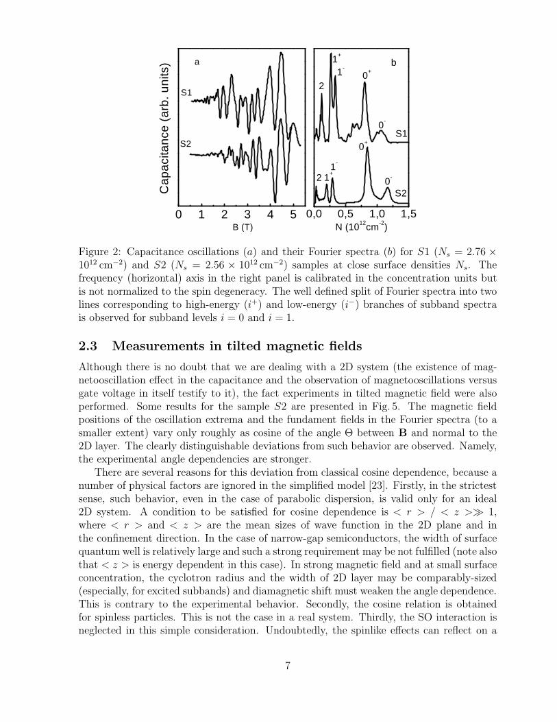
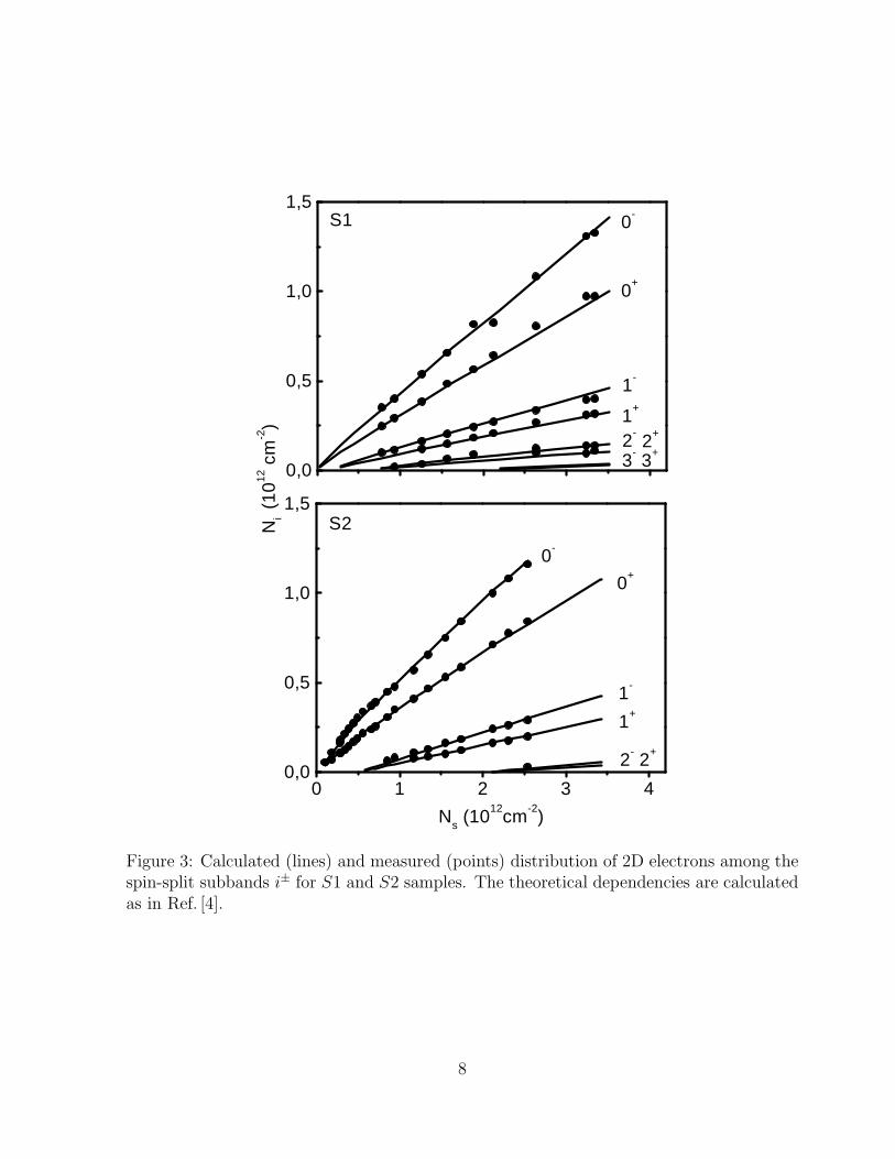
Typical C(B) oscillations for both samples at almost equal Ns are presented in Fig. 2together with their 1/B Fourier transforms. As in the case of gapless HgCdTe [4], theindividual spin components have not been observed in the oscillations at any Ns even forlowest LL’s. On the other hand, the oscillation beats and the Fourier spectra demonstratedistinctly the presence of two frequencies connected with the SO splitting of each 2Dsubband. The additional structure in Fig. 2 near the Fourier lines corresponding to i = 0subband for sample S2 results from mixed harmonics. This structure is suppressed if therange of small magnetic fields (in which the oscillations relevant to the higher subbandsare dominant) is excluded from Fourier analysis. For a sample S1, the intensities of i = 1and i = 2 lines are small, and the above features are practically indistinguishable in thescale of Fig. 2. The surface densities in the spin-split subbands N+
i and N−i determined
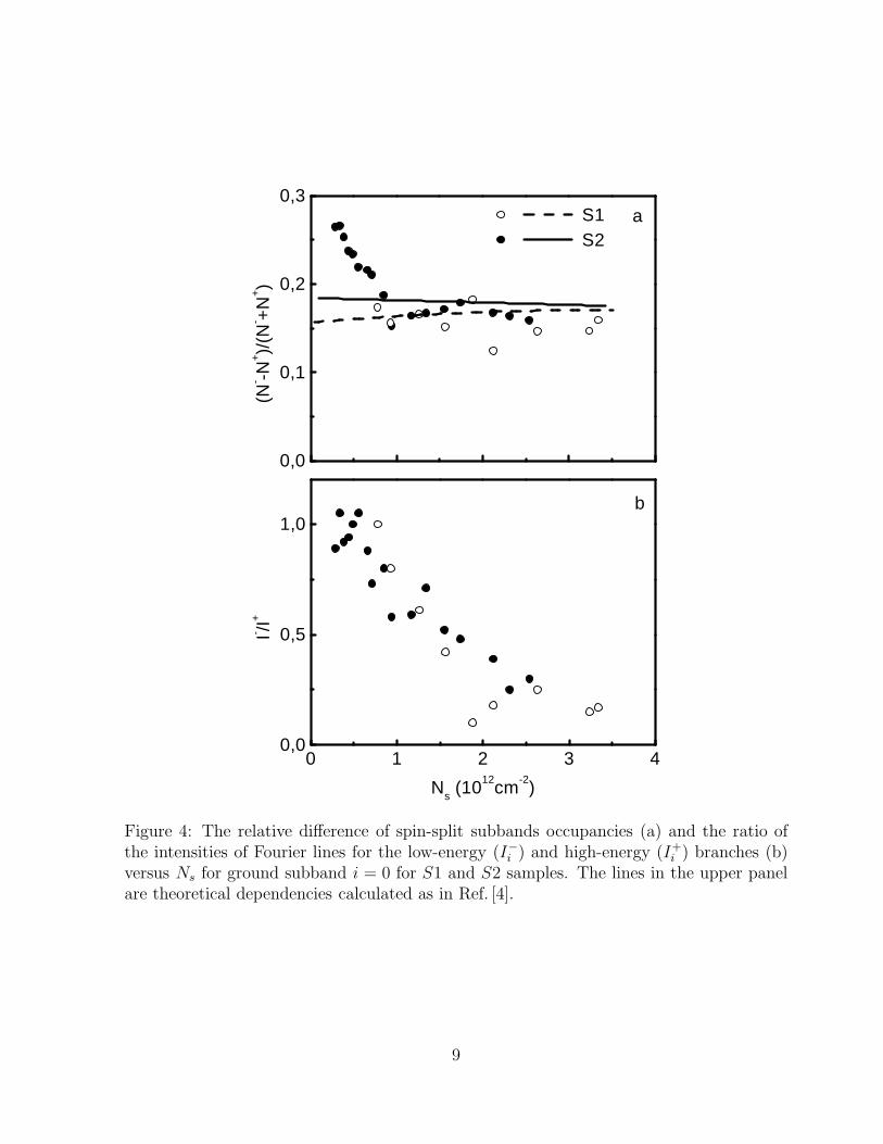
from Fourier transforms are plotted in Fig. 3 as functions of Ns. The carrier distributionamong 2D subbands is different for the two samples. The concentrations Ns, correspondingto the “starts” of excited subbands, increase with increasing doping level and agree wellwith the theoretical calculations, in which the bulk values of NA − ND are used. Thisfact also testifies that the disruption of stoichiometry in surface layers because of probablemigration of atoms is insignificant. A discrepancy with theory is detectable only in therelative differences (splitting) of occupancies ∆Ni/Ni = (N−
i −N+i )/(N−
i +N+i ) in the small
Ns range (see Fig. 4). Similar disagreement takes place for inversion layers on HgCdTe also.The possible reasons for such behavior are discussed in Ref. [4].
The intensities of Fourier lines for the high-energy branch I+i and low-energy branch I−
i
are different (see Fig. 2 and Fig. 7). At low Ni, the intensities I+i and I−
i are close for i = 0subband, and I−
i > I+i for excited subbands. The ratio I−
i /I+i as a function of Ns for i = 0
is shown in Fig. 4. The scattering of the points is due mainly to the fact that N±i values
and especially the ratios I−i /I+
i depend strongly (and non-monotonically) on a magneticfield range used in Fourier transform (for instance, it is clear that Fourier analysis willreveal no splitting for the range between beat nodes). Nevertheless, a decrease in I−
i /I+i
with increasing Ns is clearly visible. It is valid for excited subbands also.
6
0 1 2 3 4 5
Ca
pa
cita
nce
(a
rb. u
nits
) a
B (T)
S2
S1
0,0 0,5 1,0 1,5
2
2
0-
1-
1+
0+
1-
0-
b1+
0+
N (1012
cm-2)
S2
S1
Figure 2: Capacitance oscillations (a) and their Fourier spectra (b) for S1 (Ns = 2.76 ×1012 cm−2) and S2 (Ns = 2.56 × 1012 cm−2) samples at close surface densities Ns. Thefrequency (horizontal) axis in the right panel is calibrated in the concentration units butis not normalized to the spin degeneracy. The well defined split of Fourier spectra into twolines corresponding to high-energy (i+) and low-energy (i−) branches of subband spectrais observed for subband levels i = 0 and i = 1.
2.3 Measurements in tilted magnetic fields
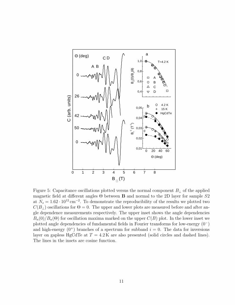
Although there is no doubt that we are dealing with a 2D system (the existence of mag-netooscillation effect in the capacitance and the observation of magnetooscillations versusgate voltage in itself testify to it), the fact experiments in tilted magnetic field were alsoperformed. Some results for the sample S2 are presented in Fig. 5. The magnetic fieldpositions of the oscillation extrema and the fundament fields in the Fourier spectra (to asmaller extent) vary only roughly as cosine of the angle Θ between B and normal to the2D layer. The clearly distinguishable deviations from such behavior are observed. Namely,the experimental angle dependencies are stronger.
There are several reasons for this deviation from classical cosine dependence, because anumber of physical factors are ignored in the simplified model [23]. Firstly, in the strictestsense, such behavior, even in the case of parabolic dispersion, is valid only for an ideal2D system. A condition to be satisfied for cosine dependence is < r > / < z >≫ 1,where < r > and < z > are the mean sizes of wave function in the 2D plane and inthe confinement direction. In the case of narrow-gap semiconductors, the width of surfacequantum well is relatively large and such a strong requirement may be not fulfilled (note alsothat < z > is energy dependent in this case). In strong magnetic field and at small surfaceconcentration, the cyclotron radius and the width of 2D layer may be comparably-sized(especially, for excited subbands) and diamagnetic shift must weaken the angle dependence.This is contrary to the experimental behavior. Secondly, the cosine relation is obtainedfor spinless particles. This is not the case in a real system. Thirdly, the SO interaction isneglected in this simple consideration. Undoubtedly, the spinlike effects can reflect on a
7
0,0
0,5
1,0
1,5
2+
S1
Ni
(1012
cm
-2)
3- 3
+2
-1
+
1-
0-
0+
0 1 2 3 40,0
0,5
1,0
1,5S2
2- 2
+
1-
1+
0-
0+
Ns (10
12cm
-2)
Figure 3: Calculated (lines) and measured (points) distribution of 2D electrons among thespin-split subbands i± for S1 and S2 samples. The theoretical dependencies are calculatedas in Ref. [4].
8
0,0
0,1
0,2
0,3a S1
S2(N
- -N+)/
(N- +
N+)
0 1 2 3 40,0
0,5
1,0b
I- /I+
Ns (10
12cm
-2)
Figure 4: The relative difference of spin-split subbands occupancies (a) and the ratio ofthe intensities of Fourier lines for the low-energy (I−
i ) and high-energy (I+i ) branches (b)
versus Ns for ground subband i = 0 for S1 and S2 samples. The lines in the upper panelare theoretical dependencies calculated as in Ref. [4].
9
spectrum in a tilted magnetic field and modify the angle dependence. Lastly, the exchangeinteraction can also make an additional contribution to the deviation from simple angledependence. This assumption has experimental support. For comparison we investigatedthe HgCdTe-based samples in a tilted magnetic field. Data for HgCdTe with Eg = −95meVand NA − ND = 2 × 1017 cm−3 are given in Fig. 5. Under the same conditions they alsomanifest a deviation from cosine behavior. However, the deviation is weaker and oppositein sign to the case of gapless HgMnTe. At the same time, the samples based on HgCdTewith Eg > 0 show a deviation of the same sign as in HgMnTe, but smaller in magnitude.Contrary to HgCdTe samples, changes in the structure of oscillations are observed inHgMnTe inversion layers. Namely, the beat nodes in oscillations C(B⊥) (B⊥ = B cos Θ)are shifted to the lower LL’s numbers with increasing Θ (i.e., with increasing total magneticfield B) (see Fig. 5).
These experimental observations testify that the behavior in tilted magnetic fields ismarkedly affected by both SO interaction (which essentially depends on Eg sign, see Sec. III.and Fig. 8) and exchange interaction. For narrow-gap semiconductors, the theoretical anal-ysis requires a consideration of spin from the outset. Strong SO and exchange interactionand resonant effects lead to serious complication of the theoretical description even forperpendicular orientation (see Sec. III.). The calculations in tilted magnetic fields aretroublesome even for the simplest parabolic Hamiltonian with a k-linear Rashba term. Atpresent we cannot make A reasonable theoretical analysis of effects in tilted fields we willrestrict our consideration to the case of perpendicular orientation.
2.4 Temperature effects
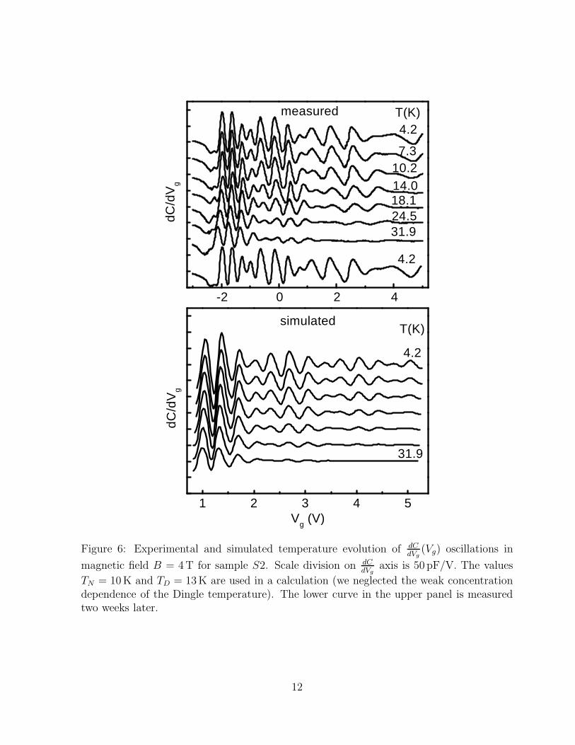
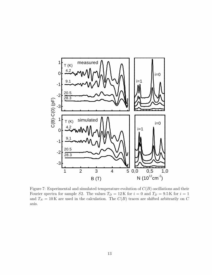
The structure of oscillations and the subband parameters extracted from oscillations areidentical to those in HgCdTe. No features due to exchange interaction are manifested.Because the exchange effects are determined by a magnetization and can be varied by thetemperature, the investigation of temperature evolution of oscillations is of prime interest.The results for dC/dVg(Vg) and C(B) oscillations are shown in Fig. 6 and Fig. 7 respectively.As it may be seen, no pronounced changes in the position of either dC/dVg(Vg) or C(B)oscillations are observed. The shift of beat nodes to the high gate voltages and to lowmagnetic fields (to the greater LL’s numbers) with increasing temperature (and hencewith decreasing magnetization) is the sole temperature effect, besides the usual diminutionof oscillation amplitudes. (Notice, the direction of shift with the increasing magnetizationis similar to the one observed with increasing total B (at the same B⊥) in the tiltedmagnetic field experiments). This shift must be attributed to the features inherent insemimagnetic semiconductors because in HgCdTe-based structures neither the positions ofthe oscillations nor those of the beat nodes change with the temperature.
The analysis based on the Fourier transform of oscillations for different temperaturescannot yield any information about exchange interaction. On the other hand, such datacannot be obtained from spin splitting either because, as noted above, the separate spincomponents are not observed in the oscillations at any temperatures. Thus we must settlethe question by capacitance magnetooscillations modeling.
10
0 1 2 3 4 5 6 7 8
0
Θ (deg)
50
42
26
0
DC
BAC
(a
rb. u
nits
)
B (T)
0,4
0,6
0,8
1,0
T=4.2 K
a
A B C D
Bn(
0)/B
n(θ)
0 20 40 600,01
0,02
0,03
0,04
0,05
⊥
0-
0+
b
Bf-1
(T
-1)
Θ (deg)
4.2 K 15 KHgCdTe
Figure 5: Capacitance oscillations plotted versus the normal component B⊥ of the appliedmagnetic field at different angles Θ between B and normal to the 2D layer for sample S2at Ns = 1.62 · 1012 cm−2. To demonstrate the reproducibility of the results we plotted twoC(B⊥) oscillations for Θ = 0. The upper and lower plots are measured before and after an-gle dependence measurements respectively. The upper inset shows the angle dependenciesBn(0)/Bn(Θ) for oscillation maxima marked on the upper C(B) plot. In the lower inset weplotted angle dependencies of fundamental fields in Fourier transforms for low-energy (0−)and high-energy (0+) branches of a spectrum for subband i = 0. The data for inversionslayer on gapless HgCdTe at T = 4.2K are also presented (solid circles and dashed lines).The lines in the insets are cosine function.
11
-2 0 2 4
dC/d
Vg
4.2
measured
31.924.518.114.010.27.3
4.2T(K)
1 2 3 4 5
dC/d
Vg
simulated
31.9
4.2
T(K)
Vg (V)
Figure 6: Experimental and simulated temperature evolution of dCdVg
(Vg) oscillations in
magnetic field B = 4T for sample S2. Scale division on dCdVg
axis is 50 pF/V. The values
TN = 10K and TD = 13K are used in a calculation (we neglected the weak concentrationdependence of the Dingle temperature). The lower curve in the upper panel is measuredtwo weeks later.
12
-3
-2
-1
0
1T (K)
measured
28.320.5
9.1
4.2
1 2 3 4 5
-3
-2
-1
0
1
C(B
)-C
(0)
(pF
)
simulated
28.3
20.5
9.1
4.2
T (K)
B (T)
i=1
i=0
0,0 0,5 1,0
i=1i=0
N (1012
cm-2)
Figure 7: Experimental and simulated temperature evolution of C(B) oscillations and theirFourier spectra for sample S2. The values TD = 12K for i = 0 and TD = 9.5K for i = 1and TN = 10K are used in the calculation. The C(B) traces are shifted arbitrarily on Caxis.
13
3 Theoretical Consideration
3.1 Landau levels structure
The direct numerical solution of an initial matrix equation (especially in the case of non-zero magnetic field) faces obstacles of a fundamental nature, such as singularity problemsand the ambiguity of boundary conditions on the interface and in the bulk, especiallyin the case of gapless semiconductors [24, 25]. In this work, we employ a concept basedon the reduction of the matrix equation to a Schrodinger-like equation with an effectivepotential [4]. At B = 0, the results are quite close to those obtained by numeric calculations[5, 24, 26, 27]. The line of attack of Ref. [4] seems to be a reasonable compromise betweenaccuracy and the ease of the calculation for a non-zero magnetic field. This simplicity ofmethod is of considerable advantage for the purposes of oscillations modeling.
Under homogeneous magnetic field B(0, 0, B) parallel to the direction of the confine-ment (surface potential V = V (z)) a motion in the 2D plane can be quantized, using themean field approximation for exchange interaction. It can be shown that in the frameworkof a six-band Kane model with an allowance for a magnetic field and exchange interac-tion, the following matrix equation determines the subband LL’s energy En(B) (we do notwrite out the usual expressions, describing the behavior of envelopes in perpendicular tomagnetic field 2D plane)
−E−+αEB
√3(n−1)
2EB
√n
20 0 sbhkz
EB
√3(n−1)
2−E++3β 0 0 0 0
EB
√n
20 −E+−β sbhkz 0 0
0 0 sbhkz −E−−αEB
√3(n+1)
2−EB
√n
2
0 0 0EB
√3(n+1)
2−E+−3β 0
sbhkz 0 0 −EB
√n
20 −E++β
fn−11 (z)
fn−23 (z)
fn5 (z)
fn2 (z)
fn−14 (z)
fn−16 (z)
= 0, (1)
where E± = En − V ± Eg/2, sb =√
|Eg| /2mb is Kane velocity, n is LL number. Theenvelopes f1,4 correspond to Γ6 symmetry band, f3,6 and f2,5 to heavy and light branches
of Γ8 band. “Magnetic energy” EB =√
2mbs2bhωb =
√2sbh/λ (hωb = heB/mbc is cyclotron
energy, λ =√
ch/eB is magnetic length) practically does not depend on band parameters
because sb is practically the same for all Kane semiconductors [28, 29]. We denote α =12xNα′〈Sz〉 and β = 1
6xNβ ′〈Sz〉, where x is the MnTe mole fraction, N is the number
of unit cells per unit volume, α′ and β ′ are the exchange integrals for Γ6 and Γ8 bandsrespectively. The thermodynamically average 〈Sz〉 of the z− component of a localized spinS (for Mn2+ ions S = 5
2) can be described via normalized Brillouin function BS (x):
〈Sz〉 = −S(1 − x)18BS
(
2µBB
kB(T + TN )
)
, (2)
where TN is effective temperature, arising from antiferromagnetic interaction between Mn2+
ions [30, 31]. This factor defines the magnetic field and temperature dependency of ex-change effects.
14
Resolving the systems (1) with respect to the components f5 and f6 we obtain the
following set of two “Schrodinger-like” equations (for the envelopes ϕn5 = fn
5 /√
H+n and
ϕn−16 = fn−1
6 /√
H−n ) for the description of the magnetic spectrum of 2D electrons in surface
layers on DMS with inverted bands (called Kane “p- electrons” as in Ref. [4])
∣
∣
∣
∣
∣
∣
∣
∣
∣
∣
h2k2z
2mb
− Eeff + U+ −iU+so − C+
g sbhkz
iU−so + C−
g sbhkz
h2k2z
2mb
− Eeff + U−
∣
∣
∣
∣
∣
∣
∣
∣
∣
∣
(
ϕn5
ϕn−16
)
= 0 (3)
with effective energyEeff = (E2 − m2
bs4b)/2mbs
2b ,
and effective potentialU± = U0 + U±
B + U±exc + U±
R ),
in which we single out the following parts: -the spin independent “Klein-Gordon“ term
U0 = (V 2 − 2EV )/2mbs2b ,
and spin-like terms: “magnetic potential”
U±B = E2
B[g2nR± + 3(n ± 1)(E+ ± β)/(E+ ± 3β)]/2mbs2b ,
”exchange potential”U±
ex = [αβ ± (αE+ + βE−)]/2mbs2b ,
and “resonant” term describing “spin-interband“ interaction, arising from the mixing ofΓ6 and Γ8 bands by an electric field
U±R =
s2bh
2
2mbs2b
3
4
(
1 + L±n
H±n
)2
+L±
n
H±n (E+ ± 3β)
(
dV
dz
)2
+s2
bh2
4mbs2b
(1 + L±n )
H±n
d2V
dz2,
where the following designations are used:
L±n = 3E2
B(n ± 1)/4(E+ ± 3β)2, H±n = E− ± α − L±
n (E+ ± 3β),
R±n = H±
n /H∓n , g = −1
The spin-orbit terms and the coefficients at linear in kz terms are determined by
U±so = Cgsbh
√
R∓n
[
1 + L±n
H±n
+1 + L∓
n
2H∓n
(R±n − 1)
]
dV
dz,
C±g = Cg
√
R∓n (R±
n − 1), Cg = gEB
√n
4mbs2b
.
15
The second term in an expression for U±B and the dimensionless parameter L±
n arise fromthe interaction with heavy hole branch. It must be stressed that the exchange interactioncauses not only the appearance of an exchange term in the effective potential, but also amodification of the terms, describing the ”resonant” and SO interaction.
The LL’s of 2D electrons in Kane semiconductors with Eg > 0 (“s-electrons”) are
described by the same set (3) (for the envelopes ϕn2 = fn
2 /√
H+n and ϕn−1
1 = fn−11 /
√
H−n )
but with g = +1, L±n = 0, H±
n = E+ ± β. It can be shown that the equations for Diraclike electrons in a magnetic field are the same as for Kane “s- electrons” but with g = +2.It should be emphasized that unlike the B = 0 case [4], the set (3) cannot be separatedand reduced to independent equations for individual spin components because of the SOinteraction U±
so (for “p- electrons”, because of linear in kz terms also).From this point on, we shall restrict our consideration to the semiclassical approxima-
tion just as in quantization of spectrum described by Eqs. (3) (it is clear that the use ofthe semiclassical approximation immediately in (1) results in the loss of spinorlike effects),so also in calculation of the surface potential V (z). A semiclassically self-consistent po-tential in such treatment is calculated in the frame of quasirelativistic modification of theThomas-Fermi method. The validity of such an approach in narrow-gap semiconductorswas argued and demonstrated by a comparison with numerical self-consistent calculationsin many papers [32, 33, 34] (see also Ref. [4] and references therein). Substituting asusual ϕm
i = Cmi exp(i
∫
kz(z)dz) and neglecting the proportional to i(zdkz/dz + kz)2 terms
(higher-order terms in the expansion of the action in powers of h) we obtain from (3) thequasiclassical expression for “spin-split” z−components of wave vector
k±z =
√
2mbs2b
sbh{K ∓ [K2 − (Eeff − U+)(Eeff − U−) + U+
soU−so]
1
2} 1
2 (4)
withK = Eeff − (U+ + U−)/2 − mbs
2bC
2g (R+
n − 1)(R−n − 1).
Together with the Bohr-Sommerfeld quantization rule
∫ V (kz=0)
V (z=0)kz(E, V )
(
dV
dz
)−1
dV = π(i +3
4) (5)
they define the magnetic levels E±n (i, B) in surface quantum well V (z).
For the Dirac-like electrons, the derived equations may be considered as a generalizationof the result of Ref. [35] that allows for magnetic quantization and spin-like effects. Inthe case of Kane “s− electrons“ and without exchange interaction, the Eqs. (3) and (4)coincide with the corresponding expressions in Ref. [36]. As might be expected, at α =0, β = 0, n → ∞, EB
√n ± 1 and EB
√n → sbhks (ks is 2D wave vector) the Eq. (5)
with kz from Eq. (4) is reduced to the corresponding equation in Ref. [4], describingsubband dispersions E±
i (ks) at B = 0. Lastly, the Eq. (4) at V (z) = const determinesthe Landau subbands E±
n (B, kz) in the bulk of Kane (at α = 0 and β = 0 non-magnetic)semiconductors.
It must be noted that the proportional to C2g term in expression for K (arising from
linear in kz terms in (3)) has little effect in comparison with the spin-orbit term in Eq.
16
0 0,001 0,002-0,32
-0,31
-0,30
0,00 0,02 0,04 0,06 0,08 0,10-0,3
-0,2
-0,1
0,0
0,1
0,2
0,3
0,4 "s electrons"
2+
1+
0+
2-
1-
0-
(En
-EF)/
µs
0,00 0,02 0,04 0,06 0,08 0,10-0,3
-0,2
-0,1
0,0
0,1
0,2
0,3
0,4
0,5"p electrons"
2+
2-
1+
1-
0+
0-
B/Bs
(En
-EF)/
µs
0 0,001 0,002-0,32
-0,31
-0,30
Figure 8: A spectrum in a magnetic field for Kane “s ” and “p electrons” in dimensionlessunits in the pseudoultrarelativistic limit Eg = 0. Drastic spin-orbit perturbation of amagnetic spectrum as compared with an ordinary set of Landau levels is observed at theenergies near the subband bottom [shown in insets] as well as nearby the Fermi level. Theeffect is essentially different for materials with direct (upper panel) and inverted (lowerpanel) bands.
17
(4). However, ignoring this term in calculations at U±so = 0 can introduce large error up
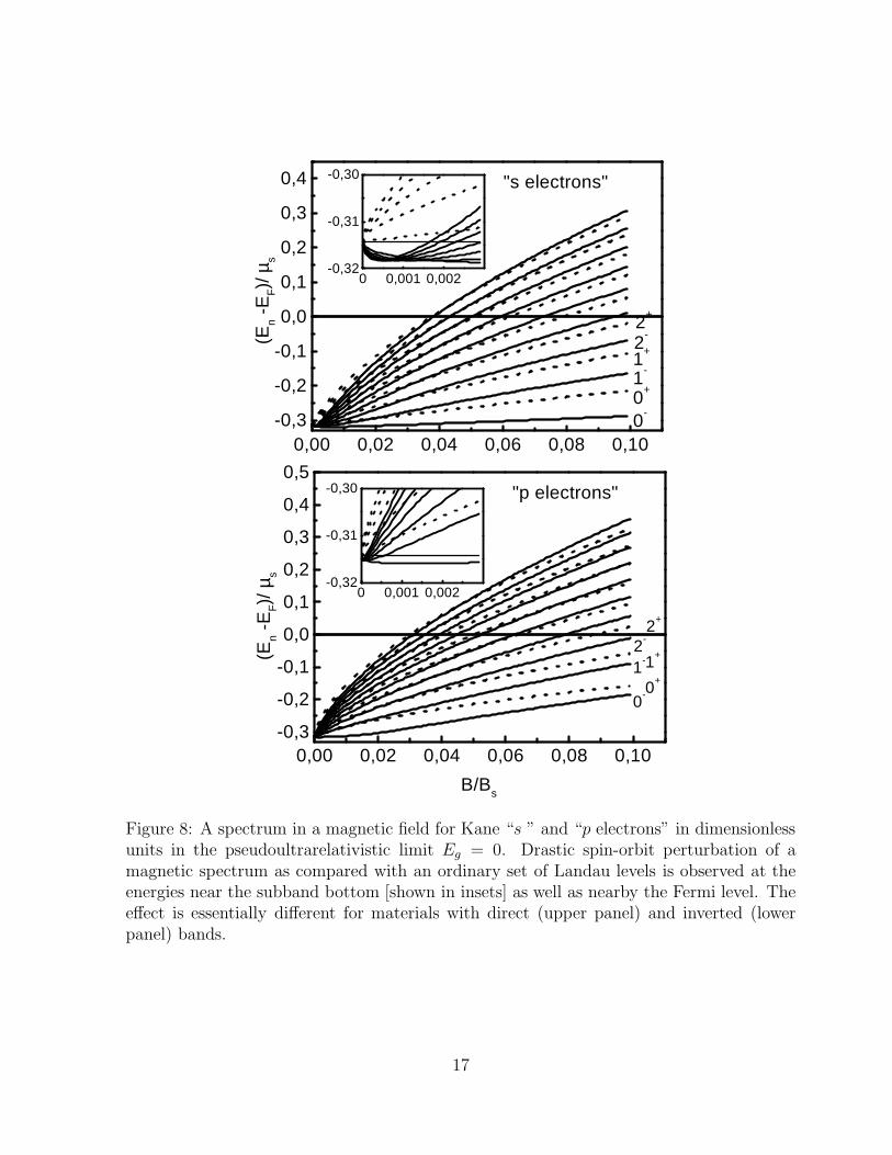
to the inversion of the order of spin sublevels. In pseudo-ultrarelativistic limit Eg = 0and without exchange interaction, the spectra in magnetic fields for both “s ” and “p-electrons” are scale invariant with respect to the surface band bending µs as well as in thecase of B = 0 [4, 28]. The results for ground subband are plotted in Fig. 8 in dimensionless(normalized to µs) coordinates E/µs − B/Bs = (EB/µs)
2 (Bs = cµ2s/2es2
bh). It is seenthat the SO interaction leads to so drastic a reconstruction of 2D spectrum in magneticfields, that the description of spin splitting by such a non-relativistic parameter as g-factorloses in essence its physical meaning. The SO splitting far exceeds a contribution due toexchange interaction (in the scale of Fig. 8, the changes induced by exchange interactionare practically indistinguishable for reasonable exchange coupling parameters). This is truefor narrow-gap DMS with Eg > 0 also. In connection with this, the results of the analysisof 2D systems in asymmetrical quantum wells in these materials are to be revised, becausethey ignore the SO interaction.
3.2 Density of states and capacitance in magnetic field
For 2D systems with the multisubband spectrum, the differential capacitance of spacecharge region with 2D electron gas is determined by the sum Csc =
∑
Ciσ of “partial”subband capacitances
Ciσ = e2 dNiσ
dµs
=e2
πs2h2
dµF i
dµs
d
dµF i
∫
Diσ(E)f(E − µF i)dE, (6)
where Niσ is the surface concentration in spin branch σ = ± of i-th subband, f(E − µF i)is the Fermi-Dirac distribution function and µF i is the subband Fermi energy. The magne-tooscillations of capacitance are dictated by peculiarities in the DOS Diσ(E) in a magneticfield, i.e. by the energy position and broadening of LL’s. The rigorous quantitative anal-ysis of disorder broadened LL’s is a complicated problem even in one-band approximation[37, 38]. We shall perform the treatment by neglecting the mixing between LL’s andassuming a Gaussian shape of each level [39, 40]
Diσ = D±i (E) =
eB
ch√
2π3
∞∑
n=0
1
Γ±i
exp
−2
(
E − E±ni
Γ±i
)2
(7)
with broadening parameters Γ±i , independent of LL’s number, but dependent on B and (for
discussed non-parabolic system) on energy. The analytical description of magnetooscilla-tion phenomena, if possible, is preferable because it is more transparent, and easy tointerpret in contrast to direct numerical methods. In addition, the peculiar features of os-cillation phenomena in 2D systems with quasirelativistic spectra as compared with those ofparabolic spectra [39] can thus be clarified. For this purpose we approximate the spin-splitsubband dispersions by analytical relativistic-like expression with the subsubband massesm±
0i and velocities s±i . Such approximation holds for practically all the energy range ofinterest. The replacement in Eq.(7) of numerical solutions of Eq. (5) with kz from Eq. (4)by the corresponding quasiclassical spectrum in a magnetic field (for simplicity we shall
18
drop the spin subband indices σ = ± in the following)
Eni =√
E2Bi (ni + δi) + m2
0is4i − m0is
2i (8)
(EBi =√
2sih/λ) does not noticeably reflect on the shape of the DOS. As to the LL’senergy positions (and the positions of oscillations on B), their values are to be calculatedon the basis of Eqs. (4) and (5). In the Born approximation for short-range scattering,the parameter Γi is related to the classical scattering time in zero magnetic field τi by
Γ2i =
√
2/πh2ωci(E)/τi (ωci(E) = eB/cmci(E), mci(E) = m0i + E/s2i ) [37]. Inserting the
above expressions for Eni and Γi in (7) and using a Poisson summation formula, we arrive(under the assumptions Γi << EBi and Γi << E + m0is
2i , which are justified even for the
states nearby the subband bottom) at a “harmonic” representation for DOS (convenientfor the description of oscillation effects)
Di(E, B) = Di(E, 0)[1 + 2∞∑
j=1
(−1)j exp
(
− j2π
ωci(E)τi
)
cos(2πjni(E))], (9)
where Di(E, 0) = mdi(E)/2πh2 = (E + m0is2i )/2πs2
i h2 is DOS at B = 0. Notice, that
in the case of a two-dimension system, as is easy to show, the effective mass of DOS mdi
coincides with the cyclotron effective mass mci for any dispersion law. The LL “number”ni(E) in Eq. (9) is regarded as an arbitrary quantity (not necessarily an integer) and isdetermined at a given energy by the solutions of Eqs. (4) and (5). One can readily see thatin “non-relativistic” limit (si → ∞), Eq. (9) is reduced to the Ando formula [39] if theterms with j > 1 are neglected. It has been shown that for all parameters and regimes ofpractical interest, the DOS given by (7) and (9) are practically equivalent. This is true inthe case of both the sinusoidal shape of DOS (when only ground harmonic predominatesin sum (9)) and the nonsinusoidal shape of D(E) dependence. The latter case takes placeat weakly broadened LL’s, when the individual spin components can be resolved in totalDOS.
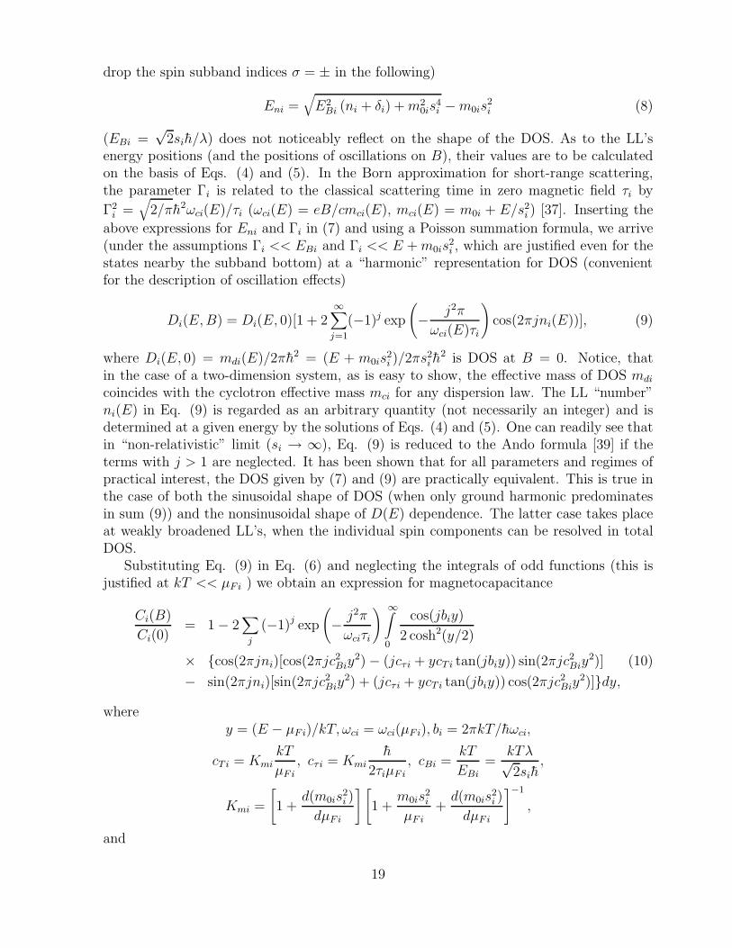
Substituting Eq. (9) in Eq. (6) and neglecting the integrals of odd functions (this isjustified at kT << µF i ) we obtain an expression for magnetocapacitance
Ci(B)
Ci(0)= 1 − 2
∑
j
(−1)j exp
(
− j2π
ωciτi
) ∞∫
0
cos(jbiy)
2 cosh2(y/2)
× {cos(2πjni)[cos(2πjc2Biy
2) − (jcτi + ycT i tan(jbiy)) sin(2πjc2Biy
2)] (10)
− sin(2πjni)[sin(2πjc2Biy
2) + (jcτi + ycT i tan(jbiy)) cos(2πjc2Biy
2)]}dy,
wherey = (E − µF i)/kT, ωci = ωci(µF i), bi = 2πkT/hωci,
cT i = Kmi
kT
µF i
, cτi = Kmi
h
2τiµF i
, cBi =kT
EBi
=kTλ√2sih
,
Kmi =
[
1 +d(m0is
2i )
dµF i
] [
1 +m0is
2i
µF i
+d(m0is
2i )
dµF i
]−1
,
and
19
Ci(0) = e2
[
Di(µF i, 0) +µF i
2πs2i h
2
d(m0is2i )
dµF i
]
dµF i
dµs
.
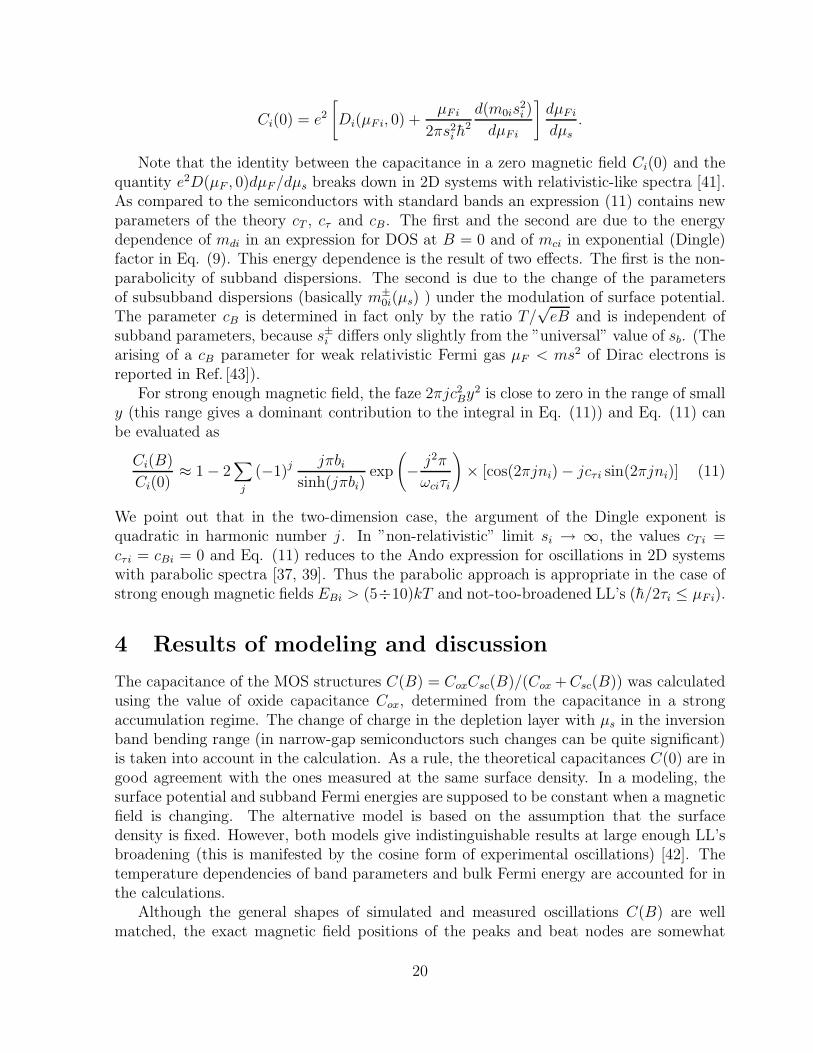
Note that the identity between the capacitance in a zero magnetic field Ci(0) and thequantity e2D(µF , 0)dµF/dµs breaks down in 2D systems with relativistic-like spectra [41].As compared to the semiconductors with standard bands an expression (11) contains newparameters of the theory cT , cτ and cB. The first and the second are due to the energydependence of mdi in an expression for DOS at B = 0 and of mci in exponential (Dingle)factor in Eq. (9). This energy dependence is the result of two effects. The first is the non-parabolicity of subband dispersions. The second is due to the change of the parametersof subsubband dispersions (basically m±
0i(µs) ) under the modulation of surface potential.The parameter cB is determined in fact only by the ratio T/
√eB and is independent of
subband parameters, because s±i differs only slightly from the ”universal” value of sb. (Thearising of a cB parameter for weak relativistic Fermi gas µF < ms2 of Dirac electrons isreported in Ref. [43]).
For strong enough magnetic field, the faze 2πjc2By2 is close to zero in the range of small
y (this range gives a dominant contribution to the integral in Eq. (11)) and Eq. (11) canbe evaluated as
Ci(B)
Ci(0)≈ 1 − 2
∑
j
(−1)j jπbi
sinh(jπbi)exp
(
− j2π
ωciτi
)
× [cos(2πjni) − jcτi sin(2πjni)] (11)
We point out that in the two-dimension case, the argument of the Dingle exponent isquadratic in harmonic number j. In ”non-relativistic” limit si → ∞, the values cT i =cτi = cBi = 0 and Eq. (11) reduces to the Ando expression for oscillations in 2D systemswith parabolic spectra [37, 39]. Thus the parabolic approach is appropriate in the case ofstrong enough magnetic fields EBi > (5÷10)kT and not-too-broadened LL’s (h/2τi ≤ µF i).
4 Results of modeling and discussion
The capacitance of the MOS structures C(B) = CoxCsc(B)/(Cox + Csc(B)) was calculatedusing the value of oxide capacitance Cox, determined from the capacitance in a strongaccumulation regime. The change of charge in the depletion layer with µs in the inversionband bending range (in narrow-gap semiconductors such changes can be quite significant)is taken into account in the calculation. As a rule, the theoretical capacitances C(0) are ingood agreement with the ones measured at the same surface density. In a modeling, thesurface potential and subband Fermi energies are supposed to be constant when a magneticfield is changing. The alternative model is based on the assumption that the surfacedensity is fixed. However, both models give indistinguishable results at large enough LL’sbroadening (this is manifested by the cosine form of experimental oscillations) [42]. Thetemperature dependencies of band parameters and bulk Fermi energy are accounted for inthe calculations.
Although the general shapes of simulated and measured oscillations C(B) are wellmatched, the exact magnetic field positions of the peaks and beat nodes are somewhat
20
different. This is not surprising, because a number of physical factors are ignored or cannotbe exactly taken into account in a theory (the contribution of remote bands, interfacecontribution to the SO interaction (see below), the deviation of real surface potential andLandau level shape from those calculated, the superposition of oscillations from differentsubbands). At the same time the positions of oscillations and especially beat nodes arevery sensitive to each of these factors. The adjustable phase factor (a correction ∆ni toLL’s “number” ni in the expressions (9), (11) and (11)) was introduced for reasons ofconvenience for a comparison of the temperature evolution in the measured and calculatedoscillations. Its magnitude was chosen to fit the high-field node position of the beat patternat T=4.2K. Any physically meaningful results discussed are not affected by the choice ofthis factor.
The oscillations calculated with this correction and their Fourier transforms are plottedin Fig. 7. The agreement is quite good with respect to the structure of oscillations as wellas the amplitudes. However, a distinguishable difference in the “number” of oscillationsbetween beat nodes for measured and calculated plots is observed. These results, as wellas the similar data on dC/dVg(Vg) oscillations (see Fig. 6), testify to the small (but dis-tinguishable) underestimation of SO splitting by the theory. This conclusion is valid forHgCdTe also. Note that a treatment based on the analysis of Fourier spectra does not givea clearly detectable discrepancy between experiment and theory (excluding the small Ns
range (see Fig. 4)). This inconsistency with theory can be caused by the interface contri-bution to the SO interaction [16], which cannot be treated in the framework of effectivemass method. In accordance with the experiment, the individual spin components are notexhibited in simulated C(B) or dC/dVg(Vg) oscillations even for the lowest LL’s at any rea-sonable broadening parameters and magnetic fields of experimental interest. The resultsof modeling based on Eq. (11) do not differ from the results obtained in the approximation(11) practically for all Ns, T and B at which the oscillations are observed experimentally.As a rule, the contribution from the sine term in Eq. (11) is small.
4.1 Exchange interaction effects
A modeling shows that the magnetic field positions of the oscillations beyond the neighbor-hood of beat nodes are unaffected by the exchange effects even at the lowest temperatures.As a result these positions are temperature independent, as occurs experimentally. Thisis true for any available values of the exchange constants Nβ ′ and Nα′ (literature datavary markedly, see Refs. [1, 44, 45] and [46] and references in these works; note that indifferent papers the notations for exchange constants differ in sign [1]). As noted in Sec. II,an exchange interaction is very weakly manifested in the studied system, showing itself asonly a slight temperature shift of beat nodes. Because the oscillation amplitudes in theneighborhood of nodes are small even at T = 4.2K and they decrease drastically withtemperature, the narrow range of T < 10 ÷ 15K is accessible to the quantitative analysis.Thus the results are not critically sensitive to a choice of Nβ ′ and Nα′. Secondly, therate of shift depends on the product of the exchange parameters Nβ ′ and Nα′ and themagnetization 〈Sz〉. So the variations in Nβ ′ and Nα′can be cancelled out by the variationin TN , which is used as an adjustable parameter (see below). It must be stressed thatthe terms containing a parameter β play the dominant role in Eqs. (1), (3) and (4) for
21
p-electrons. Under the conditions of experimental interest, the temperature shift of beatnodes is also slightly sensitive to the variations Nα′ in a wide range even if a small Nβ ′ ischosen.
Although we performed the calculations for a different net of exchange parameters, theresults discussed in this Section correspond to Nβ ′ = 1.5 eV and Nα′ = −0.4 eV, unlessotherwise specified. The results are only slightly sensitive to variances of Nβ ′ in the range1.35 ÷ 1.65 eV and do not differ at all for Nα′ varied through −(0.35 ÷ 0.50) eV range.These values are close to those obtained in Refs.[44] and [45] for narrow-gap and gaplessHgMnTe with small |Eg| by the tunnel spectroscopy method. We suppose that these data(similar values for gapless HgMnTe have been obtained in many works (see Refs. [1, 44]and [45] and references in these works) are more suitable for the purposes of this work,because in studied surface quantum wells the typical electron energies are of the order ofor even considerably more than |Eg|. In tunnel experiments, the LL’s energy positions of“p- electrons” as a function of magnetic field are measured at energies up to 150meV. Atthe same time, the states with the energy near band bottom are tested by the traditionalmethods.
It should be noted in connection with this that a decrease of |Nα′| for s-electrons in inwide-gap CdMnTe-CdMgMnTe quantum well with increasing energy is reported in a recentpaper Ref. [47]. The effect is attributed to the admixing of Γ8 band states to Γ6 band atfinite k-vectors which leads to switching-on of a kinetic exchange for electrons of Γ6 bandwith the d electrons of Mn ions. Note that in narrow-gap semiconductors, the interbandmixing, described by the Kane Hamiltonian (1), results in a strong (and energy dependent)contribution of the Nβ ′ containing terms to a spectrum of Γ6 band. This is true withoutallowing for the energy dependence of parameter Nα′. As for electrons of Γ8 band (“p-electrons“), the value of the exchange parameter (Nβ ′) is from the outset governed mainlyby kinetic exchange (at any k-vector). In this case, an increase of k-vector cannot playa critical role. At present, we do not have evidence of energy dependence of parameterNβ ′. The absence of an essential change in the value of Nβ ′ is noted in Refs. [47] and [48].Together with the weak sensitivity of the observed effects to a choice of Nβ ′ and Nα′, thissuggests that any possible energy dependence of exchange parameters cannot markedlyreflect on the results.
Once the exchange parameters are chosen, two parameters can be obtained when themodeling fits experimental data: the effective temperature TN , which describes the tem-perature shift of beat nodes, and the Dingle temperature TD = h/kB2πτ (used by us as thecharacteristic of the scattering instead of collision time τ), which determines the oscillationamplitudes.
Although a decrease of magnetization with increasing temperature results in the slightenergy shift of spin sublevels, the position of resulting oscillations on a magnetic field isalmost unchanged (see Fig. 9). The rate of shift with temperature depends on the Ni
and node number, as is shown in Fig. 10. At the same time, the value of TN , extractedfrom the fit of the temperature evolution of oscillations, is almost the same for differentnodes and Ni, which counts in favor of model used. The results of the simulation are notcritically dependent on the exact value of TN chosen. However, the “best fitting” valueTN = 10 ± 1.5K must be a fairly good estimation. Unfortunately, as far as we know, thelow-temperature data on TN value for bulk HgMnTe with x = 0.04 are absent. Most of the
22
0 10 20 30 402,5
3,0
3,5
4,0
4,5
B (
T)
T (K)
3+
2+
4-
3-
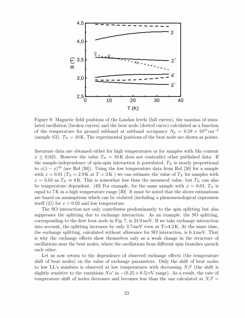
Figure 9: Magnetic field positions of the Landau levels (full curves), the maxima of simu-lated oscillation (broken curves) and the beat node (dotted curve) calculated as a functionof the temperature for ground subband at subband occupancy N0 = 0.59 × 1012 cm−2
(sample S2). TN = 10K. The experimental positions of the beat node are shown as points.
literature data are obtained either for high temperatures or for samples with Mn contentx ≤ 0.025. However the value TN = 10K does not contradict other published data. Ifthe sample-independence of spin-spin interaction is postulated, TN is nearly proportionalto x(1 − x)18 (see Ref. [30]). Using the low temperature data from Ref. [30] for a samplewith x = 0.01 (TN = 2.9K at T = 2K ) we can estimate the value of TN for samples withx = 0.04 as TN ≈ 8K. This is somewhat less than the measured value, but TN can alsobe temperature dependent. [49] For example, for the same sample with x = 0.01, TN isequal to 7K in a high temperature range [30]. It must be noted that the above estimationsare based on assumptions which can be violated (including a phenomenological expressionitself (2)) for x > 0.02 and low temperature.
The SO interaction not only contributes predominantly to the spin splitting but alsosuppresses the splitting due to exchange interaction. As an example, the SO splitting,corresponding to the first beat node in Fig. 7, is 24.9meV. If we take exchange interactioninto account, the splitting increases by only 3.7meV even at T=4.2K. At the same time,the exchange splitting, calculated without allowance for SO interaction, is 6.4meV. Thatis why the exchange effects show themselves only as a weak change in the structure ofoscillations near the beat nodes, where the oscillations from different spin branches quencheach other.
Let us now return to the dependence of observed exchange effects (the temperatureshift of beat nodes) on the value of exchange parameters. Only the shift of beat nodesto low LL’s numbers is observed at low temperatures with decreasing Nβ ′ (the shift isslightly sensitive to the variations Nα′ in −(0.25÷ 0.5) eV range). As a result, the rate oftemperature shift of nodes decreases and becomes less than the one calculated at Nβ ′ =
23
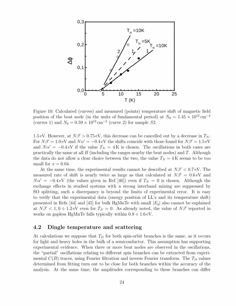
0 5 10 15 20 250,0
0,1
0,2
0,3
TN =10K
1 12
TN =10K
TN =5K
∆ϕ
T (K)
Figure 10: Calculated (curves) and measured (points) temperature shift of magnetic fieldposition of the beat node (in the units of fundamental period) at N0 = 1.45 × 1012 cm−2
(curves 1) and N0 = 0.59 × 1012 cm−2 (curve 2) for sample S2.
1.5 eV. However, at Nβ ′ > 0.75 eV, this decrease can be cancelled out by a decrease in TN .For Nβ ′ = 1.0 eV and Nα′ = −0.4 eV the shifts coincide with those found for Nβ ′ = 1.5 eVand Nα′ = −0.4 eV if the value TN = 4K is chosen. The oscillations in both cases arepractically the same at all B (including the ranges nearby the beat nodes) and T . Althoughthe data do not allow a clear choice between the two, the value TN = 4K seems to be toosmall for x = 0.04.
At the same time, the experimental results cannot be described at Nβ ′ < 0.7 eV. Themeasured rate of shift is nearly twice as large as that calculated at Nβ ′ = 0.6 eV andNα′ = −0.4 eV (the values given in Ref. [46]) even if TN = 0 is chosen. Although theexchange effects in studied systems with a strong interband mixing are suppressed bySO splitting, such a discrepancy is beyond the limits of experimental error. It is easyto verify that the experimental data (energy position of LL’s and its temperature shift)presented in Refs. [44] and [45] for bulk HgMnTe with small |Eg| also cannot be explainedat Nβ ′ < 1, 0 ÷ 1.2 eV even for TN = 0. As already noted, the value of Nβ ′ reported inworks on gapless HgMnTe falls typically within 0.9 ÷ 1.6 eV.
4.2 Dingle temperature and scattering
At calculations we suppose that TD for both spin-orbit branches is the same, as it occursfor light and heavy holes in the bulk of a semiconductor. This assumption has supportingexperimental evidence. When three or more beat nodes are observed in the oscillations,the “partial” oscillations relating to different spin branches can be extracted from experi-mental C(B) traces, using Fourier filtration and inverse Fourier transform. The TD valuesdetermined from fitting turn out to be close for both branches within the accuracy of theanalysis. At the same time, the amplitudes corresponding to these branches can differ
24
considerably (up to several times). Such a difference is not surprising. It is clear thatboth the DOS and cyclotron energy are different for two branches of a spectrum havingsignificantly different dispersions. As a result, the “partial” capacitance oscillations forthese branches differ not only by the period (which leads to the beat of oscillations) butalso by the amplitudes, even if the relaxation times are equal. Although DOS at B = 0 ina low-energy branch is higher, the corresponding amplitudes can be less, because the lowercyclotron energy in this branch leads to a lesser amplitude factor in Eqs. (11) and (11).
The relation between amplitudes depends on the subband occupancies (via the effectivemass), magnetic field, temperature and broadening parameters. For different subbands, Band Ns, the ratio of amplitudes A−
c /A+c can be below as well as above unity. However, the
value of A−c /A+
c decreases rapidly with increasing Ni. Such behavior correlates well withdecreasing ratio of Fourier line intensities I−
i /I+i experimentally observed (see Fig. 4). Thus
the difference in the amplitudes for different spin components of oscillations mentioned inRefs. [11] and [14] is to be expected for 2D systems with strong SO interaction (withoutinvoking spin-dependent scattering).
The Dingle temperature TD, determined from the fitting, slightly increases (from 8÷ 9to 13 ÷ 15K for ground subband) with the increasing Ns. Such behavior is inherent insurface roughness scattering [37, 50]. The TD(Ns) dependencies are essentially sublinear.This testifies that the efficiency of scattering is suppressed with the increasing of the Fermiwave vector. This is possible if the correlation length Λ is large enough. The best agreementbetween experimental and calculated values of TD is achieved at Λ ≈ (110÷120) Aand at theaverage interface displacement ∆ ≈ (20÷ 25) A. Note that the screening effects contributesignificantly to the scattering, because in surface layers on narrow-gap semiconductors, theFermi wavelength turns out to be of the same order of magnitude as 2D Thomas-Fermiscreening length and z-size of wave function. The above values of Λ and ∆ are many timeslarger than tuose found for silicon [37] and substantially exceed the corresponding values inIII-V semiconductors also [50]. This suggests much more disorder in the interface betweenternary compounds and their oxides. Using the TD values, the electron mobility can beestimated as 0.8× 104 cm2/Vs in i = 0 subband and 1.5× 104 cm2/Vs in i = 1 subband forsample S1 at Ns ∼ 1012 cm−2 that is close to a value 1 × 104 cm2/Vs measured for grainboundaries in p-HgMnTe with x = 0.1 [7].
Somewhat larger values of TD are detected at small surface densities Ns < 5×1011 cm−2.The Coulomb scattering from the chargers in oxide cannot cause this, because the theo-retical calculations give the values of relaxation times, which are larger by at least twoorders of magnitude. This conclusion has direct experimental evidence. It can be seen inFig. 1, that the charge localized in oxide differs by a factor of several times for differentsweep cycles. If the Coulomb scattering were important, the amplitudes of oscillations cor-responding to different cycles (different Vfb) but to the same Ns (to the same LL’s numberat fixed magnetic field) would be different. Nevertheless, the oscillation amplitudes arepractically the same. A possible cause for the increase of LL’s broadening at small Ni isintersubband scattering [50].
Acknowledgements. This work was supported in part by the project Esprit N28890NTCONGS EC (Euro Community) and by the Grant from the Education Committee ofRussian Federation.
25
References
[1] For reviews of DMS and 2D DMS systems see e.g.: J.K. Furdina and J. Kossut,Semiconductors and Semimetals, ed. by R.K. Willardson and A.C. Beer, Academic,New York, Vol 25 (1988). J.K. Furdina, J.Vac. Sci. Technol. A 4, 2002 (1986).
[2] J. Slinkman, A. Zhang, and R.E. Doezema, Phys. Rev. B, 39, 1251 (1990)).
[3] Y. Takada, K. Arai, and Y. Uemura, Lecture Notes in Physics, Proceedings of theFourth International Conference on Physics of Narrow Gap Semiconductors, Linz,Austria, 1981 (Springer-Verlag, Berlin, 1982), Vol. 152, p.101.
[4] V.F. Radantsev, T.I. Deryabina, G.I. Kulaev, and E.L. Rumyantsev, Phys. Rev. B53, 15756 (1996).
[5] A.V. Germanenko, G.M. Min’kov, V.A. Larionova, and O.E. Rut, Phys. Rev. B 54,1841 (1996).
[6] G. Grabecki, T. Dietl, J. Kossut, and W. Zawadzki, Surf. Sci. 142, 558 (1984).
[7] G. Grabecki, T. Dietl, P. Sobkowicz, J. Kossut, and W. Zawadzki, Appl. Phys. Lett.45, 1214 (1984).
[8] T. Suski, P. Wisniewski, L. Dmowski, G. Grabecki, and T. Dietl, J. Appl. Phys. 65,1203 (1989)
[9] G. Grabecki, A. Wittlin, T. Dietl, P.A.A. Teunissen, S.A.J. Wiegers, and J.A.A.J.Perenboom, Semicond. Sci. Technol. 8, S95 (1993).
[10] P. Sobkowicz, G. Grabecki, T. Suski, and T. Dietl, Acta Phys. Pol. A75, 39 (1989).
[11] V.F. Radantsev, T.I. Deryabina, L.P. Zverev, G.I. Kulaev, and S.S. Khomutova, Zh.Eksp. Teor. Fiz. 88, 2088 (1985) [Sov. Phys. JETP 61, 1234 (1985)]
[12] Yu.A. Bychkov and E.I. Rashba, J. Phys. C. 17, 6039 (1984).
[13] V.F. Radantsev, Zh. Eksp. Teor. Fiz. 96, 1793 (1989) [Sov. Phys. JETP 69, 1012(1989)].
[14] J. Luo, H. Munekata, F.F. Fang, and P.J. Stiles, Phys. Rev. B 41, 7685 (1990).
[15] B. Das, S. Datta, and R. Reifenberger, Phys. Rev. B 41, 8278 (1990).
[16] G. Engels, J. Lange, Th. Schapers, and H. Luth, Phys. Rev. B 55, R1958 (1997).
[17] J. Nitta, T. Akazaki, H. Takayanagi, and T. Enoki, Phys. Rev. Lett. 78, 1335 (1997).
[18] J.P. Heida, B.J. van Wees, J.J. Kuipers, T.M. Klapwijk, and G. Borghs, Phys. Rev.B 57, 11911 (1998)
26
[19] L. Wissinger, U. Rossler, R. Winkler, B. Jusserand, and D. Richards, Phys. Rev. B58, 15375 (1998).
[20] V.F. Radantsev, Semicond. Sci. Technol. 8, 394 (1993).
[21] R. Adar, I. Bloom and Y. Nemirovsky, Solid-St. Electron. 33, 1197 (1990).
[22] E.H. Nicollian and J.R. Brews, MOS Physics and Technology, Wiley, New York (1982).
[23] F. Stern and W.E. Howard, Phys. Rev. 163, 816 (1967).
[24] P. Sobkowicz, Semicond. Sci. Technol. 5, 183 (1990).
[25] M.J. Godfrey and A.M. Malik, Phys. Rev. B 53, 16504 (1996).
[26] I. Nachev, Phys. Scr. 37, 825 (1988).
[27] A. Ziegler and U. Rossler, Europhysics Letters 8, 543 (1989).
[28] V.F. Radantsev, Pis’ma Zh. Eksp. Teor. Fiz. 46, 157 (1987) [JETP Lett. 46, 197(1987)].
[29] E.A. Jonson, A. MacKinnon, E.P. O’Reilly, and M. Silver, Phys. Rev. Lett. 65, 752(1990).
[30] G. Bastard and C.J. Lewiner, J. Phys. C 13, 1469 (1980).
[31] D. Heiman, Y. Shapira, S. Foner, B. Khazai, R. Kershaw, K. Dwight, and A. Wold,Phys. Rev. B 29, 5634 (1984).
[32] T. Ando, J. Phys. Soc. Japan 54, 2676 (1985).
[33] V.F. Radantsev, Fiz. Tekh. Poluprov. 22, 1796 (1988) [Sov. Phys. Semicond. 22, 1136(1988)].
[34] J.P. Zollner, G. Paasch, G. Gobsch, and H. Ubensee, Phys. Stat. Sol.(b) 148, 611(1988).
[35] G.I. Artimovich and V.I. Ritus, Zh. Eksp. Teor. Fiz. 104, 2912 (1993) [Sov. Phys.JETP 77, 348 (1993)].
[36] F. Ohkawa and Y. Uemura, J. Phys. Soc. Japan 37, 1325 (1974).
[37] T. Ando, A.B. Fowler, and F. Stern, Rev. Mod. Phys. 54, 437 (1982).
[38] L. Spies, W. Apel, and B. Kramer, Phys. Rev. B 55, 4057 (1997).
[39] T. Ando, J. Phys. Soc. Jap. 37, 1233 (1974)
[40] R. Gerhardts, Z. Phys. B 21,275 (1975)
27
[41] V.F. Radantsev, T.I. Deryabina, V.V. Zav’yalov, L.P. Zverev, G.I. Kulaev, and S.S.Khomutova, Fiz. Tekh. Poluprov. 23, 346 (1989) [Sov. Phys. Semicond. 23, 213(1989)].
[42] N.J. Bassom and R.J. Nicholas, Semicond. Sci. Technol. 7, 810 (1992).
[43] A.C. Vshivtsev and K.G. Klimenko, Pis’ma Zh. Eksp. Teor. Fiz. 109, 954 (1996)[JETP Lett. 64, 338 (1996)].
[44] L.P. Zverev, V.V. Kruzhaev, G.M. Min’kov, O.E. Rut, N.P. Gavaleshko, and V.M.Frasunyak, Zh. Eksp. Teor. Fiz. 86, 1073 (1984) [Sov. Phys. JETP 59, 626 (1984)].
[45] L.P. Zverev, V.V. Kruzhaev, G.M. Min’kov, O.E. Rut, N.P. Gavaleshko, and V.M.Frasunyak, Fiz. Tverd. Tela. 26, 2943 (1984) [Sov. Phys. Solid. Stat. 26, 1788, 1984]
[46] J. Furdyna, J. Appl. Phys. 64, R29 (1988).
[47] I.A. Merkulov, D.R. Yakovlev, A. Keller, W. Ossau, J. Geurts, A. Waag, G. Landwehr,G. Karczewski, T. Wojtowicz, and J. Kossut, Phys. Rev. Lett. 83, 1431 (1999).
[48] A.K. Bhattacharjee, Phys. Rev. B 58, 15660 (1998).
[49] W. Dobrowolski, von M. Ortenberg, and A.M. Sandauer. Lecture Notes in Physics,Proceedings of the Fourth International Conference on Physics of Narrow Gap Semi-conductors, Linz, Austria, 1981 (Springer-Verlag, Berlin, 1982), Vol. 152, p.302.
[50] V.F. Radantsev, T.I. Deryabina, L.P. Zverev, G.I. Kulaev, and S.S. Khomutova, Zh.Eksp. Teor. Fiz. 91, 1016 (1986) [ Sov. Phys. JETP 64, 598 (1986)].
28