Spin Interactions in Graphene-Single Molecule Magnets ...
219
Spin Interactions in Graphene-Single Molecule Magnets Hybrid Materials Von der Fakult¨at Mathematik und Physik der Universit¨ at Stuttgart zur Erlangung der W¨ urde eines Doktors der Naturwissenschaften (Dr. rer. nat.) genehmigte Abhandlung vorgelegt von Christian Cervetti aus Modena (Italien) Hauptberichter: Dr. Lapo Bogani Mitberichter: Prof. Dr. J¨ org Wrachtrup Tag der m¨ undlichen Pr¨ ufung: 04.09.2015 1. Physikalisches Institut der Universit¨ at Stuttgart 2015
-
Upload
khangminh22 -
Category
Documents
-
view
1 -
download
0
Transcript of Spin Interactions in Graphene-Single Molecule Magnets ...
Spin Interactions inGraphene-Single Molecule Magnets
Hybrid Materials
Von der Fakultat Mathematik und Physik der Universitat Stuttgartzur Erlangung der Wurde eines Doktors der Naturwissenschaften
(Dr. rer. nat.) genehmigte Abhandlung
vorgelegt von
Christian Cervettiaus Modena (Italien)
Hauptberichter: Dr. Lapo BoganiMitberichter: Prof. Dr. Jorg Wrachtrup
Tag der mundlichen Prufung: 04.09.2015
1. Physikalisches Institut der Universitat Stuttgart2015


Dedicated to Laura
”Progress is what the hard worker is looking for”
– Tony Allen

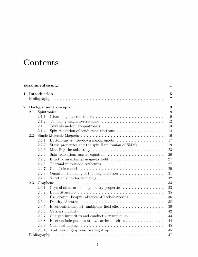
Contents
Zusammenfassung 1
1 Introduction 5Bibliography . . . . . . . . . . . . . . . . . . . . . . . . . . . . . . . . . . . . . 7
2 Background Concepts 92.1 Spintronics . . . . . . . . . . . . . . . . . . . . . . . . . . . . . . . . . . . . 9
2.1.1 Giant magneto-resistance . . . . . . . . . . . . . . . . . . . . . . . . 92.1.2 Tunneling magneto-resistance . . . . . . . . . . . . . . . . . . . . . 122.1.3 Towards molecular-spintronics . . . . . . . . . . . . . . . . . . . . . 132.1.4 Spin relaxation of conduction electrons . . . . . . . . . . . . . . . . 14
2.2 Single Molecule Magnets . . . . . . . . . . . . . . . . . . . . . . . . . . . . 162.2.1 Bottom-up vs. top-down nanomagnets . . . . . . . . . . . . . . . . 172.2.2 Static properties and the spin Hamiltonian of SMMs . . . . . . . . 192.2.3 Modeling the anisotropy . . . . . . . . . . . . . . . . . . . . . . . . 232.2.4 Spin relaxation: master equation . . . . . . . . . . . . . . . . . . . 262.2.5 Effect of an external magnetic field . . . . . . . . . . . . . . . . . . 272.2.6 Thermal relaxation: Arrhenius . . . . . . . . . . . . . . . . . . . . . 272.2.7 Cole-Cole model . . . . . . . . . . . . . . . . . . . . . . . . . . . . 292.2.8 Quantum tunneling of the magnetization . . . . . . . . . . . . . . . 312.2.9 Selection rules for tunneling . . . . . . . . . . . . . . . . . . . . . . 32
2.3 Graphene . . . . . . . . . . . . . . . . . . . . . . . . . . . . . . . . . . . . 332.3.1 Crystal structure and symmetry properties . . . . . . . . . . . . . . 332.3.2 Band Structure . . . . . . . . . . . . . . . . . . . . . . . . . . . . . 352.3.3 Pseudospin, Isospin: absence of back-scattering . . . . . . . . . . . 362.3.4 Density of states . . . . . . . . . . . . . . . . . . . . . . . . . . . . 382.3.5 Electronic transport: ambipolar field-effect . . . . . . . . . . . . . . 392.3.6 Carriers mobility . . . . . . . . . . . . . . . . . . . . . . . . . . . . 422.3.7 Charged impurities and conductivity minimum . . . . . . . . . . . . 432.3.8 Electron-hole puddles at low carrier densities . . . . . . . . . . . . . 442.3.9 Chemical doping . . . . . . . . . . . . . . . . . . . . . . . . . . . . 452.3.10 Synthesis of graphene: scaling it up . . . . . . . . . . . . . . . . . . 45
Bibliography . . . . . . . . . . . . . . . . . . . . . . . . . . . . . . . . . . . . . 47
i
Contents
3 Sub-THz spectroscopy of large-area graphene 593.1 Transferred CVD graphene: structure . . . . . . . . . . . . . . . . . . . . . 603.2 Sub-THz Mach-Zehnder spectrometry of graphene . . . . . . . . . . . . . . 623.3 Effect of adsorbates on large-area graphene . . . . . . . . . . . . . . . . . . 643.4 Electronic quality of large area graphene . . . . . . . . . . . . . . . . . . . 643.5 Conclusions . . . . . . . . . . . . . . . . . . . . . . . . . . . . . . . . . . . 68Bibliography . . . . . . . . . . . . . . . . . . . . . . . . . . . . . . . . . . . . . 69
I Single Molecule Magnets-Graphene hybrids 73
4 Creation of Graphene functional structures 754.1 Identification of single layer graphene . . . . . . . . . . . . . . . . . . . . . 75
4.1.1 Exfoliated graphene . . . . . . . . . . . . . . . . . . . . . . . . . . . 754.1.2 Microscopy . . . . . . . . . . . . . . . . . . . . . . . . . . . . . . . 774.1.3 Raman Spectroscopy . . . . . . . . . . . . . . . . . . . . . . . . . . 78
4.2 Fe4Py: a graphene-binding SMM . . . . . . . . . . . . . . . . . . . . . . . 804.3 Molecular self-assembly on graphene . . . . . . . . . . . . . . . . . . . . . 83
4.3.1 Topography of SMMs on graphene . . . . . . . . . . . . . . . . . . 834.3.2 Dynamic scaling behavior . . . . . . . . . . . . . . . . . . . . . . . 874.3.3 Stimuli-driven molecular reorganization on graphene . . . . . . . . 92
4.4 Electronic properties of graphene functionalized with SMMs . . . . . . . . 944.4.1 Raman spectrum of SMMs-graphene hybrids . . . . . . . . . . . . . 944.4.2 Electronic transport in SMMs-graphene hybrids . . . . . . . . . . . 94
4.5 Bulk hybrid samples . . . . . . . . . . . . . . . . . . . . . . . . . . . . . . 964.5.1 Graphene by liquid phase exfoliation . . . . . . . . . . . . . . . . . 964.5.2 Structural stability . . . . . . . . . . . . . . . . . . . . . . . . . . . 974.5.3 Electronic stability . . . . . . . . . . . . . . . . . . . . . . . . . . . 99
4.6 Conclusions . . . . . . . . . . . . . . . . . . . . . . . . . . . . . . . . . . . 102Bibliography . . . . . . . . . . . . . . . . . . . . . . . . . . . . . . . . . . . . . 103
5 Classical and quantum dynamics of molecular spins on graphene 1095.1 Hybrids static magnetic response . . . . . . . . . . . . . . . . . . . . . . . 1095.2 Dynamics of molecular spins on graphene . . . . . . . . . . . . . . . . . . . 111
5.2.1 Effect of graphene on the thermal relaxation . . . . . . . . . . . . . 1115.2.2 Effect of graphene on the spin quantum relaxation . . . . . . . . . . 114
5.3 Conclusions . . . . . . . . . . . . . . . . . . . . . . . . . . . . . . . . . . . 120Bibliography . . . . . . . . . . . . . . . . . . . . . . . . . . . . . . . . . . . . . 121
6 Development of a theory of magnetic relaxation on graphene 1236.1 Modelling spin interactions . . . . . . . . . . . . . . . . . . . . . . . . . . . 1236.2 Dynamics of molecular spins on graphene . . . . . . . . . . . . . . . . . . . 1246.3 Spin relaxation due to a 2D phonon bath . . . . . . . . . . . . . . . . . . . 126
ii
Contents
6.3.1 Spin-phonon relaxation in 3D crystals . . . . . . . . . . . . . . . . . 128
6.3.2 Spin-phonon relaxation in 2D environments . . . . . . . . . . . . . 129
6.4 The effect of the graphene phonon bath . . . . . . . . . . . . . . . . . . . . 131
6.5 Magnetic quantum tunneling for Fe4 cluster on graphene . . . . . . . . . . 132
6.5.1 Tunneling ”selection rules” . . . . . . . . . . . . . . . . . . . . . . . 133
6.6 Effect of dipolar and hyperfine interactions . . . . . . . . . . . . . . . . . . 135
6.6.1 Hyperfine coupling . . . . . . . . . . . . . . . . . . . . . . . . . . . 135
6.6.2 Dipolar interaction: coherent and incoherent tunneling . . . . . . . 136
6.7 Effect of the B34 term: Villain’s coherent tunneling . . . . . . . . . . . . . . 136
6.7.1 Effect of graphene on quantum tunneling . . . . . . . . . . . . . . . 138
6.8 Conclusions . . . . . . . . . . . . . . . . . . . . . . . . . . . . . . . . . . . 141
Bibliography . . . . . . . . . . . . . . . . . . . . . . . . . . . . . . . . . . . . . 142
II Spin-relaxation in functionalized graphene devices 145
7 Theory of spin transport in graphene nanodevices 147
7.1 Electrical spin-injection . . . . . . . . . . . . . . . . . . . . . . . . . . . . . 148
7.1.1 Spin-split bands . . . . . . . . . . . . . . . . . . . . . . . . . . . . . 148
7.1.2 Two-spin channels . . . . . . . . . . . . . . . . . . . . . . . . . . . 148
7.1.3 Spin-transport and spin-relaxation . . . . . . . . . . . . . . . . . . 150
7.1.4 Spin-accumulation . . . . . . . . . . . . . . . . . . . . . . . . . . . 151
7.1.5 Conductivity mismatch at the FM/NM interface . . . . . . . . . . . 151
7.2 Spin-transport in graphene spinvalves . . . . . . . . . . . . . . . . . . . . . 154
7.2.1 Non-local lateral spin-valve geometry . . . . . . . . . . . . . . . . . 154
7.2.2 Spin-precession: Hanle measurement . . . . . . . . . . . . . . . . . 157
Bibliography . . . . . . . . . . . . . . . . . . . . . . . . . . . . . . . . . . . . . 160
8 Fabrication of graphene-based devices 163
8.1 Electron beam lithography . . . . . . . . . . . . . . . . . . . . . . . . . . . 163
8.1.1 Spin-coating . . . . . . . . . . . . . . . . . . . . . . . . . . . . . . . 163
8.1.2 Exposure . . . . . . . . . . . . . . . . . . . . . . . . . . . . . . . . 164
8.1.3 Proximity effect and dose test . . . . . . . . . . . . . . . . . . . . . 166
8.1.4 Development . . . . . . . . . . . . . . . . . . . . . . . . . . . . . . 167
8.1.5 Metal deposition by thermal evaporation . . . . . . . . . . . . . . . 167
8.1.6 Lift-off . . . . . . . . . . . . . . . . . . . . . . . . . . . . . . . . . . 168
8.2 Nanostructuring of graphene via reactive io etching (RIE) . . . . . . . . . 169
8.2.1 Masking . . . . . . . . . . . . . . . . . . . . . . . . . . . . . . . . . 169
8.2.2 Etching . . . . . . . . . . . . . . . . . . . . . . . . . . . . . . . . . 169
8.3 Deposition of magnetic contacts . . . . . . . . . . . . . . . . . . . . . . . . 169
Bibliography . . . . . . . . . . . . . . . . . . . . . . . . . . . . . . . . . . . . . 172
iii

Contents
9 Toward efficient spin-injection in graphene 1759.1 Tunneling graphene spin-valve . . . . . . . . . . . . . . . . . . . . . . . . . 175
9.1.1 Ultrathin Al2O3 films on graphene . . . . . . . . . . . . . . . . . . 1759.1.2 Spin transport with highly decoupled contacts. . . . . . . . . . . . . 177
9.2 Transparent graphene spinvalve . . . . . . . . . . . . . . . . . . . . . . . . 1829.2.1 Effect of rough edges on spin-transport . . . . . . . . . . . . . . . . 1839.2.2 Effect of transparent contacts . . . . . . . . . . . . . . . . . . . . . 186
9.3 Spin-relaxation in graphene . . . . . . . . . . . . . . . . . . . . . . . . . . 1899.3.1 Dependence of spin-signal on inter-electrode distance . . . . . . . . 1899.3.2 Spin-precession measurement: Hanle curve . . . . . . . . . . . . . . 191
9.4 Conclusions . . . . . . . . . . . . . . . . . . . . . . . . . . . . . . . . . . . 193Bibliography . . . . . . . . . . . . . . . . . . . . . . . . . . . . . . . . . . . . . 194
10 Perspectives 19710.1 Spin-transport in graphene-SMMs hybrid devices . . . . . . . . . . . . . . 19710.2 Spin-relaxation in graphene-SMMs hybrid devices . . . . . . . . . . . . . . 200Bibliography . . . . . . . . . . . . . . . . . . . . . . . . . . . . . . . . . . . . . 203
11 Conclusions 205
Acknowledgments 208
iv

Zusammenfassung
Die Moglichkeiten immer mehr Informationen zu speichern und zu verarbeiten hat in denletzten Jahrzehnten stetig zugenommen. Treibender Motor dieser Entwicklung ist die im-mer fortschreitender Miniaturisierung elektronischer Bauteile, so wurden im Jahr 2014,Speicherdichten von 1.3 Gbit/mm2 erreicht (Seagate 2014 [1]) . Im selben Zeitraum lagdie Transistordichte pro mm2 bei 16 Millionen, wobei die Große einzelner Komponentenlediglich 8 nm betrug (Intel 14 nm technology [2, 3]), was der Ausdehnung eines einzelnenMolekuls entspricht. In solch mesoskopischen Skalen spielen bisher vernachlassigbar kleineQuanteneffekte, wie das Quantentunneln und Quanteninterferenzen eine pragende Rolleund konnen die Leistung eines Bauelementes limitieren. Um diese neuen Hindernisse zuuberwinden wird eine zukunftige Technologie auf anderen physikalischen Grundlagen undneuartigen Materialien begrunden mussen. Einen vielversprechenden Ansatz hierfur stelltdas Gebiet der Spintronik (alias Spin-Elektronik) dar. Dabei werden die Spin Eigenschaftender Elektronen nutzbar gemacht, um damit Informationen zu verschlusseln und zu verar-beiten [4–7]. In diesen Rahmen kann Graphen [8, 9], ein kurzlich entdecktes Material, dieSpin-Informationen uber Rekordweiten von uber λs = 100µm transportieren. Weiterhinstellt Graphen ein ”reines Oberflachen-Material” dar, dessen spintronische Eigenschaftendurch die maßgeschneiderte Einbringung externer Einflusse, wie der Kombination mit mag-netischen Molekulen, genau kontrolliert werden konnen.
Die Kopplung von Graphen zu solch mesoskopischen magnetischen Systemen bietet neueWege Spin-Zustande elektronisch zu manipulieren. Gleichwohl stellt es eine ungeheureHerausforderung dar solche Spin-Systeme in reale Bauelemente zu integrieren, da dieWechselwirkungen der Spins mit in einer komplexen Umgebung nur schwer zu verste-hen oder gar handzuhaben sind. Zwei wichtige Großen die Kopplungseigenschaften zucharakterisieren sind zum einen die Spin-Relaxationszeit T1 (auch indiziert mit τ) und dieSpin-Dephasierungs Zeit T2. Erstere beschreibt die Lebenszeit eines ”klassischen Bits”, inwelchem die Informationen in ”up” und ”down” Zustanden kodiert sind. Im Gegensatzdazu beschreibt T2 die koharente Lebenszeit eines ”Quantenbits” wobei die Informationendurch die Phase der Spin-Wellenfunktion verschlusselt werden.
Im Zuge dieser Arbeit werden magnetische Molekule aus der Familie der ”Single MoleculeMagnets” als Modellsysteme verwendet, um die Relaxationsprozesse solch mesoskopischerSpins in Verbindung mit Graphen und ihren Einfluss auf die Ladungstrager innerhalbrealer Bauelemente zu untersuchen. Dabei werden zwei unterschiedliche Ansatze verfolgt.Im ersteren werden die Single Molecule Magnets (SMMs) als Modellsysteme genutzt um
1
Zusammenfassung
die komplexen Wechselwirkungs-Mechanismen zwischen Spin und Umgebung zu entwirren.Dahingehend kombinieren wir Graphen mit dem SMM [Fe4(L)2(dpm)6], wobei dpm− furdeprotonated dipivaloylmethane steht. Als Ligande L, fungiert triply deprotonated H3L=2-hydroxymethyl-2-(4-(pyren-1-yl)butoxy)methylpropane-1,3-diol, welcher eine Pyrengruppeenthalt welche eine nichtkovalente Bindung an die Graphenoberflache via π-stacking ermo-glicht.
Diese Funktionalisierung der exfolierten Graphenschichten findet in Losung statt, was esermoglicht sowohl Substrat-unterstutzte als auch ”bulk”-Material Proben herzustellen. Dieerzeugten Hybridsysteme werden dann durch mehrere Techniken charakterisiert. Matrix-unterstutzte-Desorption-Ionisations-Time of Flight Massen Spektroskopie wird dabei genutztum die strukturelle Stabilitat der Molekule nach der Dispersions-Deponierung sicherzustel-len. Rontgen-Strahlen Photo-elektron Spektroskopie zeigt dabei, dass der Oxidationszus-tand der magnetischen Kern-Ionen unverandert bleibt.
Das neuartige Hybridsystem zeigt vernachlassigbaren Ladungsaustausch zwischen demSMM und dem Graphen, welcher mittels elektronischen Messungen und Raman-Spektrosko-pie an einen Graphen-basierten Feld-Effekt Transistor nachgewiesen wurde. Um die Detailsder Selbstassemblierung von die SMMs auf Graphen zu untersuchen wurde die Hybrid-Oberflachen-topographie mit Hilfe von hochaufgeloster Raster Kraft Mikroskopie gemessen.Durch Variierung der Losungskonzentration C von die SMMs wurde eine prazise statistis-che Analyse ermoglicht, welche eine betrachtliche Diffusion der Molekul-Entitaten auf derGraphenoberflache aufzeigte. Dynamische Skalierungsanalysen erlaubten es zwischen ver-schiedenen Anordnungsverlaufen, wie Nukleation, Aggregierung und Koaleszenz zu unter-scheiden. Zuruckbleibende Oberflachen-Cluster Diffusion eroffnet hierbei neue Strategienzur Herstellung von ausgedehnten supermolekularen Strukturen auf Graphen. Durch dieBestrahlung mit Laserlicht kann ein Reorganisierung der molekularen Adsorbate induziertwerden, was eine zufallige zweidimensionale Netzwerkausbildung auf dem Graphen zurFolge hat.
Die statisch magnetischen Eigenschaften von die SMMs innerhalb der Graphenumgebungwurden in Abhangigkeit von Temperatur und Magnetfeld bestimmt und mit der Kristallmes-sung von SMM verglichen. Die Temperaturabhangigkeit des Produktes χmT , aus molarerSuszeptibiltat χm = Mm/H (wobei Mm fur die molare Magnetisierung, H fur das externemagnetische Feld stehen) und der Temperatur T , bestatigt dabei den S = 5 Grundzustandvon SMM und zeigt dabei eine perfekte Ubereinstimmung zwischen Hybrid und Kristall.Die Isothermischen Magnetisierugnskurven konnen sehr gut uber den Giant Spin Hamilto-nian modelliert werden:
H = DS2z + gµBS · H (1)
Wahrend der erste Term die uniaxiale magnetische Anisotropie des SMMs beschreibt,definiert der zweite Teil des Hamiltonians den Effekt des angelegten externen Magnet-feldes. Der uniaxial Ansiotropy Parameter D und die z-Komponente des SpinoperatorenSz, bestimmen die resultierende Energiebarriere welche die (2S + 1) entarteten Grund-multiplietts |m〉 and | −m〉 voneinander trennt. Die Gegenwart der Energiebarriere bes-
2
Zusammenfassung
timmt die Relaxation des molekularen Spins, wobei zwei Hauptrelaxationsmechanismenmoglich sind. Der klassische Mechanismus basiert auf der Absorption von Phononen ausder außeren Umgebung, wahrend der quantenmechanische Prozess durch Quantentunnel-Eigenschaften des Spins definiert ist. Das Tunneln des Spins durch die Energiebarrierewird durch zusatzliche transversale Terme im Kristallfeldhamiltonian ermoglicht. Mittelsdynamischer Suszeptibilitat Messungen konnen diese Prozesse durch die Extrahierung derRelaxationszeit t in Abhangigkeit von der Temperatur beobachtet werden. Im Vergleichzum Kristall zeigen die SMM-Graphen Hybriden in beiden Prozessen ein signifikant unter-schiedliches Relaxationsverhalten. So wurde zum Beispiel ein extrem verstarktes Quanten-tunneln bei tiefen Temperaturen festgestellt. Dahingehend wurde ein neues theoretischesModell entwickelt in welchem alle fundamentalen Wechselwirkungen in Betracht gezogenwerden die zu Spin-Relaxation in einer Graphenumgebung beitragen konnen. Wahrend derUnterschied in der thermischen Relaxation von der zwei-dimensionalen Natur der Graphen-Phononen herruhrt, kann die hohe Tunnelrate bei tieferen Temperaturen nur durch eineWechselwirkung zwischen Spin und den Graphenladungen erklart werden. Diese zusatzlicheWechselwirkung wurde im Rahmen des Stevensformalismus dargestellt und zeigt das sievollstandig koharentes Tunneln ermoglicht, wie bereits vor uber einer Dekade von Villainsvorhergesagt. Dies eroffnet neue Moglichkeiten die Koharenz eines Spin-Zustande elektro-nisch anzusteuern.Der zweite Teil dieser Arbeit beschaftigt sich mit der Fabrikation und Optimierung vonGraphen basierten Spinvalve-Bauelementen und deren Charakterisierung bei tiefen Tem-peraturen. Ferromagnetische Kobaltkontakte werden hierfur mit Graphen verbunden undfungieren als Quelle fur Spin-polarisierte Ladungstrager. Uber eine nicht lokale Messungs-geometrie kann der Spin-Transport von Ladungstransport und weiteren magnetoresisi-tiven Mechanismen getrennt werden. Die Spininjektionseffizienz ist limitiert durch denLeitungsunterschied am Ubergang zwischen Ferromagnet und Graphen (FM/G), was zueinem erheblich schwacheren Spin-Signal fuhrt. Um diesen Umstand zu umgehen muss derWiderstand des Spin-abhangigen Uberganges angepasst werden. Die kann durch die Im-plementierung von Tunnelkontakten oder durch eine Großenreduzierung der Kontaktstelleerreicht werden. In dieser Arbeit werden beide Strategien getestet, wobei der erste Ansatzsehr herausfordernd ist, daher die Kreation von ultra-dunnen Tunnelbarrieren erfordert.Diese wurden aus Al2O3 gefertigt und haben eine dicke von < 2 nm. In Kombinationmit aus Titankeimen basierten Inseln und Dunnfilmdeponierung wurden hochhomogeneFilme geschaffen. Die Injektion Effizienz ist sehr sensitiv was die chemische Zusammenset-zung der Barriere betrifft, nur eine vollstandig oxidierte Keimung erlaubt einen effizientenSpin Transport zusammen mit einer hohen Entkopplung zwischen den ferromagnetischenKontakten und dem Graphenleitungskanal. Im zweiten Ansatz wurde versucht die Kon-taktstelle durch die Herstellung von dunnen Graphenstreifen zu minimieren. Die Struk-turierung dieser von 200 - 300 nm breiten Streifen erfolgte durch Elektronenstrahllithogra-phie und reaktive Ionen Atzung. Diese bieten des Weiteren eine passendere Grundlagefur die folgende Funktionalisierung mit SMMs. Hanle Spin Prezession Messungen reinerGraphen-Spinvalves zeigten Relaxatzionzeiten von τ ≈ 10−11 s. Vorlaufige Messungen anden SMM funionalisierten Spinvalves weisen auf einen hohen Spin-Transport hin. Obwohl
3

Zusammenfassung
das Spinsignal nach der Funktionalisierung stark reduziert war konnte ein deutlicher Ein-fluss der magnetischen Adsorbate festegestellt werden. Insbesondere die Hanle-Kurven bei300 mK zeigen dabei ein Hystereseverhalten welches von den molekularen Spins herruhrt.Weitere Experimente und detaillierte Modellierung konnen diese Beobachtungen und dieGate-Abhangigkeit der Spinrelaxation erklaren.
4
Chapter 1
Introduction
The world’s technological capacity to store and compute information has grown rapidlyand steadily over the past few decades [10]. The major driving force of this performanceincrease has been device scaling. In 2014 the information storage density in magnetic harddisc drives touched 1.3 Gbit/mm2 (Seagate 2014) [1]. At the same time, transistor countin consumer microprocessors reached 16 Million transistors/mm2, pushing the dimensionof the smallest feature down to only 8 nm (Intel 14 nm technology) [2, 3], the size of asingle molecule. This length lies already at the mesoscopic scale, where quantum phenom-ena, such as tunneling and interference, start to limit the device performance. To crossthis hurdle, and further increase computational and storage capacities, future computertechnology will need to rely on different physical principles and novel materials.A promising approach, called spintronics (aka spin-electronics), is to use the spin degree offreedom to encode and process information [4–7]. In this context, graphene [8, 9], a recentlydiscovered material, exhibits an unprecedented ability to transport spin information overa record length scale of λs = 100µm at room temperature1 [11]. Moreover, being graphenean all-surface materials, its spintronic properties can be tailored by external means, e.g bycombining it with different materials or by decorating its surface with magnetic moleculesor atoms [12].Coupling magnetic systems to graphene charge carriers can offer new ways to electricallymanipulate spin-states. Nevertheless, integrating mesoscopic spin-systems in real devices isa challenging task, since the interaction of a spin with a complex environment is difficult tocontrol, and, in general difficult to understand. Two important quantities that characterizethe coupling to the surroundings are2 the spin relaxation time T1 (also indicated with τ)and the spin coherence time T2. The former measures the life time of a classical bit, wherethe information is encoded in the up- and down spin states, while the latter measures thecoherence lifetime of a quantum bit where the information is encoded in the phase of thespin-wavefunction.This thesis work employs magnetic molecules, belonging to the family of single molecule
1For a given material, the spin diffusion length λs represents the maximum distance covered by aspin-polarized electron without losing its spin orientation.
2T1 and T2 are also called spin population relaxation time and phase memory time respectively
5

1. Introduction
magnets (SMMs) [13], as model systems to study the relaxation of mesoscopic spins ongraphene, and their interaction with graphene charge carriers in real devices. Their largeuniaxial anisotropy makes SMMs behave like giant spins3, with relaxation times τ of yearsat low temperatures [14–16]. Their spin dynamics combines a classical and a quantumrelaxation mechanism, that can be selectively switched on and off by either applying anexternal magnetic field or by varying the temperature [17].The work is organized as follows. The first part presents a thorough structural char-acterization of the SMMs-graphene hybrid materials via multiple techniques, includingatomic force microscopy, x-ray photoelectrons spectroscopy, mass spectrometry, Ramanspectroscopy, and electronic transport measurements on graphene-based field-effect tran-sistors. The analysis of the dynamical arrangement of molecular adsorbates on graphenereveals new opportunities to control the supramolecular surface arrangement. A compre-hensive study of the magnetization dynamics of SMMs on graphene is carried out by meansof ac-susceptibility techniques in a broad temperature range (T = 4K - 13 mK). The detailsof the complex spin-graphene interaction are unraveled in the framework of a newly devel-oped theoretical model that accounts for all the possible fundamental contributions and thetwo-dimensional nature of graphene. The focus of the second part is the design, fabrica-tion and characterization of graphene-based spintronic devices. Different strategies for theinjection of spin-polarized carriers in graphene are implemented and tested down to verylow temperatures (T = 300 mK). To conclude the first spin-transport and spin-relaxationmeasurements in SMMs-graphene devices are presented.
3Typically the magnetic moment of their ground state equals several Bohr magnetons.
6
Bibliography
Bibliography
[1] Seagate Technology. Archive HDD Data Sheet (2014). URLhttp://www.seagate.com.
[2] Bohr, M. 14 nm Process Technology: Opening New Horizons (2014). URLhttp://www.intel.com.
[3] Natarajan, S. et al. A 14nm logic technology featuring 2nd-generation FinFET in-terconnects, self-aligned double Patterning and a 0.0588 µm2 SRAM cell size. IEEEInternational Electron Devices Meeting (IEDM) 3.7.1–3.7.3 (2014).
[4] Datta, S. & Das, B. Electronic analog of the electrooptic modulator. Applied PhysicsLetters 665, 10–13 (1990).
[5] Behin-Aein, B., Datta, D., Salahuddin, S. & Datta, S. Proposal for an all-spin logicdevice with built-in memory. Nature nanotechnology 5, 266–270 (2010).
[6] Datta, S., Salahuddin, S. & Behin-Aein, B. Non-volatile spin switch for Boolean andnon-Boolean logic. Applied Physics Letters 101, 252411 (2012).
[7] Zutic, I., Fabian, J., Das Sarma, S. & Sarma, S. D. Spintronics: Fundamentals andapplications. Rev. Mod. Phys. 76, 323–410 (2004).
[8] Novoselov, K. S. et al. Electric field effect in atomically thin carbon films. Science306, 666–669 (2004).
[9] Geim, A. K. & Novoselov, K. S. The rise of graphene. Nat. Mater. 6, 183–191 (2007).
[10] Hilbert, M. & Lopez, P. The World’s Technological Capacity to Store, Communicate,and Compute Information. Science 332, 60–65 (2011).
[11] Han, W., Kawakami, R. K., Gmitra, M. & Fabian, J. Graphene spintronics. Naturenanotechnology 9, 794–807 (2014).
[12] Geim, a. K. & Grigorieva, I. V. Van der Waals heterostructures. Nature 499, 419–25(2013).
[13] Gatteschi, D., Sessoli, R. & Villain, J. Molecular Nanomagnets. Mesoscopic Physicsand Nanotechnology (OUP, Oxford, 2006).
[14] Caneschi, A., Gatteschi, D. & Sessoli, R. Alternating Current Susceptibility, HighField Magnetization and Millimeter Band EPR Evidence for a Ground S=10 State in[Mn12012(CH3COO)16(H2O)4)2CH3COOH 4H2O. Journal of the American ChemicalSociety 113, 5873–5874 (1991).
7
Bibliography
[15] Barra, A. L. et al. Single-Molecule Magnet Behavior of a Tetranuclear Iron(III) Com-plex. The Origin of Slow Magnetic Relaxation in Iron(III) Clusters. Journal of theAmerican Chemical Society 121, 5302–5310 (1999).
[16] Gatteschi, D., Sessoli, R. & Cornia, A. Single-molecule magnets based on iron(iii) oxoclusters. Chemical Communications 725–732 (2000).
[17] Bogani, L. & Wernsdorfer, W. L. Molecular spintronics using single-molecule magnets.Nat. Mater. 7, 179–186 (2008).
8

Chapter 2
Background Concepts
This thesis work establishes the connection between three fundamental fields, spintronics,molecular magnetism and graphene, that are currently the focus of the scientific communityworldwide. In this chapter the main concepts and the unsolved challenges of each topicare introduced together with the basic modeling for the main characteristic phenomena.
2.1 Spintronics
Spin-electronics, aka spintronics, aims at using spins to store and compute information[1, 2]. Spintronics finds its roots in a set of fundamental effects involving spin-polarizedcurrents and their interaction with electric charges.
2.1.1 Giant magneto-resistance
The discovery that triggered the development of spintronics is the giant magneto-resistance(GMR) effect [3, 4], observable in all-metallic spin-valve devices [5–7]. Figure 2.1 showsa current-perpendicular-to-plane spin-valve (CPP-SV) consisting in a non-ferromagneticmetallic thin film (NM) sandwiched between two ferromagnetic electrodes (FM1 and FM2).The thickness L of NM is chosen to be smaller than the electron mean free path λNM
e ofthe metal (typically λNM
e = 8 - 30 A) so that no scattering is expected in NM, and thetrilayer resistance R originates uniquely from scattering of carriers in the two ferromagneticfilms. R shows a large change, depending on whether the magnetic moments of the twoferromagnetic layers are aligned antiparallel (AP) or parallel (P) by an external magneticfield H. This large magnetoresistance (MR), defined as the maximum change in resistanceover the magnetic field range of interest divided by the high field resistance:
MR =∆R
R=
(RAP −RP)
RP
(2.1)
is a direct evidence of spin-dependent scattering in the ferromagnetic layers [8, 9]. Con-
9

2. Background Concepts
duction electrons in ferromagnetic materials ”naturally” exhibit a certain degree of spin-polarization as consequence of exchange-split bands [10–14]. In the following the prefixes upand down indicate that the electron spin is oriented parallel or antiparallel to the magneticmoment of the ferromagnetic layer respectively.
Figure 2.1: Schematic representation of a Current-perpendicular-to-plane ”vertical” spin-valve, comprising a trilayer film with two identical ferromagnetic layers FM1 and FM2sandwiching a non-magnetic layer NM. a) Parallel configuration b) Antiparallel configura-tion.
Assuming λFMup << λFM
down, spin-up electrons have higher probability to experience scatteringevents than spin-down one. When the two FM contacts are magnetized parallel (P), down-spins move through the sandwich nearly unscattered, as a consequence, a large numberof electrons makes it through the trilayer leading to low resistance RP (Figure 2.1a). Forantiparallel alignment (AP), both up and down spins experience scattering at either oneor the other FM, resulting in a higher device resistance RAP (Figure 2.1b). In otherwords, the relative alignment of the magnetic moments of the two electrodes affects theflow of spin-polarized currents by altering the overall mean free path of the conductionelectrons [15].An external magnetic field H can be used to control the relative alignment of the FM layersand thus change the resistance of the trilayer, resulting in the valve-like behavior shownin Figure 2.2a. At H = 0 the FM1 and FM2 magnetic moments are antiferromagneticallycoupled to each other by indirect exchange coupling J12 via the nonmagnetic metal [16–24],Figure 2.2a. The external H-field has to overcome this coupling in order to drive themagnetic moments to parallel alignment. During the magnetization process (H 6= 0), Rdecreases and saturates to a constant value when parallel alignment is reached at H = HS.Magnitude [18, 23] and sign [20] (i.e. ferro/antiferro) of J12, and consequently ∆R/R, arefound to oscillate on varying the thickness of the NM interlayer following a RKKY-likefunction [24, 25] (Figure 2.2b).CPP-SVs can be used to build very sensitive magnetic field sensors, and find application as
10

2.1. Spintronics
Figure 2.2: a) Typical ”spin-valve” behavior. Parallel (P) and antiparallel (AP) magneti-zations configurations correspond to different resistance levels RP and RAP. b) Oscillatingvariation of interlayer exchange coupling Ji with thickness L of the non magnetic layer.
reading elements in the magnetic disc drive (HDD) heads [26–28]. The characteristic quan-tity which determines the ”sensitivity” of the CPP-SV to an external field is the saturationfield HS. The larger ∆R/R and the smaller HS, the more sensitive the sensor is. A wayto increase the sensitivity is to arrange several FM/NM stacks in a multilayer structure,so as to increase the scattering for the up-spins and ∆R/R, Figure 2.3a. Nevertheless,this method is not very effective since also HS increases accordingly. A more sensitiveGMR-sensor can be built by pinning the magnetic moment of one FM electrode by plac-ing it in contact with a antiferromagnetic layer, e.g. FeMn , (AF in Figure 2.3b) [20].The exchange-bias field caused by AF layer induces a uniaxial anisotropy in FM2 thatconstrains its magnetic moment in the direction perpendicular to the layer plane. As aconsequence, the hysteresis loop of FM2 is centered at B 6=0, while the magnetic momentof FM1 is free to move under the influence of the external H-field.
The latter configuration enabled a more detailed understanding of the GMR effect andrevealed the different factors controlling ∆R/R. Importantly, further studies demonstratedthat spin-dependent scattering occurs mainly at the FM/NM interface, where magneticstates are predominantly localized [29]. Inserting different magnetic atoms at the FM/NMinterface enhances the spin-polarization of carriers injected in NM, thus increasing ∆R/Rsignificantly (Figure 2.3b) [19]. GMR effects are thus largely determined by the details ofthe ferromagnetic/non-magnetic interface, which extends over a maximum lateral size ofonly 2 - 3A [30].
11
2. Background Concepts
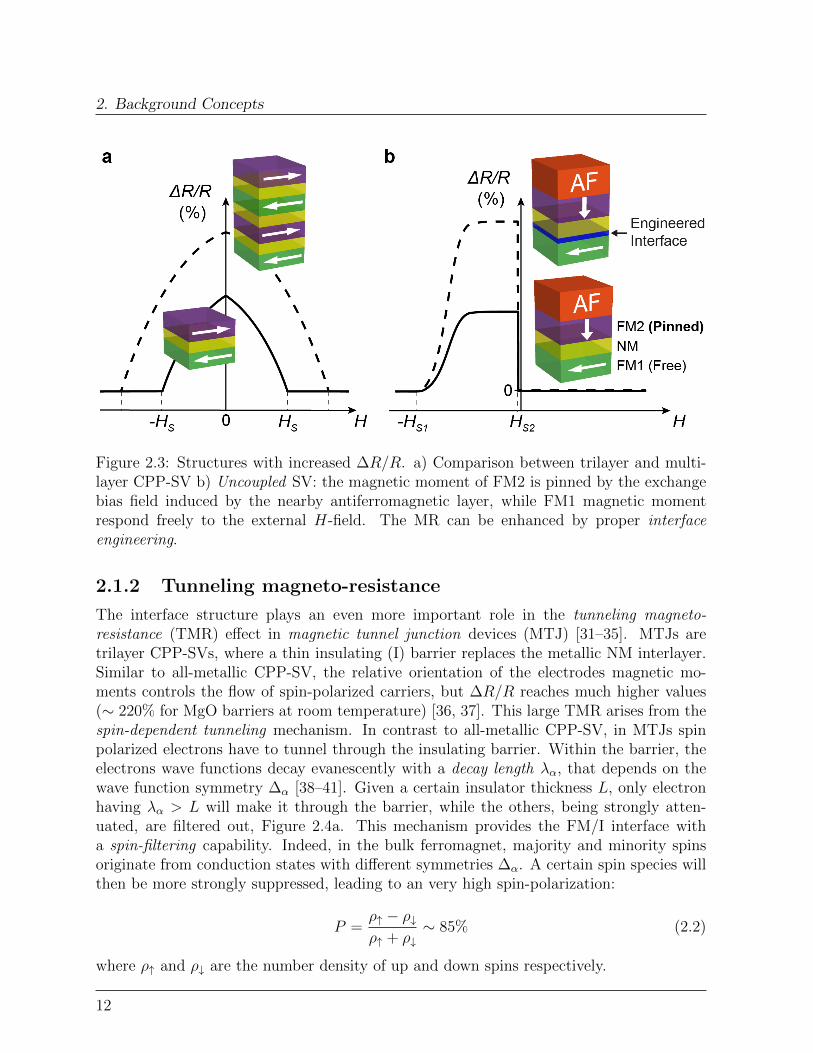
Figure 2.3: Structures with increased ∆R/R. a) Comparison between trilayer and multi-layer CPP-SV b) Uncoupled SV: the magnetic moment of FM2 is pinned by the exchangebias field induced by the nearby antiferromagnetic layer, while FM1 magnetic momentrespond freely to the external H-field. The MR can be enhanced by proper interfaceengineering.
2.1.2 Tunneling magneto-resistance
The interface structure plays an even more important role in the tunneling magneto-resistance (TMR) effect in magnetic tunnel junction devices (MTJ) [31–35]. MTJs aretrilayer CPP-SVs, where a thin insulating (I) barrier replaces the metallic NM interlayer.Similar to all-metallic CPP-SV, the relative orientation of the electrodes magnetic mo-ments controls the flow of spin-polarized carriers, but ∆R/R reaches much higher values(∼ 220% for MgO barriers at room temperature) [36, 37]. This large TMR arises from thespin-dependent tunneling mechanism. In contrast to all-metallic CPP-SV, in MTJs spinpolarized electrons have to tunnel through the insulating barrier. Within the barrier, theelectrons wave functions decay evanescently with a decay length λα, that depends on thewave function symmetry ∆α [38–41]. Given a certain insulator thickness L, only electronhaving λα > L will make it through the barrier, while the others, being strongly atten-uated, are filtered out, Figure 2.4a. This mechanism provides the FM/I interface witha spin-filtering capability. Indeed, in the bulk ferromagnet, majority and minority spinsoriginate from conduction states with different symmetries ∆α. A certain spin species willthen be more strongly suppressed, leading to an very high spin-polarization:
P =ρ↑ − ρ↓ρ↑ + ρ↓
∼ 85% (2.2)
where ρ↑ and ρ↓ are the number density of up and down spins respectively.
12
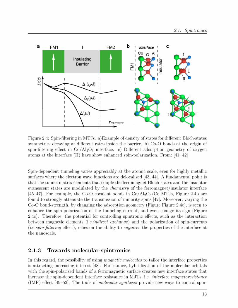
2.1. Spintronics
Figure 2.4: Spin-filtering in MTJs. a)Example of density of states for different Bloch-statessymmetries decaying at different rates inside the barrier. b) Co-O bonds at the origin ofspin-filtering effect in Co/Al2O3 interface. c) Different adsorption geometry of oxygenatoms at the interface (II) have show enhanced spin-polarization. From: [41, 42]
Spin-dependent tunneling varies appreciably at the atomic scale, even for highly metallicsurfaces where the electron wave functions are delocalized [43, 44]. A fundamental point isthat the tunnel matrix elements that couple the ferromagnet Bloch-states and the insulatorevanescent states are modulated by the chemistry of the ferromagnet/insulator interface[45–47]. For example, the Co-O covalent bonds in Co/Al2O3/Co MTJs, Figure 2.4b arefound to strongly attenuate the transmission of minority spins [42]. Moreover, varying theCo-O bond-strength, by changing the adsorption geometry (Figure Figure 2.4c), is seen toenhance the spin-polarization of the tunneling current, and even change its sign (Figure2.4c). Therefore, the potential for controlling spintronic effects, such as the interactionbetween magnetic elements (i.e.indirect exchange) and the polarization of spin-currents(i.e.spin-filtering effect), relies on the ability to engineer the properties of the interface atthe nanoscale.
2.1.3 Towards molecular-spintronics
In this regard, the possibility of using magnetic molecules to tailor the interface propertiesis attracting increasing interest [48]. For istance, hybridization of the molecular orbitalswith the spin-polarized bands of a ferromagnetic surface creates new interface states thatincrease the spin-dependent interface resistance in MJTs, i.e. interface magnetoresistance(IMR) effect [49–52]. The tools of molecular synthesis provide new ways to control spin-
13

2. Background Concepts
tronic effects down to the single molecule level, and the opportunity to build spintronicnanodevices where the central active element is a single molecule is now the focus of manyresearch groups worldwide.
Figure 2.5: Spin relaxation and manipulation. a) Spin transport, the spin has to travel withunaltered polarization over a distance λs sufficient to reach the reading element. b) Spinmanipulation enabling spin-logic applications. c) The spin diffusion length λs is limited byspin-flip mechanisms that bring an unbalanced spin population (left) back into equilibrium(right).
2.1.4 Spin relaxation of conduction electrons
Spintronic phenomena are yet used to store and read information in magnetic storagedevices. Nevertheless, their application may not be limited to this, as they can bringsome notable advantages also for logic applications [53–56]. For instance, electrons havea relatively large spin memory, that is conduction electrons retain their spin state muchlonger than their momentum. In a typical metal, momentum coherence is lost after aboutten femtoseconds, while spin coherence can survive for more than a nanosecond [57]. Thismeans that the length λs, called spin diffusion length, over which electrons conserve theirspin-polarization is much longer than the mean free path le, over which they conserve theirmomentum. Intuitively, devices based on diffusion of spins may thus require less powerthan devices based on charge drift [58].As seen in CPP-SVs, the information (up or down magnetization) stored in a magneticlayer can be encoded, via spin-injection, in the spin of conduction electrons flowing in theNM channel (Figure 2.5a). Once the spins have reached the other side of NM, a secondferromagnetic element ”reads” the information (spin-detection), translating it into two
14
2.1. Spintronics
resistance values RP and RAP . In order to perform logic operations, the spin informationneeds to be manipulated in its way towards the reading element (Figure 2.5b) [59]. Itis therefore essential to find materials in which spins can retain their polarization overa length λs sufficiently large to allow their manipulation. λs is an intrinsic property ofthe channel material, describing the spin-relaxation (spin-flip) mechanisms that cause lossof spin-polarization, thus bringing the unbalanced spin population back into equilibrium(ρ↑ 6= ρ↓, P 6= 0) → (ρ↑ = ρ↓, P = 0), Figure 2.5c [2, 57]. Equivalently, spin-flip processescan be described by a spin-relaxation time τ , that corresponds to the spin-lattice relaxationtime T1 = τ [2].
The major cause of spin-relaxation in metals and semiconductors is spin-orbit coupling(SOC), a phenomenon originating from the relativistic transformation of electric and mag-netic fields for a moving electron and from the Thomas precession [60]. In the referenceframe of an electron moving in a crystal, the lattice electric potential acts as an effectivemagnetic field Beff. The latter couples to the electron spin via the Zeeman interaction,thus coupling the spin to the electron orbital motion [61]. Depending on the symmetryproperties of the crystal, SOC can give rise to different spin-relaxation mechanisms [57]:
• D’yakonov-Perel’ mechanism [62, 63]. For bulk crystals lacking inversion symmetry, theSOC assumes the Dresselhaus form [64] and lifts the spin-degeneracy of electrons statesE↑(k) 6= E↓(k), i.e. spin-up and spin-down electrons have different energies even if theyare in the same momentum state k. This can be pictured as an internal momentum-dependent magnetic field B(k) that induces precession of spins with momentum k alonga direction perpendicular to the electron trajectory and the crystal electric field. As aconsequence, a momentum scattering event k→ k′ cause the spin to change its precessionaxis B(k) → B(k′), with back-scattering events causing a complete spin-flip. Since thespin relaxation happens between two scattering events, the spin relaxation time T1 isinversely proportional to the momentum scattering time:
T1 ∝ 1/τe (2.3)
meaning that the more the electron is scattered the less its spin flips on average. Theapplication of an external magnetic field reduces the effect of the D’yakonov - Perel’mechanism.
• Elliott-Yafet relaxation [65, 66]. In crystals with inversion symmetry, SOC does notremove the spin-degeneracy E↑(k) = E↓(k), but still affects the electron wavefunctionsintroducing mixing of spin-up and spin-down Bloch states. As a consequence, the Blochstates are not pure spin-eigenstates, but linear combinations of spin-up and spin-downcomponents. The interaction with lattice ions (i.e. lattice vibrations [67–69], magneticand non-magnetic impurities [69] and other electrons [70]) modulates this mixing, induc-ing a complete spin-flip after several (≈ 105) scattering events. T1 is then proportionalto the momentum scattering time:
T1 ∝ τe (2.4)
15
2. Background Concepts
Other relaxation mechanisms involve the electron-hole exchange interaction (Bir-Aronov-Pikus mechanism) [71]or the nuclear hyperfine field [72],For systems with spatial confinement, such as a two-dimensional electron gas (2DEG),the confinement potential induces an additional SOC term of Rashba type [73, 74]. TheRashba and Dresselhaus SOCs can be tuned by an external electric field [75] thus givingthe possibility of electrically manipulate the spin-state and opening the way to spintroniclogic architectures [53].
2.2 Single Molecule Magnets
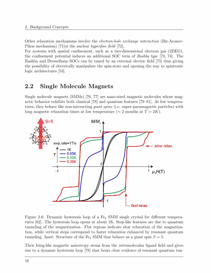
Single molecule magnets (SMMs) [76, 77] are nano-sized magnetic molecules whose mag-netic behavior exhibits both classical [78] and quantum features [79–81]. At low tempera-tures, they behave like non-interacting giant spins (i.e. super-paramagnetic particles) withlong magnetic relaxation times at low temperature (∼ 2 months at T = 2K).
Figure 2.6: Dynamic hysteresis loop of a Fe4 SMM single crystal for different tempera-tures [82]. The hysteresis loop opens at about 1K. Step-like features are due to quantumtunneling of the magnetization. Flat regions indicate slow relaxation of the magnetiza-tion, while vertical steps correspond to faster relaxation enhanced by resonant quantumtunneling. Inset: Structure of the Fe4 SMM that behave as a giant spin S = 5.
Their Ising-like magnetic anisotropy stems from the intramolecular ligand field and givesrise to a dynamic hysteresis loop [78] that bears clear evidence of resonant quantum tun-
16
2.2. Single Molecule Magnets
neling (QT) [80], Figure 2.6. The latter is enabled by both intrinsic (e.g. distortion ofthe molecular structure) [83, 84] and extrinsic (e.g. interaction with the surrounding)factors [85–89].
The way the interaction with the surrounding influences quantum tunneling is one of thisthesis main focuses.
2.2.1 Bottom-up vs. top-down nanomagnets
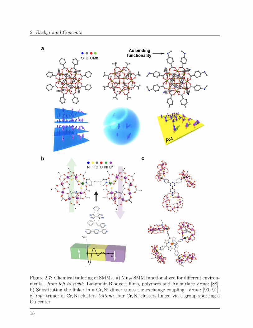
Being bottom-up objects, SMMs possess some fundamental advantages compared to othertop-down nano-objects (e.g. magnetic nanoparticles). First of all, they are monodispersedand can be arranged in large single crystals. This affords exceptionally clean magneticproperties, without any broadening due to size dispersion and offers the unique opportunityto study quantum phenomena in very high detail in macroscopic samples. For instance,quantum interference and Berry phase phenomena were reported [79, 81] and consideredas milestone in spin physics.The other important advantage is the opportunity to design and add new functionalities atwill [92–94]. For example, the molecular structure can be equipped with different functionalgroups to integrate the SMM in an new environment (e.g. gold surfaces [95], carbon-basedmaterials [82, 93] or single-molecule junctions [96] or to couple two or more SMMs toeach other [97, 98]). Adjusting the linking groups is found to control the coupling to theenvironment both electrically and magnetically, with important effects on the molecularquantum features [99, 100].An outstanding example of the high level of control achievable on both structural andmagnetic features and the role played by quantum properties is that of Cr7Ni dimers ofgeneral formula [Cr7NiF3(Etglu)(O2CtBu)162L], where the Ni site allows changing thelinking group L systematically [91, 97]. These dimers included different hetero-aromaticlinkers, such as pyrazine (pyr in short), bidimethylpyrazolyl (bipz ), 4,4’-bipyridyl (bipy),trans-1,2-bipyridylethene (bipyet) and bipyridyltetrazine (bipytz ), as in Figure 2.7b. Thesegroups differ primarily in: (1) length (ranging from 7 A for pyr to 15 A of bipytz ), (2)dihedral (torsional) angle between the aromatic cycles (from 28 in bipytz to 56 in bipz ),and (3) number of simple covalent σ bonds between the hetero-aromatic groups.DFT calculations [91, 101] revealed that, in general, the magnetic interaction is maximumwhen the overlap (both spatial and in energy) between the spin-polarized orbitals of the Nisite and the orbitals of the N linker atoms is maximized. Moreover, the π orbitals propagatethe spin-polarization along the linker group more effectively than σ orbitals. Comparingthe different linkers evinced that the spin polarization propagates through them followinga few general criteria. First of all, the spin polarization alternates moving from each atomto the next along the linker. This implies that it is possible to impose either ferromagnetic(FM) or antiferromagnetic (AFM) coupling between the two molecular spins by choosing alinker structure which enables bond pathways containing either an odd or even number ofatoms respectively. Furthermore, when the linker structure (e.g. bipz ) supports both evenand odd numbered pathways, imparting AFM and FM coupling simultaneously, destructive
17
2. Background Concepts
Figure 2.7: Chemical tailoring of SMMs. a) Mn12 SMM functionalized for different environ-ments , from left to right : Langmuir-Blodgett films, polymers and Au surface From: [88].b) Substituting the linker in a Cr7Ni dimer tunes the exchange coupling. From: [90, 91].c) top: trimer of Cr7Ni clusters bottom: four Cr7Ni clusters linked via a group sporting aCu center.
18
2.2. Single Molecule Magnets
interference between the two paths reduces considerably the spin polarization in the middleof the linker. This explains why the cross-talking between the two molecular spins isweaker for bipz, despite it being shortest. In the case of linkers containing more thanone aromatic ring, the dihedral angle θd between the conjugated rings is found to play animportant role in tuning the spin coupling [102]. The exchange coupling constant betweentwo molecular spins is found to obey a cos2(θd) trend, reaching the maximum value forcoplanar rings. Importantly, the electrical conductance of biphenyl junctions was foundto follow the same angular behaviour, [103] establishing a fundamental parallel betweenelectron transfer mechanisms and magnetic coupling.
2.2.2 Static properties and the spin Hamiltonian of SMMs
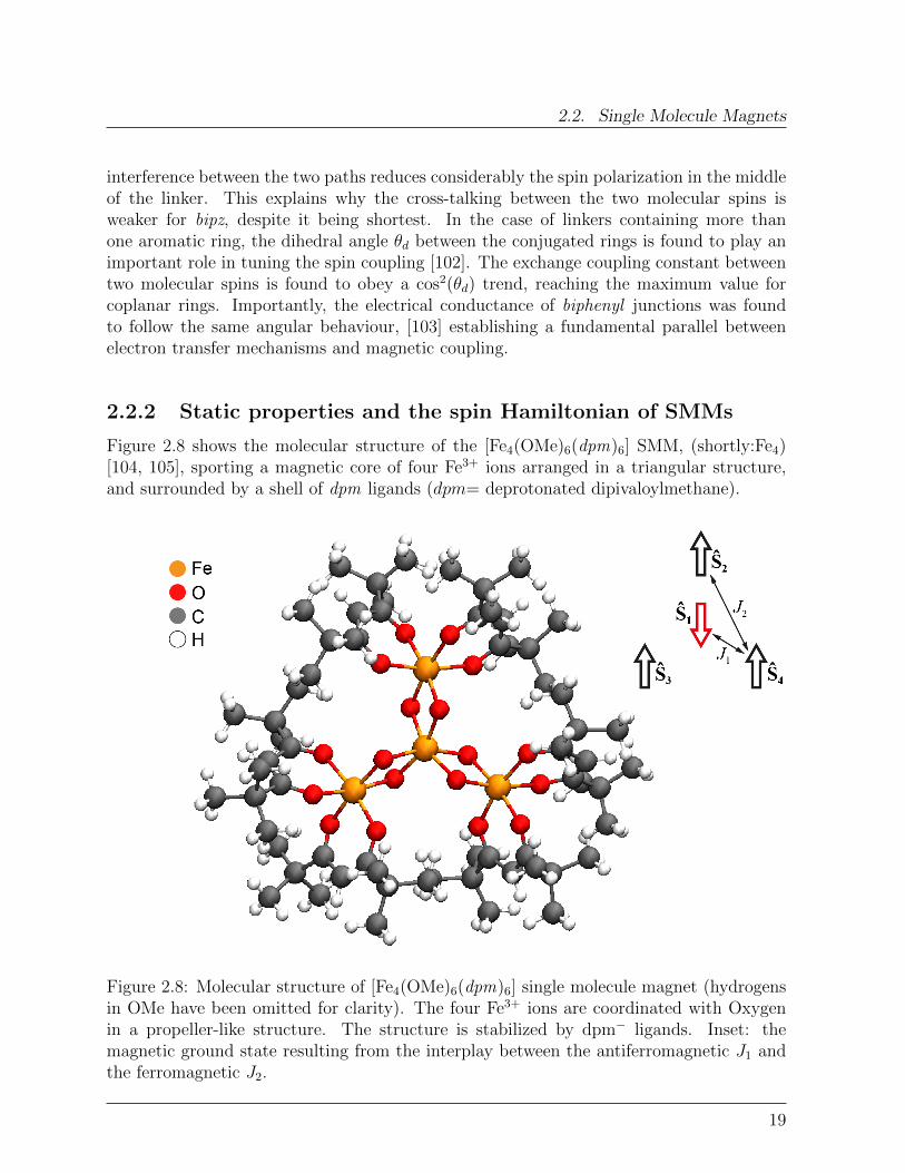
Figure 2.8 shows the molecular structure of the [Fe4(OMe)6(dpm)6] SMM, (shortly:Fe4)[104, 105], sporting a magnetic core of four Fe3+ ions arranged in a triangular structure,and surrounded by a shell of dpm ligands (dpm= deprotonated dipivaloylmethane).
Figure 2.8: Molecular structure of [Fe4(OMe)6(dpm)6] single molecule magnet (hydrogensin OMe have been omitted for clarity). The four Fe3+ ions are coordinated with Oxygenin a propeller-like structure. The structure is stabilized by dpm− ligands. Inset: themagnetic ground state resulting from the interplay between the antiferromagnetic J1 andthe ferromagnetic J2.
19

2. Background Concepts
The temperature dependence of the product χmT (where χm = Mm/H is the molar mag-netic susceptibility, Mm is the molar magnetization, H is the external magnetic field and Tthe sample temperature) is characteristic of antiferromagnetically coupled systems in whichthe spin topology does not allow full compensation of the magnetic moments [104, 106].Indeed by lowering the temperature, the product χmT shows a decreasing trend down to100 K indicative of antiferromagnetic coupling [107], after which χmT increases reaching amaximum value of about 15 emu K mol−1 at 10 K, matching the Curie constant of a spinstate S = 5.This behavior indicates that below 100 K the excited magnetic states are gradually emptiedtill only the ground state remains populated at about 10 K, meaning that below thistemperature the Fe4 molecule behaves like a single giant spin with S = 5.The above picture is also confirmed by the isothermal molar magnetization Mm at lowtemperatures (inset of Figure 2.9), which approaches the saturation value Mm = 10NAµBat fields > 4 T, matching the expected value for a spin S = 5.
Figure 2.9: Temperature dependence of the product χmT for a Fe4 powder sample, mea-sured at H = 1kOe. The blue line is a fitting with the Heisenberg Hamiltonian (2.5)comprising two exchange constants. Inset: isothermal molar magnetization Mm of thesame sample at three different temperatures, 1.8K, 2.5K and 5K, lines are fit with Equa-tion (2.6).
20
2.2. Single Molecule Magnets
Modeling of the above static response helps understanding the magnetic structure of thecluster. The core magnetic ions are magnetically super-exchange coupled via the methoxoligands. Since each Fe3+ ion bears a spin s = 5/2, the observed S = 5 suggests that thecentral Fe3+ ion is antiferromagnetically coupled to the peripheral ones, while the latterare ferromagnetically coupled to each other, see inset Figure 2.8. Fitting of χmT vs. Tcurve allows quantifying the intra-molecular magnetic interactions, blue line in Figure 2.9.It can be analyzed considering a Heisenberg Hamiltonian comprising four spins coupled bytwo exchange interactions [76, 92]:
H = J1
(S1 · S2 + S1 · S3 + S1 · S4
)+ J2
(S2 · S3 + S3 · S4 + S2 · S4
)+ gµBS · H (2.5)
where S1 is the spin operator for the central spin interacting via J1 with the peripheral S2,S3, S4 spins while the latter are coupled to each other via J2. The third term in (2.5) takesinto account the Zeeman interaction between the fixed external magnetic field H and thespin total spin S, where the g stands for the Lande g-factor and µB is the Bohr magneton.Best fit procedure gives J1 = 14.84(3) cm−1 and J2 = 0.088(18) cm−1 with g = 2.0037(7),revealing the dominance of the antiferromagnetic nearest-neighbor interaction J1.Even though below 10 K the system behaves like a single giant integer spin, the Mm vs.H characteristic cannot be fitted with a single paramagnetic Brillouin function, suggestingthe existence of magnetic anisotropy. Given the D3 symmetry of the Fe4, the magneticanisotropy can be described by a spin Hamiltonian (see the next paragraph or further de-tails) that models the crystal field acting on the core magnetic ions by a uniaxial anisotropyterm [76]:
H = DS2z (2.6)
where Sz is the z component of the spin operator andD is the uniaxial anisotropy constant1.By including the effect of an external magnetic field in the model:
H = DS2z + gµBS · H (2.7)
and averaging over all possible crystal orientations (being the above measurements for apolycrystalline sample), best fit to Mm vs. H affords:
D = −0.350(5) cm−1 g = 2.004(3)
The above observations, show that the low-temperature magnetic properties of SMMs aredominated by the presence of a large Ising-type uniaxial magnetic anisotropy, which, by
1An equivalent version [76] of equation 2.6 is :
H = D
[S2z −
1
3S(S + 1)
]+ gµBS · H
In this form the D tensor is diagonal in the basis of the eigenvalues |m〉 of the operator Sz
21
2. Background Concepts
Figure 2.10: a) Parabolic energy barrier ∆E = |D|S2 for the lowest lying spin multipletS = 5. The different (2S+ 1) m spin levels are distributed in energy according to the zero-field splitting and form a double-well potential landscape. Here ∆0 = (2S − 1)D indicatesthe ZFS between the lowest two-fold degenerate levels m = ±5 and the levels m = ±4. b)The distorted octahedral environment around one of the Fe3+ ions.
22
2.2. Single Molecule Magnets
breaking the rotational symmetry, partially lifts the 2S + 1 degeneracy of the groundmultiplet S and creates an energy barrier:
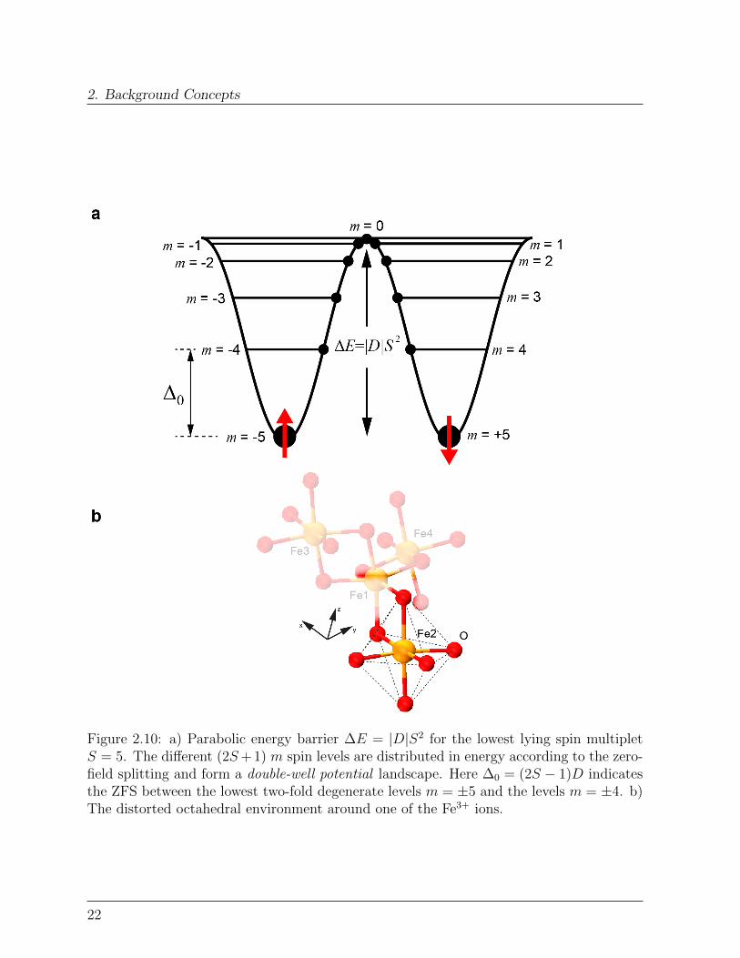
∆E = |D|S2 (2.8)
that separates |m〉 and | −m〉 sublevels, Figure 2.10a.This zero-field splitting (ZFS) provides a beautiful example of how the surroundings of anatom profoundly affect its magnetic state and determines its actual magnetic response.In the Fe4 core for instance, each Fe3+ ion is coordinated with six Oxygen atoms in adistorted octahedral environment, Figure 2.10b. The crystal-field of the latter partiallyremoves the degeneracy of the Fe3+ d orbitals, splitting them in the two subsets eg and t2g
by ∆0. The resulting zero-field splitting ∆0, gives rise to the so-called single-ion anisotropy.Having Fe3+ a 3d5 electronic configuration, the t2g orbital is half-filled imposing quenchingof the angular momentum. In the next paragraphs, we will see that quenching of theangular momentum enables a detailed modelling of the spin anisotropy based on the spinHamiltonian approach.
2.2.3 Modeling the anisotropy
In the SMM core, the electronic density distribution ρe surrounding the magnetic ionscreates a local electric field of given symmetry. This field acts on the orbital componentof the magnetic ions (the d electrons of the Fe ions, in the Fe4 case), giving rise to themagnetic anisotropy. The crystal field potential can be expressed as a sum of sphericalharmonics of progressively higher symmetry2 [108–111]:
Hsp =∑i,j
Bji O
ji (2.9)
with the indexes:
i = 2, 4, ..., 2S
(2.10)
−i ≤ j ≤ +i
where S is the molecular spin.The Oj
i terms, called Stevens operator equivalents, represent the spherical harmonics as asum of equivalent angular momentum operators, Figure 2.11.They contain the jth power of the spin ladder operators S± = Sx ± iSy and the (i − j)th
power of the spin operator Sz, which effect on the eigenvectors |m〉 is:
Sz|m〉 = m|m〉 (2.11)
2Equation (2.9) is a generalization of Equations (2.6). In particular: D = 3B02 [76]
23

2. Background Concepts
Figure 2.11: The shape of the spherical harmonics associated to each of the Stevens oper-ators, up to the sixth order.
S±|m〉 =√S(S + 1)−m(m± 1)|m± 1〉 (2.12)
Each Oji term is weighted by a coefficient Bj
i that vanishes for the Oji ’s not belonging to
the point group of the molecular structure.Equation (2.9) subdivides the spin anisotropy into different contributions, each havingthe symmetry of a corresponding spherical (tesseral) harmonic. Terms with j = 0 containpowers of Sz only and contribute to the energy barrier ∆E separating |m〉 states of oppositemagnetic moment, but do not mix the |m〉 eigenstates [76], Figure 2.12a. On the contrary,terms with j 6= 0, containing the jth power of the ladder operators, mix |m〉 states differingin m by a multiple of j, and enable the quantum tunneling (QT) mechanism [83, 87] forspin-relaxation discussed in the next section. Examples of Oj
i operators with associatedspherical harmonics are reported in Table 2.1.Important note: Stevens’ formalism non only provide an effective framework to modelthe magnetic anisotropy, but it also allows to model the effect of any external electric field,including that of the electron density in an underlying substrate, on the spin anisotropy,As discussed in Chapter 6, the effect of graphene charge density on the spin anisotropywill be modeled by introducing Bj
i Oji terms of corresponding symmetry in the sum (2.9),
and discarding all terms not belonging to the point group of the spin environment.The core of the tetrairon cluster Fe4 is a model spin with S = 5, whose crystal field reflectsthe equilateral triangle D3 symmetry, for which Equation 2.9 reads:
24

2.2. Single Molecule Magnets
Y 02 =
1
4
√5
π
3z2 − r2
r2
O02 = 3S2
z − S(S + 1)
Y 04 =
3
16
√1
π
35z4 − 30z2r2 + 3r4
r4
O04 = 35S4
z − [30S(S + 1)− 25]S2z − 6S(S + 1) + 3[S(S + 1)]2
Y ±22 =
1
4
√15
2π
(x± iy)2
r2
O22 =
1
2(S2
+ + S2−)
Y ±34 = ∓3
8
√35
π
(x± iy)3z
r4
O34 =
1
4[Sz(S
3+ + S3
−) + (S3+ + S3
−)Sz]
Table 2.1: Spherical harmonics and associated operator equivalents describing the spatialdistribution of the crystal field around each Fe3+ site in the Fe4 core.
Hsp = B02O
02 +B0
4O04 +B2
2O22 +B3
4O34. (2.13)
The higher order terms, B04O
04 and B3
4O34, belong to the D3 point group while the term B2
2O22
does not belong to D3 point group symmetry but it is necessary for a correct interpretationof neutron scattering data [112], and it may be due to distortions of the equilateral trianglein close packed single crystals [113, 114]For Fe4Py, used later in this work, electron paramagnetic resonance (EPR) studies yield[82]:
B02 = −0.194K
B04 = 3.45× 10⁻⁵ K (2.14)
B22 = 0.016K
B34 < 6.9× 10⁻⁵ K
25
2. Background Concepts
The dominant j = 0 term B02O
02 affords the barrier:
∆E ' 3B02 ·S2 = 3B0
2 · 25 = 14.55K (2.15)
2.2.4 Spin relaxation: master equation
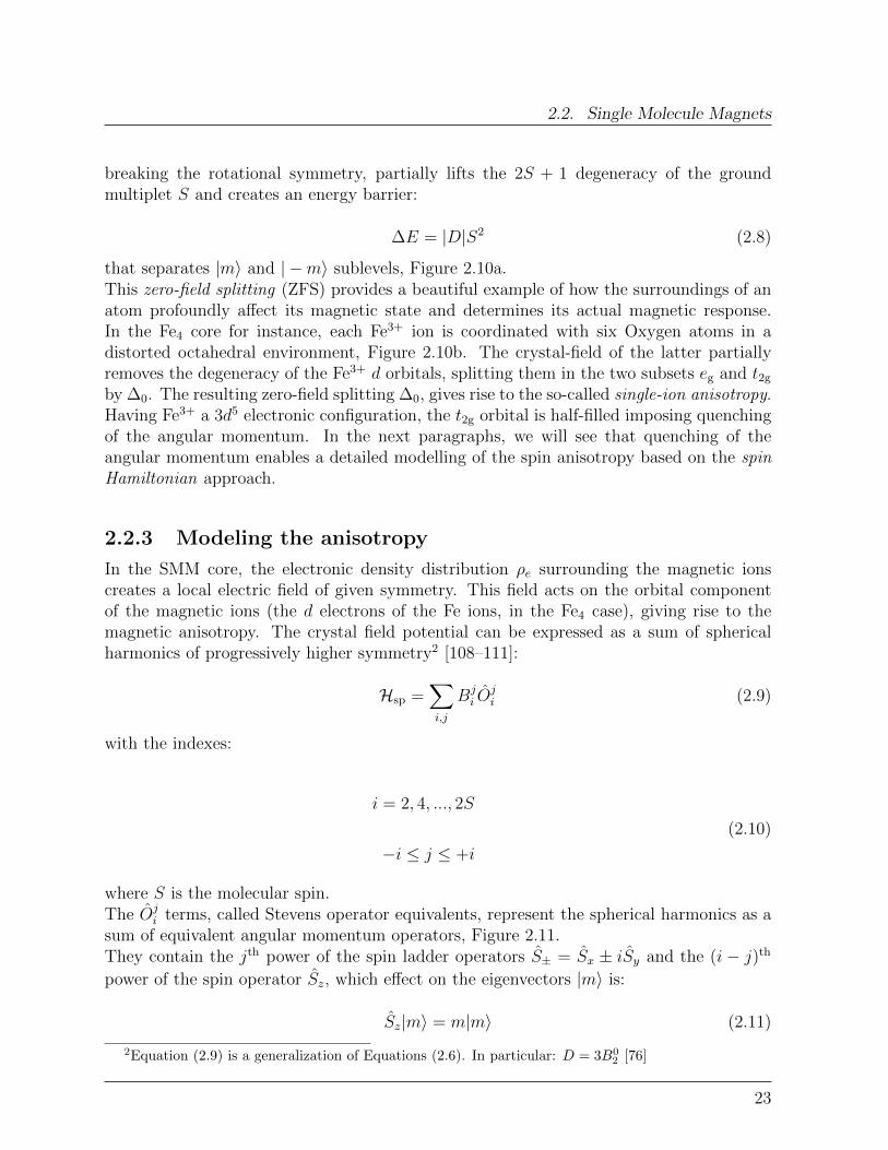
The above picture opens up two possible paths for the relaxation of molecular spins [76,83, 115, 116]:
• Classical relaxation mechanism: to reverse its direction, the molecular spin has to over-come the anisotropy barrier by interacting with the surrounding, e.g. absorbing oremitting phonons, Figure 2.12b.
• Quantum relaxation mechanism: the molecule reverses its spin via tunneling transition|m〉 → | −m〉 through the barrier, Figure 2.12c . The finite tunnel probability betweendegenerate states at opposite sides of the barrier is due to transverse (j 6= 0) Stevensterms which mix |m〉 and | −m〉 states differing in m by a multiple of j.
Figure 2.12: Spin relaxation mechanisms for molecular spins. a) Anisotropy barrier orig-inating from crystal field. b) Thermal relaxation machanism. c) Resonant quantum tun-neling between degenerate magnetic levels enabled by terms with j 6= 0.
The dynamics of a molecular spin can be modeled via the master equation [76, 115, 117]:
d
dtNm(t) =
∑m′
[Wm′,mNm′(t)−Wm,m′Nm(t)] (2.16)
that describes how the probability Nm(t) of being in the state |m〉 evolves in time due tothe above relaxation mechanisms.
Wm,m′ is the transition probability from state |m〉 to another state |m′〉 per unit time andit has to be calculated taking into account all the relaxation paths that connect |m〉 to|m′〉.
26
2.2. Single Molecule Magnets
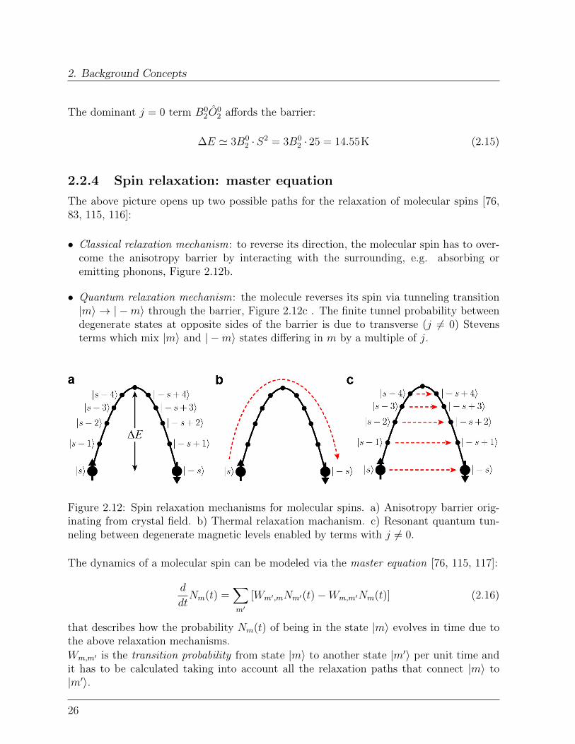
2.2.5 Effect of an external magnetic field
The effect of an external magnetic field applied along the easy axis z is to shift in energythe states |m〉 and | −m〉 at the opposite sides of the barrier, Figure 2.13.
Figure 2.13: Effect of an external magnetic field on the eigenvalues of (2.6). a) For Hz = 0,states at the opposite sides of the barrier are degenerate. b) An external field Hz 6= 0removes the degeneracy between the levels. c) For certain field values Hz = Hm,m′
thedegeneracy between some levels is reestablished.
For Hz 6= 0, two given eigenvectors |m〉 and |m′〉 of the Hamiltonian:
H = DS2z + gµBSzHz (2.17)
are degenerate for certain field values Hz = Hm,m′called crossing fields, Figure 2.13c, for
which:
gµBHm,m′
= D(m+m′) (2.18)
2.2.6 Thermal relaxation: Arrhenius
The energy barrier ∆E is at the origin of the slow relaxation of the magnetization in SMMsat low temperatures. In order to invert the orientation of its spin, a SMM has to overcome∆E by exchanging energy with the surroundings, for example via spin-phonon interaction[115] or by hyperfine coupling to the nuclear spins [76]. Lowering the temperature decreasesthe density of phonons available to the system and the relaxation of the molecule slowsdown.The spin dynamics can be explored by measuring the frequency and temperature depen-dence of the magnetic ac-susceptibility:
27

2. Background Concepts
Figure 2.14: Temperature dependence of the dynamic molar susceptibility of Fe4Pymolecule in the T range 1.8 - 5 K, measured at different frequencies at H = 1kOe. a)In-phase component of the magnetic susceptibility χ′. b) Out-of-phase component of themagnetic susceptibility χ′′. c) Arrhenius plot of the ln(τ) vs. temperature reciprocal.Linear fit affords τ0 = (8.2 ± 1.3) · 10−7 s and ∆E = 13.8 ± 0.3 K. Inset: temperaturedependence of the relaxation time, line is a single exponential fit.
χ(ν, T ) = χ′(ν, T ) + iχ′′(ν, T ) (2.19)
in response to an oscillating magnetic field with frequency ν. Figure 2.14 shows the realand imaginary components measured on the crystalline Fe4Py. In order to reveal the purethermal relaxation mechanism, a small external magnetic field H = 1 kOe was applied soas to lift the degeneracy of states at the opposite sides of the barrier and thus suppressingthe quantum relaxation channel.
While the ac-susceptibility of simple paramagnets do not show any imaginary componentχ′′, on the contrary, SMMs are characterized by the slow relaxation of the magnetizationand the appearance of a nonzero χ′′ (Figure 2.14b). When the relaxation time τ of the giantspin equals the ac-field period (2πν)−1, a maximum in χ′′ is observed. The temperaturedependence of τ is then determined by measuring τ(Tmax) = (2πν)−1 at different frequen-cies, where Tmax indicates the temperature value at which the resonance (maximum in χ′′)
28

2.2. Single Molecule Magnets
occurs. In the temperature range 1.5 - 2.6K, Figure 2.14c, the relaxation time increasesexponentially on decreasing temperature as for a typical thermally activated relaxationprocess. This can be described by the Arrhenius law [76, 104]:
τ = τ0exp (∆E/kBT ) (2.20)
which provides the value:
∆E = 3|B02 |S2 = 13.8± 0.3K
in H = 1 kOe in agreement with the teoretical value found above.The prefactor τ0 in Equation (2.20) contains information about the specific mechanismscoupling the molecular spins to the environment for which the transition probabilitiesWm,m′ of Equation (2.16) have to be explicitly calculated [104, 115]. A detailed modelingof the spin-phonon interaction will be provided in the Section 6.8.
2.2.7 Cole-Cole model
ac-susceptibility measurements probe the population pm of the different m levels by mea-suring the sample’s magnetic moment directly:
〈M〉 =∑m
pmMm (2.21)
where pm is given by the Boltzmann distribution pm =1
Zexp
(− EmkBT
)and Z is the
system partition function. Under the influence of the ac-magnetic field at frequency ω,the population of of the m states oscillates in time. To reach dynamical equilibrium,the system needs the time τ . Two different regimes are identified. When the H-fieldoscillation period is much larger than the system relaxation time (ωτ << 1), the measuredsusceptibility tend to that of a molecule in perfect thermal equilibrium χ = χT, aslo calledisothermal susceptibility. On the other hand, when the field is faster that the relaxationtime (ωτ >> 1), equilibrium cannot be reached and susceptibility approaches that of aperfectly isolated spin with no interaction with the surroundings χ = χS, i.e. adiabaticsusceptibility. In the frequency range between these two regimes, the susceptibility can bemodeled by the Cole-Cole model [118]:
χ(ω, T ) = χ′(ω, T ) + iχ′′(ω, T ) = χS +χT − χS
1 + (iωτ)(2.22a)
The real and imaginary components are explicitly written:
χ′ = χS +χT − χS
1 + ω2τ 2χ′′ =
(χT − χS)ωτ
1 + ω2τ 2(2.22b)
The relaxation time of the system can then be extracted from the frequency dependenceof χ measured at constant T , Figure 2.15.
29

2. Background Concepts
Figure 2.15: Frequency dependence of Fe4Py dynamic susceptibility, measured at H = 0.Solid circles indicate the in-phase component χ′, while open circles represent the out-of-phase part χ′′. Lines are fit with Equations 2.22
In case the relaxation process, rather than being characterized by a single relaxation time τ ,is characterized by a distribution of relaxation times, the Cole-Cole model can be extendedas follows:
χ = χS +χT − χS
1 + (iωτ)1−α (2.23)
with α representing the broadening of the relaxation time distribution. The real andmaginary components become:
χ′(ω) = χS + (χT − χS)1 + (ωτ)1−α sin(απ/2)
1 + 2(ωτ)1−α sin(απ/2) + (ωτ)2−2α
(2.24)
χ′′(ω) = (χT − χS)1 + (ωτ)1−α cos(απ/2)
1 + 2(ωτ)1−α sin(απ/2) + (ωτ)2−2α
A distribution of relaxation times is associated with the presence of different molecularspecies (with different ∆E values) in the specimen and it can be used to reveal if a fractionof molecules undergo some structural changes.
30
2.2. Single Molecule Magnets
2.2.8 Quantum tunneling of the magnetization
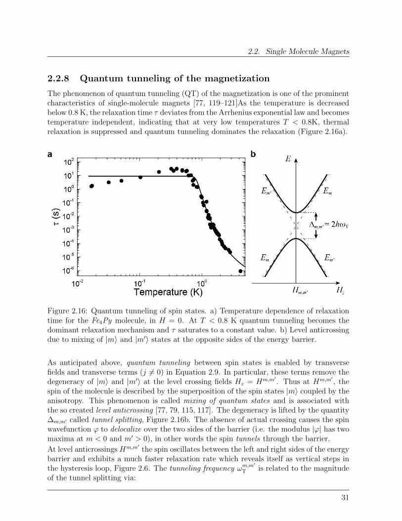
The phenomenon of quantum tunneling (QT) of the magnetization is one of the prominentcharacteristics of single-molecule magnets [77, 119–121]As the temperature is decreasedbelow 0.8 K, the relaxation time τ deviates from the Arrhenius exponential law and becomestemperature independent, indicating that at very low temperatures T < 0.8K, thermalrelaxation is suppressed and quantum tunneling dominates the relaxation (Figure 2.16a).
Figure 2.16: Quantum tunneling of spin states. a) Temperature dependence of relaxationtime for the Fe4Py molecule, in H = 0. At T < 0.8 K quantum tunneling becomes thedominant relaxation mechanism and τ saturates to a constant value. b) Level anticrossingdue to mixing of |m〉 and |m′〉 states at the opposite sides of the energy barrier.
As anticipated above, quantum tunneling between spin states is enabled by transversefields and transverse terms (j 6= 0) in Equation 2.9. In particular, these terms remove thedegeneracy of |m〉 and |m′〉 at the level crossing fields Hz = Hm,m′
. Thus at Hm,m′, the
spin of the molecule is described by the superposition of the spin states |m〉 coupled by theanisotropy. This phenomenon is called mixing of quantum states and is associated withthe so created level anticrossing [77, 79, 115, 117]. The degeneracy is lifted by the quantity∆m,m′ called tunnel splitting, Figure 2.16b. The absence of actual crossing causes the spinwavefunction ϕ to delocalize over the two sides of the barrier (i.e. the modulus |ϕ| has twomaxima at m < 0 and m′ > 0), in other words the spin tunnels through the barrier.
At level anticrossings Hm,m′the spin oscillates between the left and right sides of the energy
barrier and exhibits a much faster relaxation rate which reveals itself as vertical steps inthe hysteresis loop, Figure 2.6. The tunneling frequency ωm,m
′
T is related to the magnitudeof the tunnel splitting via:
31
2. Background Concepts
∆m,m′ = 2hωTm,m′ (2.25)
2.2.9 Selection rules for tunneling
As seen above, level anticrossing originate from transverse anisotropy terms which mixstates with different m. However, the symmetry of such terms imposes a selection rule onwhich states |m〉 are mixed and which not (thus forming anticrossings and true crossingsrespectively). As a consequence, tunneling does not occur for any field values satisfyingEquation (2.18), but it occurs only between the states linked by the transverse anisotropyterms.For instance the biaxial anisotropy:
O22 =
1
2(S2
+ + S2−) (2.26)
links states |m〉 and |m′〉, which magnetic quantum numbers differ by a multiple of two:
|m−m′| = 2k (2.27)
where k is an integer. In the Fe4 cluster, this second order term enables tunneling betweenthe lowest lying states |5〉 and | − 5〉 at H = 0.The presence of the third order term:
O34 =
1
4[Sz(S
3+ + S3
−) + (S3+ + S3
−)Sz] (2.28)
mixes states for which:
|m−m′| = 3k (2.29)
For Fe4 in zero field this term enhances the tunneling probability between the |3〉 and |−3〉states.
In this work SMMs will be combined with graphene in order to create novel hybrid mate-rials and devices with interesting spintronic properties. In these hybrids, molecular spinsinteract with a surrounding (i.e. graphene) that differs substantially from the crystal, andhas an appreciable influence on their magnetic relaxation. The SMM-graphene interactionwill be investigated in detail in the next chapters and it will be shown that a third orderterm (2.28) is essential to explain the effect of graphene charge carriers on the dynamicsof molecular spins.
32
2.3. Graphene
2.3 Graphene
In this section, the fundamental properties of graphene are presented. Special emphasisis given to the factors influencing graphene’s electronic respons, while graphene spintronicproperties are the focus of Chapter 7.
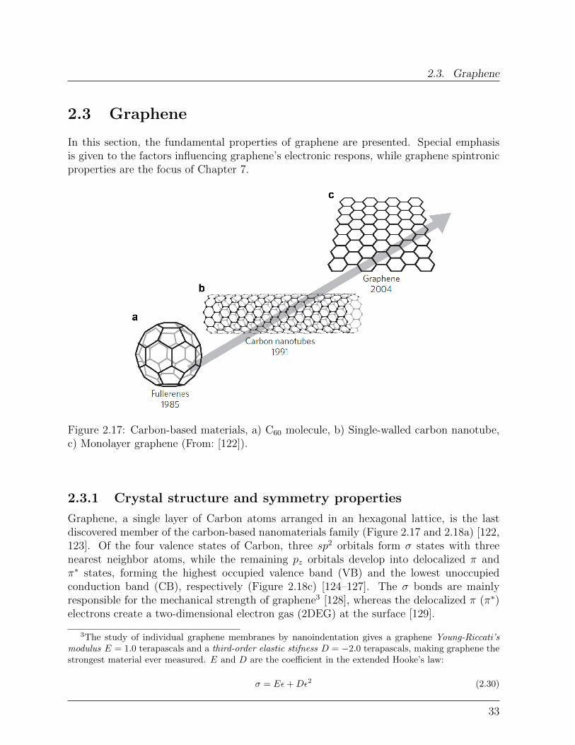
Figure 2.17: Carbon-based materials, a) C60 molecule, b) Single-walled carbon nanotube,c) Monolayer graphene (From: [122]).
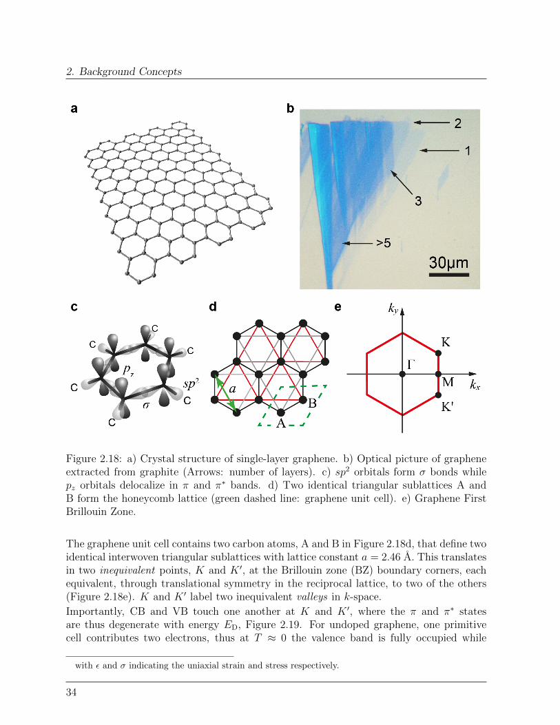
2.3.1 Crystal structure and symmetry properties
Graphene, a single layer of Carbon atoms arranged in an hexagonal lattice, is the lastdiscovered member of the carbon-based nanomaterials family (Figure 2.17 and 2.18a) [122,123]. Of the four valence states of Carbon, three sp2 orbitals form σ states with threenearest neighbor atoms, while the remaining pz orbitals develop into delocalized π andπ∗ states, forming the highest occupied valence band (VB) and the lowest unoccupiedconduction band (CB), respectively (Figure 2.18c) [124–127]. The σ bonds are mainlyresponsible for the mechanical strength of graphene3 [128], whereas the delocalized π (π∗)electrons create a two-dimensional electron gas (2DEG) at the surface [129].
3The study of individual graphene membranes by nanoindentation gives a graphene Young-Riccati’smodulus E = 1.0 terapascals and a third-order elastic stifness D = −2.0 terapascals, making graphene thestrongest material ever measured. E and D are the coefficient in the extended Hooke’s law:
σ = Eε+Dε2 (2.30)
33
2. Background Concepts
Figure 2.18: a) Crystal structure of single-layer graphene. b) Optical picture of grapheneextracted from graphite (Arrows: number of layers). c) sp2 orbitals form σ bonds whilepz orbitals delocalize in π and π∗ bands. d) Two identical triangular sublattices A andB form the honeycomb lattice (green dashed line: graphene unit cell). e) Graphene FirstBrillouin Zone.
The graphene unit cell contains two carbon atoms, A and B in Figure 2.18d, that define twoidentical interwoven triangular sublattices with lattice constant a = 2.46 A. This translatesin two inequivalent points, K and K ′, at the Brillouin zone (BZ) boundary corners, eachequivalent, through translational symmetry in the reciprocal lattice, to two of the others(Figure 2.18e). K and K ′ label two inequivalent valleys in k-space.
Importantly, CB and VB touch one another at K and K ′, where the π and π∗ statesare thus degenerate with energy ED, Figure 2.19. For undoped graphene, one primitivecell contributes two electrons, thus at T ≈ 0 the valence band is fully occupied while
with ε and σ indicating the uniaxial strain and stress respectively.
34
2.3. Graphene
the conduction band is completely unoccupied, resulting in a point-like Fermi surface(EF = ED) [130].
2.3.2 Band Structure
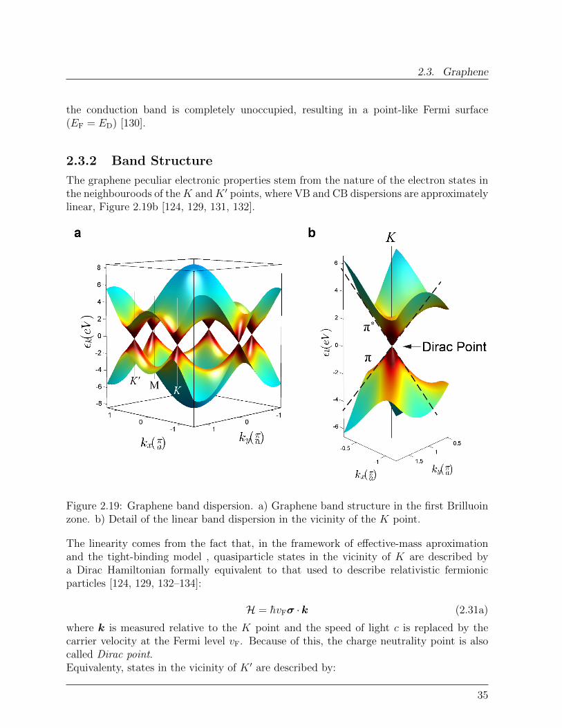
The graphene peculiar electronic properties stem from the nature of the electron states inthe neighbouroods of theK andK ′ points, where VB and CB dispersions are approximatelylinear, Figure 2.19b [124, 129, 131, 132].
Figure 2.19: Graphene band dispersion. a) Graphene band structure in the first Brilluoinzone. b) Detail of the linear band dispersion in the vicinity of the K point.
The linearity comes from the fact that, in the framework of effective-mass aproximationand the tight-binding model , quasiparticle states in the vicinity of K are described bya Dirac Hamiltonian formally equivalent to that used to describe relativistic fermionicparticles [124, 129, 132–134]:
H = hvFσ ·k (2.31a)
where k is measured relative to the K point and the speed of light c is replaced by thecarrier velocity at the Fermi level vF. Because of this, the charge neutrality point is alsocalled Dirac point.Equivalenty, states in the vicinity of K ′ are described by:
35
2. Background Concepts
H = hvFσ∗ ·k (2.31b)
The terms σ = (σx σy) and σ∗ = (σx -σy) are vectors of Pauli matrices:
σx =
(0 11 0
)σy =
(0 −ii 0
)(2.32)
describing the pseudospinproperty [124, 133, 135] of the graphene wave functions, that willbe discussed in the next paragraph.The complete Hamiltonian reads:
H =
0 γ(kx − iky) 0 0
γ(kx + iky) 0 0 00 0 0 γ(kx + iky)0 0 γ(kx − iky) 0
(2.33)
where4 γ = hvF.The Hamiltonian (2.33) does not contain elements that mix different valleys [136] so thatthe problem becomes completely decoupled into that of K and K ′ equations (2.31).Considering nearest neighbors-interactions only, the eigenvalues of (2.31) are [124, 133,135, 136]:
εb(k) ≈ bhvF|k| (2.34)
Equation (2.34) describes a linear band dispersion close to ED and implies a vanishingeffective mass m∗ = 0 for the graphene carriers. b = ±1 imparts positive and negativeenergies to π∗ and π states respectively, that hence are particles and antiparticles of eachother.The main consequence of this peculiar band dispersion, compared to the well knownparabolic dispersion ε(k) = h2k2/2m, is that the Fermi velocity is constant (vF ≈ 1× 10⁶
m/s) and does not depend on energy or momentum. So charge carriers in graphene moveat constant velocity whatever their energy, much like photons.
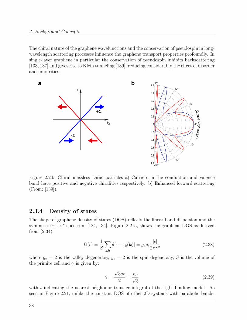
2.3.3 Pseudospin, Isospin: absence of back-scattering
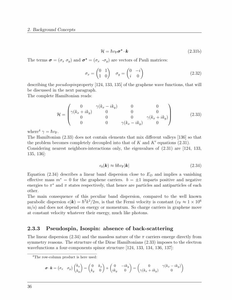
The linear dispersion (2.34) and the massless nature of the π carriers emerge directly fromsymmetry reasons. The structure of the Dirac Hamiltonians (2.33) imposes to the electronwavefunctions a four-components spinor structure [124, 133, 134, 136, 137]:
4The row-column product is here used:
σ ·k =(σx σy
)(kxky
)=
(0 kxky 0
)+
(0 −ikyiky 0
)=
(0 γ(kx − iky)
γ(kx + iky) 0
)
36

2.3. Graphene
Ψ =
ψKA
ψKB
ψK′
A
ψK′
B
(2.35)
where ψKA , ψK′
A , ψKB , ψK′
B are the slowly-varying envelope functions describing the effect ofthe sublattice periodic potential on the π (π∗) wavefunctions at K and K ′.From (2.35) follows that a graphene π (π∗) electron, in addition to its physical spin andmomentum, carries two additional degrees of freedom. One, called sublattice pseudospinindex, labels the sublattice state (A or B), while the other, called valley isospin index,labels the two independent Dirac points K and K ′ [124, 133, 138]. In analogy to thetwo-components spinor describing the usual spin, the pseudospin (σ in (2.31)) is a vectorwith two components, each describing the amplitude of the envelope functions on onesublattice. The direction of the pseudospin reflects the character (bonding or antibonding)of the underling molecular orbital [133].The eigenvectors of (2.31) are the two-components wave functions:
ψKk,±(r) =
(ψKAψKB
)=
1√2eik · r
(∓ie−iθk/2
eiθk/2
)(2.36a)
ψK′
k,±(r) =
(ψK
′A
ψK′
B
)=
1√2eik · r
(∓ieiθk/2
e−iθk/2
)(2.36b)
where θk = arctan(kx/ky) indicates the direction of k with respect to ky, i.e. kx + iky =i|k|eiθk and the terms in brackets on the right side describe a rotation of the pseudospinwith respect to k.The pseudospin is locked to the k direction and points either parallel or antiparallel to it.In fact, ψK± (r) and ψK
′± (r) are eigenvectors of the helicity operator Σ = 1
2σ · p
|p| describingthe projection of the momentum operator along the pseudospin direction:
ΣψK± (r) = ±1
2ψK± (r) (2.37a)
ΣψK′
± (r) = ∓1
2ψK
′
± (r) (2.37b)
Thus in analogy with the physics of massless neutrinos, charge carriers in graphene have awell defined chirality, i.e. states around K are right-handed (pseudospin parallel to k) whilestates close to K ′ are left-handed (pseudospin antiparallel to k). For the antiparticles in thevalence band, the situation is reversed. Physically, this means that the character (bondingor antibonding) of the wavefunction depends on the propagation direction, a valence stateclose to K with a positive kx is decribed by a linear combination of antibonding orbitalswhile a state with −kx is decribed by a linear combination of bonding orbitals [133].
37
2. Background Concepts
The chiral nature of the graphene wavefunctions and the conservation of pseudospin in long-wavelength scattering processes influence the graphene transport properties profoundly. Insingle-layer graphene in particular the conservation of pseudospin inhibits backscattering[133, 137] and gives rise to Klein tunneling [139], reducing considerably the effect of disorderand impurities.
Figure 2.20: Chiral massless Dirac particles a) Carriers in the conduction and valenceband have positive and negative chiralities respectively. b) Enhanced forward scattering(From: [139]).
2.3.4 Density of states
The shape of graphene density of states (DOS) reflects the linear band dispersion and thesymmetric π - π∗ spectrum [124, 134]. Figure 2.21a, shows the graphene DOS as derivedfrom (2.34):
D(ε) =1
S
∑b,k
δ[ε− εb(k)] = gvgs|ε|
2πγ2(2.38)
where gv = 2 is the valley degeneracy, gs = 2 is the spin degeneracy, S is the volume ofthe primite cell and γ is given by:
γ =
√3at
2=vF√
3(2.39)
with t indicating the nearest neighbour transfer integral of the tight-binding model. Asseen in Figure 2.21, unlike the constant DOS of other 2D systems with parabolic bands,
38
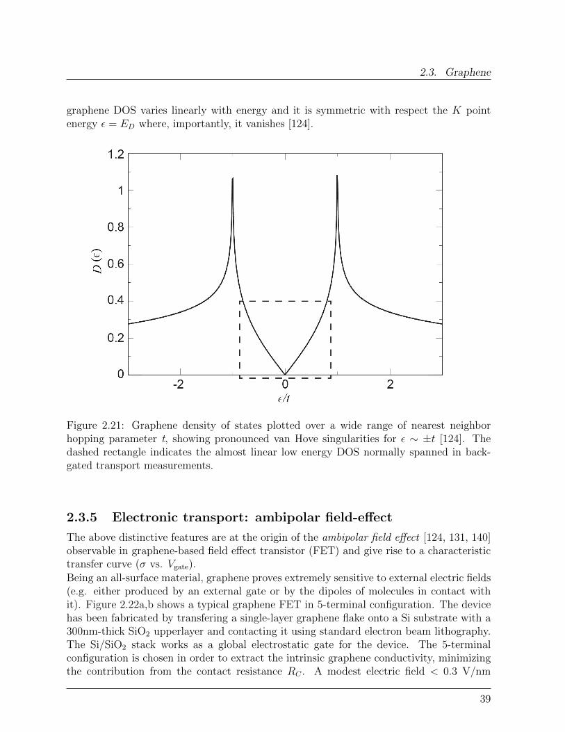
2.3. Graphene
graphene DOS varies linearly with energy and it is symmetric with respect the K pointenergy ε = ED where, importantly, it vanishes [124].
Figure 2.21: Graphene density of states plotted over a wide range of nearest neighborhopping parameter t, showing pronounced van Hove singularities for ε ∼ ±t [124]. Thedashed rectangle indicates the almost linear low energy DOS normally spanned in back-gated transport measurements.
2.3.5 Electronic transport: ambipolar field-effect
The above distinctive features are at the origin of the ambipolar field effect [124, 131, 140]observable in graphene-based field effect transistor (FET) and give rise to a characteristictransfer curve (σ vs. Vgate).Being an all-surface material, graphene proves extremely sensitive to external electric fields(e.g. either produced by an external gate or by the dipoles of molecules in contact withit). Figure 2.22a,b shows a typical graphene FET in 5-terminal configuration. The devicehas been fabricated by transfering a single-layer graphene flake onto a Si substrate with a300nm-thick SiO2 upperlayer and contacting it using standard electron beam lithography.The Si/SiO2 stack works as a global electrostatic gate for the device. The 5-terminalconfiguration is chosen in order to extract the intrinsic graphene conductivity, minimizingthe contribution from the contact resistance RC . A modest electric field < 0.3 V/nm
39
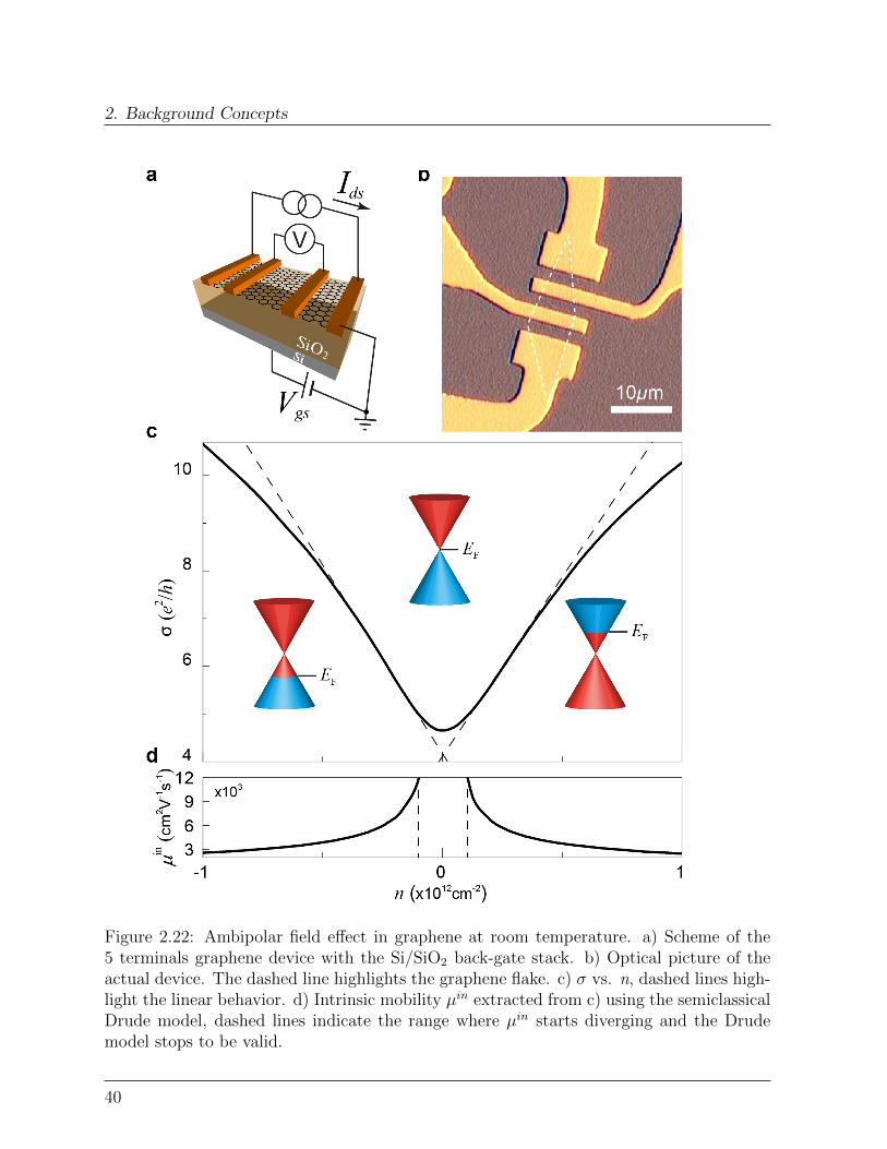
2. Background Concepts
Figure 2.22: Ambipolar field effect in graphene at room temperature. a) Scheme of the5 terminals graphene device with the Si/SiO2 back-gate stack. b) Optical picture of theactual device. The dashed line highlights the graphene flake. c) σ vs. n, dashed lines high-light the linear behavior. d) Intrinsic mobility µin extracted from c) using the semiclassicalDrude model, dashed lines indicate the range where µin starts diverging and the Drudemodel stops to be valid.
40
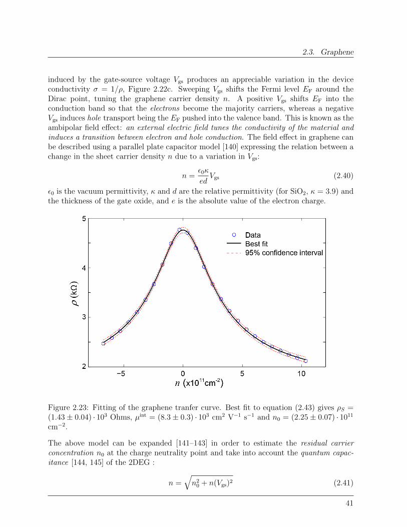
2.3. Graphene
induced by the gate-source voltage Vgs produces an appreciable variation in the deviceconductivity σ = 1/ρ, Figure 2.22c. Sweeping Vgs shifts the Fermi level EF around theDirac point, tuning the graphene carrier density n. A positive Vgs shifts EF into theconduction band so that the electrons become the majority carriers, whereas a negativeVgs induces hole transport being the EF pushed into the valence band. This is known as theambipolar field effect: an external electric field tunes the conductivity of the material andinduces a transition between electron and hole conduction. The field effect in graphene canbe described using a parallel plate capacitor model [140] expressing the relation between achange in the sheet carrier density n due to a variation in Vgs:
n =ε0κ
edVgs (2.40)
ε0 is the vacuum permittivity, κ and d are the relative permittivity (for SiO2, κ = 3.9) andthe thickness of the gate oxide, and e is the absolute value of the electron charge.
Figure 2.23: Fitting of the graphene tranfer curve. Best fit to equation (2.43) gives ρS =(1.43± 0.04) · 103 Ohms, µint = (8.3± 0.3) · 103 cm2 V−1 s−1 and n0 = (2.25± 0.07) · 1011
cm−2.
The above model can be expanded [141–143] in order to estimate the residual carrierconcentration n0 at the charge neutrality point and take into account the quantum capac-itance [144, 145] of the 2DEG :
n =√n2
0 + n(Vgs)2 (2.41)
41

2. Background Concepts
where n(Vgs) is extracted from:
e
Cen+
hvF
√πn
e= Vgs − Vmin (2.42)
The total gate capacitance Cgate = CeCq
Ce+Cqis the series capacitance of the electrostatic
capacitance Ce = ε0κd
and Cq =
√n/πe2
vFh.
The four terminal resistivity of the device, Figure 2.23, can then be expressed as:
ρ = ρS +1
eµin√n2
0 + n(Vgs)2(2.43a)
that is equivalent to:
ρ = ρS +1
eµin√n2
0 + (Cgate(Vgs − Vmin)/e)2(2.43b)
where ρS is a n-independent contribution to the resistivity due to short-range scatterers
(see next paragraph). ρ is extracted from the measured device resistance R using ρ =A
L2R,
where L is the distance between the probing contacts and A is the area of graphene enclosedbetween the probing contacts. Note that the 2D resistivity is given in units of ohms ratherthan ohms×cm as in the 3D case [140].
2.3.6 Carriers mobility
The room temperature (RT) intrinsic mobility µin of the device in Figure 2.22c is remark-ably high (Figure 2.22e). It spans µin ∼ 3000 − 12000 cm2 V−1s−1 in the concentrationrange n ∼ 1−0.1×1012 cm−2. Employing Einstein’s relation, the scattering time of about:
τ =hσ(π/n)1/2
e2vF
∼ 2ns (2.44)
a mean free path on the range:
l = vFτ ∼ 55-75nm (2.45)
at room temperature.
The mobility is limited by different factors such as scattering by charged impurities ordefects and electron-phonon scattering. In very clean and suspended samples (where theunderling SiO2 substrate has been etched away) the mean free path l increases by almosttwo order of magnitude, becoming comparabe to the device size, an indication that theballistic transport regime is reached [146, 147].
42
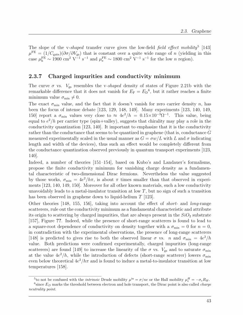
2.3. Graphene
The slope of the v-shaped transfer curve gives the low-field field effect mobility5 [143]µFE = (1/Cgate)(∂σ/∂Vgs) that is constant over a quite wide range of n (yielding in thiscase µFE
h ∼ 1900 cm2 V−1 s−1 and µFEe ∼ 1800 cm2 V−1 s−1 for the low n region).
2.3.7 Charged impurities and conductivity minimum
The curve σ vs. Vgs resembles the v-shaped density of states of Figure 2.21b with theremarkable difference that it does not vanish for EF = ED
6, but it rather reaches a finiteminimum value σmin 6= 0.
The exact σmin value, and the fact that it doesn’t vanish for zero carrier density n, hasbeen the focus of intense debate [123, 129, 148, 149]. Many experiments [123, 140, 149,150] report a σmin values very close to ≈ 4e2/h = 0.15×10⁻³Ω−1. This value, beingequal to e2/h per carrier type (spin+valley), suggests that chirality may play a role in theconductivity quantization [123, 140]. It important to emphasize that it is the conductivityrather than the conductance that seems to be quantized in graphene (that is, conductanceGmeasured experimentally scaled in the usual manner as G = σw/L with L and σ indicatinglength and width of the devices), thus such an effect would be completely different fromthe conductance quantization observed previously in quantum transport experiments [123,140].
Indeed, a number of theories [151–154], based on Kubo’s and Landauer’s formalisms,propose the finite conductivity minimum for vanishing charge density as a fundamen-tal characteristic of two-dimensional Dirac fermions. Nevertheless the value suggestedby those works, σmin = 4e2/hπ, is about π times smaller than that observed in experi-ments [123, 140, 149, 150]. Moreover for all other known materials, such a low conductivityunavoidably leads to a metal-insulator transition at low T , but no sign of such a transitionhas been observed in graphene down to liquid-helium T [123].
Other theories [148, 155, 156], taking into account the effect of short- and long-rangescatterers, rule out the conductivity minimum as a fundamental characteristic and attributeits origin to scattering by charged impurities, that are always present in the SiO2 substrate[157], Figure ??. Indeed, while the presence of short-range scatterers is found to lead toa square-root dependence of conductivity on density together with a σmin = 0 for n = 0,in contradiction with the experimental observations, the presence of long-range scatterers[148] is predicted to gives rise to both the observed linear σ vs. n and σmin = 4e2/hvalue. Both predictions were confirmed experimentally, charged impurities (long-rangescatterers) are found [149] to increase the linearity of the σ vs. Vgs and to saturate σmin
at the value 4e2/h, while the introduction of defects (short-range scatterer) lowers σmin
even below theoretical 4e2/hπ and is found to induce a metal-to-insulator transition at lowtemperatures [158].
5to not be confused with the intrinsic Drude mobility µin = σ/ne or the Hall mobility µHe = −σeRH .
6since ED marks the threshold between electron and hole transport, the Dirac point is also called chargeneutrality point.
43
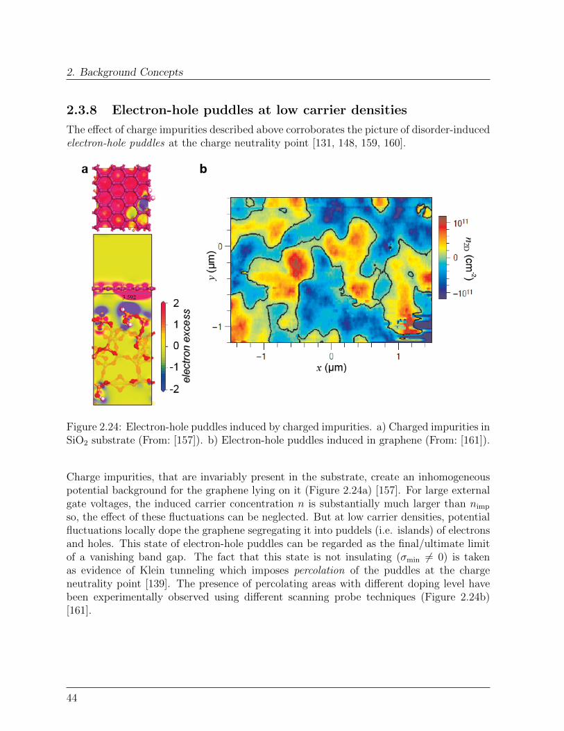
2. Background Concepts
2.3.8 Electron-hole puddles at low carrier densities
The effect of charge impurities described above corroborates the picture of disorder-inducedelectron-hole puddles at the charge neutrality point [131, 148, 159, 160].
Figure 2.24: Electron-hole puddles induced by charged impurities. a) Charged impurities inSiO2 substrate (From: [157]). b) Electron-hole puddles induced in graphene (From: [161]).
Charge impurities, that are invariably present in the substrate, create an inhomogeneouspotential background for the graphene lying on it (Figure 2.24a) [157]. For large externalgate voltages, the induced carrier concentration n is substantially much larger than nimp
so, the effect of these fluctuations can be neglected. But at low carrier densities, potentialfluctuations locally dope the graphene segregating it into puddels (i.e. islands) of electronsand holes. This state of electron-hole puddles can be regarded as the final/ultimate limitof a vanishing band gap. The fact that this state is not insulating (σmin 6= 0) is takenas evidence of Klein tunneling which imposes percolation of the puddles at the chargeneutrality point [139]. The presence of percolating areas with different doping level havebeen experimentally observed using different scanning probe techniques (Figure 2.24b)[161].
44
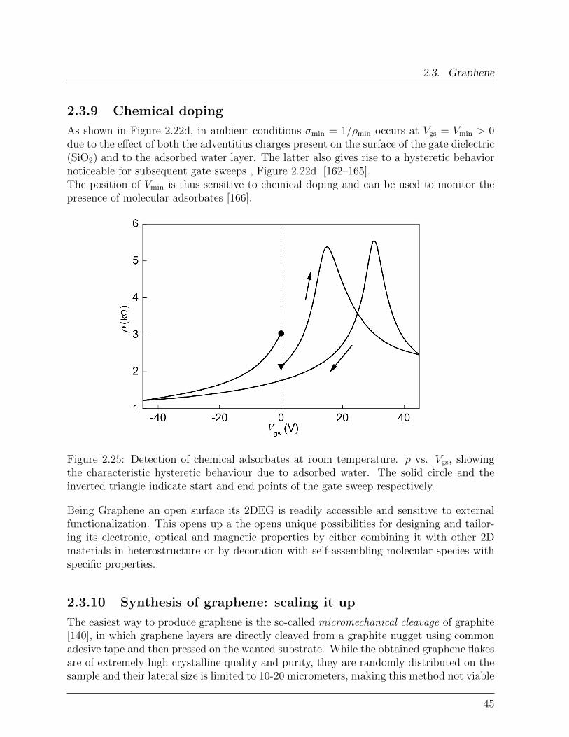
2.3. Graphene
2.3.9 Chemical doping
As shown in Figure 2.22d, in ambient conditions σmin = 1/ρmin occurs at Vgs = Vmin > 0due to the effect of both the adventitius charges present on the surface of the gate dielectric(SiO2) and to the adsorbed water layer. The latter also gives rise to a hysteretic behaviornoticeable for subsequent gate sweeps , Figure 2.22d. [162–165].The position of Vmin is thus sensitive to chemical doping and can be used to monitor thepresence of molecular adsorbates [166].
Figure 2.25: Detection of chemical adsorbates at room temperature. ρ vs. Vgs, showingthe characteristic hysteretic behaviour due to adsorbed water. The solid circle and theinverted triangle indicate start and end points of the gate sweep respectively.
Being Graphene an open surface its 2DEG is readily accessible and sensitive to externalfunctionalization. This opens up a the opens unique possibilities for designing and tailor-ing its electronic, optical and magnetic properties by either combining it with other 2Dmaterials in heterostructure or by decoration with self-assembling molecular species withspecific properties.
2.3.10 Synthesis of graphene: scaling it up
The easiest way to produce graphene is the so-called micromechanical cleavage of graphite[140], in which graphene layers are directly cleaved from a graphite nugget using commonadesive tape and then pressed on the wanted substrate. While the obtained graphene flakesare of extremely high crystalline quality and purity, they are randomly distributed on thesample and their lateral size is limited to 10-20 micrometers, making this method not viable
45
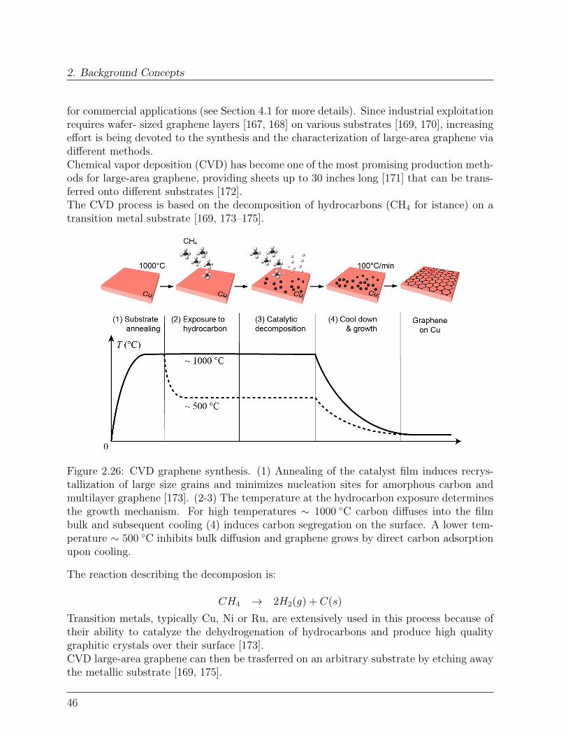
2. Background Concepts
for commercial applications (see Section 4.1 for more details). Since industrial exploitationrequires wafer- sized graphene layers [167, 168] on various substrates [169, 170], increasingeffort is being devoted to the synthesis and the characterization of large-area graphene viadifferent methods.Chemical vapor deposition (CVD) has become one of the most promising production meth-ods for large-area graphene, providing sheets up to 30 inches long [171] that can be trans-ferred onto different substrates [172].The CVD process is based on the decomposition of hydrocarbons (CH4 for istance) on atransition metal substrate [169, 173–175].
Figure 2.26: CVD graphene synthesis. (1) Annealing of the catalyst film induces recrys-tallization of large size grains and minimizes nucleation sites for amorphous carbon andmultilayer graphene [173]. (2-3) The temperature at the hydrocarbon exposure determinesthe growth mechanism. For high temperatures ∼ 1000 C carbon diffuses into the filmbulk and subsequent cooling (4) induces carbon segregation on the surface. A lower tem-perature ∼ 500 C inhibits bulk diffusion and graphene grows by direct carbon adsorptionupon cooling.
The reaction describing the decomposion is:
CH4 → 2H2(g) + C(s)
Transition metals, typically Cu, Ni or Ru, are extensively used in this process because oftheir ability to catalyze the dehydrogenation of hydrocarbons and produce high qualitygraphitic crystals over their surface [173].CVD large-area graphene can then be trasferred on an arbitrary substrate by etching awaythe metallic substrate [169, 175].
46

Bibliography
Bibliography
[1] Chappert, C., Fert, A., Van Dau, F. N. & Dau, F. V. The emergence of spinelectronics in data storage. Nature materials 3, 1–36 (2007).
[2] Zutic, I., Fabian, J., Das Sarma, S. & Sarma, S. D. Spintronics: Fundamentals andapplications. Rev. Mod. Phys. 76, 323–410 (2004).
[3] Binasch, G., Grunberg, P., Saurenbach, F. & Zinn, W. Enhanced magnetoresistancein layered magnetic structures with antiferromagnetic interlayer exchange. Phys.Rev. B 39, 4828–4830 (1989).
[4] Baibich, M. N., Broto, J. M., Fert, A., Van Dau, F. N. & Petroff, F. Giant Magnetore-sistance of (001)Fe/(001)Cr magnetic superlattices. Phys. Rev. Lett. 61, 2472–2475(1988).
[5] Pratt, W. et al. Perpendicular giant magnetoresistances of Ag/Co multilayers. Phys.Rev. Lett. 66, 3060–3063 (1991).
[6] Pratt, W. et al. Giant magnetoresistance with current perpendicular to the multilayerplanes. Journal of Magnetism and Magnetic Materials 126, 406–409 (1993).
[7] Bass, J. & Pratt, W. P. Current-perpendicular (CPP) magnetoresistance in magneticmetallic multilayers. Journal of Magnetism and Magnetic Materials 200, 274–289(1999).
[8] Valet, T. & Fert, A. Theory of the perpendicular magnetoresistance in magneticmultilayers. Phys. Rev. B 48, 7099–7113 (1993).
[9] Fert, A., Duvail, J.-L. & Valet, T. Spin relaxation effects in the perpendicularmagnetoresistance of magnetic multilayers. Phys. Rev. B 52, 6513–6521 (1995).
[10] Mott, N. F. The electrical conductivity of transition metals. Proceedings of theRoyal Society of London. Series A, Mathematical and Physical Sciences 153, 699–717 (1936).
[11] Mott, N. F. The resistance and thermoelectric properties of the transition metals.Proceedings of the Royal Society A: Mathematical, Physical and Engineering Sciences156, 368–382 (1936).
[12] Mott, N. F. Electrons in transition metals. Advances in Physics 13, 325–422 (1964).
[13] Fert, A. & Campbell, I. A. Two-current conduction in nickel. Phys. Rev. Lett. 21,1190–1192 (1968).
[14] Tsymbal, E. Y. & Pettifor, D. G. Perspectives of giant magnetoresistance. SolidState Physics - Advances in Research and Applications 56, 113–237 (2001).
47

Bibliography
[15] Zhang, S., Levy, P. & Fert, A. Conductivity and magnetoresistance of magneticmultilayered structures. Phys. Rev. B 45 (1992).
[16] Grunberg, P., Schreiber, R., Pang, Y., Brodsky, M. B. & Sowers, H. Layered magneticstructures: evidence for antiferromegnetic coupling of Fe layers across Cr interlayers.Phys. Rev. Lett. 57, 2442 (1986).
[17] Carbone, C. & Alvarado, S. F. Antiparallel coupling between Fe layers separated bya Cr interlayer: Dependence of the magnetization on the film thickness. Phys. Rev.B 36, 2433–2435 (1987).
[18] Parkin, S. S. P., More, N. & Roche, K. P. Oscillations in exchange coupling andmagnetoresistance in metallic superlattice structures: Co/Ru, Co/Cr, and Fe/Cr.Phys. Rev. Lett. 64, 2304–2307 (1990).
[19] Parkin, S. Systematic variation of the strength and oscillation period of indirectmagnetic exchange coupling through the 3d, 4d, and 5d transition metals. Phys.Rev. Lett. 67, 3598–3601 (1991).
[20] Parkin, S. & Mauri, D. Spin engineering: Direct determination of the Ruderman-Kittel-Kasuya-Yosida far-field range function in ruthenium. Phys. Rev. B 44, 7131–7134 (1991).
[21] Bruno, P. & Chappert, C. Oscillatory coupling between ferromagnetic layers sepa-rated by a nonmagnetic metal spacer. Phys. Rev. Lett. 67, 1602–1605 (1991).
[22] Bruno, P. & Chappert, C. Erratum: Oscillatory coupling between ferromagneticlayers separated by a nonmagnetic metal spacer. Phys. Rev. Lett. 67, 2592 (1991).
[23] Parkin, S. S. P., Bhadra, R. & Roche, K. P. Oscillatory magnetic exchange couplingthrough thin copper layers. Phys. Rev. Lett. 66, 2152–2155 (1991).
[24] Stiles, M. D. Interlayer exchange coupling. In Ultrathin Magnetic Structures III: Fun-damentals of Nanomagnetism, vol. 200, chap. 4, 99–142 (Springer, Berlin Heidelberg,2005).
[25] Unguris, J., Celotta, R. & Pierce, D. Observation of two different oscillation periodsin the exchange coupling of Fe/Cr/Fe (100). Phys. Rev. Lett. 67 (1991).
[26] Takagishi, M. et al. The applicability of CPP-GMR heads for magnetic recording.IEEE Transactions on Magnetics 38, 2277–2282 (2002).
[27] Parkin, S. et al. Magnetically engineered spintronic sensors and memory. Proceedingsof the IEEE 91, 661–679 (2003).
[28] Childress, J. R. et al. Fabrication and recording study of all-metal dual-spin-valveCPP read heads. INTERMAG 2006 - IEEE International Magnetics Conference 42,277 (2006).
48
Bibliography
[29] Parkin, S. Origin of enhanced magnetoresistance of magnetic multilayers: Spin-dependent scattering from magnetic interface states. Phys. Rev. Lett. 71, 1641–1644(1993).
[30] Dieny, B. et al. Giant magnetoresistive in soft ferromagnetic multilayers. Phys. Rev.B 43, 1297–1300 (1991).
[31] Parkin, S., Yang, H., Yang, S.-H. and Hayashi, M. Magnetic Tunnel Junctions. InHandbook of Magnetism and Advanced Magnetic Materials Vol. 5, 1–21 (2007).
[32] Tsymbal, E. Y., Mryasov, O. N. & LeClair, P. R. Spin-dependent tunnelling inmagnetic tunnel junctions. Journal of Physics: Condensed Matter 15, R109–R142(2003).
[33] Julliere, M. Tunneling between ferromagnetic films. Physics Letters A 54, 225–226(1975).
[34] Miyazaki, T. & Tezuka, N. Giant magnetic tunneling effect in Fe/Al2O3/Fe junction.Journal of Magnetism and Magnetic Materials 139, L231–L234 (1995).
[35] Moodera, J. S., Kinder, L. R., Wong, T. M. & Meservey, R. Large magnetoresistanceat room temperature in ferromagnetic thin film tunnel junctions. Phys. Rev. Lett.74, 3273–3276 (1995).
[36] Parkin, S. S. P. et al. Giant tunnelling magnetoresistance at room temperature withMgO (100) tunnel barriers. Nature materials 3, 862–7 (2004).
[37] Yuasa, S., Nagahama, T., Fukushima, A., Suzuki, Y. & Ando, K. Giant room-temperature magnetoresistance in single-crystal Fe/MgO/Fe magnetic tunnel junc-tions. Nature materials 3, 868–71 (2004).
[38] Mathon, J. & Umerski, a. Theory of tunneling magnetoresistance of an epitaxialFe/MgO/Fe(001) junction. Phys. Rev. B 63, 220403 (2001).
[39] Mavropoulos, P., Papanikolaou, N. & Dederichs, P. Complex band structure andtunneling through ferromagnet /insulator /ferromagnet junctions. Phys. Rev. Lett.85, 1088–1091 (2000).
[40] Butler, W., Zhang, X.-G., Schulthess, T. & MacLaren, J. Reduction of electrontunneling current due to lateral variation of the wave function. Phys. Rev. B 63,092402 (2001).
[41] Butler, W., Zhang, X.-G., Schulthess, T. & MacLaren, J. Spin-dependent tunnelingconductance of Fe—MgO—Fe sandwiches. Phys. Rev. B 63, 054416 (2001).
[42] Belashchenko, K., Tsymbal, E., Oleynik, I. & van Schilfgaarde, M. Positive spinpolarization in Co/Al2O3/Co tunnel junctions driven by oxygen adsorption. Phys.Rev. B 71, 224422 (2005).
49

Bibliography
[43] Tsymbal, E. & Pettifor, D. Modelling of spin-polarized electron tunnelling from 3dferromagnets. Journal of Physics: Condensed Matter 411 (1997).
[44] Wunnicke, O. et al. Effects of resonant interface states on tunneling magnetoresis-tance. Phys. Rev. B 65, 064425 (2002).
[45] Tsymbal, E. Y., Oleinik, I. I. & Pettifor, D. G. Oxygen-induced positive spin po-larization from Fe into the vacuum barrier. Journal of Applied Physics 87, 5230(2000).
[46] Belashchenko, K. et al. Effect of interface bonding on spin-dependent tunneling fromthe oxidized Co surface. Phys. Rev. B 69, 174408 (2004).
[47] Kaiser, C., Van Dijken, S., Yang, S. H., Yang, H. & Parkin, S. S. P. Role of tunnelingmatrix elements in determining the magnitude of the tunneling spin polarization of3d transition metal ferromagnetic alloys. Phys. Rev. Lett. 94, 247203 (2005).
[48] Raman, K. V. Interface-assisted molecular spintronics. Applied Physics Reviews 1(2014).
[49] Raman, K. V. et al. Interface-engineered templates for molecular spin memory de-vices. Nature 493, 509–513 (2013).
[50] Santos, T. et al. Room-temperature tunnel magnetoresistance and spin-polarizedtunneling through an organic semiconductor barrier. Phys. Rev. Lett. 98, 016601(2007).
[51] Barraud, C. C. et al. Unravelling the role of the interface for spin injection intoorganic semiconductors. Nature Physics 6, 615–620 (2010).
[52] Atodiresei, N. et al. Design of the local spin polarization at the organic-ferromagneticinterface. Phys. Rev. Lett. 105, 1–4 (2010).
[53] Datta, S. & Das, B. Electronic analog of the electrooptic modulator. Applied PhysicsLetters 665, 10–13 (1990).
[54] Behin-Aein, B., Datta, D., Salahuddin, S. & Datta, S. Proposal for an all-spin logicdevice with built-in memory. Nature nanotechnology 5, 266–270 (2010).
[55] Datta, S., Salahuddin, S. & Behin-Aein, B. Non-volatile spin switch for Boolean andnon-Boolean logic. Applied Physics Letters 101, 252411 (2012).
[56] Manipatruni, S., Nikonov, D. E. & Young, I. a. All-spin nanomagnetic state elements.Applied Physics Letters 103, 063503 (2013).
[57] Fabian, J. & Sarma, S. D. Spin relaxation of conduction electrons. Journal of VacuumScience Technology B 17, 1708 (1999).
50
Bibliography
[58] Wolf, S. A. et al. Spintronics: a spin-based electronics vision for the future. Science294, 1488–1495 (2001).
[59] Koo, H. C. et al. Control of spin precession in a spin-injected field effect transistor.Science 325, 1515–1518 (2009).
[60] Jackson, J. D. Classical electrodynamics (Wiley, New York, 1999), 3rd edn.
[61] Ihn, T. Semiconductor Nanostructures (Oxford University Press, New York, 2010).
[62] D’yakonov, M. I. & Perel, V. I. Possibility of orienting electron spins with current.ZhETF Pis. Red. 13, 657–660 (1971).
[63] Dyakonov, M. & Perel, V. Current-induced spin orientation of electrons in semicon-ductors. Physics Letters A 35, 459–460 (1971).
[64] Dresselhaus, G. Spin-orbit coupling effects in zinc blende structures. Phys. Rev. 100,580–586 (1955).
[65] Elliott, R. J. Theory of the effect of spin-orbit coupling on magnetic resonance insome semiconductors. Phys. Rev. 96, 266–279 (1954).
[66] Yafet, Y. Calculation of the g factor of metallic sodium. Phys. Rev. 85, 478 (1952).
[67] Yafet, Y. g Factors and Spin-Lattice Relaxation of Conduction Electrons. In Turn-bull, D. & Ehrenreich, H. (eds.) Solid state physics Vol. 14, 1–96 (Academic Press,New York, 1963).
[68] Overhauser, A. W. Paramagnetic relaxation in metals. Phys. Rev. 89, 689–700(1953).
[69] Fabian, J. & Wu, M. Spin Relaxation and Spin Dynamics in Semiconductors. InHandbook of Spin Transport and Magnetism, 303–327 (2011).
[70] Boguslawski, P. Electron-electron spin-flip scattering and spin relaxation in IIIV andIIVI semiconductors. Solid State Communications 33, 389–391 (1980).
[71] Bir, G. L., Aronov, a. G. & Pikus, G. E. Spin relaxation of electrons due to scatteringby holes. Zh. Eksp. Teor. Fiz 42, 705–712 (1975).
[72] Pershin, Y. V. & Privman, V. Spin relaxation of conduction electrons in semicon-ductors due to interaction with nuclear spins. Nano Letters 3, 695–700 (2003).
[73] Bychkov, Y. a. & Rashba, E. I. Oscillatory effects and the magnetic susceptibility ofcarriers in inversion layers. Journal of Physics C 17, 6039–6045 (1984).
[74] Bychkov, Y. a. & Rashba, E. I. Properties of a 2D electron gas with lifted spectraldegeneracy. JETP Letters 39, 78–81 (1984).
51
Bibliography
[75] Schliemann, J., Egues, J. C. & Loss, D. Nonballistic spin-field-effect transistor. Phys.Rev. Lett. 90, 146801 (2003).
[76] Gatteschi, D., Sessoli, R. & Villain, J. Molecular Nanomagnets. Mesoscopic Physicsand Nanotechnology (OUP, Oxford, 2006).
[77] Gatteschi, D. & Sessoli, R. Quantum Tunneling of Magnetization and Related Phe-nomena in Molecular Materials. Angewandte Chemie International Edition 42, 268–297 (2003).
[78] Sessoli, R., Gatteschi, D., Caneschi, A. & Novak, M. A. Magnetic bistability in ametal-ion cluster. Nature 365, 141–143 (1993).
[79] Wernsdorfer, W. & Sessoli, R. Quantum Phase Interference and Parity Effects inMagnetic Molecular Clusters. Science 284, 133–135 (1999).
[80] Thomas, L. & Barbara, B. Quantum Tunneling of the Magnetization In Mn12-Ac.Journal of Low Temperature Physics 113, 1055–1060 (1998).
[81] Ardavan, A. et al. Will Spin-Relaxation Times in Molecular Magnets Permit Quan-tum Information Processing? Phys. Rev. Lett. 98, 57201 (2007).
[82] Bogani, L. et al. Single-molecule-magnet carbon-nanotube hybrids. AngewandteChemie - International Edition 48, 746–50 (2009).
[83] Politi, P., Rettori, A., Hartmann-Boutron, F. & Villain, J. Tunneling in mesoscopicmagnetic molecules. Phys. Rev. Lett. 75, 537–540 (1995).
[84] Cornia, A. et al. Energy-Barrier Enhancement by Ligand Substitution in Tetra-iron(III) Single-Molecule Magnets. Angewandte Chemie - International Edition 116,1156–1159 (2004).
[85] Cervetti, C., Heintze, E. & Bogani, L. Interweaving spins with their environment:novel inorganic nanohybrids with controllable magnetic properties. Dalton transac-tions 43, 4220–32 (2014).
[86] Chudnovsky, E. M. & Garanin, D. A. Spin Tunneling via Dislocations in Mn12
Acetate Crystals. Phys. Rev. Lett. 87, 187203 (2001).
[87] Cornia, A. et al. Origin of second-order transverse magnetic anisotropy in Mn12-Acetate. Phys. Rev. Lett. 89, 257201 (2002).
[88] Bogani, L. et al. Magneto-Optical Investigations of Nanostructured Materials Basedon Single-Molecule Magnets Monitor Strong Environmental Effects. Advanced Ma-terials 19, 3906–3911 (2007).
[89] Mannini, M. et al. Quantum tunnelling of the magnetization in a monolayer oforiented single-molecule magnets. Nature 468, 417–421 (2010).
52

Bibliography
[90] Timco, G. a., Faust, T. B., Tuna, F. & Winpenny, R. E. P. Linking heterometallicrings for quantum information processing and amusement. Chemical Society reviews40, 3067–3075 (2011).
[91] Faust, T. B. et al. Chemical Control of Spin Propagation between HeterometallicRings. Chemistry – A European Journal 17, 14020–14030 (2011).
[92] Barra, A.-l. et al. New Single-Molecule Magnets by Site-Specific Substitution: In-corporation of Alligator Clips into Fe4 Complexes. European Journal of InorganicChemistry 2007, 4145–4152 (2007).
[93] Kyatskaya, S. et al. Anchoring of Rare-Earth-Based Single-Molecule Magnets onSingle-Walled Carbon Nanotubes. J. Am. Chem. Soc 131, 15143–15151 (2009).
[94] Pineider, F. et al. Deposition of intact tetrairon(iii) single molecule magnet mono-layers on gold: an STM, XPS, and ToF-SIMS investigation. J. Mater. Chem. 20,187–194 (2010).
[95] Corradini, V. et al. Grafting molecular CrNi rings on a gold surface. Dalton trans-actions 39, 4928–4936 (2010).
[96] Heersche, H. B. et al. Electron Transport through Single Mn12 Molecular Magnets.Phys. Rev. Lett. 96, 206801 (2006).
[97] Timco, G. A. G., McInnes, E. J. L. E., Pritchard, R. G., Tuna, F. & Winpenny, R.E. P. Heterometallic rings made from chromium stick together easily. AngewandteChemie International Edition 47, 9681–9684 (2008).
[98] Affronte, M. et al. Linking Rings through Diamines and Clusters: Exploring Syn-thetic Methods for Making Magnetic Quantum Gates. Angewandte Chemie Interna-tional Edition 44, 6496–6500 (2005).
[99] Timco, G. A. et al. Engineering the coupling between molecular spin qubits bycoordination chemistry. Nat Nano 4, 173–178 (2009).
[100] Candini, A. et al. Entanglement in Supramolecular Spin Systems of Two WeaklyCoupled Antiferromagnetic Rings Cr7Ni. Phys. Rev. Lett. 104, 37203 (2010).
[101] Bellini, V. et al. Propagation of Spin Information at the Supramolecular Scalethrough Heteroaromatic Linkers. Phys. Rev. Lett. 106, 227205 (2011).
[102] Faust, T. B. et al. Controlling magnetic communication through aromatic bridgesby variation in torsion angle. Dalton Trans. 41, 13626–13631 (2012).
[103] Venkataraman, L., Klare, J. E., Nuckolls, C., Hybertsen, M. S. & Steigerwald, M. L.Dependence of single-molecule junction conductance on molecular conformation. Na-ture 442, 904–907 (2006).
53
Bibliography
[104] Barra, A. L. et al. Single-Molecule Magnet Behavior of a Tetranuclear Iron(III)Complex. The Origin of Slow Magnetic Relaxation in Iron(III) Clusters. Journal ofthe American Chemical Society 121, 5302–5310 (1999).
[105] Cornia, A. et al. Slow quantum relaxation in a tetrairon (III) single-molecule magnet.Inorganica Chimica Acta 361, 3481–3488 (2008).
[106] Accorsi, S. et al. Tuning anisotropy barriers in a family of tetrairon (III) single-molecule magnets with an S= 5 ground state. J. Am. Chem. Soc 128, 4742–4755(2006).
[107] Blundell, S. Magnetism in condensed matter (Oxford University Press, 2001).
[108] Stevens, K. W. H. Matrix Elements and Operator Equivalents Connected with theMagnetic Properties of Rare Earth Ions. Proceedings of the Physical Society. SectionA 65, 209 (1952).
[109] Gorller-Walrand, C. & Binnemans, K. Rationalization of crystal-field parametriza-tion. In Handbook on the Physics and Chemistry of Rare Earths (1996).
[110] Misra, S. K., Poole, C. P. & Farach, H. a. A review of spin Hamiltonian forms forvarious point-group site symmetries. Applied Magnetic Resonance 11, 29–46 (1996).
[111] Buckmaster, H. a. & Chatterjee, R. The analysis of EPR spectra using tesseral tensorangular momentum operators. Physica Status Solidi B 209, 433–441 (1998).
[112] Carretta, S. et al. Intra- and inter-multiplet magnetic excitations in a tetrairon(III)molecular cluster. Phys. Rev. B 70, 214403 (2004).
[113] Rastelli, E. & Tassi, A. Magnetization steps in nanomagnets induced by a time-dependent magnetic field: Application to Fe4. Phys. Rev. B 75, 134414 (2007).
[114] Rastelli, E. & Tassi, A. Relaxation time of the nanomagnet Fe4. Phys. Rev. B 79,104415 (2009).
[115] Hartmann-Boutron, F., Politi, P. & Villain, J. Tunneling and magnetic relaxationin mesoscopic molecules. International Journal of Modern Physics B 10, 2577–2638(1996).
[116] Fort, A., Rettori, A., Villain, J., Gatteschi, D. & Sessoli, R. Mixed quantum-thermalrelaxation in Mn12 acetate molecules. Phys. Rev. Lett. 80, 612–615 (1998).
[117] Leuenberger, M. N. & Loss, D. Spin tunneling and phonon-assisted relaxation inMn12-acetate. Phys. Rev. B 61, 1286–1302 (2000).
[118] Gregoli, L. et al. Magnetostructural Correlations in Tetrairon (III) Single-MoleculeMagnets. Chemistry - A European Journal 15, 6456–6467 (2009).
54
Bibliography
[119] Thomas, L. et al. Macroscopic Quantum Tunneling of Magnetization in a Single-Crystal of Nanomagnets. Nature 383, 145–147 (1996).
[120] Friedman, J. R., Sarachik, M. P., Tejada, J. & Ziolo, R. Macroscopic measurementof resonant magnetization tunneling in high-spin molecules. Phys. Rev. Lett. 76,3830–3833 (1996).
[121] Hernandez, J. M. et al. Evidence for resonant tunneling of magnetization in Mn12-acetate complex (1997).
[122] Hirsch, A. The era of carbon allotropes. Nature materials 9, 868–871 (2010).
[123] Geim, A. K. & Novoselov, K. S. The rise of graphene. Nat. Mater. 6, 183–191 (2007).
[124] Castro Neto, A. H., Guinea, F., Peres, N. M. R., Novoselov, K. S. & Geim, A. K.The electronic properties of graphene. Rev. Mod. Phys. 81, 109–162 (2009).
[125] Wallace, P. R. The band theory of graphite. Phys. Rev. 329, 622–634 (1947).
[126] Slonczewski, J. C., Weiss, P. R., State, T. & Brgnsmck, X. Band Structure ofGraphite. Phys. Rev. 109, 272–279 (1958).
[127] Painter, G. S. & Ellis, D. E. Electronic band structure and optical properties ofgraphite from a variational approach. Phys. Rev. B 1, 4747–4752 (1970).
[128] Lee, C., Wei, X., Kysar, J. W. & Hone, J. Measurement of the Elastic Propertiesand Intrinsic Strength of Monolayer Graphene. Science 321, 385–388 (2008).
[129] Novoselov, K. S. et al. Two-dimensional gas of massless Dirac fermions in graphene.Nature 438, 197–200 (2005).
[130] Sprinkle, M. et al. First direct observation of a nearly ideal graphene band structure.Phys. Rev. Lett. 103, 1–4 (2009). arXiv:0907.5222.
[131] Das Sarma, S., Adam, S., Hwang, E. H. & Rossi, E. Electronic transport in two-dimensional graphene. Rev. Mod. Phys. 83, 407–470 (2011).
[132] Avouris, P. Graphene: Electronic and Photonic Properties and Devices. Nano Letters10, 150–496 (2010).
[133] McEuen, P. L., Bockrath, M., Cobden, D. H., Yoon, Y.-G. & Louie, S. G. Disorder,Pseudospins, and Backscattering in Carbon Nanotubes. Phys. Rev. Lett. 83, 5098–5101 (1999).
[134] Ando, T. Theory of Electronic States and Transport in Carbon Nanotubes. Journalof the Physical Society of Japan 74, 777–817 (2005).
55
Bibliography
[135] Kane, C. L. & Mele, E. J. Size, Shape, and Low Energy Electronic Structure ofCarbon Nanotubes. Phys. Rev. Lett. 78, 1932–1935 (1997).
[136] Shon, N. & Ando, T. Quantum Transport in Two-Dimensional Graphite System.Journal of the Physical Society of Japan 67, 2421–2429 (1998).
[137] Ando, T. & Nakanishi, T. Impurity scattering in carbon nanotubes: absence of backscattering. Journal of the Physical Society of Japan (1998).
[138] Recher, P. & Trauzettel, B. A defect controls transport in graphene. Physics 4, 3–5(2011).
[139] Katsnelson, M. I., Novoselov, K. S. & Geim, A. K. Chiral tunnelling and the Kleinparadox in graphene. Nature Physics 2, 620–625 (2006).
[140] Novoselov, K. S. et al. Electric field effect in atomically thin carbon films. Science306, 666–669 (2004).
[141] Kim, S. et al. Realization of a high mobility dual-gated graphene field-effect transistorwith Al2O3 dielectric. Applied Physics Letters 94, 62107 (2009).
[142] Xu, H. H., Zhang, Z., Wang, Z., Wang, S. & Peng, L.-m. L. Top-Gated GrapheneField-Effect Transistors with High Normalized Transconductance and DesignableDirac Point Voltage. ACS Nano 5, 5031–5037 (2011).
[143] Meric, I. et al. Current saturation in zero-bandgap, top-gated graphene field-effecttransistors. Nature Nanotechnology 3, 654–659 (2008).
[144] Luryi, S. Quantum capacitance devices. Applied Physics Letters 52, 501 (1988).
[145] Xia, J., Chen, F., Li, J. & Tao, N. Measurement of the quantum capacitance ofgraphene. Nature nanotechnology 4, 505–9 (2009).
[146] Bolotin, K. I., Sikes, K. J., Hone, J., Stormer, H. L. & Kim, P. Temperature-Dependent Transport in Suspended Graphene. Phys. Rev. Lett. 101, 096802 (2008).
[147] Du, X., Skachko, I., Barker, A. & Andrei, E. Y. Approaching ballistic transport insuspended graphene. Nature Nanotechnology 3, 491–495 (2008).
[148] Adam, S., Hwang, E. H., Galitski, V. M. & Das Sarma, S. A self-consistent theoryfor graphene transport. Proceedings of the National Academy of Sciences 104, 18392(2007).
[149] Chen, J. H. et al. Charged-impurity scattering in graphene. Nature Physics 4, 8–11(2008).
[150] Tan, Y.-W. et al. Measurement of Scattering Rate and Minimum Conductivity inGraphene. Phys. Rev. Lett. 99, 246803 (2007).
56
Bibliography
[151] Fradkin, E. Critical behavior of disordered degenerate semiconductors. II. Spectrumand transport properties in mean-field theory. Phys. Rev. B 33, 3263–3268 (1986).
[152] Ludwig, A. W. W., Fisher, M. P. A., Shankar, R. & Grinstein, G. Integer quantumHall transition: An alternative approach and exact results. Phys. Rev. B 50, 7526–7552 (1994).
[153] Tworzydo, J. et al. Sub-Poissonian Shot Noise in Graphene. Phys. Rev. Lett. 96,246802 (2006).
[154] Katsnelson, M. I. Zitterbewegung, chirality, and minimal conductivity in graphene.The European Physical Journal B 51, 157–160 (2006).
[155] Ziegler, K. Robust transport properties in graphene. Phys. Rev. Lett. 97, 2–5 (2006).arXiv:0604537v2.
[156] Nomura, K. & MacDonald, A. H. Quantum Transport of Massless Dirac Fermions.Phys. Rev. Lett. 98, 76602 (2007).
[157] Romero, H. E. et al. n-Type behavior of graphene supported on Si/SiO(2) substrates.ACS nano 2, 2037–44 (2008).
[158] Chen, J.-H., Cullen, W. G., Jang, C., Fuhrer, M. S. & Williams, E. D. DefectScattering in Graphene. Phys. Rev. Lett. 102, 236805 (2009).
[159] Adam, S., Hwang, E. & Das Sarma, S. Scattering mechanisms and Boltzmanntransport in graphene. Physica E 40, 1022–1025 (2008).
[160] Adam, S., Hwang, E. H., Rossi, E., Sarma, S. D. & Das Sarma, S. Theory of chargedimpurity scattering in two-dimensional graphene. Solid State Communications 149,1072–1079 (2009).
[161] Martin, J. et al. Observation of electron-hole puddles in graphene using a scanningsingle-electron transistor. Nature Physics 4, 144–148 (2008).
[162] Kim, W. et al. Hysteresis Caused by Water Molecules in Carbon Nanotube Field-Effect Transistors. Nano Letters 3, 193–198 (2003).
[163] Sabio, J. et al. Electrostatic interactions between graphene layers and their environ-ment. Phys. Rev. B 77, 195409 (2008).
[164] Veligura, A. et al. Relating hysteresis and electrochemistry in graphene field effecttransistors. Journal of Applied Physics 110, 113708 (2011).
[165] Wang, H., Wu, Y., Cong, C., Shang, J. & Yu, T. Hysteresis of Electronic Transportin Graphene Transistors. ACS nano 4, 7221–7228 (2010).
57
Bibliography
[166] Schedin, F. et al. Detection of individual gas molecules adsorbed on graphene. Nat.Mater. 6, 652–655 (2007).
[167] Kim, K. S. K. S. et al. Large-scale pattern growth of graphene films for stretchabletransparent electrodes. Nature 457, 706–710 (2009).
[168] Eda, G., Fanchini, G. & Chhowalla, M. Large-area ultrathin films of reducedgraphene oxide as a transparent and flexible electronic material. (2008).
[169] Reina, A. et al. Large Area, Few-Layer Graphene Films on Arbitrary Substrates byChemical Vapor Deposition. Nano Letters 9, 30–35 (2009).
[170] Wang, X., Zhi, L. & Mullen, K. Transparent, conductive graphene electrodes fordye-sensitized solar cells. Nano letters 8, 323–7 (2008).
[171] Bae, S. et al. Roll-to-roll production of 30-inch graphene films for transparent elec-trodes. Nature Nanotechnology 5, 574–578 (2010).
[172] Liang, X. et al. Toward clean and crackless transfer of graphene. ACS Nano 5,9144–9153 (2011).
[173] Reina, A. & Kong, J. Graphene Growth by CVD Methods. In Murali, R.(ed.) Graphene Nanoelectronics: From Materials to Circuits, chap. Ch 7, 167–203(Springer, Berlin Heidelberg, 2012).
[174] Yi, P., Dong-Xia, S. & Hong-Jun, G. Formation of graphene on Ru(0001) surface.Chinese Physics 16, 3151–3153 (2007).
[175] Yu, Q. et al. Graphene segregated on Ni surfaces and transferred to insulators.Applied Physics Letters 93, 23–25 (2008). arXiv:0804.1778.
58

Chapter 3
Determination of scatteres influencein large-area graphene by sub-THzspectroscopy
The major factor limiting the electronic quality of large-area graphene is the presence ofgrain boundaries [1], defects [2], ripples [3], and importantly metallic residues from theunderlying metal substrate, mostly in the form of micro- and nanosized Cu or Ni particles(see supplementary information in [4, 5]). As a consequence, broadly varying electronicquality has been reported, as reflected for example in a carrier mobility range [6–9] from100 to 45000 cm2 s−1 V−1.As such residues can influence the performance of the final devices [10, 11], protocols havebeen developed to yield reasonably-clean CVD graphene. In this regards, low-energy op-tical techniques have recently emerged as powerful tool to study fundamental phenomenain graphene [12] such as, excited carrier dynamics by pump-probe experiments [13–15] andtime-domain spectroscopy [16, 17] Dirac fermion behavior using Fourier transform infraredspectroscopy [18–21] and the effect of substrate [22] and doping [23, 24] on the grapheneoptical response.Despite this progress, the correlation between residual metal contaminants and the elec-tronic quality of graphene is still unclear. Here we address this issue by performing quasi-optical sub-terahertz (sub-THz) spectroscopy to detect the presence of sub-micron con-ducting contaminants in CVD. We show that the technique provides direct access to theoptical conductivity of graphene, with the high accuracy necessary for probing the subtleinfluence of a low density of metal residues. Moreover, it can be easily expanded to gatedstructures to extract the intrinsic electronic properties of individual graphene domainssuch as carrier mobility, enabling us to identify the limiting scattering mechanisms in acontact-less fashion.
59
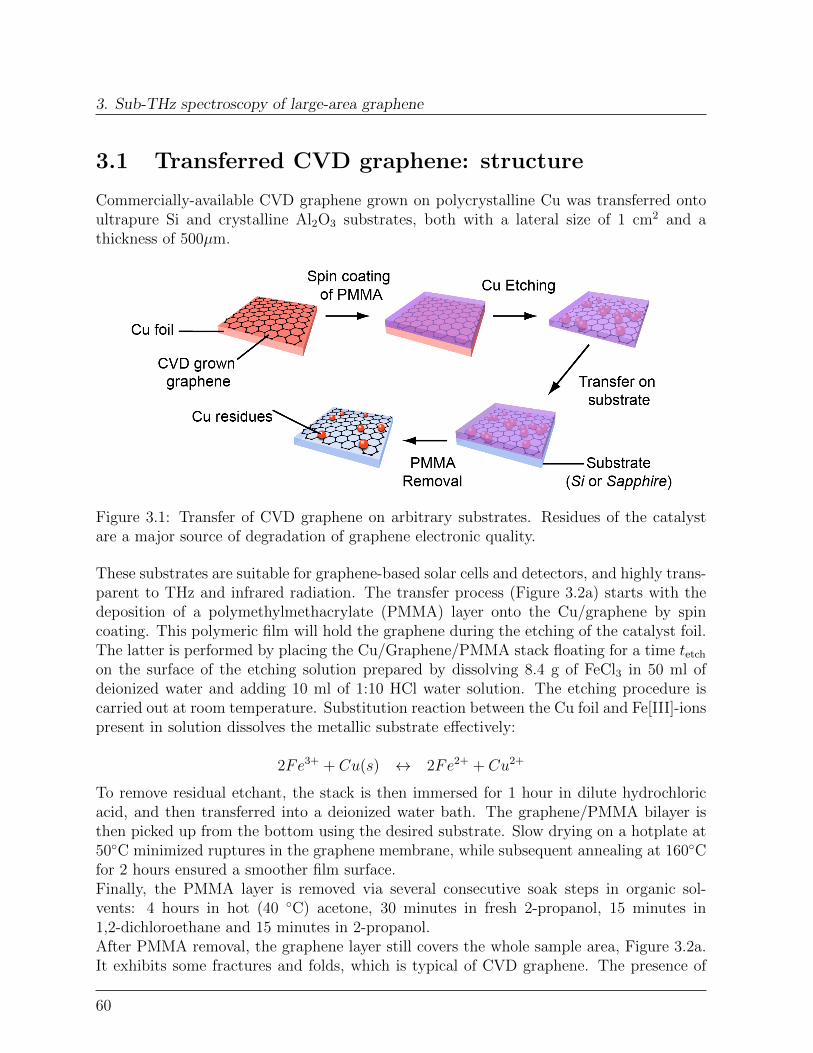
3. Sub-THz spectroscopy of large-area graphene
3.1 Transferred CVD graphene: structure
Commercially-available CVD graphene grown on polycrystalline Cu was transferred ontoultrapure Si and crystalline Al2O3 substrates, both with a lateral size of 1 cm2 and athickness of 500µm.
Figure 3.1: Transfer of CVD graphene on arbitrary substrates. Residues of the catalystare a major source of degradation of graphene electronic quality.
These substrates are suitable for graphene-based solar cells and detectors, and highly trans-parent to THz and infrared radiation. The transfer process (Figure 3.2a) starts with thedeposition of a polymethylmethacrylate (PMMA) layer onto the Cu/graphene by spincoating. This polymeric film will hold the graphene during the etching of the catalyst foil.The latter is performed by placing the Cu/Graphene/PMMA stack floating for a time tetch
on the surface of the etching solution prepared by dissolving 8.4 g of FeCl3 in 50 ml ofdeionized water and adding 10 ml of 1:10 HCl water solution. The etching procedure iscarried out at room temperature. Substitution reaction between the Cu foil and Fe[III]-ionspresent in solution dissolves the metallic substrate effectively:
2Fe3+ + Cu(s) ↔ 2Fe2+ + Cu2+
To remove residual etchant, the stack is then immersed for 1 hour in dilute hydrochloricacid, and then transferred into a deionized water bath. The graphene/PMMA bilayer isthen picked up from the bottom using the desired substrate. Slow drying on a hotplate at50C minimized ruptures in the graphene membrane, while subsequent annealing at 160Cfor 2 hours ensured a smoother film surface.Finally, the PMMA layer is removed via several consecutive soak steps in organic sol-vents: 4 hours in hot (40 C) acetone, 30 minutes in fresh 2-propanol, 15 minutes in1,2-dichloroethane and 15 minutes in 2-propanol.After PMMA removal, the graphene layer still covers the whole sample area, Figure 3.2a.It exhibits some fractures and folds, which is typical of CVD graphene. The presence of
60
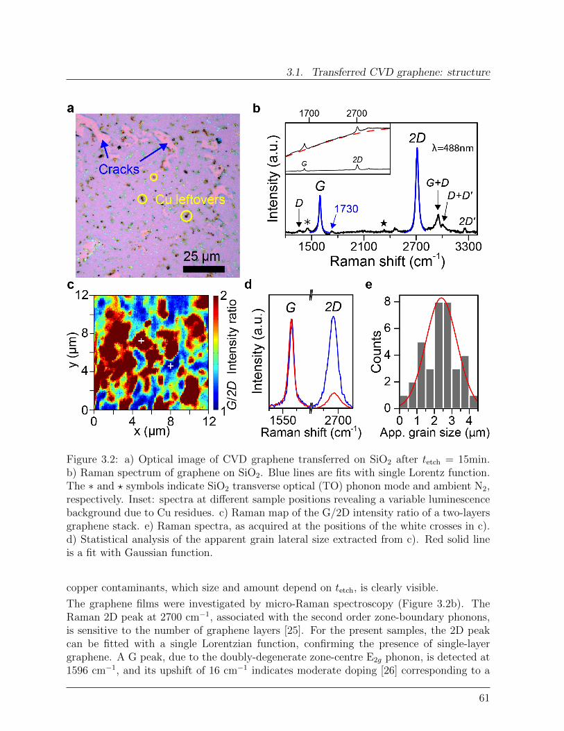
3.1. Transferred CVD graphene: structure
Figure 3.2: a) Optical image of CVD graphene transferred on SiO2 after tetch = 15min.b) Raman spectrum of graphene on SiO2. Blue lines are fits with single Lorentz function.The ∗ and ? symbols indicate SiO2 transverse optical (TO) phonon mode and ambient N2,respectively. Inset: spectra at different sample positions revealing a variable luminescencebackground due to Cu residues. c) Raman map of the G/2D intensity ratio of a two-layersgraphene stack. e) Raman spectra, as acquired at the positions of the white crosses in c).d) Statistical analysis of the apparent grain lateral size extracted from c). Red solid lineis a fit with Gaussian function.
copper contaminants, which size and amount depend on tetch, is clearly visible.
The graphene films were investigated by micro-Raman spectroscopy (Figure 3.2b). TheRaman 2D peak at 2700 cm−1, associated with the second order zone-boundary phonons,is sensitive to the number of graphene layers [25]. For the present samples, the 2D peakcan be fitted with a single Lorentzian function, confirming the presence of single-layergraphene. A G peak, due to the doubly-degenerate zone-centre E2g phonon, is detected at1596 cm−1, and its upshift of 16 cm−1 indicates moderate doping [26] corresponding to a
61

3. Sub-THz spectroscopy of large-area graphene
residual carrier density of ∼ 1012 cm−2. The very weak D peak at 1350 cm−1, connectedto the A1g breathing mode at the Brillouin zone boundary and only activated by thepresence of lattice defects, indicates very little disorder in the present sample and givesrise to additional combined modes in the upper part of the spectrum (see Section 4.1.3 formore details on Raman spectrum of graphene). A small peak at ∼ 1730 cm−1 is typicalof C=O stretching mode in PMMA residues [27]. Raman spectra acquired at differentpositions exhibit a variable background photoluminescence testifying the presence of Curesidues [28], inset in Figure 3.2b, as also confirmed by scanning electron microscopy.
CVD graphene grown on polycrystalline Cu foil, is composed of high quality crystallinegrains with random crystallographic orientations [4]. One way to reveal the CVD grainstructure is to exploit the Raman intensity dependence on the twist angle in a stackedtwo layers graphene system [29]. The two-layers stack was fabricated by first etchingboth graphene layers for 14hours and trasferred one on top of the other following theprocedure of Figure3.1. In order to maximize the interlayer interaction, the stack wasannealed in forming gas overnight at 400C after each graphene transfer. The differentcrystallographic orientations between the top and bottom layers modulates the interlayerinteraction between the domains. On this basis, monitoring the spatial distribution ofthe G/2D intensity ratio, enables probing the grain structure (Figure 3.2c, d). Statisticalanalysis (Figure 3.2e) yields an apparent grain size distribution peaked at 2.40 ± 0.13µmcorresponding to a mean grain size of ∼ 5µm for the single layer.
3.2 Sub-THz Mach-Zehnder spectrometry of graphene
For the optical investigations, we used a Mach-Zehnder interferometer-based spectrom-eter [30], Figure 3.3a, comprising backward-wave oscillators [30] as coherent sources ofcontinuous sub-THz radiation.
Their frequency can be continuously tuned between 0.03 and 1.5 THz, corresponding to 1 -50 cm−1, and 6 - 0.1 meV. The radiation is detected by either Golay cells or 4He-cooled Sibolometers. The frequency resolution ∆ν/ν is better than 10−5, and the dynamic range isbetween 40 and 50 dB. The Mach-Zehnder interferometric configuration enabled detectingboth amplitude and phase shift of the transmitted radiation, thus opening the possibility todetermine the complex electromagnetic response of graphene without involving Kramers-Kronig relations [31]. A round slit sets the beam diameter to 5 mm, so that severalgraphene domains are homogeneously irradiated. The plane-parallel undoped Si or Al2O3
substrates implemented a Fabry-Perot resonator formed by the graphene-substrate andsubstrate-air interfaces (Figure 3.3b). The resulting multiple reflections allow maximizingthe interaction of sub-THz radiation with graphene, and thus to significantly enhance thesensitivity. The electrodynamic response of the resulting multilayer was analysed usingthe Fresnel formulas [31], according to which the complex transmission tij and reflectionrij coefficients at each interface are given by:
62
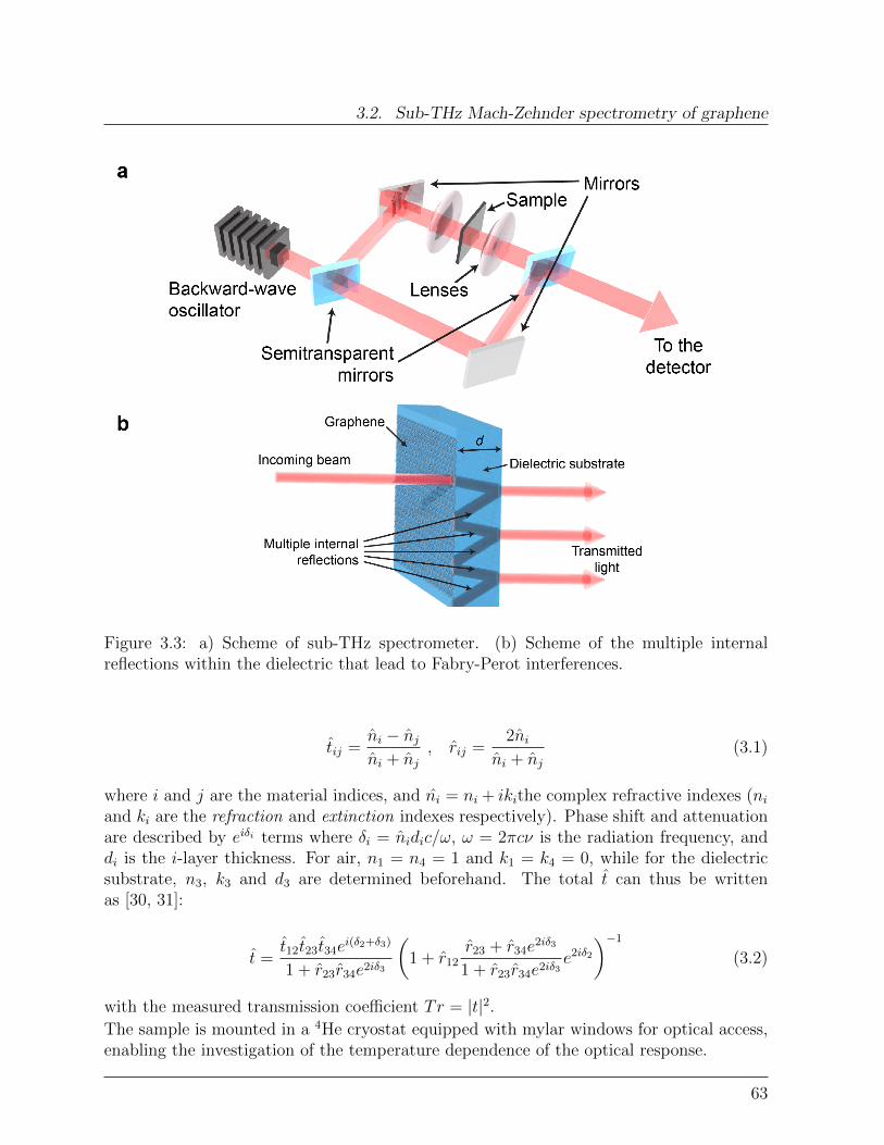
3.2. Sub-THz Mach-Zehnder spectrometry of graphene
Figure 3.3: a) Scheme of sub-THz spectrometer. (b) Scheme of the multiple internalreflections within the dielectric that lead to Fabry-Perot interferences.
tij =ni − njni + nj
, rij =2ni
ni + nj(3.1)
where i and j are the material indices, and ni = ni + ikithe complex refractive indexes (niand ki are the refraction and extinction indexes respectively). Phase shift and attenuationare described by eiδi terms where δi = nidic/ω, ω = 2πcν is the radiation frequency, anddi is the i-layer thickness. For air, n1 = n4 = 1 and k1 = k4 = 0, while for the dielectricsubstrate, n3, k3 and d3 are determined beforehand. The total t can thus be writtenas [30, 31]:
t =t12t23t34e
i(δ2+δ3)
1 + r23r34e2iδ3
(1 + r12
r23 + r34e2iδ3
1 + r23r34e2iδ3e2iδ2
)−1
(3.2)
with the measured transmission coefficient Tr = |t|2.
The sample is mounted in a 4He cryostat equipped with mylar windows for optical access,enabling the investigation of the temperature dependence of the optical response.
63
3. Sub-THz spectroscopy of large-area graphene
3.3 Effect of adsorbates on large-area graphene
Figure 3.4a compares the frequency dependence of the transmission coefficient for the bareSi substrate and four graphene samples transferred under the same conditions. Thicknessand refractive index of the dielectric substrate determine the period of the interferometricfringes [30], while the amplitude of the maxima gives the optical conductance of the sample.Phase shifts observable in the interference pattern of different graphene samples result fromsmall differences in the substrate thickness of about 25 µm. The latter does not affect theamplitude of the patterns, that are all equal and 30% smaller than those for the emptysubstrate. By fitting the spectra with equation (3.2), the graphene optical conductance Gwas obtained. The G values were corrected for the small but finite substrate absorption.
To explore the effect of contaminants and Cu residues on the electronic quality of graphene,we measured the optical conductance G for different tetch, Figure 3.4b, while keeping thePMMA layer on top (step 4 in Figure 3.2a). G is seen to increase monotonously with tetchreaching a saturation value of (2.3 ± 0.1) · 10−3Ω−1 after 14 hours. Moreover assuming aconstant graphene Fermi velocity vF = 106 m/s, illumination in the wavenumber range26 - 35 cm−1 is expected to induce a lateral carrier displacement l = vF
νbetween 1.3 and
1µm. Correspondingly, in order for an object to be non-transparent, its size must exceed∼ 1µm, which is well above the average size of molecular contaminants and Cu impuritiesalready at tetch > 15 min. This is further confirmed by the flat frequency dependence atlower wavenumbers (9 - 20 cm−1).
These observations show that Cu residues may contribute to the sample optical con-ductance only for very short tetch , while for long tetch , Cu residues behave as chargedscatterers, possibly together with other contaminants, degrading the electronic quality ofgraphene [32]. Increasing tetch, the amount of Cu impurities decreases and the electronicquality of pristine graphene is gradually approached.
Upon removal of the PMMA layer (step 5 in Figure 3.2a), the optical conductance decreasessharply to (1.0 ± 0.1) · 10−3Ω−1 (Figure 3.4c). As PMMA is fully transparent at thesefrequencies, this difference reveals the doping effect of a higher-κ dielectric environment.Air has a κ-value almost half that of PMMA (κair = 1, κPMMA ∼ 2.6); removal of the lattershifts the Fermi level closer to charge neutrality point, driving G toward the well-knownconductance minimum.
3.4 Electronic quality of large area graphene
The optical conductance of graphene is predicted to assume the universal value G0 =e2/4h = 6.1 · 10−5Ω−1 (with e the electron charge and h Plank’s constant) independentof frequency as an intrinsic property of massless Dirac fermions [33–35]. For the presentbare graphene (without PMMA) samples, a much higher conductance of approximatelyG ≈ 30G0 is detected at the lowest frequency, Figure 3.5a. Similarly large values havebeen observed at higher frequencies [18, 21, 36] and in time-resolved measurements [16, 19]
64

3.4. Electronic quality of large area graphene
Figure 3.4: Effect of Cu and PMMA leftovers a) Transmission spectra of a Si substratewithout (black) and with (colour) graphene/PMMA stack on top (tetch = 14 hours). Dif-ferent colours indicate different samples. b) Conductivity of graphene for different Cuetching time. The line is a guide to the eye. c) Comparison of transmission amplitudes forgraphene on Si, before (red) and after (blue) PMMA removal.
on large-area graphene. It is noteworthy that in contrast to previous works that use higherfrequencies [37], in our experiments the conductance is independent of the type of substrate.
The high value of G ≈ 30G0 suggests that the optical response of graphene at such lowfrequencies is notably affected by inhomogeneities and the finite temperature. In thiscontext, it is relevant that the dc conductance minimum of graphene at the Dirac pointis governed by extrinsic factors, most prominently the presence of charged impurities onthe substrate [38, 39] and residual Cu. In the present case, the carrier scattering that
65

3. Sub-THz spectroscopy of large-area graphene
arises from such impurities can be accounted for by the Drude model [30, 31] and com-plementing the sub-THz measurements with higher-frequency absorption data gained byFourier-transform spectroscopy. The combined frequency-dependence, displayed in Figure3.5a, is fitted with σ(ν) = σ0γ
2/(ν2 +γ2), where σ0 is the DC conductivity and γ is the car-rier scattering rate [30, 31]. The value of γ was found to be 270 cm−1 at high temperatureT , in agreement with previous reports [20, 21]. The T -dependence of γ, Figure 3.5b, showsa T -independent contribution below 100 K and a marked increase at higher frequencies,indicating two different scattering contributions. The first, associated with defects andcharged impurities, is the dominant factor limiting the conductance of graphene at lowtemperatures [38–40]. Fitting by a power dependence T β yielded β > 2, which cannot beattributed to scattering by longitudinal graphene phonons as this mechanism would affordβ = 1 [40]. Instead, such strong temperature dependence indicates scattering by substratephonons to be the dominant mechanism limiting G at high temperatures [41–43]. Theresidual γ = 86±1 cm−1 corresponds [21] to a concentration of scatterers of 3.4±0.5 · 1011
cm−2, in agreement with previous reports for CVD graphene [9, 20] and comparable totypical exfoliated graphene flakes at room temperature [44, 45].
The latter observation is a hint that grain boundaries do not represent the dominant sourceof scattering in these samples, as also suggested by transport measurements [4].
With the aim of determining the carrier mobility and compensate for the residual doping,we introduced a gate that allows tuning the graphene charge density n. To maintain thetransparency necessary for investigation at sub-THz energies, we fabricated the multilayerstructure depicted in Figure 3.5c. It is composed of a Al2O3 substrate, a 20 nm-thickNi:Cr alloy layer, with a d = 300 nm-thick e-gun evaporated SiO2 layer serving as gatedielectric on top of which the CVD graphene is transferred. The Ni:Cr alloy was chosenbecause it forms closed, electrically conducting thin films of sufficient high transparency inthe sub-THz range. The resulting device has an overall transmission coefficient of 0.15 inthe 9− 20cm−1 range. The gate voltage Vgate is applied between graphene, contacted withAu/Cr contacts, and the Ni:Cr layer.
The optical conductance at 9 cm−1 recorded as a function of gate voltage is shown inFigure 3.5d. The characteristic minimum at Vgate 6= 0 indicates the Dirac point. Similar todc electrical transport measurements, the Vgate- dependence exhibited hysteretic behaviourunder ambient conditions, owing to polar impurities and adsorbed water [46]. The ρ vs.Vgate curve reveals a pronounced electron-hole asymmetry at high carrier densities. As thepresent contact-less technique is not affected by work-function mismatch at the electricalcontacts like in dc transport studies [47], it follows that in graphene charge impurities havedifferent scattering cross-sections for electrons and holes [48]. As discussed in Section 2.3,fitting with [49]:
R(Vgate) = RS +
(eµc
√n2
0 + n(Vgate)2
)−1
(3.3)
yields a mobility of µe = (4.5± 0.5) · 104 cm2V−1s−1 for electrons and µh = (4.7± 0.7) · 104
cm2V−1s−1 for holes, (RS is the short-range scattering contribution to resistance, n0 the
66

3.4. Electronic quality of large area graphene
Figure 3.5: a) Frequency-dependence of the graphene conductance at two different tem-peratures on Al2O3 substrate. Lines are fits using the Drude model. b) Temperaturedependence of the carriers scattering rate, as extracted from the Drude fits. The solid lineis a simulation of the T β dependence for different β. Dashed line, β = 1, indicates electron-extrinsic phonons scattering. c) Structure of the THz-transparent multilayer structure forthe optical characterization of the n-dependence of the conductance. d) Gate dependenceof the optical behaviour at 300 K recorded at 9 cm−1 (red and blue are different sweeps),showing: (left) G vs. n, (right) resistance vs. Vgate. Lines are fits to the data. The dashedblack line indicates 4e2/h.
67

3. Sub-THz spectroscopy of large-area graphene
residual carrier density at the charge-neutrality point due to electron-hole puddles [50] and
n =ε0κSiO2
edVgate where ε0 is the vacuum permittivity and κSiO2 = 3.9).
The extracted mobilities are one to two orders of magnitude higher than those typicallyderived from dc measurements of CVD graphene on SiO2 [7, 51] while they closely matchthose of clean exfoliated flakes [9] or single-grain CVD crystals [8]. This finding supports theconclusion that sub-THz optical detection probes the intrinsic conductance of the domainsthat constitute the CVD layer, as expected from the fact that at 9cm−1 it induces electronicoscillations over lengths l ∼ 5µm, below the average domain size in CVD graphene. Itfollows that the observed mobilities are limited by surface-scatterers, analogous to other,solid-supported graphene sheets.Contact effects, which play a significant role in dc transport measurements [47], certainlydo not affect the conductance determined by optical means. Hence, the density of chargedlong-range scatterers can be estimated [38] close to the Dirac point. From the two branchesof the curve, values of (7 ± 2) · 1010 cm−2 and (9.5 ± 1) · 1010 cm−2 are extracted, whichare only slightly lower than estimated above from the T -dependence of γ. Comparisonwith electrical transport experiments on large CVD surfaces indicates that crystal defectscontribute a density of ∼ 102 cm−2 to short range scattering.Importantly, the applied gate voltage allows compensating for the extrinsic doping bycharged impurities, yielding a condactance of G ≈ 4G0, much lower than previously re-ported [16, 18, 19]. This provides further support that larger conductance values arise fromextrinsic doping (i.e. Cu and molecular contaminants or surface charges).
3.5 Conclusions
In conclusion, we demonstrated that the electronic response of individual domains inwafer-sized CVD graphene can be directly addressed by using contact-less sub-THz in-terferometry. Moreovere, this thechnique allows to quantify the graphene intrinsic opticalconductance, validating important theoretical predictions. The mobility values measuredin contact-less fashion, are orders of magnitude larger than those obtained on equivalentCVD graphene, by traditional dc transport measurements [7, 51], matching values ob-tained for high-quality samples [8, 9, 45, 51]. The mobility is found to be mainly limitedby charged scatterers on the substrate, and our observations validate previous theoreticalpredictions [38]. The high sensitivity of the sub-THz response to contaminants can be usedto address the electronic quality of large graphene structures, essential for applications intouchscreens, wearable and optoelectronic devices. The Cu contamination of both sur-faces of the graphene layer, as observed here, is an important result for device fabrication,showing that adequate treatment is required for complete removal of the catalyst.
68
Bibliography
Bibliography
[1] Tsen, A. W. et al. Tailoring electrical transport across grain boundaries in polycrys-talline graphene. Science 336, 1143–6 (2012).
[2] Lahiri, J., Lin, Y., Bozkurt, P., Oleynik, I. I. & Batzill, M. An extended defect ingraphene as a metallic wire. Nature Nanotechnology 5, 326–329 (2010).
[3] Ni, G.-X. et al. Quasi-Periodic Nanoripples in Graphene Grown by Chemical VaporDeposition and Its Impact on Charge Transport. ACS Nano 6, 1158–1164 (2012).
[4] Huang, P. Y. et al. Grains and grain boundaries in single-layer graphene atomicpatchwork quilts. Nature 469, 389–392 (2011).
[5] Liang, X. et al. Toward clean and crackless transfer of graphene. ACS Nano 5,9144–9153 (2011).
[6] Reina, A. et al. Large Area, Few-Layer Graphene Films on Arbitrary Substrates byChemical Vapor Deposition. Nano Letters 9, 30–35 (2009).
[7] Li, X. et al. Graphene Films with Large Domain Size by a Two-Step Chemical VaporDeposition Process. Nano Letters 10, 4328–4334 (2010).
[8] Petrone, N. et al. Chemical vapor deposition-derived graphene with electrical perfor-mance of exfoliated graphene. Nano letters 12, 2751–6 (2012).
[9] Li, X. et al. Large-area synthesis of high-quality and uniform graphene films on copperfoils. Science 324, 1312–4 (2009).
[10] Pi, K. et al. Electronic doping and scattering by transition metals on graphene. Phys.Rev. B 80, 75406 (2009).
[11] McCreary, K. M. et al. Effect of cluster formation on graphene mobility. Phys. Rev.B 81, 115453 (2010).
[12] Docherty, C. J. & Johnston, M. B. Terahertz properties of graphene. Journal ofInfrared, Millimeter, and Terahertz Waves 33, 797–815 (2012).
[13] Jnawali, G., Rao, Y., Yan, H. & Heinz, T. F. Observation of a transient decrease interahertz conductivity of single-layer graphene induced by ultrafast optical excitation.Nano Letters 13, 524–530 (2013).
[14] Shi, S. F. et al. Controlling graphene ultrafast hot carrier response from metal-like tosemiconductor-like by electrostatic gating. Nano Letters 14, 1578–1582 (2014).
[15] Frenzel, a. J. et al. Observation of suppressed terahertz absorption in photoexcitedgraphene. Applied Physics Letters 102, 1–5 (2013).
69
Bibliography
[16] Tomaino, J. L. et al. Terahertz imaging and spectroscopy of large-area single-layergraphene. Optics express 19, 141–146 (2011).
[17] Maeng, I. et al. Gate-controlled nonlinear conductivity of Dirac fermion in graphenefield-effect transistors measured by terahertz time-domain spectroscopy. Nano Letters12, 551–555 (2012).
[18] Horng, J. et al. Drude conductivity of Dirac fermions in graphene. Phys. Rev. B 83,165113 (2011).
[19] Ren, L. et al. Terahertz and infrared spectroscopy of gated large-area graphene. Nanoletters 12, 3711–5 (2012).
[20] Li, Z. Q. et al. Dirac charge dynamics in graphene by infrared spectroscopy. Nat.Phys. 4, 532–535 (2008).
[21] Yan, H. et al. Infrared Spectroscopy of Wafer-Scale Graphene. ACS Nano 5, 9854–9860 (2011).
[22] Kim, J. Y. et al. Far-infrared study of substrate-effect on large scale graphene. AppliedPhysics Letters 98, 10–13 (2011).
[23] Docherty, C. J. et al. Extreme sensitivity of graphene photoconductivity to environ-mental gases. Nat. Commun. 3, 1228 (2012).
[24] Liu, F., Chong, Y. D., Adam, S. & Polini, M. Gate-tunable coherent perfect absorptionof terahertz radiation in graphene. 2D Materials 1, 031001 (2014).
[25] Ferrari, A. C. et al. Raman spectrum of graphene and graphene layers. PhysicalReview Letters 97, 187401 (2006).
[26] Casiraghi, C., Pisana, S., Novoselov, K. S., Geim, A. K. & Ferrari, A. C. Ramanfingerprint of charged impurities in graphene. Applied Physics Letters 91, 233108(2007).
[27] Wang, Q. H. et al. Understanding and controlling the substrate effect on grapheneelectron-transfer chemistry via reactivity imprint lithography. Nat. Chem. 4, 724–32(2012).
[28] Costa, S. D. et al. Resonant Raman spectroscopy of graphene grown on copper sub-strates. Solid State Communications 152, 1317–1320 (2012).
[29] Havener, R. W., Zhuang, H., Brown, L., Hennig, R. G. & Park, J. Angle-resolvedraman imaging of interlayer rotations and interactions in twisted bilayer graphene.Nano Letters 12, 3162–3167 (2012).
[30] Gorshunov, B. et al. Terahertz BWO-Spectrosopy. International Journal of Infraredand Millimeter Waves 26, 1217–1240 (2005).
70

Bibliography
[31] Pracht, U. S. et al. Electrodynamics of the superconducting state in ultra-thin films atTHz frequencies. IEEE Transactions on Terahertz Science and Technology 3, 269–280(2013).
[32] Kretinin, a. V. et al. Electronic properties of graphene encapsulated with differenttwo-dimensional atomic crystals. Nano Letters 14, 3270–3276 (2014).
[33] Mishchenko, E. G. Effect of Electron-Electron Interactions on the Conductivity ofClean Graphene. Phys. Rev. Lett. 98, 216801 (2007).
[34] Stauber, T., Peres, N. M. R. & Castro Neto, A. H. Conductivity of suspended andnon-suspended graphene at finite gate voltage. Phys. Rev. B 78, 85418 (2008).
[35] Nair, R. R. et al. Fine structure constant defines visual transparency of graphene.Science 320, 1308 (2008).
[36] Mak, K. F. et al. Measurement of the Optical Conductivity of Graphene. Phys. Rev.Lett. 101, 196405 (2008).
[37] Scharf, B., Perebeinos, V., Fabian, J. & Avouris, P. Effects of optical and surfacepolar phonons on the optical conductivity of doped graphene. Phys. Rev. B 87, 1–9(2013).
[38] Adam, S., Hwang, E. H., Galitski, V. M. & Das Sarma, S. A self-consistent theoryfor graphene transport. Proceedings of the National Academy of Sciences 104, 18392(2007).
[39] Morozov, S. V. et al. Giant intrinsic carrier mobilities in graphene and its bilayer.Phys. Rev. Lett. 100, 16602 (2008).
[40] Hwang, E. & Das Sarma, S. Screening-induced temperature-dependent transport intwo-dimensional graphene. Phys. Rev. B 79, 165404 (2009).
[41] Castro, E. V. et al. Limits on Charge Carrier Mobility in Suspended Graphene dueto Flexural Phonons. Phys. Rev. Lett. 105, 266601 (2010).
[42] Hwang, E. H. & Das Sarma, S. Acoustic phonon scattering limited carrier mobilityin two-dimensional extrinsic graphene. Phys. Rev. B 77, 115449 (2008).
[43] Mariani, E. & von Oppen, F. Temperature-dependent resistivity of suspendedgraphene. Phys. Rev. B 82, 195403 (2010).
[44] Kim, K. S. K. S. et al. Large-scale pattern growth of graphene films for stretchabletransparent electrodes. Nature 457, 706–710 (2009).
[45] Novoselov, K. S. et al. Two-dimensional gas of massless Dirac fermions in graphene.Nature 438, 197–200 (2005).
71
Bibliography
[46] Kim, W. et al. Hysteresis Caused by Water Molecules in Carbon Nanotube Field-Effect Transistors. Nano Letters 3, 193–198 (2003).
[47] Huard, B., Stander, N., Sulpizio, J. A. & Goldhaber-Gordon, D. Evidence of the roleof contacts on the observed electron-hole asymmetry in graphene. Phys. Rev. B 78,121402 (2008).
[48] Novikov, D. S. Numbers of donors and acceptors from transport measurements ingraphene. Applied Physics Letters 91, 102102 (2007).
[49] Kim, S. et al. Realization of a high mobility dual-gated graphene field-effect transistorwith Al2O3 dielectric. Applied Physics Letters 94, 62107 (2009).
[50] Martin, J. et al. Observation of electron-hole puddles in graphene using a scanningsingle-electron transistor. Nature Physics 4, 144–148 (2008).
[51] Geim, A. K. & Novoselov, K. S. The rise of graphene. Nat. Mater. 6, 183–191 (2007).
72
Part I
Single Molecule Magnets-Graphenehybrids
73


Chapter 4
Creation of Graphene functionalstructures
Being graphene an all-surface open material, the self-assembly of supramolecular architec-tures on its surface [1–8] can be used to tailor graphene electronic and magnetic proper-ties. [9–16]. Here we explore the possibility to modify the graphene magnetic propertiesby combining it with single-molecule magnets (SMMs) [17–22]. Owing to the SMMs mag-netic and quantum features [23, 24], such hybrid material is interesting for the study ofenvironmental spin-interactions in carbon-based materials [25–30]. The theoretical and ex-perimental investigations presented in the following chapters demonstrate that controllingthe aggregation and surface organization of SMMs on graphene is essential to rationallydesign the magnetic behavior of the SMM-graphene hybrids. In this framework, it is thusvery important to understand the assembly regimes and associated parameters, and explorethe possibility of induce changes in the sopramolecular arrangement on the surface. Up tonow, little is known on how SMM-graphene hybrids are formed and the major factors thatgovern molecular assembly on graphene remain yet to be unraveled.
4.1 Identification of single layer graphene
4.1.1 Exfoliated graphene
The most common and easy procedure to produce graphene is the so-called microme-chanical cleavage of graphite (Figure 4.1) [31]. In this procedure, graphene layers arecleaved directly from a piece of graphite using a common adesive tape. The tape is subse-quently pressed onto a Silicon substrate with a 300 nm-thick oxide layer thermally grownon top. This SiO2 thickness is found to give the highest optical contrast, making singlelayer graphene visible using an optical microscope (Figure 4.1c) [32].
75
4. Creation of Graphene functional structures
Figure 4.1: a) Transfer of exfoliated graphene to a SiO2/Si substrate mapped with Au/Timarkers. b) Optical image of the substrate showing several graphitic residues. c) Zoom-inof a multilayer graphene stack.
76
4.1. Identification of single layer graphene
4.1.2 Microscopy
The sample is then carefully scanned at 50x magnification to identify and locate monolayergraphene, Figure 4.1a. This method produces graphene flakes with an average lateral sizeof 10 - 20 micrometers and of extremely high crystalline quality. The flakes are randomlydistributed on the substrate and often surrounded by thicker graphitic residues, Figure4.1b. For this reason, the substrates are pre-patterned with a map of Ti/Au markes tohelp to locate the suitable flakes and to enable accurate alignment during the lithographicprocess, Figure 4.1c. The properties of graphene change drastically with the number oflayers [33–37], it is thus important to correctly determine the layers number prior to anyexperiment.
Figure 4.2: Single layer graphene a) Intensity profile with a green filter helps determiningthe number of layers. b) The apparent AFM height profile of graphene is altered by thesubstrate roughness and by the presence of organic residues on it (small white spots).
77

4. Creation of Graphene functional structures
In these regards, the intensity profile in the green channel, [32, 36] of the optical pictureprovides good hints about the number of layers constituting the flake, Figure 4.2a .The finite substrate roughness and the presence of contaminants at the substrate/grapheneinterface affect the flake edge profile as acquired with an atomic force microscope (AFM),Figure 4.2b. As a consequence, the apparent single-layer thickness is often found to be inthe range ∼ 1−2 nm instead of the nominal graphene thickness (0.3 A as determined fromdiffraction measurements on graphite).
4.1.3 Raman Spectroscopy
Raman spectroscopy [38] is an important tool for the characterization of graphene andcarbon-based materials in general [39]. It provides important information about structuralmodifications and extrinsic doping and constitutes a fast and reliable method to quantifythe number of graphene layers.
Figure 4.3: Evolution of the Raman spectrum with the number of graphene layers. a) Com-parison between monolayer, bilayer and graphite. b) Shape of the 2D peak for single andbilayer graphene. Red lines are fitting with Lorentzian line shapes. Monolayer graphenegives rise to a single Lorentzian contribution whereas bilayer shows four contributions dueto interlayer interaction (Blue lines).
The Raman spectrum of graphene is relatively simple [40, 41], Figure 4.4. It exhibits
78
4.1. Identification of single layer graphene
a G peak at ∼1580 cm−1 and a 2D band at ∼2700 cm−1. The G peak arises from thedoubly-degenerate zone center E2g mode while the 2D band is due to a second order processinvolving zone-boundary phonons. The shape of the latter is sensitive to the number ofgraphene layers, Figure 4.3. For single-layer graphene the 2D peak is a single Lorentziancontribution, while for bilayer it is composed of four contributions reflecting the splittingof the π, π∗ bands in four bands due to the interlayer interaction.
Both G and 2D peaks are sensitive to extrinsic doping. The G band up-shifts (stiffens)and becomes narrower for both n- and p-doping [42, 43] while the 2D band discriminatesbetween holes and electron dopings, upshifting for the former and softening for the latter.
Figure 4.4: Raman spectrum of high quality single layer graphene (bottom) and defectedgraphene (top).
Raman spectrum of graphene is modulated by structural modifications such as the presenceof defects or dimensional confinement. In the first case, the presence of inter-valley scat-tering sites makes the A1g breathing mode at the Brillouin zone boundary Raman activeto the first order, leading to the appearance of an additional peak at ∼1350 cm−1 calledD [44].
The I(D)/I(G) intensity ratio can be used as a measure of the defects concentration inthe flakes using the empirical Tunstra-konig relation [45, 46]:
I(D)
I(G)= C(λ)/L2
D (4.1)
79
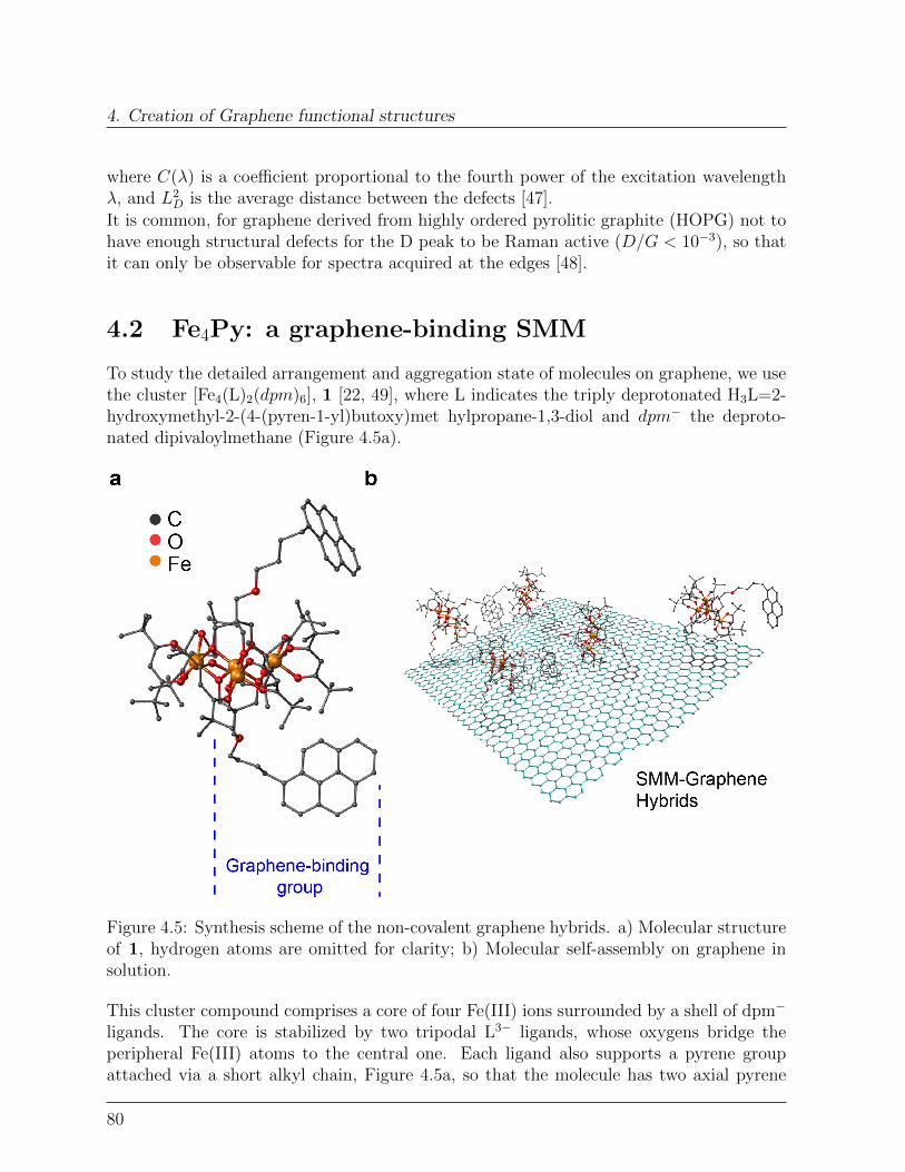
4. Creation of Graphene functional structures
where C(λ) is a coefficient proportional to the fourth power of the excitation wavelengthλ, and L2
D is the average distance between the defects [47].It is common, for graphene derived from highly ordered pyrolitic graphite (HOPG) not tohave enough structural defects for the D peak to be Raman active (D/G < 10−3), so thatit can only be observable for spectra acquired at the edges [48].
4.2 Fe4Py: a graphene-binding SMM
To study the detailed arrangement and aggregation state of molecules on graphene, we usethe cluster [Fe4(L)2(dpm)6], 1 [22, 49], where L indicates the triply deprotonated H3L=2-hydroxymethyl-2-(4-(pyren-1-yl)butoxy)met hylpropane-1,3-diol and dpm− the deproto-nated dipivaloylmethane (Figure 4.5a).
Figure 4.5: Synthesis scheme of the non-covalent graphene hybrids. a) Molecular structureof 1, hydrogen atoms are omitted for clarity; b) Molecular self-assembly on graphene insolution.
This cluster compound comprises a core of four Fe(III) ions surrounded by a shell of dpm−
ligands. The core is stabilized by two tripodal L3− ligands, whose oxygens bridge theperipheral Fe(III) atoms to the central one. Each ligand also supports a pyrene groupattached via a short alkyl chain, Figure 4.5a, so that the molecule has two axial pyrene
80
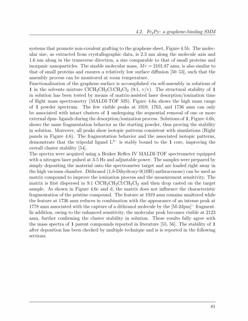
4.2. Fe4Py: a graphene-binding SMM
systems that promote non-covalent grafting to the graphene sheet, Figure 4.5b. The molec-ular size, as extracted from crystallographic data, is 2.3 nm along the molecule axis and1.6 nm along in the transverse direction, a size comparable to that of small proteins andinorganic nanoparticles. The sizable molecular mass, Mr = 2101.87 amu, is also similar tothat of small proteins and ensures a relatively low surface diffusion [50–53], such that theassembly process can be monitored at room temperature.Functionalization of the graphene surface is accomplished via self-assembly in solutions of1 in the solvents mixture ClCH2CH2Cl:CH2Cl2 (9:1, v/v). The structural stability of 1in solution has been tested by means of matrix-assisted laser desorption/ionization timeof flight mass spectrometry (MALDI-TOF MS). Figure 4.6a shows the high mass rangeof 1 powder spectrum. The few visible peaks at 1919, 1763, and 1736 amu can onlybe associated with intact clusters of 1 undergoing the sequential removal of one or moreexternal dpm- ligands during the desorption/ionization process. Solutions of 1, Figure 4.6b,shows the same fragmentation behavior as the starting powder, thus proving the stabilityin solution. Moreover, all peaks show isotopic patterns consistent with simulations (Rightpanels in Figure 4.6). The fragmentation behavior and the associated isotopic patterns,demonstrate that the tripodal ligand L3− is stably bound to the 1 core, improving theoverall cluster stability [54].The spectra were acquired using a Bruker Reflex IV MALDI-TOF spectrometer equippedwith a nitrogen laser pulsed at 3-5 Hz and adjustable power. The samples were prepared bysimply depositing the material onto the spectrometer target and are loaded right away inthe high vacuum chamber. Dithranol (1,8-Dihydroxy-9(10H)-anthracenone) can be used asmatrix compound to improve the ionization process and the measurement sensitivity. Thematrix is first dispersed in 9:1 ClCH2CH2Cl:CH2Cl2 and then drop casted on the targetsample. As shown in Figure 4.6c and d, the matrix does not influence the characteristicfragmentation of the pristine compound. The feature at 1919 amu remains unaltered whilethe feature at 1736 amu reduces in combination with the appearance of an intense peak at1778 amu associated with the capture of a dithranol molecule by the [M-2dpm]− fragment.In addition, owing to the enhanced sensitivity, the molecular peak becomes visible at 2123amu, further confirming the cluster stability in solution. These results fully agree withthe mass spectra of 1 parent compounds reported in literature [55, 56]. The stability of 1after deposition has been checked by multiple technique and is is reported in the followingsections.
81
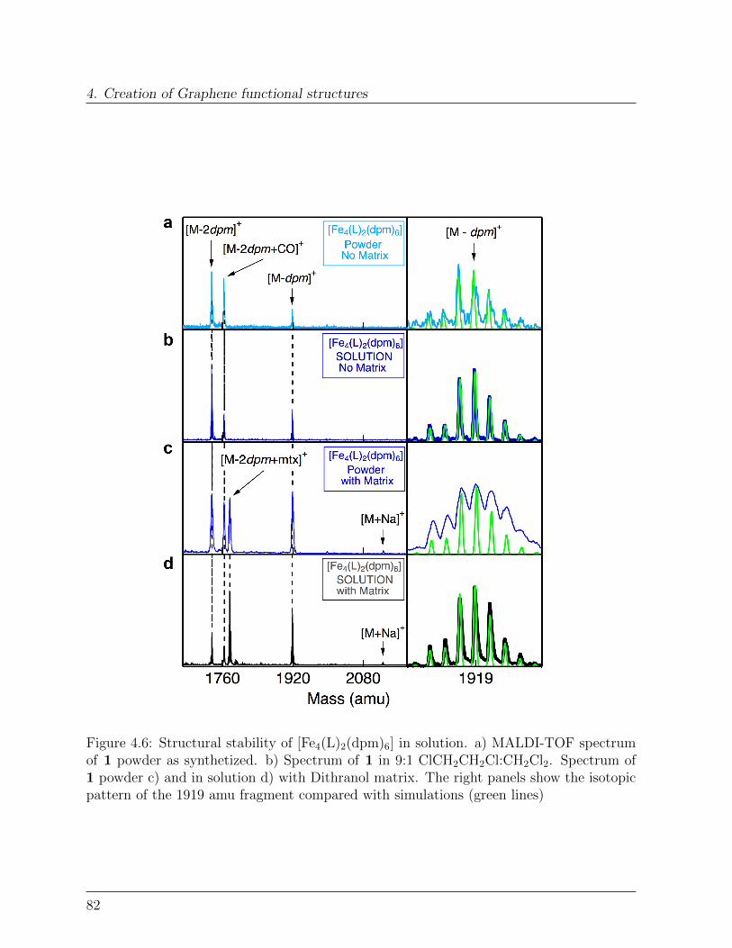
4. Creation of Graphene functional structures
Figure 4.6: Structural stability of [Fe4(L)2(dpm)6] in solution. a) MALDI-TOF spectrumof 1 powder as synthetized. b) Spectrum of 1 in 9:1 ClCH2CH2Cl:CH2Cl2. Spectrum of1 powder c) and in solution d) with Dithranol matrix. The right panels show the isotopicpattern of the 1919 amu fragment compared with simulations (green lines)
82
4.3. Molecular self-assembly on graphene
4.3 Molecular self-assembly on graphene
4.3.1 Topography of SMMs on graphene
Figure 4.7: Graphene-SMM hybrids. a) Synthesis of graphene-SMMs hybrids by liquid-phase grafting. b) Graphene surface before functionalization. c) Randomly-distributedSMMs islands on graphene after grafting of 1. d) Graphene profile height before (black)and after (red) functionalization (C = 2.5 · 10−10 M). e) The narrow distribution of islandheights is centered at the molecular size.
83

4. Creation of Graphene functional structures
Single-layer graphene flakes are obtained by mechanical exfoliation of natural graphite [31].The flakes are transferred onto Si substrates with a 300 nm thick SiO2 upperlayer. Molec-ular assembly is achieved by immersing the substrates in a solution of 1 (concentration C )in ClCH2CH2Cl:CH2Cl2 (9:1, v/v) at room temperature. After a deposition time t, thesamples are rinsed with pure solvent mixture, followed by isopropanol, and dried under Arjet.
Figure 4.8: Selective molecular decoration of the graphene surface a) AFM topographicimages of exfoliated graphene as transferred on SiO2 b) after (right column) non-covalentfunctionalization with 1, performed at different concentrations C.
Marker structures on the substrate enable the inspection of the same graphene flake beforeand after decoration by 1, Figure 4.5b. Tapping-mode atomic force microscopy (AFM)before and after deposition of 1 reveals highly selective functionalization of the graphenesurface with respect to the SiO2 one, Figure 4.8, with only minimal grafting appearing onthe SiO2 surface even for the highest concentrations.
The images are acquired employing a Veeco Dimension Icon atomic force microscope andhigh resolution Olympus OMCL-AC200TS-R3 Silicon tips. The nominal tips radius is 7nm and the cantilever free resonance frequency is 150 kHz. The tips have a tetrahedralshape with 0 tilt angle for the retrace that greatly reduces the convolution error on thelateral size of the imaged objects [57, 58]. Scan rate is 1 Hz and each image contains 1024points and 1024 lines. The selectivity of the pyrene groups for the conjugated structureof graphene can be quantified by considering the surface roughness Ra, i.e. the meandeviation of the AFM profile Z(x) within a sampling length L:
84
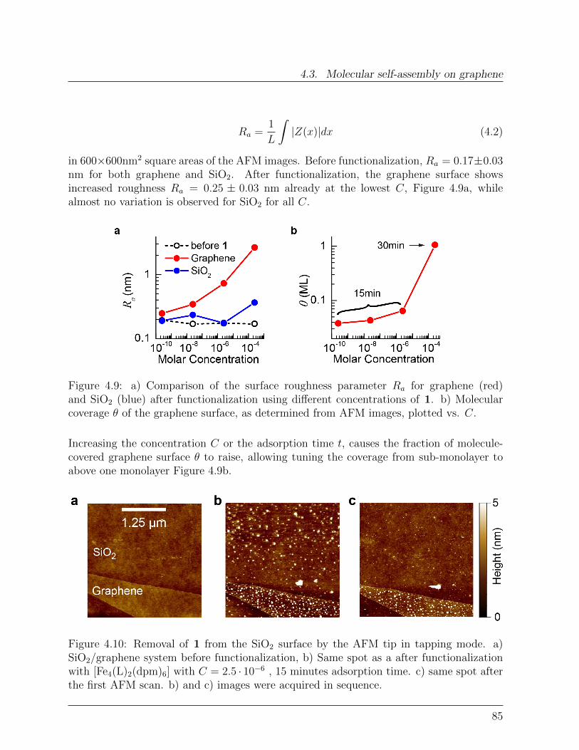
4.3. Molecular self-assembly on graphene
Ra =1
L
∫|Z(x)|dx (4.2)
in 600×600nm2 square areas of the AFM images. Before functionalization, Ra = 0.17±0.03nm for both graphene and SiO2. After functionalization, the graphene surface showsincreased roughness Ra = 0.25 ± 0.03 nm already at the lowest C, Figure 4.9a, whilealmost no variation is observed for SiO2 for all C.
Figure 4.9: a) Comparison of the surface roughness parameter Ra for graphene (red)and SiO2 (blue) after functionalization using different concentrations of 1. b) Molecularcoverage θ of the graphene surface, as determined from AFM images, plotted vs. C.
Increasing the concentration C or the adsorption time t, causes the fraction of molecule-covered graphene surface θ to raise, allowing tuning the coverage from sub-monolayer toabove one monolayer Figure 4.9b.
Figure 4.10: Removal of 1 from the SiO2 surface by the AFM tip in tapping mode. a)SiO2/graphene system before functionalization, b) Same spot as a after functionalizationwith [Fe4(L)2(dpm)6] with C = 2.5 · 10−6 , 15 minutes adsorption time. c) same spot afterthe first AFM scan. b) and c) images were acquired in sequence.
85
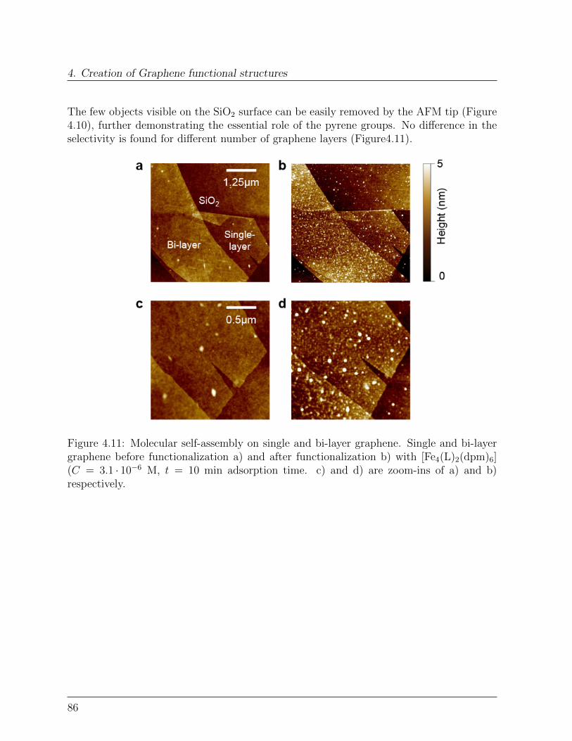
4. Creation of Graphene functional structures
The few objects visible on the SiO2 surface can be easily removed by the AFM tip (Figure4.10), further demonstrating the essential role of the pyrene groups. No difference in theselectivity is found for different number of graphene layers (Figure4.11).
Figure 4.11: Molecular self-assembly on single and bi-layer graphene. Single and bi-layergraphene before functionalization a) and after functionalization b) with [Fe4(L)2(dpm)6](C = 3.1 · 10−6 M, t = 10 min adsorption time. c) and d) are zoom-ins of a) and b)respectively.
86

4.3. Molecular self-assembly on graphene
4.3.2 Dynamic scaling behavior
To evaluate the molecular assembly process, we increase C while keeping the depositiontime constant t = 15min, Figure 4.12a.
Figure 4.12: Evolution of the 2D autocorrelation function h(x, y) with increasing C. a)600× 600 nm images from which 〈h〉 is extracted. b) 2D autocorrelation function 〈h〉. c)Autocorrelation function profile.
The two-dimensional autocorrelation 〈h〉 of the AFM height profile h(x, y):
〈h〉 =
∫ ∫ +∞
−∞h(x, y)h(x+X, y + Y )dxdy (4.3)
andN the density of molecular islands per adsorption site, Figure 4.12b,c and 4.13a indicatetwo distinct assembly regimes: one below and one above C ≈ 2.5 · 10−8 M, Figure 4.13a.The single peak in h(x, y) indicates randomly-placed objects, Figure 4.12b,c. Althoughlong-range ordering is absent, as expected for weak π − π grafting, there is a hint ofhexagonal structuring around C = 2.5 · 10−8 M, Figure 4.12b,c, suggesting a weak templateeffect of the graphene lattice.The islands height distribution peaks around the molecular size, Figure 4.13b suggestingthat molecules deposited on top of an existing island migrate towards the island edgesfavoring lateral island growth rather than three-dimensional structures.For C < 2.5 · 10−8 M, N increases only slightly over a range of C of several orders ofmagnitude, this indicates that newly adsorbed molecules aggregate to existing islands andnucleation of new stable islands is rare.The assembly behavior can be modeled in the framework of dynamic scaling theory [59–62],already employed for epitaxial [52, 53] and molecular assemblies on surfaces [57, 63–65]. Itinvolves two processes with characteristic rates: the first is the deposition rate F , associatedwith the adsorption of new molecular islands from solution; the second is the diffusion
87

4. Creation of Graphene functional structures
Figure 4.13: Self-assembly on graphene a) Concentration dependence of the density ofislands N per adsorption site (top) and the island average height h (bottom). Lines areguides to the eye. c) Island height distribution for different C (red).
coefficient D, related to aggregation into stable molecular islands, followed by coalescenceinto larger islands, Figure 4.14.
Figure 4.14: Self-assembly process. Molecules are deposited (1) with rate F (dependenton C). Once adsorbed (2), molecules diffuseon the graphene surface (3) with ”diffusivity”D. Diffusion leads to aggregation of molecular islands (4).
The kinetics of the self-assembly process depends on several factors such as the details ofthe undelying lattice (i.e. symmetry, lattice constant, insulator/metallic character), thebinding groups that impart intermolecular and molecule-substrate interactions, as well as
88
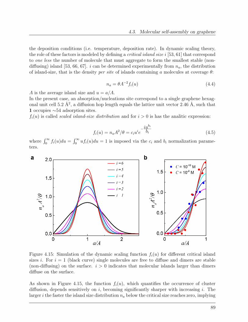
4.3. Molecular self-assembly on graphene
the deposition conditions (i.e. temperature, deposition rate). In dynamic scaling theory,the role of these factors is modeled by defining a critical island size i [53, 61] that correspondto one less the number of molecule that must aggregate to form the smallest stable (non-diffusing) island [53, 66, 67]. i can be determined experimentally from na, the distributionof island-size, that is the density per site of islands containing a molecules at coverage θ:
na = θA−2fi(u) (4.4)
A is the average island size and u = a/A.In the present case, an absorption/nucleations site correspond to a single graphene hexag-onal unit cell 5.2 A2, a diffusion hop length equals the lattice unit vector 2.46 A, such that1 occupies ∼54 adsorption sites.fi(u) is called scaled island-size distribution and for i > 0 is has the analitic expression:
fi(u) = naA2/θ = ciu
ie−iu
bi
bi (4.5)
where∫∞
0fi(u)du =
∫∞0ufi(u)du = 1 is imposed via the ci and bi normalization parame-
ters.
Figure 4.15: Simulation of the dynamic scaling function fi(u) for different critical islandsizes i. For i = 1 (black curve) single molecules are free to diffuse and dimers are stable(non-diffusing) on the surface. i > 0 indicates that molecular islands larger than dimersdiffuse on the surface.
As shown in Figure 4.15, the function fi(u), which quantifies the occurrence of clusterdiffusion, depends sensitively on i, becoming significantly sharper with increasing i. Thelarger i the faster the island size distribution na below the critical size reaches zero, implying
89

4. Creation of Graphene functional structures
that larger islands are mobile on the surface. For i = 1 single molecules diffuse freely onthe surface and the merging of two molecules creates a stable non-diffusing dimer thatbehaves as nucleation site. In this case, fi(u) extrapolates to zero following approximatelya linear behavior for small u (Figure4.15 black curve). Getting in contact with the stabledimer, additional diffusing molecules are also irreversibly embedded in it leading to islandgrowth and eventually to the formation of a complete monolayer. For i > 1 larger clustersare also free to diffuse, hence smaller islands have lower density and fi(u) goes to zerofaster than linear.
Figure 4.16a depicts the experimental fi(u) for different C values in the aggregation regime.As expected, the distribution is centered around u = 1 and extrapolates to zero faster thanlinear, indicating that aggregates larger than dimers (i > 1) are mobile and diffuse on thesurface.
Figure 4.16: Different self-assembly regimes a) Scaled island-size distribution naA2/θ vs.
the normalized island size a/A, for different C in the aggregation regime. Circles are data,and lines simulations based upon the dynamic scaling function (red points correspond toC = 2.5 · 10−10 M, blue to C = 2.5 · 10−8 M). b) Plot of naA
2/θ vs. a/A in the coalescenceregime, for C = 2.5 · 10−6 M.
By increasing C from 2.5 · 10−10 Mto 2.5 · 10−8 M, i decreases from 6 to 3, showing thatsize of stable islands decreases with C. The fact that the diffusion/deposition ratio D/Fdepends on C opens the possibility to tune the assembly mode.
The analytical expression (4.5) is based [61] in part on the experimental observation that,for small u the island size distribution na goes to zero as∼ ui [60]. Figure4.17 shows a powerlaw fitting of the experimental data in the small u region. Fittings of C = 2.5 · 10−10 M and
90
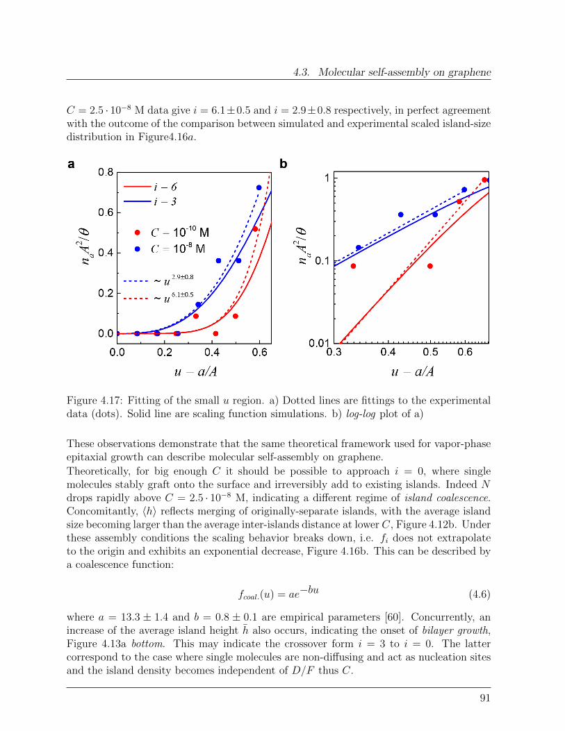
4.3. Molecular self-assembly on graphene
C = 2.5 · 10−8 M data give i = 6.1±0.5 and i = 2.9±0.8 respectively, in perfect agreementwith the outcome of the comparison between simulated and experimental scaled island-sizedistribution in Figure4.16a.
Figure 4.17: Fitting of the small u region. a) Dotted lines are fittings to the experimentaldata (dots). Solid line are scaling function simulations. b) log-log plot of a)
These observations demonstrate that the same theoretical framework used for vapor-phaseepitaxial growth can describe molecular self-assembly on graphene.
Theoretically, for big enough C it should be possible to approach i = 0, where singlemolecules stably graft onto the surface and irreversibly add to existing islands. Indeed Ndrops rapidly above C = 2.5 · 10−8 M, indicating a different regime of island coalescence.Concomitantly, 〈h〉 reflects merging of originally-separate islands, with the average islandsize becoming larger than the average inter-islands distance at lower C, Figure 4.12b. Underthese assembly conditions the scaling behavior breaks down, i.e. fi does not extrapolateto the origin and exhibits an exponential decrease, Figure 4.16b. This can be described bya coalescence function:
fcoal.(u) = ae−bu (4.6)
where a = 13.3 ± 1.4 and b = 0.8 ± 0.1 are empirical parameters [60]. Concurrently, anincrease of the average island height h also occurs, indicating the onset of bilayer growth,Figure 4.13a bottom. This may indicate the crossover form i = 3 to i = 0. The lattercorrespond to the case where single molecules are non-diffusing and act as nucleation sitesand the island density becomes independent of D/F thus C.
91
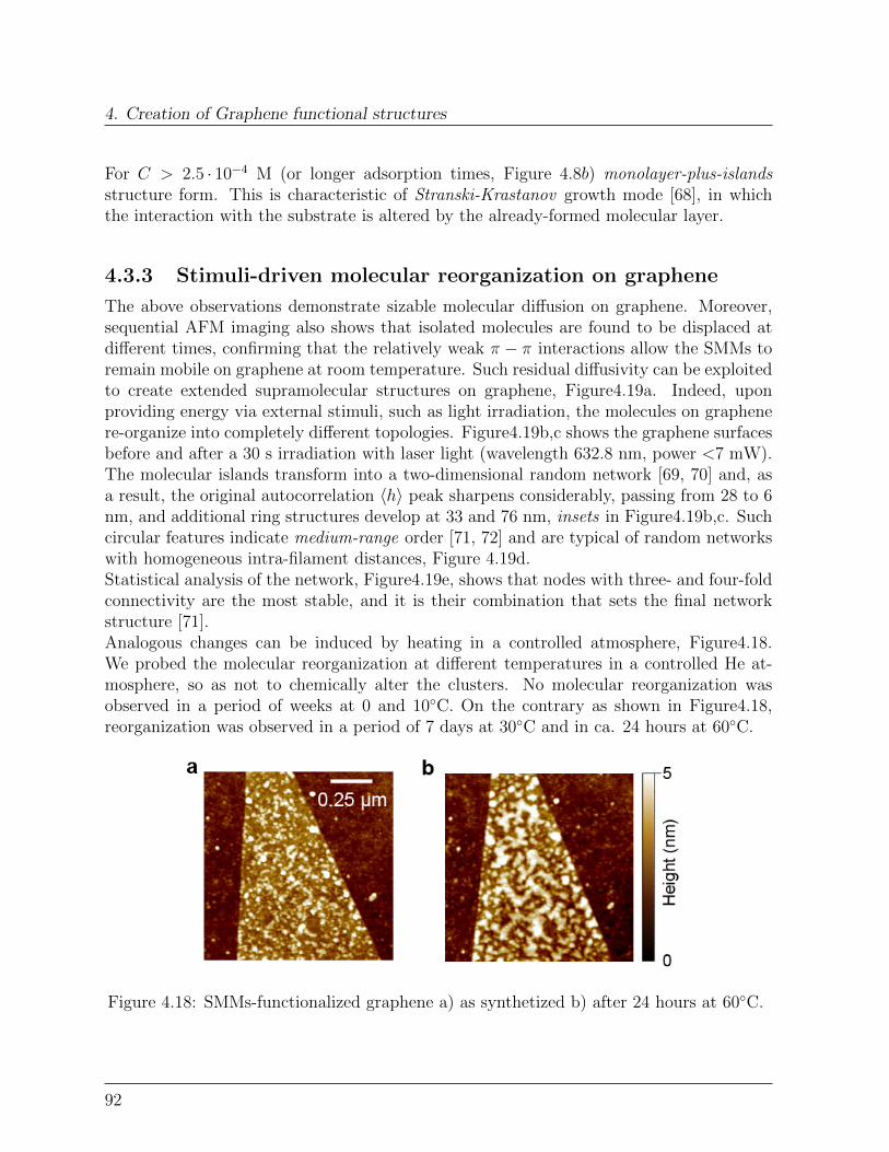
4. Creation of Graphene functional structures
For C > 2.5 · 10−4 M (or longer adsorption times, Figure 4.8b) monolayer-plus-islandsstructure form. This is characteristic of Stranski-Krastanov growth mode [68], in whichthe interaction with the substrate is altered by the already-formed molecular layer.
4.3.3 Stimuli-driven molecular reorganization on graphene
The above observations demonstrate sizable molecular diffusion on graphene. Moreover,sequential AFM imaging also shows that isolated molecules are found to be displaced atdifferent times, confirming that the relatively weak π − π interactions allow the SMMs toremain mobile on graphene at room temperature. Such residual diffusivity can be exploitedto create extended supramolecular structures on graphene, Figure4.19a. Indeed, uponproviding energy via external stimuli, such as light irradiation, the molecules on graphenere-organize into completely different topologies. Figure4.19b,c shows the graphene surfacesbefore and after a 30 s irradiation with laser light (wavelength 632.8 nm, power <7 mW).The molecular islands transform into a two-dimensional random network [69, 70] and, asa result, the original autocorrelation 〈h〉 peak sharpens considerably, passing from 28 to 6nm, and additional ring structures develop at 33 and 76 nm, insets in Figure4.19b,c. Suchcircular features indicate medium-range order [71, 72] and are typical of random networkswith homogeneous intra-filament distances, Figure 4.19d.Statistical analysis of the network, Figure4.19e, shows that nodes with three- and four-foldconnectivity are the most stable, and it is their combination that sets the final networkstructure [71].Analogous changes can be induced by heating in a controlled atmosphere, Figure4.18.We probed the molecular reorganization at different temperatures in a controlled He at-mosphere, so as not to chemically alter the clusters. No molecular reorganization wasobserved in a period of weeks at 0 and 10C. On the contrary as shown in Figure4.18,reorganization was observed in a period of 7 days at 30C and in ca. 24 hours at 60C.
Figure 4.18: SMMs-functionalized graphene a) as synthetized b) after 24 hours at 60C.
92
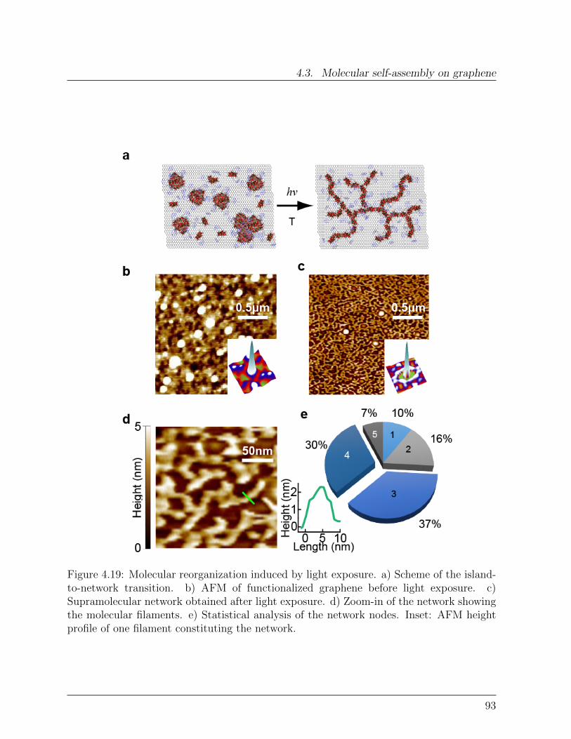
4.3. Molecular self-assembly on graphene
Figure 4.19: Molecular reorganization induced by light exposure. a) Scheme of the island-to-network transition. b) AFM of functionalized graphene before light exposure. c)Supramolecular network obtained after light exposure. d) Zoom-in of the network showingthe molecular filaments. e) Statistical analysis of the network nodes. Inset: AFM heightprofile of one filament constituting the network.
93

4. Creation of Graphene functional structures
4.4 Electronic properties of graphene functionalized
with SMMs
To test how the molecular functionalization influences the graphene electronic properties,both Raman spectroscopy and electronic transport measurements were performed beforeand after SMMs decoration (Figure4.20).
4.4.1 Raman spectrum of SMMs-graphene hybrids
Raman spectra were acquired at the center of the same graphene flake before and aftergrafting of [Fe4(L)2(dpm)6] (C = 2.5 · 10−6 M). The bare flake shows a G peak at 1582cm−1 with an full-width-half-maximum of 14 cm−1 (Figure4.20a). Decoration with 1 leadsto a slight G band up-shift of about 4 cm−1 correlated with a narrowing of the FWHMto 9.8 cm−1, indicating a very small doping effect [42], compatible with π-stacked pyrene.No enhancement of the molecular Raman signal was detected and a quenching is likelypresent, contrarily to previous reports [73].
4.4.2 Electronic transport in SMMs-graphene hybrids
To estimate the charge transferred per molecule, transport measurements were performedon graphene-based 5-terminal field-effect transistors with a 300nm-thick SiO2 gate dielectric(Figure 4.20b,c). The devices were fabricated, using electron beam lithography on a two-layer poly-methyl-methacrylate PMMA mask. To improve contact adhesion a 2nm Tibuffer-layer was employed (see Chapter 8). The contact material, Au (50nm), was depositedby thermal evaporation at residual pressure < 10−7mbar. To ensure a minimum amount ofresist residues on the graphene surface, the final lift-off step was extended over 14 hours.Measurement were performed at room temperature, by suppling a dc current (±1µA) in thelinear I-V regime and measuring the voltage drop between the inner electrodes as depictedin Figure 4.20b.
The graphene differential resistance R = ∂V/∂Isd (where Isd is the source-drain currentand V is the measured potential difference) reaches a maximum when the back-gate voltageVgate is scanned through the Dirac point. In the pristine devices, black curve in Figure4.20d, instead of being at Vgate = 0 V, the maximum is found at Vgate ≈ 10 V due tohole-doping by air exposure. The maximum upshifts of about 8 V after treatment with thesolvent mixture alone, Figure 4.20d blue curve, and it gradually shifts back to the originalVgate value as the solvent evaporates. Grafting of [Fe4(L)2(dpm)6] permanently shifts themaximum to VD, red curve in Figure 4.20d.
By evaluating the minimum number density of molecules δ from the AFM images, themaximum charge transferred per molecule can be determined using equation (2.40) ofsection 2.3 [74]:
94

4.4. Electronic properties of graphene functionalized with SMMs
Figure 4.20: Effect of molecular functionalization on graphene electronic properties. a)Raman G band, before (black) and after (red) functionalization. Solid lines are fits withsingle Lorentzian function. b) Scheme of the graphene-based field-effect transistor withfour-terminal measurement geometry and global back-gate. c) Optical photograph of thedevice. d) Gate-dependence of the graphene resistance for the pristine device (black),after treatment with solvent alone (blue) and after functionalization with 1 (C = 2.5 · 10−6
Molar solution).
95
4. Creation of Graphene functional structures
ΘM =ε0κVDed
1
δ= 0.08e− (4.7)
where ε0 is the vacuum dielectric constant, κ the SiO2 relative dielectric permittivity, ethe electron charge and d the gate-dielectric thickness. This value is very close to whatfound for neutral gas adsorbates [9], and confirms that charge transfer per molecule isnegligible, the shift being likely due not to charge trasfer processes but to the formation ofa surface dipole at the graphene-molecule interface [75]. In addition, the ρ vs. Vgate char-acteristics is seen to broaden and ρmax decreases by 8%, a clear indication that molecularadsorbates affect appreciably holes and electron mobilities. The latter can be determinedusing equation (2.43) of section 2.3. The induced change is aysmmetric, hole mobilitydrops pronouncedly from 1600 to 500 cm2V−1s−1 while the electron one is only slightly af-fected, from 1180 to 1140 cm2V−1s−1. Such effect is not observed for the solvent alone, inagreement with what already reported for atomic magnetic adsorbates [76]. The decreasein the maximum resistivity (∼ 10%) agrees with previous reports on very clean graphenedevices functionalized with neutral scatterers, and might hint at the possible creation ofmidgap states [77]. In conclusion, both Raman and dc-transport measurements confirmthe absence of appreciable charge transfer process in the hybrid.
4.5 Bulk hybrid samples
4.5.1 Graphene by liquid phase exfoliation
To achieve a detectable magnetic signal, graphene-[Fe4(L)2(dpm)6] hybrid samples withweight in the ∼ 10 mg order are needed. Bulk graphene samples were produced by soni-cating of 8.4 mg graphite powder (NGS Naturalgraphit GmbH, grain size > 0.2µm) in 20ml of the organic solvents mixture 1,2-dichloroethane:dichloromethane (9/1, v/v) for 48hrs using a low-power ultrasonic bath, Figure 4.21a. The sonication process separates thegraphite layers and forms a graphene dispersion containing single (30%) and multilayergraphene, Figure 4.21b,c, in agreement with previous studies [78–81].Bulk graphene-SMM hybrid samples were produced by non-covalent grafting of the SMMvia solution-based self-assembly. 11.5 mg of [Fe4(L)2(dpm)6] powder were dissolved in 20ml of solvent mixture and shaken for at least 30 minutes, until the solution acquired adark-yellow color. No solid sediment was seen after 30 minutes of rest, indicating thatall crystallites were completely dissolved and the solution is not saturated. The obtainedsolution was then mixed with the previously prepared graphene dispersion. The graphene-[Fe4(L)2(dpm)6] solution was stirred for 45 minutes and finally filtered through PTFEmembranes of 0.2 m average pore size (Whatman).Atomic force microscopy (AFM) reveals the appearance of randomly distributed objectson the graphene surface after the functionalization, confirming successful decoration ofgraphene by SMM, Figure 4.7c,d. The objects height distribution is peaked at 1.8 ± 0.3nm, Figure 4.7c, in close agreement with the size of individual [Fe4(L)2(dpm)6] molecules.
96
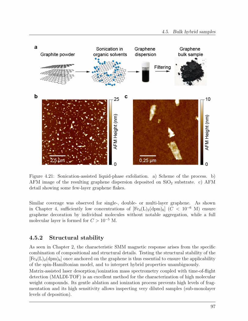
4.5. Bulk hybrid samples
Figure 4.21: Sonication-assisted liquid-phase exfoliation. a) Scheme of the process. b)AFM image of the resulting graphene dispersion deposited on SiO2 substrate. c) AFMdetail showing some few-layer graphene flakes.
Similar coverage was observed for single-, double- or multi-layer graphene. As shownin Chapter 4, sufficiently low concentrations of [Fe4(L)2(dpm)6] (C < 10−6 M) ensuregraphene decoration by individual molecules without notable aggregation, while a fullmolecular layer is formed for C > 10−5 M.
4.5.2 Structural stability
As seen in Chapter 2, the characteristic SMM magnetic response arises from the specificcombination of compositional and structural details. Testing the structural stability of the[Fe4(L)2(dpm)6] once anchored on the graphene is thus essential to ensure the applicabilityof the spin-Hamiltonian model, and to interpret hybrid properties unambiguously.
Matrix-assisted laser desorption/ionization mass spectrometry coupled with time-of-flightdetection (MALDI-TOF) is an excellent method for the characterization of high molecularweight compounds. Its gentle ablation and ionization process prevents high levels of frag-mentation and its high sensitivity allows inspecting very diluted samples (sub-monolayerlevels of deposition).
97

4. Creation of Graphene functional structures
The different samples are prepared by simply pressing the material onto a metallic targetand are immediately loaded into the spectrometer without any intermediate processing.The characterization has been carried out using a Bruker Reflex IV MALDI-TOF massspectrometer, equipped with a nitrogen laser pulsed at 3-5 Hz and adjustable power.
Figure 4.22: MALDI-TOF mass spectroscopy of a) pure [Fe4(L)2(dpm)6] powder. b) pure[Fe4(L)2(dpm)6] powder plus matrix (dithranol). c) bulk [Fe4(L)2(dpm)6]-graphene hy-brids. The hybrids exhibit the same fragmentation behavior as the starting SMM powder.
The spectrum of the pristine [Fe4(L)2(dpm)6] powder reveals several intense peaks in therange 0 - 1919 amu, Figure 4.22a, in full agreement with what reported on [Fe4(L)2(dpm)6]parent compounds [55, 56]. Peaks at 1919 and 1736 amu correspond to intact clustersundergoing the removal of respectively one and two dpm− (Hdpm=dipivaloylmethane)ligands during the desorption/ionization process. Other peaks are summarized in Table4.1.
Since the hybrid material contains a very diluted amount of SMMs, a matrix compound(Dithranol: C14H10O3) was used to improve the ionization process and the overall mea-surement sensitivity. The matrix was dispersed in the 1,2-dichloroethane:dichloromethanemixture (9/1, v/v) and drop-casted on the powder sample, previously pressed on the tar-get. As shown in Figure 4.22b, the matrix does not alter the fragmentation behavior of the
98
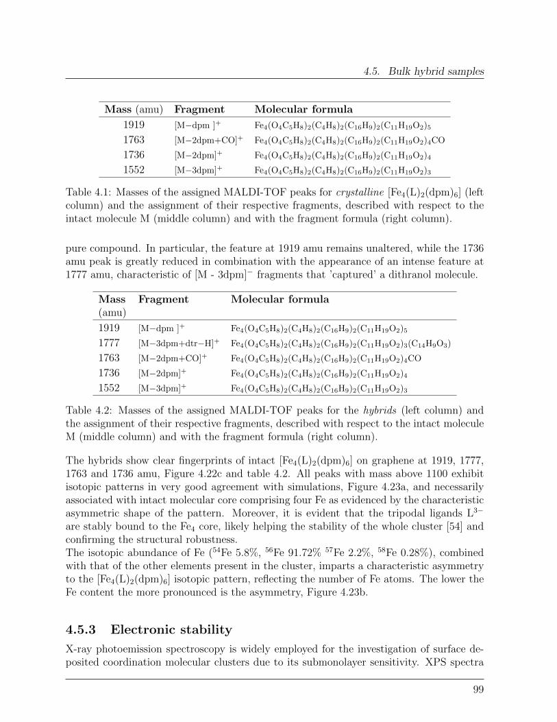
4.5. Bulk hybrid samples
Mass (amu) Fragment Molecular formula
1919 [M−dpm ]+ Fe4(O4C5H8)2(C4H8)2(C16H9)2(C11H19O2)5
1763 [M−2dpm+CO]+ Fe4(O4C5H8)2(C4H8)2(C16H9)2(C11H19O2)4CO
1736 [M−2dpm]+ Fe4(O4C5H8)2(C4H8)2(C16H9)2(C11H19O2)4
1552 [M−3dpm]+ Fe4(O4C5H8)2(C4H8)2(C16H9)2(C11H19O2)3
Table 4.1: Masses of the assigned MALDI-TOF peaks for crystalline [Fe4(L)2(dpm)6] (leftcolumn) and the assignment of their respective fragments, described with respect to theintact molecule M (middle column) and with the fragment formula (right column).
pure compound. In particular, the feature at 1919 amu remains unaltered, while the 1736amu peak is greatly reduced in combination with the appearance of an intense feature at1777 amu, characteristic of [M - 3dpm]− fragments that ’captured’ a dithranol molecule.
Mass(amu)
Fragment Molecular formula
1919 [M−dpm ]+ Fe4(O4C5H8)2(C4H8)2(C16H9)2(C11H19O2)5
1777 [M−3dpm+dtr−H]+ Fe4(O4C5H8)2(C4H8)2(C16H9)2(C11H19O2)3(C14H9O3)
1763 [M−2dpm+CO]+ Fe4(O4C5H8)2(C4H8)2(C16H9)2(C11H19O2)4CO
1736 [M−2dpm]+ Fe4(O4C5H8)2(C4H8)2(C16H9)2(C11H19O2)4
1552 [M−3dpm]+ Fe4(O4C5H8)2(C4H8)2(C16H9)2(C11H19O2)3
Table 4.2: Masses of the assigned MALDI-TOF peaks for the hybrids (left column) andthe assignment of their respective fragments, described with respect to the intact moleculeM (middle column) and with the fragment formula (right column).
The hybrids show clear fingerprints of intact [Fe4(L)2(dpm)6] on graphene at 1919, 1777,1763 and 1736 amu, Figure 4.22c and table 4.2. All peaks with mass above 1100 exhibitisotopic patterns in very good agreement with simulations, Figure 4.23a, and necessarilyassociated with intact molecular core comprising four Fe as evidenced by the characteristicasymmetric shape of the pattern. Moreover, it is evident that the tripodal ligands L3−
are stably bound to the Fe4 core, likely helping the stability of the whole cluster [54] andconfirming the structural robustness.The isotopic abundance of Fe (54Fe 5.8%, 56Fe 91.72% 57Fe 2.2%, 58Fe 0.28%), combinedwith that of the other elements present in the cluster, imparts a characteristic asymmetryto the [Fe4(L)2(dpm)6] isotopic pattern, reflecting the number of Fe atoms. The lower theFe content the more pronounced is the asymmetry, Figure 4.23b.
4.5.3 Electronic stability
X-ray photoemission spectroscopy is widely employed for the investigation of surface de-posited coordination molecular clusters due to its submonolayer sensitivity. XPS spectra
99

4. Creation of Graphene functional structures
Figure 4.23: Isotopic patterns of high-mass peaks a) Comparison between the experimentaland simulated (blue) isotopic patterns for the different samples. b) The asymmetric shapeof the isotopic patterns confirms the composition of an intact molecular core.
can provide important information about the oxidation state of the metallic ions con-stituting the molecular core, thus enabling a clear identification of important structuralmodifications. We use XPS as complement to the MALDI-TOF analysis to demonstratethe intactness of the [Fe4(L)2(dpm)6] molecules after dispersion and deposition.
Figure 4.24 shows a comparison between the XPS spectra of bulk graphene-[Fe4(L)2(dpm)6]hybrids and the pure [Fe4(L)2(dpm)6]. Since XPS spectroscopy is sensitive to the chargingbehavior of the substrate, the pure compound was deposited on highly-oriented pyroliticgraphite (HOPG) from a saturated solution. Big crystallites were clearly visible to thenaked eye.
The XPS spectrum of the hybrids reveals a well resolved Fe2p double peak, in the bind-ing energy (BE) spectral region 740 - 700 eV. Several studies (see [82–84] and referencestherein) have shown that the positions of Fe2p3/2 and Fe2p1/2 components depend stronglyon the ionic state of the Fe ions present in the sample. For compounds containing only Fe3+
coordinated with six oxygen atoms, such as Fe2O3 and [Fe4(L)2(dpm)6], the Fe2p3/2 compo-nent ranges between 710.6 to 711.5 eV, appreciably shifted towards higher binding energiesif compared with the neutral elemental Fe, which Fe2p3/2 component lies at 707.0eV. For
100

4.5. Bulk hybrid samples
Figure 4.24: Comparison between the XPS spectra of the Fe2p transition for a) pure[Fe4(L)2(dpm)6] deposited on HOPG from saturated solution and b) bulk graphene-[Fe4(L)2(dpm)6] hybrids c) surface graphene-[Fe4(L)2(dpm)6] hybrids, measured on a largeexfoliated flake (lateral size > 50µm) functionalized using a 2.5 · 10−6 Molar solution.
the bulk hybrids the Fe2p3/2 and Fe2p1/2 are found at 711.4 eV and 724.6 eV respectively,Figure 4.24b, in very good agreement with the spectrum of pure [Fe4(L)2(dpm)6], Figure4.24a. This confirms intact coordination bonds with oxygen, and no change in the oxi-dation state of the Fe ions after dispersion and deposition. It is important to note thatXPS studies [82, 84] for compounds where iron is present only in the Fe2+ state, suchas 2FeOSiO2, report a Fe2p3/2 peak at substantially lower binding energy (∼ 709 eV).In the present case there is no evidence of such lower energy contribution. The aboveobservations bring strong evidence that the [Fe4(L)2(dpm)6] molecules remain intact afterdispersion and deposition, in fully agreement with other studies on structurally-relatedcompounds [55, 85] carried out in both powder and surface deposited conditions.
101
4. Creation of Graphene functional structures
The XPS spectrum was also acquired for surface hybrids on a Si/SiO2 substrate function-alized using a 2.5 · 10−6 M solution for 15min, Figure 4.24c. The spectrum was acquired inthe sample region containing an isolated graphene flake with a lateral size of several tensof micrometers. After averaging over four days of acquisition, a weak asymmetric Fe2pdouble peak appears in the spectral region BE=740 - 700eV. However, accurate fitting wasnot possible due to the poor signal-to-noise ratio given by the extremely small lateral sizeof the sample, and the consequently small amount of [Fe4(L)2(dpm)6] grafted on it.The survey spectra do not reveal the presence of any contaminant for all samples. Allspectra were acquired using an Axis ULTRA system by Kratos Analytical Ltd. (Manch-ester) equipped with a monocromatized Al Kα (1486.6eV) X-ray source and a 8 channelshemispherical detector. Inelastic background was subtracted by means of Shirley methodand the data analysis was carried out assuming G/L=30 Gaussian/Lorentzian basic lineshapes. The strong and narrow C1s peak due to the presence of graphite/graphene enableda precise correction of charging effect. The C1s peak was set at 285.2 eV.
4.6 Conclusions
π-stacking interaction between pyrene and the graphene conjugated structure promoteseffective grafting of Fe4 SMM to graphene. SMMs deposited from solution self-assemble inmolecular islands, owing to their appreciable surface diffusion. The latter is well describedby dynamic scaling behavior. Scaling analysis identifies the transition between distinctassembly regimes at different solute concentrations. The residual surface diffusion canbe used to induce re-organization of the supramolecular arrangement, and the formationof an extended two-dimensional molecular network on graphene by external means e.g.light exposure. This opens up new strategies for the synthesis of molecular arrangementson graphene. The present findings constitute a basic step forward for the understandingand development of self-assembled SMMs-graphene hybrids, as the organization behaviorof molecules on graphene is important for magnetically- and optically-active graphenehybrids. Measurement of Raman spectrum and electronic transport in graphene field effecttransistor demonstrate negligible charge transfer between SMMs and graphene, as expectedfor non-covalently bound adsorbates. The hybrid MALDI-TOF and X-ray photoelectronspectra demonstrate that the SMMs are both structurally and electronically stable.
102

Bibliography
Bibliography
[1] Barth, J. V., Costantini, G. & Kern, K. Engineering atomic and molecular nanostruc-tures at surfaces. Nature 437, 671–679 (2005).
[2] Macleod, J. M. & Rosei, F. Molecular self-assembly on graphene. Small 10, 1038–1049(2014).
[3] Garnica, M. et al. Long-range magnetic order in a purely organic 2D layer adsorbedon epitaxial graphene. Nat. Phys. 9, 368–374 (2013).
[4] Deshpande, A. et al. Self-assembly and photopolymerization of sub-2 nm one-dimensional organic nanostructures on graphene. J. Am. Chem. Soc 134, 16759–16764(2012).
[5] Rao, C. N. R., Sood, a. K., Subrahmanyam, K. S. & Govindaraj, a. Graphene: Thenew two-dimensional nanomaterial. Angewandte Chemie - International Edition 48,7752–7777 (2009).
[6] Huang, X. et al. Graphene-based materials: Synthesis, characterization, properties,and applications. Small 7, 1876–1902 (2011).
[7] Rodrıguez-Lopez, J. et al. Quantification of the surface diffusion of tripodal bindingmotifs on graphene using scanning electrochemical microscopy. J. Am. Chem. Soc134, 6224–6236 (2012).
[8] Saywell, A. et al. Self-assembled aggregates formed by single-molecule magnets on agold surface. Nat. Commun. 1, 1 (2010).
[9] Schedin, F. et al. Detection of individual gas molecules adsorbed on graphene. Nat.Mater. 6, 652–655 (2007).
[10] Elias, D. C. et al. Control of graphene’s properties by reversible hydrogenation: evi-dence for graphane. Science 323, 610–3 (2009).
[11] Zhang, Z., Huang, H., Yang, X. & Zang, L. Tailoring Electronic Properties ofGraphene by π–π Stacking with Aromatic Molecules. Journal of Physical ChemistryLetters 2, 2897–2905 (2011).
[12] Qi, X. et al. Amphiphilic graphene composites. Angewandte Chemie - InternationalEdition 49, 9426–9429 (2010).
[13] Nair, R. R. et al. Dual origin of defect magnetism in graphene and its reversibleswitching by molecular doping. Nat. Commun. 4, 2010 (2013).
[14] Englert, J. M. et al. Covalent bulk functionalization of graphene. Nat. Chem. 3,279–286 (2011).
103
Bibliography
[15] Wang, Q. H. & Hersam, M. C. Room-temperature molecular-resolution character-ization of self-assembled organic monolayers on epitaxial graphene. Nat. Chem. 1,206–211 (2009).
[16] Quintana, M. et al. Selective organic functionalization of graphene bulk or grapheneedges. Chemical Communications 47, 9330–9332 (2011).
[17] Candini, A., Klyatskaya, S., Ruben, M., Wernsdorfer, W. & Affronte, M. Graphenespintronic devices with molecular nanomagnets. Nano letters 11, 2634–2639 (2011).
[18] Bogani, L. et al. Effect of sequential grafting of magnetic nanoparticles onto metallicand semiconducting carbon-nanotube devices: towards self-assembled multi-dots. J.Mater. Chem. 20, 2099–2107 (2010).
[19] Kyatskaya, S. et al. Anchoring of Rare-Earth-Based Single-Molecule Magnets onSingle-Walled Carbon Nanotubes. J. Am. Chem. Soc 131, 15143–15151 (2009).
[20] Khlobystov, A. N. et al. Molecular Motion of Endohedral Fullerenes in Single-Walled Carbon Nanotubes. Angewandte Chemie - International Edition 43, 1386–1389 (2004).
[21] Gimenez-Lopez, M. D. C. et al. Encapsulation of single-molecule magnets in carbonnanotubes. Nat. Commun. 2, 407 (2011).
[22] Bogani, L. et al. Single-molecule-magnet carbon-nanotube hybrids. AngewandteChemie - International Edition 48, 746–50 (2009).
[23] Gatteschi, D., Sessoli, R. & Villain, J. Molecular Nanomagnets. Mesoscopic Physicsand Nanotechnology (OUP, Oxford, 2006).
[24] Wernsdorfer, W. & Sessoli, R. Quantum Phase Interference and Parity Effects inMagnetic Molecular Clusters. Science 284, 133–135 (1999).
[25] Bogani, L. & Wernsdorfer, W. L. Molecular spintronics using single-molecule magnets.Nat. Mater. 7, 179–186 (2008).
[26] Tombros, N. et al. Electronic spin transport and spin precession in single graphenelayers at room temperature. Nature 448, 571–574 (2007).
[27] Pesin, D. & MacDonald, A. H. Spintronics and pseudospintronics in graphene andtopological insulators. Nat. Mater. 11, 409–416 (2012). arXiv:1308.3428.
[28] Wackerlin, C. et al. Controlling spins in adsorbed molecules by a chemical switch.Nat. Commun. 1, 61 (2010).
[29] Sanvito, S. Molecular spintronics. Chem. Soc. Rev. 40, 3336 (2011).
104
Bibliography
[30] Jiang, S. et al. An introduction to molecular spintronics. Science China Chemistry55, 867–882 (2012).
[31] Novoselov, K. S. K. S. et al. Electric field effect in atomically thin carbon films.Science 306, 666–669 (2004).
[32] Blake, P. et al. Making graphene visible. Applied Physics Letters 91, 63124 (2007).
[33] Zhu, W., Perebeinos, V., Freitag, M. & Avouris, P. Carrier scattering, mobilities, andelectrostatic potential in monolayer, bilayer, and trilayer graphene. Phys. Rev. B 80,235402 (2009).
[34] Novoselov, K. S. et al. Two-dimensional gas of massless Dirac fermions in graphene.Nature 438, 197–200 (2005).
[35] Novoselov, K. S. et al. Unconventional quantum Hall effect and Berry’s phase of 2piin bilayer graphene. Nat. Phys. 177–180 (2006).
[36] Craciun, M. F. et al. Trilayer graphene is a semimetal with a gate-tunable bandoverlap. Nat. Nanotech. 4, 383–388 (2009).
[37] Han, W. & Kawakami, R. K. Spin Relaxation in Single-Layer and Bilayer Graphene.Phys. Rev. Lett. 107, 47207 (2011).
[38] Cardona, M. Raman Spectroscopy Applied To The Characterization Of Semiconduc-tors And Semiconductor Microstructures. In Proc. SPIE 0822, Raman and Lumines-cence Spectroscopy in Technology, 2, vol. 822, 2–15 (1988).
[39] Dresselhaus, M. S., Jorio, A., Hofmann, M., Dresselhaus, G. & Saito, R. Perspectiveson carbon nanotubes and graphene Raman spectroscopy. Nano Letters 10, 751–758(2010).
[40] Ferrari, A. C. et al. Raman spectrum of graphene and graphene layers. PhysicalReview Letters 97, 187401 (2006).
[41] Malard, L. M., Pimenta, M. A., Dresselhaus, G. & Dresselhaus, M. S. Raman spec-troscopy in graphene. Physics Reports 473, 51–87 (2009).
[42] Casiraghi, C., Pisana, S., Novoselov, K. S., Geim, A. K. & Ferrari, A. C. Ramanfingerprint of charged impurities in graphene. Applied Physics Letters 91, 233108(2007).
[43] Casiraghi, C. Probing disorder and charged impurities in graphene by Raman spec-troscopy. Physica Status Solidi - Rapid Research Letters 3, 175–177 (2009).
[44] Thomsen, C. & Reich, S. Double Resonant Raman Scattering in Graphite. Phys. Rev.Lett. 85, 5214–5217 (2000).
105

Bibliography
[45] Tuinstra, F. & Koenig, J. L. Raman Spectrum of Graphite. The Journal of ChemicalPhysics 53, 1126–1130 (1970).
[46] Matthews, M., Pimenta, M., Dresselhaus, G., Dresselhaus, M. & Endo, M. Origin ofdispersive effects of the Raman D band in carbon materials. Physical Review B 59,R6585–R6588 (1999).
[47] Cancado, L. G. et al. Quantifying Defects in Graphene via Raman Spectroscopy atDifferent Excitation Energies. Nano Letters 11, 3190–3196 (2011).
[48] Casiraghi, C. et al. Raman Spectroscopy of Graphene Edges. Nano Letters 9, 1433–1441 (2009).
[49] Danieli, C. et al. A novel class of tetrairon(III) single-molecule magnets with graphene-binding groups. Polyhedron 28, 2029–2035 (2009).
[50] Antczak, G. & Ehrlich, G. Mechanism of cluster diffusion. In SurfaceDiffusion, 517–555 (Cambridge University Press, Cambridge, 2010). URLhttp://ebooks.cambridge.org/ref/id/CBO9780511730320A082.
[51] Roder, H., Hahn, E., Brune, H., Bucher, J.-P. & Kern, K. Building one- and two-dimensional nanostructures by diffusion-controlled aggregation at surfaces. Nature366, 141–143 (1993).
[52] Brune, H., Bales, G. S., Jacobsen, J., Boragno, C. & Kern, K. Measuring surfacediffusion from nucleation island densities. Phys. Rev. B 60, 5991–6006 (1999).
[53] Stroscio, J. a. & Pierce, D. T. Scaling of diffusion-mediated island growth in iron-on-iron homoepitaxy. Phys. Rev. B 49, 8522–8525 (1994).
[54] Cornia, A. et al. Energy-Barrier Enhancement by Ligand Substitution in Tetra-iron(III) Single-Molecule Magnets. Angewandte Chemie - International Edition 116,1156–1159 (2004).
[55] Rigamonti, L. et al. Enhanced Vapor-Phase Processing in Fluorinated Fe4 Single-Molecule Magnets. Inorganic Chemistry 52, 5897–5905 (2013).
[56] Margheriti, L. et al. Thermal Deposition of Intact Tetrairon(III) Single-MoleculeMagnets in High-Vacuum Conditions. Small 5, 1460–1466 (2009).
[57] Loske, F., Lubbe, J., Schutte, J., Reichling, M. & Kuhnle, A. Quantitative descriptionof \textbfC 60 diffusion on an insulating surface. Phys. Rev. B 82, 155428 (2010).
[58] Rahe, P., Bechstein, R., Schutte, J., Ostendorf, F. & Kuhnle, A. Repulsive interactionand contrast inversion in noncontact atomic force microscopy imaging of adsorbates.Phys. Rev. B 77, 195410 (2008).
106
Bibliography
[59] Vicsek, T. & Family, F. Dynamic scaling for aggregation of clusters. Physical reviewletters 52, 1669 (1984).
[60] Amar, J. G. J., Family, F. & Lam, P. P.-M. Dynamic scaling of the island-sizedistribution and percolation in a model of submonolayer molecular-beam epitaxy.Phys. Rev. B 50, 8781–8797 (1994).
[61] Amar, J. G. & Family, F. Critical Cluster Size: Island Morphology and Size Distri-bution in Submonolayer Epitaxial Growth. Phys. Rev. Lett. 74, 2066–2069 (1995).
[62] Amar, J. G. & Family, F. Kinetics of submonolayer and multilayer epitaxial growth.Thin Solid Films 272, 208–222 (1996).
[63] Doudevski, I., Hayes, W. A. & Schwartz, D. K. Submonolayer Island Nucleation andGrowth Kinetics during Self-Assembled Monolayer Formation. Phys. Rev. Lett. 81,4927–4930 (1998).
[64] Doudevski, I. & Schwartz, D. K. Dynamic scaling of the submonolayer island sizedistribution during self-assembled monolayer growth. Phys. Rev. B 60, 14–17 (1999).
[65] So, C. R. et al. Controlling Self-Assembly of Engineered Peptides on Graphite byRational Mutation. ACS Nano 6, 1648–1656 (2012).
[66] Chambliss, D. D. & Johnson, K. E. Nucleation with a critical cluster size of zero:Submonolayer Fe inclusions in Cu(100). Phys. Rev. B 50, 5012–5015 (1994).
[67] Muller, B., Nedelmann, L., Fischer, B. r., Brune, H. & Kern, K. Initial stages of Cuepitaxy on Ni(100): Postnucleation and a well-defined transition in critical island size.Phys. Rev. B 54, 17858–17865 (1996).
[68] Venables, J. A., Spiller, G. D. T. & Hanbucken, M. Nucleation and growth of thinfilms. Reports on Progress in Physics 47, 399 (1984).
[69] Barabasi, A.-L. & Albert, R. Emergence of scaling in random networks. Science 286,11 (1999).
[70] Bray, D. Molecular networks: the top-down view. Science 301, 1864–1865 (2003).
[71] Marschall, M. et al. Random two-dimensional string networks based on divergentcoordination assembly. Nat. Chem. 2, 131–137 (2010).
[72] Otero, R. et al. Elementary structural motifs in a random network of cytosine adsorbedon a gold(111) surface. Science 319, 312–315 (2008).
[73] Lopes, M. et al. Surface-Enhanced Raman Signal for Terbium Single-Molecule Mag-nets Grafted on Graphene. ACS Nano 4, 7531–7537 (2010).
107
Bibliography
[74] Chen, S. et al. Adsorption/desorption and electrically controlled flipping of ammoniamolecules on graphene. New Journal of Physics 12 (2010). arXiv:1006.2591.
[75] Murali, R. Graphene Transistors. In Murali, R. (ed.) Graphene Nanoelectronics, 51–91(Springer, Berlin Heidelberg, 2012).
[76] Pi, K. et al. Electronic doping and scattering by transition metals on graphene. Phys.Rev. B 80, 75406 (2009).
[77] Wehling, T. O., Katsnelson, M. I. & Lichtenstein, A. I. Impurities on graphene:Midgap states and migration barriers. Phys. Rev. B 80, 85428 (2009).
[78] Hernandez, Y. et al. Measurement of Multicomponent Solubility Parameters forGraphene Facilitates Solvent Discovery. Langmuir 26, 3208–3213 (2010).
[79] Hernandez, Y. et al. High-yield production of graphene by liquid-phase exfoliation ofgraphite. Nature Nanotechnology 3, 563–568 (2008).
[80] O’Neill, A. et al. Graphene Dispersion and Exfoliation in Low Boiling Point Solvents.The Journal of Physical Chemistry C 0, 5422–5428 (2011).
[81] Qian, W. et al. Solvothermal-assisted exfoliation process to produce graphene withhigh yield and high quality. Nano Research 2, 706–712 (2009).
[82] Yamashita, T. & Hayes, P. Analysis of XPS spectra of Fe2+ and Fe3+ ions in oxidematerials. Applied Surface Science 254, 2441–2449 (2008).
[83] Graat, P. C. J. & Somers, M. a. J. Simultaneous determination of composition andthickness of thin iron-oxide films from XPS Fe 2p spectra. Applied Surface Science100-101, 36–40 (1996).
[84] Roosendaal, S., van Asselen, B., Elsenaar, J., a.M. Vredenberg & Habraken, F. Theoxidation state of Fe(100) after initial oxidation in O2. Surface Science 442, 329–337(1999).
[85] Pineider, F. et al. Deposition of intact tetrairon(iii) single molecule magnet monolayerson gold: an STM, XPS, and ToF-SIMS investigation. J. Mater. Chem. 20, 187–194 (2010).
108
Chapter 5
Classical and quantum dynamics ofmolecular spins on graphene
Carbon-based spintronics [1–7] offers a mean to electrically manipulate localized spins inclose proximity of a carbon nanotube or graphene sheet. This task requires understand-ing and tuning of the interaction between the components, in order to improve the spinperformance [8–10], e.g. by minimizing quantum-decoherence [6], and to enable spin ma-nipulation, e.g. by altering the magnetic anisotropy or the electronic coupling. However,there is little current understanding of how the spin states in such devices are affected bythe environment.Here, we exploit the exceptionally clean magnetic features of single-molecule-magnets(SMMs) [11, 12] to explore how spins interact with the graphene substrates. A compre-hensive magnetic characterization is carried out by means of dc- and ac- magnetometries.The classical and quantum relaxation mechanisms are probed independently by apply-ing an external magnetic field. While isolated molecules on graphene exhibit unalteredstatic magnetic properties, the spin dynamics is strongly influenced by interaction withthe graphene substrate.
5.1 Hybrids static magnetic response
The temperature (T ) dependence of the dc magnetic susceptibility χm and isothermalmagnetization curves provide important information about the molecular spin-ground stateand the leading magnetic anisotropy terms.The measurements were performed on bulk samples, obtained by removing the hybridpowder from PTFE membranes and pressing it to form a pallet. The χmT curve (whereχm is the static molar magnetic susceptibility, defined as the ratio between magnetizationand the applied magnetic field, M/H) was extracted by measuring the magnetization Min the temperature range 1.8 - 230 K, using a commercial SQUID-based magnetometer ata fixed external field H = 1 kOe.All data were corrected for the diamagnetism of the sample and the sample holder. For the
109

5. Classical and quantum dynamics of molecular spins on graphene
Figure 5.1: Temperature dependence of the product of the static magnetic susceptibility χmfor [Fe4(L)2(dpm)6] (solid circles) and the hybrids (empty circles), with H = 1 kOe. Thesolid line is a fit based on Equation (2.5). Inset: dc susceptibility of an unfunctionalizedgraphene bulk sample.
former a diamagnetic correction of −1283 · 10−6 emu/mol, estimated from Pascal constants,was used, while the latter was independently determined. The diamagnetic contributionof the graphene matrix was determined from un-functionalized samples, Figure 5.1 inset.Figure 5.1 shows the comparison between the hybrids χmT vs. T and that of the crystalline[Fe4(L)2(dpm)6]. Hybrids data were rescaled to account for the different amount of SMMspresent in the sample.
The hybrids χmT vs. T curve matches that of the pure crystalline compound, and bothcan be fitted by using Equation (2.5) and the same set of magnetic parameters, J1 =−14.85 ± 0.05 cm−1 and J2 = 0.09 ± 0.05 cm−1, as known for the intact SMM core.This confirms that, owing to the cluster excellent structural and electronic stability, theleading uniaxial anisotropy term remains unaltered after grafting to graphene, and SMMsembedded in the graphene matrix behave as model spins with ground state S = 5. Thisis further confirmed by adiabatic magnetization data acquired at different temperatures(Figure 5.2).
110
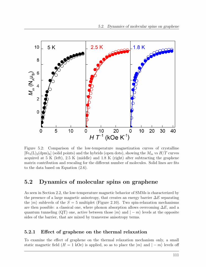
5.2. Dynamics of molecular spins on graphene
Figure 5.2: Comparison of the low-temperature magnetization curves of crystalline[Fe4(L)2(dpm)6] (solid points) and the hybrids (open dots), showing the Mm vs H/T curvesacquired at 5 K (left), 2.5 K (middle) and 1.8 K (right) after subtracting the graphenematrix contribution and rescaling for the different number of molecules. Solid lines are fitsto the data based on Equation (2.6).
5.2 Dynamics of molecular spins on graphene
As seen in Section 2.2, the low-temperature magnetic behavior of SMMs is characterized bythe presence of a large magnetic anisotropy, that creates an energy barrier ∆E separatingthe |m〉 sublevels of the S = 5 multiplet (Figure 2.10). Two spin-relaxation mechanismsare then possible: a classical one, where phonon absorption allows overcoming ∆E, and aquantum tunneling (QT) one, active between those |m〉 and | −m〉 levels at the oppositesides of the barrier, that are mixed by transverse anisotropy terms.
5.2.1 Effect of graphene on the thermal relaxation
To examine the effect of graphene on the thermal relaxation mechanism only, a smallstatic magnetic field (H = 1 kOe) is applied, so as to place the |m〉 and | −m〉 levels off
111
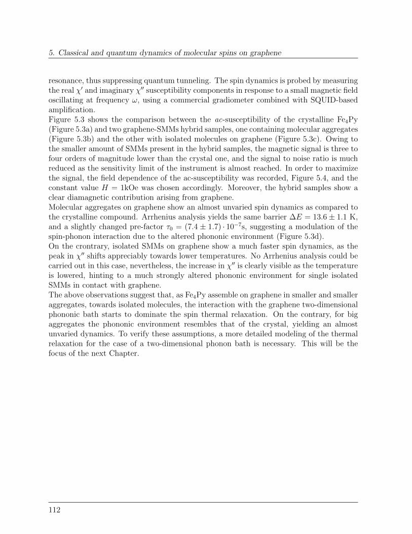
5. Classical and quantum dynamics of molecular spins on graphene
resonance, thus suppressing quantum tunneling. The spin dynamics is probed by measuringthe real χ′ and imaginary χ′′ susceptibility components in response to a small magnetic fieldoscillating at frequency ω, using a commercial gradiometer combined with SQUID-basedamplification.Figure 5.3 shows the comparison between the ac-susceptibility of the crystalline Fe4Py(Figure 5.3a) and two graphene-SMMs hybrid samples, one containing molecular aggregates(Figure 5.3b) and the other with isolated molecules on graphene (Figure 5.3c). Owing tothe smaller amount of SMMs present in the hybrid samples, the magnetic signal is three tofour orders of magnitude lower than the crystal one, and the signal to noise ratio is muchreduced as the sensitivity limit of the instrument is almost reached. In order to maximizethe signal, the field dependence of the ac-susceptibility was recorded, Figure 5.4, and theconstant value H = 1kOe was chosen accordingly. Moreover, the hybrid samples show aclear diamagnetic contribution arising from graphene.Molecular aggregates on graphene show an almost unvaried spin dynamics as compared tothe crystalline compound. Arrhenius analysis yields the same barrier ∆E = 13.6± 1.1 K,and a slightly changed pre-factor τ0 = (7.4 ± 1.7) · 10−7s, suggesting a modulation of thespin-phonon interaction due to the altered phononic environment (Figure 5.3d).On the crontrary, isolated SMMs on graphene show a much faster spin dynamics, as thepeak in χ′′ shifts appreciably towards lower temperatures. No Arrhenius analysis could becarried out in this case, nevertheless, the increase in χ′′ is clearly visible as the temperatureis lowered, hinting to a much strongly altered phononic environment for single isolatedSMMs in contact with graphene.The above observations suggest that, as Fe4Py assemble on graphene in smaller and smalleraggregates, towards isolated molecules, the interaction with the graphene two-dimensionalphononic bath starts to dominate the spin thermal relaxation. On the contrary, for bigaggregates the phononic environment resembles that of the crystal, yielding an almostunvaried dynamics. To verify these assumptions, a more detailed modeling of the thermalrelaxation for the case of a two-dimensional phonon bath is necessary. This will be thefocus of the next Chapter.
112
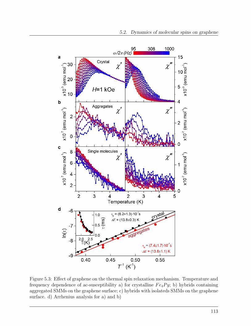
5.2. Dynamics of molecular spins on graphene
Figure 5.3: Effect of graphene on the thermal spin relaxation mechanism. Temperature andfrequency dependence of ac-susceptibility a) for crystalline Fe4Py; b) hybrids containingaggregated SMMs on the graphene surface; c) hybrids with isolateds SMMs on the graphenesurface. d) Arrhenius analysis for a) and b)
113
5. Classical and quantum dynamics of molecular spins on graphene
Figure 5.4: Field dependence of the ac-susceptibility for the crystalline Fe4Py at 1kHz (χ′′
is maximum in the range 0.5-1kOe).
5.2.2 Effect of graphene on the spin quantum relaxation
The quantum relaxation of isolated spins on graphene is investigated by switching off theexternal magnetic field, so that |m〉 and | −m〉 levels fall back into resonance. In this caseχ′ and χ′′ are measured using an home-made system based on an on-chip micro-SQUIDsensor mounted in the mixing chamber of a 3He -4He dilution cryostat. This system affordsa larger frequency range, spanning 5 decades from 1.7 Hz to 0.17 MHz, and can be operatedat ultra-low temperatures down to 13 mK. The sensitivity is also improved being the sampledirectly glued onto one of the squid pickup coils.
Figure 5.5a,b compares the frequency dependence of the ac-susceptibility of isolated moleculeson graphene in H = 0 at two different temperatures T = 4.2 K and 20 mK. The samemeasurements on the crystal are shown for comparison.
At 4.2 K the thermal relaxation still dominates over the QT relaxation. χ′ and χ′′ canbe fitted using the simple (α = 0) Cole-Cole model, introduced in Section 2.2, confirmingthe absence of barrier height ∆E broadening, thanks to the structural and electronicstability of the Fe4Py cluster. The hybrid χ′ was corrected for the appreciable graphenediamagnetic contribution, that as seen in Figure 5.5c, almost compensate the spin signalfor ω/2π → 0. The χ′′ 6= 0 in Figure 5.5c confirms graphene metallic character. Atthis temperature, isolated SMMs on graphene exhibit a slightly faster spin relaxation,τ ∼ 9 · 10−7 s, compared to the crystal, τ ∼ 1.7 · 10−6 s.
114

5.2. Dynamics of molecular spins on graphene
Figure 5.5: Mixed thermal and quantum spin relaxation in H = 0. Frequency dependenceof the real (empty circles) and imaginary (solid circles) parts of the ac-susceptibility forcrystalline Fe4Py compound and graphene-SMMs hybrids with isolated molecules at a)T = 4.2 K and b) 20 mK. Solid lines are fits with the Cole-Cole model. The hybrid dataare corrected for the diamagnetic bare graphene contribution c).
115

5. Classical and quantum dynamics of molecular spins on graphene
Figure 5.6: Temperature dependence of χ for a) crystalline Fe4Py and b) isolated moleculeson graphene at different frequencies in the QT dominated temperature range. Arrows ina) indicate a contribution from molecular spins coupled via dipole-dipole interaction.
A strikingly faster dynamics of isolated SMMs on graphene becomes evident as the tem-perature is lowered down to T = 20mK, where phononic excitations are frozen and QT isthe dominant relaxation mechanism. While the crystalline sample shows slow relaxation,with τ in the order of seconds (τ ≈ 5 s), due to the characteristic susceptibility blocking,the relaxation of isolated molecules on graphene diverges from that by several orders ofmagnitude, τ ∼ 1 · 10−5s. Since for the crystalline sample the maximum in χ′′ fall outsidethe experimentally accessible regions of temperature and frequency, τ has been estimatedusing the approximate expression τ ≈ χ′′/(χ′ω) using data points at ω/2π = 1.6Hz.
116
5.2. Dynamics of molecular spins on graphene
To investigate the transition from the classical (thermal) to the pure quantum spin relax-ation, the complete temperature dependence of the ac-susceptibility at H = 0 is measured(Figure 5.6). The crystalline sample shows the characteristic (frequency-dependent) sus-ceptibility blocking (T ∼ 0.8 K for ω/2π = 0.17 − 170 Hz), marking the suppression ofthe thermal relaxation channel and the transition to QT-dominated relaxation at lowertemperatures. By contrast, no clear blocking is observed for isolated SMMs on graphene,which nevertheless show clear maxima in both χ′ and χ′′ at much lower temperatures. Theweak temperature dependence for 0.1 < T < 4K suggests that the quantum relaxationmechanism is enhanced by the interaction with graphene.For the crystalline sample, a second peak at T ∼ 0.25 K is also seen, which is likelyattributed to a phase transition to a magnetically-ordered state induced by dipolar inter-actions among the SMM spins in the crystal. This low temperature contribution is absentin the hybrids, as expected for highly-diluted systems where dipolar interactions are dras-tically reduced. In the next Chapter we will see that the latter is a fundamental conditionto explain the observed quantum behavior.The relaxation time at different temperatures can be accurately determined from the fre-quency dependence of the ac-susceptibility, Figure 5.7. A roll-over of χ′ combined with amaximum in χ′′ between 104 − 105 Hz reveal the fast relaxation process of isolated SMMsgrafted on graphene, Figure 5.7b. Moreover the low-frequency limit of χ′ (i.e. χT) in-creases, while the onset of the χ′′ peak shifts towards lower frequencies as the temperaturedecreases, in full agreement with SMM behavior. At lower frequencies, χ′ shows a close tologarithmic dependence on frequency, accompanied by a nearly constant χ′′, in agreement
with Kramers-Kronig relation χ′′ = −π2
dχ′
dlnω.
Isosterm curves of Figure 5.7 were fitted employing the extended Cole-Cole model (Equa-tion 2.24) to take into account the logaritmic graphene contribution and a potential dis-tribution of relaxation times:
χ′(ω) = χS + (χT − χS)1 + (ωτ)β cos(βπ/2)
1 + 2(ωτ)β cos(βπ/2) + (ωτ)2β−∆χGlnω
(5.1)
χ′′(ω) = (χT − χS)1 + (ωτ)β sin(βπ/2)
1 + 2(ωτ)β cos(βπ/2) + (ωτ)2β+π
2∆χG
At T > 0.8 K, each isotherm of the crystalline Fe4Py, Figure 5.7a, is well characterized bya single relaxation time τ , affording relaxation time broadening factor β very close to 1 asexpected for an ensemble of monodisperse energy barriers. Obviously, no correction for thegraphene contribution was used in this case. The relaxation time τ increases exponentiallywith decreasing T in agreement with thermally-dominated relaxation regime. The T -dependence of the spin relaxation time τ is shown in Figure 5.8.For temperatures around T ≈ 0.8 K, β is found to decrease with decreasing T , thusrevealing a gradual broadening of the relaxation time distribution. The other fitting pa-rameter χT follows the Curie-Weiss law χT ∝ 1/T , in agreement with spin-lattice relax-
117
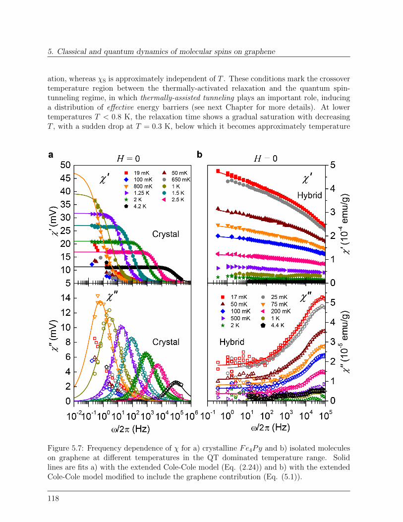
5. Classical and quantum dynamics of molecular spins on graphene
ation, whereas χS is approximately independent of T . These conditions mark the crossovertemperature region between the thermally-activated relaxation and the quantum spin-tunneling regime, in which thermally-assisted tunneling plays an important role, inducinga distribution of effective energy barriers (see next Chapter for more details). At lowertemperatures T < 0.8 K, the relaxation time shows a gradual saturation with decreasingT , with a sudden drop at T = 0.3 K, below which it becomes approximately temperature
Figure 5.7: Frequency dependence of χ for a) crystalline Fe4Py and b) isolated moleculeson graphene at different temperatures in the QT dominated temperature range. Solidlines are fits a) with the extended Cole-Cole model (Eq. (2.24)) and b) with the extendedCole-Cole model modified to include the graphene contribution (Eq. (5.1)).
118
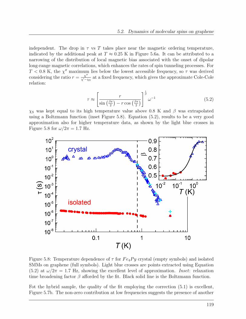
5.2. Dynamics of molecular spins on graphene
independent. The drop in τ vs T takes place near the magnetic ordering temperature,indicated by the additional peak at T ≈ 0.25 K in Figure 5.6a. It can be attributed to anarrowing of the distribution of local magnetic bias associated with the onset of dipolarlong-range magnetic correlations, which enhances the rates of spin tunneling processes. ForT < 0.8 K, the χ′′ maximum lies below the lowest accessible frequency, so τ was derivedconsidering the ratio r = χ′′
χ′−χSat a fixed frequency, which gives the approximate Cole-Cole
relation:
τ ≈
[r
sin(βπ2
)− r cos
(βπ2
)] 1β
ω−1 (5.2)
χS was kept equal to its high temperature value above 0.8 K and β was extrapolatedusing a Boltzmann function (inset Figure 5.8). Equation (5.2), results to be a very goodapproximation also for higher temperature data, as shown by the light blue crosses inFigure 5.8 for ω/2π = 1.7 Hz.
Figure 5.8: Temperature dependence of τ for Fe4Py crystal (empty symbols) and isolatedSMMs on graphene (full symbols). Light blue crosses are points extracted using Equation(5.2) at ω/2π = 1.7 Hz, showing the excellent level of approximation. Inset : relaxationtime broadening factor β afforded by the fit. Black solid line is the Boltzmann function.
Fot the hybrid sample, the quality of the fit employing the correction (5.1) is excellent,Figure 5.7b. The non-zero contribution at low frequencies suggests the presence of another
119
5. Classical and quantum dynamics of molecular spins on graphene
magnetic contribution characterized by an almost-flat distribution of relaxation times at-tributed to either a distribution of Fe4Py small aggregates or more likely from spinsembedded in the graphene layer e.g. electrons localized close to defects, or close to singleSMMs. Susceptibility data measured below T ≈ 0.2 K have been fitted by using Equation(5.1) with χS = 0, as shown in Figure 5.7b. For T > 0.2 K, the χ′′ maximum lies abovethe maximum attainable frequency, so the relaxation time was extracted using Equation
(5.2) with r =χ′′− π
2∆χG
χ′+∆χGlnωnow including the graphene correction ∆χG.
While for crystalline Fe4Py the thermally-activated region persists down to 800 mK, belowwhich QT sets in, the spin relaxation in the hybrids is fully dominated by QT already below2K, and at the lowest temperatures the quantum tunneling rate is about one million timeshigher τ ∼ 106 s compared to the crystal. Furthermore the relaxation time of the hybridexhibits a weak dependence on temperature, as τ increases with decreasing T .
5.3 Conclusions
The above observations univocally demonstrate that the spin-dynamics of isolated SMMs isgreatly modulated by interaction with graphene. On the one hand, measurements in field,suggest that the classical (thermal) spin relaxation machenism is modulated by the differ-ent graphene phononic bath. On the other hand, a strong enhancement of the quantumrelaxation at low temperatures suggests a more complex interaction with the grapheneenvironment. To shed light on the nature of such an interaction, a more sophisticatedmodeling is necessary. This will presented in the next chapter.
120
Bibliography
Bibliography
[1] Nair, R. R. et al. Spin-half paramagnetism in graphene induced by point defects. NatPhys 8, 199–202 (2012).
[2] Nair, R. R. et al. Dual origin of defect magnetism in graphene and its reversibleswitching by molecular doping. Nat. Commun. 4, 2010 (2013).
[3] Han, W., Kawakami, R. K., Gmitra, M. & Fabian, J. Graphene spintronics. Naturenanotechnology 9, 794–807 (2014).
[4] Pesin, D. & MacDonald, A. H. Spintronics and pseudospintronics in graphene andtopological insulators. Nat. Mater. 11, 409–416 (2012). arXiv:1308.3428.
[5] Hueso, L. E. et al. Transformation of spin information into large electrical signalsusing carbon nanotubes. Nature 445, 410–413 (2007).
[6] Laird, E. a., Pei, F. & Kouwenhoven, L. P. A valley-spin qubit in a carbon nanotube.Nature nanotechnology 8, 565–8 (2013). arXiv:1210.3085.
[7] Kuemmeth, F., Ilani, S., Ralph, D. C. & McEuen, P. L. Coupling of spin and orbitalmotion of electrons in carbon nanotubes. Nature 452, 448–52 (2008).
[8] Miyamachi, T. et al. Stabilizing the magnetic moment of single holmium atoms bysymmetry. Nature 503, 1–5 (2013).
[9] Warner, M. et al. Potential for spin-based information processing in a thin-film molec-ular semiconductor. Nature 503, 504–508 (2013).
[10] Oberg, J. C. et al. Control of single-spin magnetic anisotropy by exchange coupling.Nature nanotechnology 9, 64–8 (2014).
[11] Gatteschi, D. & Sessoli, R. Quantum Tunneling of Magnetization and Related Phe-nomena in Molecular Materials. Angewandte Chemie International Edition 42, 268–297 (2003).
[12] Gatteschi, D., Sessoli, R. & Villain, J. Molecular Nanomagnets. Mesoscopic Physicsand Nanotechnology (OUP, Oxford, 2006).
121

Bibliography
122
Chapter 6
Development of a theory of magneticrelaxation on graphene
Fundamental questions are still open on how the dynamics of mesoscopic spins is modulatedby the interaction with the surroundings (e.g. phonons, neighboring spin, and substratecharge carriers) [1–3]. In particular the question whether spatial confinement plays a rolein the spin-phonon coupling [4–8] and in the interaction between spins and charge carriers(e.g. of an underlying substrate) remained so far unanswered [9, 10]. The latter is inti-mately linked to the appealing opportunity of using graphene massless Dirac particles tomanipulate and probe the states of mesoscopic spins and to integrate graphene in futurenano-spintronic schemes. An appropriate theoretical modeling of this problem, corrobo-rated by experimental evidence, represents a fundamental step towards the understandingof the dynamics of spins on surfaces, and a rational design of spin-based logic [1, 11] andquantum computing [12–16] architectures.
This Chapter aims at modeling the relaxation time of SMMs under the influence ofgraphene environment. A new model for the spin-phonon interaction for a two-dimensionalphononic dispersion is developed to simulate transition between spin-states induced bygraphene phonons. The effect of dipolar and hyperfine interactions, as well as the effectof the graphene charge distribution on the tunneling transition rates is modeled using aperturbative approach. Interaction with graphene charge distribution is found to play amajor role in the quantum spin-relaxation at low temperature and by changing the mag-nitude of the interaction term drives the system through different perturbative tunnelingregimes with different level of coherence. Eventually the temperature dependence of therelaxation time τ is simulated and it is found to match very well the experimental data inthe broad temperature range here investigated.
6.1 Modelling spin interactions
To model the effect of the environment we consider the effective Hamiltonian:
123

6. Development of a theory of magnetic relaxation on graphene
H = gµBSH +∑i,j
Bji O
ji +Hsp−ph +Hdip +Hhyp (6.1)
where the first term describes the Zeeman interaction between the molecular spin S and theexternal magnetic field H, the second models the magnetic anisotropy, the third accountsfor the interaction between the spin and lattice vibrations, while Hdip and Hhyp are thedipolar and hyperfine interactions, respectively. Here, µB is the Bohr magneton, g is theLande factor and the Oj
i terms are the Stevens’ operator equivalents, introduced in Section2.2.3, each weighted by a coefficient Bj
i .
Figure 6.1: Graphical representation of the different environmental interactions acting onthe spin in graphene-SMMs hybrids.
The effect of each contribution in Equation (6.1) on the spin dynamics can be studied bytreating the relative term perturbatively.
6.2 Dynamics of molecular spins on graphene
As seen in the previous chapter, grafting to graphene alters substantially the dynamics ofmolecular spins, while leaving the static magnetic response unaltered.The modulation of the spin dynamics due to different environments can be described usingthe master equation approach introduced in Section 2.2:
d
dtNm(t) =
∑m′
[Wm′,mNm′(t)−Wm,m′Nm(t)] (6.2)
124
6.2. Dynamics of molecular spins on graphene
that describes how the occupation probability Nm(t) of a spin state |m〉 evolves in timedue to the combined thermal and tunneling relaxation paths. As one can see from Equation(6.2), the occupation probability Nm increases in time owing to transitions from all otherstates |m′〉 to |m〉 and decreases owing to transitions from |m〉 to all the other states |m′〉.For the Fe4Py system, Equation (6.2) translates into a system of eleven differential equa-tions, one for each spin level |m〉 with the form:
dNm
dt= −Nm
∑m′
Wm,m′ +∑m′
Nm′Wm′,m + Γm(Nm −N−m) (6.3)
where the first and second sums describe the phonon-assisted spin transitions from andto a given state |m〉, that are characterized by the transition rates Wm,m′ and Wm′,m
respectively. The number of terms in each sum is imparted by the specific excitationprocesses taking place in the system. The third term models the tunneling transitionsbetween |m〉 and | −m〉 states, that are described by the tunneling rates Γm.
We base our modeling on a new procedure, substantially different from what reported inprevious works [17, 18] and that is found to be more accurate also when applied to thestandard 3D case:
1) the theory of spin-phonon interaction is extended to include confinement effects for thecase of a two-dimentional phonon bath;
2) intrinsic hyperfine interactions and dipolar coupling to neighboring spins are includedin the model (6.1) as essential for energy conservation in the tunneling processes at lowtemperature;
3) the probabilities Wm′,m of spin transitions assisted by graphene phonons are calculatedvia the Fermi golden rule;
4) the interaction with the underlying graphene carriers is modeled by altered high orderanisotropy terms Bj
iOji in the spin-Hamiltonian (2.9);
5) tunneling frequencies ωm,m′
T are calculated using perturbation theory;
6) interaction-modulated tunneling rates Γm′,m are calculated taking into account the pop-ulation of spin states due to phonon-assisted transitions. These include tunneling tran-sitions from excited spin levels populated at high temperatures via thermal excitation,and the emission of phonons in the tunneling processes between the lowest lying spinstates at low temperature;
7) the occupation probabilities Nm for all the |m〉 states are calculated via a system ofmaster equations. The relaxation time at different temperatures is finally simulatedbeing it the reciprocal of the smallest non-zero eigenvalue of the system;
125
6. Development of a theory of magnetic relaxation on graphene
6.3 Spin relaxation due to a 2D phonon bath
The goal of this paragraph is the theoretical description of the phonon-assisted transitionrates Wm,m′ due to the graphene lattice vibrations.The interaction between phonons and molecular spins, has been explored extensively inthe literature for the case of 3D phonon baths [19, 20], so as to model the spin relaxation ofSMMs in bulk crystals. Here we outline the extension of the existing theoretical backgroundto the case of phonons confined in two dimensions, such as the ones in graphene.Under the effect of lattice vibrations, each molecular group undergoes a superpositionof local rotations and local strains, which produce a time-dependent modulation of theanisotropy and enables transitions between eigenstates |m〉 of the static Hamiltonian (2.9).The transition rate Wm,m′ between any pair of magnetic states |m〉 → |m′〉 is given by theFermi golden rule summed over all the initial Φ and final Φ′ phonon states:
Wm,m′ =2π
h
∑Φ
∑Φ′
|〈mΦ|Hsp−ph|m′Φ′〉|2δ(Em′ − Em + εΦ′ − εΦ) (6.4)
|mΦ〉 are eigenvectors of the spin plus phonons system total Hamiltonian:
H = Hsp +Hph +Hsp−ph (6.5)
where Hsp is the spin hamiltonian (2.9), Hph is the harmonic phonon hamiltonian:
Hph =∑q,λ
hωq,λ(c†q,λcq,λ +
1
2) (6.6)
and Hsp−ph is the spin-phonon interaction term1.Compared to the initial state |mΦ〉, the final state |m′Φ′〉 in (6.4) has one phonon withwavevector q and wavelength λ more:
|Φ′〉 = |Φ + (q, λ)〉 ≡ (1/√nq,λ + 1)c+
q,λ|Φ〉 if Em > Em′ (6.9)
or one phonon less:
|Φ′〉 = |Φ− (q, λ)〉 ≡ (1/√nq,λ)cq,λ|Φ〉 if Em < Em′ (6.10)
depending on the energy difference Em′ −Em between the final and inital magnetic states.
1In absence of spin-phonon interaction (6.11), the eigenvectors |m,Φ〉 would just be the direct product:
|mΦ〉 = |m〉|Φ〉 (6.7)
of the eigenvectors |m〉 of the spin hamiltonian (2.9) and the eigenvectors |Φ〉 of the harmonic phononhamiltonian (6.6), where:
Hph|Φ〉 = εΦ|Φ〉 (6.8)
126
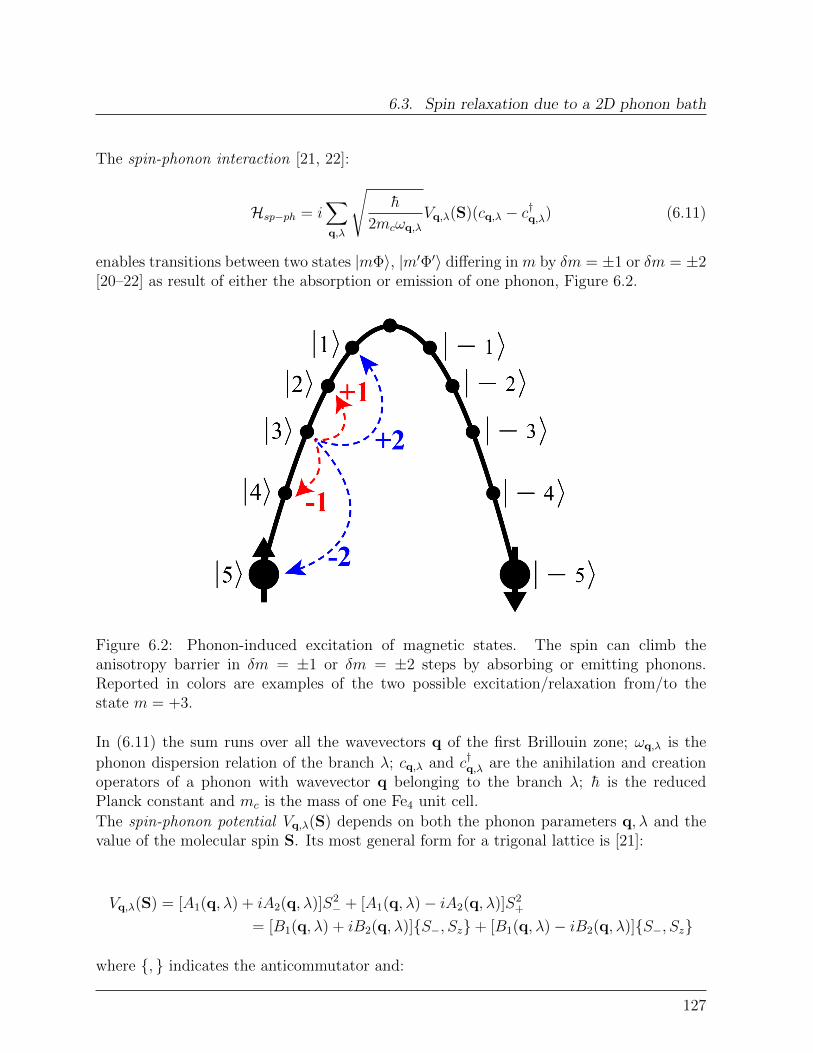
6.3. Spin relaxation due to a 2D phonon bath
The spin-phonon interaction [21, 22]:
Hsp−ph = i∑q,λ
√h
2mcωq,λ
Vq,λ(S)(cq,λ − c†q,λ) (6.11)
enables transitions between two states |mΦ〉, |m′Φ′〉 differing in m by δm = ±1 or δm = ±2[20–22] as result of either the absorption or emission of one phonon, Figure 6.2.
Figure 6.2: Phonon-induced excitation of magnetic states. The spin can climb theanisotropy barrier in δm = ±1 or δm = ±2 steps by absorbing or emitting phonons.Reported in colors are examples of the two possible excitation/relaxation from/to thestate m = +3.
In (6.11) the sum runs over all the wavevectors q of the first Brillouin zone; ωq,λ is the
phonon dispersion relation of the branch λ; cq,λ and c†q,λ are the anihilation and creationoperators of a phonon with wavevector q belonging to the branch λ; h is the reducedPlanck constant and mc is the mass of one Fe4 unit cell.
The spin-phonon potential Vq,λ(S) depends on both the phonon parameters q, λ and thevalue of the molecular spin S. Its most general form for a trigonal lattice is [21]:
Vq,λ(S) = [A1(q, λ) + iA2(q, λ)]S2− + [A1(q, λ)− iA2(q, λ)]S2
+
= [B1(q, λ) + iB2(q, λ)]S−, Sz+ [B1(q, λ)− iB2(q, λ)]S−, Sz
where , indicates the anticommutator and:
127
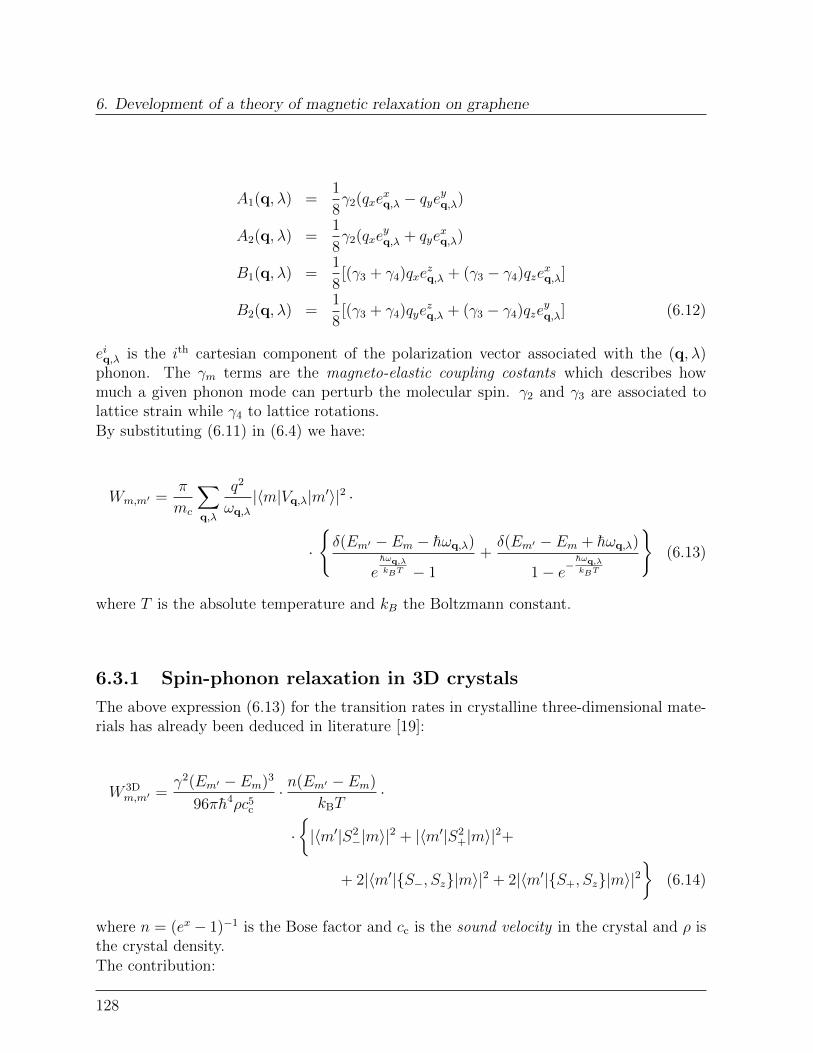
6. Development of a theory of magnetic relaxation on graphene
A1(q, λ) =1
8γ2(qxe
xq,λ − qye
yq,λ)
A2(q, λ) =1
8γ2(qxe
yq,λ + qye
xq,λ)
B1(q, λ) =1
8[(γ3 + γ4)qxe
zq,λ + (γ3 − γ4)qze
xq,λ]
B2(q, λ) =1
8[(γ3 + γ4)qye
zq,λ + (γ3 − γ4)qze
yq,λ] (6.12)
eiq,λ is the ith cartesian component of the polarization vector associated with the (q, λ)phonon. The γm terms are the magneto-elastic coupling costants which describes howmuch a given phonon mode can perturb the molecular spin. γ2 and γ3 are associated tolattice strain while γ4 to lattice rotations.By substituting (6.11) in (6.4) we have:
Wm,m′ =π
mc
∑q,λ
q2
ωq,λ
|〈m|Vq,λ|m′〉|2 ·
·
δ(Em′ − Em − hωq,λ)
ehωq,λkBT − 1
+δ(Em′ − Em + hωq,λ)
1− e−hωq,λkBT
(6.13)
where T is the absolute temperature and kB the Boltzmann constant.
6.3.1 Spin-phonon relaxation in 3D crystals
The above expression (6.13) for the transition rates in crystalline three-dimensional mate-rials has already been deduced in literature [19]:
W 3Dm,m′ =
γ2(Em′ − Em)3
96πh4ρc5c
· n(Em′ − Em)
kBT·
·|〈m′|S2
−|m〉|2 + |〈m′|S2+|m〉|2+
+ 2|〈m′|S−, Sz|m〉|2 + 2|〈m′|S+, Sz|m〉|2
(6.14)
where n = (ex − 1)−1 is the Bose factor and cc is the sound velocity in the crystal and ρ isthe crystal density.The contribution:
128

6.3. Spin relaxation due to a 2D phonon bath
|〈m′|S2−|m〉|2 + |〈m′|S2
+|m〉|2 (6.15)
accounts for the δm = ±2 transitions, while:
2|〈m′|S−, Sz|m〉|2 + 2|〈m′|S+, Sz|m〉|2 (6.16)
accounts for δm± 1 transitions.To simplify the calculation, the phonon dynamics has been approximated to only threeacoustic branches with:
ωq,λ = cq (6.17)
for both longitudinal and transverse modes, so that the sound velocity in the material c isassumed to be independent of the phonon polarization c = cL = cT . Moreover, since thereis no experimental data about the magneto-elastic coupling constants, they are assumedto have the same value γ2 = γ3 = γ4 = γ. The latter will then be extracted by consideringthe relaxation time at T = 4.2 K and H = 0 T.
6.3.2 Spin-phonon relaxation in 2D environments
We now extend the above result to a collection of non-interacting [Fe4(L)2(dpm)6] SMMs,placed on a two-dimensional graphene surface where the main contribution to the spin-phonon interaction is due to the two-dimensional phononic modes.By transforming the sum in (6.13):
1
N∑q,λ
→ 2a2
(2π)2
∫d2q (6.18)
and solving the integral we obtain:
W 2Dm,m′ =
γ2(Em′ − Em)2
64h3σc4h
· n(Em′ − Em)
kBT·
·|〈m′|S2
−|m〉|2 + |〈m′|S2+|m〉|2+
+ 2|〈m′|S−, Sz|m〉|2 + 2|〈m′|S+, Sz|m〉|2
(6.19)
where σ and ch are the speed of sound and the surface density of the two-dimensionalhybrid material respectively.Using Equation (6.19) we can calculate the spin-phonon transition rates W 2D
m,m′ for eachcouple of |m〉, |m+ 1〉 and |m〉, |m+ 2〉 states.It is now important to compare the two Wm,m′ . As a direct result of the different dimen-sionality of the phononic bath, the formulas for transition rate for the 2D and the 3D case
129
6. Development of a theory of magnetic relaxation on graphene
exhibit different power dependences on c, h and (Em′−Em). By considering the numericalprefactors only:
R3D =γ2
96πh4ρc5c
(6.20)
R2D =γ2
64h3σc4h
(6.21)
we find the relation:
R3D
R2D=
2
3
σkBch
ρπh4c5c
(6.22)
which describes the relation between the spin dynamics in the hybrids and in the crystallineform in the thermally-activated regime, where phonons are fundamental for the relaxationof the magnetization.
The quantities ρ, cc are known as extracted from measurements on crystalline sample bydifferent techniques [23]. The magnitude of the magneto-elastic coupling γ constant isunknown and microscopic derivation of this parameter has never been attempted in theliterature. Nevertheless, it is safe to assume that γ remains unaltered since it mainlydepends on:
a) the spin-obit coupling of the ions (which remains the same whether the molecules arein crystals or in hybrids);
b) the very local environment of the Fe ions, which transmits the vibrational distor-tion to the d orbitals (and this latter contribution also remains unvaried, for intact[Fe4(L)2(dpm)6] molecules).
The only unknown parameters in relation (6.22) are then the sound velocity ch and thedensity σ of the hybrid material. Since σ is a parameter characteristic of the phononic bath,it is reasonable to assume it equal to the mass-surface ratio of graphene σ = σGraphene =7.7 · 10−9g/cm2 [24, 25].
ch is the only unknown parameter. If fitting of the experimental data proves the equality:
ch = cGraphene = 2.1 · 106 cm/s (6.23)
then, equation (6.22) would demostrate the applicability of the above model and it wouldconfirm that the dimensionality of the phonon bath has a clear effect on the thermalrelaxation of a magnetic system.
130
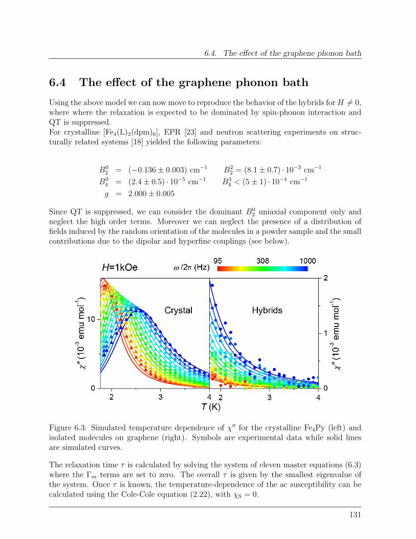
6.4. The effect of the graphene phonon bath
6.4 The effect of the graphene phonon bath
Using the above model we can now move to reproduce the behavior of the hybrids forH 6= 0,where where the relaxation is expected to be dominated by spin-phonon interaction andQT is suppressed.For crystalline [Fe4(L)2(dpm)6], EPR [23] and neutron scattering experiments on struc-turally related systems [18] yielded the following parameters:
B02 = (−0.136± 0.003) cm−1 B2
2 = (8.1± 0.7) · 10−3 cm−1
B04 = (2.4± 0.5) · 10−5 cm−1 B3
4 < (5± 1) · 10−4 cm−1
g = 2.000± 0.005
Since QT is suppressed, we can consider the dominant B02 uniaxial component only and
neglect the high order terms. Moreover we can neglect the presence of a distribution offields induced by the random orientation of the molecules in a powder sample and the smallcontributions due to the dipolar and hyperfine couplings (see below).
Figure 6.3: Simulated temperature dependence of χ′′ for the crystalline Fe4Py (left) andisolated molecules on graphene (right). Symbols are experimental data while solid linesare simulated curves.
The relaxation time τ is calculated by solving the system of eleven master equations (6.3)where the Γm terms are set to zero. The overall τ is given by the smallest eigenvalue ofthe system. Once τ is known, the temperature-dependence of the ac susceptibility can becalculated using the Cole-Cole equation (2.22), with χS = 0.
131
6. Development of a theory of magnetic relaxation on graphene
As shown in Figure 6.3 we can perfectly reproduce the susceptibility curves of the crystalsby setting B0
2 = −0.12 ± 0.02 cm−1 and g = 2.004 ± 0.003, and by considering the 3Dversion of the transition rates W 3D
m,m′ with the speed of sound cc = 2.8 · 105 cm s−1 foundin literature [26, 27].It is important to notice that the cc value extracted from the ac-susceptibility at 4.2 K, isin very good agreement with the literature, stressing the consistency and robustness of theresults. (For the details on this procedure see references [17, 18, 28]).The barrier values extracted from the simulated dynamics provides B0
2 = −0.13 ± 0.01cm−1, in agreement with the Arrhenius analysis.The behavior of the hybrid, is very well reproduced by considering the 2D version of W 2D
m,m′
(see Equation (6.14)), while mantaining the same B02 value and without introducing any
distribution of relaxation times due to other effects. Axial distortions of the Fe4Py ongraphene can thus be excluded.Importantly, an excellent match between simulated and experimental behaviors is achievedby assuming the density σ and the speed of sound ch of the hybrid sample equal to thoseof graphene:
σ = σGraphene = 7.7 · 10−9g/cm2
ch = cGraphene = 2.1 · 106 cm/s
We wish to stress here that the above simulations (Figure 6.3) contain no fitting parameters,and only use the EPR coefficients and parameters known from the literature such as,density and speed of sound of graphene and the crystal speed of sound. These observationsunderscore the relevance of graphene vibrational modes for classical spin relaxation andconfirm the effect of the dimensionality of the phonon bath on the thermal relaxationchannel of SMMs.
6.5 Magnetic quantum tunneling for Fe4 cluster on
graphene
Now that the phononic effects are established, we can move to the behavior of the spinsfor H = 0, where QT is active. Our goal here is to calculate the tunneling transition ratesΓm taking into account the modulation of the anisotropy induced by the interaction withgraphene. To model the quantum relaxation path we consider the following Hamiltonianin the framework of high order perturbation theory:
H = H0 +H1 (6.24)
where the unperturbed Hamiltonian:
H0 = −AS2z (6.25)
132
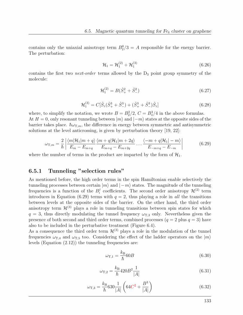
6.5. Magnetic quantum tunneling for Fe4 cluster on graphene
contains only the uniaxial anisotropy term B02/3 = A responsible for the energy barrier.
The perturbation:
H1 = H(2)1 +H(3)
1 (6.26)
contains the first two next-order terms allowed by the D3 point group symmetry of themolecule:
H(2)1 = B(S2
+ + S2−) (6.27)
H(3)1 = C[Sz(S
3+ + S3
−) + (S3+ + S3
−)Sz] (6.28)
where, to simplify the notation, we wrote B = B22/2, C = B3
4/4 in the above formulas.At H = 0, only resonant tunneling between |m〉 and |−m〉 states at the opposite sides of thebarrier takes place. hωT,m, the difference in energy between symmetric and antisymmetricsolutions at the level anticrossing, is given by perturbation theory [19, 22]:
ωT,m =2
h
∣∣∣∣〈m|H1|m+ q〉Em − Em+q
〈m+ q|H1|m+ 2q〉Em+q − Em+2q
. . .〈−m+ q|H1| −m〉E−m+q − E−m
∣∣∣∣ (6.29)
where the number of terms in the product are imparted by the form of H1.
6.5.1 Tunneling ”selection rules”
As mentioned before, the high order terms in the spin Hamiltonian enable selectively thetunneling processes between certain |m〉 and |−m〉 states. The magnitude of the tunnelingfrequencies is a function of the Bj
i coefficients. The second order anisotropy H(2) termintroduces in Equation (6.29) terms with q = 2, thus playing a role in all the transitionsbetween levels at the opposite sides of the barrier. On the other hand, the third orderanisotropy term H(3) plays a role in tunneling transitions between spin states for whichq = 3, thus directly modulating the tunnel frequency ωT,3 only. Nevertheless given thepresence of both second and third order terms, combined processes (q = 2 plus q = 3) havealso to be included in the perturbative treatment (Figure 6.4).As a consequence the third order term H(3) plays a role in the modulation of the tunnelfrequencies ωT,4 and ωT,5 too. Considering the effect of the ladder operators on the |m〉levels (Equation (2.12)) the tunneling frequencies are:
ωT,1 =kB
h60B (6.30)
ωT,2 =kB
h420B2 1
|A|(6.31)
ωT,3 =kB
h630
1
|A|
(64C2 +
B3
|A|
)(6.32)
133

6. Development of a theory of magnetic relaxation on graphene
Figure 6.4: Graphical representation of virtual processes due to theH(2) andH(3) perturba-tive terms connecting the |5〉 and |−5〉 states and included in Equation (6.29). The tunnelrate ωT,5 is determined by the combination of virtual processes connecting |m〉 states bysteps of 2 (red arrows) and combined ”3+2” processes (blue, green and purple arrows).Other combined ”3+2” paths are omitted for clarity.
ωT,4 =kB
h315
B
A2
(384C2 +
B3
|A|
)(6.33)
ωT,5 =kB
h
(1575
32
B5
A4+ 66150
B2C2
|A|3
)(6.34)
We can now proceed with the calculation of the tunneling rates Γm. The Γm’s are functionsof the tunnel frequencies ωT,m and the mean life time τm of the of the initial |m〉 stateimparted by the phonon-induced transitions above:
Γm = 4ω2T,m
τm1 + τ 2
m(Em − E−m)2/2(6.35)
where:
τm =1
Wm,m−1 +Wm,m−2 +Wm,m+1 +Wm,m+2
(6.36)
This treatment implicitly includes combined relaxation paths called phonon-assisted tun-neling [20, 22, 29], in which the spin, initially in the state |m〉, makes a transition to the
134

6.6. Effect of dipolar and hyperfine interactions
state |m±1〉 (|m±2〉) by absorbing a phonon and then tunnels to |−m∓1〉 (|−m∓2〉) onthe other side of the barrier, Figure 6.5a. Emission of a phonon after the tunneling processis also included, and is of particular importance at low temperature for tunneling betweenthe lowest lying states in presence of hyperfine and dipolar interactions [19], Figure 6.5a.
Figure 6.5: a) Phonon-assisted tunneling between excited magnetic states. At sufficientlyhigh temperatures the spin climbs the anisotropy barrier in δm = ±1 or δm = ±2 steps byabsorbing or emitting phonons and then tunnels through it. b) At low temperatures thetunneling process between the lowest-lying ground states is enabled by hyperfine and dipo-lar interaction. Energy conservation in the spin-flip process requires emission of phonons.
6.6 Effect of dipolar and hyperfine interactions
While the hyperfine interaction couples the (electronic) spin of each core magnetic ion tothe spin of its nucleus [19, 22], the long range dipolar interaction is responsible for thecoupling between the total spins S of neighboring molecules [22].
6.6.1 Hyperfine coupling
Hyperfine interaction creates an effective fluctuating magnetic field Hhyp that broadensthe energy span of each |m〉 level. This relaxes the resonance condition enabling tunnelingwhen the levels are off-resonance by less than the hyperfine energy span. The effect ofhyperfine interactions in Fe4 clusters have been investigated experimentally for crystallinesamples [22, 30], and resulted to be relatively weak Hhyp ≈ 1 Oe due to the small isotopicabundance (2.12%) of the spin carrying 57Fe nuclei.
135
6. Development of a theory of magnetic relaxation on graphene
6.6.2 Dipolar interaction: coherent and incoherent tunneling
The effect of dipolar interaction is to introduce an effective magnetic field Hdip that shiftsthe |m〉 and | −m〉 relative to the resonance condition [19, 22]. Because of level mixing,at H = 0 the lowest lying states |5∗〉 and | − 5∗〉 are not pure eigenstates of the uniaxialanisotropy term but are the superpositions:
|5∗〉 =10∑i=0
l5,5−i|5− i〉 (6.37a)
| − 5∗〉 =10∑i=0
r−5,−5+i| − 5 + i〉 (6.37b)
where rm,m′ and lm,m′ indicate the weights of the different |m〉 components on the leftand right sides of the barrier, while i = 2 and 3 is given by the high order anisotropyterms B2
2 and B34 in the Hamiltonian (6.24) (responsible for the mixing of states such that
|m−m′| = ik, with k is an integer).For Hdip = 0 the weights at the opposite sides are the same rm,m′ = lm,m′ , thus the |5∗〉,| − 5∗〉 are fully delocalized between the two sides of the barrier, favoring tunneling. Thisrepresent the ideal case of an isolated spin, whose tunnel motion is characterized by aperiodic oscillation between the left- and right-hand sides of the barrier. In this case, thewavefunction describing the spin has a well defined phase (and frequency ωT,m), so thetunneling process is coherent.In real spin systems, such as SMMs in crystals, a dipolar field Hdip 6= 0 unbalances theweights of the components in the superpositions |5∗〉 and |−5∗〉. For intermediate values ofHdip, such that gµBSzHdip < hωT,5 the wavefunction is partially localized on one side of thebarrier, so the spin oscillates between the two wells but is partially trapped in one of thetwo sides. As consequence the tunneling rate 1/τm is reduced and the phase informationis lost, leading to incoherent tunneling. When the energy shift induced by Hdip is largerthan the energy associated with the tunnel frequency gµBSzHdip >> hωT,5, the eigenstates|5∗〉 and | − 5∗〉 are fully localized on the two sides of the barrier and tunneling is fullysuppressed.Experimental investigations on pure and diluted Fe4 clusters proved that the tunnelingrate increases on lowering the dipolar interactions [30]. An upper limit of Hdip ≈ 200 Oewas found for the crystal. Moreover in graphene hybrids the graphene layer is predictedto shield effectively the molecular dipolar interactions [31].
6.7 Effect of the B34 term: Villain’s coherent tunneling
The standard treatment of the tunneling probabilities is due to Landau, Zener and Stuck-elberg [9, 29, 32, 33], and mainly concentrates on the regime where the perturbation in-troducing the level mixing (modelled by high orders terms in the spin Hamiltonian) issmall.
136
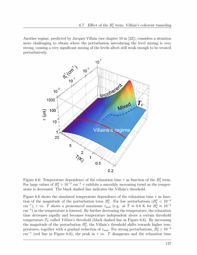
6.7. Effect of the B34 term: Villain’s coherent tunneling
Another regime, predicted by Jacques Villain (see chapter 10 in [22]), considers a situationmore challenging to obtain where the perturbation introducing the level mixing is verystrong, causing a very significant mixing of the levels albeit still weak enough to be treatedperturbatively.
Figure 6.6: Temperature dependence of the relaxation time τ as function of the B34 term.
For large values of B34 > 10−3 cm−1 τ exhibits a smoothly increasing trend as the temper-
ature is decreased. The black dashed line indicates the Villain’s threshold.
Figure 6.6 shows the simulated temperature dependence of the relaxation time τ as func-tion of the magnitude of the perturbation term B3
4 . For low perturbations (B34 < 10−4
cm−1), τ vs. T shows a pronounced maximum τmax (e.g. at T ≈ 0.8 K for B34 ≈ 10−5
cm−1) as the temperature is lowered. By further decreasing the temperature, the relaxationtime decreases rapidly and becomes temperature independent above a certain thresholdtemperature TV called Villain’s threshold (black dashed line in Figure 6.6). By increasingthe magnitude of the perturbation B3
4 , the Villain’s threshold shifts towards higher tem-peratures, together with a gradual reduction of τmax. For strong perturbations, B3
4 > 10−3
cm−1 (red line in Figure 6.6), the peak in τ vs. T disappears and the relaxation time
137

6. Development of a theory of magnetic relaxation on graphene
increases monotonously toward a saturation value of τ ≈ 4.5 µs as the temperature de-creases. In this perturbation regime the spin relaxes very fast (τ ∼ 10−6 s). Above theVillain’s threshold τ is independent of B3
4 .The Villain’s threshold is predicted [22] to mark the transition between the incoherentand coherent tunneling regimes. Above the threshold (i.e. at temperatures > TV or lowperturbation values), the tunneling process is largely incoherent, and is strongly affectedby phonon absorption and other interactions with the environment. On the contrary,overcoming of the Villain’s threshold leads to a saturated quantum tunneling regime (theτ stays constant when the perturbation is further increased in magnitude), where the spintunnels adiabatically through the barrier, oscillating coherently between the two wells.
6.7.1 Effect of graphene on quantum tunneling
For isolated Fe4Py grafted on graphene we expect the following conditions to be fulfilled:
i) Dipolar interactions are strongly suppressed, and hyperfine interaction is intrinsicallylow, leading to true degeneracy of the |m〉 and | −m〉 levels;
ii) The interaction with the graphene electron density introduces a very significant per-turbation that we model via an enhanced B3
4 term.
The effect of these conditions on the tunneling frequencies ωT,m can be modeled by makinguse of Equation (6.29) with the extended spin-Hamiltonian:
Hsp = B02O
02 +B0
4O04 +B2
2O22 +B3
4O34 +Hdip +Hhyp. (6.38)
The relaxation time is then extracted by solving the system of master equations (6.3) withthe tunneling rates Γm given by (6.35). It is important to remember that in the latter,spin-phonon interaction not only plays an important role for high temperatures, but alsofor T → 0 as it accounts for emission of phonons imparted by energy conservation in thetunneling process at low temperatures [19].Figure 6.7 shows the impact of the different interactions on the relaxation time τ and itstemperature dependence. As described above, the combined effect of hyperfine couplingand lowered dipolar interaction leads to an appreciable decrease in the relaxation time atlow temperatures while it does not have appreciable effects for T > 0.8 K. In addition,the different Wm,m′ due to the 2D graphene phonons lead to a further reduction of τ atlow temperatures. Nevertheless, these conditions cannot explain the striking enhancementof QT at H = 0, which requires introducing the coupling to graphene electrons. Thelatter is expressed by the perturbation integral 〈m|VI|ΨG〉, where molecular and grapheneelectronic states (|m〉 and |ΨG〉 respectively) interact via the potential VI, altering the spinstate |m〉. The wavefunction |ΨG〉 has threefold symmetry, and the corresponding point-group rules permit non-vanishing integral terms only for Bj
i coefficients with j a multipleof 3, independently of the form of VI. In the perturbation treatment of the spin-grapheneinteraction, all such terms have an identical effect on the level mixing and the QT rate
138
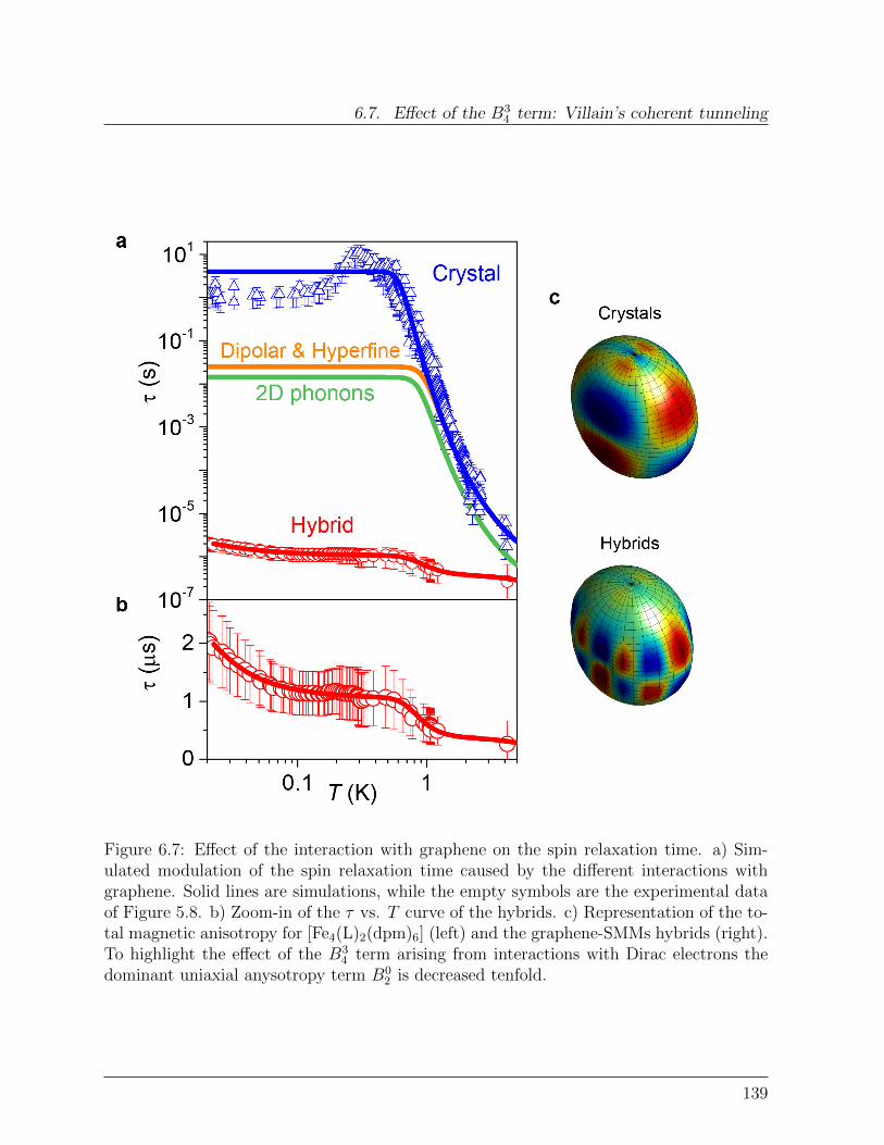
6.7. Effect of the B34 term: Villain’s coherent tunneling
Figure 6.7: Effect of the interaction with graphene on the spin relaxation time. a) Sim-ulated modulation of the spin relaxation time caused by the different interactions withgraphene. Solid lines are simulations, while the empty symbols are the experimental dataof Figure 5.8. b) Zoom-in of the τ vs. T curve of the hybrids. c) Representation of the to-tal magnetic anisotropy for [Fe4(L)2(dpm)6] (left) and the graphene-SMMs hybrids (right).To highlight the effect of the B3
4 term arising from interactions with Dirac electrons thedominant uniaxial anysotropy term B0
2 is decreased tenfold.
139

6. Development of a theory of magnetic relaxation on graphene
of the lowest |m〉 levels, differing only in the perturbation order. Accordingly, to addressQT, the overall graphene effect can be merged into the leading-order B3
4O34 term, which
directly admixes only the m = ±3 states (direct mixing of lower levels would require lowersymmetry terms, such as B2
2O22).
Figure 6.8: Temperature and frequency dependence of the real component of the dynamicsusceptibility χ′ in H = 0 for crystals (top) and isolated Fe4Py on graphene (bottom).Lines are simulations with the theory.
By introducing a B34 > 2 · 10−3 cm−1 term into the simulations, while mantaining all other
parameters as in the H 6= 0 case, both the the ac susceptibility (Figure 6.8) and the T -dependence of τ and are indeed very well reproduced. The pictorial representation of thespin anisotropy in the crystals and hybrids in Figure 6.7c shows the significant weight ofthe additional O3
4 term and highlights the signature of the threefold rotational symmetryof graphene on the spin anisotropy.The correct operator form of the microscopic interaction potential for VI is debated. Onepossibility [34–36] is the Heisenberg form Θ = (S+σ− + S−σ+ + 2Szσz)/2 where σ+, σ−,σz, are the spin operators of the Dirac fermion, nevertheless the nature of the underlyingscattering processes remains debated. For [Fe4(L)2(dpm)6] a direct quantitative comparisonamong the different proposals is intricate, because of the cumbersome ab initio evaluationof the amplitude cross-sections. Anyway, spin-flip processes as efficient as those observedare only predicted when scattering due to the presence of two K points is included in thetheory [37], and the values here obtained can be used to validate the theoretical modelsproposed for spin-Dirac fermion interactions.Strongly-perturbative QT of spins, predicted by Villain decades ago [22], strictly requirespronounced electronic perturbations combined with minimal dipolar interactions. Theseconditions are hard to fulfil in crystals, and Villains regime has so far eluded observation;
140
6.8. Conclusions
the graphene hybrids offer ideal conditions by simultaneously suppressing dipolar inter-actions and electronically enhancing the transverse terms. For suppressed dipolar fields,weak perturbations (as in crystals) would lead to a non-monotonic behaviour in the τ vsT plot, where standard tunnelling is followed by a slow descent into Villain’s QT regime.In contrast, the B3
4 perturbation term introduced by graphene is large enough to directlydrive the spins into Villain’s regime, leading to a monotonous temperature dependence ofτ . The associated threshold yields a lower bound of 0.3 eV for the interaction betweenSMM spins and the Dirac electrons.
6.8 Conclusions
The above observations set the theoretical and experimental basis for the exploration ofnovel magnetic effects associated with localized spins on graphene. The unraveled vibra-tional and electronic interactions provide fundamental guidelines for the design of spin-nanomechanical and nanospintronic devices. Strong graphene-induced transverse termsopen up possibilities to electrically tune the mixing of spin states, allowing control overquantum tunneling in ways hitherto demonstrated for other qubits [38] The realization ofVillain’s regime, being it coherent by definition, opens up novel perspectives for quantumoperations. Our findings can be extended to the analysis of other spin-substrate system(e.g. SMMs on Au surfaces [39] and NV-centers on graphene [40]), to reveal unique detailson symmetry-breaking quantum effects.
141
Bibliography
Bibliography
[1] Cervetti, C., Heintze, E. & Bogani, L. Interweaving spins with their environment:novel inorganic nanohybrids with controllable magnetic properties. Dalton transac-tions 43, 4220–32 (2014).
[2] van der Sar, T. et al. Decoherence-protected quantum gates for a hybrid solid-statespin register. Nature 484, 82–86 (2012).
[3] de Lange, G., Wang, Z. H., Riste, D., Dobrovitski, V. V. & Hanson, R. Universaldynamical decoupling of a single solid-state spin from a spin bath. Science 330,60–63 (2010).
[4] Ganzhorn, M. & Wernsdorfer, W. Molecular Quantum Spintronics Using Single-Molecule Magnets. In Bartolome, J., Luis, F. & Fernandez, J. F. (eds.) MolecularMagnets Physics and Applications, chap. 13, 319–364 (Springer, Berlin Heidelberg,2014).
[5] Garanin, D. A. & Chudnovsky, E. M. Quantum Entanglement of a Tunneling Spinwith Mechanical Modes of a Torsional Resonator. Phys. Rev. X 1, 11005 (2011).
[6] Kovalev, A. a., Hayden, L. X., Bauer, G. E. W. & Tserkovnyak, Y. Macrospin tunnel-ing and magnetopolaritons with nanomechanical interference. Phys. Rev. Lett. 106,1–4 (2011).
[7] Kontos, T. Spintronics meets nanoelectromechanics. Physics 4 (2011).
[8] Ganzhorn, M., Klyatskaya, S., Ruben, M. & Wernsdorfer, W. Strong spin-phononcoupling between a single-molecule magnet and a carbon nanotube nanoelectrome-chanical system. Nat. Nanotech. 8, 165–169 (2013).
[9] Oberg, J. C. et al. Control of single-spin magnetic anisotropy by exchange coupling.Nature nanotechnology 9, 64–8 (2014).
[10] Taminiau, T. H. et al. Detection and control of individual nuclear spins using a weaklycoupled electron spin. Physical Review Letters 109, 1–5 (2012).
[11] Bogani, L. & Wernsdorfer, W. L. Molecular spintronics using single-molecule magnets.Nat. Mater. 7, 179–186 (2008).
[12] Ardavan, A. et al. Will Spin-Relaxation Times in Molecular Magnets Permit QuantumInformation Processing? Phys. Rev. Lett. 98, 57201 (2007).
[13] Leuenberger, M. N. & Loss, D. Quantum computing in molecular magnets. Nature410, 789–793 (2001).
142

Bibliography
[14] Tejada, J., Chudnovsky, E. M., del Barco, E., Hernandez, J. M. & Spiller, T. P.Magnetic qubits as hardware for quantum computers. Nanotechnology 12, 17 (2000).
[15] Hill, S., Edwards, R. S., Aliaga-Alcalde, N. & Christou, G. Quantum coherence in anexchange-coupled dimer of single-molecule magnets. Science 302, 1015–1018 (2003).
[16] DiVincenzo, D. P. Quantum Computation. Science 270, 255–261 (1995).
[17] Rastelli, E. & Tassi, A. Relaxation time of the nanomagnet Fe4. Phys. Rev. B 79,104415 (2009).
[18] Carretta, S. et al. Intra- and inter-multiplet magnetic excitations in a tetrairon(III)molecular cluster. Phys. Rev. B 70, 214403 (2004).
[19] Hartmann-Boutron, F., Politi, P. & Villain, J. Tunneling and magnetic relaxationin mesoscopic molecules. International Journal of Modern Physics B 10, 2577–2638(1996).
[20] Fort, A., Rettori, A., Villain, J., Gatteschi, D. & Sessoli, R. Mixed quantum-thermalrelaxation in Mn12 acetate molecules. Phys. Rev. Lett. 80, 612–615 (1998).
[21] Politi, P., Rettori, A., Hartmann-Boutron, F. & Villain, J. Tunneling in mesoscopicmagnetic molecules. Phys. Rev. Lett. 75, 537–540 (1995).
[22] Gatteschi, D., Sessoli, R. & Villain, J. Molecular Nanomagnets. Mesoscopic Physicsand Nanotechnology (OUP, Oxford, 2006).
[23] Bogani, L. et al. Single-molecule-magnet carbon-nanotube hybrids. AngewandteChemie - International Edition 48, 746–50 (2009).
[24] Bruinsma, R. F., Gennes, P. G. D., Freund, J. B. & Levine, D. Aroute to high surfacearea, porosity and inclusion of large molecules in crystals. Nature 427, 523–527 (2004).
[25] Stankovich, S. et al. Graphene-based composite materials. Nature 442, 282–286(2006).
[26] Pinto, H. P. & Leszczynski, J. Fundamental Properties of Graphene. In D’Souza,F. & Kadish, K. M. (eds.) Handbook of Carbon Nano Materials Vol. 5, chap. 1, 1–37(World Scientific, New York).
[27] Morozov, S. V. et al. Giant intrinsic carrier mobilities in graphene and its bilayer.Phys. Rev. Lett. 100, 16602 (2008).
[28] Rastelli, E. & Tassi, A. Magnetization steps in nanomagnets induced by a time-dependent magnetic field: Application to Fe4. Phys. Rev. B 75, 134414 (2007).
[29] Leuenberger, M. N. & Loss, D. Incoherent Zener tunneling and its application tomolecular magnets. Phys. Rev. B 61, 12200–12203 (2000).
143
Bibliography
[30] Vergnani, L. et al. Magnetic bistability of isolated giant-spin centers in a diamagneticcrystalline matrix. Chemistry - A European Journal 18, 3390–3398 (2012).
[31] Koshino, M., Arimura, Y. & Ando, T. Magnetic Field Screening and Mirroring inGraphene. Phys. Rev. Lett. 102, 177203 (2009).
[32] Zener, C. Non-Adiabatic Crossing of Energy Levels. Proceedings of the Royal Societyof London. Series A 137, 696–702 (1932).
[33] Landau, L. On the theory of transfer of energy at collisions II. Phys. Z. Sowjetunion2, 46 (1932).
[34] Miyamachi, T. et al. Stabilizing the magnetic moment of single holmium atoms bysymmetry. Nature 503, 1–5 (2013).
[35] Fransson, J. Spin inelastic electron tunneling spectroscopy on local spin adsorbed onsurface. Nano Letters 9, 2414–2417 (2009).
[36] Hirjibehedin, C. F. et al. Large magnetic anisotropy of a single atomic spin embeddedin a surface molecular network. Science 317, 1199–1203 (2007).
[37] Trauzettel, B., Bulaev, D., Loss, D. & Burkard, G. Spin qubits in graphene quantumdots. Nature Physics 3, 0–5 (2007).
[38] Yamamoto, M. et al. Electrical control of a solid-state flying qubit. Nature Nanotech-nology 7, 247–251 (2012).
[39] Mannini, M. et al. Quantum tunnelling of the magnetization in a monolayer of orientedsingle-molecule magnets. Nature 468, 417–421 (2010).
[40] Brenneis, A. et al. Ultrafast electronic read-out of diamond NV centers coupled tographene. Nat Nano 10, 135–139 (2014).
144
Part II
Spin-relaxation in functionalizedgraphene devices
145

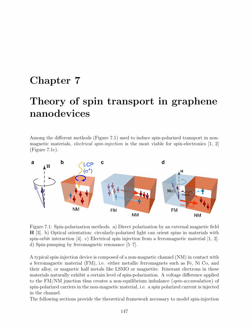
Chapter 7
Theory of spin transport in graphenenanodevices
Among the different methods (Figure 7.1) used to induce spin-polarized transport in non-magnetic materials, electrical spin-injection is the most viable for spin-electronics [1, 2](Figure 7.1c).
Figure 7.1: Spin-polarization methods. a) Direct polarization by an external magnetic fieldH [3]. b) Optical orientation: circularly-polarized light can orient spins in materials withspin-orbit interaction [4]. c) Electrical spin injection from a ferromagnetic material [1, 2].d) Spin-pumping by ferromagnetic resonance [5–7].
A typical spin-injection device is composed of a non-magnetic channel (NM) in contact witha ferromagnetic material (FM), i.e. either metallic ferromagnets such as Fe, Ni Co, andtheir alloy, or magnetic half metals like LSMO or magnetite. Itinerant electrons in thesematerials naturally exhibit a certain level of spin-polarization. A voltage difference appliedto the FM/NM junction thus creates a non-equilibrium imbalance (spin-accumulation) ofspin-polarized carriers in the non-magnetic material, i.e. a spin polarized current is injectedin the channel.
The following sections provide the theoretical framework necessary to model spin-injection
147
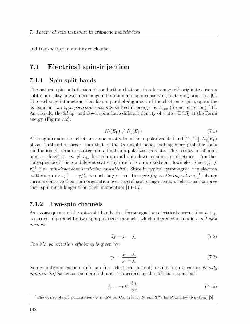
7. Theory of spin transport in graphene nanodevices
and transport of in a diffusive channel.
7.1 Electrical spin-injection
7.1.1 Spin-split bands
The natural spin-polarization of conduction electrons in a ferromagnet1 originates from asubtle interplay between exchange interaction and spin-conserving scattering processes [9].The exchange interaction, that favors parallel alignment of the electronic spins, splits the3d band in two spin-polarized subbands shifted in energy by Uexc (Stoner criterion) [10].As a result, the 3d up- and down-spins have different density of states (DOS) at the Fermienergy (Figure 7.2):
N↑(EF) 6= N↓(EF) (7.1)
Althought conduction electrons come mostly from the unpolarized 4s band [11, 12], N↑(EF)of one subband is larger than that of the 4s unsplit band, making more probable for aconduction electron to scatter into a final spin-polarized 3d state. This results in differentnumber densities, n↑ 6= n↓, for spin-up and spin-down conduction electrons. Anotherconsequence of this is a different scattering rate for spin-up and spin-down electrons, τ−1
e↑ 6=τ−1e↓ (i.e. spin-dependent scattering probability). Since in typical ferromagnet, the electron
scattering rate τ−1e = vF/le is much larger than the spin-flip scattering rates τ−1
↑,↓ , chargecarriers conserve their spin orientation over several scattering events, i.e electrons conservetheir spin much longer than their momentum [13–15].
7.1.2 Two-spin channels
As a consequence of the spin-split bands, in a ferromagnet an electrical current J = j↑+ j↓is carried in parallel by two spin-polarized channels, which difference results in a net spincurrent :
JS = j↑ − j↓ (7.2)
The FM polarization efficiency is given by:
γF =j↑ − j↓j↑ + j↓
(7.3)
Non-equilibrium carriers diffusion (i.e. electrical current) results from a carrier densitygradient ∂n/∂x across the material, and is described by the diffusion equations:
j↑ = −eD↑∂n↑∂x
(7.4a)
1The degree of spin polarization γF is 45% for Co, 42% for Ni and 37% for Permalloy (Ni80Fe20) [8]
148
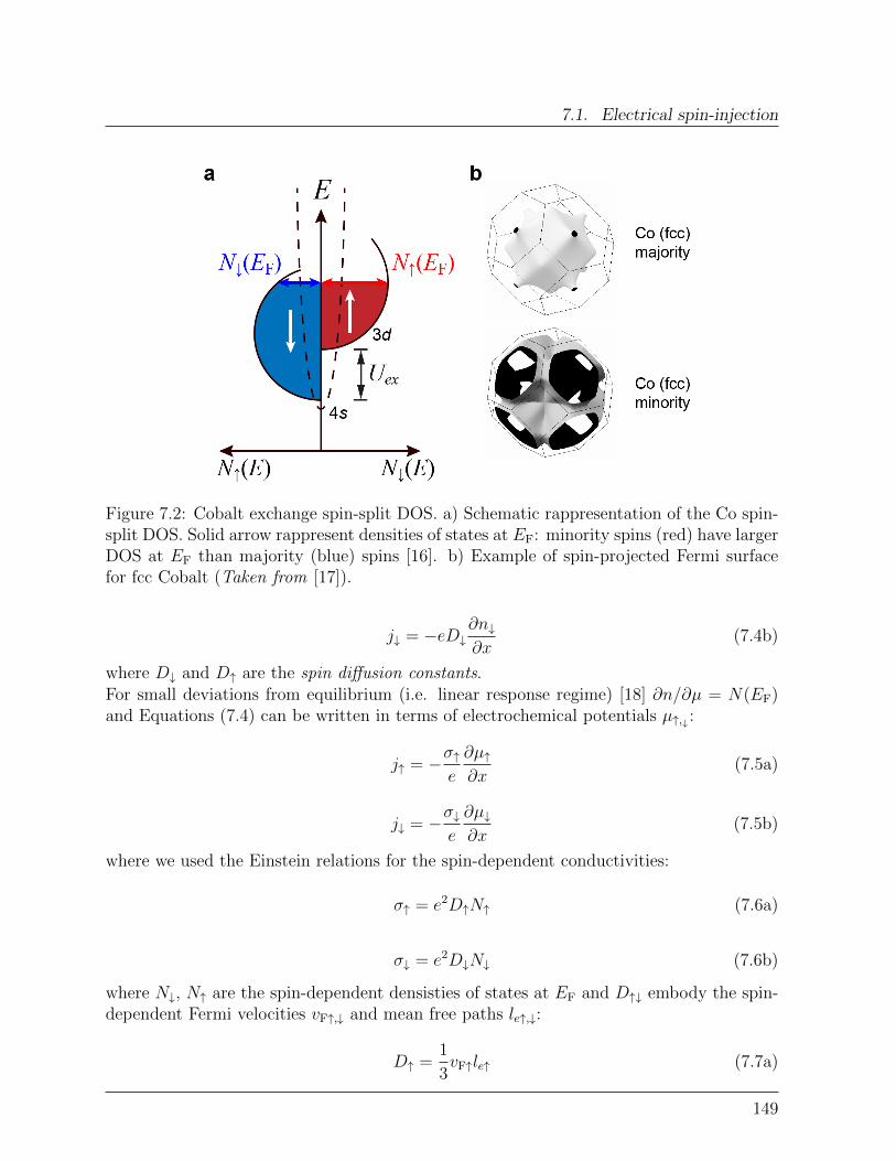
7.1. Electrical spin-injection
Figure 7.2: Cobalt exchange spin-split DOS. a) Schematic rappresentation of the Co spin-split DOS. Solid arrow rappresent densities of states at EF: minority spins (red) have largerDOS at EF than majority (blue) spins [16]. b) Example of spin-projected Fermi surfacefor fcc Cobalt (Taken from [17]).
j↓ = −eD↓∂n↓∂x
(7.4b)
where D↓ and D↑ are the spin diffusion constants.For small deviations from equilibrium (i.e. linear response regime) [18] ∂n/∂µ = N(EF)and Equations (7.4) can be written in terms of electrochemical potentials µ↑,↓ :
j↑ = −σ↑e
∂µ↑∂x
(7.5a)
j↓ = −σ↓e
∂µ↓∂x
(7.5b)
where we used the Einstein relations for the spin-dependent conductivities:
σ↑ = e2D↑N↑ (7.6a)
σ↓ = e2D↓N↓ (7.6b)
where N↓, N↑ are the spin-dependent densisties of states at EF and D↑↓ embody the spin-dependent Fermi velocities vF↑,↓ and mean free paths le↑,↓:
D↑ =1
3vF↑le↑ (7.7a)
149
7. Theory of spin transport in graphene nanodevices
D↓ =1
3vF↓le↓ (7.7b)
This is the essence of the two current model introduced by Mott in 1936 [13] that describesspin-transport in bulk ferromagnets in terms of two parallel spin-polarized conduction chan-nels, each characterized by independent bulk conductivities and diffusion characteristics.
7.1.3 Spin-transport and spin-relaxation
By diffusing in the material, carriers will undergo spin-flip scattering events at rates τ−1↑,↓
characteristic of the material. The spin-flip process, called spin relaxation, is modelledusing the second law of diffusion2, that in the steady state reads [19, 20]:
1
e
∂j↑∂x
= −n↑τ↑
+n↓τ↓
(7.8a)
1
e
∂j↓∂x
= −n↓τ↓
+n↑τ↑
(7.8b)
and in terms of electrochemical potentials reads:
D∂2(µ↑ − µ↓)
∂x2=
(µ↑ − µ↓)τs
(7.9)
where D is the averaged spin-diffusion constant:
D =σ↓D↑ + σ↑D↓σ↑ + σ↓
(7.10)
and τs is called spin relaxation time:
τ−1s = τ−1
↑ + τ−1↓ (7.11)
Equation (7.9) show that the difference between the spin-up and spin-down electrochemicalpotentials µ↑ − µ↓ (spin accumulation signal), decays exponentially over a spin diffusionlength λs:
λs =√Dτs (7.12)
meaning that the net spin-density is completely lost after a time τs characteristic of thematerial.General solutions of Equation (7.9) are:
µ↑ = a+ bx+c
σ↑exp(−x/λs) +
d
σ↑exp(x/λs) (7.13a)
µ↓ = a+ bx− c
σ↓exp(−x/λs)−
d
σ↓exp(x/λs) (7.13b)
2Equations (7.4) and (7.8) are the equivalents of the 1th and 2nd Fick’s law of diffusion in fluid dynamics.
150
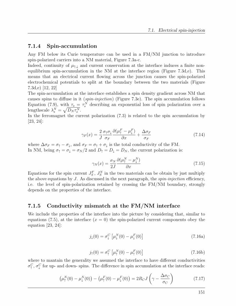
7.1. Electrical spin-injection
7.1.4 Spin-accumulation
Any FM below its Curie temperature can be used in a FM/NM junction to introducespin-polarized carriers into a NM material, Figure 7.3a-c.Indeed, continuity of µ↑,↓ and current conservation at the interface induces a finite non-equilibrium spin-accumulation in the NM at the interface region (Figure 7.3d,e). Thismeans that an electrical current flowing across the junction causes the spin-polarizedelectrochemical potentials to split at the boundary between the two materials (Figure7.3d,e) [12, 22]The spin-accumulation at the interface establishes a spin density gradient across NM thatcauses spins to diffuse in it (spin-injection) (Figure 7.3e). The spin accumulation followsEquation (7.9), with τs = τNs describing an exponential loss of spin polarization over alengthscale λNs =
√DNτNs .
In the ferromagnet the current polarization (7.3) is related to the spin accumulation by[23, 24]:
γF (x) =2
J
σ↑σ↓σF
∂(µF↑ − µF↓ )
∂x+
∆σFσF
(7.14)
where ∆σF = σ↑ − σ↓, and σF = σ↑ + σ↓ is the total conductivity of the FM.In NM, being σ↑ = σ↓ = σN/2 and D↑ = D↓ = DN , the current polarization is:
γN(x) =σN2J
∂(µN↑ − µN↓ )
∂x(7.15)
Equations for the spin current JFS , JNS in the two materials can be obtain by just multiplythe above equations by J . As discussed in the next paragraph, the spin-injection efficiency,i.e. the level of spin-polarization retained by crossing the FM/NM boundary, stronglydepends on the properties of the interface.
7.1.5 Conductivity mismatch at the FM/NM interface
We include the properties of the interface into the picture by considering that, similar toequations (7.5), at the interface (x = 0) the spin-polarized current components obey theequation [23, 24]:
j↓(0) = σC↓[µN↓ (0)− µF↓ (0)
](7.16a)
j↑(0) = σC↑[µN↑ (0)− µF↑ (0)
](7.16b)
where to mantain the generality we assumed the interface to have different conductivitiesσC↑ , σC↓ for up- and down- spins. The difference in spin accumulation at the interface reads:
(µN↑ (0)− µN↓ (0)
)−(µF↑ (0)− µF↓ (0)
)= 2RCJ
(γ − ∆σC
σC
)(7.17)
151
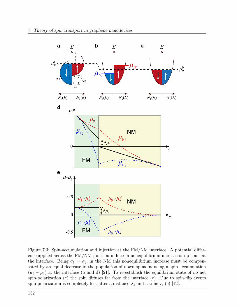
7. Theory of spin transport in graphene nanodevices
Figure 7.3: Spin-accumulation and injection at the FM/NM interface. A potential differ-ence applied across the FM/NM junction induces a nonequilibrium increase of up-spins atthe interface. Being σ↑ = σ↓, in the NM this nonequilibrium increase must be compen-sated by an equal decrease in the population of down spins inducing a spin accumulation(µ↑ − µ↑) at the interface (b and d) [21]. To re-establish the equilibrium state of no netspin-polarization (c) the spin diffuses far from the interface (e). Due to spin-flip eventsspin polarization is completely lost after a distance λs and a time τs (e) [12].
152
7.1. Electrical spin-injection
where the properties of the interface ∆σC = σC↑ − σC↓ , σC = σC↑ + σC↓ , RC = σC/4σC↑ σ
C↓
may depend on several details such as the FM/NM materials combination and the type ofcontact used (i.e tunneling, transparent etc..).The spin polarization at the interface γint is found by applying the conservation of thespin current at the interface JFS (0) = JNS (0) (i.e. assuming no spin flip at the interface)[21, 23–25]:
γ =
(RC
∆σCσC
+RF∆σFσF
)/(RC +RF +RN) (7.18)
where RF =λFs σF
4σF↑ σF↓
, RN = λNs σ−1N are the effective resistances of FM and NM respectively
[23].Equation (7.18) shows that for a transparent ohmic contact (ideally RC = 0), the polar-ization depends on the ratio RF/RN and, being RF << RN for the ferromagnet/grapheneinterface, the current polarization is strongly reduced. This phenomenon is referred toas the conductivity mismatch and can be solved by either increasing RC or by employingtunneling contacts [24].
153
7. Theory of spin transport in graphene nanodevices
7.2 Spin-transport in graphene spinvalves
7.2.1 Non-local lateral spin-valve geometry
To study the spin-transport in graphene, we fabricated graphene-based lateral spinvalves(SV) combined with a non-local measurement configuration (Figure 7.4) [1, 2, 26]. Thegraphene channel (G) is contacted with four ferromagnetic leads (Figure 7.4a). Spin-polarized carriers are injected into G by driving a current from the injector contact FM2,which has been previously magnetized to its saturation magnetization M2 (white arrowin Figure 7.4a), to FM1. Carriers injected into the channel have their spin preferentiallyaligned along M2. This produces a non-equilibrium spin accumulation in the area under-neath FM2 (Figure 7.4b). Because the difference in spin densities at the different sides ofthe device, spins diffuse towards the detector contact FM3.The advantage of a non-local configuration is to separate spin-transport from the chargeflow, the latter being confined to the injector circuit area, (dashed line in Figure 7.4a).There is no charge transport happening in the region between FM2 and FM4, where thespin-accumulation signal (i.e. pure spin-current JS) propagates. This singles out spin-diffusion effects from other phenomena, such as Hall effect, quantum interference [27],magneto-coulomb effect [28–30], or anisotropic magnetoresistance [31], found to obscure oreven mimic the spin accumulation signal. Moreover in contrast to the CPP-GMR spinvalvesof Chapter 2, the lateral geometry allows the manipulation of the spin information byexternal means such as electrostatic gates or chemical functionalizations.The voltage drop VNL between FM3 and FM4 (detection circuit) measures the spin-accumulation at a distance L from the injector. VNL depends on the relative orientationof FM2 and FM3 magnetizations, M2 and M3 respectively. When M3 points in the samedirection as M2, FM3 probes the electrochemical potential µ↑ of the spin-up electrons (mi-nority subband) (Figure 7.5a,d), giving rise to a positive voltage VNL = VP > 0. On theother hand, when M3 is antiparallel to M2, FM3 probes µ↓ (majority subband) resultingin a negative VNL = VAP < 0 (Figure 7.5b,e). This gives rise to a magnetoresistive responsecharacterized two resistance levels RP and RAP, corresponding to different configurationsof injector and detector magnetizations (Figure 7.5c).The resistance difference between parallel and anti-parallel contact configurations ∆RNL,called spin-signal, is a characteristic quantity of every spinvalve device. ∆RNL can be esti-mated by imposing the continuity of the spin-up and spin-down electrochemical potentialsµ↑, µ↓ and conservation of spin currents j↑, j↓ at the FM/G interface, and by making useof Eqs.(7.13). For parallel magnetizations, the spin accumulation is:
µ↑ − µ↓ =2B
γF(7.19)
while for anti-parallel configuration:
µ↑ − µ↓ = −2B
γF(7.20)
154

7.2. Spin-transport in graphene spinvalves
Figure 7.4: Scheme of a graphene-based non local spinvalve in lateral geometry. a) sideand top view of the device geometry. The dashed square indicate the circuit sectionwhere charge transport takes place. L indicates the distance between injector and detectorcontacts. b) Evolution of spin-dependent electrochemical potentials [26]. The chemicalpotentials are normalized by the spin chemical potential at the injection point µinj
0 .
155

7. Theory of spin transport in graphene nanodevices
Figure 7.5: Spin-detection for a) parallel and b) anti-parallel configurations. c) Spin-valvebehavior, with RP and RAP resistance levels. a) Spin-dependent DOS for a) parallel andb) antiparallel configurations.
156
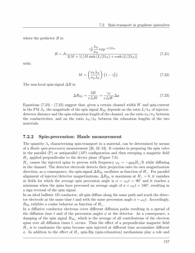
7.2. Spin-transport in graphene spinvalves
where the prefactor B is:
B = Jeγ2F
λNσN
exp−L/2λN
2(M + 1) [M sinh (L/2λN) + cosh (L/2λN)](7.21)
with:
M =
(σFλNσNλF
)(1− γ2
F
)(7.22)
The non-local spin-signal ∆R is:
∆RNL =2B
eJSW=
γFeJSW
∆µ (7.23)
Equations (7.23) - (7.22) suggest that, given a certain channel width W and spin-currentin the FM JS, the magnitude of the spin signal RNL depends on the ratio L/λN of injector-detector distance and the spin-relaxation length of the channel, on the ratio σF/σN betweenthe conductivities, and on the ratio λN/λF between the relaxation lengths of the twomaterials.
7.2.2 Spin-precession: Hanle measurement
The quantity λs characterizing spin-transport in a material, can be determined by meansof a Hanle spin-precession measurement [26, 32–34]. It consists in preparing the spin valvein the parallel (P) or antiparallel (AP) configuration and then sweeping a magnetic fieldH⊥ applied perpendicular to the device plane (Figure 7.6).
H⊥ causes the injected spins to precess with frequency ωL = −gµBH⊥/h while diffusingin the channel. The detector electrode detects their projection onto its own magnetizationdirection, as a consequence, the spin-signal ∆RNL oscillates as function of H⊥. For parallelalignment of injector/detector magnetizations, ∆RNL is maximum at H⊥ = 0, it vanishesat fields for which the average spin precession angle is φ = ωLt = 90 and it reaches aminimum when the spins have precessed an average angle of φ = ωLt = 180, resulting ina sign reversal of the spin signal.
In an ideal ballistic 1D conductor, all spin diffuse along the same path and reach the detec-tor electrode at the same time t and with the same precession angle φ = ωLt. Accordingly,RNL exhibits a cosine behavior as function of H⊥.
In a diffusive conductor electrons cover different diffusion paths resulting in a spread ofthe diffusion time t and of the precession angles φ at the detector. As a consequence, adamping of the spin signal RNL, which is the average of all contributions of the electronspins over all diffusion times t, occurs. Thus the effect of a perpendicular magnetic fieldH⊥ is to randomize the spins because spin injected at different time accumulate differentφ. In addition to the effect of H⊥ spin-flip (spin-relaxation) mechanisms play a role and
157
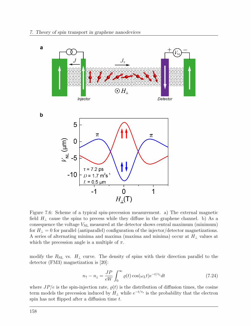
7. Theory of spin transport in graphene nanodevices
Figure 7.6: Scheme of a typical spin-precession measurement. a) The external magneticfield H⊥ cause the spins to precess while they diffuse in the graphene channel. b) As aconsequence the voltage VNL measured at the detector shows central maximum (minimum)for H⊥ = 0 for parallel (antiparallel) configuration of the injector/detector magnetizations.A series of alternating minima and maxima (maxima and minima) occur at H⊥ values atwhich the precession angle is a multiple of π.
modify the RNL vs. H⊥ curve. The density of spins with their direction parallel to thedetector (FM3) magnetization is [20]:
n↑ − n↓ =JP
eW
∫ ∞0
%(t) cos(ωLt)e−t/τsdt (7.24)
where JP/e is the spin-injection rate, %(t) is the distribution of diffusion times, the cosineterm models the precession induced by H⊥ while e−t/τs is the probability that the electronspin has not flipped after a diffusion time t.
158
7.2. Spin-transport in graphene spinvalves
Considering that µ↑−µ↓ = 2N(EF )
n↑−n↓ and that for a diffusive conductor the distributionof diffusion times at a distance L reads:
%(t) =√
1/4πDt e−L2/4Dt (7.25)
the measured non-local signal VNL for parallel injector/detector configuration is:
VNL =JP 2
e2WN(EF )
∫ ∞0
e−L2/4Dt
√4πDt
cos(ωLt)e−t/τsdt (7.26)
which analytical solution [20]:
VNL =JP 2
e2WN(EF )Re
1
2√D
exp
(−L√
1
Dτs− iωL
D
)√
1
τs− iωL
(7.27)
can be used to fit the Hanle curve.
159
Bibliography
Bibliography
[1] Johnson, M. & Silsbee, R. H. Coupling of electronic charge and spin at a ferromagnetic-paramagnetic metal interface. Physical Review B 37, 5312–5325 (1988).
[2] Jedema, F. J., Filip, A. T. & van Wees, B. J. Electrical spin injection and accumulationat room temperature in an all-metal mesoscopic spin valve. Nature 410, 345–348(2001).
[3] A. Abragam, B. B. Electron paramagnetic resonance of transition ions (Dover Publi-cations Inc., New York, 1986).
[4] Fiederling, R. et al. Injection and detection of a spin-polarized current in a light-emitting diode. Nature 402, 787–790 (1999).
[5] Zutic, I. & Dery, H. Spintronics: Taming spin currents. Nature materials 10, 647–8(2011).
[6] Ando, K. et al. Electrically tunable spin injector free from the impedance mismatchproblem. Nature Materials 10, 655–659 (2011).
[7] Kurebayashi, H. et al. Controlled enhancement of spin-current emission by three-magnon splitting. Nat Mater 10, 660–664 (2011).
[8] Coey, J. Materials for Spin Electronics. In Spin electronics, chap. 12, 277–297 (2001).
[9] Chappert, C., Fert, A., Van Dau, F. N. & Dau, F. V. The emergence of spin electronicsin data storage. Nature materials 3, 1–36 (2007).
[10] Kashyap, A., Sabirianov, R. & Jaswal, S. S. Spin-Polarized Electronic Structure. InAdvanced Magnetic Nanostructures, chap. 2, 13–39 (2006).
[11] Stearns, M. B. Simple explanation of tunneling spin-polarization of Fe, Co, Ni andits alloys. Journal of Magnetism and Magnetic Materials 5, 167–171 (1977).
[12] Johnson, M. Spin Injection, Accumulation, and Relaxation in Metals. In Handbookof Spin Transport and Magnetism, vol. 30, 115–136 (2011).
[13] Mott, N. F. The electrical conductivity of transition metals. Proceedings of the RoyalSociety of London. Series A, Mathematical and Physical Sciences 153, 699–717 (1936).
[14] Fert, A. & Campbell, I. A. Two-current conduction in nickel. Phys. Rev. Lett. 21,1190–1192 (1968).
[15] Fert, A. & Campbell, I. A. Electrical resistivity of ferromagnetic nickel and iron basedalloys. Journal of Physics F: Metal Physics 6, 849 (1976).
160
Bibliography
[16] Johnson, M. Magnetoelectronics (Elsevier Academic Press, 2004).
[17] Lehmann, C., Sinning, S., P. Zahn, H. & Wonn, I. M. http://www.physik.tu-dresden.de/˜fermisur.
[18] Datta, S. Electronic Transport in Mesoscopic Systems (Cambridge University Press,1997).
[19] Jedema, F., Nijboer, M., Filip, a. & van Wees, B. Spin injection and spin accumulationin all-metal mesoscopic spin valves. Physical Review B 67, 085319 (2003).
[20] Jedema, F. Electrical spin injection in metallic mesoscopic spin valves. Ph.D. thesis,University of Groningen (2002). URL http://irs.ub.rug.nl/ppn/244584443.
[21] van Son, P. C., van Kempen, H., Wyder, P., Son, P. V. & Kempen, H. V. BoundaryResistance of the Ferromagnetic-Nonferromagnetic Metal Interface. Physical reviewletters 58, 2271–2273 (1987).
[22] Johnson, M. Spin Injection, vol. 157, 279–307 (Springer Berlin Heidelberg, 2008).
[23] Rashba, E. I. Diffusion theory of spin injection through resistive contacts. EuropeanPhysical Journal B 29, 513–527 (2002).
[24] Rashba, E. I. Theory of electrical spin injection: Tunnel contacts as a solution of theconductivity mismatch problem. Phys. Rev. B 62, 16267–16270 (2000).
[25] Son, P. V., van Kempen, H. & Wyder, P. van Son, van Kempen, and Wyder reply.Physical review letters 65, 1988 (1988).
[26] Tombros, N. et al. Electronic spin transport and spin precession in single graphenelayers at room temperature. Nature 448, 571–574 (2007).
[27] Man, H. T. & Morpurgo, a. F. Sample-specific and ensemble-averaged magnetocon-ductance of individual single-wall carbon nanotubes. Physical Review Letters 95, 6–9(2005). arXiv:0411141.
[28] Ono, K., Shimada, H. & Ootuka, Y. Enhanced Magnetic Valve Effect and Magneto-Coulomb Oscillations in Ferromagnetic Single Electron Transistor (1997).
[29] Shimada, H., Ono, K. & Ootuka, Y. Driving the single-electron device with a magneticfield (invited). Journal of Applied Physics 93, 8259–8264 (2003).
[30] van der Molen, S. J., Tombros, N. & van Wees, B. J. Magneto-Coulomb effect inspin-valve devices. Phys. Rev. B 73, 220406 (2006).
[31] Jedema, F. J., Nijboer, M. S., Filip, a. T. & van Wees, B. J. Spin injection and spin ac-cumulation in permalloy-copper mesoscopic spin valves. Journal of Superconductivity15, 8 (2001).
161
Bibliography
[32] Jedema, F. J. et al. Electrical detection of spin precession in a metallic mesoscopicspin valve. Nature 416, 713–716 (2002).
[33] Johnson, M. & Silsbee, R. H. Interfacial charge-spin coupling: Injection and detectionof spin magnetization in metals. Physical review letters 55, 1790–1793 (1985).
[34] Johnson, M. & Silsbee, R. H. Spin-injection experiment. Physical Review B 37,5326–5335 (1988).
162

Chapter 8
Fabrication of graphene-baseddevices
This chapter is devoted to the techniques used for the fabrication of graphene nanodevices.
8.1 Electron beam lithography
Electron beam (ebeam) lithography is an important microfabrication technique, that allowscreating structures with lateral size down to 30 nm routinely. The creation of structureswith size below this limit is still possible but requires special efforts.It is based on the chemical modification of PMMA-based resists1, induced by irradiationwith electrons. Upon electron irradiation, the resist polymer chains break and the exposedresist becomes more soluble and thus easily removable. The sensitivity to electron irradi-ation (i.e the minimum electron dose required to chemically modify the resist through thewhole film thickness) depends on the polymer chain length and the film thickness. PMMAis available [1] in different lengths: short (50K), long (950K) and intermediate (200K,600K), and different dilutions in organic solvents (e.g. chlorobenzene). The 50K PMMApossesses approximately 20% higher sensitivity as compared to the 950K polymer [1]. Fig-ure 8.1 shows the different steps constituting the usual fabrication procedure.
8.1.1 Spin-coating
Homogeneous resist films of predefined thickness in the sub-µm range are created on topof the desired substrate by spin-coating, Figure 8.1(1). The thickness of the film is deter-mined by the PMMA concentration and the spinning speed, which are chosen accordingto previous calibration (e.g. 950K PMMA spun at 3000 rpm for 5s followed by 30s at8000 rpm produces a film of thickness of about ∼60 nm). After spin-coating, the sampleis backed at 160 C for 1 hour in an oven evacuated with Argon gas.
1PMMA=Polymethylmethacrylate
163
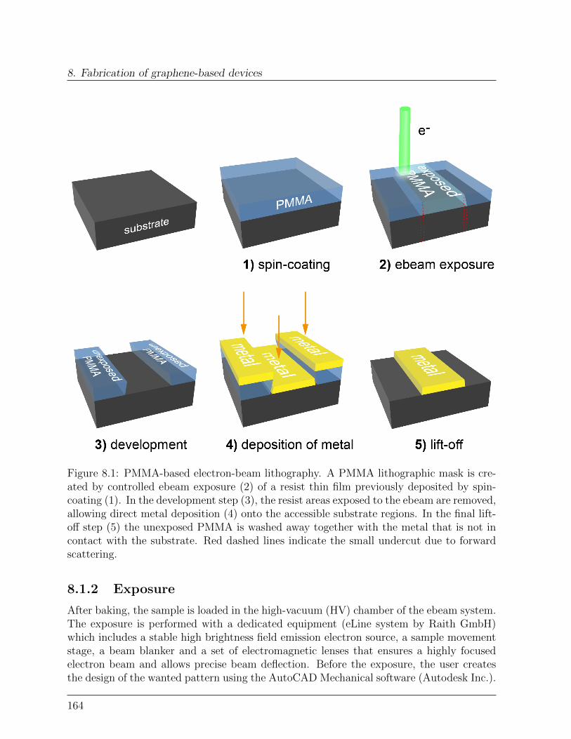
8. Fabrication of graphene-based devices
Figure 8.1: PMMA-based electron-beam lithography. A PMMA lithographic mask is cre-ated by controlled ebeam exposure (2) of a resist thin film previously deposited by spin-coating (1). In the development step (3), the resist areas exposed to the ebeam are removed,allowing direct metal deposition (4) onto the accessible substrate regions. In the final lift-off step (5) the unexposed PMMA is washed away together with the metal that is not incontact with the substrate. Red dashed lines indicate the small undercut due to forwardscattering.
8.1.2 Exposure
After baking, the sample is loaded in the high-vacuum (HV) chamber of the ebeam system.The exposure is performed with a dedicated equipment (eLine system by Raith GmbH)which includes a stable high brightness field emission electron source, a sample movementstage, a beam blanker and a set of electromagnetic lenses that ensures a highly focusedelectron beam and allows precise beam deflection. Before the exposure, the user createsthe design of the wanted pattern using the AutoCAD Mechanical software (Autodesk Inc.).
164
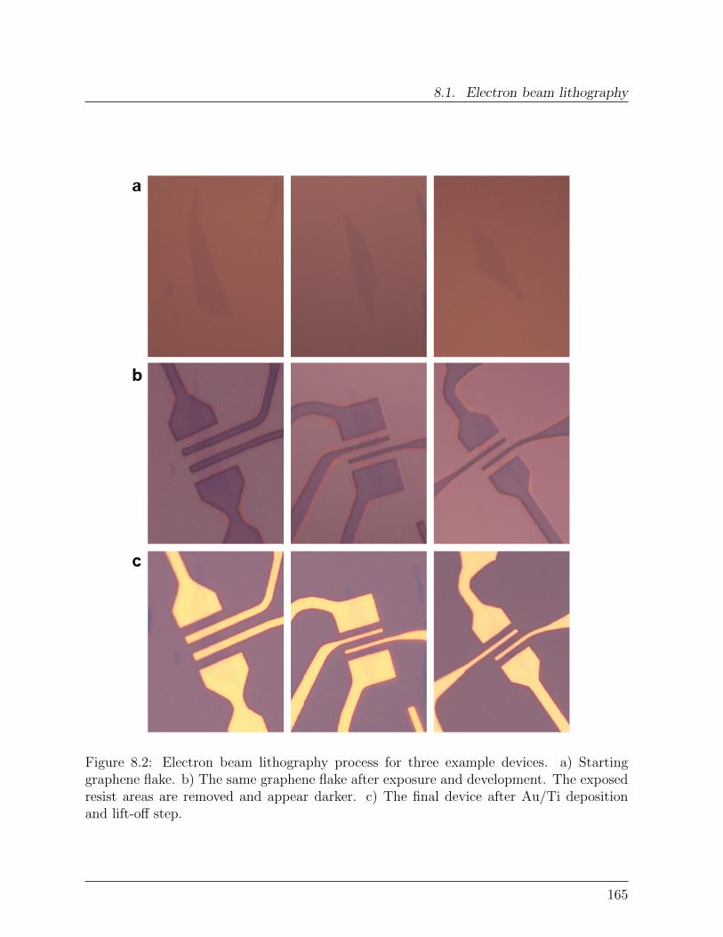
8.1. Electron beam lithography
Figure 8.2: Electron beam lithography process for three example devices. a) Startinggraphene flake. b) The same graphene flake after exposure and development. The exposedresist areas are removed and appear darker. c) The final device after Au/Ti depositionand lift-off step.
165

8. Fabrication of graphene-based devices
The output .dxf file is then used as reference to drive the ebeam system. The exposurestarts with two alignment procedures. A first one to correct for the misalignments betweensample and the reference frame of the moving stage (called XY reference system), and asecond one to align the sample with the pattern design (UV reference system). It followsa procedure to compensate for the astigmatism of the lenses (that causes the beam spotto not have the expected round shape) and to ensure an optimal focus (i.e. the smallestachievable beam spot). The exposure is performed as direct writing or raster scan modes,Figure 8.1(2).
Upon ebeam irradiation the main chain of the PMMA molecule is broken into many radicalfragments. For positive2 resist at optimal electron doses, the fragments recombine formingpolymers of reduced mass, for instance the initial molar mass of 950 000 g/mol of 950KPMMA drops to 5 000−10 000 g/mol upon exposure. As a consequence the solubility ofthe exposed regions increases dramatically and the exposed resist can be easily removed inthe development step. Larger dose values induce molecular cross-linking [1], resulting in amuch lower solubility compared to the pristine resist, meaning that high doses convert thePMMA in a negative3 resist that is hardly removable.
8.1.3 Proximity effect and dose test
To ensure a correct patterning, most of the electrons have to pass through the entire resistlayer. This ensures also absence of resist residues at the contact interface that may causehigh contact resistances. As an electron enters the resist, it undergoes multiple low energyelastic collisions, which deflect its trajectory. This forward scattering cause the image ofthe beam on the resist to be larger than the actual beam spot, reducing considerably theachievable writing resolution, Figure 8.3a. The use of thinner resist layers with longerchain lengths and higher beam energies reduces considerably the forward scattering ofelectrons, thus enhancing the resolution. On the one hand this broadening deteriorates thestructural accuracy. On the other hand, it is useful in producing an undercut in two-layersresist stacks that help the final lift-off, Figure 8.3c,d. The two layers constituting the stackhave different chain lengths, with the ”softer”(shorter chain) PMMA at the bottom andthe ”harder” (longer chain) PMMA on top. Undergoing weaker broadening, the hard toplayer ensures an high writing accuracy while the broadening of the bottom layer creates anhollow structure that facilitates the flow of solvent during the lift-off, easing the removal ofthe unexposed areas. In addition to forward scattering, a fraction of the electrons undergoenough large angle collisions (especially reflection at the substrate interface) to re-emergeinto the resist at some distance from the set exposure point, Figure 8.3b. Depending on thebeam energy, these backscattered electrons may cause exposure of the resist microns awayfrom the wanted point [2–4], causing distortions in the pattern, loss of contrast [3, 5, 6] and,in the worse case, merging of two or more distinct features, Figure 8.4a. This is usuallyreferred to as proximity-effect and to reduce its impact on the final structure, an optimal
2For positive resist the pattern areas that need to be revealed are exposed.3For negative resist the pattern areas that need to be remain covered are exposed.
166
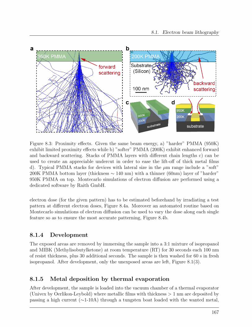
8.1. Electron beam lithography
Figure 8.3: Proximity effects. Given the same beam energy, a) ”harder” PMMA (950K)exhibit limited proximity effects while b) ”softer” PMMA (200K) exhibit enhanced forwardand backward scattering. Stacks of PMMA layers with different chain lengths c) can beused to create an appreciable undercut in order to ease the lift-off of thick metal filmsd). Typical PMMA stacks for devices with lateral size in the µm range include a ”soft”200K PMMA bottom layer (thickness ∼ 140 nm) with a thinner (60nm) layer of ”harder”950K PMMA on top. Montecarlo simulations of electron diffusion are performed using adedicated software by Raith GmbH.
electron dose (for the given pattern) has to be estimated beforehand by irradiating a testpattern at different electron doses, Figure 8.4a. Moreover an automated routine based onMontecarlo simulations of electron diffusion can be used to vary the dose along each singlefeature so as to ensure the most accurate patterning, Figure 8.4b.
8.1.4 Development
The exposed areas are removed by immersing the sample into a 3:1 mixture of isopropanoland MIBK (Methylisobutylketone) at room temperature (RT) for 30 seconds each 100 nmof resist thickness, plus 30 additional seconds. The sample is then washed for 60 s in freshisopropanol. After development, only the unexposed areas are left, Figure 8.1(3).
8.1.5 Metal deposition by thermal evaporation
After development, the sample is loaded into the vacuum chamber of a thermal evaporator(Univex by Oerlikon-Leybold) where metallic films with thickness > 1 nm are deposited bypassing a high current (∼1-10A) through a tungsten boat loaded with the wanted metal,
167

8. Fabrication of graphene-based devices
Figure 8.4: Proximity correction. a) Typical ”dose test” used to calibrate the exposure ofparallel injector and detector contacts in spinvalve devices. The dose increases from leftto right. The red rectangle indicates the optimally exposed structure. b) An example ofproximity effect correction based on Montecarlo simulations applied to a Hall-bar device.For the darker regions the exposure is reduced to prevent over-exposure. At the cornersand edges the dose is increased to compensate for under-exposure.
Figure 8.1(4). The film thickness is controlled by varying the deposition time, while thedeposition rate (>A/s) depends on the set current. A lower deposition rate usually ensuresmore homogeneous films but also more prolonged sample heating. The typical depositionrate used for 50 nm-thick Au contacts was 2 A/s, while for 40 nm-thick Cobalt the ratewas reduced to 1 A/s.
Depending on the desired metal it might be necessary to use a buffer layer to promoteadhesion with the substrate material. Typically a Ti buffer thin-layer (< 2 nm) is used for50 nm-thick Au contacts on SiO2 substrates.
8.1.6 Lift-off
Once a continuous metallic film is deposited on the whole sample, the latter is immersedin NEP (1-Ethyl-2-pyrrolidone)-based remover (AR 300-76 by Allresist GmbH) at 60 Cfor at least 4 hours. The solvent dissolves the unexposed PMMA removing also the metalthat is not in contact with the substrate, Figure 8.1(5). For standard devices with Goldcontacts, this is typically the most difficult step of the lithographic process. Indeed, Aufilms of thickness > 10 nm are pretty robust, and so difficult to be removed. It is thusrecommendable to use a two-layer PMMA stack with an appreciable undercut that favors
168

8.2. Nanostructuring of graphene via reactive io etching (RIE)
the rupture of the film, as seen Figure 8.3d.
8.2 Nanostructuring of graphene via reactive io etch-
ing (RIE)
8.2.1 Masking
As discussed in the next chapter, one way to enhance the spin-injection efficiency ingraphene is by increasing the contact resistance of the device. One way to do that isto reduce the contact area by patterning the graphene in narrow stripes (of width of fewhundreds of nanometers) [7, 8]. For this, an additional lithographic procedure is carriedout previous to the standard device lithography. The PMMA mask is designed so as toopen a window over the graphene areas that have to be removed, while leaving the narrowstripe protected, Figure 8.5.In order to achieve the required accuracy, a single thin film (∼ 60 nm) of ”hard” 950KPMMA is used;. In addition the Montecarlo-based proximity correction is used to ensurea uniform width along the whole stripe.
8.2.2 Etching
Reactive Ion Etching containing Typical parameters for the patterning of single layergraphene are: Ar at a flow of 100sccm (standard cubic centimeters per minute), O2 at11sccm, at an overall pressure of P = 0.05 mbar for t=5 seconds at P= 48W.The starting graphene flake (1) is masked using positive PMMA (2-3) and exposed toreactive ion etching (4) in order to remove part of the flake. After the development (5),only a narrow graphene stripe is left. The adhesion to the SiO2 substrate is remarkablefor stripes with width > 150 nm, enabling further processing (6). Scale: the bottom-rightmetallic marker is 9 µm wide, the stripe width is 200 nm.
8.3 Deposition of magnetic contacts
The magnetic properties of Cobalt contacts used in spinvalve devices (see Chapters 7) areaffected by the Oxygen content and other contaminants [9–13]. The typical Cobalt thicnessused in this work is 44±1 nm. In order to maximize the ferromagnet purity, the evaporationis carried out at a residual pressure of P < 1 · 10−7 mbar. This high vacuum values areachieved after at least 48 hours of continuous pumping. Interestingly, long pumping timesseem to decrease appreciably the contact resistance of graphene devices, likely due to thecomplete desorption of surface contaminants.In order to avoid oxidation once the device is exposed to air, a 10 nm-thick Au capping layeris added on top of the Cobalt contacts, Figure 8.7a. This latter step, introduces the risk
169

8. Fabrication of graphene-based devices
Figure 8.5: Patterning of sub-µm graphene stripes. 1) Starting graphene flake. 2) Auto-CAD Mechanical design of the patterning structure, including a narrow stripe between twolarge areas that are going to be exposed. 3) After exposure and development, two ”win-dows” are opened in the positive PMMA layer, leaving a narrow PMMA stripe unexposed.4) Reactive ion etching removes parts of the graphene flake. 5) After the development(5), only the narrow graphene stripe protected by the unexposed PMMA is left. 6) Theadhesion to the SiO2 substrate is remarkable for stripes with width > 150 nm, enablingfurther processing. The stripe width is 200 nm.
170
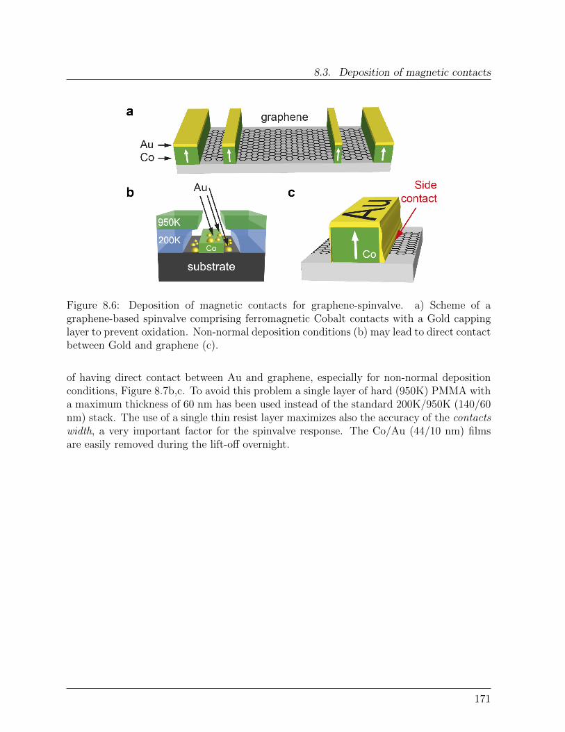
8.3. Deposition of magnetic contacts
Figure 8.6: Deposition of magnetic contacts for graphene-spinvalve. a) Scheme of agraphene-based spinvalve comprising ferromagnetic Cobalt contacts with a Gold cappinglayer to prevent oxidation. Non-normal deposition conditions (b) may lead to direct contactbetween Gold and graphene (c).
of having direct contact between Au and graphene, especially for non-normal depositionconditions, Figure 8.7b,c. To avoid this problem a single layer of hard (950K) PMMA witha maximum thickness of 60 nm has been used instead of the standard 200K/950K (140/60nm) stack. The use of a single thin resist layer maximizes also the accuracy of the contactswidth, a very important factor for the spinvalve response. The Co/Au (44/10 nm) filmsare easily removed during the lift-off overnight.
171
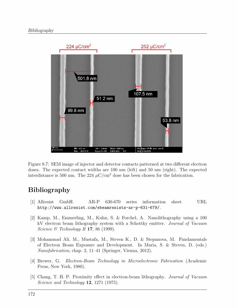
Bibliography
Figure 8.7: SEM image of injector and detector contacts patterned at two different electrondoses. The expected contact widths are 100 nm (left) and 50 nm (right). The expectedinterdistance is 500 nm. The 224 µC/cm2 dose has been chosen for the fabrication.
Bibliography
[1] Allresist GmbH. AR-P 630-670 series information sheet. URLhttp://www.allresist.com/ebeamresists-ar-p-631-679/.
[2] Kamp, M., Emmerling, M., Kuhn, S. & Forchel, A. Nanolithography using a 100kV electron beam lithography system with a Schottky emitter. Journal of VacuumScience & Technology B 17, 86 (1999).
[3] Mohammad Ali, M., Mustafa, M., Steven K., D. & Stepanova, M. Fundamentalsof Electron Beam Exposure and Development. In Maria, S. & Steven, D. (eds.)Nanofabrication, chap. 2, 11–41 (Springer, Vienna, 2012).
[4] Brewer, G. Electron-Beam Technology in Microelectronic Fabrication (AcademicPress, New York, 1980).
[5] Chang, T. H. P. Proximity effect in electron-beam lithography. Journal of VacuumScience and Technology 12, 1271 (1975).
172

Bibliography
[6] Mun, L. K., Drouin, D., Lavallee, E. & Beauvais, J. The Impact of Charging onLow-Energy Electron Beam Lithography. Microscopy and Microanalysis 10, 804–809(2004).
[7] Kimura, T., Otani, Y. & Hamrle, J. Enhancement of spin accumulation in a nonmag-netic layer by reducing junction size. Phys. Rev. B 73, 132405 (2006).
[8] Jo, S., Ki, D.-K., Jeong, D., Lee, H.-J. & Kettemann, S. Spin relaxation properties ingraphene due to its linear dispersion. Phys. Rev. B 84, 075453 (2011).
[9] Kim, W., Oh, S.-J. & Nahm, T.-U. Oxidation and Annealing Effect on Cobalt Filmson Palladium(111). Surface Review and Letters 09, 931–936 (2002).
[10] Cren, T., Rusponi, S., Weiss, N., Epple, M. & Brune, H. Oxidation induced enhancedmagnetic susceptibility of Co Islands on Pt(111). Journal of Physical Chemistry B108, 14685–14691 (2004).
[11] Tracy, J. B. & Bawendi, M. G. Defects in CoO in oxidized cobalt nanoparticlesdominate exchange biasing and exhibit anomalous magnetic properties. Phys. Rev. B74, 1–11 (2006).
[12] Hill, T., Mozaffari-Afshar, M., Schmidt, J., Risse, T. & Freund, H. J. Changes in themagnetism of small supported cobalt particles during the oxidation process observedby ferromagnetic resonance. Surface Science 429, 246–254 (1999).
[13] Tracy, J. B., Weiss, D. N., Dinega, D. P. & Bawendi, M. G. Exchange biasing andmagnetic properties of partially and fully oxidized colloidal cobalt nanoparticles. Phys.Rev. B 72, 1–8 (2005).
173

Bibliography
174
Chapter 9
Toward efficient spin-injection ingraphene
9.1 Tunneling graphene spin-valve
As introduced in Section 7.1.5, the conductivity mismatch at the ferromagnet/graphene(FM/G) interface is the main factor limiting spin-injection in graphene. One way toovercome this problem is to employ tunneling contacts, with barriers of thickness ≤ 2 nm,that introduce a spin-dependent interface resistance and ”decouple” the graphene channelfrom the ferromagnet [1]. Extensive efforts have been devoted to fabricate insulatingultra-thin films on graphene, using a variety of techniques. Successful tunneling spin-injection has been demonstrated for MgO [2] and Al2O3 [3] barriers by molecular beamepitaxy and sputtering respectively, while oxidation of ultranthin Al film deposited atliquid nitrogen temperature revealed a limited spin-injection efficiency [4], likely due tofilm inhomogeneities and presence of pinholes. Here we demonstrate that homogeneousAl2O3 tunneling barriers can be fabricated via atomic layer deposition (ALD) using Tiseeding. While the use of Ti seeding is not enough to create closed Al2O3 films withthickness < 1 nm, complete oxidation of the Ti seeding prior to ALD is essential to ensureefficient tunneling spin-injection in graphene.
9.1.1 Ultrathin Al2O3 films on graphene
Growing homogeneous dielectric Al2O3 films (e.g. Al2O3, HfO2) by atomic layer depositionon graphene has proved challenging due to the inertness and hydrophobic nature of thegraphene surface. Previous studies [5–8] have shown that, for direct ALD on graphene,film nucleation takes place mainly at the edges, while nucleation in the basal plane isextremely rare in high quality samples. As a consequence, high homogeneity over a tech-nologically relevant length scale of 50 nm is achieved only for rather thick films (> 8 nm)at temperature T = 200C [5].
Several methods have been developed to enhance film uniformity at lower thicknesses by
175
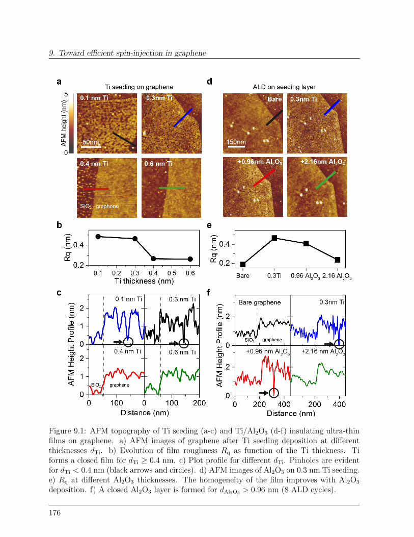
9. Toward efficient spin-injection in graphene
Figure 9.1: AFM topography of Ti seeding (a-c) and Ti/Al2O3 (d-f) insulating ultra-thinfilms on graphene. a) AFM images of graphene after Ti seeding deposition at differentthicknesses dTi. b) Evolution of film roughness Rq as function of the Ti thickness. Tiforms a closed film for dTi ≥ 0.4 nm. c) Plot profile for different dTi. Pinholes are evidentfor dTi < 0.4 nm (black arrows and circles). d) AFM images of Al2O3 on 0.3 nm Ti seeding.e) Rq at different Al2O3 thicknesses. The homogeneity of the film improves with Al2O3
deposition. f) A closed Al2O3 layer is formed for dAl2O3 > 0.96 nm (8 ALD cycles).
176
9.1. Tunneling graphene spin-valve
inducing nucleation in the graphene basal plane (by increasing the density of nucleationsites). These included ozone (O2) [7] or NO2 [9] pre-treatment, low-k polymer buffer layer[10], molecular seeding [8, 11], substrate-induced nucleation [12] and metallic seeding layer[13, 14]. In the latter, Ti seeding shows important improvements in both the crystallinityand the dielectric constant of the Al2O3 layers. Nevertheless, tunneling spin-injection ingraphene employing such tunneling barrier structure has not been yet reported and onlyspin-injection experiments using molecular seeding/Al2O3 barrier have been attempted [15].
Here we employ the Ti seeding/Al3O2 barrier stack to efficiently decouple the graphenespin-transport channel from the ferromagnetic leads and we provide important guidelinesfor the efficient spin-injection/accumulation in graphene.
Graphene flakes are mechanically exfoliated from HOPG and transferred to highly dopedSi substrates with 300 nm-thick thermal SiO2 layer. A thin Ti film of thickness 0.3-2 nm isdeposited by thermal evaporation with deposition rates < 0.1 nm/s, at the residual pressureof < 106 mbar. The sample is directly transferred to the ALD chamber to avoid oxidation.The thin metal film serves as nucleation layer for the subsequent ALD process. TheAl2O3 films are deposited using Cambridge Nanotech ALD system with trimethylaluminum(TMA) and H2O as precursors. The growth was carried out in vacuum at 100 C with0.1s/40s and 0.1s/15s pulse/purge time for H2O and TMA respectively. The resultinggrowth rate is approximately 0.12-0.16 nm/cycle.
Figure 9.1a shows the topography of graphene flakes probed by atomic force microscopyafter the deposition of Ti with thickness tTi =0.1 - 0.6 nm. The graphene surface roughnessfor tTi =0.3 nm is Rq = 0.44 nm (Figure 9.1b), more than twice that of pristine graphene(top-left image in Figure 9.1d. For tTi ≥ 0.4 nm, Rq drops to 0.27 nm indicating a closedspatially-uniform film. The height profile (Figure 9.1c) evidences the absence of pinholesfor tTi ≥ 0.4 nm.
To study the influence of Ti seeding on the ALD nucleation a tTi = 0.3 nm is chosen. 8ALD cycles (tAl2O3 = 0.96 nm) leads to slightly reduced Rq (Figure 9.1d,e) and the heightprofile confirms the presence of pinholes. Only for tAl2O3 > 1.2 nm (10 cycles) a spatiallyuniform Al2O3 film is created (Figure 9.1d,e,f).
9.1.2 Spin transport with highly decoupled contacts.
Spinvalve devices are fabricated by ebeam lithography using a 950K/200K double layerPMMA stack. A barrier structure of 0.3nm Ti seeding combined with 10 ALD cycles ischosen to ensure the lowest barrier thickness (Figure 9.2a). To make sure that the completecontact area is covered with Ti islands, the deposition is carried out with rotating sampleat a tilt angle of θ = 20 (Figure 9.2a).
To produce a clear spin-valve characteristic (Figure 7.5c), the ferromagnetic electrodes needto have distinct coercive fields HFM
c . To this end [16], the electrodes with different widthsw are fabricated. In fact, HFM
c decreases with increasing w [17] because of the differentshape anisotropy. Typically, an electrode with w ∼ 100 nm and thickness t ∼ 45 nmexhibits a coercive field of about 100 mT (the final HFM
c depends also on other geometrical
177

9. Toward efficient spin-injection in graphene
Figure 9.2: Tunneling graphene spinvalve. a) Deposition of Al2O3 tunneling contacts withTi seeding layer (tTi =0.3 nm) and 10 ALD cycles. b) Scheme of the non-local spinvalveconfiguration. c) Optical picture of the device. Dashed red curve indicates the grapheneflake. Black circle: one of the 90 turns used pin the contact domain structure. Electrodesare equidistant with L = 0.8µm. d) I-V curve of a device with a continuous Ti seedinglayer (tTi = 1.5 nm). Symbols are experimental data for (red) tAl2O3 = 1.2-1.6 nm (10 ALDcycles) and (black) tAl2O3 = 1.8-2 nm (13 ALD cycles). Solid lines are fits with Simmon’smodel.
factors). In this way, parallel and anti-parallel configurations of the injector and detectormagnetizations are obtained by sweeping the external field H|| along the contacts longdirection.
The ferromagnetic domain structure of the electrode plays an important role in the finalspin-injection efficiency. The presence of multiple domains in the FM/graphene junctionarea can cause simultaneous injection of both spin-up and spin-down species, leading toa decreased net spin-accumulation signal ∆RNL. This is avoided by designing electrodeswith large length/width aspect ratio, that maximizes the domains size [16]. In addition,to inhibit domain wall motion, so as to produce a more neat switching characteristics,
178
9.1. Tunneling graphene spin-valve
each contact is designed with a 90 degree turn before crossing the graphene strip [18] asshown in Figure 9.2c (black circle). Cobalt contacts are deposited by thermal evaporationat a residual pressure of < 107 mbar. A 10 nm-thick gold capping layer is added to avoidoxidation of the ferromagnetic contacts (Figure 9.2b). The resulting device is shown inFigure 9.2c.
Spin-transport measurements are carried out in a non-local geometry (Figure 9.2b) usingthe dc polarity inversion method (also called ’Delta method’ ) implemented via a dc cur-rent source coupled with a low-noise nanovoltmeter (Keithley Delta system [19], with anexcitation current of J = 0.3 µA. Such a device does not show the expected spinvalvecharacteristics. This is expected in case of a not oxidized Ti layer. In fact tunneling wouldoccurs mainly towards the metallic Ti and not directly to graphene, both because the Al2O3
thickness is lower on top of a Ti island, and because for a 0.3nm-thick seeding the total areacovered by Ti is much larger than the uncovered graphene area. This leads to a reducedspin accumulation signal. To verify the oxidation level of the seeding, we fabricated deviceswith a continuous Ti layer (tTi = 1.5 nm) and measured their tunneling characteristics.Figure 9.2d shows the I-V characteristic for two devices with different Al2O3 thicknesstAl2O3 (10 and 13 ALD cycles). The curves are highly non-linear and fitting with the Sim-mon’s tunneling model [20–22] gives effective barrier thicknesses of t10cycles
Al2O3= 1.45 ± 0.03
nm and t13cyclesAl2O3
= 1.74 ± 0.08 nm. These are in excellent agreement with the thicknessesexpected for 10 and 13 ALD cycles respectively, and demonstrate that the seeding layeris not oxidized. In fact, Ti oxidation would lead to an appreciable increase in barrierthickness. An oxidation step previous to the ALD process is then necessary to minimizethe spin-relaxation at the contact interface, and consequently enhance the spin-injectionefficiency.
Figure 9.3 shows the magnetotransport response of a device with tTi = 0.3 nm and tAl2O3 =0.6 - 0.8 nm (5 ALD cycles) for which the Ti seeding has been oxidized for 1.5 hours incontrolled oxygen atmosphere. Up-sweeping H|| from negative to positive values givesrise to the red curve of Figure 9.3. At HFM3
c = 42 ± 1 mT the 140 nm-wide (FM3)electrode flips its magnetization direction as first, resulting in a lowered RNL. This marksthe transition from the parallel to the antiparallel magnetization configuration, where FM2injects up-spins in the channel and FM3 probes the consequent depletion of down-spins.At HFM2
c = 75 ± 1 mT, the magnetization of FM2 (w = 90 nm) flips, restablishing theparallel magnetization configuration (higher RNLvalue), in which FM2 injects down-spinsand FM3 probes their accumulation. The fact that the device magnetoresistance (MR) doesshow two different RNL values for different magnetization configurations demonstrates theeffective spin-injection and detection in the graphene channel. Moreover it suggests thatthe spin-diffusion length of the graphene stripe is larger than the FM2-FM3 interdistanceL, i.e. λs > L = 0.8µm. A third resistance level is seemingly present at HFM2
c = 12 ± 1mT, likely indicating the flipping of FM4, suggesting an even larger spin diffusion length,λsf > 1.6µm
A clear spinvalve behavior is observed at different gate voltages Vgate (Figure 9.4a,b). Thedependence of the spin-signal on Vgate indicates that ∆RNL is maximum at the charge
179
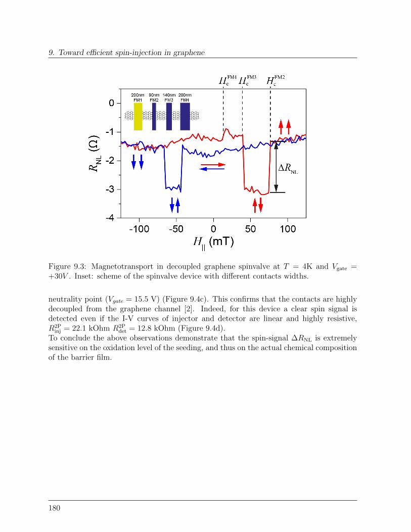
9. Toward efficient spin-injection in graphene
Figure 9.3: Magnetotransport in decoupled graphene spinvalve at T = 4K and Vgate =+30V . Inset: scheme of the spinvalve device with different contacts widths.
neutrality point (Vgate = 15.5 V) (Figure 9.4c). This confirms that the contacts are highlydecoupled from the graphene channel [2]. Indeed, for this device a clear spin signal isdetected even if the I-V curves of injector and detector are linear and highly resistive,R2P
inj = 22.1 kOhm R2Pdet = 12.8 kOhm (Figure 9.4d).
To conclude the above observations demonstrate that the spin-signal ∆RNL is extremelysensitive on the oxidation level of the seeding, and thus on the actual chemical compositionof the barrier film.
180
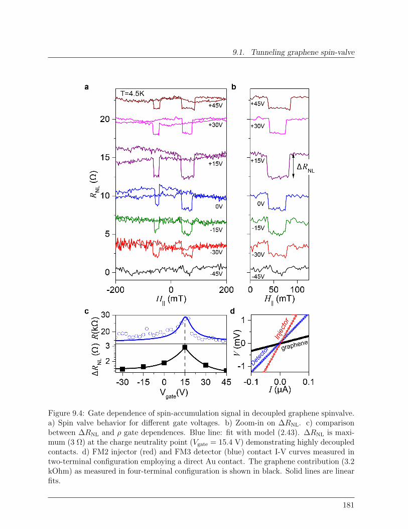
9.1. Tunneling graphene spin-valve
Figure 9.4: Gate dependence of spin-accumulation signal in decoupled graphene spinvalve.a) Spin valve behavior for different gate voltages. b) Zoom-in on ∆RNL. c) comparisonbetween ∆RNL and ρ gate dependences. Blue line: fit with model (2.43). ∆RNL is maxi-mum (3 Ω) at the charge neutrality point (Vgate = 15.4 V) demonstrating highly decoupledcontacts. d) FM2 injector (red) and FM3 detector (blue) contact I-V curves measured intwo-terminal configuration employing a direct Au contact. The graphene contribution (3.2kOhm) as measured in four-terminal configuration is shown in black. Solid lines are linearfits.
181

9. Toward efficient spin-injection in graphene
9.2 Transparent graphene spinvalve
The observations of the previous section highlight how the performance of graphene spin-valves depends sensibly on the barrier chemical composition, and on the interface qual-ity. The presence of unoxidized seeding material completely hinders the spin-injection ingraphene. This not only makes the fabrication and the characterization of the such devicesmore difficult, but it will hardly allow discriminating the effect of the SMMs functionaliza-tion on the channel spin-transport from the effect of the same on the barrier composition,being the functionalization performed via a wet-chemistry approach.
Figure 9.5: a) Scheme of the transparent graphene spinvalve. b) AFM-height image ofdevice IB (dashed black rectangle). Black circle: one of the 90 degree turns inhibitingdomain wall motion. The red arrow shows the reduced junction area. b) Optical picturebefore metal deposition and c) of the completed IA (W = 300 nm L = 1µm) and IIB(W = 200 nm L = 0.5µm) spinvalves.
182
9.2. Transparent graphene spinvalve
Another way to overcome the conductivity mismatch problem is to increase the contactresistance by reducing the junction area [23, 24]. To this end, graphene flakes are patternedin narrow stripes of width W = 200 and 300 nm, via a combination of ebeam lithographystep and reactive ion etching (RIE) micropatterning (see Chapter 8). The graphene stripesare then contacted with a sets of 44 nm-thick Cobalt electrodes capped with 10 nm-thinkAu. Examples of a final device is shown in Figure 9.5.Figure 9.5 shows a typical device built for a 200 nm wide graphene stripe. The devicedesign comprises four electrodes sets, each containing 300, 100, 150 and 200 nm-wideequidistant electrodes. The following sections present measurements performed on threedifferent devices which details are reported in Table 9.1.
Device L W
IA 1 µm 300 nm
IB 1 µm 200 nm
IIB 0.5 µm 200 nm
Table 9.1: List of the devices described in this chapter.
9.2.1 Effect of rough edges on spin-transport
Figure 9.6a shows the magnetoresistance response of device IB (Figure 9.5b) at T = 1.6K.The non-local voltage VNL is measured while sweeping the magnetic field H|| at theconstant rate of 20 mT/min. In analogy with the previous section, the measurementsare carried out using the polarity inversion method (also called ’Delta method’ ) imple-mented via a dc current source coupled with a low-noise nanovoltmeter (Keithley Deltasystem [19]. The excitation current used in this case is |J | = 15µA. To avoid any unwantedcharge transport between FM2 and FM4, the nanovoltmeter is used in float configuration.Up-sweeping H|| from negative to positive values gives rise to the red curve of Figure 9.6a.At HFM3
c = +70± 1 mT the 150nm-wide (FM3) electrode flips its magnetization directionas first, resulting in a negative VNL. This marks the transition from the parallel to theantiparallel magnetization configuration, where FM2 injects up-spins in the channel andFM3 probes the consequent depletion of down-spin. At HFM2
c = +104± 1 mT, the magne-tization of FM2 (w = 100nm) flips, restablishing the parallel magnetization configuration(positive value of VNL), in which FM2 injects down-spins and FM3 probes their accumula-tion. The fact that the device magnetorestistance (MR) response does show two differentVNL values for different magnetization configurations demonstrates effective spin-injectionand detection in the graphene channel. Moreover this observation suggests that the spin-diffusion length of the graphene stripe is larger than the FM2-FM3 interdistance L, i.e.λs > L = 1µm.Figure 9.6b shows a similar spin-transport measurement for device IA (W = 300 nm) atVgs = −10 V. For this device, four different VNL levels are observed. By up-sweeping H||,the electrodes switch their magnetization in the reverse order of their width: FM1, FM4,
183

9. Toward efficient spin-injection in graphene
Figure 9.6: Spin-transport in transparent graphene spinvalves at T = 1.6 K and Vgs = −10V. a) For device IB (|J | = 15µA) VNL parallel ad antiparallel configurations of injector(FM2) and detector (FM3) contacts are observed. b) For device IA (|J | = 20µA), fourdifferent resistance levels are observed, corresponding to the magnetization-flip of all fourelectrodes.
184
9.2. Transparent graphene spinvalve
FM3, and FM2. Observing four magnetization configurations means that λs is at leastequal to the FM1-FM3 (or FM4-FM2) distance λs > L13 = 2µm.The observation of only two resistance levels for the W = 200 nm stripe, suggests a reducedspin-diffusion length λs, compared with the W = 300 nm case. A possible cause of thisenhanced spin-relaxation is spin-flip scattering at the stripe edges. The influence of theedges is confirmed by a reduced mobility µ for the narrower stripe (IB) as extracted fromfit of the two-point differential resistance with (2.43) (Figure9.10). Moreover for device IB,the constant contribution ρS is more than four times larger. This contribution stems bothfrom the contact resistance RC (that is expected to be inversely proportional to W ), aswell as from short-range scatterers. Short-range (inter-valley) nature of the defects at theedges is also confirmed by the appreciable D band in the stripes Raman spectra (Figure9.7), which becomes more prominent as the W is reduced.The spin-injection efficiency (i.e. spin polarization P ) can be extracted by solving thespin-coupled diffusion equations for spin-up and spin-down electrons (7.9), which in thelimit of RC >> RN gives [27, 28]:
RNL = ±P2λs
2σWe−L/λs (9.1)
where P is the spin-injection efficiency, σ is the graphene conductivity and W is the widthof the graphene stripe.The measurements of Figure 9.6 give RNL = 2.0± 0.4 Ω and RNL = 9.8± 0.9 Ω for deviceIB and IA respectively. Considering that σ = 1.1 · 10−4 S and σ = 5.3 · 10−4 S for device IBand IA respectively, and assuming λs > 1µm for IB and λs > 2µ for AI, Formula (9.1) givesP = 0.6% and P = 2.4% (in agreement with other investigations on graphene-spinvalveswith transparent contacts [24, 29]), indicating a reduced spin-injection efficiency for thenarrower stripe.The reduction the spin-diffusion length with the W suggests that the defects at the edgesinduce spin-dependent scattering and contribute to the overall spin-relaxation. Moreover,the fact that spin-flip scattering at the edges impacts on the overall spin-injection efficiencyis an important result and further measurements are on the way to better clarify theunderlying mechanism.
185
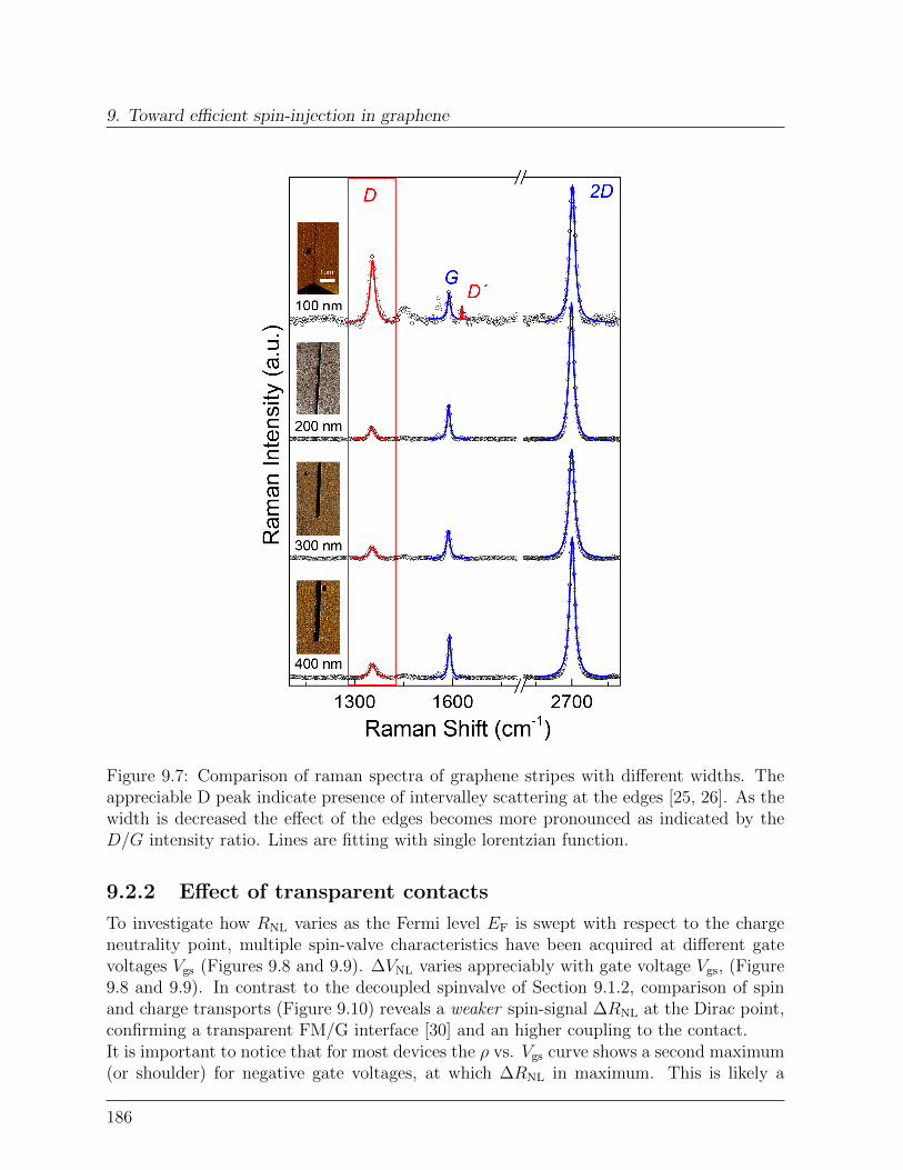
9. Toward efficient spin-injection in graphene
Figure 9.7: Comparison of raman spectra of graphene stripes with different widths. Theappreciable D peak indicate presence of intervalley scattering at the edges [25, 26]. As thewidth is decreased the effect of the edges becomes more pronounced as indicated by theD/G intensity ratio. Lines are fitting with single lorentzian function.
9.2.2 Effect of transparent contacts
To investigate how RNL varies as the Fermi level EF is swept with respect to the chargeneutrality point, multiple spin-valve characteristics have been acquired at different gatevoltages Vgs (Figures 9.8 and 9.9). ∆VNL varies appreciably with gate voltage Vgs, (Figure9.8 and 9.9). In contrast to the decoupled spinvalve of Section 9.1.2, comparison of spinand charge transports (Figure 9.10) reveals a weaker spin-signal ∆RNL at the Dirac point,confirming a transparent FM/G interface [30] and an higher coupling to the contact.It is important to notice that for most devices the ρ vs. Vgs curve shows a second maximum(or shoulder) for negative gate voltages, at which ∆RNL in maximum. This is likely a
186
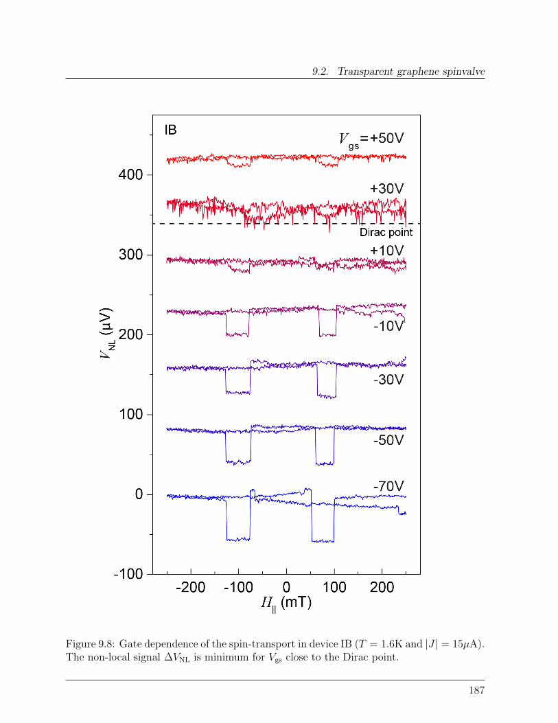
9.2. Transparent graphene spinvalve
Figure 9.8: Gate dependence of the spin-transport in device IB (T = 1.6K and |J | = 15µA).The non-local signal ∆VNL is minimum for Vgs close to the Dirac point.
187
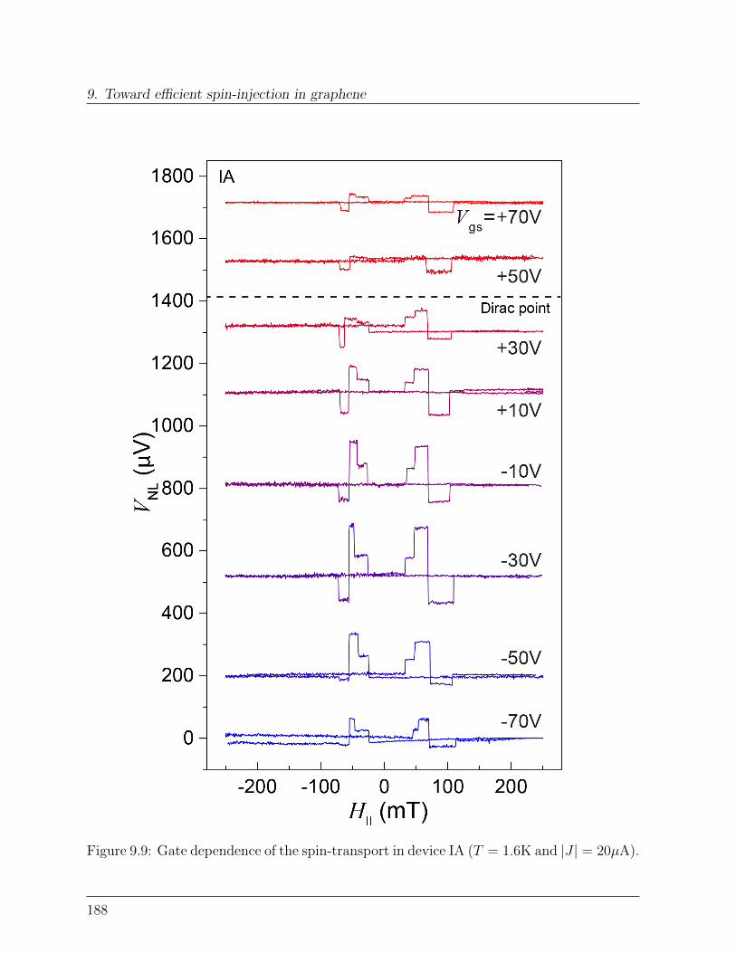
9. Toward efficient spin-injection in graphene
Figure 9.9: Gate dependence of the spin-transport in device IA (T = 1.6K and |J | = 20µA).
188
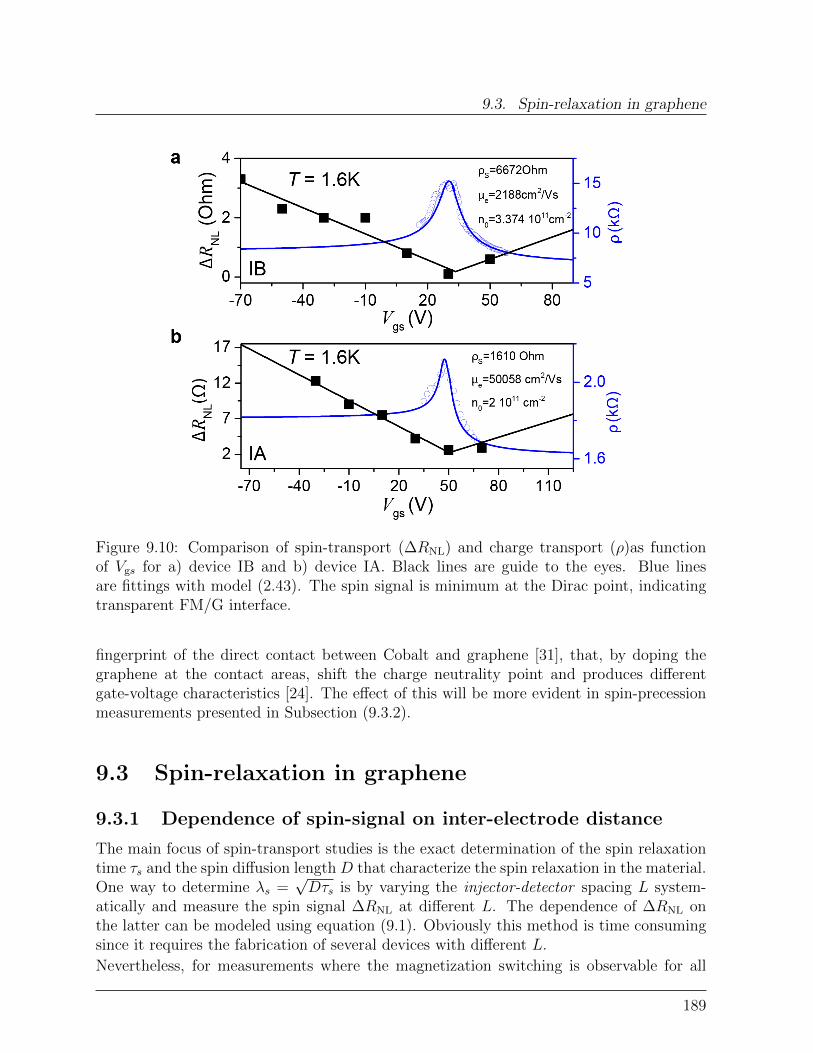
9.3. Spin-relaxation in graphene
Figure 9.10: Comparison of spin-transport (∆RNL) and charge transport (ρ)as functionof Vgs for a) device IB and b) device IA. Black lines are guide to the eyes. Blue linesare fittings with model (2.43). The spin signal is minimum at the Dirac point, indicatingtransparent FM/G interface.
fingerprint of the direct contact between Cobalt and graphene [31], that, by doping thegraphene at the contact areas, shift the charge neutrality point and produces differentgate-voltage characteristics [24]. The effect of this will be more evident in spin-precessionmeasurements presented in Subsection (9.3.2).
9.3 Spin-relaxation in graphene
9.3.1 Dependence of spin-signal on inter-electrode distance
The main focus of spin-transport studies is the exact determination of the spin relaxationtime τs and the spin diffusion length D that characterize the spin relaxation in the material.One way to determine λs =
√Dτs is by varying the injector-detector spacing L system-
atically and measure the spin signal ∆RNL at different L. The dependence of ∆RNL onthe latter can be modeled using equation (9.1). Obviously this method is time consumingsince it requires the fabrication of several devices with different L.
Nevertheless, for measurements where the magnetization switching is observable for all
189
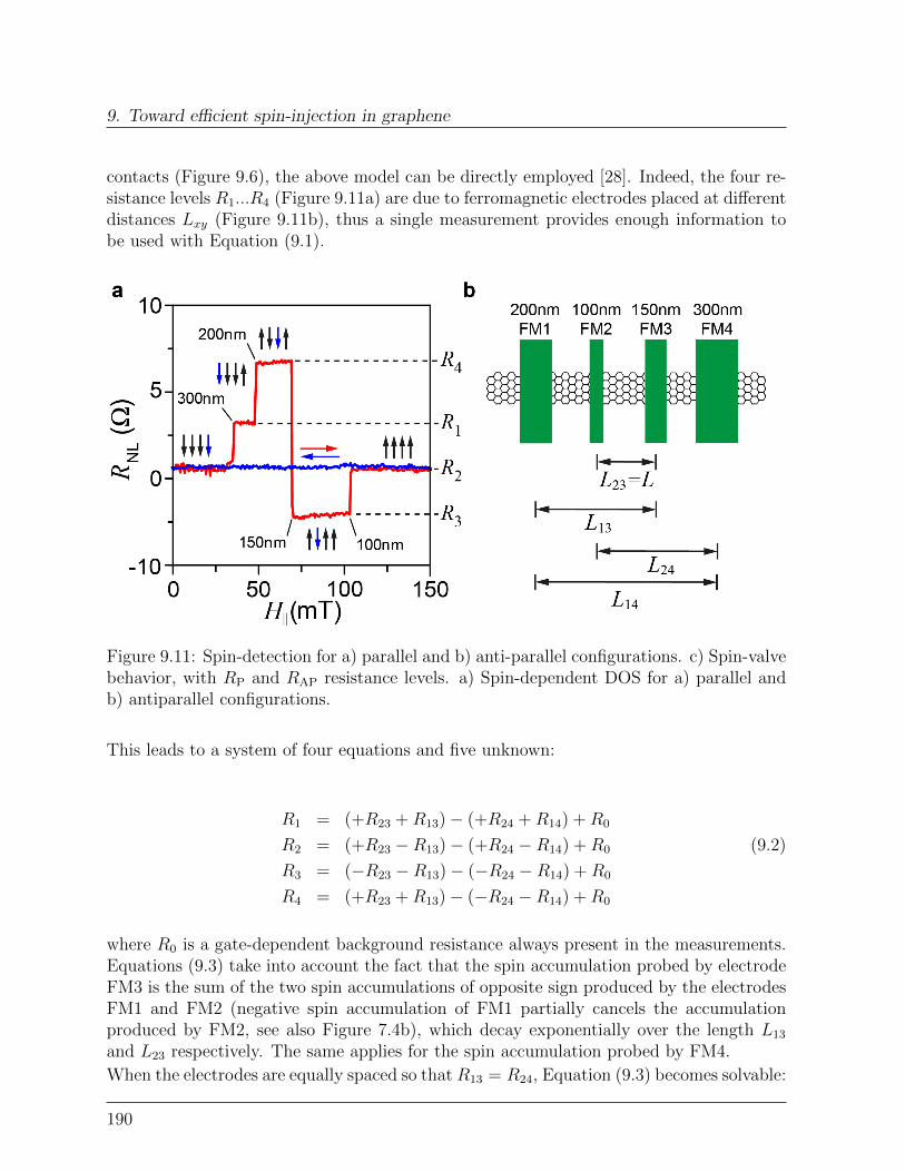
9. Toward efficient spin-injection in graphene
contacts (Figure 9.6), the above model can be directly employed [28]. Indeed, the four re-sistance levels R1...R4 (Figure 9.11a) are due to ferromagnetic electrodes placed at differentdistances Lxy (Figure 9.11b), thus a single measurement provides enough information tobe used with Equation (9.1).
Figure 9.11: Spin-detection for a) parallel and b) anti-parallel configurations. c) Spin-valvebehavior, with RP and RAP resistance levels. a) Spin-dependent DOS for a) parallel andb) antiparallel configurations.
This leads to a system of four equations and five unknown:
R1 = (+R23 +R13)− (+R24 +R14) +R0
R2 = (+R23 −R13)− (+R24 −R14) +R0 (9.2)
R3 = (−R23 −R13)− (−R24 −R14) +R0
R4 = (+R23 +R13)− (−R24 −R14) +R0
where R0 is a gate-dependent background resistance always present in the measurements.Equations (9.3) take into account the fact that the spin accumulation probed by electrodeFM3 is the sum of the two spin accumulations of opposite sign produced by the electrodesFM1 and FM2 (negative spin accumulation of FM1 partially cancels the accumulationproduced by FM2, see also Figure 7.4b), which decay exponentially over the length L13
and L23 respectively. The same applies for the spin accumulation probed by FM4.
When the electrodes are equally spaced so that R13 = R24, Equation (9.3) becomes solvable:
190
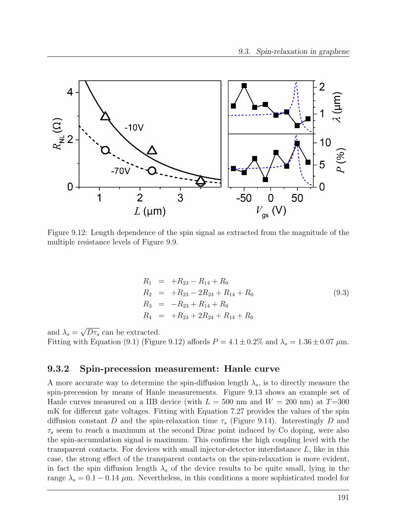
9.3. Spin-relaxation in graphene
Figure 9.12: Length dependence of the spin signal as extracted from the magnitude of themultiple resistance levels of Figure 9.9.
R1 = +R23 −R14 +R0
R2 = +R23 − 2R24 +R14 +R0 (9.3)
R3 = −R23 +R14 +R0
R4 = +R23 + 2R24 +R14 +R0
and λs =√Dτs can be extracted.
Fitting with Equation (9.1) (Figure 9.12) affords P = 4.1± 0.2% and λs = 1.36± 0.07 µm.
9.3.2 Spin-precession measurement: Hanle curve
A more accurate way to determine the spin-diffusion length λs, is to directly measure thespin-precession by means of Hanle measurements. Figure 9.13 shows an example set ofHanle curves measured on a IIB device (with L = 500 nm and W = 200 nm) at T=300mK for different gate voltages. Fitting with Equation 7.27 provides the values of the spindiffusion constant D and the spin-relaxation time τs (Figure 9.14). Interestingly D andτs seem to reach a maximum at the second Dirac point induced by Co doping, were alsothe spin-accumulation signal is maximum. This confirms the high coupling level with thetransparent contacts. For devices with small injector-detector interdistance L, like in thiscase, the strong effect of the transparent contacts on the spin-relaxation is more evident,in fact the spin diffusion length λs of the device results to be quite small, lying in therange λs = 0.1− 0.14 µm. Nevertheless, in this conditions a more sophisticated model for
191
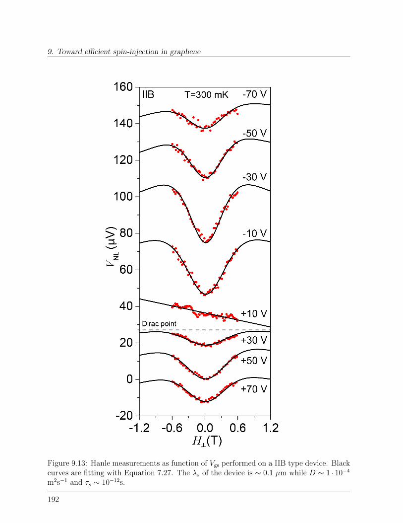
9. Toward efficient spin-injection in graphene
Figure 9.13: Hanle measurements as function of Vgs performed on a IIB type device. Blackcurves are fitting with Equation 7.27. The λs of the device is ∼ 0.1 µm while D ∼ 1 · 10−4
m2s−1 and τs ∼ 10−12s.
192

9.4. Conclusions
Figure 9.14: Evolution of the spin-diffusion constant D and the spin-relaxation time τswith Vgs. Both show a minimum at the charge neutrality point, while they are maximumat the second Dirac point induced by doping by the Co contacts.
the spin-precession is necessary in order to account for the effect of high coupling to thecontacts.
9.4 Conclusions
To conclude, we presented a new fabrication process for the creation of uniform Al2O3
ultra-thin films by atomic layer deposition (ALD) on graphene, to be used as tunnelingbarriers in spinvalve devices. The uniformity of the films is enhanced by employing a Tita-nium seed layer that promotes ALD nucleation in the graphene basal plane. Moreover, wedemonstrated that the chemical composition of the barrier film is the main factor deter-mining the spin-injection efficiency of the device, even in absence of pinholes. The presenceof unoxidized seeding material can hinder the spin-injection in graphene completely, andan additional oxidation step previous to the ALD process is necessary to ensure a fullyoxidized barrier stack. While on the one hand, the possibility of using ALD methodsgreatly simplifies the fabrication of tunneling barriers, the sensibility of the spin-injectionon the barrier chemical composition makes this kind of devices non suitable for the studyof chemically-functionalized graphene spinvalves, therefore spinvalve devices with ohmiccontacts are preferred. To maximize the spin-injection efficiency in transparent spinvalves,the graphene was patterned in narrow stripes so as to reduce the junction size and in-crease the spin-dependent interface resistance. The patterning is performed by combiningelectron-beam lithography and reactive ion etching. The design of the final devices in-volved also the optimization of different factors, such as the ferromagnetic domain sizeand shape anisotropy, so as to maximize the spin-transport response. Spin-transport ingraphene was studied by means of magnetoresistance and Hanle spin-precession measure-ments. Several factors, such as the width of the graphene stripe and the injector-detector
193
Bibliography
inter-distance, were found to play an important role in determining the final spin-diffusionlength of the devices. The comparison between spin- and charge transports confirms thecontact transparency and reveals the doping effect of the ferromagnetic contacts. The de-sign and fabrication process here developed can now be used to study the effect of differentchemical functionalizations on the graphene spin-relaxation.
Bibliography
[1] Rashba, E. I. Theory of electrical spin injection: Tunnel contacts as a solution of theconductivity mismatch problem. Phys. Rev. B 62, 16267–16270 (2000).
[2] Han, W. et al. Tunneling spin injection into single layer graphene. Phys. Rev. Lett.105, 167202 (2010).
[3] Dlubak, B. et al. Highly efficient spin transport in epitaxial graphene on SiC. NatPhys 8, 557–561 (2012).
[4] Tombros, N. et al. Electronic spin transport and spin precession in single graphenelayers at room temperature. Nature 448, 571–574 (2007).
[5] Xie, G. et al. Graphene Edge Lithography. Nano Letters 0, null (2012).
[6] Xuan, Y. et al. Atomic-layer-deposited nanostructures for graphene-based nanoelec-tronics. Applied Physics Letters 92, 13101 (2008).
[7] Lee, B. et al. Conformal Al2O3 dielectric layer deposited by atomic layer depositionfor graphene-based nanoelectronics. Applied Physics Letters 92, 203102 (2008).
[8] Wang, X., Tabakman, S. M. & Dai, H. Atomic Layer Deposition of Metal Oxideson Pristine and Functionalized Graphene. Journal of the American Chemical Society130, 8152–8153 (2008).
[9] Wang, L. et al. Ultrathin oxide films by atomic layer deposition on graphene. NanoLetters 12, 3706–3710 (2012).
[10] Farmer, D. B. et al. Utilization of a Buffered Dielectric to Achieve High Field-EffectCarrier Mobility in Graphene Transistors. Nano Letters 9, 4474–4478 (2009).
[11] Sangwan, V. K. et al. Quantitatively enhanced reliability and uniformity of high-κdielectrics on graphene enabled by self-assembled seeding layers. Nano Letters 13,1162–1167 (2013).
[12] Dlubak, B., Kidambi, P. R., Weatherup, R. S., Hofmann, S. & Robertson, J.Substrate-assisted nucleation of ultra-thin dielectric layers on graphene by atomiclayer deposition. Applied Physics Letters 100, 173113 (2012).
194
Bibliography
[13] Robinson, J. a. et al. Epitaxial graphene materials integration: Effects of dielectricoverlayers on structural and electronic properties. ACS Nano 4, 2667–2672 (2010).
[14] Fallahazad, B. et al. Scaling of Al2O3 dielectric for graphene field-effect transistors-dielectric for graphene field-effect transistors. Applied Physics Letters 100, 93112(2012).
[15] Yamaguchi, T., Masubuchi, S., Iguchi, K., Moriya, R. & MacHida, T. Tunnel spininjection into graphene using Al2O3 barrier grown by atomic layer deposition onfunctionalized graphene surface. Journal of Magnetism and Magnetic Materials 324,849–852 (2012).
[16] Crangle, J. The Magnetic Properties of Solids Ch. 6. Ch. 6 (Edward Arnold, London,1977).
[17] Jedema, F. J., Nijboer, M. S., Filip, a. T. & van Wees, B. J. Spin injection and spin ac-cumulation in permalloy-copper mesoscopic spin valves. Journal of Superconductivity15, 8 (2001).
[18] Han, W. et al. Spin transport and relaxation in graphene. Journal of Magnetism andMagnetic Materials 324, 369–381 (2012).
[19] http://www.keithley.com/.
[20] Simmons, J. G. Generalized Formula for the Electric Tunnel Effect between SimilarElectrodes Separated by a Thin Insulating Film. Journal of Applied Physics 34,1793–1803 (1963).
[21] Prins, F. et al. Room-temperature gating of molecular junctions using few-layergraphene nanogap electrodes. Nano Letters 11, 4607–4611 (2011). arXiv:1110.2335.
[22] Mangin, a., Anthore, a., Della Rocca, M. L., Boulat, E. & Lafarge, P. Reduced workfunctions in gold electromigrated nanogaps. Physical Review B - Condensed Matterand Materials Physics 80, 1–5 (2009).
[23] Kimura, T., Otani, Y. & Hamrle, J. Enhancement of spin accumulation in a nonmag-netic layer by reducing junction size. Phys. Rev. B 73, 132405 (2006).
[24] Jo, S., Ki, D.-K., Jeong, D., Lee, H.-J. & Kettemann, S. Spin relaxation properties ingraphene due to its linear dispersion. Phys. Rev. B 84, 075453 (2011).
[25] Casiraghi, C. et al. Raman Spectroscopy of Graphene Edges. Nano Letters 9, 1433–1441 (2009).
[26] Ryu, S., Maultzsch, J., Han, M. Y., Kim, P. & Brus, L. E. Raman spectroscopy oflithographically patterned graphene nanoribbons. ACS nano 5, 4123–30 (2011).
195

Bibliography
[27] Jedema, F. J. et al. Electrical detection of spin precession in a metallic mesoscopicspin valve. Nature 416, 713–716 (2002).
[28] Popinciuc, M. et al. Electronic spin transport in graphene field-effect transistors. Phys.Rev. B 80, 214427 (2009).
[29] Han, W. et al. Electrical detection of spin precession in single layer graphene spinvalves with transparent contacts. Applied Physics Letters 94, 222109 (2009).
[30] Han, W. & Kawakami, R. K. Spin Relaxation in Single-Layer and Bilayer Graphene.Phys. Rev. Lett. 107, 47207 (2011).
[31] Volmer, F. et al. Role of MgO barriers for spin and charge transport inCo/MgO/graphene nonlocal spin-valve devices. Physical Review B 88, 161405 (2013).
196

Chapter 10
Perspectives
This chapter presents the first preliminary spin-transport and spin-precession experimentsin graphene spinvalves functionalized with SMMs. The sophisticated mechanisms (spin-injection, -diffusion) underlying the spinvalves function, combined with the rich magneticbehavior of SMMs makes these experiments extremely challenging.The ultimate goal is to investigate how electronic spins in graphene couple to the spin ofSMMs, and to reveal the details of related spin-interactions. The tunable parameters inthese experiment are temperature and electrostatic gating. Varying the temperature acrossthe blocking temperature Tb changes the SMMs magnetic response. The Fe4Py clusterexhibits a clear transition from paramagnetic to superparamagnetic behaviors at a tem-perature of about Tb = 800 mK (see Chapter 2.2). The presence of Fe4Py grafted on thegraphene surface is thus expected to influence the electron spin in different ways for tem-peratures above and below Tb. T does not affect spin transport in graphene appreciably.On the contrary, electrostatic gating affects the graphene spin signal ∆RNL substantially(see Chapter 9). At the same time, an external gate electric field strongly influences themagnetic state of SMMs, as demonstrated by transport experiments in molecular nano-junctions [1–3].
10.1 Spin-transport in graphene-SMMs hybrid devices
The spinvalve devices developed in the previous chapters are here used to study the effect ofmagnetic adsorbates on the graphene spin-injection mechanism (Figure 10.1a). To this enda IIB type device has been functionalized with Fe4Py by dropcasting, using a C = 2.5 · 10−6
M, solution prepared as described Section 4.2, followed by washing with fresh solventmixture and drying under Ar jet. The functionalization is performed directly on the chipwithout removing the bonding wires. A shift of the resistivity maximum towards highergate voltages indicates successful molecular decoration (Figure 10.1b), in agreement withthe observations of Section 4.20. After functionalization, the charge neutrality point of thedevice lies at VD = 33.4 V. The increase in the device mobility after functionalization islikely due to the removal of the resist impurities introduced by the lithographic steps.
197
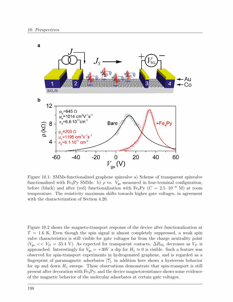
10. Perspectives
Figure 10.1: SMMs-functionalized graphene spinvalve a) Scheme of transparent spinvalvefunctionalized with Fe4Py SMMs. b) ρ vs. Vgs measured in four-terminal configuration,before (black) and after (red) functionalization with Fe4Py (C = 2.5 · 10−6 M) at roomtemperature. The resistivity maximum shifts towards higher gate voltages, in agreementwith the characterization of Section 4.20.
Figure 10.2 shows the magneto-transport response of the device after functionalization atT = 1.6 K. Even though the spin signal is almost completely suppressed, a weak spinvalve characteristics is still visible for gate voltages far from the charge neutrality point(Vgs << VD = 33.4 V). As expected for transparent contacts, ∆RNL decreases as VD isapproached. Interestingly for Vgs = +30V a dip for H|| ≈ 0 is visible. Such a feature wasobserved for spin-transport experiments in hydrogenated graphene, and is regarded as afingerprint of paramagnetic adsorbates [?], in addition here shows a hysteresis behaviorfor up and down H|| sweeps. These observations demonstrate that spin-transport is stillpresent after decoration with Fe4Py, and the device magnetoresistance shows some evidenceof the magnetic behavior of the molecular adsorbates at certain gate voltages.
198

10.1. Spin-transport in graphene-SMMs hybrid devices
Figure 10.2: SMMs-functionalized graphene spinvalve: gate dependence of magneto-transport at T = 1.6 K. The H|| sweep-rate is 20 mT/min. The black circle for Vgs = +30V highlights a typical fingerprint of paramagnetic adsorbates [?].
199
10. Perspectives
10.2 Spin-relaxation in graphene-SMMs hybrid de-
vices
The effect of coupling to the Fe4Py spins on the spin-relaxation in graphene is studiedby means of Hanle spin-precession measurements. The spinvalve is prepared with theinjector and detector magnetizations parallel to each other, and lying along the electrodeslong direction. The non-local voltage VNL is then acquired while sweeping H⊥ (appliedperpendicular to the graphene plane) with excitation current |J | = 10µA. Figure 10.3shows spin-precession response measured at T = 1.6 K. Both up- and down-sweeps areacquired to reveal any hysteric behavior. The measurements show a very rich behavior,with the shape of the Hanle-curve varying to a great extent as function of the gate voltageVgs (Figure 10.3). Surprisingly for Vgs = −70V , VNL is minimum at H⊥ = 0 in contrast towhat expected for parallel injector/detector magnetizations. Fitting with (7.27) providesτs = 21.4 ps and D = 3.3 · 10−4 m2s−1 that yield λs = 0.084µm, a slightly reduced values incomparison with the empty device shown in Figurehanlegate. By increasing Vgs the shapeof the Hanle curve changes drastically. The signal increases as the charge neutrality pointis approached, where a more clear Hanle shape is observed. Interestingly the curve seemsto undergo an inversion as Vgs crosses the charge neutrality point at Vgs = VD.Up and down sweeps overlap at all gate voltages, thus no hysteresis is observed as expectedfor the paramagnetic behavior of Fe4Py at these temperatures. Hystereretic behavior ap-pears indeed only at lower temperatures (T = 300 mK), as an effect of the superparamag-netism of Fe4Py. (Figure 10.4). Interestingly, hysteresis are only observed for Vgs close tothe Dirac point where the spin signal is minimum (Figure 10.5), suggesting that the sensi-tivity of the device to the magnetic adsorbates is maximum as the charge neutrality pointis approached. A detailed modeling is now necessary to explain the complicated behaviorhere presented, and to correctly take into account the effect of electrostatic gating on theSMMs magnetic response.
200

10.2. Spin-relaxation in graphene-SMMs hybrid devices
Figure 10.3: SMMs-functionalised graphene spinvalve: Hanle spin-precession for up- (left)and down- (right) magnetic field sweeps at T = 1.6 K.
201
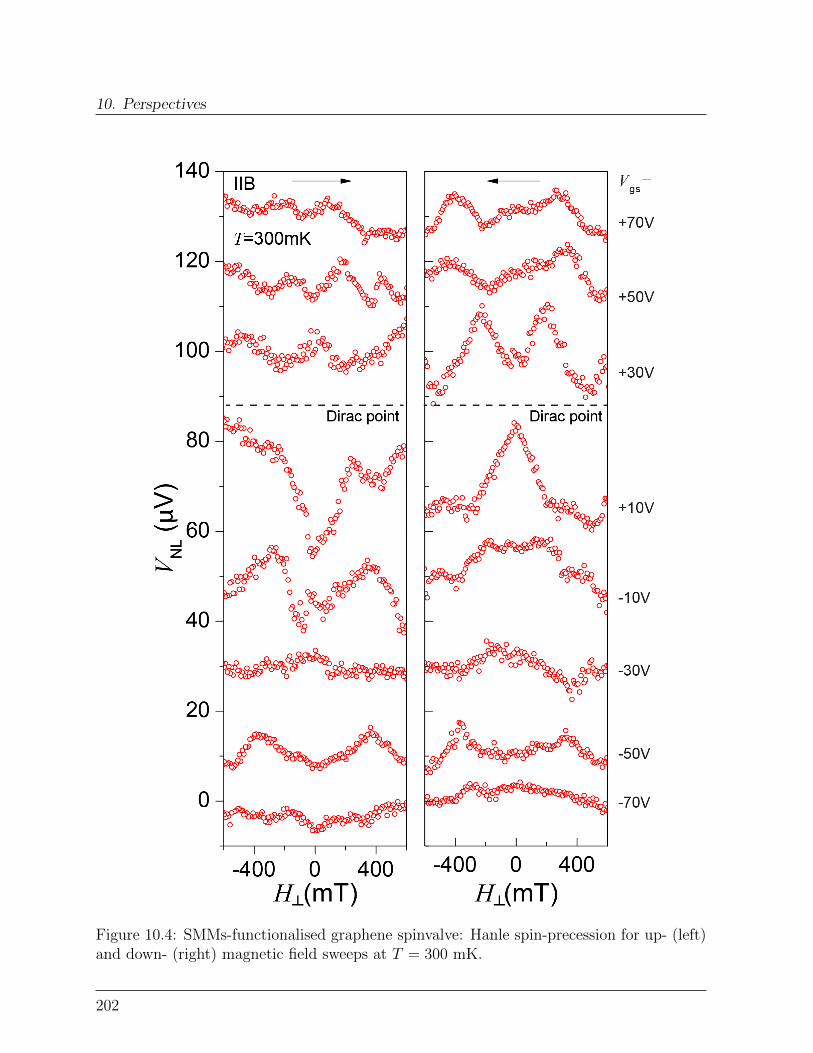
10. Perspectives
Figure 10.4: SMMs-functionalised graphene spinvalve: Hanle spin-precession for up- (left)and down- (right) magnetic field sweeps at T = 300 mK.
202
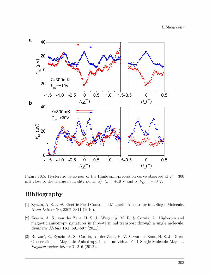
Bibliography
Figure 10.5: Hysteretic behaviour of the Hanle spin-precession curve observed at T = 300mK close to the charge neutrality point. a) Vgs = +10 V and b) Vgs = +30 V.
Bibliography
[1] Zyazin, A. S. et al. Electric Field Controlled Magnetic Anisotropy in a Single Molecule.Nano Letters 10, 3307–3311 (2010).
[2] Zyazin, A. S., van der Zant, H. S. J., Wegewijs, M. R. & Cornia, A. High-spin andmagnetic anisotropy signatures in three-terminal transport through a single molecule.Synthetic Metals 161, 591–597 (2011).
[3] Burzurı, E., Zyazin, A. S., Cornia, A., der Zant, H. V. & van der Zant, H. S. J. DirectObservation of Magnetic Anisotropy in an Individual Fe 4 Single-Molecule Magnet.Physical review letters 2, 2–6 (2012).
203

Bibliography
204

Chapter 11
Conclusions
This thesis sets the theoretical and experimental basis for the study of spin-relaxation ingraphene-based hybrid materials, thus opening the way to the first experimental charac-terization and the theoretical understanding of graphene-based spintronic devices.
To reach this aim two complementary approaches were followed. In the first, single moleculemagnets (SMMs) are used as model spin systems to unveil the detailed interaction be-tween a spin and its environment, by directly looking at their dynamics when placed ontographene. In the second approach, robust graphene-based spinvalve devices are developedas novel tool to study how molecular spins influence the diffusion of spin-polarized carri-ers in graphene. Moreover, in the quest for scalable production of high-quality graphene,a novel non-invasive technique based on continuous-wave sub-millimeter spectroscopy ispresented as powerful tool for the electrical characterization of large-area graphene.
The SMM [Fe4(L)2(dpm)6] with pyrene grafting groups was employed to embed isolatedspins in the graphene environment via wet-chemistry approach. The grafting mecha-nism was investigated by studying the topography of the molecules bound to high qualitygraphene flakes. The concentration of the functionalizing solution is found to control thegrowth mode of molecular islands on the graphene surface. Statistical analysis of theAFM height profile indicates that π-stacking interaction tend to promote the formation oftwo-dimensional molecular arrangements on the graphene surface. Being three-dimensionalgrowth only possible at high concentrations, proves that the grafting to graphene is strongerthan the intramolecular binding. This is confirmed by scaling-analysis that indicates an ap-preciable surface-diffusion of the adsorbates during the reaction in solution. This opens theway to novel methods for the creation of extended molecular arrangements on graphene. Inparticular, the synthesis of two-dimension molecular random network is here demonstratedby exposing the functionalized surface to laser light.
The effect of the grafting on the molecular properties is investigated via multiple tech-niques. Matrix assisted laser desorption ionization mass spectrometry demonstrate thestructural robustness of the molecular units, with isotopic patterns that unequivocally in-dicate an unvaried coordination structure for the molecules magnetic core. The electronicstability of the cluster is confirmed by the position of the Fe2p double peak in the X-rayphotoelectron spectra, that matches that of the crystalline compounds and clearly indi-
205
11. Conclusions
cate binding to Oxygen. The absence of appreciable charge transfer is also supported byelectronic transport measurements on graphene-based field effect transistors functionalizedwith the SMMs. The position of the Fermi level with respect to the Dirac point (touch-ing point between the conical valence and conduction bands of graphene) is found to beextremely sensitive to the external functionalization. The simple formation of a dipoleat the graphene/molecule interface is seen to induce a Fermi level shift of around 30 V.This matches with the energy up-shift and the stiffening of the E2g mode in the grapheneRaman spectra after functionalization.Magnetization and dc-susceptibility measurements prove that the static magnetic proper-ties of the clusters remain unchanged after the dispersion in solution and the subsequentgrafting to graphene, owing to the cluster excellent structural and electronic stability. Af-ter subtracting the strong graphene diamagnetic contribution, the χT vs. T curve of thehybrid acquired at 1000 Oe perfectly matches that of the starting crystalline compound,indicating the unvaried nearest neighbor and next nearest neighbor exchange interactionscharacteristic of the Fe4 core. Moreover the value of the susceptibility maximum observableat low temperature confirms a spin-ground state S = 5. The latter is further confirmed bythe saturation value of isothermal magnetization curves acquired at different temperatures.The dynamics of molecular spins in the graphene matrix was studied by means of ac-susceptibility measurements in the broad temperature range T = 4 K - 13 mK. Twospin-relaxation regimes were identified: a classical (thermal) one, dominating the relax-ation at temperatures T > 0.8, and a quantum one that dominates the relaxation at lowtemperatures T < 0.8. The spin dynamics of the hybrids diverges considerably from thatof the pristine crystal compound. A fixed external magnetic field is used to suppress thequantum relaxation channel, so as to study the effect of the graphene environment onclassical spin-relaxation mechanism only. The thermal relaxation is found to be mainlydetermined by interaction of the spins with the graphene phonon bath via spin-phononinteraction. By extending the existing theoretical models to the case of a two-dimensionalphonon bath, reveals the effect of the phonon-bath dimensionality on the classical spin-relaxation mechanism. The experimental observation are nicely reproduced using the SMMcharacteristics as extracted from crystal and the graphene sound velocity and without anyfree fitting parameter.The quantum relaxation path is studied in absence of external field in the temperaturerange where the thermal excitation of spin states is negligible. Interaction with grapheneenhances the quantum tunneling rate by almost 6 orders of magnitude. Analysis basedon a newly developed theoretical model, based on the Stevens’ operator equivalents for-malism, allows to quantify the contributions of the different fundamental interactions (i.e.hyperfine, dipole-dipole, spin-phonon) to the quantum relaxation. The rate enhancementis explained by introducing in the theory a large perturbative term having a three-foldsymmetry that mixes the quantum spin-states differing in m by multiples of 3. This termis likely a fingerprint of the interaction between the spin and graphene charge distribu-tion and is seen to drives the spin dynamics into a strongly perturbative quantum tunnelingregime predicted by Villain’s more than a decade ago, and here observed experimentally forthe first time. Being this regime coherent by definition, the influence of graphene carriers
206
on spin tunneling allows envisaging new schemes for the electrical control of the quantumcoherence of spin-states.The second part of this work is dedicated to the study of spintronic interations betweenthe molecular spins and the spin-polarized massless carriers in graphene.The challenges in the development of robust graphene-SMMs hybrid spintronic devicesare addressed by employing two different strategies. On the one hand, the conductivitymismatch between the graphene channel and the ferromagnetic contacts (used as source ofspin-polarized carriers) is overcome by integrating ultra-thin Al2O3 tunneling barriers atthe graphene/ ferromagnet interface. The growth of highly uniform insulating thin-filmsby atomic layer deposition (ALD) is made possible implementing a Titanium seeding, thatpromotes Al2O3 nucleation in the graphene basal plane. Nevertheless, the spin-injectionefficiency is found to be very sensitive to the barrier chemical composition, and the presenceof unoxidized Ti island at the interface with graphene is seen to hinder the spin-injectioncompletely. A fully oxidized seeding is the key for the realization of highly decoupled ferro-magnetic contact and helps preserving the long spin-diffusion length of graphene. However,being the spin trasport in such devices very sensitive to the barrier composition, such de-vice architecture is incompatible with the study of graphene chemical functionalizationthat ask for a more robust devices. Efficient spin-injection is achieved in graphene spin-valves with transparent contacts by reducing the contact junction sized so as to enhancethe spin-dependent interface resistance. To this end, the graphene flakes are patternedin few hundreds nanometers-wide stripes, via combining ebeam lithography masking andplasma etching. The spin-diffusion length and the spin-injection efficiency are stronglyreduced as the stripe width is decreased. This validates theories of spin-flip scattering in-duced by short-range scatterers at the graphene edges. Presence of short-range scatterers isconfirmed by an increase in the constant resistivity contribution in two terminal electronictransport measurements, and further supported by the prominent D band in the Ramanspectrum for small-width stripes.First spin-transport and spin-relaxation experiments in hybrid SMMs-graphene transparentspinvalves reveal a very rich behavior as function of both temperature and electrostaticgating. While clear evidences of interaction with the magnetic adsorbates are observedin both magnetoresistance and Hanle measurements at T = 1.6 K. Clear fingerprintsof the superparamagnetic SMMs behavior is observed for temperatures below the SMMblocking temperature, as indicated by a clear hysteresis opening. Further experimentalinvestigations and new theoretical modeling are now on the way to further explore thespintronic characteristics of SMM-graphene hybrid devices, and to unravel potential newopportunities for the control of graphene spintronic properties.
207

11. Conclusions
208
Acknowledgments
And here it comes the most read section of any PhD thesis, the Acknowledgments!
My sincere gratitude goes to my supervisor Dr. Lapo Bogani for having complete confidencein me and for giving me total freedom during these years. Thank you for encouraging mein pursuing my own ideas and in developing a broader outlook on everything I do. Youtaught me how to be an independent scientist and to take full responsibility of my actions.From you I gained a great deal of scientific knowledge and expertise. Thank you sincerelyfor your esteem and your friendship.
A very special ”thank you” goes to Dr. Marko Burghard, for being my ”MPI supervisor”.Thank you for your patience, understanding and perseverance, and for sharing with me thelove for the challenge! I am grateful to you for your constant support, for your sympathywhenever a sample died, and, most importantly, for your esteem and friendship.
I would like to thank Prof. Martin Dressel for welcoming me in his institute and for givingme total freedom to focus on my projects. Thank you for not complaining when I skippedthe institute seminar to be at the mpi. Thank you for the having confidence in me, foryour patience and support.
My gratitude goes also to Prof. Klaus Kern for welcoming me in his department and forconstantly supporting the collaborative work presented in this thesis.
An important thanks to Karin Goß for sharing with me the toughest moments of my PhDand for her friendship in the outside world! Thank you for being always willing to helpme. I still would like to see the photo of you with green hair...
Eric Heintze you will always be ”our coach”. Thank you for your injections of motivationin the toughest of moments, and for your philosophical insights, yes ”it’s not just a PhD,we are here to stimulate new synapses in the network of science...”.
A big thank to Alexander Hoyer for struggling with me in the lab all the time and forbeing always ready to help and support me and my crazy ideas. I will never forget your:”you know what?, it’s a mess...”. Hold on Alex you are almost there!
A sincere thanks to Kristina Vaklinova for sharing with me our first office and for helpingme whenever I needed it, sorry if I missed some of your cakes, they were always so delicious!
A special thank to Adarsh Sagar, Ravi Shankar Sundaran, Eva Peters, Thomas Defauxfor introducing me to the world of nanofabrication and electronic transport measurements,
209

Acknowledgments
and Loc Duong for assisting me with the CVD domains magic.
I would like to thank Marion Hagel for her help and support with the ALD and for bondingthe most difficult samples I ever worked with. A special thank also to Thomas Riendl,Achim Guth and Ulrike Weitzmann for their constant help in the cleanroom and for theirvaluable flexibility.
My gratitude goes also to Prof. Boris Gorschunov. I really enjoyed working with you thelong hours. A sincere thank you for your esteem and confidence in me.
I would like to thank Gabriele Untereiner for her support in the THz project and forsharing her expertise with me. And thank all the past and present members of the 1.Physikalisches Institut.
Thank you to Conrad Clauss and Ralph Hubner, for sharing the office with me and forbeing always ready for the next beer.
Thanks Junfeng ”Cicci” Wang for his friendship and patience and for pushing me all thetime!
I would also like to thank all the bachelor and master students I worked with in these yearsand from which I learned a lot both on the scientific and personal level. Thank you JulianWinter, Lukas Sebeke (twice!), Matthias Kuhnle, Simon Seyfferle and Ralf Konnerth.
A big thank you to the gorgeous ”Little Italy” group: Nicola Dotti, Stefano De Zuani.Thank you guys for your friendship and for the nice moments we spent and we will spendtogether.
My gratitude goes also to Dr. Hans-Georg Libuda for all his efforts in making the IMPRS-AM a real success. I really enjoyed all the meetings and workshops he organized for us.Thank you also for you support in the tough moments.
A very special place in my heart is dedicated to Pascal Gehring, Michaela Pendelin, YeWeng and Johannes Hirschmann. You made my journey unforgettable and you really mademe feel at home here in Stuttgart.
Last but not least, most of my gratitude goes to Laura, my beloved, to whom this PhDthesis is dedicated. You have been the brightest light in the toughest moments of my life.Thank you for existing.
210

Declaration
I hereby declare that I have authored this thesis independently and used no other sourcesand aids than the stated ones.
Christian CervettiStuttgart, July 2015