Sorbonne Université - CORE
237
Sorbonne Université Ecole doctorale 388 Chimie Physique et Chimie Analytique Laboratoire Interfaces et Systèmes Electrochimiques (LISE), UMR8235 Tip-enhanced Raman spectroscopy on electrochemical systems Par Thomas Touzalin Thèse de doctorat de chimie physique Dirigée par Emmanuel Maisonhaute Co-encadrée par Ivan T. Lucas Pour une soutenance publique prévue le 20 septembre 2018 Devant un jury composé de : M me Sophie Lecomte DR CNRS, Université de Bordeaux Rapporteure M. Fouad Maroun DR CNRS, Ecole Polytechnique Rapporteur M. Ludovic Jullien Prof., Sorbonne Université, ENS Examinateur M me Katrin F. Domke Dr., Max Planck Institute for Polymer Research Examinatrice M. Emmanuel Maisonhaute Prof., Sorbonne Université Directeur de thèse M. Ivan T. Lucas MCF, Sorbonne Université Co-encadrant
-
Upload
khangminh22 -
Category
Documents
-
view
6 -
download
0
Transcript of Sorbonne Université - CORE
Sorbonne Université
Ecole doctorale 388
Chimie Physique et Chimie Analytique
Laboratoire Interfaces et Systèmes Electrochimiques (LISE), UMR8235
Tip-enhanced Raman spectroscopy on electrochemical
systems
Par Thomas Touzalin
Thèse de doctorat de chimie physique
Dirigée par Emmanuel Maisonhaute
Co-encadrée par Ivan T. Lucas
Pour une soutenance publique prévue le 20 septembre 2018
Devant un jury composé de :
Mme Sophie Lecomte DR CNRS, Université de Bordeaux Rapporteure
M. Fouad Maroun DR CNRS, Ecole Polytechnique Rapporteur
M. Ludovic Jullien Prof., Sorbonne Université, ENS Examinateur
Mme Katrin F. Domke Dr., Max Planck Institute for Polymer Research Examinatrice
M. Emmanuel Maisonhaute Prof., Sorbonne Université Directeur de thèse
M. Ivan T. Lucas MCF, Sorbonne Université Co-encadrant


Tip-enhanced Raman spectroscopy on
electrochemical systems
Thomas Touzalin


Contents
Introduction 7
1 Raman spectroscopy at the nanoscale for electrochemistry: state
of the art 13
1.1 Raman scattering and spectroscopy . . . . . . . . . . . . . . . . . . . 13
1.1.1 Light-matter interactions in the UV-Vis and IR range . . . . . 13
1.1.2 Theory of Raman scattering . . . . . . . . . . . . . . . . . . . 15
1.1.3 Raman cross section . . . . . . . . . . . . . . . . . . . . . . . 18
1.1.4 Enhancement of the Raman scattering . . . . . . . . . . . . . 19
1.2 Fundamentals of plasmonics and surface-enhanced Raman scattering . 21
1.2.1 Surface Plasmons . . . . . . . . . . . . . . . . . . . . . . . . . 21
1.2.1.1 Optical properties of noble metals . . . . . . . . . . . 21
1.2.1.2 Localized Surface Plasmon Resonance . . . . . . . . 24
1.2.2 Surface-Enhanced Raman Spectroscopy . . . . . . . . . . . . . 27
1.2.2.1 SERS enhancement mechanism . . . . . . . . . . . . 27
1.2.2.2 Electrochemical SERS . . . . . . . . . . . . . . . . . 28
1.2.2.3 Shell-Isolated Nanoparticles Enhanced Raman Spec-
troscopy . . . . . . . . . . . . . . . . . . . . . . . . . 30
1.3 Beyond the diraction limit: scanning near-eld optical microscopy . 31
1.3.1 Optical diraction limit . . . . . . . . . . . . . . . . . . . . . 31
1.3.2 Principles of near-eld optics . . . . . . . . . . . . . . . . . . 32
1

1.3.3 Aperture SNOM . . . . . . . . . . . . . . . . . . . . . . . . . 34
1.3.4 Scattering SNOM . . . . . . . . . . . . . . . . . . . . . . . . . 36
1.3.5 Photothermal approach for nano-IR . . . . . . . . . . . . . . . 38
1.4 Tip-enhanced Raman Spectroscopy: Raman beyond the diraction
limit . . . . . . . . . . . . . . . . . . . . . . . . . . . . . . . . . . . . 39
1.4.1 Pioneer experimental TERS evidences . . . . . . . . . . . . . 39
1.4.2 About TERS enhancement . . . . . . . . . . . . . . . . . . . . 40
1.4.3 Enhancement mechanisms and gap mode conguration . . . . 43
1.4.4 Spatial resolution in TERS . . . . . . . . . . . . . . . . . . . . 45
1.4.5 Feedback Mechanisms . . . . . . . . . . . . . . . . . . . . . . 46
1.4.5.1 AFM-TERS . . . . . . . . . . . . . . . . . . . . . . . 47
1.4.5.2 STM-TERS . . . . . . . . . . . . . . . . . . . . . . . 48
1.4.5.3 TF-TERS . . . . . . . . . . . . . . . . . . . . . . . . 49
1.4.6 Fabrication of AFM and STM-TERS tips . . . . . . . . . . . . 51
1.4.7 Other types of SNOM and TERS tips . . . . . . . . . . . . . . 53
1.5 Probing and inducing chemical reactions with TERS . . . . . . . . . 54
1.5.1 Catalytic reactions monitored by TERS . . . . . . . . . . . . 54
1.5.2 Plasmonic tip-induced reactions . . . . . . . . . . . . . . . . . 55
1.6 Electrochemical TERS . . . . . . . . . . . . . . . . . . . . . . . . . . 57
1.6.1 Congurations proposed for TERS in liquids . . . . . . . . . . 57
1.6.2 EC TERS . . . . . . . . . . . . . . . . . . . . . . . . . . . . . 58
1.6.3 Challenges for EC-TERS . . . . . . . . . . . . . . . . . . . . . 61
2 Description of TERS experiments 63
2.1 Description of the setup for microRaman and TERS experiments . . . 63
2.2 TERS tips manufacturing . . . . . . . . . . . . . . . . . . . . . . . . 68
2.2.1 Fabrication of gold TERS tips . . . . . . . . . . . . . . . . . . 68
2.2.2 Fabrication of silver TERS tips . . . . . . . . . . . . . . . . . 71
2.2.3 Prevention of TERS tips degradation . . . . . . . . . . . . . . 72
2

2.3 TF-TERS experiments . . . . . . . . . . . . . . . . . . . . . . . . . . 77
2.4 Conclusion . . . . . . . . . . . . . . . . . . . . . . . . . . . . . . . . . 79
3 Tip-Enhanced Raman Spectroscopy imaging of opaque samples in
organic liquids 81
3.1 Introduction . . . . . . . . . . . . . . . . . . . . . . . . . . . . . . . . 81
3.2 Description of the experimental setup . . . . . . . . . . . . . . . . . . 82
3.2.1 Optical coupling . . . . . . . . . . . . . . . . . . . . . . . . . 82
3.2.2 Spectroscopic characteristization of the solvent and of the
molecular layer . . . . . . . . . . . . . . . . . . . . . . . . . . 83
3.2.3 Focusing of the laser at the apex . . . . . . . . . . . . . . . . 85
3.2.3.1 TER in the air . . . . . . . . . . . . . . . . . . . . . 85
3.2.3.2 TERS in hexadecane . . . . . . . . . . . . . . . . . . 86
3.3 TERS imaging in organic liquid . . . . . . . . . . . . . . . . . . . . . 87
3.4 Conclusion . . . . . . . . . . . . . . . . . . . . . . . . . . . . . . . . . 92
4 Electrochemical Tip Surface-Enhanced Raman Spectroscopy 93
4.1 Context . . . . . . . . . . . . . . . . . . . . . . . . . . . . . . . . . . 93
4.2 Description of the studied system: 4-NTP . . . . . . . . . . . . . . . 95
4.2.1 Electrochemical study of the reduction mechanism of a 4-NTP
monolayer . . . . . . . . . . . . . . . . . . . . . . . . . . . . . 95
4.2.1.1 Description of the studied system . . . . . . . . . . . 95
4.2.1.2 Gold sphere electrode functionalization and experi-
mental details . . . . . . . . . . . . . . . . . . . . . . 97
4.2.1.3 Gold sphere electrode characterization . . . . . . . . 97
4.2.1.4 Irreversible reduction of 4-NTP . . . . . . . . . . . . 98
4.2.1.5 Electrochemical characterization of 4-ATP . . . . . . 99
4.2.1.6 Study of the conversion of 4-NTP into 4-HATP . . . 101
4.2.2 Spectroscopic characteristics of the system . . . . . . . . . . . 105
3

4.3 Spectroelectrochemical analysis of 4-NTP reduction reaction . . . . . 106
4.3.1 Electrochemical reduction of 4-NTP monitored by ex situ TERS106
4.3.2 Electrochemical reduction of 4-NTP monitored by in situ EC
tip SERS . . . . . . . . . . . . . . . . . . . . . . . . . . . . . 110
4.3.2.1 Description of the setup and experimental conditions 110
4.3.2.2 Ex situ tip SERS . . . . . . . . . . . . . . . . . . . . 112
4.3.3 Potential dependent tip SERS measurements . . . . . . . . . . 113
4.4 Conclusion . . . . . . . . . . . . . . . . . . . . . . . . . . . . . . . . . 119
5 Electrochemical TERS imaging of functionalized gold surfaces 121
5.1 Introduction . . . . . . . . . . . . . . . . . . . . . . . . . . . . . . . . 121
5.2 Description of the setup . . . . . . . . . . . . . . . . . . . . . . . . . 122
5.2.1 Electronic implementation . . . . . . . . . . . . . . . . . . . . 122
5.2.2 Cell design for EC STM-TERS measurements . . . . . . . . . 124
5.2.3 Tip insulation and characterization . . . . . . . . . . . . . . . 125
5.3 Evaluation of the system stability . . . . . . . . . . . . . . . . . . . . 128
5.4 EC TERS imaging . . . . . . . . . . . . . . . . . . . . . . . . . . . . 130
5.4.1 Laser focusing on the tip . . . . . . . . . . . . . . . . . . . . . 130
5.4.2 Preliminary results on EC-TERS imaging . . . . . . . . . . . 132
5.5 Conclusion . . . . . . . . . . . . . . . . . . . . . . . . . . . . . . . . . 135
6 TERS characterization of surfaces derivatized with diazonium salts137
6.1 Introduction . . . . . . . . . . . . . . . . . . . . . . . . . . . . . . . . 137
6.2 Chemistry and electrochemistry of diazonium salts . . . . . . . . . . . 138
6.3 Electrochemical grafting of a monolayer of a diazonium salt . . . . . . 141
6.3.1 Electrochemical grafting and characterization of a monolayer
of penuorobenzene . . . . . . . . . . . . . . . . . . . . . . . . 142
6.3.2 STM imaging of PFBD-grafted gold surfaces . . . . . . . . . . 145
6.3.3 TERS analysis of the PFBD-grafted surface . . . . . . . . . . 146
4

6.4 Electrochemical and TERS investigation of an electroactive diazo-
nium salt . . . . . . . . . . . . . . . . . . . . . . . . . . . . . . . . . 147
6.4.1 Electrochemical characterization of a gold electrode function-
alized by FeBTPD . . . . . . . . . . . . . . . . . . . . . . . . 147
6.4.2 STM-TERS analysis of a FeBTP grafted surface . . . . . . . . 150
6.5 Spontaneous grafting of diazonium salts investigated by STM-TERS . 154
6.5.1 Sample preparation and characterization . . . . . . . . . . . . 155
6.5.2 STM-TERS analysis of the spontaneously grafted layer . . . . 156
6.6 Conclusion . . . . . . . . . . . . . . . . . . . . . . . . . . . . . . . . . 159
Conclusion and outlook 161
A Supplementary materials to Chapter 4 165
A.1 Raman signature of N,N-dimethylnitrosoaniline . . . . . . . . . . . . 165
B Supplementary materials to Chapter 6 167
B.1 Electrochemical characterization of a FeBTP functionalized gold sphere
electrode . . . . . . . . . . . . . . . . . . . . . . . . . . . . . . . . . . 167
B.2 Raman Spectra of reference products . . . . . . . . . . . . . . . . . . 169
B.2.1 Raman signature of 2,3,4,5,6-pentauorobenzenediazonium tetra-
uoroborate (PFBD) . . . . . . . . . . . . . . . . . . . . . . . 169
B.2.2 Raman signature of 4'-(phenyl)-2,2':6',2-terpyridine (BTP) . . 170
B.2.3 Raman signature of [Fe (4'-(phenyl)-2,2':6',2-terpyridine) (4-
([2,2':6',2-terpyridin]-4'-yl)benzenediazonium)(PF−6 )2(BF−4 )2]
(FeBTPD) . . . . . . . . . . . . . . . . . . . . . . . . . . . . . 171
B.3 Synthesis and characterization of organic compounds . . . . . . . . . 172
B.3.1 Synthesis of 2,3,4,5,6-pentauorobenzenediazonium tetrauoro-
borate (PFBD) . . . . . . . . . . . . . . . . . . . . . . . . . . 172
B.3.2 Synthesis of 4'-(phenyl)-2,2':6',2-terpyridine (BTP) . . . . . . 172
B.3.3 Synthesis of 4-aminobenzaldehyde . . . . . . . . . . . . . . . . 173
5

B.3.4 Synthesis of 4'-(4-aminophenyl)-2,2':6',2-terpyridine . . . . . 173
B.3.5 Synthesis of 4'-(4-bromophenyl)-2,2':6',2-terpyridine . . . . . 174
B.3.6 Synthesis of 4-([2,2':6',2-terpyridin]-4'-yl)benzenethiol . . . . 174
B.3.7 Synthesis of [Fe (4'-(phenyl)-2,2':6',2-terpyridine)2(PF−6 )2] (FeBTP)
derivatives . . . . . . . . . . . . . . . . . . . . . . . . . . . . . 175
B.3.7.1 Synthesis of [Fe (4'-(phenyl)-2,2':6',2-terpyridine)2-
(PF−6 )2] (FeBTP) . . . . . . . . . . . . . . . . . . . . 176
B.3.7.2 Synthesis of [Fe (4'-(phenyl)-2,2':6',2-terpyridine)-
(4'-(4-aminophenyl)-2,2':6',2-terpyridine)(PF−6 )2] . . 176
B.3.8 Synthesis of [Fe (4'-(phenyl)-2,2':6',2-terpyridine) (4-([2,2':6',2-
terpyridin]-4'-yl)benzenediazonium)(PF−6 )2(BF−4 )2] (FeBTPD) 177
Abbreviations and symbols 179
Bibliography 187
6
Introduction
At electrochemical interfaces, complex and interlinked phenomena involving elec-
trons and protons transfers, ions exchanges or accumulation take place. These are
of major interest in a wide range of domains in biology, physics and chemistry
such as energy storage and conversion, materials synthesis and transformation, cor-
rosion science, analytical chemistry, sensors, molecular assemblies on surfaces or
nanosciences.
The understanding of the mechanisms of electrochemical reactions can be achieved
with advanced electrochemical techniques such as cyclic voltammetry (CV) or elec-
trochemical impedance spectroscopy (EIS) among others that can provide informa-
tion on the kinetics of the reaction and the structure of the electrochemical double
layer. [1] Classical electrochemical experiments can be interpreted with the usual
simple interconnected variables, namely current, potential and charge. However,
these purely electrochemical approaches do not give access to the chemical struc-
ture of the material or the molecule. This is why electrochemical measurements are
often coupled or at least compared to other investigation methods. Further, the
electrode-electrolyte interface can be complex due to the structure of the electrode
and dierent and intricate processes can occur at the same electrode depending on
the local structure and composition of the material. Hence, it is crucial, for a deeper
understanding of the electrochemical processes to be able to scrutinize directly or
indirectly the electron transfer at their native spatial scale, i.e. the molecular or
atomic scale. The development of scanning probe microscopies (SPM) in the 1980's,
7
namely atomic force and scanning tunnelling microscopy (AFM and STM) have
greatly helped to provide unobtainable information on the structure of surfaces at
the nanoscale. These SPM, through mechanisms that will be further explained in
the following, provide mainly topographic information. Their unique capabilities
have rapidly been used to probe electrochemical interfaces and provide new insights
into processes as diverse as: metal deposition, corrosion, ion adsorption or molecu-
lar layer rearrangement upon potential changes. One of the main strengths of these
scanning probe techniques is that they can reach the nanoscale or even the atomic
one even under electrochemical conditions.
Another SPM has been developed by Bard in the late 1980's [1,2] called scanning
electrochemical microscopy (SECM). SECM uses an ultramicroelectrode (UME), i.e.
an electrode with one of its characteristic dimensions that is micrometric. This pecu-
liar tip measures the current caused by an electrochemical reaction triggered at the
tip or at the sample. This reaction can be aected by the close proximity of a sample
and the type of perturbation provides information on the nature of the substrate.
Scanning this UME over a sample enables to probe the spatial (electro)chemical re-
activity of the sample albeit the lateral resolution is degraded as compared to AFM
or STM (typically, around a few tens of nanometres at best). SECM, depending
on its mode of operation can probe the catalytic activity of a sample, its topogra-
phy or can give access to specic unstable electroactive species. [3] Like AFM and
STM, SECM does not enable the direct chemical identication of species adsorbed
at the electrode or the chemical evolution of the electrode material. Superresolu-
tion microscopies may also in the future represent alternative possibilities, [4] but
their combination with electrochemical methods is still in its infancy and chemical
identication is still lacking. [5]
With the aim of obtaining structural information on the molecules or materials
at these interfaces, coupling electrochemical measurements to optical spectroscopies
can be of major interest. This coupling, generally called spectroelectrochemistry
8
(SEC), can be dened as the in situ coupling of spectroscopic techniques to elec-
trochemical measurements while an electrochemical process is occurring and can be
carried out in situ. [1, 6, 7] These spectroscopic techniques can also be performed
ex situ with the risk of compromising the properties of the surface by removing
the electrode from the electrolyte and no information can be obtained on the dy-
namics. At the molecular level three main types of optical spectroscopies can be
distinguished: absorption spectroscopies (UV-Vis, probing electronic transitions in
molecules and infrared (IR) spectroscopy, probing the vibrational structure), scatter-
ing spectroscopies (Raman spectroscopy, probing vibrational structure of molecules)
and emission spectroscopies such as uorescence spectroscopy.
UV-Vis absorption and uorescence spectroscopy can provide indirect electro-
chemical information such as the standard redox potential of a couple. It is partic-
ularly relevant for species, such as biological macromolecules that do not exchange
electrons directly with the electrode but with smaller mediators. [1]
IR and Raman spectroscopies can probe structural changes through the appear-
ance or the disappearance of certain vibrational modes while a reaction is occurring.
They have been extensively used in electrochemistry as they can probe organic and
inorganic species and then changes in the structure of the electrode material as well
as molecules in solution or adsorbed onto a surface upon polarization. Raman is
of special interest for electrochemical studies since it is easier to implement in elec-
trochemical environment than IR absorption spectroscopy. Indeed, the strong IR
absorption of water makes IR measurements in aqueous electrolytes more challeng-
ing.
Thus, combining all of the above-mentioned approaches would provide a com-
plete view over electrochemical processes occurring at an electrode by acquiring
simultaneously local topography, electrochemical current or potential, and vibra-
tional information about the material or molecules at the interface under potential
control. In this context, a great challenge has been to merge and couple all of
9

these approaches, namely electrochemical measurements, SPMs and Raman spec-
troscopy to help gaining insights in processes occurring at electried interfaces in
electrolyte solution at the nanoscale. This coupled technique, called electrochemical
tip-enhanced Raman spectroscopy (EC TERS), is still at its early stage of develop-
ment so that many fundamental and technical impediments have to be overcome.
This work has started the same year as the acquisition of a nanoRaman platform
in 2015 at the LISE laboratory. Therefore the developments and results described
in the following chapters have pioneered TERS experiments in the laboratory. Our
main motivation was to develop a TERS platform which would enable a coupled
SPM and enhanced Raman analysis for a wide range of electrochemical interfaces.
In this thesis, the rst chapter aims at drawing the general context in which this
study can be positioned. It will describe the fundamentals of Raman spectroscopy
and SPM, their common use in the analysis of electrochemical interfaces and how
they can be coupled into TERS for Raman spectroscopy characterization at the
nanoscale. Finally, we will describe EC TERS, its principles, the rst milestones
that have already been reached and the future challenges.
A second chapter will be dedicated more specically to technical and practical
requirements of TERS experiments such as the optical coupling between a con-
ventional Raman spectrometer and a SPM platform and the fabrication of TERS-
ecient probes.
The third chapter will detail the rst example of TERS imaging of a molecular
layer in an organic solvent.
The fourth chapter is dedicated to a new spectroscopic tool developed during
this thesis. The so-called EC tip-Surface-Enhanced Raman Spectroscopy (EC tip-
SERS) uses a TERS probe as a microelectrode that can be functionalized with
an electroactive molecular layer enabling both EC and Raman monitoring of an
electrochemical transformation.
The fth chapter will cover the development of a new setup for EC STM-TERS
10

imaging of an electrode under potential control. Preliminary results obtained with
this conguration will be exposed.
The last chapter focuses on TERS analysis of surface grafting by aryl-based
compounds from diazonium salts reduction which is a reaction of major interest for
surface functionalization. [8]
11

12

Chapter 1
Raman spectroscopy at the nanoscale
for electrochemistry: state of the art
1.1 Raman scattering and spectroscopy
1.1.1 Light-matter interactions in the UV-Vis and IR range
Light-matter interactions are at the core of an extremely large range of physico-
chemical methods. With photons in the Ultra-Violet (UV) or in the Infra-Red (IR)
range, two processes can occur: photons can be absorbed if their energy matches
an electronic or a vibrational transition or they can be scattered. These electronic
and/or vibrational transitions are summarized in the simplied Jablonski diagram
displayed in Figure 1.1.
Ultra-Violet-visible (UV-vis) and visible (Vis) light (280 - 800 nm) can promote
electrons from a ground electronic state to an unstable excited state. Relaxation
from this excited state can occur through three processes: uorescence (without
change in the spin of the molecule), non-radiative and phosphorescence decay to-
wards the ground state. Phosphorescence can occur if the unstable excited state
(usually singlet) non-radiatively passes to a metastable triplet state (inter-crossing
system) and then relaxes from this state to the singlet ground state.
13

Figure 1.1 Simplied Jablonski diagram for most of the vibrational or electronic transitions inthe IR to UV light range. IR: Infra-red; AS: Anti-Stokes, R: Rayleigh, S: Stokes; UV: ultra-violet,Vis: visible; Si: singulet state, Ti, triplet state, νi: vibrational state; vs: virtual state; light greydashed arrow: vibrational relaxation, dark grey dashed arrow: intersystem crossing.
Absorption of a photon can also occur in the mid-IR region (2.5 - 25 µm or 4000 -
400 cm−1) and promote an electron to a higher vibrational state within the same
electronic sate (usually the ground sate): this energy range is commonly used in IR
absorption spectroscopy which allows probing the vibrational states of a molecule.
A quantum analysis of the transitions between vibrational states lead to selection
rules for optical absorption: in IR, a specic mode of vibration is active only if it
leads to a change in the dipolar moment of the molecule. One of the most prominent
drawbacks of IR spectroscopy for its use in electrochemical studies is the very strong
absorbance of water: even a very thin layer of water gives rise to broad absorption
bands at 3400, 1640 and 675 cm−1 with a strong background signal. [9]
If the photon energy does not match any vibrational or electronic transition it
can be scattered. The majority of the photons are scattered elastically, i.e. with
the same energy as the incident photon, the so-called Rayleigh scattering. Raman
scattering is associated to photons which are inelastically scattered (with an energy
dierent from the one of the incident photon) due to molecular vibrations. We
14
describe below the key elements for the understanding of Raman scattering.
1.1.2 Theory of Raman scattering
The scattering process was experimentally evidenced in 1928, by C.V. Râman and
K.S. Krishnan in India [10] and L. Mandelstam in Russia on several liquids,
vapors or solids. In Raman scattering the photons can be scattered with lower
energy if the molecule undergoes a transition from a lower to a higher vibrational
state (referred as Stokes scattering) or with a higher energy if the molecule undergoes
a transition from a higher to a lower state (referred as anti-Stokes scattering). As
anti-Stokes Raman scattering requires the molecule to be in an excited vibrational
state, this scattering is less likely to occur and anti-Stokes Raman scattering is much
weaker than the Stokes one. Indeed, the population of an excited state is given by
a Boltzmann law:
Nn+1
Nn
= exp
(−∆EkBT
)(1.1)
where Nn is the number of molecules in the nth vibrational state, ∆E is the dif-
ference of energy between these states (J), kB is the Boltzmann constant (1.38065 ·
10−23 J K−1) and T the temperature (K). The theory of Raman scattering can
be considered from a purely classical point of view (the molecule is viewed as an
harmonic oscillator) or with quantum theory (the quantication of the vibrational
states are considered). Several textbooks describe in details the Raman scattering
theory. [9, 11]
Let us rst consider the classical view: the molecule is an harmonic oscillator
with a permanent dipolar moment (−→µp) due to the electronic distribution in the
electron cloud around the constituting atoms. Under the inuence of an electric
eld
−→E (t) =
−→E0 cos(2πν0t) (1.2)
15

with−→E0 the magnitude of the electric eld and ν0 the frequency of the incident
photon, the molecule can vibrate with a frequency νk. Because of the molecular
vibrations, an instantaneous induced dipolar moment −→µi adds to the permanent
dipolar moment so that the total dipolar moment −→µ is
−→µ = −→µp +−→µi (1.3)
This induced dipolar moment depends directly on the system polarisability α.
Polarisability is a second rank tensor which describes the movements of the electrons
in the three dimensions of space in response to the movement of the nuclei oscillating
at the normal mode frequency νk such as:
−→µi(t) = α · −→E (t) (1.4)
In the classical model of the harmonic oscillator, the normal vibrations are de-
scribed by the normal coordinate qk and the normal frequency νk. The mass center
variation relatively to its equilibrium position is:
qk(t) = q0k cos(2πνkt) (1.5)
and the variations of the polarisability with respect to the normal coordinate can
be expressed as a Taylor series:
αk = α0 +
(∂α
∂qk
)0
q0k cos(2πνkt) + ... (1.6)
The rst term in this series represents the unperturbed polarizability; the second
term is the rst order perturbation. As for a linear polyatomic molecule, 3N-5
vibrational have to be considered (N, being the number of atoms in the molecule)
16

or 3N-6 if the molecule is non-linear, the polarisability can be written as:
α = α0 +
3N−5(6)∑k=1
(∂α
∂qk
)0
q0k cos(2πνkt) (1.7)
if we neglect the perturbations at orders higher than one (they should be taken into
account only in non-linear processes, such as multi-photons interactions). And the
total dipolar moment is obtained by combining 1.2, 1.3, 1.4 and 1.7:
−→µ = −→µp +
α0 +
3N−5(6)∑k=1
(∂α
∂qk
)0
q0k cos(2πνkt)
· −→E 0 cos(2πν0t) (1.8)
i.e.:
−→µ = −→µp
+(α0 ·−→E 0 cos(2πν0t)
)+
1
2q0k
3N−5(6)∑k=1
(∂α
∂qk
)0
(cos(2π(ν0 + νk)t) + cos(2π(ν0 − νk)t))
· −→E 0
(1.9)
The second term of 1.9 (∝ cos(2πν0t)) describes Rayleigh scattering and the
third term can be decomposed into anti-Stokes (∝ (cos(2π(ν0 + νk)t)) and Stokes
(∝ (cos(2π(ν0 − νk)t)) Raman scattering. From this term, an essential selection
rule can be deduced: a vibrational mode is Raman active if there is a change in
the polarizability of the molecule with respect to the normal coordinates, i.e. the
derived polarizability:
(∂α
∂qk
)0
6= 0 (1.10)
which can be compared to the main IR selection rule: a vibrational mode is IR
active if the induced dipolar moment −→µ i is non zero.
17
1.1.3 Raman cross section
An important parameter in Raman scattering is the cross section (σ, in m2) of the
material or the molecule which quanties the eciency of the scattering for one
specic incident photon energy and one normal vibration mode. The scattering
cross section determines the intensity of Raman bands in the spectra. It can be
expressed as the ratio of the scattered photon intensity for the k mode (Ik) over the
incident intensity (I0):
Ik ∝ σk · I0 (1.11)
where Ik is the intensity of the scattered electrons integrated over all scattering
directions and polarizations. A more accurate denition of the Raman scattering
cross section is given by its absolute dierential expression over the solid angle Ω
(in steradians: sr) of scattering, for a normal mode k with a frequency νk:
Ik ∝dσkdΩ
I0δΩ (1.12)
δΩ being the solid angle of collection (related to the numerical aperture (NA) of the
objective microscope, when used). Without giving the full expression of the cross
section the relationship between the incoming photons frequency and the compo-
nents of the polarizability can be demonstrated to be:
(dσkdΩ
)S
k
∝ (ν0 − νk)4(45α′2k + 7γ′2k
45
)(1− exp
(−hcνkkBT
))−1(1.13)
In 1.13, the S superscript stands for Stokes; the rst term highlights the ν4
relationship between the Raman scattering intensity and the energy of the source
(or λ−4) which is of great importance in Raman spectroscopy. Indeed, as for Raman
spectroscopy visible laser sources are mostly used, Raman scattering can compete
18

with uorescence (a more ecient process that can screen Raman signal). One of the
solutions is to use near-IR or IR laser sources to prevent the absorption of photons
by electronic transitions. The main direct drawback of this approach is to severely
decrease the Raman eciency. The second term corresponds to the Raman activity
of the normal mode k where α′k and γ′k are the isotropic and anistropic contributions
of the polarizability changes upon a the vibration. They depend on the polarizability
changes(∂αij
∂q
)0allong all directions and therefore take into account the symmetry
of the vibration. The last term accounts for the population of the vibrational state
which is close to 1.
It has to be noticed that classical approaches are unable to estimate the inten-
sity of the Raman lines, i.e. to calculate the expression of the cross section and the
polarizability tensors. Semi-classical approaches (the molecule is treated as a quan-
tum oscillator and the electric eld is treated classically) or full quantum mechanics
approaches can in contrast evaluate the changes in polarizabilty in a molecule for
certain vibrations and therefore allow an estimation of the Raman bands intensity.
Taking the example of a benzene molecule, the Raman cross section of the ring-
breathing mode at 992 cm−1 with a 514.5 nm excitation is 4.0 · 10−28 cm2. [12]
In contrast, UV absorption and then its uorescence cross section has an order
of magnitude of 10−17 cm2. [13] These values evidence that Raman scattering is
intrinsically a non-ecient process. Several strategies and mechanisms can be used
to enhance the Raman intensity such as Resonance Raman (RR) or surface-enhanced
Raman spectroscopy (SERS) that will be described in the following.
1.1.4 Enhancement of the Raman scattering
In the so-called resonance Raman scattering (RRS) the excitation laser is set to
an energy close to the one of an electronic transition and the Raman scattering
intensity can increase by six orders of magnitude. The details of the theory require
a semi-classical description of the polarizability [9,14] which is out of the scope of this
19
chapter but some singularities of RRS can be though highlighted. This enhancement
is not homogeneous for all vibration modes of a molecule and greatest enhancement
factors are found for modes related to structural changes upon photon absorption.
In the early stages of RRS development, Hirakawa studied RRS of NH3 in the
gas phase. [15] As this molecule has a pyramidal structure in its electronic ground
state and a planar one in its rst electronic excited state, they observed strong
enhancement of the so-called umbrella vibration modes if the excitation energy was
close the electronic transition energy while other vibration modes were much less
aected.
RRS can then be very helpful for the attribution of Raman bands and the under-
standing of intramolecular charge-transfers. RRS has been widely used for the study
of charge transfers in organometallic complexes where several types of transition can
occur. [14]
One diculty of RRS is the choice of the wavelength: most of Raman equipments
have a set of lasers with discrete wavelengths available. Tunable laser sources can-
not be used easily mainly because specic laser line rejection lters have to be used
for each excitation wavelength to remove the Rayleigh contribution (see below, the
instrumental part in 2.1). However, coupled to other enhancement mechanisms this
RR eect can be benecial to increase the Raman scattering intensity. The other
enhancement mechanisms we will consider in the following at the origin of surface
and tip-enhanced Raman (SERS, TERS). In SERS, enhancement occurs when a
molecule lies on a roughened or nanostructured noble metallic surface (e.g. silver or
gold). In TERS, enhancement is obtained with the introduction of a nanostructured
metallic tip brought to the vicinity of the molecule. In both case, the enhancement
mainly comes from the interaction of the electromagnetic eld with the metal and
the excitation of surface plasmons which are collective oscillations of the free elec-
trons at the metal surface. The nature of these interactions and the origins of the
enhancement in SERS and TERS is part of the eld of plasmonics which will be
20
described in the following section.
1.2 Fundamentals of plasmonics and surface-enhanced
Raman scattering
1.2.1 Surface Plasmons
The interaction of a metal with an electromagnetic wave can be seen as the excitation
of free conduction electrons in the metal that can be considered as a plasma i.e. a
gas of charged electrons responding collectively to an electromagnetic eld. This
interaction is dierent between bulk metal and nano-sized materials (characteristic
length below the wavelength of the electromagnetic source), the latter exhibiting
unique properties like signal enhancement in Raman spectroscopy among others.
Before describing in details the plasmonic response of nanomaterials, we will rst
consider the case of bulk metals. The following description of plasmonics was mostly
inspired by two textbooks by E. Le Ru [11] and L. Novotny [16] and notes from
lessons by B. Palpant in 2016. [17]
1.2.1.1 Optical properties of noble metals
In an homogeneous medium, the light propagation can be described using a complex
refractive index:
n = n+ iκ (1.14)
where n is the refractive index and κ the extinction coecient (inversely proportional
to the absorption coecient α). Both of these parameters are wavelength-dependent.
This complex index is related to the complex dielectric function of the material
ε = ε1 + iε2 by:
ε = n2 (1.15)
21

and can be dened relatively to the susceptibility of the medium, χ:
ε = 1 + χ (1.16)
The complex dielectric constant has to account for all possible light-matter interac-
tions: the electronic transitions (and their oscillator strengths), the screening and
polarization eects and nally the scattering and collisions phenomena implying
electrons. In metals ε has to account for two kinds of electron transitions in the Vis
and near-UV range summarized in the simplied band diagram of noble metals (Cu,
Au or Ag, ((n− 1)d10ns1)) presented in Scheme 1.1:
• the interband (ib) transitions between the valence (d electrons) and the con-
duction band;
• the intraband transitions of the quasi-free (sp) electrons within the conductive
band.
ε can therefore be written as the sum of interband transitions contribution εib
and the intraband contribution εD:
ε = εib + εD (1.17)
The intraband contribution has been modelled by the classical Drude model
(D superscript): the metal is considered as a array of positively charged spheres
surrounded by an electron gas (i.e. a plasma) that are subjected to a Lorentz
force (due to the electric eld) and a phenomenological friction force (due to all the
possible collisions and interactions with the positively charged spheres). With this
model it is possible to show that εD is expressed as:
εD(ω) = 1− ω2p
ω2 + iΓω(1.18)
22

Scheme 1.1 Simplied electronic structure of a noble metal ((n− 1)d10ns1) and the band dia-gram of the bulk metal with electronic transisitons in the Vis and near-UV range. CB: conductionband, VB: valence band, T.: transition, EF : Fermi energy level
where ω is the angular frequency of the incident electromagnetic eld, Γ a damp-
ing constant (sum of all the contributions) and ωp is the angular frequency of the
plasma dened as:
ωp =
√nee2
meε0(1.19)
with ne the density of electrons in the metal, me the eective mass of an electron
and ε0 the dielectric constant of the free space. In a metal, these oscillations are
quantized and are then quasiparticles called plasmons. Under certain conditions,
this plasmon can be excited by an external electric eld leading to a so-called bulk
plasmon resonance (PR).
Due to the Pauli principle the interband contribution concerns only photons with
an energy higher than the energy gap between the Fermi level (EF ) and the highest
level of the valence band which is known as the interband transition threshold. This
threshold is in the UV for silver (3.9 eV or 318 nm) but in the visible for gold (2.4 eV
or 518 nm) which explains that gold is colored as it can absorb the blue part of the
23

visible spectrum. Contrary to εD, εib cannot be evaluated by a simple classical model
as it requires to know exactly the electronic density and distribution of the valence
and the conduction bands. This can be treated by the Rosei model. [18, 19] The
combination of these two models can satisfyingly explain the experimental optical
properties of noble metals.
1.2.1.2 Localized Surface Plasmon Resonance
The above-mentioned bulk plasmons cannot be excited by light but only by parti-
cles like electrons and cannot propagate. However, this limitation can be potentially
overcome at the interface between a metal and a dielectric material. Under specic
conditions (excitation with wavevector−→k nearly parallel to the surface, use of cor-
rugated surfaces or excitation with an evanescent wave or an optical near-eld...)
the oscillations of the electrons can be coupled to an evanescent electric eld normal
to the surface on each side of the metal-dielectric junction. The evanescent eld
is conned within 10 nm in the metal and half of the wavelength in the dielectric
(called the skin depth, δ). This surface wave which can propagate along the interface
is called a Surface Plasmon Polariton (SPP) or propagating surface plasmon. This
phenomenon and the eld magnitude in each material are pictured in Figure 1.2.
Figure 1.2 Scheme of a propagating SPP at a metaldielectric interface along the z-direction.The Electric eld is normal to the interface (y-axis) and along the propagation direction (z-axis).The left part gures the charge-induced electric eld magnitude at the interface in each material.From [20].
SP can also be localized or conned in metal structures of nanometre size (size be-
24
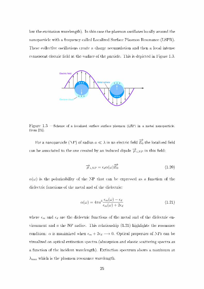
low the excitation wavelength). In this case the plasmon oscillates locally around the
nanoparticle with a frequency called Localized Surface Plasmon Resonance (LSPR).
These collective oscillations create a charge accumulation and then a local intense
evanescent electric eld at the surface of the particle. This is depicted in Figure 1.3.
Figure 1.3 Scheme of a localized surface surface plasmon (LSP) in a metal nanoparticle.From [21].
For a nanoparticle (NP) of radius a λ in an electric eld−→E0 the localized eld
can be associated to the one created by an induced dipole −→µ i,NP in this eld:
−→µ i,NP = εdα(ω)−→E0 (1.20)
α(ω) is the polarizability of the NP that can be expressed as a function of the
dielectric functions of the metal and of the dielectric:
α(ω) = 4πa3εm(ω)− εdεm(ω) + 2εd
(1.21)
where εm and εd are the dielectric functions of the metal and of the dielectric en-
vironment and a the NP radius. This relationship (1.21) highlights the resonance
condition: α is maximized when εm + 2εd −→ 0. Optical properties of NPs can be
vizualized on optical extinction spectra (absorption and elastic scattering spectra as
a function of the incident wavelength). Extinction spectrum shows a maximum at
λmax which is the plasmon resonance wavelength.
25
LSPR is very sensitive to the environment and λLSP can be shifted by several tens
of nanometres by changing the dielectric constant of the surrounding medium. For
example, increasing εd shifts the LSPR towards red wavelengths. [22] An analytical
solution to Maxwell's equation can be found (Mie theory, [11]) for a spherical NP
and it can be demonstrated that the magnitude of the eld outside the particle is
enhanced in the very close proximity of the surface and decays with r−3 (r being
the radial distance to the center of the NP).
It is noteworthy that the size and the shape of the particles also aect the LSPR.
Increasing the size leads to higher absorption and scattering of the incoming light.
However, the shape is also a key parameter: oblong spheroids exhibit higher enhance-
ments than spheres while the LSPR is red-shifted. Note that the polarization of the
incoming eld has to be aligned with the main axis of the particle to observe the
highest enhancement. [11] Some more complicated structures such as nanorods [23]
or nanostars [24, 25] evidence the strong dependence of LSPR on the shape of the
particle but also highlight two key aspects: the eld enhancement is higher at sharp
ends, edges or cones apices in nanostars and are highly sensitive to the polarization.
The last essential parameter that can aect both LSPR and eld enhancement is
the coupling between several nanostructures: a simple example is the LSPR of a gold
NP dimer. As the gap between two NP decreases from 20 nm to 1 nm, the LSPR
is red-shifted by ca. 200 nm and the eld is highly enhanced in the gap [11] if the
eld polarization is along the axis of the dimer. This specic region of space where
the eld enhancement is maximum is called a hot spot. This term will be used in
the following for SERS and TERS experiments. One can now understand why these
properties of nano-sized metallic materials can be of tremendous interest for Raman
spectroscopy: the intensity of the scattered signal can be considerably increased in
presence of metallic nano-objects, opening the way to enhanced spectroscopy for the
characterization of low cross section materials, molecules or nano-objects.
26
1.2.2 Surface-Enhanced Raman Spectroscopy
SERS makes prot of the strong electric eld enhancement provided by a nanostruc-
tured substrate with plasmonic properties. This enhancement of Raman signal was
rst experienced by Fleischman in 1974 in his studies on the changes of Raman scat-
tering of a monolayer of pyridine adsorbed on a silver electrode as a function of the
applied electrochemical potential. [26] The enhancement mechanism of the signal was
then discovered by Van Duyne and Creighton simultaneously in 1977 in works where
the role of the silver substrate was pointed out. [27,28] Initially SERS was performed
on electrochemically roughened substrates which displays a random distribution of
hot spots on the surface. Since the 90's potentialities of SERS have been increasingly
exploited and single-molecule detection could be achieved in 1997. [29,30] Top-down
or bottom-up nanofabrication processes now allow the design of reproducible and
tunable SERS substrates (lithography, 3D NP assembly). [31]
1.2.2.1 SERS enhancement mechanism
The increase in intensity of the SER scattering is usually quantied by the en-
hancement factor (EF ) which compares the SERS intensity to the normal Raman
scattering signal. This enhancement factor can be as high as 106 to 107 or even 1010
when SER and resonance eect are combined (surface-enhanced resonance Raman
spectroscopy, SERRS). [14] It can be demonstrated that for a purely electromag-
netic enhancement mechanism, the SER intensity scales with the local electric eld
magnitude (E4loc) as both the excitation and the scattered signals are enhanced by
the substrate. In practice, this EF can be determined by comparing the intensity of
the SER signal (ISER) to the intensity of normal Raman scattering (INR) normalized
by the number of molecules N probed in each case:
EF =ISERINR
× NNR
NSER(1.22)
27
In most situations the number of molecules probed in SER experiments is dicult
to etimate. [32]
The electromagnetic enhancement cannot account for enhancement higher than
ca. 105. In fact, another mechanism, called the chemical mechanism, is responsi-
ble for higher enhancement factors. It originates from interactions of the adsorbed
molecule with the substrate. This mechanism, which is not simple as many eects
interplay, is still under debate. Its nature is discussed in several reviews such as [33]
and [11]. The most studied mechanisms are those involving partial charge transfer
between the metal and the molecule. We briey describe them below since they may
be of importance in electrochemical SERS experiments. One mechanism considers
the perturbation of the electronic structure of the molecule due to the close prox-
imity of the metal that can aect its polarizability and then the Raman scattering
intensity of some vibrational modes. Another mechanism considers the formation of
"surface-complexes" with specic available electronic states which can be resonant
with the incident excitation. The third one is also a resonance-based mechanism: if
the energy gap between the Fermi level of the metal and the highest occupied molec-
ular orbital (HOMO) or lowest unoccupied molecular orbital (LUMO) states of the
adsorbate matches the energy of the incoming photon, RR can occur and enhance
the scattering process. The latter can be important in EC-SERS experiments as the
applied electrochemical potential tunes the Fermi level energy of the metal. These
experiments were in fact a clear and experimental proof of the existence of such a
chemical enhancement mechanism. [27,34]
1.2.2.2 Electrochemical SERS
As SERS can considerably increase the Raman scattering, it appears as an ideal
tool to monitor the evolution of an electrochemical interface in situ. In fact, SERS
has often been closely associated to electrochemistry for two main reasons. The rst
is historical: the rst SERS experimental evidences were revealed on EC-Raman
28

measurements. [2628] The second one is practical since the rst roughened silver
SERS substrates were prepared by a process known as oxidation-reduction cycle
(ORC), [35] where the silver is successively electrodissolved and electrodeposited
forming a non-homogeneous surface with rough features supporting the electric eld
enhancement.
Since then, more advanced electrochemical deposition of metals have been de-
veloped such as the one proposed by Burgress et al. in 2016 for the electrochemical
growing of dense lms of "dagger-shaped" gold particles. [36]
On the other hand a recent study by Baumberg et al. explored, in an elec-
trochemical environment, the plasmonic properties of a junction constituted of an
organic layer sandwiched between a metal NP and a metal surface. The strong
eld enhancement at the junction (the gap) provides strong SER signal of the layer.
Upon polarization, they observe variation of the SERS intensity that they explained
by the potential-dependent changes in the double-layer composition and then of the
local refractive index, the presence of ionic charges close to the NP inducing shifts
in the plasmon resonance and in their case hydrogen evolution with a low refractive
index at the surface. [37]
EC-SERS could help understanding the interactions between molecules and sur-
faces. As Raman spectroscopy is very sensitive to the orientation of the molecule
versus the polarization of the excitation laser, SERS can exhibit more intense scat-
tering from some vibration modes depending on the orientation of the molecule with
respect to the local electric eld. An example is the orientation of nicotinic acid (and
its isomers, isonicotinic and picolinic acids) which can adsorb with various confor-
mations depending on the pH and on the charge of the substrate surface. [38,39] To
study these phenomena, a coupled electrochemical impedance-Raman experiment
was developped at LISE and enables the variations of the Raman intensity with the
potential (∆IRaman(ω)
∆E(ω)) [40] together with the changes in capacitance of the electrical
double layer.
29
The interpretation of EC-SERS results can be challenging because of the inter-
ferance of several parameters. The rst one is the nature of the substrate which
it is usually made of roughened metallic structures so that the exact environment
of each molecule cannot be known. [41] The second one is that the collected SERS
signal is averaged on an area dened by the optical resolution of microRaman, and
therefore is diraction-limited.
One last issue is that only molecules or compounds which can be deposited on
SERS substrates can be studied. A SERS-inspired solution was proposed for the
study of surfaces other than gold and silver, the so-called shell-isolated NP enhanced
Raman spectroscopy (SHINERS) which will be described in the following.
1.2.2.3 Shell-Isolated Nanoparticles Enhanced Raman Spectroscopy
SHINERS uses plasmonic NPs deposited on a substrate to be investigated. As the
NPs enhance locally the electric eld, materials in their vicinity are probed by the
intense near-eld generated around the particles. The "Shell-isolated" part means
that the NPs are covered with an insulator dielectric layer (silica or alumina) that
prevents any possible (electro)catalytic interference of the NPs with the material
under scrutiny.
SHINERS has been successfully applied to the study of the conformation of
molecules on at metallic substrates, [42,43] to the study of catalytic processes, [44]
and also to the study of interfacial processes on energy storage materials. [45]
If multiple SERS platforms are now available and can be selected depending on
the targeted application, SERS analyses suer from the limited spatial resolution of
optical microscopies (around the micrometre in the visible range). The following sec-
tion will describe how this limitation can be circumvented and how electrochemical
interfaces can be characterized at the nanoscale.
30

1.3 Beyond the diraction limit: scanning near-eld
optical microscopy
All the optical microscopies and spectroscopies previously described can provide
multiple and complementary information about the nature, the structure and the
properties of materials or molecules as well as their transformation under electro-
chemical potential control for example. Today, the strong trend towards nanoscale
science and technologies has catalyzed the development of new fabrication, manip-
ulation and investigation tools able to reach this scale. Electron microscopies are
attractive by providing subatomic details but their implementation in situ is di-
cult. Moreover, the beam-induced damages to the sample may alter the mechanism
under study. Another powerful approach is based on scanning probe microscopies
(SPM) such as STM, AFM and their implementation in combination with optical
methods. A new paradigm has emerged out of these developments: scaling down
the matter investigation towards the nanoscale has revealed news borders beyond
which new physical phenomena and eects were observed and even become promi-
nent. Particularly, in optics, a new domain called nano-optics has emerged and aims
at understanding optical phenomena that occur below the diraction limit. Indeed,
classically, objects observed with optical spectroscopies cannot be distinguished if
they are separated by a distance smaller than roughly half of the wavelength used
for their observation (200 nm in the visible range).
1.3.1 Optical diraction limit
The optical diraction limit can be understood considering that the propagation of
a photon in free space is determined by the dispersion relationship connecting its
angular frequency ω and its wavevector k =√k2x + k2y + k2z via the light velocity c :
~ω = c · ~k (1.23)
31

Considering Heisenberg's uncertainty relationship on the spatial position and the
momentum p of a particle in a particular direction:
∆x ·∆px ≥~2
(1.24)
we can write for a photon the relationship between the spatial connement and the
spreading in magnitude of the wavevector in one particular direction:
∆x ≥ 1
2∆kx(1.25)
As for a photon the maximum spread of the wavevector is k = 2πλ, 1.25 can be
written as:
∆x ≥ λ
4π(1.26)
This expression can be compared to the Abbe's diraction limit one, formulated in
1873 (followed by a similar expression proposed by Rayleigh six years later) that
states that the optical spatial resolution cannot be lower than half of the photon
wavelength:
∆x ≥ λ
2× NA(1.27)
where NA is the numerical aperture of the microscope objective. [46]
1.3.2 Principles of near-eld optics
An approach for improving spatial resolution in optical imaging is provided by Scan-
ning Near-Field Optical Microscopy (SNOM) which allows the optical imaging of
features below the diraction limit near a surface. SNOM is usually coupled to a
scanning probe microscope (SPM) allowing a topographic and optical imaging of
the samples combining both the single digit nanometre scale of the SPM and the
fast dynamics of optical measurements.
The optical near-eld can be dened as the non-propagating electromagnetic
32
eld surrounding an object illuminated with a propagating electromagnetic eld
(light, called the optical far-eld). The optical near-eld exists in a restricted region
of space (generally less than 100 nm) around the irradiated object. As the optical
near-eld cannot propagate it cannot be directly measured with a detector but
requires back-coupling to far-eld through interactions with matter. [47]
The rst idea of SNOM was originally proposed by Synge in a pioneer paper in
1928. [48] He suggested the illumination of a sub-wavelength aperture in an opaque
lm placed at a sub-wavelength distance on the top of a transparent substrate to be
imaged: the light passing through the apperture is focused on the sample and trans-
mitted to a detector through a non-diraction-limited process. The implementation
of this idea could be practically demonstrated with an electromagnetic radiation
in 1972 by Ash and Nicholls (who actually ignored Synge's work) by using a mi-
crowave radiation with wavelength of 3 cm passing through a hole with an aperture
diameter of 1.5 mm: a resolution of λ60
was observed on a metallic line grating with
a 500 µm periodicity. [49] These rst experimental evidences opened the way to the
domain of near-eld microscopy.
The rst experimental evidences of SNOM carried out with an excitation source
in the visible range were obtained a decade later by Pohl et al. with a λ20
(25 nm)
resolution [50] and Lewis et al. with a λ14(50 nm) resolution. [51] Finally, one decade
later, Betzig et al. acquired the rst single molecule uorescence imaging with a λ50
resolution. [52] All these experiments have been performed in a conguration similar
to the one originally proposed by Synge. Other congurations have been described
so that SNOM can be divided arbitrarily into three general classes, organized by the
type of near-eld probe employed:
• nano-aperture-based techniques called aperture SNOM (a-SNOM);
• methods using sharp tips acting as optical transducers called scattering SNOM
(s-SNOM);
33

• and strategies based on advanced tip designs that involve sophisticated optical
antenna and/or apertures, incorporating concepts from the eld of plasmonics.
In the following, each of these categories will be briey described with a few
examples of applications in the analysis of solid-liquid interfaces.
1.3.3 Aperture SNOM
The most commonly used SNOM approach is the one imagined by Synge, the aper-
ture SNOM (a-SNOM): it makes use of conventional aperture-based probes which
are usually metal-coated tapered dielectric waveguides with a sub-wavelength aper-
ture at the apex of the structure (see Figure 1.4a). The metal-dielectric interface
at the apex of the tip allows a localized evanescent wave (near-eld) to leak out at
the aperture creating a light nano-source in the vicinity of this aperture. It can also
be used as a nano light collector (see Figure 1.4b). The size of this spot, and then
the resolution is mainly dened by the size of the aperture (and not by the wave-
length anymore). This approach enables background-free imaging because sample
illumination occurs only within the nanoscale light spot created at the aperture.
Figure 1.4 Scheme of the three main modes of operation in a-SNOM: a) excitation mode, b)collection mode, c) excitation and collection mode.
The optical transmission has been shown to decrease exponentially with the
aperture diameter [53, 54] leading to transmission eciency lower than 10−6 for
34

apertures below 100 nm in the visible range. It has to be added that high laser
powers cannot be used to compensate this drawback for the illumination as it may
damage or melt the metal-coating layer. These factors prevents the use of the
combined collection and excitation through the same ber (Figure 1.4c). Hence,
only collection or illumination modes can be used: the sample can be locally excited
through the aperture while the emitted, scattered, or transmitted light is collected
with a microscope objective, [55,56] and reversely. [57]
It is now easily understandable that near-eld Raman spectroscopy with this kind
of microscope is very delicate because of the lack of eciency of Raman scattering
and because of the poor collection or excitation of aperture SNOM probes. Despite
these diculties several nano-Raman studies have been conducted using this con-
guration since the pioneer paper of Tsai and co-workers in 1994: they could probe
the phonon mode of a diamond sample in an excitation-collection conguration with
a 100 nm aperture probe. Another diculty is due to the broadband Stokes sig-
nal of the material of the ber which is superimposed to the Raman bands of the
analyte. [57]
However, Grausem et al. published in 1997 the rst near-eld Raman spec-
troscopy results in a liquid environment (CCl4) by extracting the spectrum of the
tetrachloromethane through an aperture of 50 nm (using a 514.5 nm laser excita-
tion) with a decent signal-to-noise ratio despite the low number of probed molecules
that they estimated to be 0.4 attomol (∼ 240000 molecules). [58]
An a-SNOM-inspired opto-electrochemical analysis was proposed by Bard in
2002. [59] In this work, the authors propose to use a tapered optical ber coated
with a metallic layer as a scanning electrochemical microscope (SECM) probe. With
these probes, an array of interdigitated electrodes was imaged in constant-height
mode: simultaneously topographic (the tip was mounted on a tuning fork), optical
and electrochemical current (a redox probe was in solution) could be recorded. It
has to be noticed that in this work, the aperture size was estimated to be 1.3 µm
35

much larger than the wavelength used (514.5 nm): the optical resolution is higher
than 2 µm, very far from the performances reached in SNOM at this time.
Moreover, as SNOM probes are usually made by gluing an optical ber onto the
prong of a tuning fork to control the probe-sample distance, it reveals dicult to
operate when the tip is immersed in a liquid (see Section 1.4.5.3 below for more
details). This consequently results in poor lateral resolution on topography images.
These examples highlight the diculties to use an a-SNOM approach for non-ecient
optical processes such as Raman spectroscopy without any enhancement of the signal
especially in a liquid environment.
1.3.4 Scattering SNOM
In apertureless or scattering SNOM (s-SNOM) a sharp metallic tip with a radius of
curvature smaller than the wavelength of the source light is used to locally scatter
the electric eld at its apex (the near-eld region). [60] As such probes act as an-
tenna, they can be used as nano-sources of light but also as nano-scatterers. The
enhancement mechanism, usually referred as the lightning-rod eect, is due to the
tappered prole of the illuminated probe that concentrates the surface charge den-
sity at the apex of the tip (or any sharp singularity over the surface) as depicted
on Figure 1.5. [61] This enhancement is very sensitive to the polarization of the elec-
tric eld relatively to the axis of the tip and is maximized when the light is linearly
polarized along the main axis.
The capability of a nanoprobe to conne the electric eld was for example evi-
denced over photosensitive polymers [62] which can imprint the electric eld distri-
bution around the tip with several illumination patterns.
s-SNOM has been successfully used with broadband IR sources to implement
nanoIR spectroscopy and imaging. It was for example demonstrated on the iden-
tication of polymers thin lms on silicium [63] and recently on viruses in a thin
layer of water trapped between sheets of graphene using a plattinum-coated AFM
36

(a) (b)
Figure 1.5 a) Calculated surface charge density (σ) at a 5 nm radius gold tip illuminated witha laser polarized linearly along the tip shaft (z); b) E2 distribution around the same tip underthe same conditions of illumination. A maximum of 3000 was calculated at the apex (adaptedfrom [60]).
tip. [64] In these works, fast single frequency nano-IR imaging was possible due to
the background signal ecient ltering by demodulation of the s-SNOM signal at
the oscillation frequency of the AFM probe. However recording a full nano-IR spec-
trum under these conditions takes at least 60 s which renders hyperspectral analysis
of a sample long and delicate.
Nano-IR imaging and spectroscopy has also been performed on electrochemical
materials and interfaces of interest in the eld of Li-ion batteries: the phase change
in positive electrode material during delithiation could be observed [65] and several
products of the solid-electrolyte interphase (SEI) could be distinguished. [66] These
studies are promising as they extend the range of materials that can be studied.
Nevertheless, none of those were carried out in situ. IR s-SNOM for in situ analysis
may be compromised as the harmonic motion of the tip is not guaranteed in liquids
(poor demodulation of the scattered signal).
37

1.3.5 Photothermal approach for nano-IR
A very dierent nano-IR system was developped by A. Dazzi in 2005 and com-
mercialized by the Anasys company. It is based on the photothermal expansion of
materials upon excitation by an IR laser as depicted in Figure 1.6. With this system
a full local IR spectrum can be recovered by tuning the IR laser wavelength and by
analyzing the cantilever response to the absorption-induced mechanical stress of the
sample. It has found a wide range of applications from biology to plasmonics that
are summarized in a review by Dazzi and Prater. [67] However, no nano-IR studies
have been reported in liquids using this system due to strong absorption of water in
the IR range.
Figure 1.6 Principle of the photo-induced AFM-IR spectroscopy. As the material absorbs theIR incident radiation from the laser, the material expands and triggers an oscillation of the AFMcantilever. From Ref. [67].
38
1.4 Tip-enhanced Raman Spectroscopy: Raman be-
yond the diraction limit
The successful combination of the Raman enhancement by SERS and of the nanoscale
analysis by SNOM or SPM was achieved in 2000 simultaneously by the groups of
Kawata [68], Pettinger [69], Anderson [70] and Zenobi [71] pioneering a new eld in
enhanced Raman spectroscopies: tip-enhanced Raman spectroscopy (TERS).
TERS can be seen as nanometric single SERS hot spot positioned at the apex
of a SPM probe enabling the chemical imaging of a sample. The strength of this
approach is that the sample under scrutiny is not altered and its Raman response
can be extracted at each point of the sample by a strong and localized electric eld
(near-eld) by scanning the metal tip over the sample.
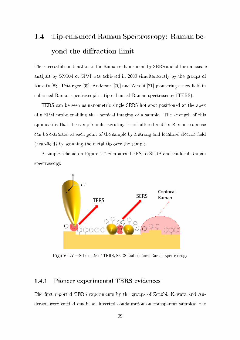
A simple scheme on Figure 1.7 compares TERS to SERS and confocal Raman
spectroscopy.
Figure 1.7 Schematic of TERS, SERS and confocal Raman spectroscopy
1.4.1 Pioneer experimental TERS evidences
The rst reported TERS experiments by the groups of Zenobi, Kawata and An-
derson were carried out in an inverted conguration on transparent samples: the
39
illumination of the tip and the collection of the TERS signal was achieved using an
inverted microscope. In all studies the molecules were Raman resonant (e.g. dyes)
ensuring a strong and even detectable far-eld signal which enabled the quanti-
cation of the enhancement due to the presence of the tip. Anderson also reported
Raman enhancement from a sulfur lm deposited on a glass slide using a gold-coated
AFM tip. [70]
Zenobi et al. [71] used BCB (Brilliant Cresyl Blue) molecules deposited on a glass
support and a silver-coated AFM tip. They could report an enhancement factor of
104. They also reported TERS signal from a C60 monolayer. Kawata et al. [68]
reported TERS from a thin layer of Rhodamine 6G (Rh6G) deposited on thin silver
plates on glass and silver-coated AFM tip. They reported an enhancement factor
of 40. However, this enhancement factor is highly underestimated as the far-eld
signal they observed was probably also originating from several SERS hot spots due
to the presence of silver nanoplates in the focus of the laser. [72]
The same year Pettinger's group reported TERS from BCB deposited on a thin
gold layer on glass with a silver STM probe. [69]
BCB and Rh6G have been widely used in TERS experiments as standard refer-
ence molecules. They provide strong Raman signal and allowed TERS to reach a
breakthrough in 2008 with the detection of single BCB molecules at very low laser
power in UHV. These results were reporter by Pettinger's group [73] with a 106
enhancement factor.
1.4.2 About TERS enhancement
The enhancement factor quanties the signal enhancement obtained in TERS. It is
dened in a similar way to what was presented above for SERS by:
EF =INF
IFF× NFF
NNF(1.28)
40

where INF is the near-eld intensity of a vibrational mode provided by TERS, IFF
the intensity of the same mode in the far-eld spectrum (microRaman) and NNF
and NFF are the numbers of molecules probed by the near-eld and the far-eld
respectively. Practically, the evaluation of the EF requires to be able to distinguish
between the pure TER signature and the far-eld signal and to assess the number
of molecules probed in each case.
The discrimination between the far-eld and the near-eld signal is easy as a
TER spectrum is the sum of INF and IFF. The pure far-eld signal is obtained
usually by collecting a spectrum after pulling the tip away from the sample. When
the objective and the tip are xed and when a side or top illumination mode is used
(which is our case in this work) the FF contribution is obtained after retracting the
sample by a few nanometres (usually 10 to 50).
Determining the number of molecules is simple in case of a monolayer or thin
layer or molecules: the number of molecules probed by TERS can be approximately
estimated to be proportional to half the square of the tip radius, R2tip/2. [74] The
area of the surface probed by microRaman is proportional to R2foc, the laser beam
radius at the focus. In case of a side illumination, the shape of the focus is not
circular but ellipsoidal and has to be corrected by the angle to the normal surface
α so that the real far-eld focus area is proportional to R2foc cos(α): [72]
EF = 4
(INF + IFF
IFF− 1
)×(Rfoc
Rtip
)2
cos(α) (1.29)
As an example, TER (NF) and far-eld (FF) spectra of a self-assembled mono-
layer of thioazobenzene that forms homogeneous layers on gold is shown on Fig-
ure 1.8. The TER spectrum acquired in STM-TERS is superimposed to the FF
spectrum acquired while the sample is retracted by 30 nm with the same laser
power and integration time. In this case, the far-eld signal does not allow one to
detect any of the Raman bands of the molecule. If the FF signal cannot be detected
it is assumed that its intensity is lower than the maximum of the signal noise in the
41

FF spectrum. This value is then arbitrarily chosen as IFF. This assumption can
lead to a large overestimate of the FF intensity. With this molecule and such a low
laser power (1 µW), obtaining a sucient S/N ratio requires long integration times
(minutes). In our conguration α = 60o and the beam radius is around 500 nm.
We chose a tip radius of 30 nm which is a value commonly observed on SEM mea-
surements. Practically, a better estimation of the tip radius can be obtained by a
deconvolution procedure when a well-dened object is imaged. With the intensities
reported on Fig. 1.8b, the EF can be estimated to be at least 6 · 105. This value is
obviously below the real enhancement value but this method can be used to compare
tips quantitatively on a reference sample.
(a) (b)
Figure 1.8 a) NF and FF spectra of a thioazobenzene SAM on gold. STM TERS (gold tip,632.8 nm, 1 muW, bias voltage (BV): 100 mV, it: 100 pA) in contact with the sample (NF) andwith the sample retracted by 30 nm (FF); b) Zoom onto the framed area for NF and FF spectrawith intensities used for the calculation of the EF: 6 · 105.
Another possible source of EF underestimation in the previous calculation is the
size of the NF region below the tip especially when the sample is a noble metal: this
conguration that will be described later as the gap mode provides higher enhance-
ments and lateral resolution.
The following section will discuss the enhancement mechanisms occuring at a
tapered tip and the eld connement.
42
1.4.3 Enhancement mechanisms and gap mode conguration
In TERS a gold or silver probe tapered tip is brought at the vicinity of a surface,
below ca. 1 nm, and a laser source is focused on its apex, the polarization being
linear and aligned with the shaft of the tip. The laser induces a resonant excitation
of the SP at the apex of the tip creating a strong and localized hot spot such as in
SERS. As visible excitation is commonly used in Raman spectroscopy, only gold and
silver tips can support SPR. The enhancement mechanism is parent to the SERS
enhancement i.e. with an electromagnetic mechanism based on the excitation of the
plasmon resonance and a chemical mechanism that add to the lightening rod eect
described in the s-SNOM section.
In gap mode TERS a noble metal substrate is used as substrate for the analyte.
This conguration is singular as the tip and the sample can couple optically and form
a new antenna with dierent plasmonic properties. One can see this interaction by
considering the charge accumulation at the tip surface as a point dipole: by reducing
the gap, a mirror dipole is formed within the sample by coulombic repulsion so that
the LSP of the probe and the SPP of the surface couple to produce an hybrid
plasmonic mode. [75] When the tip-sample distance increases TER signal evolution
exhibits a behavior very similar to the one observed in the gap between two NPs. [76]
Pettinger et al. examined the TERS enhancement and the plasmonic properties of
the tip by varying the gap distance. By varying the gap between 1 and 10 nm
they could observe a strong and rapid decrease in TERS and background intensity
which highlights the strong eect of the optical coupling in the gap mode. They
also analyzed background signal (lorentzian shape) in TER spectra and assumed its
maximum to be the LSPR position of the tip-sample plasmonic antenna. They could
observe a blueshift as the distance increases similarly to what is observed between
two NPs. [77]
Another consequence of the gap-mode in TERS is the connement of the near-
eld below the tip. Beck et al. calculated the eld enhancement and its extent in a
43

gap between a 10 nm radius gold tip and a gold substrate. They found that as the gap
is larger than the tip radius, the near-eld is not aected and the enhancement can
be compared to the one of a free-standing tip (apex mode regime). However below
this value the near-eld is increasingly conned (hybrid gap plasmon) to roughly
one fourth of the initial connement. [75] This phenomenon is shown in Figure 1.9.
Figure 1.9 Calculated eld distribution around a 10 nm radius gold TERS tip above a gold lmwith three dierent gap widths. Numbers in the lower left corners indicate multiplying factors thatwere applied to the color scale and below, the electric eld connement from 0.2 nm gap width toa few hundred of nm. Adapted from [75].
The gap-mode conguration has also shown to be ecient with other metal
substrates that can couple to the TERS tip such as Cu, Mo, Ti, Ni or Pt [78, 79]
which is interesting for experiments that cannot be performed on gold or silver
substrates or for investigating catalytic reactions that can occur on such metals.
44

1.4.4 Spatial resolution in TERS
The spatial resolution of a SPM or SNOM probe is evaluated through its ability to
distinguish between two dierent adjacent objects. In TERS particularly, it can be
experimentally determined by imaging small objects such as single molecules, [8083]
1D (C60) or 2D (nanotubes or nanowires) materials, [84,85] an interface between two
dierent materials [86] or molecular layers. [87]
Lateral resolution as low as 1.7 nm has been reported on single-wall carbon
nanotubes (SWCNTs) imaged by gold coated AFM probes with radii of curvature
ranging from 30 to 80 nm. [88] This is still to our knowledge the smallest reported
lateral resolution at the ambient. Development of TERS in UHV has even allowed
Dong's group to perform TERS imaging at the sub-nanometre scale reaching the
submolecular imaging: distinct vibrational modes could be extracted in a single at-
lying H2TBPP porphyrin deposited on Ag(111). [89] New questions have emerged
about the mechanism of TERS enhancement given that such a resolution cannot be
fully understood on the basis of a classical electromagnetic theory.
The spatial resolution is often assumed to be limited by the size of the tip
apex but it can be increased in the gap mode due to strong eld connement.
In the gap mode, the connement was calculated to be proportional to√Rtipd
(see Figure 1.9, [75]) where d is the width of the gap. This model which considers
only classical electromagnetic theory can easily account for resolution below 10 nm
and down to 1 nm for a tip radius around 5 nm.
Various theoretical models have been proposed to explain these results: time-
dependent density functional theory calculations (TDDFT) incorporating a quantum
mechanics component to the system have demonstrated that the localized near-
eld could be conned down to the atomic scale which cannot be interpreted with
the classical plasmon theory. [90] A classical approach by Deckert et al. involving
atomic-scale protrusions at the apex of the tip could theoretically provide such high
enhancement factors with connement below the nanometre scale. [91]
45
Zhang et al. [92] recently proposed an optical model where a molecule was con-
sidered at the junction between a silver tip and a silver substrate: in such a congu-
ration, the enhancement is so strong that the Stokes scattering has to be considered
as a new source of excitation for the molecule itself. This was called the molecule
self-interaction since the molecule plays an important role in the new coupled system
allowing the creation of what the authors called a "super-hot spot" with a width at
least 3 times lower than without the molecule.
All these theoretical views are still under debate and have to be supported by
experimental proofs but greatly help to better understand the physical phenom-
ena occurring in these very particular optical nano-cavities. From all the previous
description of the physics hiden behind TERS enhancement, one can clearly un-
derstand that the control of the distance between the tip and the sample is a key
parameter in TERS experiments. In the following, the probe to sample distance
control will be discussed.
1.4.5 Feedback Mechanisms
As explained before, it is crucial to maintain a constant and short distance between
the tip and the specimen to be analyzed, within the nanometre range since the
enhancement of the electric eld decreases dramatically with the distance. Three
main near-eld microscope feedback mechanisms are used for TERS: AFM-TERS,
STM-TERS and Tuning-Fork-based TERS (TF-TERS: normal or shear-force, NF
or TF). They will be described in the following, highlighting their advantages and
intrinsic drawbacks for TERS and their possible use in liquids for EC-TERS.
All these feedback mechanisms rely on the change of one measurable parameter
reecting the interaction between the tip and the sample: a feedback loop ensures
this parameter to remain constant by moving precisely (with a piezoelectric stage)
and quickly the probe or the sample in the z direction, while the tips or the sample
is scanned in the xy plan. Thus, the relative motion in z is recorded and reects
46

the topography below the tip.
1.4.5.1 AFM-TERS
In AFM, the probe is made of an oscillating cantilever (typically made of silicon)
that bears a nanometre size tip at the extremity. In AC mode of AFM, the can-
tilever is excited close to its resonance frequency and oscillates with an amplitude
that can be modulated. Interaction forces with the sample induce a decrease of
the amplitude and shifts of the oscillation phase. Usually, the feedback is ensured
by tracking the amplitude of the cantilever oscillation. The cantilevers are coated
with a reective aluminium layer: a laser is focused at the extremity and reected
towards a four-quadrant photodiode that senses the laser deection and is analyzed.
The Z-deection collected by the photodiode (converted to a voltage) is compared
to a reference value chosen from the approach curve and the piezoelectric stage con-
stantly adjusts the Z position to keep this value, i.e. the forces probed by the tip,
constant. The feedback time constant is adjusted with integral and proportional
gains to minimize the error signal (dierence between the measured and the set-
point amplitude): correction of the error with the feedback loop is at the origin of
the topographic information.
AFM is versatile as it can be used on any type of substrates (insulators, conductor
or semiconductor materials) and allows scanning areas as large as tens of microme-
tres. AFM can provide atomic resolution under UHV conditions [93,94] but also in
liquids. [95] As the type of substrates that can be analyzed by AFM-TERS is wide,
we can nd a large amount of papers using this feedback mechanisms in all the
elds already explored by TERS in any conguration for the excitation/collection
mode. Pioneer works by Kawata et al. [68] on Rhodamine 6-G and Zenobi et al. [71]
on Brilliant Cresyl Blue (BCB) in 2000 used metal coated AFM silicon probes in
a bottom illumination and collection conguration. AFM is also widely used for
probing isolated biological objects. As AFM can be used on any type of sample and
47
especially on non-conductive ones, it is particularly interesting to use this imaging
mode on biological samples such as cells, viruses, lipidic membranes, etc. Cialla et
al. studied for example the composition of the membrane of single viruses (300 nm
in length and 20 nm in width) and could distinguish reproducibly Raman signature
from the capsule proteins and from RNA. [96] Another group proposed to use TERS
to distinguish two types of viruses: no far eld signal could be clearly extracted but
TERS revealed the chemical composition for each virus. [97] The groups of Deck-
ert, Zenobi and Bonhommeau studied amyloid brils involved in neurodegenerative
diseases using AFM-based TERS. [98100]
However, one of the drawbacks of AFM-TERS is related to the probe coating.
Indeed, the balance between the thickness of metal (and then the lateral resolution)
and the occurrence of a eld-enhancement at the apex is tedious. Moreover, as the
gold or silver lms are thin, their mechanical resistance is poor and it is impossible to
use high laser powers without degradation of the metal coating. Another drawback
may be the cost: commercial AFM-TERS tips are indeed very expensive. Using
bulk metal tips is also possible but the reliability of these tips is still controversial:
controlling the quality factor of the tip which is crucial to ensure a good imaging
quality (for the topography) is still a challenge.
A last drawback of AC-AFM for TERS measurements is that the tip-sample dis-
tance varies continuously ranging from a few to several tens of nanometres. There-
fore, in a large portion of the oscillation cycle the TERS enhancement is very weak
as the tip/sample distance is too large. In order to overcome this drawback, spectra
may be acquired while the oscillation is stopped and the tip maintained at a short
distance corresponding to a predened force (contact mode).
1.4.5.2 STM-TERS
STM is a scanning probe microscopy where a bias is applied between a metallic
nanometre-sized tip and a conductive or semiconductor sample. When, the tip is
48
close to the sample (less than 1 nm), electrons can be transferred from the tip
to the sample thanks to the quantum tunnel eect through a classically forbidden
barrier. In this feedback mechanism the tunnelling current does not really probe the
topography of the surface but the density of states of the metal or of the molecules
on the metal. This assumption is crucial when it comes to interpret STM maps
with atomic resolution which is not the case in our TERS experiments in air as the
stability of the setup during TERS experiments is not good enough to reach this
resolution due to mechanical noise.
STM-TERS is widely used at it can be implemented with probes made from
electrochemically etched gold or silver wires. The method for their fabrication will
be discussed in the following chapter. Moreover, STM is an appropriate and easy
feedback mode for topographic surface analysis for conductive substrates. It has also
been developed in liquids and in electrochemical environments for decades down to
the atomic resolution. [101]
1.4.5.3 TF-TERS
The basic principle of normal or shear-force (NF or SF) imaging is similar to AFM:
a probe glued onto a quartz tuning-fork (TF) oscillates above the sample at the
resonance frequency of the TF and interactions with the sample induce changes in
both the amplitude and the phase of the oscillation. Commonly, microfabricated
quartz TF are used as time standards in clock watches. As represented in Figure 1.10
it is made of two prongs that can oscillate at a resonance frequency (f0 with a usual
215 Hz = 32.8 kHz value for a non-modied TF): these oscillations induce surface
charges on the quartz prongs that are collected by electrodes and measured using
lock-in detection. Their oscillation can therefore be induced by applying an external
voltage. If the system is considered as an eective harmonic oscillator, it can be
described by a Lorentzian function with a quality factor (Q-factor) dened as:
49
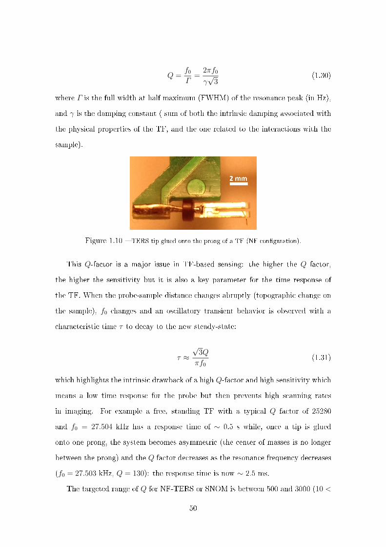
Q =f0Γ
=2πf0
γ√3
(1.30)
where Γ is the full width at half maximum (FWHM) of the resonance peak (in Hz),
and γ is the damping constant ( sum of both the intrinsic damping associated with
the physical properties of the TF, and the one related to the interactions with the
sample).
Figure 1.10 TERS tip glued onto the prong of a TF (NF conguration).
This Q-factor is a major issue in TF-based sensing: the higher the Q factor,
the higher the sensitivity but it is also a key parameter for the time response of
the TF. When the probe-sample distance changes abruptly (topographic change on
the sample), f0 changes and an oscillatory transient behavior is observed with a
characteristic time τ to decay to the new steady-state:
τ ≈√3Q
πf0(1.31)
which highlights the intrinsic drawback of a high Q-factor and high sensitivity which
means a low time response for the probe but then prevents high scanning rates
in imaging. For example a free, standing TF with a typical Q factor of 25280
and f0 = 27.504 kHz has a response time of ∼ 0.5 s while, once a tip is glued
onto one prong, the system becomes asymmetric (the center of masses is no longer
between the prong) and the Q factor decreases as the resonance frequency decreases
(f0 = 27.503 kHz, Q = 130): the response time is now ∼ 2.5 ms.
The targeted range of Q for NF-TERS or SNOM is between 500 and 3000 (10 <
50

τ < 50 ms) which enables a good sensitivity and a reasonable time constant suitable
for fast scanning of the samples.
TF can be used in two congurations: if the probe is glued along the main axis
of the prong, the tip probes shear forces (SF); if the tip is glued perpendicular to
the long axis, the tip will oscillate as in an AFM and probe normal-force (NF). The
latter is usually used in SNOM as it allows a better tip-to-sample distance control.
TF-based TERS studies are not as commonly encountered in the literature as
AFM-based ones because of the diculty to obtain suitable tip reproducibly with a
Q-factor in the 500− 3000 range.
1.4.6 Fabrication of AFM and STM-TERS tips
The two major ways of producing TERS tips are based either on the physical de-
position of a thin layer of gold or silver onto commercial AFM probes or on the
electrochemical etching of bulk metallic wires. The latter produces tips which can
be used with a STM, AFM or NF-tuning-fork feedback. Even if some companies
commercialize TERS tips (AFM: Horiba, NT-MDT, Brücker (260 e per tip), Tip-
sNano (290 e per tip); STM: Brücker (160 e per tip)), they are still expensive
and as no standardized procedure has been established, it is dicult to compare
the eciency and reliability of dierent TERS probes. An objective comparison of
TERS probes and instrumentations is thus dicult. These diculties have been
highlighted by a large inter-laboratory study (twelve groups involved) in 2013: the
same samples (thiophenol, and a peptide self-assembled on gold) prepared by one
group was investigated by TERS in dierent congurations (with top, side or bot-
tom illuminationn and one equiped whith a parabolic mirror) and with dierent
feedback mechanisms (AFM and NF, SF or STM). Even if the spectral pattern was
similar on the same sample, a broad variability was observed on the intensities, on
the Raman shifts of the main bands and on the signal to noise ratio in similar con-
ditions. Even into the same research groups, variability was observed when dierent
51
feedback mechanisms or metals were used. [102] This study is a good example of the
diculties encountered in characterizing the eciency of a TERS tip as it depends
on many non-standardized experimental parameters. It also highlights the lack of
reproducibility in the fabrication protocols. Between all the approaches that have
been reported for the development of TERS active probes, the coating of commer-
cial AFM probes by physical deposition of metals and the electrochemical etching
of bulk metal wires (usually silver or gold) are by far the most popular. The latter
are versatile as they can be used in the STM-TERS mode, but also can be glued
on the prong of a tuning fork for SF or NF-TERS measurements. The etched wires
can also be bent at its extremity and attened to produce a cantilever and glued on
a chip for AFM-TERS. [103,104]
The fabrication of TERS tips mainly depends on the application and on the
type of feedback mode selected for the TERS measurement. For the most commonly
used conguration, AFM-TERS, many groups have used standard Si AFM tips onto
which gold, silver, or both metals are deposited by physical deposition techniques.
[68, 71] This process allows one to control the thickness of metal deposited and
benets from the initial nanometric sharpness of the AFM tip. This method was
proposed for tuning the LSPR resonance of the tip by adjusting the thickness, the
composition of the deposited layer and of the possible dielectric coatings. [105107]
Metal coated probes suer from one major drawback: the thickness of the layer
can be controlled to reach a maximum of the eld enhancement but this is at the
expense of the spatial resolution. [105]
More recently, Ren et al. developped an electrochemical deposition procedure for
the preparation of AFM-TERS tips: Si AFM probes are coated with silver by po-
tentiostatic electrodeposition in a silver sulte (Ag2SO3) solution. A precise control
of the deposition potential and time enabled them to produce TERS tips with high
enhancement factors (105) and good reproducibility. Surprisingly, they evidenced
a long lifetime (around 13 days) for these probes much higher than the lifetime of
52

probes prepared by physical deposition (a few hours). This was interpreted by the
strong dierence in the morphology of the tips (the tips prepared by electrochemical
being smoother). [108]
1.4.7 Other types of SNOM and TERS tips
Beyond the common bulk metal and metal coated tips, a lot of eorts have been
engaged in designing more advanced tips especially in order to tune their LSPR and
to produce probes with dierent proles to match the wavelength of the excitation
laser for a maximal enhancement of the signal. One route is the attachment of a
single nanoparticle at the apex of an optical ber, an AFM or STM tip. As the LSPR
of a single particle can be nely tuned by controlling its size and its composition,
it seems particularly suitable and has been reported several times: with a single-
crystal silver nano wire onto a tungsten STM tip, [109,110] with Ag NPs produced
by photoreduction of AgNO3 directly onto Si AFM tips apex [111] or with Au NP
at the apex of an optical ber. [112]
Schuck's group studied experimentally the inuence of the shape and the size of
the TERS tip apex by designing it with focused ion beam (FIB) milling of AFM
probes with the idea of precisely tuning the SPR. [113,114]
In the same trend, Raschke et al. proposed a gold tip onto which a grating is
FIB-milled onto the tip shaft far above the tip apex so that the SPPs can be excited
by the laser and propagate to the tip apex for TERS measurements. This approach
enables a background-free TERS measurement as the sample is not illuminated with
the laser. The space between the lines of the gratings is to be tuned to be adjusted
to the laser wavelength. [115]
Another background-free and highly ecient SNOM probe was proposed by
Weber-Bargioni et al. in 2012 called the Campanile probe: it is based on a metal-
insulator-metal (MIM) nanogap fabricated at the apex of an etched optical ber.
This probe that can be seen as a plasmonic bowtie antenna and is capable of ef-
53
cient far-eld to near-eld coupling (and vice-versa) with a broad bandwidth. It
has been used for imaging the photoluminescence in InP nanowires with a spatial
resolution below 50 nm. Due to its large optical bandwidth and signal enhancement
capabilities, it was assumed that it could also be used for Raman spectroscopy but
this has never been evidenced up to now. [116118]
All of these approaches have been really important as they bring experimental
evidences of the inuence of geometrical parameters of TERS tips on LSPR position
and enhancement factor, but are too expensive and too dicult to implement to be
used routinely for TERS experiments.
1.5 Probing and inducing chemical reactions with
TERS
Over the last two decades, TERS has appeared to be a new powerful analytical tool
able to investigate complex samples such as biological objects [119,120] ranging from
isolated nucleotides to RNA or DNA strands [121127], cell membranes [128130],
or to discriminate proteins through the identication of aminoacids. [100, 120, 131]
However none of these works could provide dynamic information on these biologic
objects since it would require conducting experiments in liquids which is still a
challenge in the TERS community. Dynamic TERS studies have however been
carried out in the eld of heterogeneous catalysis.
1.5.1 Catalytic reactions monitored by TERS
As TERS can detect adsorbates on metal surfaces it is a technique of choice for scru-
tinizing heterogeneous catalytic reactions operando, i.e. reacting systems similarly
to SERS. [132134] The main advantage of TERS over SERS in catalysis lies in the
possibility to distinguish dierent catalytic sites with dierent reactivity due to the
high lateral resolution of TERS.
54
The rst study on a catalytic system was reported by Domke and Pettinger in
2009: they studied at the ambient a cobalt meso-tetraphenylporphyrin (CoTPP)
complex, an organometallic catalyst in STM-TERS supported on an Au (111) sub-
strate. Topographic imaging revealed ordered and disordered areas that could be
correlated with dierent states of complexation of CoTPP. TERS spectra from the
disordered areas revealed vibrational signatures of CO and NO axially coordinated
to CoTPP and generated upon the catalytic reduction of CO2 and NO2 from ambi-
ent air. [135] However, in this study, the atmosphere was not controlled and the CO-
and NO-adducts formation mechanistic study would have required a precise control
of the atmosphere gases. This was recently performed by Van Duyne's group in
2018: using a UHV-STM-TERS setup they could investigate the oxygen binding
to Cobalt(II) phtalocyanine (CoPc), an important and noble metal-free catalyst for
oxygen reduction reaction. As the atmosphere was controlled an isotopic study of
the TER spectra by exposing the samples to 18O2 and16O2, Co−O and O−O vi-
brational modes could be observed and allowed to identify free-standing CoPc from
the molecular O2 or atomic O-bound CoPc. [136]
In 2016, Ren et al. demonstrated the capability of TERS to probe the catalytic
properties of a Pd(sub-monolayer)/Au(111) bimetallic surface and especially at Pd
step edges where the oxidation of phenylisocyanide, Ph − NC (bound to Pd and
Au via its terminal carbon atom) into phenyl-isocyanate. Ph − NCO formation is
facilitated due to a weaker CN bond at step edges. In this study, the TERS resolution
is demonstrated to be as low as 3 nm allowing them to assess the catalytic activity
at the edge precisely. [137]
1.5.2 Plasmonic tip-induced reactions
In the previously mentioned papers the catalyst is a molecule lying on a bulk material
or the metallic substrate. As TERS probes are made of noble metals, the tip can
be used simultaneously as a nanoscale vibrational probe and a catalyst. [133,134]
55

The rst reported TERS study of a tip-catalyzed process was performed by
the groups of Deckert and Weckhuysen in 2012. [138] They followed the laser-
induced dimerization of 4-nitrothiophenol (4-NTP) into p,p' -dimercaptoazobenzene
(DMAB) characterized by the formation of an azo (N = N) bond and the disap-
pearance of the nitro group(−NO2). This photoinduced reaction is known to be
activated by a metal-to-molecule charge transfer mechanism with a green laser as
already demonstrated on silver SERS substrates. In the TERS study, two lasers
were focused on the apex of a silver AFM tip: a red (632.8 nm) laser to measure the
TERS signal of the molecular layer and a green (532 nm) laser to locally induce the
dimerization reaction. The characteristic band of DMAB appeared only after illu-
mination by the green laser. A similar study was led by Xu et al. who functionalized
both a gold tip and a silver substrate with 4-NTP. With a red laser illumination
they could at the same time induce the coupling of 4-NTP molecules between the
tip and the substrate and monitor the real-time transformation by simultaneously
recording TER spectra. [139]
The azo bond can also be formed by coupling two adjacent aniline residues: this
approach was used by Deckert et al. in 2017 to induce the polymerization of a thio-
lated molecule with two aniline functions. As for the previous works, the Ag AFM
tip is at the same time the catalyst of the reaction and the TERS probe enabling
the monitoring of the reaction by following the appearance of the vibrational mode
of the azo bond.
These studies show the ability of TERS to monitor or even catalyze reaction at
a metal interface under ambient, controlled atmosphere or UHV. Recently, TERS
studies have demonstrated that TERS could also be carried out in liquids paving the
way to in situ nanoscale analysis of electrochemical reactions, as described below.
56
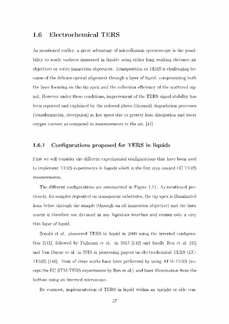
1.6 Electrochemical TERS
As mentioned earlier, a great advantage of microRaman spectroscopy is the possi-
bility to study surfaces immersed in liquids using either long working distance air
objectives or water immersion objectives. Transposition to TERS is challenging be-
cause of the delicate optical alignment through a layer of liquid, compromising both
the laser focusing on the tip apex and the collection eciency of the scattered sig-
nal. However under these conditions, improvement of the TERS signal stability has
been reported and explained by the reduced photo (thermal) degradation processes
(transformation, desorption) at hot spots due to greater heat dissipation and lower
oxygen content as compared to measurements in the air. [41]
1.6.1 Congurations proposed for TERS in liquids
First we will consider the dierent experimental congurations that have been used
to implement TERS experiments in liquids which is the rst step toward EC TERS
measurements.
The dierent congurations are summarized in Figure 1.11. As mentioned pre-
viously, for samples deposited on transparent substrates, the tip apex is illuminated
from below through the sample (through an oil immersion objective) and the laser
source is therefore not deviated at any liquid-air interface and crosses only a very
thin layer of liquid.
Zenobi et al. pioneered TERS in liquid in 2009 using the inverted congura-
tion [141], followed by Fujinami et al. in 2013 [142] and nally Ren et al. [41]
and Van Duyne et al. in 2015 in pioneering papers on electrochemical TERS (EC-
TERS) [140]. Most of these works have been performed by using AFM-TERS (ex-
cept the EC STM-TERS experiments by Ren et al.) and laser illumination from the
bottom using an inverted microscope.
By contrast, implementation of TERS in liquid within an upright or side con-
57
(a) (b)
Figure 1.11 Experimental congurations for performing TERS in liquids; a) side illuminationand collection trough a quartz window for EC-STM-TERS, from [41]; b) inverted AFM-TERSwith a mobile AFM tip and a xed transparent sample, from [140].
guration is the most challenging since the optical signal is inevitably deviated and
considerably attenuated by refraction at the liquid-air interface. However Ren et al.
in 2015 [41] and then Domke et al. since 2016 [143,144] demonstrated its feasibility
by proposing a conguration where the irradiation of a TERS-STM tip is carried
out through a side window opened in the liquid cell wall. An improvement of this
conguration was proposed by Ren et al. in 2017 [145] by using an immersion objec-
tive and by adding a drop of water between the objective lens and the side window
diminishing strongly the signal losses at this interface as it has previously shown to
be ecient for conventional microRaman spectroscopy. [146] TERS imaging within
such conguration may be restricted to only small displacements of the cell-sample
for which the laser focusing is not compromised since displacing the sample might
degrade the required ne laser alignment.
1.6.2 EC TERS
The characterization and the comprehension of electroactive systems using electro-
chemical techniques has been eciently extended by TERS analyses run ex situ to
assess the structure and the distribution of surface compositions. In 2016, Ren et al.
58

evidenced by electrochemical impedance spectroscopy (EIS) and TERS important
conformation changes during the formation of a self-assembled monolayer. [147] The
aromatic C = C bond vibration was used as a marker of intermolecular pi-stacking
and showed a non-monotonous evolution with the contacting time of the substrate
with the precursor solution. Measurement of the charge transfer resistance by EIS
conrmed this tendency.
If the potential of ex situ TERS analyses to help the interpretation of irreversible
electrochemical processes has been already established, the real-time monitoring
of an electrochemical transformation by TERS (EC-TERS) represents the most
interesting challenge. So far, only three dierent electrochemically active systems
have been studied by EC-TERS setups and reported in the literature: the potential
dependent protonation of 4-PBT ((4'-(pyridine-4-yl)biphenyl-4-yl) methanethiol),
[41] the potential-induced reorientation of adenine on a gold surface [148] and the
reduction of Nile Blue dye (NB) [140, 149] or of a covalently bound NB derivative.
[150] Although the development of EC- TERS is still at its early stages, important
experimental facts have already been raised by the leaders of the elds, using the
dierent congurations described above.
The rst EC-TERS characterization was carried out by Ren et al. in 2015 on
4-PBT layer adsorbed on Au (111) using an upright conguration and a side il-
lumination with an insulated gold tip in the EC-STM mode and a bipotentiostat
to control the potential of both the tip and the substrate. Distinct and stable
TERS signatures associated to dierent protonation state of 4-PBT at pH 10 were
successfully extracted when scanning the potential applied. Interestingly the pro-
tonated form could not be observed using SERS substrates made of 4-PBT func-
tionalized Au nanoparticles. The dominant SERS signal of the double-end bonded
4-PBT molecules connecting adjacent particles (in the gap) was interpreted to mask
the signal of protonated single-end-bonded, revealing the importance to control the
structure of the probed interface (number of probed molecules and their organization
59

around multiple hot spots). This control almost impossible with SERS substrates
can be achieved with TERS if the molecules are deposited on a well dened sub-
strate. [41]
Domke et al. in 2017 using a similar EC-STM conguration also demonstrated
the reversible potential-induced deprotonation and subsequent reorientation of ade-
nine molecules adsorbed on a (111) gold surface. Strong intensity changes were
observed on the collected TERS spectra upon polarization and were interpreted us-
ing DFT calculations by the induced reorientation of adenine molecules on the gold
surface. Switching from tilted to vertical orientations could be observed around
the point of zero charge (PZC) while a planar orientation of deprotonated adenine
molecules could be triggered by the strong Au-N interactions. [148]
Using the inverted TERS setup described above, a gold coated AFM probe and
a conductive ITO covered coverslip, Van Duyne et al. captured the electrochemical
transformation of model dye NB adsorbates described in three papers released be-
tween 2015 and 2017. [140,149,151] At low NB surface coverages, individual events
with dierent behavior (single or few molecules transformation) could be detected
at the tip-sample junction, revealing a distribution of local environments, i.e. of the
standard redox potential of the molecules (E0′), an observation otherwise impossible
to achieve with microRaman. They could also observe that the statistical distribu-
tion of apparent standard potentials of the anodic events is narrower than for the
cathodic events: this was interpreted as a lower sensitivity of the reduced form of
NB to its close environment. The close proximity of the metal tip with the polarized
substrate was reported to interfere locally with the electric eld, potentially aect-
ing the electrochemical response. A potential shift in the transition from oxidized
and reduced forms of NB has also been observed between the TERS signal and the
electrochemical current intensity measured at the sample (> 100 mV), pointing out
the inuence of the tip on the eective potential experienced by the scrutinized NB
molecules.
60
1.6.3 Challenges for EC-TERS
Only a few works have been published so far on TERS combined with electrochem-
ical measurements, mostly because of the important eorts required in instrumen-
tal developments. Despite the recent progresses, TERS imaging with high spatial
resolution still have to be demonstrated under electrochemical conditions. A rst
AFM-based TERS imaging of a CNT has recently been reported in water (but with-
out potential control), exhibiting a sub-30 nm lateral resolution. [152] As the spatial
resolution limit under electrochemical conditions is expected to reach the single
digit nanometre scale as in air, EC-TERS will probably help in pushing forward the
understanding of electrochemical and electrocatalytic events at specic sites of an
electrode. It is expected to reach the single molecule analysis to visualize directly
the chemical consequences of an electron transfer.
Note that several fundamental questions have still to be answered such as the
inuence the particular environment associated to electrochemical measurements:
eect of the surrounding medium, electrolyte, charges at the interface, etc. More-
over, as it has been underlined by Van Duyne et al., [140] the presence of the tip
seems to aect the electrochemical behaviour of the electroactive molecules (pertur-
bation of the electrochemical double layer). This inuence has to be evaluated for
further analysis of EC-TER spectra.
61

62
Chapter 2
Description of TERS experiments
In this chapter we will detail the main technical requirements and experimental
details of TERS experiments. We will rst describe the dierent micro and nano-
Raman setups. Then, the fabrication process of TERS tips used in this work will
be presented.
2.1 Description of the setup for microRaman and
TERS experiments
In this part the technical characteristics of the Raman spectrometer used in LISE
will be exposed as well as the optical coupling to the scanning probe microscopy
(SPM: STM, AFM, TF) platform for TERS experiments.
The spectrometer we used is a LabRam HR Evolution (Horiba). It is an au-
tomated confocal Raman microscope. A simplied scheme in Figure 2.1 describes
the optical path into the spectrometer and the coupling to a Smart SPM platform
(Omegascope, AIST) for TERS experiments. All the abbreviations in the following
refer to Figure 2.1.
An internal HeNe laser (632.8 nm, 10 µW) provides a linearly polarized beam. It
is rst cleaned by a laser-line clean-up lter (F1) and directed to a neutral density
63

lter wheel (ND) with 9 positions (100 %, 50 %, 25 %, 10 %, 5 %, 2.5 %, 1 %,
0.1 % and 0.01 % of the initial power). An additional polarizer can be installed
before the ND lter to change the polarization angle of the beam and adjust it to
the shape of the TERS tip in NF experiments. After the laser passes through a
beam expander (BE), mirror (M3) directs the beam on the rejection Filter F2 1
that reects the beam towards the objective (µRaman part of the scheme). For
microRaman measurements, M4 is removed from the path (all the mirrors symbol-
ized with dashed-line can be manually or automatically removed depending on the
application). Mirror M10 is used only to reect a part of the signal to a side CCD
camera which helps visualizing both the sample via white light illumination and the
focalized laser spot. For microRaman experiments the sample is mounted onto a
motorized XYZ platform designed for compositional mapping.
For TERS measurements, the laser is deviated by mirror M4 that ensures a top
or side optical access to the TERS tip mounted on scanning probe microscope (SPM)
(Omegascope, AIST). The Raman spectrometer and the SPM are supported by the
same optical table to ensure the stability of the mechanical and optical coupling.
When mirror M5 is placed on the optical path, the laser beam enters the pupil of a
long working distance objective mounted on a piezo stage (XYZ(1)) with an angle of
60o to the normal to be focused on the apex of the TERS tip. Rough prealignment
of the laser can be done with micrometre screws on the Omegascope module through
video control using a CCD camera positioned between M7 and the objective. This
CCD is manually removed before any measurements.
For top illumination and collection mirror M5 is removed. The piezo objective
stage XYZ(1) is positioned vertically below mirror M6 enabling the laser beam to
be focused to the apex of a slightly bent TERS tip. As for side conguration, a
CCD camera can help with the alignment of the laser on the tip. M6 is replaced
by a semi-reecting mirror for this operation. During measurements, M6 is used for
1In our setup, this lter is a notch lter for the 632.8 nm laser line and an edge lter for allother wavelengths.
64

excitation an collection.
For all congurations, the back-scattered signal is ltered by the laser-line rejec-
tion lter F2 (a notch lter for 632.8 nm and an edge lter for other wavelengths).
The role of F2 is to remove the Rayleigh scattered light from the collected signal so
that only Stokes (and anti-Stokes with the notch lter) contribution is directed to
the detector (CCD3 camera, EM-CCD Newton 970, Andor, cooled to −70 oC with
a Peltier stage) and recorded. Before reaching the detector, the scattered signal can
be ltered by a polarizer (P2) and then passes through a confocal hole (CH): its
aperture size can be adjusted to control the depth of the analysis. Diminishing the
size of this confocal hole in TERS experiments ensures that most of the signal orig-
inates from a thin focal plan where the tip apex is positioned, and that the far-eld
contribution is minimized. Finally, the Raman signal is directed to the spectrom-
eter containing two parabolic mirrors and two diraction gratings (Gr) which can
be selected to adjust the spectral resolution (3 available: 300, 600 and 1200 grooves
per mm). A shutter (Sh) is positioned before Gr and is open only during spectra
acquisition. The grating nally disperses the collected scattered signal on the detec-
tor: each pixel of the CCD camera receives photons related to a range of wavelength
(resolution). The spectral resolution (in cm−1) is dened by the periodicity of the
grating, the excitation laser wavelength, the number and the size of pixels on the
EM-CCD (1600× 400 array of 16 µm pixels).
In this thesis, all the experiments were performed using a 300 grooves per mm
grating and most of the TERS experiments were performed with a 632.8 nm laser.
With this grating and the EM-CCD Newton (Andor), the spectral resolution is
0.065 nm (i.e. 1.4 cm−1 between 0 and 2200 cm−1). Table 2.1 gives the spectral
resolution obtained with each laser wavelength available as well as the cut-o fre-
quency of each notch (n) or edge (e) lter. This resolution can be decreased when
binning of the data is used to increase the signal intensity: pixels of the spectra are
then the sum of two or more pixels of the CCD which enables one to increase the
65
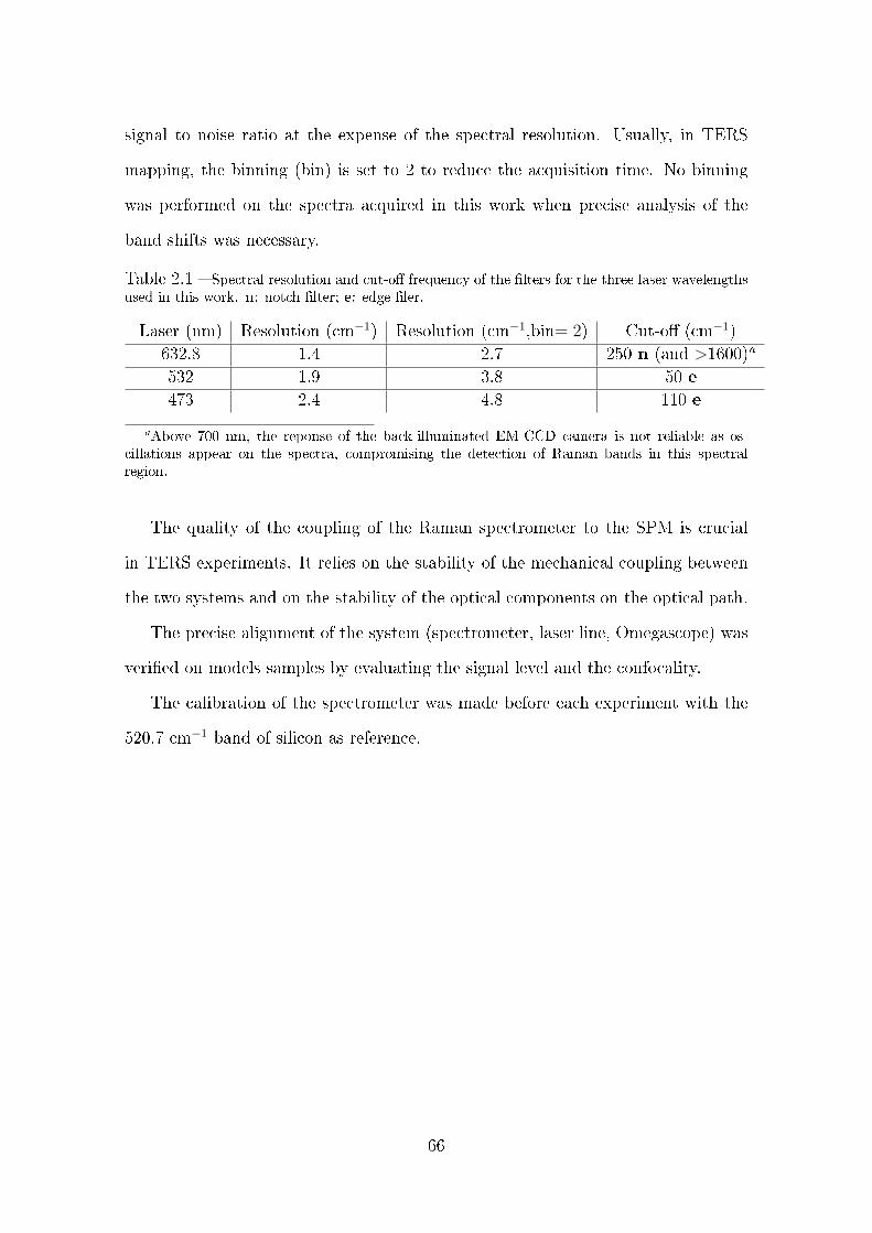
signal to noise ratio at the expense of the spectral resolution. Usually, in TERS
mapping, the binning (bin) is set to 2 to reduce the acquisition time. No binning
was performed on the spectra acquired in this work when precise analysis of the
band shifts was necessary.
Table 2.1 Spectral resolution and cut-o frequency of the lters for the three laser wavelengthsused in this work. n: notch lter; e: edge ler.
Laser (nm) Resolution (cm−1) Resolution (cm−1,bin= 2) Cut-o (cm−1)
632.8 1.4 2.7 250 n (and >1600)a
532 1.9 3.8 50 e
473 2.4 4.8 110 e
aAbove 700 nm, the reponse of the back-illuminated EM-CCD camera is not reliable as os-cillations appear on the spectra, compromising the detection of Raman bands in this spectralregion.
The quality of the coupling of the Raman spectrometer to the SPM is crucial
in TERS experiments. It relies on the stability of the mechanical coupling between
the two systems and on the stability of the optical components on the optical path.
The precise alignment of the system (spectrometer, laser line, Omegascope) was
veried on models samples by evaluating the signal level and the confocality.
The calibration of the spectrometer was made before each experiment with the
520.7 cm−1 band of silicon as reference.
66
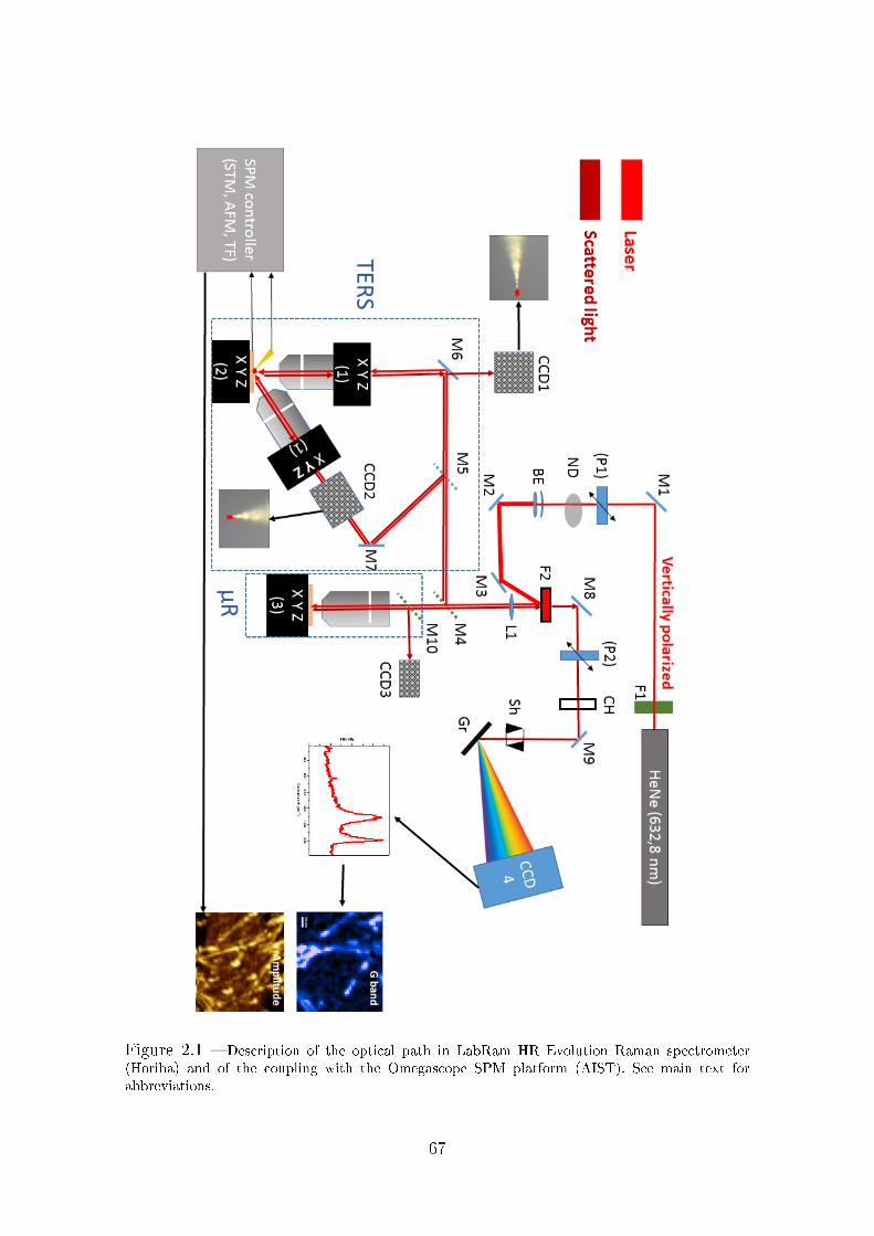
Figure 2.1 Description of the optical path in LabRam HR Evolution Raman spectrometer(Horiba) and of the coupling with the Omegascope SPM platform (AIST). See main text forabbreviations.
67

2.2 TERS tips manufacturing
As previously mentioned, one of the main impediments to TERS implementation
and development is the production of ecient and robust TERS tips (mechanically
and chemically) at low manufacturing cost.
2.2.1 Fabrication of gold TERS tips
In this work, we mainly developed bulk gold TERS tips for three main reasons:
• they can be produced without much eort with good reproducibility following
a fabrication protocol detailed hereafter;
• they do not degrade as fast as metal-coated tips and are more chemically stable
than silver tips which oxidize in the air;
• EC STM-TERS measurements require the tip-sample junction to be biased but
also the potential of the sample to be controlled and possibly set to oxidative
values. As oxidation of gold occurs at higher potential than silver, gold tips
enable the exploration of a larger potential range.
The electrochemical etching of gold wires can be achieved in solutions of hy-
drochloric acid (HCl) as gold metal can be oxidized into chloraurate ions (AuCl−4
and AuCl−2 ). The standard potentials of the associated redox couples are given by
A.J. Bard in Ref. [153]:
AuCl−2 + e− = Au + 2Cl− (E0 = 1.154 V/SHE) (2.1)
AuCl−4 + 3e− = Au + 4Cl− (E0 = 1.002 V/SHE) (2.2)
AuCl−4 + 2e− = AuCl−2 + 2Cl− (E0 = 0.926 V/SHE) (2.3)
Usually, a gold wire anode is positioned at the center of a ring-shaped gold
or platinum electrode (cathode) so that the current lines are homogeneous in the
68

cell, providing tapered and symmetrical tips through an homogeneous etching (Fig-
ure 2.2,a). Two main classes of etching are described depending on the type of
voltage applied (AC or DC). In 2004 Ren et al. published a study using DC volt-
age and exploring the electrolyte composition as well as the voltage applied [154]:
an electrolyte composed of a 1:1 (v:v) mixture of aqueous hydrochloride acid (37%)
and absolute ethanol and a DC voltage (2.2 V) gave the desired tapered and smooth
proles for TERS application. The anode is a 250 µm gold wire (99% purity) and
the ring-shaped cathode is made of platinum. In this conguration and at such a
voltage, an oscillatory behavior is observed in the current response due to the inter-
facial depletion in chloride ions and the accumulation at the interface of insoluble
gold complexes. This depletion allows the formation of gold oxides that temporarily
block the electrode causing sudden oscillations in current. This work has highlighted
the importance of selecting this oscillation region of potential to obtain sharp tips.
Note that the formation of oxygen and chlorine gas bubbles at the gold electrolyte
interface can also induce perturbations. The presence of ethanol in the electrolyte
modied the surface tension of the electrolye and helps reducing the size of the bub-
bles and then the possible perturbations at the interface. As production of hydrogen
bubbles at the cathode can also aect the etching process, a special cell (beaker-
cell) was proposed by Kharintsev et al. in 2013: in this cell an additional beaker
is introduced in solution between the cathode and the gold wire to eliminate the
perturbation induced by the hydrogen production. [155] However, this conguration
may increase the electrolyte resistance between both electrodes and severely aect
the potential of the wire in this two-electrode conguration. But interestingly, this
group also proposed to use potential pulses. Two potentials are applied alterna-
tively, one which corresponds to the oscillatory regime for the etching, the other
one corresponds to a relaxation potential below this oscillatory regime, allowing the
diusion of the corrosion products away from the electrode and of the chloride ions
toward the gold wire. This procedure was further rened by varying the pulses se-
69

quence [156] and recently by using a three-electrode conguration enabling a better
control of the potential applied to the wire. [157]
Figure 2.2 Elaboration of gold TERS ecient tip by electrochemical etching: a) the goldwire (working electrode, 250 µm diameter) is positioned at the center of a platinum ring counterelectrode in etching bath composed of a mixture of HCl and EtOH. During the electroetchingprocess when the diameter of the Au wire decreases the meniscus position progressively shiftsdownward until the nal cuto, producing the tapered prole; b) the bath composition and theelectrochemical sequence had to be optimized to produce in a reproducible way TERS tips with aradius of curvature around 20 nm.
On the basis of these works, Alice Dauphin (a bachelor student intern) developed
an etching protocol before this work started. It uses an etching bath composed of
a 1:1 (v:v) HCl (37%) and absolute ethanol mixture and a pulsed sequence for the
polarization.2 The procedure was further improved at the beginning of this thesis
by adding an analog switch in the circuit. The latter which compares the read-out
etching current with a chosen threshold value opens the circuit when the current
drops below this pre-set value when the immersed part of the wire falls down. This
prevents over-etching that can happen if the apex of the tip is still in contact with the
solution. With this fabrication procedure we could produce with a good reliability
smooth and sharp tips (with radii of curvature as low as 20 nm) with a controlled
cone angle in less than 10 minutes for gold wires with a 250 µm diameter. All the
tips are rinsed with bi-distilled water and absolute ethanol after fabrication and can
be stored several weeks after preparation. SEM images present the typical prole
obtained after etching of 250 µm diameter gold wire (Figure 2.2,b). In order to
prevent carbon contamination during SEM imaging of the tips, SEM analysis was
2Further details cannot be disclosed. A Soleau envelope was led in 2017 protecting this processas well as the fabrication of silver tips described in the following.
70

performed after TERS experiments if needed. In order to preselect suitable tips
after their fabrication an optical microscope (40X objective) was preferred to sort
and possibly discard round-shaped and non-TERS-active tips.
2.2.2 Fabrication of silver TERS tips
As for gold tips, several procedures have already been proposed for the electrochem-
ical etching of silver wires for the fabrication of TERS tips. The variety of the
etchants and of the type of voltage applied is wide. The etchant baths are usually
based on ammonia solutions [158,159], ammonium nitrate [160], nitric acid [161], cit-
ric acid [162] and perchloric acid [159,163166] with additives (methanol, ethanol).
Similarly to gold tips, the range of applied potentials is wide (from a few to tens
of V) as well as the type of applied voltages (AC, DC, pulsed). For this work, the
etching of silver wires was explored too, during the internship of Ghizlene Zenasni
(bachelor student) in 2017. We rapidly converged onto applying DC voltage in a
1:4 (v:v) perchloric acid (70%) and ethanol electrolyte. A pulsed sequence similar
to the one used for gold did not lead to reproducible results. For silver, the etching
mechanism is in fact more simple as no electrode passivation takes place. Using the
same setup as for gold tips and a cut-o switch in the circuit, this protocol enabled
the reliable and reproducible fabrication of Ag TERS tips in less than three min-
utes. The fabricated tips with a radius of curvature lower than 100 nm showed EF
between 1 ·103 and 2 ·104. A SEM-FEG image of an etched silver TERS tip is given
in Figure 2.3
As for Au TERS tips, to prevent carbon contamination during SEM-FEG mea-
surements, the tips were preselected with an optical microscope but immediately
used in TERS experiments to prevent any degradation of their performances upon
exposure to the air (oxidation).
71
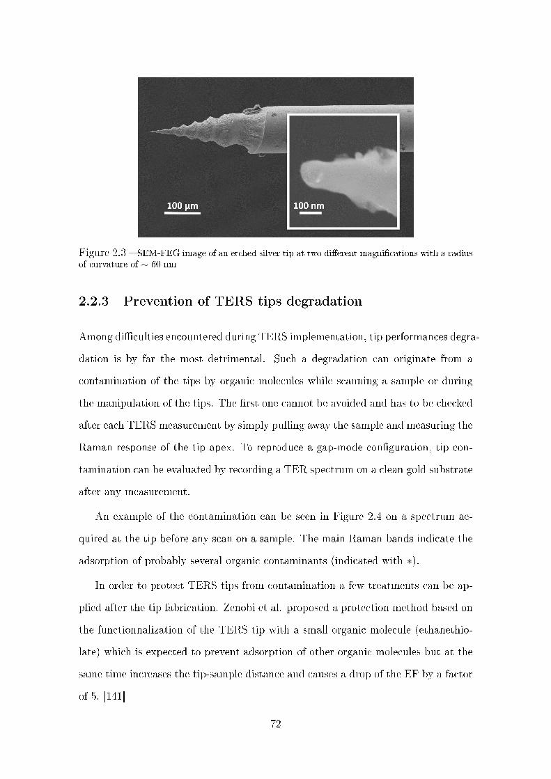
Figure 2.3 SEM-FEG image of an etched silver tip at two dierent magnications with a radiusof curvature of ∼ 60 nm
2.2.3 Prevention of TERS tips degradation
Among diculties encountered during TERS implementation, tip performances degra-
dation is by far the most detrimental. Such a degradation can originate from a
contamination of the tips by organic molecules while scanning a sample or during
the manipulation of the tips. The rst one cannot be avoided and has to be checked
after each TERS measurement by simply pulling away the sample and measuring the
Raman response of the tip apex. To reproduce a gap-mode conguration, tip con-
tamination can be evaluated by recording a TER spectrum on a clean gold substrate
after any measurement.
An example of the contamination can be seen in Figure 2.4 on a spectrum ac-
quired at the tip before any scan on a sample. The main Raman bands indicate the
adsorption of probably several organic contaminants (indicated with ∗).
In order to protect TERS tips from contamination a few treatments can be ap-
plied after the tip fabrication. Zenobi et al. proposed a protection method based on
the functionnalization of the TERS tip with a small organic molecule (ethanethio-
late) which is expected to prevent adsorption of other organic molecules but at the
same time increases the tip-sample distance and causes a drop of the EF by a factor
of 5. [141]
72

Figure 2.4 TER spectrum at the apex of a silver tip exhibiting bands of the oxides andsulde stretching modes (below 400 cm−1). Bands marked with asterisks are assigned to organiccontaminants. λexc = 532 nm, 220 µW, 5 s.
Ren et al. proposed a way to regenerate gold TERS tips by immersion of the
contaminated tips into a concentrated sulfuric acid solution. This procedure enables
the removal of organic contaminants adsorbed during previous TERS measurements
or after a long storage. [167]
For silver tips, another drawback is the oxidation of silver at air. It usually can be
oxidized by oxygen into Ag2−O and by H2S or sulfur containing species into Ag2S.
This oxidation of the surface aects the plasmonic properties of nanostructures. For
instance, the LSPR of silver NPs is quickly red shifted and their EF diminishes,
resulting in drastic decrease of SERS eciency. [168]
The formation of an oxide layer can be seen on the TER spectrum of the con-
taminated silver tip in Figure 2.4 as the oxidation products exhibit strong Raman
bands below 300 cm−1. [169]
Laser-induced oxidation is also observed for TERS silver tips. This phenomenon
could be observed after a long illumination of a silver tip at high laser power
(632.8 nm, 3.3 mW) and long exposure. TER spectra were acquired with both
73

632.8 and 532 nm lasers before a long-time exposure for comparison(Figure 2.5).
The STM-TER spectrum at 632.8 nm exhibits a clear signature from the organic
SAM on the sample (thioazobenzene); a slight shoulder at low frequency can indicate
the presence of an oxide layer on the tip. However, the 632.8 nm notch lter used
with the 632.8 nm line truncates the spectrum below 250 cm−1. If the 532 nm laser
is used, a lower signal to noise ratio is obtained for the TER signature of the azoben-
zene SAM (due to a lower enhancement at this wavelength) but low frequency bands
exhibit clearly stretching modes of silver oxides and sulde. After illuminating the
tip during 300 s, TER spectra were acquired under similar conditions with both ex-
citation lasers: the TER spectrum obtained with the red laser displays a clear rising
of the tail of the oxide band below 400 cm−1 and a strong decrease of the intensity
of the Raman bands intensity of thioazobenzene. The TER spectrum acquired at
532 nm exhibits strong band intensities in the low frequency region and new ones
especially below 200 cm−1 which was attributed to the formation of Ag2S. Note
that at this wavelength, the TERS intensity is not aected by a long illumination.
The mean lifetime of a silver TERS tip exposed to the ambient ranges from 6
to 8 hours maximum. Silver tips can be stored under inert atmosphere after their
fabrication to extend their lifetime up to several weeks. [170]
Regeneration of oxidized tips was also proposed: the principle is based on the gal-
vanic reduction of silver oxides or suldes in presence of aluminium (E0(Al3+/Al =
−1.68 V vs SHE and E0(Ag2S/Ag) = −0.69 V vs SHE). Tips are electrically con-
nected to an alluminium foil and immersed into a NaHCO3 aqueous solution. This
cell can also be used for long-term storage. [171]
We also investigated the protection of Ag TERS tips in this work. We used
a paran wax (docosane, C22H46) to reversibly protect them. Docosane is a low
melting point wax (45 oC) in which tips can be dipped without any damage. After
solidication the wax protects the tip from organic molecules, ambient oxygen or
sulfur species. The tip can then be unprotected by slight heating of the tip so that
74

Figure 2.5 Evolution of the TER spectra of a thioazobenzene derivative SAM on gold probedby STM TERS with a silver tip. a) TER spectra with a 632.8 nm laser exitation (1 s, 3.3 mW)before (grey) and after (purple) 300 s of exposure of the tip to the red laser. Black arrows showthe evolution of the main bands intensities: global ITERS diminishes while a low frequency mode(silver oxides) appears; b) TER spectra with a 532 nm laser excitation (1 s, 220 µW) before (grey)and after the 300 s exposure to the 632.8 nm laser. The black arrows show the evolution of theintensity of silver oxides vibration modes, the red arrow highlights the appearance of the Ag-Sstretching mode of Ag2S. No baseline correction and no y-oset were applied.
the tip apex is free of wax. This allowed the storage of the tips during more than one
week with no contamination and just a slight loss in TERS eciency. An example of
two TER spectra on a reference sample (thioazobenzene) is given in Figure 2.6 just
after the tip fabrication (less than 1 h) and after a one-week storage in docosane. A
25 % decrease in intensity can be observed on the 1140 cm−1 band and a small raise
75
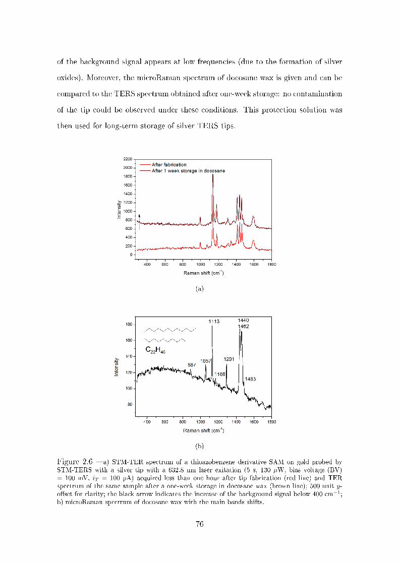
of the background signal appears at low frequencies (due to the formation of silver
oxides). Moreover, the microRaman spectrum of docosane wax is given and can be
compared to the TERS spectrum obtained after one-week storage: no contamination
of the tip could be observed under these conditions. This protection solution was
then used for long-term storage of silver TERS tips.
(a)
(b)
Figure 2.6 a) STM-TER spectrum of a thioazobenzene derivative SAM on gold probed bySTM-TERS with a silver tip with a 632.8 nm laser exitation (5 s, 130 µW, bias voltage (BV)= 100 mV, iT = 100 pA) acquired less than one hour after tip fabrication (red line) and TERspectrum of the same sample after a one-week storage in docosane wax (brown line); 500 unit y-oset for clarity; the black arrow indicates the increase of the background signal below 400 cm−1;b) microRaman spectrum of docosane wax with the main bands shifts.
76

2.3 TF-TERS experiments
During this thesis, the implementation of TF-TERS (in NF conguration) was also
considered, and we therefore established a protocol for gluing gold TERS tips on TF
resonators. Q-factors can be tuned by adjusting the mass and the position of the
tip. Controlling the mass can be done by gluing tips etched from wires with dierent
diameters and length. We rst designed probes starting from 250 µm diameter gold
wires which imposed the use of very short and light tips dicult to manipulate and
also the use of small amount of glue (cyanoacrylate) which renders them fragile. The
use of thinner wires is possible as our etching process enables us to routinely etch
gold wires of 30, 100 and 250 µm to produce TERS tips. TF-probe systems with
100 µm diameter wires (see Figure 1.10) were found to provide the highest Q-factors
(several thousands). Diminishing Q to values in the 500-3000 range is achieved by
successive addition of small amounts of glue. It has to be noticed that even if this
kind of glue is supposed to cure within a few minutes, the system is not stabilized
until several hours (24 hours was estimated to be long enough) as f0 and Q drift
until the glue hardens and the tip is rmly bound to the prong. Figure 2.7 shows
the evolution of Q and f0 for a TERS-TF with a 250 µm diameter etched gold wire
as a function of the hardening time: initially, the free standing TF had a 37.8 kHz
resonance frequency and Q = 14660.
These NF-TERS probes were tested on several samples to evaluate their sensitiv-
ity to topography and their lateral resolution and TER activity. Here, in Figure 2.8,
we could image a gold surface covered with multiwall carbon nanotubes (MWCNTs):
the TER map exhibits clear Raman features of CNTs, the G band, tangential vibra-
tion mode (1590 cm−1) and the disorder mode (sp3 carbons, D mode) at 1300 cm−1.
One can deduce from these maps a resolution around 20 nm; moreover, even if the
topographic data are poor, Raman signature allows one to distinguish very specic
parts of the CNTs such as the extremities with high D mode intensity. [172]
TF-based probes have also been developed for studies in liquids. In this con-
77

Figure 2.7 Evolution of the resonance frequency (f0) and of the quality factor (Q) of a TFonto which a 250 µm diameter etched gold wire was glued (cyanoacrylate glue) as a function ofthe hardening time. Dashed lines show the values of Q and f0 after a complete hardening of theglue and stabilisation of the system (24h).
(a) (b)
Figure 2.8 a) TER spectrum of a MWCNT on gold recorded with a NF-TERS feedbackmechanism. Red line: tip engaged (near-eld); Grey: Tip retracted by 50 nm (Far-eld); b)50x50 px2, 500x500 nm2 NF-TERS mapping of a MWCNT bundle on a gold substrate: the blueand red maps are obtained by integration of the D and G mode bands of the CNTs (laser: 632.8 nm,10 µW, 100 ms/px). Simultaneous topography (height) and changes in the amplitude signal wererecorded.
guration the tip can be in the liquid without immersing the whole TF. This was
achieved with SF-SNOM with a 200 µm protruding ber in several aqueous solutions
78
with small degradation of the Q factor (30 % for the highest Q factor in a buer
solution used in biological experiments). [173] An alternative strategy is the encap-
sulation of the the TF so that only the tip apex is in contact with the solution. [142]
However these strategies are dicult to implement and were not explored for TERS
in liquids or EC-TERS in this work.
2.4 Conclusion
In this chapter, the main practical aspects of TERS experiments have been de-
scribed. The description of the optical coupling between the conventional Raman
spectrometer and the SPM platform has demonstrated that its robustness is a key
element for reliable TERS measurements.
The manufacturing of robust and reproducible gold and silver TERS probes has
been detailed. The major tip-related issue, the tip degradation, has been addressed
by reporting solutions provided by other groups in the literature and a specic
development we proposed for the storage of air-sensitive silver probes.
Finally, TF-TERS probes and their characteristics have been described. As
these TF-based SPM are hard to be implemented in liquids, this approach has been
discarded for operation in EC-TERS and will not be discussed in the following.
In the following chapters, we decided to focus only onto STM-TERS experiments.
79

80

Chapter 3
Tip-Enhanced Raman Spectroscopy
imaging of opaque samples in organic
liquids
3.1 Introduction
TERS implementation in liquid represents an important challenge because of the
delicate optical alignment through a layer of liquid to achieve an accurate focusing
of the laser beam on the tip apex and also to ensure an ecient collection of the
scattered signal. Most literature reports describe transparent samples set on an
inverted optical microscope; focusing of the laser beam on the TERS probe is there-
fore easily achieved directly through the sample. [140,142] With opaque samples that
necessitate top or side illumination and collection, the optical signal is inevitably
deviated and considerably attenuated by refraction at the air-liquid interface. Ren
et al. [41] as well as Domke et al. [143] recently elegantly circumvented this problem
by mounting the sample in a liquid cell equipped with a side thin glass window
and obtained an ecient side illumination of an STM probe enabling single point
TERS spectroscopy. The window was positioned about 1 mm apart from the probe.
81

This solution unfortunatly freezes the tip vs sample/window positioning, obliter-
ating TERS sample imaging capabilities in liquid. We propose in this chapter a
new TERS setup based on an upright illumination and collection conguration that
enables TERS imaging in an organic liquid (hexadecane). We will rst prove its
capability to record TERS signal through a layer of liquid with a strong near-eld
to far-eld ratio and then to investigate the structure of a molecular monolayer on
a gold surface.
3.2 Description of the experimental setup
3.2.1 Optical coupling
In our setup described in Figure 3.1, a polarized excitation laser (λexc = 632.8 nm)
is focused on the STM probe apex through a long distance 100 x objective (working
distance: 6 mm) with high numerical aperture (NA = 0.7). Therefore, the STM
tip holder can be positionned between the objective and the sample. A gold tip is
bent with an angle of 30 to 45o to the normal of the sample as previously depicted
by Zenobi et al. in air. [78, 165] This angle allows the apex of the tip to reach the
focal point of the objective for an optimized signal collection and enables a suitable
alignment of the electric eld along the shaft of the tip. Within this conguration,
the STM imaging capabilities of the probe are maintained. The objective is mounted
onto a piezoelectric positioning system which allows an accurate screening of the
optical hot spot on the gold tip, i.e. the position of laser on the tip giving the
maximum enhancement of the Raman signal intensity.
82

Figure 3.1 Upright illumination and collection setup used in STM-TERS imaging through athin layer of organic liquid (depicted as a light blue line).
3.2.2 Spectroscopic characteristization of the solvent and of
the molecular layer
For this study, a thioazobenzene derivative (4-[(phenylazo)phenoxy]hexan-1-thiol,
named thioazobenzene, ProChimia, Poland) was chosen to form a SAM onto a gold
surface. The TERS signal of the thioazobenzene derivative (see Figure 3.2) self-
assembled on a gold surface was rst collected in the air. It can be compared to the
Raman spectrum of the powder and of the far-eld micro-Raman signal collected
of the SAM on gold that are displayed in Figure 3.2b. The main Raman bands
in the spectrum of azobenzene are: a broad medium band at 1595 cm−1 assigned
to the aromatic ring breathing; a strong triplet: a band at 1443 cm−1 assigned to
the N = N streching mode, and the 1415 and 1465 cm−1 bands assigned to ring
deformations; a strong C − N streching mode band at 1143 cm−1 and a medium
C− C stretching band at 1184 cm−1. [174177]
Gold samples were prepared by thermal evaporation of 100 nm of gold onto
cleaved mica heated at 400 oC and ame annealed prior to use. The sample was
prepared by soaking a gold substrate in a 0.2 mM ethanolic solution of thioazoben-
zenefor 1 h, followed by immersion in pure ethanol for 1 h in order to remove any
physisorbed molecules. In comparison to literature, the SAM was prepared in more
dilute solution and soaked for a shorter time. [178,179]
83

(a)
(b)
Figure 3.2 a) Raman spectrum of the powder of thioazobenzene after baseline substraction(λexc = 632.8 nm); b) Micro-Raman spectrum of the SAM of thioazobenzene on a gold surface(λexc = 632.8 nm, laser power: 98 µW, acquisition time: 10 s).
The liquid STM-TERS experiments were carried out using a non-volatile and
non-conductive organic solvent, i.e. hexadecane (Sigma Aldrich). This latter shows
very limited evaporation ensuring the stability over time of the tip-liquid interface
and therefore of the optical path. Moreover, within hexadecane, no insulating of the
STM tip is required since leaking currents (faradaic current) are negligible in such
non-conductive solvent. The Raman spectrum of hexadecane is given in Figure 3.3:
84
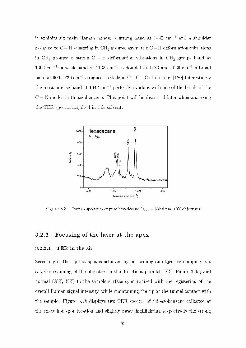
it exhibits six main Raman bands: a strong band at 1442 cm−1 and a shoulder
assigned to C−H scissoring in CH2 groups, asymetric C−H deformation vibrations
in CH3 groups; a strong C − H deformation vibrations in CH2 groups band at
1303 cm−1; a weak band at 1133 cm−1, a doublet at 1083 and 1066 cm−1 a broad
band at 900 - 830 cm−1 assigned to skeletal C−C−C stretching. [180] Interestingly
the most intense band at 1442 cm−1 perfectly overlaps with one of the bands of the
C− N modes in thioazobenzene. This point will be discussed later when analyzing
the TER spectra acquired in this solvent.
Figure 3.3 Raman spectrum of pure hexadecane (λexc = 632.8 nm, 10X objective).
3.2.3 Focusing of the laser at the apex
3.2.3.1 TER in the air
Screening of the tip hot spot is achieved by performing an objective mapping, i.e.
a raster scanning of the objective in the directions parallel (XY , Figure 3.4a) and
normal (XZ, Y Z) to the sample surface synchronized with the registering of the
overall Raman signal intensity, while maintaining the tip at the tunnel contact with
the sample. Figure 3.4b displays two TER spectra of thioazobenzene collected at
the exact hot spot location and slightly away, highlighting respectively the strong
85
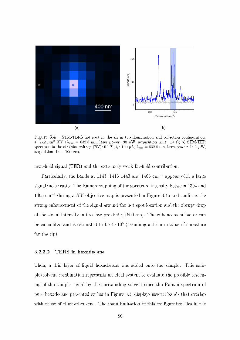
(a) (b)
Figure 3.4 STM-TERS hot spot in the air in top illumination and collection conguration.a) 2x2 µm2 XY (λexc = 632.8 nm, laser power: 98 µW, acquisition time: 10 s); b) STM-TERspectrum in the air (bias voltage (BV): 0.1 V, it: 100 pA, λexc = 632.8 nm, laser power: 14.1 µW,acquisition time: 100 ms).
near-eld signal (TER) and the extremely weak far-eld contribution.
Particularly, the bands at 1143, 1415 1443 and 1465 cm−1 appear with a large
signal/noise ratio. The Raman mapping of the spectrum intensity between 1394 and
1495 cm−1 during a XY objective map is presented in Figure 3.4a and conrms the
strong enhancement of the signal around the hot spot location and the abrupt drop
of the signal intensity in its close proximity (600 nm). The enhancement factor can
be calculated and is estimated to be 4 · 105 (assuming a 15 nm radius of curvature
for the tip).
3.2.3.2 TERS in hexadecane
Then, a thin layer of liquid hexadecane was added onto the sample. This sam-
ple/solvent combination represents an ideal system to evaluate the possible screen-
ing of the sample signal by the surrounding solvent since the Raman spectrum of
pure hexadecane presented earlier in Figure 3.3, displays several bands that overlap
with those of thioazobenzene. The main limitation of this conguration lies in the
86
tip/liquid meniscus that interferes with the optical path. The height and radius of
curvature of this meniscus strongly depends on the diameter and angle of the tip.
We observed that a thickness of liquid of a few micrometres (2 - 20 µm) however
still allowed an accurate focusing of the laser on the tip. Under such conditions,
searching for the hot spot in liquid became possible as revealed by the XY objec-
tive map depicted in Figure 3.5a. The spectrum at the exact hot spot (blue) and
slightly o (red) appear in Figure 3.5b. A weak contribution from the solvent is
present on all collected spectra as revealed on the average spectrum collected for a
large area of the Raman map outside the hot spot (black spectrum). At the hot spot
however, the contribution from thioazobenzene largely dominated the Raman sig-
nature, demonstrating that TERS is eective in hexadecane. It is noteworthy that
the laser power and integration time have to be slightly increased to compensate for
the optical losses and to obtain a signal to noise ratio similar to the one in the air
(a factor 3 on the laser power and 5 on the integration time).
Despite these losses the enhancement factor in this conguration could be eval-
uated to be 4 · 105 which is exactly the same as the one in air highlighting that the
tip-enhancement is not aected by the presence of the solvent and the change in
refractive index of the dielectric medium sourrounding the tip (∼ 1 in air vs ∼ 1.43
in hexadecane).
3.3 TERS imaging in organic liquid
To evidence that our setup is also suitable for TERS imaging in liquid, a 300 ×
300 nm2 area of the sample was scanned in STM mode in hexadecane while record-
ing TERS spectra. With a 30 × 30 px2 image and 0.107 s acquisition time per
spectrum (laser power = 98 µW), the recording of a full TERS image took only
97 s. A higher resolution STM image (256×256 px2) was also recorded immediately
after. In Figure 3.6, the comparison between low and high resolution STM images
87

(a) (b)
Figure 3.5 STM-TERS experiment performed in a thin layer of liquid hexadecane: a) 3x3µm2 XY objective map (integration of the peak intensity with baseline correction between 1125and 1162 cm−1); b) Raman spectrum at the exact hot spot location on the tip (blue: TERS) andslightly apart (red: far-eld), and averaged spectrum for the dashed rectangle area of the objectivemap revealing the spectrum of hexadecane (λexc = 632.8 nm, laser power: 287 µW, acquisitiontime: 500 ms, BV: 0.1 V, it: 1000 pA).
shows that a 30× 30 px2 image is sucient to evidence topography details, like pin-
holes present over the gold surface. Furthermore, in the high resolution image, the
topography is well-described meaning that the STM-TERS tip was sharp enough to
minimize convolution eects.
A TERS map obtained by integrating the band intensity of thioazobenzene be-
tween 1125 and 1162 cm−1 is presented in Figure 3.6. It reveals that signal intensity
on the lower left part of the image is more intense. Such local intensity uctuations
(both in X and Y directions) would never be detected in microRaman. Figure 3.7
displays ten spectra obtained by averaging the 9 spectra around each position in-
dicated in Figure 3.6a. The lower intensity (position 1) corresponds to 40% of the
highest one (position 9). Note that the scan proceeded from left to right and from
bottom to top.
To explain the drop in intensity along the vertical direction of the raster scan, a
change in the laser focusing on the tip may be invoked. The latter could originate
88
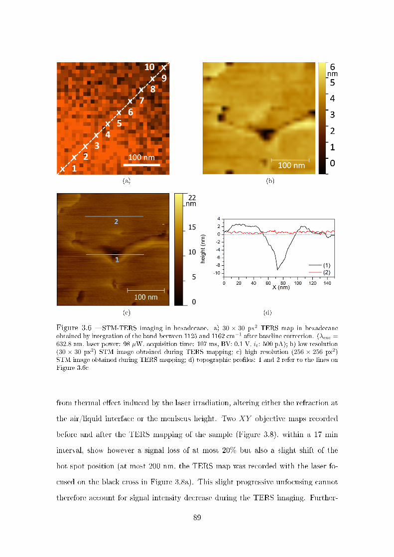
(a) (b)
(c) (d)
Figure 3.6 STM-TERS imaging in hexadecane. a) 30 × 30 px2 TERS map in hexadecaneobtained by integration of the band between 1125 and 1162 cm−1 after baseline correction. (λexc =632.8 nm, laser power: 98 µW, acquisition time: 107 ms, BV: 0.1 V, it: 500 pA); b) low resolution(30 × 30 px2) STM image obtained during TERS mapping; c) high resolution (256 × 256 px2)STM image obtained during TERS mapping; d) topographic proles: 1 and 2 refer to the lines onFigure 3.6c
from thermal eect induced by the laser irradiation, altering either the refraction at
the air/liquid interface or the meniscus height. Two XY objective maps recorded
before and after the TERS mapping of the sample (Figure 3.8), within a 17 min
interval, show however a signal loss of at most 20% but also a slight shift of the
hot spot position (at most 200 nm, the TERS map was recorded with the laser fo-
cused on the black cross in Figure 3.8a). This slight progressive unfocusing cannot
therefore account for signal intensity decrease during the TERS imaging. Further-
89

(a) (b)
Figure 3.7 TER spectra from Figure 3.6a. a) series of 10 averages TER spectra (9 pixels).Numbers (1-10) refer to the positions in Figure 3.6a. Spectra were oset (+100) for the sake ofclarity; b) intensity of 3 raman modes as a function of the position on the sample.
more, unfocusing of the laser cannot account for variations along the horizontal (X)
direction.
We therefore rather incriminate a local variation in the surface coverage of thioa-
zobenzenedue to non-homogenous SAM formation on gold, possibly combined with
a modication of the molecular orientation of thioazobenzene on the surface. This
change in the molecular orientation cannot be clearly extracted from TER spectra,
however a close look at the 1595 cm−1 band reveals some slight changes: in spectra
1 an 2 (low surface coverage), the peak is broad and unique (26 cm−1 width) while
in spectrum 3, the peak could be deconvoluted into two peaks 1593 and 1602 cm−1.
These two modes have previously been theoretically predicted as in-plane ring de-
formation [174, 175] but have never been evidenced to our knowledge. Considering
they originate from two similar vibration modes, they cannot easily be interpreted
as molecular orientation dierences. This intensity variation was then only inter-
preted as a molecular surface concentration gradient and was assumed to be due
to the SAM preparation and especially the low immersion time in the ethanolic
90

solution of thioazobenzene. [178, 179] As a consequence of this surface concentra-
tion change, no relation between the topography and the Raman intensity could be
clearly established. [181,182]
(a) (b)
(c)
Figure 3.8 2x2 µm2 XY hotspot imaging a) before and b) after TERS imaging (Figure 3.6)obtained by integration of the peak intensity with baseline correction between 1125 and 1162 cm−1;c) Raman spectra corresponding to the markers in (a) and (b) maps (λexc = 632.8 nm, laser power:98 µW, 107 ms acquisition, BV: 0.1 V, it: 500 pA); +x below each spectrum: y-oset for clarity.
This set of results illustrates that TERS imaging is operational in organic solvent
using an upright conguration. The next stage will be to precisely determine the
spatial resolution of TERS in liquid by imaging small nano objects in a similar
way to what was recently performed by Chen et al. in air with carbon nanotubes
91
(CNTs): they could demonstrate a lateral resolution down to 1.7 nm. [88] More
recently, imaging of CNTs was performed in water on an inverted microscope with
an AFM TERS probe revealing a sub-30 nm lateral resolution which is still far from
the single digit nanometre scale reachable at ambiant. [152]
3.4 Conclusion
In this chapter we have demonstrated that it is possible, using an upright optical
conguration, to implement TERS imaging of an opaque sample in an organic liq-
uid which the Raman signature overlaps with the one of the SAM under scrutiny,
with fast acquisition time and minimal laser power. With this set-up, the ecient
excitation and collection of the scattered Raman signal allows the extraction of the
chemical signature of a molecular monolayer from the one of the surrounding solvent.
To achieve such performances, the liquid thickness has to be optimized (around 20
µm at most here), in order to reduce the distortion of the optical path and the loss
of signal at the tip-liquid interface (meniscus). These promising results pave the
road to TERS imaging in other solvents or electrolytes. Moreover, the thin layer of
liquid deposited over the sample is also an interesting and easy way of protecting
oxygen sensitive samples. It can also prevent the sample from being contaminated
by organics present in the air. Moreover, it has already been demonstrated that
less uctuation of the TER spectra intensity are observed in liquids as compared to
the air, it could be interesting using this set-up to determinate if this eect relates
to the local temperature stabilization due to the presence of the solvent which acts
locally as a heat sink. [183]
92
Chapter 4
Electrochemical Tip
Surface-Enhanced Raman
Spectroscopy
4.1 Context
In TERS, among previously mentionned diculties due to liquid environement, sig-
nal uctuations can be observed when scrutinizing only a few molecules with the
tip and challenge the real-time quantication of surface processes, although these
variations can also provide important information regarding the local microenvi-
ronment of individual molecules. [140] Besides, in an electro-chemical TERS setup,
other complications may arise from ohmic losses across large polarized substrates.
These latter drastically aect the temporal resolution of the electrochemical pro-
cesses [184] and minimize the benets of time-resolved TERS experiments. Similar
questions may arise in electrochemical Surface Enhanced Raman Spectroscopy (EC
SERS) for which the signal is collected and averaged on a square micrometer area
possibly on an inhomogeneous substrate. [140] Finally, the close proximity of the tip
with the polarized substrate may interfere locally with the electric eld, potentially
93
aecting the electrochemical response. In some cases, these drawbacks may hinder
detection and identication of reaction intermediates by TERS and thus the compre-
hension of complex reaction schemes involving multi-electron transfer to molecular
species.
In this chapter we introduce a novel spectroscopic analytical tool for the study of
electrochemical mechanisms based on the Raman enhancement provided by TERS
tips. We will demonstrate that a partially insulated TERS tip can be functionalized
by an electroactive molecule and used both as a microelectrode and as a single hot
spot surface-enhanced Raman (SERS) platform.
This conguration has previously been proposed by Pienpinijtham et al. to
probe the local pH by functionalizing a gold TERS tip with p-aminothiophenol
and p-mercaptobenzoic acid whose Raman vibrations are sensitive to the pH. [185]
Even if in this conguration the spatial resolution is lost (no surface is scanned), as
well as the enhancement due to the possible tip-substrate junction between the tip
and a gold or silver substrate, [186, 187] the number of probed molecules is higher
than in usual TERS measurements providing intense Raman signal with no uctua-
tions. Functionalized tips have also been used to probe inhomogeneities of plasmons
enhanced eld distribution on SERS substrates at the nanoscale [188,189] or to evi-
dence higher electric eld enhancement on the edges of Au(111) substrates [190] by
scanning the functionalized TERS tip over the substrate. However, to the best of
our knowledge no work has been conducted on electrochemical systems using such
a conguration.
This chapter will be dedicated to the study of the electrochemichal reduction
mechanism of a monolayer of 4-nitrothiophenol self-assembled on TERS active mi-
croelectrode that was chosen as a reference system to test and validate our approach.
This approach which combines the advantages of measurements onto microelectrodes
to those provided by SERS is denominated as tip SERS (EC tip SERS) in the fol-
lowing.
94
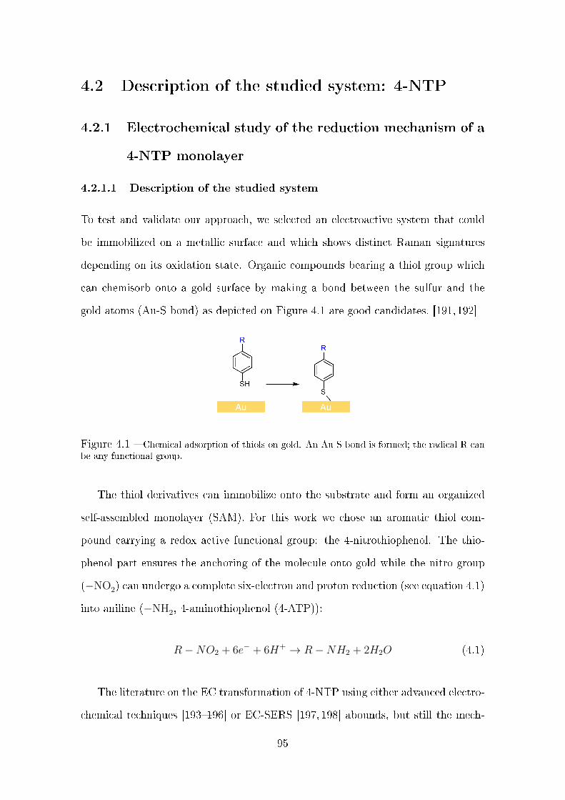
4.2 Description of the studied system: 4-NTP
4.2.1 Electrochemical study of the reduction mechanism of a
4-NTP monolayer
4.2.1.1 Description of the studied system
To test and validate our approach, we selected an electroactive system that could
be immobilized on a metallic surface and which shows distinct Raman signatures
depending on its oxidation state. Organic compounds bearing a thiol group which
can chemisorb onto a gold surface by making a bond between the sulfur and the
gold atoms (Au-S bond) as depicted on Figure 4.1 are good candidates. [191,192]
Figure 4.1 Chemical adsorption of thiols on gold. An Au-S bond is formed; the radical R canbe any functional group.
The thiol derivatives can immobilize onto the substrate and form an organized
self-assembled monolayer (SAM). For this work we chose an aromatic thiol com-
pound carrying a redox active functional group: the 4-nitrothiophenol. The thio-
phenol part ensures the anchoring of the molecule onto gold while the nitro group
(−NO2) can undergo a complete six-electron and proton reduction (see equation 4.1)
into aniline (−NH2, 4-aminothiophenol (4-ATP)):
R−NO2 + 6e− + 6H+ → R−NH2 + 2H2O (4.1)
The literature on the EC transformation of 4-NTP using either advanced electro-
chemical techniques [193196] or EC-SERS [197, 198] abounds, but still the mech-
95

anism of its transformation remains poorly understood. The mechanism of this
electroreduction has been investigated since the pioneer works of Haber in 1898
on nitrobenzene. [199] This reduction can occur following a direct path: the nitro
group is rst reduced to nitroso (4-NSTP, 4-nitrosothiophenol) and then to an hy-
droxylamine group (4-HATP, 4-hydroxylaminothiophenol). The latter can nally be
reduced to the aniline derivative (see top part of Scheme 4.1). A condensation path
has also to be considered in alkaline medium: the nucleophilic 4-HATP can condense
with 4-NSTP to form p,p' -dimercaptoazoxybenzene (DMAOB) which is reduced
to p,p' -dimercaptoazobenzene (DMAB), then into p,p' -dimercaptohydrazobenzene
(DMHAB); this latter can be reduced into two 4-ATP molecules (see the second line
on Scheme 4.1).
Scheme 4.1 Possible reaction paths for the electroreduction of 4-NTP into 4-ATP (Habermechanism)
The electrochemical behavior of 4-NTP was rst studied on a model gold sphere
electrode (no contaminants and well dened electroactive surface).
96
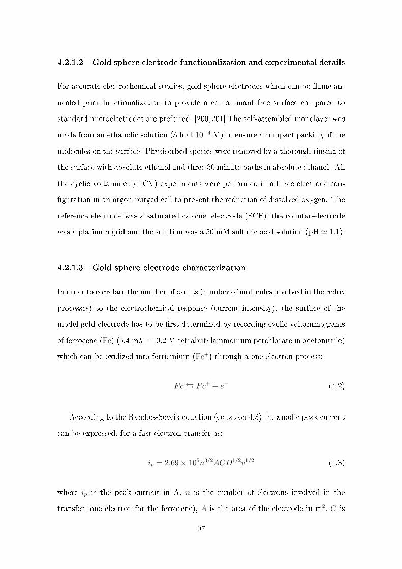
4.2.1.2 Gold sphere electrode functionalization and experimental details
For accurate electrochemical studies, gold sphere electrodes which can be ame an-
nealed prior functionalization to provide a contaminant free surface compared to
standard microelectrodes are preferred. [200,201] The self-assembled monolayer was
made from an ethanolic solution (3 h at 10−4 M) to ensure a compact packing of the
molecules on the surface. Physisorbed species were removed by a thorough rinsing of
the surface with absolute ethanol and three 30 minute baths in absolute ethanol. All
the cyclic voltammetry (CV) experiments were performed in a three electrode con-
guration in an argon-purged cell to prevent the reduction of dissolved oxygen. The
reference electrode was a saturated calomel electrode (SCE), the counter-electrode
was a platinum grid and the solution was a 50 mM sulfuric acid solution (pH ' 1.1).
4.2.1.3 Gold sphere electrode characterization
In order to correlate the number of events (number of molecules involved in the redox
processes) to the electrochemical response (current intensity), the surface of the
model gold electrode has to be rst determined by recording cyclic voltammograms
of ferrocene (Fc) (5.4 mM + 0.2 M tetrabutylammonium perchlorate in acetonitrile)
which can be oxidized into ferricinium (Fc+) through a one-electron process:
Fc Fc+ + e− (4.2)
According to the Randles-Sevcik equation (equation 4.3) the anodic peak current
can be expressed, for a fast electron transfer as:
ip = 2.69× 10⁵n3/2ACD1/2v1/2 (4.3)
where ip is the peak current in A, n is the number of electrons involved in the
transfer (one electron for the ferrocene), A is the area of the electrode in m2, C is
97

the concentration in ferrocene in mol m−3, D is the diusion coecient in m2 s−1
(2.43×10⁻⁹ m2 s−1 for the ferrocene under these conditions [202]) and v is the sweep
rate in V s−1. [1] Figure 4.2 shows the linear relationship between the anodic peak
current (ipa) and the square root of the sweep rate. A linear regression provides an
area of 0.87 mm2
Figure 4.2 Anodic peak current as a function of the square root of the sweep rate () andlinear regression (red line) (slope= 2.76× 10⁻⁵ A V−1/2 s1/2).
4.2.1.4 Irreversible reduction of 4-NTP
A rst CV experiment was performed to fully reduce the 4-NTP SAM into 4-ATP.
The potential was swept from +450 mV to −550 mV vs SCE over two cycles: a
broad irreversible cathodic peak appeared during the rst cycle at −265 mV and
disappeared at the second cycle (see Figure 4.3). Assuming a six electron and
proton exchange (reduction of the nitro group into aniline) the surface coverage
could be estimated by the charge integration of the irreversible peak between −90
and −475 mV:
ΓNTP =Q
nFA=
∫ −90−475
if (E)
v.dE
nFA(4.4)
where Q is the charge of the irreversible peak at −265 mV obtained after baseline
subtraction, n is the number of electrons involved in the reduction (6), F is the
Faraday constant, A is the area of the electrode and if is the faradaic current. We
98

found a coverage of 7.73×10⁻⁶ mol m−2. This value is slightly higher but consistent
with values reported in the literature under such conditions. [193,203]
Figure 4.3 Cyclic voltammetry response of a 4-NTP functionalized gold sphere electrode ina 50 mM H2SO4 solution (scan rate: 100 mV s−1); irreversible reduction into 4-ATP involving 6electrons and 6 protons during the rst cycle (black line) with a −550 mV vs SCE vertex potential.
4.2.1.5 Electrochemical characterization of 4-ATP
To conrm the formation of 4-ATP at the electrode, the reduced SAM was oxidized
under the same conditions: a functionalized electrode was reduced by two successive
CVs from +400 to −800 mV vs SCE. The potential range was then increased to ox-
idize the SAM within the −500 to +1000 mV vs SCE range: the CV is comparable
to the ones observed in previous studies by other groups. [204,205] During the rst
cycle an oxidation irreversible peak (A) appears at +730 mV vs SCE followed by
two peaks at +443 (B) and +197 mV vs SCE (C) in the second cyle (Figure 4.4).
During the second scan, the irreversible peak (A) disappears while a new reversible
peak appears centered at +478 mV vs SCE (peak B) and the irreversible reduction
peak at +197 mV vs SCE (peak C) disappears. These peaks have been attributed
to: (A), the formation of the 4-ATP radical cation followed by a dimerization to-
wards 4,4'-thiophenylquinone diimine (4-TPQDI) involving the breaking of one C-S
99
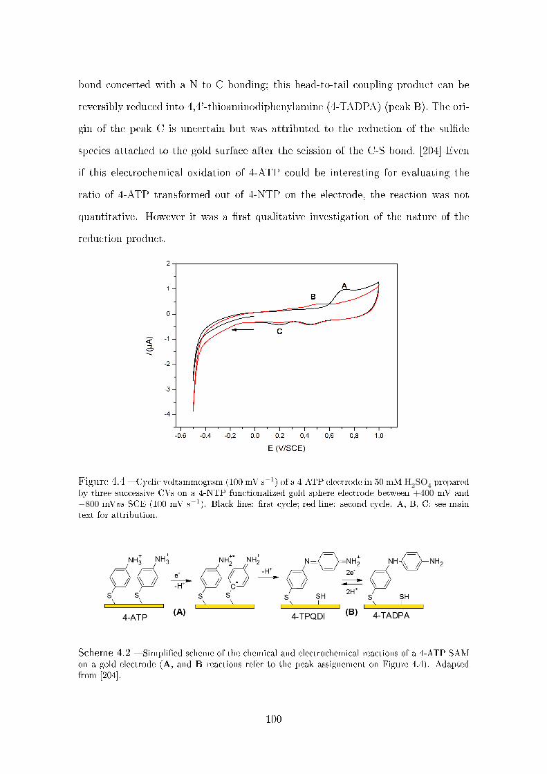
bond concerted with a N to C bonding; this head-to-tail coupling product can be
reversibly reduced into 4,4'-thioaminodiphenylamine (4-TADPA) (peak B). The ori-
gin of the peak C is uncertain but was attributed to the reduction of the sulde
species attached to the gold surface after the scission of the C-S bond. [204] Even
if this electrochemical oxidation of 4-ATP could be interesting for evaluating the
ratio of 4-ATP transformed out of 4-NTP on the electrode, the reaction was not
quantitative. However it was a rst qualitative investigation of the nature of the
reduction product.
Figure 4.4 Cyclic voltammogram (100 mV s−1) of a 4-ATP electrode in 50 mM H2SO4 preparedby three successive CVs on a 4-NTP functionalized gold sphere electrode between +400 mV and−800 mVvs SCE (100 mV s−1). Black line: rst cycle; red line: second cycle. A, B, C: see maintext for attribution.
Scheme 4.2 Simplied scheme of the chemical and electrochemical reactions of a 4-ATP SAMon a gold electrode (A, and B reactions refer to the peak assignement on Figure 4.4). Adaptedfrom [204].
100
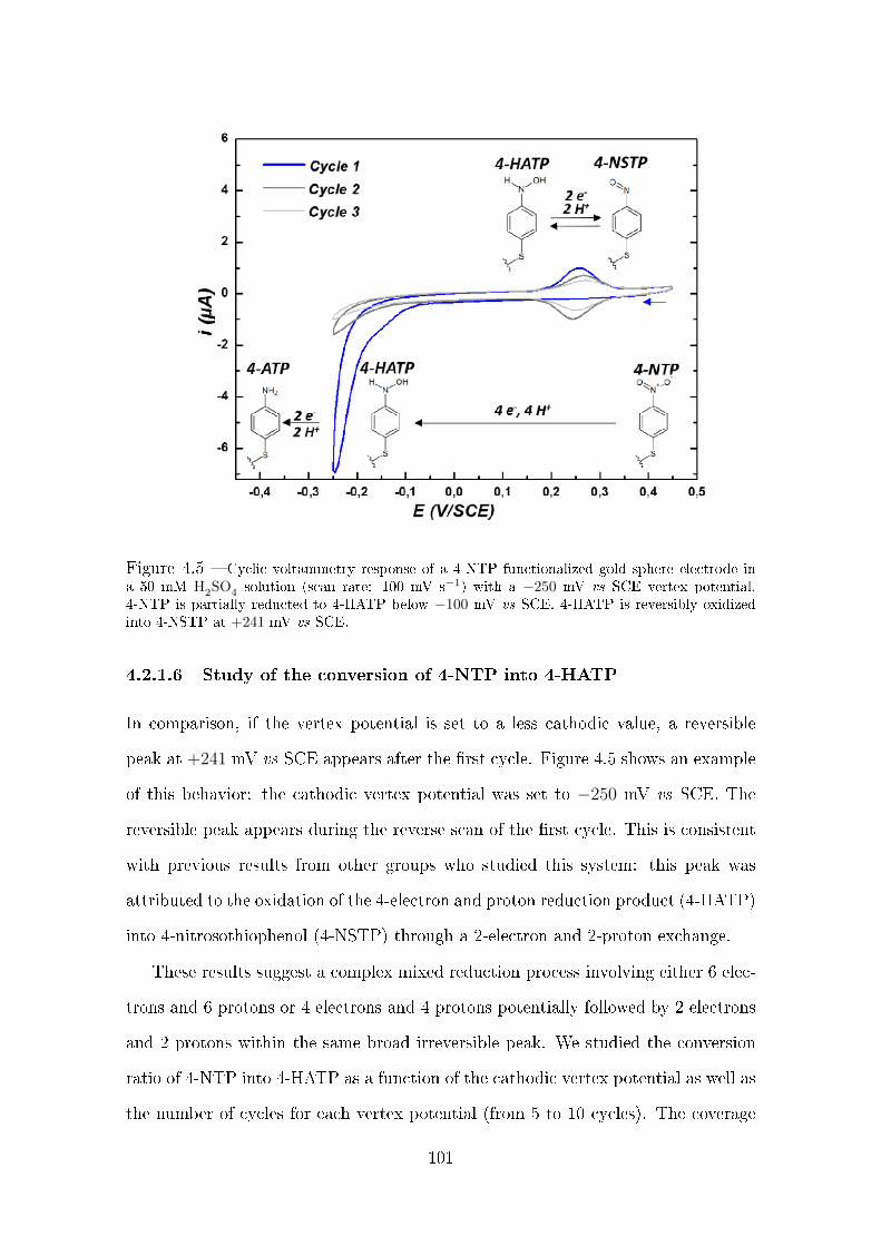
Figure 4.5 Cyclic voltammetry response of a 4-NTP functionalized gold sphere electrode ina 50 mM H2SO4 solution (scan rate: 100 mV s−1) with a −250 mV vs SCE vertex potential.4-NTP is partially reducted to 4-HATP below −100 mV vs SCE. 4-HATP is reversibly oxidizedinto 4-NSTP at +241 mV vs SCE.
4.2.1.6 Study of the conversion of 4-NTP into 4-HATP
In comparison, if the vertex potential is set to a less cathodic value, a reversible
peak at +241 mV vs SCE appears after the rst cycle. Figure 4.5 shows an example
of this behavior: the cathodic vertex potential was set to −250 mV vs SCE. The
reversible peak appears during the reverse scan of the rst cycle. This is consistent
with previous results from other groups who studied this system: this peak was
attributed to the oxidation of the 4-electron and proton reduction product (4-HATP)
into 4-nitrosothiophenol (4-NSTP) through a 2-electron and 2-proton exchange.
These results suggest a complex mixed reduction process involving either 6 elec-
trons and 6 protons or 4 electrons and 4 protons potentially followed by 2 electrons
and 2 protons within the same broad irreversible peak. We studied the conversion
ratio of 4-NTP into 4-HATP as a function of the cathodic vertex potential as well as
the number of cycles for each vertex potential (from 5 to 10 cycles). The coverage
101

(a) (b)
(c)
Figure 4.6 Three rst CV cycles of a gold sphere electrode functionalized with 4-NTP in50 mM H2SO4 (scan rate: 100 mV s−1) with various cathodic vertices. a)−150 mV vs SCE;b)−200 mV vs SCE; c)−300 mV vs SCE
was estimated by integrating the reversible peak at +241 mV vs SCE assuming a 2
electron and proton transfer and then the conversion ratio was calculated as:
ΓHATP
ΓNTP× 100 = 3× Q−265
Q+241× 100 (4.5)
where Qi is the charge associated to the peak centered on a specic potential value
i mV after baseline subtraction.
Within the rst CV and for a vertex potential of −150 mV vs SCE (Figure 4.6a),
the conversion takes place as the reversible peak appears and increases during the
four rst cycles until it reaches a plateau at around 10%. This indicates either
102

that only a fraction of the 4-NTP SAM can be reduced to 4-HATP without further
reduction to 4-ATP or that the competition between the 4 and 6 electron processes is
balanced. During the next CV series on a freshly functionalized electrode, the vertex
potential was set to −200 mV vs SCE (Figure 4.6b). The conversion ratio reaches
its maximum during the second CV at 23.5% and decreases afterwards indicating
that the 4-HATP or remaining 4-NTP are reduced to 4-ATP. The last two CV
series (−250 and −300 mV vertex potentials, Figure 4.5 and 4.6c) exhibit a similar
behavior: the maximum of conversion is reached during the rst cycle and decreases
abruptly. The higher conversion ratio (27.5%) was observed for the rst CV of the
series with a −250 mV vertex potential.
This series of data, summarized in Figure 4.7, led us to a rst set of conclusions
about this system: the reduction of 4-NTP under acidic conditions allows the forma-
tion of 4-ATP preferentially over 4-HATP. More than 72.5% of the 4-NTP SAM was
not converted into 4-HATP, the latter being reduced to 4-ATP since it is formed.
Figure 4.7 Calculated conversion ratio of 4-NTP to 4-HATP extracted from the charge of thereversible peak at +241 mV vs SCE on successive CVs with dierent vertex potentials (Evertex)presented in Figure 4.6 and Figure 4.5.
To further support this conclusion, the conversion ratio of 4-NTP into 4-HATP
103

Figure 4.8 Evolution of the +241 mV vs SCE reversible peak charge (Q: right vertical axis)and estimated 4-NTP to 4-HATP conversion ratio (left vertical axis) as function of time (s) duringa reduction sequence on the same gold sphere electrode in 50 mM H2SO4. Each data pointcorresponds to a 15 second chronoamperometry at dierent potentials (Echrono ranges from +50to −350 mV vs SCE); reference electrode: SCE.
was also evaluated after a chronoamperometric reduction sequence: this latter is
composed of successive 15 second chronoamperometric steps at more and more ca-
thodic potentials (Echrono ranging from +50 to −350 mV vs SCE). After each polar-
ization at Echrono a CV was recorded at 100 mV s−1 around the 4-HATP/4-NSTP
reversible peak. The peak at +241 mV was integrated and the conversion ratio was
calculated for each step. These data are reported in Figure 4.8. In this experiment
the highest conversion ratio was 5.8% and obtained after 5 steps at 50, 0, −50,
−100 mV followed by three steps (3×15 s) at −150 mV vs SCE. The low conversion
ratios are explained by the progressive transformation of 4-HATP or remaining 4-
NTP into 4-ATP at potentials as high as −50 mV vs SCE during long polarization
steps (15 s). The ratios are much lower than in CV experiments as the polarization
time scale is larger in the chronoamperometric experiments. These observations
support the conclusion drawn from CV experiments.
104

4.2.2 Spectroscopic characteristics of the system
The 4-NTP/4-ATP system shows intense and distinct Raman signatures as seen
on Figure 4.9: the 4-NTP spectrum exhibits a very strong band at 1335 cm−1
(attributed to the NO2 symmetric stretching) and one at 1570 cm−1 (attributed to
the C = C stretching mode of the aromatic ring). The 4-ATP can be characterized
by the absence of the 1335 cm−1 band and by a blue shift of the C-C stretching
mode up to 1588 cm−1.
The Raman spectra of ATP and NTP were acquired using rst microRaman
on powders of the two compounds (Figure 4.9) and then STM-TERS on SAMs
developed on a gold functionalized sample (from ethanolic solution of 4-ATP and
4-NTP). The Au-S bond formation is conrmed by the disappearance of the S-H
bond vibration at ca. 2700 cm−1.
Possible products from the reduction of 4-NTP such as 4-NSTP and 4-HATP are
expected to show particular bands such as a N = O stretching mode for the nitroso
compounds in the 1488-1523 cm−1 region or a band at 1230 cm−1 for 4-HATP. [206]
These vibrational modes could not be detected during our experiments. Moreover,
these products are not stable (oxidation or dimerization in air) and dicult to obtain
in the powder form for a microRaman measurement. We then used a compound
with a similar structure as 4-NSTP, N,N-dimethylnitrosoaniline, which is reported
to dimerize easily into azodioxides ((O−N) = (N−O) bond, see Annex A.1). The
dimerization was conrmed by three Raman bands in the 1300-1400 cm−1 region.
The characteristic Raman bands of the dierent systems are presented in table
Table 4.1 and in Figure 4.9 (Raman spectra of the powders of 4-ATP and 4-NTP).
105

(a)
(b)
Figure 4.9 Raman spectra of a) 4-NTP, b) 4-ATP (powders, 632.8 nm)
4.3 Spectroelectrochemical analysis of 4-NTP re-
duction reaction
4.3.1 Electrochemical reduction of 4-NTP monitored by ex
situ TERS
To get a deeper understanding of the reduction process of the 4-NTP, ex situ TERS
measurements were performed on a 4-NTP monolayer self-assembled onto a large
gold-coated electrode. In order to ensure that the functionalization is homoge-
neous, a TERS map was realized prior to its polarization. Figure 4.10a shows a
300× 300 nm2 STM-TERS map on a freshly derivatized electrode. The STM map
(Figures 4.10b and 4.10c) reveals the typical structure of a ame-annealed gold lm
106
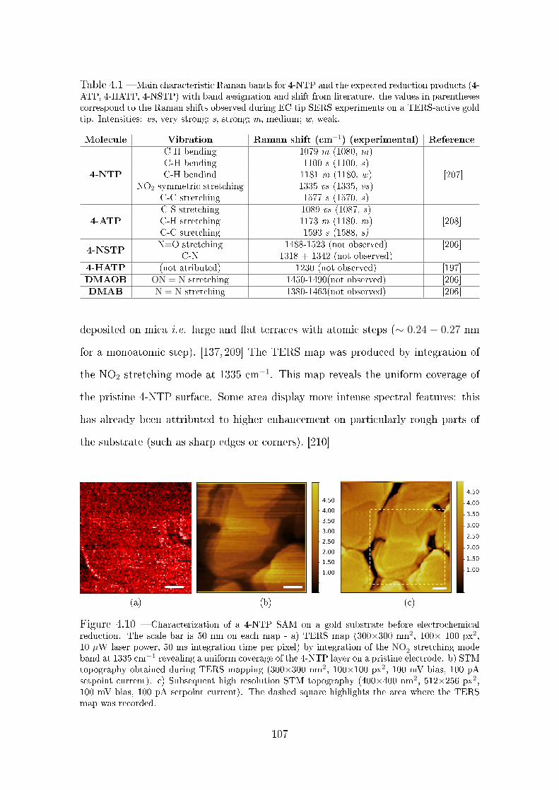
Table 4.1 Main characteristic Raman bands for 4-NTP and the expected reduction products (4-ATP, 4-HATP, 4-NSTP) with band assignation and shift from literature. the values in parenthesescorrespond to the Raman shifts observed during EC tip SERS experiments on a TERS-active goldtip. Intensities: vs, very strong; s, strong; m, medium; w, weak.
Molecule Vibration Raman shift (cm−1) (experimental) Reference
4-NTP
C-H bending 1079 m (1080, m)C-H bending 1100 s (1100, s)C-H bendind 1181 m (1180, w) [207]
NO2 symmetric stretching 1335 vs (1335, vs)C-C stretching 1577 s (1570, s)
4-ATPC-S stretching 1089 vs (1087, s)C-H stretching 1173 m (1180, m) [208]C-C stretching 1593 s (1588, s)
4-NSTPN=O stretching 1488-1523 (not observed) [206]
C-N 1318 + 1342 (not observed)4-HATP (not atributed) 1230 (not observed) [197]DMAOB ON = N stretching 1450-1490(not observed) [206]DMAB N = N stretching 1380-1463(not observed) [206]
deposited on mica i.e. large and at terraces with atomic steps (∼ 0.24 − 0.27 nm
for a monoatomic step). [137, 209] The TERS map was produced by integration of
the NO2 stretching mode at 1335 cm−1. This map reveals the uniform coverage of
the pristine 4-NTP surface. Some area display more intense spectral features: this
has already been attributed to higher enhancement on particularly rough parts of
the substrate (such as sharp edges or corners). [210]
(a) (b) (c)
Figure 4.10 Characterization of a 4-NTP SAM on a gold substrate before electrochemicalreduction. The scale bar is 50 nm on each map - a) TERS map (300×300 nm2, 100× 100 px2,10 µW laser power, 50 ms integration time per pixel) by integration of the NO2 stretching modeband at 1335 cm−1 revealing a uniform coverage of the 4-NTP layer on a pristine electrode. b) STMtopography obtained during TERS mapping (300×300 nm2, 100×100 px2, 100 mV bias, 100 pAsetpoint current). c) Subsequent high resolution STM topography (400×400 nm2, 512×256 px2,100 mV bias, 100 pA setpoint current). The dashed square highlights the area where the TERSmap was recorded.
107

A 4-NTP SAM was then electrochemically reduced by chronoamperometry at
-300 mV vs SCE in a 50 mM H2SO4 solution during 30 s. According to the previous
CV and chronoamperometric results, considering this polarization time at this po-
tential, the whole layer should be fully reduced into 4-ATP. A seen on Figure 4.11,
a 300×300 nm2 TERS map (integration of the 1080 cm−1 and 1588 cm−1 bands)
exhibits a rather homogeneous distribution of the 4-ATP spectrum. Concomitantly,
the NO2 stretching band at 1335 cm−1 has completely disappeared as expected.
(a) (b)
(c)
Figure 4.11 Characterization of the 4-NTP functionalized gold electrode after a uniformelectrochemical reduction. a) STM topography obtained during TERS mapping (300×300 nm2,100×100 px2, 100 mV bias, 500 pA setpoint current); b) TERS map (300×300 nm2, 100× 100 px2,250 µW laser power, 50 ms integration time per pixel) by integration of the band at 1590 cm−1
revealing a uniform coverage of the 4-ATP. c) Point spectra associated to points on the TERS map(b).
On a second sample polarized this time at −300 mV vs SCE during 5 min in
108
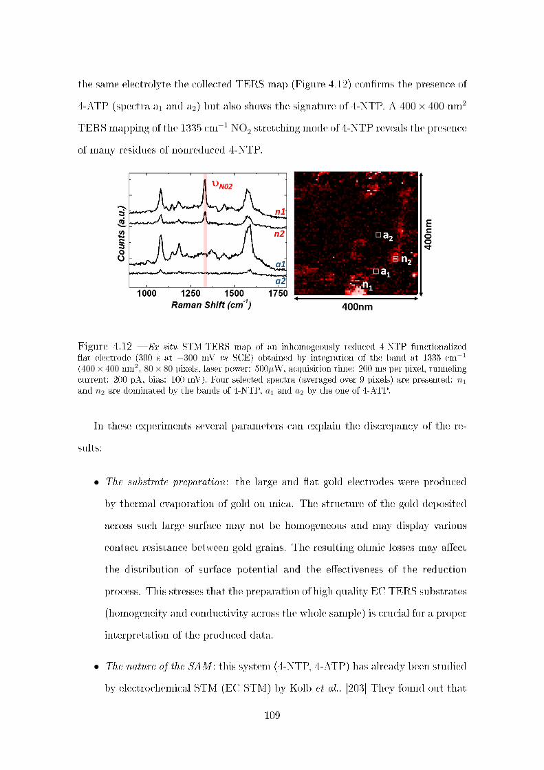
the same electrolyte the collected TERS map (Figure 4.12) conrms the presence of
4-ATP (spectra a1 and a2) but also shows the signature of 4-NTP. A 400× 400 nm2
TERS mapping of the 1335 cm−1 NO2 stretching mode of 4-NTP reveals the presence
of many residues of nonreduced 4-NTP.
Figure 4.12 Ex situ STM-TERS map of an inhomogeously reduced 4-NTP functionalizedat electrode (300 s at −300 mV vs SCE) obtained by integration of the band at 1335 cm−1
(400× 400 nm2, 80× 80 pixels, laser power: 500µW, acquisition time: 200 ms per pixel, tunnelingcurrent: 200 pA, bias: 100 mV). Four selected spectra (averaged over 9 pixels) are presented: n1and n2 are dominated by the bands of 4-NTP, a1 and a2 by the one of 4-ATP.
In these experiments several parameters can explain the discrepancy of the re-
sults:
• The substrate preparation: the large and at gold electrodes were produced
by thermal evaporation of gold on mica. The structure of the gold deposited
across such large surface may not be homogeneous and may display various
contact resistance between gold grains. The resulting ohmic losses may aect
the distribution of surface potential and the eectiveness of the reduction
process. This stresses that the preparation of high quality EC TERS substrates
(homogeneity and conductivity across the whole sample) is crucial for a proper
interpretation of the produced data.
• The nature of the SAM : this system (4-NTP, 4-ATP) has already been studied
by electrochemical STM (EC STM) by Kolb et al.. [203] They found out that
109

only 50 % of the 4-NTP SAM organizes in ordered domains on Au(111). When
the potential is set below the reduction potential (20 mV vs SCE in 50 mM
H2SO4) the formation of disorganized islands could be observed over 40 % of
the surface. These authors could however not conclude on the nature of these
disorganized islands (no correlation with the 4-HATP formation quantied by
the reversible peak at 250 mV vs SCE in a 50 mM H2SO4 solution); an EC
STM study after reductive desorption of the SAM in a Na2SO4 solution also
revealed the formation of small gold triangular islands (4-5 % of the surface)
all over the sample. These observations revealed two important characteristics
of this reduction reaction: rst, it seems to be very dependent on the chemical
nano-environment of the molecule (formation of disorganized islands) and then
the reaction seems to directly impact the structure of the underlying gold
(appearance of the gold islands).
4.3.2 Electrochemical reduction of 4-NTP monitored by in
situ EC tip SERS
4.3.2.1 Description of the setup and experimental conditions
To circumvent the above-mentionned diculties associated to EC TERS on large
at electrodes, we designed a TERS-inspired platform for in situ Raman analysis by
functionalizing and partially insulating a TERS-active gold tip to be used a micro-
electrode. In this conguration the TERS tip acts as a single hot spot SERS platform
of which the potential can be modulated. The setup, described in Scheme 4.3, is
based on an upright conguration with top illumination and collection including a
40X water immersion objective with high numerical aperture (NA = 0.8) mounted
on a XYZ piezoelectric stage.
The use of an immersion objective has already been reported for EC SERS
[211, 212] or EC microRaman [213, 214] as it prevents losses and distortion of the
110

Scheme 4.3 Scheme of the electrochemical tip SERS setup including a three-electrode cell:a TERS active gold working microelectrode (WE) functionalized by 4-NTP, a platinum counterelectrode (CE), a silver wire pseudo-reference electrode (RE), and a 40X immersion objective withhigh numerical aperture (0.8), all immersed in a 50 mM H2SO4 solution.
optical path at the air/liquid (or air and glass or quartz if a window is used to close
the electrochemical cell) interface (mainly due to the refractive index mismatch:
ca. 1.33 for the electrolyte and 1.00 for air). Moreover the long working distance
(3.3 mm) of the 40X immersion objective allows a gold TERS tip mounted on a
side holder to reach the focal point with an angle between 10 and 30. In this
setup, we use a three-electrode conguration where the tip stands as the working
electrode (WE), a platinum wire as counter electrode (CE) and a silver wire as
pseudo-reference electrode (RE). The potential of the silver wire was measured to
be +208 ± 20 mV vs SCE in 50 mM H2SO4. All the potential values reported in
this chapter will be shifted by this value and given relative to the SCE in order
to facilitate the comparison with values from the literature. The TERS tip was
partially insulated with polyethylene wax to reduce the size of the electroactive
area. In this conguration, ohmic losses and the RC charging time constant of the
electrode are minimized.
111

4.3.2.2 Ex situ tip SERS
In order to reveal the signal enhancement capabilities of the produced tips, an XY
objective mapping was rst implemented in the air on a non-insulated gold TERS
tip (rc: 35 nm; θt: 55 tapper angle) functionalized with 4-NTP through a high
magnication, high NA and long working distance objective (Mitutoyo; 100X; N.A.=
0.7; 6 mm working distance) in a side illumination and collection conguration
(Figure 4.13).
Figure 4.13 SEM micrographs at dierent magnications of a TERS-active gold tip obtainedfrom electrochemical etching of gold wires, used for ex situ tip TERS and revealing the typicaltapered prole whith the following characteristics: rc = 35 nm and θt = 55.
The tip apex was imaged by XY scanning of the microscope objective: the hot
spot position is revealed by integration of the 1335 cm−1 Raman band (between
1325 and 1345 cm−1) and by classical least square (CLS) analysis of the spectra on
the 1.6 × 1.5 µm2 XY map (Figure 4.10c). Its width can be estimated to 500 nm
(Figure 4.10b). The position of this hot spot at the apex and the shape of the tip
can also be revealed by integration of the entire spectrum (gold luminescence and
TER spectra of 4-NTP, see Figure 4.10c). Furthermore, the SER origin of the signal
at the tip was also evidenced by illuminating the tip apex with a green (532 nm)
laser, i.e. out of the surface plasmon resonance for a gold tip, at a similar power
(218 µW at 532 nm and 250 µW at 632.8 nm): only a very weak signal (compared
to the 632.8 nm excitation) of the 4-NTP could be extracted since the conditions
for the plasmon resonance are not achieved with green illumination of the gold tip
112
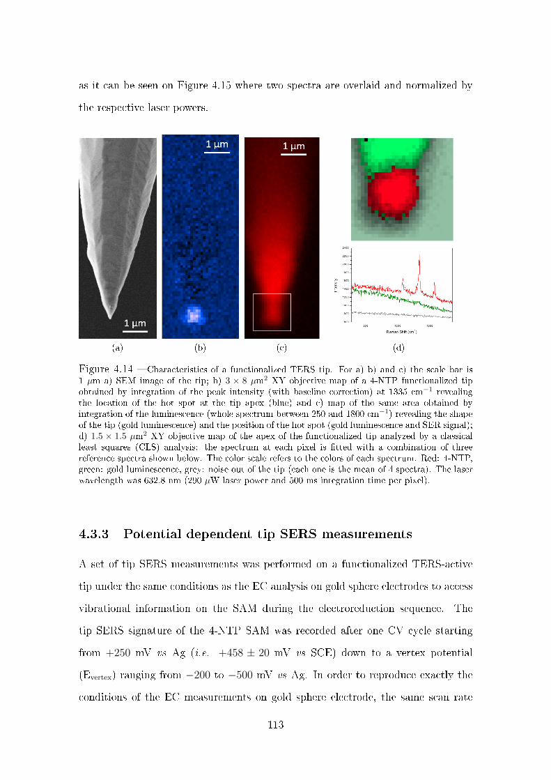
as it can be seen on Figure 4.15 where two spectra are overlaid and normalized by
the respective laser powers.
(a) (b) (c) (d)
Figure 4.14 Characteristics of a functionalized TERS tip. For a) b) and c) the scale bar is1 µm a) SEM image of the tip; b) 3 × 8 µm2 XY objective map of a 4-NTP functionalized tipobtained by integration of the peak intensity (with baseline correction) at 1335 cm−1 revealingthe location of the hot spot at the tip apex (blue) and c) map of the same area obtained byintegration of the luminescence (whole spectrum between 250 and 1800 cm−1) revealing the shapeof the tip (gold luminescence) and the position of the hot spot (gold luminescence and SER signal);d) 1.5 × 1.5 µm2 XY objective map of the apex of the functionalized tip analyzed by a classicalleast squares (CLS) analysis: the spectrum at each pixel is tted with a combination of threereference spectra shown below. The color scale refers to the colors of each spectrum. Red: 4-NTP,green: gold luminescence, grey: noise out of the tip (each one is the mean of 4 spectra). The laserwavelength was 632.8 nm (290 µW laser power and 500 ms integration time per pixel).
4.3.3 Potential dependent tip SERS measurements
A set of tip SERS measurements was performed on a functionalized TERS-active
tip under the same conditions as the EC analysis on gold sphere electrodes to access
vibrational information on the SAM during the electroreduction sequence. The
tip SERS signature of the 4-NTP SAM was recorded after one CV cycle starting
from +250 mV vs Ag (i.e. +458 ± 20 mV vs SCE) down to a vertex potential
(Evertex) ranging from −200 to −500 mV vs Ag. In order to reproduce exactly the
conditions of the EC measurements on gold sphere electrode, the same scan rate
113
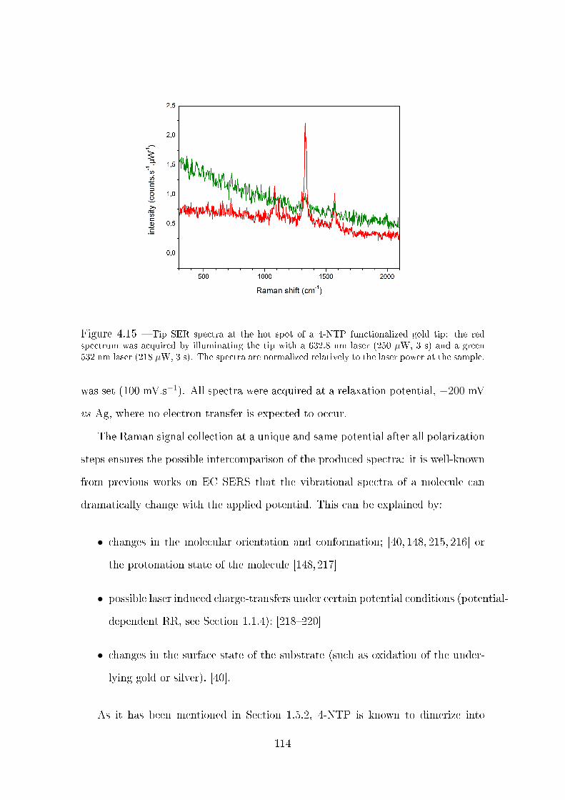
Figure 4.15 Tip SER spectra at the hot spot of a 4-NTP functionalized gold tip: the redspectrum was acquired by illuminating the tip with a 632.8 nm laser (250 µW, 3 s) and a green532 nm laser (218 µW, 3 s). The spectra are normalized relatively to the laser power at the sample.
was set (100 mV.s−1). All spectra were acquired at a relaxation potential, −200 mV
vs Ag, where no electron transfer is expected to occur.
The Raman signal collection at a unique and same potential after all polarization
steps ensures the possible intercomparison of the produced spectra: it is well-known
from previous works on EC SERS that the vibrational spectra of a molecule can
dramatically change with the applied potential. This can be explained by:
• changes in the molecular orientation and conformation; [40, 148, 215, 216] or
the protonation state of the molecule [148,217]
• possible laser induced charge-transfers under certain potential conditions (potential-
dependent RR, see Section 1.1.4); [218220]
• changes in the surface state of the substrate (such as oxidation of the under-
lying gold or silver). [40].
As it has been mentioned in Section 1.5.2, 4-NTP is known to dimerize into
114

Figure 4.16 Tip SER spectra of a 4-NTP monolayer acquired at −200 mV vs Ag(+8 mV vs SCE) after successive CVs ranging from +250 mV vs Ag to Evertex (50 mM H2SO4,scan rate: 100 mV s−1
DMAB upon intense laser illumination or by plasmon-induced reactions. Thus, to
prevent this dimerization, the laser power was set to a minimal value (100 µW).
In order to compare all the spectra acquired throughout the experiment, they
were normalized by the intensity of the 1078 cm−1 peak which is common to both
4-ATP and 4-NTP (Inormω = IωI1078
). To build diagrams of the evolution of the charac-
teristic vibration modes the area of the main bands (Ai) of the two main species were
compared to the area of the 1078 cm−1 band ( Ai
A1078). These diagrams are reported
in Figure 4.17 and discussed in the following.
The rst CV down to−200mV vs Ag exhibits only the vibration modes of 4-NTP
and was used as a reference spectrum for this molecule at this potential (Figure 4.16).
The next CV (no 2) down to −400 mV vs Ag and the associated spectrum did not
show signicant dierences with the 4-NTP spectrum except a slight decrease in
the ratio of the area of the major bands (1110, 1335 and 1570 cm−1) of 4-NTP.
115

(a) (b)
Figure 4.17 Evolution of the characteristic bands of 4-NTP (1110, 1335 and 1570 cm−1) andof 4-ATP (386, 628 and 1588 cm−1) depending on the cycle number (see Figure 4.16). The areasare normalized by the area of the band that is common to the two molecules (1080 cm−1), theseratios being then normalized.
However, no spectral features from 4-HATP, such as a band at 1230 cm−1, could
be observed whereas, according to the previous electrochemical study, this rst CV
must have generated around 22, 5% of 4-HATP. During the next cycles (3, 4 and
5), where the vertex potential was lowered to −450 mV vs Ag, the same general
behavior was observed for the 4-NTP bands: their intensity decreases, especially
the NO2 stretching mode indicating the disappearance of the nitro group. More-
over, characteristic bands from 4-ATP appear from the third CV (386, 628 cm−1,
not attributed, and the C-C stretching mode shifted from 1570 to 1588 cm−1) while
no band from the 4-HATP appears. After this measurement the potential was set
to +100 mV vs Ag, where the 4-HATP is oxidized to 4-NSTP and a spectrum was
acquired (Figure 4.18): we could not observe any new Raman bands but only a
change in the band intensities that could not be attributed to the nitroso com-
pound. The relative intensities of the bands attributed to 4-NTP are higher in the
spectrum acquired at +100 mV vs Ag than at −200 mV vs Ag. This highlights
the possible inuence of the potential on the Raman signal enhancement factor that
might dier from one molecule to another. A nal CV with a vertex potential set at
−500 mV vs Ag exhibits a spectrum characteristic of a 4-ATP SAM: all the bands
116

Figure 4.18 Comparison of the EC tip SER spectrum acquired at −200 mV vs Ag (spectrum 5extracted from Figure 4.16) with the spectrum acquired immediatly afterwards at +100 mV vs Ag.
attributed to 4-NTP disappeared. Figure 4.19 shows EC tip SERS obtained from
a pristine 4-ATP functionalized tip at the same potential in the same electrolyte:
the perfect resemblance conrms the complete reduction of the 4-NTP SAM into
4-ATP.
We noticed that no spectral signature of 4-HATP or 4-NSTP could be detected
throughout the experiment, even under the conditions of maximum conversion ob-
served in electrochemical measurements on gold sphere electrode (see Figure 4.7).
This could be explained by the low conversion ratio of 4-NTP into 4-HATP (27.5%
at maximum) and/or by a Raman cross section lower than 4-ATP and 4-NTP. Then,
a further analysis of the spectra revealed that the tip SER spectra (2-5) can be fairly
reproduced by a linear combination of the spectra of 4-ATP and 4-NTP as shown
in Figure 4.20 where the spectrum 5 is reproduced by:
I5 = 0.30I1 + 0.70I6 (4.6)
117

Figure 4.19 EC tip SER spectrum of a pristine 4-ATP functionalized electrode (E=−200 mV vs Ag, laser power = 10 µW, 30 s integration, 632.8 nm)
Figure 4.20 EC tip SERS spectra 1 (blue, 4-NTP), 6 (4-ATP), 5 from Figure 4.16 and thespectrum obtained by linear combinaison of 1 and 6 (70% 4-ATP + 30% 4-NTP) in black.
118

Even if this linear combinations cannot be quantitatively interpreted, it suggests
that 4-ATP is formed as early as the second cycle and also that the reduction of
4-NTP leads concomitantly to 4-HATP and 4-ATP. This was recently suggested by
Zhao et al. [221] in a study of p-NTP electroreduction at gold and silver electrodes
using density functional theory (DFT) calculations. They calculated that standard
reduction potentials decrease as p-HATP > p-NSTP > p-NTP, which means that
p-NTP is directly reduced to p-ATP since the electrode potential reaches the poten-
tial reduction of p-NTP, explaining then the broad reduction peak observed in CV
experiments. Kinetic considerations may explain the observations on the reversible
peak attributed to the 4-HATP/4-NSTP couple: the 4-NTP to 4-HATP reduction
must be faster than the 4-NTP to 4-ATP one. This kinetics issue can be highlighted
by the comparison of the chronoamperometry results with the one observed in CV
experiments on a gold sphere electrode: the maximum conversion ratio is observed
in the CV experiments i.e. in the experiment where the time scale is the smallest
(of the order of 1 s in CVs, 15 s in chronoamperometry).
4.4 Conclusion
In this chapter we demonstrated the capability of a functionalized TERS tip to
act as a powerful single hot spot SERS platform to probe in situ electrochemical
transformation of a 4-NTP monolayer assembled on a tapered gold microelectrode.
In this non-gap mode conguration the volume of the enhanced near-eld is larger
than in the gap mode so that SER signal arises from more molecules: tip SERS
averages signal from possibly dierent molecular environments and then prevents
signal uctuation. The use of an immersion objective allowed us to overcome air-
liquid interface issues such as reection, laser path distortion and to increase the
signal collection eciency (higher NA than air objectives). We could therefore use
minimal laser powers that prevented the photochemical degradation of the organic
119

layer (e.g. dimerization of the 4-NTP layer). The electrochemical 4-NTP reduction
into 4-ATP was studied both by classical CV experiments and EC tip SERS. The
Raman signature extracted during EC tip SERS measurements revealed that 4-
ATP is formed simultaneously to 4-HATP which has never been reported in any
electrochemical studies. Lowering the reduction potential makes the 6-electron and
6-proton transfer (4-ATP) to dominate over the 4-electron and 4-proton one (4-
HATP). However, even in the maximum conversion ratio conditions, neither the
4-HATP or 4-NSTP Raman signatures could be observed: this can be explained
both by a low Raman cross-section of these two molecules and/or by the somehow
low conversion ratio (27.5% maximum) determined from CV experiments. The EC
Tip SERS experiment which proved its eectiveness to solve the reduction process of
4-NTP is expected to be applied to the study of many redox processes for which the
mechanism of electron transfer is still unknown and also to complicated molecular
architectures as long as they can be immobilized on a gold or silver surfaces. The
hybrid tips developed herein, i.e. TERS ready UMEs, also pave the way to time-
resolved EC TERS experiments. [222]
120
Chapter 5
Electrochemical TERS imaging of
functionalized gold surfaces
5.1 Introduction
As it has already been mentionned in the previous chapters, implementation of
TERS imaging under electrochemical conditions is still a challenge as many technical
diculties remain to be overcome (for more details, see Section 1.6.3). Up to now,
TERS imaging has only been performed in organic liquids (see Chapter 3 and [223])
or more recently in water with a sub-30 nm lateral resolution. [152]
This chapter aims at describing an EC STM-TERS setup inspired by the devel-
opment of the one used for EC tip SERS and introduced in Chapter 4. The proposed
design couples then a conventional EC-STM cell (in a four-electrode conguration)
with the optical conguration used in EC tip SERS experiments, i.e. a top illumi-
nation and collection conguration with a water immersion objective for an optimal
illumination and collection eciency.
We will rst demonstrate the possibility to record eciently EC STM-TER spec-
tra. Then, preliminary results on EC TERS imaging will be presented. To the best
of our knowledge, this set of results is the rst demonstration of TERS imaging
121

under electrochemical conditions.
5.2 Description of the setup
Several important modications were introduced to the commercial (AIST-Horiba)
setup in order to run EC STM-TERS:
• both tip and sample potentials (working electrodes, WE1 and WE2) have to
be controlled and dened vs a reference electrode (RE), so that a 4-electrode
potentiostat also including a counter electrode (CE) should be implemented;
• the cell design used for the EC Tip-SERS method developed in this work
(see Chapter 4) needs to be revised to allow introduction of the sample to be
imaged;
• electrical insulation of the tip should be improved to minimize leakage currents
vs tunnelling current (it).
5.2.1 Electronic implementation
Implementation of EC STM requires to introduce 4 electrodes into the cell. Indeed,
in addition to the traditional counter and reference electrodes (CE and RE) that
allow a precise control of the sample potential (WE2), the tip potential (WE1) needs
also to be accurately dened. Therefore, while in Chapter 4 we simply relied onto
a commercial potentiostat, a dedicated electronic setup was elaborated to run EC-
TERS experiments since it was not directly available onto the SMART-SPM system.
The challenge is here to maintain accurate potentials at the tip and sample (versus
the reference electrode) and a precise measure of the tip current with a noise level
below 30 pA because typical setpoint currents for STM imaging are in the 200-
1000 pA range. This may be performed currently by commercial or home-made
122
bipotentiostats but some specic adjustments need to be made for implementation
onto our system.
In a rst attempt, we thus tried to use only a home-made bipotentiostat made
by our electronic engineer Daniel Rose. However, while the potentials of the two
working electrodes (WE1 and WE2) could be accurately controlled, we noticed that
the electronic noise at the tip was far too important to allow regulation of the
feedback STM loop. This may be a consequence of a too long and unshielded
connection to the tip, or to the noise introduced via the signal access module that
was used to reinject the current into the STM feedback loop.
Consequently, we focused onto an intermediate solution where the current at the
tip was still measured by the SMART-SPM current amplier that shows a very low
noise level, the other electrodes being connected to the bipotentiostat. The setup is
described in Figure 5.1.
It is beyond the scope of this chapter to fully describe the operation of the
bipotentiostat, and we only underline below some important features:
• in the conguration we used, the tip potential (Vtip) is in fact at 0 V vs ground
(virtual ground of the current amplier);
• the bias voltage (BV = Vtip - Vsample) is applied thanks to two potentiometers
(tension dividers);
• an external tension, provided by an external generator (Agilent Technologies,
33521A, USA), can be added to both WE1 and WE2 channels (oset) to con-
duct cyclic voltammetry while maintaining a constant bias.
A large gold ring counter electrode and an Ag wire as reference electrode were
used. This conguration provided noise levels below 30 pA provided that the tip
was correctly insulated (see Section 5.2.3 below for details). The interested reader
may refer to Chapter 15 of [1] for a complete electronic scheme of a bipotentiostat.
123

(a)
(b)
Figure 5.1 EC STM setup: a) simplied scheme of the electronics required for EC STMmeasurements; b) picture of the coupling between the SPM (Omegascope, AIST) and a home-made bipotentiostat.
5.2.2 Cell design for EC STM-TERS measurements
The EC-cell, depicted in Figure 5.2 is composed of a at PEEK (Polyether Ether
Ketone) support onto which the sample (WE2) is immobilized. An O-ring is glued
(with an epoxy resin) to form the walls of the cell. A ring-shaped gold wire (CE),
attached to the PEEK support is placed into the cell as well as a silver wire (pseudo
RE). These three electrodes are connected to the bipotentiostat, the cell is mounted
on the STM piezostage and nally lled with ca. 1 mL of electrolyte.
When the tip is just a few millimetres away from the sample surface, the ob-
124
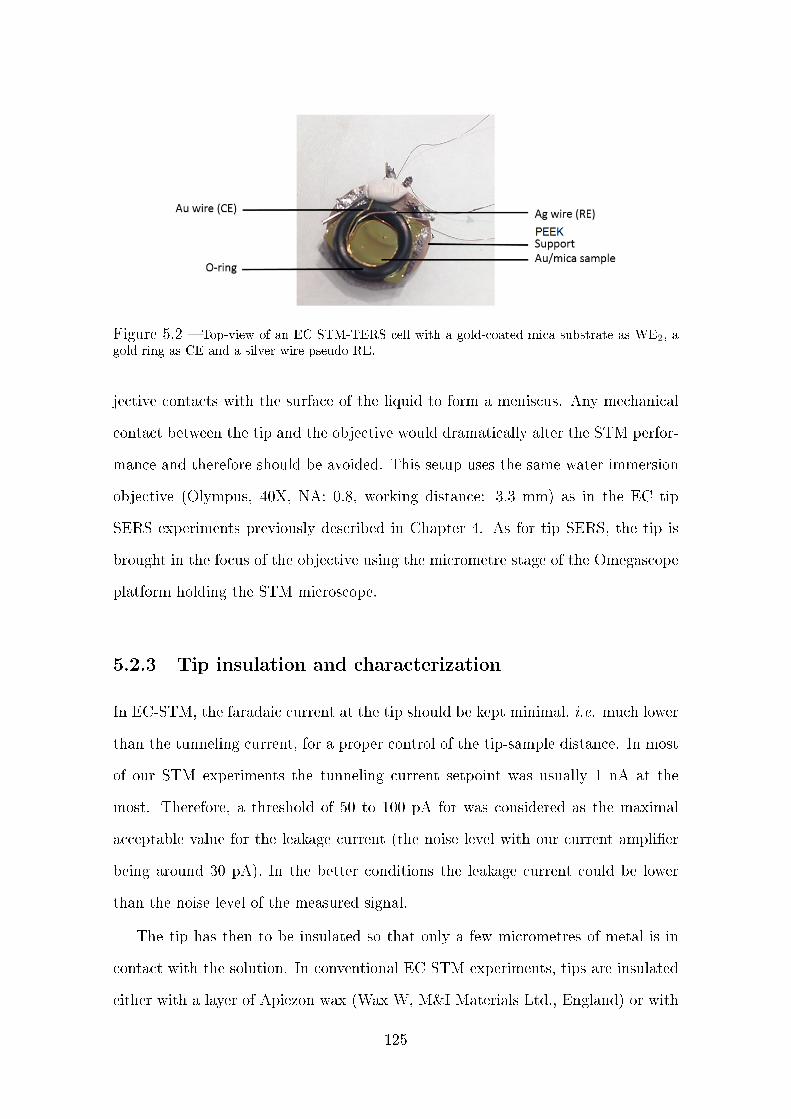
Figure 5.2 Top-view of an EC STM-TERS cell with a gold-coated mica substrate as WE2, agold ring as CE and a silver wire pseudo RE.
jective contacts with the surface of the liquid to form a meniscus. Any mechanical
contact between the tip and the objective would dramatically alter the STM perfor-
mance and therefore should be avoided. This setup uses the same water immersion
objective (Olympus, 40X, NA: 0.8, working distance: 3.3 mm) as in the EC tip
SERS experiments previously described in Chapter 4. As for tip SERS, the tip is
brought in the focus of the objective using the micrometre stage of the Omegascope
platform holding the STM microscope.
5.2.3 Tip insulation and characterization
In EC-STM, the faradaic current at the tip should be kept minimal, i.e. much lower
than the tunneling current, for a proper control of the tip-sample distance. In most
of our STM experiments the tunneling current setpoint was usually 1 nA at the
most. Therefore, a threshold of 50 to 100 pA for was considered as the maximal
acceptable value for the leakage current (the noise level with our current amplier
being around 30 pA). In the better conditions the leakage current could be lower
than the noise level of the measured signal.
The tip has then to be insulated so that only a few micrometres of metal is in
contact with the solution. In conventional EC STM experiments, tips are insulated
either with a layer of Apiezon wax (Wax W, M&I Materials Ltd., England) or with
125
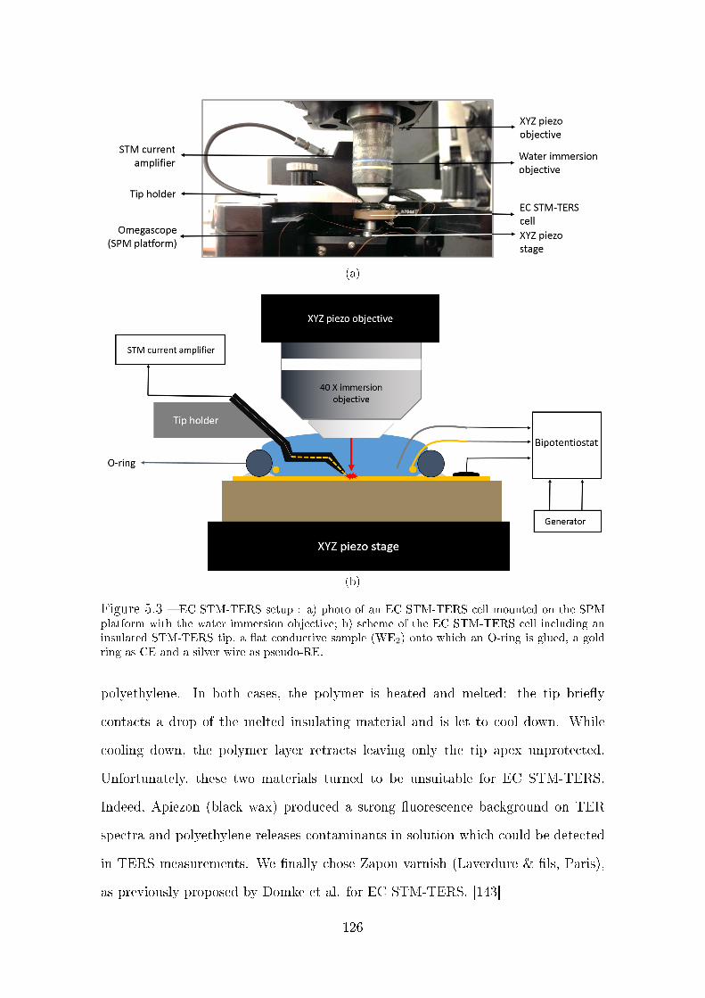
(a)
(b)
Figure 5.3 EC STM-TERS setup : a) photo of an EC STM-TERS cell mounted on the SPMplatform with the water immersion objective; b) scheme of the EC STM-TERS cell including aninsulated STM-TERS tip, a at conductive sample (WE2) onto which an O-ring is glued, a goldring as CE and a silver wire as pseudo-RE.
polyethylene. In both cases, the polymer is heated and melted: the tip briey
contacts a drop of the melted insulating material and is let to cool down. While
cooling down, the polymer layer retracts leaving only the tip apex unprotected.
Unfortunately, these two materials turned to be unsuitable for EC STM-TERS.
Indeed, Apiezon (black wax) produced a strong uorescence background on TER
spectra and polyethylene releases contaminants in solution which could be detected
in TERS measurements. We nally chose Zapon varnish (Laverdure & ls, Paris),
as previously proposed by Domke et al. for EC STM-TERS. [143]
126
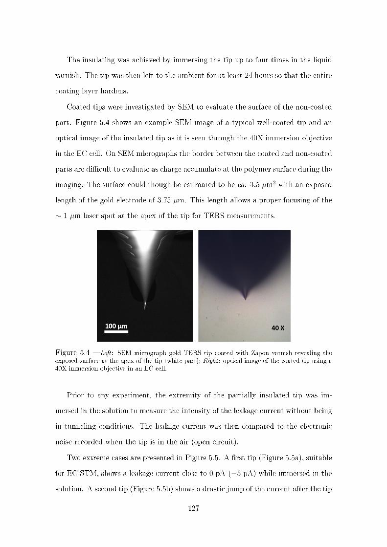
The insulating was achieved by immersing the tip up to four times in the liquid
varnish. The tip was then left to the ambient for at least 24 hours so that the entire
coating layer hardens.
Coated tips were investigated by SEM to evaluate the surface of the non-coated
part. Figure 5.4 shows an example SEM image of a typical well-coated tip and an
optical image of the insulated tip as it is seen through the 40X immersion objective
in the EC cell. On SEM micrographs the border between the coated and non-coated
parts are dicult to evaluate as charge accumulate at the polymer surface during the
imaging. The surface could though be estimated to be ca. 3.5 µm2 with an exposed
length of the gold electrode of 3.75 µm. This length allows a proper focusing of the
∼ 1 µm laser spot at the apex of the tip for TERS measurements.
Figure 5.4 Left : SEM micrograph gold TERS tip coated with Zapon varnish revealing theexposed surface at the apex of the tip (white part); Right : optical image of the coated tip using a40X immersion objective in an EC cell.
Prior to any experiment, the extremity of the partially insulated tip was im-
mersed in the solution to measure the intensity of the leakage current without being
in tunneling conditions. The leakage current was then compared to the electronic
noise recorded when the tip is in the air (open circuit).
Two extreme cases are presented in Figure 5.5. A rst tip (Figure 5.5a), suitable
for EC STM, shows a leakage current close to 0 pA (−5 pA) while immersed in the
solution. A second tip (Figure 5.5b) shows a drastic jump of the current after the tip
127
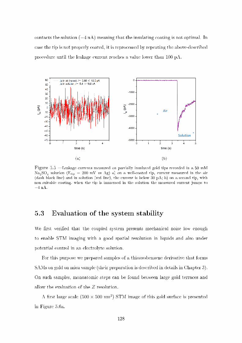
contacts the solution (−4 nA) meaning that the insulating coating is not optimal. In
case the tip is not properly coated, it is reprocessed by repeating the above-described
procedure until the leakage current reaches a value lower than 100 pA.
(a) (b)
Figure 5.5 Leakage currents measured on partially insulated gold tips recorded in a 50 mMNa2SO4 solution (Etip = 200 mV vs Ag) a) on a well-coated tip, current measured in the air(dash black line) and in solution (red line), the current is below 30 pA; b) on a second tip, withnon-suitable coating, when the tip is immersed in the solution the measured current jumps to−4 nA.
5.3 Evaluation of the system stability
We rst veried that the coupled system presents mechanical noise low enough
to enable STM imaging with a good spatial resolution in liquids and also under
potential control in an electrolyte solution.
For this purpose we prepared samples of a thioazobenzene derivative that forms
SAMs on gold on mica sample (their preparation is described in details in Chapter 3).
On such samples, monoatomic steps can be found between large gold terraces and
allow the evaluation of the Z resolution.
A rst large scale (500× 500 nm2) STM image of this gold surface is presented
in Figure 5.6a.
128

(a) (b)
Figure 5.6 EC STM imaging (500×500 nm2) of a gold surface functionalized with thioazoben-zene in a 50 mM Na2SO4 solution; Esample = 0 V vs Ag, BV = 200mV, it = 400 pA, scan rate:1 Hz per line; a) STM image b) height prole along the white line.
This EC STM image exhibits the typical characteristics of such surfaces with
monoatomic steps of 0.3 nm on Au(111) surfaces as revealed by the height prole
(Figure 5.6b).
A second image performed on a smaller area (200 × 200 nm2, depicted in Fig-
ure 5.7) exhibits the characteristic gold vacancy islands ("pits"), with heights of one
or several gold atoms (∼ 0.3, 0.6 or 0.9 nm) created by the Au atom removal from
terraces to form thiolate-gold complexes upon sulfur species adsorption. [224, 225]
The width of these vacancies can be measured to be as low as 5 nm providing an
estimation of the minimal lateral resolution that can be achieved by our EC STM
setup.
These results are comparable to those obtained in the air on similar samples
and evidence the good mechanical stability of the STM/Raman coupled system in
liquid, prerequisite for EC STM-TERS experiments.
129

(a) (b)
Figure 5.7 EC STM imaging (200×200 nm2) of a gold surface functionalized with thioazoben-zene in a 50 mM Na2SO4 solution; Esample = 0 V vs Ag, BV = 200mV, it = 400 pA, scan rate:1 Hz per line; a) STM image b) height prole along the white line.
5.4 EC TERS imaging
5.4.1 Laser focusing on the tip
As previously mentioned, the EC STM-TERS experiments using a water immersion
objective can be carried out in the exact same way as in air because the liquid/air
interface is no longer a problem.
This can be evidenced by the ease to bring the tip in the focus of the objective
and at the position of the laser spot. A picture of the partially insulated tip as seen
through the 40X water immersion objective is presented in Figure 5.8a with the laser
pointed at the apex of the tip. The precise laser focusing is realized by scanning
the piezo objective scanner in the three directions XY Z. The map presented in
Figure 5.8b is built by integration of the triplet between 1380 and 1510 cm−1 of the
azobenzene derivative. The intensity of the Raman signal decreases to zero from the
hot spot within 1 µm as observed in the air, attesting of the quality of the coupling
and of the eciency of the enhancement at the tip (see spectra in Figure 5.8c and
Figure 3.4 for comparison). An averaged spectrum over 100 pixels provides a clear
130

far-eld (FF) Raman signature, composed of a single band at 982 cm−1 which can
be assigned to the symmetric stretching mode of the sulfate ions of the electrolyte
(Na2SO4). [226]
(a) (b)
(c) (d)
Figure 5.8 Hot spot imaging in EC TERS in 50 mM Na2SO4 solution; a) image of the tip incontact with the sample and when the laser is focused at the apex; b) 6×6 µm2XY objective maprevealing the position of the hot spot (1) obtained by integration of the triplet between 1380 and1510 cm−1 c) selected spectra from b) 1 at the exact hot spot position, 2: 1 µm away, 3: FF signal;d) FF signal obtained by averaging the spectra in the white rectangle in b). λexc = 632.8 nm, laserpower: 250 µW, acquisition time: 307 ms/px; Esample = 0 V vs Ag, BV = 200mV, it = 400 pA.
To reinforce the evidence that the measured signal was TERS and not SERS from
the gold substrate, the tip-sample distance was increased to 100 nm so that the laser
is still focused on the sample but the gap mode is no longer eective. The spectrum
with the sample retracted (grey line in Figure 5.9) exhibits only the Raman band of
the sulfate ion conrming that the enhancement is due to the presence of the tip.
131
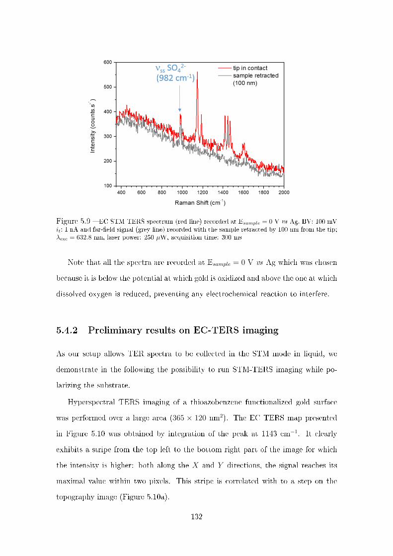
Figure 5.9 EC STM-TERS spectrum (red line) recorded at Esample = 0 V vs Ag, BV: 100 mVit: 1 nA and far-eld signal (grey line) recorded with the sample retracted by 100 nm from the tip;λexc = 632.8 nm, laser power: 250 µW, acquisition time: 300 ms
Note that all the spectra are recorded at Esample = 0 V vs Ag which was chosen
because it is below the potential at which gold is oxidized and above the one at which
dissolved oxygen is reduced, preventing any electrochemical reaction to interfere.
5.4.2 Preliminary results on EC-TERS imaging
As our setup allows TER spectra to be collected in the STM mode in liquid, we
demonstrate in the following the possibility to run STM-TERS imaging while po-
larizing the substrate.
Hyperspectral TERS imaging of a thioazobenzene functionalized gold surface
was performed over a large area (365 × 120 nm2). The EC TERS map presented
in Figure 5.10 was obtained by integration of the peak at 1143 cm−1. It clearly
exhibits a stripe from the top left to the bottom right part of the image for which
the intensity is higher: both along the X and Y directions, the signal reaches its
maximal value within two pixels. This stripe is correlated with to a step on the
topography image (Figure 5.10a).
132
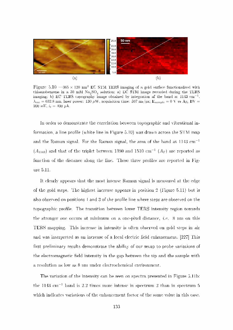
(a) (b)
Figure 5.10 365 × 120 nm2 EC STM TERS imaging of a gold surface functionalized withthioazobenzene in a 50 mM Na2SO4 solution; a) EC STM image recorded during the TERSimaging; b) EC TERS topography image obtained by integration af the band at 1143 cm−1.λexc = 632.8 nm, laser power: 130 µW, acquisition time: 507 ms/px; Esample = 0 V vs Ag, BV =200 mV, it = 400 pA.
In order to demonstrate the correlation between topographic and vibrational in-
formation, a line prole (white line in Figure 5.10) was drawn across the STM map
and the Raman signal. For the Raman signal, the area of the band at 1143 cm−1
(A1143) and that of the triplet between 1380 and 1510 cm−1 (AT ) are reported as
function of the distance along the line. These three proles are reported in Fig-
ure 5.11.
It clearly appears that the most intense Raman signal is measured at the edge
of the gold steps. The highest increase appears in position 2 (Figure 5.11) but is
also observed on positions 1 and 3 of the prole line where steps are observed on the
topographic prole. The transition between lower TERS intensity region towards
the stronger one occurs at minimum on a one-pixel distance, i.e. 8 nm on this
TERS mapping. This increase in intensity is often observed on gold steps in air
and was interpreted as an increase of a local electric eld enhancement. [227] This
rst preliminary results demonstrate the ability of our setup to probe variations of
the electromagnetic eld intensity in the gap between the tip and the sample with
a resolution as low as 8 nm under electrochemical environment.
The variation of the intensity can be seen on spectra presented in Figure 5.11b:
the 1143 cm−1 band is 2.2 times more intense in spectrum 2 than in spectrum 5
which indicates variations of the enhancement factor of the same value in this case.
133

(a)
(b)
Figure 5.11 EC TERS and STM prole along the white line in Figure 5.10. a) Integration ofthe band intensity at 1143 cm−1 (A1143) and of the triplet between 1380 and 1510 cm−1 (AT ) asfunction of the distance along the prole line compared to the STM topography (dashed line): b)selected EC TER spectra at dierent positions of the sample marked in Figure 5.11a.
The enhancement factors can be calculated to be at minimum 7.2 105 at point 2
and 3.3 105 at point 4 (see Section 1.4.2 for the calculation method).
As it had already been observed for the same molecule in liquid hexadecane
(see Chapter 3), the presence of the surrounding electrolyte or of the polarization
does not aect the energy of the vibration mode of this molecule since the observed
Raman bands are found to be at the exact same Raman shift as in air. Further
134
experiments have to be carried out to investigate the inuence of electrochemical
polarization on TERS mechanism, i.e. on the plasmonic properties of the tip under
such conditions.
5.5 Conclusion
In this chapter we described a new setup and conguration for EC TERS imaging
that overcomes the major drawbacks of previously reported experimental setups for
EC TERS. This was made possible through the use of an immersion objective that
prevents optical distortions and signal losses at the interface between air and liquid
(or glass and liquid).
This setup has demonstrated to be robust both for EC STM imaging of func-
tionalized surfaces (with lateral resolution better than 5 nm in STM imaging) and
for EC STM-TERS measurements in an electrochemical environment.
Finally we evidenced the ability of our coupled EC STM-TERS system to im-
age an electrochemical interface under potential control, which is to the best of our
knowledge the rst ever reported EC TERS image in an electrochemical environ-
ment. Moreover we could probe the local variations of the electric eld in the gap
between the TERS probe and the substrate with a lateral resolution as low as 8 nm.
We expect that this conguration will soon demonstrate EC TERS lateral res-
olution down to the single nanometre as it has already been demonstrated in the
air. [88] For this purpose, non-homogeneous surfaces or nano-objects have to be
probed.
These preliminary results pave the road for TERS analysis of more complex
electrochemical interfaces and reactivity at the nanoscale under potential control.
135

136
Chapter 6
TERS characterization of surfaces
derivatized with diazonium salts
6.1 Introduction
Electrochemical grafting of diazonium is a simple and well-established method to
functionalize carbon, metal or semiconductor surfaces with organic lms. The
grafted organic layers are strongly attached to the surface via covalent bonding
which is rare in the eld of surface modication. [228]
Surface modications by such diazonium salts has shown to be a very ecient
mean of grafting covalently organic moieties onto an electrode. The initial studies
were carried out onto glassy carbon electrodes. [229, 230] But since the grafting
process relies on radicalar reactions, it was quickly extended to many other materials.
Highly Oriented Pyrolytic Graphite (HOPG) [231] is also reactive as well as metals
(Fe [232], Co, Ni, Cu, Zn, Pt, and Au [233]) and semiconductors. [234] Graphene
has also been reported to be functionalized in order to tune its electronic properties.
[235237]
Even if the mechanism of electrochemical reduction of diazonium salts is well-
known, the structure of the grafted layers is not always clear and can be dicult to
137
ascertain. TERS oers the possibility of nanoscale analysis of the chemical structure
of these layers but has never been used for the investigation of such functionalized
surfaces, to the best of our knowledge.
This chapter will expose preliminary results on the use of STM-TERS to inves-
tigate the structure of gold surfaces functionalized using diazonium salts.
6.2 Chemistry and electrochemistry of diazonium
salts
A diazonium compound is an aliphatic, aromatic or heterocyclic compound in which
a −N+2 group is attached to a carbon atom. In aromatic diazonium compounds (aryl
diazonium salts) the conjugation with the aromatic cycle makes aryl diazonium ions
much more stable than their aliphatic counterparts.
The reactivity of diazonium salts is known since the pioneer work of Pinson et al.
in 1992. [229] These authors modied a glassy carbon electrode to further immobilize
glucose oxidase. Upon reduction, N2 is released and the aryl radical may attack the
surface as shown on Figure 6.1. It was later demonstrated that electron transfer is
concerted with C− N bond rupture. [230]
The tight covalent binding of the aryl layers with the subsrates can be evidenced
by the strong resistance of these lms to aggressive treatments such as ultrasonica-
tion in a variety of solvents, heating of the substrate up to 700 K in UHV, [230] or
even polarization at high potential. [238] They can only be removed by mechanical
abrasion, i.e. electrode polishing or by AFM lithography. [239]
Due to its high reactivity, the aryl radical formed by electrochemical reduction
of the diazonium salt can attack the C-H bonds of the rst aryl-grafted layer via
an aromatic homolytic substitution. This reaction can lead to the formation of
polyarylene multilayers through the formation of new C-C bonds as depicted on the
top part of Figure 6.1. [228,240] Some other side reactions have been suggested such
138

Figure 6.1 Electrochemical reduction of an aryl diazonium (top) for the formation of mono-or multilayers and partial alternative path for the spontaneous grafting (bottom). R can be anychemical group; the dashed area can represent any electrode material.
as azo bonding (-N=N-) in multilayer lms as shown on Figure 6.1. [241]
Characterization of the layer structure and composition can be achieved by vari-
ous and complementary methods. As the reduction of diazonium salts is irreversible,
the electrochemical response of the electrode to be functionalized can be a rst in-
dication of the grafting process. If the grafting is performed using CV, a broad
irreversible peak due to the one-electron transfer can be observed at the rst cycle
and disappears during the subsequent cycles since the grafted layer blocks the sur-
face of the electrode. The blocking properties of the organic layer are usual proofs
of the eciency of the grafting. For example, on a functionalized electrode, re-
versible redox probes such as ferrocenemethanol, [242] ferrocene, dopamine [243] or
Fe(CN)4−6 can become irreversible or even not be detected. [244]
When the diazonium salt carries a redox-active chemical group, the electrochem-
ical signature of the functionalized electrode allows the direct quantication of the
grafted entities. For example, the reversible one-electron reduction of the nitro-
phenyl groups in the layer grafted from nitrobenzene diazonium has been used for
139

the determination of the surface coverage of the electrode. [230]
For structural characterisation SPMs have been used on electrochemically grafted
surfaces. STM has for example revealed the possibility to control the surface orga-
nization by precisely adjusting the grafting parameters (charge, concentration, po-
larization time and potential) by imaging at the molecular scale the self-organized
grafted layer of bromophenyl groups on Si surface modied by bromobenzenediazo-
nium reduction. [234] The formation of multilayers with important surface roughness
as well as inhomogeneities have been demonstrated by AFM. [245,246] Such multi-
layers are not conductive enough to be imaged by STM.
The presence of grafted layers can also be revealed by vibrational spectroscopies
such as Raman or Fourier Transform IR Reection Spectroscopy (FTIRRAS) through
the chemical identication of functional groups. FTIRRAS is very sensitive to vi-
brational modes perpendicular to the surface and is a tool of choice for determining
the orientation of surface-bounded molecules. [247, 248] Raman spectroscopy and
especially SERS could evidence the formation of an Au-C bond upon reaction of
diazonium salts with gold nanoparticles. [249] Grafting-induced defects in graphene
layers could also be observed by Raman after spontaneous grafting of nitrobenzene
diazonium. [250] X-ray photoelectron spectroscopy (XPS) is also a popular technique
for chemical characterization of organic layers as it generally allows a non-destructive
and quantitative analysis of chemical groups. [251]
As previously mentioned, diazonium salts can spontaneously react with surfaces
(see the bottom part of Figure 6.1). This has in particular been demonstrated
on non-noble metals such as iron that can provide the required electrons for the
reduction without potential control. [252] This spontaneous grafting has also been
demonstrated on other substrates such as Au, [249] or carbon. [252] Spontaneous
grafting may occur following a dierent mechanism than the one obtained under
polarization of the surface. XPS studies have for example revealed the existence of
Au-N bonds at the surface of spontaneously derivatized gold surfaces (bottom line
140

of Figure 6.1). [253]
All of these reports suggest varied structures for electrochemically and sponta-
neously grafted layers from diazonium salts. They strongly depend on the substrate
and on the experimental conditions.
One challenge in diazonium chemistry is to obtain well-dened monolayers. The
simplest structures are provided by diazonium salts that cannot form multilayers.
Among all the possible strategies employed for grafting only monolayers of aryl
groups on surfaces, the most common are the addition of radical scavengers to the
solution [254, 255] or the use of sterically hindered aryldiazonium derivatives (such
as bis-tert-butylbenzene diazonium). [256,257] The previously mentioned organized
self-assembly of bromophenyl groups on Si substrate is a rare example of organized
structures formed from diazonium precursors by electrochemical reduction. [234]
Another alternative, described in the following section, is to rely on a system for
which radicalar addition is prevented.
6.3 Electrochemical grafting of a monolayer of a di-
azonium salt
In this section we rst relied on compounds for which multilayer formation is impos-
sible. Indeed, a way for preventing multilayer formation is the use of aryl derivatives
without C-H bonds where the aromatic homolytic substitution usually takes place.
We describe in this section the results obtained with the penuorobenzenediazonium
salt (PFBD) presented in Figure 6.2.
As for the work described in Chapter 4, we rst conducted an electrochemical
study onto gold sphere electrodes and then onto at gold-coated mica substrates for
STM and STM-TERS analyses.
141
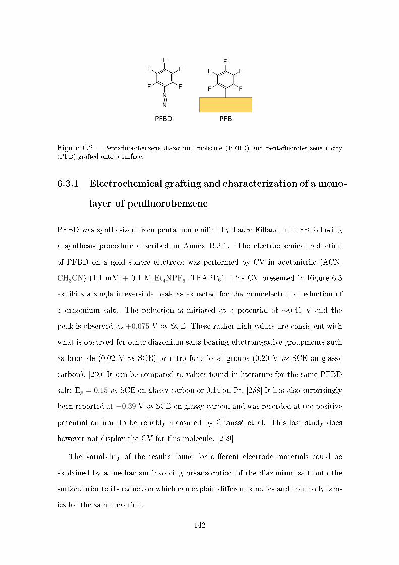
Figure 6.2 Pentauorobenzene diazonium molecule (PFBD) and pentauorobenzene moity(PFB) grafted onto a surface.
6.3.1 Electrochemical grafting and characterization of a mono-
layer of penuorobenzene
PFBD was synthesized from pentauoroaniline by Laure Fillaud in LISE following
a synthesis procedure described in Annex B.3.1. The electrochemical reduction
of PFBD on a gold sphere electrode was performed by CV in acetonitrile (ACN,
CH3CN) (1.1 mM + 0.1 M Et4NPF6, TEAPF6). The CV presented in Figure 6.3
exhibits a single irreversible peak as expected for the monoelectronic reduction of
a diazonium salt. The reduction is initiated at a potential of ∼0.41 V and the
peak is observed at +0.075 V vs SCE. These rather high values are consistent with
what is observed for other diazonium salts bearing electronegative groupments such
as bromide (0.02 V vs SCE) or nitro functional groups (0.20 V vs SCE on glassy
carbon). [230] It can be compared to values found in literature for the same PFBD
salt: Ep = 0.15 vs SCE on glassy carbon or 0.14 on Pt. [258] It has also surprisingly
been reported at −0.39 V vs SCE on glassy carbon and was recorded at too positive
potential on iron to be reliably measured by Chaussé et al. This last study does
however not display the CV for this molecule. [259]
The variability of the results found for dierent electrode materials could be
explained by a mechanism involving preadsorption of the diazonium salt onto the
surface prior to its reduction which can explain dierent kinetics and thermodynam-
ics for the same reaction.
142
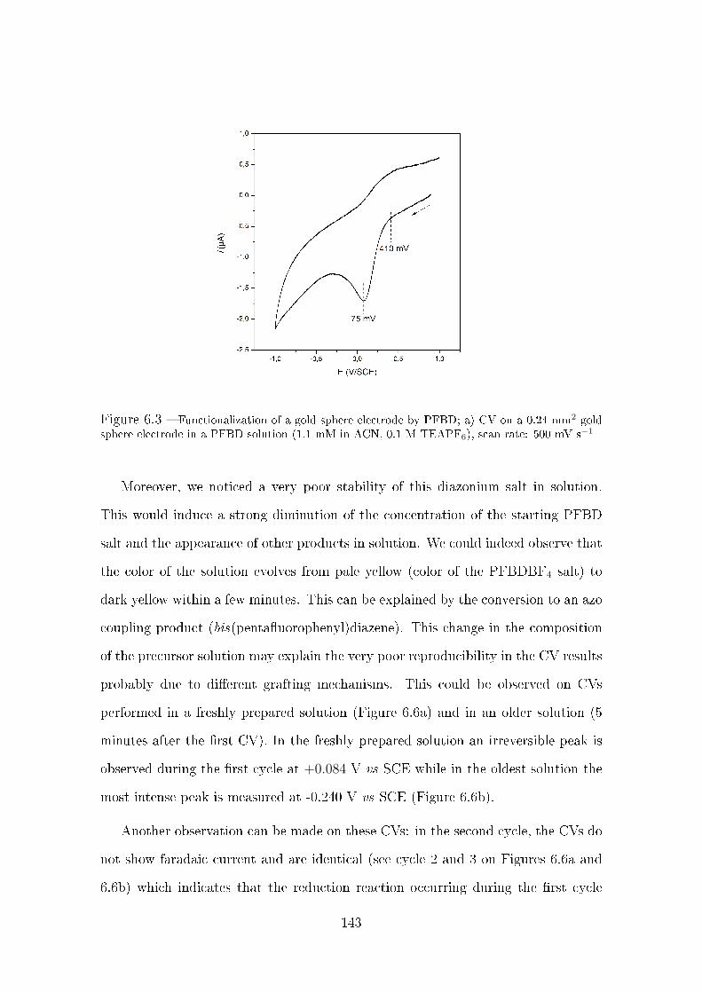
Figure 6.3 Functionalization of a gold sphere electrode by PFBD; a) CV on a 0.24 mm2 goldsphere electrode in a PFBD solution (1.1 mM in ACN, 0.1 M TEAPF6), scan rate: 500 mV s−1
Moreover, we noticed a very poor stability of this diazonium salt in solution.
This would induce a strong diminution of the concentration of the starting PFBD
salt and the appearance of other products in solution. We could indeed observe that
the color of the solution evolves from pale yellow (color of the PFBDBF4 salt) to
dark yellow within a few minutes. This can be explained by the conversion to an azo
coupling product (bis(pentauorophenyl)diazene). This change in the composition
of the precursor solution may explain the very poor reproducibility in the CV results
probably due to dierent grafting mechanisms. This could be observed on CVs
performed in a freshly prepared solution (Figure 6.6a) and in an older solution (5
minutes after the rst CV). In the freshly prepared solution an irreversible peak is
observed during the rst cycle at +0.084 V vs SCE while in the oldest solution the
most intense peak is measured at -0.240 V vs SCE (Figure 6.6b).
Another observation can be made on these CVs: in the second cycle, the CVs do
not show faradaic current and are identical (see cycle 2 and 3 on Figures 6.6a and
6.6b) which indicates that the reduction reaction occurring during the rst cycle
143

(a) (b)
Figure 6.4 Comparison of the the functionalization of a gold sphere electrode by PFBD (1.1 mMin ACN, 0.1 M TEAPF6) by CV ; a) in a freshly prepared solution, b) on the same ame-annealedelectrode, 5 minutes later. Scan rate: 100 mV s−1.
blocks the surface of the electrode for further reduction of PFBD. Finally, a small
irreversible peak at 0.70-0.71 V vs SCE is also observed: this peak cannot clearly be
attributed but could be due to the reduction of pre-adsorbed species as it has been
previously observed for other diazonium salts on gold. [260]
The charge associated with the irreversible peak in the CV presented in Figure 6.3
corresponds to a maximum coverage of ca. 2.8 · 10−9 mol cm−2 which is smaller but
consistent with what can be estimated from ref [258] (ca. 6 · 10−9 mol cm−2). These
values are however still higher than those determined from geometrical models (ca.
1 ·10−9 mol cm−2). The electrochemical properties of the layer were characterized by
comparing the CV of a ferrocene solution before and after the grafting (Figure 6.5):
the current does not signicantly decrease from one CV to the other which is consis-
tent whith a thin and non-blocking monolayer. Electron transfer from the ferrocene
to the metal is still ecient which is for example not the case in the well-known
blocking layers formed by polymerization of nitrobenzenediazonium. [245] It is then
suggested that the larger charge observed reects that only a fraction of the radical
144

produced by electrochemical reduction is grafted. The other radicals probably react
in solution.
Figure 6.5 CV of a gold sphere electrode in a Ferrocene solution (4.6 mM in ACN, 0.1 MTEAPF6) before (green line) and after (grey line) electrochemical grafting of PFBD presented inFigure 6.3; scan rate: 100 mV s−1.
6.3.2 STM imaging of PFBD-grafted gold surfaces
The covalent grafting of PFB moities onto gold was investigated by STM. The EC
reduction of PFBD (7 · 10−5 M in ACN, 0.1 M TEAPF6) was performed on a large
(∼ 0.7 cm2) at ame-annealed gold surface by CV (from 1 to -0.5 V vs SCE,
500 mV s−1).
The STM map is characteristic of a functionalized gold surface: a non homo-
geneous distribution of small pits with depths ranging from 0.5 to 1 nm appears
over the surface. This depth is consistent with the height of a benzene molecule.
Larger depletions observed in the structure are due to holes on gold terraces that are
usually observed on our ame-annealed Au(111) surfaces. This observation is con-
sistent with an organic layer formed from diazonium salts reduction that usually do
145
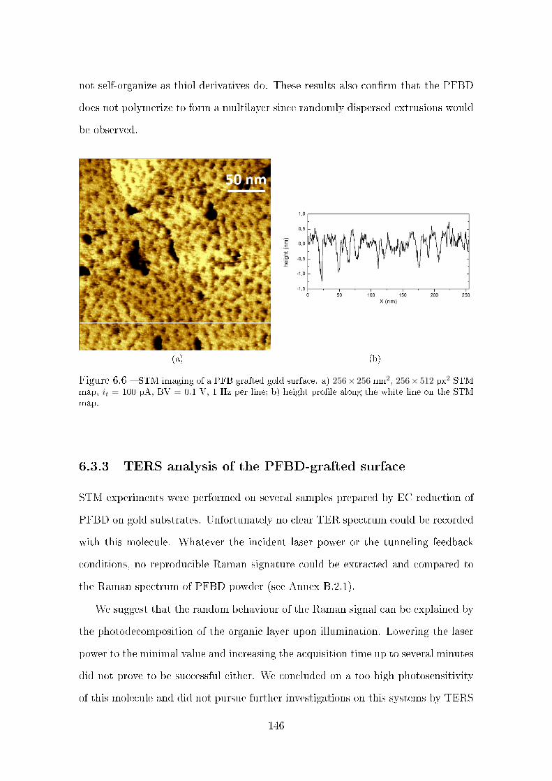
not self-organize as thiol derivatives do. These results also conrm that the PFBD
does not polymerize to form a multilayer since randomly dispersed extrusions would
be observed.
(a) (b)
Figure 6.6 STM imaging of a PFB grafted gold surface. a) 256× 256 nm2, 256× 512 px2 STMmap, it = 100 pA, BV = 0.1 V, 1 Hz per line; b) height prole along the white line on the STMmap.
6.3.3 TERS analysis of the PFBD-grafted surface
STM experiments were performed on several samples prepared by EC reduction of
PFBD on gold substrates. Unfortunately no clear TER spectrum could be recorded
with this molecule. Whatever the incident laser power or the tunneling feedback
conditions, no reproducible Raman signature could be extracted and compared to
the Raman spectrum of PFBD powder (see Annex B.2.1).
We suggest that the random behaviour of the Raman signal can be explained by
the photodecomposition of the organic layer upon illumination. Lowering the laser
power to the minimal value and increasing the acquisition time up to several minutes
did not prove to be successful either. We concluded on a too high photosensitivity
of this molecule and did not pursue further investigations on this systems by TERS
146

6.4 Electrochemical and TERS investigation of an
electroactive diazonium salt
Another diazonium salt was studied to investigate the structure of the grafted layer
onto a gold surface. We chose an electroactive diazonium salt composed of an
organometallic core: the bis(phenylterpyridyl)iron. This type of redox diazonium
salt has in fact already been used in molecular junctions for molecular electronics.
[261] As an example, in a recent work by Tefashe et. al., the eciency of a molecular
lm containing Ru(bipyridine)2+3 to act as an emitting diode was demonstrated. In
this study, a 7 nm thick layer was grafted and light emission was assigned to the
existence of change in the redox state of the organometallic compound. [262] The
properties of these molecular layers are strongly dependent on the mechanism of the
electron transfers in the layer. For this purpose electrochemical experiments can
provide a rich set of information which should be correlated with the structure of
the molecular layer produced by electrochemical reduction of the diazonium salt.
In this part we mainly focused on the structure of the molecular layer produced
from the reduction of a bis(phenylterpyridyl)iron diazonium derivative.
6.4.1 Electrochemical characterization of a gold electrode func-
tionalized by FeBTPD
The structure of bis(phenylterpyridyl)iron diazonium derivative used in this study
([Fe(4'-(phenyl)-2,2:6',2-terpyridine)(4-([-2,2':6',2-terpyridin]-4';- yl)benzenediazo-
nium)(PF−6 )2(BF−4 )]) is presented in Figure 6.7. It will be abbreviated FeBTPD
in the following. FeBTPD was synthetized from its aniline-derivatized parent com-
pound by Laure Fillaud at the LISE laboratory. Details about its synthesis and the
synthesis of other parent compounds used in this section can be found in Annex B.3.
The grafting of FeBTPD was performed on a gold sphere electrode in ACN
(10−5 M, 0.1 M TEAPF6) during one CV from 0.9 to −1 V vs SCE. Surprisingly the
147

Figure 6.7 Structure of FeBTPD
recorded CVs do not show any reduction peak that could be attributed to the one-
electron reduction of the diazonium. This may originate from the low concentration
of the initial solution due to the poor solubility of FeBTPD in ACN.
To attest the eectiveness of the functionalization, the electrochemical behaviour
of the electrode was tested in an electrolyte solution without any precursor (ACN
+0.1 M TEAPF6). A reversible peak centered at 1.13 V vs SCE could be observed
as shown on Figure 6.10. The scan rate was varied between 100 and 2000 V s−1:
a linear relationship between the peak current and the scan rate (Figure 6.8c) was
found up to 2000 V s−1, which is consistent with the presence of a redox system
immobilized onto the surface of the electrode. [1]
Below a scan rate of 100 V s−1 the faradaic current could not be distinguished
from the capacitive one because of a too important noise level. This peak is assigned
to the reversible Fe(III)/Fe(II) couple. Its integration can provide an estimation of
a surface coverage of 2 · 10−8 mol m−2 which is very low. It is ca. one order
of magnitude lower than what is expected for a densely packed monolayer of this
molecule. [263]1
The electrochemical signature of this layer can be compared to the one of the cor-
responding molecule with a thiol group instead of the diazonium function (FeBTPSH)
depicted in Figure 6.9.
FeBTPSH was self-assembled onto a gold sphere electrode and a CV was recorded
1Further experiments involving dierent reduction potentials, solvent and scan rates could notbe explored because of time constraints. This will be performed in the future.
148
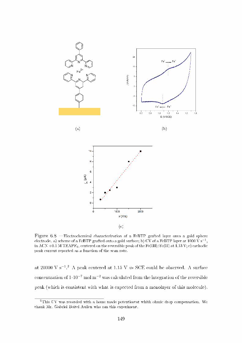
(a) (b)
(c)
Figure 6.8 Electrochemical characterization of a FeBTP grafted layer onto a gold sphereelectrode. a) scheme of a FeBTP grafted onto a gold surface; b) CV of a FeBTP layer at 1000 V s−1,in ACN+0.1MTEAPF6, centered on the reversible peak of the Fe(III)/Fe(II) at 1.13 V; c) cathodicpeak current reported as a function of the scan rate.
at 20000 V s−1.2 A peak centered at 1.15 V vs SCE could be observed. A surface
concentration of 1·10−7 mol m−2 was calculated from the integration of the reversible
peak (which is consistent with what is expected from a monolayer of this molecule).
2This CV was recorded with a home-made potentiostat whith ohmic drop compensation. Wethank Mr. Gabriel Boitel-Aullen who ran this experiment.
149

Figure 6.9 Structure of FeBTPSH
These observations support the conclusion that FeBTP is anchored onto the gold
surface.
(a) (b)
Figure 6.10 a) FeBTPSH anchored onto a gold surface; b) CV of a FeBTPSH SAM assembledonto a gold electrode in ACN (0.1 M TEAPF6), scan rate: 20000 V s−1.
6.4.2 STM-TERS analysis of a FeBTP grafted surface
In order to investigate the structure of the layer grafted onto gold, STM and TERS
measurements were performed. For this purpose, a ame-annealed gold electrode
(∼ 1 mm2) was functionalized by electrochemical reduction of FeBTPD (10−5 M
in ACN, 0.1 M TEAPF6, CV at 100 mV s−1 from 0.9 to -1 V vs SCE). As for gold
sphere electrodes, no reduction peak could be observed during the CV.
150
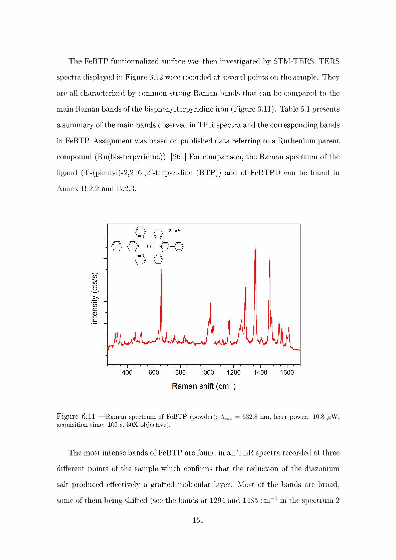
The FeBTP funtionnalized surface was then investigated by STM-TERS. TERS
spectra displayed in Figure 6.12 were recorded at several points on the sample. They
are all characterized by common strong Raman bands that can be compared to the
main Raman bands of the bisphenylterpyridine iron (Figure 6.11). Table 6.1 presents
a summary of the main bands observed in TER spectra and the corresponding bands
in FeBTP. Assignment was based on published data referring to a Ruthenium parent
compound (Ru(bis-terpyridine)). [264] For comparison, the Raman spectrum of the
ligand (4'-(phenyl)-2,2':6',2-terpyridine (BTP)) and of FeBTPD can be found in
Annex B.2.2 and B.2.3.
Figure 6.11 Raman spectrum of FeBTP (powder); λexc = 632.8 nm, laser power: 10.8 µW,acquisition time: 100 s, 50X objective).
The most intense bands of FeBTP are found in all TER spectra recorded at three
dierent points of the sample which conrms that the reduction of the diazonium
salt produced eectively a grafted molecular layer. Most of the bands are broad,
some of them being shifted (see the bands at 1294 and 1485 cm−1 in the spectrum 2
151

Figure 6.12 STM-TER spectra at three dierent positions of a FeBTP layer grafted onto goldby EC reduction of FeBTPD in ACN ; λexc = 632.8 nm, laser power: 130 µW, acquisition time:10 s, BV: −100 mV, it = 200 pA.
of Figure 6.12). New bands appear especially in the 1100 - 1600 cm−1 region (such
as the strong one at 1557 cm−1 in spectrum 1). This kind of spectral characteristics
may indicate a non-homogeneous and non-organized organic layer under the tip.
These observations should be further correlated with topographic information of
the layer. On this sample STM imaging could however not be performed which can
indicate a thick non-organized layer on gold that makes STM imaging complicated
or impossible.
In order to ensure that the structure is a non-organized multilayer, we assembled
the thiol derivative of FeBTP (FeBTPSH) on a gold sample from a 0.1 mM solution
in ACN and recorded its TER spectrum for comparison. As a thiol compound,
FeBTPSH is expected to form an organized SAM and then the same TER spectrum
should be recorded at dierent positions of the sample to attest the homogeneity of
the SAM. Three STM-TER spectra taken from dierent positions on the surface are
152

Table 6.1 Main bands of Raman spectra of FeBTP (powder, microRaman), of the TER spectrarecorded on a gold sample electrochemically grafted by FeBTPD (TER) and their assignationfrom [264]. The Raman shifts are in cm−1; the shift values marked with a star are found in onlyone spectrum. "bend.": bending; "str.": stretching.
FeBTP (Raman) FeBTP (TER) Assignation [264]654 651 ring bend.1009 997 ring str.1024 1023 ring str.- 1075 ring str. + C-H bend.
1166 1157 C-H bend.1287 1285 (1294?) ring str. + C-H bend.1361 1362 C-H bend. + ring str.1466 1470 (1485?) ring str.1563 1557? ring str.1612 1598 ring str.
presented in Figure 6.13. It has rst to be noticed that collected spectra are similar
across the surface (both for the position and relative intensity of the bands) which
is a rst clear indication of an homogeneous molecular assembly. Moreover, the
spectra all exhibit the same main Raman bands as the spectrum of the FeBTPSH
powder.
TERS results support therefore the hypothesis of a non-organized multilayer
formation upon electrochemical reduction of FeBTPD on gold. Further important
information on the exact structure of the layer should be provided by AFM-TERS
experiments as imaging is easier in AFM on samples with high roughness and po-
tentially insulating areas. In order to favour formation of a monolayer that can be
analyzed by STM-TERS, we further discuss the results obtained on samples onto
which spontaneous grafting was explored.
153

Figure 6.13 STM-TER spectra of a FeBTPSH SAM on gold at dierent positions on the sample(black, red and blue lines) compared with the microRaman spectrum of the FeBTPSH powder.TER spectra: λexc = 632.8 nm, laser power: 10.8 µW, acquisition time: 30 s, BV: 100 mV,it =200 pA; microRaman: λexc = 632.8 nm, laser power: 10.8 µW, acquisition time: 30 s, intensitydivided by a factor of 3 for comparison. All spectra are oset for clarity.
6.5 Spontaneous grafting of diazonium salts inves-
tigated by STM-TERS
The spontaneous grafting of diazonium salts, as the result of simple immersion of the
surface in a diazonium salt solution, is known to lead to thiner organic layers (from
a monolayer to a bilayer) as compared to the electrochemically grafted ones that can
grow up to 15 nm. [265] It has previously been demonstrated with nitrobenzenedia-
zonium that alternative routes my be followed involving for example the formation
of Au-N bonds besides the expected Au-C ones (see bottom part of Figure 6.1). [253]
Herein, we propose to investigate the spontaneous grafting of FeBTPD in ACN
on a gold surface.
154

6.5.1 Sample preparation and characterization
The samples were prepared by immersing ame-annealed gold surfaces in a 4·10−5 M
solution of FeBTPD in ACN for 30 min at 22 oC. The surface was then thoroughly
rinsed with ACN and ethanol to remove any physisorbed species from the surface
and dried under a nitrogen ow.
The surface was then investigated by STM. A STM image of the surface on a
300× 300 nm2 area is presented in Figure 6.14.
Figure 6.14 STM imaging of a gold surface spontaneously grafted by FeBTPD. BV: 0.20 V,it: 200 pA; 300× 300 nm2, 512× 128 px2; scan rate: 1 Hz per line.
First, contrary to the samples grafted by electrochemical reduction of the same
diazonium salt, the imaging in STM mode is here possible indicating that either
the grafted layer is thinner in the case of a spontaneous grafting or that no grafting
occurs under such conditions. Some dispersed protrusions are observed all over
the scanned area with heights ranging from 0.5 to several nanometres: as most
of them are found along the X axis, they may be STM artefacts. STM imaging
onto a restricted area will be performed in the future to try to visualize molecules
individually within the layer.
155

6.5.2 STM-TERS analysis of the spontaneously grafted layer
As no topographical details could clearly evidence the grafting of FeBTP by STM,
compositional analyses by STM-TERS were performed on the same sample.
A STM TER spectrum is given in Figure 6.15. It exhibits all of the main spectral
features of FeBTP. Compared to the spectra of the FeBTP layer grafted by EC
reduction of FeBTPD (Figure 6.12), the bands are thinner and no extra bands
appear in this spectrum. The collected spectra compared to the TER spectrum of
the FeBTPSH SAM indicating then a much more organized molecular layer than
the one formed upon electrochemical reduction of FeBTPD.
Figure 6.15 STM-TER spectra of a gold surface immersed in a FeBTPD ACN solution (blueline). The orange line is a spectrum recorded with the same STM parameters and Raman acquisi-tion conditions on a clean gold sample as a control for tip contamination. λexc = 632.8 nm, laserpower: 10.8 µW, acquisition time: 30 s, BV = 200 mV, it =200 pA; the spectra are the average of5 aquisitions.
A TERS map was recorded over the same area as the STM map in Figure 6.14
to corroborate the hypothesis of a more organized structure. This STM-TERS map
156
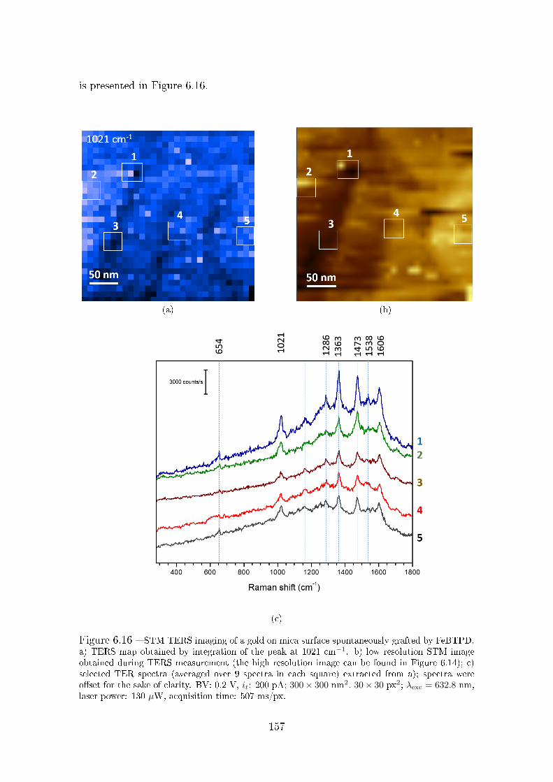
is presented in Figure 6.16.
(a) (b)
(c)
Figure 6.16 STM TERS imaging of a gold on mica surface spontaneously grafted by FeBTPD.a) TERS map obtained by integration of the peak at 1021 cm−1. b) low resolution STM imageobtained during TERS measurement (the high resolution image can be found in Figure 6.14); c)selected TER spectra (averaged over 9 spectra in each square) extracted from a); spectra wereoset for the sake of clarity. BV: 0.2 V, it: 200 pA; 300× 300 nm2, 30× 30 px2; λexc = 632.8 nm,laser power: 130 µW, acquisition time: 507 ms/px.
157

The TERS map obtained by integration of the band at 1021 cm−1 displays
heterogeneities in intensity that can be related to the topography of the substrate:
the most intense area is located (middle left part of the map) over a specic gold
terrace while the less intense part is found in a valley between two terraces. On
other parts of the sample, the intensity is mainly homogeneous.
A selection of 5 spectra were extracted from this map on 5 dierent positions of
the sample and are displayed in Figure 6.16c.
The main dierence between all of these spectra concerns the overall intensity
of the bands. A close look to spectra 2 and 5 recorded on gold terraces suggest
that the surface concentration is dierent between both areas. Indeed, the overall
TER intensity is 1.3 higher on position 2 than on position 5. This suggests that
the spontaneous grafting does not occur completely homogeneously over the sample.
These slight dierences cannot be explained at the moment.
Note that a spectrum was collected on a clean gold substrate after all the TERS
measurements: it does not exhibit Raman bands from FeBTP or any other organ-
ics which discards contamination of the tip by FeBTP during previously described
experiments (see orange line in Figure 6.15).
TERS imaging therefore supports the hypothesis of the formation of a monolayer
of FeBTP on gold.
A more spatially resolved TERS mapping (down to the molecular scale) on this
surface could help correlating these intensity variations with specic sites on the
sample. However, in the ambient, TERS mapping at the molecular scale has not
been achieved yet and might be very dicult because of the thermal drift of the
sample at the timescale of TER experiments (500 ms per spectrum in this example).
158

6.6 Conclusion
In this chapter, we have investigated the structure of a molecular layer grafted
onto gold surfaces from electrochemical reduction of diazonium salts. The rst
diazonium derivative, PFBD, was studied as a model compound for the formation of
monolayers. STM images revealed the non-compact structure of these layers but also
conrmed their ability to form only monolayers. This system could unfortunately
not be investigated by TERS probably due to its high photosensitivity. In this case
no spectroscopic information could be correlated to the structure determined by
STM.
The second system, based on a diazonium salt with a redox core, was studied by
cyclic voltammetry. Its anchoring onto the gold surface could be demonstrated. Two
grafting paths were investigated: the electrochemical reduction and the spontaneous
grafting. STM and TERS measurements revealed dierent molecular organizations
depending on the grafting origin. In electrochemical grafting, we concluded on
the formation of a thick multilayer. TERS results corroborated this hypothesis by
providing spectra that could be associated to a disorganized organic layer. Compar-
atively, the STM and TERS experiments conducted on a sample functionalized by
spontaneous grafting suggested the anchoring of a less densely packed monolayer.
The STM and TERS results were in this case complementary since STM images did
not provide clear evidences of the grafting.
This is to the best of our knowledge the rst set of TERS results provided on
the grafting of diazonium salts. These preliminary results should be completed by
deeper electrochemical analysis, especially to measure the electron transfer rate in
these redox layers and correlate them to the structure that can be investigated by
STM and TERS. This work demonstrated that TERS can be a powerful tool for
the understanding of the mechanism of both the grafting of diazonium salts and of
electron transfer in such organic layers, which are of major importance for molecular
electronics.
159

160

General conclusion and outlook
The work described in this thesis has demonstrated that the implementation of
TERS for the analysis of electrochemical systems can be realized under a wide range
of conditions for various applications. In this work, several instrumental challenges
had to be overcome due to diculties related to the coupling of electrochemical
measurements with SPM and Raman investigations.
In chapter 2, the experimental prerequisites of conventional STM-TERS mea-
surements have been developed. In particular, we have described the manufacturing
process of reliable and robust bulk gold and silver TERS probes for STM-based
TERS. These probes are a key element in any TERS experiment since both lateral
resolution and sensitivity for nanoRaman imaging strongly depend on tip geometry
and on the structure of the probe apex.
Chapter 3 covered the possibility of TERS to image samples immersed in an
organic liquid in an upright illumination and collection conguration. These results
were the rst demonstration of TERS imaging in liquid and revealed the ability of our
setup to probe inhomogeneities in the coverage density of a molecular self-assembled
monolayer (SAM) on a gold surface. It may be of major interest for the protection
and investigation of air-sensitive samples or to prevent surface contamination and
signal uctuation usually observed in the air. Implementation of this conguration
in electrochemical conditions is potentially possible, but would require handling a
very thin layer of electrolyte.
We introduced in Chapter 4 a TERS-inspired analytical tool, the so-called tip
161

SERS, to monitor electrochemical reactions. A partially insulated and functionalized
TERS tip was used as a single hot spot SERS and microelectrode to probe the
electrochemical transformation of a 4-nitrothiophenol SAM. We introduced in this
chapter the high excitation and signal collection eciency provided by the use of
a water immersion objective for in situ TERS en SERS experiments. The hybrid
tips developed are expected to be applied to the investigation of more complicated
electrochemical transformation in immobilized molecular systems.
In Chapter 5, TERS imaging in electrochemical environment was evidenced. The
EC tip-SERS conguration was promoted in order to enable STM-TERS imaging
of a surface under potential control. The presented preliminary results demonstrate
the ability of the proposed setup to probe variations of the local electromagnetic
eld enhancement under the tip with a lateral sensitivity down to 8 nm. This
is to the best of our knowledge the rst demonstration of TERS imaging under
electrochemical conditions.
The last chapter was dedicated to the TERS analysis of surfaces functionalized
by electrochemical reduction and spontaneous grafting of aryldiazonium salts. STM
and TERS results evidenced the dierent molecular structures obtained from a dia-
zonium salt with an electroactive core depending on the grafting route and revealed
that layers formed upon spontaneous grafting are less densely packed monolayers
whereas electrochemical reduction led to disorganized multilayers. These prelim-
inary results have to be completed by deeper electrochemical analyses and to be
corroborated by more accurate topographic information which could be provided by
AFM-TERS.
During this work several approaches have demonstrated the strengths of TERS
to investigate electrochemical interfaces both in situ and ex situ. The reliable setup
developed for EC STM-TERS imaging was a rst important milestone to reach
for further investigations of electrode/electrolyte interfaces. Even if TERS lateral
resolution is still to be demonstrated, we expect this conguration to enable Raman
162

analysis at the nanoscale of more complicated electrochemical systems and pave the
road for the operando investigation of catalytic reactions, energy storage materials
under the conditions of their operation or organic layers for molecular electronics.
Implementation of AFM-TERS in electrochemical conditions is also to be explored
and requires further instrumental developments. It would enable to probe a more
varied range of samples especially for energy storage and conversion for which STM
imaging would be dicult to implement because of the poor conductivity of the
substrate.
163

164

Appendix A
Supplementary materials to
Chapter 4
A.1 Raman signature of N,N-dimethylnitrosoaniline
As 4-nitrosothiophenol (4-NSTP) is not commercial, we used N,N-dimethylnitrosoaniline
(Aldrich, 97% purity) as a reference compound for nitroso compounds. The spec-
trum, acquired with a 632.8 nm laser line through a 50X objective, exhibits mainly
bands that can be assigned to the cis nitroso dimer: the strong band at 1391 cm−1
(N = N stretching for cis dimer) and the 1358 and 1331 cm−1 bands (C−N stretch-
ing). The medium band at 1298 cm−1 can be assigned to N−O stretching. [206]
165
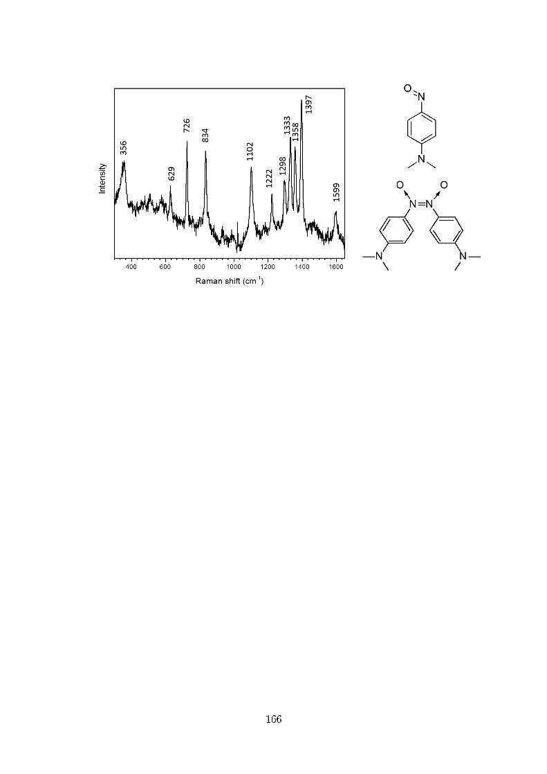
166

Appendix B
Supplementary materials to
Chapter 6
B.1 Electrochemical characterization of a FeBTP
functionalized gold sphere electrode
A gold sphere electrode (A = 0.250 mm2) was functionalized by electrochemical
reduction of FeBTPD (5 · 10−4 M) in ACN (0.2 M TBAPF6) under nitrogen by CV
(200 mV s−1, 1 cycle, from +1 to −1.5 V vs SCE. The electrode was then thoroughly
rinced with ACN and CVs were recorded in ACN + 0.2MTBAPF6 under nitrogen at
scan rates ranging from 100 to 2000 V s−1 between 0.6 and 1.7 V vs SCE centered
on the reversible peak of the Fe at 1.13 V vs SCE. Below 100 V s−1, the noise
was too large so that no faradaic current could be separated from the capacitive
signal. Above 2000 V s−1, the electrode time constant and ohmic drop were far too
important to allow a proper CV aquisition (undistorded signal). [266]
167

(a) (b)
(c) (d)
(e) (f)
(g)
Figure B.1 CVs recorded on a gold sphere electrode grafted with FeBTPD at a) 100 V s−1, b)300 V s−1, c) 500 V s−1, d) 1000 V s−1, e) 1500 V s−1, f) 2000 V s−1.
168

B.2 Raman Spectra of reference products
The Raman spectra were recorded on products powders through a 50X objective
with a Labram HR Evolution Raman Spectrometer (Horiba, Japan) with a 632.8 nm
laser excitation.
B.2.1 Raman signature of 2,3,4,5,6-pentauorobenzenediazonium
tetrauoroborate (PFBD)
169

B.2.2 Raman signature of 4'-(phenyl)-2,2':6',2-terpyridine (BTP)
170
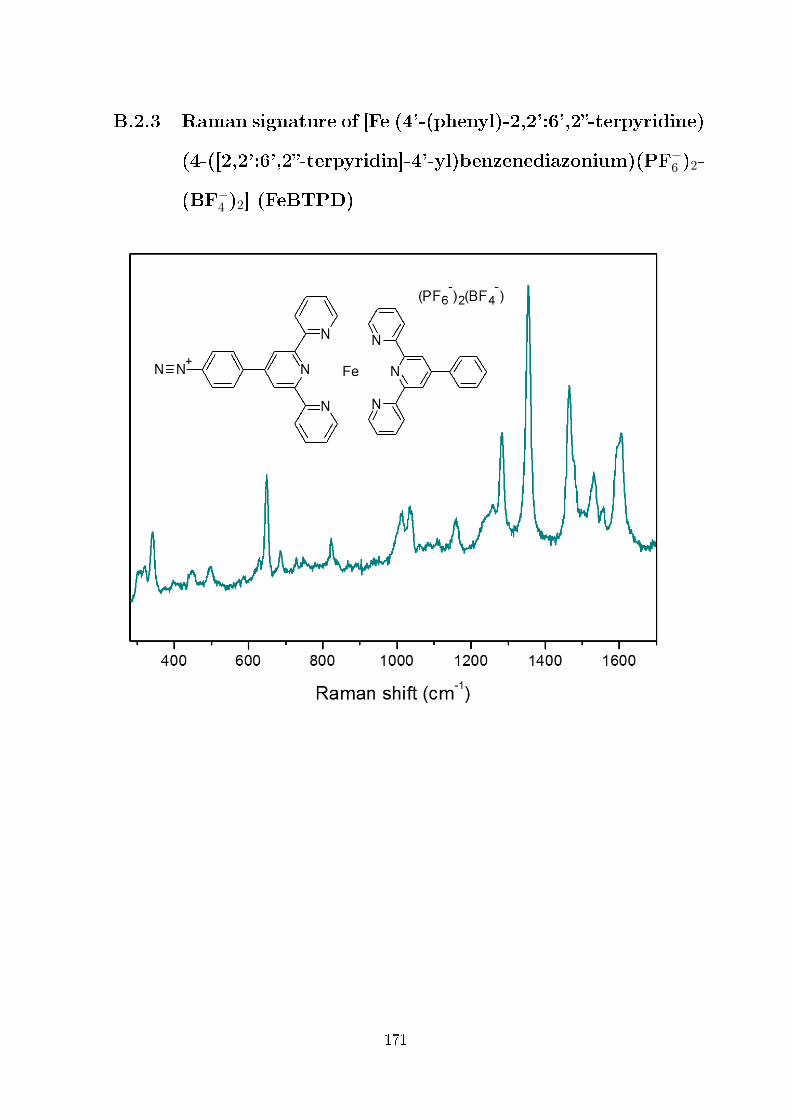
B.2.3 Raman signature of [Fe (4'-(phenyl)-2,2':6',2-terpyridine)
(4-([2,2':6',2-terpyridin]-4'-yl)benzenediazonium)(PF−6 )2-
(BF−4 )2] (FeBTPD)
171

B.3 Synthesis and characterization of organic com-
pounds
B.3.1 Synthesis of 2,3,4,5,6-pentauorobenzenediazonium tetra-
uoroborate (PFBD)
At −40C under argon atmosphere, to a solution of 2,3,4,5,6-pentauoroaniline
(2.7 mmol, 0.5 g) in cold acetonitrile (4 mL), nitrosium tetrauoroborate (4.9 mmol,
0.57 g) was added dropwise. The mixture was stirred for 45 min. Cold diethyl ether
(40 mL) was added. A white powder appears; which was ltered and washed with
diethyl ether. Yield: 94.7%, (0.72 mg). IR: νmax = 2306 cm−1, ν(N≡N); Raman:
ν(N≡N) = 2310 cm−1.
B.3.2 Synthesis of 4'-(phenyl)-2,2':6',2-terpyridine (BTP)
To a solution of benzenaldehyde (18.8 mmol, 2 g, 1.92 mL) in ethanol (50 mL), 2-
acetylpyridine (38.29 mmol, 4.64 g, 4.29 mL) and potassium hydroxyde (38.29 mmol,
2.15 g) were added. The solution became orange. The reaction mixture was stirred
overnight at room temperature. A yellow precipitate appeared which was ltered,
washed three times with diethyl ether and dried under vacuum. A light yellow
powder was obtained. Yield: 46 % (2.7 g). 1H NMR (DMSO-d6, δ (ppm)):
172
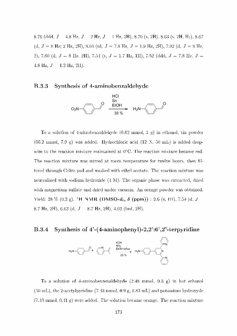
8.76 (ddd, J = 4.8 Hz, J = 2 Hz, J = 1 Hz, 2H), 8.70 (s, 2H), 8.63 (s, 2H, H7), 8.67
(d, J = 8 Hz; 2 Hz, 2H), 8.04 (td, J = 7.8 Hz, J = 1.9 Hz, 2H), 7.92 (d, J = 8 Hz,
2), 7.60 (d, J = 8 Hz, 2H), 7.54 (t, J = 1.7 Hz, 1H), 7.52 (ddd, J = 7.8 Hz, J =
4.8 Hz, J = 1.2 Hz, 2H).
B.3.3 Synthesis of 4-aminobenzaldehyde
To a solution of 4-nitrobenzaldehyde (6.62 mmol, 1 g) in ethanol, tin powder
(66.2 mmol, 7.9 g) was added. Hydrochloric acid (12 N, 50 mL) is added drop-
wise to the reaction mixture maintained at 0C. The reaction mixture became red.
The reaction mixture was stirred at room temperature for twelve hours, then l-
tered through Celite pad and washed with ethyl acetate. The reaction mixture was
neutralized with sodium hydroxide (4 M). The organic phase was extracted, dried
with magnesium sulfate and dried under vacuum. An orange powder was obtained.
Yield: 38 % (0.3 g). 1H NMR (DMSO-d6, δ (ppm)) : 9.6 (s, 1H), 7.54 (d, J =
8.7 Hz, 2H), 6.63 (d, J = 8.7 Hz, 2H), 4.03 (brd, 2H).
B.3.4 Synthesis of 4'-(4-aminophenyl)-2,2':6',2-terpyridine
To a solution of 4-aminobenzenaldehyde (2.48 mmol, 0.3 g) in hot ethanol
(50 mL), the 2-acetylpyridine (7.43 mmol, 0.9 g, 0.83 mL) and potassium hydroxyde
(7.43 mmol, 0.41 g) were added. The solution became orange. The reaction mixture
173

was kept under reux and stirred overnight at room temperature. A yellow precip-
itate appeared which was ltered, washed three times with diethyl ether and dried
under vacuum. A light yellow powder was obtained. Yield: 25 % (0.2 g). 1H NMR
(DMSO-d6, δ (ppm)): 8.74 (ddd, J = 4.8 Hz, J = 2 Hz, J = 0.9 Hz, 2H), 8.63
(dt, J = 7.8 Hz, J = 1.2 Hz, 2H), 8.59 (s, 2H), 7.98 (td, J = 7.6 Hz, J = 2 Hz,
2H), 7.58 (d, J = 8.1 Hz, 2H), 7.48 (ddd, J = 7.8 Hz, J = 4.8 Hz, J = 1.2 Hz, 2H),
6.68 (d, J = 8.1 Hz, 2H), 5.59 (brd, 2H).
B.3.5 Synthesis of 4'-(4-bromophenyl)-2,2':6',2-terpyridine
To a solution of 4-bromobenzenaldehyde (10.9 mmol, 2 g) in ethanol (50 mL), 2-
acetylpyridine (43.38 mmol, 5.25 g, 4.86 mL) and potassium hydroxyde (42.84 mmol,
2.40 g) were added. The solution became dark yellow. The reaction mixture was kept
under reux and stirred overnight at room temperature. A light green precipitate
appeared which was ltered, washed three times with diethyl ether and dried under
vacuum. A light green powder was obtained. Yield: 59.6 % (2.49 g). 1H NMR
(DMSO-d6, δ (ppm)): 8.77 (ddd, J = 4.8 Hz, J = 1.9 Hz, J = 1 Hz, 2H), 8.76
(s, 2H), 8.67 (d, J = 7.8 Hz, 2H), 8.04 (td, J = 8 Hz, J = 1.8 Hz, 2H), 7.91 (d,
J = 8.5 Hz, 2H), 7.78 (d, J = 8.3 Hz, 2H), 7.58 (ddd, J = 7.8 Hz, J = 4.8 Hz, J =
1.1 Hz, 2H).
B.3.6 Synthesis of 4-([2,2':6',2-terpyridin]-4'-yl)benzenethiol
174

To a solution of copper (II) sulfate pentahydrate (0.14 mmol, 0.035 g) and
potassium hydroxide (13.5 mmol, 0.75 g) in DMSO:H2O (1:0.1; 20:2 mL), 1,2-
ethanedithiol (5.4 mmol, 0.49 mL) was added. The solution became brown. The
reaction mixture was heated at 110C during 1 h and stirred overnight at room tem-
perature. The organic phase was extracted by (ethyl acetate: H2O:HCl) (1:1:0.05),
dried with magnesium sulfate and dried under vacuum. The crude product was
further puried by column chromatography to provide light yellow crystals. Yield:
91.3 % (0.84 g). 1H NMR (DMSO-d6, δ (ppm)): 8.75 (ddd, J = 4.8 Hz, J =
2 Hz, J = 0.8 Hz, 2H), 8.69 (s, 2H), 8.67 (dd, J = 7.8 Hz, J = 0.8 Hz, 2H), 8.03
(td, J = 7.8 Hz, J = 1.0 Hz, 2H), 7.88 (d, J = 8.5 Hz, 2H), 7.76 (d, J = 8.6 Hz,
2H), 7.52 (ddd, J = 7.8 Hz, J = 4.0 Hz, J = 1.1 Hz, 2H), 3.00 (s, 1H). [267]
B.3.7 Synthesis of [Fe (4'-(phenyl)-2,2':6',2-terpyridine)2(PF−6 )2]
(FeBTP) derivatives
The syntheses of FeBTP asymmetric derivatives were carried out according to pro-
cedures described by Kurita et al. [268]
175
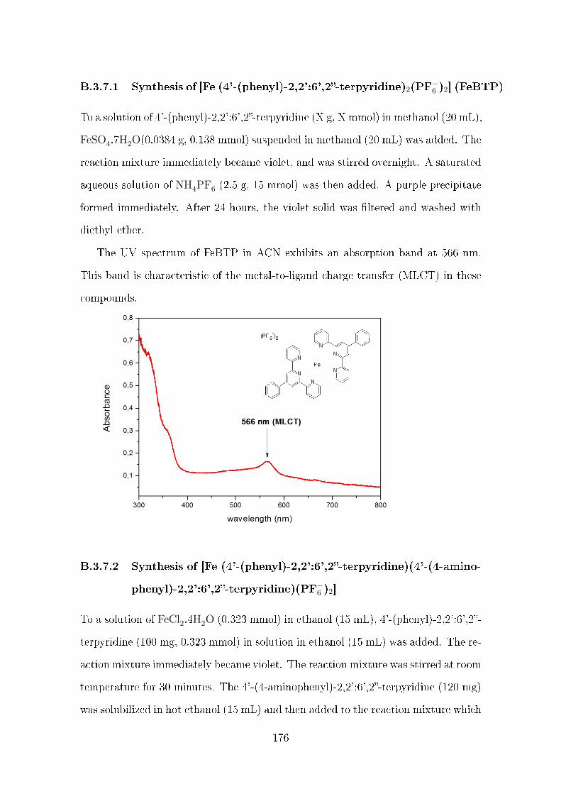
B.3.7.1 Synthesis of [Fe (4'-(phenyl)-2,2':6',2-terpyridine)2(PF−6 )2] (FeBTP)
To a solution of 4'-(phenyl)-2,2':6',2-terpyridine (X g, X mmol) in methanol (20 mL),
FeSO4.7H2O(0.0384 g, 0.138 mmol) suspended in methanol (20 mL) was added. The
reaction mixture immediately became violet, and was stirred overnight. A saturated
aqueous solution of NH4PF6 (2.5 g, 15 mmol) was then added. A purple precipitate
formed immediately. After 24 hours, the violet solid was ltered and washed with
diethyl ether.
The UV spectrum of FeBTP in ACN exhibits an absorption band at 566 nm.
This band is characteristic of the metal-to-ligand charge transfer (MLCT) in these
compounds.
B.3.7.2 Synthesis of [Fe (4'-(phenyl)-2,2':6',2-terpyridine)(4'-(4-amino-
phenyl)-2,2':6',2-terpyridine)(PF−6 )2]
To a solution of FeCl2.4H2O (0.323 mmol) in ethanol (15 mL), 4'-(phenyl)-2,2':6',2-
terpyridine (100 mg, 0.323 mmol) in solution in ethanol (15 mL) was added. The re-
action mixture immediately became violet. The reaction mixture was stirred at room
temperature for 30 minutes. The 4'-(4-aminophenyl)-2,2':6',2-terpyridine (120 mg)
was solubilized in hot ethanol (15 mL) and then added to the reaction mixture which
176
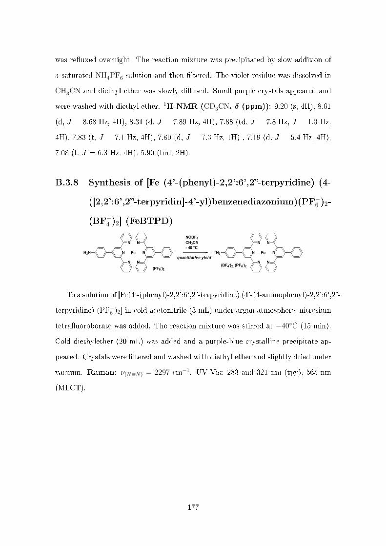
was reuxed overnight. The reaction mixture was precipitated by slow addition of
a saturated NH4PF6 solution and then ltered. The violet residue was dissolved in
CH3CN and diethyl ether was slowly diused. Small purple crystals appeared and
were washed with diethyl ether. 1H NMR (CD3CN, δ (ppm)): 9.20 (s, 4H), 8.61
(d, J = 8.68 Hz, 4H), 8.31 (d, J = 7.89 Hz, 4H), 7.88 (td, J = 7.8 Hz, J = 1.3 Hz,
4H), 7.83 (t, J = 7.1 Hz, 4H), 7.80 (d, J = 7.3 Hz, 1H) , 7.19 (d, J = 5.4 Hz, 4H),
7.08 (t, J = 6.3 Hz, 4H), 5.90 (brd, 2H).
B.3.8 Synthesis of [Fe (4'-(phenyl)-2,2':6',2-terpyridine) (4-
([2,2':6',2-terpyridin]-4'-yl)benzenediazonium)(PF−6 )2-
(BF−4 )2] (FeBTPD)
To a solution of [Fe(4'-(phenyl)-2,2':6',2-terpyridine) (4'-(4-aminophenyl)-2,2':6',2-
terpyridine) (PF−6 )2] in cold acetonitrile (3 mL) under argon atmosphere, nitrosium
tetrauoroborate was added. The reaction mixture was stirred at −40C (15 min).
Cold diethylether (20 mL) was added and a purple-blue crystalline precipitate ap-
peared. Crystals were ltered and washed with diethyl ether and slightly dried under
vacuum. Raman: ν(N≡N) = 2297 cm−1. UV-Vis: 283 and 321 nm (tpy), 565 nm
(MLCT).
177

178

Abbreviations and symbols
Abbreviations
AC Alternating current
AFM Atomic Force Microscopy
BCB Brilliant Cresyl Blue
BE Beam Expander
BV Bias Voltage (STM)
CCD Charge-Coupled Device
CE Counter Electrode (auxiliary electrode)
CH Confocal Pinhole
CLS Classical Least Square
CV Cyclic Voltammetry
DC Direct Current
DFT Density Functional Theory
e Edge lter
EC Electrochemical
EF Enhancement Factor
EIS Electrochemical Impedance Spectroscopy
EM-CCD Electron-multiplying CCD
179

F Filter
FIB Focused Ion Beam
FF Far-Field
FTIRRAS Fourier Transform IR Reection Spectroscopy
Gr Diraction Grating
HOMO Highest Occupied Molecular Orbital
HOPG Highly-Orientated Pyrogenic Graphite
IR Infrared
ITO Indium-Tin Oxide
LSP Localized Surface Plasmon
LSPR Localized Surface Plasmon resonance
LUMO Lowest Unoccupied Molecular Orbital
M Mirror
MIM Metal-Insulator-Metal
n Notch Filter
NA Numerical Aperture
ND Neutral Density Filter
NF Near-Field
NF Normal Force (TF)
NFM Normal-Force Microscopy
NP Nanoparticle
ORC Oxidation-Reduction Cycle
PR Plasmon Resonance
PZC Potential of Zero Charge
RC Resistor-Capacitor
180

RE Reference Electrode
RR Resonance Raman
RRS Resonance Raman Spectroscopy
SAM Self-Assembled Monolayer
SCE Saturated Calomel Electrode
SEC Spectroelectrochemistry
SECM Scanning Electrochemical Microscopy
SECCM Scanning Electrochemical Cell Microscopy
SEI Solide-Electrolyte Interphase
SEM Scanning Electrons Microscopy
SERS Surface-Enhanced Raman Spectroscopy
SERRS Surface-Enhanced Resonance Raman Spectroscopy
SF Shear-Force
SFM Shear-Force Microscopy
Sh Shutter
SHE Standard Hydrogen Electrode
SHINERS Shell-Isolated Nanoparticles Enhanced Raman Microscopy
SNOM Scanning Near-Field Optical Microscopy
a-SNOM Aperture SNOM
s-SNOM Scattering SNOM
SPM Scanning Probe Microscopy
SP Surface Plasmon
SPP Surface Plasmon Polariton
SRS Stimulated Raman Spectroscopy
SPR Surface plasmon Resonance
181

STM Scanning Tunneling Microscopy
TDDFT Time-Dependent DFT
TERS Tip-Enhanced Raman Spectroscopy
TF Tuning fork
UHV Ultra-High Vacuum
UME Ultra-Microelectrode
UV Ultraviolet
Vis Visible
WE Working Electrode
XPS X-ray Photoelectron Spectroscopy
Abbreviations and acronyms of chemical compounds
4-ATP 4-aminothiophenol
4-HATP 4-hydroxylaminothiophenol
4-NSTP 4-nitrosothiophenol
4-NTP 4-nitrothiophenol
4-PBT ((4'-(pyridine-4-yl)biphenyl-4-yl) methanethiol)
4-TADPA 4-4'-thioaminodiphenylamine
4-TPQDI 4,4'-thiophenylquinone
ACN Acetonitrile (CH3CN)
CoTPP meso-tetraphenylporphyrin cobalt
CNT Carbon Nanotube
DMAB p-p' -dimercaptoazobenzene
DMAOB p-p' -dimercaptoazoxybenzene
DMHAB p-p' -dimercaptohydrazobenzene
DNA Desoxyribonucleic Acid
182

Fc Ferrocene
FeBTP [Fe (4'-(phenyl)-2,2':6',2-terpyridine)2(PF−6 )2]
FeBTPD [Fe(4'-(phenyl)-terpyridine) (4-(terpyridin-4';- yl)benzenediazonium)(PF−6 )2(BF−4 )]
FeBTPSH [Fe(4'-(phenyl)-terpyridine) (4-(terpyridin-4';- yl)benzenethiol)(PF−6 )2]
PFBD 2,3,4,5,6-pentauorobenzenediazonium
H2TBPP meso-tetrakis(3,5-di-tetrarybutyl-phenyl-porphyrin)
MWCNT Multiwall Carbone Nanotube
NB Nile Blue
Rh6G Rhodamine 6G
RNA Ribonucleic Acid
SWCNT Single-Wall Carbone Nanotube
TBAP Tetrabutylammonium perchlorate (Bu4NClO4)
TBPP (tert-butyl-phenyl)-porphyrin
TEAPF6 Tetraethylammonium Hexauorophosphate (Et4NPF6)
Symbols (and units)
α Angle to the normal surface of the sample degree
α Polarisability C m2 V−1
Γ Surface coverage mol m−2
∆E Dierence of energy between two states in eq. 1.1 J
ε Complex dielectric function -
ε0 Dielectric constant of the free space F m−1
εd Dielectric function of the dielectric medium -
εib Interband transition contribution to ε -
εD Intraband transition contribution to ε (Drude model) -
γ Damping constant (harmonic oscillator) Hz
183

Γ Molecular surface coverage mol m−2
Γ Damping constant in the expression of εD -
Γ Resonance peak FWHM (harmonic oscillator) Hz
θt Tapper angle degrees
κ Extinction coecient -
λ Wavelength nm
−→µ Total dipolar moment C m
−→µi Induced dipolar moment C m
−→µp Permanent dipolar moment C m
−→µp Induced dipolar moment C m
ν0 Frequency of an incident photon s−1
νk Frequency of the normal mode k s−1
σk Cross section for the k mode m2
τ Characteristic time constant (harmonic oscillator) s
ω Angular frequency of an EM eld rad s−1
ωp Angular frequency of a plasma rad s−1
ω Raman shift cm−1
Ω Solid angle sr
a NP radius m
A Electrode area m2
Ai Raman peak area cnts s−1 cm−1
c Light velocity m s−1
C Concentration mol m−3
d Tip-sample distance (TERS) m
D Diusion coecient m2 s−1
184

E Electrode potential V
E0 Standard redox potential V
Evertex Cathodic vertex potential in CVs V
Eloc Local electric eld magnitude in TERS and SERS V m−1
−→E Electric eld V m−1
EF Fermi energy level of a metal J
f0 Resonance frequency (TF) Hz
F Faraday constant 96, 485.3 A mol−1
~ Reduced Planck constant 6.582 119 · 10−16 eV s rad−1
if Faradaic current A
ip Peak current in CV A
ipa Anodic peak current in CV A
ipc Cathodic peak current in CV A
Ik Scattering intensity of the k mode -
Iω Raman intensity at a ω cm−1 shift cnts s−1
INR Intensity of confocal Raman signal a.u.
ISER Intensity of SER signal a.u.
it Tunneling current (STM) A
ITER Intensity of TER signal a.u.
−→k Wavevector m−1
kB Boltzmann constant J K−1
me Eective mass of an electron 9.11 · 10−31 kg
n Number of electrons -
ne Density of electrons in a metal m−3
n Complex refractive index -
185

N Number of atoms in a molecule -
Nn Population of vibrational state -
NNR Number of molecules probed in confocal Raman -
NSER Number of molecules probed in SERS -
NTER Number of molecules probed in TERS -
p Momentum of a particle kg m s−1
q0k Normal coordinate at equilibrium (harmonic oscillator) -
qk Normal coordinate (harmonic oscillator) -
Q Charge C
Q Quality factor (TF) -
r Radial distance to the center of a NP m
rc Radius of curvature (TERS tip) nm
Rfoc Focused laser beam radius m
Rtip TERS tip radius m
t Time s
T Temperature K
v Sweep rate in CV V s−1
x Position of a particle m
186

Bibliography
[1] A. J. Bard and L. R. Faulkner. Electrochemical methods: Fundamentals and applications.
Wiley, 2d edition, 2001.
[2] A. J. Bard, F. R. F. Fan, J. Kwak, and O. Lev. Scanning electrochemical microscopy.
introduction and principles. Analytical Chemistry, 61(2):132138, 1989.
[3] A. A. Gewirth and B. K. Niece. Electrochemical applications of in situ scanning probe
microscopy. Chemical Reviews, 97(4):11291162, 1997.
[4] S. W. Hell. Toward uorescence nanoscopy. Nature Biotechnology, 21(11):1347, 2003.
[5] V. Brasiliense, J. Clausmeyer, A. L. Dauphin, J.-M. Noël, P. Berto, G. Tessier, W. Schuh-
mann, and F. Kanou. Opto-electrochemical in situ monitoring of the cathodic formation of
single cobalt nanoparticles. Angewandte Chemie International Edition, 56(35):1059810601,
2017.
[6] W. Kaim and J. Fiedler. Spectroelectrochemistry: the best of two worlds. Chemical Society
Reviews, 38(12):33733382, 2009.
[7] Y. Zhai, Z. Zhu, S. Zhou, C. Zhu, and S. Dong. Recent advances in spectroelectrochemistry.
Nanoscale, 10:30893111, 2018.
[8] M. M. Chehimi. Aryl Diazonium Salts (New Coupling Agents in Polymer and Surface Sci-
ence). John Wiley & Sons, 2012.
[9] B. Schrader. Infrared and Raman spectroscopy: methods and applications. John Wiley &
Sons, 2008.
[10] C. V. Raman. A new radiation. Indian Journal of Physics, 2:387398, 1928.
[11] E. C. Le Ru and P. G. Etchegoin. Principles of surface-enhanced Raman spectroscopy: and
related plasmonic eects. Elsevier, Amsterdam, 1 edition, 2009.
187

[12] K. Schomacker, J. Delaney, and P. Champion. Measurements of the absolute Raman cross
sections of benzene. The Journal of Chemical Physics, 85(8):42404247, 1986.
[13] A. Hiraya and K. Shobatake. Direct absorption spectra of jet-cooled benzene in 130260 nm.
The Journal of Chemical Physics, 94(12):77007706, 1991.
[14] A. B. Myers. Resonance Raman intensities and charge-transfer reorganization energies.
Chemical Reviews, 96(3):911926, 1996.
[15] A. Y. Hirakawa and M. Tsuboi. Molecular geometry in an excited electronic state and a
preresonance Raman eect. Science, 188(4186):359361, 1975.
[16] L. Novotny and B. Hecht. Principles of nano-optics. Cambridge University Press, 2d edition,
2012.
[17] B. Palpant. Cours de plasmonique. 2016.
[18] R. Rosei and D. W. Lynch. Thermomodulation spectra of Al, Au, and Cu. Physical Review
B, 5(10):3883, 1972.
[19] M. Guerrisi, R. Rosei, and P. Winsemius. Splitting of the interband absorption edge in Au.
Physical Review B, 12(2):557, 1975.
[20] C. L. Smith, N. Stenger, A. Kristensen, N. A. Mortensen, and S. I. Bozhevolnyi. Gap and
channeled plasmons in tapered grooves: a review. Nanoscale, 7(21):93559386, 2015.
[21] K. A. Willets and R. P. Van Duyne. Localized surface plasmon resonance spectroscopy and
sensing. Annual Review of Physical Chemistry, 58:267297, 2007.
[22] T. R. Jensen, M. L. Duval, K. L. Kelly, A. A. Lazarides, G. C. Schatz, and R. P. Van Duyne.
Nanosphere lithography: eect of the external dielectric medium on the surface plasmon
resonance spectrum of a periodic array of silver nanoparticles. The Journal of Physical
Chemistry B, 103(45):98469853, 1999.
[23] T. Ming, L. Zhao, Z. Yang, H. Chen, L. Sun, J. Wang, and C. Yan. Strong polariza-
tion dependence of plasmon-enhanced uorescence on single gold nanorods. Nano Letters,
9(11):38963903, 2009.
[24] F. Hao, C. L. Nehl, J. H. Hafner, and P. Nordlander. Plasmon resonances of a gold nanostar.
Nano Letters, 7(3):729732, 2007.
[25] C. L. Nehl and J. H. Hafner. Shape-dependent plasmon resonances of gold nanoparticles.
Journal of Materials Chemistry, 18(21):24152419, 2008.
188

[26] M. Fleischmann, P. J. Hendra, and A. J. McQuillan. Raman spectra of pyridine adsorbed
at a silver electrode. Chemical Physics Letters, 26(2):163166, 1974.
[27] D. L. Jeanmaire and R. P. Van Duyne. Surface Raman spectroelectrochemistry: Part I. Het-
erocyclic, aromatic, and aliphatic amines adsorbed on the anodized silver electrode. Journal
of Electroanalytical Chemistry and Interfacial Electrochemistry, 84(1):120, 1977.
[28] M. G. Albrecht and J. A. Creighton. Anomalously intense Raman spectra of pyridine at a
silver electrode. Journal of the American Chemical Society, 99(15):52155217, 1977.
[29] S. Nie and S. R. Emory. Probing single molecules and single nanoparticles by surface-
enhanced Raman scattering. Science, 275(5303):11021106, 1997.
[30] K. Kneipp, Y. Wang, H. Kneipp, L. T. Perelman, I. Itzkan, R. R. Dasari, and M. S. Feld.
Single molecule detection using surface-enhanced Raman scattering (SERS). Physical Review
Letters, 78(9):1667, 1997.
[31] L. Chapus, P. Aubertin, S. Joiret, I. T. Lucas, E. Maisonhaute, and A. Courty. Tunable
SERS Platforms from Small Nanoparticle 3D Superlattices: A Comparison between Gold,
Silver, and Copper. ChemPhysChem, 18(21):30663075, 2017.
[32] P. L. Stiles, J. A. Dieringer, N. C. Shah, and R. P. Van Duyne. Surface-enhanced Raman
spectroscopy. Annual Review of Analytical Chemistry, 1:601626, 2008.
[33] A. Otto. The `chemical' (electronic) contribution to surface-enhanced Raman scattering.
Journal of Raman Spectroscopy, 36(6-7):497509, 2005.
[34] D.-Y. Wu, J.-F. Li, B. Ren, and Z.-Q. Tian. Electrochemical surface-enhanced Raman
spectroscopy of nanostructures. Chemical Society Reviews, 37(5):10251041, 2008.
[35] F. Barz, J. G. Gordon, M. R. Philpott, and M. J. Weaver. Intense electrochemical SERS
signal following hydrogen evolution. Chemical Physics Letters, 94(2):168171, 1983.
[36] S. Simon, T. I. Olumorin, B. Guo, and I. J. Burgess. Role of Au(I) Intermediates in the
Electrochemical Formation of Highly Anisotropic Gold Nanostructures with Near-IR SERS
Applications. The Journal of Physical Chemistry C, 120(45):2615026158, 2016.
[37] G. Di Martino, V. Turek, C. Tserkezis, A. Lombardi, A. Kuhn, and J. J. Baumberg. Plas-
monic response and SERS modulation in electrochemical applied potentials. Faraday Dis-
cussions, 205:537545, 2017.
[38] R. Wen and Y. Fang. Adsorption of pyridine carboxylic acids on silver surface investigated
by potential-dependent SERS. Vibrational Spectroscopy, 39(1):106113, 2005.
189

[39] R. Wen and Y. Fang. An investigation of the surface-enhanced Raman scattering (SERS)
eect from a new substrate of silver-modied silver electrode. Journal of Colloid and Interface
Science, 292(2):469475, 2005.
[40] F. Bondu. Étude de la conformation d'adsorption de l'acide isonicotinique sur Au < 111 >
par spectroscopie d'impédance-Raman et modulation de capacité. PhD thesis, Université
Pierre et Marie Curie, 2013.
[41] Z.-C. Zeng, S.-C. Huang, D.-Y. Wu, L.-Y. Meng, M.-H. Li, T.-X. Huang, J.-H. Zhong, X.
Wang, Z.-L. Yang, and B. Ren. Electrochemical Tip-Enhanced Raman Spectroscopy. Journal
of the American Chemical Society, 137(37):1192811931, 2015.
[42] C.-Y. Li, S.-Y. Chen, Y.-L. Zheng, S.-P. Chen, R. Panneerselvam, S. Chen, Q.-C. Xu, Y.-X.
Chen, Z.-L. Yang, D.-Y. Wu, J.-F. Li, and Z.-Q. Tian. In-situ electrochemical shell-isolated
Ag nanoparticles-enhanced Raman spectroscopy study of adenine adsorption on smooth Ag
electrodes. Electrochimica Acta, 199:388393, 2016.
[43] B.-Y. Wen, J. Yi, Y.-H. Wang, K. Madasamy, H. Zhang, M. Kathiresan, J.-F. Li, and Z.-Q.
Tian. In-situ monitoring of redox processes of viologen at Au(hkl) single-crystal electrodes us-
ing electrochemical shell-isolated nanoparticle-enhanced Raman spectroscopy. Electrochem-
istry Communications, 72:131134, 2016.
[44] H. Zhang, C. Wang, H.-L. Sun, G. Fu, S. Chen, Y.-J. Zhang, B.-H. Chen, J. R. Anema, Z.-L.
Yang, J.-F. Li, et al. In situ dynamic tracking of heterogeneous nanocatalytic processes by
shell-isolated nanoparticle-enhanced Raman spectroscopy. Nature Communications, 8:15447,
2017.
[45] T. A. Galloway and L. J. Hardwick. Utilizing in situ electrochemical SHINERS for oxygen
reduction reaction studies in aprotic electrolytes. The Journal of Physical Chemistry Letters,
7(11):21192124, 2016.
[46] L. Novotny. Nano-optics: Optical antennas tuned to pitch. Nature, 455(7215):887887, 2008.
[47] J. Tominaga and T. Nakano. Optical near-eld recording: science and technology. Springer
Science & Business Media, 2005.
[48] E. Synge. A suggested method for extending microscopic resolution into the ultra-microscopic
region. The London, Edinburgh, and Dublin Philosophical Magazine and Journal of Science,
6(35):356362, 1928.
[49] E. Ash and G. Nicholls. Super-resolution aperture scanning microscope. Nature,
237(5357):510, 1972.
190
[50] D. W. Pohl, W. Denk, and M. Lanz. Optical stethoscopy: Image recording with resolution
λ/20. Applied Physics Letters, 44(7):651653, 1984.
[51] A. Lewis, M. Isaacson, A. Harootunian, and A. Muray. Development of a 500 spatial reso-
lution light microscope: I. light is eciently transmitted through λ/16 diameter apertures.
Ultramicroscopy, 13(3):227231, 1984.
[52] E. Betzig and R. J. Chichester. Single molecules observed by near-eld scanning optical
microscopy. Science, 262(5138):14221425, 1993.
[53] T. Saiki, S. Mononobe, M. Ohtsu, N. Saito, and J. Kusano. Tailoring a high-transmission
ber probe for photon scanning tunneling microscope. Applied Physics Letters, 68(19):2612
2614, 1996.
[54] N. Essaidi, Y. Chen, V. Kottler, E. Cambril, C. Mayeux, N. Ronarch, and C. Vieu. Fab-
rication and characterization of optical-ber nanoprobes for scanning near-eld optical mi-
croscopy. Applied Optics, 37(4):609615, 1998.
[55] J. Grausem, B. Humbert, M. Spajer, D. Courjon, A. Burneau, and J. Oswalt. Near-eld
Raman spectroscopy. Journal of Raman Spectroscopy, 30(9):833840, 1999.
[56] J. Schreiber, F. Demoisson, B. Humbert, G. Louarn, O. Chauvet, and S. Lefrant. First
observation of the Raman spectrum of isolated single-wall carbon nanotubes by near-eld
optical Raman spectroscopy. In AIP Conference Proceedings, volume 685, pages 181184.
AIP, 2003.
[57] D. P. Tsai, A. Othonos, M. Moskovits, and D. Uttamchandani. Raman spectroscopy using a
ber optic probe with subwavelength aperture. Applied Physics Letters, 64(14):17681770,
1994.
[58] J. Grausem, B. Humbert, A. Burneau, and J. Oswalt. Subwavelength Raman spectroscopy.
Applied Physics Letters, 70(13):16711673, 1997.
[59] Y. Lee, Z. Ding, and A. J. Bard. Combined scanning electrochemical/optical microscopy
with shear force and current feedback. Analytical Chemistry, 74(15):36343643, 2002.
[60] L. Novotny, R. X. Bian, and X. S. Xie. Theory of nanometric optical tweezers. Physical
Review Letters, 79(4):645, 1997.
[61] P. F. Liao. Lightning rod eect in surface enhanced Raman scattering. The Journal of
Chemical Physics, 76(1):751, 1982.
191

[62] F. H'dhili, R. Bachelot, A. Rumyantseva, G. Lerondel, and P. Royer. Nano-patterning
photosensitive polymers using local eld enhancement at the end of apertureless SNOM tips.
Journal of Microscopy, 209(3):214222, 2003.
[63] T. Taubner, R. Hillenbrand, and F. Keilmann. Nanoscale polymer recognition by spectral
signature in scattering infrared near-eld microscopy. Applied Physics Letters, 85(21):5064
5066, 2004.
[64] O. Khatib, J. D. Wood, A. S. McLeod, M. D. Goldam, M. Wagner, G. L. Damhorst, J. C.
Koepke, G. P. Doidge, A. Rangarajan, R. Bashir, et al. Graphene-based platform for infrared
near-eld nanospectroscopy of water and biological materials in an aqueous environment.
ACS Nano, 9(8):79687975, 2015.
[65] I. T. Lucas, A. S. McLeod, J. S. Syzdek, D. S. Middlemiss, C. P. Grey, D. N. Basov, and R.
Kostecki. IR Near-Field Spectroscopy and Imaging of Single LixFePO4 Microcrystals. Nano
Letters, 15(1):17, 2015.
[66] M. Ayache, S. F. Lux, and R. Kostecki. IR near-eld study of the solid electrolyte interphase
on a tin electrode. The Journal of Physical Chemistry Letters, 6(7):11261129, 2015.
[67] A. Dazzi and C. B. Prater. AFM-IR: technology and applications in nanoscale infrared
spectroscopy and chemical imaging. Chemical Reviews, 117(7):51465173, 2016.
[68] N. Hayazawa, Y. Inouye, Z. Sekkat, and S. Kawata. Metallized tip amplication of near-eld
Raman scattering. Optics Communications, 183(1-4):333336, 2000.
[69] B. Pettinger, G. Picardi, R. Schuster, and G. Ertl. Surface enhanced Raman spectroscopy:
towards single molecule spectroscopy. Electrochemistry (Tokyo), 68(12):942949, 2000.
[70] M. S. Anderson. Locally enhanced Raman spectroscopy with an atomic force microscope.
Applied Physics Letters, 76(21):31303132, 2000.
[71] R. M. Stöckle, Y. D. Suh, V. Deckert, and R. Zenobi. Nanoscale chemical analysis by
tip-enhanced Raman spectroscopy. Chemical Physics Letters, 318(13):131136, 2000.
[72] B. Pettinger, P. Schambach, C. J. Villagómez, and N. Scott. Tip-Enhanced Raman Spec-
troscopy: Near-Fields Acting on a Few Molecules. Annual Review of Physical Chemistry,
63(1):379399, 2012.
[73] J. Steidtner and B. Pettinger. Tip-enhanced Raman spectroscopy and microscopy on single
dye molecules with 15 nm resolution. Physical Review Letters, 100(23):236101, 2008.
192

[74] B. Pettinger, B. Ren, G. Picardi, R. Schuster, and G. Ertl. Tip-enhanced Raman spec-
troscopy (TERS) of malachite green isothiocyanate at Au (111): bleaching behavior under
the inuence of high electromagnetic elds. Journal of Raman Spectroscopy, 36(6-7):541550,
2005.
[75] S. F. Becker, M. Esmann, K. Yoo, P. Gross, R. Vogelgesang, N. Park, and C. Lienau.
Gap-Plasmon-Enhanced Nanofocusing Near-Field Microscopy. ACS Photonics, 3(2):223
232, 2016.
[76] I. Romero, J. Aizpurua, G. W. Bryant, and F. J. G. De Abajo. Plasmons in nearly touching
metallic nanoparticles: singular response in the limit of touching dimers. Optics Express,
14(21):99889999, 2006.
[77] B. Pettinger, K. F. Domke, D. Zhang, R. Schuster, and G. Ertl. Direct monitoring of plasmon
resonances in a tip-surface gap of varying width. Physical Review B, 76(11):113409, 2007.
[78] J. Stadler, B. Oswald, T. Schmid, and R. Zenobi. Characterizing unusual metal substrates
for gap-mode tip-enhanced Raman spectroscopy. Journal of Raman Spectroscopy, 44(2):227
233, 2013.
[79] Z. Yang, J. Aizpurua, and H. Xu. Electromagnetic eld enhancement in TERS congurations.
Journal of Raman Spectroscopy, 40(10):13431348, 2009.
[80] A. B. Zrimsek, N. L. Wong, and R. P. Van Duyne. Single Molecule Surface-Enhanced Raman
Spectroscopy: A Critical Analysis of the Bianalyte versus Isotopologue Proof. The Journal
of Physical Chemistry C, 120(9):51335142, 2016.
[81] M. D. Sonntag, J. M. Klingsporn, L. K. Garibay, J. M. Roberts, J. A. Dieringer, T. Seideman,
K. A. Scheidt, L. Jensen, G. C. Schatz, and R. P. Van Duyne. Single-Molecule Tip-Enhanced
Raman Spectroscopy. The Journal of Physical Chemistry C, 116(1):478483, 2012.
[82] S. Jiang, Y. Zhang, R. Zhang, C. Hu, M. Liao, Y. Luo, J. Yang, Z. Dong, and J. G. Hou.
Distinguishing adjacent molecules on a surface using plasmon-enhanced Raman scattering.
Nature Nanotechnology, 10(10):865869, 2015.
[83] J. Lee, N. Tallarida, X. Chen, P. Liu, L. Jensen, and V. A. Apkarian. Tip-Enhanced Ra-
man Spectromicroscopy of Co(II)-Tetraphenylporphyrin on Au(111): Toward the Chemists'
Microscope. ACS Nano, 11(11):1146611474, 2017.
[84] Y. Okuno, Y. Saito, S. Kawata, and P. Verma. Tip-Enhanced Raman Investigation of
Extremely Localized Semiconductor-to-Metal Transition of a Carbon Nanotube. Physical
Review Letters, 111(21):216101, 2013.
193
[85] G. Picardi, M. Chaigneau, and R. Ossikovski. High resolution probing of multi wall carbon
nanotubes by Tip Enhanced Raman Spectroscopy in gap-mode. Chemical Physics Letters,
469(1-3):161165, 2009.
[86] Y. Zhang, D. V. Voronine, S. Qiu, A. M. Sinyukov, M. Hamilton, Z. Liege, A. V. Sokolov, Z.
Zhang, and M. O. Scully. Improving resolution in quantum subnanometre-gap tip-enhanced
Raman nanoimaging. Scientic Reports, 6:25788, 2016.
[87] S. Jiang, X. Zhang, Y. Zhang, C. Hu, R. Zhang, Y. Zhang, Y. Liao, Z. J. Smith, Z. Dong, and
J. Hou. Subnanometer-resolved chemical imaging via multivariate analysis of tip-enhanced
Raman maps. Light: Science & Applications, 6(11):e17098, 2017.
[88] C. Chen, N. Hayazawa, and S. Kawata. A 1.7 nm resolution chemical analysis of carbon
nanotubes by tip-enhanced Raman imaging in the ambient. Nature Communications, 5:3312,
2014.
[89] R. Zhang, Y. Zhang, Z. C. Dong, S. Jiang, C. Zhang, L. G. Chen, L. Zhang, Y. Liao, J.
Aizpurua, Y. Luo, J. L. Yang, and J. G. Hou. Chemical mapping of a single molecule by
plasmon-enhanced Raman scattering. Nature, 498(7452):8286, 2013.
[90] F. Benz, M. K. Schmidt, A. Dreismann, R. Chikkaraddy, Y. Zhang, A. Demetriadou, C.
Carnegie, H. Ohadi, B. de Nijs, R. Esteban, et al. Single-molecule optomechanics in pico-
cavities. Science, 354(6313):726729, 2016.
[91] S. Trautmann, J. Aizpurua, I. Götz, A. Undisz, J. Dellith, H. Schneidewind, M. Rettenmayr,
and V. Deckert. A classical description of subnanometer resolution by atomic features in
metallic structures. Nanoscale, 9(1):391401, 2017.
[92] C. Zhang, B.-Q. Chen, and Z.-Y. Li. Optical origin of subnanometer resolution in tip-
enhanced Raman mapping. The Journal of Physical Chemistry C, 119(21):1185811871,
2015.
[93] F. J. Giessibl. Atomic resolution of the silicon (111)-(7x7) surface by atomic force microscopy.
Science, 267(5194):6871, 1995.
[94] L. Gross, F. Mohn, N. Moll, P. Liljeroth, and G. Meyer. The chemical structure of a molecule
resolved by atomic force microscopy. Science, 325(5944):11101114, 2009.
[95] T. Fukuma, K. Kobayashi, K. Matsushige, and H. Yamada. True atomic resolution in liquid
by frequency-modulation atomic force microscopy. Applied Physics Letters, 87(3):034101,
2005.
194

[96] D. Cialla, T. Deckert-Gaudig, C. Budich, M. Laue, R. Möller, D. Naumann, V. Deckert, and
J. Popp. Raman to the limit: tip-enhanced Raman spectroscopic investigations of a single
tobacco mosaic virus. Journal of Raman Spectroscopy, 40(3):240243, 2009.
[97] P. Hermann, A. Hermelink, V. Lausch, G. Holland, L. Möller, N. Bannert, and D. Naumann.
Evaluation of tip-enhanced Raman spectroscopy for characterizing dierent virus strains.
Analyst, 136(6):11481152, 2011.
[98] T. Deckert-Gaudig, E. Kämmer, and V. Deckert. Tracking of nanoscale structural variations
on a single amyloid bril with tip-enhanced Raman scattering. Journal of Biophotonics,
5(3):215219, 2012.
[99] M. Paulite, C. Blum, T. Schmid, L. Opilik, K. Eyer, G. C. Walker, and R. Zenobi. Full
spectroscopic tip-enhanced Raman imaging of single nanotapes formed from β-amyloid (1
40) peptide fragments. ACS Nano, 7(2):911920, 2013.
[100] S. Bonhommeau, D. Talaga, J. Hunel, C. Cullin, and S. Lecomte. Tip-enhanced Raman spec-
troscopy to distinguish toxic oligomers from Aβ142 brils at the nanometer scale. Ange-
wandte Chemie International Edition, 129(7):17971800, 2017.
[101] M. T. Polk. Electrochemical STM. Wiley, 2007.
[102] C. Blum, L. Opilik, J. M. Atkin, K. Braun, S. B. Kämmer, V. Kravtsov, N. Kumar, S.
Lemeshko, J.-F. Li, K. Luszcz, et al. Tip-enhanced Raman spectroscopy an interlaboratory
reproducibility and comparison study. Journal of Raman Spectroscopy, 45(1):2231, 2014.
[103] R. D. Rodriguez, A. Anne, E. Cambril, and C. Demaille. Optimized hand fabricated afm
probes for simultaneous topographical and electrochemical tapping mode imaging. Ultrami-
croscopy, 111(8):973981, 2011.
[104] R. Rodriguez, E. Sheremet, S. Müller, O. Gordan, A. Villabona, S. Schulze, M. Hietschold,
and D. Zahn. Compact metal probes: A solution for atomic force microscopy based tip-
enhanced Raman spectroscopy. Review of Scientic Instruments, 83(12):123708, 2012.
[105] L. Meng, T. Huang, X. Wang, S. Chen, Z. Yang, and B. Ren. Gold-coated AFM tips for
tip-enhanced Raman spectroscopy: theoretical calculation and experimental demonstration.
Optics Express, 23(11):1380413813, 2015.
[106] X. Cui, W. Zhang, B.-S. Yeo, R. Zenobi, C. Hafner, and D. Erni. Tuning the resonance
frequency of Ag-coated dielectric tips. Optics Express, 15(13):83098316, 2007.
195

[107] B.-S. Yeo, T. Schmid, W. Zhang, and R. Zenobi. Towards rapid nanoscale chemical anal-
ysis using tip-enhanced Raman spectroscopy with Ag-coated dielectric tips. Analytical and
Bioanalytical Chemistry, 387(8):26552662, 2007.
[108] T.-X. Huang, C.-W. Li, L.-K. Yang, J.-F. Zhu, X. Yao, C. Liu, K.-Q. Lin, Z.-C. Zeng, S.-
S. Wu, X. Wang, et al. Rational fabrication of silver-coated AFM TERS tips with a high
enhancement and long lifetime. Nanoscale, 10(9):43984405, 2018.
[109] Y. You, N. Purnawirman, H. Hu, J. Kasim, H. Yang, C. Du, T. Yu, and Z. Shen. Tip-
enhanced Raman spectroscopy using single-crystalline Ag nanowire as tip. Journal of Raman
Spectroscopy, 41(10):11561162, 2010.
[110] Y. Fujita, R. Chiba, G. Lu, N. N. Horimoto, S. Kajimoto, H. Fukumura, and H. Uji-i.
A silver nanowire-based tip suitable for STM tip-enhanced Raman scattering. Chemical
Communications, 50(69):98399841, 2014.
[111] T. Umakoshi, T.-a. Yano, Y. Saito, and P. Verma. Fabrication of near-eld plasmonic tip
by photoreduction for strong enhancement in tip-enhanced Raman spectroscopy. Applied
Physics Express, 5(5):052001, 2012.
[112] C. Höppener and L. Novotny. Antenna-Based Optical Imaging of Single Ca2+ Transmem-
brane Proteins in Liquids. Nano Letters, 8(2):642646, 2008.
[113] A. Weber-Bargioni, A. Schwartzberg, M. Cornaglia, A. Ismach, J. J. Urban, Y. Pang, R.
Gordon, J. Bokor, M. B. Salmeron, D. F. Ogletree, et al. Hyperspectral nanoscale imaging
on dielectric substrates with coaxial optical antenna scan probes. Nano Letters, 11(3):1201
1207, 2011.
[114] M. Fleischer, A. Weber-Bargioni, M. V. P. Altoe, A. M. Schwartzberg, P. J. Schuck, S.
Cabrini, and D. P. Kern. Gold nanocone near-eld scanning optical microscopy probes. ACS
Nano, 5(4):25702579, 2011.
[115] C. C. Neacsu, S. Berweger, R. L. Olmon, L. V. Saraf, C. Ropers, and M. B. Raschke.
Near-eld localization in plasmonic superfocusing: a nanoemitter on a tip. Nano Letters,
10(2):592596, 2010.
[116] W. Bao, M. Melli, N. Caselli, F. Riboli, D. Wiersma, M. Staaroni, H. Choo, D. Ogletree, S.
Aloni, J. Bokor, et al. Mapping local charge recombination heterogeneity by multidimensional
nanospectroscopic imaging. Science, 338(6112):13171321, 2012.
196
[117] W. Bao, M. Staaroni, J. Bokor, M. B. Salmeron, E. Yablonovitch, S. Cabrini, A. Weber-
Bargioni, and P. J. Schuck. Plasmonic near-eld probes: a comparison of the Campanile
geometry with other sharp tips. Optics Express, 21(7):81668176, 2013.
[118] N. Caselli, F. La China, W. Bao, F. Riboli, A. Gerardino, L. Li, E. H. Lineld, F. Pagliano,
A. Fiore, P. J. Schuck, et al. Deep-subwavelength imaging of both electric and magnetic
localized optical elds by plasmonic Campanile nanoantenna. Scientic Reports, 5:9606,
2015.
[119] T. Deckert-Gaudig and V. Deckert. Nanoscale structural analysis using tip-enhanced Raman
spectroscopy. Current Opinion in Chemical Biology, 15(5):719724, 2011.
[120] S. Bonhommeau and S. Lecomte. Tip-enhanced raman spectroscopy: A tool for nanoscale
chemical and structural characterization of biomolecules. ChemPhysChem, 19(1):818, 2018.
[121] D. Zhang, K. F. Domke, and B. Pettinger. Tip-Enhanced Raman Spectroscopic Studies of the
Hydrogen Bonding between Adenine and Thymine Adsorbed on Au (111). ChemPhysChem,
11(8):16621665, 2010.
[122] R. Treer, X. Lin, E. Bailo, T. Deckert-Gaudig, and V. Deckert. Distinction of nucleobases
a tip-enhanced Raman approach. Beilstein Journal of Nanotechnology, 2:628637, 2011.
[123] N. Kolodziejski. Tip-Enhanced Raman Spectroscopy for the Base Interrogation of DNA. In
Methods in Cell Biology, volume 114, pages 611628. Elsevier, 2013.
[124] E. A. Pozzi, M. D. Sonntag, N. Jiang, J. M. Klingsporn, M. C. Hersam, and R. P. Van Duyne.
Tip-Enhanced Raman Imaging: An Emergent Tool for Probing Biology at the Nanoscale.
ACS Nano, 7(2):885888, 2013.
[125] E. Lipiec, R. Sekine, J. Bielecki, W. M. Kwiatek, and B. R. Wood. Molecular Characteri-
zation of DNA Double Strand Breaks with Tip-Enhanced Raman Scattering. Angewandte
Chemie International Edition, 53(1):169172, 2014.
[126] S. Najjar, D. Talaga, L. Schué, Y. Conier, S. Szunerits, R. Boukherroub, L. Servant, V.
Rodriguez, and S. Bonhommeau. Tip-Enhanced Raman Spectroscopy of Combed Double-
Stranded DNA Bundles. The Journal of Physical Chemistry C, 118(2):11741181, 2014.
[127] F. Pashaee, M. Tabatabaei, F. A. Caetano, S. S. G. Ferguson, and F. Lagugné-Labarthet.
Tip-enhanced Raman spectroscopy: plasmid-free vs. plasmid-embedded DNA. The Analyst,
141(11):32513258, 2016.
197

[128] C. Budich, U. Neugebauer, J. Popp, and V. Deckert. Cell wall investigations utilizing tip-
enhanced Raman scattering. Journal of Microscopy, 229(3):533539, 2008.
[129] R. Böhme, M. Richter, D. Cialla, P. Rösch, V. Deckert, and J. Popp. Towards a specic
characterisation of components on a cell surface-combined TERS-investigations of lipids and
human cells. Journal of Raman Spectroscopy, 40(10):14521457, 2009.
[130] R. Böhme, D. Cialla, M. Richter, P. Rösch, J. Popp, and V. Deckert. Biochemical imaging
below the diraction limit - probing cellular membrane related structures by tip-enhanced
Raman spectroscopy (TERS). Journal of Biophotonics, 3(7):455461, 2010.
[131] B. R. Wood, M. Asghari-Khiavi, E. Bailo, D. McNaughton, and V. Deckert. Detection
of nano-oxidation sites on the surface of hemoglobin crystals using tip-enhanced Raman
scattering. Nano Letters, 12(3):15551560, 2012.
[132] C. E. Harvey and B. M. Weckhuysen. Surface- and Tip-Enhanced Raman Spectroscopy
as Operando Probes for Monitoring and Understanding Heterogeneous Catalysis. Catalysis
Letters, 145(1):4057, 2014.
[133] X. Wang, S.-C. Huang, T.-X. Huang, H.-S. Su, J.-H. Zhong, Z.-C. Zeng, M.-H. Li, and
B. Ren. Tip-enhanced Raman spectroscopy for surfaces and interfaces. Chemical Society
Reviews, 46(13):40204041, 2017.
[134] T. Hartman, C. S. Wondergem, N. Kumar, A. van den Berg, and B. M. Weckhuysen. Surface-
and Tip-Enhanced Raman Spectroscopy in Catalysis. The Journal of Physical Chemistry
Letters, 7(8):15701584, 2016.
[135] K. F. Domke and B. Pettinger. In situ discrimination between axially complexed and ligand-
free Co porphyrin on Au (111) with tip-enhanced Raman spectroscopy. ChemPhysChem,
10(11):17941798, 2009.
[136] D. Nguyen, G. Kang, N. Chiang, X. Chen, T. Seideman, M. C. Hersam, G. C. Schatz, and
R. P. Van Duyne. Probing molecular-scale catalytic interactions between oxygen and cobalt
phthalocyanine using tip-enhanced Raman spectroscopy. Journal of the American Chemical
Society, 140(18):59485954, 2018.
[137] J.-H. Zhong, X. Jin, L. Meng, X. Wang, H.-S. Su, Z.-L. Yang, C. T. Williams, and B. Ren.
Probing the electronic and catalytic properties of a bimetallic surface with 3 nm resolution.
Nature Nanotechnology, 12(2):132, 2017.
198

[138] E. M. van Schrojenstein Lantman, T. Deckert-Gaudig, A. J. G. Mank, V. Deckert, and B. M.
Weckhuysen. Catalytic processes monitored at the nanoscale with tip-enhanced Raman
spectroscopy. Nature Nanotechnology, 7(9):583586, 2012.
[139] M. Sun, Y. Fang, Z. Zhang, and H. Xu. Activated vibrational modes and Fermi resonance
in tip-enhanced Raman spectroscopy. Physical Review E, 87(2), 2013.
[140] D. Kurouski, M. Mattei, and R. P. Van Duyne. Probing Redox Reactions at the Nanoscale
with Electrochemical Tip-Enhanced Raman Spectroscopy. Nano Letters, 15(12):79567962,
2015.
[141] T. Schmid, B.-S. Yeo, G. Leong, J. Stadler, and R. Zenobi. Performing tip-enhanced Raman
spectroscopy in liquids. Journal of Raman Spectroscopy, 40(10):13921399, 2009.
[142] A. Nakata, T. Nomoto, T. Toyota, and M. Fujinami. Tip-enhanced Raman spectroscopy of
lipid bilayers in water with an alumina-and silver-coated tungsten tip. Analytical Sciences,
29(9):865869, 2013.
[143] N. Martín Sabanés, L. M. A. Driessen, and K. F. Domke. Versatile Side-Illumination Geome-
try for Tip-Enhanced Raman Spectroscopy at Solid/Liquid Interfaces. Analytical Chemistry,
88(14):71087114, 2016.
[144] N. Martín Sabanés, A. Elizabeth, J. H. Psterer, and K. F. Domke. The eect of STM
parameters on tip-enhanced Raman spectra. Faraday Discussions, 205:233243, 2017.
[145] B. Ren. Tip-enhanced Raman spectroscopy for nanoscale characterization of surface reaction
and dynamics. The 6th International Conference on Tip-Enhanced Raman Spectroscopy,
NIST, Gaithersburg, USA., 2017.
[146] Z.-C. Zeng, S. Hu, S.-C. Huang, Y.-J. Zhang, W.-X. Zhao, J.-F. Li, C. Jiang, and B. Ren.
Novel electrochemical Raman spectroscopy enabled by water immersion objective. Analytical
Chemistry, 88(19):93819385, 2016.
[147] X. Wang, J.-H. Zhong, M. Zhang, Z. Liu, D.-Y. Wu, and B. Ren. Revealing Intermolecular
Interaction and Surface Restructuring of an Aromatic Thiol Assembling on Au(111) by Tip-
Enhanced Raman Spectroscopy. Analytical Chemistry, 88(1):915921, 2016.
[148] N. Martín Sabanés, T. Ohto, D. Andrienko, Y. Nagata, and K. F. Domke. Electrochemical
TERS elucidates potential-induced molecular reorientation of Adenine/Au (111). Ange-
wandte Chemie International Edition, 56(33):97969801, 2017.
199

[149] S. Zaleski, A. J. Wilson, M. Mattei, X. Chen, G. Goubert, M. F. Cardinal, K. A. Willets, and
R. P. Van Duyne. Investigating nanoscale electrochemistry with surface-and tip-enhanced
Raman spectroscopy. Accounts of Chemical Research, 49(9):20232030, 2016.
[150] X. Chen, G. Goubert, S. Jiang, and R. P. Van Duyne. Electrochemical stm tip-enhanced
Raman spectroscopy study of electron transfer reactions of covalently tethered chromophores
on Au (111). The Journal of Physical Chemistry C, 122(21):1158611590, 2018.
[151] M. Mattei, G. Kang, G. Goubert, D. V. Chulhai, G. C. Schatz, L. Jensen, and R. P.
Van Duyne. Tip-enhanced Raman voltammetry: Coverage dependence and quantitative
modeling. Nano Letters, 17(1):590596, 2016.
[152] N. Kumar, W. Su, M. Veselý, B. M. Weckhuysen, A. J. Pollard, and A. J. Wain.
Nanoscale chemical imaging of solidliquid interfaces using tip-enhanced Raman spec-
troscopy. Nanoscale, 10:18151824, 2018.
[153] A. J. Bard. Standard potentials in aqueous solution. Routledge, 1985.
[154] B. Ren, G. Picardi, and B. Pettinger. Preparation of gold tips suitable for tip-enhanced
Raman spectroscopy and light emission by electrochemical etching. Review of Scientic
Instruments, 75(4):837841, 2004.
[155] S. S. Kharintsev, A. I. Noskov, G. G. Homann, and J. Loos. Near-eld optical taper antennas
fabricated with a highly replicable AC electrochemical etching method. Nanotechnology,
22(2):025202, 2010.
[156] S. S. Kharintsev, A. Alekseev, V. Vasilchenko, A. Kharitonov, and M. Salakhov. Elec-
trochemical design of plasmonic nanoantennas for tip-enhanced optical spectroscopy and
imaging performance. Optical Materials Express, 5(10):22252230, 2015.
[157] S. S. Kharintsev, A. Alekseev, and J. Loos. Etchant-based design of gold tip apexes for
plasmon-enhanced Raman spectromicroscopy. Spectrochimica Acta Part A: Molecular and
Biomolecular Spectroscopy, 171:139143, 2017.
[158] K. Dickmann, F. Demming, and J. Jersch. New etching procedure for silver scanning tun-
neling microscopy tips. Review of Scientic Instruments, 67(3):845846, 1996.
[159] C. Zhang, B. Gao, L. Chen, Q. Meng, H. Yang, R. Zhang, X. Tao, H. Gao, Y. Liao, and
Z. Dong. Fabrication of silver tips for scanning tunneling microscope induced luminescence.
Review of Scientic Instruments, 82(8):083101, 2011.
200

[160] L. Ramanauskaite, H. Xu, E. Griskonis, D. Batiuskaite, and V. Snitka. Comparison and eval-
uation of silver probe preparation techniques for tip-enhanced Raman spectroscopy. Plas-
monics, pages 113, 2018.
[161] J. Lloyd, A. Williams, R. Rickman, A. McCowen, and P. Dunstan. Reproducible electro-
chemical etching of silver probes with a radius of curvature of 20 nm for tip-enhanced Raman
applications. Applied Physics Letters, 99(14):143108, 2011.
[162] A. Gorbunov, B. Wolf, and J. Edelmann. The use of silver tips in scanning tunneling
microscopy. Review of Scientic Instruments, 64(8):23932394, 1993.
[163] M. Iwami, Y. Uehara, and S. Ushioda. Preparation of silver tips for scanning tunneling
microscopy imaging. Review of Scientic Instruments, 69(11):40104011, 1998.
[164] W. Zhang, B. S. Yeo, T. Schmid, and R. Zenobi. Single molecule tip-enhanced Raman
spectroscopy with silver tips. The Journal of Physical Chemistry C, 111(4):17331738, 2007.
[165] J. Stadler, T. Schmid, and R. Zenobi. Nanoscale chemical imaging using top-illumination
tip-enhanced Raman spectroscopy. Nano Letters, 10(11):45144520, 2010.
[166] M. Li, R. Lv, S. Huang, Y. Dai, Z. Zeng, L. Wang, and B. Ren. Electrochemical fabrication
of silver tips for tip-enhanced Raman spectroscopy assisted by a machine vision system.
Journal of Raman Spectroscopy, 47(7):808812, 2016.
[167] Z. Liu, X. Wang, K. Dai, S. Jin, Z.-C. Zeng, M.-D. Zhuang, Z.-L. Yang, D.-Y. Wu, B. Ren,
and Z.-Q. Tian. Tip-enhanced Raman spectroscopy for investigating adsorbed nonresonant
molecules on single-crystal surfaces: tip regeneration, probe molecule, and enhancement
eect. Journal of Raman Spectroscopy, 40(10):14001406, 2009.
[168] Y. Han, R. Lupitskyy, T.-M. Chou, C. M. Staord, H. Du, and S. Sukhishvili. Eect of oxi-
dation on surface-enhanced Raman scattering activity of silver nanoparticles: a quantitative
correlation. Analytical Chemistry, 83(15):58735880, 2011.
[169] I. Martina, R. Wiesinger, and M. Schreiner. Micro-raman investigations of early stage silver
corrosion products occurring in sulfur containing atmospheres. Journal of Raman Spec-
troscopy, 44(5):770775, 2013.
[170] N. Kumar, S. J. Spencer, D. Imbraguglio, A. M. Rossi, A. J. Wain, B. M. Weckhuysen,
and D. Roy. Extending the plasmonic lifetime of tip-enhanced Raman spectroscopy probes.
Physical Chemistry Chemical Physics, 18(19):1371013716, 2016.
201

[171] L. Opilik, Ü. Dogan, J. Szczerbi«ski, and R. Zenobi. Degradation of silver near-eld optical
probes and its electrochemical reversal. Applied Physics Letters, 107(9):091109, 2015.
[172] M. S. Dresselhaus, G. Dresselhaus, R. Saito, and A. Jorio. Raman spectroscopy of carbon
nanotubes. Physics Reports, 409(2):4799, 2005.
[173] L. F. Lee, R. D. Schaller, L. H. Haber, and R. J. Saykally. High spatial resolution imaging
with near-eld scanning optical microscopy in liquids. Analytical Chemistry, 73(21):5015
5019, 2001.
[174] D. Armstrong, J. Clarkson, and W. Smith. Vibrational analysis of trans-azobenzene. The
Journal of Physical Chemistry, 99(51):1782517831, 1995.
[175] N. Biswas and S. Umapathy. Density functional calculations of structures, vibrational fre-
quencies, and normal modes of trans-and cis-azobenzene. The Journal of Physical Chemistry
A, 101(30):55555566, 1997.
[176] T. Fujino and T. Tahara. Picosecond time-resolved raman study of trans-azobenzene. The
Journal of Physical Chemistry A, 104(18):42034210, 2000.
[177] C. Toccafondi, G. Picardi, and R. Ossikovski. Molecular bending at the nanoscale evidenced
by tip-enhanced Raman spectroscopy in tunneling mode on thiol self-assembled monolayers.
The Journal of Physical Chemistry C, 120(32):1820918219, 2016.
[178] G. Picardi, M. Chaigneau, R. Ossikovski, C. Licitra, and G. Delapierre. Tip enhanced Raman
spectroscopy on azobenzene thiol self-assembled monolayers on Au(111). Journal of Raman
Spectroscopy, 40(10):14071412, 2009.
[179] H. K. Wickramasinghe, M. Chaigneau, R. Yasukuni, G. Picardi, and R. Ossikovski. Billion-
Fold Increase in Tip-Enhanced Raman Signal. ACS Nano, 8(4):34213426, 2014.
[180] G. Socrates. Infrared and Raman characteristic group frequencies: tables and charts. John
Wiley & Sons, 2001.
[181] P. Z. El-Khoury, Y. Gong, P. Abellan, B. W. Arey, A. G. Joly, D. Hu, J. E. Evans, N. D.
Browning, and W. P. Hess. Tip-enhanced Raman nanographs: Mapping topography and
local electric elds. Nano Letters, 15(4):23852390, 2015.
[182] W. Zhang, X. Cui, B.-S. Yeo, T. Schmid, C. Hafner, and R. Zenobi. Nanoscale roughness on
metal surfaces can increase tip-enhanced Raman scattering by an order of magnitude. Nano
Letters, 7(5):14011405, 2007.
202
[183] J. Szczerbi«ski, J. Kaeslin, and R. Zenobi. Understanding photodamage in plasmonic hot
spots. The 6th International Conference on Tip-Enhanced Raman Spectroscopy, NIST,
Gaithersburg, USA., 2017.
[184] C. Amatore and E. Maisonhaute. When voltammetry reaches nanoseconds. Analytical Chem-
istry, 77(15):303 A311 A, 2005.
[185] P. Pienpinijtham, S. Vantasin, Y. Kitahama, S. Ekgasit, and Y. Ozaki. Nanoscale pH Prole
at a Solution/Solid Interface by Chemically Modied Tip-Enhanced Raman Scattering. The
Journal of Physical Chemistry C, 120(27):1466314668, 2016.
[186] S. F. Becker, M. Esmann, K. Yoo, P. Gross, R. Vogelgesang, N. Park, and C. Lienau.
Gap-Plasmon-Enhanced Nanofocusing Near-Field Microscopy. ACS Photonics, 3(2):223
232, 2016.
[187] N. Kazemi-Zanjani, S. Vedraine, and F. Lagugné-Labarthet. Localized enhancement of elec-
tric eld in tip-enhanced Raman spectroscopy using radially and linearly polarized light.
Optics Express, 21(21):2527125276, 2013.
[188] C. Awada, J. Plathier, C. Dab, F. Charra, L. Douillard, and A. Ruediger. High resolution
scanning near eld mapping of enhancement on SERS substrates: comparison with pho-
toemission electron microscopy. Physical Chemistry Chemical Physics, 18(14):94059411,
2016.
[189] A. Bhattarai and P. Z. El-Khoury. Imaging localized electric elds with nanometer preci-
sion through tip-enhanced Raman scattering. Chemical Communications, 53(53):73107313,
2017.
[190] A. Bhattarai, A. G. Joly, W. P. Hess, and P. Z. El-Khoury. Visualizing Electric Fields at
Au(111) Step Edges via Tip-Enhanced Raman Scattering. Nano Letters, 17(11):71317137,
2017.
[191] G. E. Poirier. Characterization of organosulfur molecular monolayers on Au (111) using
scanning tunneling microscopy. Chemical Reviews, 97(4):11171128, 1997.
[192] A. Ulman. Formation and Structure of Self-Assembled Monolayers. Chemical Reviews,
96(4):15331554, 1996.
[193] H. Tsutsumi, S. Furumoto, M. Morita, and Y. Matsuda. Electrochemical Behavior of a
4-Nitrothiophenol Modied Electrode Prepared by the Self-Assembly Method. Journal of
Colloid and Interface Science, 171(2):505511, 1995.
203
[194] P. M. Mendes, K. L. Christman, P. Parthasarathy, E. Schopf, J. Ouyang, Y. Yang, J. A.
Preece, H. D. Maynard, Y. Chen, and J. F. Stoddart. Electrochemically Controllable Con-
jugation of Proteins on Surfaces. Bioconjugate Chemistry, 18(6):19191923, 2007.
[195] C. Médard and M. Morin. Chemisorption of aromatic thiols onto a glassy carbon surface.
Journal of Electroanalytical Chemistry, 632(1-2):120126, 2009.
[196] S. Schwamborn, L. Stoica, S. Neugebauer, T. Reda, H.-L. Schmidt, andW. Schuhmann. Local
Modulation of the Redox State of p -Nitrothiophenol Self-Assembled Monolayers Using the
Direct Mode of Scanning Electrochemical Microscopy. ChemPhysChem, 10(7):10661070,
2009.
[197] H. Shindo. Raman spectroscopic observation of adsorbates on Ag during electrochemical
reduction of nitrobenzene. Journal of the Chemical Society, Faraday Transactions 1: Physical
Chemistry in Condensed Phases, 82(1):4551, 1986.
[198] P. Gao, D. Gosztola, L.-W. H. Leung, and M. J. Weaver. Surface-enhanced Raman scatter-
ing at gold electrodes: dependence on electrochemical pretreatment conditions and compar-
isons with silver. Journal of Electroanalytical Chemistry and Interfacial Electrochemistry,
233(1):211222, 1987.
[199] F. Haber. Gradual electrolytic reduction of nitrobenzene with limited cathode potential.
Zeitschrift für Elektrochemie, 4:506513, 1898.
[200] C. Amatore, E. Maisonhaute, B. Schöllhorn, and J. Wadhawan. Ultrafast voltammetry for
probing interfacial electron transfer in molecular wires. ChemPhysChem, 8(9):13211329,
2007.
[201] M. Steenhagen, A. Latus, T. M. N. Trinh, I. Nierengarten, I. T. Lucas, S. Joiret, J. Lan-
doulsi, B. Delavaux-Nicot, J.-F. Nierengarten, and E. Maisonhaute. A rotaxane scaold
bearing multiple redox centers: Synthesis, surface modication and electrochemical proper-
ties. Chemistry-A European Journal, 24(7):17011708, 2018.
[202] Y. Wang, E. I. Rogers, and R. G. Compton. The measurement of the diusion coecients of
ferrocene and ferrocenium and their temperature dependence in acetonitrile using double po-
tential step microdisk electrode chronoamperometry. Journal of Electroanalytical Chemistry,
648(1):1519, 2010.
[203] J. U. Nielsen, M. J. Esplandiu, and D. M. Kolb. 4-Nitrothiophenol SAM on Au(111) Inves-
tigated by in Situ STM, Electrochemistry, and XPS. Langmuir, 17(11):34543459, 2001.
204
[204] J. Lukkari, K. Kleemola, M. Meretoja, T. Ollonqvist, and J. Kankare. Electrochemical post-
self-assembly transformation of 4-aminothiophenol monolayers on gold electrodes. Langmuir,
14(7):17051715, 1998.
[205] W. A. Hayes and C. Shannon. Electrochemistry of surface-conned mixed monolayers of
4-aminothiophenol and thiophenol on Au. Langmuir, 12(15):36883694, 1996.
[206] D. Lin-Vien, N. B. Colthup, W. G. Fateley, and J. G. Grasselli. The handbook of infrared
and Raman characteristic frequencies of organic molecules. Elsevier, 1991.
[207] M. R. Lopez-Ramirez, D. Aranda Ruiz, F. J. Avila Ferrer, S. P. Centeno, J. F. Arenas,
J. C. Otero, and J. Soto. Analysis of the Potential Dependent Surface-Enhanced Raman
Scattering of p-Aminothiophenol on the Basis of MS-CASPT2 Calculations. The Journal of
Physical Chemistry C, 120(34):1932219328, 2016.
[208] M. Tabatabaei, A. Sangar, N. Kazemi-Zanjani, P. Torchio, A. Merlen, and F. Lagugné-
Labarthet. Optical Properties of Silver and Gold Tetrahedral Nanopyramid Arrays Prepared
by Nanosphere Lithography. The Journal of Physical Chemistry C, 117(28):1477814786,
2013.
[209] R. Yamada and K. Uosaki. In situ scanning tunneling microscopy observation of the self-
assembly process of alkanethiols on gold (111) in solution. Langmuir, 14(4):855861, 1998.
[210] A. Merlen, J. Plathier, and A. Ruediger. A near eld optical image of a gold surface: a
luminescence study. Physical Chemistry Chemical Physics, 17(33):2117621181, 2015.
[211] M. R. Bailey and Z. D. Schultz. SERS Speciation of the Electrochemical Oxidation-Reduction
of Riboavin. Analyst, 141(17):50785087, 2016.
[212] H. Minamimoto, F. Kato, F. Nagasawa, M. Takase, and K. Murakoshi. Electrochemical
control of strong coupling states between localized surface plasmons and molecule excitons
for Raman enhancement. Faraday Discussions, 205(0):261269, 2017.
[213] Z.-C. Zeng, S. Hu, S.-C. Huang, Y.-J. Zhang, W.-X. Zhao, J.-F. Li, C. Jiang, and B. Ren.
Novel Electrochemical Raman Spectroscopy Enabled by Water Immersion Objective. Ana-
lytical Chemistry, 88(19):93819385, 2016.
[214] X. Wang, M. C. Bernard, C. Deslouis, S. Joiret, and P. Rousseau. A new transfer function
in electrochemistry: Dynamic coupling between Raman spectroscopy and electrochemical
impedance spectroscopy. Electrochimica Acta, 55(21):62996307, 2010.
205
[215] B. Han, Z. Li, and T. Wandlowski. Adsorption and self-assembly of aromatic carboxylic
acids on Au/electrolyte interfaces. Analytical and Bioanalytical Chemistry, 388(1):121129,
2007.
[216] Y. Kim, K. Cho, K. Lee, J. Choo, M.-s. Gong, and S.-W. Joo. Electric eld-induced adsorp-
tion change of 1, 3, 5-benzenetricarboxylic acid on gold, silver, and copper electrode surfaces
investigated by surface-enhanced Raman scattering. Journal of Molecular Structure, 878(1-
3):155161, 2008.
[217] Y. Chao, Q. Zhou, Y. Li, Y. Yan, Y. Wu, and J. Zheng. Potential dependent surface-enhanced
Raman scattering of 4-mercaptopyridine on electrochemically roughened silver electrodes.
The Journal of Physical Chemistry C, 111(45):1699016995, 2007.
[218] M. Osawa, N. Matsuda, K. Yoshii, and I. Uchida. Charge transfer resonance Raman process
in surface-enhanced Raman scattering from p-aminothiophenol adsorbed on silver: Herzberg-
Teller contribution. The Journal of Physical Chemistry, 98(48):1270212707, 1994.
[219] D. L. Akins, C. K. Akpabli, and X. Li. Surface potential dependence of enhanced Raman
bands of aggregated cyanine dyes. The Journal of Physical Chemistry, 93(5):19771984,
1989.
[220] J. R. Lombardi, R. L. Birke, L. A. Sanchez, I. Bernard, and S. C. Sun. The eect of molecular
structure on voltage induced shifts of charge transfer excitation in surface-enhanced Raman
scattering. Chemical Physics Letters, 104(2-3):240247, 1984.
[221] L.-B. Zhao, J.-L. Chen, M. Zhang, D.-Y. Wu, and Z.-Q. Tian. Theoretical study on electrore-
duction of p-nitrothiophenol on silver and gold electrode surfaces. The Journal of Physical
Chemistry C, 119(9):49494958, 2015.
[222] X.-S. Zhou, B.-W. Mao, C. Amatore, R. Compton, J.-L. Marignier, M. Mostafavi, J.-F.
Nierengarten, and E. Maisonhaute. Transient electrochemistry: beyond simply temporal
resolution. Chemical Communications, 52(2):251263, 2016.
[223] T. Touzalin, A. L. Dauphin, S. Joiret, I. T. Lucas, and E. Maisonhaute. Tip-enhanced Raman
spectroscopy imaging of opaque samples in organic liquid. Physical Chemistry Chemical
Physics, 18(23):1551015513, 2016.
[224] C. Vericat, M. Vela, G. Benitez, P. Carro, and R. Salvarezza. Self-assembled monolayers
of thiols and dithiols on gold: new challenges for a well-known system. Chemical Society
Reviews, 39(5):18051834, 2010.
206
[225] E. Pensa, C. Vericat, D. Grumelli, R. C. Salvarezza, S. H. Park, G. S. Longo, I. Szleifer,
and L. P. M. De Leo. New insight into the electrochemical desorption of alkanethiol sams
on gold. Physical Chemistry Chemical Physics, 14(35):1235512367, 2012.
[226] K. Ben Mabrouk, T. H. Kaumann, H. Aroui, and M. D. Fontana. Raman study of cation
eect on sulfate vibration modes in solid state and in aqueous solutions. Journal of Raman
Spectroscopy, 44(11):16031608, 2013.
[227] A. Merlen, J. Plathier, and A. Ruediger. A near eld optical image of a gold surface: a
luminescence study. Physical Chemistry Chemical Physics, 17(33):2117621181, 2015.
[228] J. Pinson and F. Podvorica. Attachment of organic layers to conductive or semiconductive
surfaces by reduction of diazonium salts. Chemical Society Reviews, 34(5):429439, 2005.
[229] M. Delamar, R. Hitmi, J. Pinson, and J. M. Saveant. Covalent modication of carbon
surfaces by grafting of functionalized aryl radicals produced from electrochemical reduction
of diazonium salts. Journal of the American Chemical Society, 114(14):58835884, 1992.
[230] P. Allongue, M. Delamar, B. Desbat, O. Fagebaume, R. Hitmi, J. Pinson, and J.-M. Saveant.
Covalent modication of carbon surfaces by aryl radicals generated from the electrochemical
reduction of diazonium salts. Journal of the American Chemical Society, 119(1):201207,
1997.
[231] M. Tanaka, T. Sawaguchi, Y. Sato, K. Yoshioka, and O. Niwa. Surface modication of gc
and hopg with diazonium, amine, azide, and olen derivatives. Langmuir, 27(1):170178,
2010.
[232] A. Adenier, M.-C. Bernard, M. M. Chehimi, E. Cabet-Deliry, B. Desbat, O. Fagebaume, J.
Pinson, and F. Podvorica. Covalent modication of iron surfaces by electrochemical reduction
of aryldiazonium salts. Journal of the American Chemical Society, 123(19):45414549, 2001.
[233] M.-C. Bernard, A. Chaussé, E. Cabet-Deliry, M. M. Chehimi, J. Pinson, F. Podvorica, and
C. Vautrin-Ul. Organic layers bonded to industrial, coinage, and noble metals through
electrochemical reduction of aryldiazonium salts. Chemistry of Materials, 15(18):34503462,
2003.
[234] C. H. De Villeneuve, J. Pinson, M. Bernard, and P. Allongue. Electrochemical formation of
close-packed phenyl layers on Si (111). The Journal of Physical Chemistry B, 101(14):2415
2420, 1997.
[235] C. K. Chua and M. Pumera. Covalent chemistry on graphene. Chemical Society Reviews,
42(8):32223233, 2013.
207
[236] G. L. Paulus, Q. H. Wang, and M. S. Strano. Covalent electron transfer chemistry of graphene
with diazonium salts. Accounts of Chemical Research, 46(1):160170, 2012.
[237] Q. H. Wang, Z. Jin, K. K. Kim, A. J. Hilmer, G. L. Paulus, C.-J. Shih, M.-H. Ham, J. D.
Sanchez-Yamagishi, K. Watanabe, T. Taniguchi, et al. Understanding and controlling the
substrate eect on graphene electron-transfer chemistry via reactivity imprint lithography.
Nature Chemistry, 4(9):724, 2012.
[238] M. D'Amours and D. Bélanger. Stability of substituted phenyl groups electrochemically
grafted at carbon electrode surface. The Journal of Physical Chemistry B, 107(20):4811
4817, 2003.
[239] F. Anariba, S. H. DuVall, and R. L. McCreery. Mono-and multilayer formation by diazonium
reduction on carbon surfaces monitored with atomic force microscopy scratching. Analytical
Chemistry, 75(15):38373844, 2003.
[240] C. Combellas, F. Kanou, J. Pinson, and F. I. Podvorica. Time-of-ight secondary ion mass
spectroscopy characterization of the covalent bonding between a carbon surface and aryl
groups. Langmuir, 21(1):280286, 2005.
[241] P. Doppelt, G. Hallais, J. Pinson, F. Podvorica, and S. Verneyre. Surface modication of
conducting substrates. existence of azo bonds in the structure of organic layers obtained from
diazonium salts. Chemistry of Materials, 19(18):45704575, 2007.
[242] C. Bourdillon, M. Delamar, C. Demaille, R. Hitmi, J. Moiroux, and J. Pinson. Immobilization
of glucose oxidase on a carbon surface derivatized by electrochemical reduction of diazonium
salts. Journal of Electroanalytical Chemistry, 336(1-2):113123, 1992.
[243] L. Lee, P. A. Brooksby, P. Hapiot, and A. J. Downard. Electrografting of 4-
nitrobenzenediazonium ion at carbon electrodes: catalyzed and uncatalyzed reduction pro-
cesses. Langmuir, 32(2):468476, 2016.
[244] D. Hetemi, H. Hazimeh, P. Decorse, A. Galtayries, C. Combellas, F. Kanou, J. Pinson, and
F. I. Podvorica. One-step formation of bifunctionnal aryl/alkyl grafted lms on conducting
surfaces by the reduction of diazonium salts in the presence of alkyl iodides. Langmuir,
31(19):54065415, 2015.
[245] P. A. Brooksby and A. J. Downard. Electrochemical and atomic force microscopy study of
carbon surface modication via diazonium reduction in aqueous and acetonitrile solutions.
Langmuir, 20(12):50385045, 2004.
208

[246] P. A. Brooksby and A. J. Downard. Multilayer nitroazobenzene lms covalently attached
to carbon. an AFM and electrochemical study. The Journal of Physical Chemistry B,
109(18):87918798, 2005.
[247] A. Ricci, C. Rolli, S. Rothacher, L. Baraldo, C. Bonazzola, E. J. Calvo, N. Tognalli, and A.
Fainstein. Electron transfer at au surfaces modied by tethered osmium bipyridinepyridine
complexes. Journal of Solid State Electrochemistry, 11(11):15111520, 2007.
[248] A. Ricci, C. Bonazzola, and E. J. Calvo. An FT-IRRAS study of nitrophenyl mono-and
multilayers electro-deposited on gold by reduction of the diazonium salt. Physical Chemistry
Chemical Physics, 8(37):42974299, 2006.
[249] L. Laurentius, S. R. Stoyanov, S. Gusarov, A. Kovalenko, R. Du, G. P. Lopinski, and M. T.
McDermott. Diazonium-derived aryl lms on gold nanoparticles: Evidence for a carbongold
covalent bond. ACS Nano, 5(5):42194227, 2011.
[250] P. Huang, L. Jing, H. Zhu, and X. Gao. Diazonium functionalized graphene: Microstructure,
electric, and magnetic properties. Accounts of Chemical Research, 46(1):4352, 2012.
[251] K. Hinrichs, K. Roodenko, J. Rappich, M. M. Chehimi, and J. Pinson. Analytical methods
for the characterization of aryl layers. Wiley-VCH Verlag GmbH & Co. KGaA: Weinheim,
2012.
[252] A. Adenier, N. Barré, E. Cabet-Deliry, A. Chaussé, S. Griveau, F. Mercier, J. Pinson, and
C. Vautrin-Ul. Study of the spontaneous formation of organic layers on carbon and metal
surfaces from diazonium salts. Surface Science, 600(21):48014812, 2006.
[253] A. Mesnage, X. Lefèvre, P. Jégou, G. Deniau, and S. Palacin. Spontaneous Grafting of
Diazonium Salts: Chemical Mechanism on Metallic Surfaces. Langmuir, 28(32):1176711778,
2012.
[254] B. Cui, J.-Y. Gu, T. Chen, H.-J. Yan, D. Wang, and L.-J. Wan. Solution eect on diazonium-
modied Au (111): Reactions and structures. Langmuir, 29(9):29552960, 2013.
[255] T. Menanteau, E. Levillain, and T. Breton. Electrografting via diazonium chemistry: from
multilayer to monolayer using radical scavenger. Chemistry of Materials, 25(14):29052909,
2013.
[256] C. Combellas, F. Kanou, J. Pinson, and F. I. Podvorica. Sterically hindered diazonium
salts for the grafting of a monolayer on metals. Journal of the American Chemical Society,
130(27):85768577, 2008.
209
[257] J. Greenwood, T. H. Phan, Y. Fujita, Z. Li, O. Ivasenko, W. Vanderlinden, H. Van Gorp, W.
Frederickx, G. Lu, K. Tahara, Y. Tobe, H. Uji-i, S. F. L. Mertens, and S. De Feyter. Covalent
Modication of Graphene and Graphite Using Diazonium Chemistry: Tunable Grafting and
Nanomanipulation. ACS Nano, 9(5):55205535, 2015.
[258] S. Datsenko, N. Ignat'ev, P. Barthen, H.-J. Frohn, T. Scholten, T. Schroer, and D.
Welting. Electrochemical reduction of pentauorophenylxenonium,-diazonium,-iodonium,-
bromonium, and-phosphonium salts. Zeitschrift für Anorganische und Allgemeine Chemie,
624(10):16691673, 1998.
[259] A. Chaussé, M. M. Chehimi, N. Karsi, J. Pinson, F. Podvorica, and C. Vautrin-Ul. The
electrochemical reduction of diazonium salts on iron electrodes. the formation of covalently
bonded organic layers and their eect on corrosion. Chemistry of Materials, 14(1):392400,
2002.
[260] A. Benedetto, M. Balog, P. Viel, F. Le Derf, M. Sallé, and S. Palacin. Electro-reduction of
diazonium salts on gold: Why do we observe multi-peaks? Electrochimica Acta, 53(24):7117
7122, 2008.
[261] J. C. Lacroix. Electrochemistry does the impossible: Robust and reliable large area molecular
junctions. Current Opinion in Electrochemistry, 7:153160, 2018.
[262] U. M. Tefashe, Q. V. Nguyen, F. Lafolet, J.-C. Lacroix, and R. L. McCreery. Robust
bipolar light emission and charge transport in symmetric molecular junctions. Journal of the
American Chemical Society, 139(22):74367439, 2017.
[263] E. Figgemeier, L. Merz, B. Hermann, Y. Zimmermann, C. Housecroft, H.-J. Güntherodt, and
E. Constable. Self-assembled monolayers of ruthenium and osmium bis-terpyridine complexes
insights of the structure and interaction energies by combining scanning tunneling microscopy
and electrochemistry. The Journal of Physical Chemistry B, 107(5):11571162, 2003.
[264] P. W. Hansen and P. W. Jensen. Vibrational studies on bis-terpyridine-ruthenium (II)
complexes. Spectrochimica Acta Part A: Molecular Spectroscopy, 50(1):169183, 1994.
[265] J. K. Kariuki and M. T. McDermott. Nucleation and growth of functionalized aryl lms on
graphite electrodes. Langmuir, 15(19):65346540, 1999.
[266] X.-S. Zhou, B.-W. Mao, C. Amatore, R. G. Compton, J.-L. Marignier, M. Mostafavi, J.-F.
Nierengarten, and E. Maisonhaute. Transient electrochemistry: beyond simply temporal
resolution. Chemical Communications, 52(2):251263, 2015.
210

[267] Y. Liu, J. Kim, H. Seo, S. Park, and J. Chae. Copper (ii)-catalyzed single-step synthesis
of aryl thiols from aryl halides and 1, 2-ethanedithiol. Advanced Synthesis & Catalysis,
357(10):22052212, 2015.
[268] T. Kurita, Y. Nishimori, F. Toshimitsu, S. Muratsugu, S. Kume, and H. Nishihara. Surface
junction eects on the electron conduction of molecular wires. Journal of the American
Chemical Society, 132(13):45244525, 2010.
211

Abstract - The in situ investigation of electrochemical interfaces structures at the nanoscale
is a key element in the understanding of charge and electron transfer mechanisms e.g. in the elds
of energy storage or electrocatalysis. This thesis introduces the implementation of tip-enhanced
Raman spectroscopy (TERS) in liquid and in electrochemical conditions enabling the nanoscale
analysis of electried solid/liquid interfaces through the strong and local electric eld enhancement
at gold or silver scanning tunneling microscopy (STM) probes. The ability of TERS to image inho-
mogeneities in the coverage density of a self-assembled monolayer (SAM) through a layer of organic
solvent on gold was demonstrated. A TERS-inspired analytical tool was also developed, based on a
TERS tip used simultaneously as a single-hot spot surface-enhanced Raman spectroscopy (SERS)
platform and as a microelectrode (EC tip SERS). The reduction of an electroactive SAM could
then be monitored by electrochemical and in situ SERS measurements. In situ electrochemical
STM-TERS was also evidenced through the imaging of local variations of the electric eld en-
hancement on peculiar sites of a gold electrode with a lateral resolution lower than 8 nm. Finally
TERS also demonstrated to be ecient in investigating the structure of organic layers grafted
either by electrochemical reduction or spontaneously. This work is therefore a major advance for
the analysis of functionalized surfaces.
Résumé - L'analyse in situ d'interfaces électrochimiques à l'échelle nanométriques est un enjeu
majeur pour la compréhension des mécanismes de transferts de charges et d'électrons dans les
domaines du stockage d'énergie ou de l'électrocatalyse. Ce travail a permis le développement de la
spectroscopie Raman exaltée de pointe (TERS) en milieu liquide et en conditions électrochimiques.
Le TERS permet l'analyse de la structure de molécules ou de matériaux à l'échelle nanométrique
du fait de l'exaltation localisée du champ électrique à l'extrémité d'une sonde de microscope à eet
tunnel (STM) en or ou en argent. Un dispositif reposant sur l'illumination d'une pointe au travers
d'un solvant organique a démontré la possibilité d'imager les inhomogénéités d'une monocouche
auto-assemblée sur or. Une seconde approche reposant sur l'exaltation du signal Raman à l'apex
d'une pointe de taille nanométrique utilisée comme microélectrode (spectroscopie Raman exaltée de
surface de pointe, tip SERS) a permis de suivre la réduction d'une monocouche auto-assemblée et
d'améliorer la compréhension de son mécanisme. An d'imager la surface d'une électrode polarisée,
le couplage d'un STM utilisant une pointe TERS en conditions électrochimiques a montré une
résolution latérale de moins de 8 nm pour sonder de variations locales de l'exaltation du champ
électromagnétique induites par des singularités géométriques de surface. Par ailleurs, l'analyse
TERS de couches organiques formées à partir de sels d'aryldiazoniums a permis de montrer des
diérences de structures selon type de greage. Ce travail constitue donc une avancée majeure
pour l'analyse locale de surfaces modiées.

Spectroscopie Raman exaltée de pointe pour
l'étude d'interfaces électrochimiques
Résumé
Thomas Touzalin
Spectroscopie Raman exaltée de
pointe pour l'étude d'interfaces
électrochimiques
Positionnement de la thématique de recherche
La compréhension de phénomènes physico-chimiques aux interfaces complexes
(biologiques, électrochimiques, catalytiques, etc.) ainsi que l'émergence de nombreux
matériaux nanostructurés (nanoparticules, objets unidimensionnels comme les nano-
tubes de carbone, bidimensionnels comme les feuillets monoatomiques de graphène
ou de dichalcogénures de métaux, etc.) nécessite le développement de nouveaux outils
d'analyse permettant d'obtenir des informations sur la structure et les propriétés de
ces matériaux à l'échelle nanométrique. Parmi ces propriétés le comportement élec-
trochimique des matériaux à l'échelle nanométrique est d'une importance capitale
dans tous les domaines tels que la biologie, la catalyse, les domaines impliqués dans
la production ou le stockage de l'énergie, la synthèse et la transformation de ma-
tériaux, la corrosion, l'analyse chimiqu et les capteurs. Dans tous ces domaines les
mécanismes de transfert d'électrons sous-jacents sont accessibles par des méthodes
électrochimiques classiques (voltampérométrie cyclique, spectroscopie d'impédance
électrochimique) où les grandeurs mesurables que sont le courant et le potentiel
sont obtenues par des mesures sur des électrodes de taille micro- ou nanométrique
i
pour les plus petites. Ces mesures ne peuvent néanmoins fournir que des valeurs
de courant ou de potentiel qui représentent des moyennes sur tous les évènements
possibles à l'interface avec la solution. Son comportement électrochimique peut par
exemple varier en fonction de l'état de surface de l'électrode (rugosités, adatomes,
etc.) ou de l'environnement moléculaire direct (molécule isolée ou en interaction
avec d'autres). [1] Il est donc nécessaire de pouvoir sonder à l'échelle moléculaire la
structure de l'interface an de mieux comprendre ces phénomènes.
Le développement rapide des microscopies à sonde locale (microscopie à eet
tunnel, STM et à force atomique, AFM) dans les années 1980 a permis d'obtenir
des informations sur la structure des matériaux à l'échelle atomique et ce même en
conditions électrochimiques. Il est ainsi devenu possible de suivre à l'échelle ato-
mique ou moléculaire la croissance de métaux, leur corrosion ou le réarrangement
d'assemblages moléculaires sous contrôle du potentiel de l'interface. [2] Un autre
type de microscopie, électrochimique, développé par Bard à la n des années 1980
et appelé microscopie électrochimique à balayage (scanning electrochemical micro-
scopy, SECM) repose sur l'utilisation d'une ultramicroélectrode (UME), électrode
dont une des tailles caractéritiques est micrométrique, balayant une surface et son-
dant la réactivité du substrat. Si le SECM permet de sonder à l'échelle locale des
événements électrochimiques, sa résolution spatiale est limitée par la taille de l'élec-
trode, c'est-à-dire au mieux à quelques dizaines de nanomètres. Et comme le STM
ou l'AFM, le SECM ne fournit aucune information sur la composition chimique des
matériaux ou des molécules présents à l'interface sondée. [1, 3]
Les spectroscopies vibrationnelles - infra-rouge (IR) et Raman - permettent d'ac-
céder à la structure d'un matériau ou d'une molécule : leurs spectres sont constitués
de bandes qui peuvent en règle générale être assignées à des modes de vibrations
caractéristiques de certains groupements chimiques. Aussi, le couplage in situ de la
spectroscopie IR ou Raman à des mesures électrochimiques classiques est un moyen
d'accéder à la nature des transformations structurelles lors de réations électrochi-
ii

miques. [1, 4, 5]
La spectroscopie IR est une spectroscopie d'absorption qui sonde les transitions
vibrationnelles permises d'une molécule, ce qui la rend parfois peu adaptée à l'étude
de systèmes en solution aqueuse : si le solvant a un fort pouvoir absorbant dans
le domaine IR (c'est le cas de l'eau), son signal peut écranter le signal d'intérêt
provenant de l'interface sondée. Au contraire la spectroscopie Raman repose sur la
diusion inélastique d'un photon (d'une source monochromatique, en règle générale
dans la gamme d'énergie du visible). Bien que ce phénomène soit très rare (1/107
photons, environ), il est en particulier inecace pour la molécule d'eau ce qui rend
possible des analyses en solution sans problème d'écrantage par le solvant. Le phé-
nomène de diusion Raman étant peu ecace, il est souvent nécessaire de l'exalter
dans les cas de couches minces de matériaux, de molécules à faible section ecace de
diusion, ou de façon plus générale lorsque la quantité de matière sondée est faible.
L'exaltation du signal Raman peut être obtenue soit en utilisant une source laser
dont la longueur d'onde est proche en énergie d'une transition électronique (Raman
résonnant) soit en utilisant des substrats à base de métaux nobles nanostructurés
qui permettent d'exalter le champ électrique au niveau de rugosités et donc le signal
Raman, ces deux stratégies pouvant être combinées. Ce dernier phénomène, connu
depuis les années 1970, a donné naissance à la spectroscopie Raman exaltée du Sur-
face (Surface-Enhanced Raman Spectroscopy, SERS). Le champ électrique de l'onde
incidente peut exciter l'oscillation résonnante des éléctrons quasi-libres d'un métal
noble dans des nanostructures de taille inférieure à la longueur d'onde d'excitation.
Cette oscillation collective des électrons est appelée plasmon de surface résonnant.
Les charges peuvent s'accumuler par eet d'antenne au niveau de sommets géné-
rant ainsi des zones où le champ électromagnétique est plus intense, appelées points
chauds : la majorité du signal Raman collecté provient alors de molécules situées
au niveau de ces points chauds. [68] Le couplage du SERS avec les méthode élec-
trochimiques permet donc d'étudier, entre autres, le comportement de monocouches
iii

autoassemblées sur des électrodes dont le signal serait trop faible sans SER.
Il apparaît donc que la combinaison des méthodes de sondes locales (AFM ou
STM) couplées à la spectrosocopie Raman exaltée permettrait d'obtenir un ensemble
complémentaire de données sur les processus se produisant à l'interface electrode-
électrolyte. Cette combinaison a été réalisée en 2000 par quatre groupes diérents
en utilisant des pointes STM ou AFM de taille nanométrique qui permettent à la
fois de sonder la topographie d'une surface et d'exalter le signal Raman lorsqu'elles
sont illuminées par un laser qui excite leur plasmon à la résonance. Cette méthode
appelée spectroscopie exaltée de pointe (Tip-Enhanced Raman Spectroscopy, TERS)
est une technique de champ proche optique qui permet de conner (en deçà de la
limite de diraction classique en imagerie optique ∼ λexc/2 connue sous le nom de
critère de Rayleigh [9]) et d'exalter le champ électromagnétique a l'extrémité de la
pointe. [1015] La pointe pouvant balayer la surface d'un échantillon, le TERS a
permis d'obtenir pour l'imagerie de composition chimique des résolutions spatiales
de l'ordre du nanomètre à l'air et submoléculaires sous vide. [16,17] Il a été appliqué
depuis 2009, de façon assez ponctuelle, à l'analyse d'interfaces liquide-solide [18] et
en particulier à l'étude de réactions électrochimiques grâce aux travaux des groupes
de B. Ren, R. Van Duyne et K. Domke. [1921] Cependant, à notre conaissance,
aucun des systèmes TERS n'a permis de montrer la possibilité d'imager une électrode
polarisée. En 2018, un groupe a pu démontrer une résolution spatiale de l'ordre de
30 nm dans l'eau en imageant des nanotubes de carbone sur un substrat transparent
en utilisant un microscope inversé : la conguration expérimentale proposée est donc
limitante puisqu'elle ne peut être utilisée que sur des substrat transparents. [22]
L'une des dicultés liées à l'application de l'imagerie TERS en milieu liquide est
de pouvoir à la fois illuminer une pointe et collecter avec ecacité le signal Raman
à travers un liquide, voire une interface liquide-air tout en gardant la possibilité
d'imager une surface avec une technique de champ proche.
Dans le cadre de cette thèse trois grands axes de développements et de recherche
iv

ont été suivis :
le développement instrumental d'un système TERS électrochimique impli-
quant le développement de sondes locales appropriées pour le TERS et l'élec-
trochimie ainsi des couplages instrumentaux (optiques et électrochimiques) ;
l'imagerie de surfaces en milieu liquide et l'étude de réactions électrochimiques
suivies par TERS ou inspirées par le TERS ;
utiliser ces développements pour les appliquer à l'étude de modications élec-
trochimiques de surfaces pour l'électronique moléculaire.
Imagerie TERS d'un substrat opaque en milieu li-
quide organique
Ce travail de thèse s'inscrit dans une dynamique récente de recherche visant à uti-
liser les capacités du TERS pour la compréhension des phénomènes électrochimiques
nécessitant le couplage des méthodes de microscopie en champ proches (AFM, STM)
et de spectroscopie vibrationnelle (Raman) en conditions électrochimiques (milieu
liquide, potentiel contrôlé pour le substrat étudié) ou pour l'étude de systèmes ca-
talytiques ou biologiques. De façon séparée, la spectroscopie micro-Raman, l'AFM
et le STM ont été implémentés pour étudier des systèmes électrochimiques in situ.
Cependant, le développement du TERS électrochimique en est encore à ses débuts :
une diculté majeure étant l'illumination et la collection du signal Raman à tra-
vers une couche de liquide, voire une interface liquide-air où la lumière est rééchie
et diusée, atténuant à la fois l'excitation et le signal collecté. Plusieurs dispositifs
expérimentaux ont été déjà proposés. Le premier, par Zenobi et al. en 2009, repose
sur l'illumination de la pointe et la collection du signal TERS au travers d'un échan-
tillon transparent [18] (restreignant sur ce critère le choix des matériaux étudiés) ; le
second, proposé par Ren et al. [19] et Domke et al. [21] est basé sur une cellule élec-
trochimique présentant une fenêtre latérale transparente à travers laquelle la pointe
v
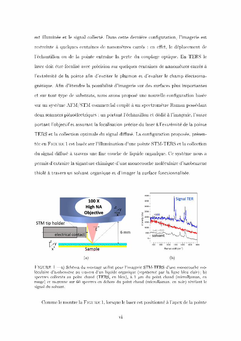
est illuminée et le signal collecté. Dans cette dernière conguration, l'imagerie est
restreinte à quelques centaines de nanomètres carrés : en eet, le déplacement de
l'échantillon ou de la pointe entraîne la perte du couplage optique. En TERS le
laser doit être focalisé avec précision sur quelques centaines de nanomètres carrés à
l'extrémité de la pointe an d'exciter le plasmon et d'exalter le champ électroma-
gnétique. An d'étendre la possibilité d'imagerie sur des surfaces plus importantes
et sur tout type de substrats, nous avons proposé une nouvelle conguration basée
sur un système AFM/STM commercial couplé à un spectromètre Raman possédant
deux scanners piézoélectriques : un portant l'échantillon et dédié à l'imagerie, l'autre
portant l'objectif et assurant la focalisation précise du laser à l'extrémité de la pointe
TERS et la collection optimale du signal diusé. La conguration proposée, présen-
tée en Figure 1 est basée sur l'illumination d'une pointe STM-TERS et la collection
du signal diusé à travers une ne couche de liquide organique. Ce système nous a
permis d'extraire la signature chimique d'une monocouche moléculaire d'azobenzene
thiolé à travers un solvant organique et d'imager la surface fonctionnalisée.
(a) (b)
Figure 1 a) Schéma du montage utilisé pour l'imagerie STM-TERS d'une monocouche mo-léculaire d'azobenzène au travers d'un liquide organique (représenté par la ligne bleu clair) ; b)spectres collectés au point chaud (TERS, en bleu), à 1 µm du point chaud (microRaman, enrouge) et moyenne sur 60 spectres en dehors du point chaud (microRaman, en noir) révélant lesignal du solvant.
Comme le montre la Figure 1, lorsque le laser est positionné à l'apex de la pointe
vi

(au niveau du point chaud), le spectre obtenu est celui de la molécule assemblée
en monocouche sur la surface. Le spectre en rouge est celui obtenu dans les même
conditions d'illumination et de collection mais à 1 µm de la position du point chaud :
aucune bande n'est observée. Le spectre noir est celui obtenu en moyennant 60
spectres en dehors du point chaud et correspond à la signature du solvant utilisé
(l'hexadécane) qui n'écrante pas le signal exalté sous la pointe au niveau du point
chaud.
Cette conguration nous a permis d'obtenir la première image TERS d'une sur-
face en milieu liquide, présentée en Figure 2 avec la topographie de la surface me-
surée sur la même zone. Cette image est obtenue par intégration d'une des bandes
du spectre.
L'intensité du signal est inhomogène sur l'ensemble de la zone cartographiée
ce qui a été attribué à une transition entre deux zones à taux de couverture en
azobenzène diérents. [23]
Outre la démonstration de la possibilité de cartographier des surfaces en TERS
en milieu liquide avec ce mode d'illumination et de collection du signal, ce dispositif
devrait aussi permettre d'étudier des échantillons sensibles à l'air en les protégeant
d'une ne couche de liquide organique ou an de prévenir la contamination des
surfaces par des polluants organiques présents dans l'atmosphère. De plus, il a été
montré que le signal TER était moins uctuant en liquide qu'à l'air : ce montage
devrait permettre d'évaluer l'eet du solvant sur l'exaltation et la stabilité du signal
en fonction de l'environnement en l'étendant aux liquides.
Spectroscopie Raman exaltée de surface sur pointe
pour l'étude de réactions électrochimiques
Dans un deuxième temps, les capacités d'une pointe TERS à exalter le signal
Raman ont été employées pour suivre une réaction électrochimique se produisant
vii

(a) (b)
(c)
Figure 2 Image STM-TERS dans l'hexadecane. a) cartographie TERS obtenue dans l'hexa-decane par intégration de la bande entre 1125 and 1162 cm−1 (λexc = 632.8 nm, puissance laser :98 µW, temps d'acquisition : 107 ms par pixel, 30 × 30 px2) ; b) cartographie STM (256 × 256px2) de la zone a) ; c) série de 10 spectres issus de la cartographie présentée en a) (moyenne de 9spectres à chaque position).
sur cette pointe utilisée comme électrode. Dans cette conguration, l'extrémité de
la pointe se comporte comme un substrat SERS à point chaud unique. Ce mode
d'exaltation du signal Raman a été appelé spectroscopie Raman exaltée de surface
sur pointe (tip surface-enhanced Raman spectroscopy, tip SERS). An de l'utiliser
pour suivre des réactions électrochimiques, la pointe doit être immergée dans un
électrolyte. A l'inverse de la conguration précédente, un des apports majeurs de
viii
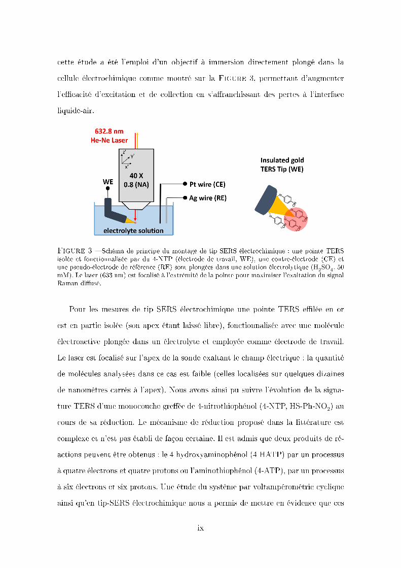
cette étude a été l'emploi d'un objectif à immersion directement plongé dans la
cellule électrochimique comme montré sur la Figure 3, permettant d'augmenter
l'ecacité d'excitation et de collection en s'aranchissant des pertes à l'interface
liquide-air.
Figure 3 Schéma de principe du montage de tip SERS électrochimique : une pointe TERSisolée et fonctionnalisée par du 4-NTP (électrode de travail, WE), une contre-électrode (CE) etune pseudo-électrode de référence (RE) sont plongées dans une solution électrolytique (H2SO4, 50mM). Le laser (633 nm) est focalisé à l'extrémité de la pointe pour maximiser l'exaltation du signalRaman diusé.
Pour les mesures de tip SERS électrochimique une pointe TERS elée en or
est en partie isolée (son apex étant laissé libre), fonctionnalisée avec une molécule
électroactive plongée dans un électrolyte et employée comme électrode de travail.
Le laser est focalisé sur l'apex de la sonde exaltant le champ électrique : la quantité
de molécules analysées dans ce cas est faible (celles localisées sur quelques dizaines
de nanomètres carrés à l'apex). Nous avons ainsi pu suivre l'évolution de la signa-
ture TERS d'une monocouche greée de 4-nitrothiophénol (4-NTP, HS-Ph-NO2) au
cours de sa réduction. Le mécanisme de réduction proposé dans la littérature est
complexe et n'est pas établi de façon certaine. Il est admis que deux produits de ré-
actions peuvent être obtenus : le 4-hydroxyaminophénol (4-HATP) par un processus
à quatre électrons et quatre protons ou l'aminothiophénol (4-ATP), par un processus
à six électrons et six protons. Une étude du système par voltampérométrie cyclique
ainsi qu'en tip-SERS électrochimique nous a permis de mettre en évidence que ces
ix

deux voies de réduction étaient en compétition. Certains intermédiaires réactionnels
parfois suggérés (produits de dimérisation du 4-HATP : dimercaptoazobenzene et
dérivés) n'ont pas pu être observés.
La Figure 4 présente une série de spectres EC-TERS enregistrés au cours d'un
processus de réduction progressif de la monocouche sur une pointe. Ils attestent de
la formation du 4-ATP lorsque la réduction est complète et nous avons pu montrer
que ce produit est aussi formé dans des conditions de réduction où le seul produit
de réduction attendu était décrit comme étant le 4-HATP.
Figure 4 Evolution du spectre EC-TERS enregistré après diérents voltampérogrammessuccessifs à des potentiels de réduction de plus en plus grands. Le spectre évolue de cycle en cyclede celui du 4-NTP (1, en rouge) à celui du 4-ATP (6, en bleu) après réduction complète.
Cette étude a démontré les capacités du tip-SERS électrochimique à suivre une
réaction in situ et à améliorer la compréhension de son mécanisme. Cette méthode
doit pouvoir être étendue à d'autre systèmes moléculaires plus complexes pouvant
être immobilisés sur des pointes TERS pour étudier leur comportement électrochi-
mique en suivant l'évolution de leur signature vibrationnelle. [24]
x
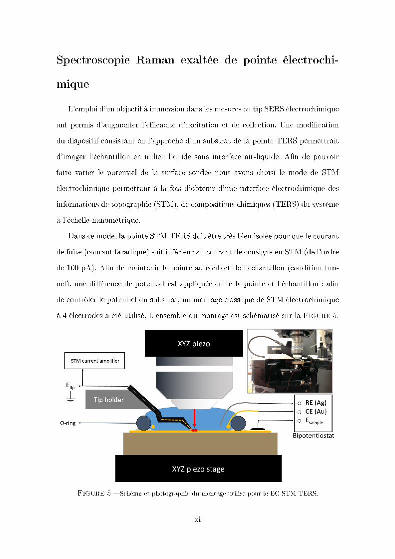
Spectroscopie Raman exaltée de pointe électrochi-
mique
L'emploi d'un objectif à immersion dans les mesures en tip SERS électrochimique
ont permis d'augmenter l'ecacité d'excitation et de collection. Une modication
du dispositif consistant en l'approche d'un substrat de la pointe TERS permettrait
d'imager l'échantillon en milieu liquide sans interface air-liquide. An de pouvoir
faire varier le potentiel de la surface sondée nous avons choisi le mode de STM
électrochimique permettant à la fois d'obtenir d'une interface électrochimique des
informations de topographie (STM), de compositions chimiques (TERS) du système
à l'échelle nanométrique.
Dans ce mode, la pointe STM-TERS doit être très bien isolée pour que le courant
de fuite (courant faradique) soit inférieur au courant de consigne en STM (de l'ordre
de 100 pA). An de maintenir la pointe au contact de l'échantillon (condition tun-
nel), une diérence de potentiel est appliquée entre la pointe et l'échantillon : an
de contrôler le potentiel du substrat, un montage classique de STM électrochimique
à 4 électrodes a été utilisé. L'ensemble du montage est schématisé sur la Figure 5.
Figure 5 Schéma et photographie du montage utilisé pour le EC-STM TERS.
xi
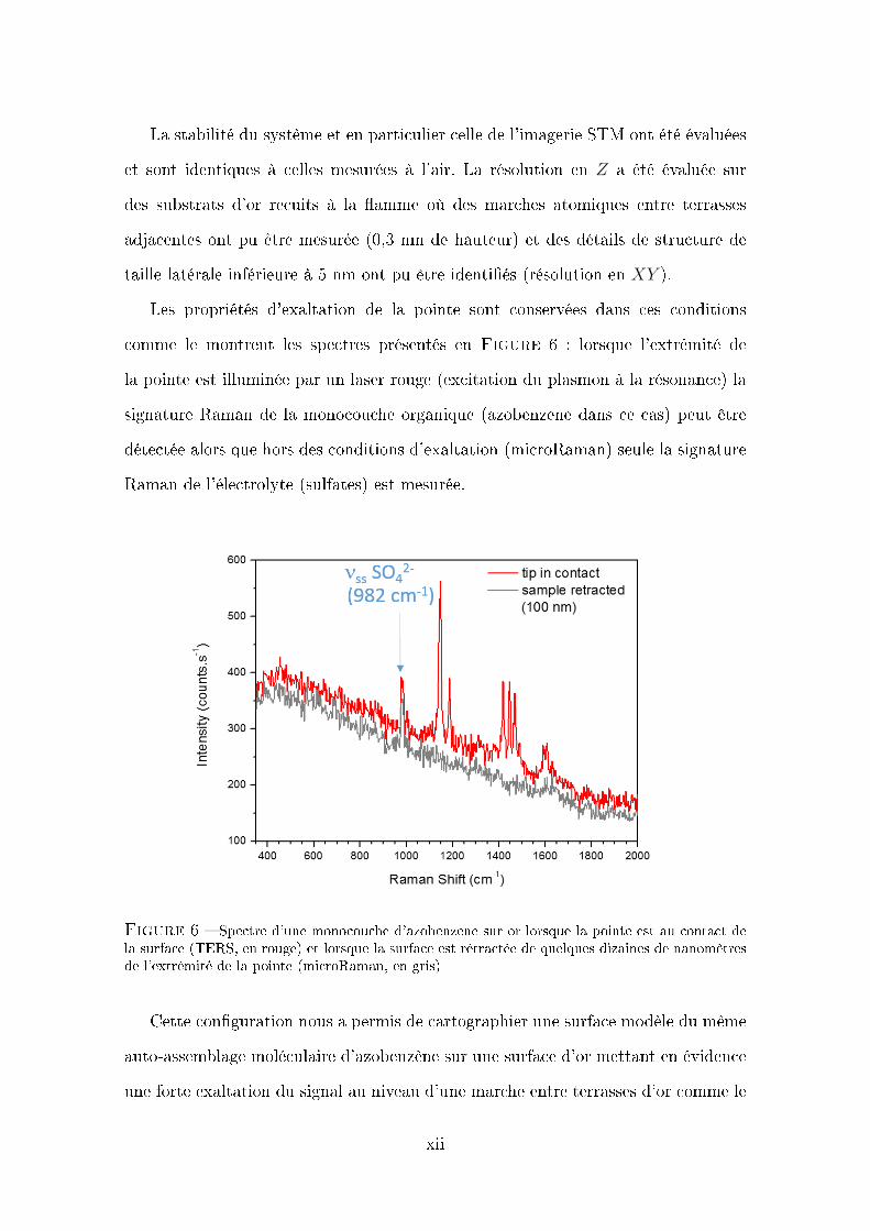
La stabilité du système et en particulier celle de l'imagerie STM ont été évaluées
et sont identiques à celles mesurées à l'air. La résolution en Z a été évaluée sur
des substrats d'or recuits à la amme où des marches atomiques entre terrasses
adjacentes ont pu être mesurée (0,3 nm de hauteur) et des détails de structure de
taille latérale inférieure à 5 nm ont pu être identiés (résolution en XY ).
Les propriétés d'exaltation de la pointe sont conservées dans ces conditions
comme le montrent les spectres présentés en Figure 6 : lorsque l'extrémité de
la pointe est illuminée par un laser rouge (excitation du plasmon à la résonance) la
signature Raman de la monocouche organique (azobenzene dans ce cas) peut être
détectée alors que hors des conditions d'exaltation (microRaman) seule la signature
Raman de l'électrolyte (sulfates) est mesurée.
Figure 6 Spectre d'une monocouche d'azobenzene sur or lorsque la pointe est au contact dela surface (TERS, en rouge) et lorsque la surface est rétractée de quelques dizaines de nanomètresde l'extrémité de la pointe (microRaman, en gris)
Cette conguration nous a permis de cartographier une surface modèle du même
auto-assemblage moléculaire d'azobenzène sur une surface d'or mettant en évidence
une forte exaltation du signal au niveau d'une marche entre terrasses d'or comme le
xii

montre la Figure 7.
(a) (b)
Figure 7 Cartographie STM-TERS électrochimique d'une monocouche d'azobenzène dans unesolution de Na2SO4 (50 mM), Es = 0 V/Ag ; a) cartographie EC-TERS obtenue par intégration desbandes entre 1100 and 1200 cm−1 (λexc = 632.8 nm, puissance laser : 98 µW, temps d'acquisition :500 ms par pixel, 50 × 27 px2) et cartographie STM (50 × 27 px2) de la même zone ; b) spectresTER aux positions indiquées sur la cartographie en a).
Ces résultats préliminaires mettent en évidence la capacité de ce dispositif à ima-
ger des surfaces en conditions électrochimiques, c'est-à-dire en contrôlant le potentiel
de la surface à analyser, et au travers d'une couche d'électrolyte. Ce dispositif de-
vrait pouvoir être étendu, comme le tip SERS, à l'étude de systèmes plus complexes
mettant en jeu des transformations électrochimiques an, dans ce cas, de mettre en
relation les informations spectroscopiques sur la transformation avec la topographie
de l'échantillon et ses hétérogénéités.
Analyse par TERS d'une surface fonctionnalisée par
des sels de diazoniums
La dernière partie des travaux présentés dans cette thèse concerne une autre
approche, ex situ, du TERS pour l'analyse de phénomènes électrochimiques et la
compréhension de leurs mécanismes. Nous nous sommes intéressés à l'étude de la
xiii

fonctionnalisation de surfaces par voie électrochimique. Une des méthodes classiques
développée depuis le début des années 1990 est la réduction de sels de diazoniums
qui permet l'ancrage covalent d'édices moléculaires variées sur tout type de maté-
riaux. [25,26] Leur diversité de structures et donc de propriétés les rend attractifs en
ce qu'ils permettent de modier les propriétés de surface d'un matériau pour des ap-
plications qui vont de la protection des métaux contre la corrosion, aux biocapteurs
en passant par l'électronique moléculaire. [2729]
Nous nous sommes intéressés au cas d'une molécule électroactive d'intérêt pour
des applications en électronique moléculaire : un dérivé diazonium de bisterpyridine
de fer. L'analyse électrochimique et TERS de surfaces fonctionalisées par cette molé-
cule a mis en évidence des diérences majeures dans la structure des couches greées
dans le cas d'un greage spontané (sans application de potentiel) et d'une réduction
électrochimique. Dans le cas du greage spontané, les couches sont moins denses,
mieux organisées et semblent se limiter à la formation de monocouches. Dans le cas
du greage électrochimique, les données obtenues en TERS tendent à laisser penser
que le greage se fait sur plusieurs couches de façon moins organisée. La connaissance
de la structure de ces couches est primordiales pour pouvoir interpréter des données
électrochimiques telles que les vitesses de transfert d'électrons de l'électrode vers la
couche (ou l'inverse) et entre plusieurs centres redox au sein même de la couche qui
peuvent être obtenues par voltampérométrie cyclique utra-rapide.
Perspectives
Diérentes approches ont été développées au cours de cette thèse dans le but
d'étendre le champ d'investigation possible du TERS aux systèmes électrochimiques :
l'étude de surfaces fonctionnalisées par greage électrochimique de sels de
diazoniums devrait pouvoir être étendu à d'autres structures moléculaires du
même type an de mieux connaître leur structures, le mécanisme de greage
xiv

et ainsi de mieux contrôler leurs propriétés ;
le tip SERS électrochimique s'est montré ecace pour l'analyse in situ d'un
mécanisme réactionnel modéle et devrait pouvoir permettre l'étude de sys-
tèmes adsorbés plus complexes et dont le mécanisme de transformation élec-
trochimique est encore à élucider ;
la cartographie de composition en liquide voire en conditions électrochimiques
est rendue possible et montrée pour la première fois, ouvrant ainsi la voie à
des études sur d'autres systèmes plus complexes que les interfaces modèles
choisies pour démontrer les capacités de notre approche.
Ce travail s'inscrit donc à la suite des premiers travaux sur l'application du
TERS aux interfaces électrochimiques. Les diverses approches proposées ouvrent
donc la voie à des études de systèmes plus complexes et à portée plus large comme
des interfaces de catalyse hétérogène ou matériaux de batteries, in situ, c'est-à-dire
dans les conditions de leur fonctionnement.
xv

Bibliographie
[1] A. J. Bard and L. R. Faulkner. Electrochemical methods : Fundamentals and
applications. Wiley, 2d edition, 2001.
[2] M. T. Polk. Electrochemical STM. Wiley, 2007.
[3] A. J. Bard, F. R. F. Fan, J. Kwak, and O. Lev. Scanning electrochemical
microscopy. introduction and principles. Analytical Chemistry, 61(2) :132138,
1989.
[4] W. Kaim and J. Fiedler. Spectroelectrochemistry : the best of two worlds.
Chemical Society Reviews, 38(12) :33733382, 2009.
[5] Y. Zhai, Z. Zhu, S. Zhou, C. Zhu, and S. Dong. Recent advances in spectroe-
lectrochemistry. Nanoscale, 10 :30893111, 2018.
[6] M. Fleischmann, P. J. Hendra, and A. J. McQuillan. Raman spectra of pyridine
adsorbed at a silver electrode. Chemical Physics Letters, 26(2) :163166, 1974.
[7] D. L. Jeanmaire and R. P. Van Duyne. Surface raman spectroelectrochemistry :
Part I. Heterocyclic, aromatic, and aliphatic amines adsorbed on the anodized
silver electrode. Journal of electroanalytical chemistry and interfacial electro-
chemistry, 84(1) :120, 1977.
[8] M. G. Albrecht and J. A. Creighton. Anomalously intense Raman spectra
of pyridine at a silver electrode. Journal of the american chemical society,
99(15) :52155217, 1977.
[9] L. Novotny and B. Hecht. Principles of nano-optics. Cambridge University
Press, 2d edition, 2012.
xvi

[10] R. M. Stöckle, Y. D. Suh, V. Deckert, and R. Zenobi. Nanoscale chemi-
cal analysis by tip-enhanced Raman spectroscopy. Chemical Physics Letters,
318(13) :131136, February 2000.
[11] B. Pettinger, G. Picardi, R. Schuster, and G. Ertl. Surface enhanced Raman
spectroscopy : towards single molecule spectroscopy. Electrochemistry (Tokyo),
68(12) :942949, 2000.
[12] M. S. Anderson. Locally enhanced Raman spectroscopy with an atomic force
microscope. Applied Physics Letters, 76(21) :31303132, 2000.
[13] N. Hayazawa, Y. Inouye, Z. Sekkat, and S. Kawata. Metallized tip amplication
of near-eld Raman scattering. Optics Communications, 183(1-4) :333336,
2000.
[14] C. C. Neacsu, S. Berweger, and M. B. Raschke. Tip-Enhanced Raman Imaging
and Nanospectroscopy : Sensitivity, Symmetry, and Selection Rules. NanoBio-
technology, 3(3-4) :172196, December 2007.
[15] B. Pettinger, P. Schambach, C. J. Villagómez, and N. Scott. Tip-Enhanced
Raman Spectroscopy : Near-Fields Acting on a Few Molecules. Annual Review
of Physical Chemistry, 63(1) :379399, May 2012.
[16] C. Chen, N. Hayazawa, and S. Kawata. A 1.7 nm resolution chemical analysis
of carbon nanotubes by tip-enhanced Raman imaging in the ambient. Nature
communications, 5 :3312, 2014.
[17] R. Zhang, Y. Zhang, Z. C. Dong, S. Jiang, C. Zhang, L. G. Chen, L. Zhang, Y.
Liao, J. Aizpurua, Y. Luo, J. L. Yang, and J. G. Hou. Chemical mapping of a
single molecule by plasmon-enhanced Raman scattering. Nature, 498(7452) :82
86, June 2013.
[18] T. Schmid, B.-S. Yeo, G. Leong, J. Stadler, and R. Zenobi. Performing tip-
enhanced Raman spectroscopy in liquids. Journal of Raman Spectroscopy,
40(10) :13921399, October 2009.
xvii

[19] Z.-C. Zeng, S.-C. Huang, D.-Y. Wu, L.-Y. Meng, M.-H. Li, T.-X. Huang, J.-H.
Zhong, X. Wang, Z.-L. Yang, and B. Ren. Electrochemical Tip-Enhanced Ra-
man Spectroscopy. Journal of the American Chemical Society, 137(37) :11928
11931, September 2015.
[20] D. Kurouski, M. Mattei, and R. P. Van Duyne. Probing Redox Reactions at
the Nanoscale with Electrochemical Tip-Enhanced Raman Spectroscopy. Nano
Letters, 15(12) :79567962, December 2015.
[21] N. Martín Sabanés, L. M. A. Driessen, and K. F. Domke. Versatile Side-
Illumination Geometry for Tip-Enhanced Raman Spectroscopy at Solid/Liquid
Interfaces. Analytical Chemistry, 88(14) :71087114, July 2016.
[22] N. Kumar, W. Su, M. Veselý, B. M. Weckhuysen, A. J. Pollard, and A. J. Wain.
Nanoscale chemical imaging of solidliquid interfaces using tip-enhanced Raman
spectroscopy. Nanoscale, 10 :18151824, 2018.
[23] T. Touzalin, A. L. Dauphin, S. Joiret, I. T. Lucas, and E. Maisonhaute. Tip-
enhanced Raman spectroscopy imaging of opaque samples in organic liquid.
Physical Chemistry Chemical Physics, 18(23) :1551015513, 2016.
[24] T. Touzalin, S. Joiret, E. Maisonhaute, and I. T. Lucas. Complex electron
transfer pathway at a microelectrode captured by in situ nanospectroscopy.
Analytical chemistry, 89(17) :89748980, 2017.
[25] M. Delamar, R. Hitmi, J. Pinson, and J. M. Saveant. Covalent modication
of carbon surfaces by grafting of functionalized aryl radicals produced from
electrochemical reduction of diazonium salts. Journal of the American Chemical
Society, 114(14) :58835884, 1992.
[26] P. Allongue, M. Delamar, B. Desbat, O. Fagebaume, R. Hitmi, J. Pinson, and J.-
M. Saveant. Covalent modication of carbon surfaces by aryl radicals generated
from the electrochemical reduction of diazonium salts. Journal of the American
Chemical Society, 119(1) :201207, 1997.
xviii
[27] A. Chaussé, M. M. Chehimi, N. Karsi, J. Pinson, F. Podvorica, and C. Vautrin-
Ul. The electrochemical reduction of diazonium salts on iron electrodes. the
formation of covalently bonded organic layers and their eect on corrosion.
Chemistry of Materials, 14(1) :392400, 2002.
[28] J. J. Gooding. Advances in interfacial design for electrochemical biosensors
and sensors : aryl diazonium salts for modifying carbon and metal electrodes.
Electroanalysis, 20(6) :573582, 2008.
[29] J. C. Lacroix. Electrochemistry does the impossible : Robust and reliable large
area molecular junctions. Current Opinion in Electrochemistry, 7 :153160,
2018.
xix

233