Interfacial charge transfer in nanoscale polymer transistors

© 2013 WILEY-VCH Verlag GmbH & Co. KGaA, Weinheim
www.advhealthmat.dewww.MaterialsViews.com
wileyonlinelibrary.com 313
REV
IEW
Solution-Gated Graphene Transistors for Chemical and Biological Sensors
Feng Yan ,* Meng Zhang, and Jinhua Li
Prof. F. Yan, M. Zhang, J. H. LiDepartment of Applied Physics and Materials Research CenterThe Hong Kong Polytechnic UniversityKowloon , Hong Kong , China Email: [email protected]
DOI: 10.1002/adhm.201300221
1 . Introduction
Graphene has attracted much attention in biomedical applica-tions, including chemical or biological sensors, drug delivery, bioimaging, photodynamic therapy, and tissue engineering. Highly sensitive chemical and biological sensors are in great demand in many fi elds, including medical analysis, healthcare products, food safety tests, environmental monitoring, agri-culture industry, security, and so on. Features of each sensing strategy are profoundly infl uenced by the materials used in the devices. Graphene, because of its unique physical properties, has been regarded as a promising material in the chemical and biological sensors. [ 1–6 ] After Novoselov et al. fi rstly separated stable single-layer graphene in ambient conditions in 2004, [ 7,8 ] much progress has been made in developing graphene devices in various types of sensors. [ 9–14 ] Among all kinds of graphene-based chemical sensors and biosensors, solution-gated gra-phene transistor (SGGT), in which the gate and the graphene channel are separated by electrolyte instead of dielectric insu-lator, has shown to be the most promising one for real-time, highly sensitive, and high-throughput chemical and biological
sensors. [ 15,16 ] As shown in Figure 1 a, a SGGT is an electronic device with three metal contacts (source, drain, and gate) and a graphene channel fabricated on a substrate. The source is grounded while two different voltages are applied on the drain and the gate. The graphene channel and the gate are exposed to an electrolyte. The conductance of the graphene channel can be modulated by the gate voltage due to change of carrier densities in the channel, which is very similar to typical fi eld-effect transistors popularly used in electronic products.
Graphene, an allotrope of carbon, with a so-called honeycomb 2D single-atomic-layer structure is constructed by a sheet of sp 2 -bonded carbon atoms, which has been viewed as the basic structure of many other carbon allotropes, such as graphite
and carbon nanotubes. [ 17 ] The carbon–carbon bond length in graphene is about 0.142 nm. The unique 2D structure of gra-phene has led to many remarkable physical properties including massless carriers (both electrons and holes), high transpar-ency (97.7% for single layer), high conductivity, and extremely high carrier mobilities up to 10 5 cm 2 V −1 s −1 , which is about 2–3 orders of magnitude higher than those of typical semicon-ductors such as silicon. [ 18 ] Because of the excellent properties, graphene has been intensely investigated for the applications in transistors, solar cells, transparent conducting electrodes, sensors, and so on. Graphene holds advantages particularly in the sensing applications because it is chemically robust and bioinert. More importantly, graphene is extremely sensitive to electric fi eld and charges around it because every carbon atom of a graphene sheet is exposed to the environment.
Graphene was fi rstly prepared by mechanical exfoliation method. [ 8 ] However, it is very diffi cult to obtain large-area gra-phene fi lms using this technique. Then, several more conven-ient approaches, such as chemical vapor deposition (CVD) on metal substrates, [ 19–22 ] epitaxial growth on SiC, [ 23–26 ] and reduc-tion from separated graphene oxide (GO) fl akes, [ 27 ] and so on, have been extensively studied by many research groups. Some approaches are potentially low cost and suitable for mass pro-duction. It is notable that large-area and high-quality single- or few-layer graphene has been successfully fabricated by CVD methods, [ 21,28 ] which paved the way for the development of high performance, high density, and multifunctional graphene-based devices for many applications including the chemical and biological sensors.
Graphene has attracted much attention in biomedical applications for its fascinating properties. Because of the well-known 2D structure, every atom of graphene is exposed to the environment, so the electronic properties of graphene are very sensitive to charged analytes (ions, DNA, cells, etc.) or an electric fi eld around it, which renders graphene an ideal material for high-per-formance sensors. Solution-gated graphene transistors (SGGTs) can operate in electrolytes and are thus excellent candidates for chemical and biological sensors, which have been extensively studied in the recent 5 years. Here, the device physics, the sensing mechanisms, and the performance of the recently developed SGGT-based chemical and biological sensors, including pH, ion, cell, bacterial, DNA, protein, glucose sensors, etc., are introduced. Their advantages and shortcomings, in comparison with some conventional techniques, are discussed. Conclusions and challenges for the future develop-ment of the fi eld are addressed in the end.
Adv. Healthcare Mater. 2013, 3, 313–331
www.MaterialsViews.com
314
www.advhealthmat.de
© 2013 WILEY-VCH Verlag GmbH & Co. KGaA, Weinheimwileyonlinelibrary.com
REV
IEW
SGGTs operate in electrolytes in direct contact with analytes, which is meaningful for the detection of many biological rel-evant molecules and reactions in aqueous solutions. SGGT-based sensors are expected to have high sensitivities because of the following factors. Firstly, a transistor-based sensor could serve as both a sensor and an amplifi er. A small variation of voltage could induce a pronounced response of channel current due to the inherent amplifi cation function of the device. [ 29,30 ] Secondly, graphene shows much higher carrier mobilities than many other semiconductors used in transistor-based sensors, [ 8 ] such as organic semiconductors, [ 31–33 ] silicon nanowires, [ 34 ] and
Prof. Feng Yan has research interests on biosensors, gra-phene, organic electronics, thin fi lm transistors, solar cells, and smart materials. He received his Ph.D. degree in physics from Nanjing University in China. Then he joined the Engineering Department of Cambridge University in February 2001 as a Research Associate and joined National Physical Laboratory in UK in
April 2006 as a Higher Research Scientist. He became an Assistant Professor at the Department of Applied Physics of the Hong Kong Polytechnic University in September 2006 and was promoted to Associate Professor in July 2012.
Meng Zhang received a B.S. degree and MPhil degree in materials in School of Physics Science and Technology, Wuhan University, China. She is currently a Ph.D. student in the Department of Applied Physics of the Hong Kong Polytechnic University under the supervision of Prof. Feng Yan. Her research interests include novel sensors based
on organic thin fi lm transistors and graphene transistors for applications such as biochemical sensing, medical diagnosis, and drug delivery.
Dr. Jinhua Li received a B.E. degree in Electronic Science and Technology in 2002 and a M.E. degree in Materials Science in 2008 from Hubei University in China. He received his Ph.D. degree at the Department of Applied Physics of the Hong Kong Polytechnic University in 2012 and then carried out post-doctoral research in the same
research group. His research interests include device physics and sensing applications of organic thin fi lm transistors and graphene transistors.
carbon nanotubes. [ 1 ] Therefore, SGGTs have higher transcon-ductance (i.e., the ratio of channel current response to the gate voltage change) than other types of transistors, which is a key factor to the signal amplifi cation of the devices. [ 30 ] Thirdly, SGGTs have the operational voltages normally less than 1 V, [ 15 ]
Figure 1. a) Typical confi guration of a SGGT. b) Potential drop in a SGGT device under a gate voltage V G . The blue regions represent electric double layer (EDL). c) A typical transfer curve (channel current I DS ≈ gate voltage V G ) of a SGGT characterized at a constant drain voltage V DS .
Adv. Healthcare Mater. 2014, 3, 313–331

www.MaterialsViews.com
315
www.advhealthmat.de
© 2013 WILEY-VCH Verlag GmbH & Co. KGaA, Weinheim wileyonlinelibrary.com
REV
IEW
so the devices are very sensitive to small potential changes induced by analytes near the interfaces on the channel or the gate. Of particular interest is the factor that SGGTs can be miniaturized without the degradation of device performance because the channel current is proportional to the ratio of the channel width to length rather than the actual device size, so the devices are promising in the applications as high-density and multifunctional microarrays that can provide unprec-edented simultaneous and multiplexed analysis in a high-throughput screening format. [ 29 ]
In this Review, we will focus on the recent progress and the performance of SGGT-based chemical and biological sensors in the detection of pH, ions, biological analytes and bioreac-tions, as shown in Table 1 . Some other kind of graphene-based sensors such as gas sensors and electrochemical sensors can be found in other review papers. [ 1–6,35 ] The detailed working
principle and the fabrication of SGGTs are introduced fi rst. Then, the sensors are sorted by their applications and described in the two sessions: 1) chemical sensors, including pH and ion sensors; 2) biosensors, including glucose, DNA, cell, bacterial, and protein sensors. It is notable that all of the sensors are potentially useful in healthcare products. In the end, conclu-sions and outlook for the SGGT-based sensors are presented.
2 . Device Physics and Fabrication
2.1 . Performance of SGGTs
Figure 1 a shows the structure of a typical SGGT consisting of a graphene channel between source and drain electrodes and a gate electrode immersed in an electrolyte. In a transistor, the
Table 1. Parameters of different types of chemical and biological sensors based on SGGTs.
Sensor type Analyte Active layer Detection limit or sensitive region Reference, year
pH sensor H 3 O + , OH − Epitaxal graphene pH 14–2, 99 mV/pH [ 73 ] , 2008
pH Exfoliated graphene pH 4.0–8.2, 25 mV/pH [ 47 ] , 2009; [ 76 ] , 2010
pH Suspended graphene pH 6–9, 20 mV/pH [ 77 ] , 2010
pH CVD-grown graphene Insensitive, 6–0 mV/pH [ 78 ] , 2011
Ion sensor NaF Exfoliated graphene 10 × 10 −3 M to 1 M [ 79 ] , 2009
NaCl, KCl CVD-grown graphene [ 80 ] , 2010
Na + Exfoliated graphene 1.0 × 10 −9 M to 1.0 × 10 −3 M [ 81 ] , 2010
Ca 2+ , Mg 2+ , Hg 2+ , Cd 2+ rGO Ca 2+ : ≈ 1 × 10 −6 M , Hg 2+ : ≈ 1 × 10 −9 M , Cd 2+ : ≈ 1 × 10 −9 M [ 74 ] , 2011
KCl CVD-grown graphene 1 × 10 −6 M [ 36 ] , 2012
NaCl CVD-grown graphene ≈ 40 × 10 −9 M [ 75 ] , 2012
Pb 2+ CVD-grown graphene ≈ 20 × 10 −12 M [ 63 ] , 2012
Cell-based biosensor Chicken cardiomyocyte Exfoliated graphene [ 44 ] , 2010
Cardiomyocyte-like HL-1 CVD-grown graphene [ 88 ] , 2011
Malaria-infected red blood cells CVD-grown graphene [ 91 ] , 2011
Bacterial sensor Gram-positive Bacillus cereus cells GO and GA A single bacterium [ 45 ] , 2008
E. coli , P. aeruginosa CVD-grown graphene 10 cfu mL −1 [ 41 ] , 2011
DNA sensor DNA GO [ 45 ] , 2008
DNA CVD-grown graphene 10 × 10 −12 M [ 42 ] , 2010
DNA rGO 10 × 10 −9 M [ 96 ] , 2010
DNA CVD-grown graphene 1 × 10 −9 M [ 93 ] , 2011
DNA rGO 2.4 × 10 −9 M [ 97 ] , 2012
DNA CVD-grown graphene 1 × 10 −12 M [ 94 ] , 2013
DNA CVD-grown graphene 1 × 10 −12 M [ 43 ] , 2013
Glucose sensor Glucose CVD-grown graphene 0.1 × 10 −3 M [ 60 ] , 2010
Glucose CVD-grown graphene 3.3–10.9 × 10 −3 M [ 106 ] , 2012
Protein sensor BSA Exfoliated graphene 0.3 × 10 −9 M [ 47 ] , 2009
IgE Exfoliated graphene 0.29 × 10 −9 M [ 99 ] , 2010
Fibronectin; avidin rGO 0.5 × 10 −9 M ; 80 × 10 −9 M [ 100 ] , 2011
Immunoglobulin G rGO 0.2 ng mL −1 [ 58 ] , 2011
PSA–ACT complex rGO 1.1 × 10 −15 M [ 101 ] , 2013
Dopamine sensor Dopamine rGO 1–60 × 10 −3 M [ 109 ] , 2010
Bioelectronic nose Amyl butyrate CVD-grown graphene 0.04 × 10 −15 M [ 110 ] , 2012
Adv. Healthcare Mater. 2013, 3, 313–331

www.MaterialsViews.com
316
www.advhealthmat.de
© 2013 WILEY-VCH Verlag GmbH & Co. KGaA, Weinheimwileyonlinelibrary.com
REV
IEW direct conduction current between the gate electrode and the
source or the drain electrode is prohibited. According to our experience, the source and drain electrode cannot be exposed to the electrolyte. A direct contact of the source and the drain elec-trodes with the electrolyte can induce high gate leakage current and unstable performance of the device when a gate voltage is applied. Because the electrolyte is conductive, the gate voltage is thus actually applied on the two interfaces, including gate/electrolyte and electrolyte/graphene interfaces, as shown in Figure 1 b. Each interface has an EDL that can be regarded as a capacitor. [ 36 ] Similar to a fi eld-effect transistor, the channel con-ductance of the SGGT can be modulated by the gate voltage due to fi eld-effect doping. The device performance of a SGGT can be presented by a transfer curve, which is the channel current I DS between source and drain as a function of gate voltage V G at a fi xed drain voltage V DS . Because graphene has zero bandgap, SGGTs exhibit ambipolar transfer characteristics, which means the device exhibits both p-channel (hole conduction) at negative gate voltage side and n-channel (electron conduction) at posi-tive gate voltage side, as shown in Figure 1 c. No off current can be observed in the transfer curve of a SGGT. The channel cur-rent I DS for both p-channel and n-channel of a SGGT is given by [ 15 ] :
IDS ≈ W
L:Ci |VG − VDirac| VDS, for |VG − VDirac| >> |VDS|
(1)
where V DS and V G are the voltages applied on the drain and the gate electrodes, respectively; W and L are the width and length of the channel, respectively; μ is the carrier (electron or hole) mobility in graphene; C i is the gate capacitance. It is worth noting that C i is not a constant value and is dependent on V G . V Dirac is the gate voltage when the Fermi level in gra-phene channel is modulated to the charge neutrality point (Dirac point). This gate voltage is called the Dirac point voltage of the device.
As shown in Figure 1 b, the gate capacitance of a SGGT is related to the two EDL capacitors ( C EDL1 and C EDL2 ) connected in series. The capacitance of an EDL is about 10–40 μ F cm −2 , [ 37 ] which is largely dependent on ion concentrations in the elec-trolyte and the applied bias voltage. In addition, the quantum capacitance of graphene channel due to the change of Fermi level when it is charged should be considered. The quantum capacitance C Q is given by: [ 38 ]
CQ = ∂ Q/∂Vch= q 2 2
Bq Vch
(�vF)2 (q Vch � kT )
(2)
where Q is the charge density in graphene channel, q is electron charge, V ch is the channel electrostatic potential, v F ≈ 10 8 cm s −1 is the Fermi velocity of carriers in graphene, and � is the reduced Planck’s constant. The quantum capaci-tance of graphene is dependent on V ch and changes from zero to tens of μ F cm −2 , which is lower than or even comparable to double-layer capacitance. [ 38 ] Therefore, the gate capacitance of the graphene transistor consists of the two double-layer capacitors and the quantum capacitance connected in series, as shown in Figure 1 b. Nevertheless, the total gate capacitance (tens of μ F cm −2 ) of a SGGT is much bigger than that of a typ-ical fi eld-effect transistor with a thermal oxide gate insulator.
For example, the capacitance for a 100 nm-thick SiO 2 layer is only ≈ 345 nF cm −2 . [ 39 ] According to Equation (1) , if C i is very high, a low gate voltage can induce a substantial change of channel current. Therefore, the operational voltage of a SGGT is normally less than 1 V, which is much lower than that of a typical fi eld-effect transistor.
The sensitivity of an electronic sensor is the minimum magnitude of input signal that can produce an output signal with a specifi ed signal-to-noise ratio. In analytical chemistry, detection limit, which is the minimum concentration or quan-tity of a substance that can be distinguished from a suitable blank value, [ 40 ] actually has the similar meaning and is nor-mally used to describe the sensitivity of a chemical or bio-logical sensor. An electronic sensor may have a signal even when a blank is analyzed, which is referred to as the noise level. So the detection limit is normally defi ned as the concen-tration of analyte that can generate output signal three times higher than the standard deviation of the noise level. Noise in typical graphene fi led-effect transistors has been found to be inversely proportional to frequency ( f) at low-frequency region ( f < 100 Hz) and related to the quality of graphene and the device fabrication conditions. [ 10 ] However, the noise level of SGGTs has not been systematically studied until now and fur-ther work is needed.
The current responses of SGGTs to analytes are impor-tant for their sensing applications. Because the SGGT-based sensors are sensitive to potential changes at interfaces as explained in the following section in more details, the cur-rent responses of the devices are proportional to the transcon-ductance of the devices. The change in I DS for a given change in V G is called the transconductance ( g m ) of a transistor. [ 39 ] According to Equation (1) , the transconductance of the device is given by: [ 39 ]
gm = �IDS
�VG= W
L:CiVDS
(3)
So the channel current response of a SGGT is proportional to the carrier mobility ( μ ) and the gate capacitance ( C i ).
2.2 . Sensing Mechanisms of SGGT-Based Sensors
When SGGTs are used as chemical or biological sensors, there are several different sensing mechanisms as reported in litera-ture. In general, analytes can change one or several parameters in Equation (1) . The possible sensing mechanisms are as follows.
1. Potential drops at interfaces . SGGTs are sensitive to potential changes at the gate electrodes or the graphene channels, which are similar to other types of transistor-based sen-sors. [ 30 ] In this case, the Dirac point voltages ( V Dirac ) of the devices can be changed by the analytes, which lead to hori-zontal shifts of the transfer curves. Almost all pH and ion-sensitive SGGT sensors are based on this mechanism. [ 36 ] Some biosensors, such as bacterial and DNA sensors, [ 41,42 ] also operate with the same principle. It is notable that most of the researchers were focusing on the potential change on the graphene active layer, whereas few noticed that the potential drop on the gate electrode is equally important to
Adv. Healthcare Mater. 2014, 3, 313–331

www.MaterialsViews.com
317
www.advhealthmat.de
© 2013 WILEY-VCH Verlag GmbH & Co. KGaA, Weinheim wileyonlinelibrary.com
REV
IEW
the sensing applications. Our group recently demonstrated that a KCl ion sensor could be realized by using a SGGT with an Ag/AgCl gate electrode based on the changes of the potential drop at the gate electrode with the variation of ion concentrations. [ 36 ] So many other types of chemical and bio-logical sensors with functional gate electrodes are expected to be realized in the future although few works have been reported until now.
2. Changes of carrier mobility or doping level in graphene . The interactions between analytes and graphene channel may dramatically change the graphene properties, especially the carrier mobility and the Fermi level, which all infl uence the performance of the SGGTs. Many biosensors, such as DNA, [ 43 ] cell, [ 44 ] and bacteria sensors, [ 45 ] have been realized based on this mechanism. The selectivity of this type of de-vices would be a major problem if pristine graphene was used in the active layer, so surface modifi cation on the gra-phene layer is needed in specifi c detections.
3. Change of contact resistance . Contact resistance in a transistor is an important factor for the device performance, although it is not included in Equation 1 . The contact resistance is nor-mally due to the nonohmic contact near the source and/or drain electrodes induced by energy level mismatch between the metal contact and the semiconductor layer. Therefore, the modulation of the work function of the metal electrode can change the device performance, including the calculated fi eld-effect carrier mobility and the Dirac point voltage. [ 46 ] Although this mechanism in the SGGT sensors has not yet been confi rmed, [ 47 ] biosensors based on other types of tran-sistors, including carbon nanotube transistors and organic thin fi lm transistors, [ 48,49 ] were reported to operate with this mechanism. Similar effect is expected in some SGGT-based sensors especially short channel devices. It is notable that some researchers may not realize this effect in analyzing their data as the effect is rather diffi cult to be clarifi ed and separated from other possible factors.
4. Potential change in electrolyte . Electrolytes are conductive and are thus equipotential in the bulk. However, in some special cases, there is a potential drop in the electrolyte between the gate and the channel, which will also infl uence the perfor-mance of a SGGT device. For example, our group reported the SGGT-based fl ow velocity sensor, [ 36 ] which was based on measuring the variation of streaming potential in the electrolyte due to the change of fl ow velocity. In biological systems, especially living organisms, potential drops maybe induced by fl uids or the diffusion of ions, which all may change the performance of a SGGT device when it was used for in vitro or in vivo tests.
5. Gate capacitance change . The EDL capacitance ( C EDL1 and C EDL2 in Figure 1 b) is related to ion concentrations, impuri-ties, or distribution of charges near the graphene laye or the gate electrode. [ 50 ] Therefore, the device performance can be infl uenced by this factor at certain measurement conditions.
2.3 . Device Fabrication
Compared with typical thin fi lm transistors with a multi-layer structure, SGGTs have a much simpler design with the
separated gate and channel regions, as shown in Figure 1 a. The source, drain, and gate electrodes can be deposited and pat-terned with typical microfabrication techniques directly on sub-strates. [ 36 ] The graphene active layer can be fabricated by using printing or transfer techniques. The metal (e.g., Au) source and drain electrodes can be isolated from the electrolyte by the graphene layer above them because high-quality graphene fi lm is impermeable to water. However, if the metal electrodes are deposited on top of the graphene layer, packaging of the metal contacts is needed to ensure low gate leakage currents. [ 36 ]
The major concern in the fabrication of SGGTs is the quality of graphene used in the devices. Producing high-quality gra-phene in scalable, economical processes is a very important step for the fabrication of graphene devices. Three major kinds of graphene have been used in the fabrication of SGGTs, including graphene fl akes prepared by mechanical exfoliation, [ 8 ] CVD-grown graphene, [ 28 ] and solution-based and chemically reduced graphene oxide (rGO) prepared by chemical exfoliation of graphite. [ 6,45 ] Each method has its own advantages, draw-backs, and unique features in terms of economic cost, quality, and processability.
2.3.1 . Mechanically Exfoliated Graphene
Pristine graphene without any functionalization is insoluble in any solvent. Therefore, pristine graphene channel can be fabricated by directly transferring graphene sheets onto the substrate by mechanical cleavage, known as the “scotch-tape” method. [ 8,51 ] The technique is easy to achieve, using adhesive tape to repeatedly peel layers off of highly oriented pyrolytic graphite and pressing it onto an target substrate. The pristine single- or few-layer graphene exhibits the best electronic and structural qualities, high carrier mobilities at room tempera-ture, and low intrinsic noises as compared with other nano-structured graphene fi lms. So that it is used very often to study the intrinsic properties of graphene and related devices. How-ever, it is diffi cult to control the shape, size, and location of this kind of graphene, as shown in Figure 2 a. Hence, the yield of the devices is extremely low. It is obvious that mechanically exfoliated graphene is more suitable for fundamental study than practical applications, such as SGGTs.
2.3.2 . Graphene Prepared by CVD
CVD method has emerged to be one of the most promising techniques for the large-scale production of single- and multi-layer graphene fi lms. Carbon atoms can be dissolved in metal (e.g., Ni, Ru, and Cu) foils at high temperature and then pre-cipitated onto the metal surfaces to form graphene fi lms upon cooling. By using this method, graphene fi lms could be pre-pared on the metal substrates particularly on Cu foils that can lead to single-layer yield as high as 95%. [ 19–22 ] As shown in Figure 2 b, large-area graphene with a size up to tens of inches can be prepared by a CVD method. So this technique can enable the mass production of SGGTs with high reproducibility for many practical applications. Another advantage of CVD growth is the feasibility of substitutional doping by introducing heteroatoms (nitrogen, boron, etc.) into the carbon lattice, [ 52 ] which is also important in functionalizing or optimizing the
Adv. Healthcare Mater. 2013, 3, 313–331

www.MaterialsViews.com
318
www.advhealthmat.de
© 2013 WILEY-VCH Verlag GmbH & Co. KGaA, Weinheimwileyonlinelibrary.com
REV
IEW
graphene transistors. Because of the large size of CVD grown graphene, arrays of SGGTs with designed shapes and sizes could be achieved by microfabrication techniques, which shows great potential for miniaturized multifunctional sensing arrays and lab-on-a-chip applications. [ 36,50 ]
On the other hand, there are still many shortcomings of this technique. The CVD-grown graphene can only be prepared on certain metallic substrates and needs to be transferred to target substrates by wet-chemical process with the assistance of a layer of polymer, such as polymethyl methacrylate (PMMA), [ 53,54 ] coated on the surface to stabilize the graphene fi lm before the metal substrate is etched away. The transfer process adds addi-tional complications to the quality and consistency of samples such as cracking, contaminations, and destruction of graphene sheets, causes deterioration of the physical and electronic prop-erties. So the transfer process needs to be optimized in the fab-rication of high-performance SGGTs. In addition, the substrate can also infl uence the physical properties of graphene dramati-cally due to the interaction between them as evidenced by many reports. Therefore, the substrate modifi cation or treatment is another issue needs to be considered in the fabrication of gra-phene transistors. [ 53 ]
Alternatively, another method to obtain an arbitrarily large graphene fi lm is to decompose silicon carbide (SiC) to gra-phene at high temperatures. [ 23–26 ] However, several issues limit its practical applications. It is diffi cult to precisely control the properties of graphene epitaxially grown on SiC and it also
needs additional transfer steps for device fabrication. More importantly, this technique is not suitable for mass-production for the high price of single-crystal SiC.
2.3.3 . GO and rGO
Chemical exfoliation of graphite into GO provides an oppor-tunity to produce solution-processable graphene, which ena-bles the mass production of graphene-based electronics at low cost. [ 6 ] Different from direct physical cleavage, chemicals were used to intercalate bulk graphite by inserting reactants between layers that weaken the cohesive van der waals force. Typically, a stable, homogeneous GO aqueous suspension could be gener-ated by a modifi ed Hummers method, [ 55–57 ] graphite is oxidized with sulfuric acid and potassium permanganate and exfoliated as a result. As shown in Figure 2 c, the lateral dimensions of GO fl akes ranging from several hundred nanometers to sev-eral micrometers. This method has relatively shorter reaction time and has little toxic side products. Mohanty and Berry fi rstly used GO as sensing material in SGGTs, [ 45 ] and this mate-rial is still popularly used in SGGT until now. So GO could be produced at low cost, easily used in various devices, and most importantly, have plenty of oxygen functional groups such as carboxylic acid, epoxy and alcohol groups that could be used for modifying biorecognition molecules in biosensors. However, GO has a signifi cant shortcoming compared with pristine gra-phene and CVD graphene. The oxidation process could induce defects that can scatter charge carriers, decrease the carrier mobility and increase the overall noise of the device.
Many method of removing the functional groups on GO through chemical reduction, thermal, photothermal, or electro-chemcial reduction has been developed to produce rGO with π -conjugated structure and much higher electrical conduc-tivity. [ 58 ] However, typical chemical reduction cannot completely remove all oxygen in GO. The electronic parameters such as mobility and conductivity are still lower than those of pristine graphene, whereas, on the other hand, rGO-based SGGTs may benefi t from the enhanced interaction or chemical reaction between the remaining functional groups and the analytes.
2.3.4 . Graphene Modifi cation
To improve the selectivity, sensitivity, and stability of the SGGT-based sensors, surface modifi cations on the graphene layers are normally needed in many cases. For example, pristine graphene is chemically inert and it cannot be used for any specifi c detec-tion without surface modifi cation. For GO and rGO, oxygen-containning chemical groups such as carboxylic, hydroxyl groups is naturely existing. Besides, different kinds of chem-ical moieties, such as amino, hydroxyl, alkyl, sulfonate groups, and so on, could be introduced by chemical reactions. [ 59 ] The chemical moieties can be used to graft functional molecules through covalent bonding. For example, carboxylic groups can react with proteins via amide or ester linkages, leading to high sensitivity and selectivity. [ 60 ] The covalent strategies can thus effectively introduce various functionalities; however, they una-voidably alter the electronic structure and the physical proper-ties of graphene in the devices.
Figure 2. a) Optical microscopy image of exfoliation graphene prepared on a oxidized Si wafer by the scotch-tape technique. Reproduced with permission. [ 51 ] Copyright 2009, Science. b) A transparent ultralarge-area CVD-grown graphene fi lm transferred on a 35-in. polyethylene terephtha-late (PET) sheet. Reproduced with permission. [ 28 ] Copyright 2010, Nature Publishing Group. c) AFM image of GO sheets on freshly cleaved mica, the height difference between two arrows is 1 nm, indicating a single-layer GO. Reproduced with permission. [ 55 ] Copyright 2008, American Chemical Society. d) AFM image of phages bound to mechanically exfoliated pris-tine graphene fi lm (scale bars 1 μ m). Reproduced with permission. [ 61a ] Copyright 2010, American Chemical Society.
Adv. Healthcare Mater. 2014, 3, 313–331
www.MaterialsViews.com
319
www.advhealthmat.de
© 2013 WILEY-VCH Verlag GmbH & Co. KGaA, Weinheim wileyonlinelibrary.com
REV
IEW
For mechanically exfoliated or CVD-grown graphene, improvement of the performance of graphene sensors requires more effort because graphene is almost inert in many chemical reactions. In some sensing applications, graphene needs to be functionalized to enhance its specifi city, sensitivity, loading capacity, biocompatibility, and so on. Graphene could be modi-fi ed through covalent and noncovalent approaches. However, it is relatively diffi cult to modify mechanically exfoliated or CVD-grown graphene by covalent attachment and the disrupted sp 2 structure after the modifi cation may induce dramatic changes in its electronic properties. Thus, noncovalent modifi cations have been employed in order to preserve the intrinstic proper-ties of the original graphene materials. As shown in Figure 2 d, functional molecules can noncovalently bind to the graphene surface through van der Waals, π – π interaction, or electrostatic interactions. [ 61 ] Graphene materials also can be non covalently decorated with nanoparticle through in situ reduction, elec-trospray, or electrochemical deposition. [ 62 ] For example, thiol-ssDNA probes can be anchored on graphene via gold nanoparticles modifi ed on the graphene surface and used for sensing target DNA and Pb 2+ ions. [ 42,63 ]
2.4 . Advantages of SGGT-Based Chemical and Biological Sensors
Because of the unique properties of graphene and the inherent amplifi cation function of transistors, [ 29 ] SGGTs show advan-tages over conventional techniques for sensing applications in the following aspects.
1. High sensitivity. A SGGT-based sensor is the combination of a sensor and an amplifi er. According to Equation (3), the channel current of the device is very sensitive to gate voltage change because the SGGT has high carrier mobility, high gate capacitance, and thus high transconductance. As well known, high-quality graphene shows ultrahigh carrier mo-bilities (up to 200 000 cm 2 V s −1 ). [ 51 ] Even for CVD-grown polycrystalline graphene, [ 21 ] the carrier mobilities can be up to 4000 cm 2 V s −1 that is several times higher than those of single crystal silicon. [ 39 ] In addition, the gate capacitance C i of a SGGT is tens of μ C cm − 2 , which is much higher than those of typical fi eld-effect transistors with gate oxides. On the other hand, the carrier mobilities of graphene are very sensitive to charged analytes due to electrostatic interaction or carrier scattering, [ 43 ] which in turn results in high current response of the device.
2. Suitability of miniaturization . According to Equation (1), the channel current of the SGGT is proportional to W/L ratio instead of the actual device size. So the device can be min-iaturized with little change of device performance, which is critical to many sensing applications. Consequently, SGGT-based sensor arrays are expected to be realized in the future for high density, multifunctional, and high-throughput chemical or biological analysis. On the other hand, the de-vices can be fabricated with ultrathin thickness because of the single-atom layer structure of graphene.
3. Excellent mechanical fl exibility . Graphene has shown excel-lent mechanical fl exibility and is an ideal material for fl exible
electronics. [ 36 ] Integration of SGGT-based sensors in fl exible systems may fi nd some brand-new applications in biologi-cal or medical analysis. Secondly, the devices can be used in wearable electronics, which promises to be used in both clinical diagnosis and healthcare products.
4. Good biocompatibility . Many experiments have demon-strated the good biocompatibility of graphene fi lms. Cells, such as mouse fi broblast cell line (L-929) and Hippocampal neurons, [ 64,65 ] can be cultivated on the surface of graphene, which is essential for the application of SGGTs in cell-based biosensors. Although some experiments showed graphene-induced cytotoxicity on some cells, [ 66 ] it is likely due to the physicochemical properties of graphene might not be always well controlled, which may induce different reactions on bio-logical/toxicological activities. [ 65 ]
3 . Chemical Sensors
A chemical sensor is a transducer that can convert chemical information, ranging from the concentration of a specifi c sample component to total composition analysis (like gas or ion concentrations), into signals that can be read out by an observer or by an (mostly electronic) instrument. Chemical sensors may be classifi ed according to the operating principle of the transducer, including optical, electrochemical, electrical, mass sensitive, magnetic, and thermometric devices. [ 67 ] Most of the SGGT-based chemical sensors are electrochemical or electrical ones, in which the interaction between the analyte and the sen-sitive layer induces a potential change that is then transformed into a change of the channel current. SGGTs have been success-fully used as pH sensors and ion (i.e., K + , Na + , Ca 2+ , Hg 2+ ,Mg 2+ , Pb 2+ , etc.) sensors that are described as follows.
3.1 . pH Sensor
pH sensors have many applications because pH is an impor-tant parameter for lots of chemical and biological reactions. The fi rst transistor-based pH sensor is the ion-sensitive fi eld-effect transistors (ISFET) fabricated on silicon chips in 1970 by P. Bergveld. [ 68 ] An ISFET normally shows a gate voltage shift Δ V G as a function of pH value of the aqueous solution given by [ 68 ] :
�VG = 2.3kT
q"�pH
(4)
where k is the Boltzmann constant, T is the temperature of system, q is the electronic charge, α is a constant less than 1, Δ pH is the pH relative change of solutions. Only in ideal con-ditions, α is equal to 1 and in this case Equation (4) is called Nernstian relationship. At room temperature ( T = 300 K), the gate voltage shift is about 59 mV pH −1 when α = 1.
Then many different types of transistors, including poly-silicon thin fi lm transistors, [ 69 ] carbon nanotube transistors, [ 70 ] oxide nanowire transistors, [ 71 ] and organic thin fi lm transis-tors [ 72 ] were successfully used in pH sensors. SGGTs has been used and studied as pH sensors since 2008. [ 73 ] Although the
Adv. Healthcare Mater. 2013, 3, 313–331
www.MaterialsViews.com
320
www.advhealthmat.de
© 2013 WILEY-VCH Verlag GmbH & Co. KGaA, Weinheimwileyonlinelibrary.com
REV
IEW sensing mechanism in some devices remains unclear, large
variation of pH sensitivities ranging from zero to a value of 99 mV pH −1 (larger than the ideal value given by Nernstian relation) has been reported. Recent research indicated that this variation could be attributed to different graphene quality and a clean graphene device actually had minor sensitivity toward pH.
In 2008, Ang et al. fi rstly fabricated SGGTs using epitaxial graphene grown on SiC substrates by thermal deposition and patterned by photolithography. [ 73 ] Because the insulating sub-strate is very thick, only top gate transistor can be fabricated on the epitaxial graphene via “solution gating.” The transfer curve exhibited ambipolar behavior with the maximum hole and electron mobilities of about 3600 and 2100 cm 2 V s −1 , respec-tively. By applying a gate potential from an Ag/AgCl reference electrode placed on top of the channel, the channel conduct-ance was modulated for only about 30%, which is much lower than those of the SGGTs reported later. [ 36,74,75 ] So the graphene used in the device may have high density of traps. The transfer curves of the devices shifted to more positive gate voltage with the increase of pH and showed a supra-Nernstian response of 99 mV pH −1 , indicating great potential for pH sensing appli-cations. The mechanism may be attributed to the interplay between surface potential modulation by ion adsorption and the attached amphoteric OH– groups on the graphene surface. They also investigated the electrochemical properties of the EDL on graphene using cyclic voltammetry (CV) and frequency dependent impedance methods and found that the graphene/electrolyte interface was very sensitive to pH, which further confi rmed that the pH-sensitive behavior of the SGGTs is due to the graphene/electrolyte interface.
Ohno et al. fabricated SGGTs with mechanically exfoliated pristine graphene for electrical detecting pH as well as protein adsorption. [ 47,76 ] The transfer characteristics were measured in buffer solutions with different pH ranged from 4.0 to 8.2. The dependence of the channel conductance at fi xed gate and drain voltages on the pH value was also characterized. It was reasonable to fi nd that the Dirac point of the SGGT shifted to a positive direction with increasing pH, similar to the pre-vious report. [ 73 ] However, the transfer curve only shifted for about 25 mV pH −1 , which is much lower than the above result reported by Ang et al. [ 73 ]
Cheng et al. reported performance improvement of SGGTs by suspending them in aqueous solution through a novel in situ etching technique. [ 77 ] The transconductance of the device was increased for about two times after the suspension of gra-phene from the substrate, whereas the low-frequency noise was decreased for about one order of magnitude. Therefore, the sensitivity of a sensor based on the suspended device can be improved. The devices were demonstrated as real-time and sensitive pH sensors in testing solutions with pH values varied from 6 to 9. The Dirac point voltage of the transfer curve shifted positively with the increase of pH while the shift was only about 20 mV pH −1 .
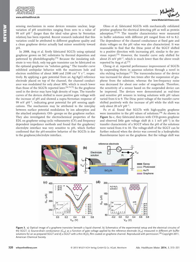
Fu et al. found that SGGTs with high-quality graphene were insensitive to the pH values of solutions. [ 78 ] As shown in Figure 3 a–c, they fabricated devices with CVD-grown graphene and observed little gate voltage shift (6 ± 1 mV pH −1 ) in the transfer characteristic of a SGGT when the pH of the solutions were varied from 4 to 10. The voltage-shift of the SGGT can be further reduced when the device was covered by a hydrophobic fl uorobenzene layer on the graphene. But the voltage shift was
Figure 3. a) Optical image of a graphene transistor beneath a liquid channel. b) Schematics of the experimental setup and the electrical circuitry of the SGGT. c) Source-drain conductance ( G sd ) as a function of gate voltage applied by the reference electrode ( V ref ) measured in different pH buffer solutions for an as-prepared SGGT and d) a SGGT with a thin Al 2 O 3 fi lm coated on graphene channel. Reproduced with permission. [ 78 ] Copyright 2011, American Chemical Society.
Adv. Healthcare Mater. 2014, 3, 313–331

www.MaterialsViews.com
321
www.advhealthmat.de
© 2013 WILEY-VCH Verlag GmbH & Co. KGaA, Weinheim wileyonlinelibrary.com
REV
IEW
increased to 17 ± 2 mV pH −1 when a thin Al 2 O 3 layer was coated on the graphene, as shown in Figure 3 d. It is notable that Al 2 O 3 is a pH-sensitive material that has been used in ion-sensitive fi eld-effect transistors before. [ 68 ] So, the results suggested that clean graphene was not sensitive to the concentration of proton or pH in solutions, which is a consequence of its ideal hydro-phobic surface with few dangling bonds. They believed that the gate voltage shifts induced by pH change reported in the pre-vious literature refl ected the quality of graphene. So, it is rea-sonable to conclude that defective graphene, where free bonds exist on the surface, is sensitive to the pH value of the solution, whereas high-quality graphene with no dangling bonds is not.
These studies indicated that pH sensors can be realized by using SGGTs only in some special conditions. Compared with typical silicon-based ISFETs that showed pH-dependent gate voltage shifts close to Nernstian relationship, [ 68,69 ] the pH sen-sors based on graphene transistors exhibited responses diverged greatly from this relationship. Supra-Nernstian response was even observed in the devices with high-density defects in the graphene layers. [ 73 ] Therefore, to realize the high-performance pH sensors, it is necessary to know the underline mechanism that can induce the big shift of Dirac point voltage, [ 73 ] which is unclear until now. Further work is needed to better understand this effect.
3.2 . Ion Sensors
Ion sensors have many important applications, such as envi-ronment monitoring, food safety inspections, and so on. On the other hand, the interactions between ions and graphene are important to all types of SGGT-based chemical or biological sensors since the devices operate in aqueous solutions. Besides the pH sensors, various ion sensors based on SGGTs, including Na + , K + , Ca 2+ , Mg 2+ , Hg 2+ , and Pb 2+ sensors, have also aroused great attentions in recent years.
Chen et al. prepared SGGTs with mechanically exfoliated graphene on SiO 2 substrates. [ 79 ] Ag wires or Ag/AgCl reference electrodes were used as gate electrodes. They studied the infl u-ence of ionic concentrations in NaF solutions on the device per-formance and observed the shift of the transfer curve to lower gate voltage with the increase of ionic concentration. Assuming that the potential drop across the electrolyte/SiO 2 interface was induced by the impurity charges and partially counteracted by the ions in solution, the infl uence of ionic concentrations on the shift was then simulated with an analytical model success-fully. In addition, they found that the charged impurity on the SiO 2 substrates was another important factor that can infl u-ence charge transport in graphene layer. By fi tting the device performance, the concentrations of charged impurities in dif-ferent devices were extracted. A clear relationship between the minimum conductivity at the Dirac point and the impurity con-centration was obtained. The minimum conductivity decreased exponentially with the impurity density, which was attributed to the impurity scattering of the carriers.
Heller et al. investigated SGGTs composed of single-layer graphene fl akes and Cr/Au source and drain electrodes on SiO 2 substrates. [ 80 ] An Ag/AgCl reference electrode was used as the gate. The device performance was sensitive to the ionic
concentrations and pH values of the electrolytes. The transfer curve shifted to positive gate voltage with the increase of pH, similar to the pH-sensitive SGGTs reported before. [ 73 ] At the same pH condition, the transfer curve shifted with the change of ionic concentrations. When pH is 7, the shift is −42.7 mV decade −1 for both LiCl and KCl solutions, whereas for pH of 3, the shift is +18.9 mV decade −1 . So the shift of the transfer curve was sensitive to different ions without selec-tivity. They believed that the response to ions in electrolytes could be affected by a high density of ionizable groups on both the underlying substrate and the graphene surfaces. These effects should be considered in many other sensing applica-tions of SGGTs, in which the electrical signal can be affected by charged target molecules as well as electrolyte ions. There-fore, careful control of electrolyte properties is needed in some experiments.
Sofue et al. used mechanically exfoliated graphene to fabri-cate SGGTs for ion sensors and demonstrated sensitive elec-trical detection of NaCl of various concentrations in Tris–HCl buffer solution. [ 81 ] Sodium ion in electrolytes was found to affect the electrical potential of graphene channels. As a result, the transfer curves shifted toward negative voltages with increasing Na + concentration. The voltage shift of the SGGT can be used to accurately detect the concentrations from 1.0 × 10 −9 M to 1.0 × 10 −3 M . The device was also demonstrated for real-time detection of Na + concentrations with high sensitivity.
In practical applications, device packaging of SGGTs is important to achieving stable performance. SGGTs can be integrated in microfl uidic systems with only small active areas exposed to electrolyte while all contacts are well packaged. More importantly, microfl uidic chips can be easily fabricated in clean room to achieve low cost, highly sensitivity, and high-throughput detections. Our group fabricated and integrated SGGTs into microfl uidic channels on both glass and fl exible substrates (PET), [ 36 ] as shown in the Figure 4 a. The transfer curve of a SGGT with Ag/AgCl gate electrode shifted toward the negative voltage direction with the increase of KCl con-centration in the microfl uidic channel, as shown in Figure 4 b. But the device was insensitive to ionic concentration when the Ag/AgCl gate electrode was replaced with an Au wire, indi-cating that the gate electrode was responsible for the ion-sen-sitive performance. As shown in Figure 4 c, the voltage shift in the former case was about 61.9 mV decade −1 close to the ideal value (59 mV decade −1 ) given by Nernst equation at room tem-perature. So the response was caused by the variation of the potential drop at the Ag/AgCl gate electrode.
The SGGT could also be used to detect fl ow velocities in the microfl uidic channel. As shown in Figure 4 d, the channel current I DS changes with the variation of fl ow velocity. We also observed that the transfer curve of the device shifted horizon-tally with the change of fl ow velocity shown in Figure 4 e. The voltage shift can be fi tted with the following equation for the streaming potential ( V str ) generated by the moving counterions inside the EDL: [ 82 ]
Vstr = g0gr.whR
0e(C + 8):v
(5)
where ζ is the zeta potential on the surface of the micro-chip channel, ε 0 is the vacuum permittivity, ε r is the relative
Adv. Healthcare Mater. 2013, 3, 313–331

www.MaterialsViews.com
322
www.advhealthmat.de
© 2013 WILEY-VCH Verlag GmbH & Co. KGaA, Weinheimwileyonlinelibrary.com
REV
IEW
dielectric constant of the electrolyte solution, w , h, and R are the width, height, and fl ow resistance of the microchannel, respec-tively; η is the dynamic viscosity of the electrolyte solution, e is the electron charge, C is the ionic concentration, λ is an offset concentration that arises from the background concentration of ions, μ is the effective ionic mobility, and ν is the fl ow velocity in the microchannel.
Because the streaming potential in Equation (5) is dependent on three physical quantities, including the fl ow velocity v , the ionic strength of the fl uid C , and the zeta potential of the sub-strate ζ , the device could be adopted for sensing any one of the three quantities when the other two were known. As shown in Figure 4 f, the SGGTs on different substrates (glass or plastic) exhibited different sensing behavior, which further confi rmed the sensing mechanism of the devices. This fl exible, multifunc-tional, and miniaturized SGGT-based sensor might have great potential for applications in lab-on-a-chip platforms, biological systems, or medical devices.
Recently, Newaz et al. investigated the infl uence of fl uid fl ow on the performance of a SGGT in a microfl uidic channel. [ 75 ] Because the change of fl ow velocity or the concentration of ions (NaCl) would induce transfer characteristic shift due to the change of streaming potential given by Equation (5) , they developed a graphene-based mass fl ow and ionic strength sen-sors. The fl ow sensitivity of SGGTs reached about 70 nL min −1 , which was about 300 times higher than the reported fl ow sensi-tivity of a carbon nanotubes device, and about four times higher compared with a device based on Si nanowire. Their SGGTs could also detect changes in the ionic strength of a moving liquid with the sensitivity of about 40 × 10 −9 M . So the devices sensitive to liquid fl ow and ionic strength may fi nd some appli-cations as mentioned above.
After surface modifi cation on graphene, SGGTs could achieve high sensitivity and specifi city to certain kind of ions. Wen et al. reported Pb 2+ ion sensors using gold nanoparticle and DNAzyme-functionalized SGGTs. [ 66 ] As shown in Figure 5 ,
Figure 4. a) Schematic diagram of a SGGT with an Ag/AgCl gate electrode integrated in microfl uidic channel; b) transfer curves of a SGGT measured in KCl aqueous solutions with different concentrations; c) the shift of Dirac point voltage as a function of KCl concentration. d) Time-dependent channel current of the SGGT characterized in fl owing KCl solution with different velocities; e) transfer curves of the SGGT characterized at different fl ow velocities; f) the shift of Dirac point voltage ( Δ V G ) of SGGTs on glass or plastic substrates at different fl ow velocities. Reproduced with permission. [ 36 ] Copyright 2012, American Chemical Society.
Adv. Healthcare Mater. 2014, 3, 313–331

www.MaterialsViews.com
323
www.advhealthmat.de
© 2013 WILEY-VCH Verlag GmbH & Co. KGaA, Weinheim wileyonlinelibrary.com
REV
IEW
CVD-grown graphene was decorated with gold nanoparticles that serve as the anchoring sites to covalently immobilize thi-olated Pb 2+ -dependent DNAzyme molecules. Upon binding with Pb 2+ ion, the enzymatic strand cleaved the substrate strand and induced the diffusion of enzymatic strand and the unthi-olated portion of the substrate strand from the graphene active layer, which altered the original electronic coupling between the charged DNAzyme complex and the graphene. They found that the transfer curve shifted to positive gate voltage after adding Pb 2+ ion, indicating the alleviation of n-doping by DNA mol-ecules. So the Dirac point shift was caused by the interaction between DNAzyme molecules and graphene surface rather than between Pb 2+ ions and graphene. The detection limit of the devices to Pb 2+ was about 20 × 10 −12 M , which was several orders of magnitude lower than that of other approaches, such as optical methods. [ 83 ] Moreover, the selectivity of the devices was very high because Pb 2+ -dependent DNAzyme was used as the recognition element.
Sudibya et al. used micropatterned rGO fi lms to fabricate SGGTs as ion sensors. [ 74 ] rGO is the desirable alternative to the pristine graphene due to its low cost, solution processable, and scalable production. [ 84,85 ] After the modifi cation of specifi c proteins, the devices can be used to effectively detect Ca 2+ , Mg 2+ , Hg 2+ , and Cd 2+ ions with high specifi city and the detec-tion limit down to 1 × 10 −9 M , which is comparable to those of conventional methods. [ 83 ] By applying different gate voltages, both the p-type and n-type detection can be easily realized in the same rGO-based SGGT. The simple rGO devices could be readily patterned and fabricated by solution process on various substrates and utilized to detect various metal ions in solutions rapidly and label-freely with high sensitivity and specifi city. The devices could be easily integrated in lab-on-a-chip systems as microarrays for parallel recording multiple targets.
4 . Biosensors
A biosensor is an analytical device combining functional mate-rials or biological components with a physicochemical detector for sensing a biological analyte. The device can convert the biological information into another signal that can be more easily quantifi ed. Graphene has shown great biocompatibility, environmental sensitivity, and stability in biosystems, which is important to either point-of-care or real-time sensing applica-tions. Recently, SGGTs has been fabricated and developed as many kinds of biosensing applications such as biomolecule and bacteria sensing, cell activity monitoring, and so on. After cer-tain modifi cations, SGGTs could achieve similar or higher sen-sitivities to bacteria, DNA, protein, and so on compared with other sensing techniques. [ 86,87 ] SGGTs can be easily miniatur-ized and integrated into microfl uidic systems, exhibiting great potential for high-throughput, ultrasensitive, and highly selec-tive biosensors for broad applications.
4.1 . Cell and Bacterial Sensors
Because of the good biocompatibility of graphene, [ 65 ] SGGTs can be integrated with cells for sensing applications. Cohen-Karni et al. reported the fi rst application of SGGTs in cell-based biosensors, in which electrogenic cells were integrated with the graphene channel. [ 44 ] Single-layer graphene fl akes prepared by mechanical exfoliation were transferred to SiO 2 substrates and Cr/Au/Cr source and drain contacts were then patterned on the graphene layers by electron beam lithography. Spontaneously beating embryonic chicken cardiomyocytes were brought to have direct contact with graphene channels. The devices could yield well-defi ned extracellular conductance signals with signal
Figure 5. a) Schematic illustration of the SGGT functionalized with Au nanoparticles (AuNPs) and DNAzyme molecules. b) Schematic of Pb 2+ -induced self-cleavage of the DNAzyme. c) The Dirac point shifts of SGGTs based on bare graphene, AuNP-decorated graphene, nonspecifi c DNA–AuNP com-plex decorated graphene, and DNAzyme–AuNP complex decorated graphene, to various Pb 2+ concentrations. d) The averaged Dirac point shift of DNAzyme–AuNP complex decorated SGGTs in the presence of 20 × 10 −12 M Pb 2+ ion for different incubation time. Reproduced with permission. [ 63 ]
Adv. Healthcare Mater. 2013, 3, 313–331

www.MaterialsViews.com
324
www.advhealthmat.de
© 2013 WILEY-VCH Verlag GmbH & Co. KGaA, Weinheimwileyonlinelibrary.com
REV
IEW
to noise ratio higher than 4. By adjusting the solution gate potential V G , the amplitude of the signal could be tuned nearly one order of magnitude. Both n- and p-type recording could be easily achieved from the same device by changing V G . They also studied the relative resolution of SGGTs with different sizes. The peak-to-peak width of the signal increased with the device area, indicating that the devices presented an averaged signal from different points across the outer membrane of the beating cells. The study demonstrated that SGGTs showed better per-formance than other planar devices, such as microelectrode arrays and other fi eld-effect transistors and offered the unique capability of recording signals as both n- and p-type devices by simply changing the gate voltage.
Hess et al. recently developed a system including arrays of SGGTs using CVD-grown graphene for the detection of elec-trical activities of electrogenic cells, [ 88 ] as shown in Figure 6 . Compared with exfoliated graphene used by Cohen-Karni et al., [ 44 ] CVD-grown graphene can be utilized to prepare large-area devices or arrays, which offers a more suitable plat-form allowing mass production at low cost. Cardiomyocyte-like HL-1 cells were seeded and cultured on these arrays and exhibited a healthy growth. The action potentials of these cells were detected and resolved by the working SGGTs under the cells, similar to other types of cell-based biosensors. [ 89 ] Using the whole transistor array, the propagation of the cell sig-nals across the cell was also tracked and recorded, as shown in Figure 6 b and c. The propagation speed was observed to be 12–28 μ m ms −1 , which is similar to that observed by microelectrode arrays. [ 90 ] As shown in Figure 6 d, the SGGT arrays were capable of detecting single voltage spikes as low as 100 μ V with a signal-to-noise ratio better than 10, exhib-iting a similar performance to that of microelectrode arrays and better signal to noise ratio than that of the solution-gated
Si transistors. This study suggests that the outstanding perfor-mance of SGGTs together with the promising applications of graphene in fl exible electronics imply innovative technologies that can be developed in the fi eld of bioelectronics, [ 36 ] such as electrically functional neural prostheses.
Ang et al. integrated SGGTs with microfl uidic systems for the “fl ow-catch release” sensing of malaria-infected red blood cells at the single-cell level, [ 91 ] as shown in Figure 7 . Graphene was functionalized with the endothelial CD36 receptors for the selective capture of the malaria-infected cells when the diseased blood fl ows through the microfl uidic channel. Coulomb-impu-rity potential exerted by charged protrusions on cell surfaces induced local doping in graphene channel and led to conduct-ance changes between source and drain electrodes. Therefore, the SGGT sensor is able to generate dynamic disease diagnostic patterns in term of conductance changes and characteristic dwell time, showing great potential in clinical diagnostic applications.
SGGTs also showed great promise in sensing bacteria because the graphene layer can be easily functionalized with biomaterials. Mohanty and Berry integrated chemically modi-fi ed graphene (CMG) nanostructure (GO and plasma-modifi ed graphene-amine) with bacteria and DNA. [ 45 ] The Gram-positive Bacillus cereus cells possessing a highly negative-charged surface were employed in the study. The CMG device exhibited a sharp increase in conductivity upon the attachment of a single bacte-rial cell on the surface. The increase in graphene conductance is due to the increased hole density induced by bacterial surface. This detection relied on nonspecifi c electrostatic adhesion of bacteria without discrimination of bacterial species. They also fabricated a novel bacterial DNA/protein and polyelectrolyte chemical transistor based on graphene-amine for the fi rst time. Electrostatic adsorption of a mixture of negatively charged bac-terial, DNA, and proteins extracted from Bacillus cereus cells
Figure 6. a) A SGGT array with calcein-stained cells (fl uorescence image) on the top. The scale bar is 100 μ m. b,c) Time dependent current of eight transistors in one FET array measured simultaneously. d) Exemplary single spikes of two transistors. The current response has been converted to an extracellular voltage signal. Reproduced with permission. [ 88 ]
Adv. Healthcare Mater. 2014, 3, 313–331

www.MaterialsViews.com
325
www.advhealthmat.de
© 2013 WILEY-VCH Verlag GmbH & Co. KGaA, Weinheim wileyonlinelibrary.com
REV
IEW
on the device led to a sharp 2 orders of magnitude decrease in resistance due to the negative charge gating effect.
Huang et al. recently developed a type of bacterium sen-sors based on SGGTs with high sensitivity (10 cfu mL −1 ). [ 41 ] The SGGTs were fabricated using CVD-grown graphene modi-fi ed with anti- E. coli antibody on the surface. When the device was exposed to different concentrations of E. coli , it showed the increase in channel conductance with the increase of the bacterial concentration from 10 cfu mL −1 . Meanwhile, different bacteria, such as P. aeruginosa with the concentration of 10 5 cfu mL −1 , did not cause signifi cant response of the anti- E. coli antibody func-tionalized SGGT, indicating the high specifi city of the detections. Furthermore, this device was employed to detect the glucose-induced metabolic activities of the bound E. coli bacteria in real time, providing a platform for screening antibacterial drugs.
4.2 . DNA Sensors
DNA diagnostics has shown great scientifi c and economic importance in many areas. It has signifi cant applications in gene expression monitoring, clinical medicine, viral and bacte-rial identifi cation, biowarfare and bioterrorism agents detecting, and so on. [ 29 ] However, it is challenging to detect the nucleic acid molecules especially short DNA strands without the use of time-consuming radioactive labelling assays and the unportable confocal fl uorescence microscope. Many studies focusing on the application of SGGTs in label-free DNA sensors have been reported. In these devices, graphene channels were functional-ized with DNA probes and nanomaterials, which led to highly sensitive and selective DNA detections.
Mohanty and Berry fi rstly studied DNA hybridization by characterizing the conduct-ance change of amino-modifi ed GO active layer. [ 45 ] The hybridization process can lead to large increase in hole density due to the electrostatic gating effect by the negatively charged DNA molecules. However, the detec-tion sensitivity of this kind of device was strongly dependent on the size and the shape of GO sheets, the presence of wrinkles on GO surface and the degree of oxidation in GO.
Dong et al. reported electrical detection of DNA hybridization with high specifi city using SGGTs based on CVD-grown multilayer gra-phene as an alternative of low conductive GO. [ 42 ] After preimmobilizing probe-DNAs on graphene surface via nonspecifi c binding due to the nonelectrostatic stacking interac-tion, the devices were capable of detecting the hybridization of target DNAs with the concentration down to 0.01 × 10 −9 M and dis-tinguishing single base mismatch, which are similar to some other transistor-based DNA sensors. [ 29,30 ] Being different from the above GO-based DNA sensors, the sensing mecha-nism of the SGGTs was attributed to electron transfer from the electron-rich, aromatic
nucleotide to graphene. The gate voltage at the Dirac point was identifi ed from the transfer curve and used to monitor the elec-tron doping state of the graphene fi lm. They observed that the Dirac point shifted to negative voltage with the addition of com-plimentary DNA targets in the solution. The upper limit of the DNA detection could be extended from 10 to 500 × 10 −9 M by decorating Au nanoparticles on graphene sheets because more DNA mole cules were immobilized on the graphene surface. In addition to the voltage shift, the minimum channel current at the Dirac point was also decreased obviously with increasing DNA concentration, which might be attributed to nonspecifi c binding of charged molecules or ions on the graphene sur-face that can infl uence carrier transport in graphene by scat-tering. [ 92 ] This study demonstrates the great potential of SGGTs in sensitive and selective detections of DNA.
Guo et al. developed label-free DNA sensors based on gra-phene fi eld-effect transistors with CVD-grown graphene. [ 93 ] The devices were patterned by conventional photolithography and modifi ed by 1-pyrenebutanoic acid succinimdyl ester. Probe DNA molecules were immobilized on graphene surface by the ester and used for detecting complimentary target DNA with the detection limit of about 1 × 10 −9 M , which is inferior to the above DNA sensors reported by Dong et al. [ 42 ]
Chen et al. reported the SGGT fabricated with CVD-grown monolayer graphene. [ 94 ] Operational conditions were optimized to achieve the DNA detection as low as 1 × 10 −12 M , which was more sensitive than the aforementioned SGGTs with few-layer graphene. They also demonstrated that the gold-transfer tech-nique is better than the typical PMMA-transfer in the fabrica-tion of SGGTs for sensing applications. Recently, Lin et al. from the same group studied the underline sensing mechanism of
Figure 7. Graphene-based detection of single plasmodium falciparum-infected erythrocyte (PE). a) Left: schematic illustration of an array of graphene transistors on quartz. Right: specifi c binding between ligands located on positively charged membrane knobs of parasitized erythro-cyte and graphene channel induces a conductance change. b) Image of SGGTs integrated with a microfl uidic channel. Scale bar in the inset is 30 μ m. c) Three-dimensional AFM images of (left) parasitized erythrocyte14 (scale bar is 1 μ m) and (right) 3D height plot of the surface of parasitized erythrocyte with Protruding knobs. Reproduced with permission. [ 91 ] Copyright 2011, American Chemical Society.
Adv. Healthcare Mater. 2013, 3, 313–331

www.MaterialsViews.com
326
www.advhealthmat.de
© 2013 WILEY-VCH Verlag GmbH & Co. KGaA, Weinheimwileyonlinelibrary.com
REV
IEW the SGGT-based DNA sensors by measuring Hall effect of the
graphene channels. [ 43 ] The Hall effect is the production of a voltage difference (called Hall voltage) across an electrical con-ductor or a semiconductor, transverse to an electric current in the material and a magnetic fi eld perpendicular to the current. The Hall effect measurement is very useful as a means to char-acterize the carrier density and mobility of a semiconductor. They observed that the addition of either complementary or one-base mismatched DNA on the devices could increase the sheet resistance and decrease the hole carrier mobility and thus one-base mismatched DNA could not be differentiated by the conductance change. Fortunately, they found that the hole car-rier concentration in graphene increased signifi cantly with the addition of complementary DNA while it was less affected by one-base mismatched DNA, as shown in Figure 8 . So they con-cluded that the increase in hole carrier density, evidenced by n-doping in graphene, is better correlated with the DNA hybrid-ization. However, the underline mechanism is still unclear since both complementary DNA and one-base mismatched DNA strands are negatively charged, which are expected to induce n-type doping in the graphene channel as shown in other types of sensors based on graphene transistors reported before. [ 95 ]
Stine et al. fabricated SGGTs utilizing rGO for real-time and label-free DNA detection. [ 96 ] An amino-silane fi lm was formed on the substrate before GO deposition and reduction, which could stabilize the rGO layer on the surface in aqueous solutions. Then a fl ow cell contained a Pt wire inside the fl ow region was attached to the device to isolate the active rGO areas for solution exposure. The DNA sensors could reach the detec-tion limits as low as 10 × 10 −9 M , which is not as good as the devices based on CVD-grown graphene. [ 42 ] However, rGO fi lms could be easily deposited and etched to form device arrays, this technique might offer a simple and low-cost approach for high-throughput DNA detection with good specifi city and sensitivity.
Yin et al. reported Pt nanoparticle-decorated rGO-based SGGTs for real-time DNA detection. [ 97 ] Large-area rGO thin fi lm was fab-ricated on a Si/SiO 2 wafer using the Langmuir–Blodgett method followed by thermal reduction. Then Pt nanoparticles were directly synthesized onto rGO sheets by photochemical reduction. The resulting composite was used as the channel material of the SGGTs. Pt electrodes were employed as the gate in the devices. The decoration of probe DNA on the devices was achieved by Pt-S covalent bonding. The devices were used to detect and ana-lyze the hybridization process of target DNA in real time through continuously monitoring channel current. The hybridization of target DNA caused a decrease of channel current, which can be explained by the increased n-doping effect by DNA. The detection limit of the read time detection was estimated to be 2.4 × 10 −9 M , being similar to other rGO-based devices. [ 96 ]
Therefore, DNA sensors based on SGGTs has been suc-cessfully realized by several research groups with the similar sensing mechanism. The interaction between DNA and gra-phene can induce n-doping in graphene due to the negative charge on the DNA molecules in solution. In addition, many experiments demonstrated the decrease of channel conduct-ance at the Dirac point of a SGGT induced by DNA immobi-lization or hybridization, indicating that the carrier mobility was decreased by charge scattering from DNA. This effect was
also confi rmed by Hall effect measurement recently. [ 43 ] So the SGGT-based DNA sensors show the performance comparable to that of other types of transistor-based counterparts and better than conventional techniques for DNA analysis accomplished by fl uorescence observation. [ 86 ]
4.3 . Protein Sensors
Proteins, large biological molecules consisting of one or more chains of amino acids, perform a vast number of functions within living organisms. They are the center of most patho-logical conditions and have been regarded as most disease biomarkers. Besides the studies of DNA, they are perhaps the subject most intensely researched. Protein sensors have emerged as the most promising platforms for the study of pro-teins, which will be more and more important in the diagnoses of diseases. [ 98 ] Similar to the aforementioned DNA sensors in
Figure 8. a) The Dirac point voltage ( V CNP ) as a function of complemen-tary DNA concentration added in the solution. Inset: the transfer curves for the graphene devices before and after each DNA addition step. b) The carrier concentration of graphene as a function of the concentration of added complementary and onebase mismatched DNA. Two curves were measured separately in dry (without PBS) and wet (in PBS) states by the Hall effect measurement. Reproduced with permission. [ 43 ]
Adv. Healthcare Mater. 2014, 3, 313–331

www.MaterialsViews.com
327
www.advhealthmat.de
© 2013 WILEY-VCH Verlag GmbH & Co. KGaA, Weinheim wileyonlinelibrary.com
REV
IEW
Section 4.2., the SGGT-based protein sensors are label free, sensitive, and potentially low cost.
Ohno et al. fi rstly reported SGGTs for the detection of pro-tein adsorption in electrolytes. [ 47 ] The devices were fabricated with mechanically exfoliated pristine single-layer graphene with the channel length of only several micrometers. This device was used for label-free protein detection without any modifi ca-tion on the graphene surface. A negatively charged phosphate serum albumin (BSA) was tested in a phosphate buffer solu-tion with a pH of 6.8. When the adsorption of BSA onto the graphene surface occurred, the conductance of the channel at a fi xed gate voltage (−0.1 V) was increased. This change of con-ductance with BSA concentration was fi tted with the Langmuir adsorption isotherm. In this work, the conductance change due to BSA adsorption was quite small, which might be induced by three possible reasons including: 1) the change of electrode-gra-phene contact resistance; 2) the desorption of BSA molecules; 3) the relatively small difference between isoelectric point of BSA and the solution pH, which may lead to some uncharged amino acid of BSA molecules.
In another work of Ohno et al., they demonstrated a label-free immunsensor based on an aptamer-modifi ed graphene transistor. [ 99 ] Immunoglobulin E (IgE) aptamers were success-fully immobilized on a graphene surface, the benefi t of using aptamers is that they are smaller than the Debye length of an EDL. This aptamer-modifi ed SGGT exhibited selective detec-tion of IgE protein to 0.29 × 10 −9 M . The drain current was dependent on IgE concentration, due to the reaction between negatively charged IgE aptamers and positively charged IgE protein. By fi tting the drain current change with IgE concentra-tion, the dissociation constant was estimated to be 47 × 10 −9 M . Meanwhile, nonspecifi c sensing of BSA and SA protein was also investigated. The results showed that the effects from the nontarget proteins were successfully suppressed in the aptamer-modifi ed SGGTs.
He et al. reported the fabrication of transparent, fl exible, all rGO-based SGGTs by the combination of solution-pro-cessed rGO electrodes with micropatterned rGO channels, as shown in Figure 9 a, and their applications in detecting pro-teins. [ 100 ] After being functionalized with 1-pyrenebutanoic acid
Figure 9. a) Schematic illustration for the fabrication of all-rGO SGGT. b) Real-time detection of fi bronection in PBS buffer using the pyrene-function-alized SGGT. c) Channel current changes at different fi bronectin concentrations. Reproduced with permission. [ 100 ] Copyright 2011, American Chemical Society.
Adv. Healthcare Mater. 2013, 3, 313–331

www.MaterialsViews.com
328
www.advhealthmat.de
© 2013 WILEY-VCH Verlag GmbH & Co. KGaA, Weinheimwileyonlinelibrary.com
REV
IEW succinimidyl ester (PSE), which served as linker molecules to
catch proteins in buffer solution, the device was used to detect fi bronectin. The cross-linking of fi bronectin onto the function-alized rGO channel resulted in the decrease of channel current. As shown in Figure 9 b,c, the devices successfully detected the concentration of fi bronectin down to 0.5 × 10 −9 M with a signal-to-noise ratio of 16. They further linked biotin and coated PEG on the rGO channel to prevent nonspecifi c binding of proteins, detected the lowest avidin concentration of 80 × 10 −9 M through avidin–biotin binding, whereas the introduction of BSA caused no current change. Therefore the all-rGO SGGTs can be used in fl exible electronics for biosensors with high sensitivity and selectivity.
Mao et al. reported antibody–antigen protein biosensors based on a thermally reduced GO transistor decorated with Au nanoparticle–antibody conjugates. [ 58 ] Probe antibody was labeled on the surface of rGO sheets through the Au nanocrys-tals to catch target protein. The channel current change induced by protein binding process (Immunoglobulin G/IgG and anti-Immunoglobulin G/anti-IgG) on the device was observed. The detection limit of the protein sensor was about 0.2 ng mL −1 , which was among the best of the reported carbon-based protein sensors at that time.
Kim et al. reported rGO-based SGGTs for label-free detection of a prostate cancer biomarker, prostate specifi c antigen/ α lantichymotrypsin (PSA–ACT) complex. [ 101 ] Immu-noreaction of PSA–ACT complexes with PSA monoclonal anti-bodies on the rGO channel surface caused a linear response in the shift of the gate voltage at Dirac point. The SGGT can detect protein-protein interaction down to femtomolar level (1.1 × 10 −15 M ) with a dynamic range over 6 orders of magni-tude. The ultralow detection limit is very similar to those of the protein sensors based on silicon nanowire transistors and better than those based on carbon nanotube transistors. [ 102,103 ] This sensor showed a high specifi city to other cancer biomarker in both the phosphate-buffered saline solutions as well as in the human serum.
4.4 . Glucose Sensors and Others
Glucose is an indispensable part of metabolic activities. Glu-cose sensing is important to human health, especially in the diagnosis of diabetes mellitus. [ 104 ] Currently, glucose biosensors account for about 85% of the entire biosensor market. Electro-chemical glucose sensors have been studied for more than 50 years. [ 105 ] Recently, glucose sensors based on SGGTs have been reported by several groups.
Huang et al. demonstrated the use of CVD-grown gra-phene fi lm in SGGTs for real-time biomolecular sensing. [ 60 ] Glucose or glutamate molecules were detected by measuring the conductance change of the graphene channel because the molecules can be oxidized by the specify redox enzyme (glu-cose oxidase (GOD) or glutamic dehydrogenase) functional-ized onto the graphene fi lm. The detection limits of the glu-cose sensor (0.1 × 10 −3 M ) and glutamate sensor (5 × 10 −3 M ) are comparable to the commonly used electrochemical sen-sors, yet inferior to some electrochemical sensors integrated with functional nanomaterials. Kwak et al. reported a fl exible
glucose SGGT sensor using CVD-grown graphene on a PET fl exible substrate. [ 106 ] The graphene surface was functionalized with linker molecules (PSE) in purpose of better immobilizing GOD enzyme that induce the catalytic response of glucose. By measuring the Dirac point shift and drain-source current vari-ation, the SGGT sensor could detect gluose levels in the range of 3.3–10.9 × 10 −3 M . In addition, the SGGTs could provide con-tinuous real-time monitoring. However, the detection limit of the above glucose sensors are much worse than other types of transistor-based glucose sensors reported before. [ 104 ] Therefore, further work is needed to improve the performance of SGGT-based glucose sensors.
Dopamine, a neurotransmitter produced in brain, plays an important role in the regulation of neuronal transmission and is related to many diseases such as Parkinson’s and schizo-phrenia. [ 107 ] Normal level dopamine in human plasma is quite low, only around several × 10 −9 M . [ 108 ] Thus, it is necessary to fi nd dopamine sensors with low detection limit and high sen-sitivity. He et al. described the fabrication of SGGTs by large-scale direct patterning of rGO on fl exible substrate. [ 109 ] As a proof of concept, the SGGTs were used for sensing both the manually titrated dopamine in the concentration region of 1–60 × 10 −3 M and the vescular released catecholamines from living meuroendocrine PC12 cells. Although, the device only showed the detection limit to dopamine at × 10 −3 M level, which is much worse than that of other transistor-based dopamine sensors, [ 107 ] the methodology demonstrated by them indicated the potential use of SGGTs in neurochemistry measurement. Further work is needed to optimize the performance of the devices.
Recently, Park et al. reported fl exible ultrasensitive bio-electronic nose (B-nose) based on SGGTs, [ 110 ] in which gra-phene was conjugated with human olfactory receptors 2AG1 (hOR2AG1: OR). As shown in Figure 10 , the ORs can selec-tively bind to the particular odorant amyl butyrate (AB), so the device can detect AB with unprecedented sensitivity and good selectivity. The minimum detection limit was as low as 0.04 × 10 −15 M , which was 2–5 orders of magnitude more sensi-tive than other odorant sensors reported before. [ 111 ] In addition, the B-noses were stable for more than 10 d and showed excel-lent bending stability. Therefore, this methodology offers a new direction for the highly sensitive and selective recognition of odorants and could be expanded to a broader range of applica-tions in fl exible and wearable electronics.
5 . Conclusions and Outlook
Graphene, the 2D material with high carrier mobilities, excel-lent mechanical fl exibility, and good chemistry stability, has been viewed as one of the most promising materials for the fabrication of rapid, highly sensitive, and low-cost chemical and biological sensors. Viable approaches for synthesizing high-quality and low-cost graphene have been developed very fast in the past few years, which paved the way for the development of many different graphene-based sensors. SGGTs have been successfully used in various types of chemical or biological sensors, including pH, ion, glucose, DNA, cell, bacterial, and protein sensors. Compared with conventional counterparts, the
Adv. Healthcare Mater. 2014, 3, 313–331

www.MaterialsViews.com
329
www.advhealthmat.de
© 2013 WILEY-VCH Verlag GmbH & Co. KGaA, Weinheim wileyonlinelibrary.com
REV
IEW
SGGT-based sensors are more sensitive in many applications due to the strong interactions between analytes and graphene or the high transconductance of the devices for the high carrier mobilities. Some reported sensors exhibited outstanding per-formance and great potential for many important applications, such as single-molecule detection or single-cell monitoring. [ 86 ] However, these techniques are still far from real applications due to the diffi culties in fabricating devices with good uni-formity and reproducibility. Moreover, the complicated inter-actions between graphene and organic or inorganic materials may lead to uncertainties in the future applications.
Therefore, challenges still exist and more effort needs to be paid on the following aspects of this fi eld. Firstly, specifi c detections of the chemical or biological sensors are of critical importance to their practical applications. The reported devices are normally tested in strictly controlled conditions while many interference factors widely existing in real environment have not been considered. So, the selectivity and stability of the SGGT-based sensors need to be characterized and optimized. Secondly, miniaturization and functionalization of SGGTs should be investigated to facilitate the fabrication of SGGT arrays that can be used in multifunctional microchips for highly sensitive, selective, and high-throughput sensing. One advan-tage of using the transistor-based sensors is the feasibility for miniaturization and multiplexing. Some conventional micro-fabrication techniques, such as metal deposition, photolitho-graphy, and so on, can be used in the fabrication of device arrays, whereas some key techniques for graphene transfer, inter-face treatment, and surface modifi cation should be developed
specifi cally for graphene devices. Thirdly, the applications of SGGTs for real-time environment analyzing, in vitro or in vivo biological sensing, and some healthcare products are still open for exploration. Because graphene shows excellent stability and fl exibility, SGGTs can be integrated in biological systems for the above applications. A few attempts have been made in the past several years by utilizing the graphene devices as Pb 2+ ion sensors and cell-based biosensors. [ 63,90,91 ] Finally, synthesizing high-quality graphene is not only important to SGGTs but also to all other applications of graphene. For SGGTs, the uniformity and cleanness of graphene are the important factors to device performance. Some unexpected results may come from the impurities or defects on the surface of graphene as evidenced in the previous studies. So, the techniques for synthesizing high-quality and low-cost graphene need to be developed.
Acknowledgements This work is fi nancially supported by the Research Grants Council (RGC) of Hong Kong, China (project number: PolyU5322/10E) and the Hong Kong Polytechnic University (project number: 1-ZV8N and A-PK07).
Received: June 5, 2013 Published online: August 15, 2013
[1] W. R. Yang , K. R. Ratinac , S. P. Ringer , P. Thordarson , J. J. Gooding , F. Braet , Angew. Chem. Int. Ed. 2010 , 49 , 2114 .
[2] M. Pumera , Mater. Today 2011 , 14 , 308 .
Figure 10. a) Schematic diagram of a B-nose based on a SGGT with OR-modifi ed bilayer graphene (MBLG). b) Real-time responses of SGGT B-noses based on OR-conjugated oxygen plasma-treated graphene (OR-OG) and ammonia plasma-treated graphene (OR-NG) measured at V DS = 10 mV ( V G = 0 V) to different AB concentrations (0.04 × 10 −15 to 4 × 10 −9 M ). Pristine MBLG without OR was a control sample. c) Schematic for plausible binding mechanism of B-nose through active and inactive OR forms. The addition of odorant (AB) leads to the active form with functional OR with negative charges. Reproduced with permission. [ 110 ] Copyright 2012, American Chemical Society.
Adv. Healthcare Mater. 2013, 3, 313–331

www.MaterialsViews.com
330
www.advhealthmat.de
© 2013 WILEY-VCH Verlag GmbH & Co. KGaA, Weinheimwileyonlinelibrary.com
REV
IEW [39] S. M. Sze , Physics of Semiconductor Devices , Wiley , New York 1981 .
[40] A. D. Manaught , A. Wilkinson , Compendium of Chemical Termi-nology , Blackwell Science , Oxford 1987 .
[41] Y. X. Huang , X. C. Dong , Y. X. Liu , L. J. Li , P. Chen , J. Mater. Chem. 2011 , 21 , 12358 .
[42] X. C. Dong , Y. M. Shi , W. Huang , P. Chen , L. J. Li , Adv. Mater. 2010 , 22 , 1649 .
[43] C. T. Lin , P. T. K. Loan , T. Y. Chen , K. K. Liu , C. H. Chen , K. H. Wei , L. J. Li , Adv. Funct. Mater. 2013 , 23 , 2301 .
[44] T. Cohen-Karni , Q. Qing , Q. Li , Y. Fang , C. M. Lieber , Nano Lett. 2010 , 10 , 1098 .
[45] N. Mohanty , V. Berry , Nano Lett. 2008 , 8 , 4469 . [46] D. B. Farmer , R. Golizadeh-Mojarad , V. Perebeinos , Y. M. Lin ,
G. S. Tulevski , J. C. Tsang , P. Avouris , Nano Lett. 2009 , 9 , 388 . [47] Y. Ohno , K. Maehashi , Y. Yamashiro , K. Matsumoto , Nano Lett.
2009 , 9 , 3318 . [48] X. W. Tang , S. Bansaruntip , N. Nakayama , E. Yenilmez , Y. L. Chang ,
Q. Wang , Nano Lett. 2006 , 6 , 1632 . [49] F. Yan , S. M. Mok , J. Yu , H. L. W. Chan , M. Yang , Biosens. Bioelec-
tron. 2009 , 24 , 1241 . [50] M. Dankerl , M. V. Hauf , A. Lippert , L. H. Hess , S. Birner ,
I. D. Sharp , A. Mahmood , P. Mallet , J. Y. Veuillen , M. Stutzmann , J. A. Garrido , Adv. Funct. Mater. 2010 , 20 , 3117 .
[51] A. K. Geim , Science 2009 , 324 , 1530 . [52] T. Wu , H. Shen , L. Sun , B. Cheng , B. Liu , J. Shen , New J. Chem.
2012 , 36 , 1385 . [53] C. Mattevi , H. Kim , M. Chhowalla , J. Mater. Chem. 2011 , 21 , 3324 . [54] Z. K. Liu , J. H. Li , F. Yan , Adv. Mater. 2013 , DOI: 10.1002/
adma.201205337. [55] Y. Si , E. T. Samulski , Nano Lett. 2008 , 8 , 1679 . [56] W. S. Hummers , R. E. Offeman , J. Am. Chem. Soc. 1958 , 80 , 1339 . [57] D. Li , M. B. Muller , S. Gilje , R. B. Kaner , G. G. Wallace , Nat. Nano-
technol. 2008 , 3 , 101 . [58] S. Mao , K. H. Yu , G. H. Lu , J. H. Chen , Nano Res. 2011 , 4 , 921 . [59] S. Park , R. S. Ruoff , Nat. Nanotechnol. 2009 , 4 , 217 . [60] Y. X. Huang , X. C. Dong , Y. M. Shi , C. M. Li , L. J. Li , P. Chen ,
Nanoscale 2010 , 2 , 1485 . [61] a) Y. Cui , S. N. Kim , S. E. Jones , L. L. Wissler , R. R. Naik ,
M. C. McAlpine , Nano Lett. 2010 , 10 , 4559 ; b) Y. Cui , S. N. Kim , R. R. Naik , M. C. McAlpine , Acc. Chem. Res. 2012 , 45 , 696 .
[62] Z. K. Liu , J. H. Li , Z. H. Sun , G. Tai , S. P. Lau , F. Yan , ACS Nano 2012 , 6 , 810 .
[63] Y. Wen , F. Y. Li , X. Dong , J. Zhang , Q. Xiong , P. Chen , Adv. Healthcare Mater. 2013 , 2 , 271 .
[64] H.Q. Chen , M. B. Müller , K. J. Gilmore , G. G. Wallace , D. Li , Adv. Mater. 2008 , 20 , 3557 .
[65] N. Lia , X. M. Zhang , Q. Song , R. G. Su , Q. Zhang , T. Kong , L. W. Liu , G. Jin , M. L. Tanga , G. S. Cheng , Biomaterials 2011 , 32 , 9374 .
[66] Y. Zhang , S. F. Ali , E. Dervishi , Y. Xu , Z. Li , D. Casciano , A. S. Biris , ACS Nano 2010 , 4 , 3181 .
[67] A. Hulanicki , S. Glab , F. Ingman , Pure Appl. Chem. 1991 , 63 , 1247 . [68] P. Bergveld , Sens. Actuators B 2003 , 88 , 1 . [69] F. Yan , P. Estrela , Y. Mo , P. Migliorato , H. Maeda , S. Inoue ,
T. Shimoda , Appl. Phys. Lett. 2005 , 86 , 053901 . [70] A. K. Feldman , M. L. Steigerwald , X. F. Guo , C. Nuckolls , Acc.
Chem. Res. 2008 , 41 , 1731 . [71] B. S. Kang , F. Ren , Y. W. Heo , L. C. Tien , D. P. Norton , S. J. Pearton ,
Appl. Phys. Lett. 2005 , 86 , 112105 . [72] U. Lange , N. V. Roznyatovskaya , V. M. Mirsky , Anal. Chim. Acta
2008 , 614 , 1 . [73] P. K. Ang , W. Chen , A. T. S. Wee , K. P. Loh , J. Am. Chem. Soc. 2008 ,
130 , 14392 . [74] H. G. Sudibya , Q. He , H. Zhang , P. Chen , ACS Nano 2011 , 5 ,
1990 .
[3] X. Huang , Z. Yin , S. Wu , X. Qi , Q. He , Q. Zhang , Q. Yan , F. Boey , H. Zhang , Small 2011 , 7 , 1876 .
[4] Y. X. Liu , X. C. Dong , P. Chen , Chem. Soc. Rev. 2012 , 41 , 2283 . [5] S. Liu , X. F. Guo , NPG Asia Mater. 2012 , 4 , 1 . [6] Q. Y. He , S. X. Wu , Z. Y. Yin , H. Zhang , Chem. Sci. 2012 , 3 , 1764 . [7] A. K. Geim , Angew. Chem. Int. Ed. 2011 , 50 , 6966 . [8] K. S. Novoselov , A. K. Geim , S. V. Morozov , D. Jiang , Y. Zhang ,
S. V. Dubonos , I. V. Grigorieva , A. A. Firsov , Science 2004 , 306 , 666 . [9] L. Z. Feng , Z. A. Liu , Nanomedicine 2011 , 6 , 317 . [10] F. Schedin , A. K. Geim , S. V. Morozov , E. W. Hill , P. Blake ,
M. I. Katsnelson , K. S. Novoselov , Nat. Mater. 2007 , 6 , 652 . [11] J. T. Robinson , F. K. Perkins , E. S. Snow , Z. Wei , P. E. Sheehan ,
Nano Lett. 2008 , 8 , 3137 . [12] J. Lu , I. Do , L. T. Drzal , R. M. Worden , I. Lee , ACS Nano 2008 , 2 ,
1825 . [13] O. Akhavan , E. Ghaderi , R. Rahighi , ACS Nano 2012 , 6 , 2904 . [14] C.-L. Sun , H.-H. Lee , J.-M. Yang , C.-C. Wu , Biosens. Bioelectron.
2011 , 26 , 3450 . [15] F. Chen , Q. Qing , J. L. Xia , N. J. Tao , Chem. Asian J. 2010 , 5 , 2144 . [16] R. Stine , S. P. Mulvaney , J. T. Robinson , C. R. Tamanaha ,
P. E. Sheehan , Anal. Chem. 2013 , 85 , 509 . [17] N. O. Weiss , H. Zhou , L. Liao , Y. Liu , S. Jiang , Y. Huang , X. Duan ,
Adv. Mater. 2012 , 24 , 5776 . [18] X. Du , I. Skachko , A. Barker , E. Y. Andrei , Nat. Nanotechnol. 2008 ,
3 , 491 . [19] P. W. Sutter , J. I. Flege , E. A. Sutter , Nat. Mater. 2008 , 7 , 406 . [20] A. T. N’Diaye , J. Coraux , T. N. Plasa , C. Busse , T. Michely , New J.
Phys. 2008 , 10 , 043033 . [21] X. Li , W. Cai , J. An , S. Kim , J. Nah , D. Yang , R. Piner , A. Velama-
kanni , I. Jung , E. Tutuc , S. K. Banerjee , L. Colombo , R. S. Ruoff , Science 2009 , 324 , 1312 .
[22] J. Wintterlin , M. L. Bocquet , Surf. Sci. 2009 , 603 , 1841 . [23] E. Rollings , G. H. Gweon , S. Y. Zhou , B. S. Mun , J. L. McChesney ,
B. S. Hussain , A. V. Fedorov , P. N. First , W. A. de Heer , A. Lanzara , J. Phys. Chem. Sol. 2006 , 67 , 2172 .
[24] J. Robinson , X. Weng , K. Trumbull , R. Cavalero , M. Wetherington , E. Frantz , M. LaBella , Z. Hughes , M. Fanton , D. Snyder , ACS Nano 2009 , 4 , 153 .
[25] J. K. Hite , M. E. Twigg , J. L. Tedesco , A. L. Friedman , R. L. Myers-Ward , C. R. Eddy , D. K. Gaskill , Nano Lett. 2011 , 11 , 1190 .
[26] J. Hass , W. A. d. Heer , E. H. Conrad , J. Phys. Condens. Matter 2008 , 20 , 323202 .
[27] O. C. Compton , S. T. Nguyen , Small 2010 , 6 , 711 . [28] S. K. Bae , H. K. Kim , Y. B. Lee , X. B. Xu , J. S. Park , Y. Zheng ,
J. Balakrishnan , T. Lei , H. R. Kim , Y. L. Song , Y. J. Kim , K. S. Kim , B. Ozyilmaz , J. H. Ahn , B. H. Hong , S. Iijima , Nat. Nanotechnol. 2010 , 5 , 574 .
[29] F. Yan , H. Tang , Expert Rev. Mol. Diagn. 2010 , 10 , 547 . [30] P. Lin , F. Yan , Adv. Mater. 2012 , 24 , 34 . [31] F. Cicoira , M. Sessolo , O. Yaghmazadeh , J. A. DeFranco , S. Y. Yang ,
G. G. Malliaras , Adv. Mater. 2010 , 22 , 1012 . [32] Z. H. Sun , J. H. Li , C. M. Liu , S. H. Yang , F. Yan , Adv. Mater. 2011 ,
23 , 3648 . [33] J. H. Li , Z. H. Sun , F. Yan , Adv. Mater. 2012 , 24 , 88 . [34] F. Patolsky , B. P. Timko , G. F. Zheng , C. M. Lieber , MRS Bull. 2007 ,
32 , 142 . [35] T. Kuila , S. Bose , P. Khanra , A.K. Mishra , N.H. Kim , J.H. Lee , Bio-
sens. Bioelectron. 2011 , 26 , 4637 . [36] R. X. He , P. Lin , Z. K. Liu , H. W. Zhu , X. Z. Zhao , H. L. W. Chan ,
F. Yan , Nano Lett. 2012 , 12 , 1404 . [37] A. J. Bard , L. R. Faulkner , Electrochemical Methods , John Wiley &
Sons , New York 1980 . [38] T. Fang , A. Konar , H. L. Xing , D. Jena , Appl. Phys. Lett. 2007 , 91 ,
092109.
Adv. Healthcare Mater. 2014, 3, 313–331

www.MaterialsViews.com
331
www.advhealthmat.de
© 2013 WILEY-VCH Verlag GmbH & Co. KGaA, Weinheim wileyonlinelibrary.com
REV
IEW
[93] S. R. Guo , J. Lin , M. Penchev , E. Yengel , M. Ghazinejad , C. S. Ozkan , M. Ozkan , J. Nanosci. Nanotechnol. 2011 , 11 , 5258 .
[94] T. Y. Chen , P. T. K. Loan , C.-L. Hsu , Y. H. Lee , J. T. W. Wang , K. H. Wei , C. T. Lin , L. J. Li , Biosens. Bioelectron. 2013 , 41 , 103 .
[95] Z. H. Sun , Z. K. Liu , J. H. Li , G. A. Tai , S. P. Lau , F. Yan , Adv. Mater. 2012 , 24 , 5878 .
[96] R. Stine , J. T. Robinson , P. E. Sheehan , C. R. Tamanaha , Adv. Mater. 2010 , 22 , 5297 .
[97] Z. Y. Yin , Q. Y. He , X. Huang , J. Zhang , S. X. Wu , P. Chen , G. Lu , Q. C. Zhang , Q. Y. Yan , H. Zhang , Nanoscale 2012 , 4 , 293 .
[98] M. Vestergaard , K. Kerman , E. Tamiya , Sensors 2007 , 7 , 3442 . [99] Y. Ohno , K. Maehashi , K. Matsumoto , J. Am. Chem. Soc. 2010 ,
132 , 18012 . [100] Q. Y. He , S. X. Wu , S. Gao , X. H. Cao , Z. Y. Yin , H. Li , P. Chen ,
H. Zhang , ACS Nano 2011 , 5 , 5038 . [101] D. J. Kim , I. Y. Sohn , J.-H. Jung , O. J. Yoon , N. E. Lee , J. S. Park ,
Biosens. Bioelectron. 2013 , 41 , 621 . [102] G. Zheng , F. Patolsky , Y. Cui , W. U. Wang , C. M. Lieber , Nat. Bio-
technol. 2005 , 23 , 1294 . [103] C. B. Jacobs , M. J. Peairs , B. J. Venton , Anal. Chim. Acta 2010 , 662 ,
105 . [104] H. Tang , F. Yan , P. Lin , J. Xu , H. L. W. Chan , Adv. Funct. Mater.
2011 , 21 , 2264 . [105] L. Clark , C. Lyons , Ann. NY Acad. Sci. 1962 , 102 , 29 . [106] Y. H. Kwak , D. S. Choi , Y. N. Kim , H. Kim , D. H. Yoon , S.-S. Ahn ,
J.-W. Yang , W. S. Yang , S. Seo , Biosens. Bioelectron. 2012 , 37 , 82 . [107] H. Tang , P. Lin , H. L. W. Chan , F. Yan , Biosens. Bioelectron. 2011 ,
26 , 4559 . [108] K. Hashizume , A. Yamatodani , T. Ogihara , Hypertens. Res. 1995 ,
18 , S205 . [109] Q. He , H. G. Sudibya , Z. Yin , S. Wu , H. Li , F. Boey , W. Huang ,
P. Chen , H. Zhang , ACS Nano 2010 , 4 , 3201 . [110] S. J. Park , O. S. Kwon , S. H. Lee , H. S. Song , T. H. Park , J. S. Jang ,
Nano Lett. 2012 , 12 , 5082 . [111] T. H. Kim , S. H. Lee , J. Lee , H. S. Song , E. H. Oh , T. H. Park ,
S. Hong , Adv. Mater. 2009 , 21 , 91 .
[75] A. K. M. Newaz , D. A. Markov , D. Prasai , K. I. Bolotin , Nano Lett. 2012 , 12 , 2931 .
[76] Y. Ohno , K. Maehashi , K. Matsumoto , Biosens. Bioelectron. 2010 , 26 , 1727 .
[77] Z. G. Cheng , Q. Li , Z. J. Li , Q. Y. Zhou , Y. Fang , Nano Lett. 2010 , 10 , 1864 .
[78] W. Fu , C. Nef , O. Knopfmacher , A. Tarasov , M. Weiss , M. Calame , C. Schö nenberger , Nano Lett. 2011 , 11 , 3597 .
[79] F. Chen , Q. Qing , J. L. Xia , J. H. Li , N. J. Tao , J. Am. Chem. Soc. 2009 , 131 , 9908 .
[80] I. Heller , S. Chatoor , J. Mannik , M. A. G. Zevenbergen , C. Dekker , S. G. Lemay , J. Am. Chem. Soc. 2010 , 132 , 17149 .
[81] Y. Sofue , Y. Ohno , K. Maehashi , K. Inoue , K. Matsumoto , Jpn. J. Appl. Phys. 2011 , 50 , 06GE07 .
[82] R. J. Hunter , Foundations of Colloid Science , Oxford University Press , New York 2001 .
[83] J. W. Liu , Z. H. Cao , Y. Lu , Chem. Rev. 2009 , 109 , 1948 . [84] H. X. Chang , Z. H. Sun , K. Y. F. Ho , X. Tao , F. Yan , W. M. Kwok ,
Z. J. Zheng , Nanoscale 2010 , 3 , 258 . [85] H. X. Chang , Z. H. Sun , Q. H. Yuan , F. Ding , X. M. Tao , F. Yan ,
Z. J. Zheng , Adv. Mater. 2010 , 22 , 4872 . [86] P. Lin , X. Luo , I. M. Hsing , F. Yan , Adv. Mater. 2011 , 23 , 4035 . [87] R. X. He , M. Zhang , F. Tan , P. H. M. Leung , X. Z. Zhao ,
H. L. W. Chan , M. Yang , F. Yan , J. Mater. Chem. 2012 , 22 , 22072 . [88] L. H. Hess , M. Jansen , V. Maybeck , M. V. Hauf , M. Seifert ,
M. Stutzmann , I. D. Sharp , A. Offenhäusser , J. A. Garrido , Adv. Mater. 2011 , 23 , 5045 .
[89] P. Lin , F. Yan , J. J. Yu , H. L. W. Chan , M. Yang , Adv. Mater. 2010 , 22 , 3655 .
[90] B. Hofmann , V. Maybeck , S. Eick , S. Meffert , S. Ingebrandt , P. Wood , E. Bamberg , A. Offenhäusser , Lab Chip 2010 , 10 , 2588 .
[91] P. K. Ang , A. Li , M. Jaiswal , Y. Wang , H. W. Hou , J. T. L. Thong , C. T. Lim , K. P. Loh , Nano Lett. 2011 , 11 , 5240 .
[92] J. H. Chen , C. Jang , S. Adam , M. S. Fuhrer , E. D. Williams , M. Ishigami , Nat. Phys. 2008 , 4 , 377 .
Adv. Healthcare Mater. 2013, 3, 313–331
Copyright © 2022 FDOKUMEN