Multi-Antenna Systems & Interconnection Strategies for CDMA ...

SOLDER INTERCONNECTION SPECIMEN DESIGN AND TEST CONTROL PROCEDURE FOR VALID CONSTITUTIVE MODELING OF SOLDER ALLOYS
D. Bhate1, D. Chan1, G. Subbarayan1, and T.C. Chiu2
1School of Mechanical Engineering, Purdue University, West Lafayette, IN 47907-2088 2Texas Instruments, Dallas, TX 75243
Phone: (765) 494-9770 Fax: (765) 494-0539
Email: [email protected]
ABSTRACT
Commonly, constitutive models of solder alloys are derived from mechanical tests performed on either bulk solder specimens or on specially assembled BGA test coupons where the stresses are borne by solder ball interconnects. It has been widely recognized that models derived from bulk sample test data may not be reliable when predicting deformation behavior at the solder interconnect level due to the differences in the inherent microstructures at these different scales. This is particularly critical for lead-free SnAgCu solder alloys owing to their complex microstructures. There are two primary challenges associated with developing models from solder interconnect level test data: the experimental complexity associated with accurately resolving and controlling displacement at the scale of the interconnection, and the non-uniformity of stresses inherent in the solder interconnection geometry. In testing at interconnection level, published studies have used testing techniques that don’t control deformation at the interconnect and have made uniformity of stress (and strain) approximations that are mostly invalid. Developing constitutive models from such data can produce erroneous results. In this study, we first demonstrate tests that control deformation at the interconnection level. We then show how heterogeneous stress distribution in solder interconnects can significantly affect the constitutive modeling of solder alloys and describe the conditions under which approximations may be made in the determination of accurate constitutive models. We validate our approach through experimental testing on Sn3.8Wwt%Ag0.7Wt%Cu solder joints and finite element analysis. Keywords: Lead-free solder, constitutive modeling, interconnect level testing, solder joint shape/geometry effects
NOMENCLATURE A pad area, m2
h standoff height, m P applied shear load, N Greek symbols δ measured shear displacement, m σ stress, Pa ε strain
INTRODUCTION
Constitutive models for Sn-Pb solder materials have been conventionally developed through experimental testing of bulk solder specimen, mostly in the form of dogbone-shaped samples [1]. A selected model (such as Anand’s viscoplasticity model) is then fit to experimentally observed data and material parameters describing the model are obtained [2, 3]. This has given fairly acceptable estimates for the modeling of material behavior of Sn-Pb solders under a variety of test conditions and for varying solder interconnection geometries. Lead-free solders have been the subject of a great deal of study in recent times and continue to pose several interesting challenges to the microelectronics research community. In particular, significant work is being done to understand the fundamental material behavior of the lead-free solders under consideration by industry and developing constitutive and failure models for these alloys. One of the key reasons that the behavior of currently popular lead-free solders is challenging to model is the fact that they consist of three constituent phases (Sn, Ag, and Cu) and have more complex microstructures than the Sn-Pb solders. The nature of the microstructure has been shown to be strongly dependent on environmental conditions as well as processing [4,5]. Additionally, it has been demonstrated that the microstructure has a significant effect on its behavior [5]. Constitutive models for lead-free solders must therefore take into consideration the microstructural composition of the solder alloy with regard to the finer details of its use in a microelectronic package. Many researchers have also shown the significance of intermetallic compounds in solder interconnection failure at the high strain rate and overstress conditions that are observed during shock and vibration events [6]. This is an area of growing importance due to the growth in portable electronics applications. There is thus a need for understanding solder behavior at the interconnection scale where all the microstructural influences are adequately captured leading to more meaningful constitutive models than could be obtained from testing of bulk solder specimens. Mechanical tests have been performed in the past on Sn-Pb solder interconnections [7,8] as well as more recently on lead-free solder interconnections [8, 9, 10], but for both types of
9770-7803-9524-7/06/$20.00/©2006 IEEE

solder alloys, the test data generated from solder interconnections is greatly outweighed by that generated from bulk specimen testing. There are two primary reasons for this: the experimental complexity associated with accurately resolving load and displacement at the smaller scale of the interconnection, and the heterogeneity of stresses inherent to the solder interconnection geometry. The former obstacle has been overcome by researchers using a number of experimental methods including the use of video extensometers [9]. The problem of stress heterogeneity in the solder interconnection is a challenge for developing constitutive models due to the problem of having to estimate stress-strain curves accurately (a requirement for model fitting) from load-displacement data (an output of the experimental test). This problem either has not been addressed in detail or has been resolved by using approximations that may not always be appropriate. In the first part of this paper, we describe experimental techniques that make it possible to accurately estimate load-displacement information from mechanical testing of samples that mimic real packages and address the issues involved in doing so. In the second part we address the problem of stress heterogeneity in the solder interconnection geometry: we present results from finite element analyses that demonstrate the erroneous nature of the results that may be obtained from employing the approximations commonly made in the literature discussing this problem. We also present the conditions under which these approximations may be made and applied with accurate results.
EXPERIMENTAL METHOD As part of ongoing research to develop constitutive models for Sn-Ag-Cu solder alloys from experimental data acquired at the solder interconnection level, special samples were prepared using square alumina coupons with solder joints of 95.5Sn-3.8Ag-0.7Cu alloy composition at each of the four corners. The precise dimensions of the sample are shown in figure 1(a). The cross-section of the virgin solder ball is shown in figure 1(b). Monotonic tests were performed on an Instron MicroTester 5848 which is specially designed for low-load applications. Loads were measured using a 100 N Instron Load Cell and the displacement was measured using a capacitance sensor. The capacitance sensor was mounted in close proximity to the sample so as to read only the displacement of the solder joint during the test, thereby eliminating the need for having to account for the compliance in the load train. The capacitance sensor has a range of 200 µm with a resolution of 0.1 µm. The test employed was the double lap shear setup as shown in Figure 2. The samples were bonded to the base structure using a cyanoacrylate adhesive for tests under 50°C and a two part room temperature curing epoxy for tests at higher temperatures.
a
Fig. 1 (a) Schematic showing dimensions of test specimen with solder interconnections at 4 corners (b) Cross-section of solder interconnection showing interconnection geometry
b
It is important to note that displacement is not only measured but also controlled by the capacitance sensor in a feedback loop that allows it to control the motion of the Instron crosshead. Discussion of this critical issue is often overlooked in published work that only describe the use of a local displacement measurement scheme without discussing control of the imposed displacement itself. The significance of controlling displacement locally at the solder joint interconnect is due to the strong rate dependence shown by these materials. The interaction of this strong rate dependency of the solder interconnection and the relatively large compliance inherent in a load train could likely affect the effective applied displacement rate at the interconnect level and produce inaccurate results. This is illustrated in
a b Fig. 2 (a) Schematic showing double lap shear test setup (b) Actual experimental setup with capacitance sensor in close proximity to test specimen to avoid compliance measurements
978

0
10
20
30
40
50
60
70
80
0 0.005 0.01 0.015 0.02 0.025 0.03 0.035 0.04
Displacement (mm)
Load
(N)
Capacitance Control; Capacitance MeasurementCrosshead Control; Crosshead MeasurementCrosshead Control; Capacitance Measurement
Fig. 3 Plot showing load-displacement curves obtained for an identical test specimen controlled/measured using either the crosshead input or a capacitance sensor located at the specimen
0
10
20
30
40
50
60
70
80
0 0.005 0.01 0.015 0.02 0.025 0.03 0.035 0.04
Displacement (mm)
Load
(N)
Capacitance Control; Capacitance MeasurementCrosshead Control; Crosshead MeasurementCrosshead Control; Capacitance Measurement
Fig. 4 Plot showing load-displacement curves obtained for a single solder interconnection made of Sn3.8Ag0.7Cu alloy through capacitance control. Measurements are at four different displacement rates, all at 25 oC Figure 3, where double lap shear tests on test samples using different measuring and controlling schemes show that even for the same input displacement rate, it is possible to obtain different peak loads. This is a result of the fact that the solder interconnection is experiencing different applied displacement rates for different modes of control and due to its rate dependent behavior yields different yield stress estimates. Results obtained from monotonic tests performed on the previously described samples at four different strain rates have been compiled in Figure 4. The test data is presented in terms of load and displacement as estimated for a single solder ball (obtained by dividing the total measured load by 8). The task of estimating stress and strain, which are the quantities needed for model fitting, from shear test data such
as that shown in Figure 4 has been achieved in literature by making simplifying assumptions while employing the von Mises yield criterion [7,8,9,10]. Accordingly, stress and strain are estimated as: (1)
(2)
There are two major assumptions that are made in arriving at the above expressions. The first involves the use of pad area and standoff height to estimate stress and strain quantities, which is clearly a simplification due to the absence of a nominal section as is conventionally defined for a dog-bone like specimen. The second assumption is made in treating the solder ball to be in a state of pure shear, which is again clearly, a simplification. This assumption is made use of while applying the von Mises yield criterion, which states that yielding under multi-axial loading conditions occurs when the elastic distortion energy reaches a critical value. The assumption of a state of pure shear then allows for the estimation of equivalent tensile stress and strain quantities from shear quantities as described in Equations (1) and (2) [11, 12]. Constitutive modeling relies on stress-strain data to estimate material parameters. For solder alloys, this has involved accurately estimating the rate dependence of the yield stress. While the expressions described above have been used in the literature for these purposes, no attempt seems to have been made to study their validity for different solder interconnection geometries. Given the complex nature of the stress distribution in the solder interconnection and the rate dependent behavior of solder materials, the need for simplification is justified but is meaningful only when the ramifications of making these simplifications are fully understood.
FINITE ELEMENT ANALYSES AND RESULTS
Finite element (FE) analysis has often been used as an inverse modeling tool to solve problems in mechanics that are too complex to describe analytically or tedious to study experimentally. In this study, we follow a similar strategy, that is, we attempt to simulate a set of experiments using FE analysis and use the resulting model outputs to better understand the mechanics of the problem. Specifically, we construct a variety of solder interconnection geometries and subject them to different loading conditions with the aim of extracting material behavior that was supplied as an input to the model. The accuracy of the predicted material behavior can then be used as an indication of the meaningfulness of the experiment for the interconnection geometry under consideration.
3 Pσ =A
13 hδε =
979
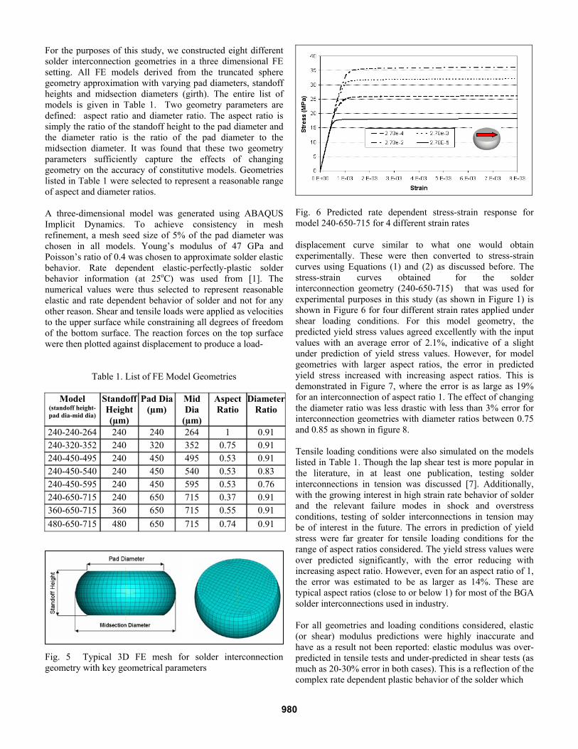
For the purposes of this study, we constructed eight different solder interconnection geometries in a three dimensional FE setting. All FE models derived from the truncated sphere geometry approximation with varying pad diameters, standoff heights and midsection diameters (girth). The entire list of models is given in Table 1. Two geometry parameters are defined: aspect ratio and diameter ratio. The aspect ratio is simply the ratio of the standoff height to the pad diameter and the diameter ratio is the ratio of the pad diameter to the midsection diameter. It was found that these two geometry parameters sufficiently capture the effects of changing geometry on the accuracy of constitutive models. Geometries listed in Table 1 were selected to represent a reasonable range of aspect and diameter ratios. A three-dimensional model was generated using ABAQUS Implicit Dynamics. To achieve consistency in mesh refinement, a mesh seed size of 5% of the pad diameter was chosen in all models. Young’s modulus of 47 GPa and Poisson’s ratio of 0.4 was chosen to approximate solder elastic behavior. Rate dependent elastic-perfectly-plastic solder behavior information (at 25oC) was used from [1]. The numerical values were thus selected to represent reasonable elastic and rate dependent behavior of solder and not for any other reason. Shear and tensile loads were applied as velocities to the upper surface while constraining all degrees of freedom of the bottom surface. The reaction forces on the top surface were then plotted against displacement to produce a load-
Table 1. List of FE Model Geometries
Model (standoff height-pad dia-mid dia)
Standoff Height (µm)
Pad Dia (µm)
Mid Dia
(µm)
Aspect Ratio
Diameter Ratio
240-240-264 240 240 264 1 0.91 240-320-352 240 320 352 0.75 0.91 240-450-495 240 450 495 0.53 0.91 240-450-540 240 450 540 0.53 0.83 240-450-595 240 450 595 0.53 0.76 240-650-715 240 650 715 0.37 0.91 360-650-715 360 650 715 0.55 0.91 480-650-715 480 650 715 0.74 0.91
Fig. 5 Typical 3D FE mesh for solder interconnection geometry with key geometrical parameters
Fig. 6 Predicted rate dependent stress-strain response for model 240-650-715 for 4 different strain rates displacement curve similar to what one would obtain experimentally. These were then converted to stress-strain curves using Equations (1) and (2) as discussed before. The stress-strain curves obtained for the solder interconnection geometry (240-650-715) that was used for experimental purposes in this study (as shown in Figure 1) is shown in Figure 6 for four different strain rates applied under shear loading conditions. For this model geometry, the predicted yield stress values agreed excellently with the input values with an average error of 2.1%, indicative of a slight under prediction of yield stress values. However, for model geometries with larger aspect ratios, the error in predicted yield stress increased with increasing aspect ratios. This is demonstrated in Figure 7, where the error is as large as 19% for an interconnection of aspect ratio 1. The effect of changing the diameter ratio was less drastic with less than 3% error for interconnection geometries with diameter ratios between 0.75 and 0.85 as shown in figure 8. Tensile loading conditions were also simulated on the models listed in Table 1. Though the lap shear test is more popular in the literature, in at least one publication, testing solder interconnections in tension was discussed [7]. Additionally, with the growing interest in high strain rate behavior of solder and the relevant failure modes in shock and overstress conditions, testing of solder interconnections in tension may be of interest in the future. The errors in prediction of yield stress were far greater for tensile loading conditions for the range of aspect ratios considered. The yield stress values were over predicted significantly, with the error reducing with increasing aspect ratio. However, even for an aspect ratio of 1, the error was estimated to be as larger as 14%. These are typical aspect ratios (close to or below 1) for most of the BGA solder interconnections used in industry. For all geometries and loading conditions considered, elastic (or shear) modulus predictions were highly inaccurate and have as a result not been reported: elastic modulus was over-predicted in tensile tests and under-predicted in shear tests (as much as 20-30% error in both cases). This is a reflection of the complex rate dependent plastic behavior of the solder which
980

-5
0
5
10
15
20
0.3 0.4 0.5 0.6 0.7 0.8 0.9 1
Aspect Ratio
Avg
% E
rror
in Y
ield
Str
ess
Fig. 7 Plot showing increase in error in predicted yield stress with increasing aspect ratio for shear loading conditions
-5
0
5
10
15
20
0.7 0.75 0.8 0.85 0.9 0.95
Diameter Ratio
Avg
% E
rror
in Y
ield
Str
ess
Fig. 8 Plot showing error in predicted yield stress versus aspect ratio for shear conditions. The effect of changing diameter ratio is less significant for typical diameter ratios
10
15
20
25
30
35
40
45
0.3 0.4 0.5 0.6 0.7 0.8 0.9 1
Aspect Ratio
Avg
% E
rror
in Y
ield
Str
ess
Fig. 9 Plot showing decrease in error in predicted yield stress with increasing aspect ratio for tensile loading conditions
Fig. 10 Contour diagram for two different interconnection geometries showing yielded elements at the moment of gross yield observed in the load-displacement curve for shear loading conditions causes onset of yield in several locations in the solder interconnection even before it is observed in the gross load-displacement curve. This is shown in Figure 10 which is a FE contour plot corresponding to the moment of the gross yield point in the load-displacement curve showing elements where the computed equivalent plastic strain has exceeded the critical value to cause yield. Also of interest, as seen in Figure 10 is the fact that the distribution of elements across the pad that have yielded differs significantly for the two different solder geometries. For the low aspect ratio, almost all elements on the pad have yielded, while in the high aspect ratio interconnection geometry, they are concentrated around the corner. This explains well why the use of the pad area to estimate shear stress from shear load works well for low aspect ratio but not for higher aspect ratios. This also suggests the possibility of estimating a correction for calculating the shear stress based on the area of the pad elements that have yielded, instead of using the entire pad area. This will be studied in the future as a potential for applying a correction factor for any given solder interconnection geometry.
DISCUSSION Several authors have published work relating to the testing of interconnections and the estimation of stress-strain curves that are often presented as representing material behavior. Test data from several different sources [10,13,14] relating to room temperature monotonic testing of Sn4.0Ag0.5Cu interconnections (and in a few cases Sn3.Ag0.7Cu – processing tolerances effectively reduce both alloys to the same composition for purposes of comparison) has been compiled in Figure 11. The peak stress (as opposed to yield stress) is plotted versus strain rate due to the lack of clarity in several of the publications reviewed on the specific measurement of yield stress. The discrepancy in the experimental data is very significant. Interestingly, all interconnection data except that obtained from tests carried out as part of this work, under-predict data obtained from bulk samples. This effect was observed in the FE models as well, where solder interconnections loaded in shear were observed to under-predict yield stress values. The experimental results
981

0
10
20
30
40
50
60
70
1.E-06 1.E-05 1.E-04 1.E-03 1.E-02 1.E-01 1.E+00Strain Rate (s-1)
Peak
Str
ess
(MPa
)
Rodgers et.al. (Bulk) This Work (Interconnect)Pei et.al. (Bulk) Pang et.al. (Bulk)Darveaux (Interconnect) Unaged Darveaux (Interconnect) AgedPang et.al. (Interconnect)
Fig. 11 Peak stress-strain rate relationships derived from literature for SnAgCu 405/387 specimen. The solid markers represent data from bulk testing, the rest are from interconnection level testing obtained from this work with low aspect ratio solder joints is in very good agreement with that published by Pei and Qu [13] for bulk Sn4.0Ag0.5Cu solder alloy. Literature discussing interconnection level testing appears to be deficient in several respects. The experimental technique regarding control of the displacement rate is often not described in the detail it deserves. Approximations such as pure shear stress states are made prior to using Von Mises criterion without verifying their validity. Additionally, while these approximations are made for estimating stress and strain, often no consideration is given to the applied shear strain rate, which is not converted into an effective tensile strain rate using the same approximation. Further, the authors make comparisons to bulk sample test results and draw conclusions on the influence of material microstructure, which appear to be of questionable validity. From the comparison in Figure 11 and tests performed as part of this work on interconnections, it appears that a greater understanding of the effects of interconnection geometry and an appreciation for the need for more precise test control is required before any conclusions can be drawn. The work presented here confirms something that researchers have intuitively known but not discussed in detail previously: testing interconnections can give significantly erroneous results if the effect of heterogeneous stress states are not accounted for and corrected in developing the constitutive model. For low aspect ratio solder joint geometries these errors can be minimized, but this does not seem to have been implemented or discussed in prior literature. In fact, in almost all the literature surveyed, there seemed to be no discussion regarding the need for low aspect ratio solder interconnection geometries when testing in shear which even intuitively, is expected to give more meaningful results than a high aspect ratio solder joint. Aspect ratios as high as 0.73 [10] have been used in the past and in some cases, the geometry of the solder
20
25
30
35
40
45
50
1.E-05 1.E-04 1.E-03 1.E-02 1.E-01
Strain Rate (s-1)
Yiel
d St
ress
(MPa
)
240-450-495240-450-540240-450-595240-650-715360-650-715Input Values
Fig. 12 Rate dependency of yield stress as predicted in five different FE models with aspect ratios close to and under 0.5 show good agreement with model input values interconnection post reflow is not described in enough detail [9]. Simple verification simulations can be performed by authors to reproduce the experimentally obtained load-displacement results that were used to estimate material behavior. Accurate closure via the use of computationally inexpensive finite element simulations in this manner is an easy way to validate the predicted material parameters.
CONCLUSIONS
The purpose of this study was to understand the effects of different solder interconnection geometries on the estimation of stress-strain behavior of solder for the purposes of constitutive modeling. While the variations in interconnection geometry and the complex rate dependent behavior of solder make it difficult to estimate accurate analytical descriptions for these effects, simple equations may be used for some cases. The conclusions from this study are summarized below: 1. Accurate control of displacement rate (in addition to
measurement) is crucial in the experimental testing of solder interconnections due to the strong rate dependent behavior of solder.
2. The effects of solder ball geometry on the estimation of stress-strain quantities from load-displacement data are well characterized by two parameters: Aspect ratio and diameter ratio.
3. Solder ball geometries of aspect ratio less than 0.5 (Stand-off Height/Pad Diameter) can be used with confidence to describe plastic behavior of the solder material (error <3%) when tested under shear loading conditions. This is shown in Figure 12 where the rate dependency of solder as predicted by five different interconnection geometries closely matches that of the values input into the model. As aspect ratios increase, error in predicted yield stress increases for shear loading.
4. Elastic properties may not be accurately estimated from interconnection testing data.
982
5. Tensile tests on solder interconnects generate poor constitutive model data with large error in predicted quantities even for high aspect ratio geometries.
6. Simple FE simulations can be performed to verify validity of predicted models by reproducing experimentally observed load-displacement data.
References [1] X. Q. Shi, W. Zhou, H. L. J. Pang, and Z. P. Wang, “Effect of Temperature and Strain Rate on Mechanical Properties of 63Sn/37Pb Solder Alloy,” ASME Journal of Electronic Packaging, ASME, USA, Vol. 121, No. 3, 1999, pp. 179-185. [2] Wilde J., Becker K., Thoben M., Blum W., Jupitz T., Wang G., Cheng Z., “Rate Dependent Constitutive Relations Based on Anand Model for 92.5Pb5Sn2.5Ag Solder,” IEEE Transactions on Advanced Packaging, Vol. 23, No. 3, August 2000 [3] Wang G.Z., Cheng Z.N., Becker K., Wilder J., “Applying Anand Model to the Viscoplastic Deformation Behavior of Solder Alloys,” ASME Journal of Electronic Packaging,Vol. 123, pp. 247-253, September 2001. [4] Tu K.N., Gusak A.M., Li M., “Physics and Materials Challenges for Lead-Free Solders,” Journal of Applied Physics, Vol. 93, No. 3, pp. 1335-1353, 2003. [5] Kim K.S., Huh S.H., Suganuma K., “Effects of cooling speed on microstructure and tensile properties of Sn–Ag–Cu alloys,” Materials Science and Engineering, A333, pp. 106–114, 2002. [6] Chong D.Y.R., Ng K., Tan J.Y.N, Low P.T.H., Pang J.H.L, Che F.X., Xiong B.S., Xu L., “Drop Impact Reliability Testing for Lead-Free and Leaded Soldered IC Packages,” Electronic Components and Technology Conference ECTC, pp. 622-629, 2005. [7] Darveaux R., Banerji K., “Constitutive Relations for Tin-based Solder Joints,” IEEE Transactions on Components, Hybrids and Manufacturing Technology, Vol. 15, No. 6, pp. 1013-1024 December 1992. [8] Wiese S., Schubert A., Walter H., Dudek R., Feustel F., Meusel E., Michel B., “Constitutive Behaviour of Lead-free Solders vs. Lead-containing Solders - Experiments on Bulk Specimens and Flip-Chip Joints,” Electronic Components and Technology Conference ECTC, 2001. [9] Pang J.H.L, Xiong B.S., Neo C.C., Zhang X.R., Low T.H., “Bulk Solder and Solder Joint Properties for Lead Free 95.5Sn-3.8Ag-0.7Cu Solder Alloys,” Electronic Components and Technology Conference ECTC, pp. 673-679, 2003. [10] Darveaux R., “Shear Deformation of Lead Free Solder Joints,” Electronic Components and Technology Conference, pp. 882-893, 2005 [11] ABAQUS Theory Manual, Chapter 4, Mechanical Constitutive Theories, Version 6.5, 2004. [12] Stoller R.E., Zinkle S.J., “On the relationship between uniaxial yield strength and resolved shear stress in polycrystalline materials,” Journal of Nuclear Materials, 283-287, pp. 349-352, 2000. [13] Pei M., Qu J., “Constitutive Modeling of Lead-free Solders,” Proceedings of ASME InterPACK, July 17-22 2005.
[14] Rodgers B., Flood B., Punch J., Waldron F., “Determination of the Anand Viscoplasticity Model Constants for SnAgCu,” Proceedings of ASME InterPACK, 2005.
983
Copyright © 2022 FDOKUMEN