Modeling the Mechanical Properties of Intermetallic/Solder ...
200
NORTHWESTERN UNIVERSITY Modeling the Mechanical Properties of Intermetallic/Solder Interfaces A DISSERTATION SUBMITTED TO THE GRADUATE SCHOOL IN PARTIAL FULFILLMENT OF THE REQUIREMENTS For the degree DOCTOR OF PHILOSOPHY Field of Theoretical and Applied Mechanics Department of Civil and Environmental Engineering By Yao Yao EVANSTON, ILLINOIS December 2008
-
Upload
khangminh22 -
Category
Documents
-
view
2 -
download
0
Transcript of Modeling the Mechanical Properties of Intermetallic/Solder ...

NORTHWESTERN UNIVERSITY
Modeling the Mechanical Properties of Intermetallic/Solder Interfaces
A DISSERTATION
SUBMITTED TO THE GRADUATE SCHOOL IN PARTIAL FULFILLMENT OF THE REQUIREMENTS
For the degree
DOCTOR OF PHILOSOPHY
Field of Theoretical and Applied Mechanics
Department of Civil and Environmental Engineering
By
Yao Yao
EVANSTON, ILLINOIS
December 2008

2
© Copyright by Yao Yao 2008 All Rights Reserved
3
ABSTRACT
Modeling the Mechanical Properties of Intermetallic/Solder Interfaces
Yao Yao
Solder joint integrity is recognized as a key issue in the reliability of flip chip and ball
grid arrays in integrated circuit packages. Significant reductions in the solder-joint interconnect
size results in both the increased volume fraction of brittle intermetallics in the joint and joule
heating and electromigration failure due to high current density.
Based on cohesive fracture theory, a 3D computational model has been developed to
predict the crack nucleation, propagation and interfacial damage of interconnects. Unified creep-
plasticity theory and a cohesive zone model were incorporated to predict the creep and hysteresis
effects on fatigue crack propagation in solder and the interfacial behavior between the solder
bulk and the intermetallic layer, respectively. A thermo-electric numerical analysis was
conducted to predict the electrical concentration and joule heating effects on the failure of solder
under different applied current densities. The temperature and current density distribution in a
solder joint with a crack that propagates near the interface of the bulk solder and intermetallic
layer was predicted.
An approach based on phase transformation theory, micromechanics, and fracture
mechanics has been developed to treat fatigue crack propagation in both lead rich and lead free
eutectic solders. The predicted fatigue crack propagation rate using phase transformation theory
was compared with experimental data for Sn-3.5Ag and Sn-37Pb eutectic solders. Reasonable
agreement between theoretical predictions and experimental results was obtained.
4
With the reduction of the size of electronic devices, the current density is increasing
rapidly and the electromigration effect becomes more critical to the failure of solder
interconnects. The mechanism of electromigration effect to void propagation caused
interconnect failure was studied in the research. A kinetic mass diffusion model was developed
to predict void width and propagation speed near the interface of intermetallic and solder caused
by electromigration. The model gives reasonable prediction to the void width and propagation
velocity compared with experimental results.

5
Acknowledgements
I would like to express my special gratitude to my advisor, Professor Leon M. Keer, I
sincere appreciate his valuable and patient guidance and support throughout my study at
Northwestern University. Working with him is a wonderful experience that I will always
treasure.
I wish to express my deep appreciation to Professor Morris E. Fine for advising and
reviewing of the work. His inspirations and encouragement have always motivated me and
helped me overcome the difficulties of research.
Sincere gratitude is expressed to Professor Semyon Vaynman, Professor Gautam Ghosh,
and Mr. Brent Fiedler for good suggestions and use of their experimental data. It would not have
been possible to write this dissertation without having access to their data.
I wish to thank Professor Jane Wang, Professor Yu Nie, Professor Brian Moran, Dr.
Xiaoqin Jin, Dr. Shenmin Wen, Dr. Fan Wang, and the members of Professor Keer’s group,
Professor Fine’s group and Professor Wang’s group for their help and friendship. I wish to thank
my relatives and friends for their support.
I gratefully acknowledge the financial support from Semiconductor Research Corporation
through contract 1393, and from the Northwestern University McCormick Fellowship and Smith
Final Year Fellowship.
I express my profound gratitude to my wife and son for their support, devotion and
patience throughout my study.

6
Finally, I dedicate this work to my beloved grandparents and parents for their love.
Without their support and love, I could never have succeeded.
7
Table of Contents
Abstract…………………………………………………………………………………... 3
Acknowledgement…………………………………………………………….................. 5
Table of contents………………………………………………………………………… 7
List of Figures……………………………………………………………………………. 10
List of Tables………………………………………………………………….................. 14
Chapter 1 Introduction and Literature Review……………………………………….. 15
1.1 General Introduction and Background of Research………………………………...… 15
1.2 Literature Review to Fatigue Theories and Analysis to Solder Interconnect………… 18
1.3 Constitutive Model for Solder………………………………………………................ 23
1.4 Failure of Interconnects near the Interface of Solder and Intermetallic Compound under Thermal-mechanical Cyclic Loading……................................................................. 25
1.5 Failure Analysis to Solder under Cyclic Load Using Cohesive Zone Model………… 30
1.6 Electromigration Effect on IMC Growth and Solder Failure………………………… 33
1.7 Objectives of the Study……………………………………………………………….. 36
1.8 Outline of the Dissertation……………………………………………………………. 37
Chapter 2 Mechanical and Thermo-Electrical Computational Analysis to Interfacial Failure of Solder Joint……………………………………………………… 39
2.1 Introduction………………………………………………………………………….... 40
8
2.2 Cohesive Zone Modeling and Finite Element Mechanical Analysis to Simulate Interfacial Behavior of Solder/IMC………………………………….................................
43
2.3 Unified Creep and Plasticity Model to Simulate Behavior of Solder Materials…………………………………………………………………………………... 47
2.4 Case Study and IMC Layer Thickness Effect on Solder Failure……………………... 49
2.5 Coupled Thermo-Electric Analysis to Solder Joint with Crack Propagation near the Interface of Bulk Solder and Intermetallic Layer………………………………………… 57
2.6 Solder and IMC Thermal and Electrical Conductivities Effects on Crack Tip Temperature………………………………………………………………………………. 68
2.7 Wiedemann-Franz-Lorenz Relation for Solder and Intermetallic Materials................. 73
2.8 Conclusion……………………………………………………………………………. 80
Chapter 3 Phase Transformation Theory Applied to Predict Fatigue Crack Propagation………………………………………………………………………………. 82
3.1 Introduction…………………………………………………………………………… 83
3.2 Experimental Observations and Numerical Analysis on Solder Interconnects Fatigue Failure…………………………………………………………………………………….. 87
3.3 Phase Transformation Theory to Predict Fatigue Crack Nucleation ………………… 96
3.4 Phase Transformation Theory to Predict Fatigue Crack Propagation ……………….. 99
3.5 Experimental and Computational Analysis on Fatigue Crack Propagation of Sn-3.5Ag Eutectic Solder…………………………………………………………………….. 106
3.6 Computational Analysis to Determine the Energy to Propagate a Unit Fatigue Crack Surface (U) Value for Solder Materials…………………………………………………... 113
3.7 Case Studies and Discussion………………………………………………................. 116
3.8 Conclusion……………………………………………………………………………. 125
Chapter 4 Electromigration Effect on Void Propagation near the Interface of Solder and Intermetallic Compound…………………………………………………… 127
9
4.1 Introduction…………………………………………………………………………… 127
4.2 A Kinetic Mass Diffusion Model to Consider Electromigration Effect……………… 128
4.3 Computational Analysis to Consider the Current Concentration Effect ……………... 139
4.4 Case Study by Comparing with Experimental Results……………………………….. 149
4.5 Conclusion……………………………………………………………………………. 157
Chapter 5 Conclusion…………………………………………………………………… 158
5.1 Conclusion……………………………………………………………………………. 158
5.2 Future Research……………………………………………………………………….. 160
References……………………………………………………………………………….. 163
Appendix A Example of ABAQUS code for 3D solder/IMC Mechanical Analysis………………………………………………………………………………….. 174
Appendix B Apply the Phase Transformation Theory to Ellipsoidal Crack……….. 185
Appendix C Considering Electrical Current Effect into Phase Transformation Model………………………………………………………............................................. 188
Appendix D Numerical Analysis to Electric Packaging under Drop Impact………. 190
Vita…………………………………………………………………………….................. 200
10
List of Figures
Page
Figure 1.1 Normal and tangential components of cohesive traction (Roe and
Siegmund 2003)
31
Figure 2.1 Description of finite element model (XZ plane for 3D model) 45
Figure 2.2 Traction-separation law of cohesive element for 95.5Sn-3.8Ag-0.7Cu
solder compared with experimental result
46
Figure 2.3 von Mises stress distribution in a solder joint using
(a)elastic-plastic model; (b)cohesive zone and UCP model (MPa)
51
Figure 2.4 von Mises stress distribution in a Sn-3.5Ag-0.7Cu eutectic solder joint
with a crack propagating near the interface of solder/IMC under cyclic
loading
53
Figure 2.5 Effect of intermetallic layer thickness on crack initiation stress 54
Figure 2.6 IMC Young’s modulus effect on maximum von Mises stress at
solder/IMC interface (crack nucleation point)
55
Figure 2.7 Solder Young’s modulus effect on maximum von Mises stress at
solder/IMC interface (crack nucleation point)
55
Figure 2.8 Simulation of applied current density versus average temperature in a
solder joint
59
Figure 2.9 Current density distribution in a Sn-2.5Ag-0.8Cu-0.5Sb solder joint under
applied current density of 104 A/cm2 with a void propagating near the
interface of solder/IMC
63
Figure 2.10 Temperature distribution in a Sn-2.5Ag-0.8Cu-0.5Sb solder joint under
applied current density of 104 A/cm2 with a void propagating near the
interface of solder/IMC
66
Figure 2.11 Temperature at the crack tip of Sn-2.5Ag-0.8Cu-0.5Sb solder with an
interfacial crack propagating under different current densities
67
Figure 2.12 Liquidus surface for Ag-Cu-Sn system (NIST database 2002) 68
11
Figure 2.13 Solder and IMC thermal and electrical conductivities effects on crack tip
temperature for different crack lengths
70
Figure 2.14 Solder and IMC thermal and electrical conductivities effects on crack tip
temperature with crack propagation predicted using FEM
72
Figure 2.15 Distribution of Lorenz factor for different materials 77
Figure 2.16 WFL law for Sn, IMC, and some solders 78
Figure 2.17 WFL law for Sn, Ni, and Ni3Sn4 78
Figure 2.18 WFL law for Sn, Cu, Cu6Sn5, and Cu3Sn 79
Figure 3.1 (a) cross-section diagram of specimens used in monotonic and cyclic
loading tests for this study; (b) the arrangement of 288 interconnects on
23mm square surface
88
Figure 3.2 Test fixtures for mode II loading in fatigue and monotonic shear tests 88
Figure 3.3 Sudden failure fracture surface seen in monotonic shear and tensile tests 89
Figure 3.4 Fatigue fracture surfaces of Sample A, (a) board fracture surface; (b) ball 90
Figure 3.5 Fatigue fracture cross-section showing the crack path of Sample B 92
Figure 3.6 von Mises stress distribution of a Sn-Ag-Cu interconnect predict from
finite element analysis (MPa)
95
Figure 3.7 Schematics of plastic zone ahead of crack tip 101
Figure 3.8 Schematic of the fatigue tests specimen 107
Figure 3.9 Fatigue crack propagation path in Sn-3.5Ag Solder during cyclic loading 108
Figure 3.10 Fatigue Crack in Sn-3.5Ag Solder (two sides of crack are shown) Sample
aged 10 minutes in liquid state
109
Figure 3.11 SEM micrograph of fatigued solder specimen surface 109
Figure 3.12 von Mises stress distribution for the experiment predicted using FEM 111
Figure 3.13 Relationship between stress intensity factor range and crack length ratio
a/W
112
Figure 3.14 Relationship between cyclic number and crack length 112
Figure 3.15 Relationship between stress intensity factor range and crack propagation
rate
113
12
Figure 3.16 Stress-strain relationship of Sn-3.5Ag eutectic solder under cyclic loading
predicted from numerical analysis compared with experimental data (Wen
2001)
116
Figure 3.17 Distribution of the values of B/mean(B) for steels and aluminum alloys
(∆K varies from 2.5 to 20 MN/m3/2)
119
Figure 3.18 Predictions of fatigue crack propagation rate dA/dN for case study using
Eq. (3.22) and the mean values of B
119
Figure 3.19 Values of B with respect to the magnitude of ∆K for materials in Table 3.2 120
Figure 3.20 Distribution of dA/dN from Eq. (3.22) with B determined from Eq. (3.25)
compared with experimental data of steels and aluminum alloys
121
Figure 3.21 Predictions of fatigue crack propagation rate dA/dN for case study using
Eq. (3.22) with B determined from Eq. (3.25)
122
Figure 3.22 Distribution of da/dN using phase transformation theory compared with
experimental data of Sn-3.5Ag and 63Sn-37Pb eutectic solders
(Kanchanomai et al. 2005)
124
Figure 3.23 Predictions of fatigue crack propagation rate da/dN for case study using
phase transformation theory (experimental data from Vaynman’s
experiments and Kanchanomai et al. 2005)
125
Figure 4.1 Projection of interconnect sizes 127
Figure 4.2 SEM micrographs of void formation in flip chip 95.5Sn-4.0Ag-0.5Cu
solder (Gee et al. 2005)
129
Figure 4.3 von Mises stress distribution in interconnects with void defect under shear
loading
131
Figure 4.4 Variation of stress with the distance from void defect point in Y direction
(MPa)
132
Figure 4.5 3D schematics of void propagation along interface of IMC and solder 134
Figure 4.6 2D schematics of void tip at the interface of IMC and solder 136
Figure 4.7 Current density distribution in a lead free solder joint under applied
current density of 1.5×10⁴ A/cm2 with a void propagating near the
interface of solder and IMC
142

13
Figure 4.8 Solder/IMC interface current density and temperature distribution in a 95.5Sn-4Ag-0.5Cu eutectic solder interconnect with a void nucleation at the upper left corner
144
Figure 4.9 Solder/IMC interface current density distribution in the 95.5Sn-4Ag-0.5Cu solder interconnect with a void propagating near the solder/ IMC interface
147
Figure 4.10 Maximum and average electric current density with the propagation of
void at the interface of solder and IMC
149
Figure 4.11 Mode I steady-state shapes corresponding to different η values
(Yang et al. 1994)
152
Figure 4.12 η vs. void growth speed v under different current densities 153
Figure 4.13 η vs. void width d under different current densities 154
Figure 4.14 current density j vs. v for different η values 154
Figure 4.15 current density j vs. d for different η values 155
Figure D. 1 Schematic of the simplified packaging model 193
Figure D.2 von Mises stress distribution predicted from the proposed model 194
Figure D.3 von Mises stress distribution of the packaging when drop to the ground
from 1.5m height
198

14
List of Tables Page
Table 2.1 Fracture toughness of different materials 41
Table 2.2 Material properties used in finite element model 46
Table 2.3 Thermal and electrical properties of Castin™ (Sn-2.5Ag-0.8Cu-0.5Sb)
(NIST database 2002)
60
Table 2.4 Pure copper, Tin and Nickel, and their intermetallics: room-temperature
physical and thermal properties (NIST database 2002)
60
Table 2.5 Lorenz factor for different materials (NIST database 2002) 75
Table 2.6 Thermal conductivity predicted using WFL law of Sn for different materials
79
Table 3.1 Material properties used in finite element model (NIST database 2002)
(Kanchanomai et al. 2005)
115
Table 3.2 Experimental results used to verify phase transformation theory
(Izumi and Fine 1979; Liaw et al. 1981; McKittrick et al. 1981; Fine et
al. 1999)
117
Table 4.1 Effects of different parameters on the theoretical predicted void width d
and propagation speed v
156
Table D. 1 Material properties used in the finite element model 193

15
Chapter 1
Introduction and Literature Review
1.1 General Introduction and Background of Research
The continuing reduction in size of electronic device interconnects and the switch to lead-
free solders moves fatigue failure prediction for these interconnects into the zone of insufficient
data and experience. Previously, empirical approaches based on many years of experience were
highly successful, but now a better scientific understanding of the fatigue failure processes is
needed to assure reliability with minimum experimentation. It is found that more interconnects
fail because of relative brittle failure near the interface of intermetallic compound and bulk
solder which is not considered in the traditional design method, which usually considers the
fatigue failure in bulk solder only. A scientific theory to predict interconnect failure should
combine the creep-plasticity behavior in bulk solder with the mechanical failure mode of the
interface and intermetallic compound. For interconnects operating under high current density,
the electromigration effect plays the more important role and needs be considered. The present
work is undertaken with the above in mind, trying to develop a scientific approach to predict the
failure mode and behavior of interconnects under cyclic loading and high current density.
Although a significant amount of research has been performed with a goal to predict
fatigue life of interconnects; however, a clear understanding of the physical meaning of
interconnect fatigue failure is still incomplete and needs further research. A phase
transformation theory has been developed and applied to fatigue crack propagation in an
16
interconnect, consisting solder, an intermetallic and the interface between them. Modeling the
interconnect fatigue failure of this sub-system is one of the objects of the research in this
dissertation.
During the past few decades, research has been conducted on fatigue analysis of solders,
but those on Intermetallic Compound (IMC) of solder/Cu pad interface are limited. With the
help of more advanced experimental methods, it is noted that most of the solder failures are due
to the cracking on the interface of IMC/solder or within the IMC layer. Thus it is important to
understand the mechanical properties and behavior of IMC under cyclic thermal-mechanical
load. With higher current density, the effect of electromigration was found to play an important
role in the failure of solder. To the author’s best knowledge, there is no available model to
predict the failure of solder by combining the effect of thermal-mechanical fatigue and
electromigration. Failure of IMC in solder/Cu pad interface for flip-chips will be discussed in
chapter one. Current research is focus on the behavior of solder and IMC behavior under
thermal-mechanical cyclic load. Some observations from experiments on the behavior of IMC
under thermal-mechanical load are reviewed in this chapter.
A 3D finite element model based on cohesive fracture mechanics and unified creep and
plasticity theory is developed in chapter 2 to predict the crack initiation and propagation near the
IMC/solder interface. The traction-separation law of a cohesive element at interface is applied in
the finite element program, ABAQUS, and a numerical analysis of IMC related solder joint
failure has been conducted. The cohesive-UCP finite element model is applied to analyze the
effect of IMC layer thickness on solder joint failure. The growth of IMC layer thickness has a
significant effect on solder joint failure. The von Mises stress required to initiate a crack is
found lower for a thicker IMC layer and the solder joint lifetime decreases with increasing IMC

17
layer thickness. Since solder joint failure is a complex coupled problem caused by mechanical,
thermal, and electrical loads, a coupled thermo-electric numerical analysis has been conducted to
understand the phenomenon better. The electrical crowding and joule heating effects are found
to play important roles on solder joint failure, especially when a crack propagates near the
interface of IMC and solder. The temperature and electric current density distribution in Sn-
2.5Ag-0.8Cu-0.5Sb solder under different applied currents has been predicted. It is found that
there has pronounced temperature and electrical current concentration near the crack tip.
Although the lead-free solders usually have higher melting temperatures as compared with lead-
rich solder, the concentration of heat at the crack tip caused by joule heating may still melt the
solder material under a high current density, which will enhance the propagation of crack and
cause a circuit failure.
An approach to predict the fatigue crack propagation in solids is developed based on
phase transformation theory and fracture mechanics in chapter 3 (Yao et al. 2008). The theory
shows reasonable accuracy when compared with experimental data for steels and aluminum
alloys (Izumi et al. 1979, 1981). Motivated by the experimental observations on fatigue failure
of interconnects, this method is extended to interconnects. The required energy U to propagate a
unit crack area in solder is determined from numerical analysis with the finite element model
developed in chapter 2. The prediction of fatigue crack propagation rate for 63Sn-37Pb eutectic
solder is compared with experimental data. The theory can be used to predict fatigue crack
propagation for different types of interconnects under cyclic stress with the needed parameters
for solder and intermetallics are available from experiment.
The background of electromigration effect on solder/IMC interconnect failure will be
discussed in section 1.6. A kinetic mass diffusion model is developed in chapter 4 based on the

18
Einstein relation and mass conservation principle. The approach is applied to predict void width
and propagation velocity near the solder/IMC interface caused by electromigration. Finite
element analysis has been conducted to determine the current crowding parameter in the model.
This chapter starts with the literature review to the available fatigue theories.
1.2 Literature Review to Fatigue Theories and Analysis to Solder Interconnect
The word fatigue originated from the Latin expression fatigue which means ‘to tire’. The
terminology used in engineering refers to the damage and failure of materials under cyclic loads,
including mechanical loads, thermal loads, etc. Major advances have been made during the past
hundred years in fatigue analysis. However, the application of fatigue concepts to practical
situations encounters many complicated conditions and is far from final solution. Different
fatigue methods have been proposed in the past century and will be reviewed in this section.
There are two major fatigue theories widely adopted, one is the S-N curve theory, which
is used when elastic deformation dominates, it is an empirical law to relate stress and fatigue
failure cycles for metals. The other is the Coffin-Manson type relationship, which is used when
substantial plastic deformation occurs in the material under cyclic loading, it is also an empirical
law to relate the load cycle numbers cause fatigue failure to the plastic strain magnitude. It was
proposed by Coffin (Coffin and Schenectady 1954) and Manson (1953), the method is
convenient to use but a materials science basis and physical meaning of the formula is still not
clear and need further research.
The Coffin-Manson type fatigue law is used for solder materials since solder alloys have
inelastic strain at very low stress level, the law is in following form:

19
CN f =αε∆ (1.1)
where ε∆ is the inelastic strain range, Nf is the number of cycles to failure, α and C are material
constants fitted from fatigue tests. The method is not applicable for case beyond experimental
investigates range.
Another well known fatigue theory is the Paris law, which was proposed by Paris in the
1960’s. The method is generally a defect-tolerant approach. The theory assumes pre-existing
cracks and uses an empirical power law relationship between the crack propagation rate and
range of stress intensity factor at the crack tip. The fatigue life is determined by the load cycle
number to propagate the pre-existing crack to a critical crack length. There are many other
versions of the Paris law type fatigue theory. Details can be referring to Paris’s paper (1998).
Morrow (1964) concluded that both stress and plastic strain are required for fatigue
damage. He proposed a plastic strain energy density to consider both stress and plastic strain:
nff NWW )2('=∆ (1.2)
where W∆ is the plastic strain energy density dissipated per cycle, which physically
corresponding to the area in the hysteresis loop; fN is the number of cycles to failure.
Experimental results agreed with the formula reasonable with an exponent of 65.0−=n .
Solomon (1986) developed a revised Coffin-Manson type relationship for 60Sn-40Pb
solder:
CN fp =∆ αγ (1.3)

20
where pγ∆ is the applied plastic strain range; fN is the number of cycles to failure; α and C are
constants that depend on temperature. To account for the influence of frequency on fatigue life
of this solder, Eq. (1.3) was modified to:
( ) CN Kfp =∆ − ανγ 1 (1.4)
Vaynman (1987) modified the Coffin-Manson type formula to a time-based empirical
formula to predict the fatigue life:
hchtr
hchtf ttt
ttDCN++++
=2
)( (1.5)
where subscripts r, ht and hc refer to ramp, tensile hold and compressive hold,
respectively; C and D are constants that take into account the strain range effect, and fN is the
cycle number when the tensile load dropping occurs. The compressive hold time is incorporated
in his model.
Clech et al. (1989) fitted the experimental data for different leaded packaging assemblies
by using Morrow’s approach:
nf WCN /1)(∆= (1.6)
where fN is the mean cyclic life; W∆ is the cyclic strain energy density; and the exponent n
was determined to be -0.64 in their research.
Zubelewicz et al. (1990) presented a modified Coffin-Manson relationship based on
micromechanical study:

21
κητσε /1
cr0
ov
ov ⎟⎟⎠
⎞⎜⎜⎝
⎛−
∆=∆
npfN (1.7)
where fN is the instable deformation beginning cycle number; ovσ∆ is the overall stress
magnitude ovσ∆ ; The theory includes micro structural evolution and it was applied to predict
fatigue life of high lead and eutectic PbSn solder.
Dasgupta et al. (1992) proposed an energy-partitioning approach to study solder fatigue
by applying Morrow’s energy formula to elastic, plastic and creep strain energy terms
respectively:
dfccc
cfppp
bfee NWWNWWNUU 000 ,, === (1.8)
where 0U , 0pW , and 0cW are material constants and can be determined from experiment. A
Rankine type equation is used to predict failure cycle number:
fcfpfef NNN
N/1/1/1
1++
= (1.9)
Here, fN is the cycle number with 50% of load drop.
A stress-based fatigue formula is developed by Guo et al. (1992):
3/4 ff
BNσσ −∆
= (1.10)
where fN is the cycle number at which the peak stress range acceleration start to decrease; B is
a material constant; σ∆ is the peak stress range; fσ is the flow stress in tension. His work is

22
based on a dislocation pile-up model and Mura’s fatigue crack initiation theory. The formula
was used to model thermomechanical fatigue of 63Sn-37Pb solder.
Wen and Ross (1995) proposed a revised Coffin-Manson relationship as following:
( ) CSN kpmf =∆ /1/ εσ γ (1.11)
where mσ is the maximum flow stress amplitude; S is the reference ultimate stress. In their
model, the failure criteria for fN are based on electronic monitoring and visual inspection.
Ju et al. (1996) suggested the following approach through the J integral range:
( )mCdNda J∆= (1.12)
Here N is the cycle number and C is a material constant.
Since the plastic strain energy density is not uniform in a real solder structure, Akay et al.
(1997) proposed a volume-weighted total strain energy criterion to predict fatigue life:
ktotal
f WWN
/1
0⎟⎟⎠
⎞⎜⎜⎝
⎛ ∆= (1.13)
( ) eavavtotal VdW Σ=∆ ∫ εσ , for a stabilized cycle (1.14)
where fN is the cycle number when electrical open circuiting occurs, k is a mterail constant.
Stolkarts et al. (1999) proposed a formula based on percolation theory:
( ) ccycle
fN ωγ∆ χ= (1.15)
23
where fN is the cycle number at which accelerated decrease of peak tensile stress starts; cycleγ∆
is the shear strain range per cycle; cω is the critical microcrack density. The formula presents a
strain-based Coffin-Manson type form and uses damage accumulation to determine fatigue life.
Recently at Northwestern University, Wen et al. (2002) proposed a unified creep and
plasticity theory following McDowell et al.’s work (1994) to predict the fatigue life of solder,
which shows reasonable agreement with experimental data. The model is adopted in current
research.
From the literature review to the available fatigue theories introduced in this section, it
can be seen that although lots of methods have been proposed to predict the fatigue life of
interconnects, a scientific based method is still timely and of use to the electronics industry,
which is the one of the major objects of this dissertation.
1.3 Constitutive Model for Solder
It should be noted that the fatigue formulas introduced in Section 1.2 usually requires the
stress, strain or strain energy density as input for a real solder interconnect system. These
quantities are not directly measured or controlled in the field situation. Usually they are
estimated by numerical simulations, which depend on the constitutive model for solder materials.
Thus, constitutive relationships for solder alloys should be incorporated into the solder life
prediction methodology. The unified creep plasticity (UCP) model follows the materials science
perspective that dislocation motion is the cause of both creep (time-dependent) and plastic (time-
independent) deformation, and it uses inelastic deformation to include both. The total stain is
expressed as follows:

24thine εεεε &&&& ++= (1.16)
where inε& is the inelastic strain rate. Some of the recently published and used models are
described next.
McDowell et al. (1994) introduced a thermoviscoplastic internal state variable model to
simulate the solder alloys. The inelastic strain rate inD is defined as follows:
ND Θ⎟⎟
⎠
⎞
⎜⎜
⎝
⎛⎟⎟⎠
⎞⎜⎜⎝
⎛⎟⎟⎠
⎞⎜⎜⎝
⎛=
+1
exp23
nv
nvin
DS
BDS
A (1.17)
RSv −−= αS23 (1.18)
αSαSN
−−
= (1.19)
2exp m
G
TTforTR
Q≥⎟⎟
⎠
⎞⎜⎜⎝
⎛−=Θ (1.20)
21
2ln2exp mm
G
TTforT
TTR
Q≤⎟⎟
⎠
⎞⎜⎜⎝
⎛⎥⎦
⎤⎢⎣
⎡+⎟
⎠⎞
⎜⎝⎛−=Θ (1.21)
where vS is the viscous over stress, S is the deviatoric stress tensor, α is the backstress that
plays a primary role in the model to establish the non-linear mechanical behavior for solders, R is
the yield stress radius, D is the drag strength, N is the direction of the inelastic strain rate, and Θ
is a diffusivity parameter.

25
There are some other unified constitutive models been developed for solder materials.
For instance, Desai et al. (1997) developed a temperature dependent yield function; Ju et al.
(1996) proposed a scalar function to obtain the inelastic strain rate; Whitelaw et al. (1999)
adopted isotropic hardening and directional hardening variable to obtain the inelastic strain rate.
Recently, a modified unified creep and plasticity model was developed by Wen et al. (2001
2002) following McDowell’s work (1994), which is adopted in current research and introduced
in chapter 2 to simulate solder coupled creep-plastic behavior.
1.4 Failure of Interconnects near the Interface of Solder and Intermetallic Compound
under Thermal-mechanical Cyclic Loading
It has been observed experimentally that solders fail by crack nucleation and propagation
at or near the interface of Intermetallic Compound (IMC) and solder (Chan et al. 1997) (Zhang et
al. 2006). To predict the failure mode of the solder-intermetallic interface and the interconnect
lifetime, it is important to know the material properties of both solder and IMC materials. The
material property and behavior of IMC under cyclic thermal and mechanical loading observed in
experiments will be discussed in this section. In the past few decades, the behavior of solder in
micro electro device has been analyzed by lots of researchers, however, only few research has
been conducted on behavior of IMC in recent years. Some experimental observations and
analyses will be introduced in this section.
The growth of IMC layer in solder joints is not only caused by a long reflow time and
high reflow temperature during soldering, but also by aging, storage, and long term cyclic
operation of the electronic assembly at room temperature including long dwell times in operation
or sleep mode (Chan et al. 1997). The effects of Cu-Sn IMC on solder joint failure during
26
thermal shock can be summarized as follows: during thermal cycling, the IMC thickness
increases almost linearly with the square root of cycle number. The flat IMC/solder boundary
degrades the solder joint performance and the fatigue lifetime. Fatigue failure occurs mainly in
the IMC/solder interface. The lifetime of solder joints decreases rapidly with the increase of
IMC thickness during reflowing.
Generally it is found in experiments that most of the failure of solders is on the layer of
IMC, namely, the crack usually initiate, and propagate in the IMC layer due to cyclic thermal-
mechanical load and effect of electromigration (Gupta 2004). The effect of Cu-Sn IMC on the
fatigue failure of solder joint has been studied by Chan et al. (1997). From statistics analysis,
numerically the reliability R is the fraction of survivors and can be defined as:
)(1)( xFxR −= (1.22)
where )(xF is the lifetime distribution. Chan et al. (1997) found that the lifetime distribution of
solder joints could be modeled by the two parameters Weibull cumulative distribution function,
which has the following form:
BQxexF )/(1)( −−= (1.23)
where x is the value of a random variable, which corresponds to number of load cycles to failure
(N) of solder joints, B is the Weibull shape parameter relate to Weibull slope, and Q is the scale
parameter (characteristic value). The “best fit” Weibull parameters can be obtained from
experimental data fitting. Thus, the effect of the IMC layer on joint fatigue lifetime can be
expressed as a function of Weibull parameters B and Q. Obviously, the bigger Q will cause

27
longer probable lifetime. In Chan’s work, the x value corresponding to F(x)=0.5 is called the
number of cycles to failure at 50% failure rate (N50% ). N50% is an important parameter to express
fatigue lifetime. The fatigue lifetime of solder joints can be characterized using the parameters Q
and N50% for the study of the effect of intermetallic growth on the shear thermal-mechanical
cycling failure of solder joints. It is found that the thinner the IMC layer, the larger number of
cycles to failure as the Weibull distribution curve moves to higher N. The lifetime distribution is
characterized by the scale parameter Q.
Some experiments on solder and IMC behavior under cyclic load have been conducted by
Chan et al. (1997) and observed by using Scanning Electron Microscope (SEM). SEM is a type
of electron microscope capable of producing high resolution images of a sample surface. Due to
the manner in which the image is created, SEM images have a characteristic three-dimensional
appearance and are useful for judging the surface structure of the sample. Chan found that with
the increasing of aging time and temperature, the thickness of IMC grows thicker, and it will
have worse effect on the failure of solder joint. The IMC layer has higher stiffness than the bulk
solder, so the shear stress will be concentrated on the IMC/solder interface. The dislocations and
vacancies that exist at the smooth boundary of the IMC gather gradually, and then the crack
forms, grows, and gives rise to joint failure (Chan et al.1997). After the crack initiated, it
propagates fast and fracture quickly (100 cycles), and generally the fracture behavior of solder
joints after major crack initiated appears to be brittle. Since the stress is generated mainly due to
the development of cyclic strains by temperature fluctuations and a mismatch in thermal
expansion coefficients (TEC) between component and Printed Circuit Board (PCB). The crack
initiates and grows in η-phase (Cu6Sn5) or the boundary of ε-phase (Cu3Sn) and η-phase.

28
Therefore, it can be concluded that the cracks mainly initiate and propagate along the IMC/bulk
solder interface. This conclusion matches the observations from other researches (Gupta 2004).
It has also been found in Chan’s experiments (1997) that the ε-phase is formed between
Cu-pad and η-phase (Cu6Sn5), and grows faster than the η-phase. The intermetallic reduces the
solder joint lifetime, the lower solder joint lifetime with greater IMC thickness and aging time.
The lifetime with a thickness of IMC around 2.8ηm is corresponding to 62% of lifetime of an
unaged sample. The decreasing rate of lifetime with increase of IMC thickness gradually slows
because The IMC/solder interface becomes flat. In conclusion, solder joint fatigue lifetime is
affected by the morphology of the Cu–Sn intermetallic compounds/bulk solder interface for
shear cycling.
Although the ε -phase is formed between Cu-pad and η -phase, and grows more quickly
than the η-phase, it has little effect on failure of IMC. The IMC thickness increases linearly
almost with the square root of aging time, and the IMC/bulk solder interface becomes gradually
flatter. Chan et al. (1997) proposed a simplified equation to predict the thickness of IMC as a
function of aging time. Similar formula has been proposed by Tu et al. (1999) as well.
tk α= (1.24)
where k is the thickness of IMC layer; t is hold time at constant temperature, proportional to
cyclic number N (hold at 125˚C in Chan’s experiment); α is diffusion coefficient define as:
)(
0TQ
e γαα−
= (1.25)

29
where 0α is a diffusion constant equals to 1.68×10⁻⁴m2/s, which can be modified for different
cases; Q is a diffusion coefficient (1.09ev in Chan’s experiment); γ is Boltzmann constant (1.38
× 10−23 joules/kelvin); and T is the absolute temperature.
In conclusion, the effects of Cu-Sn IMC on solder joint failure during thermal shock can
be summarized as follows (Chan et al. 1997): at the beginning the IMC/solder interface is
uneven, but the IMC layer flattens gradually at the interface of IMC/solder. Under reflowing, the
Cu6Sn5 IMC is formed between the Cu-pad and the solder joint, longer reflowing time causes
thicker IMC layer and rougher the IMC/solder boundary. During thermal cycling, the IMC
thickness increases almost linearly with the square root of cycle number. The flat IMC/solder
boundary degrades the solder joint performance and the fatigue lifetime. The fatigue failure
occurs mainly in the IMC/solder interface. The Cu3Sn ε-phase between Cu-pad and η-phase
formed during the thermal cycling is found to have little influence on the lifetime. The lifetime
of solder joints goes down rapidly with the increase of IMC thickness during reflowing.
Although some experiments have been conducted on IMC growth under thermal aging,
very few of them provided the material properties of IMC, which is useful in developing the
mechanical failure models for IMC failure. Recently, Ghosh (2004) has performed a series of
experiments to analyze the electric properties, hardness, and indentation fracture toughness of
IMC relevant to electronic packaging. Some of his experimental data for IMC materials are used
in the cohesive zone mechanical model developed in chapter 2.
Ghosh (2004) found that indentation crack propagation in Cu3Sn, Cu6Sn5, and NiSn4 are
similar to the brittle materials and varies by factor of 2. Ag3Sn is relatively ductile compare with
other intermetallics. By knowing the material properties of IMC material, the objective of
30
current research is to find a mechanical model to predict the behavior of IMC layer under
thermal-mechanical cyclic load as well as high current density. Generally the materials show
ductile fracture with high fracture toughness and brittle failure with low fracture toughness. It is
noted that IMC layer materials range from quasi-brittle to semi-ductile. Thus cohesive zone
model is applicable for IMC materials, which will be introduced in next section.
1.5 Failure Analysis to Solder under Cyclic Load Using Cohesive Zone Model
Recently, the cohesive zone model (CZM) has been used to predict failure of Pb and Pb-
free solder joints. The damage mechanics incorporated in the model is introduced in this section.
The model can be applied to predict the IMC layer thickness and Young’s modulus effects on
crack initiation stress of solder interconnects.
Yang et al. (2004) proposed a cohesive zone model to predict the low cycle fatigue life of
solder joints plastically deformed under cyclic loading. Damage mechanics is incorporated into
the cohesive law to account for deterioration of stiffness and strength of solder materials under
cyclic loading. The damage evolution law is assumed to be a simple function of accumulated
plastic strain in their paper. However, only plastic-induced damage is considered in their work,
the strain rate and temperature effects are not considered. They used a simplified method to
obtain D with a form of bpa )(γ by curve fitting experimental data, where γp is the accumulated
plastic shear strain, a and b are constant curve fitted from experimental data. Since most solder
joints are subjected mainly to in-plane shear deformations, only the mode-II (pure shear) of the
cohesive zone model is considered in their paper.
31
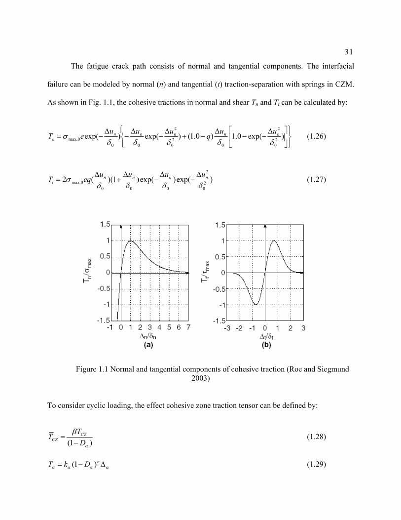
The fatigue crack path consists of normal and tangential components. The interfacial
failure can be modeled by normal (n) and tangential (t) traction-separation with springs in CZM.
As shown in Fig. 1.1, the cohesive tractions in normal and shear Tn and Tt can be calculated by:
⎭⎬⎫
⎩⎨⎧
⎥⎦
⎤⎢⎣
⎡ ∆−−
∆−+
∆−
∆−
∆−= )exp(0.1)0.1()exp()exp( 2
0
2
020
2
000max, δδδδδ
σ nnnnnn
uuquuueT (1.26)
)exp()exp()1)((2 20
2
0000max, δδδδ
σ nnnnt
uuuueqT ∆−
∆−
∆+
∆= (1.27)
Figure 1.1 Normal and tangential components of cohesive traction (Roe and Siegmund 2003)
To consider cyclic loading, the effect cohesive zone traction tensor can be defined by:
)1( α
βD
TT CZCZ −
= (1.28)
αααα ∆−= nDkT )1( (1.29)
32
where m
xx )(0
=β , k is the initial stiffness, ∆ is the opening displacement of crack,
The current cohesive strengths are:
)1(0max,max D−=ασσ (1.30)
)1(0max,max D−= αττ (1.31)
To develop a damage evolution law, essentially the following requirements should be
obeyed (Roe and Siegmund, 2003): 1) an endurance stress limit σf under which the cyclic load
will never cause the solder joint failure; 2) a critical deformation δ0, the damage starts to
accumulate only if the deformation greater than δ0; 3) the rate of damage variable D& is a function
including traction T, separation vector across the cohesive zone ∆u, and damage variable D. 4)
the increment of damage is related to the increment of deformation with respect to load level.
Based on the principles, the evolution law is suggest by Baqi et al. (2005):
)1
()1( fm
DT
rDcD σα
ααααα −
−+−∆= && (1.32)
where cα is a constant which controls the damage accumulation, α∆& is the rate of the relative
opening of the cohesive zone, r and m are constants which control the decay of the reaction force
at the final stage of damage and σf is the cohesive zone endurance limit.
The cohesive zone model has been adopted in current research to simulate the interfacial
behavior between IMC and solder bulk; details are introduced in chapter 2.
33
1.6 Electromigration Effect on IMC Growth and Solder Failure
Electromigration is the transport of material caused by the gradual movement of the ions
in a conductor due to the momentum transfer between conducting electrons and diffusing metal
atoms. The effect is important in applications where high current densities are used, such as in
microelectronics and related structures. As the structure size in electronics such as integrated
circuits (ICs) decreases nowadays, the practical significance of this effect increases.
Initial research on the failure mechanisms of electromigration in thin metal conductors
has been conducted by James R. Black (Black 1969) in 1960s. He found that the lifetime of a
thin metal conductor is inversely proportional to the square of the current density and has an
exponential component with activation energy consistent with grain boundary diffusion. He
proposed the following median time to failure equation:
)exp(50 kTE
jAt a
n= (1.33)
where t50, median time to failure (MTTF), is defined as the time at which 50% of a large number
of identical devices have failed, A is a empirical material constant, j is the current density, n is
the current density exponent and is found to be 2 in Black’s experiments, Ea is the activation
energy, k is Boltzman’s constant, and T is the absolute temperature. This equation is known as
Black’s Equation. Black’s experiments suggest that grain boundary diffusion is the major
diffusion mechanism and electromigration failure is controlled by grain boundary diffusion. The
activation energy of time to failure coincides with the grain boundary diffusion activation energy.
The single mode of distribution of aluminum thin film structure has been widely accepted.
However, Black’s law ignores the influence of thermal gradient across the specimen, it only
provide an empirical formula to roughly estimate the MTTF value.

34
Gan and Tu (2002) have conducted a series of experiments to analyze electromigration
effect on IMC behavior under high current density. They found that IMC is comprised mainly of
Cu3Sn compound rather than Cu6Sn5 compound. Besides, copper has much better
electromigration resistance than Aluminum; they found in the experiment that void started to
appear in the solder part just in front of the solder/IMC cathode interface after 21 hours and grow
bigger after 87 hours. Based on the solder V-groove samples experimental observation, H. Gan
and K.N.Tu (2002) proposed a method to consider the electromigration effect on IMC formation.
In their model, the general form of the atomic flux J can be described as:
dxd
TDCejZ
TDC
xCDJJJJ emchem
Ω−+
∂∂
−=++=σ
γρ
γσ* (1.34)
where C is the concentration =1/Ω for pure metal, Ω is the atomic volume; D is the diffusivity;
γ is the Boltzmann constant; T is the absolute temperature; Z* is the effective charge number; e
is the electron charge; ρ is the resistivity; j is the current density; Jchem is the diffusion term and
Jem is the drift term due to electron momentum transfer effect (electron wind force); Jσ is the back
stress term due to electromigration.
The growth rate of IMC at the anode can be calculated as:
emem JGGJxkT
DGCx
CGD
dtdx
2' −−∆Ω∆
+∆∆
=ση (1.35)
Cη is the Cu concentration in the Cu6Sn5 compound.
*2111
CCCCGGG
Cu −+
−=+=
ηη
(1.36)

35
Eq. (1.45) can be simplified as:
bxaab
xA
dtdx
+∆+
=+∆
=*
(1.37)
a* and b>0 for anode; a* and b<0 for cathode.
where Ω∆= σkTDGCa* ηCGDa ∆= emem GJJGb '2 −=
The grow rate dx/dt depends on chemical potential, electron wind force and back stress
due to electromigration, which corresponds to a/∆x, a*/∆x, b term respectively. It should be
noted that when the linear term b=0, the growth of IMC layer has parabolic dependence with
time. For no current case, the growth rate is smaller at the cathode, larger at anode. It can be
found that there is a thicker layer of Cu6Sn5 formed at the anode side and a thinner layer at the
cathode side. The difference is due to the polarity of electric current and local current crowding
(Gan and Tu 2002).
Generally, for interconnects under high current density that cause electromigration,
vacancy diffusion is driven by four forces: 1) electrical current field forces, which is due to
momentum exchange between moving electrons and host ions, 2) stress gradient, due to
localization of accumulation and depletion of mass, 3) temperature gradient, due to joule heating,
4) vacancy concentration gradient. At high current densities, void formation becomes important.
The chemical potential, electron wind force, and thermal stress effects will be investigated
numerically. Based on the well known Einstein relation (Einstein 1905), the actual flux is
proportional to the thermal dynamic force. For solder interconnect, the thermal dynamic force
has contributions mainly from electron wind force, capillary force, and thermal stress gradient.

36
Electric crowding and joule heating effects also play important roles. The electron wind force
corresponding to the electromigration effect can be predicted using a dislocation core diffusion
model. The surface energy term corresponding to capillary force can be determined based on
Herring’s formula (Herring 1951). The thermal stress field distribution will be determined either
experimentally or numerically. It is noted that in both IMC layer and bulk solder,
electromigration and stress migration forces are generally at the same order of magnitude, and
the electromigration force is stronger than stress migration force under very high applied current
density. The terms of the Einstein relation for the interconnect system can be determined, and
the kinetic mass diffusion model to predict the void growth in interconnects will be available by
combining with available experimental data. A kinetic mass diffusion model is developed in
chapter 4 to predict the electromigration effect on interconnect failure under high current density.
1.7 Objectives of the Study
Based on the literature review of previous research works performed by different
researchers, the ultimate objective of this dissertation is to develop a materials science based
theory for interconnects combine intermetallic compound failure mode and interfacial behavior.
The following investigations are undertaken to achieve this goal:
Firstly, a 3D computational model is developed including cohesive zone model and
unified creep and plasticity theory to simulate the interfacial behavior and creep-plastic behavior
of solder, respectively. Thermal-mechanical analysis is also conducted using the 3D solder/IMC
interconnect model. Secondly, an energy based phase transformation theory is developed based
on fracture mechanics and micromechanics to predict the fatigue crack nucleation and
propagation in solids, experimental data for steels, aluminum alloys, and solder alloys are
37
compared with the prediction of the theory. Some parameters in the theory are obtained from
numerical analysis using the proposed computational model. Finally, a kinetic mass diffusion
theory is developed to predict the electromigration effect on interconnect failure. The predicted
void width and propagation speed are compared with experimental data. Application of the
proposed theory has no size limitation, is applicable to various solder materials, allows data
sharing, is able to handle high current effect, avoids choosing fatigue location or predefining
crack parameters, and, more importantly, gives metallurgical directions so that necessary
measures can be taken to optimize the microstructure and achieve longer lifetime.
1.8 Outline of the Dissertation
The solder and IMC behavior under thermal-mechanical cyclic load is studied in this
dissertation; some theoretical and experimental works on solder interconnect failure have been
reviewed. It is found that most of the solder joints failure is caused by failure near the interface
of IMC and bulk solder. A cohesive zone-UCP mechanical model is applied to predict the crack
initiation and propagation at the interface of solder/IMC or in IMC layer. Thermal mechanical
fatigue analysis to IMC related solder failure is conducted. An energy based phase
transformation model is developed to predict fatigue crack propagation. A kinetic mass diffusion
model is proposed to predict the electromigration effect on interconnect failure.
Chapter 1 introduces the background of current research and gives literature review to
research works conducted by previous researchers. Chapter 2 develops the cohesive-UCP
computational model for solder interconnect including intermetallic layers. Both mechanical and
thermal-electric numerical analyses have been conducted. Chapter 3 investigates the physical
damage process within solder/IMC system. Based on experimental findings, a fatigue theory
38
with its failure criterion based on physical damage mechanism is developed for interconnects.
The theory applies phase transformation concept and energy-based micromechanical fatigue
model to the solder structure. Fatigue crack propagation rate has been accurately predicted for
different steels, aluminum alloys, and solder alloys. Chapter 4 develops a kinetic mass diffusion
model to predict the electromigration effect on solder failure under high current density. Void
width and growth speed can be predicted using the proposed model; reasonable agreement is
obtained compared with experimental data. Chapter 5 concludes the dissertation and suggests
the future research directions. Appendix lists the ABAQUS code for the cohesive-UCP
interconnects structure; the derivation to apply the phase transformation theory to ellipsoidal
crack; a method to incorporate the electrical current effect into phase transformation theory; and
numerical analysis to ball grid array (BGA) electric packaging under drop impact.
39
Chapter 2
Mechanical and Thermo-Electrical Computational Analysis to
Interfacial Failure of Solder Joint
Based on cohesive fracture theory and continuum mechanics, a 3D computational model
has been developed in this chapter to predict the crack nucleation, propagation and interfacial
damage of interconnects. Unified creep-plasticity theory is incorporated in the model to predict
the creep and hysteresis effects on fatigue crack propagation in solder. In addition the cohesive
zone model is adopted to predict the interfacial behavior between the solder bulk and the
intermetallic layer. Using the cohesive-UCP finite element model, the intermetallic-layer growth
effect on crack initiation stress has been studied for different solders. A thermo-electric finite
element analysis has been conducted to predict the electrical concentration and joule heating
effects on the failure of Sn-2.5Ag-0.8Cu-0.5Sb solder under different applied current densities.
The temperature and current density distribution in a solder joint with a crack that propagates
near the interface of the bulk solder and intermetallic layer has been predicted. Pronounced
temperature and electrical current concentration is observed near the crack tip. Although the Pb-
free solder is usually regarded as having a higher melting temperature compared with Pb-Sn
eutectic solder, the concentration of heat at the crack tip caused by joule heating may still melt
the solder material under high current density. The crack propagation will be enhanced and

40
cause a circuit failure. The developed numerical model will be applied to predict some
parameters for phase transformation theory, detail will be introduced in chapter 3.
2.1 Introduction
It has been observed experimentally that solders fail by crack nucleation and propagation
at or near the interface of Intermetallic Compound (IMC) and solder (Mattila and Kivilahti 2006)
(Zhang et al. 2006). To predict the failure mode of the solder-intermetallic interface and the
interconnect lifetime, it is important to know the material properties of both solder and IMC
materials. The objective of this chapter is to develop a finite element model predicting the
interconnect behavior including IMC layer and IMC/solder interface by knowing the thermal,
electrical, and mechanical properties of the interconnect system materials, including IMCs.
Initial emphasis will be on the IMC and IMC/solder interface failure. The fracture toughness of
various materials compared to IMC’s is given in Table 2.1 by Ghosh (2004). Generally the
materials show ductile fracture with high fracture toughness and brittle failure with low fracture
toughness. It is noted that IMC layer materials range from quasi-brittle to semi-ductile.

41
Table 2.1 Fracture toughness of different materials Ghosh (2004)
Material mMPa Soda-lime-glass 0.7-0.8
Polystyrene 0.8-1.1 Cu6Sn5 (η) 2.22-3.38
Cu6Sn5 (η’) 2.37-2.83 Cu3Sn 4.86-6.58
AuSn4 2.15-2.85 Ni3Sn4 3.77-4.67
An aluminum alloy 36 A steel alloy 50
During the past four decades, several methods have been proposed to predict the failure
of solder joints. Typically the most widely used empirical method is the ‘‘Coffin-Manson’’ law.
However, the approach is not useful for cases beyond the experimental range investigated.
Another empirical method is to apply the rate- and temperature-dependent constitutive model
(rate independent inelastic deformation such as plasticity is incorporated in unified creep-
plasticity (UCP) theories) combined with mechanical continuum damage mechanics (CDM)
(McDowell et al. 1994) (Wen et al. 2001 2002) (Wang et al. 2004). The theory gives accurate
predictions to the constitutive relationship of solder materials, typically a large number of
experimentally determined material constants are needed to describe the mechanical behaviors
and damage evolution to achieve a reasonable accuracy. However, both of the methods are not
useful to predict the interfacial failure of solder/IMC. Thus, an advanced method to predict
solder/IMC interfacial failure is required besides applying UCP theory for solder materials.
Recently, the cohesive zone model (CZM) has been used to predict failure of Pb and Pb-
free solder joints (Baqi et al. 2005) (Yang et al. 2001) (Roe and Siegmund 2003) (Nguyen et al.
42
2001) (Yang et al. 2004) (Towashiraporn et al. 2005) (Cavalli et al. 2004) (Yu et al. 2006) (Yao
and Shang 1996). The cohesive zone method is a numerical tool for the mechanics of interfaces;
initially it was developed to model crack initiation and growth in quasi-brittle materials. This
method treats fracture as a gradual process in which separation between incipient material
surfaces is resisted by cohesive tractions. Compared with the traditional empirical method, the
CZM can be applied from micro- to macro-scale, as long as the parameters, cohesive strength
and critical separation displacement, are determined by careful fracture experiments. The model
can predict the entire fracture process from crack initiation to propagation accurately for any
joint geometry and under any applied loads. Crack initiation and propagation are natural
outcomes of a CZM analysis and has been adopted in this chapter through the finite element
program, ABAQUS. The damage mechanics incorporated in the model is introduced and the
damage initiation and evolution conditions are defined. The model is applied to predict the
effects of IMC layer thickness and Young’s modulus on crack initiation stress of solder joints.
Since the solder joint failure is a coupled thermo-electric-mechanical problem, in addition
to a mechanical analysis, a thermo-electric analysis to solder joint with a crack propagating near
the interface of bulk solder and intermetallic layer has been conducted. The temperature and
current density distribution in a solder joint with interfacial crack propagation has been predicted
numerically. The current concentration and joule heating effects are discussed based on
experimental observation and computational analysis results.

43
2.2 Cohesive Zone Modeling and Finite Element Mechanical Analysis to Simulate
Interfacial Behavior of Solder/IMC
To incorporate a cohesive zone model into the finite element model, the principle of
virtual work can be modified to (Roe and Siegmund 2003):
∫∫∫ ∂⋅=∆⋅−
V eS CZVdSuTdSuTdVFP
i
rrrrδδδ~:~ (2.1)
where P~ is the nominal stress tensor which equals σ~)~det(~ 1 FF − , F~ is the deformation gradient,
σ~ is the Cauchy stress tensor, V is the control volume, ur is the displacement vector, CZTr
is the
cohesive zone traction vector, eTr
is the traction vector on the external surface of the body, Si is
the internal boundary, and V∂ is the external boundary of V.
A quadratic nominal stress criterion to predict damage initiation is adopted in this
chapter. Damage is assumed to initiate when a quadratic interaction function involving the
nominal stress ratios reaches unity. This criterion is represented as (ABAQUS documentation
6.6.3 2006):
1)()()( 20
20
20 =++
t
t
s
s
n
n
tt
tt
tt
(2.2)
where nt , st , tt refer to the normal, the first, and the second shear stress components; 0nt , 0
st ,
0tt represent the peak values of the nominal stress when the deformation is either purely normal
to the interface or in the first or the second shear direction. The symbol is the usual

44
Macaulay bracket interpretation, used to signify that a purely compressive deformation or stress
state does not initiate damage. It should be noted that the damage initiation can also be predicted
by using the energy based phase transformation theory, which is introduced in chapter 3.
The damage evolution for mixed mode failure is defined based on Benzeggagh-Kenane
fracture criterion (Benzeggagh and Kenane 1996), when the critical fracture energies during
deformation along the first and the second shear directions are similar; i.e. Ct
Cs GG = , the criteria
is given by:
C
T
SCn
Cs
Cn G
GGGGG =−+ η))(( (2.3)
where the mixed-mode fracture energy tsnC GGGG ++= . Gn, Gs, and Gt refer to the work
done by the traction and its conjugate relative displacement in the normal, the first, and the
second shear directions, respectively, and CnG , C
sG and CtG refer to the critical fracture energies
required to cause failure in the normal, the first, and the second shear directions, respectively.
Here, tsS GGG += , SnT GGG += , and η is a material parameter.
45
2
1
2
1
3
d
d t
Maximum Displacement U1=0.5
solder
t
tdie
substrate
Cu3Sn layer thickness=t4
Cu3Sn layer
Cu6Sn5 layer thickness=t5
Cu6Sn5
layer
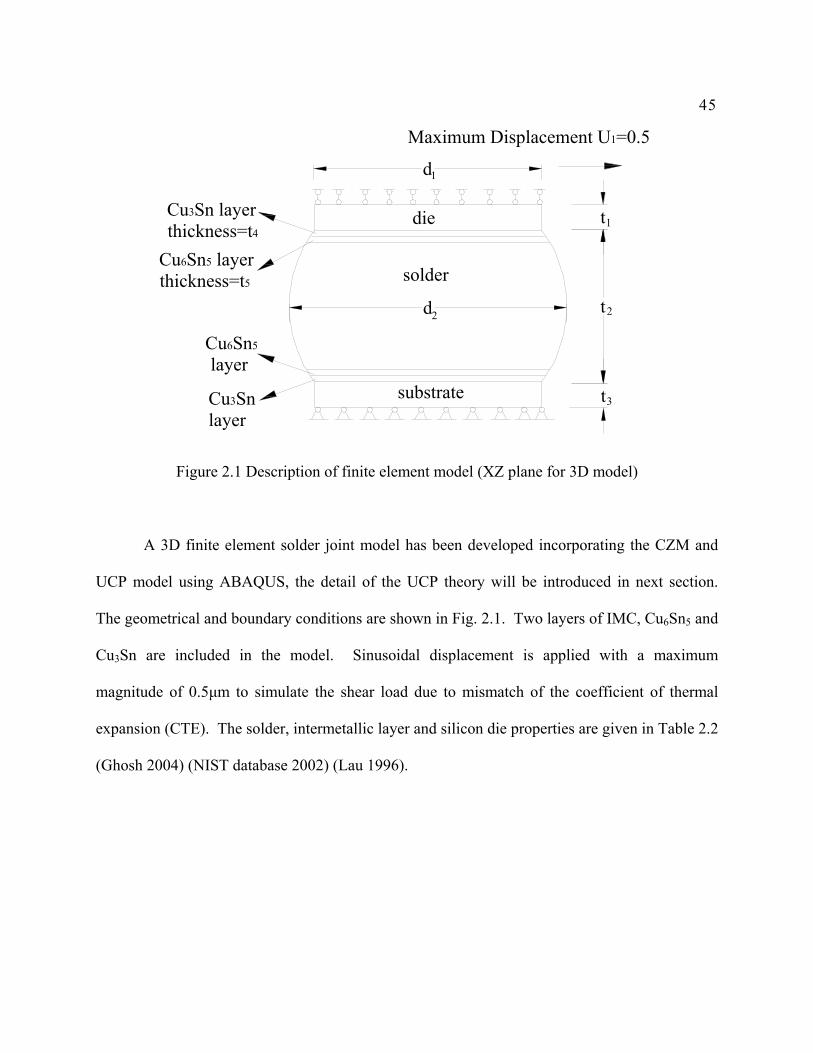
Figure 2.1 Description of finite element model (XZ plane for 3D model)
A 3D finite element solder joint model has been developed incorporating the CZM and
UCP model using ABAQUS, the detail of the UCP theory will be introduced in next section.
The geometrical and boundary conditions are shown in Fig. 2.1. Two layers of IMC, Cu6Sn5 and
Cu3Sn are included in the model. Sinusoidal displacement is applied with a maximum
magnitude of 0.5µm to simulate the shear load due to mismatch of the coefficient of thermal
expansion (CTE). The solder, intermetallic layer and silicon die properties are given in Table 2.2
(Ghosh 2004) (NIST database 2002) (Lau 1996).
46
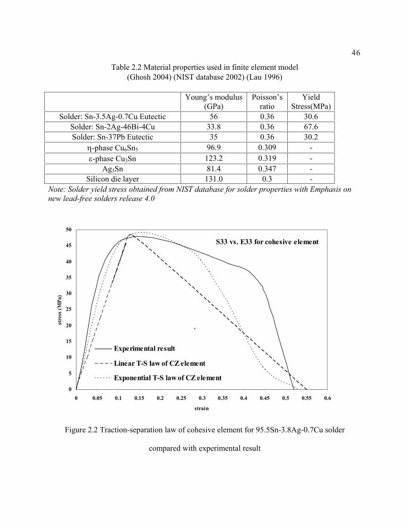
Table 2.2 Material properties used in finite element model (Ghosh 2004) (NIST database 2002) (Lau 1996)
Young’s modulus
(GPa) Poisson’s
ratio Yield
Stress(MPa)Solder: Sn-3.5Ag-0.7Cu Eutectic 56 0.36 30.6
Solder: Sn-2Ag-46Bi-4Cu 33.8 0.36 67.6 Solder: Sn-37Pb Eutectic 35 0.36 30.2
η-phase Cu6Sn5 96.9 0.309 - ε-phase Cu3Sn 123.2 0.319 -
Ag3Sn 81.4 0.347 - Silicon die layer 131.0 0.3 -
Note: Solder yield stress obtained from NIST database for solder properties with Emphasis on new lead-free solders release 4.0
S33 vs. E33 for cohesive element
0
5
10
15
20
25
30
35
40
45
50
0 0.05 0.1 0.15 0.2 0.25 0.3 0.35 0.4 0.45 0.5 0.55 0.6
strain
stre
ss (M
Pa)
Experimental result
Linear T-S law of CZ element
Exponential T-S law of CZ element
`
Figure 2.2 Traction-separation law of cohesive element for 95.5Sn-3.8Ag-0.7Cu solder
compared with experimental result

47
For simplicity an exponential traction-separation (T-S) law of the interfacial cohesive
element is assumed, and the model is applied to simulate 95.5Sn-3.8Ag-0.7Cu solder, for which
experimental data is available (Ren et al. 2005). The stress-strain relationship for the cohesive
element is compared with experimental results, as in Fig. 2.2, which shows acceptable accuracy
using an exponential T-S law.
2.3 Unified Creep and Plasticity Model to Simulate Behavior of Solder Materials
For solder materials, the UCP theory is adopted in the finite element model based on the
dual backstress thermoviscoplasticity model proposed by McDowell et al. (1994) and Wen et al.
(2001 2002). The relationship between stress rateσ& and strain rate can be written as:
TT
TT in &&&&∂∂
+−−= − CσCI εεCσ ::)(:)( 1χ (2.4)
where C is the matrix of the elastic constants and is a function of Poisson’s ratio ν and Young’s
modulus E(T), which is also a function of absolute temperature T; ε& is the total strain rate; inε& is
the inelastic strain rate; χ is the coefficient of thermal expansion and I is the unit tensor. Here,
the term I Tχ refers to the thermal strain rate.
The form of the flow rule for inelastic strain rate is given by:
Nε )(exp23 1
TdS
DdS
An
vn
vin Θ⎟⎟⎠
⎞⎜⎜⎝
⎛⎟⎠⎞
⎜⎝⎛
⎟⎠⎞
⎜⎝⎛=
+
& (2.5)

48
where d is the drag strength; A and D are material constants; the diffusivity
term ))/(exp()( kTQT −=Θ ; Q is the apparent activation energy; k is the universal gas constant,
equal to 8.314J/Kmole; N is a unit vector in the direction of the deformation loading, defined by:
αSαSN −−= /)( (2.6)
where S is the deviatoric tensor, 3/)(σσS tr−= ; vS is the viscous overstress defined by:
RSv −= α-S23
(2.7)
where R is the yield stress radius; α is the deviatoric back stress
The evolutionary law for α is defined as:
αNεα βµ −= in&& (2.8)
where µ and β are material constants. Eq. (2.8) is similar to Prager’s flow law (Prager 1956) in
plasticity, and it is noted that α reaches a saturated value along with the loading process.
To determine the R term in Eq. (2.7),
addinitial RRR += (2.9)
χϖ && =addR (2.10)
where ϖ is a material constant; χ is the hardening from the dislocation increment within the
material, which is defined as:

49
)( χχεµχ −= in&& (2.11)
where χ is the sutured value of χ; µ is a material constant.
The material constants for the model were obtained through analysis of the material
behavior and by fitting to the experimental data (Vaynman and Zubelewicz 1990) (Vaynman and
McKeown 1993) (Wen 2001) (Wen et al. 2002) (Wang et al. 2004). For the Sn-3.5Ag eutectic
solders, the values of the parameters were determined as: E=45GPa, A=5.81×10³s-1, α=0,
D=0.001, n=2, d=70MPa, R=8.0MPa, µ=16, β=0.009s-1, Q=38000J/mole. For the 63Sn-37Pb
eutectic solders, the values of the parameters were determined as: A=0.009, α=0, D=0.001,
n=1.2, d=70MPa, Rinitial=2.0MPa, µ=8, χ =8MPa, 085.0=ϖ , Q=22000 J/mole.
2.4 Case Study and IMC Layer Thickness Effect on Solder Failure
A 3D finite element model for an interconnect has been developed incorporating CZM
and UCP theories to simulate solder/IMC interfacial behavior and hysteresis effect in solder
bulk, respectively (Yao et al. 2008). The model has been programmed into the commercial
software, ABAQUS, through a user defined subroutine using FORTRAN language. The
ABAQUS code for the model is given in Appendix A.
The main process of building a model is as follows:
a. Defining the job title and units
b. Creating the model geometry
c. Defining parts, section and material properties (User defined subroutine are combined into the
model to include CZM and UCP theory)

50
d. Defining element type and property, cohesive element and solid stress elements are used for
2D/3D stress analysis; electrical-thermal element is used for joule heating analysis
e. Meshing
f. Defining the analysis type and analysis options
g. Applying loads and boundary conditions
h. Specifying load step options
i. Initiating the solution
j. Review the results
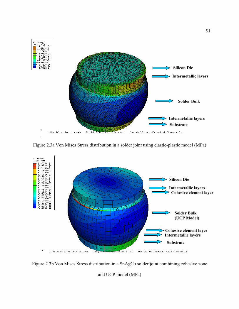
Fig. 2.3a shows the stress analysis with typical elastic-plastic solder modeling applied to
the solder/IMC interconnect system, where the von Mises stress distribution is predicted. Fig.
2.3b shows the analysis to solder/IMC using the combined CZM and UCP theory. A cohesive
layer with traction-separation type cohesive element has been defined at the interface of the
solder and IMC to predict the interfacial failure. In addition to the von Mises stress distribution,
the crack nucleation and propagation near the solder/IMC interface can be predicted in a
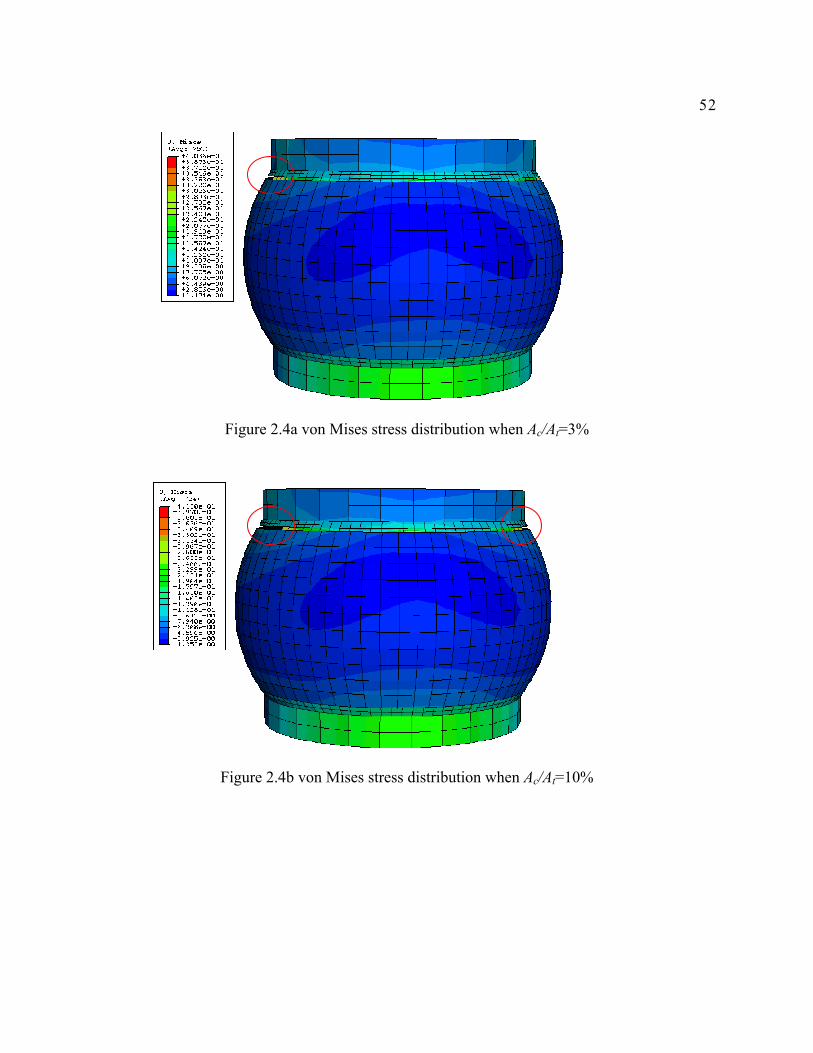
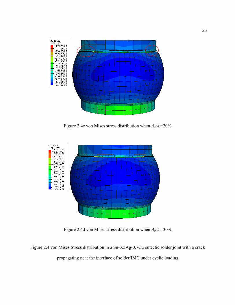
cohesive element model with the defined damage initiation and evolution law. Figure 2.4 shows
the von Mises Stress distribution in a Sn-3.5Ag-0.7Cu eutectic solder joint with a crack
propagating near the interface of solder/IMC under cyclic loading, here Ac is the crack area and
At is the total cross section area.
51
Figure 2.3a Von Mises Stress distribution in a solder joint using elastic-plastic model (MPa)
Figure 2.3b Von Mises Stress distribution in a SnAgCu solder joint combining cohesive zone
and UCP model (MPa)
Intermetallic layers
Solder Bulk
Intermetallic layers
Silicon Die
Substrate
Intermetallic layers
Solder Bulk (UCP Model)
Intermetallic layers
Cohesive element layer
Silicon Die
Substrate
Cohesive element layer
52
Figure 2.4a von Mises stress distribution when Ac/At=3%
Figure 2.4b von Mises stress distribution when Ac/At=10%
53
Figure 2.4c von Mises stress distribution when Ac/At=20%
Figure 2.4d von Mises stress distribution when Ac/At=30%
Figure 2.4 von Mises Stress distribution in a Sn-3.5Ag-0.7Cu eutectic solder joint with a crack
propagating near the interface of solder/IMC under cyclic loading

54
The proposed cohesive-UCP finite element model is applied to predict the effect of IMC
layer thickness on the crack initiation stress of a solder joint. The growth of an IMC layer in
solder joint is caused not only by a long reflow time and high reflow temperature during
soldering, but also by aging, storage, and long term cyclic operation of the electronic assembly at
room temperature, including long dwell times during operation or sleep mode at higher
temperatures. It is found experimentally that the IMC thickness increases linearly, almost with
the square root of aging time (Chan et al. 1997) (Gan and Tu 2002) (Xu et al. 2006).
von-Mises vs. IMC layer thickness
0.8
0.82
0.84
0.86
0.88
0.9
0.92
0.94
0.96
0.98
1
2 3 4 5 6 7 8 9 10 11 12
IMC thickness (µm)
von
Mise
s cra
ck in
itiat
ed
stre
ss/st
ress
whe
n IM
C=2
µm
Sn-3.5Ag-0.7Cu Eutectic
Sn-37Pb Eutectic
Sn-2Ag-46Bi-4Cu
Figure 2.5 Effect of intermetallic layer thickness on crack initiation stress
55
10
15
20
25
30
35
40
45
50
20 40 60 80 100 120 140 160 180 200EIMC (GPa)
max
. str
ess a
t cra
ck n
ucle
atio
n po
int n
ear
IMC
/sold
er in
terf
ace
(MPa
)
Sn-3.5Ag-0.7CuSn-37PbSn-2.5Ag-0.8Cu-0.5Sb
Figure 2.6 IMC Young’s modulus effect on maximum von Mises stress at solder/IMC interface
(crack nucleation point)
20
25
30
35
40
45
50
20 30 40 50 60 70 80 90 100
ESolder (GPa)
max
. str
ess n
ear
crac
k nu
clea
tion
poin
t at
IMC
/sold
er in
terf
ace
(MPa
)
Cu6Sn5Ag3SnCu3Sn
Figure 2.7 Solder Young’s modulus effect on maximum von Mises stress at solder/IMC interface
(crack nucleation point)
56
Although some experiments have been performed on IMC growth under thermal aging,
limited material properties of IMC are available for use in developing mechanical failure models
for IMC failure. Recently, a series of experiments to analyze the electric properties, hardness,
and indentation fracture toughness of IMC relevant to electronic packaging has been conducted
at Northwestern University (Ghosh 2004). Based on these experimental results, a finite element
analysis has been conducted to analyze the effect of IMC thickness upon solder joint failure.
Different layer thicknesses of Cu3Sn and Cu6Sn5 are incorporated in the cohesive finite element
model, and Fig. 2.5 shows the effects of intermetallic layer thickness on crack initiation stress for
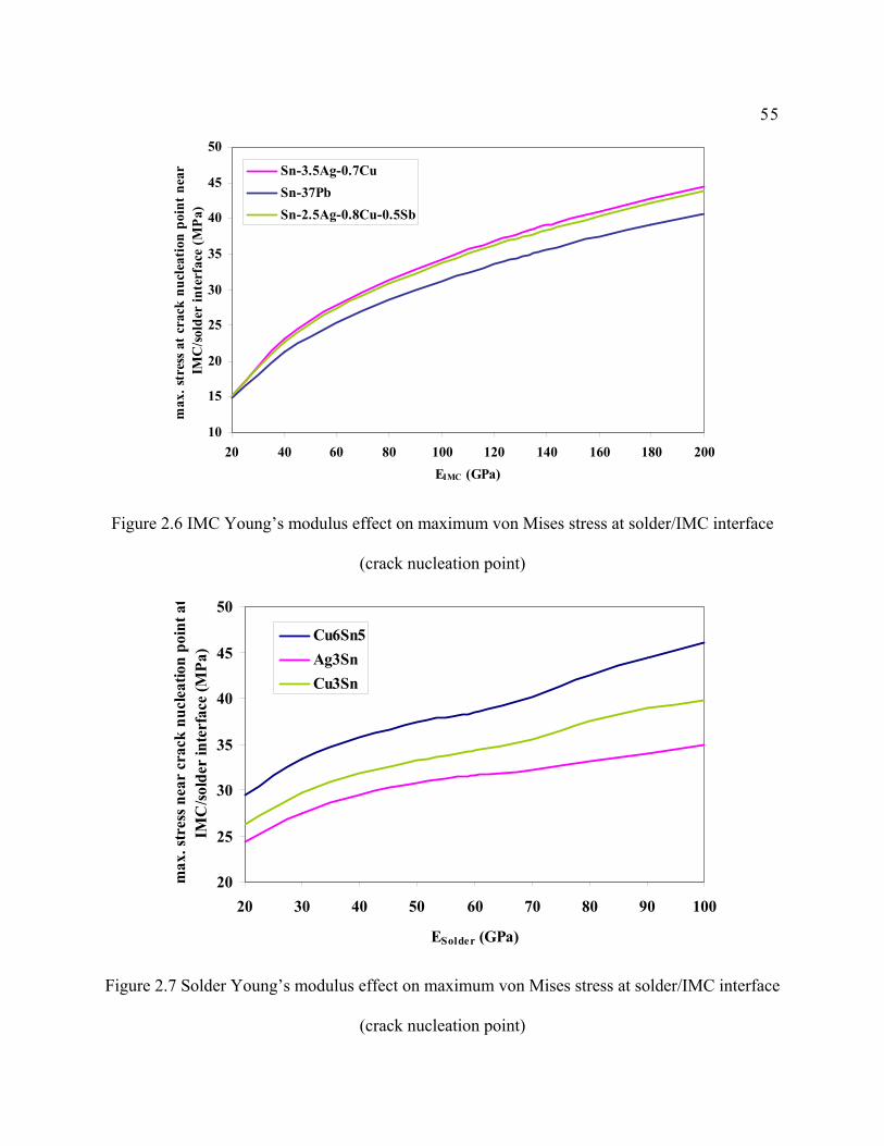
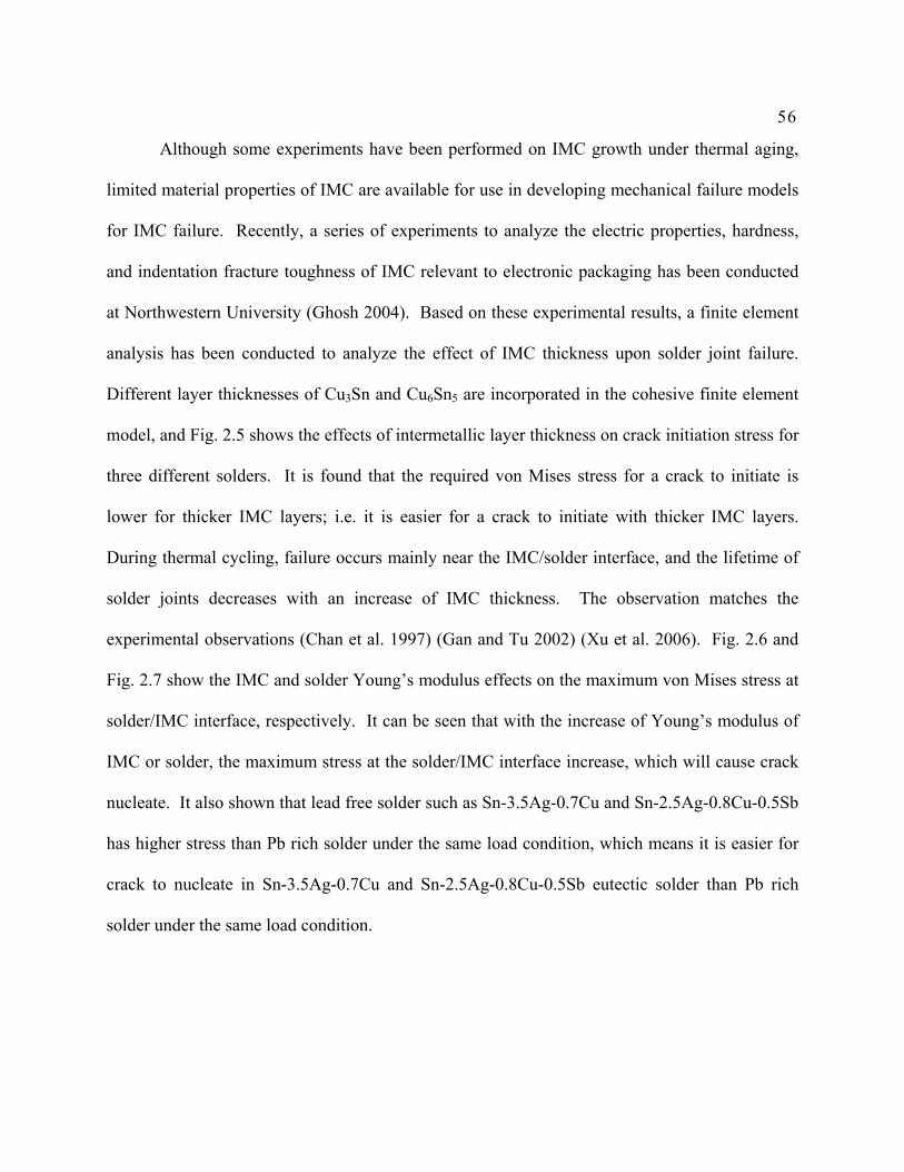
three different solders. It is found that the required von Mises stress for a crack to initiate is
lower for thicker IMC layers; i.e. it is easier for a crack to initiate with thicker IMC layers. During thermal cycling, failure occurs mainly near the IMC/solder interface, and the lifetime of
solder joints decreases with an increase of IMC thickness. The observation matches the
experimental observations (Chan et al. 1997) (Gan and Tu 2002) (Xu et al. 2006). Fig. 2.6 and
Fig. 2.7 show the IMC and solder Young’s modulus effects on the maximum von Mises stress at
solder/IMC interface, respectively. It can be seen that with the increase of Young’s modulus of
IMC or solder, the maximum stress at the solder/IMC interface increase, which will cause crack
nucleate. It also shown that lead free solder such as Sn-3.5Ag-0.7Cu and Sn-2.5Ag-0.8Cu-0.5Sb
has higher stress than Pb rich solder under the same load condition, which means it is easier for
crack to nucleate in Sn-3.5Ag-0.7Cu and Sn-2.5Ag-0.8Cu-0.5Sb eutectic solder than Pb rich
solder under the same load condition.
57
2.5 Coupled Thermo-Electric Analysis to Solder Joint with Crack Propagation near the
Interface of Bulk Solder and Intermetallic Layer
Since the failure of solder joint is a coupled thermo-electric-mechanical problem, a
thermo-electric analysis is necessary in addition to the mechanical analysis to understand the
interconnect failure mechanism. When a crack propagates near the interface between solder and
IMC, an important issue affecting solder joint failure is joule heating, which arises when the
energy dissipated by an electrical current flowing through a conductor is converted to thermal
energy. The effect has been researched experimentally (Alam et al. 2006) (Ye et al. 2003) (Nah
et al. 2005) (Liang et al. 2006) (Chiu et al. 2006). However, the joule heating effect on solder
joint failure with interfacial crack propagation is still not clear. In this section finite element
analysis is conducted to analyze the joule heating and electrical concentration near the crack tip.
The thermo-electric coupling arises from two sources: the temperature dependent conductivity in
the electrical problem, and the internal heat generated, which is a function of electric current.
The flow of electrical current is described by Ohm's law. Since a potential rise occurs
when a charged particle moves against the electrical field, the direction of the gradient is
opposite to that of the electric field. Using this definition of the electrical field, Ohm's law is
written as:
Ej E ˆ⋅= σ (2.12)
Here j is the current density (A/cm2); ),( ασ fTE is the electrical conductivity matrix; T is the
temperature; and f α, α = 1, 2…are any predefined field variables. The conductivity can be
isotropic, orthotropic, or fully anisotropic. The electrical field intensity E can be defined as:
58
xE
∂∂
−=ϕˆ (2.13)
where ϕ is the electric potential field.
Ej ˆ=ρ (2.14)
ρ is the resistivity (µΩcm);
From conservation of charge, 0ˆ 2 =∇=∇ ϕE
The electric field in a conducting material is governed by Maxwell's conservation of
charge equation (ABAQUS documentation 6.6.3 2006). Assuming steady-state direct current, the
equation is:
∫ ∫=⋅S V
cdVrdSnj rr (2.15)
where V is any control volume whose surface is S, nr is the outward normal to S, jr
is the
electrical current density (current per unit area), njj rr⋅−= is the current density entering the
control volume across S, and rc is the internal volumetric current source per unit volume.
The equivalent weak form is obtained by introducing an arbitrary electrical potential
field, δϕ , and integrating over the volume. Appling the chain rule, divergence theorem and
Ohm's law, the governing conservation of charge Eq. (2.15) becomes:
∫∫∫ +=∂∂⋅⋅
∂∂
−V
cSV
E dVrjdSdVxx
δϕδϕϕσδϕrr
~ (2.16)

59
where Eσ~ is the electrical conductivity matrix.
Based on Eq. (2.16), a coupled thermo-electric finite element analysis is conducted to
determine the joule heating effect, temperature concentration and electrical current concentration
with a crack propagating near the interface of solder and IMC. The finite element model is used
first to predict the average temperature in a solder joint under different applied currents, and the
results match well when compared with experiment (Chiu et al. 2006), as shown in Fig. 2.8.
70
75
80
85
90
95
0.1 0.2 0.3 0.4 0.5 0.6
Applied current (A)
Ave
rage
sol
der j
oint
tem
pera
ture
(°C
Experimental resultsFEM predictions
Figure 2.8 Simulation of applied current density versus average temperature in a solder joint
Because of limited experimental data for thermal and electrical properties of solders and
IMC materials, Castin™ (Sn-2.5Ag-0.8Cu-0.5Sb) solder is analyzed here. The thermal and
electrical properties of solder and IMC materials for Castin™ solder are given in Table 2.3 and
2.4 (NIST database 2002). Fig. 2.9 and 2.10 show the electric current density and temperature
distribution of a solder joint with a crack propagating near the interface of solder bulk and IMC
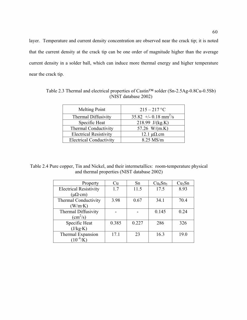
60
layer. Temperature and current density concentration are observed near the crack tip; it is noted
that the current density at the crack tip can be one order of magnitude higher than the average
current density in a solder ball, which can induce more thermal energy and higher temperature
near the crack tip.
Table 2.3 Thermal and electrical properties of Castin™ solder (Sn-2.5Ag-0.8Cu-0.5Sb)
(NIST database 2002)
Melting Point 215 – 217 °C Thermal Diffusivity 35.82 +/- 0.18 mm2/s
Specific Heat 218.99 J/(kg.K) Thermal Conductivity 57.26 W/(m.K) Electrical Resistivity 12.1 µΩ.cm
Electrical Conductivity 8.25 MS/m
Table 2.4 Pure copper, Tin and Nickel, and their intermetallics: room-temperature physical and thermal properties (NIST database 2002)
Property Cu Sn Cu6Sn5 Cu3Sn Electrical Resistivity
(µΩ·cm) 1.7 11.5 17.5 8.93
Thermal Conductivity (W/m·K)
3.98 0.67 34.1 70.4
Thermal Diffusivity (cm2/s)
- - 0.145 0.24
Specific Heat (J/kg·K)
0.385 0.227 286 326
Thermal Expansion (10–6/K)
17.1 23 16.3 19.0

61
2.9a. current distribution when crack length=0µm
2.9b. current distribution when crack length=5µm
Cu
Solder
IMC
Cu
Solder
IMC
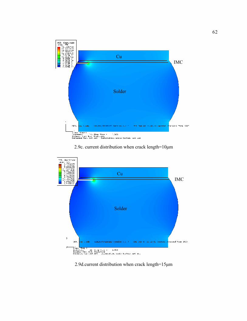
62
2.9c. current distribution when crack length=10µm
2.9d.current distribution when crack length=15µm
Cu
Solder
IMC
Cu
Solder
IMC
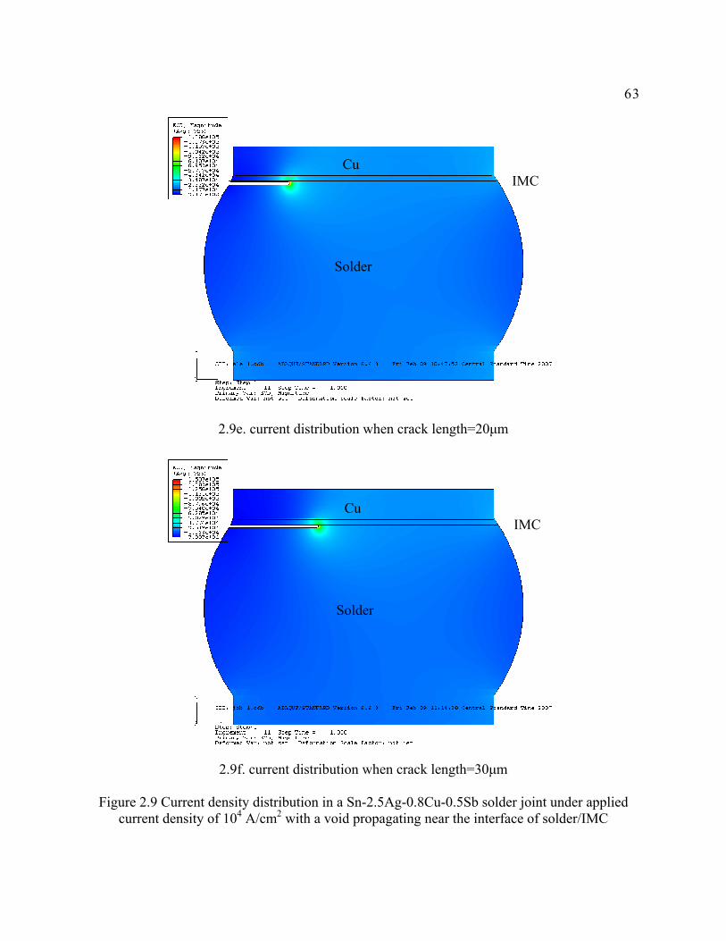
63
2.9e. current distribution when crack length=20µm
2.9f. current distribution when crack length=30µm
Figure 2.9 Current density distribution in a Sn-2.5Ag-0.8Cu-0.5Sb solder joint under applied current density of 104 A/cm2 with a void propagating near the interface of solder/IMC
Cu
Solder
IMC
Cu
Solder
IMC
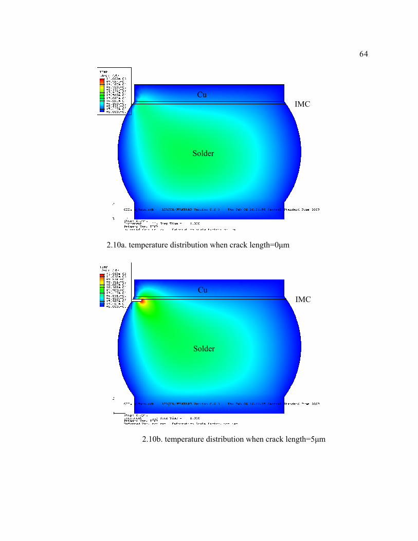
64
2.10a. temperature distribution when crack length=0µm
2.10b. temperature distribution when crack length=5µm
Cu
Solder
IMC
Cu
Solder
IMC
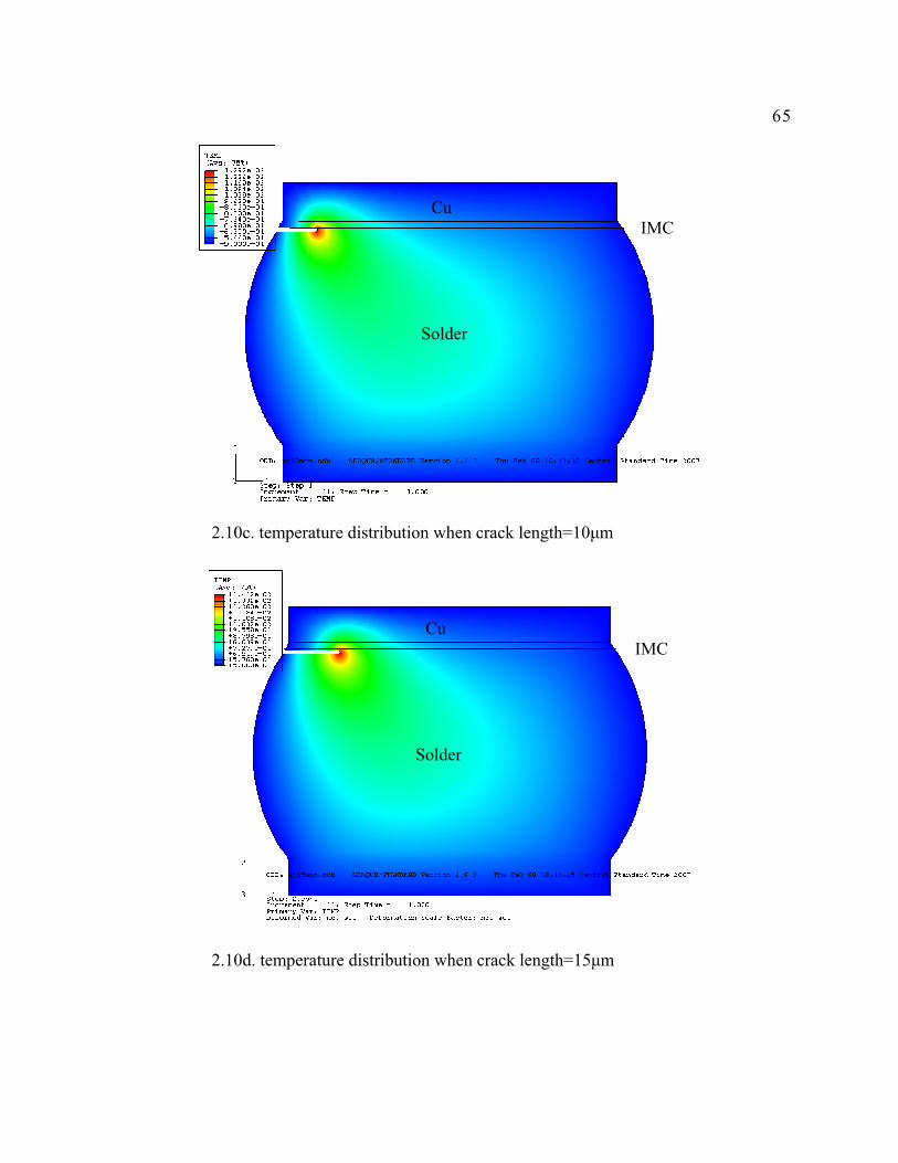
65
2.10c. temperature distribution when crack length=10µm
2.10d. temperature distribution when crack length=15µm
Cu
Solder
IMC
Cu
Solder
IMC
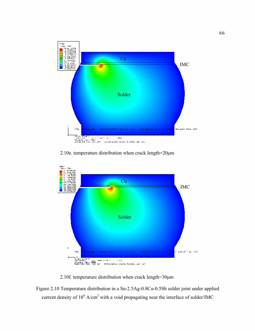
66
2.10e. temperature distribution when crack length=20µm
2.10f. temperature distribution when crack length=30µm
Figure 2.10 Temperature distribution in a Sn-2.5Ag-0.8Cu-0.5Sb solder joint under applied
current density of 104 A/cm2 with a void propagating near the interface of solder/IMC
Cu
Solder
IMC
Cu
Solder
IMC
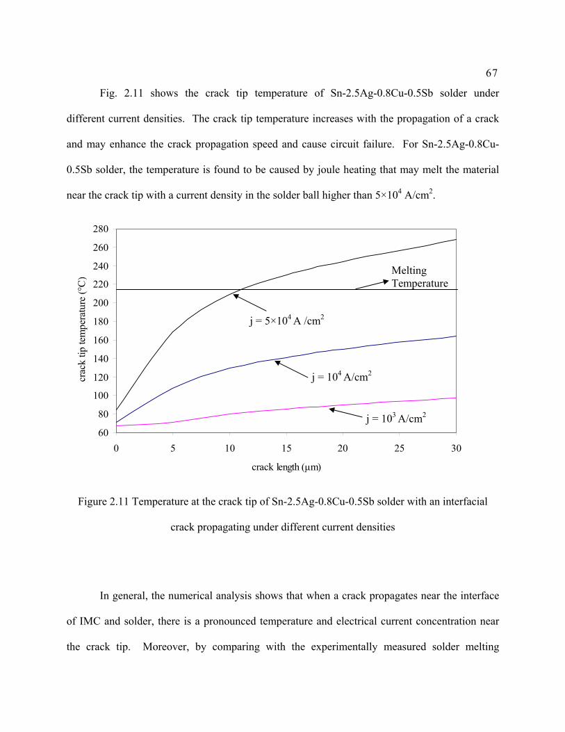
67
Fig. 2.11 shows the crack tip temperature of Sn-2.5Ag-0.8Cu-0.5Sb solder under
different current densities. The crack tip temperature increases with the propagation of a crack
and may enhance the crack propagation speed and cause circuit failure. For Sn-2.5Ag-0.8Cu-
0.5Sb solder, the temperature is found to be caused by joule heating that may melt the material
near the crack tip with a current density in the solder ball higher than 5×10⁴ A/cm2.
60
80
100
120
140
160
180
200
220
240
260
280
0 5 10 15 20 25 30
crack length (µm)
crac
k tip
tem
pera
ture
(°C
)
Figure 2.11 Temperature at the crack tip of Sn-2.5Ag-0.8Cu-0.5Sb solder with an interfacial
crack propagating under different current densities
In general, the numerical analysis shows that when a crack propagates near the interface
of IMC and solder, there is a pronounced temperature and electrical current concentration near
the crack tip. Moreover, by comparing with the experimentally measured solder melting
j = 103 A/cm2
j = 104 A/cm2
j = 5×10⁴ A /cm2
Melting Temperature

68
temperature, as given in Fig. 2.12 (NIST database 2002), the concentration of heat at the crack
tip caused by joule heating may high enough to melt the solder.
Figure 2.12 Liquidus surface for Ag-Cu-Sn system (NIST database 2002)
2.6 Solder and IMC Thermal and Electrical Conductivities Effects on Crack Tip
Temperature
For solder and IMC materials, the thermal and electrical conductivities effects on crack
tip temperature are analyzed using the developed finite element model. The crack tip
temperatures with respect to different solder and IMC thermal and electrical conductivities for
different crack lengths are shown in Fig. 2.13 and Fig. 2.14. In current research, the solder and
IMC’s thermal conductivity ranges from 10 to 100W/mK, and electrical conductivity ranges
from 2 to 20MS/m. The solder joints are under the current density of 104 A/cm2.

69
50
100
150
200
250
300
350
400
450
10 20 30 40 50 60 70 80 90 100
thermal conductivity of solder W/(m.K)
high
est t
empe
ratu
re a
t cra
ck ti
p °C
. crack length=0µmcrack length=5µmcrack length=10µmcrack length=15µmcrack length=20µmcrack length=30µm
2.13a) Solder TC VS crack tip temperature
60
80
100
120
140
160
180
200
10 20 30 40 50 60 70 80 90 100
thermal conductivity of IMC W/(m.K)
high
est t
empe
ratu
re a
t cra
ck ti
p °C
.
crack length=0µm
crack length=5µm
crack length=10µm
crack length=15µm
crack length=20µm
crack length=30µm
2.13b) IMC TC VS crack tip temperature
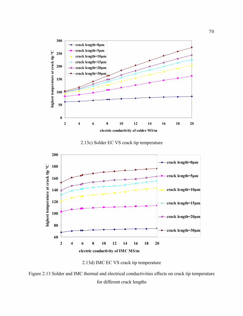
70
0
50
100
150
200
250
300
2 4 6 8 10 12 14 16 18 20
electric conductivity of solder MS/m
high
est t
empe
ratu
re a
t cra
ck ti
p °C
.
crack length=0µmcrack length=5µmcrack length=10µmcrack length=15µmcrack length=20µmcrack length=30µm
2.13c) Solder EC VS crack tip temperature
60
80
100
120
140
160
180
200
2 4 6 8 10 12 14 16 18 20
electric conductivity of IMC MS/m
high
est t
empe
ratu
re a
t cra
ck ti
p °C
. crack length=0µm
crack length=5µm
crack length=10µm
crack length=15µm
crack length=20µm
crack length=30µm
2.13d) IMC EC VS crack tip temperature
Figure 2.13 Solder and IMC thermal and electrical conductivities effects on crack tip temperature
for different crack lengths

71
50
100
150
200
250
300
350
400
450
0 5 10 15 20 25 30
crack length µm
high
est t
empe
ratu
re a
t cra
ck ti
p °C
.solder TC=57.3solder TC=10solder TC=20solder TC=30solder TC=40solder TC=50solder TC=60solder TC=70solder TC=80solder TC=90solder TC=100
14a) Crack lengths VS crack tip temperature for different Solder TC
60
80
100
120
140
160
180
200
0 5 10 15 20 25 30
crack length µm
high
est t
empe
ratu
re a
t cra
ck ti
p °C
.
IMC TC=34.1IMC TC=10IMC TC=20IMC TC=30IMC TC=40IMC TC=50IMC TC=60IMC TC=70IMC TC=80IMC TC=90IMC TC=100
14b) Crack lengths VS crack tip temperature for different IMC TC

72
50
100
150
200
250
300
0 5 10 15 20 25 30
crack length µm
high
est t
empe
ratu
re a
t cra
ck ti
p °C
.solder EC=8.25solder EC=2solder EC=4solder EC=6solder EC=8solder EC=10solder EC=12solder EC=14solder EC=16solder EC=18solder EC=20
14c) Crack lengths VS crack tip temperature for different Solder EC
60
80
100
120
140
160
180
200
0 5 10 15 20 25 30
crack length µm
high
est t
empe
ratu
re a
t cra
ck ti
p °C
.
IMC EC=5.71IMC EC=2IMC EC=4IMC EC=6IMC EC=8IMC EC=10IMC EC=12IMC EC=14IMC EC=16IMC EC=18IMC EC=20
14d) Crack lengths VS crack tip temperature for different IMC EC
Figure 2.14 Solder and IMC thermal and electrical conductivities effects on crack tip temperature
with crack propagation predicted using FEM

73
It is found that the crack tip temperature increases with crack growth. Larger thermal
conductivity leads lower crack tip temperature because of better heat dissipation. With larger
electrical conductivity, the crack tip temperature is higher because more electrons pass through
the cross section. At the initial stage of crack propagation, the slope is larger than that at the
later stage of crack propagation, which means crack tip temperature increases faster at the
beginning stages of crack propagation. The research is thus focus on initial stages of crack
propagation. The importance of the effects on crack tip temperature is found to be: solder’s
thermal conductivity > solder’s electrical conductivity > IMC’s thermal conductivity > IMC’s
electrical conductivity. For solder and IMC materials, thermal conductivities from 20 to
100W/mK can be regarded as a band and crack tip temperature increase consistently with smaller
thermal conductivities; however, when solders’ thermal conductivity changes from 20 to 10
W/mK, the increase of crack tip temperature will be much serious.
2.7 Wiedemann-Franz-Lorenz Relation for Solder and Intermetallic Materials
Due to the limitation of available experimental data for thermal conductivity of solder
and IMC materials, the Wiedemann-Franz-Lorenz (WFL) law is a possible solution to predict
thermal conductivity with known electrical conductivity. The thermal and electrical
conductivities of Sn and Sn rich solder and intermetallic materials are studied in this section.
The WFL law is obeyed well in Sn, however, there is a positive deviation from the theoretical
Lorenz number. In metals the WFL law is written as:
TL σκ 0= (2.17)
For metal and alloy materials, the thermal conductivity mainly consists of two parts:
74
le κκκ += (2.18)
κe is the electronic conductivity and κl is the lattice conductivity. The electrical and thermal
conductivities are related by the Wiedemann-Franz-Lorenz law:
le TL κσκ += (2.19)
where Le is the Lorenz factor, σ is the electrical conductivity, and T is the absolute temperature.
It is interesting to investigate how well the theory is obeyed for Sn and Sn rich solder
alloys. Table 2.5 gives the predicted Lorenz factors for different materials.
75
Table 2.5a Lorenz factor for different materials (Austin 1942) (NIST database 2002)
Metal Temp.(K) EC:σ(108/Ωm) σ *T TC:κ(W/mK) Lorenz factor
Cu 293 0.588 172.284 398 2.310139 Cu 293 0.588 172.284 393 2.281117 Cu 293 0.588 172.284 401 2.327552 Sn 293 0.087 25.491 67 2.628379 Sn 293 0.087 25.491 73 2.863756 Sn 90 0.294 26.46 82 3.099017 Sn 273 0.0763 20.8299 64 3.072506 Sn 293 0.087 25.491 64 2.51069 Sn 364 0.0549 19.9836 59 2.952421 Sn 449 0.0424 19.0376 59 3.09913 Sn 498 0.0455 22.659 61 2.692087 Ni 293 0.128 37.504 90.5 2.413076 Ni 293 0.147 43.071 92 2.136008 Ni 293 0.147 43.071 91 2.112791 Ag 293 0.625 183.125 418 2.282594 Ag 293 0.625 183.125 429 2.342662 Al 293 0.2326 68.1518 240 3.52155 Cr 293 0.05 14.65 66 4.505119 Au 293 0.4545 133.1685 297 2.230257 Mo 293 0.192 56.256 146 2.595279 Pd 293 0.0926 27.1318 70 2.579998 Pt 293 0.0943 27.6299 71 2.56968 W 293 0.182 53.326 200 3.750516
FeNi 293 0.0217 6.3581 11 1.730077 Kovar 293 0.02 5.86 17 2.901024 Ag-Pd 293 0.05 14.65 150 10.23891 Au-Pt 293 0.0333 9.7569 130 13.3239
Au-20Sn 293 0.0625 18.3125 57 3.112628 Pb-5Sn 293 0.0526 15.4118 63 4.087777
Cu-W(20%Cu) 293 0.4 117.2 248 2.116041 Cu-Mo(20%Cu) 293 0.417 122.181 197 1.612362
IMC Cu6Sn5 293 0.057 16.701 34.1 2.041794 Cu3Sn 293 0.112 32.816 70.4 2.145295 Ni3Sn4 293 0.035 10.255 19.6 1.911263 Solder
Sn-2.5Ag-0.8Cu-0.5Sb 293 0.0825 24.1725 57.26 2.368808 Sn-2.8Ag-20.0In 293 0.0588 17.2284 53.5 3.105338 Sn-37Pb(eutectic) 293 0.0685 20.0705 50.9 2.53606
293 0.069 20.217 50.9 2.517683
76
Table 2.5b Lorenz factor for different materials (Sorted)
Materials Absolute Temp.(K)
Elec.Conduc.σ(108/Ωm) σ *T Ther.Conduc.
κ(W/mK) Lorenz factor
Cu-Mo(20%Cu) 293 0.417 122.181 197 1.612362FeNi 293 0.0217 6.3581 11 1.730077
Ni3Sn4 293 0.035 10.255 19.6 1.911263Cu6Sn5 293 0.057 16.701 34.1 2.041794
Ni 293 0.147 43.071 91 2.112791Cu-W(20%Cu) 293 0.4 117.2 248 2.116041
Ni 293 0.147 43.071 92 2.136008Cu3Sn 293 0.112 32.816 70.4 2.145295
Au 293 0.4545 133.1685 297 2.230257Cu 293 0.588 172.284 393 2.281117Ag 293 0.625 183.125 418 2.282594Cu 293 0.588 172.284 398 2.310139Cu 293 0.588 172.284 401 2.327552Ag 293 0.625 183.125 429 2.342662
Sn-2.5Ag-0.8Cu-0.5Sb 293 0.0825 24.1725 57.26 2.368808Ni 293 0.128 37.504 90.5 2.413076Sn 293 0.087 25.491 64 2.51069
Sn-37Pb(eutectic) 293 0.069 20.217 50.9 2.517683Sn-37Pb(eutectic) 293 0.0685 20.0705 50.9 2.53606
Pt 293 0.0943 27.6299 71 2.56968 Pd 293 0.0926 27.1318 70 2.579998Mo 293 0.192 56.256 146 2.595279Sn 293 0.087 25.491 67 2.628379Sn 498 0.0455 22.659 61 2.692087Sn 293 0.087 25.491 73 2.863756
Kovar 293 0.02 5.86 17 2.901024Sn 364 0.0549 19.9836 59 2.952421Sn 273 0.0763 20.8299 64 3.072506Sn 90 0.294 26.46 82 3.099017Sn 449 0.0424 19.0376 59 3.09913
Sn-2.8Ag-20.0In 293 0.0588 17.2284 53.5 3.105338Au-20Sn 293 0.0625 18.3125 57 3.112628
Al 293 0.2326 68.1518 240 3.52155 W 293 0.182 53.326 200 3.750516
Pb-5Sn 293 0.0526 15.4118 63 4.087777Cr 293 0.05 14.65 66 4.505119
Ag-Pd 293 0.05 14.65 150 10.23891Au-Pt 293 0.0333 9.7569 130 13.3239

77
Fig. 2.15 shows the distribution of Lorenz factor for different materials. Figure 2.16 to
Fig. 2.18 gives the predicted Wiedemann-Franz-Lorenz law for Cu, Ni, Sn, and different solder
and IMC materials.
2
1
5
7 7
2
3
5
2 2
0
1
2
3
4
5
6
7
8
1.6~1.8 1.8~2.0 2.0~2.2 2.2~2.4 2.4~2.6 2.6~2.8 2.8~3 3~3.2 3.2~4.0 4.0~4.5
Lorenz factor
Num
ber o
f mat
eria
ls
(Including every data point)
Figure 2.15a Distribution of Lorenz factor for different materials
2
1
3
5
4
0
2 2 2 2
0
1
2
3
4
5
6
1.6~1.8 1.8~2.0 2.0~2.2 2.2~2.4 2.4~2.6 2.6~2.8 2.8~3 3~3.2 3.2~4.0 4.0~4.5
Lorenz factor
Num
ber o
f mat
eria
ls
Figure 2.15b Distribution of Lorenz factor for Cu, Sn, Ag, Ni, and Sn-37Pb)
78
Sn: y = 2.0854x + 17.785
0
20
40
60
80
100120
140
160
180
200
0 10 20 30 40 50
Electrical conductivity×absolute temperature σT(108K(ohm-1m-1))
Ther
mal
con
duct
ivity
κ(W
/mK
) _
Sn
Cu6Sn5
Cu3Sn
Ni3Sn4
Sn-2.5Ag-0.8Cu-0.5SbSn-2.8Ag-20.0In
Sn-37Pb(eutectic)
Linear (Sn)
Figure 2.16 WFL law for Sn, IMC, and some solders
Ni: y = 2.107x + 7.0038
Sn: y = 2.085x + 17.85
0
50
100
150
200
250
300
350
400
0 50 100 150 200
Electrical conductivity×absolute temperature σT(108K(ohm-1m-1))
Ther
mal
con
duct
ivity
κ(W
/mK
) _
Ni3Sn4
Linear (Ni)
Linear (Sn)
Figure 2.17 WFL law for Sn, Ni, and Ni3Sn4

79
Cu: y = 2.31x + 9.8558
Sn: y = 2.085x + 17.85
0
50
100
150
200
250
300
350
400
0 50 100 150 200
Electrical conductivity×absolute temperature σT(108K(ohm-1m-1))
Ther
mal
con
duct
ivity
κ(W
/mK
) _
Cu6Sn5
Cu3Sn
Linear (Cu)
Linear (Sn)
Figure 2.18 WFL law for Sn, Cu Cu3Sn and Cu6Sn5
Table 2.6 Thermal conductivity predicted using WFL law of Sn for different materials
Table 2.6 shows the thermal conductivities predicted using WFL law of Sn for different
materials. Generally, the analysis to the experimental data shows that the Wiedemann-Franz-
Lorenz law is obeyed in both solder alloy and intermetallic materials especially matches close to
IMC WFL (Sn) predicted TC
(W/mK) TC measured from
experiment (W/mK) Factor of prediction
Cu6Sn5 52.61327 34.1 1.5 Cu3Sn 86.21949 70.4 1.2 Ni3Sn4 39.17078 19.6 2 Solder
Sn-2.5Ag-0.8Cu-0.5Sb 68.19433 57.26 1.2 Sn-2.8Ag-20.0In 53.71311 53.5 1.0 Sn-37Pb(eutectic) 59.64002 50.9 1.2

80
the law for Sn. Thus, with the available electrical conductivity data, which is more easily
measured, the thermal conductivity can be obtained based on the Wiedemann-Franz-Lorenz law.
2.8 Conclusion
It has been experimentally observed that solder joints fail near the IMC/solder interface.
A 3D computational model based on cohesive fracture and continuum mechanics has been
developed to predict the crack initiation and propagation near the IMC/solder interface. The
traction-separation law of a cohesive element at interface is applied in the finite element
program, ABAQUS; UCP theory is incorporated in the model to simulate the creep-plastic solder
behavior. A numerical analysis of IMC related solder joint failure has been conducted. The
cohesive-UCP finite element model is applied to analyze the effect of IMC layer thickness on
solder joint failure. The growth of IMC layer thickness has a significant effect on solder joint
crack initiation. The von Mises stress required to initiate a crack is found lower for a thicker
IMC layer and the solder joint lifetime decreases with increasing IMC layer thickness. A
coupled thermo-electric numerical analysis has been conducted. The electrical concentration and
joule heating effects are found to play important roles on solder joint failure, especially when a
crack propagates near the interface of IMC and solder. The temperature and electric current
density distribution in Sn-2.5Ag-0.8Cu-0.5Sb solder under different applied currents has been
predicted. Pronounced temperature and electrical current concentration was found near the crack
tip. Although the lead-free solders usually have higher melting temperatures as compared with
lead-rich solder, the concentration of heat at the crack tip caused by joule heating may still melt
the solder material under a high current density, which will enhance the propagation of crack and
cause a circuit failure. The effect of thermal and electrical conductivity of solder and IMC on

81
crack tip temperature are analyzed using the proposed finite element model. The Wiedemann-
Franz-Lorenz (WFL) law is found to be well obeyed in IMC and solder alloys, which can save
big amount of experimental work to determined thermal conductivity for solder and IMC
materials.

82
Chapter 3
Phase Transformation Theory Applied to Predict Fatigue Crack
Propagation
Mechanical deformation of a solid during fatigue cycling is broadly defined a phase
transformation, because defects are produced that increase its internal energy. Change in the
defect structure, crack initiation and growth are also examples of phase transformations. Many
of the concepts of phase transformation theory are applicable to fatigue crack nucleation and
propagation. Phase transformation theory was applied to penny-shaped crack nucleation in
interconnects in previous research (Fine et al. 1999, 2000). The physical meaning of fatigue
crack nucleation in solid materials was previously studied by Fine et al. (2000) using energy
considerations. This chapter extended the treatment to fatigue crack propagation. Phase
transformation theory is applied to predict the fatigue crack propagation rate in metals, alloys,
and solder materials. The fatigue crack propagation rates predicted is compared with
experimental data for different steels, aluminum alloys, and solder materials to demonstrate that
the prediction of the theory agrees reasonably well with experimental results. The theory is
applicable to predict fatigue crack propagation in interconnects under cyclic loading with
corresponding experimental data for different solder and intermetallics.
Fatigue experiments were carried out on plastic ball grid array (PBGA) solder
interconnects at Northwestern University by B. Fiedler, which prove the applicability of the
83
proposed theory on interconnect failure. Fatigue experiments on Sn-3.5Ag solder alloys were
conducted at Northwestern University by S. Vaynman. With the stress intensity factor range
determined from numerical analysis, the effect of stress intensity factor range on fatigue crack
propagation is discussed. The relationship between stress intensity factor range and crack
propagation rate is obtained.
Solder alloys operate at high homologous temperatures, usually around 50% of their
melting temperatures, and thus combined creep and plasticity effects play important roles in
interconnect failure and need to be considered in the analysis. The 3D cohesive-UCP finite
element interconnect model developed in Chapter 2 is used to predict the required energy U to
increase the crack by a unit area. With U determined numerically, the predicted fatigue crack
propagation rate using phase transformation theory is compared with available experimental data
for Sn-3.5Ag and 63Sn-37Pb eutectic solder eutectic solder. Reasonable agreement between
theoretical predictions and experimental results is obtained.
3.1 Introduction
The continuing reduction in size of electronic device interconnects and the switch to lead-
free solders moves fatigue failure prediction for these interconnects into the zone of insufficient
data and experience. Previously, empirical approaches based on many years of experience were
highly successful, but now a better scientific understanding of the fatigue failure processes is
needed to assure reliability with minimum experimentation. The present research is undertaken
with the above in mind, and the results are applicable to solders and intermetallics and the
interfaces between them in the interconnect.
84
Over the years research has been conducted on predicting fatigue crack nucleation,
propagation, and structural life under cyclic loading for different materials both theoretically
(Rice 1967; Weertman 1973; Ellyin 1997; Huang et al. 1997; Paris 1998; McDowell 1999;
Ritchie 1999; Yi et al. 1999; Laz et al. 2001; Deshpande and Needleman 2002; Klingbeil and
Nathan 2003) and experimentally (Lang and Larsen 1999; Harlow and Wei 1999; Mars and
Fatemi 2003; Korhonen et al. 2004; Soboyejo et al. 2004). However, the fundamental physical
meaning of fatigue crack nucleation and propagation is still not resolved and requires further
research. Mura and co-workers showed that the initial fatigue crack formation is a nucleation
process as there is an energy barrier to the formation of a fatigue crack (Funabashi et al. 1978;
Lin et al. 1986). As in Griffith’s theory for fracture of brittle solids, the energy barrier is due to
the energy required to create new surfaces. The energy release on crack formation is due to
release of elastic energy from the applied load and loss of lattice defects at the nucleation site.
The model of Mura et al. (Mura and Lin 1974; Kwon et al. 1988; Mura 1994) is a two
dimensional one, where the crack is modeled as a line. In the model dislocation dipoles are
assumed to accumulate along closely spaced parallel slip bands during fatigue cycling and are
emitted or lost when the energy of the accumulation reaches the critical value, ∆W, versus cycle
number N given by a maximum in the curve of the work to form a crack. At this value of ∆W =
∆W*, a fatigue crack spontaneously nucleates. Mura’s theory used the dislocation dipole
accumulation model to give a ∆W vs. N relation and then finds the maximum by setting d∆W/dN
equal to zero and solving for Ni, the critical number of cycles to crack initiation.
By extending Mura’s ideas, a thermodynamic approach to predict fatigue crack
nucleation was developed by Fine et al. (Izumi et al. 1981; Fine 2000). In their method, the
85
increase in internal energy from damage accumulation was theoretically investigated. Thermally
assisted fatigue crack nucleation was treated and applied to the kinetics of fatigue crack
nucleation for a Sn-Pb eutectic solder. The melting temperature is 183 °C (456 K). The
operating temperature of interconnects is about 0.7 of the absolute melting temperature and
thermal activation is expected to play an important role in the nucleation kinetics. The
intermetallic layer between the solder and the chip or chip carrier will have a much higher
melting temperature and thermal activation plays a smaller role. The η phase in the Sn-Cu
system, for example, melts at 415 °C, while Sn4Ni3 melts at 795 °C.
The elastic contribution for penny-shaped cracks was expanded to three dimensions and
fatigue at elevated temperatures was treated to include thermal activation as well as
accumulation of defects. This approach was applied to fatigue of Sn-Pb eutectic solder at room
and elevated temperatures. At high homologous temperatures such as for this solder at room
temperature, recovery reduces the dislocation pile up rate so that after some initial cycling a
steady state dislocation structure at the maximum stress in the cycle was assumed to be
established, which may result in a constant rate of crack nucleation. The dislocation energy
released on crack formation was assumed constant with cycling due to recovery, and the
differentiation was carried out with respect to a, the radius of the virtual crack, where d∆W/da =
0 yielded the critical crack radius, a*. Reaction rate theory was then used to determine the crack
nucleation rate assisted by thermal energy, i.e., energy from thermal vibrations of the atoms. The
cracks that form on fatigue of Sn-Pb eutectic solder are on interfaces.
Based on Fine’s theory, the increase in internal energy from damage accumulation is a
measurable quantity that can be theoretically investigated. Thermally assisted fatigue crack
nucleation was treated and applied to the kinetics of fatigue crack nucleation in tin-lead eutectic

86
solder. Recently, the theory has been extended to lower temperatures where thermal activation is
smaller and shows reasonable accuracy compared with experimental data (Bhat and Fine 2001).
The proposed phase transformation theory is applied to predict fatigue crack propagation in this
chapter combined with fracture mechanics from energy considerations. Fatigue cracking in the
broad sense is regarded as a phase transformation in that there is a reduction in internal energy
on fatigue cracking. The theoretical crack propagation work presented in this chapter is based on
extensive experimental work on fatigue of metals and solder alloys. The objective of present
research is to find a science based equation including measurable quantities related to
microstructural processes occurring in the material during fatigue. The predictions are compared
with experimental data of different steels and aluminum alloys.
Motivated by the experimental observations on fatigue failure of interconnects, this
chapter applied the phase transformation theory to interconnects. The required energy U to
propagate a unit crack area in solder is determined from numerical analysis, and a 3D finite
element model has been developed to simulate the behavior of an interconnect under cyclic
loading. The unified creep and plasticity (UCP) theory and cohesive zone model (CZM) are
incorporated in the finite element model as introduced in chapter 2 to predict the hysteresis effect
and interfacial behavior of solder, respectively. The prediction of fatigue crack propagation rate
for 63Sn-37Pb and Sn-3.5Ag eutectic solder is compared with experimental data. The theory can
be applied to predict fatigue crack propagation for various Pb-rich or Pb-free solders under cyclic
stress if the needed parameters for solder and intermetallics are provided.
The chapter starts with experimental observation on solder failure and follows with a
discussion of crack nucleation and propagation.
87
3.2 Experimental Observations and Numerical Analysis on Solder Interconnects Failure at
Northwestern University (Experiments Conducted by B. Fiedler, 2007)
Experiments were conducted by B. Fiedler in 2007 at Northwestern University (Fiedler et
al. 2007), the experiments physically support the application of phase transformation theory to
solder interconnect. In his experiments, observation of the phase transformation theory was
carried out in modern plastic ball-grid-array (PBGA) lead free solder interconnects. Fig. 3.1a
shows a diagram of a cross-section of the joints used in his work. Solder balls nominally 600 µm
in diameter with a 1.0mm pitch were reflowed onto 300 µm Cu pads with an electroless nickel-
gold (ENIG) surface finish. The average joint height after reflow was 500 µm and the glass-
epoxy laminate is 1.5mm thick. The specimens were made up of 288 solder joints daisy-chained
together in series, set up on a 23 mm square as shown in Fig. 3.1b. These components were
made by Practical Components of Los Alamitos, CA and assembled by Lace Technologies in St.
Charles, IL.
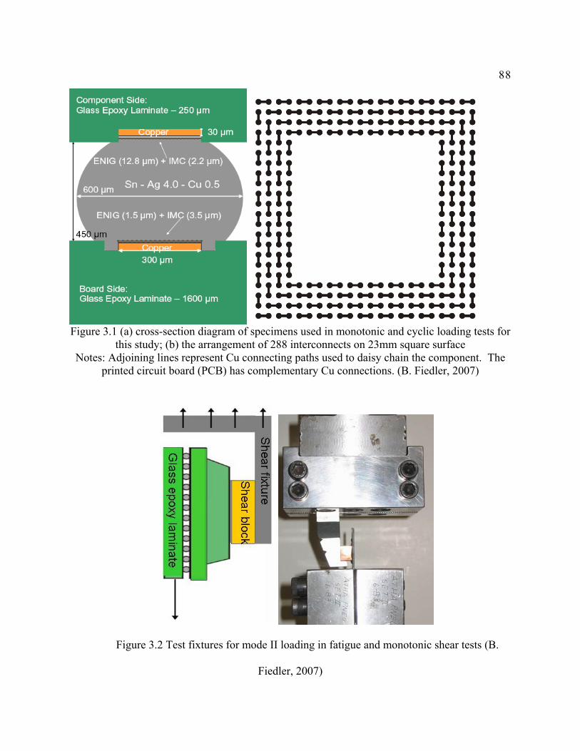
88
Figure 3.1 (a) cross-section diagram of specimens used in monotonic and cyclic loading tests for
this study; (b) the arrangement of 288 interconnects on 23mm square surface Notes: Adjoining lines represent Cu connecting paths used to daisy chain the component. The
printed circuit board (PCB) has complementary Cu connections. (B. Fiedler, 2007)
Figure 3.2 Test fixtures for mode II loading in fatigue and monotonic shear tests (B.
Fiedler, 2007)
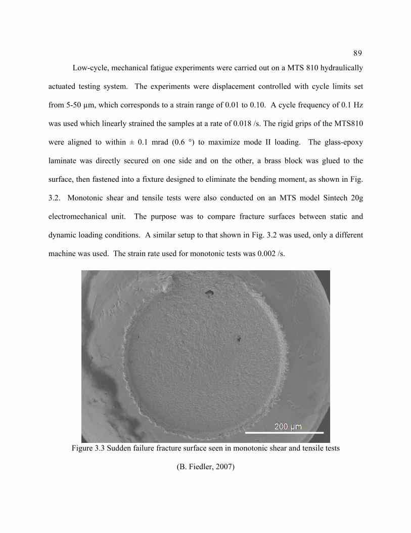
89
Low-cycle, mechanical fatigue experiments were carried out on a MTS 810 hydraulically
actuated testing system. The experiments were displacement controlled with cycle limits set
from 5-50 µm, which corresponds to a strain range of 0.01 to 0.10. A cycle frequency of 0.1 Hz
was used which linearly strained the samples at a rate of 0.018 /s. The rigid grips of the MTS810
were aligned to within ± 0.1 mrad (0.6 °) to maximize mode II loading. The glass-epoxy
laminate was directly secured on one side and on the other, a brass block was glued to the
surface, then fastened into a fixture designed to eliminate the bending moment, as shown in Fig.
3.2. Monotonic shear and tensile tests were also conducted on an MTS model Sintech 20g
electromechanical unit. The purpose was to compare fracture surfaces between static and
dynamic loading conditions. A similar setup to that shown in Fig. 3.2 was used, only a different
machine was used. The strain rate used for monotonic tests was 0.002 /s.
Figure 3.3 Sudden failure fracture surface seen in monotonic shear and tensile tests
(B. Fiedler, 2007)

90
Figure 3.4 Fatigue fracture surfaces of Sample A, (a) board fracture surface; (b) ball fracture
surface Note: Regions 1 and 2 are fatigue crack initiation sites. (B. Fiedler, 2007)

91
A marked difference between monotonic and fatigue fracture surfaces may be seen by
comparing Figs. 3.3 and 3.4. Fig. 3.3 shows the sudden failure mode which was observed
between the IMC and solder in monotonic shear and tensile tests. This sample was tested in as-
flowed condition, without any further heat treatment. The average intermetallic compound
(IMC) layer thickness for the monotonically tested specimen was 3 µm. Sample A, shown in Fig.
3.4 underwent a 96 hr heat treatment at 125 °C, which resulted in the IMC at the interface
reaching an average thickness of 4 µm. Sample A also experienced 5000 cycles of mode II,
stroke controlled fatigue loading in the aforementioned displacement profile, after which time it
was pried apart to expose the fatigue fracture surfaces. Hysteresis loops were recorded at set
intervals in order to monitor sample degradation. Hysteresis from monitoring the stress and strain
of this sample was first seen after 1000 cycles. Fig. 3.4a and 3.4b are mirror images of opposite
fracture surfaces on the same joint. Two semi-circular (thumbnail shaped) regions of fatigue
crack can clearly be seen. Region 1 shows numerous voids contributing to the formation of a
crack, while region 2 is free of these defects. The intergranular (between grain) failure
characteristic of LCF failure can clearly be seen in the bulk solder of regions 1 and 2. Region 3
is the planar, rapid failure area.
Both regions 1 and 2 are the crack nucleation and propagation regions known as phase I
and phase II. The majority of the sample lifetime consists of these microcrack formation,
conglomeration (or aggregation) and propagation phases. Region 2 displays a thumbnail shape
characteristic of fatigue cracking in phases I and II. Region 1 shows 4 large voids of 25-35 µm
in diameter within 55 µm of the edge of the joint and 1 smaller void of 12.5 µm diameter with its
center only 9 µm from the interconnect edge. The size and location of voids or inclusions has
been shown to have a significant effect on the fatigue lifetime of metals. Seniw et al. (2000)

92
observed that larger voids nearer to the center of a specimen may have less of an effect on
fatigue life than a smaller void located closer to a stress concentration in cast aluminum samples.
The numerous voids in region 1 frustrate the thumbnail shaped growth as each void may be
nucleating cracks simultaneously.
Figure 3.5 Fatigue fracture cross-section showing the crack path of Sample B
(B. Fiedler, 2007)
Figure 3.5 shows a cross section view of a crack path in sample B which underwent
168hr heat treatment at 125 °C resulting in an average IMC layer thickness of 5 µm. The total
length of the fatigue crack path measures 88µm. This increase in length, compared to sample A
is due to some phase III crack growth occurring at the solder / IMC interface. The sections of
phase I, II and III cracking are labeled as such. Phase II growth progresses immediately after
microcracks from phase I come together and form a crack. This development can be seen
Rapid failure region (phase III)
Cu IMC = 5 µm average thickness
Sn-4.0Ag-0.5Cu
Phase I & II

93
through the bulk solder as it progresses towards the IMC interface at a 30° angle, for 30 µm.
This angled path toward the interface is due to the butterfly shaped plastic zone ahead of the
crack tip (Fig. 3.6) which generates dislocations. These then accumulate at solder IMC interface
leading to cracking along this brittle portion of the solder joint. There is a transition region of 10
µm before the final 48 µm of phase III cracking between the solder and IMC.
Given the crack length of 61 µm in region 2 and that sample A underwent 5000 cycles.
Sample B experienced 4400 cycles and had an 88 µm crack, giving a whole test average crack
growth rate of 20 nm / cycle. This agrees with the value from Sample A and shows that a slower
average crack propagation rate occurs during phase I and II. Additionally, these data suggest the
majority of the sample lifetime is contained within these regions of early stage crack growth.
Thus, from the experimental observation, the interconnect failure may be divided into
three phases. Phase I corresponds to crack nucleation plus dislocation and micro crack
accumulation in the solder. Phase II corresponds to the crack propagating in the bulk solder to
the intermetallic and the interfaces of the intermetallic with the solder and the copper pad. Phase
III corresponds to the crack propagating at the interfaces or within IMC layer. Since Kc values in
the interfaces and intermetallic are very small, brittle crack propagation and rapid fracture will
occur once phase III is reached. The fatigue life time of an interconnect is mainly during phase I
and II. Phase III constitutes a very small fraction of the fatigue life of a single interconnect. The
physical meaning can be explained from Eq. (3.7) in next section, in which U is a major
parameter to determine the process of interconnects failure. The U value for a crack propagating
in bulk solder is much larger than the U in IMC layer. Thus, the fatigue propagation rate, da/dN,
of phase II is much smaller than that of phase III, and the fatigue life during the crack
propagation stage (phase II plus phase III) will be almost exclude during phase II. Based on the
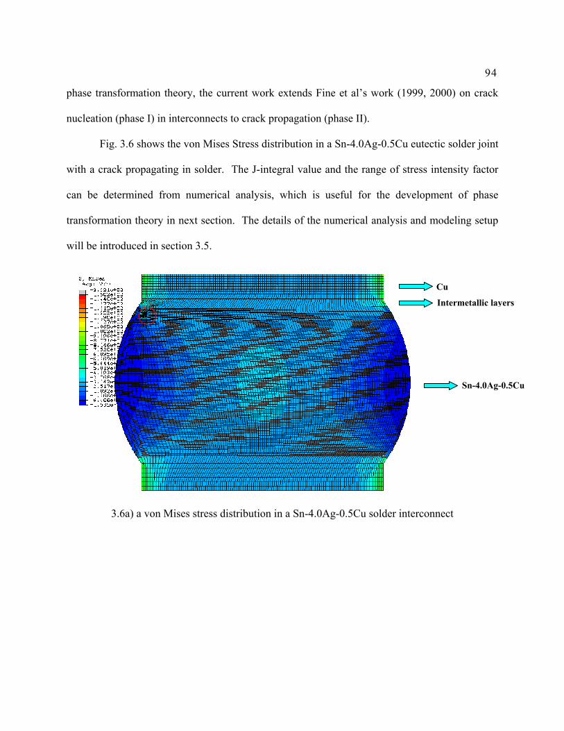
94
phase transformation theory, the current work extends Fine et al’s work (1999, 2000) on crack
nucleation (phase I) in interconnects to crack propagation (phase II).
Fig. 3.6 shows the von Mises Stress distribution in a Sn-4.0Ag-0.5Cu eutectic solder joint
with a crack propagating in solder. The J-integral value and the range of stress intensity factor
can be determined from numerical analysis, which is useful for the development of phase
transformation theory in next section. The details of the numerical analysis and modeling setup
will be introduced in section 3.5.
3.6a) a von Mises stress distribution in a Sn-4.0Ag-0.5Cu solder interconnect
Cu
Intermetallic layers
Sn-4.0Ag-0.5Cu
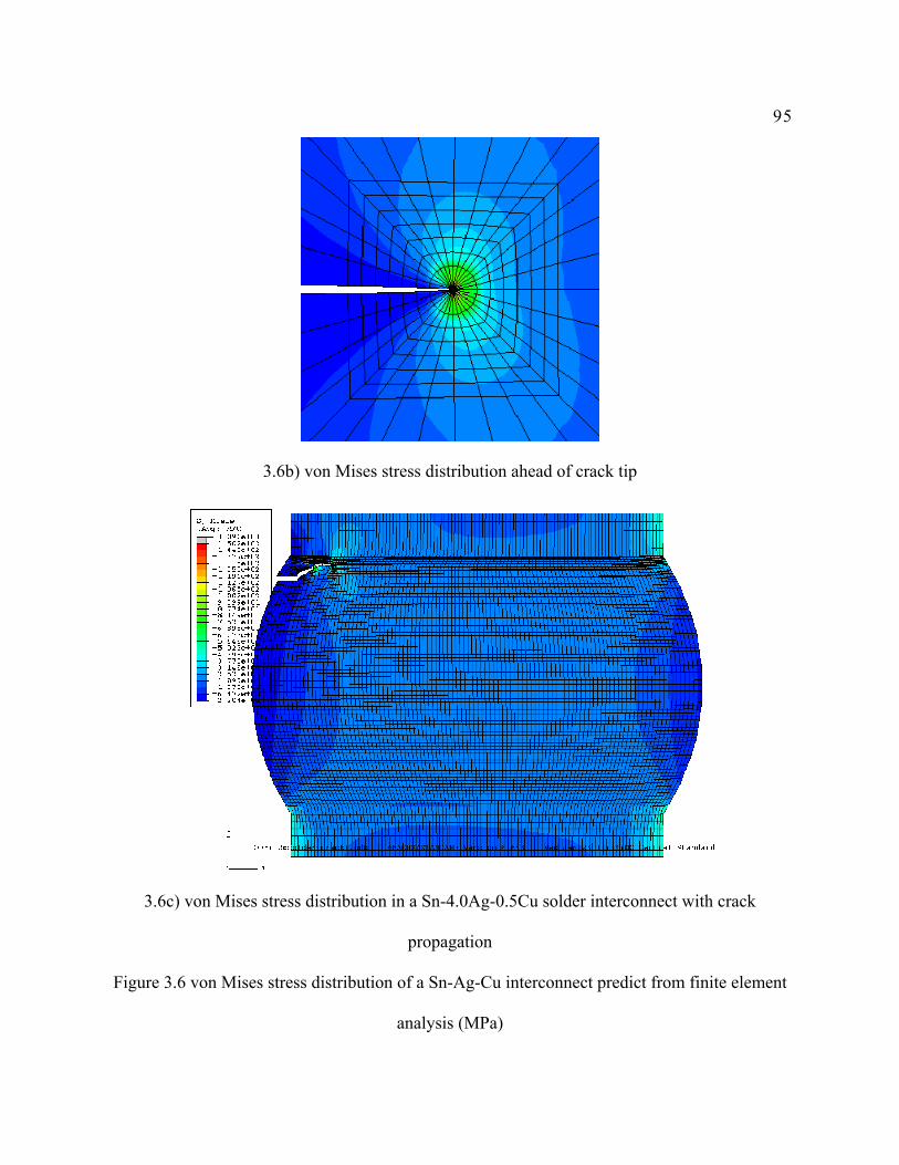
95
3.6b) von Mises stress distribution ahead of crack tip
3.6c) von Mises stress distribution in a Sn-4.0Ag-0.5Cu solder interconnect with crack
propagation
Figure 3.6 von Mises stress distribution of a Sn-Ag-Cu interconnect predict from finite element
analysis (MPa)

96
3.3 Phase Transformation Theory to Predict Fatigue Crack Nucleation
The accumulated damage from fatigue loading is essentially an increase in dislocation
density but dynamic recovery (due to thermally activated diffusion-like processes like
dislocation climb) sets in immediately, where dislocations of opposite sign annihilate and a
stable steady-state dislocation structure forms if thermal energy is sufficiently high and the
activation energy for dislocation motion is not too high. For example, in Al fatigued at room
temperature a dislocation cell structure forms but dislocation tangles form at liquid nitrogen
temperature (Williams and Fine 1985). While a stable steady state dislocation structure is
expected to form after a transient during fatigue cycling of solder, fatigue cracks nucleate from
the point with local concentration of dislocations and here damage continues to increase at some
rate per cycle.
When a crack forms in a solid material or at an interface, defects are released at the new
surfaces along with a reduction in internal energy and stored elastic energy. These counteract the
energy increase due to the increase in surface area. The change in energy ∆W to form a crack of
area A is (Fine 2000):
AWAW Tγδ +∆−−=∆ 2 (3.1)
where δ = stored energy in defects per unit area of crack, which is smaller if the material is
brittle, as in most intermetallics;
2W∆ = stored elastic energy;

97
γγ 2=T = total surface energy per unit area of crack, where the parameter 2 indicates two
surfaces are created; if the crack is at a pre existing interface, the surface energy term
iT γγγ −= 2 , and iγ is the interfacial energy per unit area.
For a penny-shaped crack, 2W∆ can be obtained based on eigenstrain theory by Mura (1991):
EaW
3)1(8 322
2σν−
=∆ (3.2)
where σ = the maximum stress in the cycle;
E = the Young’s modulus;
ν = Poisson’s ratio;
a = crack radius.
A simplified solution for crack nucleation for this case can be defined as:
TaE
aaW γσνδπ 2322
2
3)1(8
π+−
−−=∆ (3.3)
Bhat and Fine (2001) defined the parameter δ related to hysteresis loop parameters as:
pftNN εσδ ∆∆= ** )( (3.4)
where f = efficiency factor (efficiency in storing defects caused by fatigue);
t = sum of the thicknesses of materials on each side of the crack that are drained of defects when
the crack is formed;
N* = critical number of cycles for crack nucleation;
pεσ ∆∆ are the stress and plastic strain ranges of the fatigue cycling.

98
Eq. (3.4) is an extension of the ideas advanced by Mura and coworkers (Mura and Lin
1974; Izumi et al. 1981; Mura 1994) based on the concept of Gibbs free energy change
accompanying the transition from the bulk deformation stage (in this stage, cyclic deformation
during which the repeated applications of stress or strain condition the metal for the subsequent
stages) to that containing microcracks (in this stage, crack initiation during which microcracks
nucleate and coalesce to form macrocracks). The term f is taken as a constant for the material
and specific combination of test conditions. The term ft may be looked upon as an indicator of
the energy that is stored from cycle to cycle.
Differentiating Eq. (3.3) with respect to a with N* constant gives:
22* )1(4
*))((*0σν
δγπ−−
=→=⎟⎠⎞
⎜⎝⎛ ∆
NEaWdad
N
(3.5)
where a* = critical crack radius; N* can be predicted by:
pEftaEN
εσπνσγπ
∆∆−−
=)1(4 2*2
* (3.6)
There are a number of unknowns in Eq. (3.6) and experimental determination of these
parameters is the key to the applicability of these equations. The value of a* is limited by our
ability to detect small cracks, which is a function of the experimental techniques used to monitor
crack initiation. For a penny-shaped crack, a conservative value for a* is assumed to be 250 nm
although smaller cracks have been observed by examining shadowed surface replicas in the
electron microscope. For simplicity the assumption of a penny-shaped crack is adopted in

99
present research, which is reasonable for many fatigue crack nucleation and propagation
situations in steel or aluminum alloy (Williams and Fine 1985; Bhat and Fine 2001).
3.4 Phase Transformation Theory to Predict Fatigue Crack Propagation
The main focus of current research is to apply phase transformation theory to predict
fatigue crack propagation. An equation similar to Eq. (3.1) is used as a basis for discussing
fatigue crack growth.
AAWAWWAWW Tba ∆+∆∆+∆∆+∆−∆∆−=∆ γ3121 (3.7)
where ∆W = the energy required to increase the crack area by ∆A;
∆W1a = the gain in energy per unit area due to loss of defects as the crack advances by ∆A. Under
constant ∆K (the stress intensity range) this gain is negated by ∆W1b due to the plastic zone
extension and the attendant increasing defect density in the extension.
∆W1b = the energy per unit area consumed by the extension of the plastic zone;
∆W2 = the stored elastic energy;
∆W3= the plastic work per unit area transferred to heat for each cyclic loading step. ∆W3 may be
regarded as a “frictional” term, measured by the hysteresis between the loading and unloading
stress strain curves. This is the mechanical energy converted to heat that raises the specimen
temperature and is lost to the surroundings.
Normally aWW 13 ∆>∆ because f <<1 (for example, for an HSLA steel, f = 0.0006, Bhat and
Fine 2001). Whether the fatigue is under constant stress or constant strain control but increasing
∆K, the plastic zone will grow in length and ∆W1b will be numerically larger than ∆W1a, but the
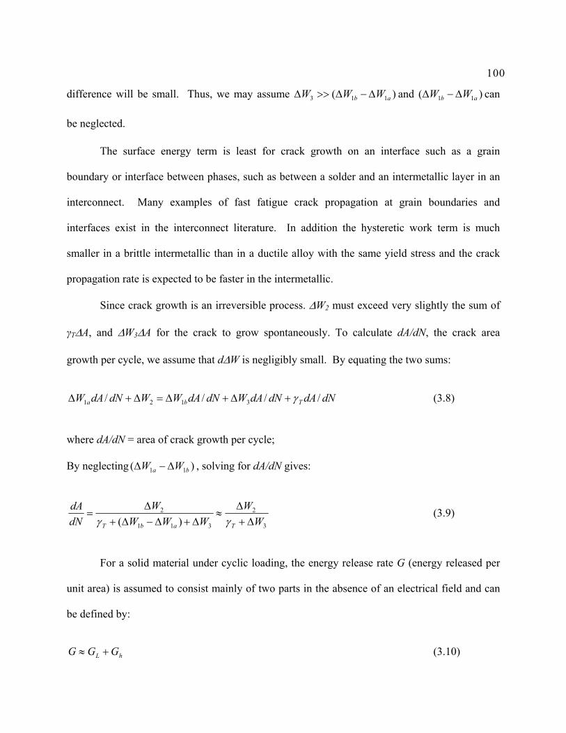
100
difference will be small. Thus, we may assume )( 113 ab WWW ∆−∆>>∆ and )( 11 ab WW ∆−∆ can
be neglected.
The surface energy term is least for crack growth on an interface such as a grain
boundary or interface between phases, such as between a solder and an intermetallic layer in an
interconnect. Many examples of fast fatigue crack propagation at grain boundaries and
interfaces exist in the interconnect literature. In addition the hysteretic work term is much
smaller in a brittle intermetallic than in a ductile alloy with the same yield stress and the crack
propagation rate is expected to be faster in the intermetallic.
Since crack growth is an irreversible process. ∆W2 must exceed very slightly the sum of
γT∆A, and ∆W3∆A for the crack to grow spontaneously. To calculate dA/dN, the crack area
growth per cycle, we assume that d∆W is negligibly small. By equating the two sums:
dNdAdNdAWdNdAWWdNdAW Tba //// 3121 γ+∆+∆=∆+∆ (3.8)
where dA/dN = area of crack growth per cycle;
By neglecting )( 11 ba WW ∆−∆ , solving for dA/dN gives:
3
2
311
2
)( WW
WWWW
dNdA
TabT ∆+∆
≈∆+∆−∆+
∆=
γγ (3.9)
For a solid material under cyclic loading, the energy release rate G (energy released per
unit area) is assumed to consist mainly of two parts in the absence of an electrical field and can
be defined by:
hL GGG +≈ (3.10)

101
Here, GL corresponds to the Griffith-Irwin energy dissipation mechanism (energy to create the
new crack surfaces), which corresponds to the material’s surface energy Tγ and is equivalent to
the J-integral value of J calculated from Fracture Mechanics (J/m2). The term Gh corresponds to
energy dissipation by conversion of mechanical energy to heat, ie. internal friction previously
associated with the dislocation motion in the plastic zone ahead of the crack as shown in Fig. 3.7.
loaded with dislocations
physical crack
plastic work zone
Figure 3.7 Schematics of plastic zone ahead of crack tip
Since we assume )( 113 ab WWW ∆−∆>>∆ , the hysteretic fracture energy loss release rate Gh
3W∆≈ . Thus, we assume,
3WGJG Th ∆+≈+≈ γ (3.11)
Here, the generalized force acting on the tip of a crack can be expressed in terms of J-
integral of the Maxwell energy-momentum tensor ljP of elasticity taken over a surface (Mura

102
1981), and the three-dimensional expression of J-integral can be defined by (Rice 1967;
Weertman 1973):
∫∫∫ΓΓΓ
=+−= dSnPdSWndSunJ jljllijijl ,σ (3.12)
where liijljlj uWP ,σδ −= ; ∫= ji
ijij dWε
εσ0
and lijijlW ,, εσ= ; )(21
,, ijjiij uu +=ε ; the integration
path Γ is an arbitrary closed contour followed counterclockwise surrounding the crack tip in a
stressed body; ijσ is the stress and ijε is the strain; iu is the displacement; and nj is the normal
vector on the boundary dS.
For homogeneous, isotropic materials, the J-integral value can be simplified and calculated as
follows (Suo and Hutchinson 1990). For a crack within a material:
222
21)(1
IIIIII KKKE
Jµ
++= (3.13)
where KI, KII, and KIII are the stress intensity factors for fracture modes I, II, and III, respectively;
µ is the shear modulus; 21 ν−=
EE for plane strain.
For a crack in the interface between two layers of materials:
2*
22*
2
21)(1
IIIIII KKKE
Jµ
β++
−= (3.14)

103
Here, )11(211
21* EEE
+= , )11(211
21* µµµ
+= , where the shear modulus)1(2 1
11 ν
µ+
=E ,
)1(2 2
22 ν
µ+
=E .
The Dundur’s parameter can be determined by (Dundurs 1969):
)1()1()1()1(
1221
1221
+−+−−−
=κµκµκµκµ
β , (3.15)
where νκ 43 −= for plain strain
The physical meaning of the theory can be explained from energy considerations.
Assume a crack propagates under external load Fi in a solid with domain of V, external boundary
of S and internal crack boundary of A. When an existing crack with area of A extends to an area
of δA, from the first law of thermodynamics and using Gauss theorem,
dSundVudSundSuF iAA
jijjiijV
iS
jijS
ii δσδσδσδδ∫∫∫∫+
−== ,)( (3.16)
where iuδ is the displacement; nj is the normal vector on the boundary.
From the equations of equilibrium, 0, =jijσ in V; assume a free surface, i.e. 0=jij nσ on A; and
Eq. (3.16) is simplified as:
dSundVudSuF iA
jijV
jiijS
ii δσδσδδ∫∫∫ −= , (3.17)
Based on the assumption of small strains, the total strain consists of elastic strain ije and plastic
strain pijε :

104
pijijijji euu ε+=+ )(
21
,, , pijijijji euu δεδδδ +=+ )(
21
,, (3.18)
Substituting Eq. (3.18) into Eq. (3.17) gives:
AUdSundVdVedSuF iA
jijV
pijij
Vijij
Sii δδσδεσδσδ
δ
=−+= ∫∫∫∫ (3.19)
Here, ∫S
ii dSuFδ is the potential energy of external load; ∫V
ijij dVeδσ is the elastic strain energy
corresponding to the stored elastic energy; ∫V
pijij dVδεσ is the plastic work term
and )( dSun iA
jij δσδ∫− corresponds to the surface energy and equals to the value of J-integral
(Izumi et al. 1981). The energy to propagate a unit area fatigue crack surface is U (J/m2), which
can be determined from experiment (Liaw et al. 1981).
For the plasticity and hardening model, Weertman (1973) and Mura and Lin’s (1974)
work extending BCS crack theory is followed in this chapter. Considering the plastic
part ∫V
pijij dVδεσ and noting that
y
pij
Kµσ
δε2)(∆
∝ and the plastic domain 2
2)(
y
Kσ
∆∝ , by neglecting the
work done on the new crack surface, a generally accepted equation for the crack growth per
cycle for a ductile material is obtained:
2
4
yUbK
dNdA
σµ∆
∝ (3.20)
where yσ = yield stress;

105
b = specimen thickness;
Eq. (3.20) is obtained by extending the Griffith fracture theory to fatigue crack
propagation problem by defining the Gibbs free energy of solids under cyclic loading. In the
analysis stress rather than cumulative displacement or cumulative damage is the quantity whose
critical value controls the crack growth. The assumption is that the material at the tip of a fatigue
crack progressively work hardens until the stress reaches a critical value.
Based on Eq. (3.7) and (3.19), relating Eq. (3.20) to phase transformation theory gives:
dNdAJbKBW
dNdAUW
y
+∆
+∆−==∆ 2
4
2 µσ (3.21)
where B is a dimensionless constant;
The area of fatigue crack propagated per cycle can thus be obtained by:
)()()(2
2
422
4
JUW
JUbKB
JU
WbKB
dNdA
y
y
−∆
−−
∆=
−
∆−∆
=µσ
µσ (3.22)
Eq. (3.22) provides a theoretical basis to predict the fatigue crack propagation rate for
both brittle and ductile solid materials. To verify the theory, Eq. (3.22) is applied to different
materials and compared with experimental data in next section.
Based on Eq. (3.7), an equation to predict the length of fatigue crack propagated per cycle
can be derived similarly:
bJUW
JUKB
dNda
y )()(2
2
4
−∆
−−
∆=
µσ (if cKK ∆<∆ ) (3.23)
106
where da/dN is the area of crack growth per cycle; B is a dimensionless constant; J is the value
of J-integral; yσ is yield stress; b is specimen thickness; K∆ is the range of stress intensity factor;
cK∆ is the critical stress intensity factor and µ is shear modulus. A formula to predict the
dimensionless constant B is suggested by:
mKmaglB ))(( ∆×= (3.24)
where )( Kmag ∆ is the dimensionless magnitude of stress intensity range, which equals
unitKK /∆ , and 1=unitK MN/m3/2; here l and m are material constants.
3.5 Experimental and Computational Analysis on Fatigue Crack Propagation of Sn-3.5Ag
Eutectic Solder at Northwestern University (experiments conducted by S. Vaynman, 2007)
To verify the proposed phase transformation theory, experiments on fatigue crack
propagation in Sn-3.5Ag solder alloy have been conducted by S. Vaynman at Northwestern
University, 2007. In his experiments, fatigue crack propagation in solder in Mode I loading was
studied utilizing a solder-joint plate specimen with a single edge notch (Fig. 3.8). Two copper
plates were joined by Sn–Ag eutectic solder. Prior to soldering, the copper plates were polished
with 600-grit emery chapter and cleaned with diluted nitric acid, rinsed in distilled water and
dried with methanol. The copper surface to be soldered was coated with SnCl2 solution, placed in
a fixture and pre-heated to 260°C on hot plate. The solder was melted in the gap between the
copper plates. The fixture was removed from the hot plate ten minutes after the joint was formed
and was cooled down to room temperature. The excess solder was removed from the specimen
surface by grinding/polishing. The notch was introduced by wire in the electro-discharge

107
machine. Fatigue crack propagation tests were performed in air at room temperature in a servo-
hydraulic fatigue machine (MTS-810) in load control (sinusoidal waveform, 5 Hz) with
maximum load of 2,400N and the load ratio of 0.1. The crack growth was monitored by a
traveling microscope. Scanning electron microscopy (SEM) and optical microscope
examinations were performed directly on the specimens.
Figure 3.8 Schematic of the fatigue tests specimen (S. Vaynman 2007)

108
Figure 3.9 Fatigue crack propagation path in Sn-3.5Ag Solder during cyclic loading
(S. Vaynman 2007)
The fatigue crack propagation path in Sn-3.5Ag Solder during fatigue cyclic is shown in
Fig. 3.9. It is found that the crack gradually propagates in a direction approximately
perpendicular to the stress direction through the region with accumulation of dislocation. When
after 867000 cycles, the crack grew to approximately 13mm in the horizontal direction; the crack
migrated to the copper/solder interface resulting in sudden catastrophic failure. Fig. 3.10 is
optical micrograph of the crack. Different phases of fatigue failure, fatigue crack initiation,
propagation and catastrophic failure are observed. Fig. 3.11 is a SEM micrograph of fatigued
solder specimen surface. There is a wire-cut surface of the solder on the left. The crack starts and
then propagates to the right.
-0.0025
0.0000
0.0025
0.000 0.005 0.010 0.015 0.020 0.025X-direction, m
Y-di
rect
ion,
m
Notch
Catastrophic Failure
Fatigue Crack
Intermetallic
Intermetallic
867,000 cycles

109
Figure 3.10 Fatigue Crack in Sn-3.5Ag Solder (two sides of crack are shown) Sample aged 10
minutes in liquid state (S. Vaynman 2007)
Figure 3.11 SEM micrograph of fatigued solder specimen surface (S. Vaynman 2007)
Cu Solder
Catastrophic Fracture
Crack Starts
Crack Propagates
Cu3Sn

110
A finite element model has been developed to predict the range of stress intensity factor
∆K for the experiment. The CPS8R element in ABAQUS was used for the analysis, and the
square root and 1/r singularities were built into finite element meshes using standard elements.
To simulate the singularity at the crack tip, a ring of collapsed quadrilateral elements were used
to perform the modeling there. The mid-side nodes on the sides connected to the crack tip were
moved to the 1/4 point nearest the crack tip, and a quarter point spacing with second-order
isoparametric elements was created. Fig. 3.12 shows the distribution of von Mises stress for
solder/IMC predicted by using the finite element model; a stress concentration is predicted ahead
of crack tip and higher stress is also observed near the interface between solder and the IMC
layer. Fig. 3.13 shows the relationship between stress intensity factor range ∆K and crack length
ratio a/W. With the increase of crack length, the stress intensity factor range increases. The
relationship between cycle number and crack length for two different specimens is shown in Fig.
3.14. It is found for the specimen before 600000 cycles the crack length increases linearly, after
600000 cycles, the crack length increases exponentially and much faster. Fig. 3.15 shows the
relationship between stress intensity factor range and crack propagation rate. The experimental
results are used to validate the prediction of fatigue crack propagation rate using phase
transformation theory in section 3.7.
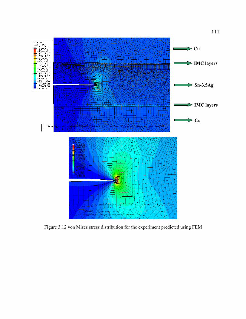
111
Figure 3.12 von Mises stress distribution for the experiment predicted using FEM
Sn-3.5Ag
Cu
Cu
IMC layers
IMC layers

112
0
1
2
3
4
5
6
7
8
0.2 0.25 0.3 0.35 0.4 0.45 0.5 0.55
a/W
∆KI (
MPa
.m1/
2 )
Specimen
Figure 3.13 Relationship between stress intensity factor range and crack length ratio a/W
Figure 3.14 Relationship between cyclic number and crack length
0.000
0.002
0.004
0.006
0.008
0 200000 400000 600000 800000 1000000
N, cycles
Fatig
ue C
rack
Len
gth,
m Specimen
Specimen
Cycled from 0.245 to 2.45 kN (load control) Frequency 5Hz 25°C
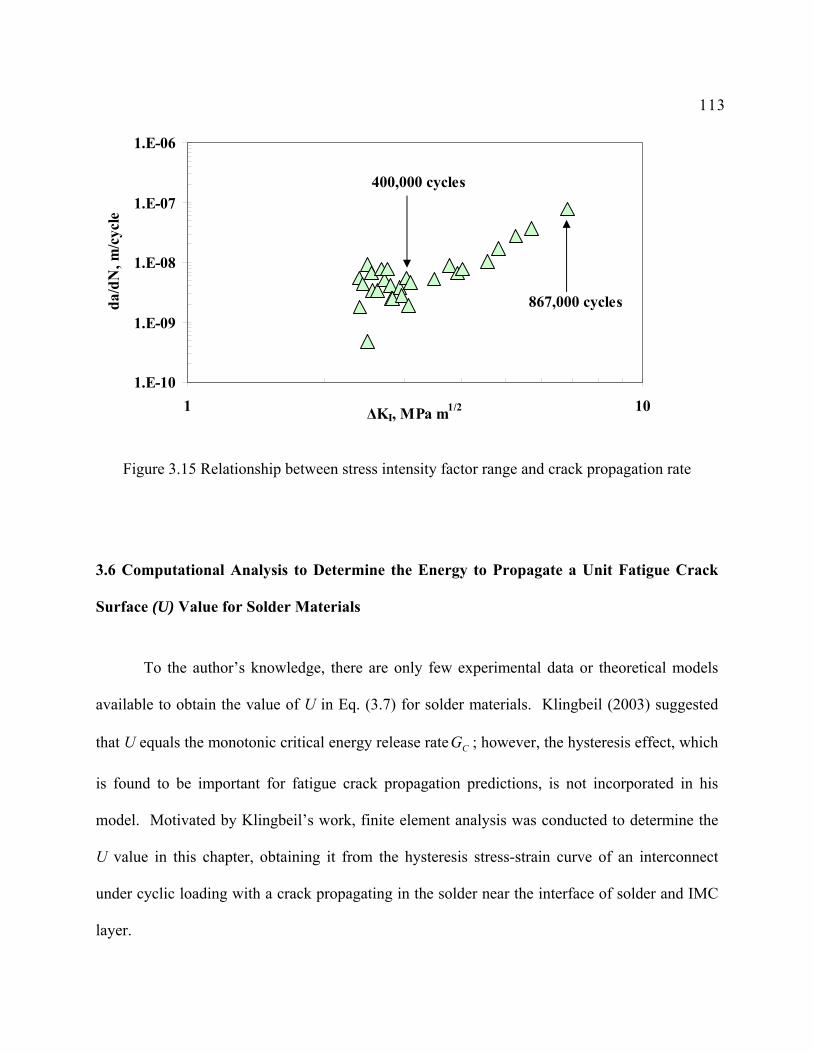
113
Figure 3.15 Relationship between stress intensity factor range and crack propagation rate
3.6 Computational Analysis to Determine the Energy to Propagate a Unit Fatigue Crack
Surface (U) Value for Solder Materials
To the author’s knowledge, there are only few experimental data or theoretical models
available to obtain the value of U in Eq. (3.7) for solder materials. Klingbeil (2003) suggested
that U equals the monotonic critical energy release rate CG ; however, the hysteresis effect, which
is found to be important for fatigue crack propagation predictions, is not incorporated in his
model. Motivated by Klingbeil’s work, finite element analysis was conducted to determine the
U value in this chapter, obtaining it from the hysteresis stress-strain curve of an interconnect
under cyclic loading with a crack propagating in the solder near the interface of solder and IMC
layer.
1.E-10
1.E-09
1.E-08
1.E-07
1.E-06
1 10∆KI, MPa m1/2
da/d
N, m
/cyc
le
400,000 cycles
867,000 cycles
114
To determine the value of U in Eq. (3.7) for a solder, as introduced in Chapter 2, a 3D
finite element model for an interconnect has been developed incorporating CZM and UCP
theories to simulate solder/IMC interfacial behavior and hysteresis effect in solder bulk,
respectively. The model is programmed into the commercial software ABAQUS through a user
defined subroutine using FORTRAN language. Two layers of IMC, Cu6Sn5 and Cu3Sn, are
included in the 3D finite element model. A cohesive layer with a traction-separation type
cohesive element has been defined at the interface of the solder and IMC to predict the interfacial
behavior. An exponential traction-separation (T-S) law of the interfacial cohesive element is
assumed, and a quadratic nominal stress criterion to predict damage initiation is adopted. The
damage evolution for mixed mode failure is defined based on the Benzeggagh-Kenane fracture
criterion. For solder, the UCP theory is adopted based on the dual backstress thermo-plasticity
model proposed by McDowell et al. (1994) and Wen et al. (2002), which is introduced in
Chapter 2 in detail. To simulate realistic operating conditions of an interconnect, sinusoidal
displacement is assumed with a maximum magnitude of 0.5µm to simulate the shearing load
caused by thermal mismatch of the coefficients of thermal expansion (CTE). The solder, IMC
layer and silicon die properties are given in Table 3.1 (NIST database 2002) (Kanchanomai et al.
2005). The distribution of von Mises stress for solder/IMC predicted using the proposed finite
element model, higher stress is observed near the interface of bulk solder and IMC layer.

115
Table 3.1 material properties used in finite element model
(NIST database 2002) (Kanchanomai et al. 2005)
Young’s modulus (GPa)
Poisson’s ratio
Yield Stress(MPa)
Solder: 63Sn-37Pb 32 0.32 18.1 Solder: Sn-3.5Ag 45 0.36 30.6
Cu 117 0.33 70 IMC close to solder: η-phase Cu6Sn5 96.9 0.309 -
IMC close to Cu:ε-phase Cu3Sn 123.2 0.319 -
Since very few experimental data of fatigue crack propagation available for interconnects
operating under thermal-mechanical shear. To verify the proposed approach, the boundary and
loading condition of finite element model was modified to simulate the test condition of
experiments for 63Sn-37Pb (Kanchanomai et al. 2005) and Sn-3.5Ag eutectic solder by
Vaynman as introduced in previous section (refer to Yao et al. 2008) under mode I loading.
Cyclic sinusoidal tensile loading rather than shear loading was applied with a frequency of 10 Hz,
and the results should be viewed as the first approximation for application of the phase
transformation theory to predict fatigue crack propagation in interconnects. More experimental
data for fatigue crack propagation in interconnects under realistic operating conditions are
required for future research. Under mode I loading, similar to the shear loading case, the crack
was found to nucleate and propagate in solder bulk near the interface of solder and IMC layer,
which matches the experimental observation.
The stress-strain relationship predicted using UCP model for Sn-3.5Ag eutectic solder
under cyclic loading is compared with experimental data (Wen 2001), (Fig. 3.16), which shows
stable matching with experimental data. The area within the hysteresis loop was integrated
numerically, and assumed in this method to be approximately equal to the value of U
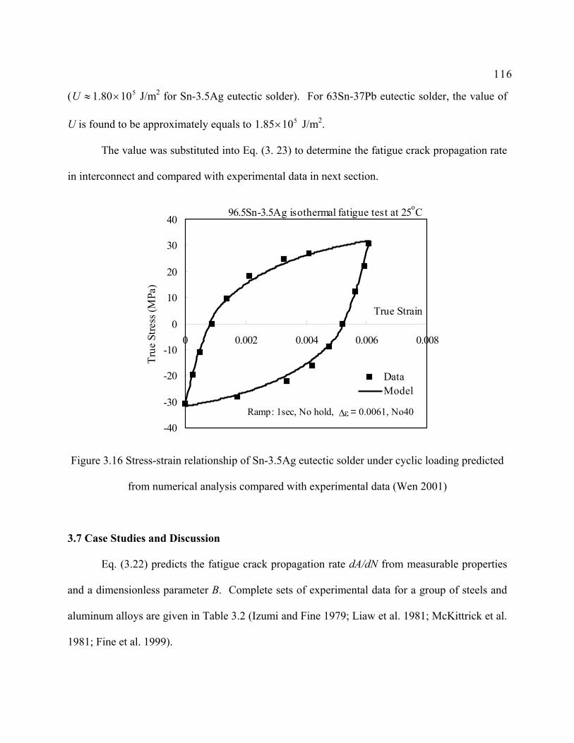
116
( 51080.1 ×≈U J/m2 for Sn-3.5Ag eutectic solder). For 63Sn-37Pb eutectic solder, the value of
U is found to be approximately equals to 51085.1 × J/m2.
The value was substituted into Eq. (3. 23) to determine the fatigue crack propagation rate
in interconnect and compared with experimental data in next section.
96.5Sn-3.5Ag isothermal fatigue test at 25oC
-40
-30
-20
-10
0
10
20
30
40
0 0.002 0.004 0.006 0.008
True Strain
True
Stre
ss (M
Pa)
DataModel
Ramp: 1sec, No hold, ∆ε = 0.0061, No40
Figure 3.16 Stress-strain relationship of Sn-3.5Ag eutectic solder under cyclic loading predicted
from numerical analysis compared with experimental data (Wen 2001)
3.7 Case Studies and Discussion
Eq. (3.22) predicts the fatigue crack propagation rate dA/dN from measurable properties
and a dimensionless parameter B. Complete sets of experimental data for a group of steels and
aluminum alloys are given in Table 3.2 (Izumi and Fine 1979; Liaw et al. 1981; McKittrick et al.
1981; Fine et al. 1999).
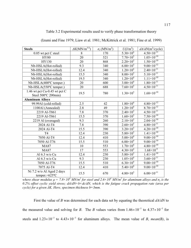
117
Table 3.2 Experimental results used to verify phase transformation theory
(Izumi and Fine 1979; Liaw et al. 1981; McKittrick et al. 1981; Fine et al. 1999)
Steels ∆K(MN/m3/2) σy (MN/m2) U(J/m2) dA/dN(m2/cycle)0.05 wt pct C steel 8 170 5.30×10⁶ 4.50×10⁻¹²
HY80 20 521 7.70×10⁵ 1.05×10⁻¹⁰ HY130 20 868 2.20×10⁵ 1.50×10⁻¹⁰
Nb-HSLA(Hot-rolled) 9.3 340 6.00×10⁵ 9.00×10⁻¹² Nb-HSLA(Hot-rolled) 12.4 340 1.20×10⁶ 2.40×10⁻¹¹ Nb-HSLA(Hot-rolled) 15.5 340 8.00×10⁵ 5.10×10⁻¹¹ Nb-HSLA(Hot-rolled) 19.5 340 1.20×10⁶ 1.11×10⁻¹⁰
Nb-HSLA(400ºC temper.) 20 600 3.00×10⁶ 1.80×10⁻¹¹ Nb-HSLA(550ºC temper.) 20 688 7.60×10⁵ 4.50×10⁻¹¹
1.46 wt pct Cu-0.45 wt pct C Steel 500ºC 200min) 19.5 780 1.30×10⁵ 1.68×10⁻¹⁰
Aluminum Alloys 99.99Al (cold-rolled) 2.5 42 1.80×10⁶ 4.80×10⁻¹² 1100Al (Annealed) 2.8 49 1.20×10⁶ 8.70×10⁻¹²
2219 Al-T861 7.8 370 2.40×10⁵ 4.50×10⁻¹¹ 2219 Al-T861 15.5 370 1.60×10⁵ 7.50×10⁻¹⁰
2219 Al (overaged) 9.3 260 2.10×10⁵ 2.04×10⁻¹⁰ 2024 Al-T4 7.8 390 2.60×10⁵ 4.80×10⁻¹¹ 2024 Al-T4 15.5 390 3.20×10⁵ 4.20×10⁻¹⁰
T4 12.4 230 5.80×10⁵ 1.41×10⁻¹⁰ 7050 Al-T4 12.4 410 5.00×10⁴ 9.00×10⁻¹⁰ 7050 Al-T76 15.5 510 6.00×10⁴ 9.00×10⁻¹⁰
MA87 10 553 1.70×10⁴ 4.80×10⁻¹⁰ MA87 17 553 4.30×10⁴ 1.68×10⁻⁹
Al 6.3 w/o Cu 12.4 230 5.80×10⁵ 1.41×10⁻¹⁰ Al 6.3 w/o Cu 9.3 230 1.05×10⁶ 3.60×10⁻¹¹ 7050 Al-T76 15.5 510 6.30×10⁴ 9.00×10⁻¹⁰ 7075 Al-T4 12.4 410 5.40×10⁴ 9.00×10⁻¹⁰
Ni 7.2 w/o Al Aged 2 days temper.=625ºC 15.5 670 4.80×10⁵ 6.00×10⁻¹¹
where shear modulus µ = 7.8×10⁴ MN/m2 for steel and 2.6×10⁴ MN/m2 for aluminum alloys and σy is the 0.2% offset cyclic yield stress; dA/dN=b×dc/dN, which is the fatigue crack propagation rate (area per cycle) for a given ∆K. Here, specimen thickness b=3mm.
First the value of B was determined for each data set by equating the theoretical dA/dN to
the measured value and solving for B. The B values varies from 31046.1 −× to 31037.4 −× for
steels and 31023.1 −× to 31043.4 −× for aluminum alloys. The mean value of B, mean(B), is

11831008.3 −× and 31085.2 −× for steels and aluminum alloys, respectively. The distribution of
B/mean(B) for steels and aluminum alloys is given in Fig. 3.17 with ∆K varies from 2.5 to 20
MN/m3/2. Various theoretical models have been proposed to predict the dimensionless constant
B by different researchers (Mura and Lin 1974; Irving and McCartney 1977; Izumi et al. 1981).
The values of B calculated from the theoretical models are generally 5 to 10 times higher than
the measured experimental values. The difference between the prediction of the theoretical
model and experimental measurement may be explained by the fact that crack propagation is a
nonreversible and spontaneous process, and the hysteresis effect is not incorporated in the
theoretical models. From the experimental data, the mean(B) values are substituted into Eq.
(3.22) to predict dA/dN for steels and aluminum alloys, respectively. As shown in Fig. 3.18,
compared with experimentally measured dA/dN, the mean of predicted dA/dN is 1.062 and the
coefficient of variation (COV) is 0.255 for steels; the mean is 1.185 and the coefficient of
variation is 0.286 for aluminum alloys. Here, the coefficient of variation is a measure of
dispersion of a probability distribution, which defined as the ratio of the standard deviation to the
mean.

119
distribution of B
0
1
2
3
4
5
6
7
8
0.6 0.8 1 1.2 1.4 1.6 1.8 2
The values of B/mean(B) for steels and aluminum alloys
num
ber o
f met
als a
nd a
lloys
_
Figure 3.17 Distribution of the values of B/mean(B) for steels and aluminum alloys
(∆K varies from 2.5 to 20 MN/m3/2)
0.0E+00
5.0E-10
1.0E-09
1.5E-09
2.0E-09
2.5E-09
0.0E+00 5.0E-10 1.0E-09 1.5E-09 2.0E-09
dA/dN measured from experiments
dA/d
N p
redi
cted
by
phas
e tra
nsfo
rmat
ion
theo
ry w
ith th
e m
ean
valu
e of
B
SteelsMean=1.062COV=0.255Aluminum alloysMean=1.185COV=0.286
Figure 3.18 Predictions of fatigue crack propagation rate dA/dN for case study using Eq.
(3.22) and the mean values of B
Note: here, 2.0E-09 stands for 9100.2 −×
0

120
Analysis of the data shows that the values of B are related to the magnitude of ∆K rather
than being a universal constant. Thus, instead of using the mean value of B, least-squares
regression of a plot of B vs. )( Kmag ∆ is given in Fig. 3.19, yields the following empirical
equation:
15.0))((0045.0 −∆×= KmagB (3.25)
where )( Kmag ∆ is the dimensionless magnitude of stress intensity range, which equals to
unitKK /∆ , and 1=unitK MN/m3/2.
y = 0.0045x-0.15
0
0.001
0.002
0.003
0.004
0.005
0.006
0 5 10 15 20 25magnitude of ∆K
valu
es o
f B
SteelsAluminum alloys
Figure 3.19 Values of B with respect to the magnitude of ∆K for materials in Table 3.2

121
distribution of dA/dN
0
2
4
6
8
10
12
0.4 0.6 0.8 1 1.2 1.4 1.6 1.8 2dA/dN predicted from Eq.(3.22) with B determnnied from Eq.(3.25) divided
by dA/dN measured from experiemnt
num
ber o
f met
als
and
allo
ys
Figure 3.20 Distribution of dA/dN from Eq. (3.22) with B determined from Eq. (3.25) compared
with experimental data of steels and aluminum alloys
Fig. 3.20 shows the distribution of dA/dN predicted from Eq. (3.22) with B determined
from Eq. (3.25). The proposed approach gives relatively accurate predictions of dA/dN for both
the steels and aluminum alloys. As shown in Fig. 3.21, compared with experimental data, the
predicted dA/dN has a mean of 1.028 and the coefficient of variation is 0.264 for steels, the mean
is 1.310 and the coefficient of variation is 0.253 for aluminum alloys. In general the phase
transformation theory predicts fatigue crack propagation rate conservatively with reasonable
accuracy. It should be noted that Eq. (3.25) are only applicable to steels and aluminum alloys
and may not applicable to brittle or quasi-brittle materials such as glass or intermetallics. Most
of the materials analyzed in the case study are relatively ductile, and the value of dA/dN depends

122
mostly on the first term on the right-hand side of Eq. (3.22). For a very ductile material, the
second term on right hand side of Eq. (3.22) can be neglected, although it could play an
important role on fatigue crack propagation in brittle materials.
0.0E+00
5.0E-10
1.0E-09
1.5E-09
2.0E-09
2.5E-09
3.0E-09
0.0E+00 5.0E-10 1.0E-09 1.5E-09 2.0E-09
dA/dN measured from experiments
dA/d
N p
redi
cted
by
phas
e tra
nsfo
rmat
ion
theo
ry w
ith B
det
erm
ined
from
Eq.
(3.2
5)
SteelsMean=1.028COV=0.264Aluminum alloysMean=1.310COV=0.253
Figure 3.21 Predictions of fatigue crack propagation rate dA/dN for case study using Eq.
(3.22) with B determined from Eq. (3.25)
The proposed theory can be applied to predict fatigue crack propagation in interconnects
if corresponding experimental data for solder and intermetallics materials are available.
Compared with solder, the intermetallics are expected to be relatively brittle, so the value of U
will be smaller and the crack propagation rate will be higher in intermetallics based on Eq. (3.
23). In addition less energy is required for a crack to nucleate and propagate at an interface
(heterogeneous nucleation) such as in Sn-Ag-Cu eutectic solder or at the interface between the
0
123
solder and an intermetallic sub-layer. The interfacial failure caused by fatigue crack propagation
between bulk solder and intermetallic layers is expected to be an important failure mode of
interconnects.
Eq. (3.23) was applied to predict the fatigue crack propagation rate da/dN of solder with
the value of U determined numerically. The material constants l and m in Eq. (3.24) were
obtained through analysis of the material behavior and by fitting to the experimental data. For
63Sn-37Pb eutectic solder, the material constants values were suggested to be: 4105.8 −×=l and
m=-1.5. For Sn-3.5Ag eutectic solder, the values for the material constants were suggested as:
4100.3 −×=l and m=-1.3. Fig. 3.22 shows the distribution of da/dN predicted using the phase
transformation theory. It is seen that the proposed approach gives relatively accurate predictions
of da/dN for both Sn-Ag and Sn-Pb solders. Compared with the experimental data of fatigue
crack propagation rate of Sn-3.5Ag and 63Sn-37Pb eutectic solder, Fig. 3.23, the predicted
da/dN has mean values of 1.15 and1.10 and the coefficient of variation of 0.412 and 0.272 for
Sn-3.5Ag and 63Sn-37Pb eutectic solder, respectively. The phase transformation theory predicts
fatigue crack propagation rate conservatively and with reasonable accuracy. With enough
experimental data to determine the material constants, the theory can be applied to different
types of Pb-rich and Pb-free solders.

124
distribution of da/dN
0
2
4
6
8
10
12
14
16
0.4 0.6 0.8 1 1.2 1.4 1.6 1.8 2da/dN predicted using phase transformation theory divided by da/dN
measured from experiment
num
ber
of so
lder
dat
a.Sn-3.5Ag (current research)Sn-37Pb (Kanchanomai et al. 2005)
Figure 3.22 Distribution of da/dN using phase transformation theory compared with
experimental data of Sn-3.5Ag and 63Sn-37Pb eutectic solders (Kanchanomai et al. 2005)
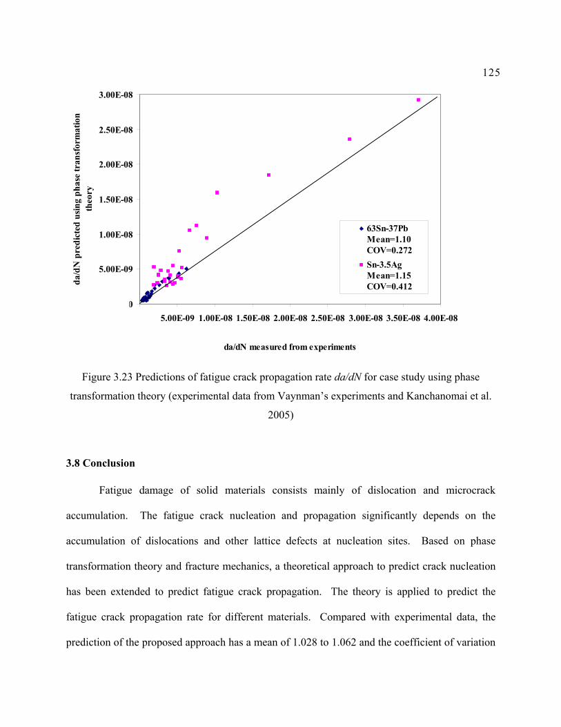
125
0.00E+00
5.00E-09
1.00E-08
1.50E-08
2.00E-08
2.50E-08
3.00E-08
0.00E+00
5.00E-09 1.00E-08 1.50E-08 2.00E-08 2.50E-08 3.00E-08 3.50E-08 4.00E-08
da/dN measured from experiments
da/d
N p
redi
cted
usin
g ph
ase
tran
sfor
mat
ion.
theo
ry
63Sn-37PbMean=1.10COV=0.272Sn-3.5AgMean=1.15COV=0.412
Figure 3.23 Predictions of fatigue crack propagation rate da/dN for case study using phase
transformation theory (experimental data from Vaynman’s experiments and Kanchanomai et al.
2005)
3.8 Conclusion
Fatigue damage of solid materials consists mainly of dislocation and microcrack
accumulation. The fatigue crack nucleation and propagation significantly depends on the
accumulation of dislocations and other lattice defects at nucleation sites. Based on phase
transformation theory and fracture mechanics, a theoretical approach to predict crack nucleation
has been extended to predict fatigue crack propagation. The theory is applied to predict the
fatigue crack propagation rate for different materials. Compared with experimental data, the
prediction of the proposed approach has a mean of 1.028 to 1.062 and the coefficient of variation
126
is 0.255 to 0.264 for steels, the mean is 1.185 to 1.310 and the coefficient of variation is 0.253 to
0.286 for aluminum alloys. Fatigue experiment on solder interconnects was conducted by B.
Fiedler at Northwestern University. Based on experimental and finite element analysis, phase
transformation theory was applied to predict fatigue crack propagation in interconnects. Fatigue
experiments on Sn-3.5Ag solder alloy were conducted by S. Vaynman at Northwestern
University, and crack propagation rate is characterized successfully by stress intensity factor
range ∆K. The fatigue crack was found to initiate in the solder alloy and migrate to the
solder/IMC layer interface; the crack propagated near the interface and caused catastrophic
failure. Finite element analysis incorporating UCP theory and CZM was applied to determine
the required energy U to propagate a unit crack area in solder. Interconnects failure caused by
fatigue crack nucleation and propagation under cyclic loading was analyzed. Phase
transformation theory was applied to predict the fatigue crack propagation rate of Sn-3.5Ag and
63Sn-37Pb eutectic solder. Compared with experimental data, the prediction of the proposed
approach has a mean of 1.15 and 1.10 and the coefficient of variation of 0.412 and 0.272 for Sn-
3.5Ag and 63Sn-37Pb eutectic solder, respectively. The results show that the phase
transformation theory is not only accurate and consistent but also conservative. The proposed
theory provides a scientific basis for a theoretical examination to fatigue crack nucleation and
propagation in interconnects.
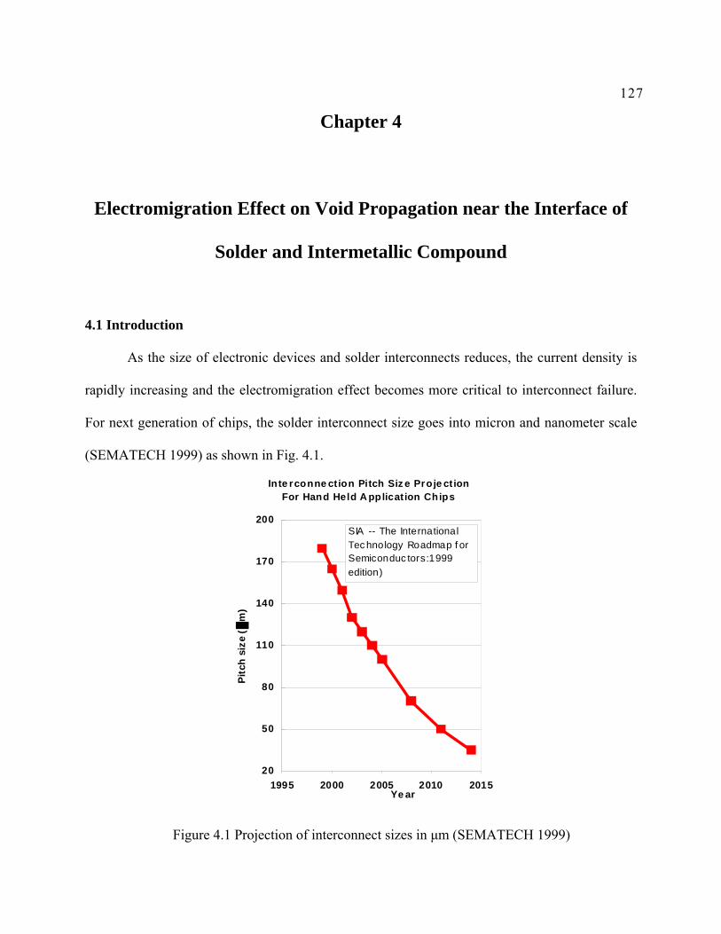
127
Chapter 4
Electromigration Effect on Void Propagation near the Interface of
Solder and Intermetallic Compound
4.1 Introduction
As the size of electronic devices and solder interconnects reduces, the current density is
rapidly increasing and the electromigration effect becomes more critical to interconnect failure.
For next generation of chips, the solder interconnect size goes into micron and nanometer scale
(SEMATECH 1999) as shown in Fig. 4.1.
Inte rconne ction Pitch Siz e Proje ction For Hand Held A pplication Chips
20
50
80
110
140
170
200
1995 2000 2005 2010 2015Ye ar
Pitc
h si
ze (
m)
SIA -- The International Tec hnology Roadmap f or Semiconduc tors:1999 edition)
Figure 4.1 Projection of interconnect sizes in µm (SEMATECH 1999)
128
The mechanism of electromigration effect on solder/IMC interfacial void propagation and
interconnect failure is studied in this chapter. A kinetic mass diffusion model is developed to
predict void width and propagation speed near the interface of IMC and solder caused by
electromigration. The current concentration effect at void tip is considered by using
computational analysis. The model gives reasonable prediction to the void width and
propagation velocity compared with experimental observations.
4.2 Kinetic Mass Diffusion Model to Predict Electromigration Effect for Pancake Type
Void Propagation
The trend of minimization of electronic devices results in higher operating current
densities in interconnects. Electromigration plays an important role in interconnect failure
mechanisms under high current density (Zhang et al. 2006). Generally electromigration is the
transport of material caused by the gradual movement of the ions in a conductor due to the
momentum transfer between conducting electrons and diffusing metal atoms. As the structure
size in electronic devices decreases, the physical significance of this effect increases.
Experimental research relating the electromigration effect on interconnect failure has been
performed by different investigators in the past decade. Gan and Tu (2002) conducted a series of
experiments to analyze the electromigration effect in IMC and bulk solder under different current
densities. They found that voids began to appear in the solder part just in front of the solder/IMC
cathode interface and grew toward the interface between the IMC and solder bulk. Similarly,
Miyazaki and Omata (2006) observed that voids nucleate from the current crowding point and
then propagated through the interface between the solder and IMC. They concluded that the
polarity and tilting effects are key factors to the electromigration effect on solder behavior.
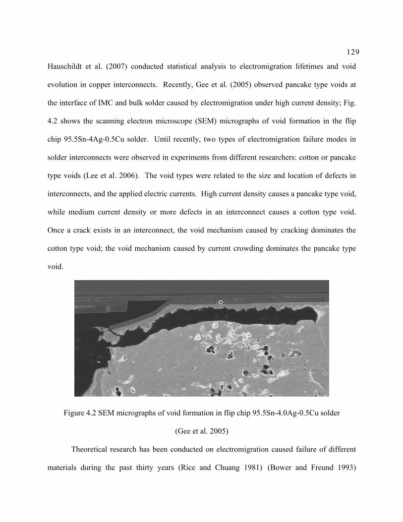
129
Hauschildt et al. (2007) conducted statistical analysis to electromigration lifetimes and void
evolution in copper interconnects. Recently, Gee et al. (2005) observed pancake type voids at
the interface of IMC and bulk solder caused by electromigration under high current density; Fig.
4.2 shows the scanning electron microscope (SEM) micrographs of void formation in the flip
chip 95.5Sn-4Ag-0.5Cu solder. Until recently, two types of electromigration failure modes in
solder interconnects were observed in experiments from different researchers: cotton or pancake
type voids (Lee et al. 2006). The void types were related to the size and location of defects in
interconnects, and the applied electric currents. High current density causes a pancake type void,
while medium current density or more defects in an interconnect causes a cotton type void.
Once a crack exists in an interconnect, the void mechanism caused by cracking dominates the
cotton type void; the void mechanism caused by current crowding dominates the pancake type
void.
Figure 4.2 SEM micrographs of void formation in flip chip 95.5Sn-4.0Ag-0.5Cu solder
(Gee et al. 2005)
Theoretical research has been conducted on electromigration caused failure of different
materials during the past thirty years (Rice and Chuang 1981) (Bower and Freund 1993)
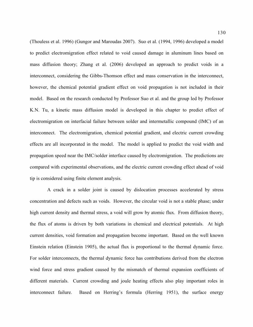
130
(Thouless et al. 1996) (Gungor and Maroudas 2007). Suo et al. (1994, 1996) developed a model
to predict electromigration effect related to void caused damage in aluminum lines based on
mass diffusion theory; Zhang et al. (2006) developed an approach to predict voids in a
interconnect, considering the Gibbs-Thomson effect and mass conservation in the interconnect,
however, the chemical potential gradient effect on void propagation is not included in their
model. Based on the research conducted by Professor Suo et al. and the group led by Professor
K.N. Tu, a kinetic mass diffusion model is developed in this chapter to predict effect of
electromigration on interfacial failure between solder and intermetallic compound (IMC) of an
interconnect. The electromigration, chemical potential gradient, and electric current crowding
effects are all incorporated in the model. The model is applied to predict the void width and
propagation speed near the IMC/solder interface caused by electromigration. The predictions are
compared with experimental observations, and the electric current crowding effect ahead of void
tip is considered using finite element analysis.
A crack in a solder joint is caused by dislocation processes accelerated by stress
concentration and defects such as voids. However, the circular void is not a stable phase; under
high current density and thermal stress, a void will grow by atomic flux. From diffusion theory,
the flux of atoms is driven by both variations in chemical and electrical potentials. At high
current densities, void formation and propagation become important. Based on the well known
Einstein relation (Einstein 1905), the actual flux is proportional to the thermal dynamic force.
For solder interconnects, the thermal dynamic force has contributions derived from the electron
wind force and stress gradient caused by the mismatch of thermal expansion coefficients of
different materials. Current crowding and joule heating effects also play important roles in
interconnect failure. Based on Herring’s formula (Herring 1951), the surface energy
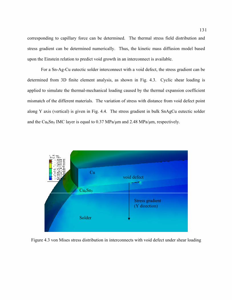
131
corresponding to capillary force can be determined. The thermal stress field distribution and
stress gradient can be determined numerically. Thus, the kinetic mass diffusion model based
upon the Einstein relation to predict void growth in an interconnect is available.
For a Sn-Ag-Cu eutectic solder interconnect with a void defect, the stress gradient can be
determined from 3D finite element analysis, as shown in Fig. 4.3. Cyclic shear loading is
applied to simulate the thermal-mechanical loading caused by the thermal expansion coefficient
mismatch of the different materials. The variation of stress with distance from void defect point
along Y axis (vertical) is given in Fig. 4.4. The stress gradient in bulk SnAgCu eutectic solder
and the Cu6Sn5 IMC layer is equal to 0.37 MPa/µm and 2.48 MPa/µm, respectively.
Figure 4.3 von Mises stress distribution in interconnects with void defect under shear loading
void defect
Stress gradient (Y direction)
Cu
Solder
Cu6Sn5
132
-49-48-47-46-45-44-43-42-41-40-39-38-37-36-35
0 2 4 6 8 10 12 14 16 18 20 22 24 26 28
distance to the defect point (µm)
stre
ss in
Y d
irec
tion
(MPa
)
Series1
Figure 4.4 Variation of stress with the distance from void defect point in Y direction (MPa)
From the Einstein relation, the actual atomic flux FkT
DJ ss
Ω=
δ , where D is the diffusivity
(cm2/s); Ω is the atomic volume (cm3); k is the Boltzmann constant (1.38×10⁻²³ joules/kelvin); T
is the absolute temperature (K); δs is thickness of diffusion layer, which assumed equal to 0.5nm
for the interface of solder/IMC (Zhang et al. 2006); F is the thermal dynamic force which
consists of electromigration and stress migration forces. The electromigration force per atom,
written as ** jZeZeEF tE ρ−=−= , where Z* is the effective charge number, which includes the
electric field and momentum exchange effects; e is the electron charge (1.6×10⁻¹⁹
Coulomb/electron); ρ is the resistivity (µΩcm); j is the current density (A/cm2); tE is the electric
field projected on the surface: the electric field component tangent to the dislocation line. From
the experimental results of Ye and Tu (2000), Wu et al. (2004), the effective charge number is
ZSn* =17 for Sn and Zη
* =50 for Cu6Sn5. The resistivity of Sn is ρSn=13.25 µΩcm and that of
Stress gradient in IMC layer = 2.48 MPa/µm
Stress gradient in solder bulk = 0.37 MPa/µm

133
Cu6Sn5 is ρη=17.5 µΩcm; the atomic volume Ω is taken as 2.0×10⁻²³ cm3. With the above
experimental data, the electromigration and stress migration force of atoms can be determined.
For example, with an applied current density equal to 1.5×10⁴ A/cm2, in a IMC layer, the
electromigration force 17* 1021 −×=−= jeZFem ηη ρ N, and the stress migration force:
171096.4 −×=∂∂
=y
FsmσΩ N; in bulk solder, the electromigration force
17* 104.5 −×=−= jeZF SnSnSnem ρ N; stress migration force: 171074.0 −×=∂∂
Ω=y
Fsmσ N.
It is noted that in both IMC layer and bulk solder, electromigration and stress migration
forces are generally in the same order of magnitude, and the electromigration force is stronger
than the stress migration force under the applied current density of 1.5×10⁴ A/cm2. The results
prove that the electromigration effect provides an important contribution to the interconnect
failure mechanism under high current density.
Under electromigration the atoms in a solder interconnect will be driven to the anode and
a corresponding vacancy flux will return to cathode interface; because the bonding energy in
Cu6Sn5 is larger, the flux of vacancy that enters IMC layer is small, and a flux divergence of
vacancy occurs at the interface, which leads to vacancy supersaturation, void nucleation, and
finally void propagation at the solder/IMC interface.
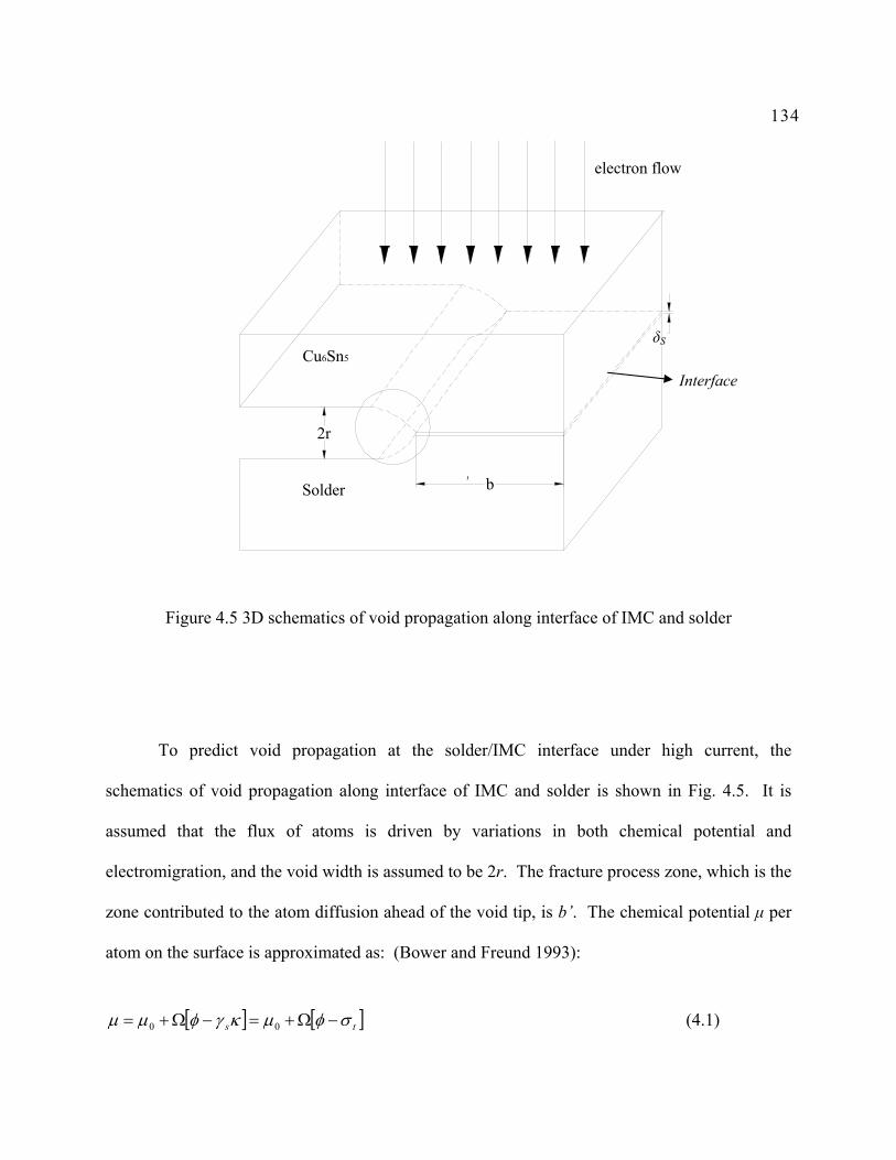
134
2r
Cu6Sn5
Solder b
electron flow
Figure 4.5 3D schematics of void propagation along interface of IMC and solder
To predict void propagation at the solder/IMC interface under high current, the
schematics of void propagation along interface of IMC and solder is shown in Fig. 4.5. It is
assumed that the flux of atoms is driven by variations in both chemical potential and
electromigration, and the void width is assumed to be 2r. The fracture process zone, which is the
zone contributed to the atom diffusion ahead of the void tip, is b’. The chemical potential µ per
atom on the surface is approximated as: (Bower and Freund 1993):
[ ] [ ]ts σφµκγφµµ −Ω+=−Ω+= 00 (4.1)
δS
Interface
’

135
where µ0 is the potential of the bulk; ijijεσφ21
= is the elastic energy strain density; γs is the
surface energy (J/m2); κ is the curvature of the surface of the void tip. The stress acts normal to
the grain boundary is σt.
In Eq. (4.1), there are two contributions to the chemical potential of an atom on a free
surface: the surface energy term and the elastic strain energy term. Rice and Chuang (1981)
showed that for most cases the elastic strain energy effect can be neglected, and this assumption
is adopted in current research. Eq. (4.1) can thus be simplified to:
ts σµκγµµ Ω−=Ω−= 00 (4.2)
The flux on the void surface due to the chemical potential is expressed as:
ykTD
skTD
skTDJ s
s ∂∂
Ω=
∂∂
=∂∂
Ω−=
σκγµ intintint (4.3)
where s∂
∂µ denotes the gradient of chemical potential along the void surface; kTD is the atomic
mobility; and y∂
∂σ is the stress gradient along the direction of electron flux.
The curvature κ of the surface of the void tip in Eq. (4.3) is obtained as:
dYd
dsdYdX
dsd
dsd θθθκ sintan
−=−=−≈−= (4.4)
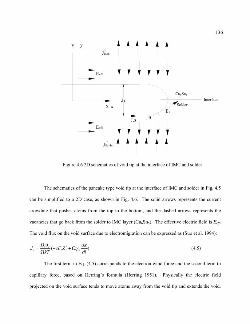
136
Eeff
Eeff
y
x2r
J,s
vJIMC
JSolder
Et
v
Figure 4.6 2D schematics of void tip at the interface of IMC and solder
The schematics of the pancake type void tip at the interface of IMC and solder in Fig. 4.5
can be simplified to a 2D case, as shown in Fig. 4.6. The solid arrows represents the current
crowding that pushes atoms from the top to the bottom, and the dashed arrows represents the
vacancies that go back from the solder to IMC layer (Cu6Sn5). The effective electric field is Eeff.
The void flux on the void surface due to electromigration can be expressed as (Suo et al. 1994):
)( *
dldZeE
kTDJ sst
sss
κγδ
Ω+−Ω
= (4.5)
The first term in Eq. (4.5) corresponds to the electron wind force and the second term to
capillary force, based on Herring’s formula (Herring 1951). Physically the electric field
projected on the void surface tends to move atoms away from the void tip and extends the void.
θ
Cu6Sn5
Solder Interface
X
Y

137
Surface energy tends to move atoms toward a free surface. The propagation of the void is
determined by the competition between the electric field and surface energy.
Assume κ is a function of Y only, the curvature gradient is determined by:
)(cos)(cossincossin2
222
2
2
dYd
dYd
dYd
dsd θθθθθθθκ
−=−= (4.6)
From mass conservation and by assuming the flux J is a function of Y, then Ω= /)( YvYJ .
Substituting Eq. (4.6) into Eq. (4.5), and defining y=Y/r, gives (Suo et al. 1994):
0sincossin12
2
=++ ydy
d θθθµ
(4.7)
The void shape for the composite is assumed to be the same as that in Suo et al.’s work (1994).
With the following initial conditions: 1sin =θ , 0/sin =dyd θ , at 1−=y , r, the radius of the void
equals d/2, where d is the width of the void.
By approximating the void tip curvature as r/1≈κ , the curvature gradient is of order 2/1 r≈ , and
a dimensionless coefficient is defined based on Eq. (4.5):
Ω=
S
rjeZγρη
2* ' (4.8)
where ***ηη ZaZaZ SnSn += , ηη ρρρ bb SnSn += , 1=+ ηaaSn , 1=+ ηbbSn . For
simplicity,2
*** ηZZ
Z Sn += ; 2
ηρρρ
+= Sn are defined here; further experimental work will be
required to accurately determine the value of unitless constant ηaaSn , , ηbbSn , , which determine
the fraction of Sn or Cu6Sn5 atoms passing through the interface. Here η is equal to 5.743 for the
pancake type void, which is determined from solution of Eq. (4.7) using a fourth-order Runge-
138
Kutta method, and perturbation analysis is conducted to obtain the eigen-solution of Mathieu’s
equation in Suo’s analysis (Suo et al. 1994).
The definition of the vacancy flux of Cu6Sn5 and solder by Zhang et al. (2006) is adopted
here:
'* jeZkT
DCJ
bulkv
ηηηη
η ρ= (4.9)
'* jeZkT
DCJ SnSnSn
bulkSnv
Sn ρ= (4.10)
where vJη and vSnJ are the vacancy flux of Cu6Sn5 and solder respectively; C is the concentration,
C=1/Ω for pure metal (1/cm3);
Assuming the pancake type void extends steadily, i.e., the front moves with an invariant
shape and has speed v relative to the lateral X direction. From the mass conservation principle,
the increasing void volume vd is equal to the volume of atoms diffusing out at the fracture
process zone in front of the void, where the fracture process zone is the region in which
electronmigration caused atom flux contribute to the void formation.
'')( ** bkT
ejZDCZDCJvd bulkSnSnSn
bulkSnv
Ω−=Ω= ηηηη ρρ (4.11)
Here b’ is the fracture process zone width. By estimating the width of b’ considering the Gibbs-
Thomson effect, Zhang et al. (2006) have calculated that the width of b’ varies from 10.2% to
17.7% of solder diameter for a 95.5Sn-4Ag-0.5Cu eutectic solder, and 15% of the solder
diameter is suggested as the value of b’; this assumption is adopted here. The current density j’
in Eq. (4.11) is taken as the average current density in the fracture process zone rather than the
original applied current density.

139
Thus, the void opening width d can be determined from Eq. (4.8) with η=5.743,
'793.42 * jeZ
rd S
ργ Ω
== (4.12)
The void propagation velocity v is determined from Eq. (4.11) as:
)(')()'(209.0
'')(793.4
'
**2/1
2/1*2/3
***
ηηηη
ηηηη
ρργ
ρ
ρργρ
ZDCZDCkT
bZej
bkT
ejZDCZDCjeZ
v
bulkSnSnSn
bulkSn
S
bulkSnSnSn
bulkSn
S
−Ω
=
Ω−
Ω=
(4.13)
Here the value 0.209 in Eq. (4.13) arises from dimensionless parameter η and can be
varied for different void shapes.
4.3 Computational Analysis to Consider the Current Concentration Effect
Computational analysis is conducted to analyze the current concentration effect near the
void tip. The effective current density j’ can be determined based on the thermal-electrical finite
element analysis as introduced in Chapter 2. The current density distribution in a Sn-Ag solder
joint under applied current density of 104 A/cm2 with a void propagating near the interface of
solder/IMC is shown in Fig. 4.7. Here Av is the void area and At is the interconnect cross section
area. The void area can be related to crack length by:
222 )/arccos( LRLRLRAv −−= (4.14)
where R is the radius of solder bulk and CdL −= 2/ , d is the pad opening. (Gee et al. 2005).
Fig. 4.8 shows the solder/IMC interface current density and temperature distribution in
the solder interconnect with void nucleation at the upper left corner, where current crowding
occurs. The cross-section is plotted on the X-Y plane and the current density is plotted along the

140
Z axis. The electrical current density ECD has units in A/cm2, and X, Y are the nodes
coordinates in µm. Higher temperature caused by joule heating was observed near the void
nucleation plot. Fig. 4.9 shows the corresponding IMC/solder interfacial current density
distribution with a void propagation under the applied current density of 1.5×10⁴ A/cm2.
Av/At = 0.6%
Av/At = 2.2%
Cu
95.5Sn-4Ag-0.5Cu
IMC

141
Av/At = 6.1%
Av/At = 11.0%
Av/At = 16.5%
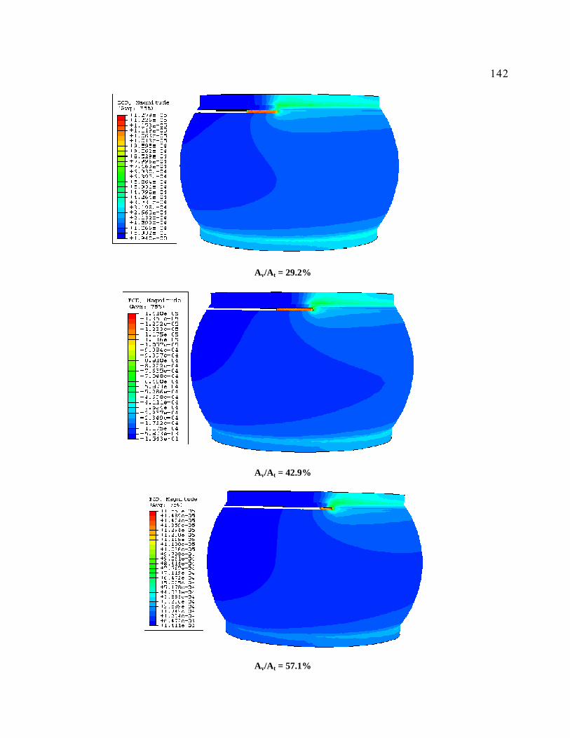
142
Av/At = 29.2%
Av/At = 42.9%
Av/At = 57.1%
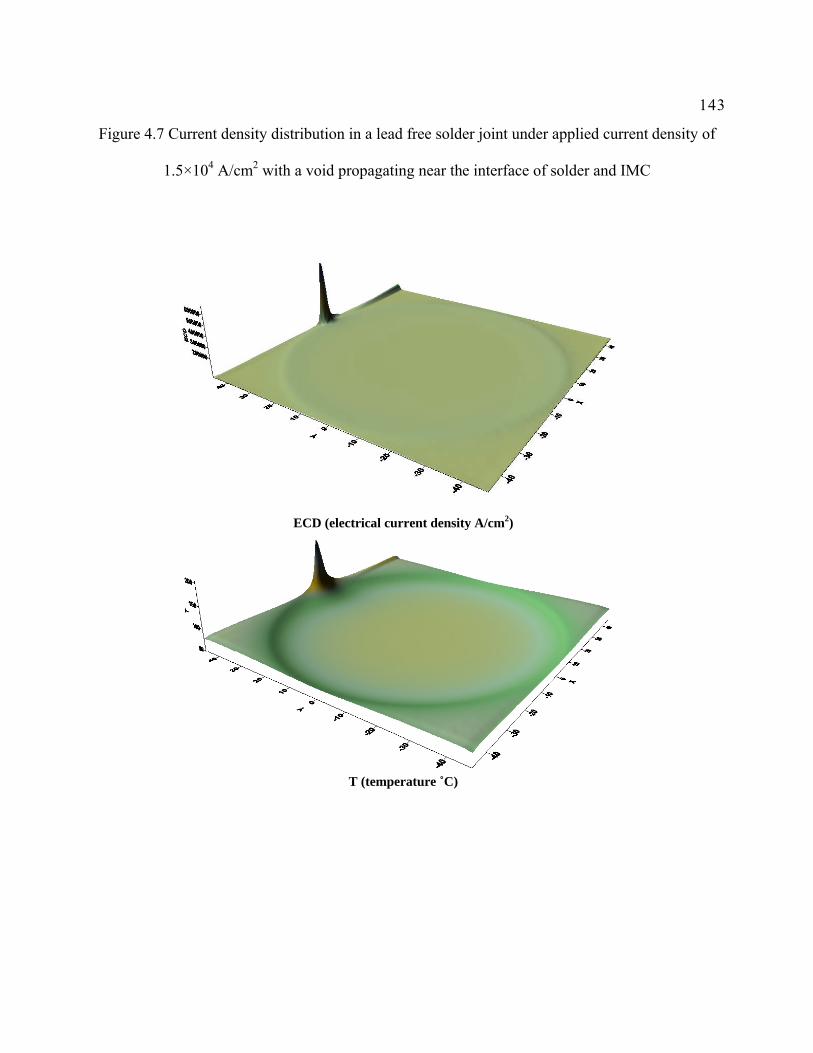
143
Figure 4.7 Current density distribution in a lead free solder joint under applied current density of
1.5×10⁴ A/cm2 with a void propagating near the interface of solder and IMC
ECD (electrical current density A/cm2)
T (temperature ˚C)
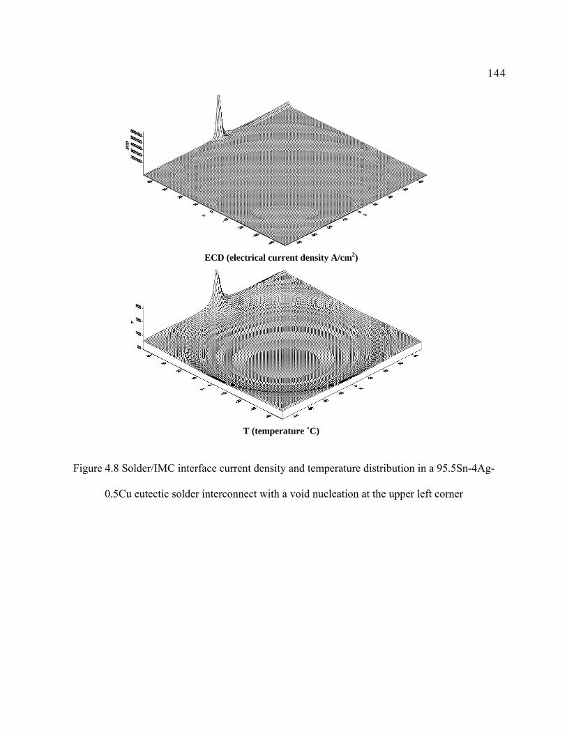
144
ECD (electrical current density A/cm2)
T (temperature ˚C)
Figure 4.8 Solder/IMC interface current density and temperature distribution in a 95.5Sn-4Ag-
0.5Cu eutectic solder interconnect with a void nucleation at the upper left corner

145
Av/At = 0.6% (jmax=8.059×10⁴A/cm2)
Av/At = 2.2% (jmax=9.268×10⁴A/cm2)
Av/At = 6.1% (jmax=10.27×10⁴A/cm2)

146
Av/At = 11.0% (jmax=11.01×10⁴A/cm2)
Av/At = 16.5% (jmax=11.71×10⁴A/cm2)
Av/At = 29.2% (jmax=12.79×10⁴A/cm2)

147
Av/At = 42.9% (jmax=14.10×10⁴A/cm2)
Av/At = 57.1% (jmax=15.53×10⁴A/cm2)
Figure 4.9 Solder/IMC interface current density distribution in the 95.5Sn-4Ag-0.5Cu solder
interconnect with a void propagating near the solder/ IMC interface
(note: ECD is electrical current density in A/cm2, X, Y is the coordinate in µm)
Figure 4.10 shows the maximum current density at the void tip; the average electric
current density in the fracture process zone b’ and in the whole interconnect with the propagation
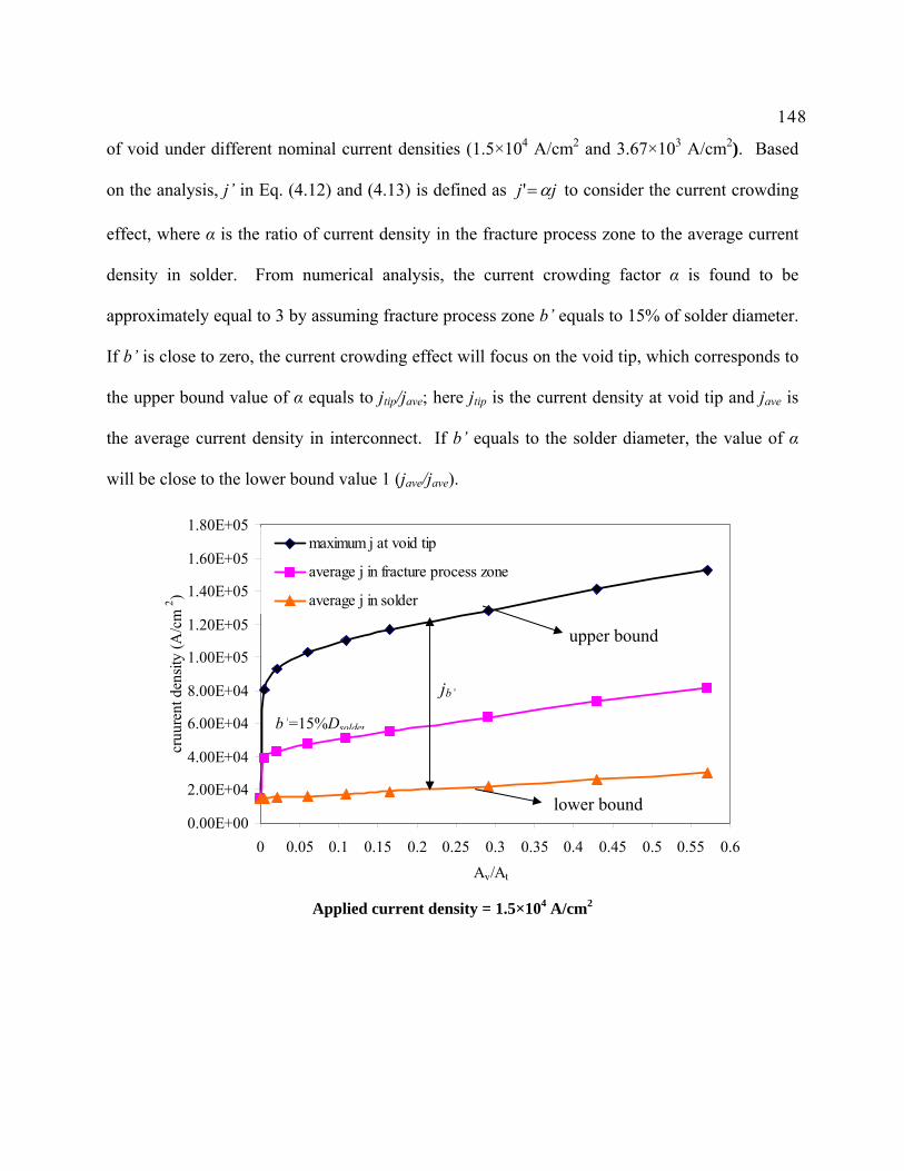
148
of void under different nominal current densities (1.5×10⁴ A/cm2 and 3.67×10³ A/cm2). Based
on the analysis, j’ in Eq. (4.12) and (4.13) is defined as jj α=' to consider the current crowding
effect, where α is the ratio of current density in the fracture process zone to the average current
density in solder. From numerical analysis, the current crowding factor α is found to be
approximately equal to 3 by assuming fracture process zone b’ equals to 15% of solder diameter.
If b’ is close to zero, the current crowding effect will focus on the void tip, which corresponds to
the upper bound value of α equals to jtip/jave; here jtip is the current density at void tip and jave is
the average current density in interconnect. If b’ equals to the solder diameter, the value of α
will be close to the lower bound value 1 (jave/jave).
0.00E+00
2.00E+04
4.00E+04
6.00E+04
8.00E+04
1.00E+05
1.20E+05
1.40E+05
1.60E+05
1.80E+05
0 0.05 0.1 0.15 0.2 0.25 0.3 0.35 0.4 0.45 0.5 0.55 0.6Av/At
cruu
rent
den
sity
(A/c
m 2 )
maximum j at void tip
average j in fracture process zone
average j in solder
Applied current density = 1.5×10⁴ A/cm2
upper bound
lower bound
jb’
b’=15%Dsolder

149
0.00E+00
5.00E+03
1.00E+04
1.50E+04
2.00E+04
2.50E+04
3.00E+04
3.50E+04
4.00E+04
4.50E+04
0 0.05 0.1 0.15 0.2 0.25 0.3 0.35 0.4 0.45 0.5 0.55 0.6Av/At
cruu
rent
den
sity
(A/c
m 2 )
maximum j at void tip
average j in fracture process zone
average j in solder
Applied current density = 3.67×10³ A/cm2
Figure 4.10 Maximum and average electric current density with the propagation of void at the
interface of solder and IMC
4.4 Case Study by Comparing with Experimental Results
The proposed model is verified by using experimental results collected from literature.
The following experimental data are obtained from Gee et al. (2005) and Zhang el al. (2006). In
their experiments, the void width d is measured as 2.44µm. The test temperature is 146 °C, the
electric current density is about 3.67×10³ A/cm2, the void length is 26.4µm, the void propagation
process is 6 hours, and therefore the average void growth velocity is about 4.4µm/h. The fracture
process zone mb µ5.3725015.0' =×= for the interconnect used in the experiment. The
diffusivity is DSn=1.3×10⁻¹⁰ cm2/s for Sn and Dη = 2.76×10⁻¹³ cm2/s for Cu6Sn5, and the
upper bound
lower bound
jb’
b’=15%Dsolder
150
diffusivity of the interface is taken to be 4.2×10⁻⁵ cm2/s. The surface energy
2215 J/m 6.1eV/cm10 ==Sγ (Wu et al. 2004).
Defining the material constant 9** 10453.1 ×=−= ηηηη ρρλ ZDCZDC bulkSnSnSn
bulkSn (Ω/s), and
substituting the corresponding experimental determined values into Eq. (4.12) and (4.13), yields:
mrd µ847.21067.3310375.15106.15.33
1026.1793.42 7819
29
=×××××××
×××== −−
−
,
hmsmv /198.4/10166.110847.24191038.1
105.371021067.33106.110453.1 9623
6297199
µ=×=××××
××××××××××= −
−−
−−−
The predictions match the experimental results (Zhang et al. 2006) well, which are the void
width d=2.44µm and void growth velocity v=4.4 µm/h.
It is interesting to discuss the effects of fracture process zone b’ and effective charge
number *Z on the accuracy of predictions. By varying the range of b’ from 5% to 50% of the
solder diameter, the current crowding parameter α is changed accordingly from numerical
analysis. By applying Eq. (4.12) and (4.13), the predicted void width d varies from 2.20 to 4.41
µm and void growth velocity v varies from 3.01 to 5.45 µm/h. With the increasing IMC layer,
more Cu6Sn5 atoms will flux through the interface, which also has important effect on the void
formation and propagation in the interconnect. For the value of ***ηη ZaZaZ SnSn += , Eq. (4.8), if
Sna = 0, ηa = 1, only the Cu6Sn5 atoms flux matters, 50** == ηZZ (upper bound), then the
predicted v=5.13 µm/h, d=2.33 µm. If ηa =0, Sna =1, only the Sn atoms flux
matters, 17** == SnZZ (lower bound), then the predicted v=2.99 µm/h, d=3.99 µm.
It should be noted that the void shape depends on the value of η in Eq. (4.8). Fig. 4.11
shows the mode I and mode II post-bifurcation steady-state shapes corresponding to different

151
eigenvalues of η by Yang et al. (1994). The bifurcation analysis performed by Yang et al. is
based on Lyapunov’s stability theory (Lyapunov 1966), the assumption adopted is that a circular
loop will bifurcate if a shape perturbation exists so that the loop never returns to the circular
shape. A circular void in solder may be developed from defects; it will distort, drift and evolve
into a noncircular shape, and finally migrate to a fixed shape under the electron wind force. If η
is small, the surface energy dominates the failure mode and the void will remain circular in shape
and drift in the electron wind. If η is larger than 5.743, the electric field dominates and the cavity
buckles to a noncircular shape. The void buckles when η=10.65, and becomes infinitely long and
finger-like when η drops back to 5.743. The range 5.743< η <10.65 corresponds to mode-I
(lateral) steady-state shapes, while the range 10.65 < η < 14.91 correspond to mode-II (vertical)
steady-state shapes, where the loops elongate normal to the electric field, when 0)0( →κ , η
=14.91. For pancake-type void, the value of η is assumed to be 5.743.
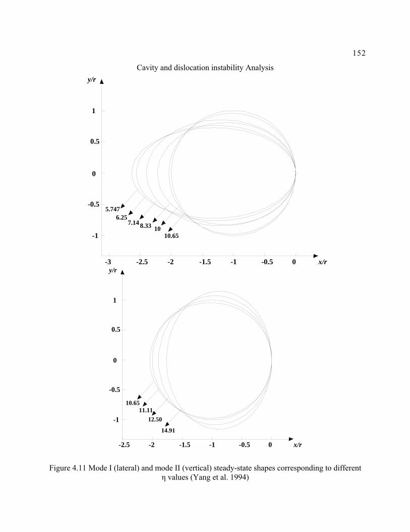
152
Cavity and dislocation instability Analysis
1
0.5
0
-0.5
-1
0-0.5-1-1.5-2-2.5-3
y/r
x/r
10.65108.337.14
6.255.747
14.91
12.50
10.65
1
0.5
0
-0.5
-1
0-0.5-1-1.5-2-2.5
y/r
x/r
11.11
Figure 4.11 Mode I (lateral) and mode II (vertical) steady-state shapes corresponding to different η values (Yang et al. 1994)
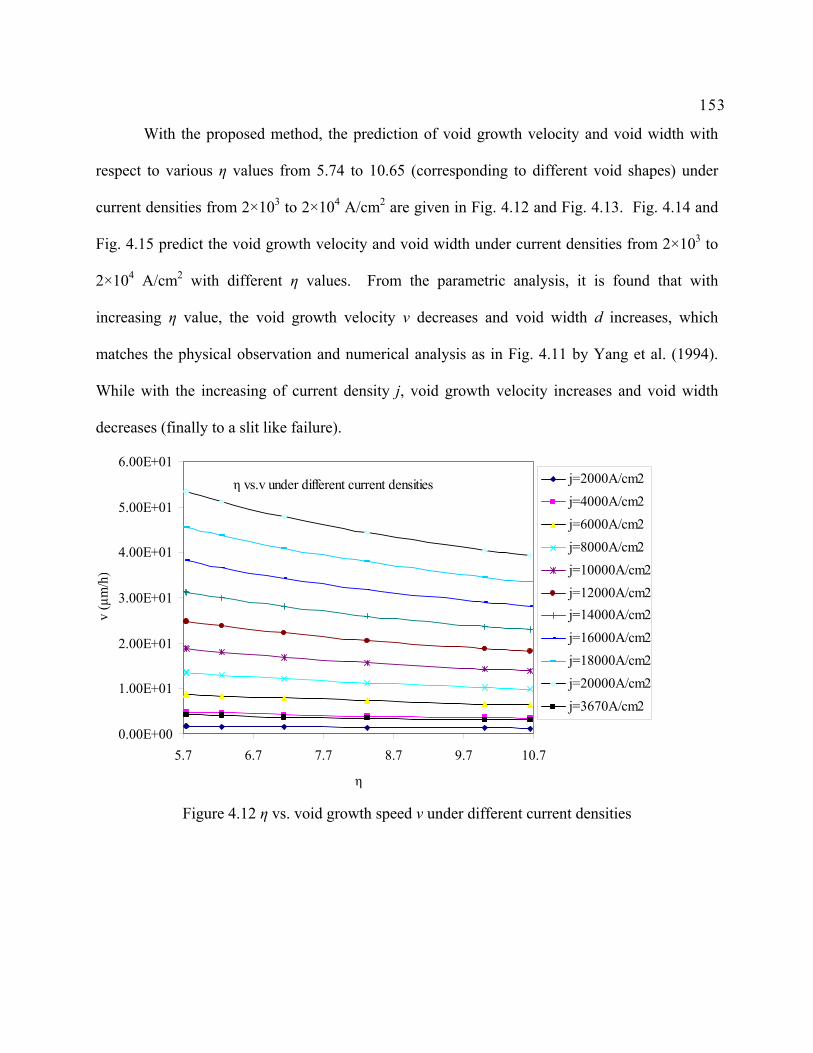
153
With the proposed method, the prediction of void growth velocity and void width with
respect to various η values from 5.74 to 10.65 (corresponding to different void shapes) under
current densities from 2×10³ to 2×10⁴ A/cm2 are given in Fig. 4.12 and Fig. 4.13. Fig. 4.14 and
Fig. 4.15 predict the void growth velocity and void width under current densities from 2×10³ to
2×10⁴ A/cm2 with different η values. From the parametric analysis, it is found that with
increasing η value, the void growth velocity v decreases and void width d increases, which
matches the physical observation and numerical analysis as in Fig. 4.11 by Yang et al. (1994).
While with the increasing of current density j, void growth velocity increases and void width
decreases (finally to a slit like failure).
η vs.v under different current densities
0.00E+00
1.00E+01
2.00E+01
3.00E+01
4.00E+01
5.00E+01
6.00E+01
5.7 6.7 7.7 8.7 9.7 10.7
η
v (µ
m/h
)
j=2000A/cm2j=4000A/cm2j=6000A/cm2j=8000A/cm2j=10000A/cm2j=12000A/cm2j=14000A/cm2j=16000A/cm2j=18000A/cm2j=20000A/cm2j=3670A/cm2
Figure 4.12 η vs. void growth speed v under different current densities
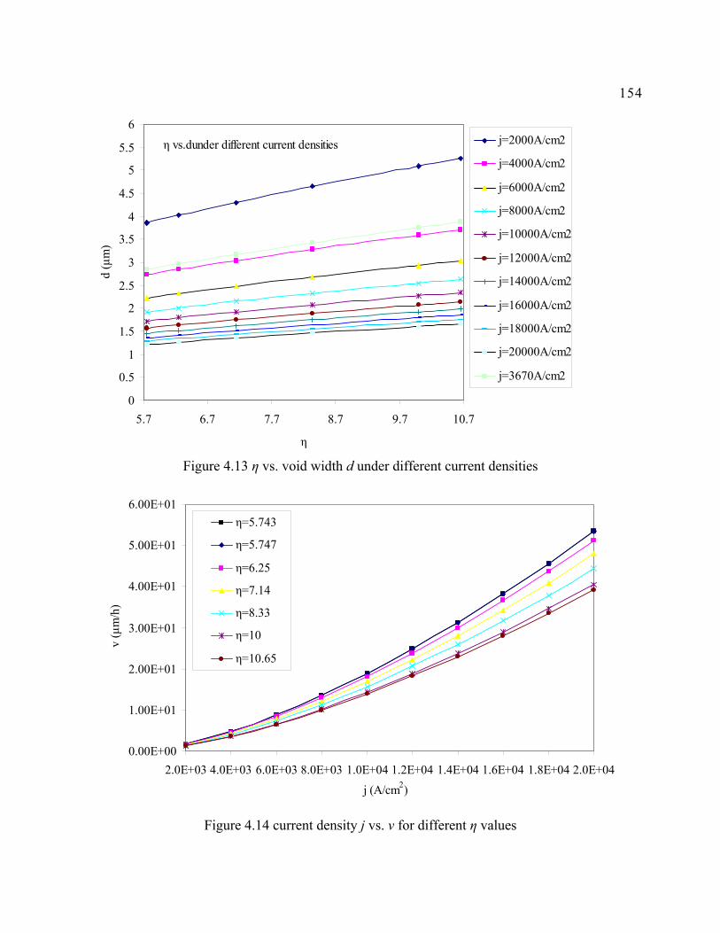
154
η vs.dunder different current densities
0
0.5
1
1.5
2
2.5
3
3.5
4
4.5
5
5.5
6
5.7 6.7 7.7 8.7 9.7 10.7
η
d (µ
m)
j=2000A/cm2
j=4000A/cm2
j=6000A/cm2
j=8000A/cm2
j=10000A/cm2
j=12000A/cm2
j=14000A/cm2
j=16000A/cm2
j=18000A/cm2
j=20000A/cm2
j=3670A/cm2
Figure 4.13 η vs. void width d under different current densities
0.00E+00
1.00E+01
2.00E+01
3.00E+01
4.00E+01
5.00E+01
6.00E+01
2.0E+03 4.0E+03 6.0E+03 8.0E+03 1.0E+04 1.2E+04 1.4E+04 1.6E+04 1.8E+04 2.0E+04j (A/cm2)
v (µ
m/h
)
η=5.743
η=5.747
η=6.25
η=7.14
η=8.33
η=10
η=10.65
Figure 4.14 current density j vs. v for different η values

155
1
1.5
2
2.5
3
3.5
4
4.5
5
5.5
2.0E+03 4.0E+03 6.0E+03 8.0E+03 1.0E+04 1.2E+04 1.4E+04 1.6E+04 1.8E+04 2.0E+04
j (A/cm2)
d (µ
m)
η=5.743
η=5.747η=6.25
η=7.14
η=8.33
η=10η=10.65
Figure 4.15 current density j vs. d for different η values
Table 4.1 shows the predicted void width d and propagation speed v by varying different
parameters in the model, including b’, j, *Z , and η. Effects of different parameters on the
theoretical predictions are calculated and given in the table. It is shown that the theoretical
calculations are consistent and in reasonable agreement with the experimental observations (Gee
et al. 2005, Zhang el al. 2006).
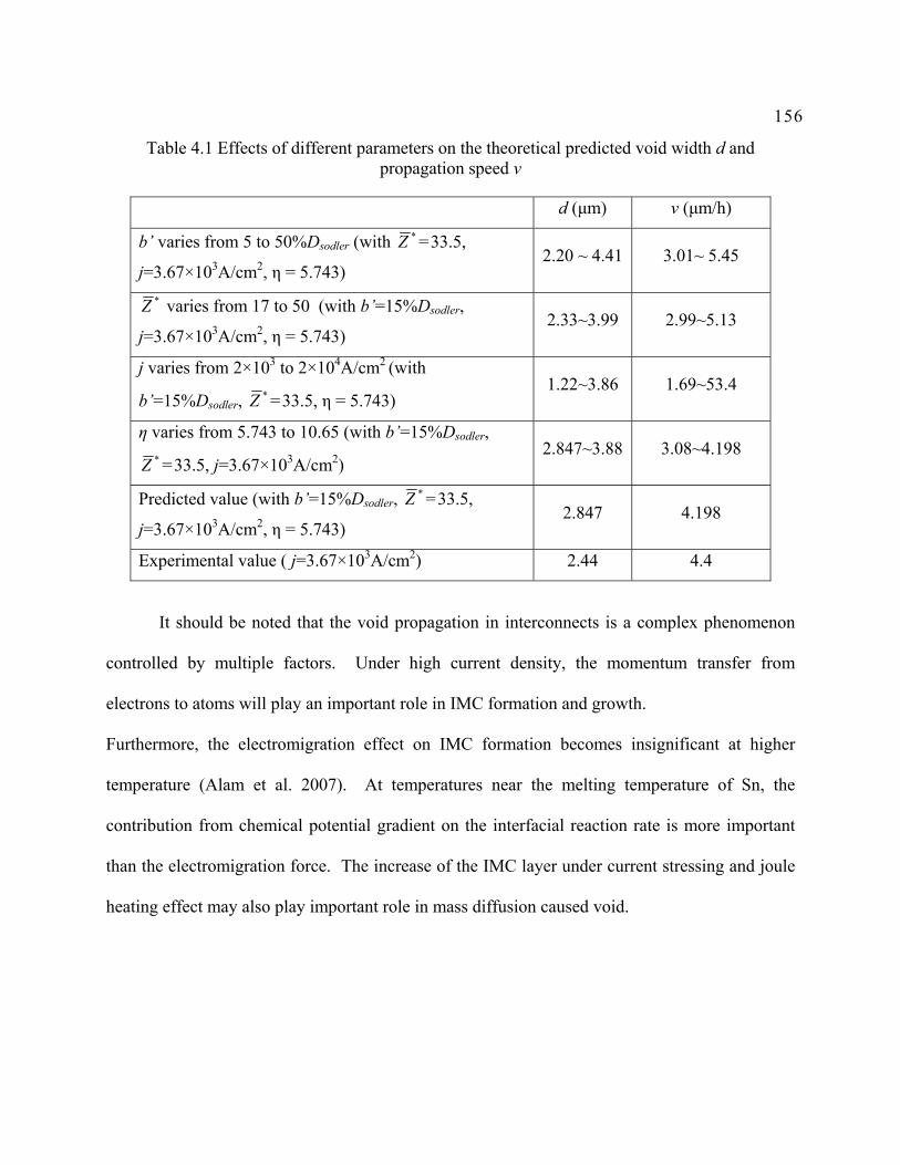
156
Table 4.1 Effects of different parameters on the theoretical predicted void width d and propagation speed v
d (µm) v (µm/h)
b’ varies from 5 to 50%Dsodler (with *Z =33.5,
j=3.67×10³A/cm2, η = 5.743) 2.20 ~ 4.41 3.01~ 5.45
*Z varies from 17 to 50 (with b’=15%Dsodler,
j=3.67×10³A/cm2, η = 5.743) 2.33~3.99 2.99~5.13
j varies from 2×10³ to 2×10⁴A/cm2 (with
b’=15%Dsodler, *Z =33.5, η = 5.743) 1.22~3.86 1.69~53.4
η varies from 5.743 to 10.65 (with b’=15%Dsodler, *Z =33.5, j=3.67×10³A/cm2)
2.847~3.88 3.08~4.198
Predicted value (with b’=15%Dsodler, *Z =33.5,
j=3.67×10³A/cm2, η = 5.743) 2.847 4.198
Experimental value ( j=3.67×10³A/cm2) 2.44 4.4
It should be noted that the void propagation in interconnects is a complex phenomenon
controlled by multiple factors. Under high current density, the momentum transfer from
electrons to atoms will play an important role in IMC formation and growth.
Furthermore, the electromigration effect on IMC formation becomes insignificant at higher
temperature (Alam et al. 2007). At temperatures near the melting temperature of Sn, the
contribution from chemical potential gradient on the interfacial reaction rate is more important
than the electromigration force. The increase of the IMC layer under current stressing and joule
heating effect may also play important role in mass diffusion caused void.
157
4.5 Conclusion
It has been observed experimentally that most of the solder joints failure is near the
IMC/solder interface under high current density. Electromigration effects on interconnect failure
mechanism is discussed in the chapter. From numerical analysis, it is found that the
electromigration force contributes more to void formation than stress migration force under high
current density. A kinetic mass diffusion model is developed based on the Einstein relation and
mass conservation principle. The approach is applied to predict void width and propagation
velocity at the solder/IMC interface caused by electromigration. Computational analysis has
been conducted to determine the current crowding parameter in the model. The predicted void
width and propagation velocity matches experimental results reasonably well.

158
Chapter 5
Conclusion
5.1 Conclusion
It has been experimentally observed that solder joints fail near the IMC/solder interface.
A 3D computational model based on cohesive fracture mechanics and continuum mechanics has
been developed in the dissertation to predict the crack initiation and propagation near the IMC
and solder interface. The traction-separation law of a cohesive element at interface is included in
the finite element program, ABAQUS. Unified-creep-plasticity Model is incorporated in the
model to simulate creep-plastic behavior of solder materials. A numerical analysis of IMC
related solder joint failure has been conducted. The cohesive-UCP finite element model is
applied to analyze the IMC layer thickness effect on solder joint failure. The growth of IMC
layer thickness is found to have a significant effect on solder joint failure. The von Mises stress
required to initiate a crack is found lower for a thicker IMC layer and the solder joint lifetime
decreases with increasing IMC layer thickness. Higher Young’s modulus of IMC tends to cause
crack nucleation at interface. Since solder joint failure is a complex coupled problem caused by
mechanical, thermal, and electrical stresses, a coupled thermo-electric numerical analysis has
been conducted to understand better the phenomenon. The electrical concentration and joule
heating effects are found to play important roles on solder joint failure, especially when a crack
propagates near the interface of IMC and solder. The temperature and electric current density
distribution in Sn-2.5Ag-0.8Cu-0.5Sb solder under different applied currents has been predicted.
It is found that there has pronounced temperature and electrical current concentration near the
159
crack tip. Although the lead-free solders usually have higher melting temperatures as compared
with lead-rich solder, the concentration of heat at the crack tip caused by joule heating may still
melt the solder material under a high current density, which will enhance the propagation of
crack and cause a circuit failure.
Fatigue damage of solid materials consists mainly of dislocation and microcrack
accumulation. The fatigue crack nucleation and propagation significantly depends on the
accumulation of dislocations and other lattice defects at nucleation sites. Based on phase
transformation theory, micromechanics, and fracture mechanics, a theoretical approach has been
developed to predict fatigue crack propagation in solid materials. The theory is first applied to
predict the fatigue crack propagation rate in steels and aluminum alloys, where the required
energy U to propagate a unit crack area in steel and aluminum alloys is determined by
experimental analysis from Professor Fine’s group at Northwestern University. Compared with
experimental data, the prediction of the proposed approach has a mean of 1.028 to 1.062 and the
coefficient of variation is 0.255 to 0.264 for steels, the mean is 1.185 to 1.310 and the coefficient
of variation is 0.253 to 0.286 for aluminum alloys. Based on experimental and finite element
analysis, the proposed phase transformation theory is extended to predict fatigue crack
propagation in interconnects. Fatigue experiments on Sn-3.5Ag solder alloy conducted by S.
Vaynman at Northwestern University is used to verify the approach. Fatigue crack propagation
rate is characterized successfully by stress intensity factor range ∆K. The fatigue crack was
found to initiate in the solder alloy and to migrate to the solder/ IMC layer interface; the crack
propagated near the interface and caused catastrophic failure. The developed computational
model incorporating UCP theory and CZM was applied to determine the required energy U to
propagate a unit crack area in solder. With U determined numerically, phase transformation

160
theory was applied to predict the fatigue crack propagation rate of Sn-3.5Ag and 63Sn-37Pb
eutectic solder. Compared with experimental data, the prediction of the proposed approach has a
mean of 1.15 and 1.10 and the coefficient of variation of 0.412 and 0.272 for Sn-3.5Ag and
63Sn-37Pb eutectic solder, respectively. The results show that the phase transformation theory is
not only accurate and consistent but also conservative. The proposed theory provides a basis for
a theoretical examination to fatigue crack propagation in interconnects.
With the reduction of electronic device size, interconnects will operate under higher
current density; eletromigration will play a more important role to interconnect failure in the near
future. From numerical analysis, it is found that the electromigration force contributes more to
void formation than stress migration force under high current density. A kinetic mass diffusion
model is developed based on the Einstein relation and mass conservation principle to predict the
electromigration effect on solder/IMC interfacial failure. The predicted void width and
propagation speed shows reasonable agreement with experimental data.
5.2 Future Research
For future research, the electrical current effect could be included into the phase
transformation theory; a possible method is proposed in Appendix C, which still in a preliminary
development stage. More theoretical and experimental research works are needed on the coupled
fatigue, joule heating and electromigration effects to failure of small-scale solder joints.
Electromigration effect can also be included in the computational model, combined with the
UCP theory. Since void nucleation and growth are the dominant damage mechanisms in
electromigration induced failure, the electromigration research efforts on damage failure
prediction will focus on these effects in future research. To simulate the damage process, initial
161
thermal and electrical fields are required. The current field distribution sometimes is a dominant
feature and thermal expansion coefficient mismatch of different materials will also contribute to
the stress field. For a 3-D solder joints computational model, a coupled system is needed to
solve the displacement-diffusion problem. Boundary conditions, which include diffusion and
displacement fields, will be considered in future research. Plastic strain accumulation is also an
important factor in the void nucleation and growth process. The dislocation accumulation at
second phase particles in the matrix phase is a source for void nucleation and growth. In order to
accurately simulate the damage process, both plasticity (due to the high homologous temperature
of the solder at ambient temperature) and creep must be considered. Plastic deformation will
also contribute to the main damage phenomenon, which is void nucleation at the cathode side.
Plastic deformation by grain boundary sliding produces high stress localization when the slip
band intersects with particles at a grain boundary, which is a favorite site for void nucleation.
The complexity of this problem arises from the coupling terms between diffusion governing
partial differential equations and force equilibrium governing partial differential equations. In
order to determine Jacobian contributions (stiffness matrix contribution) a material constitutive
equation is needed. Because of the nonlinear material behavior, a local integration scheme is
also needed; for example, a return mapping algorithm can be used. To validate the analysis, an
ABAQUS user defined element subroutine can be developed for 3D thermal-mechanical-
electromigration analysis and a computational solution of the governing partial differential
equations will be obtained. With the program developed, void nucleation kinetics under coupled
thermal-electrical load can be predicted. Furthermore, the mean time to failure of an
interconnect can be determined from this process. The computational prediction will need to be
compared with experiment, where parameters in the model having clear physical meaning can be

162
determined. With the program developed, a significant amount of experimental work can be
saved. Anisotropic properties can be included in the developed finite element model with the
material properties determined experimentally; if necessary molecular dynamic based technology
can be applied to simulate the inter-grain interactions. A 3D computational model using a multi-
physics analysis package can be developed in future research to predict the thermal stress,
current crowding, and joule heating effects. The material properties used in the model need to be
determined from experiments.

163
References ABAQUS documentation 6.6.3 (2006) Akay, H. U., Paydar N. H. and Bilgic, A., “Fatigue life predictions for thermally loaded solder joints using a volume-weighted averaging technique”, Journal of Electronic Packaging 119:228-235, (1997) Alam, M. O., Wu, B.Y., Chan, Y. C. and Tu, K. N. “High electric current density-induced interfacial reactions in micro ball grid array (µBGA) solder joints.” Acta Materialia, v54, n3, Feb., p613-621 (2006) Austin J. B., “The flow of heat in metals”, American Society for Metals, Cleveland, Ohio, (1942) Baqi, A. A., Schreurs, P. J. G. and Geers, M. G. D., “Fatigue damage modeling in solder interconnects using a cohesive zone approach” International Journal of Solids and Structures, 42, 927–942 (2005) Benzeggagh, M. L. and Kenane, M., “Measurement of mixed-mode delamination fracture toughness of unidirectional glass/epoxy composites with mixed-mode bending apparatus”, Composites Science and Technology, Volume 56, Number 4, April, pp. 439-449(11), (1996) Bhat, P. S. and Fine, M. E., “Fatigue crack nucleation in iron and a high strength low alloy steel”, Material Science and Engineering A314 90-96, (2001) Black, J.R., “Electromigration-A Brief Survey and Some Recent Results”, IEEE Transactions on Electron Devices, Vol. ED-16(No. 4):p. 338 347, April, (1969) Blech, I. A. and Herring, C., “Stress generation by electromigration “, Appl. Phys. Lett. 29, 131 (1976). Bower, A. F. and Craft, D., “Analysis of failure mechanisms in the interconnect lines of microelectronic circuits”, Fatigue and Fracture of Engineering Materials & Structures, v 21, n 5, May, p 611-630, (1998) Cavalli, M. N. Thouless, M. D. and Yang, Q. D., “Cohesive-zone modeling of the deformation and fracture of weld-bonded joints”, Welding Journal (Miami, Fla), v 83, n 4, April , p 133-139, (2004) Chan, Y. C., Tu, P. L., So, A. C. K. and Lai, J. K. L., “Effect of Intermetallic Compounds on the Shear Fatigue of Cu/63Sn–37Pb Solder Joints” IEEE Transaction on Components, Packing, and Manufacturing Technology —Part BVol. 20, No. 4, (1997)

164
Chiu, S. H., Liang, S. W., Chen, C., Yao, D. J. and Hsu, C. Y., “Infrared microscopy of hot spots induced by Joule heating in flip-chip SnAg solder joints under accelerated electromigration” Appl. Phys. Lett. Volume 88, 022110 (2006) Clech, J. M., Werner, E. and Robert, W. K. ,“Reliability figures of merit for surface-soldered leadless chip carriers compared to leaded packages”, IEEE Transactions On Components Hybrids and Manufacturing Technology 12, 449 – 458, (1989) Coffin, L. F. J. and Schenectady, N. Y., “A Study of the Effects of Cyclic Thermal Stresses on a Ductile Metal”, Transactions of the ASME, 931-950, (1954) Dasgupta, A., Oyan, C., Barker, D. and Pecht, M., “Solder creep-fatigue analysis by an energy-partitioning approach”, Journal of Electronic Packaging 114, 152-160, (1992) Desai, C. S., Chia, J., Kundu, T. and Prince, J. L., “Thermomechanical response of materials and interfaces in electronic packaging: Part I - Unified constitutive model and calibration”, Journal of Electronic Packaging 119, 294-300, (1997) Deshpande, V. S., Needleman, A. and Vander, G., “Discrete dislocation modeling of fatigue crack propagation”, Acta Materialia, v 50, n 4, Feb 25, p 831-846, (2002) Dundurs, J., “Edge-bonded dissimilar orthogonal elastic wedges under normal and shear loading”, ASME Journal of Applied Mechanics 36, 650–652, (1969). Einstein, A., “Über die von der molekularkinetischen Theorie der Wärme geforderte Bewegung von in ruhenden Flüssigkeiten suspendierten Teilchen”, Annalen der Physik 17: 549-560, (1905) Ellyin, F., “Fatigue Damage, Crack Growth and Life Prediction”, Chapman and Hall, New York, (1997) Erinc, M., Schreurs, P. J. G., Zhang, G. Q. and Geers, M. G. D., “Microstructural damage analysis of SnAgCu solder joints and an assessment on indentation procedures,” Journal of Materials Science: Materials in Electronics 16:93-700, (2005) Fiedler, B. A., Yao, Y., Vaynman, S., Ghosh, G., Keer, L. M. and Fine, M. E., “Pb-Free Sodler Joint Fatigue Crack Initiation and Propagation Related to Electrical, Thermal and Mechanical Loading”, Proceeding of SRC Techcon conference, Austin, (2007) Fine, M. E., Stolkarts, V. and Keer, L. M., “Fatigue crack nucleation assisted by thermal activation”, Materials Science and Engineering A: Structural Materials: Properties, Microstructure and Processing, v 272, n 1, Nov, p 5-9, (1999) Fine, M. E., “Phase transformation theory applied to elevated temperature fatigue”, Scripta Materialia, v 42, n 10, May, p 1007-1012, (2000)

165
Frear, D. R., Jang, J. W., Lin, J. K. and Zhang, C., “Pb-free solders for flip-chip interconnects”, JOM, v 53, n 6, June, p 28-32+38, (2001) Funabashi, N., Mura, T. and Keer, L. M., “Fatigue Crack Initiation and Propagation in Bonded Sheets”, Journal of Adhesion, v 9, n 3, p 229-235, (1978) Gan, H. and Tu, K. N., “Effect of Electromigration on Intermetallic Compound Formation in Pb-free solder-Cu interfaces” Electronic components and technology conference (2002) Gee, S., Kelkar, N., Huang, J. and Tu, K. N., “Lead-Free and PbSn Bump Electromigration Testing”, ASME InterPACK, San Franscisco, CA, (2005) Ghosh, G., “Elastic properties, hardness and indentation fracture toughness of intermetallics relevant to electronic packaging” J. Mater. Res., Vol. 19, No. 5, May (2004) Gungor, M. R. and Maroudas, D., “Stress-induced deceleration of electromigration-driven void motion in metallic thin films”, Journal of Applied Physics, v 101, n 6, (2007) Guo, Q., Cutiongco, E. C., Keer, L. M. and Fine, M. E., “Thermomechanical Fatigue Life Prediction of 63Sn/37Pb Solder”, Journal of Electronic Packaging 114:145-151, (1992) Gupta, P., “Effect of IMC on Thermal-mechanical Reliability of Lead-Free Solder Interconnections for Flip-Chips”, Master thesis, Georgia Institute of Technology (2004) Harlow, D. G. and Wei, R.P., “Probabilities of occurrence and detection of damage in airframe materials”, Fatigue and Fracture of Engineering Materials and Structures, v 22, n 5, p 427-436, (1999) Hauschildt, M., Gall, M., Thrasher, S., Justison, P., Hernandez, R., Kawasaki, H. and Ho, P. S., “Statistical analysis of electromigration lifetimes and void evolution” Journal of Applied Physics, v 101, n 4, p 043523, (2007) Herring, C., “in the physics of power metallurgy”, (McGraw-Hill, New York), p.143, (1951). Huntington HB and Grone AR, ‘Current-induced marker motion in gold wires “, J. Phys. Chem. Solids 20, 76 (1961). Huang, Y., Gong, X. Y., Suo, Z. and Jiang, Z. Q., “Model of evolving damage bands in materials”, International Journal of Solids and Structures, v 34, n 30, Oct., p 3941-3951, (1997) Huntington, H. B. and Grone, A. R., ‘Current-induced marker motion in gold wires “, J. Phys. Chem. Solids 20, 76 (1961) Irving, P. E. and McCartney, L. N., “Prediction of Fatigue Crack Growth Rates-Theory, Mechanisms and Experimental Results”, Metal Science, v 11, n 8-9, Aug-Sep, p 351-361, (1977)

166
Izumi, Y. and Fine, M. E., “Role of Plastic Work in Fatigue Crack Propagation in Metals”, Engineering Fracture Mechanics, v 11, n 4, p 791-804, (1979) Izumi, Y., Fine, M. E. and Mura, T., “Energy Considerations in Fatigue Crack propagation”, International Journal of Fracture, v 17, n 1, Feb., p 15-25, (1981) Ju, S. H., Sandor B. I., and Plesha M. E., “Life prediction of solder joints by damage and fracture mechanics”, Journal of Electronic Packaging 118:193-200, (1996) Kanchanomai, C., Limtrakarn, W. and Mutoh, Y., “Fatigue crack growth behavior in Sn-Pb eutectic solder/copper joint under mode I loading”, Mechanics of Materials, v 37, n 11, November, p 1166-1174, (2005) Kanchanomai, C. and Mutoh, Y., “Fatigue crack initiation and growth in solder alloys”, Fatigue and Fracture of Engineering Materials and Structures, v 30, n 5, May, Structural Integrity in Electronics, p 443-457, (2007) Kim, D. H., Elenius, P. and Barrett, S., “Solder joint reliability and characteristics of deformation and crack growth of Sn-Ag-Cu versus eutectic Sn-Pb on a WLP in a thermal cycling test”, IEEE Transactions on Electronics Packaging Manufacturing, v 25, n 2, April, p 84-90, (2002). Klingbeil, N. W., “A total dissipated energy theory of fatigue crack growth in ductile solid”, International Journal of Fatigue, v 25, n 2, February, p 117-128, (2003) Knecht, S., and L. R. Fox., “Constitutive Relation and Creep-Fatigue Life Model For Eutectic Tin Lead Solder”, IEEE Transactions On Components Hybrids and Manufacturing Technology 13:424-433, (1990) Korhonen, T. K., Henderson, D. W. and Korhonen, M. A., “Nucleation and propagation of fatigue damage in near-eutectic Sn-Ag-Cu alloy”, JOM, v 56, n 11, November, p 251-252, (2004) Kuo, C. G., Sastry, S. M. L., and Jerina, K. L., ”Creep-fatigue life prediction of in situ composite solders”, Metallurgical and Materials Transactions a-Physical Metallurgy and Materials Science 26:3265-3275, (1995) Kwon, I. B., Fine, M. E., and Mura, T., “Elastic strain energy analysis of the dislocation structures in fatigue”, Acta Metallurgica, v 36, n 9, Sep., p 2605-2614, (1988) Kwun, S. I. and Fine, M. E., “Fatigue Macrocrack Growth in Tempered HY80, HY130, and 4140 Steels: Threshold and Mid-Delta K Range”, Fatigue of Engineering Materials and Structures, v 3, n 4, p 367-382, (1980) Lang, M. and Larsen, J. M., “Fatigue crack propagation and load interaction effects in a titanium alloy”, Fatigue and Fracture Mechanics, vol. 30, ASTM STP 1360, 201–213, (1999).
167
Larson, M. C. and Verges, M. A., “Extending the fatigue life of solder grid array (SGA) electronic packages”, Journal of Electronic Packaging, Transactions of the ASME, v 125, n 1, p 18-23, (2003). Lau, J. H., “Solder Joint Reliability of Flip Chip and Plastic Ball Grid Array Assembles under Thermal, Mechanical, and Vibrational conditions”, IEEE Transactions VOL. 19, NO 4, NOV. (1996) Laz, P. J., Craig, B. A. and Hillberry, B. M., “A probabilistic total fatigue life model incorporating material inhomogeneities, stress level and fracture mechanics”, International Journal of Fatigue, v 23, n Suppl. 1, p S119-S127, (2001) Lee, C. C., Lee, C. C., Chiu, C. C., Chen, C. C., Kuo, F. and Chiang, K. N., “Electromigration Characteristic of SnAg3.0Cu0.5 Flip Chip Interconnection”, Electronic Component and Technology Conference, (2006) Lee, S. B., and Kim, J. K., “A mechanistic model for fatigue life prediction of solder joints for electronic packages” International Journal of Fatigue 19:85-91, (1997) Leicht, L. and Skipor A., “Mechanical cycling fatigue of PBGA package interconnects”, International Journal of Microcircuits and Electronic Packaging, v 22, n 1, First Quarter, p 57-61, (1999) Liang, S. W., Shao, T. L., Chen, C. Y., Everett, C. C. and Tu, K. N., “Relieving the current crowding effect in flip-chip solder joints during current stressing”, Journal of Materials Research, v 21, n 1, January, p 137-146, (2006) Liaw, P. K., Kwun, S. I. and Fine, M. E., “Plastic work of fatigue crack propagation in steel and aluminum alloys”, Metallurgical Transactions A (Physical Metallurgy and Materials Science), v 12A, n 1, Jan , p 49-55, (1981) Lin, M. R., Fine, M. E. and Mura, T., “Fatigue Crack Initiation Slip Bands: Theory and Experiments”, Acta Metallurgica, v 34, n 4, Apr, p 619-628, (1986) Liu, X., Sooklal, V. K., Verges, M. A. and Larson, M. C., “Experimental study and life prediction on high cycle vibration fatigue in BGA packages”, Microelectronics Reliability, v 46, n 7, July, p 1128-1138, (2006) Lyapunov A.M., “Stability of motion”, Academic Press, New-York and London, (1966) Manson, S. S., “Behavior of Materials under conditions of thermal stress”, In Heat transfer, a symposium held at the University of Michigan during the summer of 1952. Ann Arbor, MI: Engineering Research Institute, University of Michigan,(1953)

168
Mars, W. V. and Fatemi, A., “Fatigue crack nucleation and growth in filled natural rubber”, Fatigue and Fracture of Engineering Materials and Structures, v 26, n 9, September, p 779-789, (2003) Mattila, T. T. and Kivilahti, J. K., “Reliability of lead free interconnects under consecutive thermal and mechanical loadings.” Journal of Electronic Materials, v 35, n 2, February, 2006, p 250-256 , (2006) McDowell, D. L., “Damage mechanics and metal fatigue: a discriminating perspective”, International Journal of Damage Mechanics, v 8, n 4, Oct., p 376-403, (1999) McDowell, D. L., Miller, M. P. and Brooks, D. C., “A unified creep-plasticity theory for solder alloys,” Fatigue of Electronic Materials, ASTM STP 1153, pp. 42-59, (1994) McKittrick, J., Liaw, P. K., Kwun, S. I. and Fine, M. E., “Threshold for Fatigue Macrocrack Propagation in Some Aluminum Alloys”, Metallurgical Transactions A (Physical Metallurgy and Materials Science), v 12A, n 8, Aug. , p 1535-1539, (1981) Miyazaki, T. and Omata, T., “Electromigration degradation mechanism for Pb-free flip-chip micro solder bumps”, Microelectronics Reliability, v 46, n 9-11, Proceedings of the 17th European Symposium on Reliability of Electron Devices, Failure Physics and Analysis, p1898-1903, (2006) Morrow, J., “Cyclic Plastic Strain Energy and Fatigue of Metals”, In Internal Friction, Damping, and Cyclic Plasticity. Philadelphia: ASTM, (1964) Mura, T. and Lin, S. C., “Thin Inclusions and Cracks in Anisotropic Media”, Journal of Applied Mechanics, Transactions ASME, v 41 Ser E, n 1, Mar., p 209-214, (1974) Mura, T., “Three-dimensional constitutive relations and ductile fracture”, Discussion on Section 2, 147-153, North-Holland Publishing Company, (1981) Mura, T., “Micromechanics of defects in solids (2nd ed.)”, The Netherlands: Martinus Nijhoff, (1991) Mura, T., “Theory of fatigue crack initiation”, Materials Science & Engineering A: Structural Materials: Properties, Microstructure and Processing, v A176, n 1-2, Mar 31 , p 61-70, (1994) Nah, J. W., Suh, J. O. and Tu, K. N., “Effect of current crowding and Joule heating on electromigration-induced failure in flip chip composite solder joints tested at room temperature” Journal of Applied Physics 98, 013715 (2005) Nayeb, H. H. and Yang, P., “Mixed mode I/II fracture and fatigue crack growth along 63Sn-37Pb solder/brass interface”, International Journal of Fatigue 23 S325-335, (2001)

169
Nguyen, O., Repetto, E. A., Ortiz, M. and Radovitzky, R. A., “A cohesive model of fatigue crack growth”, International Journal of Fracture 110: 351–369, (2001) NIST database for solder properties, Release 4.0 (2002) Pan, K., Zhou, B. and Yan, Y., “Simulation Analysis of Dynamic Response for CSP under Board Level Drop Test”, IEEE Inter. Conf. Electro. Packag. Tech. (2006) Pao, Y. H., “A Fracture-Mechanics Approach to Thermal Fatigue Life Prediction of Solder Joints”, IEEE Transactions On Components Hybrids and Manufacturing Technology 15:559-570, (1992) Paris, P. C., “Fracture mechanics and fatigue: a historical perspective”, Fatigue and Fracture of Engineering Materials & Structures, v 21, n 5, May, p 535-540, (1998) Prager, W., “A new method of analyzing stresses and strains in work-hardening plastic solids”, J. Appl. Mech., Trans. Am. Soc. Mech. Eng.,23, No. 5, 493–496 (1956) Ren, F., Nah, J. W., Tu, K. N., Xiong, B. S., Xu, L. H. and Pang, J. H. L., “Electromigration induced ductile-to-brittle transition in lead-free solder joints”, Applied Physics Letters 89, 141914, (2005) Rice, J. R., “Mechanics of crack tip deformation and extension by fatigue”, ASTM STP 415, 247–311,(1967) Rice, J. R. and Chuang, T. J., “Energy Variations In Diffusive Cavity Growth”, J.AM.CERAM.SOC. J. Am. Ceram. Soc. Vol. 64, no. 1, pp. 46. (1981). Ritchie, R. O., “Mechanisms of fatigue-crack propagation in ductile and brittle solids”, International Journal of Fracture, v 100, n 1, p 55-83, (1999) Roe, K. L. and Siegmund, T., “An irreversible cohesive zone model for interface fatigue crack growth simulation” Engineering Fracture Mechanics 70 209–232, (2003) Sematech, “The International Technology Roadmap for Semiconductors: 1999 edition. 1999 ed, Semiconductor Industry Association (SIA). Austin, TX: International Sematech, (1999) Shang, J. K., Zeng, Q. L., Zhang, L. and Zhu, Q. S., “mechanical fatigue of Sn-rich Pb-free solder alloys”, Journal of Materials Science: Materials in Electronics, v 18, n 1-3, March, p 211-227, (2007) Shangguan, D. K., “Analysis of crack growth in solder joints”, Soldering and Surface Mount Technology, v 11, n 3, p 27-32, (1999)

170
Shi, X. Q., Pang, H. L. J., Zhou, W., and Wang, Z. P., “A modified energy-based low cycle fatigue model for eutectic solder alloy”, Scripta Materialia 41:289-296, (1999) Seniw, M. E., Conley, J. G. and Fine, M. E., “The effect of microscopic inclusion locations and silicon segregation on fatigue lifetimes of aluminum alloy A356 castings” Materials Science and Engineering A285, 43–48, (2000) Soboyejo, W. O., Shen, W., Srivatsan, T. S., “An investigation of fatigue crack nucleation and growth in a Ti-6Al-4V/TiB in situ composite”, Mechanics of Materials, v 36, n 1-2, January/February, p 141-159, (2004) Solomon, H. D., “Fatigue of 60/40 Solder”, IEEE Transactions On Components Hybrids and Manufacturing Technology 9:423-432,(1986) Stolkarts, V., Keer, L. M. and Fine, M. E., “Damage evolution governed by microcrack nucleation with application to the fatigue of 63Sn-37Pb solder” Journal of the Mechanics and Physics of Solids 47:2451-2468, (1999) Subrahmanyan, R., Wilcox, J. R. and Li, C. Y., “A Damage Integral Approach to Thermal Fatigue of Solder Joints”, IEEE Transactions On Components Hybrids and Manufacturing Technology 12:480-491, (1989) Suo, Z. and Hutchinson, J. W., “Interface crack between two elastic layers”, International Journal of Fracture, v 43, n 1, May 1, p 1-18, (1990) Suo, Z., Wang, W. and Yang, M., “Electromigration instability: Transgranular slits in interconnects” Applied Physics Letter 64(15), 11 April (1994) Syed, A. R., “Creep Crack-Growth Prediction of Solder Joints During Temperature Cycling - an Engineering Approach”, Journal of Electronic Packaging 117:116-122, (1995) Towashiraporn, P., Subbarayan, G. and Desai, C. S., “A hybrid model for computationally efficient fatigue fracture simulations at microelectronic assembly interfaces” International Journal of Solids and Structures, v 42, n 15, July, p 4468-4483, (2005) Thouless, M. D., Yu, H., Zhao, Z. and Yang, W.,” Damage nucleation during electromigration along an isolated interface in an elastic medium”, Journal of the Mechanics and Physics of Solids, v 44, n 3, Mar, p 371, (1996) Vaynman, S., “Isothermal fatigue of 96.5Pb-3.5Sn solder”, Ph.D. Dissertation, Department of Materials Science and Engineering, Northwestern University, Evanston, IL. (1987) Vaynman, S. and Zubelewicz, A., “Fatigue Life Prediction For Low-Tin Lead-Based Solder At Low Strains”, Welding Journal 69:S395-S398, (1990)
171
Vaynman, S. and McKeown S. A., “Energy-Based Methodology For the Fatigue Life Prediction of Solder Materials”, IEEE Transactions On Components Hybrids and Manufacturing Technology 16:317-322, (1993) Wang, F., Keer, L. M., Vaynman, S. and Wen, S., “Constitutive model and numerical analysis for high lead solders”, IEEE Trans. on Components and Packaging Technology, 27, 718 (2004) Wang, W., Suo, Z. and Hao, T. H., “A simulation of electromigration-induced transgranular slits”, J. Appl. Phys. 79 (5), 1 March (1996) Weertman, J., “Theory of fatigue crack growth based on a BCS crack theory with work hardening”, International Journal of Fracture 9(2), pp. 125–131, (1973) Wen, L. C., and Ronald, G. R., “Comparison of LCC solder joint life predictions with experimental data”, Journal of Electronic Packaging 117:109-115, (1995) Wen, S., Keer, L. M., and Mavoori, H., “Constitutive And Damage Model For A Lead-Free Solder”, Journal of Electronic Materials, v 30, n 9, September, Lead-Free Solder Materials and Soldering Technologies, p 1190-1196, (2001) Wen, S., “Thermomechanical fatigue life prediction for several solders”, PhD. Dissertation, Dept. Mech. Eng., Northwestern Univ., Evanston, IL, (2001) Wen S., Keer L. M., Vaynman S. and Lawson, L. R., “A constitutive model for a high lead solder,” IEEE Trans. on Components and Packaging Technology, vol. 25, pp. 23–31, Mar. (2002) Whitelaw, R. S., Neu R. W., and Scott, D. T., “Deformation behavior of two lead-free solders: Indalloy 227 and Castin alloy”, Journal of Electronic Packaging 121:99-107, (1999) Williams, D. R. and Fine, M. E., “Quantitative Determineation on Fatigue Microcrack Growth in SiC Whisker Reinforced 2124 Al Alloy Composites”, Metallurgical Soc Inc, p 639-670, (1985) Wu, A. T., Tu, K. N., Lloyd, J. R., Tamura, N., Valek, B. C. and Kao, C. R., “Electromigration-induced microstructure evolution in tin studied by synchrotron x-ray microdiffraction” , Applied Physics Letters, v 85, n 13, Sep 27, p 2490-2492, (2004) Xu, L., Pang, J. H. L., Ren, F. and Tu, K. N., “Electromigration effect on intermetallic growth and Young's modulus in SAC solder joint”, Journal of Electronic Materials, v 35, n 12, December, p 2116-2125, (2006) Yamada, S. E., “A Fracture-Mechanics Approach to Soldered Joint Cracking”, IEEE Transactions On Components Hybrids and Manufacturing Technology 12:99-104. (1989) Yang, B., Mall, S. and Ravi, C. K., “A cohesive zone model for fatigue crack growth in quasibrittle materials”, International Journal of Solids and Structures” 38 3927-3944 (2001)
172
Yang, D., Wu, B. Y., Chan, Y. C. and Tu, K. N., “Microstructural evolution and atomic transport by thermomigration in eutectic tin-lead flip chip solder joints”, Journal of Applied Physics, v 102, n 4, p 043502, (2007) Yang, Q. D., Shim, D. J. and Spearing, S. M., “A cohesive zone model for low cycle fatigue life prediction of solder joints” Microelectronic Engineering 75, 85–95 (2004) Yang, W., Wang, W. and Suo, Z., “Cavity and dislocation instability due to electric current”, Journal of the Mechanics and Physics of Solids, v 42, n 6, June, p 897-911, (1994) Yao, D. and Shang, J. K., “Effect of cooling rate on interfacial fatigue-crack growth in Sn-Pb solder joints”, IEEE Transactions on Components, Packaging, and Manufacturing Technology Part B: Advanced Packaging, v 19, n 1, Feb, p 154-165, (1996) Yao, Y. and Keer, L. M., “A 3D Finite Element Analysis to Failure of Solder Joint Near the Interface of Intermetallic Compounds and Solder Bulk”, SRC Techcon Conference, Austin, Texas, September (2007) Yao, Y., Fine, M. E. and Keer, L. M., “An Energy Approach to Predict Fatigue Crack Propagation in Metals and Alloys”, International J. of Fracture, v146, n3, 149-158, Aug., (2007) Yao, Y., Vaynman, S., Keer, L. M. and Fine, M. E., “Energy Based Micromechanics Analysis on Fatigue Crack Propagation Behavior in Sn-Ag Eutectic Solder”, J. of Electronic Materials, v37, n3,339-346, March, (2008) Yao, Y., Fiedler, B. A., Keer, L. M., and Fine, M. E., “Electromigration Effect to Void Propagation near the Interface of Solder and Intermetallic Compound” , Proceeding of SRC Techcon conference, Austin, (2008) Yao, Y., Keer, L. M. and Fine, M. E., “Mechanical and Thermo-Electrical Analysis of Interfacial Failure of Solder Joint”, submitted to IEEE Trans. on Components and Packaging Technology, 2008 (under review) Yao, Y., Fiedler, A. B., Keer, L. M. and Fine, M. E., “Phase Transform Theory Applied to Fatigue Crack Propagation in Interconnects”, submitted to IEEE Trans. on Components and Packaging Technology, 2008 (under review) Yao Y., Keer L.M., and Fine M.E., “Electromigration Effect on Pancake Type Void Propagation near the Interface of Solder Bulk and Intermetallic Compound”, submitted to J. of Applied Physics, 2008 (under review) Ye, H., Basaran, C., and Hopkins, D., “Thermomigration in Pb–Sn solder joints under joule heating during electric current stressing” Applied Physics Letters Volume 82, NUMBER 7 (2003)

173
Yeh, E. C. C. and Tu, K. N.,” Numerical simulation of current crowding phenomena and their effects on electromigration in very large scale integration interconnects” Journal of Applied Physics, v 88, n 10, Nov 15, p 5680-5686, (2000) Yi, K .S., Cox, B. N. and Dauskardt, R. H., “Fatigue crack-growth behavior of materials in viscous fluid environments. Journal of the Mechanics and Physics of Solids”, v 47, n 9, Sep., p 1843-1871, (1999) Yu, H., Mhaisalkar, S. G., Wong, E. H., Teh, L. K., and Wong, C. C., “Investigation of cure kinetics and its effect on adhesion strength of nonconductive adhesives used in flip chip assembly”, IEEE Transactions on Components and Packaging Technologies, v 29, n 1, March, p 71-79, (2006) Zhang, L., Ou, S., Huang, J. and Tu, K. N., “Effect of current crowding on crack propagation at the interface between intermetallic compound and solder in flip chip solder joints”, Applied Physics Letter 88, 012106 (2006) Zubelewicz, A., Guo, Q., Cutiongco, E. C., Fine, M. E. and Keer, L. M., “Micromechanical Method to Predict Fatigue Life of Solder”, Journal of Electronic Packaging 112:179-182, (1990)

174
Appendix A: Example of ABAQUS code for 3D solder/IMC interconnect
mechanical analysis
ABAQUS code for 3D solder/IMC interconnect mechanical analysis using cohesive zone-UCP model (here geometrical descriptions for nodes and elements are omitted) *Heading ** Job name: UCP-cohesive interconnect model ** Model name: UCP-cohesive interconnect model *Preprint, echo=NO, model=NO, history=NO, contact=NO ** ** PARTS ** *Part, name=COHESIVE-1 *Node 1, 0., 98., 0. ……………………………………… 1586, -79.8450317, 97., -90.7089691 *Element, type=COH3D8 1, 303, 306, 48, 47, 466, 469, 82, 81 ………………………………………. *Nset, nset=_PICKEDSET2, internal, generate 1, 1586, 1 *Elset, elset=_PICKEDSET2, internal, generate 1, 748, 1 *Elset, elset=_PickedSet5, internal, generate 1, 748, 1 ** Region: (Section-3-_PICKEDSET2:Picked) *Elset, elset=_PickedSet5, internal, generate 1, 748, 1 ** Section: Section-3-_PICKEDSET2 *Cohesive Section, elset=_PickedSet5, material=COHESIVE, response=TRACTION SEPARATION, *End Part ** *Part, name=DIE-1 *Node 1, 125., 100., 0. …………………………………….. 693, 16.4849625, 110., 105.32383 *Element, type=C3D8R

175
1, 195, 196, 545, 539, 16, 17, 149, 148 ……………………………………. 416, 689, 489, 488, 664, 533, 143, 142, 503 *Nset, nset=_PICKEDSET2, internal, generate 1, 693, 1 *Elset, elset=_PICKEDSET2, internal, generate 1, 416, 1 ** Region: (Section-4-_PICKEDSET2:Picked) *Elset, elset=_I1, internal, generate 1, 416, 1 ** Section: Section-4-_PICKEDSET2 *Solid Section, elset=_I1, material=DIE 1., *End Part ** *Part, name=IMC1-1 *Node 1, 0., 100., 0. ………………………………….. 2379, -78.8546448, 99.0005951, -90.1376038 *Element, type=C3D8R 1, 464, 465, 1751, 1748, 13, 14, 289, 288 ………………………………….. 1496, 2360, 1196, 1184, 2239, 1727, 223, 222, 1707 *Nset, nset=_PICKEDSET2, internal, generate 1, 2379, 1 *Elset, elset=_PICKEDSET2, internal, generate 1, 1496, 1 *Nset, nset=_PICKEDSET3, internal, generate 1, 2379, 1 *Elset, elset=_PICKEDSET3, internal, generate 1, 1496, 1 ** Region: (Section-1-_PICKEDSET3:Picked) *Elset, elset=_I1, internal, generate 1, 1496, 1 ** Section: Section-1-_PICKEDSET3 *Solid Section, elset=_I1, material=IMC1 1., *End Part ** *Part, name=IMC2-1 *Node 1, 0., -98., 0. ………………………………… 2379, -78.8554688, -99.0005875, -90.1368561

176
*Element, type=C3D8R 1, 464, 465, 1751, 1748, 13, 14, 289, 288 ………………………………… 1496, 2360, 1196, 1184, 2239, 1727, 223, 222, 1707 *Nset, nset=_PICKEDSET2, internal, generate 1, 2379, 1 *Elset, elset=_PICKEDSET2, internal, generate 1, 1496, 1 ** Region: (Section-2-_PICKEDSET2:Picked) *Elset, elset=_I1, internal, generate 1, 1496, 1 ** Section: Section-2-_PICKEDSET2 *Solid Section, elset=_I1, material=IMC2 1., *End Part ** *Part, name=SBUSTRATE-1 *Node 1, 125., -120., 0. ……………………………………... 693, 16.4849625, -110., 105.32383 *Element, type=C3D8R 1, 195, 196, 545, 539, 16, 17, 149, 148 ……………………………………. *Nset, nset=_PICKEDSET2, internal, generate 1, 693, 1 *Elset, elset=_PICKEDSET2, internal, generate 1, 416, 1 ** Region: (Section-5-_PICKEDSET2:Picked) *Elset, elset=_I1, internal, generate 1, 416, 1 ** Section: Section-5-_PICKEDSET2 *Solid Section, elset=_I1, material=SUBSTRATE 1., *End Part ** *Part, name=SOLDER-1 *Node 1, 0., 97., 0. …………………………………. 14301, -10.0929403, -10.5563126, -124.465775 *Element, type=C3D8R 1, 720, 721, 4330, 3934, 13, 14, 355, 354 …………………………………. 12800, 11998, 2569, 2540, 11709, 14301, 2669, 2651, 12195
177
*Nset, nset=_PICKEDSET2, internal, generate 1, 14301, 1 *Elset, elset=_PICKEDSET2, internal, generate 1, 12800, 1 ** Region: (Section-6-_PICKEDSET2:Picked) *Elset, elset=_I1, internal, generate 1, 12800, 1 ** Section: Section-6-_PICKEDSET2 *Solid Section, elset=_I1, material=SOLDER 1., *End Part ** ** ASSEMBLY ** *Assembly, name=Assembly ** *Instance, name=IMC1-1, part=IMC1-1 *End Instance ** *Instance, name=IMC2-1, part=IMC2-1 *End Instance ** *Instance, name=COHESIVE-1, part=COHESIVE-1 *End Instance ** *Instance, name=DIE-1, part=DIE-1 *End Instance ** *Instance, name=SBUSTRATE-1, part=SBUSTRATE-1 *End Instance ** *Instance, name=SOLDER-1, part=SOLDER-1 *End Instance ** *Nset, nset=uppernodes, instance=DIE-1 4, 5, 6, 8, 10, 37, 38, 39, 40, 41, 42, 43, 44, 45, 46, 47 ……………………………………… 527, 528, 529, 530, 531, 532, 533 *Nset, nset=lowernodes, instance=SBUSTRATE-1 1, 2, 3, 7, 9, 11, 12, 13, 14, 15, 16, 17, 18, 19, 20, 21 …………………………………….. 477, 478, 479, 480, 481, 482, 483 *Elset, elset=_die-low_S2, internal, instance=DIE-1 1, 2, 3, 4, 5, 6, 7, 8, 9, 10, 11, 12, 13, 14, 15, 16 ……………………………………

178
349, 350, 351, 352, 353, 354, 355, 356, 357, 358, 359, 360, 361, 362, 363, 364 *Surface, type=ELEMENT, name=die-low _die-low_S2, S2 *Elset, elset=_IMC1-up_S2, internal, instance=IMC1-1 1, 2, 3, 4, 5, 6, 7, 8, 9, 10, 11, 12, 13, 14, 15, 16 ………………………………….. 1298, 1299, 1300, 1301, 1302, 1303, 1304, 1305, 1306, 1307, 1308, 1309 *Surface, type=ELEMENT, name=IMC1-up _IMC1-up_S2, S2 *Elset, elset=_IMC1-low_S2, internal, instance=IMC1-1 342, 343, 344, 345, 346, 347, 348, 349, 350, 351, 352, 353, 354, 355, 356, 357 ………………………………… 1495, 1496 *Elset, elset=_IMC1-low_S3, internal, instance=IMC1-1 188, 189, 190, 191, 192, 193, 194, 195, 196, 197, 198, 199, 200, 201, 202, 203 ……………………………….. 1459, 1460, 1461, 1462, 1463 *Elset, elset=_IMC1-low_S4, internal, instance=IMC1-1 221, 222, 223, 224, 225, 226, 227, 228, 229, 230, 231, 232, 233, 234, 235, 236 ………………………………. 1338, 1339, 1340, 1341, 1342 *Surface, type=ELEMENT, name=IMC1-low _IMC1-low_S2, S2 _IMC1-low_S3, S3 _IMC1-low_S4, S4 *Elset, elset=_cohesive-up_S1, internal, instance=COHESIVE-1, generate 1, 748, 1 *Surface, type=ELEMENT, name=cohesive-up _cohesive-up_S1, S1 *Elset, elset=_cohesive-low_S2, internal, instance=COHESIVE-1, generate 1, 748, 1 *Surface, type=ELEMENT, name=cohesive-low _cohesive-low_S2, S2 *Elset, elset=_solder-up_S2, internal, instance=SOLDER-1 1, 2, 3, 4, 5, 6, 7, 8, 9, 10, 11, 12, 13, 14, 15, 16 ………………………………….. 10915, 10916, 10917, 10918, 10919, 10920, 10921, 10922, 10923, 10924, 10925, 10926, 10927, 10928, 10929, 10930 *Surface, type=ELEMENT, name=solder-up _solder-up_S2, S2 *Elset, elset=_solder-low_S2, internal, instance=SOLDER-1 2901, 2902, 2903, 2904, 2905, 2906, 2907, 2908, 2909, 2910, 2911, 2912, 2913, 2914, 2915, ……………………………………. 12519, 12520, 12521, 12522, 12523, 12524, 12525, 12526, 12527, 12528, 12529, 12530
179
*Elset, elset=_solder-low_S3, internal, instance=SOLDER-1 1601, 1602, 1603, 1631, 1632, 1633, 1661, 1662, 1663, 1691, 1692, 1693, 1721, 1722, 1723, …………………………………… 12409, 12410 *Elset, elset=_solder-low_S4, internal, instance=SOLDER-1 1910, 1920, 1930, 1940, 1950, 1960, 1970, 1980, 1990, 2000, 2010, 2020, 2030, 2040, …………………………………. 11490, 11500 *Surface, type=ELEMENT, name=solder-low _solder-low_S2, S2 _solder-low_S3, S3 _solder-low_S4, S4 *Elset, elset=_IMC2-up_S2, internal, instance=IMC2-1 1, 2, 3, 4, 5, 6, 7, 8, 9, 10, 11, 12, 13, 14, 15, 16 ……………………………… 1298, 1299, 1300, 1301, 1302, 1303, 1304, 1305, 1306, 1307, 1308, 1309 *Surface, type=ELEMENT, name=IMC2-up _IMC2-up_S2, S2 *Elset, elset=_IMC2-low_S2, internal, instance=IMC2-1 342, 343, 344, 345, 346, 347, 348, 349, 350, 351, 352, 353, 354, 355, 356, 357 …………………………….. 1495, 1496 *Elset, elset=_IMC2-low_S3, internal, instance=IMC2-1 188, 189, 190, 191, 192, 193, 194, 195, 196, 197, 198, 199, 200, 201, 202, 203 ……………………………. 1459, 1460, 1461, 1462, 1463 *Elset, elset=_IMC2-low_S4, internal, instance=IMC2-1 221, 222, 223, 224, 225, 226, 227, 228, 229, 230, 231, 232, 233, 234, 235, 236 ………………………….. 1338, 1339, 1340, 1341, 1342 *Surface, type=ELEMENT, name=IMC2-low _IMC2-low_S2, S2 _IMC2-low_S3, S3 _IMC2-low_S4, S4 *Elset, elset=_substrate-up_S2, internal, instance=SBUSTRATE-1 93, 94, 95, 96, 97, 98, 99, 100, 101, 102, 103, 104, 405, 406, 407, 408 409, 410, 411, 412, 413, 414, 415, 416 *Elset, elset=_substrate-up_S3, internal, instance=SBUSTRATE-1 63, 64, 65, 66, 67, 68, 69, 70, 71, 72, 73, 74, 75, 76, 77, 78 ……………………………. 311, 312, 365, 366, 367, 368, 369, 370, 371, 372, 373, 374 *Elset, elset=_substrate-up_S4, internal, instance=SBUSTRATE-1 53, 54, 55, 56, 57, 58, 59, 60, 61, 62, 157, 158, 159, 160, 161, 162 …………………………….
180
393, 394, 395, 396, 397, 398, 399, 400, 401, 402, 403, 404 *Surface, type=ELEMENT, name=substrate-up _substrate-up_S2, S2 _substrate-up_S3, S3 _substrate-up_S4, S4 ** Constraint: IMC1-cohesive *Tie, name=IMC1-cohesive, adjust=yes cohesive-up, IMC1-low ** Constraint: IMC2-sbustrate *Tie, name=IMC2-sbustrate, adjust=yes IMC2-low, substrate-up ** Constraint: cohesive-solder *Tie, name=cohesive-solder, adjust=yes cohesive-low, solder-up ** Constraint: die-IMC1 *Tie, name=die-IMC1, adjust=yes IMC1-up, die-low ** Constraint: solder-IMC2 *Tie, name=solder-IMC2, adjust=yes IMC2-up, solder-low *End Assembly *Amplitude, name=Amp-1, definition=PERIODIC 1, 3.14, 0., 0. 0., 1. ** ** MATERIALS ** *Material, name=DIE *Elastic 131000., 0.3 *Material, name=cohesive *Elastic, type=traction separation 7e4, 4e4, 4e4 *Damage initiation, criterion=MAXS 8e1, 5e1, 5e1 *Damage evolution, type=energy, mixed mode behavior=bk, power=1.45 0.8, 1.0, 1.0 ** *Material, name=IMC1 *Elastic 96900., 0.309 *Material, name=IMC2 *Elastic 96900., 0.309 *Material, name=SOLDER

181
*Elastic 48000., 0.4 *CREEP, LAW=USER *DEPVAR 4 *Expansion 2.9E-5 *Material, name=SUBSTRATE *Elastic 131000 ** ** BOUNDARY CONDITIONS ** ** Name: bc-lower Type: Displacement/Rotation *Boundary lowernodes, 1, 1 lowernodes, 2, 2 lowernodes, 3, 3 lowernodes, 4, 4 lowernodes, 5, 5 lowernodes, 6, 6 ** Name: bc-upper Type: Displacement/Rotation *Boundary uppernodes, 2, 2 ** ---------------------------------------------------------------- ** ** STEP: Step-1 ** *Step, name=Step-1, nlgeom=YES, inc=10000 *Static, stabilize=0.0002 0.01, 100., 1.0E-6, 1. ** ** BOUNDARY CONDITIONS ** ** Name: cyclic load Type: Displacement/Rotation *Boundary, amplitude=Amp-1 uppernodes, 1, 1, 1. ** ** OUTPUT REQUESTS ** *Restart, write, frequency=0 ** ** FIELD OUTPUT: F-Output-1 ** *Output, field

182
*Node Output CF, RF, U *Element Output, directions=YES CFAILURE, E, ENER, JK, LE, PE, PEEQ, PEMAG, S, SDEG, STATUS *Contact Output CDISP, CSTRESS ** ** HISTORY OUTPUT: H-Output-1 ** *Output, history, variable=PRESELECT *End Step SUBROUTINE CREEP(DECRA,DESWA,STATEV,SERD,EC0,ESW0,P,QTILD, 1 TEMP,DTEMP,PREDEF,DPRED,TIME,DTIME,CMNAME,LEXIMP,LEND, 2 COORDS,NSTATV,NOEL,NPT,LAYER,KSPT,KSTEP,KINC) C INCLUDE 'ABA_PARAM.INC' C CHARACTER*80 CMNAME C DIMENSION DECRA(5),DESWA(5),STATEV(*),PREDEF(*),DPRED(*), 1 TIME(2),COORDS(*) C C DEFINE CONSTANTS C AA=0.009 DD=70.0 AIWA=0.0 BB=0.001 QQ=10000.0 RT=8.314 XX_sat=8.0 miu=7.0 omig=0.015 NN=1.2 YY=0.1 C c set initial RR, XX c IF(KSTEP.EQ.1.AND.KINC.EQ.1) THEN STATEV(4)=2.0 STATEV(3)=0.0 ENDIF IF(KSTEP.GE.2.AND.KINC.EQ.1) THEN STATEV(4)=STATEV(4)+YY/STATEV(3) ENDIF
183
IF(KINC.EQ.1) THEN STATEV(1)=STATEV(4) STATEV(2)=0.0 ENDIF c c set FLAG_SIGN (elastic or inelastic) c IF(KINC.EQ.1) THEN FLAG_SIGN=0 ENDIF c RR=STATEV(1) XX=STATEV(2) c KK=1.5**0.5*(QTILD-AIWA)-RR IF(KK.LT.0) THEN DECRA(1)=0 DECRA(5)=0 FLAG_SIGN=1 GOTO 100 ELSE SV=KK DFSV=1.5**0.5 END IF c IF(FLAG_SIGN.EQ.0) THEN GOTO 100 ENDIF c c calculate inelastic strain rate c DECRA(1)=1.5**0.5*AA*(SV/DD)**NN*EXP(BB*(SV/DD)**(NN+1)) 1 *EXP(-QQ/(RT*TEMP))*DTIME IF(LEXIMP.EQ.1) THEN DECRA(5)=1.5**0.5*AA*NN*(SV/DD)**(NN-1)*(1/DD)*DFSV 2 *EXP(BB*(SV/DD)**(NN+1))*EXP(-QQ/RT*TEMP)*DTIME 3 +1.5**0.5*AA*(SV/DD)**NN*EXP(BB*(SV/DD)**(NN+1)) 4 *BB*(NN+1)*(SV/DD)**NN 5 *(1/DD)*DFSV*EXP(-QQ/(RT*TEMP))*DTIME END IF c c calculate XX c CR_rate=DECRA(1)/DTIME
184
XX_rate=miu*CR_rate*(XX_sat-XX) XX=XX+XX_rate*DTIME STATEV(2)=XX STATEV(3)=STATEV(3)+XX_rate*DTIME STATEV(1)=STATEV(4)+XX_rate*(1-omig) c 100 RETURN END
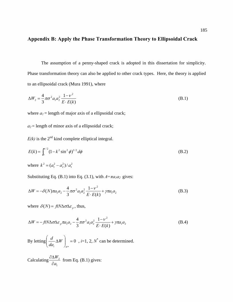
185
Appendix B: Apply the Phase Transformation Theory to Ellipsoidal Crack
The assumption of a penny-shaped crack is adopted in this dissertation for simplicity.
Phase transformation theory can also be applied to other crack types. Here, the theory is applied
to an ellipsoidal crack (Mura 1991), where
)(1
34 2
221
22 kEE
aaW⋅−
=∆νπσ (B.1)
where a1 = length of major axis of a ellipsoidal crack;
a2 = length of minor axis of a ellipsoidal crack;
E(k) is the 2nd kind complete elliptical integral.
∫ −=2/
0
2/122 )sin1()(π
φφ dkkE (B.2)
where 21
22
21
2 /)( aaak −=
Substituting Eq. (B.1) into Eq. (3.1), with A=πa1a2 gives:
21
2221
221 )(
134)( aa
kEEaaaaNW γπνπσπδ +
⋅−
−−=∆ (B.3)
where pftNN εσδ ∆∆=)( , thus,
21
2221
221 )(
134 aa
kEEaaaaftNW p γπνπσπεσ +
⋅−
−∆∆−=∆ (B.4)
By letting 0*
=⎟⎟⎠
⎞⎜⎜⎝
⎛∆
Ni
Wdad , i=1, 2, N* can be determined.
Calculating1
2
aW
∂∆∂ from Eq. (B.1) gives:
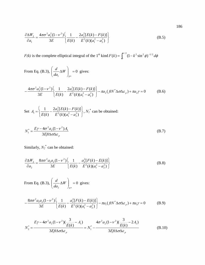
186
⎭⎬⎫
⎩⎨⎧
−−
−−
=∂∆∂
))(()]()([2
)(1
3)1(4
22
21
2
22
222
2
1
2
aakEkFkEa
kEEa
aW νπσ (B.5)
F(k) is the complete elliptical integral of the 1st kind ∫ −−=2/
0
2/122 )sin1()(π
φφ dkkF
From Eq. (B.3), 0*1
=⎟⎟⎠
⎞⎜⎜⎝
⎛∆
N
Wdad gives:
0)())(()]()([2
)(1
3)1(4
2*
222
21
2
22
222
2
=+∆∆−⎭⎬⎫
⎩⎨⎧
−−
−−
− γπεσπνπσ aftNaaakE
kFkEakEE
ap (B.6)
Set ⎭⎬⎫
⎩⎨⎧
−−
−=))(()]()([2
)(1
22
21
2
22
1 aakEkFkEa
kEA , N1
* can be obtained:
pEftAaEN
εσνσγ
∆∆−−
=3
)1(4 12
22
*1 (B.7)
Similarly, N2* can be obtained:
⎭⎬⎫
⎩⎨⎧
−−
−−
=∂∆∂
))(()]()([
)(1
3)1(8
22
21
2
22
221
2
2
2
aakEkEkFa
kEEaa
aW νπσ (B.8)
From Eq. (B.3), 0*2
=⎟⎟⎠
⎞⎜⎜⎝
⎛∆
N
Wdad gives:
0)())(()]()([
)(1
3)1(8
1*
122
21
2
22
221
2
=+∆∆−⎭⎬⎫
⎩⎨⎧
−−
−−
− γπεσπνπσ aftNaaakEkEkFa
kEEaa
p (B.9)
pp Eft
AkE
aN
Eft
AkE
aEN
εσ
νσ
εσ
νσγ
∆∆
−−−=
∆∆
−−−=
3
)2)(
3)(1(4
3
))(
3)(1(4 12
22
*1
12
22
*2 (B.10)

187
For a conservative prediction, we use minimum value of (N1*, N2
*) to obtain the critical cycle
number. From Eq. (B.7) and (B.10),
))(()]()([4
)(1
))(()]()([4
)(12
)(3
22
21
2
22
22
21
2
22
1 aakEkEkFa
kEaakEkFkEa
kEA
kE −−
−=−−
+=− (B.11)
From the definition of ellipsoidal crack and elliptic integral, a1 >a2, F(k)>E(k)> 0, thus
if 1))(()]()([4
22
21
22 <
−−
aakEkEkFa , N1
*<N2*, Eq. (B.7) is used to predict the critical failure cycle number; if
1))(()]()([4
22
21
22 >
−−
aakEkEkFa , N1
*>N2*, Eq. (B.10) is used to predict the critical failure cycle number. It
should be noted that if 21 aa = , the case simplifies to the penny-shaped crack. Phase
transformation theory can be applied to other types of cracks if the corresponding value of 2W∆ is
determined.

188
Appendix C: Considering Electrical Current Effect into Phase
Transformation Model
To include electrical current effect in the proposed phase transformation model for crack
propagation, the energy release rate Ge due to electrical current concentration at the crack tip
needs to be determined. Motivated by the formulation of Thouless et al. (1996), when a crack
propagating near the solder/IMC interface, the stress singularity is characterized by a stress
intensity factor induced by electrical current as:
2/3** )(ˆ
aZZEe
K Sne Ω
−= ηπ
( mMPa ) (C.1)
where a is the crack length; *ηZ and *
SnZ is the effective charge number for IMC and solder,
respectively; e is the electron charge (Coulomb). It should be noted that Thouless’s argument
does not account for void growth, which should be added to the analysis in future research. Eq.
(C.1) is similar to the definition of stress intensity factor for mode I crack, and the effect of
current is included. Thus, the energy release rate due to electrical current is proposed as:
EKG e
e
2
= (J/m2) 21 ν−=
EE for plane strain (C.2)
By considering the energy from electrical current, Eq. (3.7) can be rewritten as:
AGAAWAWWAWW eTba ∆−∆+∆∆+∆∆+∆−∆∆−=∆ γ3121
∆W1a dA/dN + ∆W2 +Ge dA/dN = ∆W1b dA/dN + ∆W3 dA/dN+ γTdA/dN (C.3)

189
The proposed phase transformation model can be applied to predict solder/IMC failure including
electrical current effect based on Eq. (C.4),
eT GWW
dNdA
−∆+∆
=3
2
γ (C.4)
From the deviation of chapter 3, Eq. (C4) can be written as:
eGUJW
dNdA
−+∆
= 2 (C.5)
It should be noted that there are a number of constants in the phase transformation model
which need be determined either from the literature, by computation, or by experiment, further
research works are need to verify the model with available experimental data.

190
Appendix D: Numerical Analysis to Electric Packaging under Drop Impact
The drop impact performance of solder joints in electric packaging is a critical concern of
semiconductor and electronic product manufacturers. This problem is more serious with the
application of lead free soldering, because compared with the traditional SnPb solder alloy, lead
free solder alloy have higher rigidity and lower ductibility. The traditional drop test is high cost
and time consuming, and it is quite difficult to observe the full dynamic responses during the
drop impact. Aim at this problem, the section is focus on numerical analysis of drop impact
effect on BGA packaging with the intention of providing the fundamental understanding required
to design a reliable electric packaging.
Recently, some finite element simulations were carried out on drop impact reliability
study. The dynamic material properties of solder are different from static ones because the
dynamic material properties are dependent on strain rate. The solder constitutive model used in
finite element simulation will affect stress strain behavior of solder significantly. Assuming
solder joints has linear elastic behavior will lead to error predictions. Another method is to
consider rate-dependent bilinear plastic model for Sn/Pb solder in finite element simulation of
drop impact load. However, rate-dependent stress-strain behaviors of SnAgCu lead-free solder
are needed. In this study, finite element modeling and simulation of drop impact were conducted
incorporating UCP constitutive models of lead-free solder comprising elastic and rate dependent
plastic models. The presence of the IMC layer can affect the drop impact response of the solder
joint interface. In this study, the Cu6Sn5 IMC layer was incorported in solder interconnects. A
3D finite element model has been developed to simulate the behavior of ball grid array (BGA)
electronic packaging under drop impact. An impact analysis procedure coupled with
191
submodeling technique in ABAQUS/Explicit under version 6.6.3 was established. Numerical
analyses were performed to understand the physics of failure in board-level drop impact.
Development of Simplified BGA Packaging Model
The finite element model for the electronic packaging has been developed as shown in
Fig. D.1. The silicon die and substrate is connected with representative lead –free solder arrays
(6×6 matrix). The solders are protected by the underfill (epoxy) materials, and the whole
package is protected by mold compound. Table D.1 gives the material prosperities used in the
finite element model (NIST database 2002). Unified creep and plasticity (UCP) model as
introduced in Chapter 2 is adopted to predict the plastic and creep behavior of solder joints.
192
solder joint
mold compound
substrate
underfillsilicon die
2.2
42.02.5
5.53.0
3.0
38.0
3.02.52.5
3.0
20.0
20.0
2.0
1.5
1.8
3.0
193
Figure D. 1 Schematic of the simplified packaging model (unit: mm)
Table D. 1 Material properties used in the finite element model (NIST database 2002)
Density × 10-3 (g/mm3)
Young Modulus (GPa)
Poisson’s Ratio
Thermal Expansion Coefficient
(/°C)
Temperature (°C)
2.33 162 0.23 2.8e-6 0 2.33 150 0.23 2.8e-6 50 Silicon
die 2.33 140 0.23 2.8e-6 100 7.50 44.8 0.37 2.4e-5 0 7.50 43.2 0.37 2.4e-5 20 7.50 36.8 0.37 2.4e-5 100
Solder
7.50 34.5 0.37 2.4e-5 130 Cu6Sn5 8.28 96.9 0.309 1.63e-5 25
1.0 10 0.333 2.31e-5 25 1.0 9.7 0.329 2.31e-5 50 1.0 8.1 0.306 2.31e-5 125 Underfill
1.0 7.0 0.296 2.31e-5 150
A periodic temperature load has been applied to the package firstly; since the packaging
is a symmetric structure, the von Mises stress distribution of one quarter of the package and the
solders is shown in Fig. D. 2.
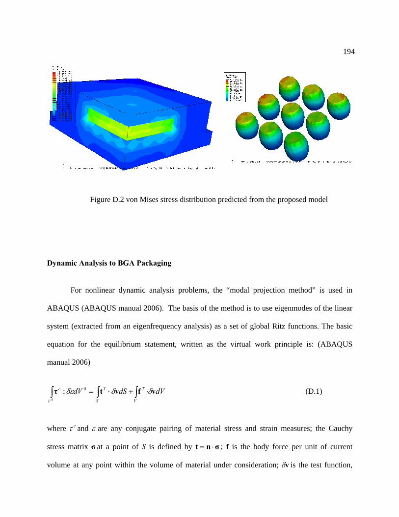
194
Figure D.2 von Mises stress distribution predicted from the proposed model
Dynamic Analysis to BGA Packaging
For nonlinear dynamic analysis problems, the “modal projection method” is used in
ABAQUS (ABAQUS manual 2006). The basis of the method is to use eigenmodes of the linear
system (extracted from an eigenfrequency analysis) as a set of global Ritz functions. The basic
equation for the equilibrium statement, written as the virtual work principle is: (ABAQUS
manual 2006)
dVdSdVV
T
V S
Tc vfvtτ δδδε ∫∫ ∫ ⋅+⋅=0
0: (D.1)
where cτ and ε are any conjugate pairing of material stress and strain measures; the Cauchy
stress matrix σ at a point of S is defined by σnt ⋅= ; f is the body force per unit of current
volume at any point within the volume of material under consideration; vδ is the test function,
195
which is compatible with all kinematics constraints. t, f, and σ are an equilibrium set, i.e.,
σnt ⋅= , 0)( =+⋅∂∂ fσx
, Tσσ = .
The finite element approximation to equilibrium equation is:
0=−+ NNMNM PIuM && (D.2)
where ∫ ⋅=0
00V
MNNM dVM NNρ , MNM is the consistent mass matrix, ∫=0V
NNI β : 0dVσ ,
IN is the internal force vector, and ∫∫ ⋅+⋅=V
N
S
NN dVNdSNP Ft , PN is the external force vector.
F is externally body force; N is shape function;ρ0 is reference density; V0 is reference volume;
βN is a matrix that depends, in general, on the current position, x, of the material point being
considered. The matrix βN that defines the strain variation from the variations of the kinematic
variables is derivable immediately from the interpolation functions once the particular strain
measure to be used is defined.
The time step depends on the smallest element size in the explicit time integration. In
current research, the element size of model has a large variation for different materials. If the
time step size is set to default, the total solution time will take a few days. It is necessary to use
the mass-scaling technique increasing the minimum time step to shorten the solution time. But a
longer time step will induce negative element volume and imprecise results. For example, some
high frequency components in the dynamic responses can not be carried out by modeling. A
scale factor of 2.0 and a time step size of 2×10⁻² s are applied in current model for ensuring a
stable solution and reducing solution time.
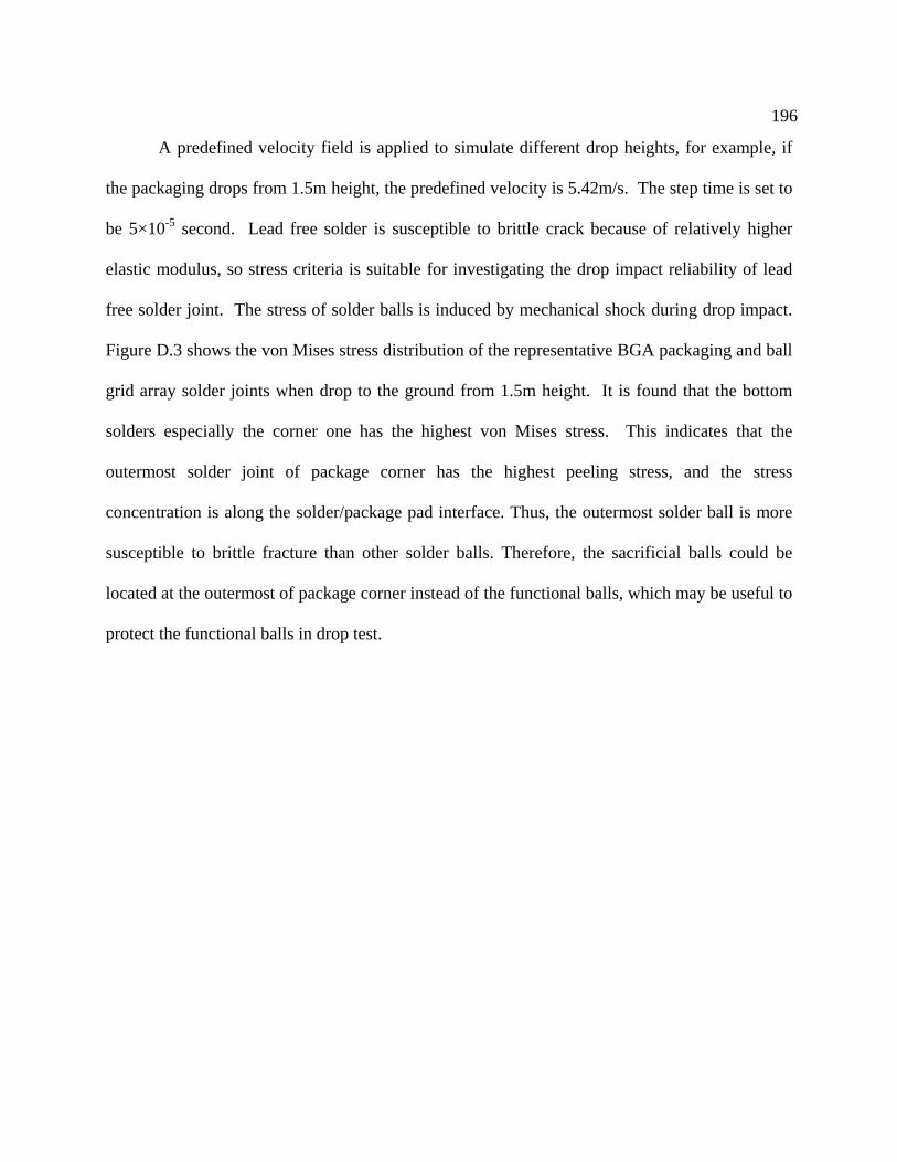
196
A predefined velocity field is applied to simulate different drop heights, for example, if
the packaging drops from 1.5m height, the predefined velocity is 5.42m/s. The step time is set to
be 5×10⁻⁵ second. Lead free solder is susceptible to brittle crack because of relatively higher
elastic modulus, so stress criteria is suitable for investigating the drop impact reliability of lead
free solder joint. The stress of solder balls is induced by mechanical shock during drop impact.
Figure D.3 shows the von Mises stress distribution of the representative BGA packaging and ball
grid array solder joints when drop to the ground from 1.5m height. It is found that the bottom
solders especially the corner one has the highest von Mises stress. This indicates that the
outermost solder joint of package corner has the highest peeling stress, and the stress
concentration is along the solder/package pad interface. Thus, the outermost solder ball is more
susceptible to brittle fracture than other solder balls. Therefore, the sacrificial balls could be
located at the outermost of package corner instead of the functional balls, which may be useful to
protect the functional balls in drop test.

197
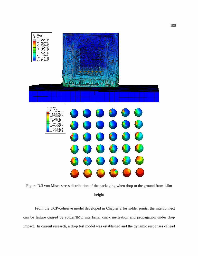
198
Figure D.3 von Mises stress distribution of the packaging when drop to the ground from 1.5m
height
From the UCP-cohesive model developed in Chapter 2 for solder joints, the interconnect
can be failure caused by solder/IMC interfacial crack nucleation and propagation under drop
impact. In current research, a drop test model was established and the dynamic responses of lead
199
free solder joint were studied. The mechanical shock is the main failure mechanism of solder
joint during drop impact. The maximum stress is observed at the outermost corner solder joint.
The susceptible failure location is concluded at the interface between the solder and intermetallic
compound based on the stress criteria. The current model can be used to compare the drop
impact performance of different components and solder alloys, which can be used to guide the
proper selection of component and optimize the layout of BGA electric packing. The results
from the current model can be further applied directly to other sub-models for better analyzing
the actual failure location of solder joints. A drop life evaluation equation of lead free solder
joint based on the normal stress criterion can be further developed. Based on the developed
model, the behavior of electric packaging and different types of solder interconnects under drop
impact can be predicted with corresponding material parameters determined from experiment.
200
VITA
Yao Yao Born on June 27, 1978, Zun Yi, Gui Zhou Province, China
DEGREES
Ph.D. in Structure, Theoretical and Applied Mechanics, Civil and Environmental Engineering,
Northwestern University, Evanston, IL, USA, December 2008
M.S. in Civil Engineering, Nanyang Technological University, Singapore, April 2002
B.S. in Civil Engineering, Tongji University, Shanghai, China, July 1999
PUBLICATIONS
Yao Y., Vaynman S., Keer L.M., and Fine M.E., “Energy Based Micromechanics Analysis on Fatigue Crack Propagation Behavior in Sn-Ag Eutectic Solder”, J. of Electronic Materials, v37, n3,339-346, March, 2008
Yao Y., Fine M.E., and Keer L.M., “An Energy Approach to Predict Fatigue Crack Propagation in Metals and Alloys”, Inter. J. of Fracture, v146, n3, 149-158, Aug., 2007
Yao Y., Fiedler B.A., Keer L.M., and Fine M.E., “Fatigue Crack Propagation Behavior of Sn-Ag-Cu Solder Interconnects ”, submitted to IEEE Trans. on Components and Packaging Technology, 2008 (under review)
Yao Y., Keer L.M., and Fine M.E., “Mechanical and Thermo-Electrical Analysis of Interfacial Failure of Solder Joint”, submitted to ASME J. of Electronic Packaging, 2008 (under review)
Yao Y., Keer L.M., and Fine M.E., “Electromigration Effect on Pancake Type Void Propagation near the Interface of Solder Bulk and Intermetallic Compound”, submitted to J. of Applied Physics, 2008 (under review)
Yao Y., Fiedler B.A., Keer L.M., and Fine M.E., “Electromigration Effect to Void Propagation near the Interface of Solder and Intermetallic Compound” , Proceeding of SRC Techcon conference, Austin, 2008
Fiedler B.A., Yao Y., Vaynman S., Ghosh G., Keer L.M., and Fine M.E., “Pb-Free Solder Joint Fatigue Crack Initiation and Propagation Related to Electrical, Thermal and Mechanical Loading”, Proceeding of SRC Techcon conference, Austin, 2007
Yao Y. and Keer L.M., “Cohesive Zone Modeling and Finite Element Analysis to Intermetallic in Solder Connects”, Proceeding of SRC Techcon conference, Austin, 2007