Growth and structural characterization of epitaxial Cu/Nb multilayers

www.elsevier.com/locate/actamat
Acta Materialia 55 (2007) 5057–5071
Dissolution and interfacial reaction of Nb in contact with themolten 52In–48Sn solder
J.F. Li a,*, S.H. Mannan a, M.P. Clode a, C. Johnston b, A. Crossley b
a Department of Mechanical Engineering, King’s College London, Strand, London WC2R 2LS, UKb Department of Materials, Oxford University, Begbroke Science Park, Sandy Lane, Yarnton, Oxford OX5 1PF, UK
Received 20 April 2007; received in revised form 15 May 2007; accepted 17 May 2007Available online 5 July 2007
Abstract
The dissolution and interfacial reaction of Nb in contact with the molten 52In–48Sn solder has been investigated in the temperaturerange 192–260 �C for periods ranging up to 1 year. Intermetallic compounds (IMCs) grow at the interface between the Nb and the solder,after a latency time required for Nb to diffuse in the solder, and these have been identified by X-ray diffraction as NbSn2 hexagonal plate-let crystals, with a highly preferred orientation. The crystal sizes have been found to follow a log-normal distribution and crystal growthbegins first at the corners of the substrate, followed by the edges and then finally in the centre. The Nb/solder system is unusual in thatthe IMC growth is several orders of magnitude slower than observed in other solder–substrate systems, and the limiting size of the IMClayer actually decreases with increasing temperature. A model explaining these observations is presented where the IMC nucleation andgrowth are controlled by diffusion of Nb atoms in the liquid solder. Low meta-stable concentration of Nb at the interface, a criticalsupersaturated concentration of Nb very close to the meta-stable concentration required before the IMC can grow and negligible solidstate diffusion in the IMC are identified as the key factors responsible for the observed kinetics of dissolution and interfacial reaction.� 2007 Acta Materialia Inc. Published by Elsevier Ltd. All rights reserved.
Keywords: Interfaces; Intermetallic compounds; Kinetics; Liquid; Solder
1. Introduction
Electronic assemblies are not normally designed to func-tion reliably outside the temperature range of �40 to+125 �C [1–3]. Technological progress leads to an increas-ing need of electronic assemblies and interconnections tooperate at temperatures above 125 �C, for example in highdensity power assemblies, sensors and control systems inautomotive and aerospace or oil/gas drilling applications[1]. Although many components can function at tempera-tures up to 200 �C, and even up to 250 �C, at least for lim-ited times, conventional interconnect materials, and inparticular the solder joints, are not reliable at elevated tem-peratures [3].
1359-6454/$30.00 � 2007 Acta Materialia Inc. Published by Elsevier Ltd. All
doi:10.1016/j.actamat.2007.05.026
* Corresponding author. Tel.: +44 20 7848 2370; fax: +44 20 7848 2932.E-mail address: [email protected] (J.F. Li).
Two main approaches have been proposed for improv-ing the solder joint reliability of high-temperature electron-ics for operation at temperature above 125 �C. Thestandard approach is to use solder materials with highermelting points than the standard 63Sn–37Pb solder, whichmelts at 183 �C, such as 90Pb–10Sn and 96Sn–4Cu solders[4]. However, these solder joints can still be prone to strainhardening and eventual crack formation, resulting in lossof electrical continuity. An alternative approach is to allowthe solder interconnects to melt, releasing the stresses onthe joint [1,3,5]. The component will be mechanicallyattached to the substrate by an underfill or glob-top. Sur-face tension will ensure that the liquid solder interconnectremains in contact with the terminations on the componentand the substrate, and that electrical contact between themremains unbroken.
A number of scientific and technological issues mustbe addressed for the successful implementation of liquid
rights reserved.

5058 J.F. Li et al. / Acta Materialia 55 (2007) 5057–5071
solder interconnects. These include suitable solder/barriermetal combinations, optimum underfill or glob-top materi-als, stable solder connections subject to thermal andmechanical shocks, as well as applicability to differentassembly geometries, etc. [3,6]. In particular, the role ofthe barrier metal is crucial in such high-temperatureliquid-phase solder interconnects. The barrier layer’s func-tion is to slow down intermetallic compound (IMC) forma-tion between the solder and the substrate; in order formechanical adhesion to develop between the solder andthe contact metallizations, there must be growth of anIMC at the interface, but excessive IMC formation maycause brittle failure [4,7,8].
Among the commercially available lead-free solders, theeutectic 52In–48Sn solder which has a melting temperatureof 118 �C has the lowest melting temperature. In previouswork [3], IMC growth rates and solder/substrate adhesionstrength had been measured for a range of potential barrierlayers, including Ni, Cr, Pt, Ti, V, Nb, Ta and W in contactwith the eutectic 52In–48Sn. Of these, only Nb was foundto have acceptable properties for a high-temperature bar-rier layer to the molten 52In–48Sn solder. It shows bothextremely slow IMC growth rates and good adhesion tothe solder when it is solid. Preliminary results for the inter-facial reaction of Nb in contact with the molten In–Sn sol-der have been reported, including the extremely slow IMCgrowth rate [4] and the preferred growth of the IMC crys-tals at the corner and edge zones of the solid/liquid inter-face [9]. However, the results were limited to fewerexperimental points and/or relatively shorter reaction peri-ods. The crystalline structure of the IMC crystals was notidentified and their size variations were not analyzed.
In the present work, the dissolution and interfacial reac-tion of Nb in contact with the molten 52In–48Sn solder hasbeen further systematically investigated. In addition tomore experimental temperatures, increased experimentalpoints and longer reaction periods, special effort has beendevoted to understanding the extremely slow IMC crystalgrowth rate and the reduction in the limiting thickness ofthe IMC with increasing temperature. This was achievedby developing a theoretical model to fit the experimentaldata of the dissolution and reaction kinetics. In addition,the size variations of the IMC crystals in the different sam-ples were analyzed statistically and their crystalline struc-ture was identified.
Fig. 1. Schematic sample geometry of Nb–solder couple: (a) whole view a
2. Experimental procedures
2.1. Preparation and high-temperature storage of samples
A layer of vacuum-sputtered Nb, varying from 1.3 to2.2 lm in thickness, followed by a layer of 0.2 lm Au,deposited on Si wafer, was chosen as the substrate. Beforeapplication of the In–Sn solder, the substrate was cut intoplates with a surface area of 7 mm · 7 mm. All substrateplates were cleaned using isopropyl alcohol (IPA), acetoneand finally deionized water. Approximately 0.1 ml of 58In–42Sn solder paste (particles of solder, mixed with a liquidflux) was next placed on each of the cleaned substrateplates, using a 2 ml syringe, and then reflowed in air at240 �C for 60 s, resulting in an approximately semi-spheri-cal solder profile with a maximum thickness of 1 mm at thetop of the solder dome. Fig. 1 illustrates the sample geom-etry of the reflowed Nb–solder couples. It should bepointed out that the 0.2-lm-thick Au layer, added to pre-serve the wettability of the Nb layer, was consumed rapidlyin the solder during the reflowing process. Following clean-ing again using IPA, acetone and finally deionized water,the reflowed samples were ready for high-temperaturestorage.
High-temperature storage of the samples was carried outin silicon carbide heated ovens at four temperatures, 192,220, 240 and 260 �C. The storage periods varied from afew hours to over 12 months, depending on the storagetemperature, and plots of crystal size vs. storage time arepresented in Fig. 10 below.
Most of the samples after the high-temperature storagewere taken out of the ovens and naturally cooled downto room temperature with a time of about 2 min. In orderto investigate whether a significant amount of the IMCcrystals formed during cooling stage, the samples storedat 240 �C for 21 h and at 260 �C for 9 h were also cooleddown to room temperature at a rapid cooling rate byquenching the samples in water and a slow cooling rateof about 10 �C min�1.
In addition, in order to detect that how much Nb hadbeen dissolved into the liquid solder during the high-tem-perature storage, the consumed thicknesses of the Nb sub-strate for the samples stored at 240 �C for 21 h and at260 �C for 9 h were monitored by masking part of theNb substrate from the solder using an epoxy adhesive. In
nd (b) cross-sectional view. Note that the dimensions are not to scale.
J.F. Li et al. / Acta Materialia 55 (2007) 5057–5071 5059
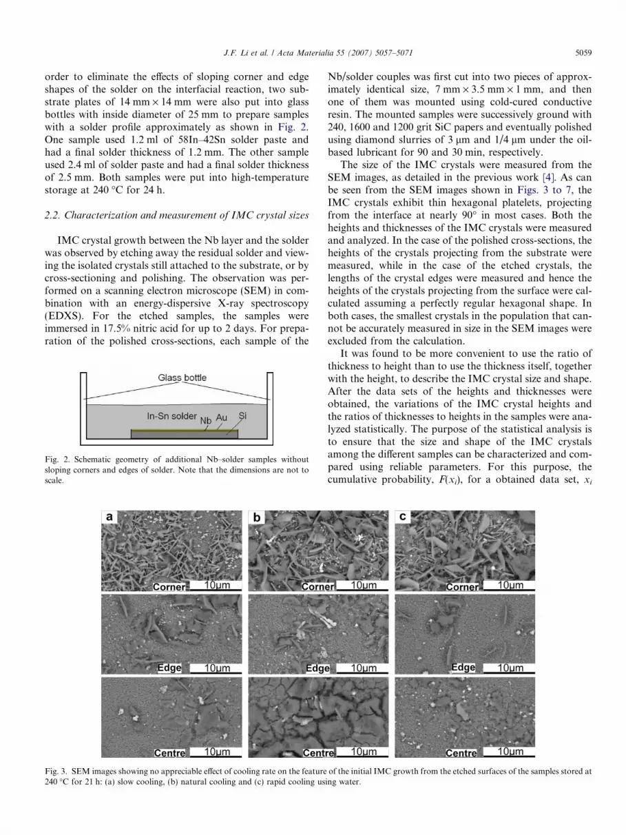
order to eliminate the effects of sloping corner and edgeshapes of the solder on the interfacial reaction, two sub-strate plates of 14 mm · 14 mm were also put into glassbottles with inside diameter of 25 mm to prepare sampleswith a solder profile approximately as shown in Fig. 2.One sample used 1.2 ml of 58In–42Sn solder paste andhad a final solder thickness of 1.2 mm. The other sampleused 2.4 ml of solder paste and had a final solder thicknessof 2.5 mm. Both samples were put into high-temperaturestorage at 240 �C for 24 h.
2.2. Characterization and measurement of IMC crystal sizes
IMC crystal growth between the Nb layer and the solderwas observed by etching away the residual solder and view-ing the isolated crystals still attached to the substrate, or bycross-sectioning and polishing. The observation was per-formed on a scanning electron microscope (SEM) in com-bination with an energy-dispersive X-ray spectroscopy(EDXS). For the etched samples, the samples wereimmersed in 17.5% nitric acid for up to 2 days. For prepa-ration of the polished cross-sections, each sample of the
Fig. 2. Schematic geometry of additional Nb–solder samples withoutsloping corners and edges of solder. Note that the dimensions are not toscale.
Fig. 3. SEM images showing no appreciable effect of cooling rate on the feature240 �C for 21 h: (a) slow cooling, (b) natural cooling and (c) rapid cooling us
Nb/solder couples was first cut into two pieces of approx-imately identical size, 7 mm · 3.5 mm · 1 mm, and thenone of them was mounted using cold-cured conductiveresin. The mounted samples were successively ground with240, 1600 and 1200 grit SiC papers and eventually polishedusing diamond slurries of 3 lm and 1/4 lm under the oil-based lubricant for 90 and 30 min, respectively.
The size of the IMC crystals were measured from theSEM images, as detailed in the previous work [4]. As canbe seen from the SEM images shown in Figs. 3 to 7, theIMC crystals exhibit thin hexagonal platelets, projectingfrom the interface at nearly 90� in most cases. Both theheights and thicknesses of the IMC crystals were measuredand analyzed. In the case of the polished cross-sections, theheights of the crystals projecting from the substrate weremeasured, while in the case of the etched crystals, thelengths of the crystal edges were measured and hence theheights of the crystals projecting from the surface were cal-culated assuming a perfectly regular hexagonal shape. Inboth cases, the smallest crystals in the population that can-not be accurately measured in size in the SEM images wereexcluded from the calculation.
It was found to be more convenient to use the ratio ofthickness to height than to use the thickness itself, togetherwith the height, to describe the IMC crystal size and shape.After the data sets of the heights and thicknesses wereobtained, the variations of the IMC crystal heights andthe ratios of thicknesses to heights in the samples were ana-lyzed statistically. The purpose of the statistical analysis isto ensure that the size and shape of the IMC crystalsamong the different samples can be characterized and com-pared using reliable parameters. For this purpose, thecumulative probability, F(xi), for a obtained data set, xi
of the initial IMC growth from the etched surfaces of the samples stored ating water.

Fig. 4. SEM images showing no appreciable difference of Nb thickness in the sample rapidly cooled down to room temperature using water after the high-temperature storage at 260 �C for 9 h between (a) the reacted part and (b) the protected part.
5060 J.F. Li et al. / Acta Materialia 55 (2007) 5057–5071
(i = 1,2, . . . ,n), of the IMC crystals could be calculatedfrom placing the data in ascending order and letting
F ðxiÞ ¼i� 0:5
nð1Þ
where n is the total number of data points and i is the ithorder in ascending data set [10]. Then these experimentalcumulative density functions of probability can be fittedto the theoretical functions of probability to analyze thestatistical characteristics. In this work, both the normaland log-normal distributions were tested and compared,and their cumulative density functions of probability aregiven as Eqs. (2) and (3), respectively [11].
F ðxÞ ¼Z
1
rffiffiffiffiffiffi2pp e�
ðx�lÞ2
2r2 dx ð2Þ
F ðln xÞ ¼Z
1
rln
ffiffiffiffiffiffi2pp e
�ðln x�llnÞ2
2r2ln d ln x ð3Þ
where F(x) or F(lnx) is the cumulative probability, x is arandom variable (here x is either the height or the ratioof thickness to height for the IMC crystals), l and r arethe mean and standard deviation of random variable x,and lln and rln are the mean and standard deviation ofthe logarithms of x. Thus the cumulative probability curvewill be approximately linear on the normal or log-normalprobability coordinates if a data set follows the normalor log-normal distribution, respectively. The closer to line-arity the cumulative probability curve, the higher the con-fidence that a particular data set follows the particulartheoretical distribution [10,11].
2.3. Crystallographic identification of IMC crystals
In order to identify the crystalline structure of the IMCcrystals, the X-ray diffraction (XRD) spectra were collectedfrom seven selected samples on which the solder had beenetched away. The incident surfaces for the X-ray radiationon these samples were from 4 mm · 5 mm to 7 mm · 7 mm.The experimental conditions of XRD included a Cu target,
operating at 40 kV and 30 mA. The collected data anglesranged from 10� to 130�, with a step size of 0.05� and acounting time of 20 s per step.
Because of the highly preferred orientation of the IMCcrystal growth, typical electron diffraction (ED) spots ofthese crystals were also taken using transmission electronmicroscopy (TEM) to further confirm the crystalline struc-ture identified using XRD. For the TEM observation, afew IMC crystals were carefully removed from one etchedsample that had been stored at 192 �C for 6.5 months usinga knife of stainless steel and dispersed on extremely thin Nifoil.
3. Results and discussion
3.1. SEM observation of IMC crystal growth and
morphology
At all four storage temperatures, a latency time wasclearly observed before IMC crystal nucleation andgrowth were observed. The latency time decreases withan increase in the storage temperature: approximately550 h at 192 �C, decreasing to approximately 8 h at260 �C. After the latency time, the IMC crystals werefound to grow initially at the corners of the samples,along the interface between the solder and the substrate,spreading towards the edges, and then gradually coveringthe whole interface, for all the samples with the soldershape shown in Fig. 1. From Fig. 3 it can be seen thatthe effect of cooling rate on the feature of the initialIMC growth is negligible. This is unusual and can rea-sonably be ascribed to extremely low saturation concen-tration of Nb in the molten solder. The latter can befurther proved by Fig. 4, where no appreciable differenceof thickness can be detected between the reacted andprotected parts of the Nb substrate in the sample rapidlycooled down to room temperature using water after thehigh-temperature storage at 260 �C for 9 h. Therefore,the observed IMC crystals in all samples have predomi-
J.F. Li et al. / Acta Materialia 55 (2007) 5057–5071 5061
nantly formed during the interfacial reaction between themolten solder and the Nb substrate.
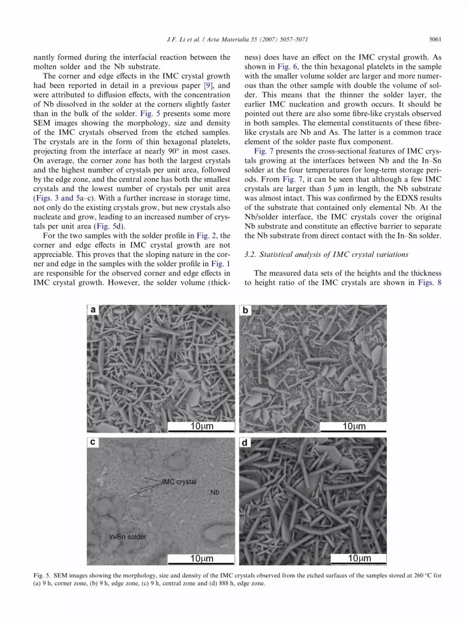
The corner and edge effects in the IMC crystal growthhad been reported in detail in a previous paper [9], andwere attributed to diffusion effects, with the concentrationof Nb dissolved in the solder at the corners slightly fasterthan in the bulk of the solder. Fig. 5 presents some moreSEM images showing the morphology, size and densityof the IMC crystals observed from the etched samples.The crystals are in the form of thin hexagonal platelets,projecting from the interface at nearly 90� in most cases.On average, the corner zone has both the largest crystalsand the highest number of crystals per unit area, followedby the edge zone, and the central zone has both the smallestcrystals and the lowest number of crystals per unit area(Figs. 3 and 5a–c). With a further increase in storage time,not only do the existing crystals grow, but new crystals alsonucleate and grow, leading to an increased number of crys-tals per unit area (Fig. 5d).
For the two samples with the solder profile in Fig. 2, thecorner and edge effects in IMC crystal growth are notappreciable. This proves that the sloping nature in the cor-ner and edge in the samples with the solder profile in Fig. 1are responsible for the observed corner and edge effects inIMC crystal growth. However, the solder volume (thick-
Fig. 5. SEM images showing the morphology, size and density of the IMC cry(a) 9 h, corner zone, (b) 9 h, edge zone, (c) 9 h, central zone and (d) 888 h, ed
ness) does have an effect on the IMC crystal growth. Asshown in Fig. 6, the thin hexagonal platelets in the samplewith the smaller volume solder are larger and more numer-ous than the other sample with double the volume of sol-der. This means that the thinner the solder layer, theearlier IMC nucleation and growth occurs. It should bepointed out there are also some fibre-like crystals observedin both samples. The elemental constituents of these fibre-like crystals are Nb and As. The latter is a common traceelement of the solder paste flux component.
Fig. 7 presents the cross-sectional features of IMC crys-tals growing at the interfaces between Nb and the In–Snsolder at the four temperatures for long-term storage peri-ods. From Fig. 7, it can be seen that although a few IMCcrystals are larger than 5 lm in length, the Nb substratewas almost intact. This was confirmed by the EDXS resultsof the substrate that contained only elemental Nb. At theNb/solder interface, the IMC crystals cover the originalNb substrate and constitute an effective barrier to separatethe Nb substrate from direct contact with the In–Sn solder.
3.2. Statistical analysis of IMC crystal variations
The measured data sets of the heights and the thicknessto height ratio of the IMC crystals are shown in Figs. 8
stals observed from the etched surfaces of the samples stored at 260 �C forge zone.

Fig. 6. SEM images showing the effect of solder thickness on the IMC crystal growth observed from the etched surfaces of the samples with solder profileshown in Fig. 2 and stored at 240 �C for 24 h: (a) solder volume 1.2 ml, solder thickness 1.2 mm, (b) solder volume 2.5 ml, solder thickness 3.0 mm.
Fig. 7. SEM images showing the polished cross-sectional features of the IMC crystals observed from the samples: (c) 192 �C, 2160 h, (b) 220 �C, 4320 h,(c) 240 �C, 5180 h and (d) 260 �C, 888 h.
5062 J.F. Li et al. / Acta Materialia 55 (2007) 5057–5071
and 9. These show the cumulative probability curves of theheights, x, and the ratios of thicknesses to heights, b, forthe IMC crystals measured from the SEM images shownin Fig. 5, on the normal and log-normal coordinates,respectively. From the coefficients of correlation of the lin-ear data fittings, it can be seen that the data sets follow thelog-normal distribution better than the normaldistribution.
Since the IMC crystal variations in the samples consis-tently follow the log-normal distribution, a single parame-ter such as the average crystal height can be used tocharacterize the size. Fig. 10 shows the plots of the meanof the crystal heights vs. storage period. Those inFig. 10a are the single curves of the corner, edge and centrezones for the storage temperatures of 260 �C, while those inFig. 10b are the average curves of the corner, edge and

Fig. 10. Plots of mean of IMC crystal height, �r, vs. storage time t. (a) Single curves of the corner, edge and centre zones for the storage temperatures of260 �C; (b) average curves of the corner, edge and centre zones for all the four storage temperatures.
0 2 4 86 100.01
1
10
40
70
95
99.5
9 hrs, corner, R=0.921 9 hrs, edge, R=0.916 9 hrs, centre, R=0.944888 hrs, edge, R=0.947
Cum
ulat
ive
prob
abili
ty (
%)
r (µm)
0.05 0.15 0.25 0.35 0.450.01
1
10
40
70
95
99.5
9 hrs, corner, R=0.9489 hrs, edge, R=0.9709 hrs, centre, R=0.995888 hrs, edge, R=0.980C
umul
ativ
e pr
obab
ility
(%
)
b
a b
Fig. 8. Cumulative probability curves of (a) height, r, and (b) the thickness to height ratio, b, for the IMC crystals measured from the SEM images shownin Fig. 5, on normal coordinates. The R values stand for the coefficients of correlation for the linear data fittings.
0.37 1.00 2.72 7.390.01
1
10
40
70
95
99.5
9 hrs, corner, R=0.997 9 hrs, edge, R=0.993 9 hrs, centre, R=0.990 888 hrs, edge, R=0.992
Cum
ulat
ive
prob
abili
ty (
%)
r (µm)0.06 0.14 0.37
0.01
1
10
40
70
95
99.5
9 hrs, corner, R=0.9979 hrs, edge, R=0.9959 hrs, centre, R=0.991888 hrs, edge,R=0.967
Cum
ulat
ive
prob
abili
ty (
%)
b
a b
Fig. 9. Cumulative probability curves of (a) height, r, and (b) the thickness to height ratio, b, for the IMC crystals measured from the SEM images shownin Fig. 5, on log-normal coordinates. The R values stand for the coefficients of correlation for the linear data fittings.
J.F. Li et al. / Acta Materialia 55 (2007) 5057–5071 5063
centre zones for all the four storage temperatures. It wasfound that the means of the crystal heights measured fromthe etched surfaces were in agreement with those measured
from polished cross-sections of the corresponding samples.This means that the growth rate of the elongated axisapproximately vertical to the interface was essentially equal

10 20 30 40 50 60 70
SnSn
Sn
008
117
260 oC, 888 hrs
Nb240 oC, 64 hrs
240 oC, 2784 hrs
220 oC, 2784 hrs
192 oC, 2784 hrs
192 oC, 1008 hrs
Calculated
Nb
Nb
400
404
206
311
02.1
060
242
6
31.1
151
7
119
313
206
192 oC, 4680 hrs
620
315
008
117
404
400
220
311
115
11300
4 1
11
Inte
nsity
(ar
bitr
ary
units
)
Diffraction angle (o)
Fig. 12. XRD spectra collected from the seven etched samples, togetherwith the calculated spectrum of NbSn2 with random orientations ofcrystals, showing that the IMC crystals in the samples can be identified asNbSn2 with preferred orientation along the [311] direction.
5064 J.F. Li et al. / Acta Materialia 55 (2007) 5057–5071
to that of the elongated axis parallel to the interface foreach of the IMC crystals. From Fig. 10a, it can be seen thatthe crystals on the centre zone are clearly smaller thanthose on the edge and corner zones, and it can be extrapo-lated that the IMC crystals nucleated 2–4 h later at the cen-tre zone than at the corner zone at 260 �C. Fig. 10 alsoshows that once crystal growth is initiated, a stage of rela-tively rapid growth begins, followed by slow growth at allfour storage temperatures. For the 240 and 260 �C samples,a limiting crystal height is observed.
By contrast, the mean of the ratios of thicknesses toheights of the IMC crystals appears independent of thelocation, storage temperature and storage period.Fig. 11a presents the single curves of the corner, edgeand centre zones for the storage temperature of 260 �C,and Fig. 11b presents the average curves of the corner, edgeand centre zones for the storage temperatures of 220, 240and 260 �C, for the mean of the ratios of thicknesses toheights of the IMC crystals with respect to the storage per-iod. In Fig. 11, with the exception of a value of 0.20, theother data are all in the range 0.12–0.17, and most of themare around 0.15. Therefore, it can be concluded that usingthe heights of the IMC crystals alone can reliably charac-terize the average crystal size in the various substrate/solder interface zones, and for varying storage tempera-tures and times.
3.3. XRD and TEM identification of IMC crystals
Fig. 12 presents the XRD spectra collected from theseven etched samples, together with the spectrum ofNbSn2, which is the expected IMC from previous studiesof Nb interacting with liquid Sn [12], calculated using thecrystallographic software PowderCell [13], and the unit-cellconstants and atomic parameters reported by Gomes deMesquita et al. [14]. For the following presentation and dis-cussion, the unit-cell constants and atomic parameters arelisted in Table 1. Despite the absence of some diffractionpeaks for NbSn2, the IMC crystals in these samples can
Fig. 11. Plots of mean thickness to height ratio of IMC crystals, �b, vs. storage ttemperatures of 260 �C; (b) average curves of the corner, edge and centre zon
be identified as NbSn2. Such an identification is in goodagreement with the NbSn2 observed in several studies ofIMC crystal growth between Nb and liquid Sn [7,15,16],and also expected from the morphology of hexagonalplatelets similar to that of CuMg2 [15,17]. The absence of
ime, t. (a) Single curves of the corner, edge and centre zones for the storagees for all the four storage temperatures.

Table 1The unit-cell constants and atomic parameters of NbSn2, space groupFddd (no. 70), reported by Gomes de Mesquita et al. [14]
Unit-cell constants
a (A) b (A) c (A)9.860 5.6477 19.127
Atomic parameters
x y z B (A2)Nb 0 0 0.1268 (0.0001) 0.04SnI 0 0 0.4174 (0.0001) 0.57SnII 0.1687 (0.0002) 0 0 0.34
The values in parentheses are estimated standard deviations.
J.F. Li et al. / Acta Materialia 55 (2007) 5057–5071 5065
some diffraction peaks for NbSn2 can be ascribed to thehighly preferred orientations of the thin hexagonal plateletcrystals shown in Figs. 5 and 7. Compared to the calculatedspectrum of NbSn2 with random orientations of crystals,the IMC crystals preferentially grew along the [311] direc-tion for all the seven samples. The relative intensities of thepeaks for (404), (008), (117) and (206) decreased, and thepeaks for (220), (313) and (115) disappeared. Consideringthat the elongated axes of the thin hexagonal platelet crys-tals have certain angles with the normal of the substrate/solder interface despite projecting from the interface atnearly 90�, it is suggested that the corresponding elongatedaxes are probably along the [100] direction of NbSn2.
In addition to NbSn2, there exist diffraction peaks ofmetallic Nb and Sn for the two samples stored at 192 �Cfor 1008 h and at 240 �C for 64 h, respectively [18]. Thiscan be attributed to the fact that the NbSn2 crystals didnot cover the solder/substrate interface completely at theseshorter storage periods. It is difficult to identify the broad-ened halos centred at the diffraction angle of 26� on thesame two XRD spectra. They may be also associated withthe partial coverage of the NbSn2 crystals on the substrate/solder interfaces.
Fig. 13. (a) TEM image and (b) corresponding ED spots and index for a brorevealing that the crystal is NbSn2 and its short axis corresponds to the c-axis
ED further confirmed that the IMC crystals can be iden-tified as NbSn2. Fig. 13 shows a TEM image and the cor-responding ED spots and index for a broken plateletcrystal removed from the sample stored at 192 �C for4680 h. The ED spots are in good agreement with thoseof the [001] zone for NbSn2 and hence reveal that the shortaxes of the thin hexagonal platelet crystals correspond tothe c axis of NbSn2. Thus, it can be concluded thatalthough c is the largest among the three unit-cell constantsof NbSn2, the crystals grew the slowest along the [001]direction among the various crystalline directions duringthe high-temperature storage of the samples.
Fig. 14 illustrates the structure of NbSn2 viewed approx-imately along the [100] direction, drawn using the unit-cellconstants and atomic parameters listed in Table 1. For thecrystal growth along the [001] direction, there must beaccumulation and growth of the layers of pure Sn andNb atoms on the previously formed (00 1) plane of theNbSn2 crystals. This generally requires relatively higheractivation energy and may be the reason why the crystalsgrew the slowest along the [001] direction.
3.4. Kinetic model of dissolution and interfacial reaction
In a previous paper [4], a mathematical model wasdeveloped to explain the reported data of the IMC crystalheights at 192 and 240 �C. However, the model was basedon a uniform concentration distribution of Nb within thebulk of the molten solder. It cannot explain the observedcorner and edge effects in the IMC crystal growth shownin Fig. 5. In the present work, the model is modified to takeaccount of these effects. The model includes further exper-imental data points at 240 �C, and new results at 220 and260 �C. In addition, it is also adapted to predict the limitingcrystal height observed in Fig. 10 as a function oftemperature.
ken platelet crystal removed from the sample stored at 192 �C for 4680 h,.

Fig. 14. Structure of NbSn2 viewed approximately along the [100]direction, drawn using the unit-cell constants and atomic parameters listedin Table 1.
5066 J.F. Li et al. / Acta Materialia 55 (2007) 5057–5071
For simplicity, we assume that the crystals are all of thesame size, are distributed uniformly across the substrateand are orientated in the same direction. This allows usto consider just the growth of a single crystal, in contactwith an area A0 of substrate. The parameter A0 can be esti-mated by either counting the number of crystals per unitarea or by data fitting as presented below. The fact thatnew crystals are constantly being nucleated should resultin a lower value for A0, while the fact that the crystalsare not in reality evenly spaced should raise the A0 value,but these effects are ignored in the present model. The sim-plified geometry of the model is sketched in Fig. 15.
Fig. 15 shows a crystal which has grown to a height r
above the substrate, having a thickness br. From measure-ments of crystal thickness, we find that b � 0.15 (correctedfrom the value of 0.10 given in Ref. [4]). The supersatu-rated concentration of Nb must be above a critical value,hereafter referred to as cs0, before the IMC crystals cannucleate. At the interface between the solid substrate andliquid solder, there is a dynamic equilibrium for the con-centration of Nb, which is termed c2. The parameter c2
should not be confused with cs, the equilibrium Nb concen-
Fig. 15. Schematic model geometry of the IMC crystal growth. Note thatthe dimensions are not to scale.
tration between the IMC and the solder, and hence the sat-uration concentration [19]. We now introduce parameterL0, defined as the minimum height of the region adjacentto the substrate where the concentration of Nb, c, exceedscs0 and within which crystals can nucleate and grow. Thishas previously been calculated as twice the critical radiusof a stable crystal aggregate [20]. The height of solderabove the surface is given by h, and the effects of the slop-ing corners and edges can be taken as reduction in h.
Given that the storage experiments are at constant tem-perature, no convective stirring of the liquid solder isexpected to occur. The corner and edge effects in theIMC crystal growth suggest that the initiation of theIMC crystal growth should be diffusion-controlled [9]. Fur-thermore, the solubility of Nb in the molten In–Sn solder isextremely low, and so only the diffusion of Nb is taken intoaccount [4,16]. The one-dimension equation of diffusioncan now be used to derive the governing equation for theconcentration distribution of Nb within the solder as:
ocot� D
o2cox2¼ 0 ð4Þ
with the boundary and initial conditions: c = c2 whenx = 0, oc/ot = 0 when x = h, and c = 0 when t = 0. Herex is the one-dimensional coordinate, D is the diffusivity, c
is the concentration of Nb and t is time. Making use ofthe following definitions:
x0 ¼ xL0
; c0 ¼ cc2
; t0 ¼ Dt
L20
ð5Þ
Eq. (4) can be rewritten in dimensionless form as:
oc0
ot0¼ o
2c0
ox02ð6Þ
with the boundary and initial conditions: c 0 = 1 whenx 0 = 0, oc 0/ot 0 = 0 when x 0 = h/L0, and c 0 = 0 whent 0 = 0. Eq. (6) can be solved numerically using the finitedifference method. Fig. 16 presents the results of Nb
Fig. 16. Nb concentration evolution at the location x0 = l, i.e. x = L0, forthe different dimensionless solder heights h/L0.

100 101 102 103 104 105 106100
101
102
103
104
105
106
107 cso=0.9999c2
cso=0.9c2
cso=0.95c2
cso=0.999c2
cso=0.85c2
cso=0.99c2
Dt 0
/L02
h/L0
Fig. 17. The dimensionless latency times for the various cs0 valuesconsidered as functions of the dimensionless solder height h/L0.
J.F. Li et al. / Acta Materialia 55 (2007) 5057–5071 5067
concentration evolution at the location x 0 = l, i.e. x = L0
for different dimensionless solder heights h/L0. By settingc0 ¼ c0s0, the time t00 at which crystal starts to grow, i.e.the dimensionless latency time, can be obtained. Then thereal latency time, t0, is given by:
t0 ¼t00L2
0
Dð7Þ
In previous work [9], c0s0 was taken as 0.85. In such a case,the observed latency times in Fig. 8 would require the val-ues of the diffusivity of Nb atoms in the molten In–Sn sol-der to be very low, in the order of magnitude of10�15 m2 s�1. Therefore, various values for c0s0 are consid-ered in the present study and the obtained dimensionless la-tency times are presented in Fig. 17 as functions of thedimensionless solder height h/L0.
Theoretically, L0 can be calculated as [20]:
L0 ¼ 2r�0 ¼4rSLv
kT lnðcs0=csÞð8Þ
where r�0 is the critical nuclear radius, rSL is interfacial freeenergy per unit area between the crystal nucleus and the li-quid solder, v is the specific volume in the nuclear, k isBoltzmann’s constant, T is absolute temperature, and cs
is saturation concentration of Nb atoms in the liquid sol-der. However, the values of rSL, cs0 and cs are unknownfor the present In–Sn/Nb system. The maximum valueamong the three unit-cell constants of NbSn2 is very closeto 2 nm (Table 1) and the samples were stored under iso-thermal conditions, generally giving rise to relatively lowratios of cs0/cs. Therefore, L0 may be reasonably assumedto be in the range of tens to a hundred nanometres. Fur-thermore, as a refractory metal, the solubility of Nb inthe liquid In–Sn solder is extremely low and c0s0 may be ta-ken to be very close to 1, e.g. 0.9999. Under the above twoassumptions, Eq. (7) would predict the values of the diffu-sivity of Nb atoms in the molten In–Sn solder in the ordersof magnitude of 10�12 m2 s�1, falling around the lower lim-it of the reported values for many solid metals to diffusivethrough liquid metals [21–23]. For solder heights of103 lm, corresponding to our experimental range (h/L0
around 30,000 in Fig. 17), the effect of h on the latency timeis still appreciable, so that the reduction in h/L0 caused bythe sloping corners and edges leads to the observed de-creased latency time (Eq. (7) and Fig. 17) at corners andedges (Figs. 5 and 6).
After the latency time, the NbSn2 crystal starts to grow.Suppose that Nb atoms that are diffusing through both theliquid solder and the growing solid crystal contribute to thecrystal growth. The rate of increase of r can be expressedas:
drdt¼
kDðA0 � 49br2Þ
r � 49br2
þ acDc
rð9Þ
The first term on the right-hand side represents the contri-bution of Nb atoms diffusing through the liquid solder,where b � 3
ffiffiffi3p
b and k is a parameter associated with geo-
metric correction between the average diffusion distance ofNb atoms through the liquid solder and the crystal height r,and probably also the meta-stable concentration of Nbatoms at the liquid solder/Nb substrate interface. Suchan expression is very similar to one of the equations derivedfor the grain boundary/molten channel controlled growthof IMCs in the systems of Cu and Ni in contact with liquideutectic Sn-based solders [24,25]. However, in the presentwork, the average thickness of the grain boundary andthe average grain size have been replaced by the area of li-quid/solid In–Sn/Nb interface, A0 � 4
9br2, and the area of
the solid/solid NbSn2/Nb interface, 49br2, respectively.
The second term on the right-hand side of Eq. (9) repre-sents the contribution of Nb atoms diffusing through thegrowing solid crystal, where ac is purely a geometricparameter and Dc is the diffusivity of Nb through the solidcrystal.
Eq. (9) is valid until the crystal covers the substrate,when the crystal height is given by
r0 ¼
ffiffiffiffiffiffiffiffi9A0
4b
sð10Þ
When this occurs, the crystal can only grow vertically andthe growth is controlled by the diffusion of Nb atomsthrough the solid crystal as expressed as:
drdt¼ acDc
rð11Þ
The diffusivities for metallic atoms through solid metals aregenerally several orders of magnitude lower than those forthem through liquid metals [21–29]. The experimental re-sults indicate that the IMC crystals have almost stoppedgrowing after the substrate has been covered by crystals.Thus, the diffusion of Nb atoms through the solid crystalcan be neglected. As shown in Fig. 18, r0 appears to be in-versely proportional to the storage temperature, T. Thisrelationship is the same as that between the parameter L0
and T as expressed by Eq. (8). Thus, the parameter L0 is

0.0019 0.0020 0.0021
3.0
4.0
5.0
6.0
7.0
r 0 (µ
m)
1/T (1/K)
Fig. 18. Plot of r0 vs. 1/T.
5068 J.F. Li et al. / Acta Materialia 55 (2007) 5057–5071
proportional to the r0. If we assign a value L0 = 0.02r0,then L0 will be in the expected range of tens to a hundrednanometres and Eq. (7) would predict latency times of 22.7and 23.2 h for the samples stored at 240 �C with solderthicknesses of 1.2 and 2.5 mm, respectively. Such a predic-tion can well explain the observed effect of solder thicknesson the IMC crystal growth as shown in Fig. 6. ThenEqs. (7), (9) and (11) can be simplified to:
0 2000 4000 6000 80000
1
2
3
4
5
Experimental data Eq. (13)
-
192 oC
r (µ
m)
t (hr)
0 1000 2000 3000 4000 50000
1
2
3
4
Experimental data Eq. (13)
-
240 oC
r (µ
m)
t (hr)
a
c
Fig. 19. Data fittings to Eq. (13) for the measured data of the mean IMC
t0 ¼t00r2
0
2500Dð12Þ
drdt¼ kDðr2
0 � r2Þr3
; t > t0 and r < r0 ð13aÞ
drdt¼ 0; otherwise ð13bÞ
Using the experimentally estimated r0 and t0, the diffusivi-ties at the four temperatures are calculated from Eq. (12)and Fig. 17. Eq. (13) governs crystal growth. They aresolved numerically, using a fourth- or fifth-order Runge–Kutta–Fehlberg algorithm. The values of kD for the fourstorage temperatures are obtained by fitting the measureddata of the mean IMC crystal heights in Fig. 10b to Eq.(13). Then values of k are calculated by dividing the valuesof kD by those of D. The predicted curves of IMC growthare shown in Fig. 19, together with the experimental datapoints. It can be seen that the curves fit the experimentaldata very well. All the obtained parameters, r0, t0, D, kD
and k, are listed in Table 2. It should be pointed out thevalues of kD are obtained from direct data fittings to exper-imental results, and can be used for further predictions.However, because of the assumptions in L0 and cs0, the ob-tained values of D, and hence also the values k, can be con-sidered as just reasonable approximations.
0 1000 2000 3000 40000
1
2
3
4
Experimental data Eq. (13)
-
220 oC
r (µ
m)
t (hr)
0 200 400 600 8000
1
2
3
Experimental data Eq. (13)
-
260 oC
r (µ
m)
t (hr)
b
d
crystal heights for: (a) 192 �C, (b) 220 �C, (c) 240 �C and (d) 260 �C.

Table 2Parameters used in the solutions for the kinetic model of dissolution and interfacial reaction
T (�C) t0 (h) h (lm) r0 (lm) D (10�12 m2/s) k (10�6) kD (10�18 m2/s)
192 550 1000 6.4 0.19 0.69 0.13220 168 1000 4.6 0.42 1.85 0.77240 21 1000 3.8 2.20 3.23 7.11260 8 1000 3.1 4.22 4.36 18.40
J.F. Li et al. / Acta Materialia 55 (2007) 5057–5071 5069
The temperature dependence of D and k is furtherexplored using the Arrhenius-type plots by plotting themagainst 1/T on a semi-log graph. This is done in Fig. 20,and we find that the values for both D and k at 192, 240and 260 �C lie on straight lines. The Ea values are theactivation energies calculated from the slopes of the fittedlines. The errors for the derived values indicate the widthsof the 95% confidence limits and were estimated from thelinear regression analysis of the corresponding data fit-tings. The activation energy for D derived from Fig. 20ais 100.4 ± 37.0 kJ mol�1, which is slightly lower thanthe previous estimate for the rate constant of Nb atomsdissolving into the solder (155 ± 25 kJ mol�1) in Ref. [4].In Ref. [4], this rate constant plays the same role in deter-mining the latency time as the present D, as expressed inEq. (12), but the diffusion of Nb in Ref. [4] was notexplicitly modelled. Nonetheless, the present activationenergy for D, 100.4 ± 37.0 kJ mol�1, is somewhat highfor diffusion in the molten solder. The activation energyfor diffusion of Ni in liquid Sn reported in the existing lit-erature is in the range 13–27.6 kJ mol�1 [30]. Note thatthe actual range should be 26–57.3 kJ mol�1 because theauthor used the power law equation where the diffusioncoefficient was defined outside of the time exponent.The activation energy for diffusion of Nb in liquid Al isabout 37.4 kJ mol�1 [21]. The activation energy for k
derived from Fig. 20b is 57.7 ± 11.5 kJ mol�1. This is dif-ferent from that for a similar parameter used in the equa-tion describing grain boundary/molten channel controlledgrowth of IMCs in the systems of Cu and Ni in contact
0.0019 0.0020 0.0021
0.4
1.0
2.7
7.4
-Ea=100.4+37.0 kJ/mol
D (
10-1
2 m2 /s
)
1/T (1/K)
a b
Fig. 20. Arrhenius-type plots of the parameters: (a) D and (b) k listed in Tabl
with liquid eutectic Sn-based solders [24,25]. In the lattercase, the parameter was considered only as a geometricalcorrection factor independent of temperature, and hencehad an activation energy of zero. However, no valuewas given and/or estimated for such a geometrical correc-tion factor in the existing literature [24,25]. In the presentwork, the observed Arrhenius-type plot and the obtainedactivation energy for k are probably associated with theeffect of the meta-stable concentration of Nb at the inter-face between the solid substrate and the liquid solder onthe rate of the IMC growth. The latter can be expectedto have an Arrhenius-type dependence of the temperatureand be in the range of order of magnitude of the k listedin Table 2 [4,16,29]. Therefore, it is reasonable to supposethat there is approximate linear relationship existingbetween the flux of Nb atoms diffusing through the liquidsolder and the extremely low meta-stable concentration ofNb at the interface between the liquid solder and the solidsubstrate.
There are no reports of the latency time and corner andedge effects in IMC crystal growth in a wealth of studies onIMC crystal growth at metallic solid–liquid interfaces[21,29–34]. This may be due to the fact that the cs valueof the refractory Nb metal is much closer to the meta-stableconcentration, cs0, than those of the reported metals, suchas Cu and Ni. Indeed, the cooling rate during the solidifi-cation stage has been found to affect the morphology andfeature of IMC crystals formed between Sn-based solderand Cu and Ni substrates [34,35]. In addition, accordingto Eq. (13), the extremely slow IMC growth in the present
0.0019 0.0020 0.0021
1.0
2.7
7.4
-Ea=57.7+11.5 kJ/mol
k x
106
1/T (1/K)
e 2 for the developed kinetic model of dissolution and interfacial reaction.

5070 J.F. Li et al. / Acta Materialia 55 (2007) 5057–5071
work is probably related to the low meta-stable concentra-tion of Nb atoms at the Nb/In–Sn interface, c2.
Examining the 240 and 260 �C results in Fig. 18, it isclear that the rate of crystal growth reduces to zero atthe longest storage times, and in particular that there isno evidence of growth proportional to
ffiffitp
, as might beexpected from continued IMC growth due to transport ofatoms through the solid IMC layer itself [21]. Extremelyslow diffusion through the IMC is thought to be responsi-ble for this effect. Previous work [4] found that at 170 �CNb–Sn crystals began to form sometime between 17 and28 weeks. Using the D value extrapolated from Fig. 20aand the r0 value extrapolated from Fig. 18, we obtain alatency time of 22 weeks at this temperature, giving furtherconfidence in the mathematical model for the system,despite the approximations made. In order for strong adhe-sion between the substrate and the solder to develop, theremust be some IMC crystals existing at the interface.The model expressed by Eq. (13) and Fig. 17 also predictsthat the latency time will reduce as the thickness of the sol-der layer reduces, so that for a typical 100 lm thick solderjoint at 260 �C the latency time should be only around42 min.
The present interfacial reactions were carried out atconstant temperature. Practical applications of the tech-nology will involve thermal cycling between elevated tem-peratures where the solder is molten and the lowertemperatures where the solid is in solid state. Because ofdecreased diffusion of atoms, the interfacial reactionswould slow down at lower temperatures in both the liquidand solid states. From the point of view of practical appli-cation, suitable underfill or glob-top materials that aresurrounding the solder joints are also crucial. This isbecause any defect, e.g. voids or small delaminations, inthese surrounding materials may allow the molten solderto flow into it by capillary action [36]. This could depletethe solder joint, resulting in an open circuit, or form abridge between adjacent joints, leading to a short circuit.Another issue is possible oxidation of the solder joints atelevated temperature to form a brittle crust. Experimentshave, however, shown that the oxide layer is undetectableby SEM even when the In–Sn/Nb system has been storedat 240 �C for over 1 year.
4. Conclusions
The dissolution and interfacial reaction of Nb in contactwith molten 52In–48Sn solder has been systematicallyinvestigated, at temperatures of 192, 220, 240 and 260 �Cfor periods of several hours up to over 1 year. Based onthe results obtained, the following conclusions can bedrawn:
(1) A latency time was observed before the interfacialreaction started to occur. This latency time is causedby the time required for the Nb in the solder to reachsupersaturated concentration.
(2) After the latency time, the IMC crystals grow initiallyaround the corners of the interface between the solderand the substrate, spreading towards the edges, andthen gradually covering the whole interface. Thecooling rate during the solidification stage of the sam-ples has no appreciable effect on such corner and edgeeffects in IMC growth. The IMC crystals exhibit thinhexagonal platelets, and grow extremely slowly. Theirheights and ratios of thicknesses to heights fit a log-normal distribution more closely than a normaldistribution.
(3) Once crystal growth is initiated, a stage of relativelyrapid growth begins, followed by a slower growthstage, as the Nb–solder interface is gradually cov-ered by the IMC layer, cutting off the supply ofNb into the solder. A higher storage temperatureresults in a higher nucleation density and a smallerlimiting size of the IMC crystals. However, the meanratio of crystal thickness to height is constant atabout 0.15, independent of the localized zone ofthe interface, storage temperature and storageperiod.
(4) The IMC crystals can be identified as NbSn2, withhighly preferred orientation along the [311] direction.Both the XRD and TEM results indicate that one ofthe elongated axes of the IMC crystals is probablyalong the a-axis and the short axis corresponds tothe c-axis of NbSn2.
(5) The original analytical model based on dissolutionof Nb atoms within the liquid solder has been mod-ified to take into account of the corner and edgeeffects in the IMC growth. The main modificationhas been to explicitly model the diffusion of Nbatoms in the liquid solder, rather than assuming thatdiffusion time scales are negligible compared to crys-tal growth. The corner and edge effects observedduring IMC growth are attributed to diffusion ofNb in the solder, allowing it to accumulate morerapidly at the corner and edge zones than at the cen-tre, where the height of the solder is larger. A valueof cs0 for Nb very close to c2 at the interface isresponsible for the observed latency time, and hencealso the corner and edge effects. With the low meta-stable concentration of Nb atoms at the Nb/In–Sninterface, c2 is the main factor that causes the slowIMC growth.
(6) The latency time decreases with increasing storagetemperature, from 550 h at 192 �C down to about8 h at 260 �C. This result provides practical guidancefor the pre-treatment of the Nb/In–Sn solder inter-connects to ensure IMC formation and hence adhe-sion between the solder and substrate when thesolder is solid. The model also predicts that thelatency time will reduce as the thickness of the solderlayer reduces, so that for a typical 100 lm thick sol-der joint at 260 �C, the latency time should be onlyaround 42 min.

J.F. Li et al. / Acta Materialia 55 (2007) 5057–5071 5071
Acknowledgements
This research was funded by the Engineering and Phys-ical Science Research Council (Grant Ref. GR/S87478/01),in collaboration with Loughborough University, DynexSemiconductor Ltd., Schlumberger, TWI Ltd., HenkelTechnologies and Oxford Applied Technology Ltd.
References
[1] Nowottnick M, Pape U, Wittke K, Scheel W. In: 2003 SMTAinternational conference proceedings, Chicago, IL; September 23–262003. p. 693.
[2] Lea C. Global SMT & Packag 2004;4(3):6.[3] Mannan SH, Clode MP. IEEE T Adv Packag 2004;27:508.[4] Mannan SH, Clode MP, Dagher M. J Electron Mater 2005;34(2):125.[5] Keelere R. EP&P 1989;29(6):14.[6] Smith JW. US Patent 5808874; 1998.[7] Chen HS, Bacon DD, Law HH, Kammlot GW, Wu TC. J Mater Res
1995;10:2870.[8] Werder DJ, Chen CH, Chen HS, Bacon DD. J Mater Res
1995;10:2988.[9] Li JF, Mannan SH, Clode MP. Appl Phys Lett 2006;88:104105.
[10] Peterlik H. J Mater Sci 1995;30:1972.[11] Li JF, Ding CX. J Mater Sci Lett 1999;18:1591.[12] Studnitzky T, Schmid-Fetzer R. Z Metallkde 2002;93:894.[13] Kraus W, Nolze G. PowderCell for Windows Version 2.4. Available
from: http://www.ccp14.ac.uk/tutorial/powdcell/.
[14] Gomes de Mesquita AH, Langereis C, Leenhouts JI. Philips ResRepts 1963;18:377.
[15] Toffolon C, Servant C, Sundman B. J Phase Equilib Diff 1998;19:479.[16] Schadler HW, Rosenbaum HS. J Metals 1964;16:97.[17] Haussermann U, Simak SI, Abrikosov IA, Johansson B, Lidin S. J
Am Chem Soc 1998;120:10136.[18] Patankar SN, Froes FH. Solid State Sci 2004;6:887.[19] Mannan SH, Clode MP. Soldering & Surf M Tech 2004;16(3):31.[20] Richardson CB, Snyder TD. Langmuir 1994;10:2462.[21] Dybkov VI. Growth kinetics of chemical compound layers. Cam-
bridge: Cambridge International Science Publishing; 2001. p. 135.[22] Ghosh G. Acta Mater 2001;49:2609.[23] Suzuki S, Kraatz KH, Frohberg G. Ann NY Acad Sci 2004;1027:169.[24] Ghosh G. J Appl Phys 2001;88:6887.[25] Schaefer M, Fournelle RA, Liang J. J Electron Mater 1998;27:1167.[26] Borg RJ, Dienes GJ. An introduction to solid state diffusion. San
Diego (CA): Academic Press; 1988. p. 80.[27] Bhatt YJ, Kumar L, Patil RV, Kale GB, Garg SP. J Alloys Compd
2000;320:177.[28] Du Y, Chang YA, Huang B, Gong W, Jin Z, Xu H, et al. Mater Sci
Eng A-Struct 2003;363:140.[29] Kang SK, Ramachandran V. Scripta Metall 1980;14:421.[30] Ellis TG, Wilhelm HA. J Less-Common Metals 1964;7:67.[31] Lee BJ, Hwang NM, Lee HM. Acta Mater 1997;45:1867.[32] Prakash KH, Sritharan T. Acta Mater 2001;49:2481.[33] Young BL, Duh JG. J Electron Mater 2001;30(7):878.[34] He M, Lau WH, Qi G, Chen Z. Thin Solid Films 2004;462–
463:376.[35] Yoon JW, Kim SW, Jung SB. J Alloys Comp 2006;415:56.[36] Chung S, Tang Z, Park S. IEEE Trans Adv Packag 2007;30(1):38.
Copyright © 2022 FDOKUMEN