A More Practical Method of Predicting Flip Chip Solder Bump Electromigration Reliability
6
A More Practical Method of Predicting Flip Chip Solder Bump Electromigration Reliability Shiguo(Richard) Rao Vitesse Semiconductor Corp. 741 Calle Plano, Camarillo, CA 93012, USA [email protected] Abstract The study of flip chip solder bump electromigration reliability is mainly on daisy chain test structures on small test die that was subjected to high temperature and current density. Then an electromigration design rule is established based on the results on the test structures. However, for the big die flip chip BGA package, the actual electrical and thermal mechanical stress conditions of solder bumps are much more complicated and also vary with many factors such as the bump location, underfill properties and the shape of Cu traces on the package substrate, etc. These factors have significant effects on the bump failure mode and lifetime. Simply applying the design rule established on test structures may lead to a wrong or more optimistic reliability prediction. In this paper, a more practical method of predicting solder bump electromigration reliability was proposed by considering the major stress factors solder bumps will see in actual flip chip package in field application. The solder bump migration study was performed on a big die flip chip BGA package by considering the effects of temperature, thermal mechanical stresses for different bump location and pad structure and current crowding, etc. Multi level Finite Element Analysis (FEA) simulation was performed based on a multi physics electromigration model considering the current, temperature gradient, stress gradient and atomic density effects. The testing was performed on a super big flip chip BGA package by supplying different electrical currents to solder bumps. The migration induced bump failure was detected by electrical testing, non destructive 3D X-ray inspection and destructive cross-section analysis. The simulation results have a reasonably good correlation with the testing results. The predicted lifetime based on the new method shows more conservative and realistic result than the traditional electromigration design rule, particularly for bumps with high mechanical stresses and local current crowding. Based on this study, some practical recommendations are also made to optimize the package design and material selection to improve the solder bump electromigration reliability. Introduction Electromigration is a phenomenon of mass transport in metallization structures when the metallization is stressed with high electrical current density. This mechanism was first reported mainly for metal interconnects. The Time to Failure (TTF) is dependent on the current density and temperature, known as Black’s model in Equation 1. (1) Where J is the current density; T absolute temperature; Ea thermal activation energy and n the current density exponent. The demand of higher current densities increases as the electronics industry continues to scale down to smaller geometry while requiring more functions and higher performance. This causes electromigration failures not only in integrated circuit (IC) interconnects but also in solder bumps connection die to package substrate. Tu and his co-workers [1- 2] have done many theoretical and experimental studies and reviews of solder bump electromigration failure mechanisms. JEDEC [3] has published a guideline for characterizing solder bump electromigration under constant current and temperature stress. The test structures proposed include a single bump and multiple bumps daisy chain structures. The resistance of the bump electromigration structure is measured using a 4-point measurement technique with the measurement points as close to the bump as possible. The device is considered to have failed when its resistance change (either absolute value or percent increase) reaches a predetermined value. In daisy chains, alternate bumps are stressed with current flowing in opposite directions. There is a difficulty in separating failures from each current direction without detailed failure analysis. This shortcoming can be addressed with a structure which contains multiple bumps in one direction of current flow and one bump in the other direction. Figure 1 shows a typical daisy chain structure widely used to do the solder bump electromigration testing and then establish flip chip package design rule for maximum bump carrying current. The test is typically performed at high bump current density and temperature. Then the Black’s model in Equation 1 is used to establish the maximum bump current by extrapolating the testing conditions to operating conditions. The maximum bump current is dependent on the maximum allowable failure rate and target lifetime. Since Black’s model only considers temperature and current density effects, it is more applicable to a device level test structure. The solder
-
Upload
independent -
Category
Documents
-
view
4 -
download
0
Transcript of A More Practical Method of Predicting Flip Chip Solder Bump Electromigration Reliability

A More Practical Method of Predicting Flip Chip Solder Bump Electromigration Reliability
Shiguo(Richard) Rao
Vitesse Semiconductor Corp.
741 Calle Plano, Camarillo, CA 93012, USA
Abstract
The study of flip chip solder bump electromigration
reliability is mainly on daisy chain test structures on small test
die that was subjected to high temperature and current density.
Then an electromigration design rule is established based on
the results on the test structures. However, for the big die flip
chip BGA package, the actual electrical and thermal
mechanical stress conditions of solder bumps are much more
complicated and also vary with many factors such as the bump
location, underfill properties and the shape of Cu traces on the
package substrate, etc. These factors have significant effects
on the bump failure mode and lifetime. Simply applying the
design rule established on test structures may lead to a wrong
or more optimistic reliability prediction.
In this paper, a more practical method of predicting solder
bump electromigration reliability was proposed by considering
the major stress factors solder bumps will see in actual flip
chip package in field application. The solder bump migration
study was performed on a big die flip chip BGA package by
considering the effects of temperature, thermal mechanical
stresses for different bump location and pad structure and
current crowding, etc.
Multi level Finite Element Analysis (FEA) simulation was
performed based on a multi physics electromigration model
considering the current, temperature gradient, stress gradient
and atomic density effects. The testing was performed on a
super big flip chip BGA package by supplying different
electrical currents to solder bumps. The migration induced
bump failure was detected by electrical testing, non
destructive 3D X-ray inspection and destructive cross-section
analysis. The simulation results have a reasonably good
correlation with the testing results. The predicted lifetime
based on the new method shows more conservative and
realistic result than the traditional electromigration design
rule, particularly for bumps with high mechanical stresses and
local current crowding.
Based on this study, some practical recommendations are
also made to optimize the package design and material
selection to improve the solder bump electromigration
reliability.
Introduction
Electromigration is a phenomenon of mass transport
in metallization structures when the metallization is stressed
with high electrical current density. This mechanism was first
reported mainly for metal interconnects. The Time to Failure
(TTF) is dependent on the current density and temperature,
known as Black’s model in Equation 1.
(1)
Where J is the current density; T absolute
temperature; Ea thermal activation energy and n the current
density exponent.
The demand of higher current densities increases as
the electronics industry continues to scale down to smaller
geometry while requiring more functions and higher
performance. This causes electromigration failures not only in
integrated circuit (IC) interconnects but also in solder bumps
connection die to package substrate. Tu and his co-workers [1-
2] have done many theoretical and experimental studies and
reviews of solder bump electromigration failure mechanisms.
JEDEC [3] has published a guideline for characterizing
solder bump electromigration under constant current and
temperature stress. The test structures proposed include a
single bump and multiple bumps daisy chain structures. The
resistance of the bump electromigration structure is measured
using a 4-point measurement technique with the measurement
points as close to the bump as possible. The device is
considered to have failed when its resistance change (either
absolute value or percent increase) reaches a predetermined
value. In daisy chains, alternate bumps are stressed with
current flowing in opposite directions. There is a difficulty in
separating failures from each current direction without
detailed failure analysis. This shortcoming can be addressed
with a structure which contains multiple bumps in one
direction of current flow and one bump in the other direction.
Figure 1 shows a typical daisy chain structure widely
used to do the solder bump electromigration testing and then
establish flip chip package design rule for maximum bump
carrying current. The test is typically performed at high bump
current density and temperature. Then the Black’s model in
Equation 1 is used to establish the maximum bump current by
extrapolating the testing conditions to operating conditions.
The maximum bump current is dependent on the maximum
allowable failure rate and target lifetime. Since Black’s model
only considers temperature and current density effects, it is
more applicable to a device level test structure. The solder

bumps in actual flip chip BGA package, particularly for
bumps at corners of big die are more a structure rather than a
device. It has very complex thermal mechanical stresses and
current distribution. All these factors may significantly affect
the actual electromigration performance.
IC designers use the design rule based on JEDEC
structures to check the maximum bump current density, but
there are very few work has been done to verify the
effectiveness of such design rule for big flip chip BGA
package in field application.
Figure 1. JEDEC Type of EM Test Structure
In this study, a test structure was built in a real
functional ASIC design and put along the die edge. The failure
of the structures can be detected by automated electrical
testing of the device. The testing results show that the actual
electromigration lifetime at die corner and edge is much
shorter than the lifetime from design rule that was based on
simple test structure and Black’s model. Considering the
structure effects on bumps in the real package, a multi physics
migration model was used to predict the bump migration
lifetime. The simulation results gives the time to void
initiation instead of fully open or resistive open. In order to
better understand how package structure/material effect the
bump lifetime, further simulations have been performed by
changing the underfill property, bump material and Cu trace
shape. Finally, some recommendations were made for
designing big die flip chip packages.
Test Vehicle and Results
The test vehicle is a super big flip chip BGA package
with a single big Si die. It is a real functional part with very
high speed data inputs and outputs. The solder bump material
is SnPb and electroplated. There are multiple bump migration
test structures placed on the die edge and corner so they will
experience the worst case thermal mechanical stress. The
failure of solder bump, i.e., opens or resistive open can be
detected when testing the high speed performance.
The rectangular in Figure 2 represents one high speed
output functional block that contains one bump migration test
structure and high speed circuits. The failure of a structure
only affects the output performance of this specific functional
block but not others.
Figure 2. Bump Layout and Migration Test Structures
Besides the high speed electrical testing of the failure
bumps, a non destructive 3D X-ray was also tried to detect the
failure mode. Figure 3 shows the 3D images of several bumps
at one stress time. 3a is a bump that is part of the high speed
circuit but not under migration test. 3b is a bump in middle of
edge under stress that shows void initiation at the neck of
solder bump and 3c is a die corner bump under stress that
shows a bigger void.
3a 3b 3c
Figure 3. 3D X-Ray Inspection of Solder Bumps
When a failure is detected by electrical testing, cross-
section was performed to understand the failure mode. Figure
4 shows the bump failure mode and extent of failure for
different types of solder bumps. 4a is a bump with minimal
current but part of the high speed circuit. 4b and 4c are both
the stressed bumps in the middle of die edge and 4d is the die
corner bump that is fully cracked and detectable by electrical
testing.
4a 4b 4c 4d
Figure 4. Cross-section Images of Solder Bumps
For most of the failing parts, the first bump failure
occurs at or near the die corner while very few occur in the
middle of die edge. All the failures are plotted in a Weibull
distribution plot in Figure 5. The time to failure is for every
single part tested instead of single bump. Based on the number
of test structures on every part, the failure rate was converted
into failure probability per bump instead of per part so that we
can compare the TTF on actual FCBGA with the TTF

established from simple test structure. The comparison was
summarized in Table 1.
ReliaSoft Weibull++ 7 - www.ReliaSoft.com
Probability - Weibull
Time, (t)
Un
re
lia
bilit
y, F
(t)
x 2
x 3
x 2
x 3x 2
x 3x 3
x 3x 2x 2x 3
x 3
Probability-Weibull
Figure 5. Weibull Distribution Plot
Table 1: Comparison of TTF between Testing and Design
Rule
Normalized
Time to
0.1%
Failure
t0.1%
Based on Testing
on big FCBGA
Design Rule Based
on Simple Test
Structure
1.0 2.1
The preliminary results show that the demonstrated lifetime of
a solder bump in FCBGA is much shorter than that measured
on simple test structure. It is suspected that the bumps in BGA
package have multiple complex stresses that accelerate the
migration failure.
Simulation
Simulations are performed to better understand how
other stresses affect the solder bump migration mechanisms.
There are some efforts attempting to predict the
electromigration failure and to evaluate the lifetime through
modeling. Dalleau and Zaage [4-5] developed the finite
element model for in interconnects with mass continuity
equation, which considers three mechanisms including the
electromigration, the thermo-migration and the stress-
migration. There are many other researchers also studied the
atomic flux divergence (AFD) method based on finite element
models. However, the accuracy of the AFD method is always
an issue. Tan et al.[6] found that the conventional atomic flux
divergence formulation is not accurate in the predicting void
nucleation site in a very thin film structure. In fact, due to the
coupled multiphysics character of EM and the challenges to
get the divergence of stress and atomic flux gradients, it is
extremely difficult to predict the exact location of EM induced
void nucleation and to simulate the subsequent void evolution
in a solder joint. In this study, we use a new methodology
developed by Jing, et al [7] of predicting void generation and
Time to Failure (TTF). This methodology is developed based
on discretized weighted residual method (WRM) in a user-
defined finite element analysis (FEA) framework to solve the
local EM mass continuity equation with the variable of atomic
density. The local iteration procedure of the EM governing
equation for the atomic concentration redistribution and its
time step scheme are developed and discussed. Then the local
solution of atomic concentration is incorporated in the
multiphysics environment for electrical, thermal and stress in
both sub-model and global model. Both the sub-model and the
global model FEA algorithms based on the multiphysics
platform of ANSYS® are developed to combine all the
coupled fields and the information from the local atomic
concentration finite element solution by WRM. This new
method considers the current density, atomic density gradient
migration, stress-migration and thermal-migration. Liang L.H.,
et al [8] has used this new method to simulate the solder bump
migration.
The solder bump migration is a diffusion process
which is controlled by the mass continuity equation. In this
simulation, the electromigration formulation of a bump in
structure is driven by the effects of the electron wind force,
stress gradients, temperature gradients, and the atomic density
gradient. The time dependent evolution equation of a local
atomic density in a solder bump can be written as in equation
2:
(2)
Where
c: atomic density;
k: Boltzmann constant;
e: electron (electrical charge unit);
Z*: effective charge;
T: absolute temperature;
D: diffusity; D= D0 exp (-Ea/kT)
r: resistivity;
J: current density
Q*: specific heat of transport;
W: atomic volume;
Ea: activation energy;
sm: local hydrostatic stress.
Figure 6 is the cross-section of the package. The solder bump
under this simulation connects the Si die to the package
substrate.

Figure 6. Package Construction
Figure 7 is a quarter of the global model that consists of
flip chip BGA package mounted on a printed circuit board. A
heatsink is attached on top of the package.
Figure 7. A Quarter of Global FEA Model
Figure 8 is sub model that is cut out from the global
model.
Figure 8. FEA Sub Models
Figure 9 shows the actual shape and dimensions of the solder
bumps in this simulation. All materials and their thermal,
mechanical and electrical properties are summarized in table
2. Figure 10 shows the typical simulation results of the bump
under testing. It includes the current density distribution,
bump temperature distribution, hydrostatic stress and
displacement distribution. It also shows where the voids are
initiated.
Figure 9. Geometry of Solder Bump
Table 2: Materials Properties
Figure 10. Simulation Results
As stated before, the only parameter that determines the
void initiation is the normalized atomic density. Figure 11
shows the actual normalized atomic density and the void
initiates when normalized atomic density reaches 0.95, i.e.,
95% of the original atomic density.
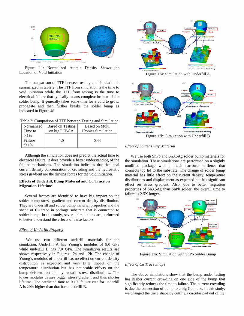
Figure 11: Normalized Atomic Density Shows the
Location of Void Initiation
The comparison of TTF between testing and simulation is
summarized in table 2. The TTF from simulation is the time to
void initiation while the TTF from testing is the time to
electrical failure that typically means complete broken of the
solder bump. It generally takes some time for a void to grow,
propagate and then further breaks the solder bump as
indicated in Figure 4d.
Table 2: Comparison of TTF between Testing and Simulation
Normalized
Time to
0.1%
Failure
t0.1%
Based on Testing
on big FCBGA
Based on Multi
Physics Simulation
1.0 0.44
Although the simulation does not predict the actual time to
electrical failure, it does provide a better understanding of the
failure mechanisms. The simulation indicates that the local
current density concentration or crowding and the hydrostatic
stress gradient are the driving forces for the void initiation.
Effects of Underfill, Bump Material and Cu Trace on
Migration Lifetime
Several factors are identified to have big impact on the
solder bump stress gradient and current density distribution.
They are underfill and solder bump material properties and the
shape of Cu trace in package substrate that is connected to
solder bump. In this study, several simulations are performed
to better understand the effects of these factors.
Effect of Underfill Property
We use two different underfill materials for the
simulation. Underfill A has Young’s modulus of 9.0 GPa
while underfill B has 7.0 GPa. The simulation results are
shown respectively in Figures 12a and 12b. The change of
Young’s modulus of underfill has no effect on current density
distribution as expected and very little impact on the
temperature distribution but has noticeable effects on the
bump deformation and hydrostatic stress distributions. The
lower modulus causes bigger stress gradient and thus shorter
lifetime. The predicted time to 0.1% failure rate for underfill
A is 20% higher than that for undedrfill B.
Figure 12a: Simulation with Underfill A
Figure 12b: Simulation with Underfill B
Effect of Solder Bump Material
We use both SnPb and Sn3.5Ag solder bump materials for
the simulation. These simulations are performed on a slightly
modified package with a much narrower stiffener that
connects top lid to the substrate. The change of solder bump
material has little effect on the current density, temperature
distributions and displacement as expected but has significant
effect on stress gradient. Also, due to better migration
properties of Sn3.5Ag than SnPb solder, the overall time to
failure is 2.5X longer.
Figure 13a: Simulation with SnPb Solder Bump
Effect of Cu Trace Shape
The above simulations show that the bump under testing
has higher current crowding on one side of the bump that
significantly reduces the time to failure. The current crowding
is due the connection of bump to a big Cu plane. In this study,
we changed the trace shape by cutting a circular pad out of the

Figure 13b: Simulation with Sn3.5Ag Solder Bump
big plane shown in Figure 14. The electrical simulation shows
that the change has no impact on the electrical performances.
Figure 15 shows the simulation results with this new Cu trace
shape together with Sn3.5Ag bump material. It clearly
indicates a very uniform current density and a smaller stress
gradient compared to the results in Figure 13b. By changing to
the new Cu trace shape, the time to failure increased by 1.5X.
Figure 14: New Cu Trace Shape
Figure 15: Simulation Results with New Cu Trace and
Sn3.5Ag Bump Material
Conclusions and Discussions
This study shows that the solder bump electromigration
lifetime in actual package could be much different from the
that based on JEDEC test structures. Multi physics simulations
reveal that the interactions of bumps with packaging materials
and the Cu trace shape on package substrate could
significantly affect the demonstrated lifetime in package.
The multi physics simulation in this study predicts the time
to void initiation only but not the time to electrical failure.
However, it does provide a clear understanding about the
failure mechanisms and how various factors could affect the
lifetime.
The current solder bump migration design rule is based on
the simple test structure that in most cases does not represent
the complex structural stresses of bumps in actual package.
The current design rule may potentially lead to under designs
of solder bump reliability. Based on the results in this study, it
is recommended that a more robust and practical design rule
should be established on an actual FCBGA package instead of
simple test structure.
Acknowledgments
The author gratefully acknowledges the tremendous
supports from his colleagues and management at Vitesse
Semiconductor Corp, Moses Chan, Max Helix, Silvia Gao,
Saidur Rahman, Alfredo Restrivera and Roy Carew. Special
thanks to Professor Lihua Liang at Zhejiang University of
Technology and Jack Kasahara at Xradia for their supports in
simulation and 3D X-Ray imaging.
References
[1] Tu, K. N., 2003, “Recent Advances on Electromigration in
Every-Large-Scale-Integration of Interconnects,” J. Appl.
Phys., 94(9), pp. 5451–5473.
[2] Korhonen, M. A., Borgesen, P., Tu, K. N., and Li, C. Y.,
1993, “Stress Evolution Due to Electromigration in Confined
Metal Lines,” J. Appl. Phys., 73(8), pp. 3790–3799.
[3] JEDEC JEP154, 2008, “Guideline for Characterizing.
Solder Bump Electromigration under Constant Current and
Temperature Stress”
[4] Dalleau, D., and Weide-Zaage, K., 2001, “Three-
dimensional Voids Simulation in Chip-level Metallization
Structures: A Contribution to Reliability Evaluation,”
Microelectron. Reliab., 41(9–10), pp. 1625–1630.
[5] Weide-Zaage, K., Dalleau, D., and Yu, X. B., 2003,
“Static and Dynamic Analysis of Failure Locations and Void
Formation in Interconnects Due to Various Migration
Mechanisms,” Mater. Sci. Semicond. Process., 6(1–3), pp.
[6] Tan, C. M., and Roy, A., 2006, “Investigation of the Effect
of Temperature and Stress Gradients on Accelerated EM Test
for Cu Narrow Interconnects,” Thin Solid Films, 504(1–2),
pp. 288–293.
[7] Jing, J. P., Liang, L. H., and Guang, M., 2010,
“Electromigration Simulation for Metal Lines,” ASME J
Electron. Packag., 132(1), pp. 1–7. 85–92.
[8] Liang, L.H., Zhang, Y. X., Liu Y., 2011, “Prediction of
Electromigration Failure of Solder Joints and Its Sensitivity
Analysis” Journal of Electronic Packaging, September, Vol.
133.