A Critical Review on the Electromigration Effect, the ... - arXiv
45
1 A Critical Review on the Electromigration Effect, the Electroplastic Effect, and Perspectives on Effect of Electric Current upon Alloy Phase Stability Yu-chen Liu 1 and Shih-kang Lin 1,2,3,* 1 Department of Materials Science and Engineering, National Cheng Kung University, Tainan city 70101, TAIWAN; 2 Center for Micro/Nano Science and Technology, National Cheng Kung University, Tainan city 70101, TAIWAN; 3 Hierarchical Green- Energy Materials (Hi-GEM) Research Center, National Cheng Kung University, Tainan 70101, TAIWAN *E-mail: [email protected] Abstract The electronic interconnections in the state-of-the-art integrated circuit (IC) manufacturing are scaled down to the micron or sub-micron scale. This results in a dramatic increase in the current density passing through interconnections, so the electromigration (EM) effect plays a significant role in the reliability of products. Although thorough studies and reviews of EM effects have been continuously conducted in the past 60 years, some parts of EM theories lack clear elucidation of the electric current-induced non-directional effects, including the electric current-induced phase equilibrium changes. This review article is intended to provide a broad picture of
-
Upload
khangminh22 -
Category
Documents
-
view
1 -
download
0
Transcript of A Critical Review on the Electromigration Effect, the ... - arXiv

1
A Critical Review on the Electromigration Effect, the Electroplastic Effect, and
Perspectives on Effect of Electric Current upon Alloy Phase Stability
Yu-chen Liu1 and Shih-kang Lin1,2,3,*
1 Department of Materials Science and Engineering, National Cheng Kung University,
Tainan city 70101, TAIWAN; 2 Center for Micro/Nano Science and Technology,
National Cheng Kung University, Tainan city 70101, TAIWAN; 3 Hierarchical Green-
Energy Materials (Hi-GEM) Research Center, National Cheng Kung University,
Tainan 70101, TAIWAN
*E-mail: [email protected]
Abstract
The electronic interconnections in the state-of-the-art integrated circuit (IC)
manufacturing are scaled down to the micron or sub-micron scale. This results in a
dramatic increase in the current density passing through interconnections, so the
electromigration (EM) effect plays a significant role in the reliability of products.
Although thorough studies and reviews of EM effects have been continuously
conducted in the past 60 years, some parts of EM theories lack clear elucidation of the
electric current-induced non-directional effects, including the electric current-induced
phase equilibrium changes. This review article is intended to provide a broad picture of

2
electric current-induced lattice stability change and to summarize the existing literature
on EM-related phenomena, EM-related theoretical models, and relevant effect of the
electroplastic (EP) effect in order to lead to a better understanding of the electric
current-induced effects on materials. This article also posits that EM is either part of
the EP effect or shares the intrinsic electric current-induced plastic deformation
associtated with the EP effect. This concept appears to contribute to the missing parts
of the EM theories.
Keywords: electromigration effect, electroplastic effect, phase stability, electric
current effect

3
Background
Electric current is intimately related to human life. During the past hundred years,
thorough theoretical models have been proposed for the electric current-induced effect,
such as the thermoelectric effect, and the Joule heating effect. Currently, the technology
node of state-of-the-art integrated circuit (IC) manufacturing can be scaled down to the
nano scale. This leads to the interconnections being scaled down to the micron or sub-
nano scale [1-3]. The scaling-down tremendously multi-functionalizes modern
electronic devices, and allows continuous reductions in their feature size. However, the
scaling-down has drawn attention to new effects induced by electric current due to
increases in the current density passing through the interconnections, and resulted in
significant reliability concerns [2, 4-10]. Therein, electromigration (EM) effect has
caused significant reliability concerns in modern industrial electronic devices due to the
formation of voids and hillocks [11], as well as the polarity effect [12, 13]. We call this
EM-induced voids/hillocks formation and polarity effect directional effects because the
atomic diffusion often follows the direction of the electron flow, which results in the
formation of voids and hillocks as well as variations in the interface growth rate on
opposite sites. The existing theories have successfully explained the EM-induced
voids/hillocks formation and polarity effect [14].
Despite the success of EM theories, phenomena induced by electric current that

4
have been found more recently cannot be thoroughly understood using the existing EM
theoretical models [14-16]. For example, electric current is found to induce the alloy
supersaturation effect [17, 18], the non-polarity effect [19], lattice deformation [20-26],
electrorecrystallization [27], and grain rotation [28]. Unlike the voids/hillocks
formation and the polarity effect, these phenomena are found non-directional, which
means the effects do not follow the direction of electron flow and thus cannot be well
explained by the existing EM models. We call them the non-directional effects. The
missing parts of the existing EM theory motivated this article as a review of the existing
literature on EM-related phenomena, EM-related theoretical models, and relevant
electric current-induced effects such as the electroplastic (EP) effect. This study is an
attempt to summarize all the EM- and EP-induced effects under a broad picture of
electric current-induced lattice stability change. To be more specific, the existing
literature either from EM or EP research points out that electric current will induce a
lattice deformation, which is believed to be induced by atomic diffusion in EM and by
the electron-dislocation interaction in EP. Based on the literature, an idea is proposed
herein suggesting that either EM is part of the EP effect or shares the intrinsic electric
current-induced plastic deformation induced by the EP effect. This idea may rationalize
the electric current-induced phase equilibria change as well as the non-polarity effect.
First, the existing models for the EM driving force are reviewed, and the missing

5
parts of these models are pointed out. The model of EM occurrence is then reviewed,
where it is pointed out that the occurrence of EM is not only the function of the intrinsic
resistivity property of materials but also that of the strip length, which is the so-called
the Blech effect. The concept of EM-induced stress/deformation (e.g. back stress model)
is introduced to elucidate the occurrence of EM. Early stages (i.e. before EM occurs)
of lattice deformation found in the EM tests is reviewed, and correlations between the
occurrence of EM and the mechanical properties of materials are pointed out. The
relevant EP effect is then reviewed to reveal the intrinsic electric current-induced lattice
deformation. Changes in electric current-induced phase equilibria and interfacial
reactions are reviewed in the final section. Overall in this study, the missing parts of
EM theories are revealed to clearly elucidate the non-directional effects.

6
Theories of the electric current-induced force on ions (driving force for EM)
Generally, the driving force of electromigration comprises two components, one
of which is the direct force Fd from the external electric field causing the columbic
force, and the other of which is the electron wind force Fw. The general equation to
formulate the driving force F of EM can be written as Eq. (1):
𝐹 = 𝐹𝑑 + 𝐹𝑤 = (𝑧𝑑 + 𝑧𝑤)𝑒𝜌𝑗 = 𝑧∗𝑒𝜌𝑗 (1),
where 𝑧𝑑, 𝑧𝑤, 𝑧∗ are the effective charges in the direct force, electron wind force, and
the net force, respectively. 𝑒 is the fundamental charge, 𝜌 is the resistivity, and 𝑗 is
the current density. The effective charge sets the scale of the driving force and is one of
the most important quantity by which to evaluate EM effect since it can be directly
measured via experimental methods [14, 29]. The existing theoretical models tackled a
fundamental understanding of 𝐹𝑑 and 𝐹𝑤 . Thorough reviews on the existing
theoretical models for EM have been provided elsewhere [15, 29-32]. In this section,
we review four representative classic models and recently-proposed models, and
highlight their potential issues.
Semi-ballistic model
Huntington et al. conducted a marker motion experiment in gold under an electric
current, e.g. 30A and 60A, at high temperatures, e.g. 830-1020℃, and proposed the

7
ballistic model for the EM effect [14]. They considered the momentum transfer per unit
time to a point defect in a current-conducting metal. The electrons were considered to
be scattered by the defect alone, which was decoupled from the lattice. The scattering
process took place without the creation or annihilation of phonons. The x-component
of the momentum transfer per unit time per unit volume to the defects 𝑑𝑀𝑥
𝑑𝑡 is shown in
Eq. (2):
𝑑𝑀𝑥
𝑑𝑡= − (
1
4𝜋3)
2
∬𝑚0
ℏ(
𝜕𝐸
𝜕𝑘𝑥′ −
𝜕𝐸
𝜕𝑘𝑥) × 𝑓(𝑘){1 − 𝑓(𝑘′)} 𝑊𝑑(𝑘, 𝑘′) 𝑑𝑘′𝑑𝑘 (2),
where 𝑚0 is the mass of electron, 𝜕𝐸
ℏ𝜕𝑘𝑥 is the group velocity of electron, 𝑓(𝑘) is the
distribution function of electrons in k-space, and 𝑊𝑑(𝑘, 𝑘′) is the transition probability
function per unit time that the electron in state k will jump to state k’ by virtue of its
interaction with the defects. The momentum transfer between the electron and the
defects is the mass times the group velocity. The problem with this model is that it is
only applicable for an isolated defect in free electron gas. In real metals, the
complicated band structure effect should be considered. The other concern is that not
all the momentum lost by the electrons goes to the ion of interest [15]. The momentum
lost may go to the lattice or neighboring scatters. Despite the fact the ballistic model is
not general, it still formulates a pioneer physical picture of the driving force for EM.
Charge polarization model

8
Bosvieux and Friedel proposed a charge polarization model to approach the EM
effect [16]. The charge polarization was more generalized and enabled a number of later
modeling studies [15, 33-36]. Different from the momentum transfer proposed by the
semi-ballistic model, the charge polarization model considered the electron wind force
arising from the perturbed electron density in the vicinity of the bare defect complex,
e.g. the combination of a bare ion with a vacancy in its vicinity. The perturbed electron
density under electric field was assumed to come from two sources: (1) Arising from
the incident electrons scattered by the defect complex, and (2) arising from the
electrostatic electric field, including the polarization response. The general form of the
electron wind force 𝐹𝑤 is therefore formulated as Eq. (3):
𝐹𝑤 = − ∫ 𝛿𝑛(𝑟)𝛻𝑅𝑣𝑜(𝑟 − 𝑅)𝑑3𝑟 (3),
where δ𝑛(𝑟) is the perturbed electron density for any defects to generalize the formula
to a realistic system, and 𝑣𝑜 is the bare potential for the defects. In order to obtain the
δ𝑛(𝑟) , one has to perform the self-consistent calculation to solve the Schrödinger
equation. The total self-consistent potential is shown in Eq.(4):
𝑣𝑡𝑜𝑡𝑎𝑙(𝑟) = 𝑣𝑜(𝑟) + 𝑣𝑠𝑐(𝑟) (4),
where 𝑣𝑜(𝑟) is the bare columbic potential of ion, and 𝑣𝑠𝑐(𝑟) is the screening
potential. The change in the electron density comes from the screening potential term,
𝑣𝑠𝑐(𝑟). The self-consistent total potential and wavefunction is obtained by solving the

9
Schrödinger equation. Once the total electron density is known, the electron density
under perturbation 𝛥𝑛(𝑟) can be obtained by using Eq. (5):
𝑛(𝑟) = 𝑛0(𝑟) + 𝛥𝑛(𝑟) (5),
where n0(𝑟) is the electron density at equilibrium state.
Research has shown that when using the charge polarization model to describe the
case of an isolated ion in electron free gas, the equation for Fw is identical to that in the
semi-ballistic model [15]. The merit of the charge polarization model is that it rests on
the charge density contribution calculation and can avoid disentangling the momentum
transfer between electrons and ions. Despite the fact that the charge polarization model
calculating the electron wind force is shown to be more generalized to realistic systems,
the way Bosvieux and Friedel treated the direct force calculation is not relevant, i.e.
they considered the direct force to be zero since the screening effect exists. This is not
true for alloy systems such as H impurities in metal hosts, i.e. the direct force value is
equal to the valence electron of H multiplied by the electric field [15]. Controversies
exist for how to properly describe the direct force value to this date [37].
Pseudopotential-based model
The way Bosvieux and Friedel treated the individual ion potential 𝑣𝑜(𝑟) was
overrated since the repulsive part necessary to cancel the attractive part of 𝑣𝑜(𝑟) near

10
the ion core was not considered. In order to overcome this problem, Sorbello performed
a pseudopotential-based analysis to calculate the Fw of the EM driving force [38]. In
the pseudopotential method, the potential induced by the core electron and the nuclei is
considered as a unified pseudopotential to simplify the complicated description. The
pseudopotential of an individual bare ion is w0, and the total pseudopotential of the
crystal system is the sum of the individual pseudopotential and the total screened
potential (i.e. 𝑤𝑡𝑜𝑡𝑎𝑙 = Σ𝑤0 + 𝑉𝑠𝑐). Through Eq. (3) to (5), the wind force can then be
resolved.
Despite the fact that the pseudopotential-based analysis proposed by Sorbello can
be generalized more easily to a real system, the model suffers from arbitrary form factor
selection. Metals with a more complicated band structure effect (e.g. d- or f- electron
orbital contributions) will show a huge error range in the effective charge calculation.
For example, the error in the calculated effective charge for Cu ranges from 5.61% to
103%; for Ag, it ranges from 14.04% to 64.91%, and for Au, it ranges from 41.92% to
71.62%. On the other hand, the direct force contribution was assumed to be equal to the
nominal valence of metals multiplied by the electric field. This assumption may not be
universal and again creates controversy. Nevertheless, the analysis done by Sorbello is
viewed as a pioneer work to generalize the calculation of the EM driving force.

11
Korringa-Kohn-Rostoker (KKR) Green’s function
The Korringa-Kohn-Rostoker (KKR) method is one of the first principles
calculation methods that is wave-function-based. Dekker et al. performed the KKR
Green’s function to calculate the electron wind force in pure Al, Cu, Ag, Au, impurities
in Al, impurities in Ag, and some 4d transition metals in [34]. In [35], Dekker et al.
systematically calculated the z𝑤𝑑∗ in face-centered-cubic and body-centered-cubic
metals. In [36], Dekker et al. focused on calculating the Al-alloy systems. The electron
wind force in these studies was treated by using the polarization model shown in Eq.
(3). The alloy system is described with respect to an intermediate system containing a
void as a reference system proposed by Lodder [39] in order to depict the saddle point
of the diffusion process in EM. The results obtained by Dekker et al. appear to be more
precise than those obtained using the previous theoretical approach proposed by
Sorbello, especially when dealing with noble metals (e.g. Cu, Ag and Au) with
complicated band structure. However, a comparison with the experimental data
suggests that a quantitative approach to the effective charge fails in terms of some dilute
alloy systems, e.g. impurities in Ag [34].
Recent-proposed models (Machine learning model)
Recently, Liu et al. performed the machine learning method with an

12
experimentally-determined effective charge (i.e. the parameter that set the scales of the
EM driving force) data as the training data set, in an attempt to build a model to decipher
the effective charge [40]. They found that the effective charge is the function of not
only the electrical conductivity of the system, but the electronegativity, periodic table
column, and number of p valence electrons. Their results were consistent with the
classical understanding but provided far more information related to the effective
charge since the classical methods only suggested the effective charge to be a function
of valence electrons and electrical conductivity (i.e. z∗ = 𝑧𝑑 +𝐾
𝜌(𝑇)). They attempted
to predict technologically-relevant host-impurity pairs, such as impurities across the
periodic table in the host elements of Al, Ag, Au, Cu, Co and Sn, as shown in Figure 1.
Despite the fact that the models seemed to work well, the limitation to the model was
the temperature limit (e.g. at only a homologous temperature of 0.9), the composition
limit (e.g. only binary systems are valid), and the fact that it can only be applied to
metal elements (e.g. non-metal systems such as H may have different underlying
physics). The data set may need further refinement to improve the accuracy and
generalization for further application.

13
Figure 1. z* of impurities in dilute alloys of Al, Ag, Au, Cu, Co and Sn predicted by
the machine learning model. Reprinted with permission from reference [40].
These theoretical models can be well applied to explain EM-induced phenomena
such as the formation of voids/hillocks and the polarity effect since they are all
directional effects. However, in the following sections, it is shown that only applying
the driving force theory for EM cannot explain non-directional phenomena, such as the
Blech critical product, the phase equilibria change under an electric current, and the
non-polarity effect. This suggests that in addition to the diffusion standpoint, other
factors governing EM-induced phenomena exist.

14
EM-induced stress
Blech critical product for EM occurrence and the back stress mechanism
Blech found that the edge drift of Al strips could only be observed beyond a
critical length of the strip under a given current density [41]. The current density
multiplied by the critical length was a constant. This product was called the Blech
critical length-current-density product or the Blech critical product, where a higher
critical product led to more criteria for the occurrence of EM. Blech further found that
the Blech critical product of the Al strip increased if the strip was fully covered by a
SiN layer, as compared to one without a covered layer. The Blech critical product
cannot be well explained by either the semi-ballistic model or the charge polarization
model solely since these models does not include any quantities related to the strip
length ℓ. Blech suggested that beside the fact that an electric current will induce force
to the ions and cause EM, atomic diffusion itself induced by an electric current will also
induce mechanical stress due to atom accumulation before relaxation, which refers to
EM-induced stress. Therefore, a so-called back stress existed with the aid of the covered
layer. When covered, atoms will accumulate at one side (e.g. anode side). Due to the
accumulation of atoms at one side, the vacancy concentration increases at the other side
(e.g. cathode) so that a vacancy concentration gradient is established. The side with
atom accumulation will develop a compressive stress while the other side with vacancy

15
accumulation will develop a tensile stress. Therefore, a back stress gradient forms that
will compensate the EM driving force. The steady-state net flux of diffusion 𝐽 under
electric current is written as Eq. (6) [42]:
𝐽 =𝑁𝐷
𝑘𝑇[𝑧∗𝑒𝜌𝑗 −
𝜕
𝜕𝑥(𝜇𝑎 − 𝜇𝑣)] (6),
where D is the diffusivity, k is the Boltzmann constant, T is the absolute temperature,
z* is the effective charge, 𝜌 is the resistivity, j is the current density, 𝜇𝑎 and 𝜇𝑣 are
the chemical potential of atoms and vacancies, respectively, and x is the distance along
the film in the direction of the electric current. EM-induced atom/vacancy diffusion has
been typically assumed to be deposited at grain boundaries. These atoms/vacancies may
combine with the grain boundary dislocations and induce dislocation climbing that
changes the available lattice sites in the grains (i.e. dislocation climbing is considered
to be the source/sinks of lattice sites). It has been assumed that the time span for the
local equilibrium between the stress state and the vacancy is far shorter than the long
distance diffusion that occurs via grain boundaries. Therefore, Eq. (7) could be
established:
𝜇𝑎 − 𝜇𝑣 = 𝜇0 + 𝛺𝜎𝑛𝑛 (7),
where μ0 is a constant, Ω is the atomic volume, and 𝜎𝑛𝑛 is the stress normal to the
grain boundary. Substituting Eq. (6) with Eq. (7), the steady-state flux J can be written
as Eq. (8):

16
𝐽 =𝑁𝐷
𝑘𝑇(𝑧∗𝑒𝜌𝑗 −
𝑑𝜎
𝑑𝑥𝛺) (8),
when the electric field-induced driving force was totally compensated by the back stress
gradient-induced driving force at steady-state, there was no net flux (i.e. EM ceased),
as shown in Eq. (9)-(10):
𝑧∗𝑒𝜌𝑗 =𝑑𝜎
𝑑𝑥Ω (9),
jℓcr =σΩ
𝑧∗𝑒𝜌 (10),
Eq. (10) is well-known as an equation by which to estimate the Blech critical product
of EM occurrence. Based on Blech critical product Schreiber further derived a so-called
Blech-Schreiber formula to predict the steady-state cathode edge displacement velocity
𝑉, as shown in Eq. (11) [43]:
𝑉 = 𝑉𝑑(1 −𝐿𝑡ℎ
𝐿) = 𝑉𝑑(1 −
𝜎𝑐𝑟Ω
𝑧∗𝜌𝑗𝐿) (11),
where 𝑉𝑑 is the displacement velocity for the strip length toward infinity, 𝐿𝑡ℎ is the
threshold strip length for EM occurrence, 𝐿 is any given strip length, and 𝜎𝑐𝑟 is the
threshold stress for EM occurrence. Despite the fact that debates existed for Eq. (8) to
Eq. (11), which will be discussed in the following sections, the Blech critical product is
currently still very useful for interconnection design in electronic products. Table I
summarizes the critical product of different systems.
Table I. Blech critical product measurement.

17
System Testing
structure
Critical product
(A/cm)
Temperature
(∘𝐂) Reference
Sn Blech structure 1500 63 [44]
Sn-0.7
wt.%Cu Blech structure 500 63 [44]
Sn-3.0
wt.%Cu Blech structure 1580 63 [44]
Sn-1.8
wt.%Ag Solder joint 30 145 [45]
Cu Blech structure 900 to 1600 175 to 275 [46]
Cu
Dual damascene
(processed with a
SiCN cap)
3850±350
3760±220
4010±200
350
300
250
[47]
Cu Dual damascene 3000 250 [48]
Cu Blech structure 1200 to 2400 N/A [49]
Cu Dual damascene 9000 325 [50]
Cu
Single-damascene
(passivated with
nitride/oxide)
3940
3470
2660
295
350
400
[51]
Cu/CNT Blech structure 4800 to 6000 N/A [49]
Al Blech structure 1260 350 [41]
Al Blech structure 901 200 [52]
Al-
0.5wt.%Cu
Two level
structure 5900 210-250 [53]
EM-induced hillocks formation and stress relaxation
Blech suggested that when the compressive stress at the anode side induced by
EM reaches a threshold stress, hillocks will form as the result of stress relaxation.
Nevertheless, Eq. (11) assumes the back stress gradient to be linear along the strip
length at steady-state, the threshold stress 𝜎𝑐𝑟 to be constant, and the maximum
compressive stress to be built up at the very end of the anode. These assumptions made

18
the hillocks form only at a sharp point (e.g. at the anode end), where the threshold stress
was reached. Glickman et al. criticized that this was not consistent with the
experimental observation since hillock formation is generally found to occur over a
finite strip length instead of at a sharp point [54]. Klinger et al. [55] and Glickman et
al. [54, 56] proposed a model to account for hillock formation based on the stress
relaxation mechanism. The key assumptions behind their models consisted of the
followings: (1) The threshold stress 𝜎𝑐𝑟 was dependent on the strip length and current
density (i.e. the strip length of the hillock formation zone depended on the total strip
length and current density), and (2) the relaxation occurred not only via fast dislocation
gliding but required time-dependent dislocation movement (e.g. climbing, diffusional
creep, etc.). Their result experimentally proved that the cathode edge displacement
velocity did not follow Eq. (11) (i.e. a negative deviation existed) at higher current
densities but approximately followed the model they built based on the diffusional
creep mechanism. Even though the authors argued that the threshold stress was
intrinsically related to the creep threshold stress, the correct physics underlying the
threshold stress induced by EM is still not clear.
Theoretical frameworks for EM-induced stress evolution
Even though the aforementioned discussion suggests issues in Eq. (11), the back

19
stress model proposed by Blech is still generally accepted because it is easily
comprehended. More accurate theoretical frameworks based on the back stress model
to simulate EM-induced stress evolution from the transient state to steady state were
further pursued in several works. Kirchheim proposed that when an EM-induced
vacancy diffuses to the grain boundary, it causes a volume change in the grain due to
the relaxation of its neighboring atoms by 𝑓𝛺, where f is a relaxation factor, and 𝛺 is
the atomic volume [57]. Due to the strain induced by the vacancy, a new driving force
induced by the strain gradient for vacancy diffusion at the grain boundary was
established as 𝐽𝜎 = −𝐷𝐶
𝑘𝑇𝑓Ω
𝜕𝜎
𝜕𝑥 , where 𝐶 is the vacancy concentration at the grain
boundary, and 𝜕𝜎
𝜕𝑥 is the stress gradient. The equilibrium vacancy concentration is
formulated as 𝐶𝑒 = 𝐶0𝑒𝑥𝑝 ((1−𝑓)𝛺𝜎
𝑘𝑇) , where 𝐶0 is the equilibrium vacancy
concentration in the absent of stress. The total flux of the vacancy is shown in Eq. (12):
J = −D𝜕𝐶
𝜕𝑥+
𝐷𝐶
𝑘𝑇𝑧∗𝑒𝜌𝑗 −
𝐷𝐶
𝑘𝑇𝑓Ω
𝜕𝜎
𝜕𝑥 (12),
The first term on right hand side of the equation is due to the driving force of
concentration gradient; the second term is due to the electric field, and the third term is
due to the vacancy-induced stress gradient. By introducing the annihilation/production
of vacancy term (i.e. 𝐶−𝐶𝑒
𝜏𝑠, where 𝜏𝑠 is the relaxation time), the numerical solution for
Eq. (12) can be obtained to demonstrate the stress evolution induced by EM.
Korhonen et al. proposed an analytical stress evolution model under EM subjected

20
to a confined metal line [58]. They assumed atoms were transported along the grain
boundary and are predominately deposited at the grain boundaries under electric current.
Following the same assumption made by Blech [42] and Eq. (7), the stress increment
caused by the climbing of the grain boundary dislocations in a confined metal line is
shown as 𝑑𝜎 = −𝐵dC
C , where B is the applicable modulus, and
𝑑𝐶
𝐶 is the relative
change in the available lattice sites due to dislocation climbing. The stress evolution
during EM is thus formulated as Eq. (13):
∂σ
𝜕𝑡=
𝜕
𝜕𝑥[𝐷𝑎𝐵Ω
𝑘𝑇(𝜕𝜎
𝜕𝑥+
𝑒𝑧∗𝜌𝑗
Ω)] (13),
where 𝐷𝑎 is the effective diffusion coefficient of atoms along the grain boundary (i.e.
𝐷𝑎 =𝛿𝐷𝐺𝐵
𝑑, 𝛿 is the grain boundary width, 𝐷𝐺𝐵 is the diffusion coefficient diffusion
coefficient, and d is the grain size. Clement et al. further considered the vacancy
diffusion mechanism and introduced the vacancy annihilation/creation sink/source term
to revisit Korhonen’s model, as shown in Eq. (14) [59]:
∂σ
𝜕𝑡=
𝐷𝑣𝐶𝑣𝐵Ω
𝐶𝑘𝑇[𝜕2𝜎
𝜕𝑥2+ (
Ω
𝑘𝑇
𝜕𝜎
𝜕𝑥+
𝑧∗𝑒𝜌𝑗
𝑘𝑇)
𝜕𝜎
𝜕𝑥 ] (14),
where 𝐷𝑣 is the vacancy diffusion coefficient, 𝐶𝑣 is the equilibrium vacancy
concentration, and 𝐶 is the lattice site concentrations. Clement et al. suggested that
Korhonen’s model is only valid when the EM-induced maximum stress is relatively
small. Park et al. followed Korhonen’s model but further discussed the effect of the
stress on the atomic diffusivity [60]. The stress-dependent diffusivity is shown as D′ =

21
D exp [(Ω
𝑘𝑇+
1
𝐵) σ]. Lloyd summarized the analytical models for evaluating the EM-
induced stress including the thermal stress effect [61]. Sarychev et al. further provided
an analytical model to solve three dimensional EM-induced stress in analog to the
thermal stress [62].
Debates for the models simulating the EM-induced stress evolution
The vital question for models simulating the EM-induced stress evolution is
related to determining how the stress will build up without the external confinement
(e.g. oxide layer, passivated layer, etc.) necessary to help the atoms accumulate. Tu
argued that the back stress model might not be valid for cases of non-covered strips (e.g.
Au) since atom accumulation will be instantly relaxed, and no stress will be induced
[63]. It also might not be valid for cases undergoing surface diffusion (e.g. Cu) since
the atoms accumulating on the surface cannot build stress for the bulk. The boundary
condition of the covered layers seems to make the back stress model and the associated
theoretical frameworks phenomenological and not general to all cases. To be more
specific, this gives rise to five points that are unclear: (1) How will the stress build up
without an external constraint? (2) How will the stress relax (e.g. via dislocation glide,
climb, creep, etc.)? (3) How fast is the stress build-up compared with the stress
relaxation? (4) What is the physics underlying the critical stress that causes electric
current-induced deformation? (5) Is the critical stress a constant, or does it depend on

22
the current density or the strip length?
On the other hand, Eq. (10) suggests that the product is only valid for a short strip
length. Typically, the upper bound (i.e. the threshold) of the EM-induced stress is
considered to be the yield strength (σy) of the material [63]. The yield stress of metals
is generally in the hundred MPa scale. For instance in Al, σy = 110 MPa, Ω =
1.67 × 10⁻²⁹ 𝑚3, 𝑧∗ = −13, 𝜌 = 2.6 × 10⁻⁸ 𝑚Ω , and the typical lower bound of
current density for EM occurrence in Al is 104 𝐴/𝑐𝑚2. Following Eq. (10), the upper
bound for the threshold strip length yields 340 𝜇𝑚, which agrees with the typical strip
length scale used in the experiment [41, 52, 53]. It is likely that above this sub-micron
length scale Eq. (10) would no longer be valid. This seems true in the experimental
observation made by Lin et al, where EM was found to occur in a 2-cm-long Cu strip
subjected to a current density of ca. 7.5 × 10⁵ A/cm2, which corresponds to a critical
product of 1.5 × 10⁶ A/cm. This seems way larger than the conventional observation,
e.g. 900 [46] to 9000 [50] A/cm. This may suggest a missing part exists in the Blech
critical product theoretical framework.

23
EM-induced lattice deformation measurement
A series of in situ synchrotron radiation (SR)-based current stressing experiments
were conducted to gain more insights into the EM-induced stress evolution from
experimentally measuring the lattice deformation under an electric current. The
deformation include lattice strain evolution [20-24], dislocation formation [25, 26, 64-
66], grain rotation [64, 66, 67], and sub-grain formation (i.e. polygonization) [25, 26,
64]. A quantitative study showed the resolved shear stress (based on the FCC metals
slip system) at the location where atoms accumulate (e.g. hillocks were found) to be 10
times larger than at a location without atom accumulation [65]. The location where
atoms accumulate was suggested to have higher dislocation density [65]. Valek et al.
studied the early stage (i.e. before the void/hillock formation induced by EM could be
observed) of crystal plasticity change induced by the electric current of Al, as shown in
Figure 2 [25]. They found very similar results to those in [64], where individual grains
underwent bending induced by the electric current and thereby introduced a preferred-
oriented dislocation formation (a dislocation density of 3 × 10⁹ /cm2) and formation of
small angle grain boundaries in the direction of the electron flow (presumably via
dislocation climbing) before the void/hillock formation. Similar results were suggested
by Budiman et al., who studied Cu at the early stage of an electric current [26], and the
dislocation density was found to be 3 × 10⁹ /cm2.

24
Figure 2. The (222) plane peak profile at different grains along the Al strip subjected
to electric current. Peak streaking, rotation, and broadening were found under electric
current, indicating the plastic deformation at the early-stage of current-stressing.
Reprinted with permission from reference [25].
Here, an effort is made to highlight the experimental works done at the early stage
of EM [24-26], which experimentally suggested that before the void/hillock formation,
crystal plasticity including the dislocation formation was found. A plausible explanation
for these findings was that the plasticity resulted from the stress developed by the
atom/vacancy accumulation, which was discussed in the aforementioned section.
However, how the atom/vacancy accumulation will induce stress without covered
layers is not clear. A more rigid quantitative model and mechanistic study to correlate
the electric current and early-stage stress state is required. Nevertheless, these works

25
provided a different insight suggesting that the way to view EM-induce failures (e.g.
void/hillock formation) is not just a kinetics problem but also involves the mechanical
stress.
An additional insight is that Lin et al. found that voids/hillocks formed at a
homologous temperature of 0.28 under current stressing for 1680 s [24]. Under this
condition, very low kinetics was suggested (i.e. where a surface diffusion coefficient of
10-16 m2/s, an absolute temperature of 373 K, an effective charge of -5.5, resistivity of
1.68 × 10⁻⁸ m·Ω, a current density of 1010 A/m2 yielded a self-diffusion velocity of ca.
0.001 nm/s). From this velocity, it was not possible to find a hillock size of ca. 1 μm
after 1680 s of current-stressing. The classical models for the EM driving force seem to
be missing some aspects of the low kinetics. With an understanding of the electric
current-induced plastic deformation found at the early-stage, one plausible explanation
for this issue is that an electric current will induce dislocation formation. Either the
stress relaxation may result in hillock formation, as shown schematically in Figure 3
[24], or the dislocations may provide a fast diffusion path [25, 26, 64-66]. It is also
likely that a high resistivity location (e.g. grain boundary) may provide local Joule
heating and extra electron wind force that dominates the diffusion process. Overall,
only applying the kinetics perspective seems inadequate to elucidate the observed
phenomenon.

26
Figure 3. Schematic diagram of the stress relaxation induced voids/hillocks formation
subjected to electric current. Reprinted with permission from reference [24].
Correlation between the mechanical properties of materials and EM occurrence
The aforementioned discussions point out that EM will induce mechanical stress
due to atom accumulation/depletion before relaxation occurs. This infers that EM is
likely to be the result of the electric current-induced crystal plasticity. When the stress
reaches a “yield” strength of materials, plastic deformation, including the void/hillock
formation, and crystal plasticity will be found. If this is true, it is then sensible to ask
one question regarding the correlation between EM and mechanical stress - does EM

27
occurrence correlate to a material’s mechanical properties? To be more specific, do
materials with stronger mechanical properties tend to have stronger EM-resistance? The
answer to these questions seem positive when observing what people have done in
regard to enhancing the EM-resistance of materials. For example, (111)-textured face-
centered cubic (fcc) materials have stronger EM-resistance than non-textured ones [10,
68-70], while (111)-textured fcc materials have been found to have a maximum Young’s
modulus compared to other planes. Precipitation of Al2Cu existing in an Al-Cu alloy
was found to have a longer mean time to failure (MTF) [71, 72], and precipitation has
been found to harden materials. EM occurrence was found to be delayed when fully-
covered layers were present, e.g. anodization [73], and passivated layers [50]. These
“rigid walls” may suppress the lattice deformation induced by an electric current.
Therefore, materials are more prone to being retained in the elastic deformation region
[24]. Though one may argue that precipitation or segregation found at the grain
boundary retards EM-induced diffusion [74], the reason for enhancement of EM-
resistivity by textured film, covered film, and the presence of precipitation is not easily
understood via pure diffusion theory. These indirect correlations likely suggest that EM
occurrence is strongly related to the mechanical properties of materials.
Electroplastic (EP) effect

28
The aforementioned discussion suggests that the mechanical stress/mechanical
properties of materials may be one of the key factors that can be used to evaluate the
EM effect, especially when speaking of EM-induced failure such as formation of
voids/hillocks, the Blech effect, EM-induced stress, etc. However, most EM studies
have solely focused on the atomic diffusion aspect (i.e. elucidating the EM-related
phenomena via various diffusion theories). Very few EM studies have provided direct
experimental evidence to prove that EM occurrence is mechanistically related to the
mechanical properties of materials [63, 75]. The very direct correlation between an
electric current and plastic deformation has been found for a related effect called the
electroplastic (EP) effect, which refers to the plastic deformation induced by current
stressing [76-81]. The theoretical EP model is generally accepted as an electron-
dislocation interaction, but this is still being debated up to the present time [79]. The
most well-known phenomenon induced by EP is where the electric current decreases
the flow stress but no change is found in the elastic stress, as shown in Figure 4 [82-
84]. The recrystallization temperature was found to decrease under current stressing (i.e.
to accelerate the occurrence of recrystallization) [85]. The grain size of materials has
been found to be refined under current stressing [86-88]. Even though scientists usually
consider the EP effect to be different from that of EM by suggesting the model for the
EM driving force is merely one way to explain EP (i.e. the local Joule heating is

29
considered as one of the possible mechanisms for EP) [89], it is still very difficult to
separate EM from EP when current-stressing materials. Up to the present time, no
studies have directly proven that these two effects are parallel. Based on our
understanding and the aforementioned discussions, it is likely that EM is part of the EP
effect framework, or EM shares the intrinsic electric current-induced plastic
deformation induced by the EP effect. In this context, the crystal plasticity found in the
early-stage of the current stress is likely to result from the EP effect. EP effect might be
the reason why electric current will induce stress without external covering layer.
Figure 4. The true stress vs. true strain relation of Ti subjected to pulse direct current.
At each pulse, the true stress dropped. Data was taken from [84].

30
Electric current-induced phase equilibria change
Electric current has been found to change the phase equilibria of materials [17, 27,
89-102]. Conrad provided a thorough discussion of phase transformation under an
electric current, including the interfacial reaction, precipitation, crystallization, and
recrystallization of metals [89]. Guan et al. reviewed and discussed the electric current-
induced phase transformation effect [81]. Dolinsky and Elperin discussed the
thermodynamics of phase transition [103] and nucleation [104] under electric current.
They showed that additional work is required to form a nucleation with lower electrical
conductivity. In other words, an additional energy term is added in the Gibbs free energy
change of a given phase transformation due to the change in the current distribution
when a nucleus forms. Jiang et al. performed a thermodynamics analysis of the
dissolution of the beta phase in the Mg-Al-Zn alloy under electric current following
Dolinsky and Elperin’s work, and the analytical results agreed with their experimental
results [18]. Lin et al. used the ab initio-aided CALPHAD method to explain the
supersaturation of Pb-Sn induced by an electric current [105]. The relationship between
compressive stress and current density was empirically established by correlating that
the Sn whisker growth rate was the same under the associated electric current or
compressive stress [106]. The modeling results showed that when the current density is
higher than a critical value of ca. 2.5 × 10⁴ A/cm2, the phase boundaries of the Pb-
31
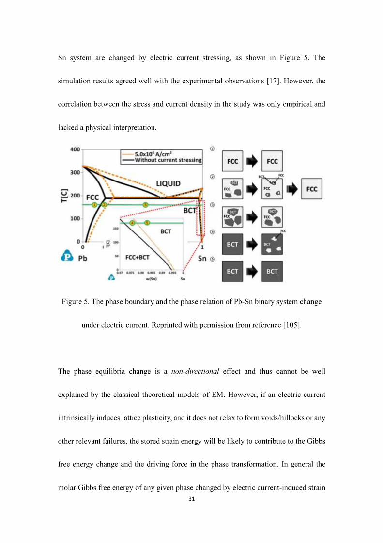
Sn system are changed by electric current stressing, as shown in Figure 5. The
simulation results agreed well with the experimental observations [17]. However, the
correlation between the stress and current density in the study was only empirical and
lacked a physical interpretation.
Figure 5. The phase boundary and the phase relation of Pb-Sn binary system change
under electric current. Reprinted with permission from reference [105].
The phase equilibria change is a non-directional effect and thus cannot be well
explained by the classical theoretical models of EM. However, if an electric current
intrinsically induces lattice plasticity, and it does not relax to form voids/hillocks or any
other relevant failures, the stored strain energy will be likely to contribute to the Gibbs
free energy change and the driving force in the phase transformation. In general the
molar Gibbs free energy of any given phase changed by electric current-induced strain

32
can be described using Eq. (15):
Gm′ = 𝐺 0
𝑟𝑒𝑓 + 𝐺 𝑖𝑑
𝑚 + 𝐺 𝑒𝑥
𝑚 + 𝐺 𝑠𝑡𝑟𝑎𝑖𝑛−𝑒𝑥
𝑚 (15),
where 𝐺 0
𝑟𝑒𝑓, 𝐺 𝑖𝑑
𝑚, 𝐺 𝑒𝑥
𝑚, 𝐺 𝑠𝑡𝑟𝑎𝑖𝑛−𝑒𝑥
𝑚 are the are the reference energy of the
constituent components, and the molar Gibbs free energy, ideal mixing Gibbs free
energy, excess Gibbs free energy due to non-ideal mixing, and excess Gibbs free energy
due to the electric current-induced strain, respectively. Therefore, the addition of the
𝐺 𝑠𝑡𝑟𝑎𝑖𝑛−𝑒𝑥
𝑚 term might result in an abnormal supersaturation phenomenon, and would
also be the origin of the stress introduced to the CALPHAD model proposed by Lin et
al. [105].
Polarized and non-polarized effect
Interfacial reactions are found to be changed by the EM effect [107, 108],
including the polarity and non-polarity effects. In a given reaction couple (e.g. an A/B/A
sandwich structure) forming interface layers (e.g. A/L/B/L/A, where L denotes the
interface layer), the flux of dominant diffusion species a (𝐽𝑎) under a direct electric
current can be denoted as Eq. (16):
𝐽𝑎 = −𝐷𝑎𝑁𝑎
𝑅𝑇(𝑅𝑇
𝜕 ln 𝑁𝑎
𝜕𝑥± 𝑧𝑎
∗𝑒𝐸) (16),
where Na is the mole fraction of species a, and x is the thickness of the interface layer

33
formed at the interface. If the dominant diffusion species a diffuses in the same direction
as the transporting electron flow to form the interface layer, the second term in the
parenthesis on the right hand side of Eq. (16) will be +𝑧𝑎∗𝑒𝐸. If the diffusion direction
is opposite to that of the electron flow, the second term will be −𝑧𝑎∗𝑒𝐸. Eq. (16) clearly
indicates that in the case of the two interface layers in the given A/B/A sandwich
structure under an electric current, one will be enhanced and the other one will be
suppressed comparing to the reaction couple without current stressing. This
phenomenon is called the polarity effect. EM theories of the semi-ballistic model or the
charge polarization model can explain the polarity effect effectively. Table II
summarizes the experimental results for the polarity effect found in several reaction
couple systems.
However, the direct current has also been found to have either no effect on the
growth rate of the interface layers, or to cause a symmetrical enhancement/suppression
of the interface layers at both the cathode and anode side. These results were in contrast
to the usual polarity effect on the asymmetrical growth rate of the interface layers, and
were independent of the electric current direction. Therefore, the phenomenon showing
symmetrical enhancement/suppression of the interface layer under an electric current is
called the non-polarity effect. Eq. (16) then fails to explain the non-polarity effect since
it is a non-directional effect. A series of models was proposed to explain the non-

34
polarity effect, but are plausible [109, 110] and phenomenological [111]. A better
understanding of how investigate the underlying physics of the non-polarity effect is
still being pursued. Table III summarizes the experimental results showing no effects
of a direct current on the interfacial reaction and the results for the non-polarity effect.
It is worth mentioning that AC or a reversing current have also been found to induce
the non-polarity effect, as summarized in Table III.
The non-polarity effect is likely to result from the phase equilibria changed by
electric current. To be more specific, the chemical potential of a given species is
changed by electric current as suggested by Eq. (15). For example, the diffusion-
controlled NiBi3 interface layers at the cathode and the anode side of Bi/Ni reaction
couple were found to be both enhanced under electric current [19]. If the chemical
potential of the NiBi3 phase is changed by the electric current due to the presence of
strain energy, then the chemical potential gradient of the dominant diffusion species
controlling the growth of NiBi3, which is Bi in this case, will be changed simultaneously.
If the chemical potential gradient of Bi is enhanced by the electric current due to the
strain energy, the diffusion velocity of Bi will be enhanced, and the diffusion will be
independent of the direction of the electron flow [112]. Therefore, NiBi3 growth will be
accelerated. This is likely to be true for NiBi3 growth since it is a diffusion-controlled
reaction process (i.e. the reaction between Bi and Ni is fast enough so that the NiBi3

35
phase forms immediately when Bi reaches Ni). In short, it is likely that the non-polarity
effect originates from the change in the electric current-induced phase stability, which
changes the driving force of diffusion in the meantime.
Table II. Summary of the experimental results for the polarity effect found in several
reaction couple systems. Adapted from Ref. [111].
System (Temperature)
Current
density
(A/cm2)
*IMC Growth
Reference Cathode Anode
Sn/Ni (160-200℃) 500 E S [13]
Sn/Ag ( 120-200℃) 500 E S [113]
Sn-3.5wt%Ag/Ni (160-
200℃) 500 E S [114]
Sn-0.7wt%Cu/Ni (160-
200℃) 500 E S [114]
Cu/Sn-3.8wt%Ag-0.7wt%Cu
(180℃) 103 to 104 S E [12]
*E: Enhanced; S: Suppressed.
Table III. Summary of the experimental results showing no effects of direct current
upon the interfacial reaction and results for the non-polarity effect. Adapted from Ref.
[111].
System
(Temperature)
Current density
(A/cm2)
*IMC Growth Reference
Cathode Anode
Sn/Cu (200℃) 500 N N [13]
Zn/Ni
(150,200℃) 300 N N [19]
Bi/Ni (185,200℃) 300 N N [19]
Al/Ni (400℃) 500,1000 E E [109]
Bi/Ni (150-
170℃) 300 E E [19]
Al/Au (400-
500℃) 1000 E E [110]

36
Ni/Ti
(625~850℃) 0 to 2546 E E [115]
Ag/Zn
(300,350℃) 0 to 764 E E [116]
Ni-P/Sn-3.5%Ag 1000 S S [117] $Al/Cu (200-
525℃) 500 to 1300 E E [118]
$Sn/Ag (160℃) 500 E E [119] $Sn/Ni (180-
200℃) 500 E E [119]
*N: No effect; E: Enhanced; S: Suppressed.
$Under alternating current or reversing current.
Conclusion
This review article provides a thorough review on the EM-related phenomena,
especially for non-directional effects, EM-related theoretical models, and the relevant
EP effects. A broad picture of electric current-induced phase stability changes is
proposed, which could complement the missing aspects of the existing EM theories for
the non-directional phenomena. Main concerns in the existing EM theories are
summarized as follows: (1) Although the general picture of the EM theory, i.e., the
charge polarization model, has been established, it is still not fully complete due to the
fact that the zd value cannot be easily simulated; (2) the classical theories are not fully
applicable to explain the non-directional changes of phase equilibria induced by electric
currents; (3) the existing theoretical frameworks were developed based on experiments
with external covers, such as native oxides or passivated layers, so the stress could

37
evolved; however, it is not clear why the stress could be built up without external covers.
The origin of the EM-induced stress and early-stage crystal plasticity is not clear.
By introducing the electric current-induced plasticity, or the EP effect to the EM
effect, the aforementioned electric current-induced peculiar phenomena could be
comprehended. In the case of electric current-induced crystal plasticity, the additional
strain energy could contribute to the changes in Gibbs free energy of phase
transformation. Therefore, the phase stability and interfacial reactions are expected to
be changed by electric currents. The EP effect might also be the reason for early-stage
lattice deformation observed in the EM studies. The missing part of EM theory to
elucidate the non-directional effect is proposed in the review article. Further
investigations for establishing a complete theory for the effect of electric currents upon
materials are needed.

38
Acknowledgement
The authors gratefully acknowledge the financial support from the Ministry of
Science and Technology (MOST) in Taiwan (MOST 103-2221-E-006-043-MY3 and
106-2628-E-006-002-MY3).
Authors’ contributions
Y.C.L collected important papers and made first draft of the article with the
guidance of S.K.L. S.K.L modified and revised for publication. All authors read and
approved the final manuscript.

39
Reference
1. D. Shahrjerdi and S.W. Bedell, Nano Lett., 13(1), 315-320 (2013).
2. K.N. Tu, Y. Liu, and M. Li, Appl. Phys. Rev., 4(1), 011101 (2017).
3. A. Lancaster and M. Keswani, Integration, 60, 204-212 (2018).
4. F.M. d'Heurle, Proc. IEEE, 59(10), 1409-1418 (1971).
5. T. Kwok, Mater. Chem. Phys., 33(3-4), 176-188 (1993).
6. D. Malone and R. Hummel, CRIT REV SOLID STATE, 22(3), 199-238 (1997).
7. D. Pierce and P. Brusius, MICROELECTRON RELIAB., 37(7), 1053-1072 (1997).
8. E.T. Ogawa, K.-D. Lee, V.A. Blaschke, and P.S. Ho, IEEE Trans. Rel., 51(4), 403-419
(2002).
9. K. Zeng and K.-N. Tu, Mater. Sci. Eng., R, 38(2), 55-105 (2002).
10. C.M. Tan and A. Roy, Mater. Sci. Eng., R, 58(1), 1-75 (2007).
11. C.Y. Liu, C. Chen, and K.N. Tu, J. Appl. Phys., 88(10), 5703-5709 (2000).
12. H. Gan and K.N. Tu, J. Appl. Phys., 97(6), 063514 (2005).
13. S.-W. Chen, C.-M. Chen, and W.-C. Liu, J. Electron. Mater., 27(11), 1193-1199
(1998).
14. H.B. Huntington and A.R. Grone, J. Phys. Chem. Solids, 20(1–2), 76-87 (1961).
15. R.S. Sorbello, Solid State Phys., 51, 159-231 (1997).
16. C. Bosvieux and J. Friedel, J. Phys. Chem. Solids, 23(1–2), 123-136 (1962).
17. Y.T. Chiu, C.H. Liu, K.L. Lin, and Y.S. Lai, Scripta Mater., 65(7), 615-617 (2011).
18. Y. Jiang, G. Tang, C. Shek, Y. Zhu, and Z. Xu, Acta Mater., 57(16), 4797-4808
(2009).
19. C.M. Chen and S.W. Chen, J. Electron. Mater., 29(10), 1222-1228 (2000).
20. P.-C. Wang, G. Cargill III, I. Noyan, and C.-K. Hu, Appl. Phys. Lett., 72(11), 1296-
1298 (1998).
21. H. Zhang, G. Cargill III, Y. Ge, A. Maniatty, and W. Liu, J. Appl. Phys., 104(12),
123533 (2008).
22. H.-K. Kao, G.S.C. III, F. Giuliani, and C.-K. Hu, J. Appl. Phys., 93(5), 2516-2527
(2003).
23. K. Chen, N. Tamura, M. Kunz, K.N. Tu, and Y.-S. Lai, J. Appl. Phys., 106(2), 023502
(2009).
24. S.-k. Lin, Y.-c. Liu, S.-J. Chiu, Y.-T. Liu, and H.-Y. Lee, Scientific Reports, 7(1), 3082
(2017).
25. B.C. Valek, N. Tamura, R. Spolenak, W.A. Caldwell, A.A. MacDowell, R.S.
Celestre, H.A. Padmore, J.C. Bravman, B.W. Batterman, W.D. Nix, and J.R. Patel,
J. Appl. Phys., 94(6), 3757-3761 (2003).
26. A.S. Budiman, W.D. Nix, N. Tamura, B.C. Valek, K. Gadre, J. Maiz, R. Spolenak,

40
and J.R. Patel, Appl. Phys. Lett., 88(23), 233515 (2006).
27. Y.-T. Chiu, K.-L. Lin, A.T. Wu, W.-L. Jang, C.-L. Dong, and Y.-S. Lai, J. Alloys Compd.,
549, 190-194 (2013).
28. A.T. Wu, A.M. Gusak, K.N. Tu, and C.R. Kao, Appl. Phys. Lett., 86(24), 241902
(2005).
29. P.S. Ho and T. Kwok, Rep. Prog. Phys., 52(3), 301 (1989).
30. F.M. D'Heurle and R. Rosenberg, Physics of Thin Films, G. Hass, M.H. Francombe,
and R.W. Hoffman, (Amsterdam, Netherlands: Elsevier, 1973), p. 257-310.
31. H. Huntington, Diffusion in solids: recent developments, A.S. NOWICK and J.J.
BURTON, (Amsterdam, Netherlands: Elsevier, 1975), p. 303-352.
32. K.-N. Tu, Solder Joint Technology, K.-N. Tu, (New York, NY: Springer, 2007), p.
211-243.
33. J. van Ek, J.P. Dekker, and A. Lodder, Phys. Rev. B, 52(12), 8794-8800 (1995).
34. J.P. Dekker, A. Lodder, and J. van Ek, Phys. Rev. B, 56(19), 12167-12177 (1997).
35. J.P. Dekker and A. Lodder, J. Appl. Phys., 84(4), 1958-1962 (1998).
36. J.P. Dekker, P. Gumbsch, E. Arzt, and A. Lodder, Phys. Rev. B, 59(11), 7451-7457
(1999).
37. A. Lodder, Defect Diffus. Forum, 261-262, 77-84 (2007).
38. R.S. Sorbello, J. Phys. Chem. Solids, 34(6), 937-950 (1973).
39. A. Lodder, J. Phys. F: Met. Phys., 6(10), 1885 (1976).
40. Y.-c. Liu, B. Afflerbach, R. Jacobs, S.-k. Lin, and D. Morgan, MRS COMMUN, 1-9
(2019).
41. I.A. Blech, J. Appl. Phys., 47(4), 1203-1208 (1976).
42. I.A. Blech and C. Herring, Appl. Phys. Lett., 29(3), 131-133 (1976).
43. H.U. Schreiber, Thin Solid Films, 175, 29-36 (1989).
44. C.C. Wei and C.Y. Liu, J. Mater. Res., 20(08), 2072-2079 (2005).
45. Y. Li and D. Goyal, 3D Microelectronic Packaging: From Fundamentals to
Applications. 1 ed. (New York, NY: Springer, 2017). p. 71-99.
46. R. Frankovic and G.H. Bernstein, IEEE Trans. Electron Devices, 43(12), 2233-
2239 (1996).
47. D. Ney, X. Federspiel, V. Girault, O. Thomas, and P. Gergaud, IEEE Trans. Device
Mater. Rel., 6(2), 175-180 (2006).
48. L. Arnaud, T. Berger, and G. Reimbold, J. Appl. Phys., 93(1), 192-204 (2003).
49. Y. Chai, P.C. Chan, Y. Fu, Y. Chuang, and C. Liu, IEEE Electron Device Lett., 29(9),
1001-1003 (2008).
50. E.T. Ogawa, A.J. Bierwag, K.-D. Lee, H. Matsuhashi, P.R. Justison, A.N.
Ramamurthi, P.S. Ho, V.A. Blaschke, D. Griffiths, A. Nelsen, M. Breen, and R.H.
Havemann, Appl. Phys. Lett., 78(18), 2652-2654 (2001).

41
51. P.-C. Wang and R.G. Filippi, Appl. Phys. Lett., 78(23), 3598-3600 (2001).
52. R. Frankovic, G.H. Bernstein, and J.J. Clement, IEEE Electron Device Lett., 17(5),
244-246 (1996).
53. R.G. Filippi, G.A. Biery, and M.H. Wood, MRS Symp. Proc., 309, 141 (1993).
54. E. Glickman, N. Osipov, A. Ivanov, and M. Nathan, J. Appl. Phys., 83(1), 100-107
(1998).
55. L. Klinger, E. Glickman, A. Katsman, and L. Levin, Mater. Sci. Eng., B, 23(1), 15-
18 (1994).
56. E. Glickman and M. Nathan, Microelectron. Eng., 50(1-4), 329-334 (2000).
57. R. Kirchheim, ACTA METALL MATER, 40(2), 309-323 (1992).
58. M.A. Korhonen, P. Bo/rgesen, K.N. Tu, and C.Y. Li, J. Appl. Phys., 73(8), 3790-
3799 (1993).
59. J.J. Clement and C.V. Thompson, J. Appl. Phys., 78(2), 900-904 (1995).
60. Y.J. Park and C.V. Thompson, J. Appl. Phys., 82(9), 4277-4281 (1997).
61. J.R. Lloyd, Microelectron. Eng., 49(1), 51-64 (1999).
62. M. Sarychev, Y.V. Zhitnikov, L. Borucki, C.-L. Liu, and T. Makhviladze, J. Appl.
Phys., 86(6), 3068-3075 (1999).
63. K.N. Tu, J. Appl. Phys., 94(9), 5451-5473 (2003).
64. B.C. Valek, J.C. Bravman, N. Tamura, A.A. MacDowell, R.S. Celestre, H.A.
Padmore, R. Spolenak, W.L. Brown, B.W. Batterman, and J.R. Patel, Appl. Phys.
Lett., 81(22), 4168-4170 (2002).
65. N. Tamura, R.S. Celestre, A.A. MacDowell, H.A. Padmore, R. Spolenak, B.C.
Valek, N.M. Chang, A. Manceau, and J.R. Patel, Rev. Sci. Instrum., 73(3), 1369-
1372 (2002).
66. K. Chen, N. Tamura, B.C. Valek, and K.N. Tu, J. Appl. Phys., 104(1), 013513 (2008).
67. A.T. Wu, K.N. Tu, J.R. Lloyd, N. Tamura, B.C. Valek, and C.R. Kao, Appl. Phys. Lett.,
85(13), 2490-2492 (2004).
68. H. Shibata, M. Murota, and K. Hashimoto, Jpn. J. Appl. Phys., 32(Part 1, No. 10),
4479-4484 (1993).
69. S. Vaidya and A.K. Sinha, Thin Solid Films, 75(3), 253-259 (1981).
70. M.J. Attardo and R. Rosenberg, IEEE 8th Rel. Phys. Symp., 41(6), 2381-2386
(1970).
71. C. Kim and J.W.M. Jr., J. Appl. Phys., 72(5), 1837-1845 (1992).
72. E.G. Colgan and K.P. Rodbell, J. Appl. Phys., 75(7), 3423-3434 (1994).
73. A.J. Learn, J. Appl. Phys., 44(3), 1251-1258 (1973).
74. X.Y. Liu, C.L. Liu, and L.J. Borucki, Acta Mater., 47(11), 3227-3231 (1999).
75. K.N. Tu, Phys. Rev. B, 45(3), 1409 (1992).
76. H.-D. Nguyen-Tran, H.-S. Oh, S.-T. Hong, H.N. Han, J. Cao, S.-H. Ahn, and D.-M.

42
Chun, INT J PR ENG MAN-GT., 2(4), 365-376 (2015).
77. A.F. Sprecher, S.L. Mannan, and H. Conrad, Acta Metall., 34(7), 1145-1162
(1986).
78. H. Conrad, A. Sprecher, W. Cao, and X. Lu, JOM, 42(9), 28-33 (1990).
79. B.J. Ruszkiewicz, T. Grimm, I. Ragai, L. Mears, and J.T. Roth, J MANUF SCI E-T
ASME, 139(11)(2017).
80. W.A. Salandro, J.J. Jones, C. Bunget, L. Mears, and J.T. Roth, Electrically Assisted
Forming, (Switzerland: Springer, Cham, 2015), p. 255-311.
81. L. Guan, G. Tang, and P.K. Chu, J. Mater. Res., 25(7), 1215-1224 (2011).
82. O.A. Troitskii, Pis'ma Zhurn. Experim. Teor. Fiz., 10, 18-22 (1969).
83. V.I. Spitsyn, O.A. Troitskii, E.V. Gusov, and V.K. Kurdynkov, Izvest. Akad. Nauk,
SSSR, Metallog, 2(123)(1974).
84. K. Okazaki, M. Kagawa, and H. Conrad, Scr. Metall., 12(11), 1063-1068 (1978).
85. H. Conrad, N. Karam, and S. Mannan, Scr. Metall., 17(3), 411-416 (1983).
86. V.L.A. Silveira, R.A.F.O. Fortes, and W.A. Mannheimer, Scr. Metall., 17(11), 1381-
1382 (1983).
87. J.P. Barnak, A.F. Sprecher, and H. Conrad, Scr. Metall., 32(6), 879-884 (1995).
88. Y. Cao, L. He, Y. Zhou, P. Wang, and J. Cui, Mater. Sci. Eng., A, 674(Supplement
C), 193-202 (2016).
89. H. Conrad, Mater. Sci. Eng., A, 287(2), 276-287 (2000).
90. M.-J. Kim, M.-G. Lee, K. Hariharan, S.-T. Hong, I.-S. Choi, D. Kim, K.H. Oh, and
H.N. Han, Int. J. Plast., 94(Supplement C), 148-170 (2017).
91. J.-Y. He, K.-L. Lin, and A.T. Wu, J. Alloys Compd., 619, 372-377 (2015).
92. W.-Y. Chen, T.-C. Chiu, K.-L. Lin, A.T. Wu, W.-L. Jang, C.-L. Dong, and H.-Y. Lee,
Scripta Mater., 68(5), 317-320 (2013).
93. J. Kuang, T.S.E. Low, S.R. Niezgoda, X. Li, Y. Geng, A.A. Luo, and G. Tang, Int. J.
Plast., 87(Supplement C), 86-99 (2016).
94. H. Lv, R. Zhou, L. Li, H. Ni, J. Zhu, and T. Feng, Materials, 11(11), 2220 (2018).
95. V. Stolyarov, ACTA METALL SIN-ENGL, 31(12), 1305-1310 (2018).
96. Y. Jiang, G. Tang, C. Shek, Y. Zhu, L. Guan, S. Wang, and Z. Xu, J. Mater. Res.,
24(5), 1810-1814 (2009).
97. Y. Jiang, G. Tang, C. Shek, and Y. Zhu, Appl. Phys. A, 97(3), 607-615 (2009).
98. Y. Zhu, S. To, W.B. Lee, X. Liu, Y. Jiang, and G. Tang, J. Mater. Res., 24(8), 2661-
2669 (2009).
99. W. Zhang, M. Sui, Y. Zhou, and D. Li, Micron, 34(3-5), 189-198 (2003).
100. W. Zhang, M.L. Sui, K.Y. Hu, D.X. Li, X.N. Guo, G.H. He, and B.L. Zhou, J. Mater.
Res., 15(10), 2065-2068 (2011).
101. S. To, Y. Zhu, W. Lee, X. Liu, Y. Jiang, and G. Tang, Appl. Phys. A, 96(4), 939-944

43
(2009).
102. G. Tang, J. Zhang, Y. Yan, H. Zhou, and W. Fang, J. Mater. Process. Technol.,
137(1), 96-99 (2003).
103. Y. Dolinsky and T. Elperin, Phys. Rev. B, 47(22), 14778-14785 (1993).
104. Y. Dolinsky and T. Elperin, Phys. Rev. B, 50(1), 52 (1994).
105. S.K. Lin, C.K. Yeh, W. Xie, Y.C. Liu, and M. Yoshimura, Sci. Rep., 3(2013).
106. K.N. Tu, Phys. Rev. B, 49(3), 2030-2034 (1994).
107. S.-w. Chen and S.-k. Lin, J. Mater. Res., 21(12), 3065-3071 (2011).
108. S.-w. Chen, S.-k. Lin, and J.-m. Jao, Mater. Trans., 45(3), 661-665 (2004).
109. W.C. Liu, S.W. Chen, and C.M. Chen, J. Electron. Mater., 27(1), L6-L9 (1998).
110. N. Bertolino, J. Garay, U. Anselmi-Tamburini, and Z.A. Munir, TPHB, 82(8), 969-
985 (2002).
111. C.M. Hsu, D.S.H. Wong, and S.W. Chen, J. Appl. Phys., 102(2), 023715-023715-
7 (2007).
112. C.K. Yeh and S.K. Lin, National Cheng Kung University, Tainan, Taiwan,
unpublished research, 2013
113. C.M. Chen and S.W. Chen, J. Electron. Mater., 28(7), 902-906 (1999).
114. C.-m. Chen, National Tsing Hua University, Hsinchu, Taiwan, unpublished
research, 2002
115. J.E. Garay, U. Anselmi-Tamburini, and Z.A. Munir, Acta Mater., 51(15), 4487-
4495 (2003).
116. J.R. Friedman, J.E. Garay, U. Anselmi-Tamburini, and Z.A. Munir, Intermetallics,
12(6), 589-597 (2004).
117. A. Kumar, M. He, Z. Chen, and P.S. Teo, Thin Solid Films, 462, 413-418 (2004).
118. M. Braunovic and N. Alexandrov, IEEE Compon. Packag. Manuf. Technol. Part A,
17(1), 78-85 (1994).
119. M.Y. Du, C.M. Chen, and S.W. Chen, Mater. Chem. Phys., 82(3), 818-825 (2003).

44
Table Caption:
Table I. Blech critical product measurement.
Table II. Summary of the experimental results for the polarity effect found in several
reaction couple systems. Adapted from Ref. [111].
Table III. Summary of the experimental results showing no effects of direct current
upon the interfacial reaction and results for the non-polarity effect. Adapted from Ref.
[111].

45
Figure Captions:
Figure 1. z* of impurities in dilute alloys of Al, Ag, Au, Cu, Co and Sn predicted by
the machine learning model. Reprinted with permission from reference [40].
Figure 2. The (222) plane peak profile at different grains along the Al strip subjected
to electric current. Peak streaking, rotation, and broadening were found under electric
current, indicating the plastic deformation at the early-stage of current-stressing.
Reprinted with permission from reference [25].
Figure 3. Schematic diagram of the stress relaxation induced voids/hillocks formation
subjected to electric current. Reprinted with permission from reference [24].
Figure 4. The true stress vs. true strain relation of Ti subjected to pulse direct current.
At each pulse, the true stress dropped. Data was taken from [84].
Figure 5. The phase boundary and the phase relation of Pb-Sn binary system change
under electric current. Reprinted with permission from reference [105].