Microstructural investigation of 25Cr-20Ni-Nb-N austenitic ...
Upload
khangminh22Category
view
4download
0
Nb3Sn for SRF Applications
Ryan PorterCornell University
Supported by:U.S. DOE award DE-SC0008431: 1.3 GHz coatings + testsNSF Award 1734189: 2.6 GHz + 3.9 GHz coatings + tests
Center for Bright Beams , NSF Award PHY-1549132: material studies
This works make use of Cornell Center for Materials Research, NSF MRSEC program (DMR-1719875)

Outline
• Introduce Nb3Sn + standard Nb3Sn cavity performance
• High frequency Nb3Sn cavities
• Progress in increasing Q
• Progress in increasing Eacc
• Outlook: gradients, 9-cells
• Conclusion
31/10/2019 Ryan Porter LCWS 2019

Properties of Nb3Sn
Parameter Niobium Nb3Sn
Transition temperature 9.2 K 18 K
Superheating field 219 mT 425 mT
Energy gap Δ/kbTc 1.8 2.2
λ at T = 0 K 50 nm 111 nm
ξ at T = 0 K 22 nm 4.2 nm
GL parameter κ 2.3 26
Blue: tinRed: niobium
Higher critical temperature→ Operation at 4.2 KHigher superheating field→ Double the limit of niobium
1. Lower losses
2. Higher gradients~90 MV/m
31/10/2019 Ryan Porter LCWS 2019
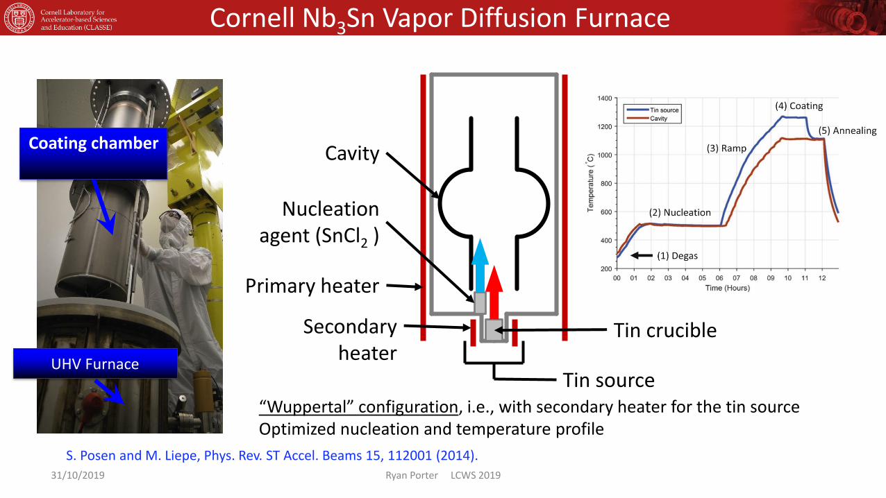
Cornell Nb3Sn Vapor Diffusion Furnace
UHV Furnace
Coating chamber
S. Posen and M. Liepe, Phys. Rev. ST Accel. Beams 15, 112001 (2014).
Tin source
Secondary heater
Tin crucible
Primary heater
Cavity
Nucleation agent (SnCl2 )
“Wuppertal” configuration, i.e., with secondary heater for the tin sourceOptimized nucleation and temperature profile
31/10/2019 Ryan Porter LCWS 2019

Nb3Sn Coatings
2 μm
Nb3Sn forms a polycrystalline layer on the surface of the niobium
1 μm
≈3 μm
RF Surface
1 μm
Nb
Nb3Sn
Before Coating
After Coating
31/10/2019 Ryan Porter LCWS 2019

Comparison to Niobium
20× more efficient than Nb
at 4.2 Kand 1.3 GHz!
31/10/2019 Ryan Porter LCWS 2019
• High Q at 4.2 K– More efficient
• Lower dynamic load
– Longer pulsed operation
• Could run at 4.2 K– Simplify cryomodule
• Lower static load
– Simplify cryogenicsystem

JLAB and Fermilab Nb3Sn Vapor Diffusion Furnaces
Nb Coating Chamber – contains Sn vapor
Sn source 1 Sn source 2
Previously existing SRF vacuum furnace
Heat shields
Fermilab Nb3Sn Coating SystemJLAB Nb3Sn Coating System
“Siemens” configuration, i.e., no secondary heater for the tin source
“Wuppertal” configuration, i.e., with secondary heater for the tin source
Sam Posen
31/10/2019 Ryan Porter LCWS 2019

• Very reproducible performance • ~4K operation with unprecedented Q >1010 at typical CW operating fields
1.3 GHz Nb3Sn Cavity Performance: JLab and Fermilab
4.2 K
G. Ciovati, I. Parajuli, U. Pudasaini S. Posen
31/10/2019 Ryan Porter LCWS 2019
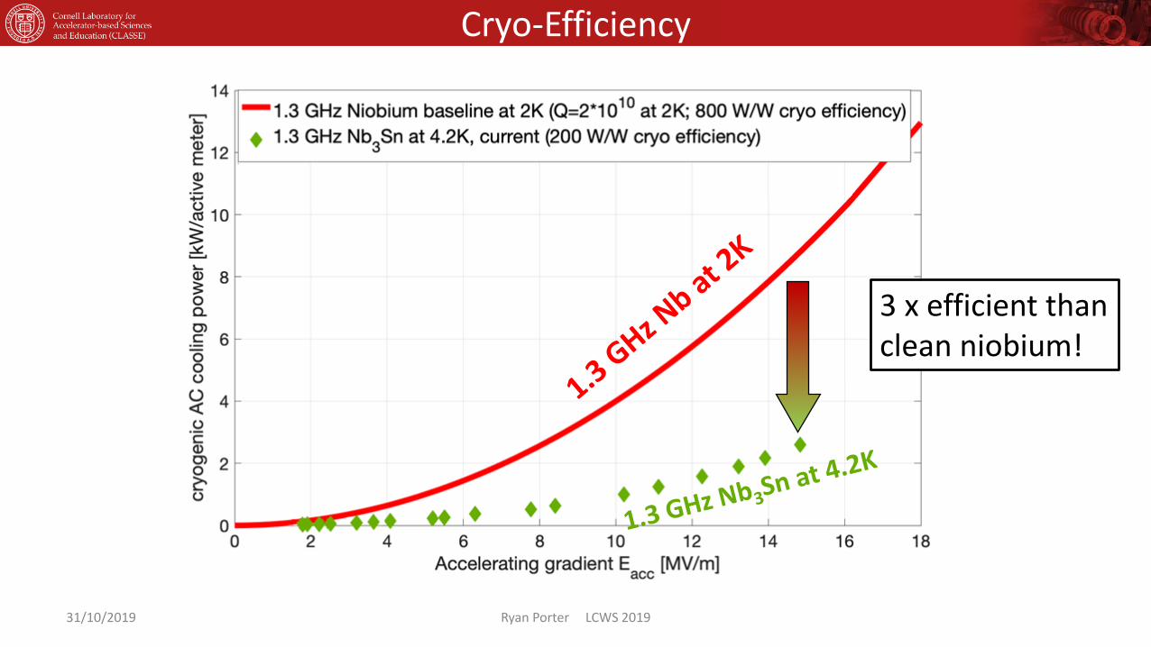
Cryo-Efficiency
3 x efficient thanclean niobium!
31/10/2019 Ryan Porter LCWS 2019
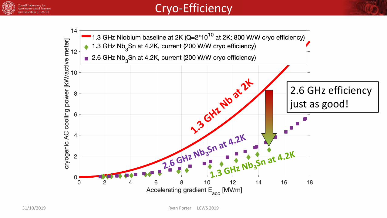
Cryo-Efficiency
31/10/2019 Ryan Porter LCWS 2019
2.6 GHz efficiency just as good!

High Frequency Nb3Sn Cavities
31/10/2019 Ryan Porter LCWS 2019

High Frequency Nb3Sn
31/10/2019 Ryan Porter LCWS 2019
All 4.2 K
Higher frequency -> Smaller cavities-> Material savings

Cryo-Efficiency
31/10/2019 Ryan Porter LCWS 2019
2.6 GHz efficiency just as good!

Increasing Q?
31/10/2019 Ryan Porter LCWS 2019

Breaking down the Q
0 nΩ
16 nΩ
Trapped flux
“Double Gap”
BCS Resistance
Ambient fields
Thermal gradients
Surface resistance at 4.2 K and 10 MV/m
31/10/2019 Ryan Porter LCWS 2019

Breaking down the Q
0 nΩ
16 nΩ
Trapped flux
“Double Gap”
BCS Resistance
Ambient fields
Thermal gradients
Surface resistance at 4.2 K and 10 MV/m
Good magnetic shielding can eliminate
31/10/2019 Ryan Porter LCWS 2019

“Double Gap”
• Cause still under investigation:– Well fit for “2-gap” BCS
• Multiple regions of “Sn depleted” Nb3Sn?
– Dirty surface layers?
• Good news:– Removing will increase Q:
• Q2.6 GHz, 4.2 K → 9·109
• Q1.3 GHz, 4.2 K → 2.3·1010
→ 3.5·1010 with good magnetic shielding
• “BCS” resistance shows two slope behavior
RBCS for 2 Gaps (3 MV/m)
R0 ~ 5.5 nΩ (from trapped magnetic flux)
31/10/2019 Ryan Porter LCWS 2019

Increasing Eacc
31/10/2019 Ryan Porter LCWS 2019

Limitations in quench field
Nb3Sn cavities consistently quench at fields between 14_and 18_MV/m in CW operation
The superheating field suggests we can achieve fields up to 96 MV/m!
14 MV/m
18 MV/m
31/10/2019 Ryan Porter LCWS 2019

T-Map experiment
T-Map sensor
Niobium surface
Thermal paste
Pogo stickConnector leads
Use temperature map to look for quench mechanism/site:
31/10/2019 Ryan Porter LCWS 2019
T-Map board

Localised quench
Nb3Sn cavities are limited by a quench at a localized spot
What could be at fault?31/10/2019 Ryan Porter LCWS 2019
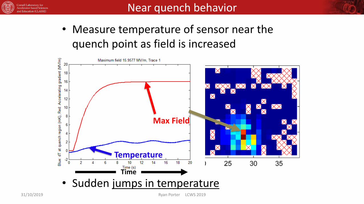
Near quench behavior
• Measure temperature of sensor near the quench point as field is increased
• Sudden jumps in temperature
Temperature
Max Field
Time
31/10/2019 Ryan Porter LCWS 2019
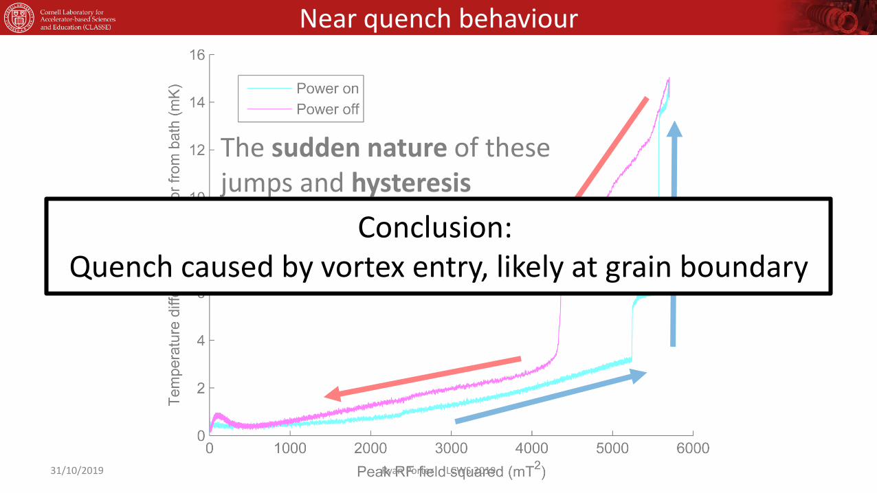
Near quench behaviour
The sudden nature of these jumps and hysteresisstrongly suggests flux entryConclusion:
Quench caused by vortex entry, likely at grain boundary
31/10/2019 Ryan Porter LCWS 2019

Cavity Autopsy – Anything on Surface?
• Cut out this region and examined with microscopy
• Nothing obvious except Nb grain boundary cliff
– Rough SurfaceNb3Sn surface
Nb substrate grain boundary?Quench Site
31/10/2019 Ryan Porter LCWS 2019

Surface Roughness and Quench Fields
Surface Roughness:• Rough surface → increased magnetic field on some surfaces
– Quench field decreased by 1/3 (?)
• Poor grain boundary geometry can decrease magnetic flux entry barrier– A. R. Pack, M. Transtrum (BYU): SRF’19: MOP017
31/10/2019 Ryan Porter LCWS 2019
Enhancement Factor (Hrough/Hsmooth)
Conclusion: Grain boundary geometry/roughness lowers quench field

Surface Polishing
• Developing surface treatments to reduce surface roughness
• Early result: Oxypolishing halves roughness and surface field enhancement with 800 nm removal
ElectropolishingH. Hu: MOP013 at SRF19
31/10/2019 Ryan Porter LCWS 2019

Why is Nb3Sn Rough?
• Nb3Sn roughness comes from growth– Bad Sn nucleation -> rough surface– Good Sn nucleation -> smooth surface
2 μm
200 nm
200 nm
200 nm
50
0 C
80
0 C
87
5 C
2 µm
2 µm
2 µm
Nb3Sn Growth:
50
% Sn
Sn+Nb
0
31/10/2019 Ryan Porter LCWS 2019

Sn Electroplating
Zeming Sun (Cornell):• Electroplate Sn onto Nb before heat
treatment– > Grow smoother Nb3Sn 10 μm
Heat Treatment
4 μm
400 nmSEM
Nb3Sn
Sn Plated Nb
31/10/2019 Ryan Porter LCWS 2019

Sn Electroplating
Sn2Cl Nucleation Ra ~ 300 nm
“Sn Plating Nucleation” Ra ~ 70 nm
Conclusion: Sn plating nucleation 5 x roughness reduction!
Next step: Grow entire cavity using Sn plating
31/10/2019 Ryan Porter LCWS 2019

Outlook
31/10/2019 Ryan Porter LCWS 2019

Nb3Sn Outlook: Making Great Progress!
Q0 > 1x10¹⁰ at 20 MV/m at 4.4 K
S. Posen
World record CW gradient for Nb3Sn accelerator cavities!
Ref: S. Posen, “Frequency Dependence Studies of Nb3Sn Cavities,” presented at TTC 2019, Vancouver, Canada, Feb. 2019
• Sam Posen (FNAL) reached 22 MV/m in CW operation (Nb3Sn world record)!• Pulsed operation can reach 25 MV/m
• Does not (yet) reach ILC spec. but reaches old TESLA spec.
Continuous→17 MV/m
Pulsed→26 MV/m
Ready in time for ILC upgrade?
31/10/2019 Ryan Porter LCWS 2019

9-Cell Cavity Work at Fermilab
• Sam Posen (Fermilab) completed a first coating of a 9-cell cavity– Real cavity that could be put in cryomodule
• Eacc ~ 10.5 MV/m, Q ~ 8⸱109 at 4.4 K!• First attempt: expect even better results soon!
Ref: S. Posen et. al., “Nb3Sn at Fermilab: Exploring Performance,” in Proc. of SRF2019, Hamburg, Germany, July 2019
31/10/2019 Ryan Porter LCWS 2019
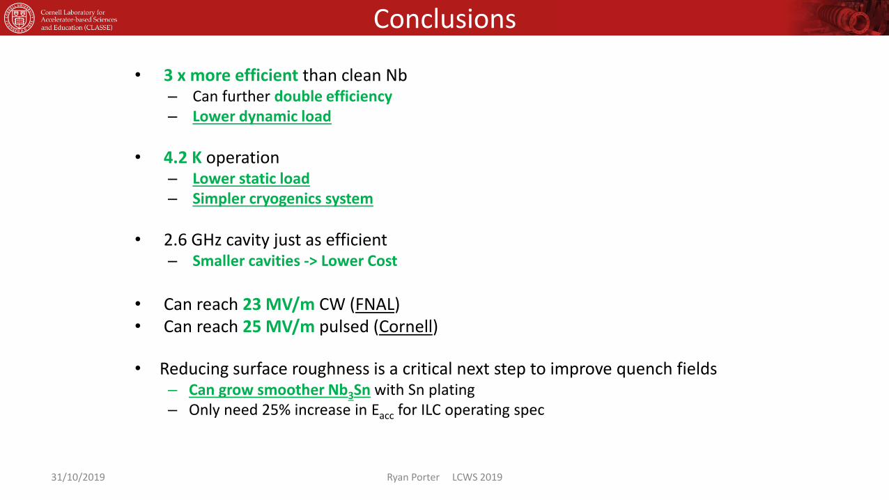
Conclusions
• 3 x more efficient than clean Nb– Can further double efficiency– Lower dynamic load
• 4.2 K operation– Lower static load– Simpler cryogenics system
• 2.6 GHz cavity just as efficient– Smaller cavities -> Lower Cost
• Can reach 23 MV/m CW (FNAL)• Can reach 25 MV/m pulsed (Cornell)
• Reducing surface roughness is a critical next step to improve quench fields– Can grow smoother Nb3Sn with Sn plating– Only need 25% increase in Eacc for ILC operating spec
31/10/2019 Ryan Porter LCWS 2019

The Cornell Nb3Sn program is supported by:U.S. DOE award DE-SC0008431: 1.3 GHz Nb3Sn tests and Nb3Sn R&D
NSF Award 1734189: 2.6 GHz and 3.9 GHz tests and R&DCenter for Bright Beam (NSF Award 1549132): Materials studies
This works make use of Cornell Center for Materials Research, NSF MRSEC program (DMR-1719875)
Acknowledgements
Prof. Matthias Liepe
Prof. Tomas Arias
Prof. David A. Muller
Prof. James P. Sethna
Prof. Mark Transtrum
Dr. Danilo Liarte
Dr. Zeming Sun
Dr. Daniel Hall
Dr. Sam Posen
Paul Cueva
Nathan Sitaraman
James Maniscalco
Alden Pack
James Sears
Greg Kulina
John Kaufman
Holly Conklin
Terri Gruber
Paul Bishop
Adam Holic
with special thanks to
Copyright © 2022 FDOKUMEN