SN74AUP1G79 Low-Power Single Positive-Edge-Triggered D ...
50
-0.5 0 0.5 1 1.5 2 2.5 3 3.5 0 5 10 15 20 25 30 35 40 45 Time - ns Voltage - V † AUP1G08 data at C L = 15 pF Output Input Switching Characteristics at 25 MHz † Product Folder Order Now Technical Documents Tools & Software Support & Community An IMPORTANT NOTICE at the end of this data sheet addresses availability, warranty, changes, use in safety-critical applications, intellectual property matters and other important disclaimers. PRODUCTION DATA. SN74AUP1G79 SCES592I – JULY 2004 – REVISED SEPTEMBER 2017 SN74AUP1G79 Low-Power Single Positive-Edge-Triggered D-Type Flip-Flop 1 1 Features 1• Available in the Texas Instruments NanoStar™ Package • Low Static-Power Consumption: I CC = 0.9 μA Maximum • Low Dynamic-Power Consumption: C pd = 3 pF Typical at 3.3 V • Low Input Capacitance: C i = 1.5 pF Typical • Low Noise: Overshoot and Undershoot < 10% of V CC • I off Supports Partial Power-Down-Mode Operation • Input Hysteresis Allows Slow Input Transition and Better Switching Noise Immunity at the Input (V hys = 250 mV Typical at 3.3 V) • Wide Operating V CC Range of 0.8 V to 3.6 V • Optimized for 3.3-V Operation • 3.6-V I/O Tolerant to Support Mixed-Mode Signal Operation • t pd = 4 ns Maximum at 3.3 V • Suitable for Point-to-Point Applications • Latch-Up Performance Exceeds 100 mA Per JESD 78, Class II • ESD Performance Tested Per JESD 22 – 2000-V Human-Body Model (A114-B, Class II) – 1000-V Charged-Device Model (C101) 2 Applications • Barcode Scanner • Cable Solutions • E-Book • Embedded PC • Field Transmitter: Temperature or Pressure Sensor • Fingerprint Biometrics • HVAC: Heating, Ventilating, and Air Conditioning • Network-Attached Storage (NAS) • Server Motherboard and PSU • Software Defined Radio (SDR) • TV: High-Definition (HDTV), LCD, and Digital • Video Communications System • Wireless Data Access Card, Headset, Keyboard, Mouse, and LAN Card 3 Description The AUP family is TI's premier solution to the industry's low-power needs in battery-powered portable applications. This family assures a very-low static and dynamic power consumption across the entire V CC range of 0.8 V to 3.6 V, thus resulting in an increased battery life. The AUP devices also maintain excellent signal integrity. The SN74AUP1G79 is a single positive-edge- triggered D-type flip-flop. When data at the data (D) input meets the setup-time requirement, the data is transferred to the Q output on the positive-going edge of the clock pulse. Clock triggering occurs at a voltage level and is not directly related to the rise time of the clock pulse. Following the hold-time interval, data at the D input can be changed without affecting the levels at the outputs. NanoStar™ package technology is a major breakthrough in IC packaging concepts, using the die as the package. The SN74AUP1G79 device is fully specified for partial-power-down applications using I off . The I off circuitry disables the outputs when the device is powered down. This inhibits current backflow into the device which prevents damage to the device. Device Information (1) PART NUMBER PACKAGE BODY SIZE (NOM) SN74AUP1G79DBV SOT-23 (5) 2.90 mm × 1.60 mm SN74AUP1G79DCK SC70 (5) 2.00 mm × 1.25 mm SN74AUP1G79DRL SOT-5X3 (5) 1.60 mm × 1.20 mm SN74AUP1G79DRY SON (6) 1.45 mm × 1.00 mm SN74AUP1G79DSF SON (6) 1.00 mm × 1.00 mm SN74AUP1G79DPW X2SON (5) 0.80 mm x 0.80 mm SN74AUP1G79YFP DSBGA (6) 1.16 mm × 0.76 mm SN74AUP1G79YZP DSBGA (5) 1.39 mm × 0.89 mm (1) For all available packages, see the orderable addendum at the end of the data sheet. Power Consumption and Performance
-
Upload
khangminh22 -
Category
Documents
-
view
0 -
download
0
Transcript of SN74AUP1G79 Low-Power Single Positive-Edge-Triggered D ...

−0.5
0
0.5
1
1.5
2
2.5
3
3.5
0 5 10 15 20 25 30 35 40 45Time − ns
Vo
ltag
e−
V
† AUP1G08 data at CL = 15 pF
OutputInput
Switching Characteristics
at 25 MHz†
Product
Folder
Order
Now
Technical
Documents
Tools &
Software
Support &Community
An IMPORTANT NOTICE at the end of this data sheet addresses availability, warranty, changes, use in safety-critical applications,intellectual property matters and other important disclaimers. PRODUCTION DATA.
SN74AUP1G79SCES592I –JULY 2004–REVISED SEPTEMBER 2017
SN74AUP1G79 Low-Power Single Positive-Edge-Triggered D-Type Flip-Flop
1
1 Features1• Available in the Texas Instruments NanoStar™
Package• Low Static-Power Consumption:
ICC = 0.9 µA Maximum• Low Dynamic-Power Consumption:
Cpd = 3 pF Typical at 3.3 V• Low Input Capacitance:
Ci = 1.5 pF Typical• Low Noise: Overshoot and Undershoot
< 10% of VCC
• Ioff Supports Partial Power-Down-Mode Operation• Input Hysteresis Allows Slow Input Transition and
Better Switching Noise Immunity at the Input(Vhys = 250 mV Typical at 3.3 V)
• Wide Operating VCC Range of 0.8 V to 3.6 V• Optimized for 3.3-V Operation• 3.6-V I/O Tolerant to Support Mixed-Mode Signal
Operation• tpd = 4 ns Maximum at 3.3 V• Suitable for Point-to-Point Applications• Latch-Up Performance Exceeds 100 mA Per
JESD 78, Class II• ESD Performance Tested Per JESD 22
– 2000-V Human-Body Model(A114-B, Class II)
– 1000-V Charged-Device Model (C101)
2 Applications• Barcode Scanner• Cable Solutions• E-Book• Embedded PC• Field Transmitter: Temperature or Pressure
Sensor• Fingerprint Biometrics• HVAC: Heating, Ventilating, and Air Conditioning• Network-Attached Storage (NAS)• Server Motherboard and PSU• Software Defined Radio (SDR)• TV: High-Definition (HDTV), LCD, and Digital• Video Communications System• Wireless Data Access Card, Headset, Keyboard,
Mouse, and LAN Card
3 DescriptionThe AUP family is TI's premier solution to theindustry's low-power needs in battery-poweredportable applications. This family assures a very-lowstatic and dynamic power consumption across theentire VCC range of 0.8 V to 3.6 V, thus resulting in anincreased battery life. The AUP devices also maintainexcellent signal integrity.
The SN74AUP1G79 is a single positive-edge-triggered D-type flip-flop. When data at the data (D)input meets the setup-time requirement, the data istransferred to the Q output on the positive-going edgeof the clock pulse. Clock triggering occurs at avoltage level and is not directly related to the risetime of the clock pulse. Following the hold-timeinterval, data at the D input can be changed withoutaffecting the levels at the outputs.
NanoStar™ package technology is a majorbreakthrough in IC packaging concepts, using the dieas the package.
The SN74AUP1G79 device is fully specified forpartial-power-down applications using Ioff. The Ioffcircuitry disables the outputs when the device ispowered down. This inhibits current backflow into thedevice which prevents damage to the device.
Device Information(1)
PART NUMBER PACKAGE BODY SIZE (NOM)SN74AUP1G79DBV SOT-23 (5) 2.90 mm × 1.60 mmSN74AUP1G79DCK SC70 (5) 2.00 mm × 1.25 mmSN74AUP1G79DRL SOT-5X3 (5) 1.60 mm × 1.20 mmSN74AUP1G79DRY SON (6) 1.45 mm × 1.00 mmSN74AUP1G79DSF SON (6) 1.00 mm × 1.00 mmSN74AUP1G79DPW X2SON (5) 0.80 mm x 0.80 mmSN74AUP1G79YFP DSBGA (6) 1.16 mm × 0.76 mmSN74AUP1G79YZP DSBGA (5) 1.39 mm × 0.89 mm
(1) For all available packages, see the orderable addendum atthe end of the data sheet.
Power Consumption and Performance

2
SN74AUP1G79SCES592I –JULY 2004–REVISED SEPTEMBER 2017 www.ti.com
Product Folder Links: SN74AUP1G79
Submit Documentation Feedback Copyright © 2004–2017, Texas Instruments Incorporated
Table of Contents1 Features .................................................................. 12 Applications ........................................................... 13 Description ............................................................. 14 Revision History..................................................... 25 Pin Configuration and Functions ......................... 36 Specifications......................................................... 4
6.1 Absolute Maximum Ratings ...................................... 46.2 ESD Ratings.............................................................. 46.3 Recommended Operating Conditions....................... 56.4 Thermal Information .................................................. 56.5 Electrical Characteristics: TA = 25°C ........................ 66.6 Electrical Characteristics: TA = –40°C to 85°C ......... 76.7 Timing Requirements ................................................ 86.8 Switching Characteristics: CL = 5 pF ........................ 96.9 Switching Characteristics: CL = 10 pF ...................... 96.10 Switching Characteristics: CL = 15 pF .................. 106.11 Switching Characteristics: CL = 30 pF .................. 116.12 Operating Characteristics...................................... 116.13 Typical Characteristics .......................................... 12
7 Parameter Measurement Information ................ 137.1 Propagation Delays, Setup and Hold Times, and
Pulse Width.............................................................. 13
7.2 Enable and Disable Times ...................................... 148 Detailed Description ............................................ 15
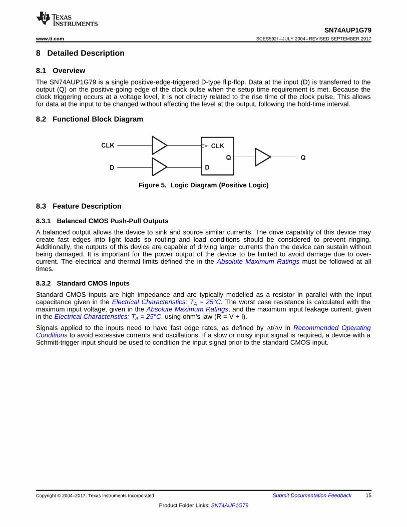
8.1 Overview ................................................................. 158.2 Functional Block Diagram ....................................... 158.3 Feature Description................................................. 158.4 Device Functional Modes........................................ 16
9 Applications, Implementation, and Layout ....... 179.1 Application Information............................................ 179.2 Typical Application .................................................. 17
10 Power Supply Recommendations ..................... 1911 Layout................................................................... 19
11.1 Layout Guidelines ................................................. 1911.2 Layout Example .................................................... 19
12 Device and Documentation Support ................. 2012.1 Documentation Support ........................................ 2012.2 Receiving Notification of Documentation Updates 2012.3 Community Resources.......................................... 2012.4 Trademarks ........................................................... 2012.5 Electrostatic Discharge Caution............................ 2012.6 Glossary ................................................................ 20
13 Mechanical, Packaging, and OrderableInformation ........................................................... 20
4 Revision HistoryNOTE: Page numbers for previous revisions may differ from page numbers in the current version.
Changes from Revision H (April 2015) to Revision I Page
• Added DPW (X2SON) package.............................................................................................................................................. 1• Added Maximum junction temperature, TJ in Absolute Maximum Ratings ............................................................................ 4• Changed values in the Thermal Information table to align with JEDEC standards. .............................................................. 5• Added Balanced High-Drive CMOS Push-Pull Outputs, Standard CMOS Inputs, Clamp Diodes, Partial Power Down
(Ioff), Over-voltage Tolerant Inputs ........................................................................................................................................ 15• Added Receiving Notification of Documentation Updates and Community Resources ....................................................... 20
Changes from Revision G (May 2010) to Revision H Page
• Updated document to the new TI data sheet format .............................................................................................................. 1• Removed Ordering Information table .................................................................................................................................... 1• Added Device Information table ............................................................................................................................................ 1• Added Typical Characteristics section.................................................................................................................................. 12

1 2
C
B
A
Not to scale
GND Q
CLK
D VCC
1 2
C
B
A
Not to scale
GND Q
CLK N.C.
D VCC
GND Q3 4
CLK 2 5
D 61
NC
VCC
CLK NC
D 6
5
4
2
3GND Q
VCC
1
3
2
4
51D VCC
Q
CLK
GND
Q
VCC
CLK
DGND
51 VCCD
2CLK
3 4GND Q
2CLK
3 4GND
VCC
5D
Q
1
3
SN74AUP1G79www.ti.com SCES592I –JULY 2004–REVISED SEPTEMBER 2017
Product Folder Links: SN74AUP1G79
Submit Documentation FeedbackCopyright © 2004–2017, Texas Instruments Incorporated
5 Pin Configuration and Functions
DBV Package5-Pin SOT-23
Top ViewDCK Package
5-Pin SC70Top View
DRL Package5-Pin SOT-5X3
Top ViewDPW Package5-Pin X2SON
Top View
DRY Package6-Pin SONTop View
DSF Package6-Pin SONTop View
YFP Package6-Pin DSBGABottom View
YZP Package5-Pin DSBGABottom View
Pin FunctionsPIN
I/O DESCRIPTIONNAME DBV, DCK,
DRL, DPWDRY,DSF YZP YFP
CLK 2 2 B1 B1 I Positive-Edge-Triggered Clock inputD 1 1 A1 A1 I Data InputGND 3 3 C1 C1 — Ground pinNC — 5 — B2 — No ConnectQ 4 4 C2 C2 O Q outputVCC 5 6 A2 A2 — Positive supply

4
SN74AUP1G79SCES592I –JULY 2004–REVISED SEPTEMBER 2017 www.ti.com
Product Folder Links: SN74AUP1G79
Submit Documentation Feedback Copyright © 2004–2017, Texas Instruments Incorporated
(1) Stresses beyond those listed under Absolute Maximum Ratings may cause permanent damage to the device. These are stress ratingsonly, and functional operation of the device at these or any other conditions beyond those indicated under Recommended OperatingConditions is not implied. Exposure to absolute-maximum-rated conditions for extended periods may affect device reliability.
(2) The input negative-voltage and output voltage ratings may be exceeded if the input and output current ratings are observed.
6 Specifications
6.1 Absolute Maximum Ratingsover operating free-air temperature range (unless otherwise noted) (1)
MIN MAX UNITVCC Supply voltage –0.5 4.6 VVI Input voltage (2) –0.5 4.6 VVO Voltage range applied to any output in the high-impedance or power-off state (2) –0.5 4.6 VVO Output voltage range in the high or low state (2) –0.5 VCC + 0.5 VIIK Input clamp current VI < 0 –50 mAIOK Output clamp current VO < 0 –50 mAIO Continuous output current ±20 mA
Continuous current through VCC or GND ±50 mATJ Maximum junction temperature 150 °CTstg Storage temperature –65 150 °C
(1) JEDEC document JEP155 states that 500-V HBM allows safe manufacturing with a standard ESD control process.(2) JEDEC document JEP157 states that 250-V CDM allows safe manufacturing with a standard ESD control process.
6.2 ESD RatingsVALUE UNIT
V(ESD) Electrostatic dischargeHuman-body model (HBM), per ANSI/ESDA/JEDEC JS-001 (1) 2000
VCharged-device model (CDM), per JEDEC specification JESD22-C101 (2) 1000

5
SN74AUP1G79www.ti.com SCES592I –JULY 2004–REVISED SEPTEMBER 2017
Product Folder Links: SN74AUP1G79
Submit Documentation FeedbackCopyright © 2004–2017, Texas Instruments Incorporated
(1) All unused inputs of the device must be held at VCC or GND to assure proper device operation. See the TI application report,Implications of Slow or Floating CMOS Inputs.
6.3 Recommended Operating ConditionsMIN MAX UNIT
VCC Supply voltage 0.8 3.6 V
VIH High-level input voltage
VCC = 0.8 V VCC
VVCC = 1.1 V to 1.95 V 0.65 × VCC
VCC = 2.3 V to 2.7 V 1.6VCC = 3 V to 3.6 V 2
VIL Low-level input voltage
VCC = 0.8 V 0
VVCC = 1.1 V to 1.95 V 0.35 × VCC
VCC = 2.3 V to 2.7 V 0.7VCC = 3 V to 3.6 V 0.9
VI Input voltage (1) 0 3.6 VVO Output voltage 0 VCC V
IOH High-level output current
VCC = 0.8 V –20 µAVCC = 1.1 V –1.1
mAVCC = 1.4 V –1.7VCC = 1.65 V –1.9VCC = 2.3 V –3.1VCC = 3 V –4
IOL Low-level output current
VCC = 0.8 V 20 µAVCC = 1.1 V 1.1
mAVCC = 1.4 V 1.7VCC = 1.65 V 1.9VCC = 2.3 V 3.1VCC = 3 V 4
Δt/Δv Input transition rise or fall rate VCC = 0.8 V to 3.6 V 200 ns/VTA Operating free-air temperature –40 85 °C
(1) For more information about traditional and new thermal metrics, see the Semiconductor and IC Package Thermal Metrics applicationreport.
6.4 Thermal Information
THERMAL METRIC (1)
SN74AUP1G79
UNITDBV(SOT-23)
DCK(SC70)
DRL(SOT-5X3)
DRY(SON)
DSF(SON)
DPW(X2SON)
YFP(DSBGA)
YZP(DSBGA)
5 PINS 5 PINS 5 PINS 6 PINS 6 PINS 5 PINS 6 PINS 5 PINS
RθJAJunction-to-ambient thermalresistance 267.2 284.1 294.1 341.1 377.1 489.2 125.4 146.2 °C/W
RθJC(top)Junction-to-case (top) thermalresistance 191.9 208.5 132.5 233.1 187.7 226.3 1.9 1.4 °C/W
RθJBJunction-to-board thermalresistance 101.1 103.1 143.4 206.7 236.6 352.9 37.2 39.3 °C/W
ψJTJunction-to-top characterizationparameter 83.0 76.6 14.5 63.4 29.0 38.2 0.5 0.7 °C/W
ψJBJunction-to-boardcharacterization parameter 100.8 102.3 143.9 206.7 236.3 352.1 37.5 39.8 °C/W
RθJC(bot)Junction-to-case (bottom)thermal resistance N/A N/A N/A N/A N/A 150.8 N/A N/A °C/W
6
SN74AUP1G79SCES592I –JULY 2004–REVISED SEPTEMBER 2017 www.ti.com
Product Folder Links: SN74AUP1G79
Submit Documentation Feedback Copyright © 2004–2017, Texas Instruments Incorporated
(1) One-input switching
6.5 Electrical Characteristics: TA = 25°Cover recommended operating free-air temperature range (unless otherwise noted)
PARAMETER TEST CONDITIONS VCC MIN TYP MAX UNIT
VOH
IOH = –20 µA 0.8 V to 3.6 V VCC – 0.1
V
IOH = –1.1 mA 1.1 V 0.75 × VCC
IOH = –1.7 mA 1.4 V 1.11IOH = –1.9 mA 1.65 V 1.32IOH = –2.3 mA
2.3 V2.05
IOH = –3.1 mA 1.9IOH = –2.7 mA
3 V2.72
IOH = –4 mA 2.6
VOL
IOL = 20 µA 0.8 V to 3.6 V 0.1
V
IOL = 1.1 mA 1.1 V 0.3 × VCC
IOL = 1.7 mA 1.4 V 0.31IOL = 1.9 mA 1.65 V 0.31IOL = 2.3 mA
2.3 V0.31
IOL = 3.1 mA 0.44IOL = 2.7 mA
3 V0.31
IOL = 4 mA 0.44
IID or CLKinput VI = GND to 3.6 V 0 V to 3.6 V 0.1 µA
Ioff VI or VO = 0 V to 3.6 V 0 V 0.2 µAΔIoff VI or VO = 0 V to 3.6 V 0 V to 0.2 V 0.2 µAICC VI = GND or VCC to 3.6 V, IO = 0 0.8 V to 3.6 V 0.5 µAΔICC VI = VCC – 0.6 V, (1) IO = 0 3.3 V 40 µA
Ci VI = VCC or GND0 V 1.5
pF3.6 V 1.5
Co VO = GND 0 V 3 pF
7
SN74AUP1G79www.ti.com SCES592I –JULY 2004–REVISED SEPTEMBER 2017
Product Folder Links: SN74AUP1G79
Submit Documentation FeedbackCopyright © 2004–2017, Texas Instruments Incorporated
(1) One-input switching
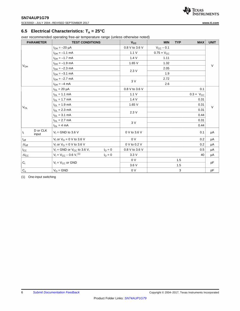
6.6 Electrical Characteristics: TA = –40°C to 85°Cover recommended operating free-air temperature range (unless otherwise noted)
PARAMETER TEST CONDITIONS VCC MIN MAX UNIT
VOH
IOH = –20 µA 0.8 V to 3.6 V VCC – 0.1
V
IOH = –1.1 mA 1.1 V 0.7 × VCC
IOH = –1.7 mA 1.4 V 1.03IOH = –1.9 mA 1.65 V 1.3IOH = –2.3 mA
2.3 V1.97
IOH = –3.1 mA 1.85IOH = –2.7 mA
3 V2.67
IOH = –4 mA 2.55
VOL
IOL = 20 µA 0.8 V to 3.6 V 0.1
V
IOL = 1.1 mA 1.1 V 0.3 × VCC
IOL = 1.7 mA 1.4 V 0.37IOL = 1.9 mA 1.65 V 0.35IOL = 2.3 mA
2.3 V0.33
IOL = 3.1 mA 0.45IOL = 2.7 mA
3 V0.33
IOL = 4 mA 0.45
IID or CLKinput VI = GND to 3.6 V 0 V to 3.6 V 0.5 µA
Ioff VI or VO = 0 V to 3.6 V 0 V 0.6 µAΔIoff VI or VO = 0 V to 3.6 V 0 V to 0.2 V 0.6 µAICC VI = GND or VCC to 3.6 V, IO = 0 0.8 V to 3.6 V 0.9 µAΔICC VI = VCC – 0.6 V, (1) IO = 0 3.3 V 50 µA

8
SN74AUP1G79SCES592I –JULY 2004–REVISED SEPTEMBER 2017 www.ti.com
Product Folder Links: SN74AUP1G79
Submit Documentation Feedback Copyright © 2004–2017, Texas Instruments Incorporated
(1) TA = 25°C
6.7 Timing Requirementsover recommended operating free-air temperature range, TA = –40°C to +85°C (unless otherwise noted) (see Figure 3)
VCC MIN TYP (1) MAX UNIT
fclock Clock frequency
0.8 V 20
MHz
1.2 V ± 0.1 V 801.5 V ± 0.1 V 1001.8 V ± 0.15 V 1402.5 V ± 0.2 V 2103.3 V ± 0.3 V 260
tw Pulse duration, CLK high or low
0.8 V 4.8
ns
1.2 V ± 0.1 V 2.21.5 V ± 0.1 V 1.51.8 V ± 0.15 V 1.62.5 V ± 0.2 V 1.73.3 V ± 0.3 V 1.9
tsuSetup time beforeCLK↑
Data high
0.8 V 4.2 2.9
ns
1.2 V ± 0.1 V 1.41.5 V ± 0.1 V 11.8 V ± 0.15 V 0.92.5 V ± 0.2 V 0.73.3 V ± 0.3 V 0.6
Data low
0.8 V 5.3 3.51.2 V ± 0.1 V 1.81.5 V ± 0.1 V 1.21.8 V ± 0.15 V 1.12.5 V ± 0.2 V 13.3 V ± 0.3 V 1
th Hold time, data after CLK↑
0.8 V 0 0
ns
1.2 V ± 0.1 V 01.5 V ± 0.1 V 01.8 V ± 0.15 V 02.5 V ± 0.2 V 03.3 V ± 0.3 V 0

9
SN74AUP1G79www.ti.com SCES592I –JULY 2004–REVISED SEPTEMBER 2017
Product Folder Links: SN74AUP1G79
Submit Documentation FeedbackCopyright © 2004–2017, Texas Instruments Incorporated
6.8 Switching Characteristics: CL = 5 pFover recommended operating free-air temperature range, CL = 5 pF (unless otherwise noted) (see Figure 3 and Figure 4)
PARAMETER FROM(INPUT)
TO(OUTPUT) TEST CONDITIONS MIN TYP MAX UNIT
fmax
VCC = 0.8 VTA = 25°C 93
MHz
TA = –40°C to +85°C 90
VCC = 1.2 V ± 0.1 VTA = 25°C 199TA = –40°C to +85°C 220
VCC = 1.5 V ± 0.1 VTA = 25°C 250TA = –40°C to +85°C 230
VCC = 1.8 V ± 0.15 VTA = 25°C 271TA = –40°C to +85°C 240
VCC = 2.5 V ± 0.2 VTA = 25°C 280TA = –40°C to +85°C 250
VCC = 3.3 V ± 0.3 VTA = 25°C 280TA = –40°C to +85°C 260
tpd CLK Q
VCC = 0.8 V TA = 25°C 15.9
ns
VCC = 1.2 V ± 0.1 VTA = 25°C 3.7 6.9 11TA = –40°C to +85°C 2.6 13.1
VCC = 1.5 V ± 0.1 VTA = 25°C 3 4.8 7.6TA = –40°C to +85°C 2 8.8
VCC = 1.8 V ± 0.15 VTA = 25°C 2.4 3.8 6.1TA = –40°C to +85°C 1.5 7.1
VCC = 2.5 V ± 0.2 VTA = 25°C 1.8 2.7 4.4TA = –40°C to +85°C 1.1 5
VCC = 3.3 V ± 0.3 VTA = 25°C 1.5 2.1 3.6TA = –40°C to +85°C 0.9 4
6.9 Switching Characteristics: CL = 10 pFover recommended operating free-air temperature range, CL = 10 pF (unless otherwise noted) (see Figure 3 and Figure 4)
PARAMETER FROM(INPUT)
TO(OUTPUT) TEST CONDITIONS MIN TYP MAX UNIT
fmax
VCC = 0.8 VTA = 25°C 62
MHz
TA = –40°C to +85°C 50
VCC = 1.2 V ± 0.1 VTA = 25°C 147TA = –40°C to +85°C 160
VCC = 1.5 V ± 0.1 VTA = 25°C 189TA = –40°C to +85°C 200
VCC = 1.8 V ± 0.15 VTA = 25°C 180TA = –40°C to +85°C 240
VCC = 2.5 V ± 0.2 VTA = 25°C 260TA = –40°C to +85°C 250
VCC = 3.3 V ± 0.3 VTA = 25°C 280TA = –40°C to +85°C 260

10
SN74AUP1G79SCES592I –JULY 2004–REVISED SEPTEMBER 2017 www.ti.com
Product Folder Links: SN74AUP1G79
Submit Documentation Feedback Copyright © 2004–2017, Texas Instruments Incorporated
Switching Characteristics: CL = 10 pF (continued)over recommended operating free-air temperature range, CL = 10 pF (unless otherwise noted) (see Figure 3 and Figure 4)
PARAMETER FROM(INPUT)
TO(OUTPUT) TEST CONDITIONS MIN TYP MAX UNIT
tpd CLK Q
VCC = 0.8 V TA = 25°C 18
ns
VCC = 1.2 V ± 0.1 VTA = 25°C 4.3 7.8 12.3TA = –40°C to +85°C 3.2 14.4
VCC = 1.5 V ± 0.1 VTA = 25°C 3.5 5.5 8.4TA = –40°C to +85°C 2.5 9.8
VCC = 1.8 V ± 0.15 VTA = 25°C 2.8 4.4 6.8TA = –40°C to +85°C 1.9 8
VCC = 2.5 V ± 0.2 VTA = 25°C 2.2 3.2 5TA = –40°C to +85°C 1.5 5.7
VCC = 3.3 V ± 0.3 VTA = 25°C 1.8 2.6 4.1TA = –40°C to +85°C 1.3 4.5
6.10 Switching Characteristics: CL = 15 pFover recommended operating free-air temperature range, CL = 15 pF (unless otherwise noted) (see Figure 3 and Figure 4)
PARAMETER FROM(INPUT)
TO(OUTPUT) TEST CONDITIONS MIN TYP MAX UNIT
fmax
VCC = 0.8 VTA = 25°C 48
MHz
TA = –40°C to +85°C 30
VCC = 1.2 V ± 0.1 VTA = 25°C 112TA = –40°C to +85°C 120
VCC = 1.5 V ± 0.1 VTA = 25°C 151TA = –40°C to +85°C 160
VCC = 1.8 V ± 0.15 VTA = 25°C 194TA = –40°C to +85°C 220
VCC = 2.5 V ± 0.2 VTA = 25°C 248TA = –40°C to +85°C 250
VCC = 3.3 V ± 0.3 VTA = 25°C 280TA = –40°C to +85°C 260
tpd CLK Q
VCC = 0.8 V TA = 25°C 20.3
ns
VCC = 1.2 V ± 0.1 VTA = 25°C 5 8.7 13.6TA = –40°C to +85°C 3.9 15.6
VCC = 1.5 V ± 0.1 VTA = 25°C 4.1 6.3 9.3TA = –40°C to +85°C 3.1 10.7
VCC = 1.8 V ± 0.15 VTA = 25°C 3.3 4 7.6TA = –40°C to +85°C 2.4 8.7
VCC = 2.5 V ± 0.2 VTA = 25°C 2.6 3.6 5.5TA = –40°C to +85°C 1.9 6.3
VCC = 3.3 V ± 0.3 VTA = 25°C 2.2 3 4.5TA = –40°C to +85°C 1.6 5
11
SN74AUP1G79www.ti.com SCES592I –JULY 2004–REVISED SEPTEMBER 2017
Product Folder Links: SN74AUP1G79
Submit Documentation FeedbackCopyright © 2004–2017, Texas Instruments Incorporated
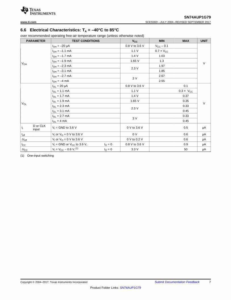
6.11 Switching Characteristics: CL = 30 pFover recommended operating free-air temperature range, CL = 30 pF (unless otherwise noted) (see Figure 3 and Figure 4)
PARAMETER FROM(INPUT)
TO(OUTPUT) TEST CONDITIONS MIN TYP MAX UNIT
fmax
VCC = 0.8 VTA = 25°C 24
MHz
TA = –40°C to +85°C 20
VCC = 1.2 V ± 0.1 VTA = 25°C 72TA = –40°C to +85°C 80
VCC = 1.5 V ± 0.1 VTA = 25°C 100TA = –40°C to +85°C 100
VCC = 1.8 V ± 0.15 VTA = 25°C 127TA = –40°C to +85°C 140
VCC = 2.5 V ± 0.2 VTA = 25°C 185TA = –40°C to +85°C 210
VCC = 3.3 V ± 0.3 VTA = 25°C 266TA = –40°C to +85°C 260
tpd CLK Q
VCC = 0.8 V TA = 25°C 27.2
ns
VCC = 1.2 V ± 0.1 VTA = 25°C 7 11.5 17.3TA = –40°C to +85°C 5.9 24
VCC = 1.5 V ± 0.1 VTA = 25°C 5.7 8.3 11.8TA = –40°C to +85°C 4.6 15.9
VCC = 1.8 V ± 0.15 VTA = 25°C 4.7 6.7 9.6TA = –40°C to +85°C 3.8 13
VCC = 2.5 V ± 0.2 VTA = 25°C 3.7 4.9 7TA = –40°C to +85°C 2.9 9
VCC = 3.3 V ± 0.3 VTA = 25°C 3.2 4.1 5.8TA = –40°C to +85°C 2.6 7.2
6.12 Operating CharacteristicsTA = 25°C
PARAMETER TEST CONDITIONS VCC TYP UNIT
Cpd Power dissipation capacitance f = 10 MHz
0.8 V 2.5
pF
1.2 V ± 0.1 V 2.51.5 V ± 0.1 V 2.51.8 V ± 0.15 V 2.52.5 V ± 0.2 V 33.3 V ± 0.3 V 3

VCC (V)
TP
D (
ns)
0 1 2 3 40
2
4
6
8
10
12
14
16
18
D001
TPD in ns
Temperature (qC)
TP
D (
ns)
-50 0 50 100 1500
1
2
3
4
5
6
D001
TPD in ns
12
SN74AUP1G79SCES592I –JULY 2004–REVISED SEPTEMBER 2017 www.ti.com
Product Folder Links: SN74AUP1G79
Submit Documentation Feedback Copyright © 2004–2017, Texas Instruments Incorporated
6.13 Typical Characteristics
Figure 1. TPD vs VCC Figure 2. TPD vs Temperature

VM
From Output
Under Test
CL
(see Note A)
LOAD CIRCUIT
1 MW
VOLTAGE WAVEFORMS
PROPAGATION DELAY TIMES
INVERTING AND NONINVERTING OUTPUTS
tPLH
tPHL
tPHL
tPLH
VOH
VOH
VOL
VOL
VI
0 V
Input
Output
Output
NOTES: A. CL includes probe and jig capacitance.
B. All input pulses are supplied by generators having the following characteristics: PRR≤ 10 MHz, ZO = 50 W, tr/tf = 3 ns.
C. The outputs are measured one at a time, with one transition per measurement.
D. tPLH and tPHL are the same as tpd.
E. All parameters and waveforms are not applicable to all devices.
VM VM
VM VM
VM
5, 10, 15, 30 pF
VCC/2
VCC
VCC = 1.2 V
± 0.1 VVCC = 0.8 V
VCC = 1.5 V
± 0.1 V
VCC = 1.8 V
± 0.15 V
VCC = 2.5 V
± 0.2 V
VCC = 3.3 V
± 0.3 V
5, 10, 15, 30 pF
VCC/2
VCC
5, 10, 15, 30 pF
VCC/2
VCC
5, 10, 15, 30 pF
VCC/2
VCC
CL
VM
VI
5, 10, 15, 30 pF
VCC/2
VCC
5, 10, 15, 30 pF
VCC/2
VCC
thtsu
Data Input
Timing Input
VCC
0 V
VCC
0 V
0 V
tw
Input
VOLTAGE WAVEFORMS
SETUP AND HOLD TIMES
VOLTAGE WAVEFORMS
PULSE DURATION
VCC/2 VCC/2
VCC/2
VCC/2
VCC
VCC/2
13
SN74AUP1G79www.ti.com SCES592I –JULY 2004–REVISED SEPTEMBER 2017
Product Folder Links: SN74AUP1G79
Submit Documentation FeedbackCopyright © 2004–2017, Texas Instruments Incorporated
7 Parameter Measurement Information
7.1 Propagation Delays, Setup and Hold Times, and Pulse Width
Figure 3. Load Circuit and Voltage Waveforms

NOTES: A. CL includes probe and jig capacitance.
B. Waveform 1 is for an output with internal conditions such that the output is low, except when disabled by the output control.
Waveform 2 is for an output with internal conditions such that the output is high, except when disabled by the output control.
C. All input pulses are supplied by generators having the following characteristics: PRR≤ 10 MHz, ZO = 50 W, tr/tf = 3 ns.
D. The outputs are measured one at a time, with one transition per measurement.
E. tPLZ and tPHZ are the same as tdis.
F. tPZL and tPZH are the same as ten.
G. All parameters and waveforms are not applicable to all devices.
5, 10, 15, 30 pF
VCC/2
VCC
0.15 V
VCC = 1.2 V
± 0.1 VVCC = 0.8 V
VCC = 1.5 V
± 0.1 V
VCC = 1.8 V
± 0.15 V
VCC = 2.5 V
± 0.2 V
VCC = 3.3 V
± 0.3 V
5, 10, 15, 30 pF
VCC/2
VCC
0.1 V
5, 10, 15, 30 pF
VCC/2
VCC
0.1 V
5, 10, 15, 30 pF
VCC/2
VCC
0.1 V
CL
VM
VI
VD
5, 10, 15, 30 pF
VCC/2
VCC
0.15 V
5, 10, 15, 30 pF
VCC/2
VCC
0.3 V
Output
Waveform 1
S1 at 2 × VCC
(see Note B)
Output
Waveform 2
S1 at GND
(see Note B)
VOL
VOH
tPZL
tPZH
tPLZ
tPHZ
VCC
0 V
VOL + VD
VOH − VD
≈0 V
VCC
VOLTAGE WAVEFORMS
ENABLE AND DISABLE TIMES
LOW- AND HIGH-LEVEL ENABLING
Output
ControlVCC/2 VCC/2
VCC/2
VCC/2
tPLZ/tPZL
tPHZ/tPZH
2 × VCC
GND
TEST S1
From Output
Under Test
CL
(see Note A)
LOAD CIRCUIT
S1
GND
5 kW
5 kW
2 × VCC
14
SN74AUP1G79SCES592I –JULY 2004–REVISED SEPTEMBER 2017 www.ti.com
Product Folder Links: SN74AUP1G79
Submit Documentation Feedback Copyright © 2004–2017, Texas Instruments Incorporated
7.2 Enable and Disable Times
Figure 4. Load Circuit and Voltage Waveforms
D
CLK
Q
CLK
D
Q
15
SN74AUP1G79www.ti.com SCES592I –JULY 2004–REVISED SEPTEMBER 2017
Product Folder Links: SN74AUP1G79
Submit Documentation FeedbackCopyright © 2004–2017, Texas Instruments Incorporated
8 Detailed Description
8.1 OverviewThe SN74AUP1G79 is a single positive-edge-triggered D-type flip-flop. Data at the input (D) is transferred to theoutput (Q) on the positive-going edge of the clock pulse when the setup time requirement is met. Because theclock triggering occurs at a voltage level, it is not directly related to the rise time of the clock pulse. This allowsfor data at the input to be changed without affecting the level at the output, following the hold-time interval.
8.2 Functional Block Diagram
Figure 5. Logic Diagram (Positive Logic)
8.3 Feature Description
8.3.1 Balanced CMOS Push-Pull OutputsA balanced output allows the device to sink and source similar currents. The drive capability of this device maycreate fast edges into light loads so routing and load conditions should be considered to prevent ringing.Additionally, the outputs of this device are capable of driving larger currents than the device can sustain withoutbeing damaged. It is important for the power output of the device to be limited to avoid damage due to over-current. The electrical and thermal limits defined the in the Absolute Maximum Ratings must be followed at alltimes.
8.3.2 Standard CMOS InputsStandard CMOS inputs are high impedance and are typically modelled as a resistor in parallel with the inputcapacitance given in the Electrical Characteristics: TA = 25°C. The worst case resistance is calculated with themaximum input voltage, given in the Absolute Maximum Ratings, and the maximum input leakage current, givenin the Electrical Characteristics: TA = 25°C, using ohm's law (R = V ÷ I).
Signals applied to the inputs need to have fast edge rates, as defined by Δt/Δv in Recommended OperatingConditions to avoid excessive currents and oscillations. If a slow or noisy input signal is required, a device with aSchmitt-trigger input should be used to condition the input signal prior to the standard CMOS input.
GND
LogicInput Output
VCCDevice
-IIK -IOK
16
SN74AUP1G79SCES592I –JULY 2004–REVISED SEPTEMBER 2017 www.ti.com
Product Folder Links: SN74AUP1G79
Submit Documentation Feedback Copyright © 2004–2017, Texas Instruments Incorporated
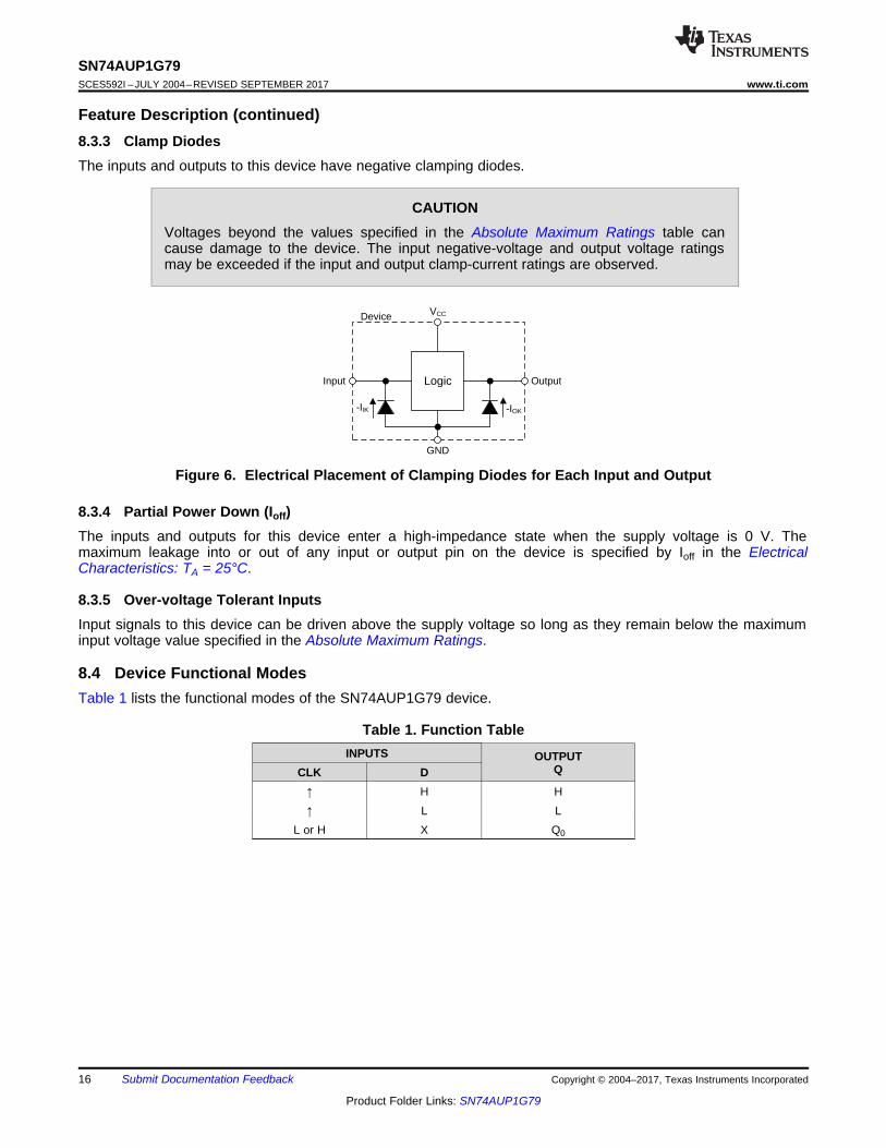
Feature Description (continued)8.3.3 Clamp DiodesThe inputs and outputs to this device have negative clamping diodes.
CAUTIONVoltages beyond the values specified in the Absolute Maximum Ratings table cancause damage to the device. The input negative-voltage and output voltage ratingsmay be exceeded if the input and output clamp-current ratings are observed.
Figure 6. Electrical Placement of Clamping Diodes for Each Input and Output
8.3.4 Partial Power Down (Ioff)The inputs and outputs for this device enter a high-impedance state when the supply voltage is 0 V. Themaximum leakage into or out of any input or output pin on the device is specified by Ioff in the ElectricalCharacteristics: TA = 25°C.
8.3.5 Over-voltage Tolerant InputsInput signals to this device can be driven above the supply voltage so long as they remain below the maximuminput voltage value specified in the Absolute Maximum Ratings.
8.4 Device Functional ModesTable 1 lists the functional modes of the SN74AUP1G79 device.
Table 1. Function TableINPUTS OUTPUT
QCLK D↑ H H↑ L L
L or H X Q0

tpd
QINA
QINB
DIR
tpd
SN74AUP1G79
1
2
3
5
4
D
CLK
GND
VCC
Q
0.1 �F
0.8-3.6V
QINA
QINB
DIR
QuadratureEncoder
17
SN74AUP1G79www.ti.com SCES592I –JULY 2004–REVISED SEPTEMBER 2017
Product Folder Links: SN74AUP1G79
Submit Documentation FeedbackCopyright © 2004–2017, Texas Instruments Incorporated
9 Applications, Implementation, and Layout
NOTEInformation in the following applications sections is not part of the TI componentspecification, and TI does not warrant its accuracy or completeness. TI’s customers areresponsible for determining suitability of components for their purposes. Customers shouldvalidate and test their design implementation to confirm system functionality.
9.1 Application InformationA rotary quadrature encoder is a simple, infinitely-turning knob that outputs two out-of-phase square waves as itis turned and is often used in electronics as a method of human interface. One signal will lead the other in phasedepending on which direction the knob is turned. The SN74AUP1G79 can be used to determine which directionthe knob is being turned without the need for a microcontroller or other complex monitoring system by connectingthe outputs of the knob to the D and CLK inputs of the SN74AUP1G79 as shown in Figure 7. It is important tonote that the CLK input will control when the direction signal changes, as shown in Figure 8.
9.2 Typical Application
Figure 7. Typical Application Diagram
Figure 8. Timing Diagram for Quadrature Encoder Application
9.2.1 Design RequirementsThe SN74AUP1G79 device uses CMOS technology and has balanced output drive. Take care to avoid buscontention because it can drive currents that would exceed maximum limits.
9.2.2 Detailed Design Procedure1. Recommended Input conditions
– Rise time and fall time specifications. See Δt/ΔV in Recommended Operating Conditions.– Specified high and low levels. See VIH and VIL in Recommended Operating Conditions.– Inputs are overvoltage tolerant, which allows them to go as high as 3.6 V at any valid VCC
2. Recommended output conditions– Load currents must not exceed 20 mA on the output and 50 mA total for the part

−0.5
0
0.5
1
1.5
2
2.5
3
3.5
0 5 10 15 20 25 30 35 40 45Time − ns
Vo
ltag
e−
V
† AUP1G08 data at CL = 15 pF
OutputInput
Switching Characteristics
at 25 MHz†
18
SN74AUP1G79SCES592I –JULY 2004–REVISED SEPTEMBER 2017 www.ti.com
Product Folder Links: SN74AUP1G79
Submit Documentation Feedback Copyright © 2004–2017, Texas Instruments Incorporated
Typical Application (continued)9.2.3 Application Curves
Figure 9. AUP – The Lowest-Power Family Figure 10. Excellent Signal Integrity

SOLDER MASKOPENING, TYP
METAL UNDERSOLDER MASK, TYP
8 mil
4 m
il
8 mil
04020.1 �F
Bypass Capacitor
8 mil
WORST BETTER BEST
1W min.
W
2W
19
SN74AUP1G79www.ti.com SCES592I –JULY 2004–REVISED SEPTEMBER 2017
Product Folder Links: SN74AUP1G79
Submit Documentation FeedbackCopyright © 2004–2017, Texas Instruments Incorporated
10 Power Supply RecommendationsThe power supply can be any voltage between the minimum and maximum supply voltage rating located in theRecommended Operating Conditions table. A 0.1-µF bypass capacitor is recommended to be connected fromthe VCC terminal to GND to prevent power disturbance. To reject different frequencies of noise, use multiplebypass capacitors in parallel. Capacitors with values of 0.1 µF and 1 µF are commonly used in parallel. Thebypass capacitor must be installed as close to the power terminal as possible for best results.
11 Layout
11.1 Layout GuidelinesEven low data rate digital signals can contain high-frequency signal components due to fast edge rates. When aprinted-circuit board (PCB) trace turns a corner at a 90° angle, a reflection can occur. A reflection occursprimarily because of the change of width of the trace. At the apex of the turn, the trace width increases to 1.414times the width. This increase upsets the transmission-line characteristics, especially the distributed capacitanceand self–inductance of the trace which results in the reflection. Not all PCB traces can be straight and thereforesome traces must turn corners. Figure 11 shows progressively better techniques of rounding corners. Only thelast example (BEST) maintains constant trace width and minimizes reflections.
An example layout is given in Figure 12 for the DPW (X2SON-5) package. This example layout includes a 0402(metric) capacitor and uses the measurements found in the example board layout appended to this end of thisdatasheet. A via of diameter 0.1 mm (3.973 mil) is placed directly in the center of the device. This via can beused to trace out the center pin connection through another board layer, or it can be left out of the layout
11.2 Layout Example
Figure 11. Trace Example
Figure 12. Example Layout With DPW (X2SON-5) Package

20
SN74AUP1G79SCES592I –JULY 2004–REVISED SEPTEMBER 2017 www.ti.com
Product Folder Links: SN74AUP1G79
Submit Documentation Feedback Copyright © 2004–2017, Texas Instruments Incorporated
12 Device and Documentation Support
12.1 Documentation Support
12.1.1 Related DocumentationFor related documentation see the following:
Implications of Slow or Floating CMOS Inputs
12.2 Receiving Notification of Documentation UpdatesTo receive notification of documentation updates, navigate to the device product folder on ti.com. In the upperright corner, click on Alert me to register and receive a weekly digest of any product information that haschanged. For change details, review the revision history included in any revised document.
12.3 Community ResourcesThe following links connect to TI community resources. Linked contents are provided "AS IS" by the respectivecontributors. They do not constitute TI specifications and do not necessarily reflect TI's views; see TI's Terms ofUse.
TI E2E™ Online Community TI's Engineer-to-Engineer (E2E) Community. Created to foster collaborationamong engineers. At e2e.ti.com, you can ask questions, share knowledge, explore ideas and helpsolve problems with fellow engineers.
Design Support TI's Design Support Quickly find helpful E2E forums along with design support tools andcontact information for technical support.
12.4 TrademarksNanoStar, E2E are trademarks of Texas Instruments.All other trademarks are the property of their respective owners.
12.5 Electrostatic Discharge CautionThese devices have limited built-in ESD protection. The leads should be shorted together or the device placed in conductive foamduring storage or handling to prevent electrostatic damage to the MOS gates.
12.6 GlossarySLYZ022 — TI Glossary.
This glossary lists and explains terms, acronyms, and definitions.
13 Mechanical, Packaging, and Orderable InformationThe following pages include mechanical, packaging, and orderable information. This information is the mostcurrent data available for the designated devices. This data is subject to change without notice and revision ofthis document. For browser-based versions of this data sheet, refer to the left-hand navigation.

PACKAGE OPTION ADDENDUM
www.ti.com 10-Dec-2020
Addendum-Page 1
PACKAGING INFORMATION
Orderable Device Status(1)
Package Type PackageDrawing
Pins PackageQty
Eco Plan(2)
Lead finish/Ball material
(6)
MSL Peak Temp(3)
Op Temp (°C) Device Marking(4/5)
Samples
SN74AUP1G79DBVR ACTIVE SOT-23 DBV 5 3000 RoHS & Green NIPDAU Level-1-260C-UNLIM -40 to 85 H79R
SN74AUP1G79DBVRG4 ACTIVE SOT-23 DBV 5 3000 RoHS & Green NIPDAU Level-1-260C-UNLIM -40 to 85 H79R
SN74AUP1G79DBVT ACTIVE SOT-23 DBV 5 250 RoHS & Green NIPDAU Level-1-260C-UNLIM -40 to 85 H79R
SN74AUP1G79DBVTG4 ACTIVE SOT-23 DBV 5 250 RoHS & Green NIPDAU Level-1-260C-UNLIM -40 to 85 H79R
SN74AUP1G79DCKR ACTIVE SC70 DCK 5 3000 RoHS & Green NIPDAU Level-1-260C-UNLIM -40 to 85 (HWF, HWK, HWO, HW R)
SN74AUP1G79DCKT ACTIVE SC70 DCK 5 250 RoHS & Green NIPDAU Level-1-260C-UNLIM -40 to 85 (HWO, HWR)
SN74AUP1G79DPWR ACTIVE X2SON DPW 5 3000 RoHS & Green NIPDAU Level-1-260C-UNLIM -40 to 85 9N
SN74AUP1G79DRLR ACTIVE SOT-5X3 DRL 5 4000 RoHS & Green NIPDAUAG Level-1-260C-UNLIM -40 to 85 HWR
SN74AUP1G79DRYR ACTIVE SON DRY 6 5000 RoHS & Green NIPDAU | NIPDAUAG Level-1-260C-UNLIM -40 to 85 HW
SN74AUP1G79DSFR ACTIVE SON DSF 6 5000 RoHS & Green NIPDAU | NIPDAUAG Level-1-260C-UNLIM -40 to 85 HW
SN74AUP1G79YFPR ACTIVE DSBGA YFP 6 3000 RoHS & Green SNAGCU Level-1-260C-UNLIM HWN
SN74AUP1G79YZPR ACTIVE DSBGA YZP 5 3000 RoHS & Green SNAGCU Level-1-260C-UNLIM -40 to 85 HWN
(1) The marketing status values are defined as follows:ACTIVE: Product device recommended for new designs.LIFEBUY: TI has announced that the device will be discontinued, and a lifetime-buy period is in effect.NRND: Not recommended for new designs. Device is in production to support existing customers, but TI does not recommend using this part in a new design.PREVIEW: Device has been announced but is not in production. Samples may or may not be available.OBSOLETE: TI has discontinued the production of the device.
(2) RoHS: TI defines "RoHS" to mean semiconductor products that are compliant with the current EU RoHS requirements for all 10 RoHS substances, including the requirement that RoHS substancedo not exceed 0.1% by weight in homogeneous materials. Where designed to be soldered at high temperatures, "RoHS" products are suitable for use in specified lead-free processes. TI mayreference these types of products as "Pb-Free".RoHS Exempt: TI defines "RoHS Exempt" to mean products that contain lead but are compliant with EU RoHS pursuant to a specific EU RoHS exemption.Green: TI defines "Green" to mean the content of Chlorine (Cl) and Bromine (Br) based flame retardants meet JS709B low halogen requirements of <=1000ppm threshold. Antimony trioxide basedflame retardants must also meet the <=1000ppm threshold requirement.

PACKAGE OPTION ADDENDUM
www.ti.com 10-Dec-2020
Addendum-Page 2
(3) MSL, Peak Temp. - The Moisture Sensitivity Level rating according to the JEDEC industry standard classifications, and peak solder temperature.
(4) There may be additional marking, which relates to the logo, the lot trace code information, or the environmental category on the device.
(5) Multiple Device Markings will be inside parentheses. Only one Device Marking contained in parentheses and separated by a "~" will appear on a device. If a line is indented then it is a continuationof the previous line and the two combined represent the entire Device Marking for that device.
(6) Lead finish/Ball material - Orderable Devices may have multiple material finish options. Finish options are separated by a vertical ruled line. Lead finish/Ball material values may wrap to twolines if the finish value exceeds the maximum column width.
Important Information and Disclaimer:The information provided on this page represents TI's knowledge and belief as of the date that it is provided. TI bases its knowledge and belief on informationprovided by third parties, and makes no representation or warranty as to the accuracy of such information. Efforts are underway to better integrate information from third parties. TI has taken andcontinues to take reasonable steps to provide representative and accurate information but may not have conducted destructive testing or chemical analysis on incoming materials and chemicals.TI and TI suppliers consider certain information to be proprietary, and thus CAS numbers and other limited information may not be available for release.
In no event shall TI's liability arising out of such information exceed the total purchase price of the TI part(s) at issue in this document sold by TI to Customer on an annual basis.

TAPE AND REEL INFORMATION
*All dimensions are nominal
Device PackageType
PackageDrawing
Pins SPQ ReelDiameter
(mm)
ReelWidth
W1 (mm)
A0(mm)
B0(mm)
K0(mm)
P1(mm)
W(mm)
Pin1Quadrant
SN74AUP1G79DBVR SOT-23 DBV 5 3000 180.0 8.4 3.23 3.17 1.37 4.0 8.0 Q3
SN74AUP1G79DBVT SOT-23 DBV 5 250 180.0 8.4 3.23 3.17 1.37 4.0 8.0 Q3
SN74AUP1G79DCKR SC70 DCK 5 3000 179.0 8.4 2.2 2.5 1.2 4.0 8.0 Q3
SN74AUP1G79DCKR SC70 DCK 5 3000 180.0 8.4 2.47 2.3 1.25 4.0 8.0 Q3
SN74AUP1G79DCKT SC70 DCK 5 250 180.0 8.4 2.47 2.3 1.25 4.0 8.0 Q3
SN74AUP1G79DPWR X2SON DPW 5 3000 178.0 8.4 0.91 0.91 0.5 2.0 8.0 Q3
SN74AUP1G79DRLR SOT-5X3 DRL 5 4000 180.0 8.4 1.98 1.78 0.69 4.0 8.0 Q3
SN74AUP1G79DRYR SON DRY 6 5000 180.0 9.5 1.15 1.6 0.75 4.0 8.0 Q1
SN74AUP1G79DSFR SON DSF 6 5000 180.0 9.5 1.16 1.16 0.5 4.0 8.0 Q2
SN74AUP1G79YFPR DSBGA YFP 6 3000 178.0 9.2 0.89 1.29 0.62 4.0 8.0 Q1
SN74AUP1G79YZPR DSBGA YZP 5 3000 178.0 9.2 1.02 1.52 0.63 4.0 8.0 Q1
PACKAGE MATERIALS INFORMATION
www.ti.com 5-Jan-2021
Pack Materials-Page 1

*All dimensions are nominal
Device Package Type Package Drawing Pins SPQ Length (mm) Width (mm) Height (mm)
SN74AUP1G79DBVR SOT-23 DBV 5 3000 202.0 201.0 28.0
SN74AUP1G79DBVT SOT-23 DBV 5 250 202.0 201.0 28.0
SN74AUP1G79DCKR SC70 DCK 5 3000 200.0 183.0 25.0
SN74AUP1G79DCKR SC70 DCK 5 3000 202.0 201.0 28.0
SN74AUP1G79DCKT SC70 DCK 5 250 202.0 201.0 28.0
SN74AUP1G79DPWR X2SON DPW 5 3000 205.0 200.0 33.0
SN74AUP1G79DRLR SOT-5X3 DRL 5 4000 202.0 201.0 28.0
SN74AUP1G79DRYR SON DRY 6 5000 184.0 184.0 19.0
SN74AUP1G79DSFR SON DSF 6 5000 184.0 184.0 19.0
SN74AUP1G79YFPR DSBGA YFP 6 3000 220.0 220.0 35.0
SN74AUP1G79YZPR DSBGA YZP 5 3000 220.0 220.0 35.0
PACKAGE MATERIALS INFORMATION
www.ti.com 5-Jan-2021
Pack Materials-Page 2

www.ti.com
PACKAGE OUTLINE
C
0.220.08 TYP
0.25
3.02.6
2X 0.95
1.9
1.450.90
0.150.00 TYP
5X 0.50.3
0.60.3 TYP
80 TYP
1.9
A
3.052.75
B1.751.45
(1.1)
SOT-23 - 1.45 mm max heightDBV0005ASMALL OUTLINE TRANSISTOR
4214839/F 06/2021
NOTES: 1. All linear dimensions are in millimeters. Any dimensions in parenthesis are for reference only. Dimensioning and tolerancing per ASME Y14.5M.2. This drawing is subject to change without notice.3. Refernce JEDEC MO-178.4. Body dimensions do not include mold flash, protrusions, or gate burrs. Mold flash, protrusions, or gate burrs shall not exceed 0.25 mm per side.
0.2 C A B
1
34
5
2
INDEX AREAPIN 1
GAGE PLANE
SEATING PLANE
0.1 C
SCALE 4.000

www.ti.com
EXAMPLE BOARD LAYOUT
0.07 MAXARROUND
0.07 MINARROUND
5X (1.1)
5X (0.6)
(2.6)
(1.9)
2X (0.95)
(R0.05) TYP
4214839/F 06/2021
SOT-23 - 1.45 mm max heightDBV0005ASMALL OUTLINE TRANSISTOR
NOTES: (continued) 5. Publication IPC-7351 may have alternate designs. 6. Solder mask tolerances between and around signal pads can vary based on board fabrication site.
SYMM
LAND PATTERN EXAMPLEEXPOSED METAL SHOWN
SCALE:15X
PKG
1
3 4
5
2
SOLDER MASKOPENINGMETAL UNDER
SOLDER MASK
SOLDER MASKDEFINED
EXPOSED METAL
METALSOLDER MASKOPENING
NON SOLDER MASKDEFINED
(PREFERRED)
SOLDER MASK DETAILS
EXPOSED METAL

www.ti.com
EXAMPLE STENCIL DESIGN
(2.6)
(1.9)
2X(0.95)
5X (1.1)
5X (0.6)
(R0.05) TYP
SOT-23 - 1.45 mm max heightDBV0005ASMALL OUTLINE TRANSISTOR
4214839/F 06/2021
NOTES: (continued) 7. Laser cutting apertures with trapezoidal walls and rounded corners may offer better paste release. IPC-7525 may have alternate design recommendations. 8. Board assembly site may have different recommendations for stencil design.
SOLDER PASTE EXAMPLEBASED ON 0.125 mm THICK STENCIL
SCALE:15X
SYMM
PKG
1
3 4
5
2


www.ti.com
PACKAGE OUTLINE
C
1.71.5
2X 0.5
2X 1
5X 0.30.1
0.6 MAX
5X 0.180.08
5X 0.40.2
0.050.00 TYP
5X 0.270.15
B 1.31.1
A
1.71.5
NOTE 3
SOT - 0.6 mm max heightDRL0005APLASTIC SMALL OUTLINE
4220753/B 12/2020
NOTES: 1. All linear dimensions are in millimeters. Any dimensions in parenthesis are for reference only. Dimensioning and tolerancing per ASME Y14.5M.2. This drawing is subject to change without notice.3. This dimension does not include mold flash, protrusions, or gate burrs. Mold flash, protrusions, or gate burrs shall not exceed 0.15 mm per side.4. Reference JEDEC registration MO-293 Variation UAAD-1
1 5
PIN 1ID AREA
34
SEATING PLANE
0.05 C
SCALE 8.000
0.1 C A B0.05
SYMM
SYMM

www.ti.com
EXAMPLE BOARD LAYOUT
0.05 MAXAROUND
0.05 MINAROUND
5X (0.67)
5X (0.3)
(1.48)
2X (0.5)
(R0.05) TYP
(1)
4220753/B 12/2020
SOT - 0.6 mm max heightDRL0005APLASTIC SMALL OUTLINE
NOTES: (continued) 5. Publication IPC-7351 may have alternate designs. 6. Solder mask tolerances between and around signal pads can vary based on board fabrication site.
SYMM
LAND PATTERN EXAMPLESCALE:30X
SYMM1
3 4
5
SOLDER MASKOPENING
METAL UNDERSOLDER MASK
SOLDER MASKDEFINED
METALSOLDER MASKOPENING
NON SOLDER MASKDEFINED
(PREFERRED)
SOLDERMASK DETAILS

www.ti.com
EXAMPLE STENCIL DESIGN
(1.48)
2X (0.5)
5X (0.67)
5X (0.3)
(R0.05) TYP
(1)
SOT - 0.6 mm max heightDRL0005APLASTIC SMALL OUTLINE
4220753/B 12/2020
NOTES: (continued) 7. Laser cutting apertures with trapezoidal walls and rounded corners may offer better paste release. IPC-7525 may have alternate design recommendations. 8. Board assembly site may have different recommendations for stencil design.
SOLDER PASTE EXAMPLEBASED ON 0.1 mm THICK STENCIL
SCALE:30X
SYMM
SYMM1
3 4
5

GENERIC PACKAGE VIEW
Images above are just a representation of the package family, actual package may vary.Refer to the product data sheet for package details.
DRY 6 USON - 0.6 mm max heightPLASTIC SMALL OUTLINE - NO LEAD
4207181/G
www.ti.com
PACKAGE OUTLINE
C
6X 0.250.15
4X0.5
5X 0.350.25
2X1
0.6 MAX
0.050.00
3X 0.6
0.40.3
B 1.050.95
A
1.51.4
(0.05) TYP (0.127) TYP
4222894/A 01/2018
USON - 0.6 mm max heightDRY0006APLASTIC SMALL OUTLINE - NO LEAD
PIN 1 INDEX AREA
SEATING PLANE
0.08 C
1
34
6
(OPTIONAL)PIN 1 ID
0.1 C A B0.05 C
SYMM
SYMM
NOTES: 1. All linear dimensions are in millimeters. Any dimensions in parenthesis are for reference only. Dimensioning and tolerancing per ASME Y14.5M.2. This drawing is subject to change without notice.
SCALE 8.500

www.ti.com
EXAMPLE BOARD LAYOUT
0.05 MINALL AROUND
0.05 MAXALL AROUND
5X (0.3)
6X (0.2)
4X (0.5)
(0.6)(R0.05) TYP
(0.35)
4222894/A 01/2018
USON - 0.6 mm max heightDRY0006APLASTIC SMALL OUTLINE - NO LEAD
SYMM
1
34
6
SYMM
LAND PATTERN EXAMPLE1:1 RATIO WITH PKG SOLDER PADS
EXPOSED METAL SHOWNSCALE:40X
NOTES: (continued) 3. For more information, see QFN/SON PCB application report in literature No. SLUA271 (www.ti.com/lit/slua271).
METALSOLDER MASKOPENING
SOLDER MASK DETAILS
NON SOLDER MASKDEFINED
EXPOSEDMETAL
SOLDER MASKOPENING
METAL UNDERSOLDER MASK
SOLDER MASKDEFINED
(PREFERRED)
EXPOSEDMETAL

www.ti.com
EXAMPLE STENCIL DESIGN
5X (0.3)
6X (0.2)
4X (0.5)
(0.6)(R0.05) TYP
(0.35)
4222894/A 01/2018
USON - 0.6 mm max heightDRY0006APLASTIC SMALL OUTLINE - NO LEAD
NOTES: (continued) 4. Laser cutting apertures with trapezoidal walls and rounded corners may offer better paste release. IPC-7525 may have alternate design recommendations.
SOLDER PASTE EXAMPLEBASED ON 0.075 - 0.1 mm THICK STENCIL
SCALE:40X
SYMM
1
3 4
6
SYMM

www.ti.com
PACKAGE OUTLINE
C
6X 0.220.12
6X 0.450.35
2X0.7
4X0.35
0.4 MAX
0.050.00
B 1.050.95 A
1.050.95
(0.11) TYP
(0.1)PIN 1 ID
4220597/A 06/2017
X2SON - 0.4 mm max heightDSF0006APLASTIC SMALL OUTLINE - NO LEAD
PIN 1 INDEX AREA
SEATING PLANE
0.05 C
1
34
6
0.07 C B A0.05 C
SYMM
SYMM
NOTES: 1. All linear dimensions are in millimeters. Any dimensions in parenthesis are for reference only. Dimensioning and tolerancing per ASME Y14.5M. 2. This drawing is subject to change without notice.3. Reference JEDEC registration MO-287, variation X2AAF.
SCALE 10.000

www.ti.com
EXAMPLE BOARD LAYOUT
0.07 MINALL AROUND0.07 MAX
ALL AROUND
6X (0.6)
6X (0.17)
4X (0.35)
(0.8)
(R0.05) TYP
X2SON - 0.4 mm max heightDSF0006APLASTIC SMALL OUTLINE - NO LEAD
4220597/A 06/2017
SOLDER MASKOPENING
SOLDER MASKOPENING
NOTES: (continued) 4. For more information, see Texas Instruments literature number SLUA271 (www.ti.com/lit/slua271).
LAND PATTERN EXAMPLEEXPOSED METAL SHOWN
SCALE:40X
SYMM
SYMM
1
34
6
EXPOSED METAL
METAL
NON SOLDER MASKDEFINED
SOLDER MASK DETAILS
EXPOSED METAL
METAL UNDERSOLDER MASK
SOLDER MASKDEFINED

www.ti.com
EXAMPLE STENCIL DESIGN
6X (0.6)
6X (0.17)
4X (0.35)
(0.8)
(R0.05) TYP
X2SON - 0.4 mm max heightDSF0006APLASTIC SMALL OUTLINE - NO LEAD
4220597/A 06/2017
4. Laser cutting apertures with trapezoidal walls and rounded corners may offer better paste release. IPC-7525 may have alternate design recommendations.
SOLDER PASTE EXAMPLEBASED ON 0.125 mm THICK STENCIL
PRINTED SOLDER COVERAGE BY AREA UNDER PACKAGE
SCALE:40X
SYMM
SYMM
1
34
6


www.ti.com
PACKAGE OUTLINE
C
4X 0.2450.145
3X 0.2880.188
0.4 MAX
0.050.00
2X0.48
0.2390.139
0.25 0.1
B 0.850.75
A
0.850.75
(0.1)
4X (0.05) (0.324)
2X (0.26)
X2SON - 0.4 mm max heightDPW0005APLASTIC SMALL OUTLINE - NO LEAD
4223102/C 06/2021
PIN 1 INDEX AREA
SEATING PLANE
NOTE 3
1
2
3
4
0.1 C A B0.05 C
5
NOTES: 1. All linear dimensions are in millimeters. Any dimensions in parenthesis are for reference only. Dimensioning and tolerancing per ASME Y14.5M. 2. This drawing is subject to change without notice. 3. The size and shape of this feature may vary.
NOTE 3
SCALE 12.000

www.ti.com
EXAMPLE BOARD LAYOUT
0.05 MINALL AROUNDTYP
(0.21) TYPEXPOSED METALCLEARANCE
(0.48)
(0.78)
4X (0.42)
4X (0.22)
( 0.25)
4X (0.26)
4X (0.06)
( 0.1)VIA
(R0.05) TYP
X2SON - 0.4 mm max heightDPW0005APLASTIC SMALL OUTLINE - NO LEAD
4223102/C 06/2021
SYMM
1
2
3
4
SYMM
LAND PATTERN EXAMPLESOLDER MASK DEFINED
SCALE:60X
SOLDER MASKOPENING, TYP
METAL UNDERSOLDER MASKTYP
5
NOTES: (continued) 4. This package is designed to be soldered to a thermal pad on the board. For more information, refer to QFN/SON PCB application note in literature No. SLUA271 (www.ti.com/lit/slua271).
www.ti.com
EXAMPLE STENCIL DESIGN
(0.48)
(0.78)
4X (0.42)
4X (0.22)
4X (0.26)
4X (0.06)
( 0.24)
(0.21)TYP
(R0.05) TYP
X2SON - 0.4 mm max heightDPW0005APLASTIC SMALL OUTLINE - NO LEAD
4223102/C 06/2021
NOTES: (continued) 5. Laser cutting apertures with trapezoidal walls and rounded corners may offer better paste release. IPC-7525 may have alternate design recommendations.
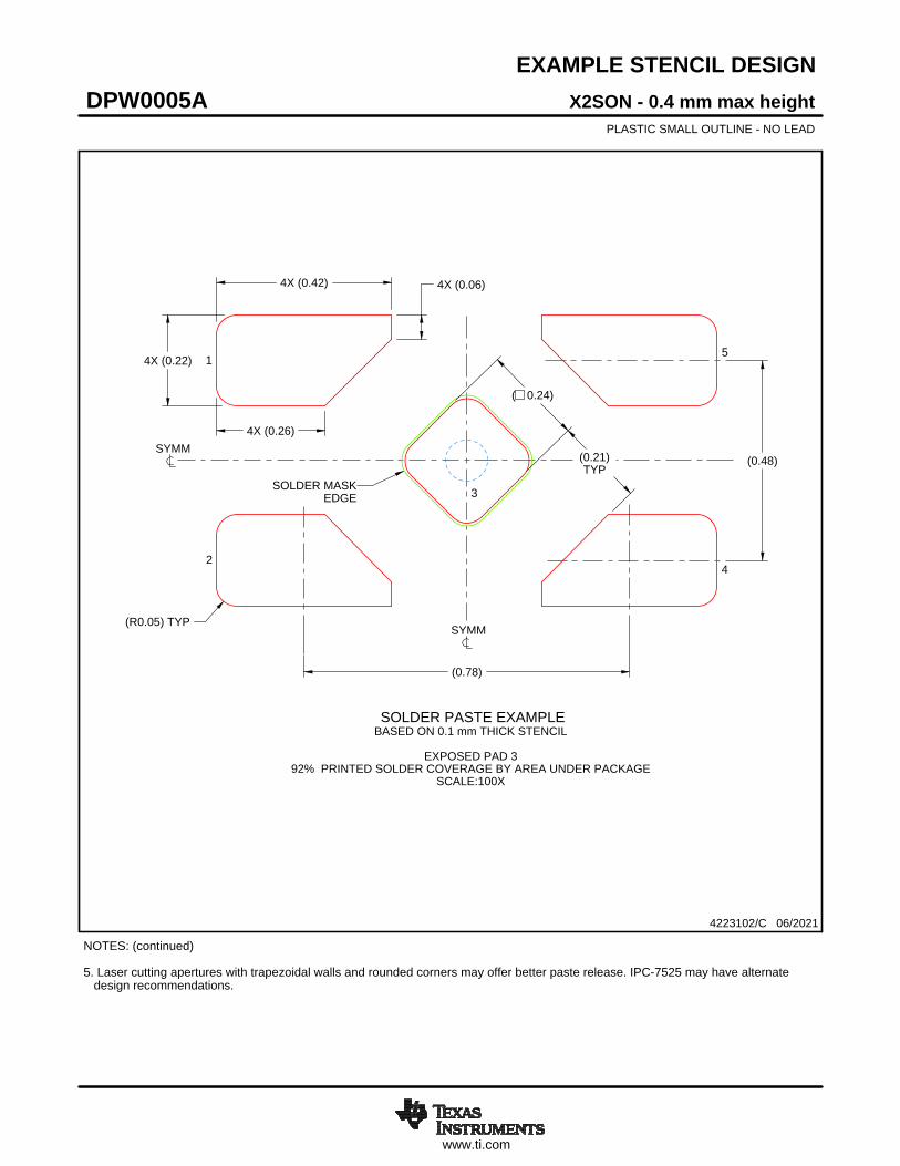
SOLDER PASTE EXAMPLEBASED ON 0.1 mm THICK STENCIL
EXPOSED PAD 3
92% PRINTED SOLDER COVERAGE BY AREA UNDER PACKAGESCALE:100X
SYMM
1
2
3
4
SYMM
EDGESOLDER MASK
5

www.ti.com
PACKAGE OUTLINE
C0.5 MAX
0.190.15
1TYP
0.5 TYP
5X 0.250.21
0.5TYP
B E A
D
4219492/A 05/2017
DSBGA - 0.5 mm max heightYZP0005DIE SIZE BALL GRID ARRAY
NOTES: 1. All linear dimensions are in millimeters. Any dimensions in parenthesis are for reference only. Dimensioning and tolerancing per ASME Y14.5M.2. This drawing is subject to change without notice.
BALL A1CORNER
SEATING PLANE
BALL TYP0.05 C
B
1 2
0.015 C A B
SYMM
SYMM
C
A
SCALE 8.000
D: Max =
E: Max =
1.418 mm, Min =
0.918 mm, Min =
1.358 mm
0.858 mm

www.ti.com
EXAMPLE BOARD LAYOUT
5X ( 0.23)(0.5) TYP
(0.5) TYP
( 0.23)METAL
0.05 MAX ( 0.23)SOLDER MASKOPENING
0.05 MIN
4219492/A 05/2017
DSBGA - 0.5 mm max heightYZP0005DIE SIZE BALL GRID ARRAY
NOTES: (continued) 3. Final dimensions may vary due to manufacturing tolerance considerations and also routing constraints. For more information, see Texas Instruments literature number SNVA009 (www.ti.com/lit/snva009).
SYMM
SYMM
LAND PATTERN EXAMPLESCALE:40X
1 2
A
B
C
NON-SOLDER MASKDEFINED
(PREFERRED)
SOLDER MASK DETAILSNOT TO SCALE
SOLDER MASKOPENING
SOLDER MASKDEFINED
METAL UNDERSOLDER MASK

www.ti.com
EXAMPLE STENCIL DESIGN
(0.5)TYP
(0.5) TYP
5X ( 0.25) (R0.05) TYP
METALTYP
4219492/A 05/2017
DSBGA - 0.5 mm max heightYZP0005DIE SIZE BALL GRID ARRAY
NOTES: (continued) 4. Laser cutting apertures with trapezoidal walls and rounded corners may offer better paste release.
SYMM
SYMM
SOLDER PASTE EXAMPLEBASED ON 0.1 mm THICK STENCIL
SCALE:40X
1 2
A
B
C

www.ti.com
PACKAGE OUTLINE
C0.5 MAX
0.190.13
0.8TYP
0.4TYP
0.4 TYP
6X 0.250.21
B E A
D
4223410/A 11/2016
DSBGA - 0.5 mm max heightYFP0006DIE SIZE BALL GRID ARRAY
NOTES: 1. All linear dimensions are in millimeters. Any dimensions in parenthesis are for reference only. Dimensioning and tolerancing per ASME Y14.5M. 2. This drawing is subject to change without notice.
BALL A1CORNER
SEATING PLANE
BALL TYP 0.05 C
A
B
C
20.015 C A B
SYMM
SYMM
1
SCALE 10.000
D: Max =
E: Max =
1.19 mm, Min =
0.79 mm, Min =
1.13 mm
0.73 mm

www.ti.com
EXAMPLE BOARD LAYOUT
6X ( 0.23)
(0.4) TYP
(0.4) TYP
( 0.23)METAL
0.05 MAX
SOLDER MASKOPENING
METAL UNDERSOLDER MASK
( 0.23)SOLDER MASKOPENING
0.05 MIN
4223410/A 11/2016
DSBGA - 0.5 mm max heightYFP0006DIE SIZE BALL GRID ARRAY
NOTES: (continued) 3. Final dimensions may vary due to manufacturing tolerance considerations and also routing constraints. For more information, see Texas Instruments literature number SNVA009 (www.ti.com/lit/snva009).
SOLDER MASK DETAILSNOT TO SCALE
SYMM
SYMM
LAND PATTERN EXAMPLESCALE:50X
A
B
C
1 2
NON-SOLDER MASKDEFINED
(PREFERRED)
SOLDER MASKDEFINED

www.ti.com
EXAMPLE STENCIL DESIGN
(0.4) TYP
(0.4) TYP
6X ( 0.25) (R0.05) TYP
METALTYP
4223410/A 11/2016
DSBGA - 0.5 mm max heightYFP0006DIE SIZE BALL GRID ARRAY
NOTES: (continued) 4. Laser cutting apertures with trapezoidal walls and rounded corners may offer better paste release.
SYMM
SYMM
SOLDER PASTE EXAMPLEBASED ON 0.1 mm THICK STENCIL
SCALE:50X
A
B
C
1 2

IMPORTANT NOTICE AND DISCLAIMERTI PROVIDES TECHNICAL AND RELIABILITY DATA (INCLUDING DATASHEETS), DESIGN RESOURCES (INCLUDING REFERENCEDESIGNS), APPLICATION OR OTHER DESIGN ADVICE, WEB TOOLS, SAFETY INFORMATION, AND OTHER RESOURCES “AS IS”AND WITH ALL FAULTS, AND DISCLAIMS ALL WARRANTIES, EXPRESS AND IMPLIED, INCLUDING WITHOUT LIMITATION ANYIMPLIED WARRANTIES OF MERCHANTABILITY, FITNESS FOR A PARTICULAR PURPOSE OR NON-INFRINGEMENT OF THIRDPARTY INTELLECTUAL PROPERTY RIGHTS.These resources are intended for skilled developers designing with TI products. You are solely responsible for (1) selecting the appropriateTI products for your application, (2) designing, validating and testing your application, and (3) ensuring your application meets applicablestandards, and any other safety, security, or other requirements. These resources are subject to change without notice. TI grants youpermission to use these resources only for development of an application that uses the TI products described in the resource. Otherreproduction and display of these resources is prohibited. No license is granted to any other TI intellectual property right or to any third partyintellectual property right. TI disclaims responsibility for, and you will fully indemnify TI and its representatives against, any claims, damages,costs, losses, and liabilities arising out of your use of these resources.TI’s products are provided subject to TI’s Terms of Sale (https:www.ti.com/legal/termsofsale.html) or other applicable terms available eitheron ti.com or provided in conjunction with such TI products. TI’s provision of these resources does not expand or otherwise alter TI’sapplicable warranties or warranty disclaimers for TI products.IMPORTANT NOTICE
Mailing Address: Texas Instruments, Post Office Box 655303, Dallas, Texas 75265Copyright © 2021, Texas Instruments Incorporated