sn54ls11, sn54s11, sn74ls11, sn74s11 triple 3-input positive ...
20
SN54LS11, SN54S11, SN74LS11, SN74S11 TRIPLE 3-INPUT POSITIVE-AND GATES SDLS131 – APRIL 1985 – REVISED MARCH 1988 1 POST OFFICE BOX 655303 • DALLAS, TEXAS 75265 Copyright 1988, Texas Instruments Incorporated PRODUCTION DATA information is current as of publication date. Products conform to specifications per the terms of Texas Instruments standard warranty. Production processing does not necessarily include testing of all parameters.
-
Upload
khangminh22 -
Category
Documents
-
view
1 -
download
0
Transcript of sn54ls11, sn54s11, sn74ls11, sn74s11 triple 3-input positive ...
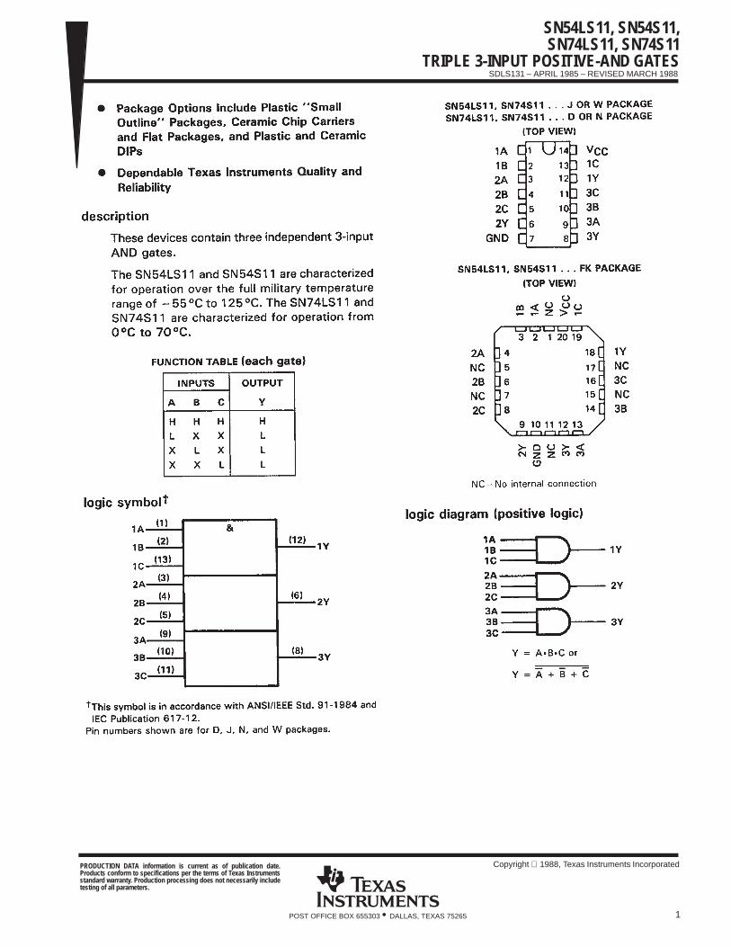
SN54LS11, SN54S11,SN74LS11, SN74S11
TRIPLE 3-INPUT POSITIVE-AND GATES
SDLS131 – APRIL 1985 – REVISED MARCH 1988
1POST OFFICE BOX 655303 • DALLAS, TEXAS 75265
Copyright 1988, Texas Instruments IncorporatedPRODUCTION DATA information is current as of publication date.Products conform to specifications per the terms of Texas Instrumentsstandard warranty. Production processing does not necessarily includetesting of all parameters.
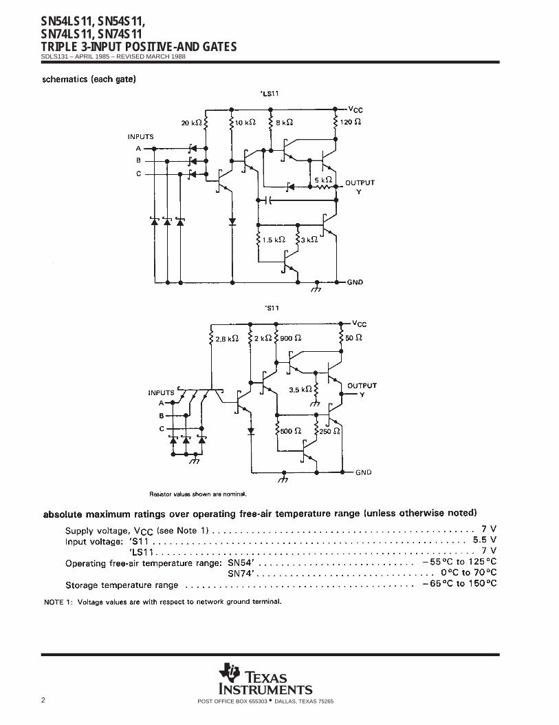
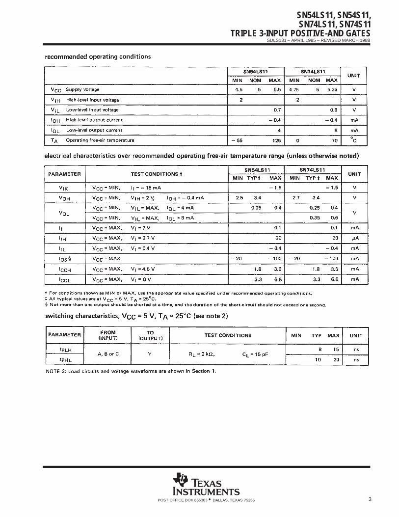
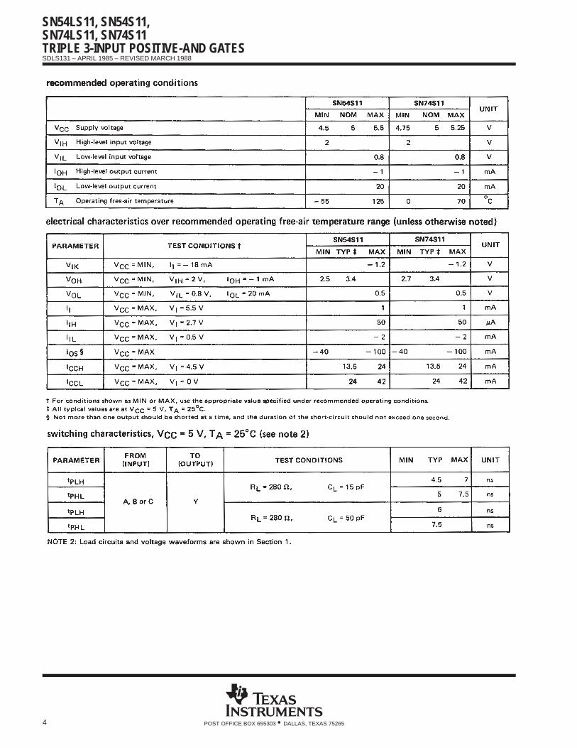
SN54LS11, SN54S11,SN74LS11, SN74S11TRIPLE 3-INPUT POSITIVE-AND GATES
SDLS131 – APRIL 1985 – REVISED MARCH 1988
2 POST OFFICE BOX 655303 • DALLAS, TEXAS 75265
SN54LS11, SN54S11,SN74LS11, SN74S11
TRIPLE 3-INPUT POSITIVE-AND GATES
SDLS131 – APRIL 1985 – REVISED MARCH 1988
3POST OFFICE BOX 655303 • DALLAS, TEXAS 75265
SN54LS11, SN54S11,SN74LS11, SN74S11TRIPLE 3-INPUT POSITIVE-AND GATES
SDLS131 – APRIL 1985 – REVISED MARCH 1988
4 POST OFFICE BOX 655303 • DALLAS, TEXAS 75265
PACKAGE OPTION ADDENDUM
www.ti.com 23-Mar-2022
Addendum-Page 1
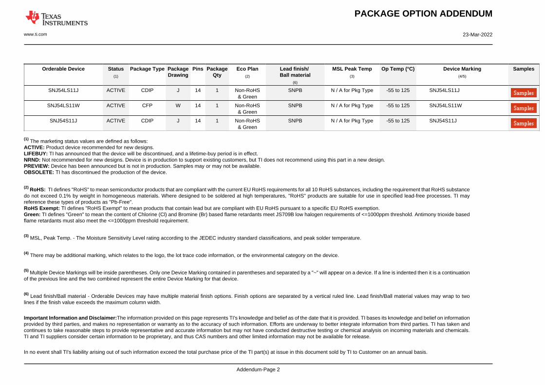
PACKAGING INFORMATION
Orderable Device Status(1)
Package Type PackageDrawing
Pins PackageQty
Eco Plan(2)
Lead finish/Ball material
(6)
MSL Peak Temp(3)
Op Temp (°C) Device Marking(4/5)
Samples
JM38510/08001BCA ACTIVE CDIP J 14 1 Non-RoHS& Green
SNPB N / A for Pkg Type -55 to 125 JM38510/08001BCA
JM38510/08001BDA ACTIVE CFP W 14 1 Non-RoHS& Green
SNPB N / A for Pkg Type -55 to 125 JM38510/08001BDA
JM38510/31001BCA ACTIVE CDIP J 14 1 Non-RoHS& Green
SNPB N / A for Pkg Type -55 to 125 JM38510/31001BCA
JM38510/31001BDA ACTIVE CFP W 14 1 Non-RoHS& Green
SNPB N / A for Pkg Type -55 to 125 JM38510/31001BDA
M38510/08001BCA ACTIVE CDIP J 14 1 Non-RoHS& Green
SNPB N / A for Pkg Type -55 to 125 JM38510/08001BCA
M38510/08001BDA ACTIVE CFP W 14 1 Non-RoHS& Green
SNPB N / A for Pkg Type -55 to 125 JM38510/08001BDA
M38510/31001BCA ACTIVE CDIP J 14 1 Non-RoHS& Green
SNPB N / A for Pkg Type -55 to 125 JM38510/31001BCA
M38510/31001BDA ACTIVE CFP W 14 1 Non-RoHS& Green
SNPB N / A for Pkg Type -55 to 125 JM38510/31001BDA
SN54LS11J ACTIVE CDIP J 14 1 Non-RoHS& Green
SNPB N / A for Pkg Type -55 to 125 SN54LS11J
SN54S11J ACTIVE CDIP J 14 1 Non-RoHS& Green
SNPB N / A for Pkg Type -55 to 125 SN54S11J
SN74LS11D ACTIVE SOIC D 14 50 RoHS & Green NIPDAU Level-1-260C-UNLIM 0 to 70 LS11
SN74LS11DR ACTIVE SOIC D 14 2500 RoHS & Green NIPDAU Level-1-260C-UNLIM 0 to 70 LS11
SN74LS11DRG4 ACTIVE SOIC D 14 2500 RoHS & Green NIPDAU Level-1-260C-UNLIM 0 to 70 LS11
SN74LS11N ACTIVE PDIP N 14 25 RoHS & Green NIPDAU N / A for Pkg Type 0 to 70 SN74LS11N
SN74LS11NE4 ACTIVE PDIP N 14 25 RoHS & Green NIPDAU N / A for Pkg Type 0 to 70 SN74LS11N
SN74LS11NSR ACTIVE SO NS 14 2000 RoHS & Green NIPDAU Level-1-260C-UNLIM 0 to 70 74LS11
SNJ54LS11FK ACTIVE LCCC FK 20 1 Non-RoHS& Green
SNPB N / A for Pkg Type -55 to 125 SNJ54LS11FK
PACKAGE OPTION ADDENDUM
www.ti.com 23-Mar-2022
Addendum-Page 2
Orderable Device Status(1)
Package Type PackageDrawing
Pins PackageQty
Eco Plan(2)
Lead finish/Ball material
(6)
MSL Peak Temp(3)
Op Temp (°C) Device Marking(4/5)
Samples
SNJ54LS11J ACTIVE CDIP J 14 1 Non-RoHS& Green
SNPB N / A for Pkg Type -55 to 125 SNJ54LS11J
SNJ54LS11W ACTIVE CFP W 14 1 Non-RoHS& Green
SNPB N / A for Pkg Type -55 to 125 SNJ54LS11W
SNJ54S11J ACTIVE CDIP J 14 1 Non-RoHS& Green
SNPB N / A for Pkg Type -55 to 125 SNJ54S11J
(1) The marketing status values are defined as follows:ACTIVE: Product device recommended for new designs.LIFEBUY: TI has announced that the device will be discontinued, and a lifetime-buy period is in effect.NRND: Not recommended for new designs. Device is in production to support existing customers, but TI does not recommend using this part in a new design.PREVIEW: Device has been announced but is not in production. Samples may or may not be available.OBSOLETE: TI has discontinued the production of the device.
(2) RoHS: TI defines "RoHS" to mean semiconductor products that are compliant with the current EU RoHS requirements for all 10 RoHS substances, including the requirement that RoHS substancedo not exceed 0.1% by weight in homogeneous materials. Where designed to be soldered at high temperatures, "RoHS" products are suitable for use in specified lead-free processes. TI mayreference these types of products as "Pb-Free".RoHS Exempt: TI defines "RoHS Exempt" to mean products that contain lead but are compliant with EU RoHS pursuant to a specific EU RoHS exemption.Green: TI defines "Green" to mean the content of Chlorine (Cl) and Bromine (Br) based flame retardants meet JS709B low halogen requirements of <=1000ppm threshold. Antimony trioxide basedflame retardants must also meet the <=1000ppm threshold requirement.
(3) MSL, Peak Temp. - The Moisture Sensitivity Level rating according to the JEDEC industry standard classifications, and peak solder temperature.
(4) There may be additional marking, which relates to the logo, the lot trace code information, or the environmental category on the device.
(5) Multiple Device Markings will be inside parentheses. Only one Device Marking contained in parentheses and separated by a "~" will appear on a device. If a line is indented then it is a continuationof the previous line and the two combined represent the entire Device Marking for that device.
(6) Lead finish/Ball material - Orderable Devices may have multiple material finish options. Finish options are separated by a vertical ruled line. Lead finish/Ball material values may wrap to twolines if the finish value exceeds the maximum column width.
Important Information and Disclaimer:The information provided on this page represents TI's knowledge and belief as of the date that it is provided. TI bases its knowledge and belief on informationprovided by third parties, and makes no representation or warranty as to the accuracy of such information. Efforts are underway to better integrate information from third parties. TI has taken andcontinues to take reasonable steps to provide representative and accurate information but may not have conducted destructive testing or chemical analysis on incoming materials and chemicals.TI and TI suppliers consider certain information to be proprietary, and thus CAS numbers and other limited information may not be available for release.
In no event shall TI's liability arising out of such information exceed the total purchase price of the TI part(s) at issue in this document sold by TI to Customer on an annual basis.
PACKAGE OPTION ADDENDUM
www.ti.com 23-Mar-2022
Addendum-Page 3
OTHER QUALIFIED VERSIONS OF SN54LS11, SN74LS11 :
• Catalog : SN74LS11
• Military : SN54LS11
NOTE: Qualified Version Definitions:
• Catalog - TI's standard catalog product
• Military - QML certified for Military and Defense Applications
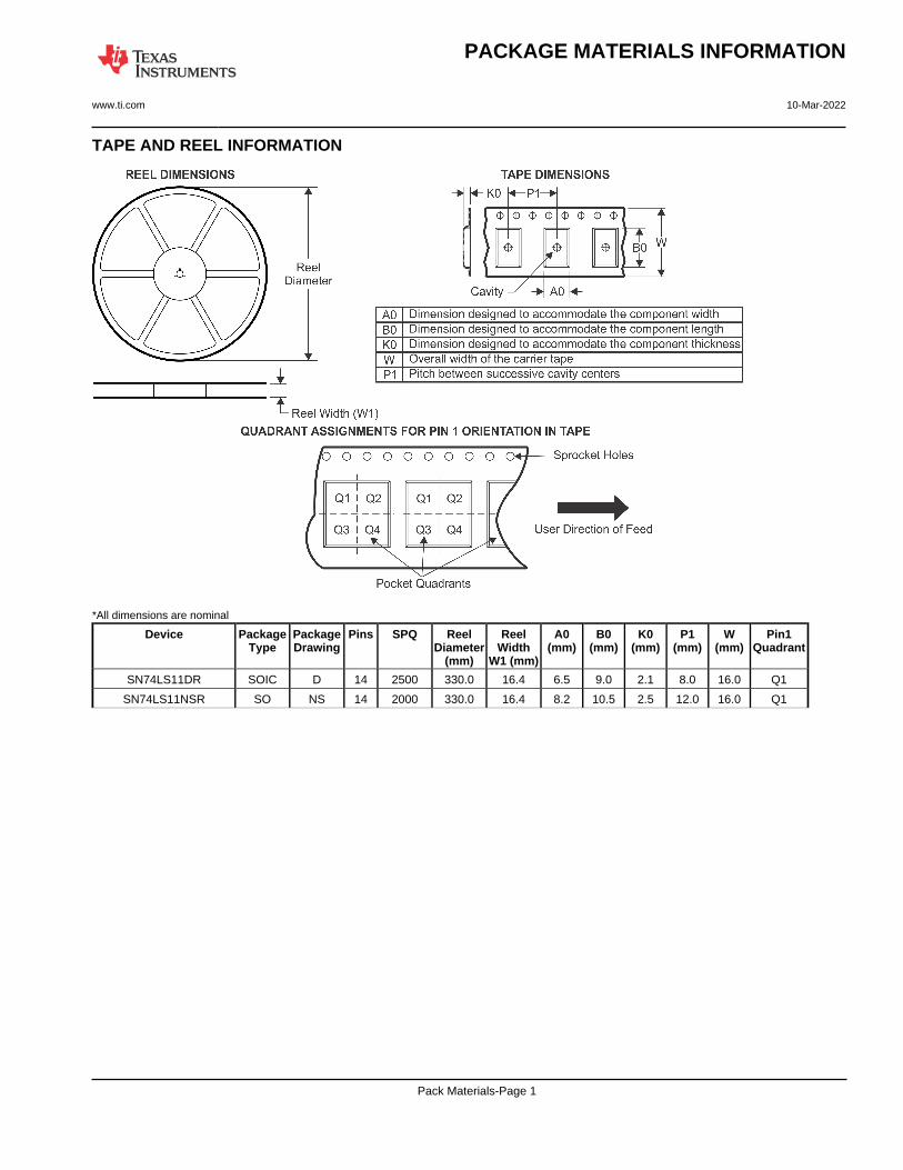
TAPE AND REEL INFORMATION
*All dimensions are nominal
Device PackageType
PackageDrawing
Pins SPQ ReelDiameter
(mm)
ReelWidth
W1 (mm)
A0(mm)
B0(mm)
K0(mm)
P1(mm)
W(mm)
Pin1Quadrant
SN74LS11DR SOIC D 14 2500 330.0 16.4 6.5 9.0 2.1 8.0 16.0 Q1
SN74LS11NSR SO NS 14 2000 330.0 16.4 8.2 10.5 2.5 12.0 16.0 Q1
PACKAGE MATERIALS INFORMATION
www.ti.com 10-Mar-2022
Pack Materials-Page 1
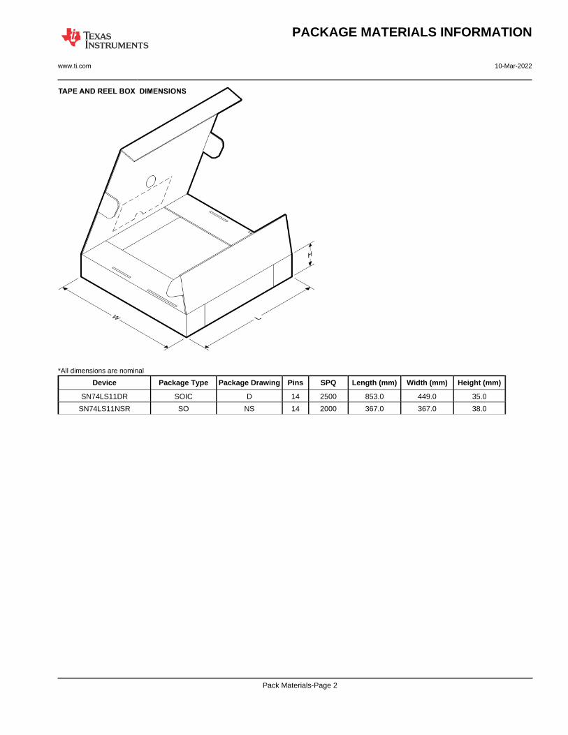
*All dimensions are nominal
Device Package Type Package Drawing Pins SPQ Length (mm) Width (mm) Height (mm)
SN74LS11DR SOIC D 14 2500 853.0 449.0 35.0
SN74LS11NSR SO NS 14 2000 367.0 367.0 38.0
PACKAGE MATERIALS INFORMATION
www.ti.com 10-Mar-2022
Pack Materials-Page 2
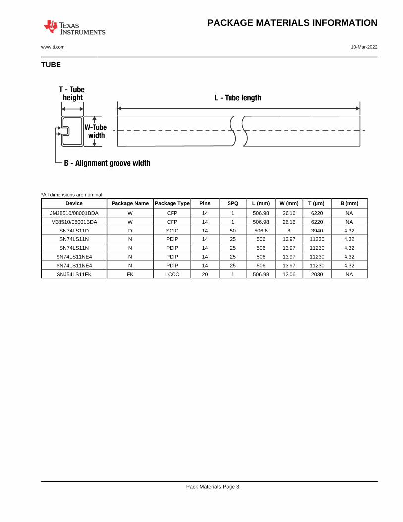
TUBE
*All dimensions are nominal
Device Package Name Package Type Pins SPQ L (mm) W (mm) T (µm) B (mm)
JM38510/08001BDA W CFP 14 1 506.98 26.16 6220 NA
M38510/08001BDA W CFP 14 1 506.98 26.16 6220 NA
SN74LS11D D SOIC 14 50 506.6 8 3940 4.32
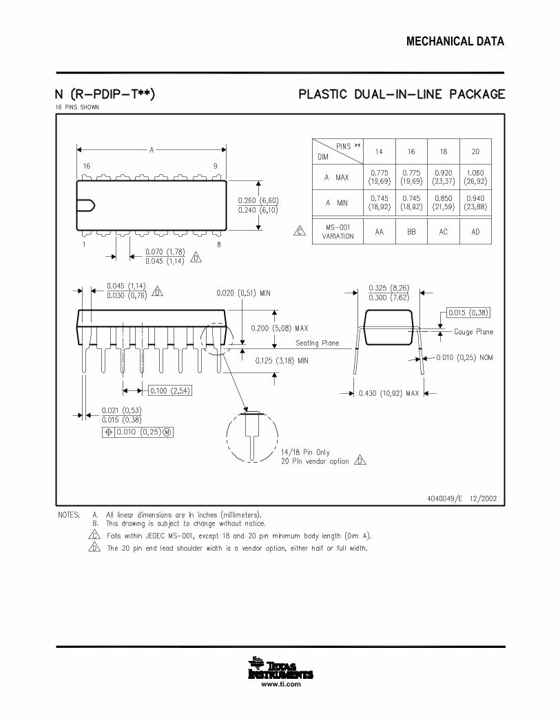
SN74LS11N N PDIP 14 25 506 13.97 11230 4.32
SN74LS11N N PDIP 14 25 506 13.97 11230 4.32
SN74LS11NE4 N PDIP 14 25 506 13.97 11230 4.32
SN74LS11NE4 N PDIP 14 25 506 13.97 11230 4.32
SNJ54LS11FK FK LCCC 20 1 506.98 12.06 2030 NA
PACKAGE MATERIALS INFORMATION
www.ti.com 10-Mar-2022
Pack Materials-Page 3
www.ti.com
PACKAGE OUTLINE
C
14X .008-.014 [0.2-0.36]TYP
-150
AT GAGE PLANE
-.314.308-7.977.83[ ]
14X -.026.014-0.660.36[ ]14X -.065.045
-1.651.15[ ]
.2 MAX TYP[5.08]
.13 MIN TYP[3.3]
TYP-.060.015-1.520.38[ ]
4X .005 MIN[0.13]
12X .100[2.54]
.015 GAGE PLANE[0.38]
A
-.785.754-19.9419.15[ ]
B -.283.245-7.196.22[ ]
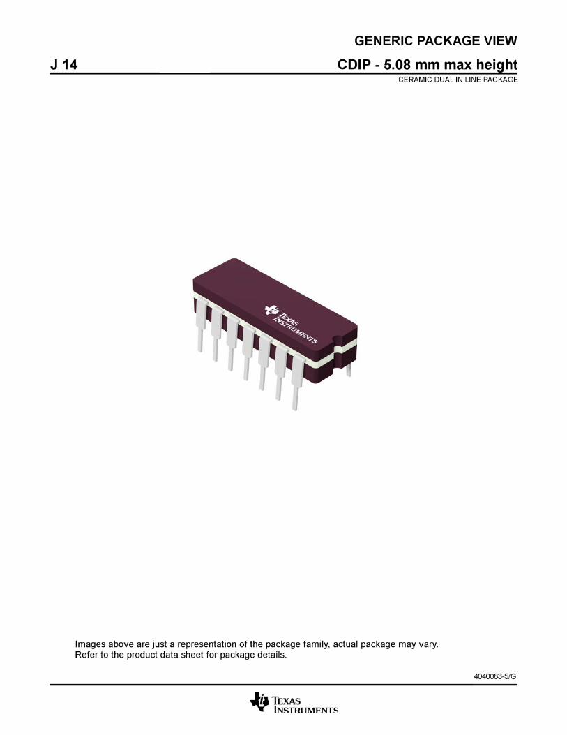
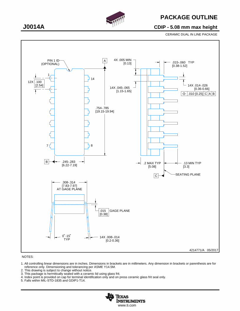
CDIP - 5.08 mm max heightJ0014ACERAMIC DUAL IN LINE PACKAGE
4214771/A 05/2017
NOTES: 1. All controlling linear dimensions are in inches. Dimensions in brackets are in millimeters. Any dimension in brackets or parenthesis are for reference only. Dimensioning and tolerancing per ASME Y14.5M.2. This drawing is subject to change without notice. 3. This package is hermitically sealed with a ceramic lid using glass frit.4. Index point is provided on cap for terminal identification only and on press ceramic glass frit seal only.5. Falls within MIL-STD-1835 and GDIP1-T14.
7 8
141
PIN 1 ID(OPTIONAL)
SCALE 0.900
SEATING PLANE
.010 [0.25] C A B
www.ti.com
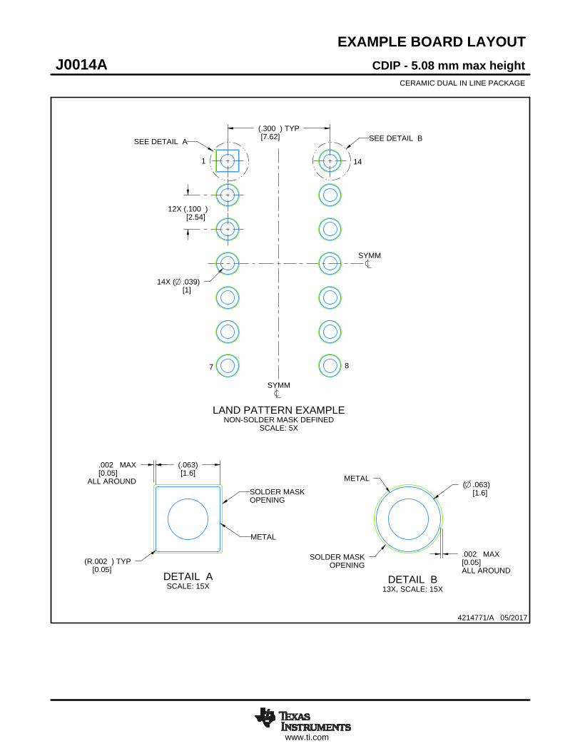
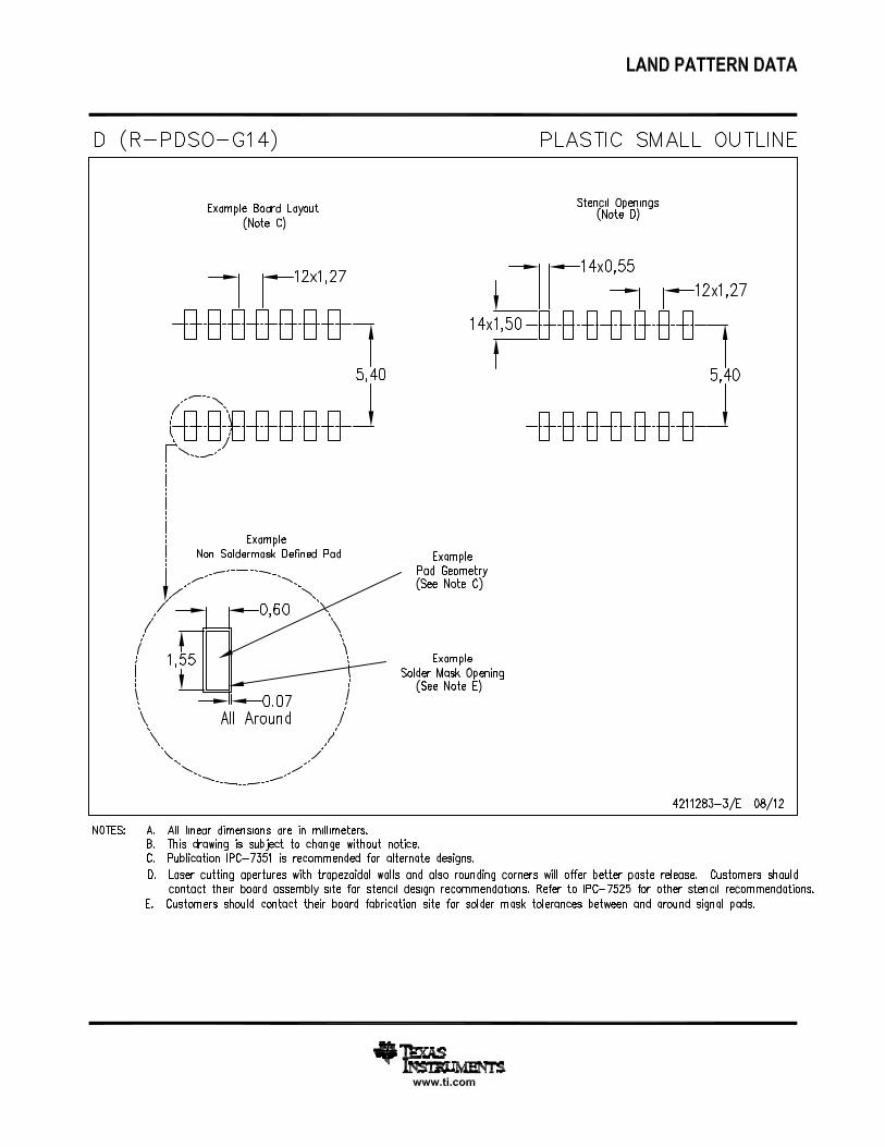
EXAMPLE BOARD LAYOUT
ALL AROUND[0.05]
MAX.002
.002 MAX[0.05]ALL AROUND
SOLDER MASKOPENING
METAL
(.063)[1.6]
(R.002 ) TYP[0.05]
14X ( .039)[1]
( .063)[1.6]
12X (.100 )[2.54]
(.300 ) TYP[7.62]
CDIP - 5.08 mm max heightJ0014ACERAMIC DUAL IN LINE PACKAGE
4214771/A 05/2017
LAND PATTERN EXAMPLENON-SOLDER MASK DEFINED
SCALE: 5X
SEE DETAIL A SEE DETAIL B
SYMM
SYMM
1
7 8
14
DETAIL ASCALE: 15X
SOLDER MASKOPENING
METAL
DETAIL B13X, SCALE: 15X
IMPORTANT NOTICE AND DISCLAIMERTI PROVIDES TECHNICAL AND RELIABILITY DATA (INCLUDING DATA SHEETS), DESIGN RESOURCES (INCLUDING REFERENCE DESIGNS), APPLICATION OR OTHER DESIGN ADVICE, WEB TOOLS, SAFETY INFORMATION, AND OTHER RESOURCES “AS IS” AND WITH ALL FAULTS, AND DISCLAIMS ALL WARRANTIES, EXPRESS AND IMPLIED, INCLUDING WITHOUT LIMITATION ANY IMPLIED WARRANTIES OF MERCHANTABILITY, FITNESS FOR A PARTICULAR PURPOSE OR NON-INFRINGEMENT OF THIRD PARTY INTELLECTUAL PROPERTY RIGHTS.These resources are intended for skilled developers designing with TI products. You are solely responsible for (1) selecting the appropriate TI products for your application, (2) designing, validating and testing your application, and (3) ensuring your application meets applicable standards, and any other safety, security, regulatory or other requirements.These resources are subject to change without notice. TI grants you permission to use these resources only for development of an application that uses the TI products described in the resource. Other reproduction and display of these resources is prohibited. No license is granted to any other TI intellectual property right or to any third party intellectual property right. TI disclaims responsibility for, and you will fully indemnify TI and its representatives against, any claims, damages, costs, losses, and liabilities arising out of your use of these resources.TI’s products are provided subject to TI’s Terms of Sale or other applicable terms available either on ti.com or provided in conjunction with such TI products. TI’s provision of these resources does not expand or otherwise alter TI’s applicable warranties or warranty disclaimers for TI products.TI objects to and rejects any additional or different terms you may have proposed. IMPORTANT NOTICE
Mailing Address: Texas Instruments, Post Office Box 655303, Dallas, Texas 75265Copyright © 2022, Texas Instruments Incorporated