Small π-conjugated organic molecules based transistor and inverter with Cu electrodes
8
Small p-conjugated organic molecules based transistor and inverter with Cu electrodes Sarita Yadav, Pawan K. Srivastava, Subhasis Ghosh ⇑ School of Physical Sciences, Jawaharlal Nehru University, New Delhi 110067, India article info Article history: Received 12 July 2013 Received in revised form 4 September 2013 Accepted 6 September 2013 Available online 24 September 2013 Keywords: Organic inverter Cu electrodes Interface dipole abstract In absence of metallurgical Ohmic contacts in organic semiconductors, the relative position of metal work function with respect to highest occupied molecular orbital (HOMO) or low- est unoccupied molecular orbital (LUMO) decides whether a metal electrode is Ohmic or non-Ohmic. Here we report that Cu whose work function is close to HOMO of the small p-conjugated organic molecules: pentacene and copper phthalocyanine (CuPc), can be used to achieve high performance of transistors and inverters. Fermi level is pinned at metal/copper hexadecafluoro phthalocyanine (F 16 CuPc) interface resulting the barrier for carrier injection from metal to F 16 CuPc independent of metal work functions. We have fab- ricated organic field effect transistors and inverters based on pentacene, CuPc and F 16 CuPc with Cu and Au electrodes and observed that the performance of the devices with Cu elec- trodes are comparable to the devices with Au electrodes. Ó 2013 Elsevier B.V. All rights reserved. 1. Introduction In the last decade, the organic field effect transistors (OFETs) have been investigated extensively for their poten- tial applications in large area flexible display and organic integrated circuits. In particular different parameters such as field effect mobility, threshold voltage, sub-threshold swing and on/off ratio are being attempted to improve constantly [1,2]. However, except the investigations on how to reduce the contact resistance, there is little work on the electrode/organic contacts in OFETs. The properties of interface between source/drain (S/D) electrodes and or- ganic layers in OFETs cannot be optimized with conven- tional processes such as semiconductor doping or metal alloying. Interface properties between S/D electrodes and organic semiconductors are critical factors for OFETs per- formance [3]. To reduce the carrier injection barrier due to the difference in the work function of S/D electrodes and highest occupied molecular orbital (HOMO) or lowest unoccupied molecular orbital (LUMO) of organic semicon- ductor, it is required to choose an appropriate S/D metal electrode that has a work function close to either HOMO or LUMO level in p-type or n-type organic semiconductors, respectively. Until now, Au has been the most widely used S/D electrodes for OFETs. There are some reports on OFETs with Cu S/D electrodes [5,6] but organic inverter using Cu electrodes have not been demonstrated yet. It is important to demonstrate high performance organic inverter based on Cu electrodes. Moreover, it is desirable to achieve sim- ilar or even better performing OFET and inverter with Cu S/ D electrodes compared to Au S/D electrodes. Cu is a viable candidate for electrodes and interconnects in Si-based microelectronics and has enabled designers to pack more than 100 million transistors on a single Si chip. Cu wires conduct electricity almost same as that in Au and about 40 percent less resistive than Al wires. In view of paradigm shift brought by Cu in Si microelectronics, it could be envisaged that Cu as S/D electrode will further advance the development of OFET based microelectronics. The organic inverter which would be the building block for future organic based microelectronics is required for minimal power dissipation and high density device 1566-1199/$ - see front matter Ó 2013 Elsevier B.V. All rights reserved. http://dx.doi.org/10.1016/j.orgel.2013.09.008 ⇑ Corresponding author. Tel.: +91 1126738771. E-mail addresses: [email protected], subhasis.ghosh.jnu@ gmail.com (S. Ghosh). Organic Electronics 14 (2013) 3415–3422 Contents lists available at ScienceDirect Organic Electronics journal homepage: www.elsevier.com/locate/orgel
-
Upload
independent -
Category
Documents
-
view
0 -
download
0
Transcript of Small π-conjugated organic molecules based transistor and inverter with Cu electrodes
Organic Electronics 14 (2013) 3415–3422
Contents lists available at ScienceDirect
Organic Electronics
journal homepage: www.elsevier .com/locate /orgel
Small p-conjugated organic molecules based transistorand inverter with Cu electrodes
1566-1199/$ - see front matter � 2013 Elsevier B.V. All rights reserved.http://dx.doi.org/10.1016/j.orgel.2013.09.008
⇑ Corresponding author. Tel.: +91 1126738771.E-mail addresses: [email protected], subhasis.ghosh.jnu@
gmail.com (S. Ghosh).
Sarita Yadav, Pawan K. Srivastava, Subhasis Ghosh ⇑School of Physical Sciences, Jawaharlal Nehru University, New Delhi 110067, India
a r t i c l e i n f o a b s t r a c t
Article history:Received 12 July 2013Received in revised form 4 September 2013Accepted 6 September 2013Available online 24 September 2013
Keywords:Organic inverterCu electrodesInterface dipole
In absence of metallurgical Ohmic contacts in organic semiconductors, the relative positionof metal work function with respect to highest occupied molecular orbital (HOMO) or low-est unoccupied molecular orbital (LUMO) decides whether a metal electrode is Ohmic ornon-Ohmic. Here we report that Cu whose work function is close to HOMO of the smallp-conjugated organic molecules: pentacene and copper phthalocyanine (CuPc), can beused to achieve high performance of transistors and inverters. Fermi level is pinned atmetal/copper hexadecafluoro phthalocyanine (F16CuPc) interface resulting the barrier forcarrier injection from metal to F16CuPc independent of metal work functions. We have fab-ricated organic field effect transistors and inverters based on pentacene, CuPc and F16CuPcwith Cu and Au electrodes and observed that the performance of the devices with Cu elec-trodes are comparable to the devices with Au electrodes.
� 2013 Elsevier B.V. All rights reserved.
1. Introduction
In the last decade, the organic field effect transistors(OFETs) have been investigated extensively for their poten-tial applications in large area flexible display and organicintegrated circuits. In particular different parameters suchas field effect mobility, threshold voltage, sub-thresholdswing and on/off ratio are being attempted to improveconstantly [1,2]. However, except the investigations onhow to reduce the contact resistance, there is little workon the electrode/organic contacts in OFETs. The propertiesof interface between source/drain (S/D) electrodes and or-ganic layers in OFETs cannot be optimized with conven-tional processes such as semiconductor doping or metalalloying. Interface properties between S/D electrodes andorganic semiconductors are critical factors for OFETs per-formance [3]. To reduce the carrier injection barrier dueto the difference in the work function of S/D electrodesand highest occupied molecular orbital (HOMO) or lowest
unoccupied molecular orbital (LUMO) of organic semicon-ductor, it is required to choose an appropriate S/D metalelectrode that has a work function close to either HOMOor LUMO level in p-type or n-type organic semiconductors,respectively. Until now, Au has been the most widely usedS/D electrodes for OFETs. There are some reports on OFETswith Cu S/D electrodes [5,6] but organic inverter using Cuelectrodes have not been demonstrated yet. It is importantto demonstrate high performance organic inverter basedon Cu electrodes. Moreover, it is desirable to achieve sim-ilar or even better performing OFET and inverter with Cu S/D electrodes compared to Au S/D electrodes. Cu is a viablecandidate for electrodes and interconnects in Si-basedmicroelectronics and has enabled designers to pack morethan 100 million transistors on a single Si chip. Cu wiresconduct electricity almost same as that in Au and about40 percent less resistive than Al wires. In view of paradigmshift brought by Cu in Si microelectronics, it could beenvisaged that Cu as S/D electrode will further advancethe development of OFET based microelectronics.
The organic inverter which would be the building blockfor future organic based microelectronics is requiredfor minimal power dissipation and high density device
(a) (b) (c)
LUMO 3.1 eV
HOMO 4.8 eV
LUMO 3.0 eV
HOMO 4.8 eV Cu 4.5eV
LUMO 4.8eV
HOMO 6.3 eV
Cu 4.5 eV
Au 5.2eV Au 5.2eV
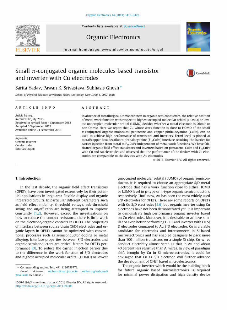
Fig. 1. AFM images of organic semiconductors (a) CuPc (1 lm � 1 lm),(b) F16CuPc (1 lm � 1 lm), and (c) pentacene (5 lm � 5 lm). Schematicrepresentation of energetic positions of highest occupied molecularorbital (HOMO) and lowest occupied molecular orbital (LUMO) of CuPc,F16CuPc and pentacene and relative positions of work function of Cu andAu are also shown.
3416 S. Yadav et al. / Organic Electronics 14 (2013) 3415–3422
integration on an organic microchip. For organic inverter itis necessary that the mobilities and threshold voltage ofn-channel and p-channel OFETs should be similar. Though,p-type pentacene and n-type copper hexadecafluorophthalocyanine (F16CuPc) or C60 are promising organicmaterials for organic inverter, but the OFETs based onthese organic materials have a large difference in mobility.The differences in charge carrier mobility are generallytaken care of by adjusting the channel dimension of OFETin order to drive same current in p- and n-channel of inver-ter [7,8]. Efficient charge injection from the electrodes top-channel and n-channel of inverters based on pentaceneand F16CuPc or pentacene and C60 require different metalelectrodes [9]. Hence a process based on two step pattern-ing of metal electrodes is required for these types of invert-ers. Multistep patterning is still an issue in organicelectronics. These problems can be overcome by usingsame metal for all three electrodes for n-channel andp-channel transistors in inverter [10]. In our previous work[11] we have shown that the device performances can beimproved by increasing the effective contact area betweenS/D electrodes and organic layer with a typical morphologyachieved by engineering different growth parameters. Thegrowth temperature determines the kinetic energy of theadsorbates to overcome the diffusion barrier and the depo-sition rate determines the density of molecules diffusingon the substrate. Hence, the engineering of thin filmgrowth to obtain high quality thin film with low structuraldisorders requires appropriate balancing between diffu-sion and deposition flux to optimize the growth processand desired film morphology. By optimization of growthconditions we have found that at growth temperature�100 �C and at very low evaporation rate �0.1 Å/s, copperphthalocyanine (CuPc) and F16CuPc thin films based OFETshave similar mobility and threshold voltage. This ensuresdesirable voltage transfer characteristics of inverter withswitching voltage at half of supply voltage. The surfacemorphology of pentacene and phthalocyanine thin filmsare different [12,13]. On the contrary, the OFETs fabricatedon pentacene thin film grown at higher substrate temper-ature show poor device performance, because at highersubstrate temperature desorption of molecule occurredresulting low surface coverage.
In this paper, we show that Cu S/D electrodes can beused for both n-type and p-type organic semiconductorsto be used for n-channel and p-channel OFETs. We haveused pentacene and CuPc as p-channel and F16CuPc as n-channel transistors in inverter. The pentacene and CuPcare technologically important organic molecular semicon-ductors (OMSs), and they have completely different surfacemorphologies. CuPc thin films show elongated [11] grainystructure whereas pentacene thin films show pyramidalgrowth which is combination of diffusion limited aggrega-tion (DLA) with vertical mound growth [12,13]. F16CuPc ismost thermally stable n-type OMS and shows similar mor-phology in thin films as in case of CuPc. The HOMO ofpentacene, CuPc and LUMO of F16CuPc are close to thework function of Cu so it can be used as S/D electrodesfor these organic materials. Two sets of inverter;Inverter-I, consisting p-channel of CuPc and n-channel ofF16CuPc and Inverter-II comprised of p-channel of
pentacene and n-channel of F16CuPc with Au and Cu elec-trodes have been fabricated and compared.
2. Results and discussion
Fig. 1 shows the AFM images and schematic illustra-tions of energy level diagram of pentacene, CuPc and F16-
CuPc with respect to work function of metal electrodes.The surface morphology of CuPc and F16CuPc thin filmsare similar and consist of elongated grains whereas penta-cene thin film shows the DLA growth with pyramidalstructures. Fig. 1 also shows the relative positions of metalwork functions with respect to electron affinity (v) or low-est unoccupied molecular orbital (LUMO) of OMS and ion-ization potential (I) or highest occupied molecular orbital(HOMO). The energy level alignment at metal–organicsemiconductor (MOS) interfaces is the most crucial forthe performance of the OFET. At MOS interface, the barrierfor electrons (UBe) and holes (UBh) depend on the v and I ofOMS, respectively. Depending on the degree to which thebarriers for charge injection at MOS interface vary withmetal work function (UM), two extreme cases are consid-ered: vacuum-level alignment (VLA) [14], known asMott–Schottky limit and Fermi level pinning [14,15].According to Mott–Schottky VLA rule, the energy barriersthat control the electrons (holes) are entirely determinedby UM and v(I). But, it has been found [4,14,15] as in caseof metal/inorganic semiconductor interfaces, energy levelalignment at interface departs from ideal situation, i.e.VLA. Detailed investigations using photoemission spectros-copy (PES) by different groups [4,16–21] have shown thatthe mechanism of carrier injection is much more compli-cated than the simple energy level alignment predicted
S. Yadav et al. / Organic Electronics 14 (2013) 3415–3422 3417
by VLA. The work function of Au and Cu are 5.2 eV and4.5 eV, respectively. The I of pentacene and CuPc are at4.8 eV [22] and v of the F16CuPc is at 4.8 eV [23]. If VLAis assumed for determining the injection for barrier atMOS interfaces. There would be (i) no barrier for holes atAu/pentacene and Au/CuPc interfaces, (ii) a small barrierof 0.3 eV for holes at Cu/pentacene and Cu/CuPc interfaces,(iii) no barrier for electrons at Cu/F16CuPc interface and (iv)a small barrier of 0.4 eV for electrons at Au/F16CuPc inter-face (Fig. 1). Whether VLA can explain the experimentalobservation on OFETs with Au and Cu electrodes, or depar-ture from VLA or other extreme situation i.e. Fermi levelpinning is required to be invoked, will be discussed atthe end.
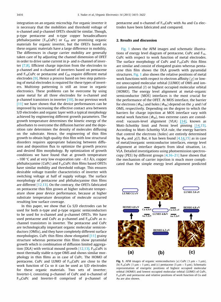
Figs. 2 and 3 show the output and transfer characteris-tics of p-type pentacene and CuPc based OFET with Cu andAu S/D electrodes. Pentacene based OFET with Au (Fig. 2c)and Cu (Fig. 2a) S/D electrodes exhibit high saturation cur-rent of 5.3 � 10�5 A and 3.0 � 10�5 A (at VGS = �60 V),respectively, showing a small difference in saturation cur-rent of transistors with Au and Cu electrodes and almostsimilar charge carrier mobility (�0.2 cm2 V�1 s�1) has beenobserved in pentacene OFET with Au and Cu S/D elec-trodes. The threshold voltage of pentacene based OFETwith Cu S/D electrodes is �1.1 V which is less than that(�5.0 V) with Au S/D electrodes. Thus it can be inferredthat the device performance of pentacene based OFET withCu S/D electrodes is comparable to that with Au S/D elec-trodes. In CuPc based OFETs the field effect mobilities of
-30
-20
-10
0
(a)VGS -60 V
I DS( μ
A)
-45
-30
-15
0
-50 -40 -30 -20 -10 0
(c)
VGS -60V
VDS (V)
I DS(μ
A)
Fig. 2. Output and transfer characteristics of p-type pentacene based OFET with (the step of 10 V. The transfer characteristics were measured at VDS = �1 V.
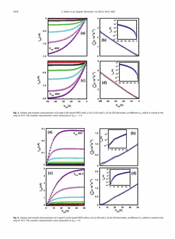
holes are 1.3 � 10�3 cm2 V�1 s�1 and 1.1 � 10�2 cm2 V�1 -s�1 with Cu (Fig. 3a) and Au (Fig. 3c) S/D electrodes, respec-tively, inferring a one order increment in mobility with AuS/D electrodes. The threshold voltages are �2.2 V and�1.0 V in CuPc based OFETs with Cu and Au electrodes,respectively. Fig. 4 shows the transistor characteristics ofn-type F16CuPc based OFET. The F16CuPc based OFETs showa small difference in field effect mobility with Cu(7.5 � 10�3 cm2 V�1 s�1) and Au (1.3 � 10�2 cm2 V�1 s�1)S/D electrodes. Threshold voltage is 0.9 V for F16CuPc basedOFET with Cu S/D electrodes which are lower than thatwith the Au electrodes (3.3 V). Therefore it can be inferredthat Cu can be used as S/D electrodes in pentacene, CuPcand F16CuPc based OFETs and could be used for all threeelectrodes in organic inverter. Table 1 summarizes theparameters of OFETs based on pentacene, CuPc and F16-
CuPc with Cu and Au S/D electrodes.Fig. 5 shows the voltage transfer characteristics and
gain of inverter comprised of p-channel of CuPc andn-channel of F16CuPc (Inverter-I) and Fig. 6 shows thetransfer characteristics of inverter comprised of p-channelof pentacene and n-channel of F16CuPc (Inverter-II) withCu and Au S/D electrodes as discussed in previous section.The common gate and common top electrode of p andn-channel act as the input (VIN) and output (VOUT) terminalof inverter, respectively. The performance of an inverter isevaluated by its noise margin, static gain and switchingvoltage which are determined by voltage transfercharacteristics. All devices show the clear switching
(b)
0
1.5
3.0
4.5
6.0
7.5
I1/2
DS(x
10-4
A1/
2 )
10-11
10-10
10-9
10-8
10-7
10-6
-50 -40 -30 -20 -10 0
I DS(A
)
0
20
40
-50 -40 -30 -20 -10 0
(d)
VGS(V)
DS
I1/2 (x
10-4
A1/
2 )
10-10
10-8
10-6
-50 -40 -30 -20 -10 0
I DS(A
)
a, b) Cu S/D and (c, d) Au S/D electrodes, at different VGS which is varied at
-2.8
-1.8
-0.8
-50 -40 -30 -20 -10 0
VGS -60V
(c)
VDS(V)
I DS(μ
A)
-1.5
-1.0
-0.5
0
VGS -60V
(a)I D
S( μA
)
0
1
2
3
4
(b)
I1/2
DS(x
10-4
A1/
2 )
10-11
10-10
10-9
10-8
10-7
10-6
-50 -40 -30 -20 -10 0
I DS(A
)
0
2
4
6
8
-50 -40 -30 -20 -10 0
(d)
VGS(V)
I1/2
DS(x
10-4
A1/
2 )
10-11
10-10
10-9
10-8
10-7
10-6
-50 -40 -30 -20 -10 0
I DS(A
)Fig. 3. Output and transfer characteristics of p-type CuPc based OFET with (a, b) Cu S/D and (c, d) Au S/D electrodes, at different VGS which is varied at thestep of 10 V. The transfer characteristics were measured at VDS = �1 V.
0
0.1
0.2
0.3
VGS 60V(a)
I DS(μ
A)
0
0.5
1.0
1.5 (b)
I DS
1/2 (x
10-4
A1/2 )
10-10
10-9
10-8
0 10 20 30 40 50
I DS(A
)
0
0.5
1.0
1.5
2.0
0 10 20 30 40 50
(d)
VGS(V)
I1/2
DS(x
10-4
A1/2 )
10-12
10-11
10-10
10-9
10-8
10-7
0 10 20 30 40 50
I DS(A
)
0
1
2
3
4
5
0 10 20 30 40 50
(c) VGS 60 V
VDS(V)
I DS(μ
A)
Fig. 4. Output and transfer characteristics of n-type F16CuPc based OFET with (a, b) Cu S/D and (c, d) Au S/D electrodes, at different VGS which is varied at thestep of 10 V. The transfer characteristics were measured at VDS = 1 V.
3418 S. Yadav et al. / Organic Electronics 14 (2013) 3415–3422
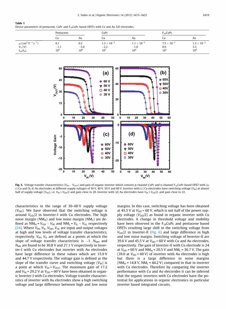
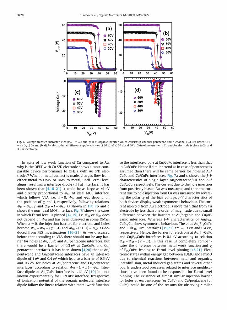
Table 1Device parameters of pentacene, CuPc and F16CuPc based OFETs with Cu and Au S/D electrodes.
Pentacene CuPc F16CuPc
Cu Au Cu Au Cu Au
l (cm2 V�1 s�1) 0.1 0.2 1.3 � 10�3 1.1 � 10�2 7.5 � 10�3 1.3 � 10�2
VT (V) �1.1 �5.0 �2.2 �1.0 0.9 3.3Ion/Ioff 105 106 103 104 103 104
-20
-15
-10
-5
0
0 10 20 30 40 50
60V50V40V30V
(c)
VIN (V)
Volta
ge G
ain
0
15
30
45
60
0 10 20 30 40 50
60 V50 V40 V30 V
(a)
V OU
T(V
)
0
20
40
60
0 10 20 30 40 50 60
60V50V40V30V
(b)
-20
-10
0
0 10 20 30 40 50 60
60V50V40V30V
(d)
VIN(V)
Fig. 5. Voltage transfer characteristics (VIN � VOUT) and gain of organic inverter which consists p-channel CuPc and n-channel F16CuPc based OFET with (a,c) Cu and (b, d) Au electrodes at different supply voltages of 30 V, 40 V, 50 V and 60 V. Inverter with (c) Cu electrodes have switching voltage (VM) at almosthalf of supply voltage (VDD), i.e. VM = VDD/2 and gain close to 20. Inverter with (d) Au electrodes have VM > VDD/2, and gain close to 22.
S. Yadav et al. / Organic Electronics 14 (2013) 3415–3422 3419
characteristics in the range of 30–60 V supply voltage(VDD). We have observed that the switching voltage isaround VDD/2 in Inverter-I with Cu electrodes. The highnoise margin (NMH) and low noise margin (NML) are de-fined as NMH = VOH � VIH and NML = VIL � VOL respectively[24]. Where VIH, VIL, VOH, VOL are input and output voltagesat high and low levels of voltage transfer characteristics,respectively. VIH, VIL are defined as a points at which theslope of voltage transfer characteristic is �1. NMH andNML are found to be 30.8 V and 27.1 V respectively in Inver-ter-I with Cu electrodes but inverter with Au electrodeshave large difference in these values which are 15.9 Vand 44.7 V respectively. The voltage gain is defined as theslope of the transfer curve and switching voltage (VM) isa point at which VIN = VOUT. The maximum gain of 17.2and VM = 29.2 V at VDD = 60 V have been obtained in organ-ic Inverter-I with Cu electrodes. Voltage transfer character-istics of inverter with Au electrodes show a high switchingvoltage and large difference between high and low noise
margins. In this case, switching voltage has been obtainedat 45.5 V at VDD = 60 V, which is not half of the power sup-ply voltage (VDD/2) as found in organic inverter with Cuelectrodes. A change in threshold voltage and mobilityhave been observed in the F16CuPc and pentacene basedOFETs resulting large shift in the switching voltage fromVDD/2 in Inverter-II (Fig. 6) and large difference in highand low noise margin. Switching voltage of Inverter-II are39.6 V and 45.5 V at VDD = 60 V with Cu and Au electrodes,respectively. The gain of Inverter-II with Cu electrode is 24at VDD = 60 V and NMH = 20.5 V and NML = 36.7 V. The gain(39.0 at VDD = 60 V) of inverter with Au electrodes is highbut there is a large difference in noise margins(NMH = 14.8 V, NML = 44.2 V) compared to that in inverterwith Cu electrodes. Therefore by comparing the inverterperformance with Cu and Au electrodes it can be inferredthat the organic inverters with Cu electrodes have the po-tential for applications in organic electronics in particularinverter based integrated circuits.
-30
-20
-10
0
0 10 20 30 40 50 60
60V50V40V30V
(c)
VIN(V)
Volta
ge G
ain
0
20
40
60
0 10 20 30 40 50 60
60V50V40V30V
(b)
-30
-10
0 10 20 30 40 50 60
60V50V40V30V
(d)
VIN(V)
0
20
40
60
0 10 20 30 40 50 60
60V50V40V30V
(a)
V OU
T(V)
Fig. 6. Voltage transfer characteristics (VIN � VOUT) and gain of organic inverter which consists p-channel pentacene and n-channel F16CuPc based OFETwith (a, c) Cu and (b, d) Au electrodes at different supply voltages of 30 V, 40 V, 50 V and 60 V. Gain of inverter with Cu and Au electrode is close to 24 and39, respectively.
3420 S. Yadav et al. / Organic Electronics 14 (2013) 3415–3422
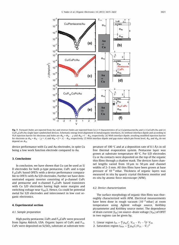
In spite of low work function of Cu compared to Au,why is the OFET with Cu S/D electrode shows almost com-parable device performance to OFETs with Au S/D elec-trodes? When a metal contact is made, charges flow fromeither metal to OMS, or OMS to metal, until Fermi levelaligns, resulting a interface dipole (D) at interface. It hasbeen shown that [4,16–21] D could be as large as ±1 eVand directly proportional to UM. At ideal MOS interface,which follows VLA, i.e. D = 0, UBe and UBh depend onthe position of v and I, respectively, following relations,UBe = UM�v and UBh = I �UM, as shown in Fig. 7b and dshows the non-ideal MOS interface. Fig. 7f shows the casesin which Fermi level is pinned [14,15], i.e. UBe or UBh doesnot depend on UM and has been observed in some OMSs.When D – 0, the injection barriers for electrons and holesbecome UBe = UM � (v ± D) and UBh = (I ± D) �UM, as de-duced from PES investigations [16–21]. As we discussedbefore that according to VLA there should not be any bar-rier for holes at Au/CuPc and Au/pentacene interfaces, butthere would be a barrier of 0.3 eV at Cu/CuPc and Cu/pentacene interfaces. It has been shown [4,20] that at Au/pentacene and Cu/pentacene interfaces have an interfacedipole of 1 eV and 0.4 eV which lead to a barrier of 0.6 eVand 0.7 eV for holes at Au/pentacene and Cu/pentaceneinterfaces, according to relation UBh = (I + D) �UM. Inter-face dipole at Au/CuPc interface is �1.1 eV [19] but notknown experimentally for Cu/CuPc interface. Irrespectiveof ionization potential of the organic molecule, interfacedipole follow the linear relation with metal work function,
so the interface dipole at Cu/CuPc interface is less than thatin Au/CuPc. Hence if similar trend as in case of pentacene isassumed then there will be same barrier for holes at Au/CuPc and Cu/CuPc interfaces. Fig. 7a and c shows the J–Vcharacteristics of single layer Au/pentacene/Cu and Au/CuPc/Cu, respectively. The current due to the hole injectionfrom positively biased Au was measured and then the cur-rent due to hole injection from Cu was measured by revers-ing the polarity of the bias voltage. J–V characteristics ofboth devices display weak asymmetric behaviour. The cur-rent injected from Au electrode is more than that from Cuelectrode by less than one order of magnitude due to smalldifference between the barriers at Au/organic and Cu/or-ganic interfaces. Whereas J–V characteristics of Au/F16-
CuPc/Cu show symmetric behaviour. The D at Au/F16CuPcand Cu/F16CuPc interfaces [19,21] are �0.3 eV and 0.4 eV,respectively. Hence, the barrier for electrons at Au/F16CuPcand Cu/F16CuPc interfaces is 0.1 eV according to relationUBe = UM � (v � D). In this case, D completely compen-sates the difference between metal work function and vof F16CuPc, leading to Fermi level pinning [15,21]. Elec-tronic states within energy gap between LUMO and HOMOdue to chemical reactions between metal and organics,interdiffusion, metal induced gap states and several otherpoorly understood processes related to interface modifica-tions, have been found to be responsible for Fermi levelpinning. The existence of almost similar injection barrierfor holes at Au/pentacene (or CuPc) and Cu/pentacene (orCuPc), could be one of the reasons for observing similar
HOMO
LUMO
Au or Cu
χ
I
ΔΦM
ΦBe
(d)
ΦBh
PentaceneCuPc
HOMO
LUMO
Au Or Cu
χ
I
ΔΦM
(f)
ΦBe
ΦBh
F16CuPc
I
Evac
LUMO
Au or Cu
χΔ=0
ΦM
ΦBe
ΦBh
HOMO
(b)
(c)
10-8
10-7
10-6
10-5
10-4
10-3
Cu/CuPc/Au
J (A
mp/
cm2 )
10-8
10-7
10-6
10-5
10-4
10-3
-3 -2 -1 0 1 2 3
Cu/F CuPc/Au16
V
10-8
10-7
10-6
10-5
10-4
10-3
Cu/Pentacene/Au
(e)
(a)
Fig. 7. Forward (holes are injected from Au) and reverse (holes are injected from Cu) J–V characteristics of (a) Cu/pentacene/Au and (c) Cu/CuPc/Au and (e)Cu/F16CuPc/Au single layer sandwiched devices. Schematic energy level alignment in metal/organic interfaces, (b) without interface dipole and according toVLA injection barrier for electrons and holes are UBe = UM � v and UBh = I �UM, respectively. (d) With interface dipole, resulting modified injection barrierfor electrons as UBe = UM � (v + D) and UBh = (I + D) �UM, respectively. (f) With interface dipole and gap states which pin Fermi level, UBe and UBh do notdepend on UM.
S. Yadav et al. / Organic Electronics 14 (2013) 3415–3422 3421
device performance with Cu and Au electrodes, in spite Cubeing a low work function electrode compared to Au.
3. Conclusions
In conclusion, we have shown that Cu can be used as S/D electrodes for both p-type pentacene, CuPc and n-typeF16CuPc based OFETs with a device performance compara-ble to OFETs with Au S/D electrodes. Further we have dem-onstrated organic inverter consisting of p-channel CuPcand pentacene and n-channel F16CuPc based transistorswith Cu S/D electrodes having high noise margins andswitching voltage near VDD/2. Hence, Cu could be potentialmetal for S/D electrodes and interconnect in low cost or-ganic electronics.
4. Experimental section
4.1. Sample preparation
High purity pentacene, CuPc and F16CuPc were procuredfrom Sigma Aldrich, USA. Organic layers of CuPc and F16-
CuPc were deposited on Si/SiO2 substrate at substrate tem-
perature of 100 �C and at a deposition rate of 0.1 Å/s in oilfree thermal evaporation system. Pentacene layer wasgrown at substrate temperature 40 �C. For S/D electrodesCu or Au contacts were deposited on the top of the organicthin films through a shadow mask. The devices have chan-nel lengths varied from 10 lm to 50 lm and channelwidths of 2–3 mm. All thin films have been grown at basepressure of 10�6 mbar. Thickness of organic layers wasmeasured in situ by quartz crystal thickness monitor andex-situ by atomic force microscope (AFM).
4.2. Device characterization
The surface morphology of organic thin films was thor-oughly characterized with AFM. Electrical measurementshave been done in rough vacuum (10�2 mbar) at roomtemperature using Agilent voltage source, Keithleypicoammeter and Keithley source meter. The dependenceof drain current (IDS) on source–drain voltage (VDS) of OFETin two regions can be given by,
1. Linear region IDS ¼ WL lFECi VGS � VT � VDS
2
� �VDS
2. Saturation region IDSat ¼ W2L lFECiðVGS � VTÞ2

3422 S. Yadav et al. / Organic Electronics 14 (2013) 3415–3422
where lFE is the field effect carrier mobility of the organicsemiconductor, W/L is the channel width to length ratio, Ci
the capacitance per unit area of SiO2 layer. OFETs normallyoperate in accumulation mode, where an increase in gatevoltage (VGS) enhances the conductivity of the channel.The charge carrier mobility is calculated in the linearregime by fitting the IDS–VDS characteristic.
Acknowledgements
SY and PKS thank Council of Scientific & Industrial Re-search, India, for the financial support through fellowship.This work was partly supported by DST, Govt. of India.
References
[1] H. Sirringhaus, Adv. Mater. 21 (2009) 3859.[2] P. Kumar, A. Sharma, S. Chaudhuri, S. Ghosh, Appl. Phys. Lett. 99
(2011) 173304.[3] D. Natali, M. Caironi, Adv. Mater. 24 (2012) 1357.[4] S. Braun, W.R. Salaneck, M. Fahlman, Adv. Mater. 21 (2009) 1450.
[5] C. Di, G. Yu, Y. Liu, Y. Guo, Y. Wang, W. Wu, D. Zhu, Adv. Mater. 20(2008) 1286.
[6] W. Gu, W. Jin, B. Wei, J. Zhang, J. Wang, Appl. Phys. Lett. 97 (2010)243303.
[7] H. Klauk, U. Zschieschang, J. Pflaum, M. Halik, Nature 445 (2007) 745.[8] H. Klauk et al., IEEE Trans. Electron. Dev. 52 (2005) 618.[9] M. Kitamura, Y. Arakawa, Appl. Phys. Lett. 91 (2007) 053505.
[10] S. Yadav, A. Sharma, S. Ghosh, Appl. Phys. Lett. 102 (2013) 093303.[11] S. Yadav, P. Kumar, S. Ghosh, Appl. Phys. Lett. 101 (2012) 193307.[12] R. Ruiz et al., Chem. Mater. 16 (2004) 4497.[13] S. Zorba, Y. Shapir, Y. Gao, Phys. Rev. B 74 (2006) 245410.[14] S.M. Sze, Physics of Semiconductor Devices, second ed., Wiley, New
York, 1981.[15] R. Agrawal, S. Ghosh, Appl. Phys. Lett. 89 (2006) 222114.[16] D. Kahen, A. Kahn, Adv. Mater. 15 (2003) 271.[17] I.G. Hill, A. Rajagopal, A. Kahn, Y. Hu, Appl. Phys. Lett. 73 (1998) 662.[18] H. Ishii, K. Sugiyama, E. Ito, K. Seki, Adv. Mater. 11 (1999) 605.[19] H. Peisert, M. Knupfer, J. Fink, Appl. Phys. Lett. 81 (2002) 2400.[20] N.J. Watkins, Li Yan, Y. Gao, Appl. Phys. Lett. 80 (2002) 4384.[21] A. Kahn, N. Koch, W. Gao, J. Polym. Sci.: B 41 (2003) 2529.[22] R. Agrawal, P. Kumar, S. Ghosh, A.K. Mahapatro, Appl. Phys. Lett. 93
(2008) 073311.[23] C. Shen, A. Kahn, J. Appl. Phys. 90 (2001) 4549.[24] K.C. Smith, A.S. Sedra, Microelectronics Circuits, fifth ed., Oxford,
New York, 2004.