Failure of an ACCIS metal-on-metal hip resurfacing prosthesis: A ...

IEEE ENGINEERING IN MEDICINE AND BIOLOGY MAGAZINE SEPTEMBER/OCTOBER 2006 470739-5175/06/$20.00©2006IEEE
CLIN
ICA
L NEU
ROEN
GIN
EERING
: PART 2
Silicon LSI-BasedSmart Stimulatorsfor Retinal ProsthesisA Flexible and Extendable Microchip-Based Stimulator
BY JUN OHTA, TAKASHI TOKUDA,KEIICHIRO KAGAWA, TETSUO FURUMIYA,AKIHIRO UEHARA, YASUO TERASAWA,MOTOKI OZAWA, TAKASHI FUJIKADO,AND YASUO TANO
©EYEWIRE
Neural electronic stimulators play an important rolein neuroscience and clinical neuroengineering.Stimulators are now commercially available,while others continue to be developed [1]–[11].As examples in clinical neuroengineering, stimu-
lators have been applied to cochlear prostheses [12], [13] andretinal prostheses [14]–[20]. In this article, we focus on retinalprosthesis as schematically shown in Figure 1. In the configu-ration, the implanted stimulator is placed upon the supra-choroid; this stimulation method is called STS (suprachoroidaltransretinal stimulation) [21], [22].
The stimulator includes several electrodes that stimulate theretinal cells electrically and evoke a spatial phosphen pattern.Thus, the number of the electrodes is considered to be impor-tant, although at the present time, only a small number ofstimulus electrodes have been realized. Creating devices withover 1,000 electrodes is challenging; such a large number ofconnections between electrodes and external lead wires areextremely difficult to fabricate.
Recently, neural interface devices based on silicon micro-electronics or large-scale-integration (LSI) have emerged[23]–[38]. Since LSI allows the integration of smart functionssuch as control, amplification, and signal processing with thestimulators, LSI-based neural interface devices are attractingsignificant interest. To solve the interconnection issue, wehave proposed the introduction of LSI technologies to retinalprosthesis devices [39]–[48]. In addition to solving the inter-connections issue, LSI-based stimulators bring several advan-tages to photosensors for subretinal implantation. We havestudied LSI-based stimulators for STS [47], [48], subretinalimplantation [39]–[44], and epiretinal implantation [45].
There are many technical challenges to overcome whenapplying LSI-based neural interface devices to retinal prosthe-sis. First, the LSI-based interface must be biocompatible. Astandard LSI structure is not at all suitable in a biological envi-ronment; silicon nitride is conventionally used as a protectivetop layer in standard LSIs but is eroded in a biological envi-ronment. Second, the stimulus electrodes must be compatiblewith the standard LSI structure; aluminum is conventionallyused for wire-bonding pads in standard LSIs but is completelyinadequate as a stimulus electrode for neural cells because alu-minum dissolves in saline solution. Third, in addition to the
electrode material, the shape of the electrode affects the effi-ciency of stimulation, with a convex shape being suitable forefficient stimulation. Consequently, we need to develop acompletely new packaging technology that fits into a standardLSI structure, is biocompatible, and is effective in stimulatingneural cells. Finally, the devices must also be thin and flexibleto fit the anatomy of target organs and to avoid damaging tis-sues. However, silicon, the base material of the LSI chip, is sorigid that thinning of the LSI chip increases the risk of break-age. We have previously demonstrated that an image sensormade of silicon thinner than 50 µm can be bent and can oper-ate with sufficient accuracy [41]. Such a thinned LSI chip,however, must be handled very carefully. To overcome theissue of mechanical rigidity and to realize a feasible LSI-basedneural interface device, we have proposed a device architec-ture consisting of silicon (Si)-based microchips that coopera-tively operate under a single set of control signals [46]–[48].
In this article, we report on a retinal prosthesis smart stimu-lator that is biocompatible and fully compatible with a stan-dard LSI structure and that provides high-stimulationefficiency. Our stimulator is based on multimicrochip archi-tecture. We have specifically developed the stimulator for reti-nal prostheses, but it could be applied to other neuroscienceand clinical neuroengineering fields.
Si-LSI Based Stimulator: Operation Principle and Fundamental Characteristics
Circuit Design IssuesTo stimulate retinal cells effectively, biphasic current pulsestimulation is generally preferred [49]. In addition, biphasicpulses are required to maintain the charge balance of the bio-logical environment [50]. When such stimulation is imple-mented using standard LSI technology, a necessaryconsideration is that the output current and voltage range muststay within the limits of the technology. That is, the outputcurrent must stay within about −500 to +500 µA and thevoltage from slightly below 0 V to the power supply voltageVdd of the LSI technology used; for example, using standard0.6-µm CMOS (complementary metal oxide semiconductor)technology, the range is from −0.5 to +5.5 V. It is noted thatwhen we use a biphasic current pulse, the reference voltage

IEEE ENGINEERING IN MEDICINE AND BIOLOGY MAGAZINE SEPTEMBER/OCTOBER 2006
Vref is usually set at half of the full swing of voltage range inthe system used, and, therefore, the voltage swing in onepolarity must be less than 0.5 × Vdd . For example, forVdd = 5 V, the positive voltage swing must be less than 2.5 V.Consequently, it is necessary to design an LSI that can outputenough high pulse current amplitude in the voltage range in abiological environment such as saline solution.
Electrodes and PackagingThe electrodes and packaging technologies used in thedesign of a standard LSI-based stimulator are nowdescribed. Figure 2(a) shows the fabrication process for ourelectrode [47], [48]. First, a platinum/gold (Pt/Au) stackedbump structure is formed on an aluminum (Al)-bondingpad in a standard LSI chip. Aluminum cannot be used inthe biological environment, but platinum is a suitable elec-trode material due to its excellent biocompatibility andcharge injection efficiency [51]–[53]. The platinum elec-trode juts out of the top surface of the chip to enable closecontact with neural cells. To make this jutting platinumelectrode, we have formed the stacked bump in two steps,in which a gold bump is initially formed and a platinumbump is formed on top. The gold bump acts as a cushionfor the hard platinum bump; direct formation of the plat-inum bump sometimes breaks the LSI I/O pad.
After fabrication of the stacked Pt/Au bump, the entire LSIchip, including the bonding wires, is covered with a biocom-patible epoxy resin. Finally, the resin on top of the electrodes iscompletely removed using a high-power argon (Ar) ion laser;thus the entire LSI chip, except for the top of the platinum elec-trodes, is covered with resin. Parylene coating can be addition-ally applied to the resin to ensure durability in the biological
environment and can also be removedby the Ar ion laser.
Figure 2(b) shows a scanning elec-tron micrograph (SEM) of the stackedPt/Au bump electrodes fabricated onan LSI chip. The diameter of thestructure is about 100 µm and can becontrolled by changing the silver andplatinum wire diameter. We haveobtained good reproducibility in fabri-cating over 100 such bump electrodesusing an automatic bump bonder. Thecoating has been confirmed to protectthe interior of the LSI chip, includingthe area close to the electrodes, fromthe biological environment. It is notedthat other high-efficiency, biocompati-ble electrode materials such as iridiumoxide (IrOx ) and titanium nitride(TiN) [54], [55] can be deposited onthe platinum bump.
Operation in Saline SolutionTo assess the applicability of the elec-trodes and packaging technologies, weoperated the fabricated stimulator in asaline environment. The stimulator
Fig. 1. The conceptual drawing of a retinal prosthesis. Theimplanted chip is placed upon the suprachoroid in thiscase [47].
Fig. 2. Pt/Au stacked bump electrodes on an LSI chip. (a) Fabrication process flow: (1)gold bump forming, (2) pressing of gold bump, (3) platinum bump forming, (4) pressingof platinum bump, (5) molding, and (6) platinum exposure. (b) SEM photograph [48].
Secondary Coil
Flexible Cables
ReferenceElectrode
Primary Coil
RF Power/DataTrans/Rec. Chip
StimulatorChip
Au Bump
AI Pad(1)
(2)
(3)
(4)
(5)
(6)
AI Pad
Press
Press
Epoxy
Epoxy
Laser Fabrication
(a) (b)
AI I/O Pad
Au Bump Pt Bump
Circuits
029812 5 KV × 150 14 mm100 m
Pt Bump
48
We need to develop a completely new
packaging technology that fits into a standard
LSI structure, is biocompatible, and is effective
in stimulating neural cells.
IEEE ENGINEERING IN MEDICINE AND BIOLOGY MAGAZINE SEPTEMBER/OCTOBER 2006
chip was fabricated in 0.6-µm standard CMOS technology.The chip formed with a Pt/Au stacked bump electrode waswire-bonded to a test board and was molded. Then the coat-ing on the platinum electrode was removed by an excimerlaser to leave an exposed area with a diameter of about 20µm, by the process described above. A reservoir of salinesolution was formed around the chip. Figure 3(a) shows theprocessed chip on the test board with the reservoir. Thedetails of the circuits are described in a later section.
The molded chip was dipped in saline solution and thereference voltage Vref = 1.5 V was supplied via ansilver/silver chloride (Ag/AgCl) reference electrode. Thebiphasic pulse parameters are theamplitudes of the cathodic and anodiccurrents, Ic and Ia , and the pulsedurations of the anodic, cathodic, andinterpulses, tc, ti, and ta. In this work,we fixed |Ic| = Ia . The pulse dura-tions tc, ti, and ta were set to the samevalue. Hence, the biphasic pulsewaveform can simply be described bythe amplitude and interval, for exam-ple, 100 µA/100 µs.
Figure 3(b) shows the measuredoperational voltage for three bipha-sic, current-controlled pulses. Thepulse parameters used are shown inthe figure. Similar reports on neuralstimulation using platinum electrodessuggest that the trace presented inFigure 3(b) is reasonable for acathodic-first biphasic charge injec-tion [51], [52]. In Figure 3(b), theoperational voltage lies within thevoltage swing of the chip (from −0.5to +5.5 V for the present device) fortypical conditions in retinal cell stim-ulation experiments. This indicatesthat the LSI chip can output suffi-cient biphasic current pulses to stim-ulate retinal cells.
Another consideration relates to theelectrochemical aspect of currentinjection into a biological environ-ment. Current injection from an elec-trode into saline (or other biologicalsolution) includes electrochemicalreactions at the interface. Excess volt-ages applied to the interface causeirreversible chemical reactions such aselectrolysis and the formation of bub-
bles [52], [53]. The current injection for neural stimulationneeds to be carried out without causing irreversible electrol-ysis or bubbles. The current injection capability depends onthe material and surface structure of the electrode. In ourexperiments, we have confirmed in electrochemical experi-ments using platinum electrodes that the voltage for appro-priate current injection swings within the safe range forreversible electrochemical processes. In addition, weobserved no bubbles on the platinum electrodes during cur-rent injection. Consequently, we conclude that the presentpackaging of Pt/Au stacked bump electrodes is applicablefor neural stimulation.
Fig. 3. Current injection experiments of Pt/Au stacked bump electrodes in a saline envi-ronment [48]. (a) A packaged LSI chip on a testing board for experiments in a salineenvironment. (b) Oscilloscope traces of current stimulation in a saline solution. Upperand lower traces show voltages of electrodes and injection current, respectively.
(a)
Testing Board
Reservoir forSaline Solution
Pt/Au BumpElectrode
AI WirePackaged Chip
2.5
2
1.5
1,000 2,000
(b)
1
200
100
−1,000 0 1,000 2,000−1,000 0 1,000 2,000−1,000 0
−100
−200
49
Our smart LSI-based stimulator is
effective in stimulating retinal cells.

50 IEEE ENGINEERING IN MEDICINE AND BIOLOGY MAGAZINE SEPTEMBER/OCTOBER 2006
Stimulation of Frog Retina witha Smart LSI-Based Stimulator
Electrical Stimulation Using a Smart LSI-Based StimulatorIn the previous section, we demonstrated the successful oper-ation of the LSI stimulator in saline solution. In this section,we show that our smart LSI-based stimulator is effective instimulating retinal cells. We used detached bullfrog retinas asthe in vitro experiment [44]. The stimulator used was aCMOS image sensor-based stimulator array we have devel-
oped for retinal prostheses [43], [44]. Table 1 summarizes thechip specifications.
The chip has two functions, which can be switched; anexternally controlled stimulator and a stimulator that iscontrolled by input light intensity such as in photoreceptorcells. A current source and pulse shape circuits are integrat-ed on the chip (the details are described in [43], [44]). ThePt/Au stacked bump electrode and chip molding processeswere performed as described in the previous section.Before molding, the chip was bonded onto a printed circuit
board for handling. A reservoir of Ringersolution was placed surrounding the chip.
A piece of the bullfrog retina (about 3–5mm in width) was placed, with the retinalganglion cell (RGC) side face up, on the sur-face of the packaged chip. Figure 4(a) showsthe experimental setup. Electrical stimulationwas performed using the chip at a selectedsingle pixel. A tungsten counter electrodewith a tip diameter of 5 µm was placed on theretina and, thus, a transretinal current wasproduced between the counter electrode andthe chip electrode. A top-view photograph of
Fig. 4. The electrical stimulation of a detached retina with the fabricated LSI-based stimulator [44]. (a) Experimental setup, (b) amicrophotograph of the experiment, (c) an example of the RGC response waveform, and (d) the firing rate of the RGC as afunction of the stimulus pulse amplitude.
NIR
SilverElectrode
TungstenElectrode
Ag/AgCIElectrode
RecordElectrode
CounterElectrode
DetachedRetina
PtAuEpoxy
Mold
RingerSolution
StimulusElectrode
PFM Sensor Chip
Print Circuit Board
(a) (b)
RGC Response
10 ms
1ms
1ms
1ms
1 10 100 1,000
(d)
120
100
80
60
40Firi
ng R
ate
(%)
20
0
(c)
Stimulus Electrode
Table 1. Chip specifications.
Technology 0.6 µm standard 2-poly 3-metal CMOS
Number of pixels 16 × 16
Pixel size 240 µm × 240 µm
Power supply voltage 3 V (logic), 5 V (stimulus)
Stimulus electrode size About 100 µm φ
Stimulus current Range −1 to +1 mA (biphasic)
Resolution exponent: 3-b; significand: 3-b

IEEE ENGINEERING IN MEDICINE AND BIOLOGY MAGAZINE SEPTEMBER/OCTOBER 2006
the experimental setup is shown in Figure 4(b). We used acathodic-first biphasic current pulse. Stimulus pulses weregenerated with the chip for tc = ti = ta = 1 ms and Ia = |Ic|.A silver electrode with a diameter of 50 µm was used torecord the extracellular response of the RGCs. An Ag/AgClwire was used for the reference electrode.
We have previously examined the firing rate of the RGCresponse [44]; Figure 4(c) shows an exampleof the RGC response waveform obtained. Wehave confirmed that the firing rate increases inresponse to input light intensity as shown inFigure 4(d). This demonstrates the effective-ness of the developed electrodes, which arecompatible with the standard LSI structure.
Light-to-Pulse StimulationThe chip is integrated with an image sens-ing function; that is, the input light intensityis converted into pulse trains with the pulsefrequency proportional to the input lightintensity. This device, known as a pulse-frequency-modulation (PFM) photosensor[56], is suitable for stimulating retinal cells.We were the first to propose that a PFM-based photosensor could be applied to aretinal prosthesis device [39]. The schemat-ic of a PFM photosensor is shown in Figure5(a). The operation principle is brieflydescribed as follows. The node voltageVPD
decreases by discharging the parasiticcapacitance CPD through the photocurrent,and eventually, when VPD reaches thethreshold voltage of the inverter Vth , theinverter turns on, resets the transistor Mrst,and finally charges CPD, which is the initialstate. The D-FF (flip-flop) acts as a delayelement. The pulse is output when theinverter chain turns on and results in a pulsefrequency that is proportional to the inputlight intensity. We have already fabricatedand demonstrated PFM photosensors[39]–[41] and have analyzed their operation
theoretically [42]. Such a photosensor could be applied tosubretinal implantation and has been recently studied byother researchers [57].
Subsequently, we have tested this PFM function in stimu-lation of the detached frog retina. The experimental setup isthe same as for electrical stimulation except for an addition-al input of near-infrared (NIR) light. Note that NIR light
Fig. 6. A conceptual drawing of the smart distributed LSI-based microchip array[4]. Each microchip has stimulus electrodes: (a) a schematic of the entire arrayand (b) a cross-sectional view.
Fig. 5. Light-to-pulse stimulation: (a) the schematic of a PFM photosensor and (b) the firing rate of RGCs as a function of theinput NIR light intensity [44].
Input Light
Time
Time
PD
VPD
Vdd
VINV
INV
CPDCLK
Input Light Intensity
Ligh
t Int
ensi
ty
Firi
ng R
ate
(%)
Output Pulse
VOUT
Output Pulse100
100.1 1
Illumination (lux)
(b)(a)
10
CLK
D Q
Mrst
−Q
Pt/Au Bump Electrodes (φ 100 µm, 50 µm Height)
Epoxy Molding
150–250 µm
MicrochipPolyimide Substrate
(600 µm × 600 µm, 100 µm Thick)(75 µm Thick)
AddressableElectrode Array
300–1000 µm
LSI-Based Microchip
Bus Wiring
(a)
(b)
51

52 IEEE ENGINEERING IN MEDICINE AND BIOLOGY MAGAZINE SEPTEMBER/OCTOBER 2006
does not excite the retinal cells but does excite the PFMphotosensor cells. We have confirmed that the firing rateincreases as the input NIR light intensity increases. Thisdemonstrates that the smart LSI-based stimulator activatesthe retinal cells through an input of NIR light and suggeststhat it could be applied to human retinal prosthesis. Figure5(b) shows the dependence on the input NIR light intensityand clearly indicates that the firing rate increases in relationto the input light intensity. This in vitro experiment suggeststhe effectiveness of the PFM photosensor for a stimulatordevice in subretinal implantation.
The Microchip-Based Smart StimulatorIn the previous sections, we have demonstrated a smart LSI-based neural stimulator. To apply the device to a retinalprosthesis, however, it must be implanted in the eyeball andwill inevitably be bent. As already mentioned, a thinned Si-LSI chip is fragile. Another issue arises associated withfragility; that is, how to realize a large number of electrodesusing Si-LSI. For example, a 1,000-electrode array needs anarea of over 10-mm2, and the fragile characteristics of Siprevent such a large chip size. Thus, flexibility andextendibility are issues to be solved for the implementation
of a Si-LSI stimulator as a retinal pros-thesis device.
In this section, we propose anddemonstrate a solution to the flexibil-ity and extendibility limitations of oursmart LSI-based stimulator. We havedeveloped a new type of smart stimu-lator that consists of a number ofmicrochips distributed on a flexiblesubstrate. Figure 6 shows the conceptand cross-sectional view of our smartdistributed stimulator. The array con-sists of a number of LSI-basedmicrochips, each of which is about500-µm square. Each microchip hasseveral Pt/Au stacked bump elec-trodes and is covered by the sameprocess as described previously. Wehave developed two types of architec-ture for the microchip-based stimula-tor: broadcast and serial bus. Thebroadcast architecture is simple butonly stimulates one electrode at atime, while the serial bus architectureconsumes a large area for circuitrybut stimulates multiple electrodes.
The Fabrication Process ofMicrochip-Based Smart StimulatorFor the smart distributed microchiparchitecture, we have developed a dedi-cated fabrication process. Figure 7illustrates the process flow. The “moth-er” chip contains several of themicrochips. In the mother chip, groovesover 100-µm deep are formed aroundthe microchips by micromachiningusing an excimer laser. The chip isbonded upside-down to a plate jig withwax and is then thinned to a thickness
Fig. 7. The process flow of fabrication of the microchip-based stimulator [47]. (a) baredie (4 × 4 microchips), (b) groove formation, (c) gluing wax onto a flat jig, (d) back-grinding and separation, (e) gluing onto a flexible substrate (thermal removal of jig),(f) wiring and bump forming, and (g) molding with epoxy resin.
(a) (b)
Grooves
Grooves
Plate Jig Plate Jig
Plate Jig
(c) (d)
(e) (f)
(g)
To implant the device with a minimum
of difficulties, the thickness of the
device must be as thin as possible.

of 50–100 µm. Finally, the chip is bonded to a flexible poly-imide substrate with thermosetting epoxy resin. The plate jigis automatically removed. The Pt/Au stacked bump electrodesand coating process are the same as previously described.
The fabricated stimulator is shown in Figure 8. To implantthe device with a minimum of difficulties, the thickness of thedevice must be as thin as possible; our device has a thick-ness of around 200 µm, which isacceptable. As shown in Figure 8(b),the device can be bent easily. Animage of the entire stimulator withplatinum wires covered with siliconetubing is shown in Figure 8(c). Thewidth of the stimulator is about 3 mm.
In order to validate the stimulator insemichronic implantation, we have fab-ricated a stimulator by the same processdescribed above except, in this case, themicrochip is just a silicon substratewith a single Pt/Au bump electrodeformed on it. The stimulator wasimplanted in the sclera pocket of a rab-bit, and the electrically evoked potential(EEP) with stimulating retinal cells wasmeasured daily. After two weeks, theEEP signal slightly decreased but wasmeasurable. These results demonstratethe possibility of applying the stimula-tor to retinal prostheses, although fur-ther studies are required to investigatelong-term biocompatibility, safety, andother factors.
A Smart Distributed Stimulator with Broadcast ArchitectureIn the stimulator with broadcast archi-tecture, the microchips are connected
to each other via two wires (not including the power supplylines) and are placed on a flexible polyimide substrate. Thefeatures of the new chip are as follows. First, it is thin andbendable so that it can achieve closer contact with neuralcells when implanted and, thus, is suitable for stimulatingneural cells. Second, the incorporation of LSI in themicrochip allows control and processing of the signals; for
Fig. 8. Photographs of the fabricated microchip-based stimulator [47]: (a) close-up ofthe microchips, (b) bending of the stimulator, and (c) the stimulator with platinumwires covered with silicone tubing.
Fig. 9. (a) The circuit diagram and (b) layout of the microchip with broadcast architecture [48].
Bump Electrodes
Microchip
10 mm
(a) (b)
(c)
Address8-b
Address Buffer
Power-OnReset
ElectrodeControl
1–9
Electrode1–9
Selected
Chip Identify
Chip ID
Upper 4-b
Lower 4-b
Res
et
STIM/REC
Electrode''0001''
Electrode''0100''
Electrode''0111''
Electrode''1000''
Electrode''1001''
Electrode''0101''
Electrode''0110''
Electrode''0010''
Electrode''0011''
VDD GND
Address Address
STIM/REC STIM/REC
VDD GND
(b)(a)
IEEE ENGINEERING IN MEDICINE AND BIOLOGY MAGAZINE SEPTEMBER/OCTOBER 2006 53

54 IEEE ENGINEERING IN MEDICINE AND BIOLOGY MAGAZINE SEPTEMBER/OCTOBER 2006
example, on-chip amplification circuitry enhances the sig-nal-to-noise ratio in the monitoring of the electrode imped-ance, and both sensing and detecting can be implementedon the same chip. This provides the device with highperformance and versatility. In addition, LSI reduces theinput/output pads needed in the device such that only twosignal lines for stimulation/record and control are requiredapart from the power supply lines. The control line operatesthe entire set of microchips, and each microchip includesenough circuitry to decode the control signal. Third, thedevice can be connected with another device; such a “daisychain” could combine a large number of electrodes, forexample, over 1,000 electrodes.
Figure 9 shows the circuit block diagram and the layout ofthe microchip [44], [45]. The chip is fabricated using 0.6-µm2-poly 3-metal standard CMOS technology. The microchip isso small, at 600 µm × 600 µm, that it can be thinned down toless than 100 µm without risk of it breaking, as shown inFigure 8(b). The fabricated microchip has ninestimulation/recording electrodes and control circuits with fourinput/output (I/O) pads for addressing (ADDRESS) and stimu-lation/recording (STIM/REC) and four pads for power supply(VDD and GND), as shown in Figure 10. It is to be noted that
each microchip relays ADDRESS and STIM/REC lines in thevertical direction and VDD and GND lines in the horizontaldirection (Figure 10). This wiring architecture reduces thewiring area on the substrate.
We use a broadcast topology to assign one electrode to beactivated; this consumes only a small area of circuitry, suffi-ciently small for the size of the microchip. An external con-troller broadcasts a control signal to all of the microchips.Each microchip has its own identification tag (ID). Themicrochip has an 8-b asynchronous counter as an addressbuffer [see Figure 9(a)]. The addressing counter counts thedigital pulses applied to the ADDRESS line, and themicrochip interprets the value in the counter as the address ofthe selected electrode. The upper 4 b and the lower 4 b repre-sent the addresses of the selected chip and the selected elec-trode, respectively. Only the selected electrode on the selectedchip is connected to the STIM/REC line. Once selected, neuralstimulation/recording can be activated at the selected electrodevia the STIM/REC line. The ID of each microchip is shown inFigure 10(a). Figure 10(b) shows experimental results of thefabricated stimulator in a saline solution. In each timing, onlyone electrode is activated, thus demonstrating that an arbitraryelectrode can be selectively activated.
Fig. 10. (a) Connection diagrams of a 4 × 4 microchip-based stimulator and (b) the output waveforms from the stimulator insaline solution [47]. The four-digit numbers are the microchip IDs.
0000 0100 1000
0001 0101 1001
0010 0110 1010
0011 0111 1011
GND
VDD500 m
Add
ress
ST
M/R
EC
Reset
Address(Address Increment)
STIM/REC(Stimulation)
a) Output of Electrode ''00000001''
b) Output of Electrode ''00010001''
5V
0 2 4 6 8 10Time (ms)
Sig
nal (
V)
(a) (b)
The application of LSI technologies
confers benefits such as versatility,
signal integrity, and compactness.
IEEE ENGINEERING IN MEDICINE AND BIOLOGY MAGAZINE SEPTEMBER/OCTOBER 2006
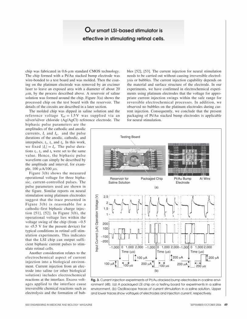
It should be noted that the number of microchips to be con-trolled is restricted by the asynchronous counter design andthat the number could easily be increased if we design thecounter with longer bits. Figure 11 illustrates the extendibilityof the fabricated device: two stimulators consisting of 4 × 4microchips with nine electrodes on each microchip (total 144electrodes) are connected; thus, a stimulator with 288 elec-trodes is realized.
The Microchip-Based Neural Interface Device with Serial Bus ArchitectureThe broadcast architecture described in the previous section issimple but cannot realize independent control of the stimulus
parameters for each microchip. In this section, we describe thenext-generation microchip-based device, which integrates asingle-wire serial interface, a PFM-based photosensor, animage processing circuit, and a current driver circuit [43].Introducing the serial bus architecture enables the stimulator tovary in pulse parameters such as amplitude and duration foreach microchip through the serial interface. The microchip isfabricated by 0.6-µm CMOS technology and is 500 µm ×500 µm. A microphotograph of one of the microchips isshown in Figure 12(a).
Special care is taken in the design in consideration of powerconsumption because we assume stimulator operation of anumber of the microchips via wireless communication, which
Fig. 11. Extendibility of the proposed stimulator: (a) original stimulator, (b) two stimulators with horizontal connection, and (c)two stimulators with vertical connection.
Add
ress
Stim
rec
Stim
recS
timrec
Add
ress
GND
VDD
GND
VDD
Address
Address
Address
GND
VDD
GN
D
VD
D
GND
VDD
Stimre C Stimre C
(a) (b)
(c)
Introducing the serial bus architecture enables
the stimulator to vary in pulse parameters
such as amplitude and duration for each
microchip through the serial interface.
55

56 IEEE ENGINEERING IN MEDICINE AND BIOLOGY MAGAZINE SEPTEMBER/OCTOBER 2006
limits the usable power of the device. The operation isdescribed in detail in [43] and is briefly mentioned here. Thedata transaction is based on packets as shown in Figure 12(b).The packet is transmitted on a serial bus line, which is a physi-cal connection between the microchips. A packet consists ofan 8-b address bit field followed by an 8-b data bit field. The
address assigns one of 254 microchips, and the data sets thestimulus amplitude parameters. After receiving two packets,the microchip is activated for photodetection and outputs stim-ulus currents; the pulse duration is the same as that of theclock as shown in Figure 12(b). Figure 12(c) shows experi-mental results of operation for three microchips, denoted as
Fig. 12. Microchip-based stimulator with serial bus architecture [46]. (a) Microphotograph of the fabricated microchip.Experimental results of (b) oscilloscope waveforms of the bus signal and the stimulus signal. (c) Oscilloscope waveforms ofpacket and the stimulus signals for #1, #2, and #3 microchips. The corresponding positions of the microchips are shown.
PacketDecoder
Refernce CurrentCircuit
Ser
ial
inte
rfac
e
Photo Sensor
Current DriverDAC
Rectifier
BusSignal
#1
#2 #3
@ : 680 mv∆ : 2.76
Stimulus Current
Bus Signal
PacketCh1T
TT
2.00
2
1
Clock A ch1− 1.74400 ms
2.60 v
Ch1 Ch2−1.527 ms
00 v
Packet
Ch1Ch3
Ch2Ch4
5.00 V Ω1.00 V ∼
5.00 mv∼1.00 V ∼
M 10.0 ms
20.0800ms
Ch2
#3
T
#2
#1
(a) (b)
(c)
We intend to design a microchip with a simpler
serial bus architecture that includes Pt/Au
stacked bump electrodes.

IEEE ENGINEERING IN MEDICINE AND BIOLOGY MAGAZINE SEPTEMBER/OCTOBER 2006 57
#1, #2, and #3. According to the bus signals, the threemicrochips produce different output current pulses.
The present microchip design mainly focuses on circuitarchitecture, and thus the device is not integrated with anyelectrodes. In the next step, we intend to design a microchipwith a simpler serial bus architecture that includes Pt/Austacked bump electrodes.
ConclusionsWe have developed Si-LSI-based smart neural stimulatorsfor retinal prosthesis. The application of LSI technologiesconfers benefits such as versatility, signal integrity, and com-pactness but requires a dedicated process for the integrationand packaging of electrodes with the standard LSI structure.For this purpose, we have developed a Pt/Au stacked bumpelectrode stimulator with epoxy molding, which is suitablefor forming on standard LSI chips and is effective in stimu-lating retinal cells. This stimulator has been evaluated insaline solution and in an in vivo experiment using detachedfrog retina. The positive results obtained suggest its potentialin retinal prosthesis.
In summary, we have demonstrated a flexible andextendable microchip-based stimulator in which a numberof microchips are distributed on a flexible polyimide sub-strate. Two types of such a microchip-based stimulatorhave been prepared: a broadcast type and a serial bus type.Both types demonstrate fundamental operations and showpromising capability. In the next stage, we are planning toimplant our developed microchip-based stimulator in ani-mals to further confirm the possibility of application tohuman retinal prosthesis.
AcknowledgmentsThe authors would like to thank Prof. Tetsuya Yagi of OsakaUniversity for the valuable discussion of in vitro experiments,Kazuaki Nakauchi of Osaka University for the semichronicdata of the implanted stimulator, and Hiroyuki Tashiro ofKyushu University, Kenzo Shodo and Hiroyuki Kanda ofVision Institute, Nidek Co. Ltd. for the valuable discussion ofelectrodes. They also wish to thank Dr. Shigeru Nishimuraand Naoko Tsunematsu of Tokyo Research Center, Nidek Co.Ltd. for their continuous encouragement and valuable discus-sion. This work was partly supported by the New EnergyDevelopment Organization (NEDO) of Japan (“ArtificialVision System,” Prof. Y. Tano, project leader), and by Healthand Labor Sciences Research Grants, Japan (Prof. Y. Tano,principal investigator).
Jun Ohta received the B.E., M.E., and Dr.Eng. degrees in applied physics, all fromthe University of Tokyo, Japan, in 1981,1983, and 1992, respectively. In 1983, hejoined Mitsubishi Electric Corporation,Hyogo, Japan, where he has been engagedin the research on optoelectronic integratedcircuits, optical neural networks, and artifi-
cial retina chips. From 1992–1993, he was a visitingresearcher in Optoelectronics Computing Systems Center,University of Colorado at Boulder. In 1998, he has been anassociate professor at Graduate School of Materials Science,Nara Institute of Science and Technology (NAIST), Nara,Japan, and in 2004, he has been the professor of NAIST. His
current research interests include vision chips, complementarymetal oxide semiconductor image sensors, retinal prosthesisdevices, biophotoniclarge-scale-integrations (LSIs), and inte-grated photonic devices.
He received the Best Paper Award of the Institute ofElectronics, Information, and Communication EngineersIEICE Japan in 1992, the Ichimura Award in 1996, and theNational Commendation for Invention in 2001. He is a mem-ber of the Japan Society of Applied Physics, the Institute ofElectronics, Information and Communication Engineers ofJapan, the Institute of Image Information and TelevisionEngineers of Japan, Japanese Society for Medical andBiological Engineering, the Institute of Electronic andElectronics Engineers, and the Optical Society of America.
Takashi Tokuda received his B.S. andM.S. degrees in electronic engineering fromKyoto University, Kyoto, Japan, in 1993and 1995, respectively. He received his Dr.Eng. degree in materials engineering fromKyoto University in 1998. He has been anassistant professor in the Graduate Schoolof Materials Science, Nara Institute of
Science and Technology, since 1999. He has been working on photonic materials science and
photonic device engineering. His research interestsinclude CMOS image sensors, retinal prosthesis devices,bioimaging sensors, and biosensing devices. He is a mem-ber of the Japan Society of Applied Physics, and theInstitute of Electronics, Information and CommunicationEngineers of Japan.
Keiichiro Kagawa received his B.E.degree in applied physics from OsakaUniversity, Japan, in 1996. He received hisM.E. and Dr. Eng. degrees in material andlife science in 1998 and 2001, respectively.From 1995–2001, he was engaged inresearch on optical packaging and prototyp-ing of optoelectronic parallel computers.
Since 2001, he has been an assistant professor at the NaraInstitute of Science and Technology, Nara, Japan.
His research interests include complementary metal oxidesemiconductor image sensors, vision chips, and optoelectronicsystems. He is a member of the Japan Society of AppliedPhysics, the Institute of Image Information and TelevisionEngineers of Japan, and the IEEE.
Tetsuo Furumiya received the B.S. degreein mechanical engineering from KansaiUniversity, Osaka, Japan, and the M.S.degree from Nara Institute of Science andTechnology, Nara, Japan, in 2001 and2003, respectively. Currently, he is workingtoward the Ph.D. degree at Nara Institute ofScience and Technology.
Akihiro Uehara received the B.S. degree in electricalengineering from Osaka University, Japan in 1997. Hereceived M.S. and Dr. Eng degrees from Nara Institute ofScience and Technology, Nara, Japan, in 2000 and 2005,respectively.

58 IEEE ENGINEERING IN MEDICINE AND BIOLOGY MAGAZINE SEPTEMBER/OCTOBER 2006
In 2002, he joined the Nidek VisionInstitute, Nidek Co., Ltd., Japan, where hehas been engaged in the research of artifi-cial vision prosthetic devices. His researchinterest is in complementary metal oxidesemiconductor sensors and mixed-signalcircuit design.
Yasuo Terasawa received the B.S. degreein applied physics from Tohoku University,Japan, in 1996, and an M.S. degree in infor-mation science from Tohoku University,Japan, in 1998. He joined Nidek Co., Ltd.,Japan in 2001, working on the developmentof the retinal prosthesis. His researchincludes electrode technology, implantable
electrical systems, and psychophysical evaluation of the pros-thetic vision.
Motoki Ozawa received the B.E. degree inchemical engineering from NagoyaUniversity, Japan, in 1985. He receivedM.S. degree in optics from the Universityof Rochester, New York, in 1987.
In 1988, he joined Dai Nippon PrintingCo., Ltd., Japan, where he participated incommercialization of a digital proof printer
and an electrical publishing system. In 1992, he joined NidekCo., Ltd., Japan, where he worked on the research and devel-opment (R&D) of an excimer laser corneal surgery system. In2003, he has been a director of the R&D division of Nidek,and since 2005, he has been a vice president of Nidek.
Takashi Fujikado is a professor of appliedvisual science at Osaka University MedicalSchool, Japan. He received the B.S. andM.E. degrees from Tokyo University,Tokyo, Japan, in 1976 and 1978, respec-tively. He received the M.D. and Ph.D.degrees from Osaka University in 1982 and1989, respectively.
Since joining in the department of Ophthalmology, OsakaUniversity Medical School in 1985, he has been engaged inthe research and clinical works on pediatric ophthalmologyand neuro-ophthalmology. Currently, he is a member ofJapanese Consortium for Artificial Retina and is engaged inthe functional assessment of artificial retina.
Yasuo Tano is the professor and chairmanof the Department of Ophthalmology atOsaka University Medical School as wellas the vice president of the OsakaUniversity Hospital, Japan. He is the pres-ident of the Japanese OphthalmologicalSociety that holds more than 13,000 mem-bers. He is currently the president of Asia-
Pacific Academy of Ophthalmology, which covers an areawith more than half of world population. He is the executiveeditor of the Japanese Journal of Ophthalmology and is amember of many international editorial boards of prominentpeer-review journals. He is also a member of the
International Council of Ophthalmology, the AdvisoryCommittee for the International Council of Ophthalmology,the Academia Ophthalmologica Internationalis (Chair V) andthe Executive Committee for the Club Jules Gonin and is acharter member of the International Council ofOphthalmology Foundation.
He received his M.D. from Osaka University MedicalSchool in 1972. After completing his residency in Japan, hebecame a vitreoretinal research fellow at Bascom PalmerEye Institute, Miami, Florida, in 1977 and then at Duke EyeCenter, Durham, North Carolina, in 1978. Tano has authoredand coauthored over 550 English and Japanese publicationsin various fields of ophthalmology and has written or editedover 50 books and chapters on related topics. Tano has deliv-ered many important lectures both domestically and interna-tionally, including the Sir Norman McAllister Gregg Lectureat the 2000 Annual Meeting of the Royal Australian andNew Zealand College of Ophthalmologists, the PyronLecture at the 19th Annual Meeting of the Vitreous Society,and the LIX Jackson Memorial Lecture.
Tano was one of the first to perform vitrectomy in Japanand has since dedicated his time in training aspiring surgeonsin the field of vitreoretinal surgery. He is the pioneer in non-vitrectomised macular surgery and is one of the leading sur-geons in macular translocation. He has invented manyvitreoretinal instruments, which have contributed to advancesin vitreoretinal surgery in the last decade.
Address for Correspondence: Jun Ohta, Graduate School ofMaterials Science, Nara Institute of Science and Technology,Takayama 8916-5, Ikoma, Nara 630-0101 Japan. E-mail:[email protected].
References[1] M.A.L. Nicolelis, Ed. Methods for Neural Ensemble Recordings. Boca Raton,FLA: CRC Press, 1999.
[2] J. Chen, K.D. Wise, J.F. Hetke, and S.C. Bledsoe Jr., “A multichannel neuralprobe for selective chemical delivery at the cellular level,” IEEE Trans. Biomed.Eng., vol. 44, no. 8, pp. 760–769, 1997.
[3] Q. Bai, K.D. Wise, and D.J. Anderson, “A high-yield microassembly structurefor three-dimensional microelectrode arrays,” IEEE Trans. Biomed. Eng., vol. 47,no. 3, pp. 281–289, 2000.
[4] M.O. Heuschkel, M. Fejtl, M. Raggenbass, D. Bertrand, and P. Renaud, “Athree-dimensional multi-electrode array for multi-site stimulation and recording inacute brain slices,” J. Neurosci. Methods, vol. 114, no. 2, pp. 135–148, 2002.
[5] T. Kawano, Y. Kato, M. Futagawa, H. Takao, K. Sawada, and M. Ishida,“Fabrication and properties of ultrasmall Si wire arrays with circuits by vapor-liquid-solid growth,” Sens. Actuators A, Phys. vol. 97–98, pp. 709–715, 2002.
[6] E. Margalit, J.D. Weiland, R.E. Clatterbuck, G.Y. Fujii, M. Maia, M. Tameesh,G. Torres, S.A. D’Anna, S. Desai, D.V. Piyathaisere, A. Olivi, E. de Juan, andM.S. Humayun, “Visual and electrical evoked response recorded from subretinalelectrodes implanted above the visual cortex in normal dogs under two methods ofanesthesia,” J. Neurosci. Methods, vol. 123, no. 2, pp. 129–137, 2003.
[7] S. Takeuchi, T. Suzuki, K. Mabuchi, and H. Fujita, “3D flexible multichannelneural probe array,” J. Micromech. Microeng., vol. 14, no. 1, pp. 104–108, 2004.
[8] T. Suzuki, D. Ziegler, K. Mabuchi, and S. Takeuchi, “Flexible neural probeswith micro-fluidic channels for stable interface with the nervous system,” in Proc.26th Int. Conf. IEEE EMBS, San Francisco, California, 1–5 Sept. 2004.
[9] L. Johnson, F.K. Perkins, T. O’Hearn, P. Skeath, C. Merritt, J. Frieble, S.Sadda, M. Humayun, and D. Scribner, “Electrical stimulation of isolated retinalwith microwire glass electrodes,” J. Neurosci., Methods, vol. 137, no. 2, pp.265–273, 2004.
[10] R. Rathnasingham, D.R. Kipke, S.C. Bledsoe Jr., and J.D. McLaren,“Characterization of implantable microfabricated fluid delivery devices,” IEEETrans. Biomed. Eng., vol. 51, no. 1, pp. 138–145, 2004.
[11] R.J. Vetter, J.C. Williams, J.F. Hetke, E.A. Nunamaker, and D.R. Kipke,“Chronic neural recording using silicon-substrate microelectrode arrays implantedin cerebral cortex,” IEEE Trans. Biomed. Eng., vol. 51, no 6, pp. 896–904, 2004.
IEEE ENGINEERING IN MEDICINE AND BIOLOGY MAGAZINE SEPTEMBER/OCTOBER 2006 59
[12] K.J. Dormer, “Implantable electronic otologic devices for hearing rehabilita-tion,” in Handbook of Neuroprosthetic Methods, W. Finn and P. LoPresti, Eds.Boca Raton, FLA: CRC Press, 2002, pp. 237–260.
[13] J. Georgiou and C. Toumazou, “A 126-µW cochlear chip for a totallyimplantable system,” IEEE J. Solid-State Circuits, vol. 40, no. 2, pp. 430–443,2005.
[14] M.S. Humayun, J.D. Weiland, G.Y. Fujii, R. Greenberg, R. Williamson, J.Little, B. Mech, V. Cimmarusti, G. Van Boemel, G. Dagnelie, and E. de Juan Jr.,“Visual perception in a blind subject with a chronic microelectronic retinal pros-thesis,” Vision Res., vol. 43, no. 24, pp. 2573–2581, 2003.
[15] J.F. Rizzo III, J. Wyatt, J. Loewenstein, S. Kelly, and D. Shire, “Methods andperceptual thresholds for short-term electrical stimulation of human retina withmicroelectrode arrays,” Invest. Ophthalmol. Vis. Sci. , vol. 44, no. 12, pp. 5355–5361, 2003.
[16] R. Eckmiller, “Learning retinal implants with epiretinal contacts,” OphthalmicRes., vol. 29, pp. 281–289, 1997.
[17] R. Hornig, T. Laube, P. Walter, M. Velikay-Parel, N. Bornfeld, M. Feucht, H. Akguel, G. Rössler, N. Alteheld, D.L. Notarp, J. Wyatt, and G. Richard, “Amethod and technical equipment for an acute human trial to evaluate retinalimplant technology,” J. Neural Eng., vol. 2, no. 1, pp. S129–S134, 2005.
[18] A.Y. Chow, V.Y. Chow, K. Packo, J. Pollack, G. Peyman, and R. Schuchard,“The artificial silicon retina microchip for the treatment of vision loss from retini-tis pigmentosa,” Arch. Ophthalmol., vol. 122, no. 4, pp. 460–469, 2004.
[19] E. Zrenner, “Will retinal implants restore vision?,” Science, vol. 295, pp. 1022–1025, 2002.
[20] D. Palanker, A. Vankov, P. Huie, and S. Baccus, “Design of a high-resolutionoptoelectronic retinal prosthesis,” J. Neural Eng., vol. 2, no. 1, pp. S105–S120,2005.
[21] H. Kanda, T. Morimoto, T. Fujikado, Y. Tano, Y. Fukuda, and H. Sawai,“Electrophysiological studies of the feasibility of suprachoroidal-transretinal stim-ulation for artificial vision in normal and RCS rats,” Invest. Ophthal. Vis. Sci., vol.45, no. 2, pp. 560–566, 2004.
[22] K. Nakauchi, T. Fujikado, H. Kanda, T. Morimoto, J.S. Choi, Y. Ikuno, H. Sakaguchi, M. Kamei, M. Ohji, T. Yagi, S. Nishimura, H. Sawai, Y. Fukuda,and Y. Tano, “Transretinal electrical stimulation by an intrascleral multichannelelectrode array in rabbit eyes,” Graefes Arch. Clin. Exp. Ophthalmol., vol. 243, no.2, pp. 169–174, 2005.
[23] W. Liu, P. Singh, C. DeMarco, R. Bashirullah, M. Humayun, and J. Weiland,“Semiconductor-based implantable microsystems,” Chap. 6, in Handbook ofNeuroprosthetic Methods, W. Finn and P. LoPresti, Ed. Boca Raton, FLA: CRCPress, 2002, pp. 127–161.
[24] W. Liu, K. Vichienchom, M. Clements, S.C. DeMarco, C. Hughes, E.McGucken, M.S. Humayun, E. De Juan, J.D. Weiland, and R. Greenberg, “Aneuro-stimulus chip with telemetry unit for retinal prosthetic device,” IEEE J.Solid-State Circuits, vol. 35, no. 10, pp. 1487–1497, 2000.
[25] W. Liu and M.S. Humayun, “Retinal prosthesis,” in IEEE Int. Solid-StateCircuits Conf. Dig. Tech. Papers, 2004, pp. 218–219.
[26] K. Najafi and K.D. Wise, “An implantable multielectrode array with on-chipsignal processing,” IEEE J. Solid-State Circuits, vol. 21, no. 6, pp. 1035–1986, 1986.
[27] J. Ji, K. Najafi, and K.D. Wise, “A low-noise demultiplexing system foractive multichannel microelectrode arrays,” IEEE Trans. Biomed. Eng., vol. 38,no. 1, pp. 75–81, 1991.
[28] S.J. Tanghe and K.D. Wise, “A 16-channel CMOS neural stimulating array,”IEEE J. Solid-State Circuits, vol. 27, no. 12, pp. 1819–1825, 1992.
[29] C. Kim and K.D. Wise, “A 64-site multishank CMOS low-profile neural stim-ulating probe,” IEEE J. Solid-State Circuits, vol. 31, no. 9, pp. 1230–1238, 1996.
[30] S.C. DeMarco, W. Liu, P.R. Singh, G. Lazzi, M.S. Humayun, and J.D.Weiland, “An arbitrary waveform stimulus circuit for visual prostheses using a lowarea multibias DAC,” IEEE J. Solid-State Circuits, vol. 38, no. 10, pp. 1679–1690,2003.
[31] Q. Bai and K.D. Wise, “Single-unit neural recording with active microelec-trode arrays,” IEEE Trans. Biomed. Eng., vol. 48, no. 8, pp. 911–920, 2001.
[32] M. Sivaprakasam, L. Wentai, M.S. Humayun, J.D. Weiland, "A variablerange bi-phasic current stimulus driver circuitry for an implantable retinal prosthet-ic device," IEEE J. Solid-State Circuits, vol. 40, no. 3, pp. 763–771, 2005.
[33] T. Kawano, Y. Kato, R. Tani, H. Takao, K. Sawada, and M. Ishida, “Selectivevapor-liquid-solid epitaxial growth of micro-Si probe electrode arrays with on-chipMOSFETs on Si (111) substrates,” IEEE Trans. Electron. Devices, vol. 51, no. 3, pp. 415–420, 2004.
[34] P. Fromherz, “Neuroelectronic interfacing: Semiconductor chips with ionchannels, nerve cells, and brain,” in Nanoelectronics and Information Technology,R. Waser, Ed. New York: Wiley, 2003, pp. 781–810.
[35] B. Eversmann, M. Jenkner, F. Hofmann, C. Paulus, R. Brederlow, B.Holzapfl, P. Fromherz, M. Merz, M. Brenner, M. Schreiter, R. Gabl, K. Plehnert,M. Steinhauser, G. Eckstein, D.S.-Landsiedel, and R. Thewes, “A 128 × 128CMOS bio-sensor array for extracellular recording of neural activity,” IEEE J.Solid-State Circuits, vol. 38, no. 12, pp. 2306–2317, 2003.
[36] P.I.-Pastor, I. Mody, and J.W. Judy, “In-vivo EEG recording using a wirelessimplantable neural transceiver,” in Proc. 1st Int. IEEE EMBS Conf. Neural Eng.,Capri Island, Italy, 2003, pp. 622–625.
[37] J. Deguchi, T. Watanabe, T. Nakamura, Y. Nakagawa, T. Fukushima, J.-C.Shim, H. Kurino, T. Abe, M. Tamai, and M. Koyanagi, “Three-dimensionallystacked analog retinal prosthesis chip,” Jpn. J. Appl. Phys., vol. 43, no. 4B, pp. 1685–1689, 2004.
[38] M. Sawan, Y. Hu, and J. Coulombe, “Wireless smart implants dedicated tomultichannel monitoring and microstimulation,” IEEE Circuit Syst. Mag., vol. 5,no. 1, pp. 21–39, 2005.
[39] J. Ohta, N. Yoshida, K. Kagawa, and M. Nunoshita, “Proposal of applicationof pulsed vision chip for retinal prosthesis,” Jpn. J. Appl. Phys., vol. 41, no. 4B,pp. 2322–2325, 2002.
[40] K. Kagawa, K. Isakari, T. Furumiya, A. Uehara, T. Tokuda, J. Ohta, and M.Nunoshita, “Pixel design of a pulsed CMOS image sensor for retinal prosthesiswith digital photosensitivity control,” Electron. Lett., vol. 39, no. 5, pp. 419–420,2003.
[41] D.C. Ng, K. Isakari, A. Uehara, K. Kagawa, T. Tokuda, J. Ohta, and M.Nunoshita, “A study of bending effect on pulsed frequency modulation based pho-tosensor for retinal prosthesis,” Jpn. J. Appl. Phys., vol. 42, no. 12, pp. 7621–7624,2003.
[42] K. Kagawa, N. Yoshida, T. Tokuda, J. Ohta, and M. Nunoshita, “Building asimple model of a pulse-frequency-modulation photosensor and demonstration of a128 × 128-pixel pulse-frequency-modulation image sensor fabricated in aStandard 0.35-µm complementary metal-oxide semiconductor technology,” Opt.Rev., vol. 11, no. 3, pp. 176–181, 2004.
[43] K. Kagawa, K. Yasuoka, D.C. Ng, T. Furumiya, T. Tokuda, J. Ohta, and M. Nunoshita, “Pulse-domain digital image processing for vision chips employinglow-voltage operation in deep-submicrometer technologies,” IEEE J. Select.Topics Quantum Electron., vol. 10, no. 4, pp. 816–828, 2004.
[44] T. Furumiya, D.C. Ng, K. Yasuoka, K. Kagawa, T. Tokuda, M. Nunoshita, and J. Ohta, “Functional verification of pulse frequency modulation-based imagesensor for retinal prosthesis by in vitro electrophysiological experiments using frogretina,” Biosens. Bioelectron., vol. 21, no. 7, pp. 1059–1068, 2006.
[45] A. Uehara, K. Kagawa, T. Tokuda, J. Ohta, and M. Nunoshita, “Back-illuminated pulse-frequency-modulated photosensor using silicon-on-sapphiretechnology developed for use as epi-retinal prosthesis device,” Electron. Lett., vol. 39, no. 15, pp. 1102–1103, 2003.
[46] A. Uehara, Y.-L. Pan, K. Kagawa, T. Tokuda, J. Ohta, and M. Nunoshita,“Micro-sized photo-detecting stimulator array for retinal prosthesis by distributedsensor network approach,” Sens. Actuators A, Phys., vol. 120, no. 1, pp. 78–87,2005.
[47] T. Tokuda, Y.-L. Pan, A. Uehara, K. Kagawa, M. Nunoshita, and J. Ohta,“Flexible and extendible neural interface device based on cooperative multi-chipCMOS LSI architecture,” Sens. Actuators A Phys., vol. 122, no. 1, pp. 88–98,2005.
[48] Y.-L. Pan, T. Tokuda, A. Uehara, K. Kagawa, J. Ohta, and M. Nunoshita, “Aflexible and extendible neural stimulation device with distributed multi-chiparchitecture for retinal prosthesis,” Jpn. J. Appl. Phys., vol. 44, no. 4B, pp.2099–2103, 2005.
[49] L. Li, Y. Hayashida, and T. Yagi, “Temporal properties of retinal ganglioncell responses to local trans retinal current stimuli in the frog retina,” Vision Res.,vol. 45, no. 2, pp. 263–273, 2005.
[50] A.P. Chu, K. Morris, R.J. Greenberg, and D.M. Zhou, “Stimulus induced pHchanges in retinal implants,” in Proc. 26th Int. Conf. IEEE EMBS, San Francisco,California, U.S.A., 1–5 Sept. 2004, pp. 4160–4162.
[51] T.L. Rose and L.S. Robblee, “Electrical stimulation with Pt electrodes. VIII.Electrochemically safe charge injection limits with 0.2 ms pulses,” IEEE Trans.Biomed. Eng., vol. 37, no. 11, pp. 1118–1120, 1990.
[52] S.B. Brummer and M.J. Turner, “Electrical stimulation with Pt electrodes:II—estimation of maximum surface redox (theoretical non-gassing) limits,” IEEETrans. Biomed. Eng., vol. 24, no. 5, pp. 440–443, 1977.
[53] S.B. Brummer and M.J. Turner, “Electrical stimulation with Pt electrodes: I.A method for determination of ‘real’ electrode areas,” IEEE Trans. Biomed. Eng.,vol. 24, no. 5, pp. 436–439, 1977.
[54] J.D. Weiland and D.J. Anderson, “Chronic neural stimulation with thin-film,Iridium Oxide electrodes,” IEEE Trans. Biomed. Eng., vol. 47, no. 7, pp. 911–918,2000.
[55] S.F. Cogan, T.D. Plante, J. Ehrlich, “Sputtered iridium oxide films (SIROFs)for low-impedance neural stimulation and recording electrodes,” in Proc. 26th Int.Conf. IEEE EMBS, San Francisco, California, U.S.A., 1–5 Sept. 2004, pp.4153–4156.
[56] W. Yang, “A wide-dynamic-range, low-power photosensor array,” in IEEEInt. Solid-State Circuits Conf. Dig. Tech. Papers, 1994, pp. 230–231.
[57] M. Mazza, P. Renaud, D.C. Bertrand, and A.M. Ionescu, “CMOS Pixels forSubretinal Implantable Prosthesis,” IEEE Sens. J., vol. 5, no. 1, pp. 32–37, 2005.
Copyright © 2022 FDOKUMEN