Sigma-Delta Control of Charge Trapping in Heterogeneous ...
163
Sigma-Delta Control of Charge Trapping in Heterogeneous Devices Dissertation presented in partial fulfillment of the requirements for the degree of Doctor in Electronic Engineering Chenna Reddy Bheesayagari Supervisor: Dr. Manuel Domínguez Pumar Septiembre 2019 Electronic Engineering Department
-
Upload
khangminh22 -
Category
Documents
-
view
4 -
download
0
Transcript of Sigma-Delta Control of Charge Trapping in Heterogeneous ...

Sigma-Delta Control of ChargeTrapping in Heterogeneous
Devices
Dissertation presented in partial fulfillment of the requirements for the degree ofDoctor in Electronic Engineering
Chenna Reddy Bheesayagari
Supervisor: Dr. Manuel Domínguez Pumar
Septiembre 2019
Electronic Engineering Department


Acknowledgments
I would like to express my sincere gratitude to everyone who has contributed to the realization ofthis thesis.
Firstly, I would like to thank my thesis director, Manuel Domínguez Pumar, for the continuoussupport and guidance, for his patience and knowledge. His door was always open for me and hehas been there to help me throughout this journey of my PhD. I appreciate all his contributionsto make my PhD experience productive and stimulating. I would also like to thank Joan Pons forhis patience and consistent support in numerous ways over the years. My sincere thanks to Prof.Lluís Pradell and Prof. Luis Castañer for providing me the opportunity to work at UPC.
My profound gratitude to all my colleagues and friends who made my stay at UPC enriching,pleasant, and enjoyable. I am grateful to: Teresa Atienza for her help and support; Gema López foralways helping me; Guillermo Gerling, Sergi Gorreta, Lukasz Kowalski for sharing good momentsand interesting conversations; Guillermo Martínez, Bremnen for fabricating the devices for mywork; Miguel García, Pablo Ortega for their help during the experiments; Santi Pérez and Manuelfor nice conversations over coffee; Julio, Roselena, Zaira, Mohamed Saad, Chen Jin for spendinggood time together.
I am indebted to all my dear friends for always being helpful and spending their precious timewith me. David and Dani: I am grateful to have you two as my friends. I truly appreciate yourunconditional love, support, and care that you show towards me. Thanks for always having myback no matter what. Angie: Muchas gracias por su amable apoyo y esfuerzo para hacerme unamejor persona. Te estoy agradecido. Anand: Thanks for being a great friend, flatmate and for yoursupport. Joan and Jose: Thanks for all the good times we spent together. A very special thanksto Sudheer, Mahesh, Sagar, Chenna Krishna, Shajahan, EC, Maneesh, Kartheek, Gopi, Devendar,Shravan, Shailesh, Prakash, Madhu, Subbu, Mohit, Sridhar for all the love and support.
Finally, I would like to say heartfelt thanks to my family: my sister and my parents for theirlove and support all my life.
i


Abstract
Dielectric charging represents a major reliability issue in a variety of semiconductor devices. Theaccumulation of charge in dielectric layers of a device often alters its performance, affecting itscircuital features and even reducing its effective lifetime. Although several contributions have beenmade in order to mitigate the undesired effects of charge trapping on circuit performance, dielectriccharge trapping still remains an open reliability issue in several applications.
The research work underlying this Thesis mainly focuses on the design, analysis and experi-mental validation of control strategies to compensate dielectric charging in heterogeneous devices.These control methods are based on the application of specifically designed voltage waveforms thatproduce complementary effects on the charge dynamics. Using sigma-delta loops, these controlsallow to set and maintain, within some limits, the net trapped charge in the dielectric to desiredlevels that can be changed with time. This allows mitigating long-term reliability issues such ascapacitance-voltage (C-V) shifts in MOS and MIM capacitors. Additionally, the bit streams gen-erated by the control loops provide real-time information on the evolution of the trapped charge.
The proposed controls also allow compensating the effects of the charge trapping due to externaldisturbances such as radiation. This has been demonstrated experimentally with MOS capacitorssubjected to various types of ionizing radiation (X-rays and gamma rays) while a charge controlis being applied. This approach opens up the possibility of establishing techniques for activecompensation of radiation-induced charge in MOS structures as well as a new strategy for radiationsensing.
A modeling strategy to characterize the dynamics of the dielectric charge in MOS capacitorsis also presented. The diffusive nature of the charge trapping phenomena allows their behavioralcharacterization using Diffusive Representation tools. The experiments carried out demonstrate avery good matching between the predictions of the model and the experimental results obtained.The time variations in the charge dynamics due to changes in the voltages applied and/or due toexternal disturbances have been also investigated and modeled.
Moreover, the charge dynamics of MOS capacitors under sigma-delta control is analyzed usingthe tools of Sliding Mode Controllers for an infinite sampling frequency approximation. A phe-nomenological analytical model is obtained which allows to predict and analyze the sequence ofcontrol signals. This model has been successfully validated with experimental data.
Finally, the above control strategies are extended to other devices such as eMIM capacitors and
iii

iv
perovskite solar cells. Preliminary results including open loop and closed loop control experimentsare presented. These results demonstrate that the application of the controls allows to set andstabilize both the C-V characteristic of an eMIM capacitor and the current-voltage characteristic(J-V) of a perovskite solar cell.

Resumen
La carga atrapada en dieléctricos suele implicar un problema importante de fiabilidad en muchosdispositivos semiconductores. La acumulación de dicha carga, normalmente provocada por lastensiones aplicadas durante el uso del dispositivo, suele alterar el rendimiento de éste con el tiempo,afectar sus prestaciones a nivel de circuital e, incluso, reducir su vida útil. Aunque durante años sehan realizado muchos trabajos para mitigar sus efectos no deseados, sobre todo a nivel circuital, lacarga atrapada en dieléctricos sigue siendo un problema abierto que frena la aplicabilidad prácticade algunos dispositivos.
El trabajo de investigación realizado en esta Tesis se centra principalmente en el diseño, análisisy validación experimental de estrategias de control para compensar la carga atrapada en dieléctricosde diversos tipos de dispositivos, incluyendo condensadores MOS, condensadores MIM fabricadoscon nanotecnología y dispositivos basados en perovskitas. Los controles propuestos se basan enutilizar formas de onda de tensión, específicamente diseñadas, que producen efectos complemen-tarios en la dinámica de la carga. Mediante el uso de lazos sigma-delta, estos controles permitenestablecer y mantener, dentro de unos límites, la carga neta atrapada en el dieléctrico a valoresprefijados, que pueden cambiarse con el tiempo. Esto permite mitigar problemas de fiabilidad alargo plazo como por ejemplo las derivas de la curva capacidad-tensión (C-V) en condensadoresMOS y MIM. Adicionalmente, las tramas de bits generadas por los lazos de control proporcionaninformación en tiempo real sobre la evolución de la carga.
Los controles propuestos permiten también compensar los efectos de la carga atrapada endieléctricos debida a perturbaciones externas como la radiación. Esto se ha demostrado experi-mentalmente con condesadores MOS sometidos a diversos tipos de radiación ionizante (rayos X ygamma) mientras se les aplicaba un control de carga. Este resultado abre la posibilidad tanto deestablecer técnicas de compensación activa de carga inducida por radiación en estructuras MOS,como una nueva estrategia de sensado de radiación.
Se presenta también una estrategia de modelado para caracterizar la dinámica de la cargadieléctrica en condensadores MOS. La naturaleza difusiva de los fenómenos de captura y elimi-nación de carga en dieléctricos permite caracterizar dichos fenómenos empleando herramientas deRepresentación Difusiva. Los experimentos realizados demuestran una muy buena correspondenciaentre las predicciones del modelo y los resultados experimentales obtenidos. Se muestra tambiéncomo las variaciones temporales de los modelos son debidas a cambios en las formas de onda de
v

vi
actuación del dispositivo y/o a perturbaciones externas.Además, la dinámica de carga en condensadores MOS bajo control sigma-delta se analiza uti-
lizando herramientas de control en modo deslizante (SMC), considerando la aproximación de fre-cuencia de muestreo infinita. Con ello se obtiene un modelo analítico simplificado que permitepredecir y analizar con éxito la secuencia de señales de control. Este modelo se ha validado satis-factoriamente con datos experimentales.
Finalmente, las estrategias de control anteriores se han extendido a otros dispositivos suscep-tibles de sufrir efectos de carga atrapada que pueden afectar su fiabilidad. Así, se han llevado acabo experimentos preliminares cuyos resultados demuestran que la aplicación de controles de cargapermite controlar y estabilizar la característica C-V de un condensador eMIM y la característicacorriente-tensión (J-V) de una célula solar basada en perovskitas.

What can be asserted without evidence canalso be dismissed without evidence.
Christopher Hitchens


Contents
1 Introduction 11.1 Framework . . . . . . . . . . . . . . . . . . . . . . . . . . . . . . . . . . . . . . . . . 11.2 Objectives . . . . . . . . . . . . . . . . . . . . . . . . . . . . . . . . . . . . . . . . . . 41.3 Document Organization . . . . . . . . . . . . . . . . . . . . . . . . . . . . . . . . . . 5
2 Thesis Background 132.1 Dielectric Charging . . . . . . . . . . . . . . . . . . . . . . . . . . . . . . . . . . . . . 13
2.1.1 Dielectric Charging in Semiconductor Devices . . . . . . . . . . . . . . . . . . 132.1.2 Charge Trapping in MOS Devices . . . . . . . . . . . . . . . . . . . . . . . . 162.1.3 Ionizing Radiation on MOS Devices . . . . . . . . . . . . . . . . . . . . . . . 20
2.2 Modeling of Charge Dynamics . . . . . . . . . . . . . . . . . . . . . . . . . . . . . . . 262.2.1 Diffusive Representation . . . . . . . . . . . . . . . . . . . . . . . . . . . . . . 262.2.2 Sliding Mode Control . . . . . . . . . . . . . . . . . . . . . . . . . . . . . . . 31
3 Dielectric Charge Trapping Controls for MOS Capacitors 493.1 Introduction . . . . . . . . . . . . . . . . . . . . . . . . . . . . . . . . . . . . . . . . . 49
3.1.1 Sigma-Delta Control . . . . . . . . . . . . . . . . . . . . . . . . . . . . . . . . 493.1.2 MOS Capacitors - Fabrication Process . . . . . . . . . . . . . . . . . . . . . . 503.1.3 Modeling the Device Capacitance . . . . . . . . . . . . . . . . . . . . . . . . . 513.1.4 Charge Control Method: Sigma-Delta Approach . . . . . . . . . . . . . . . . 54
3.2 First Order Sigma-Delta Control . . . . . . . . . . . . . . . . . . . . . . . . . . . . . 583.2.1 Experimental Setup . . . . . . . . . . . . . . . . . . . . . . . . . . . . . . . . 583.2.2 Results and Discussion . . . . . . . . . . . . . . . . . . . . . . . . . . . . . . . 593.2.3 Simulations versus Experimental Data . . . . . . . . . . . . . . . . . . . . . . 62
3.3 Second Order Sigma-Delta Control . . . . . . . . . . . . . . . . . . . . . . . . . . . . 633.3.1 Charge Control Method . . . . . . . . . . . . . . . . . . . . . . . . . . . . . . 633.3.2 Fabrication Process . . . . . . . . . . . . . . . . . . . . . . . . . . . . . . . . 643.3.3 Results and Discussion . . . . . . . . . . . . . . . . . . . . . . . . . . . . . . . 65
3.4 Conclusions . . . . . . . . . . . . . . . . . . . . . . . . . . . . . . . . . . . . . . . . . 67
ix

x Contents
4 Compensation of Charge Induced by Radiation in MOS Capacitors 734.1 Charge Trapping Control under Ionizing Radiation . . . . . . . . . . . . . . . . . . . 744.2 Experimental . . . . . . . . . . . . . . . . . . . . . . . . . . . . . . . . . . . . . . . . 75
4.2.1 Device Fabrication Process . . . . . . . . . . . . . . . . . . . . . . . . . . . . 754.2.2 Experimental Setup . . . . . . . . . . . . . . . . . . . . . . . . . . . . . . . . 774.2.3 Experiment 1: Gamma Radiation . . . . . . . . . . . . . . . . . . . . . . . . . 794.2.4 Experiment 2: X-radiation . . . . . . . . . . . . . . . . . . . . . . . . . . . . 82
4.3 Conclusions . . . . . . . . . . . . . . . . . . . . . . . . . . . . . . . . . . . . . . . . . 86
5 Modeling and Analysis of Charge Trapping Dynamics in MOS Capacitors 895.1 Characterization of Trapped Charge Dynamics . . . . . . . . . . . . . . . . . . . . . 89
5.1.1 Diffusive Representation . . . . . . . . . . . . . . . . . . . . . . . . . . . . . . 905.1.2 Model Prediction and Validation using DR . . . . . . . . . . . . . . . . . . . 92
5.2 Sliding Mode Controllers (SMC): Sigma-Delta Modulation Approach . . . . . . . . . 945.2.1 SMC: Linear Time-Varying Charge Model . . . . . . . . . . . . . . . . . . . . 965.2.2 Deterministic Switching: Average System . . . . . . . . . . . . . . . . . . . . 975.2.3 Sliding Mode Analysis . . . . . . . . . . . . . . . . . . . . . . . . . . . . . . . 985.2.4 Effect of External Disturbances and Parameter Uncertainties . . . . . . . . . 99
5.3 Experimental Results and Discussion . . . . . . . . . . . . . . . . . . . . . . . . . . . 1005.3.1 Experiment 1: Charge Trapping Control . . . . . . . . . . . . . . . . . . . . . 1005.3.2 Experiment 2: Charge Control under Ionizing Radiation . . . . . . . . . . . . 103
5.4 Conclusions . . . . . . . . . . . . . . . . . . . . . . . . . . . . . . . . . . . . . . . . . 105
6 Sigma-Delta Charge Control Applied to Other Devices 1096.1 MIM Capacitors . . . . . . . . . . . . . . . . . . . . . . . . . . . . . . . . . . . . . . 109
6.1.1 Fabrication Details . . . . . . . . . . . . . . . . . . . . . . . . . . . . . . . . . 1106.1.2 Implementing the Control Method . . . . . . . . . . . . . . . . . . . . . . . . 1106.1.3 Experimental Results and Discussion . . . . . . . . . . . . . . . . . . . . . . . 115
6.2 Perovskite Solar Cells . . . . . . . . . . . . . . . . . . . . . . . . . . . . . . . . . . . 1196.2.1 Fabrication Details . . . . . . . . . . . . . . . . . . . . . . . . . . . . . . . . . 1206.2.2 Experimental Results and Discussion . . . . . . . . . . . . . . . . . . . . . . . 121
6.3 Conclusions . . . . . . . . . . . . . . . . . . . . . . . . . . . . . . . . . . . . . . . . . 127
7 Conclusions and Future Work 1337.1 Conclusions . . . . . . . . . . . . . . . . . . . . . . . . . . . . . . . . . . . . . . . . . 1337.2 Future Work . . . . . . . . . . . . . . . . . . . . . . . . . . . . . . . . . . . . . . . . 134
Appendices 137

Contents xi
A Journal Publications and Conferences 139A.1 Diffusive Representation and Sliding Mode Control of Charge Trapping in Al2O3
MOS Capacitors . . . . . . . . . . . . . . . . . . . . . . . . . . . . . . . . . . . . . . 141A.2 Second order sigma-delta control of charge trapping for MOS capacitors . . . . . . . 142A.3 Closed-Loop Compensation of Charge Trapping Induced by Ionizing Radiation in
MOS Capacitors . . . . . . . . . . . . . . . . . . . . . . . . . . . . . . . . . . . . . . 143A.4 Charge trapping control in MOS capacitors . . . . . . . . . . . . . . . . . . . . . . . 144A.5 Second order sigma-delta control of charge trapping for MOS capacitors . . . . . . . 145A.6 Sliding mode control of fractional order systems: applications to sensors . . . . . . . 146A.7 Active charge trapping control in dielectrics under ionizing radiation . . . . . . . . . 147

Chapter 1
Introduction
1.1 Framework
The reliability of dielectric materials has always been one of the major concerns in the commercial-ization of microelectronic technologies [1, 2, 3]. A great deal of success in the evolution of modernmicroelectronics industry has been attributed to the excellent dielectric properties of silicon diox-ide (SiO2). Silicon dioxide can be formed by thermal oxidation, and has characteristics of gooddielectric strength, low defect density, large band gap and provides a thermodynamically stableinterface, making it the most commonly used insulator in IC technology. A lot of investigation andinvestments have been made over decades in research, development and manufacture of highly reli-able oxides. This has been evident from its successful and diverse applications not only in the fieldof semiconductor devices but also in metallurgy [4], material science [5], and geology [6], to namea few. However, in most of the applications involving the gate and passivation oxide layers (MOSdevices, for example), operating the devices under high stress conditions [7, 8, 9] or in radiationenvironment [10, 11] over a period of time could degrade the electrical properties of the oxide layerleading to critical device failures.
A thorough and detailed analysis of surface properties of the oxides has been carried outto gain the knowledge about such instabilities. Primarily, the origin of such instabilities corre-sponds to defects in the dielectric layer and at the interface between the dielectric and the elec-trode/semiconductor [12, 13, 14]. When a bias voltage is applied across the gate oxide, these defectsact as traps for electrons and holes. This trapping of charge carriers in the dielectric and at theinterface is an important issue that controls the performance of the devices. Gaining insight aboutthe properties of these defects contributes to the development of models related to the long termreliability of MOS devices. Significant practical and theoretical knowledge concerning the reliabilityissues have been accumulated in the past decades to address the challenges and to meet lifetimespecifications for commercial applications [15, 16, 17].
When the devices are under operating conditions, the dielectric films undergo electrical stressand charge carrier injection. With the applications of high fields, trapping of charge carriers takes
1

2 Chapter 1. Introduction
place at defects and affects device parameters such as operating voltage, gate leakage current,mobility etc. In general, the measurement of shift in threshold voltage, VT , serves as an indirectestimation for the amount of charge trapped in the dielectric. It has been observed in most ofthe MOS devices that a negative gate bias stress would result in a negative shift of VT due to anincrease in the amount of positively-charged oxide traps. Similarly, applying a positive gate biasvoltage would cause a VT shift in positive direction possibly due to electron trapping in the oxide.Accumulation of large amounts of charge would cause a large VT shift, resulting in potential devicefailure.
The mechanisms of electron and hole trapping in dielectrics are important for understanding andimproving the performance of devices in applications such as photovoltaics, electronics. Especially,charge trapping phenomena in SiO2 gate dielectrics has been studied extensively in the past [18,19, 20]. However, aggressive scaling of device dimensions and need for high power electronics hasraised concerns over the use of conventional SiO2 in the device architecture. So, many studiesinvestigated the effects of charge trapping in alternative (high-k) dielectric materials [21, 22] toimprove the reliability of devices. It has been reported that employing high-k materials with a highinjection barrier and low concentration of interface states may overcome the dielectric charging [23].Most of the strategies to mitigate the instabilities in the operating characteristics of MOS devicesrelated to charge trapping involves the reduction of defect denisities by improving the fabricationprocessing control and annealing procedures [24, 25, 26, 27].
On the other hand, electrostatic MEMS also suffer from the effects of dielectric charging. Thenet charge accumulated in dielectric layers has a significant impact on the behavior of such devicesresulting in undesirable effects such as shifts of the capacitance-voltage (CV) characteristic andeven permanent stiction of movable mechanical parts. Several techniques proposed for mitigatingthis undesirable phenomena focus on either improving the design of the device or implementingintelligent bipolar voltage waveforms for actuation in open loop. However, these strategies havenot been able to completely solve the charge trapping issue in long term.
In order to reduce the effects of dielectric charge trapping, charge control strategies have beenproposed and implemented in [28, 29]. Under predefined limits, these controls allow to set andmaintain a previously given amount of net dielectric charge, thus mitigating long-term reliabilityissues such as CV shifts or VT drifts. In these controls, the charge being continuously leaked outof the dielectric is compensated in average by applying an adequate sequence of bipolar voltages.The theoretical validation of these control methods has been carried out employing the numericalsimulation and matching it with experimental results in case of MEMS [30].
Another challenging reliability issue for the microelectronic devices operating in aerospace sys-tems is their exposure to various forms of radiation. The radiation effects include the buildup ofoxide and interface trap charge, leading to the changes in threshold voltage. Following the expo-sure to ionizing radiation, MOS structures typically exhibit a negative shift in oxide-charge-inducedthreshold voltage component, Vot that could potentially persist for hours to years. Figure 1.1 showstypical radiation-induced oxide charge buildup characteristics with respect to gate bias for an MOScapacitor [31]. This component is the predominant and most commonly observed form of radiation

1.1. Framework 3
damage in MOS devices. Hence in this work, effort towards compensating this oxide positive chargetrapping has been made by implementing a charge compensation strategy.
Figure 1.1: Radiation-induced flatband voltage shift of an MOS capacitor vs gate bias duringirradiation [31].
The characterization of charge trapping mechanisms in the bulk oxide and at the oxide-semiconductorinterface is of crucial importance in mitigating the effects of dielectric charging. Modeling the chargedynamics at different actuation voltages allows to describe the evolution of dielectric charge contri-butions. Thus, characterization of charge dynamics as a function of the voltages applied is of greatrelevance for the active operation of MOS based devices, especially while operating in environmentsaffected by external factors such as ionizing radiation. The charging/discharging phenomena hasbeen identified as a diffusion like process and has been widely studied and analyzed in case ofMEMS [32, 33, 34, 35, 36].
The characterization of the charge trapping dynamics in MOS devices has been extensivelystudied in literature [37]. Trap distributions are obtained from impedance spectra for differentvoltages in [38, 39]. Other works analyze the charging dynamics as the result of the application ofa voltage (or temperature) stress, while observing discharging currents or shifts in the thresholdvoltage. In these methods, the stress factor is instantaneously changed and changes in drain currentsor threshold voltage shifts are monitored and fitted. Models with one or two time constants, as wellas, more generally, stretched exponentials have been used to this purpose. In stretched exponentialsthe charge transient is characterized by the function exp(−(t/τ)β), with β ∈ (0, 1). This modelhas been linked to Gaussian distributions in the energy barriers found in charge trapping anddetrapping [40]. However, in all these cases the analysis of the time evolution of systems underarbitrary excitation becomes difficult because it is necessary to take into account the distributednature of the processes involved. In this Thesis, the dynamics of trapped charge in MOS capacitorsis characterized by obtaining the state-space model using Diffusive Representation (DR) and the

4 Chapter 1. Introduction
behavior of the device under control has been predicted using a specific analytical model, derivedfrom the Sliding Mode Control (SMC) theory.
DR is a mathematical tool that allows the description of any physical phenomena based ondiffusion using state-space models of arbitrary order in the frequency domain. The key idea behindDR is to decompose long range time series on a continuous family of purely damped exponentials [41,42]. Additionally, SMC is a non-linear control technique which employs a discontinuous feedbacksignal to drive the system state trajectory onto a predetermined sliding surface [43, 44] for allsubsequent time. The theory of SMC has recently been applied for the prediction of the closed-loop dynamics of wind sensors [45, 46] that have been thermally characterized. In this Thesis, DRtechnique is employed to describe the charge dynamics of a system using an arbitrary order state-space model. The behavioural models obtained with DR are used in the analysis and prediction ofthe closed-loop control of charge trapping, using the tools of SMC.
Furthermore, in this Thesis, the charge trapping issue has been explored in other devices suchas perovsite solar cells and electrosprayed nanoparticle MIM (eMIM) capacitors. Perovskite baseddevices are considered promising materials in photovoltaic technology due to their high efficiency,and low fabrication costs. However, the photovoltaic performance of organic-inorganic perovskiteshave been severely affected by the charge traps by deactivating the photoexcited species [47].In [48, 49, 50], it has been established that charge traps have significant impact on the degradationof metal halide perovskites by monitoring trapped electronfree hole recombination kinetics. Manyworks in the literature suggests the possibility of improving the perovskite stability by encapsulationand varying the fabrication process or the chemical composition of the materials [51, 52, 53, 54].However, currently the maximum stability is established in 6 months, far from the 25 years requiredto compete commercially against conventional Silicon based solar cells. The work carried in thisThesis intend to tackle the issue of charge trapping by means of an external control circuit.
In case of energy storage applications, it has been recently demonstrated that MIM capacitorswith SiO2 nanoparticles [55, 56] have been projected as future of high density energy storage el-ements. The recent advances in functional nanostructures along with their intrinsic advantage oflarge surface area to volume ratio has resulted in widespread use of supercapacitors as potentialenergy storage devices. Since the overall performance of the supercapacitor devices strongly de-pends on the properties and the structure of the component materials, characterization of differentdielectric materials has become one of the most important aspects to be investigated to improvethe energy storage performance. In this Thesis, the effects of bias voltage on charge distribution ineMIM dielectric layer has been investigated with an aim to improve the energy storage ability ofthe devices.
1.2 Objectives
With regard to the above discussion, the main objective of this Thesis is to contribute to theimprovement of the reliability and/or operating lifetime of MOS capacitors by designing and an-alyzing effective strategies for dielectric charge control. This Thesis implements the closed loop

1.3. Document Organization 5
control techniques to control and maintain the net amount of charge in dielectric layer of thesedevices. Further a model is developed to analyze the dynamics of the oxide trapped charge withdifferent actuation voltages and in also with external disturbances. The secondary objective is toextend the control strategies to other devices such as eMIM capacitors and perovskite devices.
The specific objectives for the research work are as following:
• Dielectric charge control: Implement the charge control method based on sigma-delta loopby continuous monitoring and keeping constant the net trapped charge in the dielectric. Thishas been achieved by periodically sampling the horizontal displacement of the capacitance-voltage (CV) characteristic curve of the device and applying the adequate voltage waveformsto maintain it at a desired position. In particular, the main focus has been on the analysisand compensation of dielectric charging in MOS capacitors.
• Compensation of radiation-induced charge: Compensating the ionizing radiation (X-ray andGamma radiation) induced charge accumulation in the dielectric layer to improve the radi-ation response of MOS capacitors made of SiO2 and Al2O3 dielectrics. In particular, sincetrapping of net positive charge dominates other effects such as electron trapping and interfacetrap buildup, our aim in this Thesis is to control the oxide trapped charge.
• Characterization of trapped charge dynamics: Characterization of the trapped charge dynam-ics in the dielectric of a MOS capacitor to obtain the dynamic model of the device using DRtheory. Validation of the model predictions using the experiments under arbitrary voltageexcitations.
The main objective is to derive behavioral models, considering MOS capacitor as a ’blackbox’, thus capturing the dynamical behavior of the device without interpreting the results interms of physical phenomena.
• Sliding mode analysis of the charge dynamics: Analyze and predict the closed loop charge dy-namics, operating under sigma-delta control, using the tools of SMC for an infinite samplingfrequency approximation.
• Charge control applied to other semiconductor devices: Employ the proposed closed loop con-trol strategies to investigate the charge control capability in eMIM capacitors and perovskitesolar cells.
1.3 Document Organization
The rest of this document is organized as follows:
• Chapter 2 describes the background of this Thesis. In this chapter, the contributions regard-ing the issues in literature related to charge trapping in heterogeneous semiconductor deviceshave been discussed. The significance of mathematical tools which are used to analyze andmodel the charge dynamics is also discussed.

6 Chapter 1. Introduction
• Chapter 3 introduces and demonstrates the effectiveness of closed loop control techniquebased on sigma-delta modulation in controlling the dielectric charge in a MOS capacitor. Ananalytical model is developed to characterize and predict the effects of oxide trapped chargeon device capacitance. A second order sigma-delta control strategy is also presented and theadvantages over the first order control are discussed.
• Chapter 4 discusses the radiation-induced effects of ionizing radiation on the operation ofMOS capacitors. It demonstrates the effectiveness of the proposed control method in im-proving the radiation response of the device. This provides a potential control technique toimprove the reliability of MOS-related devices working in hardness environments.
• Chapter 5 presents a modeling strategy, based on DR to characterize the dynamics of thecharge trapped in the dielectric of MOS capacitors. It also introduces the SMC technique toanalyze the charge dynamics when the device is being controlled by a sigma-delta control.The predictions made using these models are validated with the experimental measurements.
• Chapter 6 demonstrates the effectiveness of the control schemes in avoiding the drifts inthe device characteristics. This chapter also discusses the experiments comprising open loopstress and closed loop control to study and understand the charge dynamics in case of eMIMcapacitors and perovskite devices.
• Chapter 7 draws the main conclusions derived from the results of the Thesis work. It alsoincludes a future work section, which highlights potential research lines outlined from thiswork.

Bibliography 7
Bibliography
[1] John S Suehle. Ultrathin gate oxide reliability: Physical models, statistics, and characteriza-tion. IEEE Transactions on Electron Devices, 49(6):958–971, 2002.
[2] Ryu Hasunuma, Hiroaki Kawamura, and Kikuo Yamabe. Reliability factors of ultrathin di-electric films based on highly controlled SiO2 films. Japanese Journal of Applied Physics, 57(6S3):06KB05, 2018.
[3] Sean P Ogden, Juan Borja, Joel L Plawsky, T-M Lu, Kong Boon Yeap, and William N Gill.Charge transport model to predict intrinsic reliability for dielectric materials. Journal ofApplied Physics, 118(12):124102, 2015.
[4] Kenneth Easterling. Introduction to the physical metallurgy of welding. Elsevier, 2013.
[5] M Stefanidou and I Papayianni. Influence of nano-SiO2 on the Portland cement pastes. Com-posites Part B: Engineering, 43(6):2706–2710, 2012.
[6] MJ Walter, AR Thomson, WWang, OT Lord, J Ross, SC McMahon, MA Baron, E Melekhova,AK Kleppe, and SC Kohn. The stability of hydrous silicates in Earth’s lower mantle: Exper-imental constraints from the systems MgO − SiO2 −H2OandMgO − Al2O3 − SiO2 −H2O.Chemical Geology, 418:16–29, 2015.
[7] SK Sahoo and Durgamadhab Misra. Field dependent electrical conduction in HfO2/SiO2gate stack for before and after constant voltage stressing. Journal of Applied Physics, 110(8):084104, 2011.
[8] C Glenn Shirley. High field phenomena in thermal SiO2. Journal of the ElectrochemicalSociety, 132(2):488–500, 1985.
[9] Te-Chih Chen, Ting-Chang Chang, Tien-Yu Hsieh, Wei-Siang Lu, Fu-Yen Jian, Chih-TsungTsai, Sheng-Yao Huang, and Chia-Sheng Lin. Investigating the degradation behavior causedby charge trapping effect under DC and AC gate-bias stress for InGaZnO thin film transistor.Applied Physics Letters, 99(2):022104, 2011.
[10] Surendra Singh Rathod, AK Saxena, and Sudeb Dasgupta. Radiation effects in MOS-baseddevices and circuits: A review. IETE Technical Review, 28(6):451–469, 2011.
[11] Tomasz Brozek. Radiation hardness of silicon dioxide dielectric strength in silicon MOS struc-tures. In International Conference of Microelectronics: Microelectronics’ 92, volume 1783,pages 360–365. International Society for Optics and Photonics, 1992.
[12] N Stojadinović and S Dimitrijev. Instabilities in MOS transistors. Microelectronics Reliability,29(3):371–380, 1989.

8 Bibliography
[13] S Dimitrijev and N Stojadinović. Analysis of CMOS transistor instabilities. Solid-state elec-tronics, 30(10):991–1003, 1987.
[14] Udo Schwalke, Martin Pölzl, Thomas Sekinger, and Martin Kerber. Ultra-thick gate oxides:charge generation and its impact on reliability. Microelectronics reliability, 41(7):1007–1010,2001.
[15] Andreas Kerber, Eduard Cartier, Luigi Pantisano, Robin Degraeve, Thomas Kauerauf, Y Kim,A Hou, Guido Groeseneken, HE Maes, and U Schwalke. Origin of the threshold voltageinstability in SiO2/HfO2 dual layer gate dielectrics. IEEE Electron Device Letters, 24(2):87–89, 2003.
[16] C Leroux, J Mitard, G Ghibaudo, X Garros, G Reimbold, B Guillaumor, and F Martin. Char-acterization and modeling of hysteresis phenomena in high K dielectrics. In IEDM TechnicalDigest. IEEE International Electron Devices Meeting, 2004., pages 737–740. IEEE, 2004.
[17] DJ Breed. A new model for the negative voltage instability in MOS devices. Applied PhysicsLetters, 26(3):116–118, 1975.
[18] Yoshihito Katsu, Takuji Hosoi, Yuichiro Nanen, Tsunenobu Kimoto, Takayoshi Shimura, andHeiji Watanabe. Impact of NO annealing on flatband voltage instability due to charge trappingin SiC MOS devices. InMaterials Science Forum, volume 858, pages 599–602. Trans Tech Publ,2016.
[19] Eddy Simoen, Chun Gong, NE Posthuma, Emmanuel Van Kerschaver, Jozef Poortmans, andR Mertens. A DLTS study of SiO2 and SiO2/SiNx surface passivation of silicon. Journal ofThe Electrochemical Society, 158(6):H612–H617, 2011.
[20] Daniel B Habersat and Aivars J Lelis. Improved observation of SiC/SiO2 oxide charge trapsusing MOS CV. In Materials Science Forum, volume 679, pages 366–369. Trans Tech Publ,2011.
[21] Andreas Kerber, Eduard Cartier, Robin Degraeve, Philippe J Roussel, Luigi Pantisano,Thomas Kauerauf, Guido Groeseneken, Herman E Maes, and Udo Schwalke. Charge trappingand dielectric reliability of SiO2−Al2O3 gate stacks with TiN electrodes. IEEE Transactionson Electron Devices, 50(5):1261–1269, 2003.
[22] Robin Degraeve, Andreas Kerber, Philippe Roussel, Ed Cartier, Thomas Kauerauf, LuigiPantisano, and Guido Groeseneken. Effect of bulk trap density on HfO2 reliability andyield. In 2003 IEEE International Electron Devices Meeting, Technical Digest, pages 935–938.Institute of Electrical and Electronics Engineers, 2003.
[23] Julian J McMorrow, Cory D Cress, and Chaffra A Affouda. Charge injection in high-κ gatedielectrics of single-walled carbon nanotube thin-film transistors. ACS nano, 6(6):5040–5050,2012.

Bibliography 9
[24] Duc D Nguyen, Camron Kouhestani, Kenneth E Kambour, and Roderick AB Devine. Directevidence for interface state annealing in the negative bias temperature instability response.Journal of Vacuum Science & Technology B, Nanotechnology and Microelectronics: Materials,Processing, Measurement, and Phenomena, 32(1):011205, 2014.
[25] D Lu, GA Ruggles, and JJ Wortman. Effects of processing conditions on negative bias tem-perature instability in metal-oxide-semiconductor structures. Applied physics letters, 52(16):1344–1346, 1988.
[26] Mao-Chieh Chen and John W Hile. Oxide charge reduction by chemical gettering withtrichloroethylene during thermal oxidation of silicon. Journal of The Electrochemical Soci-ety, 119(2):223–225, 1972.
[27] A Goetzberger and HE Nigh. Surface charge after annealing of Al − SiO2 − Si structuresunder bias. Proceedings of the IEEE, 54(10):1454–1454, 1966.
[28] Elena Blokhina, Sergi Gorreta, David Lopez, David Molinero, Orla Feely, Joan Pons-Nin,and Manuel Dominguez-Pumar. Dielectric charge control in electrostatic MEMS position-ers/varactors. Journal of microelectromechanical systems, 21(3):559–573, 2012.
[29] Manuel Dominguez-Pumar, Sergi Gorreta, Joan Pons-Nin, Elena Blokhina, PanagiotisGiounanlis, and Orla Feely. Real-time characterization of dielectric charging in contactlesscapacitive MEMS. Analog integrated circuits and signal processing, 82(3):559–569, 2015.
[30] Sergi Gorreta, Joan Pons-Nin, Elena Blokhina, Orla Feely, and Manuel Domínguez-Pumar.Delta-sigma control of dielectric charge for contactless capacitive MEMS. Journal of micro-electromechanical systems, 23(4):829–841, 2014.
[31] GF Derbenwick and BL Gregory. Process optimization of radiation-hardened CMOS integratedcircuits. IEEE Transactions on Nuclear Science, 22(6):2151–2156, 1975.
[32] R. W. Herfst, P. G. Steeneken, J. Schmitz, A. J. G. Mank, and M. van Gils. Kelvin probe studyof laterally inhomogeneous dielectric charging and charge diffusion in RF MEMS capacitiveswitches. In 2008 IEEE International Reliability Physics Symposium, pages 492–495, April2008.
[33] R.W. Herfst, P.G. Steeneken, and J. Schmitz. Time and voltage dependence of dielectriccharging in RF MEMS capacitive switches. In IEEE 45th Annual Int. Reliability PhysicsSymp., Phoenix, pages 417–421, 2007.
[34] R. W. Herfst, P. G. Steeneken, H. G. A. Huizing, and J. Schmitz. Center-shift method for thecharacterization of dielectric charging in rf mems capacitive switches. IEEE Transactions onSemiconductor Manufacturing, 21(2):148–153, May 2008. ISSN 0894-6507.

10 Bibliography
[35] X. Yuan, J.C.M. Hwang, D. Forehand, and C.L. Goldsmith. Modeling and characterization ofdielectric-charging effects in RF MEMS capacitive switches. In Digest of IEEE MTT-S 2005Microwave Symposium Digest, pages 753–756, 2005.
[36] U. Zaghloul, G. Papaioannou, F. Coccetti, P. Pons, and R. Plana. Dielectric charging insilicon nitride films for mems capacitive switches: Effect of film thickness and deposition con-ditions. Microelectronics Reliability, 49(9):1309 – 1314, 2009. ISSN 0026-2714. 20th EuropeanSymposium on the Reliability of Electron Devices, Failure Physics and Analysis.
[37] James H Stathis and Sufi Zafar. The negative bias temperature instability in MOS devices: Areview. Microelectronics Reliability, 46(2-4):270–286, 2006.
[38] Yu Yuan, Lingquan Wang, Bo Yu, Byungha Shin, Jaesoo Ahn, Paul C McIntyre, Peter MAsbeck, Mark JW Rodwell, and Yuan Taur. A Distributed Model for Border Traps in Al2O3−InGaAs MOS Devices. IEEE Electron Device Letters, 32(4):485–487, 2011.
[39] Yu Yuan, Bo Yu, Jaesoo Ahn, Paul C McIntyre, Peter M Asbeck, Mark JW Rodwell, andYuan Taur. A Distributed Bulk-Oxide Trap Model for Al2O3 − InGaAs MOS Devices. IEEETransactions on Electron Devices, 59(8):2100–2106, 2012.
[40] Olle Edholm and Clas Blomberg. Stretched exponentials and barrier distributions. ChemicalPhysics, 252(1-2):221–225, 2000.
[41] Gabriel Dauphin, David Heleschewitz, and Denis Matignon. Extended diffusive representationsand application to non-standard oscillators. In Mathematical Theory of Networks and Systemssymposium, volume 10, 2000.
[42] Denis Matignon. Can positive pseudo-differential operators of diffusive type help stabilizeunstable systems? In Mathematical Theory of Networks and Systems, page 14. South BendIndiana, 2002.
[43] Vadim I Utkin and I Vadim. Sliding mode control. Variable Structure Systems, from PrinciplesTo Implementation, 66, 2004.
[44] Raymond A. DeCarlo and Stanislaw H. Zak. A quick introduction to sliding mode control andits applications 1. 2008.
[45] Maria-Teresa Atienza, Lukasz Kowalski, Sergi Gorreta, Vicente Jiménez, Luis M Castaner, andManuel Dominguez-Pumar. Sliding mode analysis applied to improve the dynamical responseof a spherical 3d wind sensor for mars atmosphere. Sensors and Actuators A: Physical, 267:342–350, 2017.
[46] Maria-Teresa Atienza, Lukasz Kowalski, Sergi Gorreta, Vicente Jiménez, and ManuelDomínguez-Pumar. Thermal dynamics modeling of a 3d wind sensor based on hot thin filmanemometry. Sensors and Actuators A: Physical, 272:178–186, 2018.

Bibliography 11
[47] Hyung Do Kim and Hideo Ohkita. Charge traps in lead-halide perovskites with different grainsizes. Japanese Journal of Applied Physics, 57(8S3):08RE03, 2018.
[48] Tomas Leijtens, Giles E Eperon, Alex J Barker, Giulia Grancini, Wei Zhang, James M Ball,Ajay Ram Srimath Kandada, Henry J Snaith, and Annamaria Petrozza. Carrier trapping andrecombination: the role of defect physics in enhancing the open circuit voltage of metal halideperovskite solar cells. Energy & Environmental Science, 9(11):3472–3481, 2016.
[49] Linghai Zhang and Patrick H-L Sit. Ab initio study of the role of oxygen and excess electronsin the degradation of CH3NH3PbI3. Journal of Materials Chemistry A, 5(19):9042–9049,2017.
[50] N. Ahn, K. Kwak, M.S. Jang, H. Yoon, B.Y. Lee, J.K. Lee, P.V. Pikhitsa, J. Byun, andM. Choi. Trapped charge-driven degradation of perovskite solar cells. Nature Comm., 7:13422, 2016. doi: 10.1038/ncomms13422.
[51] Silvia G Motti, Marina Gandini, Alex J Barker, James M Ball, Ajay Ram Srimath Kan-dada, and Annamaria Petrozza. Photoinduced emissive trap states in lead halide perovskitesemiconductors. ACS Energy Letters, 1(4):726–730, 2016.
[52] Jeong-Hyeok Im, Chang-Ryul Lee, Jin-Wook Lee, Sang-Won Park, and Nam-Gyu Park. 6.5%efficient perovskite quantum-dot-sensitized solar cell. Nanoscale, 3(10):4088–4093, 2011.
[53] Hui-Seon Kim, Chang-Ryul Lee, Jeong-Hyeok Im, Ki-Beom Lee, Thomas Moehl, AriannaMarchioro, Soo-Jin Moon, Robin Humphry-Baker, Jun-Ho Yum, Jacques E Moser, et al.Lead iodide perovskite sensitized all-solid-state submicron thin film mesoscopic solar cell withefficiency exceeding 9%. Scientific reports, 2:591, 2012.
[54] Nam-Gyu Park, Michael Grätzel, Tsutomu Miyasaka, Kai Zhu, and Keith Emery. Towardsstable and commercially available perovskite solar cells. Nature Energy, 1(11):16152, 2016.
[55] Eduard Martínez Morales. New supercapacitor based on nanostructured devices. Master’sthesis, Universitat Politècnica de Catalunya, 2015.
[56] Bremnen Véliz, Sandra Bermejo, Arnau Coll, and Luis Castañer. Metal-insulator-metal ca-pacitor using electrosprayed nanoparticles. Applied Physics Letters, 105(1):013109, 2014.


Chapter 2
Thesis Background
This chapter provides the background details of the research work carried out in this thesis. Itfocuses on elucidating the idea of the research topic undertaken and the methodologies employedalong the main topics related to the research work. Accordingly, Section 2.1 reviews the mainissues related to dielectric charge trapping in heterogeneous devices such as MOS devices, organicfield effect transistors (organic FETs or OFETs), MEMS, and perovskite devices. Section 2.1.3discusses about the effects of ionizing radiation and the radiation response of MOS systems. Finally,Section 2.2 reviews the significance of mathematical tools such as Diffusive Representation andSliding Mode Control in the modeling and analysis of charge trapping dynamics in MOS capacitordevices.
2.1 Dielectric Charging
2.1.1 Dielectric Charging in Semiconductor Devices
Traps, in general, refer to anomalous defects in a crystal lattice, which create energy levels into thebandgap of the structure where the charge carriers can be trapped, either temporarily or perma-nently. Charge trapping in a dielectric occurs when the charge carriers tunnel into the dielectriclayer (from an adjacent metal or semiconductor layer) under voltage stress and get trapped, therebyscreening the applied voltage [1]. Depending on the positions of these energy levels, these trapsor defect states can be categorized as shallow levels and deep levels. Shallow traps correspond todefects with energy levels close to band edges (either conduction band or valence band) and arethermally ionized at room temperature. On the other hand, deep-level traps are the ones whoseenergy levels lie near the middle of the bandgap and, therefore, the energy required to remove thecharge carrier from the trap to the valence or conduction band is larger than the characteristicthermal energy, given by kT , where k is the Boltzmann constant and T is temperature. Under theinfluence of an electric field, these charge carriers begin to migrate through the oxide where someof them get trapped in shallow traps and deep traps. These give rise to undesirable effects such as:
13

14 Chapter 2. Thesis Background
• a shift in the threshold (or operating) voltage of the device.
• a reduction in the carrier mobility by scattering the carriers.
• instability of operating characteristics leading to eventual device failure.
A large number of semiconductor devices such as MOS capacitors, MOSFETs, OFETs, thinfilm transistors, MEMS etc. suffer from reliability issues, where trapping and detrapping of chargecarriers in their dielectric layers generate typically stress-induced leakage currents and bias-inducedthreshold voltage shifts. Instabilities in the characteristics of MOS transistors have been extensivelyinvestigated [2, 3, 4]. In MOSFETs, oxide defects have been responsible for random telegraph and1/f noise [5] due to their random exchange of charge with the substrate. Also, bias temperatureinstability (BTI) degradation has been a critical reliability concern for CMOS circuits and devcies [6,7]. The impact of time-dependent degradation of device electrical properties due to BTIs havebeen studied [8, 9] at circuit level. The earlier investigations [10] show that MOSFETs are mostseverely affected due to negative BTI (NBTI) compared to positive BTI (PBTI), see Figure 2.1.However, in modern nanometer technologies, PBTI poses a serious degradation problem in pMOStransistors [11, 12]. In addition, process variations in fabrication of these devices lead to thresholdvoltage variability.The combined effects of threhold voltage variability and device degradation leadsto time-dependent variations in the transistor characteristics at device and circuit levels [13, 14].
Figure 2.1: Threshold voltage shifts for p- and n-MOSFETs for positive and negative gate bias [10].
In case of organic FETs [15, 16], with the application of gate bias stress, a decrement in thesource-drain current has been observed, which corresponds to a shift of the threshold voltage. Themost commonly accepted mechanism associated with this voltage shift is accumulation of charge inthe dielectric layer and/or at the interface between semiconductor/metal and dielectric. Nonethe-less, it has been reported that charge trapping on the dielectric surface could be semiconductor-independent and depends on electrochemical reactions taking place under positive and negative bias

2.1. Dielectric Charging 15
Figure 2.2: Comparison of measured lifetimes between for different methods: positive and negativeunipolar actuation, bipolar actuation and IBA [22].
stresses [17]. Thus, charge induced by gate bias stress [18, 19] imposes rudimentary impediment tothe commercial applications of organic semiconductors.
In microelectromechanical systems (MEMS) devices that operate electrostatically, accumula-tion of parasitic charge in the dielectric layer also poses serious reliability problems, preventing theiruse in many commercial applications [20, 21, 22, 23]. Effects such as the shift in the capacitance-voltage (CV) characteristic and even permanent stiction of movable mechanical parts to actuationelectrodes in case of varactors and RF switches [24, 25, 26] or changes of the resonant frequencyin oscillators [27, 28, 29] are induced by trapped charge in the dielectric. Although the effects ofcharging on MEMS performance have been extensively studied, obtaining mitigation strategies isstill an open challenge. For example, open loop [30, 31] and closed loop [22, 32] control strate-gies have been proposed as a promising way to reduce the long-term effects of dielectric charging.Figure 2.2 shows the device lifetimes comparison when a MEMS switch is actuated with four dif-ferent methods: positive and negative unipolar actuation, bipolar actuation and intelligent bipolaractuaton (IBA) [22].
On the other hand, perovskite based photovoltaic cells suffer from degradation effects affecting

16 Chapter 2. Thesis Background
their long-term stability. Most of the research aimed at improving the stability of the perovskitefocus on varying the manufacturing process and/or the materials used. However, many recentworks published have linked the degradation of perovskites to the presence of trapped charge in thelayers [33, 34, 35, 36]. In particular, it has been pointed out that the presence of trapped charge ingrain boundaries, either positive or negative, triggers the degradation in perovskite materials. Thistrapped charge is due to ionic vacancies, which are able to move through the prevoskite and alsoaffect the interfaces with the electron and hole transport layers. Depending on the species involved,ionic vacancies can exhibit dynamics with different activation energies and time constants [37, 38].Typical effects of perovskite cells such as current-voltage curve (J-V) hysteresis or their behaviourat different time scales have been explained recently by combining coupled ionic and electroniccharging effects [39].
In order to pacify the issues of dielectric charge trapping, closed loop control techniques basedon sigma-delta modulation have been proposed [40, 41, 42]. These techniques involve bipolaractuation waveforms, BIT0/BIT1, and indirect charge sensing from quasi-differential capacitancemeasurements. In this case, control loops always try to compensate any deviations from the desiredtarget charge in the dielectric by generating an adequate sequence of actuation waveforms, thusmaintaining the charge at desired level. These strategies serve as effective ways of compensatingthe effects of charge trapping, even in the presence of external disturbances.
Since charge trapping phenomena plays a significant role in the operating characteristics ofvarious electronic devices, a better insight into the charging mechanisms is necessary to obtaingood analytical models that describe the influence of charge accumulation on the device behavior.Nonetheless, despite the advances in modeling, the dielectric charging issue is still an open challengelimiting the use of some semiconductor devices in a large set of commercial applications.
2.1.2 Charge Trapping in MOS Devices
Charge trapping in gate oxide layers has been widely identified as one of the key factors affectingthe reliability of many MOS-related devices [43]. In earlier times, during the fabrication process, itis more likely that charged mobile ions such as Na+, K+ get incorporated into the oxide layer ofthe structure that led to deterioration of the device characteristics [44]. Extensive works have beencarried out to show the impact of this charge migration on the instability issues resulting in thefailure of MOS devices [45, 46]. However, with the recent advancements in fabrication processes,the effects of these ionic contaminations have been significantly reduced.
One of the key elements that enables the improvement of integrated circuits (ICs) performanceis the gate dielectric material used and its electrical properties. Traditionally, silicon dioxide (SiO2)has been the primary choice as a gate insulator since it can be thermally grown and can form a verystable interface with the silicon substrate. MOS devices with SiO2 as the gate dielectric have beenthoroughly studied and relatively well understood in the past decades. SiO2 has a main advantageof being made from Si by thermal oxidation and forming an excellent interface with Si, while othersemiconductors such as Ge, GaAs, GaN form a poor native oxide.
However, with phenomenal downscaling of the MOS devices to smaller physical dimensions

2.1. Dielectric Charging 17
in order to improve the device performance, so does the gate oxide thickness, leading to a severeleakage current across the dielectric. As the requirement for new dielectric materials has becomeevident and with the evolution of new technology, many new materials have been studied. In thisregard, alternate materials with high dielectric constant (high-k) gate dielectrics such as Al2O3,HfO2, ZrO2, TiO2, Ta2O5 [47, 48, 49] have been actively investigated with an aim to replace thetraditional SiO2 as the oxide layer. Regardless, it is crucial to ensure that the electrical interfacebetween the chosen dielectric and the semiconductor needs to have less pronounced defect states. Atthe same time, the chosen oxide must create a large band offsets with the adjacent semiconductor(typically > 1eV ) in order to restrict the conduction of electrons or holes by Schottky emissionto the bands of the oxide [50]. Figure 2.3 shows the inverse relation of dielectric values with thebandgap of various oxides [51].
Figure 2.3: Dielectric constant versus band gap for different gate oxides [51].
Except for few materials such as Al2O3, ZrO2, Y2O3, most of the high-k dielectrics havesmaller band gap and smaller conduction and valence band offsets, limiting their incorporation intocommercial ICs.
On the other hand, the presence of oxide network defects introduce energy levels into thebandgaps of oxide layer, thus acting as charge traps for electrons and holes [2, 52], while the defectslocated near the oxide-semiconductor interface introduce energy levels in the silicon, acting asinterface traps. The physical mechanisms responsible for such charge trapping are rather complexand, for a given device type, mainly dependent on the fabrication process, the temperature, ionizingradiation, and the applied stress [53, 54, 55, 56, 57, 58, 59, 60].
It has been identified that the buildup of the densities of these oxide trap and interface trapcharges when bias is applied at elevated temperatures leads to a degradation phenomena known asBias Temperature Instability (BTI) [61, 62, 63]. The resulting phenomena manifests as a shift in

18 Chapter 2. Thesis Background
threshold voltage and a decrease of carrier mobility which could possibly influence the long termreliability leading to circuit failures [64]. Several studies have been undertaken [65, 66] to understandthe nature of these instabilities related to gate oxide traps and their properties. Numerous modelshave been developed to analyze the effects of oxide traps on the behavior of MOS structures.
In order to investigate and gain the insight about charge injection mechanisms in the MOSdevices, MOS capacitors have been extensively used as a two-terminal test structures. Ease offabrication, simplicity of analysis, and simple structure allows it to serve as the most powerful toolfor investigating the electrical properties of the MOS structure. Figure 2.4 shows the cross-sectionof an MOS structure.
Figure 2.4: The metal-oxide-semiconductor structure.
Extensive measurements on MOS capacitors reveal a lot of information regarding the oxidequality. The oxide layer can be inadventently contaminated with some defects during oxide growthor processing steps resulting in different types of charges and traps. The reliability and performanceof the devices strongly depend on these charges in the bulk oxide and at the oxide-semiconductorinterface. Thus maintaining the quality and realiability of gate oxides has become one of the mostchallenging tasks. The details about the origin and properties of these charges have been discussedin Chapter 3. The non-uniform distribution of these charges within the oxide layer would also affectthe device characteristics [67, 68].
The amounts of bulk oxide traps and interface traps increase with the levels of voltage stressapplied to the gate oxides. To illustrate the effects of bias voltages on the charge traps and onCV shift, the case of a SiO2/Si structure is considered. When a large positive bias voltage isapplied at the gate electrode, electrons are injected from the semiconductor into the traps of theoxide layer. This trapping of electrons in SiO2 results in a linear shift in the CV characteristic inpositive direction with the applied bias until dielectric breakdown occurs. Whereas the applicationof negative bias causes the release of trapped electrons from the oxide layer and results in negativeshifts in the CV curves. However, the charge injection mechanism is complex and it depends notonly on the applied voltages, but also on the previous bias history.

2.1. Dielectric Charging 19
In case of Al2O3/Si [69, 70], with the application of a small negative gate bias, electronsfrom the gate electrode gets injected into the oxide, causing a positive voltage shift. The electrontrapping near Si/Al2O3 interface is more efficient, which implies that more energy is needed totrap electrons at negative bias compared to positive bias. The trapped electrons near the interface(due to positive bias) are more easily released compared to those away from the interface (due tonegative bias) and hence positive voltage shift caused by the negative biases decay slowly thanthose due to the positive biases. However, when a large negative bias is applied, current throughthe oxide increases exponentially, which results in the release of trapped electrons causing negativevoltage shifts. In short, the threshold voltage instability in MOS devices is caused by a voltagedependent charge exchange between the gate electrode and the semiconductor.
Alternative gate dielectrics with good electrical characteristics have been widely investigatedfor MOS applications. High-k dielectric materials have larger charge storage capacity comparedto SiO2, allowing them to have physically thicker gate oxide while maintaining lower electricalthickness. Among the high-k dielectrics, HfO2 seems to be promising due to its relatively largebandgap, good thermal stability, and high dielectric constant. However, unlike SiO2 films, high-kdielectrics tend to exhibit significant charge trapping. The charge trapping properties of ultrathinHfO2 MOS capacitors during constant bias stress have been investigated in [71]. The influence ofbias voltage, substrate type, annealing temperature, and gate electrode on trapping of charge hasbeen discussed. Moreover, a model has been developed [72] to predict the threshold voltage shiftdue to charge trapping, at different stress voltages and temperatures over decades of stress time,for Al2O3 and HfO2 based MOS devices. However, forming a chemically stable interface betweenHfO2 and Si remains a challenge.
On the other hand, different types of semiconductor substrates other than silicon have beenexplored. For example, silicon carbide (SiC) has a wide bandgap and high thermal conducitivity,making it a strong contender for use in high-power MOS devices. Recently, group III-V compoundsemiconductor based (GaAs, InGaAs) MOS devices have been projected as active replacements tosilicon devices for high-performance digital applications [73, 74] due to their high mobility. It hasbeen reported in [75] that Al2O3/β −Ga2O3 MOS capacitors trap predominantly negative chargeduring positive voltage stress due to electron trapping in Al2O3 and the trapping increases withincreasing stress bias. However, the poor electrical characteristics of oxide-semiconductor interfaceresults in higher interface trap density and oxide traps [76, 77, 78].
Interestingly, the property of charge trapping in MOS devices has been exploited to use thempredominantly as chemical or gas sensing elements [79, 80, 81, 82, 83] by virtue of their highsensitivity and selectivity, especially at high temperatures. It has been first reported in [84, 85]that semiconductor field effect devices could be made gas sensitive by incorporating catalyticallyactive elements such as platinum, iridium, palladium as metal electrodes. These structures operateby exploiting the drifts in the device parameters such as threshold voltage shift [86] or field-effectmobility [87] upon exposure to chemical species, allowing them to detect the chemical elements.
For example, in [88, 89], sensors based on platinum metal MOS capacitor have been used todetect the saturated hydrocarbons by sensing the changes in the flatband voltage of the capacitor.

20 Chapter 2. Thesis Background
Similarly, the changes in the threshold voltage of a silicon MOSFET with a palladium (Pd) metalelectrode in [90] have been attributed to a decrement in the electronic work function of the Pd dueto adsorption of hydrogen at the Pd − SiO2 interface. In [91], the sensing response of a PdMOS(Pd gate metal-oxide-semiconductor) transistor has been improved by eliminating the hydrogen-induced drift issues. In recent years, field-effect transistors have been used as gas sensors to detectNO2 by sensing the threshold voltage shifts due to gate bias induced electron trapping [92, 93].Also, the time response of the gas sensors have been improved by compensating the charges inducedby the target gases [94].
2.1.3 Ionizing Radiation on MOS Devices
Microelectronic devices are fundamental components in space exploration systems. Exposure ofthese electronic systems to various types of radiation, in general, could detrimentally affect theirelectrical performance, sometimes leading to complete failure. Understanding radiation effects onthe operation of semiconductor devices remains crucial to the advancements in space applications.There have been extensive studies on the sources of radiation and its effects on the semiconductordevices [95, 96, 97]. The main motivation prompting the serious investigation of the radiationeffects dates back to 1962, when the Telstar 1 communication satellite failed due to radiation fromthe Starfish Prime operation [98] and the Van Allen belts [99]. Furthermore, erroneous behaviourshave been registered in the electronic systems in many applications including space [100, 101],avionics [102, 103], nuclear [104], and military [105]. When operating in such environments, theelectronic devices may get struck by electrons, protons, neutrons or other heavier particles, thusaltering their functionality/electrical properties and causing their failure. Another driving forcefor the active research in the area of radiation is the radiation damage caused by fabricationprocessing techniques such as electron-beam lithography [106, 107], X-ray lithography [108], reactiveion etching [109]. In this regard, investigation of radiation effects in the semiconductor devices is ofparamount importance for the development of the circuits that can operate properly in radiation-rich environments.
Ionizing radiation exposure in semiconductor devices generates electron-hole pairs (EHPs). Incase of MOS devices, these EHPs are created by the energy deposited in the gate oxide layer. Thesegenerated charge carriers further induce the buildup of charge leading to device degradation. Themajor mechanisms contributing to such degradation are depicted using a band diagram as shownin Figure 2.5 for a p-substrate SiO2 MOS capacitor under a positive gate bias.
Most of the radiation induced free electrons, being extremely mobile, are immediately swepttowards the gate under the influence of positive bias, while the holes drift towards the oxide-semiconductor (SiO2/Si) interface. However, depending on the applied field and the incidentradiation energy, a small fraction of electrons and holes recombine within the first few picosecondswhich is referred to as initial recombination. The fraction of electron/hole pairs that escape re-combination is called charge yield. Figure 2.6 provides the data for the dependence of fraction ofunrecombined holes on the electric field in the oxide for different energy particles. As the elec-tric field strength increases, the probability of electron-hole pair recombination decreases and this

2.1. Dielectric Charging 21
Figure 2.5: Radiation response effects in MOS structures [110].
results in an increase in the total number of unrecombined holes, given by
Nh = f(Eox)g0Dtox (2.1)
where f(Eox) is the hole yield as a function of the electric field applied to the oxide, D is thetotal radiation dose, tox is the oxide thickness, and g0 is a material-dependent parameter givingthe initial charge pair density per radiation dose.
The holes that escape the initial recombination undergo an anomalous hopping transportthrough the oxide towards the SiO2/Si (positively applied gate bias) or the gate/SiO2 (nega-tively applied gate bias) in response to an electric field present. Under the positive gate bias,some fraction of holes gets trapped near the interface in the oxygen vacancies formed due to theout-diffusion of oxygen in the oxide [111]. These trapped holes form a cloud of positive oxide-trapcharge, denoted by Not, and cause a negative shift (∆Vot) in the electrical characteristics of thedevice. In addition, there is a buildup of radiation induced interface traps, Nit, at the SiO2/Si in-terface within the silicon bandgap. As seen in Figure 2.5, protons that are released during the holetransport have been linked to the interface trap formation. These interface traps can be positive,neutral, or negative. In general, it is widely accepted that traps in the lower portion of the bandgap are predominantly donors and hence are positively charged, while the traps in the upper por-tion of the band gap are predominantly acceptors i.e., the traps are negatively charged [110]. Thusthese traps can contribute either a net positive or negative charge depending on the silicon surfacepotential and therefore resulting in a negative or positive shift (∆Vit) in the device characteristics.So, considering the effects of the two types of traps, the shift in the threshold voltage, ∆Vth, of thedevice is the sum of the threshold-voltage shifts due to oxide-trap and interface-trap charges, i.e.,
∆Vth = ∆Vot + ∆Vit (2.2)

22 Chapter 2. Thesis Background
Figure 2.6: Charge yield vs electric field in the oxide for low energy protons, alpha particles,gamma rays (Co-60), and x rays [110].
These undesirable radiation induced shifts in the threshold voltage due to the trapped chargecould result in malfunction and sometimes failure of the systems. For example, in case of CMOSdevices, if ∆Vth is large enough, the device may enter into ON state even at zero bias applied,resulting in an undesired device operation. Besides, trapping of positive charge can create leakagepaths by inverting the underlying Si and enables leakage current to flow in the OFF state (i.e.,VGS = 0). This means an increase in the static power supply current, which eventually could resultin the failure of an IC.
The irradiation of MOS structures has gone through a lot of research for different kinds ofradiation exposures. A lot of research work related to radiation is driven by the need for thedevelopment of radiation-hardened devices. It has been observed that exposure to any ionizingradiation with a photon energy more than the bandgap of SiO2 can induce a net positive trappedcharge in the oxide region. Typical radiation dos over which most of the radiation effects couldoccur ranges between 10 Gy(SiO2) and 1 MGy(SiO2), see Figure 2.7.
The shift in threshold voltage of an NMOS transistor with irradiation dose biased at differentgate voltages is shown in Figure 2.8. It can be seen that the more positive the field is from thegate to the substrate, the faster is the threshold voltage shift. But, as the bias voltage increases to10V, the holes traverse the oxide too fast to get trapped and so the threshold voltage shifts less.In case of n-channel transistors [113], an irradiation sensitivity of 1.2 mV/Gy(SiO2) is obtained at500 Gy(SiO2), whereas displacement of 0.4 mV/Gy(SiO2) at 1 kGy(SiO2) is obtained in [114].
Similarly, MOS capacitor with SiO2 as dielectric subjected to Co60 irradiation at a total dose of

2.1. Dielectric Charging 23
Figure 2.7: Voltage shift in the CV characteristics of the MOS capacitor and the correspondingtrapped oxide charge as a function of radiation dose at various dose rates [112].
Figure 2.8: Threshold voltage vs irradiation dose [115].

24 Chapter 2. Thesis Background
1 KGy with 10V applied to the gate results in an irradiation sensitivity of 2mV/Gy(SiO2) [116] cor-responding to the generation of nearly 1.1e11 electron-hole pairs. The capacitors measured in [117],biased at 10V during irradiation, exhibit displacements of 1.33 mV/Gy(SiO2) for a total dose of300 Gy(SiO2), decreasing to 0.8 mV/Gy(SiO2) for 1kGy(SiO2). In [118], 0.625 mV/Gy(SiO2)at 120 Gy(SiO2) is obtained with 5 V biased MOS capacitors. For a 100-nm-thick oxides, thesensitivity obtained has been 2.38 mV/Gy [119]. In case of high-k dielectric based MOS devices,the irradiation sensitivity is approximately 72 mV/Gy for a 140-nm thick Al2O3 [120], 10 mV/Gyfor 120-nm thick Sm2O3 [121], and 5.32 mV/Gy for 150-nm thick La2O3 [122]. The irradiationsensitivities for various MOS capacitors can be seen in Table 2.9.
Figure 2.9: Irradiation sensitivity values for different MOS capacitors [123].
In case of MEMS, different studies about the effects of ionizing radiation on RF-MEMS switcheshave been carried out to determine the influence of this phenomenon on the device lifetime [124,125, 126]. Alternate design configurations have been implemented to reduce dielectric charging dueto polarization and radiation [127]. In [128], it has been reported that X-ray radiation inducednoticeable negative charge in MEMS dielectric. However, the recovery of the device has been slowand charge removal is partial at the end of experiment, as seen in Figure 2.10.
Amidst all these reliability issues due to ionizing radiation, there is a need to develop radiationhardened components in order to ensure proper operation of the systems. Changes in the process-ing conditions and incorporation of high-k dielectric materials into ICs may tend to improve theradiation response. In [129], it has been shown that Al2O3 devices, when received the additionalO2 anneal exhibited enhanced radiation hardness relative to the devices which received only a FGA(Forming Gas Anneal). The electrical characteristics and radiation response of high-k dielectricMOS devices can be influenced by the quality of oxide/Si interface, the film growth process, energybandgap of dielectric resulting in an increase of interface traps. Also, the thickness of the interfaciallayer in a high-k dielectric stack devices can impact the buildup of the radiation induced trappedcharge. The defect microstructures in these dielectric stacks can lead to degraded interface quality

2.1. Dielectric Charging 25
Figure 2.10: Evolution of voltage shift when the MEMS is irradiated for the first 1.5 h, then notirradiated for the next 2 h. The actuation bias is 0V during all the time [128].
with interface trap densities Λ100 times larger than in conventional SiO2 oxides [130].
As a part of this thesis, the effects of ionizing radiation (Gamma rays and X-rays) on chargetrapping in the dielectric layer of a MOS capacitor is discussed in Chapter 4. A closed loop controlscheme has been implemented on the device to compensate the radiation induced charge trappingand improve the lifetime of the device operating in hardness environments. Real-time informationabout the charge being induced by radiation can be obtained by monitoring the average bitstreamprovided by the control loop. This may allow the possibility of using this method in radiationdetection applications such as RADFET devices specially designed for radiation sensing.
RADFETs or radiation dosimeters operate using the principle of sensing the radiation doseor charge trapped by measurement of the drift in threshold voltage [131]. MOS dosimeters havefound wide range of applications due to its small size, low power requirements, reproducibility etc.However, in some cases, exposure to high energy radiation would saturate the drift in thresholdvoltage making the readings incompatible. Several techniques have been proposed to extend thelifetime of the RADFETs by delaying/avoiding the saturation of the shift of threshold voltagewith accumulated dose. In [132] periodical charge neutralization of radiation-induced trappedcharge is performed to keep the threshold voltage of RADFETs between some predetermined limits.Measurement is carried out in open loop configuration between bias switching operations. Someworks have focused on obtaining a trapped hole annealing in order to delay the saturation of thesensor and to keep it working in near optimal conditions. This has been achieved by applying biasswitching [133]. On the other hand, Fowler-Nordheim tunnelling is used in [134] to compensateholes trapped in the buried oxide layer of a monolithic pixel detector used in high-energy physics,X-ray imaging etc.

26 Chapter 2. Thesis Background
2.2 Modeling of Charge Dynamics
The characterization of the charge trapping dynamics in MOS devices has been extensively stud-ied [135]. In this thesis, a state-space model characterizing the dynamics of trapped charge in MOScapacitor using Diffusive Representation (DR) has been obtained and the behavior of the deviceunder control has been predicted using a specific analytical model, derived from the Sliding ModeControl (SMC) theory.
In the recent times, the models based on continuous sliding mode controllers (SMCs) have beenemployed to analyze the charge dynamics in MEMS [136], and improving the response of windsensors [137]. On the other hand, discrete-time SMCs proposed for applications such as positiontracking control of linear motors [138], [139] have been found to achieve better performances com-pared to the continuous SMCs. In addition, non-singular terminal sliding mode (NTSM) control,combined with finite-time observers [140] and backpropagating constraints [141] has been imple-mented for accurate tracking of systems with unknown dynamics affected by external disturbances.
In this regard, DR and SMC have been applied together in trapped charge analysis, wherethe diffusive symbols extracted using DR modeling have been used to predict the behavior of thesystem under closed loop control and in the presence of external disturbances.
2.2.1 Diffusive Representation
Diffusive Representation is a mathematical tool well-suited to describe any diffusion-based physicalphenomena, thanks to the properties of diffusion equations. It has been successfully used in approx-imation of fractional-order systems in practical implementations, such as thermal [142, 143, 144]and electrical [145, 146] modelings. This method allows the description of a physical phenomenabased on diffusion using state-space models of arbitrary order.
The main advantage of diffusive representation is that it is possible to obtain reduced ordermodels of long-memory systems without great computational load. Besides, these state-space mod-els are very well suited to describe the behavior of diffusive systems under nontrivial controls, suchas sliding mode controllers (see section 2.2.2). Therefore this has been the method employed in thecharacterization of the systems related to the content of this Thesis.
The theory of DR was developed with an aim of transforming long memory fractional operators,which is often present in most physical models, into input-output dynamic representation of sys-tems [147, 148]. Although fractional integrodifferential operators can accurately model the systemswith long memory dynamics, the state space representation has been revealed to be convenientfor analysis as well as modeling and control issues, in particular, when long-memory dynamics arepresent [149, 150, 151, 152]. The dynamic systems describing complex physical phenomena, whichfollows a power-law time-dependence, could be effectively modelled using DR as an input-outputstate-space model.
The modeling approach based on DR has recently been employed recently in thermal charac-terization of the wind sensors [153, 154, 155], modeling of power electronic components [156], andtrapped charge characterization in MEMS [157]. In this Thesis, we have applied this modeling

2.2. Modeling of Charge Dynamics 27
method to the identification of the dynamic model of a MOS capacitor and the obtained modeldescribes the dynamics of trapped charge in the dielectric layer. In this regard, the theoreticalconcept about Diffusive Reperesentation has been explained in this section.
Diffusive representation allows obtaining exact and approximation state realizations of a wideclass of integral operators [158, 159] of rational or non-rational nature. Given a non-rational transferfunction, H(p), associated with a convolution causal operator denoted by H(∂t), the diffusive real-ization of this operator is expressed by the following input (u) – output (y) state-space realizationof u 7−→ y = H(∂t)u = h ∗ u of the form [145]:
∂ψ(ξ,t)∂t = −ξψ(ξ, t) + u(t), ψ(ξ, 0) = 0
y(t) =∫∞
0 η(ξ)ψ(ξ, t)dξ(2.3)
where ξ ∈ R+ is frequency, η(ξ) is the diffusive symbol of H(∂t) that represents how the systembehaves, and the state-variable ψ(ξ, t) is a time-frequency representation of the input, called thediffusive representation of u(t) [145]. In general, and in the case of linear processes, the identificationunder diffusive representation consists in the determination of the difffusive symbol η(ξ), (or η(ξ, t)if applicable), that completely characterizes the system in a state-space form. It must to be notedthat the non-linear case can also be approached through the extension of the theory [160]. Thediffusive symbol η(ξ) is a solution of the frequency domain equation (2.4), which is directly obtainedfrom the Laplace transform (with respect to t) of the trasfer function H(p) [145]:
H(jω) =∫ ∞
0
η(ξ)jω + ξ
dξ ω ∈ R (2.4)
The impulse response h := L−1H can also be expressed from η(ξ) [145]:
h(t) =∫ ∞
0e−ξtη(ξ)dξ (2.5)
and, reciprocally, the diffusive symbol can be given also as the inverse Laplace transform of theimpulse response: [145]
η = L−1h (2.6)
It must be noted that since ξ is a continuous variable it is possible to handle infinite order systems,such as in the case of fractional operators. The complexity of equation (2.3) is intermediate be-tween ordinary differential equations (ODE)s and partial differential (PDE)s ones. Therefore, thisunified form benefits from the combination of the dynamic richness of a PDE together with thestraightforward rational approximation [145].
To be able to handle experimental data, a finite-dimensional approximation, arbitrarily close tothe original operator, H(∂t)u, can be built discretizing the continuous variable ξ into ξk1≤k≤K ,where K is the finite order of the discretized model. This leads to an input – output approximationu 7−→ y ≈ H( ddt )u. The discretized model can be described by:

28 Chapter 2. Thesis Background
dψk(t)dt = −ξkψk(t) + u(t), ψk(0) = 0
y(t) =∑Kk=1 ηkψk(t)
(2.7)
where ψk(t) = ψ(ξk, t) and ηk = η(ξk) with ηk ∈ RK .Figure 2.11 shows the block diagram of the discrete diffusive representation of the Laplace
transform of equation (2.7).The goodness of the approximation will depend on the chosen frequency mesh ξk1≤k≤K , in
the band of interest and in concordance with the dynamic characteristics of the system [142]. Themesh is usually chosen so that the frequencies are geometrically spaced:
ξk+1 = rξk, r =(ξKξ1
)( 1K−1 ) (2.8)
This choice allows a constant quality of approximation (in terms of relative error) in each frequencydecade over the whole frequency band under consideration [145]. The chosen bandwidth for ξ goesfrom ξmin = 2π/T to ξmax = π/Ts, (in rad/s), where T is the total duration of the measurements(long enough for the stabilization of the system), and Ts is the sampling period. Therefore, theexperiment duration and the sampling period set a limit on the minimum and maximum frequency,respectively. When the system under consideration is time-invariant, ηK converges, under suitableconditions, to the exact (but unknown) diffusive symbol:
ηK −→K→∞
η (2.9)
Figure 2.11: Block diagram of the Laplace transform of the discrete diffusive representation modelof (2.7)

2.2. Modeling of Charge Dynamics 29
Which means that if the frequency mesh is sufficiently dense, it is possible to describe with arbitraryaccuracy the response of any fractional system.
The inference of the diffusive symbol is done from the experimental data. Considering that themeasurement data is distributed in a temporal mesh, [tn]1≤n≤N ∈ R+, we can define the matrixA = [ψk(tn)] and the output vector of measurements as YT = [y(t0), . . . , y(tn), . . . , y(tN )]. Takingthis notation into account, the solution to the identification problem is found solving the finitedimensional least squares problem formulated by [142]:
minη∈RK
||Aη −Y||2 (2.10)
that is clasically solved by the standard pseudo-inversion method:
η = [A∗A]−1A∗Y (2.11)
The model identfication problem is often ill-conditioned because the matrix [A∗A] is close to anon-invertible one. This problem is usually solved by adding a small penalization term ε > 0 tothe equation [142]
η = [A∗A + εI]−1A∗Y (2.12)
where I is the identity matrix and the parameter ε is chosen as small as possible as long as ηremains quasi-insensitive to important relative variations of ε. In practice, very small values of εare sufficient to stabilize the problem.
It has to be mentioned that when solving numerically the integral of equation (2.3), to dealwith numerical approximations, standard quadrature methods have to be used. One method isbased on the use of linear interpolation [145]:
ηk = η(ξk)∫ +∞
0Λk(ξ)dξ = η(ξk)ξk+1 − ξk−1
2 (2.13)
with Λk the classical interpolation function defined by:
Λk(ξ) =
0, for ξ ≤ ξk−1 or ξ ≥ ξk+1ξ−ξk−1ξk−ξk−1
, for ξk−1 < ξ < ξkξk+1−ξξk+1−ξk , for ξk < ξ < ξk+1
(2.14)
where for k = 1 and k = K, fictious points are introduced: ξ0 = ξ1/r and ξK+1 = rξK , being r theratio of the geometric sequence of the mesh of ξ defined in (2.8). Regarding to the identificationproblems of this Thesis, to solve the integral from equation (2.3) a logarithmic change of variable hasbeen used due to the fact that ξ variable has been chosen to be spaced geometrically. Specifically,ξ = 10x and dξ = ln(10)10xdx. Taking this into account, the second expression of equation (2.3)

30 Chapter 2. Thesis Background
becomes:
y(tn) =∫ x1x0η(10x)ψ(10x, t)ln(10)10xdx ≈
∑Kk=1 ηkψk(tn)λk (2.15)
Therefore, ηk = ηkλk
, where λk = ln(10)log(r)ξk.
In this thesis, we have considered the general case of ηk being time-varying considering thevarying charge injection conditions with applied voltage waveforms. With respect to that, in orderto maintain the linearity of the model, it was necessary to reformulate the discretized approachfrom equation (2.7).
ψ(n)k (t) = 0 t ∈ [t0, tn]
ψ(n)k (t) = −ξkψ(n)
k + u(t) t ∈ [tn, tn+1]ψ
(n)k (t) = −ξkψ(n)
k t > tn+1
(2.16)
y(t) =∑n,k η
(n)k ψ
(n)k (t) +
∑Kk cke
−ξk(t−t0)
where η(n)k ∈ RK is the diffusive symbol associated to the conditions of the system in the n-th
interval in t ∈ [tn, tn+1]. In this general formulation, the state of the system at the beginning of themeasurements is taken into account thanks to ck ∈ RK that represents the initial conditions of thesystem, at t = t0. The time intervals are a discretization of time for which the diffusive symbolscan be considered constant in a experiment. From an experiment the discrete number of diffusivesymbols that will be obtained is J . For example, in the case where the dielectric trapped charge isbeing characterized, J will be the number of voltage waveforms applied in the experiment. Eachevent ajj=1,...,K represents the time interval of a experiment where the diffusive symbol η(n)
k isconstant.
The solution again to this identification problem is found solving the finite least squares problemfrom equation (2.10), but in this general case, matrix A is of the form shown in equation (2.17)and ηT is that of equation (2.18):
A =
∑
n:g(n)=a1
ψ(n)1 (t0) . . .
∑n:g(n)=a1
ψ(n)K
(t0), . . .∑
n:g(n)=aJ
ψ(n)1 (t0) . . .
∑n:g(n)=aJ
ψ(n)K
(t0), [1]k
... . . . ......
... . . . ......∑
n:g(n)=a1
ψ(n)1 (tF ) . . .
∑n:g(n)=a1
ψ(n)K
(tF ), . . .∑
n:g(n)=aJ
ψ(n)1 (tF )] . . .
∑n:g(n)=aJ
ψ(n)K
(tF ), [e−ξk(tF −t0)]k]
(2.17)
for a experiment with t ∈ [t0, tF ]. The function g(n) returns the aj event at every n-th time intervalin t ∈ [tn, tn+1]n=0,...,N at which η(n)
k is constant. Returning to the wind sensor example, g(n) willreturn the wind applied at every interval n. The last column of matrix (2.17), [1]k ∈ RK is anall ones vector and [e−ξk(t−t0)]k = [e−ξ1(t−t0), . . . , e−ξK(t−t0)]. The diffusive symbol vector that is
2.2. Modeling of Charge Dynamics 31
going to be inferred is of the form of Eq. (2.18):
ηT = [[ηa11 , . . . , ηa1
K ]T , . . . , [ηaJ1 , . . . , ηaJK ]T , [c1, . . . , cK ]T ] (2.18)
where [ηajk ]T is the diffusive symbol corresponding to the aj event. The measurements vector, YT ,remains as in (2.10), and the solution to the inference problem is classically given by (2.11).
In practice, small values of the model order, K, are mostly sufficient to obtain good aproxi-mations. From the literature [145, 142] and the experiments it has been observed that low ordermodels are enough to obtain a good fitting of the experimental data and to recover the analyticaldiffusive symbol. It is usually observed that increasing the model order does not improve the rootmean square error between the experimental and the fitting data beyond a certain order value [157].
2.2.2 Sliding Mode Control
Sliding Mode Control (SMC) is a non-linear control technique that uses discontinuous control signalsto alter the dynamics of a non-linear system in order to allow it to slide along a desired systembehavior [136, 161]. The control technique has discontinuous control law designed such that thestate variables of the system are forced to be confined to a predefined surface in state-space, knownas sliding surface. As soon as the desired surface is reached, the feedback control maintains thesystem along the sliding manifold by switching between the two control signals based on the currentposition of the state variable. Thus, with the application of such high frequency control signals, thecontrol technique alters the dynamics of the system. This non-linear technique inherently providesrobust features such as fast dynamic response, insensitivity to variations in plant parameters andexternal disturbances and hence proved to be appropiate for a wide range of problems, such asrobotics, process control and vehicle and motion control [162, 163, 164, 165].
The models based on continuous sliding mode controllers have been successfully employed toanalyze the charge dynamics in MEMS [136], and wind sensors [137]. On the other hand, discrete-time SMCs proposed for applications such as position tracking control of linear motors [138], [139]have been found to achieve better performances compared to the continuous SMCs. In addition,non-singular terminal sliding mode (NTSM) control, combined with finite-time observers [140] andbackpropagating constraints [141] has been implemented for accurate tracking of systems withunknown dynamics affected by external disturbances.
Suppose a non-linear dynamical system is described using a model with state space represen-tation in a usual control system:
x = f(x, u) (2.19)
where x ∈ Rn is a vector which represents the state and u ∈ Rm is the control input. It is assumedthat f(·) is differentiable with respect to x and represents a system of equations such that
f+ = f(x, u+), f− = f(x, u−), (2.20)

32 Chapter 2. Thesis Background
The control u is a discontinuous function of the state such that:
ui =
ui+(x), if σi(x) > 0ui−(x), if σi(x) < 0
(2.21)
where i = 1, 2, ..., n and we can define σi = Six(t), being S a surface in the state space given by:
S = x : σ(x) = 0 (2.22)
An ideal sliding mode is said to take place on equation (2.22) if the states x(t) evolve with timesuch that σ(x(tr)) = 0 for some finite tr ∈ R+ and σ(x(t)) = 0 for all t > tr. The control u thatdrives the state variables x(t) to the sliding surface of (2.22) in finite time, and keeps them onthe surface thereafter is called a sliding mode controller [166]. The main objective is to select anadmissible control law u such that the control surface σ(x) = 0 is reached in a finite time.
The closed loop dynamics of the system, under the control law of (2.21) in a discrete timeinterval [nTs, (n+ 1)Ts], is given by:
x = 1 + sgn(σ(nTs))2 f(x, u+(x)) + 1− sgn(σ(nTs))
2 f(x, u−(x)) (2.23)
For this section, the sign function is redefined as sgn(ρ) = +1 when ρ ≥ 0 and sgn(ρ) = −1 whenρ < 0. Under the infinite sampling approximation, when Ts tends to zero, the system can be writtenas a switched system [161]:
x =
f−(x), if σ > 0f+(x), if σ < 0
(2.24)
If solutions starting nearby the surface are directed towards it, the switching surface is determinedas attractive, which guarantees the existance of a sliding region within the control surface. Thisoccurs if σσ < 0, [167], with σ computed over the system trajectories:
σ = Sx =
Sf−(x), if σ > 0Sf+(x), if σ < 0
(2.25)
The attractive sliding region or sliding domain, Ω is given by [167]:
Ω := x ∈ Rn : Sf−(x) < 0 ∩ x ∈ Rn : Sf+(x) > 0 ∩ σ(x) = 0 (2.26)
Let us assume that the system defined in (2.24) undergoes over the switching surface with a slidingmotion, i.e., the sliding domain Ω is nonempty. The obtention of the ideal sliding dynamics consistson obtaining a solution in the sense of Filippov [167]. A solution in the sense of Filippov is obtainedwhen the system is defined on the sliding surface as a convex linear combination of f−(x) and f+(x),acting in the corresponding space region:

2.2. Modeling of Charge Dynamics 33
x = (α(x)f−(x) + (1− α(x))f+(x)) |σ(x)=0 (2.27)
for α(x) ∈ [0, 1]. This convex combination, will be such that the derivative will be tangent to thesliding surface. This last condition, implies that the time derivative of σ(x), evaluated at any pointsuch that σ(x) = 0, must be zero:
σ = 0 = Sx =(S(α(x)f−(x) + (1− α(x))f+(x)
))|σ(x)=0 (2.28)
Taking this into account, we have that α(x) ∈ [0, 1] must be such that:
α(x) =(
Sf+(x)Sf+(x)−Sf−(x)
)|σ(x)=0
(2.29)
The function α(x) may be seen as the equivalent control, ueq, necessary to keep the system in thesliding surface. With this expression, the time evolution of the system once it has reached thesliding surface, this is, the sliding motion x, can be described as:
x = Sf+(x)f−(x)− Sf−(x)f+(x)Sf+(x)− Sf−(x) (2.30)
Accordingly to the above, we have derived the state-space models necessary to carry out thesliding mode analysis of trapped charge dynamics in MOS capacitors using the diffusive represen-tation modeling in Chapter 5. Also, the dynamics of trapped charge has been analyzed using SMCand insensitivity of closed loop response to external disturbances such as ionizing radiation (X-rays,Gamma radiation) has been studied.
34 Bibliography
Bibliography
[1] R. Maboudian F.W. Delrio, C. Carraro. Tribology and Dynamics of Engine and Powertrain,Chapter 33: Small-scale surface engineering problems. Elsevier, 2010.
[2] N Stojadinović and S Dimitrijev. Instabilities in MOS transistors. Microelectronics Reliability,29(3):371–380, 1989.
[3] Jeong-Min Lee, In-Tak Cho, Jong-Ho Lee, and Hyuck-In Kwon. Bias-stress-induced stretched-exponential time dependence of threshold voltage shift in InGaZnO thin film transistors.Applied Physics Letters, 93(9):093504, 2008.
[4] A Salleo, F Endicott, and RA Street. Reversible and irreversible trapping at room tem-perature in poly (thiophene) thin-film transistors. Applied Physics Letters, 86(26):263505,2005.
[5] Tibor Grasser. Stochastic charge trapping in oxides: From random telegraph noise to biastemperature instabilities. Microelectronics Reliability, 52(1):39–70, 2012.
[6] Subhadeep Mukhopadhyay, Nilesh Goel, and Souvik Mahapatra. A comparative study ofNBTI and PBTI using different experimental techniques. IEEE Transactions on ElectronDevices, 63(10):4038–4045, 2016.
[7] Ben Kaczer, Tibor Grasser, Ph J Roussel, Jacopo Franco, Robin Degraeve, L-A Ragnarsson,Eddy Simoen, Guido Groeseneken, and Hans Reisinger. Origin of NBTI variability in deeplyscaled pFETs. In 2010 IEEE International Reliability Physics Symposium, pages 26–32. IEEE,2010.
[8] Raoul Fernandez, Ben Kaczer, Axel Nackaerts, Steven Demuynck, R Rodriguez, MontseratNafria, and Guido Groeseneken. AC NBTI studied in the 1 Hz–2 GHz range on dedicatedon-chip CMOS circuits. In 2006 International Electron Devices Meeting, pages 1–4. IEEE,2006.
[9] R Rodriguez, JH Stathis, and BP Linder. A model for gate-oxide breakdown in CMOSinverters. IEEE Electron Device Letters, 24(2):114–116, 2003.
[10] Dieter K Schroder. Negative bias temperature instability: What do we understand? Micro-electronics Reliability, 47(6):841–852, 2007.
[11] Andrea Natale Tallarico, Steve Stoffels, Niels Posthuma, Paolo Magnone, Denis Marcon,Stefaan Decoutere, Enrico Sangiorgi, and Claudio Fiegna. PBTI in GaN-HEMTsWith p-TypeGate: Role of the Aluminum Content on ∆VTH and Underlying Degradation Mechanisms.IEEE Transactions on Electron Devices, 65(1):38–44, 2017.

Bibliography 35
[12] Alejandro Campos-Cruz, Guillermo Espinosa-Flores-Verdad, Alfonso Torres-Jacome, and Es-teban Tlelo-Cuautle. On the Prediction of the Threshold Voltage Degradation in CMOSTechnology Due to Bias-Temperature Instability. Electronics, 7(12):427, 2018.
[13] Javier Martin-Martinez, Rosana Rodriguez, Montserrat Nafria, and Xavier Aymerich. Time-dependent variability related to BTI effects in MOSFETs: Impact on CMOS differentialamplifiers. IEEE Transactions on Device and Materials Reliability, 9(2):305–310, 2009.
[14] Hua Wang, Miguel Miranda, Francky Catthoor, and Wim Dehaene. On the combined impactof soft and medium gate oxide breakdown and process variability on the parametric figures ofSRAM components. In 2006 IEEE International Workshop on Memory Technology, Design,and Testing (MTDT’06), pages 6–pp. IEEE, 2006.
[15] Benedikt Rösner, Nina Zeilmann, Ute Schmidt, and Rainer H Fink. Employing microspec-troscopy to track charge trapping in operating pentacene OFETs. Organic Electronics, 15(2):435–440, 2014.
[16] Henrique L Gomes, Peter Stallinga, F Dinelli, M Murgia, Fabio Biscarini, DM De Leeuw,T Muck, J Geurts, LW Molenkamp, and V Wagner. Bias-induced threshold voltages shiftsin thin-film organic transistors, journal=Applied Physics Letters. 84(16):3184–3186, 2004.
[17] Hio-Ieng Un, Peng Cheng, Ting Lei, Chi-Yuan Yang, Jie-Yu Wang, and Jian Pei. Charge-Trapping-Induced Non-Ideal Behaviors in Organic Field-Effect Transistors. Advanced Mate-rials, 30(18):1800017, 2018.
[18] Hyun Ho Choi, Wi Hyoung Lee, and Kilwon Cho. Bias-Stress-Induced Charge Trapping atPolymer Chain Ends of Polymer Gate-Dielectrics in Organic Transistors. Advanced FunctionalMaterials, 22(22):4833–4839, 2012.
[19] Simon GJ Mathijssen, Mark-Jan Spijkman, Anne-Marije Andringa, Paul A van Hal, IainMcCulloch, Martijn Kemerink, René AJ Janssen, and Dago M de Leeuw. Revealing BuriedInterfaces to Understand the Origins of Threshold Voltage Shifts in Organic Field-EffectTransistors. Advanced Materials, 22(45):5105–5109, 2010.
[20] Stepan Lucyszyn. Advanced RF MEMS. Cambridge University Press, 2010.
[21] WM Van Spengen. Capacitive RF MEMS switch dielectric charging and reliability: a criti-cal review with recommendations. Journal of Micromechanics and Microengineering, 22(7):074001, 2012.
[22] Tamio Ikehashi, Takayuki Miyazaki, Hiroaki Yamazaki, Atsushi Suzuki, Etsuji Ogawa, ShinjiMiyano, Tomohiro Saito, Tatsuya Ohguro, Takeshi Miyagi, Yoshiaki Sugizaki, et al. An RFMEMS variable capacitor with intelligent bipolar actuation. In 2008 IEEE InternationalSolid-State Circuits Conference-Digest of Technical Papers, pages 582–637. IEEE, 2008.

36 Bibliography
[23] Usama Zaghloul, G Papaioannou, Fabio Coccetti, Patrick Pons, and Robert Plana. Dielectriccharging in silicon nitride films for MEMS capacitive switches: Effect of film thickness anddeposition conditions. Microelectronics Reliability, 49(9-11):1309–1314, 2009.
[24] Jürgen Wibbeler, Günter Pfeifer, and Michael Hietschold. Parasitic charging of dielectricsurfaces in capacitive microelectromechanical systems (MEMS). Sensors and Actuators A:Physical, 71(1-2):74–80, 1998.
[25] JR Webster, CW Dyck, CD Nordquist, JA Felix, MR Shaneyfelt, JR Schwank, and JC Banks.Process-induced trapping of charge in PECVD dielectrics for RF MEMS capacitive switches.In 2005 IEEE International Reliability Physics Symposium, 2005. Proceedings. 43rd Annual.,pages 330–336. IEEE, 2005.
[26] D Molinero, R Comulada, and L Castaner. Dielectric charge measurements in capacitivemicroelectromechanical switches. Applied physics letters, 89(10):103506, 2006.
[27] Stanislaw Kalicinski, Martine Wevers, and Ingrid DeWolf. Charging and discharging phenom-ena in electrostatically-driven single-crystal-silicon MEM resonators: DC bias dependence andinfluence on the series resonance frequency. Microelectronics reliability.
[28] Gaurav Bahl, Renata Melamud, Bongsang Kim, Saurabh A Chandorkar, James C Salvia,Matthew A Hopcroft, David Elata, Robert G Hennessy, Rob N Candler, Roger T Howe,et al. Model and observations of dielectric charge in thermally oxidized silicon resonators.Journal of Microelectromechanical Systems, 19(1):162–174, 2009.
[29] Gaurav Bahl, James C Salvia, Renata Melamud, Bongsang Kim, Roger T Howe, andThomas W Kenny. AC polarization for charge-drift elimination in resonant electrostaticMEMS and oscillators. Journal of Microelectromechanical Systems, 20(2):355–364, 2011.
[30] Zhen Peng, Xiaobin Yuan, James CM Hwang, David I Forehand, and Charles L Goldsmith.Superposition model for dielectric charging of RF MEMS capacitive switches under bipolarcontrol-voltage waveforms. IEEE Transactions on Microwave Theory and Techniques, 55(12):2911–2918, 2007.
[31] Xiaobin Yuan, Zhen Peng, James CM Hwang, David Forehand, and Charles L Goldsmith.Acceleration of dielectric charging in RF MEMS capacitive switches. IEEE Transactions ondevice and materials reliability, 6(4):556–563, 2006.
[32] Guanghai Ding, David Molinero, Weike Wang, Cristiano Palego, Subrata Halder, James CMHwang, and Charles L Goldsmith. Intelligent bipolar control of MEMS capacitive switches.IEEE Transactions on Microwave Theory and Techniques, 61(1):464–471, 2012.
[33] N. Ahn, K. Kwak, M.S. Jang, H. Yoon, B.Y. Lee, J.K. Lee, P.V. Pikhitsa, J. Byun, andM. Choi. Trapped charge-driven degradation of perovskite solar cells. Nature Comm., 7:13422, 2016. doi: 10.1038/ncomms13422.
Bibliography 37
[34] K. Kwak, E. Lim, N. Ahn, J. Heo, K. Bang, S.K. Kim, and M. Choi. Atomistic mecha-nism for trapped-charge driven degradation of perovskite solar cells. arXiv e-prints, pagearXiv:1709.04130, 2017.
[35] Nicholas Aristidou, Christopher Eames, Irene Sanchez-Molina, Xiangnan Bu, Jan Kosco,M Saiful Islam, and Saif A Haque. Fast oxygen diffusion and iodide defects mediate oxygen-induced degradation of perovskite solar cells. Nature communications, 8:15218, 2017.
[36] Zhiping Wang, David P McMeekin, Nobuya Sakai, Stephan van Reenen, Konrad Woj-ciechowski, Jay B Patel, Michael B Johnston, and Henry J Snaith. Efficient and air-stablemixed-cation lead mixed-halide perovskite solar cells with n-doped organic electron extractionlayers. Advanced Materials, 29(5):1604186, 2017.
[37] J.M. Azpiroz, E. Mosconi, J. Bisquert, and F. De Angelis. Defect migration in methylam-monium lead iodide and its role in perovskite solar cell operation. Energy Environ. Sci., 8:2118–2127, 2015. doi: 110.1039/C5EE01265A.
[38] S. Chen et al. Mobile Ion Induced Slow Carrier Dynamics in OrganicInorganic PerovskiteCH3 NH3 Pb Br3. ACS Applied Materials & Interfaces, 8(8):5351–5357, 2016. doi: 10.1021/acsami.5b12376.
[39] A. Pockett et al. Microseconds, milliseconds and seconds: deconvoluting the dynamic be-haviour of planar perovskite solar cells. Phys. Chem. Chem. Phys., 19:5959–5970, 2017. doi:10.1039/C6CP08424A.
[40] Sergi Gorreta, Joan Pons-Nin, Elena Blokhina, Orla Feely, and Manuel Domínguez-Pumar.Delta-sigma control of dielectric charge for contactless capacitive MEMS. Journal of micro-electromechanical systems, 23(4):829–841, 2014.
[41] Manuel Dominguez-Pumar, Sergi Gorreta, Joan Pons-Nin, Elena Blokhina, PanagiotisGiounanlis, and Orla Feely. Real-time characterization of dielectric charging in contactlesscapacitive MEMS. Analog integrated circuits and signal processing, 82(3):559–569, 2015.
[42] Sergi Gorreta, Joan Pons-Nin, Elena Blokhina, and Manuel Dominguez. A second-orderdelta-sigma control of dielectric charge for contactless capacitive MEMS. Journal of Micro-electromechanical Systems, 24(2):259–261, 2015.
[43] Manijeh Razeghi. Fundamentals of solid state engineering. Springer, 2006.
[44] EH Snow, AS Grove, BE Deal, and CT Sah. Ion transport phenomena in insulating films.Journal of Applied Physics, 36(5):1664–1673, 1965.
[45] L Krusin-Elbaum and GA Sai-Halasz. Shifts in the flatband voltage of metal-oxide-siliconstructure due to iodine in SiO2. Applied physics letters, 48(2):177–179, 1986.
38 Bibliography
[46] DR Kerr. A review of instability mechanisms in passivation films. In 8th Reliability PhysicsSymposium, pages 1–8. IEEE, 1970.
[47] J Robertson. High dielectric constant oxides. The European Physical Journal-Applied Physics,28(3):265–291, 2004.
[48] John Robertson. High dielectric constant gate oxides for metal oxide Si transistors. Reportson progress in Physics, 69(2):327, 2005.
[49] John Robertson and Robert M Wallace. High-K materials and metal gates for CMOS appli-cations. Materials Science and Engineering: R: Reports, 88:1–41, 2015.
[50] Don Ayendra Dilshan Chathuranga. Engineered High-k Oxides. PhD thesis, University ofLiverpool, 2016.
[51] John Robertson. Band offsets of wide-band-gap oxides and implications for future electronicdevices. Journal of Vacuum Science & Technology B: Microelectronics and Nanometer Struc-tures Processing, Measurement, and Phenomena, 18(3):1785–1791, 2000.
[52] Udo Schwalke, Martin Pölzl, Thomas Sekinger, and Martin Kerber. Ultra-thick gate oxides:charge generation and its impact on reliability. Microelectronics reliability, 41(7):1007–1010,2001.
[53] Sufi Zafar, Alessandro Callegari, Evgeni Gusev, and Massimo V Fischetti. Charge trappingrelated threshold voltage instabilities in high permittivity gate dielectric stacks. Journal ofApplied physics, 93(11):9298–9303, 2003.
[54] Andreas Gehring and Siegfried Selberherr. Modeling of tunneling current and gate dielec-tric reliability for nonvolatile memory devices. IEEE Transactions on Device and MaterialsReliability, 4(3):306–319, 2004.
[55] V Huard, M Denais, and C Parthasarathy. NBTI degradation: From physical mechanismsto modelling. Microelectronics Reliability, 46(1):1–23, 2006.
[56] T Grasser, B Kaczer, W Goes, Th Aichinger, Ph Hehenberger, and M Nelhiebel. Un-derstanding negative bias temperature instability in the context of hole trapping, jour-nal=Microelectronic Engineering. 86(7-9):1876–1882, 2009.
[57] Tibor Grasser. Stochastic charge trapping in oxides: From random telegraph noise to biastemperature instabilities. Microelectronics Reliability, 52(1):39–70, 2012.
[58] S Mahapatra, N Goel, S Desai, S Gupta, B Jose, S Mukhopadhyay, K Joshi, A Jain, AE Is-lam, and MA Alam. A comparative study of different physics-based NBTI models. IEEEtransactions on electron devices, 60(3):901–916, 2013.

Bibliography 39
[59] Zhi Yan Tung and Diing Shenp Ang. Impact of voltage-accelerated stress on hole trappingat operating condition. IEEE Electron Device Letters, 37(5):644–647, 2016.
[60] S-H Yoon, C-Y Chang, D-H Ahn, M Takenaka, and S Takagi. Interface state generationof Al2O3/InGaAs MOS structures by electrical stress. Microelectronic Engineering, 178:313–317, 2017.
[61] Andreas Kerber and Tanya Nigam. Bias temperature instability in scaled CMOS technologies:A circuit perspective. Microelectronics Reliability, 81:31–40, 2018.
[62] Daniel M Fleetwood. Border traps and bias-temperature instabilities in MOS devices. Mi-croelectronics Reliability, 80:266–277, 2018.
[63] James H Stathis, Souvik Mahapatra, and Tibor Grasser. Controversial issues in negative biastemperature instability. Microelectronics Reliability, 81:244–251, 2018.
[64] Vijay Reddy, Anand T Krishnan, Andrew Marshall, John Rodriguez, Sreedhar Natarajan,Tim Rost, and Srikanth Krishnan. Impact of negative bias temperature instability on digitalcircuit reliability. Microelectronics Reliability, 45(1):31–38, 2005.
[65] Jacopo Franco, Vamsi Putcha, Abhitosh Vais, Sonja Sioncke, Niamh Waldron, Daisy Zhou,Gerhard Rzepa, Ph J Roussel, Guido Groeseneken, Marc Heyns, et al. Characterization ofoxide defects in InGaAs MOS gate stacks for high-mobility n-channel MOSFETs. 2017.
[66] Dieter K Schroder and Jeff A Babcock. Negative bias temperature instability: Road to crossin deep submicron silicon semiconductor manufacturing. Journal of applied Physics, 94(1):1–18, 2003.
[67] Szu-Wei Huang and Jenn-Gwo Hwu. Lateral nonuniformity of effective oxide charges inMOS capacitors with Al2O3 gate dielectrics. IEEE Transactions on electron devices, 53(7):1608–1614, 2006.
[68] Jen-Chou Tseng and Jenn-Gwo Hwu. Lateral nonuniformity effects of border traps on thecharacteristics of metal–oxide–semiconductor field-effect transistors subjected to high-fieldstresses. IEEE Transactions on Electron Devices, 55(6):1366–1372, 2008.
[69] T Tsujide, S Nakanuma, and Y Ikushima. Properties of aluminum oxide obtained by hydrol-ysis of alcl3. Journal of The Electrochemical Society, 117(5):703–708, 1970.
[70] M Specht, H Reisinger, F Hofmann, T Schulz, E Landgraf, RJ Luyken, W Rösner, M Grieb,and L Risch. Charge trapping memory structures with al2o3 trapping dielectric for high-temperature applications. Solid-state electronics, 49(5):716–720, 2005.
[71] WJ Zhu, TP Ma, S Zafar, and T Tamagawa. Charge trapping in ultrathin hafnium oxide.IEEE Electron Device Letters, 23(10):597–599, 2002.

40 Bibliography
[72] Sufi Zafar, Alessandro Callegari, Evgeni Gusev, and Massimo V Fischetti. Charge trappingin high k gate dielectric stacks. In Digest. International Electron Devices Meeting,, pages517–520. IEEE, 2002.
[73] JA del Alamo, DA Antoniadis, J Lin, W Lu, A Vardi, and X Zhao. III-V MOSFETs for FutureCMOS. In 2015 IEEE Compound Semiconductor Integrated Circuit Symposium (CSICS),pages 1–4. IEEE, 2015.
[74] SA Shaikh. Emerging III-V semiconductor compound materials for future high-speed and lowpower applications: a review and challenges. Int J Innov Res Sci Eng Technol, 6:1929–1935,2017.
[75] Maruf A Bhuiyan, Hong Zhou, Rong Jiang, En Xia Zhang, Daniel M Fleetwood, D Ye Peide,and Tso-Ping Ma. Charge Trapping in Al2O3/β − Ga2O3-based MOS Capacitors. IEEEElectron Device Letters, 39(7):1022–1025, 2018.
[76] Z Chen, AC Ahyi, X Zhu, M Li, T Isaacs-Smith, JR Williams, and Leonard C Feldman. MOScharacteristics of C-face 4H-SiC. Journal of electronic materials, 39(5):526–529, 2010.
[77] Aivars J Lelis, Daniel B Habersat, Ronald Green, and Neil Goldsman. Temperature-dependence of SiC MOSFET threshold-voltage instability. In Materials Science Forum, vol-ume 600, pages 807–810. Trans Tech Publ, 2009.
[78] L Lin and J Robertson. Defect states at III-V semiconductor oxide interfaces. Applied PhysicsLetters, 98(8):082903, 2011.
[79] George F Fine, Leon M Cavanagh, Ayo Afonja, and Russell Binions. Metal oxide semi-conductor gas sensors in environmental monitoring. sensors, 10(6):5469–5502, 2010.
[80] Chengxiang Wang, Longwei Yin, Luyuan Zhang, Dong Xiang, and Rui Gao. Metal oxide gassensors: sensitivity and influencing factors. Sensors, 10(3):2088–2106, 2010.
[81] K Wetchakun, T Samerjai, N Tamaekong, C Liewhiran, C Siriwong, V Kruefu, A Wisit-soraat, A Tuantranont, and S Phanichphant. Semiconducting metal oxides as sensors forenvironmentally hazardous gases. Sensors and Actuators B: Chemical, 160(1):580–591, 2011.
[82] Ghenadii Korotcenkov. Metal oxides for solid-state gas sensors: What determines our choice?Materials Science and Engineering: B, 139(1):1–23, 2007.
[83] N Barsan, D Koziej, and U Weimar. Metal oxide-based gas sensor research: How to? Sensorsand Actuators B: Chemical, 121(1):18–35, 2007.
[84] KI Lundström, MS Shivaraman, and CM Svensson. A hydrogen-sensitive Pd-gate MOStransistor. Journal of Applied Physics, 46(9):3876–3881, 1975.

Bibliography 41
[85] I Lundström, MS Shivaraman, and C Svensson. Chemical reactions on palladium surfacesstudied with Pd-MOS structures. Surface science, 64(2):497–519, 1977.
[86] Ananth Dodabalapur, L Torsi, and HE Katz. Organic transistors: two-dimensional transportand improved electrical characteristics. Science, 268(5208):270–271, 1995.
[87] Simon Min Sze. Semiconductor devices: physics and technology. John wiley & sons, 2008.
[88] A Arbab, Anita Spetz, and Ingemar Lundström. Gas sensors for high temperature operationbased on metal oxide silicon carbide (MOSiC) devices. Sensors and Actuators B: Chemical,15(1-3):19–23, 1993.
[89] Martin C Steele, John W Hile, and Bernard A MacIver. Hydrogen-sensitive palladium gateMOS capacitors. Journal of Applied Physics, 47(6):2537–2538, 1976.
[90] I Lundström, S Shivaraman, C Svensson, and L Lundkvist. A hydrogen- sensitive MOS field-effect transistor. Applied Physics Letters, 26(2):55–57, 1975.
[91] M Armgarth and C Nylander. A stable hydrogen-sensitive Pd gate metal-oxide semiconductorcapacitor. Applied Physics Letters, 39(1):91–92, 1981.
[92] Anne-Marije Andringa, Juliaan R Meijboom, Edsger CP Smits, Simon GJ Mathijssen,Paul WM Blom, and Dago M De Leeuw. Gate-Bias Controlled Charge Trapping as a Mech-anism for NO2 Detection with Field-Effect Transistors. Advanced Functional Materials, 21(1):100–107, 2011.
[93] Anne-Marije Andringa, Claudia Piliego, Ilias Katsouras, Paul WM Blom, and Dago M deLeeuw. NO2 detection and real-time sensing with field-effect transistors. Chemistry of Ma-terials, 26(1):773–785, 2013.
[94] Manuel Dominguez-Pumar, Lukasz Kowalski, Raul Calavia, and E Llobet. Smart controlof chemical gas sensors for the reduction of their time response. Sensors and Actuators B:Chemical, 229:1–6, 2016.
[95] Myung-Hee Y Kim, John W Wilson, Francis A Cucinotta, Lisa C Simonsen, William Atwell,Francis F Badavi, and Jack Miller. Contribution of high charge and energy (HZE) ions duringsolar-particle event of September 29, 1989. (1999).
[96] Robert C Baumann. Radiation-induced soft errors in advanced semiconductor technologies.IEEE Transactions on Device and Materials Reliability, 5(3):305–316, 2005.
[97] Gerhard Lutz et al. Semiconductor radiation detectors, volume 40. Springer, 1999.
[98] https://www.smecc.org/james_early___telstar.htm. Accessed: 2019-06-06.

42 Bibliography
[99] James Alfred Van Allen, LA Frank, and BJ O’Brien. Satellite observations of the artificialradiation belt of July 1962. Journal of Geophysical Research, 68(3):619–627, 1963.
[100] E Grossman and I Gouzman. Space environment effects on polymers in low earth orbit.Nuclear Instruments and Methods in Physics Research Section B: Beam Interactions withMaterials and Atoms, 208:48–57, 2003.
[101] Joseph R Srour and James M McGarrity. Radiation effects on Microelectronics in Space.Proceedings of the IEEE, 76(11):1443–1469, 1988.
[102] Eugene Normand. Single-event effects in avionics. IEEE Transactions on Nuclear Science,43(2):461–474, 1996.
[103] CS Dyer and PR Truscott. Cosmic radiation effects on avionics. Radiation Protection Dosime-try, 86(4):337–342, 1999.
[104] WJ Weber, RC Ewing, CRA Catlow, T Diaz De La Rubia, LW Hobbs, C Kinoshita,Hj Matzke, AT Motta, M Nastasi, EKH Salje, et al. Radiation effects in crystalline ceram-ics for the immobilization of high-level nuclear waste and plutonium. Journal of MaterialsResearch, 13(6):1434–1484, 1998.
[105] James Conklin. Military Radiobiology. Elsevier, 2012.
[106] RF Egerton, P Li, and M Malac. Radiation damage in the TEM and SEM. Micron, 35(6):399–409, 2004.
[107] Florian Banhart. Irradiation effects in carbon nanostructures. Reports on Progress in Physics,62(8):1181, 1999.
[108] WA Johnson, RA Levy, DJ Resnick, TE Saunders, AW Yanof, H Betz, H Huber, and H Oertel.Radiation damage effects in boron nitride mask membranes subjected to x-ray exposures.Journal of Vacuum Science & Technology B: Microelectronics Processing and Phenomena, 5(1):257–261, 1987.
[109] DJ DiMaria, LM Ephrath, and DR Young. Radiation damage in silicon dioxide films exposedto reactive ion etching. Journal of Applied Physics, 50(6):4015–4021, 1979.
[110] Timothy R Oldham. Ionizing radiation effects in MOS oxides, volume 3. World Scientific,1999.
[111] WL Warren, MR Shaneyfelt, DM Fleetwood, JR Schwank, PS Winokur, and RAB Devine.Microscopic nature of border traps in MOS oxides. IEEE transactions on nuclear science, 41(6):1817–1827, 1994.
[112] EH Snow, AS Grove, and DJ Fitzgerald. Effects of ionizing radiation on oxidized siliconsurfaces and planar devices. Proceedings of the IEEE, 55(7):1168–1185, 1967.

Bibliography 43
[113] B. Djezzar, A. Smatti, A. Amrouche, and M. Kechouane. Channel-length impact on radiation-induced threshold-voltage shift in N-MOSFET devices at low gamma ray radiation doses.IEEE Transactions on Nuclear Science, 47:1872–1878, 2000.
[114] J.R. Schwank, P.S. Winokur, P.J. McWhorter, F.W. Sexton, P.V. Dressendorfer, and D.C.Turpin. Physical Mechanisms Contributing to Device "Rebound". IEEE Transactions onNuclear Science, 31:1434–1438, 1984.
[115] Stephan Böttcher. Study of the radiation damage in analog CMOS pipelines, MOS transistors,and MOS capacitors. Technical report, 1996.
[116] Peter S Winokur and Martin M Sokoloski. Comparison of interface-state buildup in MOScapacitors subjected to penetrating and nonpenetrating radiation. Applied Physics Letters,28(10):627–630, 1976.
[117] P.S. Winokur, J.R. Schwank, P.J. McWhorter, P.V. Dressendorfer, and D.C. Turpin. Corre-lating the Radiation Response of MOS Capacitors and Transistors. IEEE Transactions onNuclear Science, 31:1453–1460, 1984.
[118] S. Bottcher, C. Coldewey, N. Croitoru, A. Seidman, and H. Vogt. Comparative study ofthe radiation hardness of an analog CMOS pipeline, discrete MOS transistors and interfacetraps in MOS capacitors. In Proc. of the 3rd European Conf. on Radiation and its Effects onComponents and Systems, RADECS 95, pages 50–56, 1995.
[119] Goran S Ristić, Nikola D Vasović, Milojko Kovačević, and Aleksandar B Jakšić. The sensitiv-ity of 100 nm RADFETs with zero gate bias up to dose of 230 Gy (Si). Nuclear Instrumentsand Methods in Physics Research Section B: Beam Interactions with Materials and Atoms,269(23):2703–2708, 2011.
[120] Senol Kaya and Ercan Yilmaz. Influences of Co-60 gamma-ray irradiation on electrical char-acteristics of Al 2 O 3 MOS capacitors. Journal of Radioanalytical and Nuclear Chemistry,302(1):425–431, 2014.
[121] S Kaya, E Yilmaz, A Kahraman, and H Karacali. Frequency dependent gamma-ray irradiationresponse of Sm2O3 MOS capacitors. Nuclear Instruments and Methods in Physics ResearchSection B: Beam Interactions with Materials and Atoms, 358:188–193, 2015.
[122] Ercan Yilmaz and Senol Kaya. A Detailed Study on Zero-Bias Irradiation Responses of La2O3
MOS Capacitors. IEEE Transactions on Nuclear Science, 63(2):1301–1305, 2016.
[123] Aysegul Kahraman and Ercan Yilmaz. Proposal of alternative sensitive region for MOS basedradiation sensors: Yb2O3. Journal of Vacuum Science & Technology A: Vacuum, Surfaces,and Films, 35(6):061511, 2017.

44 Bibliography
[124] A Tazzoli, M Barbato, V Giliberto, G Monaco, S Gerardin, P Nicolosi, A Paccagnella, andG Meneghesso. Accelerated testing of RF-MEMS contact degradation through radiationsources. In 2010 IEEE International Reliability Physics Symposium, pages 246–251. IEEE,2010.
[125] Steven T Patton, Albert J Frasca, Joseph W Talnagi, Daniel J Hyman, Benjamin S Phillips,John G Jones, Richard A Vaia, and Andrey A Voevodin. Effect of space radiation on theleakage current of MEMS insulators. IEEE transactions on nuclear science, 60(4):3074–3083,2013.
[126] A Tazzoli, G Cellere, E Autizi, V Peretti, A Paccagnella, and G Meneghesso. Radiation sensi-tivity of ohmic RF-MEMS switches for spatial applications. In 2009 IEEE 22nd InternationalConference on Micro Electro Mechanical Systems, pages 634–637. IEEE, 2009.
[127] Steven S McClure, LD Edmonds, R Mihailovich, AH Johnston, P Alonzo, J DeNatale,J Lehman, and C Yui. Radiation effects in micro-electromechanical systems (mems): Rfrelays. IEEE Transactions on Nuclear Science, 49(6):3197–3202, 2002.
[128] Manuel Dominguez-Pumar, Sergi Gorreta, Joan Pons-Nin, Faustino Gomez-Rodriguez,Diego M Gonzalez-Castaño, and Michele Muschitiello. Closed-loop compensation of dielec-tric charge induced by ionizing radiation. Journal of Microelectromechanical Systems, 24(3):534–536, 2015.
[129] JA Felix, MR Shaneyfelt, DM Fleetwood, TL Meisenheimer, James Ralph Schwank,RD Schrimpf, PE Dodd, EP Gusev, and C D’Emic. Radiation-induced charge trapping inthin Al2O3/SiOxNy/Si(100) gate dielectric stacks. IEEE Transactions on Nuclear Science,50(6):1910–1918, 2003.
[130] JA Felix, MR Shaneyfelt, JR Schwank, PE Dodd, DM Fleetwood, XJ Zhou, and EP Gusev.The effects of radiation and charge trapping on the reliability of alternative gate dielectrics.In Defects in High-k Gate Dielectric Stacks, pages 299–321. Springer, 2006.
[131] Andrew Holmes-Siedle and Leonard Adams. RADFET: A review of the use of metal-oxide-silicon devices as integrating dosimeters. International Journal of Radiation Applications andInstrumentation. Part C. Radiation Physics and Chemistry, 28(2):235–244, 1986.
[132] M. Garcia-Inza, S. Carbonetto, J. Lipovetzky, M. Carra, L. Salomone, E. Redin, andA. Faigon. Switched Bias Differential MOSFET Dosimeter. IEEE Transactions on NuclearScience, 61(3):1407–1413, June 2004.
[133] D.M. Fleetwood. Radiation induced charge neutralization and interface trap build up inmetal oxide semiconductor devices. Journal of Applied Physics, 67:580–583, 1990.

Bibliography 45
[134] M. Yamada, Y. Arai, Y. Fujita, R. Hamasaki, Y. Ikegami, I. Kurachi, T. Miyoshi,R. Nishimura, K. Tauchi, and T. Tsuboyama. Compensation for radiation damage of SOIpixel detector via tunneling. Nuclear Instruments and Methods in Physics Research, 831:309–314, September 2016.
[135] James H Stathis and Sufi Zafar. The negative bias temperature instability in MOS devices:A review. Microelectronics Reliability, 46(2-4):270–286, 2006.
[136] Manuel Dominguez-Pumar, Sergi Gorreta, and Joan Pons-Nin. Sliding-mode analysis of thedynamics of sigma-delta controls of dielectric charging. IEEE Transactions on IndustrialElectronics, 63(4):2320–2329, 2015.
[137] Maria-Teresa Atienza, Lukasz Kowalski, Sergi Gorreta, Vicente Jiménez, Luis M Castañer,and Manuel Domínguez-Pumar. Sliding mode analysis applied to improve the dynamicalresponse of a spherical 3D wind sensor for Mars atmosphere. Sensors and Actuators A:Physical, 267:342–350, 2017.
[138] Guanghui Sun, Ligang Wu, Zhian Kuang, Zhiqiang Ma, and Jianxing Liu. Practical trackingcontrol of linear motor via fractional-order sliding mode. Automatica, 94:221–235, 2018.
[139] Haibo Du, Xiuping Chen, Guanghui Wen, Xinghuo Yu, and Jinhu Lü. Discrete-time fastterminal sliding mode control for permanent magnet linear motor. IEEE Transactions onIndustrial Electronics, 65(12):9916–9927, 2018.
[140] Ning Wang, Shuailin Lv, Weidong Zhang, Zhongzhong Liu, and Meng Joo Er. Finite-timeobserver based accurate tracking control of a marine vehicle with complex unknowns. OceanEngineering, 145:406–415, 2017.
[141] Ning Wang, Shun-Feng Su, Min Han, and Wen-Hua Chen. Backpropagating constraints-basedtrajectory tracking control of a quadrotor with constrained actuator dynamics and complexunknowns. IEEE Transactions on Systems, Man, and Cybernetics: Systems, (99):1–16, 2018.
[142] B. Allard, X. Jorda, P. Bidan, A. Rumeau, H. Morel, X. Perpina, M. Vellvehi, and S. M’Rad.Reduced-order thermal behavioral model based on diffusive representation. IEEE Transac-tions on Power Electronics, 24(12):2833–2846, Dec 2009. ISSN 0885-8993.
[143] S. M’Rad, B. Allard, H. Morel, A. Ammous, and N. Masmoudi. Analytic thermal modelling ofpower electronic components: The diffusive representation. In 4th International Conferenceon Integrated Power Systems, pages 1–6, June 2006.
[144] S. Mrad, P. Lefranc, P. Dessante, P. Chiozzi, G. Blondel, M. Fakes, and P. Masson. A compacttransient electrothermal model for integrated power systems: Automotive application. In 200935th Annual Conference of IEEE Industrial Electronics, pages 3755–3760, Nov 2009.

46 Bibliography
[145] L. Laudebat, P. Bidan, and G. Montseny. Modeling and optimal identification of pseudod-ifferential electrical dynamics by means of diffusive representation-part i: modeling. IEEETransactions on Circuits and Systems I: Regular Papers, 51(9):1801–1813, Sept 2004. ISSN1549-8328.
[146] C. Restrepo, G. Garcia, J. Calvente, R. Giral, and L. Martz-Salamero. Static and dynamiccurrent – voltage modeling of a proton exchange membrane fuel cell using an input – outputdiffusive approach. IEEE Transactions on Industrial Electronics, 63(2):1003–1015, Feb 2016.ISSN 0278-0046.
[147] G. Montseny, J. Audounet, and B. Mbodje. Optimal models of fractional integrators andapplication to systems with fading memory. In Proceedings of IEEE Systems Man and Cy-bernetics Conference - SMC, pages 65–70 vol.5, Oct 1993.
[148] Montseny, Grd. Diffusive representation of pseudo-differential time-operators. ESAIM: Proc.,5:159–175, 1998.
[149] Jacques Audounet, Vincent Giovangigli, and Jean-Michel Roquejoffre. A threshold phe-nomenon in the propagation of a point source initiated flame. Physica D: Nonlinear Phenom-ena, 121(3):295 – 316, 1998. ISSN 0167-2789.
[150] F. Levernhe, G. Montseny, and J. Audounet. Markovian diffusive representation of 1/f alpha;noises and application to fractional stochastic differential models. IEEE Transactions onSignal Processing, 49(2):414–423, Feb 2001. ISSN 1053-587X.
[151] David Levadoux and Gérard Montseny. Diffusive Realization of the Impedance Operator onCircular Boundary for 2D Wave Equation, pages 136–141. Springer Berlin Heidelberg, Berlin,Heidelberg, 2003. ISBN 978-3-642-55856-6.
[152] J. Solhusvik, F. Lavernhe, G. Montseny, and J. A. Farre. A new low-noise ccd signal acqui-sition method based on a commutable band-pass filter. IEEE Transactions on Circuits andSystems II: Analog and Digital Signal Processing, 44(3):164–173, Mar 1997. ISSN 1057-7130.
[153] Maria-Teresa Atienza, Lukasz Kowalski, Sergi Gorreta, Vicente Jimz, Luis M. Casta andManuel Domuez-Pumar. Sliding mode analysis applied to improve the dynamical responseof a spherical 3d wind sensor for mars atmosphere. Sensors and Actuators A: Physical, 2017.ISSN 0924-4247.
[154] Maria-Teresa Atienza, Lukasz Kowalski, Sergi Gorreta, Joan Pons-Nin, Vicente Jiménez, andManuel Domínguez-Pumar. Model identification of time-varying diffusive systems. pages 1–5,2018.
[155] Maria-Teresa Atienza, Lukasz Kowalski, Sergi Gorreta, Vicente Jiménez, and ManuelDomínguez-Pumar. Thermal dynamics modeling of a 3d wind sensor based on hot thinfilm anemometry. Sensors and Actuators A: Physical, 272:178–186, 2018.

Bibliography 47
[156] Sabrine M’Rad, Bruno Allard, Herve Morel, Anis Ammous, and Nouri Masmoudi. Analyticthermal modelling of power electronic components: The diffusive representation. pages 1–6,2006.
[157] M. T. Atienza, S. Gorreta, J. Pons-Nin, and M. Dominguez-Pumar. Characterization ofdielectric charging in mems using diffusive representation. IEEE Transactions on IndustrialElectronics, 64(2):1529–1533, Feb 2017. ISSN 0278-0046.
[158] C. Casenave and G. Montseny. Introduction to diffusive representation. IFAC ProceedingsVolumes, 43(21):370 – 377, 2010. ISSN 1474-6670. 4th IFAC Symposium on System Structureand Control.
[159] G. Montseny. Simple approach to approximation and dynamical realization of pseudodiffer-ential time operators such as fractional ones. IEEE Transactions on Circuits and Systems II:Express Briefs, 51(11):613–618, Nov 2004. ISSN 1549-7747.
[160] Lionel Laudebat. Modélisation et identification sous repreésentation diffusive de comporte-ments dynamiques non rationnels en génie électrique. PhD thesis, Universite Toulouse III -Paul Sabatier, 2003.
[161] Hebertt Sira-Ramz. Sliding Mode Control. The Delta-Sigma Modulation Approach. BirkherBasel, 2015.
[162] V. Utkin, J. Guldner, and M. Shijun. Sliding Mode Control in Electro-mechanical Systems.Automation and Control Engineering. Taylor & Francis, 1999. ISBN 9780748401161.
[163] Shuanghe Yu, Xinghuo Yu, Bijan Shirinzadeh, and Zhihong Man. Continuous finite-timecontrol for robotic manipulators with terminal sliding mode. Automatica, 41(11):1957 –1964, 2005. ISSN 0005-1098.
[164] Yong Feng, Xinghuo Yu, and Zhihong Man. Non-singular terminal sliding mode control ofrigid manipulators. Automatica, 38(12):2159 – 2167, 2002. ISSN 0005-1098.
[165] Oscar Camacho and Carlos A. Smith. Sliding mode control: an approach to regulate nonlinearchemical processes. ISA Transactions, 39(2):205 – 218, 2000. ISSN 0019-0578.
[166] Y. Shtessel, C. Edwards, L. Fridman, and A. Levant. Sliding Mode Control and Observation.Control Engineering. Springer New York, 2013. ISBN 9780817648930.
[167] Vadim I. Utkin. Sliding Modes in Control and Optimization. Springer-Verlag Berlin Heidel-berg, 1992.


Chapter 3
Dielectric Charge TrappingControls for MOS Capacitors
The aim of this chapter is to introduce a closed loop control strategy and demonstrate its effec-tiveness in controlling the charge trapping in MOS capacitors. The chapter has been organizedin three main sections. Section 3.1 focuses on the description of charge control method basedon Sigma-Delta modulator, the fabrication process and modeling of MOS capacitors. Section 3.2discusses the experimental results obtained when the first order sigma-delta control is applied tothe device. The experimental results have been compared with the predictions from the analyticalmodel described in section 3.1.3 to demonstrate the ability of the proposed method to control chargetrapping. Finally, a second order sigma-delta control is discussed in section 3.3. The experimentalresults obtained demonstrates the advantages of second order control over the first order control.
3.1 Introduction
3.1.1 Sigma-Delta Control
An analog-to-digital converter (ADC) is a system that converts an analog input signal into a digitalsignal. Sigma-Delta ADC is a popular and well-known class of conversion scheme that has beenused extensively for decades [1, 2, 3]. In particular, an oversampling sigma-delta ADC is widely usedconversion technique owing its popularity to the factors such as simplicity and robustness in frontof circuit imperfections and component mismatch because of the usage of a two-level quantizer.The block diagram of such an ADC is show in Figure 3.1.
Here, the sampler block samples the incoming analog input signal at a rate, fS , much greaterthan the typical nyquist rate, fN , so that the number of reference levels would be reduced to aminimum of two, allowing it to use a simple 1-bit quantizer. The sampled analog signal is sentto the modulator block which converts it into digital representation. A single loop Sigma-Deltamodulator is well-suited for such conversion due to its ease of realization. These modulators provide
49

50 Chapter 3. Dielectric Charge Trapping Controls for MOS Capacitors
Figure 3.1: Oversampled analog-to-digital converter [4].
quantization noise shaping, which means that the circuit moves the quantization noise out of thefrequency band of interest of the analog input. By finally filtering the stream of symbols in the bandof interest the quantization noise is removed to a large degree, depending on the oversampling ratioand the order of the converter. Oversampling of the input signal in conjunction with the property ofnoise shaping [5, 6] allows the circuits with sigma-delta modulation to reach higher resolutions thanin the case of other A/D converters, without the use of high-precision components. Moreover, therobustness against circuit imperfections and component matching inaccuracy allows the widespreaduse of sigma-delta modulators in audio and other signal processing applications [7, 8, 9, 10].
Besides, in the recent years, sigma-delta modulators have been used as a way of implementingSliding Mode Controllers. The control method based on sigma-delta modulator has been appliedin thermal delta-sigma modulators for wind sensors [11, 12], active control of surface potentialin chemical sensors [13, 14, 15], and dielectric charge control in MEMS switches [16, 17]. In thecase of wind sensing application, the control loop senses the temperature difference (which here isthe control parameter) between the sensor temperature and the desired temperature and applies aseries of pulses to the heater and maintain it at a desired level thus compensating the convectionheat loss of the sensor. Similarly, in MEMS switches, compensation of dielectric charge is obtainedby periodically monitoring the net dielectric charge through an indirect measurement and applyingthe actuation waveforms to maintain it constant. This way it is possible to achieve a closed-loopcontrol of a given variable (such as temperature or dielectric charge) and an implicit analog-to-digitalconversion of a given magnitude. The average bitstream generated by the control loop will providethe information about the state of the device. For example, in [11], the output bitstream providesthe value of average power injected to the sensor from which the thermal conductance between thehot point and the atmosphere has been evaluated. On the other hand, it has been reported thatoperating in closed loop configuration enhances the time response of the wind sensors [18], andchemical gas sensors [14].
In this work, a similar control strategy based on sigma-delta modulation has been implementedon MOS capacitors to demonstrate its ability to control the dielectric charge trapping. The nextsection gives the fabrication details of the capacitors that have been used in this work.
3.1.2 MOS Capacitors - Fabrication Process
The capacitors used for the experiments in this chapter have been fabricated in the clean room atUPC. The capacitors were fabricated on a n-type c-Si 〈 100 〉 wafer, 280 µm thick and resistivity
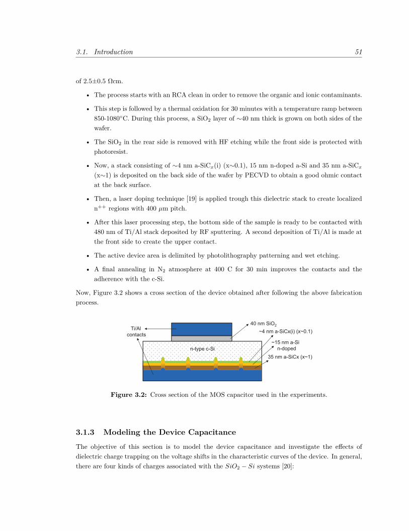
3.1. Introduction 51
of 2.5±0.5 Ωcm.
• The process starts with an RCA clean in order to remove the organic and ionic contaminants.
• This step is followed by a thermal oxidation for 30 minutes with a temperature ramp between850-1080C. During this process, a SiO2 layer of ∼40 nm thick is grown on both sides of thewafer.
• The SiO2 in the rear side is removed with HF etching while the front side is protected withphotoresist.
• Now, a stack consisting of ∼4 nm a-SiCx(i) (x∼0.1), 15 nm n-doped a-Si and 35 nm a-SiCx(x∼1) is deposited on the back side of the wafer by PECVD to obtain a good ohmic contactat the back surface.
• Then, a laser doping technique [19] is applied trough this dielectric stack to create localizedn++ regions with 400 µm pitch.
• After this laser processing step, the bottom side of the sample is ready to be contacted with480 nm of Ti/Al stack deposited by RF sputtering. A second deposition of Ti/Al is made atthe front side to create the upper contact.
• The active device area is delimited by photolithography patterning and wet etching.
• A final annealing in N2 atmosphere at 400 C for 30 min improves the contacts and theadherence with the c-Si.
Now, Figure 3.2 shows a cross section of the device obtained after following the above fabricationprocess.
n-type c-Si
~4 nm a-SiCx(i) (x~0.1)
~15 nm a-Si
n-doped
35 nm a-SiCx (x~1)
Ti/Al
contacts
40 nm SiO2
Figure 3.2: Cross section of the MOS capacitor used in the experiments.
3.1.3 Modeling the Device Capacitance
The objective of this section is to model the device capacitance and investigate the effects ofdielectric charge trapping on the voltage shifts in the characteristic curves of the device. In general,there are four kinds of charges associated with the SiO2 − Si systems [20]:

52 Chapter 3. Dielectric Charge Trapping Controls for MOS Capacitors
• Mobile ionic charge: These are positive charges present in the oxide bulk primarily due toionic impurities such as Na+, K+.
• Oxide-trapped charge: These are positive or negative charges due to the trapping of holesor electrons in the oxide bulk. Ionization radiation, avalanche injection are some of themechanisms that result in the formation of these kinds of traps.
• Fixed oxide charge: This is a positive charge located closer to the oxide-semiconductor in-terface and formed due to structural defects. The density of these charges depend on theoxidation ambient and temperature, and cooling conditions.
• Interface-trapped charge: These can be positive or negative charges formed due to processinduced defects, metal impurities and bond-breaking processes (induced by radiation) and arelocated at the oxide-semiconductor interface. The polarity of these trapped charges dependon the surface potential and usually most of them can be neutralized by low temperature H2
or H2/N2 annealing.
Figure 3.3: Typical CV characteristic curve of a MOS capacitor.
The typical capacitance-voltage (CV) characteristic curve of a MOS capacitor is shown inFigure 3.3. The first three types of charge lead to rigid shift of the CV curve whereas the interfacetraps results in the stretching of the curves along the gate voltage axis. The model obtained in thiswork includes the charge accumulated in the oxide bulk and the charge trapped near the SiO2−Siinterface. For the frequencies that we have used in our experiments, we consider that there is nocontribution from interface states to the high frequency capacitance, although some could be presentunder accumulation and depletion conditions for traps very close to the conduction band (< 0.2 eV)with very high interface state densities [21]. Thus, the capacitance per unit area of the structureC is a series combination of the oxide layer capacitance Cox and the depletion layer-semiconductor

3.1. Introduction 53
capacitance Cs,C = CoxCs
Cox + Cs(3.1)
where Cox = εoxε0/dox, being εox and dox the oxide permittivity and thickness respectively.An analytical expression of Cs for uniformly-doped silicon and high frequency (HF) conditions
is obtained in Chapter 7 of [22] from the equivalent charge density in the semiconductor Qs. Forn-type silicon the latter is,
Qs = ±√
2εsε0βLD
√n2i
N2D
(e−βψs + βψs − 1) + eβψs − βψs − 1
= ±√
2εsε0βLD
F (βψs,niND
)
(3.2)
where ni and εs are the intrinsic carrier concentration and the permittivity of silicon, ND is thedonor concentration, LD =
√εsε0/qβND is the Debye length, β = q/kBT and ψs is the potential,
or energy band bending, at the silicon surface.The semiconductor capacitance can be obtained as,
Cs = dQsdψs
= εsε0√2LD
∣∣∣∣∣∣n2i
N2D
(1− e−βψs) + eβψs − 1F (βψs, niND )
∣∣∣∣∣∣ (3.3)
This implies that ψs must be calculated first to obtain Cs.Now a voltage bias VG is applied to the gate of the device. The voltage drop across the entire
structure must be zero,VG −∆φms − ψs − ψox = 0 (3.4)
where ∆φms is the work function difference between the metal and the semiconductor and ψs andψox are respectively the potential drops along the semiconductor and along the oxide. ψox can becalculated as Qm/Cox, being Qm the charge density in the metal layer. Additionally, by chargeneutrality Qm must be equal to the charge at the oxide-semiconductor interface and the charge inthe semiconductor Qs. As discussed later in this section, the charge at the oxide-semiconductorinterface can be modelled as Qox + Qit, where Qox is an equivalent oxide charge and Qit is thecharge due to interface traps. According to all this, charge neutrality leads to,
ψox = QmCox
= −QoxCox− Qit(ψs)
Cox− Qs(ψs)
Cox(3.5)
Note that both Qit and Qs are functions of the surface potential ψs. By substituting (3.5) into (3.4),one can obtain
VG −∆φms − ψs −QoxCox− Qit(ψs)
Cox− Qs(ψs)
Cox= 0 (3.6)
The surface potential ψs and therefore the total capacitance of the device C(VG) can be calculatedby numerically solving equation (3.6) and then using equations (3.3) and (3.1). Interface traps are

54 Chapter 3. Dielectric Charge Trapping Controls for MOS Capacitors
electrically connected with the semiconductor and therefore can be charged or not depending on thesurface potential ψs. It is well known that interface traps can be acceptor-like (negatively-chargeswhen filled with an electron and neutral when empty) or donor-like (positively-charged when emptyand neutral when filled with an electron). Additionally, it is not possible to determine this trapcharacteristic from the capacitance measured at 2 MHz, where only the variation of the interface-trapped charge Qit coming from both types of traps can be obtained. Then, the simplified modelof Qit used in this work assumes that: a) there is a constant trap density Dit along the silicongap, being half of it acceptor-like and half of it donor-like, i.e. Dit = DA
it/2 = DDit /2, b) all trap
levels below the Fermi level Ef are full and all above Ef are empty. Under these assumptions theexpression below is obtained, where NV and NC are the valence and conduction levels, respectively.
Qit(ψs) = Dit
(kBT ln( ni
ND)− 1
2kBT ln(NVNC
)− qψs)
(3.7)
The above analytical model of the device is obtained after the classical theory for Metal-SiO2 − Si structures [22, 23]. The effects of oxide and interface trapped charges are evaluatedby fitting with the results obtained from the experiments. In the next section, description of thecharge control scheme used in this work is presented.
3.1.4 Charge Control Method: Sigma-Delta Approach
In this section, the control method based on sigma-delta modulation similar to the one implementedin [11, 16], has been introduced. The discrete-time circuit shown in Figure 3.5 (a) corresponds to afirst order 1-bit sigma-delta converter. Note that this circuit is basically composed of an integratorand a quantizer (sign function). In many applications this integrator is not in the electrical domain.It can be in the thermal domain, as in thermal sigma-delta modulators [24], or in the mechanicaldomain, as in the case of some force feedback accelerometers [25].
Now, this control method has been implemented to control the charge trapped in the oxide layerof MOS capacitors. This can be achieved by periodically monitoring the horizontal displacement ofthe CV characteristic of the device and applying the adequate voltage waveforms to maintain it at adesired position. Figure 3.7 shows the closed loop circuit designed for this purpose. It is a sampledcircuit which monitors the capacitance at a reference voltage in periodic sampling intervals, nTS ,and evaluates this control parameter using a negative feedback loop to maintain it around a fixedthreshold value. In our case, the actual magnitude to control is the total charge in the dielectriclayer of a MOS capacitor, which is indirectly sensed by observing the horizontal displacement ofthe CV curve or in other words, voltage shift.
Figure 3.4 illustrates this idea, where C2 and C3 represent the shifted versions of the originalCV curve C1 due to the accumulation of trapped charges. The detection of whether the CV liesto the right or to the left of its desired position can be achieved by observing the value of thecapacitance at a constant voltage of interest, C1[V1].
The objective of the control is to shift the CV curve of the device so that the value of thecapacitance at the voltage reference V1 is Cth, i.e., C[V1](t) ≈ Cth. To this effect an adequate
3.1. Introduction 55
Figure 3.4: Illustration of the working of control method. If C1[V1] represents the target capaci-tance at the voltage of interest, the control loop applies adequate voltage waveforms to shift the CVcurves to left (C2[V1]) or to right (C3[V1]) around the target capacitance. The CV displacementsare intentionally enlarged for the purpose of demonstration.
Figure 3.5: a) Control feedback loop for CV control. The device capacitance is measured peri-odically at voltage V1 and compared with a threshold value, Cth. Depending on the result, eithera BIT1 or BIT0 waveform is applied during the next sampling period. b) BIT0 and BIT1 voltagewaveforms. The sampling period is TS and V1 is applied for a short time δTS in each waveform.The capacitance measurement is taken at the end of each V1 application.
sequence of voltage waveforms are being applied by the feedback loop to the device. The voltagewaveforms, also named as BIT0 and BIT1 waveforms, should be designed in order to obtain two

56 Chapter 3. Dielectric Charge Trapping Controls for MOS Capacitors
separate results:
• The applied waveforms must allow periodical monitoring of C[V1](t) at times t = nTS . Inorder to have such periodic measurements at a fixed reference voltage at each samplinginterval, it is necessary to switch the voltage levels during the sampling period. The designedvoltage waveforms can be seen in Fig. 3.5 (b). In both cases the waveform ends with asegment of time of duration δTS , during which V1 is applied to the device to be able tomonitor the relative position of the C-V curve, with regard to the desired position, i.e., makethe comparison between C[V1]n = C[V1](nTS) and Cth.
• The chosen voltage levels must apply the correct excitation to shift the CV in the adequatedirection. In this regard, the actuation voltages, V +, V −, which are being applied during(1 − δ)TS , are chosen so that they generate horizontal shifts of the CV of different sign:if C[V1]n < Cth a BIT1 is applied during the next clock cycle, and a BIT0 otherwise (seeFig. 3.5). Accordingly the following control law has been defined:
Next symbol =
BIT0, if C[V1](nTS) > Cth
BIT1, otherwise(3.8)
Now the implementation of the charge control method can be described in the form of thefollowing flowchart:
Figure 3.6: Flowchart description of the control method.
The comparison between C[V1]n and Cth at the end of each sampling period, nTS , generatesa bitstream at the output of the modulator, bn = sgn(Cth − C[V1]n). Averaging of these bits over

3.1. Introduction 57
a period of time provides the average voltage required to maintain the desired charge level in thedielectric. From this signal it is possible to obtain real time information of the charging dynamicsin the dielectric of the device.
In order to analyze the charge dynamics involved with the proposed control method (see Chap-ter 5), it would be convenient to establish a link to a first-order sigma-delta modulator, as shownin Figure 3.7. Considering a constant input, β, to the system, the output of the modulator, yn,is a bit stream obtained by quantizing the accumated or integrated sum of the error signals overeach sampling period, TS . Since the quantizer is a two-level comparator, the output will be either1 or -1. The main objective of the modulator is to minimize the difference between the integratedmodulator ouput and the integrated input. This can be expressed in the form of a typical equationof Sigma-Delta modulator [4] as
un+1 = un − β + yn (3.9)
Comparing the charge control circuit, see Figure 3.5, with the 1st order sigma-delta modulator,
Figure 3.7: First order sigma-delta modulator [11].
we can notice that the function of integration in our control method is performed by the dielectriclayer, which is considered to be a reservoir of charge. Since the control parameter is the capacitanceat the reference voltage, C[V1], which is an indirect measurement of the net dielectric charge, theinput to the quantizer can be seen as difference between the target charge and the net charge in thedielectric. And this net charge in the dielectric at the end of each sampling interval is the sum ofthe previously stored charge and the integral over the sampling period of two charge contributions:charge injection and charge leak. Thus the control method maintains the net charge around a fixedvalue and generates an average bitstream, b, such that the balance between charge leak and chargeinjection, given by β, fixes the net charge around the desired target value.
β = b = limN→∞
1N
N−1∑n=1
bn (3.10)
The steady-state average bitstream corresponds to a stable level of dielectric charge, therefore theamount of trapped charge in the dielectric can be inferred from the average of the output bitstreamgiven by b. Any change in the desired level of charge (or in other words, Cth) results in a change

58 Chapter 3. Dielectric Charge Trapping Controls for MOS Capacitors
in the average bitstream thus we obtain a unique relation between b vs Cth.In the next section, a set of experiments have been performed on a MOS capacitor, described
in Section 3.1.2, in order to validate the control method discussed in this section.
3.2 First Order Sigma-Delta Control
In this section the first order sigma-delta control described in the previous section has been imple-mented as a tool to provide a sliding mode control of net trapped charge [26, 17]. To this effect, along experiment has been planned with the control being applied on a MOS capacitor for differenttarget capacitances.
3.2.1 Experimental Setup
The experimental setup used to implement the control strategy, described in section 3.1.4, is de-picted in Figure 3.8. A Keysight E4980A LCR meter, controlled from a computer, periodicallymeasures the capacitance and applies the voltage waveforms at each sampling interval according tothe control law 3.8. The control parameters must be chosen so that the continuous application ofBIT0 waveforms must generate shifts of different sign to the continuous application of BIT1 wave-forms. So the voltage levels for BITx waveforms are selected such that V − = −3V , and V + = 6Vgenerate, respectively, shift to the right and to the left of the CV curve of our device. The valueV1 = −4.5V gives good sensitivity to sense the displacements of the CV curve produced during theexperiments. The sampling period has been chosen to be TS = 350ms with δ = 1/3.
Figure 3.8: Implementation of the charge control method. The LCR meter monitors thecapacitance,C(t), and decides to apply either the symbol BIT0 or BIT1 from the comparisonbetween C(t) and Cth.

3.2. First Order Sigma-Delta Control 59
3.2.2 Results and Discussion
The experiment consists of applying the control method on the capacitor for 16h with 8 differenttarget capacitances, each one lasting for 2 hours (see Table 3.2).
Figure 3.9 shows the evolution as a function of time of the capacitance measured at the end ofeach clock cycle, C[V1]n. At the beginning of each interval a transient can be observed in which themeasured capacitance either increases or decreases till the target threshold value is reached. Duringthis transient period, a continuous sequence of BITx waveforms is being applied. Once the desiredvalue has been reached, the feedback loop applies the excitation required to keep it constant.
Figure 3.9: Time evolution of C[V1]n during the experiment. For each Ci segment this value isalmost constant and matches its corresponding target value, Cth. V1 = −4.5V .
A zoom of the evolution of the capacitance measured at V1 can be observed in Figure 3.10.As it can be seen, each time the capacitance is below the desired threshold value (Cth=0.6231nFfor segment C−4) the feedback loop applies a BIT1, and in this case it takes between 3 and 4consecutive BIT0s to take it down again below the threshold. This is compatible with the standardbehaviour of first-order sigma-delta modulators [16]. The CV characteristics of the device at theend of each 2-hour controlling segments (Ci) are depicted in Figure 3.11. We can observe thatby choosing different target values and applying the control method, it is possible to shift the CVcurve horizontally and maintain it around a desired operating point. The corresponding values ofthe voltage shift, measured at 0.4nF of device capacitance, are listed in Table I.
The average bitstream generated by the feedback loop during the experiment is shown in Fig-ure 3.12. As it can be observed, it is necessary to inject more BIT0 waveforms (the average bitstream

60 Chapter 3. Dielectric Charge Trapping Controls for MOS Capacitors
7.786 7.787 7.788 7.789 7.79 7.791 7.792
0.6231
0.6232
0.6233
0.6234
0.6235
0.6236
0.6237
C(-
4.5)
[n
F]
7.786 7.787 7.788 7.789 7.79 7.791 7.792Time [h]
-1
-0.5
0
0.5
1
Bit
stre
am
Figure 3.10: Top: Zoom of C[V1](nTS) for a short time within segment C−4. Bottom: sequenceof bits applied during this time.
-7 -6.5 -6 -5.5 -5 -4.5 -4 -3.5 -3 -2.5 -2Voltage (V)
0
0.1
0.2
0.3
0.4
0.5
0.6
0.7
0.8
Cap
acit
ance
[n
F]
CV4
CV3
CV2
CV1
CV-1
CV-2
CV-3
CV-4
CV0
CV-4
CV-3CV
-2CV0
CV-1
CV4
CV1
CV2
CV3
Figure 3.11: C-V curves obtained at the end ofeach Ci segment. For each CVi curve shown, itis C(−4.5V ) ≈ Cthi, as defined in Table 3.2.
Ci Time [h] Vsh(0.4nF ) [mV ]C0 t < 0 0 (Initial Value)C−1 t ∈ [0, 2] −36C−2 t ∈ [2, 4] 135C−3 t ∈ [4, 6] 275C−4 t ∈ [6, 8] 384C1 t ∈ [8, 10] −288C2 t ∈ [10, 12] −624C3 t ∈ [12, 14] −1034C4 t ∈ [14, 16] —
Table 3.2: Cth values used during the experi-ment. Voltage shifts of the obtained C-V curvesmeasured at 0.4nF .
decreases) to achieve lower Cth values. On the other hand, increasing the average number of BIT1waveforms generates higher values of C[V1].
Each time a new target value is applied the control saturates i.e it applies a continuous sequenceof either BIT0 or BIT1 waveforms till the new Cth value is reached. Once in this range, the averagebitstream follows a slow time evolution, which has also been observed in previous works [17].

3.2. First Order Sigma-Delta Control 61
Figure 3.12: Average bitstream obtained during the experiment. Each time the target capacitance,Cth, is changed the bitstream saturates till such target value is reached. Increasing the averagenumber of BIT1 waveforms allows to increase the value C[V1], hence displacing the C-V to the left.
A distinctive feature of sigma-delta modulators is the power spectrum density of the generatedbitstream. For the first order case it is known that the quantization noise presents a zero at 0Hzand the slope is approximately 20dB/dec (see Fig. 3.13).
10-3 10-2 10-1 100 101
Frequency (Hz)
-50
-40
-30
-20
-10
0
10
Po
wer
Sp
ectr
al D
ensi
ty
Figure 3.13: Power spectral density obtained from the C1 step of the experiment (between t=8hand t=10h). Total number of bits of the sequence: 16312.

62 Chapter 3. Dielectric Charge Trapping Controls for MOS Capacitors
3.2.3 Simulations versus Experimental Data
Fittings of the experimental CV curves reported in Figure 3.11 with the analytical model describedabove have been performed, takingQox andDit as parameters. The results are shown in Figure 3.14.In good agreement with theory, these results indicate that the horizontal-rigid CV shifts correspondto variations of the charge trapped in the oxide Qox. Moreover, both the mobile ionic charge andthe fixed oxide charge components of Qox depend on the fabrication process and they can hardlyvary during the experiments. Then it can be concluded that such CV shifts correspond to positiveand negative variations of the charge trapped in the bulk of the oxide, being the total oxide chargepositive in the cases reported.
CV0
CV-4
CV1
CV2
3.15x10¹²
2.96x10¹²
3.29x10¹²
3.45x10¹²
Figure 3.14: Comparison between experimental CV curves (ticks) and simulation results of thereference device (dashed lines). The value of Qox used in each simulation is given in cm−2. Aninterface trap density Dit=1.55×1012cm−2eV−1 was used in all simulations.
Additionally, the charge trapped in the interface Qit can be either positive or negative de-pending on the surface potential, thus on the gate voltage, VG. This produces opposite shift inthe accumulation and depletion sections within the same C-V curve, a phenomenon known as CVstretch-out [22]. This phenomenon may also explain the CV stretching observed for the CV4 casein Figure 3.11. In Figure 3.14 a small discrepancy between simulation and experimental results isseen in the accumulation section. However, this discrepancy is due to the simplified model used,which assumes a constant Dit. This is a rough approach, since in practice Dit can exhibit notice-able variation along the band gap [27] and, as mentioned before, some response could be related tointerface traps close to the conduction band edge [21].

3.3. Second Order Sigma-Delta Control 63
3.3 Second Order Sigma-Delta Control
3.3.1 Charge Control Method
In the previous sections, a first order control of charge trapping for MOS capacitors based on sigma-delta modulators has been implemented. The control allows to obtain a desired shift of the CVcharacteristic of the device (and hence of the net trapped charge in the oxide) and then to maintainit by the application of a proper sequence of bipolar voltage waveforms. However, one of the knownproblems of first order sigma-delta modulators is the appearance of plateaus [10], conventionallyknown to be Devil’s staircase.
The occurance of this non-linear effect is associated with leaky integrators, usually finite-gainop-amps in practical realizations of a modulator. This devil’s staircase behavior has been observedin the case of systems such as MEMS oscillators [28], Capacitive MEMS devices [16, 29, 30], gassensors [31] where control strategy based on 1st order sigma-delta modulator is implemented. Inthese devices, the dielectric layer, which is considered to be a reservoir of charge, works as a leakycharge integrator and the sampling time, TS , associated with this integrator can be seen as ananalog to the leakage parameter. If the sampling time is of the same order or greater than theshortest time constant of the charging and discharging processes of the device, the control mayprovide a constant output during certain time intervals in which the system is effectively in anopen loop configuration. It must be noted that the charging and discharging time constants willdepend on the applied voltages in a non-linear way and that several processes may coexist in asingle device, resulting in a complex dynamics that is generally difficult to predict beforehand.
Figure 3.15: a) Block diagram of the second order sigma-delta control circuit of charge trapping.b) Experimental implementation of the second order control.
Now, a second order sigma-delta control method is introduced in order to control the chargetrapping in MOS capacitors. Figure 3.15 shows the double loop sigma-delta modulator with twointegrators and two feedback loops. The objective of this section is to present a second order controlof charge trapping for MOS capacitors. This topology effectively removes the presence of plateausin the experimental measurements.
The block diagram of the second order control circuit proposed is shown in Figure 3.15. Themain difference compared to the first-order topology is the use of an integrator before the sign

64 Chapter 3. Dielectric Charge Trapping Controls for MOS Capacitors
detector. The error signal,, obtained at the end of each sampling interval, TS , is integrated nu-merically and the sign of the result decides the actuation BITx waveform to be applied in the nextsampling period. The addition of an integrator element will result in a second order zero in thequantization noise at the output of the modulator, and also in the disappearance of the unwantedplateaus [29, 32].
3.3.2 Fabrication Process
The processing steps followed to fabricate the capacitors used for these experiments are described:
• The process starts with an RCA clean in order to remove the organic and ionic contaminants.
• This step is followed by a thermal oxidation for 45 minutes with a temperature ramp between850-1080C. During this process, a SiO2 layer of ∼25 nm thick is grown on both sides of thewafer.
• Next, the SiO2 in the back side is removed with HF etching, while the front side is protectedwith photoresist.
• Then, aluminum is deposited at the back side of the wafer by evaporation, resulting in alayer thickness of approximately 700 nm. Later, a laser doping technique is applied.
• Finally, the top electrode is conformed via a sputtering deposition of aluminum using ashadow mask for patterning.
Figure 3.16: Measured (ticks) and fitted (solid lines) CV curves for the capacitors MC-1 andMC-2. The fitting has been done using the model described in section 3.1.3.

3.3. Second Order Sigma-Delta Control 65
3.3.3 Results and Discussion
Two sets of MOS capacitor devices used here, named as MC-1 and MC-2, from the same fabricationbatch have been used. The CV characteristics of the devices have been shown in Figure 3.16.
An initial set of experiments have been performed in order to evaluate the effectiveness of thesigma-delta control method using devices MC-1 and MC-2. The parameter values chosen for BIT0and BIT1 waveforms are reported in Table 3.3. .
Table 3.3: Parameter values used in BIT0 and BIT1 waveforms.
Device V + V − V1 TS δ
MC − 1 5V −1V −0.5V 350mS 1/3MC − 2 6V −1V −0.5V 350mS 1/3
Figure 3.17: First order sigma-delta control applied to MC-1 to obtain a sequence of six targetcapacitances. a) Device capacitance measured during the experiment. b) Averaged bit streamprovided by the control loop. Circles denote time intervals in which the control is in a plateau.

66 Chapter 3. Dielectric Charge Trapping Controls for MOS Capacitors
In a first experiment, first order sigma-delta control was applied to device MC-1 to achieve asequence of six target capacitances, Cth = 0.98, 1.01, 0.99, 1.02, 0.975, 1.03nF. Each target-steplasted for 2 hours. From the results of this experiment, shown in Figure 3.17, it can be seen thatthe control method allows to reach the desired target levels and maintain them. For example, att = 4h more BIT0s (V − dominant) are being applied by the control forcing the C-V to shift tothe right and thus decreasing C[V1](t) until the target, Cth = 0.99nF , is reached. From then untilt = 6h, the bit stream keeps the capacitance successfully around this target value.
However, plateau-associated phenomena can be observed in three different time intervals high-lighted with a circle in Figure 3.17. When the control becomes trapped in a plateau, it providesconstant bit stream output, and the observed variable, C[V1](t), is in fact left uncontrolled and ex-hibits open-loop behaviour. The time length of such control-locking effect is unpredictable, thereforeplateaus must be avoided when possible.
The aim of the next set of experiments is to investigate the eventual improvements provided bythe second order sigma-delta control when applied to devices that exhibit fast charging dynamics.Figure 3.18 shows the results of an experiment when a first order and a second order sigma-delta con-trols have been applied to device MC-1 with four target levels, Cth = 0.95, 0.935, 0.96, 0.925nF,in 3h steps. A plateau has been detected in case of a first order sigma-delta control, which impliesthat control was lost for approximately 145 minutes, whereas in case of second order sigma-deltacontrol, there has been no sign of plateau during the control.
Figure 3.18: Results of (a) 1st order and (b) 2nd order sigma-delta controls applied to MC-1 toobtain a sequence of four target capacitances. The circle denotes an interval in which the controlis in a plateau.
Figure 3.19, taken from experimental data, illustrates how first and second order controlsdo work. In the first order case, the behaviour of the capacitance and of the bit stream are

3.4. Conclusions 67
Figure 3.19: Sampled capacitance and bit stream taken from the experiment of 3.18(a) and fromthe experiment of 3.18(b), both in the Cth = 0.96nF time step.
straightforward related: the next BIT changes each time C[V1] exceeds Cth. However, in case ofsecond order controller, the presence of the integrator makes this relationship not so easy to see,but the behaviour obtained fully agrees with the sigma-delta modulator theory [33] and with theexperiments reported in [30].
Figure 3.20 compares the spectral power densities of the bit streams obtained from two exper-iments in which MC-2 was set to Cth = 1.33 nF for 16 hours using both first and second ordercontrols. The presence of the additional integrator in the 2nd order method produces noticeabledifferences. The noise at low frequencies becomes considerably reduced and the slope of the quan-tization noise rolled out of the band of interest increases in the 2nd order case.
3.4 Conclusions
A new CV control for MOS capacitors has been implemented. The proposed method, based onsigma-delta modulation, allows to horizontally displace the CV characteristic of the device and

68 Chapter 3. Dielectric Charge Trapping Controls for MOS Capacitors
Figure 3.20: Power spectral density estimation, obtained using Welch’s method in MatLab after105 samples of the control bit stream. First and second order controls were applied to device MC-2for 16 hours to obtain the same target capacitance, Cth = 1.33 nF.
maintain it at a desired point so that the net charge trapped in the dielectric layer remains constant.The control capability relies on the complementary sign of the shift generated by voltages of differentpolarity, in what is a sliding mode control. Several analysis and experiments have been undertakento explain how the changes in the CV can be related to charge trapping in the bulk of the oxidelayer and in the silicon-oxide interface, and how charge trapped can be sensed and actuated. Asecond order method of dielectric charging control for MOS capacitors has also been presented andchecked experimentally. The main advantages being that the quantization noise shaping is secondorder and that the typical plateaus of first order sigma-delta controllers can be avoided. Thesecontrol strategies can be seen as a promising way of improving the reliability of MOS structures.

Bibliography 69
Bibliography[1] Steven R Norsworthy, Richard Schreier, Gabor C Temes, et al. Delta-sigma data converters:
theory, design, and simulation, volume 97. IEEE press New York, 1996.
[2] Bernhard E Boser and Bruce AWooley. The design of sigma-delta modulation analog-to-digitalconverters. IEEE Journal of solid-state circuits, 23(6):1298–1308, 1988.
[3] J.C. Candy and G.C. Temes. Oversampling delta-sigma data converters: theory, design, andsimulation. Selected reprint series. IEEE Press, 1962. ISBN 9780879422462.
[4] Orla Feely. Nonlinear dynamics and chaos in Sigma-Delta modulation. Journal of the FranklinInstitute, 331(6):903–936, 1994.
[5] Max W Hauser. Principles of oversampling A/D conversion. Journal of the Audio EngineeringSociety, 39(1/2):3–26, 1991.
[6] James Candy and O Benjamin. The structure of quantization noise from sigma-delta modu-lation. IEEE Transactions on Communications, 29(9):1316–1323, 1981.
[7] Eric J van der Zwan. A 2.3 mW CMOS Σ∆ modulator for audio applications. In 1997 IEEEInternational Solids-State Circuits Conference. Digest of Technical Papers, pages 220–221.IEEE, 1997.
[8] Katelijn Vleugels, Shahriar Rabii, and Bruce A Wooley. A 2.5-V sigma-delta modulator forbroadband communications applications. IEEE Journal of Solid-State Circuits, 36(12):1887–1899, 2001.
[9] Edmund Mark Schneider, Aniruddha Satoskar, Daniel J Allen, and Seyedeh Maryam Mor-tazavi Zanjani. Multi-path analog front end and analog-to-digital converter for a signal pro-cessing system, sep 2015. US Patent 9,148,164.
[10] Orla Feely and Leon O Chua. The effect of integrator leak in sigma-delta modulation. IEEETransactions on circuits and systems, 38(11):1293–1305, 1991.
[11] M. Domuez, V. Jimz, J. Ricart, L. Kowalski, J. Torres, S. Navarro, J. Romeral, and L. CastaA hot film anemometer for the Martian atmosphere. Planetary and Space Science, 56(8):1169– 1179, 2008. ISSN 0032-0633.
[12] Maria-Teresa Atienza, Lukasz Kowalski, Sergi Gorreta, Vicente Jiménez, and ManuelDomínguez-Pumar. Thermal dynamics modeling of a 3D wind sensor based on hot thin filmanemometry. Sensors and Actuators A: Physical, 272:178–186, 2018.
[13] Manuel Dominguez-Pumar, Lukasz Kowalski, E Llobet, and Raül Calavia. Active control ofthe surface potential of nanostructured layers. IEEE Sensors Journal, 16(8):2213–2214, 2016.

70 Bibliography
[14] Manuel Dominguez-Pumar, Lukasz Kowalski, Raul Calavia, and E Llobet. Smart controlof chemical gas sensors for the reduction of their time response. Sensors and Actuators B:Chemical, 229:1–6, 2016.
[15] Oscar Monge-Villora, Manuel Dominguez-Pumar, and Josep M Olm. Analysis of the dynamicsof an active control of the surface potential in metal oxide gas sensors. Computers & ChemicalEngineering, 113:1–10, 2018.
[16] S. Gorreta, J. Pons-Nin, E. Blokhina, O. Feely, and M. Dominguez-Pumar. Delta-SigmaControl of Dielectric Charge for Contactless Capacitive MEMS. IEEE J. Microelectromech.Syst., 23(4):829–841, Aug 2014.
[17] M. Dominguez-Pumar, S. Gorreta, and J. Pons-Nin. Sliding Mode Analysis of the Dynamicsof Sigma-Delta Controls of Dielectric Charging. IEEE Trans. Ind. Electron., 63(4):2320–2329,Apr 2016.
[18] Maria-Teresa Atienza, Lukasz Kowalski, Sergi Gorreta, Vicente Jiménez, Luis M Castañer, andManuel Domínguez-Pumar. Sliding mode analysis applied to improve the dynamical responseof a spherical 3D wind sensor for Mars atmosphere. Sensors and Actuators A: Physical, 267:342–350, 2017.
[19] I. Martín, M. Colina, A. Coll, G. Lopez, P. Ortega, A. Orpella, and R. Alcubilla. c-Si SolarCells based on Laser-processed Dielectric Films. Energy Procedia, 55:255–264, 2014.
[20] B.E. Deal. Standardized Terminology for Oxide Charges Associated with Thermally OxidizedSilicon. IEEE Trans. Electron Devices, 27(3):606–608, Mar 1980.
[21] I. Pintilie, C.M. Teodorescu, F. Moscatelli, R. Nipoti, A. Poggi, S. Solmi, L.S. Lovlie, and B.G.Svensson. Analysis of electron traps at the 4H − SiC/SiO2 interface; influence by nitrogenimplantation prior to wet oxidation. J. Appl. Physics, 108:024503, Jul 2010.
[22] S. Sze and K. Ng. Physics of Semiconductor Devices, 3rd ed. Wiley, NJ USA, 2006.
[23] R.F. Pierret. Field Effect Devices: Volume IV, 2nd ed. Addison-Wesley, MA USA.
[24] K. Makinwa and J.H. Huijsing. A smart wind sensor using thermal sigma-delta modulationtechniques. Sensors and Actuators A: Physical, 97-98(1):15–20, 2002.
[25] F. Chen, X. Li, and M. Kraft. Electromechanical Sigma Delta Modulators Force FeedbackInterfaces for Capacitive MEMS Inertial Sensors. A Review. IEEE Sensors Journal, 16:6476–6495, 2016.
[26] H. Sira-Ramirez. Sliding Mode Control: The Delta-Sigma Modulation Approach. Birkhauser,2015.

Bibliography 71
[27] T. Hori. Gate Dielectrics and MOS ULSIs. Principles, Technologies and Applications. Springer-Verlag, Heidelberg Germany, 1997.
[28] Manuel Domínguez, Joan Pons-Nin, Jordi Ricart, Agustín Bermejo, E Figueras Costa, andMarta Morata. Analysis of the Σ∆ pulsed digital oscillator for MEMS. IEEE Transactions onCircuits and Systems I: Regular Papers, 52(11):2286–2297, 2005.
[29] Manuel Dominguez-Pumar, Sergi Gorreta, Joan Pons-Nin, Elena Blokhina, PanagiotisGiounanlis, and Orla Feely. Real-time characterization of dielectric charging in contactlesscapacitive MEMS. Analog integrated circuits and signal processing, 82(3):559–569, 2015.
[30] Sergi Gorreta, Joan Pons-Nin, Elena Blokhina, and Manuel Dominguez. A second-order delta-sigma control of dielectric charge for contactless capacitive MEMS. Journal of Microelectrome-chanical Systems, 24(2):259–261, 2015.
[31] Lukasz Kowalski, Joan Pons-Nin, Eric Navarrete, Eduard Llobet, and Manuel Domínguez-Pumar. Using a second order sigma-delta control to improve the performance of metal-oxidegas sensors. Sensors, 18(2):654, 2018.
[32] Panagiotis Giounanlis, Sergi Gorreta, Manuel Dominguez-Pumar, Joan Pons-Nin, Orla Feely,and Elena Blokhina. Σ∆ Effects and Charge Locking in Capacitive MEMS Under DielectricCharge Control. IEEE Transactions on Circuits and Systems II: Express Briefs, 64(2):206–210,2016.
[33] S.R. Norsworthy, R. Schreier, G.C. Temes, and IEEE Circuit & Systems Society. Delta-Sigmadata converters: theory, design, and simulation. IEEE Press, 1997. ISBN 9780780310452.


Chapter 4
Compensation of Charge Inducedby Radiation in MOS Capacitors
Radiation, in general, is the emission or transmission of energy in the form of waves or particlesthrough space or through a material medium. Depending on the energy carried by the radiatingparticles, radiation is often categorized as either non-ionizing or ionizing. Non-ionizing radiationis a low frequency electromagnetic radiation that does not carry enough energy (often less than10eV ) to ionize atoms or molecules, while ionizing radiation has high frequency and carries enoughenergy to detach electrons and ionize atoms or molecules. Exposure to ionizing radiation couldbe detrimental to electronic systems in the sense that it alters the electrical properties of activecomponents and results in the degradation of circuit performance and even circuit failure. Hence, agood understanding of the physical mechanisms underlying the response of the devices to radiationis essential in order to improve the tolerance of the electronic circuits and develop radiation hardenedcircuits.
Charge trapping induced by ionizing radiation in semiconductor devices represents a majorreliability issue in many applications [1, 2, 3]. Most of the modern integrated circuits (ICs) employinsulators and oxides as key components and exposure to ionizing radiation results in the buildupof trapped charge, often leading to device degradation and failure [4, 5]. Under the influence ofhigh energy ionizing radiation, these devices suffer from a drift in the threshold voltage, an increaseof the leakage current, and a decrease of the transconductance [6, 7]. This results in a degradedperformance thereby increasing the failure rate of the device operation [8, 9, 10, 11].
Over the past 40 years, the effects of total ionizing dose on radiation-induced trapped chargebuildup in MOS devices have been investigated [12, 13].
However, most works related to reducing the effects of charge trapping focus on the designand characterization of materials and structures. Alternatively, it is equally important to developsome active control techniques such as proposed in [14, 15] to improve the radiation response of thedevices. This control method, based on sliding control [16], effectively compensates the dielectric
73

74 Chapter 4. Compensation of Charge Induced by Radiation in MOS Capacitors
charge induced by ionizing radiation by the application of bipolar actuation voltage waveforms.Now, the objective of this chapter is to explore the capability of a charge trapping control
loop to improve the radiation response of MOS capacitors made of SiO2 and Al2O3 dielectricsby compensating the oxide-trap charge induced by ionizing radiation. To this effect, two sets ofdevices made with silicon dioxide and alumina have been irradiated with gamma radiation andX-rays respectively. Each set has two capacitors exposed to irradiation, one operating at constantvoltage bias while the other working under a dielectric charge control. The experiments showsubstantial charge trapping in the uncontrolled device whereas, at the same time, the control loopis able to compensate the charge induced by ionizing radiation in the second device.
4.1 Charge Trapping Control under Ionizing Radiation
The objective of this section is to introduce the closed-loop control strategies that can effectivelycope with charge induced by ionizing radiation. The charge control circuit shown in Figure 4.1 cor-responds to a first order sigma-delta converter, as discussed in Chapter 3. The dielectric in the MOScapacitor can be seen as a reservoir of trapped charge which is continuously being filled/emptiedby three different contributions:
• the trapped charge injected/extracted by the applied voltage actuation,
• the trapped charge being leaked out, and
• the trapped charge generated by ionizing radiation.
δ δ δ δ
Figure 4.1: (a) Sigma-Delta feedback loop implemented on device under irradiation. The devicecapacitance at voltage V1 is measured periodically and compared with Cth. Depending on theresult, either a BIT1 or BIT0 waveform is applied during the next sampling period. (b) BIT0 andBIT1 waveforms. Capacitance measurements are taken at the end of each V1 application.

4.2. Experimental 75
All three contributions will depend on the instantaneous applied electric field and on the state ofthe trapped charge, among other parameters. The generated control signal, composed of a sequenceof voltage waveforms tries in average to inject the necessary charge into the dielectric to keep thetotal net charge constant. Since the net trapped charge is a hidden variable it is indirectly obtainedby keeping track of the capacitance of the device measured at a constant reference voltage, V1,chosen beforehand.
The aim of the control is therefore to keep this value constant, and at a desired level Cth. Anydisplacement or stretching of the C-V curve due to radiation will generate unwanted shifts in thiscapacitance. This is perceived by the control loop as a deviation from the target value for thecapacitance, and therefore it tries to generate the adequate compensation in the next samplingperiod.
4.2 ExperimentalThis section presents the control experiments performed on MOS capacitors to observe how dielec-tric charge induced by ionizing radiation such as gamma radiation and X-rays could be effectivelycompensated by a charge control strategies based on sigma-delta modulation. To this effect, twosets of devices have been fabricated. The first set of capacitors (Set-1) have SiO2 as dielectriclayer and is used for gamma irradiation experiments, whereas the second set of devices (Set-2) withAl2O3 as dielectric is irradiated with X-rays. The fabrication details of the capacitors used for theradiation experiments are described in the next section.
4.2.1 Device Fabrication Process
Set-1
The capacitors (SiO2 devices) used for gamma irradiation experiments were fabricated in the cleanroom at UPC. The steps followed during the fabrication process are:
• The process starts with an RCA clean in order to remove the organic and ionic contaminants.
• This step is followed by a thermal oxidation for 30 minutes with a temperature ramp between850-1080C. During this process, a SiO2 layer of ∼40 nm thick is grown on both sides of thewafer.
• The SiO2 in the rear side is etched with hydrofluoric acid (HF) while the front side is protectedwith photoresist.
• Now, to form the upper contact, a stack of Ti/Al is deposited by RF sputtering with athickness of 480 nm on the front side of the wafer.
• The active device area is patterned by photolithography and wet etching.
• The next step is to deposit a stack of Ti/Al with a thickness of 540 nm on the rear side ofthe wafer by RF sputtering.

76 Chapter 4. Compensation of Charge Induced by Radiation in MOS Capacitors
• A final annealing in N2 atmosphere at 400ºC for 30 min is performed to reduce the resistanceand improve the adherence with the c-Si.
The cross section of the devices is shown in Fig. 4.2.
Figure 4.2: Cross section of SiO2 MOS capacitors.
Set-2
The capacitors (Al2O3 devices) used in the X-ray experiments are fabricated at UPC. They havebeen fabricated on a p-type c-Si 〈 100 〉 wafer, 280 µm thick and resistivity of 2.5±0.5 Ωcm.
• The process starts with an RCA clean in order to remove the organic and ionic contaminants.
• This step is followed by a thermal atomic layer deposition of Al2O3 at 200C. During thisprocess, an oxide layer of ∼40 nm thick is grown on both sides of the wafer.
• The front side of the wafer is covered with photoresist and then the Al2O3 layer on the rearside is etched using HF solution.
• Now, a 700 nm thick Al layer is evaporated on top of the Al2O3 layer.
• Next, photolithography is used to pattern the capacitors and the unwanted Al and Al2O3
are removed with isopropyl and phosphoric acid solution.
• Then the rear side of the wafer is covered with Al evaporated by electron beam to form theback contact.
• A final annealing in N2 atmosphere at 350ºC is performed to reduce the resistance andimprove the adherence with the c-Si.
The schematic view of vertical cross section of the device is shown in Fig. 4.2.

4.2. Experimental 77
Figure 4.3: Cross section of Al2O3 MOS capacitors.
4.2.2 Experimental Setup
The gamma irradiation tests have been performed at the ESTEC 60Co Facility [17], exposing thedevices to the rays emitted from a 2000 Ci Co-60 gamma source. The test setup is shown inFigure 4.4.
Figure 4.4: Test setup: The PCB containing DUTs are placed in vertical position in front of theradiation source using vertical supports provided by the facility.
The Co-60 has an half-life of 5.25 years, Co-60 decays by beta decay to Ni-60. The activatedNi nucleus emits two photons with energies of 1.173MeV and 1.332 MeV photons and its activitywas 76.7 TBq at the time of testing. The source is stored in its own special housing, built of steelwith integral lead shielding. When the source is raised to the irradiation position, the gammabeam produced by the Co-60 decay exits the irradiation unit through a collimator window into
78 Chapter 4. Compensation of Charge Induced by Radiation in MOS Capacitors
the radiation cell. The setup has been positioned at a distance corresponding to a dose rate of 1.1Krad/h. Real time dosimetry has been performed using a 2670 Farmer Dosimeter equipped witha 2571 Farmer 0.6 cc air Ionisation Chamber, the associated uncertainty is 4.4% to the dose ratemeasurement. The methods for the determination of the Total Ionizing Dose (TID) and the DoseRate (DR) used in the laboratory have been accredited against ISO-17025 standard.
On the other hand, the X-Ray experiments have been performed at the Radiation PhysicsLaboratory of University of Santiago de Compostela. The PCB (Printed Circuit Board) containingthe packaged devices is placed facing the radiation source. The capacitors under test are irradiatedby a 50 kV X-Ray beam delivered by an Oxford Instruments Neptune tube. The beam output hasbeen characterized by measuring the spectrum and exposure rate. These tests have been carriedout in compliance to ESA/SCC 22900 and other standards.
The experimental setup used here for gamma irradiation and X-ray measurements is similar tothe one described in Chapter 3, section 3.2.1. However, in the current experimental arrangements,shown in Fig. 4.5, we allow simultaneous irradiation of two capacitor devices, with one deviceoperating in open loop configuration while the other device is under closed loop using sigma-deltacontrol. Periodical C-V measurements have been performed for both the devices every 2 hours overthe course of the entire experiment. The parameters for the closed loop control have been carefullychosen in order to obtain the desired behavior.
Figure 4.5: Experimental setup: MOS capacitors Dev-1/Dev-3 and Dev-2/Dev-4 are irradiatedsimultaneously with the same dose rate patterns. A constant bias is applied to Dev-1/Dev-3,whereas the control is being applied to Dev-2/Dev-4 to set a target capacitance. Short C-V mea-surements are taken in Dev-1/Dev-3 in constant time intervals, whereas only initial and final C-Vmeasurements are taken for Dev-2/Dev-4.

4.2. Experimental 79
4.2.3 Experiment 1: Gamma Radiation
In order to analyze the behavior of the charge trapping control method applied to devices undergamma radiation, two different capacitors from the same fabrication batch, Dev-1 and Dev-2, havebeen irradiated simultaneously. A long experiment has been scheduled in which Dev-1 was keptat a constant voltage bias of +1V, while the control was being applied to Dev-2 to achieve andmaintain a previously given target capacitance, Cth. The experiment has been scheduled for 70hours with the following three phases:
• Phase#0: During this phase, no radiation has been applied to the devices for the first 4hours. This step is necessary in order for Dev-2 to reach the target level by the applicationof appropriate BITx waveforms and later maintain the control.
• Phase#1: In this phase, a constant radiation dose rate DR of 11 Gy(water)/h has beenapplied for the next 22 hours. Significant horizontal diplacements in the CV curves to theleft can be observed for Dev-1 with radiation, while a stable CV characteristics have beenguaranteed for Dev-2 working under closed loop control. The measured TID at the end ofthis irradiation phase was 237.6 Gy.
• Phase#2: During this phase of 42 hours, no radiation has been applied to the devices. Wenotice that as soon as the radiation is turned off, the devices starts recovering towards theprevious state.
Radiation Response under Open Loop
The evolution with time of the CV characteristic curves of Dev-1 with and without radiation areshown in Figure 4.6. The device is kept under a constant bias and fast C-V measurements havebeen taken in 2-hour intervals during the entire experiment.
No significant displacement in the CV curve has been registered during the initial phase of zeroirradiation. When the capacitor is exposed to the gamma radiation (DR=11 Gy/h) during thePhase#1, we notice a left-shift of the C-V which implies an accumulation of net positive charge inthe dielectric, consistent with the theory described in section ??. Finally, during the post-irradiationphase, the displacements in the CVs to the left come to a halt and we can even notice a small shiftto the right. The closely spaced CVs observed in Figure 4.6 corresponds to the final rest phase.
The evolution of the voltage shift corresponding to the CV curves of Dev-1 during the ex-periment is depicted in Figure 4.7, along with the dose rates applied. The time evolution of thecapacitance measured at a reference voltage, V1 = -7.25 V has also been plotted. We notice that amaximum voltage shift of approximately -450 mV has been obtained at the end of the irradiationphase while a large variation of the capacitance of the device is measured at constant voltage.The total dose is 237.6 Gy(SiO2) and therefore this represents an average voltage shift of 1.9mV/Gy(SiO2).

80 Chapter 4. Compensation of Charge Induced by Radiation in MOS Capacitors
Figure 4.6: Plot of successive CVs periodically obtained in the open loop device Dev-1 polarizedat 1V bias. The first plot is just after having switched on radiation (DR=11 Gy/h).
Radiation Response under Closed Loop Control
Let us now consider the case of Dev-2 operating under the closed loop sigma-delta control withthe same sequence of irradiation and non-irradiation phases. In this case the feedback loop wasconfigured to set the capacitance to a target value Cth = 0.495 nF at V1 = -6.25 V, being thecontrol voltages V += 4 V and V −= -8 V. These voltage levels are chosen so that the applicationof the BITx waveforms results in the displacement of C-Vs in the opposite direction. Figure 4.8depicts the time evolution of the capacitance and the average bitstream for the controlled device.
The top graph of Figure 4.8 shows the time evolution of the capacitance at the referencevoltage, V1 during the course of the control. In Phase#0, as soon as control starts working att=0, only BIT1 waveforms are being applied to the device until the capacitance rapidly reaches thetarget value. Once the desired capacitance Cth is reached, the feedback loop applies the requiredstream of voltage waveforms to maintain the capacitance approximately constant. When the averagebitstream reaches a stable value, we begin the irradiation phase (Phase#1), where the device undercontrol is subjected to gamma irradiation, resulting in the gradual accumulation of positive chargein the oxide layer. As we have seen in the previous section, this phenomenon tends to shift the C-Vto the left. Therefore C[V1]n starts decreasing and the control forces the feedback loop to apply lessBIT1 waveforms such that the target capacitance, C[V1]n ≈ Cth is kept constant. Decreasing theaverage number of BIT1s tends to displace the CV curve to the right, therefore increasing C[V1]n

4.2. Experimental 81
Figure 4.7: Top: Time evolution of the capacitance of Dev-1, biased at +1V during the irradiationexperiment. Middle: time evolution of the voltage shift of the CV curve of the same device. Bottom:sequence of dose rates applied.
and compensating the charge generated by radiation. As the accumulated radiation dose grows,the average bitstream necessary to maintain constant the CV curve decreases, therefore implyingthe application of more negative voltages.
Finally, during Phase#2, when the irradiation is turned off, we notice that the average bit-stream slowly starts to recover until it reaches a quite stable regime. The behavior of the averagebitstream during the three phases shown in Figure 4.8 for Dev-2 can be related to that of thevoltage shift shown in Figure 4.7 for Dev-1. This clear correlation indicates that the control loopis continuously compensating the effect of the dielectric charge induced by the radiation regimeapplied.
Finally, Figure 4.9 shows the C-V curves of Dev-2 obtained at the beginning and at the end ofthe control experiment. As it can be seen, the curves are almost undistinguishable indicating thatunder ionizing radiation the control loop guarantees a long-time stable CV characteristic.

82 Chapter 4. Compensation of Charge Induced by Radiation in MOS Capacitors
Figure 4.8: Closed loop experiment with Dev-2 under control, simultaneously irradiated withDev-1. Top: time evolution of the capacitance measured at the reference voltage, V1 = −6.25V .Middle: Average bitstream evolution (each sample is the average of 500 bits of the bitstream).Bottom: Sequence of dose rates applied.
4.2.4 Experiment 2: X-radiation
In this section, the second set of devices, containing two capacitors (Dev-3 and Dev-4) with Al2O3
as dielectric layer, have been exposed to irradiation from an X-ray source. Dev-3 is operated inopen loop configuration at a constant bias voltage of +1V, while the control loop is applied toDev-4 to effectively compensate the oxide-trap charge induced by X-rays.
Given the conditions of the experiment, a second-order loop is used to improve the reliabilityof the control, avoiding potential effects such as the existence of plateaus that can be present infirst-order loops, as discussed in Chapter 3, section 3.3. In this case the capacitance of DUT4 atvoltage V1 is sampled periodically and compared with Cth to obtain an error signal, which is thenintegrated and depending on the sign of the integral, either a BIT1 or BIT0 waveform is appliedduring the next sampling period.
The voltages used in BIT0 and BIT1 are V +=5V, V −=-3V and V1=1.5V, whereas the targetcapacitance is Cth=0.6nF. The timing parameters are TS=350ms and δ=1/3, being TS smaller than

4.2. Experimental 83
Figure 4.9: Initial and final CV of Dev-2 during the irradiation experiment. This device wascontrolled with a target capacitance value of Cth = 0.495nF at V1 = -6.25V. The CV curves arehardly distinguishable.
the fastest time constant observed in the charging dynamics when these voltages are applied. Twoprecision LCR Meters generate the BITx waveforms and perform the capacitance measurements oneach device.
Radiation Response under Open Loop
The experiment starts with no radiation for 90 minutes, followed by X-ray irradiation for 9 hours(at a constant dose rate of 10Gy/h), and an 8-hour final stage with no radiation.
Fig. 4.10(a) shows the evolution of the CV of DUT3, which is under constant +1V bias. TheCVs exhibit noticeable rigid left-shifting during the irradiation stage. Since other effects such asstretch-out are not observed, it can be concluded that the shifts are produced by increasing amountsof positive net charge trapped in the dielectric during irradiation [12].
Additionally, a constant shift rate of 0.25 mV/Gy during the irradiation phase is observed inFig. 4.10(b). It is also seen that the device starts getting stabilized once radiation is turned off,and that the charge generated in the radiation phase remains once radiation ceases. This indicatesthat the charge accumulated by radiation is not removed after irradiation.

84 Chapter 4. Compensation of Charge Induced by Radiation in MOS Capacitors
Figure 4.10: Results obtained with DUT3 in experiment 2. The device was under constantVbias=1V. a) CV curves measured periodically during the experiment. The inset shows a closerview of the transition region of the CVs. b) Evolution of the voltage shift of the CVs during theexperiment. Noticeable left-shifting due to positive charge induced by the radiation is observed.
Radiation Response under Closed Loop Control
On the other hand, the top graph in Fig. 4.11 shows the evolution of the capacitance at V 0=1.5Vof DUT4, which is under charge control. During the initial stage (radiation off) the control actsuntil (at t=30 minutes) the target capacitance Cth =0.6nF is achieved. Once this value is reached,

4.2. Experimental 85
it is successfully maintained during the rest of the experiment, irrespective of whether the radiationis on or off.
Figure 4.11: Evolution of the capacitance at V1 = 1.5V (top) and of the control bit stream(bottom) of DUT4 during experiment 2. The device was under second order charge control withtarget capacitance Cth =0.6 nF.
The bottom graph in Fig. 4.11 shows the evolution of the bit stream provided by the controlloop. It illustrates how the control works; initially only BIT1s are applied, accumulating positivecharge in the dielectric and moving the CV to the left to reach Cth. During the irradiation stage(from t=90 min to t=10h 15 min), the control increases the number of BIT0s, thus injecting morenegative charge that compensates the accumulation of positive charge produced by the radiation.Once irradiation stops, the accumulated-remaining charge leads the bit stream to stabilize. Astraight relationship between the voltage shifts of Fig. 4.10 and the control bit stream of Fig. 4.11can also be observed.
Finally, Figure 4.12 shows three CV curves of DUT4, measured during the experiment. Theinset shows the curves at t=0m when the device is in its initial state, at t=45m when the deviceunder closed loop control, and finally at t=18h 30m just before the control has ended. As expected,once the target value is reached (at t=45 m) the CVs are hardly distinguishable.

86 Chapter 4. Compensation of Charge Induced by Radiation in MOS Capacitors
Figure 4.12: CV curves of DUT4 measured at three different times of the experiment reported inFig. 4.11. The inset shows a closer view of the transition region of the CVs.
4.3 ConclusionsAn active control technique based on sigma-delta modulation has been implemented on MOS ca-pacitors operating under ionizing radiation to keep constant the CV characteristic during the wholeoperation of the devices. The evolution of the voltage shift of the CV curve and the correlationbetween the control bitstream and the dose rates applied indicate that the dielectric charge gener-ated by irradiation can be compensated. Experiments have been shown in which this compensationis obtained with gamma radiation and X-rays. The results obtained open the possibility of usingthis technique to improve the reliability of MOS-related devices working in hardness environments.One of the possible applications could be in the field of radiation detection such as RADFETs(RADiation sensitive Field Effect Transistors), devices specially designed for radiation sensing.
Using the charge trapping control method proposed in this thesis, it would be possible to avoidthe saturation of the threshold voltage shift with accumulated dose, thereby extending the life timeof RADFETs. Also, the real-time information about the charge being induced by radiation can beobtained from the binary bitstream provided at the output by the control loop.

Bibliography 87
Bibliography[1] Edward W Enlow, Ronald L Pease, W Combs, Ronald D Schrimpf, and R Nathan Nowlin.
Response of advanced bipolar processes to ionizing radiation. IEEE Transactions on NuclearScience, 38(6):1342–1351, 1991.
[2] HJ Barnaby. Total-ionizing-dose effects in modern CMOS technologies. IEEE Transactionson Nuclear Science, 53(6):3103–3121, 2006.
[3] D.M. Fleetwood. Total Ionizing Dose effects in MOS and Low-Dose-Rate-Sensitive Linear-Bipolar Devices. IEEE Transactions on Nuclear Science, 60(3):1706–1730, June 2013.
[4] CW Gwyn. Model for radiation-induced charge trapping and annealing in the oxide layer ofMOS devices. Journal of Applied Physics, 40(12):4886–4892, 1969.
[5] Timothy R Oldham and FB McLean. Total ionizing dose effects in MOS oxides and devices.IEEE Transactions on Nuclear Science, 50(3):483–499, 2003.
[6] A Scarpa, A Paccagnella, F Montera, G Ghibaudo, G Pananakakis, G Ghidini, and PG Fuochi.Ionizing radiation induced leakage current on ultra-thin gate oxides. IEEE Transactions onNuclear Science, 44(6):1818–1825, 1997.
[7] AP Gnana Prakash, SC Ke, and K Siddappa. High-energy radiation effects on subthresholdcharacteristics, transconductance and mobility of n-channel MOSFETs. Semiconductor Scienceand Technology, 18(12):1037, 2003.
[8] James R Schwank, Marty R Shaneyfelt, Daniel M Fleetwood, James A Felix, Paul E Dodd,Philippe Paillet, and Véronique Ferlet-Cavrois. Radiation effects in MOS oxides. IEEE Trans-actions on Nuclear Science, 55(4):1833–1853, 2008.
[9] X.J. Zhou, D.M. Fleetwood, J.A. Felix, E.P. Gusevand, and C. D’Emic. Bias-TemperatureInstabilities and Radiation Effects in MOS Devices. IEEE Transactions on Nuclear Science,52(6):2231–2238, February 2006.
[10] H.L. Hughes and J.M. Benedetto. Radiation Effects and Hardening of MOS Technology:Devices and Circuits. IEEE Transactions on Nuclear Science, 50(3):500–521, July 2003.
[11] C. Claeys and E. Simoen. Radiation Effects in Advanced Semiconductor Materials and Devices.Springer Science Business Media, 2013.
[12] T.P. Ma and P.V. Dressendorfer. Ionizing Radiation Effects in MOS Devices and Circuits.Wiley, USA, 1989.
[13] Timothy R Oldham. Ionizing radiation effects in MOS oxides, volume 3. World Scientific,1999.

88 Bibliography
[14] Manuel Domínguez-Pumar, Sergi Gorreta, Joan Pons-Nin, Faustino Gómez-Rodríguez, andDiego M González-Castaño. Charge induced by ionizing radiation understood as a disturbancein a sliding mode control of dielectric charge. Microelectronics Reliability, 55(9-10):1926–1931,2015.
[15] Manuel Dominguez-Pumar, Sergi Gorreta, Joan Pons-Nin, Faustino Gomez-Rodriguez,Diego M Gonzalez-Castaño, and Michele Muschitiello. Closed-loop compensation of dielec-tric charge induced by ionizing radiation. Journal of Microelectromechanical Systems, 24(3):534–536, 2015.
[16] Manuel Dominguez-Pumar, Sergi Gorreta, and Joan Pons-Nin. Sliding-mode analysis of thedynamics of sigma-delta controls of dielectric charging. IEEE Transactions on IndustrialElectronics, 63(4):2320–2329, 2015.
[17] https://escies.org/webdocument/showArticle?id=251. Accessed: 2019-06-06.

Chapter 5
Modeling and Analysis of ChargeTrapping Dynamics in MOSCapacitors
The purpose of this chapter is to characterize the dynamics of charge trapped in the dielectric layerof a MOS capacitor using Diffusive Representation (DR) technique. An experimental model hasbeen drafted from a series of predetermined test signals applied to the device and recording thecorresponding responses. The model thus obtained represents the properties of the device thusallowing us to understand better the device. An experimental corroboration has been made inorder to validate the model predictions under open and closed loop actuation strategies. Further,the behavior of the device under closed loop control has been predicted using the tools of slidingmode control. The obtained time-varying model is in very good agreement with the experimentaldata even under the influence of the external disturbances. In this regard, the chapter has beenorganised as follows: Section 5.1 derives the DR model used to characterize the charge dynamicsand validates it using the experiments. Section 5.2 presents the sliding mode model to analyze thecharge dynamics when the device is being controlled by a sigma-delta control. The experimentalmeasurements validating the proposed models discussed in the previous sections are presented inSection 5.3. Finally, section 5.4 concludes this chapter.
5.1 Characterization of Trapped Charge Dynamics
Diffusive Representation technique, introduced in Chapter 2, has been used for the identificationof the dynamic model of charge trapping in MOS capacitor structures. The diffusive nature of thecharge trapping phenomena allows their behavioral characterization using state-space models basedon DR. In recent times, DR tools have been successfully used for modeling and prediction purposesin several diffusion-based systems, such as thermal [14, 15] and electrical [16, 17] fractional systems.
89

90 Chapter 5. Modeling and Analysis of Charge Trapping Dynamics in MOS Capacitors
In this thesis, DR has been used since it allows directly obtaining models from measurements thatcan be very easily simulated and are compatible with physical processes including diffusion anddispersion in general.
5.1.1 Diffusive Representation
DR is a convenient mathematical tool used to represent the complex integral operators in termsof approximate state realizations making the time analysis and numerical implementations simple.This tool enables a modeling strategy for complex systems that provides simpler analysis of theirdynamics with reduced computational cost. In this section, a model based on DR is developed tocharacterize the dynamics of the charge trapped in the dielectric of MOS capacitors. Later, the themodel predictions are validated using the experiments under arbitrary voltage excitations.
Given a non-rational transfer function, H(p), associated with a convolution causal operatordenoted by H(∂t), the diffusive realization of this operator is expressed by the following input (u)– output (y) state space realization of u 7−→ y = H(∂t)u = h ∗ u of the form [28, 16]:
ψ(ξ, t) = −ξψ(ξ, t) + u(t), ψ(ξ, 0) = 0
y(t) =∫ ∞
0η(ξ)ψ(ξ, t)dξ (5.1)
where ξ ∈ R is frequency and ψ(ξ, t) the diffusive representation of the input, u(t) [16] and it storesa part of the history of input. The weight distribution of ψ(ξ, t) in the output, η(ξ), is the diffusivesymbol of the operator that represents the behavior of the system.
The diffusive symbol η(ξ) is a solution of the equation shown below, directly obtained from theLaplace transform with respect to time. Note that the diffusive symbol depends on the operatorbut not on the input.
H(p) =∫ ∞
0
η(ξ)p+ ξ
dξ (5.2)
The DR model used in this work is obtained by finite order approximation of the operatorH(∂t), with the continuous variable ξ discretized into ξk1≤k≤N , where N is the order of themodel. This gives us the input-output approximation u 7−→ y ≈ y = H( ddt )u of the dynamicalsystem described as:
ψk(t) = −ξψ(t) + u(t), ψ(0) = 0
y(t) =N∑k=1
η(ξk)ψk(t) (5.3)
This approach allows working with experimental data, which consist on periodical samples ofthe output (a variable related to the variation of the trapped charge), when specific time-varyinginput functions are applied to the device. These input functions, described later in this section,are sequences of voltage waveforms that imply switching between a reduced number of M voltage

5.1. Characterization of Trapped Charge Dynamics 91
levels. According to this, let us consider the input function v(t) : V −→ R, of the form,
v(t) =M∑i=1
Vi 1Si(t) (5.4)
where 1Si(t) is an indicator function, defined as,
1Si(t) =
1, v(t) = Vi
0, v(t) 6= Vi(5.5)
and where Si is a sequence of disjoint measurable sets. Now, the charge trapping in the device canbe modelled as a time-varying linear system and the time evolution of such a system is describedwith the following set of M ×N equations,
ψik(t) = −ξkψik(t) + 1Si(t), i = 1 · · ·M (5.6)
where ξk1≤k≤N is the frequency mesh [20].The state vector is ψ(t) = (ψ1(t) ψ2(t) ... ψM (t))T ∈ RM
where ψi(t) = (ψi1(t) ψi2(t) ... ψiN (t)) ∈ RN . This state vector is always continuous during theswitching between voltages.
The output of the system can be expressed as,
y(t) =M∑i=1
N∑k=1
ηikψik(t) (5.7)
where ηik is the diffusive symbol related to the frequency ξk and the voltage Vi. The set of diffusivesymbols related to each voltage Vi is defined as ηi = (ηi1 ηi2 ... ηiN ) ∈ RN .
Since the device could be in an arbitrary charge status at the beginning of an experiment (i.eat t = t0), adding an exponential decay term with coefficients ak allows including such ’initialcondition’ in the model. In this case, the output y(t) becomes:
y(t) =M∑i=1
N∑k=1
ηikψik(t) +
N∑k=1
ake−ξk(t−to) (5.8)
The diffusive symbols ηik and the coefficients ak are obtained by fitting the output correspondingto the finite order approximation of the operator with experimental data. Here, the diffusive symbolsobtained by pseudo-inverting H(p) provide a close approximation to the operator.
The accuracy of this model depends on the distribution of the frequency mesh ξk1≤k≤N ,which in our case is chosen to be geometrically spaced in the band of interest
ξk+1 = rξk, r =(ξNξ1
) 1N−1
(5.9)

92 Chapter 5. Modeling and Analysis of Charge Trapping Dynamics in MOS Capacitors
The minimum and maximum frequencies (and hence the bandwidth) depend respectively on thetotal duration of the measurements, T (then ξmin = 2π/T ), and on the sampling time, TS (thenξmax = 2π/TS).
The output of the system in our model is the amount of voltage shift generated in the C-V characteristic of the device due to the accumulation of charge. Thus the voltage shift can beinterpreted as an indirect representation of the changes in the net charge trapped in the dielectric.This is compatible with the observations in [27], which indicated that charge injection changedwhen the net charge levels around which they were studied were far apart one of the other. Inpractice, this means that constant multi-exponential charge models are valid for MOS capacitors,so long as the total displacement of the net charge is not significantly changed.
5.1.2 Model Prediction and Validation using DR
In order to obtain the DR model, an open loop experiment has been performed to characterizethe capacitor by applying a sequence of BIT0s and BIT1s as the input data. Concretely, a PseudoRandom Binary Sequence (PRBS) technique has been used to this purpose. PRBS is a simplebinary sequence especially used for the purpose of system identification. It is a random sequenceof finite length predetermined signals, synthesized using linear-feedback shift registers of lengthn by taking the exclusive-NOR from several taps. In our case, PRBS is a random sequence ofmacro-bits, each one composed of a specific number of identical BIT0 (or BIT1) waveforms withthe specific number (in our case 30) chosen based on the duration of the BITx waveform, TS , andthe frequency of the PRBS sequence. The BITx parameters chosen are V +=V 1=1.5V, V −=-3V,δ=1/3 and TS=420ms. The voltage levels have been chosen to simplify the process of obtainingthe DR model. Since the length of the experiment is 21 hours, the frequency ranges approximatelyfrom fmin=8.5µHz to fmax = 0.1Hz, with values spaced geometrically.
The experiment has been divided into two parts of equal duration. During the first half, thediffusive symbols are extracted from fittings of the experimental data. The DR model derived isthen used for prediction purposes in the second half of the experiment. There, the DR modelsimulation is compared with the remaining experimental data. Let us remark here that the dataobtained from the experiment is the evolution of the sampled device capacitance at a given voltage,C(V 1)|n. However, since we are interested in the charge control characteristics in terms of shiftsof the CV curves, the capacitance variation has been converted into voltage shift variation. Letus also remark that the DR model describes the time evolution of the net charge in the device forgiven constant voltages. For a given voltage, this net charging will generally be the result of theinjection of both positive and negative charge.
A DR model of order N = 5 has been chosen to fit the data from the first part of the experiment,reported in Figure 5.1. The time evolution of both the experimental voltage shift and the modeldata are shown there. Note that a perfect match exists. The order of the DR model is theminimum allowing good accuracy in the fittings, since further increasing the order does not improvesuch accuracy, as shown in [29]. The diffusive symbols inferred from the fitting, associated withthe two voltage levels used, are shown in Figure 5.2. As discussed above, the dependence of the

5.1. Characterization of Trapped Charge Dynamics 93
obtained symbols only on the operator but not on the input allows modeling the charge/voltage shiftdynamics of the device for arbitrary input sequences. The difference when a positive or negativevoltage is applied can be observed in the diffusive symbol, as well as a difference in the amplitudesdue to the absolute voltage values. The non-convergence of the diffusive symbols observed at highfrequencies is due to the lack of high frequency components.
Figure 5.1: Top: Evolution of the voltage shift of the C-V (in blue) and diffusive representationfitting (in red) for an experiment in which a PRBS was applied to the device for 10.5 hours. Theroot mean square error (RMSE) value obtained from fitting is 0.69mV. A 15-minute zoom is shownat the bottom. The diffusive symbols obtained from the fitting are shown in Figure 5.2.
The next objective is to validate the model through comparison of its predictions with theexperimental results obtained taking the second half of the PRBS as the input signal. This stepis necessary to investigate the capability of the model to describe the charge dynamics when otherarbitrary waveforms using the same voltages are applied. The result of this second half of theexperiment is reported in Figure 5.3, where very good match between prediction and experimentaldata is observed.

94 Chapter 5. Modeling and Analysis of Charge Trapping Dynamics in MOS Capacitors
10-4 10-3 10-2 10-1 100
frequency [Hz]
-2
-1
0
1
2
3
4
5
6
7d
iffu
sive
sym
bo
l [m
V]
V=-3VV=1.5V
Figure 5.2: 5-th order diffusive symbols of the voltage shift for the two voltages used in the BIT0and BIT1 waveforms applied to the device: V + = +1.5V and V − = −3V .
5.2 Sliding Mode Controllers (SMC): Sigma-Delta Modula-tion Approach
In this section, the state space models obtained in the previous section have been used to analyzethe charge dynamics of a capacitor device, operating under sigma-delta control, using the tools ofsliding mode controllers for an infinite sampling frequency approximation. The sigma-delta controlmethod, introduced in Chapter 3, is aimed to provide sliding mode control of the net chargetrapped in the dielectric of a MOS capacitor. Sigma-delta modulators have been linked to slidingmode controllers [31, 32]. The link comes from the fact that the modulator tries to minimize thequantization noise of the quantizer (in the case of Fig. 5.4 the sign function), in the frequencyband of interest. In Fig. 5.4, for example, the modulator tries to enforce a zero average value ofthe integrator output: un ≈ 0. This may be seen as a sliding motion on a desired control surfacewithin the space of state variables (here, only one state variable: the integrator output). In orderto obtain this result, the average value of the bitstream must be the same as the average value ofthe input signal: xn = bn. Finally bn provides, therefore, the well-known equivalent control signalof sliding mode controllers which will be discussed further in the next sections.
Here, no specific design of sliding mode controllers has been made, but a simplified analyticalmodel, which allows to predict and analyze the sequence of control signals, has been introducedand then validated with experimental data.

5.2. Sliding Mode Controllers (SMC): Sigma-Delta Modulation Approach 95
Figure 5.3: Evolution of voltage shift (in blue) versus DR model prediction (in red) for anexperiment in which a PRBS was applied to a MOS capacitor for 10.5 hours. The root meansquare error (RMSE) value obtained from comparing the model prediction with the experimentaldata is 0.86mV. This experiment followed that shown in Fig. 5.1. A 15-minute zoom is shown atthe bottom.
Figure 5.4: First-order sigma-delta charge control loop [18].

96 Chapter 5. Modeling and Analysis of Charge Trapping Dynamics in MOS Capacitors
5.2.1 SMC: Linear Time-Varying Charge Model
In this subsection, a linear time-varying charge model is presented to describe the sigma-deltacharge control system using the tools of SMC. The time evolution of the system for an arbitraryvoltage waveforms with different voltage levels, say v(t) ∈ V1, V2, V3, can be analyzed using thetime-varying linear systems described as:
ψik(t) = −ξkψik(t) + 1si(t), i = 1...M (5.10)
where 1si(t) is an indicator function defined in equation (5.5) The output of the system, as canbe seen in the case of SISO systems, is expressed as a weighted combination of the state variables.The weight coefficients in this particular case are the diffusive symbols, ηk, obtained by fittingwith the experimental data as discussed in section 5.1.2. So the output of the system in our caseis the voltage shift in the C-V characteristics due to the accumulation of dielectric charge and isgiven/expressed as
Vsh(t) = ηTψ(t) (5.11)
The voltage waveforms, as we call them BITx waveforms, used to actuate the device/system arecomposed of different voltage levels with different durations. In our experiments, each BITx wave-form consists of two voltage levels, the voltage level with longer duration is used to control whereasthe other voltage level senses the state of the system at the end of each sampling time period, Ts.
The actuation voltage waveforms BIT0 and BIT1 can be described as:
vbit0(t) =
V1, t ∈ [0, (1− δ)TS)V2, t ∈ [(1− δ)TS , TS)0, t /∈ [0, TS)
(5.12)
vbit1(t) =
V3, t ∈ [0, (1− δ)TS)V2, t ∈ [(1− δ)TS , TS)0, t /∈ [0, TS)
(5.13)
where V1 = V −, V2 = V 1 and V3 = V +. Taking into account the definitions of time-varying linearsystem, and the actuation waveforms described earlier, one can write a first-order sigma-delta

5.2. Sliding Mode Controllers (SMC): Sigma-Delta Modulation Approach 97
control loop as:
ψik(t) = −ξkψik(t) + 1si(t) (5.14)
v(t) = 12∑n
(1 + bn)vbit1(t− nTS)
+(1− bn)vbit0(t− nTS) (5.15)
Vsh(t) =M∑i=1
N∑k=1
ηikψik(t) = ηTψ(t) (5.16)
bn = sgn(Vsh(nTS)− Vtarget) (5.17)
where bn is the control bit stream, and Vsh and Vtarget are respectively the actual and the targetvalues of the voltage shift.
As can be seen from (5.12), and (5.13), vbitx(t) waveform is discontinuous signal, the com-ponents of which switch from V1 to V2 and V3 to V2 respectively within the sampling interval[nTs, (n+ 1)Ts]. This discontinuous switching can be eliminated by imposing an ’infinite samplingfrequency approximation’ on control bits/signals and the current sigma-delta control system canbe approximated to an average system. The obtained average system, as described in the nextsection, conserves all the essential features of the original system dynamics.
5.2.2 Deterministic Switching: Average System
The voltage waveforms BIT0 and BIT1 present a two level hierarchy. The first level is voltageswitching within each waveform and it provides an instantaneous amount of voltage shift at theend of each sampling time interval. The second level is the switching between different waveforms,which depends on the instantaneous value of the net charge at the sampling times nTS and thereforeon the sampled state vector, ψ.
Now the average system is a smooth dynamical system obtained from (5.14), and (5.15) when thesampling frequency of the system tends to infinity. Assuming this ’infinite sampling approximation’,which in this case implies that the sampling period, in the limit TS → 0, is at least one order ofmagnitude below the shortest time constant in the affine models, the continuous voltage switchingwithin the bits can no longer be considered. Thus the discontinuous control bit waveforms canbe replaced by a continuous waveform which is a convex combination of the available voltagecomponents with the average parameter defined by the duty cycle associated with the voltages.According to this the time evolution of the state variables under the application of either BIT0 orBIT1 can be written as:
ψik(t) = −ξkψik(t) + αi01b0(t) + αi11b1(t) (5.18)
where the function 1bx(t) indicates whether a BIT0 or a BIT1 is applied at time t (then∑x 1bx(t) =
1) and αix is the percentage of time within BITx in which the voltage Vi, i ∈ [1, ...,M ], is applied.This therefore means that 0 ≤ αix ≤ 1 and
∑i α
ix = 1. To illustrate this, we consider three voltage
98 Chapter 5. Modeling and Analysis of Charge Trapping Dynamics in MOS Capacitors
levels, V1, V2, and V3 such that the waveforms for BIT0 and BIT1 can be expressed as
vbit0(t) = V11[0,(1−δ)TS)(t) + V21[(1−δ)TS ,TS ](t)vbit1(t) = V31[0,(1−δ)TS)(t) + V21[(1−δ)TS ,TS ](t)
(5.19)
From this, we get (α10, α
20, α
30) = (1 − δ, δ, 0) for BIT0 and (α1
1, α21, α
31) = (0, δ, 1 − δ) for BIT1,
respectively.The dynamics of this system under the sigma-delta control can be described as:
ψik(t) = −ξkψik(t) + αi01− sgn(σ)
2 + αi11 + sgn(σ)
2 (5.20)
where σ = Vsh(t)− Vtarget.So under the assumption of an infinite sampling frequency approximation, we have shown that
an average system can be expressed as convex combination of subsystems with averaging parametergiven by αi0 and αi1 for BIT0 and BIT1 respectively.
Finally, equation (5.20) can be simplified to express in the form of a conditional expression as:
ψik(t) =
−ξkψik(t) + αi0, σ < 0,−ξkψik(t) + αi1, σ > 0,
(5.21)
5.2.3 Sliding Mode Analysis
The set of equations (5.21) can be seen as the description of a particular case of sliding modecontroller, in which the sliding function is defined as σ = Vsh(t) − Vtarget and where the timedynamics of two average systems depend on whether the state vector is on one side (σ < 0) orthe other (σ > 0) of the control surface σ = 0. This result is very similar to that obtained forcharge control in MEMS [19] and is in perfect accordance with the relationship between slidingmode control and sigma-delta modulation explained in [31].
The sliding mode control can be understood as consisting of two successive phases. The firstpart is the reaching phase, where the control applies a constant sequence of actuation waveformsto make the average system reach the sliding surface (σ = 0) from an arbitrary initial position, sayψ−(0)(σ < 0) or ψ+(0)(σ > 0), depending on whether the system initially lies above or below thesliding surface. A series of continuous BITx waveforms is being applied until it reaches the designedsurface. The second part consists of the sliding phase, during which the state of the system movesalong the sliding surface. The system/control dynamics depend on the system parameters duringthe reaching phase whereas they strictly depend on the surface in the sliding mode. The timeevolution of the state variables is determined by the equivalent control necessary to maintain thesystem within the control surface.
The ability of the system to reach the control surface depends on the target level, the appliedvoltage levels and also on the parameter δ. Once a target level has been set, the control will tryto reach this level and depending on the chosen charging models, the target may or may not be

5.2. Sliding Mode Controllers (SMC): Sigma-Delta Modulation Approach 99
reached. In our case, the control surface is defined as σ =∑Mi=1∑Nk=1 η
ikψ
ik(t) − Vtarget = 0.
Suppose that the initial state of the system, ψ(0) is such that∑Mi=1∑Nk=1 η
ikψ
ik(0) < Vtarget (i.e
in the plane σ < 0), then the control surface is reached if the asymptotic point of this trajectory(ψ(t → ∞) =
∑Mi=1∑Nk=1
ηikαi0
ξk) lies on the other side of the plane (i.e σ < 0) which gives us the
conditionM∑i=1
N∑k=1
ηikαi0
ξk> Vtarget (5.22)
A similar analysis when applied to the system lying in the plane σ > 0 provides us with thecondition given by
M∑i=1
N∑k=1
ηikαi1
ξk< Vtarget (5.23)
If the conditions (5.22) and (5.23) are satisfied, then the system reaches the control surface fromany arbitrary initial position in finite time.
Now, assuming that the conditions for reachability are fulfilled and that an attractive slidingdomain exists with the control surface, then the control surface,σ = 0, will be reached. A solution isobtained in the sense of Filippov for these systems with discontinuity, as a convex linear combinationof the vector fields applied on both sides of the control surface:
ψik(t) = −ξkψik(t) + λ(ψ)αi1 + (1− λ(ψ))αi0 (5.24)
where 0 ≤ λ ≤ 1 must coincide with the average values of the bit stream (properly windowedby a low pass filter) and must ensure that σ must be zero i.e., the system slides on the controlsurface. It is important to note that, in fact, the average bitstream λ depends on the state vectorψ. However, to simplify the notation we will not explicitly indicate this dependence in the nextequations.
Taking into account the expression of the voltage shift given in (5.16), the condition σ = 0leads to:
Vsh(t) =M∑i=1
N∑k=1
ηik(−ξkψik(t) + λ(ψ)αi1 + (1− λ(ψ))αi0) = 0 (5.25)
The solution of the above equation is λ(ψ), the control equivalent which keeps the system onthe control surface:
λ =∑i
∑k η
ikξkψ
ik(t)−
∑i
∑k η
ikα
i0∑
i
∑k η
ik(αi1 − αi0) (5.26)
Now, expressions (5.24) and (5.26) together provide the non-linear equation evaluating the timeresponse of the system after reaching the sliding surface, σ = 0.
5.2.4 Effect of External Disturbances and Parameter Uncertainties
SMC is an attractive control technique for systems with parametric uncertainties and unknown dis-turbances due to its disturbance rejection capabilities. Suppose the disturbances can be represented

100Chapter 5. Modeling and Analysis of Charge Trapping Dynamics in MOS Capacitors
by a vector φ(ψ, t) then (5.24) can be rewritten as
ψik(t) = −ξkψik(t) + λ(ψ)αi1 + (1− λ(ψ))αi0 + φ(ψ, t) (5.27)
Now, disturbances can be decomposed as matched,φ(ψ, t) and mismatchedφ(ψ, t) components. Thematched component enters the system through the control input and can be successfully cancelledout directly by the equivalent control, whereas the mismatched component affects the states directlyand generates changes in both the equivalent control and the control surface.
Let us now investigate the case in which the device, with or without control, is under anexternal disturbance such as ionizing radiation. As it will be shown experimentally in the nextsection, ionizing radiation creates additional charge trapping that should be added to the analysisof the previous sections. According to this, it can be supposed that the voltages applied to thedevice have an almost negligible effect on the dynamics of the charge generated by the disturbance.Under this consideration, the effect of this charge can be seen as an additional term in (5.24) andconsequently as a shift of the C-V of value φ(t). Then, the ’effective’ voltage shift becomes:
Vsh(t) =M∑i=1
N∑k=1
ηikψik(t) + φ(t) (5.28)
and the new expression for λ is:
λ =∑i
∑k η
ikξkψ
ik(t)−
∑i
∑k η
ikα
i0 − φ(t)∑
i
∑k η
ik(αi1 − αi0) (5.29)
This result can be interpreted as follows: an external disturbance produces changes in both thecontrol surface and the average bit stream that are necessary to keep the voltage shift (or the netcharge) constant at the target value Vtarget.
5.3 Experimental Results and Discussion
The purpose of this section is to validate the effectiveness of the DR model when charge control isapplied to a MOS capacitor. Another objective is to verify that the control system behaves as asliding controller and therefore it can be analyzed and interpreted by means of the analytical modelintroduced in the previous section.
5.3.1 Experiment 1: Charge Trapping Control
In this experiment, sigma-delta control is applied to an Al2O3 capacitor to set a constant targetvoltage shift for 25 hours. The BITx parameters used are: V +=V1=1.5V, V −=-3V, TS=350msand δ=1/3. The target voltage shift is Vtarget=7.8mV, which for the device chosen corresponds toa target capacitance Cth=0.6nF at V1=1.5V. As in previous experiments, a precision LCR Metergenerates the BITx waveforms and measures the capacitance of the device C(V1) at times nTS . The
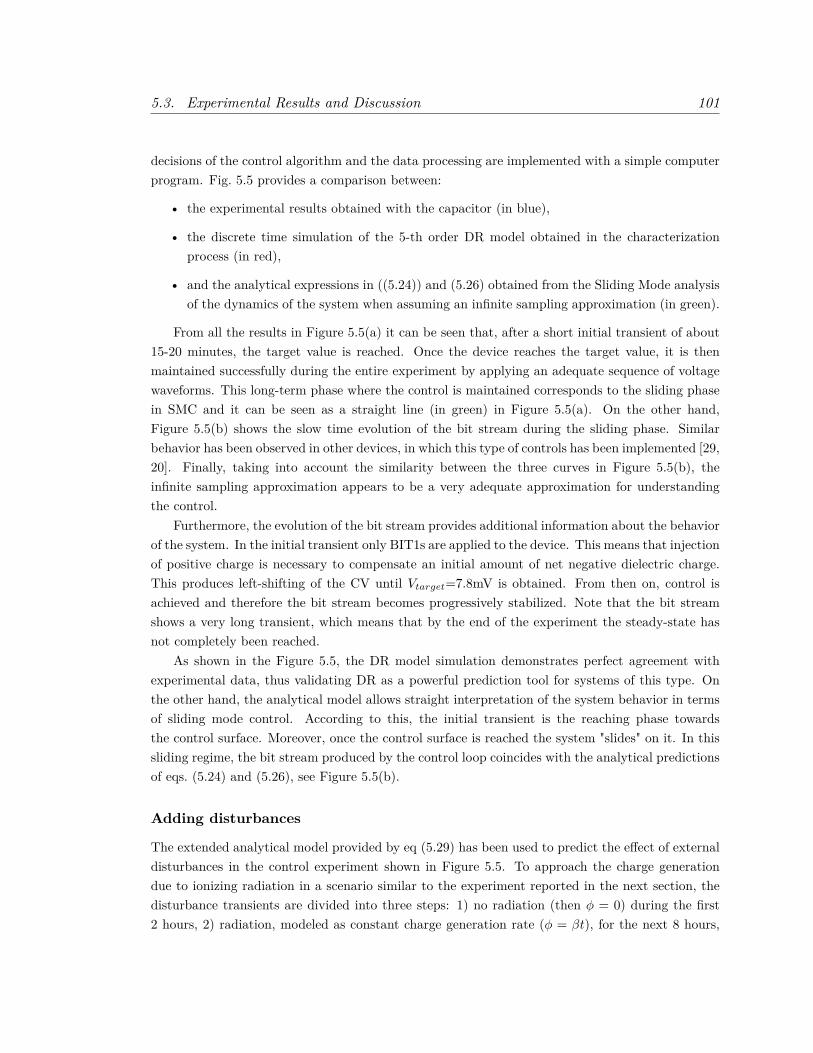
5.3. Experimental Results and Discussion 101
decisions of the control algorithm and the data processing are implemented with a simple computerprogram. Fig. 5.5 provides a comparison between:
• the experimental results obtained with the capacitor (in blue),
• the discrete time simulation of the 5-th order DR model obtained in the characterizationprocess (in red),
• and the analytical expressions in ((5.24)) and (5.26) obtained from the Sliding Mode analysisof the dynamics of the system when assuming an infinite sampling approximation (in green).
From all the results in Figure 5.5(a) it can be seen that, after a short initial transient of about15-20 minutes, the target value is reached. Once the device reaches the target value, it is thenmaintained successfully during the entire experiment by applying an adequate sequence of voltagewaveforms. This long-term phase where the control is maintained corresponds to the sliding phasein SMC and it can be seen as a straight line (in green) in Figure 5.5(a). On the other hand,Figure 5.5(b) shows the slow time evolution of the bit stream during the sliding phase. Similarbehavior has been observed in other devices, in which this type of controls has been implemented [29,20]. Finally, taking into account the similarity between the three curves in Figure 5.5(b), theinfinite sampling approximation appears to be a very adequate approximation for understandingthe control.
Furthermore, the evolution of the bit stream provides additional information about the behaviorof the system. In the initial transient only BIT1s are applied to the device. This means that injectionof positive charge is necessary to compensate an initial amount of net negative dielectric charge.This produces left-shifting of the CV until Vtarget=7.8mV is obtained. From then on, control isachieved and therefore the bit stream becomes progressively stabilized. Note that the bit streamshows a very long transient, which means that by the end of the experiment the steady-state hasnot completely been reached.
As shown in the Figure 5.5, the DR model simulation demonstrates perfect agreement withexperimental data, thus validating DR as a powerful prediction tool for systems of this type. Onthe other hand, the analytical model allows straight interpretation of the system behavior in termsof sliding mode control. According to this, the initial transient is the reaching phase towardsthe control surface. Moreover, once the control surface is reached the system "slides" on it. In thissliding regime, the bit stream produced by the control loop coincides with the analytical predictionsof eqs. (5.24) and (5.26), see Figure 5.5(b).
Adding disturbances
The extended analytical model provided by eq (5.29) has been used to predict the effect of externaldisturbances in the control experiment shown in Figure 5.5. To approach the charge generationdue to ionizing radiation in a scenario similar to the experiment reported in the next section, thedisturbance transients are divided into three steps: 1) no radiation (then φ = 0) during the first2 hours, 2) radiation, modeled as constant charge generation rate (φ = βt), for the next 8 hours,

102Chapter 5. Modeling and Analysis of Charge Trapping Dynamics in MOS Capacitors
Figure 5.5: Comparison of experimental data (in blue) with SR (in red) and sliding mode control(in black) predictions for a MOS capacitor in which charge control was applied for 25 hours. a)Evolution of the voltage shift of the CV curve. b) Evolution of the bit stream provided by thecontrol loop.
3) no radiation (then φ constant) for the last 6 hours. This disturbance model is compatible withtrapped charge being generated by radiation that is never removed from the dielectric. The bitstreams necessary to keep the same target voltage shift for four different values of the generationratio β are shown in Figure 5.6. It is seen that the increasing amounts of positive charge generatedbetween t=2 and t=10 hours are compensated by the control by increasing the number of BIT0s,which eventually increase the negative charge. When the disturbance episode ceases, the averagebit streams always tend to stable-constant values. It is also seen that the charge generated byradiation is successfully compensated, but not removed.
The disturbance model developed would help understand the influence of external disturbances

5.3. Experimental Results and Discussion 103
Figure 5.6: Evolution of the bit stream provided by the control loop, as predicted by the slidinganalytical model, when a set of disturbance functions, with different charge generation rates (β),are applied for 8h during the experiment reported in Fig. 5.5.
on the closed loop control of the device. In particular, the model demonstrates the effect of ioniza-tion radiation dose rate on the amount of trapped charge generated (thus the amount of voltageshift) and the average bit streams needed to compensate it.
5.3.2 Experiment 2: Charge Control under Ionizing Radiation
This experiment investigates the effects of ionizing radiation on Al2O3 MOS capacitors operatingunder charge trapping control method. A specific objective is to check the goodness of the predic-tions of the sliding analytical model introduced when charging generated by the radiation occurs.To this effect, a pristine MOS capacitor has been irradiated with X-rays.
The device, DUT1, has been operated under sigma-delta control to achieve and maintain agiven target capacitance Cth. Given the conditions of the experiment, a second-order loop has beenused to improve the reliability of the control, avoiding potential effects such as the existence ofplateaus that can be present in first-order loops [30]. In this case, the capacitance at voltage V1
is sampled periodically and compared with Cth to obtain an error signal, which is then integratedand depending on the sign of the integral, either a BIT1 or BIT0 waveform is applied during thenext sampling period.
The voltages used in BIT0 and BIT1 are V +=5V, V −=-3V and V1=1V, whereas the target ca-pacitance is Cth=0.498nF. The timing parameters are TS=350ms and δ=1/3, being TS smaller thanthe fastest time constant observed in the charging dynamics when these voltages are applied. Theprecision LCR Meter generates the BITx waveforms and performs the capacitance measurements

104Chapter 5. Modeling and Analysis of Charge Trapping Dynamics in MOS Capacitors
on the device.The experiment starts with no radiation for 40 minutes, followed by X-ray irradiation for 8
hours (at a constant dose rate of 10 Gy/h), and an 8-hour final stage with no radiation. Thetop graph in Fig. 5.7 shows the evolution of the capacitance at V 0=1V of DUT1, which is undercharge control. During the initial stage (radiation off) the control reaches the target capacitanceCth =0.498nF within a finite time, t=5min. Once this value is reached, it is successfully maintainedduring the rest of the experiment, irrespective of whether the radiation is on or off.
Figure 5.7: Evolution of the capacitance at V1 = 1V (top) and of the control bit stream (bottom)of DUT1 during experiment 2. The device was under second order charge control with targetcapacitance Cth =0.498 nF.
The bottom graph in Figure 5.7 shows the evolution of the bit stream provided by the controlloop. It illustrates how the control works; initially only BIT1s are applied, accumulating positivecharge in the dielectric and moving the C-V to the left to reach Cth. During the irradiation stage(from t=40 min to t=8h 30min), the control increases the number of BIT0s, thus injecting morenegative charge that compensates the accumulation of positive charge produced by the radiation.Once irradiation stops, the accumulated-remaining charge leads the bit stream to stabilize.
Finally, it can be observed that the experimental bit stream shown in Figure 5.7 matches withthe predictions of the sliding control model summarized in Figure 5.6. As in experiment 1, thisallows explaining the experimental results obtained in terms of a sliding mode controller: oncethe system reaches the target capacitance, or the control surface, the applied bit stream keeps thecapacitance constant. Exposure to ionizing radiation generates an additional term, as in (5.28),that works as a mismatched disturbance, since the average bit stream is continuous. The changes inthe dynamics generated by this disturbance clearly follow the predictions obtained in Section 5.2.4.
5.4. Conclusions 105
5.4 Conclusions
Diffusive representation has been used to characterize the dynamics of charge trapping in MOScapacitors, seen as time-varying diffusive systems in which time variability comes from the voltagesapplied to the devices. Experimental corroboration has been obtained. The obtained time-varyingmodel has very good agreement with the experimental data obtained in both open and closed loopactuation strategies. Moreover, the state-space models are very well suited to describe the behaviorof such diffusive systems under non-trivial controls, as sliding mode controllers.
Experiments involving ionizing radiation in MOS capacitors under charge control have alsobeen presented. The results indicate that the trapped charge induced by radiation is not removedbut successfully compensated by the control loop. Applying the theory of sliding mode controllers,the changes observed in the control bit streams due to radiation are compatible with the effect ofmismatched external disturbances on the system dynamics.
Bibliography
[1] M. Razeghi, Fundamentals of Solid State Engineering. Second Edition. Springer, 2006.
[2] S. Zafar, A. Callegari, E. Gusev, and M. V. Fischetti ”Charge trapping related threshold voltageinstabilities in high permittivity gate dielectric stacks,” Journal of Applied Physics, vol. 93,pp. 9298–9303, 2003.
[3] A. Gehring and S. Selberherr, ”Modeling of tunneling current and gate dielectric reliability fornon volatile memory devices,” IEEE Trans. on Device and Materials Reliability, vol. 4, no. 3,pp. 306–319, 2004.
[4] V. Huard, M. Denais and C. Parthasarathy, ”NBTI degradation: From physical mechanisms tomodeling,” Microelectronics Reliability, vol. 46, no. 1, pp. 1–23, 2006.
[5] T. Grasser, B. Kaczer, W. Goes, T. Aichinger, P. Hehenberger, and M. Nelhiebel, ”Under-standing negative bias temperature instability in the context of hole trapping,” MicroelectronicEngineering, vol. 86, no. 7-9, pp. 1876–1882, 2009.
[6] T. Grasser ”Stochastic charge trapping in oxides: from random telegraph noise to bias temper-ature instabilities,” Microelectron. Reliab, vol. 52, pp. 39–70, 2012.
[7] S. Mahapatra, N. Goel, S. Desai, S. Gupta, B. Jose, S. Mukhopadhyay, K. Joshi, A. Jain,A. E. Islam and M. A. Alam ”A Comparative Study of Different Physics-Based NBTI Models,”IEEE Trans. on Electron Devices, vol. 60, no.3, pp. 901–916, 2013.
[8] Z. Y. Tung and D. S. Ang, ”Impact of Voltage-Accelerated Stress on Hole Trapping at OperatingCondition,” IEEE Electron Device Letters, vol. 37, no. 5, pp. 644–647, 2016.

106 Bibliography
[9] S. H. Yoon, C. Y. Chang, D. H. Ahn, M. Takenaka and S. Takagi, ”Interface state generationof Al2O3/InGaAs MOS structures by electrical stress,” Microelectronics Engineering, vol. 178,pp. 313–317, 2017.
[10] J.H. Stathis and S. Zafar, ”The negative bias temperature instability in MOS devices: Areview”, Microelectronics Reliab., vol. 46, no. 2-4, pp. 270–276, 2006.
[11] Y. Yuan, L. Wang, B. Yu, B. Shin, J. Ahn, P.C. McIntyre, P.M. Asbeck, M.J.W. Rodwelland Y. Taur, ”A Distributed Model for Border Traps in Al2O3 InGaAs MOS Devices”, IEEEElectron Device Letters, vol. 32, no. 4, pp. 485–487, 2011.
[12] Y. Yuan, B. Yu, J. Ahn, P.C. McIntyre, P.M. Asbeck, M.J.W. Rodwell and Y. Taur, ”ADistributed Bulk-Oxide Trap Model for Al2O3 InGaAs MOS Devices”, IEEE Trans. on ElectronDevices, vol. 59, no. 8, pp. 2100–2106, 2012.
[13] O. Endholm and C. Blomberg, ”Stretched exponentials and barrier distributions”, ChemicalPhysics, vol. 252, no. 1-2, pp. 221–225, 2000.
[14] B. Allard, X. Jorda, P. Bidan, A. Rumeau, H. Morel, X. Perpina, M. Vellvehi and S. M’Rad,”Reduced-Order Thermal Behavioral Model Based on Diffusive Representation,” IEEE Trans.Power Electron., vol. 24, no. 12, pp. 2833–2846, 2009.
[15] S. M’Rad, B. Allard, H. Morel, A. Ammous and N. Masmoudi ”Analytic thermal modelingof power electronic components: The Diffusive Representation,” Proc. of 4th Int. Conf. onIntegrated Power Systems (CIPS), pp. 1–6, 2006.
[16] L. Laudebat, P. Bidan and G. Montseny, ”Modeling and Optimal Identification of Pseudo-differential Electrical Dynamics by means of Diffusive Representation-Part I: Modeling,” IEEETrans. Circ. and Syst. I: Regular Papers, vol. 51, no. 9, pp. 1801–1813, 2014.
[17] C. Restrepo, G. Garcia, J. Calvente, R. Giral and L. Martinez-Salamero, ”Static and DynamicCurrent-Voltage Modeling of a Proton Exchange Membrane Fuel Cell Using an Input-OutputDiffusive Approach,” IEEE Trans. Ind. Electron., vol. 63, no. 2, pp. 1003–1015, 2016.
[18] M. Dominguez-Pumar, C. Bheesayagari, S. Gorreta, G. Lopez, I. Martin, E. Blokhina and J.Pons-Nin, ”Charge Trapping Control in MOS Capacitors,” IEEE Trans. Ind. Electron., vol. 64,no. 4, pp. 3023–3029, 2017.
[19] M. Domínguez-Pumar, S. Gorreta and J. Pons-Nin, ”Sliding-Mode Analysis of the Dynamicsof Sigma-Delta Controls of Dielectric Charging,” IEEE Trans. Ind. Electron., vol. 63, no. 4, pp.2320–2329, 2016.
[20] M.T. Atienza, S. Gorreta, J. Pons-Nin and M. Dominguez-Pumar, ”Characterization of di-electric charging in MEMS using Diffusive Representation,” Ind. Electron, vol. 64, no. 2, pp.1529-1533, 2017.

Bibliography 107
[21] M.T. Atienza, L. Kowalski, S. Gorreta, J. Pons-Nin, V. Jiménez, and M. Dominguez-Pumar,”Model identification of Time-Varying Diffusive Systems,” IEEE Int. Symp. on Circuits andSystems (ISCAS), pp. 1–5, 2018.
[22] D.M. Fleetwood, ”Total Ionizing Dose effects in MOS and Low-Dose-Rate-Sensitive Linear-Bipolar Devices,” IEEE Trans. Nucl. Sci., vol. 60, no. 3, pp. 1706–1730, June 2013.
[23] J.R. Schwank, M.R. Shaneyfelt, D.M. Fleetwood, J.A. Felix, P.E. Dodd, P. Paillet and V.Ferlet-Cavrois, ”Radiation Effects in MOS Oxides,” IEEE Trans. Nucl. Sci., vol. 55, no. 4, pp.1833–1853, September 2008.
[24] X.J. Zhou, D.M. Fleetwood, J.A. Felix, E.P. Gusevand and C. D’Emic, ”Bias-TemperatureInstabilities and Radiation Effects in MOS Devices,” IEEE Trans. Nucl. Sci., vol. 52, no. 6, pp.2231–2238, February 2006.
[25] H.L. Hughes and J.M. Benedetto, ”Radiation Effects and Hardening of MOS Technology:Devices and Circuits,” IEEE Trans. Nucl. Sci., vol. 50, no. 3, pp. 500–521, July 2003.
[26] C. Claeys and E. Simoen, Radiation Effects in Advanced Semiconductor Materials and Devices,Springer Science Business Media, 2013.
[27] M. Dominguez-Pumar, C. Bheesayagari, S. Gorreta, G. Lopez and J. Pons-Nin, ”Closed-loopcompensation of charge trapping induced by ionizing radiation in MOS capacitors,” IEEE Trans.Ind. Electron, vol. 65, no. 3, pp. 2518–2524, 2018.
[28] G. Montseny ”Diffusive Representation of Pseudo-differential Time-operation,” Proc. ofESAIM, vol. 5, pp. 4817–4828, 1998.
[29] M. Dominguez-Pumar, M.T. Atienza, L. Kowalski, S. Novio, S. Gorreta, V. Jimenez, andS. Silvestre, ”Heat Flow Dynamics in Thermal Systems Described by Diffusive Representation,”IEEE Trans. Ind. Electron, vol. 64, no.1, pp. 664–673, 2017.
[30] C. Bheesayagari, S. Gorreta, J. Pons-Nin and M. Dominguez-Pumar, ”Second order sigma-delta control of charge trapping for MOS capacitors”, Microelectronics Reliab., vol. 76-77, no.4, pp. 635–639, 2017.
[31] Hebertt Sira-Ramirez, Sliding Mode Control: The Delta-Sigma Modulation Approach. Switzer-land: Birkhäuser-Springer, 2015.
[32] M. Domguez-Pumar, S. Gorreta and J. Pons-Nin, ”Sliding-Mode Analysis of the Dynamicsof Sigma-Delta Controls of Dielectric Charging”, IEEE Transactions on Industrial Electronics,vol. 63, no. 4, pp. 2320–2329, 2016.
[33] T.P. Ma and P.V. Dressendorfer, Ionizing Radiation Effects in MOS Devices and Circuits,NY, USA: Wiley, 1989.

108 Bibliography
[34] Atienza, Maria-Teresa and Kowalski, Lukasz and Gorreta, Sergi and Jiménez, Vicente andCastañer, Luis M and Dominguez-Pumar, Manuel, ”Sliding mode analysis applied to improvethe dynamical response of a spherical 3D wind sensor for Mars atmosphere”, Sensors andActuators A: Physical, vol. 267, pp. 342–350, 2017.
[35] Sun, Guanghui and Wu, Ligang and Kuang, Zhian and Ma, Zhiqiang and Liu, Jianxing,”Practical tracking control of linear motor via fractional-order sliding mode”, Automatica, vol.94, pp. 221–235, 2018.
[36] Du, Haibo and Chen, Xiuping and Wen, Guanghui and Yu, Xinghuo and Lu, Jinhu, ”Discrete-Time Fast Terminal Sliding Mode Control for Permanent Magnet Linear Motor”, IEEE Trans-actions on Industrial Electronics, 2018.
[37] Wang, Ning and Lv, Shuailin and Zhang, Weidong and Liu, Zhongzhong and Er, Meng Joo,”Finite-time observer based accurate tracking control of a marine vehicle with complex un-knowns”, Ocean Engineering, Elsevier, vol. 145, pp. 406–415, 2017.
[38] Wang, Ning and Su, Shun-Feng and Han, Min and Chen, Wen-Hua, ”BackpropagatingConstraints-Based Trajectory Tracking Control of a Quadrotor With Constrained ActuatorDynamics and Complex Unknowns”, IEEE Transactions on Systems, Man, and Cybernetics:Systems, 2018.
[39] Domínguez-Pumar, Manuel and Gorreta, Sergi and Pons-Nin, Joan and Gómez-Rodríguez,Faustino and González-Castaño, Diego M, ”Charge induced by ionizing radiation understoodas a disturbance in a sliding mode control of dielectric charge,” Microelectronics Reliability, vol.55, no.9-10, pp. 1926–1931, 2015.

Chapter 6
Sigma-Delta Charge ControlApplied to Other Devices
In this chapter, charge control methods similar to that used for MOS capacitors in Chapter3 havebeen applied to other devices such as eMIM capacitors and perovskite solar cells. The main objectivehere is to investigate the goodness of these controls to improve the performance or the reliability inthese types of devices which can also suffer from charging effects. Accordingly, several preliminaryexperiments applying open loop and closed loop bias voltages to the devices have been performed,and the results are compared and discussed. These results are very promising and they give roomto further investigation.
6.1 MIM Capacitors
Metal-insulator-metal (MIM) capacitors are one of the essential components in analog, RF andmixed signal ICs due to their low parasitic capacitances and high conductive electrodes [1, 2].Several studies have been made to improve the capacitance density and reduce the leakage cur-rent for SOC (system-on-chip) applications [3, 4, 5] and have been fabricated conventionally usingphotolithographic technology with continuous dielectric layer between the metal layers.
In recent years, nanoparticles as dielectric material between the metal electrodes have beeninvestigated to build an enhanced capacitor with improved capacitance values [6, 7, 8]. In [9], ithas been reported that a metal-insulator-metal structure with SiO2 nanoparticles fabricated usingan electrospray technique (eMIM capacitor or supercapacitor) showed an increment in capacitancevalue by a factor of 4.4 compared to a continuous dielectric layer. The typical electrosprayedMetal-nanoparticles-Metal (eMIM) capacitor consists on several layers of dielectric nanospheressandwiched between two metal electrodes (typically aluminium). This capacitance increment ismainly due to charge accumulation on the nanospheres surface. Also, increasing the number oflayers of nanospheres by reducing their diameter results in an increase in the capacitance.
109

110 Chapter 6. Sigma-Delta Charge Control Applied to Other Devices
Figure 6.1 shows the schematic of the eMIM concept.
Figure 6.1: eMIM device concept: several layers of nanospheres sandwiched between two metalelectrodes (typically aluminium).
The next section provides with the details of the fabrication process used to obtain an eMIMdevice with SiO2 nanoparticles.
6.1.1 Fabrication Details
The eMIM devices used for the experiements have been fabricated at UPC. An electrospray tech-nique has been used to deposit nanoparticles as insulator layer. The fabrication process involvesthe following steps [9]:
• The process starts with the deposition of a photoresist layer on a glass substrate. A maskhas been used to remove photoresist and open an active area.
• A thick layer of Al film is deposited by sputtering.
• Lift-off technique is used to etch away the photoresist and the target bottom electrode remainson the top of the glass.
• An aqueous colloidal solution with 5%SiO2 nanoparticles of 250nm diameter is placed in areservoir connected to a needle. A high voltage has been applied between the needle and thebottom electrode to generate an aerosol of tiny droplets containing the nanoparticles thattransport over the top of the substrate.
• Finally, a layer of Al (which is the top electrode) is deposited by sputtering through a shadowmask.
Figure 6.2 shows the cross section and the top view of the fabricated device schematically.
6.1.2 Implementing the Control Method
The main objective of our work involves investigating the effects of bias voltage on the chargeredistribution in nanospheres which in turn generate changes in the impedance of the device. Inthis regard, we have initially performed constant polarization experiments on the device to studythe evolution of the Nyquist plots with the application of bias voltages.

6.1. MIM Capacitors 111
Figure 6.2: Schematic cross section and top view of the fabricated eMIM device [9].
Figure 6.3: Nyquist plots of a SiO2 MIM capacitor subjected to constant bias voltages.
The application of a constant bias voltages to the MIM capacitor results in the observation oftwo effects. The first one has a fast dynamics and generates changes in the impedance of the devicewhich are reflected as changes in its Nyquist plot. This effect can be seen in Figure 6.3. Here,the Nyquist plots have been obtained consecutively in time, taken at different bias voltages. Thedifferences observed in the impedance are attributed to the fast redistribution of electronic andionic charge in the nanospheres, generating large swings in the resulting impedance.
On the other hand, the application of a constant bias for a long time implies slow change in thecharge dynamics. To observe this effect, constant bias voltages have been applied periodically anddrift in the differential capacitance was monitored. A 14-hour experiment has been made in whicha constant bias of 0.6V was applied during the first 2 hours, -0.6V during the next 2h, repeating

112 Chapter 6. Sigma-Delta Charge Control Applied to Other Devices
Figure 6.4: Successive CV curves measured every 2h at the end of constant bias voltages in a 14hexperiment.
the sequence. The CV curves have been measured periodically at the end of each constant biascycle and the plots can be seen in Figure 6.4.
The voltage shifts as a function of time corresponding to the displacements of the CV charac-teristic have been plotted as shown in Figure 6.5. As it can be observed the application of positive
Figure 6.5: Position of the bottom of the CV, as a function of time, for the experiment inFigure 6.4. Application of positive bias tends to increase the voltage shift (displacement of the CVto the right). Application of negative bias tends to decrease the voltage shift (CV displacement tothe left).

6.1. MIM Capacitors 113
Figure 6.6: First order sigma-delta control of the voltage shift of the MIM device.
bias tends to increase the voltage shift (displacement to the right), whereas the application of neg-ative bias tends to decrease the voltage shift (displacement to the left). This behaviour opens thepossibility of designing a control based on polarity of the applied bias voltage.
We can notice that the CV characteristic of the MIM capacitor is quite similar to that of aMEMS switch in open state i.e. it has parabolic shape. This property of parabola function hasbeen exploited in MEMS switches, where measuring the shift of the bottom of the CV curve givesthe estimation of the voltage shift due to dielectric charging [10, 11]. This technique, referred toas center-shift method, has the advantage of being minimally invasive since voltage levels appliedare well below the pull-in range. A new strategy based on this method has been proposed [12, 13]to monitor the CV shifts through quasi differential capacitance measurements. Here, change ofpull-in voltage has been obtained from the variation of capacitance, ∆C, measured at two voltagesof different polarity in close instants of time.
In this work, we have used similar control strategy based on sigma-delta modulation as in [13],as shown in Figure 6.6 . Here, the main objective of the control is to maintain the desired state orparameter of a system by periodically monitoring the state and applying an appropriate sequence ofcontrol signals. In this case of MIM capacitors, the state/parameter to be monitored and controlledis the differential capacitance, rather than the capacitance at a single voltage reference value.The control circuit evaluates the capacitance values at two different voltage levels at periodicinstances nTs, and applies an adequate sequence of positive or negative voltage pulses during thenext sampling intervals (n+ 1)Ts using the feedback loop to maintain it around a desired value.
The design of actuation voltage waveforms, BIT0 and BIT1, is shown in Figure 6.7(a). Thesewaveforms have a total duration of Ts with two different voltage levels, V + and V −. For BIT0/BIT1,V −/V + is applied during most of the time, (1− δ)Ts, whereas V +/V − is applied for a short timeinterval, δTs. The parameters V −, V +, δ, Ts have been chosen appropriately such that the BIT0and BIT1 waveforms generate horizontal shifts of C-V curves of different sign. In case of MIMcapacitor, application of BIT0 waveform results in the left shift of the C-V curve while applyingBIT1 waveform shifts it to the right.
The illustration of how the closed loop control works in this case is shown in Figure 6.7(b).The differential capacitance, ∆C, has been obtained from the capacitance measurements preformed

114 Chapter 6. Sigma-Delta Charge Control Applied to Other Devices
Figure 6.7: (left) BIT1 and BIT0 actuation sensing waveforms. Application of BIT1 (BIT0)waveforms tends to increase (decrease) the voltage shift of the C(V) characteristic of the device [14].
at times (n − 1)Ts + (1 − δ)Ts and nTs corresponding to the application of V +/V − and V −/V +
respectively for BIT1/BIT0 symbols. Comparing this value with the desired threshold capacitancevalue ∆Cth, the next symbol,BITx, to be applied is decided as,
BITx =
BIT1, ∆C −∆Cth < 0,BIT0, ∆C −∆Cth > 0,
(6.1)
In general, the relation of MIM capacitance with voltage is parabolic and therefore can bemodeled as:
C(V, t) = α(V − Vsh(t))2 + C0 (6.2)
where the parameter α is obtained by fitting the above equation with measured C-V curve, Vsh isthe amount of voltage shift and C0 is the minimum capacitance value.
Since the small changes in temperature or humidity could result in the generation of verticaldisplacements in the CV curve, these influences have been accounted for the slow time variation inC0(t). In order to minimize these effects, the capacitance measurements are taken at two differentpoints of the CV curve at the end of the sampling period in close instants of time t and t+ ∆t suchthat ∆t is smaller than the time constants involved in the dynamics of the device. In such a case,we can write C0(t) = C0(t+ ∆t). Suppose the capacitance values obtained by applying V + > 0 attime t is C(V +) and V − < 0 at time t+ ∆t is C(V −), the differential capacitance ∆C obtained atthe end of the sampling period can be written as:
∆C = C(V +)− C(V −) (6.3)= α[(V +)2 − (V −)2]− 2αVsh[V + − V −]

6.1. MIM Capacitors 115
From equation (6.3), it is obvious that ∆C is independent of the variations in C0(t). Thus it ispossible to eliminate the effects of vertical shifts during the measurements.
Now, in the next sections, we apply open loop stress (BIT0/BIT1) to the device to monitorthe drift in the differential capacitance with time and implement the charge control scheme thatallows controlling the time evolution of this drift. This entails the possibility of controlling theimpedance of the device.
6.1.3 Experimental Results and Discussion
Open loop Experiments
We have observed in the previous section that the application of a constant bias voltage to thedevices generates drifts in the impedance. In this section, a set of open loop experiments have beenperformed on the capacitor where the device is excited with a constant BIT voltage waveforms withperiodic monitoring of the differential capacitance, ∆C. Extensive measurements have been madein order to optimise actuation waveforms by choosing optimal values for the actuation voltages (V +
and V −), the value of δ and the sampling period (TS). Accordingly, BITx waveforms with voltagelevels V + = 0.6V , V − = −0.6V , and a sampling time period, Ts = 1s with δ = 1/5 have beenchosen.
Figure 6.8 shows the evolution of ∆C(t) for the continuous application of BIT0 and BIT1waveforms, in time intervals of 4h. As it can be seen, BIT1s tend to decrease ∆C(t), thereforeincreasing the associated voltage shift, whereas the opposite behaviour can be noticed with theapplication of BIT0 waveforms. These results are consistent with those in Figure 6.5, wherethe continuous application of 0.6V increased the voltage shift (and the reverse behaviour wasobtained for -0.6V). The successive CV measurements have been interspersed each 2h during this16h experiment, allowing to directly measure the resultant voltage shift. These results have beenplotted in Figure 6.9.
Now, Figure 6.10 shows the Nyquist plots of the same experiment, measured every 4h. Theinset shows the zoom of the final part of the Nyquist plots. The order to the initial plot is (70mV→ 40mV → 0V). The application of BIT1s tends to impose this order in the Nyquist plot: (70mV→ 40mV→ 0V). The application of BIT0s tends to impose either (40mV→ 0V→ 70mV) or (0V→40mV → 70mV). This means that applying BIT0s (which is equivalent to apply a negative voltagemost of the time) tends to decrease the Nyquist plot for 0V, whereas the opposite behaviour isobtained for BIT1.
From these open loop experiments, it is obvious that BIT0 and BIT1 waveforms are effectivein generating voltage shifts of different sign. These voltage shifts can be understood as small shiftsof the Nyquist plots taken at any bias voltage. In our case, since the observed shifts in the CVcurves are small (< 100mV ), the effect can be seen more easily when the Nyquist plots are takenwith low bias voltages (voltages of the order of the shifts in the CV curves). In our case, then, theNyquist plots at 0V, 40mV and 70mV are reordered.

116 Chapter 6. Sigma-Delta Charge Control Applied to Other Devices
Figure 6.8: Evolution of ∆C(t) for an experiment in which BIT1 and BIT0 waveforms werealternated in intervals of 4h each. Capacitance is measured at 10KHz.
Figure 6.9: Voltage shift measured each 2h in the experiment of Figure 6.8. BIT1 waveformsincrease the voltage shift whereas BIT0 waveforms decrease it.
Closed loop Experiments
The 1st order control method described in Section 6.1.2 has been applied to the MIM capacitorstructure. In order to minimize the effects of temperature and/or humidity variation, the device ismaintained at a constant temperature on a thermal chuck using a STC200 temperature controller.A precision LCR Meter E4980A has been used to perform periodic capacitance measurements and

6.1. MIM Capacitors 117
Figure 6.10: Groups of Nyquist plots at bias voltages: 0V, 40mV and 70mV. Each group of threeNyquist plots is measured at time intervals of 4h. (Inset) Zoom of the nyquist plots. The Nyquistplots change their order depending on the history of the actuation waveform applied.
Figure 6.11: a) Time evolution of differential capacitance, ∆C measured when the control methodis applied. The parameters used are V + = 0.6V , V − = −0.6V , Ts = 1s, and δ = 1/5. b) Theaverage bitstream extracted at the end of each control loop experiment.
generate the BIT waveforms. The amplitude of AC signal used is 500mV and the test frequency is100KHz. It has been observed from the open loop experiments that the continuous application ofBIT1 symbols would shift the CV curve to the left while the application of BIT0 symbols wouldresult in the right shift.
The first experiment has been carried out for 105 min with seven different target values, each

118 Chapter 6. Sigma-Delta Charge Control Applied to Other Devices
lasting for 15 min. A constant temperature is maintained to minimize the vertical displacementsin the CV curves. Figure 6.11 shows the evolution of differential capacitance as a function of timetaken periodically at the end of each sampling time, nTs. The high mobility of the ions results inthe fast dynamics of the control parameter with the applied BIT waveforms. A transient can beobserved at the beginning of each interval where the capacitance either increases or decreases withthe application of BIT0/BIT1 waveforms until it reaches the desired target value. Once the targetvalue has been reached, the control loop injects appropriate BIT sequences to keep it constant.This can be observed using the average bitstream generated during the control. It can be seenthat each time a new target has been chosen, the feedback loop applies a continuous sequence ofBIT0/BIT1 waveforms until it reaches the target level, after which a slow evolution of the averagebitstream is observed. However, the capacitance level set at t=90 min is so large that the feedbackcontrol loop could not reach the target within the limited table available. In other words, thecontrol becomes saturated (only BIT0s are applied) but the target value is not achieved.
Figure 6.12 shows the horizontal displacements of the CV characteristics of the device obtainedat the end of each control experiment. The corresponding voltage shift values measured with respectto 0V are shown in Figure 6.13.
Figure 6.12: CV characteristics obtainedat the end of each control. The ac frequencyused is 100 KHz.
Figure 6.13: Voltage shifts correspondingto the CV curves obtained at the end of eachcontrol segment.
The Nyquist plots obtained at the end of the control loop are also shown in Figure 6.14. Wecan notice that the positions of Nyquist curves at the end of each control segment correspond tothe voltage shifts obtained in Figure 6.13.
Now, a long experiment has been scheduled with seven different targets each lasting for 2h.The time evolution of ∆C measured at periodic sampling time intervals is plotted in Figure 6.15.As observed in the previous closed loop experiment, the feedback loop applies either only a BIT0or only a BIT1 waveform during the initial transient phase, and once it reaches the target level,injects an appropriate sequence of BIT0−BIT1 waveforms to maintain the threshold value. Theslow evolution of average bitstream gives the voltage levels required to maintain the control duringthe experiment.
Figure 6.16 shows the horizontal displacements of the CV characteristics obtained at the endof each target control step. The corresponding voltage shift values measured with respect to 0Vare shown in Figure 6.17.

6.2. Perovskite Solar Cells 119
Figure 6.14: Nyquist plots measured at the end of the control segments.
Figure 6.15: a) Time evolution of differential capacitance, ∆C measured when the control methodis applied. The parameters used are V + = 0.6V , V − = −0.6V , Ts = 1s, and δ = 1/5. b) Theaverage bitstream provided by the control loop during the experiment.
6.2 Perovskite Solar Cells
In recent years, the use of perovskite materials in photovoltaic, optical and superconductor ap-plications has experienced considerable growing interest. For instance, perovskite solar cells com-bine good performance (i.e. a spectacular 8% efficiency improvement was obtained in just threeyears [15]) reaching an efficiency of 22.1% [16, 17, 18] with a relatively cheap manufacturing process.However, serious reliability problems slow down the rise of this technology, being the biggest prob-

120 Chapter 6. Sigma-Delta Charge Control Applied to Other Devices
Figure 6.16: CV characteristics obtainedat the end of each control. The ac frequencyused is 100KHz.
Figure 6.17: Voltage shifts correspondingto the CV curves obtained at the end of eachcontrol segment.
lem the degradation of the material [19, 15]. There is wide consensus in identifying environmentalconditions -oxygen, temperature [20], humidity [21, 22], light [23] and electrical stress [24, 25] asthe factors responsible for the degradation, but there is still little understanding on the physicalmechanisms involved.
Although most works try to improve perovskite stability varying the fabrication process orthe chemical composition of the materials used, a radical new approach is implemented here. Itconsists in using a sigma-delta loop to control the charge trapped in the perovskite, allowing toplace the J-V of the device at a desired-stable position. This strategy, inspired in that used for MOScapacitors, may open a new way to mitigate perovskite degradation. According to this, in this workcharge control is applied to perovskite solar cells that suffer noticeable degradation effects. Let usnote that the objective here is to investigate the feasibility of charge control to stabilize the J-Vof the device. Specific application targets such as mitigating the degradation of key photovoltaicparameters will be the objective of future work.
6.2.1 Fabrication Details
The perovskite solar cells used in the experiements have been fabricated at ICFO (Instituto deCiencias Fotonicas). The devices were fabricated on patterned ITO substrates and the processinvolves the following steps:
• The substrate is covered with a 2.5%wt in methanol TiO2 nanoparticle precursor (20%wt inwater). The precursor was previously mixed with 2.5%wt of Ti diisopropoxidebis (acetylace-tonate).
• Then, the perovskite (methylammonium lead iodide/CH3NH3PbI3/MAPbI3) was depositedas in [26], without adding the triiodide solution.
• Next, a 72.3 mg/ml 2,2’,7,7’-Tetrakis [N, N-di(4-methoxyphenyl) amino]-9,9’-spirobifluorene(Spiro-OMeTAD) solution in chlorobenzene with 17 µL of a 520 mg/mL bis (trifluoromethyl-sulfonyl) amine Li salt solution in acetonitrile and 29 µL of 4-tert-butylpyridine was spin-coated on top of the perovskite.

6.2. Perovskite Solar Cells 121
• Finally, gold was thermally evaporated and patterned to form the top electrode.
The resulting stack of layers is: ITO(140 nm), TiO2(40 nm), perovskite(500 nm), Spiro-OMeTAD(200 nm) and Au(60 nm), with 0.06 cm2 of active area. The schematic of the fabricateddevice is depicted in Figure 6.18
Figure 6.18: Schematic view of the fabricated perovskite solar cell.
Now, the control scheme based on sigma-delta modulation is implemented on the perovskitedevice. The objective of this control method is to set the Current density-Voltage (J-V) curveto a desired position. This is done by applying the voltage waveforms BIT0 and BIT1 shown inFigure 6.19. In BIT0/1, a voltage V0/V1 is applied for (1−δ)TS , while VC is applied for a short timeδTS , 0 < δ < 1. As shown later, V0 and V1 are chosen so that their application produces oppositeJ-V shifts. According to this, the control method consists in sampling the current at the controlvoltage J(VC) at each BITx end. Depending on whether J(VC) is above or below a previously giventarget Jth, either a BIT0 or a BIT1 is applied in the next sampling period.
To investigate the suitability of the control method proposed, open loop and closed-loop controlexperiments have been performed both in dark and illumination as described in the next section.
6.2.2 Experimental Results and Discussion
A Keysight 2912A SMU has been used to generate the voltage waveforms and to perform theperiodic current measurements. The sampling time TS is chosen such that the voltage switchingwithin the BITx waveform, necessary to measure J(VC), has fairly unnoticeable effect on the stateof the device. VC is chosen to ensure sufficient current sensibility.
Figure 6.20 shows the J-V curves measured in a pristine device in dark and under illumination.Noticeable differences between forward and reverse scans can be observed. The solar cell devicesfabricated using perovskite materials differs from conventional silicon devices in that they showdiscrepancy in the J-V measurements with voltage scan direction and scan rate [27, 28]. This isdue to the slow charge redistribution owing to slow charge collection in the perovskite, which resultsin preventing the fast response to the applied voltage scan [28].

122 Chapter 6. Sigma-Delta Charge Control Applied to Other Devices
Figure 6.19: BIT0 and BIT1 voltage waveforms used in the control. The current at the controlvoltage J(VC) is sampled at the end of each waveform.
Figure 6.20: J-V characteristics of a pristine device in dark (a) and under illumination (b). Thescan rate is 440 mV/s.
Experiments in dark
In the first experiment, an open loop stress (consisting in applying either only BIT0 or only BIT1waveforms) has been applied to the device in order to monitor the evolution of J(VC). As shownin Figure 6.21(a), application of a BIT0 stress produces an initial sharp increment in the current,and then it slowly appears to decrease towards a stable value. That is, the continuous applicationof BIT0s produces a shift in the J-V characteristic to the right. On the other hand, applying BIT1waveform produces left shifts of the J-V, as shown in Fig. 6.21(b). Summarizing, the applicationof BIT0 and BIT1 waveforms results in opposite shifts of the J-V curves.
Since no photogenerated carriers are present during this experiment, the possible ion speciespresent in the perovskite layer are CH3NH+
3 , Pb+2 , and I− [29]. While I− ions are predicted to

6.2. Perovskite Solar Cells 123
Figure 6.21: (a) Evolution of the current monitored at the control voltage when only BIT0s (a) orBIT1s (b) are applied to the device. BIT0/1 parameters: TS=400ms, δ=1/3, V0=0.3V, V1=0.7V,VC=1.1V. To set comparable initial conditions, the device was at 0V bias for 15min before eachBITx stress.
be dominant due to their low activation energy [30], the fast migration of these ions would notrespond to the sampling times used here. Besides, CH3NH+
3 , and Pb+2 ions would be probably
responsible for the slow dynamics observed, since their migration times are of the order of tens ofms to minutes [31] compatible with the sampling times involved in the control method.
In the next experiment, closed loop control has been applied to check the effectiveness of thecontrol method by applying a sequence of eight 5h steps, each with a different target, Jth. The timeevolution of J(VC) and the bit stream genereated during the control were continuously monitored,and a fast J-V measurement was made at the end of each control step. The Jth values and theevolution of J(VC) during the experiment have been depicted in Figure 6.22(a). We can noticethat all target levels have been achieved succesfully: at each step, the current reaches very fastthe target level, then the control loop keeps the current around Jth by applying an appropriatesequence of BIT0s and BIT1s. The inset of Figure 6.22(b) shows a zoom of the evolution of J(VC)during step 4. Each time J(VC) is below Jth=2mA/cm2, the feedback loop applies BIT1s until thecurrent goes above Jth. Once this happens, a BIT0 is applied to decrease the current below Jth.

124 Chapter 6. Sigma-Delta Charge Control Applied to Other Devices
Figure 6.22: (a) Evolution of J(VC) while control is applied with the target values Jth listed inthe table. The green line represents the target current levels. (b) Zoom of J(VC) for a short timeinterval within step 4. (c) Average bit stream provided by the control loop during the experiment.BIT0/1 parameters: V0=0.25V, V1=0.75V, VC=1.1V, TS=400ms, δ=1/3.
This behavior is typical of 1st-order sigma-delta controllers [32]. The noticeable large deviations ofthe instantaneous current values from the target levels could be attributed to the fast dynamics of

6.2. Perovskite Solar Cells 125
Figure 6.23: J-V curves obtained at each step end in the experiment of Fig. 6.22. The instanta-neous current deviates from the desired value due to the J-V measurement itself.
the current due to the small time constants involved in the control waveforms, when compared tothe migration times of the mobile ions [31, 33].
The average bit stream generated by the control loop is plotted in Figure 6.22(c). It can beseen that higher the level of Jth, more the injection of BIT1s, and that the bit stream exhibits slowtime evolution once the target levels are reached. The fall to zero distortions of Figure 6.22(c) aredue to the J-V measurements made at each control step end. The curves thus obtained, plottedin Figure 6.23, show that the control allows to set and maintain successfully the J-V around thedesired targets.
Effect of sampling time on control
In this section, the influence of TS on the effectiveness of the control has been investigated. To thisend, control was applied with Jth=3 mA/cm2 and two values of TS in 4h steps. Figure 6.24 showsthe evolution of J(VC) and the average bistream. A plateau-like behavior is clearly observed duringthe control with TS=1s: the average bit stream is stacked at zero -having alternate sequence ofBIT0s and BIT1s- while J(VC) has noticeable variation and, therefore, no control is obtained. Inperfect agreement with sigma-delta theory [32], reducing the sampling time mitigates this undesiredeffect, as seen for the case of TS=400ms.

126 Chapter 6. Sigma-Delta Charge Control Applied to Other Devices
Figure 6.24: Evolution of J(VC) (a) and average bit stream (b), while control is being appliedwith Jth=3 mA/cm2 (green line) and two values of TS . Other BIT0/1 parameters: V0=0.25V,V1=0.75V, VC=1.1V.
Experiment under illumination
In this section, the sigma-delta control has been applied to the device under illumination. Followinga similar strategy than in the experiment of Figures 6.22 and 6.23, several different values of Jth wereapplied in 1h steps, with fast J-V measurements made at the end of control steps. Figure 6.25(a)shows the evolution of J(VC) and of the average bit stream. Each time Jth changes, the controlloop has been successful in reaching and maintaining the new desired level, although the control islost due to a fractal-like episode for some time in step 7.
Photo-excitation of MAPbI3 creates iodide vacancies that allow the migration of I− ions. Withthe application of an external bias under illumination, redistribution of these ions occurs causingthe ions move towards the electrodes depending on the applied bias. Applying BIT0 waveformcauses I− ions to move towards TiO2 layer also referred to as ETL (electron transport layer) whileMA+ ions migrate towards spiro-OMeTAD or HTL (hole transport layer), resulting in the creationof a barrier for the charge carriers at the contacts. On the other hand, applying BIT1 waveformscauses ions to move in the opposite direction thus improving the charge carrier extraction at thecontacts.
Finally, Figure 6.26 shows the sequence of J-V curves measured at the end of each control step.

6.3. Conclusions 127
Figure 6.25: (a) Evolution of J(VC) while control is being applied under illumination with thetarget values Jth listed in the table. The green line represents the target current levels. (b) Averagebitstream provided by the control loop during the experiment. BIT0/1 parameters: V0=0.25V,V1=0.75V, VC=1.2V, TS=400ms, δ=1/3.
The same complementary behavior seen when applying BIT0s or BIT1s in dark is also observedunder illumination, therefore enabling the control loop to place the J-V to previously given targetpositions. Thus the proposed control allows to displace the J-V of the device and maintain it at adesired point, even in dark or illumination conditions.
6.3 Conclusions
We have investigated the influence of bias voltage on charge dynamics of a MIM structure withnanoparticles. The constant application of a bias voltage to the MIM device generates drifts inthe impedance and presents a double dynamics: a fast one in which the Nyquist plot changesinstantaneously and a second one, in which the application of the bias for long times (hours, forexample) generates small drifts in the Nyquist plots. We have observed that it is possible to control

128 Chapter 6. Sigma-Delta Charge Control Applied to Other Devices
Figure 6.26: J-V curves measured at each step-end in the experiment of Fig. 6.25.
the voltage shifts by generating the adequate average bias voltage using a closed loop control basedon sigma-delta modulation. This entails the possibility of controlling the impedance of the device.The potential applications of this type of controls could be the improvement of energy storagecapability of the device.
In case of devices made of perovskite materials, trapped charge is one of the most triggeringfactors in the degradation of perovskite devices. Most of the research work done in this line ofimproving the stability of the perovskite is focused on the variations in the fabrication processand/or the materials used. In this work, we have implemented an active control scheme for chargetrapping in solar cell devices. The control capability relies on the complementary J-V shiftingproduced by the voltages applied. This may be seen as a promising way to improve the reliabilityand practical applicability of devices based on perovskites.

Bibliography 129
Bibliography
[1] Jeffrey A Babcock, Scott G Balster, Angelo Pinto, Christoph Dirnecker, Philipp Steinmann,Reiner Jumpertz, and Badih El-Kareh. Analog characteristics of metal-insulator-metal capac-itors using pecvd nitride dielectrics. IEEE Electron Device Letters, 22(5):230–232, 2001.
[2] Hyuk-Min Kwon, In-Shik Han, Sang-Uk Park, Jung-Deuk Bok, Yi-Jung Jung, Hong-Sik Shin,Chang-Yong Kang, Byoung-Hun Lee, Raj Jammy, Ga-Won Lee, et al. Conduction mecha-nism and reliability characteristics of a metal–insulator–metal capacitor with single zro2 layer.Japanese Journal of Applied Physics, 50(4S):04DD02, 2011.
[3] Naoya Inoue, Ippei Kume, Jun Kawahara, Shinobu Saito, Naoya Furutake, Takeshi Toda,Koichiro Matsui, Takayuki Iwaki, Masayuki Furumiya, Toshiki Shinmura, et al. Surface controlof bottom electrode in ultra-thin sin metal–insulator–metal decoupling capacitors for highspeed processors. Japanese journal of applied physics, 46(4S):1968, 2007.
[4] Toshiro Ono, Koji Kato, Hiroshi Toyota, Yukio Fukuda, and Yoshito Jin. Characterization ofmetal insulator metal electrical properties of electron cyclotron resonance plasma depositedta2o5. Japanese journal of applied physics, 45(9S):7345, 2006.
[5] SD Park, C Park, DC Gilmer, HK Park, CY Kang, KY Lim, C Burham, J Barnett, PD Kirsch,HH Tseng, et al. Bulk and interface effects on voltage linearity of zro 2–sio 2 multilayeredmetal-insulator-metal capacitors for analog mixed-signal applications. Applied Physics Letters,95(2):022905, 2009.
[6] GA Topasna. Capacitance of spherical dielectric layers. Journal of applied physics, 100(2):024501, 2006.
[7] Kevin C Leonard, Wendy E Suyama, and Marc A Anderson. Evaluating the electrochemicalcapacitance of surface-charged nanoparticle oxide coatings. Langmuir, 28(15):6476–6484, 2012.
[8] Kevin C Leonard, Wendy E Suyama, and Marc A Anderson. Improvement of electrochemicalcapacitor electrodes using sio2 nanoparticles. Electrochimica Acta, 56(27):10137–10144, 2011.
[9] Bremnen Véliz, Sandra Bermejo, Arnau Coll, and Luis Castañer. Metal-insulator-metal ca-pacitor using electrosprayed nanoparticles. Applied Physics Letters, 105(1):013109, 2014.
[10] RW Herfst, HGA Huizing, PG Steeneken, and Jurriaan Schmitz. Characterization of dielectriccharging in rf mems capacitive switches. In 2006 IEEE International Conference on Micro-electronic Test Structures, pages 133–136. IEEE, 2006.
[11] Rodolf W Herfst, Peter G Steeneken, HGA Huizing, and Jurriaan Schmitz. Center-shift methodfor the characterization of dielectric charging in rf mems capacitive switches. IEEE Transac-tions on semiconductor manufacturing, 21(2):148–153, 2008.

130 Bibliography
[12] Manuel Dominguez-Pumar, Sergi Gorreta, Joan Pons-Nin, Elena Blokhina, PanagiotisGiounanlis, and Orla Feely. Real-time characterization of dielectric charging in contactlesscapacitive mems. Analog integrated circuits and signal processing, 82(3):559–569, 2015.
[13] Sergi Gorreta, Joan Pons-Nin, Elena Blokhina, Orla Feely, and Manuel Domínguez-Pumar.Delta-sigma control of dielectric charge for contactless capacitive mems. Journal of microelec-tromechanical systems, 23(4):829–841, 2014.
[14] Sergi Gorreta, Joan Pons-Nin, Elena Blokhina, and Manuel Dominguez. A second-order delta-sigma control of dielectric charge for contactless capacitive mems. Journal of Microelectrome-chanical Systems, 24(2):259–261, 2015.
[15] M.I. Asghar, J. Zhang, H. Wang, and P.D. Lund. Device stability of perovskite solar cells areview. Renew. and Sust. Energy Rev., 77:131–146, 2017. doi: 10.1016/j.rser.2017.04.003.
[16] Woon Seok Yang, Byung-Wook Park, Eui Hyuk Jung, Nam Joong Jeon, Young Chan Kim,Dong Uk Lee, Seong Sik Shin, Jangwon Seo, Eun Kyu Kim, Jun Hong Noh, et al. Iodide man-agement in formamidinium-lead-halide–based perovskite layers for efficient solar cells. Science,356(6345):1376–1379, 2017.
[17] Mingzhen Liu, Michael B Johnston, and Henry J Snaith. Efficient planar heterojunctionperovskite solar cells by vapour deposition. Nature, 501(7467):395, 2013.
[18] Huanping Zhou, Qi Chen, Gang Li, Song Luo, Tze-bing Song, Hsin-Sheng Duan, Ziruo Hong,Jingbi You, Yongsheng Liu, and Yang Yang. Interface engineering of highly efficient perovskitesolar cells. Science, 345(6196):542–546, 2014.
[19] T. Ibn-Mohammed et al. Perovskite solar cells: An integrated hybrid lifecycle assessment andreview in comparison with other pv technologies. Renew. and Sust. Energy Rev., 80:1321–1344,2017. doi: 10.1016/j.rser.2017.05.095.
[20] Giorgio Divitini, Stefania Cacovich, Fabio Matteocci, Lucio Cinà, A Di Carlo, and CaterinaDucati. In situ observation of heat-induced degradation of perovskite solar cells. NatureEnergy, 1(2):15012, 2016.
[21] Jeffrey A Christians, Pierre A Miranda Herrera, and Prashant V Kamat. Transformation ofthe excited state and photovoltaic efficiency of ch3nh3pbi3 perovskite upon controlled exposureto humidified air. Journal of the American Chemical Society, 137(4):1530–1538, 2015.
[22] Yu Han, Steffen Meyer, Yasmina Dkhissi, Karl Weber, Jennifer M Pringle, Udo Bach, LeoneSpiccia, and Yi-Bing Cheng. Degradation observations of encapsulated planar ch 3 nh 3 pbi 3perovskite solar cells at high temperatures and humidity. Journal of Materials Chemistry A,3(15):8139–8147, 2015.

Bibliography 131
[23] Daniel Bryant, Nicholas Aristidou, Sebastian Pont, Irene Sanchez-Molina, Thana Chotchu-nangatchaval, Scot Wheeler, James R Durrant, and Saif A Haque. Light and oxygen induceddegradation limits the operational stability of methylammonium lead triiodide perovskite solarcells. Energy & Environmental Science, 9(5):1655–1660, 2016.
[24] Michael Saliba, Taisuke Matsui, Ji-Youn Seo, Konrad Domanski, Juan-Pablo Correa-Baena,Mohammad Khaja Nazeeruddin, Shaik M Zakeeruddin, Wolfgang Tress, Antonio Abate, An-ders Hagfeldt, et al. Cesium-containing triple cation perovskite solar cells: improved stability,reproducibility and high efficiency. Energy & environmental science, 9(6):1989–1997, 2016.
[25] Konrad Domanski, Bart Roose, Taisuke Matsui, Michael Saliba, Silver-Hamill Turren-Cruz,Juan-Pablo Correa-Baena, Cristina Roldan Carmona, Giles Richardson, Jamie M Foster,Filippo De Angelis, et al. Migration of cations induces reversible performance losses overday/night cycling in perovskite solar cells. Energy & Environmental Science, 10(2):604–613,2017.
[26] W.S. Yang et al. Iodide management in formamidinium-lead-halide based perovskite layers forefficient solar cells. 356(6345):1376–1379, 2017.
[27] W. Tress et al. Understanding the rate-dependent jv hysteresis, slow time component, andaging in CH3 NH3 PbI3 perovskite solar cells: the role of a compensated electric field. EnergyEnviron. Sci., 8:995–1004, 2015. doi: 10.1039/C4EE03664F.
[28] A. Pockett et al. Microseconds, milliseconds and seconds: deconvoluting the dynamic be-haviour of planar perovskite solar cells. Phys. Chem. Chem. Phys., 19:5959–5970, 2017. doi:10.1039/C6CP08424A.
[29] Y. Wang et al. Ionic behavior of organicinorganic metal halide perovskite based metal-oxide-semiconductor capacitors. Phys. Chem. Chem. Phys., 19(20):13002–13009, 2017. doi: 10.1039/C7CP01799E.
[30] S. Chen et al. Mobile ion induced slow carrier dynamics in organicinorganic perovskite CH3NH3 Pb Br3. ACS Applied Materials & Interfaces, 8(8):5351–5357, 2016. doi: 10.1021/acsami.5b12376.
[31] J.M. Azpiroz, E. Mosconi, J. Bisquert, and F. De Angelis. Defect migration in methylam-monium lead iodide and its role in perovskite solar cell operation. Energy Environ. Sci., 8:2118–2127, 2015. doi: 110.1039/C5EE01265A.
[32] P.M. Aziz, H.V. Sorensen, and J. Van Spiegel. An overview of sigma-delta control converters.IEEE Signal Proc. Mag., 1:61–84, 1996.
[33] C. Eames, J.M. Frost, P.R. Barnes, B.C. Oregan, A. Walsh, and M.S. Islam. Ionic transport inhybrid lead iodide perovskite solar cells. Nature Commun., 6, 2015. doi: 10.1038/ncomms8497.


Chapter 7
Conclusions and Future Work
7.1 Conclusions
This Thesis addressed the issue of dielectric charge trapping in heterogeneous systems. Morespecifically, smart charge control techniques to effectively control the charge trapping in MOScapacitors and improve the operative lifetime of the devices have been proposed, designed andtested experimentally. This Thesis also contributed to the analysis and modeling of the chargetrapping dynamics in MOS capacitors using Diffusive Representation and Sliding Mode Control.Furthermore, application of these control strategies have been extended to devices which also sufferfrom the effects of charge trapping.
The main conclusions of the research work are summarized as follows:
• Closed loop control strategies based on sigma-delta modulation have been implemented tocontrol the net amount of charge trapped in the dielectric layers of MOS capacitors. Thesecontrols use specific voltage waveforms, allowing to continuously monitor the status of thenet dielectric charge and to maintain it around a desired target level. The experimentalresults show that the controls implemented are successful in controlling the trapped charge.An improved second order sigma-delta control has also been implemented and checked ex-perimentally.
• The response of MOS capacitors operating under ionizing radiation while they are beingcontrolled has also been investigated. The experiments demonstrate that the charge inducedby ionizing radiation can be successfully compensated by the control loops. The bit streamgenerated at the output serves as an indirect measure of the total amount of trapped chargeand therefore provides information on the ionizing dose received by the device. These exper-iments were carried out at ESA-ESTEC Co-60 facility and at Radiation Physics Laboratoryof University of Santiago de Compostela.
• The dynamics of the charge trapped in a MOS capacitor has been modeled using Diffusive
133

134 Chapter 7. Conclusions and Future Work
Representation. The model predictions successfully describes the charge dynamics in thedielectric and are validated using the experiments under arbitrary waveforms.
The charge dynamics of the device operating under sigma-delta controls has been analyzedusing the tools of Sliding Mode Control. The analytical model has been very successful inpredicting the system behavior even under the influence of external disturbances such asionizing radiation.
• The charge control techniques have been extended to other devices such as eMIM capacitorsand pervoskite solar cells. Preliminary results demonstrate that the control loops success-fully avoid the impedance drifts in MIM devices, while they effectively allow to control thedisplacement of the J-V characteristic in a perovskite solar cell.
As a result of this Thesis, four peer reviewed journal papers have been published and threecommunications have been presented in congresses. The experimental findings from eMIM devicesand perovskite devices have been submitted for publication.
7.2 Future Work
Although the major goals of the Thesis have been accomplished, there is always scope to addresscharge trapping issues in other devices or applications. The work carried out in this Thesis providesbasis for future research in several areas.
• Extend the application of closed loop control techniques to MOS-based devices like MOS-FETs. These devices, in general, suffer from problems such as threshold voltage instabilityand reduced mobility, due to charge trapping. Future work will focus on implementing theproposed controls to improve their reliability.
• Implementation of charge trapping compensation control loops on Radiation Sensing FieldEffect Transistors (RADFETs) to extend their lifetime by avoiding the build-up of trappedcharge with accumulated dose. This will be achieved by implementing a continuous chargetrapping control to keep constant the threshold voltage during the whole operation of thedevice.
• Further experimental studies are needed to investigate the possibility of control strategiesimproving photovoltaic features such as open-circuit voltage or efficiency in perovskite solarcells and energy storage ability in eMIM capacitors.
• Application of Diffusive Representation and Sliding Mode Control techniques to perovskitesolar cells to characterize and model the charge dynamics. The developed model wouldallow us to understand the charge transport mechanisms in the device and contribute to theimprovement of its efficiency.

7.2. Future Work 135
• Investigation of the impact of device processing changes on charge trapping behavior inMOS capacitors under irradiation. The future work in this area can be directed towards thedevelopment of radiation-hard devices for space applications.


Appendices


Appendix A
Journal Publications andConferences
This appendix summarizes the Journal publications and Conference works related to the mainsubject of this Thesis.
Works:
1. Diffusive Representation and Sliding Mode Control of Charge Trapping in Al2O3
MOS Capacitors on page 141.
Published in IEEE Transactions on Industrial Electronics, Jan 2019.
2. Second order sigma-delta control of charge trapping for MOS capacitors onpage 142.
Published in Microelectronics Reliability, 76, pp. 635-639, Sept 2017.
3. Closed-Loop Compensation of Charge Trapping Induced by Ionizing Radiationin MOS Capacitors on page 143.
Published in IEEE Transactions on Industrial Electronics, vol. 65, no. 3, pp. 2518-2524,Aug 2017.
4. Charge trapping control in MOS capacitors on page 144.
Published in IEEE Transactions on Industrial Electronics, vol. 64, no. 4, pp. 3023-3029,Sept 2017.
5. Second order sigma-delta control of charge trapping for MOS capacitors onpage 145.
139

140 Appendix A. Journal Publications and Conferences
Presented in 28th European Symposium on Reliability of Electron Devices, Failure Physicsand Analysis, in Bordeaux, France, Sept 2017.
6. Sliding mode control of fractional order systems: applications to sensors onpage 146.
Presented in 2nd Fractional Calculus Meeting, in Madrid, Spain, Nov 2018.
7. Active charge trapping control in dielectrics under ionizing radiation on page 147.
Presented in American Geophysical Union, Fall Meeting 2017, in New Orleans, USA, Dec2017.

8628 IEEE TRANSACTIONS ON INDUSTRIAL ELECTRONICS, VOL. 66, NO. 11, NOVEMBER 2019
Diffusive Representation and SlidingMode Control of Charge Trapping
in Al2O3 MOS CapacitorsChenna Reddy Bheesayagari, Joan Pons-Nin , Maria Teresa Atienza ,
and Manuel Dominguez-Pumar , Senior Member, IEEE
Abstract—The objective of this paper is to introducea modeling strategy to characterize the dynamics of thecharge trapped in the dielectric of MOS capacitors, usingdiffusive representation. Experimental corroboration is pre-sented with MOS capacitors made of Alumina in three dif-ferent scenarios. First, the model predictions are comparedwith the trapped charge evolution due to arbitrary voltageexcitations. Second, the predictions are compared with themeasurements of a device in which a sigma–delta control oftrapped charge is implemented. Finally, the time evolutionwhen the device is simultaneously controlled and irradiatedwith X-rays is compared with the predictions. In all cases, agood matching between the models and the measurementsis obtained.
Index Terms—Charge trapping control, diffusive repre-sentation (DR), ionizing radiation, MOS capacitors, slidingcontrol.
I. INTRODUCTION
D IELECTRIC charge trapping is widely identified as akey factor affecting the reliability of many metal-oxide-
semiconductor (MOS) related devices [1]. The physical mech-anisms responsible for such charge trapping are rather complexand, for a given device type, mainly dependent on the fabrica-tion process, the temperature, and the voltage applied [2]–[9].Other factors, such as external disturbances (i.e., due to ionizingradiation), have also a remarkable influence on charge trapping.
The characterization of the charge trapping dynamics in MOSdevices has been extensively studied [10]. Trap distributions areobtained from impedance spectra for different voltages in [11]and [12]. Other works analyze the charging dynamics as theresult of the application of voltage, or temperature, stress, whileobserving discharging currents or shifts in the threshold voltage.In these methods, the stress factor is instantaneously changed
Manuscript received July 6, 2018; revised October 7, 2018 and Novem-ber 19, 2018; accepted December 9, 2018. Date of publication January8, 2019; date of current version June 28, 2019. This work was sup-ported in part by the Spanish MINECO Project ESP2016-79612-C3-2R.(Corresponding author: Manuel Dominguez-Pumar.)
The authors are with the Micro and Nano Technologies Group, Elec-tronic Engineering Department, Polytechnic University of Catalonia,08034 Barcelona, Spain (e-mail:,[email protected]; [email protected]; [email protected]; [email protected]).
Color versions of one or more of the figures in this paper are availableonline at http://ieeexplore.ieee.org.
Digital Object Identifier 10.1109/TIE.2018.2890488
and changes in drain currents or threshold voltage shifts aremonitored and fitted. Models with one or two time constants, aswell as, more generally, stretched exponentials have been usedto this purpose. In stretched exponentials, the charge transientis characterized by the function exp (−(t/τ)β ), with β ∈ (0, 1).This model has been linked to Gaussian distributions in theenergy barriers found in charge trapping and detrapping [13].However, in all these cases, the analysis of the time evolutionof systems under arbitrary excitation becomes difficult becauseit is necessary to take into account the distributed nature of theprocesses involved.
Besides, the diffusive nature of the charge trapping phenom-ena allows their behavioral characterization using state-spacemodels based on diffusive representation (DR). In recent times,DR tools have been successfully used for modeling and pre-diction purposes in several diffusion-based systems, such asthermal [14], [15] and electrical [16], [17] fractional systems.In this paper, we use DR since it allows to directly obtain modelsfrom experimental data, which can be very easily simulated andare compatible with physical processes including diffusion anddispersion in general.
On the other hand, charge trapping controls based on sigma-delta loops have been proposed recently for MOS capacitorsin [18]. Under some limits, these controls allow to set and main-tain a previously given amount of net dielectric charge, thusmitigating long-term reliability issues such as C–V shifting orthreshold voltage drifts. In these controls, the charge being con-tinuously leaked out of the dielectric is compensated in averageby applying an adequate sequence of bipolar voltages. The sametype of sigma–delta strategies had been previously used to con-trol the charge in micro-electromechanical systems (MEMS)[19]–[21]. In this case, DR and sliding-mode control tools wereused successfully to analyze and predict the dynamics of thetrapped charge.
Furthermore, charge trapping generated by ionizing radia-tion in harsh environments such as space applications has beenextensively studied. Changes in the threshold voltage of MOStransistors are among the most noticeable effects [22]–[26]. Tomitigate this problem, extensive design and shielding strategiesare routinely implemented. Besides, compensation of chargetrapped in SiO2 MOS capacitors induced by gamma radia-tion using sigma–delta controls has been demonstrated recentlyin [27]. Ionizing radiation such as gamma and X-ray radiation
0278-0046 © 2018 IEEE. Personal use is permitted, but republication/redistribution requires IEEE permission.See http://www.ieee.org/publications standards/publications/rights/index.html for more information.
A.1. Diffusive Representation and Sliding Mode Control of Charge Trapping in Al2O3MOS Capacitors 141

Second order sigma-delta control of charge trapping for MOS capacitors
C. Bheesayagari, S. Gorreta, J. Pons-Nin, M. Domínguez-Pumar ⁎Micro and Nano Technologies Group, Electronic Engineering Department, Universitat Politècnica de Catalunya, Jordi Girona 1-3, 08034 Barcelona, Spain
a b s t r a c ta r t i c l e i n f o
Article history:Received 20 May 2017Received in revised form 17 June 2017Accepted 30 June 2017Available online 14 July 2017
This paper presents the circuit topology of a second order sigma-delta control of charge trapping for MOS capac-itors. With this new topology it is possible to avoid the presence of plateaus that can be found in first-ordersigma-delta modulators. Plateaus are unwanted phenomena in which the control is locked for a certain time in-terval (of unknown duration). In this case the control output is constant and therefore the controlled device is infact in open-loop configuration. It is shown that the presence of plateaus is avoided in MOS capacitors using theproposed approach.
© 2017 Elsevier Ltd. All rights reserved.Keywords:Charge trappingMOSDielectric chargingSigma-deltaSliding mode control
1. Introduction
Charge trapping is a ubiquitous phenomenon present in almost anydevice containing dielectric materials. Among the devices for whichcharge trapping represents a reliability problem we find:
• MOS capacitors and related structures such as ultrathin gate oxidesused in MOSFETs [1–4]. Charge trapping generates changes in thethreshold voltage of the transistors, among other effects.
• Electrostatic MEMS/NEMS [5–7]. Charge trapping generates shift ofthe C-V characteristic of the device, shift of the pull-in voltage andeven permanent stiction. This has been a particularly difficult problemfor RF-MEMS switches [8].
• Organic FETs (OFETS). Charge trapping also generates changes in thethreshold voltage of the transistors [9].
In general, this phenomenon alters device performance, affecting itscircuital features and even reducing its effective lifetime. The physicalmechanisms responsible for charge trapping are rather complex andde-pendent on fabrication processes, temperature, and electrical stressesapplied to the device [10–14].
Many researchworks focus on characterization andmitigation of theeffects of dielectric charging from very different approaches. For
example, specific geometries and dielectricless structures have beenproposed forMEMS [15,16], while newdielectricmaterials and stack ar-rangements allowing charge trapping reduction have been proposed forMOS structures [17–19]. Moreover, some circuit strategies to compen-sate dielectric-related degradation effects during device lifetime havebeen proposed for specific MOSFET applications [20,21].
Additionally, several actuation strategies using smart voltage wave-forms have been proposed tomitigate and even control the effects of di-electric charging in MEMS [8,22,23]. These strategies are based on theopposite effects produced by bipolar voltages on the charge dynamics.Following this complementarity principle, a first order control of chargetrapping for MOS capacitors was presented in [24]. This control allowsto obtain a desired shift of the C-V characteristic of the device (andhence of the net trapped charge in the oxide) and then to maintain it.This is achieved through a control loop based on sigma-delta modula-tion that applies a proper sequence of bipolar voltage waveforms tohave the average charge injection necessary to keep the desired chargelevel, see Fig. 1.
However, one of the known problems of first-order sigma-deltamodulators is the appearance of plateaus [25]. If the sampling time isof the same order or greater than the shortest time constant of thecharging and discharging processes of the device, the control may pro-vide a constant output during certain time intervals inwhich the systemis effectively in an open loop configuration. It must be noted that thecharging and discharging time constants will depend on the appliedvoltages in a nonlinear way and that several processes may coexist ina single device, resulting in a complex dynamics that is generally diffi-cult to predict beforehand.
Microelectronics Reliability 76–77 (2017) 635–639
⁎ Corresponding author.E-mail address: [email protected] (M. Domínguez-Pumar).
http://dx.doi.org/10.1016/j.microrel.2017.06.0960026-2714/© 2017 Elsevier Ltd. All rights reserved.
Contents lists available at ScienceDirect
Microelectronics Reliability
j ourna l homepage: www.e lsev ie r .com/ locate /microre l
142 Appendix A. Journal Publications and Conferences

2518 IEEE TRANSACTIONS ON INDUSTRIAL ELECTRONICS, VOL. 65, NO. 3, MARCH 2018
Closed-Loop Compensation of Charge TrappingInduced by Ionizing Radiation in
MOS CapacitorsManuel Dominguez-Pumar , Senior Member, IEEE, Chenna Reddy Bheesayagari,Sergi Gorreta, Student Member, IEEE, Gema Lopez-Rodriguez, and Joan Pons-Nin
Abstract—The objective of this paper is to explore thecapability of a charge trapping control loop to continuouslycompensate charge induced by ionizing radiation in the di-electric of metal–oxide–semiconductor (MOS) capacitors.To this effect, two devices made with silicon oxide havebeen simultaneously irradiated with gamma radiation: onewith constant voltage bias and the other working under adielectric charge control. The experiment shows substan-tial charge trapping in the uncontrolled device, whereas, atthe same time, the control loop is able to compensate thecharge induced by gamma radiation in the second device.
Index Terms—Charge trapping control, ionizing radiation,metal–insulator–semiconductor (MIS) capacitors, metal–oxide–semiconductor (MOS) capacitors, radiation effects.
I. INTRODUCTION
CHARGE trapping induced by ionizing radiation in metal–oxide–semiconductor (MOS) devices represents a relia-
bility issue in space applications [1]. Under the influence ofhigh energy ionizing radiation, these devices suffer from a driftin the threshold voltage, an increase of the leakage current, and adecrease of the transconductance [2]. This results in a degradedperformance, thereby, increasing the failure rate of the deviceoperation [3]–[6].
In the opposite direction, radiation sensitive field-effect tran-sistors (RADFETs) are MOS structures especially designed forradiation sensing. In recent years, some works have focused onobtaining a trapped hole annealing in order to delay the satura-tion of the sensor and to keep it working in near optimal con-ditions. This has been achieved by applying bias switching [7].In [8], periodical charge neutralization of radiation-inducedtrapped charge is performed to keep the threshold voltage of
Manuscript received December 12, 2016; revised March 30, 2017, May26, 2017, and July 18, 2017; accepted August 22, 2017. Date of publica-tion August 31, 2017; date of current version December 15, 2017. Thiswork was supported in part by the Spanish projects TEC2013-48102-C2-1P and ESP2016-79612-C3-2R. (Corresponding author: ManuelDominguez-Pumar.)
The authors are with the Micro and Nano Technologies Group, Uni-versitat Politecnica de Catalunya, Barcelona 08034, Spain (e-mail:[email protected]; [email protected]; [email protected]; [email protected]; [email protected]).
Color versions of one or more of the figures in this paper are availableonline at http://ieeexplore.ieee.org.
Digital Object Identifier 10.1109/TIE.2017.2748033
RADFETs between some predetermined limits. Measurementis carried out in open-loop configuration between bias switch-ing operations. On the other hand, Fowler–Nordheim tunnelingis used in [9] to compensate holes trapped in the buried oxidelayer of a monolithic pixel detector used in high-energy physics,X-ray imaging, etc. As a consequence, techniques focused oncontrolling the total charge in dielectrics may have many differ-ent applications (drift avoidance or sensor optimization).
Dielectric charge controls, first proposed in [10], have beenrecently achieved in the case of electrostatic microelectrome-chanical systems (MEMS) [11], [12] and MOS capacitors [13].This paper presents results obtained in gamma radiation exper-iments carried out to observe how dielectric charge induced byionizing radiation can be effectively compensated by a chargecontrol loop. In particular, we prove that the control loop pre-sented in [13] can also be used to compensate the charge inducedby ionizing radiation in MOS capacitors with silicon oxide asdielectric. A first result in this direction has already been ob-tained for electrostatic MEMS [14]. To the best knowledge ofthe authors, this is the first time that charge induced by ionizingradiation has been compensated in an MOS structure. This newapproach opens the possibility of establishing active compensa-tion techniques of radiation-induced charge in MOS structures.
II. CHARGE CONTROL LOOP
The control method implemented in this paper, presentedin [13], is based on sigma-delta modulation [15], used as atool to provide a sliding mode control of net trapped charge[16], [17].
A. Sigma-Delta Modulation and Sliding Mode Control
Sigma-delta modulators are extensively used in analog-to-digital and digital-to-analog conversion. In the analog-to-digitalcase, they are oversampled circuits that use rough quantizers(reaching even the 1-bit case, or sign function) to produce astream of symbols from which the final digital conversions areobtained by filtering and decimation. These modulators providequantization noise shaping, which means that the circuit movesthe quantization noise out of the frequency band of interestof the analog input. By finally filtering the stream of symbols inthe band of interest, the quantization noise is removed to a large
0278-0046 © 2017 IEEE. Personal use is permitted, but republication/redistribution requires IEEE permission.See http://www.ieee.org/publications standards/publications/rights/index.html for more information.
A.3. Closed-Loop Compensation of Charge Trapping Induced by Ionizing Radiation inMOS Capacitors 143

IEEE TRANSACTIONS ON INDUSTRIAL ELECTRONICS, VOL. 64, NO. 4, APRIL 2017 3023
Charge Trapping Control in MOS CapacitorsManuel Domınguez-Pumar, Senior Member, IEEE, Chenna Reddy Bheesayagari,
Sergi Gorreta, Student Member, IEEE, Gema Lopez-Rodrıguez, Isidro Martın,Elena Blokhina, Senior Member, IEEE, and Joan Pons-Nin
Abstract—This paper presents an active control ofcapacitance–voltage (C–V) characteristic for MOS capaci-tors based on sliding-mode control and sigma–delta mod-ulation. The capacitance of the device at a certain voltageis measured periodically and adequate voltage excitationsare generated by a feedback loop to place the C–V curveat the desired target position. Experimental results are pre-sented for an n-type c-Si MOS capacitor made with silicondioxide. It is shown that with this approach, it is possibleto shift the C–V curve horizontally to the desired operationpoint. A physical analysis is also presented to explain howthe C–V horizontal displacements can be linked to chargetrapping in the bulk of the oxide and/or in the silicon–oxideinterface. Finally, design criteria are provided for tuning themain parameters of the sliding-mode controller.
Index Terms—Dielectric charge control, MOS capacitors,sliding-mode control.
I. INTRODUCTION
D IELECTRIC charge trapping is widely known as an im-portant reliability issue in MOS capacitors and related
structures such as ultrathin gate oxides used in MOSFETs [1], orin MEMS. This phenomenon alters device performance, affect-ing its circuital features and even reducing its effective lifetime.Shift of the capacitance–voltage (C–V) characteristic [2], [3],and therefore of the threshold voltage, or negative-bias temper-ature instability (NBTI) degradation observed in p-MOSFETs[4] are examples of serious reliability problems due to oxidecharge trapping.
The physical mechanisms responsible for charge trapping arerather complex and dependent on the fabrication process, thetemperature, and the electrical stress applied to the device [5]–[10]. Most works focus on the design and characterization ofmaterials and structures to reduce the effects of charge trapping.
Manuscript received June 28, 2016; revised October 3, 2016 and Oc-tober 31, 2016; accepted November 12, 2016. Date of publication De-cember 26, 2016; date of current version March 8, 2017. This work wassupported in part by the Project TEC2013-48102-C2-1P. (Correspondingauthor: Manuel Domınguez-Pumar.)
M. Domınguez-Pumar, C. R. Bheesayagari, S. Gorreta, G. Lopez-Rodrıguez, I. Martın, and J. Pons-Nin are with the Micro and Nano Tech-nologies Group, Universitat Politecnica de Catalunya, 08034 Barcelona,Spain (e-mail: [email protected]; [email protected]; [email protected]; [email protected]; [email protected]; [email protected]).
E. Blokhina is with the School of Electrical, Electronic and Communi-cations Engineering, University College Dublin, Dublin 4, Ireland (e-mail:[email protected]).
Color versions of one or more of the figures in this paper are availableonline at http://ieeexplore.ieee.org.
Digital Object Identifier 10.1109/TIE.2016.2645159
Fig. 1. Cross section of the MOS capacitor used in the experiments.
Although these methods have substantially reduced the chargetrapping in the dielectrics, shift of the C–V characteristic due tocharge trapping still represents a reliability issue in MOS tran-sistors and capacitors. The purpose of this paper is to show howa simple control technique, based on sliding control [11], canbe used to deliberately shift the C–V characteristic to a desiredoperation point, either for compensating dielectric charging orfor other circuital requirements.
The method is similar to that used in MEMS devices [11],[12] consisting in the application of bipolar actuation volt-age stresses and a sigma–delta modulation control loop. Ithas been successfully demonstrated in silicon dioxide MOScapacitors.
II. FABRICATION PROCESS
The capacitors used in the experiments were fabricated on ann-type c-Si 〈 100 〉 wafer, 280 μm thick and resistivity of 2.5± 0.5 Ω· cm. The process starts with an RCA clean followedby a thermal oxidation for 30 min with a temperature rampbetween 850 C and 1080 C. An SiO2 layer of ∼40-nm thickis grown on both sides of the wafer. The SiO2 of the backside is removed with high-frequency (HF) etching, whereas thefront side is protected with photoresist. To obtain a good ohmiccontact at the back surface, a stack consisting of ∼4-nm a-SiCx (i) (x ∼ 0.1), 15-nm n-doped a-Si and 35-nm a-SiC x (x ∼1) is deposited on the back side of the wafer by PECVD. Then,a laser doping technique [13] is applied trough this dielectricstack to create localized n++ regions with 400 μm pitch. Afterthis laser processing step, the bottom of the sample is readyto be contacted with 480 nm of Ti/Al stack deposited by RFsputtering. A second deposition of Ti/Al is made at the front sideto create the upper contact. The active device area is delimited byphotolithography patterning and wet etching. A final annealingin N2 atmosphere at 400 C for 30 min improves the contactsand the adherence with the c-Si. Fig. 1 shows a cross section ofthe device.
0278-0046 © 2016 IEEE. Personal use is permitted, but republication/redistribution requires IEEE permission.See http://www.ieee.org/publications standards/publications/rights/index.html for more information.
144 Appendix A. Journal Publications and Conferences

Second order sigma-delta control of charge trapping for MOS capacitors
C. Bheesayagari, S. Gorreta, J. Pons-Nin, M. Domínguez-Pumar Micro and Nano Technologies Group, Electronic Engineering Department,
Universitat Politècnica de Catalunya, Jordi Girona 1-3, 08034 Barcelona, Spain Abstract This paper presents the circuit topology of a second order sigma-delta control of charge trapping for MOS capacitors. With this new topology it is possible to avoid the presence of plateaus that can be found in first-order sigma-delta modulators. Plateaus are unwanted phenomena in which the control is locked for a certain time interval (possibly of infinite duration). In this case the control output is constant and therefore the controlled device is in fact in open-loop configuration. It will be shown that the presence of plateaus is avoided in MOS capacitors using the proposed approach.
Corresponding author. [email protected] Tel: +34 (93) 401 5679; Fax: +34 (93) 401 6756
A.5. Second order sigma-delta control of charge trapping for MOS capacitors 145

Sliding mode control of fractional order systems: application to
sensors
Dominguez, M.; Bermejo, S.; Bheesayagari, C.; Pons, J.
Sliding mode controls (SMCs) are applied during sensor operation in order to
accelerate their time response and/or obtain other improvements in performance.
The main objective is to avoid the typically slow dynamics of the underlying
physical structures (thermal circuits, diffusion processes, etc.). This can be
achieved by designing controls that continuously compensate the effects of the
external factors to be measured, so that the state variables of the system remain
constant. The necessary control actions are then the new system output, which
can be significantly faster than in open loop operation. Additionally, it is also
possible to improve in other ways such as increasing sensitivity, or avoiding
effects of some parasitic elements or even mitigating the effects of undesired
external influences. In many applications, the dynamics of the physical structures
can be modelled using fractional calculus (thermal sensors, charge trapping in
dielectrics, chemical sensors, etc.). In this paper we present how Diffusive
Representation can be used to model fractional order systems, and how the
dynamics of the system, working under SMCs, can be analysed in the infinite
sampling approximation. We will present how external disturbances trigger
changes in the control actions, which must be adapted to compensate their effect.
Experimental examples will be presented for two different applications:
compensation of charge trapping generated by ionizing radiation in MOS
capacitors, and control applied to heat flux sensors.
146 Appendix A. Journal Publications and Conferences

Active charge trapping control in dielectrics under ionizing
Radiation
Dominguez-Pumar, M.; Bheesayagari, C.; Gorreta, S.; Pons-Nin, J.
Charge trapping is a design and reliability factor in plasma sensors. Examples
can be found in microchannel plate detectors in plasma analyzers, where
multiple layers have been devised to ensure filled trapped electrons for
enhanced secondary emission. Charge trap mapping is used to recover
distortion in telescope CCDs. Specific technologies are designed to mitigate
the effect of ionizing radiation in monolithic Active Pixel Sensors. We report
in this paper a control loop designed to control charge in Metal-Oxide-
Semiconductor capacitors. We find that the net trapped charge in the device
can be set within some limits to arbitrary values that can be changed with
time. The control loop periodically senses the net trapped charge by detecting
shifts in the capacitance vs voltage characteristic, and generates adequate
waveform sequences to keep the trapped charge at the desired level. The
waveforms continuously applied have been chosen to provide different levels
of charge injection into the dielectric. The control generates the adequate
average charge injection to reach and maintain the desired level of trapped
charge, compensating external disturbances. We also report that this control
can compensate charge generated by ionizing radiation. Experiments will be
shown in which this compensation is obtained with X-rays and gamma
radiation. The presented results open the possibility of applying active
compensation techniques for the first time in a wide number of devices such
as radiation sensors, MOS transistors and other devices. The continuous drive
towards integration may allow the implementation of this type of controls in
devices needing to reject external disturbances, or needing to optimize their
response to radiation or ion fluxes.
A.7. Active charge trapping control in dielectrics under ionizing radiation 147