Influence of atomic layer deposition chemistry on high- k dielectrics for charge trapping memories
10
Influence of atomic layer deposition chemistry on high-k dielectrics for charge trapping memories Nikolaos Nikolaou a , Panagiotis Dimitrakis a , Pascal Normand a , Vassilios Ioannou-Sougleridis a,⇑ , Konstantinos Giannakopoulos b , Konstantina Mergia c , Kaupo Kukli d,e , Jaakko Niinistö d , Mikko Ritala d , Markku Leskelä d a Institute of Microelectronics, NCSR ‘‘Demokritos’’, 153-10 Athens, Greece b Institute of Materials Science, NCSR ‘‘Demokritos’’, 153-10 Athens, Greece c Institute of Nuclear Technology and Radiation Protection, NCSR ‘‘Demokritos’’, 153-10 Athens, Greece d Department of Chemistry, University of Helsinki, FI-00014 Helsinki, Finland e Institute of Physics, University of Tartu, Riia 142, EE-51014 Tartu, Estonia article info Article history: Received 11 March 2011 Received in revised form 7 July 2011 Accepted 21 September 2011 Available online 14 November 2011 The review of this paper was arranged by Prof. S. Cristoloveanu Keywords: SONOS Flash Silicon nitride Non-volatile memories High-k dielectrics Hafnium oxide Zirconium oxide abstract In this work we report the performance of the SiO 2 /Si 3 N 4 /HfO 2 and SiO 2 /Si 3 N 4 /ZrO 2 stacks with emphasis on the influence of atomic layer deposition chemistry used for forming the HfO 2 and ZrO 2 blocking layers. Two Hf precursors were employed – tetrakis(ethylmethylamino)hafnium (TEMAH) and bis(methylcyclo- pentadienyl)methoxymethyl hafnium (HfD-04). For ZrO 2 , tetrakis(ethylmethylamino)zirconium (TEMAZ) and bis(methylcyclopentadienyl)methoxymethyl zirconium (ZrD-04) were used as metal precursors. Ozone was used as the oxygen source. The structural characteristics of the stacks were examined by transmission electron microscopy and grazing incidence X-ray diffraction. The electrical properties of the stacks were studied using platinum-gated capacitor structures. The memory performance of the stacks was evaluated by write/erase (W/E) measurements, endurance and retention testing. Endurance measurements revealed the most important difference between the stacks. The films grown from TEMAH and TEMAZ could withstand a significantly higher number of W/E pulses (>3 10 5 in the 10 V/11 V, 10 ms regime), in comparison to the stacks made from HfD-04 and ZrD-04 precursors (<5 10 3 W/E cycles). This difference in endurance characteristics is attributed mainly to the different deposition tem- peratures suited for these two precursors and the nature of the layer formed at the Si 3 N 4 /HfO 2 and the Si 3 N 4 /ZrO 2 interfaces. Ó 2011 Elsevier Ltd. All rights reserved. 1. Introduction The scaling of conventional floating-gate (FG) flash memory cells faces significant challenges mainly due to the scalability lim- itations for the active dielectrics, typically made of a SiO 2 thin film for the tunnel oxide and of an oxide–nitride–oxide (ONO) stack for the blocking (or control) dielectric [1]. It is projected that these cell limitations together with the FG interference effects between neighboring cells, which increase with the cell density, will not al- low flash memory scaling below the 22 nm technology node [1,2]. An alternative approach for the continuation of non-volatile memory cell downscaling is offered by the silicon nitride charge- trap memory technology [1,3]. The typical paradigm of this class of memory cells is the SONOS structure (silicon–oxide–nitride– oxide–silicon) which exploits for charge storage the high density of electron and hole traps that are inherent within the silicon nitride layer [4]. The main drawbacks of the SONOS structure are the limited speed of the erase operation and the over-erase effect. While the write operation (substrate electron injection and trap- ping into the nitride layer) is fast, the erase operation (substrate hole injection and trapping into the nitride layer and/or electron ejection) depends strongly on the thickness of the bottom or tunnel oxide [5]. If the tunnel oxide is thicker than 2.5 nm, the erase oper- ation becomes very slow. In turn, if the tunnel oxide is thinner than 2 nm, degradation of the retention characteristics occurs, as the trapped charge carriers leak through the thin tunnel oxide [6]. Fur- thermore, the use of high negative gate voltages in order to enhance the erase operation combined with the trapped positive charge leads to electron injection via the top electrode, an effect that limits the amount of positive trapped charge (over-erase effect) [5]. The extreme sensitivity of the erase operation to the thickness of the tunnel oxide layer has limited the SONOS memory applications to niche markets such as military, radiation and space applications [7]. The interest in charge trap memory technology re-emerged with the NROM memory cell [8] and the introduction of the high 0038-1101/$ - see front matter Ó 2011 Elsevier Ltd. All rights reserved. doi:10.1016/j.sse.2011.09.016 ⇑ Corresponding author. Tel.: +30 210 650 3240; fax: +30 210 651 1723. E-mail address: [email protected] (V. Ioannou-Sougleridis). Solid-State Electronics 68 (2012) 38–47 Contents lists available at SciVerse ScienceDirect Solid-State Electronics journal homepage: www.elsevier.com/locate/sse
Transcript of Influence of atomic layer deposition chemistry on high- k dielectrics for charge trapping memories

Solid-State Electronics 68 (2012) 38–47
Contents lists available at SciVerse ScienceDirect
Solid-State Electronics
journal homepage: www.elsevier .com/locate /sse
Influence of atomic layer deposition chemistry on high-k dielectrics for chargetrapping memories
Nikolaos Nikolaou a, Panagiotis Dimitrakis a, Pascal Normand a, Vassilios Ioannou-Sougleridis a,⇑,Konstantinos Giannakopoulos b, Konstantina Mergia c, Kaupo Kukli d,e, Jaakko Niinistö d, Mikko Ritala d,Markku Leskelä d
a Institute of Microelectronics, NCSR ‘‘Demokritos’’, 153-10 Athens, Greeceb Institute of Materials Science, NCSR ‘‘Demokritos’’, 153-10 Athens, Greecec Institute of Nuclear Technology and Radiation Protection, NCSR ‘‘Demokritos’’, 153-10 Athens, Greeced Department of Chemistry, University of Helsinki, FI-00014 Helsinki, Finlande Institute of Physics, University of Tartu, Riia 142, EE-51014 Tartu, Estonia
a r t i c l e i n f o
Article history:Received 11 March 2011Received in revised form 7 July 2011Accepted 21 September 2011Available online 14 November 2011
The review of this paper was arranged byProf. S. Cristoloveanu
Keywords:SONOSFlashSilicon nitrideNon-volatile memoriesHigh-k dielectricsHafnium oxideZirconium oxide
0038-1101/$ - see front matter � 2011 Elsevier Ltd. Adoi:10.1016/j.sse.2011.09.016
⇑ Corresponding author. Tel.: +30 210 650 3240; faE-mail address: [email protected] (V.
a b s t r a c t
In this work we report the performance of the SiO2/Si3N4/HfO2 and SiO2/Si3N4/ZrO2 stacks with emphasison the influence of atomic layer deposition chemistry used for forming the HfO2 and ZrO2 blocking layers.Two Hf precursors were employed – tetrakis(ethylmethylamino)hafnium (TEMAH) and bis(methylcyclo-pentadienyl)methoxymethyl hafnium (HfD-04). For ZrO2, tetrakis(ethylmethylamino)zirconium (TEMAZ)and bis(methylcyclopentadienyl)methoxymethyl zirconium (ZrD-04) were used as metal precursors.Ozone was used as the oxygen source. The structural characteristics of the stacks were examined bytransmission electron microscopy and grazing incidence X-ray diffraction. The electrical properties ofthe stacks were studied using platinum-gated capacitor structures. The memory performance of thestacks was evaluated by write/erase (W/E) measurements, endurance and retention testing. Endurancemeasurements revealed the most important difference between the stacks. The films grown from TEMAHand TEMAZ could withstand a significantly higher number of W/E pulses (>3 � 105 in the 10 V/�11 V,10 ms regime), in comparison to the stacks made from HfD-04 and ZrD-04 precursors (<5 � 103 W/Ecycles). This difference in endurance characteristics is attributed mainly to the different deposition tem-peratures suited for these two precursors and the nature of the layer formed at the Si3N4/HfO2 and theSi3N4/ZrO2 interfaces.
� 2011 Elsevier Ltd. All rights reserved.
1. Introduction
The scaling of conventional floating-gate (FG) flash memorycells faces significant challenges mainly due to the scalability lim-itations for the active dielectrics, typically made of a SiO2 thin filmfor the tunnel oxide and of an oxide–nitride–oxide (ONO) stack forthe blocking (or control) dielectric [1]. It is projected that these celllimitations together with the FG interference effects betweenneighboring cells, which increase with the cell density, will not al-low flash memory scaling below the 22 nm technology node [1,2].
An alternative approach for the continuation of non-volatilememory cell downscaling is offered by the silicon nitride charge-trap memory technology [1,3]. The typical paradigm of this classof memory cells is the SONOS structure (silicon–oxide–nitride–oxide–silicon) which exploits for charge storage the high densityof electron and hole traps that are inherent within the silicon
ll rights reserved.
x: +30 210 651 1723.Ioannou-Sougleridis).
nitride layer [4]. The main drawbacks of the SONOS structure arethe limited speed of the erase operation and the over-erase effect.While the write operation (substrate electron injection and trap-ping into the nitride layer) is fast, the erase operation (substratehole injection and trapping into the nitride layer and/or electronejection) depends strongly on the thickness of the bottom or tunneloxide [5]. If the tunnel oxide is thicker than 2.5 nm, the erase oper-ation becomes very slow. In turn, if the tunnel oxide is thinner than2 nm, degradation of the retention characteristics occurs, as thetrapped charge carriers leak through the thin tunnel oxide [6]. Fur-thermore, the use of high negative gate voltages in order to enhancethe erase operation combined with the trapped positive chargeleads to electron injection via the top electrode, an effect that limitsthe amount of positive trapped charge (over-erase effect) [5]. Theextreme sensitivity of the erase operation to the thickness of thetunnel oxide layer has limited the SONOS memory applications toniche markets such as military, radiation and space applications [7].
The interest in charge trap memory technology re-emergedwith the NROM memory cell [8] and the introduction of the high

N. Nikolaou et al. / Solid-State Electronics 68 (2012) 38–47 39
permittivity (or high-k) metal oxides into the mainstream semi-conductor logic devices [9]. Simulation and experimental worksshowed that the replacement of the SiO2 control oxide in SONOSdevices by a high-k oxide (e.g., Al2O3) leads to a significant electricfield redistribution across the structure [10,11]. For a given voltagethe use of a high-k control oxide in a tri-layer stack (high-k/N/O)results in an increase of the tunnel oxide electric field, leading tofaster write–erase operations. In addition, when the high-k oxideis combined with a high work-function metallic electrode theover-erase effect during the erase operation is significantly sup-pressed [11]. A typical realization of this approach is the so-calledTANOS structure (tantalum nitride, alumina, silicon nitride, siliconoxide, silicon) [11]. Besides Al2O3, other materials such as HfO2,HfAlO, and HfSiO have been tested as blocking oxides [12–16].
The above mentioned efforts constitute alternative routes forthe improvement of the charge trap memory technology. How-ever, while the replacement of one or more dielectric layers ofthe standard ONO gate stack by high-k materials remains anattractive option, the majority of these materials are characterizedby a relatively high defect density, and low energy barriers forboth electrons and/or holes with respect to Si and metal gates,which in turn leads to defect assisted conduction modes such asthe Poole–Frenkel or the trap enhanced carrier tunneling mecha-nisms [17–21]. As a result the properties of the memory cells maybecome strongly dependent on the properties of the high-k layers,making their processing very challenging. Furthermore, the high-kmetal oxides are refractory materials that may be processed inmost controlled way using the atomic layer deposition (ALD)technique. As has been reported in several works the quality ofa high-k film produced by ALD depends highly upon the usedchemistry, i.e., on the metallic precursors, the oxygen sourceand the deposition temperature [22,23]. In this work our primaryinterest is to examine the influence of the HfO2 and ZrO2 ALD pre-cursor chemistry on the memory properties of SiO2/Si3N4/HfO2
and SiO2/Si3N4/ZrO2 memory stacks where HfO2 and ZrO2 are usedas blocking oxides.
2. Experimental procedure
2.1. Selection of ALD precursors
Over the last 20 years, several ALD precursor chemistries havebeen developed for the deposition of HfO2 and ZrO2 thin films,which include mainly the hafnium and zirconium halides, thealkoxides, the alkylamides and the cyclopentadienyls [22–24].The Hf and Zr halides are solid compounds with low volatilities[23]. Although the growing films have no carbon contaminationthe halogen incorporation affects the integrity of the dielectricsand is a disadvantage of the ALD halide chemistry [23,25]. Further-more, dust and particle contamination of the film may occur andthe production of HCl by-product corrodes the reactor [23]. Forthese reasons the halides were excluded as precursors in thecurrent study. Similarly, the alkoxide precursors suffer from ther-mal decomposition which limits the ALD temperature range andresult in film contamination by hydrogen and carbon [23].
Common precursors for ALD growth of HfO2 and ZrO2 are the Hfand Zr alkylamides which contain metal–nitrogen bonds. Theseprecursors were introduced in order to replace the chloride basedHf and Zr precursors. Hf and Zr alkylamides are volatile with highreactivity towards water and ozone [26]. The major drawback ofalkylamides is their thermal instability which limits the depositiontemperature below 300 �C [27]. Higher deposition temperaturesare usually preferable since they ensure that the chemical reac-tions are more complete and effective, leaving less residuals whichmay otherwise weaken the film properties. For example, the tetra-
kisethylmethylamides of hafnium and zirconium, Hf[N(C2H5)(CH3)]4 and Zr[N(C2H5)(CH3)]4, referred here as to TEMAH and TE-MAZ, respectively, decompose thermally at reactor temperatureshigher than 275 �C. Despite this fact, HfO2 films deposited usingTEMAH and H2O are stoichiometric, while the impurity levels forresidual hydrogen and carbon, determined by elastic recoil detec-tion analysis (ERDA), were found to be 1–2 and 0.5 at.%, respec-tively [28]. On these bases, TEMAH and TEMAZ were selected inthe present study as precursors for the deposition of the HfO2
and ZrO2 films.Alternative metal precursors that were introduced recently in
ALD processing are the metal cyclopentadienyls. These are orga-nometallic molecules with metal atoms bound to a ligand basi-cally consisting of five-membered carbon ring [22,24]. Inaddition to their high volatility and chemical reactivity towardswater and ozone, these precursors possess higher thermal stabil-ity than the alkylamides and can sustain deposition temperaturesup to 375 �C [29,30]. This is quite beneficial leading to films withhigh chemical purity. For example the carbon and hydrogen con-tents in ZrO2 films grown by the bis(methylcyclopentadie-nyl)methoxymethyl zirconium ((CpMe)2Zr(OMe)Me, whereCp = C5H5 and Me = CH3, further denoted as ZrD-04) is below thedetection limits of ERDA (0.5 at.%) [29]. Therefore, other precur-sors for deposition of ZrO2 and HfO2 used in this study wereZrD-04 and also HfD-04 (bis(methylcyclopentadienyl)methoxy-methyl hafnium, (CpMe)2Hf(OMe)Me). The formation of metaloxide films was provided by the application of ozone, which is astrong oxidizer leading to the formation of dense films with lowimpurity content [24].
2.2. Sample fabrication and experimental methods
In the deposition experiments, n-type silicon substrates withresistivity of 1–2 O cm were used after initial oxidation in N2Oambient at 800 �C to produce a 2.5 nm thick thermal SiO2, followedby the deposition of a 5 nm thick Si3N4 layer by low pressurechemical vapor deposition using NH3 and dichlorosilane at800 �C. On top of the SiO2/Si3N4 stack, hafnium oxide or zirconiumoxide thin films were deposited by ALD to a thickness of 10 nm.The HfO2 layer was formed using either the TEMAH precursorand ozone (O3) at 275 �C, or the HfD-04 precursor and O3 at350 �C, i.e. at temperatures below the critical limits to thermaldecomposition of these precursors. Similarly, the ZrO2 layer wasformed either by TEMAZ and O3 at 275 �C or by the ZrD-04 andO3 at 350 �C. Reference dual stacks of SiO2/HfO2 and SiO2/ZrO2
were also fabricated using the alkylamide processes (TEMAH/O3,TEMAZ/O3). In addition, the effect of oxygen annealing on the gatestack properties was also studied and, for this reason, a part of thesamples was subjected to annealing at 600 �C for 2 min in oxygenambient.
The structural characteristics of the samples were examined bygrazing incidence X-ray diffraction (GIXRD) using a Bruker D8instrument and employing parallel beam optics. Transmissionelectron microscopy (TEM) studies were performed in cross sectionand plan view geometry using a Philips CM 20 electron microscopein both TEM and high resolution TEM (HRTEM) modes. Generictype platinum capacitors were fabricated using photolithographyand lift-off process for the study of the electrical characteristicsincluding the memory properties of the gate stacks. The currentvoltage (I–V) characteristics were recorded using a HP 4140Bpicoammeter and the C–V characteristics using a HP 4284A LCRmeter. The electrical pulses were applied to the capacitors usinga HP 8110 pulse generator. The capacitor area of the samples underinvestigation was 1 � 10�4 cm2. Table 1 shows the major ALDparameters and the processed samples.

Table 1Main ALD processing parameters.
Material Precursors Tgrowth (�C) Cycles Substrates
HfO2 Hf[N(C2H5)(CH3)]4/O3 275 110 � 1.0–2.0–1.0–2.0 s Si3N4/SiO2, and SiO2
HfO2 (CpMe)2Hf(OMe)Me/O3 350 190 � 1.0–2.0–1.0–2.0 s Si3N4/SiO2
ZrO2 Zr[N(C2H5)(CH3)]4/O3 275 120 � 1.0–2.0–1.0–2.0 s Si3N4/SiO2 and SiO2
ZrO2 (CpMe)2Zr(OMe)Me/O3 350 180 � 1.0–2.0–1.0–2.0 s Si3N4/SiO2
Where Cp = C5H5, Me = CH3.
40 N. Nikolaou et al. / Solid-State Electronics 68 (2012) 38–47
3. Results and discussion
3.1. Structural characteristics
Fig. 1 shows bright field cross-section TEM images of the SiO2/Si3N4/HfO2 samples fabricated using the TEMAH/O3 (a) and theHfD-04/O3 (b) precursors. Both images clearly reveal the 2.5 nm-thick SiO2 layer and the Si3N4 layer with a thickness around5 nm. The HfO2 layers obtained from the TEMAH/O3 and HfD-04/O3 precursors have a mean thickness of 10 and 9 nm, respectively.The SiO2/Si3N4 interface is sharp, while the Si3N4/HfO2 interface israther rough. At present, it is not clear if the Si3N4/HfO2 interfaceroughness originates from the LPCVD nitride deposition processor from ozone- related-oxidation of the Si3N4 layer. The smallundulation of the surface of the HfO2 layer follows closely theirregularities of the Si3N4–HfO2 interface. This interface roughnessis an obstacle for the determination of the possible interfacial layer(IL) between the Si3N4 and HfO2 layers. Unlike the stack depositedin the HfD-04/O3 process, there was no evidence for IL formation inthe case of that deposited in TEMAH/O3 process. Fig. 2a shows across-section image of ZrD-04/O3-deposited stack were the pres-ence of an IL with a thickness of approximately 0.5 nm can beclearly observed across most of the interface. These observationsindicate that the higher deposition temperature of cyclopentadi-enyl-based processes (350 �C) as compared to that based on thealkylamides (275 �C), favors the partial oxidation of the nitridelayer and may lead to the formation of an IL. The details and con-ditions causing the formation of an interfacial layer due to slightoxidation of the silicon nitride as well as its impact on the electricalcharacteristics of the stacks are actually unknown. Fig. 2b shows aplan-view bright-field image from the same sample which revealsthe polycrystalline nature of the deposited high-k films. The sizedistribution of the ZrO2 crystallites in this case was found to bewithin the range of 5–50 nm.
Fig. 3 shows the GIXRD patterns of the SiO2/Si3N4/HfO2 stacksfabricated by both processes. In the HfD-04/O3 case, the as-grownHfO2 layer is polycrystalline with at least two phases. The one is
Fig. 1. Bright field cross-sectional images of the SiO2/Si3N4/HfO2 dielectric s
the monoclinic, while possible existing phases could either bethe tetragonal or the orthorhombic crystallographic systems. Anaverage crystallite size of 14 nm was extracted from profile analy-sis of the GIXRD patterns. In the TEMAH/O3 case, the pattern of theas-grown film exhibits a very broad peak at 32�, which correspondto 2 nm crystallite size.
After annealing at 600 �C, the HfD-0/O3 processed HfO2 filmsenhance their crystallization to the observed crystallographicsystems. For the case of the TEMAH/O3 annealing induce crystalli-zation in the monoclinic and in the cubic/tetragonal phases.
The GIXRD patterns of the SiO2/Si3N4/ZrO2 structures are shownin Fig. 4. The ZrO2 layers of both ALD chemistries crystallize in thetetragonal system, with an average crystallite size of 14 nm.Annealing does not influence the phase structure and increasesthe size of the crystallites by 6%.
The GIXRD results agree very well with previously reportedanalysis of ALD grown HfO2 and ZrO2 films [28,29]. HfO2 depositedfilms have the tendency to be either amorphous or to crystallizepreferably into the stable monoclinic polymorph, which is a lowpermittivity phase. In contrast the deposited ZrO2 films tend tocrystallize into the tetragonal or cubic polymorphs which areconsidered high-temperature metastable phases possessing highpermittivity values [29]. Although the reasons for these generaltendencies are not well understood, it is expected that the ZrO2
films are characterized by higher permittivity values comparedto the HfO2 films.
3.2. Electrical characteristics
3.2.1. SiO2/HfO2 and SiO2/ZrO2 control stacksFig. 5 shows the 1 MHz C–V characteristics of the control SiO2/
HfO2 stack formed by the TEMAH/O3 process. The capacitance den-sity of the as-grown samples at accumulation is 6.6 � 10�7 F cm�2,which decreases to 6.3 � 10�7 F cm�2 after annealing. The capaci-tance equivalent oxide thickness (CET) was determined to be5.2 nm for the as-grown and 5.5 nm for the annealed samples. Ataccumulation the SiO2/HfO2 stack capacitance is given by:
tacks fabricated by the TEMAH/O3 (a) and the HfD-04/O3 (b) processes.

Fig. 2. (a) Bright field cross sectional image of the SiO2/Si3N4/ZrO2 dielectric stack fabricated by the ZrD-04/O3 process. The image shows clearly the presence of an interfaciallayer between the nitride and the ZrO2 layer. (b) Plan view image from the same stack showing numerous crystallites which compose the layer.
Fig. 3. GIXRD patterns of the SiO2/Si3N4/HfO2 stacks fabricated by the TEMAH/O3
and HfD-04/O3 processes. In the as-grown state (curves (a) and (c)) and in theannealed state (curves (b) and (d)). For the orthorhombic or tetragonal or cubicphases only the Bragg peaks that do not belong to the monoclinic structure areindicated.
Fig. 4. GIXRD patterns of the SiO2/Si3N4/ZrO2 stacks fabricated by the TEMAZ/O3
and ZrD-04/O3 processes.
Fig. 5. Capacitance–Voltage characteristics of the control SiO2/HfO2 dual stackfabricated by the TEMAH process.
Fig. 6. J–V characteristics of the control SiO2/HfO2 dual stack fabricated by theTEMAH process, before and after annealing.
N. Nikolaou et al. / Solid-State Electronics 68 (2012) 38–47 41
CETeox¼ tox
eoxþ tHfO2
eHfO2
ð1Þ
where tox and eox are the thickness and permittivity of the SiO2 layer(2.5 nm and 3.9) and tHfO2 and eHfO2 are those of the HfO2 layer. Con-sidering the TEM value of 10 nm for the HfO2 layer, the effectivepermittivity of the HfO2 layer was determined to be around 14.5for the as-grown and 13 for the annealed structures. These effective
permittivity values are in agreement with published data of filmsdeposited by ALD using similar processes [28,29].
The J–V characteristics of the SiO2/HfO2 capacitors are shown inFig. 6. The characteristics were recorded by biasing the structuresfrom 0 V towards positive or negative voltages until breakdown.At the negative gate voltage regime the characteristics wererecorded under white light illumination to enhance the substrate

Table 2Main extracted results from the SiO2/HfO2 dual and SiO2/Si3N4/HfO2 triple gate stacks. The thicknesses of the HfO2 layers (tHfO2
) were extracted from TEM imaging. CET andpermittivity values from capacitance measurements. Conduction onset electric fields (EðþÞTox and EðþÞTox) from J–V characteristics and flat-band voltage shifts (DV ðþÞFB and DV ðþÞFB ) from thecharging characteristics.
Stack HfO2 precursors tHfO2(nm) Annealing 600 �C CET (nm) VFB (V) eHfO2 EðþÞTox (MV/cm) Eð�ÞTox (MV/cm) DV ðþÞFB (V) DV ð�ÞFB (V)
SiO2/HfO2 TEMAH/O3 10 No 5.2 0.47 14.4 3.8 7.6 0.7 –SiO2/HfO2 TEMAH/O3 10 Yes 5.5 0.5 13 4.2 7.6 2.8 0.9SiO2/Si3N4/HfO2 TEMAH/O3 10 No 8.0 �0.59 14 5.4 7 6.4 �2.9SiO2/Si3N4/HfO2 TEMAH/O3 10 Yes 8.4 �0.45 13 4.1 7.9 6.5 �3SiO2/Si3N4/HfO2 HfD-04/O3 9 No 7.9 �0.66 12–13 4.7 6.1 5.2 �2.2SiO2/Si3N4/HfO2 HfD-04/O3 9 Yes 7.9 �0.53 12–13 5.8 6.8 5.2 �2.2
Table 3Main extracted results from the SiO2/ZrO2 dual and SiO2/Si3N4/ZrO2 triple gate stacks.
Stack ZrO2 precursors tZrO2 (nm) Annealing 600 �C CET (nm) VFB (V) eZfO2 EðþÞTox (MV/cm) Eð�ÞTox (MV/cm) DV ðþÞFB (V) DV ð�ÞFB (V)
SiO2/ZrO2 TEMAZ/O3 9–10 No 4.5 0.63 18–20 4 7.9 0.4 –SiO2/ZrO2 TEMAZ/O3 9–10 Yes 4.2 0.94 21–23 5.8 6.7 0.7 0.8SiO2/Si3N4/ZrO2 TEMAZ/O3 9–10 No 7.3 �0.19 17–18 5.6 5.1 4.6 �2.3SiO2/Si3N4/ZrO2 TEMAZ/O3 9–10 Yes 7.1 �0.21 18–20 5.3 6.3 3.8 �2.3SiO2/Si3N4/ZrO2 ZrD-04/O3 10–11 No 7.4 �0.26 18–20 6.1 6.3 5.9 4.4SiO2/Si3N4/ZrO2 ZrD-04/O3 10–11 Yes 7.1 �0.33 21-23 6.2 5.7 4 �1.7
42 N. Nikolaou et al. / Solid-State Electronics 68 (2012) 38–47
minority carriers. The conduction onset voltages were defined asthe voltage values at which the current density exceeds1 � 10�8 A/cm2. For the as-grown SiO2/HfO2 stack the onset volt-ages were 2.6 V and �4.6 V at the positive and negative biasregimes, which correspond to electric fields of 3.8 and 7.6 MV/cm, respectively, applied across the tunnel oxide, as determinedby:
ETox ¼Vg � VFB � ws
CETð2Þ
where Vg is the gate voltage, VFB is the flat-band voltage and ws isthe semiconductor surface potential. For the positive bias regimethe current density increases exponentially with the bias, whilefor the negative bias region the current–density increase showstwo exponential slopes. Breakdown of the capacitors at accumula-tion occurs between 7 and 8 V, corresponding to electric fieldswithin the range of 12–14 MV/cm across the tunnel oxide, whilethe electric field across the HfO2 layer reaches values of 3–4 MV/cm. Similar arguments hold for the case of the negative gate voltageregime. The major influence of annealing occurs in the positive biasregion where the current density appears reduced and deviatesfrom the exponential rise. This deviation could be attributed tothe film crystallization and the increased electron trapping at thegrain boundaries of the HfO2 film.
The charging properties of the SiO2/HfO2 stacks were deter-mined by monitoring the flat-band voltage shift (DVFB) of thecapacitors induced by the application of positive or negative gatepulses. Application of positive gate voltages results in positiveshifts of the flat-band voltage DV ðþÞFB while negative pulses resultsin negative DV ð�ÞFB . These experiments (not shown here) revealedthat the as-grown structures had a limited electron charging abilityshowing a maximum of 0.7 V DV ðþÞFB shift after the application of a5 V amplitude pulse. Higher gate voltage pulses resulted in thebreakdown of the capacitor. Application of negative gate voltagesup to �12 V does not affect significantly the flat-band voltage, thusindicating that no hole trapping occurs in the as-grown samples.However, after annealing the DV ðþÞFB shift due to electron trappingincreases to 2.8 V and the structure sustains pulses up to +8 V,while the DV ð�ÞFB due to hole trapping is 0.9 V after application ofa �10 V voltage pulse. From the above it can be concluded thatthe TEMAH/O3 as-deposited HfO2 layers exhibit a poor charge trap-ping ability limited to electron trapping, while after annealing the
induced crystallization of the HfO2 layer leads to a SiO2/HfO2 stackwith enhanced electron trapping and substantial hole trappingcapability. These measurements indicate also that the enhancedelectron trapping is the main reason for the observed currentdensity reduction in the annealed SiO2/HfO2 stacks.
Similar results were obtained for the SiO2/ZrO2 samples fabri-cated by the TEMAZ/O3 process. In this case, however, no signifi-cant electron trapping was observed after the annealing processand the flat-band voltage shifts were always below 1 V. Tables 2and 3 shows the major outcomes of the control SiO2/HfO2 andSiO2/ZrO2 stacks.
The conduction onset electric fields detected across the tunneloxide for both gate polarities indicate that the most probable sub-strate injection mechanisms are the band to trap tunneling (BT)involving shallow traps within the HfO2 or ZrO2 layers, and/orthe modified Fowler–Nordheim (MFN) tunneling mechanisms,which justifies the observation of the exponentially rising current.This is illustrated in Fig. 7a and b, which show the energy banddiagrams of the SiO2/HfO2 stack at the conduction onset voltages.The energy band diagrams were extracted using the energy banddiagram program [31]. The energy gap of the HfO2 was set at6 eV with an electron affinity of 2.65 eV which result in 1.5 eVand 1.4 eV band offsets between the conduction and valence bandsof SiO2 and HfO2, respectively. The work function of the platinumgate electrode was set at 4.8 eV due to its contact with HfO2 [32].At higher voltages, direct tunneling of electrons takes place. Withinthe HfO2 layer the electrons can either be trapped or drift towardsthe Pt electrode. For the case of the negative gate voltages, conduc-tion through the stack initiates via hole BT as indicated in Fig. 7b.At higher gate voltages electron injection from the gate electrodetakes place. The above two mechanisms justify the observation ofthe two different exponential regions of the current increase withvoltage in the negative bias region.
3.2.2. SiO2/Si3N4/HfO2 and SiO2/Si3N4/ZrO2 structuresThe accumulation capacitance density of the SiO2/Si3N4/HfO2
gate stacks, fabricated by the TEMAH/O3 process was found to be4.3 � 10�7 and 4.1 � 10�7 F cm�2 for the as grown and annealedsamples, respectively. The accumulation capacitance density isindependent of frequency and corresponds to CET values of 8.0and 8.4 nm, respectively. The accumulation capacitance of theSiO2/Si3N4/HfO2 stacks can be written as:
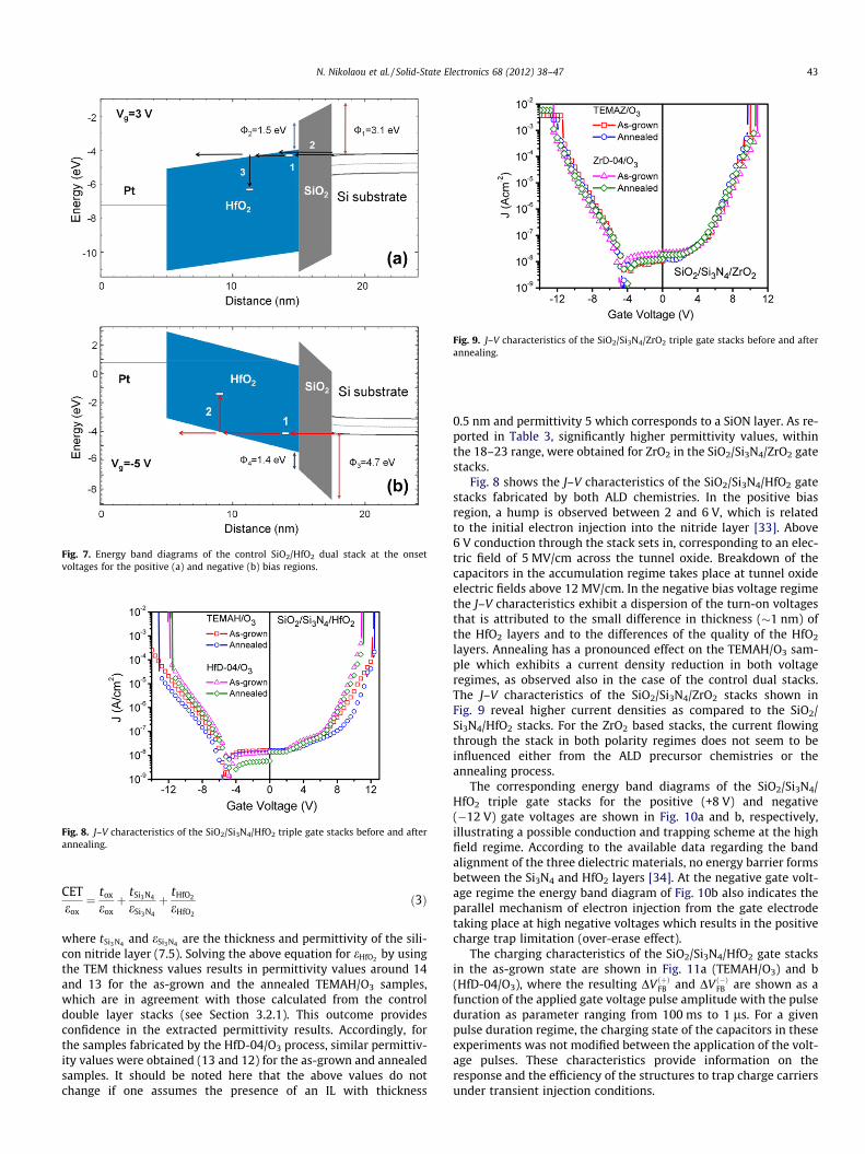
Fig. 7. Energy band diagrams of the control SiO2/HfO2 dual stack at the onsetvoltages for the positive (a) and negative (b) bias regions.
Fig. 8. J–V characteristics of the SiO2/Si3N4/HfO2 triple gate stacks before and afterannealing.
Fig. 9. J–V characteristics of the SiO2/Si3N4/ZrO2 triple gate stacks before and afterannealing.
N. Nikolaou et al. / Solid-State Electronics 68 (2012) 38–47 43
CETeox¼ tox
eoxþ tSi3N4
eSi3N4
þ tHfO2
eHfO2
ð3Þ
where tSi3N4 and eSi3N4 are the thickness and permittivity of the sili-con nitride layer (7.5). Solving the above equation for eHfO2 by usingthe TEM thickness values results in permittivity values around 14and 13 for the as-grown and the annealed TEMAH/O3 samples,which are in agreement with those calculated from the controldouble layer stacks (see Section 3.2.1). This outcome providesconfidence in the extracted permittivity results. Accordingly, forthe samples fabricated by the HfD-04/O3 process, similar permittiv-ity values were obtained (13 and 12) for the as-grown and annealedsamples. It should be noted here that the above values do notchange if one assumes the presence of an IL with thickness
0.5 nm and permittivity 5 which corresponds to a SiON layer. As re-ported in Table 3, significantly higher permittivity values, withinthe 18–23 range, were obtained for ZrO2 in the SiO2/Si3N4/ZrO2 gatestacks.
Fig. 8 shows the J–V characteristics of the SiO2/Si3N4/HfO2 gatestacks fabricated by both ALD chemistries. In the positive biasregion, a hump is observed between 2 and 6 V, which is relatedto the initial electron injection into the nitride layer [33]. Above6 V conduction through the stack sets in, corresponding to an elec-tric field of 5 MV/cm across the tunnel oxide. Breakdown of thecapacitors in the accumulation regime takes place at tunnel oxideelectric fields above 12 MV/cm. In the negative bias voltage regimethe J–V characteristics exhibit a dispersion of the turn-on voltagesthat is attributed to the small difference in thickness (�1 nm) ofthe HfO2 layers and to the differences of the quality of the HfO2
layers. Annealing has a pronounced effect on the TEMAH/O3 sam-ple which exhibits a current density reduction in both voltageregimes, as observed also in the case of the control dual stacks.The J–V characteristics of the SiO2/Si3N4/ZrO2 stacks shown inFig. 9 reveal higher current densities as compared to the SiO2/Si3N4/HfO2 stacks. For the ZrO2 based stacks, the current flowingthrough the stack in both polarity regimes does not seem to beinfluenced either from the ALD precursor chemistries or theannealing process.
The corresponding energy band diagrams of the SiO2/Si3N4/HfO2 triple gate stacks for the positive (+8 V) and negative(�12 V) gate voltages are shown in Fig. 10a and b, respectively,illustrating a possible conduction and trapping scheme at the highfield regime. According to the available data regarding the bandalignment of the three dielectric materials, no energy barrier formsbetween the Si3N4 and HfO2 layers [34]. At the negative gate volt-age regime the energy band diagram of Fig. 10b also indicates theparallel mechanism of electron injection from the gate electrodetaking place at high negative voltages which results in the positivecharge trap limitation (over-erase effect).
The charging characteristics of the SiO2/Si3N4/HfO2 gate stacksin the as-grown state are shown in Fig. 11a (TEMAH/O3) and b(HfD-04/O3), where the resulting DV ðþÞFB and DV ð�ÞFB are shown as afunction of the applied gate voltage pulse amplitude with the pulseduration as parameter ranging from 100 ms to 1 ls. For a givenpulse duration regime, the charging state of the capacitors in theseexperiments was not modified between the application of the volt-age pulses. These characteristics provide information on theresponse and the efficiency of the structures to trap charge carriersunder transient injection conditions.

Fig. 10. Energy band diagrams of the SiO2/Si3N4/HfO2 triple stacks at high fieldconditions in the positive (a) and negative (b) gate voltage regimes.
Fig. 11. Flat-band voltage shifts of the oxide–nitride-high-k capacitor structures in the awhile hole charging ðDV ð�ÞFB Þ at the 100–10 ms. The capacitors were not discharged betwe(b), TEMAZ/O3 (c), and ZrD-04/O3 (d).
44 N. Nikolaou et al. / Solid-State Electronics 68 (2012) 38–47
Both TEMAH/O3 and HfD-04/O3 processed samples are capableto trap electrons and holes. Substantial electron trapping initiatesat applied voltage pulses ranging from 6 to 9 V for pulse durationsgoing from 100 ms to 1 ls. Electron trapping significantly increaseswith the applied voltage leading to DV ðþÞFB as large as 5–6 V. Holetrapping appears less efficient than electron trapping and was de-tected only for the 100 and 10 ms regimes due to the inherent lim-itation of the minority carrier response time. Moreover, holes areheavier than electrons and thus exhibit a much lower tunnelingrate than electrons. It should be mentioned that no hole chargingwas observed in the same gate stacks tested with aluminuminstead of platinum gate electrodes, due to the significantly lowerwork function of aluminum. In the present samples, hole trappinginitiates at applied voltages around�8 V and leads at high negativevoltages to flat-band voltage shifts ðDV ð�ÞFB Þ of about 2–3 V. For bothsamples, memory windows ðDV ðþÞFB þ DV ð�ÞFB Þ as large as 7–9 V areattainable by combining the 1 ls–100 ms electron charging re-gimes with the 10–100 ms hole charging regimes.
As can be seen in the graphs of Fig. 11, the electron trappingability of the samples made with the TEMAH/O3 process is slightlyhigher than that of the HfD-04/O3 one; the attainable DV ðþÞFB of theformer is 6 V while that of the latter is around 5 V. This increasedelectron trapping of the TEMAH/O3 sample is attributed to thehigher parasitic electron trapping into the HfO2 layer, which devel-ops during the application of large pulse amplitudes. The linearpart of the charging characteristics, which corresponds to the ini-tial rise of the DV ðþÞFB has a slope in the range of 0.75–0.85 for bothTEMAH/O3 and HfD-04/O3 samples in the 1 ls–100 ms pulse dura-tion regime, thus indicating that the gain in VFB is 0.75–0.85 V per1 V increase of the gate voltage pulse amplitude. Such a result re-veals that both HfO2 based samples accumulate trapped electronswith the same initial rate, which is expected for samples having
s-grown state. Electron charging ðDV ðþÞFB Þ was obtained at the 100 ms–1 ls regimes,en two consecutive pulses for capacitors processed from TEMAH/O3 (a), HfD-04/O3

N. Nikolaou et al. / Solid-State Electronics 68 (2012) 38–47 45
the same structural and physical characteristics. Therefore, themaximum attainable memory window is limited by the dielectricstrength of the tri-layer gate stack. At high positive applied volt-ages both the HfD-04/O3 and TEMAH/O3 samples exhibit electrontrapping saturation. This saturation effect, which is more pro-nounced for the HfD-04/O3 sample, does not arise from the fillingof all the available trapping sites of the nitride layer or from chargecompensation between electrons and holes. Instead the saturationoccurs because the additional injected charges caused by thefurther increase of the applied voltage above a certain value leakto the gate due to the absence of an electron energy barrierbetween the Si3N4 and HfO2 [13].
For the case of hole trapping, the TEMAH/O3 sample exhibits alarger trapping ability ðDV ð�ÞFB � �3 VÞ in comparison to the HfD-04/O3 sample (��2 V). The gain in VFB is about 0.4 V per voltincrease of the gate bias for both samples. Saturation in this casearises due to the over-erase effect, which occurs at lower voltagesfor the HfD-04/O3 sample owing to the slightly smaller HfO2 layerthickness. This in turn explains the lower hole charging ability ofthe HfD-04/O3 stack. The charging characteristics of both samplesafter annealing (not shown) do not indicate any major differencesin comparison to the as-grown ones.
The charging characteristics of the as-grown SiO2/Si3N4/ZrO2
gate stacks are shown in Fig. 11c and d revealing no significant dif-ferences between the two ALD precursor chemistries. Electrontrapping for the TEMAZ/O3 and ZrD-04/O3-processed samples leadsto DV ðþÞFB in the 3–4 V range for pulse durations going from 1 ls to100 ms. The gain in VFB goes from 0.65 to 0.80 V per volt increase ofthe gate voltage pulse amplitude for pulse durations in the 1 ls–100 ms range. Hole injection and trapping within the nitride layerresults in a maximum DV ð�ÞFB of about 2 V. Erase saturation occurs at�12 V (100 ms regime) for both samples with a gain in VFB of about
Fig. 12. Erase–write performance of the oxide–nitride-high-k capacitors in as-grown staZrD-04/O3 (c), and TEMAZ/O3 (d).
0.4 V per volt increase of the gate bias. The maximum attainablememory windows by combining the 100 ls–100 ms electroncharging regimes and the 100 ms hole charging regime are in the5–6 V range. The slightly higher charging observed for the ZrD-04/O3-processed sample is attributed to the higher thickness ofthe ZrO2 layer and to the small differences in the dielectric con-stants of the deposited ZrO2 materials. In comparison to the SiO2/Si3N4/HfO2 stacks, the SiO2/Si3N4/ZrO2 stacks exhibit a smallerelectron trapping ability in terms of attainable DV ðþÞFB (and a slightlylower VFB gain) in the 1 ls–100 ms pulse duration range. This isattributed to the higher permittivity of the ZrO2 layer (20–22)compared to that of the HfO2 layer (13–14), which leads to higherelectric fields across the tunnel oxide and Si3N4 layers in the ZrO2
based samples, and thus the injected electrons leak towards thegate electrode without being trapped.
Fig. 12 shows the programming performance of the gate stacks.The initial charging state of the capacitors was set by a single neg-ative pulse to the erase state (hole charging) and then the capacitorwas programmed by a single pulse of constant amplitude with thepulse width as parameter. The opposite operation of the transitionfrom the write to the erase state is not shown since it is limited bythe time required for the formation of the inversion layer withinthe time regime of 10–100 ms. The general trend of these programcharacteristics, which applies to all the samples studied both in theas-grown and annealed states, is that they exhibit two slopes atlarge write amplitudes. At small pulse widths (below 1–10 ls)the d(DVFB)/dlog10t is greater than 1 V per decade in time, whileat larger pulse widths the slope is �0.75 V/decade very close tothe values extracted from the charging characteristics of Fig. 11.The HfD-04/O3 triple stack shows clearly this behavior (Fig. 12a).At 8 V write pulse the E/W transition exhibits a constant slope of0.8 V/decade while higher voltage pulses split the E/W transition
te or after annealing for the samples processed from HfD-04/O3 (a), TEMAH/O3 (b),

Fig. 13. Charge retention of the SiO2/Si3N4/HfO2 structures grown with TEMAH/O3.
Fig. 14. Endurance characteristics of the SiO2/Si3N4/HfO2 structures (a) and theSiO2/Si3N4/ZrO2 structures (b).
46 N. Nikolaou et al. / Solid-State Electronics 68 (2012) 38–47
into two separate regimes. For the case of 10 V the initial slope hasa value of 1.7 V/decade, while above 10 ls the slope becomes0.8 V/decade, without saturation. The memory window for thestack depends strongly on the write pulse characteristics and canreach 5 V for a 10 V 1 ms voltage pulse. Annealing does not induceany significant changes.
The same behavior was observed for the TEMAH/O3 triple gatestacks (Fig. 12b). In this case larger pulse amplitudes were em-ployed and thus only the two slope characteristics were monitored.For the as-grown sample the application of 10 V write pulses pro-vides an initial slope of 1.9 V/decade which drops to 0.89 V/decadeabove 10 ls. Higher write pulses increase the initial slope, withoutaltering the slope at large pulse widths. Compared to the as-grownsamples, larger pulse widths are required after annealing in the
case of the 10 and 11 V program voltages characteristics for achiev-ing the same DVFB. In addition, the annealed TEMAH/O3 capacitorsdo not exhibit program saturation. The wide memory window(7.5 V) shown in the graph is due to the high applied pulses whichthe capacitors can tolerate.
For the SiO2/Si3N4/ZrO2 stacks similar program characteristicswere measured (Fig. 12c and d). These samples indicate that theapplication of a medium amplitude pulse around 10 V of a durationshorter than 1 ms is necessary to bring the capacitor from the eraseto the write state. It should be mentioned that the extracted valuesof the flat-band voltage gain per decade increase of the pulse widthare quite similar to the values extracted in [35].
Fig. 13 shows the room temperature retention characteristics ofthe as-grown and annealed TEMAH/O3 gate stacks. A write pulse of10 V/10 ms and an erase pulse of �12 V/10 ms were used to estab-lish the same VFB shifts in both samples. The charge loss rate for theelectron discharge was identical for the as-grown and the annealedstacks with a 0.43 V/decade in time. The hole discharge rates werefound to be 0.16 and 0.11 V/decade for the as-grown and annealedsamples, respectively. Although the HfO2 layer underwent a crys-tallization process during annealing, this does not influence thedischarge rates of the stacks. This indicates that the dischargeoccurs mainly through the 2.5 nm tunnel oxide via trap to bandtunneling [36]. In addition, the same charge loss rates were ex-tracted from the retention measurements of the other triple gatestacks (not shown). Despite the large charge loss rate, extrapola-tion to 10 years shows a remaining memory window of approxi-mately 1 V for the electron trapped charge and a residualwindow of less than 0.5 V for the holes.
The endurance characteristics of the SiO2/Si3N4/HfO2 and SiO2/Si3N4/ZrO2 stacks are shown in Fig. 14. The applied voltage pulseswere 10 V/10 ms for the write state and �11 V/10 ms for the erasestate. For the HfO2 based stacks, the TEMAH/O3 sample shows nei-ther memory window closure and drift, nor degradation of the C–Vcharacteristics after the application of 3 � 105 W/E cycles. In turn,the HfD-04/O3 stack exhibits a lower reliability to W/E cycling andwas not able to sustain more than 104 cycles. The SiO2/Si3N4/ZrO2
stacks follow the above trend. The TEMAZ/O3 structure can with-stand 3 � 105 W/E cycles, with, however, a significant memorywindow closure arising from the write state (�25%). The ZrD-04/O3 stack sustains only a limited number of cycles (�3–7 � 103). Itshould be emphasized here that the chosen W/E pulsing conditionsand especially the write pulse lead the memory stacks to a differ-ent percentage of their maximum electron charging ability. Forboth ZrO2 based samples the 10 V/10 ms write pulse drives themto their maximum charging ability. These pulsing conditionsseverely stress both ZrO2 samples, while the HfO2 based stacks,especially the TEMAH-processed one, operate under moderatestress conditions. Despite these differences a clear dividing linecan be drawn, where the capacitors made of alkylamides exhibitfar greater endurance than those made using cyclopentadienyls.
4. Conclusions
In this work we studied the influence of the HfO2 and ZrO2 ALDprecursor chemistry on the memory properties of SiO2/Si3N4/HfO2,and SiO2/Si3N4/ZrO2 dielectric stacks, where these high-k layersserved as control oxides combined with a platinum gate electrode.The studied precursors were Hf and Zr alkylamides (tetrakiseth-ylmethylamides of Hf and Zr), and Hf and Zr cyclopentadienyls(bis (methylcyclopentadienyl)methoxymethyls of hafnium and zir-conium), combined with ozone as the oxygen source. Deposition ofthe ZrO2 layers on Si3N4 did not show any structural dependenceupon the employed precursor; both films were found to crystallizeinto the tetragonal phase. In contrast the Hf-alkylamide precursor

N. Nikolaou et al. / Solid-State Electronics 68 (2012) 38–47 47
yielded an almost amorphous HfO2 film, while the Hf cyclopenta-dienyl resulted in a film crystallized into the monoclinic and ortho-rhombic or tetragonal phases. Annealing at 600 �C in O2 for 2 minresults in the enhancement of the crystallization in the case ofthe as-deposited crystallized films or induces crystallization inthe case of the as-deposited amorphous films.
The electrical testing of the triple gate memory stacks showedthat their electrical properties are quite similar. This outcomearises because the electrical properties of the stack are determinedmainly by the SiO2 tunnel oxide characteristics (quality, thickness)and by the permittivity and the quality of the high-k layer. As aresult, the electron injection mechanism is determined by thethickness of the SiO2 layer, while the permittivity of the high-kcontrols the electric field distribution within the stack. Moreover,the small thickness of the tunnel oxide allows hole injection intothe nitride layer. Therefore, the J–V, C–V, and charging characteris-tics as well as the programming performance of the stacks, aregrouped according to the high-k layer and exhibit small differ-ences. Furthermore, no substantial variations in data retentionare detected between all the stacks under examination thus indi-cating that the very thin SiO2 layer is the principal reason for thedetected charge loss.
However, the endurance measurements indicate a significantdifference between the samples grown using cyclopentadienylsand alkylamides. The alkylamide-processed samples can withstandsignificantly higher W/E cycles than those grown from cyclopenta-dienyls, thus indicating that the reliability of the high-k layersseems to be strongly dependent upon the precursor choice. Thisobservation is attributed to the different deposition temperatures,average structural homogeneity of the layers and the formation ofan interfacial layer (IL) between the high-k and nitride layers. Asobserved by TEM imaging, the higher deposition temperature ofthe cyclopentadienyls leads to the formation of a 0.5 nm thick IL,which may be the weakest spot of the structures leading to fastercollapse of the triple gate stack.
References
[1] Lu C-Y, Hsieh K-Y, Lu R. Microelectron Eng 2009;86:283–6.[2] Fazio A. MRS Bull 2004;29:814–9.[3] Kuesters KH, Beug MF, Schroeder U, Nagel N, Bewersdorff U, Dallmann G, et al.
Adv Eng Mater 2007;11:241–8.[4] Roizin Y, Gritsenko V. In: Baklanov MR, Green M, Maex K, editors. Dielectric
films for advanced microelectronics. New York: John Wiley and Sons, Ltd.;2007. p. 251–96.
[5] Bachhofer H, Reisinger H, Bertagnolli E, von Philipsborn H. J Appl Phys2001;89:2791–800.
[6] French ML, White MH. Solid State Electron 1994;37:1913–23.[7] White MH, Wang YR, Wrazien SJ, Zhao YS. Int J High Speed Electron Syst
2002;16:479–501.[8] Eitan B, Pavan P, Bloom I, Aloni E, Frommer A, Finzi D. IEEE Electron Device Lett
2000;21:543–5.[9] Chau R, Datta S, Doczy M, Doyle B, Kavalieros J, Metz M. IEEE Electron Device
Lett 2004;25:408–10.[10] Gritsenko VA, Nasyrov KA, Novikov YuN, Aseev AL, Yoon SY, Lee J-W, et al.
Solid State Electron 2003;47:1651–6.[11] Lee C-H, Hur S-H, Shin Y-C, Choi J-H, Park D-G, Kim K. Appl Phys Lett
2005;86:152908.[12] Tsai P-H, Liao K-SC, Yang D-W, Chung Y-B, Wang T-K, Tzeng PJ, et al. Appl Phys
Lett 2008;93:252902.[13] van Schaijk R, Slotboom M, van Duuren M, Dormans D, Akil N, Beurze R, et al.
Solid State Electron 2005;49:1849–56.[14] Govoreanu B, Degraeve R, Zahid MB, Nyns L, Cho M, Kaczer B, et al.
Microelectron Eng 2009;86:1807–11.[15] Molas G, Bocquet M, Buckley J, Grampeix H, Gely M, Colonna JP, et al.
Microelectron Eng 2008;85:2393–9.[16] Erlbacher T, Jank MPM, Lemberger M, Bauer AJ, Ryssel H. Thin Solid Films
2008;516:7727–31.[17] Yeh C-C, Ma TP, Ramaswamy N, Rocklein N, Gealy D, Graettinger T, et al. Appl
Phys Lett 2007;91:113521.[18] Jeong DS, Hwang CS. J Appl Phys 2005;98:113701.[19] Xu Z, Houssa M, De Gendt S, Heyns M. Appl Phys Lett 2002;80:1975–7.[20] Kim H, Marshall A, McIntryre P, Saraswat K. Appl Phys Lett 2004;84:2064–6.[21] Southwick III RG, Reed J, Buu C, Butler R, Bersuker G, Knowlton WB, et al. IEEE
Trans Device Mater Reliab 2010;10:201–7.[22] Puurunen R. J Appl Phys 2005;97:121301.[23] Niinisto J, Kukli K, Heikkila M, Ritala M, Leskela M. Adv Eng Mater
2007;11:223–34.[24] Niinisto L, Paivasaari J, Niinisto J, Putkonen M, Nieminen M. Phys Status Solidi
A 2004;201:1443–52.[25] Kukli K, Aarik J, Ritala M, Uustare T, Sajavaara T, Lu J, et al. J Appl Phys
2004;96:5298–307.[26] Hausmann DM, Kim E, Berker J, Gordon RG. Chem Mater 2002;14:4350–8.[27] Rushworth S, Coward K, Davies H, Heys P, Leese T, Kempster L, et al. Surf Coat
Technol 2007;201:9060–5.[28] Kukli K, Ritala M, Sajavaara T, Keinonen J, Leskela M. Chem Vap Deposition
2002;8:199–204.[29] Dezelah CL, Niinisto J, Kukli K, Munnik F, Lu J, Ritala M, et al. Chem Vap
Deposition 2008;14:358–65.[30] Duenas S, Castan H, Garcia H, Gomez A, Bailon L, Kukli K, et al. J Vac Sci Technol
B 2009;27:389–93.[31] Southwick III RG, Knowlton WB. IEEE Trans Device Mater Reliab
2006;6:136–45.[32] Schaeffer JK, Fonseca LRC, Samavedam SB, Liang Y, Tobin PJ, White BE. J Appl
Phys 2004;85:1826–8.[33] Ioannou-Sougleridis V, Dimitrakis P, Vamvakas VEm, Normand P, Bonafos C,
Schamm S, et al. Nanotechnology 2007;18:215204.[34] Robertson J. J Vac Sci Technol B 2000;18:1785–91.[35] Golonovic DS, van Duuren MJ, Akil N, Arreghini A, Driussi F. Microelectron Eng
2009;86:1999–2004.[36] Gu S-H, Hsu C-W, Wang T, Lu W-P, Ku Y-HJ, Lu C-Y. IEEE Trans Electron Devices
2007;54:90–7.