SERVICE MANUAL LC-32D44E/S/RU-BK/GY
142
SERVICE MANUAL LC32D44E/S/RU-BK/GY (1st Eddition) Parts marked with " " are important for maintaining the safety of the set. Be sure to replace these parts with specified ones for maintaining the safety and performance of the set. This document has been published to be used for after sales service only. The contents are subject to change without notice. SAFETY PRECAUTION IMPORTANT SERVICE SAFETY PRE- CAUTION ...........................................................i PRECAUTIONS A PRENDRE LORS DE LA REPARATION .............................................. ii PRECAUTIONS FOR USING LEAD-FREE SOLDER .......................................................... iii CHAPTER 1. SPECIFICATIONS [1] SPECIFICATIONS ........................................ 1-1 [2] OPERATION MANUAL ................................. 1-2 [3] DIMENSIONS ............................................... 1-5 CHAPTER 2. REMOVING OF MAJOR PARTS [1] REMOVING OF MAJOR PARTS .................. 2-1 CHAPTER 3. ADJUSTMENT [1] After replacement of any PWB and/or IC for repair, note the following. .............................. 3-1 [2] SOFTWARE UPDATING............................... 3-1 [3] Entering and exiting the adjustment pro- cess mode ................................................... 3-18 [4] Remote controller key operation and de- scription of display in adjustment process mode. .......................................................... 3-18 [5] Adjustment process mode menu................. 3-19 [6] Special features........................................... 3-20 [7] Video signal adjustment procedure ............. 3-21 [8] White Balance Adjustment .......................... 3-22 [9] Adjusting procedure by use of [RS-232C] ...... 3-23 [10] Initialization to factory settings..................... 3-24 [11] Lamp error detection ................................... 3-24 [12] Public Mode (Hotel Mode) ........................... 3-25 CHAPTER 4. TROUBLE SHOOTING TABLE [1] TROUBLE SHOOTING TABLE ..................... 4-1 CHAPTER 5. MAJOR IC INFORMATIONS [1] MAJOR IC INFORMATIONS ......................... 5-1 CHAPTER 6. BLOCK DIAGRAM/OVERALL WIRING [1] BLOCK DIAGRAM......................................... 6-1 [2] SYSTEM BLOCK DIAGRAM ......................... 6-3 [3] OVERALL WIRING DIAGRAM ...................... 6-4 CHAPTER 7. PRINTED WIRING BOARD ASSEM- BLIES [1] MAIN Unit ...................................................... 7-1 [2] R/C, LED Unit ................................................ 7-5 [3] MINI AV Unit .................................................. 7-6 [4] KEY ............................................................... 7-7 CHAPTER 8. SCHEMATIC DIAGRAM [1] DESCRIPTION OF SCHEMATIC DIA- GRAM ............................................................ 8-1 [2] SCHEMATIC DIAGRAM ................................ 8-2 Parts Guide TopPage CONTENTS No. S38F8LC32D44E LCD COLOUR TELEVISION LC-32D44E/S/RU-BK/GY MODELS In the interests of user-safety (Required by safety regulations in some countries) the set should be restored to its orig- inal condition and only parts identical to those specified should be used.
-
Upload
khangminh22 -
Category
Documents
-
view
0 -
download
0
Transcript of SERVICE MANUAL LC-32D44E/S/RU-BK/GY

SERVICE MANUALLC32D44E/S/RU-BK/GY (1st Eddition)
Parts marked with " " are important for maintaining the safety of the set. Be sure to replace these parts with specified ones for maintaining thesafety and performance of the set.
This document has been published to be used forafter sales service only.The contents are subject to change without notice.
SAFETY PRECAUTIONIMPORTANT SERVICE SAFETY PRE-CAUTION............................................................iPRECAUTIONS A PRENDRE LORS DE LA REPARATION............................................... iiPRECAUTIONS FOR USING LEAD-FREE SOLDER ........................................................... iii
CHAPTER 1. SPECIFICATIONS[1] SPECIFICATIONS ......................................... 1-1[2] OPERATION MANUAL .................................. 1-2[3] DIMENSIONS ................................................ 1-5
CHAPTER 2. REMOVING OF MAJOR PARTS[1] REMOVING OF MAJOR PARTS ................... 2-1
CHAPTER 3. ADJUSTMENT[1] After replacement of any PWB and/or IC for
repair, note the following. ............................... 3-1[2] SOFTWARE UPDATING................................ 3-1[3] Entering and exiting the adjustment pro-
cess mode.................................................... 3-18[4] Remote controller key operation and de-
scription of display in adjustment process mode. ........................................................... 3-18
[5] Adjustment process mode menu.................. 3-19[6] Special features............................................ 3-20[7] Video signal adjustment procedure.............. 3-21[8] White Balance Adjustment ........................... 3-22[9] Adjusting procedure by use of [RS-232C]...... 3-23
[10] Initialization to factory settings.....................3-24[11] Lamp error detection ...................................3-24[12] Public Mode (Hotel Mode) ...........................3-25
CHAPTER 4. TROUBLE SHOOTING TABLE[1] TROUBLE SHOOTING TABLE .....................4-1
CHAPTER 5. MAJOR IC INFORMATIONS[1] MAJOR IC INFORMATIONS .........................5-1
CHAPTER 6. BLOCK DIAGRAM/OVERALL WIRING[1] BLOCK DIAGRAM.........................................6-1[2] SYSTEM BLOCK DIAGRAM.........................6-3[3] OVERALL WIRING DIAGRAM......................6-4
CHAPTER 7. PRINTED WIRING BOARD ASSEM-BLIES[1] MAIN Unit ......................................................7-1[2] R/C, LED Unit ................................................7-5[3] MINI AV Unit ..................................................7-6[4] KEY ...............................................................7-7
CHAPTER 8. SCHEMATIC DIAGRAM[1] DESCRIPTION OF SCHEMATIC DIA-
GRAM............................................................8-1[2] SCHEMATIC DIAGRAM................................8-2
Parts Guide
TopPage
CONTENTS
No. S38F8LC32D44E
LCD COLOUR TELEVISION
LC-32D44E/S/RU-BK/GYMODELSIn the interests of user-safety (Required by safety regulations in some countries) the set should be restored to its orig-inal condition and only parts identical to those specified should be used.

LC32D44E/S/RU-BK/GY (1st Eddition)
LC32D44E-BK Service ManualSAFETY PRECAUTION
IMPORTANT SERVICE SAFETY PRECAUTION
WARNING1. For continued safety, no modification of any circuit should be
attempted.
2. Disconnect AC power before servicing.
BEFORE RETURNING THE RECEIVER (Fire & Shock Hazard)Before returning the receiver to the user, perform the followingsafety checks:
3. Inspect all lead dress to make certain that leads are not pinched,and check that hardware is not lodged between the chassis andother metal parts in the receiver.
4. Inspect all protective devices such as non-metallic control knobs,insulation materials, cabinet backs, adjustment and compartmentcovers or shields, isolation resistor-capacitor networks, mechanicalinsulators, etc.
5. To be sure that no shock hazard exists, check for leakage current inthe following manner.
• Plug the AC cord directly into a 220~240 volt AC outlet.
• Using two clip leads, connect a 1.5k ohm, 10 watt resistor paral-leled by a 0.15µF capacitor in series with all exposed metal cabinetparts and a known earth ground, such as electrical conduit or elec-trical ground connected to an earth ground.
• Use an AC voltmeter having with 5000 ohm per volt, or higher, sen-sitivity or measure the AC voltage drop across the resistor.
• Connect the resistor connection to all exposed metal parts having areturn to the chassis (antenna, metal cabinet, screw heads, knobsand control shafts, escutcheon, etc.) and measure the AC voltagedrop across the resistor.All checks must be repeated with the AC cord plug connectionreversed. (If necessary, a nonpolarized adaptor plug must be usedonly for the purpose of completing these checks.)Any reading of 1.05 V peak (this corresponds to 0.7 mA peak AC.)or more is excessive and indicates a potential shock hazard whichmust be corrected before returning the monitor to the owner.
///////////////////////////////////////////////////////////////////////////////////////////////////////////////////////////////////////////////////////////////////////////////////////////////////////////////////////////////////////////
SAFETY NOTICEMany electrical and mechanical parts in LCD color television havespecial safety-related characteristics.
These characteristics are often not evident from visual inspection, norcan protection afforded by them be necessarily increased by usingreplacement components rated for higher voltage, wattage, etc.
Replacement parts which have these special safety characteristics areidentified in this manual; electrical components having such featuresare identified by “ ” and shaded areas in the Replacement PartsList and Schematic Diagrams.
For continued protection, replacement parts must be identical to thoseused in the original circuit.
The use of a substitute replacement parts which do not have the samesafety characteristics as the factory recommended replacement partsshown in this service manual, may create shock, fire or other hazards.
///////////////////////////////////////////////////////////////////////////////////////////////////////////////////////////////////////////////////////////////////////////////////////////////////////////////////////////////////////////
Service work should be performed only by qualified service technicians who are thoroughly familiar with all safety checks and the servicing guidelines which follow:
CAUTION : FOR CONTINUED PROTECTION
AGAINST A RISK OF FIRE REPLACE ONLY WITH
SAME TYPE FUSE.
F7101, F7103 (250V 3.15A)
F7102 (250V 1A)
DVM
AC SCALE
1.5k ohm10W
TO EXPOSEDMETAL PARTS
CONNECT TOKNOWN EARTHGROUND
0.15 µF
TEST PROBE
i

LC32D44E/S/RU-BK/GY (1st Eddition)
PRECAUTIONS A PRENDRE LORS DE LA REPARATIONDe nombreuses pièces, électriques et mécaniques, dans les télévi-seur ACL présentent des caractéristiques spéciales relatives à la sé-curité, qui ne sont souvent pas évidentes à vue. Le degré de protec-tion ne peut pas être nécessairement augmentée en utilisant despièces de remplacement étalonnées pour haute tension, puissance,etc.Les pièces de remplacement qui présentent ces caractéristiques sontidentifiées dans ce manuel; les pièces électriques qui présentent cesparticularités sont identifiées par la marque " " et hachurées dans laliste des pièces de remplacement et les diagrammes schématiques.
Pour assurer la protection, ces pièces doivent être identiques à cellesutilisées dans le circuit d'origine. L'utilisation de pièces qui n'ont pasles mêmes caractéristiques que les pièces recommandées par l'usine,indiquées dans ce manuel, peut provoquer des électrocutions, incen-dies, radiations X ou autres accidents.
AVERTISSEMENT
1.
2.
3.
4.
5.
•
•
•
•
/////////////////////////////////////////////////////////////////////////////////////////////////////////////////////////////////////////////////////////////////////////////////////////////////////////////////////////////////////////////
/////////////////////////////////////////////////////////////////////////////////////////////////////////////////////////////////////////////////////////////////////////////////////////////////////////////////////////////////////////////
Ne peut effectuer la réparation qu' un technicien spécialisé qui s'est parfaitement accoutumé à toute vérification de sécurité et aux
conseils suivants.
N'entreprendre aucune modification de tout circuit. C'est danger-eux.
Débrancher le récepteur avant toute réparation.
Inspecter tous les faisceaux de câbles pour s'assurer que les filsne soient pas pincés ou qu'un outil ne soit pas placé entre le châs-sis et les autres pièces métalliques du récepteur.
Inspecter tous les dispositifs de protection comme les boutons decommande non-métalliques, les isolants, le dos du coffret, les cou-vercles ou blindages de réglage et de compartiment, les réseauxde résistancecapacité, les isolateurs mécaniques, etc.
S'assurer qu'il n'y ait pas de danger d'électrocution en vérifiant lafuite de courant, de la facon suivante:
Brancher le cordon d'alimentation directem-ent à une prise de cou-rant de 120V. (Ne pas utiliser de transformateur d'isolation pourcet essai).
A l'aide de deux fils à pinces, brancher une résistance de 1.5 kΩ10 watts en parallèle avec un condensateur de 0.15µF en sérieavec toutes les pièces métalliques exposées du coffret et une terreconnue comme une conduite électrique ou une prise de terrebranchée à la terre.
Utiliser un voltmètre CA d'une sensibilité d'au moins 5000Ω/V pourmesurer la chute de tension en travers de la résistance.
Toucher avec la sonde d'essai les pièces métalliques exposées quiprésentent une voie de retour au châssis (antenne, coffret métalli-que, tête des vis, arbres de commande et des boutons, écusson,etc.) et mesurer la chute de tension CA en-travers de la résistance.Toutes les vérifications doivent être refaites après avoir inversé lafiche du cordon d'alimentation. (Si nécessaire, une prised'adpatation non polarisée peut être utilisée dans le but de termin-er ces vérifications.)La tension de pointe mesurèe ne doit pas dépasser 0.75V (corre-spondante au courant CA de pointe de 0.5mA).Dans le cas contraire, il y a une possibilité de choc électrique quidoit être supprimée avant de rendre le récepteur au client.
PRECAUTION: POUR LA PROTECTION CON-
TINUE CONTRE LES RISQUES D'INCENDIE,
REMPLACER LE FUSIBLE
F7101, F7103 (250V 3.15A)
F7102 (250V 1A)
VERIFICATIONS CONTRE L'INCEN-DIE ET LE
CHOC ELECTRIQUE
Avant de rendre le récepteur à l'utilisateur, effectuer les vérifica-
tions suivantes.
DVM
ECHELLE CA
1.5k ohm10W
0.15 µF
SONDE D'ESSAI
AUX PIECESMETALLIQUESEXPOSEES
BRANCHER A UNETERRE CONNUE
AVIS POUR LA SECURITE
ii

LC32D44E/S/RU-BK/GY (1st Eddition)
PRECAUTIONS FOR USING LEAD-FREE SOLDEREmploying lead-free solder• “PWBs” of this model employs lead-free solder. The LF symbol indicates lead-free solder, and is attached on the PWBs and service manuals. The
alphabetical character following LF shows the type of lead-free solder.
Example:
Using lead-free wire solder• When fixing the PWB soldered with the lead-free solder, apply lead-free wire solder. Repairing with conventional lead wire solder may cause dam-
age or accident due to cracks.
As the melting point of lead-free solder (Sn-Ag-Cu) is higher than the lead wire solder by 40 °C, we recommend you to use a dedicated solderingbit, if you are not familiar with how to obtain lead-free wire solder or soldering bit, contact our service station or service branch in your area.
Soldering• As the melting point of lead-free solder (Sn-Ag-Cu) is about 220 °C which is higher than the conventional lead solder by 40 °C, and as it has poor
solder wettability, you may be apt to keep the soldering bit in contact with the PWB for extended period of time. However, Since the land may bepeeled off or the maximum heat-resistance temperature of parts may be exceeded, remove the bit from the PWB as soon as you confirm thesteady soldering condition.
Lead-free solder contains more tin, and the end of the soldering bit may be easily corroded. Make sure to turn on and off the power of the bit asrequired.
If a different type of solder stays on the tip of the soldering bit, it is alloyed with lead-free solder. Clean the bit after every use of it.
When the tip of the soldering bit is blackened during use, file it with steel wool or fine sandpaper.
• Be careful when replacing parts with polarity indication on the PWB silk.
Lead-free wire solder for servicing
Indicates lead-free solder of tin, silver and copper. Indicates lead-free solder of tin, silver and copper.
PARTS CODE PRICE RANK
PART DELIVERY DESCRIPTION
ZHNDAi123250E BL J φ0.3mm 250g (1roll)ZHNDAi126500E BK J φ0.6mm 500g (1roll)ZHNDAi12801KE BM J φ1.0mm 1kg (1roll)
iii
LC32D44E/S/RU-BK/GY (1st Eddition)
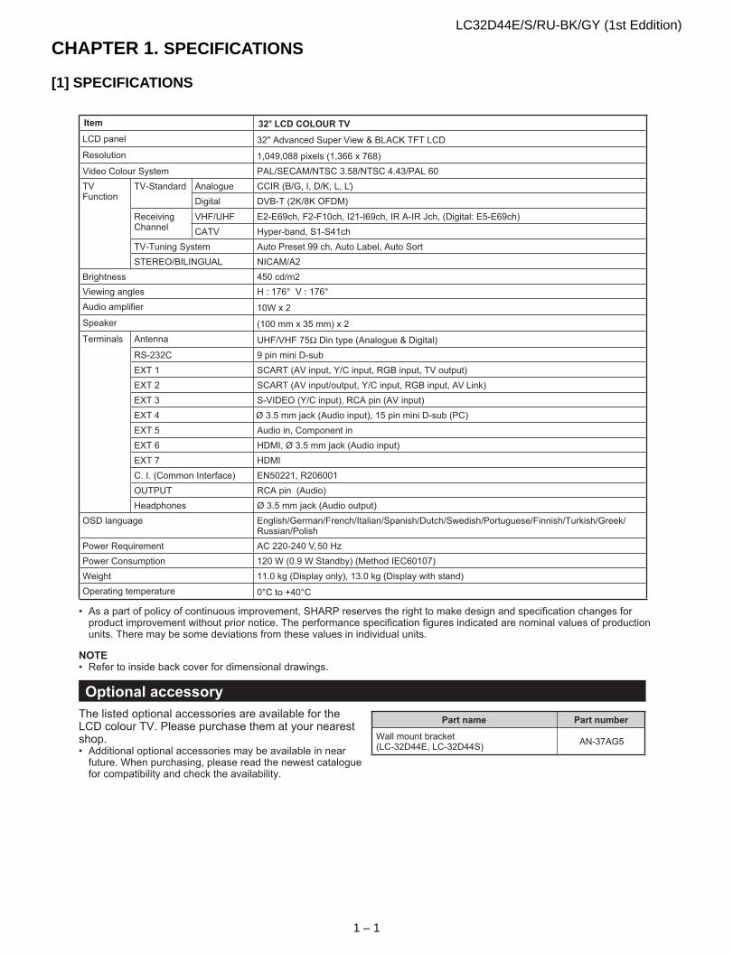
LC32D44E-BK Service Manual CHAPTER 1. SPECIFICATIONS[1] SPECIFICATIONS
Item 32" LCD COLOUR TV
LCD panel 32" Advanced Super View & BLACK TFT LCD
Resolution 1,049,088 pixels (1,366 x 768)
Video Colour System PAL/SECAM/NTSC 3.58/NTSC 4.43/PAL 60
TVFunction
TV-Standard Analogue CCIR (B/G, I, D/K, L, L’)
Digital DVB-T (2K/8K OFDM)
ReceivingChannel
VHF/UHF E2-E69ch, F2-F10ch, I21-I69ch, IR A-IR Jch, (Digital: E5-E69ch)
CATV Hyper-band, S1-S41ch
TV-Tuning System Auto Preset 99 ch, Auto Label, Auto Sort
STEREO/BILINGUAL NICAM/A2
Brightness 450 cd/m2
Viewing angles H : 176° V : 176°
Audio amplifier 10W x 2
Speaker (100 mm x 35 mm) x 2
Terminals Antenna UHF/VHF 75Ω Din type (Analogue & Digital)
RS-232C 9 pin mini D-sub
EXT 1 SCART (AV input, Y/C input, RGB input, TV output)
EXT 2 SCART (AV input/output, Y/C input, RGB input, AV Link)
EXT 3 S-VIDEO (Y/C input), RCA pin (AV input)
EXT 4 Ø 3.5 mm jack (Audio input), 15 pin mini D-sub (PC)
EXT 5 Audio in, Component in
EXT 6 HDMI, Ø 3.5 mm jack (Audio input)
EXT 7 HDMI
C. I. (Common Interface) EN50221, R206001
OUTPUT RCA pin (Audio)
Headphones Ø 3.5 mm jack (Audio output)
OSD language English/German/French/Italian/Spanish/Dutch/Swedish/Portuguese/Finnish/Turkish/Greek/Russian/Polish
Power Requirement AC 220-240 V,50 Hz
Power Consumption 120 W (0.9 W Standby) (Method IEC60107)
Weight 11.0 kg (Display only), 13.0 kg (Display with stand)
Operating temperature 0°C to +40°C
• As a part of policy of continuous improvement, SHARP reserves the right to make design and specification changes forproduct improvement without prior notice. The performance specification figures indicated are nominal values of productionunits. There may be some deviations from these values in individual units.
NOTE• Refer to inside back cover for dimensional drawings.
Optional accessory
The listed optional accessories are available for theLCD colour TV. Please purchase them at your nearestshop.• Additional optional accessories may be available in nearfuture. When purchasing, please read the newest cataloguefor compatibility and check the availability.
Part name Part number
Wall mount bracket(LC-32D44E, LC-32D44S)
AN-37AG5
1 – 1

LC32D44E/S/RU-BK/GY (1st Eddition)
[2] OPERATION MANUAL12
4
3
5
6789
10
11
12
13
14
151617
18
19
20212223
24
25
26
27
28
29
1 (Standby/On)Enter standby mode or turn on thepower.
2 AV MODESelect a video setting.
3 0–9Set the channel in TV and DTV mode.Set the page in Teletext mode.
4 (Flashback)Press to return to the previous imagein normal viewing mode. (Will not workwhile operating in EPG/ESG screen.)
5 (WIDE MODE)Select the wide mode.
6 (Sound mode)Select the sound multiplex mode.(See below.)
7 EPGDTV: To display EPG (ElectronicProgramme Guide) screen.
8 ESGDTV: To display ESG (Electronic ServiceGuide) screen.
9 (Teletext)Select the TELETEXT mode. (All TVimage, DTV/DATA image, all TEXTimage, TV/TEXT image)DTV: Select DTV data broadcasting andTELETEXT.
10 / / / (Cursor)Select a desired item on the settingscreen.
11 ENDExit the menu screen.
12 (Reveal hidden Teletext)
13 (Freeze/Hold)
14 SURROUNDSwitch the surround effects on and off.
15 RADIODTV: Switch between RADIO and DTVmode.
16 (Mute)Switch the sound on and off.
17 DTVPress to access DTV mode whilewatching other input sources, and viceversa.(This button will not work if you werewatching DTV immediately beforeturning off the TV. In this case first selectany other input source except DTVusing the button.)
18 (+/-) (Volume)(+) Increase the volume.(-) Decrease the volume.
19 P ( / )TV/DTV: Select the channel.External: Switch to TV or DTV inputmode.eletext: Move to the next/previous
20 (INPUT SOURCE)Select an input source.(TV, DTV, EXT1, EXT2, EXT3, EXT4,EXT5, EXT6, EXT7)
21 SLEEPSet the sleep timer on (in units of 30min. up to max. 2 hr. 30 min) and off.
22 (Display information)23 DTV MENU
DTV: Display DTV Menu screen.
24 MENUDisplay the MENU screen.
25 OKExecute a command within the menuscreen.Display the programme list. (Exceptexternal input.)
26 RETURNReturn to the previous menu screen.
27 (Subpage)
28 (Subtitle for Teletext)TV/External: To turn the subtitles on andoff.DTV: Display the subtitle selectionscreen.
29 Colour (Red/Green/Yellow/Blue)TELETEXT: Select a page.DTV: The coloured buttons are used toselect correspondingly to the coloureditems in the menu screen.
NOTE• When no signal is input, the sound mode will display “MONO”.
NICAM TV broadcasts selection
Signal Selectable items
Stereo NICAM STEREO, MONO
BilingualNICAM CH A, NICAM CH B,NICAM CH AB, MONO
Monaural NICAM MONO, MONO
A2 TV broadcasts selection
Signal Selectable items
Stereo STEREO, MONO
Bilingual CH A, CH B, CH AB
Monaural MONO
Using on the remote control unit
DTV mode:
Press to open the multi audio screen.
Analogue TV mode:
Each time you press , the mode switches as illustrated in the followingtables.
Remote control unit
When Sweden is selected in thecountry setting from the Initialauto installation, DTV channelsare 4-digit. When anothercountry is selected, DTV channelsare 3-digit.
1 – 2

LC32D44E/S/RU-BK/GY (1st Eddition)
TV (Front view)
TV (Rear view)
10
1
2
6
7
8
9
3 4 5
1311
12
NOTE• Only if you use an active terrestrial antenna, select “On (5V)” under “Supply Voltage”.
Remote control sensor (Standby/On) indicator
(Power button)
(Input button)
(-/+) (Volume buttons)
P ( / )(Programme [channel] buttons)
MENU button
1 RS-232C terminal2 EXT 4 (ANALOGUE RGB/AUDIO)
terminals3 EXT 5 (COMPONENT) terminals4 EXT 1 (RGB) terminal5 EXT 2 (RGB) terminal
6 Antenna input terminal(DVB-T 5V=/80 mA)
7 OUTPUT (AUDIO) terminals8 EXT 6 (HDMI/AUDIO) terminals9 EXT 7 (HDMI) terminal10 COMMON INTERFACE slot
11 EXT 3 terminals12 Headphone jack13 AC INPUT terminal
1 – 3
LC32D44E/S/RU-BK/GY (1st Eddition)
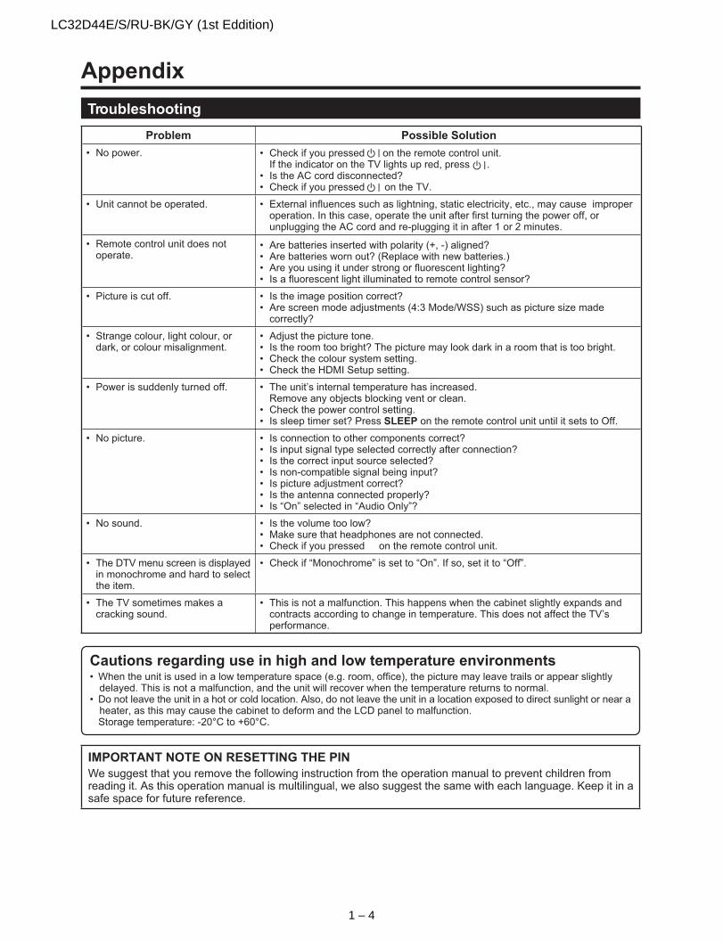
Appendix
Troubleshooting
Problem Possible Solution
• No power. • Check if you pressed on the remote control unit.If the indicator on the TV lights up red, press .
• Is the AC cord disconnected?• Check if you pressed on the TV.
• Unit cannot be operated. • External influences such as lightning, static electricity, etc., may cause improperoperation. In this case, operate the unit after first turning the power off, orunplugging the AC cord and re-plugging it in after 1 or 2 minutes.
• Remote control unit does notoperate.
• Are batteries inserted with polarity (+, -) aligned?• Are batteries worn out? (Replace with new batteries.)• Are you using it under strong or fluorescent lighting?• Is a fluorescent light illuminated to remote control sensor?
• Picture is cut off. • Is the image position correct?• Are screen mode adjustments (4:3 Mode/WSS) such as picture size madecorrectly?
• Strange colour, light colour, ordark, or colour misalignment.
• Adjust the picture tone.• Is the room too bright? The picture may look dark in a room that is too bright.• Check the colour system setting.• Check the HDMI Setup setting.
• Power is suddenly turned off. • The unit’s internal temperature has increased.Remove any objects blocking vent or clean.
• Check the power control setting.• Is sleep timer set? Press SLEEP on the remote control unit until it sets to Off.
• No picture. • Is connection to other components correct?• Is input signal type selected correctly after connection?• Is the correct input source selected?• Is non-compatible signal being input?• Is picture adjustment correct?• Is the antenna connected properly?• Is “On” selected in “Audio Only”?
• No sound. • Is the volume too low?• Make sure that headphones are not connected.• Check if you pressed on the remote control unit.
• The DTV menu screen is displayedin monochrome and hard to selectthe item.
• Check if “Monochrome” is set to “On”. If so, set it to “Off”.
• The TV sometimes makes acracking sound.
• This is not a malfunction. This happens when the cabinet slightly expands andcontracts according to change in temperature. This does not affect the TV’sperformance.
Cautions regarding use in high and low temperature environments• When the unit is used in a low temperature space (e.g. room, office), the picture may leave trails or appear slightlydelayed. This is not a malfunction, and the unit will recover when the temperature returns to normal.
• Do not leave the unit in a hot or cold location. Also, do not leave the unit in a location exposed to direct sunlight or near aheater, as this may cause the cabinet to deform and the LCD panel to malfunction.Storage temperature: -20°C to +60°C.
IMPORTANT NOTE ON RESETTING THE PIN
We suggest that you remove the following instruction from the operation manual to prevent children fromreading it. As this operation manual is multilingual, we also suggest the same with each language. Keep it in asafe space for future reference.
1 – 4

LC32D44E/S/RU-BK/GY (1st Eddition)
[3] DIMENSIONS200.0200,0
776.0776,0
73.973,9
94.594,5
402.0402,0
230.0230,0
699.2699,2
393.8
393,8
332.0
332,0
523.0
523,0
110.0
110,0
52.0
52,0
575.0
575,0
200.0
200,0
1 – 5

LC32D44E/S/RU-BK/GY (1st Eddition)
LC32D44E-BK Service Manual CHAPTER 2. REMOVING OF MAJOR PARTS[1] REMOVING OF MAJOR PARTS1. Remove the 4 lock screws and detach the Stand.
2. Remove the 3 lock screws , 6 lock screws , 2 lock screw and detach the Rear Cabinet.
1
2 3 4
Front Cabinet
Rear Cabinet
Stand
2
3
4
1
2 – 1

LC32D44E/S/RU-BK/GY (1st Eddition)
3. Remove the 3 lock screws , 2 lock screws , 1 lock screws and detach the Main Shield.
4. Disconnect all the connectors from all the PWBs.
5. Remove the KEY Unit Ass'y .
5A 5B 6
7
[LB]
[PD]
[LB][PD]
[KM]
[SP][RA]
[FPC][KM]
Main Shield
KEY Unit
Operation Button
SP-R
5A
5B
6
7
SP-L
2 – 2

LC32D44E/S/RU-BK/GY (1st Eddition)
6. Remove the Speaker (L) , (R) .
7. Remove the 4 lock screws and detach the POWER/INVERTER Unit.
8. Remove the 2 lock screws , and detach the MAIN Unit.
9. Remove the 2 lock screws and detach the MINI AV Unit.
8 9
10
11
12
Power/Inverter Unit
MINI AV Unit
Speaker(R) Speaker(L)
MINI AV Cover
Main Unit
11
9 8
12
10
2 – 3

LC32D44E/S/RU-BK/GY (1st Eddition)
10.Remove the 1 lock screw and detach the Bottom Cover.
11.Remove the 4 lock screws and detach the Stand Fix Angle.
12.Remove the R/C, LED Unit .
13
14
15
R/C,LED Unit
Stand Fix Angle
Bottom Cover
1415
13
2 – 4

LC32D44E/S/RU-BK/GY (1st Eddition)
13.Remove the 6 lock screws and detach the LCD Panel Module.
14.Remove the 2 lock screws and detach the LCD Fix Angle-A.
15.Remove the 2 lock screws and detach the LCD Fix Angle-B.
16.Remove the 8 lock screws and detach the Panel Fix Angle.
16
17
18
19
LCD Fix Angle-A
LCD Fix Angle-A
Panel Fix Angle
1716
19
191616
LCD Fix Angle-B
LCD Fix Angle-B
18
16
1716
1816
2 – 5

LC32D44E/S/RU-BK/GY (1st Eddition)
LC32D44E-BK Service Manual CHAPTER 3. ADJUSTMENT[1] After replacement of any PWB and/or IC for repair, note the following.When replacing the following units, be sure to prepare the new units loaded with updated software.
• Note that an IC into which ROM data is written is available for MAIN-UNIT servicing (see below)
[2] SOFTWARE UPDATINGThere are 2 methods to update software in the VCTp: I2C method, RS-232C HyperTerminal and RS-232C Tera Term method.
• RS-232C method is allowed when the TV is working properly and the action should be only software upgrade.
1. RS-232C Method Description (HyperTerminal).The hardware tools requirement are:
1. A Modem-null (Cross type) DB9 female to DB9 female cable.
2. Make the connections as indicated in the figure:
Before using RS-232C updating method is necessary to configure a Terminal PC software. HyperTerminal has been selected as a Terminal soft-ware because it’s include in all Windows versions as an accessory, and you can find it inside “Accessories\Communications” folder. For this rea-son, please follow carefully the next steps:
1) First time HyperTerminal is used, it’s necessary to configure some settings. Follows next action to configure two connection: low speed(9600bps) and high speed (115200bps).
2) Create a New Connection file with name “P55_9600bps”.
3) Select a free COM port and select the Port Settings properties as follows:
MAIN-UNIT: DUNTKE449FM02
IC1902 RH-iXC448WJZZS EDID (HDMI)IC1922 RH-iXC447WJZZS EDID (HDMI)IC2321 RH-iXC206WJQZS EDID (PC)IC8101 RH-iXC639WJZZS EEPROM
Computer TV set
RS-232C
IOIOI
TV Set
3 – 1

LC32D44E/S/RU-BK/GY (1st Eddition)
4) Click on “File\Properties” menu for selecting the General and ASCII properties as follows:5) Select “New Connection” in the File Menu.
6) Answer “Yes” to close current connection and “Yes” to save session “P55_9600bps”.
7) Create a new connection with the name “P55_115200bps”.
8) Select a the same COM port used in item 2 and select the Port Settings properties as follows:
9) Select the same General and ASCII properties as item 3.
10)Close HyperTerminal session, answering “Yes” to close current connection and “Yes” to save session “P55_115200bps”.
To start updating session, click over “P55_9600bps” icon that you can find in the “START\All programs\Accessories\ Communications\HyperTermi-nal\HyperTerminal” folder and follow next procedure:
3 – 2

LC32D44E/S/RU-BK/GY (1st Eddition)
1) Check the connection between TV set and PC, sending a wrong command, as for example: “aaa”. TV set returns an “ERR” label as an syntaxisERROR (Not correct order or sequence).
2) Send the command “DWMD” to enter TV set in Download Mode. The TV set answer sending same symbol continuosly. If this symbol characterdoesn’t appear, please don’t worry and pass to next step.
3) Close this connection and open “P55_115200bps” connection clicking over the “P55_115200bps” that you can find in “START\All pro-grams\Accessories\ Communications\HyperTerminal\HyperTerminal” folder.
4) Using “Transfer\Send file...” menu, select desired file (.bin format) and the transmission protocol (Xmodem) as show below.
5) After press “Send” button the updating process starts as follows:
6) When flash update process finishes, the “Flash Programming Complete” label appears in the screen, the device automatically go to switch off,and in a few seconds go to switch on again.
VERY IMPORTANT NOTE:
During the updating time, please don’t use the PC for other purpouses, in order to abolish communication problems between TV set andPC. If TV set was not updated properly, the TV won’t have the software to startup again, and you must follow the “I2C method” to updateanother time the TV set.
3 – 3

LC32D44E/S/RU-BK/GY (1st Eddition)
2. RS-232C Method Description (Tera Term)The hardware tools requirement are:1. A Modem-null (Cross type) DB9 female to DB9 female cable.
2. Make the connections as indicated in the figure:
Software requirements:
To upgrade VCTp software from RS-232C external connector is necessary to use a Tera Term (Pro) free software.
The URL of Tera Term home page is:
http://hp.vector.co.jp/authors/VA002416/teraterm.html
(The address may be changed in future)
Tera Term (Pro) supported operating systems:
MS-Windows 95 or upper
MS-Windows NT 3.5 and 4.0 or upper
Note.- For Windows 3.1 use Tera Term version 1.X.
Copy all the distribution files to an empty floppy disk or temporary directory (for example C:\ TEMP).
Run SETUP.EXE and follow the instruction given by it.
After the installation, the distribution? les are no longer needed, you can delete them or may keep them in the floppy disk.
How to use Tera Term Pro:
When the Tera Term (Pro) program is used, it’s necessary to shape some settings. Follows next action to configure the connection:
Computer TV set
RS-232C
IOIOI
TV Set
3 – 4

LC32D44E/S/RU-BK/GY (1st Eddition)
1) Select: Serial→COM X→ O.K.2) Select: Terminal
3) Choose the same options as the above picture.
3 – 5

LC32D44E/S/RU-BK/GY (1st Eddition)
4) Select: Setup → Serial port → O.K. Appear the follow screen:5) Select follows settings:
6) Check the connection between TV set and PC, sending a wrong command, as for example: “aaa”. TV set returns an “err” label as an syntaxesERROR (Not correct order or sequence).
Send a “DWMD” (capital letters) command to enter TV set in Download Mode.
Change a baud rate to 115200.
Select: Setup → Baud rate → 115200 → O.K.
Serial port to use: COM xBaud rate: 9600Data: 8 bitsParity: noneStop: 1 bitFlow control: noneEnter O.K.
3 – 6

LC32D44E/S/RU-BK/GY (1st Eddition)
7) Select: File → Transfer → XMODEM → Sent8) Choose the file for upgrade and click “Open”.
9) After select “Open” the upgrade process starts as follows:
3 – 7

LC32D44E/S/RU-BK/GY (1st Eddition)
10)When flash update process finishes, the “Flash programming complete” label appear in the screen, the device automatically go to switch off, andin a few seconds go to switch on again.
VERY IMPORTANT NOTE:
During the updating time, please don’t use the PC for other purposes, in order to abolish communication problems between TV set and PC.If TV set was not updated properly, the TV won’t have the software to startup again, and you must follow the “I2C method” to updateanother time the TV set.
3. How to update the Digital Board Software.There are 2 methods to update the Digital Board Software on Flash Memory (IC4251) throught the Digital Processor (IC4001).
• RS-232 Method (From PC trough RS-232C COM port).
• PCMCIA CARD (Compact Flash Memory) Method.
NOTE: The PCMCIA method is only compatible with those PCs running XP Windows Version.
3.1. Jig RS-232 Method Description• Hardware requirements:
1. A modem null (Cross type) DB9 female to DB9 female cable.
2. Make the connections as in the below figure.
• Software requirements:
1. “Winupload” application software on PC.
~~
Computer
TV Set
(CI Terminal)
Jig
RS-232C serial control cable
(cross type, commercially available)
RS-232C
IOIOI
TV Set
3 – 8

LC32D44E/S/RU-BK/GY (1st Eddition)
• How to setup the “Winupload” software for the first time:1. Start “Winupload”. It will appear the following picture.
2. Select the most suitable RS232 Serial Port from “Port Setting” - “Process” Menu.
3. Select the following settings from “Port Settings” Menu.
Bits Per Second: 115200
Parity: None
Data bits: 8
Stop bits: 1
Hardware Flow Control: OFF
• Procedure for updating the TV set.
1. Switch off the TV set to be updated, in DTV mode.
2. Start “Winupload”. It will appear the following picture on PC.
3 – 9

LC32D44E/S/RU-BK/GY (1st Eddition)
3. Establish connection on Winupload Software.4. Select “Upload URT file”
5. Select and open the “.urt” data file from data directory
NOTE: Consider the version shown below just an example, may be is not the latest one, and could be different depending on the TV set destination(market/Country) or model.
6. Switch On the TV Set (previously in DTV Mode). The Uploading Process starts automatically.
3 – 10

LC32D44E/S/RU-BK/GY (1st Eddition)
While the TV set is uploading the software, the following information is shown on the TV set screen.Then, data transfer from PC to TV set finishes when the “Upload progress completed” label appears in the “Winupload” screen. Now, the TV set madesome additional verification (Items #2 to #7). When the full uploading process is finished, in the “Winupload” window appears the label “Preparing tostart application” for a new TV Set, and just now, in the TV screen of the updated set, appears a congratulations label (Item #8).
NOTE: Do not turn off the TV set while the software updating was in progress.
7. Unplug the AC cord.
8. Disconnect the Jig from TV Set.
• Software Version verification procedure.
1. Connect the AC cord and Switch On the TV Set.
2. Select DTV Menu on TV Set. The following On Screen Display will appear.
3. Select “Version”. The updated version can be verified.
NOTE: Consider the version shown above just as example, may be is not the latest one, and could be different depending on the TV set destination(market/Country) or model.
3 – 11

LC32D44E/S/RU-BK/GY (1st Eddition)
4. Software Version Upgrade Using Card1. Write the software (ATV and DTV) on the PCMCIA CARD by following the procedure described in the separate document, “How to write software(ATV and DTV) to PCMCIA CARD”.
(* In the document, both ATV and DTV are written; you may write either of them.)
(You can equally use any version after “Storage Media Manager Version 1.3.1”.)
2. Turn off the power.
(* You can select either of the mode ATV or DTV. In this document, ATV is selected.)
3. Insert the PCMCIA CARD with the upper side facing up into the card slot.
(* Do not insert the card with the upper side facing down.)
4. Turn on the power. After a short time, the message, “SYSTEM SOFTWARE UPDATE IN PROGRESS. ...) appears and the software upgradestarts.
If the ATV software upgrade is necessary, the step proceeds to (5); if unnecessary, the DTV software upgrade starts and the step proceeds to (7).
5. If the ATV software upgrade is necessary, the following display appears and the upgrade starts.
When the status bar reaches 100 %, the ATV upgrade is complete. Then the system restarts from the ATV mode. The step proceeds to (6).
3 – 12

LC32D44E/S/RU-BK/GY (1st Eddition)
6. The message, “SYSTEM SOFTWARE UPDATE IN PROGRESS. ...” appears again and the DTV software upgrade starts. Then the step proceedsto (7).
7. After a short time, the message, “Congratulations! ...” appears. The upgrade is complete.
(Note: You cannot downgrade the ATV software but can downgrade the DTV software.)
3 – 13

LC32D44E/S/RU-BK/GY (1st Eddition)
3 – 14

LC32D44E/S/RU-BK/GY (1st Eddition)
3 – 15

LC32D44E/S/RU-BK/GY (1st Eddition)
3 – 16

LC32D44E/S/RU-BK/GY (1st Eddition)
3 – 17

LC32D44E/S/RU-BK/GY (1st Eddition)
[3] Entering and exiting the adjustment process mode1) Unplug the AC power cord of running TV set to force off the power.2) While holding down the “VOL (-)” and “INPUT” keys on the set at once, plug in the AC power cord to turn on the power.
The letter appears on the screen.
3) Next, hold down the “VOL (-)” and “P( )” keys on the set at once.
Multiple lines of orange characters appearing on the screen indicate that the set is now in the adjustment Process mode.
If you fail to enter the adjustment process mode (the display is the same as normal startup), retry the procedure.
4) To exit the adjustment process mode after the adjustment is done, unplug the AC power cord to force off the power. (When the power is turned offwith the remote controller, once unplug the AC power cord and plug it in again. In this case, wait 10 seconds or so before plugging.)
[4] Remote controller key operation and description of display in adjustment process mode.
1. key operation
* Input mode is switched automatically when relevant adjustment is started so far as the necessary input signal is available.
2. Description of display
Caution: Use due care in handling the information described here lest the users should know how to enter the adjustment process mode.If the settings are tampered with in this mode, unrecoverable system damage may result.
Remote controller key Main unit key FunctionP ( / ) P ( / ) Moving an item (line) by one (UP/DOWN)
(+ / –) (+ / –) Changing a selected line setting (+1/-1)Cursor ( / ) —————— Turning a page (PREVIOUS/NEXT)Cursor ( / ) —————— Changing a selected line setting (+10/-10)
Input button on remote controller
Input button Input source switching (toggle switching)(TV→DTV→EXT1→EXT2→EXT3→EXT4→EXT5→EXT6)
OK —————— Executing a function
(1) Current page/Total pages (3) Currently selected input(4) Current colour TV system
(5) Destination
1/11 [INFO] TV AUTO XX:EURO
Dev Version
Pic VersionTEMP SENSOR
Dev Loader Version
Adjustment processmenu header
(7) Parameters
LEW07 01.XX (XX/XX/XXX)
(2) Current page title
NORMAL STANDBY CAUSE
ERROR STANDBY CAUSE
XX
XX
XX
XX
Main Version
XX
[1] 0
[2] 0
[3] 0
[4] 0
[5] 0
00H 00M
00H 00M
00H 00M
00H 00M
00H 00M
XX
3 – 18

LC32D44E/S/RU-BK/GY (1st Eddition)
[5] Adjustment process mode menuThe character string in brackets [ ] will appear as a page title in the adjustment process menu header.Page Line Item Description Remarks (adjustment detail, etc.)1/11 [INFO]
1 Main Version LEW07 01XX(XX/XX0/XX) Main microprocessor version2 Dev Version XX DTV microprocessor version3 Dev Loader Version XX DTV microprocessor-Loader version4 Pic Version xxxxxx Pic MICON version5 TEMP SENSOR xxxxxx6 NORMAL STANDBY CAUSE RC_STANDBY7 ERROR STANDBY CAUSE [1] 00H 00M Error standby cause Total operating time before error
[2] 00H 00M[3] 00H 00M[4] 00H 00M[5] 00H 00M
2/11 [INIT]1 Factory Init [EURO/RUSSIA/SWEDEN] Initialization to factory settings execution2 Inch Setting XX Inch present setting 3 Public Mode OFF/ON HOTEL MODE flag setting4 Center Acutime xxH xxM Main operating hours5 RESET OFF/ON Main operating hours reset6 Backlight Acutime xxH xxM Backlight operating hours7 RESET OFF/ON Backlight operating hours reset8 Picture Read Pos X 0-xxx x-axis setting of picture data9 Picture Read Pos Y 0-xxx y-axis setting of picture data
10 Picture Read ON/OFF Start/stop of picture data3/11 [PAL.SECAM.N358]
1 RF-AGC ADJ ENTER RF-AGC auto adjustment execution2 PAL+TUNER ADJ ENTER PAL TUNER auto adjustment execution3 PAL ADJ ENTER PAL auto adjustment execution4 TUNER ADJ ENTER TUNER auto adjustment execution5 CONTRAST SD 32 PAL contrast adjustment6 SECAM CB OFFSET 1 SECAM offset adjustment 7 SECAM CR OFFSET 1 SECAM offset adjustment 8 TUNER A DAC 32 TUNER DAC adjustment9 RF AGC 16 RF AGC adjustment
4/11 [COMP 15K]1 COMP 15K ADJ ENTER COMP15K auto adjustment execution2 COMP 15K CONTRAST 40 Contrast adjustment
5/11 [HDTV]1 HDTV CONTRAST 41 HDTV Contrast adjustment
6/11 [SMPTE]1 RF-AGC ADJ ENTER RF-AGC auto adjustment execution2 PAL-AGC ADJ ENTER PAL AGC auto adjustment execution3 PAL ADJ ENTER PAL auto adjustment execution4 TUNER ADJ ENTER TUNER auto adjustment execution5 CONTRAST SD 30 PAL contrast adjustment6 SECAM CB OFFSET 1 SECAM offset adjustment 7 SECAM CR OFFSET 1 SECAM offset adjustment 8 TUNER A DAC 36 TUNER DAC adjustment9 RF AGC 16 RF AGC adjustment
7/11 [M GAMMA INFO]1 M GAMMA IN 1 160 W/B adjustment, gradation 1 input setting2 M GAMMA IN 2 320 W/B adjustment, gradation 2 input setting3 M GAMMA IN 3 480 W/B adjustment, gradation 3 input setting4 M GAMMA IN 4 640 W/B adjustment, gradation 4 input setting5 M GAMMA IN 5 800 W/B adjustment, gradation 5 input setting6 M GAMMA IN 6 960 W/B adjustment, gradation 6 input setting7 M GAMMA WRITE OFF/ON EEP writing of adjustment values8 M GAMMA RESET OFF/ON Initialization of adjustment values
3 – 19

LC32D44E/S/RU-BK/GY (1st Eddition)
[6] Special features* ERROR STANDBY CAUSE (Page 1/11)
The total time when the unit enters the standby due to operational error and cause of error are recorded on EEPROM as much as possible.
The values can be used to locate the fault for repair.
* EEP CLEAR (Page10/11)
Clear of process adjustment EEP value.
Page Line Item Description Remarks (adjustment detail, etc.)8/11 [M GAMMA 1-3]
1 M GAMMA R 1 0 W/B adjustment, gradation 1R adjustment value2 M GAMMA G 1 0 W/B adjustment, gradation 1G adjustment value3 M GAMMA B 1 0 W/B adjustment, gradation 1B adjustment value4 M GAMMA R 2 0 W/B adjustment, gradation 2R adjustment value5 M GAMMA G 2 0 W/B adjustment, gradation 2G adjustment value6 M GAMMA B 2 0 W/B adjustment, gradation 2B adjustment value7 M GAMMA R 3 0 W/B adjustment, gradation 3R adjustment value8 M GAMMA G 3 0 W/B adjustment, gradation 3G adjustment value9 M GAMMA B 3 0 W/B adjustment, gradation 3B adjustment value10 M GAMMA WRITE OFF/ON EEP writing of adjustment values
9/11 [M GAMMA 4-6]1 M GAMMA R 4 0 W/B adjustment, gradation 4R adjustment value2 M GAMMA G 4 0 W/B adjustment, gradation 4G adjustment value3 M GAMMA B 4 0 W/B adjustment, gradation 4B adjustment value4 M GAMMA R 5 0 W/B adjustment, gradation 5R adjustment value5 M GAMMA G 5 0 W/B adjustment, gradation 5G adjustment value6 M GAMMA B 5 0 W/B adjustment, gradation 5B adjustment value7 M GAMMA R 6 0 W/B adjustment, gradation 6R adjustment value8 M GAMMA G 6 0 W/B adjustment, gradation 6G adjustment value9 M GAMMA B 6 0 W/B adjustment, gradation 6B adjustment value10 M GAMMA WRITE OFF/ON EEP writing of adjustment values
10/11 [ETC]1 EEP CLEAR OFF/ON Clear of all adjustment value2 EEP CLEAR B OFF/ON Clear of adjustment value of B mode3 STANDBYCAUSE RESET OFF/ON Reset of STANDBY CAUSE4 AUTO INSTALLATION SW 0/1 1: * * * 0: * * *5 OPTION 06 COUNTRY AUTO/EURO/UK Destination setting7 L ERR RESET 0 LAMP ERR RESET Initializatio of L_ERR8 L ERR STOP 0/1 LAMP ERR Inhibit L_LRR detection9 DTV CLR ENTER Clear of DTV setting
10 I2C-OFF ENTER I2C DATA execution11/11 [COM-BIAS]
1 VCOM ADJ 63 INVERTER drive frequency setting2 TEST PATTERN 0 INVERTER drive frequency setting
3 – 20

LC32D44E/S/RU-BK/GY (1st Eddition)
[7] Video signal adjustment procedure* The adjustment process mode menu is listed in Section 5.1. Signal check1. Signal generator level adjustment check (Adjustment to the specified level)
2. Entering the adjustment process mode 1. Enter the adjustment process mode according to Section 3.
3. RF AGC adjustment
4. PAL signal & tuner adjustment
• Composite signal PAL : 0.7Vp-p ±0.02Vp-p (Pedestal to white level)• 15K component signal (50 Hz) : Y level 0.7Vp-p ±0.02Vp-p (Pedestal to white level)
PB, PR level 0.7Vp-p ±0.02Vp-p
Adjustment point Adjustment Conditions Adjustment procedure1 Setting [Signal]
PALSprit Field Colour BarRF signal UV
[Terminal]TUNER
• Feed the PAL Sprit Field colour bar signal to TUNER.Signal level: 55 dB µV +1dB, -1dB (75Ω LOAD)
2 Auto adjustmentperformance
Adjustment processPage3
Bring the cursor on [ RF AGC ADJ] and press [OK][***OK***] appears when finished.
Adjustment point Adjustment Conditions Adjustment procedure1 Setting [Signal]
PALFull Field Colour BarComposite or RF signal
[Terminal]EXT1 SCART INTUNER
• Feed the PAL full field colour bar signal (75% colour saturation) to EXT1 SCART IN.
• Feed the RF signal (PAL colour bar) to TUNER.• Make sure the PAL colour bar pattern has the sync level of 7:3 with
the picture level.
2 Auto adjustmentperformance
Adjustment processPage3
Bring the cursor on [ PAL + TUNER ADJ] and press [OK][***OK***] appears when finished.
[E-12CH]
100% white
100% white
VIDEO IN SIGNAL]
100% white
[RF Signal]
3 – 21

LC32D44E/S/RU-BK/GY (1st Eddition)
5. ADC adjustment (Component 15K)[8] White Balance AdjustmentAdjustment gradation values (IN) appear on page 7/11 of process adjustment, and adjustment initial values (offset value) appear on pages 8/11 and9/11. For white balance adjustment, adjust the offset values on pages 8/11 and 9/11.
[Condition of the unit for inspection] Modulated light: MAX (+8)
[Adjustment reference device] Minolta CA-210
[Adjustment]
Check that the values on page 7/11 of process adjustment are set as below. If not, change them accordingly.
1) Display the current adjustment status at point 6. (Page 8/11 of process adjustment)
The display for checking the adjustment status is toggled by pressing the “6” button on the remote control.
(Normal OSD display → “6” → display for check (OSD disappears) → “6” →normal OSD display → • • •)
2) Read the value of the luminance meter.
3) Change M GAMMA R6/M GAMMA B6 (Adjustment offset value) on page 9/11 of process adjustment so that the values of the luminance meterapproach x = 0.272 and y = 0.277.
(Basically, G is not changed. If adjustment fails with R and B, change G. When G is lowered, the weaker of R and B must be fixed.)
4) If G is changed in step 3), change the values of M GAMMA G1-M GAMMA G5 on pages 8/11 and 9/11 of process adjustment as follows. When notchanged, go to step5).
Offset value of M GAMMA G1 = (Offset value of M GAMMA G6) * (160/960)
Offset value of M GAMMA G2 = (Offset value of M GAMMA G6) * (320/960)
Offset value of M GAMMA G3 = (Offset value of M GAMMA G6) * (480/960)
Offset value of M GAMMA G4 = (Offset value of M GAMMA G6) * (640/960)
Offset value of M GAMMA G5 = (Offset value of M GAMMA G6) * (800/960)
5) Display the adjustment status of the current point 5. (Each time the “5” button on the remote control is pressed, the adjustment status check dis-play is toggled.)
(Normal OSD display → “5” → Check display (OSD disappears) → “5” → Normal OSD display → • • •)
Change M GAMMA R5/M GAMMA B5 (adjustment offset value) on page 9/11 of process adjustment so that the values of the luminance meterapproach x = 0.272 and y = 0.277.
6) Repeat step 5) for points 4, 3, 2, and 1.
[Adjustment reference standard value]
Adjustment point Adjustment Conditions Adjustment procedure1 Setting [Signal]
COMP15K, 50Hz100% Full Field Colour Bar
[Terminal]EXT5 COMPONENT IN
• Feed the COMPONENT 15K 100% full field colour bar signal (100% colour saturation) to EXT5 COMPONENT IN.
2 Auto adjustmentperformance
Adjustment processPage4
Bring the cursor on [ COMP15K ADJ] and press [OK][***OK***] appears when finished.
M GAMMA IN 1 160 M GAMMA IN 2 320M GAMMA IN 3 480 M GAMMA IN 4 640M GAMMA IN 5 800 M GAMMA IN 6 960
Adjustment spec ±0.004 Inspection spec ±0.006 (point 1)Adjustment spec ±0.002 Inspection spec ±0.004 (Excluding the above-mentioned)
100% white Black
3 – 22

LC32D44E/S/RU-BK/GY (1st Eddition)
[9] Adjusting procedure by use of [RS-232C]1) Get ready the PC with COM port (RS-232C) running on Windows 95/98/ME/2000/XP operating system, as well as the RS-232C cross cable.2) Start the unit with the RS-232C cable connected.
3) Start the terminal software. (The freeware readily available on the Internet will do.)
4) Make the following settings.
5) If the settings are correct, the terminal software indicates "ERR" against pressing of the "ENTER" key.
6) After the settings are done correctly, it is possible to make an adjustment by typing in the command shown in the table below and pressing the"ENTER" key on the keyboard.
7) Command entry is successful if the terminal software indicates "OK" when the "ENTER" is pressed. If "ERR" is shown, retry to enter the command.
8) Send the process mode switching command to switch from the RS232C operation mode to the process mode.
KRSW0001: "ERR" is returned.
KKT10037: When "OK" is returned, the process mode becomes active. When "ERR", start over from KRSW0001.
9) Send each adjustment command.
RS-232C command list
Baud rate 9,600 bpsData LENGTH 8 bitParity bit NoneStop bit 1 bitFlow control None
Command Function RemarksKYOF0000 Remote control disabledOSDS0001 OSD display inhibitedSBSL0016 Light control level MAXMSET0001 Background adjustment startMSET0004 Initialization of adjustment valueLEV60928 Gradation 6 (928-gradation adjustment)MG6G **** Adjustment of G of gradation 6 0000 ~4095MG6R **** Adjustment of R of gradation 6 0000 ~ 4095MG6B **** Adjustment of B of gradation 6 0000 ~ 4095LEV50800 Gradation 5 (800-gradation adjustment)MG5G **** Input of G of gradation 5 Calculated valueMG5R **** Input of R of gradation 5 0000 ~4095MG5B **** Input of B of gradation 5 0000 ~ 4095LEV40656 Gradation 4 (656-gradation adjustment)MG4G **** Input of G of 4 Calculated valueMG4R **** Input of R of 4 0000 ~4095MG4B **** Input of B of 4 0000 ~ 4095LEV30528 Gradation 3 (528-gradation adjustment)MG3G **** Input of G of 3MG3R**** Input of R of 3 0000 ~ 4095MG3B **** Input of B of 3 0000 ~ 4095LEV20352 Gradation 2 (352-gradation adjustment) Calculated valueMG2G **** Input of G of 2 0000 ~ 4095MG2R **** Input of R of 2 0000 ~ 4095MG2B **** Input of B of 2 0000 ~ 4095LEV10184 Gradation 1(176-gradation adjustment)MG1G **** Input of G of 1 Calculated valueMG1R **** Input of R of 1 0000 ~ 4095MG1B **** Input of B of 1 0000 ~ 4095MSET0003 Writing of adjustment value
3 – 23

LC32D44E/S/RU-BK/GY (1st Eddition)
[10] Initialization to factory settings[11] Lamp error detection
1. Function descriptionThis LCD colour television has a function (lamp error detection) to be turned OFF automatically for safety when the lamp or lamp circuit is abnormal
If the lamp or lamp circuit is abnormal, or some other errors happen, and the lamp error detection is executed, the following occur.
1- The main unit of television is turned OFF 5 seconds after it is turned ON. (The power LED on the front side of TV turns from green to red.)
2 - If the situation “1” happens 5 times sequentially, the power is turned on (relay is turned ON).
However, the backlight is not turned on, and then the relay is turned OFF after 5 to 6 seconds. (The power LED turns from green to red.)
2. CountermeasuresWhen television is turned OFF by the lamp error detection mentioned above, it enters the adjustment process with the power LED red. Entering theadjustment process turns OFF the error detection and turns ON TV. This enables the operation check to detect errors in the lamp or lamp circuit
Check whether “L ERROR RESET” on point 7, page 10/11 of the adjustment process is 1 or more. If it is 1 or more, it indicates the lamp error detec-tion was executed. After confirming that the lamp or lamp circuit is normal, reset the lamp error counter pushing “OK” in the R/C. After resettingcounter the label “***OK***” appears on Screen.
3. Reset standby cause error listAfter confirming that the lamp error counter has been erased, select “STAND BY CAUSE RESET” on point 3, page 10/11 of the adjustment processand select ON using the right cursor. For execute press “OK” in the R/C and the label “***OK***” appears on Screen.
Caution: When the factory settings have been made, all user setting data, including the channel settings, are initialized.(The adjustments done in the adjustment process mode are not initialized.) Keep this in mind when initializing these settings.
Adjustment item Adjustment conditions Adjustment procedure1 Factory settings Forcibly turn off the power
(See to below caution)• Enter the adjustment process mode.• Move the cursor to [Factory Init] on page 2/11.• Use the R/C key to select a destination [EURO/RUSSIA/
SWEDEN]. And, press the [OK] key.• “EXECUTING...” appears and initialization starts.• After a while, “*** OK ***” appears and the setting is complete.
NOTE: Never turn the power off during initialization.When performing factory settings (while displaying page 2 of adjustment process), confirm that the item “Inch Setting” or the panel size displayed in the upper right corner corresponds to each panel size.The following settings will be back to their factory ones.1. User settings2. Channel data (e.g. broadcast frequencies)3. Maker option setting4. Password data
After adjustments, exit the adjustment process mode.To exit the adjustment process mode, unplug the AC power cord from the outlet to forcibly turn off the power.When the power is turned off with the remote control, unplug the AC power cord and plug it back in (wait approximately 10 seconds before plugging in the AC power cord)
3 – 24

LC32D44E/S/RU-BK/GY (1st Eddition)
[12] Public Mode (Hotel Mode)1. How to Enter in the Public Mode (Hotel Mode).Turn on the power and enter in the Adjustment Process mode as usual.
In the [INIT], Page 2/11 of Service, turns ON the Public Mode option.
Turn off TV by pressing Main Power switch.
While pressing “VOL+” and “INPUT” keys at the same time, press Main Power switch for more than 2 seconds.
Then, when you are asked for the password, enter “027”.
After this sequence the TV will turn on showing the Public Mode setting screen as follows:
Is possible to select each item of function by pressing cursor UP/DOWN keys on the remote control or CH( )( ) keys on the LCD TV. (ExceptDTV)
The setting position of each item of functions is made by pressing cursor RIGHT/LEFT keys on the remote control or VOL (+) / (-) keys on the LCDTV.
Select EXECUTE position after you set all function, and press cursor RIGHT/LEFT keys on the remote control or VOL (+) / (-) keys on the LCD TV forconfirmation.
2. Public Mode Settings.1. POWER ON FIXED [VARIABLE FIXED]
When it is set to “FIXED” the TV is impossible to be switch off by Main Switch or Remote Control.
2. MAXIMUM VOLUME [0 60]
Is possible to set the maximum volume at limited level.
3. VOLUME FIXED [VARIABLE FIXED]
Is possible to fix the sound volume at limited level.
When “FIXED” is selected the sound volume before limited is fixed.
4. VOLUME FIXED LEVEL [0 60]
If “FIXED” has been selected, is possible to set a fixed volume at the level that is chosen.
5. RC BUTTON [RESPOND NO RESPOND]
If “NO RESPOND” is selected, the remote control keys are inoperative.
6. PANEL BUTTON [RESPOND NO RESPOND]
If “NO RESPOND” has been selected, the set’s keys remain deactivated (Except POWER key).
7. MENU BUTTON [RESPOND NO RESPOND]
If “NO RESPOND” has been selected, “MENU” key, of remote control, is inoperative.
8. ON SCREEN DISPLAY [YES NO]
If “NO” has been selected, the On Screen Display does not appear.
9. INPUT MODE START [NORMAL → TV (X) →DTV→ INPUT1 → INPUT2 → INPUT3 → INPUT4 → INPUT5]
When any other item than “NORMAL” has been selected, the sets will start in a selected input mode at the next power-on.
10.INPUT MODE FIXED [VARIABLE → FIXED]
“FIXED” has been selected, any channels and input modes other than those selected at the start mode cannot be picked up.
3 – 25

LC32D44E/S/RU-BK/GY (1st Eddition)
11.RESETCancel all Public Mode settings. (It returns to the factory settings)
12.EXECUTE
Select this item, and press cursor RIGHT / LEFT keys on the remote control or VOL (+) / (-) keys on the LCD TV for confirmation the functions set-tings.
3 – 26

LC32D44E/S/RU-BK/GY (1st Eddition)
LC32D44E-BK Service Manual CHAPTER 4. TROUBLE SHOOTING TABLE[1] TROUBLE SHOOTING TABLE
No power supply (Front LED does not light up) and no power-up even if turned on (Front LED light up).
Is the wire harness in the unit properly connected?NO
Reconnect and recheck the wire harness.
YES
Are F7101 and F7103 normal?NO Are L7101-2, L7110, C7104-5, VA7103, D7101, etc. faulty? Check if
the peripheral circuits are short-circuited.
YES
Is F7102 normal?NO Are T7101, D7104, TH7101, C7118, etc.faulty? Check if the periph-
eral circuits are short-circuited.
YES
Is BU5V supplied from PIN(11) of connector CN7201 when the power switch is turned on?
NO Check the peripheral circuits on the primary side of IC7101, T7101, etc. and the secondary side of D7222, D7215, L7206, PC7104, etc.
YESIs the PS_ON signal sent to PIN(10) of connector CN7201 when turning on the power switch and does RL7101 nor-mally work?
NO Check the peripheral circuits such as PS_ON circuits of Q7207, PC7103, RL7101, etc.
YES
Is a DC voltage of approx. 400V applied to both ends of C7129?
NO Does the PFC circuit normally work?(Check IC7102, L7103, L7104, D7106, D7108, TH7102, Q7104-5, Q7117, etc. and the peripheral circuits.)
YES
Is 13V supplied from PIN(1-4) of connector CN7201 when the power switch is turned on?
NO Check the primary side of T7102-3, Q7111-6, etc., the secondary side of D7203, etc., the peripheral circuits and the protection circuits of D7205, D7208, PC7102, etc.
YES
Is 60V supplied when the power switch is turned on?NO Check the secondary side of D7201, the protection circuits of D7206,
D7207, D7209, PC7102, etc. and the peripheral circuits.
4 – 1

LC32D44E/S/RU-BK/GY (1st Eddition)
The backlight does not lightAre all fluorescent lamps on?NO Check each fluorescent lamp, and replace if defective.
(CN7503-12, etc.)
NO
Is F7501 normal?NO Check if the peripheral circuits are short-circuited or parts are faulty.
(Q7501, Q7503, etc.)
YES
Is 60V applied to both ends of C7501?NO Refer to "No power supply (Front LED does not light up)" and "No
power-up even if turned on (Front LED light up)".
YES
Is a voltage of 13V applied to PIN(20) of IC7501?NO
Check the 13V line and the peripheral circuits.
YES
Is the STB_ON/OFF signal supplied from PIN(2) of CN7502?
NO Check the STB signal line on the MAIN_UNIT side and the peripheral circuits.(P2303/CN7502, etc.)
YESIs each control signal of connector CN7502 normally func-tion? NO Check each control circuit.
PIN(3) OFL (PWM light control signal input) OFL (PWM light control signal input)/H: Lamp ON, L: Lamp OFF
PIN(5) ERR (Error output) ERR (Error output)/H: Normal, L: Error
PIN(7) REG2 (Light control method identification) REG2 (Light control method identification)/H: External PWM input, L: Analog voltage input
PIN(9) ADIM (Tube current setting) ADIM (Tube current setting)/H: Tube current 12mA, L: Tube current 8.5mA
YES
Is [0] displayed as the number of [LAMP_ERROR] in the process mode?
NO Reset the number of [LAMP_ERROR] to the default value in the pro-cess mode.
YES
Is the drive output signal sent from PIN(16) and (15) of IC7501?
NOCheck IC7501and the peripheral circuits.
YES
Does the drive output circuit normally work?NO
Are Q7509-10, Q7501-4, etc. faulty? Check the peripheral circuits.
YES
Does the secondary side of T7501-5 normally work?NO
Is T7501-5, etc. faulty? Check the peripheral circuits.
YESCheck if the feedback circuit is normal.(D7501-5, D7507-11, D7513-17, etc.)
4 – 2

LC32D44E/S/RU-BK/GY (1st Eddition)
The sound is not emitted from the speaker though the picture has come out.
No sound output in all modes.?
Is the audio signal output of pins (28/L) and (27/R) of IC3001 (MAIN_MICON) normal?
NOCheck IC3001 and its peripheral circuits.
YES
Is audio signal input to pin(5/L), pin(9/R) of IC2701(AMP)?NO
Check the line between IC3001 and IC2701.
YES
Is MUTE circuit [MUTE_SP_LINE, RESET_N_LINE] nor-mal?
NO Check the MUTE_SP_LINE and RESET_N_LINE.(Q2701, etc.)
YES
Is the audio signal output of pins (3, 4) (L-ch) and (2, 1) (R-ch) of P2701(AOUDIO-CONNECTOR) normal?
NOCheck IC2701 and its peripheral circuits.
YESCheck Speaker (right and left) and wire harness.
No sound (during the reception of TV(ANALOG) broadcasting)
Does not the sound go out though the picture has come out when UHF/VHF is received?
Is the SIF signal output from pin (4) of TUNER (TU201)?NO Check the tuner and its peripheral circuits.
Replace as required.
YES
Is the SIF signal sent to pins (31) of IC3001 (MAIN_MICON)?
NOCheck the line between TU201 and IC3001.
YESRefer to “No sound output in all modes”.
4 – 3

LC32D44E/S/RU-BK/GY (1st Eddition)
No sound (during the reception of TV(DIGITAL) broadcasting)Does not the sound go out though the picture has come out when DTV is received?
Is the audio signal output from PIN(24,25)/ LETFT_M/P, PIN(28,29)/ RIGH_M/P of IC4001(SET-TOP_BOX_DECODER).
NOCheck IC4001 and its peripheral circuits.
YES
Is the audio signal input to PIN(6,5)/ LETFT_M/P, (2,3)/ RIGH_M/P of IC4005(OP-AMP)?
NOCheck the line between IC4001 and IC4005.
YES
Is the audio signal sent from PIN(7)/ AIN1L, (1)/AIN1R of IC4005 to PIN(10), PIN(9) of IC3001 (MAIN_MICON)?
NOCheck the line between IC4005 and IC3001.
YES
Refer to “No sound output in all modes”.
No sound from external input devices (1)
Does not the sound of the audio signal input to EXT1(SCART1) go out?Does not the sound of the audio signal input to EXT2(SCART2) go out?
EXT1Is the audio signal properly sent to pins (6) (AIN3_L) and (2) (AIN3_R) of SCART1(SC1102)?
NO Check the setting of an external input device that connects of SC1102.
EXT2Is the audio signal properly sent to pins (6) (AIN2_L) and (2) (AIN2_R) of SCART2(SC1101)?
NO Check the setting of an external input device that connects of SC1101.
YESEXT1Is the audio signal properly sent to pins (14) (AIN3_L) and (13) (AIN3_R) of IC3001(MAIN_MICON)?
NOCheck the line between SC1102 and IC3001.
EXT2Is the audio signal properly sent to pins (12) (AIN2_L) and (11) (AIN2_R) of IC3001(MAIN_MICON)?
NOCheck the line between SC1101 and IC3001.
YESRefer to “No sound output in all modes”.
4 – 4

LC32D44E/S/RU-BK/GY (1st Eddition)
No sound from external input devices (2)
Does not the sound of the audio signal input to EXT3 go out?
MINI AV UNIT:Is audio signal output from pin(5/IN3L), (4/IN3R) of input
terminal J1002 to pin(8), (6) of connector SC1001?NO Check connection of between from J1002 to SC1001 and the exter-
nal input device.
MAIN UNIT: YESIs audio signal input to pin(8/IN3L), (6/IN3R) of connector P1001?
NOCheck the connector(SC1001/ P1001).
YESIs audio signal input to pin(1/IN3L), (6/IN3R) of IC1301 (AUDIO_SELECTOR)?
NOCheck the line between P1001 and IC1301.
YES
Is the audio signal sent to pin (15/AIN4L), (11/AIN4R) of IC1301?
NOCheck IC1301 and its peripheral circuits.
YESIs audio signal input from pin (15/AIN4L), (11/AIN4R) of IC1301 to pin (16, 15) of IC3001 (MAIN_MICON)?
YES NORefer to “No sound output in all modes” Check the line between IC1301 and IC3001.
No sound from external input devices (3)
Does not the sound of the audio signal input to EXT4 go out?
Does not the sound of the audio signal input to EXT6(Analog) go out?
Whether "Analog" has selected it in the Audio setup of the HDMI option is checked.
Is audio signal sent from pin(2/L) and (3/R) of input termi-nal J1301 to pin(5) and (8) of IC1301 (AUDIO_SELECTOR)?
YES Is audio signal sent from pin(2/L) and (3/R) of input terminal J1302 to pin(3) and (7) of IC1301(AUDIO_SELECTOR)?
NO NOCheck the connection between J1301 and the peripheral circuit, the external input devices.
Check the connection between J1302 and the peripheral circuit, the external input devices.
Is the audio signal sent to pin (15/AIN4L), (11/AIN4R) of IC1301?
NOCheck IC1301 and its peripheral circuits.
4 – 5

LC32D44E/S/RU-BK/GY (1st Eddition)
YESIs audio signal input from pin (15/AIN4L), (11/AIN4R) of IC1301 to pin (16, 15) of IC3001 (MAIN_MICON)?
YES NORefer to “No sound output in all modes” Check the line between IC1301 and IC3001.
No sound from external input devices (4)
Does not the sound of the audio signal input to EXT5 go out?
Is audio signal output from pin(2/COMP_AL), (4/COMP_AR) of input terminal J1303 to pin(13), (9) of IC1301 (AUDIO_SELECTOR)?
NO Check connection of between from J1303 to IC1301 and the external input device.
YES
Is the audio signal sent to pin (15/AIN4L), (11/AIN4R) of IC1301?
NOCheck IC1301 and its peripheral circuits.
YESIs audio signal input from pin (15/AIN4L), (11/AIN4R) of IC1301 to pin (16, 15) of IC3001 (MAIN_MICON)?
YES NORefer to “No sound output in all modes” Check the line between IC1301 and IC3001.
No sound from external input devices (5)
Does not the sound of the audio signal input to EXT6/7(HDMI) go out?
Is picture of the signal input from EXT6/7 displayed?NO Refer to “Does not the picture of the HDMI signal input to EXT6/7 go
out?”.
YESIs the HDMI_SCK/ WS/ SD0 audio signal output from pin(86), (85), (84) of IC1951 (HDMI RECEIVER) to pin(39), (40), (38) of IC3001 (MAIN_MICON)?
NO Check the line between IC1951 and IC3001, and their peripheral cir-cuits.
YESRefer to “No sound output in all modes”.
4 – 6

LC32D44E/S/RU-BK/GY (1st Eddition)
The audio signal is not output (1)
No audio signal output from SCART1 terminal.
Is audio signal sent to pins (3/L-ch) and (1/R-ch) of SCART1(SC1102)?
YESCheck the connection to SCART1 and external devices.
NO
Is S-MUTE-LINE [pin(62) of IC2302(SUB_MICON)] at H?YES Check the peripheral circuits of IC2302 and S-MUTE_LINE.
(Q1101, etc.)
NO
Is audio signal sent to pins (24/L-ch) and (23/R-ch) of IC3001(MAIN_MICON)?
YES Check the line between SC1102 and IC3001.(Q1106, Q1105, etc.)
NOCheck IC3001 and its peripheral circuits.
The audio signal is not output (2)
No audio signal output from SCART2 terminal.
Is audio signal sent to pins (3/L-ch) and (1/R-ch) of SCART2(SC1101)?
YESCheck the connection to SCART2 and external devices.
NO
Is S2-MUTE-LINE [pin(63) of IC2302(SUB_MICON)] at H?YES Check the peripheral circuits of IC2302 and S2-MUTE_LINE.
(Q1102, etc.)
NO
Is audio signal sent to pins (22/L-ch) and (21/R-ch) of IC3001(MAIN_MICON)?
YES Check the line between SC1101 and IC3001.(Q1108, Q1107, etc.)
NOCheck IC3001 and its peripheral circuits.
4 – 7

LC32D44E/S/RU-BK/GY (1st Eddition)
The audio signal is not output (3) NO
No audio signal output from AUDIO_OUTPUT terminal.
Is audio signal output to pin(2/L-ch), (4/R-ch) of audio out-put terminal J1304?
YESCheck the connection to J1304 and external devices.
NO
Is S-MUTE-LINE [pin(62) of IC2302(SUB_MICON)] at H?YES Check the peripheral circuits of IC2302 and S-MUTE_LINE.
(Q1303, etc.)
NO
Is audio signal sent to pins (22/L-ch) and (21/R-ch) of IC3001(MAIN_MICON)?
YES Check the line between J1304 and IC3001.(Q1302, Q1301, etc.)
NOCheck IC3001 and its peripheral circuits.
The audio signal is not output (6)
No sound from HEDPHONE_OUTPUT terminal.
Is the HP_PLUG signal input into pin (208) of MAIN_UNIT's IC3001 (MAIN_MICON) from pin (6) of a headphone terminal (J1003)?
NO Check the line between J1003 and IC3001.(SC1001/P1001, IC3001, etc.)
YES
Is the audio signal output to pin(2/L-ch) pin(3/R-ch) of headphone terminal J1003?
YESCheck HEAD-PHONE (J1003) or peripheral circuits.
NO
Is the audio signal input into pin (3) and (1) of connector SC1001 from pin(3/L-ch),(1/R-ch) of connector P1001?
YES Check the line between P1001 and J1003.(SC1001/P1001, etc.)
NO
Is HP-MUTE-LINE [pin(40) of IC2302(SUB_MICON)] at H?
YES Check the peripheral circuits of IC2302 and HP-MUTE_LINE.(Q1001, etc.)
NO
Is audio signal sent to pins (26/L-ch) and (25/R-ch) of IC3001(MAIN_MICON)?
YES Check the line between P1001 and IC3001.(IC1102, etc.)
NOCheck IC3001 and its peripheral circuits.
4 – 8

LC32D44E/S/RU-BK/GY (1st Eddition)
No picture on the display (1)
The picture doesn't appear in all modes.
Is the LVDS signal output from IC3001 (MAIN_MICON)?LVDS0_P/N(140/141), LVDS1_P/N(137/138), LVDS2_P/N(134/135), LVDS3_P/N(128/129), LVDS4_P/N(125/126), LVDS_CP/CN(131/132).
NO
Check IC3001 and its peripheral control circuits.
YESIs the LVDS signal input to IC8103 (LCD_CONTROL)?A0+/-(165/164), A1+/-(167/166), A2+/-(169/168), A3+/-(189/188), A4+/-(191/190), ACK+/-(187/186)
NOCheck the line between IC3001 and IC8103.
YES
Is the control signal of LCD controller normal?NO Check the control signal R/L_LINE, U/D_OUT_LINE,
FRAME_LINE, BANK_SEL_LINE, TEMP1/2/3_LINE, QS_EN_LINE, etc.
YES
Is VCC_3.3V, VCC_2.5V or VCC_1.5V supplied to IC8103?
NO Check if IC8402(MULTI_CHANNEL_SYSTEM_POWER_SUPPLY) and the peripheral power supply circuit are normal.
YESAre the video signals BR/BG/BB (0_P/M-3_P/M), FR/FG/FB (0_P/M-3_M/P) and the CLK signals (BCLK_P/M, FCLK_P/M) output from IC8103?
NOCheck IC8103 and its peripheral circuits.
YESAre BR/BG/BB (0_P/M-3_P/M), BCLK (P/M) input to connector SC8201 and FR/FG/FB (0_P/M-3_P/M), FCLK (P/M) input to connector SC8202?
NOCheck the line between IC8103 and SC8201/SC8202.
YESAre the gradation signals (VH/VL_247, 191, 159, 63, 31, 0) normally sent from IC8201 (GLAY_LEVEL _GENERATION) to SC8201/SC8202?
NO Check IC8201 and that the communication between its peripheral circuits and IC8103 is normal. (Each line of DAC_CLK/DATA/LATCH)
YESCheck the connectors SC8201/SC8202 and LCD panel.
No picture on the display (2)
Does not the picture come out when VHF/UHF is received?
Is the video signal(VIN1) output from pin (6) of TUNER (TU201)?
NO Check whether I2C is normally accessed between named TU201 and IC3001(MAIN_MICON).
YES
Is the video signal(VIN1) sent to pins (191) of IC3001 (MAIN_MICON)?
NOCheck the line between TU201 and IC3001.
YESRefer to “The picture doesn't appear in all modes.”
4 – 9

LC32D44E/S/RU-BK/GY (1st Eddition)
No picture on the display (3)Does not the picture come out when DTV is received?
Is the voltage of regulation for a TUNER circuit and the power supply terminal of IC207 (COFDM) supplied? (Refer to the circuit diagram)
NOEach power supply circuit is checked.
YES
Is IF signal output from pin (16),(17) of TUNER(TU201) to pin(10),(11) of IC207(COFDM)?
NO
Check the tuner, IC207 and their peripheral circuits.Replace as required.
YES
Similarly, is communication control carried out between pin (8),(9) of TU201, and pin (20),(21)of IC207?
NO
YES
Does X201(27MHz) oscillate?NO
Check X201 and its peripheral circuits.
YES
Is the MPEG data (FESCL, FESDA, FEVALID, FES-TROUT) output from IC207 to IC4001?
NO Check if the line between IC207 and IC4001 and the control signals FERROR_LINE and FERESET_LEINE are normal. (IC4402, etc.)
YES
Are the video signals (DTV_R/G/B, DTV_CVBS) output from PIN(15,16,17), PIN(18) of IC4001?
NO Check if IC4001, IC4201(SDRAM), IC4251(FLASH_MEMORY) and IC4202(B+2.5V_REG) are normal.
YESAre the video signals (DTV_R/G/B, DTV_CVBS) input to PIN(181,180,179), PIN(184) of IC3001 (MAIN_MICON)?
NO Check the line between IC4001 and IC3001.(IC1401, IC1001, Q1031, etc.)
YESRefer to “The picture doesn't appear in all modes.”
4 – 10

LC32D44E/S/RU-BK/GY (1st Eddition)
[External input EXT1,EXT2] No picture on the display (4)
Does not the picture of the CVBS signal input to EXT1 go out?Does not the picture of the CVBS signal input to EXT2 go out?
<EXT1>Is CVBS signal sent to pin (20) of SCART1 (SC1102)?
NO Check the setting of an external input device that connects of SC1102.
<EXT2> NO Check the setting of an external input device that connects of SC1101.Is CVBS signal sent to pin (20) of SCART2 (SC1101)?
YES
<EXT1>Is CVBS signal sent to pin (6) of IC1502(SW.)?
NO Check the line between SC1102 and IC1502
<EXT2>Is CVBS signal sent to pin (4) of IC1502(SW.)?
NO Check the line between SC1101 and IC1502.
YESIs CVBS signal output to pin(190) of IC3001(MAIN_MICON) from pin(2) of IC1502?
NO Check the line between IC1502 and IC3001.(SCART12_LINE, etc.)
YES
Refer to “The picture doesn't appear in all modes.”
[External input EXT1,EXT2] No picture on the display (5)
Does not the picture of the R/G/B video signal input to EXT1 go out?Does not the picture of the R/G/B video signal input to EXT2 go out?
<EXT1>Is RGB1 signal sent to pins (15)/R1, (11)/G1 and (7)/B1 of SCART1(SC1102)?
NOCheck the setting of an external input device that connects of SC1102.
<EXT2>Is RGB2 signal sent to pins (15)/R2, (11)/G2 and (7)/B2 of SCART2(SC1101)?
NOCheck the setting of an external input device that connects of SC1101.
YES<EXT1>Is RGB1 signal sent to pins (187)/R1, (175)/G1 and (182)/B1 of IC3001(MAIN_MICON)?
NOCheck the line between SC1102 and IC3001.
<EXT2>Is RGB2 signal sent to pins (178)/R2, (177)/G2 and (176)/B2 of IC3001(MAIN_MICON)?
NOCheck the line between SC1101 and IC3001.
YESRefer to “The picture doesn’t appear in all modes.”
4 – 11

LC32D44E/S/RU-BK/GY (1st Eddition)
[External input EXT1,EXT2] No picture on the display (6)
Does not the picture of the Y/C video signal input to EXT1 go out?Does not the picture of the Y/C video signal input to EXT2 go out?
<EXT1>Is Y/C video signal sent to pins (20)/Y and (15)/C of SCART1 (SC1102)?
NO Check the setting of an external input device that connects of SC1102.
<EXT2>Is Y/C video signal sent to pins (20)/Y and (15)/C of SCART2 (SC1101)?
NO Check the setting of an external input device that connects of SC1101.
YES<EXT1>Is Y/C signal sent to pins (190)/Y, (187)/C of IC3001(MAIN_MICON)?
NO Check the line between SC1102 and IC3001..(IC502, SCART12_LINE, etc.)
<EXT2>Is Y/C signal sent to pins (190)/Y, (178)/C of IC3001(MAIN_MICON)?
NO Check the line between SC1101 and IC3001.(IC502, SCART12_LINE, etc.)
YESRefer to “The picture doesn’t appear in all modes.”
<When EXT3 is used for external input> No picture on the display (7)
Does not the picture of the composite video signal input to EXT3 go out?
Is CVBS signal output from pin(6) in input terminal J1002 to pin(10) of connector SC1001?
NO Check the line between J1002 and SC1001.
YESIs the CVBS signal input from pin(10) of connector P1001 to pin(1) of IC1001(VIDEO SELECTOR)?
NO Check the line between P1001 and IC1001. (Connector SC1001/P1001, etc.)
YESIs CVBS signal output to pin(184) of IC3001(MAIN_MICON) from pin(7) of IC1001?
NO Check the line between IC1001 and IC3001. (SV1JSW_LINE, EXT_DTV_LINE, etc.)
YESRefer to (The picture doesn't appear in all modes.)
4 – 12

LC32D44E/S/RU-BK/GY (1st Eddition)
<When EXT3 is used for external input> No picture on the display (8)
Does not the picture of the Y/C video signal input to EXT3 go out?
Is Y/C signal input into pin(14), (12) of connector SC1001 from pin(3)/Y, (4)/C of J1001?
NO Check the line between J1001 and SC1001.
YESIs Y/C signal output from pin(14)/Y,(12)/C of connector P1001 ?
NO Check the connector SC1001/P1001.
YESIs the Y/C video signal detection function SV1JSW sig-nal from pin (6) of the input terminal J1001 normal?
NO Check J1001 or peripheral circuits.
YESIs the SV1JSW signal input to pin(2) of IC1001 (VIDEO_SELECTOR) and pin(27) of IC2302 (SUB_MICON)?
NO Check the between SV1JSW_LINE J1001 and IC1001/IC2302. (Con-nector SC1001/P1001, etc.)
YESIs Y/C signal sent to pins (184), (183) of IC3001(MAIN_MICON)?
NO Check the line between P1001 and IC3001.(IC1001, EXT_DTV_LINE etc.)
YESRefer to “The picture doesn't appear in all modes.”
<When EXT4 is used for external input> No picture on the display (9)
Does not the picture of the DVI(ANALOG) video signal input to EXT4(15pin-D-SUB terminal) go out?
YESAre the video signal and the synchronized signal input from pin(1, 2, 3)/(R, G, B), (13 and 14)/(V, H) of input terminal D-SUB (SC1201)?
NO Check the connection and setup with the external DVI devices.
YESIs EDID data pin (6)/SCL, pin(5)/SDA of IC1201 (EEPROM) accessed, and is it read from pin (15),(12) of a DVI terminal(SC1201)?
NO Is access possible in the re-writing or exchange of EDID data of IC1201?
YESNO
Check the circumference circuit of SC1201, IC1201.
Are the video signal and the synchronized signal input from pin(174, 173, 172)/(R, G, B), pin(171, 47)/(H, V) of IC3001(MAIN_MICON)?
NO Check the line between SC1201 and IC3001.(IC1941,etc)
YESRefer to “The picture doesn't appear in all modes.”
4 – 13

LC32D44E/S/RU-BK/GY (1st Eddition)
<When EXT5 is used for external input> No picture on the display (10)
Does not the picture of the component video signal input to EXT5 go out?
Is COMPONENT video signal input into pin(3)/Y, (5)/Pb, (7)/Pr of the input terminal J1401?
NO Check the connection of J1401 and the external input device.
YESIs COMPONENT video signal input into pin(1)/Y, (6)/Pb, (9)/Pr of IC1401(VIDEO_BUFFER)?
NO Check the line between J1401 and IC1401.
YESIs COMPONENT signal output into pin(180), (179), (181) of IC3001(MAIN_MICON) from pin(20)/Y, (18)/PB, (16)/PR of IC1401?
NO Check the line between IC1401 and IC3001.
YESRefer to “The picture doesn't appear in all modes”
4 – 14

LC32D44E/S/RU-BK/GY (1st Eddition)
<When EXT6/7 is used for external input> No picture on the display (11)
Does not the picture of the HDMI signal input to EXT6/7 go out?
EXT6 EXT6Is the HDMI detection function output from pin (19) of the HDMI terminal (SC1901) normal?
Check between SC1901and IC3001(MAIN_MICON) of pin(205). (Q1905, etc.)NO
EXT7 EXT7
Is the HDMI detection function output from pin (19) of the HDMI terminal (SC1921) normal?
Check between SC1921 and IC3001(MAIN_MICON) of pin(203). (Q1925, etc.)
YES
Check the connection and setup with the external HDMI devices.
EXT6 NO Is access possible in the re-writing or exchange of EDID data of IC1902? Is EDID data pin (6)/SCL, pin(5)/SDA of
IC1902(EEPROM) accessed, and is it read from pin (15),(16) of a HDMI terminal(SC1901)?
NOCheck the circumference circuit of SC1901, IC1902 and IC1951(HDMI_RECEIVER).
EXT7Is EDID data pin (6)/SCL, pin(5)/SDA of IC1922(EEPROM) accessed, and is it read from pin (15),(16) of a HDMI terminal(SC1921)?
NO Is access possible in the re-writing or exchange of EDID data of IC1922?
NOCheck the circumference circuit of SC1921, IC1922 and IC1951(HDMI_RECEIVER).
YESEXT6Is TMDS signal input into pin(59,58)/TMDS2_CLKP/N, (63,62)/TMDS2_D0P/N, (67,66)/TMDS2_D1P/N, (71,70)/TMDS2_D2P/N of IC1951 from SC1901?
NOCheck the line between SC1901 and IC1951.
EXT7Is TMDS signal input into pin(40,39)/TMDS1_CLKP/N, (44,43)/TMDS1_D0P/N, (48,47)/TMDS1_D1P/N, (52,51)/TMDS1_D2P/N of IC1951 from SC1921?
NOCheck the line between SC1921 and IC1951.
YESIs each signal output from DINR[0:7], DING[0:7], DINB[0:7], pin(2,3)/HDMI_H/V, (1)/DINEN, (121)/DINCK, of IC1951?
NO Is the control signal of IC1951 and IC3001 (MAIN_MICON) normal? (HDMI_RST, IC1941, etc.)
YESIs each signal of DINR[0:7], DING[0:7], DINB[0:7], pin(171,47)/HDMI_H/V, (48)/DINEN, (49)/DINCK of IC3001(MAIN_MICON) input?
YES NO
Refer to “The picture doesn't appear in all modes.” Check the line between IC1951 and IC3001.(IC1941, etc.)
4 – 15

LC32D44E/S/RU-BK/GY (1st Eddition)
<During external connection> No picture on the monitor (1)SCART1:No picture appears on EXT1 - connected monitor during the tuner (U/V) reception.
Checklist:1) Is the Signal Type (item) in MENU-Option-Input Select equal to Signal Type of an external device?... Set it to ”CVBS”, ”Y/C” or “RGB”.2) Is ANT-CABLE disconnected or connected improperly? ... Connect it correctly as per the operation manual.3) The picture is sent to the monitor in a CVBS signal if the source during display is TV, CVBS or Y/C of EXT1-3. When sent by component, etc., that signal is not sent to the monitor.4) When the monitor picture is not sent and is not displayed on the monitor, refer to “No picture” for each terminal.5) The video output from EXT1 is not the monitor output (output of the picture now watching). The picture of the last selected TV channel is always sent to EXT1. (Specification)
Is CVBS signal output into pin(19) of SC1102(SCART1) from pin(2) of IC1102(SW)?
YES Check the setting of an external input device that connects of SC1102.
NOIs CVBS signal output from PIN(195) of IC3001(MAIN_MICON) to PIN(6) of IC1102?
YES Check the line between IC1102 and SC1102.
NOIs video signal (CVBS) sent to pin (195) of IC3001? YES Check power supply of IC3001 and peripheral circuits.
NOIs VIN1 signal output from pin(6) of TUNRE(TU201)? YES Check the line between TU201 and IC3001.
NOCheck whether I2C is normally accessed between TU201 and IC3001.
4 – 16

LC32D44E/S/RU-BK/GY (1st Eddition)
<During external connection> No picture on the monitor (2)SCART1:No picture appears on EXT1 - connected monitor during the tuner (DTV) reception.
Checklist:1) Is the Signal Type (item) in MENU-Option-Input Select equal to Signal Type of an external device? ... Set it to “CVBS”, “Y/C” or “RGB”.2) Is ANT-CABLE disconnected or connected improperly? ... Connect it correctly as per the operation manual.3) The picture is sent to the monitor in a CVBS signal if the source during display is TV, CVBS or Y/C of EXT1-3. When sent by component, etc., that signal is not sent to the monitor.4) When the monitor picture is not sent and is not displayed on the monitor, refer to “No picture” for each terminal.5) The video output from EXT1 is not the monitor output (output of the picture now watching). The picture of the last selected TV channel is always sent to EXT1. (Specification)
Is DTV_CVBS signal output from pin(2) of IC1102(SW) to pin(19) of SC1102(SCART1)?
YES Check the setting of an external input device that connects of SC1102.
NOIs DTV_CVBS signal output from PIN(195) of IC3001(MAIN_MICON) to PIN(6) of IC1102?
YES Check the line between IC1102 and SC1102.
NOIs video signal (DTV_CVBS) sent to pin (184) of IC3001?
YES Check power supply of IC3001 and peripheral circuits.
NOIs DTV_CVBS signal output from PIN(18) of IC4001(SET-TOP_BOX_DECODER)?
YES Check the line between IC4001 and IC3001.(IC1001, EXT_DTV_LINE, etc.)
NOCheck the IC4001 and its peripheral circuits.
4 – 17

LC32D44E/S/RU-BK/GY (1st Eddition)
<During external connection> No picture on the monitor (3)SCART2:No picture from EXT1 appears on EXT2-connected monitor.NOTE: Normally, if the screen during display is sent to EXT2, no picture is sent to EXT2.
Checklist:1) Is the Signal Type (item) in MENU-Option-Input Select equal to Signal Type of an external device? ... Set it to “CVBS”, “Y/C” or “RGB”.2) The picture is sent to the monitor in a CVBS signal if the source during display is TV, CVBS or Y/C of EXT1-3. 3) When the monitor picture is not sent and is not displayed on the monitor, refer to “No picture” for each terminal. When sent by component, etc., that signal is not sent to the monitor.4) The video output from EXT1 is not the monitor output (output of the picture now watching). The picture of the last selected TV channel is always sent to EXT1. (Specification)
Is CVBS signal output into pin(19) of SC1101(SCART2) from pin(2) of IC1101(SW)?
YES Check the setting of an external input device that connects of SC1101.
NOIs CVBS signal output into pin(194) of IC3001(MAIN_MICON) from pin(6) of IC1101?
YES Check the line between IC1101 and SC1101.
NOIs video signal (VIN2) from EXT1 sent to pin (190) of IC3001 (MAIN_MICON)?
YES Check power supply of IC3001 and peripheral circuits.
NOIs CVBS signal sent to pin (20) of SCART1(SC1102)? YES Check the line between SC1102 and IC3001.
(IC1502, SCART12_LINE, etc.)
NOCheck the setting of an external input device that con-nects of SC1102.
4 – 18

LC32D44E/S/RU-BK/GY (1st Eddition)
<During external connection> No picture on the monitor (4)SCART2:No picture from EXT3 appears on EXT2- connected monitor.
Checklist:1) Is the Signal Type (item) in MENU-Option-Input Select equal to Signal Type of an external device? ... Set it to “CVBS”, “Y/C” or “RGB”.2) The picture is sent to the monitor in a CVBS signal if the source during display is TV, CVBS or Y/C of EXT1-3. When sent by component, etc., that signal is not sent to the monitor.3) When the monitor picture is not sent and is not displayed on the monitor, refer to “No picture” for each terminal.4) The video output from EXT1 is not the monitor output (output of the picture now watching). The picture of the last selected TV channel is always sent to EXT1. (Specification)
Is CVBS signal output into pin(19) of SC1101(SCART2) from pin(2) of IC1101(SW)?
YES Check the setting of an external input device that connects of SC1101.
NOIs CVBS signal output into pin(194) of IC3001(MAIN_MICON) from pin(6) of IC1101?
YES Check the line between IC1101 and SC1101.
NOIs CVBS signal output into pin(194) of IC3001 from pin(6) of IC1101(VIDEO_SELECTOR)?
YES Check power supply of IC3001 (MAIN_MICON) and peripheral circuits.
NOIs CVBS signal output into PIN(1) of IC1001 from PIN(10) of connector P1001?
YES Check IC1001 and its peripheral circuits.(SV1JSW_LINE, EXTDTV_LINE)
NOCheck the setting of an external input device that con-nects of SC1102.
MINI_AV_UNIT: NOIs the video signal output into PIN(10) of connector SC1001 from PIN(6) of input terminal J1002?
YES Check the connector SC1001/P1001.
NOCheck the setting of an external input device that con-nects of J1002.
4 – 19

LC32D44E/S/RU-BK/GY (1st Eddition)
LC32D44E-BK Service Manual CHAPTER 5. MAJOR IC INFORMATIONS[1] MAJOR IC INFORMATIONS
1. IC207 (RH-iXB964WJZZQ)The STv0362 is a single-chip demodulator using COFDM (coded orthogonal frequency division Multiplexing) and is intended for digital terrestrialreceivers using compressed video, sound and data services. It converts IF or base band differential signals to MPEG-2 format by processing OFDMcarriers.
The STv0362 is fully compliant with the DVB-T specification (ETS 300 744) and Nor Dig Unified specification.
Pin No. Pin Name I/O Pin FunctionClock and resets32 NOT_RESET I Hardware reset, active low15 XTAL_I I Analog Crystal oscillator input/external clock (2.5 V)14 XTAL_O O Analog Crystal oscillator output13 VDDA_2V5 --- Supply Analog oscillator supply (2.5 V)16 VDDA_2V5 --- Supply Analog PLL supply (2.5 V)Analog interface1 RF_LEVEL --- ADC 8 input for RF level monitoring2 VDDA_2V5 --- Analog ADC 8 supply (2.5 V)3 QP --- Positive Q analog input for baseband configuration4 QM --- Negative Q analog input for baseband configuration5 VDDA_ISO --- Analog ISO nwell polarization (2.5 V)6 VDDA_2V5 --- Analog ADC 12 supply (2.5 V)7 REFP --- Internal positive reference8 REFM --- Internal negative reference9 INCM --- Internal common mode10 IM --- Negative I analog input for IF and baseband configuration11 IP --- Positive I analog input for IF and baseband configuration12 VDDA_1.0 --- Analog supply (1.0 V)I2C interface29 SDA I/O Serial data (open drain)30 SCL I Serial clock (open drain)21 SDAT I/O SDA tuner (open drain)20 SCLT I SCL tunerMPEG interface43 D7 O Serial MPEG data or parallel MPEG data (bit 7)42 D6 O Parallel MPEG data (bit 6)40 D5 O Parallel MPEG data (bit 5)39 D4 O Parallel MPEG data (bit 4)37 D3 O Parallel MPEG data (bit 3)36 D2 O Parallel MPEG data (bit 2)35 D1 O Parallel MPEG data (bit 1)33 D0 O Parallel MPEG data (bit 0)44 CLK_OUT O MPEG byte or bit clock46 STR_OUT O MPEG first byte sync47 D/NOT_P O MPEG data valid/parity48 ERROR O MPEG packet errorFront end controls18 AGC_RF I/O RF AGC control (5 V tolerant)17 AGC_IF I/O IF AGC control (5 V tolerant)64 TEST I/O Reserved test mode, must be grounded.27 GPIO0 I/O General-purpose input/output port 0. Reserved test mode, must be grounded.49 GPIO1 I/O General-purpose input/output port 160 GPIO2 I/O General-purpose input/output port 2 or lock indicator59 GPIO3 I/O General-purpose input/output port 3 or lock indicator58 GPIO4 I/O General-purpose input/output port 457 GPIO5 I/O General-purpose input/output port 5
54 GPIO6 I/O General-purpose input/output port 653 GPIO7 I/O General-purpose input/output port 752 GPIO8 I/O General-purpose input/output port 8. Reserved test mode, must be grounded.61 GPIO9 I/O General-purpose input/output port 923 AUX_CLK I/O Auxiliary clock25 CS0 I Chip select LSB
5 – 1

LC32D44E/S/RU-BK/GY (1st Eddition)
2. IC1301 (VHINJM2750M-1Y)The NJM2750 is a 4-input/1-output stereo audio selector. It contains a switch operational amplifier and shows lower noise, lower distortion and higherchannel separation than an ordinary multiplexer or analog switch.
Description:
• Operating voltage (4.7 - 13V)
• 4-input/1-output audio selector
• Stereo 2-channel
• Low output noise (-110dBV typ.)
• Low distortion (0.005% typ.)
3. IC1401 (VHISM5309AV-1Y)The SM5309A is a 3ch video buffer with a built-in 5th-order low pass filter. The cutoff frequency of the low pass filter can be adjusted between 4MHzand 40MHz in 256 steps. The low pass filter supports analog inputs/outputs of video signal device of 480i to 1080i format. When it is used as an inputsystem, it functions as an antialiasing filter of the rear-stage ADC system. If used as an output system, aliasing noise from the video DAC or exoge-nous noise is eliminated, and the terminating resistance of up to 300Ω can be driven. The cutoff frequency or signal input method can be controlled byI2C-BUS.
Description:
• Supply voltage: Analog: 4.75 - 5.25V
Digital: 3.0 - 5.5V
• Low pass filter function where cutoff frequency can be adjusted in 256 steps
Cutoff frequency range: 4MHz - 40MHz (RISET = 1.8kΩ)
• Filter bypath mode function supporting the resolution of SXGA
• Switchable to the half fc mode suitable for the component signal (CH-2, CH-3)
• 2-input multiplexer function (switchable by the I2C-BUS or MUXSEL terminal)
• For the video input terminal, the sync-tip clamp/bias/direct input can be selected per channel.
• Possible to drive the terminating resistance of up to 300Ω
• Output gain: 0dB
• Power down function
– Consumption current at power down: 1mA or less
• Control by I2C-BUS interface
– Transfer rate: First mode (400kbit/s) supported
26 CS1 I Chip select MSBPower supply19, 24, 31, 38, 45, 51, 55, 62 VDD_1V0 --- Digital core supply (1.0 V)22, 28, 34, 41, 50, 56, 63 VDD_3V3 --- Digital I/O supply (3.3 V)
Pin No. Pin Name I/O Pin Function1 IN1a I A-ch input selector 1.2 CNT1 I control 1.3 IN2a I A-ch input selector 2.4 CNT2 I control 2.5 IN4a I A-ch input selector 4.6 IN1b I B-ch input selector 1.7 IN2b I B-ch input selector 2.8 IN4b I B-ch input selector 4.9 IN3b I B-ch input selector 3.
10 (N.C) --- No connection.11 OUTb O B-ch output.12 Vref I Reference voltage.13 IN3a I Ach input selector 3.14 V+ --- Power supply.15 OUTa O A-ch output.16 GND --- Ground.
Pin No. Pin Name I/O Pin Function1 IN1A I Video signal input terminal (CH-1, A input)2 IN1B I Video signal input terminal (CH-1, B input)3 GND --- Ground.4 ISET --- Resister (RISET) connection terminal for internal current setting.
Pin No. Pin Name I/O Pin Function
5 – 2

LC32D44E/S/RU-BK/GY (1st Eddition)
4. IC1501 (VHIISL83220-1Y)+/-15kV ESD Protected, +3V to +5.5V, 1Microamp, 250kbps, RS-232 Transmitters/Receivers.
The ISL83220E is a 3.0V to 5.5V powered RS-232 transmitter/ receiver which meets ElA/TIA-232 and V.28/ V.24 specifications, even at VCC = 3.0V.Additionally, it provides 15kV ESD protection (IEC 1000-4-2 Air Gap and Human Body Model) on transmitter outputs and receiver inputs (RS-232pins). Targeted applications are PDAs, Palmtops, and notebook and laptop computers where the low operational, and even lower standby, powerconsumption is critical. Efficient on-chip charge pumps, coupled with a manual power down function, reduce the standby supply current to a 1 Atrickle. Small footprint packaging, and the use of small, low value capacitors ensure board space savings as well. Data rates greater than 250kbps areguaranteed at worst case load conditions. This family is fully compatible with 3.3V only systems, mixed 3.3V and 5.0V systems, and 5.0V only sys-tems.
5 NC --- No connection.6 IN2A I Video signal input terminal (CH-2, A input)7 IN2B I Video signal input terminal (CH-2, B input)8 VCC --- Analog power supply.9 IN3A I Video signal input terminal (CH-3, A input)
10 IN3B I Video signal input terminal (CH-3, B input)11 MUXSEL I Input multiplexer select terminal.12 SCL I I2C clock signal input.13 SDA I/O I2C data signal in-output.14 VDD --- Digital power supply.15 GND --- Ground.16 OUT3 O Video signal output terminal (CH-3)17 VCC --- Analog power supply.18 OUT2 O Video signal output terminal (CH-2)19 GND --- Ground.20 OUT1 O Video signal output terminal (CH-1)21 VCC --- Analog power supply.22 REF2 O Internal reference voltage 2.23 REF1 O Internal reference voltage 1.24 ADS I I2C slave address setting terminal (3 states).
Pin No. Pin Name I/O Pin Function1 EN I Active low receiver enable control; doesn't disable ROUTB outputs.2 C1+ --- External capacitor (voltage doubler) is connected to this lead.3 V+ --- Internally generated positive transmitter supply.4 C1- --- External capacitor (voltage doubler) is connected to this lead.5 C2+ --- External capacitor (voltage inverter) is connected to this lead.6 C2- --- External capacitor (voltage inverter) is connected to this lead.7 V- --- Internally generated negative transmitter supply.8 RIN I ±15kV ESD Protected, RS-232 compatible receiver inputs.9 ROUT O TTL/CMOS level receiver outputs.
10 N.C. --- No connection.11 TIN I TTL/CMOS compatible transmitter Inputs.12 N.C. --- No connection.13 TOUT O ±15kV ESD Protected, RS-232 level transmitter outputs.14 GND --- Ground.15 VCC --- System power supply input.
16 SHDN I Active low input shuts down transmitters and on-board power supply, to place device in low power mode.
Pin No. Pin Name I/O Pin Function
5 – 3

LC32D44E/S/RU-BK/GY (1st Eddition)
5. IC1702/1735/1745 (VHILV5805M+-1Y)Step-down DC-DC converterThis is a 1ch step-down switching regulator. It incorporates 0.2ΩFET on the upper side and realizes high-efficiency operation for large output current.Since the current mode control method is adopted, good load current response and easy phase compensation are available.
The standby mode can be entered using the ON/OFF terminal. The load device is protected by the pulse-by-pulse or current protection and overheatprotection function. Soft start becomes possible by applying capacitance to the soft start terminal.
6. IC1951 (VHiSii9025+-1Q)The Sii9025 is a compliant with the latest HDMI 1.2 (High Definition Multimedia Interface) specification.
Backward compatibility with DVI 1.0 allows HDMI systems to connect to existing DVI 1.0 hosts.
The SiI9025 is capable of receiving and outputting two channel digital audio at up to 192 kHz- an excellent solution for Digital TVs.
An S/PDIF port supports up to 192 kHz audio.
The SiI9025 also comes pre-programmed with HDCP keys, greatly simplifying the manufacturing process, while providing the highest level of HDCPkey security.
Description:
• Dual-Input HDMI 1.2, HDCP 1.1 and DVI 1.0 compliant receiver.
• Integrated TMDSR core.
• Digital video interface supports video processors:
24-bit RGB/YCbCr 4:4:4
16/20/24-bit YCbCr 4:2:2
8/10/12-bit YCbCr 4:2:2 (ITU BT.656)
12-bit DMO (Digital Multimedia Output) RGB/YCbCr 4:4:4 (clocked with rising & falling edges)
Color Space Conversion for both RGB-to-YCbCr and YCbCr-to-RGB (both 601 and 709)
Auto video mode configuration simplifies system firmware design.
• Digital audio interface supports high-end audio systems:
One programmable I2S output for connection to low-cost DACs at 32-192kHz.
S/PDIF output supports PCM, Dolby Digital, DTS digital audio transmission (32-192kHz Fs) using IEC60958 and IEC61937.
Auto audio error detection with programmable soft mute.
• Integrated HDCP decryption engine for receiving protected audio and video content.
Pin No. Pin Name I/O Pin Function1 BOOT --- Upper part MOS transistor boot strap capacity connection terminal. 2 VIN I Power voltage supply terminal.3 SW O Power Switch terminal.4 GND --- Ground.5 FB I Feedback terminal.6 COMP --- Phase amends terminal.7 EN I Enable terminal.8 SS I Soft start terminal.
5 – 4

LC32D44E/S/RU-BK/GY (1st Eddition)
• HDCP Built in Self Test (BIST) lowers cost to test HDCP operation.• Pre-programmed HDCP keys provide highest level of key security, simplifies manufacturing.
Pin No. Pin Name I/O Pin FunctionDigital Video Output Pins.144, 143, 142, 141, 140, 137, 136, 133, 132, 131, 130, 129, 126, 125, 124, 123, 119, 118, 117, 116,
113, 112, 111, 110Q0-23 O 24-bit Output Pixel Data Bus.
1 DE O Data enable.2 HSYNC O Horizontal Sync Output control signal.3 VSYNC O Vertical Sync Output control signal.
121 ODCK O Output Data Clock.Digital Audio Output Pins.
97 XTALIN I Crystal Clock Input.96 XTALOUT O Crystal Clock Output.88 MCLKOUT O Audio Master Clock Output.86 SCK O I2S Serial Clock Output.85 WS O I2S Word Select Output.84 SD0 O I2S Serial Data Output.78 SPDIF O S/PDIF Audio Output.77 MUTEOUT O Mute Audio Output.
Configuration/Programming Pins.104 INT O Interrupt Output.102 RESET# I Reset Pin. Active LOW. 5V Tolerant.32 DSCL0 I DDCI2C Clock for Port 0. 5V Tolerant.31 DSDA0 I/O DDCI2C Data for Port 0. 5V Tolerant.30 DSCL0 I DDCI2C Clock for Port 1. 5V Tolerant.29 DSDA1 I/O DDCI2C Data for Port 1. 5V Tolerant.28 CSCL I Configuration I2C Clock. 5V Tolerant.27 CSDA I/O Configuration I2C Data. 5V Tolerant.
103 SCDT O Indicates active video at HDMI input port.107 CLK48B I/O Data Bus Latch Enable.34 R0PWR5V I Port 0 Transmitter Detect. 5V Tolerant.33 R1PWR5V I Port 1 Transmitter Detect. 5V Tolerant.
101 RSVDL I Reserved, must be tied LOW.56 RSVD_A Reserved Pin, leave unconnected.
6, 7, 8, 10, 11, 12, 13, 14, 17, 18, 19, 20, 81, 82, 83, 87, 93, 100 NC --- No internal connection.
9 EVNODD O Indicates. Even or Odd field for interlaced formats. Polarity pro-grammable in register.
Differential Signal Data Pins.40 R0XC+ I
HDMI Port 0. TMDS input clock pair.39 R0XC- I44 R0X0+ I
HDMI Port 0. TMDS input data pair.43 R0X0- I48 R0X1+ I
HDMI Port 0. TMDS input data pair.47 R0X1- I52 R0X2+ I
HDMI Port 0. TMDS input data pair.51 R0X2- I59 R1XC+ I
HDMI Port 1. TMDS input clock pair.58 R1XC- I63 R1X0+ I
HDMI Port 1. TMDS input data pair.62 R1X0- I67 R1X1+ I
HDMI Port 1. TMDS input data pair.66 R1X1- I71 R1X2+ I
HDMI Port 1. TMDS input data pair.70 R1X2- I
Power and Ground Pins.22, 23, 35, 74, 79, 92, 105, 114, 128, 139 CVCC18 --- Digital Logic VCC.21, 24, 36, 73, 80, 91, 106, 115, 127, 138 CGND --- Digital Logic GND.
5, 16, 26, 76, 89, 109, 122, 134 IOVCC --- Input/Output Pin Supply(3.3V).4, 15, 25, 75, 90, 108, 120, 135 IOGND --- Input/Output Pin Ground.
38, 42, 46, 50, 57, 61, 65, 69 AVCC --- TMDS Analog VCC.41, 45, 49, 53, 60, 64, 68, 72 AGND --- TMDS Analog GND.
37 PVCC0 --- TMDS Port 0 PLL VCC.55 PVCC1 --- TMDS Port 1 PLL VCC.
5 – 5

LC32D44E/S/RU-BK/GY (1st Eddition)
7. IC2302 (RH-IXC009WJZZQ)The RH-IXC009WJZZQ is a high-speed and high-performance 8-bit single-chip microcomputer with a built-in 61440-byte flash memory.
In this equipment, the R/C LED on the AVC side and system on the display side are controlled.
54 TMDSPGND --- TMDS PLL GND.94 AUDPVCC18 --- ACR PLL VCC.95 AUDPGND --- ACR PLL GND.98 XTALVCC --- ACR PLL Crystal Input VCC.99 REGVCC --- ACR PLL Regulator VCC.
Pin No. Pin Name I/O Pin Function1 GND --- Ground.2 8MHz_IN I Crystal oscillator input.3 8MHz_OUT O Crystal oscillator output.4 TEST I Terminal for shipping test. Fixed to “L” level.5 3.3V --- Power supply (+3.3V).6 FRC_BUS_SW O N.C.7 32kHz_OUT O N.C.8 RESET I RESET input terminal.9 P20 --- N.C.10 P00 --- N.C.11 UART-RXD1 I For flash write.12 UART-TXD1 O For flash write.13 CEC-IN I CEC.14 P04 I N.C.15 P05 O N.C.16 CEC-OUT O N.C.17 CEC-IN2 I N.C.18 VAREF --- Power supply (+3.3V).19 AVDD --- Power supply (+3.3V).20 AIN0 I Temperature sensor.21 AIN1 I N.C.
Pin No. Pin Name I/O Pin Function
5 – 6

LC32D44E/S/RU-BK/GY (1st Eddition)
22 AIN2 I N.C.23 AIN3 I N.C.24 AC_DET I Power supply detection.25 ANT_ERR I ANT5V short detection.26 BL_ERR I Backlight detection.27 SV1JSW I S-terminal detection.28 QS_EN O Panel controller QS.29 FRAME O 50/60Hz select.30 T1 I Panel controller TEMP.31 T2 I Panel controller TEMP.32 T3 I Panel controller TEMP.33 BANK_SEL O Panel controller34 R/L O Panel controller. Flip horizontal.35 U/D O Panel controller. Flip vertical.36 EXT_DTV O DTV_etc. select (H,V,Audio)37 HDMI_PC O HDMI-PC select (H,V,Audio)38 SCART12 O SCARTselect.39 PE O Panel enable.40 HP_MUTE O Mute. Headphono.41 ANT+5V_SW O ANT+5V control42 DTN_BUS_SEL O D-TUNER I2C select43 DTM_RST O DTV PWB reset44 TCON_WP O Counter adjustment write-protect45 LVDS_EN O N.C46 CONT_DET --- N.C47 PS_ON O Power_on.48 PCON1 O DC-DC_on.49 TEST O N.C50 LCD_POW O N.C51 12V_DET O LCD_12V detection.52 SCL I I2C Slave clock53 SDA I/O I2C Slave data54 I-REQ O Sub-microprocessor interrupt55 SCL_F I N.C. (Pull-up)56 SDA_F I/O N.C. (Pull-up)57 LEDPOW_R O Power R_LED ON.58 LEDPOW_G O Power G_LED ON.59 LEDSLP O N.C.60 LEDOPC O N.C.61 MUTE_SP O Mute.62 S_MUTE O Mute.63 S2_MUTE O Mute SCART2.64 IREM_SW O N.C.
Pin No. Pin Name I/O Pin Function
5 – 7

LC32D44E/S/RU-BK/GY (1st Eddition)
8. IC2701 (VHiYDA147SZ-1Y)High-efficiency digital audio power amplifier IC with maximum power output of 20W (Vddp=14V, RL=4Ω) x 2ch.It incorporates the “DRC (Dynamic range compression)” function. Since the volume is increased at low volume level and is decreased at high volumelevel, it is possible to prevent sudden volume change. It is also provided with the “power limiter” which can set the output limit.
Pin No. Pin Name I/O Pin Function1, 2, 12, 25, 35, 36 NC --- No connection.
3 PVDDREG --- Power terminal for regulator (PVDD).4 AVDD --- Output terminal for 3.3V regulator.5 INLP I Analog input terminal (Lch+)6 INLM I Analog input terminal (Lch-)7 VREF VREF terminal.8 INRM I Analog input terminal (Rch-)9 INRP I Analog input terminal (Rch+)
10 AVSS --- GND terminal for analog.11 PLIMIT I Power limit setting terminal.
13, 14 PVDDPR --- Power terminal for digital amplifier output (Rch+).15, 16, 17 OUTPR O Digital amplifier output terminal (Rch+).
18, 19 PVSSR --- Ground terminal for digital amplifier output (Rch).20, 21, 22 OUTMR O Digital amplifier output terminal (Rch-).
23, 24 PVDDMR --- Power terminal for digital amplifier output (Rch-).26 SLEEPN I Sleep control terminal.27 PROTN O Error flag output terminal.28 MUTEN I Mute control terminal.29 CKOUT O Clock output terminal for synchronization.30 CKIN I External clock input terminal.31 NCDRC0 I Non-clip/DRC1/DRC2 mode selection terminal 0.32 NCDRC1 I Non-clip/DRC1/DRC2 mode selection terminal 1.33 GAIN0 I GAIN setting terminal 0.34 GAIN1 I GAIN setting terminal 1.
37, 38 PVDDML --- Power terminal for digital amplifier output (Lch-).39, 40, 41 OUTML O Digital amplifier output terminal (Lch-).
42, 43 PVSSL --- Ground terminal for digital amplifier output (Lch).44, 45, 46 OUTPL O Digital amplifier output terminal (Lch+).
47, 48 PVDDPL --- Power terminal for digital amplifier output (Lch+).
5 – 8

LC32D44E/S/RU-BK/GY (1st Eddition)
9. IC3001 (RH-IXC354WJZZQ)The VCT-Pro front-end video processing unit offers 16 analog video inputs (CVBS/Y/C, RGB/Y Cr Cb) as well as digital interfaces for SDTV and DTV.Latest 3D+ comb filter generation provides highest performance for PAL/NTSC signals.A VBI slicer, supporting up to 2000 pages of Teletext completes the analog video front end. 3D-motion-adaptive de-interlacing, temporal noise reduc-tion and film mode detection are based on a unified memory technology.
Description:
• Stereo Decoder Audio Processing.
• Video Front-end 3D Comb filter, PC Connectivity.
• Motion Adaptive De-interlacing.
• Scaling, Display Processing and FPD Control.
• Unified Memory for Audio, Video and Text.
• Controlling, OSD and Text.
Pin No. Pin Name I/O Pin Function1 P4_6 O TP30082 P4_5 O HDMI_WPO Write-protection of HDMI_EEP.3 P4_4 O HDMI_RSTO HDMI reset.4 TCLK I JTAG Interface Clock Input (TV Controller) 5 TDO O JTAG Interface Data Output (TV Controller) 6 TDI I JTAG Interface Data Input (TV Controller) 7 TMS I JTAG Interface Mode Select Input (TV Contr.) 8 RESETQ I/O Reset Input/Output.9 AIN1R I Analog Audio 1 Input, Right.10 AIN1L I Analog Audio 1 Input, Left.11 AIN2R I Analog Audio 2 Input, Right.12 AIN2L I Analog Audio 2 Input, Left.13 AIN3R I Analog Audio 3 Input, Right.14 AIN3L I Analog Audio 3 Input, Left.15 AIN4R I Analog Audio 4 Input, Right.16 AIN4L I Analog Audio 4 Input, Left.17 VREFAU --- Reference Voltage, Audio.18 VSUP8.0AU --- Supply Voltage Analog Audio, 8.0 V.19 GNDA --- Ground Analog Audio, Platform Ground.20 SGND --- Analog Signal GND.21 AOUT2R O Analog Audio 2 Output, Right.22 AOUT2L O Analog Audio 2 Output, Left.23 AOUT1R O Analog Audio 1 Output, Right.24 AOUT1L O Analog Audio 1 Output, Left.25 HEADPHONER O Analog Headphone Output, Right.26 HEADPHONEL O Analog Headphone Output, Left.27 SPEAKERR O Analog Loudspeaker Output, Right.28 SPEAKERL O Analog Loudspeaker Output, Left.29 SUBWOOFER TEST I/O TP300130 VREFSIF I Reference Voltage, Audio SIF.31 SIFIN+ I Differential Sound IF Input.32 SIFIN- I Differential Sound IF Input.33 VSUP5.0 --- Supply Voltage Analog, 5.0 V.34 GNDA --- Ground Analog, Platform Ground.35 GND3.3DIG --- Ground Digital Interfaces.36 VSUP3.3DIG --- Supply Voltage Digital Interfaces, 3.3 V.37 SPDIF_OUT O SPDIF Output.38 I2S_DA_IN I Audio Bus Data Input.39 I2S_CL I Audio Bus Clock Input.40 I2S_WS I Audio Bus Word Strobe Input.41 I2S_DEL_OUT O TP303742 I2S_DEL_IN I TP303843 I2S_DEL_CL I/O TP303944 I2S_DEL_WS I/O TP304045 VSUP3.3RAM --- Supply Voltage Ram, 3.3 V.46 GND3.3RAM --- Ground Ram.47 DVS I Digital or Analog Video VSYNC HD Input.48 DEN I Digital Video Enable Input.49 DCLK I Digital Video Clock Input.50 DRI7 I Digital Video Red 7 Input.
5 – 9

LC32D44E/S/RU-BK/GY (1st Eddition)
51 DRI6 I Digital Video Red 6 Input.52 DRI5 I Digital Video Red 5 Input.53 DRI4 I Digital Video Red 4 Input.54 DRI3 I Digital Video Red 3 Input.55 DRI2 I Digital Video Red 2 Input.56 DRI1 I Digital Video Red 1 Input.57 DRI0 I Digital Video Red 0 Input (LSB).58 DGI7 I Digital Video Green 7 Input.59 DGI6 I Digital Video Green 6 Input.60 DGI5 I Digital Video Green 5 Input.61 DGI4 I Digital Video Green 4 Input.62 DGI3 I Digital Video Green 3 Input.63 DGI2 I Digital Video Green 2 Input.64 DGI1 I Digital Video Green 1 Input.65 DGI0 I Digital Video Green 0 Input (LSB).66 DBI7 I Digital Video Blue 7 Input.67 DBI6 I Digital Video Blue 6 Input.68 DBI5 I Digital Video Blue 5 Input.69 DBI4 I Digital Video Blue 4 Input.70 DBI3 I Digital Video Blue 3 Input.71 DBI2 I Digital Video Blue 2 Input.72 DBI1 I Digital Video Blue 1 Input.73 DBI0 I Digital Video Blue 0 Input (LSB).74 GND3.3DRI --- Ground Digital Ram Interface.75 VSUP3.3DRI --- Supply Voltage Digital Ram Interface, 3.3 V.76 GND3.3COM --- Ground Common.77 VSUP3.3COM --- Supply Voltage Common, 3.3V.78 XTALIN I Analog Crystal Input.79 XTALOUT O Analog Crystal Output.80 CLKOUT O Digital 20MHz Clock Output.81 VSO O TP305982 HSO O TP305883 SCL I/O I2C Bus Clock Input/Output.84 SDA I/O I2C Bus Data Input/Output.85 GND3.3FL --- Ground Flash.86 VSUP3.3FL --- Supply Voltage Flash, 3.3 V.87 CADC5 I KEY2 operation key input.88 CADC6 I KEY1 operation key input.89 P2_2 I IRIN Remote control input.90 P2_3 I KEY_PSW Power switch input.91 P2_4 O V_TXD RS232C TX92 P2_5 I V_RXD RS232C RX93 OSDV DBO2_0 I/O TP304294 OSDH DBO2_1 I/O TP304195 GND3.3IO1 --- Ground Digital Input/Output Port 1 96 VSUP3.3IO1 --- Supply Voltage Input/Output Port 1, 3.3 V 97 OSD_CLK I N.C.98 OSD_FSW I N.C.99 OSDHCS1 P3_6 I/O TP3021
100 OSDHCS0 P3_7 I/O TP3020101 OSDB3 P3_5 I/O TP3019102 OSDB2 P3_4 I/O TP3018103 OSDB1 I/O N.C.104 OSDB0 I/O N.C.105 OSDG3 P3_3 I/O TP3017106 OSDG2 P3_2 I/O TP3016107 OSDG1 I/O N.C.108 OSDG0 I/O N.C.109 OSDR3 P3_1 I/O TP3015110 OSDR2 P3_0 I/O TP3014111 OSDR1 I/O N.C.112 OSDR0 I/O N.C.113 GND3.3IO1 --- Ground Digital.114 VSUP3.3IO1 --- Supply Voltage Port 1, 3.3 V
Pin No. Pin Name I/O Pin Function
5 – 10

LC32D44E/S/RU-BK/GY (1st Eddition)
115 PCS5 O TP3045116 PCS4 O TP3043117 PCS3 O TP3044118 PCS2 O TP3034119 PCS1 O TP3033120 PCS0 O TP3032121 PCLK2 O TP3022122 PCLK1 O TP3031123 GND1.8DIG --- Ground Digital Core 124 VSUP1.8DIG --- Supply Voltage Digital Core, 1.8 V.125 LVDSA_4P O TP3030126 LVDSA_4N O TP3029127 VSUP3.3LVDS --- Supply Digital Voltage LVDS2 Port, 3.3 V.128 LVDSA_3P O LVDS Channel 1 bit 3 Positive Output.129 LVDSA_3N O LVDS Channel 1 bit 3 Negative Output.130 GND3.3LVDS --- Ground Digital LVDS2, 3.3 V.131 LVDSA_CLKP O LVDS Channel 1 Clock Positive Output.132 LVDSA_CLKN O LVDS Channel 1 Clock Negative Output.133 VSUP3.3LVDS --- Supply Digital Voltage LVDS2, 3.3 V.134 LVDSA_2P O LVDS Channel 1 bit 2 Positive Output.135 LVDSA_2N O LVDS Channel 1 bit 2 Negative Output.136 GND3.3LVDS --- Ground Digital LVDS2, 3.3 V.137 LVDSA_1P O LVDS Channel 1 bit 1 Positive Output.138 LVDSA_1N O LVDS Channel 1 bit 1 Negative Output.139 VSUP3.3LVDS --- Supply Digital Voltage LVDS2, 3.3 V.140 LVDSA_0P O LVDS Channel 1 bit 0 Positive Output.141 LVDSA_0N O LVDS Channel 1 bit 0 Negative Output.142 VSUP1.8LVDS --- Supply Analog Voltage LVDS2, 1.8 V.143 REXT O LVDS External Resistor 2.144 GND1.8LVDS --- Ground Analog LVDS2, 1.8 V.145 LVDSB_3P O TP3028146 LVDSB_3N O TP3027147 GND3.3LVDS --- Ground Digital LVDS2, 3.3 V.148 LVDSBCLKP O TP3026149 LVDSBCLKN O TP3025150 VSUP3.3LVDS --- Supply Digital Voltage LVDS2, 3.3 V.151 LVDSB_2P O TP3024152 LVDSB_2N O TP3023153 GND3.3LVDS --- Ground Digital LVDS2, 3.3 V.154 LVDSB_1P O TP3013155 LVDSB_1N O TP3012156 VSUP3.3LVDS --- Supply Digital Voltage LVDS2, 3.3 V.157 LVDSB_0P O TP3010158 LVDSB_0N O TP3011159 CADC4 I IF AGC For AGC adjustment.160 CADC3 I SLOWSW_1I SLOW SW1 input.161 CADC2 I SLOWSW_2I SLOW SW2 input.162 CADC1 I TP3009163 GND3.3DAC --- Ground DAC.164 VSUP3.3DAC --- Supply Voltage DAC, 3.3V.165 PWM3 O ST_RS166 PWM2 O BL_ON Back-light on.167 PWM1 O OFL1 Modulated light signal.168 REV O TP3005169 VSUP1.8FE --- Supply Voltage Analog Video Frontend, 1.8 V.170 VSUP3.3FE --- Supply Voltage Analog Video Frontend, 3.3 V.171 DHS I Digital Video H-Sync Input.172 VIN21 I Analog Video 21 B HD Input.173 VIN20 I Analog Video 20 G HD Input.174 VIN19 I Analog Video 19 R HD Input.175 VIN18 I Analog Video 18 Fast Blank 2 Input.176 VIN17 I Analog Video 17 B HD Input.177 VIN16 I Analog Video 16 G HD Input.178 VIN15 I Analog Video 15 R HD Input.
Pin No. Pin Name I/O Pin Function
5 – 11

LC32D44E/S/RU-BK/GY (1st Eddition)
179 VIN13 I Analog Video 13 B HD Input.180 VIN12 I Analog Video 12 G HD Input.181 VIN11 I Analog Video 11 R HD Input.182 VIN9 I Analog Video 9 Y or B SD Input.183 VIN8 I Analog Video 8 C or Fast Blank 1 Input.184 VIN7 I Analog Video 7 Y or G SD Input.185 VSUP1.8FE --- Supply Voltage Analog Video Frontend, 1.8 V.186 GNDA --- Analog Video Frontend, Platform Ground.187 VIN6 I Analog Video 6 C or R SD Input.188 VIN5 I Analog Video 5 Y/CVBS Input.189 VIN3 I Analog Video 3 CVBS Input.190 VIN2 I Analog Video 2 CVBS Input.191 VIN1 I Analog Video 1 CVBS Input.192 VSUP3.3VO --- Supply Voltage Analog Video Output, 3.3 V.193 VOUT3 O TP3002194 VOUT2 O Analog CVBS Video 2 Output.195 VOUT1 O Analog CVBS Video 1 Output.196 GND3.3IO3 --- Ground Digital Input/Output Port 1.197 VSUP3.3IO3 --- Supply Voltage Input/Output Port 1, 3.3 V.198 656I0 P3_0 I DTM_IRQI Interrupt from DTV.199 656I1 P3_1 I/O AVLINK_1200 656I2 P3_2 I/O AVLINK_2201 656I3 P3_3 I/O HDMI_INT_I Interrupt from receiver.202 656I4 P3_4 I/O HDMI_INT_I Interrupt from receiver.203 656I5 P3_5 O HOTP_CONT0 HDMI plug detection.204 656I6 P3_6 I MIC_IREQ Interrupt from microcomputer.205 656I7 P3_7 O HOTP_CONT1 HDMI plug detection.206 656CLKI I N.C.207 656CLKO O N.C.208 P4_7 I HP_PLG Headphone detection.
Pin No. Pin Name I/O Pin Function
5 – 12

LC32D44E/S/RU-BK/GY (1st Eddition)
10. IC4001 (RH-IXC243WJZZQ)This is a video/ audio signal processing IC (Set-top-box decoder) for digital tuner, incorporates a CPU. In this equipment, it implements GUI process-ing and video/audio processing for digital tuner, negotiation processing with CI-CARD, etc.Pin No. Pin Name I/O Pin FunctionSystem pins
138 CLK27IN I 27 MHz crystal circuit.139 CLK27OUT O 27 MHz crystal circuit.128 AUXCLKOUT O Auxiliary clock for general use.130 NOT_RESET I System reset.131 NOT_RSTOUT O Reset out.
FMI pins89 FMIDATA15 I/O Bidirectional data.90 FMIDATA14 I/O91 FMIDATA13 I/O92 FMIDATA12 I/O93 FMIDATA11 I/O94 FMIDATA10 I/O95 FMIDATA9 I/O97 FMIDATA8 I/O98 FMIDATA7 I/O99 FMIDATA6 I/O
100 FMIDATA5 I/O103 FMIDATA4 I/O104 FMIDATA3 I/O105 FMIDATA2 I/O106 FMIDATA1 I/O107 FMIDATA0 I/O56 FMIADDR23 O Address (8 Mbyte).57 FMIADDR22 O58 FMIADDR21 O59 FMIADDR20 O60 FMIADDR19 O61 FMIADDR18 O62 FMIADDR17 O63 FMIADDR16 O64 FMIADDR15 O65 FMIADDR14 O66 FMIADDR13 O69 FMIADDR12 O70 FMIADDR11 O71 FMIADDR10 O73 FMIADDR9 O74 FMIADDR8 O75 FMIADDR7 O76 FMIADDR6 O77 FMIADDR5 O78 FMIADDR4 O79 FMIADDR3 O80 FMIADDR2 O81 FMIADDR1 O52 NOT_FMICSD O Chip select.51 NOT_FMICSC O50 NOT_FMICSB O49 NOT_FMICSA O88 NOT_FMIOE O Output enable.86 NOT_FMIBE1 O Byte enable.87 NOT_FMIBE0 O85 NOT_FMILBA O Flash device load burst address.83 FMIRDNOTWR O Read not write.82 FMIWAIT I Wait input (extend read/write cycle).53 FMIFLASHCLK O Peripheral clock.
LMI pins
5 – 13

LC32D44E/S/RU-BK/GY (1st Eddition)
201 LMIDATA15 I/O Bidirectional data.199 LMIDATA14 I/O198 LMIDATA13 I/O197 LMIDATA12 I/O194 LMIDATA11 I/O192 LMIDATA10 I/O191 LMIDATA9 I/O190 LMIDATA8 I/O180 LMIDATA7 I/O178 LMIDATA6 I/O175 LMIDATA5 I/O174 LMIDATA4 I/O171 LMIDATA3 I/O Bidirectional data.169 LMIDATA2 I/O168 LMIDATA1 I/O167 LMIDATA0 I/O208 LMIADDR12 O Address.209 LMIADDR11 O157 LMIADDR10 O210 LMIADDR9 O211 LMIADDR8 O213 LMIADDR7 O214 LMIADDR6 O215 LMIADDR5 O216 LMIADDR4 O150 LMIADDR3 O152 LMIADDR2 O153 LMIADDR1 O154 LMIADDR0 O159 LMIBA1 O Bank select.160 LMIBA0 O182 LMIDQM0 O Data I/O mask lower.186 LMIDQM1 O Data I/O mask upper.181 LMIDQS0 O Data strobe lower.188 LMIDQS1 O Data strobe upper.162 NOT_LMICS O Chip select.163 NOT_LMIRAS O Latch row address strobe.164 NOT_LMICAS O Latch column address strobe.206 LMICLKEN O Clock enable.203 LMICLK O Clock.202 NOT_LMICLK O Inverted clock.183 LMI_VREF I Input reference voltage.166 LMIRDNOTWR O Write enable signal.
Analog audio DAC pins28 OUTLMINUS O Audio DAC left differential current output.24 OUTRMINUS O Audio DAC right differential current output.29 OUTLPLUS O Audio DAC left differential current output.25 OUTRPLUS O Audio DAC right differential current output.23 VGBOUT O Audio DAC filtered output reference voltage.26 IREFADAC I Current reference for Audio DAC.
Digital audio pins37 S/PDIF O Digital audio.
Analog video DAC pins15 VDAC1OUT O Video DAC outputs.16 VDAC2OUT O17 VDAC3OUT O18 VDAC4OUT O14 GNDREXTVDAC I Video DAC external resistor ground.13 REXTVDACRGB I VDAC external resistor input.
Transport stream pins35 TS0INBITCLK I TSIN0 Parallel//Serial in.33 TS0INBITCLKVALI
DI
34 TS0INPACKETCLK I36 TS0INDATA7 I
Pin No. Pin Name I/O Pin Function
5 – 14

LC32D44E/S/RU-BK/GY (1st Eddition)
Programmable I/O pins127 POI0[7] I/O PIO PORT 0126 PIO0[6]123 PIO0[5]122 PIO0[4]121 PIO0[3]120 PIO0[2]119 PIO0[1]118 PIO0[0]46 PIO1[7] I/O PIO PORT 145 PIO1[6]44 PIO1[5]43 PIO1[4]41 PIO1[3]40 PIO1[2]39 PIO1[1]38 PIO1[0]117 PIO2[7] I/O PIO PORT 2116 PIO2[6]115 PIO2[5]114 PIO2[4]111 PIO2[3]110 PIO2[2]109 PIO2[1]108 PIO2[0]12 PIO3[6] I/O PIO PORT 311 PIO3[5]10 PIO3[4]7 PIO3[3]6 PIO3[2]5 PIO3[1]4 PIO3[0]
JTAG test access port (TAP) pins134 TDI I TAP boundary scan test data input.133 TMS I TAP boundary scan test mode select.137 TCK I TAP boundary scan test clock.135 NOT_TRST I TAP boundary scan test logic reset.132 TDO O TAP boundary scan test data output.
DCU pins1 DCUTRIGGERIN I External trigger input to DCU.2 DCUTRIGGEROUT O Signal to trigger external debug circuitry.
Analog power supply pins (Audio DAC)32 VDDAADAC --- 3.3v power for audio DAC.31 GNDAADAC --- Ground for audio DAC.30 VSSUBANA --- Substrate ground for all DACs.
Analog power supply pins (Video DAC)22 VDDDAC0 --- 3.3 V power supply for video DAC 1, 2 and 3.21 VDDDAC1 --- 3.3 V power supply for CVBS video DAC 4.19 VSSDAC0 --- Ground for video DAC 1, 2 and 3.20 VSSDAC1 --- Ground for video DAC 4.
Analog power supply pins (Frequency synthesizers)140 VDDDFS1 --- Frequency synthesizer 1.2 V digital power dedicated to frequency synthesizer 1.141 GNDDFS1 --- Frequency synthesizer 1.2 V digital ground dedicated to frequency synthesizer 1.142 VCCAFS --- Frequency synthesizer 1.2 V analog power shared between frequency synthesizer
1 and 2.143 GNDAFS --- Frequency synthesizer 1.2 V analog ground shared between frequency synthe-
sizer 1 and 2.144 GNDDFS2 --- Frequency synthesizer 1.2 V digital ground dedicated to frequency synthesizer 2.145 VDDDFS2 --- Frequency synthesizer 1.2 V digital power dedicated to frequency synthesizer 2.
Analog power supply pins (PLLs)146 VCCAPLL --- 1.2V PLL1 analog power.147 GNDAPLL --- 1.2V PLL1 analog ground.148 GNDAPLL1 --- 1.2V PLL2 analog ground.149 VCCAPLL1 --- 1.2V PLL2 analog power.
Analog power supply pins (LMI SDRAM)
Pin No. Pin Name I/O Pin Function
5 – 15

LC32D44E/S/RU-BK/GY (1st Eddition)
11. IC4201 (RH-IXB765WJQZQ)This IC is 256Mb H-die DDR SDRAM (static dynamic random-access memory) IC.
In this equipment, it is used for LMI memory (for image processing), and data is used for operation of the Set-top-box decoder.
184 VDDDLL --- 1.2 V for DLL.185 GNDDLL --- Ground for DLL.176 VDDDE0 --- 1.2 V for delay element 1.177 VSSDE0 --- Ground for delay element 1.196 VDDDE1 --- 1.2 V for delay element 2.195 VSSDE1 --- Ground for delay element 2.
Digital power supply pins8, 47, 67, 101, 124, 155, 173,
204VDD12 --- 1.2 V digital power supply.
151, 158, 165, 170, 179, 187, 193, 200, 207, 212
VDD25 --- 2.5 V power supply when connected to DDR SDRAM on the LMI interface.
3, 42, 55, 72, 84, 96, 113, 129 VDD33 --- 3.3 V power supply.EP1, 9, 27, 48, 54, 68, 102,
112, 125, 136, 156, 161, 172, 189, 205
GND --- Ground.
Pin No. Pin Name I/O Pin Function45, 46 CK, CK I Clock : CK and CK are differential clock inputs.
44 CKE I Clock Enable : CKE HIGH activates, and CKE LOW deactivates internal clock signals, and device input buffers and output drivers.
24 CS I Chip Select : CS enables (registered LOW) and disables (registered HIGH) the command decoder.
23-21 RAS, CAS, WE I Command Inputs : RAS, CAS and WE (along with CS) define the command beingentered.
20, 47 LDM, (UDM) I Input Data Mask.26, 27 BA0, BA1 I Bank Addres Inputs.
29, 30, 31, 32, 35, 36, 37, 38, 39, 40, 28, 41, 42 A [0:12] I Address Inputs.
2, 4, 5, 7, 8, 10, 11, 13, 54, 56, 57, 59, 60, 62, 63, 65 DQ[0:15] I/O Data Input/Output : Data bus.
16, 51 LDQS, (U)DQS I/O Data Strobe : Output with read data, input with write data. 14, 17, 19, 25, 43, 50, 53 NC --- No Connect : No internal electrical connection is present.
3, 9, 15, 55, 61 VDDQ --- DQ Power Supply.6, 12, 52, 58, 64 VSSQ --- DQ Ground.
1, 18, 33 VDD --- Power Supply.34, 48, 66 VSS --- Ground.
49 VREF I SSTL_2 reference voltage.
Pin No. Pin Name I/O Pin Function
5 – 16

LC32D44E/S/RU-BK/GY (1st Eddition)
5 – 17

LC32D44E/S/RU-BK/GY (1st Eddition)
12. IC4251 (RH-IXC361WJZZQ)This IC is a high performance CMOS super technology 16Mbit Flash Memory.Start software (loader) for the CPU with a built-in digital processor and application software have been written on this Flash Memory.
The digital processor reads these soft wares on start-up and implements them.
13. IC4410 (VHIAOZ1320C-1Y)Load Switch with Controlled Slew Rate IC
Pin No. Pin Name I/O Pin Function25 A0 I Address Inputs.24 A1 I23 A2 I22 A3 I21 A4 I20 A5 I19 A6 I18 A7 I8 A8 I7 A9 I6 A10 I5 A11 I4 A12 I3 A13 I2 A14 I1 A15 I
48 A16 I17 A17 I16 A18 I9 A19 I
29 DQ0 I/O Data inputs/Outputs.31 DQ1 I/O33 DQ2 I/O35 DQ3 I/O38 DQ4 I/O40 DQ5 I/O42 DQ6 I/O44 DQ7 I/O30 DQ8 I/O32 DQ9 I/O34 DQ10 I/O36 DQ11 I/O39 DQ12 I/O41 DQ13 I/O43 DQ14 I/O45 DQ15A-1 I/O Data inputs/Outputs or Address input.26 E I Chip Enable.28 G I Output Enable.11 W I Write Enable.12 RP I Reset/Block Temporary Unprotect.15 RB I Ready/Busy Output.47 BYTE I Byte/Word Organization Select37 Vcc --- Supply Voltage (3.0V)
27, 46 Vss --- Ground.10, 13, 14 NC --- Not Connected Internally.
Pin No. Pin Name I/O Pin Function1 OUT O Output. OUT is the source of the P-channel MOSFET.2 GND --- Ground.3 EN I Enable. The P-channel MOSFET turns on when EN is logic HIGH.4 NC --- No Connect. This pin is not internally connected.5 GND --- Ground.
6 IN I Input. IN is the drain of the P-channel MOSFET. It is the supply input of the IC.
5 – 18

LC32D44E/S/RU-BK/GY (1st Eddition)
14. IC8103 (VHIT3Z18AFG-1Q)Single Link LCD ReceiverThe LVDS is essentially a signaling method used for high-speed transmission of binary data over copper.
It uses a lower voltage swing than other transmission standards. This low voltage differential is what delivers higher data transmission speeds andinherently greater bandwidth at lower power consumption.
This new technology not only addresses the needs of today’s high performance data transmission application, but also the needs of future applica-tion.
This LVDS receiver IP supports Single Link transmission between Host and Flat Panel Display. The receiver recovers the LVDS data and convertsinto CMOS data. An on-chip PLL synchronizes the received clock with the parallel data and then all are transmitted to the parallel output port of thereceiver.
Description:
• Supports Single Link (Single Input to Single Output) up to 135MHz dot clock for SXGA+ (input clock frequency: 25 to 135MHz)
• PLL requires no external components
• Clock strobe edge selectable
• Support 10-bit color
• Power down mode
Pin No. Pin Name I/O Function Name Pin No. Pin Name I/O Function Name1 PLLAVD 1.5V E1AVDLIVC 141 SCLK OUT BT4VIC12 PLLAVS GND E1AVSLIVC 142 SDT I/O BD4THVIC13 VSSAGND45L GND Z7RSTAGND45L 143 vext1103 1.5V SDRAMVDE14 VDDSAVCC4 3.3V Z7RSTAVCC4 144 VDDC 1.5V VDDC5 VSSAGND45C GND Z7RSTAGND45C 145 RESET IN SMTCIF6 VDDSAVCC5 3.3V Z7RSTAVCC5 146 CMOS_IN IN IBUFDIF7 BR0_M OUT Z7RSDST 147 OS_SEL IN TLCHTHDVIC18 BR0_P OUT Z7RSDST 148 OS_ON IN TLCHTHDVIC19 BR1_M OUT Z7RSDST 149 BANK_SEL IN TLCHTHDVIC1
10 BR1_P OUT Z7RSDST 150 TEMP[2] IN TLCHTHDVIC111 BR2_M OUT Z7RSDST 151 vgnd87 GND SDRAMVSE12 BR2_P OUT Z7RSDST 152 TEMP[1] IN TLCHTHDVIC113 BR3_M OUT Z7RSDST 153 TEMP[0] IN TLCHTHDVIC114 BR3_P OUT Z7RSDST 154 REV_MODE IN TLCHTHDVIC115 BCLK_M OUT Z7RSDST 155 HSCAN IN TLCHTHDVIC116 BCLK_P OUT Z7RSDST 156 VSCAN IN TLCHTHDVIC117 VDDSAVCC4 3.3V Z7RSTAVCC4 157 vext1105 1.5V SDRAMVDE118 VSSDGND1 GND Z7RSTDGND1 158 VSS12 GND VSS1219 VDDCDVCC1 1.5V Z7RSTDVCC1 159 SELLVDS IN TLCHTHUVIC120 VSSAGND45C GND Z7RSTAGND45C 160 SSCLK I/O BD8SCIF21 VDDSAVCC5 3.3V Z7RSTAVCC5 161 EXCLK IN IBUFIF22 BG0_M OUT Z7RSDST 162 VDDC 1.5V VDDC23 BG0_P OUT Z7RSDST 163 VSSAGND1L GND Z7LVRAGND1L24 BG1_M OUT Z7RSDST 164 RA_M IN Z7LVRXIO25 BG1_P OUT Z7RSDST 165 RA_P IN Z7LVRXIO26 BG2_M OUT Z7RSDST 166 RB_M IN Z7LVRXIO27 BG2_P OUT Z7RSDST 167 RB_P IN Z7LVRXIO28 BG3_M OUT Z7RSDST 168 RC_M IN Z7LVRXIO29 BG3_P OUT Z7RSDST 169 RC_P IN Z7LVRXIO30 VDDSAVCC4 3.3V Z7RSTAVCC4 170 VDDAVDD1L 3.3V Z7LVRAVDD1L31 VSSDGND1 GND Z7RSTDGND1 171 L_VDDPLL1 2.5V Z7LVRVDDPLL132 VDDCDVCC1 1.5V Z7RSTDVCC1 172 L_VSSPLL1 GND Z7LVRVSSPLL133 VSSAGND45C GND Z7RSTAGND45C 173 L_VDDPLL2 2.5V Z7LVRVDDPLL234 VDDSAVCC5 3.3V Z7RSTAVCC5 174 L_VSSPLL2 GND Z7LVRVSSPLL235 BB0_M OUT Z7RSDST 175 L_VDDD 1.5V Z7LVRVDDD36 BB0_P OUT Z7RSDST 176 L_VSSD GND Z7LVRVSSD37 BB1_M OUT Z7RSDST 177 PVDDA1B 2.5V Z7LVRVDDPLL1*138 BB1_P OUT Z7RSDST 178 PVDDA2B 2.5V Z7LVRVDDPLL2*139 BB2_M OUT Z7RSDST 179 VDDS_L 3.3V Z7LVRVDDS40 BB2_P OUT Z7RSDST 180 PVSSA1B GND Z7LVRVSSPLL1*141 BB3_M OUT Z7RSDST 181 PVSSA2B GND Z7LVRVSSPLL2*142 BB3_P OUT Z7RSDST 182 VDDC_L 1.5V Z7LVRVDDC43 VDDCLCDVDDC 1.5V Z7RSTVDDC 183 VDDAVDD2 2.5V Z7LVRAVDD244 VSSLCDVSS2 GND Z7RSTVSS2 184 VSSAGND2 GND Z7LVRAGND245 VSSAGND45R GND Z7RSTAGND45R 185 VDDAVDD1R 3.3V Z7LVRAVDD1R
5 – 19

LC32D44E/S/RU-BK/GY (1st Eddition)
46 vgnd0 GND SDRAMVSE 186 RCLKM IN Z7LVRXIO47 vext10 1.5V SDRAMVDE1 187 RCLKP IN Z7LVRXIO48 LS_B OUT B4IF 188 RD_M IN Z7LVRXIO49 SPB1 OUT BT8IF 189 RD_P IN Z7LVRXIO50 SPB2 OUT BT8IF 190 RE_M IN Z7LVRXIO51 VDDS 3.3V VDDS 191 RE_P IN Z7LVRXIO52 VSS12 GND VSS12 192 VSSAGND1R GND Z7LVRAGND1R53 REV OUT B4IF 193 VDDC 1.5V VDDC54 vext12 1.5V SDRAMVDE1 194 CLKOUT OUT Z7DDRVO55 GOE OUT B4IF 195 VDDS 3.3V VDDS56 GCK OUT B4IF 196 VCSV1 OUT B4IF57 GSP1 OUT BT4IF 197 VCSV2 OUT B4IF58 GSP2 OUT BT4IF 198 VCSV3 OUT B4IF59 GSLOP OUT B4IF 199 VCSV4 OUT Z7DDRVO60 VPOL I/O BD4CIF 200 VCSV_Z OUT B4IF61 VDDC 1.5V VDDC 201 VSS12 GND VSS1262 VSS12 GND VSS12 202 SPA2 OUT BT8IF63 ROM256 IN IBUFDIF 203 SPA1 OUT BT8IF64 MASTER IN IBUFDIF 204 LS_A OUT B4IF65 vext13 1.5V SDRAMVDE1 205 VDDS 3.3V VDDS66 vgnd2 GND SDRAMVSE 206 VSSAGND45L GND Z7RSTAGND45L67 EX_DT[0] I/O BD4CIF 207 VDDCLCDVDDC 1.5V Z7RSTVDDC68 EX_DT[1] I/O BD4CIF 208 VSSLCDVSS2 GND Z7RSTVSS269 vext21 2.5V SDRAMVDE2 209 FR0_M OUT Z7RSDST70 vgnd3 GND SDRAMVSE 210 FR0_P OUT Z7RSDST71 vext147 1.5V SDRAMVDE1 211 FR1_M OUT Z7RSDST72 vgnd37 GND SDRAMVSE 212 FR1_P OUT Z7RSDST73 vext22 2.5V SDRAMVDE2 213 FR2_M OUT Z7RSDST74 EX_DT[2] I/O BD4CIF 214 FR2_P OUT Z7RSDST75 VDDS 3.3V VDDS 215 FR3_M OUT Z7RSDST76 VSS12 GND VSS12 216 FR3_P OUT Z7RSDST77 EX_DT[3] I/O BD4CIF 217 FCLK_M OUT Z7RSDST78 EX_DT[4] I/O BD4CIF 218 FCLK_P OUT Z7RSDST79 EX_DT[5] I/O BD4CIF 219 VDDSAVCC4 3.3V Z7RSTAVCC480 EX_DT[6] I/O BD4CIF 220 VSSDGND1 GND Z7RSTDGND181 EX_DT[7] I/O BD4CIF 221 VDDCDVCC1 1.5V Z7RSTDVCC182 EX_DT[8] I/O BD4CIF 222 VSSAGND45C GND Z7RSTAGND45C83 EX_DT[9] I/O BD4CIF 223 VDDSAVCC5 3.3V Z7RSTAVCC584 EX_DT[10] I/O BD4CIF 224 FG0_M OUT Z7RSDST85 EX_DT[11] I/O BD4CIF 225 FG0_P OUT Z7RSDST86 EX_DT[12] I/O BD4CIF 226 FG1_M OUT Z7RSDST87 EX_DT[13] I/O BD4CIF 227 FG1_P OUT Z7RSDST88 EX_DT[14] I/O BD4CIF 228 FG2_M OUT Z7RSDST89 VDDS 3.3V VDDS 229 FG2_P OUT Z7RSDST90 VSS12 GND VSS12 230 FG3_M OUT Z7RSDST91 EX_DT[15] I/O BD4CIF 231 FG3_P OUT Z7RSDST92 EX_SPIO I/O BD4CIF 232 VDDSAVCC4 3.3V Z7RSTAVCC493 VDDC 1.5V VDDC 233 VSSDGND1 GND Z7RSTDGND194 VSS12 GND VSS12 234 VDDCDVCC1 1.5V Z7RSTDVCC195 EX_CLKI IN IBUFIF 235 VSSAGND45C GND Z7RSTAGND45C96 EX_CLKO OUT B8IF 236 VDDSAVCC5 3.3V Z7RSTAVCC597 EX_DT[16] I/O BD4CIF 237 FB0_M OUT Z7RSDST98 EX_DT[17] I/O BD4CIF 238 FB0_P OUT Z7RSDST99 EX_DT[18] I/O BD4CIF 239 FB1_M OUT Z7RSDST
100 EX_DT[19] I/O BD4CIF 240 FB1_P OUT Z7RSDST101 EX_DT[20] I/O BD4CIF 241 FB2_M OUT Z7RSDST102 EX_DT[21] I/O BD4CIF 242 FB2_P OUT Z7RSDST103 VSS12 GND VSS12 243 FB3_M OUT Z7RSDST104 VDDS 3.3V VDDS 244 FB3_P OUT Z7RSDST105 EX_DT[22] I/O BD4CIF 245 VDDCLCDVDDC 1.5V Z7RSTVDDC106 EX_DT[23] I/O BD4CIF 246 VSSLCDVSS2 GND Z7RSTVSS2107 EX_DT[24] I/O BD4CIF 247 VDDSAVCC4 3.3V Z7RSTAVCC4108 EX_DT[25] I/O BD4CIF 248 R_VDDPLL1 2.5V Z7RSTDDRV25109 EX_DT[26] I/O BD4CIF 249 R_VDDPLL2 2.5V Z7RSTDDRV25
Pin No. Pin Name I/O Function Name Pin No. Pin Name I/O Function Name
5 – 20

LC32D44E/S/RU-BK/GY (1st Eddition)
15. IC8201 (VHIBD8143MU-1Y)High-accuracy gradation voltage generation IC with a built-in DAC
The high-accuracy gradation voltage generation IC with a built-in DAC, BD8143MUV, has a built-in 1chip integrating the setting value control by theserial signal, high-accuracy 10bit DAC and buffer amp.
Description:
• Reduced number of parts due to 1chip
• Built-in 10bit DAC
• DAC output buffer amp (12ch)
• Amplifier input/output switching function (CTL)
• 3-wire serial interface
• Temperature protection circuit
• Power ON reset circuit
110 EX_DT[27] I/O BD4CIF 250 R_VSSPLL1 GND Z7RSTDDRVGND111 EX_DT[28] I/O BD4CIF 251 R_VSSPLL2 GND Z7RSTDDRVGND112 VDDC 1.5V VDDC 252 R_VDD15 1.5V Z7RSTDDRV15113 VSS12 GND VSS12 253 R_VSS15 GND Z7RSTDDRVGND114 EX_DT[29] I/O BD4CIF 254 VSSAGND45C GND Z7RSTAGND45C115 vext158 1.5V SDRAMVDE1 255 VDDSAVCC5 3.3V Z7RSTAVCC5116 VDDS 3.3V VDDS 256 VSSAGND45R GND Z7RSTAGND45R117 VSS12 GND VSS12118 vgnd50 GND SDRAMVSE119 vext26 2.5V SDRAMVDE2120 vgnd84 GND SDRAMVSE121 EX_DT[30] I/O BD4CIF122 EX_DIR I/O BD4CIF123 TEST_C IN IBUFDIF124 TEST_L[3] IN IBUFDIF125 TEST_L[2] IN IBUFDIF126 TEST_L[1] IN IBUFDIF127 vgnd85 GND SDRAMVSE128 vext1102 1.5V SDRAMVDE1129 TEST_L[0] IN IBUFDIF130 DAC_DATA OUT B4IF131 DAC_CLK OUT B4IF132 DAC_LATCH OUT B4IF133 READY OUT B4IF134 S_LBR OUT B4IF135 G_LBR OUT B4IF136 VDDS 3.3V VDDS137 VSS12 GND VSS12138 G_LBR_INV OUT B4IF139 FS OUT B4IF140 SREADY I/O BD4THVIC1
*Pin No.177, 178 is a power supply for SSCG, Pin No.180, 181 is GND for SSCG, and it is separated with another power supply GND.
Pin No. Pin Name I/O Pin Function1 LATCH I Series latch input.2 SDIN I Series data input3 CLK I Series clock input4 SDOUT O Series data output5 DVCC --- Logic power supply6 CT --- Capacity connection terminal for power ON reset.7 GND --- Ground.8 N.C --- No Connect.9 OSC O DAC tune clock I/O.
10 N.C --- No Connect.11 CTL I Amplifier input switch signal input.12 N.C --- No connection.13 VCC --- Buffer amplifier power supply.14 OUT0 O Gradation voltage output terminal 0.15 OUT1 O Gradation voltage output terminal 1.
Pin No. Pin Name I/O Function Name Pin No. Pin Name I/O Function Name
5 – 21

LC32D44E/S/RU-BK/GY (1st Eddition)
16. IC8202 (VHIBU55041+-1Y)Nonvolatile VCOM calibrator
• 128-gradation current output possible
• I2C interface adopted
17. IC8402 (VHIBD8162EK-1Q)Multi-channel system power supply IC
• 6-channel output system power supply with a built-in POWER FET
• 4ch gradation buffer amp + Built-in common amp
16 OUT2 O Gradation voltage output terminal 2.17 OUT3 O Gradation voltage output terminal 3.18 OUT4 O Gradation voltage output terminal 4.19 OUT5 O Gradation voltage output terminal 5.20 AGND --- Buffer amplifier ground.21 AGND --- Buffer amplifier ground.22 OUT6 O Gradation voltage output terminal 6.23 OUT7 O Gradation voltage output terminal 7.24 OUT8 O Gradation voltage output terminal 8.25 OUT9 O Gradation voltage output terminal 9.26 OUT10 O Gradation voltage output terminal 10.27 OUT11 O Gradation voltage output terminal 11.28 VCC --- Buffer amplifier power supply.29 REFIN O DAC reference input.30 VDAC O DAC voltage output.31 DACGND --- Ground for DAC.32 N.C --- No Connect.
Pin No. Pin Name I/O Pin Function1 IOUT O 128 Step current output terminal.2 AVDD --- Power supply terminal 2.
3 WPB I Rewriting protection terminal. Enable at WPB=LRewriting is "H" level (VDD).
4 VSS --- Ground terminal.5 VDD --- Power supply terminal 1.6 SDA I/O I2C data in-output terminal.7 SCL I I2C clock terminal.8 SET --- Maximum current setting terminal.
Pin No. Pin Name I/O Pin Function1 PGND3 --- Ground terminal.2 PG3 O Power good output 3.3 DTC3 I Duty control terminal 3.4 COMP3 O Error margin amplifier output 3.5 FB3 I Feedback input 3.6 PVCC3 --- Power supply terminal.7 LDFB3 I LDO feedback input 3.8 LDCTL3 I LDO control terminal 3.9 LDO3 O LDO output 3.
10 IN1 I AMP input 1.11 IN2 I AMP input 2.12 IN3 I AMP input 3.13 IN4 I AMP input 4.14 IN+ I COM input -.15 IN- I COM input +.16 VCOM O COM output.17 OUT4 O AMP output 4.18 OUT3 O AMP output 3.19 OUT2 O AMP output 2.20 OUT1 O AMP output 1.21 HGND --- Ground terminal.22 CPFB2 I Charge pump feedback 2.23 CPCTL I CP control input.24 C2 O Charge pump output 2.
Pin No. Pin Name I/O Pin Function
5 – 22
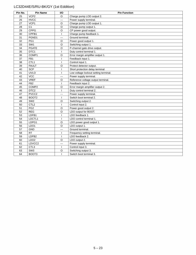
LC32D44E/S/RU-BK/GY (1st Eddition)
25 VCP2 O Charge pump LOD output 2.26 HVCC --- Power supply terminal.27 VCP1 O Charge pump LOD output 1.28 C1 O Charge pump output 1.29 CPPG O CP power good output.30 CPFB1 I Charge pump feedback 1.31 PGND1 --- Ground terminal.32 PG1 O Power good output 1.33 SW1 O Switching output 1.34 PGATE O P-channel gate drive output.35 DTC1 I Duty control terminal 1.36 COMP1 O Error margin amplifier output 1.37 FB1 I Feedback input 1.38 CTL1 I Control input 1.39 FAULT O Protect detector output.40 SCP I Short protection delay terminal41 UVLO I Low voltage lockout setting terminal.42 VCC --- Power supply terminal.43 VREF O Reference voltage output terminal.44 FB2 I Feedback input 2.45 COMP2 O Error margin amplifier output 2.46 DTC2 I Duty control terminal 2.47 PVCC2 --- Power supply terminal.48 BOOT2 I Switch boot terminal 2.49 SW2 O Switching output 2.50 CTL2 I Control input 2.51 PG2 O Power good output 2.52 REG O LDO output for BOOT.53 LDFB1 I LDO feedback 1.54 LDCTL1 I LDO control terminal 1.55 LDPG1 O LDO power good output 1.56 LDO1 O LDO output 1.57 GND --- Ground terminal.58 RT I Frequency setting terminal.59 LDFB2 I LDO feedback 2.60 LDO2 O LDO output 2.61 LDVCC2 --- Power supply terminal.62 CTL3 I Control input 3.63 SW3 O Switching output 3.64 BOOT3 I Switch boot terminal 3.
Pin No. Pin Name I/O Pin Function
5 – 23

LC32D44E/S/RU-BK/GY (1st Eddition)
1918161514 17
6 – 1
LC32D44E-BK Service ManualCHAPTER 6. BLOCK DIAGRAM/OVERALL WIRING
[1] BLOCK DIAGRAM
1 2 3 1097654 8
J
A
B
C
D
E
F
G
H
I
1311 12
BLOCK DIAGRAM (1/2)

LC32D44E/S/RU-BK/GY (1st Eddition)
1918161514 17
6 – 2
1 2 3 1097654 8
J
A
B
C
D
E
F
G
H
I
1311 12
BLOCK DIAGRAM (2/2)

LC32D44E/S/RU-BK/GY (1st Eddition)
1918161514 17
6 – 3
[2] SYSTEM BLOCK DIAGRAM
1 2 3 1097654 8
J
A
B
C
D
E
F
G
H
I
1311 12
SYSTEM BLOCK DIAGRAM

LC32D44E/S/RU-BK/GY (1st Eddition)
1918161514 17
6 – 4
[3] OVERALL WIRING DIAGRAM
1 2 3 1097654 8
J
A
B
C
D
E
F
G
H
I
1311 12
OVERALL WIRING DIAGRAM
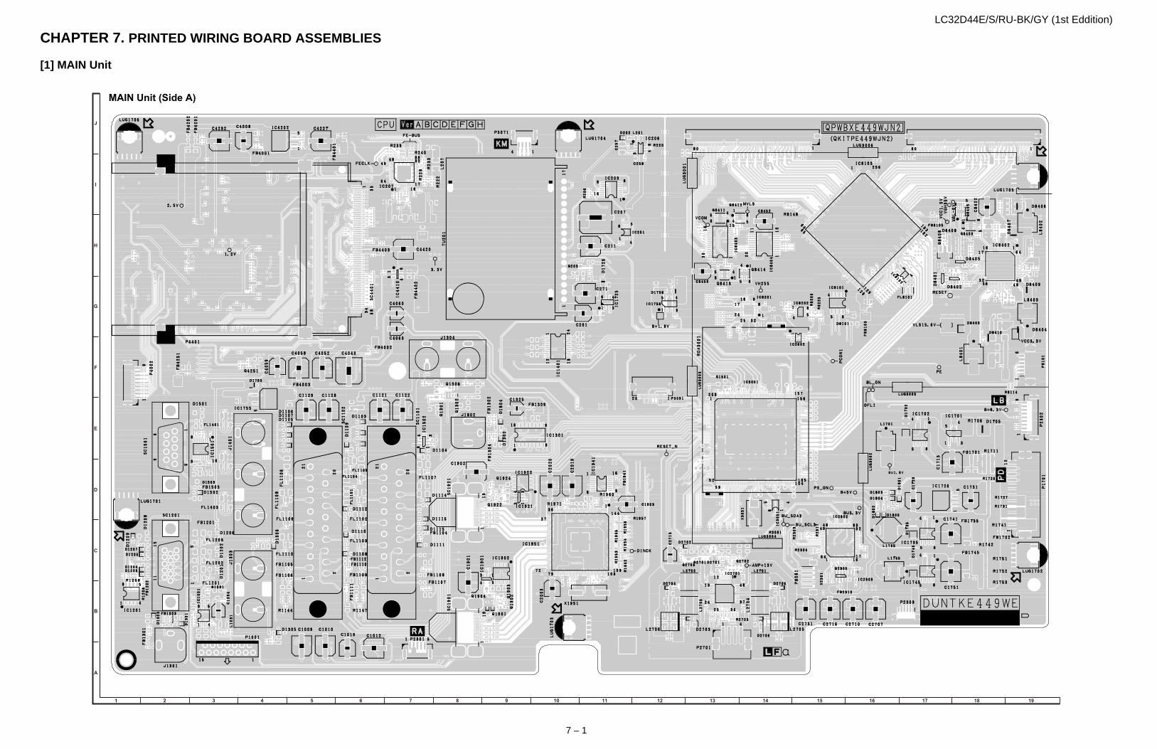
LC32D44E/S/RU-BK/GY (1st Eddition)
1918161514 17
7 – 1
LC32D44E-BK Service ManualCHAPTER 7. PRINTED WIRING BOARD ASSEMBLIES
[1] MAIN Unit
1 2 3 1097654 8
J
A
B
C
D
E
F
G
H
I
1311 12
MAIN Unit (Side A)

LC32D44E/S/RU-BK/GY (1st Eddition)
1918161514 17
C8456
R8430
C8458
Q1501
R8432
R8433
R8434
P3081
R8435
R8436
R8437
R8438
C8461
R8439
C8462
C8463
C8464
C1705
R8440
C8468
R8441
R8442R8443
R8444
R8445
C8470
R8448
R8449
C8471
C8473
C1715
C1717
R8450
R8451
C1719
R8454
IC3051
R8455
R8456
C8480
C1720
R8459
R1507
R1508
D1702
R8460
D1705
C1729
P2302
R8463
P2303
R8464
R1706
R8467
R8469
IC1701
C1731
IC1702
R8470
R8471
R1711
R3076
R1712
R8472
R8473
C1741
P2701
C1742
C1743
C1744
R3081
C2302
R8482
R8484
C2304
C2305
R1726
R8486
C2307
R1727
C2308
C1751
Q2305
C1752
C1753
C1754
IC1726
R1731
D1735
C2313 C2315
R8498
C2318
C2319
C2701
R8499
C2702
C2703
C2704
IC1735
C2705
Q2702
C2706
C2707
C2320
C2708
R1741
C2709
P8101
C2321
D1745
R1742
C2710
C2711
C2712
R2303
C2714
R2304
C2715
IC1745
C2716
C2718
R1751
IC2302
R1752
IC2303
R1753
C2720
C2721
R2312
C2724
C2726
R2317
C2728
D2705
C8101
C2729
D2706
C8102
R2706
R2708
IC2701
C2731
R2709
C2732
R2324
C2735
C2736
R2327
R2710
C2738
R2711
2716
R2718
C2740
R2719
L2601
L2602
R2336R2337
L2603
L2604
R2720
L2605
R2721
R2722
L2606
R2723
D8101
R2728
R2729
R8104
R8106
R8108
R2730
IC8101
R2732
C8132
IC8102
IC8103
C8135
C8136
LUG3002
LUG3004
R8110
LUG3005
LUG3006
R8112
R8114
R8115
R8116
R8501
SC8201
R8502
C8142
SC8202
R8504
R8505
R8507
R8508
R8121
R8122
R8124R8126
R8128
R8130
R8131R8132
R8133R8134
L8401
R8135
L8402
R8136R8137
L8403
X3051
R8142
R8143
R8145
R8146
R8147
R8148
R8149
C1802
Q1801
FL8101
FB1701
FB1702
LUG1702
D1801
LUG1705
D1802
D1803
D1804
D1805
R1801R1802
R1803
L1701
X2301
FB1735
FB1745
C2610
FB2310
L1735
IC2602C8201
L1745
C8203C8204
C8205
C8206
R2612R2613
C8207
C8208
R2614
C8209
R2615
C8402
C8210
C8211
C8406
C8212
Q8403
C8213
C8407
C8408
Q8405
Q8408
C8219
C8410
C8411
L2701
C8412
FB8103
C8413
L2704
C8414
C8415
Q8411
L2705
FB8105
C8222
C8416
Q8412
Q8413
C8417
C8223
C8418
C8224
Q8414
C8225
C8419
C8226C8228C8229
R8202
R8203
C3024
R8204
C8421
R8205
R8206
C8422
R8207
C8423
C8424
R8208
R8209
IC8201
D8401
C8425
IC8202
D8402
C8427
D8403 D8404
C8429
D8405
R3005
D8406
D8407
R3007
D8408
R8210
R3008
IC3001
R8211
D8409
R8212
R8213
R8408
R8214
R8215
IC8402
R8216
IC8403
R8217
C8433
IC8404
D8410
R8218
R8219
C8436
C8438
R8410
C8439R8411
L8101L8102
L8103L8104L8105L8106
R8222
L8107L8108
R8224
C8440
R8225
L8109
C8441
P1701
C8443
R8227
R8229 C8445
C8446
L8110
C8448
R8420
C8449
L8111L8112
R8422
R8423
L8113
R8230
L8114
R8425
R8233
R8427
R8234
R8428
C3054
R8429
C3055
C8452
7 – 2
1 2 3 1097654 8
J
A
B
C
D
E
F
G
H
I
1311 12
MAIN Unit (Chip Side A)
C1118
C1501
C1119
C1502
C1503
C1504
C1310
R210
C1505
C1311
R211
C1506
C1312
R212
C1507
C1313
R213
C1120
C1314
C1508
R214
C1121
C1315
C4001
R215
C1122
C1316
C4002
R216
C1123
C1317
C4003
R217
C1124
C1318
C4004
R218
C1319
D1101
C1125
C4005
R219
C1126
D1102
C4006
D1103
C1127
C4007
C1128
D1104
C4008
C1129
D1105
R1101
FB1201
C4009
R1102
D1106
FB1202
D1107
R1103
FB1203
C1320
FB1204
D1108
R220
R221
C1321
D1109
VA1921
FB1205
C4201
VA1922
C4202
R222
C1322
R1107
C4203
VA1923
R223
C1323
R1108
C4204
C4010
VA1924
C1324
VA1925
C1131
R1109
C1901
C4011
C4205
D1301
C1325
C3071
R8251
P3091
C1132
VA1926
C1902
C4206
C4012
D1302
C1326
R226
C3072
R8252
C1133
C4207
C1327
VA1927
D1303
R227
C3073
R8253
D1110
C1134
C4014
C4208
C1328
VA1928
D1304
R228
R8254
C1135
D1305
D1111
C4015
Q1901
R1301
C1329
R229
R8255
D1306
C1136
D1112
C1906
Q1902
R1302
R8256
C1137
C4017
R1303
Q1903
D1114
Q1904
R1110
C1138
C4018
R1304
D1115
R1111
C4019
C1139
R1305
C4401
R1112
D1116
R1306
C4402
R1113
R1307
C4210
R1308
R230
D1501
C4211
IC1301
R1309
R231
D1502
R232
D1503
R1117
R233
R1118
C4020
C4214
C1140
R234
R1119
R1501
C1141
C4021
R1502
C1142
C4022
R236
R1503
R237
R1504
C4218
C4024
R1310
C1144
R238
R1505
C4219
R1311
C1145
R239
C1146
R1312
R1506
R1313
C1147
R1120
R1314
C1148
C4410
R1315
C1149
IC1501
R1121
C4029
R4001
C1725C201
R1122
IC1502
R1316
R4002
C1726
R1317
R1123
R4003
C1727
C203
R1124
R1318
R240
C1728
R1319
R1125
C4221
P2301
FB1031
C4415
C205
R1126
R4006
C4416
C206
R1127
R4007
C4223
C4417
C207
R1128
R4008
C4224
C4030
C4419
R1129
C4225
R4009
C4031
C4226
C1922
C4033
C4227
R1320
C4034
R1321
C4035
C4229
Q1921
C1155
R1322
C1156
C4036
Q1922
D1902
C4037
Q1923
D1903
R1323
R1130
C4038
Q1924
R1324
C4420
R1131
C4039
R1325
C4421
C211
R1132
R1326
C212
R1133
R1327
C213
C4230
R1134
R1328
R1329
C4231
R1905R1135
C215
R1136
C4232 IC4202
R1906
C216
R1137
R4017
C4233
C217
R1138
C4040
R4018
C1161
IC1901
R1139
C4041
C219
C1162
IC1902
C1163
C4043
R1330
R4405
R1140
C4049
R4021
R1141
R1142
R1143
C223
R4218
R1144
R1145
D1725
R1146
R4027
R1147
C227
R1148
C228
R1149
C229
C1941
C4052
C4053
R8487
L1031
R8489
R4417
R4030
C4058
IC4410C4059
C1755
IC1725
R1922
C232
C1756
R1923
C233
R4034
R1924
C234
C1758
R4035
C4251
R1925
C235
R4036
C4252
C236
R4037
C4253
C4060
C4254
R4038
C238
Q4251
R4039
C4255
IC1921
C4062
IC1922
C4257
C4063
R4423
C1953
C4064
C4258
R4424
C1760
C1761
R4426
C1762
C1763
R4040
C240
C1764
R4041
R4235
C1765
Q2701
C243
Q2703
C245
R4046
C246
R4047
C247
R4430
FL1101
R4431
C249
FL1102
R4432
FL1103
FL1104
R4240
FL1105
R4435
R4241
FL1106
R4242
R4436
FL1107
R4243
R4437
C2713
FL1108
R4244
R4438
R4245
FL1109
R4246
C252
C253
C2717
C254
C2719
D1755
D1756
C256
C257
FL1110
C258
R4441
IC1941
C1971
R1756
C1972
C1973
R1757
R1758
C1974
R4445
C2722
R4447
C2723
C1977
C2725
IC1755
R1951
D2701
D2702
R1952
IC1756
D202
C2727
D2703R1953
R1954
D2704
R1955
R1956
R1957
IC1951
R1959
R2707
C2730
R4262
R4263
C2733
R4264
R1960
C2734
R4265
C271
R4266
R1962
R4267
R1963
C2737
R1964
R4268
R1965
C2739
R2712
R1966
R1967
R2713
R2714
R1968
R2715
R1969
R
C1993
R2717
C1995
C2741
R4272
R1970
R1971
IC201
R1973
IC203
IC206
IC207
R2731
LUG3001
LUG3003
C1005
C1006
C1007
C1008
C1009
C1201
C1202
C1203C1204
C1010
C1011
C1012
J1301
J1302
C1017
C1018
C1019
C1403
C1405
C1407
C1409
C1410
FB1101
C1411
FB1102
FB1103
C1413
FB1104
C1414
FB1105
C1415
FB1106
R1006
C1416
FB1107
C1417
FB1108
D1201
FB1109
IC1001
C1031
D1202
C1032
D1203
C1033
D1204
C1034
D1205
R1201
FB1301
Q1031
C1035
D1206
R1202
FB1302
R1203
D1207
FB1303
D1208
R1204FB1110
FB1304
R1010
FB1305
FB1111
R1205
D1209
R1011
FB1306
FB1112
R1206
R1207
R1208R1209
IC1201
FB1309
R1017
FB1501
R1402
FB1502
FB1503
R1403
R1210
R1404
FB4001
IC1401
FB4002
FB4003
L1101
LUG1701
LUG1703
LUG1704
FB4201
LUG1706
FB4202
R1031
R1032
R1033
R1034
R1035
R1036
FB4401
FB4402
C2003
FB4403
SC1901
SC4401
C2019
C2020
X1951
SC1921
FB1941
FL1201
FL1202
FL1203
FB4251
FL1401
FL1402
FL1403
Q203
C8202
L201
L207
C8214
C8215
C8216
C8217
C8218
L2702
L2703
L2706
C3036
R8221
P4002
C1103
R8223
C1104
C1105
C1106
R8226
C1107
C1108
R8228
C1109
C8447
VA1901
C1301
C1302
VA1902
C1303
VA1903
C1110
C1304
VA1904
R204
C1111
Q1301
VA1905
C1305
P3071
C1112
C1306
VA1906
Q1302
R206
C1113
C1307
VA1907
Q1303
C1308
VA1908
C1115
C1309
C1116
C1117
C8453

LC32D44E/S/RU-BK/GY (1st Eddition)
1918161514 17
7 – 3
1 2 3 1097654 8
J
A
B
C
D
E
F
G
H
I
1311 12
MAIN Unit (Side B)

LC32D44E/S/RU-BK/GY (1st Eddition)
1918161514 17
Q4001Q4002
Q4003Q4004
C1130
IC1101
IC1102
C4013
C4016
D1113
D1117
C4403
C4404
D1118
C4405
D1119
C4406
C4407
Q4403
C4408
C4409
C1143
C4023
D1120
C4025
D1121
C4026
C4027
C4028
C4411
C4412
C4413
R4004
C4414
R4005
C4418
C1150
D4201
IC4001
C1151
IC4002
C4032
C1152
IC4003
C1153
C4228
IC4004
C1154
IC4005
R4201 R4202R4203
C1157
R4010
R4204
C1158
R4205
R4011
C1159
X201
R4012
R4206R4207
R4013
R4014
R4208
C214
IC4201
R4209
R4015
R4016
C4234
C1160
C218
C4235
R4401 R4019
C4042
R4402
C4236
C4237
R4403
R4404
R4210
C4044C4045
R4211
R4212
C4046
R4406
R4407
C4047
R4213
C4048
R4214
R4020
R4408
C220
R4409
R4215
IC4401
C221
IC4402
R4216
R4022
C222
IC4403
R4023
R4217
R4024
IC4404
C224
IC4405
R4025
R4219
C2301
C225
IC4406
R4026
C226
IC4407
C2303
R4028
C4050
IC4408R4410
R4029
C4051
IC4409
R4411R4412
R4413
R4220
C4054
R4414
C4055
R4415R4416
C4056
C4057
R4418
R1150
C230
R4031
R1151
R4419
C231
R4032
R1152
R4033
R1153
C1757
R1154
C2311
R1155
C1759
C2312
R1156R1157
C237
R4420
R4421
C4061
C239
C4256
R4422
R4231
R4425
R4427R4428
R4429
C241
R4042
C242
R4043
R4044
C244
R4045
R4048
C248
D2301
R4049
R4433R4434
C250C251
C255
R1755
R4443
R4251 R4252R4446
R4253
R4448
R4254 R4255
R4256 R4257 R4258
IC4251
R4259
IC4252
IC4253
R4452
R4453
R4260
R4454
R4261
R4455
R4458
R4459
R4269
IC202
IC204
IC205
Q1001C1013
C1014
C1015
C1016
X4001
IC1002
R1012
R1013
R1014
R1015
R1016
R1018
R1019
R1020R1021
R1022
R1023
FB4004
FB2301
FB2302
FB2304
FB2305
L203
L204
L205
L206
R4561
FB202
C1101
P4001
C1102
Q1101Q1102
Q1105Q1106
Q1107Q1108
C1114
7 – 4
1 2 3 1097654 8
J
A
B
C
D
E
F
G
H
I
1311 12
MAIN Unit (Chip Side B)
R8238
C3058
C8454
Q8450
C3059
C8455
R8239
C8457
C8459
R8431
C3060
R8240
R8241
L263
C8460
C1701
C1702
C1703
C1704
C8465
C1706
C8466
C8467
C1707
C1708
C1709
C8469
R224
R225
R8446
C1903
R8447
C1904
C1710
C3074
C1905
C1711
FB1401
C3075
C8472
C3076
C1712
FB1402
C1713
R8257
C1907
R8258
C1714
C1908
Q1905
R8259
Q1906
C1716
C8476
C8477
C1330
C1718
R3054
C8478
C8479
C1331
R3056
R8452
C1332
R8453
C1333
R8260
R235
R8261
C3081C3082
R8262
IC3052
R8457
R8458
C1721
C1722
D1701
C202
D1703
C204
D1704
FB1801
R1701
R8461
R8462
R1702
R1703
R1704
C208
C1921
C209
R1705
R8466
R1707R1708
R8468
C1730
D1901
D3071
R1709
D3072
C1732
D3073
IC1703
C1733
D1904
C210
D1905
R1901
Q1925
C1735
R3071
D1906
R1902
R3072
C1736
D1907
R1903
C1737
R3073
D1908
R1904
R3074
C1738
R1710
D1909
R3075
C1739
R1907
R1713
R1714
R1909
R1715
R8475
R1716
R8476
R8477
R1717
D1910
R8478
C1740
R1718
R1719
D1911
R1331
R8479
R1332
R1911
C1745
R1912
C1746
C1747
R1914
C1748
R8480
R1915
C1749
R8481
R262
D1726
R8483
R1725
R8485
R266
R1728
C1750
D1921
R1729
D1922
D1923
D1924
R1921
D1925
R3091
R3092
R1730
R8491
R1926
R8492
D1736
R8493
R1928
C2314
R8494
R1735
R8495
C1951
C1952
R1736
R8496
C2316C2317
R8497
R1737
C1954
R1738
C1955
R1739
C1956
C1957
R1930
C1958
C1959
R1932R1933
R1740
C2322
R283
R1743
C2323
C1960
C1961
R1745R1746
C1962
C1963
R1747
R1748
C1964
R1749
C1965
R2302
C1966C1967C1968
C1969
R2305
R2306
R2307
R1750
IC2301
R1754
C1970C1975
C1976
R2313
R2314
C1978C1979
D201
TH2301
TH2302
C8103
C1980
R1958
C8104
C269
C8105
C1981C1982
C8106
C1983
C8107
C1984
C8108
R2320
R2321
C1985
C8109
C1986C1987C1988
R1961
R2325
C1989
R2326
C8110
R2328
R2329
C8111
C8112
C8113
C1990
C8114
C8115
C1991
C1992
C8116
C8117
C1994
C8118
C8119
C1996C1997
C1998C1999
R2335
C8120
C8121
C8122
C8123
C8124
C8125C8126C8127
C8128
C8129
R8101
R8102
R8107
C8130
FB3001
C8131
R8109
FB3002
C8133
FB3003
C8134
FB3004
FB3005
FB3006
C8137C8138
C8139
R8111R8113
R8117
C8140
R8500
R8118
C8141
C8143
C8144
R8506
R8123
R8125R8127
FB3021
R8129
FB3022
C1401
C1402C1404
FB3035
FB3036
C1406
FB3037
C1408
FB3038
R8140R8141
C1412
C1801
IC261
Q1802
FB3051
FB3052
FB3053
FB3054
D1401
FB3055
D1402
FB3056
D1403
R1401
R1405
R1409
FB1703
R1410
R1411
FB1901
FB3071
FB1902
FB3072
FB3073
C2000C2001
C2002C2004
C2005
Q1831
C2006C2007C2008C2009C2010C2011C2012C2013C2014C2015C2016
C2017C2018
C2601C2602
FB2309
FB1951
FB1952
FB1953
FB1954
R2601
FB1955
Q201
FB1956
Q202
R2603
FB1957
Q204
IC2601
C3001C3002
C3003
C3004
C3005
C8401
C3006
C3007
C8403
C8404
C3008
C3009
C8405
Q8401
Q8402
Q8404
C8409
C3010C3011
C3012
C3013
C3014
C3015
FB8101
C3016
FB8102
C3017
C8220
FB8104
Q8410
C3018
C3019
C8221
FB8106
C8227
C3020
C3021
C3022
C3023
C8420
C3025
C3026
C3027
C8230
C3028
C8231
C3029
R3001
C8426
R3002
R3003
R3004
C8428
R8401
R8402
R8403
R8404
C3030
R8405
C3031
C3032
IC3002
R8406
C3033
R8407
C3034
C8430
R8409
IC8401
C3035
C8431
C8432
C3037
C8434
C3038
D8411
C3039
C8435
C8437
FB201R8412
R8413
R8414
R8220
C3040
R8415
C3041
C3042
R8416
C3043
R8417
R8418
C3044
C3045
R8419
C8442
C3046
C3047
C8444
R201
R8421
R202
Q262
R203
R8231
C3051
R205
C3052
R8232
C3053
R207R208
C8450C8451
Q3051
R8235
R209
R8236
Q3052
C3056
C3057

LC32D44E/S/RU-BK/GY (1st Eddition)
1918161514 17
R/C, LED Unit (Chip Side B)
P101
7 – 5
[2] R/C, LED Unit
1 2 3 1097654 8
J
A
B
C
D
E
F
G
H
I
1311 12
R/C, LED Unit (Side A) R/C, LED Unit (Side B)R/C, LED Unit (Chip Side A)
R101
R108R109
C102
RMC101
C107
D101
D103
SLD101

LC32D44E/S/RU-BK/GY (1st Eddition)
1918161514 17
7 – 6
[3] MINI AV Unit
1 2 3 1097654 8
J
A
B
C
D
E
F
G
H
I
1311 12
MINI AV Unit (Side A)

LC32D44E/S/RU-BK/GY (1st Eddition)
1918161514 17
7 – 7
[4] KEY
1 2 3 1097654 8
J
A
B
C
D
E
F
G
H
I
1311 12
S155
R153
D152
S154
S152
R151
D151
S151
R152
S153
R154
S156
S157
D155
P151
KEY Unit (Side A) KEY Unit (Chip Parts Side A)

LC32D44E/S/RU-BK/GY (1st Eddition)
8 – 1
LC32D44E-BK Service ManualCHAPTER 8. SCHEMATIC DIAGRAM
[1] DESCRIPTION OF SCHEMATIC DIAGRAM
1. VOLTAGE MEASUREMENT CONDITION:1) The voltages at test points are measured on exclusive AC adaptor and the stable supply voltage of AC 120V. Signals are fed by a color bar signal genera-
tor for servicing purpose and the above voltages are measured with a 20k ohm/V tester.
2. INDICATION OF RESISTOR & CAPACITOR:RESISTOR
1) The unit of resistance "Ω" is omitted.
(K=kΩ=1000Ω, M=MΩ).
2) All resistors are ± 5%, unless otherwise noted.
(K= ± 10%, F= ± 1%, D= ± 0.5%)
3) All resistors are 1/16W, unless otherwise noted.
CAPACITOR
1) All capacitors are µF, unless otherwise noted.
(P=pF=µµF).
2) All capacitors are 50V, unless otherwise noted.
CAUTION:This circuit diagram is original one, therefore there may be a slight difference from yours.
SAFETY NOTES:1) DISCONNECT THE AC PLUG FROM THE AC OUTLET
BEFORE REPLACING PARTS.2) SEMICONDUCTOR HEAT SINKS SHOULD BE REGARDED AS
POTENTIAL SHOCK HAZARDS WHEN THE CHASSIS IS OPERATING.
IMPORTANT SAFETY NOTICE:PARTS MARKED WITH " " ( ) ARE IMPORTANT FOR MAINTAINING THE SAFETY OF THE SET. BE SURE TO REPLACE THESE PARTS WITH SPECIFIED ONES FOR MAIN-TAINING THE SAFETY AND PERFORMANCE OF THE SET.
AVIS DE SECURITE IMPORTANT:LES PIECES MARQUEES " " ( ) SONT IMPOR-TANTES POUR MAINTENIR LA SECURITE DE L'APPAREIL.NE REMPLACER CES PIEDES QUE PAR DES PIECES DONT LE NUMERO EST SPECIFIE POUR MAINTENIR LA SECURITE ET PROTEGER LE BON FONCTIONNEMENT DE L'APPAREIL.

LC32D44E/S/RU-BK/GY (1st Eddition)
1918161514 17
AND SHADED COMPONENTS=SAFETY RELATED PARTS
8 – 2
[2] SCHEMATIC DIAGRAM
1 2 3 1097654 8
J
A
B
C
D
E
F
G
H
I
1311 12
MAIN Unit (1/13)

LC32D44E/S/RU-BK/GY (1st Eddition)
1918161514 17
8 – 3
1 2 3 1097654 8
J
A
B
C
D
E
F
G
H
I
1311 12
MAIN Unit (2/13)

LC32D44E/S/RU-BK/GY (1st Eddition)
1918161514 17
8 – 4
1 2 3 1097654 8
J
A
B
C
D
E
F
G
H
I
1311 12
MAIN Unit (3/13)

LC32D44E/S/RU-BK/GY (1st Eddition)
1918161514 17
8 – 5
1 2 3 1097654 8
J
A
B
C
D
E
F
G
H
I
1311 12
MAIN Unit (4/13)

LC32D44E/S/RU-BK/GY (1st Eddition)
1918161514 17
8 – 6
1 2 3 1097654 8
J
A
B
C
D
E
F
G
H
I
1311 12
MAIN Unit (5/13)

LC32D44E/S/RU-BK/GY (1st Eddition)
1918161514 17
8 – 7
1 2 3 1097654 8
J
A
B
C
D
E
F
G
H
I
1311 12
MAIN Unit (6/13)

LC32D44E/S/RU-BK/GY (1st Eddition)
1918161514 17
8 – 8
1 2 3 1097654 8
J
A
B
C
D
E
F
G
H
I
1311 12
MAIN Unit (7/13)

LC32D44E/S/RU-BK/GY (1st Eddition)
1918161514 17
8 – 9
1 2 3 1097654 8
J
A
B
C
D
E
F
G
H
I
1311 12
MAIN Unit (8/13)

LC32D44E/S/RU-BK/GY (1st Eddition)
1918161514 17
8 – 10
1 2 3 1097654 8
J
A
B
C
D
E
F
G
H
I
1311 12
MAIN Unit (9/13)

LC32D44E/S/RU-BK/GY (1st Eddition)
1918161514 17
8 – 11
1 2 3 1097654 8
J
A
B
C
D
E
F
G
H
I
1311 12
MAIN Unit (10/13)

LC32D44E/S/RU-BK/GY (1st Eddition)
1918161514 17
8 – 12
1 2 3 1097654 8
J
A
B
C
D
E
F
G
H
I
1311 12
MAIN Unit (11/13)

LC32D44E/S/RU-BK/GY (1st Eddition)
1918161514 17
8 – 13
1 2 3 1097654 8
J
A
B
C
D
E
F
G
H
I
1311 12
MAIN Unit (12/13)

LC32D44E/S/RU-BK/GY (1st Eddition)
1918161514 17
8 – 14
1 2 3 1097654 8
J
A
B
C
D
E
F
G
H
I
1311 12
MAIN Unit (13/13)
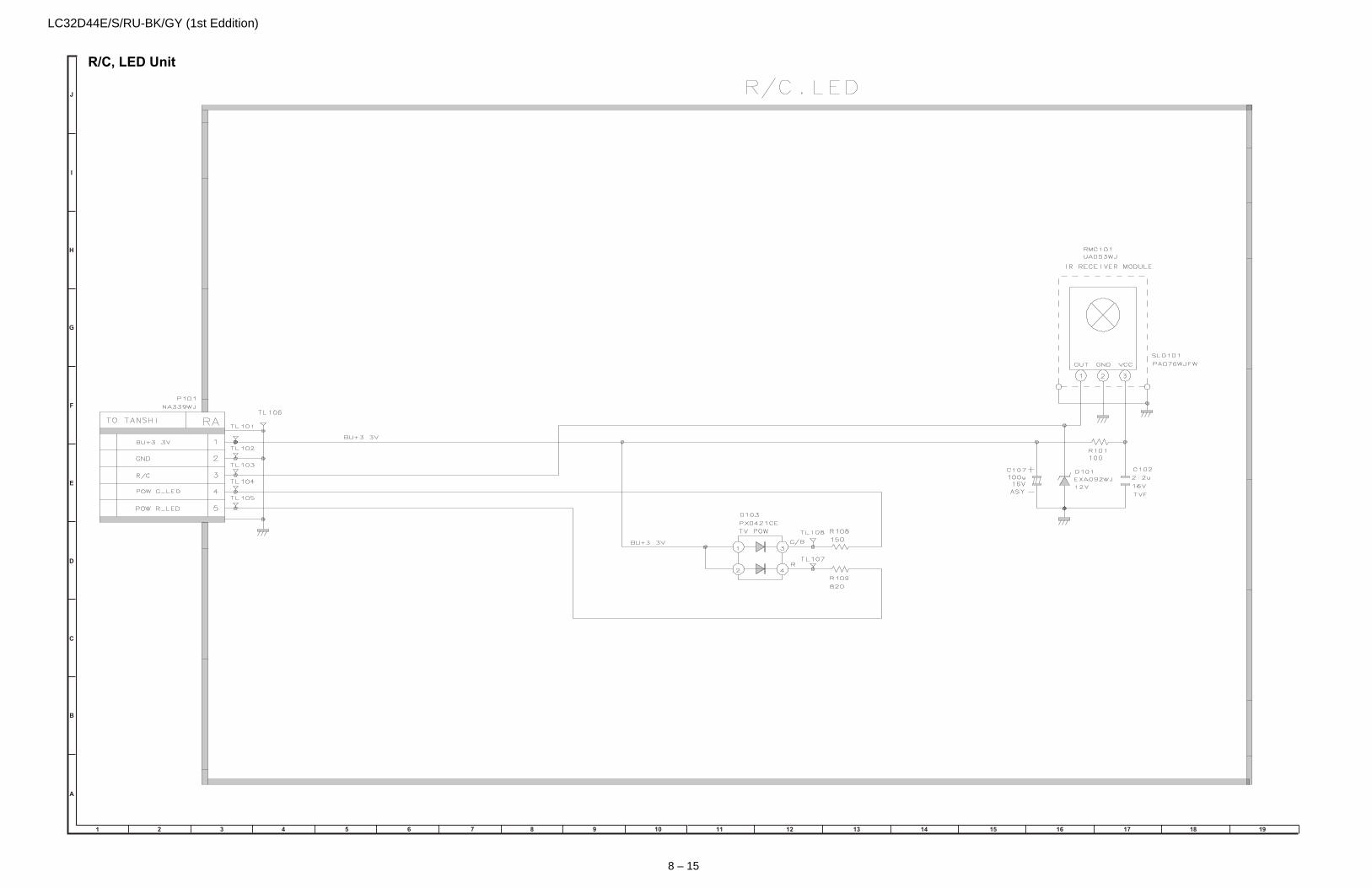
LC32D44E/S/RU-BK/GY (1st Eddition)
1918161514 17
8 – 15
1 2 3 1097654 8
J
A
B
C
D
E
F
G
H
I
1311 12
R/C, LED Unit

LC32D44E/S/RU-BK/GY (1st Eddition)
1918161514 17
8 – 16
1 2 3 1097654 8
J
A
B
C
D
E
F
G
H
I
1311 12
MINI AV Unit
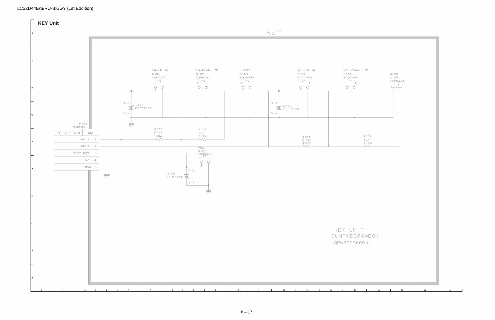
LC32D44E/S/RU-BK/GY (1st Eddition)
1918161514 17
8 – 17
1 2 3 1097654 8
J
A
B
C
D
E
F
G
H
I
1311 12
KEY Unit

& 2 9/)1 & 2 9/)1

& 2 9/)1 & 2 9/)1

& 2 9/)1 & 2 9/)1
low
low
pow
erpo
wer
full
full
pow
erpo
wer
burs
tbu
rst m
ode
mod
e

& 2 1 & 2 1
PS_ONPS_ON
3.2 V3.2 V

/)1 /)1
LampLamp ErrErr: OK= 3,2V: OK= 3,2V
ERR= 0VERR= 0V

/)1 /)1
OFL OFL fromfrom MainMain
moremore
brightness
brightness

LC32D44E/S/RU-BK/GY (1st Eddition)
PartsGuidePARTS GUIDE
CONTENTS
No. S38F8LC32D44E
LCD COLOUR TELEVISION
MODELS LC-32D44E/S/RU-BK/GY
[1] PRINTED WIRING BOARD ASSEMBLIES
[2] LCD PANEL (NOTE: THE PARTS HERE SHOWN ARE SUPPLIED AS AN ASSEMBLY BUT NOT INDEPENDENTLY.)
[3] DUNTKE266FM01(KEY Unit)
[4] DUNTKE449FM02 (MAIN Unit)
[5] DUNTKE457FM02 (R/C, LED Unit)
[6] DUNTKE491FM01(MINI-AV Unit)
[7] CABINET PARTS
[8] LCD MODULE ASSEMBLY
[9] SUPPLIED ACCESSORIES
[10] PACKING PARTS
[11] SERVICE JIGS
Parts marked with " " are important for maintaining the safety of the set. Be sure to replace theseparts with specified ones for maintaining the safety and performance of the set.
This document has been published to be usedfor after sales service only.The contents are subject to change without notice.

LC32D44E/S/RU-BK/GY (1st Eddition)PRICE NEW PART
NO. PARTS CODE RANK MARK DELIVERY DESCRIPTION[1] PRINTED WIRING BOARD ASSEMBLIESN DUNTKE266FM01 AR N R KEY UnitN DUNTKE449FM02 CP N R MAIN UnitN DUNTKE457FM02 AQ N R LED UnitN DUNTKE491FM01 AY N R MINI-AV UnitN RUNTKA396WJQZ BV N P POWER/INVERTER Unit
[2] LCD PANEL (NOTE: THE PARTS HERE SHOWN ARE SUPPLIED AS AN ASSEMBLY BUT NOT INDEPEN-DENTLY.)
N R1LK315T3GW30Y N J 32" LCD Panel Module
[3] DUNTKE266FM01(KEY Unit)D151 RH-EX0646GEZZY AA J Zener Diode MTZJT-7215BD152 RH-EX0646GEZZY AA J Zener Diode MTZJT-7215BD155 RH-EX0646GEZZY AA J Zener Diode MTZJT-7215BP151 QPLGNA059WJZZ AC J Plug 5Pin(KM)R151 VRD-RA2BE822JY AA J Resistor 8.2k 1/8W CarbonR152 VRD-RA2BE123JY AA J Resistor 12k 1/8W CarbonR153 VRD-RA2BE822JY AA J Resistor 8.2k 1/8W CarbonR154 VRD-RA2BE123JY AA J Resistor 12k 1/8W CarbonS151 QSW-K0003AJZZ+ AB J Switch CH UPS152 QSW-K0003AJZZ+ AB J Switch CH DOWNS153 QSW-K0003AJZZ+ AB J Switch CH INPUTS154 QSW-K0003AJZZ+ AB J Switch VOL UPS155 QSW-K0003AJZZ+ AB J Switch VOL DOWNS156 QSW-K0003AJZZ+ AB J Switch CH MENUS157 QSW-K0003AJZZ+ AB J Switch CH POWER
[4] DUNTKE449FM02 (MAIN Unit)C201 VCEASX1AN336MY AC J Capacitor 33 10V ElectrolyticC207 VCEASX1CN477MY AE J Capacitor 470 16V ElectrolyticC209 VCKYCZ1EB103KY AA J Capacitor 0.01 25V CeramicC210 VCKYCZ1EB103KY AA J Capacitor 0.01 25V CeramicC213 VCKYCZ1EB103KY AA J Capacitor 0.01 25V CeramicC214 VCKYCZ1EB103KY AA J Capacitor 0.01 25V CeramicC215 RC-KZA510WJPZY AB J Capacitor 10 16V CeramicC216 VCKYCY1HB104KY AA J Capacitor 0.1 50V CeramicC217 VCKYCY1HB104KY AA J Capacitor 0.1 50V CeramicC218 RC-KZA510WJPZY AB J Capacitor 10 16V CeramicC219 VCKYCZ1EF104ZY AA J Capacitor 0.1 25V CeramicC220 VCKYCZ1EF104ZY AA J Capacitor 0.1 25V CeramicC221 RC-KZA510WJPZY AB J Capacitor 10 16V CeramicC222 VCKYCZ1EF104ZY AA J Capacitor 0.1 25V CeramicC223 RC-KZA510WJPZY AB J Capacitor 10 16V CeramicC224 VCKYCZ1EF104ZY AA J Capacitor 0.1 25V CeramicC225 VCKYCZ1EB103KY AA J Capacitor 0.01 25V CeramicC226 VCKYCZ1EF104ZY AA J Capacitor 0.1 25V CeramicC227 RC-KZA510WJPZY AB J Capacitor 10 16V CeramicC228 VCKYCZ1EF104ZY AA J Capacitor 0.1 25V CeramicC229 VCKYCZ1EF104ZY AA J Capacitor 0.1 25V CeramicC230 VCKYCZ1HB102KY AB J Capacitor 1000p 50V CeramicC231 VCKYCZ1HB102KY AB J Capacitor 1000p 50V CeramicC232 RC-KZA510WJPZY AB J Capacitor 10 16V CeramicC233 VCKYCZ1EF104ZY AA J Capacitor 0.1 25V CeramicC234 RC-KZA510WJPZY AB J Capacitor 10 16V CeramicC235 VCKYCZ1EF104ZY AA J Capacitor 0.1 25V CeramicC236 VCKYCZ1EF104ZY AA J Capacitor 0.1 25V CeramicC237 VCKYCZ1EF104ZY AA J Capacitor 0.1 25V CeramicC238 RC-KZA510WJPZY AB J Capacitor 10 16V CeramicC239 VCKYCZ1HB102KY AB J Capacitor 1000p 50V CeramicC240 RC-KZA510WJPZY AB J Capacitor 10 16V CeramicC241 VCKYCZ1HB102KY AB J Capacitor 1000p 50V CeramicC242 VCKYCZ1EF104ZY AA J Capacitor 0.1 25V CeramicC243 VCKYCZ1EF104ZY AA J Capacitor 0.1 25V CeramicC244 VCKYCZ1HB102KY AB J Capacitor 1000p 50V CeramicC245 VCKYCZ1EF104ZY AA J Capacitor 0.1 25V CeramicC246 VCKYCZ1EF104ZY AA J Capacitor 0.1 25V CeramicC247 VCKYCZ1EF104ZY AA J Capacitor 0.1 25V CeramicC248 VCKYCZ1HB102KY AB J Capacitor 1000p 50V CeramicC249 VCKYCZ1HB102KY AB J Capacitor 1000p 50V CeramicC250 VCCCCZ1HH100DY AB J Capacitor 10p 50V CeramicC251 VCCCCZ1HH100DY AB J Capacitor 10p 50V CeramicC252 VCKYCZ1HB102KY AB J Capacitor 1000p 50V CeramicC253 VCKYCZ1EF104ZY AA J Capacitor 0.1 25V CeramicC254 VCKYCZ1EF104ZY AA J Capacitor 0.1 25V CeramicC255 VCKYCZ1EB103KY AA J Capacitor 0.01 25V CeramicC256 VCKYCY1HB104KY AA J Capacitor 0.1 50V CeramicC269 VCKYCZ1EF104ZY AA J Capacitor 0.1 25V CeramicC271 VCEASX1CN107MY AC J Capacitor 100 16V Electrolytic
C1005 VCKYCZ1EB103KY AA J Capacitor 0.01 25V CeramicC1006 VCKYCY1HB104KY AA J Capacitor 0.1 50V CeramicC1007 VCKYCZ1EF104ZY AA J Capacitor 0.1 25V CeramicC1008 RC-KZA510WJPZY AB J Capacitor 10 16V CeramicC1009 VCEASX1VN226MY AC J Capacitor 22 35V ElectrolyticC1010 VCEASX1VN226MY AC J Capacitor 22 35V Electrolytic
2

LC32D44E/S/RU-BK/GY (1st Eddition)PRICE NEW PART
NO. PARTS CODE RANK MARK DELIVERY DESCRIPTIONC1011 RC-KZA510WJPZY AB J Capacitor 10 16V CeramicC1012 VCEASY1CN476MY AC J Capacitor 47 16V ElectrolyticC1013 VCCCCZ1HH470JY AB J Capacitor 47p 50V CeramicC1014 VCCCCZ1HH470JY AB J Capacitor 47p 50V CeramicC1015 VCCCCZ1HH330JY AB J Capacitor 33p 50V CeramicC1016 VCCCCZ1HH330JY AB J Capacitor 33p 50V CeramicC1017 VCKYCY1HB104KY AA J Capacitor 0.1 50V CeramicC1018 RC-KZA510WJPZY AB J Capacitor 10 16V CeramicC1019 VCEASX1CN226MY AC J Capacitor 22 16V ElectrolyticC1031 VCCCCZ1HH470JY AB J Capacitor 47p 50V CeramicC1032 VCCCCZ1HH100DY AB J Capacitor 10p 50V CeramicC1033 VCCCCZ1HH470JY AB J Capacitor 47p 50V CeramicC1034 VCEASX1CN106MY AC J Capacitor 10 16V ElectrolyticC1035 RC-KZA510WJPZY AB J Capacitor 10 16V CeramicC1101 RC-KZA510WJPZY AB J Capacitor 10 16V CeramicC1102 VCKYCZ1EF104ZY AA J Capacitor 0.1 25V CeramicC1103 VCKYCY1CB104KY AB J Capacitor 0.1 16V CeramicC1104 VCKYCY1CB104KY AB J Capacitor 0.1 16V CeramicC1105 VCKYCY1CB104KY AB J Capacitor 0.1 16V CeramicC1109 VCCCCZ1HH101JY AB J Capacitor 100p 50V CeramicC1110 VCCCCZ1HH101JY AB J Capacitor 100p 50V CeramicC1111 VCKYCY1CB104KY AB J Capacitor 0.1 16V CeramicC1112 VCKYCY1CB104KY AB J Capacitor 0.1 16V CeramicC1113 VCKYCY1CB104KY AB J Capacitor 0.1 16V CeramicC1114 VCKYCZ1EB103KY AA J Capacitor 0.01 25V CeramicC1115 RC-KZA510WJPZY AB J Capacitor 10 16V CeramicC1120 RC-KZA510WJPZY AB J Capacitor 10 16V CeramicC1121 VCEASY1CN227MY AC J Capacitor 220 16V ElectrolyticC1122 VCEASY1CN227MY AC J Capacitor 220 16V ElectrolyticC1127 VCKYCZ1HB221KY AA J Capacitor 220p 50V CeramicC1128 VCEASY1CN227MY AC J Capacitor 220 16V ElectrolyticC1129 VCEASY1CN227MY AC J Capacitor 220 16V ElectrolyticC1130 VCKYCZ1EB103KY AA J Capacitor 0.01 25V CeramicC1131 VCKYCZ1HB331KY AA J Capacitor 330p 50V CeramicC1132 VCKYCZ1HB331KY AA J Capacitor 330p 50V CeramicC1133 VCCCCZ1HH101JY AB J Capacitor 100p 50V CeramicC1134 VCCCCZ1HH101JY AB J Capacitor 100p 50V CeramicC1135 VCKYCZ1HB331KY AA J Capacitor 330p 50V CeramicC1136 VCKYCZ1HB331KY AA J Capacitor 330p 50V CeramicC1137 VCKYCZ1HB102KY AB J Capacitor 1000p 50V CeramicC1138 VCKYCZ1HB102KY AB J Capacitor 1000p 50V CeramicC1139 VCKYCZ1HB471KY AB J Capacitor 470p 50V CeramicC1140 VCKYCZ1HB471KY AB J Capacitor 470p 50V CeramicC1141 VCCCCZ1HH101JY AB J Capacitor 100p 50V CeramicC1142 VCCCCZ1HH101JY AB J Capacitor 100p 50V CeramicC1143 VCKYTV1AB105KY AC J Capacitor 1 10V CeramicC1144 VCKYCZ1HB471KY AB J Capacitor 470p 50V CeramicC1145 VCKYCZ1HB471KY AB J Capacitor 470p 50V CeramicC1146 VCKYTV1AB105KY AC J Capacitor 1 10V CeramicC1147 VCKYTV1AB105KY AC J Capacitor 1 10V CeramicC1148 VCKYCZ1HB102KY AB J Capacitor 1000p 50V CeramicC1149 VCKYCZ1HB102KY AB J Capacitor 1000p 50V CeramicC1150 RC-KZA510WJPZY AB J Capacitor 10 16V CeramicC1151 RC-KZA510WJPZY AB J Capacitor 10 16V CeramicC1152 RC-KZA510WJPZY AB J Capacitor 10 16V CeramicC1153 RC-KZA510WJPZY AB J Capacitor 10 16V CeramicC1154 RC-KZA510WJPZY AB J Capacitor 10 16V CeramicC1155 VCKYTV1AB105KY AC J Capacitor 1 10V CeramicC1156 VCKYTV1AB105KY AC J Capacitor 1 10V CeramicC1157 RC-KZA510WJPZY AB J Capacitor 10 16V CeramicC1158 RC-KZA510WJPZY AB J Capacitor 10 16V CeramicC1159 RC-KZA510WJPZY AB J Capacitor 10 16V CeramicC1160 RC-KZA510WJPZY AB J Capacitor 10 16V CeramicC1161 VCCCCZ1HH101JY AB J Capacitor 100p 50V CeramicC1162 VCCCCZ1HH101JY AB J Capacitor 100p 50V CeramicC1201 VCKYCZ1AB104KY AB J Capacitor 0.1 10V CeramicC1202 VCKYCZ1AB104KY AB J Capacitor 0.1 10V CeramicC1203 VCKYCZ1AB104KY AB J Capacitor 0.1 10V CeramicC1204 VCKYCZ1EF104ZY AA J Capacitor 0.1 25V CeramicC1301 VCKYCZ1HB221KY AA J Capacitor 220p 50V CeramicC1302 VCKYCZ1HB221KY AA J Capacitor 220p 50V CeramicC1303 VCKYCZ1HB221KY AA J Capacitor 220p 50V CeramicC1304 VCKYCZ1HB221KY AA J Capacitor 220p 50V CeramicC1305 VCKYCZ1HB102KY AB J Capacitor 1000p 50V CeramicC1306 VCKYCZ1HB102KY AB J Capacitor 1000p 50V CeramicC1307 VCKYCZ1HB102KY AB J Capacitor 1000p 50V CeramicC1308 VCKYCZ1HB102KY AB J Capacitor 1000p 50V CeramicC1309 VCKYTV1AB105KY AC J Capacitor 1 10V CeramicC1310 VCKYTV1AB105KY AC J Capacitor 1 10V CeramicC1311 VCKYTV1AB105KY AC J Capacitor 1 10V CeramicC1312 VCKYTV1AB105KY AC J Capacitor 1 10V CeramicC1313 VCKYCZ1HB102KY AB J Capacitor 1000p 50V CeramicC1314 VCCCCZ1HH560JY AB J Capacitor 56p 50V CeramicC1315 VCKYTV1AB105KY AC J Capacitor 1 10V CeramicC1316 VCKYTV1AB105KY AC J Capacitor 1 10V Ceramic
[4] DUNTKE449FM02 (MAIN Unit)
3

LC32D44E/S/RU-BK/GY (1st Eddition)PRICE NEW PART
NO. PARTS CODE RANK MARK DELIVERY DESCRIPTIONC1317 VCCCCZ1HH560JY AB J Capacitor 56p 50V CeramicC1318 VCKYCZ1HB102KY AB J Capacitor 1000p 50V CeramicC1319 RC-KZA510WJPZY AB J Capacitor 10 16V CeramicC1320 RC-KZA510WJPZY AB J Capacitor 10 16V CeramicC1321 VCCCCZ1HH101JY AB J Capacitor 100p 50V CeramicC1322 RC-KZA510WJPZY AB J Capacitor 10 16V CeramicC1323 RC-KZA510WJPZY AB J Capacitor 10 16V CeramicC1324 VCCCCZ1HH101JY AB J Capacitor 100p 50V CeramicC1325 VCEASX1CN106MY AC J Capacitor 10 16V ElectrolyticC1326 VCKYCZ1EF104ZY AA J Capacitor 0.1 25V CeramicC1327 RC-KZA510WJPZY AB J Capacitor 10 16V CeramicC1328 VCCCCZ1HH101JY AB J Capacitor 100p 50V CeramicC1329 VCCCCZ1HH101JY AB J Capacitor 100p 50V CeramicC1330 VCKYTV1AB105KY AC J Capacitor 1 10V CeramicC1331 VCKYTV1AB105KY AC J Capacitor 1 10V CeramicC1332 VCKYTV1CB105KY AC J Capacitor 1 16V CeramicC1333 VCKYTV1CB105KY AC J Capacitor 1 16V CeramicC1401 RC-KZA510WJPZY AB J Capacitor 10 16V CeramicC1402 VCKYCZ1EF104ZY AA J Capacitor 0.1 25V CeramicC1404 VCKYTV1AB105KY AC J Capacitor 1 10V CeramicC1405 VCKYTV1AB105KY AC J Capacitor 1 10V CeramicC1406 VCKYCZ1EF104ZY AA J Capacitor 0.1 25V CeramicC1408 VCKYTV1AB105KY AC J Capacitor 1 10V CeramicC1409 VCKYTV1AB105KY AC J Capacitor 1 10V CeramicC1411 RC-KZA510WJPZY AB J Capacitor 10 16V CeramicC1412 VCKYTV1AB105KY AC J Capacitor 1 10V CeramicC1413 RC-KZA510WJPZY AB J Capacitor 10 16V CeramicC1414 VCKYTV1AB105KY AC J Capacitor 1 10V CeramicC1415 VCKYCY1CB104KY AB J Capacitor 0.1 16V CeramicC1416 VCKYCY1CB104KY AB J Capacitor 0.1 16V CeramicC1417 VCKYCY1CB104KY AB J Capacitor 0.1 16V CeramicC1501 RC-KZA510WJPZY AB J Capacitor 10 16V CeramicC1502 VCKYCZ1EF104ZY AA J Capacitor 0.1 25V CeramicC1503 VCKYCZ1EF104ZY AA J Capacitor 0.1 25V CeramicC1504 VCKYCZ1EF104ZY AA J Capacitor 0.1 25V CeramicC1505 VCKYCZ1EF104ZY AA J Capacitor 0.1 25V CeramicC1506 VCKYCZ1EF104ZY AA J Capacitor 0.1 25V CeramicC1507 VCKYCY1CB104KY AB J Capacitor 0.1 16V CeramicC1508 VCKYCZ1EF104ZY AA J Capacitor 0.1 25V CeramicC1701 RC-KZA510WJPZY AB J Capacitor 10 16V CeramicC1702 VCKYTV1AB105KY AC J Capacitor 1 10V CeramicC1703 VCKYCZ1EF104ZY AA J Capacitor 0.1 25V CeramicC1705 VCKYCZ1EB103KY AA J Capacitor 0.01 25V CeramicC1706 RC-KZA510WJPZY AB J Capacitor 10 16V CeramicC1707 RC-KZA510WJPZY AB J Capacitor 10 16V CeramicC1711 VCKYCZ1EB472KY AB J Capacitor 4700p 25V CeramicC1712 VCKYCZ1EB103KY AA J Capacitor 0.01 25V CeramicC1714 VCKYCZ1HB222KY AB J Capacitor 2200p 50V CeramicC1715 VCEASY1AN157MY AC J Capacitor 150 10V ElectrolyticC1718 VCKYCZ1EF104ZY AA J Capacitor 0.1 25V CeramicC1719 RC-KZA510WJPZY AB J Capacitor 10 16V CeramicC1720 VCKYTV1AB105KY AC J Capacitor 1 10V CeramicC1721 VCCCCZ1HH101JY AB J Capacitor 100p 50V CeramicC1722 VCCCCZ1HH101JY AB J Capacitor 100p 50V CeramicC1725 RC-KZA510WJPZY AB J Capacitor 10 16V CeramicC1726 VCKYCZ1EB103KY AA J Capacitor 0.01 25V CeramicC1727 VCKYCZ1EF104ZY AA J Capacitor 0.1 25V CeramicC1729 VCEASX1CN226MY AC J Capacitor 22 16V ElectrolyticC1730 VCKYCZ1EF104ZY AA J Capacitor 0.1 25V CeramicC1732 VCKYCZ1EF104ZY AA J Capacitor 0.1 25V CeramicC1735 RC-KZA510WJPZY AB J Capacitor 10 16V CeramicC1736 RC-KZA510WJPZY AB J Capacitor 10 16V CeramicC1738 VCKYCZ1HB222KY AB J Capacitor 2200p 50V CeramicC1739 VCKYCZ1EB103KY AA J Capacitor 0.01 25V CeramicC1740 VCKYCZ1HB222KY AB J Capacitor 2200p 50V CeramicC1741 VCEASY1EN107MY AC J Capacitor 100 25V ElectrolyticC1743 RC-KZA383WJZZY AC J Capacitor 10 25V CeramicC1744 RC-KZA114WJZZY AB J Capacitor 1 25V CeramicC1745 RC-KZA510WJPZY AB J Capacitor 10 16V CeramicC1746 RC-KZA510WJPZY AB J Capacitor 10 16V CeramicC1748 VCKYCZ1HB472KY AA J Capacitor 4700p 50V CeramicC1749 VCKYCZ1EB103KY AA J Capacitor 0.01 25V CeramicC1750 VCKYCZ1HB222KY AB J Capacitor 2200p 50V CeramicC1751 VCEASY1EN107MY AC J Capacitor 100 25V ElectrolyticC1753 RC-KZA383WJZZY AC J Capacitor 10 25V CeramicC1754 RC-KZA114WJZZY AB J Capacitor 1 25V CeramicC1755 RC-KZA510WJPZY AB J Capacitor 10 16V CeramicC1757 VCKYCZ1EF104ZY AA J Capacitor 0.1 25V CeramicC1760 RC-KZA510WJPZY AB J Capacitor 10 16V CeramicC1762 VCKYCZ1EB103KY AA J Capacitor 0.01 25V CeramicC1764 VCKYCZ1CF104ZY AA J Capacitor 0.1 16V CeramicC1801 VCKYCZ1HB222KY AB J Capacitor 2200p 50V CeramicC1802 RC-KZA114WJZZY AB J Capacitor 1 25V CeramicC1906 VCKYCZ1EF104ZY AA J Capacitor 0.1 25V CeramicC1907 VCKYCZ1EF104ZY AA J Capacitor 0.1 25V Ceramic
[4] DUNTKE449FM02 (MAIN Unit)
4

LC32D44E/S/RU-BK/GY (1st Eddition)PRICE NEW PART
NO. PARTS CODE RANK MARK DELIVERY DESCRIPTIONC1908 VCKYCZ1EF104ZY AA J Capacitor 0.1 25V CeramicC1922 VCKYCZ1EF104ZY AA J Capacitor 0.1 25V CeramicC1941 VCKYCZ1EF104ZY AA J Capacitor 0.1 25V CeramicC1952 RC-KZA510WJPZY AB J Capacitor 10 16V CeramicC1954 VCKYCZ1HB102KY AB J Capacitor 1000p 50V CeramicC1957 VCKYCZ1HB102KY AB J Capacitor 1000p 50V CeramicC1958 VCKYCZ1HB102KY AB J Capacitor 1000p 50V CeramicC1959 RC-KZA510WJPZY AB J Capacitor 10 16V CeramicC1960 VCKYCZ1HB102KY AB J Capacitor 1000p 50V CeramicC1961 RC-KZA510WJPZY AB J Capacitor 10 16V CeramicC1962 RC-KZA510WJPZY AB J Capacitor 10 16V CeramicC1965 VCKYCZ1HB102KY AB J Capacitor 1000p 50V CeramicC1966 VCKYCZ1HB102KY AB J Capacitor 1000p 50V CeramicC1969 VCKYCZ1EF104ZY AA J Capacitor 0.1 25V CeramicC1970 VCKYCZ1HB102KY AB J Capacitor 1000p 50V CeramicC1972 VCCCCZ1HH120JY AB J Capacitor 12p 50V CeramicC1977 VCCCCZ1HH150JY AB J Capacitor 15p 50V CeramicC1978 RC-KZA510WJPZY AB J Capacitor 10 16V CeramicC1979 VCKYCZ1HB102KY AB J Capacitor 1000p 50V CeramicC1984 VCKYCZ1HB102KY AB J Capacitor 1000p 50V CeramicC1986 VCKYCZ1HB102KY AB J Capacitor 1000p 50V CeramicC1989 VCKYCZ1HB102KY AB J Capacitor 1000p 50V CeramicC1990 VCKYCZ1EF104ZY AA J Capacitor 0.1 25V CeramicC1991 VCKYCZ1HB102KY AB J Capacitor 1000p 50V CeramicC1996 VCKYCZ1EF104ZY AA J Capacitor 0.1 25V CeramicC1998 VCKYCZ1HB102KY AB J Capacitor 1000p 50V CeramicC2000 VCKYCZ1HB102KY AB J Capacitor 1000p 50V CeramicC2002 VCKYCZ1EF104ZY AA J Capacitor 0.1 25V CeramicC2004 VCKYCZ1HB102KY AB J Capacitor 1000p 50V CeramicC2006 VCKYCZ1HB102KY AB J Capacitor 1000p 50V CeramicC2008 VCKYCZ1HB102KY AB J Capacitor 1000p 50V CeramicC2009 VCKYCZ1HB102KY AB J Capacitor 1000p 50V CeramicC2010 VCKYCZ1HB102KY AB J Capacitor 1000p 50V CeramicC2012 VCKYCZ1HB102KY AB J Capacitor 1000p 50V CeramicC2014 VCKYCZ1HB102KY AB J Capacitor 1000p 50V CeramicC2015 VCKYCZ1HB102KY AB J Capacitor 1000p 50V CeramicC2016 VCKYCZ1HB102KY AB J Capacitor 1000p 50V CeramicC2301 VCCCCZ1HH101JY AB J Capacitor 100p 50V CeramicC2303 VCCCCZ1HH101JY AB J Capacitor 100p 50V CeramicC2305 VCCCCZ1HH101JY AB J Capacitor 100p 50V CeramicC2311 VCCCCZ1HH101JY AB J Capacitor 100p 50V CeramicC2312 VCCCCZ1HH101JY AB J Capacitor 100p 50V CeramicC2316 VCKYCZ1EF104ZY AA J Capacitor 0.1 25V CeramicC2318 VCKYCZ1EF104ZY AA J Capacitor 0.1 25V CeramicC2319 VCKYCZ1EB103KY AA J Capacitor 0.01 25V CeramicC2320 VCKYCZ1EF104ZY AA J Capacitor 0.1 25V CeramicC2322 VCKYCZ1EB103KY AA J Capacitor 0.01 25V CeramicC2601 VCKYCZ1EF104ZY AA J Capacitor 0.1 25V CeramicC2602 VCKYCY1EB473KY AA J Capacitor 0.047 25V CeramicC2701 RC-KZA030WJZZY AB J Capacitor 2.2 10V CeramicC2702 RC-KZA030WJZZY AB J Capacitor 2.2 10V CeramicC2705 VCKYCY1AB105KY AB J Capacitor 1 10V CeramicC2706 VCKYCY1AB105KY AB J Capacitor 1 10V CeramicC2708 VCKYCZ1HB102KY AB J Capacitor 1000p 50V CeramicC2709 VCKYCZ1HB102KY AB J Capacitor 1000p 50V CeramicC2710 VCEASY1EN107MY AC J Capacitor 100 25V ElectrolyticC2711 VCKYCY1AB105KY AB J Capacitor 1 10V CeramicC2712 VCKYCY1AB105KY AB J Capacitor 1 10V CeramicC2714 VCKYCY1AB105KY AB J Capacitor 1 10V CeramicC2715 VCKYCZ1EF104ZY AA J Capacitor 0.1 25V CeramicC2716 VCEASY1EN107MY AC J Capacitor 100 25V ElectrolyticC2717 RC-KZA114WJZZY AB J Capacitor 1 25V CeramicC2718 RC-KZA114WJZZY AB J Capacitor 1 25V CeramicC2719 VCKYTV1EB474KY AC J Capacitor 0.47 25V CeramicC2720 VCKYTV1EB474KY AC J Capacitor 0.47 25V CeramicC2721 VCKYTV1EB474KY AC J Capacitor 0.47 25V CeramicC2722 VCKYTV1EB474KY AC J Capacitor 0.47 25V CeramicC2724 RC-KZA114WJZZY AB J Capacitor 1 25V CeramicC2725 RC-KZA114WJZZY AB J Capacitor 1 25V CeramicC2730 VCKYCZ1HB102KY AB J Capacitor 1000p 50V CeramicC3002 VCKYCZ1EB103KY AA J Capacitor 0.01 25V CeramicC3003 RC-KZA510WJPZY AB J Capacitor 10 16V CeramicC3004 VCKYCZ1EF104ZY AA J Capacitor 0.1 25V CeramicC3005 RC-KZA510WJPZY AB J Capacitor 10 16V CeramicC3006 VCKYCZ1EF104ZY AA J Capacitor 0.1 25V CeramicC3007 RC-KZA510WJPZY AB J Capacitor 10 16V CeramicC3008 RC-KZA510WJPZY AB J Capacitor 10 16V CeramicC3009 VCKYCZ1EF104ZY AA J Capacitor 0.1 25V CeramicC3010 RC-KZA510WJPZY AB J Capacitor 10 16V CeramicC3011 VCKYCZ1EF104ZY AA J Capacitor 0.1 25V CeramicC3012 VCKYCZ1EF104ZY AA J Capacitor 0.1 25V CeramicC3013 RC-KZA510WJPZY AB J Capacitor 10 16V CeramicC3014 VCKYCZ1EF104ZY AA J Capacitor 0.1 25V CeramicC3015 VCKYCZ1EF104ZY AA J Capacitor 0.1 25V CeramicC3016 RC-KZA510WJPZY AB J Capacitor 10 16V Ceramic
[4] DUNTKE449FM02 (MAIN Unit)
5

LC32D44E/S/RU-BK/GY (1st Eddition)PRICE NEW PART
NO. PARTS CODE RANK MARK DELIVERY DESCRIPTIONC3017 VCKYCZ1HB102KY AB J Capacitor 1000p 50V CeramicC3018 RC-KZA510WJPZY AB J Capacitor 10 16V CeramicC3019 VCKYCZ1HB102KY AB J Capacitor 1000p 50V CeramicC3020 VCKYCZ1HB102KY AB J Capacitor 1000p 50V CeramicC3021 VCKYCZ1EB103KY AA J Capacitor 0.01 25V CeramicC3022 VCKYCZ1EF104ZY AA J Capacitor 0.1 25V CeramicC3023 VCKYCZ1EF104ZY AA J Capacitor 0.1 25V CeramicC3024 VCKYCZ1EF104ZY AA J Capacitor 0.1 25V CeramicC3025 RC-KZA510WJPZY AB J Capacitor 10 16V CeramicC3026 RC-KZA510WJPZY AB J Capacitor 10 16V CeramicC3027 VCKYCZ1HB102KY AB J Capacitor 1000p 50V CeramicC3028 VCKYCZ1HB102KY AB J Capacitor 1000p 50V CeramicC3029 VCKYCZ1HB102KY AB J Capacitor 1000p 50V CeramicC3030 VCKYCZ1HB102KY AB J Capacitor 1000p 50V CeramicC3031 VCKYCZ1HB102KY AB J Capacitor 1000p 50V CeramicC3032 VCKYCZ1HB102KY AB J Capacitor 1000p 50V CeramicC3033 VCKYCZ1HB102KY AB J Capacitor 1000p 50V CeramicC3034 VCKYCZ1HB102KY AB J Capacitor 1000p 50V CeramicC3035 VCKYCZ1AB104KY AB J Capacitor 0.1 10V CeramicC3036 VCKYCZ1AB104KY AB J Capacitor 0.1 10V CeramicC3037 VCKYCZ1EF104ZY AA J Capacitor 0.1 25V CeramicC3038 RC-KZA510WJPZY AB J Capacitor 10 16V CeramicC3039 VCKYCZ1AB104KY AB J Capacitor 0.1 10V CeramicC3040 VCCCCZ1HH560JY AB J Capacitor 56p 50V CeramicC3041 VCKYCZ1EF104ZY AA J Capacitor 0.1 25V CeramicC3042 RC-KZA510WJPZY AB J Capacitor 10 16V CeramicC3043 VCKYCZ1EF104ZY AA J Capacitor 0.1 25V CeramicC3044 VCKYCZ1EF104ZY AA J Capacitor 0.1 25V CeramicC3045 RC-KZA510WJPZY AB J Capacitor 10 16V CeramicC3046 RC-KZA510WJPZY AB J Capacitor 10 16V CeramicC3047 VCKYCZ1HB102KY AB J Capacitor 1000p 50V CeramicC3051 VCKYCZ1EF104ZY AA J Capacitor 0.1 25V CeramicC3052 VCKYCZ1EF104ZY AA J Capacitor 0.1 25V CeramicC3053 VCKYCZ1HB102KY AB J Capacitor 1000p 50V CeramicC3054 VCCCCZ1HH150JY AB J Capacitor 15p 50V CeramicC3055 VCCCCZ1HH180JY AB J Capacitor 18p 50V CeramicC3056 VCKYCZ1EF104ZY AA J Capacitor 0.1 25V CeramicC3057 RC-KZA510WJPZY AB J Capacitor 10 16V CeramicC3058 RC-KZA510WJPZY AB J Capacitor 10 16V CeramicC3059 VCKYCZ1EF104ZY AA J Capacitor 0.1 25V CeramicC3060 VCKYCZ1EF104ZY AA J Capacitor 0.1 25V CeramicC3073 VCCCCZ1HH471JY AA J Capacitor 470p 50V CeramicC3074 VCCCCZ1HH471JY AA J Capacitor 470p 50V CeramicC3075 VCCCCZ1HH471JY AA J Capacitor 470p 50V CeramicC4001 VCKYCZ1EF104ZY AA J Capacitor 0.1 25V CeramicC4002 VCKYCZ0JF105ZY AA J Capacitor 1 6.3V CeramicC4003 VCKYCZ1EF104ZY AA J Capacitor 0.1 25V CeramicC4004 VCKYCZ1EB103KY AA J Capacitor 0.01 25V CeramicC4005 VCKYCZ1EF104ZY AA J Capacitor 0.1 25V CeramicC4006 VCKYCZ1EF104ZY AA J Capacitor 0.1 25V CeramicC4007 VCKYCZ1EF104ZY AA J Capacitor 0.1 25V CeramicC4008 VCEASY0JN476MY AC J Capacitor 47 6.3V ElectrolyticC4009 VCKYCZ1EF104ZY AA J Capacitor 0.1 25V CeramicC4010 VCKYCZ1EF104ZY AA J Capacitor 0.1 25V CeramicC4011 VCKYCZ1EF104ZY AA J Capacitor 0.1 25V CeramicC4012 VCKYCZ1EF104ZY AA J Capacitor 0.1 25V CeramicC4014 VCKYCZ1EF104ZY AA J Capacitor 0.1 25V CeramicC4015 VCKYCZ1EF104ZY AA J Capacitor 0.1 25V CeramicC4017 VCKYCZ1EF104ZY AA J Capacitor 0.1 25V CeramicC4018 VCKYCZ1EF104ZY AA J Capacitor 0.1 25V CeramicC4019 VCKYCZ1EF104ZY AA J Capacitor 0.1 25V CeramicC4020 VCKYCZ1EF104ZY AA J Capacitor 0.1 25V CeramicC4021 VCKYCZ1EB103KY AA J Capacitor 0.01 25V CeramicC4022 VCKYCZ1EB103KY AA J Capacitor 0.01 25V CeramicC4023 VCCCCZ1HH100DY AB J Capacitor 10p 50V CeramicC4024 VCKYCZ0JF105ZY AA J Capacitor 1 6.3V CeramicC4025 VCCCCZ1HH100DY AB J Capacitor 10p 50V CeramicC4026 VCKYCZ1EF104ZY AA J Capacitor 0.1 25V CeramicC4028 VCKYCZ1EF104ZY AA J Capacitor 0.1 25V CeramicC4029 VCKYCZ1EF104ZY AA J Capacitor 0.1 25V CeramicC4030 VCKYCZ1EB103KY AA J Capacitor 0.01 25V CeramicC4031 VCKYCZ1EF104ZY AA J Capacitor 0.1 25V CeramicC4032 VCKYCZ1EF104ZY AA J Capacitor 0.1 25V CeramicC4033 VCKYCZ1EF104ZY AA J Capacitor 0.1 25V CeramicC4034 VCKYCZ1EF104ZY AA J Capacitor 0.1 25V CeramicC4035 VCKYCZ1EF104ZY AA J Capacitor 0.1 25V CeramicC4036 VCKYCZ1EF104ZY AA J Capacitor 0.1 25V CeramicC4037 VCKYCZ1EF104ZY AA J Capacitor 0.1 25V CeramicC4038 VCKYCZ1EF104ZY AA J Capacitor 0.1 25V CeramicC4039 VCKYCZ1EF104ZY AA J Capacitor 0.1 25V CeramicC4040 VCKYCZ1EF104ZY AA J Capacitor 0.1 25V CeramicC4041 VCKYCZ1EF104ZY AA J Capacitor 0.1 25V CeramicC4042 VCKYCZ1EF104ZY AA J Capacitor 0.1 25V CeramicC4043 VCEASY1CN477MY AD J Capacitor 470 16V ElectrolyticC4044 VCKYCZ1EF104ZY AA J Capacitor 0.1 25V Ceramic
[4] DUNTKE449FM02 (MAIN Unit)
6

LC32D44E/S/RU-BK/GY (1st Eddition)PRICE NEW PART
NO. PARTS CODE RANK MARK DELIVERY DESCRIPTIONC4045 VCKYCZ1EF104ZY AA J Capacitor 0.1 25V CeramicC4046 VCKYCZ1EF104ZY AA J Capacitor 0.1 25V CeramicC4047 VCCCCZ1HH101JY AB J Capacitor 100p 50V CeramicC4048 VCCCCZ1HH101JY AB J Capacitor 100p 50V CeramicC4049 VCKYCZ1EF104ZY AA J Capacitor 0.1 25V CeramicC4050 VCKYCZ1EF104ZY AA J Capacitor 0.1 25V CeramicC4051 VCKYCZ1EF104ZY AA J Capacitor 0.1 25V CeramicC4052 VCEASY1CN107MY AC J Capacitor 100 16V ElectrolyticC4053 VCKYCZ0JF105ZY AA J Capacitor 1 6.3V CeramicC4054 VCKYCZ0JF105ZY AA J Capacitor 1 6.3V CeramicC4055 VCKYCZ1EF104ZY AA J Capacitor 0.1 25V CeramicC4056 VCKYCZ1EB682KY AB J Capacitor 6800p 25V CeramicC4057 VCKYCZ1EF104ZY AA J Capacitor 0.1 25V CeramicC4058 VCEASY0JN107MY AC J Capacitor 100 6.3V ElectrolyticC4059 VCEASY0JN476MY AC J Capacitor 47 6.3V ElectrolyticC4060 VCEASX1CN106MY AC J Capacitor 10 16V ElectrolyticC4061 VCKYCZ1EB682KY AB J Capacitor 6800p 25V CeramicC4063 VCEASX1CN106MY AC J Capacitor 10 16V ElectrolyticC4201 VCCCCZ1HH100DY AB J Capacitor 10p 50V CeramicC4202 VCCCCZ1HH100DY AB J Capacitor 10p 50V CeramicC4203 VCKYCZ1EF104ZY AA J Capacitor 0.1 25V CeramicC4204 VCKYCZ1HB102KY AB J Capacitor 1000p 50V CeramicC4205 VCKYCZ1HB102KY AB J Capacitor 1000p 50V CeramicC4206 VCKYCZ1EB103KY AA J Capacitor 0.01 25V CeramicC4207 VCKYCZ1EF104ZY AA J Capacitor 0.1 25V CeramicC4208 VCKYCZ1EF104ZY AA J Capacitor 0.1 25V CeramicC4210 VCKYCZ1EF104ZY AA J Capacitor 0.1 25V CeramicC4211 VCKYCZ1HB102KY AB J Capacitor 1000p 50V CeramicC4214 VCKYCZ1EB103KY AA J Capacitor 0.01 25V CeramicC4218 VCKYCZ1EB103KY AA J Capacitor 0.01 25V CeramicC4219 VCKYCZ0JF105ZY AA J Capacitor 1 6.3V CeramicC4221 VCKYCZ1EF104ZY AA J Capacitor 0.1 25V CeramicC4223 RC-KZA510WJPZY AB J Capacitor 10 16V CeramicC4224 RC-KZA510WJPZY AB J Capacitor 10 16V CeramicC4225 RC-KZA510WJPZY AB J Capacitor 10 16V CeramicC4226 VCKYCZ1EF104ZY AA J Capacitor 0.1 25V CeramicC4227 VCAAPE0JJ227MY AE J Capacitor 220 6.3V ElectrolyticC4228 VCKYTV1AB105KY AC J Capacitor 1 10V CeramicC4229 VCKYCZ1EF104ZY AA J Capacitor 0.1 25V CeramicC4230 VCKYCZ1EF104ZY AA J Capacitor 0.1 25V CeramicC4231 VCKYCZ1EB103KY AA J Capacitor 0.01 25V CeramicC4232 VCAAPE0JJ227MY AE J Capacitor 220 6.3V ElectrolyticC4233 VCKYCZ1EB103KY AA J Capacitor 0.01 25V CeramicC4234 RC-KZA578WJQZY N J Capacitor 1 4V CeramicC4235 RC-KZA578WJQZY N J Capacitor 1 4V CeramicC4236 RC-KZA578WJQZY N J Capacitor 1 4V CeramicC4237 RC-KZA578WJQZY N J Capacitor 1 4V CeramicC4251 RC-KZA510WJPZY AB J Capacitor 10 16V CeramicC4252 VCKYCZ1EB103KY AA J Capacitor 0.01 25V CeramicC4253 VCKYCZ1EF104ZY AA J Capacitor 0.1 25V CeramicC4255 VCKYCZ1EF104ZY AA J Capacitor 0.1 25V CeramicC4256 VCKYCZ1EF104ZY AA J Capacitor 0.1 25V CeramicC4401 RC-KZA510WJPZY AB J Capacitor 10 16V CeramicC4402 VCKYCZ1EF104ZY AA J Capacitor 0.1 25V CeramicC4403 VCKYCZ1EF104ZY AA J Capacitor 0.1 25V CeramicC4404 VCKYCZ1EF104ZY AA J Capacitor 0.1 25V CeramicC4405 VCKYCZ1EF104ZY AA J Capacitor 0.1 25V CeramicC4406 VCKYCZ1EF104ZY AA J Capacitor 0.1 25V CeramicC4407 VCKYCZ1EF104ZY AA J Capacitor 0.1 25V CeramicC4409 VCKYCZ1EF104ZY AA J Capacitor 0.1 25V CeramicC4410 VCKYCZ1EF104ZY AA J Capacitor 0.1 25V CeramicC4412 VCKYCZ1EF104ZY AA J Capacitor 0.1 25V CeramicC4417 VCKYCZ1EF104ZY AA J Capacitor 0.1 25V CeramicC4420 VCAAPD1AJ686MY AE J Capacitor 68 10V ElectrolyticC4421 RC-KZA510WJPZY AB J Capacitor 10 16V CeramicC8101 VCKYCZ0JF105ZY AA J Capacitor 1 6.3V CeramicC8102 RC-KZA620WJZZY AA N J Capacitor 0.1 25V CeramicC8103 VCCCCZ1HH680JY AB J Capacitor 68p 50V CeramicC8104 VCCCCZ1HH471JY AA J Capacitor 470p 50V CeramicC8105 VCCCCZ1HH151JY AB J Capacitor 150p 50V CeramicC8106 VCCCCZ1HH680JY AB J Capacitor 68p 50V CeramicC8107 RC-KZA620WJZZY AA N J Capacitor 0.1 25V CeramicC8108 RC-KZA620WJZZY AA N J Capacitor 0.1 25V CeramicC8109 VCCCCZ1HH821JY AA J Capacitor 820p 50V CeramicC8110 RC-KZA620WJZZY AA N J Capacitor 0.1 25V CeramicC8112 VCCCCZ1HH680JY AB J Capacitor 68p 50V CeramicC8113 VCCCCZ1HH680JY AB J Capacitor 68p 50V CeramicC8114 VCCCCZ1HH821JY AA J Capacitor 820p 50V CeramicC8115 VCCCCZ1HH821JY AA J Capacitor 820p 50V CeramicC8116 VCCCCZ1HH680JY AB J Capacitor 68p 50V CeramicC8118 VCCCCZ1HH471JY AA J Capacitor 470p 50V CeramicC8119 RC-KZA620WJZZY AA N J Capacitor 0.1 25V CeramicC8121 VCCCCZ1HH680JY AB J Capacitor 68p 50V CeramicC8122 RC-KZA620WJZZY AA N J Capacitor 0.1 25V CeramicC8123 VCCCCZ1HH681JY AA J Capacitor 680p 50V Ceramic
[4] DUNTKE449FM02 (MAIN Unit)
7

LC32D44E/S/RU-BK/GY (1st Eddition)PRICE NEW PART
NO. PARTS CODE RANK MARK DELIVERY DESCRIPTIONC8124 VCCCCZ1HH680JY AB J Capacitor 68p 50V CeramicC8125 VCCCCZ1HH680JY AB J Capacitor 68p 50V CeramicC8126 VCKYCZ1HB102KY AB J Capacitor 1000p 50V CeramicC8127 VCKYCZ1HB102KY AB J Capacitor 1000p 50V CeramicC8128 VCCCCZ1HH471JY AA J Capacitor 470p 50V CeramicC8129 VCCCCZ1HH471JY AA J Capacitor 470p 50V CeramicC8130 VCCCCZ1HH680JY AB J Capacitor 68p 50V CeramicC8131 VCCCCZ1HH151JY AB J Capacitor 150p 50V CeramicC8132 VCCCCZ1HH151JY AB J Capacitor 150p 50V CeramicC8134 VCCCCZ1HH680JY AB J Capacitor 68p 50V CeramicC8135 RC-KZA510WJPZY AB J Capacitor 10 16V CeramicC8141 RC-KZA510WJPZY AB J Capacitor 10 16V CeramicC8142 RC-KZA510WJPZY AB J Capacitor 10 16V CeramicC8201 RC-KZA114WJZZY AB J Capacitor 1 25V CeramicC8203 RC-KZA110WJZZY AD J Capacitor 10 25V CeramicC8204 RC-KZA620WJZZY AA N J Capacitor 0.1 25V CeramicC8206 RC-KZA510WJPZY AB J Capacitor 10 16V CeramicC8207 RC-KZA620WJZZY AA N J Capacitor 0.1 25V CeramicC8208 RC-KZA114WJZZY AB J Capacitor 1 25V CeramicC8209 RC-KZA620WJZZY AA N J Capacitor 0.1 25V CeramicC8211 RC-KZA620WJZZY AA N J Capacitor 0.1 25V CeramicC8212 RC-KZA620WJZZY AA N J Capacitor 0.1 25V CeramicC8213 RC-KZA620WJZZY AA N J Capacitor 0.1 25V CeramicC8214 RC-KZA620WJZZY AA N J Capacitor 0.1 25V CeramicC8216 RC-KZA620WJZZY AA N J Capacitor 0.1 25V CeramicC8217 RC-KZA620WJZZY AA N J Capacitor 0.1 25V CeramicC8218 VCKYCY1HB104KY AA J Capacitor 0.1 50V CeramicC8219 RC-KZA620WJZZY AA N J Capacitor 0.1 25V CeramicC8222 VCKYCZ1HB102KY AB J Capacitor 1000p 50V CeramicC8223 RC-KZA114WJZZY AB J Capacitor 1 25V CeramicC8224 RC-KZA114WJZZY AB J Capacitor 1 25V CeramicC8225 RC-KZA114WJZZY AB J Capacitor 1 25V CeramicC8226 RC-KZA114WJZZY AB J Capacitor 1 25V CeramicC8227 RC-KZA114WJZZY AB J Capacitor 1 25V CeramicC8229 VCKYCY1HB104KY AA J Capacitor 0.1 50V CeramicC8230 RC-KZA110WJZZY AD J Capacitor 10 25V CeramicC8231 RC-KZA110WJZZY AD J Capacitor 10 25V CeramicC8401 VCKYCZ1EB682KY AB J Capacitor 6800p 25V CeramicC8402 VCKYCY1EB104KY AB J Capacitor 0.1 25V CeramicC8403 VCKYCZ1EB103KY AA J Capacitor 0.01 25V CeramicC8406 RC-KZA510WJPZY AB J Capacitor 10 16V CeramicC8410 RC-KZA009WJZZY AB J Capacitor 2.2 6.3V CeramicC8411 VCKYCZ1HB472KY AA J Capacitor 4700p 50V CeramicC8412 VCCCCZ1HH680JY AB J Capacitor 68p 50V CeramicC8413 RC-KZA114WJZZY AB J Capacitor 1 25V CeramicC8416 RC-KZA510WJPZY AB J Capacitor 10 16V CeramicC8417 VCCCCZ1HH330JY AB J Capacitor 33p 50V CeramicC8419 VCKYCY1EB104KY AB J Capacitor 0.1 25V CeramicC8420 VCKYCY1EB334KY AB J Capacitor 0.33 25V CeramicC8422 VCAAPC1CJ226MY AG J Capacitor 22 16V ElectrolyticC8423 VCCCCZ1HH330JY AB J Capacitor 33p 50V CeramicC8424 VCKYCY1EB104KY AB J Capacitor 0.1 25V CeramicC8425 VCKYCY1HB104KY AA J Capacitor 0.1 50V CeramicC8427 RC-KZA110WJZZY AD J Capacitor 10 25V CeramicC8428 RC-KZA510WJPZY AB J Capacitor 10 16V CeramicC8429 RC-KZA620WJZZY AA N J Capacitor 0.1 25V CeramicC8430 RC-KZA114WJZZY AB J Capacitor 1 25V CeramicC8431 VCKYCZ1EB103KY AA J Capacitor 0.01 25V CeramicC8432 RC-KZA619WJZZY AB J Capacitor 0.47 50V CeramicC8433 RC-KZA619WJZZY AB J Capacitor 0.47 50V CeramicC8434 RC-KZA510WJPZY AB J Capacitor 10 16V CeramicC8435 RC-KZA510WJPZY AB J Capacitor 10 16V CeramicC8436 RC-KZA114WJZZY AB J Capacitor 1 25V CeramicC8437 RC-KZA211WJZZY AB J Capacitor 2.2 25V CeramicC8438 VCKYCY1EB104KY AB J Capacitor 0.1 25V CeramicC8439 RC-KZA510WJPZY AB J Capacitor 10 16V CeramicC8440 RC-KZA510WJPZY AB J Capacitor 10 16V CeramicC8441 RC-KZA510WJPZY AB J Capacitor 10 16V CeramicC8442 RC-KZA110WJZZY AD J Capacitor 10 25V CeramicC8444 RC-KZA110WJZZY AD J Capacitor 10 25V CeramicC8445 RC-KZA110WJZZY AD J Capacitor 10 25V CeramicC8458 RC-KZA211WJZZY AB J Capacitor 2.2 25V CeramicC8459 RC-KZA110WJZZY AD J Capacitor 10 25V CeramicC8461 RC-KZA620WJZZY AA N J Capacitor 0.1 25V CeramicC8462 RC-KZA110WJZZY AD J Capacitor 10 25V CeramicC8463 RC-KZA110WJZZY AD J Capacitor 10 25V CeramicC8464 RC-KZA110WJZZY AD J Capacitor 10 25V CeramicC8465 RC-KZA110WJZZY AD J Capacitor 10 25V CeramicC8466 VCCCCZ1HH330JY AB J Capacitor 33p 50V CeramicC8467 VCKYCY1EB334KY AB J Capacitor 0.33 25V CeramicC8468 VCKYCY1EB473KY AA J Capacitor 0.047 25V CeramicC8469 VCKYCZ1HB331KY AA J Capacitor 330p 50V CeramicC8470 VCKYCZ1HB331KY AA J Capacitor 330p 50V CeramicC8471 RC-KZA110WJZZY AD J Capacitor 10 25V CeramicC8472 VCKYCZ1EB103KY AA J Capacitor 0.01 25V Ceramic
[4] DUNTKE449FM02 (MAIN Unit)
8
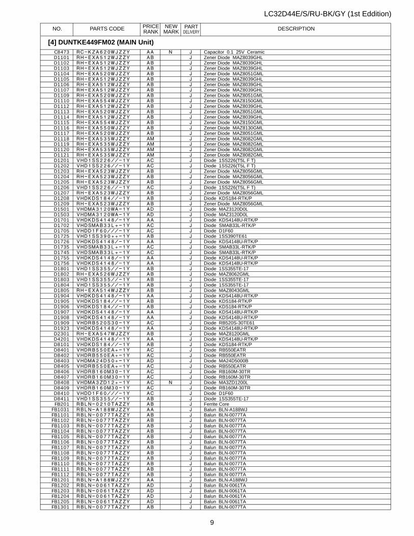
LC32D44E/S/RU-BK/GY (1st Eddition)PRICE NEW PART
NO. PARTS CODE RANK MARK DELIVERY DESCRIPTIONC8473 RC-KZA620WJZZY AA N J Capacitor 0.1 25V CeramicD1101 RH-EXA512WJZZY AB J Zener Diode MAZ8039GHLD1102 RH-EXA512WJZZY AB J Zener Diode MAZ8039GHLD1103 RH-EXA512WJZZY AB J Zener Diode MAZ8039GHLD1104 RH-EXA520WJZZY AB J Zener Diode MAZ8051GMLD1105 RH-EXA512WJZZY AB J Zener Diode MAZ8039GHLD1106 RH-EXA512WJZZY AB J Zener Diode MAZ8039GHLD1107 RH-EXA512WJZZY AB J Zener Diode MAZ8039GHLD1109 RH-EXA520WJZZY AB J Zener Diode MAZ8051GMLD1110 RH-EXA554WJZZY AB J Zener Diode MAZ8150GMLD1112 RH-EXA512WJZZY AB J Zener Diode MAZ8039GHLD1113 RH-EXA520WJZZY AB J Zener Diode MAZ8051GMLD1114 RH-EXA512WJZZY AB J Zener Diode MAZ8039GHLD1115 RH-EXA554WJZZY AB J Zener Diode MAZ8150GMLD1116 RH-EXA550WJZZY AB J Zener Diode MAZ8130GMLD1117 RH-EXA520WJZZY AB J Zener Diode MAZ8051GMLD1118 RH-EXA535WJZZY AM J Zener Diode MAZ8082GMLD1119 RH-EXA535WJZZY AM J Zener Diode MAZ8082GMLD1120 RH-EXA535WJZZY AM J Zener Diode MAZ8082GMLD1121 RH-EXA535WJZZY AM J Zener Diode MAZ8082GMLD1201 VHD1SS226//-1Y AC J Diode 1SS226(T5L F T)D1202 VHD1SS226//-1Y AC J Diode 1SS226(T5L F T)D1203 RH-EXA523WJZZY AB J Zener Diode MAZ8056GMLD1204 RH-EXA523WJZZY AB J Zener Diode MAZ8056GMLD1205 RH-EXA523WJZZY AB J Zener Diode MAZ8056GMLD1206 VHD1SS226//-1Y AC J Diode 1SS226(T5L F T)D1207 RH-EXA523WJZZY AB J Zener Diode MAZ8056GMLD1208 VHDKDS184//-1Y AB J Diode KDS184-RTK/PD1209 RH-EXA523WJZZY AB J Zener Diode MAZ8056GMLD1501 VHDMA3120WA-1Y AD J Diode MAZ3120D0LD1503 VHDMA3120WA-1Y AD J Diode MAZ3120D0LD1701 VHDKDS4148/-1Y AA J Diode KDS4148U-RTK/PD1702 VHDSMAB33L+-1Y AC J Diode SMAB33L-RTK/PD1705 VHDD1F60///-1Y AC J Diode D1F60D1725 VHD1SS390++-1Y AB J Diode 1SS390TE61D1726 VHDKDS4148/-1Y AA J Diode KDS4148U-RTK/PD1735 VHDSMAB33L+-1Y AC J Diode SMAB33L-RTK/PD1745 VHDSMAB33L+-1Y AC J Diode SMAB33L-RTK/PD1755 VHDKDS4148/-1Y AA J Diode KDS4148U-RTK/PD1756 VHDKDS4148/-1Y AA J Diode KDS4148U-RTK/PD1801 VHD1SS355//-1Y AB J Diode 1SS355TE-17D1802 RH-EXA526WJZZY AB J Diode MAZ8062GMLD1803 VHD1SS355//-1Y AB J Diode 1SS355TE-17D1804 VHD1SS355//-1Y AB J Diode 1SS355TE-17D1805 RH-EXA514WJZZY AB J Diode MAZ8043GMLD1904 VHDKDS4148/-1Y AA J Diode KDS4148U-RTK/PD1905 VHDKDS184//-1Y AB J Diode KDS184-RTK/PD1906 VHDKDS184//-1Y AB J Diode KDS184-RTK/PD1907 VHDKDS4148/-1Y AA J Diode KDS4148U-RTK/PD1908 VHDKDS4148/-1Y AA J Diode KDS4148U-RTK/PD1909 VHDRB520S30-1Y AC J Diode RB520S-30TE61D1923 VHDKDS4148/-1Y AA J Diode KDS4148U-RTK/PD2301 RH-EXA547WJZZY AB J Diode MAZ8120GMLD4201 VHDKDS4148/-1Y AA J Diode KDS4148U-RTK/PD8101 VHDKDS184//-1Y AB J Diode KDS184-RTK/PD8401 VHDRB550EA+-1Y AC J Diode RB550EATRD8402 VHDRB550EA+-1Y AC J Diode RB550EATRD8403 VHDMA24D50+-1Y AD J Diode MA24D5000BD8405 VHDRB550EA+-1Y AC J Diode RB550EATRD8406 VHDRB160M30-1Y AC J Diode RB160M-30TRD8407 VHDRB160M30-1Y AC J Diode RB160M-30TRD8408 VHDMA3ZD12+-1Y AC N J Diode MA3ZD1200LD8409 VHDRB160M30-1Y AC J Diode RB160M-30TRD8410 VHDD1F60///-1Y AC J Diode D1F60D8411 VHD1SS355//-1Y AB J Diode 1SS355TE-17FB201 RBLN-0210TAZZY AB J Ferrite Core
FB1031 RBLN-A188WJZZY AA J Balun BLN-A188WJFB1101 RBLN-0077TAZZY AB J Balun BLN-0077TAFB1102 RBLN-0077TAZZY AB J Balun BLN-0077TAFB1103 RBLN-0077TAZZY AB J Balun BLN-0077TAFB1104 RBLN-0077TAZZY AB J Balun BLN-0077TAFB1105 RBLN-0077TAZZY AB J Balun BLN-0077TAFB1106 RBLN-0077TAZZY AB J Balun BLN-0077TAFB1107 RBLN-0077TAZZY AB J Balun BLN-0077TAFB1108 RBLN-0077TAZZY AB J Balun BLN-0077TAFB1109 RBLN-0077TAZZY AB J Balun BLN-0077TAFB1110 RBLN-0077TAZZY AB J Balun BLN-0077TAFB1111 RBLN-0077TAZZY AB J Balun BLN-0077TAFB1112 RBLN-0077TAZZY AB J Balun BLN-0077TAFB1201 RBLN-A188WJZZY AA J Balun BLN-A188WJFB1202 RBLN-0061TAZZY AD J Balun BLN-0061TAFB1203 RBLN-0061TAZZY AD J Balun BLN-0061TAFB1204 RBLN-0061TAZZY AD J Balun BLN-0061TAFB1205 RBLN-0061TAZZY AD J Balun BLN-0061TAFB1301 RBLN-0077TAZZY AB J Balun BLN-0077TA
[4] DUNTKE449FM02 (MAIN Unit)
9

LC32D44E/S/RU-BK/GY (1st Eddition)PRICE NEW PART
NO. PARTS CODE RANK MARK DELIVERY DESCRIPTIONFB1302 RBLN-0077TAZZY AB J Balun BLN-0077TAFB1303 RBLN-0077TAZZY AB J Balun BLN-0077TAFB1304 RBLN-0077TAZZY AB J Balun BLN-0077TAFB1305 RBLN-0077TAZZY AB J Balun BLN-0077TAFB1306 RBLN-0077TAZZY AB J Balun BLN-0077TAFB1309 RBLN-A188WJZZY AA J Balun BLN-A188WJFB1401 RBLN-A188WJZZY AA J Balun BLN-A188WJFB1402 RBLN-A188WJZZY AA J Balun BLN-A188WJFB1501 RBLN-0061TAZZY AD J Balun BLN-0061TAFB1502 RBLN-0061TAZZY AD J Balun BLN-0061TAFB1701 RBLN-A303WJZZY AB J Balun BLN-A303WJFB1702 RBLN-0207TAZZY AB J Balun BLN-0207TAFB1703 RBLN-0207TAZZY AB J Balun BLN-0207TAFB1735 RBLN-A303WJZZY AB J Balun BLN-A303WJFB1745 RBLN-A303WJZZY AB J Balun BLN-A303WJFB1801 RBLN-0207TAZZY AB J Balun BLN-0207TAFB1901 RBLN-A192WJZZY AA J Ferrite CoreFB1902 RBLN-A192WJZZY AA J Ferrite CoreFB1941 RBLN-A192WJZZY AA J Ferrite CoreFB1951 RBLN-A192WJZZY AA J Ferrite CoreFB1952 RBLN-A192WJZZY AA J Ferrite CoreFB1953 RBLN-A192WJZZY AA J Ferrite CoreFB1954 RBLN-A192WJZZY AA J Ferrite CoreFB1955 RBLN-0210TAZZY AB J Ferrite CoreFB1956 RBLN-A192WJZZY AA J Ferrite CoreFB1957 RBLN-A192WJZZY AA J Ferrite CoreFB2301 RBLN-0061TAZZY AD J Balun BLN-0061TAFB2302 RBLN-A192WJZZY AA J Ferrite CoreFB2304 RBLN-0061TAZZY AD J Balun BLN-0061TAFB2305 RBLN-0061TAZZY AD J Balun BLN-0061TAFB2310 RBLN-A192WJZZY AA J Ferrite CoreFB3001 RBLN-A188WJZZY AA J Balun BLN-A188WJFB3002 RBLN-A192WJZZY AA J Ferrite CoreFB3003 RBLN-A192WJZZY AA J Ferrite CoreFB3004 RBLN-A192WJZZY AA J Ferrite CoreFB3005 RBLN-A192WJZZY AA J Ferrite CoreFB3006 RBLN-A192WJZZY AA J Ferrite CoreFB3021 RBLN-A188WJZZY AA J Balun BLN-A188WJFB3022 RBLN-A192WJZZY AA J Ferrite CoreFB3035 RBLN-A192WJZZY AA J Ferrite CoreFB3036 RBLN-A188WJZZY AA J Balun BLN-A188WJFB3037 RBLN-A192WJZZY AA J Ferrite CoreFB3038 RBLN-A192WJZZY AA J Ferrite CoreFB3051 RBLN-A192WJZZY AA J Ferrite CoreFB3052 RBLN-A192WJZZY AA J Ferrite CoreFB3053 RBLN-A192WJZZY AA J Ferrite CoreFB3054 RBLN-A192WJZZY AA J Ferrite CoreFB3055 RBLN-A192WJZZY AA J Ferrite CoreFB3071 RBLN-0061TAZZY AD J Balun BLN-0061TAFB3072 RBLN-0061TAZZY AD J Balun BLN-0061TAFB3073 RBLN-0061TAZZY AD J Balun BLN-0061TAFB4001 RBLN-A192WJZZY AA J Ferrite CoreFB4002 RBLN-A192WJZZY AA J Ferrite CoreFB4003 RBLN-0210TAZZY AB J Ferrite CoreFB4004 RBLN-A192WJZZY AA J Ferrite CoreFB4201 RBLN-A192WJZZY AA J Ferrite CoreFB4202 RBLN-A192WJZZY AA J Ferrite CoreFB4251 RBLN-A192WJZZY AA J Ferrite CoreFB4401 RBLN-A192WJZZY AA J Ferrite CoreFB4402 RBLN-A192WJZZY AA J Ferrite CoreFB8101 RBLN-A188WJZZY AA J Balun BLN-A188WJFB8102 RBLN-A188WJZZY AA J Balun BLN-A188WJFB8103 RBLN-A188WJZZY AA J Balun BLN-A188WJFB8104 RBLN-A188WJZZY AA J Balun BLN-A188WJFB8105 RBLN-A188WJZZY AA J Balun BLN-A188WJFB8106 RBLN-A188WJZZY AA J Balun BLN-A188WJFL1101 RFiLN0017TAZZY AC J FilterFL1102 RFiLN0017TAZZY AC J FilterFL1103 RFiLN0017TAZZY AC J FilterFL1104 RFiLN0017TAZZY AC J FilterFL1105 RFiLN0017TAZZY AC J FilterFL1106 RFiLN0017TAZZY AC J FilterFL1107 RFiLN0017TAZZY AC J FilterFL1108 RFiLN0017TAZZY AC J FilterFL1109 RFiLN0017TAZZY AC J FilterFL1110 RFiLN0017TAZZY AC J FilterFL1201 RFiLN0003TAZZY AD J FilterFL1202 RFiLN0003TAZZY AD J FilterFL1203 RFiLN0003TAZZY AD J FilterFL8101 RFiLZA007WJZZY AD J Filter
IC202 VHiPQ1M335M-1Y AD J IC PQ1M335M2SPQIC203 VHiLV4053FT-1Y AE J IC TC74LVX4053FT(EL)IC204 VHiBH25FB1G-1Y AD J IC BH25FBIWG-TRIC205 VHiMM3271AN-1Y J IC MM3271ANREIC207 RH-iXB964WJZZQ J IC STV0362
[4] DUNTKE449FM02 (MAIN Unit)
10

LC32D44E/S/RU-BK/GY (1st Eddition)PRICE NEW PART
NO. PARTS CODE RANK MARK DELIVERY DESCRIPTIONIC261 VSSSM6J51TU-1Y AF J IC Transistor IC SSM6J51TUIC1001 VHiNJM2234V-1Y AE J IC NJM2234V(TE1)IC1002 VHiNJM4558M-1Y AD J IC NJM4558M-TE1IC1101 VHiMM1506XN-1Y AD J IC MM1506XNREIC1102 VHiMM1506XN-1Y AD J IC MM1506XNREIC1201 RH-iXC206WJQZS J IC PC EDIDIC1301 VHiNJM2750M-1Y AH J IC NJM2750M(TE2)IC1401 VHiSM5309AV-1Y AL J IC SM5309AV-G-ETIC1501 VHiiSL83220-1Y AQ J IC ISL83220ECVZ-T(S2702)IC1502 VHiMM1507XN-1Y AD J IC MM1507XNREIC1701 VHiPQ1M335M-1Y AD J IC PQ1M335M2SPQIC1702 VHiLV5805M+-1Y AG J IC LV5805M-TE-L-EIC1703 VHiPST8444N-1Y AC J IC IC-PST8444NRIC1725 VHiPQ1R50//-1Y AF J IC PQ1R50J0000HIC1726 VHiPQ20WZ51-1Y AF J IC PQ20WZ5UJ00HIC1735 VHiLV5805M+-1Y AG J IC LV5805M-TE-L-EIC1745 VHiLV5805M+-1Y AG J IC LV5805M-TE-L-EIC1755 VHiPQ012GN1-1Y AF J IC PQ012GN01ZPHIC1756 VHiPQ1LA185-1Y AD J IC PQ1LA185MSPQIC1902 RH-iXC448WJZZS J IC HDMI EDIDIC1922 RH-iXC447WJZZS J IC HDMI EDIDIC1941 VHiTVHC153T-1Y AE J IC TC74VHC153FT(EL,M)IC1951 VHiSii9025+-1Q AX J IC SII9025CTUIC2302 RH-iXC009WJZZQ AU J IC 86FS49AUG-6NU2(JZIC2303 VHiPST8428N-1Y AC J IC IC-PST8428NRIC2601 VHiPST8428N-1Y AC J IC IC-PST8428NRIC2701 VHiYDA147SZ-1Y AM J IC YDA147-SZE2IC3001 RH-iXC354WJZZQ BK N J IC VCT7993P-FA-A1-H000IC3002 VHiPST8415N-1Y AC J IC IC-PST8415NRIC3051 VHiBR24S64M-1Y AF J IC BR24S64FVM-WTRIC4001 RH-iXC243WJZZQ J IC STI5105ALCIC4003 VHiPST8428N-1Y AC J IC IC-PST8428NRIC4004 VHiLV4052FT-1Y AF J IC TC74LVX4052FT(EL,M)IC4005 VHiLM833D++-1Y AE J IC LM833DTIC4201 RH-iXB765WJQZQ AW J IC K4H561638H-UCB3IC4202 VHiPQ070XNA-1Y AE J IC PQ070XNA1ZPHIC4251 RH-iXC361WJZZQ N J IC M29W160ET70N6EIC4252 VHiBR24S64M-1Y AF J IC BR24S64FVM-WTRIC4401 VHiLCX245FT-1Y AD J IC TC74LCX245FT(EKJ)IC4402 VHiLCX126FT-1Y AD J IC TC74LCX126FT(EL,K)IC4403 VHiAHC1G04W-1Y AC J IC 74AHC1G04GW,125IC4404 VHiLCX16244-1Y N J IC TC74LCX16244(EL,F)IC4405 VHiLCX16244-1Y N J IC TC74LCX16244(EL,F)IC4407 VHiTC7SH32U1EY AC J IC TC7SH32FU(TE85L,JF)IC4409 VHiAHC1G04W-1Y AC J IC 74AHC1G04GW,125IC4410 VHiAOZ1320C-1Y AE J IC AOZ1320CI-04IC8101 RH-iXC539WJZZS J IC M24256-BWMN6TPIC8102 VHiT7WU04FK-1Y AD J IC T7WU04FKIC8103 VHiT3Z18AFG-1Q BA J IC T3Z18AFG-0003(O2)IC8201 VHiBD8143MU-1Y AM J IC BD8143MUV-E2IC8202 VHiBU55041+-1Y AF J IC BU55041HFN-TR-TRIC8402 VHiBD8162EK-1Q AQ J IC VHIBD8162EK-1Q
J1301 QJAKJ0008GEZZ AD J JackJ1302 QJAKJ0008GEZZ AD J JackJ1303 QJAKFA061WJZZ AE J JackJ1304 QJAKFA061WJZZ AE J JackJ1401 QJAKGA131WJZZ AG J JackL203 VPCNN2R2JR77NY AB J Coil Peaking 2.2µHL204 VPCNN2R2JR77NY AB J Coil Peaking 2.2µHL205 VPCNN2R2JR77NY AB J Coil Peaking 2.2µHL206 VPCNN2R2JR77NY AB J Coil Peaking 2.2µHL207 VPCNN2R2JR77NY AB J Coil Peaking 2.2µHL263 VPCNN120J1R9NY AB J Coil Peaking 12µH
L1031 VPD9M100J1R7NY AC J Coil Peaking 10µHL1101 VPCNN120J1R9NY AB J Coil Peaking 12µHL1701 RCiLPA964WJZZY AD N J Coil 10uL1735 RCiLPA085WJZZY AD J CoilL1745 RCiLPA964WJZZY AD N J Coil 10uL2601 RCiLFA279WJZZY AC J CoilL2602 RCiLFA279WJZZY AC J CoilL2603 RCiLFA279WJZZY AC J CoilL2604 RCiLFA279WJZZY AC J CoilL2605 RCiLFA279WJZZY AC J CoilL2606 RCiLFA279WJZZY AC J CoilL2701 RCiLPA899WJZZY AC J Coil Peaking 22µHL2702 RCiLPA899WJZZY AC J Coil Peaking 22µHL2703 RCiLPA899WJZZY AC J Coil Peaking 22µHL2704 RCiLPA899WJZZY AC J Coil Peaking 22µHL8101 RCiLFA122WJZZY AD J CoilL8102 RCiLFA122WJZZY AD J CoilL8103 RCiLFA122WJZZY AD J CoilL8104 RCiLFA122WJZZY AD J CoilL8105 RCiLFA122WJZZY AD J CoilL8106 RCiLFA122WJZZY AD J CoilL8107 RCiLFA122WJZZY AD J Coil
[4] DUNTKE449FM02 (MAIN Unit)
11

LC32D44E/S/RU-BK/GY (1st Eddition)PRICE NEW PART
NO. PARTS CODE RANK MARK DELIVERY DESCRIPTIONL8108 RCiLFA122WJZZY AD J CoilL8109 RCiLFA122WJZZY AD J CoilL8110 RCiLFA122WJZZY AD J CoilL8111 RCiLFA122WJZZY AD J CoilL8112 RCiLFA122WJZZY AD J CoilL8113 RCiLFA275WJZZY AC J CoilL8114 RCiLFA275WJZZY AC J CoilL8401 RCiLPA962WJZZY AC N J Coil 4.7uL8402 RCiLPA964WJZZY AD N J Coil 10uL8403 RCiLPA964WJZZY AD N J Coil 10u
LUG1701 QLUGHA006WJZZY AC J LugLUG1702 QLUGHA006WJZZY AC J LugLUG1703 QLUGHA006WJZZY AC J LugLUG1704 QLUGHA006WJZZY AC J LugLUG1705 QLUGHA006WJZZY AC J LugLUG1706 QLUGHA006WJZZY AC J Lug
P1001 QCNCMA012WJZZ AD J Connector 15PinP1701 QPLGNA168WJZZY AF J Plug 12Pin(PD)P2301 QPLGNA325WJZZY AC J Plug 5Pin (RA )P2302 QPLGNA329WJZZY AD J Plug 9Pin(LB)P2701 QPLGNA160WJZZY AD J Plug 4Pin(SP)P3071 QPLGNA324WJZZY AC J Plug 4Pin(KM)P3081 QPLGN0567FJZZY AD J Plug 5PinP4001 QPLGN0463TAZZY AC J Plug, 4Pin(RS)P4401 QCNCMA313WJSA J PlugP8101 QPLGN0663TAZZY AD J Plug 6pinQ202 VSRN4904///-1Y AB J Transistor RN4904Q203 VS2SC3928AR-1Y AB J Transistor 2SC3928A-T112-1RQ262 VSRN4904///-1Y AB J Transistor RN4904
Q1001 VSiMH23T110-1Y AC J Transister IMH23T110Q1031 VS2SC3928AR-1Y AB J Transistor 2SC3928A-T112-1RQ1101 VSiMH23T110-1Y AC J Transister IMH23T110Q1102 VSiMH23T110-1Y AC J Transister IMH23T110Q1105 VS2SA1530AR-1Y AB J Transistor 2SA1530A-T112-1RQ1106 VS2SA1530AR-1Y AB J Transistor 2SA1530A-T112-1RQ1107 VS2SA1530AR-1Y AB J Transistor 2SA1530A-T112-1RQ1108 VS2SA1530AR-1Y AB J Transistor 2SA1530A-T112-1RQ1301 VS2SA1530AR-1Y AB J Transistor 2SA1530A-T112-1RQ1302 VS2SA1530AR-1Y AB J Transistor 2SA1530A-T112-1RQ1303 VSiMH23T110-1Y AC J Transister IMH23T110Q1501 VSSM3K7002F-1Y AC J Transister SSM3K7002F(5LTST,FQ1801 VSRDTC144EE-1Y AA J Transister PDTC144EE,115Q1802 VSDTA124EKA-1Y AB J Transistor DTA124EKAT146Q1901 VSRDTC144EE-1Y AA J Transister PDTC144EE,115Q1902 VSRDTC144EE-1Y AA J Transister PDTC144EE,115Q1903 VSSSM3K15F+-1Y N J Transister SSM3K15FQ1904 VSSSM3K15F+-1Y N J Transister SSM3K15FQ1905 VSRN4904///-1Y AB J Transistor RN4904Q1906 VSRDTC144EE-1Y AA J Transister PDTC144EE,115Q1921 VSRDTC144EE-1Y AA J Transister PDTC144EE,115Q1922 VSRDTC144EE-1Y AA J Transister PDTC144EE,115Q1923 VSSSM3K15F+-1Y N J Transister SSM3K15FQ1924 VSSSM3K15F+-1Y N J Transister SSM3K15FQ1925 VSRN4904///-1Y AB J Transistor RN4904Q2701 VSDTC614TK+-1Y AB J Transistor DTC614TKT146Q3051 VSSM3K7002F-1Y AC J Transister SSM3K7002F(5LTST,FQ3052 VSSM3K7002F-1Y AC J Transister SSM3K7002F(5LTST,FQ4001 VS2SC3928AR-1Y AB J Transistor 2SC3928A-T112-1RQ4002 VS2SC3928AR-1Y AB J Transistor 2SC3928A-T112-1RQ4403 VS2SC3928AR-1Y AB J Transistor 2SC3928A-T112-1RQ8401 VSEMZ1+++++-1Y AC J Transister EMZ1T2RQ8402 VSDTC114EE/-1Y AB J Transistor DTC114EETLQ8403 VSTPCP8602+-1Y AD J Transister VSTPCP8602+-1YQ8404 VS2SA1530AR-1Y AB J Transistor 2SA1530A-T112-1RQ8405 VSTPCP8505+-1Y AD J Transister VSTPCP8505+-1YQ8408 VS2SD1767++-1Y AD J Transister 2SD1767T100Q8410 VSRK7002A++-1Y AB J Transister RK7002AT116Q8450 VSRSS050P03-1Y AG J Transister RSS050P03TB
R204 VRS-CZ1JF000JY AA J Resistor 0 1/16W Metal OxideR206 VRK-SA1JF220JY J Resistor 22 1/16W Metal CompositionR209 VRS-CZ1JF102JY AA J Resistor 1k 1/16W Metal OxideR211 VRS-CZ1JF392JY AA J Resistor 3.9k 1/16W Metal OxideR212 VRS-CZ1JF151JY AA J Resistor 150 1/16W Metal OxideR213 VRS-CZ1JF103JY AA J Resistor 10k 1/16W Metal OxideR214 VRS-CZ1JF331JY AA J Resistor 330 1/16W Metal OxideR218 VRS-CZ1JF151JY AA J Resistor 150 1/16W Metal OxideR222 VRK-SA1JF472JY AA J Resistor 4.7k 1/16W Metal CompositionR223 VRK-SA1JF220JY J Resistor 22 1/16W Metal CompositionR226 VRS-CZ1JF561JY AA J Resistor 560 1/16W Metal OxideR227 VRS-CZ1JF561JY AA J Resistor 560 1/16W Metal OxideR228 VRS-CZ1JF103JY AA J Resistor 10k 1/16W Metal OxideR229 VRS-CZ1JF181JY AA J Resistor 180 1/16W Metal OxideR230 VRS-CZ1JF103JY AA J Resistor 10k 1/16W Metal OxideR231 VRS-CZ1JF103JY AA J Resistor 10k 1/16W Metal OxideR232 VRS-CZ1JF103JY AA J Resistor 10k 1/16W Metal Oxide
[4] DUNTKE449FM02 (MAIN Unit)
12

LC32D44E/S/RU-BK/GY (1st Eddition)PRICE NEW PART
NO. PARTS CODE RANK MARK DELIVERY DESCRIPTIONR233 VRK-SA1JF220JY J Resistor 22 1/16W Metal CompositionR234 VRS-CZ1JF103JY AA J Resistor 10k 1/16W Metal OxideR236 VRS-CZ1JF470JY AA J Resistor 47 1/16W Metal OxideR237 VRS-CZ1JF470JY AA J Resistor 47 1/16W Metal OxideR238 VRS-CZ1JF470JY AA J Resistor 47 1/16W Metal OxideR239 VRK-SB1FF470JY AA J Resistor 47 1/32W Metal CompositionR240 VRK-SB1FF470JY AA J Resistor 47 1/32W Metal CompositionR283 VRS-CZ1JF332JY AA J Resistor 3.3k 1/16W Metal Oxide
R1006 VRS-CZ1JF682JY AA J Resistor 6.8k 1/16W Metal OxideR1010 VRS-CZ1JF392JY AA J Resistor 3.9k 1/16W Metal OxideR1011 VRS-CZ1JF101JY AA J Resistor 100 1/16W Metal OxideR1012 VRS-TQ2EF560JY J Resistor 56 1/4W Metal OxideR1013 VRS-TQ2EF560JY J Resistor 56 1/4W Metal OxideR1014 VRK-SA1JF182JY AC J Resistor 1.8k 1/16W Metal CompositionR1015 VRS-TW2HF820JY AB J Resistor 82 1/2W Metal OxideR1016 VRS-CZ1JF103JY AA J Resistor 10k 1/16W Metal OxideR1017 VRS-CZ1JF101JY AA J Resistor 100 1/16W Metal OxideR1018 VRS-CZ1JF103JY AA J Resistor 10k 1/16W Metal OxideR1019 VRS-CZ1JF122JY AA J Resistor 1.2k 1/16W Metal OxideR1020 VRS-CZ1JF122JY AA J Resistor 1.2k 1/16W Metal OxideR1021 VRK-SA1JF103JY AB J Resistor 10k 1/16W Metal CompositionR1022 VRK-SA1JF103JY AB J Resistor 10k 1/16W Metal CompositionR1023 VRK-SA1JF103JY AB J Resistor 10k 1/16W Metal CompositionR1031 VRS-CZ1JF331FY AA J Resistor 330 1/16W Metal OxideR1032 VRS-CZ1JF331FY AA J Resistor 330 1/16W Metal OxideR1033 VRS-CZ1JF103JY AA J Resistor 10k 1/16W Metal OxideR1034 VRS-CZ1JF103JY AA J Resistor 10k 1/16W Metal OxideR1035 VRS-CZ1JF330FY AA J Resistor 33 1/16W Metal OxideR1036 VRS-CZ1JF161FY J Resistor 160 1/16W Metal OxideR1101 VRS-CZ1JF153FY AA J Resistor 15k 1/16W Metal OxideR1102 VRS-CZ1JF393FY AA J Resistor 39k 1/16W Metal OxideR1103 VRS-CZ1JF153FY AA J Resistor 15k 1/16W Metal OxideR1107 VRS-TQ2EF750JY AA J Resistor 75 1/4W Metal OxideR1108 VRS-TQ2EF680JY AA J Resistor 68 1/4W Metal OxideR1109 VRS-TQ2EF101JY AA J Resistor 100 1/4W Metal OxideR1110 VRS-TQ2EF750JY AA J Resistor 75 1/4W Metal OxideR1111 VRS-CZ1JF393FY AA J Resistor 39k 1/16W Metal OxideR1112 VRS-TQ2EF750JY AA J Resistor 75 1/4W Metal OxideR1113 VRS-TQ2EF680JY AA J Resistor 68 1/4W Metal OxideR1117 VRS-TQ2EF750JY AA J Resistor 75 1/4W Metal OxideR1118 VRS-TQ2EF750JY AA J Resistor 75 1/4W Metal OxideR1121 VRS-CY1JF000JY AA J Resistor 0 1/16W Metal OxideR1122 VRS-TQ2EF750JY AA J Resistor 75 1/4W Metal OxideR1123 VRS-TQ2EF750JY AA J Resistor 75 1/4W Metal OxideR1124 VRS-TQ2EF750JY AA J Resistor 75 1/4W Metal OxideR1125 VRS-TQ2EF101JY AA J Resistor 100 1/4W Metal OxideR1126 VRS-TQ2EF750JY AA J Resistor 75 1/4W Metal OxideR1127 VRS-TQ2EF750JY AA J Resistor 75 1/4W Metal OxideR1128 VRS-CY1JF000JY AA J Resistor 0 1/16W Metal OxideR1129 VRS-CY1JF000JY AA J Resistor 0 1/16W Metal OxideR1130 VRS-CZ1JF221JY AA J Resistor 220 1/16W Metal OxideR1131 VRS-TV1JD221JY AA J Resistor 220 1/16W Metal OxideR1132 VRS-TV1JD221JY AA J Resistor 220 1/16W Metal OxideR1133 VRS-CY1JF000JY AA J Resistor 0 1/16W Metal OxideR1134 VRS-CZ1JF104JY AA J Resistor 100k 1/16W Metal OxideR1135 VRS-CZ1JF104JY AA J Resistor 100k 1/16W Metal OxideR1136 VRS-TV1JD221JY AA J Resistor 220 1/16W Metal OxideR1137 VRS-CZ1JF102JY AA J Resistor 1k 1/16W Metal OxideR1138 VRS-CZ1JF102JY AA J Resistor 1k 1/16W Metal OxideR1139 VRS-TV1JD221JY AA J Resistor 220 1/16W Metal OxideR1142 VRS-CZ1JF104JY AA J Resistor 100k 1/16W Metal OxideR1143 VRS-CZ1JF104JY AA J Resistor 100k 1/16W Metal OxideR1144 VRK-SA1JF101JY AC J Resistor 100 1/16W Metal CompositionR1145 VRS-CZ1JF102JY AA J Resistor 1k 1/16W Metal OxideR1146 VRS-CZ1JF102JY AA J Resistor 1k 1/16W Metal OxideR1147 VRK-SA1JF101JY AC J Resistor 100 1/16W Metal CompositionR1148 VRS-CZ1JF104JY AA J Resistor 100k 1/16W Metal OxideR1149 VRS-CZ1JF104JY AA J Resistor 100k 1/16W Metal OxideR1150 VRS-CZ1JF564JY AB J Resistor 560k 1/16W Metal OxideR1151 VRS-CZ1JF564JY AB J Resistor 560k 1/16W Metal OxideR1152 VRK-SA1JF331JY J Resistor 330 1/16W Metal CompositionR1153 VRK-SA1JF331JY J Resistor 330 1/16W Metal CompositionR1154 VRS-CZ1JF564JY AB J Resistor 560k 1/16W Metal OxideR1155 VRS-CZ1JF564JY AB J Resistor 560k 1/16W Metal OxideR1156 VRK-SA1JF272JY J Resistor 2.7k 1/16W Metal CompositionR1157 VRK-SA1JF272JY J Resistor 2.7k 1/16W Metal CompositionR1201 VRS-TQ2EF750JY AA J Resistor 75 1/4W Metal OxideR1202 VRS-TQ2EF750JY AA J Resistor 75 1/4W Metal OxideR1203 VRS-TQ2EF750JY AA J Resistor 75 1/4W Metal OxideR1204 VRS-CZ1JF221JY AA J Resistor 220 1/16W Metal OxideR1205 VRS-CZ1JF221JY AA J Resistor 220 1/16W Metal OxideR1206 VRS-CZ1JF473JY AA J Resistor 47k 1/16W Metal OxideR1207 VRS-CZ1JF473JY AA J Resistor 47k 1/16W Metal OxideR1208 VRK-SB1FF101JY AA J Resistor 100 1/32W Metal CompositionR1209 VRS-CZ1JF102JY AA J Resistor 1k 1/16W Metal Oxide
[4] DUNTKE449FM02 (MAIN Unit)
13

LC32D44E/S/RU-BK/GY (1st Eddition)PRICE NEW PART
NO. PARTS CODE RANK MARK DELIVERY DESCRIPTIONR1210 VRS-CZ1JF102JY AA J Resistor 1k 1/16W Metal OxideR1301 VRS-CZ1JF102JY AA J Resistor 1k 1/16W Metal OxideR1302 VRS-CZ1JF102JY AA J Resistor 1k 1/16W Metal OxideR1303 VRS-CZ1JF102JY AA J Resistor 1k 1/16W Metal OxideR1304 VRS-CZ1JF102JY AA J Resistor 1k 1/16W Metal OxideR1305 VRS-CZ1JF104JY AA J Resistor 100k 1/16W Metal OxideR1306 VRS-CZ1JF104JY AA J Resistor 100k 1/16W Metal OxideR1307 VRS-CZ1JF104JY AA J Resistor 100k 1/16W Metal OxideR1308 VRS-CZ1JF104JY AA J Resistor 100k 1/16W Metal OxideR1309 VRS-CZ1JF102JY AA J Resistor 1k 1/16W Metal OxideR1310 VRS-CZ1JF102JY AA J Resistor 1k 1/16W Metal OxideR1311 VRS-CZ1JF102JY AA J Resistor 1k 1/16W Metal OxideR1312 VRS-CZ1JF102JY AA J Resistor 1k 1/16W Metal OxideR1313 VRS-CZ1JF104JY AA J Resistor 100k 1/16W Metal OxideR1314 VRS-CZ1JF102JY AA J Resistor 1k 1/16W Metal OxideR1315 VRS-CZ1JF102JY AA J Resistor 1k 1/16W Metal OxideR1316 VRS-CZ1JF102JY AA J Resistor 1k 1/16W Metal OxideR1317 VRS-CZ1JF102JY AA J Resistor 1k 1/16W Metal OxideR1318 VRS-CZ1JF104JY AA J Resistor 100k 1/16W Metal OxideR1319 VRS-CZ1JF104JY AA J Resistor 100k 1/16W Metal OxideR1320 VRS-CZ1JF221JY AA J Resistor 220 1/16W Metal OxideR1321 VRS-CZ1JF561JY AA J Resistor 560 1/16W Metal OxideR1322 VRS-CZ1JF102JY AA J Resistor 1k 1/16W Metal OxideR1323 VRS-CZ1JF104JY AA J Resistor 100k 1/16W Metal OxideR1324 VRS-CZ1JF221JY AA J Resistor 220 1/16W Metal OxideR1325 VRS-CZ1JF561JY AA J Resistor 560 1/16W Metal OxideR1326 VRS-CZ1JF564JY AB J Resistor 560k 1/16W Metal OxideR1327 VRS-CZ1JF102JY AA J Resistor 1k 1/16W Metal OxideR1328 VRS-CZ1JF564JY AB J Resistor 560k 1/16W Metal OxideR1329 VRS-CZ1JF102JY AA J Resistor 1k 1/16W Metal OxideR1330 VRS-CZ1JF102JY AA J Resistor 1k 1/16W Metal OxideR1331 VRS-CZ1JF102JY AA J Resistor 1k 1/16W Metal OxideR1332 VRS-CZ1JF102JY AA J Resistor 1k 1/16W Metal OxideR1401 VRK-SA1JF220JY J Resistor 22 1/16W Metal CompositionR1402 VRS-TQ2EF750JY AA J Resistor 75 1/4W Metal OxideR1403 VRS-TQ2EF750JY AA J Resistor 75 1/4W Metal OxideR1404 VRS-TQ2EF750JY AA J Resistor 75 1/4W Metal OxideR1405 VRS-CZ1JF182FY AA J Resistor 1.8k 1/16W Metal OxideR1409 VRS-CZ1JF161FY J Resistor 160 1/16W Metal OxideR1410 VRS-CZ1JF161FY J Resistor 160 1/16W Metal OxideR1411 VRS-CZ1JF161FY J Resistor 160 1/16W Metal OxideR1502 VRS-TV1JD101JY AA J Resistor 100 1/10W Metal OxideR1503 VRS-TV1JD101JY AA J Resistor 100 1/10W Metal OxideR1504 VRS-CZ1JF103JY AA J Resistor 10k 1/16W Metal OxideR1505 VRS-CZ1JF101JY AA J Resistor 100 1/16W Metal OxideR1506 VRS-CZ1JF103JY AA J Resistor 10k 1/16W Metal OxideR1507 VRS-CZ1JF223JY AA J Resistor 22k 1/16W Metal OxideR1508 VRS-CZ1JF101JY AA J Resistor 100 1/16W Metal OxideR1701 VRS-CZ1JF153FY AA J Resistor 15k 1/16W Metal OxideR1702 VRS-CZ1JF823FY AA J Resistor 82k 1/16W Metal OxideR1703 VRS-CZ1JF103FY AB J Resistor 10k 1/16W Metal OxideR1705 VRS-CZ1JF101JY AA J Resistor 100 1/16W Metal OxideR1706 VRS-TW2HF1R0JY AA J Resistor 1 1/2W Metal OxideR1707 VRS-CZ1JF473JY AA J Resistor 47k 1/16W Metal OxideR1708 VRS-CZ1JF392JY AA J Resistor 3.9k 1/16W Metal OxideR1709 VRS-CZ1JF101JY AA J Resistor 100 1/16W Metal OxideR1710 VRS-CZ1JF103JY AA J Resistor 10k 1/16W Metal OxideR1711 VRS-TW2HF1R0JY AA J Resistor 1 1/2W Metal OxideR1712 VRS-TW2HF1R0JY AA J Resistor 1 1/2W Metal OxideR1714 VRS-CZ1JF101JY AA J Resistor 100 1/16W Metal OxideR1719 VRS-CZ1JF102JY AA J Resistor 1k 1/16W Metal OxideR1725 VRS-CZ1JF222FY AA J Resistor 2.2k 1/16W Metal OxideR1726 VRS-TW2HF3R3JY AA J Resistor 3.3 1/2W Metal OxideR1727 VRS-TW2HF3R3JY AA J Resistor 3.3 1/2W Metal OxideR1728 VRS-CZ1JF202FY AA J Resistor 2k 1/16W Metal OxideR1729 VRS-CZ1JF101JY AA J Resistor 100 1/16W Metal OxideR1730 VRS-CZ1JF202FY AA J Resistor 2k 1/16W Metal OxideR1735 VRS-CZ1JF154FY AA J Resistor 150k 1/16W Metal OxideR1736 VRS-CZ1JF823FY AA J Resistor 82k 1/16W Metal OxideR1737 VRS-CZ1JF103FY AB J Resistor 10k 1/16W Metal OxideR1738 VRS-CZ1JF101JY AA J Resistor 100 1/16W Metal OxideR1740 VRS-CZ1JF103JY AA J Resistor 10k 1/16W Metal OxideR1741 VRS-TW2HF1R0JY AA J Resistor 1 1/2W Metal OxideR1742 VRS-TW2HF1R0JY AA J Resistor 1 1/2W Metal OxideR1743 VRS-CZ1JF101JY AA J Resistor 100 1/16W Metal OxideR1745 VRS-CZ1JF154FY AA J Resistor 150k 1/16W Metal OxideR1746 VRS-CZ1JF393FY AA J Resistor 39k 1/16W Metal OxideR1747 VRS-CZ1JF103FY AB J Resistor 10k 1/16W Metal OxideR1748 VRS-CZ1JF101JY AA J Resistor 100 1/16W Metal OxideR1750 VRS-CZ1JF562JY AA J Resistor 5.6k 1/16W Metal OxideR1751 VRS-TW2HF1R0JY AA J Resistor 1 1/2W Metal OxideR1752 VRS-TW2HF1R0JY AA J Resistor 1 1/2W Metal OxideR1753 VRS-TW2HF1R0JY AA J Resistor 1 1/2W Metal OxideR1754 VRS-CZ1JF101JY AA J Resistor 100 1/16W Metal OxideR1755 VRS-CZ1JF102JY AA J Resistor 1k 1/16W Metal Oxide
[4] DUNTKE449FM02 (MAIN Unit)
14

LC32D44E/S/RU-BK/GY (1st Eddition)PRICE NEW PART
NO. PARTS CODE RANK MARK DELIVERY DESCRIPTIONR1756 VRS-TW2HF2R2JY AA J Resistor 2.2 1/2W Metal OxideR1757 VRS-TW2HF2R2JY AA J Resistor 2.2 1/2W Metal OxideR1758 VRS-CZ1JF102JY AA J Resistor 1k 1/16W Metal OxideR1801 VRS-CZ1JF472JY AA J Resistor 4.7k 1/16W Metal OxideR1802 VRS-CZ1JF101JY AA J Resistor 100 1/16W Metal OxideR1803 VRS-CZ1JF101JY AA J Resistor 100 1/16W Metal OxideR1901 VRS-CZ1JF000JY AA J Resistor 0 1/16W Metal OxideR1903 VRS-CZ1JF102JY AA J Resistor 1k 1/16W Metal OxideR1904 VRS-CZ1JF103JY AA J Resistor 10k 1/16W Metal OxideR1905 VRS-CZ1JF103JY AA J Resistor 10k 1/16W Metal OxideR1907 VRK-SA1JF474JY J Resistor 470k 1/16W Metal CompositionR1909 VRK-SA1JF473JY AC J Resistor 47k 1/16W Metal CompositionR1911 VRS-CZ1JF273JY AA J Resistor 27k 1/16W Metal OxideR1912 VRK-SA1JF100JY AB J Resistor 10 1/16W Metal CompositionR1915 VRS-CZ1JF473JY AA J Resistor 47k 1/16W Metal OxideR1921 VRS-CZ1JF103JY AA J Resistor 10k 1/16W Metal OxideR1923 VRS-CZ1JF102JY AA J Resistor 1k 1/16W Metal OxideR1924 VRS-CZ1JF103JY AA J Resistor 10k 1/16W Metal OxideR1926 VRK-SA1JF474JY J Resistor 470k 1/16W Metal CompositionR1928 VRK-SA1JF473JY AC J Resistor 47k 1/16W Metal CompositionR1930 VRK-SA1JF100JY AB J Resistor 10 1/16W Metal CompositionR1933 VRS-CZ1JF473JY AA J Resistor 47k 1/16W Metal OxideR1951 VRS-CZ1JF470JY AA J Resistor 47 1/16W Metal OxideR1952 VRK-SB1FF470JY AA J Resistor 47 1/32W Metal CompositionR1953 VRK-SB1FF470JY AA J Resistor 47 1/32W Metal CompositionR1954 VRK-SB1FF470JY AA J Resistor 47 1/32W Metal CompositionR1955 VRK-SB1FF470JY AA J Resistor 47 1/32W Metal CompositionR1956 VRK-SB1FF470JY AA J Resistor 47 1/32W Metal CompositionR1957 VRK-SB1FF470JY AA J Resistor 47 1/32W Metal CompositionR1958 VRS-CZ1JF472JY AA J Resistor 4.7k 1/16W Metal OxideR1959 VRS-CZ1JF103JY AA J Resistor 10k 1/16W Metal OxideR1960 VRK-SB1FF470JY AA J Resistor 47 1/32W Metal CompositionR1961 VRS-CZ1JF223JY AA J Resistor 22k 1/16W Metal OxideR1962 VRS-CZ1JF472JY AA J Resistor 4.7k 1/16W Metal OxideR1965 VRS-CZ1JF105JY AA J Resistor 1M 1/16W Metal OxideR1966 VRS-CZ1JF102JY AA J Resistor 1k 1/16W Metal OxideR1967 VRS-CZ1JF330JY AA J Resistor 33 1/16W Metal OxideR1968 VRS-CZ1JF220JY AA J Resistor 22 1/16W Metal OxideR1969 VRS-CZ1JF220JY AA J Resistor 22 1/16W Metal OxideR1970 VRS-CZ1JF220JY AA J Resistor 22 1/16W Metal OxideR1971 VRK-SA1JF220JY J Resistor 22 1/16W Metal CompositionR1973 VRS-CZ1JF330JY AA J Resistor 33 1/16W Metal OxideR2302 VRS-CZ1JF101JY AA J Resistor 100 1/16W Metal OxideR2303 VRK-SB1FF472JY AA J Resistor 4.7k 1/32W Metal CompositionR2304 VRK-SB1FF472JY AA J Resistor 4.7k 1/32W Metal CompositionR2305 VRS-CZ1JF101JY AA J Resistor 100 1/16W Metal OxideR2306 VRS-CZ1JF102JY AA J Resistor 1k 1/16W Metal OxideR2307 VRS-CZ1JF102JY AA J Resistor 1k 1/16W Metal OxideR2312 VRS-CZ1JF472JY AA J Resistor 4.7k 1/16W Metal OxideR2313 VRS-CZ1JF105JY AA J Resistor 1M 1/16W Metal OxideR2317 VRK-SA1JF220JY J Resistor 22 1/16W Metal CompositionR2324 VRS-CZ1JF331JY AA J Resistor 330 1/16W Metal OxideR2325 VRS-CZ1JF104JY AA J Resistor 100k 1/16W Metal OxideR2327 VRS-CZ1JF472JY AA J Resistor 4.7k 1/16W Metal OxideR2328 VRK-SA1JF103JY AB J Resistor 10k 1/16W Metal CompositionR2329 VRS-CZ1JF101JY AA J Resistor 100 1/16W Metal OxideR2336 VRS-CZ1JF103JY AA J Resistor 10k 1/16W Metal OxideR2603 VRS-CZ1JF474JY AA J Resistor 470k 1/16W Metal OxideR2612 VRS-CZ1JF103JY AA J Resistor 10k 1/16W Metal OxideR2614 VRS-CZ1JF220JY AA J Resistor 22 1/16W Metal OxideR2615 VRS-CZ1JF220JY AA J Resistor 22 1/16W Metal OxideR2706 VRK-SA1JF182JY AC J Resistor 1.8k 1/16W Metal CompositionR2711 VRK-SA1JF103JY AB J Resistor 10k 1/16W Metal CompositionR2715 VRS-CZ1JF274FY AA J Resistor 270k 1/16W Metal OxideR2716 VRS-CZ1JF104FY AB J Resistor 100k 1/16W Metal OxideR2718 VRS-CZ1JF000JY AA J Resistor 0 1/16W Metal OxideR2719 VRS-CZ1JF000JY AA J Resistor 0 1/16W Metal OxideR2720 VRS-CZ1JF000JY AA J Resistor 0 1/16W Metal OxideR2722 VRS-CZ1JF000JY AA J Resistor 0 1/16W Metal OxideR2723 VRK-SB1FF224JY J Resistor 220k 1/32W Metal CompositionR2728 VRS-CZ1JF224JY AA J Resistor 220k 1/16W Metal OxideR2729 VRS-CZ1JF474JY AA J Resistor 470k 1/16W Metal OxideR2730 VRS-CZ1JF103JY AA J Resistor 10k 1/16W Metal OxideR2731 VRS-CZ1JF562JY AA J Resistor 5.6k 1/16W Metal OxideR3001 VRS-CZ1JF472JY AA J Resistor 4.7k 1/16W Metal OxideR3003 VRS-CZ1JF000JY AA J Resistor 0 1/16W Metal OxideR3004 VRS-CZ1JF622JY AA J Resistor 6.2k 1/16W Metal OxideR3007 VRS-CZ1JF472JY AA J Resistor 4.7k 1/16W Metal OxideR3054 VRK-SA1JF220JY J Resistor 22 1/16W Metal CompositionR3056 VRK-SA1JF472JY AA J Resistor 4.7k 1/16W Metal CompositionR3071 VRS-CZ1JF333FY AA J Resistor 33k 1/16W Metal OxideR3072 VRS-CZ1JF333FY AA J Resistor 33k 1/16W Metal OxideR3073 VRS-CZ1JF103FY AB J Resistor 10k 1/16W Metal OxideR3074 VRS-CZ1JF102FY AA J Resistor 1k 1/16W Metal OxideR3075 VRS-CZ1JF102FY AA J Resistor 1k 1/16W Metal Oxide
[4] DUNTKE449FM02 (MAIN Unit)
15

LC32D44E/S/RU-BK/GY (1st Eddition)PRICE NEW PART
NO. PARTS CODE RANK MARK DELIVERY DESCRIPTIONR3076 VRS-CZ1JF102FY AA J Resistor 1k 1/16W Metal OxideR3081 VRK-SA1JF220JY J Resistor 22 1/16W Metal CompositionR4002 VRS-CZ1JF103FY AB J Resistor 10k 1/16W Metal OxideR4003 VRS-CZ1JF000JY AA J Resistor 0 1/16W Metal OxideR4004 VRS-CZ1JF000JY AA J Resistor 0 1/16W Metal OxideR4005 VRS-CZ1JF000JY AA J Resistor 0 1/16W Metal OxideR4007 VRS-CZ1JF201FY AA J Resistor 200 1/16W Metal OxideR4008 VRS-CZ1JF000JY AA J Resistor 0 1/16W Metal OxideR4009 VRS-CZ1JF000JY AA J Resistor 0 1/16W Metal OxideR4010 VRS-CZ1JF102JY AA J Resistor 1k 1/16W Metal OxideR4012 VRS-CZ1JF103JY AA J Resistor 10k 1/16W Metal OxideR4013 VRS-CZ1JF103JY AA J Resistor 10k 1/16W Metal OxideR4014 VRS-CZ1JF103JY AA J Resistor 10k 1/16W Metal OxideR4016 VRS-CZ1JF103JY AA J Resistor 10k 1/16W Metal OxideR4017 VRS-CZ1JF103JY AA J Resistor 10k 1/16W Metal OxideR4018 VRS-CZ1JF000JY AA J Resistor 0 1/16W Metal OxideR4019 VRS-CZ1JF103JY AA J Resistor 10k 1/16W Metal OxideR4020 VRS-CZ1JF103JY AA J Resistor 10k 1/16W Metal OxideR4022 VRS-CZ1JF151JY AA J Resistor 150 1/16W Metal OxideR4023 VRS-CZ1JF151JY AA J Resistor 150 1/16W Metal OxideR4024 VRS-CZ1JF151JY AA J Resistor 150 1/16W Metal OxideR4025 VRS-CZ1JF103JY AA J Resistor 10k 1/16W Metal OxideR4026 VRS-CZ1JF151JY AA J Resistor 150 1/16W Metal OxideR4027 VRS-CZ1JF103JY AA J Resistor 10k 1/16W Metal OxideR4028 VRS-CZ1JF561JY AA J Resistor 560 1/16W Metal OxideR4029 VRS-CZ1JF000JY AA J Resistor 0 1/16W Metal OxideR4030 VRS-CZ1JF391JY AA J Resistor 390 1/16W Metal OxideR4031 VRS-CZ1JF392JY AA J Resistor 3.9k 1/16W Metal OxideR4032 VRK-SB1FF103JY AA J Resistor 10k 1/32W Metal CompositionR4033 VRS-CZ1JF561JY AA J Resistor 560 1/16W Metal OxideR4042 VRS-CZ1JF471JY AA J Resistor 470 1/16W Metal OxideR4043 VRS-CZ1JF392JY AA J Resistor 3.9k 1/16W Metal OxideR4044 VRS-CZ1JF103JY AA J Resistor 10k 1/16W Metal OxideR4045 VRS-CZ1JF471JY AA J Resistor 470 1/16W Metal OxideR4046 VRS-CZ1JF101JY AA J Resistor 100 1/16W Metal OxideR4047 VRS-CZ1JF101JY AA J Resistor 100 1/16W Metal OxideR4048 VRS-CZ1JF561JY AA J Resistor 560 1/16W Metal OxideR4049 VRK-SA1JF220JY J Resistor 22 1/16W Metal CompositionR4201 VRK-SB1FF820JY J Resistor 82 1/32W Metal CompositionR4202 VRK-SB1FF820JY J Resistor 82 1/32W Metal CompositionR4203 VRK-SB1FF470JY AA J Resistor 47 1/32W Metal CompositionR4204 VRK-SB1FF470JY AA J Resistor 47 1/32W Metal CompositionR4205 VRK-SB1FF820JY J Resistor 82 1/32W Metal CompositionR4206 VRK-SB1FF820JY J Resistor 82 1/32W Metal CompositionR4207 VRK-SB1FF470JY AA J Resistor 47 1/32W Metal CompositionR4208 VRK-SB1FF470JY AA J Resistor 47 1/32W Metal CompositionR4209 VRS-CZ1JF470JY AA J Resistor 47 1/16W Metal OxideR4210 VRS-CZ1JF470JY AA J Resistor 47 1/16W Metal OxideR4211 VRS-CZ1JF470JY AA J Resistor 47 1/16W Metal OxideR4212 VRS-CZ1JF470JY AA J Resistor 47 1/16W Metal OxideR4213 VRS-CZ1JF470JY AA J Resistor 47 1/16W Metal OxideR4214 VRS-CZ1JF470JY AA J Resistor 47 1/16W Metal OxideR4215 VRS-CZ1JF470JY AA J Resistor 47 1/16W Metal OxideR4216 VRS-CZ1JF470JY AA J Resistor 47 1/16W Metal OxideR4217 VRS-CZ1JF470JY AA J Resistor 47 1/16W Metal OxideR4218 VRS-CZ1JF000JY AA J Resistor 0 1/16W Metal OxideR4219 VRS-CZ1JF470JY AA J Resistor 47 1/16W Metal OxideR4220 VRS-CZ1JF470JY AA J Resistor 47 1/16W Metal OxideR4231 VRS-CZ1JF101JY AA J Resistor 100 1/16W Metal OxideR4240 VRS-CZ1JF102FY AA J Resistor 1k 1/16W Metal OxideR4241 VRS-CZ1JF102FY AA J Resistor 1k 1/16W Metal OxideR4242 VRS-CZ1JF102JY AA J Resistor 1k 1/16W Metal OxideR4243 VRS-CZ1JF102FY AA J Resistor 1k 1/16W Metal OxideR4244 VRS-CZ1JF102FY AA J Resistor 1k 1/16W Metal OxideR4251 VRK-SB1FF470JY AA J Resistor 47 1/32W Metal CompositionR4252 VRK-SB1FF470JY AA J Resistor 47 1/32W Metal CompositionR4253 VRK-SB1FF470JY AA J Resistor 47 1/32W Metal CompositionR4254 VRK-SB1FF470JY AA J Resistor 47 1/32W Metal CompositionR4255 VRK-SB1FF470JY AA J Resistor 47 1/32W Metal CompositionR4256 VRS-CZ1JF470JY AA J Resistor 47 1/16W Metal OxideR4257 VRK-SB1FF470JY AA J Resistor 47 1/32W Metal CompositionR4258 VRK-SB1FF470JY AA J Resistor 47 1/32W Metal CompositionR4259 VRK-SB1FF470JY AA J Resistor 47 1/32W Metal CompositionR4260 VRK-SB1FF470JY AA J Resistor 47 1/32W Metal CompositionR4261 VRS-CZ1JF470JY AA J Resistor 47 1/16W Metal OxideR4262 VRS-CZ1JF103JY AA J Resistor 10k 1/16W Metal OxideR4263 VRS-CZ1JF472JY AA J Resistor 4.7k 1/16W Metal OxideR4264 VRS-CZ1JF470JY AA J Resistor 47 1/16W Metal OxideR4265 VRS-CZ1JF000JY AA J Resistor 0 1/16W Metal OxideR4266 VRS-CZ1JF000JY AA J Resistor 0 1/16W Metal OxideR4268 VRK-SA1JF472JY AA J Resistor 4.7k 1/16W Metal CompositionR4269 VRK-SA1JF220JY J Resistor 22 1/16W Metal CompositionR4272 VRS-CZ1JF470JY AA J Resistor 47 1/16W Metal OxideR4401 VRK-SB1FF470JY AA J Resistor 47 1/32W Metal CompositionR4402 VRK-SB1FF470JY AA J Resistor 47 1/32W Metal Composition
[4] DUNTKE449FM02 (MAIN Unit)
16

LC32D44E/S/RU-BK/GY (1st Eddition)PRICE NEW PART
NO. PARTS CODE RANK MARK DELIVERY DESCRIPTIONR4403 VRK-SB1FF470JY AA J Resistor 47 1/32W Metal CompositionR4404 VRK-SB1FF470JY AA J Resistor 47 1/32W Metal CompositionR4405 VRS-CZ1JF103JY AA J Resistor 10k 1/16W Metal OxideR4406 VRS-CZ1JF101JY AA J Resistor 100 1/16W Metal OxideR4407 VRK-SB1FF470JY AA J Resistor 47 1/32W Metal CompositionR4408 VRK-SB1FF470JY AA J Resistor 47 1/32W Metal CompositionR4409 VRS-CZ1JF103JY AA J Resistor 10k 1/16W Metal OxideR4410 VRK-SB1FF470JY AA J Resistor 47 1/32W Metal CompositionR4411 VRK-SB1FF101JY AA J Resistor 100 1/32W Metal CompositionR4412 VRK-SB1FF470JY AA J Resistor 47 1/32W Metal CompositionR4413 VRK-SB1FF470JY AA J Resistor 47 1/32W Metal CompositionR4414 VRK-SB1FF470JY AA J Resistor 47 1/32W Metal CompositionR4415 VRK-SB1FF470JY AA J Resistor 47 1/32W Metal CompositionR4416 VRK-SB1FF470JY AA J Resistor 47 1/32W Metal CompositionR4417 VRS-CZ1JF103JY AA J Resistor 10k 1/16W Metal OxideR4418 VRS-CZ1JF470JY AA J Resistor 47 1/16W Metal OxideR4419 VRS-CZ1JF103JY AA J Resistor 10k 1/16W Metal OxideR4420 VRS-CZ1JF103JY AA J Resistor 10k 1/16W Metal OxideR4421 VRK-SB1FF470JY AA J Resistor 47 1/32W Metal CompositionR4422 VRK-SB1FF101JY AA J Resistor 100 1/32W Metal CompositionR4423 VRS-CZ1JF103JY AA J Resistor 10k 1/16W Metal OxideR4424 VRS-CZ1JF103JY AA J Resistor 10k 1/16W Metal OxideR4425 VRS-CZ1JF103JY AA J Resistor 10k 1/16W Metal OxideR4426 VRS-CZ1JF103JY AA J Resistor 10k 1/16W Metal OxideR4427 VRK-SB1FF470JY AA J Resistor 47 1/32W Metal CompositionR4428 VRK-SB1FF101JY AA J Resistor 100 1/32W Metal CompositionR4429 VRK-SB1FF470JY AA J Resistor 47 1/32W Metal CompositionR4430 VRS-CZ1JF103JY AA J Resistor 10k 1/16W Metal OxideR4431 VRS-CZ1JF103JY AA J Resistor 10k 1/16W Metal OxideR4432 VRS-CZ1JF103JY AA J Resistor 10k 1/16W Metal OxideR4433 VRS-CZ1JF470JY AA J Resistor 47 1/16W Metal OxideR4434 VRS-CZ1JF470JY AA J Resistor 47 1/16W Metal OxideR4435 VRS-CZ1JF103JY AA J Resistor 10k 1/16W Metal OxideR4436 VRS-CZ1JF103JY AA J Resistor 10k 1/16W Metal OxideR4437 VRS-CZ1JF103JY AA J Resistor 10k 1/16W Metal OxideR4438 VRS-CZ1JF103JY AA J Resistor 10k 1/16W Metal OxideR4441 VRS-CZ1JF103JY AA J Resistor 10k 1/16W Metal OxideR4443 VRS-CZ1JF333JY AA J Resistor 33k 1/16W Metal OxideR4445 VRS-CZ1JF333JY AA J Resistor 33k 1/16W Metal OxideR4446 VRS-CZ1JF103JY AA J Resistor 10k 1/16W Metal OxideR4447 VRS-CZ1JF223JY AA J Resistor 22k 1/16W Metal OxideR4448 VRS-CZ1JF470JY AA J Resistor 47 1/16W Metal OxideR4452 VRS-CZ1JF470JY AA J Resistor 47 1/16W Metal OxideR4453 VRS-CZ1JF101JY AA J Resistor 100 1/16W Metal OxideR4454 VRS-CZ1JF470JY AA J Resistor 47 1/16W Metal OxideR4455 VRS-CZ1JF470JY AA J Resistor 47 1/16W Metal OxideR4458 VRS-CZ1JF103JY AA J Resistor 10k 1/16W Metal OxideR4459 VRS-CZ1JF000JY AA J Resistor 0 1/16W Metal OxideR4561 VRS-CZ1JF470JY AA J Resistor 47 1/16W Metal OxideR8102 VRS-CZ1JF103JY AA J Resistor 10k 1/16W Metal OxideR8104 VRS-CZ1JF102JY AA J Resistor 1k 1/16W Metal OxideR8114 VRK-SB1FF220JY AA J Resistor 22 1/32W Metal CompositionR8115 VRS-CY1JF105FY AA J Resistor 1M 1/16W Metal OxideR8118 VRK-SB1FF222JY AA J Resistor 2.2k 1/32W Metal CompositionR8121 VRS-CY1JF331FY AA J Resistor 330 1/16W Metal OxideR8129 VRS-CZ1JF103JY AA J Resistor 10k 1/16W Metal OxideR8130 VRS-CZ1JF101JY AA J Resistor 100 1/16W Metal OxideR8131 VRS-CZ1JF471JY AA J Resistor 470 1/16W Metal OxideR8132 VRS-CZ1JF471JY AA J Resistor 470 1/16W Metal OxideR8133 VRS-CZ1JF471JY AA J Resistor 470 1/16W Metal OxideR8134 VRS-CZ1JF102JY AA J Resistor 1k 1/16W Metal OxideR8135 VRS-CZ1JF102JY AA J Resistor 1k 1/16W Metal OxideR8136 VRS-CZ1JF102JY AA J Resistor 1k 1/16W Metal OxideR8137 VRS-CZ1JF102JY AA J Resistor 1k 1/16W Metal OxideR8141 VRS-CZ1JF000JY AA J Resistor 0 1/16W Metal OxideR8142 VRS-CZ1JF101DY AA J Resistor 100 1/16W Metal OxideR8143 VRS-CZ1JF101DY AA J Resistor 100 1/16W Metal OxideR8145 VRS-CZ1JF101DY AA J Resistor 100 1/16W Metal OxideR8146 VRS-CZ1JF101DY AA J Resistor 100 1/16W Metal OxideR8147 VRS-CZ1JF101DY AA J Resistor 100 1/16W Metal OxideR8148 VRK-SB1FF101JY AA J Resistor 100 1/32W Metal CompositionR8149 VRS-CZ1JF101DY AA J Resistor 100 1/16W Metal OxideR8202 VRS-CZ1JF000JY AA J Resistor 0 1/16W Metal OxideR8203 VRS-CZ1JF000JY AA J Resistor 0 1/16W Metal OxideR8204 VRS-CZ1JF470JY AA J Resistor 47 1/16W Metal OxideR8208 VRS-CZ1JF470JY AA J Resistor 47 1/16W Metal OxideR8209 VRK-SA1JF220JY J Resistor 22 1/16W Metal CompositionR8210 VRS-CZ1JF752DY AA J Resistor 7.5k 1/16W Metal OxideR8211 VRS-CZ1JF000JY AA J Resistor 0 1/16W Metal OxideR8212 VRS-CZ1JF470JY AA J Resistor 47 1/16W Metal OxideR8213 VRS-CZ1JF243DY AA J Resistor 24k 1/16W Metal OxideR8215 VRS-CZ1JF243DY AA J Resistor 24k 1/16W Metal OxideR8217 VRS-CZ1JF101JY AA J Resistor 100 1/16W Metal OxideR8219 VRS-CZ1JF470JY AA J Resistor 47 1/16W Metal OxideR8221 VRS-CZ1JF470JY AA J Resistor 47 1/16W Metal Oxide
[4] DUNTKE449FM02 (MAIN Unit)
17

LC32D44E/S/RU-BK/GY (1st Eddition)PRICE NEW PART
NO. PARTS CODE RANK MARK DELIVERY DESCRIPTIONR8226 VRS-CZ1JF470JY AA J Resistor 47 1/16W Metal OxideR8227 VRS-CZ1JF000JY AA J Resistor 0 1/16W Metal OxideR8228 VRS-CZ1JF470JY AA J Resistor 47 1/16W Metal OxideR8231 VRS-CZ1JF000JY AA J Resistor 0 1/16W Metal OxideR8233 VRS-CZ1JF470JY AA J Resistor 47 1/16W Metal OxideR8234 VRS-CZ1JF000JY AA J Resistor 0 1/16W Metal OxideR8402 VRS-CZ1JF202DY AA J Resistor 2k 1/16W Metal OxideR8403 VRS-CZ1JF332DY AA J Resistor 3.3k 1/16W Metal OxideR8404 VRS-CZ1JF512DY AA J Resistor 5.1k 1/16W Metal OxideR8406 VRS-CZ1JF513DY AA J Resistor 51k 1/16W Metal OxideR8408 VRS-TW2HPR33JY AA J Resistor 0.33 1/2W Metal OxideR8409 VRS-CZ1JF103JY AA J Resistor 10k 1/16W Metal OxideR8410 VRS-CZ1JF153DY AA J Resistor 15k 1/16W Metal OxideR8411 VRS-CZ1JF153DY AA J Resistor 15k 1/16W Metal OxideR8412 VRS-CZ1JF203DY AA J Resistor 20k 1/16W Metal OxideR8413 VRS-CZ1JF104JY AA J Resistor 100k 1/16W Metal OxideR8414 VRS-CZ1JF103JY AA J Resistor 10k 1/16W Metal OxideR8415 VRS-CZ1JF103JY AA J Resistor 10k 1/16W Metal OxideR8416 VRS-CZ1JF332JY AA J Resistor 3.3k 1/16W Metal OxideR8417 VRS-CZ1JF101JY AA J Resistor 100 1/16W Metal OxideR8418 VRS-CZ1JF102JY AA J Resistor 1k 1/16W Metal OxideR8420 VRS-CZ1JF913DY AA J Resistor 91k 1/16W Metal OxideR8421 VRS-CZ1JF133DY AA J Resistor 13k 1/16W Metal OxideR8423 VRS-CZ1JF332DY AA J Resistor 3.3k 1/16W Metal OxideR8427 VRS-CZ1JF683FY AA J Resistor 68k 1/16W Metal OxideR8428 VRS-CZ1JF113FY AA J Resistor 11k 1/16W Metal OxideR8429 VRS-CZ1JF1R0JY AA J Resistor 1 1/16W Metal OxideR8430 VRS-CZ1JF511DY AA J Resistor 510 1/16W Metal OxideR8431 VRS-CZ1JF513DY AA J Resistor 51k 1/16W Metal OxideR8432 VRS-CZ1JF1R0JY AA J Resistor 1 1/16W Metal OxideR8434 VRS-CZ1JF000JY AA J Resistor 0 1/16W Metal OxideR8435 VRS-CZ1JF102DY AA J Resistor 1k 1/16W Metal OxideR8436 VRS-CY1JF562JY AA J Resistor 5.6k 1/16W Metal OxideR8437 VRS-CZ1JF391DY AA J Resistor 390 1/16W Metal OxideR8438 VRS-CZ1JF203DY AA J Resistor 20k 1/16W Metal OxideR8439 VRS-CZ1JF303DY AA J Resistor 30k 1/16W Metal OxideR8440 VRS-CZ1JF753DY AA J Resistor 75k 1/16W Metal OxideR8441 VRS-CZ1JF242DY AA J Resistor 2.4k 1/16W Metal OxideR8442 VRS-CZ1JF204DY AA J Resistor 200k 1/16W Metal OxideR8443 VRS-CZ1JF000JY AA J Resistor 0 1/16W Metal OxideR8444 VRS-CZ1JF183DY AA J Resistor 18k 1/16W Metal OxideR8445 VRS-CZ1JF000JY AA J Resistor 0 1/16W Metal OxideR8446 VRS-CZ1JF102DY AA J Resistor 1k 1/16W Metal OxideR8448 VRS-CZ1JF133DY AA J Resistor 13k 1/16W Metal OxideR8450 VRS-CZ1JF753DY AA J Resistor 75k 1/16W Metal OxideR8451 VRS-CZ1JF104JY AA J Resistor 100k 1/16W Metal OxideR8452 VRS-CZ1JF390DY AA J Resistor 39 1/16W Metal OxideR8453 VRS-CZ1JF183DY AA J Resistor 18k 1/16W Metal OxideR8454 VRS-CZ1JF334DY AA J Resistor 330k 1/16W Metal OxideR8455 VRS-CZ1JF153DY AA J Resistor 15k 1/16W Metal OxideR8456 VRS-CZ1JF102FY AA J Resistor 1k 1/16W Metal OxideR8457 VRS-TQ2BD511JY AA J Resistor 510 1/8W Metal OxideR8458 VRS-TQ2BD511JY AA J Resistor 510 1/8W Metal OxideR8459 VRS-CZ1JF513DY AA J Resistor 51k 1/16W Metal OxideR8460 VRS-CZ1JF203DY AA J Resistor 20k 1/16W Metal OxideR8461 VRS-TQ2BD511JY AA J Resistor 510 1/8W Metal OxideR8479 VRS-CZ1JF000JY AA J Resistor 0 1/16W Metal OxideR8485 VRS-CZ1JF000JY AA J Resistor 0 1/16W Metal OxideR8491 VRS-CZ1JF113DY AA J Resistor 11k 1/16W Metal OxideR8492 VRS-CZ1JF102DY AA J Resistor 1k 1/16W Metal OxideR8493 VRS-CZ1JF682DY AB J Resistor 6.8k 1/16W Metal OxideR8494 VRS-CZ1JF204DY AA J Resistor 200k 1/16W Metal OxideR8495 VRS-CZ1JF183DY AA J Resistor 18k 1/16W Metal OxideR8496 VRS-CZ1JF683DY AA J Resistor 68k 1/16W Metal OxideR8497 VRS-CZ1JF393DY AA J Resistor 39k 1/16W Metal OxideR8499 VRS-TV1JD000JY AA J Resistor 0 1/10W Metal OxideR8500 VRS-CY1JF000JY AA J Resistor 0 1/16W Metal OxideR8502 VRS-CZ1JF102FY AA J Resistor 1k 1/16W Metal OxideR8504 VRS-TW2HF3R3JY AA J Resistor 3.3 1/2W Metal OxideR8505 VRS-TV1JD3R3JY AA J Resistor 3.3 1/16W Metal OxideR8506 VRS-TV1JD101JY AA J Resistor 100 1/10W Metal OxideR8507 VRS-CZ1JF105JY AA J Resistor 1M 1/16W Metal OxideR8508 VRS-CZ1JF474JY AA J Resistor 470k 1/16W Metal Oxide
SC1101 QSOCZA161WJZZ AG J Socket 21Pin (INPUT 2)SC1102 QSOCZA161WJZZ AG J Socket 21Pin (INPUT 2)SC1201 QSOCNA770WJZZ AG N J Socket 17Pin (PC-IN(BLACK))SC1501 QSOCNA769WJZZ AG N J Socket 11Pin (RS232C)SC1901 QSOCZA171WJZZY AF J Socket 23PinSC1921 QSOCZA171WJZZY AF J Socket 23PinSC4401 QSOCJA002WJZZQ N J Socket 68PinSC8201 QCNCW2367WJZZY AG J Socket 80PinSC8202 QCNCW2367WJZZY AG J Socket 80PinTH2301 VHHM1103J03-1Y AC J Thermistor
! TU201 RTUDAA019WJQZ BA N P TunerX201 RCRSCA039WJZZY AG J Crystal
[4] DUNTKE449FM02 (MAIN Unit)
18

LC32D44E/S/RU-BK/GY (1st Eddition)PRICE NEW PART
NO. PARTS CODE RANK MARK DELIVERY DESCRIPTIONX1951 RCRSCA146WJZZY AE J Crystal 28.322MHzX2301 RCRMCA011WJZZY AD J CrystalX3051 RCRSC0012CEZZY AH J Crystal 20.25MHzX4001 RCRSCA039WJZZY AG J Crystal
N NSFTZA243WJFN J Shaft, x4N PRDARA577WJFW N J Heat SinkN PSPAZB311WJKZ AE J SpacerN XBPSN20P10JS0 AD J Screw, x2
[5] DUNTKE457FM02 (R/C, LED Unit)C102 VCKYTV1CF225ZY AB J Capacitor 2.2 16V CeramicC107 VCEASY1CN107MY AC J Capacitor 100 16V ElectrolyticD101 RH-EXA092WJZZY AB J Zener Diode UDZSNPTE-1712BD103 RH-PX0421CEZZY AD J Photo Diode CL-165HR/YG-D-TP101 QPLGNA339WJZZY AD J Plug 5pin (D)R101 VRS-CY1JF101JY AA J Resistor 100 1/16W Metal OxideR108 VRS-CY1JF151JY AA J Resistor 0 1/16W Metal OxideR109 VRS-CY1JF821JY AA J Resistor 820 1/16W Metal Oxide
RMC101 RRMCUA053WJZZ AE J Remote ControlSLD101 PSLDPA076WJFW AD J Shield Case
[6] DUNTKE491FM01(MINI-AV Unit)C1001 VCKYCY1HB102KY AA J Capacitor 1000p 50V CeramicC1002 VCKYCY1HB102KY AA J Capacitor 1000p 50V CeramicC1003 VCKYCY1HB223KY AA J Capacitor 0.022 50V CeramicC1004 VCKYCY1HB223KY AA J Capacitor 0.022 50V CeramicC1020 VCKYCY1HB102KY AA J Capacitor 1000p 50V CeramicC1046 VCCCCY1HH101JY AA J Capacitor 100p 50V CeramicC1047 VCCCCY1HH101JY AA J Capacitor 100p 50V CeramicC1049 VCCCCY1HH101JY AA J Capacitor 100p 50V CeramicD1001 RH-EXA541WJZZY AB J Zener Diode EXA541WJD1002 RH-EXA541WJZZY AB J Zener Diode EXA541WJD1005 RH-EXA541WJZZY AB J Zener Diode EXA541WJ
FB1001 RBLN-0077TAZZY AB J Balun BLN-0077TAFB1002 RBLN-0077TAZZY AB J Balun BLN-0077TAFL1001 RFiLN0080CEZZY AD J Filter FILN0080CEFL1002 RFiLN0080CEZZY AD J Filter FILN0080CEFL1003 RFiLN0080CEZZY AD J Filter FILN0080CE
J1001 QSOCD0456CEZZ AE J SocketJ1002 QJAKGA079WJZZ AD J JackJ1003 QJAKJ0047CEZZ AD J Jack
LUG1001 QLUGHA002WJZZ AB J LugLUG1002 QLUGHA002WJZZ AB J Lug
R1001 VRS-TQ2EF750JY AA J Resistor 75 1/4W Metal OxideR1002 VRS-TQ2EF750JY AA J Resistor 75 1/4W Metal OxideR1003 VRS-CY1JF102JY AA J Resistor 1k 1/16W Metal OxideR1004 VRS-TQ2EF101JY AA J Resistor 100 1/4W Metal OxideR1005 VRS-TQ2EF101JY AA J Resistor 100 1/4W Metal OxideR1007 VRS-CY1JF104JY AA J Resistor 100k 1/16W Metal OxideR1008 VRS-CY1JF104JY AA J Resistor 100k 1/16W Metal OxideR1009 VRS-TQ2EF750JY AA J Resistor 75 1/4W Metal OxideR1024 VRS-CY1JF104JY AA J Resistor 100k 1/16W Metal OxideR1025 VRS-CY1JF104JY AA J Resistor 100k 1/16W Metal OxideR1041 VRS-CY1JF102JY AA J Resistor 1k 1/16W Metal OxideR1042 VRS-CY1JF102JY AA J Resistor 1k 1/16W Metal Oxide
SC1001 QSOCZ1538CEZZ AE J Socket
[4] DUNTKE449FM02 (MAIN Unit)
19

LC32D44E/S/RU-BK/GY (1st Eddition)
[7] CABINET PARTS
1
1-1
1-4
1-3
1-2
1-61-6
1-7
1-5
1-5
28
21
7
29
4
3
10
17
20
38
13
5
38
3812
1211
38
36
36
15
15
9
838
36
3836
38
38
25
14
24
36
36
38
38
33
18
37
37
23
1930
16
6
3-1
38
11
26
27
22
3-2
35
2-2
40
2
39
2-1
2-72-3
2-42-3
2-72-3
2-72-6
2-62-32-7 2-6
2-4
34
31
20

LC32D44E/S/RU-BK/GY (1st Eddition)
NO. PARTS CODE PRICE RANK
NEW MARK
PART DELIVERY DESCRIPTION
[7] CABINET PARTS1 CCABAB985WJ01 BG N P Front Cabinet Ass'y (LC-32D44E(BK))1 CCABAB985WJ02 BM N P Front Cabinet Ass'y (LC-32D44E(GY))
1-1 Not Available - N - Front Cabinet1-2 Not Available - N - LED Cover1-3 Not Available - N - Center Dec.1-4 Not Available - N - SP Sheet1-5 Not Available - - Mask Himelon, x2 (Top/Bottom)1-6 Not Available - - Mask Himelon, x2 (Side)1-7 XEBS930P08000 AA J Screw, x3 (Center Dec.)
2 CCABBB241WJ01 BE N P Rear Cabinet Ass'y2-1 Not Available - N - Rear Cabinet2-2 Not Available - N - Terminal Label2-3 Not Available - N - VESA Holder, x42-4 Not Available - N - Molt Plane, x22-6 Not Available - N - Himelon, x52-7 XEBS930P08000 AA J Screw, x4 (VESA Holder)
3 CCOVAC614WJ01 AM N P MINI AV Cover Ass'y3-1 Not Available - N - MINI AV Cover3-2 Not Available - N - Himelon
4 R1LK315T3GW30Y N J 32" LCD Panel Module5 GCOVAC612WJ1A AH N P Bottom Cover6 GCOVAC637WJ1A AD N P PC Card Cover7 JBTN-A718WJ1A AE N P Control Button8 LANGKB350WJFW AS N P Center Angle (R)9 LANGKB351WJFW AR N P Center Angle (L)
10 LANGKB358WJFW AW N P Bottom Angle11 LANGKB359WJFW AD N P LCD Angle A, x212 LANGKB397WJFW AD N P LCD Angle B, x213 LHLDF1057CEZZ AB J Card Spacer14 LHLDW1033CE00 AA J Wire Holder15 LHLDWA143WJKZ AC J Wire Holder, x2 (Cable)16 LHLDZA933WJKZ AB J MAIN PWB Hplder17 LHLDZA934WJKZ AB N J POWER PWB Holder18 PSLDMA403WJZZ AE J Spacer (10*45H), x219 PSLDMB358WJFW AK N P Shield20 PZETKA383WJKZ AG N P Barrier Sheet21 QCNW-G658WJQZ AG P Connecting Cord (SP)22 QCNW-G660WJQZ AE N P Connecting Cord (KM)23 QCNW-G662WJQZ AF N P Connecting Cord (RA)24 QCNW-G664WJQZ AK N P Connecting Cord (LA)25 QCNW-G666WJQZ AG N P Connecting Cord (LB)26 QCNW-H025WJQZ AM J LCD FFC, x227 RCORFA064WJZZ AF P Core, x2 (LCD FFC)28 RSP-ZA321WJZZ AT N J Speaker (L)29 RSP-ZA322WJZZ AT N J Speaker (R)
! 30 RTUDAA019WJQZ BA N P Tuner31 TLABNC117WJZZ AB P Model Label33 XBBS730P04000 AA J Screw (SHIELD)34 XEBS930P08000 AA J Screw, x2 (TERMINALl)35 XEBS940P16000 AB J Screw, x6 (CAB-B FIX)36 XEBSN40P10000 AB J Screw, x6 (LCD-ANG FIX)37 XHPS730P16WS0 AB N J Screw, x4 (MAIN ETC)38 XHPS830P06WS0 AA N J Screw,x26 (PWB ETC)39 XHPS830P10WS0 AB N J Screw,x3 (CAB-B FIX)40 CDAi-A441WJ02 BF N J Stand Ass'y (LC-32D44E(BK))40 CDAi-A441WJ05 BG N P Stand Ass'y (LC-32D44E(GY))
21
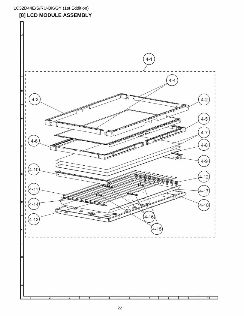
LC32D44E/S/RU-BK/GY (1st Eddition)
[8] LCD MODULE ASSEMBLY
4-4
4-1
4-2
4-5
4-7
4-8
4-9
4-12
4-17
4-18
4-15
4-13
4-14
4-11
4-10
4-6
4-16
4-3
22

LC32D44E/S/RU-BK/GY (1st Eddition)
NO. PARTS CODE PRICE RANK
NEW MARK
PART DELIVERY DESCRIPTION
[9] SUPPLIED ACCESSORIES
NO. PARTS CODE PRICE RANK
NEW MARK
PART DELIVERY DESCRIPTION
[8] LCD MODULE ASSEMBLY4-1 R1LK315T3GW30Y N J LCD Module Ass'y4-2 CANGKB549WJ01 AS N J Bezel Ass'y (Top)4-3 CANGKB549WJ02 AR N J Bezel Ass'y (Bottom)4-4 CANGKB548WJ01 AK N J Bezel Ass'y (L, R), x24-5 CHLDZB061WJ01 AT N J Panel Chassis Ass'y (Left)4-6 CHLDZB062WJ01 AT N J Panel Chassis Ass'y (Right)4-7 PSHEPA667WJZZ AU N J Lens Sheet, x24-8 PSLDK3003TPZZ AY N J Diffusion Panel4-9 LHLDZA919WJKZ AL N J Lamp Holder-L
4-10 LHLDZA918WJKZ AL N J Lamp Holder-R4-11 RLMPLA029WJN1 AR N J Lamp Unit, x104-12 QSOCFA003WJZZ AD N J Lamp Socket, x104-13 RUNTK3923TPZZ AN N J GND PWB (Top)4-14 RUNTK3924TPZZ AP N J GND PWB (Bottom)4-15 LHLDZA924WJKZ AB N J Lamp Clip A, x24-16 LHLDZA925WJKZ AC N J Lamp Clip B, x24-17 PMiR-A166WJZZ AU N J Reflection Sheet4-18 CCHSMA422WJ01 N J BL Chassis Ass'y
- LX-EZA028WJF9 AB J Screw, x12 (for Bezel, Panel Chassis)- LX-HZA039WJF7 AB N J Screw, x10 (for Bezel, Panel Chassis, BL Chassis)
[9] SUPPLIED ACCESSORIESX1 LHLDWA173WJKZ AE J Cable Clamp
! X2 QACCKA007WJPZ AK J AC Cord 2Pin (for Europe without U.K. and Ireland.! X2 QACCBA054WJPZ AQ P AC Cord 3Pin (for U.K. and Ireland)
X3 RRMCGA591WJSA AQ P Remote Control unit (LC-32D44E(BK))X3 RRMCGA591WJSB AQ P Remote Control unit (LC-32D44E(GY))X4 TiNS-D477WJZZ AM N P Operation Manual (ENGLISH...) (LC-32D44E(BK)/(GY))X5 TiNS-D478WJZZ AM N P Operation Manual(SWEDISH...) (LC-32D44E(BK)/(GY))X6 TiNS-D479WJZZ AP N P Operation Manual(POLISH...) (LC-32D44E(BK)/(GY))X7 TiNS-D480WJZZ AF N P Operation Manual(RUSSIAN) (LC-32D44E(BK)/(GY))X8 TGAN-A801WJZZ AB P AQUOS Care Plan (U.K and Ireland)X9 TGAN-A802WJZZ AC P Warranty Card (U.K and Ireland)
X10 TGAN-A077WJZZ AE J Warranty Card (Russian)X11 Not Available - - "AA" size BatteryX12 CDAi-A441WJ02 BF N J Stand Ass'y (LC-32D44E(BK))X12 CDAi-A441WJ05 BG N P Stand Ass'y (LC-32D44E(GY))
X12-1 Not Available - N - Tool for Stand
•
X3
X11 X4 X5 X6 X7X8
X9
X10
X2 X1X12
X12-1
23
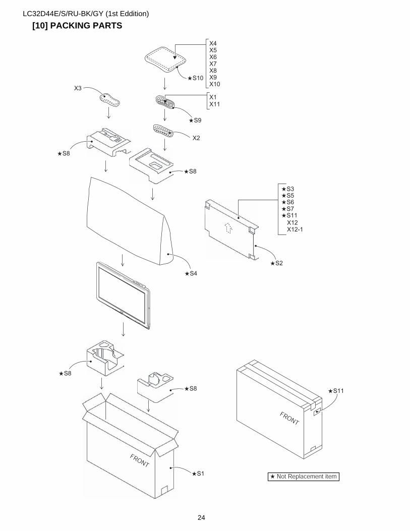
LC32D44E/S/RU-BK/GY (1st Eddition)
[10] PACKING PARTS
S3
S2
S4
S8
S1
S8
S8
S10
S9
S8
S5S6S7S11
S11
24

LC32D44E/S/RU-BK/GY (1st Eddition)
NO. PARTS CODE PRICE RANK
NEW MARK
PART DELIVERY DESCRIPTION
[10] PACKING PARTSS1 SPAKCD948WJZZ - N - Packing CaseS2 SPAKFB417WJZZ - N - Stand CaseS3 SPAKFB418WJZZ - N - Stand Pad (LC-32D44E(BK))S3 SPAKFB550WJZZ - N - Stand Pad (LC-32D44E(GY))S4 SPAKPA382WJZZ - N - Wrapping PaperS5 SPAKPB053WJZZ - N - Mirror Mat (Stand Support)S6 SPAKPB054WJZZ - N - Mirror Mat (Stand Bsse)S7 SPAKAA373WJZZ - N - Cover SheetS8 SPAKXB805WJZZ - N - Buffer material (Top/Bottom)S9 SSAKAA009WJZZ - - Polyethylene bag
S10 SSAKAA111WJZZ - N - Polyethylene bagS11 TLABM5584BMZZ - - Case No. Label
[11] SERVICE JIGSN QCNW-G440WJQZ AP N J Connecting Cord (4-5pins L=1000mm), Main to KeyN QCNW-H184WJQZ AX N J Connecting Cord, MAIN-R/C,LEDN QCNW-H185WJQZ AV N J Connecting Cord, MAIN-POWERN QCNW-H186WJQZ AQ N J Connecting Cord, MAIN-POWERN QCNW-H187WJQZ AP N J Connecting Cord, MAIN-SPEAKERN QCNW-C222WJQZ AW J Connecting Cord (80pin FFC L=1000mm), x2 MAIN t
25

LC32D44E/S/RU-BK/GY (1st Eddition)
COPYRIGHT © 2008 BY SHARP CORPORATION
ALL RIGHTS RESERVED.
No Part of this publication may be reproduced,
stored in a retrieval system, or transmitted in
any from or by any means, electronic, mechanical,
photocopying, recording, or otherwise, without
prior written permission of the publisher.
SHARP CORPORATIONAV Systems GroupCS Promotion CenterYaita,Tochigi 329-2193, Japan
Mar. 2008TQ -S SH. DS