A Differential Phase-Modulated Interferometer with Rotational ...

This article was downloaded by: [University of California Davis]On: 13 October 2014, At: 13:28Publisher: Taylor & FrancisInforma Ltd Registered in England and Wales Registered Number: 1072954 Registeredoffice: Mortimer House, 37-41 Mortimer Street, London W1T 3JH, UK
Click for updates
Philosophical MagazinePublication details, including instructions for authors andsubscription information:http://www.tandfonline.com/loi/tphm20
Room temperature mechanicalbehaviour of a Ni-Fe multilayeredmaterial with modulated grain sizedistributionLilia Kurmanaevaa, Hamed Bahmanpoura, Troy Hollandb, JonathanMcCreac, Joon Hwan Leed, Jie Jiand, Haiyan Wangd, Enrique J.Laverniaa & Amiya K. Mukherjeea
a Department of Chemical Engineering and Materials Science,University of California, Davis, CA 95817, USAb Department of Mechanical Engineering, Colorado StateUniversity, Campus Delivery 1374, Fort Collins, CO 80523, USAc Integran Technologies Inc., Toronto, Canadad Department of Electrical and Computer Engineering, Texas A &M University, College Station, TX 77843-3128, USAPublished online: 09 Oct 2014.
To cite this article: Lilia Kurmanaeva, Hamed Bahmanpour, Troy Holland, Jonathan McCrea,Joon Hwan Lee, Jie Jian, Haiyan Wang, Enrique J. Lavernia & Amiya K. Mukherjee (2014): Roomtemperature mechanical behaviour of a Ni-Fe multilayered material with modulated grain sizedistribution, Philosophical Magazine, DOI: 10.1080/14786435.2014.964346
To link to this article: http://dx.doi.org/10.1080/14786435.2014.964346
PLEASE SCROLL DOWN FOR ARTICLE
Taylor & Francis makes every effort to ensure the accuracy of all the information (the“Content”) contained in the publications on our platform. However, Taylor & Francis,our agents, and our licensors make no representations or warranties whatsoever as tothe accuracy, completeness, or suitability for any purpose of the Content. Any opinionsand views expressed in this publication are the opinions and views of the authors,and are not the views of or endorsed by Taylor & Francis. The accuracy of the Contentshould not be relied upon and should be independently verified with primary sourcesof information. Taylor and Francis shall not be liable for any losses, actions, claims,proceedings, demands, costs, expenses, damages, and other liabilities whatsoever orhowsoever caused arising directly or indirectly in connection with, in relation to or arisingout of the use of the Content.

This article may be used for research, teaching, and private study purposes. Anysubstantial or systematic reproduction, redistribution, reselling, loan, sub-licensing,systematic supply, or distribution in any form to anyone is expressly forbidden. Terms &Conditions of access and use can be found at http://www.tandfonline.com/page/terms-and-conditions
Dow
nloa
ded
by [
Uni
vers
ity o
f C
alif
orni
a D
avis
] at
13:
28 1
3 O
ctob
er 2
014

Room temperature mechanical behaviour of a Ni-Fe multilayeredmaterial with modulated grain size distribution
Lilia Kurmanaevaa*, Hamed Bahmanpoura, Troy Hollandb, Jonathan McCreac,Joon Hwan Leed, Jie Jiand, Haiyan Wangd, Enrique J. Laverniaa and
Amiya K. Mukherjeea
aDepartment of Chemical Engineering and Materials Science, University of California, Davis, CA95817, USA; bDepartment of Mechanical Engineering, Colorado State University, Campus
Delivery 1374, Fort Collins, CO 80523, USA; cIntegran Technologies Inc., Toronto, Canada;dDepartment of Electrical and Computer Engineering, Texas A & M University, College Station,
TX 77843-3128, USA
(Received 27 February 2014; accepted 2 September 2014)
To gain fundamental insight into the relationship between length scales andmechanical behaviour, Ni-Fe multilayered materials with a 5-μm-layer thick-ness and a modulated grain size distribution have been synthesized by pulsedelectrodeposition. Microstructural studies by SEM and TEM reveal the alter-nating growth of well-defined layers with either nano (d = 16 nm) or coarsegrains (d ≥ 500 nm). Room temperature tensile tests have been performed toinvestigate the mechanical response and understand the underlying deforma-tion mechanisms. Tensile test results and fractographic studies demonstratethat the overall room temperature mechanical behaviour of the multilayeredmaterial, i.e. strength and ductility, is governed primarily by the layers con-taining nanocrystalline grains. The measured properties have been discussedin the context of modulated grain structure of the multilayered sample andcontribution of each grain size regime to the overall strength and ductility.
Keywords: Ni-Fe; electrodeposition; multilayered structure; tensile test
1. Introduction
Multilayered (ML) structures provide a pathway to enhance the strength of structuralmaterials given their unique characteristics, which include a high volume fraction of grainboundaries (GB) and layer interfaces which effectively hinder dislocation activity.Inspired by the pioneering work by Koehler [1], many recent studies discussed the influ-ence of the layer thickness and thickness ratio on the mechanical behaviours of multilay-ered materials [2–7]. On the basis of these as well as many other studies, it is now wellestablished that a critical factor influencing strength and ductility is the dislocation mobil-ity within and across the layers. The mechanisms that govern the relationship betweenlayer thickness and yield strength have recently been summarized by Wang and Misra[8]. Accordingly, when layer thickness is in the range from a micron down to the submi-cron size, the deformation mechanism is mostly assisted by dislocation pile-ups at grain
*Corresponding author. Email: [email protected]
© 2014 Taylor & Francis
Philosophical Magazine, 2014http://dx.doi.org/10.1080/14786435.2014.964346
Dow
nloa
ded
by [
Uni
vers
ity o
f C
alif
orni
a D
avis
] at
13:
28 1
3 O
ctob
er 2
014

and interphase boundaries. In contrast, in the case of layer thickness in the nanometerrange, the deformation mechanism is controlled by the glide of single dislocations con-fined to individual layers. At yet smaller layer thicknesses (below 10 nm), dislocationcrossing the interfaces governs the deformation behaviour [8].
Despite encouraging preliminary results in achieving high strength in ML materials,the accompanying limited ductility has hindered extensive engineering applications. Inrelated work, Huang and Spaepen [9] reported that in a series of Ag/Cu ML samplesprepared by electron beam evaporation, ductility under tension reduced with decreasinglayer thickness. Mara et al. [10] reported an excess of 25% plastic strain under com-pression in sputtered Cu/Nb ML material. In a comprehensive study of ML Cu/Zr andCu/Nb prepared by magnetron sputtering, Zhang et al. [11] also concluded that theductility and fracture mode are strongly length-scale dependent. The challenge posed bythe inherent low ductility of nanocrystalline (NC) metals has prompted various strate-gies which are well described in the literature [12–14]. One of the proposed strategiesto improve ductility is to introduce larger sized grains into a nanograined matrix toobtain a bimodal structure, a concept originally proposed in 2001 [14] and subsequentlyimplemented by various investigators [15,16]. Notably, ML structures offer a uniqueopportunity to control the distribution of large- and small-grained microstructures byintroducing additional variables, e.g. layer thickness and spacing.
A crucial aspect of the research on ML materials is to control the intralayer micro-structure and the interface between layers. In recent years, a great deal of attention hasbeen focused on ML structures containing pure elements with different combinations offcc, bcc, and hcp phases such as Cu/Ni [6,17], Cu/Nb [18,19], and Al/Ti [20,21] sys-tems. In fact, most published papers report results, which were based on combinationsof pure elements, mostly to facilitate synthesis and analysis. In view of above discus-sion, the goal of the present work is to investigate the influence of length scales onmechanical behaviour of ML materials. We have selected a Ni-Fe system on the basisof both scientific and engineering arguments. From a scientific perspective, in the mostof range of concentrations, Ni-Fe represents a single phase material, which as a modelsystem simplifies the analysis. Moreover, numerous published studies on the mechanicalbehaviour of Ni and Ni-based alloys via electrodeposition (ED) facilitate comparativeanalysis of our results [22–24]. As an engineering system, Ni-Fe alloys are of interestowing to their excellent high temperature stability and low coefficient of thermal expan-sion of nickel alloys with high iron content [25–27]. The samples were produced bymeans of ED; optimized deposition parameters, based on prior work [28], were used toproduce large-size free-standing sheets (200 × 200 mm2) with modulated microstructuresthat are well suited for industrial application. In order to analyse contributions of modu-lated microstructure to the mechanical properties, we have compared results of MLsample with monolithic NC and coarse-grained (CG) ED Ni-Fe samples.
2. Experimental procedure
Multilayered Ni-60 wt.% Fe samples were synthesized via ED technique at IntegranTechnologies Inc. (Toronto, Canada). The electrodeposition parameters were selected toproduce modulated microstructures with alternating NC and CG sub-layers with a con-stant thickness ratio of 1:1. In this regard, large-sized sheets with a total thickness of about600 μm and layer thickness of 5 μm were produced by depositing onto a passivated
2 L. Kurmanaeva et al.
Dow
nloa
ded
by [
Uni
vers
ity o
f C
alif
orni
a D
avis
] at
13:
28 1
3 O
ctob
er 2
014

Titanium cathode from which they were subsequently mechanically stripped to yieldfree-standing sheets from which specimens for tensile testing were sectioned. Chemicalanalysis of the as-deposited sample shows minor presence of impurities that include (allcompositions are in wt.%): C: 0.026%, S: 0.018%, O: 0.0023%, N: 0.0004%, Co: 0.06%,Cu: 0.014%, and Mo: 0.017%. Monolithic samples consisting of a single layer of NC orCG with closely similar chemical composition were also deposited.
The mechanical properties of ED samples were determined using room temperaturetensile testing. Uniaxial tensile tests were performed using a dedicated tensile stage forminiature specimens at a strain rate of 10−4 s−1 in Institute of Nanotechnology, KIT(Karlsruhe, Germany). Tensile samples with measuring gauge length 2 mm × 1 mm ×0.3 mm were mechanically fine polished. The elongation was precisely measured using alaser extensometer P-50 by Fiedler Optoelectronics to read TiO2 marks that had beenapplied on the tensile specimens’ surfaces. At least three tensile samples were used foreach condition to obtain statistically valid results.
JEOL cross-section polisher was utilized to prepare samples for studying the as-deposited microstructure and chemical composition in a Philips XL 30 FEG scanningelectron microscope with a voltage of 15 kV, equipped with an Oxford Nordlys nano-electron backscatter diffraction (EBSD) detector. Energy dispersive spectroscopy (EDS)was used for an identification of chemical composition of sub-layers. EBSD map of CGsample was acquired with a step size of 75 nm. X-ray diffraction (XRD) was measuredby means of Scintag X-ray diffractometer equipped with a graphite monochromatorusing Cu Ka radiation. Cross-sectional TEM (XTEM) and selected-area electron diffrac-tion (SAED) were performed using a JEOL JEM-2010 microscope operated under200KV with a double-tilt holder and a point-to-point resolution of 0.23 nm. XTEM foilswere prepared through a conventional TEM sample preparation routine includingcutting, gluing, grinding, polishing, and final precision ion polishing.
3. Results
Figure 1 shows the XRD profile of ML and monolithic samples. Based on the phasediagram [29], Ni-60 wt.% Fe alloy presents a fcc structure, i.e. Ni with Fe atoms insolid solution, and the XRD spectra of monolithic CG samples reveal the presence ofsuch a phase. However, the monolithic NC and ML samples exhibit mixed fcc/bccmicrostructures. A bcc (1 1 0) peak can be resolved under the fcc (1 1 1) peak in bothcases. This result is not completely surprising based on extensive previous studies onNi-Fe alloy. For example, Grimmet et al. [30] observed that varying of the ED parame-ters could result in the formation of mixed fcc/bcc structures in Ni alloys containing50–60 wt.% Fe.
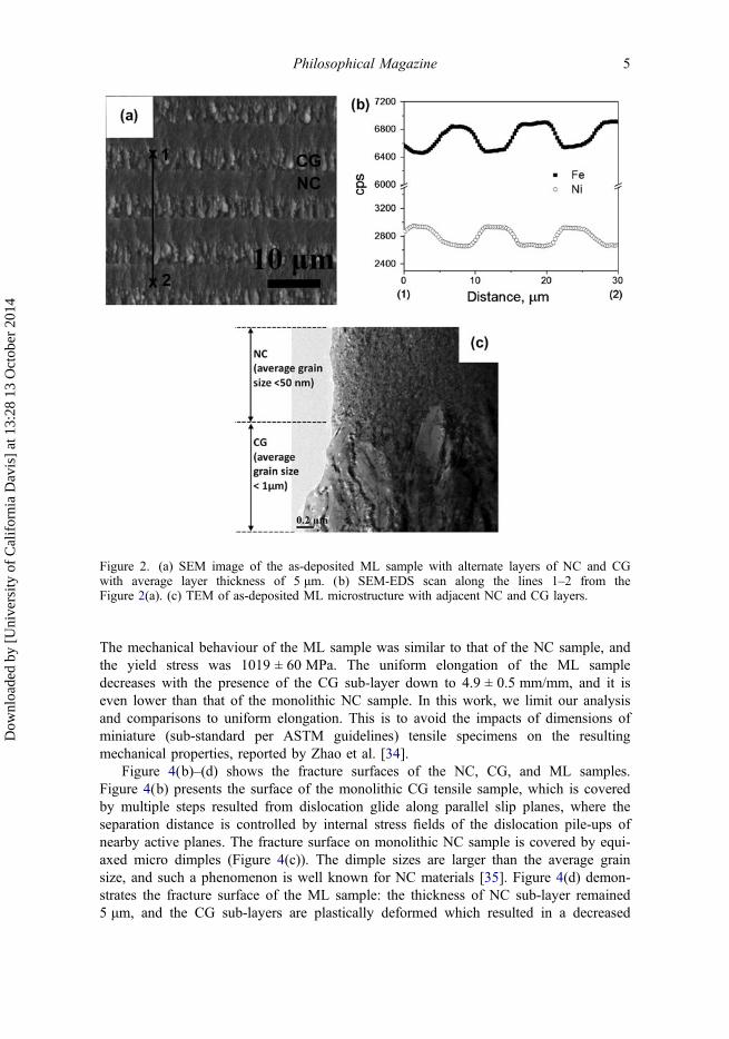
Figure 2(a) shows a representative SEM image of the ion polished cross section ofthe ML sample. The image confirms that several alternating sub-layers of NC and CGgrains were electrodeposited next to each other. Figure 2(b) presents the EDS line scanthrough several sub-layers as it pointed in Figure 2(a). The chemical composition ofCG sub-layer (point 1, Figure 2(a)) corresponded to the target Fe concentration, namely60 ± 0.2 wt.%. In the NC sub-layer, the amount of Fe was slightly higher and wasmeasured to be 63 ± 0.3 wt.% (point 2 Figure 2(a)). In order to obtain the modulatedstructure, changes of the electrodeposition parameters were applied, which lead toalteration to the Ni/Fe atomic ratio. In related work, several authors reported [27,31,32]
Philosophical Magazine 3
Dow
nloa
ded
by [
Uni
vers
ity o
f C
alif
orni
a D
avis
] at
13:
28 1
3 O
ctob
er 2
014

that during the simultaneous co-deposition of Ni and Fe, the grain size could bedecreased by increasing the Ni/Fe atom ratio of the electrolyte, which usually results ina decrease in Fe content. Figure 2(c) shows a typical bright-field TEM image of theML sample at the interface of NC and CG sub-layers. Detailed grain size analysis indi-cated that the NC and CG sub-layers have average grain sizes of 16 and 500 nm,respectively. The interlayer interfaces are important for controlling the integrity of thesample and transferring the load during the plastic deformation. Obviously, the layerinterface is clean with well-bonded sub-layers, which are required to sustain the load.
In order to correlate the precise contribution of the modulated structures, the micro-structure of monolithic samples was also studied in detail. Figure 3(a) shows the EBSDimage of a monolithic CG sample, which has an elongated microstructure with an aver-age grain width around 5 μm. The grains are preferentially oriented along the ED direc-tion and the presence of <1 0 0> texture could also be confirmed by XRD (Figure 1). Inrelated studies, Amblard et al. [33] suggested that the texture formation during ED isstrongly affected by deposition conditions rather than the substrate. Figure 3(b) and (c)show a TEM bright-field image and the corresponding SAED of the monolithic NCsample, respectively. The monolithic NC sample has a uniform nanostructure with anaverage grain size ~16 nm (Figure 3(b)). However, SAED pattern reveals the presenceof a mixture of bcc and fcc microstructures (Figure 3(c)), as well as the presence of tex-ture as evidenced by the presence of bright arced spots on the first diffraction ring of(1 1 1)fcc/(1 1 0)bcc.
Figure 4(a) plots the true stress – true strain curves obtained from room temperaturetensile tests of ML, NC, and CG samples. With decreasing grain size, the monolithicNC sample showed higher yield strength of 1357 ± 79 MPa as compared with320 ± 31 MPa for the monolithic CG sample. At the same time, the uniform elongationof the NC sample was significantly lower than that in the monolithic CG sample,7.3 ± 0.9 mm/mm vs. 24.2 ± 2.6 mm/mm for NC and CG samples, respectively.
Figure 1. (colour online) XRD profile of multilayered, monolithic NC and CG samples.
4 L. Kurmanaeva et al.
Dow
nloa
ded
by [
Uni
vers
ity o
f C
alif
orni
a D
avis
] at
13:
28 1
3 O
ctob
er 2
014
The mechanical behaviour of the ML sample was similar to that of the NC sample, andthe yield stress was 1019 ± 60 MPa. The uniform elongation of the ML sampledecreases with the presence of the CG sub-layer down to 4.9 ± 0.5 mm/mm, and it iseven lower than that of the monolithic NC sample. In this work, we limit our analysisand comparisons to uniform elongation. This is to avoid the impacts of dimensions ofminiature (sub-standard per ASTM guidelines) tensile specimens on the resultingmechanical properties, reported by Zhao et al. [34].
Figure 4(b)–(d) shows the fracture surfaces of the NC, CG, and ML samples.Figure 4(b) presents the surface of the monolithic CG tensile sample, which is coveredby multiple steps resulted from dislocation glide along parallel slip planes, where theseparation distance is controlled by internal stress fields of the dislocation pile-ups ofnearby active planes. The fracture surface on monolithic NC sample is covered by equi-axed micro dimples (Figure 4(c)). The dimple sizes are larger than the average grainsize, and such a phenomenon is well known for NC materials [35]. Figure 4(d) demon-strates the fracture surface of the ML sample: the thickness of NC sub-layer remained5 μm, and the CG sub-layers are plastically deformed which resulted in a decreased
Figure 2. (a) SEM image of the as-deposited ML sample with alternate layers of NC and CGwith average layer thickness of 5 μm. (b) SEM-EDS scan along the lines 1–2 from theFigure 2(a). (c) TEM of as-deposited ML microstructure with adjacent NC and CG layers.
Philosophical Magazine 5
Dow
nloa
ded
by [
Uni
vers
ity o
f C
alif
orni
a D
avis
] at
13:
28 1
3 O
ctob
er 2
014

sub-layer thickness. A few large voids were observed at the CG/Nc sub-layer bound-aries (Figure 4(d)). The fracture surface of the NC sub-layers was covered by smalldimples, similar to ones observed in monolithic NC sample. However, an importantcharacteristic that was evident in the fracture surface of the NC samples is the presenceof regions exhibiting copious shear localization (Figure 4(d)). When the sub-layers havedifferent flow properties, the simultaneous deformation of the ML structure results innecking or fracture of the hard phase [36,37]. In the case of NC materials, strain locali-zation often happens in the form of shear bands [38].
4. Discussion
In order to study the possible contributions of layering to the mechanical properties ofthe ML sample, it is important to establish the strengthening mechanisms that are activein the monolithic NC material. Several factors are responsible for the significantstrengthening, as well as a loss in ductility in the monolithic NC sample. First, on one
Figure 3. (colour online) (a) EBSD image of cross section of the monolithic CG sample. Averagewidth of the grains around 5 μm (b) Bright-field TEM image of monolithic NC, and (c)diffraction pattern showing presence of fcc and bcc phases.
6 L. Kurmanaeva et al.
Dow
nloa
ded
by [
Uni
vers
ity o
f C
alif
orni
a D
avis
] at
13:
28 1
3 O
ctob
er 2
014

hand, as grain size decreases, the interactions of dislocations and grain boundaries leadto strengthening via the well-known Hall-Petch mechanism [39]. On other hand, how-ever, as grain sizes fall below 30 nm strain hardening becomes more difficult and this isgenerally thought to be responsible for the inherent lower ductility of NC materials[34]. Second, the presence of different phases also plays a role in determining themechanical properties of the specimens. XRD (Figure 1) and TEM (Figure 3(c)) resultsindicated the presence of the mixture of fcc and bcc phases. At room temperature, theintrinsic lattice resistance (Peierls-Nabarro forces) in bcc metals is relatively higher thanthat in fcc metals [40], and this could result in additional strengthening of NC samples.
Early studies on the design of ML architectures were based on the fact that a com-bination of high strength and good ductility can be obtained by combining the highstrength from brittle NC sub-layers with high toughness of CG sub-layers [41]. Theconcept is straight forward, that is the CG layers, because of their higher ability todeform plastically, will blunt an advancing crack and prevent early failure of the mate-rial. In terms of the contributions of each layer to the overall mechanical behaviour,however, it is not possible to use a simple “rule of mixtures” analysis, since the
Figure 4. (colour online) (a) Engineering stress–strain curves from monolithic NC and CG andML NiFe samples. (b)–(d) SEM image of the fracture surface of tensile samples tested at roomtemperature. (b) Surface of monolithic CG sample (arrows show steps formed by glide of multi-ple dislocations (c) Fracture surface of monolithic NC. (d) Fracture surface of ML sample (blackarrows point to interlayer voids, the white arrow points shear localization region).
Philosophical Magazine 7
Dow
nloa
ded
by [
Uni
vers
ity o
f C
alif
orni
a D
avis
] at
13:
28 1
3 O
ctob
er 2
014

periodicity of the layers is not random. In the ML sample with a 5 μm sub-layer thick-ness, the NC sub-layers govern the room temperature tensile behaviour, because thestrength of ML material is much higher than that of the CG sample (Figure 4(a)). Inthis regard, the role of interfaces in transferring load from one layer to the next iscritical. Since interfaces provide a major contribution to the strength of the ML system,the presence of dissimilar phases (i.e. bcc and fcc) in alternate layers will affect coher-ency between layers and, moreover, will also influence the transmission of dislocationsfrom one layer to the adjacent layer.
The fact that the monolithic CG sample exhibits a high ductility and that the intro-duction of a CG sub-layer does not increase uniform elongation suggests that the ductil-ity of the ML sample is affected by the presence of interlayer interfaces. Based onHart’s criteria [42], in order to achieve a good ductility in tensile tests which means pre-venting fast strain localization and early fracture, the material should exhibit increasedstrain hardening and/or strain rate sensitivity. In the present work, the CG sample exhib-ited good ductility with uniform elongation up to 24.2 ± 2.6% (Figure 4(a)) due to anincrease in dislocation nucleation and storage within grains. Because electrodepositionof CG fcc material formed the preferable (1 0 0) orientation, during tensile tests, theactive slip family (1 1 1) could be easily activated by critical resolve shear stress, τcrss(Figure 5). In comparison with CG samples, where dislocations can be annihilated atGBs or at free surfaces producing steps (Figure 4(b)), in ML samples, any dislocationsfrom CG sub-layer are trapped at interlayer interfaces and will not penetrate the neigh-bouring grain or be annihilated at GBs due to interface stresses, τints (Figure 5). Andthis will hinder the slip of other dislocations from the same dislocation source, whichwould decrease the strain hardening ability and lower ductility. In the case of CG/NCinterface, the dislocation slip across is even more difficult as a result of limited disloca-tions operated in a NC structure. Related studies involving in situ X-ray diffraction andMD simulations suggested that the deformation of NC materials are accommodated byGB-mediated mechanisms, and dislocation propagation is hindered by GB pinning [43].Furthermore, in NC materials, there is different natures of strain hardening, and thesematerials usually exhibit an extended microplasticity stage [24,44,45]. For example,
Figure 5. Schematic presentation of deformation during tensile tests of CG and ML samples,where τcrss is a critical resolve shear stress, and τints is an interface stress. In ML material, thedislocation source within CG sub-layer is closed when τcrss ≤ τints.
8 L. Kurmanaeva et al.
Dow
nloa
ded
by [
Uni
vers
ity o
f C
alif
orni
a D
avis
] at
13:
28 1
3 O
ctob
er 2
014

recently Ivanisenko et al. [45] proposed that the strain hardening of NC materials atroom temperature was promoted by GB sliding which was accommodated by slip ofdislocations emitted from GBs.
In ED materials during deposition, the deposited layer often inherits the structure ororientation of the substrate [46]. But the presence of dissimilar phases in alternate layerscould affect coherency between layers and moreover, influence the transmission of dis-locations from one layer to the adjacent layer. For example, in fcc/fcc ML systems suchas Cu/Ag and Cu/Ni [17], it was demonstrated that depending on the lattice mismatch,more closely spaced misfit dislocations in Cu/Ag promote the removal of coherencystresses and lead to weak interfaces compared with Cu/Ni with wider spacing betweenmisfit dislocations. In the present ML system, two types of interphase boundaries couldpresent, namely fcc/fcc and fcc/bcc interfaces as shown in the XRD results, Figure 1.In order to prove either presented interphases are coherent, a precisely HRTEM work isneeded and planned for this ongoing research.
5. Conclusion
Ni-Fe multilayered sample with layer thickness of 5 μm was successfully prepared bypulsed ED technique. A modulated grain size regime was maintained by the imposedpulses with average grain size of 16 and 500 nm in NC and CG sub-layers, respec-tively. The produced ML sample has a mixed fcc/bcc microstructure in NC sub-layersand single fcc phase structure in CG sub-layers. Tensile test results revealed thatmechanical behaviour of ML samples relies on the strength obtained mainly from NClayers, but the ductility of the multilayered sample is greatly dependent on interlayerinterfaces. Fracture studies show that NC sub-layers develop micro dimples upon frac-ture and CG layers have high ductility. However, CG sub-layers are not strong enoughto sustain the load when the NC sub-layers experience failure and the fracture of bothsub-layers possibly happens almost simultaneously.
AcknowledgementsThe authors are grateful to Dr Troy Topping for the help in EDM machining of tensile samples,Dr Jochen Fiebig and Mr Josh Yee for the help with SEM and acquiring EBSD map. LK wouldlike to acknowledge Dr Yulia Ivanisenko (KIT, Karlsruhe, Germany) for the opportunity to usetensile machine.
Funding
Financial support from Office of Naval Research under grants N00014-13-1-0557 (Research atUCD), N00014-13-1-0555 (TEM work at Texas A&M University), and N00014-10-C-0371(Sample preparation at Integran Technologies Inc) with Dr Lawrence Kabacoff as the programmanager are gratefully acknowledged.
References
[1] J.S. Koehler, Phys. Rev. B 2 (1970) p.547.[2] S.L. Lehoczky, Phys. Rev. Lett. 41 (1978) p.1814.
Philosophical Magazine 9
Dow
nloa
ded
by [
Uni
vers
ity o
f C
alif
orni
a D
avis
] at
13:
28 1
3 O
ctob
er 2
014

[3] D. Tench and J. White, Metall. Trans. A 15 (1984) p.2039.[4] P. Anderson, I.-H. Lin and R. Thomson, Scr. Metall. Mater. 27 (1992) p.687.[5] A. Sergueeva, N. Mara and A.k. Mukherjee, MRS Online Proc. Libr. 673 (2001).[6] K.O. Schweitz, J. Chevallier, J. Bøttiger, W. Matz and N. Schell, Philos. Mag. A 81 (2001)
p.2021.[7] D. Mitlin, A. Misra, T.E. Mitchell, J.P. Hirth and R.G. Hoagland, Philos. Mag. 85 (2005)
p.3379.[8] J. Wang and A. Misra, Curr. Opin. Solid State Mater. Sci. 15 (2011) p.20.[9] H. Huang and F. Spaepen, Acta Mater. 48 (2000) p.3261.[10] N.A. Mara, D. Bhattacharyya, P. Dickerson, R.G. Hoagland and A. Misra, Appl. Phys. Lett.
92 (2008) p.231901.[11] J.Y. Zhang, X. Zhang, R.H. Wang, S.Y. Lei, P. Zhang, J.J. Niu, G. Liu, G.J. Zhang and J.
Sun, Acta Mater. 59 (2011) p.7368.[12] E. Ma, Scr. Mater. 49 (2003) p.663.[13] Y.H. Zhao, Y.T. Zhu, X.Z. Liao, Z. Horita and T.G. Langdon, Mater. Sci. Eng. A 463
(2007) p.22.[14] V.L. Tellkamp, E.J. Lavernia and A. Melmed, Metall. Mater. Trans. A 32 (2001) p.2335.[15] Y. Wang, M. Chen, F. Zhou and E. Ma, Nature 419 (2002) p.912.[16] D.B. Witkin and E.J. Lavernia, Prog. Mater. Sci. 51 (2006) p.1.[17] R.G. Hoagland, T.E. Mitchell, J.P. Hirth and H. Kung, Philos. Mag. A 82 (2002) p.643.[18] D. Bhattacharyya, N.A. Mara, P. Dickerson, R.G. Hoagland and A. Misra, J. Mater. Res. 24
(2009) p.1291.[19] V.J. Keast, A. Misra, H. Kung and T.E. Mitchell, J. Mater. Res. 16 (2001) p.2032.[20] R. Banerjee, S.A. Dregia and H.L. Fraser, Acta Mater. 47 (1999) p.4225.[21] R. Banerjee, X.-D. Zhang, S.A. Dregia and H.L. Fraser, Acta Mater. 47 (1999) p.1153.[22] F. Ebrahimi and H. Li, Scr. Mater. 55 (2006) p.263.[23] P. Egberts, P. Brodersen and G.D. Hibbard, Mater. Sci. Eng. A 441 (2006) p.336.[24] S. Van Petegem, J. Zimmermann and H. Van Swygenhoven, Acta Mater. 61 (2013) p.5846.[25] H. Flor, H. Gudladt and C. Schwink, Acta Metall. 28 (1980) p.1611.[26] M. Shiga, Curr. Opin. Solid State Mater. Sci. 1 (1996) p.340.[27] J.L. McCrea, G. Palumbo, G.D. Hibbard and U. Erb, Rev. Adv. Mater. Sci. 5 (2013) p.252.[28] J. McCrea, Personal communication, Intergran Technologies, Toronto, ON.[29] T.B. Massalski, J.L. Murray, L.H. Bennett and H. Baker, Binary Alloy Phase Diagrams, 1st
ed., Vol. 1, American Society for Metals, Metals Park, CA, 1986, p.1144.[30] D.L. Grimmett, M. Schwartz and K. Nobe, J. Electrochem. Soc. 140 (1993) p.973.[31] H. Li and F. Ebrahimi, Mater. Sci. Eng. A 347 (2003) p.93.[32] C. Cheung, F. Djuanda, U. Erb and G. Palumbo, Nanostructured Mater. 5 (1995) p.513.[33] J. Amblard, I. Epelboin, M. Froment and G. Maurin, J. Appl. Electrochem. 9 (1979) p.233.[34] Y.H. Zhao, Y.Z. Guo, Q. Wei, T.D. Topping, A.M. Dangelewicz, Y.T. Zhu, T.G. Langdon
and E.J. Lavernia, Mater. Sci. Eng. A 525 (2009) p.68.[35] M. Dao, L. Lu, R.J. Asaro, J.T.M. De Hosson and E. Ma, Acta Mater. 55 (2007) p.4041.[36] S. Roy, B.R. Nataraj, S. Suwas, S. Kumar and K. Chattopadhyay, Mater. Des. 36 (2012)
p.529.[37] Y.-M. Hwang, H.-H. Hsu and H.-J. Lee, Int. J. Mach. Tools Manuf. 36 (1996) p.47.[38] A. Khalajhedayati and T.J. Rupert, Acta Mater. 65 (2014) p.326.[39] J.R. Weertman, Mater. Sci. Eng. A 166 (1993) p.161.[40] K.T. Ramesh, Nanomaterials – Mechanics and Mechanisms, Springer, Dordrecht, 2009,
pp.172–175.[41] D.J. Srolovitz, S.M. Yalisove and J.C. Bilello, Metall. Mater. Trans. A 26 (1995) p.1805.[42] E.W. Hart, Acta Metall. 15 (1967) p.351.
10 L. Kurmanaeva et al.
Dow
nloa
ded
by [
Uni
vers
ity o
f C
alif
orni
a D
avis
] at
13:
28 1
3 O
ctob
er 2
014

[43] S. Brandstetter, P.M. Derlet, S. Van Petegem and H. Van Swygenhoven, Acta Mater. 56(2008) p.165.
[44] S. Brandstetter, H. Van Swygenhoven, S. Van Petegem, B. Schmitt, R. Maaß and P.M. Derlet,Adv. Mater. 18 (2006) p.1545.
[45] Y. Ivanisenko, E.D. Tabachnikova, I.A. Psaruk, S.N. Smirnov, A. Kilmametov, A. Kobler,C. Kübel, L. Kurmanaeva, K. Csach, Y. Mishkuf, T. Scherer, Y.A. Semerenko and H. Hahn,Int. J. Plast. 60 (2014) p.40.
[46] M.J. Stowell, Defects in epitaxial deposits, in Epitaxial Growth Part B, Ch. 5, J.W.Matthews, ed., Academic Press, New York, 1975, pp.437–492.
Philosophical Magazine 11
Dow
nloa
ded
by [
Uni
vers
ity o
f C
alif
orni
a D
avis
] at
13:
28 1
3 O
ctob
er 2
014
Copyright © 2022 FDOKUMEN


![[- 200 [ PROVIDING MODULATED COMMUNICATION SIGNALS ]](https://static.fdokumen.com/doc/165x107/6328adc85c2c3bbfa804c60f/-200-providing-modulated-communication-signals-.jpg)