Characterization of grain growth, nature and role of grain boundaries in microcrystalline...
6
Characterization of grain growth, nature and role of grain boundaries in microcrystalline silicon—review of typical features J. Ko*ka * , T. Mates, H. Stuchlı ´kova ´, J. Stuchlı ´k, A. Fejfar Institute of Physics, AS-CR, Cukrovarnicka ´ 10, 16253 Prague 6, Czech Republic Available online 11 August 2005 Abstract A boundary between amorphous and microcrystalline growth of silicon thin films was explored for the study of grain growth by changing parameters of plasma enhanced deposition (substrate temperature, silane dilution or deposition duration and thus the film thickness). Resulting series of a-Si:H/Ac-Si:H samples were characterized by values of dark conductivity and corresponding activation energy and prefactor, diffusion length, hydrogen content and morphology. The abrupt change of conductivity at the boundary is accompanied by a peak in surface roughness and diffusion length, which were connected to the formation of a percolating network of microcrystalline large grains. Results are discussed using the idea of barriers for electronic transport forming at the large grain boundaries. Comparison of transport properties with the hydrogen content pointed out the fundamental role of hydrogen present at the grain boundaries. D 2005 Elsevier B.V. All rights reserved. Keywords: Microcrystalline silicon; Growth; Transport; Hydrogen 1. Introduction As concerns the form of (solid state) matter, there are two limiting cases: mono-crystalline and amorphous. In between there are many intermediate cases like poly-, micro-, nano- and also proto-crystalline forms. This situation is typical not only for silicon but also for carbon (amorphous C, crystalline diamond, nano-diamond and even ultranano- diamond...). Amorphous hydrogenated silicon (a-Si:H) and, during the last 10 years [1], hydrogenated microcrystalline silicon (Ac-Si:H) are studied as important thin film materials for photovoltaic (PV) solar cells and many other applications. The possibility to use a wide range of substrates, including flexible and cheap polymers, led us recently to study the Ac- Si:H sample series prepared at low substrate temperatures T S 100 -C [2–4]. Here we concentrate on a-Si:H/Ac-Si:H samples, pre- pared by plasma enhanced chemical vapour deposition (PE CVD) and compare them with the hot wire (HW) CVD ones. These series of samples represent the ideal model material because the a-Si:H/Ac-Si:H transition can be achieved just by change of one technological parameter like substrate temperature (T S ), discharge frequency, hydro- gen dilution (r H =[H 2 ] / [SiH 4 ]) or thickness. The aim of this work is to summarize the characteristic features of the a-Si:H/Ac-Si:H transition in topography, crystallinity, H content and the electronic transport proper- ties. Substantial changes observed outside the transition region are also discussed. 2. Experimental details 2.1. Samples We have evaluated three thickness series, two dilution and two temperature series of a-Si:H/Ac-Si:H samples. First thickness series was prepared by Toppan Printing Co. [2] at T S =75 -C and 54 MHz with the H dilution r H =[H 2 ]/ [SiH 4 ] = 29, the other two were prepared at our institute at T S = 250 -C; 13.56 MHz; with r H =21 and r H = 32. 0040-6090/$ - see front matter D 2005 Elsevier B.V. All rights reserved. doi:10.1016/j.tsf.2005.07.212 * Corresponding author. E-mail address: [email protected] (J. Ko*ka). Thin Solid Films 501 (2006) 107 – 112 www.elsevier.com/locate/tsf
Transcript of Characterization of grain growth, nature and role of grain boundaries in microcrystalline...

www.elsevier.com/locate/tsf
Thin Solid Films 501
Characterization of grain growth, nature and role of grain boundaries
in microcrystalline silicon—review of typical features
J. Ko*ka *, T. Mates, H. Stuchlıkova, J. Stuchlık, A. Fejfar
Institute of Physics, AS-CR, Cukrovarnicka 10, 16253 Prague 6, Czech Republic
Available online 11 August 2005
Abstract
A boundary between amorphous and microcrystalline growth of silicon thin films was explored for the study of grain growth by changing
parameters of plasma enhanced deposition (substrate temperature, silane dilution or deposition duration and thus the film thickness).
Resulting series of a-Si:H/Ac-Si:H samples were characterized by values of dark conductivity and corresponding activation energy and
prefactor, diffusion length, hydrogen content and morphology. The abrupt change of conductivity at the boundary is accompanied by a peak
in surface roughness and diffusion length, which were connected to the formation of a percolating network of microcrystalline large grains.
Results are discussed using the idea of barriers for electronic transport forming at the large grain boundaries. Comparison of transport
properties with the hydrogen content pointed out the fundamental role of hydrogen present at the grain boundaries.
D 2005 Elsevier B.V. All rights reserved.
Keywords: Microcrystalline silicon; Growth; Transport; Hydrogen
1. Introduction
As concerns the form of (solid state) matter, there are two
limiting cases: mono-crystalline and amorphous. In between
there are many intermediate cases like poly-, micro-, nano-
and also proto-crystalline forms. This situation is typical not
only for silicon but also for carbon (amorphous C,
crystalline diamond, nano-diamond and even ultranano-
diamond. . .).Amorphous hydrogenated silicon (a-Si:H) and, during
the last 10 years [1], hydrogenated microcrystalline silicon
(Ac-Si:H) are studied as important thin film materials for
photovoltaic (PV) solar cells and many other applications.
The possibility to use a wide range of substrates, including
flexible and cheap polymers, led us recently to study the Ac-Si:H sample series prepared at low substrate temperatures
TS�100 -C [2–4].
Here we concentrate on a-Si:H/Ac-Si:H samples, pre-
pared by plasma enhanced chemical vapour deposition (PE
0040-6090/$ - see front matter D 2005 Elsevier B.V. All rights reserved.
doi:10.1016/j.tsf.2005.07.212
* Corresponding author.
E-mail address: [email protected] (J. Ko*ka).
CVD) and compare them with the hot wire (HW) CVD
ones. These series of samples represent the ideal model
material because the a-Si:H/Ac-Si:H transition can be
achieved just by change of one technological parameter
like substrate temperature (TS), discharge frequency, hydro-
gen dilution (rH=[H2] / [SiH4]) or thickness.
The aim of this work is to summarize the characteristic
features of the a-Si:H/Ac-Si:H transition in topography,
crystallinity, H content and the electronic transport proper-
ties. Substantial changes observed outside the transition
region are also discussed.
2. Experimental details
2.1. Samples
We have evaluated three thickness series, two dilution
and two temperature series of a-Si:H/Ac-Si:H samples. First
thickness series was prepared by Toppan Printing Co. [2] at
TS=75 -C and 54 MHz with the H dilution rH=[H2] /
[SiH4]=29, the other two were prepared at our institute at
TS=250 -C; 13.56 MHz; with rH=21 and rH=32.
(2006) 107 – 112

J. Ko*ka et al. / Thin Solid Films 501 (2006) 107–112108
Both dilution series were prepared by Toppan Printing
Co. [2–4] (first at TS=60 -C; 54 MHz; with rH=26–168
and the second series at TS=80 -C; 54 MHz; with rH=34–
168). First of the temperature series was prepared by Toppan
Printing Co. [3,4] (TS=35–200 -C; rH=133; 54 MHz) and
the second temperature series was prepared in our institute
(TS=40–250 -C; rH=32; 13.56 MHz).
2.2. Experimental techniques
As the simplest characterization, the measurement of DC
dark conductivity (rD) with coplanar contacts at room
temperature has been used, often complemented with the
evaluation of the activation energy (Ea) and the prefactor
(r0) from the temperature dependencies of rd. Steady-State
Photocarrier Grating (SSPG) method was used for evalua-
tion of the ambipolar diffusion length (Ldiff) [2]. The
topography and RMS roughness have been studied by the
modified atomic force microscope (AFM) [5]. The total H
content has been evaluated by elastic recoil detection
analysis (ERDA). The Raman spectroscopy has been used
for evaluation of crystallinity XC, see [6].
Fig. 1. Schematic picture of the electric field and optical concentration (a) due to
thickness series prepared at TS=75 -C.
3. Experimental results and discussion
3.1. Growth of microcrystalline grains
Besides the proper identification of grains, the important
input data for the characterization of the growth of grains
are their shape and size. For the grain identification and
size detection, we have used the modified AFM which
measures simultaneously the topography and local con-
ductivity [5]. The shape of grains is often studied by cross-
section TEM (Transmission Electron Microscope) [7]. We
have shown [8] that the grain shape can be also deduced
from the topography of samples from the thickness series,
see Fig. 1. The specific conical shape of microcrystalline
grains could lead to the optical and electric field concen-
tration and influence the function of PV cells, as discussed
elsewhere [8].
Fig. 2 serves to recall the basic idea of our model of
electronic transport [9], i.e., that the formation of so-called
‘‘large grain boundaries’’ (LGB) leads to the potential
barriers at LGB, which results in the drop of prefactor ro
and activation energy Ea of dark conductivity.
specific shape of grains (b), see text, based on topography (c) of the VHF

Fig. 2. Schematic illustration of the potential barriers, related to the ‘‘large
grain boundaries’’ (a) and the conductivity prefactor r0 and activation
energy Ea (b) of two RF thickness series, used for the detection of the
formation of these boundaries.
Fig. 3. Dark conductivity and crystallinity (a), SSPG diffusion length and
RMS roughness (b) together with the conductivity prefactor r0 and
activation energy Ea (c) of the TS=80 -C dilution series, displaying typical
features. The transition zone is highlighted by the grey background.
J. Ko*ka et al. / Thin Solid Films 501 (2006) 107–112 109
3.2. Characteristic features of a-Si:H/lc-Si:H transition
From measurements on many series of Ac-Si:H samples,
prepared by PE CVD (see for example [9]), we have learned
that the typical features (see Fig. 3) of the a-Si:H/Ac-Si:Htransition are:
& a clear peak in diffusion length (Ldiff) and surface
roughness,
& the drop of conductivity to below rD<10� 7 V� 1 cm� 1
and crystallinity below XC<70%,
& and a percolation threshold accompanied by LGB
formation.
Very similar features, both in structure and transport
properties, have been observed also on HW CVD
samples prepared by Niikura et al. [10,11] at substrate
temperature TS¨240 -C, filament temperature Tfil =1500
-C (see Fig. 4). Although this dilution series has been
prepared by a different deposition technique, i.e., HW
CVD, the a-Si:H/Ac-Si:H transition was crossed by
variable dilution of rH=7.3–49, keeping similar film
thicknesses around 1000 nm. However, for a detailed
review of the electronic properties of HW CVD samples
in Fig. 4, the data of the activation energy (Ea) and
conductivity prefactor (r0), as shown in Fig. 3(c) for PE
CVD series, would be needed.
Kroll et al. [12] have studied H content in PE CVD
samples (TS¨225 -C) and clearly illustrated another
feature typical for the a-Si:H/Ac-Si:H transition region,
i.e., a peak in H content (see Fig. 5) and a systematic
difference between results from ERDA (which probes all
hydrogen present in the material) and FT-IR (which detects
bonded hydrogen only).
While the common feature of HW CVD and PE CVD
samples is that the H content on the amorphous side of the
transition is about twice as high as compared to the Ac-Si:H
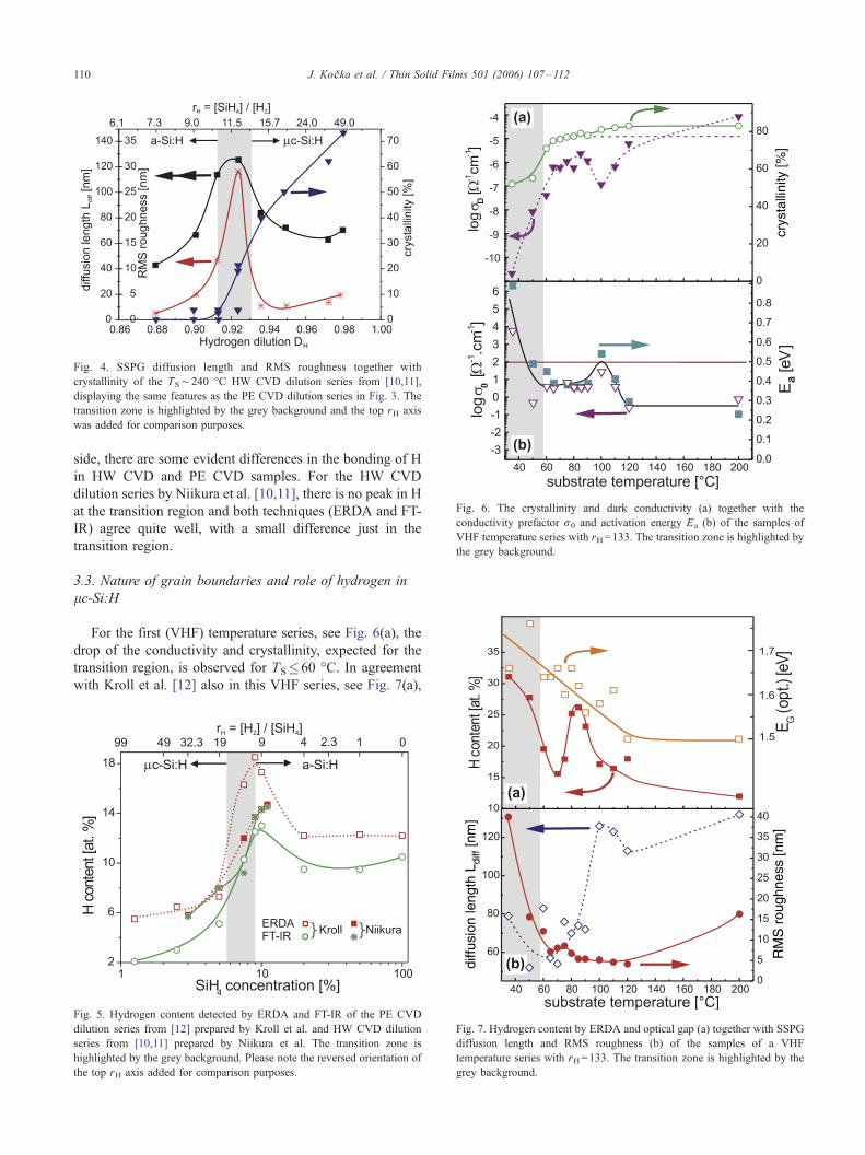
Fig. 6. The crystallinity and dark conductivity (a) together with the
conductivity prefactor r0 and activation energy Ea (b) of the samples of
VHF temperature series with rH=133. The transition zone is highlighted by
the grey background.
Fig. 4. SSPG diffusion length and RMS roughness together with
crystallinity of the TS¨240 -C HW CVD dilution series from [10,11],
displaying the same features as the PE CVD dilution series in Fig. 3. The
transition zone is highlighted by the grey background and the top rH axis
was added for comparison purposes.
J. Ko*ka et al. / Thin Solid Films 501 (2006) 107–112110
side, there are some evident differences in the bonding of H
in HW CVD and PE CVD samples. For the HW CVD
dilution series by Niikura et al. [10,11], there is no peak in H
at the transition region and both techniques (ERDA and FT-
IR) agree quite well, with a small difference just in the
transition region.
3.3. Nature of grain boundaries and role of hydrogen in
lc-Si:H
For the first (VHF) temperature series, see Fig. 6(a), the
drop of the conductivity and crystallinity, expected for the
transition region, is observed for TS�60 -C. In agreement
with Kroll et al. [12] also in this VHF series, see Fig. 7(a),
Fig. 5. Hydrogen content detected by ERDA and FT-IR of the PE CVD
dilution series from [12] prepared by Kroll et al. and HW CVD dilution
series from [10,11] prepared by Niikura et al. The transition zone is
highlighted by the grey background. Please note the reversed orientation of
the top rH axis added for comparison purposes.
Fig. 7. Hydrogen content by ERDA and optical gap (a) together with SSPG
diffusion length and RMS roughness (b) of the samples of a VHF
temperature series with rH=133. The transition zone is highlighted by the
grey background.

Fig. 8. Dark conductivity and crystallinity (a) together with SSPG diffusion
length and RMS roughness (b) and hydrogen content by ERDA (c) of the
RF samples of the temperature series with rH=32. The transition zone is
highlighted by the grey background.
J. Ko*ka et al. / Thin Solid Films 501 (2006) 107–112 111
for TS�60 -C, the H content increases, giving further
confirmation that, for TS�60 -C, there is the transition
region. As expected for the transition region, see Fig. 7(b),
both the roughness and Ldiff increase for TS�60 -C (their
maximum is not yet reached).
However, what is the reason for the surprising minimum
in conductivity, see Fig. 6(a), around TS=100 -C? While
roughness is flat at about TS=100 -C, see Fig. 7(b), dramatic
changes appear in Ldiff as well as in conductivity. Fig. 6(b)
indicates that not only for TS�60 -C but also around
TS=100 -C the GB nature changes. The observed (see Fig.
7(a)) smooth increase of the optical gap for TS<120 -C,usually related to the increase of H content, indicates that H
can play a role.
Both the roughness and the grain size are constant at
about TS=100 -C, however, H content dramatically changes
also outside the a-Si:H/Ac-Si:H transition region, see Fig.
7(a), and hence, the most probable explanation of the
change of rD and Ldiff around TS=100 -C is the change of
the GB nature induced by H.
We have observed as the typical feature of Ac-Si:H [5,9]
that there are two different grain sizes, the ‘‘small grains’’
(15–30 nm) and so-called ‘‘large grains’’ (about 300–500
nm). We have suggested that LGB and the related potential
barriers play a detrimental role in the transport properties
[9,13].
The role of H in the change of the grain boundaries has
been suggested as the explanation of the annealing induced
change of transport properties by Yoon [14] and in agree-
ment with our analysis [9], our point of view is as follows.
Formation of LGBs is related to the increase of the H
content, which concentrates at the tissue forming LGBs, and
as a result, potential barriers are formed. On the other hand,
when H content decreases (as it occurs for TS�90 -C in our
VHF temperature series), possibly supported by a few
percent increase of crystallinity, the LGBs are destroyed and
the transport properties improve, see the sharp increase of
Ldiff for TS�90 -C in Fig. 7(a).
We can test these ideas on the second temperature series
of samples—the RF series of Ac-Si:H samples, prepared at
40 -C�TS�250 -C. In Fig. 8(a) and (b), it is nicely
illustrated by the drop of rD and XC, as well as by the peak
in Ldiff and RMS roughness that for this series, the a-Si:H/
Ac-Si:H transition is found at TS¨80 -C.Also in this series, there are changes of transport
properties outside the transition region, namely, see Fig. 8,
substantial increase of Ldiff for TS�120 -C. Again for 120
-C�TS�250 -C, the roughness and also grain size are
practically constant, while for TS�120 -C, the crystallinity,slightly but systematically increases (from 80 to 86%). At
the same time, the total H content (by ERDA) clearly
decreases for TS�120 -C.So for both VHF and RF temperature series, the change
of transport properties (increase of Ldiff) tightly follows the
change (decrease) of H content, accompanied by a slight
change (increase) of the crystallinity.
Here it is important to note that the role of H in Ac-Si:His quite distinct from the role of H in poly-Si, see for
example [15]. The main difference is probably in different H
content in both structures—while in Ac-Si:H, there is 5–
30% of H, poly-Si usually contains less then 1% of H.
4. Conclusions
Hydrogen plays a key role during the Ac-Si:H growth
which is even more pronounced in the samples grown close
to the a-Si:H/Ac-Si:H transition at the low substrate
temperatures. It may also influence the properties away
from the transition by modifying the large grain boundaries.
Acknowledgements
The authors would like to thank, most of all, Manabu Ito,
Toppan Printing Research Institute, for providing samples

J. Ko*ka et al. / Thin Solid Films 501 (2006) 107–112112
and supporting this research. Support by projects AVOZ
1010914, Kontakt ME537, VaV/300/01/03, GAAV
IAA1010316, IAA1010413 and GA CR 202/03/0789 is
gratefully acknowledged.
References
[1] J. Meier, R. Fluckinger, H. Keppner, A. Shah, Appl. Phys. Lett. 65
(1994) 860.
[2] T. Mates, A. Fejfar, I. Drbohlav, B. Rezek, P. Fojtık, K. Luterova, J.
Ko*ka, C. Koch, M.B. Schubert, M. Ito, K. Ro, H. Uyama, J. Non-
Cryst. Solids 299–302 (2002) 767.
[3] A. Fejfar, T. Mates, P. Fojtık, M. Ledinsky, K. Luterova, H.
Stuchlıkova, I. Pelant, J. Ko*ka, V. Baumruk, A. Mackova, M. Ito,
K. Ro, H. Uyama, Jpn. J. Appl. Phys. 42 (2003) L987.
[4] J. Ko*ka, T. Mates, P. Fojtık, M. Ledinsky, K. Luterova, H.
Stuchlıkova, J. Stuchlık, I. Pelant, A. Fejfar, M. Ito, K. Ro, H.
Uyama, J. Non-Cryst. Solids 338–340 (2004) 287.
[5] B. Rezek, J. Stuchlık, A. Fejfar, J. Ko*ka, Appl. Phys. Lett. 74 (1999)
1475.
[6] J. Ko*ka, H. Stuchlıkova, J. Stuchlık, B. Rezek, V. Svr*ek, P. Fojtık, I.
Pelant, A. Fejfar, in: O. Bonnaud, T. Mohammed-Brahim, H.P. Strunk,
J.H. Werner (Eds.), Polycrystalline Semiconductors: VI. Bulk Materi-
als, Thin Films and Devices, Solid State Phenomena, vols. 80–81,
Scitech Publ., Uettikon am See, Switzerland, 2001, p. 213.
[7] H. Fujiwara, M. Kondo, A. Matsuda, Phys. Rev., B 63 (2001) 115306.
[8] A. Fejfar, T. Mates, O. Certık, B. Rezek, J. Stuchlık, I. Pelant, J.
Ko*ka, J. Non-Cryst. Solids 338–340 (2004) 303.
[9] J. Ko*ka, A. Fejfar, H. Stuchlıkova, J. Stuchlık, P. Fojtık, T. Mates, B.
Rezek, K. Luterova, V. Svr*ek, I. Pelant, Sol. Energy Mater. Sol. Cells
78 (2003) 493.
[10] C. Niikura, Thesis, Ecole Polytechnique, (2001).
[11] C. Niikura, Y. Poissant, M.E. Gueunier, J.P. Kleider, J.E. Bouree, J.
Non-Cryst. Solids 299–302 (2002) 1179.
[12] U. Kroll, J. Meier, A. Shah, S. Mikhailov, J. Weber, J. Appl. Phys. 80
(1996) 4971.
[13] J. Ko*ka, H. Stuchlıkova, J. Stuchlık, B. Rezek, T. Mates, V. Svr*ek,
P. Fojtık, I. Pelant, A. Fejfar, J. Non-Cryst. Solids 299–302 (2002)
355.
[14] J.H. Yoon, MRS Symp. Proc. 664 (2001) A.23.6.1.
[15] S. Honda, T. Mates, K. Knı”ek, M. Ledinsky, A.Fejfar, J. Ko*ka, T.
Yamazaki, Y. Uraoka, T. Fuyuki, these proceedings.