Room temperature H 2 sensing using functionalized GaN nanotubes with ultra low activation energy
8
Room temperature H 2 sensing using functionalized GaN nanotubes with ultra low activation energy Prasana Sahoo a , S. Dhara a, *, S. Dash a , S. Amirthapandian b , Arun K. Prasad a , A.K. Tyagi a a Surface and Nanoscience Division, Indira Gandhi Center for Atomic Research, Kalpakkam 603102, India b Materials Physics Division, Indira Gandhi Center for Atomic Research, Kalpakkam 603102, India article info Article history: Received 3 July 2012 Received in revised form 20 December 2012 Accepted 28 December 2012 Available online 29 January 2013 Keywords: Gallium nitride Hydrogen sensor Platinum functionalization abstract A single-step synthesis route of square shaped wurtzite GaN nanotubes is reported by a quasi-vaporesolid process with detailed growth kinetics involving surface energies and Ga mobility along different crystalline facets. A wet chemical route is used for the func- tionalization of GaN nanotubes with Pt nanoclusters of average diameter w1.6 (0.4) nm in order to instigate the formation of localized Schottky barrier, responsible for carrier transport in the sensing process. Catalytically enhanced dissociation of molecular H 2 down to the lowest detection limit of 25 ppm at room temperature, as compared to those of reported GaN systems has been shown. We report, for the first time, a very low activation energy value of 29.4 meV which will be useful in practical sensing of H 2 at room temper- ature without any application of bias. Copyright ª 2013, Hydrogen Energy Publications, LLC. Published by Elsevier Ltd. All rights reserved. 1. Introduction Nanotubes (NTs) with large surface areas and unidirectional curvature have received considerable interest in wide range of applications pertaining to nanofluidics, drug delivery, catal- ysis, and chemical sensing [1e4]. Direct and wide band gap GaN is one of the most promising semiconductors in future high-power optoelectronic devices and sensor applications [4]. Considerable progress has been achieved toward con- trolled growth of GaN nanowires and improvising desired functionality by appropriate surface modification. However, there is only a few published work on the growth of amor- phous, polycrystalline, and single-crystalline GaN NTs mostly employing template or using metal catalysts [5e13]. In such methods, incomplete removal of template material, partial inclusion of catalyst into the tube annulus and high porosity in as-grown samples are major blocks in the fabrication process of high pure GaN NTs. To date, contamination free direct fabrication of a GaN tubular structures have been a technical challenge. In the present work, an effort has been made to synthesize catalyst free growth of GaN NTs via a quasi vaporesolid (VS) process with an attempt toward elucidation of the underlying growth mechanism. While looking toward the device performance using nanowires or NTs, the role played by various functional groups in interface with zero-dimensional nanocrystallites assumes enormous importance [4,14e16]. Decoration of compound semiconductors with noble metal nanoclusters like Pd or Pt are of specific interest since these metals act as catalysts for numerous surface chemical reactions. An oxi- dation step is usually employed specifically to impart photo- catalytic H 2 generation capability [17,18], and to produce continuous hot electron flow in nanodiodes [19e22]. In addi- tion, such a step usually enhances electrochemical activity * Corresponding author. Tel.: þ91 44 27480500x22513; fax: þ91 44 27480081. E-mail address: [email protected] (S. Dhara). Available online at www.sciencedirect.com journal homepage: www.elsevier.com/locate/he international journal of hydrogen energy 38 (2013) 3513 e3520 0360-3199/$ e see front matter Copyright ª 2013, Hydrogen Energy Publications, LLC. Published by Elsevier Ltd. All rights reserved. http://dx.doi.org/10.1016/j.ijhydene.2012.12.131
Transcript of Room temperature H 2 sensing using functionalized GaN nanotubes with ultra low activation energy
ww.sciencedirect.com
i n t e r n a t i o n a l j o u r n a l o f h y d r o g e n en e r g y 3 8 ( 2 0 1 3 ) 3 5 1 3e3 5 2 0
Available online at w
journal homepage: www.elsevier .com/locate/he
Room temperature H2 sensing using functionalizedGaN nanotubes with ultra low activation energy
Prasana Sahoo a, S. Dhara a,*, S. Dash a, S. Amirthapandian b, Arun K. Prasad a,A.K. Tyagi a
a Surface and Nanoscience Division, Indira Gandhi Center for Atomic Research, Kalpakkam 603102, IndiabMaterials Physics Division, Indira Gandhi Center for Atomic Research, Kalpakkam 603102, India
a r t i c l e i n f o
Article history:
Received 3 July 2012
Received in revised form
20 December 2012
Accepted 28 December 2012
Available online 29 January 2013
Keywords:
Gallium nitride
Hydrogen sensor
Platinum functionalization
* Corresponding author. Tel.: þ91 44 2748050E-mail address: [email protected] (S. Dh
0360-3199/$ e see front matter Copyright ªhttp://dx.doi.org/10.1016/j.ijhydene.2012.12.1
a b s t r a c t
A single-step synthesis route of square shaped wurtzite GaN nanotubes is reported by
a quasi-vaporesolid process with detailed growth kinetics involving surface energies and
Ga mobility along different crystalline facets. A wet chemical route is used for the func-
tionalization of GaN nanotubes with Pt nanoclusters of average diameter w1.6 (0.4) nm in
order to instigate the formation of localized Schottky barrier, responsible for carrier
transport in the sensing process. Catalytically enhanced dissociation of molecular H2 down
to the lowest detection limit of 25 ppm at room temperature, as compared to those of
reported GaN systems has been shown. We report, for the first time, a very low activation
energy value of 29.4 meV which will be useful in practical sensing of H2 at room temper-
ature without any application of bias.
Copyright ª 2013, Hydrogen Energy Publications, LLC. Published by Elsevier Ltd. All rights
reserved.
1. Introduction process of high pure GaN NTs. To date, contamination free
Nanotubes (NTs) with large surface areas and unidirectional
curvature have received considerable interest in wide range of
applications pertaining to nanofluidics, drug delivery, catal-
ysis, and chemical sensing [1e4]. Direct and wide band gap
GaN is one of the most promising semiconductors in future
high-power optoelectronic devices and sensor applications
[4]. Considerable progress has been achieved toward con-
trolled growth of GaN nanowires and improvising desired
functionality by appropriate surface modification. However,
there is only a few published work on the growth of amor-
phous, polycrystalline, and single-crystalline GaN NTs mostly
employing template or using metal catalysts [5e13]. In such
methods, incomplete removal of template material, partial
inclusion of catalyst into the tube annulus and high porosity
in as-grown samples are major blocks in the fabrication
0x22513; fax: þ91 44 2748ara).2013, Hydrogen Energy P31
direct fabrication of a GaN tubular structures have been
a technical challenge. In the present work, an effort has been
made to synthesize catalyst free growth of GaN NTs via
a quasi vaporesolid (VS) process with an attempt toward
elucidation of the underlying growth mechanism.
While looking toward the device performance using
nanowires or NTs, the role played by various functional
groups in interface with zero-dimensional nanocrystallites
assumes enormous importance [4,14e16]. Decoration of
compound semiconductors with noble metal nanoclusters
like Pd or Pt are of specific interest since these metals act as
catalysts for numerous surface chemical reactions. An oxi-
dation step is usually employed specifically to impart photo-
catalytic H2 generation capability [17,18], and to produce
continuous hot electron flow in nanodiodes [19e22]. In addi-
tion, such a step usually enhances electrochemical activity
0081.
ublications, LLC. Published by Elsevier Ltd. All rights reserved.
i n t e rn a t i o n a l j o u r n a l o f h y d r o g e n en e r g y 3 8 ( 2 0 1 3 ) 3 5 1 3e3 5 2 03514
[23] and H2 sensing response across wide range of tempera-
ture [24,25]. For example, there were several reports from
Somorjai’s group on the generation of steady state chemi-
current using a planar nanodiode device which employed
5e8 nm sputtered thin film of Pt over thick GaN film, and also
metal-oxide bases [20e22] at times. They have achieved hot
electron generation induced chemi-current yield of
(3.5 � 0.8) � 10�3 under catalytic reaction of O2 or CO gas. The
aforementioned value is found to be one order of magnitude
higher than that for Pt/PdeTiO2 [21]. There are several reports
on Pt catalyzed carbon materials, metal oxides and metal-
oxynitrides used in large scale solar energy assisted H2 pro-
duction from water [26]. Pt-loaded metal nitride nanoclusters
depict superior yield than oxide counterpart toward solar
energy assisted H2 production. However, studies on the met-
alesemiconductor interface structure and crystallinity are
important for its applications in device [27].
In the present study, we have reported a methodology for
synthesizing well faceted square shaped high yield GaN NTs
with possible growth mechanism. These NTs were covalently
functionalized with Pt nanoclusters via a wet chemical route.
Room temperature (RT) H2 sensing with the lowest detection
limit, reported so far using GaN system, has been performed
on these Pt-decorated NTs with detailed analysis of activation
energy of the process.
2. Experimental
2.1. Growth of GaN nanotubes
NTs were synthesized using a hot walled CVD reactor [28e30].
Initially, a Si substrate coated with 3 nm of Au was placed
horizontally on the top of a high pure alumina boat (99.95%) at
a distance of w20 mm from the Ga (99.999%, Aldrich) source,
which was kept at the upstream side of the same boat. The
growth was carried out within the hot zone of the tubular
furnace. The furnace tube was initially evacuated to 1 mbar
base pressure and subsequently the temperature of the
chamber was slowly raised to 500 �C with a ramping rate of
w25 �C per minutes. The system was continuously evacuated
for 10 min at 500 �C. The temperature of the system was fur-
ther increased to 900 �C following a fast ramping rate of
w40 �C perminute whilemaintaining the same base pressure.
After the chamber temperature was raised to 900 �C, the base
pressure was slowly increased to 1 atm in 10 min by bleeding
high purity NH3 gas at a flow rate of 10 sccm. The reaction was
terminated after duration of 2 h. The system was allowed to
cool down slowly to RT in the same NH3 ambient. A large
quantity of light yellowish material was found to be coated
uniformly throughout the Si substrate. To identify the growth
mechanism of NTs, the role of the most decisive growth pa-
rameters, namely, growth rate, temperature and NH3 partial
pressure were taken into consideration.
2.2. Chemical functionalization and metallization
The NTs were further functionalized with Pt nanoclusters
using lysine [HO2CCH(NH2)(CH2)4NH2] as a capping agent fol-
lowing a standard procedure [31]. Initially, GaN NTs were
treated with a diluted piranha solution (50% aqueous solution
containing H2SO4:H2O2: 3:1) for 5 min, and then washed with
deionized water (w18 MU) followed by a drying process using
N2 gas. The hydroxylated samples were treated with solution
containing 1 mM of lysine followed by 1 mM of HPtCl4 in
continuous stirring condition for 30 min. A freshly prepared
solution of 0.1 M NaBH4 was added slowly into the mixture in
order to achieve the desired decoration of Pt nanoclusters
surrounding the NTs. The product was washed and dried
following the above mentioned process. The Pt coated sam-
ples were heated at 300 �C for 30 min to remove lysine [31].
Contact probes were made by sputtering a 5 nm thick Cr fol-
lowed by 80 nm thick Au films on inter-digitated electrodes
with 1 mm spacing for electrical measurements.
2.3. Characterization methodologies
Morphological features of the NTs were examined by field
emission scanning electron microscopy (FESEM; Model Zeiss
SUPRA 40). High resolution transmission electron microscopy
(HRTEM; Libra 200 Zeiss) and selected area electron diffraction
(SAED) were employed for structural characterization. Micro-
Raman scattering (inVia Renishaw spectrometer) with
514.5 nm line of Arþ laser excitation (<1 mm laser spot at the
sample surface) using 3000 gr mm�1 grating and micro-PL
with 325 nm line of HeeCd excitation using 2400 gr mm�1
grating assisted with thermoelectric cooled CCD detector in
the back scattering configuration were performed for optical
characterization of the as-grown sample. A liquid N2 stage
(Linkam) was used for temperature dependent (80e800 K)
measurements. In-situ H2 sensing was carried out by using
a custom built in-house gas exposure facility.
3. Results and discussion
3.1. Morphological studies
Fig. 1aec shows typical FESEM images of the pristine NTs on
Si substrate. Highly dense GaN layer of thickness w20 mm is
seen over the Si substrate, as revealed from the tilted cross-
sectional image (Fig. 1a). A close view of the magnified
image at middle region (Fig. 1b) reveals that NTs are homo-
epitaxially grown over a layer of GaN nanoclusters with
overall thickness w2 mm (Fig. 1a). The underlying GaN
nanocluster layer may have acted like a buffer layer, which
has initiated the NT formation. On mechanical scratching
it is found that the as-grown GaN NT layer can be
smoothly removed from the nanocluster interface region
(Supplementary Information Fig. S1). It is worthwhile men-
tioning that NTs can be isolated without being con-
taminated with nanocluster impurity. The surface layer, as
observed from the side (Fig. 1c) and normal views (Fig. 1d),
reveals that the GaN NTs are homogeneously distributed
throughout the surface. The typical images of the Pt deco-
rated GaN NTs are shown in Fig. 1deg. Most of the NTs
exhibit nearly square shaped cross-section (Fig. 1f) with wall
thickness of about w10e15 nm and average side dimensions
of nearly w50 nm (Fig. 1g). Typical length extends to several
micrometers.
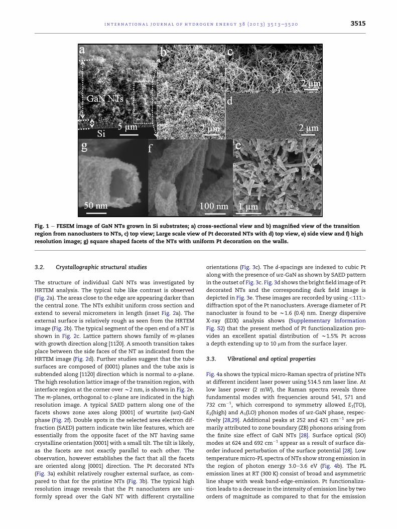
Fig. 1 e FESEM image of GaN NTs grown in Si substrates; a) cross-sectional view and b) magnified view of the transition
region from nanoclusters to NTs, c) top view; Large scale view of Pt decorated NTs with d) top view, e) side view and f) high
resolution image; g) square shaped facets of the NTs with uniform Pt decoration on the walls.
i n t e r n a t i o n a l j o u r n a l o f h y d r o g e n en e r g y 3 8 ( 2 0 1 3 ) 3 5 1 3e3 5 2 0 3515
3.2. Crystallographic structural studies
The structure of individual GaN NTs was investigated by
HRTEM analysis. The typical tube like contrast is observed
(Fig. 2a). The areas close to the edge are appearing darker than
the central zone. The NTs exhibit uniform cross section and
extend to several micrometers in length (inset Fig. 2a). The
external surface is relatively rough as seen from the HRTEM
image (Fig. 2b). The typical segment of the open end of a NT is
shown in Fig. 2c. Lattice pattern shows family of m-planes
with growth direction along [1120]. A smooth transition takes
place between the side faces of the NT as indicated from the
HRTEM image (Fig. 2d). Further studies suggest that the tube
surfaces are composed of (0001) planes and the tube axis is
subtended along [1120] direction which is normal to a-plane.
The high resolution lattice image of the transition region, with
interface region at the corner overw2 nm, is shown in Fig. 2e.
The m-planes, orthogonal to c-plane are indicated in the high
resolution image. A typical SAED pattern along one of the
facets shows zone axes along [0001] of wurtzite (wz)-GaN
phase (Fig. 2f). Double spots in the selected area electron dif-
fraction (SAED) pattern indicate twin like features, which are
essentially from the opposite facet of the NT having same
crystalline orientation [0001] with a small tilt. The tilt is likely,
as the facets are not exactly parallel to each other. The
observation, however establishes the fact that all the facets
are oriented along [0001] direction. The Pt decorated NTs
(Fig. 3a) exhibit relatively rougher external surface, as com-
pared to that for the pristine NTs (Fig. 3b). The typical high
resolution image reveals that the Pt nanoclusters are uni-
formly spread over the GaN NT with different crystalline
orientations (Fig. 3c). The d-spacings are indexed to cubic Pt
along with the presence of wz-GaN as shown by SAED pattern
in the outset of Fig. 3c. Fig. 3d shows the bright field image of Pt
decorated NTs and the corresponding dark field image is
depicted in Fig. 3e. These images are recorded by using <111>
diffraction spot of the Pt nanoclusters. Average diameter of Pt
nanocluster is found to be w1.6 (0.4) nm. Energy dispersive
X-ray (EDX) analysis shows (Supplementary Information
Fig. S2) that the present method of Pt functionalization pro-
vides an excellent spatial distribution of w1.5% Pt across
a depth extending up to 10 mm from the surface layer.
3.3. Vibrational and optical properties
Fig. 4a shows the typical micro-Raman spectra of pristine NTs
at different incident laser power using 514.5 nm laser line. At
low laser power (2 mW), the Raman spectra reveals three
fundamental modes with frequencies around 541, 571 and
732 cm�1, which correspond to symmetry allowed E1(TO),
E2(high) and A1(LO) phonon modes of wz-GaN phase, respec-
tively [28,29]. Additional peaks at 252 and 421 cm�1 are pri-
marily attributed to zone boundary (ZB) phonons arising from
the finite size effect of GaN NTs [28]. Surface optical (SO)
modes at 624 and 692 cm�1 appear as a result of surface dis-
order induced perturbation of the surface potential [28]. Low
temperature micro-PL spectra of NTs show strong emission in
the region of photon energy 3.0e3.6 eV (Fig. 4b). The PL
emission lines at RT (300 K) consist of broad and asymmetric
line shape with weak band-edge-emission. Pt functionaliza-
tion leads to a decrease in the intensity of emission line by two
orders of magnitude as compared to that for the emission
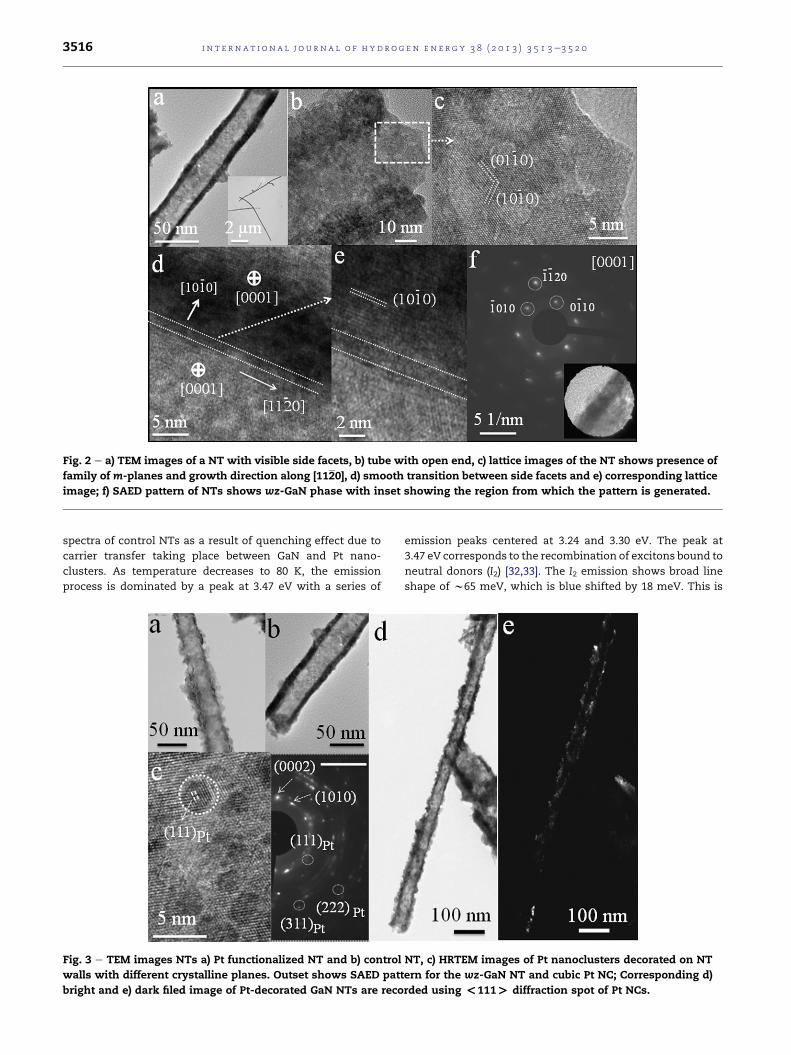
Fig. 2 e a) TEM images of a NT with visible side facets, b) tube with open end, c) lattice images of the NT shows presence of
family of m-planes and growth direction along [1120], d) smooth transition between side facets and e) corresponding lattice
image; f) SAED pattern of NTs shows wz-GaN phase with inset showing the region from which the pattern is generated.
i n t e rn a t i o n a l j o u r n a l o f h y d r o g e n en e r g y 3 8 ( 2 0 1 3 ) 3 5 1 3e3 5 2 03516
spectra of control NTs as a result of quenching effect due to
carrier transfer taking place between GaN and Pt nano-
clusters. As temperature decreases to 80 K, the emission
process is dominated by a peak at 3.47 eV with a series of
Fig. 3 e TEM images NTs a) Pt functionalized NT and b) control
walls with different crystalline planes. Outset shows SAED patt
bright and e) dark filed image of Pt-decorated GaN NTs are reco
emission peaks centered at 3.24 and 3.30 eV. The peak at
3.47 eV corresponds to the recombination of excitons bound to
neutral donors (I2) [32,33]. The I2 emission shows broad line
shape of w65 meV, which is blue shifted by 18 meV. This is
NT, c) HRTEM images of Pt nanoclusters decorated on NT
ern for the wz-GaN NT and cubic Pt NC; Corresponding d)
rded using <111> diffraction spot of Pt NCs.
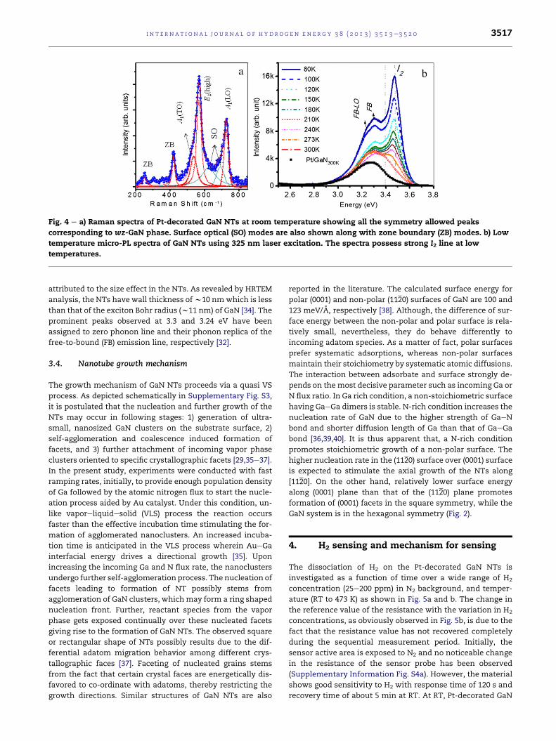
Fig. 4 e a) Raman spectra of Pt-decorated GaN NTs at room temperature showing all the symmetry allowed peaks
corresponding to wz-GaN phase. Surface optical (SO) modes are also shown along with zone boundary (ZB) modes. b) Low
temperature micro-PL spectra of GaN NTs using 325 nm laser excitation. The spectra possess strong I2 line at low
temperatures.
i n t e r n a t i o n a l j o u r n a l o f h y d r o g e n en e r g y 3 8 ( 2 0 1 3 ) 3 5 1 3e3 5 2 0 3517
attributed to the size effect in the NTs. As revealed by HRTEM
analysis, the NTs have wall thickness ofw10 nmwhich is less
than that of the exciton Bohr radius (w11 nm) of GaN [34]. The
prominent peaks observed at 3.3 and 3.24 eV have been
assigned to zero phonon line and their phonon replica of the
free-to-bound (FB) emission line, respectively [32].
3.4. Nanotube growth mechanism
The growth mechanism of GaN NTs proceeds via a quasi VS
process. As depicted schematically in Supplementary Fig. S3,
it is postulated that the nucleation and further growth of the
NTs may occur in following stages: 1) generation of ultra-
small, nanosized GaN clusters on the substrate surface, 2)
self-agglomeration and coalescence induced formation of
facets, and 3) further attachment of incoming vapor phase
clusters oriented to specific crystallographic facets [29,35e37].
In the present study, experiments were conducted with fast
ramping rates, initially, to provide enough population density
of Ga followed by the atomic nitrogen flux to start the nucle-
ation process aided by Au catalyst. Under this condition, un-
like vaporeliquidesolid (VLS) process the reaction occurs
faster than the effective incubation time stimulating the for-
mation of agglomerated nanoclusters. An increased incuba-
tion time is anticipated in the VLS process wherein AueGa
interfacial energy drives a directional growth [35]. Upon
increasing the incoming Ga and N flux rate, the nanoclusters
undergo further self-agglomeration process. The nucleation of
facets leading to formation of NT possibly stems from
agglomeration of GaN clusters, whichmay form a ring shaped
nucleation front. Further, reactant species from the vapor
phase gets exposed continually over these nucleated facets
giving rise to the formation of GaN NTs. The observed square
or rectangular shape of NTs possibly results due to the dif-
ferential adatom migration behavior among different crys-
tallographic faces [37]. Faceting of nucleated grains stems
from the fact that certain crystal faces are energetically dis-
favored to co-ordinate with adatoms, thereby restricting the
growth directions. Similar structures of GaN NTs are also
reported in the literature. The calculated surface energy for
polar (0001) and non-polar (1120) surfaces of GaN are 100 and
123 meV/A, respectively [38]. Although, the difference of sur-
face energy between the non-polar and polar surface is rela-
tively small, nevertheless, they do behave differently to
incoming adatom species. As a matter of fact, polar surfaces
prefer systematic adsorptions, whereas non-polar surfaces
maintain their stoichiometry by systematic atomic diffusions.
The interaction between adsorbate and surface strongly de-
pends on themost decisive parameter such as incoming Ga or
N flux ratio. In Ga rich condition, a non-stoichiometric surface
having GaeGa dimers is stable. N-rich condition increases the
nucleation rate of GaN due to the higher strength of GaeN
bond and shorter diffusion length of Ga than that of GaeGa
bond [36,39,40]. It is thus apparent that, a N-rich condition
promotes stoichiometric growth of a non-polar surface. The
higher nucleation rate in the (1120) surface over (0001) surface
is expected to stimulate the axial growth of the NTs along
[1120]. On the other hand, relatively lower surface energy
along (0001) plane than that of the (1120) plane promotes
formation of (0001) facets in the square symmetry, while the
GaN system is in the hexagonal symmetry (Fig. 2).
4. H2 sensing and mechanism for sensing
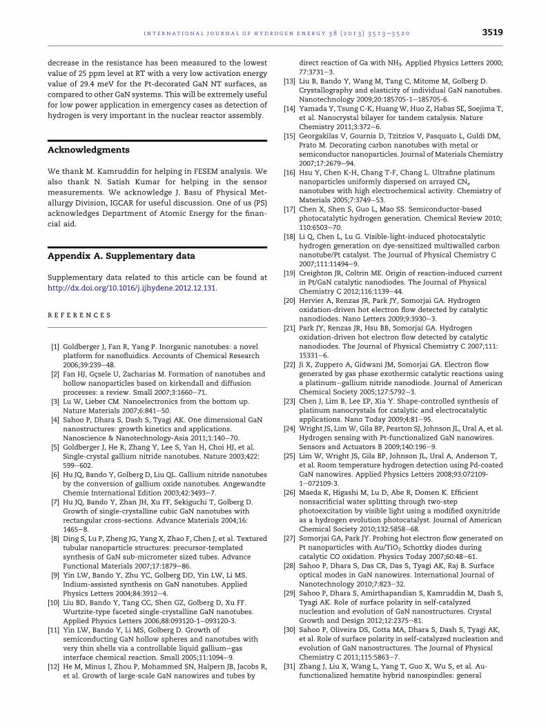
The dissociation of H2 on the Pt-decorated GaN NTs is
investigated as a function of time over a wide range of H2
concentration (25e200 ppm) in N2 background, and temper-
ature (RT to 473 K) as shown in Fig. 5a and b. The change in
the reference value of the resistance with the variation in H2
concentrations, as obviously observed in Fig. 5b, is due to the
fact that the resistance value has not recovered completely
during the sequential measurement period. Initially, the
sensor active area is exposed to N2 and no noticeable change
in the resistance of the sensor probe has been observed
(Supplementary Information Fig. S4a). However, the material
shows good sensitivity to H2 with response time of 120 s and
recovery time of about 5 min at RT. At RT, Pt-decorated GaN
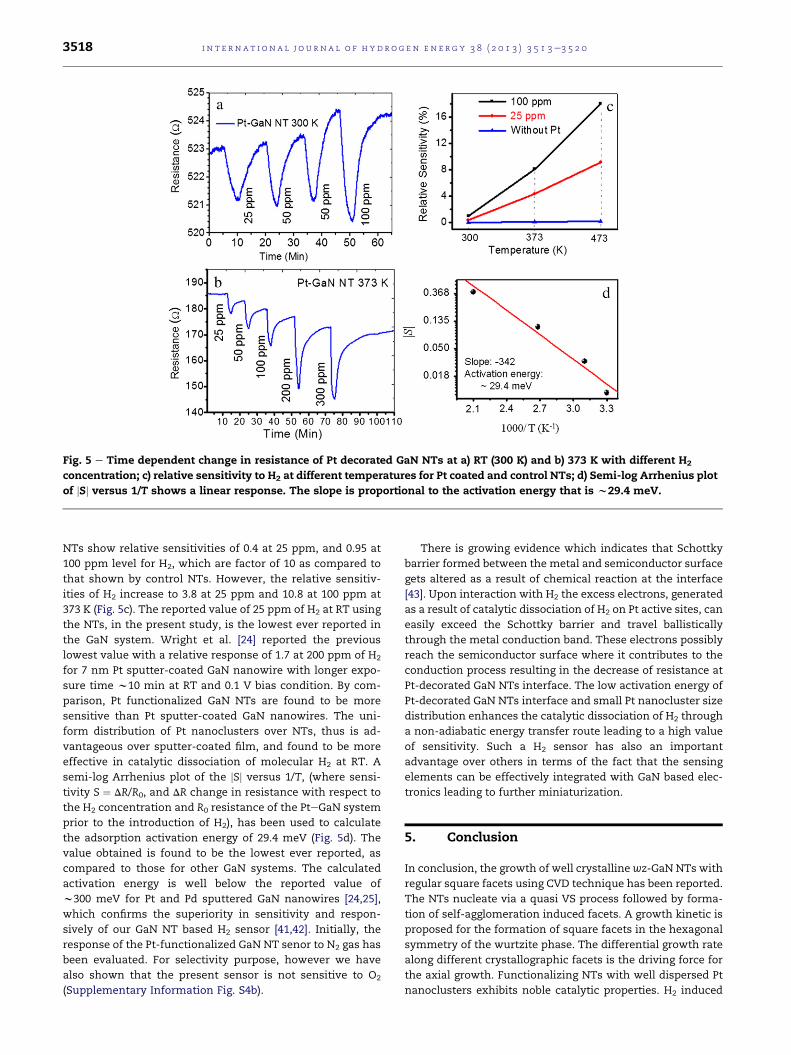
Fig. 5 e Time dependent change in resistance of Pt decorated GaN NTs at a) RT (300 K) and b) 373 K with different H2
concentration; c) relative sensitivity to H2 at different temperatures for Pt coated and control NTs; d) Semi-log Arrhenius plot
of jSj versus 1/T shows a linear response. The slope is proportional to the activation energy that is w29.4 meV.
i n t e rn a t i o n a l j o u r n a l o f h y d r o g e n en e r g y 3 8 ( 2 0 1 3 ) 3 5 1 3e3 5 2 03518
NTs show relative sensitivities of 0.4 at 25 ppm, and 0.95 at
100 ppm level for H2, which are factor of 10 as compared to
that shown by control NTs. However, the relative sensitiv-
ities of H2 increase to 3.8 at 25 ppm and 10.8 at 100 ppm at
373 K (Fig. 5c). The reported value of 25 ppm of H2 at RT using
the NTs, in the present study, is the lowest ever reported in
the GaN system. Wright et al. [24] reported the previous
lowest value with a relative response of 1.7 at 200 ppm of H2
for 7 nm Pt sputter-coated GaN nanowire with longer expo-
sure time w10 min at RT and 0.1 V bias condition. By com-
parison, Pt functionalized GaN NTs are found to be more
sensitive than Pt sputter-coated GaN nanowires. The uni-
form distribution of Pt nanoclusters over NTs, thus is ad-
vantageous over sputter-coated film, and found to be more
effective in catalytic dissociation of molecular H2 at RT. A
semi-log Arrhenius plot of the jSj versus 1/T, (where sensi-
tivity S ¼ DR/R0, and DR change in resistance with respect to
the H2 concentration and R0 resistance of the PteGaN system
prior to the introduction of H2), has been used to calculate
the adsorption activation energy of 29.4 meV (Fig. 5d). The
value obtained is found to be the lowest ever reported, as
compared to those for other GaN systems. The calculated
activation energy is well below the reported value of
w300 meV for Pt and Pd sputtered GaN nanowires [24,25],
which confirms the superiority in sensitivity and respon-
sively of our GaN NT based H2 sensor [41,42]. Initially, the
response of the Pt-functionalized GaN NT senor to N2 gas has
been evaluated. For selectivity purpose, however we have
also shown that the present sensor is not sensitive to O2
(Supplementary Information Fig. S4b).
There is growing evidence which indicates that Schottky
barrier formed between the metal and semiconductor surface
gets altered as a result of chemical reaction at the interface
[43]. Upon interaction with H2 the excess electrons, generated
as a result of catalytic dissociation of H2 on Pt active sites, can
easily exceed the Schottky barrier and travel ballistically
through the metal conduction band. These electrons possibly
reach the semiconductor surface where it contributes to the
conduction process resulting in the decrease of resistance at
Pt-decorated GaN NTs interface. The low activation energy of
Pt-decorated GaN NTs interface and small Pt nanocluster size
distribution enhances the catalytic dissociation of H2 through
a non-adiabatic energy transfer route leading to a high value
of sensitivity. Such a H2 sensor has also an important
advantage over others in terms of the fact that the sensing
elements can be effectively integrated with GaN based elec-
tronics leading to further miniaturization.
5. Conclusion
In conclusion, the growth of well crystallinewz-GaN NTs with
regular square facets using CVD technique has been reported.
The NTs nucleate via a quasi VS process followed by forma-
tion of self-agglomeration induced facets. A growth kinetic is
proposed for the formation of square facets in the hexagonal
symmetry of the wurtzite phase. The differential growth rate
along different crystallographic facets is the driving force for
the axial growth. Functionalizing NTs with well dispersed Pt
nanoclusters exhibits noble catalytic properties. H2 induced
i n t e r n a t i o n a l j o u r n a l o f h y d r o g e n en e r g y 3 8 ( 2 0 1 3 ) 3 5 1 3e3 5 2 0 3519
decrease in the resistance has been measured to the lowest
value of 25 ppm level at RT with a very low activation energy
value of 29.4 meV for the Pt-decorated GaN NT surfaces, as
compared to other GaN systems. This will be extremely useful
for low power application in emergency cases as detection of
hydrogen is very important in the nuclear reactor assembly.
Acknowledgments
We thank M. Kamruddin for helping in FESEM analysis. We
also thank N. Satish Kumar for helping in the sensor
measurements. We acknowledge J. Basu of Physical Met-
allurgy Division, IGCAR for useful discussion. One of us (PS)
acknowledges Department of Atomic Energy for the finan-
cial aid.
Appendix A. Supplementary data
Supplementary data related to this article can be found at
http://dx.doi.org/10.1016/j.ijhydene.2012.12.131.
r e f e r e n c e s
[1] Goldberger J, Fan R, Yang P. Inorganic nanotubes: a novelplatform for nanofluidics. Accounts of Chemical Research2006;39:239e48.
[2] Fan HJ, Gcsele U, Zacharias M. Formation of nanotubes andhollow nanoparticles based on kirkendall and diffusionprocesses: a review. Small 2007;3:1660e71.
[3] Lu W, Lieber CM. Nanoelectronics from the bottom up.Nature Materials 2007;6:841e50.
[4] Sahoo P, Dhara S, Dash S, Tyagi AK. One dimensional GaNnanostructures: growth kinetics and applications.Nanoscience & Nanotechnology-Asia 2011;1:140e70.
[5] Goldberger J, He R, Zhang Y, Lee S, Yan H, Choi HJ, et al.Single-crystal gallium nitride nanotubes. Nature 2003;422:599e602.
[6] Hu JQ, Bando Y, Golberg D, Liu QL. Gallium nitride nanotubesby the conversion of gallium oxide nanotubes. AngewandteChemie International Edition 2003;42:3493e7.
[7] Hu JQ, Bando Y, Zhan JH, Xu FF, Sekiguchi T, Golberg D.Growth of single-crystalline cubic GaN nanotubes withrectangular cross-sections. Advance Materials 2004;16:1465e8.
[8] Ding S, Lu P, Zheng JG, Yang X, Zhao F, Chen J, et al. Texturedtubular nanoparticle structures: precursor-templatedsynthesis of GaN sub-micrometer sized tubes. AdvanceFunctional Materials 2007;17:1879e86.
[9] Yin LW, Bando Y, Zhu YC, Golberg DD, Yin LW, Li MS.Indium-assisted synthesis on GaN nanotubes. AppliedPhysics Letters 2004;84:3912e4.
[10] Liu BD, Bando Y, Tang CC, Shen GZ, Golberg D, Xu FF.Wurtzite-type faceted single-crystalline GaN nanotubes.Applied Physics Letters 2006;88:093120-1e093120-3.
[11] Yin LW, Bando Y, Li MS, Golberg D. Growth ofsemiconducting GaN hollow spheres and nanotubes withvery thin shells via a controllable liquid galliumegasinterface chemical reaction. Small 2005;11:1094e9.
[12] He M, Minus I, Zhou P, Mohammed SN, Halpern JB, Jacobs R,et al. Growth of large-scale GaN nanowires and tubes by
direct reaction of Ga with NH3. Applied Physics Letters 2000;77:3731e3.
[13] Liu B, Bando Y, Wang M, Tang C, Mitome M, Golberg D.Crystallography and elasticity of individual GaN nanotubes.Nanotechnology 2009;20:185705-1e185705-6.
[14] Yamada Y, Tsung C-K, Huang W, Huo Z, Habas SE, Soejima T,et al. Nanocrystal bilayer for tandem catalysis. NatureChemistry 2011;3:372e6.
[15] Georgakilas V, Gournis D, Tzitzios V, Pasquato L, Guldi DM,Prato M. Decorating carbon nanotubes with metal orsemiconductor nanoparticles. Journal of Materials Chemistry2007;17:2679e94.
[16] Hsu Y, Chen K-H, Chang T-F, Chang L. Ultrafine platinumnanoparticles uniformly dispersed on arrayed CNx
nanotubes with high electrochemical activity. Chemistry ofMaterials 2005;7:3749e53.
[17] Chen X, Shen S, Guo L, Mao SS. Semiconductor-basedphotocatalytic hydrogen generation. Chemical Review 2010;110:6503e70.
[18] Li Q, Chen L, Lu G. Visible-light-induced photocatalytichydrogen generation on dye-sensitized multiwalled carbonnanotube/Pt catalyst. The Journal of Physical Chemistry C2007;111:11494e9.
[19] Creighton JR, Coltrin ME. Origin of reaction-induced currentin Pt/GaN catalytic nanodiodes. The Journal of PhysicalChemistry C 2012;116:1139e44.
[20] Hervier A, Renzas JR, Park JY, Somorjai GA. Hydrogenoxidation-driven hot electron flow detected by catalyticnanodiodes. Nano Letters 2009;9:3930e3.
[21] Park JY, Renzas JR, Hsu BB, Somorjai GA. Hydrogenoxidation-driven hot electron flow detected by catalyticnanodiodes. The Journal of Physical Chemistry C 2007;111:15331e6.
[22] Ji X, Zuppero A, Gidwani JM, Somorjai GA. Electron flowgenerated by gas phase exothermic catalytic reactions usinga platinumegallium nitride nanodiode. Journal of AmericanChemical Society 2005;127:5792e3.
[23] Chen J, Lim B, Lee EP, Xia Y. Shape-controlled synthesis ofplatinum nanocrystals for catalytic and electrocatalyticapplications. Nano Today 2009;4:81e95.
[24] Wright JS, LimW, Gila BP, Pearton SJ, Johnson JL, Ural A, et al.Hydrogen sensing with Pt-functionalized GaN nanowires.Sensors and Actuators B 2009;140:196e9.
[25] Lim W, Wright JS, Gila BP, Johnson JL, Ural A, Anderson T,et al. Room temperature hydrogen detection using Pd-coatedGaN nanowires. Applied Physics Letters 2008;93:072109-1e072109-3.
[26] Maeda K, Higashi M, Lu D, Abe R, Domen K. Efficientnonsacrificial water splitting through two-stepphotoexcitation by visible light using a modified oxynitrideas a hydrogen evolution photocatalyst. Journal of AmericanChemical Society 2010;132:5858e68.
[27] Somorjai GA, Park JY. Probing hot electron flow generated onPt nanoparticles with Au/TiO2 Schottky diodes duringcatalytic CO oxidation. Physics Today 2007;60:48e61.
[28] Sahoo P, Dhara S, Das CR, Das S, Tyagi AK, Raj B. Surfaceoptical modes in GaN nanowires. International Journal ofNanotechnology 2010;7:823e32.
[29] Sahoo P, Dhara S, Amirthapandian S, Kamruddin M, Dash S,Tyagi AK. Role of surface polarity in self-catalyzednucleation and evolution of GaN nanostructures. CrystalGrowth and Design 2012;12:2375e81.
[30] Sahoo P, Oliveira DS, Cotta MA, Dhara S, Dash S, Tyagi AK,et al. Role of surface polarity in self-catalyzed nucleation andevolution of GaN nanostructures. The Journal of PhysicalChemistry C 2011;115:5863e7.
[31] Zhang J, Liu X, Wang L, Yang T, Guo X, Wu S, et al. Au-functionalized hematite hybrid nanospindles: general
i n t e rn a t i o n a l j o u r n a l o f h y d r o g e n en e r g y 3 8 ( 2 0 1 3 ) 3 5 1 3e3 5 2 03520
synthesis, gas sensing and catalytic properties. The Journalof Physical Chemistry C 2011;115:5352e7.
[32] Reshchikova MA, Morkoc H. Luminescence properties ofdefects in GaN. Journal of Applied Physics 2005;97:061301-1e061301-95.
[33] Bae SY, Seo HW, Park J, Yang H, Kim H, Kim S. Triangulargallium nitride nanorods. Applied Physics Letters 2003;82:4564e6.
[34] Pauzauskie PJ, Yang P. Nanowire photonics. Materials Today2006;9:36e45.
[35] Cheze C, Geelhaar L, Jenichen B, Riechert H. Different growthrates for catalyst-induced and self-induced GaN nanowires.Applied Physics Letters 2010;97:153105-1e153105-3.
[36] Consonni V, Trampert A, Geelhaar L, Riechert H. Physicalorigin of the incubation time of self-induced GaN nanowires.Applied Physics Letters 2011;99:033102-1e033102-3.
[37] Consonni V, Hanke M, Knelangen M, Geelhaar L, Trampert A,Riechert H. Nucleation mechanisms of self-induced GaNnanowires grown on an amorphous interlayer. PhysicalReview B 2011;83:035310-1e035310-8.
[38] Northrup JE, Neugebauer J. Theory of GaN (1010) and (1120)surfaces. Physical Review B 1996;53:R10477e80. Northrup JE,
Neugebauer J, Feenstra RM, Smith AR. Structure ofGaN(0001):The laterally contracted Ga bilayer model.Physical Review B 2000;61:9932e5.
[39] Lymperakisand L, Neugebauer J. Large anisotropic adatomkinetics on nonpolar GaN surfaces: consequences for surfacemorphologies and nanowire growth. Physical Review B 2009;79:241308-1e241308-4.
[40] Myoung JM, Gluschenkov O, Kim K, Kim S. Growth kinetics ofGaN and effects of flux ratio on the properties of GaN filmsgrown by plasma-assisted molecular beam epitaxy. Journalof Vacuum Science and Technology A 1999;17:3019e28.
[41] Sadik PW, Norton DP, Voss LF, Pearton SJ, Wang HT, Kang BS,et al. Hydrogen-selective sensing at room temperature withZnO nanorods. Applied Physics Letters 2005;86:243503-1e243503-3.
[42] Lee C-T, Yan J-T. Sensing mechanisms of Pt/b-Ga2O3/GaNhydrogen sensor diodes. Sensors and Actuators B 2010;147:723e9.
[43] Dobrokhotov V, McIlroy DN, Norton MG, Abuzir A, Yeh WJ,Stevenson I, et al. Principles and mechanisms of gas sensingby GaN nanowires functionalized with gold nanoparticles.Journal of Applied Physics 2006;99:104302-1e104302-7.