RECOMMENDATION REPORT Apparatus to Amplify ...
51
RECOMMENDATION REPORT Apparatus to Amplify Headphones and Test Sound Quality George Ellis Self-Sponsored Applied Science 479 Engineering Physics The University of British Columbia January 9, 2012 Project Number 1164
-
Upload
khangminh22 -
Category
Documents
-
view
2 -
download
0
Transcript of RECOMMENDATION REPORT Apparatus to Amplify ...
RECOMMENDATION REPORT Apparatus to Amplify Headphones and Test Sound Quality
George Ellis Self-Sponsored
Applied Science 479 Engineering Physics The University of British Columbia January 9, 2012 Project Number 1164
ii
Executive Summary
The purpose of this project was to prototype a hi-quality headphone amplifier, and to measure
the amp’s performance using a dummy (pure resistive) or real headphone load. The idea was to
either demonstrate how a headphone amp could quantifiably improve sound quality played out of
a source, or to at least investigate typical usage scenarios and metrics for measuring sound
quality.
Key metrics identified for characterising the amp’s performance were: input and output
impedance, signal-to-noise + distortion (SINAD), and the gain response over audio frequencies.
The original discrete amplifier design chosen for the project was changed a more forgiving
LM1875 op amp design during the prototyping stage due to deficiencies in parts ordered. The
second amp was measured to have 21 Ω input and < 1 Ω output impedances, and a noise floor at
-85 dB(VRMS) relative to the audio signal. Qualitatively, the amplifier was able to drive audio
transducers from computer Line Out with impedances from 8 Ω to 100 Ω without noticeable
noise or degrading audio quality.
It was concluded that a medium-quality audio amplifier is not necessarily suitable for all
applications. Recommendations include further testing and continued prototyping of the more
ambitious (but trickier) hi-fi design.
iii
Contents Executive Summary .................................................................................................................................. ii
1.0 Introduction .......................................................................................................................................... 1 1.1 Background and Motivation ................................................................................................. 1
1.2 Project Objectives ................................................................................................................. 6
1.3 Scope and Limitations........................................................................................................... 7
1.4 Organization .......................................................................................................................... 7
2.0 Discussion ............................................................................................................................................ 8 2.1 Theory ................................................................................................................................... 8
2.2 Methods / Testing Protocol ..................................................................................................11
2.3 Alternative Designs ..............................................................................................................11
2.4 Experimental Equipment .................................................................................................... 12
2.5 Flow Diagrams .................................................................................................................... 16
2.6 Results ................................................................................................................................. 20
Gilmore Power Supply Circuit ............................................................................................. 20 Gilmore Discrete Amplifier Circuit ...................................................................................... 20
LM1875 CMoy-style Op-Amp Amplifier Circuit ................................................................ 23 3.0 Conclusions ......................................................................................................................... 31
4.0 Deliverables and Financial Summary ................................................................................................ 32 Project Deliverables .................................................................................................................. 32
Financial Summary ................................................................................................................... 34
5.0 Recommendations .............................................................................................................................. 36 Appendices ............................................................................................................................................... 39
A LM1875 Op-Amp Amplifier Circuit Schematics .............................................................. 39
B List of Equipment .............................................................................................................. 40
C List of Parts ........................................................................................................................ 41
C Original and Actual Project Schedule ................................................................................ 43
References ................................................................................................................................................ 45
iv
Figure 1 - Chart illustrating loudness of various decibel sounds to the human ear. [20] ................ 2
Figure 2 - Different standard curves of equal loudness. [19].......................................................... 3 Figure 3 - Plot showing 12dB frequency response deviation for Zout = 43 Ω with UE SuperFi 5’s.
[10] .................................................................................................................................................. 4
Figure 4 - Plot showing 12dB frequency response deviation for Zout = 10 Ω with UE SuperFi 5’s.
[10] .................................................................................................................................................. 4 Figure 5 - Ideal Thevenin representation of an audio source and sink. [10]................................... 5 Figure 6 - Schematic for single-channel amplification circuit of headphone ................................. 9 Figure 7 - Schematic for power supply circuit of headphone amp. [5] ........................................ 10
Figure 8 - Overall equipment set-up ............................................................................................. 12 Figure 9 - HP 35665A Spectrum analyser .................................................................................... 13 Figure 10 - Tektronix TDS350 Oscilloscope. CH1 is input to amp; CH2 is output from amp .... 13 Figure 11 - Dummy resistive load box .......................................................................................... 14
Figure 12 - Headphone amp & 15+/-2 VDC PSU ........................................................................ 14 Figure 13 - Gilmore prototyped PSU [5] ...................................................................................... 15
Figure 14 - Gilmore prototyped amp [5]....................................................................................... 15 Figure 15 - Network analyser instructions 1 ................................................................................. 17
Figure 16 - Network analyser instructions 2 ................................................................................. 18 Figure 17 - Measuring Zin and Zout ............................................................................................... 19 Figure 18 - PSU test circuit ........................................................................................................... 20
Figure 19 - Matching JFET's ........................................................................................................ 21 Figure 20 - Faulty biasing conditions of 1st amp stage ................................................................ 22
Figure 21 - Right amp channel driven by pure sine wave ............................................................ 23 Figure 22 - Calculating amp input impedance .............................................................................. 24 Figure 23 - FFT of 500 Hz from Headphone Out into amp driving 15 ohms showing harmonics
....................................................................................................................................................... 25
Figure 24 - Line out into amp showing 100dB floor .................................................................... 26 Figure 25 - Headphone out into amp showing 100dB floor ......................................................... 26 Figure 26 - Spectrum analyser source measurement showing -110dB floor ................................ 27
Figure 27 - Burst random waveform on scope.............................................................................. 27 Figure 28 – “Simulated gain plot”: Burst random noise 500 sample average from amp ............. 28
Figure 29 - “Simulated gain plot”: Burst random noise 500 sample average from amp; log freq
scale............................................................................................................................................... 28
Figure 30 - 500Hz output from amp driving 15 ohm; 10 sample avg .......................................... 29 Figure 31 - 500Hz source from analyser....................................................................................... 30 Figure 32 - Proposed modifications to attempt to solve PSU instability ...................................... 37 Figure 33 - Modified parts for LM1875 op-amp channel ............................................................. 39 Figure 34 - Planned and actual (red) project schedule .................................................................. 43
Figure 35 - Planned and acutal (red) project schedule .................................................................. 44
1
1.0 Introduction
1.1 Background and Motivation
In the era of the iPod and the earbud cheap portable audio set-ups have long since entered the
mainstream. Unfortunately, the average consumer is unaware of audio source limitations and
how much better their music would sound given proper amplification. Lack of industry
standardisation regarding source/sink impedances has not helped, either [10].
Many measurements exist to characterise sound quality; the industry de-facto standard in many
areas of audio testing is the Lindos sequence test system, which consists of over 25 different
segments [16]. Two easy to understand and important concepts describing sound quality are:
frequency response, and signal-to-noise ratio (SNR).
When performing objective measurements of audio signals a common unit used is decibels SPL,
which describes Sound Pressure Levels. The dBSPL is a logarithmic unit which is calculated as1:
𝑑𝐵𝑠𝑝𝑙 = 10 ∗ 𝑙𝑜𝑔10 ( 𝑃𝑟𝑚𝑠
2
𝑃𝑟𝑒𝑓2 ) = 20 ∗ 𝑙𝑜𝑔10 (
𝑃𝑟𝑚𝑠
𝑃𝑟𝑒𝑓 )
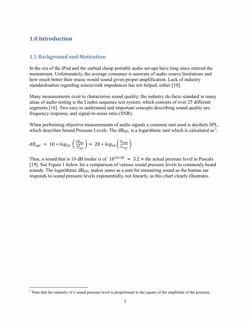
Thus, a sound that is 10 dB louder is of 1010 20⁄ ≈ 3.2 × the actual pressure level in Pascals
[19]. See Figure 1 below for a comparison of various sound pressure levels to commonly heard
sounds. The logarithmic dBSPL makes sense as a unit for measuring sound as the human ear
responds to sound pressure levels exponentially, not linearly, as this chart clearly illustrates.
1 Note that the intensity of a sound pressure level is proportional to the square of the amplitude of the pressure.
2
Figure 1 - Chart illustrating loudness of various decibel sounds to the human ear. [20]
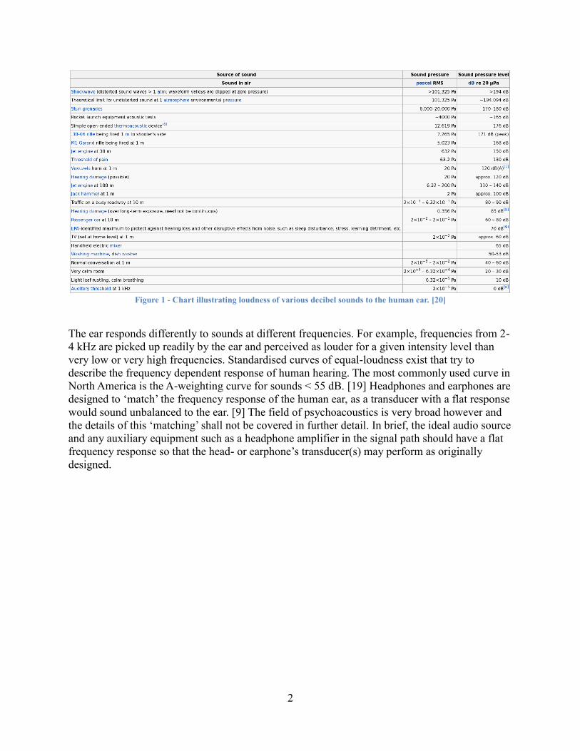
The ear responds differently to sounds at different frequencies. For example, frequencies from 2-
4 kHz are picked up readily by the ear and perceived as louder for a given intensity level than
very low or very high frequencies. Standardised curves of equal-loudness exist that try to
describe the frequency dependent response of human hearing. The most commonly used curve in
North America is the A-weighting curve for sounds < 55 dB. [19] Headphones and earphones are
designed to ‘match’ the frequency response of the human ear, as a transducer with a flat response
would sound unbalanced to the ear. [9] The field of psychoacoustics is very broad however and
the details of this ‘matching’ shall not be covered in further detail. In brief, the ideal audio source
and any auxiliary equipment such as a headphone amplifier in the signal path should have a flat
frequency response so that the head- or earphone’s transducer(s) may perform as originally
designed.
3
Figure 2 - Different standard curves of equal loudness. [19]
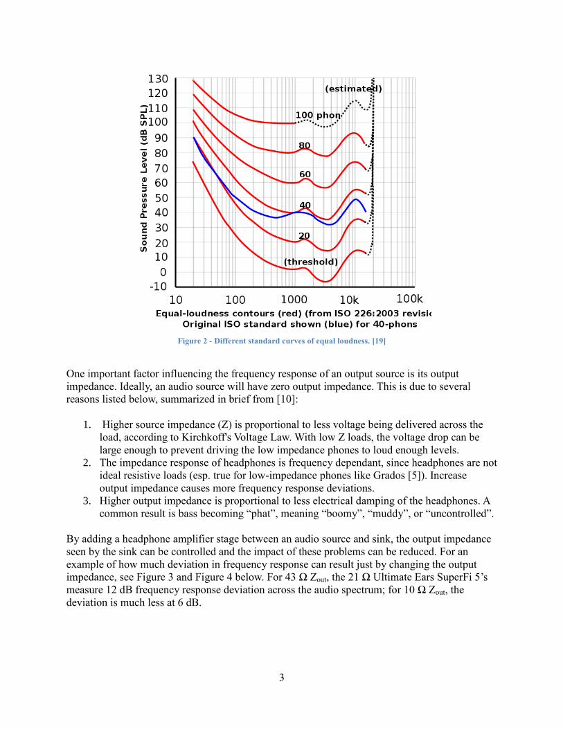
One important factor influencing the frequency response of an output source is its output
impedance. Ideally, an audio source will have zero output impedance. This is due to several
reasons listed below, summarized in brief from [10]:
1. Higher source impedance (Z) is proportional to less voltage being delivered across the
load, according to Kirchkoff's Voltage Law. With low Z loads, the voltage drop can be
large enough to prevent driving the low impedance phones to loud enough levels.
2. The impedance response of headphones is frequency dependant, since headphones are not
ideal resistive loads (esp. true for low-impedance phones like Grados [5]). Increase
output impedance causes more frequency response deviations.
3. Higher output impedance is proportional to less electrical damping of the headphones. A
common result is bass becoming “phat”, meaning “boomy”, “muddy”, or “uncontrolled”.
By adding a headphone amplifier stage between an audio source and sink, the output impedance
seen by the sink can be controlled and the impact of these problems can be reduced. For an
example of how much deviation in frequency response can result just by changing the output
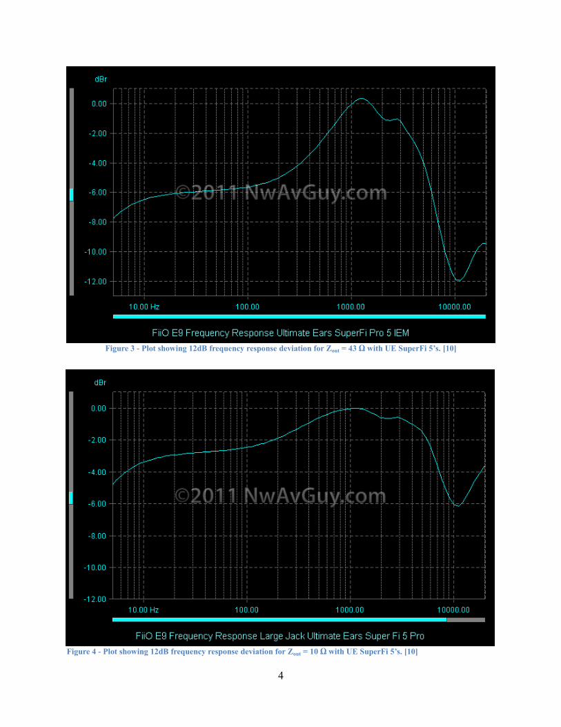
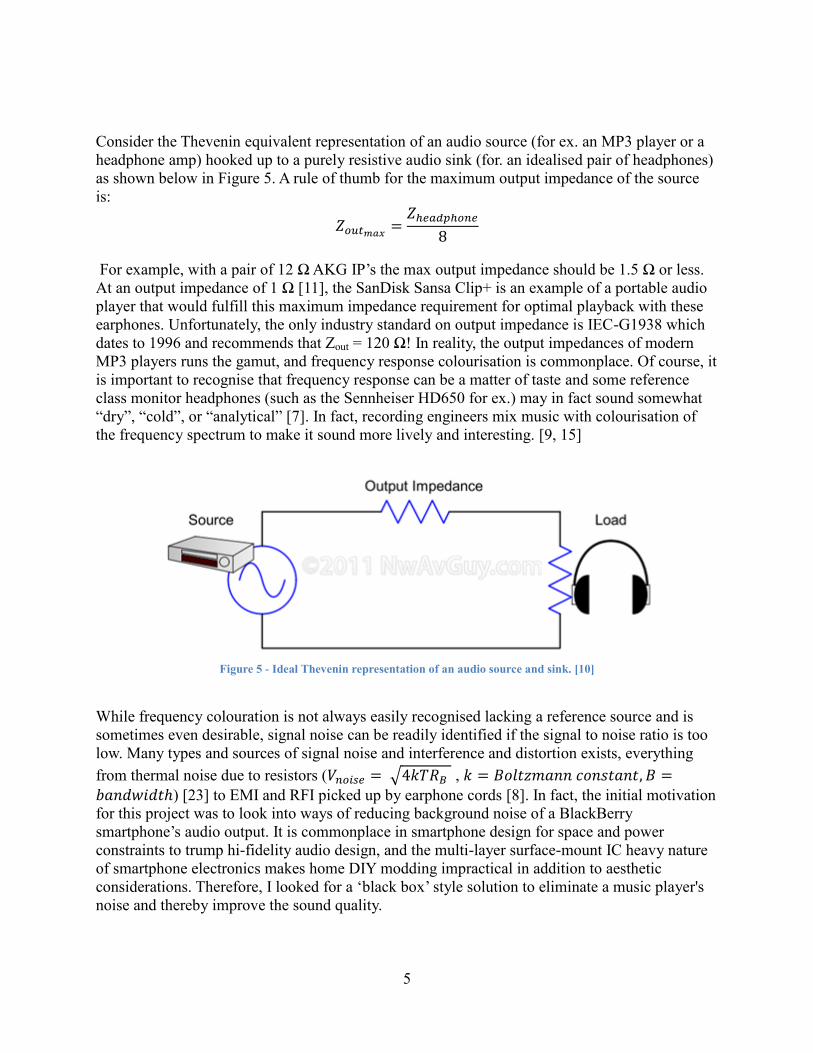
impedance, see Figure 3 and Figure 4 below. For 43 Ω Zout, the 21 Ω Ultimate Ears SuperFi 5’s
measure 12 dB frequency response deviation across the audio spectrum; for 10 Ω Zout, the
deviation is much less at 6 dB.
4
Figure 3 - Plot showing 12dB frequency response deviation for Zout = 43 Ω with UE SuperFi 5’s. [10]
Figure 4 - Plot showing 12dB frequency response deviation for Zout = 10 Ω with UE SuperFi 5’s. [10]
5
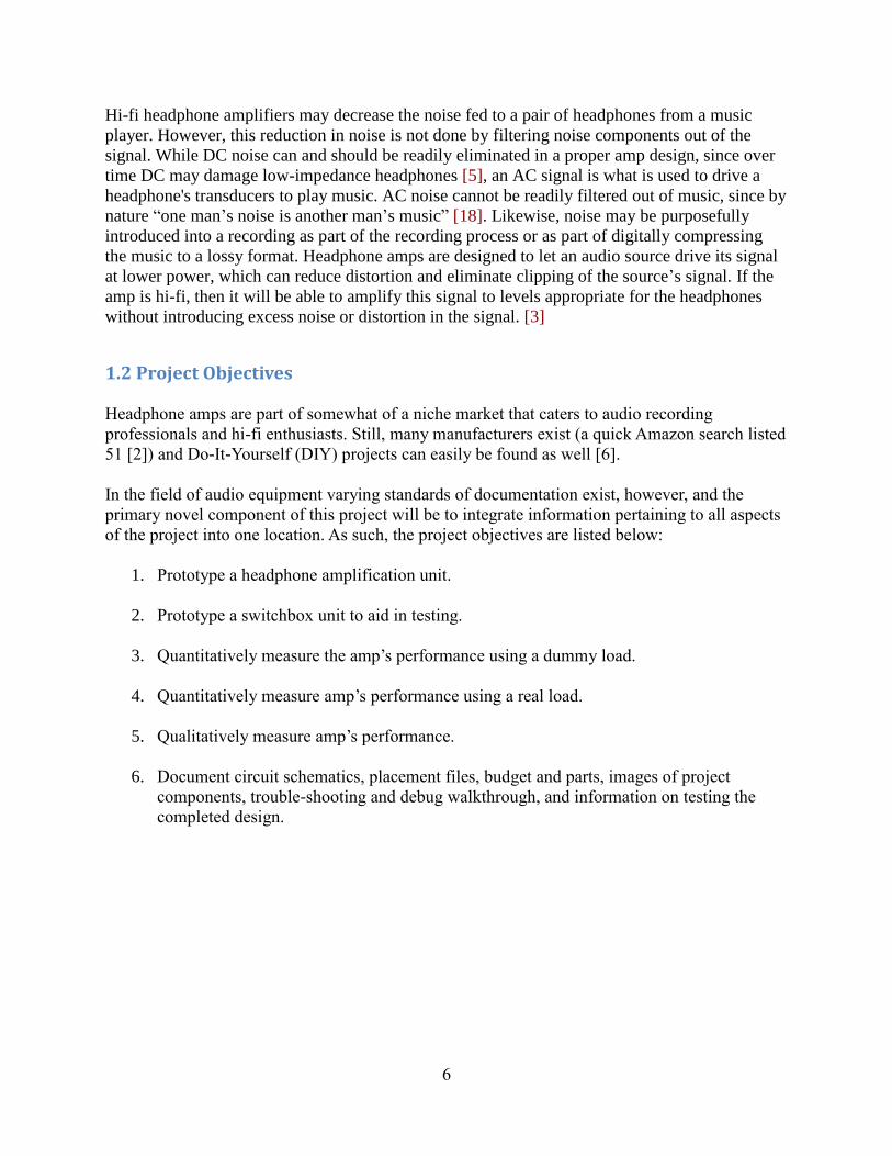
Consider the Thevenin equivalent representation of an audio source (for ex. an MP3 player or a
headphone amp) hooked up to a purely resistive audio sink (for. an idealised pair of headphones)
as shown below in Figure 5. A rule of thumb for the maximum output impedance of the source
is:
𝑍𝑜𝑢𝑡𝑚𝑎𝑥=
𝑍ℎ𝑒𝑎𝑑𝑝ℎ𝑜𝑛𝑒
8
For example, with a pair of 12 Ω AKG IP’s the max output impedance should be 1.5 Ω or less.
At an output impedance of 1 Ω [11], the SanDisk Sansa Clip+ is an example of a portable audio
player that would fulfill this maximum impedance requirement for optimal playback with these
earphones. Unfortunately, the only industry standard on output impedance is IEC-G1938 which
dates to 1996 and recommends that Zout = 120 Ω! In reality, the output impedances of modern
MP3 players runs the gamut, and frequency response colourisation is commonplace. Of course, it
is important to recognise that frequency response can be a matter of taste and some reference
class monitor headphones (such as the Sennheiser HD650 for ex.) may in fact sound somewhat
“dry”, “cold”, or “analytical” [7]. In fact, recording engineers mix music with colourisation of
the frequency spectrum to make it sound more lively and interesting. [9, 15]
Figure 5 - Ideal Thevenin representation of an audio source and sink. [10]
While frequency colouration is not always easily recognised lacking a reference source and is
sometimes even desirable, signal noise can be readily identified if the signal to noise ratio is too
low. Many types and sources of signal noise and interference and distortion exists, everything
from thermal noise due to resistors (𝑉𝑛𝑜𝑖𝑠𝑒 = √4𝑘𝑇𝑅𝐵 , 𝑘 = 𝐵𝑜𝑙𝑡𝑧𝑚𝑎𝑛𝑛 𝑐𝑜𝑛𝑠𝑡𝑎𝑛𝑡, 𝐵 =𝑏𝑎𝑛𝑑𝑤𝑖𝑑𝑡ℎ) [23] to EMI and RFI picked up by earphone cords [8]. In fact, the initial motivation
for this project was to look into ways of reducing background noise of a BlackBerry
smartphone’s audio output. It is commonplace in smartphone design for space and power
constraints to trump hi-fidelity audio design, and the multi-layer surface-mount IC heavy nature
of smartphone electronics makes home DIY modding impractical in addition to aesthetic
considerations. Therefore, I looked for a ‘black box’ style solution to eliminate a music player's
noise and thereby improve the sound quality.
6
Hi-fi headphone amplifiers may decrease the noise fed to a pair of headphones from a music
player. However, this reduction in noise is not done by filtering noise components out of the
signal. While DC noise can and should be readily eliminated in a proper amp design, since over
time DC may damage low-impedance headphones [5], an AC signal is what is used to drive a
headphone's transducers to play music. AC noise cannot be readily filtered out of music, since by
nature “one man’s noise is another man’s music” [18]. Likewise, noise may be purposefully
introduced into a recording as part of the recording process or as part of digitally compressing
the music to a lossy format. Headphone amps are designed to let an audio source drive its signal
at lower power, which can reduce distortion and eliminate clipping of the source’s signal. If the
amp is hi-fi, then it will be able to amplify this signal to levels appropriate for the headphones
without introducing excess noise or distortion in the signal. [3]
1.2 Project Objectives
Headphone amps are part of somewhat of a niche market that caters to audio recording
professionals and hi-fi enthusiasts. Still, many manufacturers exist (a quick Amazon search listed
51 [2]) and Do-It-Yourself (DIY) projects can easily be found as well [6].
In the field of audio equipment varying standards of documentation exist, however, and the
primary novel component of this project will be to integrate information pertaining to all aspects
of the project into one location. As such, the project objectives are listed below:
1. Prototype a headphone amplification unit.
2. Prototype a switchbox unit to aid in testing.
3. Quantitatively measure the amp’s performance using a dummy load.
4. Quantitatively measure amp’s performance using a real load.
5. Qualitatively measure amp’s performance.
6. Document circuit schematics, placement files, budget and parts, images of project
components, trouble-shooting and debug walkthrough, and information on testing the
completed design.
7
1.3 Scope and Limitations
Due to time limitations, the scope of the project completed before the writing of the final report
ended up being scaled back severely. Objectives 2 (switchbox) and 4 (real headphone
quantitative testing) were not pursued because of report deadlines.
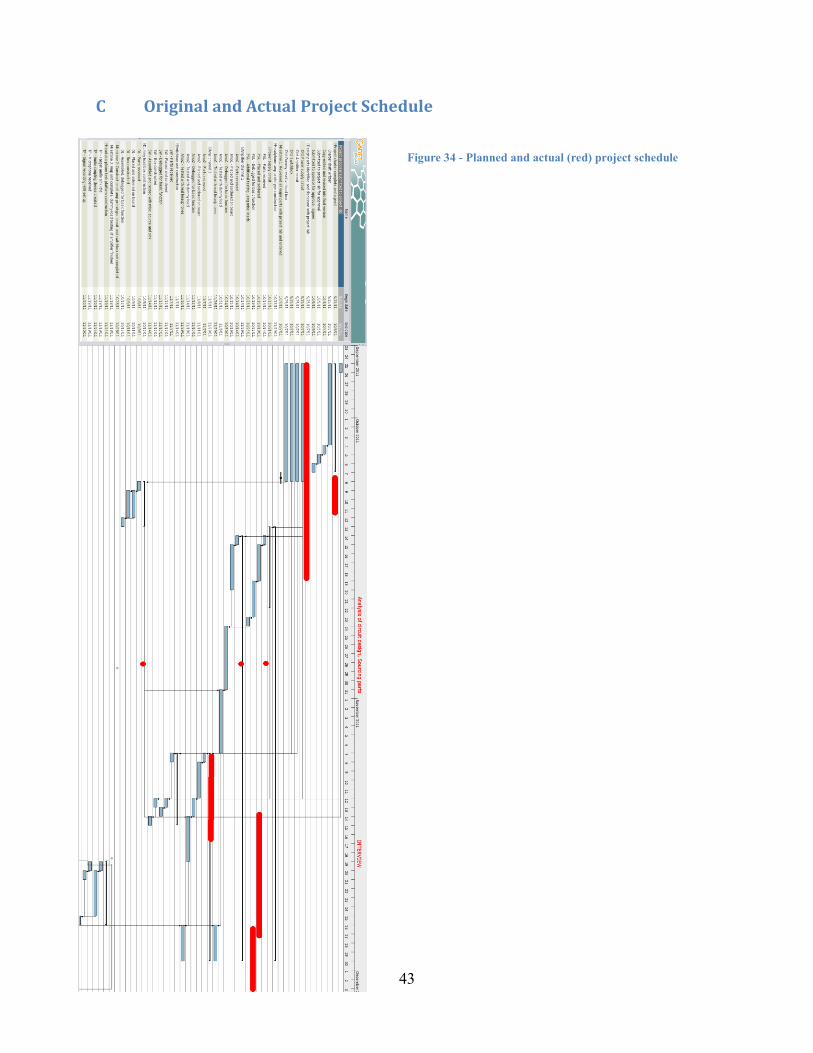
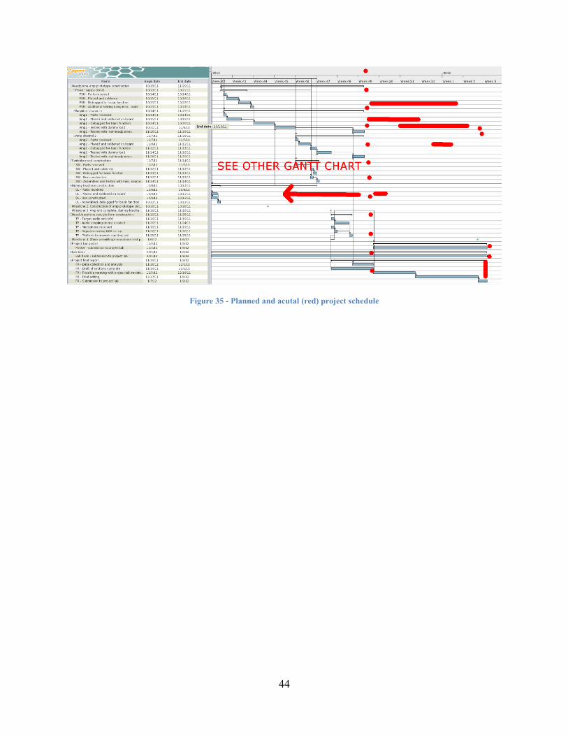
The main factor for the project running behind schedule was the greatly extended time needed to
debug the headphone amplifier power supply circuit and amp channels. Indeed, in the end the
original circuit designs were abandoned in favour of less ambitious ones in order to be able to
obtain measurable results. A compounding factor was the fact that most of the prototyping work
was scheduled during late October / early November, which is the busiest part of the fall
semester. (Refer to C Original and Actual Project Schedule).
The completed deliverables include two CMoy-style [8] amplifier channels based on the
LM1875 op-amp. The design was taken from a typical usage scenario from the device’s
specifications sheet. [25] An adjustable +/- 15VDC power supply was found in the lab and used
for the amp. A dummy 15 Ω 12W / 300 Ω 10W resistive load box was constructed to simulate a
pair of headphones for use in testing.
The op-amp based amp design was characterised by measurements of gain, frequency response,
noise and harmonic distortion, and input/output impedance.
1.4 Organization
The rest of the report will be divided into 4 sections: Discussion, Conclusion, Project
Deliverables, and Recommendations.
The Discussion section will discuss sound quality metrics and the experimental methodology and
equipment behind testing the headphone amplifier, in addition to a selection of results.
The Conclusions section outlines the most important conclusions that can be drawn from the
results.
The Project Deliverables contains a list of the current state of the project deliverables in addition
to a final budget for the project. The ongoing commitments to the project are also stated.
The Recommendations proposes future work to continue the project and sums up some
recommendations regarding audio amplifiers for personal use.
8
2.0 Discussion
2.1 Theory
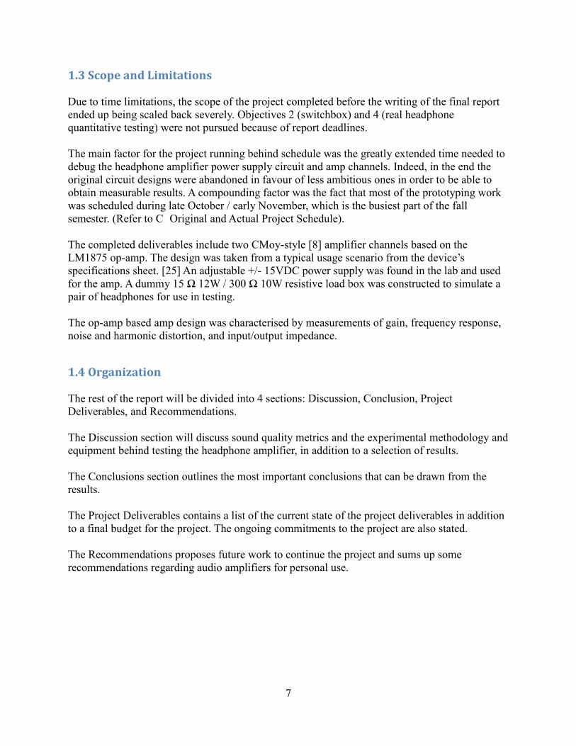
The proposed headphone amplifier design for this project was “A Pure Class A Dynamic
Headphone Amplifier by Kevin Gilmore” [5]. It is a pure class-A amplifier, meaning that in all
stages the amplifying elements (transistors, FET’s) continuously conduct over the entire cycle of
the AC input signal at the expense of greatly reduced efficiency [17].
The design is unique in that it avoids placing any capacitors, transformers, op-amps, or servos in
the audio signal path in order to reduce noise and non-linearities in the output signal. In order to
keep DC offsets low to prevent damaging the headphones, an optional servo loop feeds the DC
offset to the current sources of the stage 1 JFET differential amps which in turn reduces the
amount the corresponding stage 2 output BJT’s are driven.
9
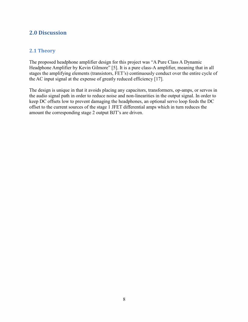
The schematic for a single-channel amplification circuit is as shown below. The circuit enclosed
in the blue square is the whole amplifier channel; the sub-circuit with the green resistors
immediately below is the channel’s op-amp. The OP27 op-amp is the servo which feeds DC bias
from the amp’s headphone output back into the main op-amp via the DC Adjust nets.
Figure 6 - Schematic for single-channel amplification circuit of headphone
The op-amp is composed of two halves, a “push” half and a “pull” half; each half is comprised of
two stages.
The first stage is a differential amplifier composed of two dual JFET’s. In the prototyped circuit,
two matched discrete JFET’s (2N5460 P-channel JFET and 2N5486 N-channel JFET) were used
instead.
10
The DC Adjust net changes the amount of current provided by the BJT current sources to the
differential amp first stage. This current controls the gain of the differential amps as:
𝐴𝑚 = 𝑔𝑚𝑅𝑐; 𝑔𝑚 = 𝛼𝐼
2𝑉𝑇
The second stage is linked to the first by a common emitter BJT. This BJT drives the second
stage common collector output BJT’s. When the servo changes DC Adjust and thereby adjusts
the gain of the differential amp, the corresponding output stage will be driven more or less
relative to the other polarity output stage and hence the DC output will decrease.
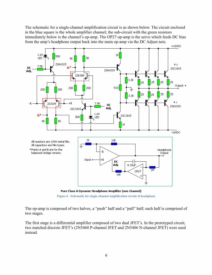
The schematic for the power supply circuit is shown below. It is designed to produce highly
regulated precisely balanced +/- 16.4 VDC. It consists of a transformer to take 115VAC from
wall down to 56VAC in centre-tapped configuration. Two bridge rectifiers rectify the AC to DC
voltages. The rectified DC is fed into adjustable voltage regulators LM317/337 which produce
regulated +/-24VDC rails. A 5VDC reference chip is fed into a non-inverting low-noise OPA548
op-amp. The gain of the op-amp as shown is:
𝐴𝑓 = (1 +𝑅2
𝑅1) , 𝑅2 = 22.8 𝑘Ω ± 0.05%, 𝑅1 = 10 𝑘Ω ± 0.05%
The resistors are picked to be as precise as possible in order to generate a voltage as close to
+16.4VDC as possible. This positive voltage is fed into an inverting unity gain op-amp to
produce -16.4VDC.
Figure 7 - Schematic for power supply circuit of headphone amp. [5]
Additional detail about the headphone amp design can be found in the HeadWize article
publishing the circuits; refer to [5].
11
2.2 Methods / Testing Protocol
Amplifier and power supply designs were taken from “A Pure Class A Dynamic Headphone
Amplifier by Kevin Gilmore” [5]. These ambitious designs were based on high-quality discrete
components and aimed towards hi-fidelity audio response, at the expense of extra components
cost and prototype time. Unfortunately, stability issues with the (adjustable) negative rail of the
power supply forced abandoning the prototyped power supply circuit in favour of an adjustable
15 +/- 2 VDC supply. In addition, it was determined that large variations in hFE (a.k.a. β, or
transistor current gain) between the PNP and NPN ordered transistors resulted in incorrect
biasing conditions for the amplifier stages.
A late decision was made to abandon the Class A discrete amp design in favour of a more easily
implemented op amp design. The op amp design chosen was a CMoy-style amp based on the
LM1875 chip similar to that found in the technical specifications manual for the LM1875.
2.3 Alternative Designs
Alternative design would certainly have been possible in this project. Given enough time and an
unlimited budget, many combinations of headphone amps and test set-ups could be construed.
The discrete component class A headphone amp design originally proposed for this project is
designed with hi-fi amplification on low- to medium-impedance headphones in mind, given no
space or power constraints, and to compete with much more expensive commercial headphone
amplifiers. [5]
The classic basic op-amp headphone amp design later chosen in order to derive some results is
called a CMoy-style amp. It was designed to provide necessary amplification for portable music
listening with full-size headphones [21]. However, CMoy-style amps are simple projects
designed more for preventing clipping and raising volume levels than for hi-fi amplification.
Another family of headphone amplifiers uses vacuum tubes, known for their characteristically
“smooth” sound or high power (> 1W) output, instead of solid-state electronics for amplification.
However, working with vacuum tubes can be dangerous as they operate at high voltages (some >
1000V) and for many headphones even 100mW is extremely loud depending on their impedance
rating [14].
12
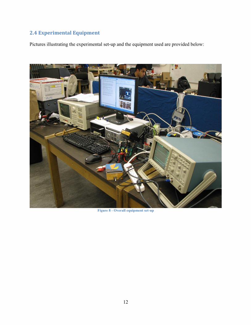
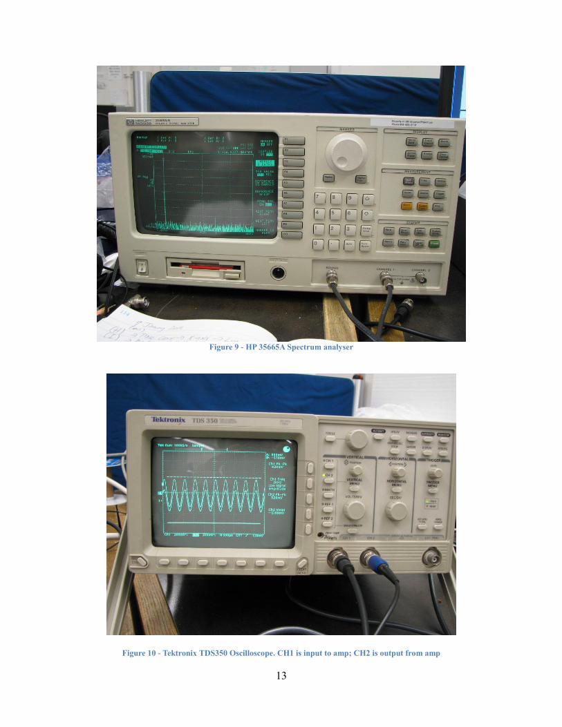
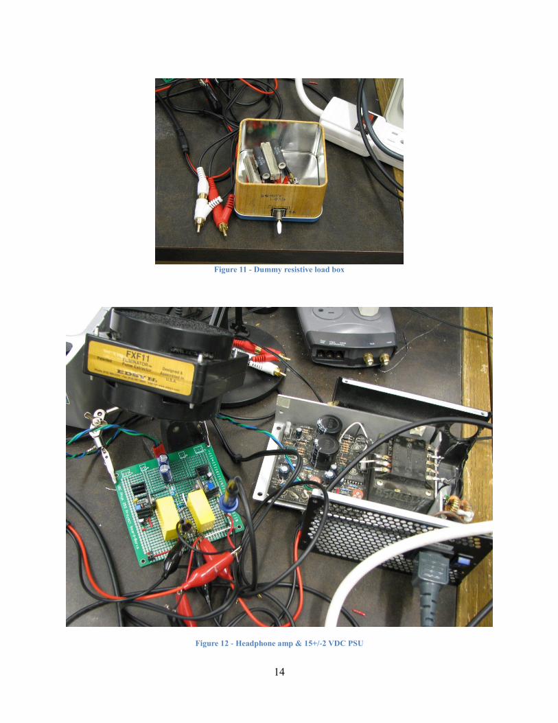
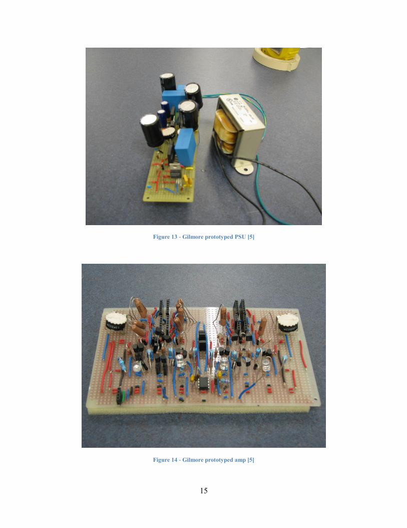
2.4 Experimental Equipment
Pictures illustrating the experimental set-up and the equipment used are provided below:
Figure 8 - Overall equipment set-up
13
Figure 9 - HP 35665A Spectrum analyser
Figure 10 - Tektronix TDS350 Oscilloscope. CH1 is input to amp; CH2 is output from amp
14
Figure 11 - Dummy resistive load box
Figure 12 - Headphone amp & 15+/-2 VDC PSU
15
Figure 13 - Gilmore prototyped PSU [5]
Figure 14 - Gilmore prototyped amp [5]
16
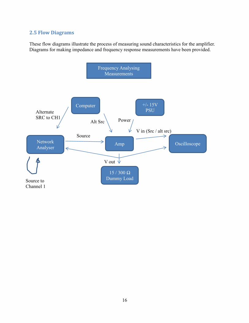
2.5 Flow Diagrams
These flow diagrams illustrate the process of measuring sound characteristics for the amplifier.
Diagrams for making impedance and frequency response measurements have been provided.
Frequency Analysing
Measurements
Amp
+/- 15V
PSU
15 / 300 Ω
Dummy Load
Oscilloscope Network
Analyser
Computer
V out
V in (Src / alt src) Source
Source to
Channel 1
Alternate
SRC to CH1 Power Alt Src
17
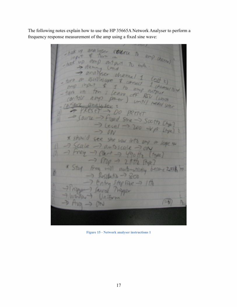
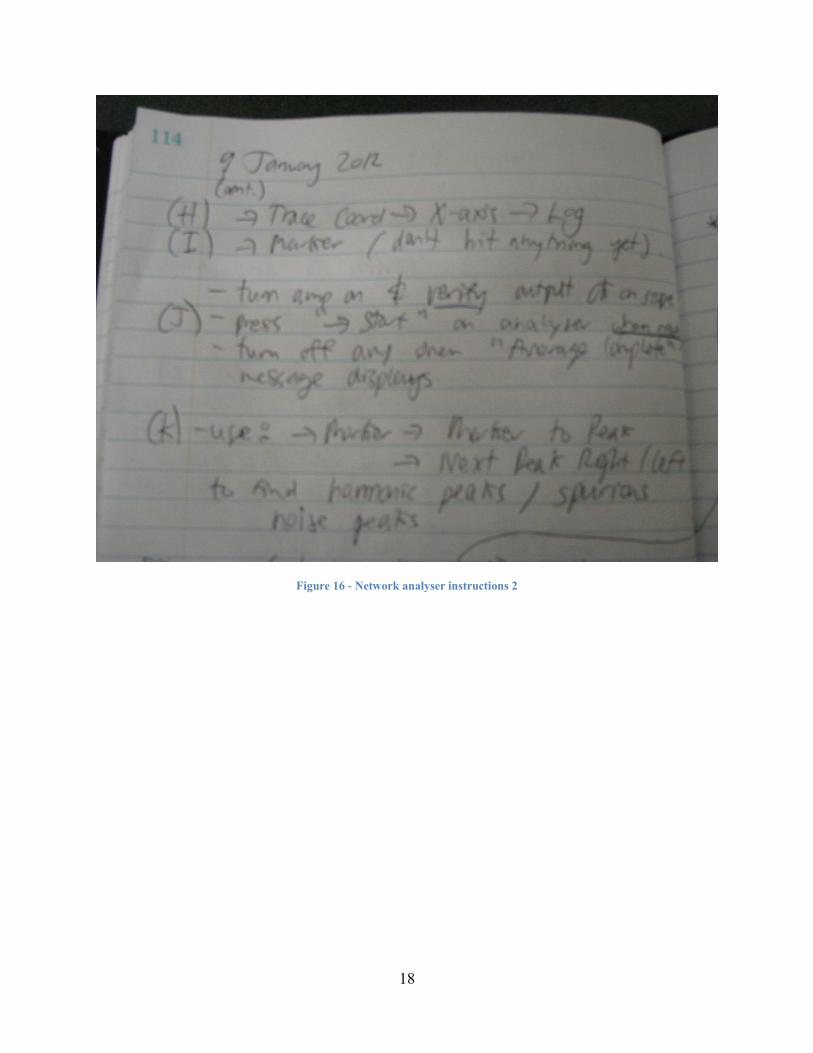
The following notes explain how to use the HP 35665A Network Analyser to perform a
frequency response measurement of the amp using a fixed sine wave:
Figure 15 - Network analyser instructions 1
18
Figure 16 - Network analyser instructions 2
19
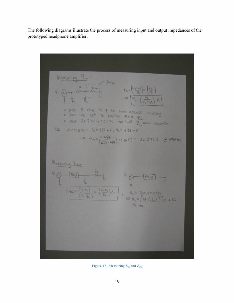
The following diagrams illustrate the process of measuring input and output impedances of the
prototyped headphone amplifier:
Figure 17 - Measuring Zin and Zout
20
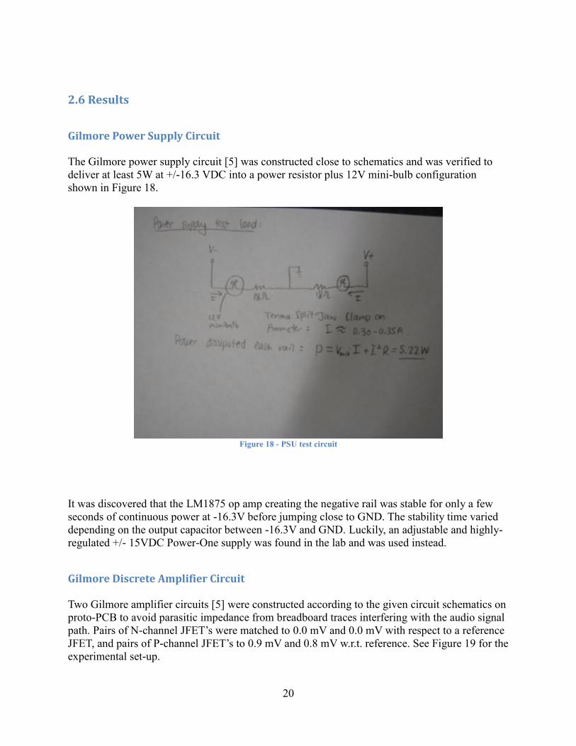
2.6 Results
Gilmore Power Supply Circuit
The Gilmore power supply circuit [5] was constructed close to schematics and was verified to
deliver at least 5W at +/-16.3 VDC into a power resistor plus 12V mini-bulb configuration
shown in Figure 18.
Figure 18 - PSU test circuit
It was discovered that the LM1875 op amp creating the negative rail was stable for only a few
seconds of continuous power at -16.3V before jumping close to GND. The stability time varied
depending on the output capacitor between -16.3V and GND. Luckily, an adjustable and highly-
regulated +/- 15VDC Power-One supply was found in the lab and was used instead.
Gilmore Discrete Amplifier Circuit
Two Gilmore amplifier circuits [5] were constructed according to the given circuit schematics on
proto-PCB to avoid parasitic impedance from breadboard traces interfering with the audio signal
path. Pairs of N-channel JFET’s were matched to 0.0 mV and 0.0 mV with respect to a reference
JFET, and pairs of P-channel JFET’s to 0.9 mV and 0.8 mV w.r.t. reference. See Figure 19 for the
experimental set-up.
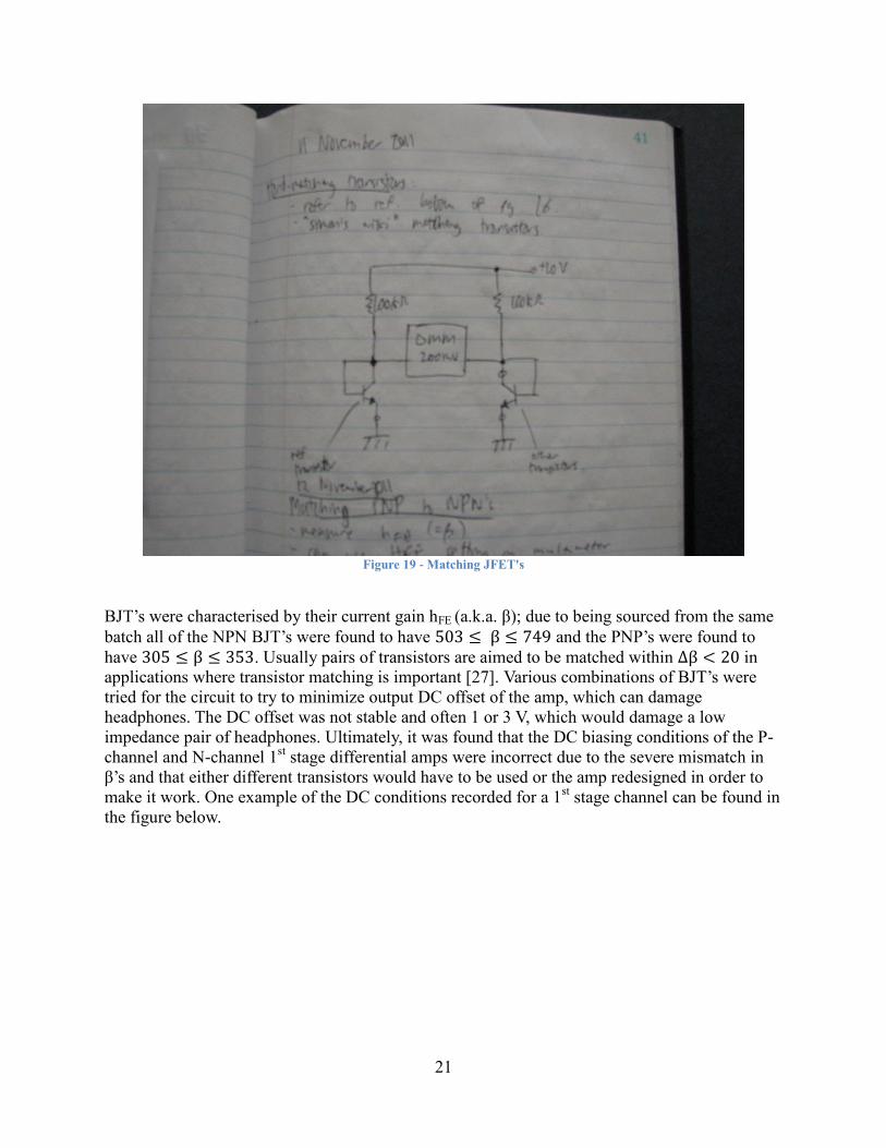
21
Figure 19 - Matching JFET's
BJT’s were characterised by their current gain hFE (a.k.a. β); due to being sourced from the same
batch all of the NPN BJT’s were found to have 503 ≤ β ≤ 749 and the PNP’s were found to
have 305 ≤ β ≤ 353. Usually pairs of transistors are aimed to be matched within Δβ < 20 in
applications where transistor matching is important [27]. Various combinations of BJT’s were
tried for the circuit to try to minimize output DC offset of the amp, which can damage
headphones. The DC offset was not stable and often 1 or 3 V, which would damage a low
impedance pair of headphones. Ultimately, it was found that the DC biasing conditions of the P-
channel and N-channel 1st stage differential amps were incorrect due to the severe mismatch in
β’s and that either different transistors would have to be used or the amp redesigned in order to
make it work. One example of the DC conditions recorded for a 1st stage channel can be found in
the figure below.
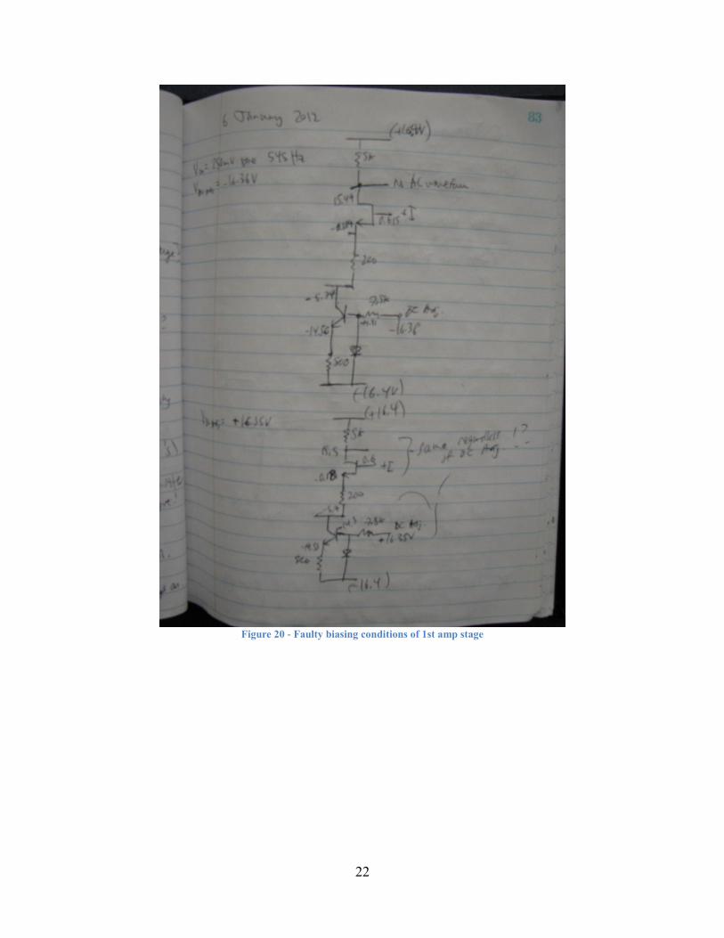
22
Figure 20 - Faulty biasing conditions of 1st amp stage
23
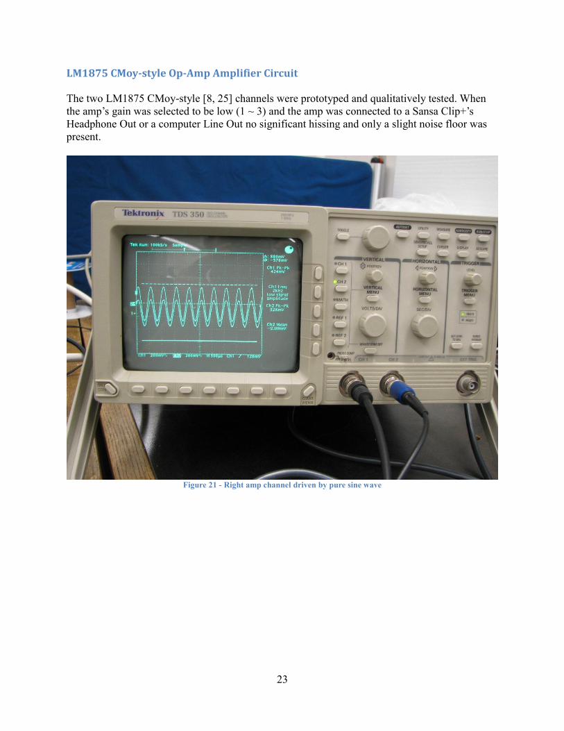
LM1875 CMoy-style Op-Amp Amplifier Circuit
The two LM1875 CMoy-style [8, 25] channels were prototyped and qualitatively tested. When
the amp’s gain was selected to be low (1 ~ 3) and the amp was connected to a Sansa Clip+’s
Headphone Out or a computer Line Out no significant hissing and only a slight noise floor was
present.
Figure 21 - Right amp channel driven by pure sine wave
24
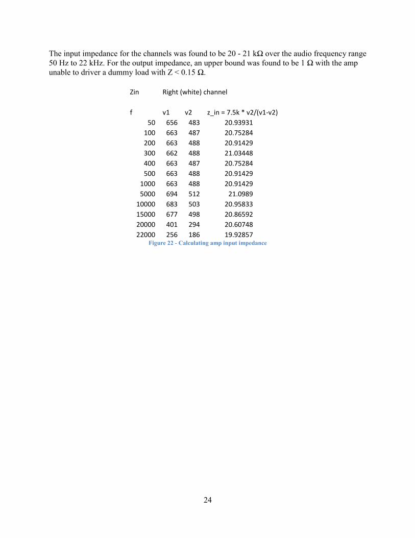
The input impedance for the channels was found to be 20 - 21 kΩ over the audio frequency range
50 Hz to 22 kHz. For the output impedance, an upper bound was found to be 1 Ω with the amp
unable to driver a dummy load with Z < 0.15 Ω.
Zin Right (white) channel
f v1 v2 z_in = 7.5k * v2/(v1-v2)
50 656 483 20.93931 100 663 487 20.75284 200 663 488 20.91429 300 662 488 21.03448 400 663 487 20.75284 500 663 488 20.91429 1000 663 488 20.91429 5000 694 512 21.0989 10000 683 503 20.95833 15000 677 498 20.86592 20000 401 294 20.60748 22000 256 186 19.92857 Figure 22 - Calculating amp input impedance
25
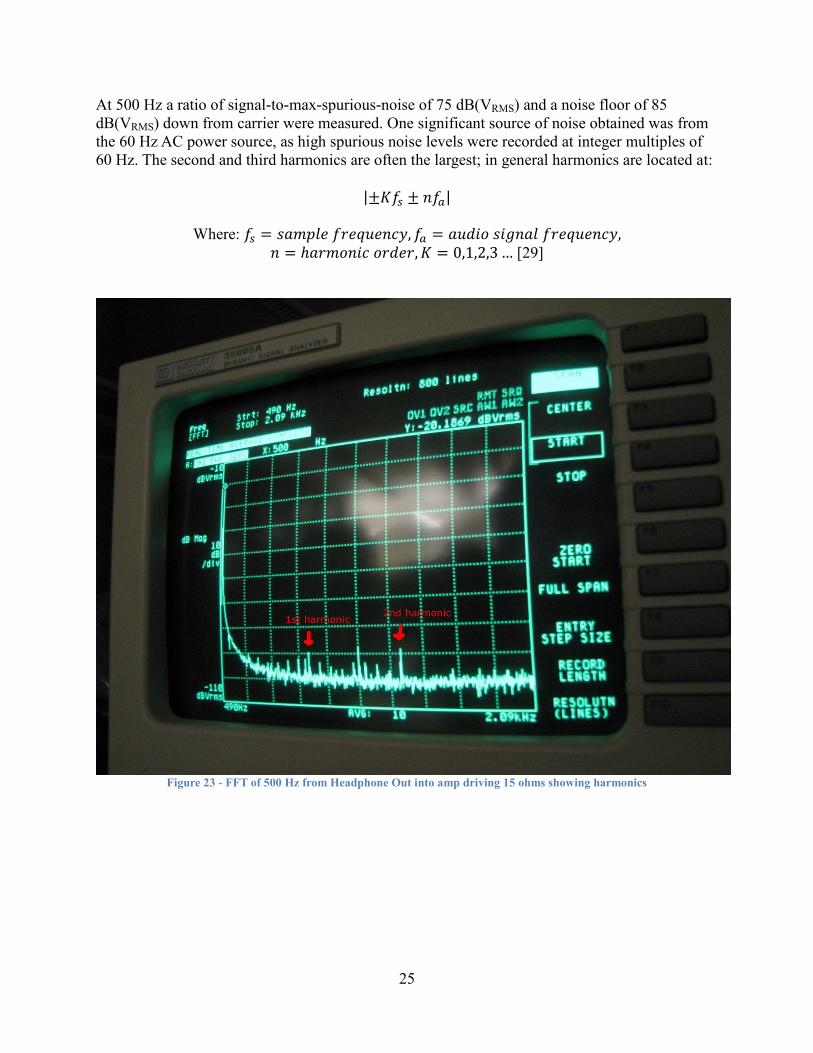
At 500 Hz a ratio of signal-to-max-spurious-noise of 75 dB(VRMS) and a noise floor of 85
dB(VRMS) down from carrier were measured. One significant source of noise obtained was from
the 60 Hz AC power source, as high spurious noise levels were recorded at integer multiples of
60 Hz. The second and third harmonics are often the largest; in general harmonics are located at:
|±𝐾𝑓𝑠 ± 𝑛𝑓𝑎|
Where: 𝑓𝑠 = 𝑠𝑎𝑚𝑝𝑙𝑒 𝑓𝑟𝑒𝑞𝑢𝑒𝑛𝑐𝑦, 𝑓𝑎 = 𝑎𝑢𝑑𝑖𝑜 𝑠𝑖𝑔𝑛𝑎𝑙 𝑓𝑟𝑒𝑞𝑢𝑒𝑛𝑐𝑦, 𝑛 = ℎ𝑎𝑟𝑚𝑜𝑛𝑖𝑐 𝑜𝑟𝑑𝑒𝑟, 𝐾 = 0,1,2,3 … [29]
Figure 23 - FFT of 500 Hz from Headphone Out into amp driving 15 ohms showing harmonics
26
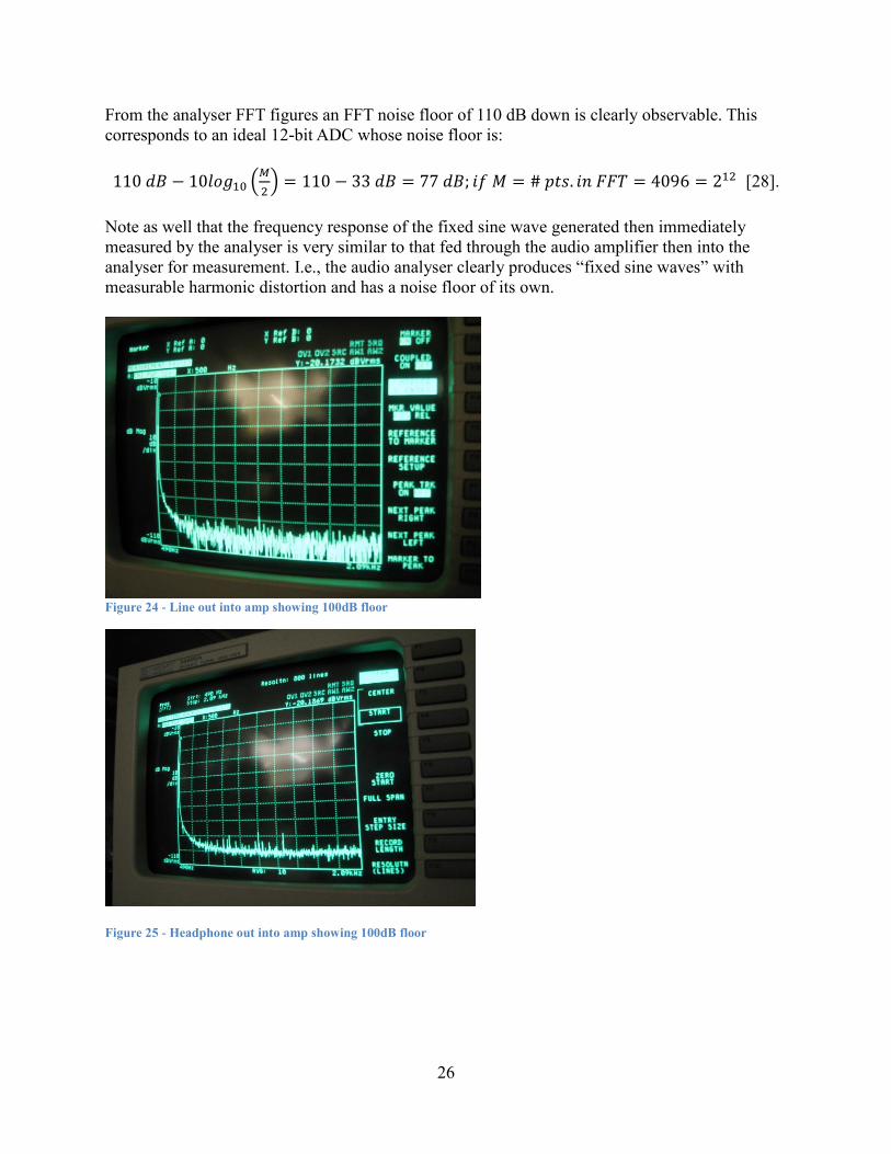
From the analyser FFT figures an FFT noise floor of 110 dB down is clearly observable. This
corresponds to an ideal 12-bit ADC whose noise floor is:
110 𝑑𝐵 − 10𝑙𝑜𝑔10 (𝑀
2) = 110 − 33 𝑑𝐵 = 77 𝑑𝐵; 𝑖𝑓 𝑀 = # 𝑝𝑡𝑠. 𝑖𝑛 𝐹𝐹𝑇 = 4096 = 212 [28].
Note as well that the frequency response of the fixed sine wave generated then immediately
measured by the analyser is very similar to that fed through the audio amplifier then into the
analyser for measurement. I.e., the audio analyser clearly produces “fixed sine waves” with
measurable harmonic distortion and has a noise floor of its own.
Figure 24 - Line out into amp showing 100dB floor
Figure 25 - Headphone out into amp showing 100dB floor
27
Figure 26 - Spectrum analyser source measurement showing -110dB floor
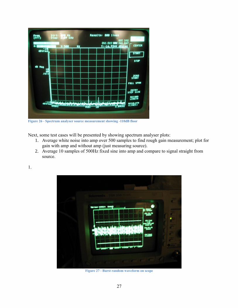
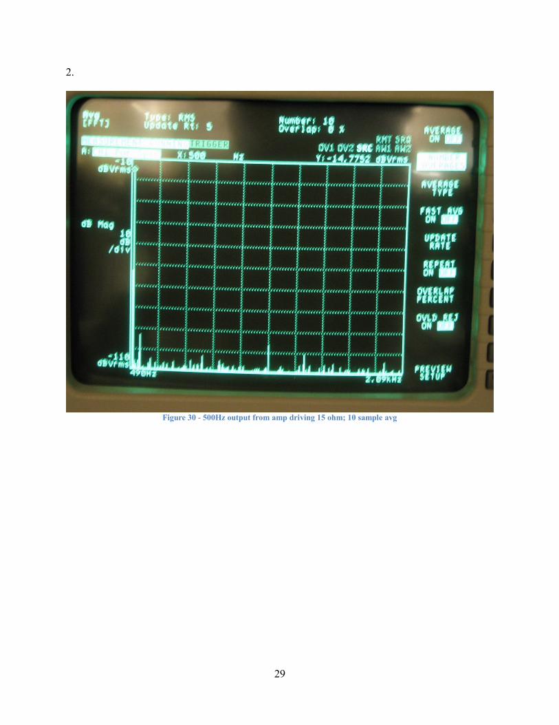
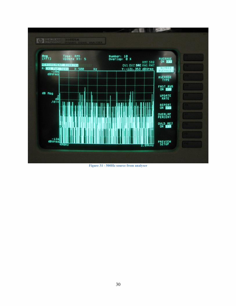
Next, some test cases will be presented by showing spectrum analyser plots:
1. Average white noise into amp over 500 samples to find rough gain measurement; plot for
gain with amp and without amp (just measuring source).
2. Average 10 samples of 500Hz fixed sine into amp and compare to signal straight from
source.
1.
Figure 27 - Burst random waveform on scope
28
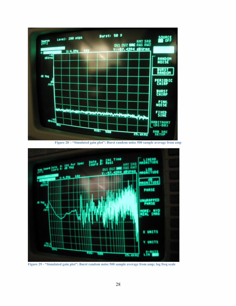
Figure 28 – “Simulated gain plot”: Burst random noise 500 sample average from amp
Figure 29 - “Simulated gain plot”: Burst random noise 500 sample average from amp; log freq scale
29
2.
Figure 30 - 500Hz output from amp driving 15 ohm; 10 sample avg
30
Figure 31 - 500Hz source from analyser
31
3.0 Conclusions
Inspecting the similarity of the FFT’s produced off the analyser fixed sine wave source compared
to the amplifier output, one may conclude that the amount of harmonic distortion or noise is
really not distinguishable by the 12-bit HP 35665A.
The estimated LM1875 CMoy-style amplifier input and output impedances of 21 kΩ and <1 Ω,
respectively, suggest that the amp will be able to drive audio transducers of most impedances that
do not need voltage levels of more than 2-3VAC. The two amp channels drove a small pair of 8
Ω loudspeakers around 1VAC correctly (corresponding to ~ 100mW of power dissipation). It
will not be able to drive electrostatic headphones that require hundreds of volts to operate.
The LM1875-based headphone amp channels were dummy-load tested to amplify pure sine
waves from 50 Hz to 22,000 kHz at Vpk-pk on the order of 1 V stably. The amp channels were
also qualitatively verified to work using 8, 16, 32, and 100 Ω audio transducers at reasonable
listening levels, with the amp driven from computer Line Out, a portable Sansa Clip+ music
player, an HP 35665A Dynamic signal analyser and a BK Precision 4012A function generator.
The Gilmore Discrete Class A Amp was abandoned due to mismatch between current gain
between PNP and NPN transistors resulting in high DC offset and incorrect (saturation) biasing
conditions. The Gilmore power supply design suffered from stability issues was abandoned in
favour of a pre-existing +/-15 VDC adjustable lab power supply. This risk of ordering parts that
might not necessarily work for the given circuit designs was both anticipated and accepted upon
drafting the Project Charter; unfortunately in this case a lengthy debug process that impacted the
quality of the project’s alternative results was required to prove that this was the case.
32
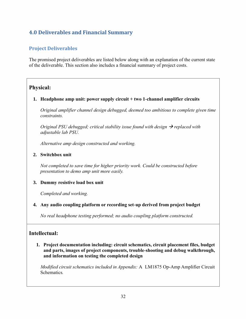
4.0 Deliverables and Financial Summary
Project Deliverables
The promised project deliverables are listed below along with an explanation of the current state
of the deliverable. This section also includes a financial summary of project costs.
Physical:
1. Headphone amp unit: power supply circuit + two 1-channel amplifier circuits
Original amplifier channel design debugged, deemed too ambitious to complete given time
constraints.
Original PSU debugged; critical stability issue found with design replaced with
adjustable lab PSU.
Alternative amp design constructed and working.
2. Switchbox unit
Not completed to save time for higher priority work. Could be constructed before
presentation to demo amp unit more easily.
3. Dummy resistive load box unit
Completed and working.
4. Any audio coupling platform or recording set-up derived from project budget
No real headphone testing performed; no audio coupling platform constructed.
Intellectual:
1. Project documentation including: circuit schematics, circuit placement files, budget
and parts, images of project components, trouble-shooting and debug walkthrough,
and information on testing the completed design
Modified circuit schematics included in Appendix: A LM1875 Op-Amp Amplifier Circuit
Schematics.
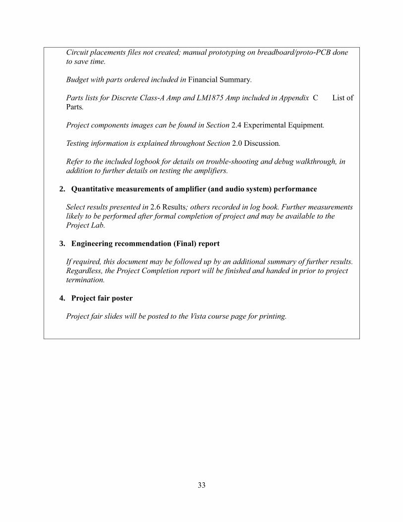
33
Circuit placements files not created; manual prototyping on breadboard/proto-PCB done
to save time.
Budget with parts ordered included in Financial Summary.
Parts lists for Discrete Class-A Amp and LM1875 Amp included in Appendix C List of
Parts.
Project components images can be found in Section 2.4 Experimental Equipment.
Testing information is explained throughout Section 2.0 Discussion.
Refer to the included logbook for details on trouble-shooting and debug walkthrough, in
addition to further details on testing the amplifiers.
2. Quantitative measurements of amplifier (and audio system) performance
Select results presented in 2.6 Results; others recorded in log book. Further measurements
likely to be performed after formal completion of project and may be available to the
Project Lab.
3. Engineering recommendation (Final) report
If required, this document may be followed up by an additional summary of further results.
Regardless, the Project Completion report will be finished and handed in prior to project
termination.
4. Project fair poster
Project fair slides will be posted to the Vista course page for printing.

34
Financial Summary
Below is a summary of all requested for the project. This is not a list of what was actually
ordered by the Project Lab or what was received. Refer to Appendix C List of Parts for the
parts actually needed for each amplifier.
Total parts ordered
Part Part # Cost ea. # requested Sum
Hammond 166J50 115V to 50 C.T. Transformer Newark 66F7394 37.99 1 37.99
5VDC REF02 precision voltage reference Mouser 700-REF02CP 3.28 1 3.28
100V 2A single phase bridge rectifier Newark 78K3297 0.361 4 1.444
LM3875 audio power amp Newark 41K5106 8.06 2 16.12
4,7uF +/-10% 75uV/s poly film capacitor Newark 29M0511 2.97 4 11.88
240Ohm 1% 250mW metal film resistor Newark 58K3832 0.062 5 0.31
10kOhm 0.1% 250mW metal film resistor Newark 12P6367 0.222 4 0.888
22.6kOhm 0.1% 250mW metal film resistor Newark 78R5152 0.805 1 0.805 499 (500 replacement)Ohm 0.1% 250mW metal film resistor Newark 97K8700 0.749 2 1.498
510Ohm 0.1% 250mW metal film resistor Newark 12T2093 0.604 1 0.604
200Ohm 0.1% 250mW metal film resistor Newark 03P4750 0.639 4 2.556
5kOhm 0.1% 250mW metal film resistor Newark 68P8706 0.278 4 1.112
1kOhm 0.1% 500mW metal film resistor Newark 67P8682 0.356 2 0.712
7.5kOhm 0.1% 250mW metal film resistor Newark 97K8736 0.659 2 1.318
3.32kOhm 0.1% 250mW metal film resistor Newark 78R5179 0.822 2 1.644
25Ohm 0.1% 250mW metal film resistor Mouser 71-RN65C25R0BB14 1.18 8 9.44
NTE460 P channel JFET (2SJ109 replacement) Newark 31C4208 8.12 1 8.12
NTE458 N channel JFET (2SK389 replacement) Newark 29C4607 7.64 1 7.64
BC549 NPN transistor 100mA (2SC1815 replacement) Newark 58K8757 0.061 20 1.22
BC559 PNP transistor 100mA (2SA1015 replacement) Newark 58K8762 0.142 20 2.84
LM833 (OP27 replacement) Newark 26K3636 0.653 2 1.306
LM337 (negative adj. Volt regulator, ~16V out) Mouser 926-LM337T/NOPB 2.12 1 2.12 499 (500 replacement)Ohm 0.1% 250mW metal film resistor Newark 98K3835 0.402 4 1.608
200Ohm 0.1% 250mW metal film resistor Newark 03P4750 0.639 4 2.556
5kOhm 0.1% 250mW metal film resistor Newark 68P8706 0.278 4 1.112
7.5kOhm 0.1% 250mW metal film resistor Newark 97K8736 0.659 2 1.318
3.32kOhm 0.1% 250mW metal film resistor Newark 78R5179 0.822 2 1.644
25Ohm 0.1% 250mW metal film resistor Mouser 71-RN65C25R0BB14 1.18 8 9.44
N-Channel Dual JFET Digikey 568-2084-1-ND 1.06 2 2.12
N-Channel Single JFET Newark 58K9646 0.085 10 0.85
P-Channel Single JFET Newark 58K2812 0.169 10 1.69
TOTAL 137.185
35
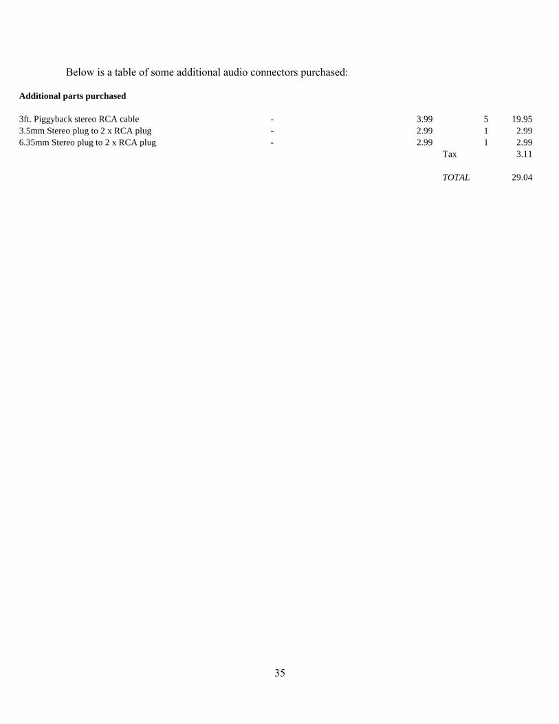
Below is a table of some additional audio connectors purchased:
Additional parts purchased
3ft. Piggyback stereo RCA cable - 3.99 5 19.95
3.5mm Stereo plug to 2 x RCA plug - 2.99 1 2.99
6.35mm Stereo plug to 2 x RCA plug - 2.99 1 2.99
Tax 3.11
TOTAL 29.04
36
5.0 Recommendations
Even though this project has not been completed on schedule, from the results at hand some
recommendations may nonetheless be in order.
The LM1875-based amplifier was able to drive audio transducers from computer Line Out (but
not Headphone Out) properly, but did not noticeably improve sound quality. It is therefore
recommended to perform further repetitions of the quantitative amplifier tests to try to find if any
sound quality difference exists. For future measurements of amplifier gain a network analyser
with a built-in swept-sine gain response measurement should be used.
It would also be of interest to perform quantitative measurements on “typical usage scenarios”,
in order to more easily convey the merits of proper audio set-ups and amplification to the
average user.
Considering that only impedance, frequency response, and noise/harmonics were investigated, it
is also logical to recommend performing different measurements of sound characteristics. Some
other very important characteristics affecting an amp’s sound quality are discussed in [24]:
output power, distortion, phase response, channel balance, crosstalk, and square wave
response/slew rate.
Given that a medium-fidelity amp did not noticeably improve sound quality, it is also
recommended to recalculate the biasing conditions for the transistors in the hi-fi discrete
amplifier set-up and to continue with fixing the circuits. It is should not be necessary invest
much more (if any) money into the amplifier to get it into a working state.
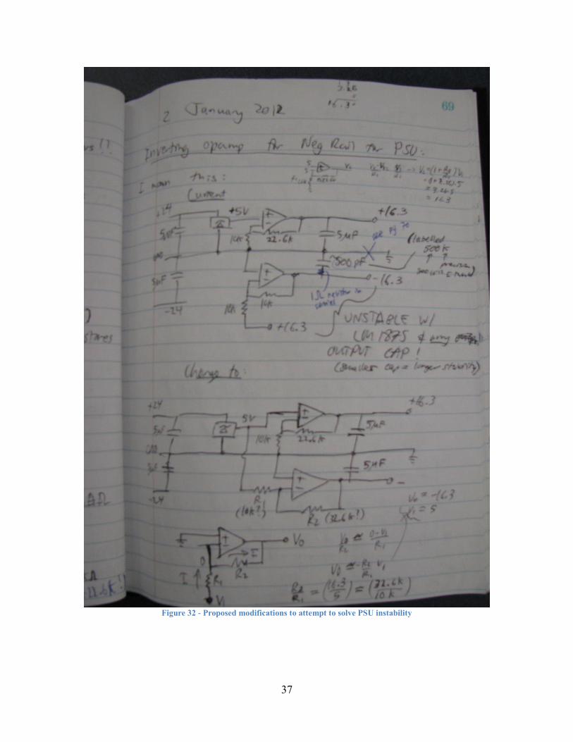
The prototyped power supply could be easily fixed and repurposed for another project if desired.
Issues may remain with the audible noise produced by the transformer if it is used without proper
mounting. The necessary modifications to fix the PSU’s stability issue are illustrated in Figure
32.
37
Figure 32 - Proposed modifications to attempt to solve PSU instability

38
39
Appendices
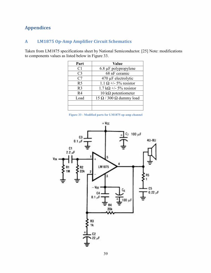
A LM1875 Op-Amp Amplifier Circuit Schematics
Taken from LM1875 specifications sheet by National Semiconductor. [25] Note: modifications
to components values as listed below in Figure 33.
Figure 33 - Modified parts for LM1875 op-amp channel
Part Value
C1 6.8 µF polypropylene
C3 68 nF ceramic
C7 470 µF electrolytic
R5 1.1 Ω +/- 5% resistor
R3 1.7 kΩ +/- 5% resistor
R4 10 kΩ potentiometer
Load 15 Ω / 300 Ω dummy load
40
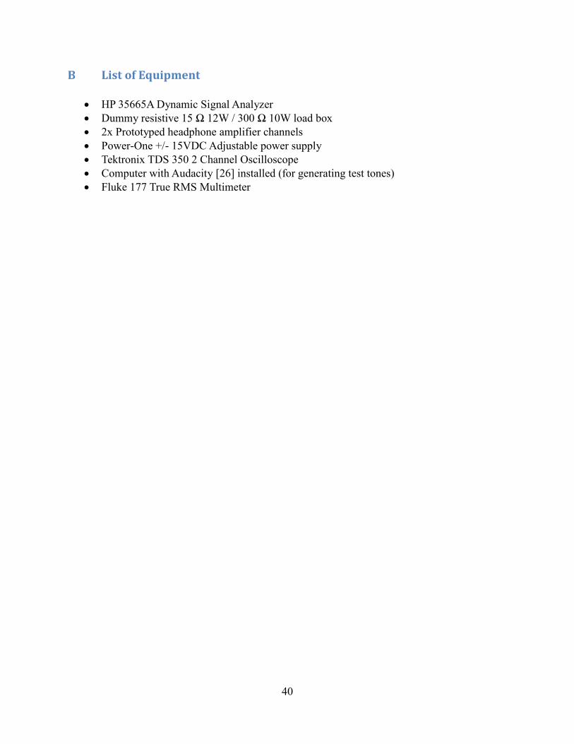
B List of Equipment
HP 35665A Dynamic Signal Analyzer
Dummy resistive 15 Ω 12W / 300 Ω 10W load box
2x Prototyped headphone amplifier channels
Power-One +/- 15VDC Adjustable power supply
Tektronix TDS 350 2 Channel Oscilloscope
Computer with Audacity [26] installed (for generating test tones)
Fluke 177 True RMS Multimeter
41
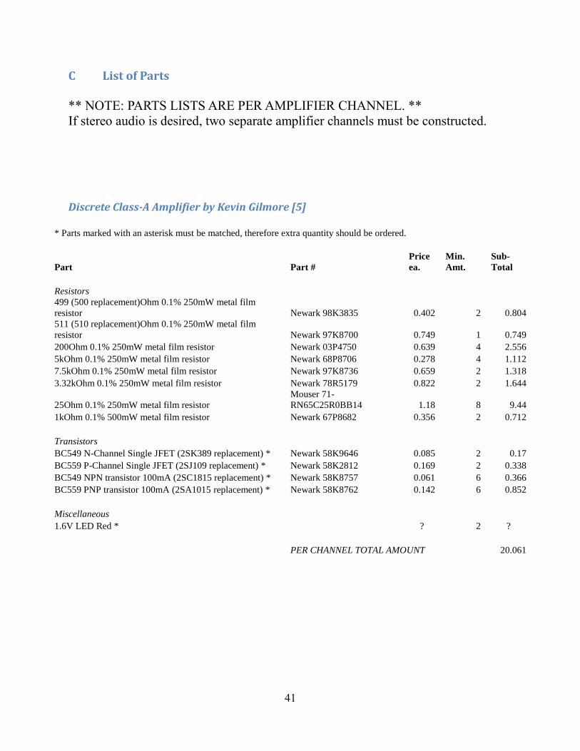
C List of Parts
** NOTE: PARTS LISTS ARE PER AMPLIFIER CHANNEL. **
If stereo audio is desired, two separate amplifier channels must be constructed.
Discrete Class-A Amplifier by Kevin Gilmore [5]
* Parts marked with an asterisk must be matched, therefore extra quantity should be ordered.
Part Part #
Price
ea.
Min.
Amt.
Sub-
Total
Resistors
499 (500 replacement)Ohm 0.1% 250mW metal film
resistor Newark 98K3835 0.402 2 0.804
511 (510 replacement)Ohm 0.1% 250mW metal film
resistor Newark 97K8700 0.749 1 0.749
200Ohm 0.1% 250mW metal film resistor Newark 03P4750 0.639 4 2.556
5kOhm 0.1% 250mW metal film resistor Newark 68P8706 0.278 4 1.112
7.5kOhm 0.1% 250mW metal film resistor Newark 97K8736 0.659 2 1.318
3.32kOhm 0.1% 250mW metal film resistor Newark 78R5179 0.822 2 1.644
25Ohm 0.1% 250mW metal film resistor
Mouser 71-
RN65C25R0BB14 1.18 8 9.44
1kOhm 0.1% 500mW metal film resistor Newark 67P8682 0.356 2 0.712
Transistors
BC549 N-Channel Single JFET (2SK389 replacement) * Newark 58K9646 0.085 2 0.17
BC559 P-Channel Single JFET (2SJ109 replacement) * Newark 58K2812 0.169 2 0.338
BC549 NPN transistor 100mA (2SC1815 replacement) * Newark 58K8757 0.061 6 0.366
BC559 PNP transistor 100mA (2SA1015 replacement) * Newark 58K8762 0.142 6 0.852
Miscellaneous
1.6V LED Red *
? 2 ?
PER CHANNEL TOTAL AMOUNT 20.061
42
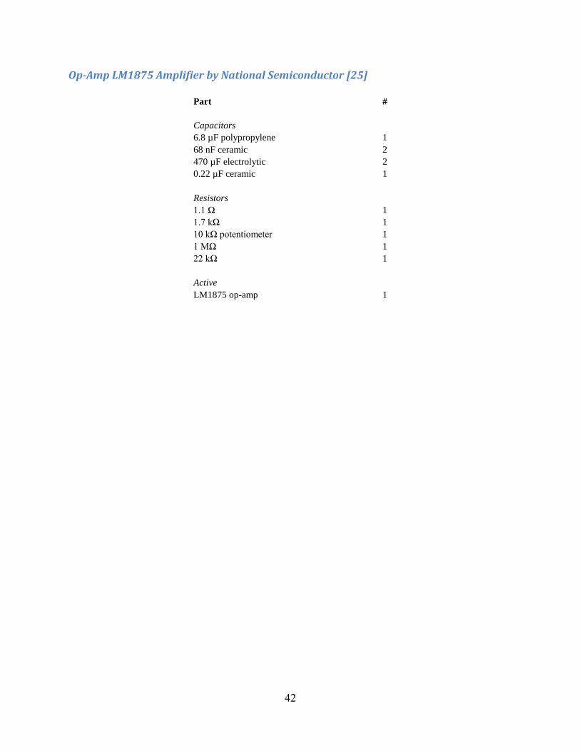
Op-Amp LM1875 Amplifier by National Semiconductor [25]
Part #
Capacitors
6.8 µF polypropylene 1
68 nF ceramic 2
470 µF electrolytic 2
0.22 µF ceramic 1
Resistors
1.1 Ω 1
1.7 kΩ 1
10 kΩ potentiometer 1
1 MΩ 1
22 kΩ 1
Active
LM1875 op-amp 1
43
C Original and Actual Project Schedule
Figure 34 - Planned and actual (red) project schedule
44
Figure 35 - Planned and acutal (red) project schedule
45
References
[1] Tyll “measuring headphones with studio six digitals acoustics analyzer for ipod touch and
iphone - pt 3.”. http://www.headphone.com/rightbetweenyourears/?p=606.
[2] Amazon.com. “headphone accessories - amps - top brands”.
http://www.amazon.com/gp/search/other/ref=sr in - 2 A?rh=i%3Aelectronics-
accessories%2Cn%3A172282%2Cn%3A!493964%2Cn%3A281407%2Cn%3A172532%2
Cn%3A11039351%2Cn%3A13880161&bbn=13880161&pickerToList=brandtextbin&ie=
UTF8&qid=1316990685
[3] D. Data. “headroom bithead headphone amplifier”. http://www.dansdata.com/bithead.htm
[4] DIYAudio.com. “safety when testing headphone amps”.
http://www.diyaudio.com/forums/headphone-systems/53808-safety-
when-testing-headphone-amp-musos.html
[5] K. Gilmore. “a pure class a dynamic headphone amplifier”.
http://gilmore2.chem.northwestern.edu/projects/showfile.php?file=gilmore3 prj.htm
[6] HeadWize. “projects”. http://gilmore2.chem.northwestern.edu/projects/index.htm.
[7] C. Lau. “sennheiser idol: Hd580 vs hd595 vs hd600 vs hd650 re-
viewed and compared”. http://www.compudio.ca/2008/05/sennheiser-
idol-hd580-vs-hd595-vs-hd600.html
[8] C. Moy. “a pocket headphone amplifier”.
http://gilmore2.chem.northwestern.edu/projects/showfile.php?file=cmoy2 prj.htm
[9] C. Moy. “judging headphones for accuracy”.
http://gilmore2.chem.northwestern.edu/articles/judging art.htm

46
[10] NwAvGuy. “headphone & amp impedance”.
http://nwavguy.blogspot.com/2011/02/headphone-amp-impedance.html
[11] NwAvGuy. “sansa clip+ measured”.
http://nwavguy.blogspot.com/2011/02/sansa-clip-measured.html
[12] NwAvGuy. “testing methods”. http://nwavguy.blogspot.com/2011/02/testing-
methods.html
[13] D. Recordings. “acoustical calibrators & couplers”. http://www.digital-
recordings.com/coupler/coupler.html
[14] Tubelab. “electrical safety”. http://www.tubelab.com/AssemblyManualTubelabSE/
Safety TSE.htm
[15] Wikipedia. “audio mixing”. http://en.wikipedia.org/wiki/Audio mixing (recorded music).
[16] Wikipedia. “audio quality measurement”. http://en.wikipedia.org/wiki/Audio quality
measurement#Automated sequence testing
[17] Wikipedia. “electronic amplifier”. http://en.wikipedia.org/wiki/
Class A amplifier#Class A
[18] Wikipedia. “noise (music)”. http://en.wikipedia.org/wiki/Noise music
[19] Wikipedia. “sound pressure”. http://en.wikipedia.org/wiki/Sound pressure level#Sound
pressure level
[20] Wikipedia. “sound pressure level”. http://en.wikipedia.org/wiki/Sound pressure level
[21] W. Young. “how to build the cmoy pocket amplifier”. http://tangentsoft.net/audio/cmoy-
tutorial/
[22] W. Young. “making a headphone dummy load”. http://tangentsoft.net/audio/hp-dummy.html
[23] W. Young. “working with cranky op-amps”. http://tangentsoft.net/audio/hs-opamp.html
47
[24] NwAvGuy. “headphone amp measurement recommendations”.
http://www.innerfidelity.com/content/nwavguys-heaphone-amp-measurement-
recommendations
[25] National Semiconductor. “lm1875 20w audio power amplifier (rev. a)”. http://
www.national.com/ds/LM/LM1875.pdf
[26] Audacity development team. “audacity: free audio editor and recorder”.
http://audacity.sourceforge.net/
[27] Andreas. “bjt transistor matching”. http://www.diamondstar.de/transistor_matching_bjt.html
[28] Walt Kester. “taking the mystery out of the infamous formula, "snr = 6.02n + 1.76db," and
why you should care”. http://www.analog.com/static/imported-files/tutorials/MT-001.pdf
[29] Walt Kester. “understand sinad, enob, snr, thd, thd + n, and sfdr so you don't get lost in the
noise floor”. http://www.analog.com/static/imported-files/tutorials/MT-003.pdf