Rapid prototyping of algorithmic AD converters based on FPAA devices
6
BULLETIN OF THE POLISH ACADEMY OF SCIENCES TECHNICAL SCIENCES, Vol. 61, No. 3, 2013 DOI: 10.2478/bpasts-2013-0073 Rapid prototyping of algorithmic A/D converters based on FPAA devices R. SUSZYNSKI * and K. WAWRYN Faculty of Electronics and Information Science, Koszalin University of Technology, 2 Sniadeckich St. 75-453- Koszalin, Poland Abstract. A rapid prototyping method for designing mixed signal systems has been presented in the paper. The method is based on implementation of the field programmable analog array (FPAA) to configure and reconfigure mixed signal systems. A serial algorithmic analog digital converter has been used as an example. Three converter architectures have been selected and implemented FPAA device. To verify and illustrate converters operation and prototyping capabilities, implemented converters have been excited by a sinusoidal signal. Analog sinusoidal excitations, digital responses and sinusoidal waveforms after reconstruction are presented. Key words: rapid prototyping, FPAA, A/D converter. 1. Introduction Rapid progress in a very large scale integration (VLSI) tech- nology at the break of the 20th and the 21st centuries has made it possible to manufacture mixed (digital and analog) circuits on a single chip. Due to such a progress the design and manufacturing of mixed circuits become very attractive, but expensive and time consuming. Most of the integrated circuit computer-aided design (IC CAD) software are digital- oriented systems incorporating simulation and testability tech- niques. These tools are not adequate to design the analog part of the IC. So the design of mixed signal systems is difficult and possible design errors may cause the design and manufac- turing processes as high cost enterprise. In order to decrease the high cost of IC design and manufacturing process, a rapid prototyping is used to evaluate functionality and performance of novel circuits on hardware at an early design stage. To fully verify new concept of analog circuits we need to de- sign, fabricate and measure prototype circuits. We have a few ways to solve this task: ASIC, programmable DSP, FPGA and lastly FPAA. The ASIC offers the best performance, but is not flexible because ASICs can provide limited parameter- ization. Moreover the design process is very long and costly. The programmable DSP is the most flexible and the easiest to program, but achieves these advantages at the cost of perfor- mance. FPGAs offer an attractive middle ground: the FPGAs offer flexibility and “reprogrammability” like the program- mable DSP. Additionally FPGAs have performance that can rival that of the ASIC. Therefore nowadays, field program- mable gate array (FPGA) devices are commonly used as fast prototyping digital systems [1–6]. Unfortunately, FPGAs are suitable for digital circuits and cannot be used in analog and mixed systems. The solution in this matter are the FPAA sys- tems, which are reprogrammable while processing analog sig- nals and may be used to face the challenges for overwhelming high cost manufacturing of the mixed signal circuits [7–16]. A limitation of these systems are low frequency and addition- al noise sources. The advantages of this method are simplicity of design, flexibility and short development time that would justify the use of this method. This paper describes a rapid development system that was used to speed up implementation and testing of a number of algorithmic analog to digital converters. The system us- es a limited set of well-specified analog functional hardware blocks and a fully software reconfigurable processing core based on a powerful FPAA. As an example 6-bit serial algo- rithmic analog to digital converter has been used to obtain rapid prototype of the specified converter using FPAA [17]. For our work a FPAA device AN221E04 based on switched capacitor technology was used [18]. The basic configurable analog block (CAB) is composed of an operational amplifier (OA) surrounded by capacitor banks, local routing resources, local switching, clocking resources, global connection points and input/output (I/O) pads. Evaluation board used to proto- typing proposed converters is shown in Fig. 1. Fig. 1. Anadigm Vortex AN220D04 Evaluation Board whit the AN221E04 device * e-mail: [email protected] 691 Authenticated | [email protected] author's copy Download Date | 5/22/15 2:18 AM
Transcript of Rapid prototyping of algorithmic AD converters based on FPAA devices
BULLETIN OF THE POLISH ACADEMY OF SCIENCES
TECHNICAL SCIENCES, Vol. 61, No. 3, 2013
DOI: 10.2478/bpasts-2013-0073
Rapid prototyping of algorithmic A/D converters based
on FPAA devices
R. SUSZYNSKI∗ and K. WAWRYN
Faculty of Electronics and Information Science, Koszalin University of Technology, 2 Sniadeckich St. 75-453- Koszalin, Poland
Abstract. A rapid prototyping method for designing mixed signal systems has been presented in the paper. The method is based on
implementation of the field programmable analog array (FPAA) to configure and reconfigure mixed signal systems. A serial algorithmic
analog digital converter has been used as an example. Three converter architectures have been selected and implemented FPAA device.
To verify and illustrate converters operation and prototyping capabilities, implemented converters have been excited by a sinusoidal signal.
Analog sinusoidal excitations, digital responses and sinusoidal waveforms after reconstruction are presented.
Key words: rapid prototyping, FPAA, A/D converter.
1. Introduction
Rapid progress in a very large scale integration (VLSI) tech-
nology at the break of the 20th and the 21st centuries has
made it possible to manufacture mixed (digital and analog)
circuits on a single chip. Due to such a progress the design
and manufacturing of mixed circuits become very attractive,
but expensive and time consuming. Most of the integrated
circuit computer-aided design (IC CAD) software are digital-
oriented systems incorporating simulation and testability tech-
niques. These tools are not adequate to design the analog part
of the IC. So the design of mixed signal systems is difficult
and possible design errors may cause the design and manufac-
turing processes as high cost enterprise. In order to decrease
the high cost of IC design and manufacturing process, a rapid
prototyping is used to evaluate functionality and performance
of novel circuits on hardware at an early design stage. To
fully verify new concept of analog circuits we need to de-
sign, fabricate and measure prototype circuits. We have a few
ways to solve this task: ASIC, programmable DSP, FPGA
and lastly FPAA. The ASIC offers the best performance, but
is not flexible because ASICs can provide limited parameter-
ization. Moreover the design process is very long and costly.
The programmable DSP is the most flexible and the easiest to
program, but achieves these advantages at the cost of perfor-
mance. FPGAs offer an attractive middle ground: the FPGAs
offer flexibility and “reprogrammability” like the program-
mable DSP. Additionally FPGAs have performance that can
rival that of the ASIC. Therefore nowadays, field program-
mable gate array (FPGA) devices are commonly used as fast
prototyping digital systems [1–6]. Unfortunately, FPGAs are
suitable for digital circuits and cannot be used in analog and
mixed systems. The solution in this matter are the FPAA sys-
tems, which are reprogrammable while processing analog sig-
nals and may be used to face the challenges for overwhelming
high cost manufacturing of the mixed signal circuits [7–16].
A limitation of these systems are low frequency and addition-
al noise sources. The advantages of this method are simplicity
of design, flexibility and short development time that would
justify the use of this method.
This paper describes a rapid development system that was
used to speed up implementation and testing of a number
of algorithmic analog to digital converters. The system us-
es a limited set of well-specified analog functional hardware
blocks and a fully software reconfigurable processing core
based on a powerful FPAA. As an example 6-bit serial algo-
rithmic analog to digital converter has been used to obtain
rapid prototype of the specified converter using FPAA [17].
For our work a FPAA device AN221E04 based on switched
capacitor technology was used [18]. The basic configurable
analog block (CAB) is composed of an operational amplifier
(OA) surrounded by capacitor banks, local routing resources,
local switching, clocking resources, global connection points
and input/output (I/O) pads. Evaluation board used to proto-
typing proposed converters is shown in Fig. 1.
Fig. 1. Anadigm Vortex AN220D04 Evaluation Board whit the
AN221E04 device
∗e-mail: [email protected]
691
Authenticated | [email protected] author's copyDownload Date | 5/22/15 2:18 AM

R. Suszynski and K. Wawryn
2. Analog to digital converter based
on iterative algorithm
An iterative, algorithmic analog to digital converter (ADC)
performs a conversion shown in Fig. 2 [19]. It repeatedly ad-
justs the subsequent input voltage VINi and recognizes its
sign. The first VIN1 is the ADC input voltage VIN . The pro-
cedure starts at the first stage (i = 1) to perform N−1 bit
(aN−1), which is the most significant bit (MSB). It is repeat-
ed until the desired number of N bits have been obtained. At
the end of the procedure a0 – the least significant bit (LSB)
is determined. To perform the conversion in each cycle a sign
of the input voltage VINi is determined. If VINi is lower than
zero, the digital output aN−i is set to “0”, otherwise is set
to “1”. The VINi voltage is doubled and summed with ref-
erence voltage (−1)aN−iVREF (i.e. VREF for aN−i = 0 and
−VREF for aN−i = 1) to perform the next step of conver-
sion. The resulting voltage VRi, called residue, is then fed
back to the input where it becomes the new input voltage
VINi+1. The subsequent residue voltages VRi are expressed
as follows
VRi = VINi+1 = 2VINi + (−1)aN−iVREF (1)
for i = 1, 2, . . . , N−1.
Fig. 2. Flow chart of an iterative algorithmic ADC
The basic circuit for performing a single bit conversion is
shown in Fig.·3. It consists of a voltage comparator, a voltage
controlled switch, a voltage gain-of-two-amplifier, a voltage
summer and a delay cell. The comparator has been used as
an one-bit analog to digital subconverter (1-bit ADC) to gen-
erate digital signal. It also controls the switch used in an
one-bit digital to analog subconverter (1-bit DAC) to generate
−VREF or VREF voltage. The delay cell has been used to
separate successive samples of the processed signal.
Fig. 3. Structure of an iterative algorithmic ADC
3. Iterative algorithm ADC structure
The block diagram for the iterative ADC performing conver-
sion algorithm of Fig. 2 is shown in Fig. 4. The MSB (aN−1)is generated in the first cycle by the 1-bit ADC. The ana-
log value corresponding to this bit is generated by the 1-bit
DAC and is equal 1aN−1VREF (i.e. VREF for aN−1 = 0 and
−VREF for aN−1 = 1). The 1-bit DAC output is summed
with the output voltage VOUT1. In the next clock cycle the
resulting residue voltage is applied to the input to perform
calculation for the next bit. All digital bits are performed in
the same circuit in sequence. After the LSB (a0) is calculated
the input of converter is switched to the input analog signal
again to perform digital value for the next sample.
Fig. 4. Block diagram of an ADC based on iterative algorithm
Figure 5 shows a circuit realization of the iterative N -bit
ADC using the FPAA AN221E04 device which is perform-
ing a conversion algorithm shown in Fig. 2. The structure is
composed of a single stage, used N -times repeatedly, to deter-
mine N -bits digital signal corresponding to the analog input
voltage VIN .
Fig. 5. Circuit realization of N -bit iterative algorithmic ADC
692 Bull. Pol. Ac.: Tech. 61(3) 2013
Authenticated | [email protected] author's copyDownload Date | 5/22/15 2:18 AM
Rapid prototyping of algorithmic A/D converters based on FPAA devices
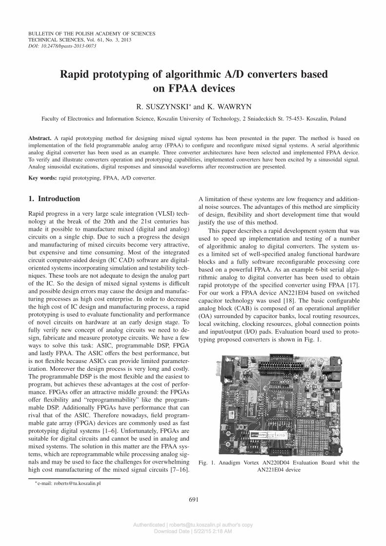
Digital outputs and sinusoidal waveforms after reconstruc-
tion of digital outputs of the iterative algorithmic 6-bit ADC
are shown in Figs. 6 and 7, respectively.
Fig. 6. Digital outputs of the iterative algorithmic 6-bit ADC
Fig. 7. Sinusoidal waveform after reconstruction digital outputs of
the iterative algorithmic 6-bit ADC
4. Serial algorithmic ADC structure
A serial algorithmic ADC performs a conversion shown in
Fig. 8. It repeatedly adjusts the subsequent input voltage VINi
and recognizes its sign. To perform the conversion in each cy-
cle a sign of the input voltage VINi is determined. If VINi is
lower than zero, the digital output ai is set to “0”, otherwise
is set to “1”. The VINi voltage is doubled and summed with
reference voltage (−1)aN−iVREF to perform the next conver-
sion. The resulting voltage VRi called residue is then passed
to the input of the next stage where becomes input voltage
VINi+1. The subsequent residue voltages VRi are expressed
by the equation (1). The procedure starts in the first stage
(i = 1) to perform N−1 bit (aN−1 − MSB) and is repeated
until the desired number of N bits have been obtained (a0 –
LSB is determined at the end).
Figure 9 shows the block diagram for the serial N -stage
converter performing conversion algorithm shown in Fig. 8.
The MSB (aN−1) is generated by the first stage 1-bit ADC.
The analog value corresponding to this bit is generated by the
first stage 1-bit DAC and is equal (−1)aN−1VREF (i.e. VREF
for aN−1 = 0 and −VREF for aN−1 = 1). The 1-bit DAC
output is summed with the output of the gain-of-two amplifi-
er. The resulting residue output voltage VR1 is then applied to
the next stage. Structure of the first N−1 stages is identical.
The N -th stage consists of the 1-bit ADC only and is used to
perform the LSB (a0).
Fig. 8. Structure of i-th stage of the serial ADC
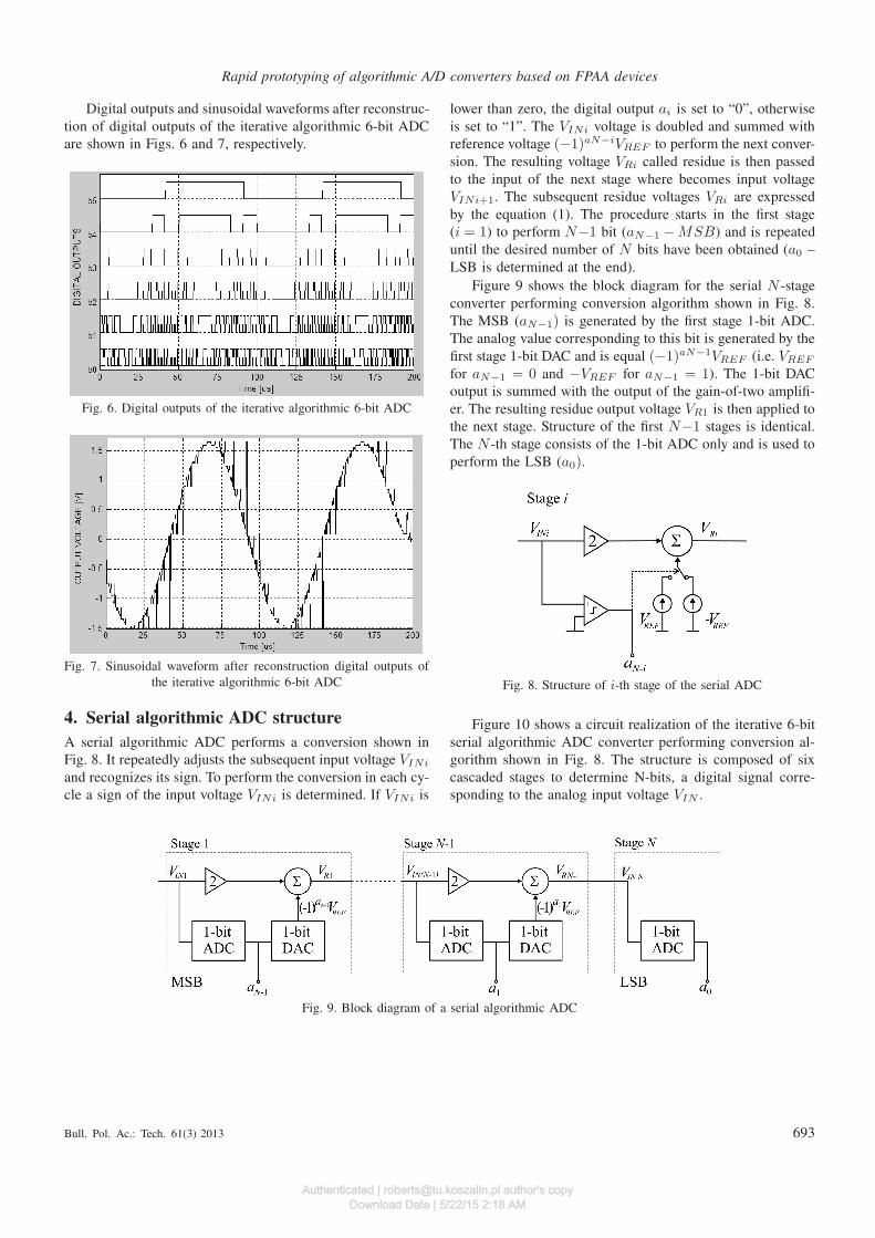
Figure 10 shows a circuit realization of the iterative 6-bit
serial algorithmic ADC converter performing conversion al-
gorithm shown in Fig. 8. The structure is composed of six
cascaded stages to determine N-bits, a digital signal corre-
sponding to the analog input voltage VIN .
Fig. 9. Block diagram of a serial algorithmic ADC
Bull. Pol. Ac.: Tech. 61(3) 2013 693
Authenticated | [email protected] author's copyDownload Date | 5/22/15 2:18 AM
R. Suszynski and K. Wawryn
Fig. 10. Circuit realization of a 6-bit serial algorithmic ADC
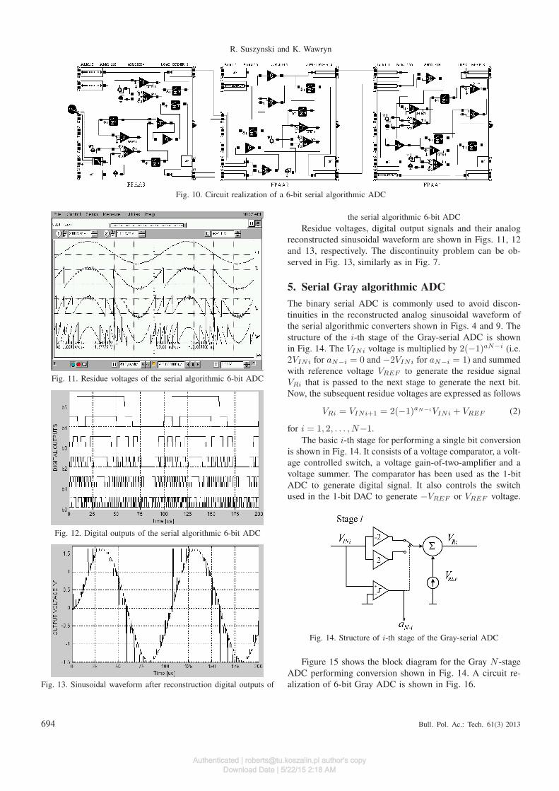
Fig. 11. Residue voltages of the serial algorithmic 6-bit ADC
Fig. 12. Digital outputs of the serial algorithmic 6-bit ADC
Fig. 13. Sinusoidal waveform after reconstruction digital outputs of
the serial algorithmic 6-bit ADC
Residue voltages, digital output signals and their analog
reconstructed sinusoidal waveform are shown in Figs. 11, 12
and 13, respectively. The discontinuity problem can be ob-
served in Fig. 13, similarly as in Fig. 7.
5. Serial Gray algorithmic ADC
The binary serial ADC is commonly used to avoid discon-
tinuities in the reconstructed analog sinusoidal waveform of
the serial algorithmic converters shown in Figs. 4 and 9. The
structure of the i-th stage of the Gray-serial ADC is shown
in Fig. 14. The VINi voltage is multiplied by 2(−1)aN−i (i.e.
2VINi for aN−i = 0 and −2VINi for aN−i = 1) and summed
with reference voltage VREF to generate the residue signal
VRi that is passed to the next stage to generate the next bit.
Now, the subsequent residue voltages are expressed as follows
VRi = VINi+1 = 2(−1)aN−iVINi + VREF (2)
for i = 1, 2, . . . , N−1.
The basic i-th stage for performing a single bit conversion
is shown in Fig. 14. It consists of a voltage comparator, a volt-
age controlled switch, a voltage gain-of-two-amplifier and a
voltage summer. The comparator has been used as the 1-bit
ADC to generate digital signal. It also controls the switch
used in the 1-bit DAC to generate −VREF or VREF voltage.
Fig. 14. Structure of i-th stage of the Gray-serial ADC
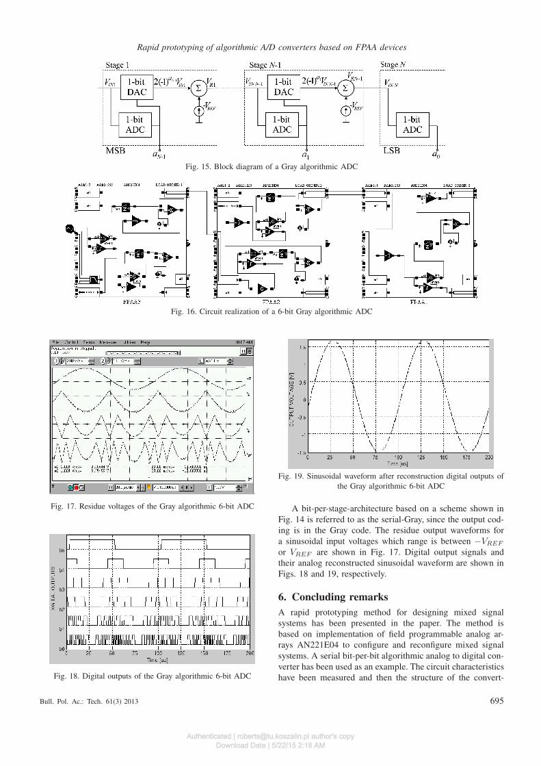
Figure 15 shows the block diagram for the Gray N -stage
ADC performing conversion shown in Fig. 14. A circuit re-
alization of 6-bit Gray ADC is shown in Fig. 16.
694 Bull. Pol. Ac.: Tech. 61(3) 2013
Authenticated | [email protected] author's copyDownload Date | 5/22/15 2:18 AM
Rapid prototyping of algorithmic A/D converters based on FPAA devices
Fig. 15. Block diagram of a Gray algorithmic ADC
Fig. 16. Circuit realization of a 6-bit Gray algorithmic ADC
Fig. 17. Residue voltages of the Gray algorithmic 6-bit ADC
Fig. 18. Digital outputs of the Gray algorithmic 6-bit ADC
Fig. 19. Sinusoidal waveform after reconstruction digital outputs of
the Gray algorithmic 6-bit ADC
A bit-per-stage-architecture based on a scheme shown in
Fig. 14 is referred to as the serial-Gray, since the output cod-
ing is in the Gray code. The residue output waveforms for
a sinusoidal input voltages which range is between −VREF
or VREF are shown in Fig. 17. Digital output signals and
their analog reconstructed sinusoidal waveform are shown in
Figs. 18 and 19, respectively.
6. Concluding remarks
A rapid prototyping method for designing mixed signal
systems has been presented in the paper. The method is
based on implementation of field programmable analog ar-
rays AN221E04 to configure and reconfigure mixed signal
systems. A serial bit-per-bit algorithmic analog to digital con-
verter has been used as an example. The circuit characteristics
have been measured and then the structure of the convert-
Bull. Pol. Ac.: Tech. 61(3) 2013 695
Authenticated | [email protected] author's copyDownload Date | 5/22/15 2:18 AM
R. Suszynski and K. Wawryn
er has been reconfigured to satisfy input specifications. The
measured output and residue waveforms of the reconfigured
converter confirm that FPAA reprogrammable devices such as
AN221E04 may be useful for rapid and low cost prototyping
of mixed signal systems.
REFERENCES
[1] R. Langwieser, C. Angerer, and A.L. Scholtz, “A UHF fron-
tend for MIMO applications in RFID”, Proc. IEEE Radio and
Wireless Symposium 1, 124–127 (2010).
[2] C. Angerer and R. Langwieser, “Flexible evaluation of RFID
system parameters using rapid prototyping”, Proc. Third IEEE
Int. Conf. on RFID 1, 42–47 (2009).
[3] P. Murphy, F. Lou, A. Sabharwal, and J.P. Frantz, “An FPGA
based rapid prototyping platform for MIMO systems”, Proc.
Thirty-Seventh Asilomar Conf. on Signals, Systems and Com-
puters 1, 900–904 (2010).
[4] M. Rice, B. Nelson, M. Padilla, and J. Havican, “On the use of
rapid prototyping for designing PCM/FM demodulators in FP-
GAs”, Proc. 2010 Int. Telemetering Conf. (ITC) 1, 10 (2010).
[5] M. Rupp, A. Burg, and E. Beck, “Rapid prototyping for wire-
less designs: the five-ones approach”, J. Signal Processing 83
(7), 1427–1444 (2003).
[6] J. Van den Keybus, B. Bolsens, K. De Brabandere, and J.
Driesen, “Using a fully digital rapid prototype platform in grid-
coupled power electronics applications”, Proc. IEEE Workshop
on Computers in Power Electronics 1, 102–111 (2004).
[7] L.S. Milor, “A tutorial Introduction to Research on Analog and
Mixed-Signal Circuit Testing”, IEEE Trans. on Circuits an d
Systems – II: Analog and Digital Signal Processing 45 (10),
1389–1407 (1998).
[8] M. Burns and G.W. Roberts, An Introduction to Mixed-signal
IC Testing and Measurement, Oxford University Press, Oxford,
2000.
[9] R. Sarahuja, V. Barcons, L. Balado, and J. Figueras, “Exper-
imental test bench for mixed-signal circuits based on FPAA
devices”, Proc. XVIII Conf. on Design of Circuit and Integrat-
ed System – DCIS 1, 344–349 (2003).
[10] R. Caponetto, A. Di Mauro, L. Fortuna, and M. Frasca, “Field
programmable analog array to implement a programmable
Chua’s circuit”, Int. J. Bifurcation and Chaos 15 (5) 1829–
1836 (2005).
[11] P.I. Yakimov, E.D. Manolov, and M.H. Hristov, “Design and
implementation of a V-f converter using FPAA”, IEEE 27th Int.
Spring Seminar on Electronics Technology 1, 126–129 (2004).
[12] T. Roberts, “Using field-programmable analog to build adapt-
able RFID readers”, RF and Microwave Technology for Design
Engineers – RFDESIGN 1, 44–48 (2004).
[13] T.R. Balen, A.Q. Andrade, F. Azais, M. Lubaszewski, and
M. Renovell, “Applying the oscillation test strategy to FPAA’s
configurable analog blocks”, J. Electronic Testing: Theory and
Applications 21, 135–146 (2005).
[14] L. Znamirowski, O.A. Palusinski, and S.B.K. Vrudhula, “Pro-
grammable analog/digital arrays in control and simulation”,
Analog Integrated Circuits and Signal Processing 39, 55–73
(2004).
[15] T. Slaughter “Fault injection emulation for field programmable
analog arrays”, Southwest Symposium on Mixed-Signal Design,
SSMSD 2003 1, 212–216 (2003).
[16] R. Suszynski and K. Wawryn, “Prototyping of higher order
Σ∆ ADC based on implementation of a FPAA”, Proc. 13th
IEEE Int. Conf. on Electronics, Circuits and Systems, ICECS
1, CD-ROM (2006).
[17] R. van de Plassche, Integrated Analog-to-digital and Digital-to-
analog Converters, Kluwer Academic Publishers, New York,
1994.
[18] “AN121E04 Field Programmable Analog Arrays – User Man-
ual, Anadigm, Inc, 2003.
[19] K. Wawryn, Switched Current Circuits, WNT Publisher, War-
saw, 1997, (in Polish).
696 Bull. Pol. Ac.: Tech. 61(3) 2013
Authenticated | [email protected] author's copyDownload Date | 5/22/15 2:18 AM