
RadSensor: x-ray detection by direct modulation of an optical probe beam
14
Approved for public release; further dissemination unlimited Lawrence Livermore National Laboratory U.S. Department of Energy Preprint UCRL-JC-154709 RadSensor: Xray Detection by Direct Modulation of an Optical Probe Beam M. E. Lowry, C. V. Bennett, S. P. Vernon, T. Bond, R. Welty, E. Behymer, H. Petersen, A. Krey, R. Stewart, N. P. Kobayashi, V. Sperry, P. Stephan, C. Reinhardt, S. Simpson, P. Stratton, R. Bionta, M. McKernan, E. Ables, L. Ott, S. Bond, J. Ayers, O. L. Landen, P. M. Bell This article was submitted to SPIE, (The International Society for Optical Engineering) International Symposium Optical Science and Technology, San Diego, California 08/04/2003 – 08/07/2003 August 1, 2003
Transcript of RadSensor: x-ray detection by direct modulation of an optical probe beam
Approved for public release; further dissemination unlimited
LawrenceLivermoreNationalLaboratory
U.S. Department of Energy
Preprint UCRL-JC-154709
RadSensor: Xray Detection by Direct Modulation of an Optical Probe Beam
M. E. Lowry, C. V. Bennett, S. P. Vernon, T. Bond, R. Welty, E. Behymer, H. Petersen, A. Krey, R. Stewart, N. P. Kobayashi, V. Sperry, P. Stephan, C. Reinhardt, S. Simpson, P. Stratton, R. Bionta, M. McKernan, E. Ables, L. Ott, S. Bond, J. Ayers, O. L. Landen, P. M. Bell
This article was submitted to SPIE, (The International Society for Optical Engineering) International Symposium Optical Science and Technology, San Diego, California 08/04/2003 – 08/07/2003
August 1, 2003
This document was prepared as an account of work sponsored by an agency of the United States Government. Neither the United States Government nor the University of California nor any of their employees, makes any warranty, express or implied, or assumes any legal liability or responsibility for the accuracy, completeness, or usefulness of any information, apparatus, product, or process disclosed, or represents that its use would not infringe privately owned rights. Reference herein to any specific commercial product, process, or service by trade name, trademark, manufacturer, or otherwise, does not necessarily constitute or imply its endorsement, recommendation, or favoring by the United States Government or the University of California. The views and opinions of authors expressed herein do not necessarily state or reflect those of the United States Government or the University of California, and shall not be used for advertising or product endorsement purposes. .
Approved for public release; further dissemination unlimited
RadSensor: Xray Detection by Direct Modulation of an Optical Probe Beam
Mark E. Lowry, Corey V. Bennett, Stephen P. Vernon, Tiziana Bond, Rebecca Welty, Elaine
Behymer, Holly Petersen, Adam Krey, Richard Stewart, Nobuhiko P. Kobayashi, Victor Sperry, Phil Stephan, Cathy Reinhardt, Sean Simpson, Paul Stratton, Rich Bionta, Mark McKernan, Elden Ables,
Linda Ott, Steven Bond, Jay Ayers, Otto L. Landen, and Perry M. Bell, Lawrence Livermore National Laboratory, P.O. Box 808, Livermore, CA 94551-0808.
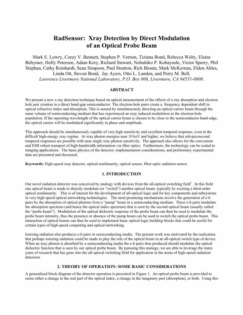
ABSTRACT
We present a new x-ray detection technique based on optical measurement of the effects of x-ray absorption and electron hole pair creation in a direct band-gap semiconductor. The electron-hole pairs create a frequency dependent shift in optical refractive index and absorption. This is sensed by simultaneously directing an optical carrier beam through the same volume of semiconducting medium that has experienced an xray induced modulation in the electron-hole population. If the operating wavelength of the optical carrier beam is chosen to be close to the semiconductor band-edge, the optical carrier will be modulated significantly in phase and amplitude. This approach should be simultaneously capable of very high sensitivity and excellent temporal response, even in the difficult high-energy xray regime. At xray photon energies near 10 keV and higher, we believe that sub-picosecond temporal responses are possible with near single xray photon sensitivity. The approach also allows for the convenient and EMI robust transport of high-bandwidth information via fiber optics. Furthermore, the technology can be scaled to imaging applications. The basic physics of the detector, implementation considerations, and preliminary experimental data are presented and discussed. Keywords: High-speed xray detector, optical nonlinearity, optical sensor, fiber-optic radiation sensor.
1. INTRODUCTION Our novel radiation detector was conceived by analogy with devices from the all-optical switching field1. In this field one optical beam is made to directly modulate (or “switch”) another optical beam, typically by exciting a third-order optical nonlinearity. This is of interest for the development of all-optical logic and for key components and subsystems in very high-speed optical networking technologies. The most promising mechanisms involve the generation of e-h pairs by the absorption of optical photons from a “pump” beam in a semiconducting medium. These e-h pairs modulate the absorption spectrum (and hence the optical index spectrum) that is seen by the second optical beam (usually called the “probe beam”). Modulation of the optical dielectric response of the probe beam can then be used to modulate the probe beam intensity, thus the presence or absence of the pump beam can be used to switch the optical probe beam. This interaction of optical beams can thus be used to implement basic optical logic building blocks that could be useful for certain types of high-speed computing and optical networking. Ionizing radiation also produces e-h pairs in semiconducting media. The present work was motivated by the realization that perhaps ionizing radiation could be made to play the role of the optical beam in an all-optical switch type of device. When an xray photon is absorbed by a semiconducting media the e-h pairs thus produced should modulate the optical dielectric function that is seen by our optical probe beam. By pursuing this analogy, we are able to leverage the many years of research that has gone into the all-optical switching field for application in the arena of high-speed radiation detection.
2. THEORY OF OPERATION: SOME BASIC CONSIDERATIONS
A generalized block diagram of the detector operation is presented in Figure 1. An optical probe beam is provided to sense either a change in the real part of the optical index, a change in the imaginary part (absorption), or both. Using this
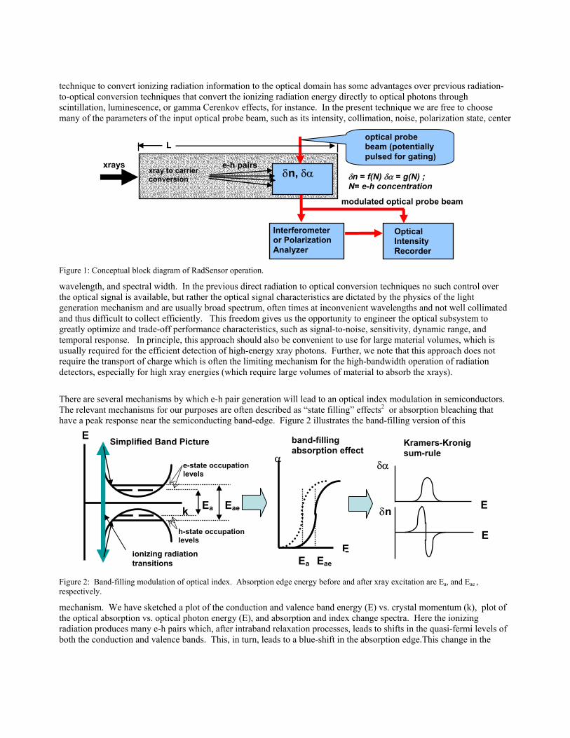
technique to convert ionizing radiation information to the optical domain has some advantages over previous radiation-to-optical conversion techniques that convert the ionizing radiation energy directly to optical photons through scintillation, luminescence, or gamma Cerenkov effects, for instance. In the present technique we are free to choose many of the parameters of the input optical probe beam, such as its intensity, collimation, noise, polarization state, center
Figure 1: Conceptual block diagram of RadSensor operation.
wavelength, and spectral width. In the previous direct radiation to optical conversion techniques no such control over the optical signal is available, but rather the optical signal characteristics are dictated by the physics of the light generation mechanism and are usually broad spectrum, often times at inconvenient wavelengths and not well collimated and thus difficult to collect efficiently. This freedom gives us the opportunity to engineer the optical subsystem to greatly optimize and trade-off performance characteristics, such as signal-to-noise, sensitivity, dynamic range, and temporal response. In principle, this approach should also be convenient to use for large material volumes, which is usually required for the efficient detection of high-energy xray photons. Further, we note that this approach does not require the transport of charge which is often the limiting mechanism for the high-bandwidth operation of radiation detectors, especially for high xray energies (which require large volumes of material to absorb the xrays).
There are several mechanisms by which e-h pair generation will lead to an optical index modulation in semiconductors. The relevant mechanisms for our purposes are often described as “state filling” effects2 or absorption bleaching that have a peak response near the semiconducting band-edge. Figure 2 illustrates the band-filling version of this
Figure 2: Band-filling modulation of optical index. Absorption edge energy before and after xray excitation are Ea, and Eae , respectively.
mechanism. We have sketched a plot of the conduction and valence band energy (E) vs. crystal momentum (k), plot of the optical absorption vs. optical photon energy (E), and absorption and index change spectra. Here the ionizing radiation produces many e-h pairs which, after intraband relaxation processes, leads to shifts in the quasi-fermi levels of both the conduction and valence bands. This, in turn, leads to a blue-shift in the absorption edge.This change in the
optical probe beam (potentially pulsed for gating)
modulated optical probe beam
δn, δα e-h pairs xray to carrier
conversion
xrays δn = f(N) δα = g(N) ; N= e-h concentration
Interferometer or Polarization Analyzer
Optical Intensity Recorder
L
α
E
band-filling absorption effect
Ea Eae
h-state occupation levels
E
k
e-state occupation levels
ionizing radiation transitions
Ea Eae
Simplified Band Picture
δα
δn E
E
Kramers-Kronig sum-rule
absorption edge produce an “absorption change” spectrum that is peaked around the band-edge. This resonant absorption change, leads to a resonant change in the index of refraction through the Kramers-Kronig sum-rule. At low pump induced carrier densities, carrier induced bleaching of the sharp excitonic absorption features found in many semiconductors is believed to be the dominant effect (see Lee, et.al.3, and Park, et. al.4) . These features result from excitonic states5-- bound e-h pairs, much like a hydrogen atom. The exciton absorption features are absorption resonances that correspond to the breaking of the e-h pair bond, and appear just below (in energy) the valence-conduction band edge. The sharpness of the absorption features leads to resonant enhancement of the optical absorption near the band edge. The primary effects of free carriers (see Ref. 3, and Gibbs6 for discussion) in the semiconductor is to screen the Coulomb interaction between the electron and hole and to occupy the electron and hole phase space states needed for the formation of bound excitons, both of which tend to prevent the absorption of light by formation of bound excitons. We expect these exciton screening effects to also dominate for the low fluence x-ray pumping case. However, as this mechanism saturates, band-filling mechanisms could then take over, greatly extending the potential dynamic range of this sensor. We further note that when the excitons are formed in quantum well structures, significant enhancement in the resonant response occurs. For one-dimensional quantum wells the enhancement is typically 3 to 4, in the case of 3-D confinement (quantum dots) enhancement can be considerably larger. The experiments that we have conducted thus far appear to be within the exciton bleaching/screening regime, so we will review some basic theory of this effect. The contribution of the exciton resonance to the optical index of refraction for all-optical switching can be represented by7
24 1 /
exex
s
nN N
απ
∆=
+ ∆ + Eq. 1
where,
max0 and probe
ex
λ λ λ λδλ∆∆ = ∆ = − Eq. 2
and exα is the peak absorption of the exciton resonance occurring at wavelength max0λ , while exδλ is the half-width at
half-maximum of the exciton absorption peak. N is the concentration of e-h pairs generated by the optical pump beam, and sN is a characteristic saturation concentration beyond which there will be little change in the index. This expression makes clear that there should be a resonant enhancement of the optical index change near the band-edge, and the magnitude of the index increases as the width of the exciton peak decreases. It also makes clear that the response will be nonlinear in N , saturating as N approaches sN . Typically sN ~ 1017-1018/cm3 , (see for instance Gibbs, Ref. 7, or Park, Ref. 4). We note an importance difference in the carrier concentration effects between the optical excitation case and the xray excitation case. In the optical case each photon produces one e-h pair. This pair can be created anywhere within the optical absorption volume (which could be as large as the entire active volume of the device). In the x-ray excitation case, for energies below a few MeV, the dominant x-ray absorption mechanism is photoelectron generation, where a single very hot photoelectron is produced. This single hot carrier interacts with the material on relatively short distance scales (microns), ultimately producing a cascade of lower energy secondary carriers with extremely short ranges , as small as 100 angstroms, in a very small volume along the track of the primary photoelectron. Since the e-h pair volume is very small and the number of pairs large, the concentration of free carriers , N, produced by a single x-ray photon can be large enough to locally cause complete bleaching of the exciton absorption along the track of the primary photoelectron. In contrast to the case of optical excitation, we expect to see no intensity threshold for x-ray induced optical modulation at x-ray energies above a few kilovolts. One can also look at this from an absorbed power perspective. The absorbed power from a single x-ray photon is much more effective at driving the index of Eq. 1 into the nonlinear regime and thus allowing us to see a phase modulation. We will discuss this point in more detail in a subsequent publication.
These all-optical switching technologies are of interest mostly for their speed. The literature of this field has many examples of devices with impulse responses in the picosecond8 and femtosecond9 regimes. Typically the rise-time of
the optically pumped index change in these devices is measurement-system-limited at 100 fs or faster, and is determined by intraband relaxation processes which are known to be in the femtosecond regime. The fall-time is determined by the trapping-times of the photo-excited carriers. Trapping times are reduced typically by the introduction of deep-gap energy levels through the incorporation of defects or impurities during growth. Okuno10 presents some recent studies of the impact of these defects and impurities, demonstrating response times (fall-times) as short as 230 fs. We note that in material without defects or impurities, this fall-time is usually in the 10’s of ns regime, sometimes approaching 1 µs.
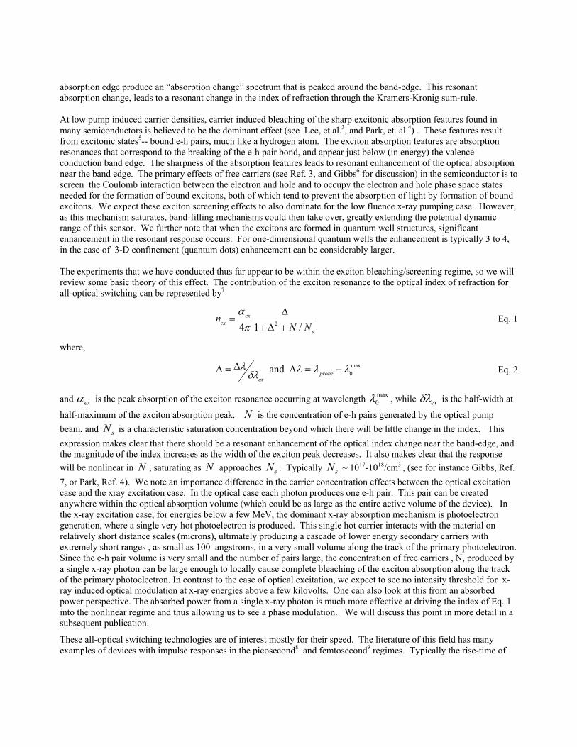
We must perform interferometry to convert the optical phase shift due to the presence of ionizing radiation created e-h pairs to an optical amplitude modulation that can then be conveniently detected. To help illustrate some of the design trade-offs and advantages of this technique we consider two examples of interferometers that could be used to detect a radiation induced optical phase shift; Figure 3 illustrates.
Figure 3. Comparison of Characteristics of Mach-Zehnder (a) and Fabry-Perot (b) Interferometers, for RadSensor applications.
In the Mach-Zehnder implementation, the optical amplitude response as a function of index change is the familiar “raised-cosine” response, while in the Fabry-Perot implementation, the response is the Airy function. If one analyzes the “small signal” response of the Mach-Zehnder approach when the device is biased at the half-power point (maximum slope), the fraction of peak modulation, what we refer to here as the “fringe-fraction”, is given by
0
p L nP
δ π δλ
= Eq. 3
where L is the distance that the optical beam propagates through the xray excitation footprint, and nδ is the average change in index seen throughout the volume probed by the optical beam. One can see that there will be an inherent degradation of the temporal response due the propagation delay of the probe beam along the distance L , given by
nLc
τ = Eq. 4
where n is the index of refraction averaged along the distance. We note that it is possible to eliminate this effect by tilting the waveguide such that the propagation speed of the optical probe matches the component of the xray beam propagation along the waveguide direction, thus phase matching the optical and xray beams.
For the Fabry-Perot interferometer operated in reflection, with its phase biased such the optical power is at the half-peak value of the Airy function resonance, and for small perturbations of the index, we find that the fringe fraction for the Fabry-Perot is given by
0.0
0.2
0.4
0.6
0.8
1.0R
ω (in units of π c/nL)
0.3
0.9R
m = 0.99
∆ωax
∆ω0
Rmax
Rmin
δn P0 P
xrays
L
R m R mincident wave
reflected wave
transmittedwave
L s
δ n
xrayP0
P
(a) (b)
L
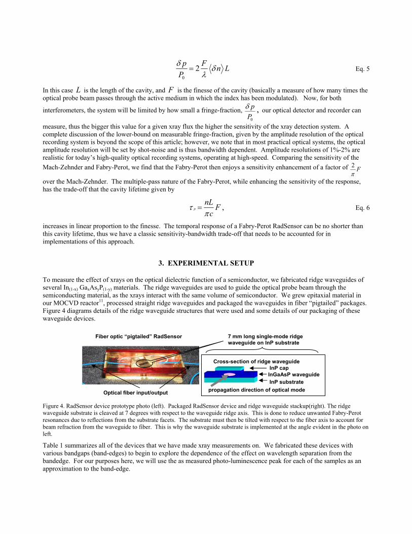
0
2p F n LP
δ δλ
= Eq. 5
In this case L is the length of the cavity, and F is the finesse of the cavity (basically a measure of how many times the optical probe beam passes through the active medium in which the index has been modulated). Now, for both
interferometers, the system will be limited by how small a fringe-fraction, 0
pP
δ , our optical detector and recorder can
measure, thus the bigger this value for a given xray flux the higher the sensitivity of the xray detection system. A complete discussion of the lower-bound on measurable fringe-fraction, given by the amplitude resolution of the optical recording system is beyond the scope of this article; however, we note that in most practical optical systems, the optical amplitude resolution will be set by shot-noise and is thus bandwidth dependent. Amplitude resolutions of 1%-2% are realistic for today’s high-quality optical recording systems, operating at high-speed. Comparing the sensitivity of the Mach-Zehnder and Fabry-Perot, we find that the Fabry-Perot then enjoys a sensitivity enhancement of a factor of 2 F
π
over the Mach-Zehnder. The multiple-pass nature of the Fabry-Perot, while enhancing the sensitivity of the response, has the trade-off that the cavity lifetime given by
pnL F
cτ
π= , Eq. 6
increases in linear proportion to the finesse. The temporal response of a Fabry-Perot RadSensor can be no shorter than this cavity lifetime, thus we have a classic sensitivity-bandwidth trade-off that needs to be accounted for in implementations of this approach.
3. EXPERIMENTAL SETUP
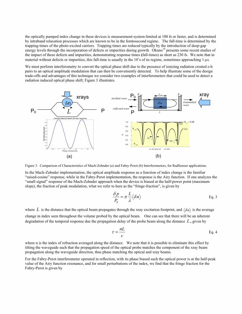
To measure the effect of xrays on the optical dielectric function of a semiconductor, we fabricated ridge waveguides of several In(1-x) GaxAsyP(1-y) materials. The ridge waveguides are used to guide the optical probe beam through the semiconducting material, as the xrays interact with the same volume of semiconductor. We grew epitaxial material in our MOCVD reactor11, processed straight ridge waveguides and packaged the waveguides in fiber “pigtailed” packages. Figure 4 diagrams details of the ridge waveguide structures that were used and some details of our packaging of these waveguide devices.
Figure 4. RadSensor device prototype photo (left). Packaged RadSensor device and ridge waveguide stackup(right). The ridge waveguide substrate is cleaved at 7 degrees with respect to the waveguide ridge axis. This is done to reduce unwanted Fabry-Perot resonances due to reflections from the substrate facets. The substrate must then be tilted with respect to the fiber axis to account for beam refraction from the waveguide to fiber. This is why the waveguide substrate is implemented at the angle evident in the photo on left.
Table 1 summarizes all of the devices that we have made xray measurements on. We fabricated these devices with various bandgaps (band-edges) to begin to explore the dependence of the effect on wavelength separation from the bandedge. For our purposes here, we will use the as measured photo-luminescence peak for each of the samples as an approximation to the band-edge.
7 mm long single-mode ridge waveguide on InP substrate
Fiber optic “pigtailed” RadSensor
InGaAsP waveguide InP cap
InP substrate
Cross-section of ridge waveguide
propagation direction of optical mode Optical fiber input/output
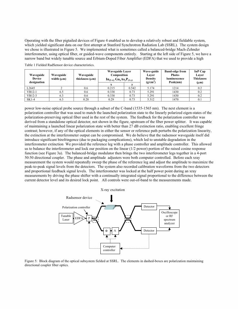
Operating with the fiber pigtailed devices of Figure 4 enabled us to develop a relatively robust and fieldable system, which yielded significant data on our first attempt at Stanford Synchrotron Radiation Lab (SSRL). The system design we chose is illustrated in Figure 5. We implemented what is sometimes called a balanced-bridge Mach-Zehnder interferometer, using optical fiber, or guided-wave components entirely. Starting at the left side of Figure 5, we have a narrow band but widely tunable source and Erbium-Doped Fiber Amplifier (EDFA) that we used to provide a high
Table 1 Fielded RadSensor device characteristics.
Waveguide Layer Composition
In(1-x) GaxAsyP(1-y)
Waveguide
Device designation
Waveguide width (µm)
Waveguide
thickness (µm)
x y
Wave-guide Layer
Density (g/cm3)
Band-edge from Photo-
luminescence Peak(nm)
InP Cap Layer
Thickness (µm)
L2645 2 0.6 0.215 0.542 5.174 1214 0.2 VB12-1 6.5 0.6 0.338 0.73 5.291 1430 0.2 VB12-3 6.3 0.6 0.338 0.73 5.291 1430 0.2 SK1-4 6.3 0.28 0.29 0.73 5.312 1470 0.1
power low-noise optical probe source through a subset of the C-band (1535-1565 nm). The next element is a polarization controller that was used to match the launched polarization state to the linearly polarized eigen-states of the polarization-preserving optical fiber used in the rest of the system. The feedback for the polarization controller was derived from a standalone optical detector, not shown in the figure, upstream of the fiber power splitter. It was capable of maintaining a launched linear polarization state with better than 27 dB extinction ratio, enabling excellent fringe contrast; however, if any of the optical elements in either the sensor or reference path perturbs the polarization linearity, the extinction at the interferometer output can be compromised. We do believe that the radsensor waveguide itself did introduce significant birefringence (due to packaging complications), which led to unstable degradation in the interferometer extinction We provided the reference leg with a phase controller and amplitude controller. This allowed us to balance the interferometer and lock our position on the linear (1/2 power) portion of the raised cosine response function (see Figure 3a). The balanced-bridge modulator then brings the two interferometer legs together in a 4-port 50:50 directional coupler. The phase and amplitude adjusters were both computer controlled. Before each xray measurement the system would repeatedly sweep the phase of the reference leg and adjust the amplitude to maximize the peak-to-peak signal levels from the detectors. The system also recorded calibration waveforms from the two detectors and proportional feedback signal levels. The interferometer was locked at the half power point during an xray measurements by driving the phase shifter with a continually integrated signal proportional to the difference between the current detector level and its desired lock point. All controls were out-of-band to the measurements made.
Figure 5: Block diagram of the optical subsystem fielded at SSRL. The elements in dashed-boxes are polarization maintaining directional coupler fiber optics.
Φ A
Tunable Laser
Oscilloscope or RF
spectrum analyzer
EDFA P
X-ray excitation
Radsensor device
Detector
Detector
Polarization controller
Computer controller
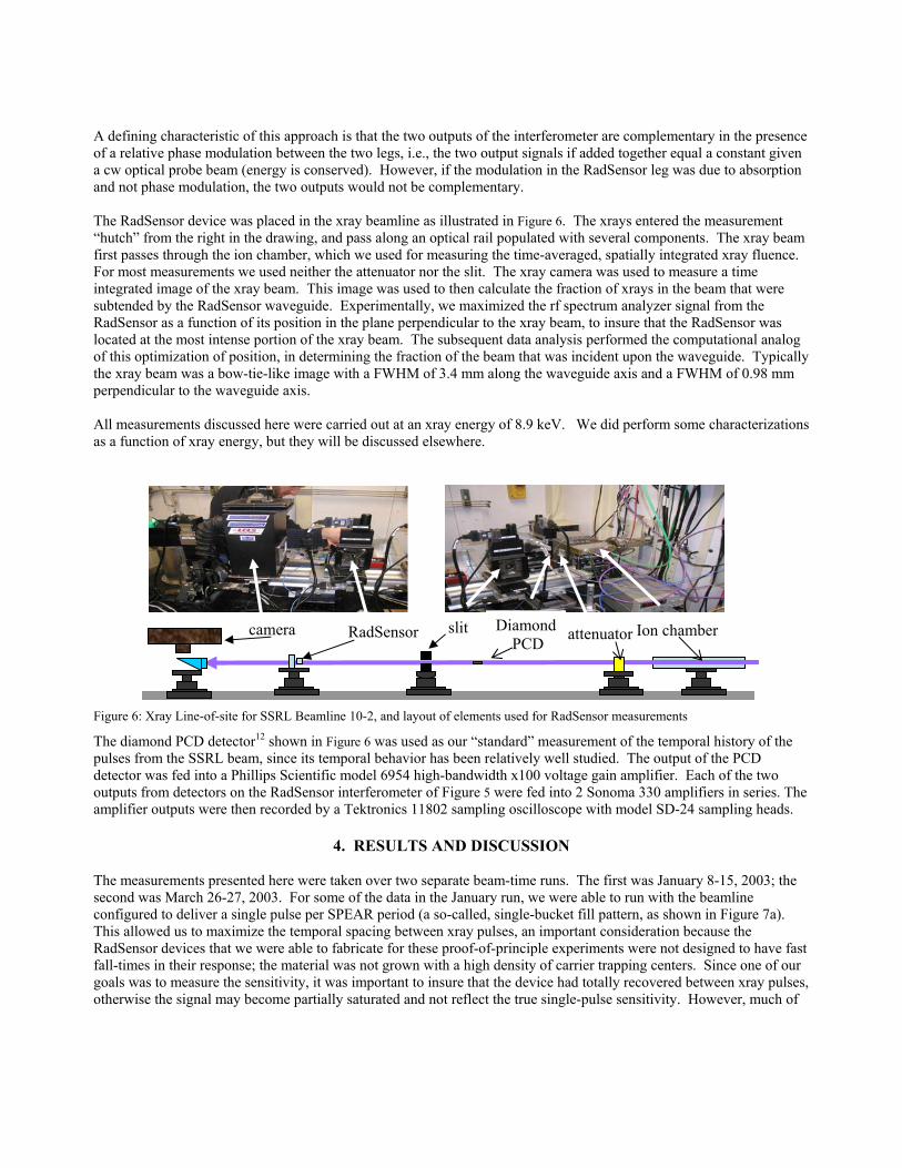
A defining characteristic of this approach is that the two outputs of the interferometer are complementary in the presence of a relative phase modulation between the two legs, i.e., the two output signals if added together equal a constant given a cw optical probe beam (energy is conserved). However, if the modulation in the RadSensor leg was due to absorption and not phase modulation, the two outputs would not be complementary. The RadSensor device was placed in the xray beamline as illustrated in Figure 6. The xrays entered the measurement “hutch” from the right in the drawing, and pass along an optical rail populated with several components. The xray beam first passes through the ion chamber, which we used for measuring the time-averaged, spatially integrated xray fluence. For most measurements we used neither the attenuator nor the slit. The xray camera was used to measure a time integrated image of the xray beam. This image was used to then calculate the fraction of xrays in the beam that were subtended by the RadSensor waveguide. Experimentally, we maximized the rf spectrum analyzer signal from the RadSensor as a function of its position in the plane perpendicular to the xray beam, to insure that the RadSensor was located at the most intense portion of the xray beam. The subsequent data analysis performed the computational analog of this optimization of position, in determining the fraction of the beam that was incident upon the waveguide. Typically the xray beam was a bow-tie-like image with a FWHM of 3.4 mm along the waveguide axis and a FWHM of 0.98 mm perpendicular to the waveguide axis. All measurements discussed here were carried out at an xray energy of 8.9 keV. We did perform some characterizations as a function of xray energy, but they will be discussed elsewhere.
Figure 6: Xray Line-of-site for SSRL Beamline 10-2, and layout of elements used for RadSensor measurements
The diamond PCD detector12 shown in Figure 6 was used as our “standard” measurement of the temporal history of the pulses from the SSRL beam, since its temporal behavior has been relatively well studied. The output of the PCD detector was fed into a Phillips Scientific model 6954 high-bandwidth x100 voltage gain amplifier. Each of the two outputs from detectors on the RadSensor interferometer of Figure 5 were fed into 2 Sonoma 330 amplifiers in series. The amplifier outputs were then recorded by a Tektronics 11802 sampling oscilloscope with model SD-24 sampling heads.
4. RESULTS AND DISCUSSION The measurements presented here were taken over two separate beam-time runs. The first was January 8-15, 2003; the second was March 26-27, 2003. For some of the data in the January run, we were able to run with the beamline configured to deliver a single pulse per SPEAR period (a so-called, single-bucket fill pattern, as shown in Figure 7a). This allowed us to maximize the temporal spacing between xray pulses, an important consideration because the RadSensor devices that we were able to fabricate for these proof-of-principle experiments were not designed to have fast fall-times in their response; the material was not grown with a high density of carrier trapping centers. Since one of our goals was to measure the sensitivity, it was important to insure that the device had totally recovered between xray pulses, otherwise the signal may become partially saturated and not reflect the true single-pulse sensitivity. However, much of
Ion chamber attenuatorcamera Diamond PCD
RadSensor slit
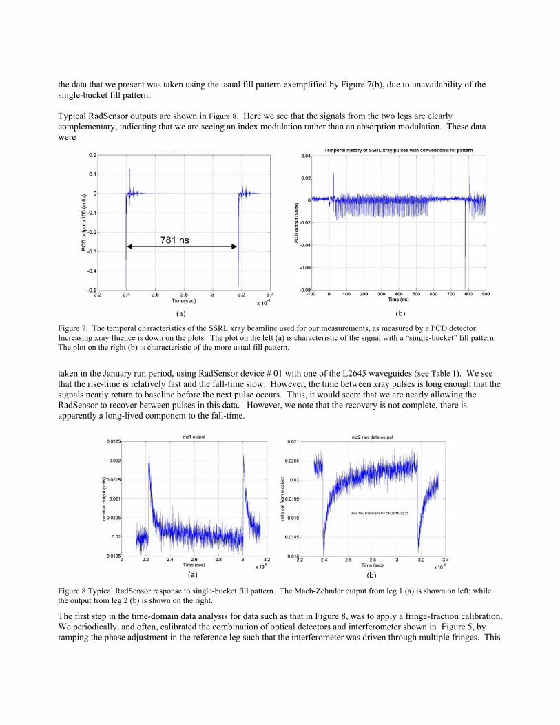
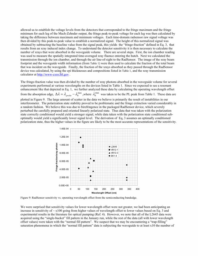
the data that we present was taken using the usual fill pattern exemplified by Figure 7(b), due to unavailability of the single-bucket fill pattern. Typical RadSensor outputs are shown in Figure 8. Here we see that the signals from the two legs are clearly complementary, indicating that we are seeing an index modulation rather than an absorption modulation. These data were
(a) (b)
Figure 7. The temporal characteristics of the SSRL xray beamline used for our measurements, as measured by a PCD detector. Increasing xray fluence is down on the plots. The plot on the left (a) is characteristic of the signal with a “single-bucket” fill pattern. The plot on the right (b) is characteristic of the more usual fill pattern.
taken in the January run period, using RadSensor device # 01 with one of the L2645 waveguides (see Table 1). We see that the rise-time is relatively fast and the fall-time slow. However, the time between xray pulses is long enough that the signals nearly return to baseline before the next pulse occurs. Thus, it would seem that we are nearly allowing the RadSensor to recover between pulses in this data. However, we note that the recovery is not complete, there is apparently a long-lived component to the fall-time.
Figure 8 Typical RadSensor response to single-bucket fill pattern. The Mach-Zehnder output from leg 1 (a) is shown on left; while the output from leg 2 (b) is shown on the right.
The first step in the time-domain data analysis for data such as that in Figure 8, was to apply a fringe-fraction calibration. We periodically, and often, calibrated the combination of optical detectors and interferometer shown in Figure 5, by ramping the phase adjustment in the reference leg such that the interferometer was driven through multiple fringes. This
781 ns
(a) (b)
allowed us to establish the voltage levels from the detectors that corresponded to the fringe maximum and the fringe minimum for each leg of the Mach-Zehnder output, the fringe peak-to-peak voltage for each leg was then calculated by taking the difference between maximum and minimum voltages. Each time-domain radsensor raw signal voltage was then divided by this peak-to-peak value to establish a normalized signal. The height of this normalized signal was obtained by subtracting the baseline value from the signal peak, this yields the “fringe-fraction” defined in Eq. 3, that results from an xray induced index change. To understand the detector sensitivity it is then necessary to calculate the number of xrays that were absorbed in the waveguide volume. There are several steps. First, the ion chamber reading was used to measure the spatially integrated time-averaged xray fluence entering the hutch. Next we calculated the transmission through the ion chamber, and through the air line-of-sight to the RadSensor. The image of the xray beam footprint and the waveguide width information (from Table 1) were then used to calculate the fraction of the total beam that was incident on the waveguide. Finally, the fraction of the xrays absorbed as they passed through the RadSensor device was calculated, by using the epi thicknesses and compositions listed in Table 1, and the xray transmission calculator at http://www-cxro.lbl.gov . The fringe-fraction value was then divided by the number of xray photons absorbed in the waveguide volume for several experiments performed at various wavelengths on the devices listed in Table 1. Since we expected to see a resonant enhancement like that depicted in Eq. 1, we further analyzed these data by calculating the operating wavelength offset from the absorption edge, max
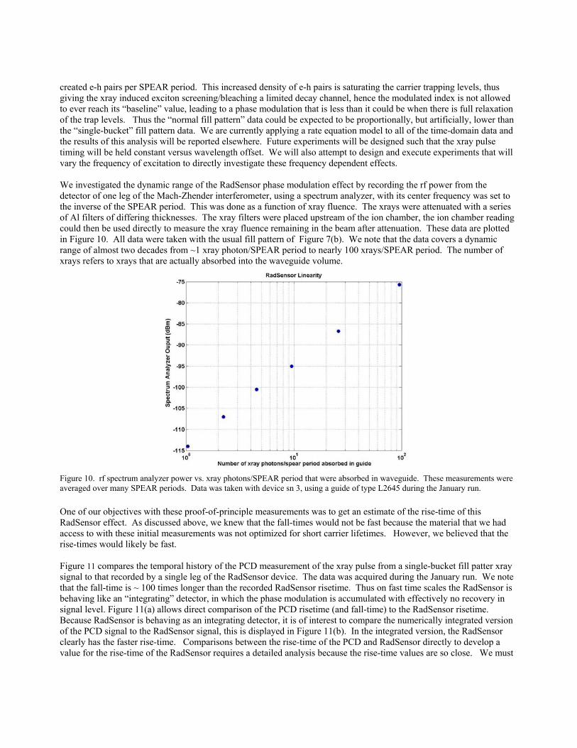
0probeλ λ λ∆ = − ,where max0λ was taken to be the PL peak from Table 1. These data are
plotted in Figure 9. The large amount of scatter in the data we believe is primarily the result of instabilities in our interferometer. The polarization state stability proved to be problematic and the fringe extinction varied considerably in a random fashion. We believe this was due to birefringence in the packaged RadSensor device, which severely perturbed the carefully prepared and oriented linearly polarized state. Thus data that was taken with the polarization state correctly conditioned would yield a stronger signal, while data taken with the polarization state conditioned sub-optimally would yield a significantly lower signal level. The derivation of Eq, 3 assumes an optimally conditioned polarization state, thus the higher values in the figure are likely to be the most accurate representations of the sensitivity.
0.00E+00
2.00E-05
4.00E-05
6.00E-05
8.00E-05
1.00E-04
1.20E-04
1.40E-04
0 50 100 150 200 250 300 350 400Wavelength Offset (nm)
Frin
ge-fr
actio
n/xr
ay p
hoto
n
L2645VB12-1VB12-3SK1-4
Figure 9: RadSensor sensitivity vs. operating wavelength offset from the semiconducting bandedge.
We were surprised that sensitivity values for lower wavelength offset were not greater, we had been anticipating an increase in sensitivity of ~ x100 going from higher values of wavelength offset to lower values based on Eq. 3 and experimental results in the literature for optical pumping (Ref. 4). However, we note that all of the L2645 data were acquired using the “single-bucket” fill pattern in the January run, while the rest of the data (all with lower wavelength offset values) were taken with the “normal fill pattern”. We suspect that we may be encountering a “trap-filling” saturation phenomena in which the “normal fill pattern” data is subjecting the waveguide to at least x10 the number of
created e-h pairs per SPEAR period. This increased density of e-h pairs is saturating the carrier trapping levels, thus giving the xray induced exciton screening/bleaching a limited decay channel, hence the modulated index is not allowed to ever reach its “baseline” value, leading to a phase modulation that is less than it could be when there is full relaxation of the trap levels. Thus the “normal fill pattern” data could be expected to be proportionally, but artificially, lower than the “single-bucket” fill pattern data. We are currently applying a rate equation model to all of the time-domain data and the results of this analysis will be reported elsewhere. Future experiments will be designed such that the xray pulse timing will be held constant versus wavelength offset. We will also attempt to design and execute experiments that will vary the frequency of excitation to directly investigate these frequency dependent effects. We investigated the dynamic range of the RadSensor phase modulation effect by recording the rf power from the detector of one leg of the Mach-Zhender interferometer, using a spectrum analyzer, with its center frequency was set to the inverse of the SPEAR period. This was done as a function of xray fluence. The xrays were attenuated with a series of Al filters of differing thicknesses. The xray filters were placed upstream of the ion chamber, the ion chamber reading could then be used directly to measure the xray fluence remaining in the beam after attenuation. These data are plotted in Figure 10. All data were taken with the usual fill pattern of Figure 7(b). We note that the data covers a dynamic range of almost two decades from ~1 xray photon/SPEAR period to nearly 100 xrays/SPEAR period. The number of xrays refers to xrays that are actually absorbed into the waveguide volume.
Figure 10. rf spectrum analyzer power vs. xray photons/SPEAR period that were absorbed in waveguide. These measurements were averaged over many SPEAR periods. Data was taken with device sn 3, using a guide of type L2645 during the January run. One of our objectives with these proof-of-principle measurements was to get an estimate of the rise-time of this RadSensor effect. As discussed above, we knew that the fall-times would not be fast because the material that we had access to with these initial measurements was not optimized for short carrier lifetimes. However, we believed that the rise-times would likely be fast. Figure 11 compares the temporal history of the PCD measurement of the xray pulse from a single-bucket fill patter xray signal to that recorded by a single leg of the RadSensor device. The data was acquired during the January run. We note that the fall-time is ~ 100 times longer than the recorded RadSensor risetime. Thus on fast time scales the RadSensor is behaving like an “integrating” detector, in which the phase modulation is accumulated with effectively no recovery in signal level. Figure 11(a) allows direct comparison of the PCD risetime (and fall-time) to the RadSensor risetime. Because RadSensor is behaving as an integrating detector, it is of interest to compare the numerically integrated version of the PCD signal to the RadSensor signal, this is displayed in Figure 11(b). In the integrated version, the RadSensor clearly has the faster rise-time. Comparisons between the rise-time of the PCD and RadSensor directly to develop a value for the rise-time of the RadSensor requires a detailed analysis because the rise-time values are so close. We must
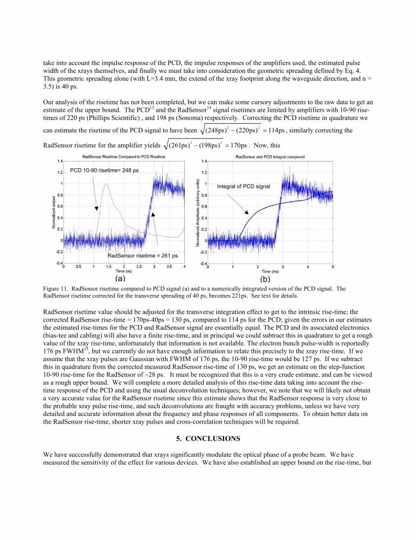
take into account the impulse response of the PCD, the impulse responses of the amplifiers used, the estimated pulse width of the xrays themselves, and finally we must take into consideration the geometric spreading defined by Eq. 4. This geometric spreading alone (with L=3.4 mm, the extend of the xray footprint along the waveguide direction, and n = 3.5) is 40 ps. Our analysis of the risetime has not been completed, but we can make some cursory adjustments to the raw data to get an estimate of the upper bound. The PCD13 and the RadSensor14 signal risetimes are limited by amplifiers with 10-90 rise-times of 220 ps (Phillips Scientific) , and 198 ps (Sonoma) respectively. Correcting the PCD risetime in quadrature we
can estimate the risetime of the PCD signal to have been 2 2(248ps) (220ps) 114ps− = , similarly correcting the
RadSensor risetime for the amplifier yields 2 2(261ps) (198ps) 170ps− = . Now, this
Figure 11. RadSensor risetime compared to PCD signal (a) and to a numerically integrated version of the PCD signal. The RadSensor risetime corrected for the transverse spreading of 40 ps, becomes 221ps. See text for details. RadSensor risetime value should be adjusted for the transverse integration effect to get to the intrinsic rise-time; the corrected RadSensor rise-time = 170ps-40ps = 130 ps, compared to 114 ps for the PCD; given the errors in our estimates the estimated rise-times for the PCD and RadSensor signal are essentially equal. The PCD and its associated electronics (bias-tee and cabling) will also have a finite rise-time, and in principal we could subtract this in quadrature to get a rough value of the xray rise-time, unfortunately that information is not available. The electron bunch pulse-width is reportedly 176 ps FWHM15, but we currently do not have enough information to relate this precisely to the xray rise-time. If we assume that the xray pulses are Gaussian with FWHM of 176 ps, the 10-90 rise-time would be 127 ps. If we subtract this in quadrature from the corrected measured RadSensor rise-time of 130 ps, we get an estimate on the step-function 10-90 rise-time for the RadSensor of ~28 ps. It must be recognized that this is a very crude estimate, and can be viewed as a rough upper bound. We will complete a more detailed analysis of this rise-time data taking into account the rise-time response of the PCD and using the usual deconvolution techniques; however, we note that we will likely not obtain a very accurate value for the RadSensor risetime since this estimate shows that the RadSensor response is very close to the probable xray pulse rise-time, and such deconvolutions are fraught with accuracy problems, unless we have very detailed and accurate information about the frequency and phase responses of all components. To obtain better data on the RadSensor rise-time, shorter xray pulses and cross-correlation techniques will be required.
5. CONCLUSIONS
We have successfully demonstrated that xrays significantly modulate the optical phase of a probe beam. We have measured the sensitivity of the effect for various devices. We have also established an upper bound on the rise-time, but
PCD 10-90 risetime= 248 ps
RadSensor risetime = 261 ps
Integral of PCD signal
(a) (b)
further measurements with faster sources will be required to fully understand the rise-time dynamics. We have demonstrated that over the range measured the effect appears to be very nearly linear in xray fluence. The best sensitivity that we have measured thus far is ~1.2x10⁻⁴ fringe-fractions/xray photon absorbed at 8.9 keV, while operating near the bandedge. However, we believe these signal levels may be artificially low due to trap filling effects that are more probable at the high average photon density excitations that were used for these measurements. Since the intended application of this detector is single-shot, these trapping effects should have no impact on reducing the signal level. Thus we expect these sensitivity values will increase when these dynamics are corrected. We anticipate significant improvements in sensitivity by employing quantum wells, and a fabry-perot cavity. Furthermore, we will be investigating the added modulation that will occur with absorption modulation, further increasing the contrast of the modulated probe. With all of these improvements we have good reason to project a single xray induced change in the probe beam power of a few percent. This should be readily detectable with existing high-bandwidth optical recording instruments down to 10 ps, and into the sub-picosecond regime with optical recording techniques that we are currently developing. Future work will focus on developing faster devices (fall-time), characterizing both the rise and fall times, the development of imaging array technology, and further characterization and improvement in the sensitivity.
ACKNOWLEDGEMENTS We gratefully acknowledge the expert assistance of John Arthur at SSRL who kindly loaned us a high-bandwidth amplifier that was used for some of these measurements and the interest and encouragement of Heinz-Dieter Nuhn, Jerry Hastings and others at SSRL. Il-Young Han grew the epi material for the L-2645 devices. This work was performed under the auspices of the U.S. Department of Energy by the University of California, Lawrence Livermore National Laboratory under contract No. W-7405-Eng-48.
REFERENCES 1 For a somewhat dated review, see C.N. Ironside, Ultra-fast all-optical switching, Contemporary Physics, Vol. 34, No.1, pp. 1-18 (1993) 2 Elsa Garmire, Nonlinear Optics in Semiconductors, Physics Today, May 1994, pp. 42-48 3 Y.H. Lee, A. Chavez-Pirson, S.W. Koch, H.M. Gibbs, S.H. Park, J.F. Morhange, A.D. Jeffery, N. Peyghambarian, L. Banyai,A.C. Gossard, and W. Weigmann, Room-temperature optical nonlinearities in GaAs, Phys. Rev. Lett. Vol. 57, pp. 2446 ( 1986 ) 4 S.H. Park, J.F. Morhange, A.D. Jeffery, R.A. Morgan, A. Chavez-Pirson, H.M. Gibbs, S.W. Koch, and N. Peyghambarian, Measurements of room-temperature band-gap-resonant optical nonlinearities of GaAs/AlGaAs multiple quantum wells and bulk GaAs., Appl. Phys. Lett. Vol. 52, no. 15, pp 1201-1203, (1988) 5 See for example pg. 189, J.M. Ziman, Principles of the Theory of Solids, Cambridge University Press (1972) 6 pg. 135, Hyatt M. Gibbs, Optical Bistability: Controlling Light with Light, Academic Press, Orlando (1985) 7 see pg. 137, Hyatt M. Gibbs, Bistability: Controlling Light with Light, Academic Press, Orlando (1985) 8 R. TakaHashi, Y. Kawamura, and H. Iwamura, Ultrafast 1.55 µm all-optical switching using low-temperature grown multiple quantum wells, Appl. Phys. Lett. Vol. 68, No. 8, pp 153 (1996) 9 K. Biermann, D. Nickel, K. Reimann, M. Woemer, T. Elsaesser, and H. Kunzel, Ultrafast optical nonlinearity of low-temperature-grown GaInAs/AlInAs quantum wells at wavelengths around 1.55 µm, Appl. Phys. Lett. Vol. 80, No. 11, pp.1936-1938 (2002). 10 T. Okuno, Y. Masumoto, Y. Sakuma, Y. Hayasaki, and H. Okamoto, Femtosecond response time in beryllium-doped low-temperature-grown GaAs/AlAs multiple quantum wells, Appl. Phys. Letts., Vol. 79, No. 6, pp764-766 (2001) 11 We also purchased some of the epi material from a commercial supplier, OEpic, Inc. Sunnyvale, CA 12 see for example, D.R. Kania, L.Pan, H. Kornblum, P. Bell, O.N. Landen, and P. Pianetta, Soft x-ray detection with diamond photoconductive detectors, Rev. Sci. Instrum. Vol. 61, No. 10 (1990) 13 from the Phillips Scientific model 6954 data sheet 14 We used two Sonoma 330 amplifiers in series and have taken the resulting amplifier ris-time to be ( )2 140 ps = 198 ps 15 private communication, John Arthur, SSRL.


![คาน[Beam or Girder] - Tumcivil](https://static.fdokumen.com/doc/165x107/63166eeac72bc2f2dd051417/beam-or-girder-tumcivil.jpg)

